
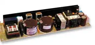


ZWS15- 5
AC/DC Open Frame Power Supply (PSU), ITE, 1 Output, 15 W, 85V AC to 265V AC, Adjustable, Fixed
- Manufacturer: TDK-LAMBDA
- Product type: AC / DC Open Frame Power Supplies
- No. of Outputs:1 Output; Power Rating (Covection Cooling):15W; Power Rating (Forced Cooling):-; Input Voltage VAC:85V AC to 265V AC; Power Supply Output Type:Adjustable, Fixed; Output Voltage - Output 1:5V;
- SVHC: No SVHC (15-Jan-2018)
- Product Range: ZWS Series
- No. of Outputs: 1 Output
- Output Power Max: 15W
- Input Voltage VAC: 85V AC to 265V AC
- Input Voltage AC Max: 265V
- Input Voltage AC Min: 85V
- Power Supply Output Type: Adjustable, Fixed
- Output Current - Output 1: 3A
- Output Current - Output 2: -
- Output Current - Output 3: -
- Output Current - Output 4: -
- Output Voltage - Output 1: 5VDC
- Output Voltage - Output 2: -
- Output Voltage - Output 3: -
- Output Voltage - Output 4: -
- Power Supply Applications: ITE
- Power Rating (Forced Cooling): -
- Power Rating (Convection Cooling): 15W
| Delivery and price | |
|---|---|
| Units per pack | 10 |
| Price | 19.49 € |
| Current stock | 10+ |
| Lead time | 30 days |
## ZWS **SERIES**

## **Single Output 5W - 300W**

**==> picture [431 x 186] intentionally omitted <==**

**----- Start of picture text -----**<br>
ZWS300<br>a 8<br>oe<br>tee a Goas) é<br>oe: j 4 aed o ZWS50<br>ZWS75AF/JA<br>(with cover option)<br>ZWS30<br>asssciiFTtisiiizsiaseeoe ten) se ‘ ey. P=<br>ZWS150AF<br>ee gn A oo Be<br>ZWS15<br>ZWS100AF<br>at % —_ ZWS5 ZWS10<br>ZWS75AF<br>ZWS50AF<br>**----- End of picture text -----**<br>


**==> picture [33 x 38] intentionally omitted <==**

**----- Start of picture text -----**<br>
2 YEARS<br>warranty<br>**----- End of picture text -----**<br>


## **■ Fea** ~~**tures**~~

## **■ Model naming method**

## **− ZWS 10 5/□□**

## CE ~~marking applicabl~~ e

- Full line-up from 5W through 300W

## Option

- Small leak current: 0.5mA max (ZWS-AF)

Blank: Molex connector, PCB type A: Molex connector, with cover

- ON/OFF control/output voltage trimmer (ZWS-AF)

J: JST connector, PCB type JA: JST connector, with cover Output voltage

- Applicable to a wide range of usages, including printers for business use and air conditioners

- Complies the harmonics current limit standard by built-in active filter (ZWS-AF)

Output power Series name

## **− ZWS 300 5/□□**

## **■ Applications**

Series Output Output name power voltage

Option

R: With remote ON/OFF control T: Vertical terminal type B: Input/output connector terminal type (Only for 12V-48V output type)

## **■ Conformity to RoHS Directive**

This means that, in conformity with EU Directive 2002/95/ EC, lead, cadmium, mercury, hexavalent chromium, and specific bromine-based flame retardants, PBB and PBDE, have not been used, except for exempted applications.

## **■ Product Line up**

**ZWS(Single Output) *In case of new design is requined, please refer to ZWS-AF series.**

5W 10W 15W 30W 50W 300W ~~aGG a~~ Output Voltage ~~eG~~ Current(Peak) Model Current(Peak) Model Current(Peak) Model Current(Peak) Model Current(Peak) Model Current(Peak) Model 3.3V ZWS5-3 ZWS10-3 ZWS15-3 ZWS30-3 ZWS50-3 ZWS300-3 1.0A(1.2) 2.0A(2.4) 3.0A(3.6) 6.0A(7.2) 10A(12) 40A(60) 5V ZWS5-5 ZWS10-5 ZWS15-5 ZWS30-5 ZWS50-5 ZWS300-5 ~~|| | | | | | | | a~~ 12V ~~GG~~ 0.42A(0.51)ZWS5-12 0.85A(1.02)ZWS10-12 1.25A(1.5) ZWS15-12 2.5A(3.0) ZWS30-12 4.3A(5.16)ZWS50-12 17A(27) ZWS300-12 ~~a~~ 15V 0.34A(0.41)ZWS5-15 ~~eeeG~~ 0.7A(0.84) ZWS10-15 1.0A(1.2) ZWS15-15 2.0A(2.4) ZWS30-15 3.5A(4.2) ZWS50-15 14A(22) ZWS300-15 24V 0.22A(0.27)ZWS5-24 0.45A(0.54)ZWS10-24 0.65A(0.78)ZWS15-24 1.3A(1.56)ZWS30-24 2.1A(2.52)ZWS50-24 9A(14) ZWS300-24 ~~aa~~ 36V ~~GGa~~ - - ~~es~~ - - ~~ss~~ - - 0.9A(1.08)ZWS30-36 1.4A(1.68)ZWS50-36 - - ~~a~~ 48V ~~GG~~ - - - - - - 0.7A(0.84)ZWS30-48 1.1A(1.32)ZWS50-48 ~~DO~~ 4.2A(6.3) ZWS300-48 **ZWS-AF(Single Output, Built-in Active Filter)** ~~a~~ 50W 75W 100W 150W ~~a~~ Output Voltage Current(Peak) ~~ee~~ Model ~~ss~~ Current(Peak) Model Current(Peak) Model Current(Peak) Model ~~a~~ 5V 10A(-) ZWS50AF-5 15A(-) ZWS75AF-5 20A(-) ZWS100AF-5 30A(-) ZWS150AF-5 ~~es~~ 12V 4.3A(5.2) ZWS50AF-12 6.3A(7.5) ZWS75AF-12 8.5A(10) ZWS100AF-12 12.5A(15) ZWS150AF-12 ~~a~~ 15V 3.5A(4.2) ZWS50AF-15 ~~ee~~ 5.0A(6.0) ZWS75AF-15 ~~es~~ 6.7A(8.0) ZWS100AF-15 10A(12) ZWS150AF-15 ~~ee es es es~~ 24V 2.1A(2.6) ZWS50AF-24 3.2A(3.8) ZWS75AF-24 4.3A(5.0) ZWS100AF-24 6.3A(7.5) ZWS150AF-24

**ZWS**

A-403

・All specifications are subject to change without notice.

**ZWS5**

## **ZWS5 Specifications**

|**ITEMS/UNITS**<br>**MODEL**<br>~~||~~<br>~~PE~~|**ITEMS/UNITS**<br>**MODEL**<br>~~||~~<br>~~PE~~|**ITEMS/UNITS**<br>**MODEL**<br>~~||~~<br>~~PE~~|**ZWS5-3**|**ZWS5-5**|**ZWS5-12**|**ZWS5-15**|**ZWS5-24**|
|---|---|---|---|---|---|---|---|
|Input<br>~~PE~~|Voltage Range<br>(*3)<br>~~PE~~|V<br>~~||~~<br><br>~~ee~~|AC85 - 265 or DC110 - 330<br>~~ee~~|||||
||Frequency<br>(*3)<br>~~PEee~~|Hz<br>~~||~~<br>~~ee~~<br>~~ee~~|47 - 440<br>~~ee~~|||||
||Efficiency (typ)<br>(*2)<br>~~ee~~<br>~~oo~~|%<br>~~ee~~<br>~~ee~~<br>~~oo~~|62<br>~~ee~~<br>~~oo~~|67<br>~~oo~~|68<br>~~oo~~||70|
||Current(100/200VAC)(typ)<br>~~oo~~|A<br>~~oo~~<br>~~ee~~|0.14 / 0.07<br>~~oo~~<br>~~ee~~|||||
||Inrush Current (100/200VAC)(typ)<br>~~oo~~<br>~~ee~~<br>~~Ls~~|A<br>~~oo~~<br>~~ee~~<br>~~ee~~|15 / 30 at Ta=25℃,cold start<br>~~oo~~<br>~~ee~~<br>~~—#~~|||||
|Output|Nominal Voltage<br>~~ee~~<br>~~#6~~<br>~~Ls~~|V<br>~~ee~~<br>~~ee~~<br>~~#6~~|3.3<br>~~ee~~<br>~~#6~~|5<br>~~#6~~|12<br>~~#6~~|15<br>~~#6~~<br>~~—#~~|24|
||Minimum Current<br>~~#6~~<br>~~Ls~~|A<br>~~#6~~|0<br>~~#6~~<br>~~—#~~|||||
||Maximum Current<br>~~#6~~<br>~~Ls~~<br>~~GG~~<br>~~RG~~|A<br>~~#6~~<br>~~GG~~<br>~~RG~~|1<br>~~#6~~<br>~~GG~~<br>G~~O~~||0.42<br>~~#6~~<br>~~GG~~<br>~~O~~|0.34<br>~~#6~~<br>~~—#~~<br>~~GG~~|0.22|
||Maximum Peak Current<br>(*1)<br>~~GG~~<br>~~RG~~|A<br>~~GG~~<br>~~RG~~|1.2<br>~~GG~~<br>G~~O~~||0.51<br>~~GG~~<br>~~O~~|0.41<br>~~GG~~|0.27|
||Maximum Power<br>~~RG~~<br>~~PO~~|W<br>~~RG ~~<br>~~PO~~|3.3<br> G<br>~~PO~~—|5.0<br>G~~O~~<br>—~~SE~~|5.04<br>~~O~~<br>~~SE~~|5.1<br>~~SE~~|5.28|
||Maximum Peak Power<br>(*1)<br>~~PO~~<br>~~GQ~~<br>~~RG~~|W<br>~~PO~~<br>~~GQ~~<br>~~RG~~|3.96<br>~~PO~~—<br>~~GQ~~<br>G|6.0<br>—~~SE~~<br>~~GQ~~<br>G~~G~~|6.048<br>~~SE~~<br>~~GQ~~<br>~~G~~|6.12<br>~~SE~~<br>~~GQ~~|6.336|
||Maximum Line Regulation(*4)(*10)<br>~~GQ~~<br>~~RG~~|mV<br>~~GQ~~<br>~~RG~~|20<br>~~GQ~~<br>G~~G~~||48<br>~~GQ~~<br>~~G~~|60<br>~~GQ~~|96|
||Maximum Load Regulation(*5)(*10)<br>~~RG~~<br>~~G~~|mV<br>~~RG ~~<br>~~G~~|40<br> G~~G~~<br>~~GQ~~||96<br>~~G~~<br>~~Q~~|120<br>~~Q~~|150|
||Temperature Coefficient<br>(*6)<br>~~G~~|mV<br>~~G~~|60<br>~~GQ~~||140<br>~~Q~~|180<br>~~Q~~|280|
||Maximum Ripple & Noise(0 to +60℃) (*10) <br>~~RG~~<br>~~ee~~|mVp-p<br><br>~~e~~|120<br>G~~G~~||150<br>~~G~~<br>|||200<br>||
||Maximum Ripple & Noise(-10 to 0℃) (*10) <br>~~RG ~~<br>~~G~~<br>~~ee~~|mVp-p<br> <br>~~G~~<br>~~e~~<br>~~ee~~|160<br> G~~G~~<br>~~GG~~<br>~~ee~~||180<br>~~G~~<br>~~G~~<br>|||200<br>||
||Hold-upTime(100VAC)(typ)<br>(*2)<br>~~G~~<br>~~ee~~|ms<br>~~G~~<br>~~e~~<br>~~ee~~<br>~~ee~~|17 at 5W, Ta=25℃<br>~~GG~~<br>|<br>~~ee~~<br>~~ee~~|||||
||Voltage Adjustable Range<br>~~ee~~<br>~~ee~~|~~e~~<br>~~ee~~<br>~~ee~~<br>~~ee~~|+/-10%<br>|<br>~~ee~~<br>~~ee~~|||||
|Function|Over Current Protection<br>(*7)<br>~~ee~~<br>~~ee~~|~~ee~~<br>~~ee~~<br>~~ee~~<br>~~ee~~|>125%<br>~~ee~~<br>~~ee~~|||||
||Over Voltage Protection<br>(*8)<br>~~ee~~<br>~~ee~~|~~ee~~<br>~~ee~~<br>~~ee~~|>140%<br>~~ee~~|||||
||Parallel Operation<br>~~ee~~<br>~~ee~~|~~ee~~<br>~~ee~~<br>~~ee~~<br>~~ee~~|-<br>~~ee~~<br>~~ee~~|||||
||Series Operation<br>(*9)<br>~~ee~~<br>~~ee~~|~~ee~~<br>~~ee~~<br>~~ee~~<br>~~ee~~|Possible<br>~~ee~~<br>~~ee~~|||||
|Environment|OperatingTemperature<br>(*11)<br>~~ee~~<br>~~ee~~|℃<br>~~ee~~<br>~~ee~~<br>~~ee~~<br>~~ee~~<br>~~ee~~|-10 to +50: 100%, +60: 70%<br>~~ee~~<br>~~ee~~<br>~~ee~~|||||
||Storage Temperature<br>~~ee~~<br>~~ee~~|℃<br>~~ee~~<br>~~ee~~<br>~~ee~~<br>~~ee~~|-30 to +85<br>~~ee~~<br>~~ee~~|||||
||OperatingHumidity<br>~~ee~~<br>~~ee~~|%RH<br>~~ee~~<br>~~ee~~<br>~~ee~~<br>~~ee~~|30 - 90<br>~~ee~~<br>~~ee~~|||||
||Storage Humidity<br>~~ee~~<br>~~ee~~|%RH<br>~~ee~~<br>~~ee~~<br>~~ee~~<br>~~ee~~|10 - 95<br>~~ee~~<br>~~ee~~|||||
||Vibration<br>~~ee~~<br>~~ee~~|~~ee~~<br>~~ee~~<br>~~ee~~<br>~~ee~~|10-55Hz (sweep 1min) less than 19.6m/s² X, Y, Z 1h each<br>~~ee~~<br>~~ee~~|||||
||Shock<br>~~ee~~<br>~~ee~~|~~ee~~<br>~~ee~~<br>~~ee~~<br>~~ee~~|Less than 196.1m/s²<br>~~ee~~<br>~~ee~~|||||
||Cooling<br>~~ee~~<br>~~ee~~|~~ee~~<br>~~ee~~<br>~~ee~~<br>~~ee~~|Convection cooling<br>~~ee~~<br>~~ee~~|||||
|Isolation|Withstand Voltage<br>~~ee~~<br>~~ee~~|~~ee~~<br>~~ee~~<br>~~ee~~<br>~~ee~~|Input - FG: 2kVAC (20mA), Input - Output: 3kVAC (20mA), Output - FG: 500VAC (100mA) for 1min<br>~~ee~~<br>~~ee~~|||||
||<br>Isolation Resistance<br>~~ee~~<br>~~ee~~|~~ee~~<br>~~ee~~<br>~~ee~~<br>~~ee~~|More than 100MΩat 25℃and 70%RH Output - FG 500VDC<br>~~ee~~<br>~~ee~~|||||
|Standards|SafetyStandards<br>~~ee~~<br>~~ee~~|~~ee~~<br>~~ee~~<br>~~ee~~<br>~~ee~~|Approved by UL60950-1,CSA C22.2 No.60950-1,EN60950-1, Built to meet DENAN<br>~~ee~~<br>~~ee~~|||||
||<br>EMI<br>~~ee~~|~~ee~~<br>~~ee~~<br>~~ee~~|Built to meet EN55022-B, FCC-ClassB, VCCI-B<br>~~ee~~<br>~~ee~~|||||
|Mechanical|Weight(typ)<br>~~ee~~<br>~~ee~~|g<br>~~ee~~<br>~~ee~~<br>~~ee~~<br>ee|120<br>~~ee~~<br>ee|||||
||<br>Size (W x H x D)<br>~~ee~~<br>~~ee~~|mm<br>~~ee~~<br>~~ee~~<br>ee|45 x 21 x 98<br>ee|||||


(*1) Operating time at peak output is less than 10 seconds. (Duty=0.35)

**●Recommended EMC Filter**

(*2) At 100VAC and maximum output current, Ta=25 ℃ .

(*3) For cases where conformance to various safety specs (UL,CSA) are required, to be described as 100 - 240VAC, 50/60Hz on name plate.

(*4) From 85 - 265VAC and constant load.

(*5) From min load - full load (maximum power) and constant input voltage.

- (*6) From -10 to +50 ℃ constant input voltage and load.

- (*7) Current limiting with automatic recovery.

Avoid to operate over load or dead short for 30 seconds.

(*8) Over voltage clamping by zener diode.

RSEL-20R5W **Please refer to "TDK-Lambda EMC Filters" catalog.**

(*9) Refer to instruction manual.

(*10) Please refer to Fig A for measurement of line & load regulation and ripple voltage.

(*11) At standard mounting method, Fig B.

**==> picture [299 x 101] intentionally omitted <==**

**----- Start of picture text -----**<br>
Measurement point<br>for Vripple L<br>|<br>C2 C1<br>CN2<br>a | COMPONENT SIDE i PCB<br>L:150mmAWG#22 } ae<br>C1:Elec.Cap 100uF Measurement point for Vo, Fig.B<br>C2:Film Cap  0.1uF Line/Load Regulation.<br>Bandwidth of scope:100MHz<br>Fig.A<br>**----- End of picture text -----**<br>


**ZWS**

A-404

・All specifications are subject to change without notice.

**ZWS5**

## **Outline Drawing**

## **【ZWS5(Standard : MOLEX connector)】**

**==> picture [282 x 450] intentionally omitted <==**

**----- Start of picture text -----**<br>
R2  -4 91±0.5<br>SEE   NOTE  A<br>CN1 COMPONENT  SIDE<br>8 L<br>INPUT<br>5 N<br>CN2<br>1 FG + 12<br>OUTPUT - 34<br>VR1<br>3.5<br>9 1 SEE   NOTE  D<br>98±1<br>(unit : mm)<br>【ZWS5(/J : JST connector)】(/J : JST connector)】】<br>R2  -4 91±0.5<br>SEE   NOTE   A<br>CN1 COMPONENT   SIDE<br>1 L<br>INPUT<br>3<br>N<br>SEE   NOTE   E<br>CN2<br>5 FG<br>OUTPUT + 43<br>SEE   NOTE   E - 21<br>VR1<br>3.5<br>91 SEE   NOTE   D<br>98±1<br>1± 0.5<br>45 ±<br>38<br>26.75 3.5 NAME PLATE 4.5 13.7<br>1<br>21<br>LEAD  CUT LESS   THAN  3mm<br>1± 0.5<br>45 ±<br>38<br>28 NAME PLATE<br>4.5 13.7<br>3.5<br>1<br>21<br>LEAD  CUT LESS   THAN 3<br>**----- End of picture text -----**<br>


## **【ZWS5(/J : JST connector)】(/J : JST connector)】】**

**==> picture [42 x 9] intentionally omitted <==**

**----- Start of picture text -----**<br>
(unit : mm)<br>**----- End of picture text -----**<br>


|CONNECTORS USED:|CONNECTORS USED:|CONNECTORS USED:|CONNECTORS USED:|
|---|---|---|---|
|PART DESCRIPTION<br>PIN HEADER (INPUT SIDE CN1)<br>|PART NAME<br>6373-A8A<br>(102)52<br>6373-A04A-|MANUFACT.<br>MOLEX<br>|QTY<br>1<br>|
|PIN HEADER (OUTPUT SIDE CN2)<br>102<br>MOLEX<br>1<br>MATCHING HOUSINGS & PINS (NOT INCLUDED WITH THE PRODUCT):<br>SOCKET HOUSING (CN1)<br>7880-08B<br>MOLEX<br>1||||
|SOCKET HOUSING (CN2)|7880-04B|MOLEX|1|
|TERMINAL PINS (CN1,2)<br>7879-2-P912<br>MOLEX<br>7<br>HAND CRIMPING TOOL : 11-01-0037 OR JHTR2262A  MANUFACTURER : MOLEX<br>PCB MATERIAL||||


## NOTES

- A: THE 2- Φ 3.5 HOLE ARE CUSTOMER CHASSIS MOUNTING HOLES. ALL MUST BE SCREWED IN ORDER TO CONFORM THE VIBRATION SPEC.

- B: MODEL NAME, MAXIMUM OUTPUT POWER, NOMINAL OUTPUT VOLTAGE, MAXIMUM OUTPUT CURRENT, MAXIMUM PEAK OUTPUT CURRENT ARE SHOWN HERE IN ACCORDANCE WITH THE SPECIFICATIONS.

- C: COUNTRY OF MANUFACTURE WILL BE SHOWN HERE.

- D: TO KEEP THE DISTANCE MORE THAN 4mm BETWEEN PCBOARD EDGE AND CUSTOMER CHASSIS.

- E: FOR I/O TERMINAL CONNECTIONS, PLEASE USE THE RECOMMENDED CONNECTORS. MOLEX SOCKET HOUSING TERMINAL PINS ARE DIFFICULT TO PROCURE IN JAPAN. WHEN MANU-FACTURING IN JAPAN, PLEASE USE “ /J ” MODELS FOR JST CONNECTORS.

## CONNECTORS USED:

|CONNECTORS USED:||||
|---|---|---|---|
|PART DESCRIPTION|PART NAME|MANUFACT.|QTY|
|PIN HEADER (INPUT SIDE CN1)<br>B3P-5-VH<br>J.S.T.<br>1<br>PIN HEADER (OUTPUT SIDE CN2)<br>B4B-XH-A<br>J.S.T.<br>1<br>MATCHING HOUSINGS & PINS (NOT INCLUDED WITH THE PRODUCT):||||
|SOCKET HOUSING (CN1)<br>SOCKET HOUSING (CN2)<br>TERMINAL PINS (CN1)|VHR-5N<br>XHP-4<br>SVH-21T-P1.1<br>|J.S.T.<br>J.S.T.<br>J.S.T.|1<br>1<br>3|
|TERMINAL PINS (CN2)|BXH-001T-<br>P0.6<br>OR<br>SXH-001T-<br>P06|J.S.T.|4|
|.<br>HAND CRIMPING TOOL : YC-160R CN1 MANUFACTURER: J.S.T.<br>: YC-110R CN2 MANUFACTURER: J.S.T.<br>: YRS-110 CN2 MANUFACTURER: J.S.T.||||


## NOTES

- A: THE 2- Φ 3.5 HOLE ARE CUSTOMER CHASSIS MOUNTING HOLES. ALL MUST BE SCREWED IN ORDER TO CONFORM THE VIBRATION SPEC.

- B: MODEL NAME, MAXIMUM OUTPUT POWER, NOMINAL OUTPUT VOLTAGE, MAXIMUM OUTPUT CURRENT, MAXIMUM PEAK OUTPUT CURRENT ARE SHOWN HERE IN ACCORDANCE WITH THE SPECIFICATIONS.

- C: COUNTRY OF MANUFACTURE WILL BE SHOWN HERE.

- D: TO KEEP THE DISTANCE MORE THAN 4mm BETWEEN PCBOARD EDGE AND CUSTOMER CHASSIS.

- E: PIN-ORDER OF CONNECTORS CN1 & CN2 ARE OPPOSITE TO PIN-ORDER ON LEGEND.

## **【ZWS5(/JA : With cover)】**

**==> picture [285 x 214] intentionally omitted <==**

**----- Start of picture text -----**<br>
NAME  PLATE<br>SEE  NOTE  A<br>SEE  NOTE  B<br>SEE<br>NOTE  B<br>CN1<br>INPUT 1L<br>3N<br>5FG CN2<br>+ 43 OUTPUT<br>- 21<br>32±1 15.3<br>5 108±0.5<br>(101)<br>103.7<br>118±1<br>SEE  NOTE  B SEE  NOTE  B<br>SEE  NOTE  A<br>5 108±0.5<br>0.530± 3.5 152±<br>26 28 26<br>11 15.7 VR1<br>(6.5)<br>10<br>3.5<br>16<br>**----- End of picture text -----**<br>


|CONNECTORS USED:|CONNECTORS USED:||||
|---|---|---|---|---|
||PART DESCRIPTION<br>PART NAME|MANUFACT.|QTY||
||PIN HEADER (INPUT SIDE CN1)<br>B3P-5-VH|J.S.T.|1||
||PIN HEADER (OUTPUT SIDE CN2)<br>B4B-XH-A|J.S.T.|1||
|MATCHING HOUSINGS & PINS (NOT INCLUDED WITH THE PRODUCT):|||||
||SOCKET HOUSING (CN1)<br>VHR-5N|J.S.T.|1||
||SOCKET HOUSING (CN2)<br>XHP-4|J.S.T.|1||
||TERMINAL PINS (CN1)<br>SVH-21T-P1.1|J.S.T.|3||
||BXH-001T-||||
||P0.6||||
||TERMINAL PINS (CN2)<br>OR|J.S.T.|4||
||SXH-001T-||||
||P0.6||||
||HAND CRIMPING TOOL : YC-160R CN1||||
||: YC-110R OR YRS-110 CN2||||
||MANUFACTURER : J.S.T.||||
|NOTES|||||
|A: M3 EMBOSSED TAPPED & COUNTERSUNK HOLES (6) ARE FOR|||||
||CUSTOMER CHASSIS MOUNTING.||||


- B: φ 3.5 HOLES (2) AND R1.75 SLOT HOLES (2) FOR CUSTOMER CHASSIS MOUNTING.

- C: MODEL NAME, NOMINAL OUTPUT VOLTAGE, MAXMUM OUTPUT CURRENT, MAXIMUM PEAK OUTPUT CURRENT AND COUNTRY OF MANUFACTURE ARE SHOWN HERE IN ACCORDANCE WITH THE SPECIFICATIONS.

(unit : mm)

**==> picture [32 x 25] intentionally omitted <==**

**----- Start of picture text -----**<br>
ZWS<br>**----- End of picture text -----**<br>


A-405

・All specifications are subject to change without notice.

**ZWS10**

## **ZWS10 Specifications**

|**ITEMS/UNITS**<br>**MODEL**|**ITEMS/UNITS**<br>**MODEL**|**ITEMS/UNITS**<br>**MODEL**|**ZWS10-3**|**ZWS10-5**|**ZWS10-12**|**ZWS10-15**|**ZWS10-24**|
|---|---|---|---|---|---|---|---|
|Input|Voltage Range<br>(*3)<br>~~PO~~|V<br>~~||~~|AC85 - 265 or DC110 - 330|||||
||Frequency<br>(*3)<br>~~PO~~<br>~~ee~~|Hz<br>~~||~~<br>~~ee~~|47 - 440|||||
||Efficiency (typ)<br>(*2)<br>~~ee~~<br>~~a~~|%<br>~~ee~~|62|70||71||
||Current(100/200VAC)(typ)<br>~~a~~<br>~~——~~|A<br>~~——~~|0.30 / 0.15|||||
||Inrush Current (100/200VAC)(typ)<br>~~——~~<br>~~PO~~|A<br>~~——~~|15 / 30 at Ta=25℃,cold start|||||
|Output|Nominal Voltage<br>~~——~~<br>~~PO~~<br>~~ee~~|VDC<br>~~——~~<br>~~ee~~|3.3<br>~~ee~~|5<br>~~ee~~|12<br>~~ee~~|15<br>~~ee~~|24|
||Minimum Current<br>~~ee~~<br>~~PO~~|A<br>~~ee~~|0<br>~~ee~~|||||
||Maximum Current<br>~~ee~~<br>~~PO~~<br>~~GO~~|A<br>~~ee~~<br>~~GO~~|2<br>~~ee~~<br>~~GO~~||0.85<br>~~ee~~<br>~~GO~~|0.7<br>~~ee~~<br>~~GO~~|0.45|
||Maximum Peak Current<br>(*1)<br>~~GO~~<br>~~a~~|A<br>~~GO~~|2.4<br>~~GO~~||1.02<br>~~GO~~|0.84<br>~~GO~~|0.54|
||Maximum Power<br>~~a~~<br>~~GG~~|W<br>~~GG~~|6.6<br>~~GG~~|10.0<br>~~GG~~|10.2<br>~~GG~~<br>~~(~~|10.5<br>~~GG~~<br>~~(~~|10.8<br>~~(~~|
||Maximum Peak Power<br>(*1)<br>~~GG~~<br>~~DD~~|W<br>~~GG~~<br>~~DD~~|7.92<br>~~GG~~<br>~~DD~~|12.0<br>~~GG~~<br>~~DD~~|12.24<br>~~GG~~<br>~~DD~~<br>~~(~~|12.6<br>~~GG~~<br>~~DD~~<br>~~(~~|12.96<br>~~(~~|
||Maximum Line Regulation(*4)(*10)<br>~~DD~~<br>~~ee~~|mV<br>~~DD~~<br>~~ee~~|20<br>~~DD~~<br>~~ee~~||48<br>~~DD~~<br>~~(~~<br>~~ee~~|60<br>~~DD~~<br>~~(~~<br>~~ee~~|96<br>~~(~~|
||Maximum Load Regulation(*5)(*10)<br>~~ee~~<br>~~G~~|mV<br>~~ee~~<br>~~G~~|40<br>~~ee~~<br>~~GO~~||96<br>~~ee~~<br>~~O~~|120<br>~~ee~~<br>~~O~~|150|
||Temperature Coefficient<br>(*6)<br>~~G~~<br>~~e~~|mV<br>~~G~~<br>~~e~~|60<br>~~GO~~<br>~~ee~~||140<br>~~O~~<br>~~e~~|180<br>~~O~~<br>~~e~~|280|
||Maximum Ripple & Noise(0 to +60℃) (*10) <br>~~e~~<br>~~a~~|mVp-p<br>~~e~~|120<br>~~ee~~||150<br>~~e~~||200|
||Maximum Ripple & Noise(-10 to 0℃) (*10) <br>~~e~~<br>~~a~~<br>~~D~~|mVp-p<br>~~e~~<br>~~D~~|160<br>~~ee~~<br>~~DD~~||180<br>~~e~~<br>~~D~~||200|
||Hold-upTime(100VAC)(typ)<br>(*2)<br>~~D~~<br>~~ee~~|ms<br>~~D~~<br>~~ee~~<br>~~ee~~|17 at 100VAC, 10W, Ta=25℃<br>~~DD~~<br>~~ee~~|||||
||Voltage Adjustable Range<br>~~ee~~<br>~~ee~~|~~ee~~<br>~~ee~~<br>~~ee~~|+/-10%<br>~~ee~~|||||
|Function|Over Current Protection<br>(*7)<br>~~ee~~<br>~~ee~~|~~ee~~<br>~~ee~~<br>~~ee~~|>125%<br>~~ee~~|||||
||Over Voltage Protection<br>(*8)<br>~~ee~~<br>~~ee~~|~~ee~~<br>~~ee~~<br>~~ee~~|>140%<br>~~ee~~|||||
||Parallel Operation<br>~~ee~~<br>~~ee~~|~~ee~~<br>~~ee~~<br>~~ee~~|-<br>~~ee~~|||||
||Series Operation<br>(*9)<br>~~ee~~<br>~~ee~~|~~ee~~<br>~~ee~~<br>~~ee~~|Possible<br>~~ee~~|||||
|Environment|OperatingTemperature<br>(*11)<br>~~ee~~<br>~~ee~~|℃<br>~~ee~~<br>~~ee~~<br>~~ee~~|-10 to +50 : 100%, +60 : 70%<br>~~ee~~|||||
||Storage Temperature<br>~~ee~~<br>~~ee~~|℃<br>~~ee~~<br>~~ee~~<br>~~ee~~<br>~~ee~~|-30 to +85<br>~~ee~~<br>~~ee~~|||||
||OperatingHumidity<br>~~ee~~<br>~~ee~~|%RH<br>~~ee~~<br>~~ee~~<br>~~ee~~<br>~~ee~~|30 - 90<br>~~ee~~<br>~~ee~~|||||
||Storage Humidity<br>~~ee~~<br>~~ee~~|%RH<br>~~ee~~<br>~~ee~~<br>~~ee~~<br>~~ee~~|10 - 95<br>~~ee~~<br>~~ee~~|||||
||Vibration<br>~~ee~~<br>~~ee~~|~~ee~~<br>~~ee~~<br>~~ee~~<br>~~ee~~|10-55Hz (sweep 1min) less than 19.6m/s² X, Y, Z 1h each<br>~~ee~~<br>~~ee~~|||||
||Shock<br>~~ee~~<br>~~ee~~|~~ee~~<br>~~ee~~<br>~~ee~~<br>~~ee~~|Less than 196.1m/s²<br>~~ee~~<br>~~ee~~|||||
||Cooling<br>~~ee~~<br>~~ee~~|~~ee~~<br>~~ee~~<br>~~ee~~<br>~~ee~~|Convection cooling<br>~~ee~~<br>~~ee~~|||||
|Isolation|Withstand Voltage<br>~~ee~~<br>~~ee~~|~~ee~~<br>~~ee~~<br>~~ee~~|Input - FG : 2kVAC (20mA), Input - Output : 3kVAC (20mA), Output - FG : 500VAC (100mA) for 1min<br>~~ee~~|||||
||<br>Isolation Resistance<br>~~ee~~<br>~~ee~~|~~ee~~<br>~~ee~~<br>~~ee~~|More than 100MΩat 25℃and 70%RH Output - FG 500VDC<br>~~ee~~|||||
|Standards|SafetyStandards<br>~~ee~~<br>~~ee~~|~~ee~~<br>~~ee~~<br>~~ee~~|Approved by UL60950-1, CSA C22.2 No.60950-1, EN60950-1 Built to meet DENAN.<br>~~ee~~|||||
||<br>EMI<br>~~ee~~|~~ee~~<br>~~ee~~<br>~~ee~~|Built to meet EN55022-B, FCC-ClassB, VCCI-B<br>~~ee~~<br>~~ee~~|||||
|Mechanical|Weight(typ)<br>~~ee~~<br>~~ee~~|g<br>~~ee~~<br>~~ee~~<br>~~ee~~<br>~~ee~~|120<br>~~ee~~<br>~~ee~~|||||
||<br>Size (W x H x D)<br>~~ee~~<br>~~ee~~|mm<br>~~ee~~<br>~~ee~~<br>~~ee~~|50 x 21 x 105<br>~~ee~~|||||


- (*1) Operating time at peak output is less than 10 seconds. (Duty=0.35)

**==> picture [104 x 9] intentionally omitted <==**

**----- Start of picture text -----**<br>
●Recommended EMC Filter<br>**----- End of picture text -----**<br>


- (*2) At 100VAC and maximum output current, Ta=25 ℃ .

- (*3) For cases where conformance to various safety specs (UL, CSA) are required, to be described as 100 - 240VAC, 50/60Hz on name plate.

- (*4) From 85 - 265VAC and constant load.

- (*5) From Min load - Full load (maximum power) and constant input voltage.

- (*6) From -10 to +50 ℃ constant input voltage and load.

- (*7) Current limiting with automatic recovery.

   - Avoid to operate over load or dead short for 30 seconds.

- (*8) Over voltage clamping by zener diode.

RSEL-20R5W **Please refer to "TDK-Lambda EMC Filters" catalog.**

- (*9) Refer to instruction manual.

- (*10) Please refer to Fig A for measurement of line & load regulation and ripple voltage.

- (*11) At standard mounting method, Fig B.

**==> picture [299 x 101] intentionally omitted <==**

**----- Start of picture text -----**<br>
Measurement point<br>for Vripple L<br>|<br>C2 C1<br>CN2<br>COMPONENT SIDE<br>na —— PCB<br>L:150mmAWG#22 { bees Fig.B<br>C1:Elec.Cap 100uF Measurement point for Vo,<br>C2:Film Cap  0.1uF Line/Load Regulation.<br>Bandwidth of scope:100MHz<br>Fig.A<br>**----- End of picture text -----**<br>


## **ZWS**

A-406

・All specifications are subject to change without notice.

**ZWS10**

## **Outline Drawing**

## **【ZWS10[(Standard : MOLEX connector)] 】**

|CONNECTORS USED:||
|---|---|
|PART DESCRIPTION<br>PART NAME|MANUFACT.<br>QTY|
|PIN HEADER (INPUT SIDE CN1)<br>6373-A8A<br>(102)52<br>PIN HEADER (OUTPUT SIDE CN2)<br>6373-A04A-<br>102|MOLEX<br>1<br>MOLEX<br>1|
|MATCHING HOUSINGS AND PINS(NOT INCLUDED WITH THE PRODUCT):||
|SOCKET HOUSING (CN1)<br>7880-08B<br>MOLEX<br>1<br>SOCKET HOUSING (CN2)<br>7880-04B<br>MOLEX<br>1<br>TERMINAL PINS (CN1,2)<br>7879-2-P912<br>MOLEX<br>7<br>HAND CRIMPING TOOL : 11-01-0037 OR JHTR2262A CN1, 2 MANUFACTURER : MOLEX-||


**==> picture [468 x 187] intentionally omitted <==**

**----- Start of picture text -----**<br>
CN1 TTT COMPONENT SIDE U SEE NOTE A Uaim PIN HEADER (OUTPUT SIDE CN2) 6373-A04A-102 MOLEX 1<br>Bo Lt KW MATCHING HOUSINGS AND PINS(NOT INCLUDED WITH THE PRODUCT):<br>INPUT<br>50 H N—I cN2 SOCKET HOUSING (CN1) 7880-08B MOLEX 1<br>SOCKET HOUSING (CN2) 7880-04B MOLEX 1<br>OUTPUT TERMINAL PINS (CN1,2) 7879-2-P912 MOLEX 7<br>| “Cc 20<br>HAND CRIMPING TOOL : 11-01-0037 OR JHTR2262A CN1, 2 MANUFACTURER : MOLEX-<br>be)0 PCB MATERIALGLASS COMPOSITE  (CEM-3 UL94V-0) i<br>NOTES<br>A: THE 2- Φ 3.5 HOLE CUSTOMER CHASSIS MOUNTING HOLES.<br>SEE NOTE D ALL MUST BE SCREWED IN ORDER TO CONFORM THE VIBRA-<br>ai a — TION SPEC.<br>98.7 B: MODEL NAME, MAXIMUM OUTPUT POWER, NOMINAL OUTPUT<br>VOLTAGE, MAXIMUM OUTPUT CURRENT, MAXIMUM PEAK<br>OUTPUT CURRENT ARE SHOWN HERE IN ACCORDANCE WITH<br>THE SPECIFICATIONS.<br>C: COUNTRY OF MANUFACTURE WILL BE SHOWN HERE.<br>D: TO KEEP THE DISTANCE MORE THAN 4mm BETWEEN PC-<br>BOARD EDGE AND CUSTOMER'S CHASSIS.<br>E: FOR I/O TERMINAL CONNECTIONS, PLEASE USE THE REC-<br>OMMENDED CONNECTORS. MOLEX SOCKET HOUSING TER-<br>MINAL PINS ARE DIFFICULT TO PROCURE IN JAPAN. WHEN MANUFACTURING IN JAPAN, PLEASE USE  “ /J ”  MODELS FOR<br>JST CONNECTORS.<br>(unit : mm)<br>NAME PLATE<br>18.4<br>1<br>21<br>LEAD  CUT LESS   THAN  3mm<br>**----- End of picture text -----**<br>


## **【ZWS10(/J : JST connector)】**

**==> picture [227 x 128] intentionally omitted <==**

**----- Start of picture text -----**<br>
98+0.5 SEE NOTE A<br>COMPONENT SIDE<br>INPUT<br>ne<br>OUTPUT<br>C=C zE Io<br>SEE NOTE E<br>SEE NOTE E _<br>‘ SEE NOTE D<br>NAME PLATE<br>**----- End of picture text -----**<br>


|CONNECTORS USED:|CONNECTORS USED:||||
|---|---|---|---|---|
||PART DESCRIPTION|PART NAME|MANUFACT.|QTY|
||PIN HEADER (INPUT SIDE CN1)|B3P-5-VH|J.S.T.|1|
||PIN HEADER (OUTPUT SIDE CN2)|B4B-XH-A|J.S.T.|1|
|MATCHING HOUSINGS AND PINS (NOT INCLUDED WITH THE PRODUCT):|||||
||SOCKET HOUSING (CN1)|VHR-5N|J.S.T.|1|
||SOCKET HOUSING (CN2)<br>TERMINAL PINS (CN1)<br>TERMINAL PINS (CN2)|XHP-4<br>SVH-21T-P1.1<br>BXH-001T-<br>P0.6<br>OR|J.S.T.<br>J.S.T.<br>J.S.T.|1<br>3<br>4|
|||SXH-001T-|||
|||P0.6|||


HAND CRIMPING TOOL : YC-160R CN1 MANUFACTURER : J.S.T. : YC-110R CN2 MANUFACTURER : J.S.T. : YRS-110 CN2 MANUFACTURER : J.S.T.

## NOTES

- A: THE 2- Φ 3.5 HOLE ARE CUSTOMER CHASSIS MOUNTING HOLES. ALL MUST BE SCREWED IN ORDER TO CONFORM THE VIBRATION SPEC.

- B: MODEL NAME, MAXIMUM OUTPUT POWER, NOMINAL OUTPUT VOLTAGE, MAXIMUM OUTPUT CURRENT, MAXIMUM PEAK OUTPUT CURRENT ARE SHOWN HERE IN ACCORDANCE WITH THE SPECIFICATIONS.

## **【ZWS10(/JA : With cover)】**

**==> picture [42 x 8] intentionally omitted <==**

**----- Start of picture text -----**<br>
(unit : mm)<br>**----- End of picture text -----**<br>


- C: COUNTRY OF MANUFACTURE WILL BE SHOWN HERE.

- D: TO KEEP THE DISTANCE MORE THAN 4mm BETWEEN PCBOARD EDGE AND CUSTOMER'S CHASSIS.

- E: PIN-ORDER OF CONNECTORS CN1 AND CN2 ARE OPPOSITE TO PIN-ORDER ON LEGEND.

## CONNECTORS USED:

**==> picture [252 x 197] intentionally omitted <==**

**----- Start of picture text -----**<br>
NAME  PLATE<br>SEE   NOTE  A<br>SEE   NOTE  B<br>SEE<br>VR1 NOTE   B<br>CN1<br>INPUT 1L<br>3N CN2<br>lzi re 5FG | —— +- f | 4321 OUTPUT |Z<br>32±1 15.3<br>5 115±0.5<br>—— nn (108.7)<br>109.9<br>[[/_<br>125±1<br>SEE   NOTE   B SEE   NOTE  B<br>Ny W s cene é-<br>if _ GOOG —  _t ea LI SEE   NOTE  A<br>5 Po 115±1<br>13.50.530± 28.5 27 )(38.6 20.4 3.5 28.5 157±<br>11 3.5<br>16<br>**----- End of picture text -----**<br>


||PART DESCRIPTION|PART NAME|MANUFACT.|QTY|
|---|---|---|---|---|
||PIN HEADER (INPUT SIDE CN1)|B3P-5-VH|J.S.T|1|
||PIN HEADER (OUTPUT SIDE CN2)|B4B-XH-A|J.S.T|1|
|MATCHING HOUSINGS & PINS (NOT INCLUDED WITH THE PRODUCT):<br>SOCKET HOUSING (CN1)<br>VHR-5N<br>J.S.T<br>1<br>SOCKET HOUSING (CN2)<br>XHP-4<br>J.S.T<br>1<br>TERMINAL PINS (CN1)<br>SVH-21T-P1.1<br>J.S.T<br>3|||||
||TERMINAL PINS (CN2)|BXH-001T-<br>P0.6<br>OR<br>SXH-001T-<br>P0.6|J.S.T|4|


HAND CRIMPING TOOL : YC-160R CN1

- : YC-110R OR YRS-110 CN2

- MANUFACTURER : J.S.T.

## NOTES

- A: M3 EMBOSSED TAPPED & COUNTERSUNK HOLES (6) ARE FOR CUSTOMER CHASSIS MOUNTING.

- B: φ 3.5 HOLES (2) AND R1.75 SLOT HOLES (2) FOR CUSTOMER CHASSIS MOUNTING.

- C: MODEL NAME, NOMINAL OUTPUT VOLTAGE, MAXMUM OUTPUT CURRENT, MAXIMUM PEAK OUTPUT CURRENT AND COUNTRY OF MANUFACTURE ARE SHOWN HERE IN ACCORDANCE WITH THE SPECIFICATIONS.

**==> picture [18 x 9] intentionally omitted <==**

**----- Start of picture text -----**<br>
ZWS<br>**----- End of picture text -----**<br>


(unit : mm)

A-407

・All specifications are subject to change without notice.

**ZWS15**

## **ZWS15 Specifications**

|**ITEMS/UNITS**<br>**MODEL**<br>~~||~~<br>~~PE~~|**ITEMS/UNITS**<br>**MODEL**<br>~~||~~<br>~~PE~~|**ITEMS/UNITS**<br>**MODEL**<br>~~||~~<br>~~PE~~|**ZWS15-3**|**ZWS15-5**|**ZWS15-12**|**ZWS15-15**|**ZWS15-24**|
|---|---|---|---|---|---|---|---|
|Input<br>~~PE~~<br>~~ee~~|Voltage Range<br>(*3)<br>~~PE~~|V<br>~~||~~<br><br>~~ee~~|AC85 - 265 or DC110 - 330<br>~~ee~~|||||
||Frequency<br>(*3)<br>~~PEee~~|Hz<br>~~||~~<br>~~ee~~<br>~~ee~~|47 - 440<br>~~ee~~|||||
||Efficiency (typ)<br>(*2)<br>~~ee~~<br>~~|~~|%<br>~~ee~~<br>~~ee~~<br>~~|~~|63<br>~~ee~~<br>~~|~~|71<br>~~|~~||||
||Current(100/200VAC)(typ)<br>~~|~~<br>~~ee~~<br>~~ee~~<br>~~——sSY~~|A<br>~~|~~<br>~~ee~~|0.45 / 0.23<br>~~|~~|||||
||Inrush Current (100/200VAC)(typ)<br>~~ee~~<br>~~ee~~<br>~~——sSY~~|A<br>~~ee~~|15 / 30 at,Ta=25℃,cold start|||||
|Output<br>~~ee~~<br>~~RR~~|Nominal Voltage<br>~~ee~~<br>~~ee~~<br>~~——sSY~~<br>~~6~~|VDC<br>~~ee~~<br>~~6~~|3.3<br>~~6~~|5<br>~~6~~|12<br>~~6~~|15<br>~~6~~|24|
||Minimum Current<br>~~6~~<br>~~Ls~~|A<br>~~6~~|0<br>~~6~~|||||
||Maximum Current<br>~~6~~<br>~~Ls~~<br>~~G~~<br>~~RG~~|A<br>~~6~~<br>~~G~~<br>~~RG~~|3<br>~~6~~<br>~~GG~~<br>GG||1.25<br>~~6~~<br>~~G~~<br>GG|1<br>~~6~~<br>~~G~~|0.65|
||Maximum Peak Current<br>(*1)<br>~~G~~<br>~~RG~~|A<br>~~G~~<br>~~RG~~|3.6<br>~~GG~~<br>GG||1.5<br>~~G~~<br>GG|1.2<br>~~G~~|0.78|
||Maximum Power<br>~~RG~~<br>~~a~~<br>~~RR~~|W<br>~~RG ~~<br>~~G~~<br>~~GG~~|9.9<br> GG<br>~~G~~G<br>~~GG~~|15.0<br>GG<br>~~GG~~|||15.6|
||Maximum Peak Power<br>(*1)<br>~~a~~<br>~~RR~~|W<br>~~G~~<br>~~GG~~|11.88<br>~~G~~G<br>~~GG~~|18.0<br>~~GG~~|||18.72|
||Maximum Line Regulation(*4)(*10)<br>~~RR~~<br>~~GGG~~|mV<br>~~GG~~<br>~~GGG~~|20<br>~~GG~~<br>~~GGG~~||48<br>~~GG~~<br>~~GGG~~|60<br>~~GG~~<br>~~GGG~~|96|
||Maximum Load Regulation(*5)(*10)<br>~~GGG~~<br>~~G~~<br>~~—————~~|mV<br>~~GGG~~<br>~~G~~<br>~~—————~~|40<br>~~GGG~~<br>~~GQ~~<br>~~—————~~—————S||96<br>~~GGG~~<br>~~Q~~<br>—————S~~Saa~~|120<br>~~GGG~~<br>~~Q~~<br>~~Saa~~|150|
||Temperature Coefficient<br>(*6)<br>~~G~~<br>~~—————~~|mV<br>~~G~~<br>~~—————~~|60<br>~~GQ~~<br>~~—————~~—————S||140<br>~~Q~~<br>—————S~~Saa~~|180<br>~~Q~~<br>~~Saa~~|280|
||Maximum Ripple & Noise(0 to +60℃) (*10) <br>~~—————~~<br>~~RG~~<br>~~ee~~|mVp-p<br>~~—————~~<br><br>~~e~~|120<br>~~—————~~—————S<br>G~~G~~||150<br>—————S~~Saa~~<br>~~G~~<br>|||200<br>||
||Maximum Ripple & Noise(-10 to 0℃) (*10) <br>~~—————~~<br>~~RG ~~<br>~~G~~<br>~~ee~~|mVp-p<br>~~—————~~<br> <br>~~G~~<br>~~e~~<br>~~ee~~|160<br>~~—————~~—————S<br> G~~G~~<br>~~GG~~<br>~~ee~~||180<br>—————S~~Saa~~<br>~~G~~<br>~~G~~<br>|||200<br>||
||Hold-upTime(100VAC)(typ)<br>(*2)<br>~~G~~<br>~~ee~~|ms<br>~~G~~<br>~~e~~<br>~~ee~~<br>~~ee~~|17 at 100VAC, 15W, Ta=25℃<br>~~GG~~<br>|<br>~~ee~~<br>~~ee~~|||||
||Voltage Adjustable Range<br>~~ee~~<br>~~ee~~|~~e~~<br>~~ee~~<br>~~ee~~<br>~~ee~~|±10%<br>|<br>~~ee~~<br>~~ee~~|||||
|Function|Over Current Protection<br>(*7)<br>~~ee~~<br>~~ee~~|~~ee~~<br>~~ee~~<br>~~ee~~<br>~~ee~~|>125%<br>~~ee~~<br>~~ee~~|||||
||Over Voltage Protection<br>(*8)<br>~~ee~~<br>~~ee~~|~~ee~~<br>~~ee~~<br>~~ee~~|>140%<br>~~ee~~|||||
||Parallel Operation<br>~~ee~~<br>~~ee~~|~~ee~~<br>~~ee~~<br>~~ee~~<br>~~ee~~|-<br>~~ee~~<br>~~ee~~|||||
||Series Operation<br>(*9)<br>~~ee~~<br>~~ee~~|~~ee~~<br>~~ee~~<br>~~ee~~<br>~~ee~~|Possible<br>~~ee~~<br>~~ee~~|||||
|Environment|OperatingTemperature<br>(*11)<br>~~ee~~<br>~~ee~~|℃<br>~~ee~~<br>~~ee~~<br>~~ee~~<br>~~ee~~<br>~~ee~~|-10 to +50 : 100%, +60 : 70%<br>~~ee~~<br>~~ee~~<br>~~ee~~|||||
||Storage Temperature<br>~~ee~~<br>~~ee~~|℃<br>~~ee~~<br>~~ee~~<br>~~ee~~<br>~~ee~~|-30 to +85<br>~~ee~~<br>~~ee~~|||||
||OperatingHumidity<br>~~ee~~<br>~~ee~~|%RH<br>~~ee~~<br>~~ee~~<br>~~ee~~<br>~~ee~~|30 - 90<br>~~ee~~<br>~~ee~~|||||
||Storage Humidity<br>~~ee~~<br>~~ee~~|%RH<br>~~ee~~<br>~~ee~~<br>~~ee~~<br>~~ee~~|10 - 95<br>~~ee~~<br>~~ee~~|||||
||Vibration<br>~~ee~~<br>~~ee~~|~~ee~~<br>~~ee~~<br>~~ee~~<br>~~ee~~|10-55Hz amplitude (sweep 1min) less than 19.6m/s² X, Y, Z 1h each<br>~~ee~~<br>~~ee~~|||||
||Shock<br>~~ee~~<br>~~ee~~<br>~~oo~~|~~ee~~<br>~~ee~~<br>~~ee~~|Less than 196.1m/s²<br>~~ee~~|||||
||Cooling<br>~~ee~~<br>~~oo~~|~~ee~~|Convection cooling|||||
|Isolation|Withstand Voltage<br>~~oo~~|~~ee~~|Input - FG : 2kVAC (20mA), Input - Output : 3kVAC (20mA)<br>Output - FG : 500VAC (100mA) for 1min<br>~~ee~~|||||
||Isolation Resistance<br>~~oo~~<br>~~ee~~|~~e~~<br>~~ee~~<br>~~ee~~|More than 100MΩat 25℃and 70%RH Output - FG 500VDC<br>~~ee~~<br>~~ee~~|||||
|Standards|SafetyStandards<br>~~ee~~|~~ee~~<br>~~ee~~<br>~~ee~~|Approved by UL60950-1, CSA C22.2 No.60950-1. EN60950-1. Built to meet DENAN.<br>~~ee~~<br>~~ee~~|||||
||<br>EMI<br>~~ee~~<br>~~ee~~|~~ee~~<br>~~ee~~<br>~~ee~~<br>~~ee~~|Built to meet EN55022-B, FCC-ClassB, VCCI-B<br>~~ee~~<br>~~ee~~|||||
|Mechanical|Weight(typ)<br>~~ee~~<br>~~ee~~<br>|g<br>~~ee~~<br>~~ee~~<br>~~ee~~<br>~~|~~|140<br>~~ee~~<br>~~|~~|||||
||<br>Size (W x H x D)<br>~~ee~~|mm<br>~~ee~~<br>~~ee|~~|50 x 21 x 125<br>~~ee~~<br>~~|~~|||||


- (*1) Operating time at peak output is less than 10 seconds. (Duty=0.35)

**●Recommended EMC Filter**

- (*2) At 100VAC and maximum output current, Ta=25 ℃ .

(*3) For cases where conformance to various safety specs (UL, CSA) are required, to be described as 100 - 240VAC, 50/60Hz on name plate.

- (*4) From 85 - 265VAC and constant load.

(*5) From Min load - Full load (maximum power) and constant input voltage.

- (*6) From -10 ~ +50 ℃ constant input voltage and load.

- (*7) Current limiting with automatic recovery. Avoid to operate over load or dead short for 30 seconds.

- (*8) Over voltage clamping by zener diode.

RSEL-2001W **Please refer to "TDK-Lambda EMC Filters" catalog.**

- (*9) Refer to instruction manual.

(*10) Please refer to Fig A for measurement of line & load regulation and ripple voltage.

- (*11) At standard mounting method, Fig B.

**==> picture [299 x 101] intentionally omitted <==**

**----- Start of picture text -----**<br>
Measurement point<br>for Vripple L<br>|<br>C2 C1<br>CN2<br>COMPONENT SIDE<br>PCB<br>L:150mmAWG#22 i Fig.B<br>C1:Elec.Cap 100uF Measurement point for Vo,<br>C2:Film Cap  1uF Line/Load Regulation.<br>Bandwidth of scope:100MHz<br>Fig.A<br>**----- End of picture text -----**<br>


## **ZWS**

A-408

・All specifications are subject to change without notice.

**ZWS15**

## **Outline Drawing**

## **【ZWS15(Standard : MOLEX connector)】**

## CONNECTORS USED:

**==> picture [287 x 194] intentionally omitted <==**

**----- Start of picture text -----**<br>
 R2-4 118±0.5<br>4-φ3.5<br>(MOUNTING HOLES)<br>8 L<br>INPUT<br>5 N COMPONENT   SIDE<br>NAME<br>     PLATE CN2<br>1CN1 FG OUTPUT VR1- + 1234<br>3.5 SEE   NOTE  A<br>111.5<br>125±1<br>(unit : mm)<br>150± 0.543±<br>25<br>10.5 14.5<br>3.5<br>1<br>21<br>LEAD  CUT LESS   THAN   3mm<br>**----- End of picture text -----**<br>


**==> picture [43 x 9] intentionally omitted <==**

**----- Start of picture text -----**<br>
(unit : mm)<br>**----- End of picture text -----**<br>


## **【ZWS15(/J : JST connector)】**

**==> picture [290 x 185] intentionally omitted <==**

**----- Start of picture text -----**<br>
4-R2 118±0.5 SEE   NOTE  A<br>CN1<br>1 L<br>3 N INPUT COMPONENT SIDE<br>CN2<br>5 FG SEE   NOTE  E OUTPUT VR1- + 4321<br>SEE   NOTE  E<br>3.5 SEE   NOTE  D<br>1 11.5<br>125±1<br>(unit : mm)<br>150± 0.543±<br>26 NAME PLATE<br>3.5 10.5 14.5<br>1<br>21<br>LEAD  CUT LESS   THAN 3<br>**----- End of picture text -----**<br>


**==> picture [43 x 9] intentionally omitted <==**

**----- Start of picture text -----**<br>
(unit : mm)<br>**----- End of picture text -----**<br>


## **【ZWS15(/JA : With cover)】**

**==> picture [300 x 220] intentionally omitted <==**

**----- Start of picture text -----**<br>
NAME  PLATE<br>SEE  NOTE  A<br>SEE  NOTE  B<br>SEE<br>NOTE  B<br>CN1<br>INPUT 1 L<br>3 N CN2<br>5FG + 43 OUTPUT<br>- 21<br>VR1<br>32±1 15.3<br>5 135±0.5<br>(121.5)<br>130.7<br>145±1<br>SEE  NOTE  B SEE  NOTE  B<br>SEE  NOTE  A<br>5 135±0.5<br>0.530± 28.5 3.5 157±<br>27 28.5<br>16.5<br>13.5<br>)<br>12.5<br>(<br>11 3.5<br>16<br>**----- End of picture text -----**<br>


|CONNECTORS USED:||||
|---|---|---|---|
|PART DESCRIPTION|PART NAME|MANUFACTURER|QTY|
|PIN HEADER (INPUT SIDE CN1)|6373-A8A(102)52|MOLEX|1|
|PIN HEADER(OUTPUT SIDE CN2)|6373-A04A-102|MOLEX|1|
|MATCHING HOUSINGS AND PINS (NOT INCLUDED WITH THE PRODUCT):||||
|<br>SOCKET HOUSING (CN1)|<br>7880-08B|<br>MOLEX|<br>1|
|SOCKET HOUSING (CN2)|7880-04B|MOLEX|1|


PCB MATERIAL GLASS COMPOSITE  (CEM-3 UL94V-0)

NOTES

- A: TO KEEP THE DISTANCE MORE THAN 4mm BETWEEN PCBOARD EDGE AND CUSTOMER'S CHASSIS.

- B: FOR I/O TERMINAL CONNECTIONS, PLEASE USE THE RECOMMENDED CONNECTORS. MOLEX SOCKET HOUSING TERMINAL PINS ARE DIFFICULT TO PROCURE IN JAPAN. WHEN MANUFACTURING IN JAPAN, PLEASE USE “ /J ” MODELS FOR JST CONNECTORS.

|CONNECTORS USED:|CONNECTORS USED:|CONNECTORS USED:|CONNECTORS USED:|
|---|---|---|---|
|PART DESCRIPTION|PART NAME|MANUFACTURER|QTY|
|PIN HEADER (INPUT SIDE CN1)|B3P-5-VH|J.S.T.|1|
|PIN HEADER(OUTPUT SIDE CN2)<br>B4B-XH-A<br>J.S.T.<br>1<br>MATCHING HOUSINGS AND PINS (NOT INCLUDED WITH THE PRODUCT):<br>SOCKET HOUSING (CN1)<br>VHR-5N<br>J.S.T.<br>1||||
|SOCKET HOUSING (CN2)<br>TERMINAL PINS (CN1)<br>TERMINAL PINS (CN2)|XHP-4<br>SVH-21T-P1.1<br>BXH-001T-P0.6<br>OR<br>SXH-001T-P06|J.S.T.<br>J.S.T.<br>J.S.T.|1<br>3<br>4|


**==> picture [18 x 4] intentionally omitted <==**

**----- Start of picture text -----**<br>
NOTES<br>**----- End of picture text -----**<br>


- A: THE 4- Φ 3.5 HOLE ARE CUSTOMER CHASSIS MOUNTING HOLES. ALL MUST BE SCREWED IN ORDER TO CONFORM THE VIBRATION SPEC.

- B: MODEL NAME, MAXIMUM OUTPUT POWER, NOMINAL OUTPUT VOLTAGE, MAXIMUM OUTPUT CURRENT, MAXIMUM PEAK OUTPUT CURRENT ARE SHOWN HERE IN ACCORDANCE WITH THE SPECIFICATIONS.

- C: COUNTRY OF MANUFACTURE WILL BE SHOWN HERE.

- D: TO KEEP THE DISTANCE MORE THAN 4mm BETWEEN PCBOARD EDGE AND CUSTOMER'S CHASSIS.

- E: PIN-ORDER OF CONNECTORS CN1 AND CN2 ARE OPPOSITE TO PIN-ORDER ON LEGEND.

- F: FOR I/O TERMINAL CONNECTIONS, PLEASE USE THE RECOMMENDED CONNECTORS.

## CONNECTORS USED:

|CONNECTORS USED:||||
|---|---|---|---|
|PART DESCRIPTION|PART NAME|MANUFACT|QTY|
|||.||
|PIN HEADER (INPUT SIDE CN1)|B3P-5-VH|J.S.T.|1|
|PIN HEADER (OUTPUT SIDE CN2)<br>B4B-XH-A<br>J.S.T.<br>1<br>MATCHING HOUSINGS & PINS (NOT INCLUDED WITH THE PRODUCT):<br>SOCKET HOUSING (CN1)<br>VHR-5N<br>J.S.T.<br>1||||
|SOCKET HOUSING (CN2)<br>TERMINAL PINS (CN1)<br>TERMINAL PINS (CN2)|XHP-4<br>SVH-21T-P1.1<br>BXH-001T-P0.6<br>OR<br>SXH-001T-P0.6|J.S.T.<br>J.S.T.<br>J.S.T.|1<br>3<br>4|
|NOTES<br>A: M3 EMBOSSED TAPPED & COUNTERSUNK HOLES (6) ARE<br>FOR CUSTOMER CHASSIS MOUNTING.<br>HAND CRIMPING TOOL : YC-160R CN1<br>: YC-110R OR YRS-110 CN2<br>MANUFACTURER : J.S.T.||||


- B: Φ 3.5 HOLES (2) AND R1.75 SLOT HOLES (2) FOR CUSTOMER CHASSIS MOUNTING.

- C: MODEL NAME, NOMINAL OUTPUT VOLTAGE, MAXMUM OUTPUT CURRENT, MAXIMUM PEAK OUTPUT CURRENT AND COUNTRY OF MANUFACTURE ARE SHOWN HERE IN ACCORDANCE WITH THE SPECIFICATIONS.

**==> picture [32 x 25] intentionally omitted <==**

**----- Start of picture text -----**<br>
ZWS<br>**----- End of picture text -----**<br>


(unit : mm)

A-409

・All specifications are subject to change without notice.

**ZWS30**

## **ZWS30 Specifications**

|**ITEMS/UNITS**<br>**MODEL**<br>~~||~~<br>~~PE~~|**ITEMS/UNITS**<br>**MODEL**<br>~~||~~<br>~~PE~~|**ITEMS/UNITS**<br>**MODEL**<br>~~||~~<br>~~PE~~|**ZWS30-3**|**ZWS30-5**|**ZWS30-12**|**ZWS30-15**|**ZWS30-24**|**ZWS30-36**|**ZWS30-48**|
|---|---|---|---|---|---|---|---|---|---|
|Input<br>~~PE~~<br>~~ee~~|Voltage Range<br>(*3)<br>~~PE~~|V<br>~~||~~<br><br>~~ee~~|AC85 - 265 or DC110 - 330<br>~~ee~~|||||||
||Frequency<br>(*3)<br>~~PEee~~|Hz<br>~~||~~<br>~~ee~~<br>~~ee~~|47 - 440<br>~~ee~~|||||||
||Efficiency (typ)<br>(*2)<br>~~ee~~<br>~~G~~|%<br>~~ee~~<br>~~ee~~<br>~~G~~|70<br>~~ee~~<br>~~GG~~|75<br>~~G~~|77<br>~~G~~||78|||
||Current(100/200VAC)(typ)<br>~~G~~<br>~~ee~~<br>~~ee~~<br>~~——sSY~~|A<br>~~G~~<br>~~ee~~|0.83 / 0.42<br>~~GG~~|||||||
||Inrush Current (100/200VAC)(typ)<br>~~ee~~<br>~~ee~~<br>~~——sSY~~<br>~~Ls~~|A<br>~~ee~~|15 / 30 at Ta=25℃,cold start<br>~~—~~|||||||
|Output<br>~~ee~~|Nominal Voltage<br>~~ee~~<br>~~ee~~<br>~~——sSY~~<br>~~4~~<br>~~Ls~~|VDC<br>~~ee~~<br>~~4~~|3.3<br>~~4~~|5<br>~~4~~|12<br>~~4~~|15<br>~~4~~|24<br>~~4~~|36<br>~~4~~<br>~~—~~|48|
||Minimum Current<br>~~4~~<br>~~Ls~~|A<br>~~4~~|0<br>~~4~~<br>~~—~~<br>G~~Q~~<br>~~|~~|||||||
||Maximum Current<br>~~4~~<br>~~Ls~~<br>~~GQ~~|A<br>~~4~~<br>~~GQ~~|6<br>~~4~~<br>~~GQ~~||2.5<br>~~4~~<br>~~GQ~~<br>G~~Q~~|2<br>~~4~~<br>~~GQ~~<br>~~Q~~|1.3<br>~~4~~<br>~~GQ~~<br>~~|~~|0.9<br>~~4~~<br>~~—~~<br>~~GQ~~<br>~~|~~|0.7<br>~~|~~|
||Maximum Peak Current<br>(*1)<br>~~GQ~~<br>~~G~~<br>~~a~~|A<br>~~GQ~~<br>~~G~~<br> <br>|7.20<br>~~GQ~~<br>~~GG~~<br> G<br>||3.00<br>~~GQ~~<br>G~~Q~~<br>~~G~~<br>|2.40<br>~~GQ~~<br>~~Q~~<br>~~GG~~<br>|1.56<br>~~GQ~~<br>~~|~~<br>~~G~~<br>|1.08<br>~~GQ~~<br>~~|~~<br>~~G~~<br>|0.84<br>~~|~~|
||Maximum Power<br>~~G~~<br>~~Re~~<br>~~a~~|W<br>~~G~~<br>~~Re~~<br> <br>|19.8<br>~~GG~~<br>~~Re~~<br> G<br>|30.0<br>~~GG~~<br>~~Re~~<br>|||31.2<br>~~G~~<br>~~Re~~<br>|32.4<br>~~G~~<br>~~Re~~<br>|33.6|
||Maximum Peak Power<br>(*1)<br>~~Re~~<br>~~a~~|W<br>~~Re~~<br> <br>~~|~~|23.76<br>~~Re~~<br> G<br>~~|~~|36.0<br>~~Re~~<br>~~|~~|||37.44<br>~~Re~~<br>~~|~~|38.88<br>~~Re~~<br>~~|~~|40.32|
||Maximum Line Regulation(*4)(*10)<br>~~a ~~<br>~~GGG~~|mV<br> <br> ~~|~~<br>~~GGG~~|20<br> G<br>~~|~~<br>~~GGG~~||48<br>~~|~~<br>~~GGG~~<br>G~~G~~|60<br>~~|~~<br>~~GGG~~<br>~~G~~|96<br>~~|~~<br>~~GGG~~<br>~~|~~|144<br>~~|~~<br>~~GGG~~<br>~~|~~|192<br>~~|~~|
||Maximum Load Regulation(*5)(*10)<br>~~GGG~~<br>~~RQ~~<br>~~GG~~|mV<br>~~GGG~~<br>~~RQ~~<br>~~GG~~|40<br>~~GGG~~<br>~~RQ~~<br>~~GG~~||96<br>~~GGG~~<br>~~RQ~~<br>G~~G~~<br>Q~~Q~~|120<br>~~GGG~~<br>~~RQ~~<br>~~G~~<br>~~Q~~|150<br>~~GGG~~<br>~~RQ~~<br>~~|~~<br>~~|~~|240<br>~~GGG~~<br>~~RQ~~<br>~~|~~<br>~~|~~|300<br>~~|~~<br>~~|~~|
||Temperature Coefficient<br>(*6)<br>~~RQ~~<br>~~Qe~~<br>~~GG~~|mV<br>~~RQ~~<br>~~Qe~~<br>~~GG~~|60<br>~~RQ~~<br>~~Qe~~<br>~~GG~~||140<br>~~RQ~~<br>G~~G~~<br>~~Qe~~<br>Q~~Q~~|180<br>~~RQ~~<br>~~G~~<br>~~Qe~~<br>~~Q~~|280<br>~~RQ~~<br>~~|~~<br>~~Qe~~<br>~~|~~|420<br>~~RQ~~<br>~~|~~<br>~~Qe~~<br>~~|~~|560<br>~~|~~<br>~~|~~|
||Maximum Ripple & Noise(0 to +60℃) (*10) <br>~~Qe~~<br>~~GG~~|mVp-p<br>~~Qe~~<br>~~GG~~|120<br>~~Qe~~<br>~~GG~~||150<br>~~Qe~~<br>Q~~Q~~<br>~~GO~~||200<br>~~Qe~~<br>~~|~~<br>~~GO~~|300<br>~~Qe~~<br>~~|~~|400<br>~~|~~|
||Maximum Ripple & Noise(-10 to 0℃) (*10) <br>~~GG~~<br>~~G~~|mVp-p<br>~~GG~~<br>~~G~~<br>~~ee~~|160<br>~~GG~~<br>~~GG~~<br>~~ee~~||180<br>Q~~Q~~<br>~~GO~~<br>~~G~~||200<br>~~|~~<br>~~GO~~<br>~~G~~|300<br>~~|~~<br>~~G~~|400<br>~~|~~|
||Hold-upTime(100VAC)(typ)<br>(*2)<br>~~G~~<br>~~ee~~|ms<br>~~G~~<br>~~ee~~<br>~~ee~~<br>~~ee~~|17 at 100VAC, 30W, Ta=25℃<br>~~GG~~<br>~~ee~~<br>~~ee~~|||||||
||Voltage Adjustable Range<br>~~ee~~<br>~~ee~~|~~ee~~<br>~~ee~~<br>~~ee~~<br>~~ee~~|±10%<br>~~ee~~<br>~~ee~~|||||||
|Function|Over Current Protection<br>(*7)<br>~~ee~~<br>~~ee~~|~~ee~~<br>~~ee~~<br>~~ee~~<br>~~ee~~|>125%<br>~~ee~~<br>~~ee~~|||||||
||Over Voltage Protection<br>(*8)<br>~~ee~~<br>~~ee~~|~~ee~~<br>~~ee~~<br>~~ee~~|>140%<br>~~ee~~|||||||
||Parallel Operation<br>~~ee~~<br>~~ee~~|~~ee~~<br>~~ee~~<br>~~ee~~<br>~~ee~~|-<br>~~ee~~<br>~~ee~~|||||||
||Series Operation<br>(*9)<br>~~ee~~<br>~~ee~~|~~ee~~<br>~~ee~~<br>~~ee~~<br>~~ee~~|Possible<br>~~ee~~<br>~~ee~~|||||||
|Environment|OperatingTemperature<br>(*11)<br>~~ee~~<br>~~ee~~|℃<br>~~ee~~<br>~~ee~~<br>~~ee~~<br>~~ee~~<br>~~ee~~|-10 to +50 : 100%, +60 : 70%<br>~~ee~~<br>~~ee~~<br>~~ee~~|||||||
||Storage Temperature<br>~~ee~~<br>~~ee~~|℃<br>~~ee~~<br>~~ee~~<br>~~ee~~<br>~~ee~~|-30 to +85<br>~~ee~~<br>~~ee~~|||||||
||OperatingHumidity<br>~~ee~~<br>~~ee~~|%RH<br>~~ee~~<br>~~ee~~<br>~~ee~~<br>~~ee~~|30 - 90<br>~~ee~~<br>~~ee~~|||||||
||Storage Humidity<br>~~ee~~<br>~~ee~~|%RH<br>~~ee~~<br>~~ee~~<br>~~ee~~<br>~~ee~~|10 - 95<br>~~ee~~<br>~~ee~~|||||||
||Vibration<br>~~ee~~<br>~~ee~~|~~ee~~<br>~~ee~~<br>~~ee~~<br>~~ee~~|10-55Hz (sweep 1min) less than 19.6m/s² X,Y,Z 1h each<br>~~ee~~<br>~~ee~~|||||||
||Shock<br>~~ee~~<br>~~ee~~<br>~~oo~~|~~ee~~<br>~~ee~~<br>~~ee~~|Less than 196.1m/s²<br>~~ee~~|||||||
||Cooling<br>~~ee~~<br>~~oo~~|~~ee~~|Convection cooling|||||||
|Isolation|Withstand Voltage<br>~~oo~~|~~ee~~|Input - FG : 2kVAC (20mA), Input - Output : 3kVAC (20mA)<br>Output - FG : 500VAC (100mA) for 1min<br>~~ee~~|||||||
||Isolation Resistance<br>~~oo~~<br>~~ee~~|~~e~~<br>~~ee~~<br>~~ee~~|More than 100MΩat 25℃and 70%RH Output - FG 500VDC<br>~~ee~~<br>~~ee~~|||||||
|Standards|SafetyStandards<br>~~ee~~|~~ee~~<br>~~ee~~<br>~~ee~~|Approved by UL60950-1, CSA C22.2 No.60950-1, EN60950-1 Built to meet DENAN.<br>~~ee~~<br>~~ee~~|||||||
||<br>EMI<br>~~ee~~<br>~~ee~~|~~ee~~<br>~~ee~~<br>~~ee~~<br>~~ee~~|Built to meet EN55022-B, FCC-ClassB, VCCI-B<br>~~ee~~<br>~~ee~~|||||||
|Mechanical|Weight(typ)<br>~~ee~~<br>~~ee~~<br>|g<br>~~ee~~<br>~~ee~~<br>~~ee~~<br>~~|~~|270<br>~~ee~~<br>~~|~~|||||||
||<br>Size (W x H x D)<br>~~ee~~|mm<br>~~ee~~<br>~~ee|~~|55 x 26 x 133<br>~~ee~~<br>~~|~~|||||||


- (*1) Operating time at peak output is less than 10 seconds. (Duty=0.35)

**==> picture [104 x 9] intentionally omitted <==**

**----- Start of picture text -----**<br>
●Recommended EMC Filter<br>**----- End of picture text -----**<br>


- (*2) At 100VAC and maximum output current, Ta=25 ℃ .

- (*3) For cases where conformance to various safety specs (UL, CSA) are required, to be described as 100 - 240VAC, 50/60Hz on name plate.

- (*4) From 85 - 265VAC and constant load.

- (*5) From Min load - Full load (maximum power) and constant input voltage.

- (*6) From -10 ~ +50 ℃ constant input voltage and load.

- (*7) Current limiting with automatic recovery. Avoid to operate over load or dead short for 30 seconds.

- (*8) Over voltage clamping by zener diode.

RSEL-2002W **Please refer to "TDK-Lambda EMC Filters" catalog.**

- (*9) Refer to instruction manual.

- (*10) Please refer to Fig A for measurement of line & load regulation and ripple voltage.

- (*11) At standard mounting method, Fig B.

**==> picture [299 x 101] intentionally omitted <==**

**----- Start of picture text -----**<br>
Measurement point<br>for Vripple L<br>|<br>C2 C1<br>CN2<br>a | COMPONENT SIDE _ PCB<br>L:150mmAWG#18x2 } ae<br>C1:Elec.Cap 100uF Measurement point for Vo, Fig.B<br>C2:Film Cap  1uF Line/Load Regulation.<br>Bandwidth of scope:100MHz<br>Fig.A<br>**----- End of picture text -----**<br>


## **ZWS**

A-410

・All specifications are subject to change without notice.

**ZWS30**

## **Outline Drawing**

## **【ZWS30(Standard : MOLEX connector)】**

## CONNECTORS USED:

**==> picture [308 x 189] intentionally omitted <==**

**----- Start of picture text -----**<br>
 4-R2 123±0.5 4-φ3.5<br>(MOUNTING  HOLES)<br>CN1 VR1<br>1 FG COMPONENT    SIDE CN2<br>- 4<br>3<br>4 N INPUT OUTPUT + 21<br>6 L<br>5 NAME   PLATE SEE   NOTE   A<br>110.2<br>133±1<br>155± 0.545±<br>40.2<br>31 29.5<br>5<br>1<br>26<br>LEAD CUT LESS  THAN3mm<br>**----- End of picture text -----**<br>


||CONNECTORS USED:|
|---|---|
||PART DESCRIPTION<br>PART NAME MANUFACTURER QTY|
||PIN HEADER (INPUT SIDE CN1)<br>5414-30B<br>MOLEX<br>1|
||PIN HEADER (OUTPUT SIDE CN2)<br>5273-04A<br>MOLEX<br>1|
||MATCHING HOUSINGS AND PINS (NOT INCLUDED WITH THE PRODUCT):|
||PCB MATERIAL<br>SOCKET HOUSING (CN1)<br>5239-06<br>MOLEX<br>1<br>SOCKET HOUSING (CN2)<br>5239-04<br>MOLEX<br>1<br>TERMINAL PINS (CN1,CN2)<br>5167PBTL<br>MOLEX<br>7<br>HAND CRIMPING TOOL : JHTR2445A CN1,2 MANUFACTURER : MOLEX|
||GLASS COMPOSITE  (CEM-3 UL94V-0)|


## NOTES

- A: TO KEEP THE DISTANCE MORE THAN 4mm BETWEEN PCBOARD EDGE AND CUSTOMER'S CHASSIS.

- B: FOR I/O TERMINAL CONNECTIONS, PLEASE USE THE RECOMMENDED CONNECTORS. MOLEX SOCKET HOUSING TERMINAL PINS ARE DIFFICULT TO PROCURE IN JAPAN. WHEN MANUFACTURING IN JAPAN, PLEASE USE “ /J ” MODELS FOR JST CONNECTORS.

(unit : mm)

## **【ZWS30(/J : JST connector)】**

**==> picture [295 x 196] intentionally omitted <==**

**----- Start of picture text -----**<br>
SEE   NOTE  A<br> 4-R2 123±0.5<br>VR1<br>CN15 FG COMPONENT    SIDE - CN212<br>3 N OUTPUT<br>3<br>INPUT + 4<br>1 L<br>SEE   NOTE  E<br>SEE   NOTE  E<br>5 NAME   PLATE SEE   NOTE  D<br>110.2<br>133±1<br>(unit : mm)<br>1± 0.5<br>55 ±<br>45<br>40.2<br>29.25 29.5<br>5<br>1<br>26<br>LEAD CUT LESS  THAN3<br>**----- End of picture text -----**<br>


|CONNECTORS USED:|CONNECTORS USED:||||||
|---|---|---|---|---|---|---|
||PART DESCRIPTION|PART NAME|MANUFACTURER||QTY||
||PIN HEADER (INPUT SIDE CN1)|B3P-5-VH|J.S.T.||1||
||PIN HEADER(OUTPUT SIDE CN2)|B4P-VH|J.S.T.||1||
|MATCHING HOUSING AND PINS (NOT INCLUDED WITH THE PRODUCT):|||||||
||SOCKET HOUSING (CN1)|VHR-5N|J.S.T.||1||
||SOCKET HOUSING (CN2)|VHR-4N|J.S.T.||1||
||TERMINAL PINS (CN1,CN2)|SVH-21T-P1.1|J.S.T.||7||
||HAND CRIMPING TOOL : YC-160R CN1,2 MANUFACTURER : J.S.T.||||||
||NOTES||||||


- A: THE 4- Φ 3.5 HOLES ARE CUSTOMER CHASSIS MOUNTING HOLES. ALL MUST BE SCREWED IN ORDER CONFORM THE VIBRATION SPEC.

- B: MODEL NAME, MAXIMUM OUTPUT POWER, NOMINAL OUTPUT VOLTAGE, MAXIMUM OUTPUT CURRENT, MAXIMUM PEAK OUTPUT CURRENT ARE SHOWN HERE IN ACCORDANCE WITH THE SPECIFICATIONS.

- C: COUNTRY OF MANUFACTURE WILL BE SHOWN HERE.

- D: TO KEEP THE DISTANCE MORE THAN 4mm BETWEEN PCBOARD EDGE AND CUSTOMER'S CHASSIS.

- E: PIN-ORDER OF CONNECTORS CN1 AND CN2 ARE OPPOSITE TO PIN-ORDER ON LEGEND.

- F: FOR I/O TERMINAL CONNECTIONS, PLEASE USE THE RECOMMENDED CONNECTORS.

## **【ZWS30(/JA : With cover)】**

**==> picture [477 x 228] intentionally omitted <==**

**----- Start of picture text -----**<br>
SEE  NOTE  D NAME PLATE<br>SEE  NOTE  A CONNECTORS USED:<br>PART DESCRIPTION PART NAME MANUFACT. QTY<br>SEE  NOTE  B SEE  NOTE  D<br>PIN HEADER (INPUT SIDE CN1) B3P-5-VH J.S.T. 1<br>VR1 SEE  NOTE  B<br>CN1 OUTPUTCN2 PIN HEADER (OUTPUT SIDE CN2) B4P-VH J.S.T. 1<br>INPUT 53NFG - 12<br>1L + 34 MATCHING HOUSINGS & PINS (NOT INCLUDED WITH THE PRODUCT):SOCKET HOUSING (CN1) VHR-5N J.S.T. 1<br>SOCKET HOUSING (CN2) VHR-4N J.S.T. 1<br>TERMINAL PINS (CN1,2) SVH-21T-P1.1 J.S.T. 7<br>HAND CRIMPING TOOL: YC-160R CN1,2 MANUFACTURER: J.S.T.<br>36±1 21.5 NOTESA: M3 EMBOSSED TAPPED & COUNTERSUNK HOLES (6)<br>7 150±0.5 ARE FOR CUSTOMER CHASSIS MOUNTING.<br>(125.2) B:  Φ TOMER CHASSIS MOUNTING.3.5 HOLES (3) AND R1.75 SLOT HOLES (2) FOR CUS-<br>142.03 C: MODEL NAME, NOMINAL OUTPUT VOLTAGE, MAX-<br>163±1 MUM OUTPUT CURRENT, MAXIMUM PEAK OUTPUT<br>CURRENT AND COUNTRY OF MANUFACTURE ARE<br>SHOWN HERE IN ACCORDANCE WITH THE SPECIFI-<br>CATIONS.<br>SEE  NOTE  B SEE  NOTE  B D: PIN-ORDER OF CONNECTORS CN1 & CN2 ARE OP-<br>POSITE TO PIN-ORDER ON LEGEND.<br>SEE  NOTE  A<br>7 150±0.5<br>0.5 0.5 1±<br>40± 20± ) 65<br>36 (45.2 34.5 3.5 33<br>13 23<br>10<br>3.5<br>15<br>**----- End of picture text -----**<br>


**==> picture [32 x 25] intentionally omitted <==**

**----- Start of picture text -----**<br>
ZWS<br>**----- End of picture text -----**<br>


(unit : mm)

A-411

・All specifications are subject to change without notice.

**ZWS50**

## **ZWS50 Specifications**

|**ITEMS/UNITS**<br>**MODEL**|**ITEMS/UNITS**<br>**MODEL**|**ITEMS/UNITS**<br>**MODEL**|**ZWS50-3**<br>**ZWS50-5**|**ZWS50-5**|**ZWS 50-12 **|**ZWS 50-15**|**ZWS50-24**|**ZWS50-36**|**ZWS50-48**|
|---|---|---|---|---|---|---|---|---|---|
|Input|Voltage Range<br>(*3)<br>~~PO~~|V<br>~~||~~<br>~~ee~~|AC85 - 265 or DC110 - 330<br>~~ee~~|||||||
||Frequency<br>(*3)<br>~~PO~~<br>~~ee~~|Hz<br>~~||~~<br>~~ee~~<br>~~ee~~|47 - 440<br>~~ee~~|||||||
||Efficiency (typ)<br>(*2)<br>~~ee~~<br>~~ee~~|%<br>~~ee~~<br>~~ee~~<br>~~ee~~|73<br>~~ee~~<br>~~ee~~|77<br>~~ee~~|80<br>~~ee~~|81<br>~~ee~~|82|||
||Current(100/200VAC)(typ)<br>~~ee~~<br>~~PO~~|A<br>~~ee~~<br>~~ee~~|1.4 / 0.7<br>~~ee~~<br>~~ee~~|||||||
||Inrush Current (100/200VAC)(typ)<br>~~ee~~<br>~~PO~~<br>~~ee~~|A<br>~~ee~~<br>~~ee~~<br>~~ee~~|15 / 30 at,Ta=25℃,cold start<br>~~ee~~<br>~~ee~~|||||||
|Output|Nominal Voltage<br>~~ee~~<br>~~Ne~~|VDC<br>~~ee~~<br>~~ee~~<br>~~Ne~~|3.3<br>~~ee~~<br>~~Ne~~|5<br>~~Ne~~|12<br>~~Ne~~|15<br>~~Ne~~|24<br>~~Ne~~|36<br>~~Ne~~|48|
||Minimum Current<br>~~Ne~~<br>~~PO~~|A<br>~~Ne~~|0<br>~~Ne~~|||||||
||Maximum Current<br>~~Ne~~<br>~~PO~~<br>~~GGG~~|A<br>~~Ne~~<br>~~GGG~~|10<br>~~Ne~~<br>~~GGG~~||4.3<br>~~Ne~~<br>~~GGG~~|3.5<br>~~Ne~~<br>~~GGG~~|2.1<br>~~Ne~~<br>~~GGG~~|1.4<br>~~Ne~~<br>~~GGG~~|1.1|
||Maximum Peak Current<br>(*1)<br>~~GGG~~<br>~~CG~~|A<br>~~GGG~~<br>~~CG~~|12.0<br>~~GGG~~<br>~~CG~~||5.16<br>~~GGG~~<br>~~CG~~|4.20<br>~~GGG~~<br>~~CG~~|2.52<br>~~GGG~~<br>~~CG~~|1.68<br>~~GGG~~<br>~~CG~~|1.32|
||Maximum Power<br>~~CG~~<br>~~GG~~|W<br>~~CG~~<br>~~GG~~|33.0<br>~~CG~~<br>~~GG~~|50.0<br>~~CG~~<br>~~GO~~|51.6<br>~~CG~~<br>~~GO~~|52.5<br>~~CG~~<br>~~GO~~|50.4<br>~~CG~~<br>~~GO~~||52.8|
||Maximum Peak Power<br>(*1)<br>~~GG~~<br>~~GG~~|W<br>~~GG~~<br>~~GG~~|39.60<br>~~GG~~<br>~~GG~~|60.00<br>~~GO~~<br>~~GO~~|61.92<br>~~GO~~<br>~~GO~~|63.00<br>~~GO~~<br>~~GO~~|60.48<br>~~GO~~<br>~~GO~~||63.36|
||Maximum Line Regulation(*4)(*10)<br>~~GG~~<br>~~CG~~|mV<br>~~GG~~<br>~~CG~~|20<br>~~GG~~<br>~~GO~~<br>~~CG~~||48<br>~~GO~~<br>~~CG~~|60<br>~~GO~~<br>~~CG~~|96<br>~~GO~~<br>~~CG~~|144<br>~~GO~~<br>~~CG~~|192|
||Maximum Load Regulation(*5)(*10)<br>~~CG~~<br>~~G~~|mV<br>~~CG~~<br>~~G~~|40<br>~~CG~~<br>~~GG~~||96<br>~~CG~~<br>~~GG~~|120<br>~~CG~~<br>~~G~~|150<br>~~CG~~<br>~~G~~|240<br>~~CG~~<br>~~G~~|300|
||Temperature Coefficient<br>(*6)<br>~~G~~<br>~~Ge~~|mV<br>~~G~~<br>~~Ge~~|60<br>~~GG~~<br>GG||140<br>~~GG~~<br>GG|180<br>~~G~~|280<br>~~G~~|420<br>~~G~~|560|
||Maximum Ripple & Noise(0 to +60℃) (*10) <br>~~Ge~~<br>~~e~~|mVp-p<br>~~Ge~~<br>~~e~~|120<br>GG<br>~~eG~~||150<br>GG<br>~~G~~||200<br>~~G~~|300<br>~~G~~|400|
||Maximum Ripple & Noise(-10 to 0℃) (*10) <br>~~e~~<br>~~Ge~~|mVp-p<br>~~e~~<br>~~Ge~~|160<br>~~eG~~<br>GG||180<br>~~G~~<br>GG||200<br>~~G~~|300<br>~~G~~|400|
||Hold-upTime(100VAC)(typ)<br>(*2)<br>~~Ge~~<br>~~ee~~|ms<br>~~Ge~~<br>~~ee~~<br>~~ee~~|17 at 100VAC, 50W, Ta=25℃<br>GG<br>~~ee~~|||||||
||Voltage Adjustable Range<br>~~ee~~<br>~~ee~~|~~ee~~<br>~~ee~~<br>~~ee~~<br>~~ee~~|±10%<br>~~ee~~<br>~~ee~~|||||||
|Function|Over Current Protection<br>(*7)<br>~~ee~~<br>~~ee~~|~~ee~~<br>~~ee~~<br>~~ee~~<br>~~ee~~<br>~~ee~~|>125%<br>~~ee~~<br>~~ee~~<br>~~ee~~|||||||
||Over Voltage Protection<br>(*8)<br>~~ee~~<br>~~ee~~|~~ee~~<br>~~ee~~<br>~~ee~~<br>~~ee~~<br>~~ee~~|115% - 135%<br>~~ee~~<br>~~ee~~<br>~~ee~~|||||||
||Parallel Operation<br>~~ee~~<br>~~ee~~|~~ee~~<br>~~ee~~<br>~~ee~~<br>~~ee~~<br>~~ee~~|-<br>~~ee~~<br>~~ee~~<br>~~ee~~|||||||
||Series Operation<br>(*9)<br>~~ee~~<br>~~ee~~|~~ee~~<br>~~ee~~<br>~~ee~~<br>~~ee~~|Possible<br>~~ee~~<br>~~ee~~|||||||
|Environment|OperatingTemperature<br>(*11)<br>~~ee~~<br>~~ee~~|℃<br>~~ee~~<br>~~ee~~<br>~~ee~~<br>~~ee~~|-10 to +50 : 100%, +60 : 70%<br>~~ee~~<br>~~ee~~|||||||
||Storage Temperature<br>~~ee~~<br>~~ee~~|℃<br>~~ee~~<br>~~ee~~<br>~~ee~~|-30 to +85<br>~~ee~~|||||||
||OperatingHumidity<br>~~ee~~<br>~~ee~~|%RH<br>~~ee~~<br>~~ee~~<br>~~ee~~<br>~~ee~~|30 - 90<br>~~ee~~<br>~~ee~~|||||||
||Storage Humidity<br>~~ee~~<br>~~ee~~|%RH<br>~~ee~~<br>~~ee~~<br>~~ee~~<br>~~ee~~|10 - 95<br>~~ee~~<br>~~ee~~|||||||
||Vibration<br>~~ee~~<br>~~ee~~|~~ee~~<br>~~ee~~<br>~~ee~~<br>~~ee~~|10-55Hz (sweep 1min) less than 19.6m/s² X,Y,Z 1h each<br>~~ee~~<br>~~ee~~|||||||
||Shock<br>~~ee~~<br>~~ee~~<br>~~oo~~|~~ee~~<br>~~ee~~<br>~~ee~~|Less than 196.1m/s²<br>~~ee~~|||||||
||Cooling<br>~~ee~~<br>~~oo~~|~~ee~~|Convection cooling|||||||
|Isolation|Withstand Voltage<br>~~oo~~||Input - FG : 2kVAC (20mA), Input - Output : 3kVAC (20mA)<br>Output - FG : 500VAC (100mA) for 1min|||||||
||Isolation Resistance<br>~~oo~~<br>~~ee~~|~~e~~<br>~~ee~~|More than 100MΩat 25℃and 70%RH Output - FG 500VDC<br>~~ee~~|||||||
|Standards|SafetyStandards<br>~~ee~~|~~ee~~<br>~~ee~~<br>~~ee~~|Approved by UL60950-1, CSA C22.2 No 60950-1, EN60950-1. Built to meet DENAN.<br>~~ee~~<br>~~ee~~|||||||
||<br>EMI<br>~~ee~~<br>~~ee~~|~~ee~~<br>~~ee~~<br>~~ee~~<br>~~ee~~<br>~~ee~~|Built to meet EN55022-B, FCC-ClassB, VCCI-B<br>~~ee~~<br>~~ee~~<br>~~ee~~|||||||
|Mechanical|Weight(typ)<br>~~ee~~<br>~~ee~~|g<br>~~ee~~<br>~~ee~~<br>~~ee~~<br>~~ee~~<br>ee|360<br>~~ee~~<br>~~ee~~<br>ee|||||||
||<br>Size (W x H x D)<br>~~ee~~|mm<br>~~ee~~<br>~~ee~~<br>ee|55 x 26 x 195<br>~~ee~~<br>ee|||||||


- (*1) Operating time at peak output is less than 10 seconds. (Duty=0.35)

**●Recommended EMC Filter**

- (*2) At 100VAC and maximum output current, Ta=25 ℃ .

- (*3) For cases where conformance to various safety specs (UL, CSA) are required, to be described as 100 - 240VAC, 50/60Hz on name plate.

- (*4) From 85 - 265VAC and constant load.

- (*5) From Min load - Full load (maximum power) and constant input voltage.

- (*6) From -10 to +50 ℃ constant input voltage and load.

- (*7) Current limiting with automatic recovery. Avoid to operate over load or dead short for 30 seconds.

- (*8) OVP circuit will shutdown ouput, manual reset.

RSEL-2002W **Please refer to "TDK-Lambda EMC Filters" catalog.**

- (*9) Refer to instruction manual.

- (*10) Please refer to Fig A for measurement of line & load regulation and ripple voltage.

- (*11) At standard mounting method, Fig B.

**==> picture [292 x 96] intentionally omitted <==**

**----- Start of picture text -----**<br>
Measurement point<br>for Vripple L<br>|<br>C2 C1<br>CN2<br>COMPONENT SIDE<br>ry | PCB<br>L:150mmAWG#18x2 t oo<br>C1:Elec.Cap 100uF Measurement point for Vo, Fig.B<br>C2:Film Cap  1uF Line/Load Regulation.<br>Bandwidth of scope:100MHz<br>**----- End of picture text -----**<br>


**==> picture [13 x 6] intentionally omitted <==**

**----- Start of picture text -----**<br>
Fig.A<br>**----- End of picture text -----**<br>


## **ZWS**

A-412

・All specifications are subject to change without notice.

**ZWS50**

## ~~**Ou**~~ **tline Drawing**

## **【ZWS50(Standard : MOLEX connector)】**

## CONNECTORS USED:

**==> picture [311 x 105] intentionally omitted <==**

**----- Start of picture text -----**<br>
R2  -4 185±0.5 SEE  NOTE  A<br>® @<br>1 FG a COMPONENT   SIDE VR1 aisi)<br>4 N CN2<br>| CN1 5 L ~A INPUT OUTPUT c -+ Cle 4231 |<br>rT? Cl ¢éPT I<br>5 NAME   PLATE SEE  NOTE  D<br>171.5<br>195±1<br>55±1 43.5 45±0.5<br>33.5<br>5 18.25<br>**----- End of picture text -----**<br>


||PART DESCRIPTION<br>PART NAME MANUFACTURER QTY|
|---|---|
||PIN HEADER (INPUT SIDE CN1)<br>5414-30B<br>MOLEX<br>1|
|PIN HEADER (OUTPUT SIDE CN2)<br>5273-04A<br>MOLEX<br>1<br>MATCHING HOUSINGS AND PINS (NOT INCLUDED WITH THE PRODUCT):||
||SOCKET HOUSING (CN1)<br>5239-06<br>MOLEX<br>1<br>SOCKET HOUSING (CN2)<br>5239-04<br>MOLEX<br>1<br>TERMINAL PINS (CN1, CN2)<br>5167PBTL<br>MOLEX<br>7<br>HAND CRIMPING TOOL : JHTR2445A CN1,2 MANUFACTURER : MOLEX|


- PCB MATERIAL GLASS COMPOSITE  (CEM-3 UL94V-0)

## NOTES

- A: THE 4- Φ 3.5 HOLES ARE CUSTOMER CHASSIS MOUNTING HOLES. ALL MUST BE SCREWED IN ORDER TO CONFORM THE VIBRATION SPEC.

- B: MODEL NAME, MAXIMUM OUTPUT POWER, NOMINAL OUTPUT VOLTAGE, MAXIMUM OUTPUT CURRENT, MAXIMUM PEAK OUTPUT CURRENT ARE SHOWN HERE IN ACCORDANCE WITH THE SPECIFICATIONS.

- C: COUNTRY OF MANUFACTURE WILL BE SHOWN HERE.

(unit : mm)

- D: TO KEEP THE DISTANCE MORE THAN 4mm BETWEEN PCBOARD EDGE AND CUSTOMER'S CHASSIS.

- E: C-UL-US, TUV and CE Marking (Only 3V,5V,12V,15V,24V,36V,48V)

- F: FOR I/O TERMINAL CONNECTIONS, PLEASE USE THE RECOMMENDED CONNECTORS. MOLEX SOCKET HOUSING TERMINAL PINS ARE DIFFICULT TO PROCURE IN JAPAN. WHEN MANUFACTURING IN JAPAN, PLEASE USE “ /J ” MODELS FOR JST CONNECTORS.

## **【ZWS50(/J : JST connector)** ~~**】**~~

## PCB MATERIAL

**==> picture [302 x 177] intentionally omitted <==**

**----- Start of picture text -----**<br>
GLASS COMPOSITE (CEM-3 UL94V-0)<br>SEE  NOTE  A<br>R2  -4 185±0.5<br>4 SEE  NOTE  E COMPONENT   SIDE VR1 ia YW]0<br>5 FG<br>3 N INPUT 5 CN2<br>I 1 L 4 a e 1 °<br>CN1 OUTPUT re 23 all<br>4<br>SEE  NOTE  E<br>LT? C} iP | T<br>5<br>171.5 SEE   NOTE  D<br>195±1<br>NAME   PLATE<br>i |<br>±1 0.5<br>55 ±<br>43.5 45<br>31.75<br>5 18.5<br>LEAD CUT  26±1<br>LESS THAN 3<br>-<br>+<br>**----- End of picture text -----**<br>


(unit : mm)

## CONNECTORS USED:

||PART DESCRIPTION|PART NAME MANUFACTURER|QTY|
|---|---|---|---|
||PIN HEADER (INPUT SIDE CN1)|B3P-5-VH<br>J.S.T.|1|
||PIN HEADER (OUTPUT SIDE CN2)|B4P-VH<br>J.S.T.|1|
|MATCHING HOUSINGS AND PINS (NOT INCLUDED WITH THE PRODUCT):||||
||SOCKET HOUSING (CN1)|VHR-5N<br>J.S.T.|1|
||SOCKET HOUSING (CN2)|VHR-4N<br>J.S.T.|1|
||TERMINAL PINS (CN1, CN2)|SVH-21T-P1.1<br>J.S.T.|7|
||HAND CRIMPING TOOL : YC-160R CN1, 2  MANUFACTURER : J.S.T.|||


## PCB MATERIAL

- GLASS COMPOSITE  (CEM-3 UL94V-0)

## NOTES

- A: THE 4- Φ 3.5 HOLE ARE CUSTOMER CHASSIS MOUNTING HOLES. ALL MUST BE SCREWED IN ORDER TO CONFORM THE VIBRATION SPEC.

- B: MODEL NAME, MAXIMUM OUTPUT POWER, NOMINAL OUTPUT VOLTAGE, MAXIMUM OUTPUT CURRENT, MAXIMUM PEAK OUTPUT CURRENT ARE SHOWN HERE IN ACCORDANCE WITH THE SPECIFICATIONS.

- C: COUNTRY OF MANUFACTURE WILL BE SHOWN HERE.

- D: TO KEEP THE DISTANCE MORE THAN 4mm BETWEEN PCBOARD EDGE AND CUSTOMER ’ S CHASSIS.

- E: PIN-ORDER OF CONNECTORS CN1 AND CN2 ARE OPPOSITE TO PIN-ORDER ON LEGEND.

- F: FOR I/O TERMINAL CONNECTIONS, PLEASE USE THE RECOMMENDED CONNECTORS.

## **【ZWS50(/JA : With cover)】**

## CONNECTORS USED:

**==> picture [304 x 184] intentionally omitted <==**

**----- Start of picture text -----**<br>
EE NOTE D NAME PLATE<br>SEE NOTEA /<br>sce nore B LYNoleCP a]|| COCHINPOOOOMOOOOy ERTSroo)OO? wy | @ELA] RteSEENOTE [B]<br>ex] | OOO 2.4<br>3 oxi On:<br>[e | DS | oe - 2 i<br>± 2 [|o 21.7 Hl| ° aqie}8 L| xs + & 0<br>±<br>[| 210 0.5<br>( 186.5 ) P|<br>±<br>225 ± 1<br>SFF _NOTF RB SFF NOTE RB<br>1B ETN J<br>=° >¥ Mrs; OOOOoe) OOCC0G,OOO ik 3a<br>2 fc BPyiOTi mas, | * cE NOTA<br>±<br>ES __________________LL___LL_tctcmmmccmcmccccmmc}}}s_p_} \.<br>± ± ) ±<br>(<br>**----- End of picture text -----**<br>


||PART DESCRIPTION|PART NAME|MANUFACTURER|QTY|
|---|---|---|---|---|
||PIN HEADER (INPUT SIDE CN1)|B3P-5-VH|J.S.T.|1|
||PIN HEADER (OUTPUT SIDE CN2)|B4P-VH|J.S.T.|1|
|MATCHING HOUSINGS AND PINS (NOT INCLUDED WITH THE PRODUCT):|||||
||SOCKET HOUSING (CN1)|VHR-5N|J.S.T.|1|
||SOCKET HOUSING (CN2)|VHR-4N|J.S.T.|1|
||TERMINAL PINS (CN1, CN2)|SVH-21T-P1.1|J.S.T.|7|
||HAND CRIMPING TOOL : YC-160R CN1, 2||||
||MANUFACTURER : J.S.T.||||


## NOTES

- A: M3 EMBOSSED TAPPED & COUNTERSUNK HOLES

- (6) ARE FOR CUSTOMER CHASSIS MOUNTING.

- B: Φ 3.5 HOLES (3) AND R1.75 SLOT HOLES (2) FOR CUSTOMER CHASSIS MOUNTING.

- C: MODEL NAME, NOMINAL OUTPUT VOLTAGE, MAXMUM OUTPUT CURRENT, MAXIMUM PEAK OUTPUT CURRENT AND COUNTRY OF MANUFACTURE ARE SHOWN HERE IN ACCORDANCE WITH THE SPECIFICATIONS.

**==> picture [18 x 9] intentionally omitted <==**

**----- Start of picture text -----**<br>
ZWS<br>**----- End of picture text -----**<br>


- D: PIN-ORDER OF CONNECTORS CN1 & CN2 ARE OPPOSITE TO PIN-ORDER ON LEGEND.

(unit : mm)

A-413

・All specifications are subject to change without notice.

**ZWS50AF**

## ZWS50AF

## **ZWS50AF Specifications**

|**ITEMS/UNITS**<br>**MODEL**<br>~~ee~~|**ITEMS/UNITS**<br>**MODEL**<br>~~ee~~|**ITEMS/UNITS**<br>**MODEL**<br>~~ee~~|**ZWS50AF-3**<br>ee|**ZWS50AF-5**<br>es|**ZWS50AF-12**<br>~~ee~~|**ZWS50AF-15**|**ZWS50AF-24**|
|---|---|---|---|---|---|---|---|
|Input<br>~~—S————~~|Voltage Range<br>(*3)<br>~~ee~~<br>~~ee~~|V<br>~~ee~~<br>~~ee~~|AC85 - 265 or DC120 - 370<br>ee<br>es~~ee~~|||||
||Frequency<br>(*3)<br>~~ee~~<br>~~ee~~<br>~~———~~|Hz<br>~~ee~~<br>~~ee~~<br>~~———~~|47-63<br>ee<br>es ~~ee~~|||||
||Power Factor(100/200VAC)(typ) (*2)<br>~~———~~<br>~~PO~~<br>~~ee~~|~~———~~<br>~~PO~~|0.99 / 0.95<br>nD<br>(OO|||||
||Efficiency (typ)<br>(*2)<br>~~———~~<br>~~PO~~<br>~~nn~~<br>~~ee~~<br>~~PO~~|%<br>~~———~~<br>~~PO~~<br>~~nn~~<br>~~PO~~|67<br>~~nn~~<br>nD<br>eee|75<br>~~nnd~~<br>(OO|78<br>~~d~~<br>OO|79<br>~~d~~|81|
||Current(100/200VAC)(typ)<br>(*2)<br>~~nn~~<br>~~ee~~<br>~~PO~~|A<br>~~nn~~<br>~~PO~~|0.6 / 0.3<br>~~nn~~<br>nD<br>eee|0.8 / 0.4<br>~~nnd~~<br>(OO||||
||Inrush Current(100/200VAC)(typ) (*4)<br>~~ee~~<br>~~PO~~<br>~~—S————~~|A<br>~~PO~~<br>~~—S————~~|14 / 28 at Ta=25℃, cold start<br>nD<br>(OO<br>eee<br>~~—S————~~————~~————e~~|||||
||Leakage Current<br>(*11)<br>~~ee~~<br>~~PO~~<br>~~ee~~<br>~~—S————~~|mA<br>~~PO~~<br>~~ee~~<br>~~—S————~~|0.5 MAX, 0.1 (typ)at 100VAC / 0.16(typ)at 230VAC<br>nD<br>(OO<br>eee<br>~~—S————~~————~~————e~~|||||
|Output<br>~~—S————~~|Nominal Voltage<br>~~ee~~<br>~~—S————~~|V<br>~~ee~~<br>~~—S————~~|3.3<br>~~—S————~~————<br>nD|5<br>————~~——~~<br>(~~GO~~|12<br>~~————e~~<br>~~GO~~|15<br>~~——e~~|24|
||Maximum Current<br>~~—S————~~<br>~~nd~~|A<br>~~—S————~~<br>~~nd~~<br>~~ns~~|10<br>~~—S————~~————<br>~~nd~~<br>nD|10<br>————~~——~~<br>~~nd~~<br>(~~GO~~|4.3<br>~~————e~~<br>~~nd~~<br>~~GO~~|3.5<br>~~——e~~<br>~~nd~~|2.1|
||Maximum Peak Current<br>(*1)<br>~~nd~~<br>~~ee~~<br>~~nd~~|A<br>~~nd~~<br>~~ee~~<br>~~ns~~<br>~~nd~~|-<br>~~nd~~<br>nD(~~GO~~<br>~~ee~~<br>(R~~GR~~||5.2<br>~~nd~~<br>~~GO~~<br>~~ee~~<br>~~GR~~|4.2<br>~~nd~~<br>~~ee~~|2.6|
||Maximum Power<br>~~ee~~<br>~~nd~~|W<br>~~ee~~<br>~~ns~~<br>~~nd~~|33<br>~~ee~~<br>(R|50<br>~~ee~~<br>(R~~GR~~<br>G~~O~~|51.6<br>~~ee~~<br>~~GR~~<br>~~O~~|52.5<br>~~ee~~|50.4|
||Maximum Peak Power<br>(*1)<br>~~nd~~<br>~~ns~~|W<br>~~nd~~<br>~~ns~~|-<br>(R~~GR~~<br>~~ns~~<br>G~~O~~<br>nD<br>~~GO~~||62.4<br>~~GR~~<br>~~ns~~<br>~~O~~<br>~~GO~~|63<br>~~ns~~|62.4|
||Maximum Line Regulation(*5)(*6)<br>~~ns~~<br>~~n~~|mV<br>~~ns~~<br>~~n~~|20<br>~~ns~~<br>~~nd~~<br>nD|20<br>~~ns~~<br>G~~O~~<br>~~d~~<br>~~GO~~|48<br>~~ns~~<br>~~O~~<br>~~d~~<br>~~GO~~|60<br>~~ns~~<br>~~d~~|96|
||Maximum Load Regulation(*5)(*7)<br>~~n~~<br>~~a~~|mV<br>~~n~~<br>~~a~~|40<br>~~nd~~<br>nD<br>~~a~~|40<br>~~d~~<br>~~GO~~<br>~~a~~|96<br>~~d~~<br>~~GO~~<br>~~a~~|120<br>~~d~~<br>~~a~~|150|
||Temperature Coefficient<br>~~a~~<br>~~ee~~<br>~~**ee**~~|~~a~~<br>~~e~~<br>~~ne~~|Less than 0.02%/℃<br>~~a~~<br>eee|||||
||Maximum Ripple & Noise(0<Ta<60℃) (*5) <br>~~a~~<br>~~ee~~<br>~~es~~<br>~~**ee**~~|mVp-p<br>~~a~~<br>~~e~~<br>~~es~~<br>~~ne~~|120<br>~~a~~<br>~~es~~<br>eee|120<br>~~a~~<br>~~es~~<br>eee|150<br>~~a~~|||
||Maximum Ripple & Noise(-10~~<~~Ta<0℃) (*5) <br>~~es~~<br>~~**ee**~~|mVp-p<br>~~es~~<br>~~ne~~|160<br>~~es~~<br>eee|160<br>~~es~~<br>eee|180|||
||Hold-upTime(typ)<br>(*10)<br>~~**ee**~~<br>~~nn~~|ms<br>~~ne~~<br>~~nn~~|20<br>eee<br>(O~~O~~|||||
||Voltage Adjustable Range<br>~~**ee**~~<br>~~nn~~<br>~~a~~|VDC<br>~~ne~~<br>~~nn~~|2.97 - 3.63<br>eee<br>(O<br>GO|4.5 - 5.5<br>eee<br>(O~~O~~<br>GO|10.8 - 13.2<br>~~O~~<br>~~(OU~~|13.5 - 16.5|21.6 - 26.4|
|Function|Over Current Protection<br>(*8)<br>~~nn~~<br>~~n~~<br>~~a~~|A<br>~~nn~~<br>~~n~~|>10.5<br>(O<br>~~nd~~<br>GO|>10.5<br>(O~~O~~<br>~~d~~<br>GO|>5.4<br>~~O~~<br>~~d~~<br>~~(OU~~|>4.4<br>~~d~~|>2.7|
||Over Voltage Protection<br>(*9) <br>~~n~~<br>~~a~~|VDC<br>~~n~~|3.79 - 4.95<br>~~nd~~<br>GO|5.75 - 7.00<br>~~d~~<br>GO|13.8 - 16.2<br>~~d~~<br>~~(OU~~|17.3 - 20.3<br>~~d~~|27.6 - 32.4|
||Remote ON/OFF Control<br>~~PO~~<br>|~~PO~~<br>~~|~~|Possible<br>~~|~~|||||
||Parallel Operation<br>~~PO~~<br>~~ee~~|~~PO~~<br>~~ee|~~|-<br>~~|~~|||||
||Series Operation<br>~~ee~~<br>~~J~~|~~ee|~~<br>~~J~~|Possible<br>~~|~~|||||
|Environment|Operating Temperature<br>(*12)<br>~~J~~<br>|℃<br>~~J~~<br>~~|~~|-10 to 60<br>Convection :  -10 to 50: 100%, +60: 70%<br>~~|~~|||||
||Storage Temperature<br>~~J~~<br>~~es~~<br>~~oo~~|℃<br>~~J~~<br>~~es|~~<br>~~|~~|-30 to +85<br>~~|~~<br>~~|~~|||||
||OperatingHumidity<br><br>~~ee~~<br>~~oo~~|%RH<br>~~|~~<br>~~ee~~<br>~~|~~|30 - 90 (No dewdrop)<br>~~|~~<br>~~|~~|||||
||Storage Humidity<br>~~ee~~<br>~~oo~~|%RH<br>~~ee~~<br>~~|~~|10 - 95 (No dewdrop)<br>~~|~~|||||
||Vibration<br>~~oo~~|~~|~~|At no operating, 10-55Hz (sweep for 1min)<br>19.6m/s² constant, X, Y, Z 1hour each.<br>~~|~~|||||
||Shock(Inpackage)<br>~~oo~~<br>~~ee~~|~~|~~<br>~~ee~~|Less than 196.1m/s²<br>~~|~~|||||
||Cooling<br>~~ee~~|~~ee~~|Convection cooling|||||
|Isolation <br>fF|Withstand Voltage<br>fF||Input - FG : 2kVAC (20mA), Input - Output : 3kVAC (20mA)<br>Output - FG : 500VAC (100mA) for 1min|||||
||Isolation Resistance<br>fF~~rr—sS~~<br>|~~S~~<br>~~|~~|More than 100MΩat 25℃and 70%RH Output - FG : 500VDC<br>~~|~~|||||
|Standards<br>fF|SafetyStandards<br>(*13)<br>fF<br>~~ee~~|~~ee|~~|Approved by UL60950-1, CSA C22.2 No.60950-1, EN60950-1. Built to meet DENAN.<br>~~|~~|||||
||PFHC<br>~~ee~~<br>~~ee~~|~~ee|~~<br>~~ee~~|Built to meet EN61000-3-2<br>~~|~~|||||
||EMI<br>~~ee~~<br>~~ee~~<br>|~~ee~~<br>~~ee~~<br>~~|~~|Built to meet EN55011/EN55022-B, FCC-ClassB, VCCI-B.<br>~~|~~|||||
||Immunity<br>~~ee~~<br>~~ee~~<br>|~~ee~~<br>~~ee|~~<br>~~|~~|Built to meet EN61000-4-2, -3, -4, -5, -6 , -8, -11<br>~~|~~<br>~~|~~|||||
|Mechanical|Weight(typ)<br>~~ee~~<br>~~ee~~|g<br>~~ee|~~<br>~~ee|~~|210<br>~~|~~<br>~~|~~|||||
||<br>Size (W x H x D)<br><br>~~es~~|mm<br>~~|~~<br>~~es~~|55 x 26 x 195 ( Refer to outline drawing )<br>~~|~~|||||


**==> picture [18 x 9] intentionally omitted <==**

**----- Start of picture text -----**<br>
ZWS<br>**----- End of picture text -----**<br>


- (*1) Operating period at peak output current is less than 10 sec. (Average output power and current is less than maximum output power and current)

- (*2) At 100/200VAC, Ta=25 ℃ and maximum output power.

- (*3) For cases where conformance to various safety specs (UL, CSA, EN) are required, to be described as 100-240VAC (50/60Hz).

- (*4) Not applicable for the in-rush current to noise filter for less than 0.2ms.

- (*5) Please refer to Fig. A for measurement of line & load regulation and ripple voltage.

   - (Measure with JEITA RC-9131 probe.)

- (*6) 85 - 265VAC, constant load.

- (*7) No load-maximum load, constant input voltage.

**==> picture [197 x 124] intentionally omitted <==**

**----- Start of picture text -----**<br>
L<br>+V<br>C1 C2<br>CN51<br>-V<br>L:150mmAWG#18<br>C1:Elec.Cap 100uF<br>C2:Film Cap  0.1uF<br>Bandwidth of scope:100MHz<br>Measurement point for Measurement point<br> Vo,Line/Load Regulation. for Vripple<br>Fig.A<br>**----- End of picture text -----**<br>


- (*8) Constant current limit with automatic recovery. Not operate at overload or dead short condition for more than 30 seconds.

- (*9) OVP circuit will shut down output, manual reset. (Line recycle)

- (*10) At 100/200VAC nominal output voltage and maximum output current.

- (*11) Measured by the each measuring method of UL, CSA, EN and DENAN (at 60Hz).

- (*12) At standard mounting.

   - Load (%) is percent of maximum output power or maximum output current, whichever is greater.

   - For other mountings, refer to derating curve.

   - When forced air cooling, refer to derating curve.

- (*13) As for DENAN, built to meet at 100VAC.

**==> picture [109 x 9] intentionally omitted <==**

**----- Start of picture text -----**<br>
●Recommended EMC Filter<br>**----- End of picture text -----**<br>


RSEL-2002W **Please refer to "TDK-Lambda EMC Filters" catalog.**

A-414

・All specifications are subject to change without notice.

**ZWS50AF**

## **Outline Drawing**

## **【ZWS50AF(/J : JST connector)】**

**==> picture [382 x 195] intentionally omitted <==**

**----- Start of picture text -----**<br>
SEE   NOTE   E SEE   NOTE   F SEE   NOTE   F<br>LEAD   CUT 185±0.5<br>LESS   THAN   3mm<br>CN2-R2 +1R CN52 -R2+R1 VOLTAGEADJUSTMENT<br>5 FG VR51<br>CN131 NL INPUT OUTPUT-+VV 1234<br>COMPONENT   SIDE CN51<br>23±1 5<br>(187.5) SEE   NOTE  A<br>195±1<br>CONNECTORS USED: NAME   PLATE NOTES<br>PART DESCRIPTION PART NAME MANUFACT. QTY A: THE 4- Φ<br>※  I/O connectors: MOLEX is also available.<br>PIN HEADER (INPUT SIDE CN1) B3P-5-VH J.S.T 1<br>PIN HEADER (OUTPUT SIDE CN51) B4P-VH J.S.T 1 THE SPECIFICATIONS.<br>*OUTPUT CURRENT OF EACH CONNECTOR PIN MUST BE LESS THAN 5A.<br>MATCHING HOUSINGS & PINS (NOT INCLUDED WITH THE PRODUCT): CUSTOMER'S CHASSIS.<br>SOCKET HOUSING (CN1) VHR-5N J.S.T 1<br>SOCKET HOUSING (CN51) VHR-4N J.S.T 1 MATCHING HOUSING : XHP-2 (J.S.T.)<br>TERMINAL PINS (CN1,51) SVH-21T-P1.1 J.S.T 7<br>HAND CRIMPING TOOL : YC-160R MANUFACTURER : J.S.T.<br>155± 50.545± )(30 )(21 )(34<br>**----- End of picture text -----**<br>


(unit : mm)

- A: THE 4- Φ 3.5 HOLES ARE FOR CUSTOMER'S CHASSIS MOUNTING HOLES. ALL MUST BE SCREWED IN ORDER TO CONFORM THE VIBRATION SPEC.

- B: MODEL NAME, INPUT VOLTAGE RANGE, NOMINAL OUTPUT VOLTAGE, MAXIMUM OUTPUT CURRENT ARE SHOWN HERE IN ACCORDANCE WITH THE SPECIFICATIONS.

- C: COUNTRY OF MANUFACTURE WILL BE SHOWN HERE.

- D: TO KEEP THE DISTANCE MORE THAN 4m/m BETWEEN PCB EDGE AND CUSTOMER'S CHASSIS.

- E: FG IS FOR SAFETY GROUND CONNECTION.

- F: REMOTE ON/OFF CONTROL CONNECTOR (CN2,CN52) : B2B-XH-AM (J.S.T.) *CN2 IS NORMALLY SHORTED BY JM-2W-96(J.S.T.). MATCHING HOUSING : XHP-2 (J.S.T.)

- MATHING TERMINAL : BXH-001T-P0.6 (J.S.T.) OR SXH-001T-P0.6 (J.S.T.) HAND CRIMPING TOOL : YC-110R OR YRS-110 MANUFACTURER : J.S.T.

- G: PIN-ORDER OF CONNECTORS CNI & CN51 ARE OPPOSITE TO PINORDER ON LEGEND.

## PCB MATERIAL

H: FOR I/O TERMINAL CONNECTIONS, PLEASE USE THE RECOMMENDED CONNECTORS.

GLASS COMPOSITE  (CEM-3 UL94V-0)

## **【ZWS50AF(/JA : With cover )】**

**==> picture [486 x 188] intentionally omitted <==**

**----- Start of picture text -----**<br>
SEE NOTE D NAME PLATE (202.5) VOLTAGEADJUSTMENT<br>SEE NOTE A<br>SEE NOTE B<br>SEE<br>CN15 FG VR51 NOTE   B<br>INPUT 31 NL CN511234 -+OUTPUTVV NOTESA: M3 EMBOSSED TAPPED & COUN-TERSUNK HOLES (6) ARE FOR CUS-<br>TOMER CHASSIS MOUNTING.<br>B:  Φ 3.5 HOLES (3) AND R1.75 SLOT<br>36±1 8 210±0.5 HOLES (2) FOR CUSTOMER CHAS-<br>225±1 SIS MOUNTING.<br>NAME  PLATE SEE  NOTE  B SEE   NOTE   B C: MODEL NAME, NOMINAL OUTPUT VOLTAGE, MAXIMUM OUTPUT CUR-<br>RENT, PEAK OUTPUT CURRENT<br>CONNECTORS USED: AND COUNTRY OF MANUFACTURE<br>PART DESCRIPTION PART NAME MA N UFACT. QTY ARE SHOWN HERE IN ACCOR-<br>DANCE WITH THE SPECIFICATIONS.<br>PIN HEADER (INPUT SIDE CN1) B3P-5-VH J.S.T. 1 SEE   NOTE   A D: FG IS FOR SAFETY GROUND CON-<br>PIN HEADER (OUTPUT SIDE CN2) B4P-VH J.S.T. 1 8 NECTION.<br>*OUTPUT CURRENT OF EACH CONNECTOR PIN MUST BE LESS THAN 5A. 210±0.5 E: PIN-ORDER OF CONNECTORS CN1 & CN51 ARE OPPOSITE TO PIN-<br>ORDER ON LEGEND.<br>MATCHING HOUSINGS & PINS (NOT INCLUDED WITH THE PRODUCT):<br>SOCKET HOUSING (CN1) VHR-5N J.S.T. 1<br>SOCKET HOUSING (CN2) VHR-4N J.S.T. 1<br>TERMINAL PINS (CN1,2) SVH-21T-P1.1 J.S.T. 7<br>HAND CRIMPING TOOL : YC-160R MANUFACTURER : J.S.T. (unit : mm)<br>0.540± 0.520± 165±<br>(35) (39) 3.5 33<br>13 23 (26)<br>3.5<br>10<br>15<br>**----- End of picture text -----**<br>


## **Output Derating**

## Convection Cooling

Output Derating Curve(Without cover)

## Convection Cooling

Output Derating Curve(With cover)

Forced Air Cooling Output Derating Curve

**==> picture [448 x 122] intentionally omitted <==**

**----- Start of picture text -----**<br>
120 120 120<br>Without cover<br>100 B,C,D 100 100<br>B,C,D<br>A<br>80 80 80<br>A<br>E,F E With cover<br>60 60 60<br>40 40 40<br>20 20 20<br>0 0 0<br>-10 0 10 20 30 40 50 60 70 -10 0 10 20 30 40 50 60 70 -10 0 10 20 30 40 50 60 70 80<br>Ta (℃) Ta (℃) Ta (℃)<br>LOAD (%) LOAD (%) LOAD (%)<br>**----- End of picture text -----**<br>


**==> picture [253 x 63] intentionally omitted <==**

**----- Start of picture text -----**<br>
CN1 CN51<br>CN1 CN1<br>Component side CN1<br>CN51 CN1 CN1<br>Mounting  ( A ) Mounting  ( B ) Mounting  ( C ) Mounting  ( D ) Mounting  ( E ) Mounting  ( F )<br>( Standard Mounting )<br>**----- End of picture text -----**<br>


Recommended standard mounting method is (A).

The output derating may vary due to mounting method and ambient temperature. Please use within the range of derating above.

In the derating curve, maximum output current or maximum output power in specification refers 100%.

* Please do not use (F) with cover.

Recommended Minimum Air Velocity : 0.7m/s (Measured at component side of PCB, Air must flow through component side.).

## **ZWS**

As a reference for forced air cooling, let air flow so that the temperature of electrolythic capacitor C6 is lower than 85 ℃ .

A-415

・All specifications are subject to change without notice.

**ZWS75AF**

## **ZWS75AF Specifications**

**ITEMS/UNITS MODEL ZWS75AF-3 ZWS75AF-5 ZWS75AF-12 ZWS75AF-15 ZWS75AF-24 ZWS75AF-36 ZWS75AF-48** ee Voltage Range ————-| (*3) V 1 1 AC85 - 265 or DC120 - 370 1 1 1 Frequency (*3) Hz 47-63 **P** Power Factor (100/200VAC)(typ) (*2) Oo 0.99 / 0.95 Input es Efficiency (typ) (*2) nn % nn 67 75 78 79 82 Current (100/200VAC)(typ) (*2) A 0.8 / 0.4 1.2 / 0.6 aPO Inrush Current (100/200VAC)(typ) (*4) A 14 / 28 at, Ta=25 ℃ , cold start Po Leakage Current (*11) mA 0.5 MAX, 0.1 (typ) at 100VAC / 0.16 (typ) at 230VAC l_—__—<— Nominal Voltage VDC 3.3 5 12 15 24 36 48 nD Maximum Current ns A nO 15 6.3 5 3.2 2.1 1.6 es Maximum Peak Current (*1) A nn nD - (OUD 7.5 (I 6 ( 3.8 2.5 1.9 nD Maximum Power W nD nD 49.5 (RU 75 75.6 (OS 75 (OO 76.8 75.6 76.8 ny Maximum Peak Power (*1) W ns nnn - 90 91.2 90 91.2 Output rs Maximum Line Regulation (*5)(*6) mV nn nD 20 (OD 48 60 ( 96 144 192 Maximum Line Regulation (*5)(*7) mV 40 96 120 150 200 240 eP Temperature Coefficient O e Less than 0.02%/ ℃ e Maximum Ripple & Noise (0 ~~s <~~ Ta ~~<~~ 60 ℃ ) (*5) mVp-p ns 120 150 200 Maximum Ripple & Noise (-10<Ta<0 ℃ ) (*5) mVp-p 160 180 240 ——P Hold-up Time (typ) ~~O—~~ (*10) ———————E ms 20 ~~r~~ Voltage Adjustable Range VDC nn 2.85 - 3.63 nD nD 4.5 - 5.5 s(Onn 10.8 - 13.2 13.5 - 16.5 ( 21.6 - 26.4 32.4 - 39.6 43.2 - 52.8 ~~n~~ Over Current Protection (*8) A nD >15.7 (OSD >7.88 >6.25 (OU >4.00 >2.6 >2.0 Over Voltage Protection (*9) VDC 3.79 - 4.95 5.75 - 7.00 13.8 - 16.2 17.3 - 20.3 27.6 - 32.4 41.4 - 48.6 55.2 - 64.8 Function Remote ON/OFF Control Possible ———————————— ee Parallel Operation | - Series Operation Possible -10 to 60 Operating Temperature (*12) ℃ I Convection :  -10 to 50: 100%, +60: 70% ee Storage Temperature ℃ | -30 to +85 ee Operating Humidity % RH 30 - 90 (No dewdrop) Environment Storage Humidity % RH 10 - 95 (No dewdrop) Vibration At no operating, 10-55Hz (sweep for 1min) I 19.6m/s² constant, X, Y, Z 1hour each. es Shock (In package) Less than 196.1m/s² Cooling Convection cooling Input - FG : 2kVAC (20mA), Input - Output : 3kVAC (20mA) Isolation[Withstand Voltage ] Output - FG : 500VAC (100mA) for 1min es Isolation Resistance | More than 100M Ω at 25 ℃ and 70%RH Output - FG : 500VDC ee Safety Standards (*13) | Approved by UL60950-1, CSA C22.2 No.60950-1, EN60950-1, EN50178. Built to meet DENAN. Standards ee PFHC | Built to meet EN61000-3-2 es EMI Built to meet EN55011/EN55022-B, FCC-ClassB, VCCI-B. es Immunity | Built to meet EN61000-4-2, -3, -4, -5, -6, -8, -11 Mechanical es[Weight (typ) ] g | 290 es Size (W x H x D) mm 55 x 32 x 222 ( Refer to outline drawing )

**ZWS**

(*1) Operating period at peak output current is less than 10 sec. (Average output power and current is less than maximum output power and current.)

- (*2) At 100/200VAC, Ta=25 ℃ and maximum output power.

- (*3) For cases where conformance to various safety specs (UL, CSA, EN) are required, to be described as 100-240VAC (50/60Hz).

- (*4) Not applicable for the in-rush current to noise filter for less than 0.2ms.

- (*5) Please refer to Fig. A for measurement of line & load regulation and ripple voltage.

(Measure with JEITA RC-9131 probe.)

- (*6) 85 - 265VAC, constant load.

- (*7) No load-maximum load, constant input voltage.

**==> picture [197 x 111] intentionally omitted <==**

**----- Start of picture text -----**<br>
L<br>+V<br>C1 C2<br>CN51<br>-V<br>L:150mmAWG#18<br>C1:Elec.Cap 100uF<br>C2:Film Cap  0.1uF<br>Bandwidth of scope:100MHz<br>Measurement point for Measurement point<br> Vo,Line/Load Regulation. for Vripple<br>**----- End of picture text -----**<br>


**==> picture [21 x 9] intentionally omitted <==**

**----- Start of picture text -----**<br>
Fig.A<br>**----- End of picture text -----**<br>


(*8) Constant current limit with automatic recovery. Not operate at overload or dead short condition for more than 30 seconds.

- (*9) OVP circuit will shut down output, manual reset. (Line recycle)

- (*10) At 100/200VAC nominal output voltage and maximum output current.

- (*11) Measured by the each measuring method of UL, CSA, EN and DENAN (at 60Hz).

- (*12) At standard mounting.

   - Load (%) is percent of maximum output power or maximum output current, whichever is greater.

   - For other mountings, refer to derating curve.

   - When forced air cooling, refer to derating curve.

- (*13) As for DENAN, built to meet at 100VAC.

## **●Recommended EMC Filter**

RSEL-2002W **Please refer to "TDK-Lambda EMC Filters" catalog.**

A-416

・All specifications are subject to change without notice.

**ZWS75AF**

## **Outline Drawing**

## **【ZWS75AF(/J : JST connector】**

**==> picture [459 x 213] intentionally omitted <==**

**----- Start of picture text -----**<br>
SEE   NOTE  E SEE   NOTE   F SEE   NOTE   F<br>LEAD   CUT 212±0.5<br>LESS   THAN   3mm<br>  VOLTAGE<br>CN2 21 +-RR CN52-R2 +1R ADJUSTMENT<br>5 FG VR51<br>3 N 1<br>CN11 L INPUT OUTPUT-V 234<br>+V 5<br>COMPONENT   SIDE CN516 7<br>il) ! | : (i call<br>29±1 5 SEE   NOTE  A<br>(216)<br>222±1 (unit : mm)<br>NAME   PLATE<br>NOTES<br>CONNECTORS USED: ※  I/O connectors: MOLEX is also available. A: THE 4- Φ<br>PART DESCRIPTION PART NAME MANUFACT. QTY BE SCREWED IN ORDER TO CONFORM THE VIBRATION SPEC.<br>PIN HEADER (INPUT SIDE CN1) B3P-5-VH J.S.T. 1<br>PIN HEADER (OUTPUT SIDE CN51) B6P-VH J.S.T. 1 TIONS.<br>C: COUNTRY OF MANUFACTURE WILL BE SHOWN HERE.<br>*OUTPUT CURRENT OF EACH CONNECTOR PIN MUST BE LESS THAN 5A.<br>CHASSIS.<br>MATCHING HOUSINGS & PINS (NOT INCLUDED WITH THE PRODUCT): E: FG IS FOR SAFETY GROUND CONNECTION.<br>SOCKET HOUSING (CN1) VHR-5N J.S.T. 1 F: REMOTE ON/OFF CONTROL CONNECTOR (CN2,CN52) : B2B-XH-AM (J.S.T)<br>SOCKET HOUSING (CN51) VHR-6N J.S.T. 1 *CN2 IS NORMALLY SHORTED BY JM-2W-96 (J.S.T.).<br>MATCHING HOUSING : XHP-2 (J.S.T)<br>TERMINAL PINS (CN1, 51) SVH-21T-P1.1 J.S.T. 9 MATCHING TERMINAL : BXH-001T-P0.6 (J.S.T.) OR SXH-001T-P0.6 (J.S.T.)<br>HAND CRIMPING TOOL : YC-160R  MANUFACTURER : J.S.T. HAND CRIMPING TOOL : YC-110R OR YRS-110 MANUFACTURER : J.S.T.<br>155± 0.545± ) )<br>33.5 ) (39<br>5 ( (22.5<br>**----- End of picture text -----**<br>


- A: THE 4- Φ 3.5 HOLES ARE FOR CUSTOMER'S CHASSIS MOUNTING HOLES. ALL MUST BE SCREWED IN ORDER TO CONFORM THE VIBRATION SPEC.

- B: MODEL NAME, INPUT VOLTAGE RANGE, NOMINAL OUTPUT VOLTAGE, MAXIMUM OUTPUT CURRENT ARE SHOWN HERE IN ACCORDANCE WITH THE SPECIFICATIONS.

- D: TO KEEP THE DISTANCE MORE THAN 4m/m BETWEEN PCB EDGE AND CUSTOMER'S CHASSIS.

- F: REMOTE ON/OFF CONTROL CONNECTOR (CN2,CN52) : B2B-XH-AM (J.S.T)

- MATCHING HOUSING : XHP-2 (J.S.T) MATCHING TERMINAL : BXH-001T-P0.6 (J.S.T.) OR SXH-001T-P0.6 (J.S.T.) HAND CRIMPING TOOL : YC-110R OR YRS-110 MANUFACTURER : J.S.T.

- G: PIN-ORDER OF CONNECTORS CNI & CN51 ARE OPPOSITE TO PIN-ORDER ON LEGEND.

## PCB MATERIAL

GLASS COMPOSITE : CEM-3 UL94V-0

H: FOR I/O TERMINAL CONNECTIONS, PLEASE USE THE RECOMMENDED CONNECTORS.

## **【ZWS75AF(/JA : With cover】**

**==> picture [484 x 441] intentionally omitted <==**

**----- Start of picture text -----**<br>
SEE  NOTE D (230) VOLTAGEADJUSTMENT<br>SEE  NOTE A<br>SEE  NOTE B CN15 FG VR51 SEENOTE  B NOTESA: M4 EMBOSSED TAPPED &<br>INPUT 31 NL CN51123456 +VOUTPUT-V B:  Φ COUNTERSUNK HOLES (6) FOR CUSTOMER CHASSIS MOUNTING.4.5 HOLES (3) AND R2.25<br>FE a SLOT HOLES (2) FOR CUS-<br>TOMER CHASSIS MOUNTING.<br>L 42±1 i H 7 E 235±0.5 C: MODEL NAME, NOMINAL OUT-<br>250±1 PUT VOLTAGE, MAXIMUM OUT-<br>CONNECTORS USED: SEE  NOTE  B SEE  NOTE  B PUT CURRENT, PEAK OUTPUT CURRENT AND COUNTRY OF<br>PART DESCRIPTION PART NAME MANUFACT. QTY MANUFACTURE ARE SHOWN<br>7 OT IK ly HERE IN ACCORDANCE WITH<br>PIN HEADER (INPUT SIDE CN1)PIN HEADER (OUTPUT SIDE CN51) B3P-5-VHB6P-VH J.S.T.J.S.T. 11 NAME        PLATE SEE  NOTE  A D: FG IS FOR SAFETY GROUND THE SPECIFICATIONS.CONNECTION.<br>*OUTPUT CURRENT OF EACH CONNECTOR PIN MUST BE LESS THAN 5A. 7 Ce 235±0.5 E: PIN-ORDER OF CONNECTORS<br>CN1 & CN51 ARE OPPOSITE<br>MATCHING HOUSINGS & PINS (NOT INCLUDED WITH THE PRODUCT): TO PIN-ORDER ON LEGEND.<br>SOCKET HOUSING (CN51)SOCKET HOUSING (CN1) VHR-5NVHR-6N J.S.T.J.S.T. 11 (unit : mm)<br>TERMINAL PINS (CN1,51) SVH-21T-P1.1 J.S.T. 9<br>HAND CRIMPING TOOL : YC-160R  MANUFACTURER : J.S.T.<br>単位 :mm<br>Output Derating<br>Convection Cooling Convection Cooling Forced Air Cooling<br>Output Derating Curve(Without cover) Output Derating Curve(With cover) Output Derating Curve<br>120 120 120<br>Without cover<br>100 100 100<br>D,E,F A B,C<br>80 80 80<br>A<br>60 B,C 60 D,E 60 With cover<br>40 40 40<br>20 20 20<br>0 0 AY 0<br>-10 0 10 20 30 40 50 60 70 -10 0 10 20 30 40 50 60 70 -10 0 10 20 30 40 50 60 70 80<br>Ta (℃) Ta (℃) Ta (℃)<br>CN1 CN51 Recommended standard mounting method is (A).<br>CN1 CN1 The output derating may vary due to mounting method and ambient tempera-<br>L Component side ——— ae CN1 [ | | ——nin ture. Please use within the range of derating above.<br>CN51 CN1 In the derating curve, maximum output current or maximum output power in<br>CN1 specification refers 100%.<br>Mounting  ( A ) Mounting Mounting Mounting Mounting Mounting  ( F ) * Please do not use (F) with cover.<br>Standard Mounting ( B ) ( C ) ( D ) ( E ) Recommended Minimum Air Velocity : 0.7m/s (Measured at component side of<br>4.5<br>40±0.5 20±0.5 (38.5) )(44 33 65±1<br>13 23 (27.5)<br>4.5<br>15<br>15<br>LOAD (%) LOAD (%) LOAD (%)<br>**----- End of picture text -----**<br>


**==> picture [18 x 9] intentionally omitted <==**

**----- Start of picture text -----**<br>
ZWS<br>**----- End of picture text -----**<br>


In the derating curve, maximum output current or maximum output power in specification refers 100%.

Recommended Minimum Air Velocity : 0.7m/s (Measured at component side of PCB, Air must flow through component side.).

As a reference for forced air cooling, let air flow so that the temperature of electrolythic capacitor C6 is lower than 85 ℃ .

A-417

・All specifications are subject to change without notice.

**ZWS100AF**

## **ZWS100AF Specifications**

|**ITEMS/UNITS**<br>**MODEL **<br>~~|~~|**ITEMS/UNITS**<br>**MODEL **<br>~~|~~|**ITEMS/UNITS**<br>**MODEL **<br>~~|~~|**ZWS100AF-3 **<br>||**ZWS100AF-5 **<br>||**ZWS100AF-12 **<br>1|**ZWS100AF-15 **<br>|_||**ZWS100AF-24 **<br>|_||**ZWS100AF-36**<br>|_|_1|**ZWS100AF-36 ZWS100AF-48**<br>_1|
|---|---|---|---|---|---|---|---|---|---|
|Input|Voltage Range<br>(*3)<br>~~|~~<br>Po|V<br>~~|~~|AC85 - 265 or DC120 - 370<br>|<br>|<br>1<br>|_|_1|||||||
||Frequency<br>(*3)<br>~~|~~<br>Po<br>ee<br>~~a~~|Hz<br>~~|~~<br>~~a~~|47-63<br>|<br>|<br>1<br>|_| _1<br>~~a~~|||||||
||Power Factor (100/200VAC)(typ) (*2)<br>ee<br>~~a~~|~~a~~<br>ns|0.98 / 0.93<br>~~a~~<br>nDI|0.99 / 0.95<br>I||||||
||Efficiency (typ)<br>(*2)<br>~~a~~<br>~~e~~|%<br>~~a~~<br>~~e~~<br>ns|69<br>~~a~~<br>~~e~~<br>nDI|75<br>~~e~~s<br>I|79<br>s||81<br>s|82<br>s||
||Current (100/200VAC)(typ)<br>(*2)<br>~~e~~<br>~~a~~|A<br>~~e~~<br>ns <br>~~a~~|1.0 / 0.5<br>~~e~~<br> nDI<br>~~a~~|1.4 / 0.7<br>~~e~~s<br>I||||||
||Inrush Current (100/200VAC)(typ) (*4)<br>~~a~~<br>Po|A<br>~~a~~|14 / 28 at, Ta=25℃, cold start<br>~~a~~|||||||
||Leakage Current<br>(*11)<br>~~a~~<br>Po<br>Po|mA<br>~~a~~|0.5MAX, 0.1 (typ) at 100VAC / 0.16 (typ) at 230VAC<br>~~a~~|||||||
|Output|Nominal Voltage<br>Po<br>a|VDC<br>I|3.3<br>nD|5<br>nD|12<br>(OID|15<br>I(|24<br>(|36|48|
||Maximum Current<br>a<br>rs|A<br>rs<br>I<br>nD|20<br>rs<br>nD|20<br>rs<br>nD<br>(OS|8.5<br>rs<br>(OID<br>(OS|6.7<br>rs<br>I(<br>(OS|4.3<br>rs<br>(|2.8<br>rs|2.1<br>rs|
||Maximum Peak Current<br>(*1)<br>rs<br>nD<br>ee|A<br>rs<br>I <br>nD<br>nD<br>ee|-<br>rs<br> nD<br>nD<br>nD<br>(OS<br>ee||10<br>rs<br>(OID<br>nD<br>(OS<br>ee|8<br>rs<br>I(<br>nD<br>(OS<br>ee|5<br>rs<br>(<br>nD<br>ee|3.4<br>rs<br>nD<br>ee|2.5<br>rs<br>nD|
||Maximum Power<br>nD<br>ee<br>rsnD|W<br>nD<br>nD<br>ee<br>nD|66<br>nD<br>ee<br>nD|100<br>nD<br>(OS<br>ee<br>nD|102<br>nD<br>(OS<br>ee<br>(OU|100.5<br>nD<br>(OS<br>ee<br>(OU|103.2<br>nD<br>ee|100.8<br>nD<br>ee||
||Maximum Peak Power<br>(*1)<br>ee<br>rsnD|W<br>ee<br>nD<br>nD|-<br>ee<br>nD<br>OO||120<br>ee<br>(OU<br>OO<br>(|||122.4<br>ee|120|
||Maximum Line Regulation (*5)(*6)<br>ee<br>rsnD<br>ns|mV<br>ee<br>nD<br>ns<br>nD|20<br>ee<br>nD<br>ns<br>OO||48<br>ee<br>(OU<br>ns<br>OO|60<br>ee<br>(OU<br>ns<br>OO|96<br>ee<br>ns<br>(|144<br>ee<br>ns|192<br>ns|
||Maximum Load Regulation (*5)(*7)<br>ns<br>r|mV<br>ns<br>nD<br>r|40<br>ns<br>OO<br>rr||96<br>ns<br>OO<br>r|120<br>ns<br>OO<br>r|150<br>ns<br>(<br>r|200<br>ns<br>r|240<br>ns<br>r|
||Temperature Coefficient<br>r<br>Po|r<br>ns|Less than 0.02%/℃<br>rr|||||||
||Maximum Ripple & Noise (0~~<~~Ta~~<~~60℃) (*5) <br>r<br>Po<br>~~m~~ens|mVp-p<br>r<br>ens<br>ns|120<br>rr<br>ens||150<br>r<br>ens|||200<br>r||
||Maximum Ripple & Noise (-10~~<~~Ta<0℃) (*5) <br>~~m~~ens<br>~~p~~|mVp-p<br>ens<br>ns<br>~~p~~|160<br>ens<br>~~p~~f||180<br>ens<br>f|||240||
||Hold-up Time (typ)<br>(*10)<br>~~p~~<br>e~~e~~|ms<br>~~p~~<br>nD|20<br>~~p~~f<br>(RR<br>OUD|||||||
||Voltage Adjustable Range<br>~~p~~<br>e~~e~~<br>~~n~~|VDC<br>~~p~~<br>~~n~~<br>nD<br>nD|2.85 - 3.63<br>~~p~~<br>~~n~~<br>(RR<br>nn|4.5 - 5.5<br>~~p~~f<br>~~n~~D<br>(RR<br>nn|10.8 - 13.2<br>f<br>D<br>(RR|13.5 - 16.5<br>f<br>D<br>OUD<br>nD|21.6 - 26.4<br>f<br>D|32.4 - 39.6V<br>D|43.2 - 52.8<br>D|
|Function|Over Current Protection<br>(*8)<br>~~n~~<br>~~n~~|A<br>~~n~~<br>nD<br>~~n~~<br>nD|21.0 -<br>~~n~~D<br>(RR<br>~~n~~d<br>nn||10.6 -<br>D<br>(RR<br>d|8.38 -<br>D<br>OUD<br>d<br>nD|5.38 -<br>D<br>d|3.5A -<br>D<br>d|2.62 -<br>D<br>d|
||Over Voltage Protection<br>(*9) <br>~~n~~<br>~~|~~|VDC<br>~~n~~<br>nD <br>~~|~~|3.79 - 4.95<br>~~n~~<br> nn|5.75 - 7.00<br>~~n~~d<br>nn|13.8 - 16.2<br>d|17.3 - 20.3<br>d<br>nD|27.6 - 32.4<br>d|41.4 - 48.6V<br>d|55.2 - 64.8<br>d|
||Remote ON/OFF Control<br>~~|~~|~~|~~|Possible|||||||
||Parallel Operation<br>~~|~~<br>es|~~|~~<br>es|-|||||||
||Series Operation<br>es<br>J|es<br>J|Possible|||||||
|Environment|Operating Temperature<br>(*12)<br>J|℃<br>J<br>ee|-10 to +60<br>Convection :  -10 to +50: 100%, +60: 60%<br>ee|||||||
||Storage Temperature<br>J<br>ee<br>|℃<br>J<br>ee<br>ee<br>||-30 to +85<br>ee<br>||||||||
||Operating Humidity<br>ee<br>ee|%RH<br>ee<br>ee<br>ee||30 - 90 (No dewdrop)<br>ee<br>||||||||
||Storage Humidity<br>ee<br>I|%RH<br>ee|<br>I|10 - 95 (No dewdrop)<br>||||||||
||Vibration<br>I|I<br>ee|At no operating, 10-55Hz (sweep for 1min)<br>19.6m/s² constant, X, Y, Z 1hour each.<br>ee|||||||
||Shock (In package)<br>I<br>ee|I<br>ee<br>ee|Less than 196.1m/s²<br>ee|||||||
||Cooling|ee|Convection cooling<br>ee|||||||
|Isolation|Withstand Voltage|ee|Input - FG : 2kVAC (20mA), Input - Output : 3kVAC (20mA)<br>Output - FG : 500VAC (100mA) for 1min<br>ee|||||||
||Isolation Resistance<br>es<br>|es<br>ee<br>||More than 100MΩat 25℃and 70%RH Output - FG : 500VDC<br>ee<br>||||||||
|Standards|Safety Standards<br>(*13)<br>es<br>ee|es<br>ee<br>ee||Approved by UL60950-1, CSA C22.2 No.60950-1, EN60950-1, EN50178. Built to meet DENAN.<br>ee<br>||||||||
||PFHC<br>ee<br>es|ee|<br>es|Built to meet EN61000-3-2<br>||||||||
||EMI<br>es<br>|es<br>||Built to meet EN55011/EN55022-B, FCC-ClassB, VCCI-B.<br>||||||||
||Immunity<br>es<br>ee|es<br>ee||Built to meet EN61000-4-2, -3, -4, -5, -6, -8, -11<br>||||||||
|Mechanical|Weight (typ)<br>ee<br>es<br>|g<br>ee|<br>es<br>||380<br>|<br>||||||||
||<br>Size (W x H x D)<br>es|mm<br>es||62 x 35 x 222 ( Refer to outline drawing )<br>||||||||


- (*1) Operating period at peak output current is less than 10 sec.

   - (Average output power and current is less than maximum output power and current.)

- (*2) At 100/200VAC, Ta=25 ℃ and maximum output power.

- (*3) For cases where conformance to various safety specs (UL, CSA, EN) are required, to be described as 100 - 240VAC (50/60Hz).

**==> picture [108 x 10] intentionally omitted <==**

**----- Start of picture text -----**<br>
●Recommended EMC Filter<br>**----- End of picture text -----**<br>


- (*4) Not applicable for the in-rush current to noise filter for less than 0.2ms.

- (*5) Please refer to Fig. A for measurement of line & load regulation and ripple voltage. (Measure with JEITA RC-9131 probe.)

- (*6) 85 - 265VAC, constant load.

- (*7) No load-maximum load, constant input voltage.

- (*8) Constant current limit with automatic recovery.

Not operate at overload or dead short condition for more than 30 seconds.

- (*9) OVP circuit will  shut down output, manual reset. (Line recycle)

- (*10) At 100/200VAC nominal output voltage and maximum output current.

- (*11) Measured by the each measuring method of UL, CSA, EN and DENAN (at 60Hz).

- (*12) At standard mounting.

   - Load(%) is percent of maximum output power or maximum output current, whichever is greater.

   - For other mountings, refer to derating curve.

   - When forced air cooling, refer to derating curve.

- (*13) As for DENAN, built to meet at 100VAC.

**==> picture [197 x 162] intentionally omitted <==**

**----- Start of picture text -----**<br>
RSEL-2002W<br>Please refer to "TDK-Lambda<br>EMC Filters" catalog.<br>ne L<br>+V<br>C1 C2<br>CN51<br>-V<br>L:150mmAWG#18<br>C1:Elec.Cap 100uF<br>C2:Film Cap  0.1uF<br>Bandwidth of scope:100MHz<br>: +<br>Measurement point for Measurement point<br> Vo,Line/Load Regulation. for Vripple<br>Fig.A<br>**----- End of picture text -----**<br>


**ZWS** i]

A-418

・All specifications are subject to change without notice.

**ZWS100AF**

## **Outline Drawing**

## **【ZWS100AF(/J : JST connector** ~~**】**~~

**==> picture [465 x 226] intentionally omitted <==**

**----- Start of picture text -----**<br>
PCB MATERIAL<br>【ZWS100AF(/J : JST connector 】 GLASS COMPOSITE :  CEM-3 UL94V-0<br>SEE   NOTE  E SEE   NOTE   F SEE   NOTE   F<br>LEAD   CUT 212±0.5<br>LESS   THAN   3mm<br>VOLTAGE<br>CN2 21 -+RR +-CN52RR 12 ADJUSTMENT<br>5 FG VR51<br>CN131 NLINPUT OUTPUT-V 12345<br>+V 67<br>COMPONENT   SIDE CN518<br>32±1 5 SEE   NOTE  A<br>(216)<br>222±1 (unit : mm)<br>NAME   PLATE NOTES<br>CONNECTORS USED: A: THE 4- Φ<br>※  I/O connectors: MOLEX is also available.<br>PART DESCRIPTION PART NAME MANUFACT. QTY CONFORM THE VIBRATION SPEC.<br>PIN HEADER (INPUT SIDE CN1) B3P-5-VH J.S.T 1<br>PIN HEADER (OUTPUT SIDE CN51) B8P-VH J.S.T 1 HERE IN ACCORDANCE WITH THE SPECIFICATIONS.<br>C: COUNTRY OF MANUFACTURE WILL BE SHOWN HERE.<br>*OUTPUT CURRENT OF EACH CONNECTOR PIN MUST BE LESS THAN 5A.<br>MATCHING HOUSINGS & PINS (NOT INCLUDED WITH THE PRODUCT): EDGE AND CUSTOMER'S CHASSIS.<br>SOCKET HOUSING (CN1) VHR-5N J.S.T 1 E: FG IS FOR SAFETY GROUND CONNECTION.<br>SOCKET HOUSING (CN51) VHR-8N J.S.T 1 XH-AM (J.S.T.)<br>TERMINAL PINS (CN1, CN51) SVH-21T-P1.1 J.S.T 11 MATCHING HOUSING : XHP-2 (J.S.T.)*CN2 IS NORMALLY SHORTED BY JM-2W-96 (J.S.T.).*CN2 IS NORMALLY SHORTED BY JM-2W-96 (J.S.T.).<br>HAND CRIMPING TOOL : YC-160R MANUFACTURER : J.S.T.<br>162± 0.552± ) )<br>38 ) 46.5<br>( 26.5 (<br>5 (<br>**----- End of picture text -----**<br>


- A: THE 4- Φ 3.5 HOLES ARE FOR CUSTOMER'S CHASSIS MOUNTING HOLES. ALL MUST BE SCREWED IN ORDER TO CONFORM THE VIBRATION SPEC.

- B: MODEL NAME, INPUT VOLTAGE RANGE, NOMINAL OUTPUT VOLTAGE, MAXIMUM OUTPUT CURRENT ARE SHOWN HERE IN ACCORDANCE WITH THE SPECIFICATIONS.

- C: COUNTRY OF MANUFACTURE WILL BE SHOWN HERE. D: TO KEEP THE DISTANCE MORE THAN 4m/m BETWEEN PCB EDGE AND CUSTOMER'S CHASSIS.

- E: FG IS FOR SAFETY GROUND CONNECTION.

- F: REMOTE ON/OFF CONTROL CONNECTOR (CN2,CN52) : B2BXH-AM (J.S.T.)

- MATCHING HOUSING : XHP-2 (J.S.T.)*CN2 IS NORMALLY SHORTED BY JM-2W-96 (J.S.T.).*CN2 IS NORMALLY SHORTED BY JM-2W-96 (J.S.T.). MATCHING TERMINAL : BXH-001T-P0.6 (J.S.T.) OR SXH001T-P0.6 (J.S.T.) HAND CRIMPING TOOL : YC-110R OR YRS-110 MANUFACTURER : J.S.T.

- G: PIN-ORDER OF CONNECTORS CNI & CN51 ARE OPPOSITE TO PIN-ORDER ON LEGEND.

## **【ZWS100AF(/JA : With cover】**

**==> picture [492 x 199] intentionally omitted <==**

**----- Start of picture text -----**<br>
H: FOR I/O TERMINAL CONNECTIONS, PLEASE USE THE<br>SEE  NOTE D (230) VOLTAGEADJUSTMENT RECOMMENDED CONNECTORS.<br>SEE  NOTE A<br>SEE  NOTE B CN15 FG VR51 SEENOTE B NOTESA: M4 EMBOSSED TAPPED &<br>INPUT 31 NL CN5112345678 OUTPUT+V-V B:  Φ COUNTERSUNK HOLES (6) FOR CUSTOMER CHASSIS MOUNTING.HOLES (2) FOR CUSTOMER CHASSIS MOUNTING.4.5 HOLES (3) AND R2.25 SLOT<br>C: MODEL NAME, NOMINAL OUTPUT<br>45±1 7 235±0.5 VOLTAGE, MAXIMUM OUTPUT CURRENT, PEAK OUTPUT CURRENT<br>250±1 AND COUNTRY OF MANUFACTURE<br>SEE  NOTE B ARE SHOWN HERE IN ACCORDANCE<br>NAME  PLATE SEE  NOTE B WITH THE SPECIFICATIONS.<br>SEE  NOTE  C D: FG IS FOR SAFETY GROUND<br>OUTPUT :INPUT : 100 -240VAC    ~1.5AZWS100AF- 5/JA50/60Hz5 VDENSEI-LAMBDAMADE IN  JAPANBAR  CODELAMBDA20 A C US NAME  PLATE SEE  NOTE A (unit : mm) E: PIN-ORDER OF CONNECTORS CN1 & CONNECTION.CN51 ARE OPPOSITE TO PIN-ORDER ON LEGEND.<br>7 235±0.5<br>CONNECTORS USED: MATCHING HOUSINGS & PINS (NOT INCLUDED WITH THE PRODUCT):<br>PART DESCRIPTION PART NAME MANUFACT. QTY SOCKET HOUSING (CN1) VHR-5N J.S.T. 1<br>PIN HEADER (INPUT SIDE CN1) B3P-5-VH J.S.T. 1 SOCKET HOUSING (CN51) VHR-8N J.S.T. 1<br>PIN HEADER (OUTPUT SIDE CN51) B8P-VH J.S.T. 1 TERMINAL PINS (CN1,51) SVH-21T-P1.1 J.S.T. 11<br>HAND CRIMPING TOOL : YC-160R  MANUFACTURER : J.S.T.<br>4.5<br>45±0.5 25±0.5 72±1<br>14 24 (43) (51.5) (31.5) 36<br>4.5<br>15<br>20<br>**----- End of picture text -----**<br>


- *OUTPUT CURRENT OF EACH CONNECTOR PIN MUST BE LESS THAN 5A.

## **Output Derating**

**==> picture [483 x 242] intentionally omitted <==**

**----- Start of picture text -----**<br>
Convection Cooling Convection Cooling Forced Air Cooling<br>Output Derating Curve(Without cover) Output Derating Curve(With cover) Output Derating Curve<br>120 120 120<br>Without cover<br>100 B,C 100 100<br>A B,C<br>80 80 80<br>A<br>D,E,F With cover<br>60 60 D,E 60<br>40 40 40<br>20 20 20<br>0 0 0<br>-10 0 10 20 30 40 50 60 70 -10 0 10 20 30 40 50 60 70 -10 0 10 20 30 40 50 60 70 80<br>Ta (℃) Ta (℃) Ta (℃)<br>CN1 CN51 Recommended standard mounting method is (A).<br>CN1 CN1 The output derating may vary due to mounting method and ambient tempera-ture. Please use within the range of derating above. In the derating curve, maxi-<br>Component side CN1 mum output current or maximum output power in specification refers 100%.<br>CN51 CN1 CN1 * Please do not use (F) with cover.<br>Mounting  ( A ) Mounting Mounting Mounting Mounting Mounting  ( F ) Recommended Minimum Air Velocity : 0.7m/s(Measured at component side of<br>Standard Mounting ( B ) ( C ) ( D ) ( E ) PCB, Air must flow through component side).<br>As a reference for forced air cooling, let air flow so that the temperature of elec-<br>trolythic capacitor C6 is lower than 85 ℃ .<br>LOAD (%) LOAD (%) LOAD (%)<br>**----- End of picture text -----**<br>


・All specifications are subject to change without notice.

**==> picture [32 x 25] intentionally omitted <==**

**----- Start of picture text -----**<br>
ZWS<br>**----- End of picture text -----**<br>


A-419

**ZWS150AF**

## **ZWS150AF Specifications**

|**ITEMS/UNITS**<br>**MODEL **|**ITEMS/UNITS**<br>**MODEL **|**ITEMS/UNITS**<br>**MODEL **|**ZWS150AF-3 **|**ZWS150AF-5 **|**ZWS150AF-12 **|**ZWS150AF-15 **|**ZWS150AF-24 **|**ZWS150AF-36 **|**ZWS150AF-48**|
|---|---|---|---|---|---|---|---|---|---|
|Input<br>||Voltage Range<br>(*3)<br>Po<br><br>||V<br>~~||~~<br>ee|AC85 - 265 or DC120 - 370<br>ee|||||||
||Frequency<br>(*3)<br>Po<br>e~~e~~<br>||Hz<br>~~||~~<br>~~e~~ee|47-63<br>ee|||||||
||Power Factor (100/200VAC)(typ) (*2)<br>e~~e~~<br>|<br>t—<“CsSSCSY<br>p~~t~~|~~e~~ee<br>~~t~~|0.99 / 0.95<br>ee<br>~~t~~|||||||
||Efficiency (typ)<br>(*2)<br><br>|<br>t—<“CsSSCSY<br>p~~t~~|%<br>ee<br>~~t~~|74<br>ee<br>~~t~~|77|79|81|82|||
||Current (100/200VAC)(typ)<br>(*2)<br>p~~t~~<br>——|A<br>~~t~~<br>——|1.4 / 0.7<br>~~t~~<br>——|2.0 / 1.0<br>——||||||
||Inrush Current (100/200VAC)(typ) (*4)<br>——|A<br>——|14 / 28 at, Ta=25℃, cold start<br>——|||||||
||Leakage Current<br>(*11)<br>——<br>Po<br>a|mA<br>——<br>a|0.5 MAX, 0.1mA (typ) at 100VAC / 0.16mA (typ) at 230VAC<br>——<br>a|||||||
|Output|Nominal Voltage<br>Po<br>a|VDC<br>a<br>Oe|3.3<br>a<br>QQ|5<br>a<br>QQ|12<br>QQ|15<br>QQ|24<br>QQ|36<br>QQ|48|
||Maximum Current<br>a<br>a|A<br>a<br>a<br>Oe<br>Gn|30<br>a<br>a<br>QQ<br>QO||12.5<br>QQ<br>QO|10<br>QQ<br>QO|6.3<br>QQ|4.2<br>QQ|3.2|
||Maximum Peak Current<br>(*1)<br>a<br>Rs|A<br>a<br>Oe<br>Rs<br>Gn|-<br>a<br>QQ<br>Rs<br>QO||15<br>QQ<br>Rs<br>QO|12<br>QQ<br>Rs<br>QO|7.5<br>QQ<br>Rs|5<br>QQ<br>Rs|3.8|
||Maximum Power<br>Rs<br>Gn|W<br>Rs<br>Gn<br>Gn|99<br>Rs<br>Gn|150<br>Rs<br>QO<br>Gn|||151.2<br>Rs<br>Gn||153.6|
||Maximum Peak Power<br>(*1)<br>Gn<br>a|W<br>Gn<br>GO|<br>Qn|-<br>Gn<br>GO|<br>QO||180<br>Gn<br>GO|<br>QO||||182.4|
||Maximum Line Regulation (*5)(*6)<br>a<br>Rs<br>———————————|mV<br>GO|<br>Rs<br>Qn<br>————————|20<br>GO|<br>Rs<br>QO<br>————————||48<br>GO|<br>Rs<br>QO<br>————————|60<br>GO|<br>Rs<br>QO<br>————————|96<br>GO|<br>Rs<br>————————|144<br>GO|<br>Rs<br>————————|192|
||Maximum Load Regulation (*5)(*7)<br>Rs<br>———————————|mV<br>Rs<br>Qn<br>————————|40<br>Rs<br>QO<br>————————||96<br>Rs<br>QO<br>————————|120<br>Rs<br>QO<br>————————|150<br>Rs<br>————————|200<br>Rs<br>————————|240|
||Temperature Coefficient<br>———————————|————————<br>Qs|Less than 0.02%/℃<br>————————<br>||||||||
||Maximum Ripple & Noise (0~~<~~Ta~~<~~60℃) (*5) <br>———————————<br>~~R~~<br>=~~=}~~|mVp-p<br>————————<br>~~R~~<br>Qs<br>~~=}~~|120<br>————————<br>~~R~~n||150<br>————————<br>n<br>||||200<br>————————||
||Maximum Ripple & Noise (-10<Ta<0℃) (*5) <br>~~R~~<br>=~~=}~~|mVp-p<br>~~R~~<br>Qs<br>~~=}~~|160<br>~~R~~n||180<br>n<br>||||240||
||Hold-up Time (typ)<br>(*10)<br>=~~=}~~<br>R~~s~~|ms<br>~~=}~~<br>GQ|20<br>GQQO|||||||
||Voltage Adjustable Range<br>=~~=}~~<br>R~~s~~|VDC<br>~~=}~~<br>GQ|2.97 - 3.63<br>GQ|4.5 - 5.5<br>GQ|10.8 - 13.2<br>GQ|13.5 - 16.5<br>QO|21.6 - 26.4<br>QO|32.4 - 39.6|43.2 - 52.8|
|Function|Over Current Protection<br>(*8)<br>R~~s~~<br>Gn|A<br>GQ<br>Gn|>31.5<br>GQ<br>QQ||>15.7<br>GQ <br>QQ|>12.5<br> QO<br>QQ|>7.87<br>QO|>5.25|>4|
||Over Voltage Protection<br>(*9) <br>Gn<br>~~|~~|VDC<br>Gn<br>~~|~~|3.79 - 4.95|5.75 - 7.00<br>QQ|13.8 - 16.2<br>QQ|17.3 - 20.3<br>QQ|27.6 - 32.4|41.4 - 48.6|55.2 - 64.8|
||Remote ON/OFF Control<br>~~|~~|~~|~~<br>ee|Possible<br>ee|||||||
||Parallel Operation<br>~~|~~<br>ee|~~|~~<br>ee<br>ee|-<br>ee|||||||
||Series Operation<br>ee<br>ee|ee<br>ee<br>ee|Possible<br>ee|||||||
|Environment|Operating Temperature<br>(*12)<br>ee<br>Po|℃<br>ee<br>Po|-10 to +60<br>Convection :  -10 to +40: 100%, +60: 50%|||||||
||Storage Temperature<br>Po<br>es|℃<br>Po<br>es<br>ee|-30 to +85<br>ee|||||||
||Operating Humidity<br>es<br>ee|%RH<br>es<br>ee<br>ee<br>ee|30 - 90 (No dewdrop)<br>ee<br>ee|||||||
||Storage Humidity<br>ee<br>ee|%RH<br>ee<br>ee<br>ee<br>ee|10 - 95 (No dewdrop)<br>ee<br>ee|||||||
||Vibration<br>ee<br>Po|ee<br>ee<br>Po<br>ee|At no operating, 10-55Hz (sweep for 1min)<br>19.6m/s² constant, X, Y, Z 1hour each.<br>ee<br>ee|||||||
||Shock (In package)<br>Po<br>ee|Po<br>ee<br>ee|Less than 196.1m/s²<br>ee|||||||
||Cooling<br>ee|ee<br>ee|Convection cooling<br>ee|||||||
|Isolation|Withstand Voltage<br>ee<br>Po|ee<br>Po|Input - FG : 2kVAC (20mA), Input - Output : 3kVAC (20mA)<br>Output - FG : 500VAC (100mA) for 1min|||||||
||Isolation Resistance<br>ee|ee<br>ee|More than 100MΩat 25℃and 70%RH Output - FG : 500VDC<br>ee|||||||
|Standards|Safety Standards<br>(*13)<br>ee<br>ee|ee<br>ee<br>ee|Approved by UL60950-1, CSA C22.2 NO.60950-1, EN609050-1. Built to meet DENAN<br>ee|||||||
||PFHC<br>ee<br>ee|ee<br>ee<br>ee|Built to meet EN61000-3-2<br>ee|||||||
||EMI<br>ee|ee|Built to meet EN55011/EN55022-B, FCC-ClassB, VCCI-B.|||||||
||Immunity<br>ee<br>ee|ee<br>ee<br>ee|Built to meet EN61000-4-2, -3, -4, -5, -6, -8, -11<br>ee|||||||
|Mechanical|Weight (typ)<br>ee<br>ee|g<br>ee<br>ee<br>ee|500<br>ee|||||||
||<br>Size (W x H x D)<br>ee<br>ee|mm<br>ee<br>ee<br>ee|75 x 40 x 222 ( Refer to outline drawing )<br>ee|||||||


- (*2) At 100/200VAC, Ta=25 ℃ and maximum output power.

- (*3) For cases where conformance to various safety specs (UL, CSA, EN) are required,

   - to be described as 100-240VAC (50/60Hz).

- (*4) Not applicable for the in-rush current to noise filter for less than 0.2ms.

- (*5) Please refer to Fig. A for measurement of line & load regulation and ripple voltage.

   - (Measure with JEITA RC-9131 probe.)

- (*6) 85 - 265VAC, constant load.

- (*7) No load - maximum load, constant input voltage.

- (*9) OVP circuit will shut down output, manual reset. (Line recycle)

- (*10) At 100/200VAC nominal output voltage and maximum output current.

- (*11) Measured by the each measuring method of UL, CSA, EN and DENAN (at 60Hz).

- (*12) At standard mounting. - Load(%) is percent of maximum output power or maximum output current,

whichever is greater.

   - For other mountings, refer to derating curve.

   - When forced air cooling, refer to derating curve.

- (*13) As for DENAN, built to meet at 100VAC.

**ZWS** |

**==> picture [193 x 120] intentionally omitted <==**

**----- Start of picture text -----**<br>
/_————+ L<br>+V<br>CN51<br>C1 C2<br>CN53<br>-V<br>L:150mmAWG#18<br>C1:Elec.Cap 100uF<br>— Bel C2:Film Cap  0.1uF<br>Bandwidth of scope:100MHz<br>7 ,<br>Measurement point for Measurement point<br> Vo,Line/Load Regulation. for Vripple<br>Fig.A<br>**----- End of picture text -----**<br>


**●Recommended EMC Filter** ey RSEL-2003W ~~oem~~ **Please refer to "TDK-Lambda EMC Filters" catalog.**

A-420

・All specifications are subject to change without notice.

**ZWS150AF**

## **Outline Drawing**

## **【ZWS150AF(/J : JST connector】**

**==> picture [414 x 106] intentionally omitted <==**

**----- Start of picture text -----**<br>
SEE   NOTE  E SEE   NOTE   F SEE   NOTE   F<br>LEAD  CUTLESS   THAN   3mm 212±0.5 VOLTAGEADJUSTMENT<br>CN52VR51+-RR 12 CN5312<br>CN1531 FGNL INPUT COMPONENT   SIDE CN2 12 +-RR 345671234 -+OUTPUTVV<br>5<br>CN516<br>37±1 5 (206) SEE   NOTE  A<br>222±1 (unit : mm)<br>NAME   PLATE<br>175± 0.565± )<br>5 )(38 )(22 )(49 (58<br>**----- End of picture text -----**<br>


## PCB MATERIAL

|PART DESCRIPTION<br>CONNECTORS USED:|PART DESCRIPTION<br>CONNECTORS USED:|PART NAME||MANUFACT.|QTY|QTY||※I/O connectors: MOLEX is also available.|
|---|---|---|---|---|---|---|---|---|
||PIN HEADER (INPUT SIDE CN1)|B3P-5-VH||J.S.T.||1|||
||PIN HEADER (OUTPUT SIDE CN51)|B6P-VH||J.S.T.||1|||
||PIN HEADER (OUTPUT SIDE CN53)|B7P-VH||J.S.T.||1|||
||*OUTPUT CURRENT OF EACH CONNECTOR PIN MUST BE LESS THAN|||||5A.|||
|MATCHING HOUSINGS & PINS (NOT INCLUDED||||WITH THE PRODUCT):|||||
||SOCKET HOUSING (CN1)|VHR-5N||J.S.T.||1|||
||SOCKET HOUSING (CN51)<br>SOCKET HOUSING (CN53)|VHR-6N<br>VHR-7N||J.S.T.<br>J.S.T.||1<br>1|||
||TERMINAL PINS (CN1,51,53)|SVH-21T-P1.1||J.S.T.|16||||
||HAND CRIMPING TOOL : YC-160R  MANUFACTURER : J.S.T.||||||||


GLASS COMPOSITE : CEM-3 UL94V-0

## NOTES

- A: THE 4- Φ 3.5 HOLES ARE FOR CUSTOMER'S CHASSIS MOUNTING HOLES. ALL MUST BE SCREWED IN ORDER TO CONFORM THE VIBRATION SPEC.

- B: MODEL NAME, INPUT VOLTAGE RANGE, NOMINAL OUTPUT VOLTAGE, MAXIMUM OUTPUT CURRENT ARE SHOWN HERE IN ACCORDANCE WITH THE SPECIFICATIONS.

- C: COUNTRY OF MANUFACTURE WILL BE SHOWN HERE.

- D: TO KEEP THE DISTANCE MORE THAN 4m/m BETWEEN PCB EDGE AND CUSTOMER'S CHASSIS.

- E: FG IS FOR SAFETY GROUND CONNECTION.

- F: REMOTE ON/OFF CONTROL CONNECTOR (CN2,CN52) : B2B-XH-AM (J.S.T.)

- *CN2 IS NORMALLY SHORTED BY JM-2W-96 (J.S.T.). MATCHING HOUSING : XHP-2 (J.S.T.) MATCHING TERMINAL : BXH-001T-P0.6 (J.S.T.) OR SXH-001T-P0.6 (J.S.T.)

- G: PIN-ORDER OF CONNECTORS CN1 & CN51 & CN53 ARE OPPOSITE TO PINORDER ON LEGEND.

## **【ZWS150AF(/JA : With cover】**

**==> picture [488 x 451] intentionally omitted <==**

**----- Start of picture text -----**<br>
SEESEE NOTENOTE DA (220) VOLTAGEADJUSTMENT H: FOR I/O TERMINAL CONNECTIONS, PLEASE USE THE RECOMMENDED CONNECTORS.<br>SEE NOTE B<br>INPUT CN15 3 1 FG N L CN53CN51VR511234567123456 -+OUTPUTVV SEENOTE  B NOTESA: M4 EMBOSSED TAPPED & COUNTERSUNK B:  Φ HOLES (6) ARE FOR CUSTOMER CHASSIS MOUNTING.FOR CUSTOMER CHASSIS MOUNTING.4.5 HOLES (3) AND R2.25 SLOT HOLES (2)<br>51±1 7 235250±±0.51 C: MODEL NAME, NOMINAL OUTPUT VOLT-AGE, MAXIMUM OUTPUT CURRENT, PEAK OUTPUT CURRENT AND COUNTRY OF<br>SEE  NOTE  B MANUFACTURE ARE SHOWN HERE IN AC-<br>SEE   NOTE   B CORDANCE WITH THE SPECIFICATIONS.<br>D: FG IS FOR SAFETY GROUND CONNECTION.<br>E: PIN-ORDER OF CONNECTORS CN1 & CN51<br>NAMEPLATE SEE   NOTE  A (unit : mm) & CN53 ARE OPPOSITE TO PIN-ORDER ON LEGEND.<br>7 235±0.5<br>MATCHING HOUSINGS & PINS (NOT INCLUDED WITH THE PRODUCT):<br>CONNECTORS USED: PART DESCRIPTION PART NAME MANUFACT. QTY<br>PART DESCRIPTION PART NAME MANUFACT. QTY<br>SOCKET HOUSING (CN1) VHR-5N J.S.T. 1<br>PIN HEADER (INPUT SIDE CN1) B3P-5-VH J.S.T. 1<br>SOCKET HOUSING (CN51) VHR-6N J.S.T. 1<br>PIN HEADER (OUTPUT SIDE CN51) B6P-VH J.S.T. 1<br>SOCKET HOUSING (CN53) VHR-7N J.S.T. 1<br>PIN HEADER (OUTPUT SIDE CN53) B7P-VH J.S.T. 1<br>TERMINAL PINS (CN1,51,53) SVH-21T-P1.1 J.S.T. 16<br>*OUTPUT CURRENT OF EACH CONNECTOR PIN MUST BE LESS THAN 5A.<br>HAND CRIMPING TOOL : YC-160R  MANUFACTURER : J.S.T.<br>Output Derating<br>Convection Cooling Convection Cooling Forced Air Cooling<br>Output Derating Curve(Without cover) Output Derating Curve(With cover) Output Derating Curve<br>120 120 120<br>Without cover<br>100 B,C 100 100<br>B,C,D<br>A<br>80 80 80<br>D,E,F A With cover<br>60 60 60<br>E<br>40 40 40<br>20 20 20<br>0 0 0<br>-10 0 10 20 30 40 50 60 70 -10 0 10 20 30 40 50 60 70 -10 0 10 20 30 40 50 60 70 80<br>Ta (℃) Ta (℃) Ta (℃)<br>CN1 CN51 Recommended standard mounting method is (A).<br>The output derating may vary due to mounting method and ambient tempera-<br>CN1 CN1 ture. Please use within the range of derating above. In the derating curve, max-<br>Component side CN1 imum output current or maximum output power in specification refers 100%.<br>CN51 CN1 CN1 * Please do not use (F) with cover.<br>Recommended Minimum Air Velocity : 0.7m/s (Measured at component side of<br>Mounting ( A ) Mounting Mounting Mounting Mounting Mounting ( F ) PCB,Air must flow through component side.).<br>Standard Mounting ( B ) ( C ) ( D ) ( E )<br>0.51555± 250.535± )(43 )(63 )(54 )(28 4.5 43 851±<br>4.5<br>15<br>20<br>LOAD (%) LOAD (%) LOAD (%)<br>**----- End of picture text -----**<br>


As a reference for forced air cooling, let air flow so that the temperature of electrolythic capacitor C6 is lower than 85 ℃ .

**ZWS**

A-421

・All specifications are subject to change without notice.

**ZWS300**

## **ZWS300 Specifications**

|**ITEMS/UNITS**<br>**MODEL**<br>|||**ITEMS/UNITS**<br>**MODEL**<br>|||**ITEMS/UNITS**<br>**MODEL**<br>|||**ZWS300-3**|**ZWS300-5**|**ZWS300-12**|**ZWS300-15**|**ZWS300-24**|**ZWS300-48**|
|---|---|---|---|---|---|---|---|---|
|Input<br>**e**|Voltage Range<br>(*3)<br>|<br>Po|V<br>|||AC85 - 132 / 170 - 265||||||
||Frequency<br>(*3)<br>|<br>Po<br>e~~s~~<br>**e**e|Hz<br>| |<br>~~s~~<br>nn|47 - 440<br>nD||||||
||Efficiency (100/200VAC)(typ)<br>(*2)<br>e~~s~~<br>~~e~~<br>**e**e<br>e|%<br>~~s~~<br>~~e~~<br>nn|72 / 74<br>~~e~~s<br>nD<br>ee|78 / 81<br>s|80 / 83<br>s|81 / 84<br>s|83 / 86<br>s||
||Current (100/200VAC)(typ)<br>(*2)<br>~~e~~<br>**e**e<br>e|A<br>~~e~~<br>nn|5 / 3<br>~~e~~s<br>nD<br>ee|7.5 / 4.5<br>s|||||
||Inrush Current (100/200VAC)(typ) (*4)<br>**e**e<br>e|A<br>nn|15 / 30 at, Ta=25℃, cold start<br>nD<br>ee||||||
||Leakage Current<br>(*12)<br>**e**e<br>e<br>ee|mA<br>nn|0.75 MAX, 0.2 (typ) at 100VAC / 0.44 (typ) at 230VAC<br>nD<br>ee||||||
|Output|Nominal Voltage<br>ee<br>a|VDC<br>nD|3.3<br>nn|5<br>nn|12<br>G(R|15<br>G(R|24|48|
||Maximum Current (Convection)<br>a<br>ey|A<br>ey<br>nD|40<br>ey<br>nn<br>(On||17<br>ey<br>G(R<br>(On|14<br>ey<br>G(R|9<br>ey<br>||4.2<br>||
||Maximum Current (Forced air)<br>ey<br>es|A<br>ey<br>nD<br>es<br>ns|60<br>ey<br>nn<br>es<br>(On<br>(O(n||27<br>ey<br>G(R<br>es<br>(On<br>(O(n|22<br>ey<br>G(R<br>es<br>(O(n|14<br>ey<br>es<br>||6.3<br>||
||Maximum Peak Current<br>(*1)<br>es<br>ny|A<br>es<br>ny<br>ns|60<br>es<br>(On<br>ny<br>(O(n<br>nn<br>(GO||27<br>es<br>(On<br>ny<br>(O(n<br>(GO|22<br>es<br>ny<br>(O(n<br>(GO|14<br>es<br>|<br>ny|6.3<br>||
||Maximum Power (Convection)<br>ny<br>ny|W<br>ny<br>ns<br>ny<br>nenn|132<br>ny<br>ny<br>nn<br>nnI|200<br>ny<br>(O(n<br>ny<br>(GO<br>I|204<br>ny<br>(O(n<br>ny<br>(GO<br>(||210<br>ny<br>(O(n<br>ny<br>(GO<br>(||216<br>ny<br>ny<br>(||201.6|
||Maximum Power (Forced air)<br>ny<br>es|W<br>ny<br>es<br>nenn|198<br>ny<br>nn<br>es<br>nnI<br>nn|300<br>ny<br>(GO<br>es<br>I<br>(O(n|324<br>ny<br>(GO<br>es<br>(|<br>(O(n|330<br>ny<br>(GO<br>es<br>(|<br>(O(n|336<br>ny<br>es<br>(||302.4|
||Maximum Peak Power<br>(*1)<br>es<br>DD<br>a|W<br>es<br>nenn<br>DD<br>nD|198<br>es<br>nnI<br>DD<br>nn<br>nn|300<br>es<br>I <br>DD<br>(O(n<br>nn|324<br>es<br> (|<br>DD<br>(O(n<br>G(R|330<br>es<br>(|<br>DD<br>(O(n<br>G(R|336<br>es<br>(|<br>DD|302.4|
||Maximum Line Regulation<br>(*6)<br>DD<br>ey<br>a|mV<br>DD<br>ey<br>nD|20<br>DD<br>nn<br>(O(n<br>ey<br>nn||48<br>DD<br>(O(n<br>ey<br>G(R|60<br>DD<br>(O(n<br>ey<br>G(R|96<br>DD<br>ey|192|
||Maximum Load Regulation<br>(*7)<br>ey<br>a|mV<br>ey<br>nD|40<br>ey<br>nn||100<br>ey<br>G(R|120<br>ey<br>G(R|150<br>ey|240|
||Temperature Coefficient<br>(*8)<br>a<br>ee|nD <br>ns|Less than 0.02%/℃<br> nn<br>G(R<br>DO||||||
||Maximum Ripple & Noise (0 to+50℃) (*5) <br>ee<br>ns|mVp-p<br>ns<br>ns|120<br>ns<br>DO||150<br>ns<br>DO|||400|
||Maximum Ripple & Noise (-10 to 0℃) (*5) <br>ns<br>a|mVp-p<br>ns<br>ns<br>a|160<br>ns<br>DO<br>a||180<br>ns<br>DO<br>a|||600|
||Hold-up Time (typ)<br>(*11)<br>a<br>Po|ms<br>a|20<br>a<br>(OR||||||
||Voltage Adjustable Range<br>a<br>Po<br>(OE|VDC<br>a<br>(OE<br>tn|2.85 - 3.6<br>a<br>(OE<br>S(O|4.5 - 5.5<br>a<br>(OE<br>S(O|10.8 - 13.2<br>a<br>(OE<br>S(O|13.5 - 16.5<br>a<br>(OE<br>(OR|21.6 - 26.4<br>a<br>(OE<br>||43.2 - 52.8<br>||
|Function<br>————————————|Over Current Protection<br>(*9)<br>(OE<br>es<br>————————————|A<br>(OE<br>es<br>tn<br>————————————|>63<br>(OE<br>es<br>S(O<br>————————————||>28.3<br>(OE<br>es<br>S(O<br>————————————|>23.1<br>(OE<br>(OR<br>es<br>————————————|>14.7<br>(OE<br>es<br>|<br>————————————|>6.62<br>||
||Over Voltage Protection<br>(*10) <br>es<br>————————————|VDC<br>es<br>tn<br>————————————|4.00 - 5.25<br>es<br>S(O<br>————————————|5.8 - 7.0<br>es<br>S(O<br>————————————|13.8 - 16.8<br>es<br>S(O<br>————————————|17.3 - 21.0<br>es<br>————————————|27.6 - 33.6<br>es<br>|<br>————————————|55.2 - 67.2<br>||
||Remote Sensing<br>————————————<br>PO|————————————<br>ee|Possible<br>————————————<br>ee||||||
||Remote ON/OFF Control<br>————————————<br>PO<br>ee<br>|————————————<br>ee<br>ee<br>||-<br>————————————<br>ee<br>|||||||
||Parallel Operation<br>ee<br>ee|ee<br>ee<br>ee||-<br>ee<br>|||||||
||Series Operation<br>ee<br>ee|ee|<br>ee<br>ee|Possible<br>|<br>ee||||||
|Environment|Operating Temperature<br>(*13)<br>ee<br>ee<br>|℃<br>ee<br>ee<br>ee<br>||-10 to +70 (-10 to +40: 100%, +60: 60%, +70: 50%)<br>ee<br>|||||||
||Storage Temperature<br>ee<br>ee|℃<br>ee<br>ee<br>ee||-30 to +85<br>ee<br>|||||||
||Operating Humidity<br>ee<br>es|%RH<br>ee|<br>es|20 - 90 (No dewdrop)<br>|||||||
||Storage Humidity<br>es|%RH<br>es|10 - 95 (No dewdrop)||||||
||Vibration||At no operating, 10-55Hz (sweep for 1min)<br>19.6m/s² constant, X, Y, Z 1hour each.||||||
||Shock<br>ee|ee|Less than 196.1m/s²||||||
||Cooling<br>(*13)<br>ee<br>oT|ee<br>oT|Convection & forced air cooling||||||
|Isolation|Withstand Voltage<br>oT|oT|Input - FG : 2kVAC (10mA), Input - Output : 3kVAC (10mA)<br>Output - FG : 500VAC (100mA) for 1min||||||
||Isolation Resistance<br>oT<br>—=|oT<br>—=|More than 100MΩat 25℃and 70%Rh<br>Input - FG, Input - Output, Output - FG…500VDC||||||
|Standards|Safety Standards<br>—=|—=|Approved by UL60950-1, CSA C22.2 No.60950-1, EN60950-1. Built to meet DENAN.||||||
||<br>EMI<br>—=|—=|Built to meet EN55011/EN55022-B, FCC-ClassB, VCCI-B.||||||
|Mechanical|Weight (typ)<br>—=|g<br>—=|1000||||||
||<br>Size (W x H x D)<br>—=|mm<br>—=|108 x 50 x 255 ( Refer to outline drawing )||||||


(*1) Duration under peak application is limited less than 30 seconds.

(Average output current under those condition should not exceed maximum output current.)

**●Recommended EMC Filter**

(*2) At 100/200VAC, Ta=25 ℃ and maximum output power.

(*3) 100-120/200-240VAC indicated on the name plate in accordance with safety application (UL, CSA, EN, etc.).

(*4) First inrush current. Not applicable for the in-rush current to noise filter less than 0.2ms.

(*5) Measure with JEITA RC-9131 probe, Bandwidth of scope: 100MHz. At maximum output power (convection). (With an external Elec., Cap of 22uF connected 150mm (maximum) far from the output terminal.)

(*6) 85-132/170-265VAC, constant load.

(*7) No load-full load, constant input voltage.

(*8) At 100/200VAC, maximum output power and Ta=-10 to +70 ℃ .

(*9) Constant current limit with automatic recovery.

RSEN-2010 **Please refer to "TDK-Lambda EMC Filters" catalog.**

(*10) OVP circuit will  shut down output, manual reset (line recycle).

- (*11) At 100/200VAC nominal output voltage and maximum output current.

- (*12) Measured by the each measuring method of UL, CSA, EN and DENAN (at 60Hz), Ta=25 ℃

(*13) Ratings  - Derating at standard mounting.

- Load(%) is percent of maximum output power or maximum output current, whichever is greater.

- As for other mountings, refer to derating curve.

- When forced air cooling, refer to derating curve.

**ZWS**

A-422

・All specifications are subject to change without notice.

**ZWS300**

## **Outline Drawing**

## **【ZWS300−** ~~a~~ **(Standard : Horizontal terminal)】**

**==> picture [473 x 413] intentionally omitted <==**

**----- Start of picture text -----**<br>
LEAD CUT TERMINAL COVER<br>LESS THAN 3 20(MAX) 245±0.5 SEE NOTE A 20(MAX) 6-M4<br>3-M4<br>FG<br>L<br>N COMPONENT SIDE -V<br>-V<br>-V<br>+V<br>+V<br>+V<br>| ia co VR51 CN52 CN51<br>(8.1) 5 160±0.5 TERMINAL COVER<br>14.6 NAME PLATE 245±0.5 SEE NOTE E<br>47±1 (191) VOLTAGE ADJUSTMENT (unit : mm)<br>255±1<br>GLASS COMPOSITE : CEM-3 UL94V-0<br>D: TO KEEP THE DISTANCE MORE THAN 4mm BETWEEN PCB EDGE AND CUSTOMER'S CHASSIS.<br>E: REMOTE & LOCAL SENSING CONNECTOR : B4B-XH-AM (JST)<br>COVER FOR BARRIER TERMINAL STRIP --- 2  MATCHING HOUSING : XHP-4 (JST)<br>(MOUNTED ON TERMINAL STRIP AT TIME OF SHIPMENT.) MATCHING TERMINAL : BXH-001T-P0.6 (JST) OR SXH-001T-P0.6 (JST)<br>SHORT PIECES FOR CONNECTING +S to +LS, -S to -LS (CN51) --- 2 PIN ASSIGNMENT<br>PIN 1 : -LS (LOCAL SENSING)<br>3.5 HOLES FOR CUSTOMER'S CHASSIS MOUNTING HOLES. PIN 2 : -S (REMOTE SENSING)<br>ALL MUST BE SCREWED IN ORDER TO CONFORM THE VIBRATION SPEC. PIN 3 : +S (REMOTE SENSING)<br>B: MODEL NAME, OPTION, INPUT VOLTAGE RANGE, NOMINAL OUTPUT VOLTAGE, MAXIMUM  PIN 4 : +LS (LOCAL SENSING)<br>OUTPUT CURRENT ARE SHOWN HERE IN ACCORDANCE WITH THE SPECIFICATIONS. * CN51 IS NORMALLY SHORTED BY JM-2W-96(JST)<br>C: COUNTRY OF MANUFACTURE WILL BE SHOWN HERE.<br>【ZWS300−   /T LEAD CUT LESS THAN 3 a (Vertical Terminal)】 245±0 】 .5 SEE NOTE A 6-M4<br>TERMINAL COVER<br>FG<br>L<br>N COMPONENT SIDE -V<br>-V<br>3-M4 -V<br>+V<br>+V<br>+V<br>VR51 CN52 CN51<br>TERMINAL COVER<br>5 160±0.5 SEE NOTE F<br>24(MAX)47±1 NAME PLATE (191) 245±0.5 VOLTAGE ADJUSTMENTSEE NOTE E (unit : mm)<br>255±1<br>GLASS COMPOSITE : CEM-3 UL94V-0 E: REMOTE ON/OFF CONTROL CONNECTOR : B2B-XH-AM (JST) ----- OPTION<br>MATCHING HOUSING : XHP-2 (JST)<br>MATCHING TERMINAL : BXH-001T-P0.6 (JST) OR SXH-001T-P0.6 (JST)<br>COVER FOR BARRIER TERMINAL STRIP --- 2 (MOUNTED ON TERMINAL STRIP AT  F: REMOTE & LOCAL SENSING CONNECTOR : B4B-XH-AM (JST)<br>MATCHING HOUSING : XHP-4 (JST)<br>SHORT PIECES FOR CONNECTING +S to +LS, -S to -LS (CN51) --- 2 MATCHING TERMINAL : BXH-001T-P0.6 (JST) OR SXH-001T-P0.6 (JST)<br>PIN ASSIGNMENT<br>3.5 HOLES FOR CUSTOMER'S CHASSIS MOUNTING HOLES. ALL MUST BE SCREWED IN  PIN 1 : -LS (LOCAL SENSING) OPTIONAL MODELS<br>ORDER TO CONFORM THE VIBRATION SPEC. PIN 2 : -S (REMOTE SENSING)<br>B: MODEL NAME, OPTION, INPUT VOLTAGE RANGE, NOMINAL OUTPUT VOLTAGE, MAXIMUM  PIN 3 : +S (REMOTE SENSING) MODEL REMOTE ON/OFF CONTROL<br>OUTPUT CURRENT ARE SHOWN HERE IN ACCORDANCE WITH THE SPECIFICATIONS. PIN 4 : +LS (LOCAL SENSING) ZWS300-*/T -<br>C: COUNTRY OF MANUFACTURE WILL BE SHOWN HERE.D: TO KEEP THE DISTANCE MORE THAN 4mm BETWEEN PCB EDGE AND CUSTOMER'S CHASSIS. eee ZWS300-*/RT e ee ○<br>8.6<br>10 8.6<br>108±1 98±0.5 98±0.5<br>10<br>21±0.5<br>5 (7.5) 5)<br>(<br>8.6<br>10 8.6<br>108±1 98±0.5 98±0.5<br>10<br>21±0.5<br>5 (7.5) 5)<br>(<br>**----- End of picture text -----**<br>


## PCB MATERIAL

GLASS COMPOSITE : CEM-3 UL94V-0

## ACCESSORIES

COVER FOR BARRIER TERMINAL STRIP --- 2

- (MOUNTED ON TERMINAL STRIP AT TIME OF SHIPMENT.)

SHORT PIECES FOR CONNECTING +S to +LS, -S to -LS (CN51) --- 2

## NOTES

- A: 5- Φ 3.5 HOLES FOR CUSTOMER'S CHASSIS MOUNTING HOLES.

- ALL MUST BE SCREWED IN ORDER TO CONFORM THE VIBRATION SPEC.

- B: MODEL NAME, OPTION, INPUT VOLTAGE RANGE, NOMINAL OUTPUT VOLTAGE, MAXIMUM OUTPUT CURRENT ARE SHOWN HERE IN ACCORDANCE WITH THE SPECIFICATIONS.

- C: COUNTRY OF MANUFACTURE WILL BE SHOWN HERE.

## **【ZWS300−   /T** ~~a~~ **(Vertical Terminal)】**

## PCB MATERIAL

GLASS COMPOSITE : CEM-3 UL94V-0

## ACCESSORIES

- COVER FOR BARRIER TERMINAL STRIP --- 2 (MOUNTED ON TERMINAL STRIP AT TIME OF SHIPMENT.)

- SHORT PIECES FOR CONNECTING +S to +LS, -S to -LS (CN51) --- 2

## NOTES

- A: 5- Φ 3.5 HOLES FOR CUSTOMER'S CHASSIS MOUNTING HOLES. ALL MUST BE SCREWED IN ORDER TO CONFORM THE VIBRATION SPEC.

- B: MODEL NAME, OPTION, INPUT VOLTAGE RANGE, NOMINAL OUTPUT VOLTAGE, MAXIMUM OUTPUT CURRENT ARE SHOWN HERE IN ACCORDANCE WITH THE SPECIFICATIONS.

- D: TO KEEP THE DISTANCE MORE THAN 4mm BETWEEN PCB EDGE AND CUSTOMER'S CHASSIS.

## **【ZWS300−  /B: Input connector** ~~o~~

## **(Applicable to 12, 15, 24, 48 Vout types)】**

**==> picture [442 x 147] intentionally omitted <==**

**----- Start of picture text -----**<br>
5-NOTE A<br>LEAD CUT LESS THAN 3mmリード長3mm以下 SEE NOTE E 245±0.5<br>SEE NOTE F<br>FG<br>[=eS ap L ———)a<br>SEE NOTE G N COMPONENT SIDE<br>-V<br>+V<br>H] [oo el<br>VR51 +R3 -R2 CN511 4<br>CN52<br>-F+—4 + ee OO) FA EE<br>25(MAX)25(MAX) 5 160±0.5<br> 47±1 245±0.5<br>NAME PLATE (191) SEE NOTE H<br>SEE NOTES B&C<br>255±1 VOLTAGE ADJUSTMENT (unit : mm)<br>5<br>4<br>3<br>2<br>1 108±1 98±0.5 (54.5)±0.5 23689101457 (44) ±0.598<br>21<br>(7.5)<br>5<br>(5)<br>**----- End of picture text -----**<br>


## ACCESORIES

SHORT PIECES FOR CONNECTING +S to +LS, -S to -LS (CN51) --- 2 (MOUNTED AT TIME OF SHIPMENT)

## PCB MATERIAL

GLASS COMPOSITE : CEM-3 UL94V-0

NOTES

- A: 5- Φ 3.5 HOLES FOR CUSTOMER'S CHASSIS MOUNTING HOLES. ALL MUST BE SCREWED IN ORDER TO CONFORM THE VIBRATION SPEC.

- B: MODEL NAME, OPTION, INPUT VOLTAGE RANGE, NOMINAL OUTPUT VOLTEGE, MAXIMUM OUTPUT CURRENT ARE SHOWN HERE IN ACCORDANCE WITH THE SPECIFICATIONS.

**==> picture [18 x 9] intentionally omitted <==**

**----- Start of picture text -----**<br>
ZWS<br>**----- End of picture text -----**<br>


- C: COUNTRY OF MANUFACTURE WILL BE SHOWN HERE.

- D: TO KEEP THE DISTANCE MORE THAN 4mm BETWEEN PCB EDGE AND CUSTOMER'S CHASSIS.

- E: CONNECTOR: 1-316132-5 (A.M.P) (MATCHING HOUSING : 1-178128-5 (A.M.P)) *1

- F: CONNECTOR: 1-178318-5 (A.M.P) (MATCHING HOUSING : 1-178288-8 (A.M.P)) *1

- *1: MATCHING CONTACT

- WIRE SIZE

|OPTIONAL MODELS||
|---|---|
|||
|MODEL<br>REMOTE ON/OFF CONTROL<br>ZWS300-*/B<br>-||
|ZWS300-*/RB<br>○||
|・All specifications are subject to change without notice.||


AWG20-16 : 1-175218-5 (A.M.P) OR 1-175196-5 (A.M.P)

- AWG16-12 : 1-917511-5 (A.M.P) OR 1-917484-5 (A.M.P)

- G: NO CONTACT PIN No.2.4

- H: REMOTE ON/OFF CONTROL CONNECTOR : B2B-XH-AM (JST) -----OPTION MATCHING HOUSING : XHP-2 (JST)

- MATCHING TERMINAL : BXH-001T-P0.6 (JST) OR SXH-001T-P0.6 (JST)

A-423

**ZWS SERIES**

## **Output Derating (Without Cover)**

Convection Cooling

Output Derating Curve

**==> picture [487 x 552] intentionally omitted <==**

**----- Start of picture text -----**<br>
【ZWS5】 【ZWS10】 【ZWS15】<br>100 100 D, E 100<br>D, E<br>90 90 90<br>80 80 80<br>70 A, B, C 70 A, B, C 70 A, B, C, D, E<br>60 60 60<br>50 50 50<br>40 40 40<br>30 30 30<br>20 20 20<br>10 10 10<br>0 0 0<br>-10 0 10 20 30 40 50 55 60 70 -10 0 10 20 30 40 50 55 60 70 -10 0 10 20 30 40 50 60 70<br>Ta(℃)→ Ta(℃)→ Ta(℃)<br>【ZWS30】 【ZWS50】<br>100 B 100<br>90 D, E 90<br>80 80 A, B, C, D, E<br>A, C<br>70 70<br>60 60<br>50 50<br>40 40<br>30 30<br>20 20<br>10 10<br>0 0<br>-10 0 10 20 30 40 50 60 70 -10 0 10 20 30 40 50 60 70<br>Ta (℃) Ta (℃)<br>CONNECTORINPUT CONNECTORINPUT CONNECTOROUTPUT Recommended standard mounting method is (A).<br>The output derating may vary due to mounting method<br>COMPONENT SIDE and ambient temperature. Please use within the range of<br>OUTPUT derating above.<br>INPUT CONNECTOR In the derating curve, maximum output current or maximum<br>CONNECTOR INPUT<br>CONNECTOR output power in specification refers 100% .<br>(Standard Mounting)Mounting(A) Mounting(B) Mounting(C) Mounting(D) Mounting(E) Don't use Please do not use (F), where the PCB will be on the top<br>side and heat will be trapped inside the unit.<br>【ZWS300】<br>Convection Cooling  Forced Air Cooling<br>Output Derating Curve Output Derating Curve<br>120 120<br>100 100<br>A<br>80 80<br>B, C, D, E<br>60 60<br>40 40<br>20 20<br>0 0<br>-10 0 10 20 30 40 50 60 70 -10 0 10 20 30 40 50 60 70 80<br>Ta (℃) Ta (℃)<br>LOAD (%) LOAD (%) LOAD (%)<br>LOAD (%) LOAD (%)<br>LOAD (%) LOAD (%)<br>**----- End of picture text -----**<br>


**==> picture [32 x 25] intentionally omitted <==**

**----- Start of picture text -----**<br>
ZWS<br>**----- End of picture text -----**<br>


**==> picture [487 x 122] intentionally omitted <==**

**----- Start of picture text -----**<br>
MOUNTING MOUNTING MOUNTING MOUNTING MOUNTING AIR②<br>A B C D E Don’t use TB1 A TB2<br>(STANDARD MOUNTING) AIR①<br>*Please make air flow to maintain the heat sink<br>(part A) temperature 85℃ or less (Operating<br>ambient temperature is 50℃).<br>The air flow direction is Air ① or Air ② indicated<br>in the above figure.<br>**----- End of picture text -----**<br>


A-424

・All specifications are subject to change without notice.

**ZWS SERIES**

## **Block Diagram**

## **【ZWS5, ZWS10, ZWS15, ZWS30】**

**==> picture [356 x 151] intentionally omitted <==**

**----- Start of picture text -----**<br>
Fuse<br>L +<br>Input O<br>  85-265VAC V Output<br>110-330VDC P<br>N -<br>A<br>OCP<br>FG A<br>Detector<br>Power IC<br>Line Filter Switching<br>Limit Circuit<br>Inrush Current Rectifier & Filter Rectifier & Filter<br>Control<br>**----- End of picture text -----**<br>


**==> picture [117 x 7] intentionally omitted <==**

**----- Start of picture text -----**<br>
●Circuit mode and switching frequency<br>**----- End of picture text -----**<br>


**==> picture [155 x 7] intentionally omitted <==**

**----- Start of picture text -----**<br>
●Fuse rating… ZWS5,10,15:2A、ZWS30:3.15A<br>**----- End of picture text -----**<br>


Switching circuit:Flyback topology (ON/OFF) 100kHz (Fixed)

## **【ZWS50】**

**==> picture [443 x 466] intentionally omitted <==**

**----- Start of picture text -----**<br>
Fuse<br>L +<br>Input<br>  85-265VAC Output<br>110-330VDC<br>N -<br>A<br>OCP<br>FG A OVP<br>Detector<br>●Circuit mode and switching frequency<br> Switching circuit:Single-ended forward topology (ON/OFF) ●Fuse rating… 3.15A<br> +S<br>Fuse<br>L 100  +<br>/<br>Input 200<br>85~132VAC Output<br>170~265VAC<br>N  ー<br> A  ーS<br>O C P<br>FG A<br>O V P<br>Detector<br>Remote Photo-  +R<br>Control Coupler ーR<br>Line Filter Switching<br>Limit Circuit<br>Inrush Current Rectifier & Filter Rectifier & Filter<br>Control<br>ilter Line F Limit Circuit  Select Switching<br>Inrush Current Input Auto Rectifier & Filter Rectifier & Filter<br>Switching Control<br>**----- End of picture text -----**<br>


- ●Circuit mode and switching frequency

Switching circuit:Single-ended forward topology (ON/OFF) 105kHz(Fixed)

## **【ZWS300】**

- ●Circuit mode…Single-ended forward topology (ON/OFF)

Optional

**==> picture [32 x 25] intentionally omitted <==**

**----- Start of picture text -----**<br>
ZWS<br>**----- End of picture text -----**<br>


- ●Switching frequency…140kHz(Fixed)

A-425

・All specifications are subject to change without notice.

## **ZWS SERIES**

## **【ZWS50AF, ZWS75AF, ZWS100AF, ZWS150AF】**

**==> picture [443 x 271] intentionally omitted <==**

**----- Start of picture text -----**<br>
Input<br>Output<br>OCP<br>Circuit<br>OVP Photo- OVP<br>Circuit Coupler Sensing<br>Photo- Output<br>Coupler Sensing<br>Remote Photo-<br>Control Coupler<br>●Circuit mode and switching frequency<br> Switching circuit:Single - ended forward topology<br> (ZWS50AF, 100AF, 150AF:130kHz, ZWS75AF:120kHz)<br> PFHC circuit:Active Filter(90kHz)<br>●Fuse rating… ZWS50AF:2A, ZWS75AF:3.15A<br>ZWS100AF:3.15A, ZWS150AF:5A<br>Filter<br>Rectifier<br>Line Filter<br>PFHC Circuit<br>Switching Circuit Rectifier & Filter<br>Inrush Current Limit Circuit<br>Control Circuit Control Circuit<br>**----- End of picture text -----**<br>


## **Circuit for Measuring Performances**

## **[ZWS5 - 50]**

**==> picture [332 x 108] intentionally omitted <==**

**----- Start of picture text -----**<br>
    :150mm<br>Wire material: AWG#22 (ZWS5 - ZWS15)<br> AWG#18 (ZWS30 - ZWS150PF)<br>C1: Electrolytic capacitor 100µF<br>Output<br>C2: Film capacitor connector<br>0.1µF (1µF for ZWS15 - ZWS50)<br>Measurement point of Measurement point for<br>output voltage V ripple<br>**----- End of picture text -----**<br>


## **[ZWS50AF - 150AF]**

**ZWS**

**==> picture [99 x 37] intentionally omitted <==**

**----- Start of picture text -----**<br>
    :150mm<br>Wire material: AWG#18<br>C1: Electrolytic capacitor 100µF<br>C2: Film capacitor 0.1µF<br>**----- End of picture text -----**<br>


**==> picture [183 x 108] intentionally omitted <==**

**----- Start of picture text -----**<br>
Output<br>connector<br>Measurement point of Measurement point for<br>output voltage V ripple<br>**----- End of picture text -----**<br>


A-426

・All specifications are subject to change without notice.

**ZWS 5** - **50**

## **ZWS5-50 Instruction Manual**

**GO!!**

- **●ZWS50AF - ZWS150AF Instruction Manual A-433**

**GO!!**

- **●ZWS300 Instruction Manual A-441**

## **BEFORE USING THE POWER SUPPLY UNIT**

Pay attention to all cautions and warnings before using the unit. Incorrect usage could lead to an electric shock, damage to the unit or a fire hazard.

- Ensure the wiring to input terminal is connected correctly according to this  instruction manual.

- This is PC board type power supply. Please hold on the board  side  while  mounting, and don't touch the component side. In using for the apparatus, please lift the power supply with a spacer.

## **WARNING**

- Do not touch the internal components, they may have high voltage or high temperature. You may get electric shock or burned.

- When the unit is operating, keep your hands and face away from it, you may get injured by an accident.

## **CAUTION**

to be used and enclosed in other equipment. Stick the WARNING label for users on the system equipment and describe the notice in the instruction manual.

- Never operate the unit under over current or shorted condition for 30 seconds or more which could result in damage or insulation failure. There is no possibility for fire or burning.

- This power supply has a possibility that hazardous voltage may occur in output terminal depending on failure mode. The outputs of these products must be earthed in the end use equipment to maintain SELV.

- If the outputs are not earthed, they must be considered hazardous and must not be made user accessible.

## **Note : CE MARKING**

CE Marking, when applied to a product covered by this handbook, indicates compliance with the low voltage directive (73/23/EEC) as modified by the CE Marking Directive (93/68/ EEC) which complies with EN60950.

- This power supply is primarily designed and manufactured

## 1. Specifications

## **1 Input Voltage Range**

**85 - 265 VAC (47 - 440 Hz) or 110** - **330 VDC**

## **2 Operating Temperature**

## **3 Safety Standards**

Approved by UL60950-1,CSA C22.2 No.60950-1, EN60950-1.

Built to meet DENAN.

**-10℃ to +50℃: 100% load,**

**+60℃: 70% load (Convection Cooling)**

## **4 Input Current (Typ) [A]**

|INPUT<br>MODEL|ZWS5|ZWS10|ZWS15|ZWS30|ZWS50|
|---|---|---|---|---|---|
|100VAC|0.14|0.30|0.45|0.83|1.4|
|200VAC|0.07|0.15|0.23|0.42|0.7|


## **5 Nominal Output Voltage [V] and Maximum Output Current [A]**

|MODEL<br>OUTPUT|3.3|5|12|15|24|36|48|
|---|---|---|---|---|---|---|---|
|ZWS5|1.0|1.0|0.42|0.34|0.22|−|−|
|ZWS10|2.0|2.0|0.85|0.70|0.45|−|−|
|ZWS15|3.0|3.0|1.25|1.00|0.65|−|−|
|ZWS30|6.0|6.0|2.50|2.00|1.30|0.90|0.70|
|ZWS50|10.0|10.0|4.30|3.50|2.10|1.40|1.10|


## 2. Explanation on Terminals

- Input must be off when making connections.

- ZWS5-15: 3A for each pin of output connector ZWS30: 5A for each pin of output connector

- Connect FG terminal of input connector and mountale FG to ground terminal of the equipment.

- Use the input/output connector housing, terminal pin as specified in outline drawing. Connector housing and terminal pin are not included with this product.

- Also, use recommended crimping tool.

**ZWS**

A-427

・All specifications are subject to change without notice.

**ZWS 5** - **50**

**==> picture [487 x 115] intentionally omitted <==**

**----- Start of picture text -----**<br>
ZWS5 (/J models)<br>① Input terminal (pin 8 of CN 1)  (pin 1 of CN1)<br>L:Live line with a fuse inside<br>② Input terminal (pin 5 of CN 1)  (pin 3 of CN1)<br>CN1 COMPONENT SIDE N:Neutral line<br>① 8 INPUT ③ Input terminal (pin 1 of CN 1)  (pin 5 of CN1)<br>② 5 1CN2 FG:Frame Ground<br>③ 1 FG OUTPUT 234 ⑤⑥ ④ Frame Ground (FG)<br>Connected to pin 1 of CN 1<br>④ ⑦<br>Please ground to the apparatus with a spacer of conductive material. (The<br>mounting surface of the spacer should be within MAXφ8.)<br>**----- End of picture text -----**<br>


## ZWS5

- ⑤ +Output terminal (pin 1, 2 of CN2) (pin 3, 4 of CN2)

- ⑥ −Output terminal (pin 3, 4 of CN2) (pin 1, 2 of CN2)

- ⑦ Output voltage adjustment trimmer (Turning the trimmer clockwise increases the output voltage.)

- * Standard models are designed for MOLEX connectors. Optional model with "/J" are designed for JST connectors.

- * MOLEX connectors are easy to procure in countries other than Japan.

- * When manufacturing in Japan, please use "/J" models for JST connectors.

**==> picture [488 x 126] intentionally omitted <==**

**----- Start of picture text -----**<br>
ZWS10 (/J models)<br>① Input terminal (pin 8 of CN1)  (pin 1 of CN1)<br>L:Live line with a fuse inside<br>② Input terminal (pin 5 of CN1)  (pin 3 of CN1)<br>CN1 COMPONENT SIDE N:Neutral line<br>①② 85 INPUT CN2 ⑦ ③ Input terminal (pin 1 of CN1)  (pin 5 of CN1)<br>1 FG:Frame Ground<br>③ 1 FG OUTPUT 234 ⑤⑥ ④ Frame Ground (FG)<br>Connected to pin 1 of CN1<br>④<br>Please ground to the apparatus with a spacer of conductive material. (The<br>mounting surface of the spacer should be within MAXφ8.)<br>⑤ +Output terminal (pin 1, 2 of CN2)  (pin 3, 4 of CN2)<br>**----- End of picture text -----**<br>


- ⑥ −Output terminal (pin 3, 4 of CN2) (pin 1, 2 of CN2)

- ⑦ Output voltage adjustment trimmer (Turning the trimmer clockwise increases the output voltage.)

- * Standard models are designed for MOLEX connectors.Optional model with "/J" are designed for JST connectors.

- * MOLEX connectors are easy to procure in countries other than Japan.

- * When manufacturing in Japan, please use "/J" models for JST connectors.

**==> picture [485 x 114] intentionally omitted <==**

**----- Start of picture text -----**<br>
ZWS15 (/J models)<br>① Input terminal (pin 8 of CN1)  (pin 1 of CN1)<br>L:Live line with a fuse inside<br>② Input terminal (pin 5 of CN1)  (pin 3 of CN1)<br>N:Neutral line<br>1 8 INPUT ③ Input terminal (pin 1 of CN1)  (pin 5 of CN1)<br>2 5 COMPONENT SIDE FG:Frame Ground<br>CN2<br>3 1CN1 FG OUTPUT+- 3421 56 ④ Frame Gound (FG)Connected to pin 1 of CN1<br>4 7 Please ground to the apparatus with a spacer of conductive ma-<br>terial.<br>**----- End of picture text -----**<br>


## ZWS15

- (The mounting surface of the spacer should be within MAXφ8.) ⑤ +Output terminal (pin 1, 2 of CN2) (pin 3, 4 of CN2)

- ⑥ −Output terminal (pin 3, 4 of CN2) (pin 1, 2 of CN2)

- ⑦ Output voltage adjustment trimmer (Turning the trimmer clockwise increases the output voltage.)

- * Standard models are designed for MOLEX connectors. Optional model with "/J" are designed for JST connectors.

- * MOLEX connectors are easy to procure in countries other than Japan.

**ZWS**

- * When manufacturing in Japan, please use "/J" models for JST connectors.

A-428

・All specifications are subject to change without notice.

**ZWS**

## **ZWS 5** - **50**

**==> picture [467 x 107] intentionally omitted <==**

**----- Start of picture text -----**<br>
ZWS30 (/J models)<br>① Input terminal (pin 6 of CN1)  (pin 1 of CN1)<br>⑦<br>L:Live line with a fuse inside<br>④ ④ ② Input terminal (pin 4 of CN1)  (pin 3 of CN1)<br>③ CN11 FG COMPONENT SIDE CN2 N:Neutral line<br>②① 46 INPUT OUTPUT-+ 4321 ⑥⑤ ③ Input terminal (pin 1 of CN1) ④ Frame Ground (FG)FG:Frame Ground (pin 5 of CN1)<br>Connected to pin 1 of CN1<br>Please ground to the apparatus with a spacer of conductive<br>**----- End of picture text -----**<br>


- Please ground to the apparatus with a spacer of conductive material.

- (The mounting surface of the spacer should be within MAXφ8.)

- ⑤ +Output terminal (pin 3, 4 of CN2) (pin 3, 4 of CN2)

- ⑥ −Output terminal (pin 1, 2 of CN2) (pin 1, 2 of CN2)

- ⑦ Output voltage adjustment trimmer (Turning the trimmer clockwise increases the output voltage.)

- * Standard models are designed for MOLEX connectors. Optional model with "/J" are designed for JST connectors.

## ZWS50

**==> picture [460 x 93] intentionally omitted <==**

**----- Start of picture text -----**<br>
ZWS50 (/J models)<br>① Input terminal (pin 6 of CN 1)  (pin 1 of CN1)<br>L:Live line with a fuse inside<br>④ ② Input terminal (pin 4 of CN 1)  (pin 3 of CN1)<br>③②① CN1146 FGINPUT COMPONENT SIDE OUTPUT+- CN24321 ⑦⑥⑤ ③ Input terminal (pin 1 of CN 1)  ④ Frame Ground (FG)N:Neutral lineFG:Frame Ground (pin 5 of CN1)<br>connected to pin 1 of CN 1<br>**----- End of picture text -----**<br>


- Please ground to the apparatus with a spacer of conductive material.

- (The mounting surface of the spacer should be within MAXφ8.)

- ⑤ +Output terminal (pin 3, 4 of CN 2) (pin 3, 4 of CN2)

- ⑥ −Output terminal (pin 1, 2 of CN 2) (pin 1, 2 of CN2)

- ⑦ Output voltage adjustment trimmer (Turning the trimmer clockwise increases the output voltage.)

- * Standard models are designed for MOLEX connectors. Optional model with "/J" are designed for JST connectors.

## 3. Terminal Connection

- Pay attention to the input wiring. If it is connected with wrong terminal, the power supply will be damaged.

**==> picture [27 x 8] intentionally omitted <==**

**----- Start of picture text -----**<br>
ZWS5<br>**----- End of picture text -----**<br>


**==> picture [214 x 195] intentionally omitted <==**

**----- Start of picture text -----**<br>
COMPONENT SIDE<br>CN1<br>INPUT 85VAC- 265VAC INPUT<br>CN2<br>FG OUTPUT<br>EARTH<br>EARTH<br>COMPONENT SIDE<br>CN1<br>INPUT 85VAC- 265VAC INPUT<br>CN2<br>FG OUTPUT<br>EARTH<br>EARTH<br>LOAD<br>LOAD<br>**----- End of picture text -----**<br>


**==> picture [33 x 8] intentionally omitted <==**

**----- Start of picture text -----**<br>
ZWS10<br>**----- End of picture text -----**<br>


- Please use the following housings & pins to connect the input terminal. Connectors in use (Molex made)

- Input side CN1:  6373-A8A(102)52

- Output side CN2:6373-A04A-102

- Matching housings & pins (not inclu ~~ded with the pr~~ oduct)(Molex made)

- Input socket housing (use for CN1):40136A-D08・・・・1 piece Output socket housing (use for CN2):40136A-D04・・・1 piece Terminal pin (use for CN1, 2):7879-2-P912・・・7 pieces Pressing Tools (Molex made)Hand Crimping Tool:11-01-0037

- Please use the following housings & pins to connect the input terminal. Connectors in use (Molex made)

- Input side CN1:  6373-A8A(102)52

- Output side CN2:6373-A04A-102

- Matching housings & pins (Not incl ~~uded with the p~~ roduct)(Molex made)

Input socket housing (use for CN1):40136A-D08・・・・1 piece Output socket housing (use for CN2):40136A-D04・・・1 piece Terminal pin (use for CN1, 2):7879-2-P912・・・7 pieces Pressing Tools (Molex made)Hand Crimping Tool:11-01-0037

A-429

・All specifications are subject to change without notice.

## **ZWS 5** - **50**

**==> picture [255 x 79] intentionally omitted <==**

**----- Start of picture text -----**<br>
ZWS15<br>INPUT<br>85VAC- 265VAC INPUT COMPONENT SIDE<br>CN2<br>EARTH CN1 FG OUTPUT+-<br>EARTH<br>LOAD<br>**----- End of picture text -----**<br>


- Please use the following housings & pins to connect the input terminal. Connectors in use (Molex made) Input side CN1:  6373-A8A(102)52 Output side CN2:6373-A04A-102

- Matching housings & pins (Not included with the product)

- (Molex made)

- Input socket housing (use for CN1):

40136A-D08・・・・1 piece Output socket housing (use for CN2): 40136A-D04・・・・1 piece

Terminal pin (use for CN1,2):

7879-2-P912・・・・7 pieces Pressing Tools (Molex made)Hand Crimping Tool: 11-01-0037

**==> picture [280 x 87] intentionally omitted <==**

**----- Start of picture text -----**<br>
ZWS30<br>EARTH EARTH<br>CN1<br>EARTH FG COMPONENT SIDE CN2<br>-<br>INPUT OUTPUT<br>85VAC- 265VAC INPUT + LOAD<br>**----- End of picture text -----**<br>


- The output current on one terminal is limited to 5A. If the necessary current is more, please use the terminals together appropriately.

- Please use the following housings & pins to connect the input terminal. Connectors in use (Molex made) Input side CN1:  5414-30B

- Output side CN2:5273-04A

- Matching housings & pins (Not included with the product)(Molex made) Input socket housing (use for CN1):

5239-06・・・・1 piece 5239-04・・・・1 piece

Output socket housing (use for CN2):

Terminal pin (use for CN1,2):

5167 PBTL・・・7 pieces Pressing Tools (Molex made)Hand Crimping Tool: JHTR24454

**==> picture [486 x 67] intentionally omitted <==**

**----- Start of picture text -----**<br>
ZWS50 ●  The output current on one terminal is limited to 5A. The output current on one terminal is limited to 5A.<br>EARTH If the necessary current is more, please use the ter-<br>EARTH FG COMPONENT SIDE minals together appropriately.<br>INPUT 85VAC- 265VAC CN1 INPUT OUTPUT+- CN2 ●  Please use the following housings & pins to connect the input terminal. Connectors in use (Molex made)<br> Input side CN1:  5414-30B<br>LOAD<br>**----- End of picture text -----**<br>


- The output current on one terminal is limited to 5A. The output current on one terminal is limited to 5A. If the necessary current is more, please use the terminals together appropriately.

- Output side CN2:5273-04A

- Matching housings & pins (Not included with the product)(Molex made) Input socket housing (use for CN1):

5239-06・・・・1 piece Output socket housing (use for CN2): 5239-04・・・・1 piece Terminal pin (use for CN1,2): 5167 PBTL・・・7 pieces Pressing Tools (Molex made)Hand Crimping Tool: JHTR24454

## 4. Functions and Cautions

## **1 Over Voltage Protection (OVP)**

input the power after interval time . The value of OVP is fixed.

## **ZWS5 - ZWS30:**

## **ZWS**

These models are provided by zener-clamp method. If the output voltage is shutdown by the overvoltage protection (between 140 - 210% of output voltage) , the zener diode must be replaced in order for the output to recover.

## **ZWS50:**

This model  is  provided with a built-in, handy reset OVP circuit of output shutdown method. The output will be down when the output voltage is up to 115 - 135% of the rated. Once OVP circuit shut the output down, the output can only be recovered by turning off the input line and re-

## **2 Over Current Protection (OCP)**

ZWS Series are provided with a built-in primary side OCP circuit with automatic recovery. OCP is workable when the load is over 125% of the rated. The power supply will automatically recover when the overload or short conditions are cleared. Please do not let the unit work under overload or short conditions over 30 seconds, or the power supply is feared to be damaged.

A-430

・All specifications are subject to change without notice.

**ZWS 5** - **50**

## **3 Ripple**

The rated maximum ripple value is the test result measuring by the instructed ripple measuring circuit, using JEITA probe or other equavalent. If the load cable is too long, please connect a capacitor (electrolytic, film, etc) to the load  terminals to reduce the ripple on the load terminal.

## **4 In-Rush Current**

ZWS Series are provided with a built-in inrush current protecting circuit. ZWS5-ZWS50 are limited by method using Power Thermistor. The limit current changes depending on the temperature, it is large at high temperature or while re-input after period of operation. Be care to select the switch and the outside fuse.

## **5 Output Voltage Range**

V.ADJ trimmer on PCB can adjust the output volume. Output voltage range is within ±10 % of nominal output voltage. To turn the trimmer clockwise, the output voltage will be increased. Note that over voltage protection (OVP) function may trigger if the output voltage is increased excessively.

## **8 Parallel Operation**

- (A) To increase the output current is not possible.

**==> picture [179 x 61] intentionally omitted <==**

**----- Start of picture text -----**<br>
Power<br>Power supply<br>supply<br>W ie, E F Load<br>Load<br>Powersupply K x supplyPower doe PL<br>g g VYoe (A) : (B)<br>**----- End of picture text -----**<br>


- (B) To use as back-up power supply

- 1. Set power supply output voltage higher by the forward voltage drop (VF) of diode.

- 2. Adjust the output voltage of each power supply to be the same.

- 3. Use within the specifications for output voltage and output power.

## **9 Insulation Resistance Test**

The insulation resistance value is above 100MΩ at 500VDC.

Considering the safety, please set the voltage value of DC insulation meter before the test, and well discharge the insulation meter after the test.

**==> picture [33 x 5] intentionally omitted <==**

**----- Start of picture text -----**<br>
OUTPUT-FG<br>**----- End of picture text -----**<br>


## **6 Peak Output Current**

Output current can cope with peak current loads. Specified maximum output current and peak output current must satisfy formulas below.

Allowable peak output operating duration is less than 10 sec. Cycle should be more than 10ms and duty should be ≦ 0.35.

(τ≦10 seconds)

ZWS series are designed to be able to withstand 3KVAC (20mA) 1minute between input-output, 2KVAC (20mA) 1minute between input-FG, and 500VAC (100mA) 1 minute between output-FG.

Please set the limit current value of the withstand voltage tester as mentioned above before doing test.

Please elevate the applying voltage gradually, and lower it gradually, too, when shutdown.

**==> picture [118 x 36] intentionally omitted <==**

**----- Start of picture text -----**<br>
Peak Output Current<br>Average output current<br>(Average output current of specification)<br>Average output current<br>Pulse width of peak output current<br>Period<br>**----- End of picture text -----**<br>


## **7 Series Operataion**

Please do not use a timer in the test. Because when the test voltage is supplied or shut down, an impulse high voltage may be generated which will break the power supply unit.

**==> picture [143 x 14] intentionally omitted <==**

**----- Start of picture text -----**<br>
INPUT-FG(   )<br>INPUT-OUTPUT (   ) OUTPUT-FG<br>**----- End of picture text -----**<br>


For series operation, either (A) or (B) is possible. Please use the output current value less than maximum output current of the series-connected power supply of whichever the maimum output current is smaller.

**==> picture [181 x 73] intentionally omitted <==**

**----- Start of picture text -----**<br>
Power<br>supplyPower +9— 40 z supply ~ ? pt Load<br>Load<br>Power<br>p supplyPower +z 9e t Gee supply “ | 2 Load<br>(A) (B)<br>**----- End of picture text -----**<br>


**==> picture [18 x 9] intentionally omitted <==**

**----- Start of picture text -----**<br>
ZWS<br>**----- End of picture text -----**<br>


A-431

・All specifications are subject to change without notice.

**ZWS 5** - **50**

## 5. Mounting

Please use the mounting hole as: ZWS5, ZWS10: 2 holes ofφ3.5 ZWS15 - ZWS50: 4 holes ofφ3.5

and insert the spacer (MAXφ8) of height over 8mm to lift the unit. The vibration spec. is the value taken when the unit is raised by 8mm spacers.

**==> picture [120 x 56] intentionally omitted <==**

**----- Start of picture text -----**<br>
HEIGHT MORE<br>THAN 8mm<br>SPACER<br>**----- End of picture text -----**<br>


* Please fix all the five mounting holes with screws.

Please note that the PCB pattern might be damaged when less than four mounting holes are fixed.

Please leave 4mm space from the surfaces and the sides of PCB, especially from the solder surface, 8mm space is

neccessary. If the space is not enough, the specification of insulation and withstand will not be satisfied.

**==> picture [134 x 64] intentionally omitted <==**

**----- Start of picture text -----**<br>
NO LESSTHAN 4mm NO LESSTHAN 4mm<br>NO LESS<br>THAN 4mm<br>NO LESS<br>THAN 5mm<br>NO LESS<br>THAN 4mm NO LESS<br>THAN 8mm<br>**----- End of picture text -----**<br>


FG should be connected to the earth terminal of the apparatus. If not, the conducted noise and output noise will increase.

**==> picture [144 x 49] intentionally omitted <==**

**----- Start of picture text -----**<br>
FG<br>WIRE<br>METAL SPACER<br>CHASSIS (CONDUCTOR)<br>**----- End of picture text -----**<br>


## 6. Wiring

In order to improve the noise property, please set the input wire far from the output wire, and twist the wires. It is effective to clear the noise by connecting a small capacitor on the output terminal.

Input: ZWS5 - ZWS15: AWG♯30 - ♯22 ZWS30, ZWS50: AWG♯22 - ♯18 Output: ZWS5 - ZWS15: AWG♯30 - ♯22 ZWS30, ZWS50: AWG♯22 - ♯18

Please select the wire materials to adapt the connector as follows.

## 7. External Fuse Rated Current

When using an outside fuse, please select the fuse capacity as follows. Moreover, please do not use the fast blow fuse.

Refer to the following fuse rating when selecting the external fuses that are to be used on input line. Surge current flows when line turns on.

|ed Current|ed Current|ed Current|
|---|---|---|
|Rated Current of Fuse|||
|Model No.|Rated Current of Fuse||
|ZWS5|2A||
|ZWS10|2A||
|ZWS15|2A||
|ZWS30|3.15A||
|ZWS50|3.15A||


Do not select the fuse according to input current (RMS) values under the actual load condition.

## 8. Check Before Thinking of Trouble

- Check the rated input voltage is connected.

- Check the wiring of input and output is correct.

- Ensure the input and output connectors are completely inserted, and the pressing of the connector pins are exactly fixed.

||Maximum capacitance|Maximum capacitance|Maximum capacitance|Maximum capacitance|Maximum capacitance|Maximum capacitance|Maximum capacitance|
|---|---|---|---|---|---|---|---|
|Model|3.3V|5V|12V|15V|24V|36V|48V|
|ZWS5, ZWS10, ZWS15|5,000uF||10,000uF|||−|−|
|ZWS30, ZWS50|10,000uF|||||||


- Check the wire material is not too thin.

**ZWS**

## 9. Repair

In case of damage or repair of this product, please return to our service center or factory.

A-432

・All specifications are subject to change without notice.

**ZWS-AF**

## **ZWS-AF Series Instruction Manual**

## **BEFORE USING THE POWER SUPPLY UNIT**

Pay attention to all warnings and cautions before using the unit. Incorrect usage could lead to an electric shock, damage to the unit or a fire hazard.

## **WARNING and CAUTION**

- Do not touch the internal components, they may have high voltage or high temperature. You may get electric shock or burned.

- When the unit is operating, keep your hands and face away from it, you may get injured by an accident.

- This power supply is primarily designed and manufactured to be used and enclosed in other equipment.

- Do not operate overload or dead short condition for more than 30 seconds which could result in damage or insulation failure. There is no possibility for fire or burning.

- Confirm connections to input/output terminals are correct as indicted in the instruction manual.

- This power supply is PC board type unit. PCB stress such

as bending, twisting could cause damage. Therefore, please handle with care.

- When handling, hold the board edge and take care not to touch component side. When mounting power supply unit on apparatus or equipment, lift the power supply with spacer.

- Do not drop or apply shock to power supply unit.

- This power supply has a possibility that hazardous voltage may occur in output terminal depending on failure mode. The outputs of these products must be earthed in the end use equipment to maintain SELV.

- If the outputs are not earthed, they must be considered hazardous and must not be made user accessible.

## **Note : CE MARKING**

CE Marking, when applied to a product covered by this handbook, indicates compliance with the low voltage directive (73/23/EEC) as modified by the CE Marking Directive (93/68/ EEC) which complies with EN60950.

## 1. Terminal Explanation

## ZWS50AF

## ZWS75AF

## ZWS100AF

## ZWS150AF

**==> picture [341 x 318] intentionally omitted <==**

**----- Start of picture text -----**<br>
COMPONENT SIDE<br>COMPONENT SIDE<br>COMPONENT SIDE<br>**----- End of picture text -----**<br>


**==> picture [289 x 101] intentionally omitted <==**

**----- Start of picture text -----**<br>
COMPONENT SIDE<br>**----- End of picture text -----**<br>


**==> picture [32 x 25] intentionally omitted <==**

**----- Start of picture text -----**<br>
ZWS<br>**----- End of picture text -----**<br>


・All specifications are subject to change without notice.

A-433

## **ZWS-AF**

① L: AC input terminal(pin 6 of CN1) Live line(fuse in line) ② N:  AC input terminal(pin 4 of CN1) Neutral line

- ③ FG:  Input terminal FG(pin 1 of CN1) Safety earth(Frame Ground)

   - Connect to safety ground of apparatus or equipment.

- ④ FG:  Frame Ground(Connected to pin 1 of CN1) Must be connected to electrically safe ground of apparatus or equipment by electrically conductive spacers. The mounting surface of the spacer should be within MAX 8mm.

⑤ CN2: ON/OFF control terminal(primary circuit) See NOTE A.

- ⑥ +: +Output terminal ⑦ −: −Output terminal

- ⑧ V.ADJ:   Output voltage rises when a trimmer is turned clockwise.

- ⑨ CN52:   ON/OFF control terminal(secondary circuit) (For power supply output on and off control with an external signal.) See NOTE A.

NOTE A : For COVER & CHASSIS TYPE(MODEL : ZWS-AF/JA). remote ON/OFF control cannot be used.

## 2. Terminal Connection Method

- Remote ON/OFF control line shall be twisted or use shielded wire.

Pay attention to the input wiring. If it is connected to wrong terminal, the power supply will be damaged.

   - When connecting or removing connector, do not apply stress to PCB.

- Input must be off when making connection.

- Connect FG terminal to ground terminal of the equipment.

   - Use the input/output connector specified in outline drawing. Also, use recommended crimping tool.

- Output current of each terminal pin must be less than 5A.

- The output load line and input line shall be separated and twisted to improve noise sensitivity.

- Connector is not included with this product.

## ZWS50AF

**==> picture [445 x 399] intentionally omitted <==**

**----- Start of picture text -----**<br>
EARTH COMPONENT SIDE<br>INPUT<br>OUTPUT<br>ZWS75AF<br>EARTH<br>INPUT OUTPUT<br>COMPONENT SIDE<br>ZWS100AF<br>EARTH<br>OUTPUT<br>INPUT<br>COMPONENT SIDE<br>ZWS150AF<br>EARTH<br>OUTPUT<br>INPUT COMPONENT SIDE<br>LOAD<br>LOAD<br>LOAD<br>LOAD<br>**----- End of picture text -----**<br>


**ZWS**

A-434

・All specifications are subject to change without notice.

## **ZWS-AF**

*Connector for Remote ON/OFF Control : CN2, CN52 (J.S.T)

|Connector|Housing|Terminal Pin|
|---|---|---|
|B2B-XH-AM|XHP-2|BXH-001T-P0.6 or SXH-001T-P0.6|


CN2 is normally shorted by JM-2W-96(J.S.T).

Hand Crimping Tool : YC-110R(J.S.T) or YRS-110(J.S.T)

## *Input & Output Connector (MOLEX)

||ZXWS50AF|ZXWS50AF|ZXWS50AF||ZWS75AF|ZWS75AF|
|---|---|---|---|---|---|---|
||Connector|Housing|Terminal Pin|Connector|Housing|Terminal Pin|
|Input : CN1<br>Output : CN51|5414-30B|5239-06|5167PBTL|5414-30B|5239-06|5167PBTL|
||5273-04A|5239-04|5167PBTL|5273-06A|5239-06|5167PBTL|
||||||||
||ZWS100AF||||ZWS150AF||
||Connector|Housing|Terminal Pin|Connector|Housing|Terminal Pin|
|Input : CN1|5414-30B|5239-06|5167PBTL|5414-30B|5239-06|5167PBTL|
|Output : CN51<br>CN53|5273-08A|5239-08|5167PBTL|5273-06A|5239-06|5167PBTL|
|||||5273-07A|5239-07|5167PBTL|


CN53 is used only for ZWS150AF.

Hand Crimping Tool : JHTR2445A (MOLEX)

## *ZWS-AF/J Input & Output Connector (J.S.T)

||ZWS50AF/J|ZWS50AF/J|ZWS50AF/J||ZWS75AF/J|ZWS75AF/J|
|---|---|---|---|---|---|---|
||Connector|Housing|Terminal Pin|Connector|Housing|Terminal Pin|
|Input : CN1<br>Output : CN51|B3P-5-VH|VHR-5N|SVH-21T-P1.1|B3P-5-VH|VHR-5N|SVH-21T-P1.1|
||B4P-VH|VHR-4N|SVH-21T-P1.1|B6P-VH|VHR-6N|SVH-21T-P1.1|
||||||||
||ZWS100AF/J||||ZWS150AF/J||
||Connector|Housing|Terminal Pin|Connector|Housing|Terminal Pin|
|Input : CN51|B3P-5-VH|VHR-5N|SVH-21T-P1.1|B3P-5-VH|VHR-5N|SVH-21T-P1.1|
|Output : CN51<br>CN53|B8P-VH|VHR-8N|SVH-21T-P1.1|B6P-VH|VHR-6N|SVH-21T-P1.1|
|||||B7P-VH|VHR-7N|SVH-21T-P1.1|


CN53 is used only for ZWS150AF. Hand Crimping Tool : YC-160R(J.S.T)

Pin-order of J.S.T connectors are opposite to pin-order of MOLEX. Please refer to outline drawing.

## 3. Explanation of Functions and Precautions

## **1 Input Voltage Range**

Input voltage range is single phase 85-265VAC (47-63Hz) or 120-370VDC. Input voltage which is out of specification may cause unit damage. For cases where conformance to various safety specs (UL, CSA, EN) are required, input voltage range will be 100-240VAC (50/60Hz).

reset type)is provided. OVP function operates within 115-135%(5V type: 115-140%)of nominal output voltage. When OVP triggers, the output will be shut down. The input shall be removed for a few minutes, and then re-input for recovery of the output. OVP setting shall be fixed and not to be adjusted externally.

## **5 Over Current Protection (OCP)**

## **2 Output Voltage Range**

V.ADJ trimmer(VR51)near output connector can adjust the output voltage within the range. Output voltage range is within ±10% of nominal output voltage. To turn the trimmer clockwise, the output voltage will be increased. Note over voltage protection(OVP)function may trigger if the output voltage is increased excessively.

## **3 Inrush Current**

This series has used Power Thermistor to protect the circuit from inrush current. Please carefully select input switch and fuse in cases of the high temperature and reinput the power.

## **4 Over Voltage Protection (OVP)**

Constant current limiting, automatic recovery. OCP function operates when the output current exceeds 125% (5V type: 105%)of maximum output current of specification. The output will be automatically recovered when the overload condition is canceled. Do not operate overload or dead short conditions for more than 30 seconds, which could result in damage.

## **6 Output Ripple & Noise**

The standard specification for maximum ripple value is measured according to measurement circuit specified by JEITA-RC9131. When load lines are longer, ripple becomes larger. In this case, electrolytic capacitor, film capacitor, etc., might be necessary to use across the load terminal. The output ripple cannot be measured accurately if the probe ground lead of oscilloscope is too long.

**ZWS**

The OVP function (inverter shut down method, manual

A-435

・All specifications are subject to change without notice.

## **ZWS-AF**

**==> picture [174 x 89] intentionally omitted <==**

**----- Start of picture text -----**<br>
Load<br>INPUT P.S. Cable<br>Oscilloscope<br>Bandwidth : 100MHz<br>Film Capacitor<br>Electric Capacitor<br>Film Capacitor<br>**----- End of picture text -----**<br>


## **7 Series Operation**

For series operation, either method (A) or (B) is possible.

**==> picture [222 x 74] intentionally omitted <==**

**----- Start of picture text -----**<br>
Power Power<br>Supply Supply<br>Output Output<br>Terminal Terminal Load<br>Load<br>Output Output Load<br>Terminal Terminal<br>**----- End of picture text -----**<br>


## **� Remote ON/OFF Control**

Remote ON/OFF control(CN2, CN52)function is available. Using this function allows the user to turn the output on and off without having to turn the AC input on and off. Remote ON/OFF control can be used by following 2 modes.

However, for Cover & Chassis type (MODEL: ZWS-AF/ JA), can not be used.

## *Using CN2

It is controlled by short or open between +R & -R of CN2. CN2 is provided in the primary circuit for ON/OFF control by means of a switch or other device. When using this connector, which is considered to be electrically connected to the mains input voltage, all the requirements of EN60950 must be met with respect to the connector. wiring and switch etc.

Method (A) Method (B)

**ZWS**

## **8 Parallel Operation**

(A)To increase the output current is not possible.

**==> picture [93 x 71] intentionally omitted <==**

**----- Start of picture text -----**<br>
Power<br>Supply<br>Load<br>Power<br>Supply<br>(A)<br>**----- End of picture text -----**<br>


- (B)To use as back-up power supply

- 1. Set power supply output voltage higher by the forward voltage drop(VF)of diode.

- 2. Adjust the output voltage of each power supply to be the same.

- 3. Use within the specifications for output voltage and output power.

**==> picture [91 x 68] intentionally omitted <==**

**----- Start of picture text -----**<br>
Power<br>Supply<br>Load<br>Power<br>Supply<br>(B)<br>**----- End of picture text -----**<br>


## **9 Peak Output Current**

For ZWS-AF series, relation with average output current and peak output current must satisfy formulas below. Also operating time at peak output is less than 10sec. When using pulse load, audible noise can be heard from power supply unit.

**==> picture [92 x 67] intentionally omitted <==**

**==> picture [136 x 44] intentionally omitted <==**

**----- Start of picture text -----**<br>
Ip : Peak output current (A)<br>IAV : Average output current<br>(Maximum output current of Speccification (A))<br>Im : Average output current (A)<br>τ  : Pulse width of peak output current (sec)<br>(Operating time at peak output)<br>T : Period (sec)<br>**----- End of picture text -----**<br>


In particular :

- 1) Basic insulation must be provided between the ON/ OFF control circuit and earth.

- 2) Reinforced insulation must be provided between the ON/OFF control circuit and any secondary circuit or accessible part.

- 3) Wiring must be routed such that damage to the insulation of the wire or additional sleeving cannot occur.

- 4) The switch must meet requirements for reinforced insulation from the ON/OFF control circuit to actuator/accessible parts.

## [CN2] The control mode is shown below.

|+R & -R terminal condition<br>SHORT<br>OPEN|Output Condition|
|---|---|
||ON|
||OFF|


## *Using CN52

At first, remove short piece of CN2.

It is controlled by the voltage applied to +R and -R. This circuit is in the secondary(output)side of the power supply unit. Do not connect in the primary(input)side. And this circuit is isolated from the output by a photo-coupler.

**==> picture [145 x 54] intentionally omitted <==**

**----- Start of picture text -----**<br>
Power Supply<br>**----- End of picture text -----**<br>


## [CN52] The control mode is shown below.

|+R & -R terminal condition|Output Condition|
|---|---|
|SW ON(Higher than 4.5V)|ON|
|SW OFF(Lower than 0.8V)|OFF|
|||
|External voltage level : E|External resistance : R|
|4.5 - 12.5VDC|No required|
|12.5 - 24.5VDC|1.5 kΩ|


A-436

・All specifications are subject to change without notice.

## **ZWS-AF**

## **� Isolation Test**

Isolation resistance between output and FG (chassis) shall be more than 100MΩ at 500VDC. For safety operation, voltage setting of DC isolation tester must be done before the test. Ensure that it is fully discharged after the test

**==> picture [144 x 65] intentionally omitted <==**

**----- Start of picture text -----**<br>
Output-FG(chassis)<br>500VDC 100M Ω or more<br>Isolation<br>Tester<br>**----- End of picture text -----**<br>


## **� Withstand Voltage**

This series is designed to withstand 3.0kVAC between input and output, 2.0kVAC between input and FG (chassis), and 500VAC between output and FG (chassis), each for

1 minute.

When testing withstand voltage, set current limit of withstand voltage test equipment at 20rnA(Output-FG(chassis): 100mA). The applied voltage must be gradually increased from zero to testing value and then gradually decreased for shut down. When timer is used, the power supply may be damaged by high impulse voltage at timer switch on and off. Connect input and output as follows.

**==> picture [181 x 81] intentionally omitted <==**

**----- Start of picture text -----**<br>
Input~Output(dotted line)<br>3kVAC 1min. (20mA) Output~FG(chassis)<br>Input~FG(chassis)(solid line) 500VAC 1min. (100mA)<br>2kVAC 1min. (20mA)<br>Withstand<br>Voltage<br>Withstand Tester<br>Voltage<br>Tester<br>**----- End of picture text -----**<br>


## 4. Mounting Directions

## **1 Output Derating according to the Mounting Directions**

Recommended standard mounting method is (A). Method (B), (C), (D), (E), and (F) are also possible. Refer to the derating below. In the following derating curve, the average output current is considered to be 100%.

**==> picture [130 x 290] intentionally omitted <==**

**----- Start of picture text -----**<br>
CN1<br>component<br>(A)STANDARD (B) (C)<br>CN1<br>component<br>CN1<br>(D) (E) (F)<br>ZWS50AF<br>(%)<br>100<br>Mounting (A)<br>80 Mounting (B), (C), (D)<br>60 Mounting (E),(F)<br>40<br>20<br>0<br>-10 0 10 20 30 40 50 60 70<br>Ambient Temperature (℃)<br>Average Load (%)<br>**----- End of picture text -----**<br>


## Output Derating(Convection Cooling)

## ZWS50AF Output Derating

|||
|---|---|
|Mounting<br>Ta|A<br>B<br>C<br>D|
|-10 to +40℃|100 100 100 10|
|+45℃|100 100 100 10|
|+50℃|100<br>83<br>83<br>8|
|+55℃|85<br>66<br>66<br>6|
|+60℃|70<br>50<br>50<br>5|


**==> picture [124 x 133] intentionally omitted <==**

**----- Start of picture text -----**<br>
ZWS75AF<br>(%)<br>100<br>Mounting (A)<br>80 Mounting (B), (C)<br>60 Mounting (D), (E), (F)<br>40<br>20<br>0<br>-10 0 10 20 30 40 50 60<br>Ambient Temperature (℃)<br>Average Load (%)<br>**----- End of picture text -----**<br>


ZWS75AF Output Derating

|F Output Derating|F Output Derating|F Output Derating|F Output Derating|F Output Derating|F Output Derating|
|---|---|---|---|---|---|
|LOAD(%)||||||
|A|B|C|D|E|F|
|100|100|100|100|100|100|
|100|100|100|80|80|80|
|100|66|66|60|60|60|
|85|50|50|50|50|50|
|70|-|-|-|-|-|


ZWS100AF

**==> picture [122 x 122] intentionally omitted <==**

**----- Start of picture text -----**<br>
(%)<br>100<br>Mounting (A)<br>80 Mounting (B), (C)<br>60 Mounting (D), (E), (F)<br>40<br>20<br>0<br>-10 0 10 20 30 40 50 60<br>Ambient Temperature (℃)<br>Average Load (%)<br>**----- End of picture text -----**<br>


ZWS100AF Output Derating

|0<br>10<br>20<br>30<br>40<br>50<br>60<br>Ambient Temperature (℃)<br>F Output Derating|0<br>10<br>20<br>30<br>40<br>50<br>60<br>Ambient Temperature (℃)<br>F Output Derating|0<br>10<br>20<br>30<br>40<br>50<br>60<br>Ambient Temperature (℃)<br>F Output Derating|0<br>10<br>20<br>30<br>40<br>50<br>60<br>Ambient Temperature (℃)<br>F Output Derating|0<br>10<br>20<br>30<br>40<br>50<br>60<br>Ambient Temperature (℃)<br>F Output Derating|0<br>10<br>20<br>30<br>40<br>50<br>60<br>Ambient Temperature (℃)<br>F Output Derating|
|---|---|---|---|---|---|
|LOAD(%)||||||
|A|B|C|D|E|F|
|100|100|100|100|100|100|
|100|100|100|75|75|75|
|100|68|68|50|50|50|
|80|50|50|-|-|-|
|60|-|-|-|-|-|


**ZWS**

A-437

・All specifications are subject to change without notice.

## **ZWS-AF**

## ZWS150AF

## ZWS150AF

**==> picture [122 x 122] intentionally omitted <==**

**----- Start of picture text -----**<br>
(%)<br>100<br>Mounting (A)<br>80 Mounting (B), (C)<br>60 Mounting (D), (E), (F)<br>40<br>20<br>0<br>-10 0 10 20 30 40 50 60<br>Ambient Temperature (℃)<br>Average Load (%)<br>**----- End of picture text -----**<br>


**==> picture [135 x 122] intentionally omitted <==**

**----- Start of picture text -----**<br>
(%)<br>100<br>80<br>60<br>40<br>20<br>0<br>-10 0 10 20 30 40 50 60 70<br>Ambient Temperature (℃)<br>Average Load (%)<br>**----- End of picture text -----**<br>


## ZWS150AF Output Derating

**ZWS**

## ZWS150AF Output Derating

|||||||
|---|---|---|---|---|---|
|Mounting<br>Ta|A|B|C|D|E|
|-10 to +25℃|100|100|100|100|100|
|+35℃|100|100|100|84|84|
|+40℃|100|88|88|76|76|
|+50℃|75|60|60|60|60|
|+60℃|50|-|-|-|-|


## Output Derating (Forced Air Cooling)

For forced air cooling, airflow of 0.7m/s above is needed for component side.

As a reference for forced cooling, Iet air flow so that E-cap. C6 temperature becomes lower than 85℃.

**==> picture [200 x 50] intentionally omitted <==**

**----- Start of picture text -----**<br>
C6<br>**----- End of picture text -----**<br>


## ZWS50AF, 75AF, 100AF

**==> picture [136 x 122] intentionally omitted <==**

**----- Start of picture text -----**<br>
(%)<br>100<br>80<br>60<br>40<br>20<br>0<br>-10 0 10 20 30 40 50 60 70<br>Ambient Temperature (℃)<br>Average Load (%)<br>**----- End of picture text -----**<br>


ZWS50AF, 75AF Output Derating

|||LOAD(%)|
|---|---|---|
||Mounting|A, B, C, D, E|
|Ta|||
|-10|to +60℃|100|
|+65℃||85|
|+70℃||70|


||LOAD(%)|
|---|---|
|Mounting<br>Ta|A, B, C, D, E|
|-10 to +50℃|100|
|+55℃|85|
|+60℃|70|


## **2 Output Derating according to the Mounting Directions (With Cover & Chassis type : MODEL ZWS-AF/JA)**

This series has cover & chassis model as option. Recommended standard mounting method is (A). Method (B), (C), (D), (E) are also possible. (Method F is impossible.) Refer to the derating below. In the following deraing curve, the average output current is considered to be 100%

**==> picture [121 x 116] intentionally omitted <==**

**----- Start of picture text -----**<br>
CN1<br>component<br>(A)STANDARD (B) (C)<br>CN1 CN51<br>CN51 component<br>CN1<br>(D) (E) (F)<br>**----- End of picture text -----**<br>


## Output Derating (Convection Cooling)

## ZWS50AF/JA

**==> picture [121 x 123] intentionally omitted <==**

**----- Start of picture text -----**<br>
(%)<br>100<br>Mounting (A)<br>80 Mounting (B), (C), (D)<br>60 Mounting (E)<br>40<br>20<br>0<br>-10 0 10 20 30 40 50 60<br>Ambient Temperature (℃)<br>Average Load (%)<br>**----- End of picture text -----**<br>


## ZWS50AF/JA Output Derating

||LOAD (%)|LOAD (%)|
|---|---|---|
|Mounting<br>Ta|A<br>B<br>C<br>|D<br>E<br>F|
|-10 to +30℃|100 100 100 1|00 100<br>-|
|+35℃|100 100 100 1|00<br>88<br>-|
|+40℃|100<br>83<br>83<br>8|3<br>75<br>-|
|+45℃|85<br>66<br>66<br>6|6<br>62<br>-|
|+50℃|70<br>50<br>50<br>5|0<br>50<br>-|


・All specifications are subject to change without notice.

A-438

## **ZWS-AF**

## ZWS75AF/JA

**==> picture [122 x 122] intentionally omitted <==**

**----- Start of picture text -----**<br>
(%)<br>100<br>Mounting (A)<br>80<br>Mounting (B), (C)<br>60<br>Mounting (D), (E)<br>40<br>20<br>0<br>-10 0 10 20 30 40 50 60<br>Ambient Temperature (℃)<br>Average Load (%)<br>**----- End of picture text -----**<br>


## ZWS75AF/JA Output Derating

||LOAD(%)|LOAD(%)|LOAD(%)|LOAD(%)|LOAD(%)|
|---|---|---|---|---|---|
|Mounting<br>Ta|A|B<br>C|D|E|F|
|-10 to +20℃|100|100 10|0 100|100|-|
|+30℃|100|100 10|0<br>80|80|-|
|+40℃|100|66<br>6|6<br>60|60|-|
|+45℃|85|50<br>5|0<br>50|50|-|
|+50℃|70|-<br>-|-|-|-|


## ZWS100AF/JA

**==> picture [123 x 122] intentionally omitted <==**

**----- Start of picture text -----**<br>
(%)<br>100<br>Mounting (A)<br>80<br>Mounting (B), (C)<br>60<br>Mounting (D), (E)<br>40<br>20<br>0<br>-10 0 10 20 30 40 50 60<br>Ambient Temperature (℃)<br>Average Load (%)<br>**----- End of picture text -----**<br>


## ZWS100AF/JA Output Derating

||LOAD(%)|LOAD(%)|LOAD(%)|LOAD(%)|LOAD(%)|
|---|---|---|---|---|---|
|Mounting<br>Ta|A|B<br>C|D|E|F|
|-10 to +20℃|100|100 10|0 100|100|-|
|+30℃|100|100 10|0<br>80|80|-|
|+40℃|100|67<br>6|7<br>60|60|-|
|+45℃|85|50<br>5|0<br>50|50|-|
|+50℃|60|-<br>-|-|-|-|


## ZWS150AF/JA

**==> picture [124 x 122] intentionally omitted <==**

**----- Start of picture text -----**<br>
(%)<br>100 Mounting (B), (C), (D)<br>80 Mounting (A)<br>60 Mounting (E)<br>40<br>20<br>0<br>-10 0 10 20 30 40 50 60<br>Ambient Temperature (℃)<br>Average Load (%)<br>**----- End of picture text -----**<br>


## ZWS150AF/JA Output Derating

||LOAD(%)|LOAD(%)|LOAD(%)|LOAD(%)|LOAD(%)|
|---|---|---|---|---|---|
|Mounting<br>Ta|A|B<br>C|D|E|F|
|-10 to +5℃|100|100 10|0 100|100|-|
|+20℃|100|100 10|0 100|81|-|
|+30℃|100|80<br>8|0<br>80|68|-|
|+40℃|65|60<br>6|0<br>60|56|-|
|+45℃|50|50<br>5|0<br>50|50|-|


## Output Derating (Forced Air Cooling)

For usage of ZWS-AF/JA model, method is the same as the standard type (ZWS-AF) forced cooling. Mounting method (F) is impossible.

## ZWS50AF/JA,75AF/JA

**==> picture [136 x 122] intentionally omitted <==**

**----- Start of picture text -----**<br>
(%)<br>100<br>80<br>60<br>40<br>20<br>0<br>-10 0 10 20 30 40 50 60 70<br>Ambient Temperature (℃)<br>Average Load (%)<br>**----- End of picture text -----**<br>


## ZWS50AF/JA, 75AF/JA Output Derating

||LOAD(%)|
|---|---|
|Mounting<br>Ta|A, B, C, D, E|
|-10 to +50℃|100|
|+55℃|85|
|+60℃|70|


## ZWS100AF/JA

**==> picture [134 x 122] intentionally omitted <==**

**----- Start of picture text -----**<br>
(%)<br>100<br>80<br>60<br>40<br>20<br>0<br>-10 0 10 20 30 40 50 60 70<br>Ambient Temperature (℃)<br>Average Load (%)<br>**----- End of picture text -----**<br>


## ZWS100AF/JA Output Derating

||LOAD(%)|
|---|---|
|Mounting<br>Ta|A, B, C, D, E|
|-10 to +50℃|100|
|+55℃|80|
|+60℃|60|


## ZWS150AF/JA

**==> picture [135 x 122] intentionally omitted <==**

**----- Start of picture text -----**<br>
(%)<br>100<br>80<br>60<br>40<br>20<br>0<br>-10 0 10 20 30 40 50 60 70<br>Ambient Temperature (℃)<br>Average Load (%)<br>**----- End of picture text -----**<br>


## ZWS150AF/JA Output Derating

||LOAD(%)|
|---|---|
|Mounting<br>Ta|A, B, C, D, E|
|-10 to +40℃|100|
|+45℃|85|
|+50℃|70|


**==> picture [32 x 25] intentionally omitted <==**

**----- Start of picture text -----**<br>
ZWS<br>**----- End of picture text -----**<br>


・All specifications are subject to change without notice.

A-439

## **ZWS-AF**

## **3 Mounting Method**

Please use the mounting hole as : ZWS50AF - ZWS150AF : 4 holes of φ3.5

And insert the spacer(MAXφ8mm)of height over 8mm to lift the unit. Also use all 4 mounting holes for the unit installation. The vibration spec. is the value taken when the unit is raised by 8mm spacers.

**==> picture [116 x 49] intentionally omitted <==**

**----- Start of picture text -----**<br>
HEIGHT MORE<br>THAN 8mm SPACER<br>**----- End of picture text -----**<br>


And allowable area by metal pieces is 9mm from each PCB corners. Refer to figure below.

Please leave 4mm space from the surfaces and the sides of PCB, especially from the solder surface, 8mm space is necessary. If the space is not enough, the specification of insulation and withstand will not be satisfied.

**==> picture [143 x 50] intentionally omitted <==**

**----- Start of picture text -----**<br>
MIN 4mm<br>MIN 4mm<br>MIN 4mm<br>MIN 4mm<br>MIN 4mm MIN 8mm<br>**----- End of picture text -----**<br>


FG should be connected to the earth terminal of the apparatus. If not, the conducted noise and output noise will increase.

**==> picture [109 x 41] intentionally omitted <==**

**----- Start of picture text -----**<br>
FG<br>WIRE<br>METAL<br>SPACER<br>CHASSIS (CONDUCTOR)<br>**----- End of picture text -----**<br>


**==> picture [84 x 35] intentionally omitted <==**

## 5. Wiring Method

- The output load line and input line shall be separated and twisted to improve noise sensitivity.

- Use all lines as thick and short as possible to make lower impedance.

- Noise can be eliminated by attaching a capacitor to the load terminals.

- For safety and EMI considerations. connect FG to ground terminal of equipment where power supply is

mounted on.

- Recommended screw torque is 0.49N.m (5kg.cm).

- Select the wire materials to adapt the connector as follows.

INPUT: ZWS50AF 〜150AF---AWG#22 〜#18 OUTPUT: ZWS50AF 〜150AF---AWG#22 〜#18

## 6. External Fuse Rating

Refer to the following fuse rating when selecting the external fuses that are to be used on input line. Surge current flows when line turns on. Therefore use slow-blow fuse or time-lug fuse. Do not use fast-blow fuse. Fuse rating is specified by in-rush current value at line turn-on. Do not select the fuse according to input current (rms.)values under the actual load condition.

ZWS50AF:  2.0A ZWS75AF: 3.15A ZWS100AF: 3.15A ZWS150AF: 5.0A

##

##

exceed specification.

Before concluding that the unit is at fault, make the following checks.

   - Audible noise can be heard during dymmic-load operation.

- Check if the rated input voltage is connected.

   - Audible noise can be heard when input voltage waveform is not sinusoidal wave.

- Check if the wiring of input and output is correct.

- Check if the wire material is not too thin.

- Check if the output voltage control(V.ADJ)is properly adjusted.

- Check if the output current and output wattage dose not

**ZWS**

## 8.Notes

1. Overvoltage Category Ⅱ

2. Radio Interference Suppression Test is nor performed.

A-440

・All specifications are subject to change without notice.

**ZWS 300**

## **ZWS300 Instruction Manual**

**GO!! ●ZWS5-50 Instruction Manual A-427**

**GO!! ●ZWS50AF-150AF Instruction Manual A-433**

## **BEFORE USING THE POWER SUPPLY UNIT**

Pay attention to all cautions and warnings before using the unit. Incorrect usage could lead to an electric shock, damage to the unit or a fire hazard.

- Ensure the wiring to input terminal is connected correctly according to this instruction manual.

- This is PC board type power supply. Please hold on the board side while mounting, and not to touch the component side. In using for the apparatus, please lift the power supply with a spacer.

## **WARNING**

- ●Do not touch the internal components, they may have high voltage or high temperature.  You may get electric shock or burned.

- ●When the unit is operating, keep your hands and face away from it, you may get injured by an accident.

## **CAUTION**

- This power supply is primarily designed and manufactured to be used and enclosed in other equipment.  Stick the WARNING label for users on the system equipment and describe the notice in the instruction manual.

- Never operate the unit under over current or shorted condition for 30 seconds or more which could result in damage or insulation failure. There is no possibility for fire or burning.

## **Note : CE MARKING**

CE Marking, when applied to a product covered by this handbook, indicates compliance with the low voltage directive (73/23/EEC) as modified by the CE Marking Directive (93/68/ EEC) which complies with EN60950.

## 1. Specifications

## **1 Input Voltage Range**

**85 - 132 /170 - 265VAC (47 - 440Hz)**

## **2 Operating Temperature**

## **3 Safety Standards**

Approued by UL60950-1, CSA C22.2 No.60950-1, EN60950-1.

Built to meet DENAN.

**-10℃ to +40℃: 100% load,  +60℃: 60% load (Convection Cooling)**

- **-10℃ to +50℃: 100% load,  +70℃: 50% load (Forced air Cooling)**

## **4 Input Voltage [VAC] and Current (Typ) [A]**

|INPUT<br>MODEL|ZWS300-3|ZWS300-5|ZWS300-12|ZWS300-15|ZWS300-24|ZWS300-48|
|---|---|---|---|---|---|---|
|100VAC|5|7.5|||||
|200VAC|3|4.5|||||
|**5 Nominal Output Voltage[V] and Maximum Output Current[A]**|||||||
|MODEL<br>OUTPUT|3.3|5|12|15|24|48|
|ZWS300<br>Convection cooling|40|40|17|14|9|4.2|
|ZWS300<br>Forced air cooling|60|60|27|22|14|6.3|


## 2. Explanation on Terminals

## ZWS300

**==> picture [239 x 83] intentionally omitted <==**

**----- Start of picture text -----**<br>
① ⑤<br>② FG<br>③④ TB1LN INPUT COMPONENT SIDE - ⑥<br>OUTPUT<br>+ ⑦<br>⑧ +R -R TB2<br>1 2 1234<br>⑨○10<br>**----- End of picture text -----**<br>


**==> picture [32 x 25] intentionally omitted <==**

**----- Start of picture text -----**<br>
ZWS<br>**----- End of picture text -----**<br>


A-441

・All specifications are subject to change without notice.

## **ZWS 300**

- ①⑤ Frame Ground (FG) Connected to FG terminal of TB1. Please ground to the apparatus with a spacer of conductive material.

④ Input terminal(N):Neutral line

⑥ −:- output terminal

      - ⑦ +:+ output terminal

   - (The mounting surface of the spacer should be within MAXφ6.)

- ② Input terminal (FG):Frame Ground

- ③ Input terminal (L): Live line with a fuse inside

## 3. Terminal Connection

Pay attention to the input wiring. If it is connected with wrong terminal, the power supply will be damaged.

## ZWS300

**==> picture [265 x 83] intentionally omitted <==**

**----- Start of picture text -----**<br>
EARTH<br>FG<br>L<br>85-132/ TB1N INPUT COMPONENT  SIDE -<br>170-265VAC OUTPUT<br>+<br>TB2<br>LOAD<br>**----- End of picture text -----**<br>


- ●The output current on one terminal is limited to 30A Terminal in use (EMUDEN made) Input side TB1:  T6969-A

Output side TB2:T6970-A

## 4. Mounting Directions (Output Derating According to the Mouting Directions)

The power supply can be mounted on the equipment as the standard mounting (A), and others mounting as (B), (C), (D)and (E). But mounting (F) is not applicable , because the upper PCB make the heat left inside the power supply .

**==> picture [396 x 59] intentionally omitted <==**

**----- Start of picture text -----**<br>
Input Output<br>Input<br>Component Input<br>Input<br>Output<br>**----- End of picture text -----**<br>


||||||||
|---|---|---|---|---|---|---|
|(A)Standard<br>Mounting<br>(B)<br>(C)<br>(D)<br>(E)<br>(F)Don't use|||||||
|Model|ZWS300 convection cooling||||||
|Mounting<br>Ta(℃)<br>|A|B|C|D|E||
|−10℃<br>1|00|100|100|100|100||
|0℃<br>1|00|100|100|100|100||
|30℃<br>1|00|100|100|100|100||
|40℃<br>1|00|80|80|80|80||
|50℃<br>|80|60|60|60|60||
|60℃<br>|60|−|−|−|−||


|Output Voltage (V)<br> <br>|Maximum Output Power (W)<br>|
|---|---|
|3.3|132|
|5|200|
|12|204|
|15|210|
|24|216|
|48|201.6|


**==> picture [233 x 72] intentionally omitted <==**

**----- Start of picture text -----**<br>
AIR ②<br>TB1 A TB2<br>AIR ①<br>Please make air flow to maintain the heat sink (part A) temperature 85℃ or<br>less. (Operating ambient temperature is 50℃).<br>**----- End of picture text -----**<br>


The air flow direction is Air ① or ② indicated in the above figure.

**ZWS**

|Model|ZWS300 Forced air cooling||Output Voltage (|V)<br>Maximum Output Power (W)|
|---|---|---|---|---|
|Mounting<br>Ta(℃)|Air fow direction ① or ②||3.3|198|
||||5|300|
|−10℃|100||12|324|
|0℃|100||15|330|
|25℃|100||24|336|
|40℃|100||48|302.6|
|50℃|100||||
|60℃|70||||
|70℃|50||||


A-442

・All specifications are subject to change without notice.

**ZWS 300**

## 5. Functions and Cautions

## **1 Input voltage**

入力電圧範囲は、85 〜132VAC/170 〜265VAC(47 〜 440Hz)入力自動切換方式です。 Input which is out of specification may cause unit damage.

## **2 Output Voltage Range**

V.ADJ trimmer on PCB can adjust the output volume. Output voltage range is within ±10% of nominal output voltage. Note that over voltage protection (OVP) function may trigger if the output voltage is increased excessively.

## **3 Over Voltage Protection (OVP)**

This model is provided with a built-in, handy reset OVP circuit of output shutdown method. The output will be down when the output voltage is up to 115 - 135% of the rated. Once OVP circuit shut the output down, the output can only be recovered by turning off the input line and re-input the power after interval time. The value of OVP is fixed.

## **4 Over Current Protection (OCP)**

ZWS300 is provided with a built-in primary side OCP circuit with automatic recovery.

OCP is workable when the load is over 120% of the rated. The power supply will automatically recover when the overload or short conditions are cleared.

Please do not let the unit work under overload or short conditions over 30 seconds, or the power supply is feared to be damaged.

## **5 Ripple**

The rated maximum ripple value is the test result measuring by the instructed ripple measuring circuit, using JEITA probe or other equivalent .

If the load cable is too long, please connect a capacitor (electrolytic film, etc.) to the load terminals to reduce the ripple on the load terminal.

**==> picture [178 x 92] intentionally omitted <==**

**----- Start of picture text -----**<br>
Load<br>Power C2<br>supply<br>Coaxial Cable<br>L 1.5m 50 Ω R Oscilloscope<br>R  :50 Ω C1 100MHz<br>C1:4700pF<br>C2:22uF<br>L  :150mm(max)<br>**----- End of picture text -----**<br>


## **6 In-Rush Current**

ZWS300 is provided with a built-in inrush current protecting circuit.

ZWS300 is limited by method using thyristors. Be care to select the switch and the outside fuse.

## **7 Remote Sensing**

(1) When not using remote sensing

**==> picture [176 x 47] intentionally omitted <==**

**----- Start of picture text -----**<br>
-LS<br>-+SS Load<br>+LS<br>- + (-) (+)<br>**----- End of picture text -----**<br>


## (2)When using remote sensing

**==> picture [201 x 78] intentionally omitted <==**

**----- Start of picture text -----**<br>
Please use twisted-pair wire or shielded wire.<br>-LS<br>-++SSLS + (+) Load<br>- + C (-)<br>Please note the Please note the<br>loose connection.  loose connection.<br>**----- End of picture text -----**<br>


- When the function of remote sensing is not used, connect +S terminal to +LS terminal, -S terminal to -LS terminal by short piece.

- Please wire with removing short peace when you use the remote sensing.

- リモートセンシングを使用時、負荷線に接触不良(ねじの ゆるみ、コネクタの接触不良など)が生じますと、センシ ング線に負荷電流が流れ、電源内部回路を破壊することが ありますので結線には十分注意して下さい。

- The total line voltage drop (+ side line and - side line) shall be less than 0.3V.

- In case that sensing line is too long, it is necessary to put a capacitor.

- +LS、−LS端子から出力を取り出さないで下さい。

## **8 Series Operataion**

For series operation, either (A) or (B) is possible. Please use the output current value less than maximum output current of the series-connected power supply of whichever the maimum output current is smaller.

**==> picture [177 x 71] intentionally omitted <==**

**----- Start of picture text -----**<br>
Power Power<br>supply supply<br>Load<br>Load<br>Power Power<br>supply supply<br>Load<br>(A) (B)<br>**----- End of picture text -----**<br>


## **9 Parallel Operation**

- (A) To increase the output current is not possible.

**==> picture [247 x 69] intentionally omitted <==**

**----- Start of picture text -----**<br>
Power Power<br>supply supply<br>Load Load ZWS<br>Power<br>supply Power<br>supply<br>(B)<br>(A)<br>**----- End of picture text -----**<br>


- (B) To use as back-up power supply

A-443

・All specifications are subject to change without notice.

## **ZWS 300**

- 1. Set power supply output voltage higher by the forward voltage drop (VF) of diode.

- 2. Adjust the output voltage of each power supply to be the same.

- 3. Use within the specifications for output voltage and output power.

500VDC.

Considering the safety, please set the voltage value of DC insulation meter before the test, and well discharge the insulation meter after the test.

**==> picture [41 x 6] intentionally omitted <==**

**----- Start of picture text -----**<br>
OUTPUT-FG<br>**----- End of picture text -----**<br>


## **Remote ON/OFF Control (Optional)**

Remote ON/OFF control function is available as option with model name followed by "/R". Using this function allows the user to turn the all outputs on and off without having to turn the AC input on and off. 基板上のコネクタ (+R、−R)に、外部電圧印加による制御方法です。It is controlled by the voltage applied to +R and -R. This current is in the secondary (output) side of the power supply unit. Do not connect in the primary (input) side. And this circuit is isolated from the output by a photocoupler.

**==> picture [175 x 141] intentionally omitted <==**

**----- Start of picture text -----**<br>
Power supply +R R<br>780Ω SW<br>E<br>a<br>-R<br>+R - -R  Output<br> SW ON(More than 4.5V)  ON<br> SW OFF(Less than 0.8V)  OFF<br>外部電源:E  制限抵抗値:R<br>4.5 - 12.5VDC  No need<br>12.5 - 24.5VDC  1.5kΩ<br>**----- End of picture text -----**<br>


ZWS300 is designed to be able to withstand 3kVAC (10mA) 1minute between input-output, 2kVAC (10mA) 1minute between input-FG, and 500VAC (100mA) 1 minute between output-FG.

Please set the limit current value of the withstand voltage tester as mentioned above before doing test.

Please elevate the applying voltage gradually, and lower it gradually, too, when shutdown.

Please do not use a timer in the test.

Because when the test voltage is supplied or shutdown, an impulse high voltage may be generated which will break the power supply unit.

**==> picture [145 x 15] intentionally omitted <==**

**----- Start of picture text -----**<br>
INPUT-FG(  )<br>INPUT-OUTPUT(  ) OUTPUT-FG<br>**----- End of picture text -----**<br>


The insulation resistance value is above 100MΩ at

## 6. Mounting Method

Please use the mounting hole as: ZWS300: 5 holes of φ3.5

and insert the spacer (MAXφ6.0) of height over 8mm to lift the unit.

The vibration spec is the value taken when the unit is raised by 8mm spacers.

**==> picture [159 x 56] intentionally omitted <==**

**----- Start of picture text -----**<br>
a> a HEIGHT MORE <a<br>0 o_ THAN 8mmSPACER<br>**----- End of picture text -----**<br>


Please left 5mm space from the surfaces and left 4mm space from the sides of PCB, especially from the solder surface, 8mm space is necessary.

If the space is not enough, the specification of insulation and withstand will not be satisfied.

**==> picture [231 x 109] intentionally omitted <==**

**----- Start of picture text -----**<br>
NO LESSTHAN 4mm NO LESSTHAN 4mm<br>NO LESS<br>THAN 4mm<br>NO LESS<br>THAN 5mm<br>a a<br>NO LESS<br>THAN 4mm NO LESS<br>THAN 8mm<br>2 ;<br>FG should be connected to the earth terminal of the appa-<br>ratus.<br>**----- End of picture text -----**<br>


If not, the conducted noise and output noise will increase.

**==> picture [179 x 61] intentionally omitted <==**

**----- Start of picture text -----**<br>
FG<br>WIRE<br>METAL SPACER<br>r=<br>CHASSIS (CONDUCTOR)<br>**----- End of picture text -----**<br>


**ZWS** oo

A-444

・All specifications are subject to change without notice.

**ZWS 300**

## 7. Wiring Method

The input line and output load shall be separated and twisted to improve noise sensitivity.

Noise can be eliminated by attaching a capacitor to the load terminals.

## 8. External Fuse Rated Current

When using an outside fuse, please select the fuse capacity as follows. Moreover, please do not use the fast blow fuse.

|Model NO.|Rated current of fuse|
|---|---|
|ZWS300|15A|


## 9. Repair

In case of damage or repair of this product, please return to our service center or factory.

## 10. Before concluding that the unit is at fault…

- Check if the rated input voltage is connected.

- Check if the wiring of input and output are correct.

- Ensure the input and output connectors are firmly inserted and the pressing of the connector pins are exactly fixed.

||Maximum capacitance|Maximum capacitance|Maximum capacitance|Maximum capacitance|Maximum capacitance|Maximum capacitance|
|---|---|---|---|---|---|---|
||3.3V|5V|12V|15V|24V|48V|
|ZWS300|15,000μF||30,000μF||||


- Check if the wiring material is not too thin.

- 出力可変ボリュームを回し過ぎていませんか。

- Ensure that a large capacitor is not connected on the output side.

Please use within maximum capacitance shown below.

**==> picture [32 x 25] intentionally omitted <==**

**----- Start of picture text -----**<br>
ZWS<br>**----- End of picture text -----**<br>


A-445

・All specifications are subject to change without notice.

**==> picture [213 x 32] intentionally omitted <==**

A-446
Updated at April 27, 2026
TDK-Lambda is globally recognized as a premier manufacturer of highly reliable power supply solutions and power management equipment. With a strong engineering heritage, the company is a trusted partner for mission-critical applications across the industrial, medical, telecommunications, and test and measurement sectors, delivering components that meet stringent international performance and safety standards. Our extensive portfolio of TDK-Lambda products is heavily focused on comprehensive power and line protection, highlighted by a vast selection of industry-leading AC/DC converters. Engineered to deliver exceptional efficiency and stable performance in demanding environments, these power supplies form the backbone of our offering and are built to support the rigorous power demands of modern electronic infrastructure. To complement these primary power solutions, we also offer a targeted range of high-performance DC/DC converters designed for precise, board-level voltage regulation. Furthermore, to ensure the optimal performance and longevity of these power systems, our catalog includes specialized cooling and thermal management components, such as natural convection heat sinks, providing complete thermal stability for your most critical designs.
About Novapart
Novapart is a B2B electronic component broker specialising in stock shortages and cost reduction. We source hard-to-find parts and identify compliant alternatives across a catalogue of 410,000+ components from 500+ manufacturers.
Learn more →Stock Shortage Specialist
When a component is unavailable, discontinued or has an unacceptable lead time, we tap into our network of vetted European and Asian distributors to source what you need — without compromising on quality or traceability.
Request a quote →Compliant Alternatives
We identify pin-to-pin, electrically equivalent substitutes that meet the same certifications (RoHS, AEC-Q100, REACH) as your original specification — validated against datasheets, not just part numbers. Often at a lower cost.
BOM Analysis service →