


TN2124K1-G
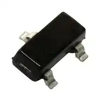
Power MOSFET, DMOS, N Channel, 240 V, 134 mA, 15 ohm, SOT-23, Surface Mount
- Manufacturer: MICROCHIP
- Product type: Single MOSFETs
- Transistor Polarity:N Channel; Continuous Drain Current Id:134mA; Drain Source Voltage Vds:240V; On Resistance Rds(on):15ohm; Rds(on) Test Voltage Vgs:4.5V; Threshold Voltage Vgs:2V
- MSL: MSL 1 - Unlimited
- SVHC: No SVHC (04-Feb-2026)
- No. of Pins: 3Pins
- Channel Type: N Channel
- Product Range: -
- Qualification: -
- Power Dissipation: 360mW
- Transistor Mounting: Surface Mount
- Rds(on) Test Voltage: 4.5V
- Transistor Case Style: SOT-23
- Drain Source Voltage Vds: 240V
- Operating Temperature Max: 150°C
- Continuous Drain Current Id: 134mA
- Drain Source On State Resistance: 15ohm
- Gate Source Threshold Voltage Max: 2V
| Delivery and price | |
|---|---|
| Units per pack | 100 |
| Price | 0.492 € |
| Current stock | 25+ |
| Lead time | 30 days |
## **TN2124** ## **N-Channel Enhancement-Mode Vertical DMOS FET** ## **Features** - Free from Secondary Breakdown - Low Power Drive Requirement - Ease of Paralleling - Low CISS and Fast Switching Speeds - Excellent Thermal Stability - Integral Source-Drain Diode - High Input Impedance and High Gain ## **Applications** - Logic-Level Interfaces (Ideal for TTL and CMOS) - Solid-State Relays - Battery-Operated Systems - Photovoltaic Drives - Analog Switches - General Purpose Line Drivers ## **General Description** The TN2124 low-threshold Enhancement-mode (normally-off) transistor uses a vertical Diffusion Metal-Oxide Semiconductor (DMOS) structure and a well-proven silicon gate manufacturing process. This combination produces a device with the power handling capabilities of bipolar transistors and the high input impedance and positive temperature coefficient inherent in Metal-Oxide Semiconductor (MOS) devices. Characteristic of all MOS structures, this device is free from thermal runaway and thermally induced secondary breakdown. Microchip’s vertical DMOS Field-Effect Transistors (FETs) are ideally suited to a wide range of switching and amplifying applications where very low threshold voltage, high breakdown voltage, high input impedance, low input capacitance and fast switching speeds are desired. - Telecommunication Switches ## **Package Type** **==> picture [113 x 103] intentionally omitted <==** **----- Start of picture text -----**<br> 3-lead SOT-23<br>(Top view)<br>DRAIN<br>SOURCE<br>GATE<br>**----- End of picture text -----**<br> See Table 3-1 for pin information. DS20005698A-page 1 2018 Microchip Technology Inc. **TN2124** ## **1.0 ELECTRICAL CHARACTERISTICS** ## **Absolute Maximum Ratings†** Drain-to-Source Voltage ...................................................................................................................................... BVDSS Drain-to-Gate Voltage .......................................................................................................................................... BVDGS Gate-to-Source Voltage ......................................................................................................................................... ±20V Operating Ambient Temperature, TA ................................................................................................... –55°C to +150°C Storage Temperature, TS ..................................................................................................................... –55°C to +150°C **† Notice:** Stresses above those listed under “Absolute Maximum Ratings” may cause permanent damage to the device. This is a stress rating only, and functional operation of the device at those or any other conditions above those indicated in the operational sections of this specification is not intended. Exposure to maximum rating conditions for extended periods may affect device reliability. ## **DC ELECTRICAL CHARACTERISTICS** **Electrical Specifications:** TA = 25°C unless otherwise specified. All DC parameters are 100% tested at 25°C unless otherwise stated. Pulse test: 300 µs pulse, 2% duty cycle |**DC ELECTRICAL CHARACTERISTICS**|**DC ELECTRICAL CHARACTERISTICS**|**DC ELECTRICAL CHARACTERISTICS**|**DC ELECTRICAL CHARACTERISTICS**|**DC ELECTRICAL CHARACTERISTICS**|**DC ELECTRICAL CHARACTERISTICS**|**DC ELECTRICAL CHARACTERISTICS**| |---|---|---|---|---|---|---| |**Electrical Specifications:**TA= 25°C unless otherwise specified. All DC parameters are 100% tested at 25°C unless<br>otherwise stated. Pulse test: 300µspulse, 2% dutycycle||||||| |**Parameter**|**Sym.**|**Min.**|**Typ.**|**Max.**|**Unit**|**Conditions**| |Drain-to-Source Breakdown Voltage|BVDSS|240|—|—|V|VGS= 0V, ID= 1 mA| |Gate Threshold Voltage|VGS(th)|0.8|—|2|V|VGS= VDS, ID= 1 mA| |Change in VGS(th)with Temperature|∆VGS(th)|—|—|–5.5|mV/°C|VGS= VDS, ID= 1 mA<br>(**Note 1**)| |Gate BodyLeakage Current|IGSS|—|0.1|100|nA|VGS= ±20V, VDS= 0V| |Zero-Gate Voltage Drain Current|IDSS|—|—|1|µA|VGS= 0V,<br>VDS= Maximum rating| |||—|—|100|µA|VDS= 0.8 Maximum rating,<br>VGS= 0V, TA= 125°C<br>(**Note 1**)| |On-State Drain Current|ID(ON)|140|—|—|mA|VGS= 4.5V, VDS= 25V| |Static Drain-to-Source On-State Resistance|RDS(ON)|—|—|30|Ω|VGS= 3V, ID= 25 mA| |||—|—|15|Ω|VGS= 4.5V, ID= 120 mA| |Change in RDS(ON)with Temperature|∆RDS(ON)|—|0.7|1|%/°C|VGS= 4.5V, ID= 120 mA<br>(**Note 1**)| **Note 1:** Specification is obtained by characterization and is not 100% tested. DS20005698A-page 2 2018 Microchip Technology Inc. **TN2124** ## **AC ELECTRICAL CHARACTERISTICS** **Electrical Specifications:** TA = 25°C unless otherwise specified. Specification is obtained by characterization and is not 100% tested. |**AC ELECTRICAL CHARACTERISTICS**|**AC ELECTRICAL CHARACTERISTICS**|**AC ELECTRICAL CHARACTERISTICS**|**AC ELECTRICAL CHARACTERISTICS**|**AC ELECTRICAL CHARACTERISTICS**|**AC ELECTRICAL CHARACTERISTICS**|**AC ELECTRICAL CHARACTERISTICS**| |---|---|---|---|---|---|---| |**Electrical Specifications:**TA= 25°C unless otherwise specified. Specification is obtained by characterization and is<br>not 100% tested.||||||| |**Parameter**|**Sym.**|**Min.**|**Typ.**|**Max.**|**Unit**|**Conditions**| |Forward Transconductance|GFS|100|170|—|mmho|VDS= 25V, ID= 120 mA| |Input Capacitance|CISS|—|38|50|pF|VGS= 0V, VDS= 25V,<br>f = 1 MHz| |Common Source Output Capacitance|COSS|—|9|15|pF|| |Reverse Transfer Capacitance|CRSS|—|3|5|pF|| |Turn-On DelayTime|td(ON)|—|4|7|ns|VDD= 25V, ID= 140 mA,<br>RGEN= 25Ω| |Rise Time|tr|—|2|5|ns|| |Turn-Off DelayTime|td(OFF)|—|7|10|ns|| |Fall Time|tf|—|9|12|ns|| |**DIODE PARAMETER**||||||| |Diode Forward Voltage Drop|VSD|—|—|1.8|V|VGS= 0V, ISD= 120 mA(**Note 1**)| |Reverse RecoveryTime|trr|—|400|—|ns|VGS= 0V, ISD= 120 mA| **Note 1:** Unless otherwise stated, all DC parameters are 100% tested at +25°C. Pulse test: 300 µs pulse, 2% duty cycle ## **TEMPERATURE SPECIFICATIONS** **Electrical Characteristics:** Unless otherwise specified, for all specifications TA = TJ = +25°C. |**TEMPERATURE SPECIFICATIONS**|**TEMPERATURE SPECIFICATIONS**|**TEMPERATURE SPECIFICATIONS**|**TEMPERATURE SPECIFICATIONS**|**TEMPERATURE SPECIFICATIONS**|**TEMPERATURE SPECIFICATIONS**|**TEMPERATURE SPECIFICATIONS**| |---|---|---|---|---|---|---| |**Electrical Characteristics:**Unless otherwise specified, for all specifications TA= TJ= +25°C.||||||| |**Parameter**|**Sym.**|**Min.**|**Typ.**|**Max.**|**Unit**|**Conditions**| |**TEMPERATURE RANGE**||||||| |OperatingAmbient Temperature|TA|–55|—|+150|°C|| |Storage Temperature|TS|–55|—|+150|°C|| |**PACKAGE THERMAL RESISTANCE**||||||| |3-lead SOT-23|JA|—|203|—|°C/W|| ## **THERMAL CHARACTERISTICS** |**Package**|**ID (Note 1)**<br>**(Continuous)**<br>**(mA)**|**ID**<br>**(Pulsed)**<br>**(mA)**|**Power Dissipation**<br>**at TA = 25°C**<br>**(W)**|**IDR(Note 1)**<br>**(mA)**|**IDRM**<br>**(mA)**| |---|---|---|---|---|---| |3-lead SOT-23|134|250|0.36|134|250| **Note 1:** ID (continuous) is limited by maximum TJ. DS20005698A-page 3 2018 Microchip Technology Inc. **TN2124** ## **2.0 TYPICAL PERFORMANCE CURVES** **Note:** The graphs and tables provided following this note are a statistical summary based on a limited number of samples and are provided for informational purposes only. The performance characteristics listed herein are not tested or guaranteed. In some graphs or tables, the data presented may be outside the specified operating range (e.g. outside specified power supply range) and therefore outside the warranted range. **==> picture [469 x 570] intentionally omitted <==** **----- Start of picture text -----**<br> 2.0 1.0<br>1.6 0.8 VGS = 10V<br>8V<br>6V<br>1.2 0.6 4V<br>VGS = 10V<br>8V<br>6V 3V<br>0.8 4V 0.4<br>3V<br>0.4 0.2<br>2V<br>2V<br>00 10 20 30 40 50 0 0 2.0 4.0 6.0 8.0 10<br>VDS (volts) VDS (volts)<br>FIGURE 2-1: Output Characteristics. FIGURE 2-4: Saturation Characteristics.<br>1.0 2.0<br>VDS = 25V<br>0.8 1.6<br>0.6 1.2<br>-55 [O] C<br>0.4 0.8<br>0.2 0.4<br>TA = 125 [O] C 25 [O] C SOT-23<br>0 0 0.2 0.4 0.6 0.8 1.0 0 0 25 50 75 100 125 150<br>ID (amperes) TA ( [O] C)<br>FIGURE 2-2: Transconductance vs. Drain<br>FIGURE 2-5: Power Dissipation vs.<br>Current.<br>Temperature.<br>10<br>1.0<br>T A = 25 [O] C<br>0.8<br>1.0<br>0.6<br>SOT-23 (pulsed)<br>0.4 SOT-23<br>0.1 TA = 25 [O] C<br>PD = 0.36W<br>0.2<br>SOT-23 (DC)<br>0.01<br>0 10 100 1000 0<br>0.001 0.01 0.1 1.0 10<br>VDS (volts) tP (seconds)<br>FIGURE 2-3: Maximum Rated Safe<br>FIGURE 2-6: Thermal Response<br>Operating Area.<br>Characteristics.<br>(amperes) (amperes)<br>ID ID<br>(watts)<br>(siemens) D<br>FS P<br>G<br>(amperes)<br>ID<br>Thermal Resistance (normalized)<br>**----- End of picture text -----**<br> DS20005698A-page 4 2018 Microchip Technology Inc. **TN2124** **==> picture [468 x 557] intentionally omitted <==** **----- Start of picture text -----**<br> 50<br>1.1<br>VGS = 3.0V<br>40<br>30<br>1.0<br>20<br>VGS = 4.5V<br>10<br>0.9<br>0<br>-50 0 50 100 150 0 0.2 0.4 0.6 0.8 1.0<br>Tj ( [O] C) ID (amperes)<br>FIGURE 2-7: BVDSS Variation with FIGURE 2-10: On-resistance vs. Drain<br>Temperature. Current.<br>1.0 2.0<br>1.4<br>RDS(ON) @ 4.5V, 120mA<br>0.8 1.6<br>1.2<br>0.6 1.2<br>1.0<br>0.4 0.8<br>0.8<br>VGS(th) @ 1.0mA<br>0.2 0.4<br>0.6<br>0 0<br>0 2.0 4.0 6.0 8.0 10 -50 0 50 100 150<br>VGS (volts) Tj ( [O] C)<br>FIGURE 2-8: Transfer Characteristics. FIGURE 2-11: V(th) and RDS Variation with<br>Temperature.<br>100 10<br>f = 1.0MHz<br>8.0<br>75<br>6.0<br>50<br>4.0 VDS = 10V<br>CISS 100pF VDS = 40V<br>25<br>2.0<br>CRSS<br>32 pF<br>0 0 10 20 30 40 0 0 0.2 0.4 0.6 0.8 1.0<br>VDS (volts) QG (nanocoulombs)<br>COSS<br>125OC<br>TA = -55OC<br>25OC<br>VDS = 25V<br>(ohms)<br>(normalized)<br>BVDSS RDS(ON)<br>(amperes) (normalized) (normalized)<br>ID<br>VGS(th) RDS(ON)<br>(volts)<br>GS<br>V<br>C (picofarads)<br>**----- End of picture text -----**<br> _**FIGURE 2-9:** Capacitance vs. Drain-to-Source Voltage._ _**FIGURE 2-12:** Gate Drive Dynamic Characteristics._ DS20005698A-page 5 2018 Microchip Technology Inc. **TN2124** ## **3.0 PIN DESCRIPTION** The details on the pins of TN2124 are listed on Table 3-1. Refer to **Package Type** for the location of pins. ## **TABLE 3-1: PIN FUNCTION TABLE** |**Pin Number**|**Pin Name**|**Description**| |---|---|---| |1|Gate|Gate| |2|Source|Source| |3|Drain|Drain| DS20005698A-page 6 2018 Microchip Technology Inc. **TN2124** ## **4.0 FUNCTIONAL DESCRIPTION** Figure 4-1 illustrates the switching waveforms and test circuit for TN2124. **==> picture [460 x 121] intentionally omitted <==** **----- Start of picture text -----**<br> 10V 90% VDD<br>INPUT 10% GeneratorPulse RL<br>0V OUTPUT<br>t t<br>(ON) (OFF) R<br>GEN<br>td(ON) tr td(OFF) tf<br>VDD INPUT D.U.T.<br>10% 10%<br>OUTPUT<br>0V 90% 90%<br>**----- End of picture text -----**<br> _**FIGURE 4-1:** Switching Waveforms and Test Circuit._ ## **TABLE 4-1: PRODUCT SUMMARY** |**BVDSS/BVDGS**<br>**(V)**|**RDS(ON)**<br>**(Maximum)**<br>**(Ω)**|**VGS(th)**<br>**(Maximum)**<br>**(V)**| |---|---|---| |240|15|2| DS20005698A-page 7 2018 Microchip Technology Inc. **TN2124** ## **5.0 PACKAGING INFORMATION** ## **5.1 Package Marking Information** **==> picture [186 x 90] intentionally omitted <==** **----- Start of picture text -----**<br> 3-lead SOT-23 Example<br>XXXNNN N1C256<br>**----- End of picture text -----**<br> **Legend:** XX...X Product Code or Customer-specific information Y Year code (last digit of calendar year) YY Year code (last 2 digits of calendar year) WW Week code (week of January 1 is week ‘01’) NNN Alphanumeric traceability code e3 Pb-free JEDEC[®] designator for Matte Tin (Sn) ***** This package is Pb-free. The Pb-free JEDEC designator ( ) e3 can be found on the outer packaging for this package. **Note** : In the event the full Microchip part number cannot be marked on one line, it will be carried over to the next line, thus limiting the number of available characters for product code or customer-specific information. Package may or not include the corporate logo. DS20005698A-page 8 2018 Microchip Technology Inc. **TN2124** ## **3-Lead TO-236AB (SOT-23) Package Outline (K1/T)** ## _**2.90x1.30mm body, 1.12mm height (max), 1.90mm pitch**_ **==> picture [359 x 242] intentionally omitted <==** **----- Start of picture text -----**<br> D<br>3<br>E1 E<br>0.25 Gauge<br>Plane<br>1 2 L Seating<br>Plane<br>L1<br>e b<br>e1<br>Top View View B<br>A View B<br>A2<br>A<br>Seating<br>Plane<br>A1<br>Side View A View A - A<br>**----- End of picture text -----**<br> **Note: For the most current package drawings, see the Microchip Packaging Specification at www.microchip.com/packaging.** **==> picture [408 x 48] intentionally omitted <==** **----- Start of picture text -----**<br> Symbol A A1 A2 b D E E1 e e1 L L1 �<br>MIN 0.89 0.01 0.88 0.30 2.80 2.10 1.20 0.20 [†] 0 [O]<br>Dimension NOM - - 0.95 - 2.90 - 1.30 0.95 1.90 0.50 0.54 -<br>(mm) BSC BSC REF<br>MAX 1.12 0.10 1.02 0.50 3.04 2.64 1.40 0.60 8 [O]<br>**----- End of picture text -----**<br> _JEDEC Registration TO-236, Variation AB, Issue H, Jan. 1999. † This dimension differs from the JEDEC drawing._ _**Drawings not to scale.**_ DS20005698A-page 9 2018 Microchip Technology Inc. **TN2124** ## **NOTES:** DS20005698A-page 10 2018 Microchip Technology Inc. **TN2124** ## **APPENDIX A: REVISION HISTORY** ## **Revision A (April 2018)** - Converted Supertex Doc# DSFP-TN2124 to Microchip DS20005698A - Added some sections to comply with the standard Microchip format - Changed the package marking format - Made minor text changes throughout the document DS20005698A-page 11 2018 Microchip Technology Inc. **TN2124** ## **PRODUCT IDENTIFICATION SYSTEM** To order or obtain information, e.g., on pricing or delivery, contact your local Microchip representative or sales office. ||**PART NO.**|**XX**|**XX**||**-X**<br> **-**|**X**||**Example:**|| |---|---|---|---|---|---|---|---|---|---| ||**Device**<br> <br>|**Package**<br> <br>**Options**|||**Environmental**<br>|**Media Type**||a) TN2124K1-G:|N-Channel Enhancement-Mode<br>Vertical DMOS FET, 3-lead SOT-23,| ||||||||||3000/Reel| ||Device:|TN2124||=|N-Channel Enhancement-Mode Vertical||||| ||||||DMOS FET||||| ||Package:|K1||=|3-lead SOT-23||||| ||Environmental:|G||=|Lead (Pb)-free/RoHS-compliant Package||||| ||Media Type:|(blank)||=|3000/Reel for a K1 Package||||| ||||||||||| DS20005698A-page 12 2018 Microchip Technology Inc. ## **Note the following details of the code protection feature on Microchip devices:** - Microchip products meet the specification contained in their particular Microchip Data Sheet. - Microchip believes that its family of products is one of the most secure families of its kind on the market today, when used in the intended manner and under normal conditions. - There are dishonest and possibly illegal methods used to breach the code protection feature. All of these methods, to our knowledge, require using the Microchip products in a manner outside the operating specifications contained in Microchip’s Data Sheets. Most likely, the person doing so is engaged in theft of intellectual property. - Microchip is willing to work with the customer who is concerned about the integrity of their code. - Neither Microchip nor any other semiconductor manufacturer can guarantee the security of their code. Code protection does not mean that we are guaranteeing the product as “unbreakable.” Code protection is constantly evolving. We at Microchip are committed to continuously improving the code protection features of our products. Attempts to break Microchip’s code protection feature may be a violation of the Digital Millennium Copyright Act. If such acts allow unauthorized access to your software or other copyrighted work, you may have a right to sue for relief under that Act. Information contained in this publication regarding device applications and the like is provided only for your convenience and may be superseded by updates. It is your responsibility to ensure that your application meets with your specifications. MICROCHIP MAKES NO REPRESENTATIONS OR WARRANTIES OF ANY KIND WHETHER EXPRESS OR IMPLIED, WRITTEN OR ORAL, STATUTORY OR OTHERWISE, RELATED TO THE INFORMATION, INCLUDING BUT NOT LIMITED TO ITS CONDITION, QUALITY, PERFORMANCE, MERCHANTABILITY OR FITNESS FOR PURPOSE **.** Microchip disclaims all liability arising from this information and its use. Use of Microchip devices in life support and/or safety applications is entirely at the buyer’s risk, and the buyer agrees to defend, indemnify and hold harmless Microchip from any and all damages, claims, suits, or expenses resulting from such use. No licenses are conveyed, implicitly or otherwise, under any Microchip intellectual property rights unless otherwise stated. _Microchip received ISO/TS-16949:2009 certification for its worldwide headquarters, design and wafer fabrication facilities in Chandler and Tempe, Arizona; Gresham, Oregon and design centers in California and India. The Company’s quality system processes and procedures are for its PIC[®] MCUs and dsPIC[®] DSCs, KEELOQ[®] code hopping devices, Serial EEPROMs, microperipherals, nonvolatile memory and analog products. In addition, Microchip’s quality system for the design and manufacture of development systems is ISO 9001:2000 certified._ ## **QUALITY MANAGEMENT SYSTEM** ## **CERTIFIED BY DNV** ## **Trademarks** The Microchip name and logo, the Microchip logo, AnyRate, AVR, AVR logo, AVR Freaks, BeaconThings, BitCloud, CryptoMemory, CryptoRF, dsPIC, FlashFlex, flexPWR, Heldo, JukeBlox, KEELOQ, KEELOQ logo, Kleer, LANCheck, LINK MD, maXStylus, maXTouch, MediaLB, megaAVR, MOST, MOST logo, MPLAB, OptoLyzer, PIC, picoPower, PICSTART, PIC32 logo, Prochip Designer, QTouch, RightTouch, SAM-BA, SpyNIC, SST, SST Logo, SuperFlash, tinyAVR, UNI/O, and XMEGA are registered trademarks of Microchip Technology Incorporated in the U.S.A. and other countries. ClockWorks, The Embedded Control Solutions Company, EtherSynch, Hyper Speed Control, HyperLight Load, IntelliMOS, mTouch, Precision Edge, and Quiet-Wire are registered trademarks of Microchip Technology Incorporated in the U.S.A. Adjacent Key Suppression, AKS, Analog-for-the-Digital Age, Any Capacitor, AnyIn, AnyOut, BodyCom, chipKIT, chipKIT logo, CodeGuard, CryptoAuthentication, CryptoCompanion, CryptoController, dsPICDEM, dsPICDEM.net, Dynamic Average Matching, DAM, ECAN, EtherGREEN, In-Circuit Serial Programming, ICSP, Inter-Chip Connectivity, JitterBlocker, KleerNet, KleerNet logo, Mindi, MiWi, motorBench, MPASM, MPF, MPLAB Certified logo, MPLIB, MPLINK, MultiTRAK, NetDetach, Omniscient Code Generation, PICDEM, PICDEM.net, PICkit, PICtail, PureSilicon, QMatrix, RightTouch logo, REAL ICE, Ripple Blocker, SAM-ICE, Serial Quad I/O, SMART-I.S., SQI, SuperSwitcher, SuperSwitcher II, Total Endurance, TSHARC, USBCheck, VariSense, ViewSpan, WiperLock, Wireless DNA, and ZENA are trademarks of Microchip Technology Incorporated in the U.S.A. and other countries. SQTP is a service mark of Microchip Technology Incorporated in the U.S.A. Silicon Storage Technology is a registered trademark of Microchip Technology Inc. in other countries. GestIC is a registered trademark of Microchip Technology Germany II GmbH & Co. KG, a subsidiary of Microchip Technology Inc., in other countries. All other trademarks mentioned herein are property of their respective companies. - © 2018, Microchip Technology Incorporated, All Rights Reserved. ISBN: 978-1-5224-2937-1 ## == == **ISO/TS 16949** DS20005698A-page 13 2018 Microchip Technology Inc. ## **Worldwide Sales and Service** ## **AMERICAS** **Corporate Office** 2355 West Chandler Blvd. Chandler, AZ 85224-6199 Tel: 480-792-7200 Fax: 480-792-7277 Technical Support: http://www.microchip.com/ support Web Address: www.microchip.com **Atlanta** Duluth, GA Tel: 678-957-9614 Fax: 678-957-1455 **Austin, TX** Tel: 512-257-3370 **Boston** Westborough, MA Tel: 774-760-0087 Fax: 774-760-0088 **Chicago** Itasca, IL Tel: 630-285-0071 Fax: 630-285-0075 **Dallas** Addison, TX Tel: 972-818-7423 Fax: 972-818-2924 **Detroit** Novi, MI Tel: 248-848-4000 **Houston, TX** Tel: 281-894-5983 **Indianapolis** Noblesville, IN Tel: 317-773-8323 Fax: 317-773-5453 Tel: 317-536-2380 **Los Angeles** Mission Viejo, CA Tel: 949-462-9523 Fax: 949-462-9608 Tel: 951-273-7800 **Raleigh, NC** Tel: 919-844-7510 **New York, NY** Tel: 631-435-6000 **San Jose, CA** Tel: 408-735-9110 Tel: 408-436-4270 **Canada - Toronto** Tel: 905-695-1980 Fax: 905-695-2078 ## **ASIA/PACIFIC** **Australia - Sydney** Tel: 61-2-9868-6733 **China - Beijing** Tel: 86-10-8569-7000 **China - Chengdu** Tel: 86-28-8665-5511 **China - Chongqing** Tel: 86-23-8980-9588 **China - Dongguan** Tel: 86-769-8702-9880 **China - Guangzhou** Tel: 86-20-8755-8029 **China - Hangzhou** Tel: 86-571-8792-8115 **China - Hong Kong SAR** Tel: 852-2943-5100 **China - Nanjing** Tel: 86-25-8473-2460 **China - Qingdao** Tel: 86-532-8502-7355 **China - Shanghai** Tel: 86-21-3326-8000 **China - Shenyang** Tel: 86-24-2334-2829 **China - Shenzhen** Tel: 86-755-8864-2200 **China - Suzhou** Tel: 86-186-6233-1526 **China - Wuhan** Tel: 86-27-5980-5300 **China - Xian** Tel: 86-29-8833-7252 **China - Xiamen** Tel: 86-592-2388138 **China - Zhuhai** Tel: 86-756-3210040 ## **ASIA/PACIFIC** **India - Bangalore** Tel: 91-80-3090-4444 **India - New Delhi** Tel: 91-11-4160-8631 **India - Pune** Tel: 91-20-4121-0141 **Japan - Osaka** Tel: 81-6-6152-7160 **Japan - Tokyo** Tel: 81-3-6880- 3770 **Korea - Daegu** Tel: 82-53-744-4301 **Korea - Seoul** Tel: 82-2-554-7200 **Malaysia - Kuala Lumpur** Tel: 60-3-7651-7906 **Malaysia - Penang** Tel: 60-4-227-8870 **Philippines - Manila** Tel: 63-2-634-9065 **Singapore** Tel: 65-6334-8870 **Taiwan - Hsin Chu** Tel: 886-3-577-8366 **Taiwan - Kaohsiung** Tel: 886-7-213-7830 **Taiwan - Taipei** Tel: 886-2-2508-8600 **Thailand - Bangkok** Tel: 66-2-694-1351 **Vietnam - Ho Chi Minh** Tel: 84-28-5448-2100 ## **EUROPE** **Austria - Wels** Tel: 43-7242-2244-39 Fax: 43-7242-2244-393 **Denmark - Copenhagen** Tel: 45-4450-2828 Fax: 45-4485-2829 **Finland - Espoo** Tel: 358-9-4520-820 **France - Paris** Tel: 33-1-69-53-63-20 Fax: 33-1-69-30-90-79 **Germany - Garching** Tel: 49-8931-9700 **Germany - Haan** Tel: 49-2129-3766400 **Germany - Heilbronn** Tel: 49-7131-67-3636 **Germany - Karlsruhe** Tel: 49-721-625370 **Germany - Munich** Tel: 49-89-627-144-0 Fax: 49-89-627-144-44 **Germany - Rosenheim** Tel: 49-8031-354-560 **Israel - Ra’anana** Tel: 972-9-744-7705 **Italy - Milan** Tel: 39-0331-742611 Fax: 39-0331-466781 **Italy - Padova** Tel: 39-049-7625286 **Netherlands - Drunen** Tel: 31-416-690399 Fax: 31-416-690340 **Norway - Trondheim** Tel: 47-7289-7561 **Poland - Warsaw** Tel: 48-22-3325737 **Romania - Bucharest** Tel: 40-21-407-87-50 **Spain - Madrid** Tel: 34-91-708-08-90 Fax: 34-91-708-08-91 **Sweden - Gothenberg** Tel: 46-31-704-60-40 **Sweden - Stockholm** Tel: 46-8-5090-4654 **UK - Wokingham** Tel: 44-118-921-5800 Fax: 44-118-921-5820 DS20005698A-page 14 2018 Microchip Technology Inc. 10/25/17
Updated at April 29, 2026
Microchip Technology Inc. is a leading global provider of smart, connected, and secure embedded control solutions. Known for enabling engineers to design with confidence, the company delivers a comprehensive product portfolio that reduces total system costs and accelerates time to market across the industrial, automotive, communications, and computing sectors. Our extensive selection of Microchip components highlights the manufacturer's strength in both discrete semiconductors and advanced wireless connectivity. We carry a robust lineup of highly efficient single MOSFETs and Schottky diodes tailored for demanding power management and switching applications. Alongside these essential discretes, engineers can source a wide array of ready-to-use networking modules, prominently featuring Bluetooth and WLAN adapters that streamline the development of modern IoT and connected devices. Rounding out the offering is a diverse range of Microchip integrated circuits and specialized components. This includes versatile I/O expanders for simplified system integration, precision timing solutions such as MEMS oscillators and pulse generators, as well as AC/DC LED driver ICs and sub-2.4GHz RF transceivers. Backed by Microchip's renowned commitment to exceptional quality and reliable performance, these components provide scalable, dependable building blocks for complex electronic designs.
About Novapart
Novapart is a B2B electronic component broker specialising in stock shortages and cost reduction. We source hard-to-find parts and identify compliant alternatives across a catalogue of 410,000+ components from 500+ manufacturers.
Learn more →Stock Shortage Specialist
When a component is unavailable, discontinued or has an unacceptable lead time, we tap into our network of vetted European and Asian distributors to source what you need — without compromising on quality or traceability.
Request a quote →Compliant Alternatives
We identify pin-to-pin, electrically equivalent substitutes that meet the same certifications (RoHS, AEC-Q100, REACH) as your original specification — validated against datasheets, not just part numbers. Often at a lower cost.
BOM Analysis service →