
Image not available
Illustrative purposes only

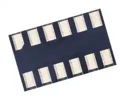
TMF8805-1BM
Distance Sensor, 2.5 m, I2C Digital, Time of Flight, 2.7 V to 3.3 V, PCB, TMF8805 Series
⚠️ Reference pricing provided. In case of supply shortages, we will connect you with our trusted procurement partners to ensure your project's continuity.
- Manufacturer: AMS OSRAM GROUP
- Product type:
- SVHC: No SVHC (21-Jan-2025)
- Product Range: TMF8805 Series
- Sensing Method: Time of Flight
- Connection Method: PCB
- Sensing Range Max: 2.5m
- Sensor Output Type: I2C Digital
- Supply Voltage Max: 3.3V
- Supply Voltage Min: 2.7V
- Sensing Distance Max: 2.5m
- Supply Voltage DC Max: 3.3V
- Supply Voltage DC Min: 2.7V
| Delivery and price | |
|---|---|
| Units per pack | 500 |
| Price | 2.21 € |
| Current stock | 200+ |
| Lead time | 30 days |
Datasheet

## **TMF8805**

## Datasheet

## **Published by ams-OSRAM AG**

Tobelbader Strasse 30, 8141 Premstaetten, Austria Phone +43 3136 500-0 ams-osram.com © All rights reserved

**TMF8805** Table of contents

## **Table of contents**

|**1**|**General description ................................................. 4**|**General description ................................................. 4**|
|---|---|---|
||1.1|Key specifications & features .................................................. 4|
||1.2|Applications ............................................................................ 5|
||1.3|Block diagram ......................................................................... 5|
||1.4|Pin assignment ....................................................................... 6|
|**2**|**Ordering information ............................................... 7**||
|**3**|**Absolute maximum ratings ..................................... 8**||
|**4**|**Electrical characteristics ......................................... 9**||
||4.1|Recommended operating conditions ...................................... 9|
||4.2|Typical operating characteristics ............................................ 9|
|**5**|**Functional description........................................... 13**||
||5.1|I²C protocol ........................................................................... 13|
||5.2|System parameters ............................................................... 13|
||5.3|I/O ......................................................................................... 14|
||5.4|Power consumption .............................................................. 14|
||5.5|Timing ................................................................................... 16|
||5.6|Algorithm performance ......................................................... 18|
||5.7|VCSEL .................................................................................. 20|
||5.8|Typical optical characteristics ............................................... 20|
|**6**|**Register description .............................................. 22**||
||6.2|App0 registers – appid=0xC0 ............................................... 25|
||6.3|Object detection results – if register register_contents = 0x55|
|||(commands 0x02 or 0x03) .................................................... 36|
||6.4|Calibration and algorithm state data exchange .................... 45|
||6.5|Raw histogram output – if register|
|||register_contents=0x80…0x93 ............................................ 54|
||6.6|Serial number readout – if register register_contents=0x47 . 55|
||6.7|Interrupt suppression registers – result of command = 0x09 56|
||6.8|Bootloader registers – appid=0x80 ....................................... 58|
||6.9|Bootloader commands .......................................................... 59|


Datasheet • PUBLIC • Document Feedback DS000692 • v7-00 • 2023-Dec-01

**2** / 74

/

**TMF8805** Table of contents

|**7**|**Application information ......................................... 62**|
|---|---|
||7.1<br>SPAD options ....................................................................... 62|
||7.2<br>Reference SPAD, TDC and histogram ................................. 63|
||7.3<br>Schematic ............................................................................. 63|
||7.4<br>PCB layout ............................................................................ 66|
||7.5<br>PCB pad layout ..................................................................... 67|
|**8**|**Package drawings & markings ............................. 68**|
||8.1<br>Package drawings ................................................................ 68|
|**9**|**Tape & reel information ......................................... 69**|
|**10**|**Soldering & storage information .......................... 70**|
||10.1<br>Soldering information ............................................................ 70|
||10.2<br>Storage information .............................................................. 71|
|**11**|**Laser eye safety ..................................................... 72**|
|**12**|**Revision information ............................................. 73**|
|**13**|**Legal information ................................................... 74**|


Datasheet • PUBLIC • Document Feedback DS000692 • v7-00 • 2023-Dec-01

**3** / 74

/

**TMF8805** General description

## **TMF8805 Time-of-flight sensor**

## 1 General description

The TMF8805 is a dToF (direct time of flight) optical distance sensor module achieving up to 2500 mm target detection distance.

The TMF8805 is a time-of-flight (TOF) sensor in a single modular package with associated VCSEL. The TOF device is based on SPAD, TDC and histogram technology. The device achieves 2500 mm detection range.

## **1.1 Key specifications & features**

The benefits and features of TMF8805, Time-of-flight sensor are listed below:

**Table 1: Key benefits & features**

|**Benefits**|**Features**|
|---|---|
|Small footprint fits in the mobile phone bezel|Modular package - 2.2 mm x 3.6 mm x 1.0 mm|
|Detecting central closest objects|No influence on multi object reflections|
|Within 5 % of measurement (accuracy); no<br>multipath and no multiple object problems as for<br>iToF|Time-to-Digital Converter (TDC)<br>Direct Time-of-Flight Measurement|
|Better accuracy detects reliably closest object<br>Minimum distance 20 mm<br>Maximum distance 2500 mm|Single Photon Avalanche Photodiode (SPAD)<br>Histogram based architecture|
|No complex calibration|Dynamic cover glass calibration|
|Compensates for dirt on glass|Reliable operation under demanding use cases|
|Improved accuracy over temperature and life|Reference SPAD|
|Make better decisions|Distance and signal quality reported|
|Class 1 eye safe|Fast VCSEL driver with protection|
|Longer battery life|27 mA power consumption at 30 Hz operation<br>0.26 µA power-down current consumption (EN=0)|


Datasheet • PUBLIC • Document Feedback DS000692 • v7-00 • 2023-Dec-01

**4** / 74

/

**TMF8805** General description

## **1.2 Applications**

- The device is ideal for use in the mobile phone market with applications including:

- Distance measurement for camera autofocus (Laser Detect Autofocus - LDAF)

- Supporting low-power system operation by enabling high-power components (i.e. 3D camera) only when an object is in the detection range

- Presence detection - Object detection

- Collision avoidance

## **1.3 Block diagram**

The functional blocks of this device are shown below:

**Figure 1: Functional blocks of TMF8805**

**==> picture [434 x 160] intentionally omitted <==**

**----- Start of picture text -----**<br>
TMF8805<br>TOF Sensor Optics<br>EN<br>Driver VCSEL<br>GPIO1 Reflective<br>Control<br>INT GPIO0 Internal  Surface<br>Host<br>SDA SPAD,  Reflection<br>Data<br>SCL TDC and<br>SRS Process Histogram Optical<br>Filter<br>Cortex M0<br>lors Background<br>Light<br>VDD GND VDDC GNDC<br>**----- End of picture text -----**<br>


Datasheet • PUBLIC • Document Feedback DS000692 • v7-00 • 2023-Dec-01

**5** / 74

/

**TMF8805** General description

## **1.4 Pin assignment**

## **1.4.1 Pin diagram**

**Figure 2: Pin locations top through view (not to scale)**

|VDDC||1|1||12|VDDV|
|---|---|---|---|---|---|---|
||||||||
||||||||
|GNDC||2|||11|GNDV|
|GPIO0||3|||10|GPIO1|
|INT||4|||9|EN|
||||||||
|SCL||5|||8|GND|
|SDA||6|||7|VDD|


**Table 2: Pin description of TMF8805**

|**Pin number**|**Pin number**|**Pin name**|**Signal**<br>**type**|**Description**|
|---|---|---|---|---|
|1||VDDC|Supply|Charge pump supply voltage (3 V); add a capacitor<br>GRM155R70J104KA01 (0402 X7R 0.1 µF 6.3 V) to GND|
|2||GNDC|Ground|Charge pump ground; connect all ground pins together|
|3||GPIO0|I/O|General purpose input/output; default output low; leave<br>open if not used|
|4||INT|Output|Interrupt. Open-drain output; connect to GND if not used|
|5||SCL|Input|I²C serial clock|
|6||SDA|I/O|I²C serial data|
|7||VDD|Supply|Chip supply voltage (3 V); add a capacitor<br>GRM155R70J104KA01 (0402 X7R 0.1 µF 6.3 V) to GND|
|8||GND|Ground|Chip ground; connect all ground pins together|


Datasheet • PUBLIC • Document Feedback DS000692 • v7-00 • 2023-Dec-01

**6** / 74

/

**TMF8805** Ordering information

|**Pin number**|**Pin number**|**Pin name**|**Signal**<br>**type**|**Description**|
|---|---|---|---|---|
|||||Enable input active high; setting to low forces the device|
|||||into shutdown and all memory content is lost; connect the|
|9||EN|Input|EN pin to a host GPIO to control the hardware reset|
|||||function of TMF8805. If this functionality is not needed,|
|||||connect to VDD.|
|10||GPIO1|I/O|General purpose input/output; default output low; leave<br>open if not used|
|11||GNDV|Ground|VCSEL ground; connect all ground pins together|
|12||VDDV|Supply|VCSEL supply voltage (3 V); add a capacitor<br>GRM155R70J104KA01 (0402 X7R 0.1 µF 6.3 V) to GND|


(1) SDA, SCL, INT and EN have no diode to any VDD supply. Therefore, even with VDD=0 V they do not block the interrupt line or I²C bus.

(2) GPIO0 and GPIO1 are push/pull output and have a diode to VDD; therefore if VDD is not powered, GPIO0 and GPIO1 should not be driven from outside.

## 2 Ordering information

|**Ordering code**|**Package**|**Marking**|**Delivery form**|**Delivery quantity**|
|---|---|---|---|---|
|TMF8805-1BM|Optical module|5-digit tracecode (coded)|Tape & reel<br>(7″ reels)|500 pcs/reel|
|TMF8805-1B|Optical module|5-digit tracecode (coded)|Tape & reel<br>(13″ reels)|5000 pcs/reel|


Datasheet • PUBLIC • Document Feedback DS000692 • v7-00 • 2023-Dec-01

**7** / 74

/

**TMF8805** Absolute maximum ratings

3

## Absolute maximum ratings

Stresses beyond those listed under “Absolute Maximum Ratings” may cause permanent damage to the device. Functional operation of the device at absolute maximum rating conditions is not implied, nor at any other conditions beyond those indicated under “Operating Conditions”.

**Table 3: Absolute maximum ratings of TMF8805**

|**Symbol**|**Parameter**|**Min**|**Max**|**Unit**|**Comment**|
|---|---|---|---|---|---|
|**Electrical parameters**||||||
|VDDC, VDDV,<br>VDD|3 V supply voltage|-0.3|3.6|V|Connect pins VDDC, VDDV,<br>VDD on PCB with very short<br>connections|
|GNDV, GNDC,<br>GND|Ground|0.0|0.0|V|Connect all GND pins on PCB<br>with very short connections|
|GPIO0, GPIO1|Digital I/O terminal<br>voltage|-0.3|VDD + 0.3 V<br>max. 3.6 V|V|Protection diode to VDD|
|INT, SCL,<br>SDA, EN|Digital I/O terminal<br>voltage|-0.3|3.6|V|No protection diodes to any<br>positive supply only to ground|
|I_SCR|Latch up immunity||± 100|mA|JEDEC JESD78E|
|**Electrostatic discharge**||||||
|ESDHBM|Electrostatic<br>discharge HBM||± 2000|V|JEDEC JS-001-2017|
|ESDCDM|Electrostatic<br>discharge CDM||± 500|V|JEDEC JS-002-2018|
|**Temperature ranges and storage conditions**||||||
|TSTRG|Storage temperature<br>range|-40|85|°C||
|TBODY|Package body<br>temperature||260|°C|IPC/JEDEC J-STD-020(1)|
|RHNC|Relative humidity<br>(non-condensing)||85|%||
|MSL|Moisture sensitivity<br>level||3||Represents a maximum floor life<br>time of 168h with TAMB< 30 °C<br>and < 60% r.h.|


(1) The reflow peak soldering temperature (body temperature) is specified according to IPC/JEDEC J-STD-020 “Moisture/Reflow Sensitivity Classification for Nonhermetic Solid State Surface Mount Devices.”

Datasheet • PUBLIC • Document Feedback DS000692 • v7-00 • 2023-Dec-01

**8** / 74

/

**TMF8805** Electrical characteristics

## 4 Electrical characteristics

All limits are guaranteed. The parameters with Min and Max values are guaranteed with production tests or SQC (Statistical Quality Control) methods.

## **4.1 Recommended operating conditions**

Device parameters are guaranteed at nominal conditions unless otherwise noted. While the device is operational across the temperature range, functionality will vary with temperature.

**Table 4: Recommended operating conditions of TMF8805**

|**Symbol**|**Parameter**|**Min**|**Typ**|**Max**|**Unit**|**Comment**|
|---|---|---|---|---|---|---|
|VDDV, VDDC, VDD|3 V supply voltage|2.7|3|3.3|V||
|Temperature range|Free-air temperature|-30|25|70|°C|Operational|


## **4.2 Typical operating characteristics**

Following operating characteristics are measured with calibrated devices with full optical stack including glass and IR ink with >90 % transmissivity. The airgap is set to 0.38 mm. The ambient light is measured on the 1 m x 1 m target. A very diffuse scotch magic tape 810 is used for measurement with smudge.

Datasheet • PUBLIC • Document Feedback DS000692 • v7-00 • 2023-Dec-01

**9** / 74

/

**TMF8805** Electrical characteristics

**Figure 3: 350 Lux fluorescent light and 18% grey card**

**Figure 4: 350 Lux fluorescent light, 18% grey card and smudge on glass**

Datasheet • PUBLIC • Document Feedback DS000692 • v7-00 • 2023-Dec-01

**10** / 74

/

**TMF8805** Electrical characteristics

**Figure 5: 1 k Lux sunlight represented by 170 Lux halogen light and 18% grey card**

**Figure 6: 1 k Lux sunlight represented by 170 Lux halogen light and 90% white card**

Datasheet • PUBLIC • Document Feedback DS000692 • v7-00 • 2023-Dec-01

**11** / 74

/

**TMF8805** Electrical characteristics

**Figure 7: 5 k Lux sunlight represented by 830 Lux halogen light and 18% grey card**

**Figure 8: Field of illumination of VCSEL (FOI), x-axis: ±10.4°, y-axis: ±10.31°, 1/e²**

Datasheet • PUBLIC • Document Feedback DS000692 • v7-00 • 2023-Dec-01

**12** / 74

/

**TMF8805** Functional description

## 5 Functional description

## **5.1 I²C protocol**

The TMF8805 is controlled by an I²C bus, one interrupt pin and two GPIO pins.

The device uses I²C serial communication protocol for communication. The device supports 7-bit chip addressing and standard, fast mode and fast mode plus modes. Read and Write transactions comply with the standard set by Philips (now NXP). For a complete description of the I²C protocol, please review the NXP I²C design specification.

Internal to the device, an 8-bit buffer stores the register address location of the byte to read or write. This buffer auto-increments upon each byte transfer and is retained between transaction events (i.e. valid even after the master issues a STOP and the I²C bus is released). During consecutive Read transactions, the future/repeated I²C Read transaction may omit the memory address byte normally following the chip address byte; the buffer retains the last register address +1.

A Write transaction consists of a START, CHIP-ADDRESSWRITE, REGISTERADDRESSWRITE, DATA BYTE(S), and STOP. Following each byte (9TH clock pulse) the slave places an ACKNOWLEDGE/NOT- ACKNOWLEDGE (ACK/NACK) on the bus. If NACK is transmitted by the slave, the master may issue a STOP.

A Read transaction consists of a START, CHIP-ADDRESSWRITE, REGISTER-ADDRESS, RESTART, CHIP-ADDRESSREAD, DATA BYTE(S), and STOP. Following all but the final byte the master places an ACK on the bus (9TH clock pulse). Termination of the Read transaction is indicated by a NACK being placed on the bus by the master, followed by STOP.

The default I²C address is 0x41. The address can be changed after power-up. Use the enable pin to enable only one device at a time to provide unique device addresses.

## **5.2 System parameters**

The on-chip microprocessor is a Cortex M0 µP.

**Table 5: ARM M0 parameters**

|**Parameter**|**Min**|**Nom**|**Max**|**Units**|**Comment**|
|---|---|---|---|---|---|
|µP operating<br>Frequency||4.7|75 (= 4.7*16)|MHz|The CPU can operate with the RC oscillator<br>directly or with a 16x PLL; frequency tuning<br>adjusts the default frequency to 4.7 MHz|


Datasheet • PUBLIC • Document Feedback DS000692 • v7-00 • 2023-Dec-01

**13** / 74

/

**TMF8805** Functional description

|**Parameter**|**Min**|**Nom**|**Max**|**Units**|**Comment**|
|---|---|---|---|---|---|
|RAM|||32|kB||
|ROM|||32|kB||
|Max PLL<br>frequency||150.4||MHz|For 4.7 MHz RC clock|


## **5.3 I/O**

## **Table 6: Typical I/O level specification**

|**Symbol**|**Parameter**|**Conditions**|**Min**|**Typ**|**Max**|**Unit**|
|---|---|---|---|---|---|---|
|ILEAK|SDA, SCL, GPIO0/1,<br>EN, INT||-5||5|µA|
|VIH(1)|SDA, SCL, GPIO0/1, EN||1.26|||V|
|||2.7 V<VDD<2.9 V, <400 kHz<br>I²C speed|||0.3||
|VIL_I2C(1)|SDA, SCL|VDD >2.9 V,<br><400 kHz I²C speed|||0.54|V|
|||2.8 V<VDD<3.0 V, <1 MHz<br>I²C speed|||0.3||
|||VDD>3.0 V,<br><1 MHz I²C speed|||0.54||
|VIL|GPIO0/1, EN||||0.54|V|
|||2 mA sink|0||0.36|V|
|VOL|SDA, GPIO0/1, INT||||||
|||4 mA sink|0||0.6|V|
|IDRIVE_H|GPIO0/1|1 V applied on GPIO|3.6|||mA|
|IDRIVE_L|GPIO0/1|1 V applied on GPIO|3.9|||mA|


(1) The input high-level VIH and low-level VIL is defined to support a pull-up supply of 1.8 V ±5 %.

## **5.4 Power consumption**

All current consumption values include silicon process variation. Temperature and voltages are at nominal conditions (23 ºC and 2.8 V).

Datasheet • PUBLIC • Document Feedback DS000692 • v7-00 • 2023-Dec-01

**14** / 74

/

**TMF8805** Functional description

**Table 7: Power consumption**

|**Parameter**|**Condition**|**Min**|**Nom**|**Max**|**Units**|**Comment**|
|---|---|---|---|---|---|---|
|I_VDD powerdown|Enable pin low I²C<br>off|0.02|0.26|1|µA|State: Powerdown|
|I_VDD standby CPU off, RAM|||||||
|on OSC Off, pon=0|||85||µA|State: Standby|
|I²C wakeup only|||||||
|I_VDD wait CPU off, RAM on,|||||||
|OSC on 5 MHz I²C on, timer|||140||µA|State: Wait|
|wakeup|||||||
|I_VDD ranging processing|||||||
|CPU running at 80 MHz no<br>VCSEL,|||2.7||mA|State: Histogram<br>processing|
|No TDC|||||||
|I_VDD ranging active CPU|||||||
|stopped<br>VCSEL_clk_div2=0 (default),|||32.5||mA|State: Ranging active|
|TDCs running|||||||
||||25.2||mA|State: Ranging active|
|I_VDD ranging active CPU<br>stopped<br>VCSEL_clk_div2=1, TDCs<br>running|1 Hz, ranging<br>period = 1000 ms<br>0.5 Hz, ranging<br>period = 2000 ms||0.23<br>0.17||mA<br>mA|Firmware 3.0.19.0 or<br>higher,<br>80 k iterations,<br>cmd_data6 = 0x23<br>(algorithm setting for<br>command 0x02 or|
|||||||0x03)|
|I_VDD ranging 30 Hz, 33 ms,<br>default settings|||27||mA|Average power<br>consumption(1)|
|Peak VCSEL current|||230||mA||
|Max VCSEL duty cycle|||2||%||


(1) Current is reduced to typ. 17.7 mA if iteration is set to 600 k instead of 900 k and output data rate is maintained at 30 Hz by setting repetition_period = 33 [ms].

Datasheet • PUBLIC • Document Feedback DS000692 • v7-00 • 2023-Dec-01

**15** / 74

/

**TMF8805** Functional description

## **5.5 Timing**

## **5.5.1 Ranging acquisition timing**

**Table 8: Ranging acquisition timing**

|**Parameter**|**Min**|**Nom**|**Max**|**Units**|**Comment**|
|---|---|---|---|---|---|
|Ranging time default settings||33||ms|Varies with operational mode|
|Ranging init (including electrical<br>calibration)||8||ms|Only done on startup and if<br>temperature changed from last<br>calibration|
||||209|ms|Programmable by the interface|
|Ranging period|||1000 /||Additional modes added with|
||||2000|ms|firmware 3.0.19.0 or higher(1)|


(1) For firmware 3.0.19.0 or higher, set register repetition_period (cmd_data2 for command 0x02 or 0x03) to 0xfe for 1000 ms ranging period and 0xff for 2000 ms ranging period.

**Figure 9: Ranging timing diagram**

Datasheet • PUBLIC • Document Feedback DS000692 • v7-00 • 2023-Dec-01

**16** / 74

/

**TMF8805** Functional description

## **5.5.2 Reset pin and power-up timing**

## **Table 9: Reset pin and power-up timing**

|**Parameter**|**Min**|**Nom**|**Max**|**Units**|**Comment**|
|---|---|---|---|---|---|
|Power on (Boot Time)||3||ms|Does not include RAM download<br>time|
|Enable high to ready for measurement||8||ms||
|Standby to active time||<<1||ms||
|Active to standby time||<<1||ms||
|Enable low to power down time||<<1||ms||


Datasheet • PUBLIC • Document Feedback DS000692 • v7-00 • 2023-Dec-01

**17** / 74

/

**TMF8805** Functional description

## **5.6 Algorithm performance**

As the performance of the algorithm is dependent on the ROM version, following section only applies for devices with order code TMF8805-1B (and TMF8805-1BM), calibrated and inapplication oscillator calibration using the reference driver code and patched with the latest software patch from ams OSRAM – contact ams OSRAM to identify latest patch version.

To achieve the full distance of 250 cm, the on chip oscillator needs to be tuned to 4.7 MHz.

The TMF8805 is embedded in the application using a 0.38 mm airgap and a glass with an IR ink with >90 % transmissivity. The glass thickness is 0.5 mm. An additional mask on the opaque ink is implemented according to TMF8805 optical design guide (external document).

## **5.6.1 Calibration**

To achieve the performance described in the next sections, a calibration of the algorithm needs to be performed (command = 0x0A). The TMF8805 shall be embedded in the final application and the cover glass including the IR ink needs to be assembled. The calibration test shall be done in a housing with minimal ambient light and no target within 40 cm in field of view of the TMF8805.

The TMF8805 generates a calibration data set which is permanently stored on the host.

On each power-up of the TMF8805 the calibration data set is sent by I²C to the TMF8805 prior to execution of any algorithms (commands=0x02 or 0x0B).

## **5.6.2 Algorithm timings**

The TMF8805 can adjust the number of iterations and detection threshold using registers. A default mode is defined having 900 k iterations and threshold=0.

**Table 10: Algorithm timings**

|**Parameter**|**Condition**|**Min**|**Nom**|**Max**|**Units**|
|---|---|---|---|---|---|
||command=0x02 or 0x03|||||
||cmd_data6=0xA3,|||||
|Default Mode|cmd_data3=0x00,||33||ms|
||cmd_data1=0x84,|||||
||cmd_data0=0x03 (900 k iterations)|||||


Datasheet • PUBLIC • Document Feedback DS000692 • v7-00 • 2023-Dec-01

**18** / 74

/

**TMF8805** Functional description

## **5.6.3 Algorithm performance parameters**

The algorithm reports distance information of the closest object in 1 mm steps. Using the timings described in 5.6.2 following performance is achieved:

**Table 11: Object detection algorithm parameters**

|**Parameter**|**Condition**|**Min**|**Nom**|**Max**|**Units**|
|---|---|---|---|---|---|
|Reflectivity of<br>object at 940 nm|Perpendicular to TMF8805|18||90|%|
||350 lux fluorescent on object, 18% grey or 90% white<br>card||2500(1)||mm|
|Maximum|170 lux halogen light on object(2), 90% white card||2400(1)||mm|
|distance<br>detection, 1.5 m|170 lux halogen light on object(2), 18% grey card||1900||mm|
|x 1.5 m object|170 lux halogen light on object(2), 18% grey card,<br>smudge on glass(3)||1500||mm|
||830 lux halogen light on object(4), 18% grey card||1100||mm|
|Minimum||||||
|distance||||||
|detection, 18 %|||20||mm|
|grey card, 20 cm||||||
|x 26 cm||||||
||Object distance ≥ 200 mm||±5||%|
|Accuracy|100 mm ≤ object distance <200 mm||±10||mm|
||20 mm ≤ object distance <100 mm||±15||mm|
|Transition short||||||
|to long distance|||200||mm|
|mode||||||


(1) To achieve the full distance, the oscillator need to be tuned to 4.7 MHz. Use ams OSRAM reference code to implement clock frequency tuning. Any target reported above 2500 mm should be considered as no object.

(2) 170 lux halogen light represents 1k lux sunlight equivalent; light on object only.

(3) Smudge on glass is defined by one layer of Scotch Magic Tape 810 (very diffuse).

(4) 830 lux halogen light represents 5 k lux sunlight equivalent; light on object only.

Datasheet • PUBLIC • Document Feedback DS000692 • v7-00 • 2023-Dec-01

**19** / 74

/

**TMF8805** Functional description

## **5.7 VCSEL**

Internal protection ensures no single point of failure will cause the VCSEL to violate the Class 1 Laser Safety.

- Laser Safety

Class 1

- VCSEL Pulse Rep Rate 26.6 ns (37.6 MHz)

If VCSEL_clk_div=1, the frequency is divided by two.

## **5.8 Typical optical characteristics**

- VCSEL Field of Illumination (FOI)

   - 25º Full width from 1% of maximum up to maximum

   - 21º Full width from 5% of maximum up to maximum

   - 19º 1/e^2

- TOF Sensor Field of View (FOV)

   - 37º FWHM – for short distances

   - 24º FWHM – for long distances

The SPAD FoV angular response uses the full TMF8805 SPADs for short distances. The SPAD FoV is reduced when the TMF8805 operates in long distance since the SPAD array is reduced. This helps to improve ambient light tolerance[1] .

## **Figure 10: FOI/FOV of TMF8805 (used 1/e^2 for FOI as example)**

1 It depends on the size and reflectivity of the object if TMF8805 algorithm detects off-axis objects.

Datasheet • PUBLIC • Document Feedback DS000692 • v7-00 • 2023-Dec-01

**20** / 74

/

**TMF8805** Functional description

## **5.8.1 Filter characteristics**

- FWHM 114 nm

- Passband center frequency 940 nm

- Stopband wavelengths 350 nm – 883 nm, 997 nm – 1100 nm

Datasheet • PUBLIC • Document Feedback DS000692 • v7-00 • 2023-Dec-01

**21** / 74

/

**TMF8805** Register description

## 6 Register description

## **6.1.1 APPID register (Address 0x00)**

**Table 12: APPID register**

|**Addr: 0x00**|**Addr: 0x00**|**APPID**|||
|---|---|---|---|---|
|**Field**|**Name**|**Rst**|**Type**|**Description**|
|||||Currently running application:|
|7:0|_appid_|0|RW|0xC0 App0 – Measurement application running|
|||||0x80 bootloader running|


## **6.1.2 APPREV_MAJOR register (Address 0x01)**

**Table 13: APPREV_MAJOR register**

|**Addr: 0x01**|**Addr: 0x01**|**APPREV_MAJOR**|**APPREV_MAJOR**|**APPREV_MAJOR**|
|---|---|---|---|---|
|**Field**|**Name**|**Rst**|**Type**|**Description**|
|7:0|_apprevMajor_|0|RW|Application major revision|


## **6.1.3 APPREQID register (Address 0x02)**

**Table 14: APPREQID register**

|**Addr: 0x02**|**Addr: 0x02**|**APPREQID**|**APPREQID**||
|---|---|---|---|---|
|**Field**|**Name**|**Rst**|**Type**|**Description**|
|||||Application that shall be started, set this to|
|7:0|_appReqid_|0|RW|0x80 … bootloader<br>0xC0 …. App0 – measurement application and wait until|
|||||register 0x00 (APPID) shows this as application.|


Datasheet • PUBLIC • Document Feedback DS000692 • v7-00 • 2023-Dec-01

**22** / 74

/

**TMF8805** Register description

## **6.1.4 ENABLE register (Address 0xE0)**

## **Table 15: ENABLE register**

|**Addr: 0xE0**|**Addr: 0xE0**|**ENABLE**|**ENABLE**||
|---|---|---|---|---|
|**Field**|**Name**|**Rst**|**Type**|**Description**|
|||||Write a '1' here to reset CPU. This generates global reset, fully|
|7|_cpu_reset_|0|RW_SC|resetting CPU and all CPU registers. The bit resets itself, no need to|
|||||explicitly clear it.|
|||||CPU is ready to handle I²C - if this bit is zero, then only the registers|
|||||0xe0 and above are usable, the memory mapped I²C space is not|
|6|_cpu_ready_|0|RO|used.|
|||||Bit gets set only explicitly by software, therefore a functional and|
|||||running firmware is necessary for this bit to work.|
|||||1=Activate oscillator; 0=Ask CPU to go to standby|
|||||Activating the oscillator is implemented in hardware. Whenever this|
|||||register is '0' and a '1' is being written, the oscillator is being started|
|||||and CPU receives a PON1 interrupt. It is implemented in the|
|||||bootloader to execute a reset at this point, but the application goes to|
|0|_pon_|1|R_PUSH|an IDLE state.<br>De-activating the oscillator is a software assisted process. It is|
|||||important that the CPU powers down all modules properly before|
|||||turning off the oscillator, therefore this is implemented in firmware. So|
|||||writing a '0' to this register will trigger an internal CPU interrupt. The|
|||||firmware, after powering down everything, sets the device into standby|
|||||state.|


## **6.1.5 INT_STATUS register (Address 0xE1)**

**Table 16: INT_STATUS register**

|**Addr: 0xE1**|**Addr: 0xE1**|**INT_STATUS**|**INT_STATUS**||
|---|---|---|---|---|
|**Field**|**Name**|**Rst**|**Type**|**Description**|
|||||Raw histogram available interrupt for App0; asserted when a raw|
|1|_int2_|0|R_PUSH1|histogram can be retrieved from I²C.<br>**int2 status**. If bit is asserted, and int2_enab is asserted as well, then the|
|||||INT pin will be pulled low. Writing a '1' here will clear int1 condition.|
|||||Object detection interrupt for App0; asserted when a result from object|
|||||detection is available.|
|0|_int1_|0|R_PUSH1|**int1 status**. If bit is asserted, and int1_enab is asserted as well, then the<br>INT pin will be pulled low. Writing a '1' here will clear int1 condition.|
|||||Note: An interrupt is raised on every result from object detection including|
|||||no-target unless persistence is set > 0|


Datasheet • PUBLIC • Document Feedback DS000692 • v7-00 • 2023-Dec-01

**23** / 74

/

**TMF8805** Register description

## **6.1.6 INT_ENAB register (Address 0xE2)**

## **Table 17: INT_ENAB register**

|**Addr: 0xE2**|**Addr: 0xE2**|**INT_ENAB**|**INT_ENAB**||
|---|---|---|---|---|
|**Field**|**Name**|**Rst**|**Type**|**Description**|
|||||Raw histogram available interrupt for App0; asserted when a raw|
|1|_int2_enab_|0|RW|histogram can be retrieved from I²C.|
|||||0=disabled, 1=enabled -> INT output is active if int2 flag is "1".|
|||||Object detection interrupt for App0; asserted when a result from object|
|0|_int1_enab_|0|RW|detection is available|
|||||0=disabled, 1=enabled -> INT output is active if int1 flag is "1".|


## **6.1.7 ID register (Address 0xE3)**

## **Table 18: ID register**

|**Addr: 0xE3**|**Addr: 0xE3**|**ID**|||
|---|---|---|---|---|
|**Field**|**Name**|**Rst**|**Type**|**Description**|
|5:0|_id_|0|RO|Chip ID, reads 07h – do not rely on register bits 6 and 7 of this register.|


## **6.1.8 REVID register (Address 0xE4)**

## **Table 19: REVID register**

|**Addr: 0xE4**|**Addr: 0xE4**|**REVID**|||
|---|---|---|---|---|
|**Field**|**Name**|**Rst**|**Type**|**Description**|
|2:0|_rev_id_|0|RO|Chip revision ID|


Datasheet • PUBLIC • Document Feedback DS000692 • v7-00 • 2023-Dec-01

**24** / 74

/

**TMF8805** Register description

## **6.2 App0 registers – appid=0xC0**

Following registers are only available if appid=0xC0 (App0):

## **6.2.1 CMD_DATA9 register (Address 0x06)**

## **Table 20: CMD_DATA9 register**

|**Addr: 0x06**|**Addr: 0x06**|**CMD_DATA9**|**CMD_DATA9**||
|---|---|---|---|---|
|**Field**|**Name**|**Rst**|**Type**|**Description**|
|7:0|_cmd_data9_|0|W|Command data 9 – see COMMAND register (Address 0x10); for future<br>extension of commands.|


## **6.2.2 CMD_DATA8 register (Address 0x07)**

## **Table 21: CMD_DATA8 register**

|**Addr: 0x07**|**Addr: 0x07**|**CMD_DATA8**|**CMD_DATA8**||
|---|---|---|---|---|
|**Bit**|**Bit name**|**Default**|**Access**|**Bit description**|
|7:0|_cmd_data8_|0|W|Command data 8 – see COMMAND register (Address<br>0x10); for future extension of commands.|


## **6.2.3 CMD_DATA7 register (Address 0x08)**

## **Table 22: CMD_DATA7 register**

|**Addr: 0x08**|**Addr: 0x08**|**CMD_DATA7**|**CMD_DATA7**||
|---|---|---|---|---|
|**Field**|**Name**|**Rst**|**Type**|**Description**|
|7:0|_cmd_data7_|0|W|Command data 7 – see COMMAND register (Address 0x10)|


Datasheet • PUBLIC • Document Feedback DS000692 • v7-00 • 2023-Dec-01

**25** / 74

/

**TMF8805** Register description

## **6.2.4 CMD_DATA6 register (Address 0x09)**

## **Table 23: CMD_DATA6 register**

|**Addr: 0x09**|**Addr: 0x09**|**CMD_DATA6**|**CMD_DATA6**||
|---|---|---|---|---|
|**Field**|**Name**|**Rst**|**Type**|**Description**|
|7:0|_cmd_data6_|0|W|Command data 6 – see COMMAND register (Address 0x10)|


## **6.2.5 CMD_DATA5 register (Address 0x0A)**

## **Table 24: CMD_DATA5 register**

|**Addr: 0x0A**|**Addr: 0x0A**|**CMD_DATA5**|**CMD_DATA5**||
|---|---|---|---|---|
|**Field**|**Name**|**Rst**|**Type**|**Description**|
|7:0|_cmd_data5_|0|W|Command data 5 – see COMMAND register (Address 0x10)|


## **6.2.6 CMD_DATA4 register (Address 0x0B)**

## **Table 25: CMD_DATA4 register**

|**Addr: 0x0B**|**Addr: 0x0B**|**CMD_DATA4**|**CMD_DATA4**||
|---|---|---|---|---|
|**Field**|**Name**|**Rst**|**Type**|**Description**|
|7:0|_cmd_data4_|0|W|Command data 4 – see COMMAND register (Address 0x10)|


Datasheet • PUBLIC • Document Feedback DS000692 • v7-00 • 2023-Dec-01

**26** / 74

/

**TMF8805** Register description

## **6.2.7 CMD_DATA3 register (Address 0x0C)**

## **Table 26: CMD_DATA3 register**

|**Addr: 0x0C**|**Addr: 0x0C**|**CMD_DATA3**|**CMD_DATA3**||
|---|---|---|---|---|
|**Field**|**Name**|**Rst**|**Type**|**Description**|
|7:0|_cmd_data3_|0|W|Command data 3 – see COMMAND register (Address 0x10)|


## **6.2.8 CMD_DATA2 register (Address 0x0D)**

## **Table 27: CMD_DATA2 register**

|**Addr: 0x0D**|**Addr: 0x0D**|**CMD_DATA2**|**CMD_DATA2**||
|---|---|---|---|---|
|**Field**|**Name**|**Rst**|**Type**|**Description**|
|7:0|_cmd_data2_|0|W|Command data 2 – see COMMAND register (Address<br>0x10)|


## **6.2.9 CMD_DATA1 register (Address 0x0E)**

**Table 28: CMD_DATA1 register**

|**Addr: 0x0E**|**Addr: 0x0E**|**CMD_DATA1**|**CMD_DATA1**||
|---|---|---|---|---|
|**Field**|**Name**|**Rst**|**Type**|**Description**|
|7:0|_cmd_data1_|0|W|Command data 1 – see COMMAND register (Address<br>0x10)|


Datasheet • PUBLIC • Document Feedback DS000692 • v7-00 • 2023-Dec-01

**27** / 74

/

**TMF8805** Register description

## **6.2.10 CMD_DATA0 register (Address 0x0F)**

**Table 29: CMD_DATA0 register**

|**Addr: 0x0F**|**Addr: 0x0F**|**CMD_DATA0**|**CMD_DATA0**||
|---|---|---|---|---|
|**Field**|**Name**|**Rst**|**Type**|**Description**|
|7:0|_cmd_data0_|0|W|Command data 0 – see COMMAND register (Address 0x10)|


## **6.2.11 COMMAND register (Address 0x10)**

**Table 30: COMMAND register**

|**Addr: 0x10**|**Addr: 0x10**|**COMMAND**|**COMMAND**|||
|---|---|---|---|---|---|
|**Field**|**Name**|**Rst**|**Type**|**Description**||
|||||Direct the device to control or select contents of the registers from|Direct the device to control or select contents of the registers from|
|||||0x20...0xDF||
|||||**Setting**|**Meaning**|
|||||0x00|No command|
||||||Set flag to perform target distance measurement with 8 bytes of|
||||||data containing where including setting of calibration (and|
||||||algorithm state) configuration.|
||||||**cmd_data7**= Bit mask which calibration/state data was|
||||||downloaded from the host to TMF8805 prior to setting this|
||||||command:|
|||||0x02|**Bits**<br>**Definition**|
|7:0|_command_|0|RW||0<br>dataFactoryCal: When 1 data from register 0x20<br>onward includes factory calibration|
||||||dataAlgState: If set, also set dataFactoryCal=1. Data|
||||||1<br>from register 0x20 onwards includes factory calibration|
||||||and algorithm state.|
||||||**cmd_data6… cmd_data0**: Identical to command=0x03.|
||||||Set flag to perform target distance measurement with 7 bytes of|
||||||data containing where|
||||||**cmd_data6**= Bit mask which algorithm is used|
|||||0x03|**Bits**<br>**Definition**|
||||||0<br>Set to ‘1’|
||||||1<br>Set to ‘1’|


Datasheet • PUBLIC • Document Feedback DS000692 • v7-00 • 2023-Dec-01

**28** / 74

/

**TMF8805** Register description

|**Addr: 0x10**|**Addr: 0x10**|**COMMAND**|**COMMAND**|||
|---|---|---|---|---|---|
|**Field**|**Name**|**Rst**|**Type**|**Description**||
||||||VCSEL_clk_div2: If set, operates the VCSEL clock at|
||||||half frequency - see section 5.7 - and doubles the|
|||||2|ranging active time where the VCSEL is enabled. It is|
||||||recommended to use together with|
||||||spread_spectrum_mode=1.|
|||||3|Reserved; set to 0b.|
||||||algImmediateInterrupt – When 1 target distance|
||||||measurement will immediately report to the host an|
|||||4|interrupt of the capturing caused by a GPIO event;|
||||||when 0, will only report to the host when target distance|
||||||measurement was finished|
|||||5|When 1 combine the capture of the short and long<br>distance histogram for maximum speed|
|||||6|Reserved; set to 0.|
||||||When 1 do not go to standby between measurements|
|||||7|(faster measurement times but higher current|
||||||consumption)|
|||||**cmd_data5**= Bits for GPIO control||
|||||**Bits**|**Definition**|
||||||GPIO0 settings|
||||||0 - Input|
||||||1 - Input: Active low disables collection, immediately|
||||||abandoning     current measurement. Returning to high|
||||||restarts new measurement|
|||||3:0|2 - Input: Active high disables collection, immediately<br>abandoning current measurement. Returning to low|
||||||restarts new measurement|
||||||3 - Output: VCSEL pulse output – see cmd_data4|
||||||4 - Output low (default after startup)|
||||||5 - Output high|
||||||6:15 - Reserved, do not use|
||||||GPIO1 settings|
||||||0 - Input|
||||||1 - Input: Active low disables collection, immediately|
||||||abandoning current measurement. Returning to high|
||||||restarts new measurement|
|||||7:4|2 - Input: Active high disables collection, immediately<br>abandoning current measurement. Returning to low|
||||||restarts new measurement|
||||||3 - Output: VCSEL pulse output – see cmd_data4|
||||||4 - Output low (default after startup)|
||||||5 - Output high|
||||||6:15 - Reserved, do not use|


Datasheet • PUBLIC • Document Feedback DS000692 • v7-00 • 2023-Dec-01

**29** / 74

/

**TMF8805** Register description

|**Addr: 0x10**|**Addr: 0x10**|**COMMAND**|**COMMAND**||
|---|---|---|---|---|
|**Field**|**Name**|**Rst**|**Type**|**Description**|
|||||**cmd_data4**= If cmd_data5 enables VCSEL pulse output for|
|||||GPIO0 and/or GPIO1, cmd_data4 sets its timings as follows:|
|||||**Value**<br>**Meaning**|
|||||0<br>No signal|
|||||1<br>GPIOx, rises 0 µs time before VCSEL pulse starts|
|||||2<br>GPIOx rises 100 µs before VCSEL pulse|
|||||3<br>GPIOx rises 200 µs before VCSEL pulse and so on|
|||||The falling edge of GPIOx happens at the same time the VCSEL|
|||||stops emitting light.|
|||||**cmd_data3**= Object detection threshold and spread spectrum|
|||||mode|
|||||**Bits**<br>**Definition**|
|||||5:0<br>Object detection threshold – use 0 as default value|
|||||spread_spectrum_mode: If set, avoids aliasing of|
|||||6<br>objects into measurement range. Use together with<br>VCSEL_clk_div2=1 otherwise maximum distance is|
|||||reduced and false objects at far distance can occur.|
|||||7<br>Set to ‘0’|
|||||**cmd_data2**= repetition_period in mSec, use 0 for single|
|||||measurement; if the repetition period is set lower than the|
|||||ranging time for this mode, the TMF8805 runs at it maximum|
|||||possible speed (best effort approach).|
|||||**cmd_data1**= Number of iterations, low byte; 1 LSB=1 k|
|||||**cmd_data0**= Number of iterations, high byte; 1 LSB=1 k*256|
|||||Once a measurement is finished, the interrupt is asserted if it is|
|||||enabled by int1_enab. Additionally, the transaction ID tid is|
|||||updated|
|||||Write additional configuration for application – only available for|
|||||firmware version 3.0.22 or higher|
|||||cmd_data4 = persistence 8-bit value for interrupt suppression|
|||||**Value**<br>**Defnition**|
|||||0<br>Any result (detect and no-detect) will trigger an interrupt|
|||||0x08<br>An interrupt will only be triggered if the detected|
|||||distance is >= low_threshold and|
|||||1-255<br>distance <= high_threshold and|
|||||the detection happened at least <persistence>|
|||||consecutive times|
|||||**cmd_data3**= low_threshold 8-bit LSB value|


Datasheet • PUBLIC • Document Feedback DS000692 • v7-00 • 2023-Dec-01

**30** / 74

/

**TMF8805** Register description

|**Addr: 0x10**|**Addr: 0x10**|**COMMAND**|**COMMAND**|||
|---|---|---|---|---|---|
|**Field**|**Name**|**Rst**|**Type**|**Description**||
||||||**cmd_data2**= low_threshold 8-bit MSB value|
||||||**cmd_data1**= high_threshold 8-bit LSB value|
||||||**cmd_data0**= high_threshold 8-bit MSB value|
||||||Read additional configuration for application – only available for|
||||||firmware version 3.0.22 or higher|
|||||0x09|After the command is executed, the persistence, low_threshold<br>and high_threshold are stored in registers 0x20 to 0x24 – see|
||||||section 6.7 Interrupt suppression registers – result of command|
||||||= 0x09|
||||||Perform factory calibration in the final customer application|
|||||0x0A|including cover glass, no ambient light and no target.<br>The result from the factory calibration is stored from register|
||||||0x20 onwards (14 bytes).|
||||||Set flag to download calibration (and algorithm state)|
||||||configuration to TMF8805|
||||||**cmd_data0**= Bit mask which calibration/state data was|
||||||downloaded from the host to TMF8805 prior to setting this|
||||||command:|
|||||0x0B|**Bits**<br>**Definition**|
||||||0<br>dataFactoryCal: when 1 data from register 0x20 onward<br>includes factory calibration|
||||||dataAlgState: if set, also set dataFactoryCal=1. Data|
||||||1<br>from register 0x20 onwards includes factory calibration|
||||||and algorithm state.|
||||||Set gpio control setting without actually performing a|
||||||measurement as commands 0x02 or 0x03 would do:|
||||||**cmd_data0**= Bits for GPIO control|
||||||**Bits**<br>**Definition**|
||||||GPIO0 settings|
||||||0 - Input|
||||||1 - Input: Active low disables collection, immediately|
||||||abandoning current measurement. Returning to high|
|||||0x0F|restarts new measurement|
||||||3:0<br>2 - Input: Active high disables collection, immediately<br>abandoning current measurement. Returning to low|
||||||restarts new measurement|
||||||3 - Output: VCSEL pulse output|
||||||4 - Output low|
||||||5 - Output high|
||||||6:15 - Reserved, do not use|
||||||7:4<br>GPIO1 settings|
||||||0 - Input|


Datasheet • PUBLIC • Document Feedback DS000692 • v7-00 • 2023-Dec-01

**31** / 74

/

**TMF8805** Register description

|**Addr: 0x10**|**Addr: 0x10**|**COMMAND**|**COMMAND**||||
|---|---|---|---|---|---|---|
|**Field**|**Name**|**Rst**|**Type**|**Description**|||
|||||||1 - Input: Active low disables collection, immediately|
|||||||abandoning current measurement. Returning to high|
|||||||restarts new measurement|
|||||||2 - Input: Active high disables collection, immediately|
|||||||abandoning current measurement. Returning to low|
|||||||restarts new measurement|
|||||||3 - Output: VCSEL pulse output|
|||||||4 - Output low|
|||||||5 - Output high|
|||||||6:15 - Reserved, do not use|
||||||Enable histogram readout; the internal state machine will stop||
||||||when a histogram (e.g. calibration) is available and wait for||
||||||readout by the host. If the selected histogram is readout, the||
||||||host shall continue the state machine by sending command||
||||||0x32.||
||||||cmd_data3 = Bitmask for the histograms to be readout:||
||||||**Bits**|**Definition**|
||||||0|Always set to ‘0’|
||||||1|Set to get electrical calibration histograms|
||||||2|Always set to ‘0’|
||||||3|Always set to ‘0’|
||||||4|Set to get short distance histograms|
||||||6:5|Always set to ‘00’|
|||||||Set to get distance measurement histograms.|
|||||0x30|7|Bin 127 respectively bin 255 is used as scaling factor|
|||||||for this type of histograms. The scaling factor is 0 for no|
|||||||scaling, 1 for 2x, 2 for 4x and so on.|
||||||**cmd_data2**= Set to 0x00||
||||||**cmd_data1**= = Bitmask for pileup correct histograms readout:||
||||||**Bits**|**Definition**|
||||||0|Set to get pileup corrected distance measurement<br>histograms|
||||||1|Set to get pileup corrected sum histogram|
||||||2|Set bit 2 to get pileup corrected short distance<br>histogram|
||||||7:3|Always set to 0|
||||||**cmd_data0**= Set to 0x00||
||||||Once above bitmask is set, the device is programmed to stop||
||||||when the histogram is available. Set command=0x04 0x03 to||
||||||actually perform the measurement.||
|||||0x32|After the host has readout the histogram, continue with internal<br>processing.||


Datasheet • PUBLIC • Document Feedback DS000692 • v7-00 • 2023-Dec-01

**32** / 74

/

**TMF8805** Register description

|**Addr: 0x10**|**Addr: 0x10**|**COMMAND**|**COMMAND**|||
|---|---|---|---|---|---|
|**Field**|**Name**|**Rst**|**Type**|**Description**||
|||||0x47|Read out serial number – results see section 6.6 Serial number<br>readout – if register register_contents=0x47|
||||||Change the I²C address of TMF8805|
||||||**cmd_data0**= Condition if I²C address is changed; program the|
||||||GPIOs input/output accordingly before using this feature|
||||||(commands 0x02, 0x03 or 0x0F):|
||||||**Bits**<br>**Definition**|
||||||0<br>mask_gpio0|
||||||1<br>mask_gpio1|
||||||2<br>value_gpio0|
||||||3<br>value_gpio1|
|||||0x49|7:4<br>always set to 0|
||||||The I²C address change is executed only if|
||||||(mask_gpio1 & GPIO1) << 1 + (mask_gpio0 & GPIO0) ==|
||||||value_gpio1 << 1 + value_gpio0|
||||||where GPIO1 and GPIO0 is the current status on pin GPIO1 and|
||||||pin GPIO0. If this conditional programming is not used, set|
||||||cmd_data0 to 0x00.|
||||||**cmd_data1**= New I²C address|
||||||**Bits**<br>**Definition**|
||||||0<br>Set to ‘0’|
||||||7:1<br>New I²C address to be used|
||||||Read 1 quarter of one histogram - copy histogram bits[4:2] to|
||||||select TDC0…TDC4, quarter bits[1:0] into 0x20..0x9f|
||||||Note: At the end of the transaction of read a quarter, the|
|||||0x80..|contents of the registers from 0x20-0x9F will be automatically|
|||||0x93|updated, and the contents of registers REGISTER_CONTENTS|
||||||and TID will be updated.|
||||||Note: At the end of a TDC, the TDC number will also auto|
||||||increment.|
||||||Stop whatever you are doing as soon as possible and reenter|
|||||0xFF|the idle state. The current state will not be interrupted and will<br>require leaving the current state processing to take effect. This|
||||||command will stop continuous measurement.|


Datasheet • PUBLIC • Document Feedback DS000692 • v7-00 • 2023-Dec-01

**33** / 74

/

**TMF8805** Register description

## **6.2.12 PREVIOUS register (Address 0x11)**

## **Table 31: PREVIOUS register**

|**Addr: 0x11**|**Addr: 0x11**|**PREVIOUS**|**PREVIOUS**||
|---|---|---|---|---|
|**Field**|**Name**|**Rst**|**Type**|**Description**|
|7:0|_previousCommand_|0|RO|Previous command that was executed (or current if continues mode<br>is selected)|


## **6.2.13 APPREV_MINOR register (Address 0x12)**

**Table 32: APPREV_MINOR register**

|**Addr: 0x12**|**Addr: 0x12**|**APPREV_MINOR**|**APPREV_MINOR**||
|---|---|---|---|---|
|**Field**|**Name**|**Rst**|**Type**|**Description**|
|7:0|_appRevMinor_|0|RO|Application minor revision|


## **6.2.14 APPREV_PATCH register (Address 0x13)**

**Table 33: APPREV_PATCH register**

|**Addr: 0x13**|**Addr: 0x13**|**APPREV_PATCH**|**APPREV_PATCH**||
|---|---|---|---|---|
|**Field**|**Name**|**Rst**|**Type**|**Description**|
|7:0|_appRevPatch_|0|RO|Application patch number|


Datasheet • PUBLIC • Document Feedback DS000692 • v7-00 • 2023-Dec-01

**34** / 74

/

**TMF8805** Register description

## **6.2.15 STATUS register (Address 0x1D)**

**Table 34: STATUS register**

|**Addr: 0x1D**|**Addr: 0x1D**|**STATUS**||||
|---|---|---|---|---|---|
|**Field**|**Name**|**Rst**|**Type**|**Description**||
|||||Current status or current general operation.||
|7:0|_status_|0|RO|**Reading**|**Meaning**|
|||||00h-0Fh|OK|
|||||10h-FFh|Error|


## **6.2.16 REGISTER_CONTENTS register (Address 0x1E)**

**Table 35: REGISTER_CONTENTS registers**

|**Addr: 0x1E**|**Addr: 0x1E**|**REGISTER_CONTENTS**|**REGISTER_CONTENTS**|**REGISTER_CONTENTS**||
|---|---|---|---|---|---|
|**Field**|**Name**|**Rst**|**Type**|**Description**|**Description**|
|||||Current contents of the I²C RAM from 0x20 to 0xEF ; the coding is||
|||||as follows:||
|||||**Reading**|**Meaning**|
|||||0Ah|Calibration data|
|||||47h|Serial number|
|||||55h|Results for commands 0x02 and 0x03|
|7:0|_register_contents_|0|RO||Raw histogram data where|
||||||80h = TDC0, bin 0…63|
||||||81h = TDC0, bin 64…127|
|||||80h-93h|82h = TDC0, bin 128..195<br>83h = TDC0, bin 196..255|
||||||84h = TDC1, bin 0…63|
||||||…|
||||||93h = TDC4, bin 196…255|


Datasheet • PUBLIC • Document Feedback DS000692 • v7-00 • 2023-Dec-01

**35** / 74

/

**TMF8805** Register description

## **6.2.17 TID register (Address 0x1F)**

## **Table 36: TID register**

|**Addr: 0x1F**|**Addr: 0x1F**|**TID**|||
|---|---|---|---|---|
|**Field**|**Name**|**Rst**|**Type**|**Description**|
|7:0|_tid_|0|RO|Unique transaction ID, changes with every update of register map by TOF.|


## **6.3 Object detection results – if register register_contents = 0x55 (commands 0x02 or 0x03)**

## **6.3.1 RESULT_NUMBER register (Address 0x20)**

**Table 37: RESULT_NUMBER register**

|**Addr: 0x20**|**Addr: 0x20**|**RESULT_NUMBER**|**RESULT_NUMBER**|**RESULT_NUMBER**|
|---|---|---|---|---|
|**Field**|**Name**|**Rst**|**Type**|**Description**|
|7:0|_result_num_|0|RO|Result number, incremented every time there is a unique answer.|


## **6.3.2 RESULT_INFO register (Address 0x21)**

**Table 38: RESULT_INFO register**

|**Addr: 0x21**|**Addr: 0x21**|**RESULT_INFO**|**RESULT_INFO**|||
|---|---|---|---|---|---|
|**Field**|**Name**|**Rst**|**Type**|**Description**|**Description**|
|||||When algImmediateInterrupt == 1||
|||||Will indicate the status of the measurement:|Will indicate the status of the measurement:|
|||||**Reading**|**Meaning**|
|7:0|_measStatus_|0|RO|0|Short distance capture interrupted, using previous short<br>distance only result|
|||||1|Short distance capture interrupted, using previous short<br>and long distance result|


Datasheet • PUBLIC • Document Feedback DS000692 • v7-00 • 2023-Dec-01

**36** / 74

/

**TMF8805** Register description

|**Addr: 0x21**|**Addr: 0x21**|**RESULT_INFO**|**RESULT_INFO**|||
|---|---|---|---|---|---|
|**Field**|**Name**|**Rst**|**Type**|**Description**|**Description**|
|||||2|Long distance capture interrupted, result is from short<br>distance algorithm only|
|||||3|Complete result (short and long distance algorithm)|
|||||When algImmediateInterrupt == 0||
|||||Will indicate the status of the measurement:|Will indicate the status of the measurement:|
|||||**Reading**|**Meaning**|
|||||0|Measurement was not interrupted|
|||||1|Reserved|
|||||2|Measurement was interrupted (delay) by GPIO interrupt|
|||||3|Reserved|
|5:0|_reliability_|0|RO|Reliability of object - valid range 0..63 where 63 is best|Reliability of object - valid range 0..63 where 63 is best|


## **6.3.3 DISTANCE_PEAK_0 register (Address 0x22)**

## **Table 39: DISTANCE_PEAK_0 register**

|**Addr: 0x22**|**Addr: 0x22**|**DISTANCE_PEAK_0**|**DISTANCE_PEAK_0**|**DISTANCE_PEAK_0**|
|---|---|---|---|---|
|**Field**|**Name**|**Rst**|**Type**|**Description**|
|7:0|_distance_peak[7:0]_|0|RO|Distance to the peak in [mm] of the object, least significant byte|


## **6.3.4 DISTANCE_PEAK_1 register (Address 0x23)**

## **Table 40: DISTANCE_PEAK_1 register**

|**Addr: 0x23**|**Addr: 0x23**|**DISTANCE_PEAK_1**|**DISTANCE_PEAK_1**|**DISTANCE_PEAK_1**|
|---|---|---|---|---|
|**Field**|**Name**|**Rst**|**Type**|**Description**|
|7:0|_distance_peak[15:8]_|0|RO|Distance to the peak in [mm] of the object, most significant byte|


The sys clock registers is a running timer information – this value is counting up (and wraps around to 0 again) as long as the internal clock is running. As it is derived from the internal RC

Datasheet • PUBLIC • Document Feedback DS000692 • v7-00 • 2023-Dec-01

**37** / 74

/

**TMF8805** Register description

oscillator and distance information is depending on its accuracy, it can be used to correct an algorithm result by comparing this clock with a more accurate clock inside the host. It is recommended to use several measurement cycles for this clock correction.

For correctly updating of these registers by TMF8805, an I²C blockread starting from address 0x1D until 0x27 shall be done.

## **6.3.5 SYS_CLOCK_0 register (Address 0x24)**

**Table 41: SYS_CLOCK_0 register**

|**Addr: 0x24**|**Addr: 0x24**|**SYS_CLOCK_0**|**SYS_CLOCK_0**||
|---|---|---|---|---|
|**Field**|**Name**|**Rst**|**Type**|**Description**|
|7:0|_sys_clock[7:0]_|0|RO|System clock/time stamp in units of 0.2 µs|


## **6.3.6 SYS_CLOCK_1 register (Address 0x25)**

**Table 42: SYS_CLOCK_1 register**

|**Addr: 0x25**|**Addr: 0x25**|**SYS_CLOCK_1**|**SYS_CLOCK_1**||
|---|---|---|---|---|
|**Field**|**Name**|**Rst**|**Type**|**Description**|
|7:0|_sys_clock[15:8]_|0|RO|System clock/time stamp in units of 0.2 µs|


## **6.3.7 SYS_CLOCK_2 register (Address 0x26)**

## **Table 43: SYS_CLOCK_2 register**

|**Addr: 0x26**|**Addr: 0x26**|**SYS_CLOCK_2**|**SYS_CLOCK_2**||
|---|---|---|---|---|
|**Field**|**Name**|**Rst**|**Type**|**Description**|
|7:0|_sys_clock[23:16]_|0|RO|System clock/time stamp in units of 0.2 µs|


Datasheet • PUBLIC • Document Feedback DS000692 • v7-00 • 2023-Dec-01

**38** / 74

/

**TMF8805** Register description

## **6.3.8 SYS_CLOCK_3 register (Address 0x27)**

**Table 44: SYS_CLOCK_3 register**

|**Addr: 0x27**|**Addr: 0x27**|**SYS_CLOCK_3**|**SYS_CLOCK_3**||
|---|---|---|---|---|
|**Field**|**Name**|**Rst**|**Type**|**Description**|
|7:0|_sys_clock[31:24]_|0|RO|System clock/time stamp in units of 0.2 µs|


Algorithm state information is captured in the next registers. To allow resume of operation after power-off, algorithm state can be stored temporarily inside the host and once after power-on of TMF8805 restored to resume operation.

## **6.3.9 STATE_DATA_0 register (Address 0x28)**

**Table 45: STATE_DATA_0 register**

|**Addr: 0x28**|**Addr: 0x28**|**STATE_DATA_0**|**STATE_DATA_0**||
|---|---|---|---|---|
|**Field**|**Name**|**Rst**|**Type**|**Description**|
|7:0|_state_data_0_|0|RO|Algorithm state data|


## **6.3.10 STATE_DATA_1 register (Address 0x29)**

**Table 46: STATE_DATA_1 register**

|**Addr: 0x29**|**Addr: 0x29**|**STATE_DATA_1**|**STATE_DATA_1**||
|---|---|---|---|---|
|**Field**|**Name**|**Rst**|**Type**|**Description**|
|7:0|_state_data_1_|0|RO|Algorithm state data|


Datasheet • PUBLIC • Document Feedback DS000692 • v7-00 • 2023-Dec-01

**39** / 74

/

**TMF8805** Register description

## **6.3.11 STATE_DATA_2 register (Address 0x2A)**

## **Table 47: STATE_DATA_2 register**

|**Addr: 0x2A**|**Addr: 0x2A**|**STATE_DATA_2**|**STATE_DATA_2**||
|---|---|---|---|---|
|**Field**|**Name**|**Rst**|**Type**|**Description**|
|7:0|_state_data_2_|0|RO|Algorithm state data|


## **6.3.12 STATE_DATA_3 register (Address 0x2B)**

**Table 48: STATE_DATA_3 register**

|**Addr: 0x2B**|**Addr: 0x2B**|**STATE_DATA_3**|**STATE_DATA_3**||
|---|---|---|---|---|
|**Field**|**Name**|**Rst**|**Type**|**Description**|
|7:0|_state_data_3_|0|RO|Algorithm state data|


## **6.3.13 STATE_DATA_4 register (Address 0x2C)**

**Table 49: STATE_DATA_4 register**

|**Addr: 0x2C**|**Addr: 0x2C**|**STATE_DATA_4**|**STATE_DATA_4**||
|---|---|---|---|---|
|**Field**|**Name**|**Rst**|**Type**|**Description**|
|7:0|_state_data_4_|0|RO|Algorithm state data|


Datasheet • PUBLIC • Document Feedback DS000692 • v7-00 • 2023-Dec-01

**40** / 74

/

**TMF8805** Register description

## **6.3.14 STATE_DATA_5 register (Address 0x2D)**

**Table 50: STATE_DATA_5 register**

|**Addr: 0x2D**|**Addr: 0x2D**|**STATE_DATA_5**|**STATE_DATA_5**||
|---|---|---|---|---|
|**Field**|**Name**|**Rst**|**Type**|**Description**|
|7:0|_state_data_5_|0|RO|Algorithm state data|


## **6.3.15 STATE_DATA_6 register (Address 0x2E)**

## **Table 51: STATE_DATA_6 register**

|**Addr: 0x2E**|**Addr: 0x2E**|**STATE_DATA_6**|**STATE_DATA_6**||
|---|---|---|---|---|
|**Field**|**Name**|**Rst**|**Type**|**Description**|
|7:0|_state_data_6_|0|RO|Algorithm state data|


## **6.3.16 STATE_DATA_7 register (Address 0x2F)**

**Table 52: STATE_DATA_7 register**

|**Addr: 0x2F**|**Addr: 0x2F**|**STATE_DATA_7**|**STATE_DATA_7**||
|---|---|---|---|---|
|**Field**|**Name**|**Rst**|**Type**|**Description**|
|7:0|_state_data_7_|0|RO|Algorithm state data|


Datasheet • PUBLIC • Document Feedback DS000692 • v7-00 • 2023-Dec-01

**41** / 74

/

**TMF8805** Register description

## **6.3.17 STATE_DATA_8_XTALK_MSB register (Address 0x30)**

**Table 53: STATE_DATA_8_XTALK_MSB register**

|**Addr: 0x30**|**Addr: 0x30**|**STATE_DATA_8_XTALK_MSB**|**STATE_DATA_8_XTALK_MSB**|**STATE_DATA_8_XTALK_MSB**|
|---|---|---|---|---|
|**Field**|**Name**|**Rst**|**Type**|**Description**|
|||||Crosstalk peak value MSB byte; only valid with minimal|
|7:0|_xtalk_msb_|0|RO|ambient light and no target within 40 cm in field of view of the|
|||||TMF8805|


## **6.3.18 STATE_DATA_9_XTALK_LSB register (Address 0x31)**

**Table 54: STATE_DATA_9_XTALK_LSB register**

|**Addr: 0x31**|**Addr: 0x31**|**STATE_DATA_9_XTALK_LSB**|**STATE_DATA_9_XTALK_LSB**|**STATE_DATA_9_XTALK_LSB**|
|---|---|---|---|---|
|**Field**|**Name**|**Rst**|**Type**|**Description**|
|||||Crosstalk peak value LSB byte; only valid with minimal|
|7:0|_xtalk_lsb_|0|RO|ambient light and no target within 40 cm in field of view of the|
|||||TMF8805|


## **6.3.19 STATE_DATA_10_TJ register (Address 0x32)**

**Table 55: STATE_DATA_10_TJ register**

|**Addr: 0x32**|**Addr: 0x32**|**STATE_DATA_10_TJ**|**STATE_DATA_10_TJ**|**STATE_DATA_10_TJ**|
|---|---|---|---|---|
|**Field**|**Name**|**Rst**|**Type**|**Description**|
|7:0|_temperature_|0|RO|8-bit signed integer of the TMF8805 sensor DIE junction<br>temperature in ºCelsius (e.g. “25” means 25 ºC)|


Reference hits and object hits are used for information purposes of the target object and are only reported if a target is detected with the distance algorithm.

Datasheet • PUBLIC • Document Feedback DS000692 • v7-00 • 2023-Dec-01

**42** / 74

/

**TMF8805** Register description

## **6.3.20 REFERENCE_HITS_0 register (Address 0x33)**

**Table 56: REFERENCE_HITS_0 register**

|**Addr: 0x33**|**Addr: 0x33**|**REFERENCE_HITS_0**|**REFERENCE_HITS_0**|**REFERENCE_HITS_0**|
|---|---|---|---|---|
|**Field**|**Name**|**Rst**|**Type**|**Description**|
|||||Sum of the reference SPADs hits during the distance|
|7:0|_reference_hits[7:0]_|0|RO|measurement; zero if no object is detected or distance|
|||||algorithm is not used|


## **6.3.21 REFERENCE_HITS_1 register (Address 0x34)**

## **Table 57: REFERENCE_HITS_1 register**

|**Addr: 0x34**|**Addr: 0x34**|**REFERENCE_HITS_1**|**REFERENCE_HITS_1**|**REFERENCE_HITS_1**|
|---|---|---|---|---|
|**Field**|**Name**|**Rst**|**Type**|**Description**|
|||||Sum of the reference SPADs hits during the distance|
|7:0|_reference_hits[15:8]_|0|RO|measurement; zero if no object is detected or distance|
|||||algorithm is not used|


## **6.3.22 REFERENCE_HITS_2 register (Address 0x35)**

**Table 58: REFERENCE_HITS_3 register**

|**Addr: 0x35**|**Addr: 0x35**|**REFERENCE_HITS_2**|**REFERENCE_HITS_2**|**REFERENCE_HITS_2**|
|---|---|---|---|---|
|**Field**|**Name**|**Rst**|**Type**|**Description**|
|||||Sum of the reference SPADs hits during the distance|
|7:0|_reference_hits[23:16]_|0|RO|measurement; zero if no object is detected or distance|
|||||algorithm is not used|


Datasheet • PUBLIC • Document Feedback DS000692 • v7-00 • 2023-Dec-01

**43** / 74

/

**TMF8805** Register description

## **6.3.23 REFERENCE_HITS_3 register (Address 0x36)**

**Table 59: REFERENCE_HITS_3 register**

|**Addr: 0x36**|**Addr: 0x36**|**REFERENCE_HITS_3**|**REFERENCE_HITS_3**|**REFERENCE_HITS_3**|
|---|---|---|---|---|
|**Field**|**Name**|**Rst**|**Type**|**Description**|
|||||Sum of the reference SPADs hits during the distance|
|7:0|_reference_hits[31:24]_|0|RO|measurement; zero if no object is detected or distance|
|||||algorithm is not used|


## **6.3.24 OBJECT_HITS_0 register (Address 0x37)**

## **Table 60: OBJECT_HITS_0 register**

|**Addr: 0x37**|**Addr: 0x37**|**OBJECT_HITS_0**|**OBJECT_HITS_0**||
|---|---|---|---|---|
|**Field**|**Name**|**Rst**|**Type**|**Description**|
|||||Sum of the object SPADs hits during the distance|
|7:0|_object_hits[7:0]_|0|RO|measurement; zero if no object is detected or distance|
|||||algorithm is no used|


## **6.3.25 OBJECT_HITS_1 register (Address 0x38)**

## **Table 61: OBJECT_HITS_1 register**

|**Addr: 0x38**|**Addr: 0x38**|**OBJECT_HITS_1**|**OBJECT_HITS_1**||
|---|---|---|---|---|
|**Field**|**Name**|**Rst**|**Type**|**Description**|
|||||Sum of the object SPADs hits during the distance|
|7:0|_object_hits[15:8]_|0|RO|measurement; zero if no object is detected or distance|
|||||algorithm is no used|


Datasheet • PUBLIC • Document Feedback DS000692 • v7-00 • 2023-Dec-01

**44** / 74

/

**TMF8805** Register description

## **6.3.26 OBJECT_HITS_2 register (Address 0x39)**

## **Table 62: OBJECT_HITS_2 register**

|**Addr: 0x39**|**Addr: 0x39**|**OBJECT_HITS_2**|**OBJECT_HITS_2**||
|---|---|---|---|---|
|**Field**|**Name**|**Rst**|**Type**|**Description**|
|||||Sum of the object SPADs hits during the distance|
|7:0|_object_hits[23:16]_|0|RO|measurement; zero if no object is detected or distance|
|||||algorithm is no used|


## **6.3.27 OBJECT_HITS_3 register (Address 0x3A)**

## **Table 63: OBJECT_HITS_3 register**

|**Addr: 0x3A**|**Addr: 0x3A**|**OBJECT_HITS_3**|**OBJECT_HITS_3**||
|---|---|---|---|---|
|**Field**|**Name**|**Rst**|**Type**|**Description**|
|||||Sum of the object SPADs hits during the distance|
|7:0|_object_hits[31:24]_|0|RO|measurement; zero if no object is detected or distance|
|||||algorithm is no used|


## **6.4 Calibration and algorithm state data exchange**

These registers shall be pre-loaded by the host before command=0x02 or 0x0B is executed.

Datasheet • PUBLIC • Document Feedback DS000692 • v7-00 • 2023-Dec-01

**45** / 74

/

**TMF8805** Register description

## **6.4.1 FACTORY_CALIB_0 register (Address 0x20)**

## **Table 64: FACTORY_CALIB_0 register**

|**Addr: 0x20**|**Addr: 0x20**|**FACTORY_CALIB_0**|**FACTORY_CALIB_0**|**FACTORY_CALIB_0**|
|---|---|---|---|---|
|**Field**|**Name**|**Rst**|**Type**|**Description**|
|||||Factory calibration data|
|||||Bits [3:0] are format revision|
|7:0|_factory_calib_0_|0|RW|Bits [7:4] are bits [3:0] of crosstalk measurement; this is a|
|||||summed value – for crosstalk specification according to|
|||||ODG use xtalk_msb and xtalk_lsb.|


## **6.4.2 FACTORY_CALIB_1 register (Address 0x21)**

## **Table 65: FACTORY_CALIB_1 register**

|**Addr: 0x21**|**Addr: 0x21**|**FACTORY_CALIB_1**|**FACTORY_CALIB_1**|**FACTORY_CALIB_1**|
|---|---|---|---|---|
|**Field**|**Name**|**Rst**|**Type**|**Description**|
|||||Factory calibration data|
|7:0|_factory_calib_1_|0|RW|Bits [11:4] of crosstalk measurement; this is a summed<br>value – for crosstalk specification according to ODG use|
|||||xtalk_msb and xtalk_lsb.|


## **6.4.3 FACTORY_CALIB_2 register (Address 0x22)**

## **Table 66: FACTORY_CALIB_2 register**

|**Addr: 0x22**|**Addr: 0x22**|**FACTORY_CALIB_2**|**FACTORY_CALIB_2**|**FACTORY_CALIB_2**|
|---|---|---|---|---|
|**Field**|**Name**|**Rst**|**Type**|**Description**|
|||||Factory calibration data|
|7:0|_factory_calib_2_|0|RW|Bits [19:12] of crosstalk measurement; this is a summed<br>value – for crosstalk specification according to ODG use|
|||||xtalk_msb and xtalk_lsb.|


Datasheet • PUBLIC • Document Feedback DS000692 • v7-00 • 2023-Dec-01

**46** / 74

/

**TMF8805** Register description

## **6.4.4 FACTORY_CALIB_3 register (Address 0x23)**

## **Table 67: FACTORY_CALIB_3 register**

|**Addr: 0x23**|**Addr: 0x23**|**FACTORY_CALIB_3**|**FACTORY_CALIB_3**|**FACTORY_CALIB_3**|
|---|---|---|---|---|
|**Field**|**Name**|**Rst**|**Type**|**Description**|
|7:0|_factory_calib_3_|0|RW|Factory calibration data|


## **6.4.5 FACTORY_CALIB_4 register (Address 0x24)**

## **Table 68: FACTORY_CALIB_4 register**

|**Addr: 0x24**|**Addr: 0x24**|**FACTORY_CALIB_4**|**FACTORY_CALIB_4**|**FACTORY_CALIB_4**|
|---|---|---|---|---|
|**Field**|**Name**|**Rst**|**Type**|**Description**|
|7:0|_factory_calib_4_|0|RW|Factory calibration data|


## **6.4.6 FACTORY_CALIB_5 register (Address 0x25)**

## **Table 69: FACTORY_CALIB_5 register**

|**Addr: 0x25**|**Addr: 0x25**|**FACTORY_CALIB_5**|**FACTORY_CALIB_5**|**FACTORY_CALIB_5**|
|---|---|---|---|---|
|**Field**|**Name**|**Rst**|**Type**|**Description**|
|7:0|_factory_calib_5_|0|RW|Factory calibration data|


Datasheet • PUBLIC • Document Feedback DS000692 • v7-00 • 2023-Dec-01

**47** / 74

/

**TMF8805** Register description

## **6.4.7 FACTORY_CALIB_6 register (Address 0x26)**

## **Table 70: FACTORY_CALIB_6 register**

|**Addr: 0x26**|**Addr: 0x26**|**FACTORY_CALIB_6**|**FACTORY_CALIB_6**|**FACTORY_CALIB_6**|
|---|---|---|---|---|
|**Field**|**Name**|**Rst**|**Type**|**Description**|
|7:0|_factory_calib_6_|0|RW|Factory calibration data|


## **6.4.8 FACTORY_CALIB_7 register (Address 0x27)**

## **Table 71: FACTORY_CALIB_7 register**

|**Addr: 0x27**|**Addr: 0x27**|**FACTORY_CALIB_7**|**FACTORY_CALIB_7**|**FACTORY_CALIB_7**|
|---|---|---|---|---|
|**Field**|**Name**|**Rst**|**Type**|**Description**|
|7:0|_factory_calib_7_|0|RW|Factory calibration data|


## **6.4.9 FACTORY_CALIB_8 register (Address 0x28)**

## **Table 72: FACTORY_CALIB_8 register**

|**Addr: 0x28**|**Addr: 0x28**|**FACTORY_CALIB_8**|**FACTORY_CALIB_8**|**FACTORY_CALIB_8**|
|---|---|---|---|---|
|**Field**|**Name**|**Rst**|**Type**|**Description**|
|7:0|_factory_calib_8_|0|RW|Factory calibration data|


Datasheet • PUBLIC • Document Feedback DS000692 • v7-00 • 2023-Dec-01

**48** / 74

/

**TMF8805** Register description

## **6.4.10 FACTORY_CALIB_9 register (Address 0x29)**

## **Table 73: FACTORY_CALIB_9 register**

|**Addr: 0x29**|**Addr: 0x29**|**FACTORY_CALIB_9**|**FACTORY_CALIB_9**|**FACTORY_CALIB_9**|
|---|---|---|---|---|
|**Field**|**Name**|**Rst**|**Type**|**Description**|
|7:0|_factory_calib_9_|0|RW|Factory calibration data|


## **6.4.11 FACTORY_CALIB_10 register (Address 0x2A)**

## **Table 74: FACTORY_CALIB_10 register**

|**Addr: 0x2A**|**Addr: 0x2A**|**FACTORY_CALIB_10**|**FACTORY_CALIB_10**|**FACTORY_CALIB_10**|
|---|---|---|---|---|
|**Field**|**Name**|**Rst**|**Type**|**Description**|
|7:0|_factory_calib_10_|0|RW|Factory calibration data|


## **6.4.12 FACTORY_CALIB_11 register (Address 0x2B)**

**Table 75: FACTORY_CALIB_11 register**

|**Addr: 0x2B**|**Addr: 0x2B**|**FACTORY_CALIB_11**|**FACTORY_CALIB_11**|**FACTORY_CALIB_11**|
|---|---|---|---|---|
|**Field**|**Name**|**Rst**|**Type**|**Description**|
|7:0|_factory_calib_11_|0|RW|Factory calibration data|


Datasheet • PUBLIC • Document Feedback DS000692 • v7-00 • 2023-Dec-01

**49** / 74

/

**TMF8805** Register description

## **6.4.13 FACTORY_CALIB_12 register (Address 0x2C)**

**Table 76: FACTORY_CALIB_12 register**

|**Addr: 0x2C**|**Addr: 0x2C**|**FACTORY_CALIB_12**|**FACTORY_CALIB_12**|**FACTORY_CALIB_12**|
|---|---|---|---|---|
|**Field**|**Name**|**Rst**|**Type**|**Description**|
|7:0|_factory_calib_12_|0|RW|Factory calibration data|


## **6.4.14 FACTORY_CALIB_13 register (Address 0x2D)**

## **Table 77: FACTORY_CALIB_13 register**

|**Addr: 0x2D**|**Addr: 0x2D**|**FACTORY_CALIB_13**|**FACTORY_CALIB_13**|**FACTORY_CALIB_13**|
|---|---|---|---|---|
|**Field**|**Name**|**Rst**|**Type**|**Description**|
|7:0|_factory_calib_13_|0|RW|Factory calibration data|


If algorithm state data is sent to TMF8805 following registers shall be pre-loaded by the host before command=0x02 or 0x0B is executed.

## **Information:**

If algorithm state data is sent to TMF8805 following registers shall be pre-loaded by the host before command=0x02 or 0x0B is executed.

## **6.4.15 STATE_DATA_WR_0 register (Address 0x2E)**

## **Table 78: STATE_DATA_WR_0 register**

|**Addr: 0x2E**|**Addr: 0x2E**|**STATE_DATA_WR_0**|**STATE_DATA_WR_0**|**STATE_DATA_WR_0**|
|---|---|---|---|---|
|**Field**|**Name**|**Rst**|**Type**|**Description**|
|7:0|_state_data_wr_0_|0|RW|Algorithm state data|


Datasheet • PUBLIC • Document Feedback DS000692 • v7-00 • 2023-Dec-01

**50** / 74

/

**TMF8805** Register description

## **6.4.16 STATE_DATA_WR_1 register (Address 0x2F)**

## **Table 79: STATE_DATA_WR_1 register**

|**Addr: 0x2F**|**Addr: 0x2F**|**STATE_DATA_WR_1**|**STATE_DATA_WR_1**|**STATE_DATA_WR_1**|
|---|---|---|---|---|
|**Field**|**Name**|**Rst**|Type|**Description**|
|7:0|_state_data_wr_1_|0|RW|Algorithm state data|


## **6.4.17 STATE_DATA_WR_2 register (Address 0x30)**

## **Table 80: STATE_DATA_WR_2 register**

|**Addr: 0x30**|**Addr: 0x30**|**STATE_DATA_WR_2**|**STATE_DATA_WR_2**|**STATE_DATA_WR_2**|
|---|---|---|---|---|
|**Field**|**Name**|**Rst**|**Type**|**Description**|
|7:0|_state_data_wr_2_|0|RW|Algorithm state data|


## **6.4.18 STATE_DATA_WR_3 register (Address 0x31)**

## **Table 81: STATE_DATA_WR_3 register**

|**Addr: 0x31**|**Addr: 0x31**|**STATE_DATA_WR_3**|**STATE_DATA_WR_3**|**STATE_DATA_WR_3**|
|---|---|---|---|---|
|**Field**|**Name**|**Rst**|**Type**|**Description**|
|7:0|_state_data_wr_3_|0|RW|Algorithm state data|


Datasheet • PUBLIC • Document Feedback DS000692 • v7-00 • 2023-Dec-01

**51** / 74

/

**TMF8805** Register description

## **6.4.19 STATE_DATA_WR_4 register (Address 0x32)**

## **Table 82: STATE_DATA_WR_4 register**

|**Addr: 0x32**|**Addr: 0x32**|**STATE_DATA_WR_4**|**STATE_DATA_WR_4**|**STATE_DATA_WR_4**|
|---|---|---|---|---|
|**Field**|**Name**|**Rst**|**Type**|**Description**|
|7:0|_state_data_wr_4_|0|RW|Algorithm state data|


## **6.4.20 STATE_DATA_WR_5 register (Address 0x33)**

## **Table 83: STATE_DATA_WR_5 register**

|**Addr: 0x33**|**Addr: 0x33**|**STATE_DATA_WR_5**|**STATE_DATA_WR_5**|**STATE_DATA_WR_5**|
|---|---|---|---|---|
|**Field**|**Name**|**Rst**|**Type**|**Description**|
|7:0|_state_data_wr_5_|0|RW|Algorithm state data|


## **6.4.21 STATE_DATA_WR_6 register (Address 0x34)**

## **Table 84: STATE_DATA_WR_6 register**

|**Addr: 0x34**|**Addr: 0x34**|**STATE_DATA_WR_6**|**STATE_DATA_WR_6**|**STATE_DATA_WR_6**|
|---|---|---|---|---|
|**Field**|**Name**|**Rst**|**Type**|**Description**|
|7:0|_state_data_wr_6_|0|RW|Algorithm state data|


Datasheet • PUBLIC • Document Feedback DS000692 • v7-00 • 2023-Dec-01

**52** / 74

/

**TMF8805** Register description

## **6.4.22 STATE_DATA_WR_7 register (Address 0x35)**

## **Table 85: STATE_DATA_WR_7 register**

|**Addr: 0x35**|**Addr: 0x35**|**STATE_DATA_WR_7**|**STATE_DATA_WR_7**|**STATE_DATA_WR_7**|
|---|---|---|---|---|
|**Field**|**Name**|**Rst**|**Type**|**Description**|
|7:0|_state_data_wr_7_|0|RW|Algorithm state data|


## **6.4.23 STATE_DATA_WR_8 register (Address 0x36)**

## **Table 86: STATE_DATA_WR_8 register**

|**Addr: 0x36**|**Addr: 0x36**|**STATE_DATA_WR_8**|**STATE_DATA_WR_8**|**STATE_DATA_WR_8**|
|---|---|---|---|---|
|**Field**|**Name**|**Rst**|**Type**|**Description**|
|7:0|state_data_wr_8|0|RW|Algorithm state data|


## **6.4.24 STATE_DATA_WR_9 register (Address 0x37)**

## **Table 87: STATE_DATA_WR_9 register**

|**Addr: 0x37**|**Addr: 0x37**|**STATE_DATA_WR_9**|**STATE_DATA_WR_9**|**STATE_DATA_WR_9**|
|---|---|---|---|---|
|**Field**|**Name**|**Rst**|**Type**|**Description**|
|7:0|_state_data_wr_9_|0|RW|Algorithm state data|


Datasheet • PUBLIC • Document Feedback DS000692 • v7-00 • 2023-Dec-01

**53** / 74

/

**TMF8805** Register description

## **6.4.25 STATE_DATA_WR_10 register (Address 0x38)**

**Table 88: STATE_DATA_WR_10 register**

|**Addr: 0x38**|**Addr: 0x38**|**STATE_DATA_WR_10**|**STATE_DATA_WR_10**|**STATE_DATA_WR_10**|
|---|---|---|---|---|
|**Field**|**Name**|**Rst**|**Type**|**Description**|
|7:0|_state_data_wr_10_|0|RW|Algorithm state data|


## **6.5 Raw histogram output – if register register_contents=0x80…0x93**

## **6.5.1 HISTOGRAM_START register (Address 0x20)**

**Table 89: HISTOGRAM_START register**

|**Addr: 0x20**|**Addr: 0x20**|**HISTOGRAM_START**|**HISTOGRAM_START**|**HISTOGRAM_START**|
|---|---|---|---|---|
|**Field**|**Name**|**Rst**|**Type**|**Description**|
|7:0|_hist_start_|0|RW|Quarter of histogram first byte|


## …all bytes until…

## **6.5.2 HISTOGRAM_END register (Address 0x9F)**

**Table 90: HISTOGRAM_END register**

|**Addr: 0x9F**|**Addr: 0x9F**|**HISTOGRAM_END**|**HISTOGRAM_END**|**HISTOGRAM_END**|
|---|---|---|---|---|
|**Field**|**Name**|**Rst**|**Type**|**Description**|
|7:0|_hist_end_|0|RW|Quarter of histogram last byte|


Datasheet • PUBLIC • Document Feedback DS000692 • v7-00 • 2023-Dec-01

**54** / 74

/

**TMF8805** Register description

## **6.6 Serial number readout – if register register_contents=0x47**

## **6.6.1 SERIAL_NUMBER_0 register (Address 0x28)**

## **Table 91: SERIAL_NUMBER_0 register**

|**Addr: 0x28**|**Addr: 0x28**|**SERIAL_NUMBER_0**|**SERIAL_NUMBER_0**|**SERIAL_NUMBER_0**|
|---|---|---|---|---|
|**Field**|**Name**|**Rst**|**Type**|**Description**|
|7:0|_serial_number_0_|0|RW|Serial number byte 0|


## **6.6.2 SERIAL_NUMBER_1 register (Address 0x29)**

## **Table 92: SERIAL_NUMBER_1 register**

|**Addr: 0x29**|**Addr: 0x29**|**SERIAL_NUMBER_1**|**SERIAL_NUMBER_1**|**SERIAL_NUMBER_1**|
|---|---|---|---|---|
|**Field**|**Name**|**Rst**|**Type**|**Description**|
|7:0|_serial_number_1_|0|RW|Serial number byte 1|


## **6.6.3 IDENTIFICATION_NUMBER_0 register (Address 0x2A)**

**Table 93: IDENTIFICATION_NUMBER_0 register**

|**Addr: 0x2A**|**Addr: 0x2A**|**IDENTIFICATION_NUMBER_0**|**IDENTIFICATION_NUMBER_0**|**IDENTIFICATION_NUMBER_0**||
|---|---|---|---|---|---|
|**Field**|**Name**|**Rst**|**Type**|**Description**||
|7:0|_identification_number_0_|0|RW|Identification number byte 0|Identification number byte 0|


Datasheet • PUBLIC • Document Feedback DS000692 • v7-00 • 2023-Dec-01

**55** / 74

/

**TMF8805** Register description

## **6.6.4 IDENTIFICATION_NUMBER_1 register (Address 0x2B)**

**Table 94: IDENTIFICATION_NUMBER_1 register**

|**Addr: 0x2B**|**Addr: 0x2B**|**IDENTIFICATION_NUMBER_1**|**IDENTIFICATION_NUMBER_1**|**IDENTIFICATION_NUMBER_1**||
|---|---|---|---|---|---|
|**Field**|**Name**|**Rst**|**Type**|**Description**||
|7:0|_identification_number_1_|0|RW|Identification number byte 1|Identification number byte 1|


The binary concatenated number of serial_number_0: serial_number_1: identification_number_0: identification_number_1 registers result in a unique number.

## **6.7 Interrupt suppression registers – result of command = 0x09**

These registers are only available for firmware version 3.0.22 or higher.

## **6.7.1 PERSISTANCE register (Address 0x20)**

**Table 95: PERSISTANCE register**

|**Addr: 0x20**|**Addr: 0x20**|**PERSISTANCE**|**PERSISTANCE**|||
|---|---|---|---|---|---|
|**Field**|**Name**|**Rst**|**Type**|**Description**||
|||||Persistence 8-bit value for interrupt suppression.||
|||||**Value**|**Definition**|
|||||0|Any result (detect and no-detect) will trigger an interrupt|
|7:0|_persistence_|0|RW||An interrupt will only be triggered if the detected|
||||||distance is >= low_threshold and|
|||||1-255|distance <= high_threshold and|
||||||the detection happened at least <persistence> consecutive|
||||||times|


Datasheet • PUBLIC • Document Feedback DS000692 • v7-00 • 2023-Dec-01

**56** / 74

/

**TMF8805** Register description

## **6.7.2 LOW_THRESHOLD_LSB register (Address 0x21)**

## **Table 96: LOW_THRESHOLD_LSB register**

|**Addr: 0x21**|**Addr: 0x21**|**LOW_THRESHOLD_LSB**|**LOW_THRESHOLD_LSB**|**LOW_THRESHOLD_LSB**|
|---|---|---|---|---|
|**Field**|**Name**|**Rst**|**Type**|**Description**|
|||||Interrupt suppression low_threshold LSB Byte – see|
|7:0|_low_threshold_lsb_|0|RW|persistence register<br>low_threshold = low_threshold_LSB + 256 *|
|||||low_threshold_MSB|


## **6.7.3 LOW_THRESHOLD_MSB register (Address 0x22)**

**Table 97: LOW_THRESHOLD_MSB register**

|**Addr: 0x22**|**Addr: 0x22**|**LOW_THRESHOLD_MSB**|**LOW_THRESHOLD_MSB**|**LOW_THRESHOLD_MSB**|
|---|---|---|---|---|
|**Field**|**Name**|**Rst**|**Type**|**Description**|
|||||Interrupt suppression low_threshold MSB Byte – see|
|7:0|_low_threshold_msb_|0|RW|persistence register<br>low_threshold = low_threshold_LSB + 256 *|
|||||low_threshold_MSB|


## **6.7.4 HIGH_THRESHOLD_LSB register (Address 0x23)**

## **Table 98: HIGH_THRESHOLD_LSB register**

|**Addr: 0x23**|**Addr: 0x23**|**HIGH_THRESHOLD_LSB**|**HIGH_THRESHOLD_LSB**|**HIGH_THRESHOLD_LSB**|
|---|---|---|---|---|
|**Field**|**Name**|**Rst**|**Type**|**Description**|
|||||Interrupt suppression high_threshold LSB Byte – see|
|7:0|_high_threshold_lsb_|0|RW|persistence register<br>high_threshold = high_threshold_LSB + 256 *|
|||||high_threshold_MSB|


Datasheet • PUBLIC • Document Feedback DS000692 • v7-00 • 2023-Dec-01

**57** / 74

/

**TMF8805** Register description

## **6.7.5 HIGH_THRESHOLD_MSB register (Address 0x24)**

**Table 99: HIGH_THRESHOLD_MSB register**

|**Addr: 0x24**|**Addr: 0x24**|**HIGH_THRESHOLD_MSB**|**HIGH_THRESHOLD_MSB**|**HIGH_THRESHOLD_MSB**|
|---|---|---|---|---|
|**Field**|**Name**|**Rst**|**Type**|**Description**|
|||||Interrupt suppression high_threshold MSB Byte – see|
|7:0|_high_threhold_msb_|0|RW|persistence register<br>high_threshold = high_threshold_LSB + 256 *|
|||||high_threshold_MSB|


## **6.8 Bootloader registers – appid=0x80**

Following registers are only available if appid=0x80 (Bootloader):

## **6.8.1 BL_CMD_STAT (Address 0x08)**

## **Table 100: BL_CMD_STAT register**

|**Addr: 0x08**|**Addr: 0x08**|**BL_CMD_STAT**|**BL_CMD_STAT**||
|---|---|---|---|---|
|**Field**|**Name**|**Rst**|**Type**|**Description**|
|||||Write: Bootloader Command – see section Bootloader|
|7:0|_bl_cmd_stat_|0|RW|commands<br>Read: Bootloader Status – anything else than 0x00|
|||||means an error|


## **6.8.2 BL_SIZE (Address 0x09)**

## **Table 101: BL_DATA register**

|**Addr: 0x09**|**Addr: 0x09**|**BL_SIZE**|**BL_SIZE**||
|---|---|---|---|---|
|**Field**|**Name**|**Rst**|**Type**|**Description**|
|6:0|_bl_size_|0|RW|Data size in bytes|


Datasheet • PUBLIC • Document Feedback DS000692 • v7-00 • 2023-Dec-01

**58** / 74

/

**TMF8805** Register description

## **6.8.3 BL_DATA (Address 0x0A-0x8A)**

## **Table 102: BL_DATA register**

|**Addr: 0x0A-0x8A**|**Addr: 0x0A-0x8A**||**BL_DATA**|**BL_DATA**||
|---|---|---|---|---|---|
|**Field**|**Name**||**Rst**|**Type**|**Description**|
|7:0|_bl_data0 … bl_data127_|_bl_data0 … bl_data127_|0|RW|Up to 128 data bytes for bootloader commands|


## **6.8.4 BL_CSUM (Address 0x8B)**

## **Table 103: BL_CSUM register**

|**Addr: 0x8B**|**Addr: 0x8B**|**BL_CSUM**|**BL_CSUM**||
|---|---|---|---|---|
|**Field**|**Name**|**Rst**|**Type**|**Description**|
|7:0|_bl_csum_|0|RW|Checksum for Sum (Command + Data Size + Data itself) XOR 0xFF|


## **6.9 Bootloader commands**

The following commands (bl_cmd_stat) are supported by the bootloader:

**Table 104: Bootloader commands**

|**Command**|**Value**|**Meaning**|
|---|---|---|
|RAMREMAP_RESET|0x11|Remap RAM to Address 0 and Reset|
|DOWNLOAD_INIT|0x14|Initialize for RAM download from host to TMF8805|
|W_RAM|0x41|Write RAM Region (Plain = not encoded into e.g. Intel Hex Records)|
|ADDR_RAM|0x43|Set the read/write RAM pointer to a given address|


## **RAMREMAP_RESET = Execute program downloaded to RAM**

This command remaps the RAM to address 0 and performs a System reset (see also command RESET).

Command is performed immediately without any delay.

Datasheet • PUBLIC • Document Feedback DS000692 • v7-00 • 2023-Dec-01

**59** / 74

/

**TMF8805** Register description

After this the application that is located in RAM will be running. If there is no valid application you will need to do a HW reset (toggle enable pin or power cycle).

**Table 105: RAMREMAP_RESET**

|**Address**|**Value**|**Meaning**|
|---|---|---|
|BL_CMD_STAT|0x11|REMAP RAM to 0 and RESET|
|BL_SIZE|0|No parameters|
|BL_CSUM|0xEE||


## **DOWNLOAD_INIT**

This command is used to initialize the download HW for secure devices.

**Table 106: DOWNLOAD_INIT**

|**Address**|**Value**|**Meaning**|
|---|---|---|
|BL_CMD_STAT|0x14|Initialize the HW for download from host to TMF8805 RAM|
|BL_SIZE|1||
|BL_DATA0|0..0xFF|Seed|
|BL_CSUM|0..0xFF||


## **W_RAM**

This command writes the given data to a defined RAM region. Note that the RAM pointer has first to be set by the command ADDR_RAM. After the command is successfully executed the RAM pointer will point to the first byte after the written region.

**Table 107: W_RAM**

|**Address**|**Value**|**Meaning**|
|---|---|---|
|BL_CMD_STAT|0x41|Write to main RAM|
|BL_SIZE|0..0x80|Number of bytes to be written|
|BL_DATA0|0..0xFF|1stbyte to be written|
|BL_DATA1|0..0xFF|2ndbyte to be written|
|…|||
|BL_DATA127|0..0xFF|128thbyte to be written (only if size was 0x80).|
|BL_CSUM|0..0xFF|The CSUM comes immediately after the data.|


Datasheet • PUBLIC • Document Feedback DS000692 • v7-00 • 2023-Dec-01

**60** / 74

/

**TMF8805** Register description

## **ADDR_RAM**

This command is to specify the RAM pointer location for the next R_RAM or W_RAM command.

**Table 108: ADDR_RAM**

|**Address**|**Value**|**Meaning**|
|---|---|---|
|BL_CMD_STAT|0x43|Specify the address of the next RAM read or write.|
|BL_SIZE|2||
|BL_DATA0|0..0xFF|LSB of address in RAM|
|BL_DATA1|0..0xFF|MSB of address in RAM.|
|BL_CSUM|0..0xFF||


Datasheet • PUBLIC • Document Feedback DS000692 • v7-00 • 2023-Dec-01

**61** / 74

/

**TMF8805** Application information

## 7 Application information

## **7.1 SPAD options**

## **7.1.1 Signal SPADs**

Firmware can enable/disable SPADs in the array as needed.

## **Table 109: Signal SPADs**

||**Min**|**Nom**|**Max**|**Comment**|
|---|---|---|---|---|
|1x SPADS|||72||
|10x Attenuated SPADs|||16||
|100x Attenuated SPADs|||16||


Physically there are 4x32=128 signal SPADs, but SPADs with too high dark count rate are disabled during production test. There are four TDCs (TDC1…TDC4) connected to the output of the SPADs. Each of the TDCs is connected to an array of 32 SPADs (SPADs with too high dark count rate are disabled). In distance mode the number of SPADs are reduced to typ. 40 SPADs to limit the FOV of the TMF8805.

## **7.1.2 Reference SPADs**

## **Table 110: Reference SPADs**

||**Min**|**Nom**|**Max**|**Comment**|
|---|---|---|---|---|
|100x Attenuated SPADs|||9||


Due to the high light intensity form the VCSEL which is located very close to the reference SPADs and has no optical barrier like the signal SPADs only highly attenuated SPADs are used. Physically there are 12 reference SPADs, but SPADs with too high dark count rate are disabled during production test. There is one TDC (TDC0) connected to the output of the SPADs.

Datasheet • PUBLIC • Document Feedback DS000692 • v7-00 • 2023-Dec-01

**62** / 74

/

**TMF8805** Application information

## **7.2 Reference SPAD, TDC and histogram**

There is an internal reference SPAD with associated TDC and histogram. This is used to determine the start time of each pulse. The reference SPAD is processed during calibration. The reference channel processing occurs internal to the device with no user interaction required.

All histograms can be processed inside the TMF8805 and/or readout through the I²C interface. As the readout is constrained by the I²C speed and the I²C bus utilization (TMF8805 can support I²C speed up to 1 MHz), it is recommended to readout the histograms only for debugging purposes.

Figure 11 shows a histogram obtained from TMF8805. The x-axis is scaled in bins, where the nominal bin size is 100 ps per bin and each TDC has 256 bins. The y-axis is scaled in counts represented by 16-bit values. The green line shows the reference histogram from TDC0 and its peak marks the reference or zero distance. The other four lines (blue, cyan, red and violet) are the histograms obtained from TDC1 to TDC4. A target at 20 cm is used to generate the peak around bin 25.

## **Figure 11: Histogram**

(1) The above histogram is used for general device information only. The actual histogram differ due to different bin size and modes used.

## **7.3 Schematic**

The TMF8805 needs only 3 small 0402 external capacitors for operation:

Datasheet • PUBLIC • Document Feedback DS000692 • v7-00 • 2023-Dec-01

**63** / 74

/

**TMF8805** Application information

**Figure 12: TMF8805 application schematic**

**==> picture [414 x 179] intentionally omitted <==**

**----- Start of picture text -----**<br>
0.1µF/6V3 VDD<br>High  SYNC<br>Power  GNDV VDDV<br>Illuminator TMF8805<br>VIO<br>Za ZN i GPIO1 TT ZN Optics<br>GPIO0<br>Driver VCSEL<br>—¥ a a ) Reflective<br>ii) EN 5 Control<br>Internal  Surface<br>rita INT<br>SPAD,  Reflection<br>Host<br>TTas SDASCL x ProcessData  HistogramTDC and  OpticalFilter<br>Background<br>VDD XX GND GNDC XPX VDDC Light<br>VDD 2x<br>T a: 0.1µF/6V3<br>**----- End of picture text -----**<br>


The SYNC signal connected to GPIO1 can be used to immediately interrupt the TMF8805 VCSEL operation if the high power illuminator is operating. It needs to be ensured that SYNC does not exceed the VDD supply of TMF8805 as otherwise an internal protection diode will start conducting. The VCSEL operation is controlled by setting cmd_data5 of command=0x02 or 0x03 according (see App0 registers). On SYNC assertion, the VCSEL is immediately switched off (typically after 10 µs), on SYNC de-assertion the VCSEL operation is resumed within >100 µs.

GPIO0 can be used as a general GPIO output signal.

The signals INT/SDA/SCL need an external pull-up resistor to the VIO supply (typically 1.8 V).

## **7.3.1 Operating several TMF8805 on a single I²C bus**

Several TMF8805 devices can share a single I²C bus if there are dedicated enable (EN) connections to each of these devices.

Datasheet • PUBLIC • Document Feedback DS000692 • v7-00 • 2023-Dec-01

**64** / 74

/

**TMF8805** Application information

**Figure 13: Sharing a single I²C bus for operating several TMF8805’s**

**==> picture [411 x 352] intentionally omitted <==**

**----- Start of picture text -----**<br>
TMF8805<br>TOF Sensor Optics<br>EN1<br>Driver VCSEL<br>GPIO1 Reflective<br>GPIO0 Control<br>Internal  Surface<br>Host<br>SDA SPAD,  Reflection<br>Data<br>LPS SCL TDC and<br>Process Optical<br>Histogram<br>Cortex M0 Filter<br>Background<br>Light<br>TMF8805<br>TOF Sensor Optics<br>W i EN2 el 3<br>Driver VCSEL<br>GPIO1 Reflective<br>INT2 GPIO0 Control Internal  Surface<br>SDA SPAD,  Reflection<br>Data<br>SCL TDC and<br>Ut Process Sse Histogram Optical =<br>Cortex M0 Filter<br>Background<br>Light<br>TMF8805<br>TOF Sensor Optics<br>EN3<br>Driver VCSEL<br>GPIO1 Reflective<br>“PEER: INT3 GPIO0 Control Internal  Surface 5<br>SDA SPAD,  Reflection<br>Data<br>a SCL TDC and<br>Process Optical<br>Histogram<br>Cortex M0 Filter<br>Background<br>Light<br>INT1<br>**----- End of picture text -----**<br>


The procedure to initialize the devices to different I²C addresses is as follows:

**1.** Set EN1=0, EN2=0, EN3=0 (reset all devices)

**2.** Set EN1=1

**3.** Download firmware patch to first TMF8805

**4.** Reprogram I²C address for first TMF8805 using command=0x49 where cmd_data0=0 and cmd_data1=I²C address for first TMF8805

**5.** Set EN2=1

**6.** Download firmware patch to second TMF8805

Datasheet • PUBLIC • Document Feedback DS000692 • v7-00 • 2023-Dec-01

**65** / 74

/

**TMF8805** Application information

**7.** Reprogram I²C address for second TMF8805 using command=0x49 where cmd_data0=0 and cmd_data1=I²C address for second TMF8805

**8.** Set EN3=1

**9.** Download firmware patch to third TMF8805

**10.** Reprogram I²C address for third TMF8805 using command=0x49 where cmd_data0=0 and cmd_data1=I²C address for third TMF8805

**11.** If there are further devices, repeat last three steps accordingly.

## **7.4 PCB layout**

**Figure 14: PCB layout recommendation**

**==> picture [344 x 249] intentionally omitted <==**

**----- Start of picture text -----**<br>
GND PLANE<br>VDD VDD<br>VDDC VDDV<br>(0402)<br>@ O GND - (0402) GNDC GNDV - (0402)  ©) GND<br>GPIO0 GPIO0 GPIO1 GPIO1<br>INT INT EN EN<br>SCL SCL GND GND<br>O<br>SDA SDA VDD<br>(0402) VDD<br>OC)<br>VDD<br>C<br>VDDC VDDV<br>C C<br>**----- End of picture text -----**<br>


Use GRM155R70J104KA01 (0402 X7R 0.1 µF 6.3 V) or capacitors with same or better performance for CVDDC, CVDD and CVDDV.

Datasheet • PUBLIC • Document Feedback DS000692 • v7-00 • 2023-Dec-01

**66** / 74

/

**TMF8805** Application information

## **7.5 PCB pad layout**

**Figure 15: PCB pad layout**

- (1) All linear dimensions are in millimeters.

- (2) Dimension tolerances are 0.05 mm unless otherwise noted.

- (3) This drawing is subject to change without notice.

Use the PCB pad layout as a recommendation only. The actual pad layout shall be optimized for the customer production line.

Datasheet • PUBLIC • Document Feedback DS000692 • v7-00 • 2023-Dec-01

**67** / 74

/

**TMF8805** Package drawings & markings

## 8 Package drawings & markings

## **8.1 Package drawings**

## **Figure 16: Package drawing**

**==> picture [151 x 140] intentionally omitted <==**

**----- Start of picture text -----**<br>
     +0.05<br>2.2 -0.10<br>PIN6<br>¢<br>    +0.05<br>3.6 -0.10  | a<br>+0.07<br>1.00 -0.08<br>**----- End of picture text -----**<br>


- (1) All linear dimensions are in millimeters.

- (2) Contact finish is Au/Ni.

- (3) This package contains no lead (Pb).

- (4) This drawing is subject to change without notice.

- (5) 5-digit tracecode is only on bottom side of the package.

Datasheet • PUBLIC • Document Feedback DS000692 • v7-00 • 2023-Dec-01

**68** / 74

/

**TMF8805** Tape & reel information

## 9 Tape & reel information

**Figure 17: Tape and reel drawing**

(1) All linear dimensions are in millimeters. Dimension tolerance is ± 0.10 mm unless otherwise noted.

(2) The dimensions on this drawing are for illustrative purposes only. Dimensions of an actual carrier may vary slightly.

(3) Symbols on drawing A0, B0, and K0 are defined in ANSI EIA Standard 481-B 2001.

(4) There are two reel sizes available (see section Ordering information) i)  7″ reels: Each reel is 7 inch in diameter and contains 500 parts.

ii) 13″ reels: Each reel is 13 inch in diameter and contains 5000 parts.

(5) ams OSRAM packaging tape and reel conform to the requirements of EIA Standard 481-B.

(6) In accordance with EIA standard, device pin 1 is located next to sprocket holes in the tape.

(7) This drawing is subject to change without notice.

Datasheet • PUBLIC • Document Feedback DS000692 • v7-00 • 2023-Dec-01

**69** / 74

/

**TMF8805** Soldering & storage information

## 10 Soldering & storage information

## **10.1 Soldering information**

The package has been tested and has demonstrated an ability to be reflow soldered to a PCB substrate. The process, equipment, and materials used in these test are detailed below.

The solder reflow profile describes the expected maximum heat exposure of components during the solder reflow process of product on a PCB. Temperature is measured on top of component. The components should be limited to a maximum of three passes through this solder reflow profile.

**Figure 18: Solder reflow profile graph**

**Table 111: Solder reflow profile**

|**Parameter**|**Reference**|**Device**|
|---|---|---|
|Average temperature gradient in preheating||2.5 °C/s|
|Soak time|tsoak|2 to 3 minutes|
|Time above 217 °C (T1)|t1|Max 60 s|


Datasheet • PUBLIC • Document Feedback DS000692 • v7-00 • 2023-Dec-01

**70** / 74

/

**TMF8805** Soldering & storage information

|**Parameter**|**Reference**|**Device**|
|---|---|---|
|Time above 230 °C (T2)|t2|Max 50 s|
|Time above Tpeak– 10 °C (T3)|t3|Max 10 s|
|Peak temperature in reflow|Tpeak|260 °C|
|Temperature gradient in cooling||Max -5 °C/s|


## **10.2 Storage information**

## **Moisture sensitivity**

Optical characteristics of the device can be adversely affected during the soldering process by the release and vaporization of moisture that has been previously absorbed into the package.

To ensure the package contains the smallest amount of absorbed moisture possible, each device is baked prior to being dry packed for shipping. Devices are dry packed in a sealed aluminized envelope called a moisture-barrier bag with silica gel to protect them from ambient moisture during shipping, handling, and storage before use.

## **Shelf life**

The calculated shelf life of the device in an unopened moisture barrier bag is 24 months from the date code on the bag when stored under the following conditions:

- Shelf Life: 24 months

- Ambient Temperature: <40 °C

- Relative Humidity: <90 %

Rebaking of the devices will be required if the devices exceed the 24 month shelf life or the Humidity Indicator Card shows that the devices were exposed to conditions beyond the allowable moisture region.

## **Floor life**

The module has been assigned a moisture sensitivity level of MSL 3. As a result, the floor life of devices removed from the moisture barrier bag is 168 hours from the time the bag was opened, provided that the devices are stored under the following conditions:

- Floor Life: 168 hours

- Ambient Temperature: <30°C

- Relative Humidity: <60 %

Datasheet • PUBLIC • Document Feedback DS000692 • v7-00 • 2023-Dec-01

**71** / 74

/

**TMF8805** Laser eye safety

If the floor life or the temperature/humidity conditions have been exceeded, the devices must be rebaked prior to solder reflow or dry packing.

## **Rebaking instructions**

When the shelf life or floor life limits have been exceeded, rebake at 50 °C for 12 hours.

## 11 Laser eye safety

The TMF8805 is designed to meet the Class 1 laser safety limits including single faults in compliance with IEC / EN 60825-1:2014 and EN 60825-1:2014/A11:2021. This applies to the stand-alone device and the included software supplied by ams OSRAM. In an end application system environment, the system may need to be tested to ensure it remains compliant. The system must not include any additional lens to concentrate the laser light or parameters set outside of the recommended operating conditions. Use outside of the recommended condition or any physical modification to the module during development could result in hazardous levels of radiation exposure.

**Figure 19: Laser eye safety certificate**

**==> picture [464 x 26] intentionally omitted <==**

**----- Start of picture text -----**<br>
| IEC 60825-1:2014 and EN 608<br>Et 25-1:2014/A11:2021<br>**----- End of picture text -----**<br>


Complies with 21 CFR 1040.10 and 1040.11 except for conformance with IEC 60825-1 Ed. 3., as described in Laser Notice No. 56, dated May 8, 2019.

**CAUTION:** Use of controls or adjustments or performance of procedures other than those specified herein may result in hazardous radiation exposure.

Example: Adding a converging lens on top of the TMF8805.

Datasheet • PUBLIC • Document Feedback DS000692 • v7-00 • 2023-Dec-01

**72** / 74

/

**TMF8805** Revision information

## 12 Revision information

## **Document status Product status Definition** ~~a~~

|**Document status**<br>~~a~~|**Product status**<br>~~a~~|**Definition**<br>~~a~~|
|---|---|---|
|Product Preview|Pre-development|Information in this datasheet is based on product ideas in the planning phase|
|||of development. All specifications are design goals without any warranty and|
|||are subject to change without notice|
|Preliminary Datasheet|Pre-production|Information in this datasheet is based on products in the design, validation or|
|||qualification phase of development. The performance and parameters shown|
|||in this document are preliminary without any warranty and are subject to|
|||change without notice|
|Datasheet|Production|Information in this datasheet is based on products in ramp-up to full production|
|||or full production which conform to specifications in accordance with the terms|
|||of ams-OSRAM AG standard warranty as given in the General Terms of Trade|


## **Other definitions**

Draft / Preliminary:

The draft / preliminary status of a document indicates that the content is still under internal review and subject to change without notice. ams-OSRAM AG does not give any warranties as to the accuracy or completeness of information included in a draft / preliminary version of a document and shall have no liability for the consequences of use of such information.

## Short datasheet:

A short datasheet is intended for quick reference only, it is an extract from a full datasheet with the same product number(s) and title. For detailed and full information always see the relevant full datasheet. In case of any inconsistency or conflict with the short datasheet, the full datasheet shall prevail.

|**Changes from previous released version to current revision v7-00**|**Page**|
|---|---|
|Updated to latest ams OSRAM datasheet template|All|
|Removed obsolete ‘optical calibration histograms’|32|
|Reduced package width and length tolerances|68|
|Added amendment for laser eye safety to EN 60825-1:2014/A11:2021|72|


- Page and figure numbers for the previous version may differ from page and figure numbers in the current revision.

- Correction of typographical errors is not explicitly mentioned.

Datasheet • PUBLIC • Document Feedback DS000692 • v7-00 • 2023-Dec-01

**73** / 74

/

**TMF8805** Legal information

## 13 Legal information

## **Copyright & disclaimer**

Copyright ams-OSRAM AG, Tobelbader Strasse 30, 8141 Premstaetten, Austria-Europe. Trademarks Registered. All rights reserved. The material herein may not be reproduced, adapted, merged, translated, stored, or used without the prior written consent of the copyright owner.

Devices sold by ams-OSRAM AG are covered by the warranty and patent indemnification provisions appearing in its General Terms of Trade. amsOSRAM AG makes no warranty, express, statutory, implied, or by description regarding the information set forth herein. ams-OSRAM AG reserves the right to change specifications and prices at any time and without notice. Therefore, prior to designing this product into a system, it is necessary to check with ams-OSRAM AG for current information. This product is intended for use in commercial applications. Applications requiring extended temperature range, unusual environmental requirements, or high reliability applications, such as military, medical life-support or life-sustaining equipment are specifically not recommended without additional processing by ams-OSRAM AG for each application. This product is provided by ams-OSRAM AG “AS IS” and any express or implied warranties, including, but not limited to the implied warranties of merchantability and fitness for a particular purpose are disclaimed.

ams-OSRAM AG shall not be liable to recipient or any third party for any damages, including but not limited to personal injury, property damage, loss of profits, loss of use, interruption of business or indirect, special, incidental or consequential damages, of any kind, in connection with or arising out of the furnishing, performance or use of the technical data herein. No obligation or liability to recipient or any third party shall arise or flow out of amsOSRAM AG rendering of technical or other services.

## **Product and functional safety devices/applications or medical devices/applications:**

ams-OSRAM AG components are not developed, constructed or tested for the application as safety relevant component or for the application in medical devices. ams-OSRAM AG products are not qualified at module and system level for such application.

In case buyer – or customer supplied by buyer – considers using ams-OSRAM AG components in product safety devices/applications or medical devices/applications, buyer and/or customer has to inform the local sales partner of ams-OSRAM AG immediately and ams-OSRAM AG and buyer and /or customer will analyze and coordinate the customer-specific request between ams-OSRAM AG and buyer and/or customer.

## **ams OSRAM semiconductor RoHS compliance statement**

**RoHS compliant:** The term RoHS compliant means that ams-OSRAM AG semiconductor products fully comply with current RoHS directives. Our semiconductor products do not contain any chemicals for all 6 substance categories plus additional 4 substance categories (per amendment EU 2015/863), including the requirement that lead not exceed 0.1% by weight in homogeneous materials.

**Important information:** The information provided in this statement represents ams-OSRAM AG knowledge and belief as of the date that it is provided. ams-OSRAM AG bases its knowledge and belief on information provided by third parties, and makes no representation or warranty as to the accuracy of such information. Efforts are underway to better integrate information from third parties. ams-OSRAM AG has taken and continues to take reasonable steps to provide representative and accurate information but may not have conducted destructive testing or chemical analysis on incoming materials and chemicals. ams-OSRAM AG and ams-OSRAM AG suppliers consider certain information to be proprietary, and thus CAS numbers and other limited information may not be available for release.

## **Headquarters**

Please visit our website at ams-osram.com

ams-OSRAM AG For information about our products go to Products Tobelbader Strasse 30 For technical support use our Technical Support Form 8141 Premstaetten For feedback about this document use Document Feedback Austria, Europe For sales offices and branches go to Sales Offices / Branches Tel: +43 (0) 3136 500 0 For distributors and sales representatives go to Channel Partners

Datasheet • PUBLIC • Document Feedback DS000692 • v7-00 • 2023-Dec-01

**74** / 74

/
Updated at April 23, 2026
About Novapart
Novapart is a B2B electronic component broker specialising in stock shortages and cost reduction. We source hard-to-find parts and identify compliant alternatives across a catalogue of 410,000+ components from 500+ manufacturers.
Learn more →Stock Shortage Specialist
When a component is unavailable, discontinued or has an unacceptable lead time, we tap into our network of vetted European and Asian distributors to source what you need — without compromising on quality or traceability.
Request a quote →Compliant Alternatives
We identify pin-to-pin, electrically equivalent substitutes that meet the same certifications (RoHS, AEC-Q100, REACH) as your original specification — validated against datasheets, not just part numbers. Often at a lower cost.
BOM Analysis service →