
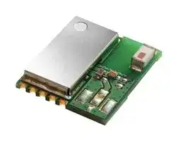


SPBTLE-RF0TR
Bluetooth 4.1, Low Energy, Module, 1.7V to 3.6V Supply, +4dBm Power, -88dBm Sensitivity
- Manufacturer: STMICROELECTRONICS
- Product type: Bluetooth Modules & Adaptors
- Bluetooth Version:Bluetooth 4.1; Supply Voltage Min:1.7V; Supply Voltage Max:3.6V; Signal Range Max:-; Data Rate:-; Bluetooth Class:-; Receive Sensitivity:-88dBm; Operating Temperature Min:-
- SVHC: No SVHC (17-Dec-2015)
- Interfaces: SPI
- Product Range: -
- Certifications: CE, FCC, IC
- Bluetooth Class: -
- Bluetooth Version: Bluetooth 4.1
- Supply Voltage Range: 1.7 V to 3.6 V
- Receiver Sensitivity Rx: -88 dBm
- Operating Temperature Range: -40 °C to 85 °C
| Delivery and price | |
|---|---|
| Units per pack | 100 |
| Price | 6.43 € |
| Current stock | 10+ |
| Lead time | 30 days |
**SPBTLE-RF0**

Datasheet

Very low power network processor module for Bluetooth® Low Energy v4.1

## **Features**

- Bluetooth v4.1 compliant – Supports master and slave modes

- – Multiple roles supported simultaneously

- 5 • Embedded Bluetooth low energy protocol stack

- MY, ‘“S, – GAP, GATT, SM, L2CAP, LL, RFPHY • Bluetooth low energy profiles provided separately • Bluetooth radio performance: – Embedded ST BlueNRG-MS – Tx power: + 4 dBm

- – Rx sensitivity: - 88 dBm

- – Provides up to 92 dB link budget with excellent link reliability

- • Host interface – SPI, IRQ, and RESET

- – On-field stack upgrading available via SPI

- • AES security co-processor • Certifications: – CE qualified

- – FCC, IC modular approval certified

- – BT SIG qualified

- • On-board chip antenna

- **Product status link** • Operating supply voltage: from 1.7 to 3.6 V SPBTLE-RF0 • Operating temperature range: -40 °C to 85 °C **Applications** • Watches • Fitness, wellness and sports • Consumer medical • Security/proximity • Remote control • Home and industrial automation • Assisted living • Mobile phone peripherals

   - PC peripherals

## **Description**

The SPBTLE-RF0 is an easy to use Bluetooth[®] Low Energy network processor module, compliant with Bluetooth v4.1. The SPBTLE-RF0 module supports multiple roles simultaneously, and can act at the same time as Bluetooth Low Energy master and slave device.

**DS12080** - **Rev 3** - **January 2021** For further information contact your local STMicroelectronics sales office.

www.st.com

**SPBTLE-RF0**

The entire Bluetooth Low Energy stack and protocols are embedded into the SPBTLE-RF0 module. The external host application processor, where the application resides, is connected to the SPBTLE-RF0 module through a standard SPI interface.

The SPBTLE-RF0 module provides a complete RF platform in a tiny form factor. Radio, antenna and high frequency oscillators are integrated to offer a certified solution to optimize the time to market of the final applications.

The SPBTLE-RF0 can be powered directly with a pair of AAA batteries or any power source from 1.7 to 3.6 V.

**DS12080** - **Rev 3**

**page 2/25**

**SPBTLE-RF0 General description**

## **1 General description**

The SPBTLE-RF0 is a Bluetooth Low Energy network processor module compliant with Bluetooth[®] v4.1.

The SPBTLE-RF0 module integrates the BlueNRG-MS BT radio controller with an on-board power-optimized Bluetooth stack.

It supports:

- Both master and slave roles

- GAP: central, peripheral, observer or broadcaster roles

- ATT/GATT: client and server

- SM: privacy, authentication and authorization

- L2CAP

The BlueNRG-MS radio embeds nonvolatile Flash memory which allows on-field stack upgrading.

In accordance with Bluetooth specification v4.1, the SPBTLE-RF0 module supports:

- Multiple simultaneous roles

- Simultaneous advertising and scanning

- Acting as slave for up to two masters simultaneously

- Privacy V1.1

- Low duty cycle directed advertising

- Connection parameter request procedure

- LE Ping

- 32 bits UUIDs

- L2CAP connection oriented channels

Both standard and proprietary Bluetooth low energy profiles, as well as a wide set of examples are available for the SPBTLE-RF0 from the ST website.

The external host application processor where the application resides is interfaced with the SPBTLE-RF0 module through an application controller interface protocol based on a standard SPI interface.

With the SPBTLE-RF0 module, developers can enable wireless connectivity in electronic devices without requiring any RF experience or expertise for integration into the final product. The SPBTLE-RF0 module provides a complete RF platform in a tiny form factor (13.5 x 11.5 x 2 mm) and, being a certified solution, optimizes the time to market of the final applications.

The SPBTLE-RF0 module allows applications to meet the tight peak current requirements when using standard coin cell batteries. SPBTLE-RF0 can be powered directly from a standard 3 V coin cell battery, a pair of AAA batteries or any power source from 1.7 to 3.6 V.

ST may update the FW provided with the modules at any time. ST recommends that users regularly check for documentation and the current FW version available at www.st.com/bluemodules.

**DS12080** - **Rev 3**

**page 3/25**

**SPBTLE-RF0 Block schematic**

## **2 Block schematic**

## **Figure 1. HW block diagram**

**==> picture [404 x 294] intentionally omitted <==**

**----- Start of picture text -----**<br>
Battery or External Supply<br>SPBTLE-RF0<br>SUPPLY FILTER<br>Bead Ferrite<br>INTERNAL 2.45 GHz<br>RF  antenna<br>LDO<br>Host Controller<br>interface<br>SPI  LINE<br>BLUETOOTH<br>RF<br>BLUENRG-MS<br>BALUN I/0 I/0 & Interrupt<br> + Filter Signals<br>(Optionals)<br>32 MHz 32.768 kHz<br>internal internal<br>clock Ring Oscillator<br> Crystal<br>32 MHz<br>clock<br>**----- End of picture text -----**<br>


**DS12080** - **Rev 3**

**page 4/25**

**SPBTLE-RF0 Software development kit**

## **3 Software development kit**

The SPBTLE-RF0 module embeds the BlueNRG-MS application processor. Refer to the BlueNRG-MS web page (http://www.st.com/en/wireless-connectivity/bluenrg-ms.html) to access:

- BlueNRG-MS datasheet

- development kit

- application notes

- user manuals

- tools and software

- design note and tips

For module firmware updates (BlueNRG-MS Bluetooth Stack), take into account the SPBTLE-RF0-specific configuration (see the block diagram) to select the proper binary file from the BlueNRG-MS Development Kit (STSW-BLUENRG-DK).

In particular the SPBTLE-RF0 module is configured with:

- 32 MHz crystal oscillator

- 32 KHz Ring Oscillator

- Internal LDO ( SMPS Off)

From the prebuilt image files provided for the BlueNRG-MS Development Kit, only the files with “32MHz”, “RO32K”, and “SMPS_OFF” in the file name are suitable for the SPBTLE-RF0.

For example only the ifr_3v1_003_mode02-32MHz-RO32K_SMPS_OFF.dat file is suitable for the SPBTLE-RF0. When used with the BlueNRG-GUI, the IFR configuration settings should reflect those pictured below.

**Figure 2. IFR configuration for SPBTLE-RF0**

**DS12080** - **Rev 3**

**page 5/25**

**SPBTLE-RF0 Software architecture**

**4 Software architecture**

The SPBTLE-RF0 module has been designed to work with an external Host processor connected via SPI.

**Figure 3. SPBTLE-RF0 application block diagram**

**DS12080** - **Rev 3**

**page 6/25**

**SPBTLE-RF0 Hardware specifications**

## **5 Hardware specifications**

General conditions (VIN = 3.3 V and 25 °C)

**Table 1. Absolute maximum ratings**

|**Rating**|**Min.**|**Typ.**|**Max.**|**Unit**|
|---|---|---|---|---|
|Storage temperature<br>range|- 40||+ 85|°C|
|Supply voltage, VIN|- 0.3||+ 3.9|V|
|I/O pin voltage (VIO<br>five-volt tolerant pin)|- 0.3||+ 3.9|V|
|RF saturation input<br>power||8||dBm|


**Table 2. Recommended operating conditions**

|**Rating**|**Min.**|**Typ.**|**Max.**|**Unit**|
|---|---|---|---|---|
|Operating temperature<br>range|- 40||+ 85|°C|
|Supply voltage, VIN|1.7|1.8|3.6|V|
|Signals and I/O pin<br>voltage (according<br>supply voltage)|1.7||3.6|V|
|RF frequency|2402||2480|MHz|


## **5.1 Current consumption**

Measurement conditions: VIN = 3.0 V, TX output power = +4 dBm, temperature = 25 °C, FW version = 7.1e

**Table 3. Current consumption**

|**Symbol**|**Parameter**|**Test conditions**|**Typ.**|**Peak**|**Unit**|
|---|---|---|---|---|---|
|IDD|Supply current|Shutdown /<br>STANDBY|1.98|1.98|µA|
|||Peripheral in<br>advertising (Adv Int<br>=<br>20 ms)|1.36|20.5|mA|
|||Peripheral in<br>advertising (Adv Int<br>=<br>40 ms)|0.68|20.5||
|||Peripheral in<br>advertising (Adv Int<br>=<br>80 ms)|0.34|20.5||
|||Peripheral in<br>connection (Conn<br>Int =|0.20|20.5||


**DS12080** - **Rev 3**

**page 7/25**

**SPBTLE-RF0 Current consumption**

|**Symbol**|**Parameter**|**Test conditions**|**Typ.**|**Peak**|**Unit**|
|---|---|---|---|---|---|
|||40 ms)|||mA|
|||Central in scan<br>mode (Scan Int =<br>1250 ms, scan<br>window = 1250 ms)|14.49|14.49||
|||Central in scan<br>mode (Scan Int =<br>1250 ms, scan<br>window = 625 ms)|7.24|14.49||
|||Central in<br>connection|0.186|20.5||


To increase the SPBTLE-RF0 module power efficiency, it is suggested to use 1.7 V power supply. For each calculated value refer to the following screenshots:

**Figure 4. Configuration of the “BlueNRG current consumption estimation tool”**

**Figure 5. Peripheral in advertising (Adv Int = 20 ms)**

**DS12080** - **Rev 3**

**page 8/25**

**SPBTLE-RF0 Current consumption**

**Figure 6. Peripheral in advertising (Adv Int = 40 ms)**

**Figure 7. Peripheral in connection (Conn Int = 80 ms)**

**DS12080** - **Rev 3**

**page 9/25**

**SPBTLE-RF0 Current consumption**

**Figure 8. Peripheral in connection (Conn Int = 40 ms)**

**Figure 9. Central in scan mode (Scan Int = 1250 ms, Scan Window = 1250 ms)**

**DS12080** - **Rev 3**

**page 10/25**

**SPBTLE-RF0 Current consumption**

**Figure 10. Central in scan mode (Scan Int = 1250 ms, Scan Window = 625 ms)**

**Figure 11. Central in connection (Conn Int = 40 ms)**

**DS12080** - **Rev 3**

**page 11/25**

**SPBTLE-RF0 Pin assignment**

## **5.2 Pin assignment**

## **Figure 12. Pin assignment**

**==> picture [404 x 236] intentionally omitted <==**

## **Table 4. Pin description**

|**Name**|**Type**|**Pin n°**|**Description**|**V max. tolerant**|
|---|---|---|---|---|
|SPI Interface|||||
|SPI_IRQ<br>O||4|SPI IRQ (SLAVE has<br>data for MASTER)|Vin|
|SPI_IRQSPI_CLK<br>I||7|SPI CLOCK (Max. 8<br>MHz)|Vin|
|SPI_MISO<br>O||8|SPI MISO (MASTER<br>in / SLAVE out)|Vin|
|SPI_MOSI<br>I||9|SPI MOSI (MASTER<br>out SLAVE in)|Vin|
|SPI_CS<br>I||10|SPI “Chip select” (SPI<br>slave select)|Vin|
|Power and ground|||||
|Vin||5|Vin|(1.7 V - 3.6 V max.)|
|GND||6|GND||
|Reset|||||
|BT_RESET<br>I||11|Reset input (active low<br>< 0.35 Vin)|(1.7 V - 3.6 V max.)|
|Not connected|||||
|EXT_LPCLK<br>I||1|Not connected. Must<br>be left floating.||
|GPIO2<br>I/|O|2|Not connected. Must<br>be left floating.||
|ANA TEST 0<br>I||3|Not connected. Must<br>be left floating.||


**DS12080** - **Rev 3**

**page 12/25**

**SPBTLE-RF0 Mechanical dimensions**

## **5.3 Mechanical dimensions**

**Figure 13. SPBTLE-RF0 module mechanical dimensions**

**==> picture [404 x 401] intentionally omitted <==**

**DS12080** - **Rev 3**

**page 13/25**

**SPBTLE-RF0 Mechanical dimensions**

**Figure 14. Recommend land pattern top view**

**==> picture [404 x 210] intentionally omitted <==**

**DS12080** - **Rev 3**

**page 14/25**

**SPBTLE-RF0 Hardware design**

## **6 Hardware design**

SPBTLE-RF0 module supports SPI hardware interfaces.

_Note:_

- _All unused pins should be left floating; do not ground_

- _All GND pins must be well grounded_

- _The area around the module should be free of any ground planes, power planes, trace routings, or metal for 6 mm from the module antenna position, in all directions._

- _Traces should not be routed underneath the module_

- _Reset pin must be keep low until Vin is stable_

## **6.1**

## **Reflow soldering**

The SPBTLE-RF0 is a high temperature strength surface mount Bluetooth[®] module supplied on an 11-pin, 4-layer PCB. The recommended final assembly reflow profiles are indicated below.

The soldering phase must be executed with care: pay special attention to the set up of the peak temperature to avoid undesired melting.

Below are some soldering profile recommendations.

**Table 5. Soldering**

|**Profile feature**|**Pb-free assembly**|
|---|---|
|Average ramp up rate (TSMAXto Tp)|3 °C / s max.|
|Preheat||
|Temperature min (TSmin.)|150 °C|
|Temperature max (TSmax.)|200 °C|
|Time (tSmin to tSmax.) (tS))|60 - 100 s|
|Time maintained above||
|Temperature TL|217 °C|
|Time tL|60 - 70 s|
|Peak temperature (TP)|240 + 0 °C|
|Time within 5 °C of actual peak temperature (TP)|10 - 20 s|
|Ramp down rate|6 °C / sec|
|Time from 25 °C to peak temperature|8 minutes max|


**DS12080** - **Rev 3**

**page 15/25**

**SPBTLE-RF0 Reflow soldering**

**Figure 15. Soldering profiles**

**==> picture [404 x 182] intentionally omitted <==**

**DS12080** - **Rev 3**

**page 16/25**

**SPBTLE-RF0 Regulatory compliance**

## **7 Regulatory compliance**

## **7.1 FCC certification**

This module has been tested and found to comply with the FCC part 15 rules. These limits are designed to provide reasonable protection against harmful interference in approved installations. This equipment generates, uses, and can radiate radio frequency energy and, if not installed and used in accordance with the instructions, may cause harmful interference to radio communications.

However, there is no guarantee that interference may not occur in a particular installation.

This device complies with part 15 of the FCC rules. Operation is subject to the following two conditions:

1. This device may not cause harmful interference,

   - and

2. this device must accept any interference received, including interference that may cause undesired operation.

Modifications or changes to this equipment not expressly approved by STMicroelectronics may render void the user's authority to operate this equipment.

## **Modular approval**

FCC ID: S9NSPBTLERF

In accordance with FCC part 15, the SPBTLE-RF0 is listed as a modular transmitter device.

This module is evaluated for stand-alone use only. Finished products incorporating multiple transmitters must comply with collocation and RF exposure requirements in accordance with FCC multi-transmitter product procedures. Collocated transmitters operating in portable RF Exposure conditions (e.g. < 20 cm from persons including but not limited to body worn and hand held devices) may require separate approval.

## **7.1.1 Labeling instructions**

When integrating the SPBTLE-RF0 into the final product, the OEM must ensure that the FCC labeling requirements are satisfied. A statement must be included on the exterior of the final product which indicates the product includes a certified module. The label should state the following (or similar wording that conveys the same meaning):

Contains FCC ID: S9NSPBTLERF

OR

This product contains FCC ID: S9NSPBTLERF

The OEM must include the following statements on the exterior of the final product unless the product is too small (e.g. less than 4 x 4 inches):

This device complies with Part 15 of the FCC Rules. Operation is subject to the following two conditions:

- this device may not cause harmful interference,

## and

- this device must accept any interference received, including any interference that may cause undesired operation.

**DS12080** - **Rev 3**

**page 17/25**

**SPBTLE-RF0 IC certification**

## **7.1.2 Product manual instructions**

This section applies to OEM final products containing the SPBTLE-RF0 module, subject to FCC compliance. The final product manual must contain the following statement (or a similar statement that conveys the same meaning):

## **Warning:**

_Changes or modifications not expressly approved by the party responsible for compliance could void the user's authority to operate the equipment. (Part. 15.21)_

In the case where an OEM seeks Class B (residential) limits for the final product, the following statement must be included in the final product manual:

_Note:_

_This equipment has been tested and found to comply with the limits for a Class B digital device, pursuant to part 15 of the FCC Rules. These limits are designed to provide reasonable protection against harmful interference in a residential installation. This equipment generates, uses and can radiate radio frequency energy and, if not installed and used in accordance with the instructions, may cause harmful interference to radio communications. However, there is no guarantee that interference will not occur in a particular installation. If this equipment does cause harmful interference to radio or television reception, which can be determined by turning the equipment off and on, the user is encouraged to try to correct the interference by one or more of the following measures:_

- _Reorient or relocate the receiving antenna_

- _Increase the separation between the equipment and receiver_

- _Connect the equipment into an outlet on a circuit different from that to which the receiver is connected_

- _Consult the dealer or an experienced radio/TV technician for help_

In the case where an OEM seeks the lesser category of a Class A digital device for the final product, the following statement must be included in the final product manual:

_Note:_

_This equipment has been tested and found to comply with the limits for a Class A digital device, pursuant to part 15 of the FCC Rules. These limits are designed to provide reasonable protection against harmful interference when the equipment is operated in a commercial environment. This equipment generates, uses, and can radiate radio frequency energy and, if not installed and used in accordance with the instruction manual, may cause harmful interference to radio communications. Operation of this equipment in a residential area is likely to cause harmful interference in which case the user will be required to correct the interference at his expense._

For more information refer to Test Report No. AR16-0006125-01 performed in accordance with:

- FCC Rules: Code of Federal Regulations (CFR) no. 47 Part 15 subpart C Section 15.247

## **7.2**

## **IC certification**

The SPBTLE-RF0 module has been tested and found compliant with the IC RSS-210 rules.

These limits are designed to provide reasonable protection against harmful interference in approved installations. This equipment generates, uses, and can radiate radio frequency energy and, if not installed and used in accordance with the instructions, may cause harmful interference to radio communications.

However, there is no guarantee that interference may not occur in a particular installation.

This device complies with RSS-210 of the IC rules. Operation is subject to the following two conditions:

- this device may not cause harmful interference and

- this device must accept any interference received, including interference that may cause undesired operation

Modifications or changes to this equipment not expressly approved by STMicroelectronics may render void the user's authority to operate this equipment.

## **Modular approval**

IC: 8976C-SPBTLERF

In accordance with IC RSS-210, the SPBTLE-RF0 is listed as a modular transmitter device.

This module is evaluated for stand-alone use only. Finished products incorporating multiple transmitters must comply with colocation and RF exposure requirements in accordance with IC multi-transmitter product procedures. Collocated transmitters operating in portable RF Exposure conditions (e.g. < 20 cm from persons including but not limited to body worn and hand held devices) may require separate approval.

**DS12080** - **Rev 3**

**page 18/25**

**SPBTLE-RF0 IC certification**

## **7.2.1 Labeling instructions**

When integrating the SPBTLE-RF0 into the final product, the OEM must ensure that the IC labeling requirements are satisfied. A statement must be included on the exterior of the final product which indicates that the product includes a certified module. The label should state the following (or similar wording that conveys the same meaning):

Contains IC: 8976C-SPBTLERF

OR

This product contains IC: 8976C-SPBTLERF

The OEM must include the following statements on the exterior of the final product unless the product is too small (e.g. less than 4 x 4 inches):

This device complies with RSS-210 of the IC rules. Operation is subject to the following two conditions:

- this device may not cause harmful interference

   - and

- this device must accept any interference received, including any interference that may cause undesired operation.

## **7.2.2 Product manual instructions**

This section applies to OEM final products containing the SPBTLE-RF0 module, subject to IC compliance. The final product manual must contain the following statement (or a similar statement that conveys the same meaning):

## **Warning:**

_Changes or modifications not expressly approved by the party responsible for compliance could void the user's authority to operate the equipment. (RSS-210)_

In the case where an OEM seeks Class B (residential) limits for the final product, the following statement must be included in the final product manual:

_Note:_

_This equipment has been tested and found to comply with the limits for a Class B digital device, pursuant to RSS-210 of the IC Rules. These limits are designed to provide reasonable protection against harmful interference in a residential installation. This equipment generates, uses and can radiate radio frequency energy and, if not installed and used in accordance with the instructions, may cause harmful interference to radio communications. However, there is no guarantee that interference will not occur in a particular installation. If this equipment does cause harmful interference to radio or television reception, which can be determined by turning the equipment off and on, the user is encouraged to try to correct the interference by one or more of the following measures:_

- _Reorient or relocate the receiving antenna_

- _Increase the separation between the equipment and receiver_

- _Connect the equipment into an outlet on a circuit different from that to which the receiver is connected_

- _Consult the dealer or an experienced radio/TV technician for help_

In the case where an OEM seeks the lesser category of a Class A digital device for the final product, the following statement must be included in the final product manual:

_Note:_

_This equipment has been tested and found to comply with the limits for a Class A digital device, pursuant to RSS-210 of the IC Rules. These limits are designed to provide reasonable protection against harmful interference when the equipment is operated in a commercial environment. This equipment generates, uses, and can radiate radio frequency energy and, if not installed and used in accordance with the instruction manual, may cause harmful interference to radio communications. Operation of this equipment in a residential area is likely to cause harmful interference in which case the user will be required to correct the interference at his expense._

For more information refer to Test Report No. AR16-0006125-02 performed in accordance with:

- INDUSTRY CANADA Spectrum Management and Telecommunications Radio Standards Specification

- RSS-210:210 Licence-exempt Radiocommunication Devices (All Frequency Bands): Category I Equipment

- RSS-247:2015Digital Transmission Systems (DTSs), Frequency Hopping Systems (FHSs) and LicenceExempt Local Area Network (LE-LAN) Devices

**DS12080** - **Rev 3**

**page 19/25**

**SPBTLE-RF0 CE certification**

## **7.3 CE certification**

The SPBTLE-RF0 module has been certified according to the following standards:

- ETSI EN 300 328 V 2.1.1 (2016-11)[(1)]

- ETSI EN 301 489-17 V3.1.1 (2017-02)[(2)]

- ETSI EN 301 489-1 V2.1.1 (2017-02)[(3)]

- EN 62368-1:2020/A11:2020[(4)]

- EN 62311:2008

_1. ETSI EN 300 328 V 2.1.1 (2016 11): “electromagnetic compatibility and radio spectrum Matters (ERM); Wideband transmission systems; data transmission equipment operating in the 2.4 GHZ ISM band and using wideband modulation techniques; harmonized EN covering essential requirements under article 3.2 of the R&TTE directive”._

_2. ETSI EN 301 489-17 V 3.1.1 (2017 02): “electromagnetic compatibility and radio spectrum matters (ERM); electromagnetic compatibility (EMC) standard for radio equipment and services; part 17: specific condition for 2.4 GHz wideband transmission systems and 5 GHz high performance RLAN equipment”._

_3. ETSI EN 301 489-1 V2.1.1 (2017 02): “electromagnetic compatibility and radio spectrum matters (ERM); electromagnetic compatibility (EMC) standard for radio equipment and services; part 1: common technical requirements”._

_4. EN 62368-1:2020/A11:2020: “Audio/video, information and communication technology equipment - Part 1: Safety requirements”._

The module is provided by CE marking:

**Figure 16. CE certified**

The module has obtained the RED certificate: No. 0051-RED-0011 The certified module production firmware release is: **7.X**

For additional information please refer to:

**STMicroelectronics Via C. Olivetti 2, Agrate Brianza 20864 (ITALY)**

## **7.4**

## **Bluetooth certification**

The module with embedded stack and profile has been qualified in accordance with the Bluetooth special interest group (BT SIG) qualification rules:

- Declaration ID: D028766

- Qualified design ID: 71984

- Product type: End Product

- Core spec version: 4.1

- Product description: Bluetooth Low Energy v4.1 module

**DS12080** - **Rev 3**

**page 20/25**

**SPBTLE-RF0 Ordering information**

**8 Ordering information**

## **Table 6. Ordering information**

|**Order code**|**Description**|**Packing**|**MOQ**|
|---|---|---|---|
|SPBTLE-RF0TR|Bluetooth® V4.1 Low Energy module|Tape and reel|1000 pcs|


**DS12080** - **Rev 3**

**page 21/25**

**SPBTLE-RF0 Package information**

**9 Package information**

In order to meet environmental requirements, ST offers these devices in different grades of ECOPACK packages, depending on their level of environmental compliance. ECOPACK specifications, grade definitions and product status are available at: www.st.com. ECOPACK is an ST trademark.

**DS12080** - **Rev 3**

**page 22/25**

**SPBTLE-RF0 Traceability**

## **10 Traceability**

Each module is univocally identified by serial number stored in a 2D data matrix laser marked on the bottom side of the module itself.

The serial number has the following format:

**Table 7. Traceability information**

|**Letter**|**Meaning**|
|---|---|
|WW|Week|
|YY|Year|
|D|Product ID family|
|FF|Production panel coordinate identification|
|NNN|Progressive serial number|


Each module bulk is identified by a bulk ID.

BULK ID and module 2D data matrix are linked by a reciprocal traceability link.

The module 2D data matrix traces the lot number of any raw material used.

**DS12080** - **Rev 3**

**page 23/25**

**SPBTLE-RF0**

## **Revision history**

**Table 8. Document revision history**

|**Date**|**Version**|**Changes**|
|---|---|---|
|10-May-2017|1|Initial release.|
|11-Jul-2017|2|Updated Ordering information.<br>Document status promoted from preliminary to production data.<br>Minor text changes.|
|05-Oct-2017|3|UpdatedSection  7.3  CE certification|
|13-Jan-2021|4|UpdatedSection  7.3  CE certificationandSection  7.4  Bluetooth<br>certification.|


**DS12080** - **Rev 3**

**page 24/25**

**SPBTLE-RF0**

## **IMPORTANT NOTICE – PLEASE READ CAREFULLY**

STMicroelectronics NV and its subsidiaries (“ST”) reserve the right to make changes, corrections, enhancements, modifications, and improvements to ST products and/or to this document at any time without notice. Purchasers should obtain the latest relevant information on ST products before placing orders. ST products are sold pursuant to ST’s terms and conditions of sale in place at the time of order acknowledgement.

Purchasers are solely responsible for the choice, selection, and use of ST products and ST assumes no liability for application assistance or the design of Purchasers’ products.

No license, express or implied, to any intellectual property right is granted by ST herein.

Resale of ST products with provisions different from the information set forth herein shall void any warranty granted by ST for such product.

ST and the ST logo are trademarks of ST. For additional information about ST trademarks, please refer to www.st.com/trademarks. All other product or service names are the property of their respective owners.

Information in this document supersedes and replaces information previously supplied in any prior versions of this document.

© 2021 STMicroelectronics – All rights reserved

**DS12080** - **Rev 3**

**page 25/25**
Updated at April 28, 2026
STMicroelectronics is a global leader in the semiconductor industry, recognized for developing highly integrated, energy-efficient solutions that power modern electronics. With a strong focus on innovation, ST provides a comprehensive portfolio of microelectronics that address the demanding requirements of industrial, automotive, communications, and consumer applications. Our extensive selection of STMicroelectronics components is built around a robust lineup of discrete semiconductors and circuit protection devices. We offer a wide variety of single MOSFETs, Schottky diodes, and fast and ultrafast recovery rectifier diodes, designed to deliver exceptional efficiency and thermal performance in power management and conversion systems. For robust circuit protection, our inventory features hundreds of transient voltage suppressors and TVS diodes that safeguard sensitive electronic components against destructive voltage spikes. In addition to core power discretes like TRIACs, SCRs, bipolar transistors, and single IGBTs, our STMicroelectronics range includes specialized integrated passive filters and MEMS sensors. Furthermore, ST offers advanced integrated passive devices, such as baluns and RF filters, which utilize high-quality monolithic RF IPD processes on glass or high-resistance silicon substrates. These components provide competitive cost structures, reduced power losses, and simplified RFIC-to-antenna matching, ensuring optimal system performance and delivering the reliability required for next-generation wireless and power designs.
About Novapart
Novapart is a B2B electronic component broker specialising in stock shortages and cost reduction. We source hard-to-find parts and identify compliant alternatives across a catalogue of 410,000+ components from 500+ manufacturers.
Learn more →Stock Shortage Specialist
When a component is unavailable, discontinued or has an unacceptable lead time, we tap into our network of vetted European and Asian distributors to source what you need — without compromising on quality or traceability.
Request a quote →Compliant Alternatives
We identify pin-to-pin, electrically equivalent substitutes that meet the same certifications (RoHS, AEC-Q100, REACH) as your original specification — validated against datasheets, not just part numbers. Often at a lower cost.
BOM Analysis service →