
Image not available
Illustrative purposes only

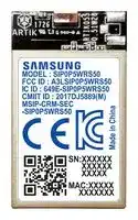
SIP-0P5WRS502
Wireless LAN Module, ARTIK 055s Series, 2.4 GHz, I2C, I2S, UART, Wireless Connectivity
⚠️ Reference pricing provided. In case of supply shortages, we will connect you with our trusted procurement partners to ensure your project's continuity.
- Manufacturer: SAMSUNG ARTIK
- Product type: WLAN Modules & USB Adaptors
- Frequency RF: 2.4GHz
- Product Range: ARTIK 055s Series
- Module Interface: I2C, I2S, SPI, UART
- Module Applications: Wireless Connectivity
| Delivery and price | |
|---|---|
| Units per pack | 250 |
| Price | 4.86 € |
| Current stock | 10+ |
| Lead time | 30 days |
Datasheet

**==> picture [220 x 164] intentionally omitted <==**

**----- Start of picture text -----**<br>
:<br>Modules<br>**----- End of picture text -----**<br>


**ARTIK 055s Module Datasheet**

**Samsung Semiconductor, Inc.**

**ARTIK 055s Module Datasheet**

## **MODULE OVERVIEW**

The Samsung ARTIK™ 055s Module is a highly integrated module for secure Internet of Things (IoT) devices that require Wi-Fi® connectivity. It is based on an ARM® Cortex® R4 core, with on-module RAM and flash memory, a complete 2.4GHz Wi-Fi subsystem with on-module antenna, an independent security subsystem, PUF-based module authentication, and a large complement of standard I/O interfaces.

The ARTIK 055s Module provides excellent performance in a variety of environments, with a feature set tailored specifically for IoT end nodes.

_Figure 1. ARTIK 055s Module Top View_

|**Processor**|**Processor**|
|---|---|
|**CPU**|32-bit ARM® Cortex® R4 with 32KB I-Cache and 32KB D-Cache @ 320MHz|
|**Memory**||
|**RAM**|1280KB (General usage)<br>128KB (Global IPC data)|
|**FLASH**|8MB Flash|
|**Security**||
|**Secure Subsystem**|AES/DES/TDES, SHA-1/SHA-2, PKA (Public Key Accelerator), PRNG/DTRNG<br>(Random Number Generators), Secure key storage|
|**PUF**|Physically Unclonable Function|
|**Radio**||
|**Wi-Fi**|Certified IEEE802.11™ b/g/n Wi-Fi® 2.4GHz radio served by a dedicated 32-bit ARM<br>Cortex R4 with 32KB I-Cache and 16KB D-Cache @ 480MHz|
|**Regulatory**|FCC (U.S.), IC (Canada), CE (EU), KC (Korea), SRRC (China)|
|**Power Management**||
|**Single Supply**|3.3V|
|**Interfaces**||
|**I/O**|UART, I2C, SPI, PWM, ADC, GPIO. I2S|
|**Form Factor**||
|**Dimensions**|15mm W x 26mm D x 3.9mm H|
|**Operation Enviroment**||
|**Temperture**|–20 to 85oC Tc|


**2**

**Samsung Semiconductor, Inc.**

**ARTIK 055s Module Datasheet**

## **TABLE OF CONTENTS**

**==> picture [542 x 586] intentionally omitted <==**

**----- Start of picture text -----**<br>
||||
|---|---|---|
|Module Overview................................................................................................................................................................2|
|Version History ...................................................................................................................................................................7|
|Block Diagram.....................................................................................................................................................................8|
|CPU ...............................................................................................................................................................................8|
|Memory.........................................................................................................................................................................9|
|Real Time Clock............................................................................................................................................................9|
|PUF Unit ........................................................................................................................................................................9|
|Security Subsystem ...................................................................................................................................................10|
|Wi-Fi Subsystem.......................................................................................................................................................... 11|
|GPIO Interfaces ........................................................................................................................................................... 11|
|SPI Interfaces............................................................................................................................................................... 11|
|I|[2]|C Interfaces............................................................................................................................................................... 11|
|PWM Interfaces ........................................................................................................................................................... 11|
|I|[2]|S Interface................................................................................................................................................................ 12|
|ADC Interfaces ........................................................................................................................................................... 12|
|UART Interfaces.......................................................................................................................................................... 13|
|Module Pad Physical Layout............................................................................................................................................. 14|
|Module Pad Signal Definitions ......................................................................................................................................... 15|
|Module Pad Signal Definitions by Function..................................................................................................................... 18|
|GPIO Interface............................................................................................................................................................ 18|
|I2C Interface............................................................................................................................................................... 19|
|SPI Interface ............................................................................................................................................................... 19|
|I2S Interface .............................................................................................................................................................. 20|
|ADC Interface ............................................................................................................................................................ 20|
|PWM Interface ............................................................................................................................................................ 21|
|UART Interface ........................................................................................................................................................... 21|
|Debug Interface ......................................................................................................................................................... 21|
|INT Interface...............................................................................................................................................................22|
|Reset Interface ...........................................................................................................................................................22|
|Power Interface ..........................................................................................................................................................22|
|Electrical Specifications...................................................................................................................................................23|
|Absolute Maximum Rating.........................................................................................................................................23|
|Recommended Operating Conditions ......................................................................................................................23|
|DC Electrical Characteristics .....................................................................................................................................24|
|Power and Current Consumption..............................................................................................................................25|
|ESD Ratings ................................................................................................................................................................25|
|RF Electrical Characteristics......................................................................................................................................25|
|Mechanical Specifications ............................................................................................................................................... 27|
|Module Antenna Placement Requirements ..............................................................................................................28|
|Certification and Compliance..........................................................................................................................................29|
|CE................................................................................................................................................................................29|
|FCC Regulatory Disclosures ......................................................................................................................................29|
|Wi-Fi ........................................................................................................................................................................... 30|
|Industry Canada Regulatory Disclosures ................................................................................................................. 30|

**----- End of picture text -----**<br>


**3**

**Samsung Semiconductor, Inc.**

**ARTIK 055s Module Datasheet**

Industry Canada Statement ............................................................................................................................... 30 KC................................................................................................................................................................................ 31 SRRC ........................................................................................................................................................................... 31 EU Regulatory Disclosures.........................................................................................................................................32 CE Statement ......................................................................................................................................................32 Ordering Information .......................................................................................................................................................33

**4**

**Samsung Semiconductor, Inc.**

**ARTIK 055s Module Datasheet**

## **LIST OF FIGURES**

|**LISTIST **|**OF FIGURES FIGURESIGURES**|
|---|---|
|Figure 1. ARTIK 055s Module Top View .............................................................................................................................2|Figure 1. ARTIK 055s Module Top View .............................................................................................................................2|
|Figure 2. ARTIK 055s Module Block Diagram ....................................................................................................................8|Figure 2. ARTIK 055s Module Block Diagram ....................................................................................................................8|
|Figure 3. ADC LSB behavior............................................................................................................................................. 12|Figure 3. ADC LSB behavior............................................................................................................................................. 12|
|Figure 4. ARTIK 055s Module Edge Pinout (Top View) ................................................................................................... 14|Figure 4. ARTIK 055s Module Edge Pinout (Top View) ................................................................................................... 14|
|Figure 5. ARTIK 055s Module Mechanical Dimensions (Top View) ................................................................................ 27|Figure 5. ARTIK 055s Module Mechanical Dimensions (Top View) ................................................................................ 27|
|Figure 6. Module Placement Restrictions........................................................................................................................28|Figure 6. Module Placement Restrictions........................................................................................................................28|


**5**

**Samsung Semiconductor, Inc.**

**ARTIK 055s Module Datasheet**

## **LIST OF TABLES**

|**LISTIST**|**LISTIST OF TABLES TABLESABLES**|
|---|---|
|Table 1. ARTIK 055s Module Pinout Signal Descriptions................................................................................................. 15|Table 1. ARTIK 055s Module Pinout Signal Descriptions................................................................................................. 15|
|Table 2. GPIO Interface .................................................................................................................................................... 18|Table 2. GPIO Interface .................................................................................................................................................... 18|
|Table 3. I2C Interface ....................................................................................................................................................... 19|Table 3. I2C Interface ....................................................................................................................................................... 19|
|Table 4. SPI Interface........................................................................................................................................................ 19|Table 4. SPI Interface........................................................................................................................................................ 19|
|Table 5. I2S Interface....................................................................................................................................................... 20|Table 5. I2S Interface....................................................................................................................................................... 20|
|Table 6. ADC Interface .................................................................................................................................................... 20|Table 6. ADC Interface .................................................................................................................................................... 20|
|Table 7. PWM Interface..................................................................................................................................................... 21|Table 7. PWM Interface..................................................................................................................................................... 21|
|Table 8. UART Interface.................................................................................................................................................... 21|Table 8. UART Interface.................................................................................................................................................... 21|
|Table 9. Debug Interface.................................................................................................................................................. 21|Table 9. Debug Interface.................................................................................................................................................. 21|
|Table 10. Interrupt Interface.............................................................................................................................................22|Table 10. Interrupt Interface.............................................................................................................................................22|
|Table 11. Reset Interface...................................................................................................................................................22|Table 11. Reset Interface...................................................................................................................................................22|
|Table 12. Power Interface .................................................................................................................................................22|Table 12. Power Interface .................................................................................................................................................22|
|Table 13. Absolute Maximum Ratings..............................................................................................................................23|Table 13. Absolute Maximum Ratings..............................................................................................................................23|
|Table 14. Recommended Operating Conditions.............................................................................................................23|Table 14. Recommended Operating Conditions.............................................................................................................23|
|Table 15. GPIO DC Electrical Characteristics...................................................................................................................24|Table 15. GPIO DC Electrical Characteristics...................................................................................................................24|
|Table 16. GPIO Signal Drive Strengths.............................................................................................................................24|Table 16. GPIO Signal Drive Strengths.............................................................................................................................24|
|Table 17. ADC DC Electrical Characteristics....................................................................................................................25|Table 17. ADC DC Electrical Characteristics....................................................................................................................25|
|Table 18. ARTIK 055s Module Power Consumption ........................................................................................................25|Table 18. ARTIK 055s Module Power Consumption ........................................................................................................25|
|Table 19. ESD Ratings .......................................................................................................................................................25|Table 19. ESD Ratings .......................................................................................................................................................25|
|Table 20. Tx Performance Characteristics ......................................................................................................................25|Table 20. Tx Performance Characteristics ......................................................................................................................25|
|Table 21. Rx Performance Characteristics ......................................................................................................................26|Table 21. Rx Performance Characteristics ......................................................................................................................26|


**6**

**Samsung Semiconductor, Inc.**

**ARTIK 055s Module Datasheet**

## **VERSION HISTORY**

|~~a~~|~~es~~||
|---|---|---|
|**Revision**<br>~~a~~|**Date**<br>~~es~~|**Description**|
|V1.0<br>~~a~~<br>~~P|~~|November 20, 2017<br>~~es~~<br>~~P|~~<br>~~|~~|First release.|
|V1.1<br>~~P|~~<br>~~ee~~|November 30, 2017<br>~~P|~~<br>~~|~~<br>~~P~~|Modified GPIO name for XSPI1_MISO,XSPI1_MOSI, XSPI1_CLK, and XSPI1_CSN in_Table 1_<br> and_Table 4_<br>to be consistent with assigned name in_Table 2_<br>.<br>Removed GPIO names from_Table 9_<br>.<br>Added maximum storage temperature range, TA, in_Absolute Maximum Rating_<br> section.<br>~~Pn~~|
|V1.2<br>~~P|~~<br>~~ee~~|December 6, 2017<br>~~P|~~<br>~~|~~<br>~~P~~|Updated_Mechanical Specifications_<br>.<br>~~Pn~~|
|V1.3<br>~~ee~~|January 8, 2018<br>~~P~~|_SRRC_<br>:Updated CMIIT ID.<br>_Wi-Fi_<br>:Certification information and certification ID added.<br>~~Pn~~|
|V1.4<br>~~a~~|January 10, 2018<br>~~ee~~|_Module Antenna Placement Requirements_<br>:Modified and separated PCB routing and component<br>placement keep-out areas.<br>_I_<br>_2S Interface_<br>:Changed features to indicate that the interface operates in slave mode only.<br>~~ee~~|


**7**

**Samsung Semiconductor, Inc.**

**ARTIK 055s Module Datasheet**

## **BLOCK DIAGRAM**

_Figure 2_ shows a functional block diagram of the ARTIK 055s Module.

**==> picture [312 x 374] intentionally omitted <==**

**----- Start of picture text -----**<br>
Processor System<br>58 GPIO<br>ARM Cortex R4<br>32KB I‐Cache<br>32KB D‐Cache<br>16<br>1280KB RAM Interrupts<br>[|<br>4 Std UART<br>8MB Flash<br>[| Ports<br>128KB RAM<br>6 PWM 58<br>Global IPC Data<br>Signals<br>a|<br>3 I2C Ports<br>Power Management<br>4 SPI Ports<br>|<br>Wi‐Fi Subsystem 1 I2S Port<br>|<br>Debug<br>Security Subsystem UART &<br>JTAG<br>|<br>4 ADC<br>PUF RTC<br>Signals<br>ee ee [ee]<br>Figure 2. ARTIK 055s Module Block Diagram<br>**----- End of picture text -----**<br>


## **CPU**

The ARTIK 055s Module CPU has an ARM® Cortex® R4. It has the following features:

- 32KB of Instruction Cache (I-Cache)

- 32KB of Data Cache (D-Cache)

- 320MHz execution clock

- R4 core tuned for embedded and real-time applications

**8**

**Samsung Semiconductor, Inc.**

**ARTIK 055s Module Datasheet**

## **Memory**

The ARTIK 055s Module on-module memory has the following features:

- CPU and general purpose RAM

   - 1280KB CPU RAM

   - 128KB global Inter-Process Communication (IPC) RAM

- 8MB flash

## **Real Time Clock**

The ARTIK 055s Module has a Real Time Clock (RTC) for tracking date/time. The RTC has the following features:

- Binary-Coded Decimal (BCD) coded seconds, minutes, hour, day of the week, day, month, and year

- Leap year detection and compensation

- Millisecond tick time interrupt for Real-Time Operating System (RTOS) kernel time tick

## **PUF Unit**

The ARTIK 055s Module has a Physically Unclonable Function (PUF) unit. The PUF unit has the following features:

- Generates unique key values, locked to an individual ARTIK 055s Module

- The algorithm construction is unique to each module

- Allows individual ARTIK 055s Modules to be “fingerprint-identified”

**9**

**Samsung Semiconductor, Inc.**

**ARTIK 055s Module Datasheet**

## **Security Subsystem**

The ARTIK 055s Module has an independent security subsystem to ensure secure end-to-end operation in any IoT environment. The security subsystem includes the following features:

- Secure IPC Mailbox for inter-subsystem communication

- Encapsulated key support

   - Backup encryption key - 256 bits

   - Security subsystem root private key - 521 bits

   - Storage key - 256 bits

- Symmetric key engines

   - Secure AES

   - Secure DES/Triple-DES

- Stream cipher engine

   - ARC4 engine

- Various Hash engines

   - SHA-1, SHA2-256, SHA2-384, SHA2-512, MD5 HMAC

- Asymmetric key engines

   - PKA (Public Key Accelerator) engine

- PRNG (Pseudo Random Number Generator)

- DTRNG (Digital True Random Number Generator)

- Secure key storage

**10**

**Samsung Semiconductor, Inc.**

**ARTIK 055s Module Datasheet**

## **Wi-Fi Subsystem**

The ARTIK 055s Module has an 802.11b/g/n Wi-Fi subsystem. The Wi-Fi subsystem has the following features:

- 802.11™ b/g/n support at 2.4GHz

- 20MHz single stream (802.11n)

- WPA/WPA2

- Dedicated Wi-Fi Processor subsystem with 480MHz 32-bit ARM Cortex R4 supported by 32KB I-Cache and 16KB D-Cache.

## **GPIO Interfaces**

The ARTIK 055s Module has flexible General Purpose Input Output (GPIO) interfaces:

- 58 configurable GPIO ports

- Independently configurable for either general purpose input or output

- 43 configurable for alternate functionality

- Configurable internal pull-up or pull-down resistors

## **SPI Interfaces**

The ARTIK 055s Module has four SPI interfaces, each with the following features:

- Full duplex communication

- 8, 16 or 32-bit shift registers and bus interface

- Motorola SPI protocol and National Semiconductor Microwire protocol

- Master and slave mode operation

- Two independent 32-bit wide transmit/receive FIFOs

- Transmit and receive speeds up to 50MHz

## **I[2] C Interfaces**

The ARTIK 055s Module has three high speed multi-master I[2] C interfaces available, with speeds up to 3.4Mbps.

## **PWM Interfaces**

The ARTIK 055s Module has six PWM timers, each with the following features:

- 32 bits of resolution for each PWM signal

- Two 8-bit prescalers (first level of division) and 5 clock dividers/multiplexers for second-level division

- Continuous run or one-shot pulse mode

- Dead zone generator to avoid simultaneous change of multiple PWM signals

- Interrupt generation

**11**

**Samsung Semiconductor, Inc.**

**ARTIK 055s Module Datasheet**

## **I[2] S Interface**

The ARTIK 055s Module has one I[2] S interface with the following features:

- Each channel includes a 32-bit × 64 data FIFO for both transmit and receive

- Supports stereo I[2] S bus channels with external DMA-based operations

- Can mix two sound sources from a primary and secondary source

- Serial data transfer formats of 8 bits, 16 bits, or 24 bits per channel

- Supports both MSB and LSB justified data formats

- Operates in I[2] S slave mode only

## **ADC Interfaces**

The ARTIK 055s Module has four analog-to-digital converter (ADC) channels. Each interface has the following features:

- 12-bit resolution

- ADC conversion clock at 1.08 mega-samples per second (MSPS) using a main 6.5MHz clock

- Supports sample averaging over 1, 2, 4, 8, 16, 32, or 64 samples

- Differential non-linearity error range of ±2 LSB bits (value of ±2)

- Integral non-linearity error range of ±3 LSB bits (value of ±6)

- Top and bottom offset error range of ±4 LSB bits (value of ±10)

- Voltage range up to 1.8V

_Figure 3_ depicts the dynamic behavior between input voltage on the ADC and resulting LSB value in the ADC register.

**==> picture [246 x 207] intentionally omitted <==**

**----- Start of picture text -----**<br>
Result (LSB) Top<br>offset<br>Ideal<br>value<br>Ideal value<br>with offset<br>Real<br>value<br>Bottom  Analog in (V)<br>offset<br>**----- End of picture text -----**<br>


_Figure 3. ADC LSB behavior_

**12**

**Samsung Semiconductor, Inc.**

**ARTIK 055s Module Datasheet**

## **UART Interfaces**

The ARTIK 055s Module has five 2-pin UART interfaces; one is used in the debug block. Each has the following features:

- Can be operated in DMA or interrupt-based mode

- Support for 5, 6, 7, or 8-bit serial data transmit and receive

- Programmable baud rate

- One or two stop-bit insertion

**13**

**Samsung Semiconductor, Inc.**

**ARTIK 055s Module Datasheet**

## **MODULE PAD PHYSICAL LAYOUT**

The ARTIK 055s Module utilizes 82 signal, power, and ground pads. The figure below shows how the physical layout orients the signal pads assigned at the edge of the ARTIK 055s Module. _Figure 1_ shows the edge pads and the signal names.

_Figure 4. ARTIK 055s Module Edge Pinout (Top View)_

**14**

**Samsung Semiconductor, Inc.**

**ARTIK 055s Module Datasheet**

## **MODULE PAD SIGNAL DEFINITIONS**

The tables below describes the characteristics of the ARTIK 055s Module pad signals. Some signals can be configured for alternate functionality. The remaining signals have dedicated functionality. Refer to the following column definitions.

- **Pad Number** defines the signal pad on the edge of the module. Refer to _Figure 4_ for pad/signal physical layout.

- **Pad Name** defines the net list name of the signal. The pad name may reflect on one of the possible optional signal functionality, and dictates the default power-on function.

- **GPIO Name** defines a generic name for referring to GPIO signals regardless of their current configured functionality. The name order is the same order as the GPIO signals appear in the GPIO configuration registers.

- **PU/PD** defines the power-on state of the internal pull up/pull down definition. PU:pull up, PD:pull down, N:no pull up/down.

- **GPIO Drive** defines the power-on state drive strength of GPIO and other signals. Configurable to 2mA, 4mA, 8mA, or 12mA. Do not use GPIO signals to power discrete components directly (such as LEDs). Use an external driver device instead (such as a transistor).

- **Option 1 - Option 6** lists the alternative functionality some signals can be configured to. Those signals without any options are dedicated to their function. The pad name signifies the default power-on state.

_Table 1. ARTIK 055s Module Pinout Signal Descriptions_

|**Pad**<br>**Number**<br>~~po~~|**Pad Name**<br>**& Default**<br>**Function**<br>~~po~~|**GPIO**<br>**Name**|**PU/PD**|**GPIO**<br>**Drive**|**Option 1**|**Option 2**|**Option 3**|**Option 4**|**Option 5**|**Option 6**|
|---|---|---|---|---|---|---|---|---|---|---|
|1<br>~~po~~<br>~~po~~|GND<br>~~po~~<br>~~po~~|–|–|–|–|–|–|–|–|–|
|2<br>~~po~~<br>~~po~~<br>~~po~~|XADC0AIN_1<br>~~po~~<br>~~po~~<br>~~po~~|–|–|–|–|–|–|–|–|–|
|3<br>~~po~~<br>~~po~~<br>~~po~~|XADC0AIN_0<br>~~po~~<br>~~po~~<br>~~po~~|–|–|–|–|–|–|–|–|–|
|4<br>~~po~~<br>~~po~~<br>~~po~~|XADC0AIN_2<br>~~po~~<br>~~po~~|–|–|–|–|–|–|–|–|–|
|5<br>~~po~~<br>~~po~~<br>~~po~~|XADC0AIN_3<br>~~po~~<br>~~po~~|–|–|–|–|–|–|–|–|–|
|6<br>~~po~~<br>~~po~~<br>~~po~~|XGPIO22<br>~~po~~<br>~~po~~|GPIO39|PD|2mA|GP Input|GP Output|–|–|–|NWEINT_GPG2[6]|
|7<br>~~po~~<br>~~po~~<br>~~po~~|XGPIO23<br>~~po~~<br>~~po~~<br>~~po~~|GPIO40|PD|2mA|GP Input|GP Output|–|–|–|NWEINT_GPG2[7]|
|8<br>~~po~~<br>~~po~~<br>~~po~~|XRESET_N<br>~~po~~<br>~~po~~<br>~~po~~|–|–|–|–|–|–|–|–|–|
|9<br>~~po~~<br>~~po~~<br>~~po~~|XJTAG_TRST_N<br>~~po~~<br>~~po~~<br>~~po~~|–|PD|–|–|–|–|–|–|–|
|10<br>~~po~~<br>~~po~~<br>~~po~~|XJTAG_TMS<br>~~po~~<br>~~po~~<br>~~po~~|–|PU|–|–|–|–|–|–|–|
|11<br>~~po~~<br>~~po~~<br>~~po~~|XJTAG_TCK<br>~~po~~<br>~~po~~<br>~~po~~|–|PD|–|–|–|–|–|–|–|
|12<br>~~po~~<br>~~po~~<br>~~po~~|XJTAG_TDO<br>~~po~~<br>~~po~~<br>~~po~~|–|PD|2mA|–|–|–|–|–|–|
|13<br>~~po~~<br>~~po~~<br>~~po~~|XJTAG_TDI<br>~~po~~<br>~~po~~<br>~~po~~|–|PU|–|–|–|–|–|–|–|
|14<br>~~po~~<br>~~po~~<br>~~po~~|XEINT_0<br>~~po~~<br>~~po~~<br>~~po~~|GPIO45|PD|2mA|GP Input|GP Output|–|–|–|NWEINT_GPA0[0]|
|15<br>~~po~~<br>~~po~~<br>~~po~~|XEINT_2<br>~~po~~<br>~~po~~<br>~~po~~|GPIO47|PD|2mA|GP Input|GP Output|–|–|–|NWEINT_GPA0[2]|
|16<br>~~po~~<br>~~po~~<br>~~po~~|XEINT_1<br>~~po~~<br>~~po~~|GPIO46|PD|2mA|GP Input|GP Output|–|–|–|NWEINT_GPA0[1]|
|17<br>~~po~~<br>~~po~~<br>~~po~~|XI2C0_SCL<br>~~po~~<br>~~po~~|GPIO48|PD|8mA|GP Input|GP Output|HSI2C_0_SCL|–|–|–|
|18<br>~~po~~<br>~~po~~<br>~~po~~|XI2C0_SDA<br>~~po~~<br>~~po~~|GPIO49|PD|8mA|GP Input|GP Output|HSI2C_0_SDA|–|–|–|
|19<br>~~po~~<br>~~po~~<br>~~po~~|XI2C1_SCL<br>~~po~~<br>~~po~~|GPIO50|PD|8mA|GP Input|GP Output|HSI2C_1_SCL|–|–|–|
|20<br>~~po~~<br>~~po~~<br>~~po~~|XI2C1_SDA<br>~~po~~<br>~~po~~|GPIO51|PD|8mA|GP Input|GP Output|HSI2C_1_SDA|–|–|–|
|21<br>~~po~~<br>~~po~~<br>~~po~~|XUART0_RXD<br>~~po~~<br>~~po~~|GPIO52|PD|8mA|GP Input|GP Output|UART_0_RXD|–|–|–|
|22<br>~~po~~<br>~~po~~<br>~~po~~|XUART0_TXD<br>~~po~~<br>~~po~~<br>~~po~~|GPIO53|PD|8mA|GP Input|GP Output|UART_0_TXD|–|–|–|
|23<br>~~po~~<br>~~po~~<br>~~po~~|XDEBUG_RXD<br>~~po~~<br>~~po~~<br>~~po~~|GPIO54|PD|8mA|GP Input|GP Output|Xdebug_RXD|–|–|–|
|24<br>~~po~~<br>~~po~~|XDEBUG_TXD<br>~~po~~<br>~~po~~|GPIO55|PD|8mA|GP Input|GP Output|Xdebug_TXD|–|–|–|
|25<br>~~po~~|XPWMTOUT_5<br>~~po~~|GPIO16|PD|8mA|GP Input|GP Output|PWM_TOUT_6|–|–|–|


**15**

**Samsung Semiconductor, Inc.**

**ARTIK 055s Module Datasheet**

_Table 1. ARTIK 055s Module Pinout Signal Descriptions (Continued)_

|**Pad**<br>**Number**<br>~~po~~|**Pad Name**<br>**& Default**<br>**Function**<br>~~po~~|**GPIO**<br>**Name**|**PU/PD**|**GPIO**<br>**Drive**|**Option 1**|**Option 2**|**Option 3**|**Option 4**|**Option 5**|**Option 6**|
|---|---|---|---|---|---|---|---|---|---|---|
|26<br>~~po~~<br>~~po~~|XPWMTOUT_4<br>~~po~~<br>~~po~~|GPIO15|PD|8mA|GP Input|GP Output|PWM_TOUT_5|–|–|–|
|27<br>~~po~~<br>~~po~~<br>~~po~~|VIN_3P3<br>~~po~~<br>~~po~~<br>~~po~~|–|–|–|–|–|–|–|–|–|
|28<br>~~po~~<br>~~po~~<br>~~po~~|VIN_3P3<br>~~po~~<br>~~po~~<br>~~po~~|–|–|–|–|–|–|–|–|–|
|29<br>~~po~~<br>~~po~~<br>~~po~~|XPWMTOUT_3<br>~~po~~<br>~~po~~<br>~~po~~|GPIO13|PD|8mA|GP Input|GP Output|PWM_TOUT_3|–|–|–|
|30<br>~~po~~<br>~~po~~<br>~~po~~|XPWMTOUT_2<br>~~po~~<br>~~po~~<br>~~po~~|GPIO12|PD|8mA|GP Input|GP Output|PWM_TOUT_2|–|–|–|
|31<br>~~po~~<br>~~po~~<br>~~po~~|XPWMTOUT_1<br>~~po~~<br>~~po~~|GPIO11|PD|8mA|GP Input|GP Output|PWM_TOUT_1|COUNTER_0|UART_3_RTSn|–|
|32<br>~~po~~<br>~~po~~<br>~~po~~|GND<br>~~po~~<br>~~po~~|-|–|–|–|–|–|–|–|–|
|33<br>~~po~~<br>~~po~~<br>~~po~~|XPWMTOUT_0<br>~~po~~<br>~~po~~|GPIO10|PD|8mA|GP Input|GP Output|PWM_TOUT_0|–|UART_3_CTSn|–|
|34<br>~~po~~<br>~~po~~<br>~~Po~~|XGPIO27<br>~~po~~<br>~~po~~<br>~~Po~~|GPIO44|PD|2mA|GP Input|GP Output|I2S_0_SDI|–|–|–|
|35<br>~~po~~<br>~~Po~~<br>~~po~~|XSPI0_CLK<br>~~po~~<br>~~Po~~<br>~~po~~|GPIO00|PD|8mA|GP Input|GP Output|SPI_0_CLK|–|–|–|
|36<br>~~Po~~<br>~~po~~<br>~~po~~|XSPI0_MOSI<br>~~Po~~<br>~~po~~<br>~~po~~|GPIO03|PD|8mA|GP Input|GP Output|SPI_0_MOSI|–|–|–|
|37<br>~~po~~<br>~~po~~<br>~~po~~|XSPI0_CSN<br>~~po~~<br>~~po~~<br>~~po~~|GPIO01|PD|8mA|GP Input|GP Output|SPI_0_CSn|–|–|–|
|38<br>~~po~~<br>~~po~~<br>~~po~~|XSPI0_MISO<br>~~po~~<br>~~po~~<br>~~po~~|GPIO02|PD|8mA|GP Input|GP Output|SPI_0_MISO|–|–|–|
|39<br>~~po~~<br>~~po~~<br>~~po~~|XUART1_RXD<br>~~po~~<br>~~po~~<br>~~po~~|GPIO04|PD|8mA|GP Input|GP Output|UART_1_RXD|UART_2_CTSn|–|–|
|40<br>~~po~~<br>~~po~~<br>~~po~~|XUART1_TXD<br>~~po~~<br>~~po~~<br>~~po~~|GPIO05|PD|8mA|GP Input|GP Output|UART_1_TXD|UART_2_RTSn|–|–|
|41<br>~~po~~<br>~~po~~<br>~~po~~|XUART2_RXD<br>~~po~~<br>~~po~~<br>~~po~~|GPIO06|PD|8mA|GP Input|GP Output|UART_2_RXD|–|–|–|
|42<br>~~po~~<br>~~po~~<br>~~po~~|XUART2_TXD<br>~~po~~<br>~~po~~<br>~~po~~|GPIO07|PD|8mA|GP Input|GP Output|UART_2_TXD|–|–|–|
|43<br>~~po~~<br>~~po~~<br>~~po~~|GND<br>~~po~~<br>~~po~~|-|–|–|–|–|–|–|–|–|
|44<br>~~po~~<br>~~po~~<br>~~po~~|XUART3_RXD<br>~~po~~<br>~~po~~|GPIO08|PD|8mA|GP Input|GP Output|UART_3_RXD|–|–|–|
|45<br>~~po~~<br>~~po~~<br>~~po~~|XUART3_TXD<br>~~po~~<br>~~po~~|GPIO09|PD|8mA|GP Input|GP Output|UART_3_TXD|–|–|–|
|46<br>~~po~~<br>~~po~~<br>~~po~~|XGPIO12<br>~~po~~<br>~~po~~|GPIO29|PD|2mA|GP Input|GP Output|–|–|–|NWEINT_GPG1[4]|
|47<br>~~po~~<br>~~po~~<br>~~po~~|XGPIO9<br>~~po~~<br>~~po~~|GPIO26|PD|2mA|GP Input|GP Output|SPI_3_CSn|–|–|NWEINT_GPG1[1]|
|48<br>~~po~~<br>~~po~~<br>~~po~~|XGPIO11<br>~~po~~<br>~~po~~|GPIO28|PD|2mA|GP Input|GP Output|SPI_3_MOSI|–|–|NWEINT_GPG1[3]|
|49<br>~~po~~<br>~~po~~<br>~~po~~|XGPIO8<br>~~po~~<br>~~po~~<br>~~po~~|GPIO25|PD|2mA|GP Input|GP Output|SPI_3_CLK|–|–|NWEINT_GPG1[0]|
|50<br>~~po~~<br>~~po~~<br>~~po~~|XGPIO10<br>~~po~~<br>~~po~~<br>~~po~~|GPIO27|PD|2mA|GP Input|GP Output|SPI_3_MISO|–|–|NWEINT_GPG1[2]|
|51<br>~~po~~<br>~~po~~<br>~~po~~|XGPIO7<br>~~po~~<br>~~po~~<br>~~po~~|GPIO24|PD|2mA|GP Input|GP Output|SPI_2_MOSI|–|–|–|
|52<br>~~po~~<br>~~po~~<br>~~po~~|XGPIO6<br>~~po~~<br>~~po~~<br>~~po~~|GPIO23|PD|2mA|GP Input|GP Output|SPI_2_MISO|–|–|–|
|53<br>~~po~~<br>~~po~~<br>~~po~~|XGPIO5<br>~~po~~<br>~~po~~<br>~~po~~|GPIO22|PD|2mA|GP Input|GP Output|SPI_2_CSn|–|–|–|
|54<br>~~po~~<br>~~po~~<br>~~po~~|XGPIO4<br>~~po~~<br>~~po~~<br>~~po~~|GPIO21|PD|2mA|GP Input|GP Output|SPI_2_CLK|–|–|–|
|55<br>~~po~~<br>~~po~~<br>~~po~~|XSPI1_MISO<br>~~po~~<br>~~po~~|GPIO56|PD|2mA|GP Input|GP Output|SPI_1_MISO|–|–|–|
|56<br>~~po~~<br>~~po~~<br>~~po~~|XSPI1_CLK<br>~~po~~<br>~~po~~|GPIO54|PD|2mA|GP Input|GP Output|SPI_1_CLK|–|–|–|
|57<br>~~po~~<br>~~po~~<br>~~po~~|XSPI1_MOSI<br>~~po~~<br>~~po~~|GPIO57|PD|2mA|GP Input|GP Output|SPI_1_MOSI|–|–|–|
|58<br>~~po~~<br>~~po~~<br>~~po~~|XSPI1_CSN<br>~~po~~<br>~~po~~|GPIO55|PD|2mA|GP Input|GP Output|SPI_1_CSn|–|–|–|
|59<br>~~po~~<br>~~po~~<br>~~po~~|XGPIO1<br>~~po~~<br>~~po~~|GPIO18|PD|2mA|GP Input|GP Output|HSI2C_2_SDA|–|–|–|
|60<br>~~po~~<br>~~po~~<br>~~po~~|XGPIO2<br>~~po~~<br>~~po~~|GPIO19|PD|2mA|GP Input|GP Output|HSI2C_3_SCL|–|–|–|
|61<br>~~po~~<br>~~po~~<br>~~po~~|XGPIO3<br>~~po~~<br>~~po~~<br>~~po~~|GPIO20|PD|2mA|GP Input|GP Output|HSI2C_3_SDA|–|–|–|
|62<br>~~po~~<br>~~po~~<br>~~po~~|XGPIO24<br>~~po~~<br>~~po~~<br>~~po~~|GPIO41|PD|2mA|GP Input|GP Output|I2S_0_BCLK|–|–|–|
|63<br>~~po~~<br>~~po~~<br>~~po~~|XGPIO25<br>~~po~~<br>~~po~~<br>~~po~~|GPIO42|PD|2mA|GP Input|GP Output|I2S_0_LRCK|–|–|–|
|64<br>~~po~~<br>~~po~~<br>~~po~~|XGPIO26<br>~~po~~<br>~~po~~<br>~~po~~|GPIO43|PD|2mA|GP Input|GP Output|I2S_0_SDO|–|–|–|
|65<br>~~po~~<br>~~po~~<br>~~po~~|XGPIO18<br>~~po~~<br>~~po~~<br>~~po~~|GPIO35|PD|2mA|GP Input|GP Output|–|–|–|NWEINT_GPG2[2]|
|66<br>~~po~~<br>~~po~~<br>~~po~~|XGPIO19<br>~~po~~<br>~~po~~<br>~~po~~|GPIO36|PD|2mA|GP Input|GP Output|–|–|–|NWEINT_GPG2[3]|
|67<br>~~po~~<br>~~po~~<br>~~po~~|XGPIO20<br>~~po~~<br>~~po~~|GPIO37|PD|2mA|GP Input|GP Output|–|–|–|NWEINT_GPG2[4]|
|68<br>~~po~~<br>~~po~~<br>~~po~~|XGPIO21<br>~~po~~<br>~~po~~|GPIO38|PD|2mA|GP Input|GP Output|–|–|–|NWEINT_GPG2[5]|
|69<br>~~po~~<br>~~po~~<br>~~po~~|XGPIO15<br>~~po~~|GPIO32|PD|2mA|GP Input|GP Output|–|–|–|NWEINT_GPG1[7]|
|70<br>~~po~~<br>~~po~~<br>~~po~~|XGPIO16<br>~~po~~<br>~~po~~|GPIO33|PD|2mA|GP Input|GP Output|–|–|–|NWEINT_GPG2[0]|
|71<br>~~po~~<br>~~po~~<br>~~po~~|XGPIO17<br>~~po~~<br>~~po~~|GPIO34|PD|2mA|GP Input|GP Output|–|–|–|NWEINT_GPG2[1]|
|72<br>~~po~~<br>~~po~~|XGPIO13<br>~~po~~<br>~~po~~|GPIO30|PD|2mA|GP Input|GP Output|–|–|–|NWEINT_GPG1[5]|
|73<br>~~po~~|XGPIO14<br>~~po~~|GPIO31|PD|2mA|GP Input|GP Output|–|–|–|NWEINT_GPG1[6]|


**16**

**Samsung Semiconductor, Inc.**

**ARTIK 055s Module Datasheet**

_Table 1. ARTIK 055s Module Pinout Signal Descriptions (Continued)_

|**Pad**<br>**Number**<br>~~po~~|**Pad Name**<br>**& Default**<br>**Function**<br>~~po~~|**GPIO**<br>**Name**|**PU/PD**|**GPIO**<br>**Drive**|**Option 1**|**Option 2**|**Option 3**|**Option 4**|**Option 5**|**Option 6**|
|---|---|---|---|---|---|---|---|---|---|---|
|74<br>~~po~~<br>~~po~~|GND<br>~~po~~<br>~~po~~|–|–|–|–|–|–|–|–|–|
|75<br>~~po~~<br>~~po~~<br>~~po~~|GND<br>~~po~~<br>~~po~~<br>~~po~~|–|–|–|–|–|–|–|–|–|
|76<br>~~po~~<br>~~po~~<br>~~po~~|GND<br>~~po~~<br>~~po~~<br>~~po~~|–|–|–|–|–|–|–|–|–|
|77<br>~~po~~<br>~~po~~<br>~~po~~|GND<br>~~po~~<br>~~po~~<br>~~po~~|–|–|–|–|–|–|–|–|–|
|78<br>~~po~~<br>~~po~~<br>~~po~~|GND<br>~~po~~<br>~~po~~<br>~~po~~|–|–|–|–|–|–|–|–|–|
|79<br>~~po~~<br>~~po~~<br>~~po~~|GND<br>~~po~~<br>~~po~~|–|–|–|–|–|–|–|–|–|
|80<br>~~po~~<br>~~po~~<br>~~po~~|GND<br>~~po~~<br>~~po~~|–|–|–|–|–|–|–|–|–|
|81<br>~~po~~<br>~~po~~<br>~~Po~~|GND<br>~~po~~<br>~~Po~~|–|–|–|–|–|–|–|–|–|
|82<br>~~po~~<br>~~Po~~|GND<br>~~po~~<br>~~Po~~|–|–|–|–|–|–|–|–|–|


**17**

**Samsung Semiconductor, Inc.**

**ARTIK 055s Module Datasheet**

## **MODULE PAD SIGNAL DEFINITIONS BY FUNCTION**

## **GPIO Interface**

_Table 2. GPIO Interface_

|**GPIO**<br>**Name**|**Pad Name**<br>**& Default**<br>**Function**|**Pad**<br>**Number**|**PU/PD**|**GPIO**<br>**Drive**|**Option 1**|**Option 2**|**Option 3**|**Option 4**|**Option 5**|**Option 6**|
|---|---|---|---|---|---|---|---|---|---|---|
|GPIO00<br>~~a~~<br>~~I~~|XSPI0_CLK<br>~~eG~~|35<br>~~eG~~|PD|8mA|GP Input|GP Output|SPI_0_CLK<br>~~GO~~|–<br>~~GO~~|–<br>~~GO~~|–|
|GPIO01<br>~~a~~<br>~~Ge~~<br>~~I~~|XSPI0_CSN<br>~~eG~~<br>~~Ge~~|37<br>~~eG~~<br>~~Ge~~|PD<br>~~Ge~~|8mA<br>~~Ge~~|GP Input<br>~~Ge~~|GP Output<br>~~Ge~~|SPI_0_CSn<br>~~Ge~~<br>~~GO~~|–<br>~~Ge~~<br>~~GO~~|–<br>~~Ge~~<br>~~GO~~|–<br>~~Ge~~|
|GPIO02<br>~~Ge~~<br>~~I~~|XSPI0_MISO<br>~~Ge~~<br>~~eG~~|38<br>~~Ge~~<br>~~eG~~|PD<br>~~Ge~~|8mA<br>~~Ge~~|GP Input<br>~~Ge~~|GP Output<br>~~Ge~~|SPI_0_MISO<br>~~Ge~~<br>~~GO~~|–<br>~~Ge~~<br>~~GO~~|–<br>~~Ge~~<br>~~GO~~|–<br>~~Ge~~|
|GPIO03<br>~~I~~<br>~~I~~|XSPI0_MOSI<br>~~eG~~<br>~~eG~~|36<br>~~eG~~<br>~~eG~~|PD<br>~~ee~~|8mA<br>~~ee~~|GP Input<br>~~ee~~|GP Output|SPI_0_MOSI<br>~~GO~~|–<br>~~GO~~|–<br>~~GO~~|–|
|GPIO04<br>~~a~~<br>~~I~~|XUART1_RXD<br>~~eG~~|39<br>~~eG~~|PD|8mA|GP Input|GP Output|UART_1_RXD<br>~~GO~~|UART_2_CTSn<br>~~GO~~|–<br>~~GO~~|–|
|GPIO05<br>~~a~~<br>~~Ge~~<br>~~I~~|XUART1_TXD<br>~~eG~~<br>~~Ge~~|40<br>~~eG~~<br>~~Ge~~|PD<br>~~Ge~~|8mA<br>~~Ge~~|GP Input<br>~~Ge~~|GP Output<br>~~Ge~~|UART_1_TXD<br>~~Ge~~<br>~~GO~~|UART_2_RTSn<br>~~Ge~~<br>~~GO~~|–<br>~~Ge~~<br>~~GO~~|–<br>~~Ge~~|
|GPIO06<br>~~Ge~~<br>~~I~~|XUART2_RXD<br>~~Ge~~<br>~~eG~~|41<br>~~Ge~~<br>~~eG~~|PD<br>~~Ge~~|8mA<br>~~Ge~~|GP Input<br>~~Ge~~|GP Output<br>~~Ge~~|UART_2_RXD<br>~~Ge~~<br>~~GO~~|–<br>~~Ge~~<br>~~GO~~|–<br>~~Ge~~<br>~~GO~~|–<br>~~Ge~~|
|GPIO07<br>~~I~~<br>~~I~~|XUART2_TXD<br>~~eG~~<br>~~eG~~|42<br>~~eG~~<br>~~eG~~|PD<br>~~ee~~|8mA<br>~~ee~~|GP Input<br>~~ee~~|GP Output|UART_2_TXD<br>~~GO~~|–<br>~~GO~~|–<br>~~GO~~|–|
|GPIO08<br>~~I~~<br>~~a~~<br>~~I~~|XUART3_RXD<br>~~eG~~<br>~~eG~~|44<br>~~eG~~<br>~~eG~~|PD<br>~~ee~~|8mA<br>~~ee~~|GP Input<br>~~ee~~|GP Output|UART_3_RXD<br>~~GO~~|–<br>~~GO~~|–<br>~~GO~~|–|
|GPIO09<br>~~a~~<br>~~Ge~~<br>~~I~~|XUART3_TXD<br>~~eG~~<br>~~Ge~~|45<br>~~eG~~<br>~~Ge~~|PD<br>~~Ge~~|8mA<br>~~Ge~~|GP Input<br>~~Ge~~|GP Output<br>~~Ge~~|UART_3_TXD<br>~~Ge~~<br>~~GO~~|–<br>~~Ge~~<br>~~GO~~|–<br>~~Ge~~<br>~~GO~~|–<br>~~Ge~~|
|GPIO10<br>~~Ge~~<br>~~I~~|XPWMTOUT_0<br>~~Ge~~<br>~~eG~~|33<br>~~Ge~~<br>~~eG~~|PD<br>~~Ge~~|8mA<br>~~Ge~~|GP Input<br>~~Ge~~|GP Output<br>~~Ge~~|PWM_TOUT_0<br>~~Ge~~<br>~~GO~~|–<br>~~Ge~~<br>~~GO~~|UART_3_CTSn<br>~~Ge~~<br>~~GO~~|–<br>~~Ge~~|
|GPIO11<br>~~I~~<br>~~I~~|XPWMTOUT_1<br>~~eG~~<br>~~eG~~|31<br>~~eG~~<br>~~eG~~|PD<br>~~ee~~|8mA<br>~~ee~~|GP Input<br>~~ee~~|GP Output|PWM_TOUT_1<br>~~GO~~|COUNTER_0<br>~~GO~~|UART_3_RTSn<br>~~GO~~|–|
|GPIO12<br>~~I~~<br>~~a~~<br>~~I~~|XPWMTOUT_2<br>~~eG~~<br>~~eG~~|30<br>~~eG~~<br>~~eG~~|PD<br>~~ee~~|8mA<br>~~ee~~|GP Input<br>~~ee~~|GP Output|PWM_TOUT_2<br>~~GO~~|–<br>~~GO~~|–<br>~~GO~~|–|
|GPIO13<br>~~a~~<br>~~Ge~~<br>~~I~~|XPWMTOUT_3<br>~~eG~~<br>~~Ge~~|29<br>~~eG~~<br>~~Ge~~|PD<br>~~Ge~~|8mA<br>~~Ge~~|GP Input<br>~~Ge~~|GP Output<br>~~Ge~~|PWM_TOUT_3<br>~~Ge~~<br>~~GO~~|–<br>~~Ge~~<br>~~GO~~|–<br>~~Ge~~<br>~~GO~~|–<br>~~Ge~~|
|GPIO15<br>~~Ge~~<br>~~I~~|XPWMTOUT_4<br>~~Ge~~<br>~~eG~~|26<br>~~Ge~~<br>~~eG~~|PD<br>~~Ge~~|8mA<br>~~Ge~~|GP Input<br>~~Ge~~|GP Output<br>~~Ge~~|PWM_TOUT_5<br>~~Ge~~<br>~~GO~~|–<br>~~Ge~~<br>~~GO~~|–<br>~~Ge~~<br>~~GO~~|–<br>~~Ge~~|
|GPIO16<br>~~I~~<br>~~I~~|XPWMTOUT_5<br>~~eG~~<br>~~eG~~|25<br>~~eG~~<br>~~eG~~|PD<br>~~ee~~|8mA<br>~~ee~~|GP Input<br>~~ee~~|GP Output|PWM_TOUT_6<br>~~GO~~|–<br>~~GO~~|–<br>~~GO~~|–|
|GPIO18<br>~~I~~<br>~~a~~<br>~~I~~|XGPIO1<br>~~eG~~<br>~~eG~~|59<br>~~eG~~<br>~~eG~~|PD<br>~~ee~~|2mA<br>~~ee~~|GP Input<br>~~ee~~|GP Output|HSI2C_2_SDA<br>~~GO~~|–<br>~~GO~~|–<br>~~GO~~|–|
|GPIO19<br>~~a~~<br>~~Ge~~<br>~~I~~|XGPIO2<br>~~eG~~<br>~~Ge~~|60<br>~~eG~~<br>~~Ge~~|PD<br>~~Ge~~|2mA<br>~~Ge~~|GP Input<br>~~Ge~~|GP Output<br>~~Ge~~|HSI2C_3_SCL<br>~~Ge~~<br>~~GO~~|–<br>~~Ge~~<br>~~GO~~|–<br>~~Ge~~<br>~~GO~~|–<br>~~Ge~~|
|GPIO20<br>~~Ge~~<br>~~I~~|XGPIO3<br>~~Ge~~<br>~~eG~~|61<br>~~Ge~~<br>~~eG~~|PD<br>~~Ge~~|2mA<br>~~Ge~~|GP Input<br>~~Ge~~|GP Output<br>~~Ge~~|HSI2C_3_SDA<br>~~Ge~~<br>~~GO~~|–<br>~~Ge~~<br>~~GO~~|–<br>~~Ge~~<br>~~GO~~|–<br>~~Ge~~|
|GPIO21<br>~~I~~<br>~~I~~|XGPIO4<br>~~eG~~<br>~~eG~~|54<br>~~eG~~<br>~~eG~~|PD<br>~~ee~~|2mA<br>~~ee~~|GP Input<br>~~ee~~|GP Output|SPI_2_CLK<br>~~GO~~|–<br>~~GO~~|–<br>~~GO~~|–|
|GPIO22<br>~~I~~<br>~~a~~<br>~~I~~|XGPIO5<br>~~eG~~<br>~~eG~~|53<br>~~eG~~<br>~~eG~~|PD<br>~~ee~~|2mA<br>~~ee~~|GP Input<br>~~ee~~|GP Output|SPI_2_CSn<br>~~GO~~|–<br>~~GO~~|–<br>~~GO~~|–|
|GPIO23<br>~~a~~<br>~~Ge~~<br>~~I~~|XGPIO6<br>~~eG~~<br>~~Ge~~|52<br>~~eG~~<br>~~Ge~~|PD<br>~~Ge~~|2mA<br>~~Ge~~|GP Input<br>~~Ge~~|GP Output<br>~~Ge~~|SPI_2_MISO<br>~~Ge~~<br>~~GO~~|–<br>~~Ge~~<br>~~GO~~|–<br>~~Ge~~<br>~~GO~~|–<br>~~Ge~~|
|GPIO24<br>~~Ge~~<br>~~I~~|XGPIO7<br>~~Ge~~<br>~~eG~~|51<br>~~Ge~~<br>~~eG~~|PD<br>~~Ge~~|2mA<br>~~Ge~~|GP Input<br>~~Ge~~|GP Output<br>~~Ge~~|SPI_2_MOSI<br>~~Ge~~<br>~~GO~~|–<br>~~Ge~~<br>~~GO~~|–<br>~~Ge~~<br>~~GO~~|–<br>~~Ge~~|
|GPIO25<br>~~I~~<br>~~I~~|XGPIO8<br>~~eG~~<br>~~eG~~|49<br>~~eG~~<br>~~eG~~|PD<br>~~ee~~|2mA<br>~~ee~~|GP Input<br>~~ee~~|GP Output|SPI_3_CLK<br>~~GO~~|–<br>~~GO~~|–<br>~~GO~~|NWEINT_GPG1[0]|
|GPIO26<br>~~a~~|XGPIO9<br>~~eG~~|47<br>~~eG~~|PD|2mA|GP Input|GP Output|SPI_3_CSn|–|–|NWEINT_GPG1[1]|
|GPIO27<br>~~a~~<br>~~a~~|XGPIO10<br>~~eG~~<br>~~eG~~|50<br>~~eG~~<br>~~eG~~|PD<br>~~ee~~|2mA<br>~~ee~~|GP Input<br>~~ee~~|GP Output|SPI_3_MISO|–|–|NWEINT_GPG1[2]|
|GPIO28<br>~~a~~<br>~~I~~|XGPIO11<br>~~eG~~<br>~~eG~~|48<br>~~eG~~<br>~~eG~~|PD<br>~~ee~~|2mA<br>~~ee~~|GP Input<br>~~ee~~|GP Output|SPI_3_MOSI|–|–|NWEINT_GPG1[3]|
|GPIO29<br>~~I~~<br>~~I~~|XGPIO12<br>~~eG~~<br>~~eG~~|46<br>~~eG~~<br>~~eG~~|PD<br>~~ee~~|2mA<br>~~ee~~|GP Input<br>~~ee~~|GP Output|–|–|–|NWEINT_GPG1[4]|
|GPIO30<br>~~a~~|XGPIO13<br>~~eG~~|72<br>~~eG~~|PD|2mA|GP Input|GP Output|–|–|–|NWEINT_GPG1[5]|
|GPIO31<br>~~a~~<br>~~a~~|XGPIO14<br>~~eG~~<br>~~Ge~~|73<br>~~eG~~<br>~~Ge~~|PD<br>~~Ge~~|2mA|GP Input|GP Output|–|–|–|NWEINT_GPG1[6]|
|GPIO32<br>~~a~~<br>~~I~~|XGPIO15<br>~~Ge~~<br>~~eG~~|69<br>~~Ge~~<br>~~eG~~|PD<br>~~Ge~~|2mA|GP Input|GP Output|–|–|–|NWEINT_GPG1[7]|
|GPIO33<br>~~I~~<br>~~I~~|XGPIO16<br>~~eG~~<br>~~eG~~|70<br>~~eG~~<br>~~eG~~|PD<br>~~ee~~|2mA<br>~~ee~~|GP Input<br>~~ee~~|GP Output|–|–|–|NWEINT_GPG2[0]|
|GPIO34<br>~~a~~|XGPIO17<br>~~eG~~|71<br>~~eG~~|PD|2mA|GP Input|GP Output|–<br>~~GO~~|–<br>~~GO~~|–<br>~~GO~~|NWEINT_GPG2[1]|
|GPIO35<br>~~a~~<br>~~Ge~~|XGPIO18<br>~~eG~~<br>~~Ge~~|65<br>~~eG~~<br>~~Ge~~|PD<br>~~Ge~~|2mA<br>~~Ge~~|GP Input<br>~~Ge~~|GP Output<br>~~Ge~~|–<br>~~Ge~~<br>~~GO~~|–<br>~~Ge~~<br>~~GO~~|–<br>~~Ge~~<br>~~GO~~|NWEINT_GPG2[2]<br>~~Ge~~|
|GPIO36<br>~~Ge~~<br>~~eG~~|XGPIO19<br>~~Ge~~<br>~~eG~~|66<br>~~Ge~~<br>~~eG~~|PD<br>~~Ge~~<br>~~eG~~|2mA<br>~~Ge~~<br>~~eG~~|GP Input<br>~~Ge~~<br>~~eG~~|GP Output<br>~~Ge~~<br>~~eG~~|–<br>~~Ge~~<br>~~GO~~<br>~~eG~~|–<br>~~Ge~~<br>~~GO~~<br>~~eG~~|–<br>~~Ge~~<br>~~GO~~<br>~~eG~~|NWEINT_GPG2[3]<br>~~Ge~~<br>~~eG~~|
|GPIO37<br>~~a~~<br>~~I~~|XGPIO20<br>~~eG~~|67<br>~~eG~~|PD|2mA|GP Input|GP Output|–<br>~~GO~~|–<br>~~GO~~|–<br>~~GO~~|NWEINT_GPG2[4]|
|GPIO38<br>~~a~~<br>~~Ge~~<br>~~I~~|XGPIO21<br>~~eG~~<br>~~Ge~~|68<br>~~eG~~<br>~~Ge~~|PD<br>~~Ge~~|2mA<br>~~Ge~~|GP Input<br>~~Ge~~|GP Output<br>~~Ge~~|–<br>~~Ge~~<br>~~GO~~|–<br>~~Ge~~<br>~~GO~~|–<br>~~Ge~~<br>~~GO~~|NWEINT_GPG2[5]<br>~~Ge~~|
|GPIO39<br>~~Ge~~<br>~~I~~|XGPIO22<br>~~Ge~~<br>~~eG~~|6<br>~~Ge~~<br>~~eG~~|PD<br>~~Ge~~|2mA<br>~~Ge~~|GP Input<br>~~Ge~~|GP Output<br>~~Ge~~|–<br>~~Ge~~<br>~~GO~~|–<br>~~Ge~~<br>~~GO~~|–<br>~~Ge~~<br>~~GO~~|NWEINT_GPG2[6]<br>~~Ge~~|
|GPIO40<br>~~I~~|XGPIO23<br>~~eG~~|7<br>~~eG~~|PD|2mA|GP Input|GP Output|–<br>~~GO~~|–<br>~~GO~~|–<br>~~GO~~|NWEINT_GPG2[7]|


**18**

**Samsung Semiconductor, Inc.**

**ARTIK 055s Module Datasheet**

_Table 2. GPIO Interface (Continued)_

|**GPIO**<br>**Name**<br>~~jf~~|**Pad Name**<br>**& Default**<br>**Function**<br>~~jf~~|**Pad**<br>**Number**<br>~~jffff}~~|**PU/PD**<br>~~fff}~~|**GPIO**<br>**Drive**<br>~~fff}~~|**Option 1**<br>~~fff}~~|**Option 2**<br>~~fff}|}~~|**Option 3**<br>~~|}~~|**Option 4**<br>~~|}ff~~|**Option 5**<br>~~ff~~|**Option 6**|
|---|---|---|---|---|---|---|---|---|---|---|
|GPIO41<br>~~jf~~|XGPIO24<br>~~jf~~|62<br>~~jffff}~~|PD<br>~~fff}~~|2mA<br>~~fff}~~|GP Input<br>~~fff}~~|GP Output<br>~~fff}|}~~|I2S_0_BCLK<br>~~|}~~|–<br>~~|}ff~~|–<br>~~ff~~|–|
|GPIO42<br>~~jf~~|XGPIO25<br>~~jf~~|63<br>~~jffff}~~|PD<br>~~fff}~~|2mA<br>~~fff}~~|GP Input<br>~~fff}~~|GP Output<br>~~fff}|}~~|I2S_0_LRCK<br>~~|}~~|–<br>~~|}ff~~|–<br>~~ff~~|–|
|GPIO43<br>~~jf~~|XGPIO26<br>~~jf~~|64<br>~~jf fff}~~|PD<br>~~fff}~~|2mA<br>~~fff}~~|GP Input<br>~~fff}~~|GP Output<br>~~fff} |}~~|I2S_0_SDO<br>~~|}~~|–<br>~~|} ff~~|–<br>~~ff~~|–|
|GPIO44|XGPIO27|34|PD|2mA|GP Input|GP Output|I2S_0_SDI|–|–|–|
|GPIO45|XEINT_0|14|PD|2mA|GP Input|GP Output|–|–|–|NWEINT_GPA0[0]|
|GPIO46|XEINT_1|16|PD|2mA|GP Input|GP Output|–|–|–|NWEINT_GPA0[1]|
|GPIO47|XEINT_2|15|PD|2mA|GP Input|GP Output|–|–|–|NWEINT_GPA0[2]|
|GPIO48|XI2C0_SCL|17|PD|8mA|GP Input|GP Output|HSI2C_0_SCL|–|–|–|
|GPIO49|XI2C0_SDA|18|PD|8mA|GP Input|GP Output|HSI2C_0_SDA|–|–|–|
|GPIO50|XI2C1_SCL|19|PD|8mA|GP Input|GP Output|HSI2C_1_SCL|–|–|–|
|GPIO51|XI2C1_SDA|20|PD|8mA|GP Input|GP Output|HSI2C_1_SDA|–|–|–|
|GPIO52|XUART0_RXD|21|–|8mA|GP Input|GP Output|UART_0_RXD|–|–|–|
|GPIO53|XUART0_TXD|22|–|8mA|GP Input|GP Output|UART_0_TXD|–|–|–|
|GPIO54|XSPI1_CLK|56|PD|2mA|GP Input|GP Output|SPI_1_CLK|–|–|–|
|GPIO55|XSPI1_CSN|58|PD|2mA|GP Input|GP Output|SPI_1_CSn|–|–|–|
|GPIO56|XSPI1_MISO|55|PD|2mA|GP Input|GP Output|SPI_1_MISO|–|–|–|
|GPIO57|XSPI1_MOSI|57|PD|2mA|GP Input|GP Output|SPI_1_MOSI|–|–|–|


## **I[2] C Interface**

_Table 3. I[2] C Interface_

|**Pad Name**<br>**& Default**<br>**Function**<br>~~—f~~|**Pad**<br>**Number**<br>~~—fff~~|**GPIO**<br>**Name**<br>~~ff~~|**PU/PD**<br>~~fff}~~|**GPIO**<br>**Drive**<br>~~fff}~~|**Option 1**<br>~~fff}~~|**Option 2**<br>~~fff}|}~~|**Option 3**<br>~~|}~~|**Option 4**<br>~~|}ff~~|**Option 5**<br>~~ff~~|**Option 6**|
|---|---|---|---|---|---|---|---|---|---|---|
|XI2C0_SCL<br>~~—f~~|17<br>~~—fff~~|GPIO48<br>~~ff~~|PD<br>~~fff}~~|8mA<br>~~fff}~~|GP Input<br>~~fff}~~|GP Output<br>~~fff}|}~~|HSI2C_0_SCL<br>~~|}~~|–<br>~~|}ff~~|–<br>~~ff~~|–|
|XI2C0_SDA<br>~~—f~~|18<br>~~—fff~~|GPIO49<br>~~ff~~|PD<br>~~fff}~~|8mA<br>~~fff}~~|GP Input<br>~~fff}~~|GP Output<br>~~fff}|}~~|HSI2C_0_SDA<br>~~|}~~|–<br>~~|}ff~~|–<br>~~ff~~|–|
|XI2C1_SCL<br>~~—f~~|19<br>~~—f ff~~|GPIO50<br>~~ff ~~|PD<br> ~~fff}~~|8mA<br>~~fff}~~|GP Input<br>~~fff}~~|GP Output<br>~~fff} |}~~|HSI2C_1_SCL<br>~~|}~~|–<br>~~|} ff~~|–<br>~~ff~~|–|
|XI2C1_SDA|20|GPIO51|PD|8mA|GP Input|GP Output|HSI2C_1_SDA|–|–|–|
|XGPIO2|60|GPIO02|PD|2mA|GP Input|GP Output|HSI2C_3_SCL|–|–|–|
|XGPIO3|61|GPIO03|PD|2mA|GP Input|GP Output|HSI2C_3_SDA|–|–|–|


## **SPI Interface**

_Table 4. SPI Interface_

|**Pad Name**<br>**& Default**<br>**Function**|**Pad**<br>**Number**|**GPIO**<br>**Name**|**PU/PD**|**GPIO**<br>**Drive**|**Option 1**|**Option 2**|**Option 3**|**Option 4**|**Option 5**|**Option 6**|
|---|---|---|---|---|---|---|---|---|---|---|
|XSPI0_CLK|35|GPIO00|PD|8mA|GP Input|GP Output|SPI_0_CLK|–|–|–|
|XSPI0_CSN|37|GPIO01|PD|8mA|GP Input|GP Output|SPI_0_CSn|–|–|–|
|XSPI0_MISO|38|GPIO02|PD|8mA|GP Input|GP Output|SPI_0_MISO|–|–|–|
|XSPI0_MOSI|36|GPIO03|PD|8mA|GP Input|GP Output|SPI_0_MOSI|–|–|–|


**19**

**Samsung Semiconductor, Inc.**

**ARTIK 055s Module Datasheet**

_Table 4. SPI Interface_

|**Pad Name**<br>**& Default**<br>**Function**|**Pad**<br>**Number**|**GPIO**<br>**Name**|**PU/PD**|**GPIO**<br>**Drive**|**Option 1**|**Option 2**|**Option 3**|**Option 4**|**Option 5**|**Option 6**|
|---|---|---|---|---|---|---|---|---|---|---|
|XSPI1_CLK<br>~~eG~~|56<br>~~eG~~|GPIO54|PD|2mA|GP Input|GP Output|SPI_1_CLK|–|–|–|
|XSPI1_CSN<br>~~Ge~~|58<br>~~Ge~~|GPIO55<br>~~ee~~|PD<br>~~ee~~|2mA|GP Input|GP Output|SPI_1_CSn|–|–|–|
|XSPI1_MISO<br>~~Ge~~<br>~~Ge~~|55<br>~~Ge ~~<br>~~Ge~~|GPIO56<br> ~~ee~~<br>~~ee~~|PD<br>~~ee~~<br>~~ee~~|2mA|GP Input|GP Output|SPI_1_MISO|–|–|–|
|XSPI1_MOSI<br>~~Ge~~<br>~~Ga~~|57<br>~~Ge ~~<br>~~Ga~~|GPIO57<br> ~~ee~~<br>~~ee~~|PD<br>~~ee~~<br>~~ee~~|2mA|GP Input|GP Output|SPI_1_MOSI|–|–|–|
|XGPIO5<br>~~Ga~~<br>~~eG~~|53<br>~~Ga~~<br>~~eG~~|GPIO22<br>~~ee~~|PD<br>~~ee~~|2mA|GP Input|GP Output|SPI_2_CSn|–|–|–|
|XGPIO4<br>~~Ge~~|54<br>~~Ge~~|GPIO21<br>~~ee~~|PD<br>~~ee~~|2mA|GP Input|GP Output|SPI_2_CLK|–|–|–|
|XGPIO6<br>~~Ge~~<br>~~Ge~~|52<br>~~Ge ~~<br>~~Ge~~|GPIO23<br> ~~ee~~<br>~~ee~~|PD<br>~~ee~~<br>~~ee~~|2mA|GP Input|GP Output|SPI_2_MISO|–|–|–|
|XGPIO7<br>~~Ge~~<br>~~Ga~~|51<br>~~Ge ~~<br>~~Ga~~|GPIO24<br> ~~ee~~<br>~~ee~~|PD<br>~~ee~~<br>~~ee~~|2mA|GP Input|GP Output|SPI_2_MOSI|–|–|–|
|XGPIO9<br>~~Ga~~<br>~~eG~~|47<br>~~Ga~~<br>~~eG~~|GPIO26<br>~~ee~~|PD<br>~~ee~~|2mA|GP Input|GP Output|SPI_3_CSn|–|–|NWEINT_GPG1[1]|
|XGPIO11<br>~~Ge~~|48<br>~~Ge~~|GPIO28<br>~~ee~~|PD<br>~~ee~~|2mA|GP Input|GP Output|SPI_3_MOSI|–|–|NWEINT_GPG1[3]|
|XGPIO8<br>~~Ge~~<br>~~Ge~~|49<br>~~Ge ~~<br>~~Ge~~|GPIO25<br> ~~ee~~<br>~~ee~~|PD<br>~~ee~~<br>~~ee~~|2mA|GP Input|GP Output|SPI_3_CLK|–|–|NWEINT_GPG1[0]|
|XGPIO10<br>~~Ge~~<br>~~Ce~~|50<br>~~Ge ~~<br>~~Ce~~|GPIO27<br> ~~ee~~|PD<br>~~ee~~|2mA|GP Input|GP Output|SPI_3_MISO|–|–|NWEINT_GPG1[2]|


## **I[2] S Interface**

_Table 5. I[2] S Interface_

|**Pad Name**<br>**& Default**<br>**Function**|**Pad**<br>**Number**|**GPIO**<br>**Name**|**PU/PD**|**GPIO**<br>**Drive**|**Option 1**|**Option 2**|**Option 3**|**Option 4**|**Option 5**|**Option 6**|
|---|---|---|---|---|---|---|---|---|---|---|
|XGPIO24<br>~~Ge~~|62<br>~~Ge~~|GPIO41<br>~~ee~~|PD<br>~~ee~~|2mA|GP Input|GP Output|I2S_0_BCLK|–|–|–|
|XGPIO25<br>~~Ge~~<br>~~Ge~~|63<br>~~Ge ~~<br>~~Ge~~|GPIO42<br> ~~ee~~<br>~~ee~~|PD<br>~~ee~~<br>~~ee~~|2mA|GP Input|GP Output|I2S_0_LRCK|–|–|–|
|XGPIO26<br>~~Ge~~<br>~~Ga~~|64<br>~~Ge ~~<br>~~Ga~~|GPIO43<br> ~~ee~~<br>~~ee~~|PD<br>~~ee~~<br>~~ee~~|2mA|GP Input|GP Output|I2S_0_SDO|–|–|–|
|XGPIO27<br>~~Ga~~<br>~~eG~~|34<br>~~Ga~~<br>~~eG~~|GPIO44<br>~~ee~~|PD<br>~~ee~~|2mA|GP Input|GP Output|I2S_0_SDI|–|–|–|


## **ADC Interface**

_Table 6. ADC Interface_

|**Pad Name**<br>**& Default**<br>**Function**|**Pad**<br>**Number**|**GPIO**<br>**Name**|**PU/PD**|**GPIO**<br>**Drive**|**Option 1**|**Option 2**|**Option 3**|**Option 4**|**Option 5**|**Option 6**|
|---|---|---|---|---|---|---|---|---|---|---|
|XADC0AIN_0<br>~~Ga~~|3<br>~~Ga~~|–<br>~~ee~~|–<br>~~ee~~|–|–|–|–|–|–|–|
|XADC0AIN_1<br>~~Ga~~<br>~~eG~~|2<br>~~Ga~~<br>~~eG~~|–<br>~~ee~~|–<br>~~ee~~|–|–|–|–|–|–|–|
|XADC0AIN_2<br>~~eG~~<br>~~Ge~~|4<br>~~eG~~<br>~~Ge~~|–<br>~~ee~~|–<br>~~ee~~|–|–|–|–|–|–|–|
|XADC0AIN_3<br>~~Ge~~<br>~~ee~~|5<br>~~Ge ~~<br>~~ee~~|–<br> ~~ee~~<br>~~ee~~|–<br>~~ee~~<br>~~ee~~|–|–|–|–|–|–|–|


**20**

**Samsung Semiconductor, Inc.**

**ARTIK 055s Module Datasheet**

## **PWM Interface**

_Table 7. PWM Interface_

|**Pad Name**<br>**& Default**<br>**Function**|**Pad**<br>**Number**|**GPIO**<br>**Name**|**PU/PD**|**GPIO**<br>**Drive**|**Option 1**|**Option 2**|**Option 3**|**Option 4**|**Option 5**|**Option 6**|
|---|---|---|---|---|---|---|---|---|---|---|
|XPWMTOUT_0<br>~~Ge~~|33<br>~~Ge~~|GPIO10<br>~~ee~~|PD<br>~~ee~~|8mA|GP Input|GP Output|PWM_TOUT_0|–|UART_3_CTSn|–|
|XPWMTOUT_1<br>~~Ge~~<br>~~Ge~~|31<br>~~Ge ~~<br>~~Ge~~|GPIO11<br> ~~ee~~<br>~~ee~~|PD<br>~~ee~~<br>~~ee~~|8mA|GP Input|GP Output|PWM_TOUT_1|COUNTER_0|UART_3_RTSn|–|
|XPWMTOUT_2<br>~~Ge~~<br>~~Ga~~|30<br>~~Ge ~~<br>~~Ga~~|GPIO12<br> ~~ee~~<br>~~ee~~|PD<br>~~ee~~<br>~~ee~~|8mA|GP Input|GP Output|PWM_TOUT_2|–|–|–|
|XPWMTOUT_3<br>~~Ga~~<br>~~eG~~|29<br>~~Ga~~<br>~~eG~~|GPIO13<br>~~ee~~|PD<br>~~ee~~|8mA|GP Input|GP Output|PWM_TOUT_3|–|–|–|
|XPWMTOUT_4<br>~~Ge~~|26<br>~~Ge~~|GPIO15<br>~~ee~~|PD<br>~~ee~~|8mA|GP Input|GP Output|PWM_TOUT_5|–|–|–|
|XPWMTOUT_5<br>~~Ge~~<br>~~ee~~|25<br>~~Ge ~~<br>~~ee~~|GPIO16<br> ~~ee~~<br>~~ee~~|PD<br>~~ee~~<br>~~ee~~|8mA|GP Input|GP Output|PWM_TOUT_6|–|–|–|


## **UART Interface**

_Table 8. UART Interface_

|**Pad Name**<br>**& Default**<br>**Funtion**|**Pad**<br>**Number**|**GPIO**<br>**Name**|**PU/PD**|**GPIO**<br>**Drive**|**Option 1**|**Option 2**|**Option 3**|**Option 4**|**Option 5**|**Option 6**|
|---|---|---|---|---|---|---|---|---|---|---|
|XUART0_RXD<br>~~Ge~~|21<br>~~Ge~~|GPIO52<br>~~ee~~|PD<br>~~ee~~|8mA|GP Input|GP Output|UART_0_RXD|–|–|–|
|XUART0_TXD<br>~~Ge~~<br>~~Ge~~|22<br>~~Ge ~~<br>~~Ge~~|GPIO53<br> ~~ee~~<br>~~ee~~|PD<br>~~ee~~<br>~~ee~~|8mA|GP Input|GP Output|UART_0_TXD|–|–|–|
|XUART1_RXD<br>~~Ge~~<br>~~Ga~~|39<br>~~Ge ~~<br>~~Ga~~|GPIO04<br> ~~ee~~<br>~~ee~~|PD<br>~~ee~~<br>~~ee~~|8mA|GP Input|GP Output|UART_1_RXD|UART_2_CTSn|–|–|
|XUART1_TXD<br>~~Ga~~<br>~~eG~~|40<br>~~Ga~~<br>~~eG~~|GPIO05<br>~~ee~~|PD<br>~~ee~~|8mA|GP Input|GP Output|UART_1_TXD|UART_2_RTSn|–|–|
|XUART2_RXD<br>~~Ge~~|41<br>~~Ge~~|GPIO06<br>~~ee~~|PD<br>~~ee~~|8mA|GP Input|GP Output|UART_2_RXD|–|–|–|
|XUART2_TXD<br>~~Ge~~<br>~~Ge~~|42<br>~~Ge ~~<br>~~Ge~~|GPIO07<br> ~~ee~~<br>~~ee~~|PD<br>~~ee~~<br>~~ee~~|8mA|GP Input|GP Output|UART_2_TXD|–|–|–|
|XUART3_RXD<br>~~Ge~~<br>~~Ga~~|44<br>~~Ge ~~<br>~~Ga~~|GPIO08<br> ~~ee~~<br>~~ee~~|PD<br>~~ee~~<br>~~ee~~|8mA|GP Input|GP Output|UART_3_RXD|–|–|–|
|XUART3_TXD<br>~~Ga~~<br>~~Ce~~|45<br>~~Ga~~<br>~~Ce~~|GPIO09<br>~~ee~~|PD<br>~~ee~~|8mA|GP Input|GP Output|UART_3_TXD|–|–|–|


## **Debug Interface**

_Table 9. Debug Interface_

|**Pad Name**<br>**& Default**<br>**Function**|**Pad**<br>**Number**|**GPIO**<br>**Name**|**PU/PD**|**GPIO**<br>**Drive**|**Option 1**|**Option 2**|**Option 3**|**Option 4**|**Option 5**|**Option 6**|
|---|---|---|---|---|---|---|---|---|---|---|
|XJTAG_TCK<br>~~Ga~~|11<br>~~Ga~~|–<br>~~ee~~|PD<br>~~ee~~|–|–|–|–|–|–|–|
|XJTAG_TMS<br>~~Ga~~<br>~~eG~~|10<br>~~Ga~~<br>~~eG~~|–<br>~~ee~~|PU<br>~~ee~~|–|–|–|–|–|–|–|
|XJTAG_TDI<br>~~Ge~~|13<br>~~Ge~~|–<br>~~ee~~|PU<br>~~ee~~|–|–|–|–|–|–|–|
|XJTAG_TDO<br>~~Ge~~<br>~~Ge~~|12<br>~~Ge ~~<br>~~Ge~~|–<br> ~~ee~~<br>~~ee~~|PD<br>~~ee~~<br>~~ee~~|–|–|–|–|–|–|–|
|XJTAG_TRST_N<br>~~Ge~~<br>~~Ga~~|9<br>~~Ge ~~<br>~~Ga~~|–<br> ~~ee~~<br>~~ee~~|PD<br>~~ee~~<br>~~ee~~|–|–|–|–|–|–|–|
|XDEBUG_RXD<br>~~Ga~~<br>~~eG~~|23<br>~~Ga~~<br>~~eG~~|–<br>~~ee~~|PD<br>~~ee~~|8mA|GP Input|GP Output|Xdebug_RXD|–|–|–|
|XDEBUG_TXD<br>~~eG~~|24<br>~~eG~~|–|PD|8mA<br>~~ee~~|GP Input<br>~~ee~~|GP Output<br>~~ee~~|Xdebug_TXD|–|–|–|


**21**

**Samsung Semiconductor, Inc.**

**ARTIK 055s Module Datasheet**

## **INT Interface**

_Table 10. Interrupt Interface_

|**Pad Name**<br>**& Default**<br>**Function**<br>~~—j}~~|**Pad**<br>**Number**<br>~~—j}+} i}~~|**GPIO**<br>**Name**<br>~~+} i}~~|**PU/PD**<br>~~+} i}~~|**GPIO**<br>**Drive**<br>~~+} i}~~|**Option 1**<br>~~+} i}ff}~~|**Option 2**<br>~~ff}~~|**Option 3**<br>~~ff}~~|**Option 4**<br>~~ff~~|**Option 5**<br>~~ff~~|**Option 6**|
|---|---|---|---|---|---|---|---|---|---|---|
|XEINT_0<br>~~—j}~~|14<br>~~—j}+} i}~~|GPIO45<br>~~+} i}~~|PD<br>~~+} i}~~|2mA<br>~~+} i}~~|GP Input<br>~~+} i}ff}~~|GP Output<br>~~ff}~~|–<br>~~ff}~~|–<br>~~ff~~|–<br>~~ff~~|NWEINT_GPA0[0]|
|XEINT_1<br>~~—j}~~|16<br>~~—j}+} i}~~|GPIO46<br>~~+} i}~~|PD<br>~~+} i}~~|2mA<br>~~+} i}~~|GP Input<br>~~+} i}ff}~~|GP Output<br>~~ff}~~|–<br>~~ff}~~|–<br>~~ff~~|–<br>~~ff~~|NWEINT_GPA0[1]|
|XEINT_2<br>~~—j}~~|15<br>~~—j} +} i}~~|GPIO47<br>~~+} i}~~|PD<br>~~+} i}~~|2mA<br>~~+} i}~~|GP Input<br>~~+} i} ff}~~|GP Output<br>~~ff}~~|–<br>~~ff} ~~|–<br> ~~ff~~|–<br>~~ff~~|NWEINT_GPA0[2]|
|XGPIO8|49|GPIO25|PD|2mA|GP Input|GP Output|SPI_3_CLK|–|–|NWEINT_GPG1[0]|
|XGPIO9|47|GPIO26|PD|2mA|GP Input|GP Output|SPI_3_CSn|–|–|NWEINT_GPG1[1]|
|XGPIO10|50|GPIO27|PD|2mA|GP Input|GP Output|SPI_3_MISO|–|–|NWEINT_GPG1[2]|
|XGPIO11|48|GPIO28|PD|2mA|GP Input|GP Output|SPI_3_MOSI|–|–|NWEINT_GPG1[3]|
|XGPIO12|46|GPIO29|PD|2mA|GP Input|GP Output|–|–|–|NWEINT_GPG1[4]|
|XGPIO13|72|GPIO30|PD|2mA|GP Input|GP Output|–|–|–|NWEINT_GPG1[5]|
|XGPIO14|73|GPIO31|PD|2mA|GP Input|GP Output|–|–|–|NWEINT_GPG1[6]|
|XGPIO15|69|GPIO32|PD|2mA|GP Input|GP Output|–|–|–|NWEINT_GPG1[7]|
|XGPIO16|70|GPIO33|PD|2mA|GP Input|GP Output|–|–|–|NWEINT_GPG2[0]|
|XGPIO17|71|GPIO34|PD|2mA|GP Input|GP Output|–|–|–|NWEINT_GPG2[1]|
|XGPIO18|65|GPIO35|PD|2mA|GP Input|GP Output|–|–|–|NWEINT_GPG2[2]|
|XGPIO19|66|GPIO36|PD|2mA|GP Input|GP Output|–|–|–|NWEINT_GPG2[3]|
|XGPIO20|67|GPIO37|PD|2mA|GP Input|GP Output|–|–|–|NWEINT_GPG2[4]|
|XGPIO21|68|GPIO38|PD|2mA|GP Input|GP Output|–|–|–|NWEINT_GPG2[5]|
|XGPIO22|6|GPIO39|PD|2mA|GP Input|GP Output|–|–|–|NWEINT_GPG2[6]|
|XGPIO23|7|GPIO40|PD|2mA|GP Input|GP Output|–|–|–|NWEINT_GPG2[7]|


## **Reset Interface**

_Table 11. Reset Interface_

**Pad Name Pad Number** XRESET_N 8 ~~————~~

## **Power Interface**

_Table 12. Power Interface_

**Pad Name Pad Number** VIN_3P3 [27-28] GND [1, 32, 43, 74, 75, 76, 77, 78, 79, 80, 81, 82] ~~—~~

**22**

**Samsung Semiconductor, Inc.**

**ARTIK 055s Module Datasheet**

## **ELECTRICAL SPECIFICATIONS**

## **Absolute Maximum Rating**

_Table 13. Absolute Maximum Ratings_

|**PAD**<br>**Number**|**Symbol**|**Description**|**Min**|**Typ**|**Max**|**Units**|
|---|---|---|---|---|---|---|
|[27, 28]|VIN|Input voltage VIN|–|–|3.8|V|
|[2-20],<br>[23-26],<br>[29-31],<br>[33-42],<br>[44-73]|Vundershoot|Undershoot voltage for I/O|-0.3|–|–|V|
|–|TA|Storage Temperature|–40||85|°C|


## **Recommended Operating Conditions**

The recommended operation of the ARTIK 055s Module is based on the operating conditions listed in _Table 14_

_Table 14. Recommended Operating Conditions_

**Parameter Symbol Min Typ Max Units** Main Power Supply: PAD: [27, 28] VIN_3P3 3.1 3.3 3.6 V ~~——~~ Operating Temperature Tc -20 – 85 °C

**23**

**Samsung Semiconductor, Inc.**

**ARTIK 055s Module Datasheet**

## **DC Electrical Characteristics**

_Table 15. GPIO DC Electrical Characteristics_

|**PAD**<br>**Number**<br>~~a~~|**Symbol**<br>~~a~~|**Description**<br>~~a~~|**Condition**<br>~~a~~|**Condition**<br>~~a~~|**Min**<br>~~a~~|**Typ**<br>~~a~~|**Max**<br>~~a~~|**Units**<br>~~a~~|
|---|---|---|---|---|---|---|---|---|
|[6-7],<br>[14-26],<br>[29-31],<br>[33-42],<br>[44-73]<br>~~a~~|VTOL<br>~~a~~<br>~~——_———~~|Tolerant External Voltage<br>~~a~~<br>~~——_———~~|3.3 Power Off and On<br>~~a~~<br>~~——_———~~||–<br>~~a~~<br>~~——_———~~|–<br>~~a~~<br>~~——_———~~|3.6<br>~~a~~<br>~~——_———~~|V<br>~~a~~<br>~~——_———~~|
||VIH<br>~~——_———~~|High-Level Input Voltage<br>~~——_———~~|||||||
|||CMOS Interface<br>~~——_———~~|–<br>~~——_———~~||2.31<br>~~——_———~~|–<br>~~——_———~~|3.6<br>~~——_———~~|V<br>~~——_———~~|
||VIL<br>~~——_———~~<br>~~——————————~~|Low-Level Input Voltage<br>~~——_———~~<br>~~——————————~~|||||||
|||CMOS Interface<br>~~——————————~~|VDD= 3.3V ± 10%<br>~~——————————~~||-0.3<br>~~——————————~~|–<br>~~——————————~~|0.7<br>~~——————————~~|V<br>~~——————————~~|
||ΔV<br>~~——————————~~|Hysteresis Voltage<br>~~——————————~~|–<br>~~——————————~~||0.15<br>~~——————————~~|–<br>~~——————————~~|–<br>~~——————————~~|V<br>~~——————————~~|
||IIH<br>~~|~~|High-Level Input Current<br>|||||||
|||Input Buffer<br>|VIN= 3.3V<br>|VDD= 3.3V Power On<br>|-3<br>|–<br>|3<br>|μA<br>|
|||||VDD= 3.3V Power Off & SNS=0<br>|-5<br>|–<br>|5<br>||
|||Input Buffer Pull-Down<br>|VIN= 3.3V<br>|VDD= 3.3V ± 10%<br>|13<br>|40<br>|90<br>||
||IIL<br>~~|SSS~~<br>~~—_——~~|Low-Level Input Current<br>~~SSS~~|||||||
|||Input Buffer<br>~~SSS~~|VIN= 0V<br>~~SSS~~|VDD= 3.3V Power On and Off<br>~~SSS~~|-3<br>~~SSS~~|–<br>~~SSS~~|3<br>~~SSS~~|μA<br>~~SSS~~<br>~~ae~~|
|||Input Buffer Pull-Down<br>~~SSS~~<br>~~—_——~~|VIN= 0V<br>~~SSS~~|VDD= 3.3V<br>~~SSS~~<br>~~ae~~|-13<br>~~SSS~~<br>~~ae~~|–<br>~~SSS~~<br>~~ae~~|-90<br>~~SSS~~<br>~~ae~~||
||VOH<br>~~—_——~~|Output High Voltage<br>~~—_——~~|IOH= 2.0mA, 4.0mA, 8.0mA and 12.0mA<br>~~ae~~||2.64<br>~~ae~~|–<br>~~ae~~|3.3<br>~~ae~~|V<br>~~ae~~|
||VOL<br>~~—_——~~|Output Low Voltage<br>~~—_——~~|IOL= -2.0mA, -4.0mA, -8.0mA and -12.0mA<br>~~ae~~||0<br>~~ae~~|–<br>~~ae~~|0.66<br>~~ae~~||
||VOZ<br>~~—_——~~|Output Hi-Z Current<br>~~—_——~~|–<br>~~ae~~||-5<br>~~ae~~|–<br>~~ae~~|5<br>~~ae~~|μA<br>~~ae~~|
||CIN<br>~~—_——~~|Input Capacitance<br>~~—_——~~|Any input and bi-directional buffers<br>~~ae~~||–<br>~~ae~~|–<br>~~ae~~|5<br>~~ae~~|pF<br>~~ae~~|
||COUT|Output Capacitance|Any output buffers||–|–|5|pF|


_Table 16. GPIO Signal Drive Strengths_

|**State**|**Currents: Max conditions VDD= 3.3V**|**Units**|
|---|---|---|
|0|2|mA|
|1|4|mA|
|2|8 (default)|mA|
|3|12|mA|


**24**

**Samsung Semiconductor, Inc.**

**ARTIK 055s Module Datasheet**

_Table 17. ADC DC Electrical Characteristics_

|**PAD**<br>**Number**|**Symbol**|**Description**|**Condition**|**Min**|**Typ**|**Max**|**Units**|
|---|---|---|---|---|---|---|---|
|[2-5]|VIH|High Level Input Voltage|Guaranteed Logic High Level|1.26|–|1.8|V|
||VIL|Low Level Input Voltage|Guaranteed Logic Low Level|0|–|0.54|V|
||VOH|Output High Voltage|IOH= 2mA, 4mA, 8mA and 12mA|1.44|–|1.8|V|
||VOL|Output Low Voltage|IOL= 2mA, 4mA, 8mA and 12mA|0|–|0.36|V|
||IRPU|Input Pull-Up Resistor<br>Current|VPAD= 0|15|–|77|μA|
||IRPD|Input Pull-Down Resistor<br>Current|VPAD= 1.8|17|–|77|μA|
||VH|Input Hysteresis|–|0.18|–|–|V|
||IPAD|Input Leakage Current<br>for Non Tolerant Cells|DVDD= 1.8, VPAD= 0 or 1.8V|-6|–|+6|μA|
||IOZ|Off State Leakage<br>Current|DVDD= 1.8, VPAD= 0 or 1.8V|-6|–|+6|μA|


## **Power and Current Consumption**

The values in this table are nominal. Measurements were taken on sample boards at room temperature using a 3.3V system power supply. _Table 18. ARTIK 055s Module Power Consumption_ **Throughput Current Power Category Scenario Condition Conditions (mA) (W)** Wi-Fi 802.11n Tx Transfer packet using iperf3 @ 25 Mbps Max 320 1.06 802.11n Rx Transfer packet using iperf3 @ 25 Mbps Max 240 0.79 802.11n Idle DTIM3 – 54 0.18 ~~——————==~~ **ESD Ratings RF Electrical Characteristics**

_Table 19. ESD Ratings_ **Parameter Min Typ Max Units** ESD stress voltage Human Body Model (JEDEC) -1.0 – 1.0 kV ESD stress voltage Charged Device Model – 250 – V ~~_——~~ _Table 20. Tx Performance Characteristics_ **Parameter Min Typ Max Units** RF frequency range 2412 - 2472 GHz 11b (1-11Mbps) – 16 – dBm ~~=~~

**25**

|**Samsung Semiconductor, Inc.**|**Samsung Semiconductor, Inc.**|**ARTIK 055s Module Datasheet**|**ARTIK 055s Module Datasheet**|**ARTIK 055s Module Datasheet**|**ARTIK 055s Module Datasheet**|**ARTIK 055s Module Datasheet**|
|---|---|---|---|---|---|---|
|_Table 20. Tx Performance Characteristics_|||||||
|11g (6-54Mbps)<br>–<br>13<br>–<br>dBm<br>11n, HT20 (MCS0-7)<br>–<br>12<br>–<br>dBm<br>**Parameter**<br>**Min**<br>**Typ**<br>**Max**<br>**Units**<br>~~—~~|||||||
|_Table 21. Rx Performance Characteristicsa_|||||||
||**Parameter**|**Min**||**Type**|**Max**|**Units**|
||RF frequency range|2412||–|2472|GHz|
||11b (1Mbps)|–||–96|–|dBm|
||11b (11Mbps)|–||–87|–|dBm|
||11g (6Mbps)|–||–91|–|dBm|
||11g (54Mbps)|–||–74|–|dBm|
||11n, HT20 (MCS0)|–||–92|–|dBm|
||11n, HT20 (MCS07)|–||–71|–|dBm|


a. Measured in a conduction test performed in a shielded room

**26**

**Samsung Semiconductor, Inc.**

**ARTIK 055s Module Datasheet**

## **MECHANICAL SPECIFICATIONS**

_Figure 5_ shows the mechanical dimensions of the ARTIK 055s Module. All dimensions are in mm.

The top layer “NO PCB ROUTING” gray areas are to prevent any shorts between exposed vias or traces and unused ARTIK 055s Module pads.

**==> picture [146 x 132] intentionally omitted <==**

**----- Start of picture text -----**<br>
1.0<br>0.7<br>| . —<br>j i<br>:<br>EJ<br>els=] = 0.7<br>0.6<br>=I)<br>1.0 0.4<br>EJ7<br>0.6<br>Fl Tle<br>**----- End of picture text -----**<br>


_Figure 5. ARTIK 055s Module Mechanical Dimensions (Top View)_

The ground pads (79–82) are _not_ centered on the module.

**27**

**Samsung Semiconductor, Inc.**

**ARTIK 055s Module Datasheet**

## **Module Antenna Placement Requirements**

The ARTIK 055s Module has an integrated on-module antenna. The figure below describes the required restrictions on location when placing the ARTIK 055s Module on your native PCB design. In addition, adhere to the following guidelines:

- To avoid severe Wi-Fi radiation loss, Samsung Semiconductor, Inc. strongly recommends allocating a “No PCB Routing or Power Planes” metal-free area of at least 7.9×3.7mm in the Wi-Fi Antenna keep-out area underneath the module, and component keep-out areas of 5×6.7mm (all layers) next to the on-module antenna, as shown in _Figure 6_ .

- Locate the antenna area at the edge of your PCB board, and as far away from other electronics as possible.

**==> picture [399 x 168] intentionally omitted <==**

**----- Start of picture text -----**<br>
2.35mm<br>7.9mm<br>5mm 5mm<br>fl 4<br>Keep‐ Keep‐<br>6.7mm out out 6.7mm<br>3.7mm<br>Area Area<br>Wi‐Fi Antenna Keep‐out Area<br>PCB Design Routing PCB Design Routing<br>ARTIK 055s<br>Module<br>**----- End of picture text -----**<br>


_Figure 6. Module Placement Restrictions_

**28**

**Samsung Semiconductor, Inc.**

**ARTIK 055s Module Datasheet**

## **CERTIFICATION AND COMPLIANCE**

## **CE**

The ARTIK 055s Module is in compliance with each applicable article of the Radio Equipment Directive (RED) Compliance with the following standards was confirmed:

- Article 3.1a (Health and Safety) EN 60950-1:2006 + A11:2009 + A1:2010 + A12:2001 + A2:2013

- Article 3.1.b (EMC) EN 301 489-1 V2.1.1 EN 301 489-17 V3.1.1

- • Article 3.2 (Radio spectrum use) EN 300 328 V2.1.1 EN 62311:2008

For a formal notified body statement of opinion contact your sales representative.

## **FCC Regulatory Disclosures**

This device complies with Part 15 of the FCC`s Rules. Operation is subject to the following two Conditions: (1) This device may not cause harmful interference, and (2) This device must accept any interference received, including interference that may cause undesirable operation.

This equipment has been tested and found to comply with the limits for a Class B digital device, pursuant to part 15 of the FCC Rules. These limits are designed to provide reasonable protection against harmful interference in a residential installation. This equipment generates, uses and can radiate radio frequency energy and, if not installed and used in accordance with the instructions, may cause harmful interference to radio communications. However, there is no guarantee that interference will not occur in a particular installation. If this equipment does cause harmful interference to radio or television reception, which can be determined by turning the equipment off and on, the user is encouraged to try to correct the interference by one or more of the following measures:

- Reorient or relocate the receiving antenna.

- Increase the separation between the equipment and receiver.

- Connect the equipment into an outlet on a circuit different from that to which the receiver is connected.

- Consult the dealer or an experienced radio/ TV technician for help.

This equipment complies with FCC radiation exposure limits set forth for an uncontrolled environment. This equipment should be installed and operated with a minimum distance of 20cm between the transmitter’s radiating structure(s) and the body of the user or nearby persons.

This module is intended for OEM integration. The OEM integrator is responsible for FCC compliance and compliance with all applicable regulations including those for modular transmitters 47 C.F.R. 15.212. The OEM product must comply with all applicable labeling requirements including those contained in 15 C.F.R. 15.19. The OEM is solely responsible for certification and testing and labeling of its own products. In addition to any independently required labels, the OEM shall also affix to the outside of a device into which the module is installed a label referring to the enclosed module. This exterior label should be prepared in a legible font and permanently affixed and using the wording “Contains Transmitter Module FCCID: A3LSIP0P5WRS50.”

The OEM is required to ensure that the end product integrates this module so as to maintain a minimum distance of 20 cm between the equipment’s radiating structure(s) and the body of the user or nearby persons. The OEM shall also advise its end user of this requirement as required by applicable rules.

**29**

**Samsung Semiconductor, Inc.**

**ARTIK 055s Module Datasheet**

The OEM shall require that the end user of its product be informed that the FCC radio frequency exposure guidelines for an uncontrolled environment can be satisfied. The OEM shall further inform its end user that any change or modifications to this module not expressly approved by the manufacturer will void the warranty and the users’ authority to operate the equipment.

## **Wi-Fi**

The ARTIK 055s Module is recognized as Wi-Fi CERTIFIED™ by the Wi-Fi Alliance®:

|**Classification**|**Program**|
|---|---|
|Connectivity|Wi-Fi CERTIFIED b, g, n|
||WPA™ - Personal|
||WPA2™ - Personal|
|Optimization|WMM®|


Certification ID: WFA75217.

## **Industry Canada Regulatory Disclosures**

## **Industry Canada Statement**

This device complies with Industry Canada license-exempt RSS standard(s). Operation is subject to the following two conditions: (1) This device may not cause harmful interference, and (2) this device must accept any interference received, including interference that may cause undesired operation.

Cet appareil est conforme avec Industrie Canada exempts de licence standard RSS (s). L’opération est soumise aux deux conditions suivantes:(1) cet appareil ne peut causer d’interférences, et?(2) cet appareil doit accepter toute ’ interférence, y compris les interférences qui peuvent causer un mauvais fonctionnement de l appareil.

## **Industry Canada Radiation Exposures Statement and Limitations on Use**

This equipment complies with IC RSS-102 radiation exposure limits set forth for an uncontrolled environment. This equipment should be installed and operated with minimum distance 20 cm between the radiator and your body. This equipment should be installed and must not be co-located or operating in conjunction with any other antenna or transmitter.

In the United States and Canada, only Channel 1~11 can be operated and these channel assignments deal only with the 2.4 GHz range.

The end product must be labeled to display the Industry Canada certification number of the module

## **Contains transmitter module IC: 649E-SIP0P5WRS50**

Le dispositif d’accueil doivent être étiquetés pour afficher le numéro de certification d’Industrie Canada du module.

**30**

**Samsung Semiconductor, Inc.**

**ARTIK 055s Module Datasheet**

## **Contient module émetteur IC : 649E-SIP0P5WRS50**

## **KC**

The ARTIK 055s Module complies with the standards set by the Korean communications commission (KC). KC Identifier: MSIP-CRM-SEC-SIP0P5WRS50

## **SRRC**

Both the ARTIK 055s Module complies with the standards set by the People’s Republic of China. CMIIT ID: 2017DJ7910

**31**

**Samsung Semiconductor, Inc.**

**ARTIK 055s Module Datasheet**

## **EU Regulatory Disclosures**

## **CE Statement**

_The following statement must be supplied with each product but can be printed in the user manual, the packaging, or provided as a separated leaflet._

Hereby, Samsung declares that this IoT Module is in compliance with the essential requirements and other relevant provisions of Article 3 Essential requirements of the Radio Equipment Directive 2014/53/EU and RoHS directive 2011/65/EU.

- “The declaration of conformity may be consulted at www.artik.io/certification”

The OEM is required to ensure that the end product integrates this module so as to maintain a minimum distance of 20 cm between the equipment’s radiating structure(s) and the body of the user or nearby persons. The OEM shall also advise its end user of this requirement as required by applicable rules.

**32**

**Samsung Semiconductor, Inc.**

**ARTIK 055s Module Datasheet**

## **ORDERING INFORMATION**

|**Type**|**Order Number**|**Description**|
|---|---|---|
|ARTIK 055s Module|SIP-0P5WRS502|One ARTIK 055s Module|
|ARTIK 055s Development Kit|SIP-KITNXH002|One ARTIK 055s Module<br>One Embedded Evaluation Board|


For volume ordering of evaluation kits, contact a sales representative in your area or visit:

- https://www.artik.io/contact us/

**33**

**Samsung Semiconductor, Inc.**

**ARTIK 055s Module Datasheet**

## **LEGAL INFORMATION**

INFORMATION IN THIS DOCUMENT IS PROVIDED IN CONNECTION WITH THE SAMSUNG ARTIK™ DEVELOPMENT KIT AND ALL RELATED PRODUCTS, UPDATES, AND DOCUMENTATION (HEREINAFTER "SAMSUNG PRODUCTS"). NO LICENSE, EXPRESS OR IMPLIED, BY ESTOPPEL OR OTHERWISE, TO ANY INTELLECTUAL PROPERTY RIGHTS IS GRANTED BY THIS DOCUMENT. THE LICENSE AND OTHER TERMS AND CONDITIONS RELATED TO YOUR USE OF THE SAMSUNG PRODUCTS ARE GOVERNED EXCLUSIVELY BY THE SAMSUNG ARTIK™ DEVELOPER LICENSE AGREEMENT THAT YOU AGREED TO WHEN YOU REGISTERED AS A DEVELOPER TO RECEIVE THE SAMSUNG PRODUCTS. EXCEPT AS PROVIDED IN THE SAMSUNG ARTIK™ DEVELOPER LICENSE AGREEMENT, SAMSUNG ELECTRONICS CO., LTD. AND ITS AFFILIATES (COLLECTIVELY, "SAMSUNG") ASSUMES NO LIABILITY WHATSOEVER, INCLUDING WITHOUT LIMITATION CONSEQUENTIAL OR INCIDENTAL DAMAGES, AND SAMSUNG DISCLAIMS ANY EXPRESS OR IMPLIED WARRANTY, ARISING OUT OF OR RELATED TO YOUR SALE, APPLICATION AND/OR USE OF SAMSUNG PRODUCTS INCLUDING LIABILITY OR WARRANTIES RELATED TO FITNESS FOR A PARTICULAR PURPOSE, MERCHANTABILITY, OR INFRINGEMENT OF ANY PATENT, COPYRIGHT, OR OTHER INTELLECTUAL PROPERTY RIGHT.

SAMSUNG RESERVES THE RIGHT TO CHANGE PRODUCTS, INFORMATION, DOCUMENTATION AND SPECIFICATIONS WITHOUT NOTICE. THIS INCLUDES MAKING CHANGES TO THIS DOCUMENTATION AT ANY TIME WITHOUT PRIOR NOTICE. THIS DOCUMENTATION IS PROVIDED FOR REFERENCE PURPOSES ONLY, AND ALL INFORMATION DISCUSSED HEREIN IS PROVIDED ON AN "AS IS" BASIS, WITHOUT WARRANTIES OF ANY KIND. SAMSUNG ASSUMES NO RESPONSIBILITY FOR POSSIBLE ERRORS OR OMISSIONS, OR FOR ANY CONSEQUENCES FROM THE USE OF THE DOCUMENTATION CONTAINED HEREIN.

Samsung Products are not intended for use in medical, life support, critical care, safety equipment, or similar applications where product failure could result in loss of life or personal or physical harm, or any military or defense application, or any governmental procurement to which special terms or provisions may apply.

This document and all information discussed herein remain the sole and exclusive property of Samsung. All brand names, trademarks and registered trademarks belong to their respective owners. For updates or additional information about Samsung ARTIK™, contact the Samsung ARTIK™ team via the Samsung ARTIK™ website at www.artik.io .

Copyright © 2018 Samsung Electronics Co., Ltd.

All rights reserved. No part of this publication may be reproduced, stored in a retrieval system, or transmitted in any form or by any means, electric or mechanical, by photocopying, recording, or otherwise, without the prior written consent of Samsung Electronics.

SAMSUNG ELECTRONICS RESERVES THE RIGHT TO CHANGE PRODUCTS, INFORMATION AND SPECIFICATIONS WITHOUT NOTICE.

Products and specifications discussed herein are for reference purposes only. All information discussed herein is provided on an "AS IS" basis, without warranties of any kind. This document and all information discussed herein remain the sole and exclusive property of Samsung Electronics. No license of any patent, copyright, mask work, trademark or any other intellectual property right is granted by one party to the other party under this document, by implication, estoppel or other-wise. Samsung products are not intended for use in life support, critical care, medical, safety equipment, or similar applications where product failure could result in loss of life or personal or physical harm, or any military or defense application, or any governmental procurement to which special terms or provisions may apply. For updates or additional information about Samsung products, contact your nearest Samsung office. All brand names, trademarks and registered trademarks belong to their respective owners.

**34**
Updated at February 9, 2023
About Novapart
Novapart is a B2B electronic component broker specialising in stock shortages and cost reduction. We source hard-to-find parts and identify compliant alternatives across a catalogue of 410,000+ components from 500+ manufacturers.
Learn more →Stock Shortage Specialist
When a component is unavailable, discontinued or has an unacceptable lead time, we tap into our network of vetted European and Asian distributors to source what you need — without compromising on quality or traceability.
Request a quote →Compliant Alternatives
We identify pin-to-pin, electrically equivalent substitutes that meet the same certifications (RoHS, AEC-Q100, REACH) as your original specification — validated against datasheets, not just part numbers. Often at a lower cost.
BOM Analysis service →