


SD2932W
RF FET Transistor, 125 V, 40 A, 500 W, 175 MHz, 230 MHz, M244
- Manufacturer: STMICROELECTRONICS
- Product type: RF FETs
- SVHC: No SVHC (25-Jun-2025)
- No. of Pins: 3Pins
- Channel Type: N Channel
- Product Range: -
- Power Dissipation: 500W
- Transistor Mounting: Flange
- Transistor Case Style: M244
- Operating Frequency Max: 230MHz
- Operating Frequency Min: 175MHz
- Drain Source Voltage Vds: 125V
- Operating Temperature Max: 200°C
- Continuous Drain Current Id: 40A
| Delivery and price | |
|---|---|
| Units per pack | 90 |
| Price | 121.32 € |
| Current stock | 10+ |
| Lead time | 30 days |
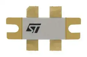
## **SD2932**

## HF/VHF/UHF RF power N-channel MOSFET

Datasheet - production data

## **Features**

- Gold metallization

- Excellent thermal stability

- Common source push-pull configuration

- POUT = 300 W min. with 15 dB gain @ 175 MHz

## **Description**

**Figure 1: Pin connection**

The SD2932 is a gold metallized N-channel MOS field-effect RF power transistor used for 50 V DC large signal applications up to 250 MHz.

**Table 1: Device summary**

|**Order code**|**Marking**|**Package**|**Packing**|
|---|---|---|---|
|SD2932W|SD2932_(1)_|M244|Tube|


## **Notes:**

- (1)For more details please refer to _Section 11: "Marking, packing and shipping specifications"_ .

November 2016

DocID6876 Rev 10

1/20

This is information on a product in full production.

_www.st.com_

|**Contents**<br>**SD2932 **|**Contents**<br>**SD2932 **|
|---|---|
|**Contents**||
|**1**|**Electrical data .................................................................................. 3**|
||1.1<br>Maximum ratings ............................................................................... 3|
||1.2<br>Thermal data ..................................................................................... 3|
|**2**|**Electrical characteristics ................................................................ 4**|
|**3**|**Impedance data ............................................................................... 5**|
|**4**|**Typical performance ....................................................................... 6**|
||4.1<br>Typical performance (175 MHz) ........................................................ 8|
|**5**|**Test circuit (175 MHz) ...................................................................... 9**|
|**6**|**Test circuit photomaster ............................................................... 11**|
|**7**|**Typical broadband data (175-230 MHz) ........................................ 12**|
|**8**|**Test circuit 175 - 230  MHz ............................................................ 13**|
|**9**|**Typical broadband data (88 - 108 MHz) ........................................ 14**|
|**10**|**Test circuit 88-108 MHZ ................................................................ 15**|
|**11**|**Marking, packing and shipping specifications ............................ 16**|
|**12**|**Package information ..................................................................... 17**|
||12.1<br>M244 package information .............................................................. 17|
|**13**|**Revision history ............................................................................ 19**|


2/20

DocID6876 Rev 10

**SD2932**

**Electrical data**

## **1 Electrical data**

## **1.1 Maximum ratings**

TCASE = 25 °C

**Table 2: Absolute maximum ratings**

|**Symbol**|**Parameter**|**Value**|**Unit**|
|---|---|---|---|
|V(BR)DSS|Drain source voltage|125|V|
|VDGR|Drain-gate voltage (RGS= 1 MΩ)|125|V|
|VGS|Gate-source voltage|±40|V|
|ID|Drain current|40|A|
|PDISS|Power dissipation|500|W|
|TJ|Max. operating junction temperature|+200|°C|
|TSTG|Storage temperature|-65 to +150|°C|


## **1.2 Thermal data**

||**Table 3: Thermal data**|||
|---|---|---|---|
|**Symbol**|**Parameter**|**Value**|**Unit**|
|RthJC|Junction-to-case thermal resistance|0.35|°C/W|


DocID6876 Rev 10

3/20

**SD2932**

**Electrical characteristics**

## **2 Electrical characteristics**

TCASE = 25 °C

**Table 4: Static**

|**Symbol**|**Test conditions**|**Min.**|**Typ.**|**Max.**|**Unit**|
|---|---|---|---|---|---|
|V(BR)DSS|VGS= 0 V                   IDS= 100 mA|125|||V|
|IDSS|VGS= 0 V                   VDS= 50 V|||50|µA|
|IGSS|VGS= 20 V                 VDS= 0 V|||250|nA|
|VGS(Q)|VDS= 10 V                  ID= 250 mA|1.5||4|V|
|VDS(ON)|VGS= 10 V                  ID= 10 A|||3.0|V|
|GFS|VDS= 10 V                  ID= 5 A|5|||mho|
|ΔVGS_(1)_|VDS= 10 V                  ID= 250 mA|||200|mV|
|CISS|VGS= 0 V                   VDS= 50 V                  f = 1 MHz||480||pF|
|COSS|VGS= 0 V                   VDS= 50 V                  f = 1 MHz||190||pF|
|CRSS|VGS= 0 V                   VDS= 50 V                  f = 1 MHz||18||pF|


## **Notes:**

(1)Absolute VGS difference between side 1 and side 2 of the device.

**Table 5: Dynamic**

|**Symbol**|**Test conditions**|**Min.**|**Typ.**|**Max.**|**Unit**|
|---|---|---|---|---|---|
|POUT|VDD= 50 V     IDQ= 500 mA        f = 175 MHz|300|||W|
|GPS|VDD= 50 V     IDQ= 500 mA   POUT= 300 W<br>f = 175 MHz|15|16||dB|
|ηD|VDD= 50 V     IDQ= 500 mA   POUT= 300 W<br>f = 175 MHz|50|60||%|
|Load<br>mismatch|VDD= 50 V     IDQ= 500 mA    POUT= 300 W<br>f = 175 MHz<br>Allphase angles|5:1|||VSWR|


4/20

DocID6876 Rev 10

**SD2932**

**Impedance data**

## **3 Impedance data**

**Figure 2: Impedance data**

**==> picture [333 x 41] intentionally omitted <==**

**----- Start of picture text -----**<br>
Table 6: Impedance data<br>f   ZIN(Ω)   ZDL(Ω)<br>175 MHz   0.92 - j 0.14   3.17 + j 4.34<br>**----- End of picture text -----**<br>


Measured gate-to-gate and drain-to-drain, respectively.

DocID6876 Rev 10

5/20

**SD2932**

**Typical performance**

## **4 Typical performance**

**Figure 3: Maximum thermal resistance vs. case temperature**

**==> picture [206 x 121] intentionally omitted <==**

**==> picture [204 x 10] intentionally omitted <==**

**----- Start of picture text -----**<br>
Figure 5: Capacitance vs. drain-source voltage<br>**----- End of picture text -----**<br>


**==> picture [205 x 122] intentionally omitted <==**

**Figure 4: Gate voltage vs. case temperature**

**==> picture [186 x 128] intentionally omitted <==**

**==> picture [191 x 154] intentionally omitted <==**

**----- Start of picture text -----**<br>
Figure 6: Drain current vs. gate voltage<br>20<br>Tc=-20 °C<br>Tc=+25 °C<br>15<br>10 Tc=+80 °C<br>5<br>0<br>2 2.5 3 3.5 4 4.5 5 5.5 6<br>VGS, GATE-SOURCE VOLTAGE (V)<br>**----- End of picture text -----**<br>


6/20

DocID6876 Rev 10

**SD2932**

**Typical performance**

**Figure 7: Maximum safe operating area**

**Figure 8: Transient thermal impedance**

**Figure 9: Transient thermal model**

DocID6876 Rev 10

7/20

**SD2932**

## **Typical performance**

## **4.1 Typical performance (175 MHz)**

**Figure 10: Output power vs. input power**

**==> picture [209 x 120] intentionally omitted <==**

**==> picture [225 x 19] intentionally omitted <==**

**----- Start of picture text -----**<br>
Figure 11: Output power vs. input power at different<br>Tc<br>**----- End of picture text -----**<br>


**==> picture [206 x 120] intentionally omitted <==**

**Figure 12: Power gain vs. output power**

**==> picture [201 x 116] intentionally omitted <==**

**Figure 13: Efficiency vs. output power**

**==> picture [204 x 116] intentionally omitted <==**

**Figure 14: Output power vs. supply voltage**

**==> picture [201 x 115] intentionally omitted <==**

**Figure 15: Output power vs. gate voltage**

**==> picture [203 x 113] intentionally omitted <==**

8/20

DocID6876 Rev 10

**SD2932**

**Test circuit** (175 MHz)

## **5 Test circuit (175 MHz)**

**Figure 16: 175 MHz production test circuit schematic**

**==> picture [408 x 205] intentionally omitted <==**

**Table 7: 175 MHz test circuit part list**

|**Component**|**Description**|
|---|---|
|R1, R2, R5, R6<br>470 Ohm 1 W|, surface mount chip resistor|
|R3, R4<br>360 Ohm 0.5|W, carbon comp. axial lead resistor or equivalent|
|R7, R8<br>560 Ohm 2 W|, resistor 2 turn wire air-wound axial lead resistor|
|R9, R10<br>20 kOhm 3.0|9 W, 10 turn wirewound precision potentiometer|
|C1, C4<br>680 pF ATC|130B surface mount ceramic chip capacitor|
|C2, C3, C7, C8,<br>C17, C19, C20,<br>C21<br>10000 pF AT|C 200B surface mount ceramic chip capacitor|
|C5<br>75 pF ATC 1|00B surface mount ceramic chip capacitor|
|C6<br>ST40 25 pF -|115 pF miniature variable trimmer|
|C9, C10<br>47 pF ATC 1|00B surface mount ceramic chip capacitor|
|C11, C12, C13<br>43 pF ATC 1|00B surface mount ceramic chip capacitor|
|C14, C15, C24,<br>C25<br>1200 pF ATC|700B surface mount ceramic chip capacitor|
|C16, C18<br>470 pF ATC|700B surface mount ceramic chip capacitor|
|C22, C23<br>0.1 μF / 500|V surface mount ceramic chip capacitor|
|C26, C27<br>0.01 μF / 500|V surface mount ceramic chip capacitor|
|C28<br>10 μF / 63 alu|minum electrolytic axial lead capacitor|
|B1<br>50 Ohm RG3<br>turns through|16 O.D 0.076[1.93] L = 11.80[299.72] flexible coaxial cable 4<br>ferrite bead|
|B2<br>50 Ohm RG-|142B O.D 0.165[4.19] L = 11.80[299.72] flexible coaxial cable|


DocID6876 Rev 10

9/20

**SD2932**

## **Test circuit** (175 MHz)

|**Test circuit**|(175MHz)|**SD2932 **||
|---|---|---|---|
||**Component**|**Description**||
||T1|R.F. transformer 4:1, 25 Ohm O.D RG316-25 O.D 0.080[2.03] L =<br>5.90[149.86] flexible coaxial cable 2 turns through ferrite multi-aperture core||
||T2|R.F. transformer 1:4, 25 Ohm semi-rigid coaxial cable O.D. 0.141[3.58] L =<br>5.90[149.86]||
||L1|Inductor λ 1/4 wave 50 Ohm O.D 0.165[4.19] L = 11.80 [299.72] flexible<br>coaxial cable 2 turns through ferrite bead||
||FB1, FB5|Shield bead||
||FB2, FB6|Multi-aperture core||
||FB3|Multilayer ferrite chip bead (surface mount)||
||FB4|Surface mount EMI shield bead||
||PCB|Woven glass reinforced PTFE microwave laminate 0.06”, 1 oz EDCu, both<br>sides, εr = 2.55||


10/20

DocID6876 Rev 10

**SD2932**

**Test circuit** photomaster

## **6 Test circuit photomaster**

**Figure 17: 175 MHz test circuit photomaster**

**Figure 18: 175 MHz test fixture**

DocID6876 Rev 10

11/20

**SD2932**

**Typical broadband** data (175-230 MHz)

## **7 Typical broadband data (175-230 MHz)**

**==> picture [433 x 146] intentionally omitted <==**

**----- Start of picture text -----**<br>
Figure 19: Input power vs. frequency  Figure 20: Power gain vs. frequency<br>**----- End of picture text -----**<br>


**Figure 21: Efficiency vs. frequency**

**==> picture [199 x 108] intentionally omitted <==**

**Figure 22: Return loss vs. frequency**

**==> picture [198 x 111] intentionally omitted <==**

**Figure 23: 1 dB compression point vs. frequency**

**==> picture [178 x 112] intentionally omitted <==**

12/20

DocID6876 Rev 10

**SD2932**

**Test circuit** 175 - 230  MHz

## **8 Test circuit 175 - 230  MHz**

**Figure 24: 175 - 230 MHz test circuit layout (engineering fixture)**

**Table 8: 175 - 230 MHz circuit layout component part list**

|**Component**|**Description**|
|---|---|
|PCB|1/32” woven fiberglass 0.030 Cu, sides, εr = 4.8|
|T1|50 Ohm flexible coax cable OD 0.06”, 3” long. ferrite core NEOSIDE|
|T2, T3|9:1 transformer, 16.5 Ohm flexible coax cable 0.1”, 3” long|
|T4, T5|4:1 transformer, 25 Ohm flexible coax cable OD 0.06”, 5” long|
|C1|8.2pF ceramic cap|
|C2, C3|100pF ceramic cap|
|C4|2 - 18pF chipcap|
|C5|47pF ceramic cap|
|C6, C11|47 nF ceramic cap|
|C7|56pF ATC chipcap|
|C8, C9, C13|470pF ATC chipcap|
|C10|100 nF ceramic cap|
|C12|2 x 330 nF / 50 V cap|
|C14|10 nF / 63 V electrolityc cap|
|R1, R3|47 Ohm resistor|
|R2|6.8 kOhm chip resistor|
|R4|4.7 kOhm multi turn trim resistor|
|R5|8.2 kOhm / 5 W resistor|
|R6|3.3 kOhm / 5 W resistor|
|D1|6.8 V Zener diode|
|L1|20 nH inductor|
|L2|70 nH inductor|
|L3|30 nH inductor|
|L4|10 nH inductor|
|L5|15 nH inductor|


DocID6876 Rev 10

13/20

**SD2932**

**Typical broadband** data (88 - 108 MHz)

## **9 Typical broadband data (88 - 108 MHz)**

**Figure 25: Input power vs. frequency (POUT=300)**

**Figure 26: Power gain vs. frequency (POUT=300)**

**Figure 27: Efficiency vs. frequency (POUT=300)**

**Figure 28: Return loss vs. frequency (POUT=300)**

**==> picture [200 x 111] intentionally omitted <==**

**==> picture [197 x 110] intentionally omitted <==**

**Figure 29: 2[nd] harmonic vs. frequency (88 - 108 MHz)**

**==> picture [190 x 118] intentionally omitted <==**

**Figure 30: 3[rd] harmonic vs. frequency (88 - 108 MHz)**

**==> picture [207 x 121] intentionally omitted <==**

14/20

DocID6876 Rev 10

**SD2932**

**Test circuit** 88-108 MHZ

## **10 Test circuit 88-108 MHZ**

**Figure 31: 88 - 108 MHz test circuit layout (engineering fixture)**

**Table 9: 88 - 108 MHz circuit layout component part list**

|**Component**|**Description**|
|---|---|
|PCB|1/32” woven fiberglass 0.030 Cu, sides, εr = 4.8|
|T1|50 Ohm flexible coax cable OD 0.06”, 3” long|
|T2, T3|9:1 transformer, 25 Ohm flexible coax cable 0.1”, 3.9” ferrite core<br>NEOSIDE|
|T4, T5|4:1 transformer, 25 Ohm flexible coax cable OD 0.1”, 5” long|
|T6|50 Ohm flexible coax cable OD 0.1”, 5” long|
|FB1|vk200|
|C1|10pF ceramic cap|
|C2, C3, C4, C7, C8|1 nF chipcap|
|C5, C6|1 nF ATC chipcap|
|C9|470pF ceramic cap|
|C10|100 nF chipcap|
|C11|100 mF / 63 V electrolytic cap|
|R1|56 Ohm resistor|
|R2, R4|10 Ohm chipresistor|
|R3|10 kOhm resistor|
|R5|5.6 Ohm resistor|
|R6|10 kOhm, 10 turn trim resistor|
|R7|3.3 kOhm / 5 W resistor|
|R8|15 Ohm / 5 W resistor|
|D1|6.8 V Zener diode|
|L1|10 nH inductor|
|L2|40 nH inductor|
|L3|70 nH inductor|


DocID6876 Rev 10

15/20

**SD2932**

**Marking,** packing and shipping specifications

## **11 Marking, packing and shipping specifications**

**Table 10: Packing and shipping specifications**

|**Order code**|**Packing**|**Pieces**<br>**per tray**|**Dry pack**<br>**humidity**|**VGS and GFS**<br>**code**|**Lot code**|
|---|---|---|---|---|---|
|SD2932W|Tube|15|< 10%|Not mixed|Not mixed|


**Figure 32: SD2932 marking layout**

**==> picture [406 x 87] intentionally omitted <==**

**Table 11: Marking specifications**

|**Symbol**|**Description**|
|---|---|
|W|Wafer process code|
|CZ|Assembly plant|
|xxx|Last 3 digits of diffusion lot|
|VY|Diffusion plant|
|MAR|Country of origin|
|CZ|Test and finishing plant|
|y|Assembly year|
|yy|Assembly week|


16/20

DocID6876 Rev 10

**SD2932**

**Package information**

## **12 Package information**

In order to meet environmental requirements, ST offers these devices in different grades of ECOPACK[®] packages, depending on their level of environmental compliance. ECOPACK[®] specifications, grade definitions and product status are available at: _**www.st.com**_ . ECOPACK[®] is an ST trademark.

## **12.1 M244 package information**

**Figure 33: M244 (0.400 x .860 4L BAL N/HERM W/FLG) package outline**

**==> picture [406 x 259] intentionally omitted <==**

DocID6876 Rev 10

17/20

**SD2932**

**Package information**

**Table 12: M244 (0.400 x .860 4L BAL N/HERM W/FLG) package mechanical data**

|**Dim.**||**mm**||
|---|---|---|---|
||**Min.**|**Typ.**|**Max.**|
|A|5.59||5.84|
|B||5.08||
|C|3.02||3.28|
|D|9.65||9.91|
|E|19.81||20.82|
|F|10.92||11.18|
|G||27.94||
|H|33.91||34.16|
|I|0.10||0.15|
|J|1.52||1.78|
|K|2.59||2.84|
|L|4.83||5.84|
|M|10.03||10.34|
|N|21.59||22.10|


18/20

DocID6876 Rev 10

**SD2932**

**Revision history**

## **13 Revision history**

**Table 13: Document revision history**

|**Date**|**Revision**|**Changes**|
|---|---|---|
|15-Jul-2004|5||
|24-Jan-2006|6|Updated_Table 4: Static (per section)_.|
|23-Nov-2009|7|Inserted ΔVGSin_Table 4: Static (per section)_.|
|31-Mar-2010|8|Added_Figure 7_,_Figure 8_and_Figure 9_.|
|11-Jan-2012|9|Inserted_Chapter 12: Marking, packing and shipping_<br>_specifications_.<br>Minor text changes.|
|24-Nov-2016|10|Updated_Section 1.1: "Maximum ratings"_.|


DocID6876 Rev 10

19/20

**SD2932**

## **IMPORTANT NOTICE – PLEASE READ CAREFULLY**

STMicroelectronics NV and its subsidiaries (“ST”) reserve the right to make changes, corrections, enhancements, modifications, and improvements to ST products and/or to this document at any time without notice. Purchasers should obtain the latest relevant information on ST products before placing orders. ST products are sold pursuant to ST’s terms and conditions of sale in place at the time of order acknowledgement.

Purchasers are solely responsible for the choice, selection, and use of ST products and ST assumes no liability for application assistance or the design of Purchasers’ products.

No license, express or implied, to any intellectual property right is granted by ST herein.

Resale of ST products with provisions different from the information set forth herein shall void any warranty granted by ST for such product.

ST and the ST logo are trademarks of ST. All other product or service names are the property of their respective owners.

Information in this document supersedes and replaces information previously supplied in any prior versions of this document.

- © 2016 STMicroelectronics – All rights reserved

20/20

DocID6876 Rev 10
Updated at March 21, 2026
STMicroelectronics is a global leader in the semiconductor industry, recognized for developing highly integrated, energy-efficient solutions that power modern electronics. With a strong focus on innovation, ST provides a comprehensive portfolio of microelectronics that address the demanding requirements of industrial, automotive, communications, and consumer applications. Our extensive selection of STMicroelectronics components is built around a robust lineup of discrete semiconductors and circuit protection devices. We offer a wide variety of single MOSFETs, Schottky diodes, and fast and ultrafast recovery rectifier diodes, designed to deliver exceptional efficiency and thermal performance in power management and conversion systems. For robust circuit protection, our inventory features hundreds of transient voltage suppressors and TVS diodes that safeguard sensitive electronic components against destructive voltage spikes. In addition to core power discretes like TRIACs, SCRs, bipolar transistors, and single IGBTs, our STMicroelectronics range includes specialized integrated passive filters and MEMS sensors. Furthermore, ST offers advanced integrated passive devices, such as baluns and RF filters, which utilize high-quality monolithic RF IPD processes on glass or high-resistance silicon substrates. These components provide competitive cost structures, reduced power losses, and simplified RFIC-to-antenna matching, ensuring optimal system performance and delivering the reliability required for next-generation wireless and power designs.
About Novapart
Novapart is a B2B electronic component broker specialising in stock shortages and cost reduction. We source hard-to-find parts and identify compliant alternatives across a catalogue of 540,000+ components from 500+ manufacturers.
Learn more →Stock Shortage Specialist
When a component is unavailable, discontinued or has an unacceptable lead time, we tap into our network of vetted European and Asian distributors to source what you need — without compromising on quality or traceability.
Request a quote →Compliant Alternatives
We identify pin-to-pin, electrically equivalent substitutes that meet the same certifications (RoHS, AEC-Q100, REACH) as your original specification — validated against datasheets, not just part numbers. Often at a lower cost.
BOM Analysis service →