
Image not available
Illustrative purposes only

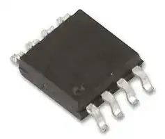
RT8468AGS
LED Driver, Buck (Step Down), 16V to 31V input, 47 kHz Switch. Frequency, SOP-7
⚠️ Reference pricing provided. In case of supply shortages, we will connect you with our trusted procurement partners to ensure your project's continuity.
- Manufacturer: RICHTEK
- Product type: AC / DC LED Driver ICs
- Device Topology:Constant Current; Input Voltage Min:16V; Input Voltage Max:31V; Output Voltage Max:-; Output Current Max:-; Switching Frequency:47kHz; No. of Outputs:1Outputs; IC Mount
- MSL: MSL 3 - 168 hours
- SVHC: No SVHC (19-Jan-2021)
- Topology: Constant Current
- IC Mounting: Surface Mount
- No. of Pins: 7Pins
- Product Range: -
- Qualification: -
- No. of Outputs: 1Outputs
- Device Topology: Constant Current
- LED Driver Type: -
- Driver Case Style: SOP
- IC Case / Package: SOP
- Input Voltage Max: 31V
- Input Voltage Min: 16V
- Output Current Max: -
- Output Voltage Max: -
- Switching Frequency: 47kHz
- Switching Frequency Typ: 47kHz
- Operating Temperature Max: 125°C
- Operating Temperature Min: -40°C
- Automotive Qualification Standard: -
| Delivery and price | |
|---|---|
| Units per pack | 1000 |
| Price | 0.27 € |
| Current stock | 10+ |
| Lead time | 30 days |
Datasheet

®

**RT8468A**

## **500V Power MOSFET Integrated High Efficiency Constant Current LED Driver**

## **General Description**

The RT8468A integrates a 500V power MOSFET and a PWM controller. It is used for step-down converters by well controlling the internal MOSFET and regulating a constant output current. The output duty cycle of the RT8468A can be up to 100% for wider input voltage applications, such as E27 and PAR30 off-line LED lighting products.

The RT8468A also features a 47kHz fixed frequency oscillator, an internal 220mV precision reference, and a PWM comparator with latching logic. The accurate output LED current is achieved by an averaging current feedback loop and the LED current dimming can be easily controlled via the ACTL pin. The RT8468A also has multiple features to protect the controller from fault conditions, including Under Voltage Lockout (UVLO), Over Current Protection (OCP) and Over Voltage Protection (OVP). Additionally, to ensure the system reliability, the RT8468A is built with the thermal protection function.

The RT8468A is housed in a SOP-7 package. Thus, the components in the whole LED driver system can be made very compact.

## **Features**

**Built-In 500V/1A Power MOSFET Low Cost and Efficient Buck Converter Solution Universal Input Voltage Range with Off-Line Topology Adjustable Constant LED Current Dimmable LED Current by ACTL Output LED String Open Protection Output LED String Short Protection Output LED String Over Current Protection Built-in Thermal Protection SOP-7 Package RoHS Compliant and Halogen Free**

## **Applications**

E27, PAR30, Offline LED Lights

## **Marking Information**

RT8468AGS : Product Number RT8468A YMDNN : Date Code GSYMDNN

## **Simplified Application Circuit**

**==> picture [355 x 186] intentionally omitted <==**

**----- Start of picture text -----**<br>
500V<br>CIN R1<br>RD D1<br>RT8468A<br>R3<br>C1 VCC DRAIN<br>VC ACTL<br>RVC SENSE<br>SGND SOURCE<br>CVC<br>RS L1<br>LED+<br>COUT<br>DF<br>LED-<br>fe<br>**----- End of picture text -----**<br>


Copyright   2013 Richtek Technology Corporation. All rights reserved.                          is a registered trademark of Richtek Technology Corporation.©

DS8468A-00   February  2013

www.richtek.com

1

**RT8468A**

## **Ordering Information**

Package Type S : SOP-7 Lead Plating System G : Green (Halogen Free and Pb Free) L

## RT8468A

Note :

Richtek products are :

RoHS compliant and compatible with the current requirements of IPC/JEDEC J-STD-020.

## **Pin Configurations**

**==> picture [139 x 100] intentionally omitted <==**

**----- Start of picture text -----**<br>
(TOP VIEW)<br>SOURCE 7 DRAIN<br>SGND 2<br>VCC 3 6 ACTL<br>SENSE 4 5 VC<br>ct<br>SOP-7<br>**----- End of picture text -----**<br>


Suitable for use in SnPb or Pb-free soldering processes.

## **Functional Pin Description**

|**Pin No.**|**Pin Name**|**Pin Function**|
|---|---|---|
|1|SOURCE Internal Power MOSFET Source Connection.|SOURCE Internal Power MOSFET Source Connection.|
|2|SGND|Ground.|
|3|VCC|Power Supply Input. For good bypass, a ceramic capacitor near the VCC pin is<br>required.|
|4|SENSE|LED Current Sense Input. Typical sensing threshold is 220mV.|
|5|VC|PWM Loop Compensation Node.|
|6|ACTL|Analog Dimming Control. The typical effective dimming range is between 0.1V to 1.2V.|
|7|DRAIN|Internal Power MOSFET Drain Connection.|


©

Copyright   2013 Richtek Technology Corporation. All rights reserved.                          is a registered trademark of Richtek Technology Corporation.©

DS8468A-00   February  2013

www.richtek.com

2

**RT8468A**

## **Function Block Diagram**

**==> picture [405 x 326] intentionally omitted <==**

**----- Start of picture text -----**<br>
+<br>+ Ee - Chip Enable 12V DRAIN<br>17V/8V<br>OVP OSC S<br>VCC +<br>35V - R SOURCE<br>R<br>/\<br>Control<br>Circuit<br>VC<br>Dimming ACTL<br>O n oe<br>- SENSE<br>+ = SGND<br>< —~—l<br>ee<br>than 100% duty. It is not always that the GATE turns low<br>in each OSC cycle. The GATE turns low until the current<br>comparator (CCOMP) resets the gate driver. The GATE<br>will be set high again by OSC and the next switching<br>cycle repeats.<br>- +<br>**----- End of picture text -----**<br>


## **Operation**

The RT8468A is a high voltage Buck PWM current mode driver with an integrated 500V power MOSFET. The start up voltage of RT8468A is around 17V. Once VCC is above 17V, RT8468A will maintain operation until VCC drops below 8V.

The RT8468A's main control loop consists of a 47kHz fixed frequency oscillator, an internal 220mV precision current sense threshold OPAMP (OP1), and a PWM comparator (CCOMP) with latching logic. In normal operation, the GATE turns high when the gate driver is set by the oscillator (OSC). The lower the average of the sensed current is below the loop-regulated 220mV threshold, the higher the VC pin voltage (OP1 output) will go high. Higher the VC voltage means longer the GATE turn-on period. The GATE of RT8468A can turn on more

The ACTL voltage of RT8468A is internally biased to 0.6V. The adjustment of the regulated sense current threshold (dimming) can be achieved by varying ACTL pin voltage. The typical range of ACTL voltage adjustment is between 0.1V and 1.2V.

The RT8468A is equipped with protection from several fault conditions, including input voltage Under Voltage Lockout (UVLO), Over Current Protection (OCP) and VIN/VOUT Over Voltage Protection (OVP). Additionally, to ensure the system reliability, the RT8468A is built with internal thermal protection function.

Copyright   2013 Richtek Technology Corporation. All rights reserved.                          is a registered trademark of Richtek Technology Corporation.©

©

DS8468A-00   February  2013

www.richtek.com

3

## **RT8468A**

## **Absolute Maximum Ratings** (Note 1)

**==> picture [501 x 251] intentionally omitted <==**

**----- Start of picture text -----**<br>
|||||||||
|---|---|---|---|---|---|---|---|
|Supply Input Voltage, VCC to SGND ---------------------------------------------------------------------------------|−|0.3V to 40V|
|ACTL Voltage to SGND   (Note 2) -------------------------------------------------------------------------------------|−|0.3V to 8V|
|VC Voltage to SGND|-----------------------------------------------------------------------------------------------------|−|0.3V to 6V|
|SENSE Voltage to SGND|-----------------------------------------------------------------------------------------------|−|1V to 0.3V|
|DRAIN to SOURCE Voltage, VDS --------------------------------------------------------------------------------------|−|0.3V to 550V|
|DRAIN Current, ID @ TC = 25|°|C ----------------------------------------------------------------------------------------|1.4A|
|DRAIN Current, ID @ TC = 100|°|C --------------------------------------------------------------------------------------|0.9A|
|Power Dissipation, PD @ TA|= 25|°|C|
|SOP-7 ------------------------------------------------------------------------------------------------------------------------|0.5W|
|Package Thermal Resistance   (Note 3)|
|SOP-7,|θ|JA ------------------------------------------------------------------------------------------------------------------|200.2|°|C/W|
|Junction Temperature -----------------------------------------------------------------------------------------------------|150|°|C|
|Lead Temperature (Soldering, 10 sec.)-------------------------------------------------------------------------------|260|°|C|
|Storage Temperature Range|--------------------------------------------------------------------------------------------|−|65|°|C to 150|°|C|
|ESD Susceptibility, Except DRAIN & SOURCE Pin   (Note 4)|
|HBM (Human Body Model)----------------------------------------------------------------------------------------------|2kV|
|MM (Machine Model)|-----------------------------------------------------------------------------------------------------|200V|

**----- End of picture text -----**<br>


## **Recommended Operating Conditions** (Note 5)

Supply Input Voltage, VCC---------------------------------------------------------------------------------------------- 16V to 31V ° ° Junction Temperature Range-------------------------------------------------------------------------------------------- − 40 C to 125 C

## **Electrical Characteristics**

(VCC = 24VDC, TA = 25 ° C, unless otherwise specified)

**==> picture [512 x 245] intentionally omitted <==**

**----- Start of picture text -----**<br>
|||||||||
|---|---|---|---|---|---|---|---|
|a|Parameter|Symbol|Test Conditions|Min|Typ|Max|Unit|
|Supply Voltage|
|OO|Input Start-Up Voltage|VST|--|16|19|V|
|a|
|Under Voltage Lockout|
|ΔVUVLO|--|8|9|V|
|a|Threshold Hysteresis|ee|ee ee|
|a|Maximum Startup Current|IST(MAX)|--|250|300|μA|
|Input Supply Current|ICC|After Start-Up, VCC = 24V|--|2|5|mA|
|a|
|a|Input Quiescent Current|IQC|Before Start-Up, VCC = 15V|--|--|2|μA|
|Current Sense Amplifier|
|Current Sense Voltage|VSENSE|(Note 6)|209|220|231|mV|
|a|
|a|Sense Input Current|ISENSE|VSENSE = 0.2V|--|20|--|μA|
|a|VC Sourcing Current|IVC_Sr|VSENSE = −150mV|--|18.5|--|μA|
|a|VC Sinking Current|IVC_Sk|VSENSE = −230mV|--|165|--|μA|
|VC Threshold for PWM|
|Switch Off|VVC|1.15|1.25|1.35|V|

**----- End of picture text -----**<br>


> Copyright   2013 Richtek Technology Corporation. All rights reserved.                          is a registered trademark of Richtek Technology Corporation.© RICHTEK

DS8468A-00   February  2013

www.richtek.com

4

**RT8468A**

|**Parameter**<br>**Symbol**<br>**Test Conditions**<br>**Min**<br>**Typ**<br>**Max**<br>**Unit**<br>~~a~~|
|---|
|**Oscillator**<br>~~OO~~|
|Switching Frequency<br>fSW<br>38<br>47<br>56<br>kHz<br>Maximum Duty in Transient<br>Operation<br>DMAX(TR)<br>VC = 3V<br>--<br>--<br>100<br>%<br>Maximum Duty in Steady State<br>Operation<br>DMAX<br>--<br>97<br>--<br>%<br>Blanking Time<br>tBLANK<br>--<br>300<br>--<br>ns<br>~~a~~<br>~~ee~~<br>~~ee~~<br>~~ee~~<br>~~ee~~<br>~~a~~|
|Minimum Off Time   (Note 7)<br>--<br>650<br>--<br>ns<br>**LED Dimming**<br>Analog Dimming ACTL Pin Input<br>Current<br>IACTL<br>VACTL= 1.2V<br>--<br>1<br>20<br>μA<br>LED Current On Threshold at ACTL VACTL_ON<br>--<br>1.2<br>--<br>V<br>~~a~~<br>~~OO~~<br>~~ee~~<br>~~ee~~<br>~~a~~|
|LED Current Off Threshold at ACTL VACTL_OFF<br>--<br>0.1<br>0.2<br>V<br>~~a~~|
|**Internal MOSFET**<br>~~OO~~|
|Static Drain-Source On-Resistance RDS(ON)<br>VVC= 3V, ID= 0.6A<br>--<br>5<br>--<br>Ω<br>~~a~~|
|Drain-Source Leakage Current<br>IDSS<br>VVC= 0V, VDS= 500V<br>--<br>--<br>10<br>μA<br>~~a~~|
|Output Capacitance<br>COSS<br>VCC= 0V, VDS= 25V, f = 1MHz<br>--<br>14<br>40<br>pF<br>~~a~~|
|**OVP**<br>~~OO~~|
|Over Voltage Protection<br>VOVP<br>VCC pin<br>32<br>35<br>38<br>V<br>**Thermal Protection**<br>Thermal Shutdown Temperature<br>TSD<br>--<br>150<br>--<br>°C<br>~~a~~<br>~~OO~~<br>~~a~~|


**Note 1.** Stresses beyond those listed “Absolute Maximum Ratings” may cause permanent damage to the device. These are

stress ratings only, and functional operation of the device at these or any other conditions beyond those indicated in the operational sections of the specifications is not implied. Exposure to absolute maximum rating conditions may affect device reliability.

**Note 2.** If a 1M Ω resistor is connected between the control input and ACTL pin, the control input voltage can be up to 36V.

**Note 3.** θ JA is measured at TA = 25 ° C on a high effective thermal conductivity four-layer test board per JEDEC 51-7.

**Note 4.** Devices are ESD sensitive. Handling precaution is recommended.

**Note 5.** The device is not guaranteed to function outside its operating conditions.

**Note 6.** The RT8468A achieves precise LED average current with a current feedback loop to sense the average LED current, in the deep discontinuous mode operation especially when a small inductor is used small current offset might occur due to current waveform distortion of the nature of the discontinuous operation. This offset current is consistent over production.

**Note 7.** Guaranteed by design, not subjected to production test.

> Copyright   2013 Richtek Technology Corporation. All rights reserved.                          is a registered trademark of Richtek Technology Corporation. ~~8~~ © DS8468A-00   February  2013 www.richtek.com

5

ee **RT8468A**

## **Typical Application Circuit**

**==> picture [430 x 212] intentionally omitted <==**

**----- Start of picture text -----**<br>
AC In ~<br>CIN<br>10µF R1<br>1M<br>R21M R10D D1<br>RT8468A R3<br>C1 3 VCC DRAIN [7] 1M<br>4.7µF<br>5 6<br>VC ACTL<br>ZD1<br>RVC SENSE 4<br>3.3k<br>2 SGND SOURCE 1 Optional<br>3.3nFCVC RS L1<br>2 1m<br>re ) [Eb | LED+<br>ZD2<br>48V<br>DF COUT Optional 100mA<br>LED-<br>**----- End of picture text -----**<br>


Copyright   2013 Richtek Technology Corporation. All rights reserved.                          is a registered trademark of Richtek Technology Corporation.© ~~ICHTEK.~~ www.richtek.com

DS8468A-00   February  2013

6

**RT8468A**

## **Typical Operating Characteristics**

**==> picture [518 x 654] intentionally omitted <==**

**----- Start of picture text -----**<br>
Switching Frequency vs. VCC Switching Frequency vs. Temperature<br>55 55<br>51 51<br>47 47<br>43 43 ait<br>39 39<br>35 35<br>0 4 8 12 16 20 24 28 32 36 -50 -25 0 25 50 75 100 125<br>VCC (V) Temperature (°C)<br>RDS(ON) vs. VCC RDS(ON) vs. Temperature<br>8.0 30<br>7.5<br>25<br>7.0<br>20<br>6.5<br>6.0 15<br>5.5<br>10<br>5.0<br>5<br>4.5<br>4.0 Saneee 0 —_—<br>0 4 8 12 16 20 24 28 32 36 -50 -25 0 25 50 75 100 125<br>VCC (V) Temperature (°C)<br>Efficiency vs. VIN Efficiency vs. Number of LEDs<br>100%100 100%100<br>7LED 17LED<br>6LED 15LED<br>95%95 5LED 12LED 95%95 110VAC<br>4LED 10LED 180VAC<br>3LED 9LED 220VAC<br>90%90 8LED<br>90%90 264VAC<br>85%85<br>85%85<br>80%80<br>80%80<br>75%75<br>75%75<br>70%70<br>== VIN_AC = 110V to 264V, IOUT = 100mA VIN_AC = 110V to 264V, IOUT = 100mA<br>65%65 70%70<br>110 130 150 170 190 210 230 250 270 3 5 7 9 11 13 15 17<br>VIN (V) Number of LEDs (pcs)<br>Copyright   2013 Richtek Technology Corporation. All rights reserved.                          is a registered trademark of Richtek Technology Corporation.©<br>Switching Frequency (kHz) 1 Switching Frequency (kHz) 1<br>Ω Ω<br> (   )  (   )<br>DS(ON) DS(ON)<br>R R<br>Efficiency (%) Efficiency (%)<br>**----- End of picture text -----**<br>


DS8468A-00   February  2013

www.richtek.com

7

**RT8468A**

**==> picture [109 x 10] intentionally omitted <==**

**----- Start of picture text -----**<br>
LED Current vs. VACTLACTL<br>**----- End of picture text -----**<br>


**==> picture [518 x 654] intentionally omitted <==**

**----- Start of picture text -----**<br>
LED Current vs. VACTLACTL LED Current vs. Output Voltage<br>120 115<br>100<br>110<br>80<br>105<br>60<br>100<br>40<br>95<br>20<br>VIN_AC = 110V, IOUT = 100mA,<br>LED 17 pcs, L = 1mH, VACTL = 0 to 2.5V VIN_AC = 110V, IOUT = 100mA, LED 17 pcs, L = 1mH<br>0 HEE 90 a<br>0 0.25 0.5 0.75 1 1.25 1.5 1.75 2 2.25 2.5 8 15 22 29 36 43 50<br>VACTL (V) Output Voltage (V)<br>LED Current vs. Input Voltage LED Current vs. Temperature<br>105 110<br>108<br>103 106<br>104<br>101 102<br>100<br>99 98<br>96<br>97 94<br>VIN_AC = 85V to 265V, 92<br>IOUT = 100mA, LED 17 pcs, L = 1mH IOUT = 100mA<br>95 90<br>85 115 145 175 205 235 265 -50 -25 0 25 50 75 100 125 150<br>Input Voltage (V) Temperature (°C)<br>Sense Voltage vs. Input Voltage VDS Voltage and Inductor Current<br>230<br>225<br>220<br>IOUT = 200mA (L = 0.68mH)<br>215 IOUT = 100mA (L = 1mH)<br>VDrain_Source<br>210 (100V/Div)<br>205<br>|<br>200<br>195 IL<br>IOUT = 60mA (L = 1.5mH)<br>(200mA/Div)<br>190<br>185<br>VIN_AC = 85V to 265V, LED 17 pcs VIN_AC = 110V, IOUT = 100mA, 17 LEDs, L = 1mH<br>180 TSS JNNY<br>90 115 140 165 190 215 240 265 Time (5 μ s/Div)<br>Input Voltage (V)<br>Copyright   2013 Richtek Technology Corporation. All rights reserved.                          is a registered trademark of Richtek Technology Corporation.©<br>LED Current (mA)<br>LED Current (mA)<br>LED Current (mA) LED Current (mA)<br>Sense Voltage(mV)<br>**----- End of picture text -----**<br>


www.richtek.com

DS8468A-00   February  2013

8

**RT8468A**

**==> picture [510 x 183] intentionally omitted <==**

**----- Start of picture text -----**<br>
Power On Power Off<br>VIN VIN<br>(200V/Div) (200V/Div)<br>VOUT Ce VOUT<br>a ANNONA<br>(50V/Div) (50V/Div)<br>IOUT IOUT<br>(50mA/Div) (50mA/Div)<br>VIN_AC = 110V, IOUT = 100mA, 17 LEDs, L = 1mH VIN_AC = 110V, IOUT = 100mA, 17 LEDs, L = 1mH<br>ie | iee<br>Time (100ms/Div) Time (100ms/Div)<br>**----- End of picture text -----**<br>


Copyright   2013 Richtek Technology Corporation. All rights reserved.                          is a registered trademark of Richtek Technology Corporation.© ~~a~~ RIGHTEK DS8468A-00   February  2013

www.richtek.com

9

**RT8468A**

## **Application Information**

The RT8468A is a high efficiency PWM Buck LED driver for high brightness LED application. Its high side floating gate driver is used to control the Buck converter with internal MOSFET and regulate the constant output current.

The RT8468A can achieve high accuracy LED output current via the average current feedback loop control. The internal sense voltage (220mV typ.) is used to set the average output current. The oscillator frequency is fixed at 47kHz to get better switching performance. Once the average current is set by the external resistor, RS, the output LED current can be dimmed by varying the ACTL voltage.

## **Under Voltage Lockout (UVLO)**

The RT8468A includes a UVLO feature with 9V hysteresis. The GATE terminal turns on when VIN rises over 17V (typ.). The GATE terminal turns off when VIN falls below 8V (typ.).

## **Setting Average Output Current**

The output current that flows through the LED string is set by an external resistor, RS, which is connected between the GND and SENSE terminal. The relationship between output current, IOUT, and RS is shown below :

0.22 IOUT = (A) RS

## **Analog Dimming Control**

The ACTL terminal is driven by an external voltage, VACTL, to adjust the output current to an average value set by RS. The voltage range for VACTL to adjust the output current is from 0.2V to 1.3V. If VACTL becomes larger than 1.3V, the output current value will just be determined by the external resistor, RS.

**==> picture [156 x 23] intentionally omitted <==**

## **Component Selection**

For component selection, an example is shown below for a typical RT8468A application, where VIN = 110 to 90VAC/ 60Hz, LED output voltage = 30V, and output current = 200mA. The user can follow this procedure to design applications with wider AC voltage input and DC output voltage as well.

## **Start-up Resistor**

Start-up resistor should be chosen not to exceed the maximum start-up current.  Otherwise, the RT8468A may latch low and will never start.  Start-up current = 130V/R1 for 110VAC regions, 260V/R1 for 220VAC regions.  The typical start-up current is 250 μ A.

## **Input Diode Bridge Rectifier Selection**

The current rating of the input bridge rectifier is dependent on the VOUT /VIN transformation ratio. The voltage rating of the input bridge rectifier, VBR, on the other hand, is only dependent on the input voltage. Thus, the VBR rating is calculated as below :

VBR = 1.2× ( - 2 × VAC(MAX) )

where VAC(MAX) is the maximum input voltage (RMS) and the parameter 1.2 is used for safety margin.

For this example : VBR = 1.2× ( Lv 2 × VAC(MAX) ) = (1.2× Lv 2 ×110) = 187V If the input source is universal, VBR will reach 466V. In this case, a 500V, 0.5A bridge rectifier can be chosen.

## **Input Capacitor Selection**

The input capacitor supplies the peak current to the inductor and flattens the current ripple on the input. The low ESR condition is required to avoid increasing power loss. The ceramic capacitor is recommended due to its excellent high frequency characteristic and low ESR. For maximum stability over the entire operating temperature range, capacitors with better dielectric are suggested. The minimum capacitor is given by :

**==> picture [201 x 33] intentionally omitted <==**

where fAC is the AC input source frequency and η is the efficiency of whole system.

Notice that VDC(MIN) is the minimum voltage at bridge rectifier, output and VDC(MIN) should be larger than 2 x VOUT(MAX).

For a 90 to 264VAC universal input range, the VDC(MIN) is 90V, therefore the LED string voltage VOUT(MAX) should be less than 45V.

> Copyright   2013 Richtek Technology Corporation. All rights reserved.                          is a registered trademark of Richtek Technology Corporation.© RICHTEK

DS8468A-00   February  2013

www.richtek.com

10

**RT8468A**

For this particular example :

**==> picture [197 x 32] intentionally omitted <==**

**==> picture [243 x 55] intentionally omitted <==**

Thus, a 22 μ F / 250V electrolytic capacitor can be chosen in this case. Due to its large ESR, the electrolytic capacitor is not suggested for high current ripple applications.

## **Inductor Selection**

The inductor value and operating frequency determine the ripple current according to a specific input and output voltage. The ripple current, Δ IL, increases with higher VIN and decreases with higher inductance, as shown in equation below :

**==> picture [114 x 29] intentionally omitted <==**

To optimize the ripple current, the RT8468A operates the Buck converter in BCM (Boundary-Condition Mode). The largest ripple current will occur at the highest VIN. To guarantee that the ripple current stays below the specified value, the inductor value should be chosen according to the following equation :

**==> picture [178 x 53] intentionally omitted <==**

where D is the duty cycle and TS is the switching period.

## **Forward Diode Selection**

When the power switch turns off, the path for the current is through the diode connected between the switch output and ground. This forward biased diode must have minimum voltage drop and recovery time. The reverse voltage rating of the diode should be greater than the maximum input voltage and the current rating should be greater than the maximum load current.

In reality, the peak current through the diode is more than the maximum output current. This component current

rating should be greater than 1.2 times the maximum load current and the diode reverse voltage rating should be greater than 1.2 times the maximum input voltage, assuming a ± 20% output current ripple.

**==> picture [229 x 63] intentionally omitted <==**

If the input source is universal (VIN = 90V to 264V), VD will reach 466V. A 500V, 2A ultra-fast diode can be used in this example.

## **Output Capacitor Selection**

The selection of COUT is determined by the required ESR to minimize output voltage ripple. Moreover, the amount of bulk capacitance is also a key for COUT selection to ensure that the control loop is stable. Loop stability can be checked by viewing the load transient response. The output voltage ripple, Δ VOUT, is determined by :

**==> picture [127 x 28] intentionally omitted <==**

where fOSC is the switching frequency. Multiple capacitors placed in parallel may be needed to meet the ESR and RMS current handling requirement. Dry tantalum, special polymer, aluminum electrolytic and ceramic capacitors are all common selections and available in surface mount packages. Tantalum capacitors have the highest capacitance density, but it is important to only use ones that pass the surge test for use in switching power supplies. Special polymer capacitors offer very low ESR value, but with the trade-off of lower capacitance density. Aluminum electrolytic capacitors have significantly higher ESR, but still can be used in cost-sensitive applications for ripple current rating and long term reliability considerations.

## **Thermal Protection**

A thermal protection feature is included to protect the RT8468A from excessive heat damage. When the junction temperature exceeds a threshold of 150 ° C, the thermal protection will turn off the GATE terminal.

> Copyright   2013 Richtek Technology Corporation. All rights reserved.                          is a registered trademark of Richtek Technology Corporation.© RICHTEK

DS8468A-00   February  2013

www.richtek.com

11

## **RT8468A**

## **Soldering Process of Pb-free Package Plating**

To meet the current RoHS requirements, pure tin is selected to provide forward and backward compatibility with both the current industry standard SnPb-based soldering processes and higher temperature Pb-free processes. In the whole Pb-free soldering processes pure tin is required with a maximum 260 ° C (<10s) for proper soldering on board, referring to J-STD-020 for more information.

## **Thermal Considerations**

For continuous operation, do not exceed absolute maximum junction temperature. The maximum power dissipation depends on the thermal resistance of the IC package, PCB layout, rate of surrounding airflow, and difference between junction and ambient temperature. The maximum power dissipation can be calculated by the following formula :

PD(MAX) = (TJ(MAX) − TA) / θ JA

where TJ(MAX) is the maximum junction temperature, TA is the ambient temperature, and θ JA is the junction to ambient thermal resistance.

For recommended operating condition specifications, the maximum junction temperature is 125 ° C. The junction to ambient thermal resistance, θ JA, is layout dependent. For SOP-7 package, the thermal resistance, θ JA, is 200.2 ° C/ W on a standard JEDEC 51-7 four-layer thermal test board. The maximum power dissipation at TA = 25 ° C can be calculated by the following formula :

PD(MAX) = (125 ° C − 25 ° C) / (200.2 ° C/W) = 0.5W for SOP-7 package

**==> picture [236 x 184] intentionally omitted <==**

**----- Start of picture text -----**<br>
0.6<br>Four-Layer PCB<br>0.5<br>0.4<br>0.3<br>0.2<br>0.1<br>0.0<br>0 25 50 75 100 125<br>Ambient Temperature (°C)<br> 1<br>Maximum Power Dissipation (W)<br>**----- End of picture text -----**<br>


Figure 1. Derating Curve of Maximum Power Dissipation

## **Layout Considerations**

For best performance of the RT8468A, the following layout guidelines should be strictly followed.

The hold up capacitor, C1, must be placed as close as possible to the VCC pin.

The output capacitor, COUT, must be placed as close as possible to the LED terminal.

The power ground (PGND) should be connected to a strong ground plane.

Place the sense resistor RS as close to the SOURCE pin as possible.

Keep the main current traces as short and wide as possible.

Place L1, RS, and DF as close to each other as possible.

The maximum power dissipation depends on the operating ambient temperature for fixed TJ(MAX) and thermal resistance, θ JA. The derating curve in Figure 1 allows the designer to see the effect of rising ambient temperature on the maximum power dissipation.

> Copyright   2013 Richtek Technology Corporation. All rights reserved.                          is a registered trademark of Richtek Technology Corporation.© RICHTEK

DS8468A-00   February  2013

www.richtek.com

12

**RT8468A**

**==> picture [284 x 320] intentionally omitted <==**

**----- Start of picture text -----**<br>
Place the Input Capacitor<br>CIN to the DRAIN pin as<br>close as possible<br>CIN<br>VIN<br>RACTL RVCC1<br>RVC<br>RVCC2<br>VCC<br>eit<br>SENSE<br>L1 RS C1<br>LED+<br>COUT id<br>CS DF Place the capacitor C1 as close as possible to<br>LED- PGND the VCC.<br>dle i<br>Place the Output capacitor<br>COUT as close as possible<br>to LED terminal<br>CVC<br>D2 RB<br>DRAIN ACTL VC<br>7 6 5<br>2 3 4<br>SOURCE SGND VCC SENSE<br>**----- End of picture text -----**<br>


Figure 2. PCB Layout Guide

Copyright   2013 Richtek Technology Corporation. All rights reserved.                          is a registered trademark of Richtek Technology Corporation.©

DS8468A-00   February  2013

www.richtek.com

13

**RT8468A**

## **Outline Dimension**

|**Symbol**<br>~~ee~~<br>~~SS~~<br>~~es~~|**Dimensions In Millimeters**<br>~~ee~~<br>~~SS~~|**Dimensions In Millimeters**<br>~~ee~~<br>~~SS~~|**Dimensions In Inches**<br>~~SS~~|**Dimensions In Inches**<br>~~SS~~|
|---|---|---|---|---|
||**Min.**<br>~~ee~~<br>~~SS~~<br>|**Max.**<br>~~ee~~<br>~~SS~~<br>|**Min.**<br>~~SS~~<br>|**Max.**<br>~~SS~~<br>|
|A<br>~~es~~<br>~~ee~~|4.801<br>|5.004<br><br>~~a~~|0.189<br>|0.197<br>|
|B<br>~~esa~~<br>~~ee~~|3.810<br>~~a~~|3.988<br>~~a~~<br>~~a~~|0.150<br>~~a~~|0.157<br>~~a~~|
|C<br>~~ee~~<br>~~es~~|1.346|1.753<br>~~a~~|0.053|0.069|
|D<br>~~ee~~<br>~~es~~<br>~~ee~~|0.330<br>|0.510<br>~~a~~<br>|0.013<br>|0.020<br>|
|F<br>~~es~~<br>~~ee~~|1.194<br>|1.346<br>|0.047<br>|0.053<br>|
|F1<br>~~eea~~<br>~~es~~|2.464<br>~~a~~|2.616<br>~~a~~|0.097<br>~~a~~|0.103<br>~~a~~|
|H<br>~~es~~<br>~~es~~|0.100<br>|0.254<br>|0.004<br>|0.010<br>|
|I<br>~~es~~<br>~~es~~|0.050<br>|0.254<br>|0.002<br>|0.010<br>|
|J<br>~~es~~|5.791<br>|6.200<br>|0.228<br>|0.244<br>|
|M<br>~~a~~|0.400<br>~~a~~|1.270<br>~~a~~|0.016<br>~~a~~|0.050<br>~~a~~|


## **7-Lead SOP Plastic Package**

## **Richtek Technology Corporation**

5F, No. 20, Taiyuen Street, Chupei City Hsinchu, Taiwan, R.O.C. Tel: (8863)5526789

Richtek products are sold by description only. Richtek reserves the right to change the circuitry and/or specifications without notice at any time. Customers should obtain the latest relevant information and data sheets before placing orders and should verify that such information is current and complete. Richtek cannot assume responsibility for use of any circuitry other than circuitry entirely embodied in a Richtek product. Information furnished by Richtek is believed to be accurate and reliable. However, no responsibility is assumed by Richtek or its subsidiaries for its use; nor for any infringements of patents or other rights of third parties which may result from its use. No license is granted by implication or otherwise under any patent or patent rights of Richtek or its subsidiaries.

DS8468A-00   February  2013

www.richtek.com

14
Updated at March 12, 2026
About Novapart
Novapart is a B2B electronic component broker specialising in stock shortages and cost reduction. We source hard-to-find parts and identify compliant alternatives across a catalogue of 410,000+ components from 500+ manufacturers.
Learn more →Stock Shortage Specialist
When a component is unavailable, discontinued or has an unacceptable lead time, we tap into our network of vetted European and Asian distributors to source what you need — without compromising on quality or traceability.
Request a quote →Compliant Alternatives
We identify pin-to-pin, electrically equivalent substitutes that meet the same certifications (RoHS, AEC-Q100, REACH) as your original specification — validated against datasheets, not just part numbers. Often at a lower cost.
BOM Analysis service →