
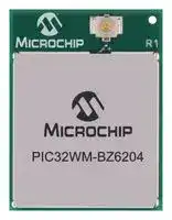


PIC32WM-BZ6204UE-I
Bluetooth Module, BLE 6.0, Class 1/2/3, 2 Mbps, -95dBm, 1.9 to 3.6 V, -40 to 85 °C
- Manufacturer: MICROCHIP
- Product type: Bluetooth Modules & Adaptors
- SVHC: No SVHC (04-Feb-2026)
- Interfaces: I2C, SPI, UART
- Product Range: PIC32-BZ6 Series
- Certifications: CE, FCC, ISED
- Bluetooth Class: Class 1, Class 2, Class 3
- Bluetooth Version: Bluetooth LE 6.0
- Supply Voltage Range: 1.9 V to 3.6 V
- Receiver Sensitivity Rx: -95 dBm
- Operating Temperature Range: -40 °C to 85 °C
| Delivery and price | |
|---|---|
| Units per pack | 250 |
| Price | 5.16 € |
| Current stock | 10+ |
| Lead time | 30 days |
Product Page Links
**PIC32CX-BZ6 and PIC32WM-BZ6 Family Data Sheet**
## **Highly Integrated Wireless MCU with CAN FD, Ethernet, USB, Motor Control, Graphics, Touch and Enhanced Security**
## **Introduction**
The PIC32-BZ6 family is a high-performance, low-power, integrated wireless microcontroller unit (MCU) powered by 128 MHz ARM[®] Cortex[®] -M4F processor. The PIC32-BZ6 family combines robust security features
with extensive wireless connectivity options, including Bluetooth[®] and IEEE 802.15.4 protocols (Thread, Proprietary, MiWi).
With 2 MB of Flash and 512 KB of RAM, the PIC32-BZ6 family provides ample memory for complex applications, while its Secure Boot feature with an immutable root of trust ensures reliable and secure operation. Equipped with a rich set of peripherals, including analog and digital signal processing, communication interfaces, Quadrature Encoder Interface (QEI), and touch sensing, the PIC32-BZ6 family can support a wide range of applications.
The PIC32-BZ6 family consists of AEC-Q100 Grade 1 (125°C) qualified PIC32CX-BZ6 SoCs and global regulatorycertified, RF-ready modules, PIC32WM-BZ6x.
Preliminary Data Sheet © 2025 Microchip Technology Inc. and its subsidiaries
DS00005998B - 1
**PIC32CX-BZ6 and PIC32WM-BZ6 Family Data Sheet**
## **PIC32CX-BZ6 SoC Family Features**
## **Operating Conditions**
- 1.9–3.6V[(1)] , −40°C to +125°C, DC to 128 MHz
- AEC Q100 Grade 1 qualified
-
- 1.9–3.6V[(1)] , −40°C to +105°C, DC to 128 MHz
- AEC Q100 Grade 2 qualified
## **Core: 128 MHz ARM Cortex-M4F**
- 3.40 Coremark[®] /MHz (with IAR Compiler)
- 4 KB Combined Instruction Cache and Data Cache
- 8-Zone Memory Protection Unit (MPU)
- Thumb[®] -2 Instruction Set
- Digital Signal Processing Application-Specific Extension (ASE) Rev 2
- Nested Vector Interrupt Controller (NVIC)
- Embedded Trace Module (ETM) with Instruction Trace Stream
- CoreSight[™] Embedded Trace Buffer (ETB)
- Trace Port Interface Unit (TPIU)
- IEEE[®] 754-Compliant Single Precision Floating Point Unit (FPU)
## **Memories**
- 64 KB ROM for Secure Boot
- Support for asymmetric secure boot
- 3072-Bit eFuse
- Secure boot key storage
- Debug lock
-
- 2 MB On-Chip Self-Programmable Flash with:
- Error Correction Code (ECC)
-
- Prefetch module to speed up Flash accesses
- 20k cycles endurance (100k cycles with erase retry option) and 20 years of data retention support
- 72 KB Boot Flash Memory (18 Pages, 17 Pages for Security Hash Enabled)
- 64 KB for User boot code configuration
-
- 8 KB for Flexible device configuration
-
- 512 KB Multi-Port Programmable QoS SRAM Main Memory
- 256 KB of ECC RAM option
- 32 KB of RAM space for CoreSight[™] ETB debug usage when enabled
- Up to 64 KB of SRAM can be retained in the Backup mode
- Up to 4 KB of Tightly Coupled Memory (TCM)
## **System**
- Power-on Reset (POR) and Brown-out Reset (BOR)
- Internal and External Clock Options
- Integrated 16 MHz Crystal Oscillator with ±30 ppm Stability and External Crystal Support
- External Interrupt Controller (EIC)
- Up to four external interrupts
-
- One non-maskable interrupt
- Extensive Debug and Trace Capabilities
- Two-Wire Serial Wire Debug (SWD) programming and debugging interface
- ETM trace interface pins for serial wire trace
## **Supported Connectivity Standards**
- Bluetooth[®] Low Energy SDK Qualified against Bluetooth[®] Core 6.0
- IEEE[®] 802.15.4 MAC/PHY SDK for Custom Protocol Support
- Capable of Zigbee[®] 3.0
- Thread 1.4
## **Power Supply**
- System-on-chip (SoC) Uses Low Dropout (LDO)
- Integrated PMU with:
- Buck (DC-DC/switching) mode; supports high power (PWM), low power (PSM)
- Modular Linear Differential Operator (MLDO) mode
- Integrated On-Chip 1.5V LDO Regulator for eFuse
- Integrated On-Chip 1.2V Low Dropout Regulators
- POR and BOR on 3.3V and 1.2V Rails
-
- Run, Idle, Standby Sleep, Deep Sleep and Extreme Deep Sleep Modes
- SleepWalking Peripherals
## **2.4 GHz RF Transceiver**
Integrated 2.4 GHz Ultra Low-Power RF Transceiver Shared Between Bluetooth Low Energy and IEEE 802.15.4 Modems and Link (MAC) Controllers
-
Integrated Transceiver (TRX) Switch and Balun with One SingleEnded Radio Frequency Input/Output (RFIO) for Transmit (TX)/ Receive (RX)
-
Hardware Radio Arbiter with Programmable QoS:
-
- The resolution is up to packet level
- Based on shared transceiver and antenna
- High Efficiency Switching Power Amplifier (PA)
-
- Programmable Transmit Output Power Ranges from −24 dBm to +11 dBm with 1 dB Step Size
-
Supported Data Rates:
-
- Bluetooth Low Energy 6.0: 2 Mbps, 1 Mbps, 500 kbps and 125 kbps
- IEEE[®] 802.15.4: 250 kbps
- Proprietary 2.4 GHz: 2 Mbps, 1 Mbps and 500 kbps
Preliminary Data Sheet © 2025 Microchip Technology Inc. and its subsidiaries
DS00005998B - 2
**PIC32CX-BZ6 and PIC32WM-BZ6 Family Data Sheet**
## **Bluetooth**
- Qualified against Bluetooth[®] Core 6.0
- Up to +11 dBm Programmable Transmit Output Power
- Typical Receiver Power Sensitivity:
- Bluetooth[®] Low Energy at 2 Mbps: −95 dBm
-
- Bluetooth[®] Low Energy at 1 Mbps: −98 dBm
- Bluetooth[®] Low Energy at 125 Kbps: −108 dBm
- Bluetooth[®] Low Energy at 500 Kbps: −102 dBm
- Bluetooth[®] Low Energy Supported Features:
- Encrypted advertising data
- Security level characteristic
- Coding scheme selection
- Connection subrating
- Periodic advertising enhancement
- Channel classification enhancement
- Low energy power control
- 2M uncoded PHY
- Long range coded PHY
- Channel selection algorithm #2
- Advertising extensions, offloads CPU with hardware based scheduler
- High duty cycle non-connectible advertising
- Data length extensions
- Secure connections
- Privacy upgrades
- Robust to interference with wideband RSSI detector
- ECDH P256 Hardware Engine for Bluetooth[®] Pairing Link Key Generation
- AES128 Hardware Module for Real-Time Bluetooth[®] Payload Data Encryption
- Bluetooth[®] Qualification Test Facility (BQTF) Certification
- Supports SIG Defined/Custom Bluetooth[®] Low Energy Profiles and Services
- Bluetooth[®] Low Energy Profiles:
- Bluetooth[®] Low Energy peripheral and central roles
- Bluetooth[®] Low Energy APIs for application layer to implement standard or customized GATT based profiles/ services
- Alert notification service (Apple Notification Center Service (ANCS))
- Proximity reporter and time information
- Multi-link and multi-role
- Bluetooth[®] Low Energy Services:
## **IEEE 802.15.4**
- Capable of Zigbee[®] 3.0, Thread 1.4, and proprietary 802.15.4 protocol stacks
**Note:** *Optional by firmware configuration.
- PLCP Service Data Unit (PSDU) Data Rate: 250 Kbps
- Proprietary data rates: 500 Kbps, 1 Mbps and 2 Mbps
- Programmable RX Mode
- RX sensitivity for 250 Kbps in Continuous mode: −103 dBm
- RX sensitivity in RPC mode: −100 dBm
- RPC mode provides lower power consumption in RX mode to support California Green Energy Specification at the system level
- TX Output Power up to +11 dBm
-
- Hardware Assisted MAC
- Auto acknowledge
-
- Auto retry
- Channel access back-off
-
- Automated Frame Check Sequence (FCS)
- Automatic Address filtering
- SFD Detection; Spreading; De-spreading; Framing; CRC-16 Computation
- Independent TX/RX Buffers for Improved CPU Offloading
- 128-byte TX and 128-byte RX frame buffer
## **High Performance Peripherals**
- 16-Channel Direct Memory Access Controller (DMAC)
- Built-in Cyclic Redundancy Check (CRC) with memory CRC generation and monitors hardware support
- One QSPI
-
- Execute-In-Place (XIP) support
- Dedicated AHB memory zone
## **Low-Cost Controllerless (LCC) Graphics Solutions**
- Supports RGB332 8-bit color with 480x272 TFT display
- I2C for maxTouch Control
- DMA and GPIO Pins for 8-bit Pixel Transmission and Synchronization[(2)]
## **Cryptography**
- Standard AES Encryption and Decryption with Key Sizes of 128 bits, 192 bits and 256 bits with Hardware Accelerator
- Standard SHA Hash Algorithms, Including SHA-256 and SHA-384 with Hardware Supported
- RSA Encryption and Decryption with Key Sizes of 1024 bits and 2048 bits
- Elliptic Curve Digital Signature Algorithm (ECDSA) Using All Supported NIST Curves
- NIST 800-90B Compliant True Random Number Generator (TRNG)
- Integrated Scatter Gather DMA
- Provisioning
- Over-the-Air firmware update (also known as OTA DFU)
- Advertisement/Beacon
-
-
- Personalized configuration
- Alert notification service
Preliminary Data Sheet © 2025 Microchip Technology Inc. and its subsidiaries
DS00005998B - 3
**PIC32CX-BZ6 and PIC32WM-BZ6 Family Data Sheet**
## **System Peripherals**
- Up to 18 Capacitive Voltage Divider (CVD) Channels for Touch Button Support (Using Shared ADC SAR Core)
- 32-Channel Event System
- All channels can be connected to any event generator
- One Temperature Sensor (Die Temperature) Built into Wireless Subsystem
-
- All channels provide a pure asynchronous path
-
- Two Controller Area Network with Flexible Data Rate (CAN-FD) Ports with Dedicated Direct Memory Access (DMA) and 16 Buffers, 16 Filters and 3 Masks
- Twelve channels support synchronous and re-synchronous
- Six Serial Communication Interfaces (SERCOM), each Configurable to Operate as:
- ISO11898-1:2015 and CAN FD 1.0 compliant, supports up to 64 data bytes
- Universal Synchronous Asynchronous Receiver Transmitter (USART) with full duplex and single-wire half duplex configuration
- Arbitration bit rate up to 1 Mbps
- ISO7816
- Data bit rate up to 10 Mbps
- Local Interconnect Network (LIN) Commander/Responder RS485
- Supports USB Full-Speed and Low-Speed Compliance
-
- Port with up to eight dedicated DMA channels
- I[2] C up to 1 MHz
- Ethernet MAC (ETH)
-
- Serial Peripheral Interface (SPI)
- Compatible with IEEE[®] Standard 802.3
- SPI inter-byte space
-
- One SERCOM Configured as I[2] C-Only Interface
- 10/100 Mbps Reduced Media Independent Interface (RMII) with dedicated DMA
- Ten 16-Bit Timers/Counters (TC), Each Configurable as:
- 802.1AS and IEEE[®] 1588-2008 Precision Time Protocol (PTP) compliant for precision clock synchronization and TSU support
- 16-bit TC with two compare/capture channels
- 8-bit TC with two compare/capture channels
- 32-bit TC with two compare/capture channels by pairing two TCs
- IEEE 802.3AZ/AF/PoE compliant for energy efficiency
- Wake on Local Area Network (LAN) support
- Two 24-Bit Timer/Counters for Control (TCC) with Extended Functions:
- One Quadrature Encoder Interface (QEI)
## **Oscillators**
- Up to six compare channels with optional complementary output
• 16 MHz, ±30 PPM Crystal/Resonator Oscillator or External Clock (POSC) for 2.4 GHz RF Transceiver
- Generation of synchronized Pulse Width Modulation (PWM) pattern across port pins
- Shared System Phase-Locked Loop (PLL) with RF Subsystem
-
- Deterministic fault protection, fast decay and configurable • dead-time between complementary output
- 50 MHz Ethernet Phase-Locked Loop (EPLL)
- 96 MHz USB Phase-Locked Loop (UPLL)
- Dithering to increase resolution up to 5 bits and reduce quantization error
- 32.768 kHz Ultra-Low Power Internal Oscillator (LPRC)
-
- Higher Accuracy 32.768 kHz, ±250 ppm Clock Options
- One 16-Bit Timer/Counters for Control (TCC) with Extended Functions:
- 32 kHz clock derived from POSC
- Up to two compare channels with optional complementary output
- 32.768 kHz crystal/resonator oscillator (SOSC)
- External 32.768 kHz clock source
- 34 PWM Channels: 6 Channels x 2 from 24-bit TCC, 2 Channels from 16-bit TCC, and 10 x 2 Channels from TC
- 8 MHz Internal RC Oscillator (FRC)
## **I/O**
- 32-Bit Real Time Counter (RTCC) with Clock/Calendar Function
- Peripheral Pin Select (PPS) Support
– Up to four wake-up pins with tamper detection and debouncing filter
- 23 I/Os with high-current sink/source
- Configurable Open-Drain Output on Digital I/O Pins
- Watchdog Timer (WDT) with Window Mode
- Up to 54 Programmable I/O Pins
- Deadman Timer (DMT)
## **DC Specification**
- Frequency Meter (FREQM)
- Configurable Custom Logic (CCL) with Two Look-up Table (LUT)
- Electrostatic Discharge (ESD) Protection
- Human Body Model (HBM): 2 kV (minimum)
- One 7-Bit General Purpose Digital-to-Analog Converter (DAC)
- Charged Device Model (CDM): 500V (minimum)
- Two 12-Bit, up to 1 Msps Analog-to-Digital Converter (ADC) SAR Core with up to 19 Analog Channels:
- Boot time[(3)] : Approximately 4 ms
Differential and single-ended input
-
- Automatic offset and gain error compensation
- Up to Two Analog Comparator (AC) with Window Compare Function
Preliminary Data Sheet © 2025 Microchip Technology Inc. and its subsidiaries
DS00005998B - 4
**PIC32CX-BZ6 and PIC32WM-BZ6 Family Data Sheet**
## **Package**
- PIC32CX2501BZ62132
- 132-pin DQFN
- Size: 10 mm x 10 mm x 0.9 mm
- PIC32CX2051BZ62064 _(Future Release)_
- 64-pin VQFN
- Size: 9 mm x 9 mm x 0.9 mm
- PIC32CX2051BZ66048 _(Future Release)_ – 48-pin QFN
- Size: 7 mm x 7 mm x 0.9 mm
## **Notes:**
1. For more details, refer to the Zero-Power BOR (ZPBOR).
2. For detailed description, refer to the _AN1387 Using PIC32 MCUs to Develop Low-Cost Controllerless (LCC) Graphics Solutions_ (DS00001387).
3. The time from Reset release until control is transferred to the Flash without code authentication.
## **PIC32WM-BZ6 Module Features**
The following section lists the PIC32WM-BZ6 Module-related features, which complement the SoC features.
## **PIC32WM-BZ6 Module Variants**
- PIC32WM-BZ6204 based on PIC32CX2501BZ62132 SoC
- PIC32WM-BZ6204UE (U.FL antenna connector)
## **Antenna**
- External Antenna
## **Clock Management**
- Integrated 16 MHz POSC
## **Advanced Analog**
- Two 12-Bit ADC up to 1 Msps Conversion Rate
- Up to 19 analog channels (PIC32WM-BZ6204)
- CVD Touch Support Using Shared ADC, with up to 18 Rx/Tx Channels for Touch Measurement
- 7-Bit General Purpose DAC
## **Input/Output**
- Up to 54 GPIO Pins (PIC32WM-BZ6204)
## **Package and Operating Conditions**
- PIC32WM-BZ6204 Module Package:
- 83-pin SMD package with Shield CAN
- Size: 19 mm x 25 mm x 2.75 mm
- Operating Conditions:
- 1.9–3.6V
- Operating temperature: -40ºC to +85ºC
## **Certified**
- PIC32WM-BZ6204 Module Certified to FCC, ISED, CE, UKCA and Radio Regulations
- Bluetooth[®] SIG
- RoHS and REACH Compliant
Preliminary Data Sheet © 2025 Microchip Technology Inc. and its subsidiaries
DS00005998B - 5
**PIC32CX-BZ6 and PIC32WM-BZ6 Family Data Sheet**
## **Table of Contents**
|**Table of Contents**|**Table of Contents**|
|---|---|
|Introduction...........................................................................................................................................................................1||
|PIC32CX-BZ6 SoC Family Features......................................................................................................................................2||
|PIC32WM-BZ6 Module Features......................................................................................................................................... 5||
|1.|Acronyms and Abbreviations.....................................................................................................................................17|
|2.|Ordering Information................................................................................................................................................. 18|
||2.1.<br>PIC32CX-BZ6 SoC Ordering Information.......................................................................................................18|
||2.2.<br>PIC32WM-BZ6 Module Ordering Information..............................................................................................18|
|3.|Confguration Summary............................................................................................................................................. 20|
|4.|PIC32CX-BZ6 SoC Description....................................................................................................................................21|
||4.1.<br>PIC32CX-BZ6 SoC Block Diagram................................................................................................................... 21|
|5.|PIC32WM-BZ6 Module Description...........................................................................................................................22|
||5.1.<br>Basic Connection Requirement......................................................................................................................22|
||5.2.<br>PIC32WM-BZ6 Module Placement Guidelines..............................................................................................25|
||5.3.<br>PIC32WM-BZ6 Module Routing Guidelines.................................................................................................. 25|
||5.4.<br>PIC32WM-BZ6 Module RF Considerations....................................................................................................26|
||5.5.<br>PIC32WM-BZ6 Module Antenna Considerations......................................................................................... 26|
||5.6.<br>PIC32WM-BZ6 Module Refow Profle Information..................................................................................... 28|
||5.7.<br>PIC32WM-BZ6 Module Assembly Considerations....................................................................................... 29|
|6.|Pinout and Signal Descriptions List...........................................................................................................................30|
|7.|I/O Ports and Peripheral Pin Select (PPS).................................................................................................................34|
||7.1.<br>Overview........................................................................................................................................................... 34|
||7.2.<br>Features............................................................................................................................................................ 34|
||7.3.<br>Block Diagram.................................................................................................................................................. 34|
||7.4.<br>Parallel I/O (PIO) Ports.....................................................................................................................................35|
||7.5.<br>Peripheral Pin Select (PPS)..............................................................................................................................38|
||7.6.<br>Peripheral Multiplexing...................................................................................................................................56|
||7.7.<br>Function Priority for Device Pins....................................................................................................................57|
||7.8.<br>Operation in Power Saving Modes................................................................................................................ 64|
||7.9.<br>Results of Various Resets................................................................................................................................64|
||7.10. Port Register Summary................................................................................................................................... 65|
||7.11. Register Description........................................................................................................................................ 73|
||7.12. Peripheral Pin Select (PPS) Input Mapping Register Summary................................................................144|
||7.13. Peripheral Pin Select (PPS) Output Mapping Register Summary.............................................................153|
||7.14. Register Description...................................................................................................................................... 164|
|8.|Power Subsystem......................................................................................................................................................167|
||8.1.<br>Block Diagram................................................................................................................................................ 167|
||8.2.<br>VDD Voltage Domain Overview ...................................................................................................................168|
||8.3.<br>VDD-AONPower Domain Overview ...............................................................................................................169|
||8.4.<br>VDDBKUPCOREPower Domain..........................................................................................................................169|
Preliminary Data Sheet © 2025 Microchip Technology Inc. and its subsidiaries
DS00005998B - 6
**PIC32CX-BZ6 and PIC32WM-BZ6 Family Data Sheet**
||8.5.|PMU Controller.............................................................................................................................................. 169|
|---|---|---|
||8.6.|Voltage Regulators.........................................................................................................................................169|
||8.7.|Power Supply Modes.....................................................................................................................................169|
||8.8.|Typical Power Supply Connection for SoC..................................................................................................171|
||8.9.|Typical Power Supply Connection for PIC32WM-BZ6 Module................................................................. 171|
||8.10.|Power-Up Sequence......................................................................................................................................172|
|9.|Product Memory Mapping Overview......................................................................................................................173||
||9.1.|Embedded Memories....................................................................................................................................174|
||9.2.|Physical Memory Map...................................................................................................................................174|
||9.3.|Boot ROM....................................................................................................................................................... 174|
||9.4.|Flash Memory Parameters........................................................................................................................... 174|
||9.5.|eFuse Memory............................................................................................................................................... 175|
||9.6.|SRAM Memory Confguration.......................................................................................................................175|
||9.7.|Boot Flash Device Confguration Word.......................................................................................................177|
||9.8.|Boot Flash Code Protection Register...........................................................................................................179|
|10.|Processor and Architecture..................................................................................................................................... 180||
||10.1.|Cortex-M4 Processor.....................................................................................................................................180|
||10.2.|Nested Vector Interrupt Controller (NVIC)..................................................................................................183|
||10.3.|High-Speed Bus System................................................................................................................................ 188|
|11.|Prefetch Cache (PCHE)..............................................................................................................................................191||
||11.1.|Overview......................................................................................................................................................... 191|
||11.2.|Features.......................................................................................................................................................... 191|
||11.3.|Block Diagram................................................................................................................................................ 191|
||11.4.|Product Dependencies..................................................................................................................................193|
||11.5.|Prefetch Behavior.......................................................................................................................................... 194|
||11.6.|Confgurations................................................................................................................................................194|
||11.7.|Predictive Prefetch Behavior........................................................................................................................195|
||11.8.|Coherency Support........................................................................................................................................195|
||11.9.|Efects of Reset...............................................................................................................................................195|
||11.10.|Error Conditions........................................................................................................................................... 196|
||11.11.|Register Summary........................................................................................................................................197|
||11.12.|Register Description.....................................................................................................................................197|
|12.|Cortex M Cache Controller (CMCC).........................................................................................................................204||
||12.1.|Overview......................................................................................................................................................... 204|
||12.2.|Features.......................................................................................................................................................... 204|
||12.3.|Block Diagram................................................................................................................................................ 205|
||12.4.|Signal Description..........................................................................................................................................206|
||12.5.|Product Dependencies..................................................................................................................................206|
||12.6.|Functional Description.................................................................................................................................. 206|
||12.7.|RAM Properties.............................................................................................................................................. 209|
||12.8.|Register Summary......................................................................................................................................... 210|
||12.9.|Register Description...................................................................................................................................... 210|
|13.|Secure Boot ROM......................................................................................................................................................224||
||13.1.|Overview......................................................................................................................................................... 224|
||13.2.|Features.......................................................................................................................................................... 224|
Preliminary Data Sheet © 2025 Microchip Technology Inc. and its subsidiaries
DS00005998B - 7
**PIC32CX-BZ6 and PIC32WM-BZ6 Family Data Sheet**
13.3. Functional Description.................................................................................................................................. 224 13.4. Register Summary......................................................................................................................................... 231 13.5. Register Description...................................................................................................................................... 231 13.6. Application Transition................................................................................................................................... 232 14. eFuse Controller........................................................................................................................................................234 14.1. Overview......................................................................................................................................................... 234 14.2. Hardware Mode ............................................................................................................................................ 234 14.3. eFuse Programming...................................................................................................................................... 234 14.4. eFuse Auto-Loading.......................................................................................................................................235 14.5. Security Keys.................................................................................................................................................. 237 14.6. Counters......................................................................................................................................................... 237 14.7. Register Summary......................................................................................................................................... 239 14.8. Register Description...................................................................................................................................... 239 15. Security Features.......................................................................................................................................................243 15.1. Overview......................................................................................................................................................... 243 15.2. Features.......................................................................................................................................................... 243 15.3. Reference Documentation........................................................................................................................... 243 15.4. Interface..........................................................................................................................................................243 15.5. Description..................................................................................................................................................... 244 15.6. Register Summary......................................................................................................................................... 245 15.7. Register Description...................................................................................................................................... 245 16. Flash Controller (FC)..................................................................................................................................................247 16.1. Overview......................................................................................................................................................... 247 16.2. Features.......................................................................................................................................................... 247 16.3. Functional Block Diagram.............................................................................................................................248 16.4. Product Dependencies..................................................................................................................................248 16.5. Flash Memory Addressing............................................................................................................................ 249 16.6. Memory Configuration..................................................................................................................................249 16.7. Boot Flash Memory (BFM) Partitions...........................................................................................................250 16.8. Program Flash Memory (PFM) Partitions....................................................................................................250 16.9. Error Correcting Code (ECC) and Flash Programming.............................................................................. 251 16.10. Interrupts...................................................................................................................................................... 251 16.11. Error Detection ............................................................................................................................................ 252 16.12. NVMKEY Register Unlocking Sequence..................................................................................................... 253 16.13. DWord Programming...................................................................................................................................254 16.14. Quad Double Word Programming............................................................................................................. 255 16.15. Row Programming....................................................................................................................................... 256 16.16. Page Erase.....................................................................................................................................................257 16.17. Program Flash Memory (PFM) Erase..........................................................................................................259 16.18. Device Code Protection Bit (CP)..................................................................................................................260 16.19. Effects of Various Resets............................................................................................................................. 260 16.20. Register Summary........................................................................................................................................261 16.21. Register Description.....................................................................................................................................263 17. Device Service Unit (DSU).........................................................................................................................................276 17.1. Overview......................................................................................................................................................... 276 17.2. Features.......................................................................................................................................................... 276
Preliminary Data Sheet
DS00005998B - 8
© 2025 Microchip Technology Inc. and its subsidiaries
**PIC32CX-BZ6 and PIC32WM-BZ6 Family Data Sheet**
17.3. DSU Block Diagram........................................................................................................................................276 17.4. Signal Description..........................................................................................................................................276 17.5. Product Dependencies..................................................................................................................................277 17.6. Debug Operation........................................................................................................................................... 278 17.7. Chip Erase.......................................................................................................................................................279 17.8. Programming................................................................................................................................................. 280 17.9. Intellectual Property Protection...................................................................................................................281 17.10. Device Identification.................................................................................................................................... 283 17.11. Functional Description.................................................................................................................................284 17.12. Register Summary........................................................................................................................................287 17.13. Register Description.....................................................................................................................................289 18. Clock and Reset Unit (CRU)...................................................................................................................................... 317 18.1. Overview......................................................................................................................................................... 317 18.2. Features.......................................................................................................................................................... 317 18.3. Clock System.................................................................................................................................................. 318 18.4. Resets..............................................................................................................................................................328 18.5. Register Summary......................................................................................................................................... 335 18.6. Register Description...................................................................................................................................... 337 19. Power Management Unit (PMU)..............................................................................................................................366 19.1. Overview......................................................................................................................................................... 366 19.2. Features.......................................................................................................................................................... 366 19.3. Functional Description.................................................................................................................................. 366 19.4. Register Summary......................................................................................................................................... 371 19.5. Register Description...................................................................................................................................... 371 19.6. Register Summary......................................................................................................................................... 375 19.7. Register Description...................................................................................................................................... 375 20. Watchdog Timer (WDT).............................................................................................................................................381 20.1. Overview......................................................................................................................................................... 381 20.2. Features.......................................................................................................................................................... 381 20.3. Block Diagram................................................................................................................................................ 381 20.4. Watchdog Timer Operation..........................................................................................................................381 20.5. Interrupt and Reset Generation...................................................................................................................385 20.6. Operation in Debug and Power-Saving Modes..........................................................................................385 20.7. Effects of Various Resets...............................................................................................................................386 20.8. Register Summary......................................................................................................................................... 387 20.9. Register Description...................................................................................................................................... 387 21. Deadman Timer (DMT)............................................................................................................................................. 389 21.1. Overview......................................................................................................................................................... 389 21.2. Features.......................................................................................................................................................... 389 21.3. Block Diagram................................................................................................................................................ 389 21.4. DMT Operation.............................................................................................................................................. 390 21.5. Register Summary......................................................................................................................................... 393 21.6. Register Description...................................................................................................................................... 394 22. RAM Error Correction Code (RAMECC)................................................................................................................... 403 22.1. Overview......................................................................................................................................................... 403
Preliminary Data Sheet
DS00005998B - 9
© 2025 Microchip Technology Inc. and its subsidiaries
**PIC32CX-BZ6 and PIC32WM-BZ6 Family Data Sheet**
22.2. Features.......................................................................................................................................................... 403 22.3. Block Diagram................................................................................................................................................ 403 22.4. Signal Description..........................................................................................................................................403 22.5. Product Dependencies..................................................................................................................................404 22.6. Functional Description.................................................................................................................................. 405 22.7. Register Summary......................................................................................................................................... 406 22.8. Register Description...................................................................................................................................... 406 23. System Configuration and Register Locking (CFG)................................................................................................413 23.1. Overview......................................................................................................................................................... 413 23.2. Features.......................................................................................................................................................... 413 23.3. Modes of Operation...................................................................................................................................... 414 23.4. Locking and Unlocking the System Configuration Registers....................................................................415 23.5. NMI Events......................................................................................................................................................415 23.6. Register Locking.............................................................................................................................................415 23.7. Effects of Various Resets...............................................................................................................................416 23.8. Register Summary......................................................................................................................................... 418 23.9. Register Description...................................................................................................................................... 420 24. Peripheral Module Disable (PMD)...........................................................................................................................464 24.1. Overview......................................................................................................................................................... 464 24.2. Enabling Peripherals..................................................................................................................................... 464 24.3. Controlling Configuration Changes............................................................................................................. 464 24.4. PMD Register Summary................................................................................................................................465 24.5. Register Description...................................................................................................................................... 465 25. Peripheral Access Controller (PAC)......................................................................................................................... 473 25.1. Overview......................................................................................................................................................... 473 25.2. Features.......................................................................................................................................................... 473 25.3. Block Diagram................................................................................................................................................ 473 25.4. Product Dependencies..................................................................................................................................473 25.5. Functional Description.................................................................................................................................. 475 25.6. Register Summary......................................................................................................................................... 478 25.7. Register Description...................................................................................................................................... 479 26. Real-Time Counter and Calendar (RTCC)................................................................................................................506 26.1. Overview......................................................................................................................................................... 506 26.2. Features.......................................................................................................................................................... 506 26.3. Block Diagram................................................................................................................................................ 507 26.4. Signal Description..........................................................................................................................................508 26.5. Product Dependencies..................................................................................................................................508 26.6. Functional Description.................................................................................................................................. 509 26.7. Register Summary - Mode 0 - 32-Bit Counter............................................................................................ 521 26.8. Register Description - Mode 0 - 32-Bit Counter......................................................................................... 522 26.9. Register Summary - Mode 1 - 16-Bit Counter............................................................................................ 547 26.10. Register Description - Mode 1 - 16-Bit Counter........................................................................................548 26.11. Register Summary - Mode 2 - Clock/Calendar..........................................................................................571 26.12. Register Description - Mode 2 - Clock/Calendar.......................................................................................572 27. Direct Memory Access Controller (DMAC)............................................................................................................. 596
Preliminary Data Sheet
DS00005998B - 10
© 2025 Microchip Technology Inc. and its subsidiaries
**PIC32CX-BZ6 and PIC32WM-BZ6 Family Data Sheet**
27.1. Overview......................................................................................................................................................... 596 27.2. Features.......................................................................................................................................................... 596 27.3. Block Diagram................................................................................................................................................ 598 27.4. Signal Description..........................................................................................................................................598 27.5. Product Dependencies..................................................................................................................................598 27.6. Functional Description.................................................................................................................................. 599 27.7. Register Summary......................................................................................................................................... 625 27.8. Register Description...................................................................................................................................... 629 27.9. Register Summary - SRAM ........................................................................................................................... 660 27.10. Register Description - SRAM....................................................................................................................... 660 28. External Interrupt Controller (EIC).......................................................................................................................... 667 28.1. Overview......................................................................................................................................................... 667 28.2. Features.......................................................................................................................................................... 667 28.3. Block Diagram................................................................................................................................................ 667 28.4. Signal Description..........................................................................................................................................667 28.5. Product Dependencies..................................................................................................................................668 28.6. Functional Description.................................................................................................................................. 669 28.7. Register Summary......................................................................................................................................... 676 28.8. Register Description...................................................................................................................................... 676 29. Configurable Custom Logic (CCL)............................................................................................................................691 29.1. Overview......................................................................................................................................................... 691 29.2. Features.......................................................................................................................................................... 691 29.3. Block Diagram................................................................................................................................................ 692 29.4. Signal Description..........................................................................................................................................692 29.5. Product Dependencies..................................................................................................................................692 29.6. Functional Description.................................................................................................................................. 693 29.7. Register Summary......................................................................................................................................... 703 29.8. Register Description...................................................................................................................................... 703 30. Frequency Meter (FREQM)....................................................................................................................................... 708 30.1. Overview......................................................................................................................................................... 708 30.2. Features.......................................................................................................................................................... 708 30.3. Block Diagram................................................................................................................................................ 708 30.4. Signal Description..........................................................................................................................................708 30.5. Product Dependencies..................................................................................................................................708 30.6. Functional Description.................................................................................................................................. 710 30.7. Register Summary......................................................................................................................................... 713 30.8. Register Description...................................................................................................................................... 713 31. Event System (EVSYS)................................................................................................................................................723 31.1. Overview......................................................................................................................................................... 723 31.2. Features.......................................................................................................................................................... 723 31.3. Block Diagram................................................................................................................................................ 724 31.4. Product Dependencies..................................................................................................................................724 31.5. Functional Description.................................................................................................................................. 725 31.6. Register Summary......................................................................................................................................... 733 31.7. Register Description...................................................................................................................................... 737
Preliminary Data Sheet
DS00005998B - 11
© 2025 Microchip Technology Inc. and its subsidiaries
**PIC32CX-BZ6 and PIC32WM-BZ6 Family Data Sheet**
32. Serial Communication Interface (SERCOM)........................................................................................................... 755 32.1. Overview......................................................................................................................................................... 755 32.2. Features.......................................................................................................................................................... 755 32.3. Block Diagram................................................................................................................................................ 756 32.4. Signal Description..........................................................................................................................................756 32.5. Product Dependencies..................................................................................................................................756 32.6. Functional Description.................................................................................................................................. 757 33. SERCOM Synchronous and Asynchronous Receiver and Transmitter (SERCOM USART)................................ 762 33.1. Overview......................................................................................................................................................... 762 33.2. USART Features..............................................................................................................................................762 33.3. Block Diagram................................................................................................................................................ 763 33.4. Signal Description..........................................................................................................................................763 33.5. Product Dependencies..................................................................................................................................763 33.6. Functional Description.................................................................................................................................. 765 33.7. Register Summary......................................................................................................................................... 782 33.8. Register Description...................................................................................................................................... 782 34. SERCOM Serial Peripheral Interface (SERCOM SPI)...............................................................................................808 34.1. Overview......................................................................................................................................................... 808 34.2. Features.......................................................................................................................................................... 808 34.3. Block Diagram................................................................................................................................................ 808 34.4. Signal Description..........................................................................................................................................809 34.5. Product Dependencies..................................................................................................................................809 34.6. Functional Description.................................................................................................................................. 810 34.7. Register Summary......................................................................................................................................... 821 34.8. Register Description...................................................................................................................................... 821 35. SERCOM Inter-Integrated Circuit (SERCOM I[2] C).................................................................................................... 842 35.1. Overview......................................................................................................................................................... 842 35.2. Features.......................................................................................................................................................... 842 35.3. Block Diagram................................................................................................................................................ 843 35.4. Signal Description..........................................................................................................................................843 35.5. Product Dependencies..................................................................................................................................843 35.6. Functional Description.................................................................................................................................. 845 35.7. Register Summary - I2C Client......................................................................................................................863 35.8. Register Description - I[2] C Client...................................................................................................................863 35.9. Register Summary - I2C Host....................................................................................................................... 880 35.10. Register Description - I[2] C Host................................................................................................................... 880 36. Quad Serial Peripheral Interface (QSPI)................................................................................................................. 899 36.1. Overview......................................................................................................................................................... 899 36.2. Features.......................................................................................................................................................... 899 36.3. Block Diagram................................................................................................................................................ 900 36.4. Signal Description..........................................................................................................................................900 36.5. Product Dependencies..................................................................................................................................900 36.6. Functional Description.................................................................................................................................. 902 36.7. Register Summary......................................................................................................................................... 920 36.8. Register Description...................................................................................................................................... 921
Preliminary Data Sheet © 2025 Microchip Technology Inc. and its subsidiaries
DS00005998B - 12
**PIC32CX-BZ6 and PIC32WM-BZ6 Family Data Sheet**
37. Analog-to-Digital Converter (ADC)...........................................................................................................................942 37.1. Overview......................................................................................................................................................... 942 37.2. Features.......................................................................................................................................................... 942 37.3. Block Diagram................................................................................................................................................ 943 37.4. ADC Operation............................................................................................................................................... 944 37.5. ADC Core Configuration................................................................................................................................948 37.6. Additional ADC Functions............................................................................................................................. 954 37.7. Interrupts........................................................................................................................................................961 37.8. Power-Saving Modes of Operation..............................................................................................................963 37.9. Effects of Reset...............................................................................................................................................965 37.10. Transfer Function......................................................................................................................................... 965 37.11. ADC Sampling Requirements......................................................................................................................965 37.12. Register Summary........................................................................................................................................968 37.13. Register Description.....................................................................................................................................974 38. Automated Touch Sensing using the Enhance Capacitive Voltage Divider (CVD)...........................................1024 38.1. Overview.......................................................................................................................................................1024 38.2. Features........................................................................................................................................................ 1024 38.3. Configuration............................................................................................................................................... 1024 38.4. Block Diagram..............................................................................................................................................1025 38.5. CVD Module Operation...............................................................................................................................1025 38.6. Register Summary....................................................................................................................................... 1029 38.7. Register Description.................................................................................................................................... 1031 39. Analog Comparators (AC).......................................................................................................................................1072 39.1. Overview.......................................................................................................................................................1072 39.2. Features........................................................................................................................................................ 1072 39.3. Block Diagram..............................................................................................................................................1073 39.4. Product Dependencies................................................................................................................................1073 39.5. Functional Description................................................................................................................................1075 39.6. Register Summary....................................................................................................................................... 1085 39.7. Register Description.................................................................................................................................... 1085 40. Digital-to-Analog Converter (DAC)........................................................................................................................ 1102 40.1. Overview.......................................................................................................................................................1102 40.2. Features........................................................................................................................................................ 1102 40.3. Block Diagram..............................................................................................................................................1102 40.4. DAC Timing Diagram................................................................................................................................... 1102 40.5. Functional Description................................................................................................................................1102 40.6. Register Summary....................................................................................................................................... 1104 41. Timer/Counter (TC)................................................................................................................................................. 1108 41.1. Overview.......................................................................................................................................................1108 41.2. Features........................................................................................................................................................ 1108 41.3. Block Diagram..............................................................................................................................................1109 41.4. Signal Description........................................................................................................................................1109 41.5. Product Dependencies................................................................................................................................1110 41.6. Functional Description................................................................................................................................1111 41.7. Register Summary - 8-bit Mode ................................................................................................................ 1127 41.8. Register Description - 8-Bit Mode..............................................................................................................1127
Preliminary Data Sheet © 2025 Microchip Technology Inc. and its subsidiaries
DS00005998B - 13
**PIC32CX-BZ6 and PIC32WM-BZ6 Family Data Sheet**
41.9. Register Summary - 16-bit Mode ..............................................................................................................1150 41.10. Register Description - 16-Bit Mode.......................................................................................................... 1150 41.11. Register Summary - 32-bit Mode .............................................................................................................1171 41.12. Register Description - 32-Bit Mode.......................................................................................................... 1171 42. Timer/Counter for Control Applications (TCC).................................................................................................... 1192 42.1. Overview.......................................................................................................................................................1192 42.2. Features........................................................................................................................................................ 1192 42.3. Block Diagram..............................................................................................................................................1193 42.4. Signal Description........................................................................................................................................1193 42.5. Product Dependencies................................................................................................................................1194 42.6. Functional Description................................................................................................................................1195 42.7. Register Summary....................................................................................................................................... 1229 42.8. Register Description.................................................................................................................................... 1231 43. Controller Area Network (CAN)............................................................................................................................. 1272 43.1. Overview.......................................................................................................................................................1272 43.2. Features........................................................................................................................................................ 1272 43.3. Block Diagram..............................................................................................................................................1273 43.4. Signal Description........................................................................................................................................1273 43.5. Peripheral Dependencies........................................................................................................................... 1273 43.6. Functional Description................................................................................................................................1274 43.7. Register Summary....................................................................................................................................... 1303 44. Universal Serial Bus (USB)......................................................................................................................................1381 44.1. Overview.......................................................................................................................................................1381 44.2. Features........................................................................................................................................................ 1381 44.3. Block Diagram..............................................................................................................................................1382 44.4. USB OTG Control Registers........................................................................................................................ 1383 45. Ethernet Media Access Controller (ETH).............................................................................................................. 1422 45.1. Overview.......................................................................................................................................................1422 45.2. Features........................................................................................................................................................ 1422 45.3. Block Diagram..............................................................................................................................................1423 45.4. Signal Interface............................................................................................................................................ 1423 45.5. Functional Description................................................................................................................................1424 45.6. Programming Interface...............................................................................................................................1448 45.7. Register Summary....................................................................................................................................... 1452 46. Quadrature Encoder Interface (QEI).....................................................................................................................1586 46.1. Overview.......................................................................................................................................................1586 46.2. Features........................................................................................................................................................ 1588 46.3. Block Diagram..............................................................................................................................................1589 46.4. Module Description.....................................................................................................................................1589 46.5. QEI Operation in Power-Saving Modes.....................................................................................................1597 46.6. QEI Registers................................................................................................................................................ 1597 47. Low-Cost Controllerless (LCC) .............................................................................................................................. 1617 48. 802.15.4 Bluetooth® Radio Subsystem................................................................................................................ 1618
Preliminary Data Sheet © 2025 Microchip Technology Inc. and its subsidiaries
DS00005998B - 14
**PIC32CX-BZ6 and PIC32WM-BZ6 Family Data Sheet**
48.1. Overview.......................................................................................................................................................1618 48.2. Features........................................................................................................................................................ 1618 48.3. Wireless Subsystem Top Level Diagram...................................................................................................1620 48.4. Analog RF Front-End....................................................................................................................................1620 48.5. Digital Front-end..........................................................................................................................................1620 48.6. Bluetooth Low Energy Link Controller...................................................................................................... 1620 48.7. 802.15.4 Subsystem.................................................................................................................................... 1621 48.8. Radio Arbiter................................................................................................................................................ 1621 48.9. Register Banks............................................................................................................................................. 1621 48.10. Coexistence Interface................................................................................................................................ 1621 49. Electrical Characteristics........................................................................................................................................ 1622 49.1. Absolute Maximum Ratings....................................................................................................................... 1622 49.2. DC Electrical Characteristics.......................................................................................................................1623 49.3. Thermal Specifications................................................................................................................................1623 49.4. Power Supply DC Module Electrical Specifications................................................................................. 1623 49.5. Active Current Consumption DC Electrical Specifications...................................................................... 1630 49.6. Idle Current Consumption DC Electrical Specifications.......................................................................... 1633 49.7. Standby/Sleep Current Consumption DC Electrical Specifications....................................................... 1636 49.8. Deep Sleep Current Consumption DC Electrical Specifications.............................................................1639 49.9. XDS (Extreme Deep Sleep) Current Consumption DC Electrical Specifications...................................1641 49.10. Wake-Up Timing from Low Power Modes AC Electrical Specifications............................................... 1642 49.11. I/O Pin AC/DC Electrical Specifications.................................................................................................... 1643 49.12. Maximum Clock Frequencies Electrical Specifications.......................................................................... 1646 49.13. External XTAL and Clock (POSC) AC Electrical Specifications................................................................1647 49.14. XOSC32 (SOSC) AC Electrical Specifications............................................................................................ 1649 49.15. Low Power Internal 32 kHz RC Oscillator AC Electrical Specifications.................................................1651 49.16. FRC AC Electrical Specifications................................................................................................................1651 49.17. RFPLL (RF/System Phase Locked Loop) AC Electrical Specifications....................................................1652 49.18. DAC Module Electrical Specifications.......................................................................................................1653 49.19. ADC Electrical Specifications.....................................................................................................................1654 49.20. Analog Comparator AC Electrical Specifications.................................................................................... 1657 49.21. SPI Module Electrical Specifications.........................................................................................................1658 49.22. UART AC Electrical Specifications............................................................................................................. 1662 49.23. I[2] C Module Electrical Specifications......................................................................................................... 1662 49.24. QSPI Module Electrical Specifications......................................................................................................1667 49.25. CANx Module AC Electrical Specifications...............................................................................................1669 49.26. TCx Timer Capture Module AC Electrical Specifications........................................................................1670 49.27. TCCx Timer Capture Module AC Electrical Specifications..................................................................... 1671 49.28. USB AC Electrical Specifications............................................................................................................... 1672 49.29. FLASH NVM AC Electrical Specifications.................................................................................................. 1673 49.30. GMAC Electrical Specifications................................................................................................................. 1673 49.31. Frequency Meter AC Electrical Specifications.........................................................................................1674 49.32. Quadrature Encoder Interface AC Electrical Specifications.................................................................. 1675 49.33. SWD Two-Wire AC Electrical Specifications.............................................................................................1677 49.34. Bluetooth Low Energy RF Characteristics................................................................................................1678 49.35. 802.15.4 RF Characteristics.......................................................................................................................1687 50. Packaging Information........................................................................................................................................... 1696
Preliminary Data Sheet © 2025 Microchip Technology Inc. and its subsidiaries
DS00005998B - 15
**PIC32CX-BZ6 and PIC32WM-BZ6 Family Data Sheet**
50.1. PIC32CX-BZ6 SoC Packaging Information.................................................................................................1696 50.2. PIC32WM-BZ6 Module Packaging Information........................................................................................1700 51. Appendix A: Regulatory Approval......................................................................................................................... 1704 51.1. United States................................................................................................................................................1704 51.2. Canada.......................................................................................................................................................... 1705 51.3. Europe...........................................................................................................................................................1707 51.4. UKCA (UK Conformity Assessed)................................................................................................................1708 51.5. Other Regulatory Information................................................................................................................... 1709 52. Appendix B: Acronyms and Abbreviations.......................................................................................................... 1710 53. Document Revision History................................................................................................................................... 1715 Microchip Information...................................................................................................................................................1719 Trademarks..............................................................................................................................................................1719 Legal Notice............................................................................................................................................................. 1719 Microchip Devices Code Protection Feature....................................................................................................... 1719 Product Page Links.........................................................................................................................................................1720
Preliminary Data Sheet © 2025 Microchip Technology Inc. and its subsidiaries
DS00005998B - 16
**PIC32CX-BZ6 and PIC32WM-BZ6 Family Data Sheet Acronyms and Abbreviations**
## **1. Acronyms and Abbreviations**
For complete list of acronyms and abbreviations, refer to Appendix B: Acronyms and Abbreviations.
Preliminary Data Sheet © 2025 Microchip Technology Inc. and its subsidiaries
DS00005998B - 17
**PIC32CX-BZ6 and PIC32WM-BZ6 Family Data Sheet Ordering Information**
## **2. Ordering Information**
This chapter provides the ordering information of the PIC32CX-BZ6 SoC and the PIC32WM-BZ6 Module.
## **2.1. PIC32CX-BZ6 SoC Ordering Information**
The following table describes the ordering information of the PIC32CX-BZ6 SoC.
**Table 2-1.** PIC32CX-BZ6 SoC Ordering Details
|**SoC Name**|**Pin and Package**|**Description**|**Ordering Code**|
|---|---|---|---|
|PIC32CX2051BZ62132|132-pin and DQFN (10<br>mm x 10 mm x 1 mm)|32-bit ARM®Cortex™-M4 with<br>MCU Bluetooth®/ 802.15.4<br>Connectivity|PIC32CX2051BZ62132-I/3WW<br>PIC32CX2051BZ62132-E/3WW<br>PIC32CX2051BZ62132T-I/3WW<br>PIC32CX2051BZ62132T-E/3WW|
The following figure illustrates the details of the PIC32CX-BZ6 ordering information.
**Figure 2-1.** PIC32CX-BZ6 Ordering Information
|**PIC32**<br>**20**<br>**BZ**<br>**62**<br>Microchip Brand<br>2 MB Flash Size<br>**CX**<br>Product Family<br>**-I/E**<br>**3WW**<br>**51**<br>**132**<br>**T**<br>CX = Mid Performance (CM4)|**PIC32**<br>**20**<br>**BZ**<br>**62**<br>Microchip Brand<br>2 MB Flash Size<br>**CX**<br>Product Family<br>**-I/E**<br>**3WW**<br>**51**<br>**132**<br>**T**<br>CX = Mid Performance (CM4)|**PIC32**<br>**20**<br>**BZ**<br>**62**<br>Microchip Brand<br>2 MB Flash Size<br>**CX**<br>Product Family<br>**-I/E**<br>**3WW**<br>**51**<br>**132**<br>**T**<br>CX = Mid Performance (CM4)|**PIC32**<br>**20**<br>**BZ**<br>**62**<br>Microchip Brand<br>2 MB Flash Size<br>**CX**<br>Product Family<br>**-I/E**<br>**3WW**<br>**51**<br>**132**<br>**T**<br>CX = Mid Performance (CM4)|**PIC32**<br>**20**<br>**BZ**<br>**62**<br>Microchip Brand<br>2 MB Flash Size<br>**CX**<br>Product Family<br>**-I/E**<br>**3WW**<br>**51**<br>**132**<br>**T**<br>CX = Mid Performance (CM4)|**PIC32**<br>**20**<br>**BZ**<br>**62**<br>Microchip Brand<br>2 MB Flash Size<br>**CX**<br>Product Family<br>**-I/E**<br>**3WW**<br>**51**<br>**132**<br>**T**<br>CX = Mid Performance (CM4)|**PIC32**<br>**20**<br>**BZ**<br>**62**<br>Microchip Brand<br>2 MB Flash Size<br>**CX**<br>Product Family<br>**-I/E**<br>**3WW**<br>**51**<br>**132**<br>**T**<br>CX = Mid Performance (CM4)|**PIC32**<br>**20**<br>**BZ**<br>**62**<br>Microchip Brand<br>2 MB Flash Size<br>**CX**<br>Product Family<br>**-I/E**<br>**3WW**<br>**51**<br>**132**<br>**T**<br>CX = Mid Performance (CM4)|**PIC32**<br>**20**<br>**BZ**<br>**62**<br>Microchip Brand<br>2 MB Flash Size<br>**CX**<br>Product Family<br>**-I/E**<br>**3WW**<br>**51**<br>**132**<br>**T**<br>CX = Mid Performance (CM4)|
|---|---|---|---|---|---|---|---|---|
||||||||||
||||||||||
512 KB RAM Size
Family Bluetooth Low Energy / 802.15.4®
Product Variant
Pin Count 132 Pin Device
Tape and Reel Flag Temperature Range -I = -40 to 85 °C -E = -40 to 125 °C Package
## **2.2. PIC32WM-BZ6 Module Ordering Information**
The following table describes the ordering information of the PIC32WM-BZ6 Module.
Preliminary Data Sheet © 2025 Microchip Technology Inc. and its subsidiaries
DS00005998B - 18
**PIC32CX-BZ6 and PIC32WM-BZ6 Family Data Sheet Ordering Information**
**Table 2-2.** PIC32WM-BZ6 Module Ordering Details
|**Model Name**|**Module SoC**|**Description**|**Regulatory**<br>**Certifcation**|**Ordering Code**|
|---|---|---|---|---|
|PIC32WM-BZ6204UE|PIC32CX2051BZ62132-<br>I/3WW|Wireless module<br>Bluetooth LE/802.15.4<br>WBZ653UE-I, with U.FL<br>connector, dimension is<br>19 mm x 25 mm x 2.75<br>mm|FCC, ISED, CE|PIC32WM-BZ6204UE-I|
The following figure illustrates the details of the PIC32WM-BZ6 Module ordering information.
**Figure 2-2.** PIC32WM-BZ6 Module Ordering Information
**==> picture [366 x 205] intentionally omitted <==**
**----- Start of picture text -----**<br>
PIC32 WM -BZ 62 04 UE -I<br>Microchip Brand<br>Wireless Module<br>Family<br>®<br>Bluetooth Low Energy/802.15.4<br>Product Variant<br>SoC<br>04 = 132 Pin IC<br>Antenna<br>UE = U.FL<br>Temperature Range<br>-I = -40 to +85 °C<br>**----- End of picture text -----**<br>
Preliminary Data Sheet © 2025 Microchip Technology Inc. and its subsidiaries
DS00005998B - 19
**PIC32CX-BZ6 and PIC32WM-BZ6 Family Data Sheet Configuration Summary**
## **3. Configuration Summary**
**Table 3-1.** PIC32CX-BZ6 and PIC32WM-BZ6 Family Features - Memory and Package
**==> picture [470 x 335] intentionally omitted <==**
**----- Start of picture text -----**<br>
Device Boot ROM Memory (KB) Program Memory (KB) [Data Memory] (KB) EFUSE(Bits) [Pins] [Package]<br>PIC32CX2051BZ62132 132 DQFN<br>PIC32CX2051BZ62064 64 2048 512 3072 64 VQFN<br>PIC32CX2051BZ66048 48 QFN<br>Table 3-2. PIC32CX-BZ6 and PIC32WM-BZ6 Family Features - Peripherals<br>Peripherals<br>Device<br>PIC32CX2051BZ62132 54<br>7 1 1 1 1<br>PIC32CX2051BZ62064 10 2/1 1 Y 2 16 Y 1/2 [(1)] Y Y Y 32 4 42<br>PIC32CX2051BZ66048 5 0 0 0 0 29<br>Note:<br>1. CCL/LUT = 1/2, means 1 CCL with 2 LUT<br>QEI QSPI RTCC WDT DMT<br>SERCOM CAN-FD CCL/LUT GPIO Pins<br>EMAC (10/100) IEEE 1588 PTP DMA Channels<br>TCC (24-bit/16-bit) IEEE 802.3az (EEE)<br>USB2.0 OTG - FS / LS<br>Frequency Measurement Event System (Channels) External Interrupt Lines<br>TC (16-bit)/Compare (Channels)<br>**----- End of picture text -----**<br>
**Table 3-3.** PIC32CX-BZ6 and PIC32WM-BZ6 Family Features - Analog, Security and Wireless
**==> picture [470 x 244] intentionally omitted <==**
**----- Start of picture text -----**<br>
Analog Security Wireless<br>Device<br>PIC32CX2051BZ62132 19 18<br>PIC32CX2051BZ62064 Y 2 14 13 1 Y Y Y Y Y Y Y Y 11 Y Y Y<br>PIC32CX2051BZ66048 9 8<br>®<br>CVD DAC AES SHA<br>TRNG<br>Bluetooth 802.15.4<br>Root-of-Trust<br>ADC (Channels)<br>ADC 12-bit SAR Cores Temperature Sensor Secure Hash Function Max TX Power (dBm)<br>Public Key Cryptography<br>ICM (SHA1/SHA224/SHA256)<br>Analog Comparators/Channels<br>BT/802.15.4 Co-existence (Radio Arbiter)<br>**----- End of picture text -----**<br>
Preliminary Data Sheet © 2025 Microchip Technology Inc. and its subsidiaries
DS00005998B - 20
**PIC32CX-BZ6 and PIC32WM-BZ6 Family Data Sheet PIC32CX-BZ6 SoC Description**
## **4. PIC32CX-BZ6 SoC Description**
This chapter illustrates the block diagram of the PIC32CX-BZ6 SoC.
## **4.1. PIC32CX-BZ6 SoC Block Diagram**
The following figure illustrates the block diagram of the core and peripheral modules in the PIC32CX-BZ6 SoC.
**Figure 4-1.** PIC32CX-BZ6 SoC Block Diagram
**==> picture [486 x 357] intentionally omitted <==**
**----- Start of picture text -----**<br>
AVDD VDD<br>UPLL<br>EPLL<br>PORT A-E<br>16 MHz XTAL<br>Efuse_1p5V RoTRoT<br>Port-n GP-Ports TPIU 24-bit Serial Single Bank Flash<br>SysTick Wire Flash Controller RMI<br>Cortex [®] -M4F CPU (SWD)<br>Config Wireless<br> WDSP, 128 MHz SRAM<br>ANx/CVDx 12-bit Subsystem DMA Control<br>ADC+CVD ETM-Coresight ETB DSU Flash Ctrl, WFT Controller<br>DMT MPU FPU Pre-fetch Cache (16 Channel) RAMECC<br>CM4 Cache<br>WDT<br> Ctrl. 4 KB<br>D+<br>D- USB AHB High Speed Bus Matrix<br>QEI<br>DAC PB PIC AHB-APB Event AHB-APB AHB-APB<br>Bridge Bridge A System Bridge C Bridge B AHB-APB<br>PLL-SYS VDDBKUPCORE Bridge D<br>FRC Osc Control (TCC) (x3)Timer/Counter for WOx QSIOx Quad SPI RTCC CAN-FD (x2)<br>DividersCRU Timer/Counter(TC) (x8) WOx SIOx (SERCOM I2C)SERCOM6 DSWDTDS Cnt Timer/Counter(x2) WOx<br>CRU SIB SERCOM (x2) SIOx CCLIOx CCL SERCOM (x4) SIOx<br>FREQM VDD-AON<br>PAC AN[1:0] Analog LPRC/SOSC<br>NMI Comparator<br>EIC Control SEM<br>EXTINTx<br>ULP VREG<br>XDS Cnt<br>GNDDB AVSS VDD/ VDDIO AVDD<br>Bandgap POR BOR33 BOR12 ZPBOR DC-DC MLDO PMU Ctrl ADC+CP EFUSE LDO SOC LDO PLL LDO PWR REG<br>SWO TRACECLK TRACEDATAx SWCLK SWDIO<br>Main OTA PDS Crypto-S GMAC<br>Crypto<br>Bridge<br>AHB-AHB<br>PORT A-E PORT A-E<br>PORT A-E<br>**----- End of picture text -----**<br>
Preliminary Data Sheet © 2025 Microchip Technology Inc. and its subsidiaries
DS00005998B - 21
**PIC32CX-BZ6 and PIC32WM-BZ6 Family Data Sheet PIC32WM-BZ6 Module Description**
## **5. PIC32WM-BZ6 Module Description**
The PIC32WM-BZ6 modules are fully certified wireless modules built around PIC32CX-BZ6 SoC. The PIC32WM-BZ6 modules integrate a 16 MHz crystal, in addition to the circuits for power supply decoupling, RF matching and the U.FL connector for external antenna (PIC32WM-BZ6UE).
The operating voltage range for the PIC32WM-BZ6 Module is 1.9–3.6V. The following figure illustrates the PIC32WM-BZ6 Module block diagram and various peripherals supported by the module.
**Figure 5-1.** PIC32WM-BZ6 Module Block Diagram
**==> picture [468 x 294] intentionally omitted <==**
**----- Start of picture text -----**<br>
PIC32WM-BZ620X Module<br>PIC32CX-BZ6 SoC PCB and Dipole<br>Antenna with<br>Power Crypto Wireless Subsystem U.FL Provision<br>MLDO AES Radio Transceiver<br>Power Supply<br>Buck<br>and<br>HASH<br>Filtering CLDO Bluetooth [®] Low Energy<br>RF Matching<br>PLL LDO Public Key Crypto Circuit<br>IEEE [®] 802.15.4<br>SOC LDO<br>MCLR<br>Bandgap TRNG Proprietary Modulation<br>SERCOM I2C/SPI/USART<br>16 MHz Cry stal<br>USB USB<br>Oscillators Cortex [®] M4<br>CPU w/DSP Ethernet<br>32.768 kHz Osc Pins 128 MHz<br>CAN QEI<br>PWM Timer/Counter QSPI QSPI<br>GPIO/EIC GPIO<br> System<br>Peripherals PPS<br>Flash<br>ADC+CVD/<br>SWD/Trace Debug Debug Analog Pins<br>AC/DAC<br>ROM<br>Secure Boot<br>AHB/APB<br>eFuse<br>SRAM<br>CCL/FREQM<br>**----- End of picture text -----**<br>
## **5.1. Basic Connection Requirement**
The PIC32WM-BZ6 modules require attention to a minimal set of device pin connections before proceeding with development.
Preliminary Data Sheet © 2025 Microchip Technology Inc. and its subsidiaries
DS00005998B - 22
**PIC32CX-BZ6 and PIC32WM-BZ6 Family Data Sheet PIC32WM-BZ6 Module Description**
**Figure 5-2.** Module Basic Connection and Interface Diagram for PIC32WM-BZ6204 Module
**==> picture [439 x 373] intentionally omitted <==**
**----- Start of picture text -----**<br>
Optional if ZPBOR DISABLED<br>VDD VBUS_USB U2 VDD<br>1 VOUT VDD 3<br>C1 C2 C3 VSS<br>4.7uF 0.1uF 0.1uF 2 TC51(1.6V)/TC54(custom)<br>10V 10V 10V<br>0402 0402 0402<br>GND<br>GND GND<br>C4 C5 R2 0R NMCLR<br>4.7uF 0.1uF<br>10V 10V<br>0402 0402 C6<br>0.1uF<br>GND<br>U1 GND<br>MOD PIC32-BZ6<br>GND C718pFY1 32.768kHz GND C818pF USB_DNUSB_DPPB14PB15PB10PA15PC10PC11PA6PD2PD4PB3PE6PD3PD5PB0PB1PB6PA5PB4PA3PE4PD1PB5PE3 A46A48A45A15A14A22A12A44A11B29A23B10B12B21A2A4A6A9B4B7B8A8A3B6B5B3B1 PB1PB6PD4SOSCIPD5PD3USB_DPPB4PB10PD2PB15PB5PB0SOSCOPD1PB3PA15PE4USB_DNPE3PC11PB14PA5PC10PA6PE6PA3 PA13PA14PA10PB12PB13PB11PD6PD7PA9PA0PA2PA4PC0PB9PB7PC8PB8PA1PB2PC9PE5PE2PC1PE1NCNCNCNCNCNCNCNC A35A40A34A39A36A41A38A37B27A30B25A28A5B23B24B15A32B16A18A20B14A16B19B18A17A27B2A29A31A26B28A21 PA10PA13PA14PB12PB13PB11PA4PA0PA1PA2PB2PA9PD7PD6PC8PC9PB8PB9PB7PC0PE5PE2PC1PE1<br>PD0PC7PE0 B20B13B9 PE0PD0PC7 PA8PA7 B17A19 PA7PA8<br>GND<br>A1 A25 B22 A47 B11 B33 B32 B31 B30<br>AVDD VDD VDD VBUS NMCLR NC NC NC NC<br>GND GND GND GND GND GND GND GND TPAD_GND GND<br>A7 A10 A13 A24 A33 A42 A43 A49 A50 B26<br>**----- End of picture text -----**<br>
## **5.1.1. Power Pins**
It is recommended that a bulk and a decoupling capacitor be added at the input supply pin (VDD, AVDD and GND pins) of the PIC32WM-BZ6 Module.
- The recommendation is to have a 4.7 μF on the AVDD pin, 4.7 μF and a 0.1 μF on the VDD pin.
- The value of the capacitors are based on typical application requirements and are the minimum recommended values. Depending on the application requirement (in other words, a noisy power line or other known noise sources), the user can adjust the values of the capacitor to provide a clean supply to the module.
- Place all the capacitors close to the module power supply pins.
**Figure 5-3.** Recommended Module Power Supply Connections
**==> picture [187 x 76] intentionally omitted <==**
**----- Start of picture text -----**<br>
VDD<br>AVDD<br>C2 (1) C3 (1) PIC32WM-BZ620X<br>0.1 µF 4.7 µF<br>GND GND<br>**----- End of picture text -----**<br>
Preliminary Data Sheet © 2025 Microchip Technology Inc. and its subsidiaries
DS00005998B - 23
**PIC32CX-BZ6 and PIC32WM-BZ6 Family Data Sheet PIC32WM-BZ6 Module Description**
## **Notes:**
1. The value of the C2 and C3 capacitors can vary based on the application requirement.
2. Place the C2 and C3 capacitors close to the module pin.
## **5.1.2. Master Clear (MCLR) Pin**
The MCLR pin provides two specific device functions:
- Device Reset
- Device programming and debugging
Pulling the MCLR pin low, generates a device Reset. Module Basic Connection and Interface Diagram illustrates a typical MCLR circuit (see _Module Basic Connection and Interface Diagrams_ in the _Basic Connection Requirement_ from Related Links).
The PIC32WM-BZ6 module has sufficient filtering (0.1 μF) and pull-up (10k) on the Reset line. On a typical application, there is no need for extra filtering on this pin.
**Figure 5-4.** Example of MCLR Pin Connections
**==> picture [190 x 79] intentionally omitted <==**
**----- Start of picture text -----**<br>
VDD<br>PIC32WM-BZ620X<br>R 10k (Optional)<br>R1 [(1)]<br>MCLR<br>1 k<br>0.1 µF [(2)] C (Optional)<br>**----- End of picture text -----**<br>
## **Notes:**
1. 470Ω ≤ R1 ≤ 1 kΩ limits any current flowing into MCLR from the external capacitor C, in the event of MCLR pin breakdown, due to Electrostatic Discharge (ESD) or Electrical Overstress (EOS). Ensure that the MCLR pin VIH and VIL specifications are met without interfering with the Debug/ Programmer tools.
2. The capacitor can be sized to prevent unintentional Resets from brief glitches or to extend the device Reset period during POR.
## **Related Links**
Basic Connection Requirement
## **5.1.3. SWD Lines**
For SWD programming and debugging purposes, use the CM4_SWCLK, CM4_SWDIO and CM4_SWO pins. The recommendation is to use the CM4_SWCLK and CM4_SWDIO pins for the PIC32WM-BZ6 Module for SWD as the default configuration (CM4_SWO can be optional).
Keep the trace length between the SWD pins of the PIC32WM-BZ6 Module and the SWD header as short as possible. If the SWD connector is expected to experience an ESD event, a series resistor is recommended with the value in the range of a few tens of Ωs, not to exceed 100Ω.
**Note:** Provide an external pull-up resistor on the SWD lines.
## **5.1.4. Unused I/O Pins**
The recommendation is not to allow the unused I/O pins to float as inputs. The user can configure them as inputs and pulled up. Alternatively, depending on the application, they can be pulled down as well.
Preliminary Data Sheet
DS00005998B - 24
© 2025 Microchip Technology Inc. and its subsidiaries
**PIC32CX-BZ6 and PIC32WM-BZ6 Family Data Sheet PIC32WM-BZ6 Module Description**
## **5.1.4.1. GPIO Pins/PPS Functions**
Most of the PIC32WM-BZ6 Module pins can be configured as GPIOs pins or for PPS functionality. To find the functionality supported by each of these GPIOs, see _I/O Ports and Peripheral Pin Select (PPS)_ from Related Links. The recommendation is to add a series resistor on the host board for all GPIOs, mainly critical high-frequency pins and clocks for EMI considerations. The value of the series resistor depends on the actual pin configuration. The user must place these resistors close to the module. Example of Host Board on Top Layer illustrates the placement of the series resistor; see the _Example of Host Board on Top Layer_ figure in the _PIC32WM-BZ6 Module Routing Guidelines_ from Related Links.
## **Related Links**
PIC32WM-BZ6 Module Routing Guidelines I/O Ports and Peripheral Pin Select (PPS)
## **5.2. PIC32WM-BZ6 Module Placement Guidelines**
- For the best PCB antenna performance, the PIC32WM-BZ6 Module must be placed at the edge of the host board.
- A low-impedance ground plane for the PIC32WM-BZ6 Module ensures the best radio performance (best range and lowest noise). The ground plane can be extended beyond the minimum recommendation as required for the host board EMC and noise reduction.
- Exposed GND pads on the bottom of the PIC32WM-BZ6 Module must be soldered to the host board (see _Example of Host Board on Top Layer_ figure in the _PIC32WM-BZ6 Module Routing Guidelines_ from Related Links).
- A PCB cutout or a copper keepout is required under RF test point. See _PIC32WM-BZ6 Module Packaging Information_ from Related Links.
- Copper keepout areas are required on the top layer under voltage test points. See _PIC32WM-BZ6 Module Packaging Information_ from Related Links.
- On the other hand, the entire region except the exposed ground paddle can be solder-masked.
## **Related Links**
PIC32WM-BZ6 Module Packaging Information PIC32WM-BZ6 Module Routing Guidelines
## **5.3. PIC32WM-BZ6 Module Routing Guidelines**
- Use the multi-layer host board for routing signals on the inner layer and the bottom layer.
- The top layer (underneath the module) of the host board must be grounded with as many GND vias as possible.
- Avoid fan-out of the signals under the module or antenna area. Use a via to fan-out signals to the edge of the PIC32WM-BZ6 Module.
- For a better GND connection to the PIC32WM-BZ6 Module, solder the exposed GND pads of the PIC32WM-BZ6 Module on the host board.
- For the module GND pad, use a GND via of a minimum 10 mil (hole diameter) for good ground to all the layers and thermal conduction path.
- The recommendation is to have a series of resistors on the host board for all GPIOs. Place these resistors close to the PIC32WM-BZ6 Module.
- Place the SOSC crystal (32.768 kHz) on the host board close to the PIC32WM-BZ6 Module and follow the shortest trace routing length with no vias.
- USB differential pair signals are 90Ω impedance controlled on the PIC32WM-BZ6 Module PCB and the same must be followed on the host board.
Preliminary Data Sheet © 2025 Microchip Technology Inc. and its subsidiaries
DS00005998B - 25
**PIC32CX-BZ6 and PIC32WM-BZ6 Family Data Sheet PIC32WM-BZ6 Module Description**
## **Figure 5-5.** Example of Host Board on Top Layer
**==> picture [445 x 134] intentionally omitted <==**
**----- Start of picture text -----**<br>
Module<br>Foot Print<br>SN °. 7<br>Exposed<br>GND Pads<br>Series<br>SOSC oe. Resistors<br>Crystal<br>**----- End of picture text -----**<br>
## **5.4. PIC32WM-BZ6 Module RF Considerations**
The product design, environment and application significantly affect the overall performance of the system. The product designer must ensure system-level shielding (if required) and verify the performance of the product features and applications.
The following are the guidelines to consider for optimal RF performance:
- Position the PIC32WM-BZ6 module in a noise-free RF environment; keep it far away from highfrequency clock signals and any other sources of RF energy.
- Do not shield the antenna with any metal objects.
- The power supply must be clean and noise-free.
- Ensure that the width of the traces routed to GND, VDD rails are sufficiently large for handling peak TX current consumption.
- **Note:** The PIC32WM-BZ6 module includes RF shielding on top of the board as a standard feature.
## **5.5. PIC32WM-BZ6 Module Antenna Considerations**
## **5.5.1. External Antenna Placement Recommendations**
The user must apply the following recommendations for the placement of the antenna and its cable:
- Do not route the antenna cable over circuits generating electrical noise on the host board or alongside or underneath the module. The recommendation is to route the cable straight out of the module.
Preliminary Data Sheet
DS00005998B - 26
© 2025 Microchip Technology Inc. and its subsidiaries
**PIC32CX-BZ6 and PIC32WM-BZ6 Family Data Sheet PIC32WM-BZ6 Module Description**
- Do not place the antenna in direct contact with or in close proximity to the plastic casing/objects. (Except when the selected antenna specifically recommends it.)
- Do not enclose the antenna within a metal shield.
- The user must keep any components capable of radiating noise, signals or harmonics in the 2.4–2.5 GHz frequency range away from the antenna, and, if feasible, provide shielding for such components. Any noise radiated from the host board in this frequency band degrades the sensitivity of the module.
- Place the antenna at a distance greater than 5 cm away from the module. The following figure illustrates the antenna keep-out area where the antenna must not be placed.
These recommendations are based on an open-air measurement and do not take into account any metal shielding of the customer end product. When a metal enclosure is used, the antenna can be located closer to the PIC32WM-BZ6 Module.
The following figure illustrates how to route the antenna cable depending on the location of the antenna with respect to the PIC32WM-BZ6 PCB. There are two possible options for the optimum routing of the cable. **Figure 5-6.** PIC32WM-BZ6 Antenna Placement Guidelines 5cm from board edge Preferred cable routing directions c 5cm from board edge ~~>7 -~~ **Note:** These are generic guidelines and the recommendation is that the customers can check and fine-tune the antenna positioning in the final host product based on RF performance. The PIC32WM-BZ6204UE/PIC32WM-BZ6204UC Modules have a small surface mount U.FL connector for an external antenna connection. The choice of antenna is limited to the antenna types that the module was tested and approved for regulatory certification.
## **5.5.1.1. External Antennas**
Preliminary Data Sheet © 2025 Microchip Technology Inc. and its subsidiaries
DS00005998B - 27
**PIC32CX-BZ6 and PIC32WM-BZ6 Family Data Sheet PIC32WM-BZ6 Module Description**
The PIC32WM-BZ6204UE/PIC32WM-BZ6204UC Modules are approved to use with the antennas listed in the following table. It is permissible to use a different antenna, provided it is the same antenna type, has the same antenna gain (equal or less than) and similar in-band and out-of-band characteristics are present (refer to antenna specification sheet for cutoff frequencies).
If other antenna types are used, the OEM installer must conduct the necessary assessments and authorize the antenna with the respective regulatory agencies and ensure compliance.
**Table 5-1.** Approved External Antenna List with Antenna Gain for PIC32WM-BZ6204UE/PIC32WM-BZ6204UC Module
|**Antenna**<br>**No.**|**Part Number**|**Manufacturer**|**Antenna**<br>**Gain at**<br>**2.4G**<br>**(dBi)**|**Antenna**<br>**Type**|**Cable**<br>**Length**<br>**(mm)**|**Regulatory**<br>**Certifcation**|**Regulatory**<br>**Certifcation**|
|---|---|---|---|---|---|---|---|
|||||||**FCC/**<br>**ISED(2)(3)**|**CE**|
|1|ANT-2.4-LPW-125|Linx Technologies|2.8|Dipole|125|x|x|
|2|RFA-02-L2H1|Aristotle|2|Dipole|150|x|x|
|3|RFA-02-C2H1-D034|Aristotle|2|Dipole|150|x|x|
|4|RFA-02-D3|Aristotle|2|Dipole|150|x|x|
|5|RFDPA870910IMAB308|Walsin|2.04|Dipole|100|x|x|
|6|W1049B030|Pulse|2.85|Dipole|76|x|x|
|7|RFDPA870920IMLB301|Walsin|1.84|Dipole|200|x|x|
|8|RFDPA870920IMAB302|Walsin|1.82|Dipole|200|x|x|
|9|RFDPA870920IMAB305|Walsin|1.82|Dipole|200|x|x|
|10|RFDPA870915IMAB306|Walsin|1.82|Dipole|150|x|x|
|11|FXP840.07.0055B|TAOGLAS|3.35|Flex PCB|55|x|x|
|12|YF0026AA|Quectel|2.1|Flex PCB|100|x|x|
|13|FXP70.07.0053A|TAOGLAS|1.1|Flex PCB|53|x|x|
|14|RFA-02-P05-D034|Aristotle|2|PCB|150|x|x|
|15|RFA-02-P33-D034|Aristotle|2|PCB|150|x|x|
|**Notes:**<br>1.<br>‘x’ denotes the antennas covered under the certifcation.<br>2.<br>If the end product using the module is designed to have an antenna port that is accessible to the end user, a unique<br>(non-standard) antenna connector (as permissible by FCC) must be used (for example, RP (Reverse Polarity)-SMA<br>socket).<br>3.<br>If an RF coaxial cable is used between the module RF output and the enclosure, a unique (non-standard) antenna<br>connector must be used in the enclosure wall to interface with the antenna.<br>4.<br>Contact the antenna vendor for detailed antenna specifcations to review the suitability to the end product operating<br>environment and to identify alternatives.||||||||
## **5.6. PIC32WM-BZ6 Module Reflow Profile Information**
The PIC32WM-BZ6 Module was assembled using the IPC/JEDEC J-STD-020 standard lead-free reflow profile. The PIC32WM-BZ6 Module can be soldered to the host board using standard leaded or lead-free solder reflow profiles. To avoid damaging the module, adhere to the following recommendations:
- For solder reflow recommendations, refer to the _AN233 Solder Reflow Recommendation Application Note_ (DS00233).
- Do not exceed a peak temperature (TP) of 250°C.
- For specific reflow profile recommendations from the vendor, refer to the _Solder Paste Data Sheet_ .
- Use no-clean flux solder paste.
- Do not wash as moisture can be trapped under the shield.
Preliminary Data Sheet © 2025 Microchip Technology Inc. and its subsidiaries
DS00005998B - 28
**PIC32CX-BZ6 and PIC32WM-BZ6 Family Data Sheet PIC32WM-BZ6 Module Description**
- Use only one flow. If the PCB requires multiple flows, apply the module on the final flow.
## **5.6.1. Cleaning**
The exposed GND pad helps to self-align the module, avoiding pad misalignment. The recommendation is to use the no clean solder pastes. Ensure full drying of no-clean paste fluxes as a result of the reflow process. As per the recommendation by the solder paste vendor, this requires longer reflow profiles and/or peak temperatures toward the high end of the process window. The uncured flux residues can lead to corrosion and/or shorting in accelerated testing and possibly the field.
## **5.7. PIC32WM-BZ6 Module Assembly Considerations**
The PIC32WM-BZ6 module is assembled with an EMI shield to ensure compliance with EMI emission and immunity rules. The EMI shield is made of a tin-plated steel (SPTE) and is not hermetically sealed. Use the solutions such as IPA and similar solvents to clean this module. The user must never use cleaning solutions containing acid on the module.
## **5.7.1. Conformal Coating**
The modules are not intended for use with a conformal coating, and the customer assumes all risks (such as the module reliability, performance degradation and so on) if a conformal coating is applied to the modules.
Preliminary Data Sheet © 2025 Microchip Technology Inc. and its subsidiaries
DS00005998B - 29
**PIC32CX-BZ6 and PIC32WM-BZ6 Family Data Sheet Pinout and Signal Descriptions List**
## **6. Pinout and Signal Descriptions List**
This following table provides detailed signal names classified by the peripherals along with the device pinout for the PIC32CX-BZ6 and the PIC32WM-BZ6 Module.
**Table 6-1.** Pinout and Signal Descriptions List
|**SoC (PIC32CX2501BZ62132) **|**Module (PIC32WM-**<br>**BZ6204)**|**Pin Name**|
|---|---|---|
|A73(3)|A7, A10, A13, A24, A33,<br>A42, A43, A49, B26|GND|
|A1|A34, A35, A36, A37, A38,<br>A39, A40, A41, B30, B31,<br>B32, B33|No connection|
|B1|—|No connection|
|A2|—|No connection|
|B2|A16|QSPI_DATA0/RTC_IN3/RPA0/IOCA0/RA0|
|A3|—|pmu_vddio/vpmu_vddc (PMU Core circuit power; 1.9–3.6V)(8)|
|B3|—|No connection|
|A4|B14|QSPI_SCK/RTC_IN2/RPA1/IOCA1/RA1|
|A5|A17|QSPI_DATA3/RTC_IN1/RPA2/IOCA2/RA2|
|B4|A12|SERCOM0_PAD0/RPA5/IOCA5/RA5|
|A6|B13|RPD0/IOCD0/RD0|
|B5|A15|RPD1/IOCD1/RD1|
|A7|—|FAVdd/VDDIO(8, 9)|
|B6|—|No connection|
|A8|B10|SERCOM0_PAD1/RPA6/IOCA6/RA6|
|B7|—|No connection|
|A9|A19|VBUSON/SERCOM1_PAD0/TRCLK/RPA7/IOCA7/RA7|
|B8|—|No connection|
|A10|B17|CAN0_TX/SERCOM1_PAD1/RPA8/IOCA8/RA8|
|B9|—|No connection|
|A11|A20|CAN0_RX/RTC_IN0_ALT/SERCOM1_PAD2/RPA9/IOCA9/RA9|
|B10|—|No connection|
|A12|A25, B22|VDDIO(8, 9)|
|B11|—|No connection|
|A13|B19|RTC_OUT_ALT/SERCOM1_PAD3/RPA10/IOCA10/RA10|
|B12|B15|QSPI_DATA1/RPB12/IOCB12/RB12|
|A14|A27|GMAC_GCRS_DV/RPE2/IOCE2/RE2|
|A15|A26|GMAC_GTXEN/RPC9/IOCC9/RC9|
|B13|B23|GMAC_GRXER/RPC8/IOCC8/RC8|
|A16|A23|RPC10/IOCC10/RC10|
|B14|A22|RPE3/IOCE3/RE3|
|A17|—|No connection|
|B15|—|No connection|
|A18|—|No connection|
|A19|—|No connection|
|B16|—|No connection|
|A20|—|No connection|
Preliminary Data Sheet © 2025 Microchip Technology Inc. and its subsidiaries
DS00005998B - 30
**PIC32CX-BZ6 and PIC32WM-BZ6 Family Data Sheet Pinout and Signal Descriptions List**
**Table 6-1.** Pinout and Signal Descriptions List (continued)
|**Table 6-1.**Pinout and Signal Descriptons List (contnued)|**Table 6-1.**Pinout and Signal Descriptons List (contnued)|**Table 6-1.**Pinout and Signal Descriptons List (contnued)|
|---|---|---|
|**SoC (PIC32CX2501BZ62132) **|**Module (PIC32WM-**<br>**BZ6204)**|**Pin Name**|
|B17|B28|INT0/SERCOM0_PAD2/CM4_SWDIO/RPB9/IOCB9/RB9|
|A21|B16|RTC_EVENT/QSPI_CS/RPB13/IOCB13/RB13|
|B18|A21|USBID/RTC_OUT/SERCOM0_PAD3/RPA4/IOCA4/RA4|
|A22|A32|CM4_SWCLK/RPB8/IOCB8/RB8|
|B19|B25|GMAC_GRX0/I2C_SERCOM_PAD1/ANN0/RPA14/IOCA14/RA14|
|A23|A29|GMAC_GRX1/I2C_SERCOM_PAD0/RPA13/IOCA13/RA13|
|A24|—|VDDIO(8,9)|
|B20|—|VDDIO(8,9)|
|A25|A30|GMAC_GREFCLKOUT/SERCOM2_PAD3/RPC1/IOCC1/RC1|
|B21|A31|GMAC_GTX0/SERCOM2_PAD2/RPC0/IOCC0/RC0|
|A26|B27|GMAC_GTX1/SERCOM2_PAD1/RPE1/IOCE1/RE1|
|B22|B20|SERCOM2_PAD0/RPE0/IOCE0/RE0|
|A27|A18|ANA0/QSPI_DATA2/RPB11/IOCB11/RB11|
|B23|—|No connection|
|A28|B21|USBOEN/AN0/RPB10/IOCB10/RB10|
|B24|—|No connection|
|A29|—|No connection|
|B25|—|No connection|
|A30|—|No connection|
|B26|—|No connection|
|A31|—|CLDO_IN (Secondary digital power supply; 1.2V ± 5%)<br>Connect this pin to CLDO_OUT pin with 1 µF capacitor to ground|
|B27|—|No connection|
|A32|—|xo_n|
|B28|—|No connection|
|A33|—|xo_p|
|B29|—|No connection|
|A34|—|VDD_RF (RF block power supply)<br>Connect this pin to RFLDO_OUT pin with 1 µF to ground|
|B30|—|No connection|
|A35|—|No connection|
|A36|—|No connection|
|A37|—|No connection|
|A38|—|No connection|
|B31|—|No connection|
|A39|—|CLDO_OUT (Core LDO power supply; 1.2V ± 5%)<br>Connect this pin to a 1 µF decoupling capacitor|
|B32|—|No connection|
|A40|—|RFLDO_OUT (RF LDO power supply; 1.2V)<br>Connect this pin to VDD_RF pin with a 1 µF decoupling capacitor|
|B33|—|No connection|
|A41|—|CLDO_BUCK (RF/DIG CLDO supply);<br>Filtered version of PMU output; connect 1 µF decoupling capacitor|
|B34|—|No connection|
Preliminary Data Sheet © 2025 Microchip Technology Inc. and its subsidiaries
DS00005998B - 31
**PIC32CX-BZ6 and PIC32WM-BZ6 Family Data Sheet Pinout and Signal Descriptions List**
**Table 6-1.** Pinout and Signal Descriptions List (continued)
|**Table 6-1.**Pinout and Signal Descriptons List (contnued)|**Table 6-1.**Pinout and Signal Descriptons List (contnued)|**Table 6-1.**Pinout and Signal Descriptons List (contnued)|
|---|---|---|
|**SoC (PIC32CX2501BZ62132) **|**Module (PIC32WM-**<br>**BZ6204)**|**Pin Name**|
|A42|—|BUCK_PA (RF PA supply);<br>Filtered version of PMU output; connect a 1 µF decoupling<br>capacitor|
|B35|—|No connection|
|A43|—|RF_IO|
|B36|—|No connection|
|A44|—|No connection|
|B37|A45|CVDT0/CVDRP16/CVD16/AN16/RPD2/IOCD2/RD2|
|A45|A44|CVDT14/CVDRP14/CVD14/AN14/RPE6/IOCE6/RE6|
|B38|B18|ANB0/RPE5/IOCE5/RE5|
|A46|A14|RPE4/IOCE4/RE4|
|B39|B6|RPC11/IOCC11/RC11|
|A47|—|VDDIO(8,9)|
|B40|B4|CVDT2/CVDR2/CVD2/AN2(5)/RPB6/IOCB6/RB6|
|A48|B12|RTC_IN0/ANN1/DACOUT/RPA3/IOCA3/RA3|
|B41|B2|AC_AIN0/CVDT6/CVDRP6/CVD6/AN6/RPB2/IOCB2/RB2|
|A49|B3|CVDT8/CVDRP8/CVD8/AN8(5)/RPB4/IOCB4/RB4|
|B42|A48|CVDT9/CVDRP9/CVD9/AN9/RPD3/IOCD3/RD3|
|A50|A46|CVDT11/CVDRP11/CVD11/AN11/RPD5/IOCD5/RD5|
|B43|A3|AC_AIN1/CVDT7/CVDR7/CVD7/AN7/RPB3/IOCB3/RB3|
|A51|A47|VBUS|
|B44|—|No connection|
|A52|A1|AVdd|
|B45|B29|RPA15/IOCA15/RA15|
|A53|—|No connection|
|A54|—|No connection|
|A55|—|No connection|
|A56|—|No connection|
|B46|A5|LVDIN/CVDT3/CVDRP3/CVD3/AN3/CM4_SWO/RPB7/IOCB7/RB7|
|A57|A11|CVDT10/CVDRP10/CVD10/AN10/RPD4/IOCD4/RD4|
|B47|—|No connection|
|A58|—|VDDIO/VUSB3V3(8, 9)|
|B48|B8|CVDT16/CVDRP17/CVD17/AN17/RPB15/IOCB15/RB15|
|A59|A9|CVDT17/CVDRP18/CVD18/AN18/RPB14/IOCB14/RB14|
|B49|B1|AC_AIN2/CVDT4/CVDRP4/CVD4/AN4/RPB0/IOCB0/RB0|
|B50|—|No connection|
|A60|B5|D+|
|B51|A2|AC_AIN3/CVDT5/CVDRP5/CVD5/AN5/RPB1/IOCB1/RB1|
|A61|A6|D-|
|B52|—|No connection|
|A62|—|PLL_VDD<br>Connect to SOC_LDO_VDD with 100 nF to ground|
|A63|—|SOC_LDO_VDD|
|B53|—|No connection|
|A64|—|SOC_LDO_VDD|
Preliminary Data Sheet
DS00005998B - 32
© 2025 Microchip Technology Inc. and its subsidiaries
**PIC32CX-BZ6 and PIC32WM-BZ6 Family Data Sheet Pinout and Signal Descriptions List**
**Table 6-1.** Pinout and Signal Descriptions List (continued)
|**Table 6-1.**Pinout and Signal Descriptons List (contnued)|**Table 6-1.**Pinout and Signal Descriptons List (contnued)|**Table 6-1.**Pinout and Signal Descriptons List (contnued)|
|---|---|---|
|**SoC (PIC32CX2501BZ62132) **|**Module (PIC32WM-**<br>**BZ6204)**|**Pin Name**|
|B54|—|No connection|
|A65|A28|GMAC_GMDIO/CVDT12/CVDRP12/CVD12/AN12/RPD6/IOCD6/RD6|
|B55|B24|GMAC_GMDC/CVDT13/CVDRP13/CVD13/AN13/RPD7/IOCD7/RD7|
|A66|B9|CVDT15/CVDRP15/CVD15/AN15/RPC7/IOCC7/RC7|
|B56|A4|CVDT1/CVDRP1/CVD1/AN1(5)/RPB5/IOCB5/RB5|
|A67|B11|MCLR|
|B57|B7|SOSCI/RPA11/RA11(4)|
|A68|A8|SOSCO/RPA12/RA12(4)|
|A69|—|PMU_MLDO_OUT|
|B58|—|No connection|
|A70|—|vpmu_vddp(8)|
|B59|—|No connection|
|A71|—|No connection|
|B60|—|PMU_BK_LX<br>Connect 4.7 µH shielded inductor with 10 µF and 100 nF<br>decoupling capacitor|
|A72|—|No connection|
|**Notes:**<br>1.<br>The remappable peripherals can use all GPIOs (RPAn, RPBn, RPCn, RPDn and RPEn) via PPS.<br>2.<br>All GPIOs (RPAn, RPBn, RPCn, RPDn, and RPEn) can be used for I/O Change Notifcation (IOCAn, IOCBn, IOCCn, IOCDn<br>and IOCEn).<br>3.<br>Connect the metal paddle at the bottom of the device to the system ground.<br>4.<br>If not using SOSC, use this pin as an input-only pin.<br>5.<br>JTAG is the default functionality on these pins. It is recommended to write`0`to the CFGCON0.JTAGEN register during<br>application initialization to use these pins for regular GPIO functionality.<br>6.<br>A pull-up resistor (10K) on the SWCLK pin is critical for reliable operation.<br>7.<br>For more details on power supply pin connections and the fltering components, refer to the_Design Package_available<br>on the product page.<br>8.<br>Provide fltered version of main supply input.<br>9.<br>Connect a 100 nF decoupling capacitor to this pin.<br>10. These I/O pins are 5.5V tolerant:<br>•<br>NMCLR, PA0, PA1, PA2, PA4, PA5, PA6, PA7, PA8, PA10, PA13, PA15, PB3, PB12, PB13, PC0, PC1, PC8, PC9, PC10, PC11,<br>PD0, PD1, PE0, PE1, PE2, PE3 and PE4.<br>•<br>All other I/O pins are 3.3V tolerant.<br>11. The following is the grouping of the pins based on their drive strength:<br>–<br>4x drive strength: PE2, PC8, PE3, PC10, PB8, PB10, PD2, PE6, PE5, PE4, PC11, PB6, PA3, PB2, PB4, PD3, PD5, PB3,<br>PA15, PB7, PD4, PB15, PB14,PB0,PB1, PD6, PD7, PC7 and PB5.<br>–<br>8x drive strength: PA0, PA1, PA2, PA4, PA5, PA6, PA7, PA8, PA9. PA10, PA13, PA14, PB12, PB13, PB9, PE0 and PB11.<br>–<br>12x drive strength: PD0, PD1, PC9, PC1, PC0 and PE1.|||
Preliminary Data Sheet © 2025 Microchip Technology Inc. and its subsidiaries
DS00005998B - 33
**PIC32CX-BZ6 and PIC32WM-BZ6 Family Data Sheet I/O Ports and Peripheral Pin Select (PPS)**
## **7. I/O Ports and Peripheral Pin Select (PPS)**
## **7.1. Overview**
General purpose I/O (GPIO) pins allow the PIC32CX-BZ6 devices to monitor and control other devices. To add flexibility and functionality, some pins are multiplexed with alternate function(s). These functions depend on which peripheral features are on the device. In general, when a peripheral is functioning, do not use that pin as a general purpose I/O pin. For more details on pin multiplexing, see _GPIO Pins/PPS Functions_ from Related Links. There are default priorities for each GPIO pin as well. For details on priorities, see _Function Priority for Device Pins_ from Related Links. **Note:** The fuse values stored in Boot Flash memory (NVR) can be used to alter the power-on default function for certain GPIO pin. See _System Configuration and Register Locking (CFG)_ from Related Links.
## **Related Links**
GPIO Pins/PPS Functions Function Priority for Device Pins System Configuration and Register Locking (CFG)
## **7.2. Features**
The following are some of the key features of the I/O ports:
- Individual Output Pin Open-Drain Enable/Disable
- Individual Input Pin Weak Pull-Up and Pull-Down
- Monitoring Selective Inputs and Generate Interrupt After Detecting Change in Pin State
- Operation During Sleep and Idle Modes
- Fast Bit Manipulation Using CLR, SET and INV Registers
- Slew Rate Control (Not Available on All Devices)
- Flexibility for Peripheral Pin Remapping Through PPS
## **7.3. Block Diagram**
The following figure illustrates a block diagram of a typical multiplexed I/O port.
Preliminary Data Sheet © 2025 Microchip Technology Inc. and its subsidiaries
DS00005998B - 34
**PIC32CX-BZ6 and PIC32WM-BZ6 Family Data Sheet I/O Ports and Peripheral Pin Select (PPS)**
## **Figure 7-1.** Typical Multiplexed Port Structure Block Diagram
**==> picture [368 x 361] intentionally omitted <==**
**----- Start of picture text -----**<br>
Peripheral Module<br>Peripheral Module Enable<br>PPS Control<br>Peripheral Output Enable<br>Peripheral Output Data<br>PIO Module<br>RD ODC<br>PB1_CLK<br>Data Bus D Q<br>ODC<br>PB1_CLK CK Q<br>EN<br>WR ODC<br>RD TRIS 1 I/O Cell<br>0<br>0<br>1<br>D Q<br>TRIS<br>1<br>CK<br>Q<br>EN 0<br>WR TRIS<br>Output Multiplexers<br>D Q<br>LAT<br>CK I/O Pin<br>Q<br>EN<br>WR LAT<br>WR PORT<br>RD LAT<br>1<br>RD PORT 0<br>Q D Q D<br>Sleep Q CK Q CK<br>PB1_CLK<br>Synchronization<br>Peripheral Input R<br>Peripheral Input Buffer<br>**----- End of picture text -----**<br>
## **7.4. Parallel I/O (PIO) Ports**
Each I/O port has 14 registers directly associated with the operation of the port. Each I/O port pin has a corresponding bit in these registers. The data direction register (TRISx) determines whether the pin is an input or an output. If the data direction bit is a ‘ `1` ’, then the pin is an input. All port pins are defined as inputs after a Reset. Throughout this section, the letter ‘x’, denotes any or all port module instances. For example, TRISx represents TRISA or TRISB. Any bit and its associated data and control registers that are not valid for a particular device are disabled and read as zeros.
## **7.4.1. I/O Ports Configuration**
## **7.4.1.1. Configuring Port Functions (PORTx)**
The PORTx registers allow I/O pins to be accessed:
- A write to a PORTx register writes to the corresponding LATx register (PORTx data latch). Those I/O port pin(s) configured as outputs are updated.
- A write to a PORTx register is effectively the same as a write to a LATx register.
- A read from a PORTx register reads the synchronized signal applied to the port I/O pins.
## **7.4.1.2. Configuring Latch Functions (LATx)**
The LATx registers (PORTx data latch) hold data written to port I/O pins:
Preliminary Data Sheet
DS00005998B - 35
© 2025 Microchip Technology Inc. and its subsidiaries
**PIC32CX-BZ6 and PIC32WM-BZ6 Family Data Sheet I/O Ports and Peripheral Pin Select (PPS)**
- A write to a LATx register latches data to corresponding port I/O pins. Those I/O port pins configured as outputs are updated.
- A read from a LATx register reads the data held in the PORTx data latch, not from the port I/O pins.
## **7.4.1.3. Open-Drain Configuration (ODCx)**
The user can individually configure each I/O pin for either normal digital output or open-drain output. This is controlled by the open-drain control register, ODCx, associated with each I/O pin. If the ODCx bit for an I/O pin is a ‘ `1` ’, the pin acts as an open-drain output. If the ODCx bit for an I/O pin is a ‘ `0` ’, configure the pin for a normal digital output (the ODCx bit is valid only for output pins). After a Reset, the status of all the bits of the ODCx register is set to ‘ `0` ’.
The maximum open-drain voltage allowed is the same as the maximum VIH specification. The ODCx register setting functions in all of the I/O modes, allowing the output to behave as an open-drain even if a peripheral is controlling the pin. Although, the user can achieve the same result by manipulating the corresponding LATx and TRISx bits, this procedure does not allow the peripheral to operate in the Open-drain mode (except for the default operation of the I[2] C pins). I[2] C pins are already open-drain pins; therefore, the ODCx settings do not influence the I[2] C pins.
## **7.4.1.4. Configuring Analog and Digital Port Pins (ANSELx)**
The ANSELx register controls the operation of the analog port pins. The port pins that are to function as analog inputs must have their corresponding ANSEL and TRISx bits set. To use port pins for I/O functionality with digital modules, such as Timers, SERCOMs and so on, the corresponding ANSELx bit must be cleared. The ANSELx register has a default value of `0xFFFF` ; therefore, all pins that share analog functions are, by default, analog and not digital.
If the TRISx bit is cleared (output) while the ANSELx bit is set, the digital output level (VOH or VOL) is converted by an analog peripheral, such as the ADC core or the comparator module. When the PORTx register is read, all pins configured as analog input channels are read as cleared (a low-level). Pins configured as digital inputs do not convert an analog input. Analog levels on any pin defined as a digital input (including the ANx pins) can cause the input buffer to consume current that exceeds the device specifications.
## **7.4.1.5. Configuring Tri-State Functions (TRISx)**
The TRISx registers configure the data direction flow through port I/O pins. The TRISx register bits determine whether a PORTx I/O pin is an input or an output:
- If a data direction bit is ‘ `1` ’, the corresponding I/O port pin is an input.
- If a data direction bit is ‘ `0` ’, the corresponding I/O port pin is an output.
- A read from a TRISx register reads the last value written to that register.
- All I/O port pins are defined as inputs after a Power-on Reset (POR).
## **7.4.1.6. I/O Port Write/Read Timing**
One instruction cycle is required between a port direction change or port write operation and a read operation of the same port. Typically this instruction is an NOP.
## **7.4.1.7. Input Change Notification (CN)**
The Input Change Notification (CN) function of the I/O ports allows PIC32CX-BZ6 devices to generate interrupt requests to the processor in response to a change-of-state on selected input pins. This feature can detect input change of states even in the Sleep mode, when the clocks are disabled.
The following control registers are associated with the CN functionality of each I/O port:
- Change Notice Pull-up Enable (CNPUEx)
- Change Notice Pull-down Enable (CNPDx)
- Change Notice Control (CNCONx)
Preliminary Data Sheet
DS00005998B - 36
© 2025 Microchip Technology Inc. and its subsidiaries
**PIC32CX-BZ6 and PIC32WM-BZ6 Family Data Sheet I/O Ports and Peripheral Pin Select (PPS)**
- Change Notice Enable (CNENx/CNNEx)
- Change Notice Status (CNSTATx/CNFx) or the positive edge control
Each I/O pin also has a weak pull-up and a weak pull-down connected to it. The pull-ups act as a current source or sink source connected to the pin and eliminate the need for external resistors when push button or keypad devices are connected. The pull-ups and pull-downs are enabled separately using the CNPUEx and the CNPDx registers, which contain the control bits for each of the pins. Setting any of the control bits enables the weak pull-ups and/or pull-downs for the corresponding pins.
**Note:** Pull-ups and pull-downs on change notification pins must always be disabled when the port pin is configured as a digital output
The CNCONx registers provide change notice control.
The CNENx/CNNEx registers contain the CN interrupt enable control bits for each of the input pins. Setting any of these bits enables a CN interrupt for the corresponding pins. CNENx enables a mismatch CN interrupt condition when EDGEDETECT is not set. When EDGEDETECT is set, CNNEx controls the negative edge while CNENx controls the positive. On devices that do not have EDGEDETECT, this CN logic acts as if EDGEDETECT is not set.
The CNSTATx/CNFx registers indicate whether a change occurred on the corresponding pin since the last read of the PORTx bit. The CNFx registers indicate the type of change that occurred.
## **7.4.1.7.1. CN Configuration and Operation**
The CN pins are configured as follows:
1. Disable the CPU interrupts.
2. Set the desired CN I/O pin as an input by setting the corresponding TRISx register bits = `1` .
3. Enable the CN Module by setting the ON bit (CNCONx[15]) = `1` .
4. Enable the individual CN input pins, and optional pull-ups or pull-downs.
5. Read the corresponding PORTx registers to clear the CN interrupt.
6. Configure the CN Interrupt Priority bits, NVIC.IP register.
7. Clear the CN Interrupt Flag bit, by setting the corresponding CLRPEND bit in the NVIC.IPCR register.
8. Configure the CN pin interrupt for a specific edge detect using the EDGEDETECT bit in the CNCONx register, and set up edge control using the CNENx/CNNEx bits.
9. Enable the CN Interrupt Enable bit by setting the corresponding enable bit in the NVIC.ISER register.
10. Enable CPU interrupts.
The CNSTATx/CNFx registers indicate whether a change occurred on the corresponding pin since the last read of the PORTx bit. The CNFx registers indicate the type. When a CN interrupt occurs in the Mismatch mode, the user must read the PORTx register associated with the CN pins. This will clear the mismatch condition and set up the CN logic to detect the next pin change. The current PORTx value can be compared to the PORTx read value obtained at the last CN interrupt or during initialization and used to determine which pin changed. The CN pins have a minimum input pulse-width specification. See _Electrical Characteristics_ from Related Links.
## **Related Links**
Electrical Characteristics
## **7.4.1.8. Slew Rate Control**
Some I/O pins can be configured for various types of slew rate control on their associated port. This is controlled by the slew rate control bits in the SRCON1x and SRCON0x registers that are associated
Preliminary Data Sheet © 2025 Microchip Technology Inc. and its subsidiaries
DS00005998B - 37
**PIC32CX-BZ6 and PIC32WM-BZ6 Family Data Sheet I/O Ports and Peripheral Pin Select (PPS)**
with each I/O port. The slew rate control is configured using the corresponding bit in each register, as shown in the following table.
As an example, writing 0x0001, 0x0000 to SRCON1A and SRCON0A, respectively, can enable slew rate control on the RA0 pin and sets the slew rate to the slow edge rate.
**Table 7-1.** Slew Rate Control Bit Settings[(1)]
|**SRCON1x**|**SRCON0x**|**Description**|
|---|---|---|
|`1`|`1`|Slew rate control is enabled and is set to the slowest edge rate|
|`1`|`0`|Slew rate control is enabled and is set to the slow edge rate|
|`0`|`1`|Slew rate control is enabled and is set to the medium edge rate|
|`0`|`0`|Slew rate control is disabled and is set to the fastest edge rate|
|**Note:**<br>1.<br>By default, all the port pins are set to the fastest edge rate.|||
## **7.4.1.9. CLR, SET and INV Registers**
Every I/O module register has corresponding SET, CLR and INV registers, which provide atomic bit manipulations. As the name of the registers imply, a value written to a SET, CLR or INV register effectively performs the implied operation, but only on the corresponding base register and only bits specified as ‘ `1` ’ are modified. Bits specified as ‘ `0` ’ are not modified. For example,
- Writing `0x0001` to the TRISASET register sets only bit 0 in the base register TRISA
- Writing `0x0020` to the PORTBCLR register clears only bit 5 in the base register PORTB
- Writing `0x9000` to the LATAINV register inverts only bits 15 and 12 in the base register LATA
Reading the SET, CLR and INV registers returns an undefined value. To see the influences of a write operation to a SET, CLR or INV register, the base register must be read instead.
A typical method to toggle an I/O pin requires a read-modify-write operation performed on a PORTx register in the software. For example, a read from a PORTx register, mask and modify the desired output bit or bits, and write the resulting value back to the PORTx register. This method is vulnerable to a read-modify-write issue where the port value may change after it is read and before the modified data can be written back, thus, changing the previous state. This method also requires more instructions.
A more efficient and atomic method uses the PORTxINV register. A write to the PORTxINV register effectively performs a read-modify-write operation on the target base register, equivalent to the software operation described previously; however, it is done in the hardware. To toggle an I/O pin using this method, a ‘ `1` ’ is written to the corresponding bit in the PORTxINV register. This operation reads the PORTx register, inverts only those bits specified as ‘ `1` ’, and writes the resulting value to the LATx register, thus, toggling the corresponding I/O pins all in a single atomic instruction cycle. PORTAINV = `0x0001` .
## **7.5. Peripheral Pin Select (PPS)**
A major challenge in general purpose devices is providing the largest possible set of peripheral features while minimizing the conflict of features on I/O pins. The challenge is even greater on low pin-count devices. In an application where more than one peripheral needs to be assigned to a single pin, inconvenient workarounds in application code or a complete redesign may be the only option.
The PPS configuration provides an alternative to these choices by enabling peripheral set selection and their placement on a wide range of I/O pins. By increasing the pinout options available on a particular device, the users can better modify the device to their entire application, rather than trimming the application to fit the device.
Preliminary Data Sheet © 2025 Microchip Technology Inc. and its subsidiaries
DS00005998B - 38
**PIC32CX-BZ6 and PIC32WM-BZ6 Family Data Sheet I/O Ports and Peripheral Pin Select (PPS)**
This feature operates over a fixed subset of digital I/O pins. The users may independently map the input and/or output of most digital peripherals to these I/O pins. The PPS configuration is performed in the software and generally does not require the device to be reprogrammed. The hardware safeguards that prevent accidental or spurious changes to the peripheral mapping are included once the PPS configuration is established.
## **7.5.1. Remappable Pin Groupings**
The remappable pins, as well as the available input and output functions, are divided into six groups. The remappable pins of Group k can be assigned pin functions only from Group k, k = 1, 2, 3, 4, 5, 6. The pins used by each peripheral are spread across all five groups when possible to maximize flexibility.
## **7.5.2. Available Pins**
The number of available pins is dependent on the particular device and its pin count. Pins that support the PPS feature include the designation “RPn” in their full pin designation, where:
- RP – Designates a remappable peripheral
- n – Remappable port number
## **7.5.3. Available Peripherals**
The peripherals managed by the PPS are all digital-only peripherals. These include general serial communications (SERCOM), general purpose timer clock inputs, timer-related peripherals (input capture and output compare), interrupt-on-change inputs and reference clocks (input and output).
In comparison, some digital-only peripheral modules are never included in the PPS feature. This is because the peripheral’s function requires special I/O circuitry on a specific port and cannot be easily connected to multiple pins. These modules include I[2] C among others. A similar requirement excludes all modules with analog inputs, such as the ADC.
A key difference between remappable and non-remappable peripherals is that remappable peripherals are not associated with a default I/O pin. The peripheral must always be assigned to a specific I/O pin before it can be used. In contrast, non-remappable peripherals are always available on a default pin, assuming that the peripheral is active and not conflicting with another peripheral.
When a remappable peripheral is active on a given I/O pin, it takes priority over all other digital I/O. Priority is given regardless of the type of peripheral that is mapped. Remappable peripherals never take priority over any analog functions associated with the pin.
## **7.5.4. RP Register Protection**
The <INPUT>R and RPxxR registers are implemented with two levels of protection:
- I/O Lock Feature – All PPS registers may only be written while CFGCON0.IOLOCK = `0` ; once the IOLOCK is set, the registers cannot be written.
- IOLOCK Protection – The state of the IOLOCK bit can only be changed once it is unlocked using the CFGCON0.CFGLOCK[1:0] register.
These features prevent the RP registers from being inadvertently written during normal operation because changing the pinout functionality may have detrimental system-level outcome.
## **7.5.5. Controlling PPS**
The PPS features are controlled through two sets of SFRs: one to map peripheral inputs and another to map outputs. They are separately controlled; therefore, a particular peripheral’s input and output (if the peripheral has both) can be placed on any selectable function pin without constraint.
The association of a peripheral to a peripheral-selectable pin is handled in two different ways, depending on whether an input or output is mapped.
Preliminary Data Sheet
DS00005998B - 39
© 2025 Microchip Technology Inc. and its subsidiaries
**PIC32CX-BZ6 and PIC32WM-BZ6 Family Data Sheet I/O Ports and Peripheral Pin Select (PPS)**
## **7.5.5.1. Remappable Inputs**
## **7.5.5.1.1. Enabling Remappable Peripheral Inputs**
With PPS, each remappable input pin function (EXTINT0, SERCOM0_PAD3 and so on) is assigned to be driven from a specific device pin by programming the corresponding <INPUT>R[4:0] register (meaning, EXTINT0R[4:0], SCOM0P3R[4:0] and so on) with a value defined in the _Input Pin Selection Group 1_ , _Input Pin Selection Group 2_ , _Input Pin Selection Group 3_ , _Input Pin Selection Group 4_ , _Input Pin Selection Group 5_ , _Input Pin Selection Group 6_ tables and _[pin name]R_ register. See these tables in the _Remappable Input Example_ and _[pin name]R_ from Related Links.
Assigning a remappable input pin function does not automatically enable the digital input buffer on the pin. The buffer must be enabled for each remap pin (RPx) by disabling all higher priority pin functions on that pin. In general, all functions other than GPIO are considered higher priority than remap pins. For the list and priority of pin functions on each pin, see _Function Priority for Device Pins_ from Related Links.
When transitioning the pin usage from one peripheral to another, it is mandatory to make sure the pins are not configured for any other peripheral. Therefore, to avoid glitching outputs, the user is responsible for turning off the appropriate peripherals before remapping the pin functions associated with that peripheral. On Reset, all inputs are mapped to a default value and all outputs are disabled; therefore, the mapping may be safely performed after any device Reset. After Reset, all inputs are mapped to a default value and all outputs are disabled, the user can safely perform the mapping after any device Reset.
## **Related Links**
Remappable Input Example [pin name]R
Peripheral Pin Select Input Register
Function Priority for Device Pins
## **7.5.5.1.2. Remappable Input Priority**
The user can select only one single pin for any of the remappable peripheral inputs. There is no need for priority encoding for RP inputs.
**Note:** A remappable input function does not have any control over the output of the RPx pin.
In this way, it is possible to drive a remappable output function on an RPx pin and a completely different remappable input function on the same pin. This can be useful, for instance, in driving an EVSYS output back into a Timer clock or gating input by assigning both functions to the same remap pin.
**Note:** To allow flexibility on a different pin variant, repeat the same input functions in multiple groups. Therefore, to differentiate between them, the ‘Off’ code is provided in the _Input Pin Selection Group_ tables. See these tables in the _Remappable Input Example_ from Related Links.
For proper operation, the software must ensure that the unused group register offset of a (repeated) input function is programmed to `5’h0` . Failure to do so leads to unknown behavior.
## **Related Links**
Remappable Input Example
## **7.5.5.1.3. Remappable Input Example**
The following figure illustrates the remappable pin selection for the EXTINT0 input. In order to remap the EXTINT0 input to a particular pin, program the EXTINT0R remap register. EXTINT0 is in Group 1; therefore, it can be mapped to any pin that is in Group 1 (RPA0, RPA6, RPA11, RPB0, RPB6, RPB11 and so on).
Preliminary Data Sheet
DS00005998B - 40
© 2025 Microchip Technology Inc. and its subsidiaries
**PIC32CX-BZ6 and PIC32WM-BZ6 Family Data Sheet I/O Ports and Peripheral Pin Select (PPS)**
To map EXTINT0 to RPB0, program the value 4 ( `5’b00100` ) into the EXINTR0R SFR register. See the _Input Pin Selection Group 1_ table in the _Input Mapping in PIC32CX-BZ6 Family of Devices_ from Related Links.
**Figure 7-2.** EXTINT0 Remappable Pin Selection
**==> picture [239 x 271] intentionally omitted <==**
**----- Start of picture text -----**<br>
EXTINT0R[4:0]<br>0<br>RPA0<br>1<br>RPA6<br>EXTINT0 Input<br>2<br>to Peripheral<br>RPA11<br>n<br>RPn<br>**----- End of picture text -----**<br>
**Note:** For input only, PPS functionality does not have priority over TRISx settings. Therefore, when configuring the RPn pin for input, the user must configure the corresponding bit in the TRISx register for input (set to ‘ `1` ’).
## **Related Links**
Input Mapping in PIC32CX-BZ6 Family of Devices
## **7.5.5.1.4. Input Mapping in PIC32CX-BZ6 Family of Devices**
The following tables provide input mapping in PIC32CX-BZ6 family of devices
Preliminary Data Sheet
DS00005998B - 41
© 2025 Microchip Technology Inc. and its subsidiaries
**PIC32CX-BZ6 and PIC32WM-BZ6 Family Data Sheet I/O Ports and Peripheral Pin Select (PPS)**
**Table 7-2.** Input Pin Selection Group 1
|**Peripheral Pin (pin name)**|**[****_pin name_]R SFR**|**[****_pin name_]R bits**|**[****_pin name_]R Value to RPn Pin**<br>**Selection**|
|---|---|---|---|
|EXTINT0|EXTINT0R|EXTINT0R[4:0]|`0 0000`= Of|
|SERCOM0/PAD3|SCOM0P3R|SCOM0P3R[4:0]|`0 0001`= RPA0<br>`0 0010`= RPA6<br>`0 0011`= RPA11<br>`0 0100`= RPB0<br>`0 0101`= RPB6<br>`0 0110`= RPB11<br>`0 0111`= RPC0<br>`0 1000`= RPD6<br>`0 1001`= RPE0<br>`0 1010`= RPE6<br>`0 1011`= RPB1<br>`0 1100`= RPC9<br>`0 1101`= RPD3<br>`0 1110`= RPE4<br>`0 1111`= RPA3<br>`1 0000`= RPA7<br>`1 0001`= RPB4<br>`1 0010`= RPB8<br>`1 0011`= RPB12<br>`1 0100`= RPA2<br>`1 0101`= RPA10<br>`1 0110`= RPA14<br>`1 0111`= RPB3<br>`1 1000`= RPB7<br>`1 1001`= RPA9<br>`1 1010 - 1 1111`= Of|
|SERCOM1/PAD2|SCOM1P2R|SCOM1P2R[4:0]||
|SERCOM2/PAD3|SCOM2P3R|SCOM2P3R[4:0]||
|SERCOM3/PAD2|SCOM3P2R|SCOM3P2R[4:0]||
|SERCOM4/PAD3|SCOM4P3R|SCOM4P3R[4:0]||
|SERCOM5/PAD2|SCOM5P2R|SCOM5P2R[4:0]||
|QSPI_DATA1|QSPI_DATA1R|QSPI_DATA1R[4:0]||
|CCL/IN0|CCLIN0R|CCLIN0R[4:0]||
|CCL/IN3|CCLIN3R|CCLIN3R[4:0]||
|TC0/WO0|TC0WO0R|TC0WO0R[4:0]||
|TC1/WO0|TC1WO0R|TC1WO0R[4:0]||
|TC2/WO0|TC2WO0R|TC2WO0R[4:0]||
|TC3/WO0|TC3WO0R|TC3WO0R[4:0]||
|TC4/WO0|TC4WO0R|TC4WO0R[4:0]||
|TC5/WO0|TC5WO0R|TC5WO0R[4:0]||
|TC6/WO0|TC6WO0R|TC6WO0R[4:0]||
|TC7/WO0|TC7WO0R|TC7WO0R[4:0]||
|TC8/WO0|TC8WO0R|TC8WO0R[4:0]||
|QEI/HOME0|QEIHOME0R|QEIHOME0R[4:0]||
|AC/CMPTEN|ACCMPTENR|ACCMPTENR[4:0]||
Preliminary Data Sheet © 2025 Microchip Technology Inc. and its subsidiaries
DS00005998B - 42
**PIC32CX-BZ6 and PIC32WM-BZ6 Family Data Sheet I/O Ports and Peripheral Pin Select (PPS)**
**Table 7-3.** Input Pin Selection Group 2
|**Peripheral Pin (pin name)**|**[****_pin name_]R SFR**|**[****_pin name_]R bits**|**[****_pin name_]R Value to RPn Pin**<br>**Selection**|
|---|---|---|---|
|EXTINT1|EXTINT1R|EXTINT1R[4:0]|`0 0000`= Of|
|SERCOM0/PAD0|SCOM0P0R|SCOM0P0R[4:0]|`0 0001`= RPA1<br>`0 0010`= RPA7<br>`0 0011`= RPA12<br>`0 0100`= RPB1<br>`0 0101`= RPB7<br>`0 0110`= RPC1<br>`0 0111`= RPC7<br>`0 1000`= RPD7<br>`0 1001`= RPE1<br>`0 1010`= RPA3<br>`0 1011`= RPB2<br>`0 1100`= RPC0<br>`0 1101`= RPD4<br>`0 1110`= RPE6<br>`0 1111`= RPA4<br>`1 0000`= RPA8<br>`1 0001`= RPB12<br>`1 0010`= RPB5<br>`1 0011`= RPB9<br>`1 0100`= RPB13<br>`1 0101`= RPB0<br>`1 0110`= RPB4<br>`1 0111`= RPB8<br>`1 1000`= RPA0<br>`1 1001`= RPA11<br>`1 1010 - 1 1111`= Of|
|SERCOM1/PAD3|SCOM1P3R|SCOM1P3R[4:0]||
|SERCOM2/PAD0|SCOM2P0R|SCOM2P0R[4:0]||
|SERCOM3/PAD3|SCOM3P3R|SCOM3P3R[4:0]||
|SERCOM4/PAD0|SCOM4P0R|SCOM4P0R[4:0]||
|SERCOM5/PAD3|SCOM5P3R|SCOM5P3R[4:0]||
|QSPI_DATA2|QSPI_DATA2R|QSPI_DATA2R[4:0]||
|CCL/IN1|CCLIN1R|CCLIN1R[4:0]||
|CCL/IN4|CCLIN4R|CCLIN4R[4:0]||
|TC0/WO0|TC0WO0R|TC0WO0R[4:0]||
|TC1/WO1|TC1WO1R|TC1WO1R[4:0]||
|TC2/WO1|TC2WO1R|TC2WO1R[4:0]||
|TC3/WO1|TC3WO1R|TC3WO1R[4:0]||
|TC4/WO1|TC4WO1R|TC4WO1R[4:0]||
|TC5/WO1|TC5WO1R|TC5WO1R[4:0]||
|TC6/WO1|TC6WO1R|TC6WO1R[4:0]||
|TC7/WO1|TC7WO1R|TC7WO1R[4:0]||
|TC8/WO1|TC8WO1R|TC8WO1R[4:0]||
|TC9/WO0|TC9WO0R|TC9WO0R[4:0]||
|QEI/HOME0|QEIHOME0R|QEIHOME0R[4:0]||
|QEI/INDX0|QEIINDX0R|QEIINDX0R[4:0]||
Preliminary Data Sheet © 2025 Microchip Technology Inc. and its subsidiaries
DS00005998B - 43
**PIC32CX-BZ6 and PIC32WM-BZ6 Family Data Sheet I/O Ports and Peripheral Pin Select (PPS)**
**Table 7-4.** Input Pin Selection Group 3
|**Peripheral Pin (pin name)**|**[****_pin name_]R SFR**|**[****_pin name_]R bits**|**[****_pin name_]R Value to RPn Pin**<br>**Selection**|
|---|---|---|---|
|EXTINT2|EXTINT2R|EXTINT2R[4:0]|`0 0000`= Of|
|SERCOM1/PAD0|SCOM1P0R|SCOM1P0R[4:0]|`0 0001`= RPA2<br>`0 0010`= RPA8<br>`0 0011`= RPA13<br>`0 0100`= RPB2<br>`0 0101`= RPB8<br>`0 0110`= RPB13<br>`0 0111`= RPC8<br>`0 1000`= RPD2<br>`0 1001`= RPE2<br>`0 1010`= RPA4<br>`0 1011`= RPB3<br>`0 1100`= RPC1<br>`0 1101`= RPD6<br>`0 1110`= RPE0<br>`0 1111`= RPA5<br>`1 0000`= RPA9<br>`1 0001`= RPB6<br>`1 0010`= RPB10<br>`1 0011`= RPA0<br>`1 0100`= RPB1<br>`1 0101`= RPB5<br>`1 0110`= RPB9<br>`1 0111`= RPA1<br>`1 1000`= RPA12<br>`1 1001`= Of<br>`1 1010 - 1 1111`= Of|
|SERCOM3/PAD0|SCOM3P0R|SCOM3P0R[4:0]||
|SERCOM5/PAD0|SCOM5P0R|SCOM5P0R[4:0]||
|QSPI_DATA3|QSPI_DATA3R|QSPI_DATA3R[4:0]||
|CCL/IN2|CCLIN2R|CCLIN2R[4:0]||
|CCL/IN5|CCLIN5R|CCLIN5R[4:0]||
|TC0/WO1|TC0WO1R|TC0WO1R[4:0]||
|TC2/WO0|TC2WO0R|TC2WO0R[4:0]||
|TC3/WO0|TC3WO0R|TC3WO0R[4:0]||
|TC4/WO0|TC4WO0R|TC4WO0R[4:0]||
|TC5/WO0|TC5WO0R|TC5WO0R[4:0]||
|TC6/WO0|TC6WO0R|TC6WO0R[4:0]||
|TC7/WO0|TC7WO0R|TC7WO0R[4:0]||
|TC8/WO0|TC8WO0R|TC8WO0R[4:0]||
|TC9/WO1|TC9WO1R|TC9WO1R[4:0]||
|QEI/INDX0|QEIINDX0R|QEIINDX0R[4:0]||
|QEI/QEA0|QEIQEA0R|QEIQEA0R[4:0]||
|CAN1/RX|CAN1RXR|CAN1RXR[4:0]||
Preliminary Data Sheet © 2025 Microchip Technology Inc. and its subsidiaries
DS00005998B - 44
**PIC32CX-BZ6 and PIC32WM-BZ6 Family Data Sheet I/O Ports and Peripheral Pin Select (PPS)**
**Table 7-5.** Input Pin Selection Group 4
|**Peripheral Pin (pin name)**|**[****_pin name_]R SFR**|**[****_pin name_]R bits**|**[****_pin name_]R Value to RPn Pin**<br>**Selection**|
|---|---|---|---|
|EXTINT3|EXTINT3R|EXTINT3R[4:0]|`0 0000`= Of|
|NMI|NMIR|NMIR[4:0]|`0 0001`= RPA3<br>`0 0010`= RPA9<br>`0 0011`= RPA14<br>`0 0100`= RPB3<br>`0 0101`= RPC9<br>`0 0110`= RPD3<br>`0 0111`= RPE3<br>`0 1000`= RPA0<br>`0 1001`= RPB4<br>`0 1010`= RPC7<br>`0 1011`= RPD7<br>`0 1100`= RPE1<br>`0 1101`= RPA6<br>`0 1110`= RPA10<br>`0 1111`= RPB7<br>`1 0000`= RPB11<br>`1 0001`= RPA1<br>`1 0010`= RPA5<br>`1 0011`= RPA13<br>`1 0100`= RPB2<br>`1 0101`= RPB6<br>`1 0110`= RPB10<br>`1 0111`= RPA8<br>`1 1000`= RPA2<br>`1 1001`= Of<br>`1 1010 - 1 1111`= of|
|SERCOM0/PAD2|SCOM0P2R|SCOM0P2R[4:0]||
|SERCOM2/PAD2|SCOM2P2R|SCOM2P2R[4:0]||
|SERCOM4/PAD2|SCOM4P2R|SCOM4P2R[4:0]||
|QSPI_DATA0|QSPI_DATA0R|QSPI_DATA0R[4:0]||
|TC0/WO1|TC0WO1R|TC0WO1R[4:0]||
|TC2/WO1|TC2WO1R|TC2WO1R[4:0]||
|TC3/WO1|TC3WO1R|TC3WO1R[4:0]||
|TC4/WO1|TC4WO1R|TC4WO1R[4:0]||
|TC5/WO1|TC5WO1R|TC5WO1R[4:0]||
|TC6/WO1|TC6WO1R|TC6WO1R[4:0]||
|TC7/WO1|TC7WO1R|TC7WO1R[4:0]||
|TC9/WO0|TC9WO0R|TC9WO0R[4:0]||
|QEI/QEA0|QEIQEA0R|QEIQEA0R[4:0]||
|QEI/QEB0|QEIQEB0R|QEIQEB0R[4:0]||
|COEX/WLAN_ACT|COEXWLANACTR|COEXWLANACTR[4:0]||
Preliminary Data Sheet © 2025 Microchip Technology Inc. and its subsidiaries
DS00005998B - 45
**PIC32CX-BZ6 and PIC32WM-BZ6 Family Data Sheet I/O Ports and Peripheral Pin Select (PPS)**
**Table 7-6.** Input Pin Selection Group 5
|**Peripheral Pin (pin name)**|**[****_pin name_]R SFR**|**[****_pin name_]R bits**|**[****_pin name_]R Value to RPn Pin**<br>**Selection**|
|---|---|---|---|
|TC8/WO1|TC8WO1R|TC8WO1R[4:0]|`0 0000`= Of|
|TC9/WO1|TC9WO1R|TC9WO1R[4:0]|`0 0001`= RPA4<br>`0 0010`= RPA10<br>`0 0011`= RPB4<br>`0 0100`= RPB10<br>`0 0101`= RPD4<br>`0 0110`= RPE4<br>`0 0111`= RPA1<br>`0 1000`= RPB0<br>`0 1001`= RPC8<br>`0 1010`= RPD2<br>`0 1011`= RPE2<br>`0 1100`= RPC10<br>`0 1101`= RPC11<br>`0 1110`= RPA15<br>`0 1111`= RPB14<br>`1 0000`= RPB15<br>`1 0001`= RPD0<br>`1 0010`= RPD1<br>`1 0011`= Of<br>`1 0100`= Of<br>`1 0101`= Of<br>`1 0110`= Of<br>`1 0111`= Of<br>`1 1000`= Of<br>`1 1001`= Of<br>`1 1010 - 1 1111`= Of|
|QEI/QEB0|QEIQEB0R|QEIQEB0R[4:0]||
Preliminary Data Sheet © 2025 Microchip Technology Inc. and its subsidiaries
DS00005998B - 46
**PIC32CX-BZ6 and PIC32WM-BZ6 Family Data Sheet I/O Ports and Peripheral Pin Select (PPS)**
**Table 7-7.** Input Pin Selection Group 6
|**Peripheral Pin (pin**<br>**name)**|**[pin name]R SFR**|**[****_pin name_]R bits**|**[****_pin name_]R Value to RPn Pin**<br>**Selection**|
|---|---|---|---|
|SERCOM0/PAD1|SCOM0P1R|SCOM0P1R[4:0]|`0 0000`= Of|
|SERCOM1/PAD1|SCOM1P1R|SCOM1P1R[4:0]|`0 0001`= RPA5<br>`0 0010`= RPB5<br>`0 0011`= RPB9<br>`0 0100`= RPD5<br>`0 0101`= RPE5<br>`0 0110`= RPA3<br>`0 0111`= RPA6<br>`0 1000`= RPA7<br>`0 1001`= RPB6<br>`0 1010`= RPB8<br>`0 1011`= Of<br>`0 1100`= Of<br>`0 1101`= Of<br>`0 1110`= Of<br>`0 1111`= Of<br>`1 0000`= Of<br>`1 0001`= Of<br>`1 0010`= Of<br>`1 0011`= Of<br>`1 0100`= Of<br>`1 0101`= Of<br>`1 0110`= Of<br>`1 0111`= Of<br>`1 1000`= Of<br>`1 1001`= Of<br>`1 1010 - 1 1111`= Of|
|SERCOM2/PAD1|SCOM2P1R|SCOM2P1R[4:0]||
|SERCOM3/PAD1|SCOM3P1R|SCOM3P1R[4:0]||
|SERCOM4/PAD1|SCOM4P1R|SCOM4P1R[4:0]||
|SERCOM5/PAD1|SCOM5P1R|SCOM5P1R[4:0]||
|REFI|REFIR|REFIR[4:0]||
## **7.5.5.2. Remappable Output**
The remappable pin output assigns a peripheral output function to an output pin. When the group for the output pin is identified, see the following table, which shows peripheral output functions and their group.
Each remappable output can be programmed to an output function that is from its same output group number. For example, if RPA0 is part of Group 2, then the user can program it to have any Group 2 output function on its pin. Therefore, for a given output peripheral signal, the user must first choose which remappable pin to use, choose a group number for that pin, then program the control registers for that pin. For example, RPA<0-10, 13, 14> G<1, 2, 3, 4> R or RPB<0-13> G<1, 2, 3, 4>R. See _Remappable Output Pin Configuration – Group 1_ , _Remappable Output Pin Configuration – Group 2_ , _Remappable Output Pin Configuration – Group 3_ , _Remappable Output Pin Configuration – Group 4_ , _Remappable Output Pin Configuration – Group 5_ and _Remappable Output Pin Configuration – Group 6_ tables in the _Output Mapping in PIC32CX-BZ6 Family of Devices_ from Related Links.
The user must follow the rules for which group belong to which pin such that multiple peripherals are not driving the same pin from different groups. For instance, pin RPA0 (PA0) as an output belongs to Group 2 and Group 3. If the peripheral driving the signal to RPA0 is coming from Group 2, the software must ensure that all Group 3 signals for RPA0 are disabled with an OFF value in the corresponding RPA0G3R control register.
Preliminary Data Sheet © 2025 Microchip Technology Inc. and its subsidiaries
DS00005998B - 47
**PIC32CX-BZ6 and PIC32WM-BZ6 Family Data Sheet I/O Ports and Peripheral Pin Select (PPS)**
A null output is associated with the output register Reset value of ‘ `0` ’. By default, do this to ensure that remappable outputs remain disconnected from all output pins.
## **Related Links**
Output Mapping in PIC32CX-BZ6 Family of Devices
## **7.5.5.2.1. Pin Output RP Registers**
Register _RPnR_ shows the RP Remap Register format for output functions. See _RPnR_ from Related Links. Each RP pin has a 6-bit field that can be assigned to the desired output function. For a complete list of output function values and their associated register names, see _Remappable Output Pin Configuration – Group 1_ , _Remappable Output Pin Configuration – Group 2_ , _Remappable Output Pin Configuration – Group 3_ , _Remappable Output Pin Configuration – Group 4_ , _Remappable Output Pin Configuration – Group 5_ and _Remappable Output Pin Configuration – Group 6_ tables in the _Output Mapping in PIC32CX-BZ6 Family of Devices_ from Related Links.
When transitioning the pin usage from one peripheral to another, it is mandatory to make sure the pins are not configured for any other peripheral. Therefore, to avoid glitching outputs, the user is responsible for turning off the appropriate peripherals before remapping the pin functions associated with that peripheral. After Reset, map all inputs to a default value and disable all outputs. The user must perform the mapping after any device Reset.
**Figure 7-3.** Example Multiplexing of Remappable Output Signal for RPA0 (Map Output Function to Pin)
**==> picture [232 x 170] intentionally omitted <==**
**----- Start of picture text -----**<br>
RPA0G2R[5:0]<br>1'b0<br>0<br>CCL01<br>1<br>SERCOM0_PAD0 2 RPA0<br>(Others)<br>31<br>**----- End of picture text -----**<br>
## **Related Links**
RPnR
Peripheral Pin Select Output Register
Output Mapping in PIC32CX-BZ6 Family of Devices
## **7.5.5.2.2. Output Mapping in PIC32CX-BZ6 Family of Devices**
The following tables provide output mapping in PIC32CX-BZ6 family of devices.
**Table 7-8.** PPS Output Groups
|**Group 1**|**Group 2**|**Group 3**|**Group 4**|**Group 5**|**Group 6**|
|---|---|---|---|---|---|
|Of|Of|Of|Of|Of|Of|
|SERCOM0_PAD3|CCLO1|CCLO0|CCLO1|CCLO0|SERCOM0_PAD1|
|SERCOM0_PAD2|SERCOM0_PAD0|SERCOM0_PAD0|SERCOM0_PAD2|SERCOM1_PAD3|SERCOM1_PAD1|
|SERCOM1_PAD0|SERCOM0_PAD3|SERCOM0_PAD3|SERCOM0_PAD0|SERCOM2_PAD0|SERCOM2_PAD1|
|SERCOM1_PAD2|SERCOM0_PAD2|SERCOM1_PAD2|SERCOM1_PAD3|TCC0_WO4|SERCOM3_PAD1|
Preliminary Data Sheet © 2025 Microchip Technology Inc. and its subsidiaries
DS00005998B - 48
**PIC32CX-BZ6 and PIC32WM-BZ6 Family Data Sheet I/O Ports and Peripheral Pin Select (PPS)**
**Table 7-8.** PPS Output Groups (continued)
|**Table 7-8.**PPS Output Groups (contnued)|**Table 7-8.**PPS Output Groups (contnued)|**Table 7-8.**PPS Output Groups (contnued)|**Table 7-8.**PPS Output Groups (contnued)|**Table 7-8.**PPS Output Groups (contnued)|**Table 7-8.**PPS Output Groups (contnued)|
|---|---|---|---|---|---|
|**Group 1**|**Group 2**|**Group 3**|**Group 4**|**Group 5**|**Group 6**|
|SERCOM2_PAD3|SERCOM1_PAD3|SERCOM1_PAD0|SERCOM1_PAD0|TCC0_WO2|SERCOM4_PAD1|
|SERCOM2_PAD2|SERCOM1_PAD2|SERCOM1_PAD3|SERCOM2_PAD2|TCC0_WO1|SERCOM5_PAD1|
|SERCOM3_PAD0|SERCOM2_PAD0|SERCOM2_PAD0|SERCOM2_PAD0|TCC1_WO4|QSPI_SCK|
|SERCOM3_PAD2|SERCOM2_PAD3|SERCOM2_PAD3|SERCOM3_PAD3|TCC1_WO2|REFO1|
|SERCOM4_PAD3|SERCOM2_PAD2|SERCOM3_PAD2|SERCOM3_PAD0|TCC1_WO1|REFO2|
|SERCOM4_PAD2|SERCOM3_PAD3|SERCOM3_PAD0|SERCOM4_PAD2|TC8_WO1|REFO3|
|SERCOM5_PAD0|SERCOM3_PAD2|SERCOM3_PAD3|SERCOM4_PAD0|TC9_WO1|REFO4|
|SERCOM5_PAD2|SERCOM4_PAD0|SERCOM4_PAD0|SERCOM5_PAD3|QSPI_CS|Of|
|TCC0_WO0|SERCOM4_PAD3|SERCOM4_PAD3|SERCOM5_PAD0|QEICCMP0|Of|
|TCC0_WO4|SERCOM4_PAD2|SERCOM5_PAD2|TCC0_WO3|GMAC_TSUCOMP|Of|
|TCC1_WO0|SERCOM5_PAD3|SERCOM5_PAD0|TCC0_WO1|TSTBUS3|Of|
|TCC1_WO4|SERCOM5_PAD2|SERCOM5_PAD3|TCC0_WO5|TSTBUS7|Of|
|TCC2_WO0|TCC0_WO1|TCC0_WO2|TCC1_WO3|TSTBUS11|Of|
|TC0_WO1|TCC0_WO5|TCC0_WO0|TCC1_WO1|Of|Of|
|TC1_WO0|TCC0_WO3|TCC0_WO4|TCC1_WO5|Of|Of|
|TC2_WO0|TCC1_WO1|TCC1_WO2|TCC2_WO1|Of|Of|
|TC3_WO0|TCC1_WO5|TCC1_WO0|TC0_WO0|Of|Of|
|TC4_WO0|TCC1_WO3|TCC1_WO4|TC1_WO1|Of|Of|
|TC5_WO0|TCC2_WO1|TCC2_WO0|TC2_WO1|Of|Of|
|TC6_WO0|TC0_WO1|TC0_WO0|TC3_WO1|Of|Of|
|TC7_WO0|TC1_WO1|TC1_WO0|TC4_WO1|Of|Of|
|TC8_WO0|TC2_WO1|TC2_WO0|TC5_WO1|Of|Of|
|QSPI_CS|TC3_WO1|TC3_WO0|TC6_WO1|Of|Of|
|QSPI_DATA3|TC4_WO1|TC4_WO0|TC7_WO1|Of|Of|
|QSPI_DATA2|TC5_WO1|TC5_WO0|TC9_WO0|Of|Of|
|QSPI_DATA1|TC6_WO1|TC6_WO0|QSPI_CS|Of|Of|
|QEICCMP0|TC7_WO1|TC7_WO0|QSPI_DATA2|Of|Of|
|TSTBUS0|TC8_WO1|TC8_WO0|QSPI_DATA1|Of|Of|
|TSTBUS4|TC9_WO0|TC9_WO1|QSPI_DATA0|Of|Of|
|TSTBUS8|QSPI_CS|QSPI_CS|TSTBUS2|Of|Of|
|FECTRL1|QSPI_DATA0|QSPI_DATA1|TSTBUS6|Of|Of|
|FECTRL2|QSPI_DATA3|QSPI_DATA0|AC_CMP1|Of|Of|
|COEX_BT_STATE|QSPI_DATA2|QSPI_DATA3|AC_CMPTOUT|Of|Of|
|Of|TSTBUS5|TSTBUS1|CAN1_TX|Of|Of|
|Of|TSTBUS9|TSTBUS10|FECTRL3|Of|Of|
|Of|FECTRL0|AC_CMP0|FECTRL5|Of|Of|
|Of|COEX_RF_ACT|AC_CMPTRDY|Of|Of|Of|
|Of|Of|FECTRL4|Of|Of|Of|
|Of|Of|Of|Of|Of|Of|
Preliminary Data Sheet © 2025 Microchip Technology Inc. and its subsidiaries
DS00005998B - 49
**PIC32CX-BZ6 and PIC32WM-BZ6 Family Data Sheet I/O Ports and Peripheral Pin Select (PPS)**
**Table 7-9.** Remappable Output Pin Configuration – Group 1
|**RPn Port Pin**|**RPnG1R SFR**|**RPnG1R Bits**|**RPnG1R Value to Peripheral Pin**<br>**Selection**|
|---|---|---|---|
|RPA0|RPA0G1R|RPA0G1R[5:0]|`00 0000`= Of|
|RPA2|RPA2G1R|RPA2G1R[5:0]|`00 0001`= SERCOM0_PAD3<br>`00 0010`= SERCOM0_PAD2<br>`00 0011`= SERCOM1_PAD0<br>`00 0100`= SERCOM1_PAD2<br>`00 0101`= SERCOM2_PAD3<br>`00 0110`= SERCOM2_PAD2<br>`00 0111`= SERCOM3_PAD0<br>`00 1000`= SERCOM3_PAD2<br>`00 1001`= SERCOM4_PAD3<br>`00 1010`= SERCOM4_PAD2<br>`00 1011`= SERCOM5_PAD0<br>`00 1100`= SERCOM5_PAD2<br>`00 1101`= TCC0_WO0<br>`00 1110`= TCC0_WO4<br>`00 1111`= TCC1_WO0<br>`01 0000`= TCC1_WO4<br>`01 0001`= TCC2_WO0<br>`01 0010`= TC0_WO1<br>`01 0011`= TC1_WO0<br>`01 0100`= TC2_WO0<br>`01 0101`= TC3_WO0<br>`01 0110`= TC4_WO0<br>`01 0111`= TC5_WO0<br>`01 1000`= TC6_WO0<br>`01 1001`= TC7_WO0<br>`01 1010`= TC8_WO0<br>`01 1011`= QSPI_CS<br>`01 1100`= QSPI_DATA3<br>`01 1101`= QSPI_DATA2<br>`01 1110`= QSPI_DATA1<br>`01 1111`= QEICCMP0<br>`10 0000`= TSTBUS0<br>`10 0001`= TSTBUS4<br>`10 0010`= TSTBUS8<br>`10 0011`= FECTRL1<br>`10 0100`= FECTRL2<br>`10 0101`= COEX_BT_STATE<br>`10 0110`= Of<br>`10 0111`= Of<br>`10 1000`= Of<br>`10 1001`= Of<br>`10 1010`= Of<br>`10 1011 - 11 1111`= Of|
|RPA3|RPA3G1R|RPA3G1R[5:0]||
|RPA6|RPA6G1R|RPA6G1R[5:0]||
|RPA7|RPA7G1R|RPA7G1R[5:0]||
|RPA9|RPA9G1R|RPA9G1R[5:0]||
|RPA10|RPA10G1R|RPA10G1R[5:0]||
|RPA14|RPA14G1R|RPA14G1R[5:0]||
|RPB0|RPB0G1R|RPB0G1R[5:0]||
|RPB1|RPB1G1R|RPB1G1R[5:0]||
|RPB3|RPB3G1R|RPB3G1R[5:0]||
|RPB4|RPB4G1R|RPB4G1R[5:0]||
|RPB6|RPB6G1R|RPB6G1R[5:0]||
|RPB7|RPB7G1R|RPB7G1R[5:0]||
|RPB8|RPB8G1R|RPB8G1R[5:0]||
|RPB11|RPB11G1R|RPB11G1R[5:0]||
|RPB12|RPB12G1R|RPB12G1R[5:0]||
|RPC0|RPC0G1R|RPC0G1R[5:0]||
|RPC9|RPC9G1R|RPC9G1R[5:0]||
|RPD3|RPD3G1R|RPD3G1R[5:0]||
|RPD6|RPD6G1R|RPD6G1R[5:0]||
|RPE0|RPE0G1R|RPE0G1R[5:0]||
|RPE4|RPE4G1R|RPE4G1R[5:0]||
|RPE6|RPE6G1R|RPE6G1R[5:0]||
Preliminary Data Sheet © 2025 Microchip Technology Inc. and its subsidiaries
DS00005998B - 50
**PIC32CX-BZ6 and PIC32WM-BZ6 Family Data Sheet I/O Ports and Peripheral Pin Select (PPS)**
**Table 7-10.** Remappable Output Pin Configuration – Group 2
|**RPn Port Pin**|**RPnG2R SFR**|**RPnG2R Bits**|**RPnG2R Value to Peripheral Pin**<br>**Selection**|
|---|---|---|---|
|RPA0|RPA0G2R|RPA0G2R[5:0]|`00 0000`= Of|
|RPA1|RPA1G2R|RPA1G2R[5:0]|`00 0001`= CCLO1<br>`00 0010`= SERCOM0_PAD0<br>`00 0011`= SERCOM0_PAD3<br>`00 0100`= SERCOM0_PAD2<br>`00 0101`= SERCOM1_PAD3<br>`00 0110`= SERCOM1_PAD2<br>`00 0111`= SERCOM2_PAD0<br>`00 1000`= SERCOM2_PAD3<br>`00 1001`= SERCOM2_PAD2<br>`00 1010`= SERCOM3_PAD3<br>`00 1011`= SERCOM3_PAD2<br>`00 1100`= SERCOM4_PAD0<br>`00 1101`= SERCOM4_PAD3<br>`00 1110`= SERCOM4_PAD2<br>`00 1111`= SERCOM5_PAD3<br>`01 0000`= SERCOM5_PAD2<br>`01 0001`= TCC0_WO1<br>`01 0010`= TCC0_WO5<br>`01 0011`= TCC0_WO3<br>`01 0100`= TCC1_WO1<br>`01 0101`= TCC1_WO5<br>`01 0110`= TCC1_WO3<br>`01 0111`= TCC2_WO1<br>`01 1000`= TC0_WO1<br>`01 1001`= TC1_WO1<br>`01 1010`= TC2_WO1<br>`01 1011`= TC3_WO1<br>`01 1100`= TC4_WO1<br>`01 1101`= TC5_WO1<br>`01 1110`= TC6_WO1<br>`01 1111`= TC7_WO1<br>`10 0000`= TC8_WO1<br>`10 0001`= TC9_WO0<br>`10 0010`= QSPI_CS<br>`10 0011`= QSPI_DATA0<br>`10 0100`= QSPI_DATA3<br>`10 0101`= QSPI_DATA2<br>`10 0110`= TSTBUS5<br>`10 0111`= TSTBUS9<br>`10 1000`= FECTRL0<br>`10 1001`= COEX_RF_ACT<br>`10 1010`= Of<br>`10 1011 - 11 1111`= Of|
|RPA3|RPA3G2R|RPA3G2R[5:0]||
|RPA4|RPA4G2R|RPA4G2R[5:0]||
|RPA7|RPA7G2R|RPA7G2R[5:0]||
|RPA8|RPA8G2R|RPA8G2R[5:0]||
|RPB0|RPB0G2R|RPB0G2R[5:0]||
|RPB1|RPB1G2R|RPB1G2R[5:0]||
|RPB2|RPB2G2R|RPB2G2R[5:0]||
|RPB4|RPB4G2R|RPB4G2R[5:0]||
|RPB5|RPB5G2R|RPB5G2R[5:0]||
|RPB7|RPB7G2R|RPB7G2R[5:0]||
|RPB8|RPB8G2R|RPB8G2R[5:0]||
|RPB9|RPB9G2R|RPB9G2R[5:0]||
|RPB12|RPB12G2R|RPB12G2R[5:0]||
|RPB13|RPB13G2R|RPB13G2R[5:0]||
|RPC0|RPC0G2R|RPC0G2R[5:0]||
|RPC1|RPC1G2R|RPC1G2R[5:0]||
|RPC7|RPC7G2R|RPC7G2R[5:0]||
|RPD4|RPD4G2R|RPD4G2R[5:0]||
|RPD7|RPD7G2R|RPD7G2R[5:0]||
|RPE1|RPE1G2R|RPE1G2R[5:0]||
|RPE6|RPE6R|RPE6R[5:0]||
Preliminary Data Sheet
DS00005998B - 51
© 2025 Microchip Technology Inc. and its subsidiaries
**PIC32CX-BZ6 and PIC32WM-BZ6 Family Data Sheet I/O Ports and Peripheral Pin Select (PPS)**
**Table 7-11.** Remappable Output Pin Configuration – Group 3
|**RPn Port Pin**|**RPnG3R SFR**|**RPnG3R Bits**|**RPnG3R Value to Peripheral Pin**<br>**Selection**|
|---|---|---|---|
|RPA0|RPA0G3R|RPA0G3R[5:0]|`00 0000`= Of|
|RPA1|RPA1G3R|RPA1G3R[5:0]|`00 0001`= CCLO0<br>`00 0010`= SERCOM0_PAD0<br>`00 0011`= SERCOM0_PAD3<br>`00 0100`= SERCOM1_PAD2<br>`00 0101`= SERCOM1_PAD0<br>`00 0110`= SERCOM1_PAD3<br>`00 0111`= SERCOM2_PAD0<br>`00 1000`= SERCOM2_PAD3<br>`00 1001`= SERCOM3_PAD2<br>`00 1010`= SERCOM3_PAD0<br>`00 1011`= SERCOM3_PAD3<br>`00 1100`= SERCOM4_PAD0<br>`00 1101`= SERCOM4_PAD3<br>`00 1110`= SERCOM5_PAD2<br>`00 1111`= SERCOM5_PAD0<br>`01 0000`= SERCOM5_PAD3<br>`01 0001`= TCC0_WO2<br>`01 0010`= TCC0_WO0<br>`01 0011`= TCC0_WO4<br>`01 0100`= TCC1_WO2<br>`01 0101`= TCC1_WO0<br>`01 0110`= TCC1_WO4<br>`01 0111`= TCC2_WO0<br>`01 1000`= TC0_WO0<br>`01 1001`= TC1_WO0<br>`01 1010`= TC2_WO0<br>`01 1011`= TC3_WO0<br>`01 1100`= TC4_WO0<br>`01 1101`= TC5_WO0<br>`01 1110`= TC6_WO0<br>`01 1111`= TC7_WO0<br>`10 0000`= TC8_WO0<br>`10 0001`= TC9_WO1<br>`10 0010`= QSPI_CS<br>`10 0011`= QSPI_DATA1<br>`10 0100`= QSPI_DATA0<br>`10 0101`= QSPI_DATA3<br>`10 0110`= TSTBUS1<br>`10 0111`= TSTBUS10<br>`10 1000`= AC_CMP0<br>`10 1001`= AC_CMPTRDY<br>`10 1010`= FECTRL4<br>`10 1011 - 11 1111`= Of|
|RPA2|RPA2G3R|RPA2G3R[5:0]||
|RPA4|RPA4G3R|RPA4G3R[5:0]||
|RPA5|RPA5G3R|RPA5G3R[5:0]||
|RPA8|RPA8G3R|RPA8G3R[5:0]||
|RPA9|RPA9G3R|RPA9G3R[5:0]||
|RPA13|RPA13G3R|RPA13G3R[5:0]||
|RPB1|RPB1G3R|RPB1G3R[5:0]||
|RPB2|RPB2G3R|RPB2G3R[5:0]||
|RPB3|RPB3G3R|RPB3G3R[5:0]||
|RPB5|RPB5G3R|RPB5G3R[5:0]||
|RPB6|RPB6G3R|RPB6G3R[5:0]||
|RPB8|RPB8G3R|RPB8G3R[5:0]||
|RPB9|RPB9G3R|RPB9G3R[5:0]||
|RPB10|RPB10G3R|RPB10G3R[5:0]||
|RPB13|RPB13G3R|RPB13G3R[5:0]||
|RPC1|RPC1G3R|RPC1G3R[5:0]||
|RPC8|RPC8G3R|RPC8G3R[5:0]||
|RPD2|RPD2G3R|RPD2G3R[5:0]||
|RPD6|RPD6G3R|RPD6G3R[5:0]||
|RPE0|RPE0G3R|RPE0G3R[5:0]||
|RPE2|RPE2G3R|RPE2G3R[5:0]||
Preliminary Data Sheet
DS00005998B - 52
© 2025 Microchip Technology Inc. and its subsidiaries
**PIC32CX-BZ6 and PIC32WM-BZ6 Family Data Sheet I/O Ports and Peripheral Pin Select (PPS)**
**Table 7-12.** Remappable Output Pin Configuration – Group 4
|**RPn Port Pin**|**RPnG4R SFR**|**RPnG4R Bits**|**RPnG4R Value to Peripheral Pin**<br>**Selection**|
|---|---|---|---|
|RPA0|RPA0G4R|RPA0G4R[5:0]|`00 0000`= Of|
|RPA1|RPA1G4R|RPA1G4R[5:0]|`00 0001`= CCLO1<br>`00 0010`= SERCOM0_PAD2<br>`00 0011`= SERCOM0_PAD0<br>`00 0100`= SERCOM1_PAD3<br>`00 0101`= SERCOM1_PAD0<br>`00 0110`= SERCOM2_PAD2<br>`00 0111`= SERCOM2_PAD0<br>`00 1000`= SERCOM3_PAD3<br>`00 1001`= SERCOM3_PAD0<br>`00 1010`=SERCOM4_PAD2<br>`00 1011`= SERCOM4_PAD0<br>`00 1100`= SERCOM5_PAD3<br>`00 1101`= SERCOM5_PAD0<br>`00 1110`= TCC0_WO3<br>`00 1111`= TCC0_WO1<br>`01 0000`= TCC0_WO5<br>`01 0001`= TCC1_WO3<br>`01 0010`= TCC1_WO1<br>`01 0011`= TCC1_WO5<br>`01 0100`= TCC2_WO1<br>`01 0101`= TC0_WO0<br>`01 0110`= TC1_WO1<br>`01 0111`= TC2_WO1<br>`01 1000`= TC3_WO1<br>`01 1001`= TC4_WO1<br>`01 1010`= TC5_WO1<br>`01 1011`= TC6_WO1<br>`01 1100`= TC7_WO1<br>`01 1101`= TC9_WO0<br>`01 1110`= QSPI_CS<br>`01 1111`= QSPI_DATA2<br>`10 0000`= QSPI_DATA1<br>`10 0001`= QSPI_DATA0<br>`10 0010`= TSTBUS2<br>`10 0011`= TSTBUS6<br>`10 0100`= AC_CMP1<br>`10 0101`= AC_CMPTOUT<br>`10 0110`= CAN1_TX<br>`10 0111`= FECTRL3<br>`10 1000`= FECTRL5<br>`10 1001`= Of<br>`10 1010`= Of<br>`10 1011 - 11 1111`= Of|
|RPA2|RPA2G4R|RPA2G4R[5:0]||
|RPA3|RPA3G4R|RPA3G4R[5:0]||
|RPA5|RPA5G4R|RPA5G4R[5:0]||
|RPA6|RPA6G4R|RPA6G4R[5:0]||
|RPA8|RPA8G4R|RPA8G4R[5:0]||
|RPA9|RPA9G4R|RPA9G4R[5:0]||
|RPA10|RPA10G4R|RPA10G4R[5:0]||
|RPA13|RPA13G4R|RPA13G4R[5:0]||
|RPA14|RPA14G4R|RPA14G4R[5:0]||
|RPB2|RPB2G4R|RPB2G4R[5:0]||
|RPB3|RPB3G4R|RPB3G4R[5:0]||
|RPB4|RPB4G4R|RPB4G4R[5:0]||
|RPB6|RPB6G4R|RPB6G4R[5:0]||
|RPB7|RPB7G4R|RPB7G4R[5:0]||
|RPB10|RPB10G4R|RPB10G4R[5:0]||
|RPB11|RPB11G4R|RPB11G4R[5:0]||
|RPC7|RPC7G4R|RPC7G4R[5:0]||
|RPC9|RPC9G4R|RPC9G4R[5:0]||
|RPD3|RPD3G4R|RPD3G4R[5:0]||
|RPD7|RPD7G4R|RPD7G4R[5:0]||
|RPE1|RPE1G4R|RPE1G4R[5:0]||
|RPE3|RPE3G4R|RPE3G4R[5:0]||
Preliminary Data Sheet © 2025 Microchip Technology Inc. and its subsidiaries
DS00005998B - 53
**PIC32CX-BZ6 and PIC32WM-BZ6 Family Data Sheet I/O Ports and Peripheral Pin Select (PPS)**
**Table 7-13.** Remappable Output Pin Configuration – Group 5
|**RPn Port Pin**|**RPnG5R SFR**|**RPnG5R Bits**|**RPnG5R Value to Peripheral Pin**<br>**Selection**|
|---|---|---|---|
|RPA1|RPA1G5R|RPA1G5R[5:0]|`00 0000`= Of|
|RPA4|RPA4G5R|RPA4G5R[5:0]|`00 0001`= CCLO0<br>`00 0010`= SERCOM1_PAD3<br>`00 0011`= SERCOM2_PAD0<br>`00 0100`= TCC0_WO4<br>`00 0101`= TCC0_WO2<br>`00 0110`= TCC0_WO1<br>`00 0111`= TCC1_WO4<br>`00 1000`= TCC1_WO2<br>`00 1001`= TCC1_WO1<br>`00 1010`= TC8_WO1<br>`00 1011`= TC9_WO1<br>`00 1100`= QSPI_CS<br>`00 1101`= QEICCMP0<br>`00 1110`= GMAC_TSUCOMP<br>`00 1111`= TSTBUS3<br>`01 0000`= TSTBUS7<br>`01 0001`= TSTBUS11<br>`01 0010`= Of<br>`01 0011`= Of<br>`01 0100`= Of<br>`01 0101`= Of<br>`01 0110`= Of<br>`01 0111`= Of<br>`01 1000`= Of<br>`01 1001`= Of<br>`01 1010`= Of<br>`01 1011`= Of<br>`01 1100`= Of<br>`01 1101`= Of<br>`01 1110`= Of<br>`01 1111`= Of<br>`10 0000`= Of<br>`10 0001`= Of<br>`10 0010`= Of<br>`10 0011`= Of<br>`10 0100`= Of<br>`10 0101`= Of<br>`10 0110`= Of<br>`10 0111`= Of<br>`10 1000`= Of<br>`10 1001`= Of<br>`10 1010`= Of<br>`10 1011 - 11 1111`= Of|
|RPA10|RPA10G5R|RPA10G5R[5:0]||
|RPA15|RPA15G5R|RPA15G5R[5:0]||
|RPB0|RPB0G5R|RPB0G5R[5:0]||
|RPB4|RPB4G5R|RPB4G5R[5:0]||
|RPB10|RPB10G5R|RPB10G5R[5:0]||
|RPB14|RPB14G5R|RPB14G5R[5:0]||
|RPB15|RPB15G5R|RPB15G5R[5:0]||
|RPC8|RPC8G5R|RPC8G5R[5:0]||
|RPC10|RPC10G5R|RPC10G5R[5:0]||
|RPC11|RPC11G5R|RPC11G5R[5:0]||
|RPD0|RPD0G5R|RPD0G5R[5:0]||
|RPD1|RPD1G5R|RPD1G5R[5:0]||
|RPD2|RPD2G5R|RPD2G5R[5:0]||
|RPD4|RPD4G5R|RPD4G5R[5:0]||
|RPE2|RPE2G5R|RPE2G5R[5:0]||
|RPE4|RPE4G5R|RPE4G5R[5:0]||
Preliminary Data Sheet © 2025 Microchip Technology Inc. and its subsidiaries
DS00005998B - 54
**PIC32CX-BZ6 and PIC32WM-BZ6 Family Data Sheet I/O Ports and Peripheral Pin Select (PPS)**
**Table 7-14.** Remappable Output Pin Configuration – Group 6
|**RPn Port Pin**|**RPnG6R SFR**|**RPnG6R Bits**|**RPnG6R Value to Peripheral Pin**<br>**Selection**|
|---|---|---|---|
|RPA3|RPA3G6R|RPA3G6R[5:0]|`00 0000`= Of|
|RPA5|RPA5G6R|RPA5G6R[5:0]|`00 0001`= SERCOM0_PAD1<br>`00 0010`= SERCOM1_PAD1<br>`00 0011`= SERCOM2_PAD1<br>`00 0100`= SERCOM3_PAD1<br>`00 0101`= SERCOM4_PAD1<br>`00 0110`= SERCOM5_PAD1<br>`00 0111`= QSPI_SCK<br>`00 1000`= REFO1<br>`00 1001`= REFO2<br>`00 1010`= REFO3<br>`00 1011`= REFO4<br>`00 1100`= Of<br>`00 1101`= Of<br>`00 1110`= Of<br>`00 1111`= Of<br>`01 0000`= Of<br>`01 0001`= Of<br>`01 0010`= Of<br>`01 0011`= Of<br>`01 0100`= Of<br>`01 0101`= Of<br>`01 0110`= Of<br>`01 0111`= Of<br>`01 1000`= Of<br>`01 1001`= Of<br>`01 1010`= Of<br>`01 1011`= Of<br>`01 1100`= Of<br>`01 1101`= Of<br>`01 1110`= Of<br>`01 1111`= Of<br>`10 0000`= Of<br>`10 0001`= Of<br>`10 0010`= Of<br>`10 0011`= Of<br>`10 0100`= Of<br>`10 0101`= Of<br>`10 0110`= Of<br>`10 0111`= Of<br>`10 1000`= Of<br>`10 1001`= Of<br>`10 1010`= Of<br>`10 1011 - 11 1111`= Of|
|RPA6|RPA6G6R|RPA6G6R[5:0]||
|RPA7|RPA7G6R|RPA7G6R[5:0]||
|RPB5|RPB5G6R|RPB5G6R[5:0]||
|RPB6|RPB6G6R|RPB6G6R[5:0]||
|RPB8|RPB8G6R|RPB8G6R[5:0]||
|RPB9|RPB9G6R|RPB9G6R[5:0]||
|RPD5|RPD5G6R|RPD5G6R[5:0]||
|RPE5|RPE5G6R|RPE5G6R[5:0]||
Preliminary Data Sheet © 2025 Microchip Technology Inc. and its subsidiaries
DS00005998B - 55
**PIC32CX-BZ6 and PIC32WM-BZ6 Family Data Sheet I/O Ports and Peripheral Pin Select (PPS)**
## **7.6. Peripheral Multiplexing**
Many pins also support one or more peripheral modules. When configured to operate with a peripheral, a pin may not be used for general input or output. In many cases, a pin must still be configured for input or output, although some peripherals override the TRISx configuration. The typical Multiplexed Port Structure Block Diagram illustrates how ports are shared with other peripherals and the associated I/O pin to which they are connected. See _Typical Multiplexed Port Structure Block Diagram_ in _Block Diagram_ from Related Links. Multiple peripheral functions may be multiplexed on each I/O pin. The priority of the peripheral function depends on the order of the pin descriptions. See _Function Priority for Device Pins_ from Related Links.
**Note:** The TRISx register bit can control the output of a pin or, in some cases, by the peripheral itself.
## **Related Links**
Block Diagram Function Priority for Device Pins
## **7.6.1. Multiplexed Digital Input Peripheral**
The following conditions are characteristics of a multiplexed digital input peripheral:
- Peripheral does not control the TRISx register. Some peripherals require the pin be configured as an input by setting the corresponding TRISx bit = `1` .
- Peripheral input path is independent of I/O input path and uses an input buffer that is dependent on the peripheral.
- PORTx register data input path is not affected and can read the pin value.
## **7.6.2. Multiplexed Digital Output Peripheral**
The following conditions are characteristics of a multiplexed digital output peripheral:
- The peripheral controls the output data. Some peripherals require the pin to be configured as an output by setting the corresponding TRISx bit = `0` .
- If a peripheral pin has an automatic tri-state feature, the peripheral can tri-state the pin.
- The peripheral can affect the pin output driver type. For example, drive strength, slew rate and so on.
- PORTx register output data has no effect.
## **7.6.3. Multiplexing Digital Bidirectional Peripheral**
The following conditions are characteristics of a multiplexed digital bidirectional peripheral:
- The peripheral automatically configures the pin as an output but not as an input. Some peripherals require the pin to be configured as an input by setting the corresponding TRISx bit = `1` .
- Peripherals control output data.
- The pin output driver type can be affected by the peripheral (for example, drive strength, slew rate and so on).
- The PORTx register data input path is not affected and can read the pin value.
- PORTx register output data has no effect.
## **7.6.4. Multiplexing Analog Input Peripheral**
The following condition is characteristic of a multiplexed analog input peripheral:
- All digital port input buffers are disabled.
- PORTx registers read ‘ `0` ’ to prevent crowbar current.
Preliminary Data Sheet © 2025 Microchip Technology Inc. and its subsidiaries
DS00005998B - 56
**PIC32CX-BZ6 and PIC32WM-BZ6 Family Data Sheet I/O Ports and Peripheral Pin Select (PPS)**
## **7.6.5. Multiplexing Analog Output Peripheral**
The following conditions are characteristics of a multiplexed analog output peripheral:
- All digital port input buffers are disabled.
- PORTx registers read ‘ `0` ’ to prevent crowbar current.
- Analog output is driven onto the pin, independent of the associated TRISx setting.
## **7.7. Function Priority for Device Pins**
The device pins have an associated priority order in which functionality is exhibited on each pin. This priority order impacts the availability of PPS functionality. For example, if enabling SERCOM0, choose the outputs to be High Speed mode in the DEVCFG1 fuses (bit 11), give priority to pins PB9, PA4, PA5 and PA6 and use them as SERCOM0 pins instead of GPIO/PPS pins. The following table provides details for the priority in which functions are brought out on each device pin. Top entry is higher priority and bottom entry is lower priority for each specific pin.
**Table 7-15.** Priority for Device Pins PAn (n = 0–15), PBn (n = 0–15), PCn (n = 0–10), PDn (n = 0–7), PEn (n = 0–6),
|**Pin Name**|**Function In Priority Order**|**Reference Peripheral**|
|---|---|---|
|pa0|QSPI_DATA0|QSPI|
||RTC_IN3|RTCC|
||RPA0|PPS|
||IOCA0|Change Notifcation|
||RA0|GPIO|
|pa1|QSPI_SCK|QSPI|
||RTC_IN2|RTCC|
||RPA1|PPS|
||IOCA1|Change Notifcation|
||RA1|GPIO|
|pa2|QSPI_DATA3|QSPI|
||RTC_IN1|RTCC|
||RPA2|PPS|
||IOCA2|Change Notifcation|
||RA2|GPIO|
|pa3|TRD2|Trace (Debug)|
||SCLKI|Secondary Oscillator - Digital|
||DACOUT|DAC|
||ANN1|ADC (Diferential)|
||RTC_IN0|RTCC|
||RPA3|PPS|
||IOCA3|Change Notifcation|
||RA3|GPIO|
|pa4|SERCOM0_PAD3|SERCOM0|
||RTC_OUT|RTCC|
||USBID|USB|
||RPA4|PPS|
||IOCA4|Change Notifcation|
||RA4|GPIO|
Preliminary Data Sheet © 2025 Microchip Technology Inc. and its subsidiaries
DS00005998B - 57
**PIC32CX-BZ6 and PIC32WM-BZ6 Family Data Sheet I/O Ports and Peripheral Pin Select (PPS)**
|**Table 7-15.**Priority for Device Pins PAn (n = 0–15), PBn (n = 0–15), PCn (n = 0–10), PDn (n = 0–7), PEn (n = 0–6),<br>(contnued)|**Table 7-15.**Priority for Device Pins PAn (n = 0–15), PBn (n = 0–15), PCn (n = 0–10), PDn (n = 0–7), PEn (n = 0–6),<br>(contnued)|**Table 7-15.**Priority for Device Pins PAn (n = 0–15), PBn (n = 0–15), PCn (n = 0–10), PDn (n = 0–7), PEn (n = 0–6),<br>(contnued)|
|---|---|---|
|**Pin Name**|**Function In Priority Order**|**Reference Peripheral**|
|pa5|SERCOM0_PAD0|SERCOM0|
||RPA5|PPS|
||IOCA5|Change Notifcation|
||RA5|GPIO|
|pa6|TRD3|Trace|
||SERCOM0_PAD1|SERCOM0|
||RPA6|PPS|
||IOCA6|Change Notifcation|
||RA6|GPIO|
|pa7|TRCLK|Trace(Debug)|
||SERCOM1_PAD0|SERCOM1|
||VBUSON|USB Charge Pump|
||RPA7|PPS|
||IOCA7|Change Notifcation|
||RA7|GPIO|
|pa8|SERCOM1_PAD1|SERCOM1|
||CAN0_TX|Enhanced CAN|
||RPA8|PPS|
||IOCA8|Change Notifcation|
||RA8|GPIO|
|pa9|SERCOM1_PAD2|SERCOM1|
||RTC_IN0_ALT|RTCC|
||CAN0_RX|Enhanced CAN|
||RPA9|PPS|
||IOCA9|Change Notifcation|
||RA9|GPIO|
|pa10|SERCOM1_PAD3|SERCOM1|
||RTC_OUT_ALT|RTCC|
||RPA10|PPS|
||IOCA10|Change Notifcation|
||RA10|GPIO|
|pa11|SOSCI|Secondary Oscillator - Analog|
||RPA11|PPS|
||RA11|GPIO|
|pa12|SOSCO|Secondary Oscillator - Analog|
||RPA12|PPS|
||RA12|GPIO|
|pa13|I2C_SERCOM_PAD0|I2C|
||GMAC_GRX1|Ethernet|
||RPA13|PPS|
||IOCA13|Change Notifcation|
||RA13|GPIO|
Preliminary Data Sheet © 2025 Microchip Technology Inc. and its subsidiaries
DS00005998B - 58
**PIC32CX-BZ6 and PIC32WM-BZ6 Family Data Sheet I/O Ports and Peripheral Pin Select (PPS)**
|**Table 7-15.**Priority for Device Pins PAn (n = 0–15), PBn (n = 0–15), PCn (n = 0–10), PDn (n = 0–7), PEn (n = 0–6),<br>(contnued)|**Table 7-15.**Priority for Device Pins PAn (n = 0–15), PBn (n = 0–15), PCn (n = 0–10), PDn (n = 0–7), PEn (n = 0–6),<br>(contnued)|**Table 7-15.**Priority for Device Pins PAn (n = 0–15), PBn (n = 0–15), PCn (n = 0–10), PDn (n = 0–7), PEn (n = 0–6),<br>(contnued)|
|---|---|---|
|**Pin Name**|**Function In Priority Order**|**Reference Peripheral**|
|pa14|ANN0|ADC (Diferential)|
||I2C_SERCOM_PAD1|I2C|
||GMAC_GRX0|Ethernet|
||RPA14|PPS|
||IOCA14|Change Notifcation|
||RA14|GPIO|
|pa15|RPA15|PPS|
||IOCA15|Change Notifcation|
||RA15|GPIO|
|pb0|AN4|ADC|
||CVD4|CVD|
||CVDR4|CVD|
||CVDT4|CVD|
||AC_AIN2|Analog Comparator|
||RPB0|PPS|
||IOCB0|Change Notifcation|
||RB0|GPIO|
|pb1|AN5|ADC|
||CVD5|CVD|
||CVDR5|CVD|
||CVDT5|CVD|
||AC_AIN3|Analog Comparator|
||RPB1|PPS|
||IOCB1|Change Notifcation|
||RB1|GPIO|
|pb2|AN6|ADC|
||CVD6|CVD|
||CVDR6|CVD|
||CVDT6|CVD|
||AC_AIN0|Analog Comparator|
||RPB2|PPS|
||IOCB2|Change Notifcation|
||RB2|GPIO|
|pb3|AN7|ADC|
||CVD7|CVD|
||CVDR7|CVD|
||CVDT7|CVD|
||AC_AIN1|Analog Comparator|
||RPB3|PPS|
||IOCB3|Change Notifcation|
||RB3|GPIO|
Preliminary Data Sheet © 2025 Microchip Technology Inc. and its subsidiaries
DS00005998B - 59
**PIC32CX-BZ6 and PIC32WM-BZ6 Family Data Sheet I/O Ports and Peripheral Pin Select (PPS)**
|**Table 7-15.**Priority for Device Pins PAn (n = 0–15), PBn (n = 0–15), PCn (n = 0–10), PDn (n = 0–7), PEn (n = 0–6),<br>(contnued)|**Table 7-15.**Priority for Device Pins PAn (n = 0–15), PBn (n = 0–15), PCn (n = 0–10), PDn (n = 0–7), PEn (n = 0–6),<br>(contnued)|**Table 7-15.**Priority for Device Pins PAn (n = 0–15), PBn (n = 0–15), PCn (n = 0–10), PDn (n = 0–7), PEn (n = 0–6),<br>(contnued)|
|---|---|---|
|**Pin Name**|**Function In Priority Order**|**Reference Peripheral**|
|pb4|AN8|ADC|
||CVD8|CVD|
||CVDR8|CVD|
||CVDT8|CVD|
||RPB4|PPS|
||IOCB4|Change Notifcation|
||RB4|GPIO|
|pb5|TRD0|Trace (Debug)|
||AN1|ADC|
||CVD1|CVD|
||CVDR1|CVD|
||CVDT1|CVD|
||RPB5|PPS|
||IOCB5|Change Notifcation|
||RB5|GPIO|
|pb6|TRD1|Trace|
||AN2|ADC|
||CVD2|CVD|
||CVDR2|CVD|
||CVDT2|CVD|
||RPB6|PPS|
||IOCB6|Change Notifcation|
||RB6|GPIO|
|pb7|SWO|Debug|
||AN3|ADC|
||CVD3|CVD|
||CVDR3|CVD|
||CVDT3|CVD|
||LVDIN|LVD Voltage Reference|
||RPB7|PPS|
||IOCB7|Change Notifcation|
||RB7|GPIO|
|pb8|SWCLK|Debug|
||RPB8|PPS|
||IOCB8|Change Notifcation|
||RB8|GPIO|
|pb9|CM4_SWDIO|Debug|
||SERCOM0_PAD2|SERCOM0|
||INT0|Wake-up interrupt|
||RPB9|PPS|
||IOCB9|Change Notifcation|
||RB9|GPIO|
Preliminary Data Sheet © 2025 Microchip Technology Inc. and its subsidiaries
DS00005998B - 60
**PIC32CX-BZ6 and PIC32WM-BZ6 Family Data Sheet I/O Ports and Peripheral Pin Select (PPS)**
|**Table 7-15.**Priority for Device Pins PAn (n = 0–15), PBn (n = 0–15), PCn (n = 0–10), PDn (n = 0–7), PEn (n = 0–6),<br>(contnued)|**Table 7-15.**Priority for Device Pins PAn (n = 0–15), PBn (n = 0–15), PCn (n = 0–10), PDn (n = 0–7), PEn (n = 0–6),<br>(contnued)|**Table 7-15.**Priority for Device Pins PAn (n = 0–15), PBn (n = 0–15), PCn (n = 0–10), PDn (n = 0–7), PEn (n = 0–6),<br>(contnued)|
|---|---|---|
|**Pin Name**|**Function In Priority Order**|**Reference Peripheral**|
|pb10|AN0|ADC|
||USBOEN|USB|
||RPB10|PPS|
||IOCB10|Change Notifcation|
||RB10|GPIO|
|pb11|QSPI_DATA2|QSPI|
||ANA0|ADC (Alternate)|
||RPB11|PPS|
||IOCB11|Change Notifcation|
||RB11|GPIO|
|pb12|QSPI_DATA1|QSPI|
||RPB12|PPS|
||IOCB12|Change Notifcation|
||RB12|GPIO|
|pb13|QSPI_CS|QSPI|
||RTC_EVENT|RTCC|
||RPB13|PPS|
||IOCB13|Change Notifcation|
||RB13|GPIO|
|pb14|AN18|ADC|
||CVD18|CVD|
||CVDR18|CVD|
||CVDT17|CVD|
||RPB14|PPS|
||IOCB14|Change Notifcation|
||RB14|GPIO|
|pb15|AN17|ADC|
||CVD17|CVD|
||CVDR17|CVD|
||CVDT16|CVD|
||RPB15|PPS|
||IOCB15|Change Notifcation|
||RB15|GPIO|
|pc0|SERCOM2_PAD2|SERCOM2|
||GMAC_GTX0|Ethernet|
||RPC0|PPS|
||IOCC0|Change Notifcation|
||RC0|GPIO|
|pc1|SERCOM2_PAD3|SERCOM2|
||GMAC_GREFCLKOUT|Ethernet|
||RPC1|PPS|
||IOCC1|Change Notifcation|
||RC1|GPIO|
Preliminary Data Sheet © 2025 Microchip Technology Inc. and its subsidiaries
DS00005998B - 61
**PIC32CX-BZ6 and PIC32WM-BZ6 Family Data Sheet I/O Ports and Peripheral Pin Select (PPS)**
|**Table 7-15.**Priority for Device Pins PAn (n = 0–15), PBn (n = 0–15), PCn (n = 0–10), PDn (n = 0–7), PEn (n = 0–6),<br>(contnued)|**Table 7-15.**Priority for Device Pins PAn (n = 0–15), PBn (n = 0–15), PCn (n = 0–10), PDn (n = 0–7), PEn (n = 0–6),<br>(contnued)|**Table 7-15.**Priority for Device Pins PAn (n = 0–15), PBn (n = 0–15), PCn (n = 0–10), PDn (n = 0–7), PEn (n = 0–6),<br>(contnued)|
|---|---|---|
|**Pin Name**|**Function In Priority Order**|**Reference Peripheral**|
|pc7|AN15|ADC|
||CVD15|CVD|
||CVDR15|CVD|
||CVDT15|CVD|
||RPC7|PPS|
||IOCC7|Change Notifcation|
||RC7|GPIO|
|pc8|GMAC_GRXER|Ethernet|
||RPC8|PPS|
||IOCC8|Change Notifcation|
||RC8|GPIO|
|pc9|GMAC_GTXEN|Ethernet|
||RPC9|PPS|
||IOCC9|Change Notifcation|
||RC9|GPIO|
|pc10|RPC10|PPS|
||IOCC10|Change Notifcation|
||RC10|GPIO|
|pc11|RPC11|PPS|
||IOCC11|Change Notifcation|
||RC11|GPIO|
|pd0|RPD0|PPS|
||IOCD0|Change Notifcation|
||RD0|GPIO|
|pd1|RPD1|PPS|
||IOCD1|Change Notifcation|
||RD1|GPIO|
|pd2|AN16|ADC|
||CVD16|CVD|
||CVDR16|CVD|
||CVDT0|CVD|
||RPD2|PPS|
||IOCD2|Change Notifcation|
||RD2|GPIO|
|pd3|AN9|ADC|
||CVD9|CVD|
||CVDR9|CVD|
||CVDT9|CVD|
||RPD3|PPS|
||IOCD3|Change Notifcation|
||RD3|GPIO|
Preliminary Data Sheet © 2025 Microchip Technology Inc. and its subsidiaries
DS00005998B - 62
**PIC32CX-BZ6 and PIC32WM-BZ6 Family Data Sheet I/O Ports and Peripheral Pin Select (PPS)**
|**Table 7-15.**Priority for Device Pins PAn (n = 0–15), PBn (n = 0–15), PCn (n = 0–10), PDn (n = 0–7), PEn (n = 0–6),<br>(contnued)|**Table 7-15.**Priority for Device Pins PAn (n = 0–15), PBn (n = 0–15), PCn (n = 0–10), PDn (n = 0–7), PEn (n = 0–6),<br>(contnued)|**Table 7-15.**Priority for Device Pins PAn (n = 0–15), PBn (n = 0–15), PCn (n = 0–10), PDn (n = 0–7), PEn (n = 0–6),<br>(contnued)|
|---|---|---|
|**Pin Name**|**Function In Priority Order**|**Reference Peripheral**|
|pd4|AN10|ADC|
||CVD10|CVD|
||CVDR10|CVD|
||CVDT10|CVD|
||RPD4|PPS|
||IOCD4|Change Notifcation|
||RD4|GPIO|
|pd5|AN11|ADC|
||CVD11|CVD|
||CVDR11|CVD|
||CVDT11|CVD|
||RPD5|PPS|
||IOCD5|Change Notifcation|
||RD5|GPIO|
|pd6|AN12|ADC|
||CVD12|CVD|
||CVDR12|CVD|
||CVDT12|CVD|
||GMAC_GMDIO|Ethernet|
||RPD6|PPS|
||IOCD6|Change Notifcation|
||RD6|GPIO|
|pd7|AN13|ADC|
||CVD13|CVD|
||CVDR13|CVD|
||CVDT13|CVD|
||GMAC_GMDC|Ethernet|
||RPD7|PPS|
||IOCD7|Change Notifcation|
||RD7|GPIO|
|pe0|SERCOM2_PAD0|SERCOM2|
||RPE0|PPS|
||IOCE0|Change Notifcation|
||RE0|GPIO|
|pe1|SERCOM2_PAD1|SERCOM2|
||GMAC_GTX1|Ethernet|
||RPE1|PPS|
||IOCE1|Change Notifcation|
||RE1|GPIO|
|pe2|GMAC_GCRS_DV|Ethernet|
||RPE2|PPS|
||IOCE2|Change Notifcation|
||RE2|GPIO|
Preliminary Data Sheet © 2025 Microchip Technology Inc. and its subsidiaries
DS00005998B - 63
**PIC32CX-BZ6 and PIC32WM-BZ6 Family Data Sheet I/O Ports and Peripheral Pin Select (PPS)**
|**Table 7-15.**Priority for Device Pins PAn (n = 0–15), PBn (n = 0–15), PCn (n = 0–10), PDn (n = 0–7), PEn (n = 0–6),<br>(contnued)|**Table 7-15.**Priority for Device Pins PAn (n = 0–15), PBn (n = 0–15), PCn (n = 0–10), PDn (n = 0–7), PEn (n = 0–6),<br>(contnued)|**Table 7-15.**Priority for Device Pins PAn (n = 0–15), PBn (n = 0–15), PCn (n = 0–10), PDn (n = 0–7), PEn (n = 0–6),<br>(contnued)|
|---|---|---|
|**Pin Name**|**Function In Priority Order**|**Reference Peripheral**|
|pe3|RPE3|PPS|
||IOCE3|Change Notifcation|
||RE3|GPIO|
|pe4|RPE4|PPS|
||IOCE4|Change Notifcation|
||RE4|GPIO|
|pe5|ANB0|ADC (Alternate)|
||RPE5|PPS|
||IOCE5|Change Notifcation|
||RE5|GPIO|
|pe6|AN14|ADC|
||CVD14|CVD|
||CVDR14|CVD|
||CVDT14|CVD|
||RPE6|PPS|
||IOCE6|Change Notifcation|
||RE6|GPIO|
## **7.8. Operation in Power Saving Modes**
## **7.8.1. I/O Port Operation in Sleep Mode**
As the device enters Sleep mode, the system clock is disabled; however, the CN module continues to operate. If one of the enabled CN pins changes state, the corresponding Interrupt flag is set in NVIC, the device wakes from Sleep (or Idle) mode, then executes the CN interrupt service routine.
## **7.8.2. I/O Port Operation in Idle Mode**
As the device enters Idle mode, the system clock sources remain functional.
## **7.9. Results of Various Resets**
**Table 7-16.** Results of Resets Available
|**Reset Name**|**Description**|
|---|---|
|Device Reset|All I/O registers are forced to their reset states upon a device Reset.|
|Power-on Reset (PoR)|All I/O registers are forced to their reset states upon a Power-on Reset (POR).|
|Watchdog Reset|All I/O registers are unchanged upon a Watchdog Reset.|
Preliminary Data Sheet © 2025 Microchip Technology Inc. and its subsidiaries
DS00005998B - 64
**PIC32CX-BZ6 and PIC32WM-BZ6 Family Data Sheet I/O Ports and Peripheral Pin Select (PPS)**
## **7.10. Port Register Summary**
See _PORT A_ module in the _Product Memory Mapping Overview_ from Related Links for base address.
**Note:** All registers in this table have corresponding CLR, SET and INV registers at their virtual address plus an offset of 0x4, 0x8 and 0xC, respectively. See _CLR, SET and INV Registers_ from Related Links.
|**Ofset**|**Name**|**Bit Pos.**|**7**|**6**|**5**|**4**|**3**|**2**|**1**|**0**|
|---|---|---|---|---|---|---|---|---|---|---|
|0x00|ANSELA|7:0|||||ANSA3||||
|||15:8||ANSA14|||||||
|||23:16|||||||||
|||31:24|||||||||
|0x04<br>...<br>0x0F|Reserved||||||||||
|0x10|TRISA|7:0|TRISAx|TRISAx|TRISAx|TRISAx|TRISAx|TRISAx|TRISAx|TRISAx|
|||15:8|TRISAx|TRISAx|TRISAx|||TRISAx|TRISAx|TRISAx|
|||23:16|||||||||
|||31:24|||||||||
|0x14<br>...<br>0x1F|Reserved||||||||||
|0x20|PORTA|7:0|RAx|RAx|RAx|RAx|RAx|RAx|RAx|RAx|
|||15:8|RAx|RAx|RAx|RAx|RAx|RAx|RAx|RAx|
|||23:16|||||||||
|||31:24|||||||||
|0x24<br>...<br>0x2F|Reserved||||||||||
|0x30|LATA|7:0|LATAx|LATAx|LATAx|LATAx|LATAx|LATAx|LATAx|LATAx|
|||15:8|LATAx|LATAx|LATAx|||LATAx|LATAx|LATAx|
|||23:16|||||||||
|||31:24|||||||||
|0x34<br>...<br>0x3F|Reserved||||||||||
|0x40|ODCA|7:0|ODCAx|ODCAx|ODCAx|ODCAx|ODCAx|ODCAx|ODCAx|ODCAx|
|||15:8|ODCAx|ODCAx|ODCAx|||ODCAx|ODCAx|ODCAx|
|||23:16|||||||||
|||31:24|||||||||
|0x44<br>...<br>0x4F|Reserved||||||||||
|0x50|CNPUA|7:0|CNPUAx|CNPUAx|CNPUAx|CNPUAx|CNPUAx|CNPUAx|CNPUAx|CNPUAx|
|||15:8|CNPUAx|CNPUAx|CNPUAx|||CNPUAx|CNPUAx|CNPUAx|
|||23:16|||||||||
|||31:24|||||||||
|0x54<br>...<br>0x5F|Reserved||||||||||
|0x60|CNPDA|7:0|CNPDAx|CNPDAx|CNPDAx|CNPDAx|CNPDAx|CNPDAx|CNPDAx|CNPDAx|
|||15:8|CNPDAx|CNPDAx|CNPDAx|||CNPDAx|CNPDAx|CNPDAx|
|||23:16|||||||||
|||31:24|||||||||
|0x64<br>...<br>0x6F|Reserved||||||||||
|0x70|CNCONA|7:0|||||||||
|||15:8|ON|FRZ|SIDL||EDGEDETECT||||
|||23:16|||||||||
|||31:24|||||||||
Preliminary Data Sheet
DS00005998B - 65
© 2025 Microchip Technology Inc. and its subsidiaries
**PIC32CX-BZ6 and PIC32WM-BZ6 Family Data Sheet I/O Ports and Peripheral Pin Select (PPS)**
## **Port Register Summary** (continued)
|**Port Register Summary**(|**Port Register Summary**(|contnued)|contnued)|contnued)|contnued)|contnued)|contnued)|contnued)|contnued)|contnued)|
|---|---|---|---|---|---|---|---|---|---|---|
|**Ofset**|**Name**|**Bit Pos.**|**7**|**6**|**5**|**4**|**3**|**2**|**1**|**0**|
|0x74<br>...<br>0x7F|Reserved||||||||||
|0x80|CNENA|7:0|CNENAx|CNENAx|CNENAx|CNENAx|CNENAx|CNENAx|CNENAx|CNENAx|
|||15:8|CNENAx|CNENAx|CNENAx|||CNENAx|CNENAx|CNENAx|
|||23:16|||||||||
|||31:24|||||||||
|0x84<br>...<br>0x8F|Reserved||||||||||
|0x90|CNSTATA|7:0|CNSTATAx|CNSTATAx|CNSTATAx|CNSTATAx|CNSTATAx|CNSTATAx|CNSTATAx|CNSTATAx|
|||15:8|CNSTATAx|CNSTATAx|CNSTATAx|||CNSTATAx|CNSTATAx|CNSTATAx|
|||23:16|||||||||
|||31:24|||||||||
|0x94<br>...<br>0x9F|Reserved||||||||||
|0xA0|CNNEA|7:0|CNNEAx|CNNEAx|CNNEAx|CNNEAx|CNNEAx|CNNEAx|CNNEAx|CNNEAx|
|||15:8|CNNEAx|CNNEAx|CNNEAx|||CNNEAx|CNNEAx|CNNEAx|
|||23:16|||||||||
|||31:24|||||||||
|0xA4<br>...<br>0xAF|Reserved||||||||||
|0xB0|CNFA|7:0|CNFAx|CNFAx|CNFAx|CNFAx|CNFAx|CNFAx|CNFAx|CNFAx|
|||15:8|CNFAx|CNFAx|CNFAx|||CNFAx|CNFAx|CNFAx|
|||23:16|||||||||
|||31:24|||||||||
|0xB4<br>...<br>0xBF|Reserved||||||||||
|0xC0|SRCON0A|7:0|SR0Ax|SR0Ax|SR0Ax|SR0Ax||SR0Ax|SR0Ax|SR0Ax|
|||15:8||SR0Ax|SR0Ax|||SR0Ax|SR0Ax|SR0Ax|
|||23:16|||||||||
|||31:24|||||||||
|0xC4<br>...<br>0xCF|Reserved||||||||||
|0xD0|SRCON1A|7:0|SR1Ax|SR1Ax|SR1Ax|SR1Ax||SR1Ax|SR1Ax|SR1Ax|
|||15:8||SR1Ax|SR1Ax|||SR1Ax|SR1Ax|SR1Ax|
|||23:16|||||||||
|||31:24|||||||||
|0xD4<br>...<br>0xFF|Reserved||||||||||
|0x0100|ANSELB|7:0|ANSBx|ANSBx|ANSBx|ANSBx|ANSBx|ANSBx|ANSBx|ANSBx|
|||15:8|ANSBx|ANSBx|||ANSBx|ANSBx|||
|||23:16|||||||||
|||31:24|||||||||
|0x0104<br>...<br>0x010F|Reserved||||||||||
|0x0110|TRISB|7:0|TRISBx|TRISBx|TRISBx|TRISBx|TRISBx|TRISBx|TRISBx|TRISBx|
|||15:8|TRISBx|TRISBx|TRISBx|TRISBx|TRISBx|TRISBx|TRISBx|TRISBx|
|||23:16|||||||||
|||31:24|||||||||
|0x0114<br>...<br>0x011F|Reserved||||||||||
Preliminary Data Sheet © 2025 Microchip Technology Inc. and its subsidiaries
DS00005998B - 66
**PIC32CX-BZ6 and PIC32WM-BZ6 Family Data Sheet I/O Ports and Peripheral Pin Select (PPS)**
|**Port Register Summary**(contnued)|**Port Register Summary**(contnued)|**Port Register Summary**(contnued)|**Port Register Summary**(contnued)|**Port Register Summary**(contnued)|**Port Register Summary**(contnued)|**Port Register Summary**(contnued)|**Port Register Summary**(contnued)|**Port Register Summary**(contnued)|**Port Register Summary**(contnued)|**Port Register Summary**(contnued)|
|---|---|---|---|---|---|---|---|---|---|---|
|**Ofset**|**Name**|**Bit Pos.**|**7**|**6**|**5**|**4**|**3**|**2**|**1**|**0**|
|0x0120|PORTB|7:0|RBx|RBx|RBx|RBx|RBx|RBx|RBx|RBx|
|||15:8|RBx|RBx|RBx|RBx|RBx|RBx|RBx|RBx|
|||23:16|||||||||
|||31:24|||||||||
|0x0124<br>...<br>0x012F|Reserved||||||||||
|0x0130|LATB|7:0|LATBx|LATBx|LATBx|LATBx|LATBx|LATBx|LATBx|LATBx|
|||15:8|LATBx|LATBx|LATBx|LATBx|LATBx|LATBx|LATBx|LATBx|
|||23:16|||||||||
|||31:24|||||||||
|0x0134<br>...<br>0x013F|Reserved||||||||||
|0x0140|ODCB|7:0|ODCBx|ODCBx|ODCBx|ODCBx|ODCBx|ODCBx|ODCBx|ODCBx|
|||15:8|ODCBx|ODCBx|ODCBx|ODCBx|ODCBx|ODCBx|ODCBx|ODCBx|
|||23:16|||||||||
|||31:24|||||||||
|0x0144<br>...<br>0x014F|Reserved||||||||||
|0x0150|CNPUB|7:0|CNPUBx|CNPUBx|CNPUBx|CNPUBx|CNPUBx|CNPUBx|CNPUBx|CNPUBx|
|||15:8|CNPUBx|CNPUBx|CNPUBx|CNPUBx|CNPUBx|CNPUBx|CNPUBx|CNPUBx|
|||23:16|||||||||
|||31:24|||||||||
|0x0154<br>...<br>0x015F|Reserved||||||||||
|0x0160|CNPDB|7:0|CNPDBx|CNPDBx|CNPDBx|CNPDBx|CNPDBx|CNPDBx|CNPDBx|CNPDBx|
|||15:8|CNPDBx|CNPDBx|CNPDBx|CNPDBx|CNPDBx|CNPDBx|CNPDBx|CNPDBx|
|||23:16|||||||||
|||31:24|||||||||
|0x0164<br>...<br>0x016F|Reserved||||||||||
|0x0170|CNCONB|7:0|||||||||
|||15:8|ON|FRZ|SIDL||EDGEDETECT||||
|||23:16|||||||||
|||31:24|||||||||
|0x0174<br>...<br>0x017F|Reserved||||||||||
|0x0180|CNENB|7:0|CNENBx|CNENBx|CNENBx|CNENBx|CNENBx|CNENBx|CNENBx|CNENBx|
|||15:8|CNENBx|CNENBx|CNENBx|CNENBx|CNENBx|CNENBx|CNENBx|CNENBx|
|||23:16|||||||||
|||31:24|||||||||
|0x0184<br>...<br>0x018F|Reserved||||||||||
|0x0190|CNSTATB|7:0|CNSTATBx|CNSTATBx|CNSTATBx|CNSTATBx|CNSTATBx|CNSTATBx|CNSTATBx|CNSTATBx|
|||15:8|CNSTATBx|CNSTATBx|CNSTATBx|CNSTATBx|CNSTATBx|CNSTATBx|CNSTATBx|CNSTATBx|
|||23:16|||||||||
|||31:24|||||||||
|0x0194<br>...<br>0x019F|Reserved||||||||||
|0x01A0|CNNEB|7:0|CNNEBx|CNNEBx|CNNEBx|CNNEBx|CNNEBx|CNNEBx|CNNEBx|CNNEBx|
|||15:8|CNNEBx|CNNEBx|CNNEBx|CNNEBx|CNNEBx|CNNEBx|CNNEBx|CNNEBx|
|||23:16|||||||||
|||31:24|||||||||
Preliminary Data Sheet © 2025 Microchip Technology Inc. and its subsidiaries
DS00005998B - 67
**PIC32CX-BZ6 and PIC32WM-BZ6 Family Data Sheet I/O Ports and Peripheral Pin Select (PPS)**
## **Port Register Summary** (continued)
|**Port Register Summary**(|**Port Register Summary**(|contnued)|contnued)|contnued)|contnued)|contnued)|contnued)|contnued)|contnued)|contnued)|
|---|---|---|---|---|---|---|---|---|---|---|
|**Ofset**|**Name**|**Bit Pos.**|**7**|**6**|**5**|**4**|**3**|**2**|**1**|**0**|
|0x01A4<br>...<br>0x01AF|Reserved||||||||||
|0x01B0|CNFB|7:0|CNFBx|CNFBx|CNFBx|CNFBx|CNFBx|CNFBx|CNFBx|CNFBx|
|||15:8|CNFBx|CNFBx|CNFBx|CNFBx|CNFBx|CNFBx|CNFBx|CNFBx|
|||23:16|||||||||
|||31:24|||||||||
|0x01B4<br>...<br>0x01BF|Reserved||||||||||
|0x01C0|SRCON0B|7:0|||||||||
|||15:8|||SR0Bx|SR0Bx|SR0Bx||SR0Bx||
|||23:16|||||||||
|||31:24|||||||||
|0x01C4<br>...<br>0x01CF|Reserved||||||||||
|0x01D0|SRCON1B|7:0|||||||||
|||15:8|||SR1Bx|SR1Bx|SR1Bx||SR1Bx||
|||23:16|||||||||
|||31:24|||||||||
|0x01D4<br>...<br>0x01FF|Reserved||||||||||
|0x0200|ANSELC|7:0|ANSCx||||||||
|||15:8|||||||||
|||23:16|||||||||
|||31:24|||||||||
|0x0204<br>...<br>0x020F|Reserved||||||||||
|0x0210|TRISC|7:0|TRISCx||||||TRISCx|TRISCx|
|||15:8|||||TRISCx|TRISCx|TRISCx|TRISCx|
|||23:16|||||||||
|||31:24|||||||||
|0x0214<br>...<br>0x021F|Reserved||||||||||
|0x0220|PORTC|7:0|RCx||||||RCx|RCx|
|||15:8|||||RCx|RCx|RCx|RCx|
|||23:16|||||||||
|||31:24|||||||||
|0x0224<br>...<br>0x022F|Reserved||||||||||
|0x0230|LATC|7:0|LATCx||||||LATCx|LATCx|
|||15:8|||||LATCx|LATCx|LATCx|LATCx|
|||23:16|||||||||
|||31:24|||||||||
|0x0234<br>...<br>0x023F|Reserved||||||||||
|0x0240|ODCC|7:0|OSCCx||||||OSCCx|OSCCx|
|||15:8|||||OSCCx|OSCCx|OSCCx|OSCCx|
|||23:16|||||||||
|||31:24|||||||||
|0x0244<br>...<br>0x024F|Reserved||||||||||
Preliminary Data Sheet
DS00005998B - 68
© 2025 Microchip Technology Inc. and its subsidiaries
**PIC32CX-BZ6 and PIC32WM-BZ6 Family Data Sheet I/O Ports and Peripheral Pin Select (PPS)**
## **Port Register Summary** (continued)
|**Port Register Summary**(|**Port Register Summary**(|contnued)|contnued)|contnued)|contnued)|contnued)|contnued)|contnued)|contnued)|contnued)|
|---|---|---|---|---|---|---|---|---|---|---|
|**Ofset**|**Name**|**Bit Pos.**|**7**|**6**|**5**|**4**|**3**|**2**|**1**|**0**|
|0x0250|CNPUC|7:0|CNPUCx||||||CNPUCx|CNPUCx|
|||15:8|||||CNPUCx|CNPUCx|CNPUCx|CNPUCx|
|||23:16|||||||||
|||31:24|||||||||
|0x0254<br>...<br>0x025F|Reserved||||||||||
|0x0260|CNPDC|7:0|CNPDCx||||||CNPDCx|CNPDCx|
|||15:8|||||CNPDCx|CNPDCx|CNPDCx|CNPDCx|
|||23:16|||||||||
|||31:24|||||||||
|0x0264<br>...<br>0x026F|Reserved||||||||||
|0x0270|CNCONC|7:0|||||||||
|||15:8|ON|FRZ|SIDL||EDGEDETECT||||
|||23:16|||||||||
|||31:24|||||||||
|0x0274<br>...<br>0x027F|Reserved||||||||||
|0x0280|CNENC|7:0|CNENCx||||||CNENCx|CNENCx|
|||15:8|||||CNENCx|CNENCx|CNENCx|CNENCx|
|||23:16|||||||||
|||31:24|||||||||
|0x0284<br>...<br>0x028F|Reserved||||||||||
|0x0290|CNSTATC|7:0|CNSTATCx||||||CNSTATCx|CNSTATCx|
|||15:8|||||CNSTATCx|CNSTATCx|CNSTATCx|CNSTATCx|
|||23:16|||||||||
|||31:24|||||||||
|0x0294<br>...<br>0x029F|Reserved||||||||||
|0x02A0|CNNEC|7:0|CNNECx||||||CNNECx|CNNECx|
|||15:8|||||CNNECx|CNNECx|CNNECx|CNNECx|
|||23:16|||||||||
|||31:24|||||||||
|0x02A4<br>...<br>0x02AF|Reserved||||||||||
|0x02B0|CNFC|7:0|CNFCx||||||CNFCx|CNFCx|
|||15:8|||||CNFCx|CNFCx|CNFCx|CNFCx|
|||23:16|||||||||
|||31:24|||||||||
|0x02B4<br>...<br>0x02BF|Reserved||||||||||
|0x02C0|SRCON0C|7:0|||||||SR0Cx|SR0Cx|
|||15:8|||||||SR0Cx||
|||23:16|||||||||
|||31:24|||||||||
|0x02C4<br>...<br>0x02CF|Reserved||||||||||
|0x02D0|SRCON1C|7:0|||||||SR1Cx|SR1Cx|
|||15:8|||||||SR1Cx||
|||23:16|||||||||
|||31:24|||||||||
Preliminary Data Sheet
DS00005998B - 69
© 2025 Microchip Technology Inc. and its subsidiaries
**PIC32CX-BZ6 and PIC32WM-BZ6 Family Data Sheet I/O Ports and Peripheral Pin Select (PPS)**
## **Port Register Summary** (continued)
|**Port Register Summary**(|**Port Register Summary**(|contnued)|contnued)|contnued)|contnued)|contnued)|contnued)|contnued)|contnued)|contnued)|
|---|---|---|---|---|---|---|---|---|---|---|
|**Ofset**|**Name**|**Bit Pos.**|**7**|**6**|**5**|**4**|**3**|**2**|**1**|**0**|
|0x02D4<br>...<br>0x02FF|Reserved||||||||||
|0x0300|ANSELD|7:0|ANSDx|ANSDx|ANSDx|ANSDx|ANSDx|ANSDx|||
|||15:8|||||||||
|||23:16|||||||||
|||31:24|||||||||
|0x0304<br>...<br>0x030F|Reserved||||||||||
|0x0310|TRISD|7:0|TRISDx|TRISDx|TRISDx|TRISDx|TRISDx|TRISDx|TRISDx|TRISDx|
|||15:8|||||||||
|||23:16|||||||||
|||31:24|||||||||
|0x0314<br>...<br>0x031F|Reserved||||||||||
|0x0320|PORTD|7:0|RDx|RDx|RDx|RDx|RDx|RDx|RDx|RDx|
|||15:8|||||||||
|||23:16|||||||||
|||31:24|||||||||
|0x0324<br>...<br>0x032F|Reserved||||||||||
|0x0330|LATD|7:0|LATDx|LATDx|LATDx|LATDx|LATDx|LATDx|LATDx|LATDx|
|||15:8|||||||||
|||23:16|||||||||
|||31:24|||||||||
|0x0334<br>...<br>0x033F|Reserved||||||||||
|0x0340|ODCD|7:0|ODCDx|ODCDx|ODCDx|ODCDx|ODCDx|ODCDx|ODCDx|ODCDx|
|||15:8|||||||||
|||23:16|||||||||
|||31:24|||||||||
|0x0344<br>...<br>0x034F|Reserved||||||||||
|0x0350|CNPUD|7:0|CNPUDx|CNPUDx|CNPUDx|CNPUDx|CNPUDx|CNPUDx|CNPUDx|CNPUDx|
|||15:8|||||||||
|||23:16|||||||||
|||31:24|||||||||
|0x0354<br>...<br>0x035F|Reserved||||||||||
|0x0360|CNPDD|7:0|CNPDDx|CNPDDx|CNPDDx|CNPDDx|CNPDDx|CNPDDx|CNPDDx|CNPDDx|
|||15:8|||||||||
|||23:16|||||||||
|||31:24|||||||||
|0x0364<br>...<br>0x036F|Reserved||||||||||
|0x0370|CNCOND|7:0|||||||||
|||15:8|ON|FRZ|SIDL||EDGEDETECT||||
|||23:16|||||||||
|||31:24|||||||||
|0x0374<br>...<br>0x037F|Reserved||||||||||
Preliminary Data Sheet © 2025 Microchip Technology Inc. and its subsidiaries
DS00005998B - 70
**PIC32CX-BZ6 and PIC32WM-BZ6 Family Data Sheet I/O Ports and Peripheral Pin Select (PPS)**
|**Port Register Summary**(contnued)|**Port Register Summary**(contnued)|**Port Register Summary**(contnued)|**Port Register Summary**(contnued)|**Port Register Summary**(contnued)|**Port Register Summary**(contnued)|**Port Register Summary**(contnued)|**Port Register Summary**(contnued)|**Port Register Summary**(contnued)|**Port Register Summary**(contnued)|**Port Register Summary**(contnued)|
|---|---|---|---|---|---|---|---|---|---|---|
|**Ofset**|**Name**|**Bit Pos.**|**7**|**6**|**5**|**4**|**3**|**2**|**1**|**0**|
|0x0380|CNEND|7:0|CNENDx|CNENDx|CNENDx|CNENDx|CNENDx|CNENDx|CNENDx|CNENDx|
|||15:8|||||||||
|||23:16|||||||||
|||31:24|||||||||
|0x0384<br>...<br>0x038F|Reserved||||||||||
|0x0390|CNSTATD|7:0|CNSTATDx|CNSTATDx|CNSTATDx|CNSTATDx|CNSTATDx|CNSTATDx|CNSTATDx|CNSTATDx|
|||15:8|||||||||
|||23:16|||||||||
|||31:24|||||||||
|0x0394<br>...<br>0x039F|Reserved||||||||||
|0x03A0|CNNED|7:0|CNNEDx|CNNEDx|CNNEDx|CNNEDx|CNNEDx|CNNEDx|CNNEDx|CNNEDx|
|||15:8|||||||||
|||23:16|||||||||
|||31:24|||||||||
|0x03A4<br>...<br>0x03AF|Reserved||||||||||
|0x03B0|CNFD|7:0|CNFDx|CNFDx|CNFDx|CNFDx|CNFDx|CNFDx|CNFDx|CNFDx|
|||15:8|||||||||
|||23:16|||||||||
|||31:24|||||||||
|0x03B4<br>...<br>0x03BF|Reserved||||||||||
|0x03C0|SRCON0D|7:0|||||||SR0Dx|SR0Dx|
|||15:8|||||||||
|||23:16|||||||||
|||31:24|||||||||
|0x03C4<br>...<br>0x03CF|Reserved||||||||||
|0x03D0|SRCON1D|7:0|||||||SR1Dx|SR1Dx|
|||15:8|||||||||
|||23:16|||||||||
|||31:24|||||||||
|0x03D4<br>...<br>0x03FF|Reserved||||||||||
|0x0400|ANSELE|7:0||ANSEx|ANSEx||||||
|||15:8|||||||||
|||23:16|||||||||
|||31:24|||||||||
|0x0404<br>...<br>0x040F|Reserved||||||||||
|0x0410|TRISE|7:0||TRISEx|TRISEx|TRISEx|TRISEx|TRISEx|TRISEx|TRISEx|
|||15:8|||||||||
|||23:16|||||||||
|||31:24|||||||||
|0x0414<br>...<br>0x041F|Reserved||||||||||
|0x0420|PORTE|7:0||REx|REx|REx|REx|REx|REx|REx|
|||15:8|||||||||
|||23:16|||||||||
|||31:24|||||||||
Preliminary Data Sheet © 2025 Microchip Technology Inc. and its subsidiaries
DS00005998B - 71
**PIC32CX-BZ6 and PIC32WM-BZ6 Family Data Sheet I/O Ports and Peripheral Pin Select (PPS)**
## **Port Register Summary** (continued)
|**Port Register Summary**(|**Port Register Summary**(|contnued)|contnued)|contnued)|contnued)|contnued)|contnued)|contnued)|contnued)|contnued)|
|---|---|---|---|---|---|---|---|---|---|---|
|**Ofset**|**Name**|**Bit Pos.**|**7**|**6**|**5**|**4**|**3**|**2**|**1**|**0**|
|0x0424<br>...<br>0x042F|Reserved||||||||||
|0x0430|LATE|7:0||LATEx|LATEx|LATEx|LATEx|LATEx|LATEx|LATEx|
|||15:8|||||||||
|||23:16|||||||||
|||31:24|||||||||
|0x0434<br>...<br>0x043F|Reserved||||||||||
|0x0440|ODCE|7:0||ODCEx|ODCEx|ODCEx|ODCEx|ODCEx|ODCEx|ODCEx|
|||15:8|||||||||
|||23:16|||||||||
|||31:24|||||||||
|0x0444<br>...<br>0x044F|Reserved||||||||||
|0x0450|CNPUE|7:0||CNPUEx|CNPUEx|CNPUEx|CNPUEx|CNPUEx|CNPUEx|CNPUEx|
|||15:8|||||||||
|||23:16|||||||||
|||31:24|||||||||
|0x0454<br>...<br>0x045F|Reserved||||||||||
|0x0460|CNPDE|7:0||CNPDEx|CNPDEx|CNPDEx|CNPDEx|CNPDEx|CNPDEx|CNPDEx|
|||15:8|||||||||
|||23:16|||||||||
|||31:24|||||||||
|0x0464<br>...<br>0x046F|Reserved||||||||||
|0x0470|CNCONE|7:0|||||||||
|||15:8|ON|FRZ|SIDL||EDGEDETECT||||
|||23:16|||||||||
|||31:24|||||||||
|0x0474<br>...<br>0x047F|Reserved||||||||||
|0x0480|CNENE|7:0||CNENEx|CNENEx|CNENEx|CNENEx|CNENEx|CNENEx|CNENEx|
|||15:8|||||||||
|||23:16|||||||||
|||31:24|||||||||
|0x0484<br>...<br>0x048F|Reserved||||||||||
|0x0490|CNSTATE|7:0||CNSTATEx|CNSTATEx|CNSTATEx|CNSTATEx|CNSTATEx|CNSTATEx|CNSTATEx|
|||15:8|||||||||
|||23:16|||||||||
|||31:24|||||||||
|0x0494<br>...<br>0x049F|Reserved||||||||||
|0x04A0|CNNEE|7:0||CNNEEx|CNNEEx|CNNEEx|CNNEEx|CNNEEx|CNNEEx|CNNEEx|
|||15:8|||||||||
|||23:16|||||||||
|||31:24|||||||||
|0x04A4<br>...<br>0x04AF|Reserved||||||||||
Preliminary Data Sheet © 2025 Microchip Technology Inc. and its subsidiaries
DS00005998B - 72
**PIC32CX-BZ6 and PIC32WM-BZ6 Family Data Sheet I/O Ports and Peripheral Pin Select (PPS)**
|**Port Register Summary**(contnued)|**Port Register Summary**(contnued)|**Port Register Summary**(contnued)|**Port Register Summary**(contnued)|**Port Register Summary**(contnued)|**Port Register Summary**(contnued)|**Port Register Summary**(contnued)|**Port Register Summary**(contnued)|**Port Register Summary**(contnued)|**Port Register Summary**(contnued)|**Port Register Summary**(contnued)|
|---|---|---|---|---|---|---|---|---|---|---|
|**Ofset**|**Name**|**Bit Pos.**|**7**|**6**|**5**|**4**|**3**|**2**|**1**|**0**|
|0x04B0|CNFE|7:0||CNFEx|CNFEx|CNFEx|CNFEx|CNFEx|CNFEx|CNFEx|
|||15:8|||||||||
|||23:16|||||||||
|||31:24|||||||||
|0x04B4<br>...<br>0x04BF|Reserved||||||||||
|0x04C0|SRCON0E|7:0|||||||SR0Ex|SR0Ex|
|||15:8|||||||||
|||23:16|||||||||
|||31:24|||||||||
|0x04C4<br>...<br>0x04CF|Reserved||||||||||
|0x04D0|SRCON1E|7:0|||||||SR1Ex|SR1Ex|
|||15:8|||||||||
|||23:16|||||||||
|||31:24|||||||||
## **Related Links**
CLR, SET and INV Registers
Product Memory Mapping Overview
## **7.11. Register Description**
Registers can be 8, 16, or 32 bits wide. Atomic 8-, 16-, and 32-bit accesses are supported. In addition, the 8-bit quarters and 16-bit halves of a 32-bit register, and the 8-bit halves of a 16-bit register can be accessed directly.
Some registers require synchronization when read and/or written. Synchronization is denoted by the "Read-Synchronized" and/or "Write-Synchronized" property in each individual register description.
Some registers are enable-protected, meaning they can only be written when the module is disabled. Enable protection is denoted by the "Enable-Protected" property in each individual register description.
The following are the list of conventions available in the register description:
- – R = Readable bit
- – W = Writable bit
- – U = Unimplemented bit, read as ‘ `0` ’
- – -n = Value at POR
- – `1` = Bit is set
- – `0` = Bit is cleared
- – x = Bit is unknown
Preliminary Data Sheet © 2025 Microchip Technology Inc. and its subsidiaries
DS00005998B - 73
**PIC32CX-BZ6 and PIC32WM-BZ6 Family Data Sheet I/O Ports and Peripheral Pin Select (PPS)**
## **7.11.1. Analog Select Register for PortA**
**Name:** ANSELA **Offset:** 0x00 **Reset:** 0x4008 - **Property:**
The ANSELA register controls the operation of the analog portA pins.
|Bit|31|30|29|28|27|26|25|24|
|---|---|---|---|---|---|---|---|---|
||||||||||
|Access|||||||||
|Reset|||||||||
|Bit|23|22|21|20|19|18|17|16|
||||||||||
|Access|||||||||
|Reset|||||||||
|Bit|15|14|13|12|11|10|9|8|
|||ANSA14|||||||
|Access||R/W|||||||
|Reset||1|||||||
|Bit|7|6|5|4|3|2|1|0|
||||||ANSA3||||
|Access|||||R/W||||
|Reset|||||1||||
## **Bit 14 – ANSA14** Analog Select for PA14
Configures the PA14 as an analog input when this bit is set to ‘ `1` ’.
## **Bit 3 – ANSA3** Analog Select for PA3 Configures the PA3 as an analog input when this bit is set to ‘ `1` ’.
Preliminary Data Sheet © 2025 Microchip Technology Inc. and its subsidiaries
DS00005998B - 74
**PIC32CX-BZ6 and PIC32WM-BZ6 Family Data Sheet I/O Ports and Peripheral Pin Select (PPS)**
## **7.11.2. Tri-state Functions for PortA**
**Name:** TRISA **Offset:** 0x10 **Reset:** 0x0 - **Property:**
The TRISA register configures the data direction flow through port I/O pins.
|Bit|31|30|29|28|27|26|25|24|
|---|---|---|---|---|---|---|---|---|
||||||||||
|Access|||||||||
|Reset|||||||||
|Bit|23|22|21|20|19|18|17|16|
||||||||||
|Access|||||||||
|Reset|||||||||
|Bit|15|14|13|12|11|10|9|8|
||TRISAx|TRISAx|TRISAx|||TRISAx|TRISAx|TRISAx|
|Access|R/W|R/W|R/W|||R/W|R/W|R/W|
|Reset|0|0|0|||0|0|0|
|Bit|7|6|5|4|3|2|1|0|
||TRISAx|TRISAx|TRISAx|TRISAx|TRISAx|TRISAx|TRISAx|TRISAx|
|Access|R/W|R/W|R/W|R/W|R/W|R/W|R/W|R/W|
|Reset|0|0|0|0|0|0|0|0|
**Bits 0,1,2,3,4,5,6,7,8,9,10,13,14,15 – TRISAx** (x = 0 to 15; x = 0 for bit0 mapped to PA0, … x = 15 for bit15 mapped to PA15) Tri-state pins for PortA
The tri-state data direction bit configures the selected I/O pin of Port A as an input or output.
|**Value**<br>**Description**<br>|**Value**<br>**Description**<br>|
|---|---|
|`1`|Confgures the I/O as input|
|`0`|Confgures the I/O as output|
Preliminary Data Sheet © 2025 Microchip Technology Inc. and its subsidiaries
DS00005998B - 75
**PIC32CX-BZ6 and PIC32WM-BZ6 Family Data Sheet I/O Ports and Peripheral Pin Select (PPS)**
## **7.11.3. Port Pin Data for PortA**
**Name:** PORTA **Offset:** 0x20 **Reset:** 0x0 - **Property:**
A write to a PORTA register writes to the corresponding LATA register (PORTA data latch). Those I/O port pin(s) configured as outputs are updated. A write to a PORTA register is effectively the same as a write to a LATA register. A read from a PORTA register reads the synchronized signal applied to the port I/O pins.
|Bit|31|30|29|28|27|26|25|24|
|---|---|---|---|---|---|---|---|---|
||||||||||
|Access|||||||||
|Reset|||||||||
|Bit|23|22|21|20|19|18|17|16|
||||||||||
|Access|||||||||
|Reset|||||||||
|Bit|15|14|13|12|11|10|9|8|
||RAx|RAx|RAx|RAx|RAx|RAx|RAx|RAx|
|Access|R/W|R/W|R/W|R/W|R/W|R/W|R/W|R/W|
|Reset|0|0|0|0|0|0|0|0|
|Bit|7|6|5|4|3|2|1|0|
||RAx|RAx|RAx|RAx|RAx|RAx|RAx|RAx|
|Access|R/W|R/W|R/W|R/W|R/W|R/W|R/W|R/W|
|Reset|0|0|0|0|0|0|0|0|
**Bits 0,1,2,3,4,5,6,7,8,9,10,11,12,13,14,15 – RAx** (x = 0 to 15; x = 0 for bit0 mapped to PA0, … x = 15 for bit15 mapped to PA15) Port pin configuration for PortA
Preliminary Data Sheet © 2025 Microchip Technology Inc. and its subsidiaries
DS00005998B - 76
**PIC32CX-BZ6 and PIC32WM-BZ6 Family Data Sheet I/O Ports and Peripheral Pin Select (PPS)**
## **7.11.4. Latch Functions for PortA**
**Name:** LATA **Offset:** 0x30 **Reset:** 0x0 - **Property:**
The LATA register (PORTA data latch) holds data written to port I/O pins. A write to a LATA register latches data to corresponding port I/O pins. Those I/O port pins configured as outputs are updated. A read from a LATA register reads the data held in the PORTA data latch, not from the port I/O pins.
|Bit|31|30|29|28|27|26|25|24|
|---|---|---|---|---|---|---|---|---|
||||||||||
|Access|||||||||
|Reset|||||||||
|Bit|23|22|21|20|19|18|17|16|
||||||||||
|Access|||||||||
|Reset|||||||||
|Bit|15|14|13|12|11|10|9|8|
||LATAx|LATAx|LATAx|||LATAx|LATAx|LATAx|
|Access|R/W|R/W|R/W|||R/W|R/W|R/W|
|Reset|0|0|0|||0|0|0|
|Bit|7|6|5|4|3|2|1|0|
||LATAx|LATAx|LATAx|LATAx|LATAx|LATAx|LATAx|LATAx|
|Access|R/W|R/W|R/W|R/W|R/W|R/W|R/W|R/W|
|Reset|0|0|0|0|0|0|0|0|
**Bits 0,1,2,3,4,5,6,7,8,9,10,13,14,15 – LATAx** (x = 0 to 15; x = 0 for bit0 mapped to PA0, … x = 15 for bit15 mapped to PA15) Port pin configuration for PortA
Preliminary Data Sheet © 2025 Microchip Technology Inc. and its subsidiaries
DS00005998B - 77
**PIC32CX-BZ6 and PIC32WM-BZ6 Family Data Sheet I/O Ports and Peripheral Pin Select (PPS)**
## **7.11.5. Open-Drain Configuration for PortA**
**Name:** ODCA **Offset:** 0x40 **Reset:** 0x0 - **Property:**
This register configures each I/O pin individually for either normal digital output or open-drain output, associated with each I/O pin.
|Bit|31|30|29|28|27|26|25|24|
|---|---|---|---|---|---|---|---|---|
||||||||||
|Access|||||||||
|Reset|||||||||
|Bit|23|22|21|20|19|18|17|16|
||||||||||
|Access|||||||||
|Reset|||||||||
|Bit|15|14|13|12|11|10|9|8|
||ODCAx|ODCAx|ODCAx|||ODCAx|ODCAx|ODCAx|
|Access|R/W|R/W|R/W|||R/W|R/W|R/W|
|Reset|0|0|0|||0|0|0|
|Bit|7|6|5|4|3|2|1|0|
||ODCAx|ODCAx|ODCAx|ODCAx|ODCAx|ODCAx|ODCAx|ODCAx|
|Access|R/W|R/W|R/W|R/W|R/W|R/W|R/W|R/W|
|Reset|0|0|0|0|0|0|0|0|
**Bits 0,1,2,3,4,5,6,7,8,9,10,13,14,15 – ODCAx** (x = 0 to 15; x = 0 for bit0 mapped to PA0, … x = 15 for bit15 mapped to PA15 Open-Drain Configuration for PortA **Note:** After a Reset, the status of all the bits of the ODCA register is set to ‘ `0` ’.
|**Value**<br>**Description**<br>|**Value**<br>**Description**<br>|
|---|---|
|`1`|Confgures an I/O pin as an open-drain output.|
|`0`|Confgures an I/O pin as an normal digital output.|
Preliminary Data Sheet © 2025 Microchip Technology Inc. and its subsidiaries
DS00005998B - 78
**PIC32CX-BZ6 and PIC32WM-BZ6 Family Data Sheet I/O Ports and Peripheral Pin Select (PPS)**
## **7.11.6. Pull-up Configuration for PortA**
**Name:** CNPUA **Offset:** 0x50 **Reset:** 0x0 - **Property:**
This register enables the weak internal pull-ups connected with an I/O pin when any of the control bits is set. **Note:** If configuring the port pin as a digital output, the user must always disable this register.
|Bit|31|30|29|28|27|26|25|24|
|---|---|---|---|---|---|---|---|---|
||||||||||
|Access|||||||||
|Reset|||||||||
|Bit|23|22|21|20|19|18|17|16|
||||||||||
|Access|||||||||
|Reset|||||||||
|Bit|15|14|13|12|11|10|9|8|
||CNPUAx|CNPUAx|CNPUAx|||CNPUAx|CNPUAx|CNPUAx|
|Access|R/W|R/W|R/W|||R/W|R/W|R/W|
|Reset|0|0|0|||0|0|0|
|Bit|7|6|5|4|3|2|1|0|
||CNPUAx|CNPUAx|CNPUAx|CNPUAx|CNPUAx|CNPUAx|CNPUAx|CNPUAx|
|Access|R/W|R/W|R/W|R/W|R/W|R/W|R/W|R/W|
|Reset|0|0|0|0|0|0|0|0|
**Bits 0,1,2,3,4,5,6,7,8,9,10,13,14,15 – CNPUAx** (x = 0, 1, 2, 3, 4, 5, 6, 7, 8, 9, 10, 13, 14, 15; x = 0 for bit0 mapped to PA0, … x = 10 for bit 10, x = 13 for bit13, … x = 15 for bit 15 mapped to PA15) Pull-up configuration for PortA
|**Value**<br>**Description**|**Value**<br>**Description**|
|---|---|
|`1`|Enables the weak pull-up associated with an I/O pin.|
|`0`|Disables the weak pull-up associated with an I/O pin.|
Preliminary Data Sheet © 2025 Microchip Technology Inc. and its subsidiaries
DS00005998B - 79
**PIC32CX-BZ6 and PIC32WM-BZ6 Family Data Sheet I/O Ports and Peripheral Pin Select (PPS)**
## **7.11.7. Pull-down Control Register Configuration for PortA**
**Name:** CNPDA **Offset:** 0x60 **Reset:** 0x0 - **Property:**
This register enables the weak pull-down connected with an I/O pin when any of the control bits is set. **Note:** If configuring the port pin as a digital output, the user must always disable this register.
|Bit|31|30|29|28|27|26|25|24|
|---|---|---|---|---|---|---|---|---|
||||||||||
|Access|||||||||
|Reset|||||||||
|Bit|23|22|21|20|19|18|17|16|
||||||||||
|Access|||||||||
|Reset|||||||||
|Bit|15|14|13|12|11|10|9|8|
||CNPDAx|CNPDAx|CNPDAx|||CNPDAx|CNPDAx|CNPDAx|
|Access|R/W|R/W|R/W|||R/W|R/W|R/W|
|Reset|0|0|0|||0|0|0|
|Bit|7|6|5|4|3|2|1|0|
||CNPDAx|CNPDAx|CNPDAx|CNPDAx|CNPDAx|CNPDAx|CNPDAx|CNPDAx|
|Access|R/W|R/W|R/W|R/W|R/W|R/W|R/W|R/W|
|Reset|0|0|0|0|0|0|0|0|
**Bits 0,1,2,3,4,5,6,7,8,9,10,13,14,15 – CNPDAx** (x = 0, 1, 2, 3, 4, 5, 6, 7, 8, 9, 10, 13, 14, 15; x = 0 for bit0 mapped to PA0, … x = 10 for bit 10, x = 13 for bit13, … x = 15 for bit 15 mapped to PA15) Pull-down configuration for PortA
|**Value**<br>**Description**|**Value**<br>**Description**|
|---|---|
|`1`|Enables the weak pull-down associated with an I/O pin.|
|`0`|Disables the weak pull-down associated with an I/O pin.|
Preliminary Data Sheet © 2025 Microchip Technology Inc. and its subsidiaries
DS00005998B - 80
**PIC32CX-BZ6 and PIC32WM-BZ6 Family Data Sheet I/O Ports and Peripheral Pin Select (PPS)**
## **7.11.8. Change Notice Control for PortA**
||**Name:**|CNCONA|CNCONA|||||||
|---|---|---|---|---|---|---|---|---|---|
||**Ofset:**|0x70||||||||
||**Reset:**|0x0||||||||
||**Property:**-|||||||||
|Bit|<br>31||30|29|28|27|26|25|24|
|||||||||||
|Access||||||||||
|Reset||||||||||
|Bit|<br>23||22|21|20|19|18|17|16|
|||||||||||
|Access||||||||||
|Reset||||||||||
|Bit|<br>15||14|13|12|11|10|9|8|
||ON||FRZ|SIDL||EDGEDETECT||||
|Access|<br>R/W||R/W|R/W||R/W||||
|Reset|0||0|0||0||||
|Bit|<br>7||6|5|4|3|2|1|0|
|||||||||||
|Access||||||||||
|Reset||||||||||
## **Bit 15 – ON** Change Notice (CN) Control ON bit
|**Value**<br>**Description**|**Value**<br>**Description**|
|---|---|
|`1`|Change Notice is enabled|
|`0`|Change Notice is disabled|
## **Bit 14 – FRZ** Change Notice (CN) Control ON bit
|**Value**<br>**Description**|**Value**<br>**Description**|
|---|---|
|`1`|Freezes the module operation when in the Debug mode|
|`0`|Continues the module operation when in the Debug mode|
## **Bit 13 – SIDL** Stop in the Idle mode bit
|**Value**<br>**Description**|**Value**<br>**Description**|
|---|---|
|`1`|Discontinues the module operation when device enters the Idle mode|
|`0`|Continues the module operation even in the Idle mode|
## **Bit 11 – EDGEDETECT** Change Notification Style bit
|**Value**<br>**Description**|**Value**<br>**Description**|
|---|---|
|`1`|Edge Style. Detects edge transitions. This is associated with CNENA (positive edge)/CNNEA (negative edge)/<br>CNFA.|
|`0`|Mismatch Style. Detects change from last PortA read. This is associated with CNENA/CNSTATA.|
Preliminary Data Sheet
DS00005998B - 81
© 2025 Microchip Technology Inc. and its subsidiaries
**PIC32CX-BZ6 and PIC32WM-BZ6 Family Data Sheet I/O Ports and Peripheral Pin Select (PPS)**
## **7.11.9. Change Notice Enable for PortA**
**Name:** CNENA **Offset:** 0x80 **Reset:** 0x0 - **Property:**
This register contains the CN interrupt enable control bits for each of the input pins. Setting any of these bits enables a CN interrupt for the corresponding pins. When EDGEDETECT is set, CNENA controls the positive edge. CNENA enables a mismatch CN interrupt condition when EDGEDETECT is not set.
|Bit|31|30|29|28|27|26|25|24|
|---|---|---|---|---|---|---|---|---|
||||||||||
|Access|||||||||
|Reset|||||||||
|Bit|23|22|21|20|19|18|17|16|
||||||||||
|Access|||||||||
|Reset|||||||||
|Bit|15|14|13|12|11|10|9|8|
||CNENAx|CNENAx|CNENAx|||CNENAx|CNENAx|CNENAx|
|Access|R/W|R/W|R/W|||R/W|R/W|R/W|
|Reset|0|0|0|||0|0|0|
|Bit|7|6|5|4|3|2|1|0|
||CNENAx|CNENAx|CNENAx|CNENAx|CNENAx|CNENAx|CNENAx|CNENAx|
|Access|R/W|R/W|R/W|R/W|R/W|R/W|R/W|R/W|
|Reset|0|0|0|0|0|0|0|0|
**Bits 0,1,2,3,4,5,6,7,8,9,10,13,14,15 – CNENAx** (x = 0, 1, 2, 3, 4, 5, 6, 7, 8, 9, 10, 13, 14, 15; x = 0 for bit0 mapped to PA0, … x = 10 for bit 10, x = 13 for bit13, … x = 15 for bit 15 mapped to PA15) Change Notice Enable for PortA
|**Value**<br>**Description**|**Value**<br>**Description**|
|---|---|
|`1`|Enables a mismatch/positive edge CN interrupt condition associated with an I/O pin.|
|`0`|Disables a mismatch/positive edge CN interrupt condition associated with an I/O pin.|
Preliminary Data Sheet © 2025 Microchip Technology Inc. and its subsidiaries
DS00005998B - 82
**PIC32CX-BZ6 and PIC32WM-BZ6 Family Data Sheet I/O Ports and Peripheral Pin Select (PPS)**
## **7.11.10. Change Notice Status for PortA**
**Name:** CNSTATA **Offset:** 0x90 **Reset:** 0x0 - **Property:**
This register indicates whether a change occurred on the corresponding pin since the last read of the PortA bit.
|Bit|31|30|29|28|27|26|25|24|
|---|---|---|---|---|---|---|---|---|
||||||||||
|Access|||||||||
|Reset|||||||||
|Bit|23|22|21|20|19|18|17|16|
||||||||||
|Access|||||||||
|Reset|||||||||
|Bit|15|14|13|12|11|10|9|8|
||CNSTATAx|CNSTATAx|CNSTATAx|||CNSTATAx|CNSTATAx|CNSTATAx|
|Access|R|R|R|||R|R|R|
|Reset|0|0|0|||0|0|0|
|Bit|7|6|5|4|3|2|1|0|
||CNSTATAx|CNSTATAx|CNSTATAx|CNSTATAx|CNSTATAx|CNSTATAx|CNSTATAx|CNSTATAx|
|Access|R|R|R|R|R|R|R|R|
|Reset|0|0|0|0|0|0|0|0|
**Bits 0,1,2,3,4,5,6,7,8,9,10,13,14,15 – CNSTATAx** (x = 0, 1, 2, 3, 4, 5, 6, 7, 8, 9, 10, 13, 14, 15; x = 0 for bit0 mapped to PA0, … x = 10 for bit 10, x = 13 for bit13, … x = 15 for bit 15 mapped to PA15) Change Notice Status for PortA
‘ `1` ’ indicates change occurred in an I/O pin.
Preliminary Data Sheet © 2025 Microchip Technology Inc. and its subsidiaries
DS00005998B - 83
**PIC32CX-BZ6 and PIC32WM-BZ6 Family Data Sheet I/O Ports and Peripheral Pin Select (PPS)**
## **7.11.11. Change Notice Enable for PortA**
**Name:** CNNEA **Offset:** 0xA0 **Reset:** 0x0 - **Property:**
This register contains the CN interrupt enable control bits for each of the input pins. Setting any of these bits enables a CN interrupt for the corresponding pins. When EDGEDETECT is set, CNNEA controls the negative edge.
|Bit|31|30|29|28|27|26|25|24|
|---|---|---|---|---|---|---|---|---|
||||||||||
|Access|||||||||
|Reset|||||||||
|Bit|23|22|21|20|19|18|17|16|
||||||||||
|Access|||||||||
|Reset|||||||||
|Bit|15|14|13|12|11|10|9|8|
||CNNEAx|CNNEAx|CNNEAx|||CNNEAx|CNNEAx|CNNEAx|
|Access|R/W|R/W|R/W|||R/W|R/W|R/W|
|Reset|0|0|0|||0|0|0|
|Bit|7|6|5|4|3|2|1|0|
||CNNEAx|CNNEAx|CNNEAx|CNNEAx|CNNEAx|CNNEAx|CNNEAx|CNNEAx|
|Access|R/W|R/W|R/W|R/W|R/W|R/W|R/W|R/W|
|Reset|0|0|0|0|0|0|0|0|
**Bits 0,1,2,3,4,5,6,7,8,9,10,13,14,15 – CNNEAx** (x = 0, 1, 2, 3, 4, 5, 6, 7, 8, 9, 10, 13, 14, 15; x = 0 for bit0 mapped to PA0, … x = 10 for bit 10, x = 13 for bit13, … x = 15 for bit 15 mapped to PA15) Change Notice Enable for PortA
**Value Description** `1` Enables a negative edge CN interrupt condition associated with an I/O pin. `0` Disables a negative edge CN interrupt condition associated with an I/O pin.
Preliminary Data Sheet © 2025 Microchip Technology Inc. and its subsidiaries
DS00005998B - 84
**PIC32CX-BZ6 and PIC32WM-BZ6 Family Data Sheet I/O Ports and Peripheral Pin Select (PPS)**
## **7.11.12. Change Notice Flag for PortA**
**Name:** CNFA **Offset:** 0xB0 **Reset:** 0x0 - **Property:**
This register indicates edge-detect style change occurred on the corresponding pin since the last read of the PortA bit.
|Bit|31|30|29|28|27|26|25|24|
|---|---|---|---|---|---|---|---|---|
||||||||||
|Access|||||||||
|Reset|||||||||
|Bit|23|22|21|20|19|18|17|16|
||||||||||
|Access|||||||||
|Reset|||||||||
|Bit|15|14|13|12|11|10|9|8|
||CNFAx|CNFAx|CNFAx|||CNFAx|CNFAx|CNFAx|
|Access|R/W|R/W|R/W|||R/W|R/W|R/W|
|Reset|0|0|0|||0|0|0|
|Bit|7|6|5|4|3|2|1|0|
||CNFAx|CNFAx|CNFAx|CNFAx|CNFAx|CNFAx|CNFAx|CNFAx|
|Access|R/W|R/W|R/W|R/W|R/W|R/W|R/W|R/W|
|Reset|0|0|0|0|0|0|0|0|
**Bits 0,1,2,3,4,5,6,7,8,9,10,13,14,15 – CNFAx** (x = 0, 1, 2, 3, 4, 5, 6, 7, 8, 9, 10, 13, 14, 15; x = 0 for bit0 mapped to PA0, … x = 10 for bit 10, x = 13 for bit13, … x = 15 for bit 15 mapped to PA15) Change Notice Flag for PortA When CNCONAx = `1` , CNFAx stores the occurrence of the CN event until cleared by the software. When CNCONAx = `0` , CNFAx Reads ‘ `0` ’.
|**Value**<br>**Description**|**Value**<br>**Description**|
|---|---|
|`1`|An Enabled Edge Event occurred on pin PORTAx|
|`0`|An Enabled Edge Event did not occur on pin PORTAx|
Preliminary Data Sheet © 2025 Microchip Technology Inc. and its subsidiaries
DS00005998B - 85
**PIC32CX-BZ6 and PIC32WM-BZ6 Family Data Sheet I/O Ports and Peripheral Pin Select (PPS)**
## **7.11.13. Slew Rate Control 0 for PortA**
**Name:** SRCON0A **Offset:** 0xC0 **Reset:** 0x0 - **Property:**
This register configures the slew rate control bits associated with Port A. **Note:** To configure the slew rate, the user must also configure the SRCON1A register associated with Port A. See _Slew Rate Control Bit Settings_ table in the _Slew Rate Control_ from Related Links.
|Bit|31|30|29|28|27|26|25|24|
|---|---|---|---|---|---|---|---|---|
||||||||||
|Access|||||||||
|Reset|||||||||
|Bit|23|22|21|20|19|18|17|16|
||||||||||
|Access|||||||||
|Reset|||||||||
|Bit|15|14|13|12|11|10|9|8|
|||SR0Ax|SR0Ax|||SR0Ax|SR0Ax|SR0Ax|
|Access||R/W|R/W|||R/W|R/W|R/W|
|Reset||0|0|||0|0|0|
|Bit|7|6|5|4|3|2|1|0|
||SR0Ax|SR0Ax|SR0Ax|SR0Ax||SR0Ax|SR0Ax|SR0Ax|
|Access|R/W|R/W|R/W|R/W||R/W|R/W|R/W|
|Reset|0|0|0|0||0|0|0|
**Bits 0,1,2,4,5,6,7,8,9,10,13,14 – SR0Ax** (x = 0, 1, 2, 4, 5, 6, 7, 8, 9, 10, 13, 14; x = 0 for bit0 mapped to PA0, … x = 2 for bit 2, x = 4 for bit4, … x = 10 for bit 10, x = 13 for bit13, … x = 14 for bit 14 mapped to PA14) Slew Rate Control 0 for PortA.
## **Related Links**
Slew Rate Control
Preliminary Data Sheet © 2025 Microchip Technology Inc. and its subsidiaries
DS00005998B - 86
**PIC32CX-BZ6 and PIC32WM-BZ6 Family Data Sheet I/O Ports and Peripheral Pin Select (PPS)**
## **7.11.14. Slew Rate Control 1 for PortA**
**Name:** SRCON1A **Offset:** 0xD0 **Reset:** 0x0 - **Property:**
This register configures the slew rate control bits associated with Port A. **Note:** To configure the slew rate, the user must also configure the SRCON0A register associated with Port A. See _Slew Rate Control Bit Settings_ table in the _Slew Rate Control_ from Related Links.
|Bit|31|30|29|28|27|26|25|24|
|---|---|---|---|---|---|---|---|---|
||||||||||
|Access|||||||||
|Reset|||||||||
|Bit|23|22|21|20|19|18|17|16|
||||||||||
|Access|||||||||
|Reset|||||||||
|Bit|15|14|13|12|11|10|9|8|
|||SR1Ax|SR1Ax|||SR1Ax|SR1Ax|SR1Ax|
|Access||R/W|R/W|||R/W|R/W|R/W|
|Reset||0|0|||0|0|0|
|Bit|7|6|5|4|3|2|1|0|
||SR1Ax|SR1Ax|SR1Ax|SR1Ax||SR1Ax|SR1Ax|SR1Ax|
|Access|R/W|R/W|R/W|R/W||R/W|R/W|R/W|
|Reset|0|0|0|0||0|0|0|
**Bits 0,1,2,4,5,6,7,8,9,10,13,14 – SR1Ax** (x = 0, 1, 2, 4, 5, 6, 7, 8, 9, 10, 13, 14; x = 0 for bit0, … x = 2 for bit 2, x = 4 for bit4, … x = 10 for bit10, x = 13 for bit13, … x = 14 for bit14) Slew Rate Control 1 for PortA
## **Related Links**
Slew Rate Control
Preliminary Data Sheet © 2025 Microchip Technology Inc. and its subsidiaries
DS00005998B - 87
**PIC32CX-BZ6 and PIC32WM-BZ6 Family Data Sheet I/O Ports and Peripheral Pin Select (PPS)**
## **7.11.15. Analog Select Register for PortB**
**Name:** ANSELB **Offset:** 0x100 **Reset:** 0xCCFF - **Property:**
The ANSELB register controls the operation of the analog PortB pins.
|Bit|31|30|29|28|27|26|25|24|
|---|---|---|---|---|---|---|---|---|
||||||||||
|Access|||||||||
|Reset|||||||||
|Bit|23|22|21|20|19|18|17|16|
||||||||||
|Access|||||||||
|Reset|||||||||
|Bit|15|14|13|12|11|10|9|8|
||ANSBx|ANSBx|||ANSBx|ANSBx|||
|Access|R/W|R/W|||R/W|R/W|||
|Reset|1|1|||1|1|||
|Bit|7|6|5|4|3|2|1|0|
||ANSBx|ANSBx|ANSBx|ANSBx|ANSBx|ANSBx|ANSBx|ANSBx|
|Access|R/W|R/W|R/W|R/W|R/W|R/W|R/W|R/W|
|Reset|1|1|1|1|1|1|1|1|
**Bits 0,1,2,3,4,5,6,7,10,11,14,15 – ANSBx** (x = 0,1,2,3,4,5,6,7,10,11,14,15; x = 0 for bit0, … x = 15 for bit15) Analog Select for PB Configures the PB as an analog input when this bit is set to ‘ `1` ’.
Preliminary Data Sheet © 2025 Microchip Technology Inc. and its subsidiaries
DS00005998B - 88
**PIC32CX-BZ6 and PIC32WM-BZ6 Family Data Sheet I/O Ports and Peripheral Pin Select (PPS)**
## **7.11.16. Tri-state Functions for PortB**
**Name:** TRISB **Offset:** 0x110 **Reset:** 0x0 - **Property:**
The TRISB register configures the data direction flow through port I/O pins.
|Bit|31|30|29|28|27|26|25|24|
|---|---|---|---|---|---|---|---|---|
||||||||||
|Access|||||||||
|Reset|||||||||
|Bit|23|22|21|20|19|18|17|16|
||||||||||
|Access|||||||||
|Reset|||||||||
|Bit|15|14|13|12|11|10|9|8|
||TRISBx|TRISBx|TRISBx|TRISBx|TRISBx|TRISBx|TRISBx|TRISBx|
|Access|R/W|R/W|R/W|R/W|R/W|R/W|R/W|R/W|
|Reset|0|0|0|0|0|0|0|0|
|Bit|7|6|5|4|3|2|1|0|
||TRISBx|TRISBx|TRISBx|TRISBx|TRISBx|TRISBx|TRISBx|TRISBx|
|Access|R/W|R/W|R/W|R/W|R/W|R/W|R/W|R/W|
|Reset|0|0|0|0|0|0|0|0|
**Bits 0,1,2,3,4,5,6,7,8,9,10,11,12,13,14,15 – TRISBx** (x = 0 to 15; x = 0 for bit0 mapped to PB0, … x = 15 for bit15 mapped to PB15) Tri-state pins for PortB The tri-state data direction bit configures the selected I/O pin of Port B as an input or output.
|**Value**<br>**Description**<br>|**Value**<br>**Description**<br>|
|---|---|
|`1`|Confgures the I/O as input|
|`0`|Confgures the I/O as output|
Preliminary Data Sheet © 2025 Microchip Technology Inc. and its subsidiaries
DS00005998B - 89
**PIC32CX-BZ6 and PIC32WM-BZ6 Family Data Sheet I/O Ports and Peripheral Pin Select (PPS)**
## **7.11.17. Port Pin Data for PortB**
**Name:** PORTB **Offset:** 0x120 **Reset:** 0x0 - **Property:**
A write to a PORTB register writes to the corresponding LATB register (PORTB data latch). Those I/O port pin(s) configured as outputs are updated. A write to a PORTB register is effectively the same as a write to a LATB register. A read from a PORTB register reads the synchronized signal applied to the port I/O pins.
|Bit|31|30|29|28|27|26|25|24|
|---|---|---|---|---|---|---|---|---|
||||||||||
|Access|||||||||
|Reset|||||||||
|Bit|23|22|21|20|19|18|17|16|
||||||||||
|Access|||||||||
|Reset|||||||||
|Bit|15|14|13|12|11|10|9|8|
||RBx|RBx|RBx|RBx|RBx|RBx|RBx|RBx|
|Access|R/W|R/W|R/W|R/W|R/W|R/W|R/W|R/W|
|Reset|0|0|0|0|0|0|0|0|
|Bit|7|6|5|4|3|2|1|0|
||RBx|RBx|RBx|RBx|RBx|RBx|RBx|RBx|
|Access|R/W|R/W|R/W|R/W|R/W|R/W|R/W|R/W|
|Reset|0|0|0|0|0|0|0|0|
**Bits 0,1,2,3,4,5,6,7,8,9,10,11,12,13,14,15 – RBx** (x = 0 to 15; x = 0 for bit0 mapped to PB0, … x = 15 for bit15 mapped to PB15) PortB configuration
Preliminary Data Sheet © 2025 Microchip Technology Inc. and its subsidiaries
DS00005998B - 90
**PIC32CX-BZ6 and PIC32WM-BZ6 Family Data Sheet I/O Ports and Peripheral Pin Select (PPS)**
## **7.11.18. Latch Functions for PortB**
**Name:** LATB **Offset:** 0x130 **Reset:** 0x0 - **Property:**
The LATB register (PORTB data latch) holds data written to port I/O pins. A write to a LATB register latches data to corresponding port I/O pins. Those I/O port pins configured as outputs are updated. A read from a LATB register reads the data held in the PORTB data latch, not from the port I/O pins.
|Bit|31|30|29|28|27|26|25|24|
|---|---|---|---|---|---|---|---|---|
||||||||||
|Access|||||||||
|Reset|||||||||
|Bit|23|22|21|20|19|18|17|16|
||||||||||
|Access|||||||||
|Reset|||||||||
|Bit|15|14|13|12|11|10|9|8|
||LATBx|LATBx|LATBx|LATBx|LATBx|LATBx|LATBx|LATBx|
|Access|R/W|R/W|R/W|R/W|R/W|R/W|R/W|R/W|
|Reset|0|0|0|0|0|0|0|0|
|Bit|7|6|5|4|3|2|1|0|
||LATBx|LATBx|LATBx|LATBx|LATBx|LATBx|LATBx|LATBx|
|Access|R/W|R/W|R/W|R/W|R/W|R/W|R/W|R/W|
|Reset|0|0|0|0|0|0|0|0|
**Bits 0,1,2,3,4,5,6,7,8,9,10,11,12,13,14,15 – LATBx** (x = 0 to 15; x = 0 for bit0 mapped to PB0, … x = 15 for bit15 mapped to PB15) Latch configuration for PortB
Preliminary Data Sheet © 2025 Microchip Technology Inc. and its subsidiaries
DS00005998B - 91
**PIC32CX-BZ6 and PIC32WM-BZ6 Family Data Sheet I/O Ports and Peripheral Pin Select (PPS)**
## **7.11.19. Open-Drain Configuration for PortB**
**Name:** ODCB **Offset:** 0x140 **Reset:** 0x0 - **Property:**
This register configures each I/O pin individually for either normal digital output or open-drain output, associated with each I/O pin.
|Bit|31|30|29|28|27|26|25|24|
|---|---|---|---|---|---|---|---|---|
||||||||||
|Access|||||||||
|Reset|||||||||
|Bit|23|22|21|20|19|18|17|16|
||||||||||
|Access|||||||||
|Reset|||||||||
|Bit|15|14|13|12|11|10|9|8|
||ODCBx|ODCBx|ODCBx|ODCBx|ODCBx|ODCBx|ODCBx|ODCBx|
|Access|R/W|R/W|R/W|R/W|R/W|R/W|R/W|R/W|
|Reset|0|0|0|0|0|0|0|0|
|Bit|7|6|5|4|3|2|1|0|
||ODCBx|ODCBx|ODCBx|ODCBx|ODCBx|ODCBx|ODCBx|ODCBx|
|Access|R/W|R/W|R/W|R/W|R/W|R/W|R/W|R/W|
|Reset|0|0|0|0|0|0|0|0|
**Bits 0,1,2,3,4,5,6,7,8,9,10,11,12,13,14,15 – ODCBx** (x = 0 to 15; x = 0 for bit0 mapped to PB0, … x = 15 for bit15 mapped to PB15) Open-Drain Configuration for PortB **Note:** After a Reset, the status of all the bits of the ODCB register is set to ‘ `0` ’.
|**Value**<br>**Description**<br>|**Value**<br>**Description**<br>|
|---|---|
|`1`|Confgures an I/O pin as an open-drain output.|
|`0`|Confgures an I/O pin as an normal digital output.|
Preliminary Data Sheet © 2025 Microchip Technology Inc. and its subsidiaries
DS00005998B - 92
**PIC32CX-BZ6 and PIC32WM-BZ6 Family Data Sheet I/O Ports and Peripheral Pin Select (PPS)**
## **7.11.20. Change Notice Pull-up for PortB**
**Name:** CNPUB **Offset:** 0x150 **Reset:** 0x0 - **Property:**
This register enables the weak internal pull-ups connected with an I/O pin when any of the control bits is set.
**Note:** This register must always be disabled when the port pin is configured as a digital output.
|Bit|31|30|29|28|27|26|25|24|
|---|---|---|---|---|---|---|---|---|
||||||||||
|Access|||||||||
|Reset|||||||||
|Bit|23|22|21|20|19|18|17|16|
||||||||||
|Access|||||||||
|Reset|||||||||
|Bit|15|14|13|12|11|10|9|8|
||CNPUBx|CNPUBx|CNPUBx|CNPUBx|CNPUBx|CNPUBx|CNPUBx|CNPUBx|
|Access|R/W|R/W|R/W|R/W|R/W|R/W|R/W|R/W|
|Reset|0|0|0|0|0|0|0|0|
|Bit|7|6|5|4|3|2|1|0|
||CNPUBx|CNPUBx|CNPUBx|CNPUBx|CNPUBx|CNPUBx|CNPUBx|CNPUBx|
|Access|R/W|R/W|R/W|R/W|R/W|R/W|R/W|R/W|
|Reset|0|0|0|0|0|0|0|0|
**Bits 0,1,2,3,4,5,6,7,8,9,10,11,12,13,14,15 – CNPUBx** (x = 0 to 15; x = 0 for bit0 mapped to PB0, … x = 15 for bit15 mapped to PB15) Change Notice Pull-up configuration for PortB
|**Value**<br>**Description**|**Value**<br>**Description**|
|---|---|
|`1`|Enables the weak pull-up associated with an I/O pin.|
|`0`|Disables the weak pull-up associated with an I/O pin.|
Preliminary Data Sheet © 2025 Microchip Technology Inc. and its subsidiaries
DS00005998B - 93
**PIC32CX-BZ6 and PIC32WM-BZ6 Family Data Sheet I/O Ports and Peripheral Pin Select (PPS)**
## **7.11.21. Change Notice Pull-down for PortB**
**Name:** CNPDB **Offset:** 0x160 **Reset:** 0x0 - **Property:**
This register enables the weak pull-down connected with an I/O pin when any of the control bits is set. **Note:** This register must always be disabled when the port pin is configured as a digital output.
|Bit|31|30|29|28|27|26|25|24|
|---|---|---|---|---|---|---|---|---|
||||||||||
|Access|||||||||
|Reset|||||||||
|Bit|23|22|21|20|19|18|17|16|
||||||||||
|Access|||||||||
|Reset|||||||||
|Bit|15|14|13|12|11|10|9|8|
||CNPDBx|CNPDBx|CNPDBx|CNPDBx|CNPDBx|CNPDBx|CNPDBx|CNPDBx|
|Access|R/W|R/W|R/W|R/W|R/W|R/W|R/W|R/W|
|Reset|0|0|0|0|0|0|0|0|
|Bit|7|6|5|4|3|2|1|0|
||CNPDBx|CNPDBx|CNPDBx|CNPDBx|CNPDBx|CNPDBx|CNPDBx|CNPDBx|
|Access|R/W|R/W|R/W|R/W|R/W|R/W|R/W|R/W|
|Reset|0|0|0|0|0|0|0|0|
**Bits 0,1,2,3,4,5,6,7,8,9,10,11,12,13,14,15 – CNPDBx** (x = 0 to 15; x = 0 for bit0 mapped to PB0, … x = 15 for bit15 mapped to PB15) Change Notice Pull-down configuration for PortB
|**Value**<br>**Description**|**Value**<br>**Description**|
|---|---|
|`1`|Enables the weak pull-down associated with an I/O pin.|
|`0`|Disables the weak pull-down associated with an I/O pin.|
Preliminary Data Sheet © 2025 Microchip Technology Inc. and its subsidiaries
DS00005998B - 94
**PIC32CX-BZ6 and PIC32WM-BZ6 Family Data Sheet I/O Ports and Peripheral Pin Select (PPS)**
## **7.11.22. Change Notice Control for PortB**
||**Name:**|CNCONB|CNCONB|||||||
|---|---|---|---|---|---|---|---|---|---|
||**Ofset:**|0x170||||||||
||**Reset:**|0x0||||||||
||**Property:**-|||||||||
|Bit|<br>31||30|29|28|27|26|25|24|
|||||||||||
|Access||||||||||
|Reset||||||||||
|Bit|<br>23||22|21|20|19|18|17|16|
|||||||||||
|Access||||||||||
|Reset||||||||||
|Bit|<br>15||14|13|12|11|10|9|8|
||ON||FRZ|SIDL||EDGEDETECT||||
|Access|<br>R/W||R/W|R/W||R/W||||
|Reset|0||0|0||0||||
|Bit|<br>7||6|5|4|3|2|1|0|
|||||||||||
|Access||||||||||
|Reset||||||||||
## **Bit 15 – ON** Change Notice (CN) Control ON bit
|**Value**<br>**Description**|**Value**<br>**Description**|
|---|---|
|`1`|Change Notice is enabled|
|`0`|Change Notice is disabled|
## **Bit 14 – FRZ** Change Notice (CN) Control ON bit
|**Value**<br>**Description**|**Value**<br>**Description**|
|---|---|
|`1`|Freezes the module operation when in the Debug mode|
|`0`|Continues the module operation when in the Debug mode|
## **Bit 13 – SIDL** Stop in the Idle mode bit
|**Value**<br>**Description**|**Value**<br>**Description**|
|---|---|
|`1`|Discontinues the module operation when device enters the Idle mode|
|`0`|Continues the module operation even in the Idle mode|
## **Bit 11 – EDGEDETECT** Change Notification Style bit
|**Value**<br>**Description**|**Value**<br>**Description**|
|---|---|
|`1`|Edge Style. Detects edge transitions. This is associated with CNENA (positive edge)/CNNEA (negative edge)/<br>CNFA.|
|`0`|Mismatch Style. Detects change from last PortA read. This is associated with CNENA/CNSTATA.|
Preliminary Data Sheet
DS00005998B - 95
© 2025 Microchip Technology Inc. and its subsidiaries
**PIC32CX-BZ6 and PIC32WM-BZ6 Family Data Sheet I/O Ports and Peripheral Pin Select (PPS)**
## **7.11.23. Change Notice Enable for PortB**
**Name:** CNENB **Offset:** 0x180 **Reset:** 0x0 - **Property:**
This register contains the CN interrupt enable control bits for each of the input pins. Setting any of these bits enables a CN interrupt for the corresponding pins. When CNSTYLE is set, CNENB controls the positive edge. CNENB enables a mismatch CN interrupt condition when CNSTYLE is not set
|Bit|31|30|29|28|27|26|25|24|
|---|---|---|---|---|---|---|---|---|
||||||||||
|Access|||||||||
|Reset|||||||||
|Bit|23|22|21|20|19|18|17|16|
||||||||||
|Access|||||||||
|Reset|||||||||
|Bit|15|14|13|12|11|10|9|8|
||CNENBx|CNENBx|CNENBx|CNENBx|CNENBx|CNENBx|CNENBx|CNENBx|
|Access|R/W|R/W|R/W|R/W|R/W|R/W|R/W|R/W|
|Reset|0|0|0|0|0|0|0|0|
|Bit|7|6|5|4|3|2|1|0|
||CNENBx|CNENBx|CNENBx|CNENBx|CNENBx|CNENBx|CNENBx|CNENBx|
|Access|R/W|R/W|R/W|R/W|R/W|R/W|R/W|R/W|
|Reset|0|0|0|0|0|0|0|0|
**Bits 0,1,2,3,4,5,6,7,8,9,10,11,12,13,14,15 – CNENBx** (x = 0 to 15; x = 0 for bit0 mapped to PB0, … x = 15 for bit15 mapped to PB15) Change Notice Enable for PortB
|**Value**<br>**Description**|**Value**<br>**Description**|
|---|---|
|`1`|Enables a mismatch/positive edge CN interrupt condition associated with an I/O pin.|
|`0`|Disables a mismatch/positive edge CN interrupt condition associated with an I/O pin.|
Preliminary Data Sheet © 2025 Microchip Technology Inc. and its subsidiaries
DS00005998B - 96
**PIC32CX-BZ6 and PIC32WM-BZ6 Family Data Sheet I/O Ports and Peripheral Pin Select (PPS)**
## **7.11.24. Change Notice Status for PortB**
**Name:** CNSTATB **Offset:** 0x190 **Reset:** 0x0 - **Property:**
This register indicates whether a change occurred on the corresponding pin since the last read of the PortB bit.
|Bit|31|30|29|28|27|26|25|24|
|---|---|---|---|---|---|---|---|---|
||||||||||
|Access|||||||||
|Reset|||||||||
|Bit|23|22|21|20|19|18|17|16|
||||||||||
|Access|||||||||
|Reset|||||||||
|Bit|15|14|13|12|11|10|9|8|
||CNSTATBx|CNSTATBx|CNSTATBx|CNSTATBx|CNSTATBx|CNSTATBx|CNSTATBx|CNSTATBx|
|Access|R|R|R|R|R|R|R|R|
|Reset|0|0|0|0|0|0|0|0|
|Bit|7|6|5|4|3|2|1|0|
||CNSTATBx|CNSTATBx|CNSTATBx|CNSTATBx|CNSTATBx|CNSTATBx|CNSTATBx|CNSTATBx|
|Access|R|R|R|R|R|R|R|R|
|Reset|0|0|0|0|0|0|0|0|
**Bits 0,1,2,3,4,5,6,7,8,9,10,11,12,13,14,15 – CNSTATBx** (x = 0 to 15; x = 0 for bit0 mapped to PB0, … x = 15 for bit15 mapped to PB15) Change Notice Status for PortB
‘ `1` ’ indicates change occurred in an I/O pin.
Preliminary Data Sheet © 2025 Microchip Technology Inc. and its subsidiaries
DS00005998B - 97
**PIC32CX-BZ6 and PIC32WM-BZ6 Family Data Sheet I/O Ports and Peripheral Pin Select (PPS)**
## **7.11.25. Change Notice Enable for PortB**
**Name:** CNNEB **Offset:** 0x1A0 **Reset:** 0x0 - **Property:**
This register contains the CN interrupt enable control bits for each of the input pins. Setting any of these bits enables a CN interrupt for the corresponding pins. When EDGEDETECT is set, CNNEB controls the negative edge.
|Bit|31|30|29|28|27|26|25|24|
|---|---|---|---|---|---|---|---|---|
||||||||||
|Access|||||||||
|Reset|||||||||
|Bit|23|22|21|20|19|18|17|16|
||||||||||
|Access|||||||||
|Reset|||||||||
|Bit|15|14|13|12|11|10|9|8|
||CNNEBx|CNNEBx|CNNEBx|CNNEBx|CNNEBx|CNNEBx|CNNEBx|CNNEBx|
|Access|R/W|R/W|R/W|R/W|R/W|R/W|R/W|R/W|
|Reset|0|0|0|0|0|0|0|0|
|Bit|7|6|5|4|3|2|1|0|
||CNNEBx|CNNEBx|CNNEBx|CNNEBx|CNNEBx|CNNEBx|CNNEBx|CNNEBx|
|Access|R/W|R/W|R/W|R/W|R/W|R/W|R/W|R/W|
|Reset|0|0|0|0|0|0|0|0|
**Bits 0,1,2,3,4,5,6,7,8,9,10,11,12,13,14,15 – CNNEBx** (x = 0 to 15; x = 0 for bit0 mapped to PB0, … x = 15 for bit15 mapped to PB15) Change Notice Enable for PortB
|**Value**<br>**Description**|**Value**<br>**Description**|
|---|---|
|`1`|Enables a mismatch/negative edge CN interrupt condition associated with an I/O pin.|
|`0`|Disables a mismatch/negative edge CN interrupt condition associated with an I/O pin.|
Preliminary Data Sheet © 2025 Microchip Technology Inc. and its subsidiaries
DS00005998B - 98
**PIC32CX-BZ6 and PIC32WM-BZ6 Family Data Sheet I/O Ports and Peripheral Pin Select (PPS)**
## **7.11.26. Change Notice Flag for PortB**
**Name:** CNFB **Offset:** 0x1B0 **Reset:** 0x0 - **Property:**
This register indicates the edge-detect style change occurred on the corresponding pin since the last read of the PortB bit.
|Bit|31|30|29|28|27|26|25|24|
|---|---|---|---|---|---|---|---|---|
||||||||||
|Access|||||||||
|Reset|||||||||
|Bit|23|22|21|20|19|18|17|16|
||||||||||
|Access|||||||||
|Reset|||||||||
|Bit|15|14|13|12|11|10|9|8|
||CNFBx|CNFBx|CNFBx|CNFBx|CNFBx|CNFBx|CNFBx|CNFBx|
|Access|R/W|R/W|R/W|R/W|R/W|R/W|R/W|R/W|
|Reset|0|0|0|0|0|0|0|0|
|Bit|7|6|5|4|3|2|1|0|
||CNFBx|CNFBx|CNFBx|CNFBx|CNFBx|CNFBx|CNFBx|CNFBx|
|Access|R/W|R/W|R/W|R/W|R/W|R/W|R/W|R/W|
|Reset|0|0|0|0|0|0|0|0|
**Bits 0,1,2,3,4,5,6,7,8,9,10,11,12,13,14,15 – CNFBx** (x = 0 to 15; x = 0 for bit0 mapped to PB0, … x = 15 for bit15 mapped to PB15) Change Notice Flag for PortB
When CNCONBx = `1` , CNFBx stores the occurrence of the CN event until cleared by the software. When CNCONBx = `0` , CNFBx Reads ‘ `0` ’.
|**Value**<br>**Description**|**Value**<br>**Description**|
|---|---|
|`1`|An Enabled Edge Event occurred on pin PORTBx|
|`0`|An Enabled Edge Event did not occur on pin PORTBx|
Preliminary Data Sheet © 2025 Microchip Technology Inc. and its subsidiaries
DS00005998B - 99
**PIC32CX-BZ6 and PIC32WM-BZ6 Family Data Sheet I/O Ports and Peripheral Pin Select (PPS)**
## **7.11.27. Slew Rate Control 0 for PortB**
**Name:** SRCON0B **Offset:** 0x1C0 **Reset:** 0x0 - **Property:**
This register configures the slew rate control bits associated with Port B. **Note:** To configure the slew rate, the user must also configure the SRCON1B register associated with PortB. See _Slew Rate Control Bit Settings_ table in the _Slew Rate Control_ from Related Links.
|Bit|31|30|29|28|27|26|25|24|
|---|---|---|---|---|---|---|---|---|
||||||||||
|Access|||||||||
|Reset|||||||||
|Bit|23|22|21|20|19|18|17|16|
||||||||||
|Access|||||||||
|Reset|||||||||
|Bit|15|14|13|12|11|10|9|8|
||||SR0Bx|SR0Bx|SR0Bx||SR0Bx||
|Access|||R/W|R/W|R/W||R/W||
|Reset|||0|0|0||0||
|Bit|7|6|5|4|3|2|1|0|
||||||||||
|Access|||||||||
|Reset|||||||||
**Bits 9,11,12,13 – SR0Bx** (x = 9, 11, 12, 13; x = 9 for bit9 mapped to PB9, … x = 13 for bit13 mapped to PB13) Slew Rate Control 0 for PortB
## **Related Links**
Slew Rate Control
Preliminary Data Sheet © 2025 Microchip Technology Inc. and its subsidiaries
DS00005998B - 100
**PIC32CX-BZ6 and PIC32WM-BZ6 Family Data Sheet I/O Ports and Peripheral Pin Select (PPS)**
## **7.11.28. Slew Rate Control 1 for PortB**
**Name:** SRCON1B **Offset:** 0x1D0 **Reset:** 0x0 - **Property:**
This register configures the slew rate control bits associated with Port B. **Note:** To configure the slew rate, the user must also configure the SRCON0B register associated with Port B. See _Slew Rate Control Bit Settings_ table in the _Slew Rate Control_ from Related Links.
|Bit|31|30|29|28|27|26|25|24|
|---|---|---|---|---|---|---|---|---|
||||||||||
|Access|||||||||
|Reset|||||||||
|Bit|23|22|21|20|19|18|17|16|
||||||||||
|Access|||||||||
|Reset|||||||||
|Bit|15|14|13|12|11|10|9|8|
||||SR1Bx|SR1Bx|SR1Bx||SR1Bx||
|Access|||R/W|R/W|R/W||R/W||
|Reset|||0|0|0||0||
|Bit|7|6|5|4|3|2|1|0|
||||||||||
|Access|||||||||
|Reset|||||||||
**Bits 9,11,12,13 – SR1Bx** (x = 9, 11, 12, 13; x = 9 for bit9 mapped to PB9, … x = 13 for bit13 mapped to PB13) Slew Rate Control 1 for PortB
## **Related Links**
Slew Rate Control
Preliminary Data Sheet © 2025 Microchip Technology Inc. and its subsidiaries
DS00005998B - 101
**PIC32CX-BZ6 and PIC32WM-BZ6 Family Data Sheet I/O Ports and Peripheral Pin Select (PPS)**
## **7.11.29. Analog Select Register for PortC**
**Name:** ANSELC **Offset:** 0x200 **Reset:** 0x80 - **Property:**
The ANSELC register controls the operation of the analog PortC pins.
|Bit|31|30|29|28|27|26|25|24|
|---|---|---|---|---|---|---|---|---|
||||||||||
|Access|||||||||
|Reset|||||||||
|Bit|23|22|21|20|19|18|17|16|
||||||||||
|Access|||||||||
|Reset|||||||||
|Bit|15|14|13|12|11|10|9|8|
||||||||||
|Access|||||||||
|Reset|||||||||
|Bit|7|6|5|4|3|2|1|0|
||ANSCx||||||||
|Access|R/W||||||||
|Reset|1||||||||
**Bit 7 – ANSCx** (x = 7 for bit7) Analog Select for PC Configures the PC as an analog input when this bit is set to ‘ `1` ’.
Preliminary Data Sheet © 2025 Microchip Technology Inc. and its subsidiaries
DS00005998B - 102
**PIC32CX-BZ6 and PIC32WM-BZ6 Family Data Sheet I/O Ports and Peripheral Pin Select (PPS)**
## **7.11.30. Tri-state Functions for PortC**
**Name:** TRISC **Offset:** 0x210 **Reset:** 0x0 - **Property:**
The TRISC register configures the data direction flow through port I/O pins.
|Bit|31|30|29|28|27|26|25|24|
|---|---|---|---|---|---|---|---|---|
||||||||||
|Access|||||||||
|Reset|||||||||
|Bit|23|22|21|20|19|18|17|16|
||||||||||
|Access|||||||||
|Reset|||||||||
|Bit|15|14|13|12|11|10|9|8|
||||||TRISCx|TRISCx|TRISCx|TRISCx|
|Access|||||R/W|R/W|R/W|R/W|
|Reset|||||0|0|0|0|
|Bit|7|6|5|4|3|2|1|0|
||TRISCx||||||TRISCx|TRISCx|
|Access|R/W||||||R/W|R/W|
|Reset|0||||||0|0|
**Bits 0,1,7,8,9,10,11 – TRISCx** (x = 0, 1, 7, 8, 9, 10, 11; x = 0 for bit0 mapped to PC0, … x = 11 for bit11 mapped to PC11) Tri-state pins for PortC
The tri-state data direction bit configures the selected I/O pin of Port C as an input or output.
|**Value**<br>**Description**<br>|**Value**<br>**Description**<br>|
|---|---|
|`1`|Confgures the I/O as input|
|`0`|Confgures the I/O as output|
Preliminary Data Sheet © 2025 Microchip Technology Inc. and its subsidiaries
DS00005998B - 103
**PIC32CX-BZ6 and PIC32WM-BZ6 Family Data Sheet I/O Ports and Peripheral Pin Select (PPS)**
## **7.11.31. Port Pin Data for PortC**
**Name:** PORTC **Offset:** 0x220 **Reset:** 0x0 - **Property:**
A write to a PORTC register writes to the corresponding LATC register (PORTC data latch). Those I/O port pin(s) configured as outputs are updated. A write to a PORTC register is effectively the same as a write to a LATC register. A read from a PORTC register reads the synchronized signal applied to the port I/O pins.
|Bit|31|30|29|28|27|26|25|24|
|---|---|---|---|---|---|---|---|---|
||||||||||
|Access|||||||||
|Reset|||||||||
|Bit|23|22|21|20|19|18|17|16|
||||||||||
|Access|||||||||
|Reset|||||||||
|Bit|15|14|13|12|11|10|9|8|
||||||RCx|RCx|RCx|RCx|
|Access|||||R/W|R/W|R/W|R/W|
|Reset|||||0|0|0|0|
|Bit|7|6|5|4|3|2|1|0|
||RCx||||||RCx|RCx|
|Access|R/W||||||R/W|R/W|
|Reset|0||||||0|0|
**Bits 0,1,7,8,9,10,11 – RCx** (x = 0, 1, 7, 8, 9, 10, 11; x = 0 for bit0 mapped to PC0, … x = 11 for bit11 mapped to PC11) PortC configuration
Preliminary Data Sheet © 2025 Microchip Technology Inc. and its subsidiaries
DS00005998B - 104
**PIC32CX-BZ6 and PIC32WM-BZ6 Family Data Sheet I/O Ports and Peripheral Pin Select (PPS)**
## **7.11.32. Latch Functions for PortC**
**Name:** LATC **Offset:** 0x230 **Reset:** 0x0 - **Property:**
The LATC register (PORTC data latch) holds data written to port I/O pins. A write to a LATC register latches data to corresponding port I/O pins. Those I/O port pins configured as outputs are updated. A read from a LATC register reads the data held in the PORTC data latch, not from the port I/O pins.
|Bit|31|30|29|28|27|26|25|24|
|---|---|---|---|---|---|---|---|---|
||||||||||
|Access|||||||||
|Reset|||||||||
|Bit|23|22|21|20|19|18|17|16|
||||||||||
|Access|||||||||
|Reset|||||||||
|Bit|15|14|13|12|11|10|9|8|
||||||LATCx|LATCx|LATCx|LATCx|
|Access|||||R/W|R/W|R/W|R/W|
|Reset|||||0|0|0|0|
|Bit|7|6|5|4|3|2|1|0|
||LATCx||||||LATCx|LATCx|
|Access|R/W||||||R/W|R/W|
|Reset|0||||||0|0|
**Bits 0,1,7,8,9,10,11 – LATCx** (x = 0, 1, 7, 8, 9, 10, 11; x = 0 for bit0 mapped to PC0, … x = 11 for bit11 mapped to PC11) Latch configuration for PortC
Preliminary Data Sheet © 2025 Microchip Technology Inc. and its subsidiaries
DS00005998B - 105
**PIC32CX-BZ6 and PIC32WM-BZ6 Family Data Sheet I/O Ports and Peripheral Pin Select (PPS)**
## **7.11.33. Open-Drain Configuration for PortC**
**Name:** ODCC **Offset:** 0x240 **Reset:** 0x0 - **Property:**
This register configures each I/O pin individually for either normal digital output or open-drain output, associated with each I/O pin.
|Bit|31|30|29|28|27|26|25|24|
|---|---|---|---|---|---|---|---|---|
||||||||||
|Access|||||||||
|Reset|||||||||
|Bit|23|22|21|20|19|18|17|16|
||||||||||
|Access|||||||||
|Reset|||||||||
|Bit|15|14|13|12|11|10|9|8|
||||||OSCCx|OSCCx|OSCCx|OSCCx|
|Access|||||R/W|R/W|R/W|R/W|
|Reset|||||0|0|0|0|
|Bit|7|6|5|4|3|2|1|0|
||OSCCx||||||OSCCx|OSCCx|
|Access|R/W||||||R/W|R/W|
|Reset|0||||||0|0|
**Bits 0,1,7,8,9,10,11 – OSCCx** (x = 0, 1, 7, 8, 9, 10, 11; x = 0 for bit0 mapped to PC0, … x = 11 for bit11 mapped to PC11) Open-Drain Configuration for PortC **Note:** After a Reset, the status of all the bits of the ODCC register is set to ‘ `0` ’.
|**Value**<br>**Description**<br>|**Value**<br>**Description**<br>|
|---|---|
|`1`|Confgures an I/O pin as an open-drain output.|
|`0`|Confgures an I/O pin as an normal digital output.|
Preliminary Data Sheet © 2025 Microchip Technology Inc. and its subsidiaries
DS00005998B - 106
**PIC32CX-BZ6 and PIC32WM-BZ6 Family Data Sheet I/O Ports and Peripheral Pin Select (PPS)**
## **7.11.34. Change Notice Pull-up for PortC**
**Name:** CNPUC **Offset:** 0x250 **Reset:** 0x0 - **Property:**
This register enables the weak internal pull-ups connected with an I/O pin when any of the control bits is set.
**Note:** This register must always be disabled when the port pin is configured as a digital output.
|Bit|31|30|29|28|27|26|25|24|
|---|---|---|---|---|---|---|---|---|
||||||||||
|Access|||||||||
|Reset|||||||||
|Bit|23|22|21|20|19|18|17|16|
||||||||||
|Access|||||||||
|Reset|||||||||
|Bit|15|14|13|12|11|10|9|8|
||||||CNPUCx|CNPUCx|CNPUCx|CNPUCx|
|Access|||||R/W|R/W|R/W|R/W|
|Reset|||||0|0|0|0|
|Bit|7|6|5|4|3|2|1|0|
||CNPUCx||||||CNPUCx|CNPUCx|
|Access|R/W||||||R/W|R/W|
|Reset|0||||||0|0|
**Bits 0,1,7,8,9,10,11 – CNPUCx** (x = 0, 1, 7, 8, 9, 10, 11; x = 0 for bit0 mapped to PC0, … x = 11 for bit11 mapped to PC11) Change Notice Pull-up configuration for PortC
|**Value**<br>**Description**|**Value**<br>**Description**|
|---|---|
|`1`|Enables the weak pull-up associated with an I/O pin.|
|`0`|Disables the weak pull-up associated with an I/O pin.|
Preliminary Data Sheet © 2025 Microchip Technology Inc. and its subsidiaries
DS00005998B - 107
**PIC32CX-BZ6 and PIC32WM-BZ6 Family Data Sheet I/O Ports and Peripheral Pin Select (PPS)**
## **7.11.35. Change Notice Pull-down for PortC**
**Name:** CNPDC **Offset:** 0x260 **Reset:** 0x0 - **Property:**
This register enables the weak pull-down connected with an I/O pin when any of the control bits is set.
**Note:** This register must always be disabled when the port pin is configured as a digital output.
|Bit|31|30|29|28|27|26|25|24|
|---|---|---|---|---|---|---|---|---|
||||||||||
|Access|||||||||
|Reset|||||||||
|Bit|23|22|21|20|19|18|17|16|
||||||||||
|Access|||||||||
|Reset|||||||||
|Bit|15|14|13|12|11|10|9|8|
||||||CNPDCx|CNPDCx|CNPDCx|CNPDCx|
|Access|||||R/W|R/W|R/W|R/W|
|Reset|||||0|0|0|0|
|Bit|7|6|5|4|3|2|1|0|
||CNPDCx||||||CNPDCx|CNPDCx|
|Access|R/W||||||R/W|R/W|
|Reset|0||||||0|0|
**Bits 0,1,7,8,9,10,11 – CNPDCx** (x = 0, 1, 7, 8, 9, 10, 11; x = 0 for bit0 mapped to PC0, … x = 11 for bit11 mapped to PC11) Change Notice Pull-down configuration for PortC
|**Value**<br>**Description**|**Value**<br>**Description**|
|---|---|
|`1`|Enables the weak pull-down associated with an I/O pin.|
|`0`|Disables the weak pull-down associated with an I/O pin.|
Preliminary Data Sheet © 2025 Microchip Technology Inc. and its subsidiaries
DS00005998B - 108
**PIC32CX-BZ6 and PIC32WM-BZ6 Family Data Sheet I/O Ports and Peripheral Pin Select (PPS)**
## **7.11.36. Change Notice Control for PortC**
|**Name:**|**Name:**|CNCONC|CNCONC|||||||
|---|---|---|---|---|---|---|---|---|---|
|**Ofset:**||0x270||||||||
|**Reset:**||0x0||||||||
|**Property:**-||||||||||
|Bit|<br>31||30|29|28|27|26|25|24|
|||||||||||
|Access||||||||||
|Reset||||||||||
|Bit|<br>23||22|21|20|19|18|17|16|
|||||||||||
|Access||||||||||
|Reset||||||||||
|Bit|<br>15||14|13|12|11|10|9|8|
||ON||FRZ|SIDL||EDGEDETECT||||
|Access|<br>R/W||R/W|R/W||R/W||||
|Reset|0||0|0||0||||
|Bit|<br>7||6|5|4|3|2|1|0|
|||||||||||
|Access||||||||||
|Reset||||||||||
## **Bit 15 – ON** Change Notice (CN) Control ON bit
|**Value**<br>**Description**|**Value**<br>**Description**|
|---|---|
|`1`|Change Notice is enabled|
|`0`|Change Notice is disabled|
## **Bit 14 – FRZ** Change Notice (CN) Control ON bit
|**Value**<br>**Description**|**Value**<br>**Description**|
|---|---|
|`1`|Freezes the module operation when in the Debug mode|
|`0`|Continues the module operation when in the Debug mode|
## **Bit 13 – SIDL** Stop in the Idle mode bit
|**Value**<br>**Description**|**Value**<br>**Description**|
|---|---|
|`1`|Discontinues the module operation when device enters the Idle mode|
|`0`|Continues the module operation even in the Idle mode|
## **Bit 11 – EDGEDETECT** Change Notification Style bit
|**Value**<br>**Description**|**Value**<br>**Description**|
|---|---|
|`1`|Edge Style. Detects edge transitions. This is associated with CNENA (positive edge)/CNNEA (negative edge)/<br>CNFA.|
|`0`|Mismatch Style. Detects change from last PortA read. This is associated with CNENA/CNSTATA.|
Preliminary Data Sheet
DS00005998B - 109
© 2025 Microchip Technology Inc. and its subsidiaries
**PIC32CX-BZ6 and PIC32WM-BZ6 Family Data Sheet I/O Ports and Peripheral Pin Select (PPS)**
## **7.11.37. Change Notice Enable for PortC**
**Name:** CNENC **Offset:** 0x280 **Reset:** 0x0 - **Property:**
This register contains the CN interrupt enable control bits for each of the input pins. Setting any of these bits enables a CN interrupt for the corresponding pins. When CNSTYLE is set, CNENC controls the positive edge. CNENC enables a mismatch CN interrupt condition when CNSTYLE is not set
|Bit|31|30|29|28|27|26|25|24|
|---|---|---|---|---|---|---|---|---|
||||||||||
|Access|||||||||
|Reset|||||||||
|Bit|23|22|21|20|19|18|17|16|
||||||||||
|Access|||||||||
|Reset|||||||||
|Bit|15|14|13|12|11|10|9|8|
||||||CNENCx|CNENCx|CNENCx|CNENCx|
|Access|||||R/W|R/W|R/W|R/W|
|Reset|||||0|0|0|0|
|Bit|7|6|5|4|3|2|1|0|
||CNENCx||||||CNENCx|CNENCx|
|Access|R/W||||||R/W|R/W|
|Reset|0||||||0|0|
**Bits 0,1,7,8,9,10,11 – CNENCx** (x = 0, 1, 7, 8, 9, 10, 11; x = 0 for bit0 mapped to PC0, … x = 11 for bit11 mapped to PC11) Change Notice Enable for PortC
|**Value**<br>**Description**|**Value**<br>**Description**|
|---|---|
|`1`|Enables a mismatch/positive edge CN interrupt condition associated with an I/O pin.|
|`0`|Disables a mismatch/positive edge CN interrupt condition associated with an I/O pin.|
Preliminary Data Sheet © 2025 Microchip Technology Inc. and its subsidiaries
DS00005998B - 110
**PIC32CX-BZ6 and PIC32WM-BZ6 Family Data Sheet I/O Ports and Peripheral Pin Select (PPS)**
## **7.11.38. Change Notice Status for PortC**
**Name:** CNSTATC **Offset:** 0x290 **Reset:** 0x0 - **Property:**
This register indicates whether a change occurred on the corresponding pin since the last read of the PortC bit.
|Bit|31|30|29|28|27|26|25|24|
|---|---|---|---|---|---|---|---|---|
||||||||||
|Access|||||||||
|Reset|||||||||
|Bit|23|22|21|20|19|18|17|16|
||||||||||
|Access|||||||||
|Reset|||||||||
|Bit|15|14|13|12|11|10|9|8|
||||||CNSTATCx|CNSTATCx|CNSTATCx|CNSTATCx|
|Access|||||R|R|R|R|
|Reset|||||0|0|0|0|
|Bit|7|6|5|4|3|2|1|0|
||CNSTATCx||||||CNSTATCx|CNSTATCx|
|Access|R||||||R|R|
|Reset|0||||||0|0|
**Bits 0,1,7,8,9,10,11 – CNSTATCx** (x = 0, 1, 7, 8, 9, 10, 11; x = 0 for bit0 mapped to PC0, … x = 11 for bit11 mapped to PC11) Change Notice Status for PortC
‘ `1` ’ indicates change occurred in an I/O pin.
Preliminary Data Sheet © 2025 Microchip Technology Inc. and its subsidiaries
DS00005998B - 111
**PIC32CX-BZ6 and PIC32WM-BZ6 Family Data Sheet I/O Ports and Peripheral Pin Select (PPS)**
## **7.11.39. Change Notice Enable for PortC**
**Name:** CNNEC **Offset:** 0x2A0 **Reset:** 0x0 - **Property:**
This register contains the CN interrupt enable control bits for each of the input pins. Setting any of these bits enables a CN interrupt for the corresponding pins. When CNSTYLE is set, CNNEC controls the negative edge.
|Bit|31|30|29|28|27|26|25|24|
|---|---|---|---|---|---|---|---|---|
||||||||||
|Access|||||||||
|Reset|||||||||
|Bit|23|22|21|20|19|18|17|16|
||||||||||
|Access|||||||||
|Reset|||||||||
|Bit|15|14|13|12|11|10|9|8|
||||||CNNECx|CNNECx|CNNECx|CNNECx|
|Access|||||R/W|R/W|R/W|R/W|
|Reset|||||0|0|0|0|
|Bit|7|6|5|4|3|2|1|0|
||CNNECx||||||CNNECx|CNNECx|
|Access|R/W||||||R/W|R/W|
|Reset|0||||||0|0|
**Bits 0,1,7,8,9,10,11 – CNNECx** (x = 0, 1, 7, 8, 9, 10, 11; x = 0 for bit0 mapped to PC0, … x = 11 for bit11 mapped to PC11) Change Notice Enable for PortC
|**Value**<br>**Description**|**Value**<br>**Description**|
|---|---|
|`1`|Enables a mismatch/negative edge CN interrupt condition associated with an I/O pin.|
|`0`|Disables a mismatch/negative edge CN interrupt condition associated with an I/O pin.|
Preliminary Data Sheet © 2025 Microchip Technology Inc. and its subsidiaries
DS00005998B - 112
**PIC32CX-BZ6 and PIC32WM-BZ6 Family Data Sheet I/O Ports and Peripheral Pin Select (PPS)**
## **7.11.40. Change Notice Flag for PortC**
**Name:** CNFC **Offset:** 0x2B0 **Reset:** 0x0 - **Property:**
This register indicates the edge-detect style change occurred on the corresponding pin since the last read of the PortC bit.
|Bit|31|30|29|28|27|26|25|24|
|---|---|---|---|---|---|---|---|---|
||||||||||
|Access|||||||||
|Reset|||||||||
|Bit|23|22|21|20|19|18|17|16|
||||||||||
|Access|||||||||
|Reset|||||||||
|Bit|15|14|13|12|11|10|9|8|
||||||CNFCx|CNFCx|CNFCx|CNFCx|
|Access|||||R/W|R/W|R/W|R/W|
|Reset|||||0|0|0|0|
|Bit|7|6|5|4|3|2|1|0|
||CNFCx||||||CNFCx|CNFCx|
|Access|R/W||||||R/W|R/W|
|Reset|0||||||0|0|
**Bits 0,1,7,8,9,10,11 – CNFCx** (x = 0, 1, 7, 8, 9, 10, 11; x = 0 for bit0 mapped to PC0, … x = 11 for bit11 mapped to PC11) Change Notice Flag for PortC
When CNCONCx = `1` , CNFCx stores the occurrence of the CN event until cleared by the software. When CNCONCx = `0` , CNFCx Reads ‘ `0` ’.
|**Value**<br>**Description**|**Value**<br>**Description**|
|---|---|
|`1`|An Enabled Edge Event occurred on pin PORTCx|
|`0`|An Enabled Edge Event did not occur on pin PORTCx|
Preliminary Data Sheet © 2025 Microchip Technology Inc. and its subsidiaries
DS00005998B - 113
**PIC32CX-BZ6 and PIC32WM-BZ6 Family Data Sheet I/O Ports and Peripheral Pin Select (PPS)**
## **7.11.41. Slew Rate Control 0 for PortC**
**Name:** SRCON0C **Offset:** 0x2C0 **Reset:** 0x0 - **Property:**
This register configures the slew rate control bits associated with Port C. **Note:** To configure the slew rate, the user must also configure the SRCON1C register associated with PortC. See _Slew Rate Control Bit Settings_ table in the _Slew Rate Control_ from Related Links.
|Bit|31|30|29|28|27|26|25|24|
|---|---|---|---|---|---|---|---|---|
||||||||||
|Access|||||||||
|Reset|||||||||
|Bit|23|22|21|20|19|18|17|16|
||||||||||
|Access|||||||||
|Reset|||||||||
|Bit|15|14|13|12|11|10|9|8|
||||||||SR0Cx||
|Access|||||||R/W||
|Reset|||||||0||
|Bit|7|6|5|4|3|2|1|0|
||||||||SR0Cx|SR0Cx|
|Access|||||||R/W|R/W|
|Reset|||||||0|0|
**Bits 0,1,9 – SR0Cx** (x = 0, 1, 9; x = 0 for bit0 mapped to PC0, … x = 9 for bit9 mapped to PC9) Slew Rate Control 0 for PortC
## **Related Links**
Slew Rate Control
Preliminary Data Sheet © 2025 Microchip Technology Inc. and its subsidiaries
DS00005998B - 114
**PIC32CX-BZ6 and PIC32WM-BZ6 Family Data Sheet I/O Ports and Peripheral Pin Select (PPS)**
## **7.11.42. Slew Rate Control 1 for PortC**
**Name:** SRCON1C **Offset:** 0x2D0 **Reset:** 0x0 - **Property:**
This register configures the slew rate control bits associated with Port C. **Note:** To configure the slew rate, the user must also configure the SRCON0C register associated with Port C. See _Slew Rate Control Bit Settings_ table in the _Slew Rate Control_ from Related Links.
|Bit|31|30|29|28|27|26|25|24|
|---|---|---|---|---|---|---|---|---|
||||||||||
|Access|||||||||
|Reset|||||||||
|Bit|23|22|21|20|19|18|17|16|
||||||||||
|Access|||||||||
|Reset|||||||||
|Bit|15|14|13|12|11|10|9|8|
||||||||SR1Cx||
|Access|||||||R/W||
|Reset|||||||0||
|Bit|7|6|5|4|3|2|1|0|
||||||||SR1Cx|SR1Cx|
|Access|||||||R/W|R/W|
|Reset|||||||0|0|
**Bits 0,1,9 – SR1Cx** (x = 0, 1, 9; x = 0 for bit0 mapped to PC0, … x = 9 for bit9 mapped to PC9) Slew Rate Control 1 for PortC
## **Related Links**
Slew Rate Control
Preliminary Data Sheet © 2025 Microchip Technology Inc. and its subsidiaries
DS00005998B - 115
**PIC32CX-BZ6 and PIC32WM-BZ6 Family Data Sheet I/O Ports and Peripheral Pin Select (PPS)**
## **7.11.43. Analog Select Register for PortD**
**Name:** ANSELD **Offset:** 0x300 **Reset:** 0xFC - **Property:**
The ANSELD register controls the operation of the analog PortD pins.
|Bit|31|30|29|28|27|26|25|24|
|---|---|---|---|---|---|---|---|---|
||||||||||
|Access|||||||||
|Reset|||||||||
|Bit|23|22|21|20|19|18|17|16|
||||||||||
|Access|||||||||
|Reset|||||||||
|Bit|15|14|13|12|11|10|9|8|
||||||||||
|Access|||||||||
|Reset|||||||||
|Bit|7|6|5|4|3|2|1|0|
||ANSDx|ANSDx|ANSDx|ANSDx|ANSDx|ANSDx|||
|Access|R/W|R/W|R/W|R/W|R/W|R/W|||
|Reset|1|1|1|1|1|1|||
**Bits 2,3,4,5,6,7 – ANSDx** (x = 2 to 7; x = 2 for bit2, … x = 7 for bit7) Analog Select for PD Configures the PC as an analog input when this bit is set to ‘ `1` ’.
Preliminary Data Sheet © 2025 Microchip Technology Inc. and its subsidiaries
DS00005998B - 116
**PIC32CX-BZ6 and PIC32WM-BZ6 Family Data Sheet I/O Ports and Peripheral Pin Select (PPS)**
## **7.11.44. Tri-state Functions for PortD**
**Name:** TRISD **Offset:** 0x310 **Reset:** 0x0 - **Property:**
The TRISD register configures the data direction flow through port I/O pins.
|Bit|31|30|29|28|27|26|25|24|
|---|---|---|---|---|---|---|---|---|
||||||||||
|Access|||||||||
|Reset|||||||||
|Bit|23|22|21|20|19|18|17|16|
||||||||||
|Access|||||||||
|Reset|||||||||
|Bit|15|14|13|12|11|10|9|8|
||||||||||
|Access|||||||||
|Reset|||||||||
|Bit|7|6|5|4|3|2|1|0|
||TRISDx|TRISDx|TRISDx|TRISDx|TRISDx|TRISDx|TRISDx|TRISDx|
|Access|R/W|R/W|R/W|R/W|R/W|R/W|R/W|R/W|
|Reset|0|0|0|0|0|0|0|0|
**Bits 0,1,2,3,4,5,6,7 – TRISDx** (x = 0 to 7; x = 0 for bit0 mapped to PD0, … x = 7 for bit7 mapped to PD7) Tri-state pins for PortD
The tri-state data direction bit configures the selected I/O pin of Port D as an input or output.
|**Value**<br>**Description**<br>|**Value**<br>**Description**<br>|
|---|---|
|`1`|Confgures the I/O as input|
|`0`|Confgures the I/O as output|
Preliminary Data Sheet © 2025 Microchip Technology Inc. and its subsidiaries
DS00005998B - 117
**PIC32CX-BZ6 and PIC32WM-BZ6 Family Data Sheet I/O Ports and Peripheral Pin Select (PPS)**
## **7.11.45. Port Pin Data for PortD**
**Name:** PORTD **Offset:** 0x320 **Reset:** 0x0 - **Property:**
A write to a PORTD register writes to the corresponding LATD register (PORTD data latch). Those I/O port pin(s) configured as outputs are updated. A write to a PORTD register is effectively the same as a write to a LATD register. A read from a PORTD register reads the synchronized signal applied to the port I/O pins.
|Bit|31|30|29|28|27|26|25|24|
|---|---|---|---|---|---|---|---|---|
||||||||||
|Access|||||||||
|Reset|||||||||
|Bit|23|22|21|20|19|18|17|16|
||||||||||
|Access|||||||||
|Reset|||||||||
|Bit|15|14|13|12|11|10|9|8|
||||||||||
|Access|||||||||
|Reset|||||||||
|Bit|7|6|5|4|3|2|1|0|
||RDx|RDx|RDx|RDx|RDx|RDx|RDx|RDx|
|Access|R/W|R/W|R/W|R/W|R/W|R/W|R/W|R/W|
|Reset|0|0|0|0|0|0|0|0|
**Bits 0,1,2,3,4,5,6,7 – RDx** (x = 0 to 7; x = 0 for bit0 mapped to PD0, … x = 7 for bit7 mapped to PD7) PortD configuration
Preliminary Data Sheet © 2025 Microchip Technology Inc. and its subsidiaries
DS00005998B - 118
**PIC32CX-BZ6 and PIC32WM-BZ6 Family Data Sheet I/O Ports and Peripheral Pin Select (PPS)**
## **7.11.46. Latch Functions for PortD**
**Name:** LATD **Offset:** 0x330 **Reset:** 0x0 - **Property:**
The LATD register (PORTD data latch) holds data written to port I/O pins. A write to a LATD register latches data to corresponding port I/O pins. Those I/O port pins configured as outputs are updated. A read from a LATD register reads the data held in the PORTD data latch, not from the port I/O pins.
|Bit|31|30|29|28|27|26|25|24|
|---|---|---|---|---|---|---|---|---|
||||||||||
|Access|||||||||
|Reset|||||||||
|Bit|23|22|21|20|19|18|17|16|
||||||||||
|Access|||||||||
|Reset|||||||||
|Bit|15|14|13|12|11|10|9|8|
||||||||||
|Access|||||||||
|Reset|||||||||
|Bit|7|6|5|4|3|2|1|0|
||LATDx|LATDx|LATDx|LATDx|LATDx|LATDx|LATDx|LATDx|
|Access|R/W|R/W|R/W|R/W|R/W|R/W|R/W|R/W|
|Reset|0|0|0|0|0|0|0|0|
**Bits 0,1,2,3,4,5,6,7 – LATDx** (x = 0 to 7; x = 0 for bit0 mapped to PD0, … x = 7 for bit7 mapped to PD7) Latch configuration for PortD
Preliminary Data Sheet © 2025 Microchip Technology Inc. and its subsidiaries
DS00005998B - 119
**PIC32CX-BZ6 and PIC32WM-BZ6 Family Data Sheet I/O Ports and Peripheral Pin Select (PPS)**
## **7.11.47. Open-Drain Configuration for PortD**
**Name:** ODCD **Offset:** 0x340 **Reset:** 0x0 - **Property:**
This register configures each I/O pin individually for either normal digital output or open-drain output, associated with each I/O pin.
|Bit|31|30|29|28|27|26|25|24|
|---|---|---|---|---|---|---|---|---|
||||||||||
|Access|||||||||
|Reset|||||||||
|Bit|23|22|21|20|19|18|17|16|
||||||||||
|Access|||||||||
|Reset|||||||||
|Bit|15|14|13|12|11|10|9|8|
||||||||||
|Access|||||||||
|Reset|||||||||
|Bit|7|6|5|4|3|2|1|0|
||ODCDx|ODCDx|ODCDx|ODCDx|ODCDx|ODCDx|ODCDx|ODCDx|
|Access|R/W|R/W|R/W|R/W|R/W|R/W|R/W|R/W|
|Reset|0|0|0|0|0|0|0|0|
**Bits 0,1,2,3,4,5,6,7 – ODCDx** (x = 0 to 7; x = 0 for bit0 mapped to PD0, … x = 7 for bit7 mapped to PD7) Open-Drain Configuration for PortD **Note:** After a Reset, the status of all the bits of the ODCD register is set to ‘ `0` ’.
|**Value**<br>**Description**<br>|**Value**<br>**Description**<br>|
|---|---|
|`1`|Confgures an I/O pin as an open-drain output.|
|`0`|Confgures an I/O pin as an normal digital output.|
Preliminary Data Sheet © 2025 Microchip Technology Inc. and its subsidiaries
DS00005998B - 120
**PIC32CX-BZ6 and PIC32WM-BZ6 Family Data Sheet I/O Ports and Peripheral Pin Select (PPS)**
## **7.11.48. Change Notice Pull-up for PortD**
**Name:** CNPUD **Offset:** 0x350 **Reset:** 0x0 - **Property:**
This register enables the weak internal pull-ups connected with an I/O pin when any of the control bits is set.
**Note:** This register must always be disabled when the port pin is configured as a digital output.
|Bit|31|30|29|28|27|26|25|24|
|---|---|---|---|---|---|---|---|---|
||||||||||
|Access|||||||||
|Reset|||||||||
|Bit|23|22|21|20|19|18|17|16|
||||||||||
|Access|||||||||
|Reset|||||||||
|Bit|15|14|13|12|11|10|9|8|
||||||||||
|Access|||||||||
|Reset|||||||||
|Bit|7|6|5|4|3|2|1|0|
||CNPUDx|CNPUDx|CNPUDx|CNPUDx|CNPUDx|CNPUDx|CNPUDx|CNPUDx|
|Access|R/W|R/W|R/W|R/W|R/W|R/W|R/W|R/W|
|Reset|0|0|0|0|0|0|0|0|
**Bits 0,1,2,3,4,5,6,7 – CNPUDx** (x = 0 to 7; x = 0 for bit0 mapped to PD0, … x = 7 for bit7 mapped to PD7) Change Notice Pull-up configuration for PortD
|**Value**<br>**Description**|**Value**<br>**Description**|
|---|---|
|`1`|Enables the weak pull-up associated with an I/O pin.|
|`0`|Disables the weak pull-up associated with an I/O pin.|
Preliminary Data Sheet © 2025 Microchip Technology Inc. and its subsidiaries
DS00005998B - 121
**PIC32CX-BZ6 and PIC32WM-BZ6 Family Data Sheet I/O Ports and Peripheral Pin Select (PPS)**
## **7.11.49. Change Notice Pull-down for PortD**
**Name:** CNPDD **Offset:** 0x360 **Reset:** 0x0 - **Property:**
This register enables the weak pull-down connected with an I/O pin when any of the control bits is set.
**Note:** This register must always be disabled when the port pin is configured as a digital output.
|Bit|31|30|29|28|27|26|25|24|
|---|---|---|---|---|---|---|---|---|
||||||||||
|Access|||||||||
|Reset|||||||||
|Bit|23|22|21|20|19|18|17|16|
||||||||||
|Access|||||||||
|Reset|||||||||
|Bit|15|14|13|12|11|10|9|8|
||||||||||
|Access|||||||||
|Reset|||||||||
|Bit|7|6|5|4|3|2|1|0|
||CNPDDx|CNPDDx|CNPDDx|CNPDDx|CNPDDx|CNPDDx|CNPDDx|CNPDDx|
|Access|R/W|R/W|R/W|R/W|R/W|R/W|R/W|R/W|
|Reset|0|0|0|0|0|0|0|0|
**Bits 0,1,2,3,4,5,6,7 – CNPDDx** (x = 0 to 7; x = 0 for bit0 mapped to PD0, … x = 7 for bit7 mapped to PD7) Change Notice Pull-down configuration for PortD
|**Value**<br>**Description**|**Value**<br>**Description**|
|---|---|
|`1`|Enables the weak pull-down associated with an I/O pin.|
|`0`|Disables the weak pull-down associated with an I/O pin.|
Preliminary Data Sheet © 2025 Microchip Technology Inc. and its subsidiaries
DS00005998B - 122
**PIC32CX-BZ6 and PIC32WM-BZ6 Family Data Sheet I/O Ports and Peripheral Pin Select (PPS)**
## **7.11.50. Change Notice Control for PortD**
|**Name:**|**Name:**|CNCOND|CNCOND|||||||
|---|---|---|---|---|---|---|---|---|---|
|**Ofset:**||0x370||||||||
|**Reset:**||0x0||||||||
|**Property:**-||||||||||
|Bit|<br>31||30|29|28|27|26|25|24|
|||||||||||
|Access||||||||||
|Reset||||||||||
|Bit|<br>23||22|21|20|19|18|17|16|
|||||||||||
|Access||||||||||
|Reset||||||||||
|Bit|<br>15||14|13|12|11|10|9|8|
||ON||FRZ|SIDL||EDGEDETECT||||
|Access|<br>R/W||R/W|R/W||R/W||||
|Reset|0||0|0||0||||
|Bit|<br>7||6|5|4|3|2|1|0|
|||||||||||
|Access||||||||||
|Reset||||||||||
## **Bit 15 – ON** Change Notice (CN) Control ON bit
|**Value**<br>**Description**|**Value**<br>**Description**|
|---|---|
|`1`|Change Notice is enabled|
|`0`|Change Notice is disabled|
## **Bit 14 – FRZ** Change Notice (CN) Control ON bit
|**Value**<br>**Description**|**Value**<br>**Description**|
|---|---|
|`1`|Freezes the module operation when in the Debug mode|
|`0`|Continues the module operation when in the Debug mode|
## **Bit 13 – SIDL** Stop in the Idle mode bit
|**Value**<br>**Description**|**Value**<br>**Description**|
|---|---|
|`1`|Discontinues the module operation when device enters the Idle mode|
|`0`|Continues the module operation even in the Idle mode|
## **Bit 11 – EDGEDETECT** Change Notification Style bit
|**Value**<br>**Description**|**Value**<br>**Description**|
|---|---|
|`1`|Edge Style. Detects edge transitions. This is associated with CNENA (positive edge)/CNNEA (negative edge)/<br>CNFA.|
|`0`|Mismatch Style. Detects change from last PortA read. This is associated with CNENA/CNSTATA.|
Preliminary Data Sheet
DS00005998B - 123
© 2025 Microchip Technology Inc. and its subsidiaries
**PIC32CX-BZ6 and PIC32WM-BZ6 Family Data Sheet I/O Ports and Peripheral Pin Select (PPS)**
## **7.11.51. Change Notice Enable for PortD**
**Name:** CNEND **Offset:** 0x380 **Reset:** 0x0 - **Property:**
This register contains the CN interrupt enable control bits for each of the input pins. Setting any of these bits enables a CN interrupt for the corresponding pins. When CNSTYLE is set, CNEND controls the positive edge. CNEND enables a mismatch CN interrupt condition when CNSTYLE is not set
|Bit|31|30|29|28|27|26|25|24|
|---|---|---|---|---|---|---|---|---|
||||||||||
|Access|||||||||
|Reset|||||||||
|Bit|23|22|21|20|19|18|17|16|
||||||||||
|Access|||||||||
|Reset|||||||||
|Bit|15|14|13|12|11|10|9|8|
||||||||||
|Access|||||||||
|Reset|||||||||
|Bit|7|6|5|4|3|2|1|0|
||CNENDx|CNENDx|CNENDx|CNENDx|CNENDx|CNENDx|CNENDx|CNENDx|
|Access|R/W|R/W|R/W|R/W|R/W|R/W|R/W|R/W|
|Reset|0|0|0|0|0|0|0|0|
**Bits 0,1,2,3,4,5,6,7 – CNENDx** (x = 0 to 7; x = 0 for bit0 mapped to PD0, … x = 7 for bit7 mapped to PD7) Change Notice Enable for PortD
|**Value**<br>**Description**|**Value**<br>**Description**|
|---|---|
|`1`|Enables a mismatch/positive edge CN interrupt condition associated with an I/O pin.|
|`0`|Disables a mismatch/positive edge CN interrupt condition associated with an I/O pin.|
Preliminary Data Sheet © 2025 Microchip Technology Inc. and its subsidiaries
DS00005998B - 124
**PIC32CX-BZ6 and PIC32WM-BZ6 Family Data Sheet I/O Ports and Peripheral Pin Select (PPS)**
## **7.11.52. Change Notice Status for PortD**
**Name:** CNSTATD **Offset:** 0x390 **Reset:** 0x0 - **Property:**
This register indicates whether a change occurred on the corresponding pin since the last read of the PortD bit.
|Bit|31|30|29|28|27|26|25|24|
|---|---|---|---|---|---|---|---|---|
||||||||||
|Access|||||||||
|Reset|||||||||
|Bit|23|22|21|20|19|18|17|16|
||||||||||
|Access|||||||||
|Reset|||||||||
|Bit|15|14|13|12|11|10|9|8|
||||||||||
|Access|||||||||
|Reset|||||||||
|Bit|7|6|5|4|3|2|1|0|
||CNSTATDx|CNSTATDx|CNSTATDx|CNSTATDx|CNSTATDx|CNSTATDx|CNSTATDx|CNSTATDx|
|Access|R|R|R|R|R|R|R|R|
|Reset|0|0|0|0|0|0|0|0|
**Bits 0,1,2,3,4,5,6,7 – CNSTATDx** (x = 0 to 7; x = 0 for bit0 mapped to PD0, … x = 7 for bit7 mapped to PD7) Change Notice Status for PortD
‘ `1` ’ indicates change occurred in an I/O pin.
Preliminary Data Sheet © 2025 Microchip Technology Inc. and its subsidiaries
DS00005998B - 125
**PIC32CX-BZ6 and PIC32WM-BZ6 Family Data Sheet I/O Ports and Peripheral Pin Select (PPS)**
## **7.11.53. Change Notice Enable for PortD**
**Name:** CNNED **Offset:** 0x3A0 **Reset:** 0x0 - **Property:**
This register contains the CN interrupt enable control bits for each of the input pins. Setting any of these bits enables a CN interrupt for the corresponding pins. When CNSTYLE is set, CNNED controls the negative edge.
|Bit|31|30|29|28|27|26|25|24|
|---|---|---|---|---|---|---|---|---|
||||||||||
|Access|||||||||
|Reset|||||||||
|Bit|23|22|21|20|19|18|17|16|
||||||||||
|Access|||||||||
|Reset|||||||||
|Bit|15|14|13|12|11|10|9|8|
||||||||||
|Access|||||||||
|Reset|||||||||
|Bit|7|6|5|4|3|2|1|0|
||CNNEDx|CNNEDx|CNNEDx|CNNEDx|CNNEDx|CNNEDx|CNNEDx|CNNEDx|
|Access|R/W|R/W|R/W|R/W|R/W|R/W|R/W|R/W|
|Reset|0|0|0|0|0|0|0|0|
**Bits 0,1,2,3,4,5,6,7 – CNNEDx** (x = 0 to 7; x = 0 for bit0 mapped to PD0, … x = 7 for bit7 mapped to PD7) Change Notice Enable for PortD
|**Value**<br>**Description**|**Value**<br>**Description**|
|---|---|
|`1`|Enables a mismatch/negative edge CN interrupt condition associated with an I/O pin.|
|`0`|Disables a mismatch/negative edge CN interrupt condition associated with an I/O pin.|
Preliminary Data Sheet © 2025 Microchip Technology Inc. and its subsidiaries
DS00005998B - 126
**PIC32CX-BZ6 and PIC32WM-BZ6 Family Data Sheet I/O Ports and Peripheral Pin Select (PPS)**
## **7.11.54. Change Notice Flag for PortD**
**Name:** CNFD **Offset:** 0x3B0 **Reset:** 0x0 - **Property:**
This register indicates the edge-detect style change occurred on the corresponding pin since the last read of the PortD bit.
|Bit|31|30|29|28|27|26|25|24|
|---|---|---|---|---|---|---|---|---|
||||||||||
|Access|||||||||
|Reset|||||||||
|Bit|23|22|21|20|19|18|17|16|
||||||||||
|Access|||||||||
|Reset|||||||||
|Bit|15|14|13|12|11|10|9|8|
||||||||||
|Access|||||||||
|Reset|||||||||
|Bit|7|6|5|4|3|2|1|0|
||CNFDx|CNFDx|CNFDx|CNFDx|CNFDx|CNFDx|CNFDx|CNFDx|
|Access|R/W|R/W|R/W|R/W|R/W|R/W|R/W|R/W|
|Reset|0|0|0|0|0|0|0|0|
**Bits 0,1,2,3,4,5,6,7 – CNFDx** (x = 0 to 7; x = 0 for bit0 mapped to PD0, … x = 7 for bit7 mapped to PD7) Change Notice Flag for PortD
When CNCONDx = `1` , CNFDx stores the occurrence of the CN event until cleared by the software. When CNCONDx = `0` , CNFDx Reads ‘ `0` ’.
|**Value**<br>**Description**|**Value**<br>**Description**|
|---|---|
|`1`|An Enabled Edge Event occurred on pin PORTDx|
|`0`|An Enabled Edge Event did not occur on pin PORTDx|
Preliminary Data Sheet © 2025 Microchip Technology Inc. and its subsidiaries
DS00005998B - 127
**PIC32CX-BZ6 and PIC32WM-BZ6 Family Data Sheet I/O Ports and Peripheral Pin Select (PPS)**
## **7.11.55. Slew Rate Control 0 for PortD**
**Name:** SRCON0D **Offset:** 0x3C0 **Reset:** 0x0 - **Property:**
This register configures the slew rate control bits associated with PortD. **Note:** To configure the slew rate, the user must also configure the SRCON1D register associated with PortD. See _Slew Rate Control Bit Settings_ table in the _Slew Rate Control_ from Related Links.
|Bit|31|30|29|28|27|26|25|24|
|---|---|---|---|---|---|---|---|---|
||||||||||
|Access|||||||||
|Reset|||||||||
|Bit|23|22|21|20|19|18|17|16|
||||||||||
|Access|||||||||
|Reset|||||||||
|Bit|15|14|13|12|11|10|9|8|
||||||||||
|Access|||||||||
|Reset|||||||||
|Bit|7|6|5|4|3|2|1|0|
||||||||SR0Dx|SR0Dx|
|Access|||||||R/W|R/W|
|Reset|||||||0|0|
**Bits 0,1 – SR0Dx** (x = 0, 1; x = 0 for bit0 mapped to PC0, … x = 1 for bit1 mapped to PC1) Slew Rate Control 0 for PortD
## **Related Links**
Slew Rate Control
Preliminary Data Sheet © 2025 Microchip Technology Inc. and its subsidiaries
DS00005998B - 128
**PIC32CX-BZ6 and PIC32WM-BZ6 Family Data Sheet I/O Ports and Peripheral Pin Select (PPS)**
## **7.11.56. Slew Rate Control 1 for PortD**
**Name:** SRCON1D **Offset:** 0x3D0 **Reset:** 0x0 - **Property:**
This register configures the slew rate control bits associated with Port D. **Note:** To configure the slew rate, the user must also configure the SRCON0D register associated with PortD. See _Slew Rate Control Bit Settings_ table in the _Slew Rate Control_ from Related Links.
|Bit|31|30|29|28|27|26|25|24|
|---|---|---|---|---|---|---|---|---|
||||||||||
|Access|||||||||
|Reset|||||||||
|Bit|23|22|21|20|19|18|17|16|
||||||||||
|Access|||||||||
|Reset|||||||||
|Bit|15|14|13|12|11|10|9|8|
||||||||||
|Access|||||||||
|Reset|||||||||
|Bit|7|6|5|4|3|2|1|0|
||||||||SR1Dx|SR1Dx|
|Access|||||||R/W|R/W|
|Reset|||||||0|0|
**Bits 0,1 – SR1Dx** (x = 0, 1; x = 0 for bit0 mapped to PC0, … x = 1 for bit1 mapped to PC1) Slew Rate Control 1 for PortD
## **Related Links**
Slew Rate Control
Preliminary Data Sheet © 2025 Microchip Technology Inc. and its subsidiaries
DS00005998B - 129
**PIC32CX-BZ6 and PIC32WM-BZ6 Family Data Sheet I/O Ports and Peripheral Pin Select (PPS)**
## **7.11.57. Analog Select Register for PortE**
**Name:** ANSELE **Offset:** 0x400 **Reset:** 0x60 - **Property:**
The ANSELE register controls the operation of the analog PortE pins.
|Bit|31|30|29|28|27|26|25|24|
|---|---|---|---|---|---|---|---|---|
||||||||||
|Access|||||||||
|Reset|||||||||
|Bit|23|22|21|20|19|18|17|16|
||||||||||
|Access|||||||||
|Reset|||||||||
|Bit|15|14|13|12|11|10|9|8|
||||||||||
|Access|||||||||
|Reset|||||||||
|Bit|7|6|5|4|3|2|1|0|
|||ANSEx|ANSEx||||||
|Access||R/W|R/W||||||
|Reset||1|1||||||
**Bits 5,6 – ANSEx** (x = 5 to 6; x = 5 for bit5, … x = 6 for bit6) Analog Select for PE Configures the PE as an analog input when this bit is set to ‘ `1` ’.
Preliminary Data Sheet © 2025 Microchip Technology Inc. and its subsidiaries
DS00005998B - 130
**PIC32CX-BZ6 and PIC32WM-BZ6 Family Data Sheet I/O Ports and Peripheral Pin Select (PPS)**
## **7.11.58. Tri-state Functions for PortE**
**Name:** TRISE **Offset:** 0x410 **Reset:** 0x0 - **Property:**
The TRISE register configures the data direction flow through port I/O pins.
|Bit|31|30|29|28|27|26|25|24|
|---|---|---|---|---|---|---|---|---|
||||||||||
|Access|||||||||
|Reset|||||||||
|Bit|23|22|21|20|19|18|17|16|
||||||||||
|Access|||||||||
|Reset|||||||||
|Bit|15|14|13|12|11|10|9|8|
||||||||||
|Access|||||||||
|Reset|||||||||
|Bit|7|6|5|4|3|2|1|0|
|||TRISEx|TRISEx|TRISEx|TRISEx|TRISEx|TRISEx|TRISEx|
|Access||R/W|R/W|R/W|R/W|R/W|R/W|R/W|
|Reset||0|0|0|0|0|0|0|
**Bits 0,1,2,3,4,5,6 – TRISEx** (x = 0 to 6; x = 0 for bit0 mapped to PE0, … x = 6 for bit6 mapped to PE6) Tri-state pins for PortE
The tri-state data direction bit configures the selected I/O pin of Port E as an input or output.
|**Value**<br>**Description**<br>|**Value**<br>**Description**<br>|
|---|---|
|`1`|Confgures the I/O as input|
|`0`|Confgures the I/O as output|
Preliminary Data Sheet © 2025 Microchip Technology Inc. and its subsidiaries
DS00005998B - 131
**PIC32CX-BZ6 and PIC32WM-BZ6 Family Data Sheet I/O Ports and Peripheral Pin Select (PPS)**
## **7.11.59. Port Pin Data for PortE**
**Name:** PORTE **Offset:** 0x420 **Reset:** 0x0 - **Property:**
A write to a PORTE register writes to the corresponding LATE register (PORTE data latch). Those I/O port pin(s) configured as outputs are updated. A write to a PORTE register is effectively the same as a write to a LATE register. A read from a PORTE register reads the synchronized signal applied to the port I/O pins.
|Bit|31|30|29|28|27|26|25|24|
|---|---|---|---|---|---|---|---|---|
||||||||||
|Access|||||||||
|Reset|||||||||
|Bit|23|22|21|20|19|18|17|16|
||||||||||
|Access|||||||||
|Reset|||||||||
|Bit|15|14|13|12|11|10|9|8|
||||||||||
|Access|||||||||
|Reset|||||||||
|Bit|7|6|5|4|3|2|1|0|
|||REx|REx|REx|REx|REx|REx|REx|
|Access||R/W|R/W|R/W|R/W|R/W|R/W|R/W|
|Reset||0|0|0|0|0|0|0|
**Bits 0,1,2,3,4,5,6 – REx** (x = 0 to 6; x = 0 for bit0 mapped to PE0, … x = 6 for bit6 mapped to PE6) PortE configuration
Preliminary Data Sheet © 2025 Microchip Technology Inc. and its subsidiaries
DS00005998B - 132
**PIC32CX-BZ6 and PIC32WM-BZ6 Family Data Sheet I/O Ports and Peripheral Pin Select (PPS)**
## **7.11.60. Latch Functions for PortE**
**Name:** LATE **Offset:** 0x430 **Reset:** 0x0 - **Property:**
The LATE register (PORTE data latch) holds data written to port I/O pins. A write to a LATE register latches data to corresponding port I/O pins. Those I/O port pins configured as outputs are updated. A read from a LATE register reads the data held in the PORTE data latch, not from the port I/O pins.
|Bit|31|30|29|28|27|26|25|24|
|---|---|---|---|---|---|---|---|---|
||||||||||
|Access|||||||||
|Reset|||||||||
|Bit|23|22|21|20|19|18|17|16|
||||||||||
|Access|||||||||
|Reset|||||||||
|Bit|15|14|13|12|11|10|9|8|
||||||||||
|Access|||||||||
|Reset|||||||||
|Bit|7|6|5|4|3|2|1|0|
|||LATEx|LATEx|LATEx|LATEx|LATEx|LATEx|LATEx|
|Access||R/W|R/W|R/W|R/W|R/W|R/W|R/W|
|Reset||0|0|0|0|0|0|0|
**Bits 0,1,2,3,4,5,6 – LATEx** (x = 0 to 6; x = 0 for bit0 mapped to PE0, … x = 6 for bit6 mapped to PE6) Latch configuration for PortE
Preliminary Data Sheet © 2025 Microchip Technology Inc. and its subsidiaries
DS00005998B - 133
**PIC32CX-BZ6 and PIC32WM-BZ6 Family Data Sheet I/O Ports and Peripheral Pin Select (PPS)**
## **7.11.61. Open-Drain Configuration for PortE**
**Name:** ODCE **Offset:** 0x440 **Reset:** 0x0 - **Property:**
This register configures each I/O pin individually for either normal digital output or open-drain output, associated with each I/O pin.
|Bit|31|30|29|28|27|26|25|24|
|---|---|---|---|---|---|---|---|---|
||||||||||
|Access|||||||||
|Reset|||||||||
|Bit|23|22|21|20|19|18|17|16|
||||||||||
|Access|||||||||
|Reset|||||||||
|Bit|15|14|13|12|11|10|9|8|
||||||||||
|Access|||||||||
|Reset|||||||||
|Bit|7|6|5|4|3|2|1|0|
|||ODCEx|ODCEx|ODCEx|ODCEx|ODCEx|ODCEx|ODCEx|
|Access||R/W|R/W|R/W|R/W|R/W|R/W|R/W|
|Reset||0|0|0|0|0|0|0|
**Bits 0,1,2,3,4,5,6 – ODCEx** (x = 0 to 6; x = 0 for bit0 mapped to PE0, … x = 6 for bit6 mapped to PE6) Open-Drain Configuration for PortE **Note:** After a Reset, the status of all the bits of the ODCE register is set to ‘ `0` ’.
|**Value**<br>**Description**<br>|**Value**<br>**Description**<br>|
|---|---|
|`1`|Confgures an I/O pin as an open-drain output.|
|`0`|Confgures an I/O pin as an normal digital output.|
Preliminary Data Sheet © 2025 Microchip Technology Inc. and its subsidiaries
DS00005998B - 134
**PIC32CX-BZ6 and PIC32WM-BZ6 Family Data Sheet I/O Ports and Peripheral Pin Select (PPS)**
## **7.11.62. Change Notice Pull-up for PortE**
**Name:** CNPUE **Offset:** 0x450 **Reset:** 0x0 - **Property:**
This register enables the weak internal pull-ups connected with an I/O pin when any of the control bits is set.
**Note:** This register must always be disabled when the port pin is configured as a digital output.
|Bit|31|30|29|28|27|26|25|24|
|---|---|---|---|---|---|---|---|---|
||||||||||
|Access|||||||||
|Reset|||||||||
|Bit|23|22|21|20|19|18|17|16|
||||||||||
|Access|||||||||
|Reset|||||||||
|Bit|15|14|13|12|11|10|9|8|
||||||||||
|Access|||||||||
|Reset|||||||||
|Bit|7|6|5|4|3|2|1|0|
|||CNPUEx|CNPUEx|CNPUEx|CNPUEx|CNPUEx|CNPUEx|CNPUEx|
|Access||R/W|R/W|R/W|R/W|R/W|R/W|R/W|
|Reset||0|0|0|0|0|0|0|
**Bits 0,1,2,3,4,5,6 – CNPUEx** (x = 0 to 6; x = 0 for bit0 mapped to PE0, … x = 6 for bit6 mapped to PE6) Change Notice Pull-up configuration for PortE
|**Value**<br>**Description**|**Value**<br>**Description**|
|---|---|
|`1`|Enables the weak pull-up associated with an I/O pin.|
|`0`|Disables the weak pull-up associated with an I/O pin.|
Preliminary Data Sheet © 2025 Microchip Technology Inc. and its subsidiaries
DS00005998B - 135
**PIC32CX-BZ6 and PIC32WM-BZ6 Family Data Sheet I/O Ports and Peripheral Pin Select (PPS)**
## **7.11.63. Change Notice Pull-down for PortE**
**Name:** CNPDE **Offset:** 0x460 **Reset:** 0x0 - **Property:**
This register enables the weak pull-down connected with an I/O pin when any of the control bits is set. **Note:** This register must always be disabled when the port pin is configured as a digital output.
|Bit|31|30|29|28|27|26|25|24|
|---|---|---|---|---|---|---|---|---|
||||||||||
|Access|||||||||
|Reset|||||||||
|Bit|23|22|21|20|19|18|17|16|
||||||||||
|Access|||||||||
|Reset|||||||||
|Bit|15|14|13|12|11|10|9|8|
||||||||||
|Access|||||||||
|Reset|||||||||
|Bit|7|6|5|4|3|2|1|0|
|||CNPDEx|CNPDEx|CNPDEx|CNPDEx|CNPDEx|CNPDEx|CNPDEx|
|Access||R/W|R/W|R/W|R/W|R/W|R/W|R/W|
|Reset||0|0|0|0|0|0|0|
**Bits 0,1,2,3,4,5,6 – CNPDEx** (x = 0 to 6; x = 0 for bit0 mapped to PE0, … x = 6 for bit6 mapped to PE6) Change Notice Pull-down configuration for PortE
|**Value**<br>**Description**|**Value**<br>**Description**|
|---|---|
|`1`|Enables the weak pull-down associated with an I/O pin.|
|`0`|Disables the weak pull-down associated with an I/O pin.|
Preliminary Data Sheet © 2025 Microchip Technology Inc. and its subsidiaries
DS00005998B - 136
**PIC32CX-BZ6 and PIC32WM-BZ6 Family Data Sheet I/O Ports and Peripheral Pin Select (PPS)**
## **7.11.64. Change Notice Control for PortE**
||**Name:**|CNCONE|CNCONE|||||||
|---|---|---|---|---|---|---|---|---|---|
||**Ofset:**|0x470||||||||
||**Reset:**|0x0||||||||
||**Property:**-|||||||||
|Bit|<br>31||30|29|28|27|26|25|24|
|||||||||||
|Access||||||||||
|Reset||||||||||
|Bit|<br>23||22|21|20|19|18|17|16|
|||||||||||
|Access||||||||||
|Reset||||||||||
|Bit|<br>15||14|13|12|11|10|9|8|
||ON||FRZ|SIDL||EDGEDETECT||||
|Access|<br>R/W||R/W|R/W||R/W||||
|Reset|0||0|0||0||||
|Bit|<br>7||6|5|4|3|2|1|0|
|||||||||||
|Access||||||||||
|Reset||||||||||
## **Bit 15 – ON** Change Notice (CN) Control ON bit
|**Value**<br>**Description**|**Value**<br>**Description**|
|---|---|
|`1`|Change Notice is enabled|
|`0`|Change Notice is disabled|
## **Bit 14 – FRZ** Change Notice (CN) Control ON bit
|**Value**<br>**Description**|**Value**<br>**Description**|
|---|---|
|`1`|Freezes the module operation when in the Debug mode|
|`0`|Continues the module operation when in the Debug mode|
## **Bit 13 – SIDL** Stop in the Idle mode bit
|**Value**<br>**Description**|**Value**<br>**Description**|
|---|---|
|`1`|Discontinues the module operation when device enters the Idle mode|
|`0`|Continues the module operation even in the Idle mode|
## **Bit 11 – EDGEDETECT** Change Notification Style bit
|**Value**<br>**Description**|**Value**<br>**Description**|
|---|---|
|`1`|Edge Style. Detects edge transitions. This is associated with CNENA (positive edge)/CNNEA (negative edge)/<br>CNFA.|
|`0`|Mismatch Style. Detects change from last PortA read. This is associated with CNENA/CNSTATA.|
Preliminary Data Sheet
DS00005998B - 137
© 2025 Microchip Technology Inc. and its subsidiaries
**PIC32CX-BZ6 and PIC32WM-BZ6 Family Data Sheet I/O Ports and Peripheral Pin Select (PPS)**
## **7.11.65. Change Notice Enable for PortE**
**Name:** CNENE **Offset:** 0x480 **Reset:** 0x0 - **Property:**
This register contains the CN interrupt enable control bits for each of the input pins. Setting any of these bits enables a CN interrupt for the corresponding pins. When CNSTYLE is set, CNENE controls the positive edge. CNENE enables a mismatch CN interrupt condition when CNSTYLE is not set
|Bit|31|30|29|28|27|26|25|24|
|---|---|---|---|---|---|---|---|---|
||||||||||
|Access|||||||||
|Reset|||||||||
|Bit|23|22|21|20|19|18|17|16|
||||||||||
|Access|||||||||
|Reset|||||||||
|Bit|15|14|13|12|11|10|9|8|
||||||||||
|Access|||||||||
|Reset|||||||||
|Bit|7|6|5|4|3|2|1|0|
|||CNENEx|CNENEx|CNENEx|CNENEx|CNENEx|CNENEx|CNENEx|
|Access||R/W|R/W|R/W|R/W|R/W|R/W|R/W|
|Reset||0|0|0|0|0|0|0|
**Bits 0,1,2,3,4,5,6 – CNENEx** (x = 0 to 6; x = 0 for bit0 mapped to PE0, … x = 6 for bit6 mapped to PE6) Change Notice Enable for PortE
|**Value**<br>**Description**|**Value**<br>**Description**|
|---|---|
|`1`|Enables a mismatch/positive edge CN interrupt condition associated with an I/O pin.|
|`0`|Disables a mismatch/positive edge CN interrupt condition associated with an I/O pin.|
Preliminary Data Sheet © 2025 Microchip Technology Inc. and its subsidiaries
DS00005998B - 138
**PIC32CX-BZ6 and PIC32WM-BZ6 Family Data Sheet I/O Ports and Peripheral Pin Select (PPS)**
## **7.11.66. Change Notice Status for PortE**
**Name:** CNSTATE **Offset:** 0x490 **Reset:** 0x0 - **Property:**
This register indicates whether a change occurred on the corresponding pin since the last read of the PortE bit.
|Bit|31|30|29|28|27|26|25|24|
|---|---|---|---|---|---|---|---|---|
||||||||||
|Access|||||||||
|Reset|||||||||
|Bit|23|22|21|20|19|18|17|16|
||||||||||
|Access|||||||||
|Reset|||||||||
|Bit|15|14|13|12|11|10|9|8|
||||||||||
|Access|||||||||
|Reset|||||||||
|Bit|7|6|5|4|3|2|1|0|
|||CNSTATEx|CNSTATEx|CNSTATEx|CNSTATEx|CNSTATEx|CNSTATEx|CNSTATEx|
|Access||R|R|R|R|R|R|R|
|Reset||0|0|0|0|0|0|0|
**Bits 0,1,2,3,4,5,6 – CNSTATEx** (x = 0 to 6; x = 0 for bit0 mapped to PE0, … x = 6 for bit6 mapped to PE6) Change Notice Status for PortE
‘ `1` ’ indicates change occurred in an I/O pin.
Preliminary Data Sheet © 2025 Microchip Technology Inc. and its subsidiaries
DS00005998B - 139
**PIC32CX-BZ6 and PIC32WM-BZ6 Family Data Sheet I/O Ports and Peripheral Pin Select (PPS)**
## **7.11.67. Change Notice Enable for PortE**
**Name:** CNNEE **Offset:** 0x4A0 **Reset:** 0x0 - **Property:**
This register contains the CN interrupt enable control bits for each of the input pins. Setting any of these bits enables a CN interrupt for the corresponding pins. When CNSTYLE is set, CNNEE controls the negative edge.
|Bit|31|30|29|28|27|26|25|24|
|---|---|---|---|---|---|---|---|---|
||||||||||
|Access|||||||||
|Reset|||||||||
|Bit|23|22|21|20|19|18|17|16|
||||||||||
|Access|||||||||
|Reset|||||||||
|Bit|15|14|13|12|11|10|9|8|
||||||||||
|Access|||||||||
|Reset|||||||||
|Bit|7|6|5|4|3|2|1|0|
|||CNNEEx|CNNEEx|CNNEEx|CNNEEx|CNNEEx|CNNEEx|CNNEEx|
|Access||R/W|R/W|R/W|R/W|R/W|R/W|R/W|
|Reset||0|0|0|0|0|0|0|
**Bits 0,1,2,3,4,5,6 – CNNEEx** (x = 0 to 6; x = 0 for bit0 mapped to PE0, … x = 6 for bit6 mapped to PE6) Change Notice Enable for PortE
|**Value**<br>**Description**|**Value**<br>**Description**|
|---|---|
|`1`|Enables a mismatch/negative edge CN interrupt condition associated with an I/O pin.|
|`0`|Disables a mismatch/negative edge CN interrupt condition associated with an I/O pin.|
Preliminary Data Sheet © 2025 Microchip Technology Inc. and its subsidiaries
DS00005998B - 140
**PIC32CX-BZ6 and PIC32WM-BZ6 Family Data Sheet I/O Ports and Peripheral Pin Select (PPS)**
## **7.11.68. Change Notice Flag for PortE**
**Name:** CNFE **Offset:** 0x4B0 **Reset:** 0x0 - **Property:**
This register indicates the edge-detect style change occurred on the corresponding pin since the last read of the PortE bit.
|Bit|31|30|29|28|27|26|25|24|
|---|---|---|---|---|---|---|---|---|
||||||||||
|Access|||||||||
|Reset|||||||||
|Bit|23|22|21|20|19|18|17|16|
||||||||||
|Access|||||||||
|Reset|||||||||
|Bit|15|14|13|12|11|10|9|8|
||||||||||
|Access|||||||||
|Reset|||||||||
|Bit|7|6|5|4|3|2|1|0|
|||CNFEx|CNFEx|CNFEx|CNFEx|CNFEx|CNFEx|CNFEx|
|Access||R/W|R/W|R/W|R/W|R/W|R/W|R/W|
|Reset||0|0|0|0|0|0|0|
**Bits 0,1,2,3,4,5,6 – CNFEx** (x = 0 to 6; x = 0 for bit0 mapped to PE0, … x = 6 for bit6 mapped to PE6) Change Notice Flag for PortE
When CNCONEx = `1` , CNFEx stores the occurrence of the CN event until cleared by the software. When CNCONEx = `0` , CNFEx Reads ‘ `0` ’.
|**Value**<br>**Description**|**Value**<br>**Description**|
|---|---|
|`1`|An Enabled Edge Event occurred on pin PORTEx|
|`0`|An Enabled Edge Event did not occur on pin PORTEx|
Preliminary Data Sheet © 2025 Microchip Technology Inc. and its subsidiaries
DS00005998B - 141
**PIC32CX-BZ6 and PIC32WM-BZ6 Family Data Sheet I/O Ports and Peripheral Pin Select (PPS)**
## **7.11.69. Slew Rate Control 0 for PortE**
**Name:** SRCON0E **Offset:** 0x4C0 **Reset:** 0x0 - **Property:**
This register configures the slew rate control bits associated with PortE. **Note:** To configure the slew rate, the user must also configure the SRCON1E register associated with PortD. See _Slew Rate Control Bit Settings_ table in the _Slew Rate Control_ from Related Links.
|Bit|31|30|29|28|27|26|25|24|
|---|---|---|---|---|---|---|---|---|
||||||||||
|Access|||||||||
|Reset|||||||||
|Bit|23|22|21|20|19|18|17|16|
||||||||||
|Access|||||||||
|Reset|||||||||
|Bit|15|14|13|12|11|10|9|8|
||||||||||
|Access|||||||||
|Reset|||||||||
|Bit|7|6|5|4|3|2|1|0|
||||||||SR0Ex|SR0Ex|
|Access|||||||R/W|R/W|
|Reset|||||||0|0|
**Bits 0,1 – SR0Ex** (x = 0, 1; x = 0 for bit0 mapped to PC0, … x = 1 for bit1 mapped to PC1) Slew Rate Control 0 for PortE
## **Related Links**
Slew Rate Control
Preliminary Data Sheet © 2025 Microchip Technology Inc. and its subsidiaries
DS00005998B - 142
**PIC32CX-BZ6 and PIC32WM-BZ6 Family Data Sheet I/O Ports and Peripheral Pin Select (PPS)**
## **7.11.70. Slew Rate Control 1 for PortE**
**Name:** SRCON1E **Offset:** 0x4D0 **Reset:** 0x0 - **Property:**
This register configures the slew rate control bits associated with PortE. **Note:** To configure the slew rate, the user must also configure the SRCON0D register associated with PortE. See _Slew Rate Control Bit Settings_ table in the _Slew Rate Control_ from Related Links.
|Bit|31|30|29|28|27|26|25|24|
|---|---|---|---|---|---|---|---|---|
||||||||||
|Access|||||||||
|Reset|||||||||
|Bit|23|22|21|20|19|18|17|16|
||||||||||
|Access|||||||||
|Reset|||||||||
|Bit|15|14|13|12|11|10|9|8|
||||||||||
|Access|||||||||
|Reset|||||||||
|Bit|7|6|5|4|3|2|1|0|
||||||||SR1Ex|SR1Ex|
|Access|||||||R/W|R/W|
|Reset|||||||0|0|
**Bits 0,1 – SR1Ex** (x = 0, 1; x = 0 for bit0 mapped to PC0, … x = 1 for bit1 mapped to PC1) Slew Rate Control 1 for PortE
## **Related Links**
Slew Rate Control
Preliminary Data Sheet © 2025 Microchip Technology Inc. and its subsidiaries
DS00005998B - 143
**PIC32CX-BZ6 and PIC32WM-BZ6 Family Data Sheet I/O Ports and Peripheral Pin Select (PPS)**
## **7.12. Peripheral Pin Select (PPS) Input Mapping Register Summary**
See the _PPS_ module in the _Product Memory Mapping Overview_ from Related Links for base address.
**Table 7-17.** Peripheral Pin Select Input Registers
|**Ofset**|**Name**|**Bit Position**|**Bits**|**Bits**|**Bits**|**Bits**|**Bits**|**Bits**|**Bits**|**Bits**|
|---|---|---|---|---|---|---|---|---|---|---|
||||**7**|**6**|**5**|**4**|**3**|**2**|**1**|**0**|
|0x000|EXTINT0R|7:0|—|—|—|EXTINT0R[4:0]|||||
|||15:8|—|—|—|—|—|—|—|—|
|||23:16|—|—|—|—|—|—|—|—|
|||31:24|—|—|—|—|—|—|—|—|
|0x004|EXTINT1R|7:0|—|—|—|EXTINT1R[4:0]|||||
|||15:8|—|—|—|—|—|—|—|—|
|||23:16|—|—|—|—|—|—|—|—|
|||31:24|—|—|—|—|—|—|—|—|
|0x008|EXTINT2R|7:0|—|—|—|EXTINT2R[4:0]|||||
|||15:8|—|—|—|—|—|—|—|—|
|||23:16|—|—|—|—|—|—|—|—|
|||31:24|—|—|—|—|—|—|—|—|
|0x00C|EXTINT3R|7:0|—|—|—|EXTINT3R[4:0]|||||
|||15:8|—|—|—|—|—|—|—|—|
|||23:16|—|—|—|—|—|—|—|—|
|||31:24|—|—|—|—|||||
|0x03C|NMIR|7:0|—|—|—|NMIR[4:0]|||||
|||15:8|—|—|—|—|—|—|—|—|
|||23:16|—|—|—|—|—|—|—|—|
|||31:24|—|—|—|—|—|—|—|—|
|0x040|SCOM0P0R|7:0|—|—|—|SCOM0P0R[4:0]|||||
|||15:8|—|—|—|—|—|—|—|—|
|||23:16|—|—|—|—|—|—|—|—|
|||31:24|—|—|—|—|—|—|—|—|
|0x044|SCOM0P1R|7:0|—|—|—|SCOM0P1R[4:0]|||||
|||15:8|—|—|—|—|—|—|—|—|
|||23:16|—|—|—|—|—|—|—|—|
|||31:24|—|—|—|—|—|—|—|—|
|0x048|SCOM0P2R|7:0|—|—|—|SCOM0P2R[4:0]|||||
|||15:8|—|—|—|—|—|—|—|—|
|||23:16|—|—|—|—|—|—|—|—|
|||31:24|—|—|—|—|—|—|—|—|
|0x04C|SCOM0P3R|7:0|—|—|—|SCOM0P3R[4:0]|||||
|||15:8|—|—|—|—|—|—|—|—|
|||23:16|—|—|—|—|—|—|—|—|
|||31:24|—|—|—|—|—|—|—|—|
|0x050|SCOM1P0R|7:0|—|—|—|SCOM1P0R[4:0]|||||
|||15:8|—|—|—|—|—|—|—|—|
|||23:16|—|—|—|—|—|—|—|—|
|||31:24|—|—|—|—|—|—|—|—|
Preliminary Data Sheet © 2025 Microchip Technology Inc. and its subsidiaries
DS00005998B - 144
**PIC32CX-BZ6 and PIC32WM-BZ6 Family Data Sheet I/O Ports and Peripheral Pin Select (PPS)**
|**Table 7-17.**Peripheral Pin Select Input Registers (contnued)|**Table 7-17.**Peripheral Pin Select Input Registers (contnued)|**Table 7-17.**Peripheral Pin Select Input Registers (contnued)|||||||||
|---|---|---|---|---|---|---|---|---|---|---|
|**Ofset**|**Name**|**Bit Position**|**Bits**||||||||
||||**7**|**6**|**5**|**4**|**3**|**2**|**1**|**0**|
|0x054|SCOM1P1R|7:0|—|—|—|SCOM1P1R[4:0]|||||
|||15:8|—|—|—|—|—|—|—|—|
|||23:16|—|—|—|—|—|—|—|—|
|||31:24|—|—|—|—|—|—|—|—|
|0x058|SCOM1P2R|7:0|—|—|—|SCOM1P2R[4:0]|||||
|||15:8|—|—|—|—|—|—|—|—|
|||23:16|—|—|—|—|—|—|—|—|
|||31:24|—|—|—|—|—|—|—|—|
|0x05C|SCOM1P3R|7:0|—|—|—|SCOM1P3R[4:0]|||||
|||15:8|—|—|—|—|—|—|—|—|
|||23:16|—|—|—|—|—|—|—|—|
|||31:24|—|—|—|—|—|—|—|—|
|0x060|SCOM2P0R|7:0|—|—|—|SCOM2P0R[4:0]|||||
|||15:8|—|—|—|—|—|—|—|—|
|||23:16|—|—|—|—|—|—|—|—|
|||31:24|—|—|—|—|—|—|—|—|
|0x064|SCOM2P1R|7:0|—|—|—|SCOM2P1R[4:0]|||||
|||15:8|—|—|—|—|—|—|—|—|
|||23:16|—|—|—|—|—|—|—|—|
|||31:24|—|—|—|—|—|—|—|—|
|0x068|SCOM2P2R|7:0|—|—|—|SCOM2P2R[4:0]|||||
|||15:8|—|—|—|—|—|—|—|—|
|||23:16|—|—|—|—|—|—|—|—|
|||31:24|—|—|—|—|—|—|—|—|
|0x06C|SCOM2P3R|7:0|—|—|—|SCOM2P3R[4:0]|||||
|||15:8|—|—|—|—|—|—|—|—|
|||23:16|—|—|—|—|—|—|—|—|
|||31:24|—|—|—|—|—|—|—|—|
|0x070|SCOM3P0R|7:0|—|—|—|SCOM3P0R[4:0]|||||
|||15:8|—|—|—|—|—|—|—|—|
|||23:16|—|—|—|—|—|—|—|—|
|||31:24|—|—|—|—|—|—|—|—|
|0x074|SCOM3P1R|7:0|—|—|—|SCOM3P1R[4:0]|||||
|||15:8|—|—|—|—|—|—|—|—|
|||23:16|—|—|—|—|—|—|—|—|
|||31:24|—|—|—|—|—|—|—|—|
|0x078|SCOM3P2R|7:0|—|—|—|SCOM3P2R[4:0]|||||
|||15:8|—|—|—|—|—|—|—|—|
|||23:16|—|—|—|—|—|—|—|—|
|||31:24|—|—|—|—|—|—|—|—|
|0x07C|SCOM3P3R|7:0|—|—|—|SCOM3P3R[4:0]|||||
|||15:8|—|—|—|—|—|—|—|—|
|||23:16|—|—|—|—|—|—|—|—|
|||31:24|—|—|—|—|—|—|—|—|
Preliminary Data Sheet © 2025 Microchip Technology Inc. and its subsidiaries
DS00005998B - 145
**PIC32CX-BZ6 and PIC32WM-BZ6 Family Data Sheet I/O Ports and Peripheral Pin Select (PPS)**
|**Table 7-17.**Peripheral Pin Select Input Registers (contnued)|**Table 7-17.**Peripheral Pin Select Input Registers (contnued)|**Table 7-17.**Peripheral Pin Select Input Registers (contnued)|||||||||
|---|---|---|---|---|---|---|---|---|---|---|
|**Ofset**|**Name**|**Bit Position**|**Bits**||||||||
||||**7**|**6**|**5**|**4**|**3**|**2**|**1**|**0**|
|0x080|SCOM4P0R|7:0|—|—|—|SCOM4P0R[4:0]|||||
|||15:8|—|—|—|—|—|—|—|—|
|||23:16|—|—|—|—|—|—|—|—|
|||31:24|—|—|—|—|—|—|—|—|
|0x084|SCOM4P1R|7:0|—|—|—|SCOM4P1R[4:0]|||||
|||15:8|—|—|—|—|—|—|—|—|
|||23:16|—|—|—|—|—|—|—|—|
|||31:24|—|—|—|—|—|—|—|—|
|0x088|SCOM4P2R|7:0|—|—|—|SCOM4P2R[4:0]|||||
|||15:8|—|—|—|—|—|—|—|—|
|||23:16|—|—|—|—|—|—|—|—|
|||31:24|—|—|—|—|—|—|—|—|
|0x08C|SCOM4P3R|7:0|—|—|—|SCOM4P3R[4:0]|||||
|||15:8|—|—|—|—|—|—|—|—|
|||23:16|—|—|—|—|—|—|—|—|
|||31:24|—|—|—|—|—|—|—|—|
|0x090|SCOM5P0R|7:0|—|—|—|SCOM5P0R[4:0]|||||
|||15:8|—|—|—|—|—|—|—|—|
|||23:16|—|—|—|—|—|—|—|—|
|||31:24|—|—|—|—|—|—|—|—|
|0x094|SCOM5P1R|7:0|—|—|—|SCOM5P1R[4:0]|||||
|||15:8|—|—|—|—|—|—|—|—|
|||23:16|—|—|—|—|—|—|—|—|
|||31:24|—|—|—|—|—|—|—|—|
|0x098|SCOM5P2R|7:0|—|—|—|SCOM5P2R[4:0]|||||
|||15:8|—|—|—|—|—|—|—|—|
|||23:16|—|—|—|—|—|—|—|—|
|||31:24|—|—|—|—|—|—|—|—|
|0x09C|SCOM5P3R|7:0|—|—|—|SCOM5P3R[4:0]|||||
|||15:8|—|—|—|—|—|—|—|—|
|||23:16|—|—|—|—|—|—|—|—|
|||31:24|—|—|—|—|—|—|—|—|
|0x0A0|QD0R|7:0|—|—|—|QD0R[4:0]|||||
|||15:8|—|—|—|—|—|—|—|—|
|||23:16|—|—|—|—|—|—|—|—|
|||31:24|—|—|—|—|—|—|—|—|
|0x0A4|QD1R|7:0|—|—|—|QD1R[4:0]|||||
|||15:8|—|—|—|—|—|—|—|—|
|||23:16|—|—|—|—|—|—|—|—|
|||31:24|—|—|—|—|—|—|—|—|
|0x0A8|QD2R|7:0|—|—|—|QD2R[4:0]|||||
|||15:8|—|—|—|—|—|—|—|—|
|||23:16|—|—|—|—|—|—|—|—|
|||31:24|—|—|—|—|—|—|—|—|
Preliminary Data Sheet © 2025 Microchip Technology Inc. and its subsidiaries
DS00005998B - 146
**PIC32CX-BZ6 and PIC32WM-BZ6 Family Data Sheet I/O Ports and Peripheral Pin Select (PPS)**
|**Table 7-17.**Peripheral Pin Select Input Registers (contnued)|**Table 7-17.**Peripheral Pin Select Input Registers (contnued)|**Table 7-17.**Peripheral Pin Select Input Registers (contnued)|||||||||
|---|---|---|---|---|---|---|---|---|---|---|
|**Ofset**|**Name**|**Bit Position**|**Bits**||||||||
||||**7**|**6**|**5**|**4**|**3**|**2**|**1**|**0**|
|0x0AC|QD3R|7:0|—|—|—|QD3R[4:0]|||||
|||15:8|—|—|—|—|—|—|—|—|
|||23:16|—|—|—|—|—|—|—|—|
|||31:24|—|—|—|—|—|—|—|—|
|0x0B0|REFIR|7:0|—|—|—|REFIR[4:0]|||||
|||15:8|—|—|—|—|—|—|—|—|
|||23:16|—|—|—|—|—|—|—|—|
|||31:24|—|—|—|—|—|—|—|—|
|0x0B4|CCLIN0R|7:0|—|—|—|CCLIN0R[4:0]|||||
|||15:8|—|—|—|—|—|—|—|—|
|||23:16|—|—|—|—|—|—|—|—|
|||31:24|—|—|—|—|—|—|—|—|
|0x0B8|CCLIN1R|7:0|—|—|—|CCLIN1R[4:0]|||||
|||15:8|—|—|—|—|—|—|—|—|
|||23:16|—|—|—|—|—|—|—|—|
|||31:24|—|—|—|—|—|—|—|—|
|0x0BC|CCLIN2R|7:0|—|—|—|CCLIN2R[4:0]|||||
|||15:8|—|—|—|—|—|—|—|—|
|||23:16|—|—|—|—|—|—|—|—|
|||31:24|—|—|—|—|—|—|—|—|
|0x0C0|CCLIN3R|7:0|—|—|—|CCLIN3R[4:0]|||||
|||15:8|—|—|—|—|—|—|—|—|
|||23:16|—|—|—|—|—|—|—|—|
|||31:24|—|—|—|—|—|—|—|—|
|0x0C4|CCLIN4R|7:0|—|—|—|CCLIN4R[4:0]|||||
|||15:8|—|—|—|—|—|—|—|—|
|||23:16|—|—|—|—|—|—|—|—|
|||31:24|—|—|—|—|—|—|—|—|
|0x0C8|CCLIN5R|7:0|—|—|—|CCLIN5R[4:0]|||||
|||15:8|—|—|—|—|—|—|—|—|
|||23:16|—|—|—|—|—|—|—|—|
|||31:24|—|—|—|—|—|—|—|—|
|0x0CC|TC0WO0R|7:0|—|—|—|TC0WO0R[4:0]|||||
|||15:8|—|—|—|—|—|—|—|—|
|||23:16|—|—|—|—|—|—|—|—|
|||31:24|—|—|—|—|—|—|—|—|
|0x0D0|TC0WO0R|7:0|—|—|—|TC0WO0R[4:0]|||||
|||15:8|—|—|—|—|—|—|—|—|
|||23:16|—|—|—|—|—|—|—|—|
|||31:24|—|—|—|—|—|—|—|—|
|0x0D4|TC0WO1R|7:0|—|—|—|TC0WO1R[4:0]|||||
|||15:8|—|—|—|—|—|—|—|—|
|||23:16|—|—|—|—|—|—|—|—|
|||31:24|—|—|—|—|—|—|—|—|
Preliminary Data Sheet © 2025 Microchip Technology Inc. and its subsidiaries
DS00005998B - 147
**PIC32CX-BZ6 and PIC32WM-BZ6 Family Data Sheet I/O Ports and Peripheral Pin Select (PPS)**
|**Table 7-17.**Peripheral Pin Select Input Registers (contnued)|**Table 7-17.**Peripheral Pin Select Input Registers (contnued)|**Table 7-17.**Peripheral Pin Select Input Registers (contnued)|||||||||
|---|---|---|---|---|---|---|---|---|---|---|
|**Ofset**|**Name**|**Bit Position**|**Bits**||||||||
||||**7**|**6**|**5**|**4**|**3**|**2**|**1**|**0**|
|0x0D8|TC0WO1R|7:0|—|—|—|TC0WO1R[4:0]|||||
|||15:8|—|—|—|—|—|—|—|—|
|||23:16|—|—|—|—|—|—|—|—|
|||31:24|—|—|—|—|—|—|—|—|
|0x0DC|TC1WO0R|7:0|—|—|—|TC1WO0R[4:0]|||||
|||15:8|—|—|—|—|—|—|—|—|
|||23:16|—|—|—|—|—|—|—|—|
|||31:24|—|—|—|—|—|—|—|—|
|0x0E4|TC1WO1R|7:0|—|—|—|TC1WO0R[4:0]|||||
|||15:8|—|—|—|—|—|—|—|—|
|||23:16|—|—|—|—|—|—|—|—|
|||31:24|—|—|—|—|—|—|—|—|
|0x0EC|TC2WO0R|7:0|—|—|—|TC2WO0R[4:0]|||||
|||15:8|—|—|—|—|—|—|—|—|
|||23:16|—|—|—|—|—|—|—|—|
|||31:24|—|—|—|—|—|—|—|—|
|0x0F0|TC2WO0R|7:0|—|—|—|TC2WO0R[4:0]|||||
|||15:8|—|—|—|—|—|—|—|—|
|||23:16|—|—|—|—|—|—|—|—|
|||31:24|—|—|—|—|—|—|—|—|
|0x0F4|TC2WO1R|7:0|—|—|—|TC2WO1R[4:0]|||||
|||15:8|—|—|—|—|—|—|—|—|
|||23:16|—|—|—|—|—|—|—|—|
|||31:24|—|—|—|—|—|—|—|—|
|0x0F8|TC2WO1R|7:0|—|—|—|TC2WO1R[4:0]|||||
|||15:8|—|—|—|—|—|—|—|—|
|||23:16|—|—|—|—|—|—|—|—|
|||31:24|—|—|—|—|—|—|—|—|
|0x0FC|TC3WO0R|7:0|—|—|—|TC3WO0R[4:0]|||||
|||15:8|—|—|—|—|—|—|—|—|
|||23:16|—|—|—|—|—|—|—|—|
|||31:24|—|—|—|—|—|—|—|—|
|0x100|TC3WO0R|7:0|—|—|—|TC3WO0R[4:0]|||||
|||15:8|—|—|—|—|—|—|—|—|
|||23:16|—|—|—|—|—|—|—|—|
|||31:24|—|—|—|—|—|—|—|—|
|0x104|TC3WO1R|7:0|—|—|—|TC3WO1R[4:0]|||||
|||15:8|—|—|—|—|—|—|—|—|
|||23:16|—|—|—|—|—|—|—|—|
|||31:24|—|—|—|—|—|—|—|—|
|0x108|TC3WO1R|7:0|—|—|—|TC3WO1R[4:0]|||||
|||15:8|—|—|—|—|—|—|—|—|
|||23:16|—|—|—|—|—|—|—|—|
|||31:24|—|—|—|—|—|—|—|—|
Preliminary Data Sheet © 2025 Microchip Technology Inc. and its subsidiaries
DS00005998B - 148
**PIC32CX-BZ6 and PIC32WM-BZ6 Family Data Sheet I/O Ports and Peripheral Pin Select (PPS)**
|**Table 7-17.**Peripheral Pin Select Input Registers (contnued)|**Table 7-17.**Peripheral Pin Select Input Registers (contnued)|**Table 7-17.**Peripheral Pin Select Input Registers (contnued)|||||||||
|---|---|---|---|---|---|---|---|---|---|---|
|**Ofset**|**Name**|**Bit Position**|**Bits**||||||||
||||**7**|**6**|**5**|**4**|**3**|**2**|**1**|**0**|
|0x10C|TC4WO0R|7:0|—|—|—|TC4WO0R[4:0]|||||
|||15:8|—|—|—|—|—|—|—|—|
|||23:16|—|—|—|—|—|—|—|—|
|||31:24|—|—|—|—|—|—|—|—|
|0x110|TC4WO0R|7:0|—|—|—|TC4WO0R[4:0]|||||
|||15:8|—|—|—|—|—|—|—|—|
|||23:16|—|—|—|—|—|—|—|—|
|||31:24|—|—|—|—|—|—|—|—|
|0x114|TC4WO1R|7:0|—|—|—|TC4WO1R[4:0]|||||
|||15:8|—|—|—|—|—|—|—|—|
|||23:16|—|—|—|—|—|—|—|—|
|||31:24|—|—|—|—|—|—|—|—|
|0x118|TC4WO1R|7:0|—|—|—|TC4WO1R[4:0]|||||
|||15:8|—|—|—|—|—|—|—|—|
|||23:16|—|—|—|—|—|—|—|—|
|||31:24|—|—|—|—|—|—|—|—|
|0x11C|TC5WO0R|7:0|—|—|—|TC5WO0R[4:0]|||||
|||15:8|—|—|—|—|—|—|—|—|
|||23:16|—|—|—|—|—|—|—|—|
|||31:24|—|—|—|—|—|—|—|—|
|0x120|TC5WO0R|7:0|—|—|—|TC5WO0R[4:0]|||||
|||15:8|—|—|—|—|—|—|—|—|
|||23:16|—|—|—|—|—|—|—|—|
|||31:24|—|—|—|—|—|—|—|—|
|0x124|TC5WO1R|7:0|—|—|—|TC5WO1R[4:0]|||||
|||15:8|—|—|—|—|—|—|—|—|
|||23:16|—|—|—|—|—|—|—|—|
|||31:24|—|—|—|—|—|—|—|—|
|0x128|TC5WO1R|7:0|—|—|—|TC5WO1R[4:0]|||||
|||15:8|—|—|—|—|—|—|—|—|
|||23:16|—|—|—|—|—|—|—|—|
|||31:24|—|—|—|—|—|—|—|—|
|0x12C|TC6WO0R|7:0|—|—|—|TC6WO0R[4:0]|||||
|||15:8|—|—|—|—|—|—|—|—|
|||23:16|—|—|—|—|—|—|—|—|
|||31:24|—|—|—|—|—|—|—|—|
|0x130|TC6WO0R|7:0|—|—|—|TC6WO0R[4:0]|||||
|||15:8|—|—|—|—|—|—|—|—|
|||23:16|—|—|—|—|—|—|—|—|
|||31:24|—|—|—|—|—|—|—|—|
|0x134|TC6WO1R|7:0|—|—|—|TC6WO1R[4:0]|||||
|||15:8|—|—|—|—|—|—|—|—|
|||23:16|—|—|—|—|—|—|—|—|
|||31:24|—|—|—|—|—|—|—|—|
Preliminary Data Sheet © 2025 Microchip Technology Inc. and its subsidiaries
DS00005998B - 149
**PIC32CX-BZ6 and PIC32WM-BZ6 Family Data Sheet I/O Ports and Peripheral Pin Select (PPS)**
|**Table 7-17.**Peripheral Pin Select Input Registers (contnued)|**Table 7-17.**Peripheral Pin Select Input Registers (contnued)|**Table 7-17.**Peripheral Pin Select Input Registers (contnued)|||||||||
|---|---|---|---|---|---|---|---|---|---|---|
|**Ofset**|**Name**|**Bit Position**|**Bits**||||||||
||||**7**|**6**|**5**|**4**|**3**|**2**|**1**|**0**|
|0x138|TC6WO1R|7:0|—|—|—|TC6WO1R[4:0]|||||
|||15:8|—|—|—|—|—|—|—|—|
|||23:16|—|—|—|—|—|—|—|—|
|||31:24|—|—|—|—|—|—|—|—|
|0x13C|TC7WO0R|7:0|—|—|—|TC7WO0R[4:0]|||||
|||15:8|—|—|—|—|—|—|—|—|
|||23:16|—|—|—|—|—|—|—|—|
|||31:24|—|—|—|—|—|—|—|—|
|0x140|TC7WO0R|7:0|—|—|—|TC7WO0R[4:0]|||||
|||15:8|—|—|—|—|—|—|—|—|
|||23:16|—|—|—|—|—|—|—|—|
|||31:24|—|—|—|—|—|—|—|—|
|0x144|TC7WO1R|7:0|—|—|—|TC7WO1R[4:0]|||||
|||15:8|—|—|—|—|—|—|—|—|
|||23:16|—|—|—|—|—|—|—|—|
|||31:24|—|—|—|—|—|—|—|—|
|0x148|TC7WO1R|7:0|—|—|—|TC7WO1R[4:0]|||||
|||15:8|—|—|—|—|—|—|—|—|
|||23:16|—|—|—|—|—|—|—|—|
|||31:24|—|—|—|—|—|—|—|—|
|0x14C|TC8WO0R|7:0|—|—|—|TC8WO0R[4:0]|||||
|||15:8|—|—|—|—|—|—|—|—|
|||23:16|—|—|—|—|—|—|—|—|
|||31:24|—|—|—|—|—|—|—|—|
|0x150|TC8WO0R|7:0|—|—|—|TC8WO0R[4:0]|||||
|||15:8|—|—|—|—|—|—|—|—|
|||23:16|—|—|—|—|—|—|—|—|
|||31:24|—|—|—|—|—|—|—|—|
|0x154|TC8WO1R|7:0|—|—|—|TC8WO1R[4:0]|||||
|||15:8|—|—|—|—|—|—|—|—|
|||23:16|—|—|—|—|—|—|—|—|
|||31:24|—|—|—|—|—|—|—|—|
|0x158|TC8WO1R|7:0|—|—|—|TC8WO1R[4:0]|||||
|||15:8|—|—|—|—|—|—|—|—|
|||23:16|—|—|—|—|—|—|—|—|
|||31:24|—|—|—|—|—|—|—|—|
|0x15C|TC9WO0R|7:0|—|—|—|TC9WO0R[4:0]|||||
|||15:8|—|—|—|—|—|—|—|—|
|||23:16|—|—|—|—|—|—|—|—|
|||31:24|—|—|—|—|—|—|—|—|
|0x160|TC9WO0R|7:0|—|—|—|TC9WO0R[4:0]|||||
|||15:8|—|—|—|—|—|—|—|—|
|||23:16|—|—|—|—|—|—|—|—|
|||31:24|—|—|—|—|—|—|—|—|
Preliminary Data Sheet © 2025 Microchip Technology Inc. and its subsidiaries
DS00005998B - 150
**PIC32CX-BZ6 and PIC32WM-BZ6 Family Data Sheet I/O Ports and Peripheral Pin Select (PPS)**
|**Table 7-17.**Peripheral Pin Select Input Registers (contnued)|**Table 7-17.**Peripheral Pin Select Input Registers (contnued)|**Table 7-17.**Peripheral Pin Select Input Registers (contnued)|||||||||
|---|---|---|---|---|---|---|---|---|---|---|
|**Ofset**|**Name**|**Bit Position**|**Bits**||||||||
||||**7**|**6**|**5**|**4**|**3**|**2**|**1**|**0**|
|0x164|TC9WO1R|7:0|—|—|—|TC9WO1R[4:0]|||||
|||15:8|—|—|—|—|—|—|—|—|
|||23:16|—|—|—|—|—|—|—|—|
|||31:24|—|—|—|—|—|—|—|—|
|0x168|TC9WO1R|7:0|—|—|—|TC9WO1R[4:0]|||||
|||15:8|—|—|—|—|—|—|—|—|
|||23:16|—|—|—|—|—|—|—|—|
|||31:24|—|—|—|—|—|—|—|—|
|0x16C|QEIHOME0R|7:0|—|—|—|QEIHOME0R[4:0]|||||
|||15:8|—|—|—|—|—|—|—|—|
|||23:16|—|—|—|—|—|—|—|—|
|||31:24|—|—|—|—|—|—|—|—|
|0x170|QEIHOME0R|7:0|—|—|—|QEIHOME0R[4:0]|||||
|||15:8|—|—|—|—|—|—|—|—|
|||23:16|—|—|—|—|—|—|—|—|
|||31:24|—|—|—|—|—|—|—|—|
|0x174|QEIINDX0R|7:0|—|—|—|QEIINDX0R[4:0]|||||
|||15:8|—|—|—|—|—|—|—|—|
|||23:16|—|—|—|—|—|—|—|—|
|||31:24|—|—|—|—|—|—|—|—|
|0x178|QEIINDX0R|7:0|—|—|—|QEIINDX0R[4:0]|||||
|||15:8|—|—|—|—|—|—|—|—|
|||23:16|—|—|—|—|—|—|—|—|
|||31:24|—|—|—|—|—|—|—|—|
|0x17C|QEIQEA0R|7:0|—|—|—|QEIQEA0R[4:0]|||||
|||15:8|—|—|—|—|—|—|—|—|
|||23:16|—|—|—|—|—|—|—|—|
|||31:24|—|—|—|—|—|—|—|—|
|0x180|QEIQEA0R|7:0|—|—|—|QEIQEA0R[4:0]|||||
|||15:8|—|—|—|—|—|—|—|—|
|||23:16|—|—|—|—|—|—|—|—|
|||31:24|—|—|—|—|—|—|—|—|
|0x184|QEIQEB0R|7:0|—|—|—|QEIQEB0R[4:0]|||||
|||15:8|—|—|—|—|—|—|—|—|
|||23:16|—|—|—|—|—|—|—|—|
|||31:24|—|—|—|—|—|—|—|—|
|0x188|QEIQEB0R|7:0|—|—|—|QEIQEB0R[4:0]|||||
|||15:8|—|—|—|—|—|—|—|—|
|||23:16|—|—|—|—|—|—|—|—|
|||31:24|—|—|—|—|—|—|—|—|
|0x18C|ACCMPTENR|7:0|—|—|—|ACCMPTENR[4:0]|||||
|||15:8|—|—|—|—|—|—|—|—|
|||23:16|—|—|—|—|—|—|—|—|
|||31:24|—|—|—|—|—|—|—|—|
Preliminary Data Sheet © 2025 Microchip Technology Inc. and its subsidiaries
DS00005998B - 151
**PIC32CX-BZ6 and PIC32WM-BZ6 Family Data Sheet I/O Ports and Peripheral Pin Select (PPS)**
|**Table 7-17.**Peripheral Pin Select Input Registers (contnued)|**Table 7-17.**Peripheral Pin Select Input Registers (contnued)|**Table 7-17.**Peripheral Pin Select Input Registers (contnued)|||||||||
|---|---|---|---|---|---|---|---|---|---|---|
|**Ofset**|**Name**|**Bit Position**|**Bits**||||||||
||||**7**|**6**|**5**|**4**|**3**|**2**|**1**|**0**|
|0x190|CAN1RXR|7:0|—|—|—|CAN1RXR[4:0]|||||
|||15:8|—|—|—|—|—|—|—|—|
|||23:16|—|—|—|—|—|—|—|—|
|||31:24|—|—|—|—|—|—|—|—|
|0x194|COEXWLANACTR|7:0|—|—|—|COEXWLANACTR[4:0]|||||
|||15:8|—|—|—|—|—|—|—|—|
|||23:16|—|—|—|—|—|—|—|—|
|||31:24|—|—|—|—|—|—|—|—|
## **Related Links**
Product Memory Mapping Overview
Preliminary Data Sheet © 2025 Microchip Technology Inc. and its subsidiaries
DS00005998B - 152
**PIC32CX-BZ6 and PIC32WM-BZ6 Family Data Sheet I/O Ports and Peripheral Pin Select (PPS)**
## **7.13. Peripheral Pin Select (PPS) Output Mapping Register Summary**
See the _PPS_ module in the _Product Memory Mapping Overview_ from Related Links for base address.
**Table 7-18.** Peripheral Pin Select Output Registers
|**Ofset**|**Name**|**Bit Position**|**Bits**|**Bits**|**Bits**|**Bits**|**Bits**|**Bits**|**Bits**|**Bits**|
|---|---|---|---|---|---|---|---|---|---|---|
||||**7**|**6**|**5**|**4**|**3**|**2**|**1**|**0**|
|0x200|RPA0G1R|7:0|—|—|RPA0G1R[5:0]||||||
|||15:8|—|—|—|—|—|—|—|—|
|||23:16|—|—|—|—|—|—|—|—|
|||31:24|—|—|—|—|—|—|—|—|
|0x204|RPA0G2R|7:0|—|—|RPA0G2R[5:0]||||||
|||15:8|—|—|—|—|—|—|—|—|
|||23:16|—|—|—|—|—|—|—|—|
|||31:24|—|—|—|—|—|—|—|—|
|0x208|RPA0G3R|7:0|—|—|RPA0G3R[5:0]||||||
|||15:8|—|—|—|—|—|—|—|—|
|||23:16|—|—|—|—|—|—|—|—|
|||31:24|—|—|—|—|—|—|—|—|
|0x20C|RPA0G4R|7:0|—|—|RPA0G4R[5:0]||||||
|||15:8|—|—|—|—|—|—|—|—|
|||23:16|—|—|—|—|—|—|—|—|
|||31:24|—|—|—|—|||||
|0x210|RPA1G2R|7:0|—|—|RPA1G2R[5:0]||||||
|||15:8|—|—|—|—|—|—|—|—|
|||23:16|—|—|—|—|—|—|—|—|
|||31:24|—|—|—|—|—|—|—|—|
|0x214|RPA1G3R|7:0|—|—|RPA1G3R[5:0]||||||
|||15:8|—|—|—|—|—|—|—|—|
|||23:16|—|—|—|—|—|—|—|—|
|||31:24|—|—|—|—|—|—|—|—|
|0x218|RPA1G4R|7:0|—|—|RPA1G4R[5:0]||||||
|||15:8|—|—|—|—|—|—|—|—|
|||23:16|—|—|—|—|—|—|—|—|
|||31:24|—|—|—|—|—|—|—|—|
|0x21C|RPA1G5R|7:0|—|—|RPA1G5R[5:0]||||||
|||15:8|—|—|—|—|—|—|—|—|
|||23:16|—|—|—|—|—|—|—|—|
|||31:24|—|—|—|—|—|—|—|—|
|0x220|RRPA2G1R|7:0|—|—|RPA2G1R[5:0]||||||
|||15:8|—|—|—|—|—|—|—|—|
|||23:16|—|—|—|—|—|—|—|—|
|||31:24|—|—|—|—|—|—|—|—|
|0x224|RPA2G3R|7:0|—|—|RPA2G3R[5:0]||||||
|||15:8|—|—|—|—|—|—|—|—|
|||23:16|—|—|—|—|—|—|—|—|
|||31:24|—|—|—|—|—|—|—|—|
Preliminary Data Sheet © 2025 Microchip Technology Inc. and its subsidiaries
DS00005998B - 153
**PIC32CX-BZ6 and PIC32WM-BZ6 Family Data Sheet I/O Ports and Peripheral Pin Select (PPS)**
|**Table 7-18.**Peripheral Pin Select Output Registers (contnued)|**Table 7-18.**Peripheral Pin Select Output Registers (contnued)|**Table 7-18.**Peripheral Pin Select Output Registers (contnued)|||||||||
|---|---|---|---|---|---|---|---|---|---|---|
|**Ofset**|**Name**|**Bit Position**|**Bits**||||||||
||||**7**|**6**|**5**|**4**|**3**|**2**|**1**|**0**|
|0x228|RPA2G4R|7:0|—|—|RPA2G4R[5:0]||||||
|||15:8|—|—|—|—|—|—|—|—|
|||23:16|—|—|—|—|—|—|—|—|
|||31:24|—|—|—|—|—|—|—|—|
|0x22C|RPA3G1R|7:0|—|—|RPA3G1R[5:0]||||||
|||15:8|—|—|—|—|—|—|—|—|
|||23:16|—|—|—|—|—|—|—|—|
|||31:24|—|—|—|—|—|—|—|—|
|0x230|RPA3G2R|7:0|—|—|RPA3G2R[5:0]||||||
|||15:8|—|—|—|—|—|—|—|—|
|||23:16|—|—|—|—|—|—|—|—|
|||31:24|—|—|—|—|—|—|—|—|
|0x234|RPA3G4R|7:0|—|—|RPA3G4R[5:0]||||||
|||15:8|—|—|—|—|—|—|—|—|
|||23:16|—|—|—|—|—|—|—|—|
|||31:24|—|—|—|—|—|—|—|—|
|0x238|RPA3G6R|7:0|—|—|RPA3G6R[5:0]||||||
|||15:8|—|—|—|—|—|—|—|—|
|||23:16|—|—|—|—|—|—|—|—|
|||31:24|—|—|—|—|—|—|—|—|
|0x23C|RPA4G2R|7:0|—|—|RPA4G2R[5:0]||||||
|||15:8|—|—|—|—|—|—|—|—|
|||23:16|—|—|—|—|—|—|—|—|
|||31:24|—|—|—|—|—|—|—|—|
|0x240|RPA4G3R|7:0|—|—|RPA4G3R[5:0]||||||
|||15:8|—|—|—|—|—|—|—|—|
|||23:16|—|—|—|—|—|—|—|—|
|||31:24|—|—|—|—|—|—|—|—|
|0x244|RPA4G5R|7:0|—|—|RPA4G5R[5:0]||||||
|||15:8|—|—|—|—|—|—|—|—|
|||23:16|—|—|—|—|—|—|—|—|
|||31:24|—|—|—|—|—|—|—|—|
|0x248|RPA5G3R|7:0|—|—|RPA5G3R[5:0]||||||
|||15:8|—|—|—|—|—|—|—|—|
|||23:16|—|—|—|—|—|—|—|—|
|||31:24|—|—|—|—|—|—|—|—|
|0x24C|RPA5G4R|7:0|—|—|RPA5G4R[5:0]||||||
|||15:8|—|—|—|—|—|—|—|—|
|||23:16|—|—|—|—|—|—|—|—|
|||31:24|—|—|—|—|—|—|—|—|
|0x250|RPA5G6R|7:0|—|—|RPA5G6R[5:0]||||||
|||15:8|—|—|—|—|—|—|—|—|
|||23:16|—|—|—|—|—|—|—|—|
|||31:24|—|—|—|—|—|—|—|—|
Preliminary Data Sheet © 2025 Microchip Technology Inc. and its subsidiaries
DS00005998B - 154
**PIC32CX-BZ6 and PIC32WM-BZ6 Family Data Sheet I/O Ports and Peripheral Pin Select (PPS)**
|**Table 7-18.**Peripheral Pin Select Output Registers (contnued)|**Table 7-18.**Peripheral Pin Select Output Registers (contnued)|**Table 7-18.**Peripheral Pin Select Output Registers (contnued)|||||||||
|---|---|---|---|---|---|---|---|---|---|---|
|**Ofset**|**Name**|**Bit Position**|**Bits**||||||||
||||**7**|**6**|**5**|**4**|**3**|**2**|**1**|**0**|
|0x254|RPA6G1R|7:0|—|—|RPA6G1R[5:0]||||||
|||15:8|—|—|—|—|—|—|—|—|
|||23:16|—|—|—|—|—|—|—|—|
|||31:24|—|—|—|—|—|—|—|—|
|0x258|RPA6G4R|7:0|—|—|RPA6G4R[5:0]||||||
|||15:8|—|—|—|—|—|—|—|—|
|||23:16|—|—|—|—|—|—|—|—|
|||31:24|—|—|—|—|—|—|—|—|
|0x25C|RPA6G6R|7:0|—|—|RPA6G6R[5:0]||||||
|||15:8|—|—|—|—|—|—|—|—|
|||23:16|—|—|—|—|—|—|—|—|
|||31:24|—|—|—|—|—|—|—|—|
|0x260|RPA7G1R|7:0|—|—|RPA7G1R[5:0]||||||
|||15:8|—|—|—|—|—|—|—|—|
|||23:16|—|—|—|—|—|—|—|—|
|||31:24|—|—|—|—|—|—|—|—|
|0x264|RPA7G2R|7:0|—|—|RPA7G2R[5:0]||||||
|||15:8|—|—|—|—|—|—|—|—|
|||23:16|—|—|—|—|—|—|—|—|
|||31:24|—|—|—|—|—|—|—|—|
|0x268|RPA7G6R|7:0|—|—|RPA7G6R[5:0]||||||
|||15:8|—|—|—|—|—|—|—|—|
|||23:16|—|—|—|—|—|—|—|—|
|||31:24|—|—|—|—|—|—|—|—|
|0x26C|RPA8G2R|7:0|—|—|RPA8G2R[5:0]||||||
|||15:8|—|—|—|—|—|—|—|—|
|||23:16|—|—|—|—|—|—|—|—|
|||31:24|—|—|—|—|—|—|—|—|
|0x270|RPA8G3R|7:0|—|—|RPA8G3R[5:0]||||||
|||15:8|—|—|—|—|—|—|—|—|
|||23:16|—|—|—|—|—|—|—|—|
|||31:24|—|—|—|—|—|—|—|—|
|0x274|RPA8G4R|7:0|—|—|RPA8G4R[5:0]||||||
|||15:8|—|—|—|—|—|—|—|—|
|||23:16|—|—|—|—|—|—|—|—|
|||31:24|—|—|—|—|—|—|—|—|
|0x278|RPA9G1R|7:0|—|—|RPA9G1R[5:0]||||||
|||15:8|—|—|—|—|—|—|—|—|
|||23:16|—|—|—|—|—|—|—|—|
|||31:24|—|—|—|—|—|—|—|—|
|0x27C|RPA9G3R|7:0|—|—|RPA9G3R[5:0]||||||
|||15:8|—|—|—|—|—|—|—|—|
|||23:16|—|—|—|—|—|—|—|—|
|||31:24|—|—|—|—|—|—|—|—|
Preliminary Data Sheet © 2025 Microchip Technology Inc. and its subsidiaries
DS00005998B - 155
**PIC32CX-BZ6 and PIC32WM-BZ6 Family Data Sheet I/O Ports and Peripheral Pin Select (PPS)**
|**Table 7-18.**Peripheral Pin Select Output Registers (contnued)|**Table 7-18.**Peripheral Pin Select Output Registers (contnued)|**Table 7-18.**Peripheral Pin Select Output Registers (contnued)|||||||||
|---|---|---|---|---|---|---|---|---|---|---|
|**Ofset**|**Name**|**Bit Position**|**Bits**||||||||
||||**7**|**6**|**5**|**4**|**3**|**2**|**1**|**0**|
|0x280|RPA9G4R|7:0|—|—|RPA9G4R[5:0]||||||
|||15:8|—|—|—|—|—|—|—|—|
|||23:16|—|—|—|—|—|—|—|—|
|||31:24|—|—|—|—|—|—|—|—|
|0x284|RPA10G1R|7:0|—|—|RPA10G1R[5:0]||||||
|||15:8|—|—|—|—|—|—|—|—|
|||23:16|—|—|—|—|—|—|—|—|
|||31:24|—|—|—|—|—|—|—|—|
|0x288|RPA10G4R|7:0|—|—|RPA10G4R[5:0]||||||
|||15:8|—|—|—|—|—|—|—|—|
|||23:16|—|—|—|—|—|—|—|—|
|||31:24|—|—|—|—|—|—|—|—|
|0x28C|RPA10G5R|7:0|—|—|RPA10G5R[5:0]||||||
|||15:8|—|—|—|—|—|—|—|—|
|||23:16|—|—|—|—|—|—|—|—|
|||31:24|—|—|—|—|—|—|—|—|
|0x2A0|RPA13G3R|7:0|—|—|RPA13G3R[5:0]||||||
|||15:8|—|—|—|—|—|—|—|—|
|||23:16|—|—|—|—|—|—|—|—|
|||31:24|—|—|—|—|—|—|—|—|
|0x2A4|RPA13G4R|7:0|—|—|RPA13G4R[5:0]||||||
|||15:8|—|—|—|—|—|—|—|—|
|||23:16|—|—|—|—|—|—|—|—|
|||31:24|—|—|—|—|—|—|—|—|
|0x2A8|RPA14G1R|7:0|—|—|RPA14G1R[5:0]||||||
|||15:8|—|—|—|—|—|—|—|—|
|||23:16|—|—|—|—|—|—|—|—|
|||31:24|—|—|—|—|—|—|—|—|
|0x2AC|RPA14G4R|7:0|—|—|RPA14G4R[5:0]||||||
|||15:8|—|—|—|—|—|—|—|—|
|||23:16|—|—|—|—|—|—|—|—|
|||31:24|—|—|—|—|—|—|—|—|
|0x2B0|RPA15G5R|7:0|—|—|RPA15G5R[5:0]||||||
|||15:8|—|—|—|—|—|—|—|—|
|||23:16|—|—|—|—|—|—|—|—|
|||31:24|—|—|—|—|—|—|—|—|
|0x2B4|RPB0G1R|7:0|—|—|RPB0G1R[5:0]||||||
|||15:8|—|—|—|—|—|—|—|—|
|||23:16|—|—|—|—|—|—|—|—|
|||31:24|—|—|—|—|—|—|—|—|
|0x2B8|RPB0G2R|7:0|—|—|RPB0G2R[5:0]||||||
|||15:8|—|—|—|—|—|—|—|—|
|||23:16|—|—|—|—|—|—|—|—|
|||31:24|—|—|—|—|—|—|—|—|
Preliminary Data Sheet © 2025 Microchip Technology Inc. and its subsidiaries
DS00005998B - 156
**PIC32CX-BZ6 and PIC32WM-BZ6 Family Data Sheet I/O Ports and Peripheral Pin Select (PPS)**
|**Table 7-18.**Peripheral Pin Select Output Registers (contnued)|**Table 7-18.**Peripheral Pin Select Output Registers (contnued)|**Table 7-18.**Peripheral Pin Select Output Registers (contnued)|||||||||
|---|---|---|---|---|---|---|---|---|---|---|
|**Ofset**|**Name**|**Bit Position**|**Bits**||||||||
||||**7**|**6**|**5**|**4**|**3**|**2**|**1**|**0**|
|0x2BC|RPB0G5R|7:0|—|—|RPB0G5R[5:0]||||||
|||15:8|—|—|—|—|—|—|—|—|
|||23:16|—|—|—|—|—|—|—|—|
|||31:24|—|—|—|—|—|—|—|—|
|0x2C0|RPB1G1R|7:0|—|—|RPB1G1R[5:0]||||||
|||15:8|—|—|—|—|—|—|—|—|
|||23:16|—|—|—|—|—|—|—|—|
|||31:24|—|—|—|—|—|—|—|—|
|0x2C4|RPB1G2R|7:0|—|—|RPB1G2R[5:0]||||||
|||15:8|—|—|—|—|—|—|—|—|
|||23:16|—|—|—|—|—|—|—|—|
|||31:24|—|—|—|—|—|—|—|—|
|0x2C8|RPB1G3R|7:0|—|—|RPB1G3R[5:0]||||||
|||15:8|—|—|—|—|—|—|—|—|
|||23:16|—|—|—|—|—|—|—|—|
|||31:24|—|—|—|—|—|—|—|—|
|0x2CC|RPB2G2R|7:0|—|—|RPB2G2R[5:0]||||||
|||15:8|—|—|—|—|—|—|—|—|
|||23:16|—|—|—|—|—|—|—|—|
|||31:24|—|—|—|—|—|—|—|—|
|0x2D0|RPB2G3R|7:0|—|—|RPB2G3R[5:0]||||||
|||15:8|—|—|—|—|—|—|—|—|
|||23:16|—|—|—|—|—|—|—|—|
|||31:24|—|—|—|—|—|—|—|—|
|0x2D4|RPB2G4R|7:0|—|—|RPB2G4R[5:0]||||||
|||15:8|—|—|—|—|—|—|—|—|
|||23:16|—|—|—|—|—|—|—|—|
|||31:24|—|—|—|—|—|—|—|—|
|0x2D8|RPB3G1R|7:0|—|—|RPB3G1R[5:0]||||||
|||15:8|—|—|—|—|—|—|—|—|
|||23:16|—|—|—|—|—|—|—|—|
|||31:24|—|—|—|—|—|—|—|—|
|0x2DC|RPB3G3R|7:0|—|—|RPB3G3R[5:0]||||||
|||15:8|—|—|—|—|—|—|—|—|
|||23:16|—|—|—|—|—|—|—|—|
|||31:24|—|—|—|—|—|—|—|—|
|0x2EO|RPB3G4R|7:0|—|—|RPB3G4R[5:0]||||||
|||15:8|—|—|—|—|—|—|—|—|
|||23:16|—|—|—|—|—|—|—|—|
|||31:24|—|—|—|—|—|—|—|—|
|0x2E4|RPB4G1R|7:0|—|—|RPB4G1R[5:0]||||||
|||15:8|—|—|—|—|—|—|—|—|
|||23:16|—|—|—|—|—|—|—|—|
|||31:24|—|—|—|—|—|—|—|—|
Preliminary Data Sheet © 2025 Microchip Technology Inc. and its subsidiaries
DS00005998B - 157
**PIC32CX-BZ6 and PIC32WM-BZ6 Family Data Sheet I/O Ports and Peripheral Pin Select (PPS)**
|**Table 7-18.**Peripheral Pin Select Output Registers (contnued)|**Table 7-18.**Peripheral Pin Select Output Registers (contnued)|**Table 7-18.**Peripheral Pin Select Output Registers (contnued)|||||||||
|---|---|---|---|---|---|---|---|---|---|---|
|**Ofset**|**Name**|**Bit Position**|**Bits**||||||||
||||**7**|**6**|**5**|**4**|**3**|**2**|**1**|**0**|
|0x2E8|RPB4G2R|7:0|—|—|RPB4G2R[5:0]||||||
|||15:8|—|—|—|—|—|—|—|—|
|||23:16|—|—|—|—|—|—|—|—|
|||31:24|—|—|—|—|—|—|—|—|
|0x2EC|RPB4G4R|7:0|—|—|RPB4G4R[5:0]||||||
|||15:8|—|—|—|—|—|—|—|—|
|||23:16|—|—|—|—|—|—|—|—|
|||31:24|—|—|—|—|—|—|—|—|
|0x2F0|RPB4G5R|7:0|—|—|RPB4G5R[5:0]||||||
|||15:8|—|—|—|—|—|—|—|—|
|||23:16|—|—|—|—|—|—|—|—|
|||31:24|—|—|—|—|—|—|—|—|
|0x2F4|RPB5G2R|7:0|—|—|RPB5G2R[5:0]||||||
|||15:8|—|—|—|—|—|—|—|—|
|||23:16|—|—|—|—|—|—|—|—|
|||31:24|—|—|—|—|—|—|—|—|
|0x2F8|RPB5G3R|7:0|—|—|RPB5G3R[5:0]||||||
|||15:8|—|—|—|—|—|—|—|—|
|||23:16|—|—|—|—|—|—|—|—|
|||31:24|—|—|—|—|—|—|—|—|
|0x2FC|RPB5G6R|7:0|—|—|RPB5G6R[5:0]||||||
|||15:8|—|—|—|—|—|—|—|—|
|||23:16|—|—|—|—|—|—|—|—|
|||31:24|—|—|—|—|—|—|—|—|
|0x300|RPB6G1R|7:0|—|—|RPB6G1R[5:0]||||||
|||15:8|—|—|—|—|—|—|—|—|
|||23:16|—|—|—|—|—|—|—|—|
|||31:24|—|—|—|—|—|—|—|—|
|0x304|RPB6G3R|7:0|—|—|RPB6G3R[5:0]||||||
|||15:8|—|—|—|—|—|—|—|—|
|||23:16|—|—|—|—|—|—|—|—|
|||31:24|—|—|—|—|—|—|—|—|
|0x308|RPB6G4R|7:0|—|—|RPB6G4R[5:0]||||||
|||15:8|—|—|—|—|—|—|—|—|
|||23:16|—|—|—|—|—|—|—|—|
|||31:24|—|—|—|—|—|—|—|—|
|0x30C|RPB6G6R|7:0|—|—|RPB6G6R[5:0]||||||
|||15:8|—|—|—|—|—|—|—|—|
|||23:16|—|—|—|—|—|—|—|—|
|||31:24|—|—|—|—|—|—|—|—|
|0x310|RPB7G1R|7:0|—|—|RPB7G1R[5:0]||||||
|||15:8|—|—|—|—|—|—|—|—|
|||23:16|—|—|—|—|—|—|—|—|
|||31:24|—|—|—|—|—|—|—|—|
Preliminary Data Sheet © 2025 Microchip Technology Inc. and its subsidiaries
DS00005998B - 158
**PIC32CX-BZ6 and PIC32WM-BZ6 Family Data Sheet I/O Ports and Peripheral Pin Select (PPS)**
|**Table 7-18.**Peripheral Pin Select Output Registers (contnued)|**Table 7-18.**Peripheral Pin Select Output Registers (contnued)|**Table 7-18.**Peripheral Pin Select Output Registers (contnued)|||||||||
|---|---|---|---|---|---|---|---|---|---|---|
|**Ofset**|**Name**|**Bit Position**|**Bits**||||||||
||||**7**|**6**|**5**|**4**|**3**|**2**|**1**|**0**|
|0x314|RPB7G2R|7:0|—|—|RPB7G2R[5:0]||||||
|||15:8|—|—|—|—|—|—|—|—|
|||23:16|—|—|—|—|—|—|—|—|
|||31:24|—|—|—|—|—|—|—|—|
|0x318|RPB7G4R|7:0|—|—|RPB7G4R[5:0]||||||
|||15:8|—|—|—|—|—|—|—|—|
|||23:16|—|—|—|—|—|—|—|—|
|||31:24|—|—|—|—|—|—|—|—|
|0x31C|RPB8G1R|7:0|—|—|RPB8G1R[5:0]||||||
|||15:8|—|—|—|—|—|—|—|—|
|||23:16|—|—|—|—|—|—|—|—|
|||31:24|—|—|—|—|—|—|—|—|
|0x320|RPB8G2R|7:0|—|—|RPB8G2R[5:0]||||||
|||15:8|—|—|—|—|—|—|—|—|
|||23:16|—|—|—|—|—|—|—|—|
|||31:24|—|—|—|—|—|—|—|—|
|0x324|RPB8G3R|7:0|—|—|RPB8G3R[5:0]||||||
|||15:8|—|—|—|—|—|—|—|—|
|||23:16|—|—|—|—|—|—|—|—|
|||31:24|—|—|—|—|—|—|—|—|
|0x328|RPB8G6R|7:0|—|—|RPB8G6R[5:0]||||||
|||15:8|—|—|—|—|—|—|—|—|
|||23:16|—|—|—|—|—|—|—|—|
|||31:24|—|—|—|—|—|—|—|—|
|0x32C|RPB9G2R|7:0|—|—|RPB9G2R[5:0]||||||
|||15:8|—|—|—|—|—|—|—|—|
|||23:16|—|—|—|—|—|—|—|—|
|||31:24|—|—|—|—|—|—|—|—|
|0x330|RPB9G3R|7:0|—|—|RPB9G3R[5:0]||||||
|||15:8|—|—|—|—|—|—|—|—|
|||23:16|—|—|—|—|—|—|—|—|
|||31:24|—|—|—|—|—|—|—|—|
|0x334|RPB9G6R|7:0|—|—|RPB9G6R[5:0]||||||
|||15:8|—|—|—|—|—|—|—|—|
|||23:16|—|—|—|—|—|—|—|—|
|||31:24|—|—|—|—|—|—|—|—|
|0x338|RPB10G3R|7:0|—|—|RPB10G3R[5:0]||||||
|||15:8|—|—|—|—|—|—|—|—|
|||23:16|—|—|—|—|—|—|—|—|
|||31:24|—|—|—|—|—|—|—|—|
|0x33C|RPB10G4R|7:0|—|—|RPB10G4R[5:0]||||||
|||15:8|—|—|—|—|—|—|—|—|
|||23:16|—|—|—|—|—|—|—|—|
|||31:24|—|—|—|—|—|—|—|—|
Preliminary Data Sheet © 2025 Microchip Technology Inc. and its subsidiaries
DS00005998B - 159
**PIC32CX-BZ6 and PIC32WM-BZ6 Family Data Sheet I/O Ports and Peripheral Pin Select (PPS)**
|**Table 7-18.**Peripheral Pin Select Output Registers (contnued)|**Table 7-18.**Peripheral Pin Select Output Registers (contnued)|**Table 7-18.**Peripheral Pin Select Output Registers (contnued)|||||||||
|---|---|---|---|---|---|---|---|---|---|---|
|**Ofset**|**Name**|**Bit Position**|**Bits**||||||||
||||**7**|**6**|**5**|**4**|**3**|**2**|**1**|**0**|
|0x340|RPB10G5R|7:0|—|—|RPB10G5R[5:0]||||||
|||15:8|—|—|—|—|—|—|—|—|
|||23:16|—|—|—|—|—|—|—|—|
|||31:24|—|—|—|—|—|—|—|—|
|0x344|RPB11G1R|7:0|—|—|RPB11G1R[5:0]||||||
|||15:8|—|—|—|—|—|—|—|—|
|||23:16|—|—|—|—|—|—|—|—|
|||31:24|—|—|—|—|—|—|—|—|
|0x348|RPB11G4R|7:0|—|—|RPB11G4R[5:0]||||||
|||15:8|—|—|—|—|—|—|—|—|
|||23:16|—|—|—|—|—|—|—|—|
|||31:24|—|—|—|—|—|—|—|—|
|0x34C|RPB12G1R|7:0|—|—|RPB12G1R[5:0]||||||
|||15:8|—|—|—|—|—|—|—|—|
|||23:16|—|—|—|—|—|—|—|—|
|||31:24|—|—|—|—|—|—|—|—|
|0x350|RPB12G2R|7:0|—|—|RPB12G2R[5:0]||||||
|||15:8|—|—|—|—|—|—|—|—|
|||23:16|—|—|—|—|—|—|—|—|
|||31:24|—|—|—|—|—|—|—|—|
|0x354|RPB13G2R|7:0|—|—|RPB13G2R[5:0]||||||
|||15:8|—|—|—|—|—|—|—|—|
|||23:16|—|—|—|—|—|—|—|—|
|||31:24|—|—|—|—|—|—|—|—|
|0x358|RPB13G3R|7:0|—|—|RPB13G3R[5:0]||||||
|||15:8|—|—|—|—|—|—|—|—|
|||23:16|—|—|—|—|—|—|—|—|
|||31:24|—|—|—|—|—|—|—|—|
|0x35C|RPB14G5R|7:0|—|—|RPB14G5R[5:0]||||||
|||15:8|—|—|—|—|—|—|—|—|
|||23:16|—|—|—|—|—|—|—|—|
|||31:24|—|—|—|—|—|—|—|—|
|0x360|RPB15G5R|7:0|—|—|RPB15G5R[5:0]||||||
|||15:8|—|—|—|—|—|—|—|—|
|||23:16|—|—|—|—|—|—|—|—|
|||31:24|—|—|—|—|—|—|—|—|
|0x364|RPC0G1R|7:0|—|—|RPC0G1R[5:0]||||||
|||15:8|—|—|—|—|—|—|—|—|
|||23:16|—|—|—|—|—|—|—|—|
|||31:24|—|—|—|—|—|—|—|—|
|0x368|RPC0G2R|7:0|—|—|RPC0G2R[5:0]||||||
|||15:8|—|—|—|—|—|—|—|—|
|||23:16|—|—|—|—|—|—|—|—|
|||31:24|—|—|—|—|—|—|—|—|
Preliminary Data Sheet © 2025 Microchip Technology Inc. and its subsidiaries
DS00005998B - 160
**PIC32CX-BZ6 and PIC32WM-BZ6 Family Data Sheet I/O Ports and Peripheral Pin Select (PPS)**
|**Table 7-18.**Peripheral Pin Select Output Registers (contnued)|**Table 7-18.**Peripheral Pin Select Output Registers (contnued)|**Table 7-18.**Peripheral Pin Select Output Registers (contnued)|||||||||
|---|---|---|---|---|---|---|---|---|---|---|
|**Ofset**|**Name**|**Bit Position**|**Bits**||||||||
||||**7**|**6**|**5**|**4**|**3**|**2**|**1**|**0**|
|0x36C|RPC1G2R|7:0|—|—|RPC1G2R[5:0]||||||
|||15:8|—|—|—|—|—|—|—|—|
|||23:16|—|—|—|—|—|—|—|—|
|||31:24|—|—|—|—|—|—|—|—|
|0x370|RPC1G3R|7:0|—|—|RPC1G3R[5:0]||||||
|||15:8|—|—|—|—|—|—|—|—|
|||23:16|—|—|—|—|—|—|—|—|
|||31:24|—|—|—|—|—|—|—|—|
|0x388|RPC7G2R|7:0|—|—|RPC7G2R[5:0]||||||
|||15:8|—|—|—|—|—|—|—|—|
|||23:16|—|—|—|—|—|—|—|—|
|||31:24|—|—|—|—|—|—|—|—|
|0x38C|RPC7G4R|7:0|—|—|RPC7G4R[5:0]||||||
|||15:8|—|—|—|—|—|—|—|—|
|||23:16|—|—|—|—|—|—|—|—|
|||31:24|—|—|—|—|—|—|—|—|
|0x390|RPC8G3R|7:0|—|—|RPC8G3R[5:0]||||||
|||15:8|—|—|—|—|—|—|—|—|
|||23:16|—|—|—|—|—|—|—|—|
|||31:24|—|—|—|—|—|—|—|—|
|0x394|RPC8G5R|7:0|—|—|RPC8G5R[5:0]||||||
|||15:8|—|—|—|—|—|—|—|—|
|||23:16|—|—|—|—|—|—|—|—|
|||31:24|—|—|—|—|—|—|—|—|
|0x398|RPC9G1R|7:0|—|—|RPC9G1R[5:0]||||||
|||15:8|—|—|—|—|—|—|—|—|
|||23:16|—|—|—|—|—|—|—|—|
|||31:24|—|—|—|—|—|—|—|—|
|0x39C|RPC9G4R|7:0|—|—|RPC9G4R[5:0]||||||
|||15:8|—|—|—|—|—|—|—|—|
|||23:16|—|—|—|—|—|—|—|—|
|||31:24|—|—|—|—|—|—|—|—|
|0x3A0|RPC10G5R|7:0|—|—|RPC10G5R[5:0]||||||
|||15:8|—|—|—|—|—|—|—|—|
|||23:16|—|—|—|—|—|—|—|—|
|||31:24|—|—|—|—|—|—|—|—|
|0x3A4|RPC11G5R|7:0|—|—|RPC11G5R[5:0]||||||
|||15:8|—|—|—|—|—|—|—|—|
|||23:16|—|—|—|—|—|—|—|—|
|||31:24|—|—|—|—|—|—|—|—|
|0x3B8|RPD0G5R|7:0|—|—|RPD0G5R[5:0]||||||
|||15:8|—|—|—|—|—|—|—|—|
|||23:16|—|—|—|—|—|—|—|—|
|||31:24|—|—|—|—|—|—|—|—|
Preliminary Data Sheet © 2025 Microchip Technology Inc. and its subsidiaries
DS00005998B - 161
**PIC32CX-BZ6 and PIC32WM-BZ6 Family Data Sheet I/O Ports and Peripheral Pin Select (PPS)**
|**Table 7-18.**Peripheral Pin Select Output Registers (contnued)|**Table 7-18.**Peripheral Pin Select Output Registers (contnued)|**Table 7-18.**Peripheral Pin Select Output Registers (contnued)|||||||||
|---|---|---|---|---|---|---|---|---|---|---|
|**Ofset**|**Name**|**Bit Position**|**Bits**||||||||
||||**7**|**6**|**5**|**4**|**3**|**2**|**1**|**0**|
|0x3BC|RPD1G5R|7:0|—|—|RPD1G5R[5:0]||||||
|||15:8|—|—|—|—|—|—|—|—|
|||23:16|—|—|—|—|—|—|—|—|
|||31:24|—|—|—|—|—|—|—|—|
|0x3C0|RPD2G3R|7:0|—|—|RPD2G3R[5:0]||||||
|||15:8|—|—|—|—|—|—|—|—|
|||23:16|—|—|—|—|—|—|—|—|
|||31:24|—|—|—|—|—|—|—|—|
|0x3C4|RPD2G5R|7:0|—|—|RPD2G5R[5:0]||||||
|||15:8|—|—|—|—|—|—|—|—|
|||23:16|—|—|—|—|—|—|—|—|
|||31:24|—|—|—|—|—|—|—|—|
|0x3C8|RPD3G1R|7:0|—|—|RPD3G1R[5:0]||||||
|||15:8|—|—|—|—|—|—|—|—|
|||23:16|—|—|—|—|—|—|—|—|
|||31:24|—|—|—|—|—|—|—|—|
|0x3CC|RPD3G4R|7:0|—|—|RPD3G4R[5:0]||||||
|||15:8|—|—|—|—|—|—|—|—|
|||23:16|—|—|—|—|—|—|—|—|
|||31:24|—|—|—|—|—|—|—|—|
|0x3D0|RPD4G2R|7:0|—|—|RPD4G2R[5:0]||||||
|||15:8|—|—|—|—|—|—|—|—|
|||23:16|—|—|—|—|—|—|—|—|
|||31:24|—|—|—|—|—|—|—|—|
|0x3D4|RPD4G5R|7:0|—|—|RPD4G5R[5:0]||||||
|||15:8|—|—|—|—|—|—|—|—|
|||23:16|—|—|—|—|—|—|—|—|
|||31:24|—|—|—|—|—|—|—|—|
|0x3D8|RPD5G6R|7:0|—|—|RPD5G6R[5:0]||||||
|||15:8|—|—|—|—|—|—|—|—|
|||23:16|—|—|—|—|—|—|—|—|
|||31:24|—|—|—|—|—|—|—|—|
|0x3DC|RPD6G1R|7:0|—|—|RPD6G1R[5:0]||||||
|||15:8|—|—|—|—|—|—|—|—|
|||23:16|—|—|—|—|—|—|—|—|
|||31:24|—|—|—|—|—|—|—|—|
|0x3E0|RPD6G3R|7:0|—|—|RPD6G3R[5:0]||||||
|||15:8|—|—|—|—|—|—|—|—|
|||23:16|—|—|—|—|—|—|—|—|
|||31:24|—|—|—|—|—|—|—|—|
|0x3E4|RPD7G2R|7:0|—|—|RPD7G2R[5:0]||||||
|||15:8|—|—|—|—|—|—|—|—|
|||23:16|—|—|—|—|—|—|—|—|
|||31:24|—|—|—|—|—|—|—|—|
Preliminary Data Sheet © 2025 Microchip Technology Inc. and its subsidiaries
DS00005998B - 162
**PIC32CX-BZ6 and PIC32WM-BZ6 Family Data Sheet I/O Ports and Peripheral Pin Select (PPS)**
|**Table 7-18.**Peripheral Pin Select Output Registers (contnued)|**Table 7-18.**Peripheral Pin Select Output Registers (contnued)|**Table 7-18.**Peripheral Pin Select Output Registers (contnued)|||||||||
|---|---|---|---|---|---|---|---|---|---|---|
|**Ofset**|**Name**|**Bit Position**|**Bits**||||||||
||||**7**|**6**|**5**|**4**|**3**|**2**|**1**|**0**|
|0x3E8|RPD7G4R|7:0|—|—|RPD7G4R[5:0]||||||
|||15:8|—|—|—|—|—|—|—|—|
|||23:16|—|—|—|—|—|—|—|—|
|||31:24|—|—|—|—|—|—|—|—|
|0x40C|RPE0G1R|7:0|—|—|RPE0G1R[5:0]||||||
|||15:8|—|—|—|—|—|—|—|—|
|||23:16|—|—|—|—|—|—|—|—|
|||31:24|—|—|—|—|—|—|—|—|
|0x410|RPE0G3R|7:0|—|—|RPE0G3R[5:0]||||||
|||15:8|—|—|—|—|—|—|—|—|
|||23:16|—|—|—|—|—|—|—|—|
|||31:24|—|—|—|—|—|—|—|—|
|0x414|RPE1G2R|7:0|—|—|RPE1G2R[5:0]||||||
|||15:8|—|—|—|—|—|—|—|—|
|||23:16|—|—|—|—|—|—|—|—|
|||31:24|—|—|—|—|—|—|—|—|
|0x418|RPE1G4R|7:0|—|—|RPE1G4R[5:0]||||||
|||15:8|—|—|—|—|—|—|—|—|
|||23:16|—|—|—|—|—|—|—|—|
|||31:24|—|—|—|—|—|—|—|—|
|0x41C|RPE2G3R|7:0|—|—|RPE2G3R[5:0]||||||
|||15:8|—|—|—|—|—|—|—|—|
|||23:16|—|—|—|—|—|—|—|—|
|||31:24|—|—|—|—|—|—|—|—|
|0x420|RPE2G5R|7:0|—|—|RPE2G5R[5:0]||||||
|||15:8|—|—|—|—|—|—|—|—|
|||23:16|—|—|—|—|—|—|—|—|
|||31:24|—|—|—|—|—|—|—|—|
|0x424|RPE3G4R|7:0|—|—|RPE3G4R[5:0]||||||
|||15:8|—|—|—|—|—|—|—|—|
|||23:16|—|—|—|—|—|—|—|—|
|||31:24|—|—|—|—|—|—|—|—|
|0x428|RPE4G1R|7:0|—|—|RPE4G1R[5:0]||||||
|||15:8|—|—|—|—|—|—|—|—|
|||23:16|—|—|—|—|—|—|—|—|
|||31:24|—|—|—|—|—|—|—|—|
|0x42C|RPE4G5R|7:0|—|—|RPE4G5R[5:0]||||||
|||15:8|—|—|—|—|—|—|—|—|
|||23:16|—|—|—|—|—|—|—|—|
|||31:24|—|—|—|—|—|—|—|—|
|0x430|RPE5G6R|7:0|—|—|RPE5G6R[5:0]||||||
|||15:8|—|—|—|—|—|—|—|—|
|||23:16|—|—|—|—|—|—|—|—|
|||31:24|—|—|—|—|—|—|—|—|
Preliminary Data Sheet © 2025 Microchip Technology Inc. and its subsidiaries
DS00005998B - 163
**PIC32CX-BZ6 and PIC32WM-BZ6 Family Data Sheet I/O Ports and Peripheral Pin Select (PPS)**
|**Table 7-18.**Peripheral Pin Select Output Registers (contnued)|**Table 7-18.**Peripheral Pin Select Output Registers (contnued)|**Table 7-18.**Peripheral Pin Select Output Registers (contnued)|||||||||
|---|---|---|---|---|---|---|---|---|---|---|
|**Ofset**|**Name**|**Bit Position**|**Bits**||||||||
||||**7**|**6**|**5**|**4**|**3**|**2**|**1**|**0**|
|0x434|RPE6G1R|7:0|—|—|RPE6G1R[5:0]||||||
|||15:8|—|—|—|—|—|—|—|—|
|||23:16|—|—|—|—|—|—|—|—|
|||31:24|—|—|—|—|—|—|—|—|
|0x438|RPE6G2R|7:0|—|—|RPE6G2R[5:0]||||||
|||15:8|—|—|—|—|—|—|—|—|
|||23:16|—|—|—|—|—|—|—|—|
|||31:24|—|—|—|—|—|—|—|—|
## **Related Links**
Product Memory Mapping Overview
## **7.14. Register Description**
Registers can be 8, 16, or 32 bits wide. Atomic 8-, 16-, and 32-bit accesses are supported. In addition, the 8-bit quarters and 16-bit halves of a 32-bit register, and the 8-bit halves of a 16-bit register can be accessed directly.
Some registers require synchronization when read and/or written. Synchronization is denoted by the "Read-Synchronized" and/or "Write-Synchronized" property in each individual register description.
Some registers are enable-protected, meaning they can only be written when the module is disabled. Enable protection is denoted by the "Enable-Protected" property in each individual register description.
The following are the list of conventions available in the register description:
- – R = Readable bit
- – W = Writable bit
- – U = Unimplemented bit, read as ‘ `0` ’
- – -n = Value at POR
- – `1` = Bit is set
- – `0` = Bit is cleared
- – x = Bit is unknown
Preliminary Data Sheet © 2025 Microchip Technology Inc. and its subsidiaries
DS00005998B - 164
**PIC32CX-BZ6 and PIC32WM-BZ6 Family Data Sheet I/O Ports and Peripheral Pin Select (PPS)**
## **7.14.1. Peripheral Pin Select Input Register**
**Name:** _[pin name]_ R **Offset:** See the following Note **Reset:** 0x00 - **Property:**
**Notes:**
1. For offset address, see _Peripheral Pin Select Input Registers_ table in the _Peripheral Pin Select (PPS) Input Mapping Register Summary_ from Related Links.
2. The user can only change the register values if the IOLOCK configuration bit (CFGCON0.IOLOCK) = `0` .
|Bit|31|30|29|28|27||26||25|24|
|---|---|---|---|---|---|---|---|---|---|---|
||||||||||||
|Access|||||||||||
|Reset|||||||||||
|Bit|23|22|21|20|19||18||17|16|
||||||||||||
|Access|||||||||||
|Reset|||||||||||
|Bit|15|14|13|12|11||10||9|8|
||||||||||||
|Access|||||||||||
|Reset|||||||||||
|Bit|7|6|5|4|3||2||1|0|
|||||||[pin name]R[4:0]|||||
|Access||||R/W-0|R/W-0||R/W-0||R/W-0|R/W-0|
|Reset||||0|0||0||0|0|
## **Bits 4:0 –** _**[pin name]**_ **R[4:0]** Peripheral Pin Select Input bits
Where [ _pin name_ ] refers to the pins that are used to configure peripheral input mapping. See _Input Pin Selection Group 1_ , _Input Pin Selection Group 2_ , _Input Pin Selection Group 3_ , _Input Pin Selection Group 4_ and _Input Pin Selection Group 5_ tables in the _Input Mapping in PIC32CX-BZ6 Family of Devices_ for input pin selection values from Related Links.
**Note:** This field is only writable when CFGCON0.IOLOCK = `0` .
## **Related Links**
Peripheral Pin Select (PPS) Input Mapping Register Summary Input Mapping in PIC32CX-BZ6 Family of Devices
Preliminary Data Sheet © 2025 Microchip Technology Inc. and its subsidiaries
DS00005998B - 165
**PIC32CX-BZ6 and PIC32WM-BZ6 Family Data Sheet I/O Ports and Peripheral Pin Select (PPS)**
## **7.14.2. Peripheral Pin Select Output Register**
**Name:** RPnR **Offset:** See the following Note **Reset:** 0x0 - **Property:**
## **Notes:**
1. For the offset address, see the _Peripheral Pin Select Output Registers_ table in the _Peripheral Pin Select (PPS) Output Mapping Register Summary_ from Related Links.
2. The user can only change the register values if the IOLOCK Configuration bit (CFGCON0.IOLOCK) = `0` .
|Bit|31|30|29|28|27|||26|25|24|
|---|---|---|---|---|---|---|---|---|---|---|
||||||||||||
|Access|||||||||||
|Reset|||||||||||
|Bit|23|22|21|20|19|||18|17|16|
||||||||||||
|Access|||||||||||
|Reset|||||||||||
|Bit|15|14|13|12|11|||10|9|8|
||||||||||||
|Access|||||||||||
|Reset|||||||||||
|Bit|7|6|5|4|3|||2|1|0|
|||||||RPnR[5:0]|||||
|Access|||R/W|R/W|R/W|||R/W|R/W|R/W|
|Reset|||0|0|0|||0|0|0|
## **Bits 5:0 – RPnR[5:0]** Peripheral Pin Select Output Register
Output bits. For output pin selection values, see _Remappable Output Pin Configuration – Group 1_ , _Remappable Output Pin Configuration – Group 2_ , _Remappable Output Pin Configuration – Group 3_ , _Remappable Output Pin Configuration – Group 4_ , _Remappable Output Pin Configuration – Group 5_ and _Remappable Output Pin Configuration – Group 6_ tables in the _Output Mapping in PIC32CX-BZ6 Family of Devices_ from Related Links.
**Note:** This field is only writable, when CFGCON0.IOLOCK = `0` .
## **Related Links**
Peripheral Pin Select (PPS) Output Mapping Register Summary Output Mapping in PIC32CX-BZ6 Family of Devices
Preliminary Data Sheet © 2025 Microchip Technology Inc. and its subsidiaries
DS00005998B - 166
**PIC32CX-BZ6 and PIC32WM-BZ6 Family Data Sheet Power Subsystem**
## **8. Power Subsystem**
## **8.1. Block Diagram**
The following figure shows the detailed view of the power subsystem on the PIC32CX-BZ6 device.
## **Figure 8-1.** Power Subsystem Block Diagram
**==> picture [468 x 463] intentionally omitted <==**
**----- Start of picture text -----**<br>
VDD DOMAIN<br>POR33 BOR33<br>ZPBOR BOR12<br>AVDD<br>Filter<br>BANDGAP FRC<br>LPRC SOSC DAC<br>VDDCORE<br>PLVD ADC<br>RF_IP<br>PMU_VDDIO PMU_MLDO_OUT BUCK_CLDO CLDO RF LDO<br>VDD Filter DC-DC, Filter RFLDO_OUT<br>Main Supply 4.7 µH OSCILLATOR<br>(1.9-3.6V) Filter MLDO Filter<br>PMU_BK_LX 10 µF BUCK_PA ZB/BLE<br>PMU_VDDP MODEM VDD_RF<br>XON ZB/BLE<br>Radio<br>XOP CLDO_OUT<br>BACKUP<br>SOC_LDO<br>DS SYSTEM<br>ALWAYS ON CONTROLLER PLL_LDO PLL_LDO_OUT<br>VDDIO LPRC RTCC DSWDT SRAM<br>Filter<br>ULP VREG<br>VDDBKUPCORE<br>XDS SYSTEM VDDCORE<br>CONTROLLER<br>CPU SUB-SYSTEM<br>INT0/NMCLR<br>2 MB FLASH CORTEX M4 CPU<br>AN/GPIO NVM CTRL<br>ETM<br>PMU CONTROLLER<br>MPU FPU<br>VDD/VDDIO<br>PMU CONTROLLER CPU PERIPHERALS<br>VDDCORE<br>FLASH_AVDD CRU<br>Filter<br>AVDD<br>UPLL EPLL<br>VDD<br>**----- End of picture text -----**<br>
The power domains of PIC32CX-BZ6 SoC are as follows:
- VDD – 1.9–3.6V, Main Supply powering VDDIO, FLASH_VDD, AVDD, PMU_VDDIO, PMU_VDDP and VUSB3V3. All other supplies are derived from VDD with or without filtering.
## – VDDIO
- 1.9 to 3.6V, powering the Always ON (AON ), PMU Controller, AN/GPIO, INT0/NMCLR, BKUP
Preliminary Data Sheet
DS00005998B - 167
© 2025 Microchip Technology Inc. and its subsidiaries
**PIC32CX-BZ6 and PIC32WM-BZ6 Family Data Sheet Power Subsystem**
- FLASH_AVDD
- 1.9V to 3.6V, filtered version of VDD (powering the Flash)
- AVDD
- 1.9V to 3.6V, filtered version of VDD for system analog functionality
- PMU_VDDIO
- 1.9 to 3.6V, filtered version of VDD (powering the PMU sub-system)
- PMU_VDDP
- 1.9 to 3.6V, filtered version of VDD (powering the PMU sub-system)
- VUSB3V3
- 3 to 3.6V, filtered version of VDD (powering USB transceiver supply)
- GND
- Common GND for digital, analog and RF sub-systems
Other power supply pins as follows:
- CLDO_OUT, RF LDO OUT (1.2V ± 5%)
- Output pin for the internal voltage regulator for decoupling, do not use this pin as an external power supply source
- CLDO_IN, VDD_RF
- Loop back path for the CLDO and RF LDO power after external filtering
- BUCK_PA, BUCK_CLDO, PLL_VDD, SOC_LDO_VDD
- 1.35V input for all the regulators in the SOC
- Powered with 1.35V ± 5% from the combination of DC-DC, MLDO and external board filtering
- PMU_BK_LX
- Pin for connecting the inductor for the internal switching regulator
- PMU_MLDO_OUT (1.35V ± 3.7%)
- 1.35V PMU output pin. This is the shared output pin for both MLDO and the DC-DC converter
- MLDO_OUT powers the internal LDO’s in the Bluetooth/802.15.4 subsystem
For decoupling recommendations for the different power supplies, refer to the schematic checklist.
## **8.2.**
## **VDD Voltage Domain Overview**
The PIC32CX-BZ6 Power System VDD Integration Block (SIB) consists of the following modules:
- Power-on Reset (POR) – This module holds all the components in their inactive state until VDD reaches a stable operating voltage. POR ensures that the supply voltage is sufficient for proper operation of all other analog modules (PD_AVDD) in the Power SIB module.
- Bandgap (BG) – This module provides a stable reference voltage for Brown-out Reset, ADC, Flash, Comparators and low-voltage detect. The ADC, Flash and Comparators are outside the Power SIB module.
- Single core voltage regulator (SOC_LDO) based architecture fed with 1.35V from combination of DC-DC and MLDO and external board filtering.
- Feed the voltage regulator powering RFIP with 1.35V ± 5% from a combination of DC-DC and MLDO and external board filtering.
- CLDO has its own BOR to monitor power status.
- Brown-out Reset (BOR) – Use the BOR module to monitor the VDD supply voltage. This module provides a more accurate trip point but is only enabled when the POR event is inactive and the bandgap reference voltage is enabled and ready. Use this module to ensure that the supply voltage is above the minimum operating voltage needed for program memory reads to be valid.
Preliminary Data Sheet © 2025 Microchip Technology Inc. and its subsidiaries
DS00005998B - 168
**PIC32CX-BZ6 and PIC32WM-BZ6 Family Data Sheet Power Subsystem**
- Zero-power BOR (ZPBOR) – Use this low-power BOR during Deep Sleep operation. The user can only enable the ZPBOR when DSZPBOR configuration bit is ‘ `1` ’.
- Flash Low-Voltage Detect (LVD) uses PLVD.
- Master Clear Filter (MCLRF) – NMCLR generates a device Reset request based on the state of a device input pin. To minimize the effects of noise and to avoid unwanted Reset conditions, the MCLRF function filters the input pin to assure a specific pulse duration of the low input pulse. **Note:** Pulse width needs to be greater 400 ns to pass through MCLRF.
- Programmable Low-Voltage Detect of VDD (PLVD) consists of the following sub-modules: – LVD comparator
- Resistor ladder
- Analog voltage switch
- LVD control (VDDCORE DOMAIN)
## **8.3. VDD-AON Power Domain Overview**
The PIC32CX-BZ6 VDD-AON power domain block consists of the following modules:
- SOSC’s analog component acts as a secondary oscillator and uses a low-power 32.768 kHz crystal oscillator for accurate time keeping.
- For context saving, use the Extreme Deep Sleep (XDS) system controller with the semaphore.
- The Deep Sleep Regulator (ULPVREG) is an ultra-low-power regulator that provides power during deep sleep modes and/or retention power to the rest of the system in various modes of operation. VDDBKUPCORE is the voltage output.
- Low Power RC oscillator (LPRC) operates at a nominal frequency of 32.768 KHz.
## **8.4. VDDBKUPCORE Power Domain**
The PIC32CX-BZ6 VDDBKUPCORE domain consists of the following modules:
- Real Time Clock Calender (RTCC)
- Deep Sleep WDT (DSWDT)
- Deep Sleep System Controller (DSCTRL)
- 32.768 kHz Oscillator Controller (digital) (SOSC_DIG)
## **8.5.**
## **PMU Controller**
The PMU controller acts as a control unit to monitor/program the BUCK/MLDO and provides unified control to various LDOs present on the PIC32CX-BZ6 device.
## **8.6. Voltage Regulators**
The following voltage regulators are available in power subsystem:
- VREG (DC-DC/MLDO):
- MLDO mode – Linear voltage regulator generating 1.35V for powering CLDO and RF LDO; operates from 1.9–3.6V
- DC-DC – Switching voltage regulator generating 1.35V; operates from 2.3–3.6V
- ULP_VREG – Ultra-low-power voltage regulator for operation in back-up mode
- CLDO, RF LDO – Powering the different blocks of the RF subsystem
- SOC_LDO – Powering the VDDCORE of the PIC32CX-BZ6
- PLL_LDO – Supplies 1.2V analog for EPLL(Ethernet PLL) and UPLL (USB PLL)
## **8.7. Power Supply Modes**
The PIC32CX-BZ6 device supports a single power supply from 1.9–3.6V. The IO supply cannot be decoupled from the main supply. The same voltage must be applied to VDDx, PMU_VDDIO,
Preliminary Data Sheet
DS00005998B - 169
© 2025 Microchip Technology Inc. and its subsidiaries
**PIC32CX-BZ6 and PIC32WM-BZ6 Family Data Sheet Power Subsystem**
VPMU_VDDC and AVDD with different levels of filtering. The system has the following different modes:
- RUN mode – The PIC32CX-BZ6 device automatically enters RUN mode upon power-up. This is the default state of the device.
- MLDO mode – Provide a soft start-up by using the MLDO, limiting the charging current. The MLDO also helps to extend the supply voltage range down to 1.9V below Buck BOR. This mode does not require an external inductor.
- BUCK mode – The most efficient mode when the CPU and peripherals are running. In this mode, the DC-DC converter powers the SoC. This mode requires external LC-filtering and appropriate decoupling on-board before supplying power to other blocks. BUCK mode has the following two operating modes:
- PWM (Pulse Width Modulation) mode – Buck can deliver the highest output current with good efficiency. The internal switching clock in this mode is 1-2 MHz. In PWM mode, it is expected to reach an efficiency of 85%.
- PSM (Pulse Skipping Mode) – This mode is recommended when the load current demand is low. The PSM mode is a type of frequency modulation scheme with an efficiency of up to 80%.
- Low-power modes – The PIC32CX-BZ6 supports various low-power modes; Sleep, Deep-Sleep (DS) and Extreme Deep Sleep (XDS). See _Power Management Unit (PMU)_ from Related Links for more details on how to transition from RUN mode to low-power modes.
- IDLE mode – See _Power Management Unit (PMU)_ from Related Links.
The on-the-fly software can do the selection between Switching (BUCK) mode and Linear (MLDO) mode. Be sure to design the power supply according to the type of mode in use.
## **Related Links**
Power Management Unit (PMU)
Preliminary Data Sheet © 2025 Microchip Technology Inc. and its subsidiaries
DS00005998B - 170
**PIC32CX-BZ6 and PIC32WM-BZ6 Family Data Sheet Power Subsystem**
## **8.8. Typical Power Supply Connection for SoC**
**Figure 8-2.** Typical Power Supply Connection for SoC
**==> picture [258 x 329] intentionally omitted <==**
**----- Start of picture text -----**<br>
VDD (1.9V to 3.6V)<br>FB<br>VDDIO<br>10 µF 0.1 µF CLDO_OUT<br>FB 1 µF 0.1 µF<br>AVDD<br>10 µF 0.1 µF CLDO_IN<br>FB 1 µF 0.1 µF<br>PMU_VDDIO/PMU_VDDC<br>1 µF 0.1 µF<br>FB<br>PMU_VDDP<br>10 µF 0.1 µF<br>FB<br>FAVDD<br>10 µF 0.1 µF PIC32CX-BZ6<br>FB<br>VUSB3V3 RFLDO_OUT<br>1 µF 0.1 µF 1 µF 0.1 µF<br>PMU_BK_LX VDD_RF<br>4.7 µH<br>10 µF 0.1 µF MLDO_OUT 1 µF 0.1 µF<br>BUCK_CLDO<br>1 µF 0.1 µF<br>PLL_VDD<br>1 µF 0.1 µF<br>SOC_LDO_VDD<br>1 µF 0.1 µF<br>BUCK_PA<br>1 µF 0.1 µF<br>**----- End of picture text -----**<br>
## **8.9. Typical Power Supply Connection for PIC32WM-BZ6 Module**
The PIC32WM-BZ6 modules require only a single power supply on the VDD pins of the module.
- VDD ranges from 1.9–3.6V for non-ECC PIC32WM-BZ6 modules.
**Figure 8-3.** PIC32WM-BZ6 Module Schematics with VDD and Optional Bulk Capacitors
**==> picture [318 x 159] intentionally omitted <==**
**----- Start of picture text -----**<br>
Main Supply (1.9-3.6V)<br>VDD<br>VDD<br>10 µF 0.1 µF<br>VDDA<br>PIC32WM-BZ6<br>10 µF GND PADDLE<br>GND<br>**----- End of picture text -----**<br>
Preliminary Data Sheet © 2025 Microchip Technology Inc. and its subsidiaries
DS00005998B - 171
**PIC32CX-BZ6 and PIC32WM-BZ6 Family Data Sheet Power Subsystem**
## **8.10. Power-Up Sequence**
Characteristics of power-up sequence are as follows:
- The VDD/AVDD domains must rise at the same time.
- At Power-on Reset, the PIC32CX-BZ6 operates in the MLDO mode.
- The LDOs start with their default settings and VDDCORE is powered-up.
- The RF block is maintained in the Sleep mode during the power-up time.
- The PMU controller switches the MLDO mode to DC-DC mode based on device settings in the Flash BCFG/TCFG area.
## **8.10.1. Starting of Voltage Regulators**
The characteristics of power-up voltage regulators are as follows:
- On power-up, the internal regulator starts in MLDO mode.
- After MLDO boots up, the CLDO, SoC LDO and PLL LDO start gets initialized.
- Start the code execution.
- The RF system is maintained in Sleep mode during the power-up time.
## **8.10.2. Starting-up of Crystals**
The characteristics of power-up crystals are as follows:
- The power-up of the SoC happens with the internal oscillators.
- After the power-up, the boot ROM code will either run on internal FRC oscillator only or turn on POSC+PLL and switch to 128 MHz, depending on seccfg[1:0]. After execution of boot ROM code, the user software can request to switch on the SOSC and the POSC crystals, if necessary.
## **8.10.3. BOR and POR**
The Brown-out Reset (BOR) monitors the VDD supply voltage. On detection of a brown-out condition, the BOR re-arms the POR. In this device, the minimum BOR trip point is the voltage below which I/O is considered un-trusted; thus, it generates a Reset. There are three classes of BOR in the PIC32CX-BZ6 and the PIC32WM-BZ6 Module:
- BOR3.3 to monitor VDD
- BOR1.2 to monitor VDDCORE and CLDO
- ZPBOR monitors VDD during the Deep Sleep and Extreme Deep Sleep mode if enabled
Preliminary Data Sheet © 2025 Microchip Technology Inc. and its subsidiaries
DS00005998B - 172
**PIC32CX-BZ6 and PIC32WM-BZ6 Family Data Sheet Product Memory Mapping Overview**
## **9. Product Memory Mapping Overview**
## **Figure 9-1.** Product Mapping
|**System**<br>0x0100_0000<br>0x0120_0000<br>0x0200_0000<br>0x0200_1000<br>0x0400_0000<br>0x0500_0000<br>0x2000_0000<br>0x0080_0000<br>0x0081_0000<br>0x0081_1000<br>0x0081_2000<br>0x2008_0000<br>0x4000_0000<br>0x4002_0000<br>0x4300_0000<br>0x4400_0000<br>0x4402_0000<br>0x4600_0000<br>0x4602_2000<br>0xE000_0000<br>0x0000_0000<br>0x0001_0000<br>0x4500_0000<br>0x4500_2000<br>Flash (PFM)<br>Unimplemented<br>Unimplemented<br>Unimplemented<br>CMCC TCM<br>QSPI<br>Unimplemented<br>Unimplemented<br>Flash Boot Code /<br>Boot Config (Alias)<br>Boot Flash (BFM)<br>OTP Space (Alias)<br>System RAM<br>PB-A<br>PB-B<br>PB-C<br>Unimplemented<br>Crypto<br>Unimplemented<br>Unimplemented<br>Unimplemented<br>PB-PIC<br>MCROM<br>Unimplemented<br>Unimplemented<br>PB-D<br>Unimplemented<br>Secure Boot ROM<br>CM4F Sysyem<br>Registers<br>Unimplemented<br>0x4100_0000<br>0x4102_0000<br>0x4200_0000<br>0x4202_0000<br>0x4302_0000|**System**<br>0x0100_0000<br>0x0120_0000<br>0x0200_0000<br>0x0200_1000<br>0x0400_0000<br>0x0500_0000<br>0x2000_0000<br>0x0080_0000<br>0x0081_0000<br>0x0081_1000<br>0x0081_2000<br>0x2008_0000<br>0x4000_0000<br>0x4002_0000<br>0x4300_0000<br>0x4400_0000<br>0x4402_0000<br>0x4600_0000<br>0x4602_2000<br>0xE000_0000<br>0x0000_0000<br>0x0001_0000<br>0x4500_0000<br>0x4500_2000<br>Flash (PFM)<br>Unimplemented<br>Unimplemented<br>Unimplemented<br>CMCC TCM<br>QSPI<br>Unimplemented<br>Unimplemented<br>Flash Boot Code /<br>Boot Config (Alias)<br>Boot Flash (BFM)<br>OTP Space (Alias)<br>System RAM<br>PB-A<br>PB-B<br>PB-C<br>Unimplemented<br>Crypto<br>Unimplemented<br>Unimplemented<br>Unimplemented<br>PB-PIC<br>MCROM<br>Unimplemented<br>Unimplemented<br>PB-D<br>Unimplemented<br>Secure Boot ROM<br>CM4F Sysyem<br>Registers<br>Unimplemented<br>0x4100_0000<br>0x4102_0000<br>0x4200_0000<br>0x4202_0000<br>0x4302_0000|**System**<br>0x0100_0000<br>0x0120_0000<br>0x0200_0000<br>0x0200_1000<br>0x0400_0000<br>0x0500_0000<br>0x2000_0000<br>0x0080_0000<br>0x0081_0000<br>0x0081_1000<br>0x0081_2000<br>0x2008_0000<br>0x4000_0000<br>0x4002_0000<br>0x4300_0000<br>0x4400_0000<br>0x4402_0000<br>0x4600_0000<br>0x4602_2000<br>0xE000_0000<br>0x0000_0000<br>0x0001_0000<br>0x4500_0000<br>0x4500_2000<br>Flash (PFM)<br>Unimplemented<br>Unimplemented<br>Unimplemented<br>CMCC TCM<br>QSPI<br>Unimplemented<br>Unimplemented<br>Flash Boot Code /<br>Boot Config (Alias)<br>Boot Flash (BFM)<br>OTP Space (Alias)<br>System RAM<br>PB-A<br>PB-B<br>PB-C<br>Unimplemented<br>Crypto<br>Unimplemented<br>Unimplemented<br>Unimplemented<br>PB-PIC<br>MCROM<br>Unimplemented<br>Unimplemented<br>PB-D<br>Unimplemented<br>Secure Boot ROM<br>CM4F Sysyem<br>Registers<br>Unimplemented<br>0x4100_0000<br>0x4102_0000<br>0x4200_0000<br>0x4202_0000<br>0x4302_0000|**Peripheral Bridge-A**<br>**Peripheral Bridge-B**<br>**Peripheral Bridge-C**|**Peripheral Bridge-A**<br>**Peripheral Bridge-B**<br>**Peripheral Bridge-C**|**Peripheral Bridge-A**<br>**Peripheral Bridge-B**<br>**Peripheral Bridge-C**|**Peripheral Bridge-A**<br>**Peripheral Bridge-B**<br>**Peripheral Bridge-C**|**Peripheral Bridge-A**<br>**Peripheral Bridge-B**<br>**Peripheral Bridge-C**|0x4401_2400<br>**Peripheral Bridge PIC**<br>0x4400_0000<br>0x4400_0500<br>0x4400_0600<br>0x4400_0800<br>0x4400_0A00<br>0x4400_0C00<br>0x4400_0E00<br>0x4400_1000<br>0x4400_1500<br>0x4400_1B00<br>0x4400_1F00<br>0x4400_2300<br>0x4400_2400<br>0x4400_2700<br>Device Config<br>WDT<br>FC<br>PFW<br>CRU<br>Reserved<br>DMT<br>PPS<br>ADCCON<br>ADCCFG<br>ADCOUT<br>Reserved<br>CVD<br>0x4400_2900<br>0x4400_2A00<br>0x4400_2B00<br>0x4400_2C00<br>0x4400_2D00<br>0x4400_2E00<br>Reserved<br>DAC<br>PORT A<br>PORT B<br>PORT C<br>PORT D<br>PORT E<br>ROT<br>Reserved<br>QEI<br>Reserved<br>USB<br>Reserved<br>ICD<br>PCHE<br>Reserved<br>PMU<br>Reserved<br>0x4400_4000<br>0x4400_5000<br>0x4400_5400<br>0x4401_1000<br>0x4401_0000<br>0x4401_2000<br>0x4401_FFFF<br>0x4401_2800<br>0x4401_3E00<br>0x4401_4000<br>0x4400_3000<br>(CFG)|0x4401_2400<br>**Peripheral Bridge PIC**<br>0x4400_0000<br>0x4400_0500<br>0x4400_0600<br>0x4400_0800<br>0x4400_0A00<br>0x4400_0C00<br>0x4400_0E00<br>0x4400_1000<br>0x4400_1500<br>0x4400_1B00<br>0x4400_1F00<br>0x4400_2300<br>0x4400_2400<br>0x4400_2700<br>Device Config<br>WDT<br>FC<br>PFW<br>CRU<br>Reserved<br>DMT<br>PPS<br>ADCCON<br>ADCCFG<br>ADCOUT<br>Reserved<br>CVD<br>0x4400_2900<br>0x4400_2A00<br>0x4400_2B00<br>0x4400_2C00<br>0x4400_2D00<br>0x4400_2E00<br>Reserved<br>DAC<br>PORT A<br>PORT B<br>PORT C<br>PORT D<br>PORT E<br>ROT<br>Reserved<br>QEI<br>Reserved<br>USB<br>Reserved<br>ICD<br>PCHE<br>Reserved<br>PMU<br>Reserved<br>0x4400_4000<br>0x4400_5000<br>0x4400_5400<br>0x4401_1000<br>0x4401_0000<br>0x4401_2000<br>0x4401_FFFF<br>0x4401_2800<br>0x4401_3E00<br>0x4401_4000<br>0x4400_3000<br>(CFG)|
|---|---|---|---|---|---|---|---|---|---|
||Secure Boot ROM||PAC<br>FREQM<br>EIC<br>SERCOM0<br>SERCOM1<br>TC0<br>TC1<br>TC2<br>TCC0<br>TCC1<br>TCC2<br>Reserved<br>TC3<br>0x4000_2400<br>0x4000_0000<br>0x4000_0400<br>0x4000_0800<br>0x4000_0C00<br>0x4000_1000<br>0x4000_1400<br>0x4000_1800<br>0x4000_1C00<br>0x4000_2000<br>0x4000_2800<br>0x4000_2C00<br>0x4000_3400<br>0x4000_3000<br>0x4000_3800<br>0x4000_3C00<br>0x4001_FFFF<br>0x4000_4000<br>TC7<br>TC6<br>TC5<br>TC4<br>C<br>D<br>E<br>RA<br>E<br>Re<br><br>Re<br>0x4100_0000<br>0x4100_2000<br>0x4100_4000<br>0x4100_6000<br>0x4100_8000<br>0x4100_A000<br>0x4101_0000<br>0x4101_5000<br>0x4102_0000<br>0x4100_C000|||DSU|QSPI|0x4401_2400<br>0x4400_0000<br>0x4400_0500<br>0x4400_0600<br>0x4400_0800<br>0x4400_0A00<br>0x4400_0C00<br>0x4400_0E00<br>0x4400_1000<br>0x4400_1500<br>0x4400_1B00<br>0x4400_1F00<br>0x4400_2300<br>0x4400_2400<br>0x4400_2700<br>Device Config<br>WDT<br>FC<br>PFW<br>CRU<br>Reserved<br>DMT<br>PPS<br>ADCCON<br>ADCCFG<br>ADCOUT<br>Reserved<br>CVD<br>0x4400_2900<br>0x4400_2A00<br>0x4400_2B00<br>0x4400_2C00<br>0x4400_2D00<br>0x4400_2E00<br>Reserved<br>DAC<br>PORT A<br>PORT B<br>PORT C<br>PORT D<br>PORT E<br>ROT<br>Reserved<br>QEI<br>Reserved<br>USB<br>Reserved<br>ICD<br>PCHE<br>Reserved<br>PMU<br>Reserved<br>0x4400_4000<br>0x4400_5000<br>0x4400_5400<br>0x4401_1000<br>0x4401_0000<br>0x4401_2000<br>0x4401_FFFF<br>0x4401_2800<br>0x4401_3E00<br>0x4401_4000<br>0x4400_3000<br>(CFG)|Device Config<br>(CFG)|
||Unimplemented||||C|MCC|SERCOM6|||
||||||||||WDT|
||||||D|MAC|Reserved|||
||Boot Flash (BFM)||||||||FC|
||||||E|VSYS|CCL|||
||Flash Boot Code /<br>Boot Config (Alias)||||RA|MECC|AC||PFW|
||||||||||CRU|
||||||E|thenet|Reserved|||
||OTP Space (Alias)||||Re|served|HMTX||Reserved|
||||||||||DMT|
||Unimplemented|||||WZBT|Reserved|||
||||||||||PPS|
||Flash (PFM)||||Re|served|RTCC|||
||||||||||ADCCON|
||||||||DSCON|||
||Unimplemented||||||||ADCCFG|
||||||||Reserved|||
||CMCC TCM||||||||ADCOUT|
||||||||||Reserved|
||Unimplemented|||||||||
||||||||||CVD|
||QSPI|||||||||
||||||||||Reserved|
||Unimplemented||||||||PORT A|
||System RAM||||||||PORT B|
||||||||||PORT C|
||Unimplemented|||||||||
||||||||||PORT D|
||PB-A|||||||||
||||||||||PORT E|
||Unimplemented|||||||||
||||||||||DAC|
||PB-B||||||||ROT|
|||||||||||
||Unimplemented||||||||Reserved|
||||||||||QEI|
||PB-C|||||||||
|||||||||||
||||||||||Reserved|
||Unimplemented|||||||||
||||||||||USB|
||Crypto||||||||Reserved|
||Unimplemented||||||||ICD|
||||||||||PCHE|
||PB-PIC|||||||||
|||||||**Peripheral Bridge-D**<br>0x4600_0000<br>0x4600_0400<br>0x4600_0800<br>0x4600_0C00<br>0x4600_1000<br>0x4600_1400<br>0x4600_1800<br>0x4600_2000<br>0x4600_2400<br>0x4600_2800<br>0x4601_0000<br>SERCOM3<br>SERCOM4<br>SERCOM5<br>TC8<br>TC9<br>Reserved<br>CAN0<br>CAN1<br>Reserved<br>Reserved<br>SERCOM2|||Reserved|
||Unimplemented|||||||||
|||||ITM<br>DWT<br>FPB<br>ETB<br>Reserved<br>CROM<br>Reserved<br>Reserved<br>0xE000_E000<br>0xE000_0000<br>0xE000_1000<br>0xE000_2000<br>0xE000_3000<br>0xE000_F000<br>0xE004_0000<br>0xE004_2000<br>0xE004_1000<br>0xE004_3000<br>0xE00F_F000<br>0xFFFF_FFFF<br>0xE010_0000<br>ETM<br>TPIU<br>Reserved<br>SCS<br>**CM4F System Registers**|||||PMU|
||MCROM||||||||Reserved|
||Unimplemented|||||||||
||PB-D|||||||||
|||||||||||
||Unimplemented|||||||||
||CM4F Sysyem<br>Registers|||||||||
|||||||||||
Preliminary Data Sheet © 2025 Microchip Technology Inc. and its subsidiaries
DS00005998B - 173
**PIC32CX-BZ6 and PIC32WM-BZ6 Family Data Sheet Product Memory Mapping Overview**
## **Notes:**
- Access attempts to any unimplemented memory location generate a bus error.
- CFGCON1.QSCHE_EN controls the QSPI (XIP) space “cacheable and bufferable” attribute.
- The MCROM is the microcode crypto ROM associated with the BA457. Only the BA457 has read permissions to MCROM.
- The DAP derives the base address of the components from CoreSight ROM (CROM) entry values.
- Component base address = CROM base address + CROM entry value
- For more details on each component register space, refer to the _Cortex-M4 Technical Reference Manual r0p0_ (CM4F) documentation.
## **9.1. Embedded Memories**
- Internal ROM for secure boot
- Internal high-speed Flash
- Internal high-speed RAM with retention capability in the low power modes
- eFuse One-Time-Programmable memory secure boot key storage
## **9.2. Physical Memory Map**
The high-speed bus is implemented as a bus matrix. All high-speed bus addresses are fixed, and they are never remapped in any way, even during boot.
**Table 9-1.** Physical Memory Map
|**Memory**|**Start Address**|**Size**|
|---|---|---|
|||**PIC32CX2051BZ6/PIC32WM-BZ6**|
|Boot ROM|0x00000000|64 KB|
|Boot Flash|0x00800000|64 KB|
|Embedded Program Flash|0x01000000|2048 KB|
|Embedded SRAM|0x20000000|512 KB|
|Peripheral Bridge A|0x40000000||
|Peripheral Bridge B|0x41000000|128 KB|
|Peripheral Bridge C|0x42000000||
|Peripheral Bridge PIC|0x44000000||
|Peripheral Bridge D|0x46000000||
|eFuse|—|3072 bits|
## **9.3. Boot ROM**
A 64-KB ROM is dedicated for the secure boot firmware as a part of Root of Trust (RoT) macro. On a POR, secure boot firmware, which actually authenticates the rest of the program image in the Flash, is always run. The RoT macro stores the keys and credentials required for code authentication that are a part of the eFuses.
## **9.4. Flash Memory Parameters**
A single page contains 4K bytes, which is applicable to all the device part numbers listed in the configuration summary chapter (see _Configuration Summary_ from Related Links).
The number of pages available in a device part number will vary depending on the available maximum Flash memory size.
**Equation 9-1.** Calculating Flash Memory
FlasℎSize Bytes NumberofPages = PageSize Bytes
Preliminary Data Sheet © 2025 Microchip Technology Inc. and its subsidiaries
DS00005998B - 174
**PIC32CX-BZ6 and PIC32WM-BZ6 Family Data Sheet Product Memory Mapping Overview**
## **Related Links**
Configuration Summary
## **9.5. eFuse Memory**
An eFuse is OTP memory that exists as a part of the RoT macro to facilitate key and other required credential storage needed by secure boot.
## **9.6. SRAM Memory Configuration**
## **Retention**
Depending on the application and power budget needs, part of the system memory can be retained in the Deep Sleep mode. The amount of the SRAM retained in this mode is software selectable, by writing the WCMSIZ register in the PMU module, up to 64 KB of SRAM.
By default, no retention is selected.
**Figure 9-2.** Retention Options
**==> picture [446 x 240] intentionally omitted <==**
**----- Start of picture text -----**<br>
Full SRAM Size (Top)<br>No Memory<br>Retention<br>64 KB<br>32 KB<br>64 KB<br>Retention<br>32 KB<br>16 KB<br>Retention<br>16 KB<br>Retention<br>0 KB (Bottom)<br>**----- End of picture text -----**<br>
## **RAM Error Correction**
For safety applications, the PIC32CX-BZ6 family embeds Error Correction Codes (ECC) to detect and correct single bit errors or to enable dual error detection for the system memory. The ECC is software selectable through the CFGCON0.FRECCDIS bit in the boot Flash device configuration. By default, ECC is disabled.
ECC can be applied only for 256 KB of SRAM. When enabled, half the memory will be reserved to store the ECC, and will not be available for the application.
Therefore, when ECC is enabled, usable System RAM is 256 KB (512 KB/2) for the main 512K data RAM variant. Row E is used as ECC memory, if enabled. ECC support for row AL/AU/B/C/D can be selected using the WCMSIZ.SRAM1_SIZ bits and CFGCON0.FRECCDIS. bit.
ECC (Error Correcting Code) is activated when both WCMSIZ.SRAM1SIZ bits are set to ‘ `0` ’ and the CFGCON0.FRECCDIS bit is ‘ `0` ’. This configuration does not enable Embedded Trace Buffer (ETB) Coresight, but it does support memory rows AL/AU/B/C/D. It is important to note that enabling ECC is independent of the ETB Coresight status. ECC can be utilized across these rows provided that the system has 224 KB of available memory and the 32 KB ETB Coresight feature is enabled. However,
Preliminary Data Sheet © 2025 Microchip Technology Inc. and its subsidiaries
DS00005998B - 175
**PIC32CX-BZ6 and PIC32WM-BZ6 Family Data Sheet Product Memory Mapping Overview**
ECC should only be enabled if the application is not using the Memory Retention feature during Deep Sleep, which corresponds to WCMSIZ.SRAM1SIZ being ‘ `00` ’. This ensures that ECC functionality does not interfere with memory retention requirements.
**Figure 9-3.** Memory with RAM Error Correction
**==> picture [160 x 343] intentionally omitted <==**
**----- Start of picture text -----**<br>
Row AL - 16K 0x20000000<br>Row AU - 16K<br>Row B - 32K<br>Row C - 64K<br>Row D - 128K<br>Row E - 256K<br>Error Correction<br>**----- End of picture text -----**<br>
**Note:** ECC is not possible if the user enables SRAM retention.
## **CoreSight ETB Connection**
When CoreSight ETB is enabled, a 32 KB system memory space is reserved for CoreSight (Embedded Trace Buffer) ETB debug usage. Therefore, when CoreSight ETB is enabled,
- For 512 KB data RAM variants: Usable system RAM is 480 KB (512-32 KB)
- For 256 KB data RAM variants: Usable system RAM is 224 KB (256-32 KB).
The following figure illustrates an example where both ECC and CoreSight ETB are enabled.
Preliminary Data Sheet
DS00005998B - 176
© 2025 Microchip Technology Inc. and its subsidiaries
**PIC32CX-BZ6 and PIC32WM-BZ6 Family Data Sheet Product Memory Mapping Overview**
## **Figure 9-4.** Memory with ECC and CoreSight ETB
**==> picture [160 x 342] intentionally omitted <==**
**----- Start of picture text -----**<br>
Row AL - Coresight ETB 16K 0x20000000<br>Row AU - Coresight ETB 16K<br>Row B - 32K<br>Row C - 64K<br>Row D - 128K<br>Row E - 256K<br>Error Correction<br>**----- End of picture text -----**<br>
## **9.7. Boot Flash Device Configuration Word**
The PIC32CX-BZ6 device provides several user-writable configuration registers related to the configuration and operation of the system. The device configuration words are programmed in boot Flash memory (NVR pages) and get loaded on equivalent registers after the device Reset. The following table shows the device configuration words in Boot Flash.
**Table 9-2.** Boot Flash and Device Configuration Word
|**Physical Address**|**Register Name**|**Bit Range**|**31:0**|
|---|---|---|---|
|0x00810E88|ALTFUSERID|31:0|See_USER_ID_in the_CFG Register Summary_from Related Links|
|0x00810E8C|ALTDEVCFG4|31:0|See_CFGCON4(L)_in the_CFG Register Summary_from Related Links|
|0x00810E90|ALTDEVCFG2|31:0|See_CFGCON2(L)_in the_CFG Register Summary_from Related Links|
|0x00810E94|ALTDEVCFG1|31:0|See_CFGCON1(L)_in the_CFG Register Summary_from Related Links|
|0x00810E98|ALTDEVCFG0|31:0|See_CFGCON0(L)_in the_CFG Register Summary_from Related Links|
|0x00810E9C|ALTFBCFG0|31:0|See_BCFG0_in the_CFG Register Summary_from Related Links|
|0x00810F88|FUSERID|31:0|See_USER_ID_in the_CFG Register Summary_from Related Links|
|0x00810F8C|DEVCFG4|31:0|See_CFGCON4(L)_in the_CFG Register Summary_from Related Links|
|0x00810F90|DEVCFG2|31:0|See_CFGCON2(L)_in the_CFG Register Summary_from Related Links|
|0x00810F94|DEVCFG1|31:0|See_CFGCON1(L)_in the_CFG Register Summary_from Related Links|
|0x00810F98|DEVCFG0|31:0|See_CFGCON0(L)_in the_CFG Register Summary_from Related Links|
|0x00810F9C|FBCFG0|31:0|See_BCFG0_in the_CFG Register Summary_from Related Links|
Preliminary Data Sheet
DS00005998B - 177
© 2025 Microchip Technology Inc. and its subsidiaries
**PIC32CX-BZ6 and PIC32WM-BZ6 Family Data Sheet Product Memory Mapping Overview**
**Table 9-2.** Boot Flash and Device Configuration Word (continued)
|**Table 9-2.**Boot Flash and Device Co|**Table 9-2.**Boot Flash and Device Co|nfguraton Word (contnued)|nfguraton Word (contnued)|nfguraton Word (contnued)|nfguraton Word (contnued)|nfguraton Word (contnued)|nfguraton Word (contnued)|nfguraton Word (contnued)|nfguraton Word (contnued)|nfguraton Word (contnued)|
|---|---|---|---|---|---|---|---|---|---|---|
|**Physical Address**|**Register Name**|**Bit Range**|**31:0**||||||||
|0x00810FBC|FCPN0|7:0|—||||||||
|||15:8|—||||||||
|||23:16|—||||||||
|||31:24|—|—|—|CP|—|—|—|—|
**Related Links** Register Summary
Preliminary Data Sheet © 2025 Microchip Technology Inc. and its subsidiaries
DS00005998B - 178
**PIC32CX-BZ6 and PIC32WM-BZ6 Family Data Sheet Product Memory Mapping Overview**
## **9.8. Boot Flash Code Protection Register**
**Name:** FCPN0 **Offset:** 0x00805FBC **Reset:** 0x00000000 — **Property:**
**Note:** Offset is an absolute address of this register.
**==> picture [499 x 227] intentionally omitted <==**
**----- Start of picture text -----**<br>
Bit 31 30 29 28 27 26 25 24<br>CP<br>Access R<br>Reset p<br>Bit 23 22 21 20 19 18 17 16<br>Access<br>Reset<br>Bit 15 14 13 12 11 10 9 8<br>Access<br>Reset<br>Bit 7 6 5 4 3 2 1 0<br>Access<br>Reset<br>**----- End of picture text -----**<br>
## **Bit 28 – CP** Flash (BFM, PFM) Code Protect
**Note:** The value of this bit is the inverse polarity of the value read from the BCFG0 register.
|**Value**<br>**Description**|**Value**<br>**Description**|
|---|---|
|`0`|Protection is enabled|
|`1`|Protection is disabled|
Preliminary Data Sheet © 2025 Microchip Technology Inc. and its subsidiaries
DS00005998B - 179
**PIC32CX-BZ6 and PIC32WM-BZ6 Family Data Sheet Processor and Architecture**
## **10. Processor and Architecture**
## **10.1. Cortex-M4 Processor**
The PIC32CX-BZ6 implements the ARM Cortex-M4 processor is a high-performance 32-bit processor with security and secure boot feature. It offers the following significant benefits to developers:
- Outstanding processing performance combined with fast interrupt handling
- Enhanced system debug with extensive breakpoint and trace capabilities
- Efficient processor core, system and memories
- Ultra-low-power consumption with integrated sleep modes
- Platform security robustness with integrated Memory Protection Unit (MPU)
The implemented ARM Cortex-M4 is revision r0p1.
For additional information, refer to http://www.arm.com.
The Cortex-M4 processor is built on a high-performance processor core with a 3-stage pipeline Harvard architecture; making it ideal for demanding embedded applications. The processor delivers exceptional power efficiency through an efficient instruction set and extensively optimized design, providing high-end processing hardware including IEEE 754-compliant single-precision floatingpoint computation, a range of single-cycle and SIMD multiplication and multiply-with-accumulate capabilities, saturating arithmetic and dedicated hardware division.
To facilitate the design of cost-sensitive devices, the Cortex-M4 processor implements tightlycoupled system components that reduce processor area while significantly improving interrupt handling and system debug capabilities. The Cortex-M4 processor implements a version of the Thumb instruction set based on Thumb-2 technology, ensuring high code density and reduced program memory requirements. The Cortex-M4 instruction set provides the exceptional performance expected of a modern 32-bit architecture, with the high code density of 8-bit and 16-bit microcontrollers.
The Cortex-M4 processor closely integrates a configurable Nested Vector Interrupt Controller (NVIC) to deliver industry-leading interrupt performance. The NVIC includes a Non-Maskable interrupt (NMI) and provides up to 8 interrupt priority levels. The tight integration of the processor core and NVIC provides fast execution of Interrupt Service Routines (ISRs), dramatically reducing the interrupt latency. This is achieved through the hardware stacking of registers and the ability to suspend loadmultiple and store-multiple operations. Interrupt handlers do not require wrapping in assembler code, removing any code overhead from the ISRs. A tail-chain optimization also significantly reduces the overhead when switching from one ISR to another.
To optimize low-power designs, the NVIC integrates with the sleep modes that include a deep sleep function that enables the entire device to be rapidly powered down while still retaining program state.
## **10.1.1. System Level Interface**
The Cortex-M4 processor provides multiple interfaces using AMBA technology to provide highspeed, low-latency memory accesses. It supports unaligned data accesses and implements atomic bit manipulation that enables faster peripheral controls, system spinlocks and thread-safe Boolean data handling.
The Cortex-M4 processor has an MPU that provides:
- Fine grain memory control
- Enabling applications to utilize multiple privilege levels
- Separating and protecting code, data and stack on a task-by-task basis
Preliminary Data Sheet
DS00005998B - 180
© 2025 Microchip Technology Inc. and its subsidiaries
**PIC32CX-BZ6 and PIC32WM-BZ6 Family Data Sheet Processor and Architecture**
These requirements are becoming critical in many embedded applications, such as automotive sector.
## **10.1.2. Integrated Configurable Debug**
The Cortex-M4 processor implements a complete hardware debug solution. This provides high system visibility of the processor and memory through a 2-pin Serial Wire Debug (SWD) port that is ideal for microcontrollers and other small package devices.
For system trace, the processor integrates an Instrumentation Trace Macrocell (ITM) alongside data watchpoints and a profiling unit. The Embedded Trace Macrocell (ETM) delivers unrivaled instruction trace capture in an area far smaller than traditional trace units, enabling many low cost MCUs to implement full instruction trace for the first time.
To enable simple and cost-effective profiling of the system events these generate, a stream of software-generated messages, data trace and profiling information is exported in three different ways:
- Output off chip using the TPIU, through a single pin, called Serial Wire Viewer (SWV). Limited to ITM system trace
- Output off chip using the TPIU, through a 4-bit pin interface. Bandwidth is limited.
- Internally stored in RAM, using the CoreSight ETB. Bandwidth is, then, optimal but capacity is limited.
The Flash Patch and Breakpoint Unit (FPB) provide up to eight hardware breakpoint comparators that debuggers can use. The comparators in the FPB also provide remap functions of up to eight words in the program code in the code memory region. This enables applications stored on a non-erasable, ROM-based microcontroller to be patched if a small programmable memory, for example, Flash, is available in the device. During initialization, the application in ROM detects, from the programmable memory, whether there is a requirement for a patch or not. If there is a requirement for a patch, the application programs the FPB to remap a number of addresses. When those addresses are accessed, the accesses are redirected to a remap table specified in the FPB configuration, which means the program in the non-modifiable ROM can be patched.
## **10.1.3. Cortex-M4 Processor Features and Configuration**
- The Thumb instruction set combines high code density with 32-bit performance
- IEEE 754-compliant single-precision Floating Point Unit (FPU)
- Integrated sleep modes for low power consumption
- Fast code execution permits slower processor clock or increases Sleep mode time
- Hardware division and fast digital-signal-processing orientated multiply accumulate
- Saturating arithmetic for signal processing
- Deterministic, high-performance interrupt handling for time-critical applications
- Memory Protection Unit (MPU) for safety-critical applications
- Extensive debug and trace capabilities: Serial wire debug and serial wire trace reduce the number of pins required for debugging, tracing and code profiling.
**Table 10-1.** Cortex-M4 Processor Features and Configuration
|**Features**|**PIC32CX-BZ6 Confguration**|
|---|---|
|Interrupts|57|
|Number of priority bits|3 = eight levels of priority|
|Data endianness|Little-endian|
|SysTick Timer calibration value|0x80000000|
|MPU|Present|
Preliminary Data Sheet
DS00005998B - 181
© 2025 Microchip Technology Inc. and its subsidiaries
**PIC32CX-BZ6 and PIC32WM-BZ6 Family Data Sheet Processor and Architecture**
**Table 10-1.** Cortex-M4 Processor Features and Configuration (continued)
|**Table 10-1.**Cortex-M4 Processor Features and Confguraton (contnued)|**Table 10-1.**Cortex-M4 Processor Features and Confguraton (contnued)|
|---|---|
|**Features**|**PIC32CX-BZ6 Confguration**|
|Debug support level|3 = Full debug plus DWT data matching|
|Trace support level|2 = Full trace. Standard trace plus ETM|
|JTAG|Not present|
|Bit Banding|Not present|
|FPU|Present|
## **10.1.4. Cortex-M4 Core Peripherals**
**Table 10-2.** Cortex-M4 Core Peripherals
|**Cortex-M4 Core Peripherals**|**Description**|
|---|---|
|Nested Vectored Interrupt Controller|The Nested Vector Interrupt Controller is an embedded<br>interrupt controller that supports low latency interrupt<br>processing.|
|System Control Block|The System Control Block (SCB) is the programmer’s<br>model interface to the processor. It provides system<br>implementation information and system control, including<br>confguration, control and reporting of system exceptions.<br>For more details, refer to the_Cortex-M4 Technical Reference_<br>_Manual_.|
|System Timer|The System Timer (SysTick) is a 24-bit countdown timer. Use<br>this as a Real-Time Operating System (RTOS) tick timer or as<br>a simple counter. The SysTick timer runs on the processor<br>clock and it does not decrement when the processor is<br>halted for debugging. For more details, refer to the_Cortex-M4_<br>_Technical Reference Manual_.|
|Memory Protection Unit|The Memory Protection Unit (MPU) improves system<br>reliability by defning the memory attributes for diferent<br>memory regions. It provides up to eight diferent regions and<br>an optional predefned background region. For more details,<br>refer to the_Cortex-M4 Technical Reference Manual_.|
|Floating-Point Unit|The Floating Point Unit (FPU) provides IEEE 754-compliant<br>operations on single-precision, 32-bit, foating-point values.<br>For more details, refer to the_Cortex-M4 Technical Reference_<br>_Manual_.|
## **10.1.5. Cortex-M4 Address Map**
**Table 10-3.** Cortex-M4 Address Map
|**Address**|**Core Peripheral**|
|---|---|
|0xE000E000-0xE000E00F|System Control Space (SCS)|
|0xE000E010-0xE000E01F|System timer|
|0xE000E100-0xE000E4EF|Nested vectored interrupt controller|
|0xE000ED00-0xE000ED3F|System control block|
|0xE000ED90-0xE000ED93|MPU type register|
|0xE000ED94-0xE000EDBB|Memory protection unit|
|0xE000EF00-0xE000EF03|Nested vectored interrupt controller|
|0xE000EF34-0xE000EF47|Floating point unit|
Preliminary Data Sheet
DS00005998B - 182
© 2025 Microchip Technology Inc. and its subsidiaries
**PIC32CX-BZ6 and PIC32WM-BZ6 Family Data Sheet Processor and Architecture**
## **10.2. Nested Vector Interrupt Controller (NVIC)**
## **10.2.1. Overview**
The Nested Vectored Interrupt Controller (NVIC) in the PIC32CX-BZ6 family devices supports 57 interrupts with eight different priority levels. For more details, refer to the _Cortex-M4 Technical Reference Manual_ (www.arm.com).
## **10.2.2. Interrupt Line Mapping**
The following table provides details about each of the interrupt lines that is connected to one peripheral instance. Each peripheral can have one or more interrupt flags, located in the peripheral’s Interrupt Flag Status and Clear (INTFLAG) register.
An interrupt flag is set when the interrupt condition occurs. Each interrupt in the peripheral can be individually enabled by configuring it in the peripheral’s Interrupt Enable register.
An interrupt request is generated from the peripheral when the interrupt flag is set and the corresponding interrupt is enabled.
Depending on their criticality, the interrupt requests for one peripheral are either ORed together on the system level, generating one interrupt, or directly connected to the NVIC interrupt lines (see the following table).
An interrupt request sets the corresponding interrupt pending bit in the NVIC interrupt pending registers (SETPEND/CLRPEND bits in ISPR/ICPR).
For the NVIC to activate the interrupt, it must be enabled in the NVIC interrupt enable register (SETENA/CLRENA bits in ISER/ICER). The NVIC interrupt priority registers IPR0-IPR7 provide a priority field for each interrupt.
**Table 10-4.** NVIC Interrupt Mapping
|**Module**|**Source**|**NVIC Line**|**Remark**|
|---|---|---|---|
|CRU Subsystem|NMI|NMI|Non-Maskable interrupt|
|RTC|PER|0|Prescalar|
||CMP||Compare|
||TAMPER||Tamper|
||OVF||Overfow|
|EIC|EXTINT|1|External interrupt|
|FREQM|DONE|2|Measurement done|
|Flash Subsystem|Flash Controller|3|Flash controller|
||PFW||Program Flash Write|
||PCACHE||Page Cache|
|PORT-A|PortA Input Change Interrupt|4|PortA input change interrupt|
|PORT-B|PortB Input Change Interrupt|5|PortB input change interrupt|
|PORT-C|PortC Input Change Interrupt|6|PortC input change interrupt|
|PORT-D|PortD Input Change Interrupt|7|PortD input change interrupt|
|PORT-E|PortE Input Change Interrupt|8|PortE input change interrupt|
|DMAC|SUSP 0..3|9|Channel suspend|
||TCMPL 0..3||Transfer complete|
||TERR 0..3||Transfer error|
||SUSP 4..15|10|Channel suspend|
||TCMPL 4..15||Transfer complete|
||TERR 4..15||Transfer error|
Preliminary Data Sheet
DS00005998B - 183
© 2025 Microchip Technology Inc. and its subsidiaries
**PIC32CX-BZ6 and PIC32WM-BZ6 Family Data Sheet Processor and Architecture**
**Table 10-4.** NVIC Interrupt Mapping (continued)
|**Table 10-4.**NVIC Interrupt Mapping (contnued)|**Table 10-4.**NVIC Interrupt Mapping (contnued)|**Table 10-4.**NVIC Interrupt Mapping (contnued)||
|---|---|---|---|
|**Module**|**Source**|**NVIC Line**|**Remark**|
|EVSYS|EVD 0..3|11|Event Detected Channel n interrupt|
||OVR 0..3||Overrun Channel n interrupt|
||EVD 4..11|12|Error|
||OVR 4..11||Overrun Channel n interrupt|
|PAC|ERR|13|Error|
|RAMECC|SINGLEE-0|14|Single bit error|
||DUALE-1||Dual bit error|
|SERCOM0<br>Order: USART, I2CM, I2CS, SPI|DRE, MB, PERC, DRE|15|Data Register Empty, Host on Bus, Stop<br>Received|
||TXC, SB, AMATCH, TXC||Transmit Complete, Device on Bus, Address<br>Match|
||RXC, -, DRDY, RXC||Receive Complete, Data Ready|
||RXS, -, -, SSL||Receive Start, Device Select Low|
||CTSIC, -, -, -||Clear to Send Input Change|
||RXBRK, -, -, -||Receive Break|
||ERR, ERR, ERR, ERR||Error|
|SERCOM1<br>Order: USART, I2CM, I2CS, SPI|DRE, MB, PERC, DRE|16|Data Register Empty, Host on Bus, Stop<br>Received|
||TXC, SB, AMATCH, TXC||Transmit Complete, Device on Bus, Address<br>Match|
||RXC, -, DRDY, RXC||Receive Complete, Data Ready|
||RXS, -, -, SSL||Receive Start, Device Select Low|
||CTSIC, -, -, -||Clear to Send Input Change|
||RXBRK, -, -, -||Receive Break|
||ERR, ERR, ERR, ERR||Error|
|SERCOM2<br>Order: USART, I2CM, I2CS, SPI|DRE, MB, PERC, DRE|17|Data Register Empty, Host on Bus, Stop<br>Received|
||TXC, SB, AMATCH, TXC||Transmit Complete, Device on Bus, Address<br>Match|
||RXC, -, DRDY, RXC||Receive Complete, Data Ready|
||RXS, -, -, SSL||Receive Start, Device Select Low|
||CTSIC, -, -, -||Clear to Send Input Change|
||RXBRK, -, -, -||Receive Break|
||ERR, ERR, ERR, ERR||Error|
|SERCOM3<br>Order: USART, I2CM, I2CS, SPI|DRE, MB, PERC, DRE|18|Data Register Empty, Host on Bus, Stop<br>Received|
||TXC, SB, AMATCH, TXC||Transmit Complete, Device on Bus, Address<br>Match|
||RXC, -, DRDY, RXC||Receive Complete, Data Ready|
||RXS, -, -, SSL||Receive Start, Device Select Low|
||CTSIC, -, -, -||Clear to Send Input Change|
||RXBRK, -, -, -||Receive Break|
||ERR, ERR, ERR, ERR||Error|
Preliminary Data Sheet © 2025 Microchip Technology Inc. and its subsidiaries
DS00005998B - 184
**PIC32CX-BZ6 and PIC32WM-BZ6 Family Data Sheet Processor and Architecture**
**Table 10-4.** NVIC Interrupt Mapping (continued)
|**Table 10-4.**NVIC Interrupt Mapping (contnued)|**Table 10-4.**NVIC Interrupt Mapping (contnued)|**Table 10-4.**NVIC Interrupt Mapping (contnued)||
|---|---|---|---|
|**Module**|**Source**|**NVIC Line**|**Remark**|
|SERCOM4<br>Order: USART, I2CM, I2CS, SPI|DRE, MB, PERC, DRE|19|Data Register Empty, Host on Bus, Stop<br>Received|
||TXC, SB, AMATCH, TXC||Transmit Complete, Device on Bus, Address<br>Match|
||RXC, -, DRDY, RXC||Receive Complete, Data Ready|
||RXS, -, -, SSL||Receive Start, Device Select Low|
||CTSIC, -, -, -||Clear to Send Input Change|
||RXBRK, -, -, -||Receive Break|
||ERR, ERR, ERR, ERR||Error|
|SERCOM5<br>Order: USART, I2CM, I2CS, SPI|DRE, MB, PERC, DRE|20|Data Register Empty, Host on Bus, Stop<br>Received|
||TXC, SB, AMATCH, TXC||Transmit Complete, Device on Bus, Address<br>Match|
||RXC, -, DRDY, RXC||Receive Complete, Data Ready|
||RXS, -, -, SSL||Receive Start, Device Select Low|
||CTSIC, -, -, -||Clear to Send Input Change|
||RXBRK, -, -, -||Receive Break|
||ERR, ERR, ERR, ERR||Error|
|SERCOM6<br>Order: I2CM, I2CS|MB, PERC|21|Data Register Empty, Host on Bus, Stop<br>Received|
||TXC, SB, AMATCH, TXC||Transmit Complete, Device on Bus, Address<br>Match|
||RXC, -, DRDY, RXC||Receive Complete, Data Ready|
||RXS, -, -, SSL||Receive Start, Device Select Low|
||CTSIC, -, -, -||Clear to Send Input Change|
||RXBRK, -, -, -||Receive Break|
||ERR, ERR, ERR, ERR||Error|
|TCC0|CNT|22|Count|
||DFS||Debug Fault State|
||ERR||Capture Overfow Error|
||FAULTA||Recoverable Fault A|
||FAULTB||Recoverable Fault B|
||FAULT0||Non-Recoverable Fault 0|
||FAULT1||Non-Recoverable Fault 1|
||OVF||Overfow/Underfow|
||TRG||Retrigger event|
||UFS||Non-Recoverable Update Fault|
||MC||Match or Capture|
Preliminary Data Sheet © 2025 Microchip Technology Inc. and its subsidiaries
DS00005998B - 185
**PIC32CX-BZ6 and PIC32WM-BZ6 Family Data Sheet Processor and Architecture**
**Table 10-4.** NVIC Interrupt Mapping (continued)
|**Table 10-4.**NVIC Interrupt Mapping (contnued)|**Table 10-4.**NVIC Interrupt Mapping (contnued)|**Table 10-4.**NVIC Interrupt Mapping (contnued)||
|---|---|---|---|
|**Module**|**Source**|**NVIC Line**|**Remark**|
|TCC1|CNT|23|Count|
||DFS||Debug Fault State|
||ERR||Capture Overfow Error|
||FAULTA||Recoverable Fault A|
||FAULTB||Recoverable Fault B|
||FAULT0||Non-Recoverable Fault 0|
||FAULT1||Non-Recoverable Fault 1|
||OVF||Overfow/Underfow|
||TRG||Retrigger event|
||UFS||Non-Recoverable Update Fault|
||MC||Match or Capture|
|TCC2|CNT|24|Count|
||DFS||Debug Fault State|
||ERR||Capture Overfow Error|
||FAULTA||Recoverable Fault A|
||FAULTB||Recoverable Fault B|
||FAULT0||Non-Recoverable Fault 0|
||FAULT1||Non-Recoverable Fault 1|
||OVF||Overfow/Underfow|
||TRG||Retrigger event|
||UFS||Non-Recoverable Update Fault|
||MC||Match or Capture|
|TC0|OVF|25|Overfow/Underfow|
||ERR||Error|
||MC||Match or Capture|
|TC1|OVF|26|Overfow/Underfow|
||ERR||Error|
||MC||Match or Capture|
|TC2|OVF|27|Overfow/Underfow|
||ERR||Error|
||MC||Match or Capture|
|TC3|OVF|28|Overfow/Underfow|
||ERR||Error|
||MC||Match or Capture|
|TC4|OVF|29|Overfow/Underfow|
||ERR||Error|
||MC||Match or Capture|
|TC5|OVF|30|Overfow/Underfow|
||ERR||Error|
||MC||Match or Capture|
|TC6|OVF|31|Overfow/Underfow|
||ERR||Error|
||MC||Match or Capture|
Preliminary Data Sheet © 2025 Microchip Technology Inc. and its subsidiaries
DS00005998B - 186
**PIC32CX-BZ6 and PIC32WM-BZ6 Family Data Sheet Processor and Architecture**
**Table 10-4.** NVIC Interrupt Mapping (continued)
|**Table 10-4.**NVIC Interrupt Mapping (contnued)|**Table 10-4.**NVIC Interrupt Mapping (contnued)|**Table 10-4.**NVIC Interrupt Mapping (contnued)||
|---|---|---|---|
|**Module**|**Source**|**NVIC Line**|**Remark**|
|TC7|OVF|32|Overfow/Underfow|
||ERR||Error|
||MC||Match or Capture|
|TC8|OVF|33|Overfow/Underfow|
||ERR||Error|
||MC||Match or Capture|
|TC9|OVF|34|Overfow/Underfow|
||ERR||Error|
||MC||Match or Capture|
|ADCTRL|GIRQ|35|Global|
||DIRQ0||Digital comparator|
||DIRQ1||Digital comparator|
||AIRQ0||Digital flter|
||AIRQ1||Digital flter|
||FLT|36|Fault|
||EOS_RDY|37|End-of-screen ready|
||FCC||First class channel BVMI DMA group|
||BGVR_RDY|38|RDY ADC analog circuit|
|AC|COMP0|39|Change in comparator0 status|
||COMP1||Change in comparator1 status|
||WIN_0||Change in window0 status|
|Crypto|INT0|40|Crypto Host|
||INT1|41|TRNG|
|QSPI|LINE|42|QSPI|
|Wireless SIB|ZB_INT0|43|802.15.4 interrupt|
||BT_INT0|44|Bluetooth interrupt|
||BT_INT1|45|Bluetooth interrupt|
||ARBITER|46|Arbiter|
||CLKI_WAKEUP_NMI|47|Clock input with a wake-up trigger|
|CVD|CVD|48|CVD event|
|Crypto|INT2|49|Crypto interrupt2|
|QEI|upbs_event[1]|50|QEI interrupt|
|CAN0|LINE0|51|CAN 0 LINE0|
||LINE1||CAN 0 LINE1|
||ERROR||Error|
|CAN1|LINE0|52|CAN1 LINE0|
||LINE1||CAN1 LINE1|
||ERROR||Error|
|ETH|eth_intreq_q|53|Ethernet interrupt signal synchronous to<br>APB clock|
|USB|usbcore1_interrupt|54|USB core 1 interrupt|
|Wireless SIB|pll_locked_out|55|PLL lock for Boot|
||pll_locked_out|56|PLL lock for User|
|BLE Stack(1)|Firmware Interrupt only|57|Firmware interrupt only|
Preliminary Data Sheet
DS00005998B - 187
© 2025 Microchip Technology Inc. and its subsidiaries
**PIC32CX-BZ6 and PIC32WM-BZ6 Family Data Sheet Processor and Architecture**
**Table 10-4.** NVIC Interrupt Mapping (continued)
**Module Source NVIC Line Remark**
**Notes:**
1. The last interrupt index is a software only interrupt intended to be used as a software interrupt by the Bluetooth LE stack. It will be used as BT_LC_IRQ by the stack. This does not have a associated hardware interrupt.
2. “-” indicates that there is no source for that module.
## **10.3. High-Speed Bus System**
The high-speed bus system matrix connects a multitude of initiator logic cores/IPs to a multitude of target logic cores/IPs, supporting AHB2/APB2 buses.
## **10.3.1. Features**
High-Speed Bus Matrix has the following features:
- AMBA Advanced High-performance Bus (AHB Lite)-compliant Interfaces
- Symmetric Crossbar Bus Switch Implementation
- Allows Concurrent Accesses from Different Initiator to Different Target
- 32-bit Data Bus
- APB Compliant User Interface
Preliminary Data Sheet © 2025 Microchip Technology Inc. and its subsidiaries
DS00005998B - 188
**PIC32CX-BZ6 and PIC32WM-BZ6 Family Data Sheet Processor and Architecture**
## **10.3.2. Configuration**
**Figure 10-1.** High-Speed Bus Matrix Inter-connectivity
|||||**High-Speed Bus Target**|**High-Speed Bus Target**|**High-Speed Bus Target**|**High-Speed Bus Target**|**High-Speed Bus Target**|**High-Speed Bus Target**|**High-Speed Bus Target**|**High-Speed Bus Target**|**High-Speed Bus Target**|**High-Speed Bus Target**|**High-Speed Bus Target**|**High-Speed Bus Target**|**High-Speed Bus Target**|**High-Speed Bus Target**|**High-Speed Bus Target**|**High-Speed Bus Target**|**High-Speed Bus Target**|**High-Speed Bus Target**|**High-Speed Bus Target**|**High-Speed Bus Target**|**High-Speed Bus Target**|**High-Speed Bus Target**|**High-Speed Bus Target**|**High-Speed Bus Target**|**High-Speed Bus Target**|**High-Speed Bus Target**|**High-Speed Bus Target**|**High-Speed Bus Target**||
|---|---|---|---|---|---|---|---|---|---|---|---|---|---|---|---|---|---|---|---|---|---|---|---|---|---|---|---|---|---|---|---|---|
|||||SRAM1||SRAM2||SRAM3||SRAM4||PCHE<br>CM4CC||PCHE<br>PERIPHERALS||PB-BRIDGE-A||PB-BRIDGE-B||PB-BRIDGE-C||PB-(PIC)||QSPI||ROT (ROM)||CRYPTO||PB-BRIDGE-D|||
|||||0||1||2||3||4||5||6||7||8||9||10||11||12||13|||
||||||||||||||||||||||||||||||||||
|CM4CPU|0||||||||||||||||||||||||||||||||
||||||||||||||||||||||||||||||||||
|CM4CC|1||||||||||||||||||||||||||||||||
||||||||||||||||||||||||||||||||||
|DMA RD|2||||||||||||||||||||||||||||||||
||||||||||||||||||||||||||||||||||
|DMA WR|3||||||||||||||||||||||||||||||||
||||||||||||||||||||||||||||||||||
|DSU/ICD|4||||||||||||||||||||||||||||||||
||||||||||||||||||||||||||||||||||
|CRYPTO|5||||||||||||||||||||||||||||||||
||||||||||||||||||||||||||||||||||
|ADC|6||||||||||||||||||||||||||||||||
||||||||||||||||||||||||||||||||||
|USB|7||||||||||||||||||||||||||||||||
||||||||||||||||||||||||||||||||||
|CAN0|8||||||||||||||||||||||||||||||||
||||||||||||||||||||||||||||||||||
|CAN1|9||||||||||||||||||||||||||||||||
||||||||||||||||||||||||||||||||||
|GMAC|10||||||||||||||||||||||||||||||||
||||||||||||||||||||||||||||||||||
||||||||||||||||||||||||||||||||||
**Table 10-5.** High Speed Bus Matrix Initiator
|**High-Speed Bus Matrix Initiator**|**Initiator ID**|
|---|---|
|CM4CPU - Cortex-M4 System Bus|0|
|CM4CC - Cortex-M4 CMCC Bus|1|
|DMA RD – DMA-Read|2|
|DMA-WR – DMA-Write|3|
|DSU/ICD (Test mode only) – Device Service Unit/In-Chip<br>Debugger|4|
|CRYPTO|5|
|ADC|6|
Preliminary Data Sheet
DS00005998B - 189
© 2025 Microchip Technology Inc. and its subsidiaries
**PIC32CX-BZ6 and PIC32WM-BZ6 Family Data Sheet Processor and Architecture**
**Table 10-5.** High Speed Bus Matrix Initiator (continued)
|**Table 10-5.**High Speed Bus Matrix Initator (contnued)|**Table 10-5.**High Speed Bus Matrix Initator (contnued)|
|---|---|
|**High-Speed Bus Matrix Initiator**|**Initiator ID**|
|USB|7|
|CAN0|8|
|CAN1|9|
|GMAC|10|
**Table 10-6.** High-Speed Bus Matrix Target
|**High-Speed Bus Matrix Target**|**Target ID**|
|---|---|
|SRAM1 – SRAM Port 1|0|
|SRAM2 – SRAM Port 2|1|
|SRAM3 – SRAM Port 3|2|
|SRAM4 – SRAM Port 4|3|
|PCHE – Prefetch Cache of CM4CC|4|
|PCHE – Prefetch Cache of Peripherals|5|
|PB-BRIDGE-A – Peripheral Bridge A|6|
|PB-BRIDGE-B – Peripheral Bridge B|7|
|PB-BRIDGE-C – Peripheral Bridge C|8|
|PB-(PIC) – Peripheral Bridge D|9|
|QSPI – Quad SPI Interface|10|
|ROT – Root of Trust|11|
|CRYPTO|12|
|PB-BRIDGE-D – Peripheral Bridge D|13|
Preliminary Data Sheet © 2025 Microchip Technology Inc. and its subsidiaries
DS00005998B - 190
**PIC32CX-BZ6 and PIC32WM-BZ6 Family Data Sheet Prefetch Cache (PCHE)**
## **11. Prefetch Cache (PCHE)**
## **11.1. Overview**
The prefetch cache is a performance-enhancing module included in the PIC32CX-BZ6 devices, along with the L1 cache (Cortex M Cache Controller) to the Cortex-M4 CPU.
## **11.2. Features**
The Prefetch module increases the system performance for most of the applications.
The Prefetch module includes the following features:
- Fully Associative Lines For:
- Four lines for CPU instructions cache
- Two lines for CPU data cache
- Two lines for peripheral data cache
- 32-Byte Cache Lines and 256-Bits Parallel Memory Fetch
- Configurable Predictive Prefetch for CPU Instructions Cache
- Error Detection and Correction
## **11.3. Block Diagram**
When running the prefetch module at high-clock rates, insert the Wait states into Program Flash Memory (PFM) read transactions to meet the access time of the PFM. The user can hide the Wait states to the core by prefetching and storing the instructions in a temporary holding area that the CPU can access quickly. Although, the data path to the CPU is 32 bits wide, the data path to the PFM is 256 bits wide. This wide data path provides the same bandwidth to the CPU as a 32-bit path running at eight times the frequency.
The prefetch module holds a subset of PFM in temporary holding spaces known as lines. Each line contains a tag and data field. In general, the lines hold a copy of what is currently in memory to make instructions or data available to the CPU without the Wait states.
The CPU or a peripheral can request the data located in the PFM. If the requested data is not currently stored in the prefetch module line, a read is performed to the PFM at the correct address, and the data is supplied to the prefetch module and to the CPU or peripheral. If the requested data is stored in the prefetch module and is valid, the data is supplied to the CPU or peripheral without Wait states.
The following figure illustrates a block diagram of the prefetch module. Logically, the prefetch module fits between the system bus module and the PFM.
Preliminary Data Sheet © 2025 Microchip Technology Inc. and its subsidiaries
DS00005998B - 191
**PIC32CX-BZ6 and PIC32WM-BZ6 Family Data Sheet Prefetch Cache (PCHE)**
## **Figure 11-1.** Prefetch Cache Block Diagram
**==> picture [406 x 169] intentionally omitted <==**
**----- Start of picture text -----**<br>
Tag Data<br>Bus Control<br>Prefetch Buffer<br>Line Control<br>Program Flash Memory (PFM)<br>System Bus/CPU System Bus/CPU<br>**----- End of picture text -----**<br>
## **11.3.1. Line Organization**
The Prefetch module consists of two arrays, data and tag, each of which hold four lines. A data array consists of program instructions, program data or peripheral data. Address matches are based on the physical address, not the virtual address.
Each line in the tag array contains the following information:
- Tag – Physical address of the data held in the data line
- Valid bit
Each line in the data array, contains 32 bytes of data. Depending on the line, the data can be CPU instructions, CPU data or peripheral data.
The following figures illustrate the organization of a line.
**Figure 11-2.** Tag Line
**==> picture [368 x 69] intentionally omitted <==**
**----- Start of picture text -----**<br>
LTAG[28:5] LValid<br>**----- End of picture text -----**<br>
Preliminary Data Sheet
DS00005998B - 192
© 2025 Microchip Technology Inc. and its subsidiaries
**PIC32CX-BZ6 and PIC32WM-BZ6 Family Data Sheet Prefetch Cache (PCHE)**
**Figure 11-3.** Data Line
|**ure 11-3.**Data Line||
|---|---|
|31|0|
||WORD 7|
|31|0|
||WORD 6|
|31|0|
||WORD 5|
|31|0|
||WORD 4|
|31|0|
||WORD 3|
|31|0|
||WORD 2|
|31|0|
||WORD 1|
|31|0|
||WORD 0|
## **11.4. Product Dependencies**
Not applicable.
## **11.4.1. I/O Lines**
Not applicable.
## **11.4.2. Power Management**
## **11.4.2.1. Standby Sleep Mode**
When the device enters Standby Sleep mode, the Prefetch module is disabled and placed into a Low-power state where no clocking occurs in the module.
## **11.4.2.2. Idle Mode**
When the device enters Idle mode, iCache, Prefetch and dCache clocks are internally gated-off, the aCache (peripheral data) clock remains functional for peripheral accesses and the CPU stops executing code. Any outstanding prefetch completes before the Prefetch module stops its clock through automatic clock gating.
## **11.4.3. Clocks**
The PCHE interfaces with the CPU through the AHB (SYS_CLK).
## **11.4.4. DMA**
Not applicable.
## **11.4.5. Interrupts**
The interrupt request line is connected to the interrupt controller. Using the PCACHE interrupt(s) requires the NVIC interrupt controller to be configured first.
Preliminary Data Sheet
DS00005998B - 193
© 2025 Microchip Technology Inc. and its subsidiaries
**PIC32CX-BZ6 and PIC32WM-BZ6 Family Data Sheet Prefetch Cache (PCHE)**
## **11.4.6. Events**
Not applicable.
## **11.4.7. Debug Operation**
The behavior of the Prefetch module is unaltered in the Debug mode.
## **11.4.8. Register Access Protection**
Not applicable.
## **11.4.9. Analog Connections**
Not applicable.
## **11.5. Prefetch Behavior**
The prefetch module complements an L1 CPU (CMCC) cache rather than replacing it. Four 256-bit (32-byte) lines hold instructions, two 256-bit (32-byte) lines hold CPU data and two 256-bit (32-byte) lines hold peripheral data from the PFM. The prefetch module uses the Wait state’s value from the PFMWS[3:0] bits (CHECON[3:0]) and Address Wait state ADRWS bit (CHECON[8]) to determine how long it must wait for Flash access when it reads instructions or data from the PFM.
If the instructions or data already reside in the prefetch module line, the prefetch module returns the instruction or data in ‘ `0` ’ Wait states. For CPU instructions, if predictive prefetch is enabled and the code is 100% linear, the prefetch module provides instructions back to the CPU with the Wait states only on the first instruction of the prefetch module line.
If the CPU accesses uncacheable addresses, it bypasses the cache. During the bypass, the prefetch module accesses the PFM for every instruction, incurring an address setup time defined by ADRWS and a Flash access time as defined by PFMWS bits. Therefore, the total Flash wait states is a sum of ADRWS and PFMWS. The Bypass mode is also forced for a cache if its associated I/D/A CHEEN bit (CHECON) is zero.
To allow caching for I and/or D caches, set the I and/or D *CHEEN bit to ‘ `1` ’. To enable a cache, set the ACHEEN bit to ‘ `1` ’.
## **11.6. Configurations**
The CHECON register controls the general configurations available for accelerating the instruction and data accesses to the Flash memory system.
The Prefetch module implements the following general options:
- The PFMWS[3:0] bits (CHECON[3:0]) control the number of system clock cycles required to access the PFM. The total Flash Wait states is a sum of ADRWS and PFMWS.
- The PREFEN[1:0] bits (CHECON[5:4]) control the predictive and prefetched instruction, which allows the cache controller to fetch the next 32-byte aligned set of instructions.
- The PFMSECEN bit (CHECON[7]) controls the Prefetch module that generates an interrupt event on a specific count of single-bit errors corrected by the Flash Error Correction Code (ECC).
- The ADRWS bit (CHECON[8]) controls the number of system clock cycles required for address setup to PFM.
- The CHEPERF bit (CHECON[12]) controls the gathering statistics of the CPU instruction cache.
- The ICHECOH bit (CHECON[16]) controls the auto invalidate for the CPU instruction cache.
- The DCHECOH bit (CHECON[17]) controls the auto invalidate for the CPU data cache.
- The ACHECOH bit (CHECON[18]) controls the auto invalidate for the peripheral data cache.
- The ICHEINV bit (CHECON[20]) controls the manual invalidate for the CPU instruction cache.
- The DCHEINV bit (CHECON[21]) controls the manual invalidate for the CPU data cache.
Preliminary Data Sheet © 2025 Microchip Technology Inc. and its subsidiaries
DS00005998B - 194
**PIC32CX-BZ6 and PIC32WM-BZ6 Family Data Sheet Prefetch Cache (PCHE)**
- The ACHEINV bit (CHECON[22]) controls the manual invalidate for the peripheral data cache.
- The ICHEEN bit (CHECON[24]) controls the CPU instruction cache enable.
- The DCHEEN bit (CHECON[25]) controls the CPU data cache enable.
- The ACHEEN bit (CHECON[26]) controls the peripheral data cache enable.
## **11.7. Predictive Prefetch Behavior**
When the user configures the module for predictive prefetch, the prefetch module predicts the next line address, fetches the instruction, then, stores it in the prefetch buffer. If the requested instruction is not in a prefetch module line and the read address matches the predicted address, the content of the prefetch buffer is loaded in the prefetch module line while simultaneously returning the critical word to the read initiator.
On enabling the predictive prefetch, the prefetch function starts predicting based on the first address read to the PFM. When the user places the first line in the prefetch module, the module increments the address to the next 32-byte aligned address and starts a PFM access.
The predictive prefetches, like all PFM read accesses, are never aborted. If a new address request does not match the predicted address, a new PFM access occurs after the current access finishes. The PREFEN [1:0] bits (CHECON[5:4]) can start a predictive prefetch. This allows the cache controller to speculatively fetch the next 32-byte aligned set of instructions. The predictive prefetch feature is available only for CPU instruction but not for CPU data and peripheral.
If the selected system clock speed is sufficiently low enough to access the Flash at zero Wait states, the predictive prefetch is detrimental and may be disabled.
## **11.8. Coherency Support**
When a PFM programming event causes flash programming initiated by the Flash controller, the prefetch module invalidates all lines and the contents of the prefetch buffer. If a transaction is in progress, the invalidation occurs after completion. When programming or erasing a Flash page, a read of that Flash page causes the transaction to stall until the erase or program event completes.
The prefetch module provides two methods for coherency control:
- Auto invalidate via I/D/A CHECOH
- Manual invalidate via I/D/A CHEINV
The user can choose to auto invalidate the each/any cache on a PFM programming event by setting *CHECOH = `1` . This is the safest option. However, the user has the option to never auto invalidate each/any cache by setting *CHECOH = `0` .
In addition to using *CHECOH, use *CHEINV as an alternate invalidate method to invalidate each/any cache manually. If using *CHEINV to manually invalidate each/any cache due to a PFM programming event, stop all instruction/data fetches from the desired Flash, set *CHEINV, wait for it to clear and, then, start the programming sequence. When using *CHEINV to invalidate each/any cache for reasons other than programming, it can be set at any time but only takes effect after any pending transactions complete.
## **11.9. Effects of Reset**
## **11.9.1. On Reset**
Upon a device Reset, the following occurs:
- All lines are invalidated
- All tag bits are cleared
## **11.9.2. After Reset**
The module operates as per the values in the CHECON register. See the _CHECON_ register from Related Links.
Preliminary Data Sheet © 2025 Microchip Technology Inc. and its subsidiaries
DS00005998B - 195
**PIC32CX-BZ6 and PIC32WM-BZ6 Family Data Sheet Prefetch Cache (PCHE)**
## **Related Links** CHECON
CHECON - Prefetch Module Control Register
## **11.10. Error Conditions**
The prefetch module handles and reports information about two error types:
- ECC Double-bit Error Detected (DED)
- ECC Single-bit Error Corrected (SEC)
The user can enable and disable the ECC Error detection logic using the configuration bits, ECCCTL[1:0] (CFGCON0/DEVCFG0[29:28]).
The ECC logic increases the read access delay from the PFM. Depending on the frequency of the system clock, the Wait states can be different between ECC-enabled and ECC-disabled.
**Note:** ECC errors are captured for predictive prefetch reads of the PFM. However, do not report those errors until, and unless, the system starts using that data.
## **11.10.1. ECC Double-bit Error Detected (DED)**
A read from the Flash memory that results in a PFM ECC DED causes the Prefetch module to return a bus exception error to the initiator. If that initiator is the CPU, it recognizes the bus exception error, prevents the instruction from executing, or read data from loading and generates an exception using the bus exception error vector.
When an ECC DED error occurs, the PFMDED bit (CHESTAT[27]) is set. The exception handling code can, then, check this bit to determine whether the PFM ECC DED event is causing an exception or not. The exception handler clears this bit in software.
**Note:** CPU instructions or data prefetched from the PFM is always loaded into the Prefetch module, even if a DED error is generated. The Prefetch module line containing the DED data is tagged as valid until the line is replaced.
## **11.10.2. ECC Single Error Corrected (SEC)**
A PFM ECC SEC event is not a critical error and, as such, is reported through an interrupt. The user has the option to enable or disable this interrupt through the PFMSECEN bit (CHECON[7]). The data in the prefetch module is correct, and no further ECC events are generated for addresses that hit the data line as long as that data is in the prefetch module.
Each read that returns from the PFM with an ECC SEC status causes the PFMSECCNT[7:0] bits (CHESTAT[7:0]) to decrement by one. If PFMSECCNT[7:0] is zero and a PFM ECC SEC event occurs, the PFMSEC bit (CHESTAT[26]) is set and generates an interrupt. Therefore, the PFMSECCNT[7:0] bits must be set to the number of PFM ECC SEC events desired for an interrupt minus 1. For example, to generate an interrupt after five PFM ECC SEC events, PFMSECCNT[7:0] must be set to four (’ `00000100` ’). The prefetch module does not reload the PFMSECCNT[7:0] bits when it reaches ‘ `0` ’. Software must write the desired count each time it services the PFMSEC interrupt.
Software can generate an ECC SEC interrupt by setting the PFMSECEN bit, then setting the PFMSEC bit. If the PFMSEC bit is already set when PFMSECEN is set, the prefetch module generates an ECC SEC interrupt. The ECC SEC interrupt persists as long as the PFMSECEN and PFMSEC bits remain set.
Preliminary Data Sheet © 2025 Microchip Technology Inc. and its subsidiaries
DS00005998B - 196
**PIC32CX-BZ6 and PIC32WM-BZ6 Family Data Sheet Prefetch Cache (PCHE)**
## **11.11. Register Summary**
See the _PCHE_ module in the _Product Memory Mapping Overview_ from Related Links for base address.
**Note:** CHECON and CHESTAT registers in this table have corresponding CLR, SET and INV registers at its virtual address, plus an offset of 0x4, 0x8 and 0xC, respectively. See _CLR, SET and INV Registers_ from Related Links.
|**Ofset**|**Name**|**Bit Pos.**|**7**|**6**|**5**|**4**|**3**|**2**|**1**|**0**|
|---|---|---|---|---|---|---|---|---|---|---|
|0x00|CHECON|7:0|PFMSECEN||PREFEN[1:0]||PFMWS[3:0]||||
|||15:8||||CHEPERF||||ADRWS|
|||23:16||ACHEINV|DCHEINV|ICHEINV||ACHECOH|DCHECOH|ICHECOH|
|||31:24||||||ACHEEN|DCHEEN|ICHEEN|
|0x04<br>...<br>0x0F|Reserved||||||||||
|0x10|CHESTAT|7:0|PFMSECCNT[7:0]||||||||
|||15:8|||||||||
|||23:16|||||||||
|||31:24|||||PFMDED|PFMSEC|||
|0x14<br>...<br>0x1F|Reserved||||||||||
|0x20|CHEHIT|7:0|CHEHIT[7:0]||||||||
|||15:8|CHEHIT[15:8]||||||||
|||23:16|CHEHIT[23:16]||||||||
|||31:24|CHEHIT[31:24]||||||||
|0x24<br>...<br>0x2F|Reserved||||||||||
|0x30|CHEMIS|7:0|CHEMIS[7:0]||||||||
|||15:8|CHEMIS[15:8]||||||||
|||23:16|CHEMIS[23:16]||||||||
|||31:24|CHEMIS[31:24]||||||||
## **Related Links**
CLR, SET and INV Registers Product Memory Mapping Overview
## **11.12. Register Description**
The following are the list of conventions available in the register description:
- – R = Readable bit
- – W = Writable bit
- – U = Unimplemented bit, read as ‘ `0` ’
- – -n = Value at POR
- – `1` = Bit is set
- – `0` = Bit is cleared
- – x = Bit is unknown
Preliminary Data Sheet © 2025 Microchip Technology Inc. and its subsidiaries
DS00005998B - 197
**PIC32CX-BZ6 and PIC32WM-BZ6 Family Data Sheet Prefetch Cache (PCHE)**
## **11.12.1. CHECON - Prefetch Module Control Register**
**Name:** CHECON **Offset:** 0x00 **Reset:** 0x0700010F - **Property:**
|Bit|31|30|29|28|27|26|25|24|
|---|---|---|---|---|---|---|---|---|
|||||||ACHEEN|DCHEEN|ICHEEN|
|Access||||||R/W|R/W|R/W|
|Reset||||||1|1|1|
|Bit|23|22|21|20|19|18|17|16|
|||ACHEINV|DCHEINV|ICHEINV||ACHECOH|DCHECOH|ICHECOH|
|Access||R/S/HC|R/S/HC|R/S/HC||R/W|R/W|R/W|
|Reset||0|0|0||0|0|0|
|Bit|15|14|13|12|11|10|9|8|
|||||CHEPERF||||ADRWS|
|Access||||R/W||||R/W|
|Reset||||0||||1|
|Bit|7|6|5|4|3|2|1|0|
||PFMSECEN||PREFEN[1:0]|||PFMWS[3:0]|||
|Access|R/W||R/W|R/W|R/W|R/W|R/W|R/W|
|Reset|0||0|0|1|1|1|1|
## **Bit 26 – ACHEEN** Peripheral Data Cache Enable bit
|**Value**<br>**Description**|**Value**<br>**Description**|
|---|---|
|`1`|Caching enabled|
|`0`|Caching disabled (and all lines invalidated)|
## **Bit 25 – DCHEEN** Data Cache Enable bit
|**Value**<br>**Description**|**Value**<br>**Description**|
|---|---|
|`1`|Caching enabled|
|`0`|Caching disabled (and all lines invalidated)|
## **Bit 24 – ICHEEN** Instruction Data Cache Enable bit
|**Value**<br>**Description**|**Value**<br>**Description**|
|---|---|
|`1`|Caching enabled|
|`0`|Caching disabled (and all lines invalidated)|
## **Bit 22 – ACHEINV** Manual Invalidate Control for Peripheral Data Cache
**Note:** Hardware auto clears this bit when cache invalidate completes. Bits may clear at different times.
|**Value**<br>**Description**|**Value**<br>**Description**|
|---|---|
|`1`|Force invalidate cache/invalidate busy|
|`0`|Cache invalidation follows ACHECOH/invalid complete|
## **Bit 21 – DCHEINV** Manual Invalidate Control for Data Cache
**Note:** Hardware auto clears this bit when cache invalidate completes. Bits may clear at different times.
Preliminary Data Sheet
DS00005998B - 198
© 2025 Microchip Technology Inc. and its subsidiaries
**PIC32CX-BZ6 and PIC32WM-BZ6 Family Data Sheet Prefetch Cache (PCHE)**
|**Value**<br>**Description**|**Value**<br>**Description**|
|---|---|
|`1`|Force invalidate cache/invalidate busy|
|`0`|Cache invalidation follows DCHECOH/invalid complete|
**Bit 20 – ICHEINV** Manual Invalidate Control for Instruction Cache
## **Notes:**
- Predictive Prefetch Buffer (PFB) is included with iCache invalidate.
- Hardware auto clears this bit when cache invalidate completes. Bits may clear at different times.
|**Value**<br>**Description**|**Value**<br>**Description**|
|---|---|
|`1`|Force invalidate cache/invalidate busy|
|`0`|Cache invalidation follows ICHECOH/invalid complete|
**Bit 18 – ACHECOH** Auto Cache Coherency Control for Peripheral Data Cache
**Note:** ACHECOH must be stable before initiation of programming to ensure correct invalidation of data.
|**Value**<br>**Description**|**Value**<br>**Description**|
|---|---|
|`1`|Auto invalidate cache on a programming event|
|`0`|No auto invalidated cache on a programming event|
## **Bit 17 – DCHECOH** Auto Cache Coherency Control for Data Cache
**Note:** DCHECOH must be stable before initiation of programming to ensure correct invalidation of data.
|**Value**<br>**Description**|**Value**<br>**Description**|
|---|---|
|`1`|Auto invalidate cache on a programming event|
|`0`|No auto invalidated cache on a programming event|
**Bit 16 – ICHECOH** Auto Cache Coherency Control for Instruction Cache
- **Note:** ICHECOH must be stable before initiation of programming to ensure correct invalidation of data.
|**Value**<br>**Description**|**Value**<br>**Description**|
|---|---|
|`1`|Auto invalidate cache on a programming event|
|`0`|No auto invalidated cache on a programming event|
## **Bit 12 – CHEPERF** Cache Performance Counters Enable
**Note:** Performance counters are reset on `0` to `1` transition of this bit.
|**Value**<br>**Description**|**Value**<br>**Description**|
|---|---|
|`1`|Enable performance counters|
|`0`|Disable performance counters|
## **Bit 8 – ADRWS** Address Wait State Enable
Total Flash wait states are ADRWS + PFMWS.
**Note:** CPU hang is observed when CHECON.ADRWS configuration switches from ‘ `1` ’ to ‘ `0` ’ and a Flash read access. To Avoid CPU hangs, execute the CHECON configuration from SRAM or Boot ROM during system initialization until the configuration change is done, then resume execution from Flash after configuration is set.
|**Value**<br>**Description**|**Value**<br>**Description**|
|---|---|
|`1`|Add 1 address Wait state - Allowing for higher clock frequencies|
|`0`|Add 0 address Wait states - Allowing for higher performance at lower clock frequencies|
**Bit 7 – PFMSECEN** Flash Single-bit Error Corrected (SEC) Interrupt Enable bit
Preliminary Data Sheet © 2025 Microchip Technology Inc. and its subsidiaries
DS00005998B - 199
**PIC32CX-BZ6 and PIC32WM-BZ6 Family Data Sheet Prefetch Cache (PCHE)**
|**Value**<br>**Description**|**Value**<br>**Description**|
|---|---|
|`1`|Generate an interrupt when PFMSEC is set|
|`0`|Do not generate an interrupt when PFMSEC is set|
## **Bits 5:4 – PREFEN[1:0]** Instruction Predictive Prefetch Enable
|**Value**<br>**Description**|**Value**<br>**Description**|
|---|---|
|`01`|Instruction predictive prefetch enabled for cacheable regions only|
|`00`|Instruction predictive prefetch disabled|
## **Note:** Other values are unavailable.
**Bits 3:0 – PFMWS[3:0]** PFM Access Time Defined in Terms of SYSCLK Wait States bits Total Flash Wait states are ADRWS + PFMWS.
|**Value**<br>**Description**|**Value**<br>**Description**|
|---|---|
|`1111`|Fifteen Wait states|
|`1110`|Fourteen Wait states|
|`...`||
|`0001`|One Wait state|
|`0000`|Zero Wait state|
## **Notes:**
- This is not the Wait state seen by the CPU.
- For the Wait states-to-SYSCLK relationship, see _Electrical Characteristics_ from Related Links.
## **Related Links**
Electrical Characteristics
Preliminary Data Sheet © 2025 Microchip Technology Inc. and its subsidiaries
DS00005998B - 200
**PIC32CX-BZ6 and PIC32WM-BZ6 Family Data Sheet Prefetch Cache (PCHE)**
## **11.12.2. CHESTAT - Prefetch Module Status Register**
**Name:** CHESTAT **Offset:** 0x10 **Reset:** 0x00000000 - **Property:**
|Bit|31|30|29|28|27|26|25|24|
|---|---|---|---|---|---|---|---|---|
||||||PFMDED|PFMSEC|||
|Access|||||HS|HS|||
|Reset|||||0|0|||
|Bit|23|22|21|20|19|18|17|16|
||||||||||
|Access|||||||||
|Reset|||||||||
|Bit|15|14|13|12|11|10|9|8|
||||||||||
|Access|||||||||
|Reset|||||||||
|Bit|7|6|5|4|3|2|1|0|
|||||PFMSECCNT[7:0]|||||
|Access|HS|HC|R/W|X|X|X|X|X|
|Reset|0|0|0|0|0|0|0|0|
**Bit 27 – PFMDED** Flash Double-bit Error Detected (DED) Status bit
This bit is set in hardware and can only be cleared (set to ‘ `0` ’) in software.
|**Value**<br>**Description**|**Value**<br>**Description**|
|---|---|
|`1`|A DED error has occurred|
|`0`|A DED error has not occurred|
## **Bit 26 – PFMSEC** Flash Single-bit Error Corrected (SEC) Status bit
**Note:** The PCACHE interrupt event reports the error event to the CPU. See _Nested Vector Interrupt Controller (NVIC)_ from Related Links.
|**Value**<br>**Description**|**Value**<br>**Description**|
|---|---|
|`1`|A SEC error occurred when PFMSECCNT[7:0] equals to zero|
|`0`|A SEC error has not occurred|
## **Bits 7:0 – PFMSECCNT[7:0]** Flash SEC Count bits
The count value decreases by ‘ `1` ’ each time an SEC error occurs. Holds at zero. When an SEC error occurs when PFMSECCNT[7:0] is zero, the PFMSEC status bit is set. If PFMSECEN is also set, a prefetch module interrupt event is generated.
## **Related Links**
Nested Vector Interrupt Controller (NVIC)
Preliminary Data Sheet
DS00005998B - 201
© 2025 Microchip Technology Inc. and its subsidiaries
**PIC32CX-BZ6 and PIC32WM-BZ6 Family Data Sheet Prefetch Cache (PCHE)**
## **11.12.3. CHEHIT – Prefetch Module Hit Statistics Register**
**Name:** CHEHIT **Offset:** 0x20 **Reset:** 0x00000000 - **Property:**
|Bit|<br>31|30|29|28|27|26|25|24|
|---|---|---|---|---|---|---|---|---|
|||||CHEHIT[31:24]|||||
|Access|<br>R/HC|R/HC|R/HC|R/HC|R/HC|R/HC|R/HC|R/HC|
|Reset|0|0|0|0|0|0|0|0|
|Bit|<br>23|22|21|20|19|18|17|16|
|||||CHEHIT[23:16]|||||
|Access|<br>R/HC|R/HC|R/HC|R/HC|R/HC|R/HC|R/HC|R/HC|
|Reset|0|0|0|0|0|0|0|0|
|Bit|<br>15|14|13|12|11|10|9|8|
|||||CHEHIT[15:8]|||||
|Access|<br>R/HC|R/HC|R/HC|R/HC|R/HC|R/HC|R/HC|R/HC|
|Reset|0|0|0|0|0|0|0|0|
|Bit|<br>7|6|5|4|3|2|1|0|
|||||CHEHIT[7:0]|||||
|Access|<br>R/HC|R/HC|R/HC|R/HC|R/HC|R/HC|R/HC|R/HC|
|Reset|0|0|0|0|0|0|0|0|
**Bits 31:0 – CHEHIT[31:0]** Instruction Cache Hit Count bits
When CHECON.CHEPERF = `1` , CHEHIT increments once per iCache or Predictive Prefetch Buffer (PFB) hit.
**Note:** CHEHIT is Reset on the ‘ `0` ’ to ‘ `1` ’ transition of CHECON.CHEPERF.
Preliminary Data Sheet © 2025 Microchip Technology Inc. and its subsidiaries
DS00005998B - 202
**PIC32CX-BZ6 and PIC32WM-BZ6 Family Data Sheet Prefetch Cache (PCHE)**
## **11.12.4. CHEMIS – Prefetch Module Miss Statistics Register**
**Name:** CHEMIS **Offset:** 0x30 **Reset:** 0x00000000 - **Property:**
|Bit|<br>31|30|29|28|27|26|25|24|
|---|---|---|---|---|---|---|---|---|
|||||CHEMIS[31:24]|||||
|Access|<br>R/HC|R/HC|R/HC|R/HC|R/HC|R/HC|R/HC|R/HC|
|Reset|0|0|0|0|0|0|0|0|
|Bit|<br>23|22|21|20|19|18|17|16|
|||||CHEMIS[23:16]|||||
|Access|<br>R/HC|R/HC|R/HC|R/HC|R/HC|R/HC|R/HC|R/HC|
|Reset|0|0|0|0|0|0|0|0|
|Bit|<br>15|14|13|12|11|10|9|8|
|||||CHEMIS[15:8]|||||
|Access|<br>R/HC|R/HC|R/HC|R/HC|R/HC|R/HC|R/HC|R/HC|
|Reset|0|0|0|0|0|0|0|0|
|Bit|<br>7|6|5|4|3|2|1|0|
|||||CHEMIS[7:0]|||||
|Access|<br>R/HC|R/HC|R/HC|R/HC|R/HC|R/HC|R/HC|R/HC|
|Reset|0|0|0|0|0|0|0|0|
**Bits 31:0 – CHEMIS[31:0]** Instruction Cache Miss Count bits
When CHECON.CHEPERF = `1` , CHEMIS increments once per iCache or Predictive Prefetch Buffer (PFB) miss.
**Note:** CHEMIS is Reset on the ‘ `0` ’ to ‘ `1` ’ transition of CHECON.CHEPERF.
Preliminary Data Sheet © 2025 Microchip Technology Inc. and its subsidiaries
DS00005998B - 203
**PIC32CX-BZ6 and PIC32WM-BZ6 Family Data Sheet Cortex M Cache Controller (CMCC)**
## **12. Cortex M Cache Controller (CMCC)**
## **12.1. Overview**
The Cortex M Cache Controller provides an L1 cache to the Cortex M CPU. The CMCC sits transparently between the CPU and the cache leading to improved performance.
The CMCC interfaces with the CPU through the AHB and is connected to the APB bus interface for its configuration.
## **12.2. Features**
- Physically Addressed and Physically Tagged
- L1 Data and Instruction Cache Set to 4 KB
- L1 Cache Line Size Set to 16 Bytes
- L1 Cache Integrates 32-Bit Bus Host Interface
- Unified 4-Way Set Associative Cache Architecture
- Lock-Down Feature, Which Allows Cached to be Locked Per Way
- Write Through Cache Operations, Read Allocate
- Configurable as Data and Instruction Tightly Coupled Memory (TCM)
- Round Robin Victim Selection Policy
- Event Monitoring, with One Programmable 32-Bit Counter
- Cache Interface Includes Cache Maintenance Operations Registers
Preliminary Data Sheet © 2025 Microchip Technology Inc. and its subsidiaries
DS00005998B - 204
**PIC32CX-BZ6 and PIC32WM-BZ6 Family Data Sheet Cortex M Cache Controller (CMCC)**
## **12.3. Block Diagram**
**Figure 12-1.** CMCC Block Diagram
**==> picture [362 x 351] intentionally omitted <==**
**----- Start of picture text -----**<br>
CM4F<br>CMCC<br>Cortex® M Interface<br>METADATA RAM<br>Cache<br>Controller<br>DATA RAM<br>RAM<br>Interface<br>TAG RAM<br>Registers<br>Interface<br>Memory Interface<br>APB High-Speed<br>Interface Bus Matrix<br>**----- End of picture text -----**<br>
**Figure 12-2.** CMCC Organization
**==> picture [431 x 155] intentionally omitted <==**
**----- Start of picture text -----**<br>
Line ‘n’<br>4 4 4 4<br>Line 0<br>Line 1 Bytes Bytes Bytes Bytes<br>Line 2<br>Line 3<br>Base Address + 0x00000000<br>Line 4<br>WAY 0<br>...<br>Base Address + 0x00000400 WAY 1 …..<br>…….<br>Base Address + 0x00000800 Line 63<br>WAY 2<br>Base Address + 0x00000C00<br>WAY 3<br>**----- End of picture text -----**<br>
Preliminary Data Sheet
DS00005998B - 205
© 2025 Microchip Technology Inc. and its subsidiaries
**PIC32CX-BZ6 and PIC32WM-BZ6 Family Data Sheet Cortex M Cache Controller (CMCC)**
## **12.4. Signal Description**
Not applicable.
## **12.5. Product Dependencies**
Not applicable.
## **12.5.1. I/O Lines**
Not applicable.
## **12.5.2. Power Management**
The CMCC will continue to function as long as the CPU is not sleeping and the CMCC is enabled.
## **12.5.3. Clocks**
The CMCC interfaces with the CPU through the AHB (SYS_CLK) and is connected to the APB bus (PB2_CLK) interface for its configuration.
## **12.5.4. DMA**
Not applicable.
## **12.5.5. Interrupts**
Not applicable.
## **12.5.6. Events**
Not applicable.
## **12.5.7. Debug Operation**
When the CPU is halted in debug mode, the CMCC is halted. Any read access by the debugger in cached zones are not cached.
## **12.5.8. Register Access Protection**
Not applicable.
## **12.5.9. Analog Connections**
Not applicable.
## **12.6. Functional Description**
## **12.6.1. Principle of Operation**
## **12.6.2. Initialization and Normal Operation**
On reset, the cache controller data entries are all invalidated and the cache is disabled. The cache is transparent to processor operations. The user can activate the cache controller by using its configuration registers. The configuration interface is memory mapped in the APB bus.
Use the following sequence to enable the cache controller:
- Verify that the CMCC is disabled, reading the value of the SR.CSTS.
- Enable the CMCC by writing ‘ `1` ’ in CTRL.CEN. The MODULE is disabled by writing a ‘ `0` ’ in CTRL.CEN.
## **12.6.3. Change Cache Size**
It is possible to change the cache size by writing to the Cache Size Configured By Software bits in the Cache Configuration register (CFG.CSIZESW).
Use the following sequence to change the cache size:
Preliminary Data Sheet © 2025 Microchip Technology Inc. and its subsidiaries
DS00005998B - 206
**PIC32CX-BZ6 and PIC32WM-BZ6 Family Data Sheet Cortex M Cache Controller (CMCC)**
- Disable the CMCC controller by writing a zero to the Cache Controller Enable bit in the Cache Control register (CTRL.CEN = `0` ).
- Check the Cache Controller Status bit in the Cache Status register to verify that the CMCC is successfully disabled (SR.CSTS = `0` ).
- Change CFG.CSIZESW to its new value.
- Enable the CMCC by writing CTRL.CEN = `1` .
## **12.6.4. Data Cache Disable**
The instructions alone can be cached by disabling the data cache, as described in the following steps:
1. Disable the cache controller by writing a ‘ `0` ’ to CTRL.CEN.
2. Check SR.CSTS to verify that the CMCC is successfully disabled.
3. Write CFG.DCDIS = `1` .
4. Enable the CMCC by writing CTRL.CEN = `1` .
## **12.6.5. Instruction Cache Disable**
The data alone can be cached by disabling the instruction cache, as described in the following steps:
1. Disable the cache controller by writing CTRL.CEN = `0` .
2. Check SR.CSTS to verify that the CMCC is successfully disabled.
3. Write CFG.ICDIS = `1` .
4. Enable the CMCC by writing CTRL.CEN = `1` .
## **12.6.6. Cache Load and Lock**
It is possible to lock a specific way for code optimization by writing the Lock Way register (LCKWAY.LCKWAY). The CMCC does not update the locked way as part of cache operations.
The load and lock mechanism can be implemented to use cache memory in a deterministic way. Follow these steps to load and lock a way:
1. Disable cache controller by clearing the CTRL.CEN bit.
2. Invalidate the desired WAY line by line. This resets the round robin algorithm of the invalidated line, which becomes eligible for the next load operation.
3. Disable the instruction cache, but keep the data cache enabled.
4. Enable the cache by setting the CTRL.CEN bit.
5. Place the respective piece of code and/or data to the corresponding WAY due to simple LOAD operations. Loading the piece of code and/or data forces the cache to refill the previous invalidated line in the right way. Validate only the first byte. The cache automatically refills the complete line.
6. Lock the specific WAY by setting LCKWAY.LCKWAY[3:0].
7. Re-enable the instruction cache. The locked WAY is now loaded and ready to operate. The user can use the remaining WAYS as I-cache or D-cache as per the requirement.
## **12.6.7. Tightly Coupled Memory**
Users can use a part of the cache as Tightly Coupled Memory (TCM). The Cache Size Configuration determines the cache size by Software bits in the Cache Configuration register (CFG.CSIZESW). The relation between cache and TCM is as given below:
TCM size = (Maximum cache size - Configured cache size)
Preliminary Data Sheet
DS00005998B - 207
© 2025 Microchip Technology Inc. and its subsidiaries
**PIC32CX-BZ6 and PIC32WM-BZ6 Family Data Sheet Cortex M Cache Controller (CMCC)**
The user can obtain the TCM start address from the product memory mapping. The cache memory starts first from the address followed by the TCM memory. Size of the Way is fixed and the number of ways varies according to the available size for the cache memory. See _Product Memory Mapping Overview_ from Related Links.
**Table 12-1.** TCM Sizes
|**Maximum Cache**|**Confgured Cache**|**TCM Size**|
|---|---|---|
|4 KB|4 KB|0 KB|
|4 KB|2 KB|2 KB|
|4 KB|1 KB|3 KB|
|4 KB|0 KB|4 KB|
The TCM is also accessible in its maximum size in case of disabling the CMCC. The TCM does not need to be locked to operate.
**Note:** Writing into the cache DATA RAM region through the CPU can overwrite the valid cache lines. This can result in data corruption when the cache controller is accessing the data for cache transactions. Access the DATA RAM region only after configuring it as TCM.
## **Related Links**
Product Memory Mapping Overview
## **12.6.8. Cache Maintenance**
## **12.6.8.1. Cache Invalidate by Line Operation**
If issuing an invalidate by line command, the CMCC resets the valid bit information of the decoded cache line. As the line is no longer valid, the replacement counter points to that line.
- Disable the cache controller by writing a zero to the Cache Controller Enable bit in the Cache Control register (CTRL.CEN).
- Check SR.CSTS to verify that the CMCC is successfully disabled.
- Perform an invalidate by line by writing the set `{index,way}` in the Cache Maintenance 1 register (MAINT1.INDEX, MAINT1.WAY).
- Enable the CMCC by writing ‘ `1` ’ to CTRL.CEN.
## **12.6.8.2. Cache Invalidate All Operation**
Use the following sequence to invalidate all cache entries.
- Disable the cache controller by writing ‘ `0` ’ to the Cache Enable bit in the Cache Control register (CTRL.CEN).
- Check SR.CSTS to verify that the CMCC is successfully disabled.
- Perform a full invalidate operation by writing ‘ `1` ’ to the Cache Controller Invalidate All bit in the Cache Maintenance 0 register (MAINT0.INVALL).
- Enable the CMCC by writing ‘ `1` ’ to CTRL.CEN.
## **12.6.9. Cache Performance Monitoring**
The Cortex M cache controller includes a programmable monitor/32-bit counter. The user can configure the monitor to count the number of clock cycles, the number of data hit or the number of instructions hit.
It is important to know that the Cortex-M4 processor prefetches instructions ahead of execution. It performs only 32-bit read access on the instruction bus, which means:
- One arm instruction is fetched per bus access
- Two thumb instructions are fetched per bus access
Preliminary Data Sheet
DS00005998B - 208
© 2025 Microchip Technology Inc. and its subsidiaries
**PIC32CX-BZ6 and PIC32WM-BZ6 Family Data Sheet Cortex M Cache Controller (CMCC)**
As a consequence, two thumb instructions (for example, `NOP` ) need one bus access, which results in the hit counter incrementing by 1.
Use the following sequence to activate the counter:
- Configure the monitor counter by writing the MCFG.MODE.
- CYCLE_COUNT is used to increment the counter along with the program counter to count the number of cycles.
- IHIT_COUNT is the instruction hit counter, which increments the counter when there is a hit for the instruction in the cache.
- DHIT_COUNT is the data hit counter, which increments the counter when there is a hit for the data in the cache.
- Enable the counter by writing a ‘ `1` ’ to the Cache Controller Monitor Enable bit in the Cache Monitor Enable register (MEN.MENABLE).
- If required, reset the counter by writing a ‘ `1` ’ to the Cache Controller Software Reset bit in the Cache Monitor Control register (MCTRL.SWRST).
- Check the value of the monitor counter by reading the MSR.EVENT_CNT bit field.
## **12.7. RAM Properties**
The following table shows the different access properties of the three RAM blocks, according to the different modes described in the previous chapters.
**Table 12-2.** Access to RAM
|**Access Condition**|**Data RAM**|**Tag RAM**|**Metadata RAM**|
|---|---|---|---|
|CPU access when CMCC DISABLED|Read/Write|no Read/Write -<br>hardfault|no Read/Write -<br>hardfault|
|CPU access when CMCC ENABLED|CACHE section confgured: Read/<br>Write(1)<br>TCM section confgured: Read/Write|no Read/Write -<br>hardfault|no Read/Write -<br>hardfault|
|Debugger access when CMCC<br>DISABLED|Read/Write|Read/Write|Read/Write|
|Debugger access when CMCC<br>ENABLED|CACHE section confgured: Read/<br>Write(1)<br>TCM section confgured: R/W|no Read/Write|no Read/Write|
|**Note:**<br>1.<br>A write operation in this zone can corrupt the coherency of the cache. There is a need for an invalidate operation.||||
Preliminary Data Sheet © 2025 Microchip Technology Inc. and its subsidiaries
DS00005998B - 209
**PIC32CX-BZ6 and PIC32WM-BZ6 Family Data Sheet Cortex M Cache Controller (CMCC)**
## **12.8. Register Summary**
See _CMCC_ module in the _Product Memory Mapping Overview_ from Related Links for base address.
|**Ofset**|**Name**|**Bit Pos.**|**7**|**6**|**5**|**4**|**3**|**2**|**1**|**0**|
|---|---|---|---|---|---|---|---|---|---|---|
|0x00|TYPE|7:0|LCKDOWN|WAYNUM[1:0]||RRP|LRUP|RANDP|GCLK|AP|
|||15:8|||CLSIZE[2:0]|||CSIZE[2:0]|||
|||23:16|||||||||
|||31:24|||||||||
|0x04|CFG|7:0||CSIZESW[2:0]||||DCDIS|ICDIS|GCLKDIS|
|||15:8|||||||||
|||23:16|||||||||
|||31:24|||||||||
|0x08|CTRL|7:0||||||||CEN|
|||15:8|||||||||
|||23:16|||||||||
|||31:24|||||||||
|0x0C|SR|7:0||||||||CSTS|
|||15:8|||||||||
|||23:16|||||||||
|||31:24|||||||||
|0x10|LCKWAY|7:0|||||LCKWAY[3:0]||||
|||15:8|||||||||
|||23:16|||||||||
|||31:24|||||||||
|0x14<br>...<br>0x1F|Reserved||||||||||
|0x20|MAINT0|7:0||||||||INVALL|
|||15:8|||||||||
|||23:16|||||||||
|||31:24|||||||||
|0x24|MAINT1|7:0|INDEX[3:0]||||||||
|||15:8|||||INDEX[7:4]||||
|||23:16|||||||||
|||31:24|WAY[3:0]||||||||
|0x28|MCFG|7:0|||||||MODE[1:0]||
|||15:8|||||||||
|||23:16|||||||||
|||31:24|||||||||
|0x2C|MEN|7:0||||||||MENABLE|
|||15:8|||||||||
|||23:16|||||||||
|||31:24|||||||||
|0x30|MCTRL|7:0||||||||SWRST|
|||15:8|||||||||
|||23:16|||||||||
|||31:24|||||||||
|0x34|MSR|7:0|EVENT_CNT[7:0]||||||||
|||15:8|EVENT_CNT[15:8]||||||||
|||23:16|EVENT_CNT[23:16]||||||||
|||31:24|EVENT_CNT[31:24]||||||||
## **Related Links**
CLR, SET and INV Registers Product Memory Mapping Overview
## **12.9. Register Description**
Registers can be 8, 16 or 32 bits wide. Atomic 8-, 16- and 32-bit accesses are supported. In addition, the 8-bit quarters and 16-bit halves of a 32-bit register and the 8-bit halves of a 16-bit register can be accessed directly.
Preliminary Data Sheet
DS00005998B - 210
© 2025 Microchip Technology Inc. and its subsidiaries
**PIC32CX-BZ6 and PIC32WM-BZ6 Family Data Sheet Cortex M Cache Controller (CMCC)**
Some registers are optionally write-protected by the Peripheral Access Controller (PAC). Optional PAC write protection is denoted by the PAC write-protection property in each individual register description.
Some registers are synchronized when read and/or written. Synchronization is denoted by the write-synchronized or the read-synchronized property in each individual register description.
Some registers are enable-protected, meaning they can only be written in case of disabling the peripheral. The enable-protected property denotes the enable protection in each individual register description.
The following are the list of conventions available in the register description:
- – R = Readable bit
- – W = Writable bit
- – U = Unimplemented bit, read as ‘ `0` ’
- – -n = Value at POR
- – `1` = Bit is set
- – `0` = Bit is cleared
- – x = Bit is unknown
Preliminary Data Sheet © 2025 Microchip Technology Inc. and its subsidiaries
DS00005998B - 211
**PIC32CX-BZ6 and PIC32WM-BZ6 Family Data Sheet Cortex M Cache Controller (CMCC)**
## **12.9.1. Cache Type**
**Name:** TYPE **Offset:** 0x00 **Reset:** 0x000012D2 **Property:** R
|Bit|31|30|29|28|27|26|25|24|
|---|---|---|---|---|---|---|---|---|
||||||||||
|Access|||||||||
|Reset|||||||||
|Bit|23|22|21|20|19|18|17|16|
||||||||||
|Access|||||||||
|Reset|||||||||
|Bit|15|14|13|12|11|10|9|8|
|||||CLSIZE[2:0]|||CSIZE[2:0]||
|Access|||R|R|R|R|R|R|
|Reset|||0|1|0|0|1|0|
|Bit|7|6|5|4|3|2|1|0|
||LCKDOWN|WAYNUM[1:0]||RRP|LRUP|RANDP|GCLK|AP|
|Access|R|R|R|R|R|R|R|R|
|Reset|1|1|0|1|0|0|1|0|
## **Bits 13:11 – CLSIZE[2:0]** Cache Line Size
This field configures the cache line size. 0x02 is the value read for PIC32CX-BZ6 devices, as cache line size is 16 bytes.
|**Value**<br>**Name**<br>**Description**|**Value**<br>**Name**<br>**Description**|**Value**<br>**Name**<br>**Description**|
|---|---|---|
|`0x0`|CLSIZE_4B|Cache line size is 4 bytes|
|`0x1`|CLSIZE_8B|Cache line size is 8 bytes|
|`0x2`|CLSIZE_16B|Cache line size is 16 bytes|
|`0x3`|CLSIZE_32B|Cache line size is 32 bytes|
|`0x4`|CLSIZE_64B|Cache line size is 64 bytes|
|`0x5`|CLSIZE_128B|Cache line size is 128 bytes|
|`0x6-0x7`|—|Reserved|
## **Bits 10:8 – CSIZE[2:0]** Cache Size
This bit field configures the cache size. 0x02 is the value read for PIC32CX-BZ6 devices, as cache size is 4 KB.
|**Value**<br>**Name**<br>**Description**|**Value**<br>**Name**<br>**Description**|**Value**<br>**Name**<br>**Description**|
|---|---|---|
|`0x0`|CSIZE_1KB|Cache size is 1 KB|
|`0x1`|CSIZE_2KB|Cache size is 2 KB|
|`0x2`|CSIZE_4KB|Cache size is 4 KB|
|`0x3`|CSIZE_8KB|Cache size is 8 KB|
|`0x4`|CSIZE_16KB|Cache size is 16 KB|
|`0x5`|CSIZE_32KB|Cache size is 32 KB|
|`0x6`|CSIZE_64KB|Cache size is 64 KB|
|`0x7`|—|Reserved|
Preliminary Data Sheet
DS00005998B - 212
© 2025 Microchip Technology Inc. and its subsidiaries
**PIC32CX-BZ6 and PIC32WM-BZ6 Family Data Sheet Cortex M Cache Controller (CMCC)**
## **Bit 7 – LCKDOWN** Lock Down Supported
|**Value**<br>**Description**|**Value**<br>**Description**|
|---|---|
|`0`|Lockdown is not supported|
|`1`|Lockdown is supported|
## **Bits 6:5 – WAYNUM[1:0]** Number of Way
This bit field configures the mapping of the cache. 0x02 is the value read for PIC32CX-BZ6 devices, as the device supports 4-Way set associative.
|**Value**<br>**Name**<br>**Description**|**Value**<br>**Name**<br>**Description**|**Value**<br>**Name**<br>**Description**|
|---|---|---|
|`0x0`|DMAPPED|Direct mapped cache|
|`0x1`|ARCH2WAY|2-WAY set associative|
|`0x2`|ARCH4WAY|4-WAY set associative|
|`0x3`|ARCH8WAY|8-WAY set associative|
## **Bit 4 – RRP** Round Robin Policy Supported
|**Value**<br>**Description**|**Value**<br>**Description**|
|---|---|
|`0`|Round robin policy is not supported|
|`1`|Round robin policy is supported|
## **Bit 3 – LRUP** Least Recently Used Policy Supported
|**Value**<br>**Description**|**Value**<br>**Description**|
|---|---|
|`0`|Least recently used policy is not supported|
|`1`|Least recently used policy is supported|
## **Bit 2 – RANDP** Random Selection Policy Supported
|**Value**<br>**Description**|**Value**<br>**Description**|
|---|---|
|`0`|Random victim selection is not supported|
|`1`|Random victim selection is supported|
## **Bit 1 – GCLK** Dynamic Clock Gating
|**Value**<br>**Description**|**Value**<br>**Description**|
|---|---|
|`0`|Cache controller does not support clock gating|
|`1`|Cache controller uses dynamic clock gating|
## **Bit 0 – AP** Access Port Access Allowed
|**Value**<br>**Description**|**Value**<br>**Description**|
|---|---|
|`0`|Access port access is disabled|
|`1`|Access port access is enabled|
Preliminary Data Sheet
DS00005998B - 213
© 2025 Microchip Technology Inc. and its subsidiaries
**PIC32CX-BZ6 and PIC32WM-BZ6 Family Data Sheet Cortex M Cache Controller (CMCC)**
## **12.9.2. Cache Configuration**
**Name:** CFG **Offset:** 0x04 **Reset:** 0x00000020 **Property:** R/W
|Bit|31|30|29|28|27|26|25|24|
|---|---|---|---|---|---|---|---|---|
||||||||||
|Access|||||||||
|Reset|||||||||
|Bit|23|22|21|20|19|18|17|16|
||||||||||
|Access|||||||||
|Reset|||||||||
|Bit|15|14|13|12|11|10|9|8|
||||||||||
|Access|||||||||
|Reset|||||||||
|Bit|7|6|5|4|3|2|1|0|
||||CSIZESW[2:0]|||DCDIS|ICDIS|GCLKDIS|
|Access||R/W|R/W|R/W||R/W|R/W|R/W|
|Reset||0|1|0||0|0|0|
## **Bits 6:4 – CSIZESW[2:0]** Cache Size Configured by Software
This field configures the cache size.
|**Value**<br>**Name**<br>**Description**<br>|**Value**<br>**Name**<br>**Description**<br>|**Value**<br>**Name**<br>**Description**<br>|
|---|---|---|
|`0x0`|CONF_CSIZE_1KB|The Cache Size is confgured to 1 KB|
|`0x1`|CONF_CSIZE_2KB|The Cache Size is confgured to 2 KB|
|`0x2`|CONF_CSIZE_4KB|The Cache Size is confgured to 4 KB|
|`0x3`|—|Reserved|
## **Bit 2 – DCDIS** Data Cache Disable
Writing a ‘ `0` ’ to this bit enables data caching. Writing a ‘ `1` ’ to this bit disables data caching.
## **Bit 1 – ICDIS** Instruction Cache Disable
Writing a ‘ `0` ’ to this bit enables instruction caching. Writing a ‘ `1` ’ to this bit disables instruction caching.
## **Bit 0 – GCLKDIS** GCLK Dynamic Clock Gating
Writing a ‘ `0` ’ to this bit disables the Dynamic Clock Gating feature. Writing a ‘ `1` ’ to this bit enables the Dynamic Clock Gating feature.
Preliminary Data Sheet
DS00005998B - 214
© 2025 Microchip Technology Inc. and its subsidiaries
**PIC32CX-BZ6 and PIC32WM-BZ6 Family Data Sheet Cortex M Cache Controller (CMCC)**
## **12.9.3. Cache Control**
**Name:** CTRL **Offset:** 0x08 **Reset:** 0x00000000 **Property:** Write-only
|Bit|31|30|29|28|27|26|25|24|
|---|---|---|---|---|---|---|---|---|
||||||||||
|Access|||||||||
|Reset|||||||||
|Bit|23|22|21|20|19|18|17|16|
||||||||||
|Access|||||||||
|Reset|||||||||
|Bit|15|14|13|12|11|10|9|8|
||||||||||
|Access|||||||||
|Reset|||||||||
|Bit|7|6|5|4|3|2|1|0|
|||||||||CEN|
|Access||||||||W|
|Reset||||||||0|
## **Bit 0 – CEN** Cache Controller Enable
Writing a ‘ `0` ’ to this bit disables the CMCC. Writing a ‘ `1` ’ to this bit enables the CMCC.
Preliminary Data Sheet © 2025 Microchip Technology Inc. and its subsidiaries
DS00005998B - 215
**PIC32CX-BZ6 and PIC32WM-BZ6 Family Data Sheet Cortex M Cache Controller (CMCC)**
## **12.9.4. Cache Status**
**Name:** SR **Offset:** 0x0C **Reset:** 0x00000000 **Property:** Read-only
|Bit|31|30|29|28|27|26|25|24|
|---|---|---|---|---|---|---|---|---|
||||||||||
|Access|||||||||
|Reset|||||||||
|Bit|23|22|21|20|19|18|17|16|
||||||||||
|Access|||||||||
|Reset|||||||||
|Bit|15|14|13|12|11|10|9|8|
||||||||||
|Access|||||||||
|Reset|||||||||
|Bit|7|6|5|4|3|2|1|0|
|||||||||CSTS|
|Access||||||||R|
|Reset||||||||0|
**Bit 0 – CSTS** Cache Controller Status Writing to this bit has no effect. Reading ‘ `0` ’ shows CMCC is disabled. Reading ‘ `1` ’ shows CMCC is enabled.
Preliminary Data Sheet © 2025 Microchip Technology Inc. and its subsidiaries
DS00005998B - 216
**PIC32CX-BZ6 and PIC32WM-BZ6 Family Data Sheet Cortex M Cache Controller (CMCC)**
## **12.9.5. Cache Lock per Way**
**Name:** LCKWAY **Offset:** 0x10 **Reset:** 0x00000000 **Property:** Read/Write
|Bit|31|30|29|28|27|26|25|24|
|---|---|---|---|---|---|---|---|---|
||||||||||
|Access|||||||||
|Reset|||||||||
|Bit|23|22|21|20|19|18|17|16|
||||||||||
|Access|||||||||
|Reset|||||||||
|Bit|15|14|13|12|11|10|9|8|
||||||||||
|Access|||||||||
|Reset|||||||||
|Bit|7|6|5|4|3|2|1|0|
|||||||LCKWAY[3:0]|||
|Access|||||R/W|R/W|R/W|R/W|
|Reset|||||0|0|0|0|
**Bits 3:0 – LCKWAY[3:0]** Lockdown Way Register This field selects which way is locked.
Preliminary Data Sheet © 2025 Microchip Technology Inc. and its subsidiaries
DS00005998B - 217
**PIC32CX-BZ6 and PIC32WM-BZ6 Family Data Sheet Cortex M Cache Controller (CMCC)**
## **12.9.6. Cache Maintenance 0**
**Name:** MAINT0 **Offset:** 0x20 **Reset:** 0x00000000 **Property:** Write-only
|Bit|31|30|29|28|27|26|25|24|
|---|---|---|---|---|---|---|---|---|
||||||||||
|Access|||||||||
|Reset|||||||||
|Bit|23|22|21|20|19|18|17|16|
||||||||||
|Access|||||||||
|Reset|||||||||
|Bit|15|14|13|12|11|10|9|8|
||||||||||
|Access|||||||||
|Reset|||||||||
|Bit|7|6|5|4|3|2|1|0|
|||||||||INVALL|
|Access||||||||W|
|Reset||||||||0|
**Bit 0 – INVALL** Cache Controller Invalidate All Writing a ‘ `0` ’ to this bit has no effect. Writing a ‘ `1` ’ to this bit invalidates all cache entries.
Preliminary Data Sheet © 2025 Microchip Technology Inc. and its subsidiaries
DS00005998B - 218
**PIC32CX-BZ6 and PIC32WM-BZ6 Family Data Sheet Cortex M Cache Controller (CMCC)**
## **12.9.7. Cache Maintenance 1**
**Name:** MAINT1 **Offset:** 0x24 **Reset:** 0x00000000 **Property:** Write-only
|Bit|31|30|||29|28|27|26|||25|24|
|---|---|---|---|---|---|---|---|---|---|---|---|---|
||||WAY[3:0]||||||||||
|Access|W|W|||W|W|||||||
|Reset|0|0|||0|0|||||||
|Bit|23|22|||21|20|19|18|||17|16|
||||||||||||||
|Access|||||||||||||
|Reset|||||||||||||
|Bit|15|14|||13|12|11|10|||9|8|
||||||||||INDEX[7:4]||||
|Access|||||||W|W|||W|W|
|Reset|||||||0|0|||0|0|
|Bit|7|6|||5|4|3|2|||1|0|
||||INDEX[3:0]||||||||||
|Access|W|W|||W|W|||||||
|Reset|0|0|||0|0|||||||
## **Bits 31:28 – WAY[3:0]** Invalidate Way
|**Value**<br>**Name**<br>**Description**|**Value**<br>**Name**<br>**Description**|**Value**<br>**Name**<br>**Description**|
|---|---|---|
|`0x0`|WAY0|Way 0 is selection for index invalidation|
|`0x1`|WAY1|Way 1 is selection for index invalidation|
|`0x2`|WAY2|Way 2 is selection for index invalidation|
|`0x3`|WAY3|Way 3 is selection for index invalidation|
|`0x4-0xF`||Reserved|
## **Bits 11:4 – INDEX[7:0]** Invalidate Index
This field selects the index value for invalidation
Preliminary Data Sheet © 2025 Microchip Technology Inc. and its subsidiaries
DS00005998B - 219
**PIC32CX-BZ6 and PIC32WM-BZ6 Family Data Sheet Cortex M Cache Controller (CMCC)**
## **12.9.8. Cache Monitor Configuration**
|**Name:**|**Name:**|MCFG|MCFG|||||||
|---|---|---|---|---|---|---|---|---|---|
|**Ofset:**||0x28||||||||
|**Reset:**||0x00000000||||||||
|**Property:**Read/Write||||||||||
|Bit|<br>31||30|29|28|27|26|25|24|
|||||||||||
|Access||||||||||
|Reset||||||||||
|Bit|<br>23||22|21|20|19|18|17|16|
|||||||||||
|Access||||||||||
|Reset||||||||||
|Bit|<br>15||14|13|12|11|10|9|8|
|||||||||||
|Access||||||||||
|Reset||||||||||
|Bit|<br>7||6|5|4|3|2|1|0|
|||||||||MODE[1:0]||
|Access||||||||R/W|R/W|
|Reset||||||||0|0|
**Bits 1:0 – MODE[1:0]** Cache Controller Monitor Counter Mode This field selects the type of data monitored.
|**Value**<br>**Name**<br>**Description**|**Value**<br>**Name**<br>**Description**|**Value**<br>**Name**<br>**Description**|
|---|---|---|
|`0x0`|CYCLE_COUNT|Cycle counter|
|`0x1`|IHIT_COUNT|Instruction hit counter|
|`0x2`|DHIT_COUNT|Data hit counter|
|`0x3`|—|Reserved|
Preliminary Data Sheet © 2025 Microchip Technology Inc. and its subsidiaries
DS00005998B - 220
**PIC32CX-BZ6 and PIC32WM-BZ6 Family Data Sheet Cortex M Cache Controller (CMCC)**
## **12.9.9. Cache Monitor Enable**
**Name:** MEN **Offset:** 0x2C **Reset:** 0x00000000 **Property:** Read/Write
|Bit|31|30|29|28|27|26|25|24|
|---|---|---|---|---|---|---|---|---|
||||||||||
|Access|||||||||
|Reset|||||||||
|Bit|23|22|21|20|19|18|17|16|
||||||||||
|Access|||||||||
|Reset|||||||||
|Bit|15|14|13|12|11|10|9|8|
||||||||||
|Access|||||||||
|Reset|||||||||
|Bit|7|6|5|4|3|2|1|0|
|||||||||MENABLE|
|Access||||||||R/W|
|Reset||||||||0|
## **Bit 0 – MENABLE** Cache Controller Monitor Enable
Writing a ‘ `0` ’ to this bit disables the monitor counter. Writing a ‘ `1` ’ to this bit enables the monitor counter.
Preliminary Data Sheet © 2025 Microchip Technology Inc. and its subsidiaries
DS00005998B - 221
**PIC32CX-BZ6 and PIC32WM-BZ6 Family Data Sheet Cortex M Cache Controller (CMCC)**
## **12.9.10. Cache Monitor Control**
**Name:** MCTRL **Offset:** 0x30 **Reset:** 0x00000000 **Property:** Write-only
|Bit|31|30|29|28|27|26|25|24|
|---|---|---|---|---|---|---|---|---|
||||||||||
|Access|||||||||
|Reset|||||||||
|Bit|23|22|21|20|19|18|17|16|
||||||||||
|Access|||||||||
|Reset|||||||||
|Bit|15|14|13|12|11|10|9|8|
||||||||||
|Access|||||||||
|Reset|||||||||
|Bit|7|6|5|4|3|2|1|0|
|||||||||SWRST|
|Access||||||||W|
|Reset||||||||0|
**Bit 0 – SWRST** Cache Controller Software Reset Writing a ‘ `0` ’ to this bit has no effect. Writing a ‘ `1` ’ to this bit resets the event counter register.
Preliminary Data Sheet © 2025 Microchip Technology Inc. and its subsidiaries
DS00005998B - 222
**PIC32CX-BZ6 and PIC32WM-BZ6 Family Data Sheet Cortex M Cache Controller (CMCC)**
## **12.9.11. Cache Monitor Status**
**Name:** MSR **Offset:** 0x34 **Reset:** 0x00000000 **Property:** Read-only
|Bit|31|30|29|28|27|26|25|24|
|---|---|---|---|---|---|---|---|---|
|||||EVENT_CNT[31:24]|||||
|Access|R|R|R|R|R|R|R|R|
|Reset|0|0|0|0|0|0|0|0|
|Bit|<br>23|22|21|20|19|18|17|16|
|||||EVENT_CNT[23:16]|||||
|Access|<br>R|R|R|R|R|R|R|R|
|Reset|0|0|0|0|0|0|0|0|
|Bit|<br>15|14|13|12|11|10|9|8|
|||||EVENT_CNT[15:8]|||||
|Access|<br>R|R|R|R|R|R|R|R|
|Reset|0|0|0|0|0|0|0|0|
|Bit|<br>7|6|5|4|3|2|1|0|
|||||EVENT_CNT[7:0]|||||
|Access|<br>R|R|R|R|R|R|R|R|
|Reset|0|0|0|0|0|0|0|0|
**Bits 31:0 – EVENT_CNT[31:0]** Monitor Event Counter This field indicates the Monitor Event Counter value.
Preliminary Data Sheet © 2025 Microchip Technology Inc. and its subsidiaries
DS00005998B - 223
**PIC32CX-BZ6 and PIC32WM-BZ6 Family Data Sheet Secure Boot ROM**
## **13. Secure Boot ROM**
## **13.1. Overview**
The boot ROM ensures the integrity of the device at boot.
An immutable boot sequence (Secure Boot Code) is implemented into a ROM called the secure boot ROM. The secure boot ROM manages system initialization, firmware, data authentication and necessary system configurations.
For secure boot support on the PIC32CX-BZ6, a 64K ROM is dedicated to the secure boot firmware. Keys, unique device ID, storage key and secure boot key required for code authentication are stored as a part of eFuses. On every reset, secure boot firmware authenticates the rest of the program image in the Flash when necessary.
**Note:** The boot ROM will either run on internal FRC oscillator or turn on POSC+PLL and switch to 128 MHz, depending on seccfg[1:0]. In addition, the boot ROM has extra security features, such as device integrity checks, memory/peripherals security attributions, and secure boot, which can be executed before jumping to the Flash in the Secure state when user configured the device in secured mode.
## **13.2. Features**
- Immutable Boot Support with ROM
- Firmware Code Authentication
- Support for Immutable Keys
- Microchip or Customer Programmable Secure Boot Key
- Support for Secure Execution Environment
- Supports Anti-Rollback
- Support for Firmware Readable Life Cycle Counter
- Defined System Boot State
- Support Fast Boot to Reduce Boot Time Using Dirty-bits Mechanism
## **13.3. Functional Description**
Preliminary Data Sheet © 2025 Microchip Technology Inc. and its subsidiaries
DS00005998B - 224
**PIC32CX-BZ6 and PIC32WM-BZ6 Family Data Sheet Secure Boot ROM**
## **13.3.1. Boot ROM Flow**
**Figure 13-1.** Boot ROM Flow
**==> picture [458 x 249] intentionally omitted <==**
**----- Start of picture text -----**<br>
Reset<br>System Initialization<br>Secure Safe Mode Firmware Authentication and Loading Security Library<br>Application<br>**----- End of picture text -----**<br>
When the device comes out of reset, Boot ROM firmware starts with system initialization. After the completion of system initialization, the bootstrap code checks for a valid firmware image and executes. If the device does not find any valid image, it jumps to Secure Safe mode. For validating the firmware image, the bootstrap code uses the security library depending on the firmware images authentication scheme specified for that firmware.
Firmware programming is handled by Device Firmware Update (DFU). DSU supports the Debug mode. Also, it implements a CoreSight[™] Debug ROM that provides device identification, as well as identification of other debug components within the system. See _Device Service Unit (DSU)_ from Related Links.
The following options are valid images for a secured and unsecured PIC32CX-BZ6 device:
- An image with valid structure and without using any authentication scheme. For more details, see _Firmware Image Format_ from Related Links.
- An image with a valid structure with an authentication scheme supported by the device. For supporting the authentication scheme using the public key cryptography, EFUSE must have a valid SECURE_BOOT_KEY. For more details, see _Firmware Image Format_ from Related Links.
- If the device is unsecured (SECURE_BOOT_KEY is invalid or device secured state is not set), the bootstrap code will look for valid images (valid sequence number, header and so on). Root of trust may not be possible in this scenario.
- If the device is secured (with SECURE_BOOT_KEY! = `0` ), the valid image must always use the `ECDSA p384 + SHA 384 or ECDSA p256 + SHA 256` for authentication and execute only trusted code.
## **Related Links**
Firmware Image Format Device Service Unit (DSU)
Preliminary Data Sheet © 2025 Microchip Technology Inc. and its subsidiaries
DS00005998B - 225
**PIC32CX-BZ6 and PIC32WM-BZ6 Family Data Sheet Secure Boot ROM**
## **13.3.1.1. DSU Mode Entry**
Immediately after resetting, the hardware performs a read operation of the register bits of code protect and Device Secured State bits to determine the Device Security state. Depending on the Security state, the ROM firmware needs to perform specific actions.
## **13.3.1.2. System Initialization**
All the necessary hardware modules that the Boot ROM firmware uses will be initialized – System clock, Interrupts and Jumping to application firmware from Boot ROM code.
## **13.3.2. Firmware Authentication and Loading**
The firmware image validation block is the primary block that ensures the integrity/authenticity of the images that are run on a secured device.
## **13.3.2.1. Firmware Image Format**
The firmware image comes with a metadata header, metadata payload and metadata footer that gives the ROM firmware information about location of the firmware image, authentication information, sequence number and more. The user can only execute the application (firmware image) from embedded Flash.
The following table provides details about the contents of each firmware image.
**Table 13-1.** Metadata Storage Structure for 272-Bit Width Flash
|**Ofset**|**Byte 0**|**Byte 1**|**Byte 2**|**Byte 3**|
|---|---|---|---|---|
|0x00|0x00||||
|0x04|0x00||||
|0x08|0x00||||
|0x0C|0x00||||
|0x10|0x00||||
|0x14|0x00||||
|0x18|“MCHP”||||
|0x1C|0x00||||
|0x20|0xFFFF_FFFF/0x00(1)||||
|0x24|0xFFFF_FFFF/0x00(1)||||
|0x28|0xFFFF_FFFF/0x00(1)||||
|0x2C|0xFFFF_FFFF/0x00(1)||||
|0x30|0xFFFF_FFFF/0x00(1)||||
|0x34|0xFFFF_FFFF/0x00(1)||||
|0x38|0xFFFF_FFFF/0x00(1)||||
|0x3C|SEQ_NUM||||
|0x40|MD_REV (0x03)|CONT_IDX|MD_AUTH_MTHD|MD_AUTH_KEY|
|0x44|PL_DEC_MTHD|PL_DEC_KEY|PL_LEN||
|...|PAYLOAD...||||
|...|...||||
|...|MD_SIG||||
|“MCHP”||The indicator that specifes this is a Microchip metadata|||
|MD_REV||Reversion of the metadata defnition. This feld is 0x03 indicating this is V3|||
Preliminary Data Sheet © 2025 Microchip Technology Inc. and its subsidiaries
DS00005998B - 226
**PIC32CX-BZ6 and PIC32WM-BZ6 Family Data Sheet Secure Boot ROM**
**Table 13-1.** Metadata Storage Structure for 272-Bit Width Flash (continued)
|**Table 13-1.**Metadata Storage Structure for 272-Bit Width Flash (contnued)|**Table 13-1.**Metadata Storage Structure for 272-Bit Width Flash (contnued)|**Table 13-1.**Metadata Storage Structure for 272-Bit Width Flash (contnued)|**Table 13-1.**Metadata Storage Structure for 272-Bit Width Flash (contnued)|**Table 13-1.**Metadata Storage Structure for 272-Bit Width Flash (contnued)|
|---|---|---|---|---|
|**Ofset**|**Byte 0**|**Byte 1**|**Byte 2**|**Byte 3**|
|CONT_IDX||Contain Indicator<br>•<br>0: Boot Confg, Device Cal, or RF Cfg/Cal.<br>•<br>1: Firmware Image.<br>•<br>2: Encapsulated Firmware Image<br>•<br>3: Variable<br>•<br>4: Stack Data<br>•<br>5: App Data. Reserved. Application Storage Format should be defned<br>by application developer<br>•<br>6 - 255: Reserved|||
|MD_AUTH_MTHD||Metadata Authentication or Integrity Method:<br>•<br>0: None.<br>•<br>1: CRC16.<br>•<br>2: ECDSA p256 + SHA2-256<br>•<br>3: ECDSA p384 + SHA2-384<br>•<br>4: Reserved|||
|MD_AUTH_KEY||Metadata Authentication Key Index:<br>•<br>0: Key #0<br>•<br>1: Key #1|||
|PL_DEC_MTHD||Payload Decrypt Method:<br>•<br>0: Plain<br>•<br>1: AES<br>**Note:**The current implementation always sets`PL_DEC_MTHD`to 0.|||
|PL_DEC_KEY||Payload Decrypt Key Index:<br>•<br>0: Key #0<br>•<br>1: Key #1<br>•<br>...|||
|PL_LEN||The Length of PAYLOAD:<br>•<br>0: 0 byte<br>•<br>1: 1 byte<br>•<br>...|||
|PAYLOAD||Payload Data|||
|MD_SIG||The signature of metadata authentication.<br>The signature length is authentication method dependent.|||
|**Note:**<br>1.<br>To support ECC, these bytes are 0xFFFF_FFFF before SEQ_NUM is programmed; and they will be programmed to 0x00<br>when programming SEQ_NUM.|||||
**Table 13-2.** Firmware Images Offsets for 2 MB Flash Variant
|**Embedded Flash Variant**|**Embedded Flash Variant**|**Embedded Flash Variant**|
|---|---|---|
||**Address**|**Size (bytes)**|
|Image 0 metadata|0x0080_0000|512|
|Image 0|0x0080_0200|Max: 60928|
|Image 1 Metadata|0x0080_8000|512|
|Image 1|0x0080_8200|Max: 28160|
Preliminary Data Sheet
DS00005998B - 227
© 2025 Microchip Technology Inc. and its subsidiaries
**PIC32CX-BZ6 and PIC32WM-BZ6 Family Data Sheet Secure Boot ROM**
**Table 13-2.** Firmware Images Offsets for 2 MB Flash Variant (continued)
|**Table 13-2.**Firmware Images Ofsets for 2 MB Flash Variant (contnued)|**Table 13-2.**Firmware Images Ofsets for 2 MB Flash Variant (contnued)|**Table 13-2.**Firmware Images Ofsets for 2 MB Flash Variant (contnued)|
|---|---|---|
|**Embedded Flash Variant**|||
||**Address**|**Size (bytes)**|
|Image 2 Metadata|0x0100_0000|512|
|Image 2|0x0100_0200|Max: 2096640|
|Image 3 Metadata|0x0110_0000|512|
|Image 3|0x0110_0200|Max: 1048064|
|Image 4 Metadata|NA|NA|
|Image 4|NA|NA|
|Image 5 Metadata|NA|NA|
|Image 5|NA|NA|
**Table 13-3.** Firmware Images Offsets for 1 MB Flash Variant
|**Embedded Flash Variant**|**Embedded Flash Variant**|**Embedded Flash Variant**|
|---|---|---|
||**Address**|**Size (bytes)**|
|Image 0 metadata|0x0080_0000|512|
|Image 0|0x0080_0200|Max: 60928|
|Image 1 Metadata|0x0080_8000|512|
|Image 1|0x0080_8200|Max: 28160|
|Image 2 Metadata|0x0100_0000|512|
|Image 2|0x0100_0200|Max: 1048064|
|Image 3 Metadata|0x0108_0000|512|
|Image 3|0x0108_0200|Max: 523776|
|Image 4 Metadata|NA|NA|
|Image 4|NA|NA|
|Image 5 Metadata|NA|NA|
|Image 5|NA|NA|
For an embedded Flash-only device, the ROM firmware checks for a valid image in three memory locations, see Table 13-3.
## **13.3.2.2. Firmware Image Validation – Secured Mode**
The following are the main blocks in the process of image validation:
1. READ_CFG – Read device configuration (Device id, secure boot key, anti-rollback counter, life cycle counter). Secure elements and device id information can be accessed from eFuse memory.
- a. Device id – Device identifier for each device
- b. Secure boot key – Bootstrap code evaluates only images that use the secure boot key.
- c. Anti-rollback counter – This counter is used to keep track of the firmware version. The values are written by firmware in the eFuse region.
- d. Life cycle counter – This counter is used by firmware to track the changes in the life cycle of the device.
2. LOOKUP_METADATA – Search for valid firmware image metadata with the lowest sequence number.
3. AUTHENTICATE_IMAGE – Authenticate the image based on the security configuration of the device (eFuse) and as indicated by its metadata. The firmware image header dictates the authentication scheme. Secure boot is done on successful authentication of the firmware.
Preliminary Data Sheet © 2025 Microchip Technology Inc. and its subsidiaries
DS00005998B - 228
**PIC32CX-BZ6 and PIC32WM-BZ6 Family Data Sheet Secure Boot ROM**
**Note:** In order to reduce the boot time while the system is waking up from Deep Sleep mode, the fast boot is introduced. A fast boot attempt will be tried first on the image. A hash code is generated from the firmware image, then encrypted with AES-ECB. The encrypted hash will be compared to that saved in the last page of boot Flash. If comparison result is positive, then Application Transition process starts. Otherwise, full authentication will be performed.
4. To support fast boot, dirty-bits are introduced, to further help the secure boot code understands a device’s activities. The dirty-bits is managed by the secure boot code, and it gets set by the Flash controller once there is a programming or erasing event. The secure boot code clears the Dirty-bits during system boot once a firmware image passes the full firmware authentication.
5. RUN_APPLICATION – If the valid image is in embedded flash and is available in its destination address space, jump to the DST_ADDR as indicated by its metadata. If the device does not find any valid image it jumps to Secure safe mode.
6. SECURE_SAFE_MODE – Secure Safe mode is a `while (1) loop` in the firmware, where the device is waiting for a valid application image to execute using the events like Power-on Reset or a programming tool to put the device into the image Lookup state to validate it.
**Figure 13-2.** Secure Boot Firmware Validation
**==> picture [438 x 401] intentionally omitted <==**
**----- Start of picture text -----**<br>
Root of Trust<br>i<br>Immutable Secure Boot ROM<br>Verification Key...<br>oe Crypto Engine<br>Manufacturer's Verification...<br>Signature Asymmetric Comp..<br>Pass/F...<br>Digest<br>Hash Function<br>= =m<br>Application Image Data (message)<br>Firmware Image Header<br>Code Address (and optionally algorithm)...<br>Signature of Digest/Hash of Code<br>Executable Code<br>7<br>**----- End of picture text -----**<br>
Preliminary Data Sheet
DS00005998B - 229
© 2025 Microchip Technology Inc. and its subsidiaries
**PIC32CX-BZ6 and PIC32WM-BZ6 Family Data Sheet Secure Boot ROM**
## **13.3.2.3. Firmware Image Validation – Unsecured Mode**
In the Unsecured mode, the device is not checked for the authentication scheme that needs SECURE_BOOT_KEY.
If the device is unsecured (SECURE_BOOT_KEY is invalid or device secured state is not set), the bootstrap code looks for valid images (valid sequence number, header and more). Root of trust cannot be possible in this scenario.
## **13.3.2.4. Firmware Loading**
Firmware metadata can be stored in embedded Flash, RAMs or external storage. The firmware loading is done by the secondary boot loader. The firmware loading depends on the firmware metadata.
The secure boot code loads the primary firmware image into the SRAMs and authenticates it on the SRAM directly. After loading the firmware from the source, it relinquishes control of it.
## **13.3.3. Device Protection**
Code Protect and Device secured state bits to determine the device security state and accessibility. The ROM firmware accessibility is defined based on the device state.
**Table 13-4.** Device Protection
||**No Code Protect**|**No Code Protect**|**No Code Protect**|**No Code Protect**|**Code Protect**|**Code Protect**|**Code Protect**|**Code Protect**|
|---|---|---|---|---|---|---|---|---|
||**Unsecured Device**||**Secured Device**||**Unsecured Device**||**Secured Device**||
||**Boot Key =**<br>**0**|**Boot Key !=**<br>**0**|**Boot Key =**<br>**0**|**Boot Key !=**<br>**0**|**Boot Key =**<br>**0**|**Boot Key !**<br>**= 0**|**Boot Key =**<br>**0**|**Boot Key !=**<br>**0**|
|Usage|Device with<br>no security/<br>code<br>protect|Debug of<br>secured<br>device|Device with<br>no security,<br>lock<br>program<br>interfaces|Secured<br>device|Device<br>with no<br>security|No<br>intended<br>usage|Device with<br>no security,<br>lock<br>program<br>interfaces|Secured<br>device/code|
|Firmware<br>Authentication|No|Optional|No|Mandatory|No|Optional|No|Mandatory|
|Debug Support|Open|Open|Secure<br>debug entry<br>required|Secure<br>debug entry<br>required|Secure<br>debug<br>entry<br>required|Secure<br>debug<br>entry<br>required|Secure<br>debug entry<br>required|Secure<br>debug entry<br>required|
|Serial<br>Programming|All<br>resources|All<br>resources|None|Flash<br>controller<br>RoT|Chip erase<br>only|Chip erase<br>only|Chip erase<br>only|Chip erase<br>only|
|DFU|Present|Present|Locked|Present|Present|Present|Locked|Present|
|OTA|Present|Present|Present|Present|Present|Present|Present|Present|
Preliminary Data Sheet © 2025 Microchip Technology Inc. and its subsidiaries
DS00005998B - 230
**PIC32CX-BZ6 and PIC32WM-BZ6 Family Data Sheet Secure Boot ROM**
## **13.4. Register Summary**
|**Ofset**|**Name**|**Bit Pos.**|**7**|**6**|**5**|**4**|**3**|**2**|**1**|**0**|
|---|---|---|---|---|---|---|---|---|---|---|
|0x00<br>...<br>0x0BFF|Reserved||||||||||
|0x0C00|SEC_BOOT|7:0|||||||||
|||15:8|BOOT_STATUS(2)[7:0]||||||||
|||23:16|||||||SEC_BOOT_DONE(1)[1:0]||
|||31:24|||||||||
## **13.5. Register Description**
Preliminary Data Sheet © 2025 Microchip Technology Inc. and its subsidiaries
DS00005998B - 231
**PIC32CX-BZ6 and PIC32WM-BZ6 Family Data Sheet Secure Boot ROM**
## **13.5.1. SEC_BOOT – Secure Boot Register**
**Name:** SEC_BOOT **Offset:** 0xC00 **Reset:** 0x00000000 - **Property:**
|Bit|31|30|29|28|27|26|25|24|
|---|---|---|---|---|---|---|---|---|
||||||||||
|Access|||||||||
|Reset|||||||||
|Bit|23|22|21|20|19|18|17|16|
||||||||SEC_BOOT_DONE(1)[1:0]||
|Access|||||||R/S|R/S|
|Reset|||||||0|0|
|Bit|15|14|13|12|11|10|9|8|
|||||BOOT_STATUS(2)[7:0]|||||
|Access|R/W|R/W|R/W|R/W|R/W|R/W|R/W|R/W|
|Reset|0|0|0|0|0|0|0|0|
|Bit|7|6|5|4|3|2|1|0|
||||||||||
|Access|||||||||
|Reset|||||||||
**Bits 17:16 – SEC_BOOT_DONE[(1)] [1:0]** Bits to Indicate that Secure Boot is Done Firmware can only set these bits. Firmware can never clear these bits. These bits drive sec_boot_done output.
|**Value**<br>**Description**|**Value**<br>**Description**|
|---|---|
|`00`|Secure boot is done|
|`01`|Secure boot is not done|
|`10`|Secure boot is not done|
|`11`|Secure boot is done|
**Bits 15:8 – BOOT_STATUS[(2)] [7:0]** Firmware Managed Bits to Indicate Secure Boot Status The 8-bit code is written to this field to indicate the secure boot status - like authentication success or failure or any other kind of indication. The code and its corresponding message is to be determined by the firmware. Refer to Application Transition for the Boot Status firmware definition. This field can be reset only on POR reset. This field drives boot_status[7:0] output from the macro.
## **Notes:**
1. These register bits are reset on **any** device reset.
2. These register bits are reset **only on** POR reset.
## **13.6. Application Transition**
After loading and authenticating a valid image, the ROM firmware must perform several additional setup steps before transitioning to the application.
1. Remap interrupt and exception vectors to the application space addresses.
2. Set the SEC_BOOT_DONE configuration register bits.
Preliminary Data Sheet © 2025 Microchip Technology Inc. and its subsidiaries
DS00005998B - 232
**PIC32CX-BZ6 and PIC32WM-BZ6 Family Data Sheet Secure Boot ROM**
## 3. Jump to application code at FW_IMG_DST_ADDR.
The ROM firmware programs the SECBOOTDONE bits to 0b11 when the firmware image is validated and before switching to the application. The BOOTSTATUS bits will be programmed with the firmware at each step and will indicate firmware status while trying to load the firmware.
**Table 13-5.** BOOT_STATUS[4:2] – Primary Status Codes
|**Code**|**Value**|**Description**|
|---|---|---|
|**DSU Mode**|||
|TMODE_PE|0x02|System is in Parallel Execution Mode|
|TMOD_LOCK_DOWN|0x03|System is in Test Lock Down Mode; check for secondary status code.|
|**Secure Boot**|||
|SYS_FW_AUTH|0x04|System is currently authenticating the frmware; do nothing.|
|SYS_FW_LOAD|0x05|System is loading or programming the frmware image; do nothing.|
|SYS_APP_MODE|0x06|System is in application mode; a frmware image is loaded and is running.|
|SYS_LOCK_DOWN|0x07|System is Locked down; check secondary status.|
**Table 13-6.** BOOT_STATUS[1:0] – Secondary Status Codes
|**Code**|**Value**|**Description**|
|---|---|---|
|**TMOD_LOCK_DOWN**|||
|TMOD_8_10|0x00|System is in TMOD 8 or TMOD 10. Proceed with Factory reset.|
|ERR_BAD_TMOD|0x01|System does not support this test mode; reset the device.|
|**SYS_LOCK_DOWN**|||
|SYS_LD_ERR_FW_AUTH_FAIL|0x00|Reset the device and program a valid frmware image.|
|SYS_LD_ERR_NO_FW_IMG|0x01|Reset the device and program a valid frmware image.|
Preliminary Data Sheet © 2025 Microchip Technology Inc. and its subsidiaries
DS00005998B - 233
**PIC32CX-BZ6 and PIC32WM-BZ6 Family Data Sheet eFuse Controller**
## **14. eFuse Controller**
## **14.1. Overview**
The PIC32CX-BZ6 devices contain a programmable eFuse memory controller, which is used to store various parameters like a user-programmable boot key, anti-rollback counter, life cycle counter and secure configuration details.
The eFuse controller is required to perform two modes of operation:
- Program mode - Programming of eFuse panel
- Read mode - Reading of eFuse panel
## **14.2. Hardware Mode**
The Hardware (HW) mode is essentially using a state machine (FSM) within the eFuse Controller to perform the program and read operations. All control of the eFuse panel is done via the eFuse controller.
The user can program using the following registers/register bits:
- EFUSE_RWDATA.ADDR
- EFUSE_RWDATA.DATA
- EFUSE_CON.PGM_1BIT
- EFUSE_CON.EN_PGM
- EFUSE_CON.PGM_MODE
For fuse reading, the user can initiate fuse loading by the following registers/register bits:
- EFUSE_RWDATA.ADDR
- EFUSE_CON.EN_LD
- EFUSE_CON.EN_LD_ALL
By default, the eFuse controller starts in Hardware mode so that it is automatically initialized. Read of the fuses can be performed after a device reset.
**Note:** To allow the use of the eFuse contents in determining the device configuration, the eFuse controller will automatically perform an initial read of the fuses after a Power-On Reset (POR) reset.
The EFUSE_RWDATA register is used to program data into the fuse panels, while the eFuse read operation leads to writing into system registers.
## **14.3. eFuse Programming**
In the eFuse programming operations, the eFuse controller can perform bit programming or byte programming determined by EFUS_CON.PGM_1BIT. In PIC32CX-BZ6, the programming voltage gets supplied by the eFuse LDO.
## **14.3.1. eFuse Programming Sequence**
For eFuse programming operations, the eFuse controller will program 1 bit or 8 bits together at a time.
1. Write EFUSE_CON.PGM_MODE = `0` .
2. Write EFUSE_CON.EN_LD = `0` , and EFUSE_CON.EN_LD_ALL = `0` .
3. Write EFUSE_CON.EN_OTP_LDO = `1` . This enables the PMU OTP LDO output to 1.5V.
4. Write the EFUSE_RWDATA register with the offset address of eFuse and the data to be written.
- a. For single-bit write operation: write eFuse offset address on EFUSE_RWDATA.ADDR[11:0] and data on EFUSE_RWDATA.DATA[0].
Preliminary Data Sheet
DS00005998B - 234
© 2025 Microchip Technology Inc. and its subsidiaries
**PIC32CX-BZ6 and PIC32WM-BZ6 Family Data Sheet eFuse Controller**
- b. For 8-bit write operation: write eFuse offset address on EFUSE_RWDATA.ADDR[11:3] and data on EFUSE_RWDATA.DATA[7:0].
- The above options are controlled by EFUSE_CON. PGM_1BIT register bit as in Step 5.b.
5. All the below steps to be done in a single step:
- a. Set EFUSE_CON.PGM_MODE register bit.
- b. Set EFUSE_CON. PGM_1BIT register bit for 1-bit write operation. Clear the bit for 8-bit write operation.
- c. Set EFUSE_CON.EN_PGM register bit.
6. The eFuse controller clears the EFUSE_CON.EN_PGM register bit when the eFuse programming is complete.
7. Repeat the steps 4 to 5 until all the values are programmed.
8. Write EFUSE_CON.EN_OTP_LDO = `0` to switch off PMU OTP LDO.
**Note:** Lifecycle counter and anti-rollback programming values to be programed in 1- bit operation mode.
## **14.3.2. eFuse Reading Sequence**
The read from the eFuse panel happens at boot time and the holding registers are loaded with the eFuse values. Therefore, the memory map of the eFuse is in 1:1 correspondence with the memory map of the holding registers. If required to verify the values in eFuse, reset the device after the eFuse programming sequence is done. The modified eFuse values are read from the eFuse and loaded on holding registers at boot-up. Read Holding Registers (similar to the process for the peripheral registers), then verify these registers.
## **14.4. eFuse Auto-Loading**
In the time of POR, the eFuse controller loads the eFuse values from the eFuse panel into the holding registers.
## **14.4.1. Holding Registers**
The RoT Holding Registers store eFuse values that auto-loaded on a POR or when the EN_LD_ALL/ EN_LD register bits are set to perform a manual load operation.
The eFuse blocks are used to implement the following holding registers:
- Unique ID
- 16-bit device ID
- 256-bit Storage Root Key (SRK)
- 384-bit public boot key
- 15-bit lifecycle counter
- 255-bit anti-rollback counter
- Security/RoT configuration
Preliminary Data Sheet © 2025 Microchip Technology Inc. and its subsidiaries
DS00005998B - 235
**PIC32CX-BZ6 and PIC32WM-BZ6 Family Data Sheet eFuse Controller**
**Figure 14-1.** Memory Map of the Fuse Panels
**==> picture [451 x 378] intentionally omitted <==**
**----- Start of picture text -----**<br>
HLD REG ADDRESS<br>FUSE ADDRESS MAP<br>MAP<br>0x0180<br>128 bit UniqueID Unique ID 128 bit<br>0x0170<br>1920 bit Reserved Reserved 1920 bit<br>0x0080<br>48_ bit Reserved Reserved 48 bit<br>0x007A<br>16 bit Device ID Device ID 16 bit<br>0x0078<br>16 bit FFCFG FCFG 16 bit<br>0x0076<br>256 bit Storage Root Key Storage Root Key 256 bit<br>0x0056<br>384 bit Secure Boot Key Secure Boot Key 384 bit<br>0x0026<br>15 bit Life Cycle Counter Life Cycle Counter 4 bit<br>0x0024<br>255 bit Anti Rollback Counter Anti Rollback Counter 8 bit<br>0x0004<br>32 bit FSECCFG SECCFG 32 bit<br>0x0000<br>eFuses SRAM<br>FF<br>**----- End of picture text -----**<br>
The holding registers are governed by their read and write access permissions. The holding registers are loaded from their corresponding fuses if any of the following conditions are met:
- After a POR during the Auto-Load state
- Explicit FW setting of EN_LD_ALL or EN_LD bits
- After fuse programming if EN_LD_ALL or EN_LD bits are set in the same cycle as EN_PGM being set
The above scheme minimizes the power and boot time associated with an eFuse load operation.
Holding registers can also be written by firmware dictated by the write locks as specified in the following table.
**Table 14-1.** Device Elements Provisioning
|**Secure Element**|**Size in Bits**|**Provisioner**|**To Program Lock**|
|---|---|---|---|
|Unique ID|128|MCHP|Yes|
|Device ID|16|MCHP|Yes|
|SECCFG|32|Code signer (MCHP, 3rd Parties, Customers)|No|
|Anti Rollback Counter|255|Code signer (MCHP, 3rd Parties, Customers)|No|
|Life Cycle Counter|15|Code signer (MCHP, 3rd Parties, Customers)|No|
Preliminary Data Sheet
DS00005998B - 236
© 2025 Microchip Technology Inc. and its subsidiaries
**PIC32CX-BZ6 and PIC32WM-BZ6 Family Data Sheet eFuse Controller**
**Table 14-1.** Device Elements Provisioning (continued)
|**Table 14-1.**Device Elements Provisioning (contnued)|**Table 14-1.**Device Elements Provisioning (contnued)|**Table 14-1.**Device Elements Provisioning (contnued)|**Table 14-1.**Device Elements Provisioning (contnued)|
|---|---|---|---|
|**Secure Element**|**Size in Bits**|**Provisioner**|**To Program Lock**|
|Secure Boot Key|384|Code signer (MCHP, 3rd Parties, Customers)|Yes|
|Storage Root Key|256|MCHP|Yes|
All the holding registers are reset by POR. All the regular SFRs in the macro are reset by a system reset signal unless specifically mentioned otherwise.
## **14.5. Security Keys**
## **14.5.1. Secure Boot Key**
Secure boot key is the public key part of the private/public key pair that is used for code authentication. It can be 256 bits or 384 bits depending on the authentication algorithm. If the secure boot key has all values set to ‘ `0` ’, it is considered invalid and no secure boot key is programmed.
## **14.5.2. Storage Root Key**
The storage root key is also called a local storage key. This is a 256-bit (symmetric crypto) secret encryption key used to store important data secretly. It is a programmable key that is randomly generated for each device in the factory.
## **14.6. Counters**
There are two thermometer counters in this PIC32CX-BZ6 device as follows:
- Lifecycle counter
- Anti-rollback counter
## **14.6.1. Life Cycle Counter**
This is a 15-bit thermometer counter that is decoded into a 4-bit value. This counter is used by firmware to track the changes in the lifecycle of the device. These fuses are programmable by firmware. The holding registers for this counter hold the decoded value from the fuses.
The possible states are as follows:
- BLANK
- FACTORY
- CUSTOMER
An example of decoding the thermometer counter can be seen in Figure 14-2.
## **14.6.2. Anti-Rollback Counter**
This is a 255-bit thermometer counter that is decoded into an 8-bit value. This counter is used to keep track of the firmware version. These fuses are programmable by firmware. The holding registers for this counter hold the decoded value from the fuses. The holding register is not writable and is only readable by firmware.
The firmware image major revision number is greater than or equal to the value of the anti-rollback counter. Also, the counter is used to indicate the minimum acceptable firmware revision.
The following figure provides an example for the decode of the thermometer counter.
Preliminary Data Sheet
DS00005998B - 237
© 2025 Microchip Technology Inc. and its subsidiaries
**PIC32CX-BZ6 and PIC32WM-BZ6 Family Data Sheet eFuse Controller**
**Figure 14-2.** 4-bit Thermometer Counter
## **Notes:**
- Rows in green indicate the correct flow of the increment steps of the counters.
- However, if the user programs an incorrect value to the counter, the decode results are shown in rows of orange.
Preliminary Data Sheet
DS00005998B - 238
© 2025 Microchip Technology Inc. and its subsidiaries
**PIC32CX-BZ6 and PIC32WM-BZ6 Family Data Sheet eFuse Controller**
## **14.7. Register Summary**
|**Ofset**|**Name**|**Bit Pos.**|**7**|**6**|**5**|**4**|**3**|**2**|**1**|**0**|
|---|---|---|---|---|---|---|---|---|---|---|
|0x00<br>...<br>0x0C03|Reserved||||||||||
|0x0C04|EFUSE_RWDATA|7:0|DATA[7:0]||||||||
|||15:8|||||||||
|||23:16|ADDR[7:0]||||||||
|||31:24|||||ADDR[11:8]||||
|0x0C08|EFUSE_CON|7:0|EN_PGM|EN_LD_ALL|EN_LD||||PGM_MODE|PGM_1BIT|
|||15:8|||||||||
|||23:16||||||||EN_OTP_LDO|
|||31:24|||||||||
## **14.8. Register Description**
Preliminary Data Sheet © 2025 Microchip Technology Inc. and its subsidiaries
DS00005998B - 239
**PIC32CX-BZ6 and PIC32WM-BZ6 Family Data Sheet eFuse Controller**
## **14.8.1. EFUSE_CON – eFuse Configuration Register**
**Name:** EFUSE_CON **Offset:** 0xC08 **Reset:** 0x00000000 - **Property:**
|Bit|31|30|29|28|27|26|25|24||
|---|---|---|---|---|---|---|---|---|---|
|||||||||||
|Access||||||||||
|Reset||||||||||
|Bit|23|22|21|20|19|18|17|16||
|||||||||EN_OTP_LDO||
|Access||||||||R/W||
|Reset||||||||0||
|Bit|15|14|13|12|11|10|9|8||
|||||||||||
|Access||||||||||
|Reset||||||||||
|Bit|7|6|5|4|3|2|1|0||
||EN_PGM|EN_LD_ALL|EN_LD||||PGM_MODE|PGM_1BIT||
|Access|R/W/HC|R/W/HC|R/W/HC||||R/W|R/W||
|Reset|0|0|0||||0|0||
## **Bit 16 – EN_OTP_LDO** Enable OTP LDO
The separate OTP LDO gets automatically enabled for programming operations. If longer settling times are desired or many values need to be programmed consecutively, the OTP LDO can be enabled manually.
**Note:** While the OTP LDO is enabled manually, it is not possible to start any loading operation. To load newly programmed values to the holding registers, EN_OTP_LDO needs to be set to `0` first, before starting the load using EN_LD_ALL/EN_LD.
|**Value**<br>**Description**|**Value**<br>**Description**|
|---|---|
|`1`|Enable OTP LDO|
|`0`|Disable OTP LDO|
## **Bit 7 – EN_PGM** eFuse Programming Start Bit **Notes:**
- This bit has no effect when PGM_MODE = `0` .
- This bit will be automatically cleared by hardware when the programming operation is complete.
- When the EN_PGM bit is set, the EFUSE_CON and EFUSE_RWDATA registers may not be changed until the EN_PGM is cleared.
- EN_PGM, PGM_MODE and PGM_1BIT can all be written in the same cycle.
|**Value**<br>**Description**|**Value**<br>**Description**|
|---|---|
|`1`|Start eFuse Programming operation|
|`0`|eFuse Programming operation has completed|
Preliminary Data Sheet
DS00005998B - 240
© 2025 Microchip Technology Inc. and its subsidiaries
**PIC32CX-BZ6 and PIC32WM-BZ6 Family Data Sheet eFuse Controller**
**Bit 6 – EN_LD_ALL** eFuse Panel Read Start Bit for Loading into the Holding Registers **Notes:**
- This bit will be automatically cleared by hardware when the read operation is complete.
- This bit resets to ‘ `1` ’, so that an initial auto-load of the fuse values is performed after a device reset. This allows the value of the fuse to be used in determining functionality like device pinout, memory configurations, etc. When this auto-load is completed, the hardware clears this register bit.
- The user can set this bit after programming the fuse for the fuses to be loaded into the holding register. After this bit is cleared, the user can read the fuses (holding registers) to verify the programmed value.
- When the EN_LD_ALL bit is set, the EFUSE_CON and EFUSE_RWDATA registers cannot be changed until EN_LD_ALL is cleared.
|**Value**<br>**Description**|**Value**<br>**Description**|
|---|---|
|`1`|Start eFuse read operation for entire eFuse panel|
|`0`|eFuse read operation has completed|
**Bit 5 – EN_LD** eFuse Word Read Start Bit for Loading the Fuse Byte Pointed by ADDR Field into the Holding Register
## **Notes:**
- This bit will be automatically cleared by hardware when the read operation is complete.
- When the EN_LD bit is set, the EFUSE_CON and EFUSE_RWDATA registers cannot be changed until EN_LD is cleared.
|**Value**<br>**Description**<br>|**Value**<br>**Description**<br>|
|---|---|
|`1`|Start eFuse read operation for specifed eFuse word as addressed in EFUSE_RWDATA register|
|`0`|eFuse read operation has completed|
**Bit 1 – PGM_MODE** eFuse Programming Mode Enable Bit
**Note:** EN_PGM, PGM_MODE and PGM_1BIT can all be written in the same cycle.
|**Value**<br>**Description**|**Value**<br>**Description**|
|---|---|
|`1`|eFuse programming enabled|
|`0`|eFuse programming disabled|
**Bit 0 – PGM_1BIT** eFuse CTRL to Program 1 Bit at a Time. Valid only when EN_PGM is Set. **Note:** EN_PGM, PGM_MODE and PGM_1BIT can all be written in the same cycle.
|**Value**<br>**Description**|**Value**<br>**Description**|
|---|---|
|`1`|eFuse controller will program EFUSE_RWDATA.DATA[0] to the address in EFUSE_RWDATA.ADDR[11:0]|
|`0`|eFuse controller will program EFUSE_RWDATA.DATA[7:0] to the address in EFUSE_RWDATA.ADDR[11:3]|
## **Note:**
1. EN_PGM, PGM_MODE, PGM_1BIT, EN_LD_ALL, EN_LD - All the bits can be written in the same cycle (as per requirement). Combinational setting of configuration bits for programming and read operation is not allowed when OTP LDO is enabled manually with EN_OTP_LDO.
Preliminary Data Sheet © 2025 Microchip Technology Inc. and its subsidiaries
DS00005998B - 241
**PIC32CX-BZ6 and PIC32WM-BZ6 Family Data Sheet eFuse Controller**
## **14.8.2. EFUSE_RWDATA – eFuse Read/Write Data Register**
**Name:** EFUSE_RWDATA **Offset:** 0xC04 **Reset:** 0x00000000 - **Property:**
|Bit|31|30|29|28|27|26|25|24|
|---|---|---|---|---|---|---|---|---|
|||||||ADDR[11:8]|||
|Access|||||R/W|R/W|R/W|R/W|
|Reset|||||0|0|0|0|
|Bit|23|22|21|20|19|18|17|16|
|||||ADDR[7:0]|||||
|Access|R/W|R/W|R/W|R/W|R/W|R/W|R/W|R/W|
|Reset|0|0|0|0|0|0|0|0|
|Bit|15|14|13|12|11|10|9|8|
||||||||||
|Access|||||||||
|Reset|||||||||
|Bit|7|6|5|4|3|2|1|0|
|||||DATA[7:0]|||||
|Access|R/W|R/W|R/W|R/W|R/W|R/W|R/W|R/W|
|Reset|0|0|0|0|0|0|0|0|
## **Bits 27:16 – ADDR[11:0]** eFuse Program/Read Address
When EN_PGM = `1` and PGM_1bit = `0` , **ADDR[11:3]** is used as eFuse program address. When EN_PGM = `1` and PGM_1bit = `1` , **ADDR[11:0]** is used as eFuse program address. When EN_LD_ALL = `0` and EN_LD = `1` , **ADDR[11:3]** is used as eFuse Sense to Read Address. When EN_LD_ALL = `1` , **ADDR[11:0]** is not used.
## **Bits 7:0 – DATA[7:0]** eFuse Program (Write) Data
When EN_PGM = `1` and PGM_1bit = `0` , **DATA[7:0]** is used as eFuse program data. When EN_PGM = `1` and PGM_1bit = `1` , **DATA[0]** is used as eFuse program data. When EN_PGM = `0` , **DATA[7:0]** is not used.
Preliminary Data Sheet © 2025 Microchip Technology Inc. and its subsidiaries
DS00005998B - 242
**PIC32CX-BZ6 and PIC32WM-BZ6 Family Data Sheet Security Features**
## **15. Security Features**
## **15.1. Overview**
This device includes a set of components that can support a high level of system security to the device.
## **15.2. Features**
The key features of the module are:
- High-Performance Cryptographic Accelerators
- Authentication, Using Public Key Algorithms
- Integrity, Using Secure Hash Algorithms
- Privacy, Using Symmetric Encryption (AES)
- Entropy, Using a True Random Number Generator
- Public Key, RSA Encryption, and Decryption with Key Sizes of 1024 Bits, 2048 Bits, 3072 Bits and 4096 Bits
- ECC, Crypto Element with Protected Hardware-Based Key Storage
- Passing the Storage Root Key from the Root of Trust Macro into the Security Module
- Integrated Scatter-Gather DMA
- AHB Host and Client Interfaces
## **15.3. Reference Documentation**
- American National Standards Institute, “ _Public Key Cryptography for the Financial Services Industry: Key Agreement and Key Transport Using Elliptic Curve Cryptography_ ”, X9.63-2011, December 2011
- American National Standards Institute, “ _Public Key Cryptography for the Financial Servic3es Industry: The Elliptic Curve Digital Signature Algorithm (ECDSA)_ ”, X9.62-2005, November 2005
- International Standards Organization, “ _Information Technology - Security techniques - Cryptographic techniques based on elliptic curves -- Part 2: Digital Signatures_ ”, ISO/IEC 15946-2, December 2002
- National Institute of Standards and Technology, “ _Secure Hash Standard (SHS)_ ”, FIPS Pub 180-4, March 2012
- National Institute of Standards and Technology, “ _Digital Signature Standard (DSS)_ ”, FIPS Pub 186-3, June 2009
- National Institute of Standards and Technology, “ _Advanced Encryption Standard (AES)_ ”, FIPS Pub 197, November 2001
- National Institute of Standards and Technology, “ _Recommendation for Block Cipher Modes of Operation_ ”, FIPS SP 800-38A, 2001
- RSA Laboratories, “ _PKCS#1 v2.2: RSA Cryptography Standard_ ”, October 2012
## **15.4. Interface**
This block is designed to be accessed internally via a registered host interface.
Preliminary Data Sheet © 2025 Microchip Technology Inc. and its subsidiaries
DS00005998B - 243
**PIC32CX-BZ6 and PIC32WM-BZ6 Family Data Sheet Security Features**
## **Figure 15-1.** I/O Block Diagram
**==> picture [442 x 116] intentionally omitted <==**
**----- Start of picture text -----**<br>
Host Interface<br>Power, Clocks and Reset Security Features Signal Description<br>Interrupts<br>**----- End of picture text -----**<br>
## **15.5. Description**
The security hardware incorporates the following functions:
## **15.5.1. Symmetric Encryption/Decryption**
Standard AES encryption and decryption with key sizes of 128 bits, 192 bits and 256 bits are supported with a hardware accelerator. AES modes that can be configured include Electronic Code Block (ECB).
## **15.5.2. Cryptographic Hashing**
Standard SHA hash algorithms, including SHA-256 and SHA-384, are supported by hardware.
## **15.5.3. Public Key Cryptographic Engine**
A large variety of public key algorithms are supported directly in hardware. These include:
- RSA encryption and decryption with key sizes of 1024 bits and 2048 bits
- Elliptic Curve point multiplication with all standard NIST curves using either binary fields or prime fields
- Elliptic Curve point multiplication with Curve25519
- The Elliptic Curve Digital Signature Algorithm (ECDSA) using all supported NIST curves
- The Elliptic Curve Korean Certificate-based Digital Signature Algorithm (EC-KCDSA) using all supported NIST curves
- The Edwards-curve Digital Signature Algorithm (EdDSA) using Curve25519
## **15.5.4. True Random Number Generator**
A True Random Number Generator includes a module provided for the pre-calculation of random bits. This block has a health check function included with it.
## **15.5.5. Cryptographic API**
The boot ROM includes an API for direct software access to cryptographic functions. API functions for hashing and AES include a DMA interface so the operations can function on large blocks of SRAM with a single call.
Preliminary Data Sheet © 2025 Microchip Technology Inc. and its subsidiaries
DS00005998B - 244
**PIC32CX-BZ6 and PIC32WM-BZ6 Family Data Sheet Security Features**
## **15.6. Register Summary**
|**Ofset**|**Name**|**Bit Pos.**|**7**|**6**|**5**|**4**|**3**|**2**|**1**|**0**|
|---|---|---|---|---|---|---|---|---|---|---|
|0x00|CRYPTOCON|7:0||RUNSTDBY|||||ENABLE|SWRST|
|||15:8|||||||||
|||23:16|||||||||
|||31:24|||||||||
## **15.7. Register Description**
There are no registers directly accessible to the application in this block. Users must use the APIs to use this block. For the list of APIs, see _Secure Boot ROM_ from Related Links. Apart from the crypto module, enable and disable the register.
## **Related Links**
Secure Boot ROM
Preliminary Data Sheet © 2025 Microchip Technology Inc. and its subsidiaries
DS00005998B - 245
**PIC32CX-BZ6 and PIC32WM-BZ6 Family Data Sheet Security Features**
## **15.7.1. CRYPTOCON – Crypto Control Register**
**Name:** CRYPTOCON **Offset:** 0x00 **Reset:** 0x00000000 - **Property:**
|Bit|31|30|29|28|27|26|25|24|
|---|---|---|---|---|---|---|---|---|
||||||||||
|Access|||||||||
|Reset|||||||||
|Bit|23|22|21|20|19|18|17|16|
||||||||||
|Access|||||||||
|Reset|||||||||
|Bit|15|14|13|12|11|10|9|8|
||||||||||
|Access|||||||||
|Reset|||||||||
|Bit|7|6|5|4|3|2|1|0|
|||RUNSTDBY|||||ENABLE|SWRST|
|Access||R/W|||||R/W|R/W|
|Reset||0|||||0|0|
## **Bit 6 – RUNSTDBY** Run in Standby bit
|**Value**<br>**Description**|**Value**<br>**Description**|
|---|---|
|`1`|If enabled, the clock to security module remains enabled in Idle mode|
|`0`|Security module clock disabled in Idle mode|
## **Bit 1 – ENABLE** Module Enable Bit
|**Value**<br>**Description**|**Value**<br>**Description**|
|---|---|
|`1`|Crypto module is enabled. Security module clock is enabled|
|`0`|Crypto module is disabled. Security module clock is disabled|
## **Bit 0 – SWRST** Software Reset
Write ‘ `1` ’ to reset registers and internal state. Writing ‘ `0` ’ has no effect. SWRST stays high until the reset completes.
|**Value**<br>**Description**|**Value**<br>**Description**|
|---|---|
|`1`|Reset registers and internal state|
|`0`|No efect|
Preliminary Data Sheet
DS00005998B - 246
© 2025 Microchip Technology Inc. and its subsidiaries
**PIC32CX-BZ6 and PIC32WM-BZ6 Family Data Sheet Flash Controller (FC)**
## **16. Flash Controller (FC)**
## **16.1. Overview**
The PIC32CX-BZ6 devices contain a single bank of Flash memory with their Program Flash Memory (PFM) partition and Boot Flash Memory (BFM) partition for storing user code or non-volatile data. The user can use the Flash controller to access the Flash memory. For commands and configuration of the Flash controller, use the peripheral bus interface.
## **16.2. Features**
## **Flash Controller**
1. PB-Bridge-D Interface that Provides Access to the Flash Controller Registers
2. AHB Initiator for Bus Hosted Reads the Row Programming Data from SRAM
3. Write Protect for Program Flash (PFM)
- a. Single page protection resolution
- b. Protect < Address
- c. Protect ≥ Address
4. Individual Page Write Protection for Boot Flash (BFM)
5. Error Correction Code Support
6. Supports Chip and Page Erase
7. Supports Double Word, Quad Double Word and Row Program Options
8. Supports Flash Erase/Retry to Increase Retention and Endurance
## **Flash Memory**
1. 256-Bit Wide Flash Memory Access
2. 4 Kbytes Page Size
3. Row Size is 1 KB (256 Word)
4. Flash-Based One-Time-Programmable (OTP) Page. The Flash controller allows the Flash memory to be accessed through the following methods:
- a. Run-Time Self-Programming (RTSP)
- b. Serial Wire Debug (SWD) programming using DSU
5. Flash Word is 256 Bits
Preliminary Data Sheet © 2025 Microchip Technology Inc. and its subsidiaries
DS00005998B - 247
**PIC32CX-BZ6 and PIC32WM-BZ6 Family Data Sheet Flash Controller (FC)**
## **16.3. Functional Block Diagram**
**Figure 16-1.** Flash Memory Block Diagram
**==> picture [457 x 409] intentionally omitted <==**
**----- Start of picture text -----**<br>
NVMDATA7[31:0] NVMDATA5[31:0] NVMDATA3[31:0] NVMDATA1[31:0]<br>NVMDATA6[31:0] NVMDATA4[31:0] NVMDATA2[31:0] NVMDATA0[31:0]<br> AHB<br>Initiator<br>Dword/QDword:0 0 1 0 1 0 1 0 1<br>Row:1<br>FC Program Data Buffer pgm data 3 pgm data 2 pgm data 1 pgm data 0<br>Flash Controller<br>Flash Wrapper<br>NVMADDR[4:3] 11 10 01 00<br>Word:2'b0<br>ECC Parity/Control<br>NVMADDR[4:2]<br>Flash Memory<br>NVMADDR[31:5]<br>DWord 3 DWord 2 DWord 1 DWord 0<br>AHB Buffer<br>**----- End of picture text -----**<br>
## **16.4. Product Dependencies**
Not applicable.
## **16.4.1. I/O Lines**
Not applicable.
## **16.4.2. Power Management**
The Flash Controller does not operate in Power-saving/Low-power/Sleep modes. If a WAIT instruction is encountered when programming, the CPU stops execution (stall), waits for the programming operation to complete, then enters the Power-saving/Low-power mode.
## **16.4.3. Clocks**
AHB (SYS_CLK) initiator for bus manager reads of row programming data from system FlexRAM. Use the PB1_CLK bus clock for control register access.
Preliminary Data Sheet
DS00005998B - 248
© 2025 Microchip Technology Inc. and its subsidiaries
**PIC32CX-BZ6 and PIC32WM-BZ6 Family Data Sheet Flash Controller (FC)**
## **16.4.4. DMA**
Not applicable.
## **16.4.5. Interrupts**
The interrupt request line is connected to the interrupt controller. Using the Flash controller interrupt(s) requires the NVIC interrupt controller to be configured first.
## **16.4.6. Events**
Not applicable.
## **16.4.7. Debug Operation**
Programming operations continues to completion if the processor execution is halted in Debug mode.
## **16.4.8. Register Access Protection**
Not applicable.
## **16.4.9. Analog Connections**
Not applicable.
## **16.5. Flash Memory Addressing**
Flash memory addressing uses physical addresses only. For more information on addressing, see _Product Memory Mapping Overview_ from Related Links.
## **Related Links**
Product Memory Mapping Overview
## **16.6. Memory Configuration**
## **16.6.1. Flash Memory Construction**
Flash memory is divided into pages. A page is the smallest unit of memory that can be erased at one time. Each page of memory is segmented into four rows. A row is the largest unit of memory that can be programmed at one time. A row consists of 32 Quad Double Words (QDW). Each Quad Double Word consists of four instruction Double Words (DW). Flash memory can be programmed in rows, Quad Double Word (256-bit) or DWord (64-bit) units.
## **Figure 16-2.** Flash Construction
**==> picture [449 x 161] intentionally omitted <==**
**----- Start of picture text -----**<br>
Flash Bank consisting of ‘n’ pages<br>Page n<br>Each page consists<br>of 4 rows Each QDW consists of<br>8 instruction (32-bit) word<br>Page 3<br>Flash Bank<br>Page 2 Row 3 DW 3 DW 1 DW 0<br>Page 1 Row 2<br>Page 0 Row 1<br>Row 0 QDW 31 QDW 1 QDW 0<br>**----- End of picture text -----**<br>
Each row consists of 32 Quad Double (256-bit) Words
Preliminary Data Sheet
DS00005998B - 249
© 2025 Microchip Technology Inc. and its subsidiaries
**PIC32CX-BZ6 and PIC32WM-BZ6 Family Data Sheet Flash Controller (FC)**
## **16.6.2. Flash Memory Organization**
The device Flash memory is divided into two logical Flash partitions:
1. Main Program Flash Memory (PFM)
2. Boot/Configuration Flash Memory (BFM)
- a. Boot Flash
- b. Device/Boot Configuration – Device and boot configuration data
- c. OTP – User system calibration data
The following table provides details about each Flash section having different protection status.
**Table 16-1.** Protection Status
|**Flash Partition**|**Memory Region**|**Write Protection**|**Erase Protection**|**Chip Erase through**<br>**DSU**|
|---|---|---|---|---|
|BFM|Boot Flash (16 pages)|Yes.<br>Page-wise Confgurable|Yes.<br>Page-wise Confgurable|Erased|
||Device/Boot Confguration (1<br>page)|Yes.<br>Confgurable|Yes.<br>Confgurable|Erased|
||One Time Programmable<br>(OTP) (1 page)|Yes.<br>Confgurable|Always Erase protected.<br>Can not be erased|Not Erased|
|PFM|Program Flash|Yes.<br>Confgurable|Yes.<br>Confgurable|Erased|
## **16.7. Boot Flash Memory (BFM) Partitions**
## **16.7.1. BFM Write Protection**
Pages in the BFM regions can be protected individually using bits in the NVMLBWP register. LBWP[15:0] are associated with Boot Flash pages 0 to 15. LBWP[16] is associated with the Device/ Boot Configuration page, and LBWP[17] is associated with the One Time Programmable (OTP) page.
At Reset, all pages are in a write-protected state and must be disabled prior to performing any programming operations on the BFM regions. There is also an unlock bit, ULOCK(NVMLBWP[31]), that is set at Reset and can be cleared by the user software. When cleared, changes to write protection for that region can no longer be made. When cleared, the ULOCK bit can only be set by a Reset.
The user can only change the NVMLBWP write-protect register by following the unlock sequence. See _NVMKEY Register Unlocking Sequence_ from Related Links.
## **Related Links**
NVMKEY Register Unlocking Sequence
## **16.8. Program Flash Memory (PFM) Partitions**
## **16.8.1. PFM Write Protection**
Write protection for the PFM region is implemented by pages and defined by the NVMPWPLT and NVMPWPGTE registers. The NVMPWP* registers define an area within the program space (PFM) that is write-protected. This write-protected address resolves to Flash page boundaries; therefore, the user can ignore the 12 LSBs for a 4 KB page Flash of any address written to the NVMPWP* registers. The size of the Flash determines the width of each NVMPWP* address register. Use the NVMPWPLT register to set the Program Flash pages lower than the provided address as write-protected. Use the NVMPWPLT register to set the Program Flash pages greater than or equal to the provided address as write-protected. Therefore, a value of all `0` s in the NVMPWPLT register and all `1` s in the NVMPWPGTE register results in no region of Flash being write-protected (default state at Reset).
Preliminary Data Sheet © 2025 Microchip Technology Inc. and its subsidiaries
DS00005998B - 250
**PIC32CX-BZ6 and PIC32WM-BZ6 Family Data Sheet Flash Controller (FC)**
There is also an unlock bit, ULOCK (NVMPWPLT [31] and NVMPWPGTE[31]), that is set at Reset and can be cleared by the user software. After clearing, the user can no longer make changes to the write-protection of the PFM, including the ULOCK bit. The NVMPWPLT and NVMPWPGTE write-protected register can only be changed by following the unlock sequence. See _NVMKEY Register Unlocking Sequence_ from Related Links.
## **Related Links**
NVMKEY Register Unlocking Sequence
## **16.9. Error Correcting Code (ECC) and Flash Programming**
The PIC32CX-BZ6 devices incorporate Error Correcting Code (ECC) features that detect and correct errors resulting in extended Flash memory life. For more details on this feature, see _Prefetch Cache_ from Related Links.
ECC is implemented in 256-bit Quad Flash Words or 64-bit DWORD. As a result, when programming Flash memory on a device with ECC, the programming operation must be, at minimum, four instruction Words or in groups of four instruction Words. This is the reason that the Quad Double Word programming command exists and why row programming always programs multiples of four Words.
For a given software application, ECC can be enabled at all times, disabled at all times or dynamically enabled using the ECCCTL Configuration bits in the CFGCON0 register. When ECC is enabled at all times, the DWORD NVMOP programming command does not function and the Quad Double Word is the smallest unit of memory that can be programmed. If disabling or enabling the ECC dynamically, both the DWORD and Quad Double Word programming NVMOP commands are functional and the programming method used determines how ECC is handled.
If dynamic ECC and if the memory was programmed with the DWORD command, ECC is turnedoff for that Word, and, when it is read, no error correction is performed. If the memory was programmed with the Quad Double Word or row programming commands, ECC data is written and tested for errors (and corrected if needed) when read. The following table describes the different ECC scenarios.
**Table 16-2.** ECC Programming Summary
|**ECCCTL Setting**|**Programming Operation**|**Programming Operation**|**Programming Operation**|**Data Read**|
|---|---|---|---|---|
||**DWord**|**Quad Double Word**|**Row Write**||
|Disabled|Allowed|Allowed|Allowed|ECC is never applied on<br>a Flash read|
|Enabled|Not allowed|Allowed|Allowed|ECC is applied on every<br>Flash Word read|
|Dynamic|Allowed but when<br>used, the programmed<br>Word is fagged to NOT<br>USE ECC|Writes ECC data<br>and fags programmed<br>Words to USE ECC|Writes ECC data<br>and fags programmed<br>Words to USE ECC|ECC is only applied on<br>Words that are fagged<br>to USE ECC|
|**Note:**When using dynamic ECC, the user must program all the non-ECC locations with the 64-bit Word programming<br>command and program all the ECC-enabled locations with a 256-bit Double Quad Double Word or row programming<br>command. Divisions between ECC and non-ECC memory must be on even Quad Word boundaries (address bits 0 through 3<br>are equal to ‘`0`’).|||||
## **Related Links**
Prefetch Cache (PCHE)
## **16.10. Interrupts**
An interrupt is generated when the Flash controller clears the WR bit upon completion of a Flash program or erase operation. The interrupt event causes a CPU interrupt if it was configured and enabled in the NVIC. For the vector mapping table, see _Nested Vector Interrupt Controller (NVIC)_ from
Preliminary Data Sheet © 2025 Microchip Technology Inc. and its subsidiaries
DS00005998B - 251
**PIC32CX-BZ6 and PIC32WM-BZ6 Family Data Sheet Flash Controller (FC)**
Related Links. The interrupt occurs regardless of the outcome of the program or erase operation, successful or unsuccessful. The only exception is the No Operation (NOP) programming operation (NVMOP = `0` ), which is used to manually clear the error flags and does not create an interrupt event on completion but does clear the WR bit.
The Flash Controller interrupts are not persistent, and, therefore, there is no need for an additional step to clear the cause or source of the interrupt.
After configuring the interrupt controller, the Flash event causes the CPU to jump to the vector assigned to the Flash event. The CPU starts executing the code at the vector address. The user software at this vector address must perform the required operations and, then, exit.
## **Related Links**
Nested Vector Interrupt Controller (NVIC)
## **16.10.1. Interrupts and CPU Stalling**
The CPU cannot fetch the code from the same Flash bank, either BFM or PFM, that is the target of the programming operation. When attempting this operation, the CPU ceases to execute code (stall) while the programming operation is in progress. CPU code execution does not resume until the programming operation is complete, and, when this occurs, any pending interrupts, including those from the Flash Controller, are processed in order of priority.
**Note:** Code that is already loaded into the processor cache continues to execute up to the point where an attempt is made to fetch code or data from the same Flash bank as the active programming operation. At this point the CPU stops.
The user can avoid the stalling of the CPU by placing any needed executable code in SRAM during Flash programming.
## **16.11. Error Detection**
The NVMCON register includes two bits for detecting error conditions during a program or erase operation. They are Low-Voltage Detect Error, LVDERR bit (NVMCON[12]), and Write Error, WRERR bit (NVMCON[13]).
The WRERR is set each time the WR bit (NVMCON[15]) is set, initiating a programming operation. When the Flash operation is complete, indicated by hardware clearing the value of the WR bit (WR bit is set to ‘ `0` ’), hardware updates the value in the WRERR bit to indicate if an error occurred. Firmware must check the value of the WR bit to see if the Flash operation completed before checking the value of the WRERR bit. When the WRERR bit is set, any future attempt to initiate programming or erase operation is ignored. WRERR must be cleared before commencing Flash program or erase operations.
The LVDERR bit is set when a Brown-out Reset (BOR) occurs during a programming operation. The only Reset that clears the LVDERR bit is a Power-on Reset (POR). Other Reset types do not affect the LVDERR bit. When the LVDERR bit is set, any attempt to initiate programming or erase operation is ignored. Clear the bit before commencing Flash program or erase operations.
In the software, manually clear both the WRERR and LVDERR bits by initiating a Flash operation (setting WR) referred to as NOP (0x00) (see the NVMOP bit fields).
**Note:** Executing the NVMOP NOP command clears WRERR, LVDERR and WR bits but does not generate an interrupt event on completion.
**Table 16-3.** Programming Error Cause and Effects
|**Cause of Error**|**Efect on Programming Erase**<br>**Operation**|**Indication**|
|---|---|---|
|A low-voltage event occurred during a<br>programming sequence.|The last programming or erase<br>operation might not have completed.|LVDERR =`1`, WRERR =`1`|
Preliminary Data Sheet
DS00005998B - 252
© 2025 Microchip Technology Inc. and its subsidiaries
**PIC32CX-BZ6 and PIC32WM-BZ6 Family Data Sheet Flash Controller (FC)**
**Table 16-3.** Programming Error Cause and Effects (continued)
|**Table 16-3.**Programming Error Cause and Efects (contnued)|**Table 16-3.**Programming Error Cause and Efects (contnued)|**Table 16-3.**Programming Error Cause and Efects (contnued)|
|---|---|---|
|**Cause of Error**|**Efect on Programming Erase**<br>**Operation**|**Indication**|
|A non-POR Reset occurred during<br>programming.|Programming or erase operation is<br>aborted.|WRERR =`1`|
|Attempt to program or erase a page out<br>of the Flash memory range.|Erase or programming operation is not<br>initiated.|WRERR =`1`|
|Attempt to erase or program a write-<br>protected PFM page.|Erase or programming operation is not<br>initiated.|WRERR =`1`|
|Attempt to erase or program a write-<br>protected BFM page.|Operation occurs, but the page is not<br>programmed or erased.|WRERR =`0`|
|Bus host error or row programming<br>data underrun error during<br>programming.|Programming or erase operation is<br>aborted.|WRERR =`1`|
## **16.12. NVMKEY Register Unlocking Sequence**
Important register settings that can compromise the Flash memory if inadvertently changed are protected by a register-unlocking sequence. The user can implement this feature using the NVMKEY register. The NVMKEY register is a write-only register that is used to implement an unlock sequence to help prevent accidental writes or erasures of the Flash memory.
In some instances, the operation is also dependent on the setting of the WREN bit (NVMCON[14]) (see the following table).
**Table 16-4.** NVMKEY Register Unlocking and WREN
|**Operation**|**WREN Setting**|**Unlock Sequence Required**|
|---|---|---|
|Changing value of NVMOP[3:0]<br>(NVMCON[3:0])|`0`|No|
|Setting WR (NVMCON[15]) to start a<br>write or erase operation|`1`|Yes|
|Changing any felds in the NVMPWP*<br>register|—|Yes|
|Changing any felds in the NVMLBWP<br>register|—|Yes|
The user must follow the following steps in the exact order as shown to enable writes to registers that require this unlock sequence:
1. Write 0x00000000 to NVMKEY.
2. Write 0xAA996655 to NVMKEY.
3. Write 0x556699AA to NVMKEY.
4. Write the value to the register NVMCON, NVMCON2, NVMPWP* or NVMLBWP requiring the unlock sequence.
When using the unlock sequence to set or clear bits in the NVMCON register (see step 4). The user must execute steps 2 through 4 without any other activity on the peripheral bus that is in use by the Flash Controller. Disable the interrupts and DMA transfers that access the same peripheral bus as the Flash Controller. In addition, the operation in step 4 must be atomic. Use the Set, Clear and Invert registers, where applicable, for the target register in step 4.
The following code shows code written in the C language to initiate an NVM Operation (NVMOP) command. In this particular example, the WR bit is being set in the NVMCON register and, therefore, must include the unlock sequence.
Preliminary Data Sheet © 2025 Microchip Technology Inc. and its subsidiaries
DS00005998B - 253
**PIC32CX-BZ6 and PIC32WM-BZ6 Family Data Sheet Flash Controller (FC)**
## **Initiate NVM Operation (System Unlock Sequence Example)** :
```
void NVMInitiateOperation(void)
{
// Disable Interrupts
asm volatile(“di%0” : “=r”(int_status));
uint32_t globalInterruptState= __get_PRIMASK();
// Disable Interrupts
__disable_irq();
NVMKEY = 0x0;
NVMKEY = 0xAA996655;
NVMKEY = 0x556699AA;
NVMCONSET = 1 << 15;// must be an atomic instruction
// Restore Interrupts
__set_PRIMASK(globalInterruptState);
}
```
**Note:** After writing the unlock codes to the NVMKEY register, the next activity on the same peripheral bus as the Flash Controller resets the lock. As a result, the user can only use the atomic operations. Use of the NVMCONSET register sets the WR bit in a single instruction without changing other bits in the register. Using NVMCONbits.WR = `1` fails as this line of code compiles to a read-modify-write sequence.
## **16.13. DWord Programming**
The smallest block of data that can be programmed in a single operation is one Flash write Word (64-bit). The data to be programmed must be written to the NVAMDATA0 and NVMDATA1 registers, and the address of the Word must be loaded into the NVMADDR register before initiating the programming sequence. The instruction Word at the physical location pointed to by the NVMADDR register is, then, programmed. Programming occurs on 64-bit Dword boundaries; therefore, the user can ignore the bits ‘ `0` ’ and ‘ `1` ’ of the NVMADDR register.
If programming a Word, erase it before programming again, even if changing a bit from an erased ‘ `1` ’ state to a ‘ `0` ’ state.
Word programming only succeeds if the target address is in a page that is not write-protected. Programming to a write-protected PFM page fails and results in the WRERR bit being set in the NVMCON register. Programming a write-protected BFM page fails but does not set the WRERR bit.
A programming sequence consists of the following steps:
1. Write two 32-bit data to be programmed to the NVMDATA0 and NVMDATA1 register.
2. Load the NVMADDR register with the address to be programmed.
3. Set the WREN bit = `1` and NVMOP bits = `1` in the NVMCON register. This defines and enables the programming operation.
4. Initiate the programming operation. (See _NVMKEY Register Unlocking Sequence_ from Related Links.)
5. Monitor the WR bit of the NVMCON register to flag completion of the operation.
6. Clear the WREN bit in the NVMCON register.
7. Check for errors and process accordingly.
The following code shows code for Double Word programming, where a value of NVMDATA0 = `0x11111111` and NVMDATA1 = `0x22222222` are programmed into address `0x1008000` and `0x1008004` .
## **Word Programming Code Example** :
```
…
// Set up Address and Data Registers
NVMADDR= 0x1008000; // physical address
NVMDATA0 = 0x11111111; //value written to 0x1008000
NVMDATA1 = 0x22222222; //value written to 0x1008004
```
Preliminary Data Sheet © 2025 Microchip Technology Inc. and its subsidiaries
DS00005998B - 254
**PIC32CX-BZ6 and PIC32WM-BZ6 Family Data Sheet Flash Controller (FC)**
```
// set the operation, assumes WREN = 0
NVMCONbits.NVMOP = 0x1; // NVMOP for Word programming
// Enable Flash for write operation and set the NVMOP
NVMCONbits.WREN = 1;
// Start programming
NVMInitiateOperation(); // see Initiate NVM Operation (Unlock Sequence
Example)
// Wait for WR bit to clear
while (NVMCONbits.WR);
// Disable future Flash Write/Erase operations
NVMCONbits.WREN = 0;
// Check Error Status
if(NVMCON & 0x3000) // mask for WRERR and LVDERR
{
// process errors
}
…
```
## **Related Links**
NVMKEY Register Unlocking Sequence
## **16.14. Quad Double Word Programming**
The process for Quad Double Word programming is identical to Word programming except that all eight of the NVMDATAx registers are used. The value of the NVMDATA0 register is programmed at address NVMADDR and so on. Refer to the following code example for details.
Always perform the Quad Double Word programming on a Quad Double Word boundary so the user can ignore the NVMADDR address bits 3 through 0.
Quad Double Word programming only succeeds, if the target address is in a page that is not write-protected. If programming a Quad Double Word, erase it before programming any word in it again, even if changing a bit from an erased ‘ `1` ’ state to a ‘ `0` ’ state.
The value of 0x11111111 is programmed into location 0x1008000 and so on. Refer to the following code example for details.
The following example code provides details about the Quad Double Word programming.
## **Quad Double Word Programming Code Example** :
```
…
// Set up Address and Data Registers
NVMADDR = 0x1008000; // physical address
NVMDATA0 = 0x11111111; // value written to 0x1008000
NVMDATA1 = 0x22222222; // value written to 0x1008004
NVMDATA2 = 0x33333333; // value written to 0x1008008
NVMDATA3 = 0x44444444; // value written to 0x100800C
NVMDATA4 = 0x55555555 // value written to 0x1008010
NVMDATA5 = 0x66666666 // value written to 0x1008014
NVMDATA6 = 0x77777777 // value written to 0x1008018
NVMDATA7 = 0x88888888 // value written to 0x100801C
// set the operation, assumes WREN = 0
NVMCONbits.NVMOP = 0x2; // NVMOP for Quad Double Word programming
// Enable Flash for write operation and set the NVMOP
NVMCONbits.WREN = 1;
// Start programming
NVMInitiateOperation(); // see Initiate NVM Operation (Unlock Sequence Example)
// Wait for WR bit to clear
while(NVMCON & NVMCON_WR);
// Disable future Flash Write/Erase operations
```
Preliminary Data Sheet
DS00005998B - 255
© 2025 Microchip Technology Inc. and its subsidiaries
**PIC32CX-BZ6 and PIC32WM-BZ6 Family Data Sheet Flash Controller (FC)**
```
NVMCONbits.WREN = 0;
// Check Error Status
if(NVMCON & 0x3000) // mask for WRERR and LVDERR bits
```
## **16.15. Row Programming**
The largest block of data that can be programmed is a row.
Unlike Word and Quad Word Programming where the SFR memory stores the data source, in Row programming, the SRAM stores the source data. The NVMSRCADDR register is a pointer to the physical location of the source data for Row programming.
Like other Non-Volatile Memory (NVM) programming commands, the NVMADDR register points to the target address of the operation. Row programming always occurs on row boundaries with the row size of 1024. The user can ignore the bits 0 through 9 of the NVMADDR register.
Row Word programming only succeeds if the target address is in a page that is not write-protected. If row programming, erase it before programming any word in it again, even if changing a bit from an erased ‘ `1` ’ state to a ‘ `0` ’ state.
Array `rowbuff` is populated with data and programmed into a row located at physical address `0x1008000` .
## **Notes:**
- When assigning the value to the NVMSRCADDR register, convert it to a physical address.
- Concurrent access from the Wireless Subsystem and Flash controller using row programming (NVM_RowWrite API) to FlexRAM can cause corrupt data. While using row programming, the Wireless Subsystem must be Inactive. Otherwise, use the quad-word programming (NVM_QuadWordWrite API) method.
## **Row Programming Code Example** :
```
…
```
```
unsigned long rowbuff[256]; // example is for a 256 Word row size.
int x; // loop counter
// put some data in the source buffer
for (x = 0; x < (sizeof(rowbuff) * sizeof (int)); x++)
((char *)rowbuff)[x] = x;
// set destination row address
NVMADDR = 0x1008000; // row physical address
// set source address. Must be converted to a physical address.
NVMSRCADDR = (unsigned int)((int)rowbuff & 0x1FFFFFF);
// define Flash operation
NVMCONbits.NVMOP = 0x3; // NVMOP for Row programming
// Enable Flash Write
NVMCONbits.WREN = 1;
// commence programming
NVMInitiateOperation(); // see Initiate NVM Operation (Unlock Sequence
Example)
// Wait for WR bit to clear
while(NVMCONbits.WR);
// Disable future Flash Write/Erase operations
NVMCONbits.WREN = 0;
// Check Error Status
if(NVMCON & 0x3000) // mask for WRERR and LVDERR bits
{
// process errors
}
…
```
Preliminary Data Sheet
DS00005998B - 256
© 2025 Microchip Technology Inc. and its subsidiaries
**PIC32CX-BZ6 and PIC32WM-BZ6 Family Data Sheet Flash Controller (FC)**
## **16.16. Page Erase**
A Page Erase performs an erase of a single page of either PFM or BFM.
The page to be erased is selected using the NVMADDR register. Pages are always erased on page boundaries; therefore, for a device with an instruction Word page size of 4096, the user can ignore the bits 0 through 11 of the NVMADDR register.
A Page Erase only succeeds, if the target address is a page that is not write-protected. Erasing a write-protected page fails and result in the WRERR bit being set in the NVMCON register.
The following code shows the code for a single Page Erase operation at address 0x1008000.
## **Page Erase Code Example** :
```
…
// set destination page address
NVMADDR = 0x1008000; // page physical address
// define Flash operation
NVMCONbits.NVMOP = 0x4; // NVMOP for Page Erase
// Enable Flash Write
NVMCONbits.WREN = 1;
// commence programming
NVMInitiateOperation(); // see Initiate NVM Operation (Unlock Sequence Example)
// Wait for WR bit to clear
while(NVMCONbits.WR);
// Disable future Flash Write/Erase operations
NVMCONbits.WREN = 0;
// Check Error Status
if(NVMCON & 0x3000) // mask for WRERR and LVDERR bits
{
// process errors
}
…
```
## **16.16.1. Page Erase Retry**
Page Erase Retry is a method to improve the life of a Flash by attempting to erase again if the Page Erase was not successful. The user can only use the Erase Retry for a Page Erase.
Page Erase Retry works by increasing the voltage used on the Flash when erasing. Initially, the minimum voltage necessary is applied by setting the RETRY[1:0] bits (NVMCON2[9:8]) = `01` . If the page erase is not successful, the voltage may be increased by incrementing the setting of the RETRY[1:0] bits from `01` to `10` to `11` and finally to `00` .
**Note:** Each Flash page, as it ages and wears, can have different voltage requirements; therefore, a higher setting on one Flash page does not indicate that the same setting must be used on all pages.
The maximum voltage for Page Erase is used when the RETRY[1:0] bits = `00` . If Page Erase is not successful after 7 trials, the Flash for that page, or the Words that did not erase, must be considered non-functional.
Together with the normal Page Erase controls, Page Erase Retry also uses the WS[4:0], CREAD1, VREAD1 and RETRY[1:0] bits in the NVMCON2 register. The ERS[3:0] bits (NVMCON2[31:28]) are for the benefit of software performing the programming sequence in the event that a drop in power causes a BOR event but not a POR event.
Perform the following steps to set up a Page Erase Retry:
1. Set the NVMADDR register with the address of the page to be erased.
2. Execute the write unlock sequence.
Preliminary Data Sheet
DS00005998B - 257
© 2025 Microchip Technology Inc. and its subsidiaries
**PIC32CX-BZ6 and PIC32WM-BZ6 Family Data Sheet Flash Controller (FC)**
3. Save the value of the NVMCON2 register.
4. Do the following in the NVMCON2 register:
- a. Set the ERS[3:0] bits as desired.
- b. Set the WS[4:0] bits per the description.
- c. Set the VREAD1 bit to ‘ `1` ’.
- d. Set the CREAD1 bit to ‘ `1` ’.
- e. Set the RETRY[1:0] bits to ‘ `01` ’, ‘ `10` ’, ‘ `11` ’, ‘ `00` ’.
5. Run the unlock sequence using the Page Erase command to start the sequence.
6. Wait for the WR bit (NVMCON[15]) to be cleared by hardware.
7. Clear the WREN bit (NVMCON[14]).
8. Verify the erase using the CPU. To shorten the verify time, use CREAD1 = `1` to perform a hardware compare to logic ‘ `1` ’ of each bit in the Flash Word including ECC. A successful compare yields a read of 0x00000001 in the lowest addressed Word in a Flash Word (256 bits). This is the Compare Word. All other Words are 0x00010000. If any bit is logic ‘ `0` ’, all Words in the Flash Word read 0x00000000. Remember to increment the address by the number of bytes in a Flash Word between reads.
9. If all Compare Words verify correctly, the Page Erase Retry process is complete. Go to step 11.
10. If a Compare Word yields a read of 0x00000000, perform steps 4 through 9 up to six more times with the following change to step 4:
- a. Increment the RETRY[1:0] bits by one if the bit has not already reached the ‘ `00` ’ setting.
- b. Maintain all other fields.
11. Restore the value of the NVMCON2 register, which was saved in step 3.
## **Notes:**
1. When CREAD1 is set to ‘ `1` ’ to perform hardware compare, the compare happens on the entire Flash panel (PFM, BFM). Hence, execute the code that performs this page erase retry operation from SRAM.
2. When the VREAD1 = `1` , the Flash uses the WS[3:0] bits for the Flash access wait state generation to the panel selected by NVMADDR. Software is responsible for writing the VREAD1 bit back to ‘ `0` ’ when both erase and verify is complete.
3. The device configuration boot page (the page containing the DEVCFGx values) does not support Page Erase Retry.
The following code provides code for a single page erase operation at address 0x1008000, in case of Page Erase Retry.
## **Page Erase Retry Code Example** :
```
uint32_tsaveNVMCON2;
uint32_t*cmpPtr;
uint8_terased;
uint8_ttryCount;
// set destination page address
NVMADDR = 0x1008000; // Page physical address
// define flash operation
NVMCONbits.NVMOP = 0x4; // NVMOP for Page Erase
// Unlock sequence
NVMKEY = 0x0;
NVMKEY = 0xAA996655;
NVMKEY = 0x556699AA;
// save NVMCON2
saveNVMCON2 = NVMCON2;
```
Preliminary Data Sheet © 2025 Microchip Technology Inc. and its subsidiaries
DS00005998B - 258
**PIC32CX-BZ6 and PIC32WM-BZ6 Family Data Sheet Flash Controller (FC)**
```
// set up Page Erase Retry
NVMCON2bits.ERS = 0; // Stage 0 - SW use only
NVMCON2bits.VREAD1 = 1;
NVMCON2bits.CREAD1 = 1;
NVMCON2bits.RETRY = 0b01;
tryCount = 0; // Up to 4 attempts
do {
tryCount++;
// commence programming
NVMInitiateOperation();
// Wait for WR bit to clear
while(NVMCONbits.WR);
// Turn off WREN
NVMCONbits.WREN = 0;
// Check that the page was erased
erased = 1;
cmpPtr = (uint32_t *)NVMADDR;
erased &= (*cmpPtr == 0x00000001);
cmpPtr++;
erased &= (*cmpPtr == 0x00010000);
cmpPtr++;
erased &= (*cmpPtr == 0x00010000);
cmpPtr++;
erased &= (*cmpPtr == 0x00010000);
if (!erased) {
// Erase failed. Try with different settings.
NVMCON2bits.RETRY++;
NVMCONbits.NVMOP = 0x4;
NVMCONbits.WREN = 1;
}
} while (!erased && (tryCount < 4));
// Restore settings
NVMCON2 = saveNVMCON2;
```
## **16.17. Program Flash Memory (PFM) Erase**
Program Flash memory can be erased entirely. All three discrete NVMOP values, 0111, 0110, 0101, do the same operation of erase of entire Flash. When erasing the entire PFM area, in case of RTSP (Run Time Self Programming), the code must be executing from BFM. When erasing the entire PFM area, PFM write-protection must be completely disabled.
The following code shows code for erasing the entire Flash bank.
**Program Flash Erase Code Example** :
```
…
// define Flash operation
NVMCONbits.NVMOP = 0x7; // NVMOP for entire PFM erase
// Enable Flash Write
NVMCONbits.WREN = 1;
// commence programming
NVMInitiateOperation(); // see Initiate NVM Operation (Unlock Sequence Example)
// Wait for WR bit to clear
while(NVMCONbits.WR);
// Disable future Flash Write/Erase operations
NVMCONbits.WREN = 0;
// Check Error Status
if(NVMCON & 0x3000) // mask for WRERR and LVDERR bits
{
// process errors
```
Preliminary Data Sheet
DS00005998B - 259
© 2025 Microchip Technology Inc. and its subsidiaries
**PIC32CX-BZ6 and PIC32WM-BZ6 Family Data Sheet Flash Controller (FC)**
```
}
…
```
## **16.18. Device Code Protection Bit (CP)**
The PIC32CX-BZ6 family of devices features code protection, which, when the user enables it, prevents reading of the Flash memory by an external programming device (SWD through DSU).
If enabling code protection, the user can only disable it by erasing the device with the `Chip Erase` command through an external programmer. See _Device Service Unit (DSU)_ from Related Links.
When programming a device that opts to utilize code protection, the external programming device must perform verification prior to enabling code protection. Enabling code protection must be the last step of the programming process. For the location of the code protection enable bits, refer to the _PIC32CX-BZ6 Programming Specification_ . Additionally, see _System Configuration and Register Locking (CFG)_ from Related Links.
## **Related Links**
Device Service Unit (DSU)
System Configuration and Register Locking (CFG)
## **16.19. Effects of Various Resets**
Device Resets, other than a Power-on Reset (POR), reset the entire contents of the NVMPWP and NVMLBWP registers. All other register content persists through a non-POR reset.
All Flash Controller registers are forced to their reset states upon a POR.
Preliminary Data Sheet © 2025 Microchip Technology Inc. and its subsidiaries
DS00005998B - 260
**PIC32CX-BZ6 and PIC32WM-BZ6 Family Data Sheet Flash Controller (FC)**
## **16.20. Register Summary**
See _FC_ module in the _Product Memory Mapping Overview_ from Related Links for the base address.
**Note:** All registers in this table have corresponding CLR, SET and INV registers at its virtual address, plus an offset of 0x4, 0x8 and 0xC, respectively. See _CLR, SET and INV Registers_ from Related Links.
|**Ofset**|**Name**|**Bit Pos.**|**7**|**6**|**5**|**4**|**3**|**2**|**1**|**0**|
|---|---|---|---|---|---|---|---|---|---|---|
|0x00|NVMCON|7:0|||||NVMOP[3:0]||||
|||15:8|WR|WREN|WRERR|LVDERR|||||
|||23:16|||||||||
|||31:24|||||||||
|0x04<br>...<br>0x0F|Reserved||||||||||
|0x10|NVMCON2|7:0||||||||NVMPREPG|
|||15:8|||CREAD1|VREAD1|||RETRY[1:0]||
|||23:16||||WS[4:0]|||||
|||31:24|ERS[3:0]|||||||SLEEP|
|0x14<br>...<br>0x1F|Reserved||||||||||
|0x20|NVMKEY|7:0|NVMKEY[7:0]||||||||
|||15:8|NVMKEY[15:8]||||||||
|||23:16|NVMKEY[23:16]||||||||
|||31:24|NVMKEY[31:24]||||||||
|0x24<br>...<br>0x2F|Reserved||||||||||
|0x30|NVMADDR|7:0|NVMADDR[7:0]||||||||
|||15:8|NVMADDR[15:8]||||||||
|||23:16|NVMADDR[23:16]||||||||
|||31:24|NVMADDR[31:24]||||||||
|0x34<br>...<br>0x3F|Reserved||||||||||
|0x40|NVMDATA0|7:0|NVMDATA[7:0]||||||||
|||15:8|NVMDATA[15:8]||||||||
|||23:16|NVMDATA[23:16]||||||||
|||31:24|NVMDATA[31:24]||||||||
|0x44<br>...<br>0x4F|Reserved||||||||||
|0x50|NVMDATA1|7:0|NVMDATA[7:0]||||||||
|||15:8|NVMDATA[15:8]||||||||
|||23:16|NVMDATA[23:16]||||||||
|||31:24|NVMDATA[31:24]||||||||
|0x54<br>...<br>0x5F|Reserved||||||||||
|0x60|NVMDATA2|7:0|NVMDATA[7:0]||||||||
|||15:8|NVMDATA[15:8]||||||||
|||23:16|NVMDATA[23:16]||||||||
|||31:24|NVMDATA[31:24]||||||||
|0x64<br>...<br>0x6F|Reserved||||||||||
|0x70|NVMDATA3|7:0|NVMDATA[7:0]||||||||
|||15:8|NVMDATA[15:8]||||||||
|||23:16|NVMDATA[23:16]||||||||
|||31:24|NVMDATA[31:24]||||||||
Preliminary Data Sheet
DS00005998B - 261
© 2025 Microchip Technology Inc. and its subsidiaries
**PIC32CX-BZ6 and PIC32WM-BZ6 Family Data Sheet Flash Controller (FC)**
## **Register Summary** (continued)
|**Register Summary**(cont|**Register Summary**(cont|nued)|nued)|nued)|nued)|nued)|nued)|nued)|nued)|nued)|
|---|---|---|---|---|---|---|---|---|---|---|
|**Ofset**|**Name**|**Bit Pos.**|**7**|**6**|**5**|**4**|**3**|**2**|**1**|**0**|
|0x74<br>...<br>0x7F|Reserved||||||||||
|0x80|NVMDATA4|7:0|NVMDATA[7:0]||||||||
|||15:8|NVMDATA[15:8]||||||||
|||23:16|NVMDATA[23:16]||||||||
|||31:24|NVMDATA[31:24]||||||||
|0x84<br>...<br>0x8F|Reserved||||||||||
|0x90|NVMDATA5|7:0|NVMDATA[7:0]||||||||
|||15:8|NVMDATA[15:8]||||||||
|||23:16|NVMDATA[23:16]||||||||
|||31:24|NVMDATA[31:24]||||||||
|0x94<br>...<br>0x9F|Reserved||||||||||
|0xA0|NVMDATA6|7:0|NVMDATA[7:0]||||||||
|||15:8|NVMDATA[15:8]||||||||
|||23:16|NVMDATA[23:16]||||||||
|||31:24|NVMDATA[31:24]||||||||
|0xA4<br>...<br>0xAF|Reserved||||||||||
|0xB0|NVMDATA7|7:0|NVMDATA[7:0]||||||||
|||15:8|NVMDATA[15:8]||||||||
|||23:16|NVMDATA[23:16]||||||||
|||31:24|NVMDATA[31:24]||||||||
|0xB4<br>...<br>0xBF|Reserved||||||||||
|0xC0|NVMSRCADDR|7:0|NVMSRCADDR[7:0]||||||||
|||15:8|NVMSRCADDR[15:8]||||||||
|||23:16|NVMSRCADDR[23:16]||||||||
|||31:24|NVMSRCADDR[31:24]||||||||
|0xC4<br>...<br>0xCF|Reserved||||||||||
|0xD0|NVMPWPLT|7:0|PWPLT[7:0]||||||||
|||15:8|PWPLT[15:8]||||||||
|||23:16|PWPLT[23:16]||||||||
|||31:24|ULOCK||||||||
|0xD4<br>...<br>0xDF|Reserved||||||||||
|0xE0|NVMPWPGTE|7:0|PWPGTE[7:0]||||||||
|||15:8|PWPGTE[15:8]||||||||
|||23:16|PWPGTE[23:16]||||||||
|||31:24|ULOCK||||||||
|0xE4<br>...<br>0xEF|Reserved||||||||||
|0xF0|NVMLBWP|7:0|LBWP[7:0]||||||||
|||15:8|LBWP[15:8]||||||||
|||23:16|||||||LBWP[17:16]||
|||31:24|ULOCK||||||||
## **Related Links**
CLR, SET and INV Registers Product Memory Mapping Overview
Preliminary Data Sheet
DS00005998B - 262
© 2025 Microchip Technology Inc. and its subsidiaries
**PIC32CX-BZ6 and PIC32WM-BZ6 Family Data Sheet Flash Controller (FC)**
## **16.21. Register Description**
The following NVM control registers control the Flash program, erase and write protection operations:
- NVMCON: Programming Control Register
- This register is the control register for Flash program/erase operations. The following are the uses of this register:
- Selects the operation to be performed
- Initiates the operation
- Provides status of the result after completing the operation
- NVMCON2: Programming Control2 Register
- This register is the control and status register for Flash program/erase operations.
- NVMKEY: Programming Unlock Register
- This is a write-only register that helps to or that helps the user to implement an unlock sequence to help prevent accidental writes/erasures of Flash memory and write permission settings.
- NVMADDR: Flash Address Register
- This register stores the physical target address for row, Quad Double Word and Single Double Word programming as well as page erasing.
- NVMDATAx: Flash Program Data Register (x = 0-3)
- These registers hold the data to be programmed during Flash Word program operations.
- NVMSRCADDR: Source Data Address Register
- This register points to the physical address of the data to be programmed when executing a row program operation.
- NVMPWPLT: Flash Program Write Protect Lower Register
- This register sets the program flash pages lower than provided address as a write protected.
- NVMPWPGTE: Flash Program Write Protect Greater Register
- This register sets the program flash pages greater than provided address as a write protected.
- NVMLBWP: Flash Boot Write Protect Register
- This register sets the boot flash partition pages as a write protected.
The following is the list of conventions available in the register description:
- – R = Readable bit
- – W = Writable bit
- – U = Unimplemented bit, read as ‘ `0` ’
- – -n = Value at POR
- – `1` = Bit is set
- – `0` = Bit is cleared
- – x = Bit is unknown
- HS = Hardware Set
- HC = Hardware Cleared
Preliminary Data Sheet © 2025 Microchip Technology Inc. and its subsidiaries
DS00005998B - 263
**PIC32CX-BZ6 and PIC32WM-BZ6 Family Data Sheet Flash Controller (FC)**
## **16.21.1. NVMCON - Programming Control Register**
**Name:** NVMCON **Offset:** 0x00 **Reset:** 0x00000000 - **Property:**
## **Notes:**
1. See _NVMPWPLT_ and _NVMPWPGTE_ for program space write protection conditions for the operation used in NVMOP.
- See _NVMLBWP_ for NVR space write protection conditions for the operation used in NVMOP.
2. This operation is only allowed if test_detect_active is asserted else no operation occurs. No interrupt generated, WRERR not set. Only available to internal (CPU) sources. All NVR and PWP protection mechanisms are ignored.
3. This operation is only allowed if test_private_mode is asserted else no operation occurs. No interrupt generated, WRERR not set. Only available to internal (CPU) sources. All NVR and PWP protection mechanisms are ignored.
4. If `cfg_flash_eccctl[1:0]=2’b00` , this operation no operation occurs but does not affect WRERR or LVDERR.
5. SRF is included in this erase. SRF substitution addresses stored in test flash are not affected by this erase.
6. When Code Protected these NVMOP commands are dis-allowed and status does not change. (This protects against modifying user CP/SIGN settings or corrupting user code.)
7. Behaves as R-0, when PFM_NUM_PANELS= `1` or `cfg_pfm_num_panels = 2’b10 or 2’b01` .
8. These bits are only reset by a POR and are not affected by other Reset sources.
|Bit|31|30|29|28|27|26|25|24|
|---|---|---|---|---|---|---|---|---|
||||||||||
|Access|||||||||
|Reset|||||||||
|Bit|23|22|21|20|19|18|17|16|
||||||||||
|Access|||||||||
|Reset|||||||||
|Bit|15|14|13|12|11|10|9|8|
||WR|WREN|WRERR|LVDERR|||||
|Access|R/S/HC|R/W|R/HS/HC|R/HS/HC|||||
|Reset|0|0|0|0|||||
|Bit|7|6|5|4|3|2|1|0|
|||||||NVMOP[3:0]|||
|Access|||||R/W|R/W|R/W|R/W|
|Reset|||||0|0|0|0|
## **Bit 15 – WR** Write Control Bit
**Note:** This field can only be modified when WREN = `1` , TEMP = `1` and the NVMKEY unlock sequence is satisfied.
**Value Description** `1` Initiate a Flash operation. Hardware clears this bit when the operation completes
Preliminary Data Sheet
DS00005998B - 264
© 2025 Microchip Technology Inc. and its subsidiaries
**PIC32CX-BZ6 and PIC32WM-BZ6 Family Data Sheet Flash Controller (FC)**
|**Value**<br>**Description**|**Value**<br>**Description**|
|---|---|
|`0`|Flash operation complete or inactive|
## **Bit 14 – WREN** Write Enable Bit
|**Value**<br>**Description**|**Value**<br>**Description**|
|---|---|
|`1`|Enables writes to WR|
|`0`|Disables writes to WR|
## **Bit 13 – WRERR** Write Error Bit[(][8][)]
**Note:** Cleared by setting NVMOP == 0000b and initiating a Flash operation (WR)
|**Value**<br>**Description**|**Value**<br>**Description**|
|---|---|
|`1`|Program or erase sequence did not complete successfully|
|`0`|Program or erase sequence completed normally|
## **Bit 12 – LVDERR** Low Voltage Detect Error Bit[(][8][)]
The error is only captured for programming/erase operations (when NVMWR = `1` ). **Note:** Cleared by setting NVMOP == 0000b and initiating a Flash operation (NVMWR)
|**Value**<br>**Description**|**Value**<br>**Description**|
|---|---|
|`1`|Low voltage is detected (possible data corruption if WRERR is set)|
|`0`|Voltage level is within the acceptable range for programming|
## **Bits 3:0 – NVMOP[3:0]** NVM Operation Bits[(][8][)]
These bits are only writable when WREN = `0` .
|**Value**<br>**Description**|**Value**<br>**Description**|
|---|---|
|`1111`|Reserved|
|`1110(2)`|Chip Erase Operation: Erases PFM, BFM (except confguration page) when accessed through SWD interface<br>only|
|`...`|...|
|`1000`|Reserved|
|`0111(5,6)`|Program erase operation: Erase all program Flash memory (PFM). All pages in this region must be unprotected<br>for the erase operation to proceed.|
|`0110(5,6)`|Upper Program Flash Memory Erase Operation: Erases only the upper mapped region of the program Flash<br>memory. All pages in this region must be unprotected for the erase operation to proceed. In the PIC32CX-BZ6,<br>which has a single bank of Flash memory, this operation functions the same as when NVMOP is set to`0111`.|
|`0101(5,6)`|Lower Program Flash Memory Erase Operation: Erases only the lower mapped region of the program Flash<br>memory. All pages in this region must be unprotected for the erase operation to proceed. In the PIC32CX-BZ6,<br>which has a single bank of Flash memory, this operation functions the same as when NVMOP is set to`0111`.|
|`0100(1,6)`|Page erase operation: Erases the page selected by NVMADDR if the page is not write-protected|
|`0011(1,6)`|Row program operation: Programs row selected by NVMADDR if the page is not write-protected|
|`0010(1,6)`|Quad Double Word (128-bit) program operation: Programs the 128-bit Flash Word selected by NVMADDR if the<br>page is not write-protected|
|`0001(1,4,6)`|Double Word program operation: Programs the Word selected by NVMADDR if the page is not write-<br>protected(2)|
|`0000`|Clear the status of WRERR and LVDERR|
Preliminary Data Sheet
DS00005998B - 265
© 2025 Microchip Technology Inc. and its subsidiaries
**PIC32CX-BZ6 and PIC32WM-BZ6 Family Data Sheet Flash Controller (FC)**
## **16.21.2. NVMCON2 - Programming Control 2 Register**
**Name:** NVMCON2 **Offset:** 0x10 **Reset:** 0x011F4000 - **Property:**
|Bit|31|30||29|28|27|26|25|24|
|---|---|---|---|---|---|---|---|---|---|
||||ERS[3:0]||||||SLEEP|
|Access|R/W|R/W||R/W|R/W||||R/W|
|Reset|0|0||0|0||||1|
|Bit|23|22||21|20|19|18|17|16|
||||||||WS[4:0]|||
|Access|||||R/W|R/W|R/W|R/W|R/W|
|Reset|||||1|1|1|1|1|
|Bit|15|14||13|12|11|10|9|8|
|||||CREAD1|VREAD1|||RETRY[1:0]||
|Access||||R/W|R/W|||R/W|R/W|
|Reset||||0|0|||0|0|
|Bit|7|6||5|4|3|2|1|0|
||||||||||NVMPREPG|
|Access|||||||||R/W|
|Reset|||||||||0|
## **Bits 31:28 – ERS[3:0]** Erase Retry State Bit
The software uses these bits to track the software state of the erase retry procedure in the event of a system Reset (MCLR) or Brown-out Reset (BOR) event.
**Note:** These bits are only reset by a POR and are not affected by other Reset sources.
## **Bit 24 – SLEEP** NVM Power Down in Sleep Mode Bit
- **Note:** This field can only be modified when the NVMKEY unlock sequence is satisfied.
|**Value**<br>**Description**<br>|**Value**<br>**Description**<br>|
|---|---|
|`1`|Confgures Flash for power down when the system is in Sleep mode|
|`0`|Confgures Flash for standby when the system is in Sleep mode|
## **Bits 20:16 – WS[4:0]** Flash Access Wait State Control for NVMVREAD1 = `1` **Notes:**
1. When VREAD1 = `1` , WS[4:0] only affects the memory containing NVMADDR[31:0].
2. The NVMKEY unlock sequence must be satisfied to modify this field.
|**Value**<br>**Description**|**Value**<br>**Description**|
|---|---|
|`11111`|31 wait states (32 total system clocks)|
|`11110`|30 wait states (31 total system clocks)|
|`...`||
|`00010`|2 wait states (3 total system clocks)|
|`00001`|1 wait state (2 total system clocks)|
|`00000`|0 wait state (1 total system clock)|
Preliminary Data Sheet © 2025 Microchip Technology Inc. and its subsidiaries
DS00005998B - 266
**PIC32CX-BZ6 and PIC32WM-BZ6 Family Data Sheet Flash Controller (FC)**
## **Bit 13 – CREAD1** Compare Read of Logic 1 Bit
Compare Read `1` causes all bits in a Flash Word (including ECC if it exists) to be evaluated during the read. If all bits are `1` , the lowest Word in the Flash Word evaluates to 0x0000_0001, all other Words are 0x0001_0000. If any bit is `0` , the read evaluates to 0x0000_0000 for all Words in the Flash Word. **Notes:**
1. When using erase retry in an ECC Flash system, use CREAD1 = `1` .
2. To modify this field, satisfy the NVMKEY unlock sequence.
|**Value**<br>**Description**|**Value**<br>**Description**|
|---|---|
|`1`|Compare read is enabled, only if NVMVREAD1 =`1`|
|`0`|Compare read is disabled|
## **Bit 12 – VREAD1** Verify Read of logic 1 Control bit **Notes:**
1. When VREAD1 = `1` , Flash Wait state control is from WS[] for the memory containing NVMADDR[].
2. Using erase retry and verify read procedure increases the life of the Flash memory.
3. This field becomes modifiable only when NVMCON.WR = `0` and the NVMKEY unlock sequence is satisfied.
|**Value**<br>**Description**|**Value**<br>**Description**|
|---|---|
|`1`|Selects erase retry procedure with Verify Read|
|`0`|Selects single erase without Verify Read|
## **Bits 9:8 – RETRY[1:0]** Erase Retry Control bit, only used when VREAD1 = `1` **Notes:**
1. This field becomes modifiable only when NVMCON.WR = `0` .
2. These bits are only reset by a POR and are not affected by other Reset sources.
|**Value**<br>**Description**|**Value**<br>**Description**|
|---|---|
|`00`|Erase strength for last retry cycle|
|`11`|Erase strength for third retry cycle|
|`10`|Erase strength for second retry cycle|
|`01`|Erase strength for frst retry cycle|
## **Bit 0 – NVMPREPG** NVM Pre-Program Control Bit
**Note:** This field can only be modified when NVMCON.NVMWR = `0` . To enable ROW programming, the pre-program control bit must be `0` .
|**Value**<br>**Description**|**Value**<br>**Description**|
|---|---|
|`1`|Program Operations include Pre-Program step|
|`0`|Program Operations exclude Pre-Program step|
Preliminary Data Sheet
DS00005998B - 267
© 2025 Microchip Technology Inc. and its subsidiaries
**PIC32CX-BZ6 and PIC32WM-BZ6 Family Data Sheet Flash Controller (FC)**
## **16.21.3. NVMKEY – Programming Unlock Register**
**Name:** NVMKEY **Offset:** 0x20 **Reset:** 0x00000000 - **Property:**
|Bit|<br>31|30|29|28|27|26|25|24|
|---|---|---|---|---|---|---|---|---|
|||||NVMKEY[31:24]|||||
|Access|W|W|W|W|W|W|W|W|
|Reset|0|0|0|0|0|0|0|0|
|Bit|<br>23|22|21|20|19|18|17|16|
|||||NVMKEY[23:16]|||||
|Access|<br>W|W|W|W|W|W|W|W|
|Reset|0|0|0|0|0|0|0|0|
|Bit|<br>15|14|13|12|11|10|9|8|
|||||NVMKEY[15:8]|||||
|Access|<br>W|W|W|W|W|W|W|W|
|Reset|0|0|0|0|0|0|0|0|
|Bit|<br>7|6|5|4|3|2|1|0|
|||||NVMKEY[7:0]|||||
|Access|<br>W|W|W|W|W|W|W|W|
|Reset|0|0|0|0|0|0|0|0|
## **Bits 31:0 – NVMKEY[31:0]** Unlock Register bits
These bits are write-only and read ‘ `0` ’ on any read.
**Note:** This register is used as part of the unlock sequence to prevent inadvertent writes to the program Flash.
Preliminary Data Sheet © 2025 Microchip Technology Inc. and its subsidiaries
DS00005998B - 268
**PIC32CX-BZ6 and PIC32WM-BZ6 Family Data Sheet Flash Controller (FC)**
## **16.21.4. NVMADDR – Flash Address Register**
**Name:** NVMADDR **Offset:** 0x30 **Reset:** 0x00000000 - **Property:**
|Bit|<br>31|30|29|28|27|26|25|24|
|---|---|---|---|---|---|---|---|---|
|||||NVMADDR[31:24]|||||
|Access|R/W|R/W|R/W|R/W|R/W|R/W|R/W|R/W|
|Reset|0|0|0|0|0|0|0|0|
|Bit|<br>23|22|21|20|19|18|17|16|
|||||NVMADDR[23:16]|||||
|Access|<br>R/W|R/W|R/W|R/W|R/W|R/W|R/W|R/W|
|Reset|0|0|0|0|0|0|0|0|
|Bit|<br>15|14|13|12|11|10|9|8|
|||||NVMADDR[15:8]|||||
|Access|<br>R/W|R/W|R/W|R/W|R/W|R/W|R/W|R/W|
|Reset|0|0|0|0|0|0|0|0|
|Bit|<br>7|6|5|4|3|2|1|0|
|||||NVMADDR[7:0]|||||
|Access|<br>R/W|R/W|R/W|R/W|R/W|R/W|R/W|R/W|
|Reset|0|0|0|0|0|0|0|0|
## **Bits 31:0 – NVMADDR[31:0]** Flash (Word) Address bits
**Note:** These bits are only reset by a POR and are not affected by other Reset sources.
## **Table 16-5.** Flash (Word) Address Bits
|**NVMOP**|**Flash Address Bits**|
|---|---|
|Page Erase|•<br>Address identifes the page to erase<br>•<br>Any address within a 4 Kbytes page boundary will cause<br>the page to be erased|
|Row program|•<br>Address identifes the row to program<br>•<br>The value of the address must be aligned to a row<br>boundary|
|Double Word Program|64-bit Word on 256-bit fash system<br>•<br>Address identifes the Double Word to program<br>•<br>NVMADDR[2:0] bits are ignored<br>•<br>Must be aligned to a Double Word boundary|
|Quad Double Word Program|256-bit Word on 256-bit fash system)<br>•<br>Address identifes the Quad Double Word to program<br>•<br>NVMADDR[4:0] bits are ignored<br>•<br>Must be aligned to a Quad Double Word boundary|
## **Notes:**
1. Hardware prevents writes to this register when NVMCON.WR = `1` .
2. For all other NVMOP[3:0] bit settings, the Flash address is ignored. For additional information on these bits, see the _NVMCON_ register from Related Links.
Preliminary Data Sheet
DS00005998B - 269
© 2025 Microchip Technology Inc. and its subsidiaries
**PIC32CX-BZ6 and PIC32WM-BZ6 Family Data Sheet Flash Controller (FC)**
## **Related Links** NVMCON
NVMCON - Programming Control Register
Preliminary Data Sheet
DS00005998B - 270
© 2025 Microchip Technology Inc. and its subsidiaries
**PIC32CX-BZ6 and PIC32WM-BZ6 Family Data Sheet Flash Controller (FC)**
## **16.21.5. NVMDATAx – Flash Program Data Register x**
**Name:** NVMDATAx **Offset:** 0x40 + x*0x10 [x=0..7] **Reset:** 0x00000000 - **Property:**
**Note:** These bits are only reset by a POR and are not affected by other Reset sources.
|Bit|<br>31|30|29|28|27|26|25|24|
|---|---|---|---|---|---|---|---|---|
|||||NVMDATA[31:24]|||||
|Access|R/W|R/W|R/W|R/W|R/W|R/W|R/W|R/W|
|Reset|0|0|0|0|0|0|0|0|
|Bit|<br>23|22|21|20|19|18|17|16|
|||||NVMDATA[23:16]|||||
|Access|<br>R/W|R/W|R/W|R/W|R/W|R/W|R/W|R/W|
|Reset|0|0|0|0|0|0|0|0|
|Bit|<br>15|14|13|12|11|10|9|8|
|||||NVMDATA[15:8]|||||
|Access|<br>R/W|R/W|R/W|R/W|R/W|R/W|R/W|R/W|
|Reset|0|0|0|0|0|0|0|0|
|Bit|<br>7|6|5|4|3|2|1|0|
|||||NVMDATA[7:0]|||||
|Access|<br>R/W|R/W|R/W|R/W|R/W|R/W|R/W|R/W|
|Reset|0|0|0|0|0|0|0|0|
## **Bits 31:0 – NVMDATA[31:0]** Flash Programming Data x bits (x=0...7)
The value in this register is written to Flash when a program operation is commanded.
- Single Double Word Program (64-bit)
- Writes NVMDATA0 to the target Flash address defined in NVMADDR]31:3]
- Writes NVMDATA1 to the target Flash address defined in NVMADDR[31:3]
- Quad Double Word Program (256-bit)
- Writes NVMDATA0 to NVMADDR[31:5], and bits [4:2]=000
- Writes NVMDATA1 to NVMADDR[31:5], and bits [4:2]=001
- Writes NVMDATA2 to NVMADDR[31:5], and bits [4:2]=010
- Writes NVMDATA3 to NVMADDR[31:5], and bits [4:2]=011
- Writes NVMDATA4 to NVMADDR[31:5], and bits [4:2]=100
- Writes NVMDATA5 to NVMADDR[31:5], and bits [4:2]=101
- Writes NVMDATA6 to NVMADDR[31:5], and bits [4:2]=110
- Writes NVMDATA7 to NVMADDR[31:5], and bits [4:2]=111
## **Note:**
- Hardware prevents writes to this register when NVMCON.NVMWR = `1` .
Preliminary Data Sheet © 2025 Microchip Technology Inc. and its subsidiaries
DS00005998B - 271
**PIC32CX-BZ6 and PIC32WM-BZ6 Family Data Sheet Flash Controller (FC)**
## **16.21.6. NVMSRCADDR – Source Data Address Register**
**Name:** NVMSRCADDR **Offset:** 0xC0 **Reset:** 0x00000000 - **Property:**
|Bit|<br>31|30|29|28|27|26|25|24|
|---|---|---|---|---|---|---|---|---|
|||||NVMSRCADDR[31:24]|||||
|Access|<br>R/W|R/W|R/W|R/W|R/W|R/W|R/W|R/W|
|Reset|0|0|0|0|0|0|0|0|
|Bit|<br>23|22|21|20|19|18|17|16|
|||||NVMSRCADDR[23:16]|||||
|Access|<br>R/W|R/W|R/W|R/W|R/W|R/W|R/W|R/W|
|Reset|0|0|0|0|0|0|0|0|
|Bit|<br>15|14|13|12|11|10|9|8|
|||||NVMSRCADDR[15:8]|||||
|Access|<br>R/W|R/W|R/W|R/W|R/W|R/W|R/W|R/W|
|Reset|0|0|0|0|0|0|0|0|
|Bit|<br>7|6|5|4|3|2|1|0|
|||||NVMSRCADDR[7:0]|||||
|Access|<br>R/W|R/W|R/W|R/W|R/W|R/W|R/W|R/W|
|Reset|0|0|0|0|0|0|0|0|
## **Bits 31:0 – NVMSRCADDR[31:0]** Source Data (Word) Address bits
This is the system physical Word address of the data (in DRM) to be programmed into the Flash when NVMCON.NVMOP is set to row programming. **Notes:**
1. Hardware prevents writes to this register when NVMCON.NVMWR = `1` .
2. These bits are only reset by a POR and are not affected by other Reset sources.
Preliminary Data Sheet © 2025 Microchip Technology Inc. and its subsidiaries
DS00005998B - 272
**PIC32CX-BZ6 and PIC32WM-BZ6 Family Data Sheet Flash Controller (FC)**
## **16.21.7. NVMPWPLT – Flash Program Write Protect Lower Register**
**Name:** NVMPWPLT **Offset:** 0xD0 **Reset:** 0x80000000 - **Property:**
|Bit|<br>31|30|29|28|27|26|25|24|
|---|---|---|---|---|---|---|---|---|
||ULOCK||||||||
|Access|<br>R/C||||||||
|Reset|1||||||||
|Bit|<br>23|22|21|20|19|18|17|16|
|||||PWPLT[23:16]|||||
|Access|<br>R/W|R/W|R/W|R/W|R/W|R/W|R/W|R/W|
|Reset|0|0|0|0|0|0|0|0|
|Bit|<br>15|14|13|12|11|10|9|8|
|||||PWPLT[15:8]|||||
|Access|<br>R/W|R/W|R/W|R/W|R/W|R/W|R/W|R/W|
|Reset|0|0|0|0|0|0|0|0|
|Bit|<br>7|6|5|4|3|2|1|0|
|||||PWPLT[7:0]|||||
|Access|<br>R/W|R/W|R/W|R/W|R/W|R/W|R/W|R/W|
|Reset|0|0|0|0|0|0|0|0|
## **Bit 31 – ULOCK** NVMPWPLT Register Unlock Bit
## **Notes:**
1. This field can only be modified when the NVMKEY unlock sequence is satisfied.
2. This field can be cleared at the same time as writing to PWPLT[23:0].
|**Value**<br>**Description**<br>|**Value**<br>**Description**<br>|
|---|---|
|`1`|NVMPWPLT register is not locked and can be modifed|
|`0`|NVMPWPLT register is locked and cannot be modifed|
## **Bits 23:0 – PWPLT[23:0]** Flash Program Write Protect Less Than Address Pages at Flash addresses less than this value are write-protected. **Notes:**
1. This field can only be modified when the NVMKEY unlock sequence is satisfied, and ULOCK = `1` .
2. This is a byte address force to align to page boundaries.
3. These bits are only reset by a POR and are not affected by other Reset sources.
Preliminary Data Sheet
DS00005998B - 273
© 2025 Microchip Technology Inc. and its subsidiaries
**PIC32CX-BZ6 and PIC32WM-BZ6 Family Data Sheet Flash Controller (FC)**
## **16.21.8. NVMPWPGTE – Flash Program Write Protect Greater Register**
**Name:** NVMPWPGTE **Offset:** 0xE0 **Reset:** 0x80FFFFFF - **Property:**
|Bit|<br>31|30|29|28|27|26|25|24|
|---|---|---|---|---|---|---|---|---|
||ULOCK||||||||
|Access|<br>R/C||||||||
|Reset|1||||||||
|Bit|<br>23|22|21|20|19|18|17|16|
|||||PWPGTE[23:16]|||||
|Access|<br>R/W|R/W|R/W|R/W|R/W|R/W|R/W|R/W|
|Reset|1|1|1|1|1|1|1|1|
|Bit|<br>15|14|13|12|11|10|9|8|
|||||PWPGTE[15:8]|||||
|Access|<br>R/W|R/W|R/W|R/W|R/W|R/W|R/W|R/W|
|Reset|1|1|1|1|1|1|1|1|
|Bit|<br>7|6|5|4|3|2|1|0|
|||||PWPGTE[7:0]|||||
|Access|<br>R/W|R/W|R/W|R/W|R/W|R/W|R/W|R/W|
|Reset|1|1|1|1|1|1|1|1|
## **Bit 31 – ULOCK** NVMPWPGTE Register Unlock bit
## **Notes:**
1. This field can only be modified when the NVMKEY unlock sequence is satisfied.
2. This field can be cleared at the same time as writing to PWPGTE[23:0].
|**Value**<br>**Description**<br>|**Value**<br>**Description**<br>|
|---|---|
|`1`|NVMPWPGTE register is not locked and can be modifed|
|`0`|NVMPWPGTE register is locked and cannot be modifed|
## **Bits 23:0 – PWPGTE[23:0]** Flash Program Write Protect Address
Pages at Flash addresses greater than or equal to this value are write-protected. **Notes:**
1. This field can only be modified when the NVMKEY unlock sequence is satisfied and ULOCK = `1` .
2. This is a byte address forced to align to page boundaries.
3. These bits are only reset by a POR and are not affected by other Reset sources.
Preliminary Data Sheet © 2025 Microchip Technology Inc. and its subsidiaries
DS00005998B - 274
**PIC32CX-BZ6 and PIC32WM-BZ6 Family Data Sheet Flash Controller (FC)**
## **16.21.9. NVMLBWP - Flash Boot (Page) Write Protect Register**
**Name:** NVMLBWP **Offset:** 0xF0 **Reset:** 0x80FFFFFF - **Property:**
|Bit|31|30|29|28|27|26|25|24|
|---|---|---|---|---|---|---|---|---|
||ULOCK||||||||
|Access|R/C||||||||
|Reset|1||||||||
|Bit|23|22|21|20|19|18|17|16|
||||||||LBWP[17:16]||
|Access|||||||R/W|R/W|
|Reset|||||||1|1|
|Bit|15|14|13|12|11|10|9|8|
|||||LBWP[15:8]|||||
|Access|R/W|R/W|R/W|R/W|R/W|R/W|R/W|R/W|
|Reset|1|1|1|1|1|1|1|1|
|Bit|7|6|5|4|3|2|1|0|
|||||LBWP[7:0]|||||
|Access|R/W|R/W|R/W|R/W|R/W|R/W|R/W|R/W|
|Reset|1|1|1|1|1|1|1|1|
## **Bit 31 – ULOCK** Boot (Page) Write Protect (LBWPn) Unlock Bit **Notes:**
1. This field can only be modified when the NVMKEY unlock sequence is satisfied.
2. This field can be cleared at the same time as writing to LBWP[msb:lsb].
|**Value**<br>**Description**<br>|**Value**<br>**Description**<br>|
|---|---|
|`1`|LBWPn bits are not locked and can be modifed|
|`0`|LBWPn bits are locked and cannot be modifed|
## **Bits 17:0 – LBWP[17:0]** Boot Pages Write Protect Bits
- Bit [15:0] – Provides erase and write protection for Boot Flash pages 0 to 15.
- Bit 16 – Provides erase and write protection for the Device/Boot Configuration page.
- Bit 17 – Indicates whether the protection settings are One Time Programmable (OTP). **Note:** The OTP page is always erase protected and its associated LBWP bit is only for write protection.
## **Notes:**
1. This field can only be modified when the NVMKEY unlock sequence is satisfied and ULOCK = `1` .
2. The OTP page is always erase protected, and its associated LBWP bit is only for write protection.
3. These bits are only reset by a POR and are not affected by other Reset sources.
|**Value**<br>**Description**|**Value**<br>**Description**|
|---|---|
|`1`|Erase and write protection for lower boot page n is enabled|
|`0`|Erase and write protection for lower boot page n is disabled|
Preliminary Data Sheet © 2025 Microchip Technology Inc. and its subsidiaries
DS00005998B - 275
**PIC32CX-BZ6 and PIC32WM-BZ6 Family Data Sheet Device Service Unit (DSU)**
## **17. Device Service Unit (DSU)**
## **17.1. Overview**
The Device Service Unit (DSU) provides a means of detecting debugger probes. It enables the ARM Debug Access Port (DAP) to have control over multiplexed debug pads and CPU Reset. The DSU also provides system-level services to debug adapters in an ARM debug system. It implements a CoreSight debug ROM that provides device identification as well as identification of other debug components within the system. Hence, it complies with the ARM peripheral identification specification. The DSU also provides system services to applications that need memory testing, as required for IEC60730 Class B compliance, for example. The DSU can be accessed simultaneously by a debugger and the CPU, as it is connected on the High-Speed Bus Matrix. For security reasons, some of the DSU features are unavailable when the Code Protect bit and SECCFG.DEBUG_LCK bit protect the device.
## **17.2. Features**
- CPU Reset Extension
- Debugger Probe Detection (Cold- and Hot-Plugging)
- Chip-Erase Command and Status
- 32-Bit Cyclic Redundancy Check (CRC32) of any Memory Accessible Through the Bus Matrix
- ARM CoreSight Compliant Device Identification
- Two Debug Communications Channels
- Debug Access Port Security Filter
## **17.3. DSU Block Diagram**
**Figure 17-1.** DSU Block Diagram
**==> picture [377 x 191] intentionally omitted <==**
**----- Start of picture text -----**<br>
DSU<br>debugger_present<br>MCLR<br>DEBUGGER PROBE<br>SWCLK INTERFACE cpu_reset_extension<br>DAP CPU FLASH<br>AHB-AP DAP SECURITY FILTER DBG CONTROLLER<br>CORESIGHT ROM<br>GPIO<br>M S<br>CRC-32<br>SWDIO HIGH-SPEED<br>M<br>CHIP ERASE BUS MATRIX<br>**----- End of picture text -----**<br>
## **17.4. Signal Description**
The DSU uses three signals to function.
Preliminary Data Sheet © 2025 Microchip Technology Inc. and its subsidiaries
DS00005998B - 276
**PIC32CX-BZ6 and PIC32WM-BZ6 Family Data Sheet Device Service Unit (DSU)**
**Table 17-1.** Signal Description
|**Signal Name**|**Type**|**Description**|
|---|---|---|
|MCLR|Digital input|External Reset pin|
|CM4_SWCLK|Digital input|Software clock pin|
|CM4_SWDIO|Digital I/O|Software bidirectional data pin|
## **17.5. Product Dependencies**
The following sections describe how the other parts of the system must be configured correctly to use this peripheral.
## **17.5.1. I/O Lines**
The SWCLK pin is, by default, assigned to the DSU module to allow debugger probe detection and to stretch the CPU Reset phase. See _Debugger Probe Detection_ from Related Links. The Hot-Plugging feature depends on the GPIO configuration. If the user changes the SWCLK pin function in the port, the Hot-Plugging feature is not disabled. Hot-Plugging is disabled with the CFGCON0.HPLUGDIS bit, which is enabled by default. Therefore, to use the SWCLK pin for GPIO functions, disable it by setting CFGCON0.HPLUGDIS = `1` .
## **Related Links**
Debugger Probe Detection
## **17.5.2. Power Management**
The DSU continues to operate in any Sleep mode (Standby Sleep, Idle) where the selected source clock is running.
## **17.5.3. Clocks**
The DSU bus clocks (CLK_DSU_APB (SYS_CLK) and CLK_DSU_AHB (SYS_CLK)) can be enabled and disabled by the CRU.
## **17.5.4. DMA**
The DMA request lines are connected to the DMA Controller (DMAC). The user must first configure the DMAC to use DMA requests with this peripheral. See _Direct Memory Access Controller (DMAC)_ from Related Links.
The CFG.DCCDMALEVEL bit field must be configured depending on the DMA channels access modes (read or write for DCC0 and DCC1).
## **Related Links**
Direct Memory Access Controller (DMAC)
## **17.5.5. Interrupts**
Not applicable.
## **17.5.6. Events**
Not applicable.
## **17.5.7. Register Access Protection**
Registers with write access can be optionally write-protected by the Peripheral Access Controller (PAC), except for the following:
- Debug Communication Channel 0 register (DCC0)
- Debug Communication Channel 1 register (DCC1)
Preliminary Data Sheet
DS00005998B - 277
© 2025 Microchip Technology Inc. and its subsidiaries
**PIC32CX-BZ6 and PIC32WM-BZ6 Family Data Sheet Device Service Unit (DSU)**
## **Notes:**
- Optional write protection is indicated by the PAC Write Protection property in the register description.
- If halting the CPU in the Debug mode, all write protection is automatically disabled. Write protection does not apply for accesses through an external debugger.
## **17.5.8. Analog Connections**
Not applicable.
## **17.6. Debug Operation**
## **17.6.1. Principle of Operation**
The DSU provides basic services to allow on-chip debug using the ARM Debug Access Port and the ARM processor debug resources:
- CPU Reset extension
- Debugger probe detection
For more details on the ARM debug components, refer to the _ARM Debug Interface v5 Architecture Specification_ .
Debug using SWD will be blocked on secured devices (SECCFG.DEBUG_LCK).
## **17.6.2. CPU Reset Extension**
The CPU Reset extension refers to the extension of the Reset phase of the CPU core after releasing the external Reset. This ensures that the CPU is not executing code at start-up while a debugger is connected to the system. The debugger is detected on a MCLR release event when SWCLK is low. At start-up, the SWCLK is internally pulled up to avoid false detection of a debugger if the SWCLK pin is left unconnected. When the CPU is held in the Reset extension phase, the CPU Reset Extension bit of the Status A register (STATUSA.CRSTEXT) is set. To release the CPU, write a ‘ `1` ’ to STATUSA.CRSTEXT. STATUSA.CRSTEXT will then be set to ‘ `0` ’. Writing a ‘ `0` ’ to STATUSA.CRSTEXT has no effect. For security reasons, it is not possible to release the CPU Reset extension when the Code Protect bit (FCPN0.CP) or the SECCFG.DEBUG_LCK bit is protecting the device. Trying to do so sets the Protection Error bit (PERR) of the Status A register (STATUSA.PERR).
**Figure 17-2.** Typical CPU Reset Extension Set and Clear Timing Diagram
**==> picture [405 x 177] intentionally omitted <==**
**----- Start of picture text -----**<br>
SWCLK<br>MCLR<br>DSU CRSTEXT<br>Clear<br>CPU Reset<br>Extension<br>CPU_STATE Reset Running<br>**----- End of picture text -----**<br>
Preliminary Data Sheet
DS00005998B - 278
© 2025 Microchip Technology Inc. and its subsidiaries
**PIC32CX-BZ6 and PIC32WM-BZ6 Family Data Sheet Device Service Unit (DSU)**
## **17.6.3. Debugger Probe Detection**
## **17.6.3.1. Cold-Plugging**
Cold-Plugging is the detection of a debugger when the system is in Reset. Cold-Plugging is detected when the CPU Reset extension is requested, as described above.
## **17.6.3.2. Hot-Plugging**
Hot-Plugging is the detection of a debugger probe when the system is not in Reset. Hot-Plugging is not possible under Reset because the detector is Reset when POR or MCLR are asserted. Hot-Plugging is active when a SWCLK falling edge is detected. The SWCLK pad is multiplexed with other functions and the user must ensure that its default function is assigned to the debug system. If changing the SWCLK pin function in the port, the Hot-Plugging feature is not disabled. Hot-Plugging is disabled with the CFGCON0.HPLUGDIS bit, which is enabled by default. Therefore, to use the SWCLK pin for GPIO functions, it must be disabled by setting CFGCON0.HPLUGDIS = `1` . The availability of the Hot-Plugging feature can be read from the Hot-Plugging Enable bit of the Status B register (STATUSB.HPE).
**Figure 17-3.** Hot-Plugging Detection Timing Diagram
**==> picture [283 x 119] intentionally omitted <==**
**----- Start of picture text -----**<br>
SWCLK<br>MCLR<br>CPU_STATE reset running<br>Hot-Plugging<br>**----- End of picture text -----**<br>
The presence of a debugger probe is detected when either Hot-Plugging or Cold-Plugging is detected. After the detection, the Debugger Present bit of the Status B register (STATUSB.DBGPRES) is set. For security reasons, the Hot-Plugging is not available when the Code Protect bit (FCPN0.CP) or SECCFG.DEBUG_LCK bit is protecting the device.
In this detection, the user must correctly power the pads. Thus, at cold start-up, this detection cannot be done until POR is released. If the device is protected using Code Protect bit (FCPN0.CP) or SECCFG.DEBUG_LCK bit, Cold-Plugging is the only way to detect a debugger probe, and so the external Reset timing must be longer than the POR timing. If deasserting the external Reset before POR release, the user must retry the above procedure until it gets connected to the device.
## **17.7. Chip Erase**
Chip erase consists of removing all sensitive information stored in the chip and clearing the Code Protect bit. Therefore, this erases all volatile memories and the Flash memory. **Note:** The OTP Boot flash memory page will not be erased.
When the device is protected using the FCPN0.CP or SECCFG.DEBUG_LCK bit, the debugger must first Reset the device to be detected. This ensures that internal registers are reset after removing the Protected state. The user can trigger the chip erase operation by writing a ‘ `1` ’ to the Chip Erase bit in the Control register (CTRL.CE). This command will be discarded if the DSU is protected by the Peripheral Access Controller (PAC). After issuing, the module clears volatile memories prior to erasing the Flash array. To ensure the completion of the chip erase operation, check the Done bit of the Status A register (STATUSA.DONE).
The chip erase operation depends on clocks and power management features that can be altered by the CPU. For that reason, the recommendation is to issue a Chip Erase command after a ColdPlugging procedure to ensure that the device is in a known and safe state.
Preliminary Data Sheet
DS00005998B - 279
© 2025 Microchip Technology Inc. and its subsidiaries
**PIC32CX-BZ6 and PIC32WM-BZ6 Family Data Sheet Device Service Unit (DSU)**
The following is the recommended sequence:
1. Issue the Cold-Plugging procedure (See _Cold-Plugging_ from Related Links), then the device performs the following:
- a. Detects the debugger probe
- b. Holds the CPU in Reset
2. Issue the Chip Erase command by writing a ‘ `1` ’ to CTRL.CE. The device, then:
- a. Clears the system volatile memories
- b. Erases the whole Flash array (excluding OTP)
- c. Erases the Lock Row and Code Protect bit protection
3. Check for completion by polling STATUSA.DONE (read as ‘ `1` ’ when completed).
4. Reset the device to let the Flash Controller update the fuses.
## **Related Links**
Cold-Plugging
## **17.8. Programming**
Programming the Flash or RAM memories is only possible when the device is not protected by the Code Protect bit.
**Important:** If securing the device using SECCFG.DEBUG_LCK, row programming is not supported because SRAM memory is not accessible by the external debugger. Either Word programming or Quad Word programming is possible based on the CFGCON0.ECCCTL setting.
The programming procedure is as follows:
1. At power-up, MCLR is driven low by a debugger. The on-chip regulator holds the system in a POR state until the input supply is above the POR threshold (See _Power-on Reset (POR)_ electrical characteristics from Related Links). The system is going to be in this Static state until the internally regulated supplies have reached a safe Operating state.
2. The power management starts, clocks are switched to the Slow clock (Core Clock, System Clock, Flash Clock and any Bus Clocks that do not have clock gate control). Internal Resets are maintained due to the external Reset.
3. The debugger maintains a low-level on SWCLK. MCLR is released, resulting in a debugger ColdPlugging procedure.
4. The debugger generates a clock signal on the SWCLK pin, the Debug Access Port (DAP) receives a clock.
5. The CPU remains in Reset due to the Cold-Plugging procedure; meanwhile, the rest of the system is released.
6. The user must issue a Chip Erase command to ensure the Flash is fully erased before programming.
7. Programming is available through the AHB-AP. For more details, refer to the _PIC32CXBZ6Programming Specification_ . Additionally, see _Flash Controller_ from Related Links. **Note:** Programming of Boot Flash Memory (BFM) pages is allowed only when the bit 3 of DSUEXT.TESTMODE at address `0x410001FC` is set to ‘ `1` ’.
8. Completing the operation, the chip can be restarted either by asserting MCLR, toggling power or writing a ‘ `1` ’ to the Status A register CPU Reset Phase Extension bit (STATUSA.CRSTEXT). Ensure that the SWCLK pin is high when releasing MCLR to prevent extending the CPU Reset.
Preliminary Data Sheet © 2025 Microchip Technology Inc. and its subsidiaries
DS00005998B - 280
**PIC32CX-BZ6 and PIC32WM-BZ6 Family Data Sheet Device Service Unit (DSU)**
## **Related Links**
Power-on Reset (POR)
Flash Controller (FC)
## **17.9. Intellectual Property Protection**
Intellectual property protection consists of restricting access to internal memories from external tools when the device is protected, and the user can accomplish this by setting the Code Protect bit or DEBUG_LCK bit.
The following are the two protection mechanisms in the PIC32CX-BZ6 devices:
1. Code Protect – If enabling the Code Protect bit by configuring FCPN0.CP in Boot Flash memory, the device is locked from programming and debugging. Only chip erase can retrieve the device to the normal programming and debugging condition. **Notes:**
- a. It is not possible to enter Debug Mode when Code Protect is active.
- b. Programming the Flash is only possible when the device is not code protected.
- c. If the device is already code protected, issue chip erase procedure to make the device un-protected and programming ready.
- d. Issue the Chip-Erase command by writing a ‘ `1` ’ to DSU.CTRL.CE. The device then:
- Clears the system volatile memories only when code protect is enabled.
- Erases the whole Flash array (excluding OTP, TCFG).
2. Secured Device – DEBUG_LCK bits in eFuse (SECCFG.DEBUG_LCK in Root of Trust) determines if the device is locked for debugging. If the DEBUG_LCK bits are non-zero, device is a secured device. Securing of the device implies:
- a. The user cannot execute any unauthenticated firmware.
- b. The debug features of the device are not available and are locked down.
- c. Device programming through SWD interface is still available. Debugger can be plugged in only through the Cold-Plugging procedure. The Hot-Plugging feature is not available (see _Cold-Plugging_ and _Hot-Plugging_ from Related Links).
- d. The DEBUG_LCK bits are in eFuse (one time programmable memory); therefore, when locked, the device is permanently locked for debug unlike the Code Protect mechanism, which can be cleared on a chip erase.
**Important:** On a secured device (non-zero value of SECCFG.DEBUG_LCK), if the boot key is zero, it implies that secure boot code need not authorize the firmware code. Therefore, programming through an external debugger is disabled on a device, which is secured, and secure boot key is zero.
When the device is protected, read/write accesses using the AHB-AP is limited to the DSU address range and DSU commands are restricted.
The DSU implements a security filter that monitors the AHB transactions generated by the ARM AHB-AP inside the DAP. If the device is protected, then AHB-AP read/write accesses outside the DSU external address range are discarded, causing an error response that sets the ARM AHB-AP sticky error bits. For more details, refer to the _ARM Debug Interface v5 Architecture Specification_ on www.arm.com.
The user can access the DSU either:
- Internally from the CPU without any limitation, even when the device is protected
- Externally from a debug adapter with some restrictions when the device is protected
Preliminary Data Sheet
DS00005998B - 281
© 2025 Microchip Technology Inc. and its subsidiaries
**PIC32CX-BZ6 and PIC32WM-BZ6 Family Data Sheet Device Service Unit (DSU)**
For security reasons, DSU features have limitations when using a debug adapter. To differentiate external accesses from internal ones, the first 0x100 bytes of the DSU register map were mirrored at offset 0x100:
- The first 0x100 bytes form the internal address range
- The next 0x100 bytes form the external address range
When the device is protected, the DAP can only issue MEM-AP accesses in the DSU range 0x0100-0x2000.
The DSU Operating registers are located in the 0x0000-0x00FF area and remapped in 0x0100-0x01FF to differentiate accesses coming from a debugger and the CPU. If the device is protected and an access is issued in the region 0x0100-0x01FF, it is subject to security restrictions. For more information, see Table 17-2.
**Figure 17-4.** APB Memory Mapping
**==> picture [432 x 264] intentionally omitted <==**
**----- Start of picture text -----**<br>
0x0000<br>Internal address range<br>DSU Operating (cannot be accessed from debug tools when the device is<br>Registers protected by the Code Protect bit or by<br>NVMCTRL security bit)<br>0x00FC<br>0x0100<br> Mirrored<br>DSU Operating<br>Registers<br>0x01FD<br>External address range<br>Empty<br>(can be accessed from debug tools with some restrictions)<br>0x1000<br>DSU CoreSight<br>ROM<br>0x1FFC<br>**----- End of picture text -----**<br>
When the device is protected, some features that are not activated by APB transactions are unavailable.
**Table 17-2.** Feature Availability Under Protection
|**Feature**|**Code Protected and**<br>**Unsecured**|**Code Protected and**<br>**Secured**|**Not Code Protected**<br>**and Unsecured**|**Not Code Protected**<br>**and Secured**|
|---|---|---|---|---|
|CPU Reset Extension|Yes|Yes|Yes|Yes|
|Clear CPU Reset Extension|No|No|Yes|No|
|Debugger Cold-Plugging|Yes|Yes|Yes|Yes|
|MEM-AP access during Cold-<br>Plugging|No|No|Yes|Yes|
|Debugger Hot-Plugging|No|No|Yes|No|
Preliminary Data Sheet © 2025 Microchip Technology Inc. and its subsidiaries
DS00005998B - 282
**PIC32CX-BZ6 and PIC32WM-BZ6 Family Data Sheet Device Service Unit (DSU)**
## **Notes:**
- Code Protected means FCPN0.CP of the Flash fuse configuration bit is set.
- Secured means SECCFG.DEBUG_LCK bits of the eFuse are non zero values.
## **Related Links**
Cold-Plugging Hot-Plugging
## **17.10. Device Identification**
Device identification relies on the ARM CoreSight component identification scheme, which allows identifying the chip as a Microchip device implementing a DSU. The DSU contains identification registers to differentiate the device.
## **17.10.1. CoreSight Identification**
A system-level ARM CoreSight ROM table is present in the device to identify the vendor and the chip identification method. Its address is provided in the MEM-AP BASE register inside the ARM debug access port. The CoreSight ROM implements a 64-bit conceptual ID composed from the PID0 to PID7 CoreSight ROM table registers. The following figure illustrates the conceptual 64-bit peripheral ID.
## **Figure 17-5.** Conceptual 64-bit Peripheral ID
**Table 17-3.** Conceptual 64-Bit Peripheral ID Bit Descriptions
|**Field**|**Size **|**Description**|**Location**|
|---|---|---|---|
|JEP-106 CC code|4|Microchip continuation code: 0x0|PID4|
|JEP-106 ID code|7|Microchip device ID: 0x1F|PID1+PID2|
|4KB count|4|Indicates that the CoreSight component is a ROM: 0x0|PID4|
|RevAnd|4|Not used; read as ‘0’|PID3|
|CUSMOD|4|Not used; read as ‘0’|PID3|
|PARTNUM|12|Contains 0xCD0 to indicate that DSU is present|PID0+PID1|
|REVISION|4|DSU revision (starts at 0x0 and increments by 1 at both major and minor revisions).<br>Identifies DSU identification method variants. If 0x0, this indicates that device<br>identification can be completed by reading the Device Identification register (DID)|PID2|
For more details, refer to the _ARM Debug Interface Version 5 Architecture Specification_ .
## **17.10.2. Chip Identification Method**
The following table shows how the DSU DIS register identifies the device:
**Table 17-4.** DSU DID Encoding
|**Field**|**Size**|**Value**|**Comments**|
|---|---|---|---|
|Revision|4 bits|0x0|Immutable Field (0x0=Rev-A0)|
|Family|5 bits|0b00000|Family[4:0]|
|Series|6 bits|0b000001|Series[5:0]|
Preliminary Data Sheet
DS00005998B - 283
© 2025 Microchip Technology Inc. and its subsidiaries
**PIC32CX-BZ6 and PIC32WM-BZ6 Family Data Sheet Device Service Unit (DSU)**
**Table 17-4.** DSU DID Encoding (continued)
|**Table 17-4.**DSU DID Encoding (contnued)|**Table 17-4.**DSU DID Encoding (contnued)|**Table 17-4.**DSU DID Encoding (contnued)|**Table 17-4.**DSU DID Encoding (contnued)|
|---|---|---|---|
|**Field**|**Size**|**Value**|**Comments**|
|Die|8 bits|0xA8|Immutable Field = Mask ID<br>[7:0]|
|DEVSEL|8 bits|RoT eFuse (device_id)|VSEL[7:0] determines product<br>variants.<br>0x00 is 132 pins variants|
## **17.11. Functional Description**
## **17.11.1. Principle of Operation**
The DSU provides memory services, such as CRC32 that require almost the same interface. Hence, the Address, Length and Data registers (ADDR, LENGTH, DATA) are shared. These shared registers must be configured first; then, a command can be issued by writing the Control register. When a command is ongoing, other commands are discarded until the completion of the current operation. Hence, the user must wait for the STATUSA.DONE bit to be set prior to issuing another one.
## **17.11.2. Basic Operation**
## **17.11.2.1. Initialization**
The module is enabled by enabling its clocks. See _Clock and Reset Unit (CRU)_ from Related Links. The DSU registers can be PAC write-protected. See _Peripheral Access Controller (PAC)_ from Related Links.
## **Related Links**
Clock and Reset Unit (CRU) Peripheral Access Controller (PAC)
## **17.11.2.2. Operation From a Debug Adapter**
Debug adapters must access the DSU registers in the external address range 0x100-0x2000. If the device is protected by the Code Protect bit, accessing the first 0x100 bytes causes the system to return an error. See _Intellectual Property Protection_ from Related Links.
When the device debug is locked through Secure Device, other than DSU external address range, Flash Controller registers, eFuse controller registers and Flash Memory addresses are placed under MEM-AP permissible address range to allow programming.
**Table 17-5.** Permissible Address Range for External Debugger when Secured Device
|**Parameter**|**Description**|**Value**|
|---|---|---|
|PERM_ADDR_START1|Permissible address range start|0x4400_0600|
|PERM_ADDR_END1|Permissible address range end|0x4400_07FF|
|PERM_ADDR_START2|Second permissible address range start|0x4400_3000|
|PERM_ADDR_END2|Second permissible address range end|0x4400_3BFF|
|FLASH_ADDR_START|Flash address start|0x0080_0000|
|FLASH_ADDR_END|Flash address end|0x011F FFFF|
|DSU_MBIST_IMPLEMENTED|MBIST Controller Enabled|1'b0|
## **Related Links**
Intellectual Property Protection
## **17.11.2.3. Operation From the CPU**
There are no restrictions when accessing DSU registers from the CPU. However, the user must access DSU registers in the internal address range (0x0–0x100) to avoid external security restrictions. See _Intellectual Property Protection_ from Related Links.
Preliminary Data Sheet
DS00005998B - 284
© 2025 Microchip Technology Inc. and its subsidiaries
**PIC32CX-BZ6 and PIC32WM-BZ6 Family Data Sheet Device Service Unit (DSU)**
## **Related Links**
Intellectual Property Protection
## **17.11.3. 32-bit Cyclic Redundancy Check (CRC32)**
The DSU unit provides support for calculating a Cyclic Redundancy Check (CRC32) value for a memory area (including Flash and AHB RAM).
When the CRC32 command is issued from:
- The internal range, the CRC32 can be operated at any memory location
- The external range, the CRC32 operation is restricted; DATA, ADDR, and LENGTH values are forced (see the following table)
**Table 17-6.** AMOD Bit Descriptions when Operating CRC32
|**AMOD[1:0] **|**Short Name **|**External Range Restrictions**|
|---|---|---|
|0|ARRAY|CRC32 is restricted to the full Flash array area. DATA forced to 0xFFFFFFFF before calculation (no<br>seed).|
|1-3|Reserved|—|
The algorithm employed is the industry standard CRC32 algorithm using the generator polynomial 0xEDB88320 (reversed representation).
## **17.11.3.1. Starting CRC32 Calculation**
CRC32 calculation for a memory range is started after writing the start address into the Address register (ADDR) and the size of the memory range into the Length register (LENGTH). Ensure both are Word-aligned.
The initial value used for the CRC32 calculation must be written to the Data register (DATA). In general, this value is 0xFFFFFFFF, but it can be, for example, the result of generating a common CRC32 of separate memory blocks through previous CRC32 calculation.
After completion, the calculated CRC32 value can be read out of the Data register. The read value must be complemented to match standard CRC32 implementations or kept non inverted if used as the starting point for subsequent CRC32 calculations.
If the device is in Protected state by the Code Protect or SECCFG.DEBUG_LCK security bit, it is only possible to calculate the CRC32 of the whole flash array when operated from the external address space. In most cases, this area is the entire onboard non-volatile memory. The Address, Length and Data registers are forced to predefined values when the CRC32 operation is started, and values written by the user are ignored. This allows the user to verify the contents of a protected device.
The actual test starts by writing a ‘ `1` ’ in the 32-bit Cyclic Redundancy Check bit of the Control register (CTRL.CRC). A running CRC32 operation can be canceled by resetting the module (writing ‘ `1` ’ to CTRL.SWRST).
## **17.11.3.2. Interpreting the Results**
The user must monitor the Status A register. After completing the operation, STATUSA.DONE is set. Then, the Bus Error bit of the Status A register (STATUSA.BERR) must be read to ensure that no bus error occurred.
## **17.11.4. Debug Communication Channels**
The Debug Communication Channels (DCCO and DCC1) consist of a pair of registers with associated handshake logic, accessible by both CPU and debugger, even if the device is protected by the Code Protect bit or SECCFG.DEBUG_LCK bit. The registers can be used to exchange data between the CPU and the debugger, during run time as well as in Debug mode. This enables the user to build a custom debug protocol using only these registers.
Preliminary Data Sheet © 2025 Microchip Technology Inc. and its subsidiaries
DS00005998B - 285
**PIC32CX-BZ6 and PIC32WM-BZ6 Family Data Sheet Device Service Unit (DSU)**
The DCC0 and DCC1 registers are accessible when the Protected state is active. When the device is protected, however, it is not possible to connect a debugger while the CPU is running (STATUSA.CRSTEXT is not writable and the CPU is held under Reset).
Two Debug Communication Channel status bits in the Status B registers (STATUS.DCCDx) indicate whether a new value is written in DCC0 or DCC1. These bits, DCC0D and DCC1D, are located in the STATUSB registers. They are automatically set on write and cleared on read.
## **17.11.5. System Services Availability when Accessed Externally and Device is Protected**
**Table 17-7.** Available Features when Operated from External Address Range and the Device is Protected
|**Features**|**Availability From External Address Range and the Device is**<br>**Code Protected or Secured Device**|
|---|---|
|Chip Erase command and status|Yes|
|CRC32|Yes, only full array of Flash|
|CoreSight Compliant Device identifcation|Yes|
|Debug communication channels|Yes|
|STATUSA.CRSTEXT clearing|No (STATUSA.PERR is set when attempting to do so)|
Preliminary Data Sheet © 2025 Microchip Technology Inc. and its subsidiaries
DS00005998B - 286
**PIC32CX-BZ6 and PIC32WM-BZ6 Family Data Sheet Device Service Unit (DSU)**
## **17.12. Register Summary**
See _DSU_ module in the _Product Memory Mapping Overview_ from Related Links for base address.
|**Ofset**|**Name**|**Bit Pos.**|**7**|**6**|**5**|**4**|**3**|**2**|**1**|**0**|
|---|---|---|---|---|---|---|---|---|---|---|
|0x00|CTRL|7:0||||CE||||SWRST|
|0x01|STATUSA|7:0||||PERR|FAIL|BERR|CRSTEXT|DONE|
|0x02|STATUSB|7:0||||HPE|DCCD1|DCCD0|DBGPRES|PROT|
|0x03|Reserved||||||||||
|0x04|ADDR|7:0|ADDR[5:0]||||||AMOD[1:0]||
|||15:8|ADDR[13:6]||||||||
|||23:16|ADDR[21:14]||||||||
|||31:24|ADDR[29:22]||||||||
|0x08|LENGTH|7:0|LENGTH[5:0]||||||||
|||15:8|LENGTH[13:6]||||||||
|||23:16|LENGTH[21:14]||||||||
|||31:24|LENGTH[29:22]||||||||
|0x0C|DATA|7:0|DATA[7:0]||||||||
|||15:8|DATA[15:8]||||||||
|||23:16|DATA[23:16]||||||||
|||31:24|DATA[31:24]||||||||
|0x10|DCC0|7:0|DATA[7:0]||||||||
|||15:8|DATA[15:8]||||||||
|||23:16|DATA[23:16]||||||||
|||31:24|DATA[31:24]||||||||
|0x14|DCC1|7:0|DATA[7:0]||||||||
|||15:8|DATA[15:8]||||||||
|||23:16|DATA[23:16]||||||||
|||31:24|DATA[31:24]||||||||
|0x18|DID|7:0|DEVSEL[7:0]||||||||
|||15:8|DIE[7:0]||||||||
|||23:16|FAMILY[0]||SERIES[5:0]||||||
|||31:24|REVISION[3:0]||||FAMILY[4:1]||||
|0x1C|CFG|7:0||||ETBRAMEN|DCCDMALEVEL[1:0]||LQOS[1:0]||
|||15:8|||||||||
|||23:16|||||||||
|||31:24|||||||||
|0x20<br>...<br>0x37|Reserved||||||||||
|0x38|UUID0|7:0|UUID[7:0]||||||||
|||15:8|UUID[15:8]||||||||
|||23:16|UUID[23:16]||||||||
|||31:24|UUID[31:24]||||||||
|0x3C|UUID1|7:0|UUID[7:0]||||||||
|||15:8|UUID[15:8]||||||||
|||23:16|UUID[23:16]||||||||
|||31:24|UUID[31:24]||||||||
|0x40|UUID2|7:0|UUID[7:0]||||||||
|||15:8|UUID[15:8]||||||||
|||23:16|UUID[23:16]||||||||
|||31:24|UUID[31:24]||||||||
|0x44|UUID3|7:0|UUID[7:0]||||||||
|||15:8|UUID[15:8]||||||||
|||23:16|UUID[23:16]||||||||
|||31:24|UUID[31:24]||||||||
|0x48|SECCFG|7:0|DEBUG_LCK[1:0]||UUID_LCK[1:0]||||||
|||15:8|||||BOOT_KEY_LCK[1:0]||ROOT_KEY_LCK[1:0]||
|||23:16||||||||ADD_BOOT_K<br>EY|
|||31:24|||||||||
Preliminary Data Sheet
DS00005998B - 287
© 2025 Microchip Technology Inc. and its subsidiaries
**PIC32CX-BZ6 and PIC32WM-BZ6 Family Data Sheet Device Service Unit (DSU)**
## **Register Summary** (continued)
|**Register Summary**(cont|**Register Summary**(cont|nued)|nued)|nued)|nued)|nued)|nued)|nued)|nued)|nued)|
|---|---|---|---|---|---|---|---|---|---|---|
|**Ofset**|**Name**|**Bit Pos.**|**7**|**6**|**5**|**4**|**3**|**2**|**1**|**0**|
|0x4C|CTR_STAT|7:0|ROLLBACK_CTR[7:0]||||||||
|||15:8|||||||||
|||23:16|||||||||
|||31:24|||||||||
|0x50|BOOT_STATUS|7:0|BOOT_STATUS[7:0]||||||||
|||15:8|||||||||
|||23:16|||||||||
|||31:24|||||||||
|0x54|BOOT_KEY0|7:0|BOOT_KEY[7:0]||||||||
|||15:8|BOOT_KEY[15:8]||||||||
|||23:16|BOOT_KEY[23:16]||||||||
|||31:24|BOOT_KEY[31:24]||||||||
|...|||||||||||
|0x80|BOOT_KEY11|7:0|BOOT_KEY[7:0]||||||||
|||15:8|BOOT_KEY[15:8]||||||||
|||23:16|BOOT_KEY[23:16]||||||||
|||31:24|BOOT_KEY[31:24]||||||||
|0x84<br>...<br>0x0FFF|Reserved||||||||||
|0x1000|ENTRY0|7:0|||||||FMT|EPRES|
|||15:8|ADDOFF[3:0]||||||||
|||23:16|ADDOFF[11:4]||||||||
|||31:24|ADDOFF[19:12]||||||||
|0x1004|ENTRY1|7:0|||||||FMT|EPRES|
|||15:8|ADDOFF[3:0]||||||||
|||23:16|ADDOFF[11:4]||||||||
|||31:24|ADDOFF[19:12]||||||||
|0x1008|END|7:0|END[7:0]||||||||
|||15:8|END[15:8]||||||||
|||23:16|END[23:16]||||||||
|||31:24|END[31:24]||||||||
|0x100C<br>...<br>0x1FCB|Reserved||||||||||
|0x1FCC|MEMTYPE|7:0||||||||SMEMP|
|||15:8|||||||||
|||23:16|||||||||
|||31:24|||||||||
|0x1FD0|PID4|7:0|FKBC[3:0]||||JEPCC[3:0]||||
|||15:8|||||||||
|||23:16|||||||||
|||31:24|||||||||
|0x1FD4<br>...<br>0x1FDF|Reserved||||||||||
|0x1FE0|PID0|7:0|PARTNBL[7:0]||||||||
|||15:8|||||||||
|||23:16|||||||||
|||31:24|||||||||
|0x1FE4|PID1|7:0|JEPIDCL[3:0]||||PARTNBH[3:0]||||
|||15:8|||||||||
|||23:16|||||||||
|||31:24|||||||||
|0x1FE8|PID2|7:0|REVISION[3:0]||||JEPU|JEPIDCH[2:0]|||
|||15:8|||||||||
|||23:16|||||||||
|||31:24|||||||||
Preliminary Data Sheet © 2025 Microchip Technology Inc. and its subsidiaries
DS00005998B - 288
**PIC32CX-BZ6 and PIC32WM-BZ6 Family Data Sheet Device Service Unit (DSU)**
## **Register Summary** (continued)
|**Register Summary**(cont|**Register Summary**(cont|nued)|nued)|nued)|nued)|nued)|nued)|nued)|nued)|nued)|
|---|---|---|---|---|---|---|---|---|---|---|
|**Ofset**|**Name**|**Bit Pos.**|**7**|**6**|**5**|**4**|**3**|**2**|**1**|**0**|
|0x1FEC|PID3|7:0|REVAND[3:0]||||CUSMOD[3:0]||||
|||15:8|||||||||
|||23:16|||||||||
|||31:24|||||||||
|0x1FF0|CID0|7:0|PREAMBLEB0[7:0]||||||||
|||15:8|||||||||
|||23:16|||||||||
|||31:24|||||||||
|0x1FF4|CID1|7:0|CCLASS[3:0]||||PREAMBLE[3:0]||||
|||15:8|||||||||
|||23:16|||||||||
|||31:24|||||||||
|0x1FF8|CID2|7:0|PREAMBLEB2[7:0]||||||||
|||15:8|||||||||
|||23:16|||||||||
|||31:24|||||||||
|0x1FFC|CID3|7:0|PREAMBLEB3[7:0]||||||||
|||15:8|||||||||
|||23:16|||||||||
|||31:24|||||||||
## **Related Links**
Product Memory Mapping Overview
## **17.13. Register Description**
Registers can be 8, 16, or 32 bits wide. Atomic 8-, 16- and 32-bit accesses are supported. In addition, the 8-bit quarters and 16-bit halves of a 32-bit register, and the 8-bit halves of a 16-bit register can be accessed directly.
Some registers are optionally write-protected by the Peripheral Access Controller (PAC). Optional PAC write protection is denoted by the "PAC Write-Protection" property in each individual register description. See _Register Access Protection_ from Related Links.
## **Related Links**
Register Access Protection
Preliminary Data Sheet © 2025 Microchip Technology Inc. and its subsidiaries
DS00005998B - 289
**PIC32CX-BZ6 and PIC32WM-BZ6 Family Data Sheet Device Service Unit (DSU)**
## **17.13.1. Control**
**Name:** CTRL **Offset:** 0x00 **Reset:** 0x00 **Property:** PAC Write-Protection
|Bit|7|6|5|4|3|2|1|0|
|---|---|---|---|---|---|---|---|---|
|||||CE||||SWRST|
|Access||||W||||W|
|Reset||||0||||0|
## **Bit 4 – CE** Chip-Erase
Writing a ‘ `0` ’ to this bit has no effect. Writing a ‘ `1` ’ to this bit starts the Chip-Erase operation.
## **Bit 0 – SWRST** Software Reset
Writing a ‘ `0` ’ to this bit has no effect. Writing a ‘ `1` ’ to this bit resets the module.
Preliminary Data Sheet © 2025 Microchip Technology Inc. and its subsidiaries
DS00005998B - 290
**PIC32CX-BZ6 and PIC32WM-BZ6 Family Data Sheet Device Service Unit (DSU)**
## **17.13.2. Status A**
**Name:** STATUSA **Offset:** 0x01 **Reset:** 0x00 **Property:** PAC Write Protection
|Bit|7|6|5|4|3|2|1|0|
|---|---|---|---|---|---|---|---|---|
|||||PERR|FAIL|BERR|CRSTEXT|DONE|
|Access||||R/W|R/W|R/W|R/W|R/W|
|Reset||||0|0|0|0|0|
## **Bit 4 – PERR** Protection Error
Writing a ‘ `0` ’ to this bit has no effect. Writing a ‘ `1` ’ to this bit clears the Protection Error bit. This bit is set when a command that is not allowed in Protected state is issued.
## **Bit 3 – FAIL** Failure
Writing a ‘ `0` ’ to this bit has no effect. Writing a ‘ `1` ’ to this bit clears the Failure bit. This bit is set when a DSU operation failure is detected.
## **Bit 2 – BERR** Bus Error
Writing a ‘ `0` ’ to this bit has no effect. Writing a ‘ `1` ’ to this bit clears the Bus Error bit. This bit is set when a bus error is detected.
## **Bit 1 – CRSTEXT** CPU Reset Phase Extension
Writing a ‘ `0` ’ to this bit has no effect.
Writing a ‘ `1` ’ to this bit clears the CPU Reset Phase Extension bit. This bit is set when a debug adapter Cold-Plugging is detected, which extends the CPU Reset phase.
## **Bit 0 – DONE** Done
Writing a ‘ `0` ’ to this bit has no effect. Writing a ‘ `1` ’ to this bit clears the Done bit. This bit is set when a DSU operation is completed.
Preliminary Data Sheet © 2025 Microchip Technology Inc. and its subsidiaries
DS00005998B - 291
**PIC32CX-BZ6 and PIC32WM-BZ6 Family Data Sheet Device Service Unit (DSU)**
## **17.13.3. Status B**
**Name:** STATUSB **Offset:** 0x02 **Reset:** 0x0x **Property:** PAC Write-Protection
Bit 7 6 5 4 3 2 1 0 HPE DCCD1 DCCD0 DBGPRES PROT Access R R R R R Reset 0 0 0 x x
## **Bit 4 – HPE** Hot-Plugging Enable
Writing a ‘ `0` ’ to this bit has no effect.
Writing a ‘ `1` ’ to this bit has no effect.
This bit is set when Hot-Plugging is enabled.
This bit is cleared when Hot-Plugging is disabled. This is the case when the SWCLK function is changed. Only a Power-on Reset or an external Reset can set it again.
## **Bits 2, 3 – DCCD** Debug Communication Channel x Dirty
Writing a ‘ `0` ’ to this bit has no effect. Writing a ‘ `1` ’ to this bit has no effect. This bit is set when DCC is written. This bit is cleared when DCC is read.
## **Bit 1 – DBGPRES** Debugger Present
Writing a ‘ `0` ’ to this bit has no effect. Writing a ‘ `1` ’ to this bit has no effect.
This bit is set when a debugger probe is detected. This bit is never cleared.
## **Bit 0 – PROT** Protected
Writing a ‘ `0` ’ to this bit has no effect. Writing a ‘ `1` ’ to this bit has no effect.
This bit is set at power-up when the device is code protected and FCPN0.CP bit in Devconfig Boot Flash memory is set to enable code protection. See _FCPN0_ from Related Links. This bit is never cleared.
## **Related Links**
FCPN0
Boot Flash Code Protection Register
Preliminary Data Sheet © 2025 Microchip Technology Inc. and its subsidiaries
DS00005998B - 292
**PIC32CX-BZ6 and PIC32WM-BZ6 Family Data Sheet Device Service Unit (DSU)**
## **17.13.4. Address**
**Name:** ADDR **Offset:** 0x04 **Reset:** 0x00000000 **Property:** PAC Write Protection
|Bit|<br>31|30|29|28|27|26|25|24|
|---|---|---|---|---|---|---|---|---|
|||||ADDR[29:22]|||||
|Access|<br>R/W|R/W|R/W|R/W|R/W|R/W|R/W|R/W|
|Reset|<br>0|0|0|0|0|0|0|0|
|Bit|<br>23|22|21|20|19|18|17|16|
|||||ADDR[21:14]|||||
|Access|<br>R/W|R/W|R/W|R/W|R/W|R/W|R/W|R/W|
|Reset|0|0|0|0|0|0|0|0|
|Bit|<br>15|14|13|12|11|10|9|8|
|||||ADDR[13:6]|||||
|Access|<br>R/W|R/W|R/W|R/W|R/W|R/W|R/W|R/W|
|Reset|0|0|0|0|0|0|0|0|
|Bit|<br>7|6|5|4|3|2|1|0|
||||ADDR[5:0]||||AMOD[1:0]||
|Access|<br>R/W|R/W|R/W|R/W|R/W|R/W|R/W|R/W|
|Reset|0|0|0|0|0|0|0|0|
## **Bits 31:2 – ADDR[29:0]** Address
Initial word start address needed for memory operations.
## **Bits 1:0 – AMOD[1:0]** Access Mode
The functionality of these bits is dependent on the operation mode.
Bit description when operating CRC32 (see _32-bit Cyclic Redundancy Check (CRC32)_ from Related Links).
## **Related Links**
32-bit Cyclic Redundancy Check (CRC32)
Preliminary Data Sheet © 2025 Microchip Technology Inc. and its subsidiaries
DS00005998B - 293
**PIC32CX-BZ6 and PIC32WM-BZ6 Family Data Sheet Device Service Unit (DSU)**
## **17.13.5. Length**
**Name:** LENGTH **Offset:** 0x08 **Reset:** 0x00000000 **Property:** PAC Write Protection
|Bit|<br>31|30|29|28|27|26|25|24|
|---|---|---|---|---|---|---|---|---|
|||||LENGTH[29:22]|||||
|Access|R/W|R/W|R/W|R/W|R/W|R/W|R/W|R/W|
|Reset|0|0|0|0|0|0|0|0|
|Bit|<br>23|22|21|20|19|18|17|16|
|||||LENGTH[21:14]|||||
|Access|<br>R/W|R/W|R/W|R/W|R/W|R/W|R/W|R/W|
|Reset|0|0|0|0|0|0|0|0|
|Bit|<br>15|14|13|12|11|10|9|8|
|||||LENGTH[13:6]|||||
|Access|<br>R/W|R/W|R/W|R/W|R/W|R/W|R/W|R/W|
|Reset|0|0|0|0|0|0|0|0|
|Bit|<br>7|6|5|4|3|2|1|0|
||||LENGTH[5:0]||||||
|Access|<br>R/W|R/W|R/W|R/W|R/W|R/W|||
|Reset|0|0|0|0|0|0|||
**Bits 31:2 – LENGTH[29:0]** Length
Length in words needed for memory operations.
Preliminary Data Sheet © 2025 Microchip Technology Inc. and its subsidiaries
DS00005998B - 294
**PIC32CX-BZ6 and PIC32WM-BZ6 Family Data Sheet Device Service Unit (DSU)**
## **17.13.6. Data**
**Name:** DATA **Offset:** 0x0C **Reset:** 0x00000000 **Property:** PAC Write Protection
|Bit|<br>31|30|29|28|27|26|25|24|
|---|---|---|---|---|---|---|---|---|
|||||DATA[31:24]|||||
|Access|<br>R/W|R/W|R/W|R/W|R/W|R/W|R/W|R/W|
|Reset|<br>0|0|0|0|0|0|0|0|
|Bit|<br>23|22|21|20|19|18|17|16|
|||||DATA[23:16]|||||
|Access|<br>R/W|R/W|R/W|R/W|R/W|R/W|R/W|R/W|
|Reset|0|0|0|0|0|0|0|0|
|Bit|<br>15|14|13|12|11|10|9|8|
|||||DATA[15:8]|||||
|Access|<br>R/W|R/W|R/W|R/W|R/W|R/W|R/W|R/W|
|Reset|0|0|0|0|0|0|0|0|
|Bit|<br>7|6|5|4|3|2|1|0|
|||||DATA[7:0]|||||
|Access|<br>R/W|R/W|R/W|R/W|R/W|R/W|R/W|R/W|
|Reset|0|0|0|0|0|0|0|0|
## **Bits 31:0 – DATA[31:0]** Data
Memory operation initial value or result value.
Preliminary Data Sheet © 2025 Microchip Technology Inc. and its subsidiaries
DS00005998B - 295
**PIC32CX-BZ6 and PIC32WM-BZ6 Family Data Sheet Device Service Unit (DSU)**
## **17.13.7. Debug Communication Channel x**
**Name:** DCC **Offset:** 0x10 + n*0x04 [n=0..1] **Reset:** 0x00000000 - **Property:**
|Bit|<br>31|30|29|28|27|26|25|24|
|---|---|---|---|---|---|---|---|---|
|||||DATA[31:24]|||||
|Access|<br>R/W|R/W|R/W|R/W|R/W|R/W|R/W|R/W|
|Reset|<br>0|0|0|0|0|0|0|0|
|Bit|<br>23|22|21|20|19|18|17|16|
|||||DATA[23:16]|||||
|Access|<br>R/W|R/W|R/W|R/W|R/W|R/W|R/W|R/W|
|Reset|0|0|0|0|0|0|0|0|
|Bit|<br>15|14|13|12|11|10|9|8|
|||||DATA[15:8]|||||
|Access|<br>R/W|R/W|R/W|R/W|R/W|R/W|R/W|R/W|
|Reset|0|0|0|0|0|0|0|0|
|Bit|<br>7|6|5|4|3|2|1|0|
|||||DATA[7:0]|||||
|Access|<br>R/W|R/W|R/W|R/W|R/W|R/W|R/W|R/W|
|Reset|0|0|0|0|0|0|0|0|
**Bits 31:0 – DATA[31:0]** Data Data register.
Preliminary Data Sheet © 2025 Microchip Technology Inc. and its subsidiaries
DS00005998B - 296
**PIC32CX-BZ6 and PIC32WM-BZ6 Family Data Sheet Device Service Unit (DSU)**
## **17.13.8. Device Identification**
## **Name:** DID **Offset:** 0x18 **Property:** PAC Write Protection
|Bit|<br>31|30|29|28|27|26|25|24|
|---|---|---|---|---|---|---|---|---|
|||REVISION[3:0]||||FAMILY[4:1]|||
|Access|<br>R|R|R|R|R|R|R|R|
|Reset|r|r|r|r|f|f|f|f|
|Bit|<br>23|22|21|20|19|18|17|16|
||FAMILY[0]|||||SERIES[5:0]|||
|Access|<br>R||R|R|R|R|R|R|
|Reset|f||s|s|s|s|s|s|
|Bit|<br>15|14|13|12|11|10|9|8|
|||||DIE[7:0]|||||
|Access|<br>R|R|R|R|R|R|R|R|
|Reset|d|d|d|d|d|d|d|d|
|Bit|<br>7|6|5|4|3|2|1|0|
|||||DEVSEL[7:0]|||||
|Access|<br>R|R|R|R|R|R|R|R|
|Reset|x|x|x|x|x|x|x|x|
## **Bits 31:28 – REVISION[3:0]** Revision Number
Identifies the die revision number. 0x0 = rev.A, 0x1 = rev.B and so on.
**Note:** The device variant (last letter of the ordering number) is independent of the die revision.
## **Bits 27:23 – FAMILY[4:0]** Product Family
The value of this field corresponds to the product family part of the ordering code.
## **Bits 21:16 – SERIES[5:0]** Product Series
The value of this field corresponds to the product series part of the ordering code.
## **Bits 15:8 – DIE[7:0]** Die Number
Identifies the die family. 0xA8 for PIC32CX-BZ6 family of devices.
## **Bits 7:0 – DEVSEL[7:0]** Device Selection
This bit field identifies a device within a product family and product series. The value corresponds to the Flash memory density, pin count and device variant parts of the ordering code. See _DSU DID Encoding_ table in _Chip Identification Method_ from Related Links for the DEVSEL[7:0] values of different variants.
## **Related Links**
Chip Identification Method
Preliminary Data Sheet © 2025 Microchip Technology Inc. and its subsidiaries
DS00005998B - 297
**PIC32CX-BZ6 and PIC32WM-BZ6 Family Data Sheet Device Service Unit (DSU)**
## **17.13.9. Configuration**
**Name:** CFG **Offset:** 0x1C **Reset:** 0x00000002 **Property:** PAC Write-Protection
**==> picture [499 x 227] intentionally omitted <==**
**----- Start of picture text -----**<br>
Bit 31 30 29 28 27 26 25 24<br>Access<br>Reset<br>Bit 23 22 21 20 19 18 17 16<br>Access<br>Reset<br>Bit 15 14 13 12 11 10 9 8<br>Access<br>Reset<br>Bit 7 6 5 4 3 2 1 0<br>ETBRAMEN DCCDMALEVEL[1:0] LQOS[1:0]<br>Access R/W R/W R/W R/W R/W<br>Reset 0 0 0 1 0<br>**----- End of picture text -----**<br>
## **Bit 4 – ETBRAMEN** Trace Control
ETB Ram Enable Writing a one to this bit will reserve the first 32 KB of the RAM for the trace ETB ram buffer.
## **Bits 3:2 – DCCDMALEVEL[1:0]** DMA Trigger Level
|**Value**<br>**Description**|**Value**<br>**Description**|
|---|---|
|`0x0`|DMA trigger rises when DCC is empty|
|`0x1`|DMA trigger rises when DCC is full|
|`0x2 - 0x3`|Reserved|
## **Bits 1:0 – LQOS[1:0]** Latency Quality Of Service
These bits define the priority access during the memory access.
Preliminary Data Sheet
DS00005998B - 298
© 2025 Microchip Technology Inc. and its subsidiaries
**PIC32CX-BZ6 and PIC32WM-BZ6 Family Data Sheet Device Service Unit (DSU)**
## **17.13.10. Unique Identifier Register n**
**Name:** UUID **Offset:** 0x38 + n*0x04 [n=0..3] **Reset:** 0x00000000 - **Property:**
These registers contain the unique identifier of the device. It is stored in eFuse memory in Root of Trust module, which is directly driven in this register.
|Bit|<br>31|30|29|28|27|26|25|24|
|---|---|---|---|---|---|---|---|---|
|||||UUID[31:24]|||||
|Access|<br>R|R|R|R|R|R|R|R|
|Reset|0|0|0|0|0|0|0|0|
|Bit|<br>23|22|21|20|19|18|17|16|
|||||UUID[23:16]|||||
|Access|<br>R|R|R|R|R|R|R|R|
|Reset|0|0|0|0|0|0|0|0|
|Bit|<br>15|14|13|12|11|10|9|8|
||||||UUID[15:8]||||
|Access|<br>R|R|R|R|R|R|R|R|
|Reset|0|0|0|0|0|0|0|0|
|Bit|<br>7|6|5|4|3|2|1|0|
||||||UUID[7:0]||||
|Access|<br>R|R|R|R|R|R|R|R|
|Reset|0|0|0|0|0|0|0|0|
**Bits 31:0 – UUID[31:0]** Unique Identifier bits
These bits provide the unique identifier value. The four 32-bit UUID registers contain the 128-bit UUID.
Preliminary Data Sheet © 2025 Microchip Technology Inc. and its subsidiaries
DS00005998B - 299
**PIC32CX-BZ6 and PIC32WM-BZ6 Family Data Sheet Device Service Unit (DSU)**
## **17.13.11. Secure Configuration**
**Name:** SECCFG **Offset:** 0x48 **Reset:** 0x00000000 - **Property:**
This register contains the secure configuration setting of the device. It is stored in eFuses memory in Root of Trust module, which is directly driven in this register.
## **Note:**
*_LCK bits in this register refer to the program locks of corresponding eFuses.
|Bit|31|30|29|28|27|26|25|24|
|---|---|---|---|---|---|---|---|---|
||||||||||
|Access|||||||||
|Reset|||||||||
|Bit|23|22|21|20|19|18|17|16|
|||||||||ADD_BOOT_K|
|||||||||EY|
|Access||||||||R|
|Reset||||||||0|
|Bit|15|14|13|12|11|10|9|8|
||||||BOOT_KEY_LCK[1:0]||ROOT_KEY_LCK[1:0]||
|Access|||||R|R|R|R|
|Reset|||||0|0|0|0|
|Bit|7|6|5|4|3|2|1|0|
||DEBUG_LCK[1:0]||UUID_LCK[1:0]||||||
|Access|R|R|R|R|||||
|Reset|0|0|0|0|||||
## **Bit 16 – ADD_BOOT_KEY** Additional Boot Key
This bit is the LSB of the Y co-ordinate in the compressed Secure Boot Key.
## **Bits 11:10 – BOOT_KEY_LCK[1:0]** Lock Bits for Secure Boot Key
|**Value**<br>**Description**|**Value**<br>**Description**|
|---|---|
|`11`|Secure boot key is locked and cannot be programmed|
|`10`|Secure boot key is locked and cannot be programmed|
|`01`|Secure boot key is locked and cannot be programmed|
|`00`|Secure boot key is not locked|
## **Bits 9:8 – ROOT_KEY_LCK[1:0]** Lock Bits for Storage Root Key
|**Value**<br>**Description**|**Value**<br>**Description**|
|---|---|
|`11`|Storage root key is locked and cannot be programmed|
|`10`|Storage root key is locked and cannot be programmed|
|`01`|Storage root key is locked and cannot be programmed|
|`00`|Storage root key is not locked|
## **Bits 7:6 – DEBUG_LCK[1:0]** Lock Bits for Debug
Preliminary Data Sheet
DS00005998B - 300
© 2025 Microchip Technology Inc. and its subsidiaries
**PIC32CX-BZ6 and PIC32WM-BZ6 Family Data Sheet Device Service Unit (DSU)**
|**Value**<br>**Description**|**Value**<br>**Description**|
|---|---|
|`11`|Debug is locked. Not possible to debug.|
|`10`|Debug is locked. Not possible to debug.|
|`01`|Debug is locked. Not possible to debug.|
|`00`|Debug is not locked.|
## **Bits 5:4 – UUID_LCK[1:0]** Programming Lock Bits for Unique ID Fuses
|**Value**<br>**Description**|**Value**<br>**Description**|
|---|---|
|`11`|Unique ID is locked and cannot be programmed|
|`10`|Unique ID is locked and cannot be programmed|
|`01`|Unique ID is locked and cannot be programmed|
|`00`|Unique ID is not locked|
Preliminary Data Sheet © 2025 Microchip Technology Inc. and its subsidiaries
DS00005998B - 301
**PIC32CX-BZ6 and PIC32WM-BZ6 Family Data Sheet Device Service Unit (DSU)**
## **17.13.12. Rollback Counter Status**
**Name:** CTR_STAT **Offset:** 0x4C **Reset:** 0x0000009C - **Property:**
This register has Rollback Counter information. It is stored in eFuse memory in Root of Trust module which is directly driven in this register.
|Bit|31|30|29|28|27|26|25|24|
|---|---|---|---|---|---|---|---|---|
||||||||||
|Access|||||||||
|Reset|||||||||
|Bit|23|22|21|20|19|18|17|16|
||||||||||
|Access|||||||||
|Reset|||||||||
|Bit|15|14|13|12|11|10|9|8|
||||||||||
|Access|||||||||
|Reset|||||||||
|Bit|7|6|5|4|3|2|1|0|
|||||ROLLBACK_CTR[7:0]|||||
|Access|R|R|R|R|R|R|R|R|
|Reset|0|0|0|0|0|0|0|0|
**Bits 7:0 – ROLLBACK_CTR[7:0]** Rollback Counter status
This bit contains the Rollback Counter status bit.
Preliminary Data Sheet © 2025 Microchip Technology Inc. and its subsidiaries
DS00005998B - 302
**PIC32CX-BZ6 and PIC32WM-BZ6 Family Data Sheet Device Service Unit (DSU)**
## **17.13.13. Boot Status**
**Name:** BOOT_STATUS **Offset:** 0x50 **Reset:** 0x0 - **Property:**
This register reflects the SEC_BOOT.BOOT_STATUS bits in Root of Trust module. The secure boot firmware in ROM manages the SEC_BOOT.BOOT_STATUS bits to indicate secure boot status.
|Bit|31|30|29|28|27|26|25|24|
|---|---|---|---|---|---|---|---|---|
||||||||||
|Access|||||||||
|Reset|||||||||
|Bit|23|22|21|20|19|18|17|16|
||||||||||
|Access|||||||||
|Reset|||||||||
|Bit|15|14|13|12|11|10|9|8|
||||||||||
|Access|||||||||
|Reset|||||||||
|Bit|7|6|5|4|3|2|1|0|
|||||BOOT_STATUS[7:0]|||||
|Access|R|R|R|R|R|R|R|R|
|Reset|0|0|0|0|0|0|0|0|
## **Bits 7:0 – BOOT_STATUS[7:0]**
These bits hold 8-bit code which is written to SEC_BOOT.BOOT_STATUS bits to indicate the secure boot status, such as authentication success, failure or any other indication.
Preliminary Data Sheet © 2025 Microchip Technology Inc. and its subsidiaries
DS00005998B - 303
**PIC32CX-BZ6 and PIC32WM-BZ6 Family Data Sheet Device Service Unit (DSU)**
## **17.13.14. Secure Boot Key n**
**Name:** BOOT_KEY **Offset:** 0x54 + n*0x04 [n=0..11] **Reset:** 0x00000000 - **Property:**
These registers read the secure boot key. The secure boot key is stored in eFuse in the Root of Trust module, which is directly driven in this register. The twelve 32-bit BOOT_KEY registers contain the 384-bit secure public boot key.
|Bit|<br>31|30|29|28|27|26|25|24|
|---|---|---|---|---|---|---|---|---|
|||||BOOT_KEY[31:24]|||||
|Access|<br>R|R|R|R|R|R|R|R|
|Reset|<br>0|0|0|0|0|0|0|0|
|Bit|<br>23|22|21|20|19|18|17|16|
|||||BOOT_KEY[23:16]|||||
|Access|<br>R|R|R|R|R|R|R|R|
|Reset|0|0|0|0|0|0|0|0|
|Bit|<br>15|14|13|12|11|10|9|8|
|||||BOOT_KEY[15:8]|||||
|Access|<br>R|R|R|R|R|R|R|R|
|Reset|0|0|0|0|0|0|0|0|
|Bit|<br>7|6|5|4|3|2|1|0|
|||||BOOT_KEY[7:0]|||||
|Access|<br>R|R|R|R|R|R|R|R|
|Reset|0|0|0|0|0|0|0|0|
**Bits 31:0 – BOOT_KEY[31:0]** Secure Boot key bits
These bits provide the secure boot key.
Preliminary Data Sheet © 2025 Microchip Technology Inc. and its subsidiaries
DS00005998B - 304
**PIC32CX-BZ6 and PIC32WM-BZ6 Family Data Sheet Device Service Unit (DSU)**
## **17.13.15. CoreSight ROM Table Entry x**
**Name:** ENTRY **Offset:** 0x1000 + n*0x04 [n=0..1] **Reset:** 0xxxxxx00x **Property:** PAC Write-Protection
|Bit|31|30|29|28|27|26|25|24|
|---|---|---|---|---|---|---|---|---|
|||||ADDOFF[19:12]|||||
|Access|R|R|R|R|R|R|R|R|
|Reset|x|x|x|x|x|x|x|x|
|Bit|23|22|21|20|19|18|17|16|
|||||ADDOFF[11:4]|||||
|Access|R|R|R|R|R|R|R|R|
|Reset|x|x|x|x|x|x|x|x|
|Bit|15|14|13|12|11|10|9|8|
|||ADDOFF[3:0]|||||||
|Access|R|R|R|R|||||
|Reset|x|x|x|x|||||
|Bit|7|6|5|4|3|2|1|0|
||||||||FMT|EPRES|
|Access|||||||R|R|
|Reset|||||||1|x|
## **Bits 31:12 – ADDOFF[19:0]** Address Offset
The base address of the component, relative to the base address of this ROM table.
## **Bit 1 – FMT** Format
Always read as ‘ `1` ’, indicating a 32-bit ROM table.
## **Bit 0 – EPRES** Entry Present
This bit indicates whether an entry is present at this location in the ROM table. This bit is set at power-up if the device is not code protected indicating that the entry is not present. This bit is cleared at power-up if the device is not code protected indicating that the entry is present.
Preliminary Data Sheet © 2025 Microchip Technology Inc. and its subsidiaries
DS00005998B - 305
**PIC32CX-BZ6 and PIC32WM-BZ6 Family Data Sheet Device Service Unit (DSU)**
## **17.13.16. CoreSight ROM Table End**
**Name:** END **Offset:** 0x1008 **Reset:** 0x00000000 - **Property:**
**Table 17-8.** Register Bit Attribute Legend
|**Symbol**<br>**Description**<br>**Symbol**<br>**Description**<br>**Symbol**<br>**Description**<br>**R**<br>Readable bit<br>**HC**<br>Cleared by Hardware<br>(Grey cell)<br>Unimplemented<br>**W**<br>Writable bit<br>**HS**<br>Set by Hardware<br>**X**<br>Bit is unknown at Reset<br>**K**<br>Write to clear<br>**S**<br>Software settable bit<br>—<br>—<br>Bit<br>31<br>30<br>29<br>28<br>27<br>26<br>25<br>24<br>END[31:24]<br>Access<br>R<br>R<br>R<br>R<br>R<br>R<br>R<br>R<br>Reset<br>0<br>0<br>0<br>0<br>0<br>0<br>0<br>0<br>Bit<br>23<br>22<br>21<br>20<br>19<br>18<br>17<br>16<br>END[23:16]<br>Access<br>R<br>R<br>R<br>R<br>R<br>R<br>R<br>R<br>Reset<br>0<br>0<br>0<br>0<br>0<br>0<br>0<br>0<br>Bit<br>15<br>14<br>13<br>12<br>11<br>10<br>9<br>8<br>END[15:8]<br>Access<br>R<br>R<br>R<br>R<br>R<br>R<br>R<br>R<br>Reset<br>0<br>0<br>0<br>0<br>0<br>0<br>0<br>0<br>Bit<br>7<br>6<br>5<br>4<br>3<br>2<br>1<br>0<br>END[7:0]<br>Access<br>R<br>R<br>R<br>R<br>R<br>R<br>R<br>R<br>Reset<br>0<br>0<br>0<br>0<br>0<br>0<br>0<br>0|**Symbol**|**Description**|**Symbol**|**Description**|**Symbol**|**Description**|
|---|---|---|---|---|---|---|
||**R**|Readable bit|**HC**|Cleared by Hardware|(Grey cell)|Unimplemented|
||**W**|Writable bit|**HS**|Set by Hardware|**X**|Bit is unknown at Reset|
||**K**|Write to clear|**S**|Software settable bit|—|—|
**Bits 31:0 – END[31:0]** End Marker
Indicates the end of the CoreSight ROM table entries.
Preliminary Data Sheet © 2025 Microchip Technology Inc. and its subsidiaries
DS00005998B - 306
**PIC32CX-BZ6 and PIC32WM-BZ6 Family Data Sheet Device Service Unit (DSU)**
## **17.13.17. CoreSight ROM Table Memory Type**
**Name:** MEMTYPE **Offset:** 0x1FCC **Reset:** 0x0000000X - **Property:**
|Bit|31|30|29|28|27|26|25|24|
|---|---|---|---|---|---|---|---|---|
||||||||||
|Access|||||||||
|Reset|||||||||
|Bit|23|22|21|20|19|18|17|16|
||||||||||
|Access|||||||||
|Reset|||||||||
|Bit|15|14|13|12|11|10|9|8|
||||||||||
|Access|||||||||
|Reset|||||||||
|Bit|7|6|5|4|3|2|1|0|
|||||||||SMEMP|
|Access||||||||R|
|Reset||||||||x|
## **Bit 0 – SMEMP** System Memory Present
This bit indicates whether system memory is present on the bus that connects to the ROM table. This bit is set at power-up if the device is not code protected, indicating that the system memory is accessible from a debug adapter.
This bit is cleared at power-up if the device is code protected, indicating that the system memory is not accessible from a debug adapter.
Preliminary Data Sheet © 2025 Microchip Technology Inc. and its subsidiaries
DS00005998B - 307
**PIC32CX-BZ6 and PIC32WM-BZ6 Family Data Sheet Device Service Unit (DSU)**
## **17.13.18. Peripheral Identification 4**
**Name:** PID4 **Offset:** 0x1FD0 **Reset:** 0x00000000 - **Property:**
|Bit|31|30|||29|28|27|26|||25|24|
|---|---|---|---|---|---|---|---|---|---|---|---|---|
||||||||||||||
|Access|||||||||||||
|Reset|||||||||||||
|Bit|23|22|||21|20|19|18|||17|16|
||||||||||||||
|Access|||||||||||||
|Reset|||||||||||||
|Bit|15|14|||13|12|11|10|||9|8|
||||||||||||||
|Access|||||||||||||
|Reset|||||||||||||
|Bit|7|6|||5|4|3|2|||1|0|
||||FKBC[3:0]||||||JEPCC[3:0]||||
|Access|R|R|||R|R|R|R|||R|R|
|Reset|0|0|||0|0|0|0|||0|0|
## **Bits 7:4 – FKBC[3:0]** 4 KB Count
These bits will always return zero when read, indicating that this debug component occupies one 4 KB block.
## **Bits 3:0 – JEPCC[3:0]** JEP-106 Continuation Code
These bits will always return ‘ `0` ’ when read.
Preliminary Data Sheet © 2025 Microchip Technology Inc. and its subsidiaries
DS00005998B - 308
**PIC32CX-BZ6 and PIC32WM-BZ6 Family Data Sheet Device Service Unit (DSU)**
## **17.13.19. Peripheral Identification 0**
**Name:** PID0 **Offset:** 0x1FE0 **Reset:** 0x000000D0 - **Property:**
|Bit|31|30|29|28|27|26|25|24|
|---|---|---|---|---|---|---|---|---|
||||||||||
|Access|||||||||
|Reset|||||||||
|Bit|23|22|21|20|19|18|17|16|
||||||||||
|Access|||||||||
|Reset|||||||||
|Bit|15|14|13|12|11|10|9|8|
||||||||||
|Access|||||||||
|Reset|||||||||
|Bit|7|6|5|4|3|2|1|0|
|||||PARTNBL[7:0]|||||
|Access|R|R|R|R|R|R|R|R|
|Reset|1|1|0|1|0|0|0|0|
## **Bits 7:0 – PARTNBL[7:0]** Part Number Low
These bits will always return 0xD0 when read, indicating that this device implements a DSU module instance.
Preliminary Data Sheet © 2025 Microchip Technology Inc. and its subsidiaries
DS00005998B - 309
**PIC32CX-BZ6 and PIC32WM-BZ6 Family Data Sheet Device Service Unit (DSU)**
## **17.13.20. Peripheral Identification 1**
**Name:** PID1 **Offset:** 0x1FE4 **Reset:** 0x0000009C - **Property:**
|Bit|31|30|29|28|27|26|25|24|
|---|---|---|---|---|---|---|---|---|
||||||||||
|Access|||||||||
|Reset|||||||||
|Bit|23|22|21|20|19|18|17|16|
||||||||||
|Access|||||||||
|Reset|||||||||
|Bit|15|14|13|12|11|10|9|8|
||||||||||
|Access|||||||||
|Reset|||||||||
|Bit|7|6|5|4|3|2|1|0|
|||JEPIDCL[3:0]||||PARTNBH[3:0]|||
|Access|R|R|R|R|R|R|R|R|
|Reset|1|0|0|1|1|1|0|0|
## **Bits 7:4 – JEPIDCL[3:0]** Low Part of the JEP-106 Identity Code
These bits will always return 0x9 when read (JEP-106 identity code is 0x29).
## **Bits 3:0 – PARTNBH[3:0]** Part Number High
These bits will always return 0xC when read, indicating that this device implements a DSU module instance.
Preliminary Data Sheet © 2025 Microchip Technology Inc. and its subsidiaries
DS00005998B - 310
**PIC32CX-BZ6 and PIC32WM-BZ6 Family Data Sheet Device Service Unit (DSU)**
## **17.13.21. Peripheral Identification 2**
**Name:** PID2 **Offset:** 0x1FE8 **Reset:** 0x0000000A - **Property:**
|Bit|31|30|29|28|27|26|25|24|
|---|---|---|---|---|---|---|---|---|
||||||||||
|Access|||||||||
|Reset|||||||||
|Bit|23|22|21|20|19|18|17|16|
||||||||||
|Access|||||||||
|Reset|||||||||
|Bit|15|14|13|12|11|10|9|8|
||||||||||
|Access|||||||||
|Reset|||||||||
|Bit|7|6|5|4|3|2|1|0|
|||REVISION[3:0]|||JEPU||JEPIDCH[2:0]||
|Access|R|R|R|R|R|R|R|R|
|Reset|0|0|0|0|1|0|1|0|
## **Bits 7:4 – REVISION[3:0]** Revision Number
Revision of the peripheral. Starts at 0x0 and increments by one at both major and minor revisions.
## **Bit 3 – JEPU** JEP-106 Identity Code is Used
This bit will always return ‘ `1` ’ when read, indicating that JEP-106 code is used.
## **Bits 2:0 – JEPIDCH[2:0]** JEP-106 Identity Code High
These bits will always return 0x2 when read, (JEP-106 identity code is 0x29).
Preliminary Data Sheet © 2025 Microchip Technology Inc. and its subsidiaries
DS00005998B - 311
**PIC32CX-BZ6 and PIC32WM-BZ6 Family Data Sheet Device Service Unit (DSU)**
## **17.13.22. Peripheral Identification 3**
**Name:** PID3 **Offset:** 0x1FEC **Reset:** 0x00000000 - **Property:**
## **Table 17-9.** Register Bit Attribute Legend
|**Symbol**<br>**Description**<br>**Symbol**<br>**Description**<br>**Symbol**<br>**Description**<br>**R**<br>Readable bit<br>**HC**<br>Cleared by Hardware<br>(Grey cell)<br>Unimplemented<br>**W**<br>Writable bit<br>**HS**<br>Set by Hardware<br>**X**<br>Bit is unknown at Reset<br>**K**<br>Write to clear<br>**S**<br>Software settable bit<br>—<br>—<br>Bit<br>31<br>30<br>29<br>28<br>27<br>26<br>25<br>24<br>Access<br>Reset<br>Bit<br>23<br>22<br>21<br>20<br>19<br>18<br>17<br>16<br>Access<br>Reset<br>Bit<br>15<br>14<br>13<br>12<br>11<br>10<br>9<br>8<br>Access<br>Reset<br>Bit<br>7<br>6<br>5<br>4<br>3<br>2<br>1<br>0<br>REVAND[3:0]<br>CUSMOD[3:0]<br>Access<br>R<br>R<br>R<br>R<br>R<br>R<br>R<br>R<br>Reset<br>0<br>0<br>0<br>0<br>0<br>0<br>0<br>0|**Symbol**|**Description**|**Symbol**|**Description**|**Symbol**|**Description**|
|---|---|---|---|---|---|---|
||**R**|Readable bit|**HC**|Cleared by Hardware|(Grey cell)|Unimplemented|
||**W**|Writable bit|**HS**|Set by Hardware|**X**|Bit is unknown at Reset|
||**K**|Write to clear|**S**|Software settable bit|—|—|
## **Bits 7:4 – REVAND[3:0]** Revision Number
These bits will always return 0x0 when read.
## **Bits 3:0 – CUSMOD[3:0]** ARM CUSMOD
These bits will always return 0x0 when read.
Preliminary Data Sheet © 2025 Microchip Technology Inc. and its subsidiaries
DS00005998B - 312
**PIC32CX-BZ6 and PIC32WM-BZ6 Family Data Sheet Device Service Unit (DSU)**
## **17.13.23. Component Identification 0**
**Name:** CID0 **Offset:** 0x1FF0 **Reset:** 0x0000000D - **Property:**
**Table 17-10.** Register Bit Attribute Legend
|**Symbol**<br>**Description**<br>**Symbol**<br>**Description**<br>**Symbol**<br>**Description**<br>**R**<br>Readable bit<br>**HC**<br>Cleared by Hardware<br>(Grey cell)<br>Unimplemented<br>**W**<br>Writable bit<br>**HS**<br>Set by Hardware<br>**X**<br>Bit is unknown at Reset<br>**K**<br>Write to clear<br>**S**<br>Software settable bit<br>—<br>—<br>Bit<br>31<br>30<br>29<br>28<br>27<br>26<br>25<br>24<br>Access<br>Reset<br>Bit<br>23<br>22<br>21<br>20<br>19<br>18<br>17<br>16<br>Access<br>Reset<br>Bit<br>15<br>14<br>13<br>12<br>11<br>10<br>9<br>8<br>Access<br>Reset<br>Bit<br>7<br>6<br>5<br>4<br>3<br>2<br>1<br>0<br>PREAMBLEB0[7:0]<br>Access<br>R<br>R<br>R<br>R<br>R<br>R<br>R<br>R<br>Reset<br>0<br>0<br>0<br>0<br>1<br>1<br>0<br>1|**Symbol**|**Description**|**Symbol**|**Description**|**Symbol**|**Description**|
|---|---|---|---|---|---|---|
||**R**|Readable bit|**HC**|Cleared by Hardware|(Grey cell)|Unimplemented|
||**W**|Writable bit|**HS**|Set by Hardware|**X**|Bit is unknown at Reset|
||**K**|Write to clear|**S**|Software settable bit|—|—|
## **Bits 7:0 – PREAMBLEB0[7:0]** Preamble Byte 0
These bits will always return 0x0000000D when read.
Preliminary Data Sheet © 2025 Microchip Technology Inc. and its subsidiaries
DS00005998B - 313
**PIC32CX-BZ6 and PIC32WM-BZ6 Family Data Sheet Device Service Unit (DSU)**
## **17.13.24. Component Identification 1**
**Name:** CID1 **Offset:** 0x1FF4 **Reset:** 0x00000010 - **Property:**
|Bit|31|30|29|28|27|26|25|24|
|---|---|---|---|---|---|---|---|---|
||||||||||
|Access|||||||||
|Reset|||||||||
|Bit|23|22|21|20|19|18|17|16|
||||||||||
|Access|||||||||
|Reset|||||||||
|Bit|15|14|13|12|11|10|9|8|
||||||||||
|Access|||||||||
|Reset|||||||||
|Bit|7|6|5|4|3|2|1|0|
|||CCLASS[3:0]||||PREAMBLE[3:0]|||
|Access|R|R|R|R|R|R|R|R|
|Reset|0|0|0|1|0|0|0|0|
## **Bits 7:4 – CCLASS[3:0]** Component Class
These bits will always return 0x1 when read indicating that this ARM CoreSight component is ROM table (For more details, refer to the _ARM Debug Interface v5 Architecture Specification_ at http:// www.arm.com).
## **Bits 3:0 – PREAMBLE[3:0]** Preamble
These bits will always return 0x0 when read.
Preliminary Data Sheet © 2025 Microchip Technology Inc. and its subsidiaries
DS00005998B - 314
**PIC32CX-BZ6 and PIC32WM-BZ6 Family Data Sheet Device Service Unit (DSU)**
## **17.13.25. Component Identification 2**
**Name:** CID2 **Offset:** 0x1FF8 **Reset:** 0x00000005 - **Property:**
**Table 17-11.** Register Bit Attribute Legend
|**Symbol**<br>**Description**<br>**Symbol**<br>**Description**<br>**Symbol**<br>**Description**<br>**R**<br>Readable bit<br>**HC**<br>Cleared by Hardware<br>(Grey cell)<br>Unimplemented<br>**W**<br>Writable bit<br>**HS**<br>Set by Hardware<br>**X**<br>Bit is unknown at Reset<br>**K**<br>Write to clear<br>**S**<br>Software settable bit<br>—<br>—<br>Bit<br>31<br>30<br>29<br>28<br>27<br>26<br>25<br>24<br>Access<br>Reset<br>Bit<br>23<br>22<br>21<br>20<br>19<br>18<br>17<br>16<br>Access<br>Reset<br>Bit<br>15<br>14<br>13<br>12<br>11<br>10<br>9<br>8<br>Access<br>Reset<br>Bit<br>7<br>6<br>5<br>4<br>3<br>2<br>1<br>0<br>PREAMBLEB2[7:0]<br>Access<br>R<br>R<br>R<br>R<br>R<br>R<br>R<br>R<br>Reset<br>0<br>0<br>0<br>0<br>0<br>1<br>0<br>1|**Symbol**|**Description**|**Symbol**|**Description**|**Symbol**|**Description**|
|---|---|---|---|---|---|---|
||**R**|Readable bit|**HC**|Cleared by Hardware|(Grey cell)|Unimplemented|
||**W**|Writable bit|**HS**|Set by Hardware|**X**|Bit is unknown at Reset|
||**K**|Write to clear|**S**|Software settable bit|—|—|
## **Bits 7:0 – PREAMBLEB2[7:0]** Preamble Byte 2
These bits will always return 0x00000005 when read.
Preliminary Data Sheet © 2025 Microchip Technology Inc. and its subsidiaries
DS00005998B - 315
**PIC32CX-BZ6 and PIC32WM-BZ6 Family Data Sheet Device Service Unit (DSU)**
## **17.13.26. Component Identification 3**
**Name:** CID3 **Offset:** 0x1FFC **Reset:** 0x000000B1 - **Property:**
**Table 17-12.** Register Bit Attribute Legend
|**Symbol**<br>**Description**<br>**Symbol**<br>**Description**<br>**Symbol**<br>**Description**<br>**R**<br>Readable bit<br>**HC**<br>Cleared by Hardware<br>(Grey cell)<br>Unimplemented<br>**W**<br>Writable bit<br>**HS**<br>Set by Hardware<br>**X**<br>Bit is unknown at Reset<br>**K**<br>Write to clear<br>**S**<br>Software settable bit<br>—<br>—<br>Bit<br>31<br>30<br>29<br>28<br>27<br>26<br>25<br>24<br>Access<br>Reset<br>Bit<br>23<br>22<br>21<br>20<br>19<br>18<br>17<br>16<br>Access<br>Reset<br>Bit<br>15<br>14<br>13<br>12<br>11<br>10<br>9<br>8<br>Access<br>Reset<br>Bit<br>7<br>6<br>5<br>4<br>3<br>2<br>1<br>0<br>PREAMBLEB3[7:0]<br>Access<br>R<br>R<br>R<br>R<br>R<br>R<br>R<br>R<br>Reset<br>1<br>0<br>1<br>1<br>0<br>0<br>0<br>1|**Symbol**|**Description**|**Symbol**|**Description**|**Symbol**|**Description**|
|---|---|---|---|---|---|---|
||**R**|Readable bit|**HC**|Cleared by Hardware|(Grey cell)|Unimplemented|
||**W**|Writable bit|**HS**|Set by Hardware|**X**|Bit is unknown at Reset|
||**K**|Write to clear|**S**|Software settable bit|—|—|
## **Bits 7:0 – PREAMBLEB3[7:0]** Preamble Byte 3
These bits will always return 0x000000B1 when read.
Preliminary Data Sheet © 2025 Microchip Technology Inc. and its subsidiaries
DS00005998B - 316
**PIC32CX-BZ6 and PIC32WM-BZ6 Family Data Sheet Clock and Reset Unit (CRU)**
## **18. Clock and Reset Unit (CRU)**
## **18.1. Overview**
The Clock and Reset Unit (CRU) provides both clocking and Reset functions. This section describes the clocking and Reset functionality, summarizes the clock distribution and terminology in the PIC32CX-BZ6 device. The CRU handles the clock control to provide system clocks and interface peripheral clocks. The clock is distributed to a different peripheral through peripheral-specific configuration. The CRU controls switching and synchronization of clock sources.
## **18.2. Features**
The Clock and Reset Unit has the following features:
- Supports the Following as System Clock Sources:
- 16 MHz Primary Crystal Oscillator (POSC)
- 8 MHz Fast RC Oscillator (FRC)
- 32 kHz Low Power RC Oscillator (LPRC)
- 32.768 kHz Secondary Crystal Oscillator (SOSC)
- 128 MHz System Phase-Locked Loop (RFPLLPGM MHz)
- USB Phase-Locked Loop (UPLL) Clock
- Ethernet Phase-Locked Loop (EPLL) Clock
- Provides Control Registers for PLL
- Provides Glitch-Free Clock Switching Between Various Clock Sources
- Post Dividers on Processor Clock Generator to Slow Down System Clock for Power Save
- A Fail Safe Clock Monitor that Detects Clock Failure and Provides Automatic Switching to the FRC
- Provides Control Registers for the User Interface of Clocks and Resets
- Provides Configuration Bits for Oscillator Selection and Calibration of On-Chip Oscillators
- Provides Control Registers to Generate a Reference Clock Output
- Provide Resets for the System
- Provides NMI for the System
- Multiple PB Clock (Peripheral Clock) Dividers
- One System Clock, SYS_CLK, which Almost All Clocks Used Throughout the System are Derived from
- Five Peripheral Clocks, Created by Independent Integer Dividers of the SYS_CLK:
- PB1_CLK: PB-PIC and PB-Bridge-A
- PB2_CLK: PB-Bridge-B and PB-Bridge-C
- PB3_CLK: DS/XDS Bus Clock
- PB4_CLK: PB-Bridge-D
- PB5_CLK: PB-Bridge-B (Wireless ZBT only)
- Six Reference Output Clocks (REFO1 – REFO6) with the Following Clock Sources:
- 96 MHz USB PLL (UPLL)
- 50 MHz Ethernet PLL (EPLL)
- System clock (SYS_CLK)
- PB1 Bus Clock (PB1_CLK)
Preliminary Data Sheet © 2025 Microchip Technology Inc. and its subsidiaries
DS00005998B - 317
**PIC32CX-BZ6 and PIC32WM-BZ6 Family Data Sheet Clock and Reset Unit (CRU)**
- 16 MHz Primary Crystal Oscillator (POSC)
- 8 MHz Fast RC Oscillator (FRC)
- 32 kHz Low Power RC Oscillator (LPRC)
- 32.768 kHz Secondary Crystal Oscillator (SOSC)
- 128 MHz system PLL (RFPLL PGM MHz), SPLL_CLK1
- REFI pin
- Provides Clock Source for Backup Core for Sleep Operations
## **18.3. Clock System**
## **18.3.1. Block Diagram**
The clock system along with the PMD provides gated clock output for all peripheral buses. See _Peripheral Module Disable_ from Related Links. The following figure illustrates the clock system block diagram.
Preliminary Data Sheet
DS00005998B - 318
© 2025 Microchip Technology Inc. and its subsidiaries
**PIC32CX-BZ6 and PIC32WM-BZ6 Family Data Sheet Clock and Reset Unit (CRU)**
## **Figure 18-1.** Clock System Block Diagram
**==> picture [465 x 490] intentionally omitted <==**
**----- Start of picture text -----**<br>
Configuration<br>PB BUS UPB BUS<br>BIF SFR Decode/CTRL<br>xPLLCON<br>PBxDIV<br>REFOxCON Fail Safe cru_fscm_event<br>FRC Calibration FRC REFOxTRIM Clock<br>Oscillator OSCCON Monitor<br>OSCTUN (FSCM)<br>OSCCON.FRCDIV[2:0]<br>LP Modes<br>ADC cp_clk AD-CP spll_clk2 Event<br>frc_clk Switch<br>[ ]0<br>rf_128mhz_clk<br>upll_clk1<br>Master<br>XTAL_IN rf_ref_clk_16 posc_clk epll_clk2 SwitchClock SourceClock<br>ZBT RF16 MHz RFPLL (MCS) Generator<br>XTL OSC Wrapper spll_clk1 (CLKGEN)<br>[ ]1<br>frc_clk<br>XTAL_OUT posc_clk<br>(16 MHz)<br>[ ]2<br>VDD-AON LPRC Oscilator lprc_clk [ ]4<br>sosc_clk<br>SOSC_CTRL [ ]3<br>SOSCI<br>UPLL upll_clk1<br>[ ]6<br>SOSC Wrapper<br>FRC<br>[ ]0<br>spll_clk1<br>SOSCO [ ]1<br>posc_clk (16 MHz)<br>[ ]2<br>epll_clk2 [ ]5 refo_clk_en[6:1]<br>WrapperEPLL sosc_clklprc_clk [ ][ ]43 ReferenceClockGenerator refo_clk[6:1]<br>epll_clk1 [ ]8 (REFO[6:1])<br>spll_clk3 (RFPLL 128-MHz)<br>[ ]7<br>pb1_clk<br>[ ]9<br>sys_clk<br>[ ]10<br>REFI<br>ETH<br>REFCLKOUT<br>OSCCON.COSC[3:0]<br>FRC_DIV<br>pb1_clk, pb2_clk, pb3_clk<br>sys_clk<br>16 MHz PGM Divider<br>REFOxCON<br>32.768 kHz<br>**----- End of picture text -----**<br>
Preliminary Data Sheet © 2025 Microchip Technology Inc. and its subsidiaries
DS00005998B - 319
**PIC32CX-BZ6 and PIC32WM-BZ6 Family Data Sheet Clock and Reset Unit (CRU)**
## **Figure 18-2.** RFPLL Wrapper
**==> picture [380 x 214] intentionally omitted <==**
**----- Start of picture text -----**<br>
posc_clk<br>PGM-DIV spll_clk2 (PGM-MHz)<br>CLKGATE<br>(4'b)<br>rf_128 MHz_clk<br>SPLL1_CLK_REQ<br>PGM-DIV spll_clk1 (PGM-MHz)<br>CLKGATE<br>(8'b)<br>frc_clk<br>SPLL1_CLK_REQ<br>**----- End of picture text -----**<br>
## **Figure 18-3.** Ethernet PLL Subsystem
**==> picture [458 x 367] intentionally omitted <==**
**----- Start of picture text -----**<br>
‘OR’ of all EWPLL<br>clock 1 consumers<br>EPLLCON.SBYPASS<br>(cru_sfr_sbypass, clk_ready)<br>epll_posc_clk_req<br>PLL_BYP<br>POSC_DIG posc_clkposc_clk_ready REFCLK CLKOUT1CLKOUT2 eeppllll__out1out2 epll_1_clk To EthernetPin Muxing<br>cru_sfr_ewpllrange{2:0] EPLL ewpll_lock epll_1_clk_ready<br>EPLLRST PWDNRESET<br>epllgate1_ewpll_clk_req To TEST_OVER*<br>and CRU<br>‘OR’ of all EWPLL To CRU<br>clock 2 consumers<br>ewpll_2_clk<br>ewpll_2_clk_ready<br>epllgate2_epll_clk_req<br>EPLLGATE1<br>EPLLGATE2<br>**----- End of picture text -----**<br>
Preliminary Data Sheet © 2025 Microchip Technology Inc. and its subsidiaries
DS00005998B - 320
**PIC32CX-BZ6 and PIC32WM-BZ6 Family Data Sheet Clock and Reset Unit (CRU)**
## **Figure 18-4.** USB PLL Subsystem
**==> picture [437 x 269] intentionally omitted <==**
**----- Start of picture text -----**<br>
tst_dc_scan_mode<br>cru_sfr_ubypass<br>BYPASS<br>posc_clk_ready<br>UPLL<br>POSC_DIG posc_clk REF CLKOUT1<br>LOCK<br>rf_ref_clk_16 UPLLRST PWDN<br>RESET<br>CRU SIB upll_posc_clk_req<br>upll_clk_switch<br>upll_freq_range[2:0]<br>To CRU<br>upll_out1<br>upll_clk Divide<br>by 2<br>upll_div2_clk<br>upll_lock func_clock<br>UPLL_TEST_OVR<br>upllgate1_epll_clk_req upll_1_clk_ready fn_clk_ready<br>controlled_clk usb_clk<br>‘OR’ of all UPLL controlled_clk_ready usb_clk_ready<br>clock 1 consumers<br>OSCCON<br>UPLLGATE1<br>**----- End of picture text -----**<br>
**Figure 18-5.** Peripheral Clock Generation (GCLK)
**==> picture [404 x 289] intentionally omitted <==**
**----- Start of picture text -----**<br>
Peripheral Channel<br>refo_clk[1]<br>refo_clk[2]<br>gclk_<peripheral><br>refo_clk[3]<br>refo_clk[4] gclk_<peripheral><br>CLKGATE gclk_<peripheral><br>refo_clk[5]<br>refo_clk[6]<br>32KHz_LPCLK CFGPCLKGENx.CD<br>CFGPCLKGENx.CSEL[2:0]<br>PCHMUX<br>**----- End of picture text -----**<br>
Preliminary Data Sheet © 2025 Microchip Technology Inc. and its subsidiaries
DS00005998B - 321
**PIC32CX-BZ6 and PIC32WM-BZ6 Family Data Sheet Clock and Reset Unit (CRU)**
## **Figure 18-6.** Low Power Clock Generation (LPCLK)
**==> picture [198 x 611] intentionally omitted <==**
**----- Start of picture text -----**<br>
VDDBUKPCORE<br>lpclk_rtc<br>1 0<br>CFGCON4.RTCNTM_CSEL<br>CFGCON4.VBKP_1KCSEL 32KHz_LPCLK lpclk_dswdt (lprc) lpclk_dswdt (sosc)<br>0 1<br>1KHz_LPCLK<br>÷32 or ÷31.25<br>÷1 or ÷1.024<br>CFGCON4.VBKP_DIVSEL<br>32KHz_LPCLK<br>CFGCON4.MLPCLK_MOD<br>32KHz_LPCLK<br>0,1 2 3<br>2KCSEL<br>CFGCON4.VBKP_3<br> SOSC (32.768 KHz) LPRC (32.768 KHz)<br>lpclkdiv_out (32 KHz)<br>LPCLKDIV<br>÷250<br>CG<br>cfg_frcdiven | cfg_poscdiven<br>0 1<br>cfg_poscdiven<br>÷2<br>FRC (8 MHz)<br>POSC (16 MHz)<br>LPCLKMUX<br>LPCLKDIVMUX<br>**----- End of picture text -----**<br>
Preliminary Data Sheet
DS00005998B - 322
© 2025 Microchip Technology Inc. and its subsidiaries
**PIC32CX-BZ6 and PIC32WM-BZ6 Family Data Sheet Clock and Reset Unit (CRU)**
The CRU Master Clock Switch (MCS) selects which input clock is fed to the CLKGEN Synchronous Clock Generator. The CLKGEN generates and controls the synchronous clocks on the system. This includes the CPU, bus clocks (APB and AHB) and the synchronous (to the CPU) user interfaces of the peripherals. It contains prescalers for the CPU and bus clocks.
## **Related Links**
Peripheral Module Disable (PMD)
## **18.3.2. Oscillators**
## **18.3.2.1. Fast RC Oscillator (FRC)**
The on-chip 8 MHz Fast RC Oscillator (FRC) is a fast internal RC oscillator with precise frequency. The FRC oscillator is accurately provides the clock frequency, which is necessary to maintain the baud rate tolerance for serial data transmissions. Power-on Reset (POR) sets OSCCON.NOSC[3:0] = 0000; hence, the device starts with FRC when powered up.
The oscillator module provides a 6-bit wide user tuning adjustment using the OSCTRIM.TUN[5:0] bits.
## **18.3.2.1.1. Enabling the FRC**
The FRC oscillator is powered in the following conditions:
- When OSCCON.NOSC[3:0] = 4’b0000 or a fail-safe clock monitor is enabled and a clock fail is detected, forcing a switch to FRC.
- When SPLL_CLK2 of ADC PMU Controller, Flash controller and 32KHz_LPCLK (32 KHz) request it as the source.
## **18.3.2.1.2. Frequency Tuning in User Mode**
In addition to the factory calibration, the user can tune base frequency in their application. This frequency tuning capability allows the user to deviate from the factory-calibrated frequency. The user can tune the frequency by writing to the OSCTRIM.TUN[5:0] register bits.
## **18.3.2.2. Low Power RC Oscillator (LPRC)**
The Low Power Internal RC Oscillator (LPRC) operates at a nominal frequency of 32.768 kHz. **Note:** The LPRC is not a 50% duty cycle clock; however, it maintains an average frequency over a number of base clocks.
The LPRC can be used as both a source for the system clock and a reference for Backup core modules. These modules include the Deep Sleep Watchdog (DSWDT), clock monitor circuits and other modules that require a 32 kHz reference clock.
## **18.3.2.3. Primary Oscillator (POSC)**
A 16 MHz ±30 ppm crystal/resonator oscillator or external clock is the primary oscillator for the 2.4 GHz RF transceiver. This is the input clock source for the system PLL, providing up to a 128 MHz clock.
## **18.3.2.4. Secondary Oscillator (SOSC)**
The Secondary Oscillator (SOSC) is a low-power 32.768 kHz crystal oscillator, which provides accurate time keeping.
The following are the features of the secondary oscillator:
- 32.768 kHz Operation
- Provides System Clock (SYS_CLK) Output
- Provides Source to CRU or LPCLKGEN on Request
- Provides Clock for the Low Power Mode
Preliminary Data Sheet
DS00005998B - 323
© 2025 Microchip Technology Inc. and its subsidiaries
**PIC32CX-BZ6 and PIC32WM-BZ6 Family Data Sheet Clock and Reset Unit (CRU)**
## **18.3.3. System and Peripheral Bus Clock Generation (CLKGEN)**
The CLKGEN module generates and controls the synchronous clocks on the system. This includes the CPU, bus clocks (APB, AHB), as well as the synchronous (to the CPU) user interfaces of the peripherals. It contains prescalers for the CPU and bus clocks.
There are two types of clocks generated by this module, called system clocks and peripheral clocks:
- The system clock (SYS_CLK used by the CPU supports components such as memory subsystems and fast peripherals.
- The peripheral bus clocks ( PB1_CLK, PB2_CLK, PB3_CLK, PB4_CLK and PB5_CLK
) are used to clock slow peripheral devices attached to the pb_bus.
The PBx_CLK outputs are based on the SYS_CLK frequency with a fixed divisor. The divisor is determined by the value of the PBxDIV registers.
The system and peripheral bus clocks are stopped when in Sleep mode. The clocks are restarted by disabling the sleep enable.
## **18.3.4. FRC Divider (FRCDIV)**
The OSCCON.FRCDIV[2:0] register enables the division of the Fast RC (FRC) oscillator, allowing it to be used as a system clock and REFO clock through divider settings. The divisor is configured for eight divider selections: /1, /2, /4, /8, /16, /32, /64, /256.
## **18.3.5. RFPLL Wrapper**
The output of RFPLL wrapper is used as a system clock or REFO clock source. Selection of the system clock source is performed with the OSCCON.NOSC[3:0] register field.
The RFPLL wrapper generates two clocks:
- SPLL_CLK1 (PGM MHz)
- Clock frequencies = 128 MHz/(1–255) frequency choices
- Clock ready indication
- SPLL_CLK2 (PGM MHz)
- Clock frequencies = 128 MHz/(1–15) and optional clock disable option
- Clock ready indication
Clocks are produced only when the consumer generates a request; CRU is the consumer for SPLL_CLK1 (SPLL_CLK1 is chosen through OSCCON.NOSC[3:0]) and ADC charge pump is the consumer for SPLL_CLK2, (SPLLCON.SPLL_BYP[1:0]). Along with the clocks, individual clock ready is also generated, which indicates that clocks are ready for consumption.
## **18.3.6. Ethernet PLL (EPLL)**
The Ethernet PLL provides 50 MHz for the Ethernet PHY, which operates at 100 Mb with two bits between the digital and PHY layers. The output should be 50 MHz when this PLL is used as the Ethernet clock source.
The clock output frequency can be obtained through EPLL feedback divider, reference frequency divider and the first post divider. VCO is the frequency before EPLL post divider and the value is calculated as:
_VCO = Ref. Clock * EPLL Feedback Divider / Reference Frequency Divider_
The EPLL output is then given by:
_EPLL OUT = VCO / First Post Divider_
There are two first post divider which corresponds to EPLL OUT1 and EPLL OUT2.
Preliminary Data Sheet
DS00005998B - 324
© 2025 Microchip Technology Inc. and its subsidiaries
**PIC32CX-BZ6 and PIC32WM-BZ6 Family Data Sheet Clock and Reset Unit (CRU)**
**Table 18-1.** Configuration Parameters and Output Frequencies for EPLL
|**Ref. Clock**|**Reference**<br>**Frequency**<br>**Divider**|**EPLL**<br>**Feedback**<br>**Divider**|**VCO (MHz)**|**Post Divider**<br>**1/2**|**EPLL OUT 1/2**<br>**(MHz)**|**Closed Loop**<br>**Bandwidth**|**Bandwidth**<br>**Select**|
|---|---|---|---|---|---|---|---|
|16|1|100|1600|32|50|1 MHz|010|
|16|1|75|1200|24|50|1 MHz|010|
|16|2|200|1600|32|50|400 KHz|001|
|16|2|150|1200|24|50|400 KHz|001|
|16|2|100|800|16|50|400 KHz|001|
|16|4|400|1600|32|50|400 KHz|001|
|16|4|300|1200|24|50|400 KHz|001|
|16|4|200|800|16|50|400 KHz|001|
Where,
- EPLL Feedback Divider is EPLLCON.EPLLREFDIV[5:0]
- Reference Frequency Divider is EPLLCON.EPLLFBDIV[9:0]
- Post Divider 1 is EPLLCON.EPLLPOSTDIV1[5:0]
- Post Divider 2 is APLLCON.EPLLPOSTDIV2[5:0]
- Bandwidth select is EPLLBSWSEL[2:0]
## **18.3.7. USB PLL**
The USB PLL (UPLL) provides the 96 MHz double sampling clock (2*48 MHz) for the Full Speed USB module. It also manages power dissipation by turning the USB clock source on or off. The usb_clock output is enabled when the USB module is active, not suspended, and not in Sleep mode. The output should be 96 MHz when this PLL is used as the USB clock source. The FRC cannot be used as the reference clock source for the UPLL.
The UPLL output can be obtained through the UPLL feedback divider, reference frequency divider, and the first post-divider. The VCO frequency is the frequency before the UPLL post-divider, calculated as:
_VCO = Ref. Clock * UPLL Feedback Divider / Reference frequency Divider_
The UPLL output is then given by:
_UPLL OUT = VCO / First Post Divider_
**Table 18-2.** Configuration Parameters and Output Frequencies for UPLL
|**Ref. Clock**|**Reference**<br>**Frequency**<br>**Divider**|**UPLL**<br>**Feedback**<br>**Divider**|**VCO (MHz)**|**Post Divider**|**UPLL OUT**<br>**(MHz)**|**CLBW**|**Bandwidth**<br>**Select**|
|---|---|---|---|---|---|---|---|
|16|1|96|1536|16|96|1 MHz|010|
|16|1|72|1152|12|96|1 MHz|010|
|16|2|192|1536|16|96|400 KHz|001|
|16|2|144|1152|12|96|400 KHz|001|
|16|2|384|1536|16|96|400 KHz|001|
|16|4|288|1152|12|96|400 KHz|001|
Where,
- UPLL Feedback Divider is UPLLCON.UPLLFBDIV[9:0]
- Reference Frequency Divider is UPLLCON.UPLLREFDIV[5:0]
- First Post Divider is UPLLCON.UPLLPOSTDIV1[5:0]
Preliminary Data Sheet
DS00005998B - 325
© 2025 Microchip Technology Inc. and its subsidiaries
**PIC32CX-BZ6 and PIC32WM-BZ6 Family Data Sheet Clock and Reset Unit (CRU)**
- Bandwidth select is UPLLBSWSEL[2:0]
## **18.3.8. Reference Clock (REFO_CLK) Generation**
The reference clock generator module uses multiple clock sources as input source and generates six different reference clock outputs.
The REFOxCON registers are used to configure the input clock source and divisor.
The clock sources for the reference clock generator:
- System clock (SYS_CLK)
- PB1 bus clock (PB1_CLK)
- 16 MHz Primary Crystal Oscillator (POSC)
- 8 MHz Fast RC Oscillator (FRC)
- 32 kHz Low Power RC Oscillator (LPRC)
- 32.768 kHz Secondary Crystal Oscillator (SOSC)
- 128 MHz system PLL (RFPLL PGM MHz, SPLL_CLK1, SPLL_CLK3)
- 96 MHz USB PLL (UPLL)
- 50 MHz Ethernet PLL (EPLL)
- REFI pin
- External clock input (REFI) is provided on anyone of the supported I/O pins. For details on supported input pins, see _I/O Ports and Peripheral Pin Select (PPS)_ from Related Links.
The following table lists the clock's source mapping for both the CLKGEN generator and REFO_CLK generator.
**Table 18-3.** CRU Source and Output Clock Mapping
|**Clock Source**|**CLKGEN Selection (OSCCON.NOSC[3:0])**|**REFO Selection (REFOxCON.ROSEL[3:0])**|
|---|---|---|
|FRC|0000|0000|
|SPLL_CLK1|0001|0001|
|POSC (16 MHz)|0010|0010|
|SOSC|0011|0011|
|LPRC|0100|0100|
|SPLL_CLK3 (RFPLL, 128 MHz)|—|0111|
|PB1_CLK|—|1001|
|SYS_CLK|—|1010|
|REFI Pin|—|1011|
|EPLL_CLK2|0101|0101|
|UPLL_CLK1|0110|0110|
|EPLL_CLK1|—|1000|
## **Related Links**
I/O Ports and Peripheral Pin Select (PPS)
## **18.3.9. Peripheral Clock Generation (GCLK)**
All six reference clock generator outputs are given as input for GCLK generator module for peripheral clock generation. The GCLK module provides selection among following clocks:
- REFO1 to REFO6 clocks
**Note:** Only REFO1 – REFO4 can get routed to chip IOs.
- Low-power clock (32KHz_LPCLK) (either LPRC, SOSC or 32 KHz clock derived from POSC/FRC)
Preliminary Data Sheet
DS00005998B - 326
© 2025 Microchip Technology Inc. and its subsidiaries
**PIC32CX-BZ6 and PIC32WM-BZ6 Family Data Sheet Clock and Reset Unit (CRU)**
The GCLK generator provides the Generic Clocks (GCLK_<Periperhal>) for system peripherals via peripheral channels. There are a total of 26 peripheral channels with the mapping as shown in the following table. The peripheral channels are fixed configuration and mapped in the CFGPCLKGENx register. CFGPCLKGENx dictates the peripheral clock selection and enables the clock for a specific peripheral. For details about the position in CFGPCLKGENx, see _Register Summary_ of the _System Configuration and Register Locking (CFG)_ from Related Links.
**Table 18-4.** Peripheral Clock Generation
|**Peripheral Clock**|**Channel Index**|
|---|---|
|GCLK_EIC, GCLK_CCL|0|
|GCLK_FREQM_MSR|1|
|GCLK_FREQM_REF|2|
|GCLK_SERCOM2_CORE|3|
|GCLK_SERCOM0_CORE, GCLK_SERCOM1_CORE|4|
|GCLK_SERCOM2_CORE|4|
|GCLK_SERCOM2_CORE|5|
|GCLK_TC0|6|
|GCLK_TC1|7|
|GCLK_TC2, GCLK_TC3|8|
|GCLK_TC4, GCLK_TC5|9|
|GCLK_TC6, GCLK_TC7|10|
|GCLK_TC8, GCLK_TC9|11|
|GCLK_EVSYS_CH_0|12|
|GCLK_EVSYS_CH_1|13|
|GCLK_EVSYS_CH_2|14|
|GCLK_EVSYS_CH_3|15|
|GCLK_EVSYS_CH_4|16|
|GCLK_EVSYS_CH_5|17|
|GCLK_EVSYS_CH_6|18|
|GCLK_EVSYS_CH_7|19|
|GCLK_EVSYS_CH_8|20|
|GCLK_EVSYS_CH_9|21|
|GCLK_EVSYS_CH_10|22|
|GCLK_EVSYS_CH_11|23|
|GCLK_TCC0|24|
|GCLK_TCC1, GCLK_TCC2|25|
|GCLK_AC|26|
|GCLK_CM4_TRACE|27|
|GCLK_CAN0|28|
|GCLK_CAN1|29|
|GCLK_ETH_TSU|30|
|GCLK_CVD|31|
The following figure illustrates an example, where SPLL_CLK1 clocks the SERCOM0. The SPLL_CLK1 is input to the REFO generator. The Generic Clock Generator uses the REFO_CLK1 as its clock source and feeds into Peripheral Channel 3. The Generic Clock channel 3, also called GCLK_SERCOM0_CORE, is connected to SERCOM0. The SERCOM0 interface is clocked by PB1_CLK bus clock.
Preliminary Data Sheet © 2025 Microchip Technology Inc. and its subsidiaries
DS00005998B - 327
**PIC32CX-BZ6 and PIC32WM-BZ6 Family Data Sheet Clock and Reset Unit (CRU)**
**Figure 18-7.** Example of SERCOM0 Clock
**==> picture [455 x 164] intentionally omitted <==**
**----- Start of picture text -----**<br>
CLKGEN<br>PB1_CLK<br>GCLK<br>REFO_CLK1 Generic Clock GCLK_SERCOM0_CORE<br>REFO_CLK Generator Peripheral Channel 3 SERCOM 0<br>SPLL_CLK1<br>**----- End of picture text -----**<br>
## **Related Links**
System Configuration and Register Locking (CFG)
## **18.3.10. LPCLK Divider**
The low-power clock divider module provides the clock source for low-power domain (VDDBUKUPCORE) modules. There are two sources of sleep clock sources, such as 32 KHz and 32.768 KHz clock. These clock sources are either from LPRC, SOSC or derived from POSC/FRC modules, such as RTCC, which requires 32.768 KHz in the RTC mode; whereas, the Bluetooth link controller requires a 32 KHz clock to maintain the Bluetooth clock in the Standby Sleep mode. Therefore, if the LPCLK source is 32 KHz, the RTC divider must be 31.25, which the user can select using CFGCON4.VBKP_DIVSEL. If the LPCLK source is 32.768 KHz, program CFGCON4.MLPCLK_MOD to divide it by 1.024. See _Power Management Unit (PMU)_ for low power mode from Related Links.
## **Related Links**
Power Management Unit (PMU)
## **18.3.11. Start-Up Considerations**
The presence of hardware NVR configuration fuses on the PIC32CX-BZ6 device allows the system configuration fuses to be ready upon exiting Reset. The following start-up conditions exist:
- On any device Reset, no start-up time is required to transfer configuration values from the NVR memory into the configuration holding registers.
- When the device is active, the user can change the primary system clock source from FRC to SPLL by using the OSCCON register.
## **18.3.12. Fail-Safe Clock Monitor (FSCM)**
The clock system includes a Fail-Safe Clock Monitor (FSCM). The FSCM monitors the SYS_CLK for continuous operation. If the SYS_CLK fails, it switches the SYS_CLK over to the FRC oscillator and triggers an NMI. The FRC is an untuned 8 MHz oscillator that drives the SYS_CLK during an FSCM event. If executing the NMI, software can restart the main oscillator or shut down the system.
The SYS_CLK and the FSCM halt in the Sleep modes to prevent FSCM detection.
## **18.4. Resets**
The Reset module combines all Reset sources and controls the device Master Reset signal, SYSRST. The device Reset sources are as follows:
- Power-on Reset (Vdd, I/O, or POR)
Preliminary Data Sheet © 2025 Microchip Technology Inc. and its subsidiaries
DS00005998B - 328
**PIC32CX-BZ6 and PIC32WM-BZ6 Family Data Sheet Clock and Reset Unit (CRU)**
- Brown-out Reset (BOR/ZPBOR)
- Master Clear Reset (MCLR)
- Watchdog Timer Reset (NMI Counter)
- Dead Man Timer Reset (NMI Counter)
- Software Reset (SWR)
- Configuration Mismatch Reset (CMR)
A simplified block diagram of the Reset module is shown in the following figure. Any active source of Reset will make the system Reset (SYSRST) signal active. Many registers associated with the CPU and peripherals are forced to a known Reset state.
**Figure 18-8.** CRU-System Reset Block Diagram
**==> picture [455 x 310] intentionally omitted <==**
**----- Start of picture text -----**<br>
MCLR<br>MCLR<br>Glitch Filter<br>Standby Sleep or Idle<br>DMTR/WDTR<br>WDT<br>Time-out NMI<br>DMT Time-out<br>Time-out<br>Voltage Regulator Enabled<br>Power-up POR<br>Timer<br>VDD<br>VDD Rise SYSRST<br>Detect<br>Brown-out BOR<br>Reset<br>Configuration Mismatch Reset CMR<br>Software Reset SWR<br>**----- End of picture text -----**<br>
## **18.4.1. Control Registers**
Most types of device resets set corresponding status bits in the RCON register to indicate the type of Reset. The one exception is for the Non-Maskable Interrupt (NMI) time-out Reset. A POR clears all RCON bits, except the BOR and POR bits (RCON[1:0]), which are set. The user software can set or clear any of the bits at any time during code execution. The RCON bits serve only as status bits. Setting a Reset status bit in software does not allow system Reset.
The RCON register has other bits associated with the Watchdog Timer (WDT) and device powersaving states. For more information on the function of these bits, see _Using the RCON Status Bits_ from Related Links.
The RSWRST control register has only one bit, SWRST. This bit is used to force a software Reset condition.
Preliminary Data Sheet
DS00005998B - 329
© 2025 Microchip Technology Inc. and its subsidiaries
**PIC32CX-BZ6 and PIC32WM-BZ6 Family Data Sheet Clock and Reset Unit (CRU)**
The system clock begins after a delay equal to the duration of the value of RNMICON.NMICNT as it is decremented to zero. During this interval, the program can clear the WDT or DMT flag bits, if desired, to avoid a Reset. If the Active flag is not cleared, the device resets at the end of the interval. The RNMICON.NMICNT value can be set to zero for no delay and up to 255 SYS_CLK cycles.
The user can also trigger the NMI interrupt by setting the RNMICON.SWNMI bit in software or if the RNMICON.CF bit is set by the FSCM. But these do not begin the countdown and do not automatically lead to a Reset.
The Resets module consists of the following Special Function Registers (SFRs):
- RCON - Reset Control Register
- RSWRST - Software Reset Register
- RNMICON - Non-maskable Interrupt (NMI) Control Register
## **Related Links**
Using the RCON Status Bits
## **18.4.2. Modes of Operation**
## **18.4.2.1. System Reset (SYSRST)**
The internal System Reset (SYSRST) can be generated from multiple Reset sources, such as:
- Power-on Reset (POR)
- Brown-out Reset (BOR/ZPBOR)
- Master Clear Reset (MCLR)(EXTR)
- Watchdog Time-out Reset (WDTO)
- Deadman Timer Reset (DMTR)
- Software Reset (SWR)
- Configuration Mismatch Reset (CMR)
## **18.4.2.1.1. Power-on Reset (POR)**
A power-on event generates an internal POR pulse when a VDD rise is detected above VPOR. The device supply voltage characteristics must meet the specified starting voltage and rise rate requirements to generate the POR pulse. In particular, VDD must fall below VPOR before initiating a new POR. For more information on the VPOR and VDD rise-rate specifications, see _Electrical Characteristics_ from Related Links.
This device has an on-chip internal voltage regulator and its power-on delay is designated as TPU (Power-up period). For more information on the TPU specification, see _Electrical Characteristics_ from Related Links.
When the POR event expires, but the device Reset is still asserted while the device configuration settings load and the clock oscillator sources configure, the clock monitoring circuitry waits for the oscillator source to become stable. The clock source of this device when exiting from Reset is always OSCCON.NOSC.
After these delays expire, the System Reset, SYSRST, is de-asserted. Before allowing the CPU to start code execution, eight system clock cycles (SYS_CLK) are required before deasserting the synchronized Reset to the CPU core. When the device is active, the user can change the primary system clock source from FRC to SPLL by using the OSCCON register
The power-on event sets the BOR and POR status bits (RCON[1:0]).
For more information on the values of the delay parameters, see _Electrical Characteristics_ from Related Links.
Preliminary Data Sheet © 2025 Microchip Technology Inc. and its subsidiaries
DS00005998B - 330
**PIC32CX-BZ6 and PIC32WM-BZ6 Family Data Sheet Clock and Reset Unit (CRU)**
**Note:** When the device exits the Reset condition (begins normal operation), the device operating parameters (voltage, frequency, temperature and so on) must be within their operating ranges, otherwise, the device will not function correctly.
## **Related Links**
Electrical Characteristics
## **18.4.2.1.2. Master Clear Reset (EXTR)**
Whenever the master clear pin (MCLR) is driven low, the Reset event is synchronized with the system clock, SYS_CLK, before asserting the SYSRST, provided the input pulse on MCLR is longer than a certain minimum width, as specified in the Electrical Specifications.
The MCLR pin provides a filter to minimize the effects of noise and to avoid unwanted Reset events. The RCON.EXTR status bit is set to indicate the MCLR Reset.
EXTR is not a true POR. The user can configure the MCLR pin to generate a POR event by configuring the CFGCON1.SMCLR bit rather than an EXTR event.
## **18.4.2.1.3. Software Reset (SWR)**
This device does not provide a specific `RESET` instruction; however, a device Reset can be performed in software (software Reset (SWR)) by executing an SWR command sequence. The SWR acts like an MCLR Reset. The SWR sequence requires the system unlock sequence to be executed before writing the RSWRST.SWRST bit.
An SWR is performed as follows:
1. Write the system unlock sequence.
2. Set the SWRST bit (RSWRST[0]) = `1` .
3. Read the RSWRST register.
Setting the SWRST bit (RSWRST[0]) will arm the SWR. The subsequent read of the RSWRST register triggers the SWR, which will occur on the next clock cycle following the read operation. To ensure no other user code is executed before the Reset event occurs, it is recommended that four `NOP` instructions or a `while(1)` statement is placed after the `READ` instruction.
The SWR Status bit (RCON[6]) is set to indicate the SWR.
## **18.4.2.1.4. Watchdog Timer Reset (WDTR)**
A WDTR event is synchronized with the system clock (SYS_CLK), before asserting the SYSRST.
The RNMICON.WDTR flag is going to be set if there is a WDT event when in the CPU Run mode. The device Reset happens after the NMI counter expires and RCON.WDTO flag is set.
A WDT timeout during the Standby Sleep or Idle mode is going to wake up the processor. The WDTR flag will be set if there is a WDT event. The RNMICON.WDTS flag will be set if there is a WDT event during the Standby Sleep/Idle mode (WDTS). The WDTS flag triggers the NMI interrupt, but does not start the NMI counter, nor cause a device Reset. There is no affect on the RCON.WDTO bit. See _Power Management Unit (PMU)_ for power modes from Related Links.
## **Related Links**
Power Management Unit (PMU)
## **18.4.2.1.5. Brown-out Reset (BOR)**
This device has a simple Brown-out Reset (BOR) capability. If the voltage supplied to the regulator is inadequate to maintain a regulated level, the regulator Reset circuitry generates a BOR event, which is synchronized with the system clock, SYS_CLK, before asserting the SYSRST. The BOR flag bit (RCON[1]) captures this event. For more information, see _Electrical Characteristics_ from Related Links.
## **Related Links**
Electrical Characteristics
Preliminary Data Sheet
DS00005998B - 331
© 2025 Microchip Technology Inc. and its subsidiaries
**PIC32CX-BZ6 and PIC32WM-BZ6 Family Data Sheet Clock and Reset Unit (CRU)**
## **18.4.2.1.6. Configuration Mismatch Reset (CMR)**
To maintain the integrity of the stored configuration values, all device Configuration bits are loaded and implemented as a complementary set of bits. As the Configuration Words are being loaded, for each bit loaded as ‘ `1` ’, a complementary value of ‘ `0` ’ is stored into its corresponding background Word location and vice versa. The bit pairs are compared every time the Configuration Words are loaded, including in Standby Sleep mode. During this comparison, if the Configuration bit values are not opposite to each other, a configuration mismatch event is generated, which causes a device Reset.
If a device Reset occurs as a result of a configuration mismatch, the CMR Status bit (RCON[9]) is set.
## **18.4.2.1.7. Deadman Timer Reset (DMTR)**
A Deadman Timer Reset (DMTR) is generated when the DMT count has expired.
The primary function of the DMTR is to reset the processor in the event of a software malfunction. The DMT is a free-running instruction fetch timer, which is clocked whenever an instruction fetch occurs until a count match occurs. Instructions are not fetched when the processor is in Standby Sleep mode.
The DMT consists of a 32-bit counter with a time-out count match value as specified by the CFGCON2.DMTCNT bits in the Configuration register.
In general, a DMTR is useful in mission-critical and safety-critical applications, where it must detect any single failure of the software functionality and sequencing. For more information on the DMTR, see _Deadman Timer (DMT)_ from Related Links.
## **Related Links**
Deadman Timer (DMT)
## **18.4.2.2. Non-Maskable Interrupt (NMI)**
The NMI timer provides a delay between DMT or WDT events and a device Reset. The delay set in the System Clock counts from 0-255 in the NMICNT[15:0] bits (RNMICON[15:0]). If these bits are set to ‘ `0` ’, there is no delay between the RNMICON.DMTO or RNMICON.WDTR flag and a device Reset. If set to a non-zero value, the NMI interrupt has that number of system clocks to clear flags or save data for debugging purposes.
If the corresponding NMI flag in RNMICON is not cleared before the counter reaches zero, then a device Reset will be issued. If the corresponding NMI flag in RNMICON is cleared before the counter reaches zero, then the counter is stopped, then reloaded with the NMICNT value again, then it waits for another NMI event to occur. In this case, a device Reset is not asserted and the software can return from this interrupt.
The RNMICON.DMTO flag will be set if there is a DMT event. The device will be reset after the NMI counter expires.
The RNMICON.WDTR flag will be set if there is a WDT event. The device will be reset after the NMI counter expires.
The RNMICON.WDTS flag will be set if there is a WDT event during Standby Sleep mode. The RNMICON.WDTS flag triggers the NMI interrupt but does not start the NMI counter nor cause a Reset.
The Fail-Safe Clock Monitor (FSCM) sets the RNMICON.CF bit in case of a clock failure. The CF flag triggers the NMI interrupt but does not start the timer nor cause a Reset.
The RNMICON.SWNMI bit can be set in software to cause an NMI interrupt but does not start the NMI counter nor cause a Reset.
Preliminary Data Sheet © 2025 Microchip Technology Inc. and its subsidiaries
DS00005998B - 332
**PIC32CX-BZ6 and PIC32WM-BZ6 Family Data Sheet Clock and Reset Unit (CRU)**
## **18.4.2.3. Determining the Source of Device Reset**
After a device Reset, examine the RCON register to confirm the source of the Reset. Clear all Reset Status bits in the RCON register after reading them to ensure the RCON value provides meaningful results after the next device Reset.
## **18.4.3. Effects of Various Resets**
The Reset value of the Reset Control register, RCON, depends on the type of device Reset, as indicated in the following table.
**Table 18-5.** Status Bits, Their Significance and Initialization Condition for RCON Register[(1)]
|**Condition**||**EXTR**|**SWR**|**WDTO**|**DMTO**|**STANDBY SLEEP(2)**|**IDLE(2)**|**CMR**|**BOR**|**POR**|
|---|---|---|---|---|---|---|---|---|---|---|
|Power-on Reset or|<br>MCLR set as POR|0|0|0|0|0|0|0|1|1|
|Brown-out Reset||0|0|0|0|0|0|0|1|*|
|MCLR Reset during the Run mode||1|*|*|*|*|*|*|*|*|
|MCLR Reset during the Idle mode||1|*|*|*|*|1|*|*|*|
|MCLR Reset during the Standby Sleep mode||1|*|*|*|1|*|*|*|*|
|Software Reset command||*|1|*|*|*|*|*|*|*|
|Confguration Word mismatch Reset||*|*|*|*|*|*|1|*|*|
|WDT Time-out Reset during the Run mode and NMI<br>counter expires||*|*|1|*|*|*|*|*|*|
|WDT Time-out Reset during the Idle mode||*|*|*|*|*|1|*|*|*|
|WDT Time-out Reset during the Standby Sleep mode||*|*|*|*|1|*|*|*|*|
|DMT Time-out Reset and NMI counter expires||*|*|*|1|*|*|*|*|*|
|Interrupt exit from the Idle mode||*|*|*|*|*|1|*|*|*|
|Interrupt exit from the Standby Sleep mode||*|*|*|*|1|*|*|*|*|
1. Legends: * = unchanged
2. The device enters the Standby Sleep or Idle states when it executes a WAIT (WFI) instruction along with the sleep sequence. See _Power Management Unit (PMU)_ for Sleep/Idle modes from Related Links.
## **Related Links**
Power Management Unit (PMU)
## **18.4.3.1. Special Function Register (SFR) Reset States**
Most of the SFRs associated with the CPU and peripherals are reset to a particular value at a device Reset. This also applies to a WDT/DMT NMI condition, which is treated as a full device Reset by the CPU and peripherals.
The Reset value for the Reset Control register, RCON, is depending on the type of device Reset, see _Status Bits, Their Significance and Initialization Condition for RCON Register_ table in _Effects of Various Resets_ from Related Links.
## **Related Links**
Effects of Various Resets
Preliminary Data Sheet © 2025 Microchip Technology Inc. and its subsidiaries
DS00005998B - 333
**PIC32CX-BZ6 and PIC32WM-BZ6 Family Data Sheet Clock and Reset Unit (CRU)**
## **18.4.3.2. Configuration Word Register Reset States**
All Reset conditions force the configuration settings to be reloaded. The POR and BOR reset all the Configuration Word registers before loading the configuration settings. For all other Reset conditions, the Configuration Word registers are not Reset prior to being reloaded.
## **18.4.3.3. Using the RCON Status Bits**
The user software can read the RCON register after any system Reset to determine the cause of the Reset. The following table provides a summary of the Reset flag bit operation.
**Note:** Clear the status bits in the RCON register after reading them so that the next RCON register value after a device Reset is meaningful.
**Table 18-6.** Reset Flag Bit Operation
|**Flag Bit**|**Set By**|**Cleared By**|
|---|---|---|
|POR (RCON[0])|POR|User Software|
|BOR (RCON[1])|POR, BOR|User Software|
|IDLE (RCON[2])|WAIT instruction|User Software, POR, BOR|
|STANDBY SLEEP (RCON[3])|WAIT instruction|User Software, POR, BOR|
|WDTO (RCON[4])|WDT timeout and NMI counter expires|User Software, POR, BOR|
|DMTO (RCON[5])|DMT timeout and NMI counter expires|User Software, POR, BOR|
|SWR (RCON[6])|Software Reset Command|User Software, POR, BOR|
|EXTR (RCON[7])|MCLR Reset|User Software, POR, BOR|
|CMR (RCON[9])|Confguration mismatch Reset|User Software, POR, BOR|
|BCFGFAIL (RCON[26])|Non-recoverable error in primary and<br>alternate Confguration Words|User Software, POR, BOR|
|BCFGERR (RCON[27])|Recoverable error in primary<br>Confguration Words|User Software, POR, BOR|
## **18.4.4. CRU Clock Configuration Registers**
The register summary table shows the mapping of the registers in memory, as well as the details of the bit fields in each register. Each register has an associated SET/CLR/INV function register with the suffix appended to the register name, for example: <reg>SET, <reg>CLR, <reg>INV.
Preliminary Data Sheet © 2025 Microchip Technology Inc. and its subsidiaries
DS00005998B - 334
**PIC32CX-BZ6 and PIC32WM-BZ6 Family Data Sheet Clock and Reset Unit (CRU)**
## **18.5. Register Summary**
See _CRU_ module in the _Product Memory Mapping Overview_ from Related Links for base address.
**Note:** All registers in this table have corresponding CLR, SET and INV registers at their virtual addresses plus an offset of 0x4, 0x8 and 0xC, respectively. See _CLR, SET and INV Registers_ from Related Links
|**Ofset**|**Name**|**Bit Pos.**|**7**|**6**|**5**|**4**|**3**|**2**|**1**|**0**|
|---|---|---|---|---|---|---|---|---|---|---|
|0x00|OSCCON|7:0|CLKLOCK|||SLPEN|CF||SOSCEN|OSWEN|
|||15:8|COSC[3:0]||||NOSC[3:0]||||
|||23:16|DRMEN||2SPDSLP||||||
|||31:24||||||FRCDIV[2:0]|||
|0x04|OSCTRIM|7:0|||TUN[5:0]||||||
|||15:8|||||||||
|||23:16|||||||||
|||31:24|||||||||
|0x08|SPLLCON|7:0||||SPLLFLOCK|SPLLPWDN||||
|||15:8|SPLL1POSTDIV1[7:0]||||||||
|||23:16|||||SPLL2POSTDIV2[3:0]||||
|||31:24|SPLL_BYP[1:0]||||||||
|0x0C|UPLLCON|7:0|UPLLPOSTDIV1[3:0]||||UPLLPWDN|UPLLBSWSEL[2:0]|||
|||15:8|UPLLFBDIV[3:0]||||UPLLRST|UPLLFLOCK|UPLLPOSTDIV1[5:4]||
|||23:16|UPLLREFDIV[1:0]||UPLLFBDIV[9:4]||||||
|||31:24|UPLL_BYP||||UPLLREFDIV[5:2]||||
|0x10|EPLLCON|7:0|EPLLPOSTDIV1[3:0]||||EPLLPWDN|EPLLBSWSEL[2:0]|||
|||15:8|EPLLFBDIV[3:0]||||EPLLRST|EPLLFLOCK|EPLLPOSTDIV1[5:4]||
|||23:16|EPLLREFDIV[1:0]||EPLLFBDIV[9:4]||||||
|||31:24|EPLL_BYP|||ECLKOUTEN|EPLLREFDIV[5:2]||||
|0x14|APLLCON|7:0|||EPLLPOSTDIV2[5:0]||||||
|||15:8|||||||||
|||23:16|||||||||
|||31:24|||||||||
|0x18|RCON|7:0|EXTR|SWR|DMTO|WDTO|SLEEP|IDLE|BOR|POR|
|||15:8||||||DPSLP|CMR||
|||23:16|||||||VBPOR|VBAT|
|||31:24|POR_IO|POR_CORE|||BCFGERR|BCFGFAIL|NVMLTA|NVMEOL|
|0x1C|RSWRST|7:0||||||||SWRST|
|||15:8|||||||||
|||23:16|||||||||
|||31:24|||||||||
|0x20|RNMICON|7:0|NMICNT[7:0]||||||||
|||15:8|NMICNT[15:8]||||||||
|||23:16|SWNMI||||EXT|PLVD|CF|WDTS|
|||31:24|||||||DMTO|WDTR|
|0x24<br>...<br>0x27|Reserved||||||||||
|0x28|REFO1CON|7:0|||||ROSEL3|ROSEL2|ROSEL1|ROSEL0|
|||15:8|ON|FRZ|SIDL|OE|RSLP||DIVSW_EN|ACTIVE|
|||23:16|RODIV7|RODIV6|RODIV5|RODIV4|RODIV3|RODIV2|RODIV1|RODIV0|
|||31:24||RODIV14|RODIV13|RODIV12|RODIV11|RODIV10|RODIV9|RODIV8|
|0x2C|REFO1TRIM|7:0|||||||||
|||15:8|||||||||
|||23:16|ROTRIM8||||||||
|||31:24|ROTRIM0|ROTRIM1|ROTRIM2|ROTRIM3|ROTRIM4|ROTRIM5|ROTRIM6|ROTRIM7|
|0x30|REFO2CON|7:0|||||ROSEL3|ROSEL2|ROSEL1|ROSEL0|
|||15:8|ON|FRZ|SIDL|OE|RSLP||DIVSW_EN|ACTIVE|
|||23:16|RODIV7|RODIV6|RODIV5|RODIV4|RODIV3|RODIV2|RODIV1|RODIV0|
|||31:24||RODIV14|RODIV13|RODIV12|RODIV11|RODIV10|RODIV9|RODIV8|
Preliminary Data Sheet © 2025 Microchip Technology Inc. and its subsidiaries
DS00005998B - 335
**PIC32CX-BZ6 and PIC32WM-BZ6 Family Data Sheet Clock and Reset Unit (CRU)**
## **Register Summary** (continued)
|**Register Summary**(cont|**Register Summary**(cont|nued)|nued)|nued)|nued)|nued)|nued)|nued)|nued)|nued)|
|---|---|---|---|---|---|---|---|---|---|---|
|**Ofset**|**Name**|**Bit Pos.**|**7**|**6**|**5**|**4**|**3**|**2**|**1**|**0**|
|0x34|REFO2TRIM|7:0|||||||||
|||15:8|||||||||
|||23:16|ROTRIM8||||||||
|||31:24|ROTRIM0|ROTRIM1|ROTRIM2|ROTRIM3|ROTRIM4|ROTRIM5|ROTRIM6|ROTRIM7|
|0x38|REFO3CON|7:0|||||ROSEL3|ROSEL2|ROSEL1|ROSEL0|
|||15:8|ON|FRZ|SIDL|OE|RSLP||DIVSW_EN|ACTIVE|
|||23:16|RODIV7|RODIV6|RODIV5|RODIV4|RODIV3|RODIV2|RODIV1|RODIV0|
|||31:24||RODIV14|RODIV13|RODIV12|RODIV11|RODIV10|RODIV9|RODIV8|
|0x3C|REFO3TRIM|7:0|||||||||
|||15:8|||||||||
|||23:16|ROTRIM8||||||||
|||31:24|ROTRIM0|ROTRIM1|ROTRIM2|ROTRIM3|ROTRIM4|ROTRIM5|ROTRIM6|ROTRIM7|
|0x40|REFO4CON|7:0|||||ROSEL3|ROSEL2|ROSEL1|ROSEL0|
|||15:8|ON|FRZ|SIDL|OE|RSLP||DIVSW_EN|ACTIVE|
|||23:16|RODIV7|RODIV6|RODIV5|RODIV4|RODIV3|RODIV2|RODIV1|RODIV0|
|||31:24||RODIV14|RODIV13|RODIV12|RODIV11|RODIV10|RODIV9|RODIV8|
|0x44|REFO4TRIM|7:0|||||||||
|||15:8|||||||||
|||23:16|ROTRIM8||||||||
|||31:24|ROTRIM0|ROTRIM1|ROTRIM2|ROTRIM3|ROTRIM4|ROTRIM5|ROTRIM6|ROTRIM7|
|0x48|REFO5CON|7:0|||||ROSEL3|ROSEL2|ROSEL1|ROSEL0|
|||15:8|ON|FRZ|SIDL|OE|RSLP||DIVSW_EN|ACTIVE|
|||23:16|RODIV7|RODIV6|RODIV5|RODIV4|RODIV3|RODIV2|RODIV1|RODIV0|
|||31:24||RODIV14|RODIV13|RODIV12|RODIV11|RODIV10|RODIV9|RODIV8|
|0x4C|REFO5TRIM|7:0|||||||||
|||15:8|||||||||
|||23:16|ROTRIM8||||||||
|||31:24|ROTRIM0|ROTRIM1|ROTRIM2|ROTRIM3|ROTRIM4|ROTRIM5|ROTRIM6|ROTRIM7|
|0x50|REFO6CON|7:0|||||ROSEL3|ROSEL2|ROSEL1|ROSEL0|
|||15:8|ON|FRZ|SIDL|OE|RSLP||DIVSW_EN|ACTIVE|
|||23:16|RODIV7|RODIV6|RODIV5|RODIV4|RODIV3|RODIV2|RODIV1|RODIV0|
|||31:24||RODIV14|RODIV13|RODIV12|RODIV11|RODIV10|RODIV9|RODIV8|
|0x54|REFO6TRIM|7:0|||||||||
|||15:8|||||||||
|||23:16|ROTRIM8||||||||
|||31:24|ROTRIM0|ROTRIM1|ROTRIM2|ROTRIM3|ROTRIM4|ROTRIM5|ROTRIM6|ROTRIM7|
|0x58|PB1DIV|7:0||PB1DIV[6:0]|||||||
|||15:8|PB1DIVON||||PB1DIVRDY||||
|||23:16|||||||||
|||31:24|||||||||
|0x5C|PB2DIV|7:0||PB2DIV[6:0]|||||||
|||15:8|PB2DIVON||||PB2DIVRDY||||
|||23:16|||||||||
|||31:24|||||||||
|0x60|PB3DIV|7:0||PB3DIV[6:0]|||||||
|||15:8|PB3DIVON||||PB3DIVRDY||||
|||23:16|||||||||
|||31:24|||||||||
|0x64|PB4DIV|7:0||PB4DIV[6:0]|||||||
|||15:8|PB4DIVON||||PB4DIVRDY||||
|||23:16|||||||||
|||31:24|||||||||
|0x68|PB5DIV|7:0||PB5DIV[6:0]|||||||
|||15:8|PB5DIVON||||PB5DIVRDY||||
|||23:16|||||||||
|||31:24|||||||||
|0x6C|SLEWCON|7:0||||||SLW_UP|SLW_DN|SLW_BUSY|
|||15:8||||||SLW_DIV[2:0]|||
|||23:16|||||SYS_DIV[3:0]||||
|||31:24|||||SLW_DELAY[3:0]||||
Preliminary Data Sheet
DS00005998B - 336
© 2025 Microchip Technology Inc. and its subsidiaries
**PIC32CX-BZ6 and PIC32WM-BZ6 Family Data Sheet Clock and Reset Unit (CRU)**
## **Register Summary** (continued)
|**Register Summary**(cont|**Register Summary**(cont|nued)|nued)|nued)|nued)|nued)|nued)|nued)|nued)|nued)|
|---|---|---|---|---|---|---|---|---|---|---|
|**Ofset**|**Name**|**Bit Pos.**|**7**|**6**|**5**|**4**|**3**|**2**|**1**|**0**|
|0x70|CLKSTAT|7:0|SPLLRDY|UPLLRDY|EPLL2RDY|LPRCRDY|SOSCRDY|POSCRDY|SPLL1RDY|FRCRDY|
|||15:8||||||PB1RDY|SYSRDY|EPLL1RDY|
|||23:16|||||||||
|||31:24|||||||||
|0x74<br>...<br>0x77|Reserved||||||||||
|0x78|CLK_DIAG|7:0||UPLL_STOP|EPLL_STOP|SPLL1_STOP|LPRC_STOP|FRC_STOP|SOSC_STOP|POSC_STOP|
|||15:8|||||||||
|||23:16|NMICTR7|NMICTR6|NMICTR5|NMICTR4|NMICTR3|NMICTR2|NMICTR1|NMICTR0|
|||31:24|NMICTR15|NMICTR14|NMICTR13|NMICTR12|NMICTR11|NMICTR10|NMICTR9|NMICTR8|
## **Related Links**
CLR, SET and INV Registers Product Memory Mapping Overview
## **18.6. Register Description**
Registers can be 8, 16 or 32 bits wide. Atomic 8-, 16- and 32-bit accesses are supported. In addition, the 8-bit quarters and 16-bit halves of a 32-bit register and the 8-bit halves of a 16-bit register can be accessed directly.
Some registers are optionally write-protected by the Peripheral Access Controller (PAC). Optional PAC write protection is denoted by the PAC Write-Protection property in each individual register description.
Some registers are synchronized when read and/or written. Synchronization is denoted by the Write-Synchronized or the Read-Synchronized property in each individual register description.
Some registers are enable-protected, meaning the user can only write them by disabling the peripheral. Enable protection is denoted by the Enable-Protected property in each individual register description.
The following are the list of conventions available in the register description:
- R = Readable bit
- W = Writable bit
- U = Unimplemented bit, read as ‘ `0` ’
- -n = Value at POR
- `1` = Bit is set
- `0` = Bit is cleared
- x = Bit is unknown
- L = Lockable bit
- HS = Hardware Set
- HC = Hardware Cleared
Preliminary Data Sheet © 2025 Microchip Technology Inc. and its subsidiaries
DS00005998B - 337
**PIC32CX-BZ6 and PIC32WM-BZ6 Family Data Sheet Clock and Reset Unit (CRU)**
## **18.6.1. CRU Oscillator Control**
**Name:** OSCCON **Offset:** 0x00 **Reset:** 0x00200003
## **Note:** Perform the system unlock sequence before writing this register.
|Bit|31|30||29|28|27|26|25|24|
|---|---|---|---|---|---|---|---|---|---|
|||||||||FRCDIV[2:0]||
|Access|||||||R/W/L|R/W/L|R/W/L|
|Reset|||||||0|0|0|
|Bit|23|22||21|20|19|18|17|16|
||DRMEN|||2SPDSLP||||||
|Access|R/W/L|||R/W/L||||||
|Reset|0|||1||||||
|Bit|15|14||13|12|11|10|9|8|
||||COSC[3:0]||||NOSC[3:0]|||
|Access|R|R||R|R|R/W/L|R/W/L|R/W/L|R/W/L|
|Reset|0|0||0|0|0|0|0|0|
|Bit|7|6||5|4|3|2|1|0|
||CLKLOCK||||SLPEN|CF||SOSCEN|OSWEN|
|Access|R/W/L||||R/W/L|R/W/HS/L||R/W/L|R/W/HC/L|
|Reset|0||||0|0||1|1|
## **Bits 26:24 – FRCDIV[2:0]** Fast RC Clock Divider bits
|**Value**<br>**Description**|**Value**<br>**Description**|
|---|---|
|`000`|FRC is divided by 1 (default value)|
|`001`|FRC is divided by 2|
|`010`|FRC is divided by 4|
|`011`|FRC is divided by 8|
|`100`|FRC is divided by 16|
|`101`|FRC is divided by 32|
|`110`|FRC is divided by 64|
|`111`|FRC is divided by 256|
## **Bit 23 – DRMEN** Enable Dream Mode bit
|**Value**<br>**Description**|**Value**<br>**Description**|
|---|---|
|`1`|When the SLEEP/WAIT (WFI) instruction is executed and SLPEN =`1`, DMA transfer complete causes the device<br>to enter the Sleep mode.|
|`0`|DMA transfer has no efect|
**Bit 21 – 2SPDSLP** 2-Speed start-up enabled in the Standby Sleep mode bit **Note:** CFGCON2.WAKE2SPD specifies the default Reset value.
|**Value**<br>**Description**|**Value**<br>**Description**|
|---|---|
|`1`|When the device exits the Standby Sleep mode, the SYS_CLK is going to be from FRC until the selected clock is<br>ready.|
|`0`|When the device exits the Standby Sleep mode, the SYS_CLK is going to be from the selected clock.|
Preliminary Data Sheet
DS00005998B - 338
© 2025 Microchip Technology Inc. and its subsidiaries
**PIC32CX-BZ6 and PIC32WM-BZ6 Family Data Sheet Clock and Reset Unit (CRU)**
## **Bits 15:12 – COSC[3:0]** Current Oscillator Selection bits (Read-only) **Notes:**
- Default value on reset is 4’b0000
- Loaded with NOSC[3:0] at the completion of a successful clock switch
- Set to FRC value (0000) when FSCM detects a failure and switches clock to FRC
|**Value**<br>**Description**|**Value**<br>**Description**|
|---|---|
|`0000`|Fast RC oscillator (FRC) divided by OSCCON.FRCDIV|
|`0001`|System PLL Clock-1 (SPLL_CLK1 module) (input clock is 128 MHz from RFPLL wrapper and divider set by<br>SPLLCON)|
|`0010`|Primary Oscillator (POSC)|
|`0011`|Secondary Oscillator (SOSC)|
|`0100`|Low Power RC Oscillator (LPRC)|
|`0101`|Ethernet PLL Clock-2 (EPLL Module) (input clock and divider set by APLLCON)|
|`0110`|USB PLL Clock (UPLL Module) (input clock and divider set by UPLLCON)|
|`0111-1111`|Reserved for future use|
## **Bits 11:8 – NOSC[3:0]** New Oscillator Selection bits
- **Note:** Default value on reset is 4’b0000.
|**Value**<br>**Description**|**Value**<br>**Description**|
|---|---|
|`0000`|Fast RC oscillator (FRC) divided by OSCCON.FRCDIV|
|`0001`|System PLL Clock-1 (SPLL_CLK1 module) (input clock is 128 MHz from RFPLL wrapper and divider set by<br>SPLLCON)|
|`0010`|Primary Oscillator (POSC)|
|`0011`|Secondary Oscillator (SOSC)|
|`0100`|Low-Power RC Oscillator (LPRC)|
|`0101`|Ethernet PLL Clock-2 (EPLL Module) (input clock and divider set by APLLCON)|
|`0110`|USB PLL Clock (UPLL Module) (input clock and divider set by UPLLCON)|
|`0111-1111`|Reserved for future use|
## **Bit 7 – CLKLOCK** Clock Lock Enabled bit
## **Notes:**
- When set, this bit can only be cleared via a device Reset.
- When active, this bit prevents writes to the following registers: NOSC[3:0] and OSWEN.
|**Value**<br>**Description**<br>|**Value**<br>**Description**<br>|
|---|---|
|`1`|All clock and PLL confguration registers are locked.<br>These include OSCCON, OSCTRIM, SPLLCON, PBxDIV|
|`0`|Clock and PLL selection registers are not locked; confgurations can be modifed.|
## **Bit 4 – SLPEN** Enable Sleep Mode bit
|**Value**<br>**Description**|**Value**<br>**Description**|
|---|---|
|`1`|When a WAIT Instruction is executed, the device enters the Standby Sleep mode.|
|`0`|When a WAIT instruction is executed, the device enters the IDLE mode.|
## **Bit 3 – CF** Clock Fail Detect bit (Read/Writable/Clearable by application) **Notes:**
- Writing ‘ `1` ’ to this bit initiates the clock-switching sequence by the clock switch state machine.
- A Reset occurs when the clock switch state machine initiates a valid clock switching sequence.
- This bit is set when the clock fail event is detected.
|**Value**<br>**Description**|**Value**<br>**Description**|
|---|---|
|`1`|FSCM detected a clock failure|
Preliminary Data Sheet
DS00005998B - 339
© 2025 Microchip Technology Inc. and its subsidiaries
**PIC32CX-BZ6 and PIC32WM-BZ6 Family Data Sheet Clock and Reset Unit (CRU)**
|**Value**<br>**Description**|**Value**<br>**Description**|
|---|---|
|`0`|FSCM did not detected a clock failure|
## **Bit 1 – SOSCEN** Low Power Secondary Oscillator Enable bit
**Note:** Set the value specified by the SOSCEN configuration bits in CFGCON2.SOSCSEL on RESET.
|**Value**<br>**Description**|**Value**<br>**Description**|
|---|---|
|`1`|Enable Secondary Oscillator|
|`0`|Disable Secondary Oscillator|
## **Bit 0 – OSWEN** Oscillator Switch Enable bit **Notes:**
- Writing ‘ `0` ’ to this bit has no effect.
- Hardware clears this bit after a successful clock switch.
- Hardware clears this bit after a redundant clock switch (NOSC = COSC).
- Hardware clears this bit after FSCM switches the oscillator to the fail-safe clock source.
|**Value**<br>**Description**<br>|**Value**<br>**Description**<br>|
|---|---|
|`1`|Requests the oscillator switch to select as specifed by NOSC[3:0] bits|
|`0`|Oscillator switch is complete|
Preliminary Data Sheet © 2025 Microchip Technology Inc. and its subsidiaries
DS00005998B - 340
**PIC32CX-BZ6 and PIC32WM-BZ6 Family Data Sheet Clock and Reset Unit (CRU)**
## **18.6.2. CRU Oscillator Trimming**
**Name:** OSCTRIM **Offset:** 0x4 **Reset:** 0x00000000
**==> picture [499 x 227] intentionally omitted <==**
**----- Start of picture text -----**<br>
Bit 31 30 29 28 27 26 25 24<br>Access<br>Reset<br>Bit 23 22 21 20 19 18 17 16<br>Access<br>Reset<br>Bit 15 14 13 12 11 10 9 8<br>Access<br>Reset<br>Bit 7 6 5 4 3 2 1 0<br>TUN[5:0]<br>Access R/W/L R/W/L R/W/L R/W/L R/W/L R/W/L<br>Reset 0 0 0 0 0 0<br>**----- End of picture text -----**<br>
**Bits 5:0 – TUN[5:0]** Internal Fast RC (FRC) Oscillator Tuning bits This bit field specifies the user tuning capability for the internal fast RC oscillator. **Note:** The system unlock sequence must be done before this register can be written.
|**Value**<br>**Description**|**Value**<br>**Description**|
|---|---|
|`011111`|Maximum Frequency|
|`011110`|—|
|`...`|—|
|`000001`|—|
|`000000`|Center Frequency, oscillator is running at calibrated frequency|
|`111111`|—|
|`111110`|—|
|`...`|—|
|`100001`|—|
|`100000`|Minimum Frequency|
Preliminary Data Sheet © 2025 Microchip Technology Inc. and its subsidiaries
DS00005998B - 341
**PIC32CX-BZ6 and PIC32WM-BZ6 Family Data Sheet Clock and Reset Unit (CRU)**
## **18.6.3. SPLL Control**
**Name:** SPLLCON **Offset:** 0x8 **Reset:** 0xC0010028
## **Note:** Perform the system unlock sequence before this register is written.
|Bit|31|30|29|28|27|26|25|24|
|---|---|---|---|---|---|---|---|---|
||SPLL_BYP[1:0]||||||||
|Access|R/W/L|R/W/L|||||||
|Reset|1|1|||||||
|Bit|23|22|21|20|19|18|17|16|
|||||||SPLL2POSTDIV2[3:0]|||
|Access|||||R/W/L|R/W/L|R/W/L|R/W/L|
|Reset|||||0|0|0|1|
|Bit|15|14|13|12|11|10|9|8|
|||||SPLL1POSTDIV1[7:0]|||||
|Access|R/W/L|R/W/L|R/W/L|R/W/L|R/W/L|R/W/L|R/W/L|R/W/L|
|Reset|0|0|0|0|0|0|0|0|
|Bit|7|6|5|4|3|2|1|0|
|||||SPLLFLOCK|SPLLPWDN||||
|Access||||R/W/L|R/W/L||||
|Reset||||0|1||||
## **Bits 31:30 – SPLL_BYP[1:0]** SPLL Bypass; SPLL_CLK2 clock source selection
## **Notes:**
- Dictates the clock source for ADC CP (Analog-to-Digital Converter Charge Pump) (SPLL_CLK2) Clock generation only
- Preselect the clock sources and keep them ready before the need of ADC CP arrives. Failure to do so results in loss of clock for one or two cycles when ADC CP is enabled.
|**Value**<br>**Description**|**Value**<br>**Description**|
|---|---|
|`00`|RFPLL Clock is the clock source for ADC CP Clock Generation.|
|`x1`|FRC is used as clock source for ADC CP Clock Generation.|
|`10`|POSC is used as clock source for ADC CP Clock Generation.|
## **Bits 19:16 – SPLL2POSTDIV2[3:0]** ADC-CP (SPLL2) Post Divide Value
**Value Description** `1 ≤` Divide by SPLL2POSTDIV2 `SPLLPOSTD IV2 ≤ 15 0` No Clock; Clock disabled
## **Bits 15:8 – SPLL1POSTDIV1[7:0]** SPLL1 Post Divide Value
**Value Description** `2 ≤` Divide by SPLL1POSTDIV1 `SPLLPOSTD IV ≤ 255 0,1` Divide by 1
Preliminary Data Sheet
DS00005998B - 342
© 2025 Microchip Technology Inc. and its subsidiaries
**PIC32CX-BZ6 and PIC32WM-BZ6 Family Data Sheet Clock and Reset Unit (CRU)**
## **Bit 4 – SPLLFLOCK** System PLL Force Lock
|**Value**<br>**Description**|**Value**<br>**Description**|
|---|---|
|`1`|Force the SPLL lock signal to be asserted|
|`0`|Do not force the SPLL lock signal to be asserted|
## **Bit 3 – SPLLPWDN** PLL Power Down Register bit
|**Value**<br>**Description**|**Value**<br>**Description**|
|---|---|
|`1`|PLL is powered down|
|`0`|PLL is active|
Preliminary Data Sheet © 2025 Microchip Technology Inc. and its subsidiaries
DS00005998B - 343
**PIC32CX-BZ6 and PIC32WM-BZ6 Family Data Sheet Clock and Reset Unit (CRU)**
## **18.6.4. UPLL Control**
**Name:** UPLLCON **Offset:** 0xC **Reset:** 0x00
|Bit|<br>31|30|29|28|27|26|25|24|
|---|---|---|---|---|---|---|---|---|
||UPLL_BYP|||||UPLLREFDIV[5:2]|||
|Access|<br>R/W/L||||R/W/L|R/W/L|R/W/L|R/W/L|
|Reset|1||||0|0|0|0|
|Bit|<br>23|22|21|20|19|18|17|16|
||UPLLREFDIV[1:0]||||UPLLFBDIV[9:4]||||
|Access|<br>R/W/L|R/W/L|R/W/L|R/W/L|R/W/L|R/W/L|R/W/L|R/W/L|
|Reset|0|0|0|0|0|0|0|0|
|Bit|<br>15|14|13|12|11|10|9|8|
|||UPLLFBDIV[3:0]|||UPLLRST|UPLLFLOCK|UPLLPOSTDIV1[5:4]||
|Access|<br>R/W/L|R/W/L|R/W/L|R/W/L|R/W/L|R/W/L|R/W/L|R/W/L|
|Reset|0|0|0|0|1|0|0|0|
|Bit|<br>7|6|5|4|3|2|1|0|
|||UPLLPOSTDIV1[3:0]|||UPLLPWDN|UPLLBSWSEL[2:0]|||
|Access|<br>R/W/L|R/W/L|R/W/L|R/W/L|R/W/L|R/W/L|R/W/L|R/W/L|
|Reset|0|0|0|0|1|0|0|0|
## **Bit 31 – UPLL_BYP** UPLL Bypass
When this bit is set, the input clock REF bypasses PLL to PLLOUTx. **Note:** It is recommended to setup SPLL first before setting up other PLLs, especially when using SYSPLL for generating main system clock.
## **Bits 27:22 – UPLLREFDIV[5:0]** Reference Frequency Divide
|**Value**<br>**Description**|**Value**<br>**Description**|
|---|---|
|`1 ≤`<br>`UPLLDIVR`<br>`≤ 63`|Divide by UPLLDIVR|
|`0`|Not used|
## **Bits 21:12 – UPLLFBDIV[9:0]** PLL Feedback Divider
**Value Description** `16 ≤` Divide by UPLLDIVR `UPLLFBDIV ≤ 1023 0 to 15` Not used
## **Bit 11 – UPLLRST** USB PLL Reset
|**Value**<br>**Description**|**Value**<br>**Description**|
|---|---|
|`1`|Assert the reset to the UPLL|
|`0`|De-assert the reset to the UPLL|
## **Bit 10 – UPLLFLOCK** USB PLL Force Lock
Preliminary Data Sheet © 2025 Microchip Technology Inc. and its subsidiaries
DS00005998B - 344
**PIC32CX-BZ6 and PIC32WM-BZ6 Family Data Sheet Clock and Reset Unit (CRU)**
|**Value**<br>**Description**|**Value**<br>**Description**|
|---|---|
|`1`|Force the UPLL lock signal to be asserted|
|`0`|Do not force the UPLL lock signal to be asserted|
## **Bits 9:4 – UPLLPOSTDIV1[5:0]** First Post Divide Value
|**Value**<br>**Description**|**Value**<br>**Description**|
|---|---|
|`1 ≤`<br>`UPLLPOSTD`<br>`IV1 ≤ 63,`|Divide by UPLLPOSTDIV1|
|`0`|Not used|
**Bit 3 – UPLLPWDN** PLL Power Down Register bit
|**Value**<br>**Description**|**Value**<br>**Description**|
|---|---|
|`1`|PLL is powered down|
|`0`|PLL is active|
## **Bits 2:0 – UPLLBSWSEL[2:0]** PLL Bandwidth Select
Use the frequency range that matches the PLL closed loop bandwidth as based on the reference frequency divided by REFDIV to be set to allow the PLL loop filter to work with the post-reference divider frequency.
Preliminary Data Sheet © 2025 Microchip Technology Inc. and its subsidiaries
DS00005998B - 345
**PIC32CX-BZ6 and PIC32WM-BZ6 Family Data Sheet Clock and Reset Unit (CRU)**
## **18.6.5. EPLL Control**
**Name:** EPLLCON **Offset:** 0x10 **Reset:** 0x00
|Bit|<br>31|30|29|28|27|26|25|24|
|---|---|---|---|---|---|---|---|---|
||EPLL_BYP|||ECLKOUTEN||EPLLREFDIV[5:2]|||
|Access|<br>R/W/L|||R/W/L|R/W/L|R/W/L|R/W/L|R/W/L|
|Reset|1|||0|0|0|0|0|
|Bit|<br>23|22|21|20|19|18|17|16|
||EPLLREFDIV[1:0]||||EPLLFBDIV[9:4]||||
|Access|<br>R/W/L|R/W/L|R/W/L|R/W/L|R/W/L|R/W/L|R/W/L|R/W/L|
|Reset|0|0|0|0|0|0|0|0|
|Bit|<br>15|14|13|12|11|10|9|8|
|||EPLLFBDIV[3:0]|||EPLLRST|EPLLFLOCK|EPLLPOSTDIV1[5:4]||
|Access|<br>R/W/L|R/W/L|R/W/L|R/W/L|R/W/L|R/W/L|R/W/L|R/W/L|
|Reset|0|0|0|0|1|0|0|0|
|Bit|<br>7|6|5|4|3|2|1|0|
|||EPLLPOSTDIV1[3:0]|||EPLLPWDN|EPLLBSWSEL[2:0]|||
|Access|<br>R/W/L|R/W/L|R/W/L|R/W/L|R/W/L|R/W/L|R/W/L|R/W/L|
|Reset|0|0|0|0|1|0|0|0|
## **Bit 31 – EPLL_BYP** EPLL Bypass
When this bit is set, the input clock REF bypasses PLL to PLLOUTx. **Note:** It is recommended to setup SPLL first before setting up other PLLs, especially when using SYSPLL for generating main system clock.
## **Bit 28 – ECLKOUTEN** Ethernet Clock Out pin Enable Bit
|**Value**<br>**Description**|**Value**<br>**Description**|
|---|---|
|`1`|ETH_CLK_OUT Pin is enabled|
|`0`|ETH_CLK_OUT Pin is disabled|
## **Bits 27:22 – EPLLREFDIV[5:0]** Reference Frequency Divide
|**Value**<br>**Description**|**Value**<br>**Description**|
|---|---|
|`1 ≤`<br>`EPLLDIVR`<br>`≤ 63`|Divide by EPLLDIVR|
|`0`|Not used|
## **Bits 21:12 – EPLLFBDIV[9:0]** PLL Feedback Divider
|**Value**<br>**Description**|**Value**<br>**Description**|
|---|---|
|`16 ≤`<br>`EPLLFBDIV`<br>`≤ 1023`|Divide by EPLLDIVR|
|`0 to 15`|Not used|
## **Bit 11 – EPLLRST** EPLL Reset
Preliminary Data Sheet © 2025 Microchip Technology Inc. and its subsidiaries
DS00005998B - 346
**PIC32CX-BZ6 and PIC32WM-BZ6 Family Data Sheet Clock and Reset Unit (CRU)**
|**Value**<br>**Description**|**Value**<br>**Description**|
|---|---|
|`1`|Assert the reset to the EPLL|
|`0`|De-assert the reset to the EPLL|
## **Bit 10 – EPLLFLOCK** EPLL Force Lock
|**Value**<br>**Description**|**Value**<br>**Description**|
|---|---|
|`1`|Force the EPLL lock signal to be asserted|
|`0`|Do not force the EPLL lock signal to be asserted|
## **Bits 9:4 – EPLLPOSTDIV1[5:0]** First Post Divide Value
|**Value**<br>**Description**|**Value**<br>**Description**|
|---|---|
|`1 ≤`<br>`EPLLPOSTD`<br>`IV1 ≤ 63,`|Divide by EPLLPOSTDIV1|
|`0`|Not used|
## **Bit 3 – EPLLPWDN** EPLL Power Down Register bit
|**Value**<br>**Description**|**Value**<br>**Description**|
|---|---|
|`1`|EPLL is powered down|
|`0`|EPLL is active|
## **Bits 2:0 – EPLLBSWSEL[2:0]** PLL Bandwidth Select
Use the frequency range that matches the PLL closed loop bandwidth as based on the reference frequency divided by REFDIV to be set to allow the PLL loop filter to work with the post-reference divider frequency.
Preliminary Data Sheet © 2025 Microchip Technology Inc. and its subsidiaries
DS00005998B - 347
**PIC32CX-BZ6 and PIC32WM-BZ6 Family Data Sheet Clock and Reset Unit (CRU)**
## **18.6.6. Auxiliary PLL Control**
**Name:** APLLCON **Offset:** 0x14 **Reset:** 0xC0010028
**Note:** The system unlock sequence must be done before this register can be written.
|Bit|31|30|29|28|27|26|25|24|
|---|---|---|---|---|---|---|---|---|
||||||||||
|Access|||||||||
|Reset|||||||||
|Bit|23|22|21|20|19|18|17|16|
||||||||||
|Access|||||||||
|Reset|||||||||
|Bit|15|14|13|12|11|10|9|8|
||||||||||
|Access|||||||||
|Reset|||||||||
|Bit|7|6|5|4|3|2|1|0|
||||||EPLLPOSTDIV2[5:0]||||
|Access|||R/W/L|R/W/L|R/W/L|R/W/L|R/W/L|R/W/L|
|Reset|||0|0|0|0|0|1|
## **Bits 5:0 – EPLLPOSTDIV2[5:0]** EPLL Post Divider
EPLL Post Divider bits for controlling second PLL clock output.
|**Value**<br>**Description**|**Value**<br>**Description**|
|---|---|
|`1 ≤`<br>`xPLLPOSTD`<br>`IV2 ≤ 63`|Divide by xPLLPOSTDIV2|
|`0`|Not used|
Preliminary Data Sheet © 2025 Microchip Technology Inc. and its subsidiaries
DS00005998B - 348
**PIC32CX-BZ6 and PIC32WM-BZ6 Family Data Sheet Clock and Reset Unit (CRU)**
## **18.6.7. Reset Control Register**
**Name:** RCON **Offset:** 0x18 **Reset:** 0x00000000 - **Property:**
**Note:** When a Brown-Out Reset (BOR) occurs during Deep Sleep with ZPBOR enabled, RCON shows either ZPBOR only triggered or both ZBPOR and POR triggered.
|Bit|31|30|29|28|27|26|25|24|
|---|---|---|---|---|---|---|---|---|
||POR_IO|POR_CORE|||BCFGERR|BCFGFAIL|NVMLTA|NVMEOL|
|Access|R/W/HS|R/W/HS|||R/W/HS|R/W/HS|R/W/HS|R/W/HS|
|Reset|0|0|||0|0|0|0|
|Bit|23|22|21|20|19|18|17|16|
||||||||VBPOR|VBAT|
|Access|||||||R/W/HS|R/W/HS|
|Reset|||||||0|0|
|Bit|15|14|13|12|11|10|9|8|
|||||||DPSLP|CMR||
|Access||||||R/W/HS|R/W/HS||
|Reset||||||0|0||
|Bit|7|6|5|4|3|2|1|0|
||EXTR|SWR|DMTO|WDTO|SLEEP|IDLE|BOR|POR|
|Access|R/W/HS|R/W/HS|R/W/HS|R/W/HS|R/W/HS|R/W/HS|R/W/HS|R/W/HS|
|Reset|0|0|0|0|0|0|0|0|
**Bit 31 – POR_IO** I/O Voltage POR Flag bit
- `1` = A Power-on Reset has occurred due to I/O voltage.
- `0` = A Power-on Reset has not occurred due to I/O voltage.
This bit is set by hardware at detection of an I/O POR event. User software must clear this bit to view the next detection.
**Note:** Writing `1` to this bit does not cause POR_IO reset.
**Bit 30 – POR_CORE** Core Voltage POR Flag bit
- `1` = A Power-on Reset has occurred due to core voltage.
- `0` = A Power-on Reset has not occurred due to core voltage.
This bit is set by hardware at detection of a core POR event. User software must clear this bit to view the next detection.
**Note:** Writing `1` to this bit does not cause POR_IO reset.
**Bit 27 – BCFGERR** BCFG Error Flag bit
- `0` = A BCFG error has not occurred.
- `1` = A BCFG error has occurred.
This bit is set when a primary BCFG value has an error but the secondary BCFG value is valid and used.
Preliminary Data Sheet
DS00005998B - 349
© 2025 Microchip Technology Inc. and its subsidiaries
**PIC32CX-BZ6 and PIC32WM-BZ6 Family Data Sheet Clock and Reset Unit (CRU)**
**Bit 26 – BCFGFAIL** BCFG Failure Flag bit
- `0` = A BCFG failure has not occurred.
- `1` = A BCFG failure has occurred.
This bit is set when both the Primary and Secondary BCFG values has an unrecoverable error. Only the default values are in effect.
**Bit 25 – NVMLTA** NVM Life Time Alert Flag bit
- `0` = A NVM LTA error has not occurred.
- `1` = A NVM LTA error has occurred.
This bit is set due to charge leakage, and the NVM (Flash) is nearing EOL.
## **Bit 24 – NVMEOL** NVM End of Life Flag bit
- `0` = A NVM EOL failure has not occurred.
- `1` = A NVM EOL failure has occurred.
This bit may not be visible to the user because the part does not come out of Reset if the bit is asserted.
**Bit 17 – VBPOR** VBPOR Mode Flag bit
- `1` = A VBAT Domain POR has occurred.
- `0` = A VBAT Domain POR has not occurred.
## **Notes:**
- User may write this bit to `1` . Does not cause a VBPOR event (used for testing only).
- The actual register is not implemented as part of this module; bit location only reflects the state of the lpwr_vbpor_status input.
**Bit 16 – VBAT** VBAT Mode Flag bit
- `1` = A POR exit from VBAT has occurred. A true POR must be established with the valid VBAT voltage level on the VBAT pin.
- `0` = A POR exit from VBAT has not occurred.
**Bit 10 – DPSLP** Deep Sleep Mode Flag bit
- `1` = Deep Sleep mode has occurred.
- `0` = Deep Sleep mode has not occurred.
This bit is set by hardware at the time of entry into the Deep Sleep mode. User software must clear this bit to view next detection.
**Bit 9 – CMR** Configuration Mismatch Reset Flag bit
- `1` = A CMR event has occurred.
- `0` = A CMR event has not occurred.
**Note:** Writing `1` to this bit does not cause Mismatch Reset.
**Bit 7 – EXTR** External Reset MCLR Status bit
- `1` = A Master Clear (pin) Reset has occurred.
- `0` = A Master Clear (pin) Reset has not occurred.
**Note:** Writing `1` to this bit does not cause a (MCLR).
Preliminary Data Sheet © 2025 Microchip Technology Inc. and its subsidiaries
DS00005998B - 350
**PIC32CX-BZ6 and PIC32WM-BZ6 Family Data Sheet Clock and Reset Unit (CRU)**
**Bit 6 – SWR** Software Reset Flag bit
- `1` = A SWR has occurred.
- `0` = A SWR has not occurred.
**Note:** Writing `1` to this bit does not cause SWR.
**Bit 5 – DMTO** Deadman Timer Time-out Flag bit
- `1` = DMT Time-out has occurred and caused a Reset.
- `0` = DMT Time-out has not occurred.
**Note:** Writing ‘ `1` ’ to this bit does not cause DMT Reset.
**Bit 4 – WDTO** Watchdog Timer Time-Out Flag bit
- `1` = WDT Time-out has occurred and caused a Reset.
- `0` = WDT Time-out has not occurred.
**Note:** Writing ‘ `1` ’ to this bit does not cause WDTR.
**Bit 3 – SLEEP** Wake from Standby Sleep Flag bit
- `1` = Device has been in Standby Sleep mode.
- `0` = Device has not been in Standby Sleep mode.
**Note:** Writing `1` to this bit does not invoke the Standby Sleep mode.
**Bit 2 – IDLE** Wake from Idle Flag bit
- `1` = Device was in Idle mode.
- `0` = Device was not in Idle mode.
**Note:** Writing ‘ `1` ’ to this bit does not invoke the Idle mode.
## **Bit 1 – BOR** BOR Flag bit
- `1` = A BOR occurred.
- `0` = A BOR did not occur.
This bit is set by hardware at detection of a BOR event. User software must clear this bit to view the next detection.
**Note:** Writing ‘ `1` ’ to this bit does not cause a BOR.
## **Bit 0 – POR** POR Flag bit
- `1` = A Power-on Reset occurred.
- `0` = A Power-on Reset did not occur.
This bit is set by hardware at detection of a POR event. User software must clear this bit to view the next detection.
**Note:** Writing `1` to this bit does not cause a POR.
Preliminary Data Sheet
DS00005998B - 351
© 2025 Microchip Technology Inc. and its subsidiaries
**PIC32CX-BZ6 and PIC32WM-BZ6 Family Data Sheet Clock and Reset Unit (CRU)**
## **18.6.8. Software Reset Register**
**Name:** RSWRST **Offset:** 0x1C **Reset:** 0x00000000 - **Property:**
**Note:** The system unlock sequence must be done before writing this register. For more details, see _Register Locking_ from Related Links.
|Bit|31|30|29|28|27|26|25|24|
|---|---|---|---|---|---|---|---|---|
||||||||||
|Access|||||||||
|Reset|||||||||
|Bit|23|22|21|20|19|18|17|16|
||||||||||
|Access|||||||||
|Reset|||||||||
|Bit|15|14|13|12|11|10|9|8|
||||||||||
|Access|||||||||
|Reset|||||||||
|Bit|7|6|5|4|3|2|1|0|
|||||||||SWRST|
|Access||||||||W/HC|
|Reset||||||||0|
## **Bit 0 – SWRST** Software Reset Trigger bit
‘ `1` ’ = Enable SWR event. A subsequent read of this register triggers the system Reset sequence. The system unlock sequence must be done before the bit can be written. This bit always reads a value of logic ‘ `0` ’.
## **Related Links**
Register Locking
Preliminary Data Sheet © 2025 Microchip Technology Inc. and its subsidiaries
DS00005998B - 352
**PIC32CX-BZ6 and PIC32WM-BZ6 Family Data Sheet Clock and Reset Unit (CRU)**
## **18.6.9. NMI Control Register**
**Name:** RNMICON **Offset:** 0x20 **Reset:** 0x00000000 - **Property:**
**Note:** The system unlock sequence must be done before writing this register. See _System Configuration and Register Locking (CFG)_ from Related Links.
|Bit|31|30|29|28|27|26|25|24|
|---|---|---|---|---|---|---|---|---|
||||||||DMTO|WDTR|
|Access|||||||R/W|R/W|
|Reset|||||||0|0|
|Bit|23|22|21|20|19|18|17|16|
||SWNMI||||EXT|PLVD|CF|WDTS|
|Access|R/W||||R/W|R/W|R/W|R/W|
|Reset|0||||0|0|0|0|
|Bit|15|14|13|12|11|10|9|8|
|||||NMICNT[15:8]|||||
|Access|R/W|R/W|R/W|R/W|R/W|R/W|R/W|R/W|
|Reset|0|0|0|0|0|0|0|0|
|Bit|7|6|5|4|3|2|1|0|
|||||NMICNT[7:0]|||||
|Access|R/W|R/W|R/W|R/W|R/W|R/W|R/W|R/W|
|Reset|0|0|0|0|0|0|0|0|
**Bit 25 – DMTO** Deadman Timer Time-Out Flag bit (this causes a Reset when NMICNT expires)
- `1` = DMT Time-out occurred and caused an NMI.
- `0` = DMT Time-out did not occur.
**Note:** Writing ‘ `1` ’ to this bit cause a user-initiated DMT NMI event and NMICNT start.
**Bit 24 – WDTR** Watchdog Timer Time-Out in Run Flag bit
- `1` = WDT Time-out occurred and caused an NMI (this may cause a Reset if NMICNT expires).
- `0` = WDT Time-out did not occur.
**Note:** Writing ‘ `1` ’ to this bit cause a user initiated WDT NMI event and NMICNT start.
**Bit 23 – SWNMI** Software NMI Trigger bit
- `1` = Writing ‘ `1` ’ to this bit generates an NMI.
- `0` = Writing ‘ `0` ’ to this bit has no effect.
**Bit 19 – EXT** External / Generic NMI Event bit
- `1` = A general NMI event was detected and caused an NMI.
- `0` = A general NMI event was not detected.
**Note:** Writing ‘ `1` ’ to this bit cause a user initiated EXT NMI event.
Preliminary Data Sheet
DS00005998B - 353
© 2025 Microchip Technology Inc. and its subsidiaries
**PIC32CX-BZ6 and PIC32WM-BZ6 Family Data Sheet Clock and Reset Unit (CRU)**
**Bit 18 – PLVD** Programmable Low Voltage Detect Event bit
- `1` = PLVD detected a low voltage condition and caused an NMI.
- `0` = PLVD did not detect a low voltage condition.
**Note:** Writing ‘ `1` ’ to this bit causes a user-initiated PLVD NMI event.
**Bit 17 – CF** Clock Fail Detect bit (Read/Clear-able by application)
- `1` = FSCM detected clock failure and caused an NMI.
- `0` = FSCM did not detect clock failure.
**Note:** Writing ‘ `1` ’ to this bit causes a user-initiated clock failure NMI event but does not cause a clock switch.
**Bit 16 – WDTS** Watch-Dog Timer Time-out in Standby Sleep Flag bit
- `1` = WDT Time-out occurred during the Standby Sleep mode and caused a wake-up from sleep.
- `0` = WDT Time-out did not occur during the Standby Sleep mode.
**Note:** Writing ‘ `1` ’ to this bit causes a user-initiated WDT NMI event.
## **Bits 15:0 – NMICNT[15:0]** NMI Reset counter value bit
This bit field specifies the reload value used by the NMI Reset counter. The following events generate an NMI event and/or reset when the NMI_CNT expires on:
- WDT event
- DMT event
|**Values**|**Description**|
|---|---|
|0x0000|No delay between NMI assertion and device Reset event.|
|0x0001|—|
|0x0002|—|
|.................|—|
|.................|—|
|.................|—|
|0xFFFE|—|
|0xFFFF|Number of SYSCLK cycles that the software has to clear the NMI event before a device Reset is performed. If the<br>NMI event is cleared before the counter reaches zero, no device Reset is asserted.|
## **Related Links**
System Configuration and Register Locking (CFG)
Preliminary Data Sheet © 2025 Microchip Technology Inc. and its subsidiaries
DS00005998B - 354
**PIC32CX-BZ6 and PIC32WM-BZ6 Family Data Sheet Clock and Reset Unit (CRU)**
## **18.6.10. Reference Oscillator x Control**
**Name:** REFOxCON **Offset:** 0x28 + (x-1)*0x08 [x=1..6] **Reset:** 0x00000000
## **Notes:**
- Do not write REFOCON.ROSEL while the REFOCON.ACTIVE bit is ‘ `1` ’. This results in undefined behavior.
- Do not write REFOCON when REFOCON.ON != REFOCON.ACTIVE. This results in undefined behavior.
- This register can always be accessed regardless of the SYSKEY value.
|Bit|31|30|29|28|27|26|25|24|
|---|---|---|---|---|---|---|---|---|
|||RODIV14|RODIV13|RODIV12|RODIV11|RODIV10|RODIV9|RODIV8|
|Access||R/W|R/W|R/W|R/W|R/W|R/W|R/W|
|Reset||0|0|0|0|0|0|0|
|Bit|23|22|21|20|19|18|17|16|
||RODIV7|RODIV6|RODIV5|RODIV4|RODIV3|RODIV2|RODIV1|RODIV0|
|Access|R/W|R/W|R/W|R/W|R/W|R/W|R/W|R/W|
|Reset|0|0|0|0|0|0|0|0|
|Bit|15|14|13|12|11|10|9|8|
||ON|FRZ|SIDL|OE|RSLP||DIVSW_EN|ACTIVE|
|Access|R/W|R/W|R/W|R/W|R/W||HC/ R/W|HS/HC/ R|
|Reset|0|0|0|0|0||0|0|
|Bit|7|6|5|4|3|2|1|0|
||||||ROSEL3|ROSEL2|ROSEL1|ROSEL0|
|Access|||||R/W|R/W|R/W|R/W|
|Reset|||||0|0|0|0|
**Bits 16, 17, 18, 19, 20, 21, 22, 23, 24, 25, 26, 27, 28, 29, 30 – RODIV** Reference Clock Divider bits Specifies 1/2 period of reference clock in the source clocks.
For example, period of REFO_CLK = [Reference source * 2] * RODIV.
|**Value**|**Description**|
|---|---|
|0x7FFF|REFOx clock is Base clock frequency divided by 65,534 (32,767 *2)|
|0x7FFE|REFOx clock is Base clock frequency divided by 65,532 (32,766 * 2)|
|...||
|...||
|...||
|0x0003|REFOx clock is Base clock frequency divided by 6 (3*2)|
|0x0002|REFOx clock is Base clock frequency divided by 4 (2*2)|
|0x0001|REFOx clock is Base clock frequency divided by 2 (1*2)|
|0x0000|REFOx clock is same frequency as Base clock (no divider)|
## **Bit 15 – ON** Output Enable bit
|**Value**<br>**Description**|**Value**<br>**Description**|
|---|---|
|`1`|Enables the Reference Oscillator Module|
|`0`|Disables the Reference Oscillator Module|
Preliminary Data Sheet
DS00005998B - 355
© 2025 Microchip Technology Inc. and its subsidiaries
**PIC32CX-BZ6 and PIC32WM-BZ6 Family Data Sheet Clock and Reset Unit (CRU)**
## **Bit 14 – FRZ** Freeze in Debug mode bit
|**Value**<br>**Description**|**Value**<br>**Description**|
|---|---|
|`1`|When emulator is in the Debug mode, module freezes operation|
|`0`|When emulator is in the Debug mode, module continues operation|
## **Bit 13 – SIDL** Peripheral Stop in Idle Mode bit
|**Value**<br>**Description**|**Value**<br>**Description**|
|---|---|
|`1`|Discontinue module operation when device enters the Idle mode|
|`0`|Continues module operation in the Idle mode|
## **Bit 12 – OE** Reference Clock Output Enable bit
|**Value**<br>**Description**|**Value**<br>**Description**|
|---|---|
|`1`|Reference clock is driven out on REFOx pin|
|`0`|Reference clock is not driven out on REFOx pin|
## **Bit 11 – RSLP** Reference Oscillator Run in Standby Sleep bit
**Note:** This bit is ignored when ROSEL[3:0] = (0000 or 0001).
|**Value**<br>**Description**|**Value**<br>**Description**|
|---|---|
|`1`|Reference Oscillator output continues to run in Standby Sleep|
|`0`|Reference Oscillator output is disabled in Standby Sleep|
## **Bit 9 – DIVSW_EN** Clock RODIV/ROTRIM switch enabled
|**Value**<br>**Description**|**Value**<br>**Description**|
|---|---|
|`1`|Clock Divider Switching is in progress|
|`0`|Clock Divider Switch is completed|
## **Bit 8 – ACTIVE** Reference Clock Request Status bit
|**Value**<br>**Description**|**Value**<br>**Description**|
|---|---|
|`1`|Reference clock request is active (User must not update this REFOCON register)|
|`0`|Reference clock request is not active (User can update this REFOCON register)|
## **Bits 0, 1, 2, 3 – ROSEL** Reference Clock Source Select bits
Select one of various clock sources to be used as the reference clock.
|**Value**<br>**Description**|**Value**<br>**Description**|
|---|---|
|`1100-1111`|Reserved|
|`1011`|REFI Pin|
|`1010`|System clock, SYS_CLK (reference clock refects any device clock switching)|
|`1001`|Peripheral clock, PB1_CLK (reference clock refects any peripheral clock switching)|
|`1000`|Ethernet PLL (Clock-1)|
|`0111`|System PLL (Clock-3), SPLL_CLK3|
|`0110`|USB PLL (Clock-1)|
|`0101`|Ethernet PLL (Clock-2)|
|`0100`|LPRC|
|`0011`|SOSC|
|`0010`|POSC|
|`0001`|System PLL (Clock-1), SPLL_CLK1|
|`0000`|FRC|
Preliminary Data Sheet
DS00005998B - 356
© 2025 Microchip Technology Inc. and its subsidiaries
**PIC32CX-BZ6 and PIC32WM-BZ6 Family Data Sheet Clock and Reset Unit (CRU)**
## **18.6.11. Reference Oscillator x Trim**
**Name:** REFOxTRIM **Offset:** 0x2C + (x-1)*0x08 [x=1..6] **Reset:** 0x00000000
## **Notes:**
- Do not write REFOxTRIM when REFOxCON.ON != REFOxCON.ACTIVE. This results in undefined behavior.
- This register can always be accessed regardless of the SYSKEY value.
|Bit|31|30|29|28|27|26|25|24|
|---|---|---|---|---|---|---|---|---|
||ROTRIM0|ROTRIM1|ROTRIM2|ROTRIM3|ROTRIM4|ROTRIM5|ROTRIM6|ROTRIM7|
|Access|R/W|R/W|R/W|R/W|R/W|R/W|R/W|R/W|
|Reset|0|0|0|0|0|0|0|0|
|Bit|23|22|21|20|19|18|17|16|
||ROTRIM8||||||||
|Access|R/W||||||||
|Reset|0||||||||
|Bit|15|14|13|12|11|10|9|8|
||||||||||
|Access|||||||||
|Reset|||||||||
|Bit|7|6|5|4|3|2|1|0|
||||||||||
|Access|||||||||
|Reset|||||||||
**Bits 23, 24, 25, 26, 27, 28, 29, 30, 31 – ROTRIM** Trim bits - Provides fractional additive to RODIV value for 1/2 period of REFOx clock
**Note:** ROTRIM values greater than zero are only valid when RODIV values are greater than 0.
|**Value**|**Description**|
|---|---|
|0000_0000_0|0/512 (0.0) divisor is added to RODIV value|
|0000_0000_1|1/512 (0.001953125) divisor is added to RODIV value|
|0000_0001_0|2/512 (0.00390625) divisor is added to RODIV value|
|...|...|
|...|...|
|100000000|256/512 (0.5000) divisor is added to RODIV value|
|...|...|
|...|...|
|1111_1111_0|510/512 (0.99609375) divisor is added to RODIV value|
|1111_1111_1|511/512 (0.998046875) divisor is added to RODIV value|
Preliminary Data Sheet © 2025 Microchip Technology Inc. and its subsidiaries
DS00005998B - 357
**PIC32CX-BZ6 and PIC32WM-BZ6 Family Data Sheet Clock and Reset Unit (CRU)**
## **18.6.12. PBx Clock Divisor Control**
**Name:** PBxDIV **Offset:** 0x58 + (x-1)*0x04 [x=1..5] **Reset:** 0x00008800
**Note:** Perform the system unlock sequence before this register can be written. The Reset value for PB3DIV[6:0] is 0x09.
|Bit|31|30|29|28|27|26|25|24|
|---|---|---|---|---|---|---|---|---|
||||||||||
|Access|||||||||
|Reset|||||||||
|Bit|23|22|21|20|19|18|17|16|
||||||||||
|Access|||||||||
|Reset|||||||||
|Bit|15|14|13|12|11|10|9|8|
||PBxDIVON||||PBxDIVRDY||||
|Access|R||||R||||
|Reset|1||||1||||
|Bit|7|6|5|4|3|2|1|0|
||||||PBxDIV[6:0]||||
|Access||R/W|R/W|R/W|R/W|R/W|R/W|R/W|
|Reset||0|0|0|0|0|0|0|
## **Bit 15 – PBxDIVON** (x=1 to 5) Output Enable bit
|**Value**<br>**Description**|**Value**<br>**Description**|
|---|---|
|`1`|Enables PBx Output clock|
|`0`|Disables PBx Output clock<br>**Note:**Do not write PB1DIV.PB1DIVON bit as ‘`0`’, as the CRU system uses this clock, and it is one of the source<br>for REFO.|
## **Bit 11 – PBxDIVRDY** (x=1 to 5) PBx Peripheral Clock Divisor Ready
|**Value**<br>**Description**|**Value**<br>**Description**|
|---|---|
|`1`|Indicates the PB clock divisor logic is not switching divisors and the PBxDIV may be written.|
|`0`|Indicates the PB clock divisor logic is currently switching values and the PBxDIV cannot be written.|
## **Bits 6:0 – PBxDIV[6:0]** (x=1 to 5) PBx Peripheral Clock Divisor Control value
|**Value**<br>**Description**|**Value**<br>**Description**|
|---|---|
|`000_0000`|Divide by 1 PBx Clock is same frequency as SYS_CLK|
|`000_0001`|Divide by 2 PBx Clock is 1/2 of SYS_CLK|
|`000_0010`|Divide by 3 PBx Clock is 1/3 of SYS_CLK|
|`000_0011`|Divide by 4 PBx Clock is 1/4 of SYS_CLK|
|`...`|...|
|`...`|...|
|`000_1111`|Divide by 16 PBx Clock is 1/16 of SYS_CLK|
|`001_0000`|Divide by 17 PBx Clock is 1/17 of SYS_CLK|
|`...`|...|
|`...`|...|
Preliminary Data Sheet
DS00005998B - 358
© 2025 Microchip Technology Inc. and its subsidiaries
**PIC32CX-BZ6 and PIC32WM-BZ6 Family Data Sheet Clock and Reset Unit (CRU)**
|**Value**<br>**Description**|**Value**<br>**Description**|
|---|---|
|`111_1110`|Divide by 127 PBx Clock is 1/127 of SYS_CLK|
|`111_1111`|Divide by 128 PBx Clock is 1/128 of SYS_CLK|
Preliminary Data Sheet © 2025 Microchip Technology Inc. and its subsidiaries
DS00005998B - 359
**PIC32CX-BZ6 and PIC32WM-BZ6 Family Data Sheet Clock and Reset Unit (CRU)**
## **18.6.13. Slew Rate Control for Clock Switching**
**Name:** SLEWCON **Offset:** 0x6C **Reset:** 0x00000000
## **Notes:**
- Perform the system unlock sequence before this register is written.
- Updates to this register do not take affect until OSCCON.OSWEN is set.
|Bit|31|30|29|28|27|26|25|24|
|---|---|---|---|---|---|---|---|---|
|||||||SLW_DELAY[3:0]|||
|Access|||||R/W|R/W|R/W|R/W|
|Reset|||||c|c|c|c|
|Bit|23|22|21|20|19|18|17|16|
|||||||SYS_DIV[3:0]|||
|Access|||||R/W|R/W|R/W|R/W|
|Reset|||||c|c|c|c|
|Bit|15|14|13|12|11|10|9|8|
||||||||SLW_DIV[2:0]||
|Access||||||R/W|R/W|R/W|
|Reset||||||c|c|c|
|Bit|7|6|5|4|3|2|1|0|
|||||||SLW_UP|SLW_DN|SLW_BUSY|
|Access||||||R/W|R/W|R/W|
|Reset||||||c|c|c|
**Bits 27:24 – SLW_DELAY[3:0]** Number of clocks generated at each slew step for a clock switch **Note:** The input, cfg_slewcon_sel[] defines the reset value of this register field.
|**Value**<br>**Description**|**Value**<br>**Description**|
|---|---|
|`0000`|1 clock is generated at each slew step|
|`0001`|2 clocks is generated at each slew step|
|`...`|...|
|`1111`|16 clocks are generated at each slew step|
## **Bits 19:16 – SYS_DIV[3:0]** PBx Peripheral Clock Divisor Control value
|**Value**<br>**Description**|**Value**<br>**Description**|
|---|---|
|`0000`|Divide by 1 - SYS_CLK_OUT same frequency as SYS_CLK source - Default|
|`0001`|Divide by 2 - SYS_CLK_OUT is 1/2 of SYS_CLK source|
|`0010`|Divide by 3 - SYS_CLK_OUT is 1/3 of SYS_CLK source|
|`...`|...|
|`1111`|Divide by 16 - SYS_CLK_OUT is 1/16 of SYS_CLK source|
**Bits 10:8 – SLW_DIV[2:0]** Divisor steps are used when doing slewed clock switches **Note:** Each Divisor step lasts for four clocks
|**Value**<br>**Description**|**Value**<br>**Description**|
|---|---|
|`000`|No Divisor is used|
|`001`|Divide by 2 (21), then no divisor is used|
|`010`|Divide by 4 (22), then by 2, then no divisor is used|
Preliminary Data Sheet
DS00005998B - 360
© 2025 Microchip Technology Inc. and its subsidiaries
**PIC32CX-BZ6 and PIC32WM-BZ6 Family Data Sheet Clock and Reset Unit (CRU)**
|**Value**<br>**Description**|**Value**<br>**Description**|
|---|---|
|`011`|Divide by 8 (23), then by 4, then by 2, then no divisor is used|
|`100`|Divide by 16 (24), then by 8, then by 4, then by 2, then no divisor is used|
|`...`|...|
|`111`|Divide by 128 (27), then by 64, then by 32, then by 16, then by 8, then by 4, then by 2, then no divisor is used|
**Bit 2 – SLW_UP** Enables clock slew for switching up to faster clocks
|**Value**<br>**Description**|**Value**<br>**Description**|
|---|---|
|`0`|Disables Clock Slewing|
|`1`|Enables Clock Slewing on a clock switch or exits from the Standby Sleep mode|
## **Bit 1 – SLW_DN** Enables clock slew for switching down to slower clocks
|**Value**<br>**Description**|**Value**<br>**Description**|
|---|---|
|`0`|Disables Clock Slewing|
|`1`|Enables Clock Slewing on a clock switch|
**Bit 0 – SLW_BUSY** Clock Switch Slewing Active Status Bit-Read-Only
|**Value**<br>**Description**<br>|**Value**<br>**Description**<br>|
|---|---|
|`0`|Clock Switch has reached its fnal value|
|`1`|Clock frequency is being actively slewed|
Preliminary Data Sheet © 2025 Microchip Technology Inc. and its subsidiaries
DS00005998B - 361
**PIC32CX-BZ6 and PIC32WM-BZ6 Family Data Sheet Clock and Reset Unit (CRU)**
## **18.6.14. Clock Status**
**Name:** CLKSTAT **Offset:** 0x70 **Reset:** 0x00000000
**Note:** The corresponding RDY bits are updated only after clock switch request is initiated via OSCCON.NOSC[3:0].
|Bit|31|30|29|28|27|26|25|24|
|---|---|---|---|---|---|---|---|---|
||||||||||
|Access|||||||||
|Reset|||||||||
|Bit|23|22|21|20|19|18|17|16|
||||||||||
|Access|||||||||
|Reset|||||||||
|Bit|15|14|13|12|11|10|9|8|
|||||||PB1RDY|SYSRDY|EPLL1RDY|
|Access||||||R/HS/HC|R/HS/HC|R/HS/HC|
|Reset||||||0|0|0|
|Bit|7|6|5|4|3|2|1|0|
||SPLLRDY|UPLLRDY|EPLL2RDY|LPRCRDY|SOSCRDY|POSCRDY|SPLL1RDY|FRCRDY|
|Access|R/HS/HC|R/HS/HC|R/HS/HC|R/HS/HC|R/HS/HC|R/HS/HC|R/HS/HC|R/HS/HC|
|Reset|0|0|0|0|0|0|0|0|
**Bit 10 – PB1RDY** PB1 Clock Ready Status value
|**Value**<br>**Description**|**Value**<br>**Description**|
|---|---|
|`1`|PB1 clock is stable and ready|
|`0`|PB1 clock is not stable and not ready|
## **Bit 9 – SYSRDY** System Clock Ready Status value
|**Value**<br>**Description**|**Value**<br>**Description**|
|---|---|
|`1`|System clock is stable and ready|
|`0`|System clock is not stable and not ready|
## **Bit 8 – EPLL1RDY** Ethernet PLL1 Ready Status value
|**Value**<br>**Description**|**Value**<br>**Description**|
|---|---|
|`1`|EPLL is stable and ready|
|`0`|EPLL is not stable and not ready|
## **Bit 7 – SPLLRDY** System PLL Ready Status value
|**Value**<br>**Description**|**Value**<br>**Description**|
|---|---|
|`1`|System PLL is stable and ready|
|`0`|System PLL is not stable and not ready|
**Bit 6 – UPLLRDY** USB PLL Ready Status value
Preliminary Data Sheet
DS00005998B - 362
© 2025 Microchip Technology Inc. and its subsidiaries
**PIC32CX-BZ6 and PIC32WM-BZ6 Family Data Sheet Clock and Reset Unit (CRU)**
|**Value**<br>**Description**|**Value**<br>**Description**|
|---|---|
|`1`|USB PLL is stable and ready|
|`0`|USB PLL is not stable and not ready|
## **Bit 5 – EPLL2RDY** Ethernet PLL2 Ready Status value
|**Value**<br>**Description**|**Value**<br>**Description**|
|---|---|
|`1`|EPLL is stable and ready|
|`0`|EPLL is not stable and not ready|
## **Bit 4 – LPRCRDY** LPRC Ready Status value
|**Value**<br>**Description**|**Value**<br>**Description**|
|---|---|
|`1`|LPRC is stable and ready|
|`0`|LPRC is not stable and not ready|
## **Bit 3 – SOSCRDY** SOSC Ready Status value
|**Value**<br>**Description**|**Value**<br>**Description**|
|---|---|
|`1`|SOSC is stable and ready|
|`0`|SOSC is not stable and not ready|
## **Bit 2 – POSCRDY** Primary Oscillator Ready Status value
|**Value**<br>**Description**|**Value**<br>**Description**|
|---|---|
|`1`|POSC is stable and ready|
|`0`|POSC is not stable and not ready|
## **Bit 1 – SPLL1RDY** System PLL (Clock-1) Ready Status value
|**Value**<br>**Description**|**Value**<br>**Description**|
|---|---|
|`1`|SPLL_CLK1 is stable and ready|
|`0`|SPLL_CLK1 is not stable and not ready|
## **Bit 0 – FRCRDY** FRC Ready Status value
|**Value**<br>**Description**|**Value**<br>**Description**|
|---|---|
|`1`|FRC is stable and ready|
|`0`|FRC is not stable and not ready|
Preliminary Data Sheet
DS00005998B - 363
© 2025 Microchip Technology Inc. and its subsidiaries
**PIC32CX-BZ6 and PIC32WM-BZ6 Family Data Sheet Clock and Reset Unit (CRU)**
## **18.6.15. User Clock Diagnostics Control**
**Name:** CLK_DIAG **Offset:** 0x78 **Reset:** 0x00000000
**Note:** The system unlock sequence must be done before this register can be written.
|Bit|31|30|29|28|27|26|25|24|
|---|---|---|---|---|---|---|---|---|
||NMICTR15|NMICTR14|NMICTR13|NMICTR12|NMICTR11|NMICTR10|NMICTR9|NMICTR8|
|Access|R|R|R|R|R|R|R|R|
|Reset|0|0|0|0|0|0|0|0|
|Bit|23|22|21|20|19|18|17|16|
||NMICTR7|NMICTR6|NMICTR5|NMICTR4|NMICTR3|NMICTR2|NMICTR1|NMICTR0|
|Access|R|R|R|R|R|R|R|R|
|Reset|0|0|0|0|0|0|0|0|
|Bit|15|14|13|12|11|10|9|8|
||||||||||
|Access|||||||||
|Reset|||||||||
|Bit|7|6|5|4|3|2|1|0|
|||UPLL_STOP|EPLL_STOP|SPLL1_STOP|LPRC_STOP|FRC_STOP|SOSC_STOP|POSC_STOP|
|Access||R/W|R/W|R/W|R/W|R/W|R/W|R/W|
|Reset||0|0|0|0|0|0|0|
**Bits 16, 17, 18, 19, 20, 21, 22, 23, 24, 25, 26, 27, 28, 29, 30, 31 – NMICTR** Internal Value of Internal NMI Counter
This field reflects the actual value of internal NMI counter.
**Bit 6 – UPLL_STOP** UPLL Clock Stop Control value
**Note:** This gating logic is outside the CRU module.
|**Value**<br>**Description**|**Value**<br>**Description**|
|---|---|
|`0`|UPLL clock source runs as normal|
|`1`|UPLL clock source is stopped|
**Bit 5 – EPLL_STOP** EPLL Clock Stop Control value
**Note:** This gating logic is outside the CRU module.
|**Value**<br>**Description**|**Value**<br>**Description**|
|---|---|
|`0`|EPLL clock source runs as normal|
|`1`|EPLL clock source is stopped|
**Bit 4 – SPLL1_STOP** SPLL Clock Stop Control value
**Note:** This gating logic is outside the CRU module.
|**Value**<br>**Description**|**Value**<br>**Description**|
|---|---|
|`0`|SPLL_CLK1 clock source runs as normal|
|`1`|SPLL_CLK1 clock source is stopped|
**Bit 3 – LPRC_STOP** LPRC Clock Stop Control value **Note:** This gating logic is outside the CRU module.
Preliminary Data Sheet
DS00005998B - 364
© 2025 Microchip Technology Inc. and its subsidiaries
**PIC32CX-BZ6 and PIC32WM-BZ6 Family Data Sheet Clock and Reset Unit (CRU)**
|**Value**<br>**Description**|**Value**<br>**Description**|
|---|---|
|`0`|LPRC clock source runs as normal|
|`1`|LPRC clock source is stopped|
## **Bit 2 – FRC_STOP** FRC Clock Stop Control value
**Note:** This gating logic is outside the CRU module.
|**Value**<br>**Description**|**Value**<br>**Description**|
|---|---|
|`0`|FRC clock source runs as normal|
|`1`|FRC clock source is stopped|
## **Bit 1 – SOSC_STOP** SOSC Clock Stop Control value
**Note:** This gating logic is outside the CRU module.
|**Value**<br>**Description**|**Value**<br>**Description**|
|---|---|
|`0`|SOSC clock source runs as normal|
|`1`|SOSC clock source is stopped|
## **Bit 0 – POSC_STOP** POSC Clock Stop Control value
**Note:** This gating logic is outside the CRU module.
|**Value**<br>**Description**|**Value**<br>**Description**|
|---|---|
|`0`|POSC clock source runs as normal|
|`1`|POSC clock source is stopped|
Preliminary Data Sheet © 2025 Microchip Technology Inc. and its subsidiaries
DS00005998B - 365
**PIC32CX-BZ6 and PIC32WM-BZ6 Family Data Sheet Power Management Unit (PMU)**
## **19. Power Management Unit (PMU)**
## **19.1. Overview**
This section describes the Power Management Unit (PMU) in the PIC32CX-BZ6 wireless SoC with the supported power saving modes. The PMU controls the sleep modes and the power domain gating of the device. Various sleep modes are provided to fit power consumption requirements. This allows the PMU to disable unused modules to save power. In the Active mode, the CPU is executing application code. When the device enters the Sleep mode, program execution is stopped and some modules and clock domains are automatically switched off according to the Sleep mode. The application code helps the device to choose the type and timing of the Sleep mode to enter. Interrupts from enabled peripherals and all enabled Reset sources can restore the device from the Sleep mode to Active mode.
**Note:** The PMU is a complex power controller that requires specific configuration and handling by the software for correct, safe operation of the SoC. The SDK and operational stacks provided by Microchip handle the start-up and operation of the PMU. Therefore, Microchip highly recommends using this software framework for all application development on the device.
## **19.2. Features**
- Low Power Modes: Idle, Standby Sleep, Deep Sleep, Extreme Deep Sleep
- Sleep Walking/Dream Available in the Standby Sleep Mode
- FlexRAM (SRAM) Retention in the Standby Sleep, and Deep Sleep Mode
- I/O Lines Retention in the Deep Sleep Mode
## **19.3. Functional Description**
## **19.3.1. Power Modes**
The power modes and power management of different modules of the PIC32CX-BZ6 are shown in the following table.
**Table 19-1.** Power Modes and Power Management Features
|**Functions**|**Device Power Modes**|**Device Power Modes**|**Device Power Modes**|**Device Power Modes**|**Device Power Modes**|**Device Power Modes**|
|---|---|---|---|---|---|---|
||**Run**|**Idle**|**SleepWalking/Dream(1)**|**Standby Sleep**|**Deep Sleep**|**Extreme Deep**<br>**Sleep**|
|CPU|ON|Clock Gated|Clock Gated|Clock Gated|OFF|OFF|
|Peripherals|ON|Idle|On Demand|Clock Gated|OFF|OFF|
|Flash|ON|Idle|On Demand|Clock Gated|OFF|OFF|
|FlexRAM|ON|Idle|On Demand|Retention Mode|OFF|OFF|
|Radio|ON|Idle|On Demand|Clock Gated|OFF|OFF|
|DSWDT|ON|ON|ON|ON|ON|OFF|
|RTCC|ON|ON|ON|ON|ON|OFF|
|FlexRAM (SRAM,<br>retention part)|ON|Idle|On Demand|Retention Mode|Retention Mode (On<br>Demand)|OFF|
|XTAL(16 MHz)|ON|ON|ON|ON|OFF|OFF|
|FRC|ON|ON|On Demand|OFF|OFF|OFF|
|LPRC|ON|ON|ON|ON|ON|OFF|
|SPLL|ON|ON|On Demand|OFF|OFF|OFF|
|SOSC|ON|ON|ON|ON|ON|OFF|
Preliminary Data Sheet
DS00005998B - 366
© 2025 Microchip Technology Inc. and its subsidiaries
**PIC32CX-BZ6 and PIC32WM-BZ6 Family Data Sheet Power Management Unit (PMU)**
## **Note:**
1. Dream (Sleep Walking) is not a mode by itself but is a companion mode to the Standby Sleep mode. This mode cannot be entered directly through a software command.
All transitions from the Run state to any of the low-power states are simply initiated by the WFI command from the CPU. However, prior to initiating the WFI command firmware must perform the operation in 18.3.1.1.
## **19.3.1.1. Operation**
All power-saving modes are controlled by sub-systems: XDS/DS Controller, CRU, PMU Controller and Wireless Subsystem. To enter into the different low power modes, the software performs the following actions:
- Disabling all interrupts
- Setting up the DSCON.DSEN, OSCCON.SLPEN, OSCCON.DRMEN and Wireless Subsystem Sleep mode control bits
- Set the Wireless Subsystem into the Low Power mode
- Enable the appropriate wake-up events
- Checking for any pending interrupts and, if present, abort Deep Sleep mode and service the interrupt
- If no pending interrupts, issue a SLEEP/WFI command from the CPU to get into the appropriate Low Power mode
The Low-Power modes entry and exit commands and wake-up resources are shown in the following table.
**Table 19-2.** Low-Power Saving Modes Entry and Exit Commands and Wake-up Resources
|**Device Power**<br>**Modes**|**Entry Commands**|**Wake-up Resources**|
|---|---|---|
|Run|—|—|
|Idle|WFI Instruction + ~OSCCON.SLPEN|IRQ, Reset, Others(1)|
|Dream|OSCCON.DREAM + Event + Standby Sleep mode|IRQ, Reset, Others|
|Standby Sleep|~DSCON.DSEN+OSCCON.SLPEN +Wireless Sleep followed by WFI|IRQ, Reset, Others|
|Deep Sleep|DSCON.DSEN + {RTCC (Enabled) or DSWDT (Enabled)} + Wireless Sleep<br>followed by WFI|INT0, RTC0, DSWDT, Reset|
|Extreme Deep Sleep|DSCON.DSEN + {RTCC (Disabled) and DSWDT (Disabled) and INT0<br>(Enabled)} + Wireless Sleep followed by WFI|INT0, Reset|
## **Note:**
1. Others = System Wake-up (Dream), WDT (Timeout Event), DMT (Timeout Event), PLVD Event, PMU Event, External NMI/INT, DSU/ICD Debug Event, CPU Debug Event.
## **19.3.1.2. Run Mode**
In the Run mode, the CPU is actively executing code. This mode provides normal operation of the processor and all peripherals that are currently enabled. On power-up, the device automatically gets into the Run mode. There are no special instructions required to get into the Run mode
## **19.3.1.3. Idle Mode**
In the Idle mode, all active peripherals can be clocked but the CPU core is clock gated off and no code is executed. This mode can be useful for applications that only require the processor to run when an interrupt occurs.
The device enters the Idle mode, when the OSCCON.SLPEN bit is low and the CPU executes a WFI instruction.
Preliminary Data Sheet © 2025 Microchip Technology Inc. and its subsidiaries
DS00005998B - 367
**PIC32CX-BZ6 and PIC32WM-BZ6 Family Data Sheet Power Management Unit (PMU)**
**Note:** When exiting from Standby Sleep mode, the CRU transitions the system to the Idle mode before transitioning to the RUN mode. This transition to the Idle mode is used to support the Dream mode and always occurs regardless of the CRU transitioning to the Dream mode or the Run mode. Therefore, when exiting the Standby Sleep mode, both the RCON.SLEEP and RCON.IDLE bits are going to be set.
## **19.3.1.4. Dream Mode**
In the Dream mode (or Sleep Walking mode), the CPU is clock gated but peripherals can be turned on on-demand by events related to those peripherals. No code is executed.
When the DRMEN bit in the OSCCON register is set, it allows the DMA controller to switch between the Idle mode and the Standby Sleep mode. When the OSCCON.SLPEN bit is set and the OSCCON.DRMEN bit is set, the CRU monitors the DMAC to ensure all transfers are complete before going into the Standby Sleep mode.
If OSCCON.SLPEN = ‘ `1` ’, OSCCON.DRMEN = ‘ `1` ’ and peripheral clock requests are active, the CRU goes into the Idle mode until all peripheral clock requests are non-active; at which time the CRU goes into the Standby Sleep mode.
If OSCCON.SLPEN is not set, the DRMEN bit has no affect as the DMA clocks are still running in the Idle mode.
If the CRU recognizes a wake/interrupt event whose priority wakes the DMA but not the CPU, the CRU transitions to the Idle mode. Therefore, the DMA can perform the needed operations and, when the DMA is finished, the CRU go backs to the Standby Sleep mode. During this time, the CPU is still asleep.
If the wake event is such that the CPU must handle the event, the whole system exits the Standby Sleep mode and transitions back to the Run mode.
## **19.3.1.5. Standby Sleep Mode**
In the Standby Sleep mode, the FlexRAM (SRAM) is in the Retention mode while the CPU and most peripherals are clock gated off and no code is executed.
## **Standby Sleep Entry**
The Standby Sleep mode is entered when DSCON.DSEN is clear and the OSCCON.SLPEN bit is set and the CPU executes a WFI instruction. This causes the device clocks to be held low (‘ `0` ’).
Entry into the Standby Sleep mode from any other mode does not require a clock switch. This is due to the fact that when the device is in the Standby Sleep mode, no clocks are required.
**Note:** If software writes to the CRU SFR before going into the Standby Sleep mode, it is recommended to perform read on the SFR to flush the write before executing the WFI instruction that initiates the Standby Sleep mode.
## **Standby Sleep Exit**
The device comes out of Standby Sleep mode and starts running with the FRC as the clock source and performs an automatic clock switch to the selected clock source.
## **19.3.1.6. Deep Sleep Mode**
In the Deep Sleep mode, the FlexRAM (SRAM) operates in Retention mode (on demand), while the CPU and peripherals are turned OFF, and no code is executed. For available peripherals that can act as wake-up sources, see _Low-Power Saving Modes Entry and Exit Commands and Wake-up Resources_ table in _Operation_ from Related Links.
## **Deep Sleep Mode Entry**
The Deep Sleep mode is entered by performing the following steps:
1. Disable all interrupts.
2. Set Wireless Subsystem into the Low-Power mode.
Preliminary Data Sheet
DS00005998B - 368
© 2025 Microchip Technology Inc. and its subsidiaries
**PIC32CX-BZ6 and PIC32WM-BZ6 Family Data Sheet Power Management Unit (PMU)**
3. Clear JTAGEN bit in the CFGCON0 register.
4. Set the DSEN bit in the DSCON register.
5. Enable the Deep Sleep wake-up source (See _Low-Power Saving Modes Entry and Exit Commands and Wake-up Resources_ table in _Operation_ from Related Links.).
6. Check for any pending interrupts and if present, abort Deep Sleep mode and service the interrupt.
7. If there are no pending interrupts, then issue a SLEEP/WFI command from the CPU.
To minimize the chance that Deep Sleep is spuriously entered, the SLEEP/WFI command must be issued as the next instruction following the setting of the DSCON.DSEN bit. This sequence can still be interrupted by interrupts and other system latencies but does not prevent the Deep Sleep mode being entered once the SLEEP/WFI command is executed. The DSEN bit is then automatically cleared when exiting the Deep Sleep mode.
**Note:** The DSWSRC register clears automatically when the DSEN bit is set, regardless of whether the Deep Sleep mode is actually entered or not. Therefore, software must read this entire register after exiting the Deep Sleep mode and before re-enabling the Deep Sleep mode.
## **Deep Sleep Mode Exit**
The Deep Sleep mode exits on any of the following events:
1. Device exits Deep Sleep due to a wake-up event.
- a. POR event (de-assertion) on the VDD supply.
- b. DSWDT time-out (if DSWDT is enabled). When the DSWDT timer times out, the Deep Sleep mode will be exited.
- c. RTCC alarm (if RTCC is enabled).
- d. Assertion (0) of the (MCLR) pin.
- e. Assertion of the INT0 pin (if the interrupt was enabled before the Deep Sleep mode was entered). The polarity configuration (refer to CFGCON0.INT0P) is used to determine the assertion level ( `0` or `1` ) of the pin that causes an exit from the Deep Sleep mode. **Note:** Any interrupts pending when entering the Deep Sleep mode are cleared, and exiting from the Deep Sleep mode requires a change on the INT0 pin while in the Deep Sleep mode.
2. The DSEN bit is automatically cleared.
3. Read the Deep Sleep Status bit and clear it.
4. Read the DSSEMA1 registers (optional).
5. When all state-related configuration is complete, clear the DSSR bit in the DSCON register.
6. Device releases all held logic and/or I/Os. Until this occurs, the control and data bits for the I/Os have no effects on the actual I/O state.
7. Software resumes normal operation.
## **Related Links**
Operation
## **19.3.1.6.1. Enabling Retention RAM in the Deep Sleep Mode**
There is no separate backup SRAM available for the PIC32CX-BZ6 family of devices. Any context saving needs to be done in the data FlexRAM (SRAM). Depending on the size requirement of the data to be retained while in the Deep Sleep mode, the right size FlexRAM (SRAM) may be selected in the WCMSIZ register. See _WCMSIZ_ from Related Links.
## **Related Links**
WCMSIZ
WCMSIZ Register
Preliminary Data Sheet
DS00005998B - 369
© 2025 Microchip Technology Inc. and its subsidiaries
**PIC32CX-BZ6 and PIC32WM-BZ6 Family Data Sheet Power Management Unit (PMU)**
## **19.3.1.6.2. Software Restore**
Even though exiting from the Deep Sleep mode looks like a POR to the device, it is possible to save the connected state of the device in FlexRAM (SRAM) memory. A mechanism, called “software restore”, allows software to indicate when the re-configuration of the device has finished, and it is safe to release the state of this logic and/or I/Os. This is done by clearing the DSCON.DSSR bit.
## **19.3.1.6.3. Zero-Power BOR (ZPBOR)**
The ZPBOR is a low-power BOR used during the Deep Sleep operation. The ZPBOR is enabled only when the CFGCON4.DSZPBOREN configuration bit is set as `1` . See _CFGCON4(L)_ from Related Links.
If ZPBOR is disabled, the internal circuitry does not perform power monitoring. When ZPBOR is enabled, the minimum operating voltage must remain above 2.1 V. If the operating voltage falls below 2.1 V, disable ZPBOR and use an external voltage monitoring solution, such as a voltage supervisor IC. For more details, see _Basic Connection Requirement_ from _Related Links_ .
## **Related Links**
CFGCON4(L)
Configuration Control Register 4
Basic Connection Requirement
## **19.3.1.6.4. Deep Sleep Watchdog Timer (DSWDT)**
The Deep Sleep Watchdog Timer is a configurable timer with a time-out range of 1 ms to over 24 days. The DSWDT is configured using the CFGCON4.DSWDTEN, CFGCON4.DSWDTPS[3:0] and CFGCON4.DSWDTLPRC. See _CFGCON4(L)_ from Related Links. The DSWDT is a separate timer from the device’s WDT that is used in the Run mode. The device’s WDT does not have to be enabled for the DSWDT to function. Entry into the Deep Sleep mode automatically resets the DSWDT.
## **Related Links**
CFGCON4(L)
Configuration Control Register 4
## **19.3.1.7. Extreme Deep Sleep (XDS) Mode**
In the Extreme Deep Sleep mode, INT0, which is the external interrupt pin, alone is active and can wake up the device. Exiting XDS is equivalent to POR. The RCON register provides the status whether it is a normal power up or exiting from XDS.
## **Extreme Deep Sleep Mode Entry**
1. Disable all the interrupts except INT0 (as desired).
2. Disable RTCC, DSWDT and WCM Retention.
3. Set the DSEN bit in the DSCON register.
4. Check for the pending interrupts, then, if present, abort the Extreme Deep Sleep mode and service the interrupt.
5. If there are no pending interrupts, issue a WFI command from the CPU. To minimize the chance of entering the Extreme Deep Sleep mode spuriously, it is recommended that the WFI command be issued as the next instruction following the setting of the DSCON.DSEN bit. This sequence can still be interrupted by interrupts and other system latencies, but it does not prevent the system entering the Extreme Deep Sleep mode once the WFI command is executed.
The DSEN bit is, then, automatically cleared when exiting the Extreme Deep Sleep mode.
## **Extreme Deep Sleep Mode Exit**
The Extreme Deep Sleep mode exits on any of the following events:
1. POR event on the VDD supply.
2. Assertion of the (MCLR) pin or INT0 pin.
Preliminary Data Sheet
DS00005998B - 370
© 2025 Microchip Technology Inc. and its subsidiaries
**PIC32CX-BZ6 and PIC32WM-BZ6 Family Data Sheet Power Management Unit (PMU)**
## **19.4. Register Summary**
See _PMU_ module in the _Product Memory Mapping Overview_ from Related Links for base address.
|**Ofset**|**Name**|**Bit Pos.**|**7**|**6**|**5**|**4**|**3**|**2**|**1**|**0**|
|---|---|---|---|---|---|---|---|---|---|---|
|0x00<br>...<br>0x53|Reserved||||||||||
|0x54|WCMCFG|7:0|||||||||
|||15:8||SRAM2_CFG[2:0]||||SRAM1_CFG[2:0]|||
|||23:16|||||||||
|||31:24|||||||||
|0x58<br>...<br>0x5F|Reserved||||||||||
|0x60|WCMSIZ|7:0|||||||||
|||15:8|||||||SRAM1_SIZE[1:0]||
|||23:16|||||||||
|||31:24|||||||||
## **Related Links**
Product Memory Mapping Overview
## **19.5. Register Description**
Registers can be 8, 16 or 32 bits wide. Atomic 8-, 16- and 32-bit accesses are supported. In addition, the 8-bit quarters and 16-bit halves of a 32-bit register, and the 8-bit halves of a 16-bit register can be accessed directly.
Some registers are optionally write-protected by the Peripheral Access Controller (PAC). Optional PAC write protection is denoted by the PAC Write-Protection property in each individual register description.
Some registers are synchronized when read and/or written. Synchronization is denoted by the Write-Synchronized or the Read-Synchronized property in each individual register description.
Some registers are enable-protected, meaning they can only be written when the peripheral is disabled. Enable protection is denoted by the Enable-Protected property in each individual register description.
Preliminary Data Sheet © 2025 Microchip Technology Inc. and its subsidiaries
DS00005998B - 371
**PIC32CX-BZ6 and PIC32WM-BZ6 Family Data Sheet Power Management Unit (PMU)**
## **19.5.1. WCMCFG Register**
**Name:** WCMCFG **Offset:** 0x54 **Reset:** 0x00001100 - **Property:**
|Bit|31|30||29|28|27|26||25|24|
|---|---|---|---|---|---|---|---|---|---|---|
||||||||||||
|Access|||||||||||
|Reset|||||||||||
|Bit|23|22||21|20|19|18||17|16|
||||||||||||
|Access|||||||||||
|Reset|||||||||||
|Bit|15|14||13|12|11|10||9|8|
||||SRAM2_CFG[2:0]|||||SRAM1_CFG[2:0]|||
|Access||R/W||R/W|R/W||R/W||R/W|R/W|
|Reset||0||0|1||0||0|1|
|Bit|7|6||5|4|3|2||1|0|
||||||||||||
|Access|||||||||||
|Reset|||||||||||
## **Bits 14:12 – SRAM2_CFG[2:0]** CMCC Memory Configuration in the Standby Sleep Mode **Notes:**
1. This field is only writable when CFGCON0.PMULOCK = `0` .
2. These bits are only applicable for controlling the state of memory in the Standby Sleep mode.
3. Memories cannot be completely turned off dynamically in the PIC32CX-BZ6 (unless in DS and 1.2V core supply is OFF). Therefore, option ‘ `000` ’ is reserved.
4. The power consumption of these modes are: ON > NAP ~ RET+NAP.
|**Value**<br>**Description**|**Value**<br>**Description**|
|---|---|
|`1xx`|CMCCRAM in the ON mode|
|`011`|CMCCRAM in the NAP mode|
|`001`|CMCCRAM in the RET + NAP mode|
|`000`|Reserved|
## **Bits 10:8 – SRAM1_CFG[2:0]** FLEXRAM (SRAM) Configuration in the Standby Sleep Mode **Notes:**
1. This field is only writable when CFGCON0.PMULOCK = `0` .
2. These bits are only applicable for controlling the state of memory in the Standby Sleep mode.
3. Memories cannot be completely turned off dynamically in the PIC32CX-BZ6 (unless in DS and 1.2V core supply is OFF). Therefore, option ‘ `000` ’ is reserved.
4. The power consumption of these modes are : ON > NAP ~ RET+NAP.
|**Value**<br>**Description**|**Value**<br>**Description**|
|---|---|
|`1xx`|FLEXRAM in the ON mode|
|`011`|FLEXRAM in the NAP mode|
Preliminary Data Sheet © 2025 Microchip Technology Inc. and its subsidiaries
DS00005998B - 372
**PIC32CX-BZ6 and PIC32WM-BZ6 Family Data Sheet Power Management Unit (PMU)**
|**Value**<br>**Description**|**Value**<br>**Description**|
|---|---|
|`001`|FLEXRAM in the RET + NAP mode|
|`000`|Reserved|
Preliminary Data Sheet © 2025 Microchip Technology Inc. and its subsidiaries
DS00005998B - 373
**PIC32CX-BZ6 and PIC32WM-BZ6 Family Data Sheet Power Management Unit (PMU)**
## **19.5.2. WCMSIZ Register**
**Name:** WCMSIZ **Offset:** 0x60 **Reset:** 0x00000000 - **Property:**
|Bit|31|30|29|28|27|26|25|24|
|---|---|---|---|---|---|---|---|---|
||||||||||
|Access|||||||||
|Reset|||||||||
|Bit|23|22|21|20|19|18|17|16|
||||||||||
|Access|||||||||
|Reset|||||||||
|Bit|15|14|13|12|11|10|9|8|
||||||||SRAM1_SIZE[1:0]||
|Access|||||||R/W|R/W|
|Reset|||||||0|0|
|Bit|7|6|5|4|3|2|1|0|
||||||||||
|Access|||||||||
|Reset|||||||||
**Bits 9:8 – SRAM1_SIZE[1:0]** Flex RAM Retention Size Configuration in the Deep Sleep Mode **Note:** This field is only writable when CFGCON0.PMULOCK = `0` .
|**Value**<br>**Description**|**Value**<br>**Description**|
|---|---|
|`11`|64K Flex RAM is available in retention|
|`10`|32K Flex RAM is available in retention|
|`01`|16K Flex RAM is available in retention|
|`00`|Flex RAM is completely powered OFF in the Deep Sleep mode|
Preliminary Data Sheet © 2025 Microchip Technology Inc. and its subsidiaries
DS00005998B - 374
**PIC32CX-BZ6 and PIC32WM-BZ6 Family Data Sheet Power Management Unit (PMU)**
## **19.6. Register Summary**
See _DSCON_ module in the _Product Memory Mapping Overview_ from Related Links for base address.
|**Ofset**|**Name**|**Bit Pos.**|**7**|**6**|**5**|**4**|**3**|**2**|**1**|**0**|
|---|---|---|---|---|---|---|---|---|---|---|
|0x00|DSCON|7:0|||||||ZPBOR|DSSR|
|||15:8|DSEN||XSEMAEN|RTCPWREQ||||RTCCWDIS|
|||23:16|||||||||
|||31:24|||||||||
|0x04|DSWSRC|7:0|FAULT|||DSWDT|RTCC|MCLR|||
|||15:8||||||||INT0|
|||23:16|||||||||
|||31:24|||||||||
|0x08|DSSEMA1|7:0|DSSEMA1[7:0]||||||||
|||15:8|DSSEMA1[15:8]||||||||
|||23:16|DSSEMA1[23:16]||||||||
|||31:24|DSSEMA1[31:24]||||||||
## **Related Links**
Product Memory Mapping Overview
## **19.7. Register Description**
Registers can be 8, 16 or 32 bits wide. Atomic 8-, 16- and 32-bit accesses are supported. In addition, the 8-bit quarters and 16-bit halves of a 32-bit register and the 8-bit halves of a 16-bit register can be accessed directly.
Some registers are optionally write-protected by the Peripheral Access Controller (PAC). Optional PAC write protection is denoted by the PAC Write-Protection property in each individual register description.
Some registers are synchronized when read and/or written. Synchronization is denoted by the Write-Synchronized or the Read-Synchronized property in each individual register description.
Some registers are enable-protected, meaning they can only be written when the peripheral is disabled. Enable protection is denoted by the Enable-Protected property in each individual register description.
Preliminary Data Sheet © 2025 Microchip Technology Inc. and its subsidiaries
DS00005998B - 375
**PIC32CX-BZ6 and PIC32WM-BZ6 Family Data Sheet Power Management Unit (PMU)**
## **19.7.1. DS Control**
**Name:** DSCON **Offset:** 0x00 **Reset:** 0x00000000
|Bit|31|30|29|28|27|26|25|24|
|---|---|---|---|---|---|---|---|---|
||||||||||
|Access|||||||||
|Reset|||||||||
|Bit|23|22|21|20|19|18|17|16|
||||||||||
|Access|||||||||
|Reset|||||||||
|Bit|15|14|13|12|11|10|9|8|
||DSEN||XSEMAEN|RTCPWREQ||||RTCCWDIS|
|Access|R/W/HC||R/W|R/W||||R/W|
|Reset|0||0|0||||0|
|Bit|7|6|5|4|3|2|1|0|
||||||||ZPBOR|DSSR|
|Access|||||||R/W/C/HS|R/C/HS/HC|
|Reset|||||||0|0|
## **Bit 15 – DSEN** Deep Sleep Enable bit
|**Value**<br>**Description**|**Value**<br>**Description**|
|---|---|
|`0`|Enters the Standby Sleep mode on a WFI command|
|`1`|Enters the Deep Sleep mode on a WFI command|
## **Bit 13 – XSEMAEN** XSEMA General Purpose Registers Enable bit
|**Value**<br>**Description**|**Value**<br>**Description**|
|---|---|
|`0`|No general purpose register retention in the Deep Sleep mode|
|`1`|Enables the general purpose register retention in the Deep Sleep mode|
## **Bit 12 – RTCPWREQ** RTCC Module Disable bit
To enable RTCC function, RTCC module level registers must be programmed in addition to the DSCON.RTCPWREQ bit.
|**Value**<br>**Description**|**Value**<br>**Description**|
|---|---|
|`0`|Enables the RTCC module|
|`1`|Disables the RTCC module|
## **Bit 8 – RTCCWDIS** RTCC Wake-up Disable bit
|**Value**<br>**Description**|**Value**<br>**Description**|
|---|---|
|`0`|Enables the wake-up from RTCC|
|`1`|Disables the wake-up from RTCC|
## **Bit 1 – ZPBOR** Deep Sleep BOR Event Status bit
Preliminary Data Sheet
DS00005998B - 376
© 2025 Microchip Technology Inc. and its subsidiaries
**PIC32CX-BZ6 and PIC32WM-BZ6 Family Data Sheet Power Management Unit (PMU)**
|**Value**<br>**Description**|**Value**<br>**Description**|
|---|---|
|`0`|CFGCON4.DSZPBOREN is disabled or VDD did not drop below the DSBOR threshold during the Deep Sleep<br>mode|
|`1`|CFGCON4.DSZPBOREN is enabled and VDD dropped below the DSBOR threshold during the Deep Sleep mode<br>**Note:**Unlike all other events, a DSBOR event does not cause a wake-up from the Deep Sleep mode. This bit is<br>present only as a status bit.|
## **Bit 0 – DSSR** I/O pin State Release bit
|**Value**<br>**Description**|**Value**<br>**Description**|
|---|---|
|`0`|Release I/O pins and allow their respective TRIS and LAT bits to control their states|
|`1`|Upon waking from Deep Sleep, the I/O pins maintain their previous states (Not user settable).<br>**Note:**The DSSR register bit is readable and can be cleared (but not set) by the software.<br>This bit is automatically set when entering the Deep Sleep mode. While exiting the Deep Sleep mode, due to<br>any wake-up source other than<br>MCLR, when all state-related confguration is complete, the software must clear<br>the DSSR bit. When the DSSR bit is cleared, the I/Os will be controlled by their I/O registers.|
Preliminary Data Sheet © 2025 Microchip Technology Inc. and its subsidiaries
DS00005998B - 377
**PIC32CX-BZ6 and PIC32WM-BZ6 Family Data Sheet Power Management Unit (PMU)**
## **19.7.2. DSWSRC**
**Name:** DSWSRC **Offset:** 0x04 **Reset:** 0x00000000
The DSWSRC register is only writable by software when DSCON.DSSR = 0.
|Bit|31|30|29|28|27|26|25|24|
|---|---|---|---|---|---|---|---|---|
||||||||||
|Access|||||||||
|Reset|||||||||
|Bit|23|22|21|20|19|18|17|16|
||||||||||
|Access|||||||||
|Reset|||||||||
|Bit|15|14|13|12|11|10|9|8|
|||||||||INT0|
|Access||||||||R/W/C/HS|
|Reset||||||||0|
|Bit|7|6|5|4|3|2|1|0|
||FAULT|||DSWDT|RTCC|MCLR|||
|Access|R/W/C/HS|||R/W/C/HS|R/W/C/HS|R/W/C/HS|||
|Reset|0|||0|0|0|||
## **Bit 8 – INT0** Deep Sleep Interrupt-on-change #0 bit
|**Value**<br>**Description**|**Value**<br>**Description**|
|---|---|
|`0`|Interrupt-on-change #0 (INT0) is not asserted during the Deep Sleep|
|`1`|Interrupt-on-change #0 (INT0) is asserted during the Deep Sleep|
## **Bit 7 – FAULT** Deep Sleep Fault Detected bit
|**Value**<br>**Description**|**Value**<br>**Description**|
|---|---|
|`0`|No fault is detected during deep sleep|
|`1`|A fault on one or more fault detect keeper cells is detected during deep sleep|
## **Bit 4 – DSWDT** Deep Sleep Watchdog Timer Time-out bit
|**Value**<br>**Description**|**Value**<br>**Description**|
|---|---|
|`0`|DSWDT does not time out during the Deep Sleep|
|`1`|DSWDT timed out during the Deep Sleep|
## **Bit 3 – RTCC** Deep Sleep Real Time Clock and Calendar Alarm bit
|**Value**<br>**Description**|**Value**<br>**Description**|
|---|---|
|`0`|Deep Sleep RTC and calendar does not trigger an alarm during the Deep Sleep|
|`1`|Deep Sleep RTC and calendar triggers an alarm during the Deep Sleep|
## **Bit 2 – MCLR** Deep Sleep MCLR Event bit
|**Value**<br>**Description**|**Value**<br>**Description**|
|---|---|
|`0`|(<br>MCLR) pin is not active or is active but not asserted during the Deep Sleep|
Preliminary Data Sheet
DS00005998B - 378
© 2025 Microchip Technology Inc. and its subsidiaries
**PIC32CX-BZ6 and PIC32WM-BZ6 Family Data Sheet Power Management Unit (PMU)**
|**Value**<br>**Description**|**Value**<br>**Description**|
|---|---|
|`1`|(<br>MCLR) pin is active and is asserted during the Deep Sleep|
Preliminary Data Sheet © 2025 Microchip Technology Inc. and its subsidiaries
DS00005998B - 379
**PIC32CX-BZ6 and PIC32WM-BZ6 Family Data Sheet Power Management Unit (PMU)**
## **19.7.3. DSSEMA1 Register**
**Name:** DSSEMA1 **Offset:** 0x08 **Reset:** 0x00000000 - **Property:**
|Bit|<br>31|30|29|28|27|26|25|24|
|---|---|---|---|---|---|---|---|---|
|||||DSSEMA1[31:24]|||||
|Access|<br>R/W|R/W|R/W|R/W|R/W|R/W|R/W|R/W|
|Reset|<br>0|0|0|0|0|0|0|0|
|Bit|<br>23|22|21|20|19|18|17|16|
|||||DSSEMA1[23:16]|||||
|Access|<br>R/W|R/W|R/W|R/W|R/W|R/W|R/W|R/W|
|Reset|0|0|0|0|0|0|0|0|
|Bit|<br>15|14|13|12|11|10|9|8|
|||||DSSEMA1[15:8]|||||
|Access|<br>R/W|R/W|R/W|R/W|R/W|R/W|R/W|R/W|
|Reset|0|0|0|0|0|0|0|0|
|Bit|<br>7|6|5|4|3|2|1|0|
|||||DSSEMA1[7:0]|||||
|Access|<br>R/W|R/W|R/W|R/W|R/W|R/W|R/W|R/W|
|Reset|0|0|0|0|0|0|0|0|
**Bits 31:0 – DSSEMA1[31:0]** Deep Sleep Persistent General Purpose Register bits
The contents of the DSSEMA1 register are retained, even in the Deep Sleep mode. The DSSEMA1 is disabled by default in the Deep Sleep mode but can be enabled with the XSEMAEN bit (DSCON[13]). All register bits are reset only in the case of a VDD POR event outside of the Deep Sleep mode.
Preliminary Data Sheet © 2025 Microchip Technology Inc. and its subsidiaries
DS00005998B - 380
**PIC32CX-BZ6 and PIC32WM-BZ6 Family Data Sheet Watchdog Timer (WDT)**
## **20. Watchdog Timer (WDT)**
## **20.1. Overview**
The Watchdog Timer (WDT) can be used to detect system software malfunctions by resetting the device if the WDT is not cleared periodically in software. The user can configure the WDT in the Windowed mode or non-Windowed mode. Various WDT time-out periods can be selected using the WDT postscaler. The WDT can also be used to wake the device from the Standby Sleep or Idle mode.
## **20.2. Features**
- Configuration Using Fuses (DEVCFG) or Software Controlled
- Up to 32 Configurable Time-Out Periods
- Can Wake the Device from the Standby Sleep or Idle Mode
- Independent Run and the Standby Sleep Mode Counters
- WDT May Use Alternate Clock Source and Postscaler for Run Mode Counter
- Independent 5-Bit Postscalers for Run and the Standby Sleep Mode Counters
- Hardware and Software Enabled
- Two Clock Sources
- Windowed WDT
**Note:** When the CPU is running on the same clock or clock frequency as the WDT, the lowest pre-scale values may not allow the CPU to have enough time to reset the WDT before it expires.
## **20.3. Block Diagram**
**Figure 20-1.** Block Diagram
**==> picture [287 x 135] intentionally omitted <==**
**----- Start of picture text -----**<br>
26<br>SYS_CLK<br>26<br>SLPDIV<4:0> (WDTCON<5:1>)<br>WDTRMCS<1:0>(CFGCON2<11:10>)<br>**----- End of picture text -----**<br>
**==> picture [34 x 42] intentionally omitted <==**
## **20.4. Watchdog Timer Operation**
The primary function of the WDT is to reset the processor in the event of a software malfunction or to wake up the processor in the event of a time-out while in the Standby Sleep mode.
If enabled, the WDT increments until it overflows or times out. A WDT time-out will force a device Reset, except during the Standby Sleep or Idle mode. To prevent a WDT time-out Reset, the user application must periodically clear the WDT by writing a keyword 0x5743 to the WDTCLRKEY[15:0] bits (WDTCON[31:16]) through a single 16-bit write.
## **Related Links**
## WDTCON
WDTCON - Watchdog Timer Control Register
Preliminary Data Sheet
DS00005998B - 381
© 2025 Microchip Technology Inc. and its subsidiaries
**PIC32CX-BZ6 and PIC32WM-BZ6 Family Data Sheet Watchdog Timer (WDT)**
## **20.4.1. Modes of Operation**
The WDT has two modes of operation:
- Non-Windowed
- Programmable Windowed
The Programmable Windowed mode can be enabled by setting the Watchdog Window Enable (WDTWINEN) bit (WDTCON[0]). In Programmable Windowed mode, software can clear the WDT only when the counter is in its final window before a period match occurs. There are four window size options. This window is active when the timer counter is greater than a predetermined value for each option. Any attempts to clear the WDT when the window is not active causes a device Reset. In Non-Windowed mode, software can clear the WDT anytime before the period match occurs.
## **20.4.2. Enabling and Disabling the WDT**
The WDT is enabled or disabled by the device configuration or controlled through software by writing to the WDTCON register. See _WDTCON_ from Related Links for more details.
## **Related Links**
WDTCON
WDTCON - Watchdog Timer Control Register
## **20.4.3. Device Configuration Controlled WDT**
If the DEVCFG2.WDTEN Configuration bit is set, the WDT is always enabled. The ON control bit (WDTCON[15]) reflects this by reading a ‘ `1` ’. In this mode, the ON bit cannot be cleared in software. The DEVCFG2.WDTEN Configuration bit will not be cleared by any form of Reset. To disable the WDT, the configuration must be rewritten to the device.
**Note:** The WDT is enabled by default on an unprogrammed device.
The DEVCFG2.WINDIS Configuration bit can be used to enable or disable the Programmable Windowed mode. The window size for the WDT Programmable Windowed mode can be configured using the DEVCFG2.WINSZ Configuration bits.
## **20.4.4. Software Controlled WDT**
If the DEVCFG2.WDTEN Configuration bit is ‘ `0` ’, the WDT module can be enabled or disabled (the default condition) by software. In this mode, the ON bit (WDTCON[15]) reflects the status of the WDT under software control. A ‘ `1` ’ indicates the WDT module is enabled and a ‘ `0` ’ indicates it is disabled. If the DEVCFG2.WINDIS Configuration bit is ‘ `0` ’, the WDT Programmable Windowed mode can be enabled or disabled by software. The Programmable Windowed mode can be configured using the WDTWINEN bit (WDTCON[0]). A ‘ `1` ’ indicates that Programmable Windowed mode is enabled and ‘ `0` ’ indicates it is disabled. The window sizes can be configured by setting the DEVCFG2.WINSZ Configuration bits only and cannot be set in software.
The WDT is enabled in software by setting the Watchdog Timer control bit, ON (WDTCON[15]). The ON control bit is cleared on any device Reset. The bit is not cleared upon a wake from Standby Sleep or exit from Idle mode. The software WDT option allows the user to enable the WDT for critical code segments and to disable the WDT during noncritical segments for maximum power savings. This bit can also be used to disable the WDT while the device is awake to eliminate the need for WDT servicing, then re-enable it before the device is put into the Idle mode or Standby Sleep mode to wake the device at a later time.
## **20.4.4.1. Watchdog Timer Programmable Window**
The window size is determined by the Configuration bits, DEVCFG2.WINSZ and WDTPS. In the Programmable Windowed mode (WDTCON.WDTWINEN = `1` ), the WDT must be cleared based on the setting of the Window Size Configuration bits (DEVCFG2.WINSZ[1:0]), see the following figure. These bit settings are:
Preliminary Data Sheet
DS00005998B - 382
© 2025 Microchip Technology Inc. and its subsidiaries
**PIC32CX-BZ6 and PIC32WM-BZ6 Family Data Sheet Watchdog Timer (WDT)**
- `11`
- = WDT window is 25% of the WDT period
- `10`
- = WDT window is 37.5% of the WDT period
- `01`
- = WDT window is 50% of the WDT period
- `00`
- = WDT window is 75% of the WDT period
If the WDT is cleared before the allowed window, a system Reset is immediately generated. See _Clock and Reset Unit (CRU)_ from Related Links for more information on which type of Reset occurs.
The Windowed mode is useful for resetting the device during unexpected quick or slow execution of a critical portion of the code.
**Figure 20-2.** Programmable Windowed WDT
**==> picture [326 x 87] intentionally omitted <==**
**----- Start of picture text -----**<br>
Watchdog Time-out Period<br>(TWTO)<br>Disallowed Window Allowed Window<br>([25, 3 7.5, 50, or 75%] x TWTO)<br>**----- End of picture text -----**<br>
**Figure 20-3.** Non-Windowed WDT
**==> picture [301 x 86] intentionally omitted <==**
**----- Start of picture text -----**<br>
Watchdog Time-out Period<br>(TWTO)<br>Allowed Window<br>**----- End of picture text -----**<br>
## **Related Links**
Clock and Reset Unit (CRU)
## **20.4.5. WDT Operation in Power-Saving Modes**
The WDT if enabled, will continue operation in the Standby Sleep mode or Idle mode. The WDT module may be used to wake the device from Standby Sleep mode or Idle mode. When the WDT times out in a Standby Sleep mode or Idle mode, a Non-Maskable Interrupt (NMI) is generated and the WDTO bit (RCON[4]) is set. The NMI vectors execution to the CPU start-up address, but does not Reset registers or peripherals. If the device is in Standby Sleep, the SLEEP status bit (RCON[3]) will also be set. If the device is in Idle, the IDLE status bit (RCON[2]) will also be set. These bits allow the start-up code to determine the cause of the wake-up.
Preliminary Data Sheet © 2025 Microchip Technology Inc. and its subsidiaries
DS00005998B - 383
**PIC32CX-BZ6 and PIC32WM-BZ6 Family Data Sheet Watchdog Timer (WDT)**
## **20.4.6. WDT NMI Reset Delay**
It is possible to program a delay time between a WDT event and a device Reset using the NMI reset counter. See _Resets_ from Related Links for more details.
## **Related Links**
Resets
## **20.4.7. Resetting the WDT**
The following events will Reset both internal WDT counters:
- Disabling the WDT via the ON bit on any device Reset
- Any counter value greater than the selected WDT period
The following event will Reset the Run Mode Counter:
- Detection of a correct write value (0x5743) to the WDTCLRKEY[15:0] bits (WDTCON[31:16])
The following event will Reset the Standby Sleep Mode Counter:
- Exiting from Idle or Standby Sleep due to WDT event
**Note:** The WDT is not Reset when the device enters a Power-Saving mode. The WDT module must be serviced prior to entering a Power-Saving mode.
## **20.4.8. WDT Period Selection**
The Sleep mode counter always uses the 32 kHz LPRC clock source. The Run mode counter uses the clock source selected by the DEVCFG2.WDTRMCS[1:0] Configuration Bits in fuses to be either the 32 kHz LPRC clock or the SYS_CLK.
**Note:** The WDT module time-out period is directly related to the frequency of the LPRC Oscillator when clock source is 32 kHz LPRC. The frequency of the LPRC Oscillator varies as a function of the device operating voltage and temperature. See _Electrical Characteristics_ from Related Links for LPRC clock frequency specifications.
## **Related Links**
Electrical Characteristics
## **20.4.9. WDT Postscalers**
The WDT has a 5-bit postscaler to create a wide variety of time-out periods. This postscaler provides 1:1 through 1:1048576 divider ratios (see the following table). Time-out periods that range between 1 ms and 1048.576 seconds (nominal) can be achieved using the postscaler.
**Table 20-1.** WDT Time-out Period versus Postscaler Settings[(1),(2)]
|**WDTPSR[4:0]/WDTPSS[4:0] **|**Postscaler Ratio **|**Time-out Period (Non-windowed**<br>**Mode)**|**Time-out Period (Programmable**<br>**Windowed Mode)(3)**|
|---|---|---|---|
|`00000`|1:1|1 ms|0.75 ms|
|`00001`|1:2|2 ms|1.5 ms|
|`00010`|1:4|4 ms|3 ms|
|`00011`|1:8|8 ms|6 ms|
|`00100`|1:16|16 ms|12 ms|
|`00101`|1:32|32 ms|24 ms|
|`00110`|1:64|64 ms|48 ms|
|`00111`|1:128|128 ms|96 ms|
|`01000`|1:256|256 ms|192 ms|
|`01001`|1:512|512 ms|384 ms|
|`01010`|1:1024|1.024s|0.768s|
Preliminary Data Sheet © 2025 Microchip Technology Inc. and its subsidiaries
DS00005998B - 384
**PIC32CX-BZ6 and PIC32WM-BZ6 Family Data Sheet Watchdog Timer (WDT)**
**Table 20-1.** WDT Time-out Period versus Postscaler Settings ~~[(1),(2)]~~ (continued)
|**Table 20-1.**WDT Time-out Period versus Postscaler Setngs~~(1),(2)~~ (contnued)|**Table 20-1.**WDT Time-out Period versus Postscaler Setngs~~(1),(2)~~ (contnued)|**Table 20-1.**WDT Time-out Period versus Postscaler Setngs~~(1),(2)~~ (contnued)|**Table 20-1.**WDT Time-out Period versus Postscaler Setngs~~(1),(2)~~ (contnued)|
|---|---|---|---|
|**WDTPSR[4:0]/WDTPSS[4:0] **|**Postscaler Ratio **|**Time-out Period (Non-windowed**<br>**Mode)**|**Time-out Period (Programmable**<br>**Windowed Mode)(3)**|
|`01011`|1:2048|2.048s|1.536s|
|`01100`|1:4096|4.096s|3.072s|
|`01101`|1:8192|8.192s|6.144s|
|`01110`|1:16384|16.384s|12.228s|
|`01111`|1:32768|32.768s|24.576s|
|`10000`|1:65536|65.536s|49.152s|
|`10001`|1:131072|131.072s|98.304s|
|`10010`|1:262144|262.144s|196.608s|
|`10011`|1:524288|524.288s|393.216s|
|`10100`|1:1045876|1048.576s|786.432s|
|**Notes:**<br>1.<br>All other combinations result in operation as if the postscaler was set to ‘`10100`’.<br>2.<br>The periods listed are based on a 32 kHz (nominal) input clock.<br>3.<br>In this case, DEVCFG2.WINSZ =`00`. The WDT window is 75% of the selected WDT period.||||
The settings are chosen using the DEVCFG2.WDTPSR[4:0] inputs for the Run mode counter and the DEVCFG1.WDTPSS[4:0] inputs for the Standby Sleep mode counter. The time-out period of the WDT is calculated as shown in the following equation:
_WDTPeriod =_ 1 _ms_ • 2 _[Postscaler]_
## **20.5. Interrupt and Reset Generation**
The NMI timer provides a delay between WDT events and a device Reset. Set the delay in the System Clock counts from 0 to 255 in the NMICNT[15:0] bits (RNMICON[15:0]). If these bits are set to zero, there is no delay between the WDTO flag and a device Reset. If set to a non-zero value, the NMI interrupt has that number of system clocks to clear flags or save data for debugging purposes.
If the corresponding NMI flag (RNMICON.WDTR) is not cleared in RNMICON before the counter reaches zero, a device Reset is issued.
If the corresponding NMI flag in RNMICON is cleared before the counter reaches zero, the counter is stopped, then reloaded with the NMICNT value again and waits for another NMI event to occur. A device Reset will not be asserted in this case, and software will be able to return from this NMI interrupt.
The WDTS flag is set if there is a WDT event during the Standby Sleep/Idle mode. The WDTS flag will wake the CPU from Standby Sleep/Idle mode, but will not start the NMI counter, nor cause a Reset.
To detect a WDT Reset, the WDTO bit (RCON[4]), SLEEP bit (RCON[3]) and IDLE bit (RCON[2]) must be tested. If the WDTO bit is ‘ `1` ’, the event was due to a WDT time-out. The SLEEP and IDLE bits can, then, be tested to determine if the WDT event occurred while the device was awake or if it was in the Standby Sleep or Idle mode.
## **20.6. Operation in Debug and Power-Saving Modes**
## **20.6.1. WDT Operation in Power-Saving Modes**
The WDT can be used to wake the device from the Standby Sleep or Idle modes. The WDT continues to operate in the Power-Saving modes. A time-out can, then, be used to wake the device. This allows the device to remain in Standby Sleep mode until the WDT expires or another interrupt wakes the device.
If the device does not re-enter the Standby Sleep or Idle mode following a wake-up, the WDT must be disabled or periodically serviced to prevent a device Reset.
Preliminary Data Sheet
DS00005998B - 385
© 2025 Microchip Technology Inc. and its subsidiaries
**PIC32CX-BZ6 and PIC32WM-BZ6 Family Data Sheet Watchdog Timer (WDT)**
## **20.6.2. WDT Operation in Standby Sleep Mode**
The WDT, if enabled, continues operation in the Standby Sleep mode. The WDT may be used to wake the device from the Sleep mode. When the WDT times out in Sleep, an NMI is generated and the WDTO bit (RCON[4]) is set. The NMI vectors execution to the CPU start-up address but does not Reset registers or peripherals. The Standby Sleep status bit (RCON[3]) is set indicating the device was in the Standby Sleep mode. These bits allow the start-up code to determine the cause of the wake-up.
## **20.6.3. WDT Operation in Idle Mode**
The WDT, if enabled, continues operation in the Idle mode. The WDT may be used to wake the device from the Idle mode. When the WDT times out in Idle, an NMI is generated and the WDTO bit (RCON[4]) is set. The NMI vectors execution to the CPU start-up address but does not Reset registers or peripherals. The IDLE status bit (RCON[2]) is set, indicating the device was in the Idle mode. These bits allow the start-up code to determine the cause of the wake-up.
## **20.6.4. Time Delays During Wake-up**
The delay between a WDT time-out and the beginning of code execution depends on the PowerSaving mode.
There is a time delay between the WDT event in the Standby Sleep mode and the beginning of code execution. The duration of this delay consists of the start-up time for the oscillator in use and the PWRT delay, if it is enabled. Unlike a wake-up from the Standby Sleep mode, there are no time delays associated with wake-up from the Idle mode. The system clock is running during the Idle mode; therefore, no start-up delays are required at wake-up.
## **20.6.5. WDT Operation in Debug Mode**
The WDT is always suspended in the Debug mode, and therefore does not time-out.
## **20.7. Effects of Various Resets**
Any form of device Reset clears the WDT. The Reset returns the WDTCON register to the default value and the WDT is disabled unless it is enabled by the device configuration.
**Note:** After a device Reset, the WDT ON bit (WDTCON[15]) reflects the state of the DEVCFG2.WDTEN.
Preliminary Data Sheet © 2025 Microchip Technology Inc. and its subsidiaries
DS00005998B - 386
**PIC32CX-BZ6 and PIC32WM-BZ6 Family Data Sheet Watchdog Timer (WDT)**
## **20.8. Register Summary**
See _WDT_ module in the _Product Memory Mapping Overview_ from Related Links for the base address.
**Note:** All registers in this table have corresponding CLR, SET and INV registers at its virtual address, plus an offset of 0x4, 0x8 and 0xC, respectively. See _CLR, SET and INV Registers_ from Related Links.
|**Ofset**|**Name**|**Bit Pos.**|**7**|**6**|**5**|**4**|**3**|**2**|**1**|**0**|
|---|---|---|---|---|---|---|---|---|---|---|
|0x00|WDTCON|7:0|||SLPDIV[4:0]|||||WDTWINEN|
|||15:8|ON|||RUNDIV[4:0]|||||
|||23:16|WDTCLRKEY[7:0]||||||||
|||31:24|WDTCLRKEY[15:8]||||||||
## **Related Links**
CLR, SET and INV Registers
Product Memory Mapping Overview
## **20.9. Register Description**
The following are the list of conventions available in the register description:
- – R = Readable bit
- – W = Writable bit
- – U = Unimplemented bit, read as ‘ `0` ’
- – -n = Value at POR
- – `1` = Bit is set
- – `0` = Bit is cleared
- – x = Bit is unknown
- y = Values set from Configuration bits on POR
- Reset values are shown in hexadecimal.
Preliminary Data Sheet © 2025 Microchip Technology Inc. and its subsidiaries
DS00005998B - 387
**PIC32CX-BZ6 and PIC32WM-BZ6 Family Data Sheet Watchdog Timer (WDT)**
## **20.9.1. WDTCON - Watchdog Timer Control Register**
**Name:** WDTCON **Offset:** 0x00 **Reset:** 0x00 - **Property:**
|Bit|31|30|29|28|27|26|25|24|
|---|---|---|---|---|---|---|---|---|
|||||WDTCLRKEY[15:8]|||||
|Access|W|W|W|W|W|W|W|W|
|Reset|0|0|0|0|0|0|0|0|
|Bit|23|22|21|20|19|18|17|16|
|||||WDTCLRKEY[7:0]|||||
|Access|W|W|W|W|W|W|W|W|
|Reset|0|0|0|0|0|0|0|0|
|Bit|15|14|13|12|11|10|9|8|
||ON|||||RUNDIV[4:0]|||
|Access|R/W|||R|R|R|R|R|
|Reset|y|||y|y|y|y|y|
|Bit|7|6|5|4|3|2|1|0|
||||||SLPDIV[4:0]|||WDTWINEN|
|Access|||R|R|R|R|R|R/W|
|Reset|||y|y|y|y|y|0|
## **Bits 31:16 – WDTCLRKEY[15:0]** Watchdog Timer Clear Key bits
To clear the WDT to prevent a time-out, software must write the value 0x5743 to this location using a single 16-bit write. Anything other than a 16-bit write will not reset the WDT. You must use a 16-bit write for the WDTCLRKEY[15:0] bits.
**Bit 15 – ON** Watchdog Timer Enable bit
## **Note:**
1. This bit only has control when the WDTEN bit (DEVCFG2/CFGCON2[23]) = 0.
|**Value**<br>**Description**|**Value**<br>**Description**|
|---|---|
|`1`|WDT is enabled|
|`0`|WDT is disabled|
## **Bits 12:8 – RUNDIV[4:0]** Watchdog Timer Postscaler Run Counter Value bits
On Reset, these bits are set to the values of the WDTPSR[4:0] Configuration bits in CFGCON2.
## **Bits 5:1 – SLPDIV[4:0]** Watchdog Timer Postscaler Sleep Counter Value bits
- On Reset, these bits are set to the values of the WDTPSS[4:0] Configuration bits in CFGCON1.
## **Bit 0 – WDTWINEN** Watchdog Timer Window Enable bit
|**Value**<br>**Description**|**Value**<br>**Description**|
|---|---|
|`1`|Enable windowed WDT|
|`0`|Disable windowed WDT|
Preliminary Data Sheet
DS00005998B - 388
© 2025 Microchip Technology Inc. and its subsidiaries
**PIC32CX-BZ6 and PIC32WM-BZ6 Family Data Sheet Deadman Timer (DMT)**
## **21. Deadman Timer (DMT)**
## **21.1. Overview**
The Deadman Timer (DMT) module is designed to enable users to be able to monitor the health of their application software by requiring periodic timer interrupts within a user-specified timing window. The DMT module is a synchronous counter and, when enabled, counts the instructions fetched and causes a system Reset if the DMT counter is not cleared within a set number of instructions. The DMT is typically connected to the system clock that drives the processor. The user specifies the timer time-out value and a mask value that specifies the range of the window, which is the range of counts that is not considered for the comparison event.
## **21.2. Features**
- 32-bit Configurable Count-limit Based on Counting Instructions Fetched
- Hardware- or Software-enabled Control
- User-configurable Time-out Period or Instruction Count
- Two Instruction Sequence to Clear Timer
- 32-bit Configurable Window to Clear Timer
## **21.3. Block Diagram**
The following figure illustrates the block diagram of the Deadman Timer.
**Figure 21-1.** Deadman Timer Block Diagram
**==> picture [456 x 328] intentionally omitted <==**
**----- Start of picture text -----**<br>
“improper sequence” flag<br>ON<br>Instruction Fetched Strobe<br>Force DMT Event<br>System Reset<br>Counter Initialization Value<br>PB1_CLK Clock 32-bit counter<br>ON<br>“Proper Clear Sequence” Flag<br>32<br>ON<br>DMT Count Reset Load<br>DMT event<br>to NMI [(3)]<br>System Reset<br>(COUNTER) = DMT Max Count [(1)]<br>(COUNTER) DMT Window Interval [(2)]<br>Window Interval Open<br>**----- End of picture text -----**<br>
Preliminary Data Sheet
DS00005998B - 389
© 2025 Microchip Technology Inc. and its subsidiaries
**PIC32CX-BZ6 and PIC32WM-BZ6 Family Data Sheet Deadman Timer (DMT)**
## **Notes:**
1. The DMT Max Count is controlled by the DMTCNT[4:0] bits in the CFGCON2 register “Maximum = 2^31”.
2. The DMT Window Interval is controlled by the DMTINTV[2:0] bits in the CFGCON2 register.
3. For more details, see _Resets_ from Related Links.
## **Related Links**
Resets
## **21.4. DMT Operation**
## **21.4.1. Mode of Operation**
The primary function of the DMT module is to Reset the processor in the event of a software malfunction. The DMT module, which works on the system clock, is a free running instruction fetch timer that is clocked whenever an instruction fetch occurs until a count match occurs. The instructions are not fetched when the processor is in the Standby Sleep mode.
The DMT module consists of a 32-bit counter, the read-only DMTCNT register with a time-out count match value as specified by the 32-bit DMT count configuration fuse bits CFGCON2.DMTCNT[4:0]. Whenever the count match occurs, a DMT Reset event will occur and the DMTEVENT bit in DMTSTAT register is set.
A DMT module is typically used in mission-critical and safety-critical applications, where any failure of the software functionality and sequencing must be detected.
## **21.4.2. Enabling and Disabling the DMT Module**
Because of the nature of the DMT, the PMD register bit is not provided to enable/disable the module. The DMT module can be enabled or disabled by the DMT ENABLE (DMTEN) bit in the Configuration Control Register 2 (CFGCON2) fuse register or it can be enabled through software by writing to the Deadman Timer Control (DMTCON) register. When the DMT is enabled, it may not be disabled without a device Reset.
If the DMTEN Configuration bit in the CFGCON2 fuse register is set, the DMT is always enabled. The ON CONTROL bit (DMTCON[15]) in the DMTCON register will reflect this by reading a ‘ `1` ’. In this mode, the ON bit (DMTCON[15]) cannot be cleared in the software. To disable the DMT, the DMTEN Configuration bit must be cleared in the CFGCON2 fuse register. When DMTEN is cleared to ‘ `0` ’ in the CFGCON2, the DMT is disabled in hardware.
Software can enable the DMT by setting the ON bit in the DMTCON register. However, for software control, the DMTEN Configuration bit in the CFGCON2 fuse register must be set to ‘ `0` ’.
## **21.4.3. DMT Count Windowed Interval**
The DMT module has the Windowed Operation mode. The DMT INTERVAL (DMTINV[2:0]) bits in the CFGCON2 Fuse register sets the window interval value. The PSINTV[31:0] bits in the DMT Interval Post Status register (DMTPSINTV) allows the software to read the DMT window interval value. That means this register reads the value that is written to the DMT INTERVAL (DMTINV[2:0]) bits in the CFGCON2 Fuse register.
In the Windowed mode, software can clear the DMT only when the counter is in its final window before a count match occurs. That is, only when the DMT counter value is greater than or equal to the value written to the window interval value, can the DMT clear sequence be executed in the DMT module. If the DMT is cleared before the allowed window, a DMT Reset event is immediately generated.
Preliminary Data Sheet
DS00005998B - 390
© 2025 Microchip Technology Inc. and its subsidiaries
**PIC32CX-BZ6 and PIC32WM-BZ6 Family Data Sheet Deadman Timer (DMT)**
## **21.4.4. DMT Count Selection**
The DMT count is set by the DMT COUNT (DMTCNT[4:0]) Configuration bits in the CFGCON2 Fuse register. The current DMT count value can be obtained by reading the DMTCNT register.
The PSCNT[31:0] bits in the DMT COUNT POST STATUS (DMTPSCNT) register allow the software to read the maximum count selected for the DMT. The PSCNTx bit values are the values that are initially written to the DMTCNTx bits in the CFGCON2 Fuse register. Whenever the DMT event occurs, the user can always compare to see whether the current counter value in the DMTCNT register is equal to the value of the DMTPSCNT register, which holds the maximum count value.
Whenever the DMT current counter value in DMTCNT reaches the value of the DMTPSINTV register, the window interval opens permitting the user to execute the DMT clear sequence. The open window interval is indicated by the WINOPN bit in DMTSTAT register.
The UPRCNT[15:0] bits in the DMT HOLD (DMTHOLDREG) register holds the value of the last read DMT upper count values whenever DMTCNT is last read.
## **21.4.5. DMT Operation in Power-Saving Modes**
As the DMT module is only incremented by instruction fetches, the count value will not change when the core is inactive. The DMT module remains inactive in the Standby Sleep and Idle modes. As soon as the device wakes-up from Standby Sleep or Idle, the DMT counter starts incrementing again for every instruction fetch.
## **21.4.6. Debug Mode Operation**
Under Debug mode operation, DMT freezes, but the DMTPRECLR, DMTCLR, PSCNT, and PSINTV registers are still readable and writable. This affects DMT timeout behavior.
## **21.4.7. Resetting the DMT**
The DMT can be reset in two ways: one way is after a system Reset, and another way is by writing an ordered sequence to the DMT PRE-CLEAR (DMTPRECLR) register and DMT CLEAR (DMTCLR) register in a specific two-step sequence.
Clearing the DMT counter value requires the following sequence of operations:
1. The STEP1[7:0] bits in the DMTPRECLR register must be written as ‘ `01000000` ’ (0x40). This action sets the “Enable for Clearing” state, which enables the DMT to be cleared by step 2.
2. The STEP2[7:0] bits in the DMTCLR register must be written as ‘ `00001000` ’ (0x08). This can only be done if preceded by step 1 and if the DMT is in the open window interval.
When these values are written, following are cleared to zero:
- DMTCNT counter
- DMTPRECLR register
- DMTCLR register
- DMTSTAT register
If any value other than 0x40 is written to the STEP1x bits, the BAD1 bit in the DMTSTAT register will be set, and it causes a DMT event to occur. Any value other than 0x08 written to the STEP2x bits will cause the BAD2 bit to be set in the DMTSTAT register. Also, if step 2 is not preceded by step 1 or step 2 is not carried out in the open window interval, it causes the BAD2 flag to be set. Immediately, a DMT event will occur. In both these cases, the DMTEVENT bit in the DMTSTAT register will be set. Refer to the flowchart illustrated in the following figure.
Preliminary Data Sheet © 2025 Microchip Technology Inc. and its subsidiaries
DS00005998B - 391
**PIC32CX-BZ6 and PIC32WM-BZ6 Family Data Sheet Deadman Timer (DMT)**
## **Figure 21-2.** Flowchart for Clearing the DMT
**==> picture [368 x 455] intentionally omitted <==**
**----- Start of picture text -----**<br>
Start<br>DMT Enable<br>Insert Preclear<br>Sequence<br>Is Sequence No<br>BAD1 Flag Set DMT Event<br>Proper?<br>Yes<br>Is Counter>=DMT No Insert Clear<br>BAD2 Flag Set DMT Event<br>Window Interval? Sequence<br>Yes<br>Insert Clear<br>Sequence<br>Is Sequence No<br>BAD2 Flag Set DMT Event<br>Proper?<br>Yes<br>DMT Reset Occurs<br>Stop<br>**----- End of picture text -----**<br>
Preliminary Data Sheet © 2025 Microchip Technology Inc. and its subsidiaries
DS00005998B - 392
**PIC32CX-BZ6 and PIC32WM-BZ6 Family Data Sheet Deadman Timer (DMT)**
## **21.5. Register Summary**
See the _DMT_ module in the _Product Memory Mapping Overview_ from Related Links for the base address.
|**Ofset**|**Name**|**Bit Pos.**|**7**|**6**|**5**|**4**|**3**|**2**|**1**|**0**|
|---|---|---|---|---|---|---|---|---|---|---|
|0x00|DMTCON|7:0|||||||||
|||15:8|ON||||||||
|||23:16|||||||||
|||31:24|||||||||
|0x04<br>...<br>0x0F|Reserved||||||||||
|0x10|DMTPRECLR|7:0|||||||||
|||15:8|STEP1[7:0]||||||||
|||23:16|||||||||
|||31:24|||||||||
|0x14<br>...<br>0x1F|Reserved||||||||||
|0x20|DMTCLR|7:0|STEP2[7:0]||||||||
|||15:8|||||||||
|||23:16|||||||||
|||31:24|||||||||
|0x24<br>...<br>0x2F|Reserved||||||||||
|0x30|DMTSTAT|7:0|BAD1|BAD2|DMT_EVENT|||||WINOPN|
|||15:8|||||||||
|||23:16|||||||||
|||31:24|||||||||
|0x34<br>...<br>0x3F|Reserved||||||||||
|0x40|DMTCNT|7:0|COUNTER[7:0]||||||||
|||15:8|COUNTER[15:8]||||||||
|||23:16|COUNTER[23:16]||||||||
|||31:24|COUNTER[31:24]||||||||
|0x44<br>...<br>0x4F|Reserved||||||||||
|0x50|DMTHOLDREG|7:0|UPRCNT[7:0]||||||||
|||15:8|UPRCNT[15:8]||||||||
|||23:16|||||||||
|||31:24|||||||||
|0x54<br>...<br>0x5F|Reserved||||||||||
|0x60|DMTPSCNT|7:0|PSCNT[7:0]||||||||
|||15:8|PSCNT[15:8]||||||||
|||23:16|PSCNT[23:16]||||||||
|||31:24|PSCNT[31:24]||||||||
|0x64<br>...<br>0x6F|Reserved||||||||||
|0x70|DMTPSINTV|7:0|PSINTV[7:0]||||||||
|||15:8|PSINTV[15:8]||||||||
|||23:16|PSINTV[23:16]||||||||
|||31:24|PSINTV[31:24]||||||||
## **Related Links**
Product Memory Mapping Overview
Preliminary Data Sheet
DS00005998B - 393
© 2025 Microchip Technology Inc. and its subsidiaries
**PIC32CX-BZ6 and PIC32WM-BZ6 Family Data Sheet Deadman Timer (DMT)**
## **21.6. Register Description**
Registers can be 8, 16 or 32 bits wide. Atomic 8-, 16- and 32-bit accesses are supported. In addition, the 8-bit quarters and 16-bit halves of a 32-bit register, and the 8-bit halves of a 16-bit register can be accessed directly.
Some registers are optionally write-protected by the Peripheral Access Controller (PAC). Optional PAC write protection is denoted by the “PAC Write-Protection” property in each individual register description.
Some registers are synchronized when read and/or written. Synchronization is denoted by the “Write-Synchronized” or the “Read-Synchronized” property in each individual register description.
Some registers are enable-protected, meaning they can only be written when the peripheral is disabled. Enable protection is denoted by the “Enable-Protected” property in each individual register description.
**Note:** All registers in this table have corresponding CLR, SET and INV registers at their virtual addresses plus an offset of 0x4, 0x8 and 0xC, respectively. See _CLR, SET and INV Registers_ from Related Links
## **Related Links**
CLR, SET and INV Registers
Preliminary Data Sheet © 2025 Microchip Technology Inc. and its subsidiaries
DS00005998B - 394
**PIC32CX-BZ6 and PIC32WM-BZ6 Family Data Sheet Deadman Timer (DMT)**
## **21.6.1. Deadman Timer Control**
**Name:** DMTCON **Offset:** 0x00 **Reset:** 0x00 - **Property:**
**==> picture [499 x 227] intentionally omitted <==**
**----- Start of picture text -----**<br>
Bit 31 30 29 28 27 26 25 24<br>Access<br>Reset<br>Bit 23 22 21 20 19 18 17 16<br>Access<br>Reset<br>Bit 15 14 13 12 11 10 9 8<br>ON<br>Access HC<br>Reset 0<br>Bit 7 6 5 4 3 2 1 0<br>Access<br>Reset<br>**----- End of picture text -----**<br>
## **Bit 15 – ON** On bit
The ON bit reflects the status of the configuration fuse CFGCON2.DMTEN, if the fuse is set.
|**Value**<br>**Description**<br>|**Value**<br>**Description**<br>|
|---|---|
|`1`|Enables the Deadman Timer if the event confguration fuse is not enabled.|
|`0`|The DMT disabled.|
Preliminary Data Sheet © 2025 Microchip Technology Inc. and its subsidiaries
DS00005998B - 395
**PIC32CX-BZ6 and PIC32WM-BZ6 Family Data Sheet Deadman Timer (DMT)**
## **21.6.2. Deadman Timer Preclear**
**Name:** DMTPRECLR **Offset:** 0x10 **Reset:** 0x00 - **Property:**
|Bit|31|30|29|28|27|26|25|24|
|---|---|---|---|---|---|---|---|---|
||||||||||
|Access|||||||||
|Reset|||||||||
|Bit|23|22|21|20|19|18|17|16|
||||||||||
|Access|||||||||
|Reset|||||||||
|Bit|15|14|13|12|11|10|9|8|
|||||STEP1[7:0]|||||
|Access|R/W|R/W|R/W|R/W|R/W|R/W|R/W|R/W|
|Reset|0|0|0|0|0|0|0|0|
|Bit|7|6|5|4|3|2|1|0|
||||||||||
|Access|||||||||
|Reset|||||||||
## **Bits 15:8 – STEP1[7:0]** Pre-Clear Enable bit
This bit pre-clears the DMT when Write Pattern is set as following:
**Value Description** `01000000` Enables the Deadman Timer Pre-Clear (STEP 1). `All other` Sets DMTSTAT.BAD1 flag to ‘ `1` ’. `write` **Note:** Bits 15:8 are cleared when a DMT Reset event occurs. STEP1 is also cleared if DMTCLR.STEP2 is loaded `patterns` with the correct value in the correct sequence.
Preliminary Data Sheet © 2025 Microchip Technology Inc. and its subsidiaries
DS00005998B - 396
**PIC32CX-BZ6 and PIC32WM-BZ6 Family Data Sheet Deadman Timer (DMT)**
## **21.6.3. Deadman Timer Clear**
**Name:** DMTCLR **Offset:** 0x20 **Reset:** 0x00 - **Property:**
|Bit|31|30|29|28|27|26|25|24|
|---|---|---|---|---|---|---|---|---|
||||||||||
|Access|||||||||
|Reset|||||||||
|Bit|23|22|21|20|19|18|17|16|
||||||||||
|Access|||||||||
|Reset|||||||||
|Bit|15|14|13|12|11|10|9|8|
||||||||||
|Access|||||||||
|Reset|||||||||
|Bit|7|6|5|4|3|2|1|0|
|||||STEP2[7:0]|||||
|Access|R/W|R/W|R/W|R/W|R/W|R/W|R/W|R/W|
|Reset|0|0|0|0|0|0|0|0|
## **Bits 7:0 – STEP2[7:0]** Clear Timer bit
This bit clears the DMT when Write Pattern is set as following:
|**Value**<br>**Description**|**Value**<br>**Description**|
|---|---|
|`00001000`|Clears DMTPRECLR.STEP1, DMTCLR.STEP2 and the Dead Man Timer if and only if preceded by the correct<br>loading of Pre-Clear Enable (STEP1) in the correct sequence. The write to the DMTCLR.STEP2 feld may be<br>verifed by reading DMTCNT and observing the counter being Reset.|
|`all other`<br>`write`<br>`patterns`|The DMTSTAT.BAD2 fag is set to ‘`1`’, the value in the DMTPRECLR.STEP1 remains unchanged and the new value<br>being written to DMTCLR.STEP2 is captured.<br>**Note:**These bits 7:0 are also cleared when a DMT Reset event occurs.|
Preliminary Data Sheet © 2025 Microchip Technology Inc. and its subsidiaries
DS00005998B - 397
**PIC32CX-BZ6 and PIC32WM-BZ6 Family Data Sheet Deadman Timer (DMT)**
## **21.6.4. Deadman Timer Status**
**Name:** DMTSTAT **Offset:** 0x30 **Reset:** 0x00 - **Property:**
**==> picture [499 x 227] intentionally omitted <==**
**----- Start of picture text -----**<br>
Bit 31 30 29 28 27 26 25 24<br>Access<br>Reset<br>Bit 23 22 21 20 19 18 17 16<br>Access<br>Reset<br>Bit 15 14 13 12 11 10 9 8<br>Access<br>Reset<br>Bit 7 6 5 4 3 2 1 0<br>BAD1 BAD2 DMT_EVENT WINOPN<br>Access R R R R<br>Reset 0 0 0 0<br>**----- End of picture text -----**<br>
## **Bit 7 – BAD1**
When an incorrect DMTPRECLR.STEP1 value is detected, this bit is set. It is cleared by a Reset.
## **Bit 6 – BAD2**
When an incorrect value of DMTCLR.STEP2 is detected, this bit is set. It is cleared by a Reset.
## **Bit 5 – DMT_EVENT**
This bit is set when the Deadman timer event is detected (counter expired or bad STEP1[7:0] or STEP2[7:0] value is entered prior to the counter increment). This bit remains set and is cleared only by a Reset.
## **Bit 0 – WINOPN** Deadman Timer Clear Window bit.
A value of ‘ `1` ’ indicates that a STEP2 clear action can take place, and if this clearing action occurs as part of a correct sequence of actions, the DMT counter will be cleared.
Preliminary Data Sheet
DS00005998B - 398
© 2025 Microchip Technology Inc. and its subsidiaries
**PIC32CX-BZ6 and PIC32WM-BZ6 Family Data Sheet Deadman Timer (DMT)**
## **21.6.5. Deadman Timer Count**
**Name:** DMTCNT **Offset:** 0x40 **Reset:** 0x00 - **Property:**
|Bit|<br>31|30|29|28|27|26|25|24|
|---|---|---|---|---|---|---|---|---|
|||||COUNTER[31:24]|||||
|Access|<br>R|R|R|R|R|R|R|R|
|Reset|0|0|0|0|0|0|0|0|
|Bit|<br>23|22|21|20|19|18|17|16|
|||||COUNTER[23:16]|||||
|Access|<br>R|R|R|R|R|R|R|R|
|Reset|0|0|0|0|0|0|0|0|
|Bit|<br>15|14|13|12|11|10|9|8|
|||||COUNTER[15:8]|||||
|Access|<br>R|R|R|R|R|R|R|R|
|Reset|0|0|0|0|0|0|0|0|
|Bit|<br>7|6|5|4|3|2|1|0|
|||||COUNTER[7:0]|||||
|Access|<br>R|R|R|R|R|R|R|R|
|Reset|0|0|0|0|0|0|0|0|
**Bits 31:0 – COUNTER[31:0]** Read Current Contents of DMT Counter This bit reads the available contents of DMT counter.
Preliminary Data Sheet © 2025 Microchip Technology Inc. and its subsidiaries
DS00005998B - 399
**PIC32CX-BZ6 and PIC32WM-BZ6 Family Data Sheet Deadman Timer (DMT)**
## **21.6.6. Deadman Timer Count Holding Register**
**Name:** DMTHOLDREG **Offset:** 0x50 **Reset:** 0x00 - **Property:**
|Bit|31|30|29|28|27|26|25|24|
|---|---|---|---|---|---|---|---|---|
||||||||||
|Access|||||||||
|Reset|||||||||
|Bit|23|22|21|20|19|18|17|16|
||||||||||
|Access|||||||||
|Reset|||||||||
|Bit|15|14|13|12|11|10|9|8|
|||||UPRCNT[15:8]|||||
|Access|R|R|R|R|R|R|R|R|
|Reset|0|0|0|0|0|0|0|0|
|Bit|7|6|5|4|3|2|1|0|
|||||UPRCNT[7:0]|||||
|Access|R|R|R|R|R|R|R|R|
|Reset|0|0|0|0|0|0|0|0|
## **Bits 15:0 – UPRCNT[15:0]**
It is the content of DMTCNT.COUNTER[31:16] when the counter was last read to ensure a synchronous snapshot of the counter. This register is initialized to ‘ `0` ’ on reset and is only loaded when the DMTCNT register is read.
Preliminary Data Sheet © 2025 Microchip Technology Inc. and its subsidiaries
DS00005998B - 400
**PIC32CX-BZ6 and PIC32WM-BZ6 Family Data Sheet Deadman Timer (DMT)**
## **21.6.7. Post Status Configure DMT Count Status Register**
**Name:** DMTPSCNT **Offset:** 0x60 **Reset:** 0x00 - **Property:**
|Bit|<br>31|30|29|28|27|26|25|24|
|---|---|---|---|---|---|---|---|---|
|||||PSCNT[31:24]|||||
|Access|<br>R|R|R|R|R|R|R|R|
|Reset|<br>0|0|0|0|0|0|0|0|
|Bit|<br>23|22|21|20|19|18|17|16|
|||||PSCNT[23:16]|||||
|Access|<br>R|R|R|R|R|R|R|R|
|Reset|0|0|0|0|0|0|0|0|
|Bit|<br>15|14|13|12|11|10|9|8|
|||||PSCNT[15:8]|||||
|Access|<br>R|R|R|R|R|R|R|R|
|Reset|0|0|0|0|0|0|0|0|
|Bit|<br>7|6|5|4|3|2|1|0|
||||||PSCNT[7:0]||||
|Access|<br>R|R|R|R|R|R|R|R|
|Reset|0|0|0|0|0|0|0|0|
**Bits 31:0 – PSCNT[31:0]** DMT Instruction Count Value Configuration Fuse Status bits This bit always reflects the value of CFGCON2.DMTCNT.
Preliminary Data Sheet © 2025 Microchip Technology Inc. and its subsidiaries
DS00005998B - 401
**PIC32CX-BZ6 and PIC32WM-BZ6 Family Data Sheet Deadman Timer (DMT)**
## **21.6.8. Post Status Configure DMT Interval Status Register**
**Name:** DMTPSINTV **Offset:** 0x70 **Reset:** 0x00 - **Property:**
|Bit|<br>31|30|29|28|27|26|25|24|
|---|---|---|---|---|---|---|---|---|
|||||PSINTV[31:24]|||||
|Access|<br>R|R|R|R|R|R|R|R|
|Reset|<br>0|0|0|0|0|0|0|0|
|Bit|<br>23|22|21|20|19|18|17|16|
|||||PSINTV[23:16]|||||
|Access|<br>R|R|R|R|R|R|R|R|
|Reset|0|0|0|0|0|0|0|0|
|Bit|<br>15|14|13|12|11|10|9|8|
|||||PSINTV[15:8]|||||
|Access|<br>R|R|R|R|R|R|R|R|
|Reset|0|0|0|0|0|0|0|0|
|Bit|<br>7|6|5|4|3|2|1|0|
|||||PSINTV[7:0]|||||
|Access|<br>R|R|R|R|R|R|R|R|
|Reset|0|0|0|0|0|0|0|0|
**Bits 31:0 – PSINTV[31:0]** DMT Window Interval Configuration Status bits. This bit reflects the value of CFGCON2.DMTINTV.
Preliminary Data Sheet © 2025 Microchip Technology Inc. and its subsidiaries
DS00005998B - 402
**PIC32CX-BZ6 and PIC32WM-BZ6 Family Data Sheet RAM Error Correction Code (RAMECC)**
## **22. RAM Error Correction Code (RAMECC)**
## **22.1. Overview**
For safety applications, the PIC32CX-BZ6 family can embed error correction codes (ECC) to detect and correct single bit errors or to enable dual bit error detection in SRAM. As discussed in the Memories chapter, when the RAMECC is enabled, the top half of the SRAM memory will be reserved to store error correction codes and will not be available for the application. See _SRAM Memory Configuration_ from Related Links.
ECC calculation is software-selectable through the CFGCON0.FRECCDIS bit in the Boot Flash Configuration. For additional information, see _System Configuration and Register Locking (CFG)_ from Related Links.
## **Related Links**
SRAM Memory Configuration
System Configuration and Register Locking (CFG)
## **22.2. Features**
- Single Bit Correction and Dual Bit Detection
- Error Interrupt
- Operates Idle and Standby Sleep Mode
- Interrupts Generated by RAMECC Can be Used to Wake-up the Device from the Standby Sleep Mode
## **22.3. Block Diagram**
**Figure 22-1.** RAMECC Block Diagram
**==> picture [192 x 227] intentionally omitted <==**
**----- Start of picture text -----**<br>
Write data<br>ECC<br>calculation<br>32<br>4x5<br>HADDR<br>ERRADDR<br>RAM Block<br>32 4x5<br>ECC logic<br>ECCERR and<br>ECCDUAL status<br>ECCDIS<br>32<br>HRDATA<br>**----- End of picture text -----**<br>
## **22.4. Signal Description**
Not applicable.
Preliminary Data Sheet © 2025 Microchip Technology Inc. and its subsidiaries
DS00005998B - 403
**PIC32CX-BZ6 and PIC32WM-BZ6 Family Data Sheet RAM Error Correction Code (RAMECC)**
## **22.5. Product Dependencies**
The following sections describe how the other parts of the system must be configured correctly to use this peripheral.
## **22.5.1. I/O Lines**
Not applicable.
## **22.5.2. Power Management**
The RAMECC continues to operate in any Sleep mode (Standby Sleep, Idle) where the selected source clock is running. The RAMECC’s interrupts can be used to wake up the device from sleep modes. See _Power Management Unit (PMU)_ from Related Links for details on the different sleep modes.
## **Related Links**
Power Management Unit (PMU)
## **22.5.3. DMA**
Not applicable.
## **22.5.4. Interrupts**
The interrupt request line is connected to the interrupt controller. Using the RAMECC interrupt(s) requires the interrupt controller to be configured first.
## **22.5.5. Events**
Not applicable.
## **22.5.6. Debug Operation**
When the CPU is halted in the Debug mode, the RAMECC corrects and logs ECC errors based on the following table.
**Table 22-1.** ECC Debug Operation
|**DBGCTRL.ECCELOG**|**DBGCTRL.ECCDIS**|**Description**|
|---|---|---|
|`0`|`0`|ECC errors from debugger reads are<br>corrected but not logged in INTFLAG|
|`1`|`0`|ECC errors from debugger reads are<br>corrected and logged in INTFLAG|
|X|`1`|ECC errors from debugger reads are not<br>corrected or logged in INTFLAG|
If the RAMECC is configured in a way that requires it to be periodically serviced by the CPU through interrupts or similar, improper operation or data loss may result during debugging.
## **22.5.7. Register Access Protection**
All registers with write access are optionally write protected by the PAC, except the following registers:
- Interrupt Flag Status and Clear (INTFLAG) register
- Status (STATUS) register
Write protection is denoted by the Write-Protected property in the register description.
Write protection does not apply to accesses through an external debugger, see _Peripheral Access Controller (PAC)_ from Related Links.
Preliminary Data Sheet
DS00005998B - 404
© 2025 Microchip Technology Inc. and its subsidiaries
**PIC32CX-BZ6 and PIC32WM-BZ6 Family Data Sheet RAM Error Correction Code (RAMECC)**
**Related Links** Peripheral Access Controller (PAC)
## **22.6. Functional Description**
## **22.6.1. Interrupts**
The RAMECC has the following interrupt sources:
- Dual Bit Error (DUALE) – Indicates that a dual bit error was detected
- Single Bit Error (SINGLEE) – Indicates that a single bit error was detected
Each interrupt source has an interrupt flag associated with it. The interrupt flag in the Interrupt Flag Status and Clear (INTFLAG) register is set when the interrupt condition occurs.
Each interrupt can be individually enabled by writing a ‘ `1` ’ to the corresponding bit in the Interrupt Enable Set (INTENSET) register and disabled by writing a ‘ `1` ’ to the corresponding bit in the Interrupt Enable Clear (INTENCLR) register.
An interrupt request is generated when the interrupt flag is set and the corresponding interrupt is enabled. The interrupt request remains active until the ERRADDR register is read, the interrupt is disabled or the RAMECC is Reset.
All interrupt requests from the peripheral are OR'ed together at the system level to generate one combined interrupt request to the NVIC. The user must read the INTFLAG register to determine which interrupt condition is present.
**Note:** Interrupts must be globally enabled for interrupt requests to be generated.
## **22.6.2. Principle of Operation**
ECC is implemented to detect and correct errors that may arise in the RAM arrays. The ECC logic is capable of double error detection and single error correction per 8-bit byte.
Upon single bit error detection, the Single Bit Error interrupt flag is raised (INTFLAG.SINGLEE). If a dual error is detected, the Dual Error interrupt flag (INTFLAG.DUALE) is raised. When the first error is detected, the ERRADDR register is frozen with the failing address and remains frozen until INTFLAG.DUALE and INTFLAG.SINGLEE are cleared. If a dual-bit error occurs while INTFLAG.SINGLEE is set, the ERRADDR register is updated with the dual bit error information and INTFLAG.DUALE is also set.
The INTFLAG.SINGLEE and INTFLAG.DUALE bits are both cleared on the ERRADDR read.
The block diagram illustrates the ECC interface. When ECC is disabled (CTRLA.ECCDIS= `1` ), the ECC field in RAM is left unchanged on writes. On reads, ECC errors are not corrected or flagged.
Preliminary Data Sheet © 2025 Microchip Technology Inc. and its subsidiaries
DS00005998B - 405
**PIC32CX-BZ6 and PIC32WM-BZ6 Family Data Sheet RAM Error Correction Code (RAMECC)**
## **22.7. Register Summary**
See the _RAMECC_ module in the _Product Memory Mapping Overview_ from Related Links for the base address.
|**Ofset**|**Name**|**Bit Pos.**|**7**|**6**|**5**|**4**|**3**|**2**|**1**|**0**|
|---|---|---|---|---|---|---|---|---|---|---|
|0x00|INTENCLR|7:0|||||||DUALE|SINGLEE|
|0x01|INTENSET|7:0|||||||DUALE|SINGLEE|
|0x02|INTFLAG|7:0|||||||DUALE|SINGLEE|
|0x03|STATUS|7:0||||||||ECCDIS|
|0x04|ERRADDR|7:0|ERRADDR[7:0]||||||||
|||15:8|ERRADDR[15:8]||||||||
|||23:16|||||||ERRADDR[17:16]||
|||31:24|||||||||
|0x08<br>...<br>0x0E|Reserved||||||||||
|0x0F|DBGCTRL|7:0|||||||ECCELOG|ECCDIS|
## **Related Links**
Product Memory Mapping Overview
## **22.8. Register Description**
Registers can be 8, 16 or 32 bits wide. Atomic 8-, 16- and 32-bit accesses are supported. In addition, the 8-bit quarters and 16-bit halves of a 32-bit register and the 8-bit halves of a 16-bit register can be accessed directly.
Some registers are optionally write protected by the PAC. Optional PAC write protection is denoted by the PAC Write-Protection property in each individual register description (see _Register Access Protection_ from Related Links).
## **Related Links**
Register Access Protection
Preliminary Data Sheet © 2025 Microchip Technology Inc. and its subsidiaries
DS00005998B - 406
**PIC32CX-BZ6 and PIC32WM-BZ6 Family Data Sheet RAM Error Correction Code (RAMECC)**
## **22.8.1. Interrupt Enable Clear**
**Name:** INTENCLR **Offset:** 0x00 **Reset:** 0x00 **Property:** PAC Write-Protection
This register allows the user to disable an interrupt without doing a read-modify-write operation. Changes in this register will also be reflected in the Interrupt Enable Set (INTENSET) register.
|Bit|7|6|5|4|3|2|1|0|
|---|---|---|---|---|---|---|---|---|
||||||||DUALE|SINGLEE|
|Access|||||||R/W|R/W|
|Reset|||||||0|0|
## **Bit 1 – DUALE** Dual Bit Error Interrupt Enable Clear
Writing a ‘ `0` ’ to this bit has no effect.
Writing a ‘ `1` ’ to this bit will clear the Dual Bit Error Interrupt Enable bit, which disables the Dual Bit Error interrupt.
|**Value**<br>**Description**|**Value**<br>**Description**|
|---|---|
|`0`|The Dual Bit Error interrupt is disabled.|
|`1`|The Dual Bit Error interrupt is enabled.|
## **Bit 0 – SINGLEE** Single Bit Error Interrupt Enable Clear
Writing a ‘ `0` ’ to this bit has no effect.
Writing a ‘ `1` ’ to this bit will clear the Single Bit Error Interrupt Enable bit, which disables the Single Bit Error interrupt.
|**Value**<br>**Description**|**Value**<br>**Description**|
|---|---|
|`0`|The Single Bit Error interrupt is disabled.|
|`1`|The Single Bit Error interrupt is enabled.|
Preliminary Data Sheet © 2025 Microchip Technology Inc. and its subsidiaries
DS00005998B - 407
**PIC32CX-BZ6 and PIC32WM-BZ6 Family Data Sheet RAM Error Correction Code (RAMECC)**
## **22.8.2. Interrupt Enable Set**
**Name:** INTENSET **Offset:** 0x01 **Reset:** 0x00 **Property:** Write-Protected
This register allows the user to enable an interrupt without doing a read-modify-write operation. Changes in this register will also be reflected in the Interrupt Enable Clear (INTENCLR) register.
|Bit|7|6|5|4|3|2|1|0|
|---|---|---|---|---|---|---|---|---|
||||||||DUALE|SINGLEE|
|Access|||||||R/W|R/W|
|Reset|||||||0|0|
## **Bit 1 – DUALE** Dual Bit Error Interrupt Enable Set
Writing a ‘ `0` ’ to this bit has no effect.
Writing a ‘ `1` ’ to this bit will set the Dual Bit Error Interrupt Enable bit, which enables the Dual Bit Error interrupt.
|**Value**<br>**Description**|**Value**<br>**Description**|
|---|---|
|`0`|The Dual Bit Error interrupt is disabled.|
|`1`|The Dual Bit Error interrupt is enabled.|
## **Bit 0 – SINGLEE** Single Bit Error Interrupt Enable Set
Writing a ‘ `0` ’ to this bit has no effect.
Writing a ‘ `1` ’ to this bit will clear the Single Bit Error Interrupt Enable bit, which disables the Single Bit Error interrupt.
|**Value**<br>**Description**|**Value**<br>**Description**|
|---|---|
|`0`|The Single Bit Error interrupt is disabled.|
|`1`|The Single Bit Error interrupt is enabled.|
Preliminary Data Sheet © 2025 Microchip Technology Inc. and its subsidiaries
DS00005998B - 408
**PIC32CX-BZ6 and PIC32WM-BZ6 Family Data Sheet RAM Error Correction Code (RAMECC)**
## **22.8.3. Interrupt Flag Status and Clear**
|**Name:**|**Name:**|INTFLAG|INTFLAG|||||||
|---|---|---|---|---|---|---|---|---|---|
|**Ofset:**||0x02||||||||
|**Reset:**||0x00||||||||
|Bit|<br>7||6|5|4|3|2|1|0|
|||||||||DUALE|SINGLEE|
|Access||||||||R/W|R/W|
|Reset||||||||0|0|
## **Bit 1 – DUALE** Dual Bit ECC Error Interrupt
This flag is set on the occurrence of a dual bit ECC error. Writing a ‘ `0` ’ to this bit has no effect. Reading the ECCADDR register will clear the Dual Bit Error interrupt flag.
|**Value**<br>**Description**|**Value**<br>**Description**|
|---|---|
|`0`|No dual bit errors have been received since the last clear.|
|`1`|At least one dual bit error has occurred since the last clear.|
## **Bit 0 – SINGLEE** Single Bit ECC Error Interrupt
This flag is set on the occurrence of a single bit ECC error. Writing a ‘ `0` ’ to this bit has no effect. Reading the ECCADDR register will clear the Single Bit Error interrupt flag.
|**Value**<br>**Description**|**Value**<br>**Description**|
|---|---|
|`0`|No errors have been received since the last clear.|
|`1`|At least one single bit error has occurred since the last clear.|
Preliminary Data Sheet © 2025 Microchip Technology Inc. and its subsidiaries
DS00005998B - 409
**PIC32CX-BZ6 and PIC32WM-BZ6 Family Data Sheet RAM Error Correction Code (RAMECC)**
## **22.8.4. Status**
|**.8.4. Status**|**.8.4. Status**|||||||||
|---|---|---|---|---|---|---|---|---|---|
|**Name:**||STATUS||||||||
|**Ofset:**||0x03||||||||
|**Reset:**||0x00||||||||
|**Property:**Read-only||||||||||
|Bit|<br>7||6|5|4|3|2|1|0|
||||||||||ECCDIS|
|Access|||||||||R|
|Reset|||||||||0|
## **Bit 0 – ECCDIS** ECC Disable
This bit is fuse-updated at start-up based on the DEVCFG0/CFGCON0.FRECCDIS bit in the Boot Flash device configuration. When enabled, the calculated ECC is written to SRAM along with data. ECC correction and detection is enabled for reads.
|**Value**<br>**Description**|**Value**<br>**Description**|
|---|---|
|`0`|ECC detection and correction is enabled.|
|`1`|ECC detection and correction is disabled.|
Preliminary Data Sheet © 2025 Microchip Technology Inc. and its subsidiaries
DS00005998B - 410
**PIC32CX-BZ6 and PIC32WM-BZ6 Family Data Sheet RAM Error Correction Code (RAMECC)**
## **22.8.5. Error Address**
**Name:** ERRADDR **Offset:** 0x04 **Reset:** 0x00000000 **Property:** Read-only
|Bit|31|30|29|28|27|26|25|24|
|---|---|---|---|---|---|---|---|---|
||||||||||
|Access|||||||||
|Reset|||||||||
|Bit|23|22|21|20|19|18|17|16|
||||||||ERRADDR[17:16]||
|Access|||||||R|R|
|Reset|||||||0|0|
|Bit|15|14|13|12|11|10|9|8|
|||||ERRADDR[15:8]|||||
|Access|R|R|R|R|R|R|R|R|
|Reset|0|0|0|0|0|0|0|0|
|Bit|7|6|5|4|3|2|1|0|
|||||ERRADDR[7:0]|||||
|Access|R|R|R|R|R|R|R|R|
|Reset|0|0|0|0|0|0|0|0|
## **Bits 17:0 – ERRADDR[17:0]** ECC Error Address
The RAM address offset from RAM start that caused an ECC error. If a single-bit error is followed by a dual-bit error, this register is updated with the address of the dual-bit error, otherwise, it stalls on the first error occurrence. This register reads as ‘ `0` ’ unless INTFLAG.SINGLEE and/or INTFLAG.DUALE are ‘ `1` ’.
Preliminary Data Sheet © 2025 Microchip Technology Inc. and its subsidiaries
DS00005998B - 411
**PIC32CX-BZ6 and PIC32WM-BZ6 Family Data Sheet RAM Error Correction Code (RAMECC)**
## **22.8.6. Debug Control**
**Name:** DBGCTRL **Offset:** 0x0F **Reset:** 0x00 **Property:** PAC Write-Protection
|Bit|7|6|5|4|3|2|1|0|
|---|---|---|---|---|---|---|---|---|
||||||||ECCELOG|ECCDIS|
|Access|||||||R/W|R/W|
|Reset|||||||0|0|
## **Bit 1 – ECCELOG** ECC Error Log
When DBGCTRL.ECCDIS= `0` , this bit controls whether ECC errors are logged in the INTFLAG register. When DBGCTRL.ECCDIS= `1` , this bit has no meaning.
|**Value**<br>**Description**|**Value**<br>**Description**|
|---|---|
|`0`|ECC errors for debugger reads are not logged.|
|`1`|ECC errors for debugger reads are logged if DBGCTRL.ECCDIS=0.|
## **Bit 0 – ECCDIS** ECC Disable
By default, ECC errors during debugger reads are corrected and logged based on DBGCTRL.ECCELOG. Setting this bit disables ECC correction and logging.
|**Value**<br>**Description**|**Value**<br>**Description**|
|---|---|
|`0`|ECC errors are corrected for debugger reads and logged based on DBGCTRL.ECCELOG.|
|`1`|ECC errors are masked for debugger reads.|
Preliminary Data Sheet © 2025 Microchip Technology Inc. and its subsidiaries
DS00005998B - 412
**PIC32CX-BZ6 and PIC32WM-BZ6 Family Data Sheet System Configuration and Register Locking (CFG)**
## **23. System Configuration and Register Locking (CFG)**
## **23.1. Overview**
A PIC32CX-BZ6 family device includes several non-volatile (programmable) configuration words that define the device's behavior. The device configuration words are located in the Boot Flash device config memory. These configuration words are loaded on equivalent system configuration registers after the device Reset. The write access to the system configuration registers is controlled through locking registers.
## **23.2. Features**
This PIC32CX-BZ6 device provides several user-writable configuration registers related to the configuration and operation of the system.
- Permission Group Configuration Register (CFGPG) Defines the Permission Group
- System Key Register (SYSKEY) Defines the System Key
- Configuration Control Register 0 (CFGCON0(L)) Provides Control, Selection and Locking for Various Features of the Device
**Note:** The registers marked with (L) are loadable from Flash.
- PPS register locking
- PMD register locking
- CFGPG register locking
- Config register locking
- PMU controller register locking
- Trace port enable, JTAG enable, SWO enable
- Flash, SRAM ECC control
- RTCC, AC alternate pinout selection
- USB Functions
- INT0 control
- SMBus3 enable
- Configuration Control Register 1 (CFGCON1(L)) Provides Control, Selection and Locking for Various Features of the Device
- QSPI DDR mode clock and address space cache enable
- High-speed SERCOM, QSPI enable
- WDT Sleep mode prescale configuration
- CAN pins enable/disable
- Debug port configuration and enable
- USB DP DM rise/fall trim
- AC1, AC0, CCL_OE output enable
- MCLR configuration
- Configuration Control Register 2 (CFGCON2(L)) Provides Control, Selection and Locking for Various Features of the Device
- DMT enable and configuration
- WDT enable and configuration
- Clock monitoring and control
Preliminary Data Sheet © 2025 Microchip Technology Inc. and its subsidiaries
DS00005998B - 413
**PIC32CX-BZ6 and PIC32WM-BZ6 Family Data Sheet System Configuration and Register Locking (CFG)**
- Oscillator enable and configuration
- Two-speed start-up enabled in Sleep mode bit
- Configuration Control Register 4 (CFGCON4(L)) Provides Control, Selection and Locking for Various Features of the Device
- Deep sleep modules control
- SOSC configuration control
- RTCC event control and clock select
- CFGI2C Register provides control for I2C slew rate control, I2C delay enable, and SMBus enable
- CFGCLKGENx Registers Provides Clock Selection for Peripherals
- User Unique ID Register (USERID(L)) Provides the End User with a 16-Bit ID Field that Can be Read Out Directly Through the SWD Interface Via the USERID SWD Instruction
## **23.3. Modes of Operation**
## **23.3.1. System Configuration Words**
The device configuration words programmed in Boot Flash memory (NVR pages) get loaded on equivalent registers after the device Reset. The following table shows the mapping between the Boot Flash memory region and loading registers. Registers marked with (L) are loadable from Flash, and they can be controlled by software after the boot with the correct unlock sequence. After programming the configuration words, the user must Reset the device to ensure the configuration data is reloaded with the new programmed values.
**Table 23-1.** Device Configuration in Flash vs Register
|**Device Confguration (Flash)**|**Physical Address in Flash**|**Reloaded Register**|
|---|---|---|
|FBCFG0|0x0081_0F9C|BCFG0 (0x4400_0200)|
|FBCFG1/DEVCFG0|0x0081_0F98|CFGCON0(L) (0x4400_0000)|
|FBCFG2/DEVCFG1|0x0081_0F94|CFGCON1(L) (0x4400_0010)|
|FBCFG3/DEVCFG2|0x0081_0F90|CFGCON2(L) (0x4400_0020)|
|FBCFG4/DEVCFG4|0x0081_0F8C|CFGCON4(L) (0x4400_0040)|
|FBCFG5/FUSERID|0x0081_0F88|USERID(L) (0x4400_00C0)|
Other than device configurations in the Boot Flash region, there are more system configuration registers. They are run-time programmable and do not have an associated Flash region.
- CFGPGQOSx (x = 1, 2) - These registers define the permission group settings for various bus hosts on the device bus matrix.
- CFGI2C - This register dictates I[2] C slew rate and delay control, SMBus enable.
- CFGPCLKGENx (x = 1, 2, 3, and 4) – These registers dictate the peripheral clock selection and enable the clock for the specific peripheral. See _Clock and Reset Unit (CRU)_ from Related Links for more details.
## **Related Links**
Clock and Reset Unit (CRU)
## **23.3.1.1. System Configuration Register Protection**
To ensure data integrity of each system configuration word, a comparison is continuously made between each configuration bit and its stored complement. If a mismatch is detected, a Configuration Mismatch Reset is generated causing a device Reset.
## **23.3.2. Alternate System Configuration Words**
In the PIC32CX-BZ6 family of devices, the configuration words select various device configurations and are located at physical addresses from 0x00810F80 (FBCFG7).
Preliminary Data Sheet
DS00005998B - 414
© 2025 Microchip Technology Inc. and its subsidiaries
**PIC32CX-BZ6 and PIC32WM-BZ6 Family Data Sheet System Configuration and Register Locking (CFG)**
If an unrecoverable ECC error occurs when reading the configuration words, the alternate configuration words are used to configure the device from Boot Flash memory. This configuration can be identical to the primary configuration words or different to operate in another condition. The alternate configuration words are located at physical addresses from 0x00810E80 (ALTFBCFG7). To flag that an ECC error has occurred, the BCFGERR (RCON[27]) bit is set.
If uncorrectable ECC errors are found in both primary and alternate words, the BCFGFAIL (RCON[26]) bit is set and the default configuration is used.
After programming the configuration words, the user application must reset the device to ensure the configuration data is reloaded with the new programmed values.
## **23.4. Locking and Unlocking the System Configuration Registers**
Write access to the system configuration registers is controlled via the CFGCON0.CFGLOCK[1:0] register bits.
## **23.5. NMI Events**
The only system configuration that gets reset on an NMI event are CPUPG bits in the CFGPGQOS register. This allows application firmware to pass control back to the bootloader and re-enable reads of all configuration words from Boot Flash NVR pages if reads of the Boot Flash pages were disabled using group permissions.
## **23.6. Register Locking**
Several modules contain registers that are protected from errant code causing unwanted changes by the system lock feature. When the system lock is in effect, system lock-protected registers are not writable. The system lock feature protects registers that are system-critical. The PIC32CX-BZ6 provides different methods of register level locking:
## **23.6.1. One-Way Lock**
This mechanism provides a one-way lock (when locked, only a Reset can unlock) using the CFGCON0.IOLOCK, CFGCON0.PMDLOCK, CFGCON0.PMULOCK and CFGCON0.PGLOCK register bits. This method includes protection for the following registers:
- All PPS registers using CFGCON0.IOLOCK
- All PMD registers using CFGCON0.PMDLOCK
- CFGPGQOS register using CFGCON0.PGLOCK
- CFGPCLKGENx register using CFGCON0.PGLOCK
- All PMU registers using CFGCON0.PMULOCK
## **23.6.2. One-Way or Two-Way Lock (Software Selectable)**
If CFGCON0.CFGLOCK[1:0] is ‘ `10` ’, it locks the registers, but it is also possible to unlock the registers by writing ‘ `00` ’ to CFGCON0.CFGLOCK[1:0]. If CFGCON0.CFGLOCK[1:0] is ‘ `11` ’, it locks the registers, and they are no longer possible to unlock as CFGCON0.CFGLOCK[1:0] bits are also locked. Only a system Reset can unlock them. This mechanism provides one-way or two-way lock (software selectable) using the CFGCON0.CFGLOCK[1:0] register bits. This method applies to the following registers:
- BCFG0
- CFGCON0
- CFGCON1
- CFGCON2
- CFGCON4
- USER_ID
Preliminary Data Sheet © 2025 Microchip Technology Inc. and its subsidiaries
DS00005998B - 415
**PIC32CX-BZ6 and PIC32WM-BZ6 Family Data Sheet System Configuration and Register Locking (CFG)**
## **23.6.3. Two-Way Lock and Unlock**
Each module that uses the system lock feature describes register bits and functions, which are affected by this system lock feature. A specific sequence of writes to the SYSKEY register unlock the access to those register bits and features.
This locking method provides a two-way (locking and unlocking) write lock of system-critical registers. It includes protection for the following registers:
- CRU.OSCCON
- CRU.OSCTRM
- CRU.SPLLCON
- CRU.RSWRST
- CRU.RNMICON
- CRU.PB1DIV
- CRU.PB2DIV
- CRU.PB3DIV
- CRU.PB4DIV
- CRU.SLEWCON
- CRU.CLK_DIAG
## **23.6.3.1. Unlock Requirements**
The unlock sequence must be atomic. If any other peripheral bus access occurs on the same peripheral bus where SYSKEY resides during the unlock attempt sequence, the unlock fails. Therefore, turn OFF all bus initiators, such as DMA, and disable interrupts.
## **23.6.3.2. Unlock Sequence**
Follow these steps to unlock the CFG registers. The unlock sequencer looks for steps 3 and 4 to be atomic. For this sequence, atomic means that there is no other activity on the peripheral bus between steps 3 and 4. Step 2 is only needed to ensure that the sequence starts from a known locked state.
1. Suspend all other peripheral bus accesses.
2. Write SYSKEY = 0x00000000
3. Write SYSKEY = 0xAA996655
4. Write SYSKEY = 0x556699AA
## **23.6.3.3. Lock Sequence**
When the system is unlocked, any write to the SYSKEY register causes the system lock to become active.
## **23.6.3.4. Lock/Unlock Indication**
The SYSKEY register read value indicates the status of the unlock sequence. A value of 0x00000000 indicates the system is still locked. A value of 0x00000001 indicates the sequence succeeded and the system is unlocked.
## **23.7. Effects of Various Resets**
The configuration data is reloaded from the corresponding Boot Flash memory configuration words on the following types of Reset:
- Power-on Reset (POR)
- Brown-out Reset (BOR)
- External Reset (NMCLR)
Preliminary Data Sheet
DS00005998B - 416
© 2025 Microchip Technology Inc. and its subsidiaries
**PIC32CX-BZ6 and PIC32WM-BZ6 Family Data Sheet System Configuration and Register Locking (CFG)**
- Configuration Mismatch Reset (CM)
- Watchdog Timer Reset (WDTR)
- Software Reset (SWR)
- NMI Time-out Reset (NMITR)
Preliminary Data Sheet © 2025 Microchip Technology Inc. and its subsidiaries
DS00005998B - 417
**PIC32CX-BZ6 and PIC32WM-BZ6 Family Data Sheet System Configuration and Register Locking (CFG)**
## **23.8. Register Summary**
See _CFG_ module in the _Product Memory Mapping Overview_ from Related Links for the base address.
**Note:** All registers in this table have corresponding CLR, SET and INV registers at its virtual address, plus an offset of 0x4, 0x8 and 0xC, respectively. See _CLR, SET and INV Registers_ from Related Links.
|**Ofset**|**Name**|**Bit Pos.**|**7**|**6**|**5**|**4**|**3**|**2**|**1**|**0**|
|---|---|---|---|---|---|---|---|---|---|---|
|0x00|CFGCON0(L)|7:0|CPENFILT|||ADCPOVR|JTAGEN|TROEN|SWOEN||
|||15:8|CFGLOCK[1:0]||IOLOCK|PMDLOCK|PGLOCK|PMULOCK|RTCOUT_ALT<br>EN|RTCIN0_ALTE<br>N|
|||23:16|SMBUS3EN2|VBUSONIO|USBIDIO|HPLUGDIS|UPLLHWMD|EPLLHWMD|USBSSEN||
|||31:24||FRECCDIS|ECCCTL[1:0]||CMEN|INT0P|INT0E|PCM|
|0x04<br>...<br>0x0F|Reserved||||||||||
|0x10|CFGCON1(L)|7:0|ZBTWKSYS|CCL_OE|TRCEN|||CAN0_PIN_EN|||
|||15:8|QSCHE_EN|SMCLR|SERCOM_HSEN[2:0]|||QSPI_HSEN|CMP1_OE|CMP0_OE|
|||23:16|USBDPRTRIM[1:0]||USBDPFTRIM[1:0]||USBDMRTRIM[1:0]||USBDMFTRIM[1:0]||
|||31:24|CAN1_PIN_EN|CLKZBREF|QSPIDDRM|WDTPSS[4:0]|||||
|0x14<br>...<br>0x1F|Reserved||||||||||
|0x20|CFGCON2(L)|7:0|PMUTEST_VD<br>D_EN||DMTINTV[2:0]|||ACMP_CYCLE[2:0]|||
|||15:8|FSCMEN|CKSWEN|WAKE2SPD|SOSCSEL|WDTRMCS[1:0]||POSCMD[1:0]||
|||23:16|WDTEN|WINDIS|WDTSPGM|WDTPSR[4:0]|||||
|||31:24|DMTEN|DMTCNT[4:0]|||||WINSZ[1:0]||
|0x24<br>...<br>0x3F|Reserved||||||||||
|0x40|CFGCON4(L)|7:0|SOSC_CFG[7:0]||||||||
|||15:8|MLPCLK_MO<br>D|VBKP_DIVSEL|VBKP_32KCSEL[1:0]||VBKP_1KCSEL|RTCEVENT_E<br>N|RTCEVENTSEL[1:0]||
|||23:16|DSWDTPS[2:0]|||DSZPBOREN|CPEN_DLY[2:0]|||RTCEVTYPE|
|||31:24|RTCNTM_CSE<br>L|LPOSCEN||DSBITEN|DSWDTEN|DSWDTLPRC|DSWDTPS[4:3]||
|0x44<br>...<br>0x4F|Reserved||||||||||
|0x50|CFGPGQOS1|7:0|||||CPUQOS[1:0]||CPUPG[1:0]||
|||15:8|||||||DMAPG[1:0]||
|||23:16|CRYPTOQOS[1:0]||CRYPTOPG[1:0]||||||
|||31:24|WISIBQOS[1:0]||FCQOS[1:0]||||DSUPG[1:0]||
|0x54<br>...<br>0x5F|Reserved||||||||||
|0x60|CFGPGQOS2|7:0|USBQOS[1:0]||USBPG[1:0]||ADCQOS[1:0]||ADCPG[1:0]||
|||15:8|CAN1QOS[1:0]||CAN1PG[1:0]||CAN0QOS[1:0]||CAN0PG[1:0]||
|||23:16|||||ETHQOS[1:0]||ETHPG[1:0]||
|||31:24|||||||||
|0x64<br>...<br>0x6F|Reserved||||||||||
|0x70|CFGI2C|7:0||SMBUSEN6||||SMBUSEN2|SMBUSEN1|SMBUSEN0|
|||15:8||I2CDSEL6||||I2CDSEL2|I2CDSEL1|I2CDSEL0|
|||23:16||SLRCTRL6||||SLRCTRL2|SLRCTRL1|SLRCTRL0|
|||31:24||SLRTEN6||||SLRTEN2|SLRTEN1|SLRTEN0|
|0x74<br>...<br>0x7F|Reserved||||||||||
Preliminary Data Sheet © 2025 Microchip Technology Inc. and its subsidiaries
DS00005998B - 418
**PIC32CX-BZ6 and PIC32WM-BZ6 Family Data Sheet System Configuration and Register Locking (CFG)**
## **Register Summary** (continued)
|**Register Summary**(cont|**Register Summary**(cont|nued)|nued)|nued)|nued)|nued)|nued)|nued)|nued)|nued)|
|---|---|---|---|---|---|---|---|---|---|---|
|**Ofset**|**Name**|**Bit Pos.**|**7**|**6**|**5**|**4**|**3**|**2**|**1**|**0**|
|0x80|CFGPCLKGEN1|7:0|FREQMRCD|FREQMRCSEL[2:0]|||EICCD|EICCSEL[2:0]|||
|||15:8|SERCOM012C<br>D|SERCOM012CSEL[2:0]|||FREQMMCD|FREQMMCSEL[2:0]|||
|||23:16|TCC12CD|TCC12CSEL[2:0]|||SERCOM6CD|SERCOM6CSEL[2:0]|||
|||31:24|CM4TCD|CM4TCSEL[2:0]|||SERCOM345C<br>D|SERCOM345CSEL[2:0]|||
|0x84<br>...<br>0x8F|Reserved||||||||||
|0x90|CFGPCLKGEN2|7:0|EVSYSC2CD|EVSYSC2SEL[2:0]|||EVSYSC1CD|EVSYSC1SEL[2:0]|||
|||15:8|EVSYSC4CD|EVSYSC4SEL[2:0]|||EVSYSC3CD|EVSYSC3SEL[2:0]|||
|||23:16|EVSYSC6CD|EVSYSC6SEL[2:0]|||EVSYSC5CD|EVSYSC5SEL[2:0]|||
|||31:24|EVSYSC8CD|EVSYSC8SEL[2:0]|||EVSYSC7CD|EVSYSC7SEL[2:0]|||
|0x94<br>...<br>0x9F|Reserved||||||||||
|0xA0|CFGPCLKGEN3|7:0|EVSYSC10CD|EVSYSC10SEL[2:0]|||EVSYSC9CD|EVSYSC9SEL[2:0]|||
|||15:8|EVSYSC12CD|EVSYSC12SEL[2:0]|||EVSYSC11CD|EVSYSC11SEL[2:0]|||
|||23:16|TCC0CD|TCC0CSEL[2:0]|||ACCD|ACCSEL[2:0]|||
|||31:24|CVDCD|CVDCSEL[2:0]|||ETHD|ETHCLKSEL[2:0]|||
|0xA4<br>...<br>0xAF|Reserved||||||||||
|0xB0|CFGPCLKGEN4|7:0|TC1CD|TC1CSEL[2:0]|||TC0CD|TC0CSEL[2:0]|||
|||15:8|TC45CD|TC45CSEL[2:0]|||TC23CD|TC23CSEL[2:0]|||
|||23:16|TC89CD|TC89CSEL[2:0]|||TC67CD|TC67CSEL[2:0]|||
|||31:24|CAN1CD|CAN1CSEL[2:0]|||CAN0CD|CAN0SEL[2:0]|||
|0xB4<br>...<br>0xBF|Reserved||||||||||
|0xC0|USER_ID|7:0|USER_ID[7:0]||||||||
|||15:8|USER_ID[15:8]||||||||
|||23:16|||||||||
|||31:24|||||||||
|0xC4<br>...<br>0xCF|Reserved||||||||||
|0xD0|SYSKEY|7:0|SYSKEY[7:0]||||||||
|||15:8|SYSKEY[15:8]||||||||
|||23:16|SYSKEY[23:16]||||||||
|||31:24|SYSKEY[31:24]||||||||
|0xD4<br>...<br>0x011F|Reserved||||||||||
|0x0120|MISCDBG|7:0|||||||||
|||15:8|CM4SWRST_E<br>N||||||CLDORDY||
|||23:16|||||||||
|||31:24|||||||||
|0x0124<br>...<br>0x01FF|Reserved||||||||||
|0x0200|BCFG0|7:0|||||||PCSCMODE||
|||15:8|||||||||
|||23:16|||||||||
|||31:24|BINFOVALID0||SIGN|CP|||||
## **Related Links**
CLR, SET and INV Registers Product Memory Mapping Overview
Preliminary Data Sheet © 2025 Microchip Technology Inc. and its subsidiaries
DS00005998B - 419
**PIC32CX-BZ6 and PIC32WM-BZ6 Family Data Sheet System Configuration and Register Locking (CFG)**
## **23.9. Register Description**
Registers can be 8, 16 or 32 bits wide. Atomic 8-, 16- and 32-bit accesses are supported. In addition, the 8-bit quarters and 16-bit halves of a 32-bit register and the 8-bit halves of a 16-bit register can be accessed directly.
Some registers are optionally write protected by the PAC. Optional PAC write protection is denoted by the PAC Write-Protection property in each individual register description.
Some registers are synchronized when read and/or written. Synchronization is denoted by the Write-Synchronized or the Read-Synchronized property in each individual register description.
Some registers are enable-protected, meaning they can only be written when the peripheral is disabled. Enable protection is denoted by the Enable-Protected property in each individual register description.
The following are the list of conventions available in the register description:
- R = Readable bit
- W = Writable bit
- L = Lockable bit
- U = Unimplemented bit, read as ‘ `0` ’
- -n = Value at POR
- `1` = Bit is set
- `0` = Bit is cleared
- x = Bit is unknown
- HS = Hardware Set
- HC = Hardware Cleared
Preliminary Data Sheet © 2025 Microchip Technology Inc. and its subsidiaries
DS00005998B - 420
**PIC32CX-BZ6 and PIC32WM-BZ6 Family Data Sheet System Configuration and Register Locking (CFG)**
## **23.9.1. Configuration Control Register 0**
**Name:** CFGCON0(L) **Offset:** 0x00 **Reset:** 0x7960000b - **Property:**
The CFGLOCK[1:0] register bits are writable only when CFGLOCK[0] = `0` .
The IOLOCK, PMDLOCK and PGLOCK register bits can only be cleared on a system Reset. Thereafter, these bits are writable using CFGLOCK.
This register is loaded with trusted data from FBCFG1/DEVCFG0 during the pre-boot period. Trusted data from Flash is the configuration word reading from Flash memory which does not receive BCFG fail status and BINFOVALID = `0` . If accompanied by the fail status BCFGFAIL (RCON[26]) or blank/ erase indication, Reset values (described in the following register description) are retained and new values from FBCFG1 are not loaded.
Under all conditions, Flash loading is omitted for the following bits in the CFGCON0 register:
- IOLOCK
- CFGLOCK[1:0]
- PMDLOC
- PGLOCK
- PMULOCK
- JTAGEN
- HPLUGDIS
Hence, writing these bits in Boot Flash does not have an effect on the configuration register.
|Bit|31|30|29|28|27|26|25|24|
|---|---|---|---|---|---|---|---|---|
|||FRECCDIS|ECCCTL[1:0]||CMEN|INT0P|INT0E|PCM|
|Access||R/L|R/W/L|R/W/L|R/W/L|R/W/L|R/W/L|R/W/L|
|Reset||1|1|1|1|0|0|1|
|Bit|23|22|21|20|19|18|17|16|
||SMBUS3EN2|VBUSONIO|USBIDIO|HPLUGDIS|UPLLHWMD|EPLLHWMD|USBSSEN||
|Access|R/W/L|R/W/L|R/W/L|R/W|R/W/L|R/W/L|R/W/L||
|Reset|0|1|1|0|0|0|0||
|Bit|15|14|13|12|11|10|9|8|
||CFGLOCK[1:0]||IOLOCK|PMDLOCK|PGLOCK|PMULOCK|RTCOUT_ALT|RTCIN0_ALTE|
||||||||EN|N|
|Access|R/W/L|R/W/L|R/S/L|R/S/L|R/S/L|R/S/L|R/W/L|R/W/L|
|Reset|0|0|0|0|0|0|0|0|
|Bit|7|6|5|4|3|2|1|0|
||CPENFILT|||ADCPOVR|JTAGEN|TROEN|SWOEN||
|Access|R/W/L|||R/W/L|R/W/L|R/W/L|R/W/L||
|Reset|0|||0|1|0|1||
## **Bit 30 – FRECCDIS** Flex RAM (SRAM) ECC Control
**Note:** Only a read-only fuse bit sets the initialization value of RAMECC Control. The true RAMECC override is available in the RAMECC module.
Preliminary Data Sheet
DS00005998B - 421
© 2025 Microchip Technology Inc. and its subsidiaries
**PIC32CX-BZ6 and PIC32WM-BZ6 Family Data Sheet System Configuration and Register Locking (CFG)**
|**Value**<br>**Description**|**Value**<br>**Description**|
|---|---|
|`1`|ECC is disabled|
|`0`|ECC is enabled|
## **Bits 29:28 – ECCCTL[1:0]** Flash ECC Control
**Note:** These bits are only writable when CFGLOCK[1:0] is ‘ `00` ’.
|**Value**<br>**Description**|**Value**<br>**Description**|
|---|---|
|`11`|ECC and dynamically ECC are disabled|
|`10`|ECC and dynamically ECC are disabled|
|`01`|Dynamically ECC is enabled|
|`00`|ECC is enabled (NVMCON.NVMOP[3:0] !=`1`(Word programming))|
## **Bit 27 – CMEN** SPA/DPA Counter measures Enable
|**Value**<br>**Description**|**Value**<br>**Description**|
|---|---|
|`1`|SPA/DPA Counter measure is enabled|
|`0`|SPA/DPA Counter measure is disabled|
## **Bit 26 – INT0P** INT0 Polarity
**Note:** This bit is only writable when CFGLOCK[1:0] is ‘ `00` ’.
|**Value**<br>**Description**|**Value**<br>**Description**|
|---|---|
|`1`|INT0 Polarity (High)|
|`0`|INT0 Polarity (Low)|
## **Bit 25 – INT0E** INT0 Enable
**Note:** This bit is only writable when CFGLOCK[1:0] is ‘ `00` ’.
|**Value**<br>**Description**|**Value**<br>**Description**|
|---|---|
|`1`|INT0 is enabled|
|`0`|INT0 is disabled|
## **Bit 24 – PCM** PCHE I/D Cacheable Mode
**Note:** This bit is only writable when CFGLOCK[1:0] is ‘ `00` ’.
|**Value**<br>**Description**|**Value**<br>**Description**|
|---|---|
|`1`|Always enabled from outside. Can be further enabled/disabled by PCHE SFR registers.|
|`0`|The cache-ability is controlled by the CPU via HPROT[3] of ARM protection control bus.|
## **Bit 23 – SMBUS3EN2** SMBus3 Enable for SERCOM2
|**I2C (TWI) Enabled?**|**SMBUS3EN**|**SMBUSEN**|**PAD0/PAD1 Interface**|
|---|---|---|---|
|No|0/1|0/1|ST|
|Yes|0|0|I2C|
|Yes|0|1|SMBus|
|Yes|1|0/1|SMBus3|
## **Notes:**
- This bit does not enable functional SMBus3 features, only SMBus3 tolerant pad functionality. It is intended to provide a mechanism for implementing a 1.8V I2C or SMBus interface using external 1.8V pull-ups.
- This bit is only writable when CFGLOCK[1:0] is ‘ `00` ’.
|**Value**<br>**Description**|**Value**<br>**Description**|
|---|---|
|`1`|SMBus3 tolerant pads are enabled|
|`0`|SMBus3 tolerant pads are disabled|
Preliminary Data Sheet © 2025 Microchip Technology Inc. and its subsidiaries
DS00005998B - 422
**PIC32CX-BZ6 and PIC32WM-BZ6 Family Data Sheet System Configuration and Register Locking (CFG)**
## **Bit 22 – VBUSONIO** USB VBUS_ON Selection bit
**Note:** This bit is only writable when CFGLOCK[1:0] is ‘ `00` ’.
|**Value**<br>**Description**|**Value**<br>**Description**|
|---|---|
|`1`|The USB module controls the VBUS_ON pin|
|`0`|The Port function controls the VBUS_ON pin|
## **Bit 21 – USBIDIO** USB USBID Selection bit
**Note:** This bit is only writable when CFGLOCK[1:0] is ‘ `00` ’.
|**Value**<br>**Description**|**Value**<br>**Description**|
|---|---|
|`1`|The USB module controls the USBID pin|
|`0`|The Port function controls the USBID pin|
## **Bit 20 – HPLUGDIS** Hot Plugging Disable (outside fuse loading)
**Note:** This bit is only writable when CFGLOCK[1:0] is ‘ `00` ’.
|**Value**<br>**Description**|**Value**<br>**Description**|
|---|---|
|`1`|Hot plugging is disabled|
|`0`|Hot plugging is enabled|
## **Bit 19 – UPLLHWMD** UWPLL HW Control Mode for PWDN and RESET
**Note:** This bit is only writable when CFGLOCK[1:0] is ‘ `00` ’.
|**Value**<br>**Description**|**Value**<br>**Description**|
|---|---|
|`1`|PWDN and RESET are generated by hardware|
|`0`|PWDN and RESET are generated by software using corresponding PLLCON register bits|
## **Bit 18 – EPLLHWMD** EWPLL HW Control Mode for PWDN and RESET
**Note:** This bit is only writable when CFGLOCK[1:0] is ‘ `00` ’.
|**Value**<br>**Description**|**Value**<br>**Description**|
|---|---|
|`1`|PWDN and RESET are generated by hardware|
|`0`|PWDN and RESET are generated by software using corresponding PLLCON register bits|
## **Bit 17 – USBSSEN** USB Suspend Sleep Enable
Enables features for USB PHY FREF clock shutdown in the SUSPEND mode. **Note:** This bit is only writable when CFGLOCK[1:0] is ‘ `00` ’.
|**Value**<br>**Description**|**Value**<br>**Description**|
|---|---|
|`1`|USB FREF clock is shut down when the Suspend mode is active|
|`0`|USB FREF clock continues to run when the Suspend mode is active|
## **Bits 15:14 – CFGLOCK[1:0]** Configuration Register Lock
**Note:** These bits are only writable when CFGLOCK[1:0] is ‘ `00` ’ or ‘ `10` ’.
|**Value**<br>**Description**<br>|**Value**<br>**Description**<br>|
|---|---|
|`11`|All NVR memory self-writes, Boot Confguration (BCFG0) and System Confguration registers (CFG* and<br>USER_ID) are locked and cannot be written. CFGLOCK value cannot be changed.|
|`10`|All NVR memory self-writes, Boot Confguration (BCFG0) and System Confguration registers (CFG* and<br>USER_ID) are locked and cannot be written. CFGLOCK value can be changed.|
|`01`|Reserved for future use|
|`00`|All NVR memory self-writes, Boot Confguration (BCFG0) and System Confguration registers (CFG* and<br>USER_ID) are not locked and can be written. CFGLOCK value can be changed.|
## **Bit 13 – IOLOCK** I/O Lock
**Note:** This bit is only writable when CFGLOCK[1:0] is ‘ `00` ’.
Preliminary Data Sheet
DS00005998B - 423
© 2025 Microchip Technology Inc. and its subsidiaries
**PIC32CX-BZ6 and PIC32WM-BZ6 Family Data Sheet System Configuration and Register Locking (CFG)**
|**Value**<br>**Description**<br>|**Value**<br>**Description**<br>|
|---|---|
|`1`|I/O Remap SFR bits are locked and cannot be modifed|
|`0`|I/O Remap SFR bits are not locked and can be modifed|
## **Bit 12 – PMDLOCK** Peripheral Module Disable (PMD) Lock
**Note:** This bit is only writable when CFGLOCK[1:0] is ‘ `00` ’.
|**Value**<br>**Description**<br>|**Value**<br>**Description**<br>|
|---|---|
|`1`|PMDx SFR bits are locked and cannot be modifed|
|`0`|PMDx SFR bits are not locked and can be modifed|
## **Bit 11 – PGLOCK** Permission Group Lock
**Note:** This bit is only writable when CFGLOCK[1:0] is ‘ `00` ’.
|**Value**<br>**Description**<br>|**Value**<br>**Description**<br>|
|---|---|
|`1`|CFGPG SFR bits are locked and cannot be modifed|
|`0`|CFGPG SFR bits are not locked and can be modifed|
## **Bit 10 – PMULOCK** PMU Controller Register Lock
**Note:** This bit is only writable when CFGLOCK[1:0] is ‘ `00` ’.
|**Value**<br>**Description**<br>|**Value**<br>**Description**<br>|
|---|---|
|`1`|PMU* SFR bits are locked and cannot be modifed|
|`0`|PMU* SFR bits are not locked and can be modifed|
## **Bit 9 – RTCOUT_ALTEN** RTCOUT Alternate Enable
**Note:** This bit is only writable when CFGLOCK[1:0] is ‘ `00` ’.
|**Value**<br>**Description**|**Value**<br>**Description**|
|---|---|
|`1`|RTC/OUT is available on PA10|
|`0`|RTC/OUT is available on PA4|
## **Bit 8 – RTCIN0_ALTEN** RTCIN0 Alternate Enable
**Note:** This bit is only writable when CFGLOCK[1:0] is ‘ `00` ’.
|**Value**<br>**Description**|**Value**<br>**Description**|
|---|---|
|`1`|RTC_IN0 is available on PA9|
|`0`|RTC_IN0 is available on PA3|
## **Bit 7 – CPENFILT** ADC CP Filter Enable
**Note:** This bit is only writable when CFGLOCK[1:0] is ‘ `00` ’.
|**Value**<br>**Description**<br>|**Value**<br>**Description**<br>|
|---|---|
|`1`|ADC CP flter is enabled|
|`0`|ADC CP flter is disabled|
## **Bit 4 – ADCPOVR** ADC Charge Pump Override
**Note:** This bit is only writable when CFGLOCK[1:0] is ‘ `00` ’.
|**Value**<br>**Description**|**Value**<br>**Description**|
|---|---|
|`1`|Overridden (Software controlled)|
|`0`|Hardware controlled|
## **Bit 3 – JTAGEN** JTAG Enable
**Note:** JTAG functionality is not available in the PIC32CX-BZ6 devices. The default value of this bit is ‘ `1` ’. It is recommended to write ‘ `0` ’ to this bit during Application initialization to use JTAG pins for regular GPIO functionality. For pin details, see _I/O Ports and Peripheral Pin Select (PPS)_ from Related Links.
Preliminary Data Sheet
DS00005998B - 424
© 2025 Microchip Technology Inc. and its subsidiaries
**PIC32CX-BZ6 and PIC32WM-BZ6 Family Data Sheet System Configuration and Register Locking (CFG)**
## **Bit 2 – TROEN** Trace Output Enable **Notes:**
- When CFGCON1.TRCEN = `0` , the value of this bit is ignored but has the effect of being ‘ `0` ’.
- This bit is only writable when CFGLOCK[1:0] is ‘ `00` ’.
|**Value**<br>**Description**|**Value**<br>**Description**|
|---|---|
|`1`|Start Trace Clock and enable Trace Outputs (Trace probe must be present)|
|`0`|Stop Trace Clock and disable Trace Outputs|
## **Bit 1 – SWOEN** SWO Enable on two-wire Debug interface
**Note:** This bit is only writable when CFGLOCK[1:0] is ‘ `00` ’.
|**Value**<br>**Description**|**Value**<br>**Description**|
|---|---|
|`1`|SWO is enabled|
|`0`|SWO is disabled|
## **Related Links**
I/O Ports and Peripheral Pin Select (PPS)
Preliminary Data Sheet © 2025 Microchip Technology Inc. and its subsidiaries
DS00005998B - 425
**PIC32CX-BZ6 and PIC32WM-BZ6 Family Data Sheet System Configuration and Register Locking (CFG)**
## **23.9.2. Configuration Control Register 1**
**Name:** CFGCON1(L) **Offset:** 0x10 **Reset:** 0x1f00403B - **Property:**
This register is loaded with trusted data from FBCFG2/DEVCFG1 during the pre-boot period.
Trusted data from Flash is the configuration word reading from Flash memory which does not receive BCFG fail status and BINFOVALID = 0. If accompanied by fail status BCFGFAIL (RCON[26]) or blank/erase indication, Reset values (described in the following register description) are retained, and new values from FBCFG2 are not loaded.
Under all conditions, Flash loading is omitted for the ZBTWKSYS bit in CFGCON1 register. Hence, writing this bit in Boot Flash will not have an effect on the configuration register.
|Bit|<br>31|30|29|28||27|26|25|24|
|---|---|---|---|---|---|---|---|---|---|
||CAN1_PIN_EN|CLKZBREF|QSPIDDRM||||WDTPSS[4:0]|||
|Access|<br>R/W/L|R/W/L|R/W/L|R/W/L||R/W/L|R/W/L|R/W/L|R/W/L|
|Reset|0|0|0|1||1|1|1|1|
|Bit|<br>23|22|21|20||19|18|17|16|
||USBDPRTRIM[1:0]||USBDPFTRIM[1:0]|||USBDMRTRIM[1:0]||USBDMFTRIM[1:0]||
|Access|<br>R/W/L|R/W/L|R/W/L|R/W/L||R/W/L|R/W/L|R/W/L|R/W/L|
|Reset|0|0|0|0||0|0|0|0|
|Bit|<br>15|14|13|12||11|10|9|8|
||QSCHE_EN|SMCLR|SERCOM_HSEN[2:0]||||QSPI_HSEN|CMP1_OE|CMP0_OE|
|Access|<br>R/W/L|R/W/L|R/W/L|R/W/L||R/W/L|R/W/L|R/W/L|R/W/L|
|Reset|0|1|0|0||0|0|0|0|
|Bit|<br>7|6|5|4||3|2|1|0|
||ZBTWKSYS|CCL_OE|TRCEN||||CAN0_PIN_EN|||
|Access|<br>R/W/L|R/W/L|R/W/L||||R/W/L|||
|Reset|0|0|1||||0|||
## **Bit 31 – CAN1_PIN_EN** CAN1 Pin Enable
**Note:** This bit is only writable when CFGLOCK[1:0] is ‘ `00` ’.
|**Value**<br>**Description**|**Value**<br>**Description**|
|---|---|
|`1`|CAN1 pins are enabled|
|`0`|CAN1 pins are disabled|
**Bit 30 – CLKZBREF** External Reference Clock ZB Enable
The external reference clock output from the 802.15.4 wireless subsystem on the REFO1 pin, which is configurable through PPS
**Note:** This bit is only writable when CFGLOCK[1:0] is ‘ `00` ’.
|**Value**<br>**Description**|**Value**<br>**Description**|
|---|---|
|`1`|Enable clk_zb_to_ext on PPS.REFO1|
|`0`|No clk_zb_to_ext on PPS.REFO1, PPS.REFO1 remains unchanged|
Preliminary Data Sheet
DS00005998B - 426
© 2025 Microchip Technology Inc. and its subsidiaries
**PIC32CX-BZ6 and PIC32WM-BZ6 Family Data Sheet System Configuration and Register Locking (CFG)**
## **Bit 29 – QSPIDDRM** QSPI Double Data Rate (DDR) Mode Clock Enable **Notes:**
- When using the QSPI DDR mode, the System Clock (SYS_CLK) must be <= 32 MHz.
- This bit is only writable when CFGLOCK[1:0] is ‘ `00` ’.
|**Value**<br>**Description**|**Value**<br>**Description**|
|---|---|
|`1`|QSPI DDR mode clock is enabled|
|`0`|QSPI DDR mode clock is disabled|
## **Bits 28:24 – WDTPSS[4:0]** Watchdog Timer Post-scale Select Sleep bits
**Note:** These bits are only writable when CFGLOCK[1:0] is ‘ `00` ’.
|**Value**<br>**Description**|**Value**<br>**Description**|
|---|---|
|`10100`|1:1048576|
|`10011`|1:524288|
|`10010`|1:262144|
|`10001`|1:131072|
|`10000`|1:65536|
|`01111`|1:32768|
|`01110`|1:16384|
|`01101`|1:8192|
|`01100`|1:4096|
|`01011`|1:2048|
|`01010`|1:1024|
|`01001`|1:512|
|`01000`|1:256|
|`00111`|1:128|
|`00110`|1:64|
|`00101`|1:32|
|`00100`|1:16|
|`00011`|1:8|
|`00010`|1:4|
|`00001`|1:2|
|`00000`|1:1|
## **Bits 23:22 – USBDPRTRIM[1:0]** USB DP Rise Trim fuse bits
**Note:** This bit is only writable when CFGLOCK[1:0] is ‘ `00` ’.
## **Bits 21:20 – USBDPFTRIM[1:0]** USB DP Fall Trim fuse bits
**Note:** This bit is only writable when CFGLOCK[1:0] is ‘ `00` ’.
## **Bits 19:18 – USBDMRTRIM[1:0]** USB DM Rise Trim fuse bits
**Note:** This bit is only writable when CFGLOCK[1:0] is ‘ `00` ’.
## **Bits 17:16 – USBDMFTRIM[1:0]** USB DM Fall Trim fuse bits
**Note:** This bit is only writable when CFGLOCK[1:0] is ‘ `00` ’.
- **Bit 15 – QSCHE_EN** QSPI Address Space Cache Attribute **Note:** This bit is only writable when CFGLOCK[1:0] is ‘ `00` ’.
|**Value**<br>**Description**|**Value**<br>**Description**|
|---|---|
|`1`|Cache attribute is enabled|
|`0`|Caching is disabled|
Preliminary Data Sheet
DS00005998B - 427
© 2025 Microchip Technology Inc. and its subsidiaries
**PIC32CX-BZ6 and PIC32WM-BZ6 Family Data Sheet System Configuration and Register Locking (CFG)**
## **Bit 14 – SMCLR** Selects CRU handling of NMCLR Control
**Note:** This bit is only writable when CFGLOCK[1:0] is ‘ `00` ’.
|**Value**<br>**Description**|**Value**<br>**Description**|
|---|---|
|`1`|Does not reset all device NMCLR Reset states|
|`0`|NMCLR external Reset causes a faux POR|
**Bits 13:11 – SERCOM_HSEN[2:0]** SERCOMx (Direct) Enable, Bit 13=SERCOM2, Bit 12=SERCOM1, Bit 11=SERCOM0
**Note:** This bit is only writable when CFGLOCK[1:0] is ‘ `00` ’.
|**Value**<br>**Description**|**Value**<br>**Description**|
|---|---|
|`1`|Enables SERCOMx via Direct Mode (High-Speed)|
|`0`|Enables SERCOMx via PPS|
## **Bit 10 – QSPI_HSEN** QSPI (Direct) Enable
**Note:** This bit is only writable when CFGLOCK[1:0] is ‘ `00` ’.
|**Value**<br>**Description**|**Value**<br>**Description**|
|---|---|
|`1`|Enables QSPI via Direct Mode (High-Speed)|
|`0`|Enables QSPI via PPS|
## **Bit 9 – CMP1_OE** Analog Comparator-1 Output Enable
**Note:** This bit is only writable when CFGLOCK[1:0] is ‘ `00` ’.
|**Value**<br>**Description**|**Value**<br>**Description**|
|---|---|
|`1`|AC1 output is enabled|
|`0`|AC1 output is disabled|
## **Bit 8 – CMP0_OE** Analog Comparator-0 Output Enable
**Note:** This bit is only writable when CFGLOCK[1:0] is ‘ `00` ’.
|**Value**<br>**Description**|**Value**<br>**Description**|
|---|---|
|`1`|AC0 output is enabled|
|`0`|AC0 output is disabled|
## **Bit 7 – ZBTWKSYS** ZBT Subsystem External Wake-up source **Notes:**
- Write-only bit, with read-as zero; when ‘ `1` ’ is written, creates one pulse on the ZBT subsystem.external_NMI0 pin. This enables external system wake-up to ZBT subsystem. This allows CPU and ZBT subsystem wake-up/sleep to be independent of each other.
- Flash fuse loading is excluded for this bit.
## **Bit 6 – CCL_OE** CCL Pads (via PPS) Output Enable
**Note:** This bit is only writable when CFGLOCK[1:0] = `00` .
|**Value**<br>**Description**|**Value**<br>**Description**|
|---|---|
|`1`|CCL pads (via PPS) output is enabled|
|`0`|CCL pads (via PPS) output is disabled|
## **Bit 5 – TRCEN** Trace Enable
**Note:** This bit is only writable when CFGLOCK[1:0] is ‘ `00` ’.
|**Value**<br>**Description**|**Value**<br>**Description**|
|---|---|
|`1`|Trace features in the CPU are enabled|
|`0`|Trace features in the CPU are disabled|
Preliminary Data Sheet
DS00005998B - 428
© 2025 Microchip Technology Inc. and its subsidiaries
**PIC32CX-BZ6 and PIC32WM-BZ6 Family Data Sheet System Configuration and Register Locking (CFG)**
## **Bit 2 – CAN0_PIN_EN** CAN0 Pin Enable
**Note:** This bit is only writable when CFGLOCK[1:0] is ‘ `00` ’.
|**Value**<br>**Description**|**Value**<br>**Description**|
|---|---|
|`1`|CAN0 pins are enabled|
|`0`|CAN0 pins are disabled|
Preliminary Data Sheet © 2025 Microchip Technology Inc. and its subsidiaries
DS00005998B - 429
**PIC32CX-BZ6 and PIC32WM-BZ6 Family Data Sheet System Configuration and Register Locking (CFG)**
## **23.9.3. Configuration Control Register 2**
**Name:** CFGCON2(L) **Offset:** 0x20 **Reset:** 0x7f7f 38 - **Property:**
This register is loaded with trusted data from FBCFG3/DEVCFG2 during the pre-boot period.
Trusted data from Flash is the configuration word reading from Flash memory which does not receive a BCFG fail status and BINFOVALID = 0. If accompanied by fail status BCFGFAIL (RCON[26]) or blank/erase indication, Reset values (described in the following register description) are retained and new values from FBCFG3 are not loaded.
Under all conditions, Flash loading is omitted for POSCMD[1:0] bits in CFGCON2 register. Hence, writing these bits in Boot Flash must not have an effect on the configuration register.
|Bit|<br>31|30|29|28|27|26|25|24|
|---|---|---|---|---|---|---|---|---|
||DMTEN|||DMTCNT[4:0]|||WINSZ[1:0]||
|Access|<br>R/W/L|R/W/L|R/W/L|R/W/L|R/W/L|R/W/L|R/W/L|R/W/L|
|Reset|<br>0|1|1|1|1|1|1|1|
|Bit|<br>23|22|21|20|19|18|17|16|
||WDTEN|WINDIS|WDTSPGM|||WDTPSR[4:0]|||
|Access|<br>R/W/L|R/W/L|R/W/L|R/W/L|R/W/L|R/W/L|R/W/L|R/W/L|
|Reset|0|1|1|1|1|1|1|1|
|Bit|<br>15|14|13|12|11|10|9|8|
||FSCMEN|CKSWEN|WAKE2SPD|SOSCSEL|WDTRMCS[1:0]||POSCMD[1:0]||
|Access|<br>R/W/L|R/W/L|R/W/L|R/W/L|R/W/L|R/W/L|R/W/L|R/W/L|
|Reset|1|1|1|1|1|1|1|1|
|Bit|<br>7|6|5|4|3|2|1|0|
||PMUTEST_VD|||DMTINTV[2:0]||ACMP_CYCLE[2:0]|||
||D_EN||||||||
|Access|<br>R/W/L||R/W/L|R/W/L|R/W/L|R/W/L|R/W/L|R/W/L|
|Reset|0||1|1|1|0|0|0|
**Bit 31 – DMTEN** Dead Man Timer Enable
**Note:** This bit is only writable when CFGLOCK[1:0] is ‘ `00` ’.
|**Value**<br>**Description**|**Value**<br>**Description**|
|---|---|
|`1`|DMT is enabled always and DMTCON.ON bit does not have control|
|`0`|DMT disabled (control is placed on the DMTCON.ON bit)|
**Bits 30:26 – DMTCNT[4:0]** Dead Man Timer Count Select
**Note:** These bits are only writable when CFGLOCK[1:0] is ‘ `00` ’.
|**Value**<br>**Description**|**Value**<br>**Description**|
|---|---|
|`00000`|Counter value is 2^8 for DMTPSCNT[31:0]|
|`00001`|Counter value is 2^9 for DMTPSCNT[31:0]|
|`...`|...|
|`10100`|Counter value is 2^28 for DMTPSCNT[31:0]|
|`10101`|Counter value is 2^29 for DMTPSCNT[31:0]|
|`10110`|Counter value is 2^30 for DMTPSCNT[31:0]|
|`10111`|Counter value is 2^31 for DMTPSCNT[31:0]|
Preliminary Data Sheet
DS00005998B - 430
© 2025 Microchip Technology Inc. and its subsidiaries
**PIC32CX-BZ6 and PIC32WM-BZ6 Family Data Sheet System Configuration and Register Locking (CFG)**
|**Value**<br>**Description**|**Value**<br>**Description**|
|---|---|
|`11000 -`<br>`11111`|Reserved|
## **Bits 25:24 – WINSZ[1:0]** Watchdog Timer Window Size
**Note:** These bits are only writable when CFGLOCK[1:0] is ‘ `00` ’.
|**Value**<br>**Description**|**Value**<br>**Description**|
|---|---|
|`00`|Window size is 75%|
|`01`|Window size is 50%|
|`10`|Window size is 37.5%|
|`11`|Window size is 25%|
## **Bit 23 – WDTEN** Watchdog Timer Enable
**Note:** This bit is only writable when CFGLOCK[1:0] is ‘ `00` ’.
|**Value**<br>**Description**|**Value**<br>**Description**|
|---|---|
|`1`|WDT is enabled always and WDTCON.ON bit does not have control|
|`0`|WDT is disabled (control is placed on the WDTCON.ON bit)|
## **Bit 22 – WINDIS** Windowed Watchdog Timer Disable
**Note:** This bit is only writable when CFGLOCK[1:0] is ‘ `00` ’.
|**Value**<br>**Description**|**Value**<br>**Description**|
|---|---|
|`1`|Standard WDT selected; windowed WDT disabled|
|`0`|Windowed WDT enabled|
## **Bit 21 – WDTSPGM** Watchdog Timer Stop during Flash Programming
**Note:** This bit is only writable when CFGLOCK[1:0] is ‘ `00` ’.
|**Value**<br>**Description**|**Value**<br>**Description**|
|---|---|
|`1`|The WDT stops during NVR programming|
|`0`|The WDT runs during NVR programming|
## **Bits 20:16 – WDTPSR[4:0]** Watchdog Timer Post-scale Select Run bits
**Note:** These bits are only writable when CFGLOCK[1:0] is ‘ `00` ’.
|**Value**<br>**Description**|**Value**<br>**Description**|
|---|---|
|`10100`|1:1048576|
|`10011`|1:524288|
|`10010`|1:262144|
|`10001`|1:131072|
|`10000`|1:65536|
|`01111`|1:32768|
|`01110`|1:16384|
|`01101`|1:8192|
|`01100`|1:4096|
|`01011`|1:2048|
|`01010`|1:1024|
|`01001`|1:512|
|`01000`|1:256|
|`00111`|1:128|
|`00110`|1:64|
|`00101`|1:32|
|`00100`|1:16|
|`00011`|1:8|
|`00010`|1:4|
Preliminary Data Sheet
DS00005998B - 431
© 2025 Microchip Technology Inc. and its subsidiaries
**PIC32CX-BZ6 and PIC32WM-BZ6 Family Data Sheet System Configuration and Register Locking (CFG)**
|**Value**<br>**Description**|**Value**<br>**Description**|
|---|---|
|`00001`|1:2|
|`00000`|1:1|
## **Bit 15 – FSCMEN** Fail-Safe Clock Monitor Enable
**Note:** This bit is only writable when CFGLOCK[1:0] is ‘ `00` ’.
|**Value**<br>**Description**|**Value**<br>**Description**|
|---|---|
|`1`|FSCM enabled|
|`0`|FSCM disabled|
## **Bit 14 – CKSWEN** Software Clock Switching Enable
**Note:** This bit is only writable when CFGLOCK[1:0] is ‘ `00` ’.
|**Value**<br>**Description**|**Value**<br>**Description**|
|---|---|
|`1`|Software clock switching enabled|
|`0`|Software clock switching disabled|
**Bit 13 – WAKE2SPD** Two-Speed Start-up Enabled in the Sleep mode
**Note:** This bit is only writable when CFGLOCK[1:0] is ‘ `00` ’.
|**Value**<br>**Description**|**Value**<br>**Description**|
|---|---|
|`1`|When the device EXITS Sleep mode, the SYS_CLK is from FRC until the selected clock is ready.|
|`0`|Not applicable.|
## **Bit 12 – SOSCSEL** SOSC Selection Configuration
**Note:** This bit is only writable when CFGLOCK[1:0] is ‘ `00` ’.
|**Value**<br>**Description**|**Value**<br>**Description**|
|---|---|
|`1`|Crystal (SOSCI/SOSCO) mode|
|`0`|Digital (SCLKI) mode|
## **Bits 11:10 – WDTRMCS[1:0]** WDT RUN Mode Clock Select
**Note:** These bits are only writable when CFGLOCK[1:0] is ‘ `00` ’.
|**Value**<br>**Description**|**Value**<br>**Description**|
|---|---|
|`11`|LPRC|
|`10`|Reserved|
|`01`|Reserved|
|`00`|WDT PB Clock (PB1_CLK)|
- **Bits 9:8 – POSCMD[1:0]** Primary Oscillator Configuration
**Note:** These bits are only writable when CFGLOCK[1:0] is ‘ `00` ’.
|**Value**<br>**Description**|**Value**<br>**Description**|
|---|---|
|`11`|Primary Oscillator mode is disabled|
|`10`|Reserved|
|`01`|Reserved|
|`00`|Primary Oscillator mode is selected|
**Bit 7 – PMUTEST_VDD_EN** PMU Test Output or VDD/2 Enable via ADC IE12
**Note:** These bits are only writable when CFGLOCK[1:0] is ‘ `00` ’.
|**Value**<br>**Description**|**Value**<br>**Description**|
|---|---|
|`1`|PMU Test output monitor is enabled|
|`0`|VDD/2 Monitor is enabled|
Preliminary Data Sheet
DS00005998B - 432
© 2025 Microchip Technology Inc. and its subsidiaries
**PIC32CX-BZ6 and PIC32WM-BZ6 Family Data Sheet System Configuration and Register Locking (CFG)**
## **Bits 5:3 – DMTINTV[2:0]** Dead Man Timer Count Window Interval
**Note:** These bits are only writable when CFGLOCK[1:0] is ‘ `00` ’.
|**Value**<br>**Description**|**Value**<br>**Description**|
|---|---|
|`000`|Window/Interval value is zero for DMTPSINTV[31:0] - Windowed mode is disabled|
|`001`|Window/Interval value is 1/2 Counter value for DMTPSINTV[31:0]|
|`010`|Window/Interval value is 3/4 Counter value for DMTPSINTV[31:0]|
|`011`|Window/Interval value is 7/8 Counter value for DMTPSINTV[31:0]|
|`100`|Window/Interval value is 15/16 Counter value for DMTPSINTV[31:0]|
|`101`|Window/Interval value is 31/32 Counter value for DMTPSINTV[31:0]|
|`110`|Window/Interval value is 63/64 Counter value for DMTPSINTV[31:0]|
|`111`|Window/Interval value is 127/128 Counter value for DMTPSINTV[31:0]|
## **Bits 2:0 – ACMP_CYCLE[2:0]** AC Comparator Result Wait Cycles
**Note:** These bits are only writable when CFGLOCK[1:0] is ‘ `00` ’.
|**Value**<br>**Description**|**Value**<br>**Description**|
|---|---|
|`n`|Wait for 32 µs* ACMP_CYCLE[2:0]+1 cycles to generate comparator done indication|
Preliminary Data Sheet © 2025 Microchip Technology Inc. and its subsidiaries
DS00005998B - 433
**PIC32CX-BZ6 and PIC32WM-BZ6 Family Data Sheet System Configuration and Register Locking (CFG)**
## **23.9.4. Configuration Control Register 4**
**Name:** CFGCON4(L) **Offset:** 0x40 **Reset:** 0x840e4000 - **Property:**
This register is loaded with trusted data from FBCFG4/DEVCFG4 during the pre-boot period.
Trusted data from Flash is the configuration word reading from Flash memory which does not receive BCFG fail status and BINFOVALID = 0. If accompanied by fail status BCFGFAIL (RCON[26]) or blank/erase indication, Reset values (described in the following register description) are retained and new values from FBCFG4 are not loaded.
|Bit|<br>31|30|29|28|27|26|25|24|
|---|---|---|---|---|---|---|---|---|
||RTCNTM_CSE|LPOSCEN||DSBITEN|DSWDTEN|DSWDTLPRC|DSWDTPS[4:3]||
||L||||||||
|Access|<br>R/W/L|R/W/L||R/W/L|R/W/L|R/W/L|R/W/L|R/W/L|
|Reset|1|0||0|0|1|0|0|
|Bit|<br>23|22|21|20|19|18|17|16|
||DSWDTPS[2:0]|||DSZPBOREN|CPEN_DLY[2:0]|||RTCEVTYPE|
|Access|<br>R/W/L|R/W/L|R/W/L|R/W/L|R/W/L|R/W/L|R/W/L|R/W/L|
|Reset|0|0|0|0|1|1|1|0|
|Bit|<br>15|14|13|12|11|10|9|8|
||MLPCLK_MO|VBKP_DIVSEL|VBKP_32KCSEL[1:0]||VBKP_1KCSEL|RTCEVENT_E|RTCEVENTSEL[1:0]||
||D|||||N|||
|Access|<br>R/W/L|R/W/L|R/W/L|R/W/L|R/W/L|R/W/L|R/W/L|R/W/L|
|Reset|0|1|0|0|0|0|0|0|
|Bit|<br>7|6|5|4|3|2|1|0|
|||||SOSC_CFG[7:0]|||||
|Access|<br>R/W/L|R/W/L|R/W/L|R/W/L|R/W/L|R/W/L|R/W/L|R/W/L|
|Reset|0|0|0|0|0|0|0|0|
**Bit 31 – RTCNTM_CSEL** RTCC Counter Mode Clock Select
**Note:** This bit is only writable when CFGLOCK[1:0] is ‘ `00` ’.
|**Value**<br>**Description**|**Value**<br>**Description**|
|---|---|
|`1`|Raw 32 KHz clock|
|`0`|Processed 32 KHz clock|
**Bit 30 – LPOSCEN** Low Power (Secondary) Oscillator Enable
**Note:** This bit is only writable when CFGLOCK[1:0] is ‘ `00` ’.
|**Value**<br>**Description**|**Value**<br>**Description**|
|---|---|
|`1`|Enable Low Power (Secondary) Oscillator, also at Reset|
|`0`|Disable Low Power (Secondary) Oscillator|
## **Bit 28 – DSBITEN** Deep Sleep Bit Enable
**Note:** This bit is only writable when CFGLOCK[1:0] is ‘ `00` ’.
**Note:** When waking up from Deep Sleep Modes, while DSCON_DSSR is set, the DSBITEN should not be changed by software, doing so may trigger a spurious Configuration Mismatch fault.
Preliminary Data Sheet
DS00005998B - 434
© 2025 Microchip Technology Inc. and its subsidiaries
**PIC32CX-BZ6 and PIC32WM-BZ6 Family Data Sheet System Configuration and Register Locking (CFG)**
|**Value**<br>**Description**|**Value**<br>**Description**|
|---|---|
|`1`|Enable DS bit in DSCON|
|`0`|Disable DS bit in DSCON|
## **Bit 27 – DSWDTEN** Deep Sleep Watchdog Timer Enable
**Note:** This bit is only writable when CFGLOCK[1:0] is ‘ `00` ’.
|**Value**<br>**Description**|**Value**<br>**Description**|
|---|---|
|`1`|Enable DSWDT during deep sleep|
|`0`|Disable DSWDT during deep sleep|
## **Bit 26 – DSWDTLPRC** Deep Sleep Watchdog Timer Reference Clock Select
**Note:** This bit is only writable when CFGLOCK[1:0] is ‘ `00` ’.
|**Value**<br>**Description**|**Value**<br>**Description**|
|---|---|
|`1`|Select LPRC as DSWDT reference clock|
|`0`|Select SOSC as DSWDT reference clock|
## **Bits 25:21 – DSWDTPS[4:0]** Deep Sleep Watchdog Timer Postscale Select
The DS WDT prescaler is 32; this creates an approximate base time unit of 1 ms. **Note:** These bits are only writable when CFGLOCK[1:0] is ‘ `00` ’.
|**Value**<br>**Description**|**Value**<br>**Description**|
|---|---|
|`11111`|1:236(25.7 days)|
|`11110`|1:235(12.8 days)|
|`11101`|1:234(6.4 days)|
|`11100`|1:233(77.0 hours)|
|`11011`|1:232(38.5 hours)|
|`11010`|1:231(19.2 hours)|
|`11001`|1:230(9.6 hours)|
|`11000`|1:229(4.8 hours)|
|`10111`|1:228(2.4 hours)|
|`10110`|1:227(72.2 minutes)|
|`10101`|1:226(36.1 minutes)|
|`10100`|1:225(18.0 minutes)|
|`10011`|1:224(9.0 minutes)|
|`10010`|1:223(4.5 minutes)|
|`10001`|1:222(135.3 s)|
|`10000`|1:221(67.7 s)|
|`01111`|1:220(33.825 s)|
|`01110`|1:219(16.912 s)|
|`01101`|1:218(8.456 s)|
|`01100`|1:217(4.228 s)|
|`01011`|1:65536 (2.114 s)|
|`01010`|1:32768 (1.057 s)|
|`01001`|1:16384 (528.5 ms)|
|`01000`|1:8192 (264.3 ms)|
|`00111`|1:4096 (132.1 ms)|
|`00110`|1:2048 (66.1 ms)|
|`00101`|1:1024 (33 ms)|
|`00100`|1:512 (16.5 ms)|
|`00011`|1:256 (8.3 ms)|
|`00010`|1:128 (4.1 ms)|
|`00001`|1:64 (2.1 ms)|
|`00000`|1:32 (1 ms)|
Preliminary Data Sheet
DS00005998B - 435
© 2025 Microchip Technology Inc. and its subsidiaries
**PIC32CX-BZ6 and PIC32WM-BZ6 Family Data Sheet System Configuration and Register Locking (CFG)**
**Bit 20 – DSZPBOREN** Deep Sleep Zero-Power BOR Enable
**Note:** This bit is only writable when CFGLOCK[1:0] is ‘ `00` ’. If ZPBOR is enabled, the minimum required supply voltage is 2.1 V. If ZPBOR is disabled, internal power monitoring is not provided, and the user must ensure proper supply voltage through external monitoring.
|**Value**<br>**Description**|**Value**<br>**Description**|
|---|---|
|`1`|Enable ZPBOR during deep sleep|
|`0`|Disable ZPBOR during deep sleep|
- **Bits 19:17 – CPEN_DLY[2:0]** Charge-pump Ready Digital Delay (Safety Delay to Analog CP Ready) n = (n+1) LPRC Clock Cycle Delay
**Note:** These bits are only writable when CFGLOCK[1:0] is ‘ `00` ’.
## **Bit 16 – RTCEVTYPE** RTCC Event Type
**Note:** This bit is only writable when CFGLOCK[1:0] is ‘ `00` ’.
|**Value**<br>**Description**|**Value**<br>**Description**|
|---|---|
|`1`|RTC_EVENT|
|`0`|RTC_OUT|
**Bit 15 – MLPCLK_MOD** LPCLK Modifier in Counter/Delay Mode
**Note:** This bit is only writable when CFGLOCK[1:0] is ‘ `00` ’.
|**Value**<br>**Description**|**Value**<br>**Description**|
|---|---|
|`1`|Divide-by 1.024 (Recommended when LPCLK = 32.768 KHz)|
|`0`|Divide-by 1 (Recommended when LPCLK = 32 KHz)|
**Bit 14 – VBKP_DIVSEL** VDDBUKPCORE LPCLK Clock Divider Selection
- **Note:** This bit is only writable when CFGLOCK[1:0] is ‘ `00` ’.
|**Value**<br>**Description**|**Value**<br>**Description**|
|---|---|
|`1`|Divide by 31.25 (Recommended when LPCLK = 32 KHz)|
|`0`|Divide-by 32 (Recommended when LPCLK = 32.768 KHz)|
## **Bits 13:12 – VBKP_32KCSEL[1:0]** VDDBUKPCORE 32 KHz Clock Source Selection **Notes:**
- When ‘ `00` ’ or ‘ `01` ’, the Deep Sleep mode is entered and it falls back to ‘ `11` ’ before entering Deep Sleep. Any change of clock source results in gaps in the LPCLK output.
- These bits are only writable when CFGLOCK[1:0] is ‘ `00` ’.
|**Value**<br>**Description**|**Value**<br>**Description**|
|---|---|
|`11`|LPRC|
|`10`|SOSC|
|`01`|POSC|
|`00`|FRC|
**Bit 11 – VBKP_1KCSEL** VDDBUKPCORE LPCLK Clock Selection
**Note:** This bit is only writable when CFGLOCK[1:0] is ‘ `00` ’.
|**Value**<br>**Description**|**Value**<br>**Description**|
|---|---|
|`1`|Divide by 32 or 31.25 clock depending on VBKP_DIVSEL|
|`0`|32 KHz low power clock|
**Bit 10 – RTCEVENT_EN** Output Enable for RTCC Event Output
**Note:** This bit is only writable when CFGLOCK[1:0] is ‘ `00` ’.
Preliminary Data Sheet
DS00005998B - 436
© 2025 Microchip Technology Inc. and its subsidiaries
**PIC32CX-BZ6 and PIC32WM-BZ6 Family Data Sheet System Configuration and Register Locking (CFG)**
|**Value**<br>**Description**|**Value**<br>**Description**|
|---|---|
|`1`|Enables RTCC-Event output|
|`0`|Disables RTCC-Event output|
## **Bits 9:8 – RTCEVENTSEL[1:0]** RTCC Event Selection
**Note:** These bits are only writable when CFGLOCK[1:0] is ‘ `00` ’.
|**Value**<br>**Description**|**Value**<br>**Description**|
|---|---|
|`00`|1-Second clock|
|`01`|Alarm pulse|
|`1x`|32 KHz clock|
## **Bits 7:0 – SOSC_CFG[7:0]** SOSC Configuration Bits
Gain configuration for SOSC Oscillator: G3>G2>G1>G0
- 11 = Gain is G3
- 10 = Gain is G2
- 01 = Gain is G1
- 00 = Gain is G0
**Note:** These bits are only writable when CFGLOCK[1:0] is ‘ `00` ’.
Preliminary Data Sheet © 2025 Microchip Technology Inc. and its subsidiaries
DS00005998B - 437
**PIC32CX-BZ6 and PIC32WM-BZ6 Family Data Sheet System Configuration and Register Locking (CFG)**
## **23.9.5. Permission Group Configuration Register 1**
**Name:** CFGPGQOS1 **Offset:** 0x50 **Reset:** 0xe040004c - **Property:**
All bits in this register are writable only when CFGCON0.PGLOCK = 0.
There is no Flash location for this register because the purpose of this register to provide software based protection mechanism to device memory mapped region.
|Bit|31|30|29|28|27|26|25|24|
|---|---|---|---|---|---|---|---|---|
||WISIBQOS[1:0]||FCQOS[1:0]||||DSUPG[1:0]||
|Access|R/W/L|R/W/L|R/W/L|R/W/L|||R/W/L|R/W/L|
|Reset|1|1|1|0|||0|0|
|Bit|23|22|21|20|19|18|17|16|
||CRYPTOQOS[1:0]||CRYPTOPG[1:0]||||||
|Access|R/W/L|R/W/L|R/W/L|R/W/L|||||
|Reset|0|1|0|0|||||
|Bit|15|14|13|12|11|10|9|8|
||||||||DMAPG[1:0]||
|Access|||||||R/W/L|R/W/L|
|Reset|||||||0|0|
|Bit|7|6|5|4|3|2|1|0|
||||||CPUQOS[1:0]||CPUPG[1:0]||
|Access|||||R/W/L|R/W/L|R/W/L|R/W/L|
|Reset|||||1|1|0|0|
## **Bits 31:30 – WISIBQOS[1:0]** Wireless SIB QOS Control Bits
**Note:** This field is only writable when CFGCON0.PGLOCK = 0.
|**Value**<br>**Description**|**Value**<br>**Description**|
|---|---|
|`00`|Disable; Background|
|`01`|Low; Sensitive bandwidth|
|`10`|Medium; Sensitive latency|
|`11`|High; Critical latency|
## **Bits 29:28 – FCQOS[1:0]** FC Controller QOS Control Bits
**Note:** This field is only writable when CFGCON0.PGLOCK = 0.
|**Value**<br>**Description**|**Value**<br>**Description**|
|---|---|
|`00`|Disable; Background|
|`01`|Low; Sensitive bandwidth|
|`10`|Medium; Sensitive latency|
|`11`|High; Critical latency|
## **Bits 25:24 – DSUPG[1:0]** DSU Permission Group
The DSU bus host has access to Access Controlled memory regions in the Bus Structure’s Permission Groups SFRs.
- DSUPG[1:0] == `2’b11` : Initiator is assigned to Permission Group 3
- DSUPG[1:0] == `2’b10` : Initiator is assigned to Permission Group 2
Preliminary Data Sheet © 2025 Microchip Technology Inc. and its subsidiaries
DS00005998B - 438
**PIC32CX-BZ6 and PIC32WM-BZ6 Family Data Sheet System Configuration and Register Locking (CFG)**
- DSUPG[1:0] == `2’b01` : Initiator is assigned to Permission Group 1
- DSUPG[1:0] == `2’b00` : Initiator is assigned to Permission Group 0
**Note:** This field is only writable when CFGCON0.PGLOCK = 0.
## **Bits 23:22 – CRYPTOQOS[1:0]** Crypto QOS Control Bits
**Note:** This field is only writable when CFGCON0.PGLOCK = 0.
|**Value**<br>**Description**|**Value**<br>**Description**|
|---|---|
|`00`|Disable; Background|
|`01`|Low; Sensitive bandwidth|
|`10`|Medium; Sensitive latency|
|`11`|High; Critical latency|
## **Bits 21:20 – CRYPTOPG[1:0]** Crypto Permission Group
The Crypto bus host has access to Access Controlled memory regions in the Bus Structure’s Permission Groups SFRs.
- CRYPTOPG[1:0] == `2’b11` : Initiator is assigned to Permission Group 3
- CRYPTOPG[1:0] == `2’b10` : Initiator is assigned to Permission Group 2
- CRYPTOPG[1:0] == `2’b01` : Initiator is assigned to Permission Group 1
- CRYPTOPG[1:0] == `2’b00` : Initiator is assigned to Permission Group 0
**Note:** This field is only writable when CFGCON0.PGLOCK = 0.
## **Bits 9:8 – DMAPG[1:0]** DMA (Rd/Wr) Permission Group
The DMA bus host has access to Access Controlled memory regions in the Bus Structure’s Permission Groups SFRs.
- DMAPG[1:0] == `2’b11` : Initiator is assigned to Permission Group 3
- DMAPG[1:0] == `2’b10` : Initiator is assigned to Permission Group 2
- DMAPG[1:0] == `2’b01` : Initiator is assigned to Permission Group 1
- DMAPG[1:0] == `2’b00` : Initiator is assigned to Permission Group 0
**Note:** This field is only writable when CFGCON0.PGLOCK = 0.
## **Bits 3:2 – CPUQOS[1:0]** CPU I/D and System Bus QOS Control Bits
**Note:** This field is only writable when CFGCON0.PGLOCK = 0.
|**Value**<br>**Description**|**Value**<br>**Description**|
|---|---|
|`00`|Disable; Background|
|`01`|Low; Sensitive bandwidth|
|`10`|Medium; Sensitive latency|
|`11`|High; Critical latency|
## **Bits 1:0 – CPUPG[1:0]** CPU (Code) Permission Group
The CPU Bus host has access to Access Controlled memory regions in the Bus Structure’s Permission Groups SFRs.
- CPUPG[1:0] == `2’b11` : Initiator is assigned to Permission Group 3
- CPUPG[1:0] == `2’b10` : Initiator is assigned to Permission Group 2
- CPUPG[1:0] == `2’b01` : Initiator is assigned to Permission Group 1
- CPUPG[1:0] == `2’b00` : Initiator is assigned to Permission Group 0
**Note:** CPUPG[1:0] automatically reverts to `2’b00` when the CPU acknowledges entering into an NMI exception.
Preliminary Data Sheet
DS00005998B - 439
© 2025 Microchip Technology Inc. and its subsidiaries
**PIC32CX-BZ6 and PIC32WM-BZ6 Family Data Sheet System Configuration and Register Locking (CFG)**
**Note:** This field is only writable when CFGCON0.PGLOCK = 0.
Preliminary Data Sheet © 2025 Microchip Technology Inc. and its subsidiaries
DS00005998B - 440
**PIC32CX-BZ6 and PIC32WM-BZ6 Family Data Sheet System Configuration and Register Locking (CFG)**
## **23.9.6. Permission Group Configuration Register 2**
**Name:** CFGPGQOS2 **Offset:** 0x60 **Reset:** 0x00084444 - **Property:**
All bits in this register are writable only when CFGCON0.PGLOCK = 0.
There is no Flash location for this register because the purpose of this register to provide software based protection mechanism to device memory mapped region.
|Bit|31|30|29|28|27|26|25|24|
|---|---|---|---|---|---|---|---|---|
||||||||||
|Access|||||||||
|Reset|||||||||
|Bit|23|22|21|20|19|18|17|16|
||||||ETHQOS[1:0]||ETHPG[1:0]||
|Access|||||R/W/L|R/W/L|R/W/L|R/W/L|
|Reset|||||1|0|0|0|
|Bit|15|14|13|12|11|10|9|8|
||CAN1QOS[1:0]||CAN1PG[1:0]||CAN0QOS[1:0]||CAN0PG[1:0]||
|Access|R/W/L|R/W/L|R/W/L|R/W/L|R/W/L|R/W/L|R/W/L|R/W/L|
|Reset|0|1|0|0|0|1|0|0|
|Bit|7|6|5|4|3|2|1|0|
||USBQOS[1:0]||USBPG[1:0]||ADCQOS[1:0]||ADCPG[1:0]||
|Access|R/W/L|R/W/L|R/W/L|R/W/L|R/W/L|R/W/L|R/W/L|R/W/L|
|Reset|0|1|0|0|0|1|0|0|
## **Bits 19:18 – ETHQOS[1:0]** ETH QOS Control bits
**Note:** This field is only writable when CFGCON0.PGLOCK = 0.
|**Value**<br>**Description**|**Value**<br>**Description**|
|---|---|
|`00`|Disable; Background|
|`01`|Low; Sensitive bandwidth|
|`10`|Medium; Sensitive latency|
|`11`|High; Critical latency|
## **Bits 17:16 – ETHPG[1:0]** ETH Permission Group
The Ethernet bus master has access to Access Controlled memory regions in the Bus Structure’s Permission Groups SFRs.
- ETHPG[1:0] == 2’b11: Initiator is assigned to Permission Group 3
- ETHPG[1:0] == 2’b10: Initiator is assigned to Permission Group 2
- ETHPG[1:0] == 2’b01: Initiator is assigned to Permission Group 1
- ETHPG[1:0] == 2’b00: Initiator is assigned to Permission Group 0
**Note:** This field is only writable when CFGCON0.PGLOCK = 0.
## **Bits 15:14 – CAN1QOS[1:0]** CAN1 QOS Control bits
**Note:** This field is only writable when CFGCON0.PGLOCK = 0.
Preliminary Data Sheet © 2025 Microchip Technology Inc. and its subsidiaries
DS00005998B - 441
**PIC32CX-BZ6 and PIC32WM-BZ6 Family Data Sheet System Configuration and Register Locking (CFG)**
|**Value**<br>**Description**|**Value**<br>**Description**|
|---|---|
|`00`|Disable; Background|
|`01`|Low; Sensitive bandwidth|
|`10`|Medium; Sensitive latency|
|`11`|High; Critical latency|
## **Bits 13:12 – CAN1PG[1:0]** CAN1 Permission Group
The CAN1 bus master has access to Access Controlled memory regions in the Bus Structure’s Permission Groups SFRs.
- CAN1PG[1:0] == 2’b11: Initiator is assigned to Permission Group 3
- CAN1PG[1:0] == 2’b10: Initiator is assigned to Permission Group 2
- CAN1PG[1:0] == 2’b01: Initiator is assigned to Permission Group 1
- CAN1PG[1:0] == 2’b00: Initiator is assigned to Permission Group 0
**Note:** This field is only writable when CFGCON0.PGLOCK = 0.
## **Bits 11:10 – CAN0QOS[1:0]** CAN0 QOS Control bits
**Note:** This field is only writable when CFGCON0.PGLOCK = 0.
|**Value**<br>**Description**|**Value**<br>**Description**|
|---|---|
|`00`|Disable; Background|
|`01`|Low; Sensitive bandwidth|
|`10`|Medium; Sensitive latency|
|`11`|High; Critical latency|
## **Bits 9:8 – CAN0PG[1:0]** CAN0 Permission Group
The CAN0 bus master has access to Access Controlled memory regions in the Bus Structure’s Permission Groups SFRs.
- CAN0PG[1:0] == 2’b11: Initiator is assigned to Permission Group 3
- CAN0PG[1:0] == 2’b10: Initiator is assigned to Permission Group 2
- CAN0PG[1:0] == 2’b01: Initiator is assigned to Permission Group 1
- CAN0PG[1:0] == 2’b00: Initiator is assigned to Permission Group 0
**Note:** This field is only writable when CFGCON0.PGLOCK = 0.
## **Bits 7:6 – USBQOS[1:0]** USB QOS Control bits
**Note:** This field is only writable when CFGCON0.PGLOCK = 0.
|**Value**<br>**Description**|**Value**<br>**Description**|
|---|---|
|`00`|Disable; Background|
|`01`|Low; Sensitive bandwidth|
|`10`|Medium; Sensitive latency|
|`11`|High; Critical latency|
## **Bits 5:4 – USBPG[1:0]** USB Permission Group
The USB bus master has access to Access Controlled memory regions in the Bus Structure’s Permission Groups SFRs.
- USBPG[1:0] == 2’b11: Initiator is assigned to Permission Group 3
- USBPG[1:0] == 2’b10: Initiator is assigned to Permission Group 2
- USBPG[1:0] == 2’b01: Initiator is assigned to Permission Group 1
- USBPG[1:0] == 2’b00: Initiator is assigned to Permission Group 0
- **Note:** This field is only writable when CFGCON0.PGLOCK = 0.
Preliminary Data Sheet
DS00005998B - 442
© 2025 Microchip Technology Inc. and its subsidiaries
**PIC32CX-BZ6 and PIC32WM-BZ6 Family Data Sheet System Configuration and Register Locking (CFG)**
## **Bits 3:2 – ADCQOS[1:0]** ADC QOS Control bits
**Note:** This field is only writable when CFGCON0.PGLOCK = 0.
|**Value**<br>**Description**|**Value**<br>**Description**|
|---|---|
|`00`|Disable; Background|
|`01`|Low; Sensitive bandwidth|
|`10`|Medium; Sensitive latency|
|`11`|High; Critical latency|
## **Bits 1:0 – ADCPG[1:0]** ADC Permission Group
The ADC bus master has access to Access Controlled memory regions in the Bus Structure’s Permission Groups SFRs.
- ADCPG[1:0] == 2’b11: Initiator is assigned to Permission Group 3
- ADCPG[1:0] == 2’b10: Initiator is assigned to Permission Group 2
- ADCPG[1:0] == 2’b01: Initiator is assigned to Permission Group 1
- ADCPG[1:0] == 2’b00: Initiator is assigned to Permission Group 0
**Note:** This field is only writable when CFGCON0.PGLOCK = 0.
Preliminary Data Sheet © 2025 Microchip Technology Inc. and its subsidiaries
DS00005998B - 443
**PIC32CX-BZ6 and PIC32WM-BZ6 Family Data Sheet System Configuration and Register Locking (CFG)**
## **23.9.7. I2C Configuration**
**Name:** CFGI2C **Offset:** 0x70 **Reset:** 0x00000000 - **Property:**
The CFGI2C dictates the peripheral clock selection described in the Clock and Reset Unit chapter. See _Clock and Reset Unit (CRU)_ from Related Links.
|Bit|31|30|29|28|27|26|25|24|
|---|---|---|---|---|---|---|---|---|
|||SLRTEN6||||SLRTEN2|SLRTEN1|SLRTEN0|
|Access||R/W/L||||R/W/L|R/W/L|R/W/L|
|Reset||0||||0|0|0|
|Bit|23|22|21|20|19|18|17|16|
|||SLRCTRL6||||SLRCTRL2|SLRCTRL1|SLRCTRL0|
|Access||R/W/L||||R/W/L|R/W/L|R/W/L|
|Reset||0||||0|0|0|
|Bit|15|14|13|12|11|10|9|8|
|||I2CDSEL6||||I2CDSEL2|I2CDSEL1|I2CDSEL0|
|Access||R/W/L||||R/W/L|R/W/L|R/W/L|
|Reset||0||||0|0|0|
|Bit|7|6|5|4|3|2|1|0|
|||SMBUSEN6||||SMBUSEN2|SMBUSEN1|SMBUSEN0|
|Access||R/W/L||||R/W/L|R/W/L|R/W/L|
|Reset||0||||0|0|0|
## **Bit 30 – SLRTEN6** I2C Slew Rate Enable for SERCOM6
## **Note:**
- This field is only writable when CFGLOCK[1:0] is ‘ `00` ’.
|**Value**<br>**Description**|**Value**<br>**Description**|
|---|---|
|`0`|I2C Slew Rate is disabled|
|`1`|I2C Slew Rate is enabled|
## **Bit 26 – SLRTEN2** I2C Slew Rate Enable for SERCOM2
## **Note:**
- This field is only writable when CFGLOCK[1:0] is ‘ `00` ’.
|**Value**<br>**Description**|**Value**<br>**Description**|
|---|---|
|`0`|I2C Slew Rate is disabled|
|`1`|I2C Slew Rate is enabled|
## **Bit 25 – SLRTEN1** I2C Slew Rate Enable for SERCOM1 **Note:**
- This field is only writable when CFGLOCK[1:0] is ‘ `00` ’.
|**Value**<br>**Description**|**Value**<br>**Description**|
|---|---|
|`0`|I2C Slew Rate is disabled|
|`1`|I2C Slew Rate is enabled|
Preliminary Data Sheet
DS00005998B - 444
© 2025 Microchip Technology Inc. and its subsidiaries
**PIC32CX-BZ6 and PIC32WM-BZ6 Family Data Sheet System Configuration and Register Locking (CFG)**
## **Bit 24 – SLRTEN0** I2C Slew Rate Enable for SERCOM0 **Note:**
- This field is only writable when CFGLOCK[1:0] is ‘ `00` ’.
|**Value**<br>**Description**|**Value**<br>**Description**|
|---|---|
|`0`|I2C Slew Rate is disabled|
|`1`|I2C Slew Rate is enabled|
## **Bit 22 – SLRCTRL6** Slew Rate Control for SERCOM6 **Note:**
- This field is only writable when CFGLOCK[1:0] is ‘ `00` ’.
|**Value**<br>**Description**|**Value**<br>**Description**|
|---|---|
|`0`|Slew Rate Control is controlled via GPIO registers|
|`1`|Slew Rate Control is controlled via SERCOM registers|
## **Bit 18 – SLRCTRL2** Slew Rate Control for SERCOM2 **Note:**
- This field is only writable when CFGLOCK[1:0] is ‘ `00` ’.
|**Value**<br>**Description**|**Value**<br>**Description**|
|---|---|
|`0`|Slew Rate Control is controlled via GPIO registers|
|`1`|Slew Rate Control is controlled via SERCOM registers|
## **Bit 17 – SLRCTRL1** Slew Rate Control for SERCOM1 **Note:**
- This field is only writable when CFGLOCK[1:0] is ‘ `00` ’.
|**Value**<br>**Description**|**Value**<br>**Description**|
|---|---|
|`0`|Slew Rate Control is controlled via GPIO registers|
|`1`|Slew Rate Control is controlled via SERCOM registers|
## **Bit 16 – SLRCTRL0** Slew Rate Control for SERCOM0 **Note:**
- This field is only writable when CFGLOCK[1:0] is ‘ `00` ’.
|**Value**<br>**Description**|**Value**<br>**Description**|
|---|---|
|`0`|Slew Rate Control is controlled via GPIO registers|
|`1`|Slew Rate Control is controlled via SERCOM registers|
## **Bit 14 – I2CDSEL6** I2C Delay Select for SERCOM6 **Note:**
- This field is only writable when CFGLOCK[1:0] is ‘ `00` ’.
|**Value**<br>**Description**|**Value**<br>**Description**|
|---|---|
|`0`|I2C delay is disabled|
|`1`|I2C delay is enabled|
## **Bit 10 – I2CDSEL2** I2C Delay Select for SERCOM2 **Note:**
- This field is only writable when CFGLOCK[1:0] is ‘ `00` ’.
|**Value**<br>**Description**|**Value**<br>**Description**|
|---|---|
|`0`|I2C delay is disabled|
|`1`|I2C delay is enabled|
Preliminary Data Sheet
DS00005998B - 445
© 2025 Microchip Technology Inc. and its subsidiaries
**PIC32CX-BZ6 and PIC32WM-BZ6 Family Data Sheet System Configuration and Register Locking (CFG)**
## **Bit 9 – I2CDSEL1** I2C Delay Select for SERCOM1 **Note:**
- This field is only writable when CFGLOCK[1:0] is ‘ `00` ’.
|**Value**<br>**Description**|**Value**<br>**Description**|
|---|---|
|`0`|I2C delay is disabled|
|`1`|I2C delay is enabled|
## **Bit 8 – I2CDSEL0** I2C Delay Select for SERCOM0
## **Note:**
- This field is only writable when CFGLOCK[1:0] is ‘ `00` ’.
|**Value**<br>**Description**|**Value**<br>**Description**|
|---|---|
|`0`|I2C delay is disabled|
|`1`|I2C delay is enabled|
## **Bit 6 – SMBUSEN6** SMBus Enable for SERCOM6
## **Note:**
- This field is only writable when CFGLOCK[1:0] is ‘ `00` ’.
|**Value**<br>**Description**|**Value**<br>**Description**|
|---|---|
|`0`|SMBus is disabled|
|`1`|SMBus is enabled|
## **Bit 2 – SMBUSEN2** SMBus Enable for SERCOM2
## **Note:**
- This field is only writable when CFGLOCK[1:0] is ‘ `00` ’.
|**Value**<br>**Description**|**Value**<br>**Description**|
|---|---|
|`0`|SMBus is disabled|
|`1`|SMBus is enabled|
## **Bit 1 – SMBUSEN1** SMBus Enable for SERCOM1
## **Note:**
- This field is only writable when CFGLOCK[1:0] is ‘ `00` ’.
|**Value**<br>**Description**|**Value**<br>**Description**|
|---|---|
|`0`|SMBus is disabled|
|`1`|SMBus is enabled|
## **Bit 0 – SMBUSEN0** SMBus Enable for SERCOM0
## **Note:**
- This field is only writable when CFGLOCK[1:0] is ‘ `00` ’.
|**Value**<br>**Description**|**Value**<br>**Description**|
|---|---|
|`0`|SMBus is disabled|
|`1`|SMBus is enabled|
## **Related Links**
Clock and Reset Unit (CRU)
Preliminary Data Sheet
DS00005998B - 446
© 2025 Microchip Technology Inc. and its subsidiaries
**PIC32CX-BZ6 and PIC32WM-BZ6 Family Data Sheet System Configuration and Register Locking (CFG)**
## **23.9.8. Peripheral Clock Generator 1**
**Name:** CFGPCLKGEN1 **Offset:** 0x80 **Reset:** 0x00000000 - **Property:**
The CFGPCLKGEN1 dictates the peripheral clock selection described in the Clock and Reset Unit chapter. See _Clock and Reset Unit (CRU)_ from Related Links.
There is no Flash location for this register because the purpose of this register is to provide application-based peripheral clocking selection. This is best handled in the application software drivers.
|Bit|<br>31|30|29|28|27|26|25|24|
|---|---|---|---|---|---|---|---|---|
||CM4TCD||CM4TCSEL[2:0]||SERCOM345C||SERCOM345CSEL[2:0]||
||||||D||||
|Access|R/W|R/W|R/W|R/W|R/W|R/W|R/W|R/W|
|Reset|0|0|0|0|0|0|0|0|
|Bit|<br>23|22|21|20|19|18|17|16|
||TCC12CD||TCC12CSEL[2:0]||SERCOM6CD||SERCOM6CSEL[2:0]||
|Access|<br>R/W|R/W|R/W|R/W|R/W|R/W|R/W|R/W|
|Reset|0|0|0|0|0|0|0|0|
|Bit|<br>15|14|13|12|11|10|9|8|
||SERCOM012C||SERCOM012CSEL[2:0]||FREQMMCD||FREQMMCSEL[2:0]||
||D||||||||
|Access|<br>R/W|R/W|R/W|R/W|R/W|R/W|R/W|R/W|
|Reset|0|0|0|0|0|0|0|0|
|Bit|<br>7|6|5|4|3|2|1|0|
||FREQMRCD||FREQMRCSEL[2:0]||EICCD||EICCSEL[2:0]||
|Access|<br>R/W|R/W|R/W|R/W|R/W|R/W|R/W|R/W|
|Reset|0|0|0|0|0|0|0|0|
**Bit 31 – CM4TCD** CM4_Trace Peripheral Clock Disable **Note:** This field is only writable when CFGCON0.PGLOCK is ‘ `0` ’.
|**Value**<br>**Description**|**Value**<br>**Description**|
|---|---|
|`0`|Clock is disabled|
|`1`|Clock is enabled|
**Bits 30:28 – CM4TCSEL[2:0]** CM4_Trace Peripheral Clock Selection
**Note:** This field is only writable when CFGCON0.PGLOCK is ‘ `0` ’.
|**Value**<br>**Description**|**Value**<br>**Description**|
|---|---|
|`0`|No clock is selected|
|`1-6`|REFO1-6 clock is selected|
|`7`|Low power clock is selected|
**Bit 27 – SERCOM345CD** SERCOM3, SERCOM4 and SERCOM5 Peripheral Clock Disable **Note:** This field is only writable when CFGCON0.PGLOCK is ‘ `0` ’.
|**Value**<br>**Description**|**Value**<br>**Description**|
|---|---|
|`0`|Clock is disabled|
Preliminary Data Sheet
DS00005998B - 447
© 2025 Microchip Technology Inc. and its subsidiaries
**PIC32CX-BZ6 and PIC32WM-BZ6 Family Data Sheet System Configuration and Register Locking (CFG)**
**Value Description** `1` Clock is enabled
## **Bits 26:24 – SERCOM345CSEL[2:0]** SERCOM3, SERCOM4 and SERCOM5 Peripheral Clock Selection
- **Note:** This field is only writable when CFGCON0.PGLOCK is ‘ `0` ’.
|**Value**<br>**Description**|**Value**<br>**Description**|
|---|---|
|`0`|No clock is selected|
|`1-6`|REFO1-6 clock is selected|
|`7`|Low power clock is selected|
## **Bit 23 – TCC12CD** TCC1 and TCC2 Peripheral Clock Disable
**Note:** This field is only writable when CFGCON0.PGLOCK is ‘ `0` ’.
|**Value**<br>**Description**|**Value**<br>**Description**|
|---|---|
|`0`|Clock is disabled|
|`1`|Clock is enabled|
## **Bits 22:20 – TCC12CSEL[2:0]** TCC1 and TCC2 Peripheral Clock Selection
- **Note:** This field is only writable when CFGCON0.PGLOCK is ‘ `0` ’.
|**Value**<br>**Description**|**Value**<br>**Description**|
|---|---|
|`0`|No clock is selected|
|`1-6`|REFO1-6 clock is selected|
|`7`|Low power clock is selected|
## **Bit 19 – SERCOM6CD** SERCOM6 Peripheral Clock Disable
**Note:** This field is only writable when CFGCON0.PGLOCK is ‘ `0` ’.
|**Value**<br>**Description**|**Value**<br>**Description**|
|---|---|
|`0`|Clock is disabled|
|`1`|Clock is enabled|
## **Bits 18:16 – SERCOM6CSEL[2:0]** SERCOM6 Peripheral Clock Selection
- **Note:** This field is only writable when CFGCON0.PGLOCK is ‘ `0` ’.
|**Value**<br>**Description**|**Value**<br>**Description**|
|---|---|
|`0`|No clock is selected|
|`1-6`|REFO1-6 clock is selected|
|`7`|Low power clock is selected|
## **Bit 15 – SERCOM012CD** SERCOM0, SERCOM1 and SERCOM2 Peripheral Clock Disable
**Note:** This field is only writable when CFGCON0.PGLOCK is ‘ `0` ’.
|**Value**<br>**Description**|**Value**<br>**Description**|
|---|---|
|`0`|Clock is disabled|
|`1`|Clock is enabled|
**Bits 14:12 – SERCOM012CSEL[2:0]** SERCOM0, SERCOM1 and SERCOM2 Peripheral Clock Selection **Note:** This field is only writable when CFGCON0.PGLOCK is ‘ `0` ’.
|**Value**<br>**Description**|**Value**<br>**Description**|
|---|---|
|`0`|No clock is selected|
|`1-6`|REFO1-6 clock is selected|
|`7`|Low power clock is selected|
## **Bit 11 – FREQMMCD** FREQM Measurement Clock Disable
**Note:** This field is only writable when CFGCON0.PGLOCK is ‘ `0` ’.
Preliminary Data Sheet
DS00005998B - 448
© 2025 Microchip Technology Inc. and its subsidiaries
**PIC32CX-BZ6 and PIC32WM-BZ6 Family Data Sheet System Configuration and Register Locking (CFG)**
|**Value**<br>**Description**|**Value**<br>**Description**|
|---|---|
|`0`|Clock is disabled|
|`1`|Clock is enabled|
## **Bits 10:8 – FREQMMCSEL[2:0]** FREQM Measurement Clock Selection
**Note:** This field is only writable when CFGCON0.PGLOCK is ‘ `0` ’.
|**Value**<br>**Description**|**Value**<br>**Description**|
|---|---|
|`0`|No clock is selected|
|`1-6`|REFO1-6 clock is selected|
|`7`|Low power clock is selected|
## **Bit 7 – FREQMRCD** FREQM Reference Clock Disable
**Note:** This field is only writable when CFGCON0.PGLOCK is ‘ `0` ’.
|**Value**<br>**Description**|**Value**<br>**Description**|
|---|---|
|`0`|Clock is disabled|
|`1`|Clock is enabled|
## **Bits 6:4 – FREQMRCSEL[2:0]** FREQM Reference Clock Selection
**Note:** This field is only writable when CFGCON0.PGLOCK is ‘ `0` ’.
|**Value**<br>**Description**|**Value**<br>**Description**|
|---|---|
|`0`|No clock is selected|
|`1-6`|REFO1-6 clock is selected|
|`7`|Low power clock is selected|
## **Bit 3 – EICCD** EIC Peripheral Clock Disable
**Note:** This field is only writable when CFGCON0.PGLOCK is ‘ `0` ’.
|**Value**<br>**Description**|**Value**<br>**Description**|
|---|---|
|`0`|Clock is disabled|
|`1`|Clock is enabled|
## **Bits 2:0 – EICCSEL[2:0]** EIC Peripheral Clock Selection
**Note:** This field is only writable when CFGCON0.PGLOCK is ‘ `0` ’.
|**Value**<br>**Description**|**Value**<br>**Description**|
|---|---|
|`0`|No clock is selected|
|`1-6`|REFO1-6 clock is selected|
|`7`|Low power clock is selected|
## **Related Links**
Clock and Reset Unit (CRU)
Preliminary Data Sheet
DS00005998B - 449
© 2025 Microchip Technology Inc. and its subsidiaries
**PIC32CX-BZ6 and PIC32WM-BZ6 Family Data Sheet System Configuration and Register Locking (CFG)**
## **23.9.9. Peripheral Clock Generator 2**
**Name:** CFGPCLKGEN2 **Offset:** 0x90 **Reset:** 0x00000000 - **Property:**
The CFGPCLKGEN2 dictates the peripheral clock selection described in the Clock and Reset Unit chapter. See _Clock and Reset Unit (CRU)_ from Related Links.
There is no Flash location for this register because the purpose of this register is to provide an application-based peripheral clocking selection. This is best handled in the application software drivers.
|Bit|<br>31|30|29|28|27|26|25|24|
|---|---|---|---|---|---|---|---|---|
||EVSYSC8CD||EVSYSC8SEL[2:0]||EVSYSC7CD||EVSYSC7SEL[2:0]||
|Access|R/W|R/W|R/W|R/W|R/W|R/W|R/W|R/W|
|Reset|0|0|0|0|0|0|0|0|
|Bit|<br>23|22|21|20|19|18|17|16|
||EVSYSC6CD||EVSYSC6SEL[2:0]||EVSYSC5CD||EVSYSC5SEL[2:0]||
|Access|<br>R/W|R/W|R/W|R/W|R/W|R/W|R/W|R/W|
|Reset|0|0|0|0|0|0|0|0|
|Bit|<br>15|14|13|12|11|10|9|8|
||EVSYSC4CD||EVSYSC4SEL[2:0]||EVSYSC3CD||EVSYSC3SEL[2:0]||
|Access|<br>R/W|R/W|R/W|R/W|R/W|R/W|R/W|R/W|
|Reset|0|0|0|0|0|0|0|0|
|Bit|<br>7|6|5|4|3|2|1|0|
||EVSYSC2CD||EVSYSC2SEL[2:0]||EVSYSC1CD||EVSYSC1SEL[2:0]||
|Access|<br>R/W|R/W|R/W|R/W|R/W|R/W|R/W|R/W|
|Reset|0|0|0|0|0|0|0|0|
## **Bit 31 – EVSYSC8CD** EVSYS Channel 8 Clock Enable
**Note:** This field is only writable when CFGCON0.PGLOCK is ‘ `0` ’.
|**Value**<br>**Description**|**Value**<br>**Description**|
|---|---|
|`0`|Clock is disabled|
|`1`|Clock is enabled|
## **Bits 30:28 – EVSYSC8SEL[2:0]** EVSYS Channel 8 Clock Selection
**Note:** This field is only writable when CFGCON0.PGLOCK is ‘ `0` ’.
|**Value**<br>**Description**|**Value**<br>**Description**|
|---|---|
|`0`|No clock is selected|
|`1-6`|REFO1-6 clock is selected|
|`7`|Low power clock is selected|
## **Bit 27 – EVSYSC7CD** EVSYS Channel 7 Clock Enable
**Note:** This field is only writable when CFGCON0.PGLOCK is ‘ `0` ’.
|**Value**<br>**Description**|**Value**<br>**Description**|
|---|---|
|`0`|Clock is disabled|
|`1`|Clock is enabled|
Preliminary Data Sheet
DS00005998B - 450
© 2025 Microchip Technology Inc. and its subsidiaries
**PIC32CX-BZ6 and PIC32WM-BZ6 Family Data Sheet System Configuration and Register Locking (CFG)**
## **Bits 26:24 – EVSYSC7SEL[2:0]** EVSYS Channel 7 Clock Selection
**Note:** This field is only writable when CFGCON0.PGLOCK is ‘ `0` ’.
|**Value**<br>**Description**|**Value**<br>**Description**|
|---|---|
|`0`|No clock is selected|
|`1-6`|REFO1-6 clock is selected|
|`7`|Low power clock is selected|
## **Bit 23 – EVSYSC6CD** EVSYS Channel 6 Clock Enable
**Note:** This field is only writable when CFGCON0.PGLOCK is ‘ `0` ’.
|**Value**<br>**Description**|**Value**<br>**Description**|
|---|---|
|`0`|Clock is disabled|
|`1`|Clock is enabled|
## **Bits 22:20 – EVSYSC6SEL[2:0]** EVSYS Channel 6 Clock Selection
**Note:** This field is only writable when CFGCON0.PGLOCK is ‘ `0` ’.
|**Value**<br>**Description**|**Value**<br>**Description**|
|---|---|
|`0`|No clock is selected|
|`1-6`|REFO1-6 clock is selected|
|`7`|Low power clock is selected|
## **Bit 19 – EVSYSC5CD** EVSYS Channel 5 Clock Enable
**Note:** This field is only writable when CFGCON0.PGLOCK is ‘ `0` ’.
|**Value**<br>**Description**|**Value**<br>**Description**|
|---|---|
|`0`|Clock is disabled|
|`1`|Clock is enabled|
## **Bits 18:16 – EVSYSC5SEL[2:0]** EVSYS Channel 5 Clock Selection
- **Note:** This field is only writable when CFGCON0.PGLOCK is ‘ `0` ’.
|**Value**<br>**Description**|**Value**<br>**Description**|
|---|---|
|`0`|No clock is selected|
|`1-6`|REFO1-6 clock is selected|
|`7`|Low power clock is selected|
## **Bit 15 – EVSYSC4CD** EVSYS Channel 4 Clock Enable
**Note:** This field is only writable when CFGCON0.PGLOCK is ‘ `0` ’.
|**Value**<br>**Description**|**Value**<br>**Description**|
|---|---|
|`0`|Clock is disabled|
|`1`|Clock is enabled|
## **Bits 14:12 – EVSYSC4SEL[2:0]** EVSYS Channel 4 Clock Selection
**Note:** This field is only writable when CFGCON0.PGLOCK is ‘ `0` ’.
|**Value**<br>**Description**|**Value**<br>**Description**|
|---|---|
|`0`|No clock is selected|
|`1-6`|REFO1-6 clock is selected|
|`7`|Low power clock is selected|
## **Bit 11 – EVSYSC3CD** EVSYS Channel 3 Clock Enable
- **Note:** This field is only writable when CFGCON0.PGLOCK is ‘ `0` ’.
|**Value**<br>**Description**|**Value**<br>**Description**|
|---|---|
|`0`|Clock is disabled|
Preliminary Data Sheet
DS00005998B - 451
© 2025 Microchip Technology Inc. and its subsidiaries
**PIC32CX-BZ6 and PIC32WM-BZ6 Family Data Sheet System Configuration and Register Locking (CFG)**
|**Value**<br>**Description**|**Value**<br>**Description**|
|---|---|
|`1`|Clock is enabled|
## **Bits 10:8 – EVSYSC3SEL[2:0]** EVSYS Channel 3 Clock Selection
**Note:** This field is only writable when CFGCON0.PGLOCK is ‘ `0` ’.
|**Value**<br>**Description**|**Value**<br>**Description**|
|---|---|
|`0`|No clock is selected|
|`1-6`|REFO1-6 clock is selected|
|`7`|Low power clock is selected|
## **Bit 7 – EVSYSC2CD** EVSYS Channel 2 Clock Enable
**Note:** This field is only writable when CFGCON0.PGLOCK is ‘ `0` ’.
|**Value**<br>**Description**|**Value**<br>**Description**|
|---|---|
|`0`|Clock is disabled|
|`1`|Clock is enabled|
## **Bits 6:4 – EVSYSC2SEL[2:0]** EVSYS Channel 2 Clock Selection
**Note:** This field is only writable when CFGCON0.PGLOCK is ‘ `0` ’.
|**Value**<br>**Description**|**Value**<br>**Description**|
|---|---|
|`0`|No clock is selected|
|`1-6`|REFO1-6 clock is selected|
|`7`|Low power clock is selected|
## **Bit 3 – EVSYSC1CD** EVSYS Channel 1 Clock Enable
**Note:** This field is only writable when CFGCON0.PGLOCK is ‘ `0` ’.
|**Value**<br>**Description**|**Value**<br>**Description**|
|---|---|
|`0`|Clock is disabled|
|`1`|Clock is enabled|
## **Bits 2:0 – EVSYSC1SEL[2:0]** EVSYS Channel 1 Clock Selection
**Note:** This field is only writable when CFGCON0.PGLOCK is ‘ `0` ’.
|**Value**<br>**Description**|**Value**<br>**Description**|
|---|---|
|`0`|No clock is selected|
|`1-6`|REFO1-6 clock is selected|
|`7`|Low power clock is selected|
## **Related Links**
Clock and Reset Unit (CRU)
Preliminary Data Sheet
DS00005998B - 452
© 2025 Microchip Technology Inc. and its subsidiaries
**PIC32CX-BZ6 and PIC32WM-BZ6 Family Data Sheet System Configuration and Register Locking (CFG)**
## **23.9.10. Peripheral Clock Generator 3**
**Name:** CFGPCLKGEN3 **Offset:** 0xA0 **Reset:** 0x00000000 - **Property:**
The CFGPCLKGEN3 dictates the peripheral clock selection described in the Clock and Reset Unit chapter. See _Clock and Reset Unit (CRU)_ from Related Links.
There is no Flash location for this register because the purpose of this register is to provide an application-based peripheral clocking selection. This is best handled in the application software drivers.
|Bit|<br>31|30|29|28|27|26|25|24|
|---|---|---|---|---|---|---|---|---|
||CVDCD||CVDCSEL[2:0]||ETHD||ETHCLKSEL[2:0]||
|Access|R/W|R/W|R/W|R/W|R/W|R/W|R/W|R/W|
|Reset|0|0|0|0|0|0|0|0|
|Bit|<br>23|22|21|20|19|18|17|16|
||TCC0CD||TCC0CSEL[2:0]||ACCD||ACCSEL[2:0]||
|Access|<br>R/W|R/W|R/W|R/W|R/W|R/W|R/W|R/W|
|Reset|0|0|0|0|0|0|0|0|
|Bit|<br>15|14|13|12|11|10|9|8|
||EVSYSC12CD||EVSYSC12SEL[2:0]||EVSYSC11CD||EVSYSC11SEL[2:0]||
|Access|<br>R/W|R/W|R/W|R/W|R/W|R/W|R/W|R/W|
|Reset|0|0|0|0|0|0|0|0|
|Bit|<br>7|6|5|4|3|2|1|0|
||EVSYSC10CD||EVSYSC10SEL[2:0]||EVSYSC9CD||EVSYSC9SEL[2:0]||
|Access|<br>R/W|R/W|R/W|R/W|R/W|R/W|R/W|R/W|
|Reset|0|0|0|0|0|0|0|0|
## **Bit 31 – CVDCD** CVD Peripheral Clock Enable
**Note:** This field is only writable when CFGCON0.PGLOCK is ‘ `0` ’.
|**Value**<br>**Description**|**Value**<br>**Description**|
|---|---|
|`0`|Clock is disabled|
|`1`|Clock is enabled|
## **Bits 30:28 – CVDCSEL[2:0]** CVD Peripheral Clock Selection
**Note:** This field is only writable when CFGCON0.PGLOCK is ‘ `0` ’.
|**Value**<br>**Description**|**Value**<br>**Description**|
|---|---|
|`0`|No clock is selected|
|`1–6`|REFO1–6 clock is selected|
|`7`|Low power clock is selected|
## **Bit 27 – ETHD** Ethernet Peripheral Clock Enable
**Note:** This field is only writable when CFGCON0.PGLOCK is ‘ `0` ’.
|**Value**<br>**Description**|**Value**<br>**Description**|
|---|---|
|`0`|Clock is disabled|
|`1`|Clock is enabled|
Preliminary Data Sheet © 2025 Microchip Technology Inc. and its subsidiaries
DS00005998B - 453
**PIC32CX-BZ6 and PIC32WM-BZ6 Family Data Sheet System Configuration and Register Locking (CFG)**
## **Bits 26:24 – ETHCLKSEL[2:0]** Ethernet Peripheral Clock Selection
**Note:** This field is only writable when CFGCON0.PGLOCK is ‘ `0` ’.
|**Value**<br>**Description**|**Value**<br>**Description**|
|---|---|
|`0`|No clock is selected|
|`1–6`|REFO1–6 clock is selected|
|`7`|Low power clock is selected|
## **Bit 23 – TCC0CD** TCC0 Peripheral Clock Enable
**Note:** This field is only writable when CFGCON0.PGLOCK is ‘ `0` ’.
|**Value**<br>**Description**|**Value**<br>**Description**|
|---|---|
|`0`|Clock is disabled|
|`1`|Clock is enabled|
## **Bits 22:20 – TCC0CSEL[2:0]** TCC0 Peripheral Clock Selection
- **Note:** This field is only writable when CFGCON0.PGLOCK is ‘ `0` ’.
|**Value**<br>**Description**|**Value**<br>**Description**|
|---|---|
|`0`|No clock is selected|
|`1–6`|REFO1–6 clock is selected|
|`7`|Low power clock is selected|
## **Bit 19 – ACCD** Analog Comparator Peripheral Clock Enable
**Note:** This field is only writable when CFGCON0.PGLOCK is ‘ `0` ’.
|**Value**<br>**Description**|**Value**<br>**Description**|
|---|---|
|`0`|Clock is disabled|
|`1`|Clock is enabled|
## **Bits 18:16 – ACCSEL[2:0]** Analog Comparator Peripheral Clock Selection
- **Note:** This field is only writable when CFGCON0.PGLOCK is ‘ `0` ’.
|**Value**<br>**Description**|**Value**<br>**Description**|
|---|---|
|`0`|No clock is selected|
|`1–6`|REFO1–6 clock is selected|
|`7`|Low power clock is selected|
## **Bit 15 – EVSYSC12CD** EVSYS Channel 12 Clock Enable
**Note:** This field is only writable when CFGCON0.PGLOCK is ‘ `0` ’.
|**Value**<br>**Description**|**Value**<br>**Description**|
|---|---|
|`0`|Clock is disabled|
|`1`|Clock is enabled|
## **Bits 14:12 – EVSYSC12SEL[2:0]** EVSYS Channel 12 Clock Selection
**Note:** This field is only writable when CFGCON0.PGLOCK is ‘ `0` ’.
|**Value**<br>**Description**|**Value**<br>**Description**|
|---|---|
|`0`|No clock is selected|
|`1–6`|REFO1–6 clock is selected|
|`7`|Low power clock is selected|
## **Bit 11 – EVSYSC11CD** EVSYS Channel 11 Clock Enable
- **Note:** This field is only writable when CFGCON0.PGLOCK is ‘ `0` ’.
|**Value**<br>**Description**|**Value**<br>**Description**|
|---|---|
|`0`|Clock is disabled|
Preliminary Data Sheet
DS00005998B - 454
© 2025 Microchip Technology Inc. and its subsidiaries
**PIC32CX-BZ6 and PIC32WM-BZ6 Family Data Sheet System Configuration and Register Locking (CFG)**
|**Value**<br>**Description**|**Value**<br>**Description**|
|---|---|
|`1`|Clock is enabled|
## **Bits 10:8 – EVSYSC11SEL[2:0]** EVSYS Channel 11 Clock Selection
**Note:** This field is only writable when CFGCON0.PGLOCK is ‘ `0` ’.
|**Value**<br>**Description**|**Value**<br>**Description**|
|---|---|
|`0`|No clock is selected|
|`1–6`|REFO1–6 clock is selected|
|`7`|Low power clock is selected|
## **Bit 7 – EVSYSC10CD** EVSYS Channel 10 Clock Enable
**Note:** This field is only writable when CFGCON0.PGLOCK is ‘ `0` ’.
|**Value**<br>**Description**|**Value**<br>**Description**|
|---|---|
|`0`|Clock is disabled|
|`1`|Clock is enabled|
## **Bits 6:4 – EVSYSC10SEL[2:0]** EVSYS Channel 10 Clock Selection
**Note:** This field is only writable when CFGCON0.PGLOCK is ‘ `0` ’.
|**Value**<br>**Description**|**Value**<br>**Description**|
|---|---|
|`0`|No clock is selected|
|`1–6`|REFO1–6 clock is selected|
|`7`|Low power clock is selected|
## **Bit 3 – EVSYSC9CD** EVSYS Channel 9 Clock Enable
**Note:** This field is only writable when CFGCON0.PGLOCK is ‘ `0` ’.
|**Value**<br>**Description**|**Value**<br>**Description**|
|---|---|
|`0`|Clock is disabled|
|`1`|Clock is enabled|
## **Bits 2:0 – EVSYSC9SEL[2:0]** EVSYS Channel 9 Clock Selection
**Note:** This field is only writable when CFGCON0.PGLOCK is ‘ `0` ’.
|**Value**<br>**Description**|**Value**<br>**Description**|
|---|---|
|`0`|No clock is selected|
|`1–6`|REFO1–6 clock is selected|
|`7`|Low power clock is selected|
## **Related Links**
Clock and Reset Unit (CRU)
Preliminary Data Sheet
DS00005998B - 455
© 2025 Microchip Technology Inc. and its subsidiaries
**PIC32CX-BZ6 and PIC32WM-BZ6 Family Data Sheet System Configuration and Register Locking (CFG)**
## **23.9.11. Peripheral Clock Generator 4**
**Name:** CFGPCLKGEN4 **Offset:** 0xB0 **Reset:** 0x00000000 - **Property:**
The CFGPCLKGEN4 dictates the peripheral clock selection described in the Clock and Reset Unit chapter. See _Clock and Reset Unit (CRU)_ from Related Links.
There is no Flash location for this register because the purpose of this register is to provide an application-based peripheral clocking selection. This is best handled in the application software drivers.
|Bit|<br>31|30|29|28|27|26|25|24|
|---|---|---|---|---|---|---|---|---|
||CAN1CD||CAN1CSEL[2:0]||CAN0CD||CAN0SEL[2:0]||
|Access|R/W|R/W|R/W|R/W|R/W|R/W|R/W|R/W|
|Reset|0|0|0|0|0|0|0|0|
|Bit|<br>23|22|21|20|19|18|17|16|
||TC89CD||TC89CSEL[2:0]||TC67CD||TC67CSEL[2:0]||
|Access|<br>R/W|R/W|R/W|R/W|R/W|R/W|R/W|R/W|
|Reset|0|0|0|0|0|0|0|0|
|Bit|<br>15|14|13|12|11|10|9|8|
||TC45CD||TC45CSEL[2:0]||TC23CD||TC23CSEL[2:0]||
|Access|<br>R/W|R/W|R/W|R/W|R/W|R/W|R/W|R/W|
|Reset|0|0|0|0|0|0|0|0|
|Bit|<br>7|6|5|4|3|2|1|0|
||TC1CD||TC1CSEL[2:0]||TC0CD||TC0CSEL[2:0]||
|Access|<br>R/W|R/W|R/W|R/W|R/W|R/W|R/W|R/W|
|Reset|0|0|0|0|0|0|0|0|
## **Bit 31 – CAN1CD** CAN1 Clock Enable
**Note:** This field is only writable when CFGCON0.PGLOCK is ‘ `0` ’.
|**Value**<br>**Description**|**Value**<br>**Description**|
|---|---|
|`0`|Clock is disabled|
|`1`|Clock is enabled|
## **Bits 30:28 – CAN1CSEL[2:0]** CAN1 Clock Selection
**Note:** This field is only writable when CFGCON0.PGLOCK is ‘ `0` ’.
|**Value**<br>**Description**|**Value**<br>**Description**|
|---|---|
|`0`|No clock is selected|
|`1-6`|REFO1-6 clock is selected|
|`7`|Low power clock is selected|
## **Bit 27 – CAN0CD** CAN0 Clock Enable
**Note:** This field is only writable when CFGCON0.PGLOCK is ‘ `0` ’.
|**Value**<br>**Description**|**Value**<br>**Description**|
|---|---|
|`0`|Clock is disabled|
|`1`|Clock is enabled|
Preliminary Data Sheet
DS00005998B - 456
© 2025 Microchip Technology Inc. and its subsidiaries
**PIC32CX-BZ6 and PIC32WM-BZ6 Family Data Sheet System Configuration and Register Locking (CFG)**
## **Bits 26:24 – CAN0SEL[2:0]** CAN0 Clock Selection
**Note:** This field is only writable when CFGCON0.PGLOCK is ‘ `0` ’.
|**Value**<br>**Description**|**Value**<br>**Description**|
|---|---|
|`0`|No clock is selected|
|`1-6`|REFO1-6 clock is selected|
|`7`|Low power clock is selected|
## **Bit 23 – TC89CD** TC8 and TC9 Peripheral Clock Enable
**Note:** This field is only writable when CFGCON0.PGLOCK is ‘ `0` ’.
|**Value**<br>**Description**|**Value**<br>**Description**|
|---|---|
|`0`|Clock is disabled|
|`1`|Clock is enabled|
## **Bits 22:20 – TC89CSEL[2:0]** TC8 and TC9 Clock Selection
- **Note:** This field is only writable when CFGCON0.PGLOCK is ‘ `0` ’.
|**Value**<br>**Description**|**Value**<br>**Description**|
|---|---|
|`0`|No clock is selected|
|`1-6`|REFO1-6 clock is selected|
|`7`|Low power clock is selected|
## **Bit 19 – TC67CD** TC6 and TC7 Peripheral Clock Enable
**Note:** This field is only writable when CFGCON0.PGLOCK is ‘ `0` ’.
|**Value**<br>**Description**|**Value**<br>**Description**|
|---|---|
|`0`|Clock is disabled|
|`1`|Clock is enabled|
## **Bits 18:16 – TC67CSEL[2:0]** TC6 and TC7 Clock Selection
- **Note:** This field is only writable when CFGCON0.PGLOCK is ‘ `0` ’.
|**Value**<br>**Description**|**Value**<br>**Description**|
|---|---|
|`0`|No clock is selected|
|`1-6`|REFO1-6 clock is selected|
|`7`|Low power clock is selected|
## **Bit 15 – TC45CD** TC4 and TC5 Clock Enable
- **Note:** This field is only writable when CFGCON0.PGLOCK is ‘ `0` ’.
|**Value**<br>**Description**|**Value**<br>**Description**|
|---|---|
|`0`|Clock is disabled|
|`1`|Clock is enabled|
## **Bits 14:12 – TC45CSEL[2:0]** TC4 and TC5 Clock Selection
- **Note:** This field is only writable when CFGCON0.PGLOCK is ‘ `0` ’.
|**Value**<br>**Description**|**Value**<br>**Description**|
|---|---|
|`0`|No clock is selected|
|`1-6`|REFO1-6 clock is selected|
|`7`|Low power clock is selected|
## **Bit 11 – TC23CD** TC2 and TC3 Clock Enable
- **Note:** This field is only writable when CFGCON0.PGLOCK is ‘ `0` ’.
|**Value**<br>**Description**|**Value**<br>**Description**|
|---|---|
|`0`|Clock is disabled|
Preliminary Data Sheet
DS00005998B - 457
© 2025 Microchip Technology Inc. and its subsidiaries
**PIC32CX-BZ6 and PIC32WM-BZ6 Family Data Sheet System Configuration and Register Locking (CFG)**
|**Value**<br>**Description**|**Value**<br>**Description**|
|---|---|
|`1`|Clock is enabled|
## **Bits 10:8 – TC23CSEL[2:0]** TC2 and TC3 Clock Selection
**Note:** This field is only writable when CFGCON0.PGLOCK is ‘ `0` ’.
|**Value**<br>**Description**|**Value**<br>**Description**|
|---|---|
|`0`|No clock is selected|
|`1-6`|REFO1-6 clock is selected|
|`7`|Low power clock is selected|
## **Bit 7 – TC1CD** TC1 Clock Enable
**Note:** This field is only writable when CFGCON0.PGLOCK is ‘ `0` ’.
|**Value**<br>**Description**|**Value**<br>**Description**|
|---|---|
|`0`|Clock is disabled|
|`1`|Clock is enabled|
## **Bits 6:4 – TC1CSEL[2:0]** TC1 Clock Selection
**Note:** This field is only writable when CFGCON0.PGLOCK is ‘ `0` ’.
|**Value**<br>**Description**|**Value**<br>**Description**|
|---|---|
|`0`|No clock is selected|
|`1-6`|REFO1-6 clock is selected|
|`7`|Low power clock is selected|
## **Bit 3 – TC0CD** TC0 Clock Enable
**Note:** This field is only writable when CFGCON0.PGLOCK is ‘ `0` ’.
|**Value**<br>**Description**|**Value**<br>**Description**|
|---|---|
|`0`|Clock is disabled|
|`1`|Clock is enabled|
## **Bits 2:0 – TC0CSEL[2:0]** TC0 Clock Selection
**Note:** This field is only writable when CFGCON0.PGLOCK is ‘ `0` ’.
|**Value**<br>**Description**|**Value**<br>**Description**|
|---|---|
|`0`|No clock is selected|
|`1-6`|REFO1-6 is clock selected|
|`7`|Low power clock is selected|
## **Related Links**
Clock and Reset Unit (CRU)
Preliminary Data Sheet
DS00005998B - 458
© 2025 Microchip Technology Inc. and its subsidiaries
**PIC32CX-BZ6 and PIC32WM-BZ6 Family Data Sheet System Configuration and Register Locking (CFG)**
## **23.9.12. User Unique ID**
**Name:** USER_ID **Offset:** 0xC0 **Reset:** 0x00000000 - **Property:**
The User ID is a 16-bit ID that can be programmed to differentiate products that use the same device. The User ID value may be read directly out of the USER_ID register or through the SWD interface.
There is no dedicated status bit to indicate when the User ID value is loaded into the USER_ID register and is ready to be read from SWD. It is assumed that a non-zero value for the User ID is used to indicate that the User ID is loaded.
The USER_ID register is reset on power-up, then is loaded with trusted data from FBCFG5 during the pre-boot period, and it is controlled.
Trusted data from Flash means that when there is no BCFG* fail status during Flash, configuration word reads. If accompanied by fail status BCFGFAIL (RCON[26]) or blank/erase indication, Reset values (described in the following register description) are retained and new values from FBCFG5/ FUSERID are not loaded.
|Bit|31|30|29|28|27|26|25|24|
|---|---|---|---|---|---|---|---|---|
||||||||||
|Access|||||||||
|Reset|||||||||
|Bit|23|22|21|20|19|18|17|16|
||||||||||
|Access|||||||||
|Reset|||||||||
|Bit|15|14|13|12|11|10|9|8|
|||||USER_ID[15:8]|||||
|Access|R/W/L|R/W/L|R/W/L|R/W/L|R/W/L|R/W/L|R/W/L|R/W/L|
|Reset|0|0|0|0|0|0|0|0|
|Bit|7|6|5|4|3|2|1|0|
|||||USER_ID[7:0]|||||
|Access|R/W/L|R/W/L|R/W/L|R/W/L|R/W/L|R/W/L|R/W/L|R/W/L|
|Reset|0|0|0|0|0|0|0|0|
## **Bits 15:0 – USER_ID[15:0]** User unique ID
**Note:** This field is only writable when CFGLOCK[1:0] is ‘ `00` ’.
Preliminary Data Sheet © 2025 Microchip Technology Inc. and its subsidiaries
DS00005998B - 459
**PIC32CX-BZ6 and PIC32WM-BZ6 Family Data Sheet System Configuration and Register Locking (CFG)**
## **23.9.13. System Key Register**
**Name:** SYSKEY **Offset:** 0xD0 **Reset:** 0x00000000
|Bit|<br>31|30|29|28|27|26|25|24|
|---|---|---|---|---|---|---|---|---|
|||||SYSKEY[31:24]|||||
|Access|<br>R/W|R/W|R/W|R/W|R/W|R/W|R/W|R/W|
|Reset|<br>0|0|0|0|0|0|0|0|
|Bit|<br>23|22|21|20|19|18|17|16|
|||||SYSKEY[23:16]|||||
|Access|<br>R/W|R/W|R/W|R/W|R/W|R/W|R/W|R/W|
|Reset|0|0|0|0|0|0|0|0|
|Bit|<br>15|14|13|12|11|10|9|8|
|||||SYSKEY[15:8]|||||
|Access|<br>R/W|R/W|R/W|R/W|R/W|R/W|R/W|R/W|
|Reset|0|0|0|0|0|0|0|0|
|Bit|<br>7|6|5|4|3|2|1|0|
|||||SYSKEY[7:0]|||||
|Access|<br>R/W|R/W|R/W|R/W|R/W|R/W|R/W|R/W|
|Reset|0|0|0|0|0|0|0|0|
## **Bits 31:0 – SYSKEY[31:0]** System Key
Keys are written to this register as part of a sequence to unlock system-critical registers. A successful key write to this register will set the system signal.
Preliminary Data Sheet © 2025 Microchip Technology Inc. and its subsidiaries
DS00005998B - 460
**PIC32CX-BZ6 and PIC32WM-BZ6 Family Data Sheet System Configuration and Register Locking (CFG)**
## **23.9.14. MISC Debug Register**
**Name:** MISCDBG **Offset:** 0x120 **Reset:** 0x00 - **Property:**
|Bit|31|30|29|28|27|26|25|24|
|---|---|---|---|---|---|---|---|---|
||||||||||
|Access|||||||||
|Reset|||||||||
|Bit|23|22|21|20|19|18|17|16|
||||||||||
|Access|||||||||
|Reset|||||||||
|Bit|15|14|13|12|11|10|9|8|
||CM4SWRST_E||||||CLDORDY||
||N||||||||
|Access|R/W||||||R||
|Reset|0||||||0||
|Bit|7|6|5|4|3|2|1|0|
||||||||||
|Access|||||||||
|Reset|||||||||
## **Bit 15 – CM4SWRST_EN** CM4 Software Reset Enable Bit
|**Value**<br>**Description**|**Value**<br>**Description**|
|---|---|
|`1`|CM4 software Reset enabled|
|`0`|CM4 software Reset disabled|
## **Bit 9 – CLDORDY** CLDO Ready Status
|**Value**<br>**Description**|**Value**<br>**Description**|
|---|---|
|`1`|Ready|
|`0`|Not ready|
Preliminary Data Sheet © 2025 Microchip Technology Inc. and its subsidiaries
DS00005998B - 461
**PIC32CX-BZ6 and PIC32WM-BZ6 Family Data Sheet System Configuration and Register Locking (CFG)**
## **23.9.15. Boot Configuration 0**
**Name:** BCFG0 **Offset:** 0x200 **Reset:** 0x00 - **Property:**
|Bit|31|30|29|28|27|26|25|24|
|---|---|---|---|---|---|---|---|---|
||BINFOVALID0||SIGN|CP|||||
|Access|R||R|R|||||
|Reset|c||c|c|||||
|Bit|23|22|21|20|19|18|17|16|
||||||||||
|Access|||||||||
|Reset|||||||||
|Bit|15|14|13|12|11|10|9|8|
||||||||||
|Access|||||||||
|Reset|||||||||
|Bit|7|6|5|4|3|2|1|0|
||||||||PCSCMODE||
|Access|||||||R||
|Reset|||||||c||
## **Bit 31 – BINFOVALID0** First 256-bit BCFG Information is Valid
## **Notes:**
1. This bit is added to know if the information from Flash is valid or invalid. The BCFG area is critical to device boot-up.
2. Trusted FBCFG* data = (BINFOVALID = `0` ) and (BCFGFAIL = `0` ).
3. It is recommended for the application to program this bit to ‘ `0` ’ for proper operation.
|**Value**<br>**Description**|**Value**<br>**Description**|
|---|---|
|`1`|FBCFG0 to FBCFG7 is not valid (Untrusted, Flash values are ignored and safe values are used)|
|`0`|FBCFG0 to FBCFG7 is valid (Trusted and loaded from Flash)|
## **Bit 29 – SIGN** Flash SIGN Bit
This bit is a read only bit. Reading this bit returns the value of the SIGN bit in the FSIGN0 fuse location (invisible to user) in the NVR memory.
|**Value**<br>**Description**|**Value**<br>**Description**|
|---|---|
|`1`|Unsigned|
|`0`|Signed|
## **Bit 28 – CP** Code Protect
The CP bit is a read-only bit. Reading this bit returns the inverted value of the CP bit in the FCPN0 Flash location (~FCPN0.CP && ~FSIGN0.SIGN). To set Code Protect, the CP bit in the FCPN0 fuse location in the NVR memory must be set to ‘ `1` ’.
|**Value**<br>**Description**|**Value**<br>**Description**|
|---|---|
|`1`|Protection enabled|
|`0`|Protection disabled|
Preliminary Data Sheet © 2025 Microchip Technology Inc. and its subsidiaries
DS00005998B - 462
**PIC32CX-BZ6 and PIC32WM-BZ6 Family Data Sheet System Configuration and Register Locking (CFG)**
## **Bit 1 – PCSCMODE** PCHE Single Cache Mode
**Note:** This bit must be changed only when there are no active accesses to Flash from CPU. If this bit is changed while the CPU is accessing Flash, a system hang may result.
|**Value**<br>**Description**|**Value**<br>**Description**|
|---|---|
|`1`|PCHE ICache Only. CPU Instructions (code, data) go to PCHE ICache only.|
|`0`|PCHE ICache and DCache. CPU opcodes go to PCHE ICache port and data goes to PCHE DCache port.|
Preliminary Data Sheet © 2025 Microchip Technology Inc. and its subsidiaries
DS00005998B - 463
**PIC32CX-BZ6 and PIC32WM-BZ6 Family Data Sheet Peripheral Module Disable (PMD)**
## **24. Peripheral Module Disable (PMD)**
## **24.1. Overview**
The Peripheral Module Disable (PMD) registers provide a method to disable a peripheral module by stopping all clock sources supplied to that module. When a peripheral is disabled using an appropriate PMD control bit, the peripheral is in a minimum power consumption state. The control and status registers associated with the peripheral are also disabled; therefore, writing to those registers does not have effect and read values are invalid.
## **24.2. Enabling Peripherals**
The PMD register bits control the operation of individual peripherals on the device. When a peripheral’s associated PMD bit is ‘ `0` ’, the peripheral is enabled and operates as programmed. However, when the associated PMD bit is ‘ `1` ’, the peripheral logic, memory map and SFR bits are removed from visibility and the peripheral is held in Reset. This disabled state provides for the lowest power state of the peripheral.
Before a peripheral may be configured or used, clear the corresponding PMD register bit to enable the peripheral.
There are some considerations to use PMD bits. The following must be observed:
1. Disabling a peripheral while its ON bit is ‘ `0` ’ results in an undefined behavior of the external interface.
2. For bus initiators, the software must verify that the module is not busy after setting the ON bit to ‘ `0` ’ before disabling it.
3. Setting the PMD bit when there is a pending interrupt results in undefined behavior. Therefore, all interrupt flags must be cleared before setting the associated PMD bit.
## **24.3. Controlling Configuration Changes**
Because peripherals can be disabled during run time, some restrictions on disabling peripherals are needed to prevent accidental configuration changes. The PIC32CX-BZ6 devices include a Control register lock sequence feature to prevent alterations to the enabled or disabled peripherals.
## **24.3.1. Control Register Lock**
Under normal operation, writing to the PMDx registers is not allowed. Attempted writes appear to execute normally, but the contents of the registers remain unchanged. To change these registers, they must be unlocked in the hardware. The CFGCON0.PMDLOCK Configuration bit controls the register lock. Setting CFGCON0.PMDLOCK prevents writes to the control registers, and clearing CFGCON0.PMDLOCK allows write operation.
Preliminary Data Sheet © 2025 Microchip Technology Inc. and its subsidiaries
DS00005998B - 464
**PIC32CX-BZ6 and PIC32WM-BZ6 Family Data Sheet Peripheral Module Disable (PMD)**
## **24.4. PMD Register Summary**
See the _PMD_ module in the _Product Memory Mapping Overview_ from Related Links for the base address.
**Note:** All registers in this table have corresponding CLR, SET and INV registers at its virtual address, plus an offset of 0x4, 0x8 and 0xC, respectively. See _CLR, SET and INV Registers_ from Related Links.
|**Ofset**|**Name**|**Bit Pos.**|**7**|**6**|**5**|**4**|**3**|**2**|**1**|**0**|
|---|---|---|---|---|---|---|---|---|---|---|
|0x00<br>...<br>0xDF|Reserved||||||||||
|0xE0|PMD1|7:0|ADCMD|ACMD|DACMD||||||
|||15:8||||||ADCSAR-<br>SHRMD|CVDMD|ADCSARMD|
|||23:16|||||||||
|||31:24|||QSPIMD||||||
|0xE4<br>...<br>0xEF|Reserved||||||||||
|0xF0|PMD2|7:0|||||||||
|||15:8|||||||||
|||23:16|||||||||
|||31:24|REFO4MD|REFO3MD|REFO2MD|REFO1MD|||REFO6MD|REFO5MD|
|0xF4<br>...<br>0xFF|Reserved||||||||||
|0x0100|PMD3|7:0|QEIMD|SER6MD|SER5MD|SER4MD|SER3MD|SER2MD|SER1MD|SER0MD|
|||15:8|TC7MD|TC6MD|TC5MD|TC4MD|TC3MD|TC2MD|TC1MD|TC0MD|
|||23:16||TCC2MD|TCC1MD|TCC0MD|||TC9MD|TC8MD|
|||31:24|||||CAN1MD|CAN0MD|ETHMD|USBMD|
## **Related Links**
Product Memory Mapping Overview CLR, SET and INV Registers
## **24.5. Register Description**
Some peripherals include module enable bits internally. The PMD bit is used for clock gating of the PBx_CLK and GCLK for all peripherals. If the peripheral also includes the internal enable bit, the PMD bit and internal enable Configuration bit must be configured by software for that peripheral.
The following table summarizes each peripheral's enable and disable controls. For more details on the internal enable/disable control, see _Peripheral Access Controller (PAC)_ from Related Links.
**Table 24-1.** Module Enable/Disable Controls
|**Module**|**PMD Control**|**Module Control**|**Enable/Disable Strategy**|
|---|---|---|---|
|AC|Present|Present|Disable at PMD or Module|
|ADC|Present|Present|Disable at PMD or Module|
|CCL|NA|Present|Disable at Module|
|CVD|Present|Present|Disable at PMD or Module|
|CMCC|NA|Present|Disable at Module|
|DMAC|NA|Present|Disable at Module|
|DSU|NA|NA|Always Enabled (Dynamic ON/OFF)|
|EIC|NA|Present|Disable at Module|
|EVSYS|NA|NA|Always Enabled (Dynamic ON/OFF)|
|FREQM|NA|Present|Disable at Module|
|PAC|NA|NA|Always Enabled (Dynamic ON/OFF)|
Preliminary Data Sheet © 2025 Microchip Technology Inc. and its subsidiaries
DS00005998B - 465
**PIC32CX-BZ6 and PIC32WM-BZ6 Family Data Sheet Peripheral Module Disable (PMD)**
**Table 24-1.** Module Enable/Disable Controls (continued)
|**Table 24-1.**Module Enable/Disable Controls (contnued)|**Table 24-1.**Module Enable/Disable Controls (contnued)|**Table 24-1.**Module Enable/Disable Controls (contnued)|**Table 24-1.**Module Enable/Disable Controls (contnued)|
|---|---|---|---|
|**Module**|**PMD Control**|**Module Control**|**Enable/Disable Strategy**|
|RAMECC|NA|NA|Disabled by default|
|SERCOM|Present|Present based on VSEL|Disable at PMD or Module|
|TC|Present|Present|Disable at PMD or Module|
|TCC|Present|Present|Disable at PMD or Module|
|CANn|Present|Present based on VSEL|Disable at PMD or Module|
|USB|Present|Present based on VSEL|Disable at PMD or Module|
|ETH|Present|Present based on VSEL|Disable at PMD or Module|
|ADCSARHR|Present|Present|Disable at PMD or Module|
|ADCSAR|Present|Present|Disable at PMD or Module|
|DAC|Present|Present|Disable at PMD or Module|
|QEI|Present|Present|Disable at PMD or Module|
**Note:** For modules with both PMD control and Module control, Enable = PMDx = `0` AND Module Enable = `1` , Disable = PMDx = `1` OR Module Enable = `0` .
## **Related Links**
Peripheral Access Controller (PAC)
Preliminary Data Sheet © 2025 Microchip Technology Inc. and its subsidiaries
DS00005998B - 466
**PIC32CX-BZ6 and PIC32WM-BZ6 Family Data Sheet Peripheral Module Disable (PMD)**
## **24.5.1. PMD1 - Peripheral Module Disable 1 Register**
**Name:** PMD1 **Offset:** 0x00E0 **Reset:** 0x00000000 - **Property:**
**Note:** This register's bits are only writable when CFGCON0.PMDLOCK = `0` .
|Bit|31|30|29|28|27|26|25|24|
|---|---|---|---|---|---|---|---|---|
||||QSPIMD||||||
|Access|||R/W/L||||||
|Reset|||0||||||
|Bit|23|22|21|20|19|18|17|16|
||||||||||
|Access|||||||||
|Reset|||||||||
|Bit|15|14|13|12|11|10|9|8|
|||||||ADCSAR-|CVDMD|ADCSARMD|
|||||||SHRMD|||
|Access||||||R/W/L|R/W/L|R/W/L|
|Reset||||||0|0|0|
|Bit|7|6|5|4|3|2|1|0|
||ADCMD|ACMD|DACMD||||||
|Access|R/W/L|R/W/L|R/W/L||||||
|Reset|0|0|0||||||
## **Bit 29 – QSPIMD** SPI Module Disable
**Note:** This bit is only writable when CFGCON0.PMDLOCK = `0`
|**Value**<br>**Description**|**Value**<br>**Description**|
|---|---|
|`1`|Disables the SPI module|
|`0`|Enables the SPI module|
## **Bit 10 – ADCSAR-SHRMD** Shared ADC SAR Core Module Disable bit
**Note:** This bit is only writable when CFGCON0.PMDLOCK = `0`
|**Value**<br>**Description**|**Value**<br>**Description**|
|---|---|
|`1`|Disables the shared ADC SAR core module|
|`0`|Enables the shared ADC SAR core module|
## **Bit 9 – CVDMD** Shared CVD Module Disable Bit
|**Value**<br>**Description**|**Value**<br>**Description**|
|---|---|
|`1`|Disables the corresponding shared CVD module|
|`0`|Enables the corresponding shared CVD module|
## **Bit 8 – ADCSARMD** Shared ADC SAR Core Module Disable Bit
|**Value**<br>**Description**|**Value**<br>**Description**|
|---|---|
|`1`|Disables the shared ADC SAR Core module|
|`0`|Enables the shared ADC SAR Core module|
Preliminary Data Sheet
DS00005998B - 467
© 2025 Microchip Technology Inc. and its subsidiaries
**PIC32CX-BZ6 and PIC32WM-BZ6 Family Data Sheet Peripheral Module Disable (PMD)**
## **Bit 7 – ADCMD** ADC Controller Module Disable
|**Value**<br>**Description**|**Value**<br>**Description**|
|---|---|
|`1`|Disables the ADC Controller module|
|`0`|Enables the ADC Controller module|
## **Bit 6 – ACMD** AC Module Disable
|**Value**<br>**Description**|**Value**<br>**Description**|
|---|---|
|`1`|Disables the AC module|
|`0`|Enables the AC module|
## **Bit 5 – DACMD** DAC Module Disable
**Note:** This bit is only writable when CFGCON0.PMDLOCK = `0`
|**Value**<br>**Description**|**Value**<br>**Description**|
|---|---|
|`1`|Disables the DAC module|
|`0`|Enables the DAC module|
Preliminary Data Sheet © 2025 Microchip Technology Inc. and its subsidiaries
DS00005998B - 468
**PIC32CX-BZ6 and PIC32WM-BZ6 Family Data Sheet Peripheral Module Disable (PMD)**
## **24.5.2. PMD2 - Peripheral Module Disable 2 Register**
**Name:** PMD2 **Offset:** 0x00F0 **Reset:** 0x00000000 - **Property:**
**Note:** This register bits are only writable when CFGCON0.PMDLOCK = `0` .
|Bit|31|30|29|28|27|26|25|24|
|---|---|---|---|---|---|---|---|---|
||REFO4MD|REFO3MD|REFO2MD|REFO1MD|||REFO6MD|REFO5MD|
|Access|R/W/L|R/W/L|R/W/L|R/W/L|||R/W/L|R/W/L|
|Reset|0|0|0|0|||0|0|
|Bit|23|22|21|20|19|18|17|16|
||||||||||
|Access|||||||||
|Reset|||||||||
|Bit|15|14|13|12|11|10|9|8|
||||||||||
|Access|||||||||
|Reset|||||||||
|Bit|7|6|5|4|3|2|1|0|
||||||||||
|Access|||||||||
|Reset|||||||||
## **Bit 31 – REFO4MD** Reference (Clock) Out 4 Disable
|**Value**<br>**Description**|**Value**<br>**Description**|
|---|---|
|`1`|Disables the Reference (clock) out 4|
|`0`|Enables the Reference (clock) out 4|
## **Bit 30 – REFO3MD** Reference (Clock) Out 3 Disable
|**Value**<br>**Description**|**Value**<br>**Description**|
|---|---|
|`1`|Disables the Reference (clock) out 3|
|`0`|Enables the Reference (clock) out 3|
## **Bit 29 – REFO2MD** Reference (Clock) Out 2 Disable
|**Value**<br>**Description**|**Value**<br>**Description**|
|---|---|
|`1`|Disables the Reference (clock) out 2|
|`0`|Enables the Reference (clock) out 2|
## **Bit 28 – REFO1MD** Reference (Clock) Out 1 Disable
|**Value**<br>**Description**|**Value**<br>**Description**|
|---|---|
|`1`|Disables the Reference (clock) out 1|
|`0`|Enables the Reference (clock) out 1|
## **Bit 25 – REFO6MD** Reference (Clock) Out 6 Disable
|**Value**<br>**Description**|**Value**<br>**Description**|
|---|---|
|`1`|Disables the Reference (clock) out 6|
Preliminary Data Sheet
DS00005998B - 469
© 2025 Microchip Technology Inc. and its subsidiaries
**PIC32CX-BZ6 and PIC32WM-BZ6 Family Data Sheet Peripheral Module Disable (PMD)**
|**Value**<br>**Description**|**Value**<br>**Description**|
|---|---|
|`0`|Enables the Reference (clock) out 6|
## **Bit 24 – REFO5MD** Reference (Clock) Out 5 Disable
|**Value**<br>**Description**|**Value**<br>**Description**|
|---|---|
|`1`|Disables the Reference (clock) out 5|
|`0`|Enables the Reference (clock) out 5|
Preliminary Data Sheet © 2025 Microchip Technology Inc. and its subsidiaries
DS00005998B - 470
**PIC32CX-BZ6 and PIC32WM-BZ6 Family Data Sheet Peripheral Module Disable (PMD)**
## **24.5.3. PMD3 - Peripheral Module Disable 3 Register**
**Name:** PMD3 **Offset:** 0x0100 **Reset:** 0x00000000 - **Property:**
**Note:** This register’s bits are only writable when CFGCON0.PMDLOCK = `0` .
|Bit|31|30|29|28|27|26|25|24|
|---|---|---|---|---|---|---|---|---|
||||||CAN1MD|CAN0MD|ETHMD|USBMD|
|Access|||||R/W/L|R/W/L|R/W/L|R/W/L|
|Reset|||||0|0|0|0|
|Bit|23|22|21|20|19|18|17|16|
|||TCC2MD|TCC1MD|TCC0MD|||TC9MD|TC8MD|
|Access||R/W/L|R/W/L|R/W/L|||R/W/L|R/W/L|
|Reset||0|0|0|||0|0|
|Bit|15|14|13|12|11|10|9|8|
||TC7MD|TC6MD|TC5MD|TC4MD|TC3MD|TC2MD|TC1MD|TC0MD|
|Access|R/W/L|R/W/L|R/W/L|R/W/L|R/W/L|R/W/L|R/W/L|R/W/L|
|Reset|0|0|0|0|0|0|0|0|
|Bit|7|6|5|4|3|2|1|0|
||QEIMD|SER6MD|SER5MD|SER4MD|SER3MD|SER2MD|SER1MD|SER0MD|
|Access|R/W/L|R/W/L|R/W/L|R/W/L|R/W/L|R/W/L|R/W/L|R/W/L|
|Reset|0|0|0|0|0|0|0|0|
## **Bits 26, 27 – CANnMD** CANn Module Disable (n=0...1)
**Note:** This bit is only writable when CFGCON0.PMDLOCK = `0`
|**Value**<br>**Description**|**Value**<br>**Description**|
|---|---|
|`1`|Disables the CANn module|
|`0`|Enables the CANn module|
## **Bit 25 – ETHMD** Ethernet Module Disable
**Note:** This bit is only writable when CFGCON0.PMDLOCK = `0`
|**Value**<br>**Description**|**Value**<br>**Description**|
|---|---|
|`1`|Disables the Ethernet module|
|`0`|Enables the Ethernet module|
## **Bit 24 – USBMD** USB Module Disable
**Note:** This bit is only writable when CFGCON0.PMDLOCK = `0`
|**Value**<br>**Description**|**Value**<br>**Description**|
|---|---|
|`1`|Disables the USB module|
|`0`|Enables the USB module|
## **Bits 20, 21, 22 – TCCnMD** TCCn Module Disable (n=0...2)
**Note:** This bit is only writable when CFGCON0.PMDLOCK = `0`
|**Value**<br>**Description**|**Value**<br>**Description**|
|---|---|
|`1`|Disables the TCCn module|
|`0`|Enables the TCCn module|
Preliminary Data Sheet
DS00005998B - 471
© 2025 Microchip Technology Inc. and its subsidiaries
**PIC32CX-BZ6 and PIC32WM-BZ6 Family Data Sheet Peripheral Module Disable (PMD)**
## **Bits 8, 9, 10, 11, 12, 13, 14, 15, 16, 17 – TCnMD** TCn Module Disable (n=0...9)
**Note:** This bit is only writable when CFGCON0.PMDLOCK = `0`
|**Value**<br>**Description**|**Value**<br>**Description**|
|---|---|
|`1`|Disables the TCn module|
|`0`|Enables the TCn module|
## **Bit 7 – QEIMD** QEI Module Disable
**Note:** This bit is only writable when CFGCON0.PMDLOCK = `0`
|**Value**<br>**Description**|**Value**<br>**Description**|
|---|---|
|`1`|Disables the QEI module|
|`0`|Enables the QEI module|
## **Bits 0, 1, 2, 3, 4, 5, 6 – SERnMD** SERCOM Module Disable (n=0...6)
- **Note:** This bit is only writable when CFGCON0.PMDLOCK = `0`
|**Value**<br>**Description**|**Value**<br>**Description**|
|---|---|
|`1`|Disables the SERCOMn module|
|`0`|Enables the SERCOMn module|
Preliminary Data Sheet © 2025 Microchip Technology Inc. and its subsidiaries
DS00005998B - 472
**PIC32CX-BZ6 and PIC32WM-BZ6 Family Data Sheet Peripheral Access Controller (PAC)**
## **25. Peripheral Access Controller (PAC)**
## **25.1. Overview**
The Peripheral Access Controller (PAC) provides an interface for the locking and unlocking of peripheral registers within the device. It reports all violations that might happen when accessing a peripheral:
- Write-protected access
- Illegal access
- Enable-protected access
- Access when clock synchronization or software reset is ongoing
These errors are reported in a unique interrupt flag for a peripheral. The PAC module also reports errors occurring at the client bus level when an access to a non-existent address is detected.
**Note:** The modules attached to the PB-Bridge-PIC bridge and wireless subsystem, as well as RTCC and DSCON are excluded from PAC. The protection mechanism described in CFG protects critical system registers. See _System Configuration and Register Locking (CFG)_ from Related Links.
## **Related Links**
System Configuration and Register Locking (CFG)
## **25.2. Features**
- Manages Write Protection Access and Reports Access Errors for the Peripheral Modules or Bridges
- Manages Security Attribution for the Peripheral Modules
## **25.3. Block Diagram**
**Figure 25-1.** PAC Block Diagram
**==> picture [384 x 223] intentionally omitted <==**
**----- Start of picture text -----**<br>
PAC<br>IRQ Client ERROR<br>CLIENTs<br>INTFLAG<br>APB<br>Peripheral ERROR<br>PERIPHERAL m<br>BUSn<br>PERIPHERAL 0<br>WRITE CONTROL<br>PAC CONTROL Peripheral ERROR PERIPHERAL m<br>BUS0<br>WRITE CONTROL PERIPHERAL 0<br>**----- End of picture text -----**<br>
## **25.4. Product Dependencies**
The following sections describe how the other parts of the system must be configured correctly to use this peripheral.
Preliminary Data Sheet © 2025 Microchip Technology Inc. and its subsidiaries
DS00005998B - 473
**PIC32CX-BZ6 and PIC32WM-BZ6 Family Data Sheet Peripheral Access Controller (PAC)**
## **25.4.1. IO Lines**
Not applicable.
## **25.4.2. Power Management**
The PAC can continue to operate in any sleep modes (Idle, Standby Sleep) where the selected source clock is running. The PAC interrupts can be used to wake up the device from sleep modes. The events can trigger other operations in the system without exiting sleep modes.
## **25.4.3. Clocks**
The PAC bus clocks (CLK_PAC_APB and CLK_PAC_AHB) can be enabled and disabled in the Main Clock module.
For details about default state of CLK_PAC_APB and CLK_PAC_AHB, see _System and Peripheral Bus Clock Generation (CLKGEN)_ from Related links.
## **Related Links**
System and Peripheral Bus Clock Generation (CLKGEN)
## **25.4.4. DMA**
Not applicable.
## **25.4.5. Interrupts**
The interrupt request line is connected to the Interrupt Controller (NVIC). Using the PAC interrupt requires the NVIC to be configured first.
## **Table 25-1.** Interrupt Lines
|**Instances**|**NVIC Line**|
|---|---|
|PAC|PACERR|
## **25.4.6. Events**
The events are connected to the Event System, which may need configuration. See _Event System (EVSYS)_ from Related Links.
## **Related Links**
Event System (EVSYS)
## **25.4.7. Debug Operation**
When the CPU is halted in Debug mode, write protection of all peripherals is disabled and the PAC continues normal operation.
## **25.4.8. Register Access Protection**
All registers with write access can be write protected optionally by the PAC, except for the following PAC registers:
- Write Control (WRCTRL) register
- AHB Client Bus Interrupt Flag Status and Clear (INTFLAGAHB) register
- Peripheral Interrupt Flag Status and Clear n (INTFLAG A/B/C...) registers
Optional write protection by the PAC is denoted by the PAC Write Protection property in each individual register description.
PAC write protection does not apply to accesses through an external debugger.
Preliminary Data Sheet © 2025 Microchip Technology Inc. and its subsidiaries
DS00005998B - 474
**PIC32CX-BZ6 and PIC32WM-BZ6 Family Data Sheet Peripheral Access Controller (PAC)**
## **25.5. Functional Description**
## **25.5.1. Principle of Operation**
The Peripheral Access Control module allows the user to set a write protection on peripheral modules and generate an interrupt in case of a peripheral access violation. The peripheral’s protection can be set, cleared or locked at the user discretion. A set of Interrupt Flag and Status registers informs the user on the status of the violation in the peripherals. In addition, client bus errors can be also reported in the cases where reserved area is accessed by the application.
## **25.5.2. Basic Operation**
## **25.5.2.1. Initialization, Enabling and Resetting**
The PAC is always enabled after reset.
Only a hardware reset will reset the PAC module.
## **25.5.2.2. Operations**
The PAC module allows the user to set, clear or lock the write protection status of all peripherals on all Peripheral Bridges, except the peripherals on PB-PIC-Bridge bus.
If a peripheral register violation occurs, the Peripheral Interrupt Flag n registers (INTFLAGn) are updated to inform the user of the status of the violation in the peripherals connected to the Peripheral Bridge n (n = A,B,C ...). The corresponding Peripheral Write Control Status n register (STATUSn) gives the state of the write protection for all peripherals connected to the corresponding Peripheral Bridge n. See _Peripheral Access Errors_ from Related Links.
The PAC module also reports the errors occurring at the client bus level when an access to a reserved area is detected. The AHB Subordinate Bus Interrupt Flag register (INTFLAGAHB) informs the user of the status of the violation in the corresponding client. See _AHB Subordinate Bus Errors_ from Related Links.
## **Related Links**
Peripheral Access Errors
AHB Subordinate Bus Errors
## **25.5.2.3. Peripheral Access Errors**
The following events generate a Peripheral Access Error:
- Protected write – To avoid unexpected writes to a peripheral's registers, each peripheral can be write protected. Only the registers denoted as PAC Write-Protection in the module’s data sheet can be protected. If a peripheral is not write protected, write data accesses are performed as usual. If a peripheral is write protected and if a write access is attempted, data will not be written and the peripheral returns an access error. The corresponding interrupt flag bit in the INTFLAGn register is set.
- Illegal access – Access to an unimplemented register within the module
- Synchronized write error – For write-synchronized registers, an error is reported if the register is written while a synchronization is ongoing.
When any of the INTFLAGn registers bit are set, an interrupt is requested if the PAC interrupt enable bit is set.
## **25.5.2.4. Write Access Protection Management**
Peripheral access control can be enabled or disabled by writing to the WRCTRL register.
The data written to the WRCTRL register is composed of two fields:
- WRCTRL.PERID – An unique identifier corresponding to a peripheral
- WRCTRL.KEY – A key value that defines the operation to be done on the control access bit These operations can be:
Preliminary Data Sheet
DS00005998B - 475
© 2025 Microchip Technology Inc. and its subsidiaries
**PIC32CX-BZ6 and PIC32WM-BZ6 Family Data Sheet Peripheral Access Controller (PAC)**
- Clear protection – Removes the write-access protection for the peripheral selected by WRCTRL.PERID. Write accesses are allowed for the registers in this peripheral.
- Set protection – Sets the write-access protection for the peripheral selected by WRCTRL.PERID. Write accesses are not allowed for the registers with the write-protection property in this peripheral.
- Set and lock protection bit – Sets the write access protection for the peripheral selected by WRCTRL.PERID and locks the access rights of the selected peripheral registers. The write access protection will only be cleared by a hardware reset.
The peripheral access control status can be read from the corresponding STATUSn register.
## **25.5.2.5. Write Access Protection Management Errors**
Only word-wise writes to the WRCTRL register effectively changes the access protection. Other types of accesses have no effect and cause a PAC write access error. This error is reported in the INTFLAGA.PAC bit.
PAC also offers an additional safety feature for correct program execution with an interrupt generated on double write clear protection or double write set protection. If a peripheral is write protected and a subsequent set protection operation is detected, the PAC returns an error and does so similarly for a double clear protection operation.
In addition, an error is generated when writing a set and lock protection to a write-protected peripheral or when a write access is done to a locked set protection. This can be used to ensure that the application follows the intended program flow by always following a write protect with an unprotect. However, in applications where a write-protected peripheral is used in several contexts, for example, interrupt, care must be taken so that either the interrupt cannot happen while the main application or other interrupt levels manipulate the write protection status or when the interrupt handler needs to unprotect the peripheral based on the current protection status by reading the STATUS register.
The errors generated while accessing the PAC module registers (for example, key error, double protect error and so on) set the INTFLAGA.PAC flag.
## **25.5.2.6. AHB Subordinate Bus Errors**
The PAC module reports errors occurring at the AHB Subordinate bus level. These errors are generated when an access is performed at an address where no subordinate (bridge or peripheral) is mapped. These errors are reported in the corresponding bits of the INTFLAGAHB register.
## **25.5.2.7. Generating Events**
The PAC module can also generate an event when any of the Interrupt Flag register bits is set. To enable the PAC event generation, the control bit EVCTRL.ERREO must be set to ‘ `1` ’.
## **25.5.3. DMA Operation**
Not applicable.
## **25.5.4. Interrupts**
The PAC has the following interrupt source:
- Error (ERR) – Indicates that a peripheral access violation occurred in one of the peripherals controlled by the PAC module, or a bridge error occurred in one of the bridges reported by the PAC.
- This interrupt is a synchronous wake-up source.
Each interrupt source has an interrupt flag associated with it. The interrupt flag in the Interrupt Flag Status and Clear (INTFLAGAHB and INTFLAGn) registers is set when the interrupt condition occurs. Each interrupt can be individually enabled by writing a ‘ `1` ’ to the corresponding bit in the Interrupt Enable Set (INTENSET) register and disabled by writing a ‘ `1` ’ to the corresponding bit in the
Preliminary Data Sheet © 2025 Microchip Technology Inc. and its subsidiaries
DS00005998B - 476
**PIC32CX-BZ6 and PIC32WM-BZ6 Family Data Sheet Peripheral Access Controller (PAC)**
Interrupt Enable Clear (INTENCLR) register. The status of enabled interrupts can be read from either INTENSET or INTENCLR.
An interrupt request is generated when the interrupt flag is set and the corresponding interrupt is enabled. The interrupt request remains active until the interrupt flag is cleared, the interrupt is disabled or the PAC is reset. All interrupt requests from the peripheral are ORed together at the system level to generate one combined interrupt request to the NVIC. The user must read the INTFLAGAHB and INTFLAGn registers to determine which interrupt condition is present.
**Note:** Interrupts must be globally enabled for interrupt requests to be generated.
## **25.5.5. Events**
The PAC generates the following output event:
- Error (ERR) – Generated when one of the interrupt flag registers bits is set
Writing a ‘ `1` ’ to an Event Output bit in the Event Control Register (EVCTRL.ERREO) enables the corresponding output event. Writing a ‘ `0` ’ to this bit disables the corresponding output event.
## **25.5.6. Sleep Mode Operation**
In Sleep mode, the PAC is kept enabled if an available bus host (CPU, DMA) is running. The PAC continues to catch access errors from the module and generate interrupts or events.
## **25.5.7. Synchronization**
Not applicable.
Preliminary Data Sheet © 2025 Microchip Technology Inc. and its subsidiaries
DS00005998B - 477
**PIC32CX-BZ6 and PIC32WM-BZ6 Family Data Sheet Peripheral Access Controller (PAC)**
## **25.6. Register Summary**
See the _PAC_ module in _Product Memory Mapping Overview_ from Related Links for base address.
|**Ofset**|**Name**|**Bit Pos.**|**7**|**6**|**5**|**4**|**3**|**2**|**1**|**0**|
|---|---|---|---|---|---|---|---|---|---|---|
|0x00|WRCTRL|7:0|PERID[7:0]||||||||
|||15:8|PERID[15:8]||||||||
|||23:16|KEY[7:0]||||||||
|||31:24|||||||||
|0x04|EVCTRL|7:0||||||||ERREO|
|0x05<br>...<br>0x07|Reserved||||||||||
|0x08|INTENCLR|7:0||||||||ERR|
|0x09|INTENSET|7:0||||||||ERR|
|0x0A<br>...<br>0x0F|Reserved||||||||||
|0x10|INTFLAGAHB|7:0|PBBB|PBAB|PFLASH|CFLASH|SRAM4|SRAM3|SRAM2|SRAM1|
|||15:8|||PBDB|CRYPTO|RoT|QSPI|PBPICB|PBCB|
|||23:16|||||||||
|||31:24|||||||||
|0x14|INTFLAGA|7:0|TC2|TC1|TC0|SERCOM1|SERCOM0|EIC|FREQM|PAC|
|||15:8|TCC2|TCC1|TCC0|TC7|TC6|TC5|TC4|TC3|
|||23:16|||||||||
|||31:24|||||||||
|0x18|INTFLAGB|7:0|||ETH|RAMECC|EVSYS|DMAC||DSU|
|||15:8|||||||||
|||23:16|||||||||
|||31:24|||||||||
|0x1C|INTFLAGC|7:0|AC|CCL|||||SERCOM6|QSPI|
|||15:8|||||||HMTX||
|||23:16|||||||||
|||31:24|||||||||
|0x20|INTFLAGD|7:0|||TC9|TC8|SERCOM5|SERCOM4|SERCOM3|SERCOM2|
|||15:8|||||||CAN1|CAN0|
|||23:16|||||||||
|||31:24|||||||||
|0x24<br>...<br>0x33|Reserved||||||||||
|0x34|STATUSA|7:0|TC2|TC1|TC0|SERCOM1|SERCOM0|EIC|FREQM|PAC|
|||15:8|TCC2|TCC1|TCC0|TC7|TC6|TC5|TC4|TC3|
|||23:16|||||||||
|||31:24|||||||||
|0x38|STATUSB|7:0|||ETH|RAMECC|EVSYS|DMAC||DSU|
|||15:8|||||||||
|||23:16|||||||||
|||31:24|||||||||
|0x3C|STATUSC|7:0|AC|CCL|||||SERCOM6|QSPI|
|||15:8|||||||HMTX||
|||23:16|||||||||
|||31:24|||||||||
|0x40|STATUSD|7:0|||TC9|TC8|SERCOM5|SERCOM4|SERCOM3|SERCOM2|
|||15:8|||||||CAN1|CAN0|
|||23:16|||||||||
|||31:24|||||||||
## **Related Links**
Product Memory Mapping Overview
Preliminary Data Sheet
DS00005998B - 478
© 2025 Microchip Technology Inc. and its subsidiaries
**PIC32CX-BZ6 and PIC32WM-BZ6 Family Data Sheet Peripheral Access Controller (PAC)**
## **25.7. Register Description**
Registers can be 8, 16, or 32 bits wide. Atomic 8-, 16- and 32-bit accesses are supported. In addition, the 8-bit quarters and 16-bit halves of a 32-bit register, and the 8-bit halves of a 16-bit register can be accessed directly.
Some registers are optionally write protected by the PAC. Optional PAC write protection is denoted by the PAC Write-Protection property in each individual register description. See _Register Access Protection_ from Related Links.
Some registers are enable protected, meaning they can only be written when the peripheral is disabled. Enable protection is denoted by the Enable-Protected property in each individual register description.
## **Related Links**
Register Access Protection
Preliminary Data Sheet
DS00005998B - 479
© 2025 Microchip Technology Inc. and its subsidiaries
**PIC32CX-BZ6 and PIC32WM-BZ6 Family Data Sheet Peripheral Access Controller (PAC)**
## **25.7.1. Write Control**
**Name:** WRCTRL **Offset:** 0x00 **Reset:** 0x00000000 – **Property:**
|Bit|31|30|29|28|27|26|25|24|
|---|---|---|---|---|---|---|---|---|
||||||||||
|Access|||||||||
|Reset|||||||||
|Bit|23|22|21|20|19|18|17|16|
|||||KEY[7:0]|||||
|Access|RW|RW|RW|RW|RW|RW|RW|RW|
|Reset|0|0|0|0|0|0|0|0|
|Bit|15|14|13|12|11|10|9|8|
|||||PERID[15:8]|||||
|Access|RW|RW|RW|RW|RW|RW|RW|RW|
|Reset|0|0|0|0|0|0|0|0|
|Bit|7|6|5|4|3|2|1|0|
|||||PERID[7:0]|||||
|Access|RW|RW|RW|RW|RW|RW|RW|RW|
|Reset|0|0|0|0|0|0|0|0|
## **Bits 23:16 – KEY[7:0]** Peripheral Access Control Key
These bits define the peripheral access control key:
|**Value**<br>**Name**<br>**Description**|**Value**<br>**Name**<br>**Description**|**Value**<br>**Name**<br>**Description**|
|---|---|---|
|`0x0`|OFF|No action|
|`0x1`|CLEAR|Clear the peripheral write control|
|`0x2`|SET|Set the peripheral write control|
|`0x3`|LOCK|Set and lock the peripheral write control until the next hardware reset|
## **Bits 15:0 – PERID[15:0]** Peripheral Identifier
The PERID represents the peripheral whose control is changed using the WRCTRL.KEY. Formula to calculate the peripheral identifier:
PERID = 32* BridgeNumber + N
Where, BridgeNumber represents the Peripheral Bridge Number (0 for Peripheral Bridge A, 1 for Peripheral Bridge B, etc). N represents the peripheral index from the respective Bridge Number. For example, PAC peripheral belongs to Peripheral Bridge A at the ‘ `0` ’ bit position (see _INTFLAGA_ from Related Links). Therefore, PERID = 32*0+0 = 0 for PAC peripheral.
## **Table 25-2.** PERID Values
|**Peripheral Bridge Name**|**BridgeNumber**|**PERID Values**|
|---|---|---|
|A|0|0+N|
|B|1|32+N|
|C|2|64+N|
|D|3|96+N|
|E|4|128+N|
Preliminary Data Sheet © 2025 Microchip Technology Inc. and its subsidiaries
DS00005998B - 480
**PIC32CX-BZ6 and PIC32WM-BZ6 Family Data Sheet Peripheral Access Controller (PAC)**
## **Related Links** INTFLAGA
Peripheral Interrupt Flag Status - Bridge A
Preliminary Data Sheet
DS00005998B - 481
© 2025 Microchip Technology Inc. and its subsidiaries
**PIC32CX-BZ6 and PIC32WM-BZ6 Family Data Sheet Peripheral Access Controller (PAC)**
## **25.7.2. Event Control**
|**Name:**|**Name:**|EVCTRL|EVCTRL|||||||
|---|---|---|---|---|---|---|---|---|---|
|**Ofset:**||0x04||||||||
|**Reset:**||0x00||||||||
|**Property:**-||||||||||
|Bit|<br>7||6|5|4|3|2|1|0|
||||||||||ERREO|
|Access|||||||||RW|
|Reset|||||||||0|
## **Bit 0 – ERREO** Peripheral Access Error Event Output
This bit indicates if the Peripheral Access Error Event Output is enabled or disabled. When enabled, an event is generated when one of the interrupt flag registers bits (INTFLAGAHB, INTFLAGn) is set.
|**Value**<br>**Description**|**Value**<br>**Description**|
|---|---|
|`0`|Peripheral Access Error Event Output is disabled.|
|`1`|Peripheral Access Error Event Output is enabled.|
Preliminary Data Sheet © 2025 Microchip Technology Inc. and its subsidiaries
DS00005998B - 482
**PIC32CX-BZ6 and PIC32WM-BZ6 Family Data Sheet Peripheral Access Controller (PAC)**
## **25.7.3. Interrupt Enable Clear**
**Name:** INTENCLR **Offset:** 0x08 **Reset:** 0x00 **Property:** PAC Write-Protection
This register allows the user to disable an interrupt without doing a read-modify-write operation. Changes in this register can also be reflected in the Interrupt Enable Set register (INTENSET).
|Bit|7|6|5|4|3|2|1|0|
|---|---|---|---|---|---|---|---|---|
|||||||||ERR|
|Access||||||||RW|
|Reset||||||||0|
**Bit 0 – ERR** Peripheral Access Error Interrupt Disable
This bit indicates that the Peripheral Access Error Interrupt is enabled and an interrupt request will be generated when one of the interrupt flag registers bits (INTFLAGAHB, INTFLAGn) is set: Writing a ‘ `0` ’ to this bit has no effect.
Writing a ‘ `1` ’ to this bit clears the Peripheral Access Error interrupt Enable bit and disables the corresponding interrupt request.
|**Value**<br>**Description**|**Value**<br>**Description**|
|---|---|
|`0`|Peripheral Access Error interrupt is disabled.|
|`1`|Peripheral Access Error interrupt is enabled.|
Preliminary Data Sheet © 2025 Microchip Technology Inc. and its subsidiaries
DS00005998B - 483
**PIC32CX-BZ6 and PIC32WM-BZ6 Family Data Sheet Peripheral Access Controller (PAC)**
## **25.7.4. Interrupt Enable Set**
**Name:** INTENSET **Offset:** 0x09 **Reset:** 0x00 **Property:** PAC Write-Protection
This register allows the user to enable an interrupt without doing a read-modify-write operation. Changes in this register can also be reflected in the Interrupt Enable Clear register (INTENCLR).
|Bit|7|6|5|4|3|2|1|0|
|---|---|---|---|---|---|---|---|---|
|||||||||ERR|
|Access||||||||RW|
|Reset||||||||0|
**Bit 0 – ERR** Peripheral Access Error Interrupt Enable
This bit indicates that the Peripheral Access Error Interrupt is enabled and an interrupt request is generated when one of the interrupt flag registers bits (INTFLAGAHB, INTFLAGn) is set: Writing a ‘ `0` ’ to this bit has no effect.
Writing a ‘ `1` ’ to this bit sets the Peripheral Access Error interrupt Enable bit and enables the corresponding interrupt request.
|**Value**<br>**Description**|**Value**<br>**Description**|
|---|---|
|`0`|Peripheral Access Error interrupt is disabled.|
|`1`|Peripheral Access Error interrupt is enabled.|
Preliminary Data Sheet © 2025 Microchip Technology Inc. and its subsidiaries
DS00005998B - 484
**PIC32CX-BZ6 and PIC32WM-BZ6 Family Data Sheet Peripheral Access Controller (PAC)**
## **25.7.5. Bridge Interrupt Flag Status**
**Name:** INTFLAGAHB **Offset:** 0x10 **Reset:** 0x00000000 - **Property:**
These flags are cleared by writing a ‘ `1` ’ to the corresponding bit.
These flags are set when an access error is detected by the corresponding AHB Client, and an interrupt request is generated if INTENCLR/SET.ERR is ‘ `1` ’.
|Bit|31|30|29|28|27|26|25|24|
|---|---|---|---|---|---|---|---|---|
||||||||||
|Access|||||||||
|Reset|||||||||
|Bit|23|22|21|20|19|18|17|16|
||||||||||
|Access|||||||||
|Reset|||||||||
|Bit|15|14|13|12|11|10|9|8|
||||PBDB|CRYPTO|RoT|QSPI|PBPICB|PBCB|
|Access|||RW|RW|RW|RW|RW|RW|
|Reset|||0|0|0|0|0|0|
|Bit|7|6|5|4|3|2|1|0|
||PBBB|PBAB|PFLASH|CFLASH|SRAM4|SRAM3|SRAM2|SRAM1|
|Access|RW|RW|RW|RW|RW|RW|RW|RW|
|Reset|0|0|0|0|0|0|0|0|
## **Bit 13 – PBDB** Interrupt Flag for PBDB (PB-Bridge-D)
This flag is set when an access error is detected by the PBDB AHB Client, and an interrupt request is generated if INTENCLR/SET.ERR is `1` . Writing a `0` has no effect.
Writing a `1` to this bit clears the PBDB Interrupt flag.
**Note:** This register bit does not reflect accesses to reserved spaces between peripherals on the PB-Bridge-D bus; instead, such accesses are reflected in the INTFLAGD register. For more details, see _INTFLAGD_ from _Related Links_ .
## **Bit 12 – CRYPTO** Interrupt Flag for Crypto
This flag is set when an access error is detected by the Crypto AHB Client, and an interrupt request is generated if INTENCLR/SET.ERR is `1` . Writing a `0` has no effect.
Writing a `1` to this bit clears the Crypto Interrupt flag.
## **Bit 11 – RoT** Interrupt Flag for RoT ROM
This flag is set when an access error is detected by the RoT ROM Client, and an interrupt request is generated if INTENCLR/SET.ERR is ‘ `1` ’. Writing a `0` has no effect.
Writing a `1` to this bit clears the RoT Interrupt flag.
Preliminary Data Sheet
DS00005998B - 485
© 2025 Microchip Technology Inc. and its subsidiaries
**PIC32CX-BZ6 and PIC32WM-BZ6 Family Data Sheet Peripheral Access Controller (PAC)**
## **Bit 10 – QSPI** Interrupt Flag for QSPI (Reserved for future use)
This flag is set when an access error is detected by the QSPI AHB Client, and an interrupt request is generated if INTENCLR/SET.ERR is `1` . Writing a `0` has no effect.
Writing a `1` to this bit clears the QSPI Interrupt flag.
## **Bit 9 – PBPICB** Interrupt Flag for PBPICB (PB-PIC-Bridge) (Reserved for future use)
This flag is set when an access error is detected by the PBPICB AHB Client, and an interrupt request is generated if INTENCLR/SET.ERR is `1` . Writing a `0` has no effect.
Writing a `1` to this bit clears the PBPICB Interrupt flag.
## **Bit 8 – PBCB** Interrupt Flag for PBCB (PB-Bridge-C)
This flag is set when an access error is detected by the PBCB Bridge AHB Client, and an interrupt request is generated if INTENCLR/SET.ERR is `1` . Writing a `0` has no effect.
Writing a `1` to this bit clears the PBCB Interrupt flag.
## **Bit 7 – PBBB** Interrupt Flag for PBBB (PB-Bridge-B)
This flag is set when an access error is detected by the PBBB Bridge AHB Client, and an interrupt request is generated if INTENCLR/SET.ERR is `1` . Writing a `0` has no effect.
Writing a `1` to this bit clears the PBBB Interrupt flag.
## **Bit 6 – PBAB** Interrupt Flag for PBAB (PB-Bridge-A)
This flag is set when an access error is detected by the PBAB Bridge AHB Client, and an interrupt request is generated if INTENCLR/SET.ERR is `1` . Writing a `0` has no effect. Writing a `1` to this bit clears the PBAB Interrupt flag.
## **Bit 5 – PFLASH** Interrupt Flag for PFLASH (Peripheral Flash)
This flag is set when an access error is detected by the PFLASH AHB Client, and an interrupt request is generated if INTENCLR/SET.ERR is `1` . Writing a `0` has no effect.
Writing a `1` to this bit clears the PFLASH Interrupt flag.
## **Bit 4 – CFLASH** Interrupt Flag for CFLASH (CPU Flash)
This flag is set when an access error is detected by the CFLASH AHB Client, and an interrupt request is generated if INTENCLR/SET.ERR is `1` . Writing a `0` has no effect.
Writing a `1` to this bit clears the CFLASH Interrupt flag.
## **Bit 3 – SRAM4** Interrupt Flag for SRAM4
This flag is set when an access error is detected by the SRAM4 AHB Client, and an interrupt request is generated if INTENCLR/SET.ERR is `1` . Writing a `0` has no effect.
Writing a `1` to this bit clears the SRAM4 Interrupt flag.
## **Bit 2 – SRAM3** Interrupt Flag for SRAM3
This flag is set when an access error is detected by the SRAM3 AHB Client, and an interrupt request is generated if INTENCLR/SET.ERR is `1` . Writing a `0` has no effect.
Writing a `1` to this bit clears the SRAM3 Interrupt flag.
Preliminary Data Sheet
DS00005998B - 486
© 2025 Microchip Technology Inc. and its subsidiaries
**PIC32CX-BZ6 and PIC32WM-BZ6 Family Data Sheet Peripheral Access Controller (PAC)**
## **Bit 1 – SRAM2** Interrupt Flag for SRAM2
This flag is set when an access error is detected by the SRAM2 AHB Client, and an interrupt request is generated if INTENCLR/SET.ERR is `1` . Writing a `0` has no effect.
Writing a `1` to this bit clears the SRAM2 Interrupt flag.
## **Bit 0 – SRAM1** Interrupt Flag for SRAM1
This flag is set when an access error is detected by the SRAM1 AHB Client, and an interrupt request is generated if INTENCLR/SET.ERR is `1` . Writing a `0` has no effect.
Writing a `1` to this bit clears the SRAM1 Interrupt flag.
## **Related Links**
## INTFLAGD
Peripheral Interrupt Flag Status - Bridge D
Preliminary Data Sheet
DS00005998B - 487
© 2025 Microchip Technology Inc. and its subsidiaries
**PIC32CX-BZ6 and PIC32WM-BZ6 Family Data Sheet Peripheral Access Controller (PAC)**
## **25.7.6. Peripheral Interrupt Flag Status - Bridge A**
**Name:** INTFLAGA **Offset:** 0x14 **Reset:** 0x00000000 – **Property:**
These flags are set when a Peripheral Access Error occurs while accessing the peripheral associated with the respective INTFLAGx bit, and an interrupt request is generated if INTENCLR/SET.ERR is ‘ `1` ’. Writing a ‘ `0` ’ to these bits has no effect.
Writing a ‘ `1` ’ to these bits clears the corresponding INTFLAGx interrupt flag.
|Bit|31|30|29|28|27|26|25|24|
|---|---|---|---|---|---|---|---|---|
||||||||||
|Access|||||||||
|Reset|||||||||
|Bit|23|22|21|20|19|18|17|16|
||||||||||
|Access|||||||||
|Reset|||||||||
|Bit|15|14|13|12|11|10|9|8|
||TCC2|TCC1|TCC0|TC7|TC6|TC5|TC4|TC3|
|Access|RW|RW|RW|RW|RW|RW|RW|RW|
|Reset|0|0|0|0|0|0|0|0|
|Bit|7|6|5|4|3|2|1|0|
||TC2|TC1|TC0|SERCOM1|SERCOM0|EIC|FREQM|PAC|
|Access|RW|RW|RW|RW|RW|RW|RW|RW|
|Reset|0|0|0|0|0|0|0|0|
## **Bit 15 – TCC2** Interrupt Flag for TCC2
This bit is set when a Peripheral Access Error occurs while accessing the TCC2, and an interrupt request is generated if INTENCLR/SET.ERR is ‘ `1` ’. Writing a ‘ `0` ’ to this bit has no effect.
Writing a ‘ `1` ’ to this bit clears the interrupt flag.
## **Bit 14 – TCC1** Interrupt Flag for TCC1
This bit is set when a Peripheral Access Error occurs while accessing the TCC1, and an interrupt request is generated if INTENCLR/SET.ERR is ‘ `1` ’. Writing a ‘ `0` ’ to this bit has no effect.
Writing a ‘ `1` ’ to this bit clears the interrupt flag.
## **Bit 13 – TCC0** Interrupt Flag for TCC0
This bit is set when a Peripheral Access Error occurs while accessing the TCC0, and an interrupt request is generated if INTENCLR/SET.ERR is ‘ `1` ’. Writing a ‘ `0` ’ to this bit has no effect.
Writing a ‘ `1` ’ to this bit clears the interrupt flag.
## **Bit 12 – TC7** Interrupt Flag for TC7
This bit is set when a Peripheral Access Error occurs while accessing the TC7, and an interrupt request is generated if INTENCLR/SET.ERR is ‘ `1` ’.
Preliminary Data Sheet © 2025 Microchip Technology Inc. and its subsidiaries
DS00005998B - 488
**PIC32CX-BZ6 and PIC32WM-BZ6 Family Data Sheet Peripheral Access Controller (PAC)**
Writing a ‘ `0` ’ to this bit has no effect. Writing a ‘ `1` ’ to this bit clears the interrupt flag.
## **Bit 11 – TC6** Interrupt Flag for TC6
This bit is set when a Peripheral Access Error occurs while accessing the TC6, and an interrupt request is generated if INTENCLR/SET.ERR is ‘ `1` ’. Writing a ‘ `0` ’ to this bit has no effect.
Writing a ‘ `1` ’ to this bit clears the interrupt flag.
## **Bit 10 – TC5** Interrupt Flag for TC5
This bit is set when a Peripheral Access Error occurs while accessing the TC5, and an interrupt request is generated if INTENCLR/SET.ERR is ‘ `1` ’. Writing a ‘ `0` ’ to this bit has no effect.
Writing a ‘ `1` ’ to this bit clears the interrupt flag.
## **Bit 9 – TC4** Interrupt Flag for TC4
This bit is set when a Peripheral Access Error occurs while accessing the TC4, and an interrupt request is generated if INTENCLR/SET.ERR is ‘ `1` ’. Writing a ‘ `0` ’ to this bit has no effect.
Writing a ‘ `1` ’ to this bit clears the interrupt flag.
## **Bit 8 – TC3** Interrupt Flag for TC3
This bit is set when a Peripheral Access Error occurs while accessing the TC3, and an interrupt request is generated if INTENCLR/SET.ERR is ‘ `1` ’. Writing a ‘ `0` ’ to this bit has no effect.
Writing a ‘ `1` ’ to this bit clears the interrupt flag.
## **Bit 7 – TC2** Interrupt Flag for TC2
This bit is set when a Peripheral Access Error occurs while accessing the TC2, and an interrupt request is generated if INTENCLR/SET.ERR is ‘ `1` ’. Writing a ‘ `0` ’ to this bit has no effect.
Writing a ‘ `1` ’ to this bit clears the interrupt flag.
## **Bit 6 – TC1** Interrupt Flag for TC1
This bit is set when a Peripheral Access Error occurs while accessing the TC1, and an interrupt request is generated if INTENCLR/SET.ERR is ‘ `1` ’. Writing a ‘ `0` ’ to this bit has no effect.
Writing a ‘ `1` ’ to this bit clears the interrupt flag.
## **Bit 5 – TC0** Interrupt Flag for TC0
This bit is set when a Peripheral Access Error occurs while accessing the TC0, and an interrupt request is generated if INTENCLR/SET.ERR is ‘ `1` ’. Writing a ‘ `0` ’ to this bit has no effect.
Writing a ‘ `1` ’ to this bit clears the interrupt flag.
## **Bit 4 – SERCOM1** Interrupt Flag for SERCOM1
This bit is set when a Peripheral Access Error occurs while accessing the SERCOM1, and an interrupt request is generated if INTENCLR/SET.ERR is ‘ `1` ’. Writing a ‘ `0` ’ to this bit has no effect.
Writing a ‘ `1` ’ to this bit clears the interrupt flag.
## **Bit 3 – SERCOM0** Interrupt Flag for SERCOM0
This bit is set when a Peripheral Access Error occurs while accessing the SERCOM0, and an interrupt request is generated if INTENCLR/SET.ERR is ‘ `1` ’.
Preliminary Data Sheet © 2025 Microchip Technology Inc. and its subsidiaries
DS00005998B - 489
**PIC32CX-BZ6 and PIC32WM-BZ6 Family Data Sheet Peripheral Access Controller (PAC)**
Writing a ‘ `0` ’ to this bit has no effect. Writing a ‘ `1` ’ to this bit clears the interrupt flag.
## **Bit 2 – EIC** Interrupt Flag for EIC
This bit is set when a Peripheral Access Error occurs while accessing the EIC, and an interrupt request is generated if INTENCLR/SET.ERR is ‘ `1` ’. Writing a ‘ `0` ’ to this bit has no effect.
Writing a ‘ `1` ’ to this bit clears the interrupt flag.
## **Bit 1 – FREQM** Interrupt Flag for FREQM
This bit is set when a Peripheral Access Error occurs while accessing the FREQM, and an interrupt request is generated if INTENCLR/SET.ERR is ‘ `1` ’. Writing a ‘ `0` ’ to this bit has no effect.
Writing a ‘ `1` ’ to this bit clears the interrupt flag.
## **Bit 0 – PAC** Interrupt Flag for PAC
This bit is set when a Peripheral Access Error occurs while accessing the PAC, and an interrupt request is generated if INTENCLR/SET.ERR is ‘ `1` ’. Writing a ‘ `0` ’ to this bit has no effect.
Writing a ‘ `1` ’ to this bit clears the interrupt flag.
Preliminary Data Sheet
DS00005998B - 490
© 2025 Microchip Technology Inc. and its subsidiaries
**PIC32CX-BZ6 and PIC32WM-BZ6 Family Data Sheet Peripheral Access Controller (PAC)**
## **25.7.7. Peripheral Interrupt Flag Status – Bridge B**
**Name:** INTFLAGB **Offset:** 0x18 **Reset:** 0x00000000 – **Property:**
These flags are set when a Peripheral Access Error occurs while accessing the peripheral associated with the respective INTFLAGx bit, and an interrupt request is generated if INTENCLR/SET.ERR is ‘ `1` ’. Writing a ‘ `0` ’ to these bits has no effect.
Writing a ‘ `1` ’ to these bits clears the corresponding INTFLAGx interrupt flag.
**==> picture [499 x 227] intentionally omitted <==**
**----- Start of picture text -----**<br>
Bit 31 30 29 28 27 26 25 24<br>Access<br>Reset<br>Bit 23 22 21 20 19 18 17 16<br>Access<br>Reset<br>Bit 15 14 13 12 11 10 9 8<br>Access<br>Reset<br>Bit 7 6 5 4 3 2 1 0<br>ETH RAMECC EVSYS DMAC DSU<br>Access RW RW RW RW RW<br>Reset 0 0 0 0 0<br>**----- End of picture text -----**<br>
## **Bit 5 – ETH** Interrupt flag for ETH
This flag is set when a Peripheral Access Error occurs while accessing the Ethernet, and will generate an interrupt request if INTENCLR/SET.ERR is ‘ `1` ’. Writing a ‘ `0` ’ to this bit has no effect.
Writing a ‘ `1` ’ to this bit clears the ETH interrupt flag.
## **Bit 4 – RAMECC** Interrupt Flag for RAMECC
This flag is set when a Peripheral Access Error occurs while accessing the RAMECC, and an interrupt request is generated if INTENCLR/SET.ERR is ‘ `1` ’. Writing a ‘ `0` ’ to this bit has no effect.
Writing a ‘ `1` ’ to this bit clears the RAMECC interrupt flag.
## **Bit 3 – EVSYS** Interrupt Flag for EVSYS
This flag is set when a Peripheral Access Error occurs while accessing the EVSYS, and an interrupt request is generated if INTENCLR/SET.ERR is ‘ `1` ’. Writing a ‘ `0` ’ to this bit has no effect.
Writing a ‘ `1` ’ to this bit clears the EVSYS interrupt flag.
## **Bit 2 – DMAC** Interrupt Flag for DMAC
This flag is set when a Peripheral Access Error occurs while accessing the DMAC, and an interrupt request is generated if INTENCLR/SET.ERR is ‘ `1` ’.
Preliminary Data Sheet © 2025 Microchip Technology Inc. and its subsidiaries
DS00005998B - 491
**PIC32CX-BZ6 and PIC32WM-BZ6 Family Data Sheet Peripheral Access Controller (PAC)**
Writing a ‘ `0` ’ to this bit has no effect. Writing a ‘ `1` ’ to this bit clears the DMAC interrupt flag.
## **Bit 0 – DSU** Interrupt Flag for DSU
This flag is set when a Peripheral Access Error occurs while accessing the DSU, and an interrupt request is generated if INTENCLR/SET.ERR is ‘ `1` ’. Writing a ‘ `0` ’ to this bit has no effect.
Writing a ‘ `1` ’ to this bit clears the DSU interrupt flag.
Preliminary Data Sheet
DS00005998B - 492
© 2025 Microchip Technology Inc. and its subsidiaries
**PIC32CX-BZ6 and PIC32WM-BZ6 Family Data Sheet Peripheral Access Controller (PAC)**
## **25.7.8. Peripheral Interrupt Flag Status - Bridge C**
**Name:** INTFLAGC **Offset:** 0x1C **Reset:** 0x00000000 – **Property:**
These flags are set when a Peripheral Access Error occurs while accessing the peripheral associated with the respective INTFLAGx bit, and an interrupt request is generated if INTENCLR/SET.ERR is ‘ `1` ’. Writing a ‘ `0` ’ to these bits has no effect.
Writing a ‘ `1` ’ to these bits clears the corresponding INTFLAGx interrupt flag.
|Bit|31|30|29|28|27|26|25|24|
|---|---|---|---|---|---|---|---|---|
||||||||||
|Access|||||||||
|Reset|||||||||
|Bit|23|22|21|20|19|18|17|16|
||||||||||
|Access|||||||||
|Reset|||||||||
|Bit|15|14|13|12|11|10|9|8|
||||||||HMTX||
|Access|||||||RW||
|Reset|||||||0||
|Bit|7|6|5|4|3|2|1|0|
||AC|CCL|||||SERCOM6|QSPI|
|Access|RW|RW|||||RW|RW|
|Reset|0|0|||||0|0|
## **Bit 9 – HMTX** HMATRIX APB Protection Enable
This flag is set when a Peripheral Access Error occurs while accessing the HMATRIX, and an interrupt request is generated if INTENCLR/SET.ERR is ‘ `1` ’. Writing a ‘ `0` ’ to this bit has no effect.
Writing a ‘ `1` ’ to this bit clears the HMATRIX interrupt flag.
## **Bit 7 – AC** Interrupt Flag for AC
This flag is set when a Peripheral Access Error occurs while the AC, and an interrupt request is generated if INTENCLR/SET.ERR is ‘ `1` ’. Writing a ‘ `0` ’ to this bit has no effect.
Writing a ‘ `1` ’ to this bit clears the AC interrupt flag.
## **Bit 6 – CCL** Interrupt Flag for CCL
This flag is set when a Peripheral Access Error occurs while accessing the CCL, and an interrupt request is generated if INTENCLR/SET.ERR is ‘ `1` ’. Writing a ‘ `0` ’ to this bit has no effect.
Writing a ‘ `1` ’ to this bit clears the CCL interrupt flag.
## **Bit 1 – SERCOM6** Interrupt Flag for SERCOM6
This flag is set when a Peripheral Access Error occurs while accessing the SERCOM6, and an interrupt request is generated if INTENCLR/SET.ERR is ‘ `1` ’.
Preliminary Data Sheet © 2025 Microchip Technology Inc. and its subsidiaries
DS00005998B - 493
**PIC32CX-BZ6 and PIC32WM-BZ6 Family Data Sheet Peripheral Access Controller (PAC)**
Writing a ‘ `0` ’ to this bit has no effect. Writing a ‘ `1` ’ to this bit clears the SERCOM6 interrupt flag.
## **Bit 0 – QSPI** Interrupt Flag for QSPI
This flag is set when a Peripheral Access Error occurs while accessing the QSPI, and an interrupt request is generated if INTENCLR/SET.ERR is ‘ `1` ’. Writing a ‘ `0` ’ to this bit has no effect.
Writing a ‘ `1` ’ to this bit clears the QSPI interrupt flag.
Preliminary Data Sheet
DS00005998B - 494
© 2025 Microchip Technology Inc. and its subsidiaries
**PIC32CX-BZ6 and PIC32WM-BZ6 Family Data Sheet Peripheral Access Controller (PAC)**
## **25.7.9. Peripheral Interrupt Flag Status - Bridge D**
**Name:** INTFLAGD **Offset:** 0x20 **Reset:** 0x00000000 – **Property:**
These flags are set when a Peripheral Access Error occurs while accessing the peripheral, and an interrupt request is generated if SET.ERR is ‘ `1` ’.
Writing a ‘ `0` ’ to these bits has no effect.
Writing a ‘ `1` ’ to these bits clears the corresponding INTFLAGx interrupt flag.
|Bit|31|30|29|28|27|26|25|24|
|---|---|---|---|---|---|---|---|---|
||||||||||
|Access|||||||||
|Reset|||||||||
|Bit|23|22|21|20|19|18|17|16|
||||||||||
|Access|||||||||
|Reset|||||||||
|Bit|15|14|13|12|11|10|9|8|
||||||||CAN1|CAN0|
|Access|||||||RW|RW|
|Reset|||||||0|0|
|Bit|7|6|5|4|3|2|1|0|
||||TC9|TC8|SERCOM5|SERCOM4|SERCOM3|SERCOM2|
|Access|||RW|RW|RW|RW|RW|RW|
|Reset|||0|0|0|0|0|0|
## **Bit 9 – CAN1** Interrupt Flag for CAN1
This flag is set when a Peripheral Access Error occurs while accessing the peripheral, and an interrupt request is generated if SET.ERR is ‘ `1` ’. Writing a ‘ `0` ’ to this bit has no effect.
Writing a ‘ `1` ’ to this bit clears the interrupt flag.
## **Bit 8 – CAN0** Interrupt Flag for CAN0
This flag is set when a Peripheral Access Error occurs while accessing the peripheral, and an interrupt request is generated if SET.ERR is ‘ `1` ’. Writing a ‘ `0` ’ to this bit has no effect.
Writing a ‘ `1` ’ to this bit clears the interrupt flag.
## **Bit 5 – TC9** Interrupt Flag for TC9
This flag is set when a Peripheral Access Error occurs while accessing the peripheral, and an interrupt request is generated if SET.ERR is ‘ `1` ’. Writing a ‘ `0` ’ to this bit has no effect.
Writing a ‘ `1` ’ to this bit clears the interrupt flag.
## **Bit 4 – TC8** Interrupt Flag for TC8
This flag is set when a Peripheral Access Error occurs while accessing the peripheral, and an interrupt request is generated if SET.ERR is ‘ `1` ’.
Preliminary Data Sheet © 2025 Microchip Technology Inc. and its subsidiaries
DS00005998B - 495
**PIC32CX-BZ6 and PIC32WM-BZ6 Family Data Sheet Peripheral Access Controller (PAC)**
Writing a ‘ `0` ’ to this bit has no effect. Writing a ‘ `1` ’ to this bit clears the interrupt flag.
## **Bit 3 – SERCOM5** Interrupt Flag for SERCOM5
This flag is set when a Peripheral Access Error occurs while accessing the peripheral, and an interrupt request is generated if SET.ERR is ‘ `1` ’. Writing a ‘ `0` ’ to this bit has no effect.
Writing a ‘ `1` ’ to this bit clears the interrupt flag.
## **Bit 2 – SERCOM4** Interrupt Flag for SERCOM4
This flag is set when a Peripheral Access Error occurs while accessing the peripheral, and an interrupt request is generated if SET.ERR is ‘ `1` ’. Writing a ‘ `0` ’ to this bit has no effect.
Writing a ‘ `1` ’ to this bit clears the interrupt flag.
## **Bit 1 – SERCOM3** Interrupt Flag for SERCOM3
This flag is set when a Peripheral Access Error occurs while accessing the peripheral, and an interrupt request is generated if SET.ERR is ‘ `1` ’. Writing a ‘ `0` ’ to this bit has no effect.
Writing a ‘ `1` ’ to this bit clears the interrupt flag.
## **Bit 0 – SERCOM2** Interrupt Flag for SERCOM2
This flag is set when a Peripheral Access Error occurs while accessing the peripheral, and an interrupt request is generated if SET.ERR is ‘ `1` ’. Writing a ‘ `0` ’ to this bit has no effect.
Writing a ‘ `1` ’ to this bit clears the interrupt flag.
Preliminary Data Sheet © 2025 Microchip Technology Inc. and its subsidiaries
DS00005998B - 496
**PIC32CX-BZ6 and PIC32WM-BZ6 Family Data Sheet Peripheral Access Controller (PAC)**
## **25.7.10. Peripheral Write Protection Status A**
**Name:** STATUSA **Offset:** 0x34 **Reset:** 0x00000000 **Property:** PAC Write-Protection
Writing to this register has no effect.
Reading the STATUS register returns the peripheral write protection status:
|**Value**<br>**Description**<br>0<br>Peripheral is not write protected<br>1<br>Peripheral is write protected<br>Bit<br>31<br>30<br>29<br>28<br>27<br>26<br>25<br>24<br>Access<br>Reset<br>Bit<br>23<br>22<br>21<br>20<br>19<br>18<br>17<br>16<br>Access<br>Reset<br>Bit<br>15<br>14<br>13<br>12<br>11<br>10<br>9<br>8<br>TCC2<br>TCC1<br>TCC0<br>TC7<br>TC6<br>TC5<br>TC4<br>TC3<br>Access<br>R<br>R<br>R<br>R<br>R<br>R<br>R<br>R<br>Reset<br>0<br>0<br>0<br>0<br>0<br>0<br>0<br>0<br>Bit<br>7<br>6<br>5<br>4<br>3<br>2<br>1<br>0<br>TC2<br>TC1<br>TC0<br>SERCOM1<br>SERCOM0<br>EIC<br>FREQM<br>PAC<br>Access<br>R<br>R<br>R<br>R<br>R<br>R<br>R<br>R<br>Reset<br>0<br>0<br>0<br>0<br>0<br>0<br>0<br>0|**Value**|**Description**|
|---|---|---|
||0|Peripheral is not write protected|
||1|Peripheral is write protected|
## **Bit 15 – TCC2** TCC2 APB Protect Enable
|**Value**<br>**Description**|**Value**<br>**Description**|
|---|---|
|`0`|TCC2 peripheral is not write protected|
|`1`|TCC2 peripheral is write protected|
## **Bit 14 – TCC1** TCC1 APB Protect Enable
|**Value**<br>**Description**|**Value**<br>**Description**|
|---|---|
|`0`|TCC1 peripheral is not write protected|
|`1`|TCC1 peripheral is write protected|
## **Bit 13 – TCC0** TCC0 APB Protect Enable
|**Value**<br>**Description**|**Value**<br>**Description**|
|---|---|
|`0`|TCC0 peripheral is not write protected|
|`1`|TCC0 peripheral is write protected|
## **Bit 12 – TC7** TC7 APB Protect Enable
|**Value**<br>**Description**|**Value**<br>**Description**|
|---|---|
|`0`|TC7 peripheral is not write protected|
Preliminary Data Sheet © 2025 Microchip Technology Inc. and its subsidiaries
DS00005998B - 497
**PIC32CX-BZ6 and PIC32WM-BZ6 Family Data Sheet Peripheral Access Controller (PAC)**
|**Value**<br>**Description**|**Value**<br>**Description**|
|---|---|
|`1`|TC7 peripheral is write protected|
## **Bit 11 – TC6** TC6 APB Protect Enable
|**Value**<br>**Description**|**Value**<br>**Description**|
|---|---|
|`0`|TC6 peripheral is not write protected|
|`1`|TC6 peripheral is write protected|
## **Bit 10 – TC5** TC5 APB Protect Enable
|**Value**<br>**Description**|**Value**<br>**Description**|
|---|---|
|`0`|TC5 peripheral is not write protected|
|`1`|TC5 peripheral is write protected|
## **Bit 9 – TC4** TC4 APB Protect Enable
|**Value**<br>**Description**|**Value**<br>**Description**|
|---|---|
|`0`|TC4 peripheral is not write protected|
|`1`|TC4 peripheral is write protected|
## **Bit 8 – TC3** TC3 APB Protect Enable
|**Value**<br>**Description**|**Value**<br>**Description**|
|---|---|
|`0`|TC3 peripheral is not write protected|
|`1`|TC3 peripheral is write protected|
## **Bit 7 – TC2** TC2 APB Protect Enable
|**Value**<br>**Description**|**Value**<br>**Description**|
|---|---|
|`0`|TC2 peripheral is not write protected|
|`1`|TC2 peripheral is write protected|
## **Bit 6 – TC1** TC1 APB Protect Enable
|**Value**<br>**Description**|**Value**<br>**Description**|
|---|---|
|`0`|TC1 peripheral is not write protected|
|`1`|TC1 peripheral is write protected|
## **Bit 5 – TC0** TC0 APB Protect Enable
|**Value**<br>**Description**|**Value**<br>**Description**|
|---|---|
|`0`|TC0 peripheral is not write protected|
|`1`|TC0 peripheral is write protected|
## **Bit 4 – SERCOM1** SERCOM1 APB Protect Enable
|**Value**<br>**Description**|**Value**<br>**Description**|
|---|---|
|`0`|SERCOM1 peripheral is not write protected|
|`1`|SERCOM1 peripheral is write protected|
## **Bit 3 – SERCOM0** SERCOM0 APB Protect Enable
|**Value**<br>**Description**|**Value**<br>**Description**|
|---|---|
|`0`|SERCOM0 peripheral is not write protected|
|`1`|SERCOM0 peripheral is write protected|
**Bit 2 – EIC** EIC APB Protect Enable
Preliminary Data Sheet
DS00005998B - 498
© 2025 Microchip Technology Inc. and its subsidiaries
**PIC32CX-BZ6 and PIC32WM-BZ6 Family Data Sheet Peripheral Access Controller (PAC)**
|**Value**<br>**Description**|**Value**<br>**Description**|
|---|---|
|`0`|EIC peripheral is not write protected|
|`1`|EIC peripheral is write protected|
## **Bit 1 – FREQM** FREQM APB Protect Enable
|**Value**<br>**Description**|**Value**<br>**Description**|
|---|---|
|`0`|FREQM peripheral is not write protected|
|`1`|FREQM peripheral is write protected|
## **Bit 0 – PAC** PAC APB Protect Enable
|**Value**<br>**Description**|**Value**<br>**Description**|
|---|---|
|`0`|PAC peripheral is not write protected|
|`1`|PAC peripheral is write protected|
Preliminary Data Sheet © 2025 Microchip Technology Inc. and its subsidiaries
DS00005998B - 499
**PIC32CX-BZ6 and PIC32WM-BZ6 Family Data Sheet Peripheral Access Controller (PAC)**
## **25.7.11. Peripheral Write Protection Status - Bridge B**
**Name:** STATUSB **Offset:** 0x38 **Reset:** 0x00000000 **Property:** PAC Write-Protection
Writing to this register has no effect.
Reading the STATUS register returns peripheral write protection status:
|**Value**<br>**Description**<br>0<br>Peripheral is not write protected<br>1<br>Peripheral is write protected<br>Bit<br>31<br>30<br>29<br>28<br>27<br>26<br>25<br>24<br>Access<br>Reset<br>Bit<br>23<br>22<br>21<br>20<br>19<br>18<br>17<br>16<br>Access<br>Reset<br>Bit<br>15<br>14<br>13<br>12<br>11<br>10<br>9<br>8<br>Access<br>Reset<br>Bit<br>7<br>6<br>5<br>4<br>3<br>2<br>1<br>0<br>ETH<br>RAMECC<br>EVSYS<br>DMAC<br>DSU<br>Access<br>RW<br>R<br>R<br>R<br>R<br>Reset<br>0<br>0<br>0<br>0<br>0|**Value**|**Description**|
|---|---|---|
||0|Peripheral is not write protected|
||1|Peripheral is write protected|
## **Bit 5 – ETH** Interrupt flag for ETH
This flag is set when a Peripheral Access Error occurs while accessing the Ethernet, and will generate an interrupt request if INTENCLR/SET.ERR is ‘ `1` ’. Writing a ‘ `0` ’ to this bit has no effect.
Writing a ‘ `1` ’ to this bit clears the ETH interrupt flag.
## **Bit 4 – RAMECC** RAMECC APB Protect Enable
|**Value**<br>**Description**|**Value**<br>**Description**|
|---|---|
|`0`|RAMECC peripheral is not write protected|
|`1`|RAMECC peripheral is write protected|
## **Bit 3 – EVSYS** EVSYS APB Protect Enable
|**Value**<br>**Description**|**Value**<br>**Description**|
|---|---|
|`0`|EVSYS peripheral is not write protected|
|`1`|EVSYS peripheral is write protected|
## **Bit 2 – DMAC** DMAC APB Protect Enable
Preliminary Data Sheet
DS00005998B - 500
© 2025 Microchip Technology Inc. and its subsidiaries
**PIC32CX-BZ6 and PIC32WM-BZ6 Family Data Sheet Peripheral Access Controller (PAC)**
|**Value**<br>**Description**|**Value**<br>**Description**|
|---|---|
|`0`|DMAC peripheral is not write protected|
|`1`|DMAC peripheral is write protected|
## **Bit 0 – DSU** DSU APB Protect Enable
|**Value**<br>**Description**|**Value**<br>**Description**|
|---|---|
|`0`|DSU peripheral is not write protected|
|`1`|DSU peripheral is write protected|
Preliminary Data Sheet © 2025 Microchip Technology Inc. and its subsidiaries
DS00005998B - 501
**PIC32CX-BZ6 and PIC32WM-BZ6 Family Data Sheet Peripheral Access Controller (PAC)**
## **25.7.12. Peripheral Write Protection Status - Bridge C**
**Name:** STATUSC **Offset:** 0x3C **Reset:** 0x00000000 **Property:** PAC Write-Protection
Writing to this register has no effect.
Reading the STATUS register returns peripheral write protection status:
|**Value**<br>**Description**<br>0<br>Peripheral is not write protected<br>1<br>Peripheral is write protected<br>Bit<br>31<br>30<br>29<br>28<br>27<br>26<br>25<br>24<br>Access<br>Reset<br>Bit<br>23<br>22<br>21<br>20<br>19<br>18<br>17<br>16<br>Access<br>Reset<br>Bit<br>15<br>14<br>13<br>12<br>11<br>10<br>9<br>8<br>HMTX<br>Access<br>R<br>Reset<br>0<br>Bit<br>7<br>6<br>5<br>4<br>3<br>2<br>1<br>0<br>AC<br>CCL<br>SERCOM6<br>QSPI<br>Access<br>R<br>R<br>R<br>R<br>Reset<br>0<br>0<br>0<br>0|**Value**|**Description**|
|---|---|---|
||0|Peripheral is not write protected|
||1|Peripheral is write protected|
## **Bit 9 – HMTX** HMATRIX APB Protection Enable
|**Value**<br>**Description**|**Value**<br>**Description**|
|---|---|
|`0`|HMATRIX APB is not write protected|
|`1`|HMATRIX APB is write protected|
## **Bit 7 – AC** AC APB Protection Enable
|**Value**<br>**Description**|**Value**<br>**Description**|
|---|---|
|`0`|AC peripheral is not write protected|
|`1`|AC peripheral is write protected|
## **Bit 6 – CCL** CCL APB Protection Enable
|**Value**<br>**Description**|**Value**<br>**Description**|
|---|---|
|`0`|CCL peripheral is not write protected|
|`1`|CCL peripheral is write protected|
## **Bit 1 – SERCOM6** SERCOM6 APB Protection Enable
|**Value**<br>**Description**|**Value**<br>**Description**|
|---|---|
|`0`|SERCOM6 peripheral is not write protected|
Preliminary Data Sheet
DS00005998B - 502
© 2025 Microchip Technology Inc. and its subsidiaries
**PIC32CX-BZ6 and PIC32WM-BZ6 Family Data Sheet Peripheral Access Controller (PAC)**
|**Value**<br>**Description**|**Value**<br>**Description**|
|---|---|
|`1`|SERCOM6 peripheral is write protected|
## **Bit 0 – QSPI** QSPI APB Protection Enable
|**Value**<br>**Description**|**Value**<br>**Description**|
|---|---|
|`0`|QSPI peripheral is not write protected|
|`1`|QSPI peripheral is write protected|
Preliminary Data Sheet © 2025 Microchip Technology Inc. and its subsidiaries
DS00005998B - 503
**PIC32CX-BZ6 and PIC32WM-BZ6 Family Data Sheet Peripheral Access Controller (PAC)**
## **25.7.13. Peripheral Write Protection Status - Bridge D**
**Name:** STATUSD **Offset:** 0x40 **Reset:** 0x00000000 **Property:** PAC Write-Protection
Writing to this register has no effect.
Reading the STATUS register returns peripheral write protection status:
|**Value**<br>**Description**<br>0<br>Peripheral is not write protected<br>1<br>Peripheral is write protected<br>Bit<br>31<br>30<br>29<br>28<br>27<br>26<br>25<br>24<br>Access<br>Reset<br>Bit<br>23<br>22<br>21<br>20<br>19<br>18<br>17<br>16<br>Access<br>Reset<br>Bit<br>15<br>14<br>13<br>12<br>11<br>10<br>9<br>8<br>CAN1<br>CAN0<br>Access<br>R<br>R<br>Reset<br>0<br>0<br>Bit<br>7<br>6<br>5<br>4<br>3<br>2<br>1<br>0<br>TC9<br>TC8<br>SERCOM5<br>SERCOM4<br>SERCOM3<br>SERCOM2<br>Access<br>R<br>R<br>R<br>R<br>R<br>R<br>Reset<br>0<br>0<br>0<br>0<br>0<br>0|**Value**|**Description**|
|---|---|---|
||0|Peripheral is not write protected|
||1|Peripheral is write protected|
## **Bit 9 – CAN1** CAN1 APB Protection Enable
|**Value**<br>**Description**|**Value**<br>**Description**|
|---|---|
|`0`|Peripheral is not write protected|
|`1`|Peripheral is write protected|
## **Bit 8 – CAN0** CAN0 APB Protection Enable
|**Value**<br>**Description**|**Value**<br>**Description**|
|---|---|
|`0`|Peripheral is not write protected|
|`1`|Peripheral is write protected|
## **Bit 5 – TC9** TC9 APB Protection Enable
|**Value**<br>**Description**|**Value**<br>**Description**|
|---|---|
|`0`|Peripheral is not write protected|
|`1`|Peripheral is write protected|
## **Bit 4 – TC8** TC8 APB Protection Enable
|**Value**<br>**Description**|**Value**<br>**Description**|
|---|---|
|`0`|Peripheral is not write protected|
Preliminary Data Sheet © 2025 Microchip Technology Inc. and its subsidiaries
DS00005998B - 504
**PIC32CX-BZ6 and PIC32WM-BZ6 Family Data Sheet Peripheral Access Controller (PAC)**
|**Value**<br>**Description**|**Value**<br>**Description**|
|---|---|
|`1`|Peripheral is write protected|
## **Bit 3 – SERCOM5** SERCOM5 APB Protection Enable
|**Value**<br>**Description**|**Value**<br>**Description**|
|---|---|
|`0`|Peripheral is not write protected|
|`1`|Peripheral is write protected|
## **Bit 2 – SERCOM4** SERCOM4 APB Protection Enable
|**Value**<br>**Description**|**Value**<br>**Description**|
|---|---|
|`0`|Peripheral is not write protected|
|`1`|Peripheral is write protected|
## **Bit 1 – SERCOM3** SERCOM3 APB Protection Enable
|**Value**<br>**Description**|**Value**<br>**Description**|
|---|---|
|`0`|Peripheral is not write protected|
|`1`|Peripheral is write protected|
## **Bit 0 – SERCOM2** SERCOM2 APB Protection Enable
|**Value**<br>**Description**|**Value**<br>**Description**|
|---|---|
|`0`|Peripheral is not write protected|
|`1`|Peripheral is write protected|
Preliminary Data Sheet © 2025 Microchip Technology Inc. and its subsidiaries
DS00005998B - 505
**PIC32CX-BZ6 and PIC32WM-BZ6 Family Data Sheet Real-Time Counter and Calendar (RTCC)**
## **26. Real-Time Counter and Calendar (RTCC)**
## **26.1. Overview**
The Real-Time Counter (RTCC) is a 32-bit counter with a 10-bit programmable prescaler that typically runs continuously to keep track of time. The RTCC can wake up the device from sleep modes using the alarm/compare wake-up, periodic wake-up, overflow wake-up mechanisms or from the wake inputs.
The RTCC can generate periodic peripheral events from outputs of the prescaler, as well as alarm/ compare interrupts and peripheral events, which can trigger at any counter value. Additionally, the timer can trigger an overflow interrupt and peripheral event and can be reset on the occurrence of an alarm/compare match. This allows periodic interrupts and peripheral events at very long and accurate intervals.
The 10-bit programmable prescaler can scale down the clock source. By this, a wide range of resolutions and time-out periods can be configured. With a 32.768 kHz clock source, the minimum counter tick interval is 30.5 µs, and time-out periods can range up to 36 hours. For a counter tick interval of 1s, the maximum time-out period is more than 136 years.
## **26.2. Features**
- 32-Bit Counter with 10-Bit Prescaler
- Multiple Clock Sources
- 32-Bit or 16-Bit Counter Mode
- Two 32-Bit or Four 16-Bit Compare Values
- Clock/Calendar Mode
- Time in seconds, minutes and hours (12/24)
- Date in day of month, month and year
- Leap year correction
- Digital Prescaler Correction/Tuning for Increased Accuracy
- Overflow, Alarm/Compare Match and Prescaler Interrupts and Events – Optional clear on alarm/compare match
- Four General Purpose Registers
- One Backup Register with Retention Capability
- Tamper Detection
- Timestamp on event or up to four inputs with debouncing
- Active layer protection
Preliminary Data Sheet © 2025 Microchip Technology Inc. and its subsidiaries
DS00005998B - 506
**PIC32CX-BZ6 and PIC32WM-BZ6 Family Data Sheet Real-Time Counter and Calendar (RTCC)**
## **26.3. Block Diagram**
**Figure 26-1.** RTCC Block Diagram (Mode 0 — 32-Bit Counter)
**==> picture [397 x 307] intentionally omitted <==**
**----- Start of picture text -----**<br>
0x00000000<br>MATCHCLR<br>CLK_RTC_OSC CLK_RTC_CNT<br>LPCLK_RTC PRESCALER COUNT OVF<br>= CMPn<br>Periodic Events<br>COMPn<br>RTCC Block Diagram (Mode 1 — 16-Bit Counter)<br>0x0000<br> CLK_RTC_OSC CLK_RTC_CNT<br>LPCLK_RTC PRESCALER COUNT<br>= OVF<br>Periodic Events PER<br>= CMPn<br>COMPn<br>**----- End of picture text -----**<br>
**Figure 26-2.** RTCC Block Diagram (Mode 1 — 16-Bit Counter)
**Figure 26-3.** RTCC Block Diagram (Mode 2 — Clock/Calendar)
**==> picture [404 x 128] intentionally omitted <==**
**----- Start of picture text -----**<br>
0x00000000<br>MATCHCLR<br>CLK_RTC_OSC CLK_RTC_CNT<br>LPCLK_RTC PRESCALER CLOCK OVF<br>MASKn = ALARMn<br>Periodic Events<br>ALARMn<br>**----- End of picture text -----**<br>
Preliminary Data Sheet © 2025 Microchip Technology Inc. and its subsidiaries
DS00005998B - 507
**PIC32CX-BZ6 and PIC32WM-BZ6 Family Data Sheet Real-Time Counter and Calendar (RTCC)**
**Figure 26-4.** RTCC Block Diagram (Tamper Detection)
**==> picture [367 x 185] intentionally omitted <==**
**----- Start of picture text -----**<br>
TAMPEVT<br>INn<br>DEBOUNCE<br>TAMPER TIMESTAMPCAPTURE DEBOUNCE IN1 Tamper Input [0..3]<br>IN0<br>DEBOUNCE<br>OUT<br>CLOCK PRESCALER<br>PCB Active Layer<br>Protection<br>=<br>ALARM FREQCORR<br>**----- End of picture text -----**<br>
## **26.4. Signal Description**
**Table 26-1.** Signal Description
|**Signal**|**Description**|**Type**|
|---|---|---|
|INn [n=0..3]|Tamper detection input|Digital input|
|OUT|Tamper detection output|Digital output|
|RTC_EVENT|RTC event output|Digital output|
## **26.5. Product Dependencies**
The following sections describe how the other parts of the system must be configured correctly to use this peripheral.
## **26.5.1. I/O Lines**
In order to use the I/O lines of this peripheral, the RTC must be enabled and no higher priority peripherals for the RTC pins can be enabled. See _I/O Ports and Peripheral Pin Select (PPS)_ from Related Links.
## **Related Links**
I/O Ports and Peripheral Pin Select (PPS)
## **26.5.2. Power Management**
The RTC continues to operate in any sleep modes (Standby Sleep, Deep Sleep, Idle) where the selected source clock is running. The RTC interrupts can be used to wake up the device from sleep modes. Events connected to the event system can trigger other operations in the system without exiting the sleep modes. See _Power Management Unit (PMU)_ from Related Links for details on the different Sleep modes.
The RTCC can only be reset by a Power-on Reset (POR) or by setting the Software Reset bit in the Control A register (CTRLA.SWRST= `1` ).
## **Related Links**
Power Management Unit (PMU)
Preliminary Data Sheet
DS00005998B - 508
© 2025 Microchip Technology Inc. and its subsidiaries
**PIC32CX-BZ6 and PIC32WM-BZ6 Family Data Sheet Real-Time Counter and Calendar (RTCC)**
## **26.5.3. Clocks**
A 32 KHz or 1 KHz oscillator clock (CLK_RTC_OSC) is required to clock the RTC. The 32 KHz clock source can be FRC, POSC, SOSC or LPRC based on the mux selection controlled by the CFGCON4.VBKP_32KCSEL bit. The 1 KHz clock source is based on the mux selection controlled by the CFGCON4.VBKP_1KCSEL bit.
This oscillator clock is asynchronous to the bus clock (PB3_CLK). Due to this asynchronicity, writing to certain registers will require synchronization between the clock domains.
## **26.5.4. DMA**
The DMA request lines (or line if only one request) are connected to the DMA Controller (DMAC). Using the RTC DMA requests requires the DMA Controller to be configured first. See _Direct Memory Access Controller (DMAC)_ from Related Links.
## **Related Links**
Direct Memory Access Controller (DMAC)
## **26.5.5. Interrupts**
The interrupt request line is connected to the Interrupt Controller. Using the RTC interrupt requires the Interrupt Controller (NVIC) to be configured first.
## **26.5.6. Events**
The events are connected to the _Event System_ . See _Event System (EVSYS)_ from Related Links.
## **Related Links**
Event System (EVSYS)
## **26.5.7. Debug Operation**
When the CPU is halted in Debug mode, the RTC halts normal operation. The RTC can be forced to continue operation during debugging. See _DBGCTRL_ from Related Links.
## **Related Links**
DBGCTRL
Debug Control
## **26.5.8. Register Access Protection**
All registers with write access are optionally write protected by the PAC, except the Interrupt Flag Status and Clear (INTFLAG) register. Write protection is denoted by the PAC Write-Protection property in the register description. Write protection does not apply to accesses through an external debugger. See _Peripheral Access Controller (PAC)_ from Related Links.
## **Related Links**
Peripheral Access Controller (PAC)
## **26.6. Functional Description**
## **26.6.1. Principle of Operation**
The RTC keeps track of time in the system and enables periodic events, as well as interrupts and events at a specified time. The RTC consists of a 10-bit prescaler that feeds a 32-bit counter. The actual format of the 32-bit counter depends on the RTC operating mode.
The RTC can function in one of these modes:
- Mode 0 - COUNT32: RTC serves as 32-bit counter
- Mode 1 - COUNT16: RTC serves as 16-bit counter
Preliminary Data Sheet
DS00005998B - 509
© 2025 Microchip Technology Inc. and its subsidiaries
**PIC32CX-BZ6 and PIC32WM-BZ6 Family Data Sheet Real-Time Counter and Calendar (RTCC)**
- Mode 2 - CLOCK: RTC serves as clock/calendar with alarm functionality
## **26.6.2. Basic Operation**
## **26.6.2.1. Initialization**
The following bits are enable-protected, meaning that they can only be written when the RTC is disabled (CTRLA.ENABLE= `0` ):
- Operating Mode bits in the Control A register (CTRLA.MODE)
- Prescaler bits in the Control A register (CTRLA.PRESCALER)
- Clear on Match bit in the Control A register (CTRLA.MATCHCLR)
- Clock Representation bit in the Control A register (CTRLA.CLKREP)
- BKUP registers Reset On Tamper bit in Control A register (CTRLA.BKTRST)
- GP registers Reset On Tamper Enable in Control A register (CTRLA.GPTRST)
The following registers are enable-protected:
- Control B register (CTRLB)
- Event Control register (EVCTRL)
- Tamper Control register (TAMPCTRL)
Enable-protected bits and registers can be changed only when the RTC is disabled (CTRLA.ENABLE= `0` ). If the RTC is enabled (CTRLA.ENABLE= `1` ), these operations are necessary: first, write CTRLA.ENABLE= `0` , then, check whether the write synchronization has finished, then, change the desired bit field value. Enable-protected bits in the CTRLA register can be written at the same time as CTRLA.ENABLE is written to ‘ `1` ’, but not at the same time as CTRLA.ENABLE is written to ‘ `0` ’.
Enable protection is denoted by the Enable-Protected property in the register description.
The RTC prescaler divides the source clock for the RTC counter.
**Note:** In the Clock/Calendar mode, the prescaler must be configured to provide a 1 Hz clock to the counter for correct operation.
The frequency of the RTC clock (CLK_RTC_CNT) is derived by the following formula:
fCLK_RTC_CNT = fCLK_RTC_OSC 2[PRESCALER]
The frequency of the oscillator clock, CLK_RTC_OSC, is given by fCLK_RTC_OSC, and fCLK_RTC_CNT is the frequency of the internal prescaled RTC clock, CLK_RTC_CNT.
## **26.6.2.2. Enabling, Disabling, and Resetting**
The RTC is enabled by setting the Enable bit in the Control A register (CTRLA.ENABLE=1). The RTC is disabled by writing CTRLA.ENABLE=0.
The RTC is reset by setting the Software Reset bit in the Control A register (CTRLA.SWRST=1). All registers in the RTC, except DEBUG, will be reset to their initial state, and the RTC will be disabled. The RTC must be disabled before resetting it.
## **26.6.2.3. 32-Bit Counter (Mode 0)**
When the RTC Operating Mode bits in the Control A register (CTRLA.MODE) are written to 0x0, the counter operates in 32-bit Counter mode. See the _RTCC Block Diagram (Mode 0-32-Bit Counter)_ figure in the _Block Diagram_ from Related Links. When the RTC is enabled, the counter is incremented on every 0-to-1 transition of CLK_RTC_CNT. The counter increments until it reaches the top value of 0xFFFFFFFF, then wraps to 0x00000000. This sets the Overflow Interrupt flag in the Interrupt Flag Status and Clear register (INTFLAG.OVF).
Preliminary Data Sheet © 2025 Microchip Technology Inc. and its subsidiaries
DS00005998B - 510
**PIC32CX-BZ6 and PIC32WM-BZ6 Family Data Sheet Real-Time Counter and Calendar (RTCC)**
The RTC counter value can be read from or written to the Counter Value register (COUNT) in 32-bit format.
The counter value is continuously compared with the 32-bit Compare registers (COMPn, n=0–1). When a compare match occurs, the Compare n Interrupt flag in the Interrupt Flag Status and Clear register (INTFLAG.CMPn) is set on the next 0-to-1 transition of CLK_RTC_CNT.
If the Clear on Match bit in the Control A register (CTRLA.MATCHCLR) is ‘ `1` ’, the counter is cleared on the next counter cycle when a compare match with COMPn occurs. This allows the RTC to generate periodic interrupts or events with longer periods than the prescaler events. Note that when CTRLA.MATCHCLR is ‘ `1` ’, INTFLAG.CMPn and INTFLAG.OVF will both be set simultaneously on a compare match with COMPn.
## **Related Links**
Block Diagram
## **26.6.2.4. 16-Bit Counter (Mode 1)**
When the RTC Operating Mode bits in the Control A register (CTRLA.MODE) are written to 0x1, the counter operates in 16-bit Counter mode. See _RTCC Block Diagram (Mode 1 – 16-Bit Counter)_ figure in the _Block Diagram_ from Related Links. When the RTC is enabled, the counter will increment on every 0-to-1 transition of CLK_RTC_CNT. In 16-bit Counter mode, the 16-bit Period register (PER) holds the maximum value of the counter. The counter will increment until it reaches the PER value, then, wrap to 0x0000. This sets the Overflow Interrupt flag in the Interrupt Flag Status and Clear register (INTFLAG.OVF).
The RTC counter value can be read from or written to the Counter Value register (COUNT) in 16-bit format.
The counter value is continuously compared with the 16-bit Compare registers (COMPn, n=0..). When a compare match occurs, the Compare n Interrupt flag in the Interrupt Flag Status and Clear register (INTFLAG.CMPn, n=0..) is set on the next 0-to-1 transition of CLK_RTC_CNT.
## **Related Links**
Block Diagram
## **26.6.2.5. Clock/Calendar (Mode 2)**
When the RTC Operating Mode bits in the Control A register (CTRLA.MODE) are written to 0x2, the counter operates in Clock/Calendar mode. See the _RTCC Block Diagram (Mode 2 — Clock/Calendar)_ figure in the _Block Diagram_ from Related Links. When the RTC is enabled, the counter increments on every 0-to-1 transition of CLK_RTC_CNT. The selected clock source and RTC prescaler must be configured to provide a 1 Hz clock to the counter for correct operation in this mode.
The time and date can be read from or written to the Clock Value register (CLOCK) in a 32-bit time/ date format. Time is represented as:
- Seconds
- Minutes
- Hours
Hours can be represented in either 12- or 24-hour format, selected by the Clock Representation bit in the Control A register (CTRLA.CLKREP). This bit can be changed only while the RTC is disabled.
The date is represented in this form:
- Day as the numeric day of the month (starting at 1)
- Month as the numeric month of the year (1 = January, 2 = February and so on)
- Year as a value from 0x00 to 0x3F. This value must be added to a user-defined reference year. The reference year must be a leap year (2016, 2020, etc). Example: the year value, 0x2D, added to a reference year, 2016, represents the year 2061.
Preliminary Data Sheet © 2025 Microchip Technology Inc. and its subsidiaries
DS00005998B - 511
**PIC32CX-BZ6 and PIC32WM-BZ6 Family Data Sheet Real-Time Counter and Calendar (RTCC)**
The RTC increments until it reaches the top value of 23:59:59 December 31 of year value 0x3F, then wraps to 00:00:00 January 1 of year value 0x00. This sets the Overflow Interrupt flag in the Interrupt Flag Status and Clear registers (INTFLAG.OVF).
The clock value is continuously compared with the 32-bit Alarm registers (ALARMn, n=0–1). When an alarm match occurs, the Alarm n Interrupt flag in the Interrupt Flag Status and Clear registers (INTFLAG.ALARMn, n=0..1) is set on the next 0-to-1 transition of CLK_RTC_CNT. For example, for a 1 Hz clock counter, it means the Alarm n Interrupt flag is set with a delay of 1s after the alarm match occurs.
A valid alarm match depends on the setting of the Alarm Mask Selection bits in the Alarm n Mask register (MASKn.SEL). These bits determine which time/date fields of the clock and alarm values are valid for comparison and which are ignored.
If the Clear on Match bit in the Control A register (CTRLA.MATCHCLR) is set, the counter is cleared on the next counter cycle when an alarm match with ALARMn occurs. This allows the RTC to generate periodic interrupts or events with longer periods than would be possible with the prescaler events only (see _Periodic Intervals_ from Related Links).
**Note:** When CTRLA.MATCHCLR is ‘ `1` ’, INTFLAG.ALARMn and INTFLAG.OVF will both be set simultaneously on an alarm match with ALARMn.
## **Related Links**
Block Diagram Periodic Intervals
## **26.6.3. DMA Operation**
The RTC generates the following DMA request:
- Tamper (TAMPER): The request is set on capture of the timestamp. The request is cleared when the Timestamp register is read.
If the CPU accesses the registers which are source for DMA request set/clear condition, the DMA request can be lost or the DMA transfer can be corrupted, if enabled.
## **26.6.4. Interrupts**
The RTC has the following interrupt sources:
- Overflow (OVF) – Indicates that the counter has reached its top value and wrapped to zero
- Tamper (TAMPER) – Indicates detection of valid signal on a tamper input pin or tamper event input
- Compare (CMPn) – Indicates a match between the counter value and the compare register
- Alarm (ALARMn) – Indicates a match between the clock value and the alarm register
- Period n (PERn) – The corresponding bit in the prescaler has toggled, see _Periodic Intervals_ from Related Links
Each interrupt source has an interrupt flag associated with it. The interrupt flag in the Interrupt Flag Status and Clear (INTFLAG) register is set when the interrupt condition occurs. Each interrupt can be individually enabled by setting the corresponding bit in the Interrupt Enable Set register (INTENSET= `1` ) and disabled by setting the corresponding bit in the Interrupt Enable Clear register (INTENCLR= `1` ). The status of enabled interrupts can be read from either INTENSET or INTENCLR.
An interrupt request is generated when the interrupt flag is raised and the corresponding interrupt is enabled. The interrupt request remains active until either the interrupt flag is cleared, the interrupt is disabled or the RTC is reset. See the description of the INTFLAG registers for details on how to clear interrupt flags.
Preliminary Data Sheet © 2025 Microchip Technology Inc. and its subsidiaries
DS00005998B - 512
**PIC32CX-BZ6 and PIC32WM-BZ6 Family Data Sheet Real-Time Counter and Calendar (RTCC)**
All interrupt requests from the peripheral are ORed together on system level to generate one combined interrupt request to the NVIC, see _Nested Vector Interrupt Controller (NVIC)_ from Related Links. The user must read the INTFLAG register to determine which interrupt condition is present.
**Note:** Interrupts must be globally enabled for interrupt requests to be generated, see _Nested Vector Interrupt Controller (NVIC)_ from Related Links.
## **Related Links**
Nested Vector Interrupt Controller (NVIC)
Periodic Intervals
## **26.6.5. Events**
The RTC can generate the following output events and can be used by the EVSYS module:
- Overflow (OVF) – Generated when the counter has reached its top value and wrapped to zero
- Tamper (TAMPER): Generated on detection of a valid signal on a tamper input pin or tamper event input
- Compare (CMPn) – Indicates a match between the counter value and the compare register
- Alarm (ALARMn) – Indicates a match between the clock value and the alarm register
- Period n (PERn) – The corresponding bit in the prescaler has toggled, see _Periodic Intervals_ from Related Links
- Periodic Daily (PERD) – Generated when the COUNT/CLOCK has incremented at a fixed period of time
- RTC Event (RTC_EVENT) – Generates specific external signal on the RTC EVENT I/O pin
Setting the Event Output bit in the Event Control Register (EVCTRL.xxxEO= `1` ) enables the corresponding output event. Writing a zero to this bit disables the corresponding output event. See _Event System (EVSYS)_ from Related Links for more details on configuring the event system.
The RTC can take the following actions on an input event:
- Tamper (TAMPEVT) – Capture the RTC counter to the timestamp register. See _Tamper Detection_ from Related Links.
Writing a one to an Event Input bit into the Event Control register (EVCTRL.xxxEI) enables the corresponding action on input event. Writing a zero to this bit disables the corresponding action on input event.
RTC Event (RTC_EVENT) – Other than the above events, which are mapped to the EVSYS module, the following events can generate a specific external signal on the RTC EVENT I/O pin:
- 32 KHz clock
- Alarm pulse
- 1-second clock
These event signals are configured using CFGCON4.RTCEVENTSEL[1:0] bits.
**Note:** The RTC_OUT and RTC_EVENT signals are multiplexed and any one of the signals can be out at a time in pin-limited variants. The selection between RTC_OUT and RTC_EVENT is configurable through the CFGCON4.RTCEVTYPE bit.
## **Related Links**
Periodic Intervals Tamper Detection Event System (EVSYS)
Preliminary Data Sheet © 2025 Microchip Technology Inc. and its subsidiaries
DS00005998B - 513
**PIC32CX-BZ6 and PIC32WM-BZ6 Family Data Sheet Real-Time Counter and Calendar (RTCC)**
## **26.6.6. Sleep Mode Operation**
The RTC continues to operate in any Sleep modes (Standby Sleep, Deep Sleep) where the source clock is active. The RTC interrupts can be used to wake-up the device from a sleep mode. RTC events can trigger other operations in the system without exiting the Sleep mode.
An interrupt request is generated after the wake-up if the NVIC interrupt controller is configured accordingly. Otherwise, the CPU will wake up directly, without triggering any interrupt. In this case, the CPU continues executing right from the first instruction that followed the entry into sleep.
The periodic events can also wake up the CPU through the interrupt function of the Event System. In this case, the event must be enabled and connected to an event channel with its interrupt enabled. See _Event System (EVSYS)_ from Related Links.
## **Related Links**
Event System (EVSYS)
## **26.6.7. Synchronization**
Due to asynchronicity between the main clock domain and the peripheral clock domains, some registers need to be synchronized when written or read.
The following bits are synchronized when written:
- Software Reset bit in Control A register, CTRLA.SWRST
- Enable bit in Control A register, CTRLA.ENABLE
- Count Read Synchronization bit in Control A register (CTRLA.COUNTSYNC)
- Clock Read Synchronization bit in Control A register (CTRLA.COUNTSYNC)
The following registers are synchronized when written:
- Counter Value register, COUNT
- Clock Value register, CLOCK
- Counter Period register, PER
- Compare n Value registers, COMPn
- Alarm n Value registers, ALARMn
- Frequency Correction register, FREQCORR
- Alarm n Mask register, MASKn
- The General Purpose n registers (GPn)
The following registers are synchronized when read:
- The Counter Value register, COUNT, if the Counter Read Sync Enable bit in CTRLA (CTRLA.COUNTSYNC) is ‘ `1` ’
- The Clock Value register, CLOCK, if the Clock Read Sync Enable bit in CTRLA (CTRLA.CLOCKSYNC) is ‘ `1` ’
- The Timestamp Value register (TIMESTAMP)
Required write synchronization is denoted by the Write-Synchronized property in the register description.
Required read synchronization is denoted by the Read-Synchronized property in the register description.
Preliminary Data Sheet
DS00005998B - 514
© 2025 Microchip Technology Inc. and its subsidiaries
**PIC32CX-BZ6 and PIC32WM-BZ6 Family Data Sheet Real-Time Counter and Calendar (RTCC)**
## **26.6.8. Additional Features**
## **26.6.8.1. Periodic Intervals**
The RTC prescaler can generate interrupts and events at periodic intervals, allowing flexible system tick creation. Any of the upper eight bits of the prescaler (bits 2 to 9) can be the source of an interrupt/event. When one of the eight Periodic Event Output bits in the Event Control register (EVCTRL.PEREO[n=0..7]) is ‘ `1` ’, an event is generated on the 0-to-1 transition of the related bit in the prescaler, resulting in a periodic event frequency of:
fPERIODIC(n) = fCLK_RTC_OSC 2[n+3]
fCLK_RTC_OSC is the frequency of the internal prescaler clock CLK_RTC_OSC, and n is the position of the EVCTRL.PEREOn bit. For example, PER0 generates an event every eight CLK_RTC_OSC cycles, PER1 every 16 cycles and so on. This is illustrated in the following figure.
Periodic events are independent of the prescaler setting used by the RTC counter, except if CTRLA.PRESCALER is ‘ `0` ’. Then, no periodic events are generated.
**Figure 26-5.** Example Periodic Events
CLK_RTC_OSC PER0 PER1 PER2 PER3
**Note:** This example also applies to interrupts. Just replace EVCTRL.PEREOn with the PERn fields of INTENCLR, INTENSET and INTFLAG. For Modes 0 and 2, n = 0,..7. For Mode 1 n = 2...7.
## **26.6.8.2. Frequency Correction**
The RTC Frequency Correction module employs periodic counter corrections to compensate for a too slow or too fast oscillator. Frequency correction requires that CTRLA.PRESCALER is greater than 1.
The digital correction circuit adds or subtracts cycles from the RTC prescaler to adjust the frequency in approximately 1 ppm steps. Digital correction is achieved by adding or skipping a single count in the prescaler once every 8192 CLK_RTC_OSC cycles. The Value bit group in the Frequency Correction register (FREQCORR.VALUE) determines the number of times the adjustment is applied over 128 of these periods. The resulting correction is as follows:
FREQCORR.VALUE Correction in ppm = ⋅10[6] ppm 8192 ⋅128
This results in a resolution of 0.95367 ppm.
The Sign bit in the Frequency Correction register (FREQCORR.SIGN) determines the direction of the correction. A positive value will add counts and increase the period (reducing the frequency), and a negative value will reduce counts per period (speeding up the frequency).
Digital correction also affects the generation of the periodic events from the prescaler. When the correction is applied at the end of the correction cycle period, the interval between the previous periodic event and the next occurrence can also be shortened or lengthened depending on the correction value.
## **26.6.8.3. Backup Registers**
The RTC includes one Backup register (BKUP0). This register maintains its content in the Deep Sleep mode. It is used to store user-defined values.
Use General Purpose registers (GPn) if the stored user-defined data are more than what the Backup register can hold.
Preliminary Data Sheet
DS00005998B - 515
© 2025 Microchip Technology Inc. and its subsidiaries
**PIC32CX-BZ6 and PIC32WM-BZ6 Family Data Sheet Real-Time Counter and Calendar (RTCC)**
## **26.6.8.4. General Purpose Registers**
The RTC includes four General Purpose registers (GPn). These registers are reset only when the RTC is reset or when tamper detection occurs while CTRLA.GPTRST=1 and remain powered while the RTC is powered. They can be used to store user-defined values while other parts of the system are powered off.
The general purpose registers 2*n and 2*n+1 are enabled by writing a ‘ `1` ’ to the General Purpose Enable bit n in the Control B register (CTRLB.GPnEN).
The GP registers share internal resources with the COMPARE/ALARM features. Each COMPARE/ ALARM register has a separate read buffer and write buffer. When the general purpose feature is enabled, the even GP uses the read buffer while the odd GP uses the write buffer.
When the the COMPARE/ALARM register is written, the write buffer temporarily holds the COMPARE/ALARM value until the synchronization is complete (bit SYNCBUSY.COMPn going to ‘ `0` ’). After the write is completed, the write buffer can be used as an odd general purpose register without affecting the COMPARE/ALARM function.
If the COMPARE/ALARM function is not used, the read buffer can be used as an even general purpose register. In this case, writing the even GP will temporarily use the write buffer until the synchronization is complete (bit SYNCBUSY.GPn going to ‘ `0` ’). Thus, an even GP must be written before writing the odd GP. Changing or writing an even GP needs to temporarily save the value of the odd GP.
Before using an even GP, the associated COMPARE/ALARM feature must be disabled by writing a ‘ `1` ’ to the General Purpose Enable bit in the Control B register (CTRLB.GPnEN). To re-enable the compare/alarm, CTRLB.GPnEN must be written to zero and the associated COMPn/ALARMn must be written with the correct value.
It is recommended to use the Backup register (BKUPn) first to store user-defined values, and use the GPn only when the user-defined values exceed the capacity of the provided BKUPn.
An example procedure to write the general purpose registers GP0 and GP1 is:
1. Wait for any ongoing write to COMP0 to complete (SYNCBUSY.COMP0= `0` ). If the RTC is operating in Mode 1, wait for any ongoing write to COMP1 to complete as well (SYNCBUSY.COMP1= `0` ).
2. Write CTRLB.GP0EN= `1` if GP0 is needed.
3. Write GP0 if needed.
4. Wait for any ongoing write to GP0 to complete (SYNCBUSY.GP0= `0` ). **Note:** GP1 will also show as busy when GP0 is busy.
5. Write GP1 if needed.
The following table provides the correspondence of General Purpose Registers and the COMPARE/ ALARM read or write buffer in all RTC modes.
**Table 26-2.** General Purpose Registers Versus Compare/Alarm Registers: n in 0, 2, 4, 6...
|**Register**|**Mode 0**|**Mode 1**|**Mode 2**|**Write Before**|
|---|---|---|---|---|
|GPn|COMPn/2 write bufer|(COMPn , COMPn+1)<br>write bufer|ALARMn/2 write bufer|GPn+1|
|GPn+1|COMPn/2 read bufer|(COMPn , COMPn+1)<br>read bufer|ALARMn/2 read bufer|—|
## **26.6.8.5. Tamper Detection**
The RTC provides four tamper channels that can be used for tamper detection.
The action of each tamper channel is configured using the Input n Action bits in the Tamper Control register (TAMPCTRL.INnACT):
Preliminary Data Sheet © 2025 Microchip Technology Inc. and its subsidiaries
DS00005998B - 516
**PIC32CX-BZ6 and PIC32WM-BZ6 Family Data Sheet Real-Time Counter and Calendar (RTCC)**
- Off – Detection for tamper channel n is disabled.
- Wake – A transition on INn input (tamper channel n) matching TAMPCTRL.TAMPLVLn will be detected and the tamper interrupt flag (INTFLAG.TAMPER) will be set. The RTC value is not captured in the TIMESTAMP register.
- Capture – A transition on INn input (tamper channel n) matching TAMPCTRL.TAMPLVLn is detected and the tamper interrupt flag (INTFLAG.TAMPER) is set. The RTC value is captured in the TIMESTAMP register.
- Active Layer Protection – A mismatch of an internal RTC signal routed between INn and OUTn pins is detected, and the tamper interrupt flag (INTFLAG.TAMPER) is set. The RTC value is captured in the TIMESTAMP register.
To determine which tamper source caused a tamper event, the Tamper ID register (TAMPID) provides the detection status of each tamper channel. These bits remain active until cleared by software.
A single interrupt request (TAMPER) is available for all tamper channels.
The RTC also supports an input event (TAMPEVT) for generating a tamper condition within the Event System. The tamper input event is enabled by the Tamper Input Event Enable bit in the Event Control register (EVCTRL.TAMPEVTEI).
Up to four polarity external inputs (INn) can be used for tamper detection. The polarity for each input is selected with the Tamper Level bits in the Tamper Control register (TAMPCTRL.TAMPLVLn).
Separate debouncers are embedded for each external input. The debouncer for each input is enabled/disabled with the Debounce Enable bits in the Tamper Control register (TAMPCTRL.DEBNCn). The debouncer configuration is fixed for all inputs as set by the Control B register (CTRLB). The debouncing period duration is configurable using the Debounce Frequency field in the Control B register (CTRLB.DEBF). The period is set for all debouncers. (In other words, the duration cannot be adjusted separately for each debouncer.)
When TAMPCTRL.DEBNCn = `0` , INn is detected asynchronously. The following figure illustrates an example.
**Figure 26-6.** Edge Detection with Debouncer Disabled
**==> picture [337 x 167] intentionally omitted <==**
**----- Start of picture text -----**<br>
CLK_RTC<br>CLK_RTC_DEB<br>IN NE PE NE PE NE PE<br>OUT<br>TAMLVL=0<br>CLK_RTC<br>CLK_RTC_DEB<br>IN NE PE NE PE NE PE<br>OUT<br>TAMLVL=1<br>**----- End of picture text -----**<br>
When TAMPCTRL.DEBNCn = `1` , the detection time depends on whether the debouncer operates synchronously or asynchronously and whether majority detection is enabled or not. For more details, refer to Table 26-3. Synchronous versus asynchronous stability debouncing is configured by the Debounce Asynchronous Enable bit in the Control B register (CTRLB.DEBASYNC):
Preliminary Data Sheet
DS00005998B - 517
© 2025 Microchip Technology Inc. and its subsidiaries
**PIC32CX-BZ6 and PIC32WM-BZ6 Family Data Sheet Real-Time Counter and Calendar (RTCC)**
- Synchronous (CTRLB.DEBASYNC = `0` ): INn is synchronized in two CLK_RTC periods, then must remain stable for four CLK_RTC_DEB periods before a valid detection occurs. The following figure illustrates an example.
**Figure 26-7.** Edge Detection with Synchronous Stability Debouncing
**==> picture [341 x 221] intentionally omitted <==**
**----- Start of picture text -----**<br>
CLK_RTC<br>CLK_RTC_DEB<br>IN NE PE NE PE NE PE<br>Whenever an edge is detected, input must be<br>stable for 4 consecutive CLK_RTC_DEB in<br>order for edge to be considered valid<br>OUT<br>TAMLVL=0<br>CLK_RTC<br>CLK_RTC_DEB<br>IN NE PE NE PE NE PE<br>Whenever an edge is detected, input must be<br>stable for 4 consecutive CLK_RTC_DEB in<br>order for edge to be considered valid<br>OUT<br>**----- End of picture text -----**<br>
**TAMLVL=1**
- Asynchronous (CTRLB.DEBASYNC = `1` ): The first edge on INn is detected. Further detection is blanked until INn remains stable for four CLK_RTC_DEB periods. The following figure illustrates an example.
**Figure 26-8.** Edge Detection with Asynchronous Stability Debouncing
**==> picture [371 x 205] intentionally omitted <==**
**----- Start of picture text -----**<br>
CLK_RTC<br>CLK_RTC_DEB<br>IN NE PE NE PE NE PE<br>Once a new edge is detected, ignore subsequent edges<br>until input is stable for 4 consecutive CLK_RTC_DEB<br>OUT<br>TAMLVL=0<br>CLK_RTC<br>CLK_RTC_DEB<br>IN NE PE NE PE NE PE<br>Once a new edge is detected, ignore subsequent edges<br>until input is stable for 4 consecutive CLK_RTC_DEB<br>OUT<br>TAMLVL=1<br>**----- End of picture text -----**<br>
Majority debouncing is configured by the Debounce Majority Enable bit in the Control B register (CTRLB.DEBMAJ). INn must be valid for two out of three CLK_RTC_DEB periods. The following figure illustrates an example.
Preliminary Data Sheet
DS00005998B - 518
© 2025 Microchip Technology Inc. and its subsidiaries
**PIC32CX-BZ6 and PIC32WM-BZ6 Family Data Sheet Real-Time Counter and Calendar (RTCC)**
**Figure 26-9.** Edge Detection with Majority Debouncing
**==> picture [371 x 152] intentionally omitted <==**
**----- Start of picture text -----**<br>
CLK_RTC<br>CLK_RTC_DEB<br>IN NE PE NE PE NE PE<br>IN shift 0 1 0 1 0 0 0 0 0 1 1 1 1 0 1 1<br>IN shift 1 1 1 0 1 0 0 0 0 0 1 1 1 1 0 1<br>IN shift 2 1 1 1 0 1 0 0 0 0 0 1 1 1 1 0<br>MAJORITY3 1 1 1 0 0 0 0 0 0 1 1 1 1 1 1<br>1-to-0 transition<br>OUT<br>**----- End of picture text -----**<br>
**TAMLVL=0**
**==> picture [371 x 152] intentionally omitted <==**
**----- Start of picture text -----**<br>
CLK_RTC<br>CLK_RTC_DEB<br>IN NE PE NE PE NE PE<br>IN shift 0 1 0 1 0 0 0 0 0 1 1 1 1 0 1 1<br>IN shift 1 1 1 0 1 0 0 0 0 0 1 1 1 1 0 1<br>IN shift 2 1 1 1 0 1 0 0 0 0 0 1 1 1 1 0<br>MAJORITY3 1 1 1 0 0 0 0 0 0 1 1 1 1 1 1<br>0-to-1 transition<br>OUT<br>**----- End of picture text -----**<br>
**TAMLVL=1**
**Table 26-3.** Debouncer Configuration
|**TAMPCTRL.**<br>**DEBNCn**|**CTRLB. DEBMAJ**<br>**CTRLB.**<br>**DEBASYNC**<br>**Descriptio**|**n**|
|---|---|---|
|0|X<br>X<br>Detect edg<br>immediate|e on INn with no debouncing. Every edge detected is<br>ly triggered.|
|1|0<br>0<br>Detect edg<br>detected i<br>CLK_RTC_|e on INn with synchronous stability debouncing. Edge<br>s only triggered when INn is stable for four consecutive<br>DEB periods.|
|1|0<br>1<br>Detect edg<br>First detec<br>detected e<br>CLK_RTC_|e on INn with asynchronous stability debouncing.<br>ted edge is triggered immediately. All subsequent<br>dges are ignored until INn is stable for four consecutive<br>DEB periods.|
|1|1<br>X<br>Detect edg<br>for three c<br>determine<br>HHL, HHH|e on INn with majority debouncing. Pin INn is sampled<br>onsecutive CLK_RTC_DEB periods. Signal level is<br>d by majority-rule (LLL, LLH, LHL, HLL =`0`and LHH, HLH,<br>=`1`).|
## **26.6.8.5.1. Timestamp**
As part of tamper detection, the RTC can capture the counter value (COUNT/CLOCK) into the TIMESTAMP register. Three CLK_RTC periods are required to detect the tampering condition and capture the value. The TIMESTAMP value can be read once the Tamper flag in the Interrupt Flag
Preliminary Data Sheet © 2025 Microchip Technology Inc. and its subsidiaries
DS00005998B - 519
**PIC32CX-BZ6 and PIC32WM-BZ6 Family Data Sheet Real-Time Counter and Calendar (RTCC)**
register (INTFLAG.TAMPER) is set. If the DMA Enable bit in the Control B register (CTRLB.DMAEN) is ‘ `1` ’, a DMA request is triggered by the timestamp. To determine which tamper source caused a capture, the Tamper ID register (TAMPID) provides the detection status of each tamper channel and the tamper input event. A DMA transfer can then read both TIMESTAMP and TAMPID in succession.
A new timestamp value cannot be captured until the Tamper flag is cleared, either by reading the timestamp or by writing a ‘ `1` ’ to INTFLAG.TAMPER. If several tamper conditions occur in a short window before the flag is cleared, only the first timestamp may be logged. However, the detection of each tamper is still recorded in TAMPID.
The Tamper Input Event (TAMPEVT) is always performing a timestamp capture. To capture on the external inputs (INn), the corresponding Input Action field in the Tamper Control register (TAMPCTRL.INnACT) must be written to ‘ `1` ’. If an input is set for wake functionality, it does not capture the timestamp; however, the Tamper flag and TAMPID is still updated.
**Note:** The TIMESTAMP value must be read once, and INTFLAG.TAMPER must be cleared. The next value must be read only after the INTFLAG.TAMPER is set again.
## **26.6.8.5.2. Active Layer Protection**
The RTC provides a means of detecting broken traces on the PCB, also known as Active layer Protection. In this mode, a generated internal RTC signal can be directly routed over critical components on the board using the RTC_OUT output pin to one RTC INn input pin. A tamper condition is detected if there is a mismatch on the generated RTC signal.
The Active Layer Protection mode and the generation of the RTC signal is enabled by setting the RTCOUT bit in the Control B register (CTRLB.RTCOUT).
**Note:** The Active Layer Protection works with one output pin (RTC_OUT) and multiple input pin INn. This is achieved by clearing the Separate Tamper Output bit CTRLB.SEPTO.
Enabling active layer protection requires the following steps:
- Enable the RTC prescaler output by writing a ‘ `1` ’ to the RTC Out bit in the Control B register (CTRLB.RTCOUT). The I/O pins must also be configured to correctly route the signal to the external pins.
- Select the frequency of the output signal by configuring the RTC Active Layer Frequency field in the Control B register (CTRLB.ACTF).
CLK_RTC_OUT = CLK_RTC
2[CTRLB.ACTF +1]
- Enable the tamper input n (INn) in Active Layer mode by writing ‘ `3` ’ to the corresponding Input Action field in the Tamper Control register (TAMPCTRL.INnACT). When active layer protection is enabled and INn and OUTn pin are used, the value of INn is sampled on the falling edge of CLK_RTC and compared to the expected value of OUTn. Therefore up to one half of a CLK_RTC period is available for propagation delay through the trace.
- Enable Active Layer Protection by setting CTRLB.RTCOUT bit.
Preliminary Data Sheet © 2025 Microchip Technology Inc. and its subsidiaries
DS00005998B - 520
**PIC32CX-BZ6 and PIC32WM-BZ6 Family Data Sheet Real-Time Counter and Calendar (RTCC)**
## **26.7. Register Summary - Mode 0 - 32-Bit Counter**
See the _RTCC_ module in the _Product Memory Mapping Overview_ from Related Links for the base address.
|**Ofset**|**Name**|**Bit Pos.**|**7**|**6**|**5**|**4**|**3**|**2**|**1**|**0**|
|---|---|---|---|---|---|---|---|---|---|---|
|0x00|CTRLA|7:0|MATCHCLR||||MODE[1:0]||ENABLE|SWRST|
|||15:8|COUNTSYNC|GPTRST|BKTRST||PRESCALER[3:0]||||
|0x02|CTRLB|7:0|DMAEN|RTCOUT|DEBASYNC|DEBMAJ|||GP2EN|GP0EN|
|||15:8||ACTF[2:0]||||DEBF[2:0]|||
|0x04|EVCTRL|7:0|PEREO7|PEREO6|PEREO5|PEREO4|PEREO3|PEREO2|PEREO1|PEREO0|
|||15:8|OVFEO|TAMPEREO|||||CMPEOn[1:0]||
|||23:16||||||||TAMPEVEI|
|||31:24|||||||||
|0x08|INTENCLR|7:0|PER7|PER6|PER5|PER4|PER3|PER2|PER1|PER0|
|||15:8|OVF|TAMPER|||CMPn[3:0]||||
|0x0A|INTENSET|7:0|PER7|PER6|PER5|PER4|PER3|PER2|PER1|PER0|
|||15:8|OVF|TAMPER|||CMPn[3:0]||||
|0x0C|INTFLAG|7:0|PER7|PER6|PER5|PER4|PER3|PER2|PER1|PER0|
|||15:8|OVF|TAMPER|||CMPn[3:0]||||
|0x0E|DBGCTRL|7:0||||||||DBGRUN|
|0x0F|Reserved||||||||||
|0x10|SYNCBUSY|7:0||COMP1|COMP0||COUNT|FREQCORR|ENABLE|SWRST|
|||15:8|COUNTSYNC||||||||
|||23:16|||||GP3|GP2|GP1|GP0|
|||31:24|||||||||
|0x14|FREQCORR|7:0|SIGN|VALUE[6:0]|||||||
|0x15<br>...<br>0x17|Reserved||||||||||
|0x18|COUNT|7:0|COUNT[7:0]||||||||
|||15:8|COUNT[15:8]||||||||
|||23:16|COUNT[23:16]||||||||
|||31:24|COUNT[31:24]||||||||
|0x1C<br>...<br>0x1F|Reserved||||||||||
|0x20|COMP0|7:0|COMP[7:0]||||||||
|||15:8|COMP[15:8]||||||||
|||23:16|COMP[23:16]||||||||
|||31:24|COMP[31:24]||||||||
|0x24|COMP1|7:0|COMP[7:0]||||||||
|||15:8|COMP[15:8]||||||||
|||23:16|COMP[23:16]||||||||
|||31:24|COMP[31:24]||||||||
|0x28<br>...<br>0x3F|Reserved||||||||||
|0x40|GP0|7:0|GP[7:0]||||||||
|||15:8|GP[15:8]||||||||
|||23:16|GP[23:16]||||||||
|||31:24|GP[31:24]||||||||
|0x44|GP1|7:0|GP[7:0]||||||||
|||15:8|GP[15:8]||||||||
|||23:16|GP[23:16]||||||||
|||31:24|GP[31:24]||||||||
|0x48|GP2|7:0|GP[7:0]||||||||
|||15:8|GP[15:8]||||||||
|||23:16|GP[23:16]||||||||
|||31:24|GP[31:24]||||||||
Preliminary Data Sheet © 2025 Microchip Technology Inc. and its subsidiaries
DS00005998B - 521
**PIC32CX-BZ6 and PIC32WM-BZ6 Family Data Sheet Real-Time Counter and Calendar (RTCC)**
## **Register Summary - Mode 0 - 32-Bit Counter** (continued)
|**Register Summary - Mode 0 - 32-Bit Counter**(contnued)|**Register Summary - Mode 0 - 32-Bit Counter**(contnued)|**Register Summary - Mode 0 - 32-Bit Counter**(contnued)|**Register Summary - Mode 0 - 32-Bit Counter**(contnued)|**Register Summary - Mode 0 - 32-Bit Counter**(contnued)|**Register Summary - Mode 0 - 32-Bit Counter**(contnued)|**Register Summary - Mode 0 - 32-Bit Counter**(contnued)|**Register Summary - Mode 0 - 32-Bit Counter**(contnued)|**Register Summary - Mode 0 - 32-Bit Counter**(contnued)|**Register Summary - Mode 0 - 32-Bit Counter**(contnued)|**Register Summary - Mode 0 - 32-Bit Counter**(contnued)|
|---|---|---|---|---|---|---|---|---|---|---|
|**Ofset**|**Name**|**Bit Pos.**|**7**|**6**|**5**|**4**|**3**|**2**|**1**|**0**|
|0x4C|GP3|7:0|GP[7:0]||||||||
|||15:8|GP[15:8]||||||||
|||23:16|GP[23:16]||||||||
|||31:24|GP[31:24]||||||||
|0x50<br>...<br>0x5F|Reserved||||||||||
|0x60|TAMPCTRL|7:0|IN3ACT[1:0]||IN2ACT[1:0]||IN1ACT[1:0]||IN0ACT[1:0]||
|||15:8|||||||||
|||23:16|||||TAMLVL3|TAMLVL2|TAMLVL1|TAMLVL0|
|||31:24|||||DEBNC3|DEBNC2|DEBNC1|DEBNC0|
|0x64|TIMESTAMP|7:0|COUNT[7:0]||||||||
|||15:8|COUNT[15:8]||||||||
|||23:16|COUNT[23:16]||||||||
|||31:24|COUNT[31:24]||||||||
|0x68|TAMPID|7:0|||||TAMPID3|TAMPID2|TAMPID1|TAMPID0|
|||15:8|||||||||
|||23:16|||||||||
|||31:24|TAMPEVT||||||||
|0x6C<br>...<br>0x7F|Reserved||||||||||
|0x80|BKUP0|7:0|BKUP[7:0]||||||||
|||15:8|BKUP[15:8]||||||||
|||23:16|BKUP[23:16]||||||||
|||31:24|BKUP[31:24]||||||||
## **Related Links**
Product Memory Mapping Overview
## **26.8. Register Description - Mode 0 - 32-Bit Counter**
This Register Description section is valid if the RTC is in COUNT32 mode (CTRLA.MODE=0).
Preliminary Data Sheet © 2025 Microchip Technology Inc. and its subsidiaries
DS00005998B - 522
**PIC32CX-BZ6 and PIC32WM-BZ6 Family Data Sheet Real-Time Counter and Calendar (RTCC)**
## **26.8.1. Control A in COUNT32 mode (CTRLA.MODE=0)**
**Name:** CTRLA **Offset:** 0x00 **Reset:** 0x0000 **Property:** Enable-Protected, Write-Synchronized
|Bit|<br>15|14|13|12|11|10|9|8|
|---|---|---|---|---|---|---|---|---|
||COUNTSYNC|GPTRST|BKTRST|||PRESCALER[3:0]|||
|Access|<br>R/W|R/W|R/W||R/W|R/W|R/W|R/W|
|Reset|0|0|0||0|0|0|0|
|Bit|<br>7|6|5|4|3|2|1|0|
||MATCHCLR||||MODE[1:0]||ENABLE|SWRST|
|Access|<br>R/W||||R/W|R/W|R/W|R/W|
|Reset|0||||0|0|0|0|
## **Bit 15 – COUNTSYNC** COUNT Read Synchronization Enable
The COUNT register requires synchronization when reading. Disabling the synchronization prevents reading valid values from the COUNT register.
This bit is not enable-protected.
|**Value**<br>**Description**|**Value**<br>**Description**|
|---|---|
|`0`|COUNT read synchronization is disabled|
|`1`|COUNT read synchronization is enabled|
**Bit 14 – GPTRST** GP Registers Reset On Tamper Enable
**Note:** Must disable this bit to avoid metastable reading of even GP registers.
Only GP registers enabled by the CTRLB.GPnEN bits are affected. This bit can be written only when the peripheral is disabled.
This bit is not synchronized.
## **Bit 13 – BKTRST** BKUP Registers Reset On Tamper Enable
All BKUPn registers are affected. This bit can be written only when the peripheral is disabled. This bit is not synchronized.
|**Value**<br>**Description**|**Value**<br>**Description**|
|---|---|
|`0`|BKUPn registers will not reset when a tamper condition occurs.|
|`1`|BKUPn registers will reset when a tamper condition occurs.|
## **Bits 11:8 – PRESCALER[3:0]** Prescaler
These bits define the prescaling factor for the RTC clock source (GCLK_RTC) to generate the counter clock (CLK_RTC_CNT). Periodic events and interrupts are not available when the prescaler is off. These bits are not synchronized.
|**Value**<br>**Name**<br>**Description**|**Value**<br>**Name**<br>**Description**|**Value**<br>**Name**<br>**Description**|
|---|---|---|
|`0x0`|OFF|CLK_RTC_CNT = GCLK_RTC/1|
|`0x1`|DIV1|CLK_RTC_CNT = GCLK_RTC/1|
|`0x2`|DIV2|CLK_RTC_CNT = GCLK_RTC/2|
|`0x3`|DIV4|CLK_RTC_CNT = GCLK_RTC/4|
|`0x4`|DIV8|CLK_RTC_CNT = GCLK_RTC/8|
|`0x5`|DIV16|CLK_RTC_CNT = GCLK_RTC/16|
|`0x6`|DIV32|CLK_RTC_CNT = GCLK_RTC/32|
|`0x7`|DIV64|CLK_RTC_CNT = GCLK_RTC/64|
Preliminary Data Sheet
DS00005998B - 523
© 2025 Microchip Technology Inc. and its subsidiaries
**PIC32CX-BZ6 and PIC32WM-BZ6 Family Data Sheet Real-Time Counter and Calendar (RTCC)**
|**Value**<br>**Name**<br>**Description**|**Value**<br>**Name**<br>**Description**|**Value**<br>**Name**<br>**Description**|
|---|---|---|
|`0x8`|DIV128|CLK_RTC_CNT = GCLK_RTC/128|
|`0x9`|DIV256|CLK_RTC_CNT = GCLK_RTC/256|
|`0xA`|DIV512|CLK_RTC_CNT = GCLK_RTC/512|
|`0xB`|DIV1024|CLK_RTC_CNT = GCLK_RTC/1024|
|`0xC-0xF`|-|Reserved|
## **Bit 7 – MATCHCLR** Clear on Match
This bit defines if the counter is cleared or not on a match. This bit is not synchronized.
|**Value**<br>**Description**|**Value**<br>**Description**|
|---|---|
|`0`|The counter is not cleared on a Compare/Alarm match|
|`1`|The counter is cleared on a Compare/Alarm match|
## **Bits 3:2 – MODE[1:0]** Operating Mode
This bit group defines the operating mode of the RTC.
This bit is not synchronized.
|**Value**<br>**Name**<br>**Description**|**Value**<br>**Name**<br>**Description**|**Value**<br>**Name**<br>**Description**|
|---|---|---|
|`0x0`|COUNT32|Mode 0: 32-bit counter|
|`0x1`|COUNT16|Mode 1: 16-bit counter|
|`0x2`|CLOCK|Mode 2: Clock/calendar|
|`0x3`|-|Reserved|
## **Bit 1 – ENABLE** Enable
**Note:** Access to registers/bits are disallowed until SYNCBUSY.ENABLE cleared by hardware.
Due to synchronization, there is a delay writing CTRLA.ENABLE until the peripheral is enabled/ disabled. The value written to CTRLA.ENABLE reads back immediately, and the Enable bit in the Synchronization Busy register (SYNCBUSY.ENABLE) is set. SYNCBUSY.ENABLE is cleared when the operation is complete.
|**Value**<br>**Description**|**Value**<br>**Description**|
|---|---|
|`0`|The peripheral is disabled|
|`1`|The peripheral is enabled|
## **Bit 0 – SWRST** Software Reset
Writing a ‘ `0` ’ to this bit has no effect.
Writing a ‘ `1` ’ to this bit resets all registers in the RTC (except DBGCTRL) to their initial state, and the RTC is disabled.
Writing a ‘ `1` ’ to CTRLA.SWRST will always take precedence, meaning that all other writes in the same write operation is discarded.
Due to synchronization, there is a delay writing CTRLA.SWRST until the Reset is complete. CTRLA.SWRST is cleared when the Reset is complete.
## **Notes:**
1. When the CTRLA.SWRST is written, the user must poll SYNCB.SWRST bit to determine when the reset operation is complete.
2. During a SWRST, access to registers/bits without SWRST are disallowed until SYNCBUSY.SWRST is cleared by hardware.
|**Value**<br>**Description**|**Value**<br>**Description**|
|---|---|
|`0`|There is no Reset operation ongoing|
|`1`|The Reset operation is ongoing|
Preliminary Data Sheet © 2025 Microchip Technology Inc. and its subsidiaries
DS00005998B - 524
**PIC32CX-BZ6 and PIC32WM-BZ6 Family Data Sheet Real-Time Counter and Calendar (RTCC)**
## **26.8.2. Control B in COUNT32 mode (CTRLA.MODE=0)**
**Name:** CTRLB **Offset:** 0x02 **Reset:** 0x0000 **Property:** Enable-Protected
|Bit|15|14|13|12|11|10|9|8|
|---|---|---|---|---|---|---|---|---|
||||ACTF[2:0]||||DEBF[2:0]||
|Access||R/W|R/W|R/W||R/W|R/W|R/W|
|Reset||0|0|0||0|0|0|
|Bit|7|6|5|4|3|2|1|0|
||DMAEN|RTCOUT|DEBASYNC|DEBMAJ|||GP2EN|GP0EN|
|Access|R/W|R/W|R/W|R/W|||R/W|R/W|
|Reset|0|0|0|0|||0|0|
## **Bits 14:12 – ACTF[2:0]** Active Layer Frequency
These bits define the prescaling factor for the RTC clock output (OUT) used during active layer protection in terms of the CLK_RTC.
|**Value**<br>**Name**<br>**Description**|**Value**<br>**Name**<br>**Description**|**Value**<br>**Name**<br>**Description**|
|---|---|---|
|`0x0`|DIV2|CLK_RTC_OUT = CLK_RTC / 2|
|`0x1`|DIV4|CLK_RTC_OUT = CLK_RTC / 4|
|`0x2`|DIV8|CLK_RTC_OUT = CLK_RTC / 8|
|`0x3`|DIV16|CLK_RTC_OUT = CLK_RTC / 16|
|`0x4`|DIV32|CLK_RTC_OUT = CLK_RTC / 32|
|`0x5`|DIV64|CLK_RTC_OUT = CLK_RTC / 64|
|`0x6`|DIV128|CLK_RTC_OUT = CLK_RTC / 128|
|`0x7`|DIV256|CLK_RTC_OUT = CLK_RTC / 256|
## **Bits 10:8 – DEBF[2:0]** Debounce Frequency
These bits define the prescaling factor for the input debouncers in terms of the CLK_RTC.
|**Value**<br>**Name**<br>**Description**|**Value**<br>**Name**<br>**Description**|**Value**<br>**Name**<br>**Description**|
|---|---|---|
|`0x0`|DIV2|CLK_RTC_DEB = CLK_RTC / 2|
|`0x1`|DIV4|CLK_RTC_DEB = CLK_RTC / 4|
|`0x2`|DIV8|CLK_RTC_DEB = CLK_RTC / 8|
|`0x3`|DIV16|CLK_RTC_DEB = CLK_RTC / 16|
|`0x4`|DIV32|CLK_RTC_DEB = CLK_RTC / 32|
|`0x5`|DIV64|CLK_RTC_DEB = CLK_RTC / 64|
|`0x6`|DIV128|CLK_RTC_DEB = CLK_RTC / 128|
|`0x7`|DIV256|CLK_RTC_DEB = CLK_RTC / 256|
## **Bit 7 – DMAEN** DMA Enable
The RTC can trigger a DMA request when the timestamp is ready in the TIMESTAMP register.
|**Value**<br>**Description**<br>|**Value**<br>**Description**<br>|
|---|---|
|`0`|Tamper DMA request is disabled. Reading TIMESTAMP has no efect on INTFLAG.TAMPER.|
|`1`|Tamper DMA request is enabled. Reading TIMESTAMP will clear INTFLAG.TAMPER.|
## **Bit 6 – RTCOUT** RTC Output Enable
|**Value**<br>**Description**|**Value**<br>**Description**|
|---|---|
|`0`|The RTC active layer output is disabled.|
Preliminary Data Sheet
DS00005998B - 525
© 2025 Microchip Technology Inc. and its subsidiaries
**PIC32CX-BZ6 and PIC32WM-BZ6 Family Data Sheet Real-Time Counter and Calendar (RTCC)**
|**Value**<br>**Description**|**Value**<br>**Description**|
|---|---|
|`1`|The RTC active layer output is enabled.|
## **Bit 5 – DEBASYNC** Debouncer Asynchronous Enable
|**Value**<br>**Description**|**Value**<br>**Description**|
|---|---|
|`0`|The tamper input debouncers operate synchronously.|
|`1`|The tamper input debouncers operate asynchronously.|
## **Bit 4 – DEBMAJ** Debouncer Majority Enable
|**Value**<br>**Description**|**Value**<br>**Description**|
|---|---|
|`0`|The tamper input debouncers match three equal values.|
|`1`|The tamper input debouncers match majority two of three values.|
## **Bit 1 – GP2EN** General Purpose 2 Enable
|**Value**<br>**Description**|**Value**<br>**Description**|
|---|---|
|`0`|COMP1 compare function enabled. GP2/GP3 disabled.|
|`1`|COMP1 compare function disabled. GP2/GP3 enabled.|
## **Bit 0 – GP0EN** General Purpose 0 Enable
|**Value**<br>**Description**|**Value**<br>**Description**|
|---|---|
|`0`|COMP0 compare function enabled. GP0/GP1 disabled.|
|`1`|COMP0 compare function disabled. GP0/GP1 enabled.|
Preliminary Data Sheet © 2025 Microchip Technology Inc. and its subsidiaries
DS00005998B - 526
**PIC32CX-BZ6 and PIC32WM-BZ6 Family Data Sheet Real-Time Counter and Calendar (RTCC)**
## **26.8.3. Event Control in COUNT32 mode (CTRLA.MODE=0)**
**Name:** EVCTRL **Offset:** 0x04 **Reset:** 0x00000000 **Property:** Enable-Protected
|Bit|31|30|29|28|27|26|25|24|
|---|---|---|---|---|---|---|---|---|
||||||||||
|Access|||||||||
|Reset|||||||||
|Bit|23|22|21|20|19|18|17|16|
|||||||||TAMPEVEI|
|Access||||||||R/W|
|Reset||||||||0|
|Bit|15|14|13|12|11|10|9|8|
||OVFEO|TAMPEREO|||||CMPEOn[1:0]||
|Access|R/W|R/W|||||R/W|R/W|
|Reset|0|0|||||0|0|
|Bit|7|6|5|4|3|2|1|0|
||PEREO7|PEREO6|PEREO5|PEREO4|PEREO3|PEREO2|PEREO1|PEREO0|
|Access|R/W|R/W|R/W|R/W|R/W|R/W|R/W|R/W|
|Reset|0|0|0|0|0|0|0|0|
## **Bit 16 – TAMPEVEI** Tamper Event Input Enable
|**Value**<br>**Description**|**Value**<br>**Description**|
|---|---|
|`0`|Tamper event input is disabled and incoming events will be ignored.|
|`1`|Tamper event input is enabled and incoming events will capture the COUNT value.|
## **Bit 15 – OVFEO** Overflow Event Output Enable
|**Value**<br>**Description**<br>|**Value**<br>**Description**<br>|
|---|---|
|`0`|Overfow event is disabled and will not be generated.|
|`1`|Overfow event is enabled and will be generated for every overfow.|
## **Bit 14 – TAMPEREO** Tamper Event Output Enable
|**Value**<br>**Description**|**Value**<br>**Description**|
|---|---|
|`0`|Tamper event output is disabled and will not be generated.|
|`1`|Tamper event output is enabled and will be generated for every tamper input.|
## **Bits 9:8 – CMPEOn[1:0]** Compare n Event Output Enable [n = 1..0]
|**Value**<br>**Description**|**Value**<br>**Description**|
|---|---|
|`0`|Compare n event is disabled and will not be generated.|
|`1`|Compare n event is enabled and will be generated for every compare match.|
## **Bits 0, 1, 2, 3, 4, 5, 6, 7 – PEREOn** Periodic Interval n Event Output Enable [n = 7..0]
|**Value**<br>**Description**|**Value**<br>**Description**|
|---|---|
|`0`|Periodic Interval n event is disabled and will not be generated.|
Preliminary Data Sheet
DS00005998B - 527
© 2025 Microchip Technology Inc. and its subsidiaries
**PIC32CX-BZ6 and PIC32WM-BZ6 Family Data Sheet Real-Time Counter and Calendar (RTCC)**
|**Value**<br>**Description**|**Value**<br>**Description**|
|---|---|
|`1`|Periodic Interval n event is enabled and will be generated.|
Preliminary Data Sheet © 2025 Microchip Technology Inc. and its subsidiaries
DS00005998B - 528
**PIC32CX-BZ6 and PIC32WM-BZ6 Family Data Sheet Real-Time Counter and Calendar (RTCC)**
## **26.8.4. Interrupt Enable Clear in COUNT32 mode (CTRLA.MODE=0)**
**Name:** INTENCLR **Offset:** 0x08 **Reset:** 0x0000 - **Property:**
This register allows the user to disable an interrupt without doing a read-modify-write operation. Changes in this register will also be reflected in the Interrupt Enable Set (INTENSET) register.
|Bit|<br>15|14|13|12|11|10|9|8|
|---|---|---|---|---|---|---|---|---|
||OVF|TAMPER||||CMPn[3:0]|||
|Access|<br>R/W|R/W|||R/W|R/W|R/W|R/W|
|Reset|0|0|||0|0|0|0|
|Bit|<br>7|6|5|4|3|2|1|0|
||PER7|PER6|PER5|PER4|PER3|PER2|PER1|PER0|
|Access|<br>R/W|R/W|R/W|R/W|R/W|R/W|R/W|R/W|
|Reset|0|0|0|0|0|0|0|0|
**Bit 15 – OVF** Overflow Interrupt Enable
Writing a ‘ `0` ’ to this bit has no effect.
Writing a ‘ `1` ’ to this bit clears the Overflow Interrupt Enable bit, which disables the Overflow interrupt.
|**Value**<br>**Description**<br>|**Value**<br>**Description**<br>|
|---|---|
|`0`|The Overfow interrupt is disabled.|
|`1`|The Overfow interrupt is enabled.|
## **Bit 14 – TAMPER** Tamper Interrupt Enable
Writing a ‘ `0` ’ to this bit has no effect.
Writing a ‘ `1` ’ to this bit clears the Tamper Interrupt Enable bit, which disables the Tamper interrupt.
|**Value**<br>**Description**|**Value**<br>**Description**|
|---|---|
|`0`|The Tamper interrupt is disabled.|
|`1`|The Tamper interrupt is enabled.|
## **Bits 11:8 – CMPn[3:0]** Compare n Interrupt Enable [n = 3..0]
Writing a ‘ `0` ’ to this bit has no effect.
Writing a ‘ `1` ’ to this bit clears the Compare n Interrupt Enable bit, which disables the Compare n interrupt.
|**Value**<br>**Description**|**Value**<br>**Description**|
|---|---|
|`0`|The Compare n interrupt is disabled.|
|`1`|The Compare n interrupt is enabled.|
## **Bits 10:8 – CMPn[2:0]** Compare n Interrupt Enable [n = 2..0]
- Writing a ‘ `0` ’ to this bit has no effect.
Writing a ‘ `1` ’ to this bit clears the Compare n Interrupt Enable bit, which disables the Compare n interrupt.
|**Value**<br>**Description**|**Value**<br>**Description**|
|---|---|
|`0`|The Compare n interrupt is disabled.|
|`1`|The Compare n interrupt is enabled.|
Preliminary Data Sheet
DS00005998B - 529
© 2025 Microchip Technology Inc. and its subsidiaries
**PIC32CX-BZ6 and PIC32WM-BZ6 Family Data Sheet Real-Time Counter and Calendar (RTCC)**
## **Bits 8, 9 – CMPn** Compare n Interrupt Enable [n = 1..0]
Writing a ‘ `0` ’ to this bit has no effect.
Writing a ‘ `1` ’ to this bit clears the Compare n Interrupt Enable bit, which disables the Compare n interrupt.
|**Value**<br>**Description**|**Value**<br>**Description**|
|---|---|
|`0`|The Compare n interrupt is disabled.|
|`1`|The Compare n interrupt is enabled.|
## **Bit 8 – CMPn** Compare 0 Interrupt Enable
Writing a ‘ `0` ’ to this bit has no effect.
Writing a ‘ `1` ’ to this bit clears the Compare 0 Interrupt Enable bit, which disables the Compare 0 interrupt.
|**Value**<br>**Description**|**Value**<br>**Description**|
|---|---|
|`0`|The Compare 0 interrupt is disabled.|
|`1`|The Compare 0 interrupt is enabled.|
- **Bits 0, 1, 2, 3, 4, 5, 6, 7 – PERn** Periodic Interval n Interrupt Enable [n = 7..0] Writing a ‘ `0` ’ to this bit has no effect.
Writing a ‘ `1` ’ to this bit clears the Periodic Interval n Interrupt Enable bit, which disables the Periodic Interval n interrupt.
|**Value**<br>**Description**|**Value**<br>**Description**|
|---|---|
|`0`|Periodic Interval n interrupt is disabled.|
|`1`|Periodic Interval n interrupt is enabled.|
Preliminary Data Sheet © 2025 Microchip Technology Inc. and its subsidiaries
DS00005998B - 530
**PIC32CX-BZ6 and PIC32WM-BZ6 Family Data Sheet Real-Time Counter and Calendar (RTCC)**
## **26.8.5. Interrupt Enable Set in COUNT32 mode (CTRLA.MODE=0)**
**Name:** INTENSET **Offset:** 0x0A **Reset:** 0x0000 - **Property:**
This register allows the user to enable an interrupt without doing a read-modify-write operation. Changes in this register will also be reflected in the Interrupt Enable Clear (INTENCLR) register.
|Bit|<br>15|14|13|12|11|10|9|8|
|---|---|---|---|---|---|---|---|---|
||OVF|TAMPER||||CMPn[3:0]|||
|Access|<br>R/W|R/W|||R/W|R/W|R/W|R/W|
|Reset|0|0|||0|0|0|0|
|Bit|<br>7|6|5|4|3|2|1|0|
||PER7|PER6|PER5|PER4|PER3|PER2|PER1|PER0|
|Access|<br>R/W|R/W|R/W|R/W|R/W|R/W|R/W|R/W|
|Reset|0|0|0|0|0|0|0|0|
**Bit 15 – OVF** Overflow Interrupt Enable
Writing a ‘ `0` ’ to this bit has no effect.
Writing a ‘ `1` ’ to this bit clears the Overflow Interrupt Enable bit, which disables the Overflow interrupt.
|**Value**<br>**Description**<br>|**Value**<br>**Description**<br>|
|---|---|
|`0`|The Overfow interrupt is disabled.|
|`1`|The Overfow interrupt is enabled.|
## **Bit 14 – TAMPER** Tamper Interrupt Enable
Writing a ‘ `0` ’ to this bit has no effect.
Writing a ‘ `1` ’ to this bit clears the Tamper Interrupt Enable bit, which disables the Tamper interrupt.
|**Value**<br>**Description**|**Value**<br>**Description**|
|---|---|
|`0`|The Tamper interrupt is disabled.|
|`1`|The Tamper interrupt is enabled.|
## **Bits 11:8 – CMPn[3:0]** Compare n Interrupt Enable [n = 3..0]
Writing a ‘ `0` ’ to this bit has no effect.
Writing a ‘ `1` ’ to this bit clears the Compare n Interrupt Enable bit, which disables the Compare n interrupt.
|**Value**<br>**Description**|**Value**<br>**Description**|
|---|---|
|`0`|The Compare n interrupt is disabled.|
|`1`|The Compare n interrupt is enabled.|
## **Bits 10:8 – CMPn[2:0]** Compare n Interrupt Enable [n = 2..0]
- Writing a ‘ `0` ’ to this bit has no effect.
Writing a ‘ `1` ’ to this bit clears the Compare n Interrupt Enable bit, which disables the Compare n interrupt.
|**Value**<br>**Description**|**Value**<br>**Description**|
|---|---|
|`0`|The Compare n interrupt is disabled.|
|`1`|The Compare n interrupt is enabled.|
Preliminary Data Sheet
DS00005998B - 531
© 2025 Microchip Technology Inc. and its subsidiaries
**PIC32CX-BZ6 and PIC32WM-BZ6 Family Data Sheet Real-Time Counter and Calendar (RTCC)**
## **Bits 8, 9 – CMPn** Compare n Interrupt Enable [n = 1..0]
Writing a ‘ `0` ’ to this bit has no effect.
Writing a ‘ `1` ’ to this bit clears the Compare n Interrupt Enable bit, which disables the Compare n interrupt.
|**Value**<br>**Description**|**Value**<br>**Description**|
|---|---|
|`0`|The Compare n interrupt is disabled.|
|`1`|The Compare n interrupt is enabled.|
## **Bit 8 – CMPn** Compare 0 Interrupt Enable
Writing a ‘ `0` ’ to this bit has no effect.
Writing a ‘ `1` ’ to this bit clears the Compare 0 Interrupt Enable bit, which disables the Compare 0 interrupt.
|**Value**<br>**Description**|**Value**<br>**Description**|
|---|---|
|`0`|The Compare 0 interrupt is disabled.|
|`1`|The Compare 0 interrupt is enabled.|
- **Bits 0, 1, 2, 3, 4, 5, 6, 7 – PERn** Periodic Interval n Interrupt Enable [n = 7..0] Writing a ‘ `0` ’ to this bit has no effect.
Writing a ‘ `1` ’ to this bit clears the Periodic Interval n Interrupt Enable bit, which disables the Periodic Interval n interrupt.
|**Value**<br>**Description**|**Value**<br>**Description**|
|---|---|
|`0`|Periodic Interval n interrupt is disabled.|
|`1`|Periodic Interval n interrupt is enabled.|
Preliminary Data Sheet © 2025 Microchip Technology Inc. and its subsidiaries
DS00005998B - 532
**PIC32CX-BZ6 and PIC32WM-BZ6 Family Data Sheet Real-Time Counter and Calendar (RTCC)**
## **26.8.6. Interrupt Flag Status and Clear in COUNT32 mode (CTRLA.MODE=0)**
**Name:** INTFLAG **Offset:** 0x0C **Reset:** 0x0000 - **Property:**
Bit 15 14 13 12 11 10 9 8 OVF TAMPER CMPn[3:0] Access R/W R/W R/W R/W R/W R/W Reset 0 0 0 0 0 0 Bit 7 6 5 4 3 2 1 0 PER7 PER6 PER5 PER4 PER3 PER2 PER1 PER0 Access R/W R/W R/W R/W R/W R/W R/W R/W Reset 0 0 0 0 0 0 0 0
## **Bit 15 – OVF** Overflow
This flag is cleared by writing a ‘ `1` ’ to the flag.
This flag is set on the next CLK_RTC_CNT cycle after an overflow condition occurs, and an interrupt request is generated if INTENCLR/SET.OVF is ‘ `1` ’. Writing a ‘ `0` ’ to this bit has no effect.
Writing a ‘ `1` ’ to this bit clears the Overflow interrupt flag.
## **Bit 14 – TAMPER** Tamper Event
This flag is set after a tamper condition occurs, and an interrupt request is generated if INTENCLR.TAMPER/INTENSET.TAMPER is ‘ `1` ’. Writing a ‘ `0` ’ to this bit has no effect. Writing a ‘ `1` ’ to this bit clears the Tamper interrupt flag.
## **Bits 11:8 – CMPn[3:0]** Compare n [n = 3..0]
This flag is cleared by writing a ‘ `1` ’ to the flag.
This flag is set on the next CLK_RTC_CNT cycle after a match with the compare condition, and an interrupt request is generated if INTENCLR/SET.COMPn is ‘ `1` ’. Writing a ‘ `0` ’ to this bit has no effect. Writing a ‘ `1` ’ to this bit clears the Compare n interrupt flag.
## **Bits 10:8 – CMPn[2:0]** Compare n [n = 2..0]
This flag is cleared by writing a ‘ `1` ’ to the flag.
This flag is set on the next CLK_RTC_CNT cycle after a match with the compare condition, and an interrupt request is generated if INTENCLR/SET.COMPn is ‘ `1` ’. Writing a ‘ `0` ’ to this bit has no effect. Writing a ‘ `1` ’ to this bit clears the Compare n interrupt flag.
## **Bit 8 – CMPn** Compare n [n = 1..0]
This flag is cleared by writing a ‘ `1` ’ to the flag.
This flag is set on the next CLK_RTC_CNT cycle after a match with the compare condition, and an interrupt request is generated if INTENCLR/SET.COMPn is ‘ `1` ’. Writing a ‘ `0` ’ to this bit has no effect. Writing a ‘ `1` ’ to this bit clears the Compare n interrupt flag.
## **Bit 8 – CMP0** Compare 0
This flag is cleared by writing a ‘ `1` ’ to the flag.
Preliminary Data Sheet
DS00005998B - 533
© 2025 Microchip Technology Inc. and its subsidiaries
**PIC32CX-BZ6 and PIC32WM-BZ6 Family Data Sheet Real-Time Counter and Calendar (RTCC)**
This flag is set on the next CLK_RTC_CNT cycle after a match with the compare condition, and an interrupt request is generated if INTENCLR/SET.COMP0 is ‘ `1` ’. Writing a ‘ `0` ’ to this bit has no effect.
Writing a ‘ `1` ’ to this bit clears the Compare 0 interrupt flag.
## **Bits 0, 1, 2, 3, 4, 5, 6, 7 – PERn** Periodic Interval n [n = 7..0]
This flag is cleared by writing a ‘ `1` ’ to the flag.
This flag is set on the 0-to-1 transition of prescaler bit [n+2], and an interrupt request is generated if INTENCLR/SET.PERn is ‘ `1` ’ .
Writing a ‘ `0` ’ to this bit has no effect.
Writing a ‘ `1` ’ to this bit clears the Periodic Interval n interrupt flag.
Preliminary Data Sheet
DS00005998B - 534
© 2025 Microchip Technology Inc. and its subsidiaries
**PIC32CX-BZ6 and PIC32WM-BZ6 Family Data Sheet Real-Time Counter and Calendar (RTCC)**
## **26.8.7. Debug Control**
**Name:** DBGCTRL **Offset:** 0x0E **Reset:** 0x00 - **Property:**
Bit 7 6 5 4 3 2 1 0 DBGRUN Access R/W Reset 0
## **Bit 0 – DBGRUN** Debug Run
This bit is not reset by a software Reset. This bit controls the functionality when the CPU is halted by an external debugger.
|**Value**<br>**Description**|**Value**<br>**Description**|
|---|---|
|`0`|The RTC is halted when the CPU is halted by an external debugger.|
|`1`|The RTC continues normal operation when the CPU is halted by an external debugger.|
Preliminary Data Sheet © 2025 Microchip Technology Inc. and its subsidiaries
DS00005998B - 535
**PIC32CX-BZ6 and PIC32WM-BZ6 Family Data Sheet Real-Time Counter and Calendar (RTCC)**
## **26.8.8. Synchronization Busy in COUNT32 mode (CTRLA.MODE=0)**
**Name:** SYNCBUSY **Offset:** 0x10 **Reset:** 0x00000000 - **Property:**
|Bit|31|30|29|28|27|26|25|24|
|---|---|---|---|---|---|---|---|---|
||||||||||
|Access|||||||||
|Reset|||||||||
|Bit|23|22|21|20|19|18|17|16|
||||||GP3|GP2|GP1|GP0|
|Access|||||R|R|R|R|
|Reset|||||0|0|0|0|
|Bit|15|14|13|12|11|10|9|8|
||COUNTSYNC||||||||
|Access|R||||||||
|Reset|0||||||||
|Bit|7|6|5|4|3|2|1|0|
|||COMP1|COMP0||COUNT|FREQCORR|ENABLE|SWRST|
|Access||R|R||R|R|R|R|
|Reset||0|0||0|0|0|0|
**Bits 16, 17, 18, 19 – GPn** General Purpose n Synchronization Busy Status
|**Value**<br>**Description**|**Value**<br>**Description**|
|---|---|
|`0`|Write synchronization for GPn register is complete.|
|`1`|Write synchronization for GPn register is ongoing.|
## **Bit 15 – COUNTSYNC** Count Read Sync Enable Synchronization Busy Status
|**Value**<br>**Description**|**Value**<br>**Description**|
|---|---|
|`0`|Write synchronization for CTRLA.COUNTSYNC bit is complete.|
|`1`|Write synchronization for CTRLA.COUNTSYNC bit is ongoing.|
## **Bits 5, 6 – COMPn** Compare n Synchronization Busy Status [n = 1..0]
|**Value**<br>**Description**|**Value**<br>**Description**|
|---|---|
|`0`|Write synchronization for COMPx register is complete.|
|`1`|Write synchronization for COMPx register is ongoing.|
**Bit 3 – COUNT** Count Value Synchronization Busy Status
|**Value**<br>**Description**|**Value**<br>**Description**|
|---|---|
|`0`|Read/write synchronization for COUNT register is complete.|
|`1`|Read/write synchronization for COUNT register is ongoing.|
## **Bit 2 – FREQCORR** Frequency Correction Synchronization Busy Status
|**Value**<br>**Description**|**Value**<br>**Description**|
|---|---|
|`0`|Write synchronization for FREQCORR register is complete.|
Preliminary Data Sheet
DS00005998B - 536
© 2025 Microchip Technology Inc. and its subsidiaries
**PIC32CX-BZ6 and PIC32WM-BZ6 Family Data Sheet Real-Time Counter and Calendar (RTCC)**
|**Value**<br>**Description**|**Value**<br>**Description**|
|---|---|
|`1`|Write synchronization for FREQCORR register is ongoing.|
## **Bit 1 – ENABLE** Enable Synchronization Busy Status
|**Value**<br>**Description**|**Value**<br>**Description**|
|---|---|
|`0`|Write synchronization for CTRLA.ENABLE bit is complete.|
|`1`|Write synchronization for CTRLA.ENABLE bit is ongoing.|
## **Bit 0 – SWRST** Software Reset Synchronization Busy Status
**Note:** During a SWRST, access to registers/bits without SWRST are disallowed until SYNCBUSY.SWRST cleared by hardware.
|**Value**<br>**Description**|**Value**<br>**Description**|
|---|---|
|`0`|Write synchronization for CTRLA.SWRST bit is complete.|
|`1`|Write synchronization for CTRLA.SWRST bit is ongoing.|
Preliminary Data Sheet © 2025 Microchip Technology Inc. and its subsidiaries
DS00005998B - 537
**PIC32CX-BZ6 and PIC32WM-BZ6 Family Data Sheet Real-Time Counter and Calendar (RTCC)**
## **26.8.9. Frequency Correction**
**Name:** FREQCORR **Offset:** 0x14 **Reset:** 0x00 **Property:** Write-Synchronized
**Note:** This register is write-synchronized: SYNCBUSY.FREQCORR must be checked to ensure the FREQCORR register synchronization is complete.
|Bit|<br>7|6|5|4|3|2|1|0|
|---|---|---|---|---|---|---|---|---|
||SIGN||||VALUE[6:0]||||
|Access|<br>R/W|R/W|R/W|R/W|R/W|R/W|R/W|R/W|
|Reset|0|0|0|0|0|0|0|0|
## **Bit 7 – SIGN** Correction Sign
|**Value**<br>**Description**|**Value**<br>**Description**|
|---|---|
|`0`|The correction value is positive, in other words., frequency is decreased.|
|`1`|The correction value is negative, in other words., frequency is increased.|
## **Bits 6:0 – VALUE[6:0]** Correction Value
These bits define the amount of correction applied to the RTC prescaler.
|**Value**<br>**Description**|**Value**<br>**Description**|
|---|---|
|`0`|Correction is disabled and the RTC frequency is unchanged.|
|`1 - 127`|The RTC frequency is adjusted according to the value.|
Preliminary Data Sheet © 2025 Microchip Technology Inc. and its subsidiaries
DS00005998B - 538
**PIC32CX-BZ6 and PIC32WM-BZ6 Family Data Sheet Real-Time Counter and Calendar (RTCC)**
## **26.8.10. Counter Value in COUNT32 mode (CTRLA.MODE=0)**
**Name:** COUNT **Offset:** 0x18 **Reset:** 0x00000000 **Property:** Write-Synchronized, Read-Synchronized
## **Notes:**
- This register is read-synchronized when CTRLA.COUNTSYNC=1: SYNCBUSY.COUNT must be checked to ensure the COUNT register synchronization is complete.
- This register is write-synchronized: SYNCBUSY.COUNT must be checked to ensure the COUNT register synchronization is complete.
|Bit|31|30|29|28|27|26|25|24|
|---|---|---|---|---|---|---|---|---|
|||||COUNT[31:24]|||||
|Access|R/W|R/W|R/W|R/W|R/W|R/W|R/W|R/W|
|Reset|0|0|0|0|0|0|0|0|
|Bit|<br>23|22|21|20|19|18|17|16|
|||||COUNT[23:16]|||||
|Access|<br>R/W|R/W|R/W|R/W|R/W|R/W|R/W|R/W|
|Reset|0|0|0|0|0|0|0|0|
|Bit|<br>15|14|13|12|11|10|9|8|
|||||COUNT[15:8]|||||
|Access|<br>R/W|R/W|R/W|R/W|R/W|R/W|R/W|R/W|
|Reset|0|0|0|0|0|0|0|0|
|Bit|<br>7|6|5|4|3|2|1|0|
|||||COUNT[7:0]|||||
|Access|<br>R/W|R/W|R/W|R/W|R/W|R/W|R/W|R/W|
|Reset|0|0|0|0|0|0|0|0|
## **Bits 31:0 – COUNT[31:0]** Counter Value
These bits define the value of the 32-bit RTC counter in mode 0.
Preliminary Data Sheet © 2025 Microchip Technology Inc. and its subsidiaries
DS00005998B - 539
**PIC32CX-BZ6 and PIC32WM-BZ6 Family Data Sheet Real-Time Counter and Calendar (RTCC)**
## **26.8.11. Compare 0 Value in COUNT32 mode (CTRLA.MODE=0)**
**Name:** COMP0 **Offset:** 0x20 **Reset:** 0x00000000 **Property:** Write-Synchronized
|Bit|<br>31|30|29|28|27|26|25|24|
|---|---|---|---|---|---|---|---|---|
|||||COMP[31:24]|||||
|Access|<br>R/W|R/W|R/W|R/W|R/W|R/W|R/W|R/W|
|Reset|<br>0|0|0|0|0|0|0|0|
|Bit|<br>23|22|21|20|19|18|17|16|
|||||COMP[23:16]|||||
|Access|<br>R/W|R/W|R/W|R/W|R/W|R/W|R/W|R/W|
|Reset|0|0|0|0|0|0|0|0|
|Bit|<br>15|14|13|12|11|10|9|8|
|||||COMP[15:8]|||||
|Access|<br>R/W|R/W|R/W|R/W|R/W|R/W|R/W|R/W|
|Reset|0|0|0|0|0|0|0|0|
|Bit|<br>7|6|5|4|3|2|1|0|
|||||COMP[7:0]|||||
|Access|<br>R/W|R/W|R/W|R/W|R/W|R/W|R/W|R/W|
|Reset|0|0|0|0|0|0|0|0|
## **Bits 31:0 – COMP[31:0]** Compare Value
The 32-bit value of COMPn is continuously compared with the 32-bit COUNT value. When a match occurs, the Compare n interrupt flag in the Interrupt Flag Status and Clear register (INTFLAG.CMPn) is set on the next counter cycle, and the counter value is cleared if CTRLA.MATCHCLR is one.
Preliminary Data Sheet © 2025 Microchip Technology Inc. and its subsidiaries
DS00005998B - 540
**PIC32CX-BZ6 and PIC32WM-BZ6 Family Data Sheet Real-Time Counter and Calendar (RTCC)**
## **26.8.12. Compare 1 Value in COUNT32 mode (CTRLA.MODE=1)**
**Name:** COMP1 **Offset:** 0x24 **Reset:** 0x00000000 **Property:** Write-Synchronized
|Bit|<br>31|30|29|28|27|26|25|24|
|---|---|---|---|---|---|---|---|---|
|||||COMP[31:24]|||||
|Access|<br>R/W|R/W|R/W|R/W|R/W|R/W|R/W|R/W|
|Reset|<br>0|0|0|0|0|0|0|0|
|Bit|<br>23|22|21|20|19|18|17|16|
|||||COMP[23:16]|||||
|Access|<br>R/W|R/W|R/W|R/W|R/W|R/W|R/W|R/W|
|Reset|0|0|0|0|0|0|0|0|
|Bit|<br>15|14|13|12|11|10|9|8|
|||||COMP[15:8]|||||
|Access|<br>R/W|R/W|R/W|R/W|R/W|R/W|R/W|R/W|
|Reset|0|0|0|0|0|0|0|0|
|Bit|<br>7|6|5|4|3|2|1|0|
|||||COMP[7:0]|||||
|Access|<br>R/W|R/W|R/W|R/W|R/W|R/W|R/W|R/W|
|Reset|0|0|0|0|0|0|0|0|
## **Bits 31:0 – COMP[31:0]** Compare Value
The 32-bit value of COMPn is continuously compared with the 32-bit COUNT value. When a match occurs, the Compare n interrupt flag in the Interrupt Flag Status and Clear register (INTFLAG.CMPn) is set on the next counter cycle, and the counter value is cleared if CTRLA.MATCHCLR is one.
Preliminary Data Sheet © 2025 Microchip Technology Inc. and its subsidiaries
DS00005998B - 541
**PIC32CX-BZ6 and PIC32WM-BZ6 Family Data Sheet Real-Time Counter and Calendar (RTCC)**
## **26.8.13. General Purpose n**
**Name:** GPn **Offset:** 0x40 + n*0x04 [n=0..3] **Reset:** 0x00000000 - **Property:**
|Bit|31|30|29|28|27|26|25|24|
|---|---|---|---|---|---|---|---|---|
||||||GP[31:24]||||
|Access|R/W|R/W|R/W|R/W|R/W|R/W|R/W|R/W|
|Reset|0|0|0|0|0|0|0|0|
|Bit|<br>23|22|21|20|19|18|17|16|
||||||GP[23:16]||||
|Access|<br>R/W|R/W|R/W|R/W|R/W|R/W|R/W|R/W|
|Reset|0|0|0|0|0|0|0|0|
|Bit|<br>15|14|13|12|11|10|9|8|
||||||GP[15:8]||||
|Access|<br>R/W|R/W|R/W|R/W|R/W|R/W|R/W|R/W|
|Reset|0|0|0|0|0|0|0|0|
|Bit|<br>7|6|5|4|3|2|1|0|
||||||GP[7:0]||||
|Access|<br>R/W|R/W|R/W|R/W|R/W|R/W|R/W|R/W|
|Reset|0|0|0|0|0|0|0|0|
## **Bits 31:0 – GP[31:0]** General Purpose
These bits are for user-defined general purpose use, see _General Purpose Registers_ from Related Links.
## **Related Links**
General Purpose Registers
Preliminary Data Sheet © 2025 Microchip Technology Inc. and its subsidiaries
DS00005998B - 542
**PIC32CX-BZ6 and PIC32WM-BZ6 Family Data Sheet Real-Time Counter and Calendar (RTCC)**
## **26.8.14. Tamper Control**
**Name:** TAMPCTRL **Offset:** 0x60 **Reset:** 0x00000000 **Property:** Enable-Protected
|Bit|31|30|29|28|27|26|25|24|
|---|---|---|---|---|---|---|---|---|
||||||DEBNC3|DEBNC2|DEBNC1|DEBNC0|
|Access|||||||||
|Reset|||||0|0|0|0|
|Bit|23|22|21|20|19|18|17|16|
||||||TAMLVL3|TAMLVL2|TAMLVL1|TAMLVL0|
|Access|||||||||
|Reset|||||0|0|0|0|
|Bit|15|14|13|12|11|10|9|8|
||||||||||
|Access|||||||||
|Reset|||||||||
|Bit|7|6|5|4|3|2|1|0|
||IN3ACT[1:0]||IN2ACT[1:0]||IN1ACT[1:0]||IN0ACT[1:0]||
|Access|||||||||
|Reset|0|0|0|0|0|0|0|0|
## **Bits 24, 25, 26, 27 – DEBNCn** Debounce Enable of Tamper Input INn [n=0..3]
**Note:** The Debounce feature does not apply to the Active Layer Protection mode (TAMPCTRL.INACT = ACTL).
|**Value**<br>**Description**|**Value**<br>**Description**|
|---|---|
|`0`|Debouncing is disabled for Tamper input INn|
|`1`|Debouncing is enabled for Tamper input INn|
**Bits 16, 17, 18, 19 – TAMLVLn** Tamper Level Select of Tamper Input INn [n=0..3]
**Note:** The Tamper Level feature does not apply to the Active Layer Protection mode (TAMPCTRL.INACT = ACTL).
|**Value**<br>**Description**|**Value**<br>**Description**|
|---|---|
|`0`|A falling edge condition will be detected on Tamper input INn.|
|`1`|A rising edge condition will be detected on Tamper input INn.|
**Bits 0:1, 2:3, 4:5, 6:7 – INnACT** Tamper Channel n Action [n=0..3]
These bits determine the action taken by Tamper Channel n.
|**Value**<br>**Name**<br>**Description**<br>|**Value**<br>**Name**<br>**Description**<br>|**Value**<br>**Name**<br>**Description**<br>|
|---|---|---|
|`0x0`|OFF|Of (Disabled)|
|`0x1`|WAKE|Wake and set Tamper fag|
|`0x2`|CAPTURE|Capture timestamp and set Tamper fag|
|`0x3`|ACTL|Compare RTC signal routed between INn and OUT pins . When a mismatch occurs, capture<br>timestamp and set Tamper fag|
Preliminary Data Sheet © 2025 Microchip Technology Inc. and its subsidiaries
DS00005998B - 543
**PIC32CX-BZ6 and PIC32WM-BZ6 Family Data Sheet Real-Time Counter and Calendar (RTCC)**
## **26.8.15. Timestamp**
**Name:** TIMESTAMP **Offset:** 0x64 **Reset:** 0x0 - **Property:**
**Note:** Once the value from TIMESTAMP register is read, INTFLAG.TAMPER bit must be cleared. The next value from this register should be read-only after the INTFLAG.TAMPER bit is set again.
|Bit|31|30|29|28|27|26|25|24|
|---|---|---|---|---|---|---|---|---|
|||||COUNT[31:24]|||||
|Access|R|R|R|R|R|R|R|R|
|Reset|0|0|0|0|0|0|0|0|
|Bit|<br>23|22|21|20|19|18|17|16|
|||||COUNT[23:16]|||||
|Access|<br>R|R|R|R|R|R|R|R|
|Reset|0|0|0|0|0|0|0|0|
|Bit|<br>15|14|13|12|11|10|9|8|
|||||COUNT[15:8]|||||
|Access|<br>R|R|R|R|R|R|R|R|
|Reset|0|0|0|0|0|0|0|0|
|Bit|<br>7|6|5|4|3|2|1|0|
|||||COUNT[7:0]|||||
|Access|<br>R|R|R|R|R|R|R|R|
|Reset|0|0|0|0|0|0|0|0|
## **Bits 31:0 – COUNT[31:0]** Count Timestamp Value
The 32-bit value of COUNT is captured by the TIMESTAMP when a tamper condition occurs
Preliminary Data Sheet © 2025 Microchip Technology Inc. and its subsidiaries
DS00005998B - 544
**PIC32CX-BZ6 and PIC32WM-BZ6 Family Data Sheet Real-Time Counter and Calendar (RTCC)**
## **26.8.16. Tamper ID**
**Name:** TAMPID **Offset:** 0x68 **Reset:** 0x00000000
|Bit|31|30|29|28|27|26|25|24|
|---|---|---|---|---|---|---|---|---|
||TAMPEVT||||||||
|Access|R/W||||||||
|Reset|0||||||||
|Bit|23|22|21|20|19|18|17|16|
||||||||||
|Access|||||||||
|Reset|||||||||
|Bit|15|14|13|12|11|10|9|8|
||||||||||
|Access|||||||||
|Reset|||||||||
|Bit|7|6|5|4|3|2|1|0|
||||||TAMPID3|TAMPID2|TAMPID1|TAMPID0|
|Access|||||R/W|R/W|R/W|R/W|
|Reset|||||0|0|0|0|
## **Bit 31 – TAMPEVT** Tamper Event Detected
Writing a ‘ `0` ’ to this bit has no effect. Writing a ‘ `1` ’ to this bit clears the tamper detection bit.
|**Value**<br>**Description**|**Value**<br>**Description**|
|---|---|
|`0`|A tamper input event has not been detected|
|`1`|A tamper input event has been detected|
## **Bits 0, 1, 2, 3 – TAMPIDn** Tamper on Channel n Detected [n=0..3]
Writing a ‘ `0` ’ to this bit has no effect. Writing a ‘ `1` ’ to this bit clears the tamper detection bit.
|**Value**<br>**Description**|**Value**<br>**Description**|
|---|---|
|`0`|A tamper condition has not been detected on Channel n|
|`1`|A tamper condition has been detected on Channel n|
Preliminary Data Sheet © 2025 Microchip Technology Inc. and its subsidiaries
DS00005998B - 545
**PIC32CX-BZ6 and PIC32WM-BZ6 Family Data Sheet Real-Time Counter and Calendar (RTCC)**
## **26.8.17. Backup0**
**Name:** BKUP0 **Offset:** 0x80 **Reset:** 0x00000000
|Bit|<br>31|30|29|28|27|26|25|24|
|---|---|---|---|---|---|---|---|---|
|||||BKUP[31:24]|||||
|Access|<br>R/W|R/W|R/W|R/W|R/W|R/W|R/W|R/W|
|Reset|<br>0|0|0|0|0|0|0|0|
|Bit|<br>23|22|21|20|19|18|17|16|
|||||BKUP[23:16]|||||
|Access|<br>R/W|R/W|R/W|R/W|R/W|R/W|R/W|R/W|
|Reset|0|0|0|0|0|0|0|0|
|Bit|<br>15|14|13|12|11|10|9|8|
|||||BKUP[15:8]|||||
|Access|<br>R/W|R/W|R/W|R/W|R/W|R/W|R/W|R/W|
|Reset|0|0|0|0|0|0|0|0|
|Bit|<br>7|6|5|4|3|2|1|0|
|||||BKUP[7:0]|||||
|Access|<br>R/W|R/W|R/W|R/W|R/W|R/W|R/W|R/W|
|Reset|0|0|0|0|0|0|0|0|
## **Bits 31:0 – BKUP[31:0]** Backup
These bits are user-defined for general purpose use in the Backup domain.
Preliminary Data Sheet © 2025 Microchip Technology Inc. and its subsidiaries
DS00005998B - 546
**PIC32CX-BZ6 and PIC32WM-BZ6 Family Data Sheet Real-Time Counter and Calendar (RTCC)**
## **26.9. Register Summary - Mode 1 - 16-Bit Counter**
See the _RTCC_ module in the _Product Memory Mapping Overview_ from Related Links for the base address.
|**Ofset**|**Name**|**Bit Pos.**|**7**|**6**|**5**|**4**|**3**|**2**|**1**|**0**|
|---|---|---|---|---|---|---|---|---|---|---|
|0x00|CTRLA|7:0|||||MODE[1:0]||ENABLE|SWRST|
|||15:8|COUNTSYNC|GPTRST|BKTRST||PRESCALER[3:0]||||
|0x02|CTRLB|7:0|DMAEN|RTCOUT|DEBASYNC|DEBMAJ|||GP2EN|GP0EN|
|||15:8||ACTF[2:0]||||DEBF[2:0]|||
|0x04|EVCTRL|7:0|PEREO7|PEREO6|PEREO5|PEREO4|PEREO3|PEREO2|PEREO1|PEREO0|
|||15:8|OVFEO|TAMPEREO|||CMPEOn[3:0]||||
|||23:16||||||||TAMPEVEI|
|||31:24|||||||||
|0x08|INTENCLR|7:0|PER7|PER6|PER5|PER4|PER3|PER2|PER1|PER0|
|||15:8|OVF|TAMPER|||CMP3|CMP2|CMP1|CMP0|
|0x0A|INTENSET|7:0|PER7|PER6|PER5|PER4|PER3|PER2|PER1|PER0|
|||15:8|OVF|TAMPER|||CMP3|CMP2|CMP1|CMP0|
|0x0C|INTFLAG|7:0|PER7|PER6|PER5|PER4|PER3|PER2|PER1|PER0|
|||15:8|OVF|TAMPER|CMPn[5:0]||||||
|0x0E|DBGCTRL|7:0||||||||DBGRUN|
|0x0F|Reserved||||||||||
|0x10|SYNCBUSY|7:0|COMP2|COMP1|COMP0|PER|COUNT|FREQCORR|ENABLE|SWRST|
|||15:8|COUNTSYNC|||||||COMP3|
|||23:16|||||GP3|GP2|GP1|GP0|
|||31:24|||||||||
|0x14|FREQCORR|7:0|SIGN|VALUE[6:0]|||||||
|0x15<br>...<br>0x17|Reserved||||||||||
|0x18|COUNT|7:0|COUNT[7:0]||||||||
|||15:8|COUNT[15:8]||||||||
|0x1A<br>...<br>0x1B|Reserved||||||||||
|0x1C|PER|7:0|PER[7:0]||||||||
|||15:8|PER[15:8]||||||||
|0x1E<br>...<br>0x1F|Reserved||||||||||
|0x20|COMP0|7:0|COMP[7:0]||||||||
|||15:8|COMP[15:8]||||||||
|0x22|COMP1|7:0|COMP[7:0]||||||||
|||15:8|COMP[15:8]||||||||
|0x24|COMP2|7:0|COMP[7:0]||||||||
|||15:8|COMP[15:8]||||||||
|0x26|COMP3|7:0|COMP[7:0]||||||||
|||15:8|COMP[15:8]||||||||
|0x28<br>...<br>0x3F|Reserved||||||||||
|0x40|GP0|7:0|GP[7:0]||||||||
|||15:8|GP[15:8]||||||||
|||23:16|GP[23:16]||||||||
|||31:24|GP[31:24]||||||||
|0x44|GP1|7:0|GP[7:0]||||||||
|||15:8|GP[15:8]||||||||
|||23:16|GP[23:16]||||||||
|||31:24|GP[31:24]||||||||
|0x48|GP2|7:0|GP[7:0]||||||||
|||15:8|GP[15:8]||||||||
|||23:16|GP[23:16]||||||||
|||31:24|GP[31:24]||||||||
Preliminary Data Sheet
DS00005998B - 547
© 2025 Microchip Technology Inc. and its subsidiaries
**PIC32CX-BZ6 and PIC32WM-BZ6 Family Data Sheet Real-Time Counter and Calendar (RTCC)**
## **Register Summary - Mode 1 - 16-Bit Counter** (continued)
|**Register Summary - Mode 1 - 16-Bit Counter**(contnued)|**Register Summary - Mode 1 - 16-Bit Counter**(contnued)|**Register Summary - Mode 1 - 16-Bit Counter**(contnued)|**Register Summary - Mode 1 - 16-Bit Counter**(contnued)|**Register Summary - Mode 1 - 16-Bit Counter**(contnued)|**Register Summary - Mode 1 - 16-Bit Counter**(contnued)|**Register Summary - Mode 1 - 16-Bit Counter**(contnued)|**Register Summary - Mode 1 - 16-Bit Counter**(contnued)|**Register Summary - Mode 1 - 16-Bit Counter**(contnued)|**Register Summary - Mode 1 - 16-Bit Counter**(contnued)|**Register Summary - Mode 1 - 16-Bit Counter**(contnued)|
|---|---|---|---|---|---|---|---|---|---|---|
|**Ofset**|**Name**|**Bit Pos.**|**7**|**6**|**5**|**4**|**3**|**2**|**1**|**0**|
|0x4C|GP3|7:0|GP[7:0]||||||||
|||15:8|GP[15:8]||||||||
|||23:16|GP[23:16]||||||||
|||31:24|GP[31:24]||||||||
|0x50<br>...<br>0x5F|Reserved||||||||||
|0x60|TAMPCTRL|7:0|IN3ACT[1:0]||IN2ACT[1:0]||IN1ACT[1:0]||IN0ACT[1:0]||
|||15:8|||||||||
|||23:16|||||TAMLVL3|TAMLVL2|TAMLVL1|TAMLVL0|
|||31:24|||||DEBNC3|DEBNC2|DEBNC1|DEBNC0|
|0x64|TIMESTAMP|7:0|COUNT[7:0]||||||||
|||15:8|COUNT[15:8]||||||||
|||23:16|||||||||
|||31:24|||||||||
|0x68|TAMPID|7:0|||||TAMPID3|TAMPID2|TAMPID1|TAMPID0|
|||15:8|||||||||
|||23:16|||||||||
|||31:24|TAMPEVT||||||||
|0x6C<br>...<br>0x7F|Reserved||||||||||
|0x80|BKUP0|7:0|BKUP[7:0]||||||||
|||15:8|BKUP[15:8]||||||||
|||23:16|BKUP[23:16]||||||||
|||31:24|BKUP[31:24]||||||||
## **Related Links**
Product Memory Mapping Overview
## **26.10. Register Description - Mode 1 - 16-Bit Counter**
This Register Description section is valid if the RTC is in COUNT16 mode (CTRLA.MODE=1).
Preliminary Data Sheet © 2025 Microchip Technology Inc. and its subsidiaries
DS00005998B - 548
**PIC32CX-BZ6 and PIC32WM-BZ6 Family Data Sheet Real-Time Counter and Calendar (RTCC)**
## **26.10.1. Control A in COUNT16 mode (CTRLA.MODE=1)**
**Name:** CTRLA **Offset:** 0x00 **Reset:** 0x0000 **Property:** Enable-Protected, Write-Synchronized
|Bit|15|14|13|12|11|10|9|8|
|---|---|---|---|---|---|---|---|---|
||COUNTSYNC|GPTRST|BKTRST|||PRESCALER[3:0]|||
|Access|R/W|R/W|R/W||R/W|R/W|R/W|R/W|
|Reset|0|0|0||0|0|0|0|
|Bit|7|6|5|4|3|2|1|0|
||||||MODE[1:0]||ENABLE|SWRST|
|Access|||||R/W|R/W|R/W|R/W|
|Reset|||||0|0|0|0|
## **Bit 15 – COUNTSYNC** COUNT Read Synchronization Enable
The COUNT register requires synchronization when reading. Disabling the synchronization prevents reading valid values from the COUNT register.
This bit is not enable-protected.
|**Value**<br>**Description**|**Value**<br>**Description**|
|---|---|
|`0`|COUNT read synchronization is disabled|
|`1`|COUNT read synchronization is enabled|
**Bit 14 – GPTRST** GP Registers Reset On Tamper Enable
**Note:** Must disable this bit to avoid metastable reading of even GP registers.
Only GP registers enabled by the CTRLB.GPnEN bits are affected. This bit can be written only when the peripheral is disabled.
This bit is not synchronized.
|**Value**<br>**Description**|**Value**<br>**Description**|
|---|---|
|`0`|GPn registers will not reset when a tamper condition occurs.|
|`1`|GPn registers will reset when a tamper condition occurs.|
## **Bit 13 – BKTRST** BKUP Registers Reset On Tamper Enable
All BKUPn registers are affected. This bit can be written only when the peripheral is disabled. This bit is not synchronized.
|**Value**<br>**Description**|**Value**<br>**Description**|
|---|---|
|`0`|BKUPn registers will not reset when a tamper condition occurs.|
|`1`|BKUPn registers will reset when a tamper condition occurs.|
## **Bits 11:8 – PRESCALER[3:0]** Prescaler
These bits define the prescaling factor for the RTC clock source (GCLK_RTC) to generate the counter clock (CLK_RTC_CNT). Periodic events and interrupts are not available when the prescaler is off. These bits are not synchronized.
|**Value**<br>**Name**<br>**Description**|**Value**<br>**Name**<br>**Description**|**Value**<br>**Name**<br>**Description**|
|---|---|---|
|`0x0`|OFF|CLK_RTC_CNT = GCLK_RTC/1|
|`0x1`|DIV1|CLK_RTC_CNT = GCLK_RTC/1|
|`0x2`|DIV2|CLK_RTC_CNT = GCLK_RTC/2|
|`0x3`|DIV4|CLK_RTC_CNT = GCLK_RTC/4|
|`0x4`|DIV8|CLK_RTC_CNT = GCLK_RTC/8|
Preliminary Data Sheet
DS00005998B - 549
© 2025 Microchip Technology Inc. and its subsidiaries
**PIC32CX-BZ6 and PIC32WM-BZ6 Family Data Sheet Real-Time Counter and Calendar (RTCC)**
|**Value**<br>**Name**<br>**Description**|**Value**<br>**Name**<br>**Description**|**Value**<br>**Name**<br>**Description**|
|---|---|---|
|`0x5`|DIV16|CLK_RTC_CNT = GCLK_RTC/16|
|`0x6`|DIV32|CLK_RTC_CNT = GCLK_RTC/32|
|`0x7`|DIV64|CLK_RTC_CNT = GCLK_RTC/64|
|`0x8`|DIV128|CLK_RTC_CNT = GCLK_RTC/128|
|`0x9`|DIV256|CLK_RTC_CNT = GCLK_RTC/256|
|`0xA`|DIV512|CLK_RTC_CNT = GCLK_RTC/512|
|`0xB`|DIV1024|CLK_RTC_CNT = GCLK_RTC/1024|
|`0xC-0xF`|-|Reserved|
## **Bits 3:2 – MODE[1:0]** Operating Mode
This field defines the operating mode of the RTC. This bit is not synchronized.
|**Value**<br>**Name**<br>**Description**|**Value**<br>**Name**<br>**Description**|**Value**<br>**Name**<br>**Description**|
|---|---|---|
|`0x0`|COUNT32|Mode 0: 32-bit counter|
|`0x1`|COUNT16|Mode 1: 16-bit counter|
|`0x2`|CLOCK|Mode 2: Clock/calendar|
|`0x3`|-|Reserved|
## **Bit 1 – ENABLE** Enable
**Note:** Access to registers/bits are disallowed until SYNCBUSY.ENABLE cleared by hardware.
Due to synchronization, there is delay from writing CTRLA.ENABLE until the peripheral is enabled/ disabled. The value written to CTRLA.ENABLE reads back immediately and the Enable bit in the Synchronization Busy register (SYNCBUSY.ENABLE) is set. SYNCBUSY.ENABLE is cleared when the operation is complete.
|**Value**<br>**Description**|**Value**<br>**Description**|
|---|---|
|`0`|The peripheral is disabled|
|`1`|The peripheral is enabled|
## **Bit 0 – SWRST** Software Reset
Writing a ‘ `0` ’ to this bit has no effect.
Writing a ‘ `1` ’ to this bit resets all registers in the RTC (except DBGCTRL) to their initial state, and the RTC is disabled.
Writing a ‘ `1` ’ to CTRLA.SWRST will always take precedence, meaning that all other writes in the same write operation is discarded.
Due to synchronization, there is a delay from writing CTRLA.SWRST until the Reset is complete. CTRLA.SWRST is cleared when the Reset is complete.
**Note:** During a SWRST, access to registers/bits without SWRST is disallowed until SYNCBUSY.SWRST is cleared by hardware.
|**Value**<br>**Description**|**Value**<br>**Description**|
|---|---|
|`0`|There is no Reset operation ongoing|
|`1`|The Reset operation is ongoing|
Preliminary Data Sheet
DS00005998B - 550
© 2025 Microchip Technology Inc. and its subsidiaries
**PIC32CX-BZ6 and PIC32WM-BZ6 Family Data Sheet Real-Time Counter and Calendar (RTCC)**
## **26.10.2. Control B in COUNT16 mode (CTRLA.MODE=1)**
**Name:** CTRLB **Offset:** 0x02 **Reset:** 0x0000 **Property:** Enable-Protected
|Bit|15|14|13|12|11|10|9|8|
|---|---|---|---|---|---|---|---|---|
||||ACTF[2:0]||||DEBF[2:0]||
|Access||R/W|R/W|R/W||R/W|R/W|R/W|
|Reset||0|0|0||0|0|0|
|Bit|7|6|5|4|3|2|1|0|
||DMAEN|RTCOUT|DEBASYNC|DEBMAJ|||GP2EN|GP0EN|
|Access|R/W|R/W|R/W|R/W|||R/W|R/W|
|Reset|0|0|0|0|||0|0|
## **Bits 14:12 – ACTF[2:0]** Active Layer Frequency
These bits define the prescaling factor for the RTC clock output (OUT) used during active layer protection in terms of the CLK_RTC.
|**Value**<br>**Name**<br>**Description**|**Value**<br>**Name**<br>**Description**|**Value**<br>**Name**<br>**Description**|
|---|---|---|
|`0x0`|DIV2|CLK_RTC_OUT = CLK_RTC / 2|
|`0x1`|DIV4|CLK_RTC_OUT = CLK_RTC / 4|
|`0x2`|DIV8|CLK_RTC_OUT = CLK_RTC / 8|
|`0x3`|DIV16|CLK_RTC_OUT = CLK_RTC / 16|
|`0x4`|DIV32|CLK_RTC_OUT = CLK_RTC / 32|
|`0x5`|DIV64|CLK_RTC_OUT = CLK_RTC / 64|
|`0x6`|DIV128|CLK_RTC_OUT = CLK_RTC / 128|
|`0x7`|DIV256|CLK_RTC_OUT = CLK_RTC / 256|
## **Bits 10:8 – DEBF[2:0]** Debounce Frequency
These bits define the prescaling factor for the input debouncers in terms of the CLK_RTC.
|**Value**<br>**Name**<br>**Description**|**Value**<br>**Name**<br>**Description**|**Value**<br>**Name**<br>**Description**|
|---|---|---|
|`0x0`|DIV2|CLK_RTC_DEB = CLK_RTC / 2|
|`0x1`|DIV4|CLK_RTC_DEB = CLK_RTC / 4|
|`0x2`|DIV8|CLK_RTC_DEB = CLK_RTC / 8|
|`0x3`|DIV16|CLK_RTC_DEB = CLK_RTC / 16|
|`0x4`|DIV32|CLK_RTC_DEB = CLK_RTC / 32|
|`0x5`|DIV64|CLK_RTC_DEB = CLK_RTC / 64|
|`0x6`|DIV128|CLK_RTC_DEB = CLK_RTC / 128|
|`0x7`|DIV256|CLK_RTC_DEB = CLK_RTC / 256|
## **Bit 7 – DMAEN** DMA Enable
The RTC can trigger a DMA request when the timestamp is ready in the TIMESTAMP register.
|**Value**<br>**Description**<br>|**Value**<br>**Description**<br>|
|---|---|
|`0`|Tamper DMA request is disabled. Reading TIMESTAMP has no efect on INTFLAG.TAMPER.|
|`1`|Tamper DMA request is enabled. Reading TIMESTAMP will clear INTFLAG.TAMPER.|
## **Bit 6 – RTCOUT** RTC Output Enable
|**Value**<br>**Description**|**Value**<br>**Description**|
|---|---|
|`0`|The RTC active layer output is disabled.|
Preliminary Data Sheet
DS00005998B - 551
© 2025 Microchip Technology Inc. and its subsidiaries
**PIC32CX-BZ6 and PIC32WM-BZ6 Family Data Sheet Real-Time Counter and Calendar (RTCC)**
|**Value**<br>**Description**|**Value**<br>**Description**|
|---|---|
|`1`|The RTC active layer output is enabled.|
## **Bit 5 – DEBASYNC** Debouncer Asynchronous Enable
|**Value**<br>**Description**|**Value**<br>**Description**|
|---|---|
|`0`|The tamper input debouncers operate synchronously.|
|`1`|The tamper input debouncers operate asynchronously.|
## **Bit 4 – DEBMAJ** Debouncer Majority Enable
|**Value**<br>**Description**|**Value**<br>**Description**|
|---|---|
|`0`|The tamper input debouncers match three equal values.|
|`1`|The tamper input debouncers match majority two of three values.|
## **Bit 1 – GP2EN** General Purpose 2 Enable
|**Value**<br>**Description**|**Value**<br>**Description**|
|---|---|
|`0`|COMP1 compare function enabled. GP2/GP3 disabled.|
|`1`|COMP1 compare function disabled. GP2/GP3 enabled.|
## **Bit 0 – GP0EN** General Purpose 0 Enable
|**Value**<br>**Description**|**Value**<br>**Description**|
|---|---|
|`0`|COMP0 compare function enabled. GP0/GP1 disabled.|
|`1`|COMP0 compare function disabled. GP0/GP1 enabled.|
Preliminary Data Sheet © 2025 Microchip Technology Inc. and its subsidiaries
DS00005998B - 552
**PIC32CX-BZ6 and PIC32WM-BZ6 Family Data Sheet Real-Time Counter and Calendar (RTCC)**
## **26.10.3. Event Control in COUNT16 mode (CTRLA.MODE=1)**
**Name:** EVCTRL **Offset:** 0x04 **Reset:** 0x00000000 **Property:** Enable-Protected
|Bit|31|30|29|28|27|26|25|24|
|---|---|---|---|---|---|---|---|---|
||||||||||
|Access|||||||||
|Reset|||||||||
|Bit|23|22|21|20|19|18|17|16|
|||||||||TAMPEVEI|
|Access||||||||R/W|
|Reset||||||||0|
|Bit|15|14|13|12|11|10|9|8|
||OVFEO|TAMPEREO||||CMPEOn[3:0]|||
|Access|R/W|R/W|||R/W|R/W|R/W|R/W|
|Reset|0|0|||0|0|0|0|
|Bit|7|6|5|4|3|2|1|0|
||PEREO7|PEREO6|PEREO5|PEREO4|PEREO3|PEREO2|PEREO1|PEREO0|
|Access|R/W|R/W|R/W|R/W|R/W|R/W|R/W|R/W|
|Reset|0|0|0|0|0|0|0|0|
## **Bit 16 – TAMPEVEI** Tamper Event Input Enable
|**Value**<br>**Description**|**Value**<br>**Description**|
|---|---|
|`0`|Tamper event input is disabled, and incoming events will be ignored|
|`1`|Tamper event input is enabled, and incoming events will capture the COUNT value|
## **Bit 15 – OVFEO** Overflow Event Output Enable
|**Value**<br>**Description**<br>|**Value**<br>**Description**<br>|
|---|---|
|`0`|Overfow event is disabled and will not be generated.|
|`1`|Overfow event is enabled and will be generated for every overfow.|
## **Bit 14 – TAMPEREO** Tamper Event Output Enable
|**Value**<br>**Description**|**Value**<br>**Description**|
|---|---|
|`0`|Tamper event output is disabled, and will not be generated.|
|`1`|Tamper event output is enabled, and will be generated for every tamper input.|
## **Bits 11:8 – CMPEOn[3:0]** Compare n Event Output Enable [n = 3..0]
|**Value**<br>**Description**|**Value**<br>**Description**|
|---|---|
|`0`|Compare n event is disabled and will not be generated.|
|`1`|Compare n event is enabled and will be generated for every compare match.|
## **Bits 0, 1, 2, 3, 4, 5, 6, 7 – PEREOn** Periodic Interval n Event Output Enable [n = 7..0]
|**Value**<br>**Description**|**Value**<br>**Description**|
|---|---|
|`0`|Periodic Interval n event is disabled and will not be generated.|
Preliminary Data Sheet
DS00005998B - 553
© 2025 Microchip Technology Inc. and its subsidiaries
**PIC32CX-BZ6 and PIC32WM-BZ6 Family Data Sheet Real-Time Counter and Calendar (RTCC)**
|**Value**<br>**Description**|**Value**<br>**Description**|
|---|---|
|`1`|Periodic Interval n event is enabled and will be generated.|
Preliminary Data Sheet © 2025 Microchip Technology Inc. and its subsidiaries
DS00005998B - 554
**PIC32CX-BZ6 and PIC32WM-BZ6 Family Data Sheet Real-Time Counter and Calendar (RTCC)**
## **26.10.4. Interrupt Enable Clear in COUNT16 mode (CTRLA.MODE=1)**
**Name:** INTENCLR **Offset:** 0x08 **Reset:** 0x0000 - **Property:**
This register allows the user to disable an interrupt without doing a read-modify-write operation. Changes in this register is also be reflected in the Interrupt Enable Set (INTENSET) register.
|Bit|<br>15|14|13|12|11|10|9|8|
|---|---|---|---|---|---|---|---|---|
||OVF|TAMPER|||CMP3|CMP2|CMP1|CMP0|
|Access|<br>R/W|R/W|||R/W|R/W|R/W|R/W|
|Reset|0|0|||0|0|0|0|
|Bit|<br>7|6|5|4|3|2|1|0|
||PER7|PER6|PER5|PER4|PER3|PER2|PER1|PER0|
|Access|<br>R/W|R/W|R/W|R/W|R/W|R/W|R/W|R/W|
|Reset|0|0|0|0|0|0|0|0|
**Bit 15 – OVF** Overflow Interrupt Enable
Writing a ‘ `0` ’ to this bit has no effect. Writing a ‘ `1` ’ to this bit will clear the Overflow Interrupt Enable bit, which disables the Overflow interrupt.
|**Value**<br>**Description**<br>|**Value**<br>**Description**<br>|
|---|---|
|`0`|The Overfow interrupt is disabled.|
|`1`|The Overfow interrupt is enabled.|
- **Bit 14 – TAMPER** Tamper Interrupt Enable
Writing a ‘ `0` ’ to this bit has no effect. Writing a ‘ `1` ’ to this bit will clear the Tamper Interrupt Enable bit, which disables the Tamper interrupt.
|**Value**<br>**Description**|**Value**<br>**Description**|
|---|---|
|`0`|The Tamper interrupt is disabled.|
|`1`|The Tamper interrupt is enabled.|
- **Bits 8, 9, 10, 11 – CMPn** Compare n Interrupt Enable [n = 3..0]
Writing a ‘ `0` ’ to this bit has no effect. Writing a ‘ `1` ’ to this bit will clear the Compare n Interrupt Enable bit, which disables the Compare n interrupt.
|**Value**<br>**Description**|**Value**<br>**Description**|
|---|---|
|`0`|The Compare n interrupt is disabled.|
|`1`|The Compare n interrupt is enabled.|
- **Bits 0, 1, 2, 3, 4, 5, 6, 7 – PERn** Periodic Interval n Interrupt Enable [n = 7..0] Writing a ‘ `0` ’ to this bit has no effect. Writing a ‘ `1` ’ to this bit will clear the Periodic Interval n Interrupt Enable bit, which disables the Periodic Interval n interrupt.
|**Value**<br>**Description**|**Value**<br>**Description**|
|---|---|
|`0`|Periodic Interval n interrupt is disabled.|
|`1`|Periodic Interval n interrupt is enabled.|
Preliminary Data Sheet
DS00005998B - 555
© 2025 Microchip Technology Inc. and its subsidiaries
**PIC32CX-BZ6 and PIC32WM-BZ6 Family Data Sheet Real-Time Counter and Calendar (RTCC)**
## **26.10.5. Interrupt Enable Set in COUNT16 mode (CTRLA.MODE=1)**
**Name:** INTENSET **Offset:** 0x0A **Reset:** 0x0000 - **Property:**
This register allows the user to enable an interrupt without doing a read-modify-write operation. Changes in this register will also be reflected in the Interrupt Enable Clear (INTENCLR) register.
|Bit|<br>15|14|13|12|11|10|9|8|
|---|---|---|---|---|---|---|---|---|
||OVF|TAMPER|||CMP3|CMP2|CMP1|CMP0|
|Access|<br>R/W|R/W|||R/W|R/W|R/W|R/W|
|Reset|0|0|||0|0|0|0|
|Bit|<br>7|6|5|4|3|2|1|0|
||PER7|PER6|PER5|PER4|PER3|PER2|PER1|PER0|
|Access|<br>R/W|R/W|R/W|R/W|R/W|R/W|R/W|R/W|
|Reset|0|0|0|0|0|0|0|0|
**Bit 15 – OVF** Overflow Interrupt Enable
Writing a ‘ `0` ’ to this bit has no effect. Writing a ‘ `1` ’ to this bit will set the Overflow Interrupt Enable bit, which enables the Overflow interrupt.
|**Value**<br>**Description**<br>|**Value**<br>**Description**<br>|
|---|---|
|`0`|The Overfow interrupt is disabled.|
|`1`|The Overfow interrupt is enabled.|
## **Bit 14 – TAMPER** Tamper Interrupt Enable
Writing a ‘ `0` ’ to this bit has no effect. Writing a ‘ `1` ’ to this bit will set the Tamper Interrupt Enable bit, which enables the Tamper interrupt.
|**Value**<br>**Description**|**Value**<br>**Description**|
|---|---|
|`0`|The Tamper interrupt is disabled.|
|`1`|The Tamper interrupt is enabled.|
- **Bits 8, 9, 10, 11 – CMPn** Compare n Interrupt Enable [n = 3..0]
Writing a ‘ `0` ’ to this bit has no effect. Writing a ‘ `1` ’ to this bit will set the Compare n Interrupt Enable bit, which and enables the Compare n interrupt.
|**Value**<br>**Description**|**Value**<br>**Description**|
|---|---|
|`0`|The Compare n interrupt is disabled.|
|`1`|The Compare n interrupt is enabled.|
- **Bits 0, 1, 2, 3, 4, 5, 6, 7 – PERn** Periodic Interval n Interrupt Enable [n = 7..0] Writing a ‘ `0` ’ to this bit has no effect. Writing a ‘ `1` ’ to this bit will set the Periodic Interval n Interrupt Enable bit, which enables the Periodic Interval n interrupt.
|**Value**<br>**Description**|**Value**<br>**Description**|
|---|---|
|`0`|Periodic Interval n interrupt is disabled.|
|`1`|Periodic Interval n interrupt is enabled.|
Preliminary Data Sheet
DS00005998B - 556
© 2025 Microchip Technology Inc. and its subsidiaries
**PIC32CX-BZ6 and PIC32WM-BZ6 Family Data Sheet Real-Time Counter and Calendar (RTCC)**
## **26.10.6. Interrupt Flag Status and Clear in COUNT16 mode (CTRLA.MODE=1)**
**Name:** INTFLAG **Offset:** 0x0C **Reset:** 0x0000 - **Property:**
Bit 15 14 13 12 11 10 9 8 OVF TAMPER CMPn[5:0] Access R/W R/W R/W R/W R/W R/W R/W R/W Reset 0 0 0 0 0 0 0 0 Bit 7 6 5 4 3 2 1 0 PER7 PER6 PER5 PER4 PER3 PER2 PER1 PER0 Access R/W R/W R/W R/W R/W R/W R/W R/W Reset 0 0 0 0 0 0 0 0
## **Bit 15 – OVF** Overflow
This flag is cleared by writing a ‘ `1` ’ to the flag. This flag is set on the next CLK_RTC_CNT cycle after an overflow condition occurs, and an interrupt request is generated if INTENCLR/SET.OVF is ‘ `1` ’ . Writing a ‘ `0` ’ to this bit has no effect. Writing a ‘ `1` ’ to this bit clears the Overflow interrupt flag.
## **Bit 14 – TAMPER** TAMPER
This flag is set after a tamper condition occurs, and an interrupt request is generated if INTENCLR.TAMPER/ INTENSET.TAMPER is ‘ `1` ’ . Writing a ‘ `0` ’ to this bit has no effect. Writing a ‘ `1` ’ to this bit clears the Tamper interrupt flag.
## **Bits 13:8 – CMPn[5:0]** Compare n [n = 5..0]
This flag is cleared by writing a ‘ `1` ’ to the flag. This flag is set on the next CLK_RTC_CNT cycle after an overflow condition occurs, and an interrupt request is generated if INTENCLR/SET.COMPn is ‘ `1` ’ . Writing a ‘ `0` ’ to this bit has no effect. Writing a ‘ `1` ’ to this bit clears the Compare n interrupt flag.
## **Bits 12:8 – CMPn[4:0]** Compare n [n = 4..0]
This flag is cleared by writing a ‘ `1` ’ to the flag. This flag is set on the next CLK_RTC_CNT cycle after an overflow condition occurs, and an interrupt request is generated if INTENCLR/SET.COMPn is ‘ `1` ’. Writing a ‘ `0` ’ to this bit has no effect. Writing a ‘ `1` ’ to this bit clears the Compare n interrupt flag.
## **Bits 8, 9, 10, 11 – CMPn** Compare n [n = 3..0]
This flag is cleared by writing a ‘ `1` ’ to the flag.
This flag is set on the next CLK_RTC_CNT cycle after an overflow condition occurs, and an interrupt request is generated if INTENCLR/SET.COMPn is ‘ `1` ’. Writing a ‘ `0` ’ to this bit has no effect.
Writing a ‘ `1` ’ to this bit clears the Compare n interrupt flag.
## **Bits 10:8 – CMPn[2:0]** Compare n [n = 2..0]
This flag is cleared by writing a ‘ `1` ’ to the flag.
Preliminary Data Sheet
DS00005998B - 557
© 2025 Microchip Technology Inc. and its subsidiaries
**PIC32CX-BZ6 and PIC32WM-BZ6 Family Data Sheet Real-Time Counter and Calendar (RTCC)**
This flag is set on the next CLK_RTC_CNT cycle after an overflow condition occurs, and an interrupt request is generated if INTENCLR/SET.COMPn is ‘ `1` ’. Writing a ‘ `0` ’ to this bit has no effect.
Writing a ‘ `1` ’ to this bit clears the Compare n interrupt flag.
## **Bits 8, 9 – CMPn** Compare n [n = 1..0]
This flag is cleared by writing a ‘ `1` ’ to the flag.
This flag is set on the next CLK_RTC_CNT cycle after an overflow condition occurs, and an interrupt request is generated if INTENCLR/SET.COMPn is ‘ `1` ’. Writing a ‘ `0` ’ to this bit has no effect.
Writing a ‘ `1` ’ to this bit clears the Compare n interrupt flag.
## **Bit 8 – CMP0** Compare 0
This flag is cleared by writing a ‘ `1` ’ to the flag.
This flag is set on the next CLK_RTC_CNT cycle after an overflow condition occurs, and an interrupt request is generated if INTENCLR/SET.COMP0 is ‘ `1` ’. Writing a ‘ `0` ’ to this bit has no effect.
Writing a ‘ `1` ’ to this bit clears the Compare 0 interrupt flag.
## **Bits 0, 1, 2, 3, 4, 5, 6, 7 – PERn** Periodic Interval n [n = 7..0]
This flag is cleared by writing a ‘ `1` ’ to the flag.
This flag is set on the 0-to-1 transition of prescaler bit [n+2], and an interrupt request is generated if INTENCLR/SET.PERx is one.
Writing a ‘ `0` ’ to this bit has no effect.
Writing a ‘ `1` ’ to this bit clears the Periodic Interval n interrupt flag.
Preliminary Data Sheet © 2025 Microchip Technology Inc. and its subsidiaries
DS00005998B - 558
**PIC32CX-BZ6 and PIC32WM-BZ6 Family Data Sheet Real-Time Counter and Calendar (RTCC)**
## **26.10.7. Debug Control**
**Name:** DBGCTRL **Offset:** 0x0E **Reset:** 0x00 - **Property:**
|Bit|7|6|5|4|3|2|1|0|
|---|---|---|---|---|---|---|---|---|
|||||||||DBGRUN|
|Access||||||||R/W|
|Reset||||||||0|
## **Bit 0 – DBGRUN** Debug Run
This bit is not reset by a software Reset. This bit controls the functionality when the CPU is halted by an external debugger.
|**Value**<br>**Description**|**Value**<br>**Description**|
|---|---|
|`0`|The RTC is halted when the CPU is halted by an external debugger.|
|`1`|The RTC continues normal operation when the CPU is halted by an external debugger.|
Preliminary Data Sheet © 2025 Microchip Technology Inc. and its subsidiaries
DS00005998B - 559
**PIC32CX-BZ6 and PIC32WM-BZ6 Family Data Sheet Real-Time Counter and Calendar (RTCC)**
## **26.10.8. Synchronization Busy in COUNT16 mode (CTRLA.MODE=1)**
**Name:** SYNCBUSY **Offset:** 0x10 **Reset:** 0x00000000
|Bit|31|30|29|28|27|26|25|24|
|---|---|---|---|---|---|---|---|---|
||||||||||
|Access|||||||||
|Reset|||||||||
|Bit|23|22|21|20|19|18|17|16|
||||||GP3|GP2|GP1|GP0|
|Access|||||R|R|R|R|
|Reset|||||0|0|0|0|
|Bit|15|14|13|12|11|10|9|8|
||COUNTSYNC|||||||COMP3|
|Access|R|||||||R|
|Reset|0|||||||0|
|Bit|7|6|5|4|3|2|1|0|
||COMP2|COMP1|COMP0|PER|COUNT|FREQCORR|ENABLE|SWRST|
|Access|R|R|R|R|R|R|R|R|
|Reset|0|0|0|0|0|0|0|0|
## **Bits 16, 17, 18, 19 – GPn** General Purpose n Synchronization Busy Status
|**Value**<br>**Description**|**Value**<br>**Description**|
|---|---|
|`0`|Write synchronization for GPn register is complete.|
|`1`|Write synchronization for GPn register is ongoing.|
## **Bit 15 – COUNTSYNC** Count Read Sync Enable Synchronization Busy Status
|**Value**<br>**Description**|**Value**<br>**Description**|
|---|---|
|`0`|Write synchronization for CTRLA.COUNTSYNC bit is complete.|
|`1`|Write synchronization for CTRLA.COUNTSYNC bit is ongoing.|
## **Bits 5, 6, 7, 8 – COMPn** Compare n Synchronization Busy Status [n = 3..0]
|**Value**<br>**Description**|**Value**<br>**Description**|
|---|---|
|`0`|Write synchronization for COMPn register is complete.|
|`1`|Write synchronization for COMPn register is ongoing.|
## **Bit 4 – PER** Period Synchronization Busy Status
|**Value**<br>**Description**|**Value**<br>**Description**|
|---|---|
|`0`|Write synchronization for PER register is complete.|
|`1`|Write synchronization for PER register is ongoing.|
## **Bit 3 – COUNT** Count Value Synchronization Busy Status
|**Value**<br>**Description**|**Value**<br>**Description**|
|---|---|
|`0`|Read/write synchronization for COUNT register is complete.|
|`1`|Read/write synchronization for COUNT register is ongoing.|
Preliminary Data Sheet
DS00005998B - 560
© 2025 Microchip Technology Inc. and its subsidiaries
**PIC32CX-BZ6 and PIC32WM-BZ6 Family Data Sheet Real-Time Counter and Calendar (RTCC)**
## **Bit 2 – FREQCORR** Frequency Correction Synchronization Busy Status
|**Value**<br>**Description**|**Value**<br>**Description**|
|---|---|
|`0`|Write synchronization for FREQCORR register is complete.|
|`1`|Write synchronization for FREQCORR register is ongoing.|
## **Bit 1 – ENABLE** Enable Synchronization Busy Status
|**Value**<br>**Description**|**Value**<br>**Description**|
|---|---|
|`0`|Write synchronization for CTRLA.ENABLE bit is complete.|
|`1`|Write synchronization for CTRLA.ENABLE bit is ongoing.|
## **Bit 0 – SWRST** Software Reset Synchronization Busy Status
**Note:** During a SWRST, access to registers/bits without SWRST are disallowed until SYNCBUSY.SWRST cleared by hardware.
|**Value**<br>**Description**|**Value**<br>**Description**|
|---|---|
|`0`|Write synchronization for CTRLA.SWRST bit is complete.|
|`1`|Write synchronization for CTRLA.SWRST bit is ongoing.|
Preliminary Data Sheet © 2025 Microchip Technology Inc. and its subsidiaries
DS00005998B - 561
**PIC32CX-BZ6 and PIC32WM-BZ6 Family Data Sheet Real-Time Counter and Calendar (RTCC)**
## **26.10.9. Frequency Correction**
**Name:** FREQCORR **Offset:** 0x14 **Reset:** 0x00 **Property:** Write-Synchronized
**Note:** This register is write-synchronized: SYNCBUSY.FREQCORR must be checked to ensure the FREQCORR register synchronization is complete.
|Bit|<br>7|6|5|4|3|2|1|0|
|---|---|---|---|---|---|---|---|---|
||SIGN||||VALUE[6:0]||||
|Access|<br>R/W|R/W|R/W|R/W|R/W|R/W|R/W|R/W|
|Reset|0|0|0|0|0|0|0|0|
## **Bit 7 – SIGN** Correction Sign
|**Value**<br>**Description**|**Value**<br>**Description**|
|---|---|
|`0`|The correction value is positive, in other words., frequency is decreased.|
|`1`|The correction value is negative, in other words., frequency is increased.|
## **Bits 6:0 – VALUE[6:0]** Correction Value
These bits define the amount of correction applied to the RTC prescaler.
|**Value**<br>**Description**|**Value**<br>**Description**|
|---|---|
|`0`|Correction is disabled and the RTC frequency is unchanged.|
|`1 - 127`|The RTC frequency is adjusted according to the value.|
Preliminary Data Sheet © 2025 Microchip Technology Inc. and its subsidiaries
DS00005998B - 562
**PIC32CX-BZ6 and PIC32WM-BZ6 Family Data Sheet Real-Time Counter and Calendar (RTCC)**
## **26.10.10. Counter Value in COUNT16 mode (CTRLA.MODE=1)**
**Name:** COUNT **Offset:** 0x18 **Reset:** 0x0000 **Property:** Write-Synchronized, Read-Synchronized
## **Notes:**
- This register is read-synchronized when CTRLA.COUNTSYNC= `1` : SYNCBUSY.COUNT must be checked to ensure the COUNT register synchronization is complete.
- This register is write-synchronized: SYNCBUSY.COUNT must be checked to ensure the COUNT register synchronization is complete.
|Bit|15|14|13|12|11|10|9|8|
|---|---|---|---|---|---|---|---|---|
|||||COUNT[15:8]|||||
|Access|R/W|R/W|R/W|R/W|R/W|R/W|R/W|R/W|
|Reset|0|0|0|0|0|0|0|0|
|Bit|<br>7|6|5|4|3|2|1|0|
|||||COUNT[7:0]|||||
|Access|<br>R/W|R/W|R/W|R/W|R/W|R/W|R/W|R/W|
|Reset|0|0|0|0|0|0|0|0|
## **Bits 15:0 – COUNT[15:0]** Counter Value
These bits define the value of the 16-bit RTC counter in COUNT16 mode (CTRLA.MODE= `1` ).
Preliminary Data Sheet © 2025 Microchip Technology Inc. and its subsidiaries
DS00005998B - 563
**PIC32CX-BZ6 and PIC32WM-BZ6 Family Data Sheet Real-Time Counter and Calendar (RTCC)**
## **26.10.11. Counter Period in COUNT16 mode (CTRLA.MODE=1)**
**Name:** PER **Offset:** 0x1C **Reset:** 0x0000 **Property:** Write-Synchronized
**Note:** This register is write-synchronized: SYNCBUSY.PER must be checked to ensure the PER register synchronization is complete.
|Bit|<br>15|14|13|12|11|10|9|8|
|---|---|---|---|---|---|---|---|---|
||||||PER[15:8]||||
|Access|<br>R/W|R/W|R/W|R/W|R/W|R/W|R/W|R/W|
|Reset|<br>0|0|0|0|0|0|0|0|
|Bit|<br>7|6|5|4|3|2|1|0|
||||||PER[7:0]||||
|Access|<br>R/W|R/W|R/W|R/W|R/W|R/W|R/W|R/W|
|Reset|0|0|0|0|0|0|0|0|
## **Bits 15:0 – PER[15:0]** Counter Period
These bits define the value of the 16-bit RTC period in COUNT16 mode (CTRLA.MODE= `1` ).
Preliminary Data Sheet © 2025 Microchip Technology Inc. and its subsidiaries
DS00005998B - 564
**PIC32CX-BZ6 and PIC32WM-BZ6 Family Data Sheet Real-Time Counter and Calendar (RTCC)**
## **26.10.12. Compare n Value in COUNT16 mode (CTRLA.MODE=1)**
**Name:** COMP **Offset:** 0x20 + n*0x02 [n=0..3] **Reset:** 0x0000 **Property:** Write-Synchronized
|Bit|<br>15|14|13|12|11|10|9|8|
|---|---|---|---|---|---|---|---|---|
|||||COMP[15:8]|||||
|Access|<br>R/W|R/W|R/W|R/W|R/W|R/W|R/W|R/W|
|Reset|<br>0|0|0|0|0|0|0|0|
|Bit|<br>7|6|5|4|3|2|1|0|
|||||COMP[7:0]|||||
|Access|<br>R/W|R/W|R/W|R/W|R/W|R/W|R/W|R/W|
|Reset|0|0|0|0|0|0|0|0|
## **Bits 15:0 – COMP[15:0]** Compare Value
The 16-bit value of COMPn is continuously compared with the 16-bit COUNT value. When a match occurs, the Compare n interrupt flag in the Interrupt Flag Status and Clear register (INTFLAG.CMPn) is set on the next counter cycle.
Preliminary Data Sheet © 2025 Microchip Technology Inc. and its subsidiaries
DS00005998B - 565
**PIC32CX-BZ6 and PIC32WM-BZ6 Family Data Sheet Real-Time Counter and Calendar (RTCC)**
## **26.10.13. Tamper Control**
**Name:** TAMPCTRL **Offset:** 0x60 **Reset:** 0x00000000 **Property:** Enable-Protected
|Bit|31|30|29|28|27|26|25|24|
|---|---|---|---|---|---|---|---|---|
||||||DEBNC3|DEBNC2|DEBNC1|DEBNC0|
|Access|||||||||
|Reset|||||0|0|0|0|
|Bit|23|22|21|20|19|18|17|16|
||||||TAMLVL3|TAMLVL2|TAMLVL1|TAMLVL0|
|Access|||||||||
|Reset|||||0|0|0|0|
|Bit|15|14|13|12|11|10|9|8|
||||||||||
|Access|||||||||
|Reset|||||||||
|Bit|7|6|5|4|3|2|1|0|
||IN3ACT[1:0]||IN2ACT[1:0]||IN1ACT[1:0]||IN0ACT[1:0]||
|Access|||||||||
|Reset|0|0|0|0|0|0|0|0|
## **Bits 24, 25, 26, 27 – DEBNCn** Debounce Enable of Tamper Input INn [n=0..3]
**Note:** The Debounce feature does not apply to the Active Layer Protection mode (TAMPCTRL.INACT = ACTL).
|**Value**<br>**Description**|**Value**<br>**Description**|
|---|---|
|`0`|Debouncing is disabled for Tamper input INn|
|`1`|Debouncing is enabled for Tamper input INn|
**Bits 16, 17, 18, 19 – TAMLVLn** Tamper Level Select of Tamper Input INn [n=0..3]
**Note:** The Tamper Level feature does not apply to the Active Layer Protection mode (TAMPCTRL.INACT = ACTL).
|**Value**<br>**Description**|**Value**<br>**Description**|
|---|---|
|`0`|A falling edge condition will be detected on Tamper input INn.|
|`1`|A rising edge condition will be detected on Tamper input INn.|
## **Bits 0:1, 2:3, 4:5, 6:7 – INnACT** Tamper Channel n Action [n=0..3]
These bits determine the action taken by Tamper Channel n.
|**Value**<br>**Name**<br>**Description**<br>|**Value**<br>**Name**<br>**Description**<br>|**Value**<br>**Name**<br>**Description**<br>|
|---|---|---|
|`0x0`|OFF|Of (Disabled)|
|`0x1`|WAKE|Wake and set Tamper fag|
|`0x2`|CAPTURE|Capture timestamp and set Tamper fag|
|`0x3`|ACTL|Compare RTC signal routed between INn and OUT pins . When a mismatch occurs, capture<br>timestamp and set Tamper fag|
Preliminary Data Sheet © 2025 Microchip Technology Inc. and its subsidiaries
DS00005998B - 566
**PIC32CX-BZ6 and PIC32WM-BZ6 Family Data Sheet Real-Time Counter and Calendar (RTCC)**
## **26.10.14. Timestamp**
**Name:** TIMESTAMP **Offset:** 0x64 **Reset:** 0x0000 - **Property:**
**Note:** Once the value from TIMESTAMP register is read, INTFLAG.TAMPER bit must be cleared. The next value from this register should be read-only after the INTFLAG.TAMPER bit is set again.
|Bit|31|30|29|28|27|26|25|24|
|---|---|---|---|---|---|---|---|---|
||||||||||
|Access|||||||||
|Reset|||||||||
|Bit|23|22|21|20|19|18|17|16|
||||||||||
|Access|||||||||
|Reset|||||||||
|Bit|15|14|13|12|11|10|9|8|
|||||COUNT[15:8]|||||
|Access|R|R|R|R|R|R|R|R|
|Reset|0|0|0|0|0|0|0|0|
|Bit|7|6|5|4|3|2|1|0|
|||||COUNT[7:0]|||||
|Access|R|R|R|R|R|R|R|R|
|Reset|0|0|0|0|0|0|0|0|
## **Bits 15:0 – COUNT[15:0]** Count Timestamp Value
The 16-bit value of COUNT is captured by the TIMESTAMP when a tamper condition occurs.
Preliminary Data Sheet © 2025 Microchip Technology Inc. and its subsidiaries
DS00005998B - 567
**PIC32CX-BZ6 and PIC32WM-BZ6 Family Data Sheet Real-Time Counter and Calendar (RTCC)**
## **26.10.15. Tamper ID**
**Name:** TAMPID **Offset:** 0x68 **Reset:** 0x00000000
|Bit|31|30|29|28|27|26|25|24|
|---|---|---|---|---|---|---|---|---|
||TAMPEVT||||||||
|Access|R/W||||||||
|Reset|0||||||||
|Bit|23|22|21|20|19|18|17|16|
||||||||||
|Access|||||||||
|Reset|||||||||
|Bit|15|14|13|12|11|10|9|8|
||||||||||
|Access|||||||||
|Reset|||||||||
|Bit|7|6|5|4|3|2|1|0|
||||||TAMPID3|TAMPID2|TAMPID1|TAMPID0|
|Access|||||R/W|R/W|R/W|R/W|
|Reset|||||0|0|0|0|
## **Bit 31 – TAMPEVT** Tamper Event Detected
Writing a ‘ `0` ’ to this bit has no effect. Writing a ‘ `1` ’ to this bit clears the tamper detection bit.
|**Value**<br>**Description**|**Value**<br>**Description**|
|---|---|
|`0`|A tamper input event has not been detected|
|`1`|A tamper input event has been detected|
## **Bits 0, 1, 2, 3 – TAMPIDn** Tamper on Channel n Detected [n=0..3]
Writing a ‘ `0` ’ to this bit has no effect. Writing a ‘ `1` ’ to this bit clears the tamper detection bit.
|**Value**<br>**Description**|**Value**<br>**Description**|
|---|---|
|`0`|A tamper condition has not been detected on Channel n|
|`1`|A tamper condition has been detected on Channel n|
Preliminary Data Sheet © 2025 Microchip Technology Inc. and its subsidiaries
DS00005998B - 568
**PIC32CX-BZ6 and PIC32WM-BZ6 Family Data Sheet Real-Time Counter and Calendar (RTCC)**
## **26.10.16. Backup0**
**Name:** BKUP0 **Offset:** 0x80 **Reset:** 0x00000000
|Bit|<br>31|30|29|28|27|26|25|24|
|---|---|---|---|---|---|---|---|---|
|||||BKUP[31:24]|||||
|Access|<br>R/W|R/W|R/W|R/W|R/W|R/W|R/W|R/W|
|Reset|<br>0|0|0|0|0|0|0|0|
|Bit|<br>23|22|21|20|19|18|17|16|
|||||BKUP[23:16]|||||
|Access|<br>R/W|R/W|R/W|R/W|R/W|R/W|R/W|R/W|
|Reset|0|0|0|0|0|0|0|0|
|Bit|<br>15|14|13|12|11|10|9|8|
|||||BKUP[15:8]|||||
|Access|<br>R/W|R/W|R/W|R/W|R/W|R/W|R/W|R/W|
|Reset|0|0|0|0|0|0|0|0|
|Bit|<br>7|6|5|4|3|2|1|0|
|||||BKUP[7:0]|||||
|Access|<br>R/W|R/W|R/W|R/W|R/W|R/W|R/W|R/W|
|Reset|0|0|0|0|0|0|0|0|
## **Bits 31:0 – BKUP[31:0]** Backup
These bits are user-defined for general purpose use in the Backup domain.
Preliminary Data Sheet © 2025 Microchip Technology Inc. and its subsidiaries
DS00005998B - 569
**PIC32CX-BZ6 and PIC32WM-BZ6 Family Data Sheet Real-Time Counter and Calendar (RTCC)**
## **26.10.17. General Purpose n**
**Name:** GPn **Offset:** 0x40 + n*0x04 [n=0..3] **Reset:** 0x00000000 - **Property:**
|Bit|31|30|29|28|27|26|25|24|
|---|---|---|---|---|---|---|---|---|
||||||GP[31:24]||||
|Access|R/W|R/W|R/W|R/W|R/W|R/W|R/W|R/W|
|Reset|0|0|0|0|0|0|0|0|
|Bit|<br>23|22|21|20|19|18|17|16|
||||||GP[23:16]||||
|Access|<br>R/W|R/W|R/W|R/W|R/W|R/W|R/W|R/W|
|Reset|0|0|0|0|0|0|0|0|
|Bit|<br>15|14|13|12|11|10|9|8|
||||||GP[15:8]||||
|Access|<br>R/W|R/W|R/W|R/W|R/W|R/W|R/W|R/W|
|Reset|0|0|0|0|0|0|0|0|
|Bit|<br>7|6|5|4|3|2|1|0|
||||||GP[7:0]||||
|Access|<br>R/W|R/W|R/W|R/W|R/W|R/W|R/W|R/W|
|Reset|0|0|0|0|0|0|0|0|
## **Bits 31:0 – GP[31:0]** General Purpose
These bits are for user-defined general purpose use, see _General Purpose Registers_ from Related Links.
## **Related Links**
General Purpose Registers
Preliminary Data Sheet © 2025 Microchip Technology Inc. and its subsidiaries
DS00005998B - 570
**PIC32CX-BZ6 and PIC32WM-BZ6 Family Data Sheet Real-Time Counter and Calendar (RTCC)**
## **26.11. Register Summary - Mode 2 - Clock/Calendar**
See the _RTCC_ module in the _Product Memory Mapping Overview_ from Related Links for the base address.
|**Ofset**|**Name**|**Bit Pos.**|**7**|**6**|**5**|**4**|**3**|**2**|**1**|**0**|
|---|---|---|---|---|---|---|---|---|---|---|
|0x00|CTRLA|7:0|MATCHCLR|CLKREP|||MODE[1:0]||ENABLE|SWRST|
|||15:8|CLOCKSYNC|GPTRST|BKTRST||PRESCALER[3:0]||||
|0x02|CTRLB|7:0|DMAEN|RTCOUT|DEBASYNC|DEBMAJ|||GP2EN|GP0EN|
|||15:8||ACTF[2:0]||||DEBF[2:0]|||
|0x04|EVCTRL|7:0|PEREO7|PEREO6|PEREO5|PEREO4|PEREO3|PEREO2|PEREO1|PEREO0|
|||15:8|OVFEO|TAMPEREO|||||ALARMEO1|ALARMEO0|
|||23:16||||||||TAMPEVEI|
|||31:24|||||||||
|0x08|INTENCLR|7:0|PER7|PER6|PER5|PER4|PER3|PER2|PER1|PER0|
|||15:8|OVF|TAMPER|||||ALARM1|ALARM0|
|0x0A|INTENSET|7:0|PER7|PER6|PER5|PER4|PER3|PER2|PER1|PER0|
|||15:8|OVF|TAMPER|||||ALARM1|ALARM0|
|0x0C|INTFLAG|7:0|PER7|PER6|PER5|PER4|PER3|PER2|PER1|PER0|
|||15:8|OVF|TAMPER|||ALARMn[3:0]||||
|0x0E|DBGCTRL|7:0||||||||DBGRUN|
|0x0F|Reserved||||||||||
|0x10|SYNCBUSY|7:0||ALARM1|ALARM0||CLOCK|FREQCORR|ENABLE|SWRST|
|||15:8|CLOCKSYNC|||MASK1|MASK0||||
|||23:16|||||GP3|GP2|GP1|GP0|
|||31:24|||||||||
|0x14|FREQCORR|7:0|SIGN|VALUE[6:0]|||||||
|0x15<br>...<br>0x17|Reserved||||||||||
|0x18|CLOCK|7:0|MINUTE[1:0]||SECOND[5:0]||||||
|||15:8|HOUR[3:0]||||MINUTE[5:2]||||
|||23:16|MONTH[1:0]||DAY[4:0]|||||HOUR[4]|
|||31:24|YEAR[5:0]||||||MONTH[3:2]||
|0x1C<br>...<br>0x1F|Reserved||||||||||
|0x20|ALARM0|7:0|MINUTE[1:0]||SECOND[5:0]||||||
|||15:8|HOUR[3:0]||||MINUTE[5:2]||||
|||23:16|MONTH[1:0]||DAY[4:0]|||||HOUR[4]|
|||31:24|YEAR[5:0]||||||MONTH[3:2]||
|0x24|MASK0|7:0||||||SEL[2:0]|||
|0x25<br>...<br>0x27|Reserved||||||||||
|0x28|ALARM1|7:0|MINUTE[1:0]||SECOND[5:0]||||||
|||15:8|HOUR[3:0]||||MINUTE[5:2]||||
|||23:16|MONTH[1:0]||DAY[4:0]|||||HOUR[4]|
|||31:24|YEAR[5:0]||||||MONTH[3:2]||
|0x2C|MASK1|7:0||||||SEL[2:0]|||
|0x2D<br>...<br>0x3F|Reserved||||||||||
|0x40|GP0|7:0|GP[7:0]||||||||
|||15:8|GP[15:8]||||||||
|||23:16|GP[23:16]||||||||
|||31:24|GP[31:24]||||||||
|0x44|GP1|7:0|GP[7:0]||||||||
|||15:8|GP[15:8]||||||||
|||23:16|GP[23:16]||||||||
|||31:24|GP[31:24]||||||||
Preliminary Data Sheet
DS00005998B - 571
© 2025 Microchip Technology Inc. and its subsidiaries
**PIC32CX-BZ6 and PIC32WM-BZ6 Family Data Sheet Real-Time Counter and Calendar (RTCC)**
## **Register Summary - Mode 2 - Clock/Calendar** (continued)
|**Register Summary - Mode 2 - Clock/Calendar**(contnued)|**Register Summary - Mode 2 - Clock/Calendar**(contnued)|**Register Summary - Mode 2 - Clock/Calendar**(contnued)|**Register Summary - Mode 2 - Clock/Calendar**(contnued)|**Register Summary - Mode 2 - Clock/Calendar**(contnued)|**Register Summary - Mode 2 - Clock/Calendar**(contnued)|**Register Summary - Mode 2 - Clock/Calendar**(contnued)|**Register Summary - Mode 2 - Clock/Calendar**(contnued)|**Register Summary - Mode 2 - Clock/Calendar**(contnued)|**Register Summary - Mode 2 - Clock/Calendar**(contnued)|**Register Summary - Mode 2 - Clock/Calendar**(contnued)|
|---|---|---|---|---|---|---|---|---|---|---|
|**Ofset**|**Name**|**Bit Pos.**|**7**|**6**|**5**|**4**|**3**|**2**|**1**|**0**|
|0x48|GP2|7:0|GP[7:0]||||||||
|||15:8|GP[15:8]||||||||
|||23:16|GP[23:16]||||||||
|||31:24|GP[31:24]||||||||
|0x4C|GP3|7:0|GP[7:0]||||||||
|||15:8|GP[15:8]||||||||
|||23:16|GP[23:16]||||||||
|||31:24|GP[31:24]||||||||
|0x50<br>...<br>0x5F|Reserved||||||||||
|0x60|TAMPCTRL|7:0|IN3ACT[1:0]||IN2ACT[1:0]||IN1ACT[1:0]||IN0ACT[1:0]||
|||15:8|||||||||
|||23:16|||||TAMLVL3|TAMLVL2|TAMLVL1|TAMLVL0|
|||31:24|||||DEBNC3|DEBNC2|DEBNC1|DEBNC0|
|0x64|TIMESTAMP|7:0|MINUTE[1:0]||SECOND[5:0]||||||
|||15:8|HOUR[3:0]||||MINUTE[5:2]||||
|||23:16|MONTH[1:0]||DAY[4:0]|||||HOUR[4]|
|||31:24|YEAR[5:0]||||||MONTH[3:2]||
|0x68|TAMPID|7:0|||||TAMPID3|TAMPID2|TAMPID1|TAMPID0|
|||15:8|||||||||
|||23:16|||||||||
|||31:24|TAMPEVT||||||||
|0x6C<br>...<br>0x7F|Reserved||||||||||
|0x80|BKUP0|7:0|BKUP[7:0]||||||||
|||15:8|BKUP[15:8]||||||||
|||23:16|BKUP[23:16]||||||||
|||31:24|BKUP[31:24]||||||||
## **Related Links**
Product Memory Mapping Overview
## **26.12. Register Description - Mode 2 - Clock/Calendar**
This Register Description section is valid if the RTC is in Clock/Calendar mode (CTRLA.MODE=2).
Preliminary Data Sheet © 2025 Microchip Technology Inc. and its subsidiaries
DS00005998B - 572
**PIC32CX-BZ6 and PIC32WM-BZ6 Family Data Sheet Real-Time Counter and Calendar (RTCC)**
## **26.12.1. Control A in Clock/Calendar mode (CTRLA.MODE=2)**
**Name:** CTRLA **Offset:** 0x00 **Reset:** 0x0000 **Property:** Enable-Protected, Write-Synchronized
|Bit|<br>15|14|13|12|11|10|9|8|
|---|---|---|---|---|---|---|---|---|
||CLOCKSYNC|GPTRST|BKTRST|||PRESCALER[3:0]|||
|Access|<br>R/W|R/W|R/W||R/W|R/W|R/W|R/W|
|Reset|0|0|0||0|0|0|0|
|Bit|<br>7|6|5|4|3|2|1|0|
||MATCHCLR|CLKREP|||MODE[1:0]||ENABLE|SWRST|
|Access|<br>R/W|R/W|||R/W|R/W|R/W|R/W|
|Reset|0|0|||0|0|0|0|
## **Bit 15 – CLOCKSYNC** CLOCK Read Synchronization Enable
The CLOCK register requires synchronization when reading. Disabling the synchronization prevents reading valid values from the CLOCK register.
This bit is not enable-protected.
|**Value**<br>**Description**|**Value**<br>**Description**|
|---|---|
|`0`|CLOCK read synchronization is disabled|
|`1`|CLOCK read synchronization is enabled|
**Bit 14 – GPTRST** GP Registers Reset On Tamper Enable
**Note:** Must disable this bit to avoid metastable reading of even GP registers.
Only GP registers enabled by the CTRLB.GPnEN bits are affected. This bit can be written only when the peripheral is disabled.
This bit is not synchronized.
## **Bit 13 – BKTRST** BKUP Registers Reset On Tamper Enable
All BKUPn registers are affected. This bit can be written only when the peripheral is disabled. This bit is not synchronized.
|**Value**<br>**Description**|**Value**<br>**Description**|
|---|---|
|`0`|BKUPn registers will not reset when a tamper condition occurs.|
|`1`|BKUPn registers will reset when a tamper condition occurs.|
## **Bits 11:8 – PRESCALER[3:0]** Prescaler
These bits define the prescaling factor for the RTC clock source (GCLK_RTC) to generate the counter clock (CLK_RTC_CNT). Periodic events and interrupts are not available when the prescaler is off. These bits are not synchronized.
|**Value**<br>**Name**<br>**Description**|**Value**<br>**Name**<br>**Description**|**Value**<br>**Name**<br>**Description**|
|---|---|---|
|`0x0`|OFF|CLK_RTC_CNT = GCLK_RTC/1|
|`0x1`|DIV1|CLK_RTC_CNT = GCLK_RTC/1|
|`0x2`|DIV2|CLK_RTC_CNT = GCLK_RTC/2|
|`0x3`|DIV4|CLK_RTC_CNT = GCLK_RTC/4|
|`0x4`|DIV8|CLK_RTC_CNT = GCLK_RTC/8|
|`0x5`|DIV16|CLK_RTC_CNT = GCLK_RTC/16|
|`0x6`|DIV32|CLK_RTC_CNT = GCLK_RTC/32|
|`0x7`|DIV64|CLK_RTC_CNT = GCLK_RTC/64|
Preliminary Data Sheet
DS00005998B - 573
© 2025 Microchip Technology Inc. and its subsidiaries
**PIC32CX-BZ6 and PIC32WM-BZ6 Family Data Sheet Real-Time Counter and Calendar (RTCC)**
|**Value**<br>**Name**<br>**Description**|**Value**<br>**Name**<br>**Description**|**Value**<br>**Name**<br>**Description**|
|---|---|---|
|`0x8`|DIV128|CLK_RTC_CNT = GCLK_RTC/128|
|`0x9`|DIV256|CLK_RTC_CNT = GCLK_RTC/256|
|`0xA`|DIV512|CLK_RTC_CNT = GCLK_RTC/512|
|`0xB`|DIV1024|CLK_RTC_CNT = GCLK_RTC/1024|
|`0xC-0xF`|-|Reserved|
## **Bit 7 – MATCHCLR** Clear on Match
This bit is valid only in Mode 0 (COUNT32) and Mode 2 (CLOCK). This bit can be written only when the peripheral is disabled. This bit is not synchronized.
|**Value**<br>**Description**|**Value**<br>**Description**|
|---|---|
|`0`|The counter is not cleared on a Compare/Alarm match|
|`1`|The counter is cleared on a Compare/Alarm match|
## **Bit 6 – CLKREP** Clock Representation
This bit is valid only in Mode 2 and determines how the hours are represented in the Clock Value (CLOCK) register. This bit can be written only when the peripheral is disabled. This bit is not synchronized.
|**Value**<br>**Description**|**Value**<br>**Description**|
|---|---|
|`0`|24 Hour|
|`1`|12 Hour (AM/PM)|
## **Bits 3:2 – MODE[1:0]** Operating Mode
This field defines the operating mode of the RTC. This bit is not synchronized.
|**Value**<br>**Name**<br>**Description**|**Value**<br>**Name**<br>**Description**|**Value**<br>**Name**<br>**Description**|
|---|---|---|
|`0x0`|COUNT32|Mode 0: 32-bit counter|
|`0x1`|COUNT16|Mode 1: 16-bit counter|
|`0x2`|CLOCK|Mode 2: Clock/calendar|
|`0x3`|-|Reserved|
## **Bit 1 – ENABLE** Enable
**Note:** Access to registers/bits are disallowed until SYNCBUSY.ENABLE cleared by hardware.
Due to synchronization there is delay from writing CTRLA.ENABLE until the peripheral is enabled/ disabled. The value written to CTRLA.ENABLE reads back immediately and the Enable bit in the Synchronization Busy register (SYNCBUSY.ENABLE) is set. SYNCBUSY.ENABLE is cleared when the operation is complete.
|**Value**<br>**Description**|**Value**<br>**Description**|
|---|---|
|`0`|The peripheral is disabled|
|`1`|The peripheral is enabled|
## **Bit 0 – SWRST** Software Reset
Writing a ‘ `0` ’ to this bit has no effect.
Writing a ‘ `1` ’ to this bit resets all registers in the RTC, except DBGCTRL, to their initial state, and the RTC is disabled.
Writing a ‘ `1` ’ to CTRLA.SWRST will always take precedence, meaning that all other writes in the same write operation is discarded.
Due to synchronization, there is a delay from writing CTRLA.SWRST until the Reset is complete. CTRLA.SWRST is cleared when the Reset is complete.
**Note:** During a SWRST, access to registers/bits without SWRST are disallowed until SYNCBUSY.SWRST is cleared by hardware.
Preliminary Data Sheet
DS00005998B - 574
© 2025 Microchip Technology Inc. and its subsidiaries
**PIC32CX-BZ6 and PIC32WM-BZ6 Family Data Sheet Real-Time Counter and Calendar (RTCC)**
|**Value**<br>**Description**|**Value**<br>**Description**|
|---|---|
|`0`|There is no Reset operation ongoing|
|`1`|The Reset operation is ongoing|
Preliminary Data Sheet © 2025 Microchip Technology Inc. and its subsidiaries
DS00005998B - 575
**PIC32CX-BZ6 and PIC32WM-BZ6 Family Data Sheet Real-Time Counter and Calendar (RTCC)**
## **26.12.2. Control B in Clock/Calendar mode (CTRLA.MODE=2)**
**Name:** CTRLB **Offset:** 0x2 **Reset:** 0x0000 **Property:** Enable-Protected
|Bit|15|14|13|12|11|10|9|8|
|---|---|---|---|---|---|---|---|---|
||||ACTF[2:0]||||DEBF[2:0]||
|Access||R/W|R/W|R/W||R/W|R/W|R/W|
|Reset||0|0|0||0|0|0|
|Bit|7|6|5|4|3|2|1|0|
||DMAEN|RTCOUT|DEBASYNC|DEBMAJ|||GP2EN|GP0EN|
|Access|R/W|R/W|R/W|R/W|||R/W|R/W|
|Reset|0|0|0|0|||0|0|
## **Bits 14:12 – ACTF[2:0]** Active Layer Frequency
These bits define the prescaling factor for the RTC clock output (OUT) used during active layer protection in terms of the CLK_RTC.
|**Value**<br>**Name**<br>**Description**|**Value**<br>**Name**<br>**Description**|**Value**<br>**Name**<br>**Description**|
|---|---|---|
|`0x0`|DIV2|CLK_RTC_OUT = CLK_RTC / 2|
|`0x1`|DIV4|CLK_RTC_OUT = CLK_RTC / 4|
|`0x2`|DIV8|CLK_RTC_OUT = CLK_RTC / 8|
|`0x3`|DIV16|CLK_RTC_OUT = CLK_RTC / 16|
|`0x4`|DIV32|CLK_RTC_OUT = CLK_RTC / 32|
|`0x5`|DIV64|CLK_RTC_OUT = CLK_RTC / 64|
|`0x6`|DIV128|CLK_RTC_OUT = CLK_RTC / 128|
|`0x7`|DIV256|CLK_RTC_OUT = CLK_RTC / 256|
## **Bits 10:8 – DEBF[2:0]** Debounce Frequency
These bits define the prescaling factor for the input debouncers in terms of the CLK_RTC.
|**Value**<br>**Name**<br>**Description**|**Value**<br>**Name**<br>**Description**|**Value**<br>**Name**<br>**Description**|
|---|---|---|
|`0x0`|DIV2|CLK_RTC_DEB = CLK_RTC / 2|
|`0x1`|DIV4|CLK_RTC_DEB = CLK_RTC / 4|
|`0x2`|DIV8|CLK_RTC_DEB = CLK_RTC / 8|
|`0x3`|DIV16|CLK_RTC_DEB = CLK_RTC / 16|
|`0x4`|DIV32|CLK_RTC_DEB = CLK_RTC / 32|
|`0x5`|DIV64|CLK_RTC_DEB = CLK_RTC / 64|
|`0x6`|DIV128|CLK_RTC_DEB = CLK_RTC / 128|
|`0x7`|DIV256|CLK_RTC_DEB = CLK_RTC / 256|
## **Bit 7 – DMAEN** DMA Enable
The RTC can trigger a DMA request when the timestamp is ready in the TIMESTAMP register.
|**Value**<br>**Description**<br>|**Value**<br>**Description**<br>|
|---|---|
|`0`|Tamper DMA request is disabled. Reading TIMESTAMP has no efect on INTFLAG.TAMPER.|
|`1`|Tamper DMA request is enabled. Reading TIMESTAMP will clear INTFLAG.TAMPER.|
## **Bit 6 – RTCOUT** RTC Out Enable
|**Value**<br>**Description**|**Value**<br>**Description**|
|---|---|
|`0`|The RTC active layer output is disabled.|
Preliminary Data Sheet
DS00005998B - 576
© 2025 Microchip Technology Inc. and its subsidiaries
**PIC32CX-BZ6 and PIC32WM-BZ6 Family Data Sheet Real-Time Counter and Calendar (RTCC)**
|**Value**<br>**Description**|**Value**<br>**Description**|
|---|---|
|`1`|The RTC active layer output is enabled.|
## **Bit 5 – DEBASYNC** Debouncer Asynchronous Enable
|**Value**<br>**Description**|**Value**<br>**Description**|
|---|---|
|`0`|The tamper input debouncers operate synchronously.|
|`1`|The tamper input debouncers operate asynchronously.|
## **Bit 4 – DEBMAJ** Debouncer Majority Enable
|**Value**<br>**Description**|**Value**<br>**Description**|
|---|---|
|`0`|The tamper input debouncers match three equal values.|
|`1`|The tamper input debouncers match majority two of three values.|
## **Bit 1 – GP2EN** General Purpose 2 Enable
|**Value**<br>**Description**|**Value**<br>**Description**|
|---|---|
|`0`|COMP1 compare function enabled. GP2/GP3 disabled.|
|`1`|COMP1 compare function disabled. GP2/GP3 enabled.|
## **Bit 0 – GP0EN** General Purpose 0 Enable
|**Value**<br>**Description**|**Value**<br>**Description**|
|---|---|
|`0`|COMP0 compare function enabled. GP0 disabled.|
|`1`|COMP0 compare function disabled. GP0 enabled.|
Preliminary Data Sheet © 2025 Microchip Technology Inc. and its subsidiaries
DS00005998B - 577
**PIC32CX-BZ6 and PIC32WM-BZ6 Family Data Sheet Real-Time Counter and Calendar (RTCC)**
## **26.12.3. Event Control in Clock/Calendar mode (CTRLA.MODE=2)**
**Name:** EVCTRL **Offset:** 0x04 **Reset:** 0x00000000 **Property:** Enable-Protected
|Bit|31|30|29|28|27|26|25|24|
|---|---|---|---|---|---|---|---|---|
||||||||||
|Access|||||||||
|Reset|||||||||
|Bit|23|22|21|20|19|18|17|16|
|||||||||TAMPEVEI|
|Access||||||||R/W|
|Reset||||||||0|
|Bit|15|14|13|12|11|10|9|8|
||OVFEO|TAMPEREO|||||ALARMEO1|ALARMEO0|
|Access|R/W|R/W|||||R/W|R/W|
|Reset|0|0|||||0|0|
|Bit|7|6|5|4|3|2|1|0|
||PEREO7|PEREO6|PEREO5|PEREO4|PEREO3|PEREO2|PEREO1|PEREO0|
|Access|R/W|R/W|R/W|R/W|R/W|R/W|R/W|R/W|
|Reset|0|0|0|0|0|0|0|0|
## **Bit 16 – TAMPEVEI** Tamper Event Input Enable
|**Value**<br>**Description**|**Value**<br>**Description**|
|---|---|
|`0`|Tamper event input is disabled, and incoming events will be ignored.|
|`1`|Tamper event input is enabled, and all incoming events will capture the CLOCK value.|
## **Bit 15 – OVFEO** Overflow Event Output Enable
|**Value**<br>**Description**<br>|**Value**<br>**Description**<br>|
|---|---|
|`0`|Overfow event is disabled and will not be generated.|
|`1`|Overfow event is enabled and will be generated for every overfow.|
## **Bit 14 – TAMPEREO** Tamper Event Output Enable
|**Value**<br>**Description**|**Value**<br>**Description**|
|---|---|
|`0`|Tamper event output is disabled, and will not be generated|
|`1`|Tamper event output is enabled, and will be generated for every tamper input.|
## **Bits 8, 9 – ALARMEOn** Alarm n Event Output Enable [n = 1..0]
|**Value**<br>**Description**|**Value**<br>**Description**|
|---|---|
|`0`|Alarm n event is disabled and will not be generated.|
|`1`|Alarm n event is enabled and will be generated for every compare match.|
## **Bits 0, 1, 2, 3, 4, 5, 6, 7 – PEREOn** Periodic Interval n Event Output Enable [n = 7..0]
|**Value**<br>**Description**|**Value**<br>**Description**|
|---|---|
|`0`|Periodic Interval n event is disabled and will not be generated.|
Preliminary Data Sheet
DS00005998B - 578
© 2025 Microchip Technology Inc. and its subsidiaries
**PIC32CX-BZ6 and PIC32WM-BZ6 Family Data Sheet Real-Time Counter and Calendar (RTCC)**
|**Value**<br>**Description**|**Value**<br>**Description**|
|---|---|
|`1`|Periodic Interval n event is enabled and will be generated.|
Preliminary Data Sheet © 2025 Microchip Technology Inc. and its subsidiaries
DS00005998B - 579
**PIC32CX-BZ6 and PIC32WM-BZ6 Family Data Sheet Real-Time Counter and Calendar (RTCC)**
## **26.12.4. Interrupt Enable Clear in Clock/Calendar mode (CTRLA.MODE=2)**
**Name:** INTENCLR **Offset:** 0x08 **Reset:** 0x0000 - **Property:**
This register allows the user to disable an interrupt without doing a read-modify-write operation. Changes in this register will also be reflected in the Interrupt Enable Set (INTENSET) register.
|Bit|<br>15|14|13|12|11|10|9|8|
|---|---|---|---|---|---|---|---|---|
||OVF|TAMPER|||||ALARM1|ALARM0|
|Access|<br>R/W|R/W|||||R/W|R/W|
|Reset|0|0|||||0|0|
|Bit|<br>7|6|5|4|3|2|1|0|
||PER7|PER6|PER5|PER4|PER3|PER2|PER1|PER0|
|Access|<br>R/W|R/W|R/W|R/W|R/W|R/W|R/W|R/W|
|Reset|0|0|0|0|0|0|0|0|
**Bit 15 – OVF** Overflow Interrupt Enable
Writing a ‘ `0` ’ to this bit has no effect. Writing a ‘ `1` ’ to this bit will clear the Overflow Interrupt Enable bit, which disables the Overflow interrupt.
|**Value**<br>**Description**<br>|**Value**<br>**Description**<br>|
|---|---|
|`0`|The Overfow interrupt is disabled.|
|`1`|The Overfow interrupt is enabled.|
**Bit 14 – TAMPER** Tamper Interrupt Enable
- **Bits 8, 9 – ALARMn** Alarm n Interrupt Enable [n = 1..0] Writing a ‘ `0` ’ to this bit has no effect. Writing a ‘ `1` ’ to this bit will clear the Alarm n Interrupt Enable bit, which disables the Alarm n interrupt.
|**Value**<br>**Description**|**Value**<br>**Description**|
|---|---|
|`0`|The Alarm n interrupt is disabled.|
|`1`|The Alarm n interrupt is enabled.|
- **Bits 0, 1, 2, 3, 4, 5, 6, 7 – PERn** Periodic Interval n Interrupt Enable [n = 7..0] Writing a ‘ `0` ’ to this bit has no effect. Writing a ‘ `1` ’ to this bit will clear the Periodic Interval n Interrupt Enable bit, which disables the Periodic Interval n interrupt.
|**Value**<br>**Description**|**Value**<br>**Description**|
|---|---|
|`0`|Periodic Interval n interrupt is disabled.|
|`1`|Periodic Interval n interrupt is enabled.|
Preliminary Data Sheet
DS00005998B - 580
© 2025 Microchip Technology Inc. and its subsidiaries
**PIC32CX-BZ6 and PIC32WM-BZ6 Family Data Sheet Real-Time Counter and Calendar (RTCC)**
## **26.12.5. Interrupt Enable Set in Clock/Calendar mode (CTRLA.MODE=2)**
**Name:** INTENSET **Offset:** 0x0A **Reset:** 0x0000 - **Property:**
This register allows the user to enable an interrupt without doing a read-modify-write operation. Changes in this register will also be reflected in the Interrupt Enable Clear (INTENCLR) register.
|Bit|<br>15|14|13|12|11|10|9|8|
|---|---|---|---|---|---|---|---|---|
||OVF|TAMPER|||||ALARM1|ALARM0|
|Access|<br>R/W|R/W|||||R/W|R/W|
|Reset|0|0|||||0|0|
|Bit|<br>7|6|5|4|3|2|1|0|
||PER7|PER6|PER5|PER4|PER3|PER2|PER1|PER0|
|Access|<br>R/W|R/W|R/W|R/W|R/W|R/W|R/W|R/W|
|Reset|0|0|0|0|0|0|0|0|
**Bit 15 – OVF** Overflow Interrupt Enable
Writing a ‘ `0` ’ to this bit has no effect. Writing a ‘ `1` ’ to this bit will set the Overflow Interrupt Enable bit, which enables the Overflow interrupt.
|**Value**<br>**Description**<br>|**Value**<br>**Description**<br>|
|---|---|
|`0`|The Overfow interrupt is disabled.|
|`1`|The Overfow interrupt is enabled.|
## **Bit 14 – TAMPER** Tamper Interrupt Enable
Writing a ‘ `0` ’ to this bit has no effect. Writing a ‘ `1` ’ to this bit will set the Tamper Interrupt Enable bit, which enables the Tamper interrupt.
|**Value**<br>**Description**|**Value**<br>**Description**|
|---|---|
|`0`|The Tamper interrupt it disabled.|
|`1`|The Tamper interrupt is enabled.|
- **Bits 8, 9 – ALARMn** Alarm n Interrupt Enable [n = 1..0]
Writing a ‘ `0` ’ to this bit has no effect. Writing a ‘ `1` ’ to this bit will set the Alarm n Interrupt Enable bit, which enables the Alarm n interrupt.
|**Value**<br>**Description**|**Value**<br>**Description**|
|---|---|
|`0`|The Alarm n interrupt is disabled.|
|`1`|The Alarm n interrupt is enabled.|
- **Bits 0, 1, 2, 3, 4, 5, 6, 7 – PERn** Periodic Interval n Interrupt Enable [n = 7..0] Writing a ‘ `0` ’ to this bit has no effect. Writing a ‘ `1` ’ to this bit will set the Periodic Interval n Interrupt Enable bit, which enables the Periodic Interval n interrupt.
|**Value**<br>**Description**|**Value**<br>**Description**|
|---|---|
|`0`|Periodic Interval n interrupt is disabled.|
|`1`|Periodic Interval n interrupt is enabled.|
Preliminary Data Sheet
DS00005998B - 581
© 2025 Microchip Technology Inc. and its subsidiaries
**PIC32CX-BZ6 and PIC32WM-BZ6 Family Data Sheet Real-Time Counter and Calendar (RTCC)**
## **26.12.6. Interrupt Flag Status and Clear in Clock/Calendar mode (CTRLA.MODE=2)**
**Name:** INTFLAG **Offset:** 0x0C **Reset:** 0x0000 - **Property:**
Bit 15 14 13 12 11 10 9 8 OVF TAMPER ALARMn[3:0] Access R/W R/W R/W R/W R/W R/W Reset 0 0 0 0 0 0 Bit 7 6 5 4 3 2 1 0 PER7 PER6 PER5 PER4 PER3 PER2 PER1 PER0 Access R/W R/W R/W R/W R/W R/W R/W R/W Reset 0 0 0 0 0 0 0 0
## **Bit 15 – OVF** Overflow
This flag is cleared by writing a ‘ `1` ’ to the flag. This flag is set on the next CLK_RTC_CNT cycle after an overflow condition occurs, and an interrupt request is generated if INTENCLR/SET.OVF is ‘ `1` ’ . Writing a ‘ `0` ’ to this bit has no effect. Writing a ‘ `1` ’ to this bit clears the Overflow interrupt flag.
## **Bit 14 – TAMPER** TAMPER
This flag is set after a tamper condition occurs, and an interrupt request is generated if INTENCLR.TAMPER/ INTENSET.TAMPER is ‘ `1` ’. Writing a ‘ `0` ’ to this bit has no effect. Writing a ‘ `1` ’ to this bit clears the Tamper Interrupt flag.
## **Bits 11:8 – ALARMn[3:0]** Alarm n [n = 3..0]
This flag is cleared by writing a ‘ `1` ’ to the flag. This flag is set on the next CLK_RTC_CNT cycle after an overflow condition occurs, and an interrupt request is generated if INTENCLR/SET.ALARMn is ‘ `1` ’. Writing a ‘ `0` ’ to this bit has no effect. Writing a ‘ `1` ’ to this bit clears the Alarm n interrupt flag.
## **Bits 10:8 – ALARMn[2:0]** Alarm n [n = 2..0]
This flag is cleared by writing a ‘ `1` ’ to the flag. This flag is set on the next CLK_RTC_CNT cycle after an overflow condition occurs, and an interrupt request is generated if INTENCLR/SET.ALARMn is ‘ `1` ’. Writing a ‘ `0` ’ to this bit has no effect. Writing a ‘ `1` ’ to this bit clears the Alarm n interrupt flag.
## **Bits 8, 9 – ALARMn** Alarm n [n = 1..0]
This flag is cleared by writing a ‘ `1` ’ to the flag.
This flag is set on the next CLK_RTC_CNT cycle after an overflow condition occurs, and an interrupt request is generated if INTENCLR/SET.ALARMn is ‘ `1` ’. Writing a ‘ `0` ’ to this bit has no effect. Writing a ‘ `1` ’ to this bit clears the Alarm n interrupt flag.
## **Bit 8 – ALARM0** Alarm 0
This flag is cleared by writing a ‘ `1` ’ to the flag.
Preliminary Data Sheet
DS00005998B - 582
© 2025 Microchip Technology Inc. and its subsidiaries
**PIC32CX-BZ6 and PIC32WM-BZ6 Family Data Sheet Real-Time Counter and Calendar (RTCC)**
This flag is set on the next CLK_RTC_CNT cycle after an overflow condition occurs, and an interrupt request is generated if INTENCLR/SET.ALARM0 is ‘ `1` ’. Writing a ‘ `0` ’ to this bit has no effect.
Writing a ‘ `1` ’ to this bit clears the Alarm 0 interrupt flag.
## **Bits 0, 1, 2, 3, 4, 5, 6, 7 – PERn** Periodic Interval n [n = 7..0]
This flag is cleared by writing a ‘ `1` ’ to the flag.
This flag is set on the 0-to-1 transition of prescaler bit [n+2], and an interrupt request is generated if INTENCLR/SET.PERx is ‘ `1` ’.
Writing a ‘ `0` ’ to this bit has no effect.
Writing a ‘ `1` ’ to this bit clears the Periodic Interval n interrupt flag.
Preliminary Data Sheet
DS00005998B - 583
© 2025 Microchip Technology Inc. and its subsidiaries
**PIC32CX-BZ6 and PIC32WM-BZ6 Family Data Sheet Real-Time Counter and Calendar (RTCC)**
## **26.12.7. Debug Control**
**Name:** DBGCTRL **Offset:** 0x0E **Reset:** 0x00 - **Property:**
|Bit|7|6|5|4|3|2|1|0|
|---|---|---|---|---|---|---|---|---|
|||||||||DBGRUN|
|Access||||||||R/W|
|Reset||||||||0|
## **Bit 0 – DBGRUN** Debug Run
This bit is not reset by a software Reset. This bit controls the functionality when the CPU is halted by an external debugger.
|**Value**<br>**Description**|**Value**<br>**Description**|
|---|---|
|`0`|The RTC is halted when the CPU is halted by an external debugger.|
|`1`|The RTC continues normal operation when the CPU is halted by an external debugger.|
Preliminary Data Sheet © 2025 Microchip Technology Inc. and its subsidiaries
DS00005998B - 584
**PIC32CX-BZ6 and PIC32WM-BZ6 Family Data Sheet Real-Time Counter and Calendar (RTCC)**
## **26.12.8. Synchronization Busy in Clock/Calendar mode (CTRLA.MODE=2)**
**Name:** SYNCBUSY **Offset:** 0x10 **Reset:** 0x00000000 - **Property:**
|Bit|31|30|29|28|27|26|25|24|
|---|---|---|---|---|---|---|---|---|
||||||||||
|Access|||||||||
|Reset|||||||||
|Bit|23|22|21|20|19|18|17|16|
||||||GP3|GP2|GP1|GP0|
|Access|||||R|R|R|R|
|Reset|||||0|0|0|0|
|Bit|15|14|13|12|11|10|9|8|
||CLOCKSYNC|||MASK1|MASK0||||
|Access|R|||R|R||||
|Reset|0|||0|0||||
|Bit|7|6|5|4|3|2|1|0|
|||ALARM1|ALARM0||CLOCK|FREQCORR|ENABLE|SWRST|
|Access||R|R||R|R|R|R|
|Reset||0|0||0|0|0|0|
**Bits 16, 17, 18, 19 – GPn** General Purpose n Synchronization Busy Status
|**Value**<br>**Description**|**Value**<br>**Description**|
|---|---|
|`0`|Write synchronization for GPn register is complete.|
|`1`|Write synchronization for GPn register is ongoing.|
## **Bit 15 – CLOCKSYNC** Clock Read Sync Enable Synchronization Busy Status
|**Value**<br>**Description**|**Value**<br>**Description**|
|---|---|
|`0`|Write synchronization for CTRLA.CLOCKSYNC bit is complete.|
|`1`|Write synchronization for CTRLA.CLOCKSYNC bit is ongoing.|
## **Bits 11, 12 – MASKn** Mask n Synchronization Busy Status [n = 1..0]
|**Value**<br>**Description**|**Value**<br>**Description**|
|---|---|
|`0`|Write synchronization for MASKx register is complete.|
|`1`|Write synchronization for MASKx register is ongoing.|
**Bits 5, 6 – ALARMn** Alarm n Synchronization Busy Status [n = 1..0]
|**Value**<br>**Description**|**Value**<br>**Description**|
|---|---|
|`0`|Write synchronization for ALARMx register is complete.|
|`1`|Write synchronization for ALARMx register is ongoing.|
## **Bit 3 – CLOCK** Clock Register Synchronization Busy Status
|**Value**<br>**Description**|**Value**<br>**Description**|
|---|---|
|`0`|Read/write synchronization for CLOCK register is complete.|
Preliminary Data Sheet
DS00005998B - 585
© 2025 Microchip Technology Inc. and its subsidiaries
**PIC32CX-BZ6 and PIC32WM-BZ6 Family Data Sheet Real-Time Counter and Calendar (RTCC)**
|**Value**<br>**Description**|**Value**<br>**Description**|
|---|---|
|`1`|Read/write synchronization for CLOCK register is ongoing.|
## **Bit 2 – FREQCORR** Frequency Correction Synchronization Busy Status
|**Value**<br>**Description**|**Value**<br>**Description**|
|---|---|
|`0`|Write synchronization for FREQCORR register is complete.|
|`1`|Write synchronization for FREQCORR register is ongoing.|
## **Bit 1 – ENABLE** Enable Synchronization Busy Status
|**Value**<br>**Description**|**Value**<br>**Description**|
|---|---|
|`0`|Write synchronization for CTRLA.ENABLE bit is complete.|
|`1`|Write synchronization for CTRLA.ENABLE bit is ongoing.|
## **Bit 0 – SWRST** Software Reset Synchronization Busy Status
**Note:** During a SWRST, access to registers/bits without SWRST are disallowed until SYNCBUSY.SWRST cleared by hardware.
|**Value**<br>**Description**|**Value**<br>**Description**|
|---|---|
|`0`|Write synchronization for CTRLA.SWRST bit is complete.|
|`1`|Write synchronization for CTRLA.SWRST bit is ongoing.|
Preliminary Data Sheet © 2025 Microchip Technology Inc. and its subsidiaries
DS00005998B - 586
**PIC32CX-BZ6 and PIC32WM-BZ6 Family Data Sheet Real-Time Counter and Calendar (RTCC)**
## **26.12.9. Frequency Correction**
**Name:** FREQCORR **Offset:** 0x14 **Reset:** 0x00 **Property:** Write-Synchronized
**Note:** This register is write-synchronized: SYNCBUSY.FREQCORR must be checked to ensure the FREQCORR register synchronization is complete.
|Bit|<br>7|6|5|4|3|2|1|0|
|---|---|---|---|---|---|---|---|---|
||SIGN||||VALUE[6:0]||||
|Access|<br>R/W|R/W|R/W|R/W|R/W|R/W|R/W|R/W|
|Reset|0|0|0|0|0|0|0|0|
## **Bit 7 – SIGN** Correction Sign
|**Value**<br>**Description**|**Value**<br>**Description**|
|---|---|
|`0`|The correction value is positive, in other words., frequency is decreased.|
|`1`|The correction value is negative, in other words., frequency is increased.|
## **Bits 6:0 – VALUE[6:0]** Correction Value
These bits define the amount of correction applied to the RTC prescaler.
|**Value**<br>**Description**|**Value**<br>**Description**|
|---|---|
|`0`|Correction is disabled and the RTC frequency is unchanged.|
|`1 - 127`|The RTC frequency is adjusted according to the value.|
Preliminary Data Sheet © 2025 Microchip Technology Inc. and its subsidiaries
DS00005998B - 587
**PIC32CX-BZ6 and PIC32WM-BZ6 Family Data Sheet Real-Time Counter and Calendar (RTCC)**
## **26.12.10. Clock Value in Clock/Calendar mode (CTRLA.MODE=2)**
**Name:** CLOCK **Offset:** 0x18 **Reset:** 0x00000000 **Property:** Write-Synchronized, Read-Synchronized
## **Notes:**
- This register is read-synchronized and write-synchronized: SYNCBUSY.CLOCK must be checked to ensure the CLOCK register synchronization is complete.
- This register must be written with 32-bit accesses only.
|Bit|<br>31|30|29||28|27|26|25|24|
|---|---|---|---|---|---|---|---|---|---|
|||||YEAR[5:0]||||MONTH[3:2]||
|Access|<br>R/W|R/W|R/W||R/W|R/W|R/W|R/W|R/W|
|Reset|<br>0|0|0||0|0|0|0|0|
|Bit|<br>23|22|21||20|19|18|17|16|
||MONTH[1:0]|||||DAY[4:0]|||HOUR[4]|
|Access|<br>R/W|R/W|R/W||R/W|R/W|R/W|R/W|R/W|
|Reset|0|0|0||0|0|0|0|0|
|Bit|<br>15|14|13||12|11|10|9|8|
|||HOUR[3:0]|||||MINUTE[5:2]|||
|Access|<br>R/W|R/W|R/W||R/W|R/W|R/W|R/W|R/W|
|Reset|0|0|0||0|0|0|0|0|
|Bit|<br>7|6|5||4|3|2|1|0|
||MINUTE[1:0]|||||SECOND[5:0]||||
|Access|<br>R/W|R/W|R/W||R/W|R/W|R/W|R/W|R/W|
|Reset|0|0|0||0|0|0|0|0|
## **Bits 31:26 – YEAR[5:0]** Year
The year offset with respect to the reference year (defined in software). The year is considered a leap year if YEAR[1:0] is zero.
## **Bits 25:22 – MONTH[3:0]** Month
1 – January
- 2 – February
...
## 12 – December
## **Bits 21:17 – DAY[4:0]** Day
Day starts at 1 and ends at 28, 29, 30 or 31, depending on the month and year.
## **Bits 16:12 – HOUR[4:0]** Hour
When CTRLA.CLKREP = 0, the Hour bit group is in 24-hour format, with values 0-23. When CTRLA.CLKREP=1, HOUR[3:0] has values 1-12, and HOUR[4] represents AM (0) or PM (1).
## **Bits 11:6 – MINUTE[5:0]** Minute
0 – 59
## **Bits 5:0 – SECOND[5:0]** Second
0 – 59
Preliminary Data Sheet
DS00005998B - 588
© 2025 Microchip Technology Inc. and its subsidiaries
**PIC32CX-BZ6 and PIC32WM-BZ6 Family Data Sheet Real-Time Counter and Calendar (RTCC)**
## **26.12.11. Alarm n Value in Clock/Calendar mode (CTRLA.MODE=2)**
**Name:** ALARM **Offset:** 0x20 + n*0x08 [n=0..1] **Reset:** 0x00000000 **Property:** Write-Synchronized
The 32-bit value of ALARMn is continuously compared with the 32-bit CLOCK value, based on the masking set by MASKn.SEL. When a match occurs, the Alarm n interrupt flag in the Interrupt Flag Status and Clear register (INTFLAG.ALARMn) is set on the next counter cycle, and the counter is cleared if CTRLA.MATCHCLR is ‘ `1` ’.
|Bit|<br>31|30|29||28|27|26|25|24|
|---|---|---|---|---|---|---|---|---|---|
|||||YEAR[5:0]||||MONTH[3:2]||
|Access|<br>R/W|R/W|R/W||R/W|R/W|R/W|R/W|R/W|
|Reset|<br>0|0|0||0|0|0|0|0|
|Bit|<br>23|22|21||20|19|18|17|16|
||MONTH[1:0]|||||DAY[4:0]|||HOUR[4]|
|Access|<br>R/W|R/W|R/W||R/W|R/W|R/W|R/W|R/W|
|Reset|0|0|0||0|0|0|0|0|
|Bit|<br>15|14|13||12|11|10|9|8|
|||HOUR[3:0]|||||MINUTE[5:2]|||
|Access|<br>R/W|R/W|R/W||R/W|R/W|R/W|R/W|R/W|
|Reset|0|0|0||0|0|0|0|0|
|Bit|<br>7|6|5||4|3|2|1|0|
||MINUTE[1:0]|||||SECOND[5:0]||||
|Access|<br>R/W|R/W|R/W||R/W|R/W|R/W|R/W|R/W|
|Reset|0|0|0||0|0|0|0|0|
## **Bits 31:26 – YEAR[5:0]** Year
The alarm year. Years are only matched if MASKn.SEL is 6.
## **Bits 25:22 – MONTH[3:0]** Month
The alarm month. Months are matched only if MASKn.SEL is greater than 4.
## **Bits 21:17 – DAY[4:0]** Day
The alarm day. Days are matched only if MASKn.SEL is greater than 3.
## **Bits 16:12 – HOUR[4:0]** Hour
The alarm hour. Hours are matched only if MASKn.SEL is greater than 2.
## **Bits 11:6 – MINUTE[5:0]** Minute
The alarm minute. Minutes are matched only if MASKn.SEL is greater than 1.
**Bits 5:0 – SECOND[5:0]** Second
The alarm second. Seconds are matched only if MASKn.SEL is greater than 0.
Preliminary Data Sheet © 2025 Microchip Technology Inc. and its subsidiaries
DS00005998B - 589
**PIC32CX-BZ6 and PIC32WM-BZ6 Family Data Sheet Real-Time Counter and Calendar (RTCC)**
## **26.12.12. Alarm n Mask in Clock/Calendar mode (CTRLA.MODE=2)**
**Name:** MASK **Offset:** 0x24 + n*0x08 [n=0..1] **Reset:** 0x00 **Property:** Write-Synchronized
|Bit|7|6|5|4|3|2|1|0|
|---|---|---|---|---|---|---|---|---|
||||||||SEL[2:0]||
|Access||||||R/W|R/W|R/W|
|Reset||||||0|0|0|
## **Bits 2:0 – SEL[2:0]** Alarm Mask Selection
These bits define which bit groups of Alarm n are valid.
|**Value**<br>**Name**<br>**Description**|**Value**<br>**Name**<br>**Description**|**Value**<br>**Name**<br>**Description**|
|---|---|---|
|`0x0`|OFF|Alarm Disabled|
|`0x1`|SS|Match seconds only|
|`0x2`|MMSS|Match seconds and minutes only|
|`0x3`|HHMMSS|Match seconds, minutes, and hours only|
|`0x4`|DDHHMMSS|Match seconds, minutes, hours, and days only|
|`0x5`|MMDDHHMMSS|Match seconds, minutes, hours, days, and months only|
|`0x6`|YYMMDDHHMMSS|Match seconds, minutes, hours, days, months, and years|
|`0x7`|-|Reserved|
Preliminary Data Sheet © 2025 Microchip Technology Inc. and its subsidiaries
DS00005998B - 590
**PIC32CX-BZ6 and PIC32WM-BZ6 Family Data Sheet Real-Time Counter and Calendar (RTCC)**
## **26.12.13. General Purpose n**
**Name:** GPn **Offset:** 0x40 + n*0x04 [n=0..3] **Reset:** 0x00000000 - **Property:**
|Bit|31|30|29|28|27|26|25|24|
|---|---|---|---|---|---|---|---|---|
||||||GP[31:24]||||
|Access|R/W|R/W|R/W|R/W|R/W|R/W|R/W|R/W|
|Reset|0|0|0|0|0|0|0|0|
|Bit|<br>23|22|21|20|19|18|17|16|
||||||GP[23:16]||||
|Access|<br>R/W|R/W|R/W|R/W|R/W|R/W|R/W|R/W|
|Reset|0|0|0|0|0|0|0|0|
|Bit|<br>15|14|13|12|11|10|9|8|
||||||GP[15:8]||||
|Access|<br>R/W|R/W|R/W|R/W|R/W|R/W|R/W|R/W|
|Reset|0|0|0|0|0|0|0|0|
|Bit|<br>7|6|5|4|3|2|1|0|
||||||GP[7:0]||||
|Access|<br>R/W|R/W|R/W|R/W|R/W|R/W|R/W|R/W|
|Reset|0|0|0|0|0|0|0|0|
## **Bits 31:0 – GP[31:0]** General Purpose
These bits are for user-defined general purpose use, see _General Purpose Registers_ from Related Links.
## **Related Links**
General Purpose Registers
Preliminary Data Sheet © 2025 Microchip Technology Inc. and its subsidiaries
DS00005998B - 591
**PIC32CX-BZ6 and PIC32WM-BZ6 Family Data Sheet Real-Time Counter and Calendar (RTCC)**
## **26.12.14. Tamper Control**
**Name:** TAMPCTRL **Offset:** 0x60 **Reset:** 0x00000000 **Property:** Enable-Protected
|Bit|31|30|29|28|27|26|25|24|
|---|---|---|---|---|---|---|---|---|
||||||DEBNC3|DEBNC2|DEBNC1|DEBNC0|
|Access|||||||||
|Reset|||||0|0|0|0|
|Bit|23|22|21|20|19|18|17|16|
||||||TAMLVL3|TAMLVL2|TAMLVL1|TAMLVL0|
|Access|||||||||
|Reset|||||0|0|0|0|
|Bit|15|14|13|12|11|10|9|8|
||||||||||
|Access|||||||||
|Reset|||||||||
|Bit|7|6|5|4|3|2|1|0|
||IN3ACT[1:0]||IN2ACT[1:0]||IN1ACT[1:0]||IN0ACT[1:0]||
|Access|||||||||
|Reset|0|0|0|0|0|0|0|0|
## **Bits 24, 25, 26, 27 – DEBNCn** Debounce Enable of Tamper Input INn [n=0..3]
**Note:** The Debounce feature does not apply to the Active Layer Protection mode (TAMPCTRL.INACT = ACTL).
|**Value**<br>**Description**|**Value**<br>**Description**|
|---|---|
|`0`|Debouncing is disabled for Tamper input INn|
|`1`|Debouncing is enabled for Tamper input INn|
**Bits 16, 17, 18, 19 – TAMLVLn** Tamper Level Select of Tamper Input INn [n=0..3]
**Note:** The Tamper Level feature does not apply to the Active Layer Protection mode (TAMPCTRL.INACT = ACTL).
|**Value**<br>**Description**|**Value**<br>**Description**|
|---|---|
|`0`|A falling edge condition will be detected on Tamper input INn.|
|`1`|A rising edge condition will be detected on Tamper input INn.|
## **Bits 0:1, 2:3, 4:5, 6:7 – INnACT** Tamper Channel n Action [n=0..3]
These bits determine the action taken by Tamper Channel n.
|**Value**<br>**Name**<br>**Description**<br>|**Value**<br>**Name**<br>**Description**<br>|**Value**<br>**Name**<br>**Description**<br>|
|---|---|---|
|`0x0`|OFF|Of (Disabled)|
|`0x1`|WAKE|Wake and set Tamper fag|
|`0x2`|CAPTURE|Capture timestamp and set Tamper fag|
|`0x3`|ACTL|Compare RTC signal routed between INn and OUT pins . When a mismatch occurs, capture<br>timestamp and set Tamper fag|
Preliminary Data Sheet © 2025 Microchip Technology Inc. and its subsidiaries
DS00005998B - 592
**PIC32CX-BZ6 and PIC32WM-BZ6 Family Data Sheet Real-Time Counter and Calendar (RTCC)**
## **26.12.15. Timestamp Value**
**Name:** TIMESTAMP **Offset:** 0x64 **Reset:** 0 - **Property:**
**Note:** Once the value from TIMESTAMP register is read, INTFLAG.TAMPER bit must be cleared. The next value from this register should be read-only after the INTFLAG.TAMPER bit is set again.
|Bit|<br>31|30|||29||28|27|26|25|24|
|---|---|---|---|---|---|---|---|---|---|---|---|
|||||||YEAR[5:0]||||MONTH[3:2]||
|Access|<br>R|R|||R||R|R|R|R|R|
|Reset|<br>0|0|||0||0|0|0|0|0|
|Bit|<br>23|22|||21||20|19|18|17|16|
||MONTH[1:0]|||||||DAY[4:0]|||HOUR[4]|
|Access|<br>R|R|||R||R|R|R|R|R|
|Reset|0|0|||0||0|0|0|0|0|
|Bit|<br>15|14|||13||12|11|10|9|8|
||||HOUR[3:0]||||||MINUTE[5:2]|||
|Access|<br>R|R|||R||R|R|R|R|R|
|Reset|0|0|||0||0|0|0|0|0|
|Bit|<br>7|6|||5||4|3|2|1|0|
||MINUTE[1:0]|||||||SECOND[5:0]||||
|Access|<br>R|R|||R||R|R|R|R|R|
|Reset|0|0|||0||0|0|0|0|0|
## **Bits 31:26 – YEAR[5:0]** Year
The year value is captured by the TIMESTAMP when a tamper condition occurs.
## **Bits 25:22 – MONTH[3:0]** Month
The month value is captured by the TIMESTAMP when a tamper condition occurs.
- **Bits 21:17 – DAY[4:0]** Day
The day value is captured by the TIMESTAMP when a tamper condition occurs.
**Bits 16:12 – HOUR[4:0]** Hour
The hour value is captured by the TIMESTAMP when a tamper condition occurs.
## **Bits 11:6 – MINUTE[5:0]** Minute
The minute value is captured by the TIMESTAMP when a tamper condition occurs.
**Bits 5:0 – SECOND[5:0]** Second
The second value is captured by the TIMESTAMP when a tamper condition occurs.
Preliminary Data Sheet © 2025 Microchip Technology Inc. and its subsidiaries
DS00005998B - 593
**PIC32CX-BZ6 and PIC32WM-BZ6 Family Data Sheet Real-Time Counter and Calendar (RTCC)**
## **26.12.16. Tamper ID**
**Name:** TAMPID **Offset:** 0x68 **Reset:** 0x00000000
|Bit|31|30|29|28|27|26|25|24|
|---|---|---|---|---|---|---|---|---|
||TAMPEVT||||||||
|Access|R/W||||||||
|Reset|0||||||||
|Bit|23|22|21|20|19|18|17|16|
||||||||||
|Access|||||||||
|Reset|||||||||
|Bit|15|14|13|12|11|10|9|8|
||||||||||
|Access|||||||||
|Reset|||||||||
|Bit|7|6|5|4|3|2|1|0|
||||||TAMPID3|TAMPID2|TAMPID1|TAMPID0|
|Access|||||R/W|R/W|R/W|R/W|
|Reset|||||0|0|0|0|
## **Bit 31 – TAMPEVT** Tamper Event Detected
Writing a ‘ `0` ’ to this bit has no effect. Writing a ‘ `1` ’ to this bit clears the tamper detection bit.
|**Value**<br>**Description**|**Value**<br>**Description**|
|---|---|
|`0`|A tamper input event has not been detected|
|`1`|A tamper input event has been detected|
## **Bits 0, 1, 2, 3 – TAMPIDn** Tamper on Channel n Detected [n=0..3]
Writing a ‘ `0` ’ to this bit has no effect. Writing a ‘ `1` ’ to this bit clears the tamper detection bit.
|**Value**<br>**Description**|**Value**<br>**Description**|
|---|---|
|`0`|A tamper condition has not been detected on Channel n|
|`1`|A tamper condition has been detected on Channel n|
Preliminary Data Sheet © 2025 Microchip Technology Inc. and its subsidiaries
DS00005998B - 594
**PIC32CX-BZ6 and PIC32WM-BZ6 Family Data Sheet Real-Time Counter and Calendar (RTCC)**
## **26.12.17. Backup0**
**Name:** BKUP0 **Offset:** 0x80 **Reset:** 0x00000000
|Bit|<br>31|30|29|28|27|26|25|24|
|---|---|---|---|---|---|---|---|---|
|||||BKUP[31:24]|||||
|Access|<br>R/W|R/W|R/W|R/W|R/W|R/W|R/W|R/W|
|Reset|<br>0|0|0|0|0|0|0|0|
|Bit|<br>23|22|21|20|19|18|17|16|
|||||BKUP[23:16]|||||
|Access|<br>R/W|R/W|R/W|R/W|R/W|R/W|R/W|R/W|
|Reset|0|0|0|0|0|0|0|0|
|Bit|<br>15|14|13|12|11|10|9|8|
|||||BKUP[15:8]|||||
|Access|<br>R/W|R/W|R/W|R/W|R/W|R/W|R/W|R/W|
|Reset|0|0|0|0|0|0|0|0|
|Bit|<br>7|6|5|4|3|2|1|0|
|||||BKUP[7:0]|||||
|Access|<br>R/W|R/W|R/W|R/W|R/W|R/W|R/W|R/W|
|Reset|0|0|0|0|0|0|0|0|
## **Bits 31:0 – BKUP[31:0]** Backup
These bits are user-defined for general purpose use in the Backup domain.
Preliminary Data Sheet © 2025 Microchip Technology Inc. and its subsidiaries
DS00005998B - 595
**PIC32CX-BZ6 and PIC32WM-BZ6 Family Data Sheet Direct Memory Access Controller (DMAC)**
## **27. Direct Memory Access Controller (DMAC)**
## **27.1. Overview**
The Direct Memory Access Controller (DMAC) contains both a Direct Memory Access engine and a Cyclic Redundancy Check (CRC) engine. The DMAC can transfer data between memories and peripherals, and, thus, off-load these tasks from the CPU. It enables high data transfer rates with minimum CPU intervention, and frees up CPU time. With access to all peripherals, the DMAC can handle automatic transfer of data between communication modules.
The DMA part of the DMAC has several DMA channels that can all receive different types of transfer triggers to generate transfer requests from the DMA channels to the arbiter (see _DMAC Block Diagram_ in the _Block Diagram_ from Related Links). The arbiter grants one DMA channel at a time to act as the active channel. When an active channel is granted, the fetch engine of the DMAC will fetch a transfer descriptor from the SRAM and store it in the internal memory of the active channel, which executes the data transmission.
An ongoing data transfer of an active channel can be interrupted by a higher prioritized DMA channel. The DMAC writes back the updated transfer descriptor from the internal memory of the active channel to SRAM, and grants the higher prioritized channel to start the transfer as the new active channel. When a DMA channel is done with its transfer, interrupts and events can be generated optionally.
The DMAC has four bus interfaces:
- The Data Transfer bus is used for performing the actual DMA transfer.
- The AHB/APB Bridge bus is used when writing and reading the I/O registers of the DMAC.
- The Descriptor Fetch bus is used by the fetch engine to fetch transfer descriptors before the data transfer can be started or continued.
- The Write-Back bus is used to write the transfer descriptor back to SRAM.
All buses are AHB Manager interfaces except for the AHB/APB Bridge bus, which is an APB Subordinate interface.
Burst transfer options, buffered active channel to pre-fetch descriptors and advance quality of service features ensure low-latency transfers for high-speed peripherals or high-speed operations.
The CRC engine can be used by software to detect an accidental error in the transferred data and to take corrective action, such as requesting the data to be sent again or simply not using the incorrect data.
## **Related Links**
Block Diagram
## **27.2. Features**
- Data Transfer From:
- Peripheral to peripheral
- Peripheral to memory
- Memory to peripheral
- Memory to memory
- Transfer Trigger Sources
- Software
- Events from event system
- Dedicated requests from peripherals
Preliminary Data Sheet © 2025 Microchip Technology Inc. and its subsidiaries
DS00005998B - 596
**PIC32CX-BZ6 and PIC32WM-BZ6 Family Data Sheet Direct Memory Access Controller (DMAC)**
- SRAM-Based Transfer Descriptors
- Single transfer using one descriptor
- Multi-buffer or circular buffer modes by linking multiple descriptors
- Up to 16 Channels
- Enable 16 independent transfers
- Automatic descriptor fetch for each channel
- Suspend/resume operation support for each channel
- Flexible Arbitration Scheme
- Four configurable priority levels for each channel
- Fixed or round-robin priority scheme within each priority level
- From 1 to 256 KB Data Transfer in a Single Block Transfer
- Multiple Addressing Modes
- Static
- Configurable increment scheme
- Optional Interrupt Generation
- On block transfer complete
- On error detection
- On channel suspend
- Eight Event Inputs
- One event input for each of the eight least significant DMA channels
- Can be selected to trigger normal transfers, periodic transfers or conditional transfers
- Can be selected to suspend or resume channel operation
- Four Event Outputs
- One output event for each of the four least significant DMA channels
- Selectable generation on AHB, block or transaction transfer complete
- Error Management Supported by Write-Back Function
- Dedicated Write-Back memory section for each channel to store ongoing descriptor transfer
- CRC Polynomial Software Selectable to
- CRC-16 (CRC-CCITT)
- CRC-32 (IEEE 802.3)
Preliminary Data Sheet © 2025 Microchip Technology Inc. and its subsidiaries
DS00005998B - 597
**PIC32CX-BZ6 and PIC32WM-BZ6 Family Data Sheet Direct Memory Access Controller (DMAC)**
## **27.3. Block Diagram**
**Figure 27-1.** DMAC Block Diagram
**==> picture [458 x 252] intentionally omitted <==**
**----- Start of picture text -----**<br>
CPU<br>SRAM M<br>Transfer Control Write-Back Buffer S HIGH SPEED BUS MATRIX S AHB/APB Bridge<br>Descriptor<br>Event System<br>M M S<br>Peripheral<br>AHB/APB<br>Bridge<br>DMAC Internal Architecture<br>Host<br>DMA Channels Interface Fifo Fetch<br>Channel n Engine<br>Channel 0<br>n Pre-Fetch<br>Channel<br>Arbiter Active<br>Channel<br>Interrupts<br>CRC Engine<br>Fetch Data Data<br>Descriptor Transfer Transfer<br>Write-back<br>Request / Ack<br>Event Output<br>Event Input / Ack<br>**----- End of picture text -----**<br>
## **27.4. Signal Description**
Not applicable.
## **27.5. Product Dependencies**
The following sections describe how the other parts of the system must be configured correctly to use this peripheral.
## **27.5.1. I/O Lines**
Not applicable.
## **27.5.2. Power Management**
The DMAC channels with CHCTRLA.RUNSTDBY = `1` continue to operate in Idle mode. In Standby Sleep mode, the DMAC becomes internally disabled but maintains its current configuration. The DMAC can support Sleep-walking/Dream mode. The DMAC’s interrupts can wake up the device from sleep modes. Events connected to the event system can trigger other operations in the system without exiting sleep modes. On a hardware or software reset, all registers are set to their reset values.
## **27.5.3. Clocks**
An AHB clock (CLK_DMAC_AHB) is required to clock the DMAC. This clock can be configured in the Main Clock peripheral (system clock) before using the DMAC, and the default state of CLK_DMAC_AHB can be found in the MCLK.AHBMASK register.
## **27.5.4. DMA**
Not applicable.
Preliminary Data Sheet
DS00005998B - 598
© 2025 Microchip Technology Inc. and its subsidiaries
**PIC32CX-BZ6 and PIC32WM-BZ6 Family Data Sheet Direct Memory Access Controller (DMAC)**
## **27.5.5. Interrupts**
The interrupt request line is connected to the interrupt controller. Using the DMAC interrupt requires the interrupt controller to be configured first. See _Nested Vector Interrupt Controller (NVIC)_ from Related Links.
## **Related Links**
Nested Vector Interrupt Controller (NVIC)
## **27.5.6. Events**
The events are connected to the event system. See _Event System (EVSYS)_ from Related Links.
## **Related Links**
Event System (EVSYS)
## **27.5.7. Debug Operation**
When the CPU is halted in Debug mode, the DMAC halts normal operation. The DMAC can be forced to continue operation during debugging. See _DBGCTRL_ from Related Links.
## **Related Links**
DBGCTRL
Debug Control
## **27.5.8. Register Access Protection**
All registers with write access can be write-protected optionally by the Peripheral Access Controller (PAC), except for the following registers:
- Interrupt Pending register (INTPEND)
- Channel ID register (CHID)
- Channel Interrupt Flag Status and Clear register (CHINTFLAG)
Optional write protection by the Peripheral Access Controller (PAC) is denoted by the "PAC Write Protection" property in each individual register description.
PAC write protection does not apply to accesses through an external debugger.
## **27.5.9. Analog Connections**
Not applicable.
## **27.6. Functional Description**
## **27.6.1. Principle of Operation**
The DMAC consists of a DMA module and a CRC module.
## **27.6.1.1. DMA**
The DMAC can transfer data between memories and peripherals without interaction from the CPU. The data transferred by the DMAC are called transactions, and these transactions can be split into smaller data transfers. The following figure illustrates the relationship between the different transfer sizes:
Preliminary Data Sheet © 2025 Microchip Technology Inc. and its subsidiaries
DS00005998B - 599
**PIC32CX-BZ6 and PIC32WM-BZ6 Family Data Sheet Direct Memory Access Controller (DMAC)**
## **Figure 27-2.** DMA Transfer Sizes
Link Enabled
Link Enabled
Link Enabled
Beat Transfer Burst Transfer Block Transfer
DMA Transaction
- Beat transfer – The size of one data transfer bus access, and the size is selected by writing the Beat Size bit group in the Block Transfer Control register (BTCTRL.BEATSIZE).
- Burst transfer: Defined as n beat transfers, where n will differ from one device family to another. A burst transfer is atomic, cannot be interrupted and the length of the burst is selected by writing the Burst Length bit group in each Channel n Control A register (CHCTRLA.BURSTLEN).
- Block transfer – The amount of data one transfer descriptor can transfer, and the amount can range from 1 to 64k beats. A block transfer can be interrupted, in contrast to the burst transfer.
- Transaction – The DMAC can link several transfer descriptors by having the first descriptor pointing to the second and so forth, as shown in Figure 27-2. A DMA transaction is the complete transfer of all blocks within a linked list.
A transfer descriptor describes how a block transfer must be carried out by the DMAC, and it must remain in SRAM (see _Transfer Descriptors_ from Related Links).
The Figure 27-2 illustrates several block transfers linked together, which are called linked descriptors (see _Linked Descriptors_ from Related Links).
A DMA transfer is initiated by an incoming transfer trigger on one of the DMA channels. This trigger can be configured to be either a software trigger, an event trigger or one of the dedicated peripheral triggers. The transfer trigger results in a DMA transfer request from the specific channel to the arbiter. If there are several DMA channels with pending transfer requests, the arbiter chooses which channel is granted access to become the active channel. The DMA channel granted access as the active channel will carry out the transaction as configured in the transfer descriptor. A current transaction can be interrupted by a higher prioritized channel after each burst transfer, but resumes the block transfer when the related DMA channel is granted access as the active channel again.
For each beat transfer, an optional output event can be generated. For each block transfer, optional interrupts and an optional output event can be generated. When a transaction is completed, depending on the configuration, the DMA channel will either be suspended or disabled.
## **Related Links**
Transfer Descriptors Linked Descriptors
## **27.6.1.2. CRC**
The internal CRC engine supports two commonly used CRC polynomials: CRC-16 (CRC-CCITT) and CRC-32 (IEEE 802.3). It can be used on a selectable DMA channel, or on the I/O interface. Refer to CRC Operation for details.
## **27.6.2. Basic Operation**
## **27.6.2.1. Initialization**
## **DMAC Initialization**
Before DMAC is enabled, it must be configured as defined below:
Preliminary Data Sheet
DS00005998B - 600
© 2025 Microchip Technology Inc. and its subsidiaries
**PIC32CX-BZ6 and PIC32WM-BZ6 Family Data Sheet Direct Memory Access Controller (DMAC)**
- The SRAM address of where the descriptor memory section is located must be written to the Description Base Address (BASEADDR) register.
- The SRAM address of where the write-back section must be located must be written to the Write-Back Memory Base Address (WRBADDR) register.
- Priority level x of the arbiter can be enabled by setting the Priority Level x Enable bit in the Control register (CTRL.LVLENx= `1` )
## **DMA Channel Initialization**
Before a DMA channel is enabled, the DMA channel and the corresponding first transfer descriptor must be configured, as defined below:
- DMA Channel Configuration:
- The channel number of the DMA channel to configure must be written to the Channel Control A (CHCTRLA) register.
- Trigger action must be selected by writing the Trigger Action bit field in the Channel Control A (CHCTRLA.TRIGACT) register.
- Trigger source must be selected by writing the Trigger Source bit field in the Channel Control A (CHCTRLA.TRIGSRC) register.
- Transfer Descriptor
- The size of each access of the data transfer bus must be selected by writing the Beat Size bit group in the Block Transfer Control (BTCTRL.BEATSIZE) register.
- The transfer descriptor must be made valid by writing a one to the Valid bit in the Block Transfer Control (BTCTRL.VALID) register.
- Number of beats in the block transfer must be selected by writing the Block Transfer Count (BTCNT) register.
- Source address for the block transfer must be selected by writing the Block Transfer Source Address (SRCADDR) register.
- Destination address for the block transfer must be selected by writing the Block Transfer Destination Address (DSTADDR) register.
## **CRC Calculation**
If CRC calculation is needed, the CRC engine must be configured before it is enabled, as described below:
- The CRC input source must selected by writing the CRC Input Source bit group in the CRC Control (CRCCTRL.CRCSRC) register.
- The type of CRC calculation must be selected by writing the CRC Polynomial Type bit group in the CRC Control (CRCCTRL.CRCPOLY) register.
- If I/O is selected as input source, the beat size must be selected by writing the CRC Beat Size bit group in the CRC Control (CRCCTRL.CRCBEATSIZE) register.
## **Register Properties**
The following DMAC registers are enable-protected, that is, they can only be written when the DMAC is disabled (CTRL.DMAENABLE=0):
- The Descriptor Base Memory Address (BASEADDR) register
- The Write-Back Memory Base Address (WRBADDR) register
The following DMAC bit is enable-protected, that is, it can only be written when the DMAC and CRC are disabled (CTRL.DMAENABLE=0 and CRCCTRL.CRCSRC=0):
- The Software Reset bit in the Control (CTRL.SWRST) register
Preliminary Data Sheet
DS00005998B - 601
© 2025 Microchip Technology Inc. and its subsidiaries
**PIC32CX-BZ6 and PIC32WM-BZ6 Family Data Sheet Direct Memory Access Controller (DMAC)**
The following DMA channel bit is enable-protected, meaning that it can only be written when the corresponding DMA channel is disabled:
- The Channel Software Reset bit in the Channel Control A (CHCTRLA.SWRST) register
The following CRC registers are enable-protected, that is, they can only be written when the CRC is disabled (CRCCTRL.CRCSRC=0):
- The CRC Control (CRCCTRL) register
- CRC Checksum (CRCCHKSUM) register
Enable-protection is denoted by the ‘Enable-Protected’ property in the register description.
## **27.6.2.2. Enabling, Disabling, and Resetting**
The DMAC is enabled by writing the DMA Enable bit in the Control register (CTRL.DMAENABLE) to ' `1` '. The DMAC is disabled by writing a ' `0` ' to the CTRL.DMAENABLE bit.
A DMA channel is enabled by writing the Enable bit in the Channel Control A register (CHCTRLA.ENABLE) to ' `1` ', after the corresponding channel ID to the channel is configured. A DMA channel is disabled by writing a ' `0` ' to CHCTRLAn.ENABLE.
The CRC is enabled by writing a ‘1’ to the CRC Enable bit in the Control register (CTRL.CRCENABLE). The CRC is disabled by writing a ' `0` ' to CTRL.CRCENABLE.
The DMAC is reset by writing a ' `1` ' to the Software Reset bit in the Control register (CTRL.SWRST) while the DMAC and CRC are disabled. All registers in the DMAC except DBGCTRL will be reset to their initial state.
A DMA channel is reset by writing a ' `1` ' to the Software Reset bit in the Channel Control A register (CHCTRLAn.SWRST), after writing the corresponding channel ID to the Channel ID bit group in the Channel ID register (CHID.ID). The channel registers will be reset to their initial state. The corresponding DMA channel must be disabled in order for the Reset to take effect.
## **27.6.2.3. Transfer Descriptors**
The transfer descriptors, together with the channel configurations, decide how a block transfer must be executed. Before a DMA channel is enabled (CHCTRLA.ENABLE is written to one) and receives a transfer trigger, its first transfer descriptor must be initialized and valid (BTCTRL.VALID). The first transfer descriptor describes the first block transfer of a transaction.
All transfer descriptors must reside in SRAM. The addresses stored in the Descriptor Memory Section Base Address (BASEADDR) and Write-Back Memory Section Base Address (WRBADDR) registers tell the DMAC where to find the descriptor memory section and the write-back memory section.
The descriptor memory section is where the DMAC expects to find the first transfer descriptors for all DMA channels. As BASEADDR points only to the first transfer descriptor of channel ‘0’ (see the following figure). All first transfer descriptors must be stored in a contiguous memory section, where the transfer descriptors must be ordered according to their channel number (see _Linked Descriptors_ from Related Links).
The write-back memory section is where the DMAC stores the transfer descriptors for the ongoing block transfers. WRBADDR points to the ongoing transfer descriptor of channel ‘0’. All ongoing transfer descriptors are stored in a contiguous memory section where the transfer descriptors are ordered according to their channel number. The figure below shows an example of linked descriptors on DMA channel ‘0’ (see _Linked Descriptors_ from Related Links).
Preliminary Data Sheet © 2025 Microchip Technology Inc. and its subsidiaries
DS00005998B - 602
**PIC32CX-BZ6 and PIC32WM-BZ6 Family Data Sheet Direct Memory Access Controller (DMAC)**
## **Figure 27-3.** Memory Sections
**==> picture [325 x 402] intentionally omitted <==**
**----- Start of picture text -----**<br>
0x00000000<br>DSTADDR<br>DESCADDR Channel 0 – Last Descriptor<br>SRCADDR<br>BTCNT<br>BTCTRL<br>DESCADDR<br>DSTADDR<br>DESCADDR Channel 0 – Descriptor n-1<br>SRCADDR<br>BTCNT<br>BTCTRL<br>Descriptor Section<br>Channel n – First Descriptor<br>DESCADDR<br>Channel 2 – First Descriptor<br>Channel 1 – First Descriptor DSTADDR<br>BASEADDR Channel 0 – First Descriptor<br>SRCADDR<br>BTCNT<br>BTCTRL<br>Write-Back Section<br>Undefined<br>Channel n Ongoing Descriptor<br>Undefined<br>Channel 2 Ongoing Descriptor<br>Channel 1 Ongoing Descriptor<br>Undefined<br>WRBADDR Channel 0 Ongoing Descriptor<br>Undefined<br>Undefined<br>Device Memory Space<br>**----- End of picture text -----**<br>
The size of the descriptor and write-back memory sections are dependent on the number of the most significant enabled DMA channel _m_ , as shown below:
## Size = 128bits ⋅ m + 1
For memory optimization, it is recommended to use the less significant DMA channels, if not all channels are required.
The descriptor and write-back memory sections can either be two separate memory sections, or they can share a memory section (BASEADDR=WRBADDR). The benefit of having them in two separate sections, is that the same transaction for a channel can be repeated without having to modify the first transfer descriptor.
## **Related Links**
Linked Descriptors
Preliminary Data Sheet © 2025 Microchip Technology Inc. and its subsidiaries
DS00005998B - 603
**PIC32CX-BZ6 and PIC32WM-BZ6 Family Data Sheet Direct Memory Access Controller (DMAC)**
## **27.6.2.4. Arbitration**
If a DMA channel is enabled and not suspended when it receives a transfer trigger, it will send a transfer request to the arbiter. When the arbiter receives the transfer request it will include the DMA channel in the queue of channels having pending transfers, and the corresponding Pending Channel x bit in the Pending Channels registers (PENDCH.PENDCHx) will be set. Depending on the arbitration scheme, the arbiter will choose which DMA channel will be the next active channel. The next transfer descriptor will be fetched from SRAM memory and stored internally in the Pre-Fetch Channel. The active channel is the DMA channel being granted access to perform its next burst transfer. When the Active Channel has completed a burst transfer, the descriptor stored in the Pre-Fetch Channel is transferred to the Active Channel and a new burst will take place.
When the descriptor stored in the Pre-Fetch Channel is transferred to the Active Channel, the corresponding PENDCH.PENDCHx will be cleared. In the same way, depending on trigger action settings and if the upcoming burst transfer is the first for the transfer request or not, the corresponding Busy Channel x bit in the Busy Channels register (BUSYCH.BUSYCHx), will either be set or remain ‘ `1` ’. When the channel has performed its granted burst transfer(s) it will be either fed into the queue of channels with pending transfers, set to be waiting for a new transfer trigger, suspended, or disabled. This depends on the channel and block transfer configuration. If the DMA channel is set to wait for a new transfer trigger, suspended or disabled, the corresponding BUSYCH.BUSYCHx will be cleared.
If a DMA channel is suspended while it has a pending transfer, it will be removed from the queue of pending channels, but the corresponding PENDCH.PENDCHx will remain set. The status will also be indicated in CHINTFLAGn.SUSP. When the same DMA channel is resumed, it will be added to the queue of pending channels again.
If a DMA channel gets disabled (CHCTRLA.ENABLE= `0` ) while it has a pending transfer, it will be removed from the queue of pending channels, and the corresponding PENDCH.PENDCHx will be cleared.
## **Figure 27-4.** Arbiter Overview
**==> picture [450 x 159] intentionally omitted <==**
**----- Start of picture text -----**<br>
Arbiter<br>Channel Pending<br>Priority<br>Channel Suspend decoder<br>Channel 0<br>Channel Priority Level<br>Channel Burst Done<br>Channel Number<br>Channel Pending Empty Pre-Fetch<br>Channel<br>Channel Suspend<br>Channel N<br>Channel Priority Level<br>Channel Burst Done Active<br>Level Enable ACTIVE.LVLEXx Channel Host Burst Transfer<br>CTRL.LVLENx PRICTRLx.LVLPRI Interface<br>Burst Done<br>**----- End of picture text -----**<br>
## **Priority Levels**
When a channel level is pending or the channel is transferring data, the corresponding Level Executing bit is set in the Active Channel and Levels register (ACTIVE.LVLEXx).
Each DMA channel supports up to 4-level priority scheme.
The priority level for a channel is configured by writing to the Channel Arbitration Level bit group in the Channel Priority Level register (CHPRILVL.PRILVL). As long as all priority levels are enabled, a channel with a higher priority level number will have priority over a channel with a lower priority
Preliminary Data Sheet © 2025 Microchip Technology Inc. and its subsidiaries
DS00005998B - 604
**PIC32CX-BZ6 and PIC32WM-BZ6 Family Data Sheet Direct Memory Access Controller (DMAC)**
level number. A priority level is enabled by writing the Priority Level x Enable bit in the Control register (CTRL.LVLENx) to ‘ `1` ’, for the corresponding level.
Within each priority level, the DMAC's arbiter can be configured to prioritize statically or dynamically. For the arbiter to perform static arbitration within a priority level, the Level X Round-Robin Scheduling Enable bit in the Priority Control x register (PRICTRL0.RRLVLENx) has to be written to ‘ `0` ’. When static arbitration is enabled (PRICTRL0.RRLVLENx is ‘ `0` ’), the arbiter will prioritize a low channel number over a high channel number as shown in the following figure. When using the static scheme, there is a risk of high channel numbers never being granted access as the active channel. This can be avoided using a dynamic arbitration scheme.
**Figure 27-5.** Static Priority Scheduling
**==> picture [293 x 228] intentionally omitted <==**
**----- Start of picture text -----**<br>
Lowest Channel Channel 0 Highest Priority<br>.<br>.<br>.<br>Channel x<br>Channel x+1<br>.<br>.<br>.<br>Highest Channel Channel N Lowest Priority<br>**----- End of picture text -----**<br>
The dynamic arbitration scheme in the DMAC is round-robin. Round-robin arbitration is enabled by writing PRICTRL0.RRLVLEN to ‘ `1` ’, for a given priority level x. With the round-robin scheme, the channel number of the last channel being granted access will have the lowest priority the next time the arbiter has to grant access to a channel within the same priority level, as shown in the following figure. The channel number of the last channel being granted access as the active channel is stored in the Level x Channel Priority Number bit group in the Priority Control 0 register (PRICTRL0.LVLPRIx) for the corresponding priority level.
Preliminary Data Sheet © 2025 Microchip Technology Inc. and its subsidiaries
DS00005998B - 605
**PIC32CX-BZ6 and PIC32WM-BZ6 Family Data Sheet Direct Memory Access Controller (DMAC)**
**Figure 27-6.** Dynamic (Round-Robin) Priority Scheduling
**==> picture [424 x 208] intentionally omitted <==**
**----- Start of picture text -----**<br>
Channel x last acknowledge request Channel (x+1) last acknowledge request<br>Channel 0 Channel 0<br>.<br>.<br>.<br>Channel x Lowest Priority Channel x<br>Channel x+1 Highest Priority Channel x+1 Lowest Priority<br>Channel x+2 Highest Priority<br>.<br>.<br>.<br>Channel N Channel N<br>**----- End of picture text -----**<br>
## **27.6.2.5. Data Transmission**
Before the DMAC can perform a data transmission, a DMA channel has to be configured and enabled, its corresponding transfer descriptor has to be initialized, and the arbiter has to grant the DMA channel access as the active channel.
Once the arbiter has granted a DMA channel access as the active channel (see _DMAC Block Diagram_ in the _Block Diagram_ from Related Links) the transfer descriptor for the DMA channel will be fetched from SRAM using the fetch bus, and stored in the internal memory for the active channel. For a new block transfer, the transfer descriptor will be fetched from the descriptor memory section (BASEADDR); For an ongoing block transfer, the descriptor will be fetched from the write-back memory section (WRBADDR). By using the data transfer bus, the DMAC will read the data from the current source address and write it to the current destination address. For further details on how the current source and destination addresses are calculated (see _Addressing_ from the Related Links).
The arbitration procedure is performed after each transfer. If the current DMA channel is granted access again, the block transfer counter (BTCNT) of the internal transfer descriptor will be decremented by the number of beats in a transfer, the optional output event Beat will be generated if configured and enabled, and the active channel will perform a new transfer. If a different DMA channel than the current active channel is granted access, the block transfer counter value will be written to the write-back section before the transfer descriptor of the newly granted DMA channel is fetched into the internal memory of the active channel.
When a block transfer has come to its end (BTCNT is zero), the Valid bit in the Block Transfer Control register will be cleared (BTCTRL.VALID= `0` ) before the entire transfer descriptor is written to the write-back memory. The optional interrupts, Channel Transfer Complete and Channel Suspend, and the optional output event Block, will be generated if configured and enabled. After the last block transfer in a transaction, the Next Descriptor Address register (DESCADDR) will hold the value 0x00000000, and the DMA channel will either be suspended or disabled, depending on the configuration in the Block Action bit group in the Block Transfer Control register (BTCTRL.BLOCKACT). If the transaction has further block transfers pending, DESCADDR will hold the SRAM address to the next transfer descriptor to be fetched. The DMAC will fetch the next descriptor into the internal memory of the active channel and write its content to the write-back section for the channel, before the arbiter gets to choose the next active channel.
Preliminary Data Sheet
DS00005998B - 606
© 2025 Microchip Technology Inc. and its subsidiaries
**PIC32CX-BZ6 and PIC32WM-BZ6 Family Data Sheet Direct Memory Access Controller (DMAC)**
**Related Links** Addressing Block Diagram
## **27.6.2.6. Transfer Triggers and Actions**
A DMA transfer through a DMA channel can be started only when a DMA transfer request is detected, and the DMA channel has been granted access to the DMA. A transfer request can be triggered from software, from a peripheral, or from an event. There are dedicated Trigger Source selections for each DMA Channel n Control A (CHCTRLAn.TRIGSRC).
The trigger actions are available in the Trigger Action bit group in the Channel n Control A register (CHCTRLAn.TRIGACT). By default, a trigger generates a request for a block transfer operation. If a single descriptor is defined for a channel, the channel is automatically disabled when a block transfer has been completed. If a list of linked descriptors is defined for a channel, the channel is automatically disabled when the last descriptor in the list is executed. As long as the list still has descriptors to execute, the channel will be waiting for the next block transfer trigger. When enabled again, the channel will wait for the next block transfer trigger. The trigger actions can also be configured to generate a request for a burst transfer (CHCTRLAn.TRIGACT=0x2) or transaction transfer (CHCTRLAn.TRIGACT=0x3) instead of a block transfer (CHCTRLAn.TRIGACT=0x0).
The following figure shows an example where triggers are used with two linked block descriptors.
## **Figure 27-7.** Trigger Action and Transfers
**==> picture [355 x 165] intentionally omitted <==**
**----- Start of picture text -----**<br>
Beat Trigger Action<br>CHENn<br>Trigger Lost<br>Trigger<br>PENDCHn<br>e ne ne a Pr f\<br>BUSYCHn<br>Block Transfer Block Transfer<br>Data Transfer BEAT BEAT BEAT BEAT BEAT BEAT<br>Be YL)ey ees Si|<br>Block Trigger Action<br>CHENn<br>Trigger Lost<br>**----- End of picture text -----**<br>
**==> picture [343 x 231] intentionally omitted <==**
**----- Start of picture text -----**<br>
CHENn<br>Trigger Lost<br>Trigger<br>PENDCHn<br>BUSYCHn<br>Block Transfer Block Transfer<br>Data Transfer BEAT BEAT BEAT BEAT BEAT BEAT<br>——| i<br>Transaction Trigger Action<br>CHENn<br>Trigger Lost<br>Trigger<br>PENDCHn<br>BUSYCHn<br>Block Transfer Block Transfer<br>Data Transfer BEAT BEAT BEAT BEAT BEAT BEAT<br>=<br>**----- End of picture text -----**<br>
## **Transaction Trigger Action**
Preliminary Data Sheet
DS00005998B - 607
© 2025 Microchip Technology Inc. and its subsidiaries
**PIC32CX-BZ6 and PIC32WM-BZ6 Family Data Sheet Direct Memory Access Controller (DMAC)**
If the trigger source generates a transfer request for a channel during an ongoing transfer, the new transfer request will be kept pending (CHSTATUSn.PEND=1), and the new transfer can start after the ongoing one is done. Only one pending transfer can be kept per channel. If the trigger source generates more transfer requests while one is already pending, the additional ones will be lost. All channels pending status flags are also available in the Pending Channels register (PENDCH).
When the transfer starts, the corresponding Channel Busy status flag is set in Channel n Status register (CHSTATUSn.BUSY). When the trigger action is complete, the Channel Busy status flag is cleared. All channel busy status flags are also available in the Busy Channels register (BUSYCH) in DMAC.
## **27.6.2.7. Addressing**
Each block transfer needs to have both a source address and a destination address defined. The source address is set by writing the Transfer Source Address (SRCADDR) register, and the destination address is set by writing the Transfer Destination Address (DSTADDR) register.
The addressing of this DMAC module can be static or incremental, for either source or destination of a block transfer, or both.
Incrementation for the source address of a block transfer is enabled by writing the Source Address Incrementation Enable bit in the Block Transfer Control register (BTCTRL.SRCINC= `1` ). The step size of the incrementation is configurable and can be chosen by writing the Step Selection bit in the Block Transfer Control register (BTCTRL.STEPSEL= `1` ) and writing the desired step size in the Address Increment Step Size bit group in the Block Transfer Control register (BTCTRL.STEPSIZE). If BTCTRL.STEPSEL= `0` , the step size for the source incrementation will be the size of one beat.
When source address incrementation is configured (BTCTRL.SRCINC= `1` ), SRCADDR is calculated as follows:
If BTCTRL.STEPSEL= `1` :
SRCADDR = SRCADDRSTART + BTCNT ⋅ BEATSIZE + 1 ⋅2[STEPSIZE]
If BTCTRL.STEPSEL= `0` :
SRCADDR = SRCADDRSTART + BTCNT ⋅ BEATSIZE + 1
- SRCADDRSTART is the source address of the first beat transfer in the block transfer
- BTCNT is the initial number of beats remaining in the block transfer
- BEATSIZE is the configured number of bytes in a beat
- STEPSIZE is the configured number of beats for each incrementation
The following figure shows an example where DMA channel 0 is configured to increment the source address by one beat after each beat transfer (BTCTRL.SRCINC= `1` ), and DMA channel 1 is configured to increment the source address by two beats (BTCTRL.SRCINC= `1` , BTCTRL.STEPSEL= `1` and BTCTRL.STEPSIZE= `0x1` ). As the destination address for both channels are peripherals, destination incrementation is disabled (BTCTRL.DSTINC= `0` ).
Preliminary Data Sheet © 2025 Microchip Technology Inc. and its subsidiaries
DS00005998B - 608
**PIC32CX-BZ6 and PIC32WM-BZ6 Family Data Sheet Direct Memory Access Controller (DMAC)**
**Figure 27-8.** Source Address Increment
**==> picture [112 x 125] intentionally omitted <==**
**----- Start of picture text -----**<br>
SRC Data Buffer<br>a<br>b<br>c<br>d<br>e<br>f<br>**----- End of picture text -----**<br>
**==> picture [101 x 50] intentionally omitted <==**
**==> picture [100 x 50] intentionally omitted <==**
Incrementation for the destination address of a block transfer is enabled by setting the Destination Address Incrementation Enable bit in the Block Transfer Control register (BTCTRL.DSTINC= `1` ). The step size of the incrementation is configurable by clearing BTCTRL.STEPSEL= `0` and writing BTCTRL.STEPSIZE to the desired step size. If BTCTRL.STEPSEL= `1` , the step size for the destination incrementation will be the size of one beat.
When the destination address incrementation is configured (BTCTRL.DSTINC= `1` ), DSTADDR must be set and calculated as follows:
|<br>set and calculated as follows:||
|---|---|
|DSTADDR = DSTADDRSTART + BTCNT •<br>BEATSIZE + 1<br>• 2STEPSIZE|where BTCTRL.STEPSEL is zero|
|DSTADDR = DSTADDRSTART + BTCNT •<br>BEATSIZE + 1|where BTCTRL.STEPSEL is one|
- DSTADDRSTART is the destination address of the first beat transfer in the block transfer
- BTCNT is the initial number of beats remaining in the block transfer
- BEATSIZE is the configured number of bytes in a beat
- STEPSIZE is the configured number of beats for each incrementation
The following figure shows an example where DMA channel 0 is configured to increment destination address by one beat (BTCTRL.DSTINC= `1` ) and DMA channel 1 is configured to increment destination address by two beats (BTCTRL.DSTINC= `1` , BTCTRL.STEPSEL= `0` and BTCTRL.STEPSIZE= `0x1` ). As the source address for both channels are peripherals, source incrementation is disabled (BTCTRL.SRCINC= `0` ).
**Figure 27-9.** Destination Address Increment
**==> picture [101 x 51] intentionally omitted <==**
**==> picture [101 x 51] intentionally omitted <==**
**==> picture [101 x 125] intentionally omitted <==**
**----- Start of picture text -----**<br>
DST Data Buffer<br>a<br>b<br>c<br>d<br>**----- End of picture text -----**<br>
## **27.6.2.8. Internal FIFO**
To improve the bandwidth, the DMAC can support FIFO operation. When single-beat burst configuration is selected (CHCTRALx.BURSTLEN = SINGLE), the channel waits until the FIFO can
Preliminary Data Sheet © 2025 Microchip Technology Inc. and its subsidiaries
DS00005998B - 609
**PIC32CX-BZ6 and PIC32WM-BZ6 Family Data Sheet Direct Memory Access Controller (DMAC)**
transmit or accept a single beat transfer before it requests a bus access to write to the destination address. In all other cases, the channel waits until the FIFO threshold is reached before it requests a bus access to write to the destination address. The threshold is configurable and can be set by writing the THRESHOLD bits in the Channel x Control A register.
If the DMAC completes the read operations before the threshold is reached, the write to the destination is automatically enabled. If the FIFO is empty and the read from source is ongoing, the DMA will wait again until the FIFO threshold is reached before it requests a bus access to write the destination.
## **27.6.2.9. Error Handling**
If a bus error is received from an AHB client during a DMA data transfer, the corresponding active channel is disabled and the corresponding Channel Transfer Error Interrupt flag in the Channel Interrupt Status and Clear register (CHINTFLAG.TERR) is set. If enabled, the optional transfer error interrupt is generated. The transfer counter will not be decremented and its current value is writtenback in the write-back memory section before the channel is disabled.
When the DMAC fetches an invalid descriptor (BTCTRL.VALID= `0` ) or when the channel is resumed and the DMA fetches the next descriptor with null address (DESCADDR=0x00000000), the corresponding channel operation is suspended, the Channel Suspend Interrupt Flag in the Channel Interrupt Flag Status and Clear register (CHINTFLAG.SUSP) is set, and the Channel Fetch Error bit in the Channel Status register (CHSTATUS.FERR) is set. If enabled, the optional suspend interrupt is generated.
## **27.6.3. Additional Features**
## **27.6.3.1. Linked Descriptors**
A transaction can consist of either a single block transfer or of several block transfers. When a transaction consists of several block transfers it is done with the help of linked descriptors.
Memory Sections illustrates how linked descriptors work (see _Memory Sections_ figure in the _Transfer Descriptors_ from Related Links). When the first block transfer is completed on DMA channel 0, the DMAC fetches the next transfer descriptor, which is pointed to by the value stored in the Next Descriptor Address (DESCADDR) register of the first transfer descriptor. Fetching the next transfer descriptor (DESCADDR) is continued until the last transfer descriptor. When the block transfer for the last transfer descriptor is executed and DESCADDR = 0x00000000, the transaction is terminated. For further details on how the next descriptor is fetched from SRAM (see _Data Transmission_ from Related Links).
## **Related Links**
Data Transmission Transfer Descriptors
## **27.6.3.1.1. Adding Descriptor to the End of a List**
To add a new descriptor at the end of the descriptor list, create the descriptor in SRAM, with DESCADDR = 0x00000000 indicating that it is the new last descriptor in the list, and modify the DESCADDR value of the current last descriptor to the address of the newly created descriptor.
## **27.6.3.1.2. Modifying a Descriptor in a List**
In order to add descriptors to a linked list, the following actions must be performed:
1. Enable the Suspend interrupt for the DMA channel.
2. Enable the DMA channel.
3. Reserve memory space in SRAM to configure a new descriptor.
4. Configure the new descriptor:
- Set the next descriptor address (DESCADDR)
Preliminary Data Sheet
DS00005998B - 610
© 2025 Microchip Technology Inc. and its subsidiaries
**PIC32CX-BZ6 and PIC32WM-BZ6 Family Data Sheet Direct Memory Access Controller (DMAC)**
- Set the destination address (DESCADDR)
- Set the source address (SRCADDR)
- Configure the block transfer control (BTCTRL) including
- Optionally enable the suspend block action
- Set the descriptor VALID bit
5. Clear the VALID bit for the existing list and for the descriptor which has to be updated.
6. Read DESCADDR from the write-back memory.
- If the DMA has not already fetched the descriptor that requires changes (in other words, DESCADDR is wrong):
- Update the DESCADDR location of the descriptor from the list
- Optionally clear the suspend block action
- Set the descriptor VALID bit to ‘ `1` ’
- Optionally enable the Resume Software command
- If the DMA is executing the same descriptor as the one that requires changes:
- Set the Channel Suspend Software command and wait for the suspend interrupt
- Update the next descriptor address (DESCADDR) in the write-back memory
- Clear the interrupt sources and set the Resume Software command
- Update the DESCADDR location of the descriptor from the list
- Optionally clear the suspend block action
- Set the descriptor VALID bit to ‘ `1` ’
7. Go to step 4 if needed.
## **27.6.3.1.3. Adding a Descriptor Between Existing Descriptors**
To insert a new descriptor ‘C’ between two existing descriptors (‘A’ and ‘B’), the descriptor currently executed by the DMA must be identified.
1. If DMA is executing descriptor B, descriptor C cannot be inserted.
2. If DMA has not started to execute descriptor A, follow the steps:
- a. Set the descriptor A VALID bit to ‘ `0` ’.
- b. Set the DESCADDR value of descriptor A to point to descriptor C instead of descriptor B.
- c. Set the DESCADDR value of descriptor C to point to descriptor B.
- d. Set the descriptor A VALID bit to ‘ `1` ’.
3. If DMA is executing descriptor A:
- a. Apply the software suspend command to the channel and
- b. Perform steps 2.1 through 2.4.
- c. Apply the software resume command to the channel.
## **27.6.3.2. Transfer Quality of Service**
Each priority level group has dedicated quality of service settings. The setting can be written in the corresponding Quality of Service bit group in the Priority Control x register (PRICTRL0.QOSn).
Preliminary Data Sheet © 2025 Microchip Technology Inc. and its subsidiaries
DS00005998B - 611
**PIC32CX-BZ6 and PIC32WM-BZ6 Family Data Sheet Direct Memory Access Controller (DMAC)**
## **Figure 27-10.** Quality of Service
**==> picture [453 x 117] intentionally omitted <==**
**----- Start of picture text -----**<br>
Transfer Trigger Channel 0<br>Transfer Trigger Channel 1<br>Fetch Operation CH0 CH1 CH0 CH1<br>Data Transfer Active CH0 Active CH1 Active CH0 Active CH1<br>Quality of Service Value<br>QOS CH0 QOS CH1 QOS CH0 QOS CH1<br>( QOS CH0 < QOS CH1)<br>**----- End of picture text -----**<br>
When a channel is stored in the Pre-Fetch or Active Channel, the corresponding PRICTRLx.QOS bits value is stored in the respective channel. As shown in Quality of Service, the DMAC will select the highest QOS value between Active and Pre-Fetch channels. This value will apply to all DMAC buses.
## **27.6.3.3. Channel Suspend**
The channel operation can be suspended at any time by software by writing a ‘ `1` ’ to the Suspend command in the Command bit field of Channel Control B register (CHCTRLB.CMD). After the ongoing burst transfer is completed, the channel operation is suspended and the suspend command is automatically cleared.
When suspended, the Channel Suspend Interrupt flag in the Channel Interrupt Status and Clear register is set (CHINTFLAG.SUSP= `1` ) and the optional suspend interrupt is generated.
By configuring the block action to suspend by writing Block Action bit group in the Block Transfer Control register (BTCTRL.BLOCKACT is `0x2` or `0x3` ), the DMA channel will be suspended after it has completed a block transfer. The DMA channel will be kept enabled and will be able to receive transfer triggers, but it will be removed from the arbitration scheme.
If an invalid transfer descriptor (BTCTRL.VALID= `0` ) is fetched from SRAM, the DMA channel will be suspended, and the Channel Fetch Error bit in the Channel Status register (CHASTATUS.FERR) will be set.
**Note:** Only enabled DMA channels can be suspended. If a channel is disabled when it is attempted to be suspended, the internal suspend command will be ignored.
For more details on transfer descriptors (see _Transfer Descriptors_ from Related Links).
## **Related Links**
Transfer Descriptors
## **27.6.3.4. Channel Resume and Next Suspend Skip**
A channel operation can be resumed by software by setting the Resume command in the Command bit field of the Channel Control B register (CHCTRLB.CMD). If the channel is already suspended, the channel operation resumes from where it previously stopped when the Resume command is detected. When the Resume command is issued before the channel is suspended, the next suspend action is skipped and the channel continues the normal operation.
Preliminary Data Sheet
DS00005998B - 612
© 2025 Microchip Technology Inc. and its subsidiaries
**PIC32CX-BZ6 and PIC32WM-BZ6 Family Data Sheet Direct Memory Access Controller (DMAC)**
**Figure 27-11.** Channel Suspend/Resume Operation
**==> picture [466 x 87] intentionally omitted <==**
**----- Start of picture text -----**<br>
CHENn<br>Descriptor 0 Descriptor 1 Descriptor 2 Descriptor 3<br>Memory Descriptor (suspend disabled) (suspend enabled) (suspend enabled) (last)<br>Channel<br>Fetch suspended<br>Transfer Block Block Block Block<br>Transfer 0 Transfer 1 Transfer 2 Transfer 3<br>Resume Command so<br>Suspend skipped<br>**----- End of picture text -----**<br>
## **27.6.3.5. Event Input Actions**
The event input actions are available only on the least significant DMA channels. For more details on channels with event input support (see _Event System (EVSYS)_ from Related Links).
Before using event input actions, the event controller must be configured first according to the following table, and the Channel Event Input Enable bit in the Channel Event Control register (CHEVCTRL.EVIE) must be written to ‘ `1` ’. See _Events_ from Related Links.
**Table 27-1.** Event Input Action
|**Action**<br>~~es~~|**CHEVCTRL.EVACT**<br>~~es~~|**CHCTRLA.TRIGSRC**|
|---|---|---|
|None<br>~~es~~|NOACT<br>~~es~~|—|
|Normal Transfer|TRIG|DISABLE|
|Conditional Transfer on Strobe|TRIG|Any peripheral|
|Conditional Transfer|CTRIG||
|Conditional Block Transfer|CBLOCK||
|Channel Suspend|SUSPEND||
|Channel Resume|RESUME||
|Skip Next Block Suspend|SSKIP||
|Increase priority|INCPRI||
## **Normal Transfer**
The event input is used to trigger a beat or burst transfer on peripherals.
The event is acknowledged as soon as the event is received. When received, both the Channel Pending status bit in the Channel Status register (CHSTATUS.PEND) and the corresponding Channel n bit in the Pending Channels register (PENDCH.PENDCHn) are set. If the event is received while the channel is pending, the event trigger is lost.
The following figure shows an example where beat transfers are enabled by internal events.
**Figure 27-12.** Burst Event Trigger Action
**==> picture [448 x 128] intentionally omitted <==**
**----- Start of picture text -----**<br>
Peripheral Trigger<br>Trigger Lost<br>Event<br>QO<br>— PENDCHn \<br>BUSYCHn<br>[| |<br>Block Transfer Block Transfer<br>,<br>Data Transfer BURST BURST BURST BURST BURST BURST<br>oo DS coo<br>**----- End of picture text -----**<br>
Preliminary Data Sheet © 2025 Microchip Technology Inc. and its subsidiaries
DS00005998B - 613
**PIC32CX-BZ6 and PIC32WM-BZ6 Family Data Sheet Direct Memory Access Controller (DMAC)**
## **Conditional Transfer on Strobe**
The event input is used to trigger a transfer on peripherals with pending transfer requests. This event action is intended to be used with peripheral triggers, for example, for timed communication protocols or periodic transfers between peripherals: only when the peripheral trigger coincides with the occurrence of a (possibly cyclic) event the transfer is issued.
The event is acknowledged as soon as the event is received. The peripheral trigger request is stored internally when the previous trigger action is completed (in other words, the channel is not pending) and when an active event is received. If the peripheral trigger is active, the DMA waits for an event before the peripheral trigger is internally registered. When both event and peripheral transfer trigger are active, both CHSTATUS.PEND and PENDCH.PENDCHn are set. A software trigger will now trigger a transfer.
The following figure shows an example where the peripheral beat transfer is started by a conditional strobe event action.
**Figure 27-13.** Periodic Event with Burst Peripheral Triggers
**==> picture [390 x 134] intentionally omitted <==**
**----- Start of picture text -----**<br>
Trigger Lost Trigger Lost<br>Event<br>Peripheral Trigger<br>PENDCHn<br>_<br>Block Transfer<br>Data Transfer BURST<br>O S<br>**----- End of picture text -----**<br>
## **Conditional Transfer**
The event input is used to trigger a conditional transfer on peripherals with pending transfer requests. For example, this type of event can be used for peripheral-to-peripheral transfers, where one peripheral is the source of event and the second peripheral is the source of the trigger.
Each peripheral trigger is stored internally when the event is received. When the peripheral trigger is stored internally, the Channel Pending status bit is set (CHSTATUS.PEND), the respective Pending Channel n Bit in the Pending Channels register is set (PENDCH.PENDCHn), and the event is acknowledged. A software trigger will now trigger a transfer.
The following figure shows an example where conditional event is enabled with peripheral beat trigger requests.
**Figure 27-14.** Conditional Event with Burst Peripheral Triggers
**==> picture [358 x 96] intentionally omitted <==**
**----- Start of picture text -----**<br>
Event<br>Peripheral Trigger<br>PENDCHn<br>o e<br>Block Transfer<br>Data Transfer<br>**----- End of picture text -----**<br>
**BURST BURST**
Preliminary Data Sheet
DS00005998B - 614
© 2025 Microchip Technology Inc. and its subsidiaries
**PIC32CX-BZ6 and PIC32WM-BZ6 Family Data Sheet Direct Memory Access Controller (DMAC)**
## **Conditional Block Transfer**
The event input is used to trigger a conditional block transfer on peripherals.
Before starting transfers within a block, an event must be received. When received, the event is acknowledged when the block transfer is completed. A software trigger will trigger a transfer.
The following figure shows an example where conditional event block transfer is started with peripheral beat trigger requests.
**Figure 27-15.** Conditional Block Transfer with Burst Peripheral Triggers
**==> picture [438 x 98] intentionally omitted <==**
**----- Start of picture text -----**<br>
Event<br>Peripheral Trigger<br>|, — ——<br>PENDCHn<br>a e -<br>Block Transfer Block Transfer<br>Data Transfer BURST BURST BURST BURST<br>no<br>**----- End of picture text -----**<br>
## **Channel Suspend**
The event input is used to suspend an ongoing channel operation. The event is acknowledged when the current AHB access is completed. For more details on Channel Suspend (see _Channel Suspend_ from Related Links).
## **Channel Resume**
The event input is used to resume a suspended channel operation. The event is acknowledged as soon as the event is received and the Channel Suspend Interrupt Flag (CHINTFLAG.SUSP) is cleared. See _Channel Suspend_ from Related Links.
## **Skip Next Block Suspend**
This event can be used to skip the next block suspend action. If the channel is suspended before the event rises, the channel operation is resumed and the event is acknowledged. If the event rises before a suspend block action is detected, the event is kept until the next block suspend detection. When the block transfer is completed, the channel continues the operation (not suspended) and the event is acknowledged.
## **Increase priority**
This event can be used to increase a channel priority and to request higher quality of service (QOS), when critical transfers must be done. When the event is detected, the channel will have the highest priority and the output Quality of Service value is internally forced to the maximum value. The event is acknowledged when the trigger action execution is completed. When acknowledged, the channel will recover its initial priority level and quality of service settings.
## **Related Links**
Channel Suspend Event System (EVSYS) Events
## **27.6.3.6. Event Output Selection**
The event output selections are available only for channels supporting event outputs.
The Channel Event Output Enable can be set in the corresponding Channel n Event Control register (CHEVCTRL.EVOE). The Event Output Mode bits in the Channel n Event Control register (CHEVCTRL.EVOMODE) selects the event type the channel will generate.
Preliminary Data Sheet
DS00005998B - 615
© 2025 Microchip Technology Inc. and its subsidiaries
**PIC32CX-BZ6 and PIC32WM-BZ6 Family Data Sheet Direct Memory Access Controller (DMAC)**
The transfer events (CHEVCTRL.EVOMODE = DEFAULT) are strobe events and their duration is one CLK_DMAC_AHB clock period. The transfer event type selection is available in each Descriptor Block Control location (BTCTRL.EVOSEL). Block or burst event output generation is supported.
The trigger action event (CHEVCTRL.EVOMODE = TRIGACT) is a level, active while the trigger action execution is not completed.
## **Block Event Output**
When the block event output is selected, an event strobe is generated when the block transfer is completed. The pulse width of a block event output from a channel is one AHB clock cycle. It is also possible to use this event type to generate an event when the transaction is complete. For this type of application, the block event selection must be set in the last transfer descriptor only, as shown below.
**Figure 27-16.** Block Event Output Generation
**==> picture [349 x 61] intentionally omitted <==**
**----- Start of picture text -----**<br>
Block Transfer Block Transfer<br>Data Transfer BURST BURST BURST BURST<br>Event Output<br>**----- End of picture text -----**<br>
## **Burst Event Output**
When the burst event output is selected, an event strobe is generated when each burst transfer within the corresponding block is completed. The pulse width of a burst event output from a channel is one AHB clock cycle. The figure below shows an example where the burst event output is set in the second descriptor of a linked list.
**Figure 27-17.** Burst Event Output Generation
**==> picture [349 x 61] intentionally omitted <==**
**----- Start of picture text -----**<br>
Block Transfer Block Transfer<br>Data Transfer BURST BURST BURST BURST<br>Event Output<br>**----- End of picture text -----**<br>
## **Trigger Action Event Output**
When the trigger action event output is selected, an event level is generated. The event output is set when the transfer trigger occurred, and cleared when the corresponding trigger action is completed. The following figure shows an example for each trigger action type.
Preliminary Data Sheet © 2025 Microchip Technology Inc. and its subsidiaries
DS00005998B - 616
**PIC32CX-BZ6 and PIC32WM-BZ6 Family Data Sheet Direct Memory Access Controller (DMAC)**
**Figure 27-18.** Trigger Action Event Output Generation
## **Burst Trigger Action Event Output**
**==> picture [323 x 306] intentionally omitted <==**
**----- Start of picture text -----**<br>
Transfer Trigger<br>Block Transfer<br>Data Transfer BURST BURST BURST<br>Event Output<br>fo \_f Nf<br>Block Trigger Action Event Output<br>Transfer Trigger<br>SJ \ J<br>Block Transfer Block Transfer<br>Data Transfer BURST BURST BURST BURST<br>Event Output<br>fo<br>Transaction Trigger Action Event Output<br>Transfer Trigger<br>SJ \<br>Block Transfer Block Transfer<br>Data Transfer BURST BURST BURST BURST<br>Event Output<br>**----- End of picture text -----**<br>
## **Transaction Trigger Action Event Output**
## **27.6.3.7. Aborting Transfers**
Transfers on any channel can be aborted gracefully by software by disabling the corresponding DMA channel. It is also possible to abort all ongoing or pending transfers by disabling the DMAC.
When a DMA channel disable request or DMAC disable request is detected:
- Ongoing transfers of the active channel will be disabled when the ongoing beat transfer is completed and the write-back memory section is updated. This prevents transfer corruption before the channel is disabled.
- All other enabled channels will be disabled in the next clock cycle.
The corresponding Channel Enable bit in the Channel Control A register is cleared (CHCTRLA.ENABLE= `0` ) when the channel is disabled.
The corresponding DMAC Enable bit in the Control register is cleared (CTRL.DMAENABLE= `0` ) when the entire DMAC module is disabled.
## **27.6.3.8. CRC Operation**
A Cyclic Redundancy Check (CRC) is an error detection technique used to find errors in data. It is commonly used to determine whether the data during a transmission, or data present in data and program memories has been corrupted or not. A CRC takes a data stream or a block of data as input and generates a 16- or 32-bit output that can be appended to the data and used as a checksum.
When the data is received, the device or application repeats the calculation using the DSU's CRC engine. If the new CRC result does not match the one calculated earlier, the block contains a data error. The application will then detect this and may take a corrective action, such as requesting the data to be sent again or simply not using the incorrect data.
Preliminary Data Sheet © 2025 Microchip Technology Inc. and its subsidiaries
DS00005998B - 617
**PIC32CX-BZ6 and PIC32WM-BZ6 Family Data Sheet Direct Memory Access Controller (DMAC)**
The CRC engine in DMAC supports two commonly used CRC polynomials: CRC-16 (CRC-CCITT) and CRC-32 (IEEE 802.3). Typically, applying CRC-n (CRC-16 or CRC-32) to a data block of arbitrary length will detect any single alteration that is ≤n bits in length, and will detect the fraction 1-2-n of all longer error bursts.
- CRC-16:
- Polynomial: x[16] + x[12] + x[5] + 1
- Hex value: 0x1021
- CRC-32:
- Polynomial: x[32] +x[26] + x[23] + x[22] +x[16] + x[12] + x[11] + x[10] + x[8] + x[7] + x[5] + x[4] + x[2] + x + 1
- Hex value: 0x04C11DB7
The data source for the CRC engine can either be one of the DMA channels or the APB bus interface, and must be selected by writing to the CRC Input Source bits in the CRC Control register (CRCCTRL.CRCSRC). The CRC engine then takes data input from the selected source and generates a checksum based on these data. The checksum is available in the CRC Checksum register (CRCCHKSUM). When CRC-32 polynomial is used, the final checksum read is bit reversed and complemented, as shown in _CRC Generator Block Diagram_ .
The CRC polynomial is selected by writing to the CRC Polynomial Type bit in the CRC Control register (CRCCTRL.CRCPOLY), the default is CRC-16. The CRC engine operates on byte only. When the DMA is used as data source for the CRC engine, the DMA channel beat size setting will be used. When used with APB bus interface, the application must select the CRC Beat Size bit field of CRC Control register (CRCCTRL.CRCBEATSIZE). 8-, 16-, or 32-bit bus transfer access type is supported. The corresponding number of bytes will be written in the CRCDATAIN register and the CRC engine will operate on the input data in a byte by byte manner.
Preliminary Data Sheet © 2025 Microchip Technology Inc. and its subsidiaries
DS00005998B - 618
**PIC32CX-BZ6 and PIC32WM-BZ6 Family Data Sheet Direct Memory Access Controller (DMAC)**
## **Figure 27-19.** CRC Generator Block Diagram
**==> picture [203 x 345] intentionally omitted <==**
**----- Start of picture text -----**<br>
DMAC<br>Channels<br>CRCDATAIN<br>CRCCTRL<br>8 16 8 32<br>CRC-16 CRC-32<br>crc32<br>CHECKSUM<br>bit-reverse +<br>complement<br>Checksum<br>read<br>**----- End of picture text -----**<br>
**CRC on DMA data**
CRC-16 or CRC-32 calculations can be performed on data passing through any DMA channel. Once a DMA channel is selected as the source, the CRC engine will continuously generate the CRC on the data passing through the DMA channel. The checksum is available for readout once the DMA transaction is completed or aborted. A CRC can also be generated on SRAM, Flash, or I/O memory by passing these data through a DMA channel. If the latter is done, the destination register for the DMA data can be the data input (CRCDATAIN) register in the CRC engine.
**CRC using the I/O** Before using the CRC engine with the I/O interface, the application must set the CRC **interface** Beat Size bits in the CRC Control register (CRCCTRL.CRCBEATSIZE). 8/16/32-bit bus transfer type can be selected.
CRC can be performed on any data by loading them into the CRC engine using the CPU and writing the data to the CRCDATAIN register. Using this method, an arbitrary number of bytes can be written to the register by the CPU, and CRC is done continuously for each byte. This means if a 32-bit data is written to the CRCDATAIN register the CRC engine takes four cycles to calculate the CRC. The CRC complete is signaled by a set CRCBUSY bit in the CRCSTATUS register. New data can be written only when CRCBUSY flag is not set.
## **27.6.3.9. Memory CRC Generation**
When enabled, it is possible to automatically calculate a memory block checksum. When the channel is enabled and the descriptor is fetched, the CRC Checksum register (CRCCHKSUM) is reloaded with the initial checksum value (CHKINIT) stored in the Block Transfer Destination Address register (DSTADDR). The DMA read and calculate the checksum over the data from the source address.When the checksum calculation is completed, the CRC value is stored in the CRC Checksum register
Preliminary Data Sheet
DS00005998B - 619
© 2025 Microchip Technology Inc. and its subsidiaries
**PIC32CX-BZ6 and PIC32WM-BZ6 Family Data Sheet Direct Memory Access Controller (DMAC)**
(CRCCHKSUM), the Transfer Complete interrupt flag is set (CHINTFLAGn.TCMPL) and optional interrupt is generated.
If linked descriptor is in the list (DESCADDR !=0), the DMA will fetch the next descriptor and CRC calculation continues as described above. When the last list descriptor is executed, the channel is automatically disabled.
In order to enable the memory CRC generation, the following actions must be performed:
1. The CRC module must be set to be used with a DMA channel (CRCCTRL.CRCSRC)
2. Reserve memory space addresses to configure a descriptor or a list of descriptors
3. Configure each descriptor:
- Set the next descriptor address (DESCADDR)
- Set the destination address with the initial checksum value (DSTADDR = CHKINIT) in the first descriptior in a list
- Set the transfer source address (SRCADDR)
- Set the block transfer count (BTCNT)
- Set the memory CRC generation operation mode (CRCCTRL.CRCMODE = CRCGEN)
- Enable optional interrupts
4. Enable the corresponding DMA channel (CHCTRLAn.ENABLE)
The figure below shows the CRC computation slots and descriptor configuration when single or linked-descriptors transfers are enabled.
**Figure 27-20.** CRC Computation with Single Linked Transfers
**==> picture [420 x 286] intentionally omitted <==**
**----- Start of picture text -----**<br>
List with Single Descriptor List with Multiple Linked Descriptors<br>Source Memory Source Memory<br>Transfer start address: ADDR1 - N Data ‘ 0’ Transfer start address: ADDR1 - N Data ‘ 0’<br>Descriptor 0 Data ‘ 1 ’ Descriptor 0 Data ‘ 1 ’<br>0x0 BTCTRL 0x0 BTCTRL<br>0x2 BTCNT = N 0x2 BTCNT = N<br>SRCADDR = SRCADDR =<br>0x4 ADDR 1 0x4 ADDR 1<br>Desc of this buffer Desc of this buffer<br>0x8 CHKINIT 0x8 CHKINIT<br>DESCADDR= DESCADDR = next<br>0xc 0x00000000 0xc desc<br>Data ‘ N-1’ Data ‘ N-1’<br>ADDR1 outside ADDR1 outside<br>Transfer start address: ADDR2 - M Data ‘ N’<br>Descriptor n (last) Data ‘ N+ 1 ’<br>0x0 BTCTRL<br>0x2 BTCNT = M<br>SRCADDR =<br>0x4 ADDR 2<br>Desc of this buffer<br>0x8 DON’T CARE<br>DESCADDR=<br>0xc 0x00000000<br>Notes : Data ‘ M-1’<br>Figures assumes that STEPSIZE is 0 (X1) ADDR2 outside<br>T o ease understanding (buffer base address is SRCADDR minus BTCNT ‘items’).<br>CRC Computation<br>CRC Computation<br>**----- End of picture text -----**<br>
Preliminary Data Sheet © 2025 Microchip Technology Inc. and its subsidiaries
DS00005998B - 620
**PIC32CX-BZ6 and PIC32WM-BZ6 Family Data Sheet Direct Memory Access Controller (DMAC)**
## **27.6.3.10. Memory CRC Monitor**
When enabled, it is possible to continuously check a a memory block data integrity by calculating and checking the CRC checksum. The following table shows the expected CRC checksum value that must be located in the last memory block location.
|**CRCCTRL.CRCPOLY**|**CRCCTRL.CRCBEATSIZE **|**Last Memory Block Byte Locations Value (MSB**<br>**Byte First)**|**CHECKSUM Result**|
|---|---|---|---|
|CRC-16|Byte|Expected CRC[7:0]|0x00000000|
||Half-word|Expected CRC[15:8]||
||Word|0x00<br>0x00<br>Expected CRC[7:0]<br>Expected CRC[15:8]||
|CRC-32|Byte|Expected CRC[31:24]|CRC Magic Number<br>|
||Half-word|Expected CRC[23:16]<br>Expected CRC[15:8]<br>Expected CRC[7:0]|(0x2144DF1C)|
||Word|||
When the channel is enabled and the descriptor is fetched, the CRC Checksum register (CRCCHKSUM) is reloaded with the initial checksum value (CHKINIT) stored in the DSTADDR location of the first descriptor. The DMA read and calculate the checksum over the entire data from the source address. When the checksum calculation is completed, the DMA read the last beat from the memory, and the calculated CRC value from the CRC Checksum register is compared to zero or the CRC magic number depending on CRC polynomial selection.
If the CHECKSUM does not match the comparison value, the DMA channel is disabled and both the CRC Error bit in the Channel n Status register (CHSTATUSn.CRCERR) and Transfer Error interrupt flag (CHINTFLAGn.TERR) are set. If enabled, the Transfer Error interrupt is generated.
If the calculated checksum value matches the compare value, the Transfer Complete Interrupt flag (CHINTFLAGn.TCMPL) is set, optional interrupt is generated and the DMA performs the following actions depending on the descriptor list settings:
- If the list has only one descriptor, the DMA re-fetches the descriptor.
- If the current descriptor is the last descriptor from the list, the DMA fetches the first descriptor from the list.
When the fetch is completed, the DMA restarts the operations described above when new triggers are detected.
To enable the memory CRC monitor, the following actions must be performed:
1. The CRC module must be set to be used with a DMA channel (CRCCTRL.CRCSRC).
2. Reserve memory space addresses to configure a descriptor or a list of descriptors.
3. Configure each descriptor.
- Set the next descriptor address (DESCADDR).
- In the first list descriptor, set the destination address with the initial checksum value (DSTADDR = CHKINIT).
- Set the transfer source address (SRCADDR).
- Set the block transfer count (BTCNT).
- Set the memory CRC monitor operation mode (CRCCTRL.CRCMODE = CRCMON).
- Enable optional interrupts.
4. Enable the corresponding DMA channel (CHCTRLAn.ENABLE).
Preliminary Data Sheet
DS00005998B - 621
© 2025 Microchip Technology Inc. and its subsidiaries
**PIC32CX-BZ6 and PIC32WM-BZ6 Family Data Sheet Direct Memory Access Controller (DMAC)**
**Figure 27-21.** CRC Computation and Check with Single or Linked Transfers
**==> picture [413 x 281] intentionally omitted <==**
**----- Start of picture text -----**<br>
List with Single Descriptor List with Multiple Linked Descriptors<br>Source Memory Source Memory<br>Transfer start address: ADDR1 - N Data ‘ 0’ Transfer start address: ADDR1 - N Data ‘ 0’<br>Descriptor 0 Data ‘ 1 ’ Descriptor 0 Data ‘ 1 ’<br>0x0 BTCTRL 0x0 BTCTRL<br>0x2 BTCNT = N 0x2 BTCNT = N<br>SRCADDR = SRCADDR =<br>0x4 ADDR 1 0x4 ADDR 1<br>Desc of this buffer Desc of this buffer<br>0x8 CHKINIT 0x8 CHKINIT<br>DESCADDR= DESCADDR<br>0xc 0x00000000 0xc = next desc address<br>Data ‘ N-2 ’<br>Expected CRC Data ‘ N-1’<br>ADDR1 outside ADDR1 outside<br>Transfer start address: ADDR2 - M Data ‘ N’<br>Descriptor n (last) Data ‘ N+ 1 ’<br>0x0 BTCTRL<br>0x2 BTCNT = M<br>SRCADDR =<br>0x4 ADDR 2<br>Desc of this buffer<br>0x8 DON’T CARE<br>DESCADDR=<br>0xc 0x00000000<br>Data ‘ M-2 ’<br>Notes : Expected CRC<br>Figures assumes that STEPSIZE is 0 (X1). ADDR2 outside<br>T o ease understanding, buffer base address is SRCADDR minus BTCNT ‘items’.<br>CRC Computation CRC Comutationp<br>CRC Computation<br>**----- End of picture text -----**<br>
## **27.6.4. DMA Operation**
Not applicable.
## **27.6.5. Interrupts**
The DMAC channels have the following interrupt sources:
- Transfer Complete (TCMPL) – Indicates that a block transfer is completed on the corresponding channel. See _Data Transmission_ from Related Links.
- Transfer Error (TERR) – Indicates that a bus error has occurred during a burst transfer or that an invalid descriptor was fetched. See _Error Handling_ from Related Links.
- Channel Suspend (SUSP) – Indicates that the corresponding channel was suspended. See _Channel Suspend_ and _Data Transmission_ from Related Links.
Each interrupt source has an Interrupt flag associated with it. The Interrupt flag in the Channel Interrupt Flag Status and Clear (CHINTFLAG) register is set when the Interrupt condition occurs. Each interrupt can be individually enabled by setting the corresponding bit in the Channel Interrupt Enable Set register (CHINTENSET=1) and disabled by setting the corresponding bit in the Channel Interrupt Enable Clear register (CHINTENCLR=1). The status of enabled interrupts can be read from either INTENSET or INTENCLR.
An interrupt request is generated when the Interrupt flag is set and the corresponding interrupt is enabled. The interrupt request remains active until the Interrupt flag is cleared, the interrupt is disabled, the DMAC is reset or the corresponding DMA channel is reset. For more details on how to clear Interrupt flags, see the _CHINTFLAG_ register from Related Links. All interrupt requests are ORed together on system level to generate one combined interrupt request to the NVIC. See _Nested Vector Interrupt Controller (NVIC)_ from Related Links.
The user must read the Channel Interrupt Status (INTSTATUS) register to identify the channels with pending interrupts and must read the Channel Interrupt Flag Status and Clear (CHINTFLAG) register
Preliminary Data Sheet © 2025 Microchip Technology Inc. and its subsidiaries
DS00005998B - 622
**PIC32CX-BZ6 and PIC32WM-BZ6 Family Data Sheet Direct Memory Access Controller (DMAC)**
to determine which Interrupt condition is present for the corresponding channel. It is also possible to read the Interrupt Pending register (INTPEND), which provides the lowest channel number with pending interrupt and the respective Interrupt flags.
**Note:** Interrupts must be globally enabled for interrupt requests to be generated.
## **Related Links**
Nested Vector Interrupt Controller (NVIC) Channel Suspend Error Handling Data Transmission CHINTFLAG
Channel Interrupt Flag Status and Clear
## **27.6.6. Events**
The DMAC can generate the following output events:
- Channel (CH) – Generated when a block transfer for a given channel completes or when a beat transfer within a block transfer for a given channel completes. See _Event Output Selection_ from Related Links.
Setting the Channel Event Output Enable bit (CHEVCTRLx.EVOE=1) enables the corresponding output event configured in the Event Output Selection bit group in the Block Transfer Control register (BTCTRL.EVOSEL). Clearing CHEVCTRLx.EVOE=0 disables the corresponding output event.
The DMAC can take the following actions on an input event:
- Transfer and Periodic Transfer Trigger (TRIG) – Normal transfer or periodic transfers on peripherals are enabled
- Conditional Transfer Trigger (CTRIG) – Conditional transfers on peripherals are enabled
- Conditional Block Transfer Trigger (CBLOCK) – Conditional block transfers on peripherals are enabled
- Channel Suspend Operation (SUSPEND) – Suspend a channel operation
- Channel Resume Operation (RESUME) – Resume a suspended channel operation
- Skip Next Block Suspend Action (SSKIP) – Skip the next block suspend transfer condition
- Increase Priority (INCPRI) – Increase channel priority
Setting the Channel Event Input Enable bit (CHEVCTRLx.EVIE=1) enables the corresponding action on input event. Clearing this bit disables the corresponding action on input event. Note that several actions can be enabled for incoming events. If several events are connected to the peripheral, any enabled action is taken for any of the incoming events. See _Event Input Actions_ from Related Links for more details on event input actions.
**Note:** Event input and outputs are not available for every channel. See _Features_ from Related Links.
## **Related Links**
Features Event Input Actions Event Output Selection
## **27.6.7. Sleep Mode Operation**
Each DMA channel can be configured to operate in any sleep mode. To run in standby, the RUNSTDBY bit in Channel Control A register (CHCTRLA.RUNSTDBY) must be written to “ `1` ”. The DMAC can wake-up the device using interrupts from any sleep mode or perform actions through the Event System.
Preliminary Data Sheet
DS00005998B - 623
© 2025 Microchip Technology Inc. and its subsidiaries
**PIC32CX-BZ6 and PIC32WM-BZ6 Family Data Sheet Direct Memory Access Controller (DMAC)**
For channels with CHCTRLA.RUNSTDBY = `0` , it is up to software to stop DMA transfers on these channels and wait for completion before going to Standby mode using the following sequence:
1. Suspend the DMAC channels for which CHCTRLA.RUNSTDBY = `0` .
2. Check the SYNCBUSY bits of registers accessed by the DMAC channels being suspended.
3. Go to sleep.
4. When the device wakes-up, resume the suspended channels.
**Note:** In Stand-by Sleep mode, the DMAC can only access RAM when it is not back biased (PM.STDBYCFG.BBIASxx = `0x0` )
## **27.6.8. Synchronization**
Not applicable.
Preliminary Data Sheet
DS00005998B - 624
© 2025 Microchip Technology Inc. and its subsidiaries
**PIC32CX-BZ6 and PIC32WM-BZ6 Family Data Sheet Direct Memory Access Controller (DMAC)**
## **27.7. Register Summary**
See the _DMAC_ module in the _Product Memory Mapping Overview_ from Related Links for the base address.
|**Ofset**|**Name**|**Bit Pos.**|**7**|**6**|**5**|**4**|**3**|**2**|**1**|**0**|
|---|---|---|---|---|---|---|---|---|---|---|
|0x00|CTRL|7:0||||||CRCENABLE|DMAENABLE|SWRST|
|||15:8|||||LVLENx3|LVLENx2|LVLENx1|LVLENx0|
|0x02|CRCCTRL|7:0|||||CRCPOLY[1:0]||CRCBEATSIZE[1:0]||
|||15:8|CRCMODE[1:0]||CRCSRC[5:0]||||||
|0x04|CRCDATAIN|7:0|CRCDATAIN[7:0]||||||||
|||15:8|CRCDATAIN[15:8]||||||||
|||23:16|CRCDATAIN[23:16]||||||||
|||31:24|CRCDATAIN[31:24]||||||||
|0x08|CRCCHKSUM|7:0|CRCCHKSUM[7:0]||||||||
|||15:8|CRCCHKSUM[15:8]||||||||
|||23:16|CRCCHKSUM[23:16]||||||||
|||31:24|CRCCHKSUM[31:24]||||||||
|0x0C|CRCSTATUS|7:0||||||CRCERR|CRCZERO|CRCBUSY|
|0x0D|DBGCTRL|7:0||||||||DBGRUN|
|0x0E<br>...<br>0x0F|Reserved||||||||||
|0x10|SWTRIGCTRL|7:0|SWTRIGn[7:0]||||||||
|||15:8|SWTRIGn[15:8]||||||||
|||23:16|||||||||
|||31:24|||||||||
|0x14|PRICTRL0|7:0|RRLVLEN0|QOS00[1:0]||LVLPRI0[4:0]|||||
|||15:8|RRLVLEN1|QOS01[1:0]||LVLPRI1[4:0]|||||
|||23:16|RRLVLEN2|QOS02[1:0]||LVLPRI2[4:0]|||||
|||31:24|RRLVLEN3|QOS03[1:0]||LVLPRI3[4:0]|||||
|0x18<br>...<br>0x1F|Reserved||||||||||
|0x20|INTPEND|7:0||||ID[4:0]|||||
|||15:8|PEND|BUSY|FERR|CRCERR||SUSP|TCMPL|TERR|
|0x22<br>...<br>0x23|Reserved||||||||||
|0x24|INTSTATUS|7:0|CHINTn[7:0]||||||||
|||15:8|CHINTn[15:8]||||||||
|||23:16|||||||||
|||31:24|||||||||
|0x28|BUSYCH|7:0|BUSYCHn[7:0]||||||||
|||15:8|BUSYCHn[15:8]||||||||
|||23:16|||||||||
|||31:24|||||||||
|0x2C|PENDCH|7:0|PENDCHn[7:0]||||||||
|||15:8|PENDCHn[15:8]||||||||
|||23:16|||||||||
|||31:24|||||||||
|0x30|ACTIVE|7:0|||||LVLEXx3|LVLEXx2|LVLEXx1|LVLEXx0|
|||15:8|ABUSY|||ID[4:0]|||||
|||23:16|BTCNT[7:0]||||||||
|||31:24|BTCNT[15:8]||||||||
|0x34|BASEADDR|7:0|BASEADDR[7:0]||||||||
|||15:8|BASEADDR[15:8]||||||||
|||23:16|BASEADDR[23:16]||||||||
|||31:24|BASEADDR[31:24]||||||||
|0x38|WRBADDR|7:0|WRBADDR[7:0]||||||||
|||15:8|WRBADDR[15:8]||||||||
|||23:16|WRBADDR[23:16]||||||||
|||31:24|WRBADDR[31:24]||||||||
Preliminary Data Sheet
DS00005998B - 625
© 2025 Microchip Technology Inc. and its subsidiaries
**PIC32CX-BZ6 and PIC32WM-BZ6 Family Data Sheet Direct Memory Access Controller (DMAC)**
## **Register Summary** (continued)
|**Register Summary**(cont|**Register Summary**(cont|nued)|nued)|nued)|nued)|nued)|nued)|nued)|nued)|nued)|
|---|---|---|---|---|---|---|---|---|---|---|
|**Ofset**|**Name**|**Bit Pos.**|**7**|**6**|**5**|**4**|**3**|**2**|**1**|**0**|
|0x3C<br>...<br>0x3F|Reserved||||||||||
|0x40|CHCTRLA0|7:0||RUNSTDBY|||||ENABLE|SWRST|
|||15:8|TRIGSRC[7:0]||||||||
|||23:16|||TRIGACT[1:0]||||||
|||31:24|||THRESHOLD[1:0]||BURSTLEN[3:0]||||
|0x44|CHCTRLB0|7:0|||||||CMD[1:0]||
|0x45|CHPRILVL0|7:0|||||||PRILVL[1:0]||
|0x46|CHEVCTRL0|7:0|EVOE|EVIE|EVOMODE[1:0]|||EVACT[2:0]|||
|0x47<br>...<br>0x4B|Reserved||||||||||
|0x4C|CHINTENCLR0|7:0||||||SUSP|TCMPL|TERR|
|0x4D|CHINTENSET0|7:0||||||SUSP|TCMPL|TERR|
|0x4E|CHINTFLAG0|7:0||||||SUSP|TCMPL|TERR|
|0x4F|CHSTATUS0|7:0|||||CRCERR|FERR|BUSY|PEND|
|0x50|CHCTRLA1|7:0||RUNSTDBY|||||ENABLE|SWRST|
|||15:8|TRIGSRC[7:0]||||||||
|||23:16|||TRIGACT[1:0]||||||
|||31:24|||THRESHOLD[1:0]||BURSTLEN[3:0]||||
|0x54|CHCTRLB1|7:0|||||||CMD[1:0]||
|0x55|CHPRILVL1|7:0|||||||PRILVL[1:0]||
|0x56|CHEVCTRL1|7:0|EVOE|EVIE|EVOMODE[1:0]|||EVACT[2:0]|||
|0x57<br>...<br>0x5B|Reserved||||||||||
|0x5C|CHINTENCLR1|7:0||||||SUSP|TCMPL|TERR|
|0x5D|CHINTENSET1|7:0||||||SUSP|TCMPL|TERR|
|0x5E|CHINTFLAG1|7:0||||||SUSP|TCMPL|TERR|
|0x5F|CHSTATUS1|7:0|||||CRCERR|FERR|BUSY|PEND|
|0x60|CHCTRLA2|7:0||RUNSTDBY|||||ENABLE|SWRST|
|||15:8|TRIGSRC[7:0]||||||||
|||23:16|||TRIGACT[1:0]||||||
|||31:24|||THRESHOLD[1:0]||BURSTLEN[3:0]||||
|0x64|CHCTRLB2|7:0|||||||CMD[1:0]||
|0x65|CHPRILVL2|7:0|||||||PRILVL[1:0]||
|0x66|CHEVCTRL2|7:0|EVOE|EVIE|EVOMODE[1:0]|||EVACT[2:0]|||
|0x67<br>...<br>0x6B|Reserved||||||||||
|0x6C|CHINTENCLR2|7:0||||||SUSP|TCMPL|TERR|
|0x6D|CHINTENSET2|7:0||||||SUSP|TCMPL|TERR|
|0x6E|CHINTFLAG2|7:0||||||SUSP|TCMPL|TERR|
|0x6F|CHSTATUS2|7:0|||||CRCERR|FERR|BUSY|PEND|
|0x70|CHCTRLA3|7:0||RUNSTDBY|||||ENABLE|SWRST|
|||15:8|TRIGSRC[7:0]||||||||
|||23:16|||TRIGACT[1:0]||||||
|||31:24|||THRESHOLD[1:0]||BURSTLEN[3:0]||||
|0x74|CHCTRLB3|7:0|||||||CMD[1:0]||
|0x75|CHPRILVL3|7:0|||||||PRILVL[1:0]||
|0x76|CHEVCTRL3|7:0|EVOE|EVIE|EVOMODE[1:0]|||EVACT[2:0]|||
|0x77<br>...<br>0x7B|Reserved||||||||||
|0x7C|CHINTENCLR3|7:0||||||SUSP|TCMPL|TERR|
|0x7D|CHINTENSET3|7:0||||||SUSP|TCMPL|TERR|
|0x7E|CHINTFLAG3|7:0||||||SUSP|TCMPL|TERR|
|0x7F|CHSTATUS3|7:0|||||CRCERR|FERR|BUSY|PEND|
Preliminary Data Sheet © 2025 Microchip Technology Inc. and its subsidiaries
DS00005998B - 626
**PIC32CX-BZ6 and PIC32WM-BZ6 Family Data Sheet Direct Memory Access Controller (DMAC)**
## **Register Summary** (continued)
|**Register Summary**(cont|**Register Summary**(cont|nued)|nued)|nued)|nued)|nued)|nued)|nued)|nued)|nued)|
|---|---|---|---|---|---|---|---|---|---|---|
|**Ofset**|**Name**|**Bit Pos.**|**7**|**6**|**5**|**4**|**3**|**2**|**1**|**0**|
|0x80|CHCTRLA4|7:0||RUNSTDBY|||||ENABLE|SWRST|
|||15:8|TRIGSRC[7:0]||||||||
|||23:16|||TRIGACT[1:0]||||||
|||31:24|||THRESHOLD[1:0]||BURSTLEN[3:0]||||
|0x84|CHCTRLB4|7:0|||||||CMD[1:0]||
|0x85|CHPRILVL4|7:0|||||||PRILVL[1:0]||
|0x86|CHEVCTRL4|7:0|EVOE|EVIE|EVOMODE[1:0]|||EVACT[2:0]|||
|0x87<br>...<br>0x8B|Reserved||||||||||
|0x8C|CHINTENCLR4|7:0||||||SUSP|TCMPL|TERR|
|0x8D|CHINTENSET4|7:0||||||SUSP|TCMPL|TERR|
|0x8E|CHINTFLAG4|7:0||||||SUSP|TCMPL|TERR|
|0x8F|CHSTATUS4|7:0|||||CRCERR|FERR|BUSY|PEND|
|0x90|CHCTRLA5|7:0||RUNSTDBY|||||ENABLE|SWRST|
|||15:8|TRIGSRC[7:0]||||||||
|||23:16|||TRIGACT[1:0]||||||
|||31:24|||THRESHOLD[1:0]||BURSTLEN[3:0]||||
|0x94|CHCTRLB5|7:0|||||||CMD[1:0]||
|0x95|CHPRILVL5|7:0|||||||PRILVL[1:0]||
|0x96|CHEVCTRL5|7:0|EVOE|EVIE|EVOMODE[1:0]|||EVACT[2:0]|||
|0x97<br>...<br>0x9B|Reserved||||||||||
|0x9C|CHINTENCLR5|7:0||||||SUSP|TCMPL|TERR|
|0x9D|CHINTENSET5|7:0||||||SUSP|TCMPL|TERR|
|0x9E|CHINTFLAG5|7:0||||||SUSP|TCMPL|TERR|
|0x9F|CHSTATUS5|7:0|||||CRCERR|FERR|BUSY|PEND|
|0xA0|CHCTRLA6|7:0||RUNSTDBY|||||ENABLE|SWRST|
|||15:8|TRIGSRC[7:0]||||||||
|||23:16|||TRIGACT[1:0]||||||
|||31:24|||THRESHOLD[1:0]||BURSTLEN[3:0]||||
|0xA4|CHCTRLB6|7:0|||||||CMD[1:0]||
|0xA5|CHPRILVL6|7:0|||||||PRILVL[1:0]||
|0xA6|CHEVCTRL6|7:0|EVOE|EVIE|EVOMODE[1:0]|||EVACT[2:0]|||
|0xA7<br>...<br>0xAB|Reserved||||||||||
|0xAC|CHINTENCLR6|7:0||||||SUSP|TCMPL|TERR|
|0xAD|CHINTENSET6|7:0||||||SUSP|TCMPL|TERR|
|0xAE|CHINTFLAG6|7:0||||||SUSP|TCMPL|TERR|
|0xAF|CHSTATUS6|7:0|||||CRCERR|FERR|BUSY|PEND|
|0xB0|CHCTRLA7|7:0||RUNSTDBY|||||ENABLE|SWRST|
|||15:8|TRIGSRC[7:0]||||||||
|||23:16|||TRIGACT[1:0]||||||
|||31:24|||THRESHOLD[1:0]||BURSTLEN[3:0]||||
|0xB4|CHCTRLB7|7:0|||||||CMD[1:0]||
|0xB5|CHPRILVL7|7:0|||||||PRILVL[1:0]||
|0xB6|CHEVCTRL7|7:0|EVOE|EVIE|EVOMODE[1:0]|||EVACT[2:0]|||
|0xB7<br>...<br>0xBB|Reserved||||||||||
|0xBC|CHINTENCLR7|7:0||||||SUSP|TCMPL|TERR|
|0xBD|CHINTENSET7|7:0||||||SUSP|TCMPL|TERR|
|0xBE|CHINTFLAG7|7:0||||||SUSP|TCMPL|TERR|
|0xBF|CHSTATUS7|7:0|||||CRCERR|FERR|BUSY|PEND|
|0xC0|CHCTRLA8|7:0||RUNSTDBY|||||ENABLE|SWRST|
|||15:8|TRIGSRC[7:0]||||||||
|||23:16|||TRIGACT[1:0]||||||
|||31:24|||THRESHOLD[1:0]||BURSTLEN[3:0]||||
|0xC4|CHCTRLB8|7:0|||||||CMD[1:0]||
Preliminary Data Sheet
DS00005998B - 627
© 2025 Microchip Technology Inc. and its subsidiaries
**PIC32CX-BZ6 and PIC32WM-BZ6 Family Data Sheet Direct Memory Access Controller (DMAC)**
## **Register Summary** (continued)
|**Register Summary**(cont|**Register Summary**(cont|nued)|nued)|nued)|nued)|nued)|nued)|nued)|nued)|nued)|
|---|---|---|---|---|---|---|---|---|---|---|
|**Ofset**|**Name**|**Bit Pos.**|**7**|**6**|**5**|**4**|**3**|**2**|**1**|**0**|
|0xC5|CHPRILVL8|7:0|||||||PRILVL[1:0]||
|0xC6|CHEVCTRL8|7:0|EVOE|EVIE|EVOMODE[1:0]|||EVACT[2:0]|||
|0xC7<br>...<br>0xCB|Reserved||||||||||
|0xCC|CHINTENCLR8|7:0||||||SUSP|TCMPL|TERR|
|0xCD|CHINTENSET8|7:0||||||SUSP|TCMPL|TERR|
|0xCE|CHINTFLAG8|7:0||||||SUSP|TCMPL|TERR|
|0xCF|CHSTATUS8|7:0|||||CRCERR|FERR|BUSY|PEND|
|0xD0|CHCTRLA9|7:0||RUNSTDBY|||||ENABLE|SWRST|
|||15:8|TRIGSRC[7:0]||||||||
|||23:16|||TRIGACT[1:0]||||||
|||31:24|||THRESHOLD[1:0]||BURSTLEN[3:0]||||
|0xD4|CHCTRLB9|7:0|||||||CMD[1:0]||
|0xD5|CHPRILVL9|7:0|||||||PRILVL[1:0]||
|0xD6|CHEVCTRL9|7:0|EVOE|EVIE|EVOMODE[1:0]|||EVACT[2:0]|||
|0xD7<br>...<br>0xDB|Reserved||||||||||
|0xDC|CHINTENCLR9|7:0||||||SUSP|TCMPL|TERR|
|0xDD|CHINTENSET9|7:0||||||SUSP|TCMPL|TERR|
|0xDE|CHINTFLAG9|7:0||||||SUSP|TCMPL|TERR|
|0xDF|CHSTATUS9|7:0|||||CRCERR|FERR|BUSY|PEND|
|0xE0|CHCTRLA10|7:0||RUNSTDBY|||||ENABLE|SWRST|
|||15:8|TRIGSRC[7:0]||||||||
|||23:16|||TRIGACT[1:0]||||||
|||31:24|||THRESHOLD[1:0]||BURSTLEN[3:0]||||
|0xE4|CHCTRLB10|7:0|||||||CMD[1:0]||
|0xE5|CHPRILVL10|7:0|||||||PRILVL[1:0]||
|0xE6|CHEVCTRL10|7:0|EVOE|EVIE|EVOMODE[1:0]|||EVACT[2:0]|||
|0xE7<br>...<br>0xEB|Reserved||||||||||
|0xEC|CHINTENCLR10|7:0||||||SUSP|TCMPL|TERR|
|0xED|CHINTENSET10|7:0||||||SUSP|TCMPL|TERR|
|0xEE|CHINTFLAG10|7:0||||||SUSP|TCMPL|TERR|
|0xEF|CHSTATUS10|7:0|||||CRCERR|FERR|BUSY|PEND|
|0xF0|CHCTRLA11|7:0||RUNSTDBY|||||ENABLE|SWRST|
|||15:8|TRIGSRC[7:0]||||||||
|||23:16|||TRIGACT[1:0]||||||
|||31:24|||THRESHOLD[1:0]||BURSTLEN[3:0]||||
|0xF4|CHCTRLB11|7:0|||||||CMD[1:0]||
|0xF5|CHPRILVL11|7:0|||||||PRILVL[1:0]||
|0xF6|CHEVCTRL11|7:0|EVOE|EVIE|EVOMODE[1:0]|||EVACT[2:0]|||
|0xF7<br>...<br>0xFB|Reserved||||||||||
|0xFC|CHINTENCLR11|7:0||||||SUSP|TCMPL|TERR|
|0xFD|CHINTENSET11|7:0||||||SUSP|TCMPL|TERR|
|0xFE|CHINTFLAG11|7:0||||||SUSP|TCMPL|TERR|
|0xFF|CHSTATUS11|7:0|||||CRCERR|FERR|BUSY|PEND|
|0x0100|CHCTRLA12|7:0||RUNSTDBY|||||ENABLE|SWRST|
|||15:8|TRIGSRC[7:0]||||||||
|||23:16|||TRIGACT[1:0]||||||
|||31:24|||THRESHOLD[1:0]||BURSTLEN[3:0]||||
|0x0104|CHCTRLB12|7:0|||||||CMD[1:0]||
|0x0105|CHPRILVL12|7:0|||||||PRILVL[1:0]||
|0x0106|CHEVCTRL12|7:0|EVOE|EVIE|EVOMODE[1:0]|||EVACT[2:0]|||
|0x0107<br>...<br>0x010B|Reserved||||||||||
Preliminary Data Sheet © 2025 Microchip Technology Inc. and its subsidiaries
DS00005998B - 628
**PIC32CX-BZ6 and PIC32WM-BZ6 Family Data Sheet Direct Memory Access Controller (DMAC)**
## **Register Summary** (continued)
|**Register Summary**(cont|**Register Summary**(cont|nued)|nued)|nued)|nued)|nued)|nued)|nued)|nued)|nued)|
|---|---|---|---|---|---|---|---|---|---|---|
|**Ofset**|**Name**|**Bit Pos.**|**7**|**6**|**5**|**4**|**3**|**2**|**1**|**0**|
|0x010C|CHINTENCLR12|7:0||||||SUSP|TCMPL|TERR|
|0x010D|CHINTENSET12|7:0||||||SUSP|TCMPL|TERR|
|0x010E|CHINTFLAG12|7:0||||||SUSP|TCMPL|TERR|
|0x010F|CHSTATUS12|7:0|||||CRCERR|FERR|BUSY|PEND|
|0x0110|CHCTRLA13|7:0||RUNSTDBY|||||ENABLE|SWRST|
|||15:8|TRIGSRC[7:0]||||||||
|||23:16|||TRIGACT[1:0]||||||
|||31:24|||THRESHOLD[1:0]||BURSTLEN[3:0]||||
|0x0114|CHCTRLB13|7:0|||||||CMD[1:0]||
|0x0115|CHPRILVL13|7:0|||||||PRILVL[1:0]||
|0x0116|CHEVCTRL13|7:0|EVOE|EVIE|EVOMODE[1:0]|||EVACT[2:0]|||
|0x0117<br>...<br>0x011B|Reserved||||||||||
|0x011C|CHINTENCLR13|7:0||||||SUSP|TCMPL|TERR|
|0x011D|CHINTENSET13|7:0||||||SUSP|TCMPL|TERR|
|0x011E|CHINTFLAG13|7:0||||||SUSP|TCMPL|TERR|
|0x011F|CHSTATUS13|7:0|||||CRCERR|FERR|BUSY|PEND|
|0x0120|CHCTRLA14|7:0||RUNSTDBY|||||ENABLE|SWRST|
|||15:8|TRIGSRC[7:0]||||||||
|||23:16|||TRIGACT[1:0]||||||
|||31:24|||THRESHOLD[1:0]||BURSTLEN[3:0]||||
|0x0124|CHCTRLB14|7:0|||||||CMD[1:0]||
|0x0125|CHPRILVL14|7:0|||||||PRILVL[1:0]||
|0x0126|CHEVCTRL14|7:0|EVOE|EVIE|EVOMODE[1:0]|||EVACT[2:0]|||
|0x0127<br>...<br>0x012B|Reserved||||||||||
|0x012C|CHINTENCLR14|7:0||||||SUSP|TCMPL|TERR|
|0x012D|CHINTENSET14|7:0||||||SUSP|TCMPL|TERR|
|0x012E|CHINTFLAG14|7:0||||||SUSP|TCMPL|TERR|
|0x012F|CHSTATUS14|7:0|||||CRCERR|FERR|BUSY|PEND|
|0x0130|CHCTRLA15|7:0||RUNSTDBY|||||ENABLE|SWRST|
|||15:8|TRIGSRC[7:0]||||||||
|||23:16|||TRIGACT[1:0]||||||
|||31:24|||THRESHOLD[1:0]||BURSTLEN[3:0]||||
|0x0134|CHCTRLB15|7:0|||||||CMD[1:0]||
|0x0135|CHPRILVL15|7:0|||||||PRILVL[1:0]||
|0x0136|CHEVCTRL15|7:0|EVOE|EVIE|EVOMODE[1:0]|||EVACT[2:0]|||
|0x0137<br>...<br>0x013B|Reserved||||||||||
|0x013C|CHINTENCLR15|7:0||||||SUSP|TCMPL|TERR|
|0x013D|CHINTENSET15|7:0||||||SUSP|TCMPL|TERR|
|0x013E|CHINTFLAG15|7:0||||||SUSP|TCMPL|TERR|
|0x013F|CHSTATUS15|7:0|||||CRCERR|FERR|BUSY|PEND|
## **Related Links**
Product Memory Mapping Overview
## **27.8. Register Description**
Registers can be 8, 16, or 32 bits wide. Atomic 8-, 16- and 32-bit accesses are supported. In addition, the 8-bit quarters and 16-bit halves of a 32-bit register, and the 8-bit halves of a 16-bit register can be accessed directly.
Some registers are optionally write-protected by the PAC. Optional PAC write protection is denoted by the PAC Write-Protection property in each individual register description. See _Register Access Protection_ from Related Links.
Preliminary Data Sheet
DS00005998B - 629
© 2025 Microchip Technology Inc. and its subsidiaries
**PIC32CX-BZ6 and PIC32WM-BZ6 Family Data Sheet Direct Memory Access Controller (DMAC)**
Some registers are enable-protected, meaning they can only be written when the peripheral is disabled. Enable-protection is denoted by the Enable-Protected property in each individual register description.
## **Related Links**
Register Access Protection
Preliminary Data Sheet © 2025 Microchip Technology Inc. and its subsidiaries
DS00005998B - 630
**PIC32CX-BZ6 and PIC32WM-BZ6 Family Data Sheet Direct Memory Access Controller (DMAC)**
## **27.8.1. Control**
**Name:** CTRL **Offset:** 0x00 **Reset:** 0x0000 **Property:** PAC Write-Protection, Enable-Protected
|Bit|15|14|13|12|11|10|9|8|
|---|---|---|---|---|---|---|---|---|
||||||LVLENx3|LVLENx2|LVLENx1|LVLENx0|
|Access|||||R/W|R/W|R/W|R/W|
|Reset|||||0|0|0|0|
|Bit|7|6|5|4|3|2|1|0|
|||||||CRCENABLE|DMAENABLE|SWRST|
|Access||||||R/W|R/W|R/W|
|Reset||||||0|0|0|
## **Bits 8, 9, 10, 11 – LVLENxx** Priority Level x Enable
When this bit is set, all requests with the corresponding level will be fed into the arbiter block. When cleared, all requests with the corresponding level will be ignored.
For details on arbitration schemes, see _Arbitration_ from Related Links. These bits are not enable-protected.
|**Value**<br>**Description**|**Value**<br>**Description**|
|---|---|
|`0`|Transfer requests for Priority level x will not be handled.|
|`1`|Transfer requests for Priority level x will be handled.|
## **Bit 2 – CRCENABLE** CRC Enable
Writing a ‘ `0` ’ to this bit will disable the CRC calculation when the CRC Status Busy flag is cleared (CRCSTATUS. CRCBUSY). The bit is zero when the CRC is disabled. Writing a ‘ `1` ’ to this bit will enable the CRC calculation.
|**Value**<br>**Description**|**Value**<br>**Description**|
|---|---|
|`0`|The CRC calculation is disabled.|
|`1`|The CRC calculation is enabled.|
## **Bit 1 – DMAENABLE** DMA Enable
Setting this bit will enable the DMA module.
Writing a ‘ `0` ’ to this bit will disable the DMA module. When writing a ‘ `0` ’ during an ongoing transfer, the bit will not be cleared until the internal data transfer buffer is empty and the DMA transfer is aborted. The internal data transfer buffer will be empty once the ongoing burst transfer is completed.
This bit is not enable-protected.
|**Value**<br>**Description**|**Value**<br>**Description**|
|---|---|
|`0`|The peripheral is disabled.|
|`1`|The peripheral is enabled.|
## **Bit 0 – SWRST** Software Reset
Writing a ‘ `0` ’ to this bit has no effect.
Writing a ‘ `1` ’ to this bit when both the DMAC and the CRC module are disabled (DMAENABLE and CRCENABLE are ‘ `0` ’) resets all registers in the DMAC (except DBGCTRL) to their initial state. If either the DMAC or CRC module is enabled, the Reset request will be ignored and the DMAC will return an access error.
Preliminary Data Sheet
DS00005998B - 631
© 2025 Microchip Technology Inc. and its subsidiaries
**PIC32CX-BZ6 and PIC32WM-BZ6 Family Data Sheet Direct Memory Access Controller (DMAC)**
|**Value**<br>**Description**|**Value**<br>**Description**|
|---|---|
|`0`|There is no Reset operation ongoing.|
|`1`|A Reset operation is ongoing.|
## **Related Links**
Arbitration
Preliminary Data Sheet © 2025 Microchip Technology Inc. and its subsidiaries
DS00005998B - 632
**PIC32CX-BZ6 and PIC32WM-BZ6 Family Data Sheet Direct Memory Access Controller (DMAC)**
## **27.8.2. CRC Control**
**Name:** CRCCTRL **Offset:** 0x02 **Reset:** 0x0000 **Property:** PAC Write-Protection, Enable-Protected
|Bit|15|14|13|12|11|10|9|8|
|---|---|---|---|---|---|---|---|---|
||CRCMODE[1:0]||||CRCSRC[5:0]||||
|Access|R/W|R/W|R/W|R/W|R/W|R/W|R/W|R/W|
|Reset|0|0|0|0|0|0|0|0|
|Bit|7|6|5|4|3|2|1|0|
||||||CRCPOLY[1:0]||CRCBEATSIZE[1:0]||
|Access|||||R/W|R/W|R/W|R/W|
|Reset|||||0|0|0|0|
**Bits 15:14 – CRCMODE[1:0]** CRC Operating Mode These bits define the block transfer mode.
|**Value**<br>**Name**<br>**Description**|**Value**<br>**Name**<br>**Description**|**Value**<br>**Name**<br>**Description**|
|---|---|---|
|`0x0`|DEFAULT|Default operating mode|
|`0x1`|—|Reserved|
|`0x2`|CRCMON|Memory CRC monitor operating mode|
|`0x3`|CRCGEN|Memory CRC generation operating mode|
## **Bits 13:8 – CRCSRC[5:0]** CRC Input Source
These bits select the input source for generating the CRC. The selected source is locked until either the CRC generation is completed or the CRC module is disabled. This means the CRCSRC cannot be modified when the CRC operation is ongoing. The lock is signaled by the CRCBUSY status bit. CRC generation complete is generated and signaled from the selected source when used with the DMA channel.
|**Value**<br>**Name**<br>**Description**|**Value**<br>**Name**<br>**Description**|**Value**<br>**Name**<br>**Description**|
|---|---|---|
|`0x00`|NOACT|No action|
|`0x01`|IO|I/O interface|
|`0x02 -`<br>`0x1F`|—|Reserved|
|`0x20`|CH0|DMA channel 0|
|`0x21`|CH1|DMA channel 1|
|`0x22`|CH2|DMA channel 2|
|`0x23`|CH3|DMA channel 3|
|`0x24`|CH4|DMA channel 4|
|`0x25`|CH5|DMA channel 5|
|`0x26`|CH6|DMA channel 6|
|`0x27`|CH7|DMA channel 7|
|`0x28`|CH8|DMA channel 8|
|`0x29`|CH9|DMA channel 9|
|`0x2A`|CH10|DMA channel 10|
|`0x2B`|CH11|DMA channel 11|
|`0x2C`|CH12|DMA channel 12|
|`0x2D`|CH13|DMA channel 13|
|`0x2E`|CH14|DMA channel 14|
|`0x2F`|CH15|DMA channel 15|
Preliminary Data Sheet © 2025 Microchip Technology Inc. and its subsidiaries
DS00005998B - 633
**PIC32CX-BZ6 and PIC32WM-BZ6 Family Data Sheet Direct Memory Access Controller (DMAC)**
## **Bits 3:2 – CRCPOLY[1:0]** CRC Polynomial Type
These bits select the CRC polynomial type.
|**Value**<br>**Name**<br>**Description**|**Value**<br>**Name**<br>**Description**|**Value**<br>**Name**<br>**Description**|
|---|---|---|
|`0x0`|CRC16|CRC-16 (CRC-CCITT)|
|`0x1`|CRC32|CRC32 (IEEE 802.3)|
|`0x2-0x3`|—|Reserved|
## **Bits 1:0 – CRCBEATSIZE[1:0]** CRC Beat Size
These bits define the size of the data transfer for each bus access when the CRC is used with I/O interface.
|**Value**<br>**Name**<br>**Description**|**Value**<br>**Name**<br>**Description**|**Value**<br>**Name**<br>**Description**|
|---|---|---|
|`0x0`|BYTE|8-bit bus transfer|
|`0x1`|HWORD|16-bit bus transfer|
|`0x2`|WORD|32-bit bus transfer|
|`0x3`|—|Reserved|
Preliminary Data Sheet © 2025 Microchip Technology Inc. and its subsidiaries
DS00005998B - 634
**PIC32CX-BZ6 and PIC32WM-BZ6 Family Data Sheet Direct Memory Access Controller (DMAC)**
## **27.8.3. CRC Data Input**
**Name:** CRCDATAIN **Offset:** 0x04 **Reset:** 0x00000000 **Property:** PAC Write Protection
|Bit|<br>31|30|29|28|27|26|25|24|
|---|---|---|---|---|---|---|---|---|
|||||CRCDATAIN[31:24]|||||
|Access|<br>R/W|R/W|R/W|R/W|R/W|R/W|R/W|R/W|
|Reset|0|0|0|0|0|0|0|0|
|Bit|<br>23|22|21|20|19|18|17|16|
|||||CRCDATAIN[23:16]|||||
|Access|<br>R/W|R/W|R/W|R/W|R/W|R/W|R/W|R/W|
|Reset|0|0|0|0|0|0|0|0|
|Bit|<br>15|14|13|12|11|10|9|8|
|||||CRCDATAIN[15:8]|||||
|Access|<br>R/W|R/W|R/W|R/W|R/W|R/W|R/W|R/W|
|Reset|0|0|0|0|0|0|0|0|
|Bit|<br>7|6|5|4|3|2|1|0|
|||||CRCDATAIN[7:0]|||||
|Access|<br>R/W|R/W|R/W|R/W|R/W|R/W|R/W|R/W|
|Reset|0|0|0|0|0|0|0|0|
## **Bits 31:0 – CRCDATAIN[31:0]** CRC Data Input
These bits store the data for which the CRC checksum is computed. A new CRC checksum is ready (CRCBEAT+ `1` ) clock cycles after the CRCDATAIN register is written.
Preliminary Data Sheet © 2025 Microchip Technology Inc. and its subsidiaries
DS00005998B - 635
**PIC32CX-BZ6 and PIC32WM-BZ6 Family Data Sheet Direct Memory Access Controller (DMAC)**
## **27.8.4. CRC Checksum**
**Name:** CRCCHKSUM **Offset:** 0x08 **Reset:** 0x00000000 **Property:** PAC Write Protection, Enable-Protected
The CRCCHKSUM represents the 16- or 32-bit checksum value and the generated CRC. The register is reset to zero by default, but it is possible to reset all bits to one by writing the CRCCHKSUM register directly. It is possible to write this register only when the CRC module is disabled. If CRC-32 is selected and the CRC Status Busy flag is cleared (i.e., CRC generation is completed or aborted), the bit reversed (bit 31 is swapped with bit 0, bit 30 with bit 1, etc.) and complemented result will be read from CRCCHKSUM. If CRC-16 is selected or the CRC Status Busy flag is set (i.e., CRC generation is ongoing), CRCCHKSUM will contain the actual content.
|Bit|<br>31|30|29|28|27|26|25|24|
|---|---|---|---|---|---|---|---|---|
|||||CRCCHKSUM[31:24]|||||
|Access|<br>R/W|R/W|R/W|R/W|R/W|R/W|R/W|R/W|
|Reset|<br>0|0|0|0|0|0|0|0|
|Bit|<br>23|22|21|20|19|18|17|16|
|||||CRCCHKSUM[23:16]|||||
|Access|<br>R/W|R/W|R/W|R/W|R/W|R/W|R/W|R/W|
|Reset|0|0|0|0|0|0|0|0|
|Bit|<br>15|14|13|12|11|10|9|8|
|||||CRCCHKSUM[15:8]|||||
|Access|<br>R/W|R/W|R/W|R/W|R/W|R/W|R/W|R/W|
|Reset|0|0|0|0|0|0|0|0|
|Bit|<br>7|6|5|4|3|2|1|0|
|||||CRCCHKSUM[7:0]|||||
|Access|<br>R/W|R/W|R/W|R/W|R/W|R/W|R/W|R/W|
|Reset|0|0|0|0|0|0|0|0|
## **Bits 31:0 – CRCCHKSUM[31:0]** CRC Checksum
These bits store the generated CRC result. The 16 MSB bits are always read zero when CRC-16 is enabled.
Preliminary Data Sheet © 2025 Microchip Technology Inc. and its subsidiaries
DS00005998B - 636
**PIC32CX-BZ6 and PIC32WM-BZ6 Family Data Sheet Direct Memory Access Controller (DMAC)**
## **27.8.5. CRC Status**
**Name:** CRCSTATUS **Offset:** 0x0C **Reset:** 0x00 **Property:** PAC Write-Protection
|Bit|7|6|5|4|3|2|1|0|
|---|---|---|---|---|---|---|---|---|
|||||||CRCERR|CRCZERO|CRCBUSY|
|Access||||||R|R|R/W|
|Reset||||||0|0|0|
## **Bit 2 – CRCERR** CRC Error
This bit is read ‘ `1` ’ when the memory CRC monitor detects data corruption.
## **Bit 1 – CRCZERO** CRC Zero
This bit is cleared when a new CRC source is selected.
This bit is set when the CRC generation is complete and the CRC Checksum is zero.
## **Bit 0 – CRCBUSY** CRC Module Busy
When used with an I/O interface (CRCCTRL.CRCSRC=0x1):
- This bit is cleared by writing a ‘ `1` ’ to it
- This bit is set when the CRC Data Input (CRCDATAIN) register is written
- Writing a ‘ `1` ’ to this bit will clear the CRC Module Busy bit
- Writing a ‘ `0` ’ to this bit has no effect
When used with a DMA channel (CRCCTRL.CRCSRC=0x20..,0x3F):
- This bit is cleared when the corresponding DMA channel is disabled
- This bit is set when the corresponding DMA channel is enabled
- Writing a ‘ `1` ’ to this bit has no effect
- Writing a ‘ `0` ’ to this bit has no effect
Preliminary Data Sheet © 2025 Microchip Technology Inc. and its subsidiaries
DS00005998B - 637
**PIC32CX-BZ6 and PIC32WM-BZ6 Family Data Sheet Direct Memory Access Controller (DMAC)**
## **27.8.6. Debug Control**
**Name:** DBGCTRL **Offset:** 0x0D **Reset:** 0x00 **Property:** PAC Write Protection
Bit 7 6 5 4 3 2 1 0 DBGRUN Access R/W Reset 0
## **Bit 0 – DBGRUN** Debug Run
This bit is not reset by a Software Reset. This bit controls the functionality when the CPU is halted by an external debugger.
|**Value**<br>**Description**|**Value**<br>**Description**|
|---|---|
|`0`|The DMAC is halted when the CPU is halted by an external debugger.|
|`1`|The DMAC continues normal operation when the CPU is halted by an external debugger.|
Preliminary Data Sheet © 2025 Microchip Technology Inc. and its subsidiaries
DS00005998B - 638
**PIC32CX-BZ6 and PIC32WM-BZ6 Family Data Sheet Direct Memory Access Controller (DMAC)**
## **27.8.7. Software Trigger Control**
**Name:** SWTRIGCTRL **Offset:** 0x10 **Reset:** 0x00000000 **Property:** PAC Write-Protection
|Bit|31|30|29|28|27|26|25|24|
|---|---|---|---|---|---|---|---|---|
||||||||||
|Access|||||||||
|Reset|||||||||
|Bit|23|22|21|20|19|18|17|16|
||||||||||
|Access|||||||||
|Reset|||||||||
|Bit|15|14|13|12|11|10|9|8|
|||||SWTRIGn[15:8]|||||
|Access|R/W|R/W|R/W|R/W|R/W|R/W|R/W|R/W|
|Reset|0|0|0|0|0|0|0|0|
|Bit|7|6|5|4|3|2|1|0|
|||||SWTRIGn[7:0]|||||
|Access|R/W|R/W|R/W|R/W|R/W|R/W|R/W|R/W|
|Reset|0|0|0|0|0|0|0|0|
**Bits 15:0 – SWTRIGn[15:0]** Channel n Software Trigger [n = 15..0]
This bit is cleared when the Channel Pending bit in the Channel Status register (CHSTATUS.PEND) for the corresponding channel is either set or by writing a ‘ `1` ’ to it.
This bit is set if CHSTATUS.PEND is already ‘ `1` ’ when writing a ‘ `1` ’ to that bit. Writing a ‘ `0` ’ to this bit clears the bit.
Writing a ‘ `1` ’ to this bit generates a DMA software trigger on channel n, if CHSTATUS.PEND = 0 for channel n. CHSTATUS.PEND will be set and SWTRIGn remains cleared.
Preliminary Data Sheet © 2025 Microchip Technology Inc. and its subsidiaries
DS00005998B - 639
**PIC32CX-BZ6 and PIC32WM-BZ6 Family Data Sheet Direct Memory Access Controller (DMAC)**
## **27.8.8. Priority Control 0**
**Name:** PRICTRL0 **Offset:** 0x14 **Reset:** 0x40404040 **Property:** PAC Write-Protection
|Bit|<br>31|30|29|28|27|26|25|24|
|---|---|---|---|---|---|---|---|---|
||RRLVLEN3|QOS03[1:0]||||LVLPRI3[4:0]|||
|Access|<br>R/W|R/W|R/W|R/W|R/W|R/W|R/W|R/W|
|Reset|<br>0|1|0|0|0|0|0|0|
|Bit|<br>23|22|21|20|19|18|17|16|
||RRLVLEN2|QOS02[1:0]||||LVLPRI2[4:0]|||
|Access|<br>R/W|R/W|R/W|R/W|R/W|R/W|R/W|R/W|
|Reset|0|1|0|0|0|0|0|0|
|Bit|<br>15|14|13|12|11|10|9|8|
||RRLVLEN1|QOS01[1:0]||||LVLPRI1[4:0]|||
|Access|<br>R/W|R/W|R/W|R/W|R/W|R/W|R/W|R/W|
|Reset|0|1|0|0|0|0|0|0|
|Bit|<br>7|6|5|4|3|2|1|0|
||RRLVLEN0|QOS00[1:0]||||LVLPRI0[4:0]|||
|Access|<br>R/W|R/W|R/W|R/W|R/W|R/W|R/W|R/W|
|Reset|0|1|0|0|0|0|0|0|
**Bits 7, 15, 23, 31 – RRLVLEN** Level Round-Robin Scheduling Enable
For details on arbitration schemes, see _Arbitration_ from Related Links.
|**Value**<br>**Description**|**Value**<br>**Description**|
|---|---|
|`0`|Static arbitration scheme for channels with level 0 priority.|
|`1`|Round-robin arbitration scheme for channels with level 0 priority.|
**Bits 5:6, 13:14, 21:22, 29:30 – QOS** Level Quality of Service
|**13:14, 21:22, 29:30 – QOS**Level Quality of Service||
|---|---|
|0x0|DISABLE Background (no sensitive operation)|
|0x1|LOW Sensitive to bandwidth|
|0x2|MEDIUM Sensitive to latency|
|0x3|Critical Latency|
## **Bits 0:4, 8:12, 16:20, 24:28 – LVLPRI** Level Channel Priority Number
When round-robin arbitration is enabled (PRICTRL0.RRLVLEN0=1) for priority level 0, this register holds the channel number of the last DMA channel being granted access as the active channel with priority level 0.
When static arbitration is enabled (PRICTRL0.RRLVLEN0=0) for priority level 0, and the value of this bit group is non-zero, it will not affect the static priority scheme.
This bit group is not reset when round-robin arbitration gets disabled (PRICTRL0.RRLVLEN0 written to ‘ `0` ’).
## **Related Links**
Arbitration
Preliminary Data Sheet © 2025 Microchip Technology Inc. and its subsidiaries
DS00005998B - 640
**PIC32CX-BZ6 and PIC32WM-BZ6 Family Data Sheet Direct Memory Access Controller (DMAC)**
## **27.8.9. Interrupt Pending**
**Name:** INTPEND **Offset:** 0x20 **Reset:** 0x0000 - **Property:**
This register allows the user to identify the lowest DMA channel with pending interrupt. An interrupt that handles several channels must consult the INTPEND register to find out which channel number has priority (ignoring/filtering each channel that has its own interrupt line). An interrupt dedicated to only one channel must not use the INTPEND register.
|Bit|15|14|13|12|11|10|9|8|
|---|---|---|---|---|---|---|---|---|
||PEND|BUSY|FERR|CRCERR||SUSP|TCMPL|TERR|
|Access|R|R|R|R/W||R/W|R/W|R/W|
|Reset|0|0|0|0||0|0|0|
|Bit|7|6|5|4|3|2|1|0|
|||||||ID[4:0]|||
|Access||||R/W|R/W|R/W|R/W|R/W|
|Reset||||0|0|0|0|0|
## **Bit 15 – PEND** Pending
This bit reads ‘ `1` ’ when the channel selected by Channel ID field (ID) is pending.
## **Bit 14 – BUSY** Busy
This bit reads ‘ `1` ’ when the channel selected by Channel ID field (ID) is busy.
## **Bit 13 – FERR** Fetch Error
This bit reads ‘ `1` ’ when the channel selected by Channel ID field (ID) fetched an invalid descriptor.
## **Bit 12 – CRCERR** CRC Error
This bit reads ‘ `1` ’ when the channel selected by the Channel ID field (ID) has a CRC Error Status Flag bit set and is set when the CRC monitor detects data corruption. Writing a ‘ `0` ’ to this bit has no effect.
Writing a ‘ `1` ’ to this bit clears it. It also clears the corresponding flag in the Channel n Interrupt Flag Status and Clear register (CHINTFLAGn), where n is determined by the Channel ID bit field (ID).
## **Bit 10 – SUSP** Channel Suspend
This bit reads ‘ `1` ’ when the channel selected by the Channel ID field (ID) has a pending Suspend interrupt.
Writing a ‘ `0` ’ to this bit has no effect.
Writing a ‘ `1` ’ to this bit clears it. It also clears the corresponding flag in the Channel n Interrupt Flag Status and Clear register (CHINTFLAGn), where n is determined by the Channel ID bit field (ID).
## **Bit 9 – TCMPL** Transfer Complete
This bit reads ‘ `1` ’ when the channel selected by Channel ID field (ID) has a pending Transfer Complete interrupt. Writing a ‘ `0` ’ to this bit has no effect.
Writing a ‘ `1` ’ to this bit clears it. It also clears the corresponding flag in the Channel n Interrupt Flag Status and Clear register (CHINTFLAGn), where n is determined by the Channel ID bit field (ID).
Preliminary Data Sheet
DS00005998B - 641
© 2025 Microchip Technology Inc. and its subsidiaries
**PIC32CX-BZ6 and PIC32WM-BZ6 Family Data Sheet Direct Memory Access Controller (DMAC)**
## **Bit 8 – TERR** Transfer Error
This bit reads ‘ `1` ’ when the channel selected by the Channel ID field (ID) has a pending Transfer Error interrupt.
Writing a ‘ `0` ’ to this bit has no effect.
Writing a ‘ `1` ’ to this bit clears it. It also clears the corresponding flag in the Channel n Interrupt Flag Status and Clear register (CHINTFLAGn), where n is determined by the Channel ID bit field (ID).
## **Bits 4:0 – ID[4:0]** Channel ID
These bits store the lowest channel number with pending interrupts. The number is valid if Suspend (SUSP), Transfer Complete (TCMPL) or Transfer Error (TERR) bits are set. The Channel ID field is refreshed when a new channel (with a channel number less than the current one) with pending interrupts is detected or when the application clears the corresponding channel interrupt sources. When no pending channel interrupts are available, these bits always return a zero value when read. When the bits are written, indirect access to the corresponding Channel Interrupt Flag register is enabled.
Preliminary Data Sheet
DS00005998B - 642
© 2025 Microchip Technology Inc. and its subsidiaries
**PIC32CX-BZ6 and PIC32WM-BZ6 Family Data Sheet Direct Memory Access Controller (DMAC)**
## **27.8.10. Interrupt Status**
**Name:** INTSTATUS **Offset:** 0x24 **Reset:** 0x00000000 - **Property:**
|Bit|31|30|29|28|27|26|25|24|
|---|---|---|---|---|---|---|---|---|
||||||||||
|Access|||||||||
|Reset|||||||||
|Bit|23|22|21|20|19|18|17|16|
||||||||||
|Access|||||||||
|Reset|||||||||
|Bit|15|14|13|12|11|10|9|8|
|||||CHINTn[15:8]|||||
|Access|R|R|R|R|R|R|R|R|
|Reset|0|0|0|0|0|0|0|0|
|Bit|7|6|5|4|3|2|1|0|
|||||CHINTn[7:0]|||||
|Access|R|R|R|R|R|R|R|R|
|Reset|0|0|0|0|0|0|0|0|
**Bits 15:0 – CHINTn[15:0]** Channel n Pending Interrupt [n=15..0]
This bit is set when Channel n has a pending interrupt/the interrupt request is received. This bit is cleared when the corresponding Channel n interrupts are disabled or the interrupts sources are cleared.
Preliminary Data Sheet © 2025 Microchip Technology Inc. and its subsidiaries
DS00005998B - 643
**PIC32CX-BZ6 and PIC32WM-BZ6 Family Data Sheet Direct Memory Access Controller (DMAC)**
## **27.8.11. Busy Channels**
**Name:** BUSYCH **Offset:** 0x28 **Reset:** 0x00000000 - **Property:**
|Bit|31|30|29|28|27|26|25|24|
|---|---|---|---|---|---|---|---|---|
||||||||||
|Access|||||||||
|Reset|||||||||
|Bit|23|22|21|20|19|18|17|16|
||||||||||
|Access|||||||||
|Reset|||||||||
|Bit|15|14|13|12|11|10|9|8|
|||||BUSYCHn[15:8]|||||
|Access|R|R|R|R|R|R|R|R|
|Reset|0|0|0|0|0|0|0|0|
|Bit|7|6|5|4|3|2|1|0|
|||||BUSYCHn[7:0]|||||
|Access|R|R|R|R|R|R|R|R|
|Reset|0|0|0|0|0|0|0|0|
## **Bits 15:0 – BUSYCHn[15:0]** Busy Channel n [n=15..0]
This bit is cleared when the channel trigger action for DMA channel n is complete, when a bus error for DMA channel n is detected, or when DMA channel n is disabled. This bit is set when DMA channel n starts a DMA transfer.
Preliminary Data Sheet © 2025 Microchip Technology Inc. and its subsidiaries
DS00005998B - 644
**PIC32CX-BZ6 and PIC32WM-BZ6 Family Data Sheet Direct Memory Access Controller (DMAC)**
## **27.8.12. Pending Channels**
**Name:** PENDCH **Offset:** 0x2C **Reset:** 0x00000000 - **Property:**
|Bit|31|30|29|28|27|26|25|24|
|---|---|---|---|---|---|---|---|---|
||||||||||
|Access|||||||||
|Reset|||||||||
|Bit|23|22|21|20|19|18|17|16|
||||||||||
|Access|||||||||
|Reset|||||||||
|Bit|15|14|13|12|11|10|9|8|
|||||PENDCHn[15:8]|||||
|Access|R|R|R|R|R|R|R|R|
|Reset|0|0|0|0|0|0|0|0|
|Bit|7|6|5|4|3|2|1|0|
|||||PENDCHn[7:0]|||||
|Access|R|R|R|R|R|R|R|R|
|Reset|0|0|0|0|0|0|0|0|
## **Bits 15:0 – PENDCHn[15:0]** Pending Channel n [n=0..15]
This bit is cleared when a trigger execution defined by channel trigger action settings for DMA channel n is started, when a bus error for DMA channel n is detected or when DMA channel n is disabled. For details on trigger action settings, refer to CHCTRLB.TRIGACT. This bit is set when a transfer is pending on DMA channel n.
Preliminary Data Sheet © 2025 Microchip Technology Inc. and its subsidiaries
DS00005998B - 645
**PIC32CX-BZ6 and PIC32WM-BZ6 Family Data Sheet Direct Memory Access Controller (DMAC)**
## **27.8.13. Active Channel and Levels**
**Name:** ACTIVE **Offset:** 0x30 **Reset:** 0x00000000 - **Property:**
|Bit|31|30|29|28|27|26|25|24|
|---|---|---|---|---|---|---|---|---|
|||||BTCNT[15:8]|||||
|Access|R|R|R|R|R|R|R|R|
|Reset|0|0|0|0|0|0|0|0|
|Bit|23|22|21|20|19|18|17|16|
|||||BTCNT[7:0]|||||
|Access|R|R|R|R|R|R|R|R|
|Reset|0|0|0|0|0|0|0|0|
|Bit|15|14|13|12|11|10|9|8|
||ABUSY|||||ID[4:0]|||
|Access|R|||R|R|R|R|R|
|Reset|0|||0|0|0|0|0|
|Bit|7|6|5|4|3|2|1|0|
||||||LVLEXx3|LVLEXx2|LVLEXx1|LVLEXx0|
|Access|||||R|R|R|R|
|Reset|||||0|0|0|0|
## **Bits 31:16 – BTCNT[15:0]** Active Channel Block Transfer Count
These bits hold the 16-bit block transfer count of the ongoing transfer. This value is stored in the active channel and written back in the corresponding Write-Back channel memory location when the arbiter grants a new channel access. The value is valid only when the active channel Active Busy flag (ABUSY) is set.
## **Bit 15 – ABUSY** Active Channel Busy
This bit is cleared when the active transfer count is written back in the write-back memory section. This bit is set when the next descriptor transfer count is read from the write-back memory section.
## **Bits 12:8 – ID[4:0]** Active Channel ID
These bits hold the channel index currently stored in the active channel registers. The value is updated each time the arbiter grants a new channel transfer access request.
**Bits 0, 1, 2, 3 – LVLEXxx** Level x Channel Trigger Request Executing [x=3..0] This bit is set when a level-x channel trigger request is executing or pending. This bit is cleared when no request is pending or being executed.
Preliminary Data Sheet
DS00005998B - 646
© 2025 Microchip Technology Inc. and its subsidiaries
**PIC32CX-BZ6 and PIC32WM-BZ6 Family Data Sheet Direct Memory Access Controller (DMAC)**
## **27.8.14. Descriptor Memory Section Base Address**
**Name:** BASEADDR **Offset:** 0x34 **Reset:** 0x00000000 **Property:** PAC Write-Protection, Enable-Protected
|Bit|<br>31|30|29|28|27|26|25|24|
|---|---|---|---|---|---|---|---|---|
|||||BASEADDR[31:24]|||||
|Access|<br>R/W|R/W|R/W|R/W|R/W|R/W|R/W|R/W|
|Reset|<br>0|0|0|0|0|0|0|0|
|Bit|<br>23|22|21|20|19|18|17|16|
|||||BASEADDR[23:16]|||||
|Access|<br>R/W|R/W|R/W|R/W|R/W|R/W|R/W|R/W|
|Reset|0|0|0|0|0|0|0|0|
|Bit|<br>15|14|13|12|11|10|9|8|
|||||BASEADDR[15:8]|||||
|Access|<br>R/W|R/W|R/W|R/W|R/W|R/W|R/W|R/W|
|Reset|0|0|0|0|0|0|0|0|
|Bit|<br>7|6|5|4|3|2|1|0|
|||||BASEADDR[7:0]|||||
|Access|<br>R/W|R/W|R/W|R/W|R/W|R/W|R/W|R/W|
|Reset|0|0|0|0|0|0|0|0|
## **Bits 31:0 – BASEADDR[31:0]** Descriptor Memory Base Address
These bits store the Descriptor memory section base address. The value must be 128-bit aligned.
## **Bits 31:0 – BASEADDR[31:0]** Descriptor Memory Base Address
These bits store the Descriptor memory section base address. The value must be 64-bit aligned.
Preliminary Data Sheet © 2025 Microchip Technology Inc. and its subsidiaries
DS00005998B - 647
**PIC32CX-BZ6 and PIC32WM-BZ6 Family Data Sheet Direct Memory Access Controller (DMAC)**
## **27.8.15. Write-Back Memory Section Base Address**
**Name:** WRBADDR **Offset:** 0x38 **Reset:** 0x00000000 **Property:** PAC Write-Protection, Enable-Protected
|Bit|<br>31|30|29|28|27|26|25|24|
|---|---|---|---|---|---|---|---|---|
|||||WRBADDR[31:24]|||||
|Access|<br>R/W|R/W|R/W|R/W|R/W|R/W|R/W|R/W|
|Reset|<br>0|0|0|0|0|0|0|0|
|Bit|<br>23|22|21|20|19|18|17|16|
|||||WRBADDR[23:16]|||||
|Access|<br>R/W|R/W|R/W|R/W|R/W|R/W|R/W|R/W|
|Reset|0|0|0|0|0|0|0|0|
|Bit|<br>15|14|13|12|11|10|9|8|
|||||WRBADDR[15:8]|||||
|Access|<br>R/W|R/W|R/W|R/W|R/W|R/W|R/W|R/W|
|Reset|0|0|0|0|0|0|0|0|
|Bit|<br>7|6|5|4|3|2|1|0|
|||||WRBADDR[7:0]|||||
|Access|<br>R/W|R/W|R/W|R/W|R/W|R/W|R/W|R/W|
|Reset|0|0|0|0|0|0|0|0|
## **Bits 31:0 – WRBADDR[31:0]** Write-Back Memory Base Address
These bits store the Write-Back memory base address. The value must be 128-bit aligned.
## **Bits 31:0 – WRBADDR[31:0]** Write-Back Memory Base Address
These bits store the Write-Back memory base address. The value must be 64-bit aligned.
Preliminary Data Sheet © 2025 Microchip Technology Inc. and its subsidiaries
DS00005998B - 648
**PIC32CX-BZ6 and PIC32WM-BZ6 Family Data Sheet Direct Memory Access Controller (DMAC)**
## **27.8.16. Channel Control A**
**Name:** CHCTRLA **Offset:** 0x40 + n*0x10 [n=0..15] **Reset:** 0x00000000 **Property:** PAC Write-Protection, Enable-Protected
|Bit|31|30|29|28|27|26|25|24|
|---|---|---|---|---|---|---|---|---|
||||THRESHOLD[1:0]|||BURSTLEN[3:0]|||
|Access|||R/W|R/W|R/W|R/W|R/W|R/W|
|Reset|||0|0|0|0|0|0|
|Bit|23|22|21|20|19|18|17|16|
||||TRIGACT[1:0]||||||
|Access|||R/W|R/W|||||
|Reset|||0|0|||||
|Bit|15|14|13|12|11|10|9|8|
|||||TRIGSRC[7:0]|||||
|Access|R/W|R/W|R/W|R/W|R/W|R/W|R/W|R/W|
|Reset|0|0|0|0|0|0|0|0|
|Bit|7|6|5|4|3|2|1|0|
|||RUNSTDBY|||||ENABLE|SWRST|
|Access||R/W|||||R/W|R/W|
|Reset||0|||||0|0|
## **Bits 29:28 – THRESHOLD[1:0]** FIFO Threshold
These bits define the threshold from where the DMA starts to write to the destination. These bits have no effect in the case of single beat transfers. These bits are not enable-protected.
|**Value**<br>**Name**<br>**Description**|**Value**<br>**Name**<br>**Description**|**Value**<br>**Name**<br>**Description**|
|---|---|---|
|`0x0`|1BEAT|Destination write starts after each beat source addess read|
|`0x1`|2BEATS|Destination write starts after 2-beats source address read|
|`0x2`|4BEATS|Destination write starts after 4-beats source address read|
|`0x3`|8BEATS|Destination write starts after 8-beats source address read|
## **Bits 27:24 – BURSTLEN[3:0]** Burst Length
## These bits define the burst mode.
These bits are not enable-protected.
|**Value**<br>**Name**<br>**Description**|**Value**<br>**Name**<br>**Description**|**Value**<br>**Name**<br>**Description**|
|---|---|---|
|`0x0`|SINGLE|Single-beat burst|
|`0x1`|2BEAT|2-beats burst length|
|`0x2`|3BEAT|3-beats burst length|
|`0x3`|4BEAT|4-beats burst length|
|`0x4`|5BEAT|5-beats burst length|
|`0x5`|6BEAT|6-beats burst length|
|`0x6`|7BEAT|7-beats burst length|
|`0x7`|8BEAT|8-beats burst length|
|`0x8`|9BEAT|9-beats burst length|
|`0x9`|10BEAT|10-beats burst length|
|`0xA`|11BEAT|11-beats burst length|
Preliminary Data Sheet
DS00005998B - 649
© 2025 Microchip Technology Inc. and its subsidiaries
**PIC32CX-BZ6 and PIC32WM-BZ6 Family Data Sheet Direct Memory Access Controller (DMAC)**
|**Value**<br>**Name**<br>**Description**|**Value**<br>**Name**<br>**Description**|**Value**<br>**Name**<br>**Description**|
|---|---|---|
|`0xB`|12BEAT|12-beats burst length|
|`0xC`|13BEAT|13-beats burst length|
|`0xD`|14BEAT|14-beats burst length|
|`0xE`|15BEAT|15-beats burst length|
|`0xF`|16BEAT|16-beats burst length|
## **Bits 21:20 – TRIGACT[1:0]** Trigger Action
These bits define the trigger action used for a transfer. These bits are not enable-protected.
|**Value**<br>**Name**<br>**Description**|**Value**<br>**Name**<br>**Description**|**Value**<br>**Name**<br>**Description**|
|---|---|---|
|`0x0`|BLOCK|One trigger required for each block transfer|
|`0x1`|—|Reserved|
|`0x2`|BURST|One trigger required for each burst transfer|
|`0x3`|TRANSACTION|One trigger required for each transaction|
## **Bits 15:8 – TRIGSRC[7:0]** Trigger Source
These bits define the peripheral that will be the source of a trigger.
**Table 27-2.** Triggers Map
|**TRIGSRC[7:0]**|**Trigger**|
|---|---|
|0|DISABLE; Only software/event triggers|
|1|RTC_DMAC_ID_TIMESTAMP|
|2|DSU_DMAC_ID_DCC0|
|3|DSU_DMAC_ID_DCC1|
|4|SERCOM0_DMAC_ID_RX|
|5|SERCOM0_DMAC_ID_TX|
|6|SERCOM1_DMAC_ID_RX|
|7|SERCOM1_DMAC_ID_TX|
|8|SERCOM2_DMAC_ID_RX|
|9|SERCOM2_DMAC_ID_TX|
|10|SERCOM3_DMAC_ID_RX|
|11|SERCOM3_DMAC_ID_TX|
|12|SERCOM4_DMAC_ID_RX|
|13|SERCOM4_DMAC_ID_TX|
|14|SERCOM5_DMAC_ID_RX|
|15|SERCOM5_DMAC_ID_TX|
|16|SERCOM6_DMAC_ID_RX|
|17|SERCOM6_DMAC_ID_TX|
|18|TCC0_DMAC_ID_OVF|
|19|TCC0_DMAC_ID_MC_0|
|20|TCC0_DMAC_ID_MC_1|
|21|TCC0_DMAC_ID_MC_2|
|22|TCC0_DMAC_ID_MC_3|
|23|TCC0_DMAC_ID_MC_4|
|24|TCC0_DMAC_ID_MC_5|
|25|TCC1_DMAC_ID_OVF|
|26|TCC1_DMAC_ID_MC_0|
|27|TCC1_DMAC_ID_MC_1|
|28|TCC1_DMAC_ID_MC_2|
|29|TCC1_DMAC_ID_MC_3|
|30|TCC1_DMAC_ID_MC_4|
|31|TCC1_DMAC_ID_MC_5|
|32|TCC2_DMAC_ID_OVF|
Preliminary Data Sheet © 2025 Microchip Technology Inc. and its subsidiaries
DS00005998B - 650
**PIC32CX-BZ6 and PIC32WM-BZ6 Family Data Sheet Direct Memory Access Controller (DMAC)**
**Table 27-2.** Triggers Map (continued)
|**Table 27-2.**Triggers Map (contnued)|**Table 27-2.**Triggers Map (contnued)|
|---|---|
|**TRIGSRC[7:0]**|**Trigger**|
|33|TCC2_DMAC_ID_MC_0|
|34|TCC2_DMAC_ID_MC_1|
|35|TC0_DMAC_ID_OVF|
|36|TC0_DMAC_ID_MC_0|
|37|TC0_DMAC_ID_MC_1|
|38|TC1_DMAC_ID_OVF|
|39|TC1_DMAC_ID_MC_0|
|40|TC1_DMAC_ID_MC_1|
|41|TC2_DMAC_ID_OVF|
|42|TC2_DMAC_ID_MC_0|
|43|TC2_DMAC_ID_MC_1|
|44|TC3_DMAC_ID_OVF|
|45|TC3_DMAC_ID_MC_0|
|46|TC3_DMAC_ID_MC_1|
|47|TC4_DMAC_ID_OVF|
|48|TC4_DMAC_ID_MC_0|
|49|TC4_DMAC_ID_MC_1|
|50|TC5_DMAC_ID_OVF|
|51|TC5_DMAC_ID_MC_0|
|52|TC5_DMAC_ID_MC_1|
|53|TC6_DMAC_ID_OVF|
|54|TC6_DMAC_ID_MC_0|
|55|TC6_DMAC_ID_MC_1|
|56|TC7_DMAC_ID_OVF|
|57|TC7_DMAC_ID_MC_0|
|58|TC7_DMAC_ID_MC_1|
|59|TC8_DMAC_ID_OVF|
|60|TC8_DMAC_ID_MC_0|
|61|TC8_DMAC_ID_MC_1|
|62|TC9_DMAC_ID_OVF|
|63|TC9_DMAC_ID_MC_0|
|64|TC9_DMAC_ID_MC_1|
|65|QSPI_DMAC_ID_RX|
|66|QSPI_DMAC_ID_TX|
|67|CAN0_DMAC_ID_DBGMSG|
|68|CAN1_DMAC_ID_DBGMSG|
## **Bit 6 – RUNSTDBY** Channel run in standby
This bit is used to keep the DMAC channel running in Idle and Standby Sleep mode. This bit is not enable-protected.
|**Value**<br>**Description**|**Value**<br>**Description**|
|---|---|
|`0`|The DMAC channel is halted in Idle and Standby Sleep mode.|
|`1`|The DMAC channel continues to run in Idle and Standby Sleep mode.|
## **Bit 1 – ENABLE** Channel Enable
When writing a ‘ `0` ’ to this bit during an ongoing transfer, the bit must not be cleared until the internal data transfer buffer is empty and the DMA transfer is aborted. The internal data transfer buffer is empty when the ongoing burst transfer is completed.
Writing a ‘ `1` ’ to this bit enables the DMA channel.
This bit is not enable-protected.
Preliminary Data Sheet © 2025 Microchip Technology Inc. and its subsidiaries
DS00005998B - 651
**PIC32CX-BZ6 and PIC32WM-BZ6 Family Data Sheet Direct Memory Access Controller (DMAC)**
|**Value**<br>**Description**|**Value**<br>**Description**|
|---|---|
|`0`|DMA channel is disabled.|
|`1`|DMA channel is enabled.|
## **Bit 0 – SWRST** Channel Software Reset
Writing a ‘ `0` ’ to this bit has no effect.
Writing a ‘ `1` ’ to this bit resets the channel registers to their initial state. The bit can be set when the channel is disabled (ENABLE=0). Writing a ‘ `1` ’ to this bit is ignored as long as ENABLE=1. This bit is automatically cleared when the reset is completed.
|**Value**<br>**Description**|**Value**<br>**Description**|
|---|---|
|`0`|There is no reset operation ongoing.|
|`1`|The reset operation is ongoing.|
Preliminary Data Sheet © 2025 Microchip Technology Inc. and its subsidiaries
DS00005998B - 652
**PIC32CX-BZ6 and PIC32WM-BZ6 Family Data Sheet Direct Memory Access Controller (DMAC)**
## **27.8.17. Channel Control B**
**Name:** CHCTRLB **Offset:** 0x44 + n*0x10 [n=0..15] **Reset:** 0x00 **Property:** PAC Write-Protection
|Bit|7|6|5|4|3|2|1||0|
|---|---|---|---|---|---|---|---|---|---|
|||||||||CMD[1:0]||
|Access|||||||R/W||R/W|
|Reset|||||||0||0|
## **Bits 1:0 – CMD[1:0]** Software Command
These bits define the software commands. See _Channel Suspend_ and _Channel Resume and Next Suspend Skip_ from Related Links.
These bits are not enable-protected.
|**CMD[1:0]**|**Name**|**Description**|
|---|---|---|
|0x0|NOACT|No action|
|0x1|SUSPEND|Channel suspend operation|
|0x2|RESUME|Channel resume operation|
|0x3|-|Reserved|
## **Related Links**
Channel Resume and Next Suspend Skip Channel Suspend
Preliminary Data Sheet © 2025 Microchip Technology Inc. and its subsidiaries
DS00005998B - 653
**PIC32CX-BZ6 and PIC32WM-BZ6 Family Data Sheet Direct Memory Access Controller (DMAC)**
## **27.8.18. Channel Priority Level**
**Name:** CHPRILVL **Offset:** 0x45 + n*0x10 [n=0..15] **Reset:** 0x00 **Property:** PAC Write-Protection
|Bit|7|6|5|4|3|2|1|0|
|---|---|---|---|---|---|---|---|---|
||||||||PRILVL[1:0]||
|Access|||||||R/W|R/W|
|Reset|||||||0|0|
## **Bits 1:0 – PRILVL[1:0]** Channel Priority Level
These bits define the priority level used for the DMA channel. The available levels are shown below, where a high level has priority over a low level. These bits are not enable-protected.
|**Value**<br>**Name**<br>**Description**|**Value**<br>**Name**<br>**Description**|**Value**<br>**Name**<br>**Description**|
|---|---|---|
|`0x0`|LVL0|Channel Priority Level 0 (Lowest Level)|
|`0x1`|LVL1|Channel Priority Level 1|
|`0x2`|LVL2|Channel Priority Level 2|
|`0x3`|LVL3|Channel Priority Level 3 (Highest Level)|
Preliminary Data Sheet © 2025 Microchip Technology Inc. and its subsidiaries
DS00005998B - 654
**PIC32CX-BZ6 and PIC32WM-BZ6 Family Data Sheet Direct Memory Access Controller (DMAC)**
## **27.8.19. Channel Event Control**
**Name:** CHEVCTRL **Offset:** 0x46 + n*0x10 [n=0..15] **Reset:** 0x00 **Property:** PAC Write-Protection, Enable-Protected
Bit 7 6 5 4 3 2 1 0 EVOE EVIE EVOMODE[1:0] EVACT[2:0] Access R/W R/W R/W R/W R/W R/W R/W Reset 0 0 0 0 0 0 0
## **Bit 7 – EVOE** Channel Event Output Enable
This bit indicates if the Channel event generation is enabled. The event is generated for every condition defined in the Channel Event Output Selection bits (CHEVCTRL.EVOMODE).
|**Value**<br>**Description**|**Value**<br>**Description**|
|---|---|
|`0`|Channel event generation is disabled.|
|`1`|Channel event generation is enabled.|
**Bit 6 – EVIE** Channel Event Input Enable
|**Value**<br>**Description**|**Value**<br>**Description**|
|---|---|
|`0`|Channel event action will not be executed on any incoming event.|
|`1`|Channel event action will be executed on any incoming event.|
## **Bits 5:4 – EVOMODE[1:0]** Channel Event Output Mode
These bits define the channel event output selection. For more details on event output generation, see _Event Output Selection_ from Related Links.
|**Value**<br>**Name**<br>**Description**|**Value**<br>**Name**<br>**Description**|**Value**<br>**Name**<br>**Description**|
|---|---|---|
|`0x0`|DEFAULT|Block event output selection. See BTCTRL.EVOSEL for available selections.|
|`0x1`|TRIGACT|Ongoing trigger action|
|`0x2-0x3`|—|Reserved|
## **Bits 2:0 – EVACT[2:0]** Channel Event Input Action
These bits define the event input action. The action is executed only if the corresponding EVIE bit in the CHEVCTRL register of the channel is set. For more details on event actions, see _Event Input Actions_ from Related Links. These bits are available only for channels with event input support.
|**Value**<br>**Name**<br>**Description**|**Value**<br>**Name**<br>**Description**|**Value**<br>**Name**<br>**Description**|
|---|---|---|
|`0x0`|NOACT|No action|
|`0x1`|TRIG|Transfer and periodic transfer trigger|
|`0x2`|CTRIG|Conditional transfer trigger|
|`0x3`|CBLOCK|Conditional block transfer|
|`0x4`|SUSPEND|Channel suspend operation|
|`0x5`|RESUME|Channel resume operation|
|`0x6`|SSKIP|Skip next block suspend action|
|`0x7`|INCPRI|Increase priority|
## **Related Links**
Event Input Actions
Event Output Selection
Preliminary Data Sheet
DS00005998B - 655
© 2025 Microchip Technology Inc. and its subsidiaries
**PIC32CX-BZ6 and PIC32WM-BZ6 Family Data Sheet Direct Memory Access Controller (DMAC)**
## **27.8.20. Channel Interrupt Enable Clear**
**Name:** CHINTENCLR **Offset:** 0x4C + n*0x10 [n=0..15] **Reset:** 0x00 **Property:** PAC Write-Protection
This register allows the user to disable an interrupt without doing a read-modify-write operation. Changes in this register will also be reflected in the Channel Interrupt Enable Set (CHINTENSET) register.
|Bit|7|6|5|4|3|2|1|0|
|---|---|---|---|---|---|---|---|---|
|||||||SUSP|TCMPL|TERR|
|Access||||||R/W|R/W|R/W|
|Reset||||||0|0|0|
## **Bit 2 – SUSP** Channel Suspend Interrupt Enable
Writing a ‘ `0` ’ to this bit has no effect.
Writing a ‘ `1` ’ to this bit will clear the Channel Suspend Interrupt Enable bit, which disables the Channel Suspend interrupt.
|**Value**<br>**Description**|**Value**<br>**Description**|
|---|---|
|`0`|The Channel Suspend interrupt is disabled.|
|`1`|The Channel Suspend interrupt is enabled.|
## **Bit 1 – TCMPL** Channel Transfer Complete Interrupt Enable
- Writing a ‘ `0` ’ to this bit has no effect.
Writing a ‘ `1` ’ to this bit will clear the Channel Transfer Complete Interrupt Enable bit, which disables the Channel Transfer Complete interrupt.
|**Value**<br>**Description**<br>|**Value**<br>**Description**<br>|
|---|---|
|`0`|The Channel Transfer Complete interrupt is disabled. When block action is set to none, the TCMPL fag will not<br>be set when a block transfer is completed.|
|`1`|The Channel Transfer Complete interrupt is enabled.|
## **Bit 0 – TERR** Channel Transfer Error Interrupt Enable
Writing a ‘ `0` ’ to this bit has no effect.
Writing a ‘ `1` ’ to this bit will clear the Channel Transfer Error Interrupt Enable bit, which disables the Channel Transfer Error interrupt.
|**Value**<br>**Description**|**Value**<br>**Description**|
|---|---|
|`0`|The Channel Transfer Error interrupt is disabled.|
|`1`|The Channel Transfer Error interrupt is enabled.|
Preliminary Data Sheet
DS00005998B - 656
© 2025 Microchip Technology Inc. and its subsidiaries
**PIC32CX-BZ6 and PIC32WM-BZ6 Family Data Sheet Direct Memory Access Controller (DMAC)**
## **27.8.21. Channel Interrupt Enable Set**
**Name:** CHINTENSET **Offset:** 0x4D + n*0x10 [n=0..15] **Reset:** 0x00 **Property:** PAC Write-Protection
This register allows the user to enable an interrupt without doing a read-modify-write operation. Changes in this register will also be reflected in the Channel Interrupt Enable Clear (CHINTENCLR) register.
|Bit|7|6|5|4|3|2|1|0|
|---|---|---|---|---|---|---|---|---|
|||||||SUSP|TCMPL|TERR|
|Access||||||R/W|R/W|R/W|
|Reset||||||0|0|0|
## **Bit 2 – SUSP** Channel Suspend Interrupt Enable
Writing a ‘ `0` ’ to this bit has no effect.
Writing a ‘ `1` ’ to this bit will set the Channel Suspend Interrupt Enable bit, which enables the Channel Suspend interrupt.
|**Value**<br>**Description**|**Value**<br>**Description**|
|---|---|
|`0`|The Channel Suspend interrupt is disabled.|
|`1`|The Channel Suspend interrupt is enabled.|
## **Bit 1 – TCMPL** Channel Transfer Complete Interrupt Enable
Writing a ‘ `0` ’ to this bit has no effect.
Writing a ‘ `1` ’ to this bit will set the Channel Transfer Complete Interrupt Enable bit, which enables the Channel Transfer Complete interrupt.
|**Value**<br>**Description**|**Value**<br>**Description**|
|---|---|
|`0`|The Channel Transfer Complete interrupt is disabled.|
|`1`|The Channel Transfer Complete interrupt is enabled.|
## **Bit 0 – TERR** Channel Transfer Error Interrupt Enable
Writing a ‘ `0` ’ to this bit has no effect.
Writing a ‘ `1` ’ to this bit will set the Channel Transfer Error Interrupt Enable bit, which enables the Channel Transfer Error interrupt.
|**Value**<br>**Description**|**Value**<br>**Description**|
|---|---|
|`0`|The Channel Transfer Error interrupt is disabled.|
|`1`|The Channel Transfer Error interrupt is enabled.|
Preliminary Data Sheet
DS00005998B - 657
© 2025 Microchip Technology Inc. and its subsidiaries
**PIC32CX-BZ6 and PIC32WM-BZ6 Family Data Sheet Direct Memory Access Controller (DMAC)**
## **27.8.22. Channel Interrupt Flag Status and Clear**
**Name:** CHINTFLAG **Offset:** 0x4E + n*0x10 [n=0..15] **Reset:** 0x00 - **Property:**
|Bit|7|6|5|4|3|2|1|0|
|---|---|---|---|---|---|---|---|---|
|||||||SUSP|TCMPL|TERR|
|Access||||||R/W|R/W|R/W|
|Reset||||||0|0|0|
## **Bit 2 – SUSP** Channel Suspend
This flag is cleared by writing a ‘ `1` ’ to it.
This flag is set when a block transfer with suspend block action is completed, when a software suspend command is executed, when a suspend event is received or when an invalid descriptor is fetched by the DMA. Writing a ‘ `0` ’ to this bit has no effect.
Writing a ‘ `1` ’ to this bit will clear the Channel Suspend interrupt flag for the corresponding channel. For details on available software commands, see _CHCTRLB_ in the _DMAC Register Summary_ from Related Links.
For details on available event input actions, see _CHCTRLB_ in the _DMAC Register Summary_ from Related Links.
For details on available block actions, see _BTCTRL_ in the _DMAC Register Summary (SRAM)_ from Related Links.
## **Bit 1 – TCMPL** Channel Transfer Complete
This flag is cleared by writing a ‘ `1` ’ to it.
This flag is set when a block transfer is completed and the corresponding interrupt block action is enabled.
Writing a ‘ `0` ’ to this bit has no effect.
Writing a ‘ `1` ’ to this bit will clear the Transfer Complete interrupt flag for the corresponding channel.
## **Bit 0 – TERR** Channel Transfer Error
This flag is cleared by writing a ‘ `1` ’ to it.
This flag is set when a bus error is detected during a beat transfer or when the DMAC fetches an invalid descriptor. Writing a ‘ `0` ’ to this bit has no effect.
Writing a ‘ `1` ’ to this bit will clear the Transfer Error interrupt flag for the corresponding channel.
## **Related Links**
Register Summary Register Summary - SRAM
Preliminary Data Sheet © 2025 Microchip Technology Inc. and its subsidiaries
DS00005998B - 658
**PIC32CX-BZ6 and PIC32WM-BZ6 Family Data Sheet Direct Memory Access Controller (DMAC)**
## **27.8.23. Channel Status**
**Name:** CHSTATUS **Offset:** 0x4F + n*0x10 [n=0..15] **Reset:** 0x00 - **Property:**
|Bit|7|6|5|4|3|2|1|0|
|---|---|---|---|---|---|---|---|---|
||||||CRCERR|FERR|BUSY|PEND|
|Access|||||R/W|R|R|R|
|Reset|||||0|0|0|0|
## **Bit 3 – CRCERR** Channel CRC Error
This bit is set when the CRC monitor detects data corruption. This bit is cleared by writing ‘ `1` ’ to it, or by clearing the CRC Error bit in the INTPEND register (INTPEND.CRCERR). See _INTPEND_ in the _DMAC Register Summary_ from Related Links.
## **Bit 2 – FERR** Channel Fetch Error
This bit is cleared when a software resume command is executed.
This bit is set when an invalid descriptor is fetched.
## **Bit 1 – BUSY** Channel Busy
This bit is cleared when the channel trigger action is completed, when a bus error is detected or when the channel is disabled.
This bit is set when the DMA channel starts a DMA transfer.
## **Bit 0 – PEND** Channel Pending
This bit is cleared when the channel trigger action is started, when a bus error is detected or when the channel is disabled. For details on trigger action settings, see _CHCTRLB_ in the _DMAC Register Summary_ from Related Links.
This bit is set when a transfer is pending on the DMA channel, as soon as the transfer request is received.
## **Related Links**
Register Summary Register Summary - SRAM
Preliminary Data Sheet © 2025 Microchip Technology Inc. and its subsidiaries
DS00005998B - 659
**PIC32CX-BZ6 and PIC32WM-BZ6 Family Data Sheet Direct Memory Access Controller (DMAC)**
## **27.9. Register Summary - SRAM**
|**Ofset**|**Name**|**Bit Pos.**|**7**|**6**|**5**|**4**|**3**|**2**|**1**|**0**|
|---|---|---|---|---|---|---|---|---|---|---|
|0x00|BTCTRL|7:0||||BLOCKACT[1:0]||EVOSEL[1:0]||VALID|
|||15:8|STEPSIZE[2:0]|||STEPSEL|DSTINC|SRCINC|BEATSIZE[1:0]||
|0x02|BTCNT|7:0|BTCNT[7:0]||||||||
|||15:8|BTCNT[15:8]||||||||
|0x04|SRCADDR|7:0|SRCADDR[7:0]||||||||
|||15:8|SRCADDR[15:8]||||||||
|||23:16|SRCADDR[23:16]||||||||
|||31:24|SRCADDR[31:24]||||||||
|0x08|DSTADDR|7:0|DSTADDR[7:0]||||||||
|||15:8|DSTADDR[15:8]||||||||
|||23:16|DSTADDR[23:16]||||||||
|||31:24|DSTADDR[31:24]||||||||
|0x0C|DESCADDR|7:0|DESCADDR[7:0]||||||||
|||15:8|DESCADDR[15:8]||||||||
|||23:16|DESCADDR[23:16]||||||||
|||31:24|DESCADDR[31:24]||||||||
## **27.10. Register Description - SRAM**
Registers can be 8, 16, or 32 bits wide. Atomic 8-, 16- and 32-bit accesses are supported. In addition, the 8-bit quarters and 16-bit halves of a 32-bit register, and the 8-bit halves of a 16-bit register can be accessed directly.
Some registers are optionally write-protected by the Peripheral Access Controller (PAC). Optional PAC write protection is denoted by the "PAC Write-Protection" property in each individual register description. For details, refer to Register Access Protection.
Some registers are enable-protected, meaning they can only be written when the peripheral is disabled. Enable-protection is denoted by the "Enable-Protected" property in each individual register description.
Preliminary Data Sheet © 2025 Microchip Technology Inc. and its subsidiaries
DS00005998B - 660
**PIC32CX-BZ6 and PIC32WM-BZ6 Family Data Sheet Direct Memory Access Controller (DMAC)**
## **27.10.1. Block Transfer Control**
**Name:** BTCTRL **Offset:** 0x00 **Reset:** 0x0000 - **Property:**
The BTCTRL register offset is relative to (BASEADDR or WRBADDR) + Channel Number * 0x10
|Bit|15|14|13|12|11|10|9|8|
|---|---|---|---|---|---|---|---|---|
|||STEPSIZE[2:0]||STEPSEL|DSTINC|SRCINC|BEATSIZE[1:0]||
|Access|R/W|R/W|R/W|R/W|R/W|R/W|R/W|R/W|
|Reset|0|0|0|0|0|0|0|0|
|Bit|7|6|5|4|3|2|1|0|
|||||BLOCKACT[1:0]||EVOSEL[1:0]||VALID|
|Access||||R/W|R/W|R/W|R/W|R/W|
|Reset||||0|0|0|0|0|
## **Bits 15:13 – STEPSIZE[2:0]** Address Increment Step Size
These bits select the address increment step size. The setting apply to source or destination address, depending on STEPSEL setting.
|**Value**<br>**Name**<br>**Description**|**Value**<br>**Name**<br>**Description**|**Value**<br>**Name**<br>**Description**|
|---|---|---|
|`0x0`|X1|Next ADDR = ADDR + (Beat size in byte) * 1|
|`0x1`|X2|Next ADDR = ADDR + (Beat size in byte) * 2|
|`0x2`|X4|Next ADDR = ADDR + (Beat size in byte) * 4|
|`0x3`|X8|Next ADDR = ADDR + (Beat size in byte) * 8|
|`0x4`|X16|Next ADDR = ADDR + (Beat size in byte) * 16|
|`0x5`|X32|Next ADDR = ADDR + (Beat size in byte) * 32|
|`0x6`|X64|Next ADDR = ADDR + (Beat size in byte) * 64|
|`0x7`|X128|Next ADDR = ADDR + (Beat size in byte) * 128|
## **Bit 12 – STEPSEL** Step Selection
This bit selects if source or destination addresses are using the step size settings.
|**Value**<br>**Name**<br>**Description**|**Value**<br>**Name**<br>**Description**|**Value**<br>**Name**<br>**Description**|
|---|---|---|
|`0x0`|DST|Step size settings apply to the destination address|
|`0x1`|SRC|Step size settings apply to the source address|
## **Bit 11 – DSTINC** Destination Address Increment Enable
Writing a ' `0` ' to this bit will disable the destination address incrementation. The address will be kept fixed during the data transfer.
Writing a ' `1` ' to this bit will enable the destination address incrementation. By default, the destination address is incremented by 1. If the STEPSEL bit is cleared, flexible step-size settings are available in the STEPSIZE register.
|**Value**<br>**Description**|**Value**<br>**Description**|
|---|---|
|`0`|The Destination Address Increment is disabled|
|`1`|The Destination Address Increment is enabled|
## **Bit 10 – SRCINC** Source Address Increment Enable
Writing a ' `0` ' to this bit will disable the source address incrementation. The address will be kept fixed during the data transfer.
Preliminary Data Sheet
DS00005998B - 661
© 2025 Microchip Technology Inc. and its subsidiaries
**PIC32CX-BZ6 and PIC32WM-BZ6 Family Data Sheet Direct Memory Access Controller (DMAC)**
Writing a ' `1` ' to this bit will enable the source address incrementation. By default, the source address is incremented by 1. If the STEPSEL bit is set, flexible step-size settings are available in the STEPSIZE register.
|**Value**<br>**Description**|**Value**<br>**Description**|
|---|---|
|`0`|The Source Address Increment is disabled|
|`1`|The Source Address Increment is enabled|
## **Bits 9:8 – BEATSIZE[1:0]** Beat Size
These bits define the size of one beat. A beat is the size of one data transfer bus access, and the setting apply to both read and write accesses.
|**Value**<br>**Name**<br>**Description**|**Value**<br>**Name**<br>**Description**|**Value**<br>**Name**<br>**Description**|
|---|---|---|
|`0x0`|BYTE|8-bit bus transfer|
|`0x1`|HWORD|16-bit bus transfer|
|`0x2`|WORD|32-bit bus transfer|
|`other`||Reserved|
## **Bits 4:3 – BLOCKACT[1:0]** Block Action
These bits define what actions the DMAC should take after a block transfer has completed.
|**BLOCKACT[1:0]**|**Name**|**Description**|
|---|---|---|
|0x0|NOACT|Channel will be disabled if it is the last block transfer in the transaction|
|0x1|INT|Channel will be disabled if it is the last block transfer in the transaction and block interrupt|
|0x2|SUSPEND|Channel suspend operation is completed|
|0x3|BOTH|Both channel suspend operation and block interrupt|
## **Bits 2:1 – EVOSEL[1:0]** Event Output Selection
These bits define the event output selection.
|**EVOSEL[1:0]**|**Name**|**Description**|
|---|---|---|
|0x0|DISABLE|Event generation disabled|
|0x1|BLOCK|Event strobe when block transfer complete|
|0x2||Reserved|
|0x3|BEAT|Event strobe when beat transfer complete|
## **Bit 0 – VALID** Descriptor Valid
Writing a ' `0` ' to this bit in the Descriptor or Write-Back memory will suspend the DMA channel operation when fetching the corresponding descriptor.
The bit is automatically cleared in the Write-Back memory section when channel is aborted, when an error is detected during the block transfer, or when the block transfer is completed.
|**Value**<br>**Description**|**Value**<br>**Description**|
|---|---|
|`0`|The descriptor is not valid|
|`1`|The descriptor is valid|
Preliminary Data Sheet © 2025 Microchip Technology Inc. and its subsidiaries
DS00005998B - 662
**PIC32CX-BZ6 and PIC32WM-BZ6 Family Data Sheet Direct Memory Access Controller (DMAC)**
## **27.10.2. Block Transfer Count**
**Name:** BTCNT **Offset:** 0x02 - **Property:**
The BTCNT register offset is relative to (BASEADDR or WRBADDR) + Channel Number * 0x10
|Bit|<br>15|14|13|12|11|10|9|8|
|---|---|---|---|---|---|---|---|---|
|||||BTCNT[15:8]|||||
|Access|<br>R/W|R/W|R/W|R/W|R/W|R/W|R/W|R/W|
|Reset|<br>0|0|0|0|0|0|0|0|
|Bit|<br>7|6|5|4|3|2|1|0|
|||||BTCNT[7:0]|||||
|Access|<br>R/W|R/W|R/W|R/W|R/W|R/W|R/W|R/W|
|Reset|0|0|0|0|0|0|0|0|
## **Bits 15:0 – BTCNT[15:0]** Block Transfer Count
This bit group holds the 16-bit block transfer count.
During a transfer, the internal counter value is decremented by one after each beat transfer. The internal counter is written to the corresponding write-back memory section for the DMA channel when the DMA channel loses priority, is suspended or gets disabled. The DMA channel can be disabled by a complete transfer, a transfer error or by software.
Preliminary Data Sheet © 2025 Microchip Technology Inc. and its subsidiaries
DS00005998B - 663
**PIC32CX-BZ6 and PIC32WM-BZ6 Family Data Sheet Direct Memory Access Controller (DMAC)**
## **27.10.3. Block Transfer Source Address**
**Name:** SRCADDR **Offset:** 0x04 - **Property:**
The SRCADDR register offset is relative to (BASEADDR or WRBADDR) + Channel Number * 0x10
|Bit|<br>31|30|29|28|27|26|25|24|
|---|---|---|---|---|---|---|---|---|
|||||SRCADDR[31:24]|||||
|Access|<br>-|-|-|-|-|-|-|-|
|Reset|0|0|0|0|0|0|0|0|
|Bit|<br>23|22|21|20|19|18|17|16|
|||||SRCADDR[23:16]|||||
|Access|<br>-|-|-|-|-|-|-|-|
|Reset|0|0|0|0|0|0|0|0|
|Bit|<br>15|14|13|12|11|10|9|8|
|||||SRCADDR[15:8]|||||
|Access|<br>-|-|-|-|-|-|-|-|
|Reset|0|0|0|0|0|0|0|0|
|Bit|<br>7|6|5|4|3|2|1|0|
|||||SRCADDR[7:0]|||||
|Access|<br>-|-|-|-|-|-|-|-|
|Reset|0|0|0|0|0|0|0|0|
## **Bits 31:0 – SRCADDR[31:0]** Transfer Source Address
This bit field holds the block transfer source address.
When source address incrementation is disabled (BTCTRL.SRCINC=0), SRCADDR corresponds to the last beat transfer address in the block transfer.
When source address incrementation is enabled (BTCTRL.SRCINC=1), SRCADDR is calculated as follows:
If BTCTRL.STEPSEL = 1:
SRCADDR = SRCADDRSTART + BTCNT ⋅ BEATSIZE + 1 ⋅2[STEPSIZE]
If BTCTRL.STEPSEL= 0:
SRCADDR = SRCADDRSTART + BTCNT ⋅ BEATSIZE + 1
- SRCADDRSTART is the source address of the first beat transfer in the block transfer
- BTCNT is the initial number of beats remaining in the block transfer
- BEATSIZE is the configured number of bytes in a beat
- STEPSIZE is the configured number of beats for each incrementation
Preliminary Data Sheet © 2025 Microchip Technology Inc. and its subsidiaries
DS00005998B - 664
**PIC32CX-BZ6 and PIC32WM-BZ6 Family Data Sheet Direct Memory Access Controller (DMAC)**
## **27.10.4. Block Transfer Destination Address**
**Name:** DSTADDR **Offset:** 0x08 - **Property:**
The DSTADDR register offset is relative to (BASEADDR or WRBADDR) + Channel Number * 0x10
|Bit|31|30|29|28|27|26|25|24|
|---|---|---|---|---|---|---|---|---|
|||||DSTADDR[31:24]|||||
|Access|-|-|-|-|-|-|-|-|
|Reset|0|0|0|0|0|0|0|0|
|Bit|<br>23|22|21|20|19|18|17|16|
|||||DSTADDR[23:16]|||||
|Access|<br>-|-|-|-|-|-|-|-|
|Reset|0|0|0|0|0|0|0|0|
|Bit|<br>15|14|13|12|11|10|9|8|
|||||DSTADDR[15:8]|||||
|Access|<br>-|-|-|-|-|-|-|-|
|Reset|0|0|0|0|0|0|0|0|
|Bit|<br>7|6|5|4|3|2|1|0|
|||||DSTADDR[7:0]|||||
|Access|<br>-|-|-|-|-|-|-|-|
|Reset|0|0|0|0|0|0|0|0|
## **Bits 31:0 – DSTADDR[31:0]** Transfer Destination Address
This bit field holds the block transfer destination address.
When destination address incrementation is disabled (BTCTRL.DSTINC = 0), DSTADDR corresponds to the last beat transfer address in the block transfer.
- When destination address incrementation is enabled (BTCTRL.DSTINC = 1), DSTADDR is calculated as follows:
If BTCTRL.STEPSEL = 1:
DSTADDR = DSTADDRSTART + BTCNT • BEATSIZE + 1
If BTCTRL.STEPSEL = 0:
DSTADDR = DSTADDRSTART + BTCNT • BEATSIZE + 1 • 2[STEPSIZE]
- DSTADDRSTART is the destination address of the first beat transfer in the block transfer
- BTCNT is the initial number of beats remaining in the block transfer
- BEATSIZE is the configured number of bytes in a beat
- STEPSIZE is the configured number of beats for each incrementation
Preliminary Data Sheet © 2025 Microchip Technology Inc. and its subsidiaries
DS00005998B - 665
**PIC32CX-BZ6 and PIC32WM-BZ6 Family Data Sheet Direct Memory Access Controller (DMAC)**
## **27.10.5. Next Descriptor Address**
**Name:** DESCADDR **Offset:** 0x0C **Reset:** 0x00000000 - **Property:**
The DESCADDR register offset is relative to (BASEADDR or WRBADDR) + Channel Number * 0x10
|Bit|<br>31|30|29|28|27|26|25|24|
|---|---|---|---|---|---|---|---|---|
|||||DESCADDR[31:24]|||||
|Access|<br>R/W|R/W|R/W|R/W|R/W|R/W|R/W|R/W|
|Reset|<br>0|0|0|0|0|0|0|0|
|Bit|<br>23|22|21|20|19|18|17|16|
|||||DESCADDR[23:16]|||||
|Access|<br>R/W|R/W|R/W|R/W|R/W|R/W|R/W|R/W|
|Reset|0|0|0|0|0|0|0|0|
|Bit|<br>15|14|13|12|11|10|9|8|
|||||DESCADDR[15:8]|||||
|Access|<br>R/W|R/W|R/W|R/W|R/W|R/W|R/W|R/W|
|Reset|0|0|0|0|0|0|0|0|
|Bit|<br>7|6|5|4|3|2|1|0|
|||||DESCADDR[7:0]|||||
|Access|<br>R/W|R/W|R/W|R/W|R/W|R/W|R/W|R/W|
|Reset|0|0|0|0|0|0|0|0|
## **Bits 31:0 – DESCADDR[31:0]** Next Descriptor Address
This bit group holds the SRAM address of the next descriptor. The value must be 64-bit aligned. If the value of this SRAM register is 0x00000000, the transaction will be terminated when the DMAC tries to load the next transfer descriptor.
Preliminary Data Sheet © 2025 Microchip Technology Inc. and its subsidiaries
DS00005998B - 666
**PIC32CX-BZ6 and PIC32WM-BZ6 Family Data Sheet External Interrupt Controller (EIC)**
## **28. External Interrupt Controller (EIC)**
## **28.1. Overview**
The External Interrupt Controller (EIC) allows external pins to be configured as interrupt lines. Each interrupt line can be individually masked and can generate an interrupt on rising, falling, both edges or on high or low levels. Each external pin has a configurable filter to remove spikes. Also, each external pin can be configured to be asynchronous to wake-up the device from Sleep modes where all clocks were disabled. External pins can generate an event.
A separate Non-Maskable Interrupt (NMI) is also supported. It has properties similar to the other external interrupts but is connected to the NMI request of the NVIC.
## **28.2. Features**
- Up to Four External Pins (EXTINTx) Plus One Non-Maskable Pin (NMI)
- Dedicated, Individually Maskable Interrupt for Each Pin
- Interrupt on Rising, Falling or Both Edges
- Synchronous or Asynchronous Edge Detection Mode
- Interrupt Pin Debouncing
- Interrupt on High or Low Levels
- Asynchronous Interrupts for Sleep Modes without Clock
- Filtering of External Pins
- Event Generation from EXTINTx
## **28.3. Block Diagram**
**Figure 28-1.** EIC Block Diagram
**==> picture [405 x 203] intentionally omitted <==**
**----- Start of picture text -----**<br>
FILTENx SENSEx[2:0]<br>intreq_extint<br>Interrupt<br>EXTINTx<br>inwake_extint<br>Edge/Level<br>Filter Wake<br>Detection<br>evt_extint<br>Event<br>NMIFILTEN NMISENSE[2:0]<br>intreq_nmi<br>Interrupt<br>NMI<br>Edge/Level<br>Filter<br>Detection<br>inwake_nmi<br>Wake<br>**----- End of picture text -----**<br>
## **28.4. Signal Description**
|**Signal Name**|**Type**|**Description**|
|---|---|---|
|EXTINT[3..0]|Digital Input|External interrupt pin|
|NMI|Digital Input|Non-maskable interrupt pin|
One signal may be available on several pins.
Preliminary Data Sheet © 2025 Microchip Technology Inc. and its subsidiaries
DS00005998B - 667
**PIC32CX-BZ6 and PIC32WM-BZ6 Family Data Sheet External Interrupt Controller (EIC)**
## **28.5. Product Dependencies**
The following sections describe how the other parts of the system must be configured correctly to use this peripheral.
## **28.5.1. I/O Lines**
To use EIC’s I/O lines, configure the I/O pins using the I/O Peripheral Pin Select (PPS).
## **28.5.2. Power Management**
The EIC continues to operate in any sleep modes (Standby Sleep, Idle) where the selected source clock is running. The EIC’s interrupts can be used to wake up the device from sleep modes. Events connected to the Event System can trigger other operations in the system without exiting the sleep modes.
## **28.5.3. Clocks**
The EIC bus clock (PB1_CLK) can be enabled and disabled by the CRU. The default state of PB1_CLK can be found in the CRU and PMD registers.
Some optional functions need a peripheral clock, which can either be a generic clock (GCLK_EIC, for wider frequency selection) or a Ultra Low-Power 32 KHz clock 32KHz_LPCLK, for the highest power efficiency). One of the clock sources must be configured and enabled before using the peripheral:
GCLK_EIC is configured and enabled in the CTRLA of CRU registers. For more details, see _Clock and Reset Unit (CRU)_ from Related Links.
32KHz_LPCLK is provided by the various internal and external low power clock sources. For more details on configuration and selection of the clock, see _Clock and Reset Unit (CRU)_ from Related Links.
Both GCLK_EIC and 32KHz_LPCLK are asynchronous to the user interface clock (PB1_CLK). Due to this asynchronicity, writes to certain registers require synchronization between the clock domains.
## **Related Links**
Clock and Reset Unit (CRU)
## **28.5.4. DMA**
Not applicable.
## **28.5.5. Interrupts**
There are four external interrupts (EXTINT) and one Non-Maskable Interrupt (NMI).
All the EXTINT interrupt request lines are connected to a single interrupt in the interrupt controller. Using the EIC interrupt requires the interrupt controller to be configured first.
The NMI interrupt request line is connected to the non-maskable interrupt of the interrupt controller but does not require the interrupt to be configured.
## **28.5.6. Events**
The events are connected to the Event System. Using the events requires the Event System to be configured first.
## **Related Links**
Event System (EVSYS)
## **28.5.7. Debug Operation**
When the CPU is halted in Debug mode, the EIC continues normal operation. If the EIC is configured in a way that requires it to be periodically serviced by the CPU through interrupts or similar, improper operation or data loss may result during debugging.
Preliminary Data Sheet
DS00005998B - 668
© 2025 Microchip Technology Inc. and its subsidiaries
**PIC32CX-BZ6 and PIC32WM-BZ6 Family Data Sheet External Interrupt Controller (EIC)**
## **28.5.8. Register Access Protection**
All registers with write access can be write protected optionally by the PAC, except for the following registers:
- Interrupt Flag Status and Clear register (INTFLAG)
- Non-Maskable Interrupt Flag Status and Clear register (NMIFLAG)
Optional write protection by the PAC is denoted by the PAC Write-Protection property in each individual register description.
PAC write protection does not apply to accesses through an external debugger.
## **28.5.9. Analog Connections**
Not applicable.
## **28.6. Functional Description**
## **28.6.1. Principle of Operation**
The EIC detects the edge or level condition to generate interrupts to the CPU interrupt controller or events to the Event System. Each external interrupt pin (EXTINT) can be filtered using majority vote filtering, clocked by GCLK_EIC or by 32KHz_LPCLK. For more details, see _External Pin Processing_ from Related Links.
## **Related Links**
External Pin Processing
## **28.6.2. Basic Operation**
## **28.6.2.1. Initialization**
The EIC must be initialized in the following order:
1. Enable CLK_EIC_APB.
2. If required, configure the NMI by writing the Non-Maskable Interrupt Control register (NMICTRL).
3. Enable GCLK_EIC or 32KHz_LPCLK when one of the following configurations is selected:
- The NMI uses edge detection or filtering
- One EXTINT uses filtering
- One EXTINT uses synchronous edge detection
- One EXTINT uses debouncing
GCLK_EIC is used when a frequency higher than 32 KHz is required for filtering.
32KHz_LPCLK is recommended when power consumption is the priority. For 32KHz_LPCLK, write a ‘ `1` ’ to the Clock Selection bit in the Control A register (CTRLA.CKSEL).
4. Configure the EIC input sense and filtering by writing the Configuration register (CONFIG).
5. Optionally, enable the Asynchronous mode.
6. Optionally, enable the Debouncer mode.
7. Enable the EIC by writing a ‘ `1` ’ to CTRLA.ENABLE.
8. Wait for SYNCBUSY.ENABLE = `0` . Level detection is now functional. Edge detection will be functional after three cycles of the selected GCLK (GCLK_EIC or CLK_ULP32K).
The following bits are enable-protected, meaning that they can only be written when the EIC is disabled (CTRLA.ENABLE= `0` ):
- Clock Selection bit in Control A register (CTRLA.CKSEL)
The following registers are enable-protected:
Preliminary Data Sheet © 2025 Microchip Technology Inc. and its subsidiaries
DS00005998B - 669
**PIC32CX-BZ6 and PIC32WM-BZ6 Family Data Sheet External Interrupt Controller (EIC)**
- Event Control register (EVCTRL)
- Configuration register (CONFIG)
- External Interrupt Asynchronous mode register (ASYNCH)
- Debouncer Enable register (DEBOUNCEN)
- Debounce Prescaler register (DPRESCALER)
Enable-protected bits in the CTRLA register can be written at the same time when setting CTRLA.ENABLE to ‘ `1` ’ but not at the same time as CTRLA.ENABLE is being cleared.
Enable protection is denoted by the Enable-Protected property in the register description.
See the _NMICTRL_ , _CTRLA_ , _CONFIG_ , _ASYNCH_ , _DEBOUNCEN_ , _DPRESCALER_ , _EVCTRL_ registers in the _EIC Register Summary_ from Related Links.
## **Related Links**
Register Summary
## **28.6.2.2. Enabling, Disabling and Resetting**
The EIC is enabled by writing a ‘ `1` ’ to the Enable bit in the Control A register (CTRLA.ENABLE). The EIC is disabled by writing CTRLA.ENABLE to ‘ `0` ’.
The EIC is reset by setting the Software Reset bit in the Control register (CTRLA.SWRST). All registers in the EIC will be reset to their initial state, and the EIC will be disabled.
## **28.6.3. External Pin Processing**
Each external pin can be configured to generate an interrupt/event on edge detection (rising, falling or both edges) or level detection (high or low). The sense of external interrupt pins is configured by writing the Input Sense x bits in the Config n register (CONFIG.SENSEx). The corresponding interrupt flag (INTFLAG.EXTINT[x]) in the Interrupt Flag Status and Clear register (INTFLAG) is set when the interrupt condition is met.
When the interrupt flag has been cleared in edge-sensitive mode, INTFLAG.EXTINT[x] will only be set if a new interrupt condition is met.
In level-sensitive mode, when the interrupt has been cleared, INTFLAG.EXTINT[x] will be set immediately if the EXTINTx pin still matches the interrupt condition.
Each external pin can be filtered by a majority vote filtering, clocked by GCLK_EIC or 32KHz_LPCLK. Filtering is enabled if the bit Filter Enable x in the Configuration n register (CONFIG.FILTENx) is written to ‘ `1` ’. The majority vote filter samples the external pin three times with GCLK_EIC or 32KHz_LPCLK and outputs the value when two or more samples are equal.
**Table 28-1.** Majority Vote Filter
|**Samples [0, 1, 2]**|**Filter Output**|
|---|---|
|[0,0,0]|`0`|
|[0,0,1]|`0`|
|[0,1,0]|`0`|
|[0,1,1]|`1`|
|[1,0,0]|`0`|
|[1,0,1]|`1`|
|[1,1,0]|`1`|
|[1,1,1]|`1`|
When an external interrupt is configured for level detection and when filtering is disabled, detection is done asynchronously. Level detection and asynchronous edge detection does not require GCLK_EIC or 32KHz_LPCLK, but interrupt and events can still be generated.
Preliminary Data Sheet © 2025 Microchip Technology Inc. and its subsidiaries
DS00005998B - 670
**PIC32CX-BZ6 and PIC32WM-BZ6 Family Data Sheet External Interrupt Controller (EIC)**
If filtering or synchronous edge detection or debouncing is enabled, the EIC automatically requests GCLK_EIC or 32KHz_LPCLK to operate. The selection between these two clocks is done by writing the Clock Selection bits in the Control A register (CTRLA.CKSEL). GCLK_EIC must be enabled in the CRU. In these modes the external pin is sampled at the EIC clock rate, thus pulses with duration lower than two EIC clock periods may not be properly detected.
**Figure 28-2.** Interrupt Detection Latency by Modes (Rising Edge)
**==> picture [316 x 118] intentionally omitted <==**
**----- Start of picture text -----**<br>
GCLK_EIC<br>PB1_CLK<br>EXTINTx<br>intreq_extint[x]<br>(level detection / no filter)<br>intreq_extint[x] No interrupt<br>(level detection / filter)<br>intreq_extint[x]<br>(edge detection / no filter)<br>intreq_extint[x] No interrupt<br>(edge detection / filter)<br>clear INTFLAG.EXTINT[x]<br>**----- End of picture text -----**<br>
The detection latency depends on the detection mode.
**Table 28-2.** Detection Latency
|**Detection Mode**|**Latency (Worst Case)**|
|---|---|
|Level without flter|Five PB1_CLK periods|
|Level with flter|Four GCLK_EIC/32KHz_LPCLK periods + fve PB1_CLK periods|
|Edge without flter|Four GCLK_EIC/32KHz_LPCLK periods + fve PB1_CLK periods|
|Edge with flter|Six GCLK_EIC/32KHz_LPCLK periods + fve PB1_CLK periods|
## **28.6.4. Additional Features**
## **28.6.4.1. Non-Maskable Interrupt (NMI)**
The non-maskable interrupt pin can also generate an interrupt on edge or level detection, but it is configured with the dedicated NMI Control register (NMICTRL). To select the sense for NMI, write to the NMISENSE bit group in the NMI Control register (NMICTRL.NMISENSE). NMI filtering is enabled by writing a ‘ `1` ’ to the NMI Filter Enable bit (NMICTRL.NMIFILTEN).
If edge detection or filtering is required, enable GCLK_EIC or 32KHz_LPCLK.
NMI detection is enabled only by the NMICTRL.NMISENSE value, and the EIC module is not required to be enabled.
When an NMI is detected, the Non-maskable Interrupt flag in the NMI Flag Status and Clear register is set (NMIFLAG.NMI). NMI interrupt generation is always enabled, and NMIFLAG.NMI generates an interrupt request when set.
## **28.6.4.2. Asynchronous Edge Detection Mode (No Debouncing)**
The EXTINT edge detection operates synchronously or asynchronously, as selected by the Asynchronous Control Mode bit for external pin x in the External Interrupt Asynchronous Mode register (ASYNCH.ASYNCH[x]). The EIC edge detection is operated synchronously when the Asynchronous Control Mode bit (ASYNCH.ASYNCH[x]) is ‘ `0` ’ (default value). It is operated asynchronously when ASYNCH.ASYNCH[x] is written to ‘ `1` ’.
In _Synchronous Edge Detection Mode_ , the external interrupt (EXTINT) or the NMI pins are sampled using the EIC clock as defined by the Clock Selection bit in the Control A register (CTRLA.CKSEL). The External Interrupt flag (INTFLAG.EXTINT[x]) or Non-Maskable Interrupt flag (NMIFLAG.NMI) is set when the last sampled state of the pin differs from the previously sampled state. The EIC clock is needed in this mode.
Preliminary Data Sheet © 2025 Microchip Technology Inc. and its subsidiaries
DS00005998B - 671
**PIC32CX-BZ6 and PIC32WM-BZ6 Family Data Sheet External Interrupt Controller (EIC)**
**Note:** The Synchronous Edge Detection Mode can be used in Idle and Standby Sleep modes.
In _Asynchronous Edge Detection Mode_ , the external interrupt (EXTINT) pins or the NMI pins set the External Interrupt flag or Non-Maskable Interrupt flag (INTFLAG.EXTINT[x] or NMIFLAG) directly. The EIC clock is not needed in this mode.
## **Note:**
The Asynchronous Edge Detection mode can be used in Idle and Standby Sleep modes.
## **28.6.4.3. Interrupt Pin Debouncing**
The external interrupt pin (EXTINT) edge detection can use a debouncer to improve input noise immunity. When selected, the debouncer can work in the synchronous mode or the asynchronous mode, depending on the configuration of the ASYNCH.ASYNCH[x] bit for the pin. The debouncer uses the EIC clock as defined by the bit CTRLA.CKSEL to clock the debouncing circuitry. The debouncing timeframe is set with the debouncer prescaler DPRESCALER.PRESCALERn, which provides the low frequency clock tick that is used to reject higher frequency signals.
The Debouncing mode for pin EXTINT x can be selected only if the Sense bits in the Configuration y register (CONFIG.SENSEx) are set to RISE, FALL or BOTH. If the Debouncing mode for pin EXTINT x is selected, the Filter mode for that pin (CONFIG.FILTENx) cannot be selected.
The debouncer manages an internal valid pin state that depends on the external interrupt (EXTINT) pin transitions, the Debouncing mode and the debouncer prescaler frequency. The valid pin state reflects the pin value after debouncing. The external interrupt pin (EXTINT) is sampled continuously on the EIC clock. The sampled value is evaluated on each low frequency clock tick to detect a transitional edge when the sampled value is different from the current valid pin state. The sampled value is evaluated on each EIC clock when DPRESCALER.TICKON= `0` or on each low frequency clock tick when DPRESCALER.TICKON= `1` , to detect a bounce when the sampled value is equal to the current valid pin state. Transitional edge detection increments the transition counter of the EXTINT pin, while bounce detection resets the transition counter. The transition counter must exceed the transition count threshold as defined by the DPRESCALER.STATESn bit field. In the Synchronous mode, the threshold is 4 when DPRESCALER.STATESn= `0` or 8 when DPRESCALER.STATESn= `1` . In the asynchronous mode, the threshold is 4.
The valid pin state for the pins can be accessed by reading the register PINSTATE for either the Synchronous or Asynchronous Debouncing mode.
**Synchronous Edge Detection mode** – In this mode, the external interrupt (EXTINT) pin is sampled continuously on the EIC clock.
1. A pin edge transition is validated when the sampled value is consistently different from the current valid pin state for 4 (or 8 depending on bit DPRESCALER.STATESn) consecutive ticks of the low frequency clock.
2. Any pin sample at the low frequency clock tick rate with a value opposite to the current valid pin state increments the transition counter.
3. Any pin sample at the EIC clock rate (when DPRESCALER.TICKON= `0` ) or the low frequency clock tick (when DPRESCALER.TICKON= `1` ) with a value identical to the current valid pin state returns the transition counter to zero.
4. When the transition counter meets the count threshold, the pin edge transition is validated and the pin state PINSTATE.PINSTATE[x] is changed to the detected level.
5. The external interrupt flag (INTFLAG.EXTINT[x]) is set when the pin state PINSTATE.PINSTATE[x] is changed.
Preliminary Data Sheet
DS00005998B - 672
© 2025 Microchip Technology Inc. and its subsidiaries
**PIC32CX-BZ6 and PIC32WM-BZ6 Family Data Sheet External Interrupt Controller (EIC)**
## **Figure 28-3.** EXTINT Pin Synchronous Debouncing (Rising Edge)
**==> picture [255 x 102] intentionally omitted <==**
**----- Start of picture text -----**<br>
CLK_EIC<br>CLK_PRESCALER<br>EXTINTx<br>PIN_STATE<br>INTGLAG<br>LOW TRANSITION HIGH<br>Set INTFLAG<br>**----- End of picture text -----**<br>
In the Synchronous Edge Detection mode, the EIC clock is required. The Synchronous Edge Detection mode can be used in Idle and Standby Sleep modes.
**Asynchronous Edge Detection mode** – In this mode, the external interrupt (EXTINT) pin directly drives an asynchronous edges detector, which triggers any rising or falling edge on the pin:
1. Any edge detected that indicates a transition from the current valid pin state immediately sets the valid pin state PINSTATE.PINSTATE[x] to the detected level.
2. The external interrupt flag (INTFLAG.EXTINT[x] is immediately changed.
3. The edge detector will then be idle until no other rising or falling edge transition is detected during four consecutive ticks of the low frequency clock.
4. Any rising or falling edge transition detected during the Idle state returns the transition counter to 0.
5. After four consecutive ticks of the low frequency clock without bounce detected, the edge detector is ready for a new detection.
**Figure 28-4.** EXTINT Pin Asynchronous Debouncing (Rising Edge)
**==> picture [253 x 102] intentionally omitted <==**
**----- Start of picture text -----**<br>
CLK_EIC<br>CLK_PRESCALER<br>EXTINTx<br>PIN_STATE<br>INTGLAG<br>LOW TRANSITION HIGH<br>Set INTFLAG<br>**----- End of picture text -----**<br>
In this mode, the EIC clock is requested. The Asynchronous Edge Detection mode can be used in Idle and Standby Sleep modes.
## **28.6.5. DMA Operation**
Not applicable.
## **28.6.6. Interrupts**
The EIC has the following interrupt sources:
- External interrupt (EXTINTx) pins. See _Basic Operation_ from Related Links.
- Non-maskable interrupt (NMI) pin. See _Additional Features_ from Related Links.
Each interrupt source has an associated Interrupt flag. The interrupt flag in the Interrupt Flag Status and Clear register (INTFLAG) is set when an Interrupt condition occurs (NMIFLAG for NMI). Each interrupt, except NMI, can be individually enabled by setting the corresponding bit in the Interrupt Enable Set register (INTENSET=1) and disabled by setting the corresponding bit in the
Preliminary Data Sheet
DS00005998B - 673
© 2025 Microchip Technology Inc. and its subsidiaries
**PIC32CX-BZ6 and PIC32WM-BZ6 Family Data Sheet External Interrupt Controller (EIC)**
Interrupt Enable Clear register (INTENCLR=1). The status of enabled interrupts can be read from either INTENSET or INTENCLR.
An interrupt request is generated when the interrupt flag is set and the corresponding interrupt is enabled. The interrupt request remains active until the interrupt flag is cleared, the interrupt is disabled or the EIC is reset. For details on how to clear Interrupt flags, see the _INTFLAG_ register from Related Links. The EIC has one interrupt request line for all external interrupts (EXTINTx) and one line for NMI. The user must read the INTFLAG (or NMIFLAG) register to determine which Interrupt condition is present.
## **Notes:**
- Interrupts must be globally enabled for interrupt requests to be generated.
- If an external interrupt (EXTINT) is common on two or more I/O pins, only one will be active (the first one programmed).
- To clear the NMI interrupt, both the RNMICON.EXT and NMIFLAG.NMI bit must be cleared by writing a “ `1` ”.
## **Related Links**
Basic Operation Additional Features
INTFLAG
Interrupt Flag Status and Clear
## **28.6.7. Events**
The EIC can generate the following output events:
- External event from pin (EXTINT0-3)
Setting an Event Output Control register (EVCTRL.EXTINTEO) enables the corresponding output event. Clearing this bit disables the corresponding output event. For more details on configuring the event system, see _Event System (EVSYS)_ from Related Links.
When the condition on pin EXTINTx matches the configuration in the CONFIG register, the corresponding event is generated, if enabled.
## **Related Links**
Event System (EVSYS)
## **28.6.8. Sleep Mode Operation**
In Sleep modes, an EXTINTx pin can wake up the device if the corresponding condition matches the configuration in the CONFIG register, and the corresponding bit in the Interrupt Enable Set register (INTENSET) is written to ‘ `1` ’.
**Figure 28-5.** Wake-up Operation Example (High-Level Detection, No Filter, Interrupt Enable Set)
**==> picture [456 x 112] intentionally omitted <==**
**----- Start of picture text -----**<br>
PB1_CLK<br>EXTINTx<br>intwake_extint[x]<br>intreq_extint[x]<br>wake from sleep mode clear INTFLAG.EXTINT[x]<br>**----- End of picture text -----**<br>
Preliminary Data Sheet
DS00005998B - 674
© 2025 Microchip Technology Inc. and its subsidiaries
**PIC32CX-BZ6 and PIC32WM-BZ6 Family Data Sheet External Interrupt Controller (EIC)**
## **28.6.9. Synchronization**
Due to asynchronicity between the main clock domain and the peripheral clock domains, some registers need to be synchronized when written or read.
The following bits are synchronized when written:
- Software Reset bit in control register (CTRLA.SWRST)
- Enable bit in control register (CTRLA.ENABLE)
Required write synchronization is denoted by the Write-Synchronized property in the register description.
Preliminary Data Sheet
DS00005998B - 675
© 2025 Microchip Technology Inc. and its subsidiaries
**PIC32CX-BZ6 and PIC32WM-BZ6 Family Data Sheet External Interrupt Controller (EIC)**
## **28.7. Register Summary**
See the _EIC_ module in the _Product Memory Mapping Overview_ from Related Links for base address.
|**Ofset**|**Name**|**Bit Pos.**|**7**|**6**|**5**|**4**|**3**|**2**|**1**|**0**|
|---|---|---|---|---|---|---|---|---|---|---|
|0x00|CTRLA|7:0||||CKSEL|||ENABLE|SWRST|
|0x01|NMICTRL|7:0||||NMIASYNCH|NMIFILTEN|NMISENSE[2:0]|||
|0x02|NMIFLAG|7:0||||||||NMI|
|0x03|Reserved||||||||||
|0x04|SYNCBUSY|7:0|||||||ENABLE|SWRST|
|||15:8|||||||||
|||23:16|||||||||
|||31:24|||||||||
|0x08|EVCTRL|7:0|||||EXTINTEO[3:0]||||
|||15:8|||||||||
|||23:16|||||||||
|||31:24|||||||||
|0x0C|INTENCLR|7:0|||||EXTINT[3:0]||||
|||15:8|||||||||
|||23:16|||||||||
|||31:24|||||||||
|0x10|INTENSET|7:0|||||EXTINT[3:0]||||
|||15:8|||||||||
|||23:16|||||||||
|||31:24|||||||||
|0x14|INTFLAG|7:0|||||EXTINT[3:0]||||
|||15:8|||||||||
|||23:16|||||||||
|||31:24|||||||||
|0x18|ASYNCH|7:0|||||ASYNCH[3:0]||||
|||15:8|||||||||
|||23:16|||||||||
|||31:24|||||||||
|0x1C|CONFIG|7:0|FILTEN1|SENSE1[2:0]|||FILTEN0|SENSE0[2:0]|||
|||15:8|FILTEN3|SENSE3[2:0]|||FILTEN2|SENSE2[2:0]|||
|||23:16|||||||||
|||31:24|||||||||
|0x20<br>...<br>0x2F|Reserved||||||||||
|0x30|DEBOUNCEN|7:0|||||DEBOUNCEN[3:0]||||
|||15:8|||||||||
|||23:16|||||||||
|||31:24|||||||||
|0x34|DPRESCALER|7:0|||||STATES0|PRESCALER0[2:0]|||
|||15:8|||||||||
|||23:16||||||||TICKON|
|||31:24|||||||||
|0x38|PINSTATE|7:0|||||PINSTATE[3:0]||||
|||15:8|||||||||
|||23:16|||||||||
|||31:24|||||||||
## **Related Links**
Product Memory Mapping Overview
## **28.8. Register Description**
Registers can be 8, 16 or 32 bits wide. Atomic 8-, 16- and 32-bit accesses are supported. In addition, the 8-bit quarters and 16-bit halves of a 32-bit register and the 8-bit halves of a 16-bit register can be accessed directly.
Preliminary Data Sheet
DS00005998B - 676
© 2025 Microchip Technology Inc. and its subsidiaries
**PIC32CX-BZ6 and PIC32WM-BZ6 Family Data Sheet External Interrupt Controller (EIC)**
Some registers require synchronization when read and/or written. Synchronization is denoted by the Read-Synchronized and/or Write-Synchronized property in each individual register description.
Some registers are enable-protected, meaning they can only be written when the module is disabled. Enable protection is denoted by the Enable-Protected property in each individual register description.
Preliminary Data Sheet © 2025 Microchip Technology Inc. and its subsidiaries
DS00005998B - 677
**PIC32CX-BZ6 and PIC32WM-BZ6 Family Data Sheet External Interrupt Controller (EIC)**
## **28.8.1. Control A**
**Name:** CTRLA **Offset:** 0x00 **Reset:** 0x00 **Property:** PAC Write-Protection, Write-Synchronized
|Bit|7|6|5|4|3|2|1|0|
|---|---|---|---|---|---|---|---|---|
|||||CKSEL|||ENABLE|SWRST|
|Access||||RW|||RW|W|
|Reset||||0|||0|0|
## **Bit 4 – CKSEL** Clock Selection
The EIC can be clocked either by GCLK_EIC (when a frequency higher than 32.768 KHz is required for filtering) or by 32KHz_LPCLK (when power consumption is the priority). This bit is not Write-Synchronized.
|**Value**<br>**Description**|**Value**<br>**Description**|
|---|---|
|`0`|The EIC is clocked by GCLK_EIC.|
|`1`|The EIC is clocked by 32KHz_LPCLK.|
## **Bit 1 – ENABLE** Enable
Due to synchronization, there is a delay between writing to CTRLA.ENABLE until the peripheral is enabled/disabled. The value written to CTRLA.ENABLE will read back immediately and the Enable bit in the Synchronization Busy register is set (SYNCBUSY.ENABLE=1). SYNCBUSY.ENABLE is cleared when the operation is complete.
**Note:** Access to registers/bits are disallowed until the hardware clears the SYNCBUSY.ENABLE register. The SYNCBUSY.ENABLE bit is functional for Level Detection and Asynchronous Edge Detection modes. For Synchronous Edge Detection mode, it is necessary to wait for three cycles of the selected clock after enabling the EIC.
This bit is not Enable-Protected.
This bit is Write-Synchronized.
|**Value**<br>**Description**|**Value**<br>**Description**|
|---|---|
|`0`|The EIC is disabled.|
|`1`|The EIC is enabled.|
## **Bit 0 – SWRST** Software Reset
Writing a ‘ `0` ’ to this bit has no effect.
Writing a ‘ `1` ’ to this bit resets all registers in the EIC to their initial state, and the EIC is disabled. Writing a ‘ `1` ’ to CTRLA.SWRST will always take precedence, meaning that all other writes in the same write operation are discarded.
Due to synchronization, there is a delay from writing CTRLA.SWRST until the Reset is complete. CTRLA.SWRST and SYNCBUSY.SWRST will both be cleared when the Reset is complete. This bit is not Enable-Protected.
This bit is Write-Synchronized.
|**Value**<br>**Description**|**Value**<br>**Description**|
|---|---|
|`0`|There is no ongoing reset operation.|
|`1`|The reset operation is ongoing.|
Preliminary Data Sheet
DS00005998B - 678
© 2025 Microchip Technology Inc. and its subsidiaries
**PIC32CX-BZ6 and PIC32WM-BZ6 Family Data Sheet External Interrupt Controller (EIC)**
## **28.8.2. Non-Maskable Interrupt Control**
**Name:** NMICTRL **Offset:** 0x01 **Reset:** 0x00 **Property:** PAC Write-Protection
|Bit|7|6|5|4|3|2|1|0|
|---|---|---|---|---|---|---|---|---|
|||||NMIASYNCH|NMIFILTEN||NMISENSE[2:0]||
|Access||||R/W|R/W|R/W|R/W|R/W|
|Reset||||0|0|0|0|0|
**Bit 4 – NMIASYNCH** Non-Maskable Interrupt Asynchronous Edge Detection Mode
The NMI edge detection can be operated synchronously or asynchronously to the EIC clock. In Synchronous Edge Detection mode, the NMI pin is sampled using the EIC clock as defined by the bit CTRLA.CKSEL. The Non-Maskable Interrupt flag (NMIFLAG) is set when the pin and the pin sampler have a different value. In this mode, the EIC clock is required. The Synchronous Edge Detection mode can be used in all Sleep modes except STANDBY.
In Asynchronous Edge Detection mode, the NMI pins directly drive the set of the Non-Maskable Interrupt flag (NMIFLAG). In this mode, the EIC clock is not requested. The Asynchronous Edge Detection Mode can be used in all sleep modes.
|**Value**<br>**Description**|**Value**<br>**Description**|
|---|---|
|`0`|The NMI edge detection is synchronously operated.|
|`1`|The NMI edge detection is asynchronously operated.|
**Bit 3 – NMIFILTEN** Non-Maskable Interrupt Filter Enable
|**Value**<br>**Description**<br>|**Value**<br>**Description**<br>|
|---|---|
|`0`|NMI flter is disabled.|
|`1`|NMI flter is enabled.|
**Bits 2:0 – NMISENSE[2:0]** Non-Maskable Interrupt Sense Configuration
These bits define which edge or level the NMI triggers on.
**Note:** The NMI cannot be triggered based on level, but it is always based on edge.
|**Value**<br>**Name**<br>**Description**|**Value**<br>**Name**<br>**Description**|**Value**<br>**Name**<br>**Description**|
|---|---|---|
|`0x0`|NONE|No detection|
|`0x1`|RISE|Rising-edge detection|
|`0x2`|FALL|Falling-edge detection|
|`0x3`|BOTH|Both-edge detection|
|`0x4`|HIGH|High-level detection|
|`0x5`|LOW|Low-level detection|
|`0x6 - 0x7`|—|Reserved|
Preliminary Data Sheet © 2025 Microchip Technology Inc. and its subsidiaries
DS00005998B - 679
**PIC32CX-BZ6 and PIC32WM-BZ6 Family Data Sheet External Interrupt Controller (EIC)**
## **28.8.3. Non-Maskable Interrupt Flag Status and Clear**
|**Name:**|**Name:**|NMIFLAG|NMIFLAG|||||||
|---|---|---|---|---|---|---|---|---|---|
|**Ofset:**||0x2||||||||
|**Reset:**||0x00||||||||
|Bit|<br>7||6|5|4|3|2|1|0|
||||||||||NMI|
|Access|||||||||RW|
|Reset|||||||||0|
## **Bit 0 – NMI** Non-Maskable Interrupt
This flag is cleared by writing a ‘ `1` ’ to it.
This flag is set when the NMI pin matches the NMI sense configuration and generates an interrupt request. Writing a ‘ `0` ’ to this bit has no effect.
Preliminary Data Sheet © 2025 Microchip Technology Inc. and its subsidiaries
DS00005998B - 680
**PIC32CX-BZ6 and PIC32WM-BZ6 Family Data Sheet External Interrupt Controller (EIC)**
## **28.8.4. Synchronization Busy**
**Name:** SYNCBUSY **Offset:** 0x04 **Reset:** 0x00000000
**==> picture [499 x 227] intentionally omitted <==**
**----- Start of picture text -----**<br>
Bit 31 30 29 28 27 26 25 24<br>Access<br>Reset<br>Bit 23 22 21 20 19 18 17 16<br>Access<br>Reset<br>Bit 15 14 13 12 11 10 9 8<br>Access<br>Reset<br>Bit 7 6 5 4 3 2 1 0<br>ENABLE SWRST<br>Access R R<br>Reset 0 0<br>**----- End of picture text -----**<br>
**Bit 1 – ENABLE** Enable Synchronization Busy Status
**Important:** The SYNCBUSY.ENABLE bit is functional in level detection and asynchronous edge detection modes. In synchronous edge detection mode, it is necessary to wait for three cycles of the selected clock (GCLK_EIC) after enabling the EIC (CTRLA.ENABLE = 1).
|**Value**<br>**Description**|**Value**<br>**Description**|
|---|---|
|`0`|Write synchronization for CTRLA.ENABLE bit is complete.|
|`1`|Write synchronization for CTRLA.ENABLE bit is ongoing.|
**Bit 0 – SWRST** Software Reset Synchronization Busy Status
|**Value**<br>**Description**|**Value**<br>**Description**|
|---|---|
|`0`|Write synchronization for CTRLA.SWRST bit is complete.|
|`1`|Write synchronization for CTRLA.SWRST bit is ongoing.|
Preliminary Data Sheet © 2025 Microchip Technology Inc. and its subsidiaries
DS00005998B - 681
**PIC32CX-BZ6 and PIC32WM-BZ6 Family Data Sheet External Interrupt Controller (EIC)**
## **28.8.5. Event Control**
**Name:** EVCTRL **Offset:** 0x08 **Reset:** 0x00000000 **Property:** PAC Write-Protection, Enable-Protected
|Bit|31|30|29|28|27|26|25|24|
|---|---|---|---|---|---|---|---|---|
||||||||||
|Access|||||||||
|Reset|||||||||
|Bit|23|22|21|20|19|18|17|16|
||||||||||
|Access|||||||||
|Reset|||||||||
|Bit|15|14|13|12|11|10|9|8|
||||||||||
|Access|||||||||
|Reset|||||||||
|Bit|7|6|5|4|3|2|1|0|
|||||||EXTINTEO[3:0]|||
|Access|||||R/W|R/W|R/W|R/W|
|Reset|||||0|0|0|0|
## **Bits 3:0 – EXTINTEO[3:0]** External Interrupt Event Output Enable
The bit x of EXTINTEO enables the event associated with the EXTINTx pin.
|**Value**<br>**Description**|**Value**<br>**Description**|
|---|---|
|`0`|Event from pin EXTINTx is disabled.|
|`1`|Event from pin EXTINTx is enabled and will be generated when EXTINTx pin matches the external interrupt<br>sensing confguration.|
Preliminary Data Sheet © 2025 Microchip Technology Inc. and its subsidiaries
DS00005998B - 682
**PIC32CX-BZ6 and PIC32WM-BZ6 Family Data Sheet External Interrupt Controller (EIC)**
## **28.8.6. Interrupt Enable Clear**
**Name:** INTENCLR **Offset:** 0x0C **Reset:** 0x00000000 **Property:** PAC Write-Protection
This register allows the user to disable an interrupt without doing a read-modify-write operation. Changes in this register will also be reflected in the Interrupt Enable Set register (INTENSET).
|Bit|31|30|29|28|27|26|25|24|
|---|---|---|---|---|---|---|---|---|
||||||||||
|Access|||||||||
|Reset|||||||||
|Bit|23|22|21|20|19|18|17|16|
||||||||||
|Access|||||||||
|Reset|||||||||
|Bit|15|14|13|12|11|10|9|8|
||||||||||
|Access|||||||||
|Reset|||||||||
|Bit|7|6|5|4|3|2|1|0|
|||||||EXTINT[3:0]|||
|Access|||||R/W|R/W|R/W|R/W|
|Reset|||||0|0|0|0|
**Bits 3:0 – EXTINT[3:0]** External Interrupt Enable
The bit x of EXTINT disables the interrupt associated with the EXTINTx pin. Writing a ‘ `0` ’ to bit x has no effect.
Writing a ‘ `1` ’ to bit x will clear the External Interrupt Enable bit x, which disables the external interrupt EXTINTx.
|**Value**<br>**Description**|**Value**<br>**Description**|
|---|---|
|`0`|The external interrupt x is disabled.|
|`1`|The external interrupt x is enabled.|
Preliminary Data Sheet © 2025 Microchip Technology Inc. and its subsidiaries
DS00005998B - 683
**PIC32CX-BZ6 and PIC32WM-BZ6 Family Data Sheet External Interrupt Controller (EIC)**
## **28.8.7. Interrupt Enable Set**
**Name:** INTENSET **Offset:** 0x10 **Reset:** 0x00000000 **Property:** PAC Write-Protection
This register allows the user to enable an interrupt without doing a read-modify-write operation. Changes in this register will also be reflected in the Interrupt Enable Clear (INTENCLR) register.
|Bit|31|30|29|28|27|26|25|24|
|---|---|---|---|---|---|---|---|---|
||||||||||
|Access|||||||||
|Reset|||||||||
|Bit|23|22|21|20|19|18|17|16|
||||||||||
|Access|||||||||
|Reset|||||||||
|Bit|15|14|13|12|11|10|9|8|
||||||||||
|Access|||||||||
|Reset|||||||||
|Bit|7|6|5|4|3|2|1|0|
|||||||EXTINT[3:0]|||
|Access|||||R/W|R/W|R/W|R/W|
|Reset|||||0|0|0|0|
**Bits 3:0 – EXTINT[3:0]** External Interrupt Enable
The bit x of EXTINT enables the interrupt associated with the EXTINTx pin.
Writing a ‘ `0` ’ to bit x has no effect.
Writing a ‘ `1` ’ to bit x will set the External Interrupt Enable bit x, which enables the external interrupt EXTINTx.
|**Value**<br>**Description**|**Value**<br>**Description**|
|---|---|
|`0`|The external interrupt x is disabled.|
|`1`|The external interrupt x is enabled.|
Preliminary Data Sheet © 2025 Microchip Technology Inc. and its subsidiaries
DS00005998B - 684
**PIC32CX-BZ6 and PIC32WM-BZ6 Family Data Sheet External Interrupt Controller (EIC)**
## **28.8.8. Interrupt Flag Status and Clear**
**Name:** INTFLAG **Offset:** 0x14 **Reset:** 0x00000000 - **Property:**
|Bit|31|30|29|28|27|26|25|24|
|---|---|---|---|---|---|---|---|---|
||||||||||
|Access|||||||||
|Reset|||||||||
|Bit|23|22|21|20|19|18|17|16|
||||||||||
|Access|||||||||
|Reset|||||||||
|Bit|15|14|13|12|11|10|9|8|
||||||||||
|Access|||||||||
|Reset|||||||||
|Bit|7|6|5|4|3|2|1|0|
|||||||EXTINT[3:0]|||
|Access|||||R/W|R/W|R/W|R/W|
|Reset|||||0|0|0|0|
## **Bits 3:0 – EXTINT[3:0]** External Interrupt
The flag bit x is cleared by writing a ‘ `1` ’ to it.
This flag is set when EXTINTx pin matches the external interrupt sense configuration and will generate an interrupt request if INTENCLR/SET.EXTINT[x] is ‘ `1` ’. Writing a ‘ `0` ’ to this bit has no effect.
Writing a ‘ `1` ’ to this bit clears the External Interrupt x flag.
Preliminary Data Sheet © 2025 Microchip Technology Inc. and its subsidiaries
DS00005998B - 685
**PIC32CX-BZ6 and PIC32WM-BZ6 Family Data Sheet External Interrupt Controller (EIC)**
## **28.8.9. External Interrupt Asynchronous Mode**
**Name:** ASYNCH **Offset:** 0x18 **Reset:** 0x00000000 **Property:** PAC Write-Protection, Enable-Protected
**==> picture [499 x 227] intentionally omitted <==**
**----- Start of picture text -----**<br>
Bit 31 30 29 28 27 26 25 24<br>Access<br>Reset<br>Bit 23 22 21 20 19 18 17 16<br>Access<br>Reset<br>Bit 15 14 13 12 11 10 9 8<br>Access<br>Reset<br>Bit 7 6 5 4 3 2 1 0<br>ASYNCH[3:0]<br>Access RW RW RW RW<br>Reset 0 0 0 0<br>**----- End of picture text -----**<br>
## **Bits 3:0 – ASYNCH[3:0]** Asynchronous Edge Detection Mode
The bit x of ASYNCH set the Asynchronous Edge Detection Mode for the interrupt associated with the EXTINTx pin.
|**Value**<br>**Description**|**Value**<br>**Description**|
|---|---|
|`0`|The EXTINT x edge detection is synchronously operated.|
|`1`|The EXTINT x edge detection is asynchronously operated.|
Preliminary Data Sheet © 2025 Microchip Technology Inc. and its subsidiaries
DS00005998B - 686
**PIC32CX-BZ6 and PIC32WM-BZ6 Family Data Sheet External Interrupt Controller (EIC)**
## **28.8.10. External Interrupt Sense Configuration**
**Name:** CONFIG **Offset:** 0x1C **Reset:** 0x00000000 **Property:** PAC Write-Protection, Enable-Protected
|Bit|31|30|29|28|27|26|25|24|
|---|---|---|---|---|---|---|---|---|
||||||||||
|Access|||||||||
|Reset|||||||||
|Bit|23|22|21|20|19|18|17|16|
||||||||||
|Access|||||||||
|Reset|||||||||
|Bit|15|14|13|12|11|10|9|8|
||FILTEN3||SENSE3[2:0]||FILTEN2||SENSE2[2:0]||
|Access|RW|RW|RW|RW|RW|RW|RW|RW|
|Reset|0|0|0|0|0|0|0|0|
|Bit|7|6|5|4|3|2|1|0|
||FILTEN1||SENSE1[2:0]||FILTEN0||SENSE0[2:0]||
|Access|RW|RW|RW|RW|RW|RW|RW|RW|
|Reset|0|0|0|0|0|0|0|0|
## **Bits 3, 7, 11, 15 – FILTENx** Filter Enable x [x=3..0]
**Note:** The filter must be disabled if the asynchronous detection is enabled.
|**Value**<br>**Description**|**Value**<br>**Description**|
|---|---|
|`0`|Filter is disabled for EXTINT[x] input.|
|`1`|Filter is enabled for EXTINT[x] input.|
## **Bits 0:2, 4:6, 8:10, 12:14 – SENSEx** Input Sense Configuration x [x=3..0]
These bits define which edge or level the interrupt or event for EXTINT[x] is generated on.
|**Value**<br>**Name**<br>**Description**|**Value**<br>**Name**<br>**Description**|**Value**<br>**Name**<br>**Description**|
|---|---|---|
|`0x0`|NONE|No detection|
|`0x1`|RISE|Rising-edge detection|
|`0x2`|FALL|Falling-edge detection|
|`0x3`|BOTH|Both-edge detection|
|`0x4`|HIGH|High-level detection|
|`0x5`|LOW|Low-level detection|
|`0x6 - 0x7`|—|Reserved|
Preliminary Data Sheet © 2025 Microchip Technology Inc. and its subsidiaries
DS00005998B - 687
**PIC32CX-BZ6 and PIC32WM-BZ6 Family Data Sheet External Interrupt Controller (EIC)**
## **28.8.11. Debouncer Enable**
**Name:** DEBOUNCEN **Offset:** 0x30 **Reset:** 0x00000000 **Property:** PAC Write-Protection, Enable-Protected
**==> picture [499 x 227] intentionally omitted <==**
**----- Start of picture text -----**<br>
Bit 31 30 29 28 27 26 25 24<br>Access<br>Reset<br>Bit 23 22 21 20 19 18 17 16<br>Access<br>Reset<br>Bit 15 14 13 12 11 10 9 8<br>Access<br>Reset<br>Bit 7 6 5 4 3 2 1 0<br>DEBOUNCEN[3:0]<br>Access RW RW RW RW<br>Reset 0 0 0 0<br>**----- End of picture text -----**<br>
## **Bits 3:0 – DEBOUNCEN[3:0]** Debouncer Enable
The bit x of DEBOUNCEN set the Debounce mode for the interrupt associated with the EXTINTx pin.
|**Value**<br>**Description**|**Value**<br>**Description**|
|---|---|
|`0`|The EXTINT x edge input is not debounced.|
|`1`|The EXTINT x edge input is debounced.|
Preliminary Data Sheet © 2025 Microchip Technology Inc. and its subsidiaries
DS00005998B - 688
**PIC32CX-BZ6 and PIC32WM-BZ6 Family Data Sheet External Interrupt Controller (EIC)**
## **28.8.12. Debouncer Prescaler**
**Name:** DPRESCALER **Offset:** 0x34 **Reset:** 0x00000000 **Property:** PAC Write-Protection, Enable-Protected
**==> picture [499 x 227] intentionally omitted <==**
**----- Start of picture text -----**<br>
Bit 31 30 29 28 27 26 25 24<br>Access<br>Reset<br>Bit 23 22 21 20 19 18 17 16<br>TICKON<br>Access RW<br>Reset 0<br>Bit 15 14 13 12 11 10 9 8<br>Access<br>Reset<br>Bit 7 6 5 4 3 2 1 0<br>STATES0 PRESCALER0[2:0]<br>Access RW RW RW RW<br>Reset 0 0 0 0<br>**----- End of picture text -----**<br>
## **Bit 16 – TICKON** Pin Sampler frequency selection
This bit selects the clock used for the sampling of bounce during transition detection.
|**Value**<br>**Description**|**Value**<br>**Description**|
|---|---|
|`0`|The bounce sampler is using GCLK_EIC.|
|`1`|The bounce sampler is using the low frequency clock.|
## **Bit 3 – STATES0** Debouncer number of states
This bit selects the number of samples by the debouncer low frequency clock needed to validate a transition from the current pin state to the next pin state in synchronous debouncing mode for pins EXTINT[3:0].
|**Value**<br>**Description**|**Value**<br>**Description**|
|---|---|
|`0`|The number of low frequency samples is 3.|
|`1`|The number of low frequency samples is 7.|
## **Bits 2:0 – PRESCALER0[2:0]** Debouncer Prescaler
These bits select the debouncer low frequency clock for pins EXTINT[3:0].
|**Value**<br>**Name**<br>**Description**|**Value**<br>**Name**<br>**Description**|**Value**<br>**Name**<br>**Description**|
|---|---|---|
|`0x0`|F/2|EIC clock divided by 2|
|`0x1`|F/4|EIC clock divided by 4|
|`0x2`|F/8|EIC clock divided by 8|
|`0x3`|F/16|EIC clock divided by 16|
|`0x4`|F/32|EIC clock divided by 32|
|`0x5`|F/64|EIC clock divided by 64|
|`0x6`|F/128|EIC clock divided by 128|
|`0x7`|F/256|EIC clock divided by 256|
Preliminary Data Sheet
DS00005998B - 689
© 2025 Microchip Technology Inc. and its subsidiaries
**PIC32CX-BZ6 and PIC32WM-BZ6 Family Data Sheet External Interrupt Controller (EIC)**
## **28.8.13. Pin State**
**Name:** PINSTATE **Offset:** 0x38 **Reset:** 0x00000000
|Bit|31|30|29|28|27|26|25|24|
|---|---|---|---|---|---|---|---|---|
||||||||||
|Access|||||||||
|Reset|||||||||
|Bit|23|22|21|20|19|18|17|16|
||||||||||
|Access|||||||||
|Reset|||||||||
|Bit|15|14|13|12|11|10|9|8|
||||||||||
|Access|||||||||
|Reset|||||||||
|Bit|7|6|5|4|3|2|1|0|
|||||||PINSTATE[3:0]|||
|Access|||||R|R|R|R|
|Reset|||||0|0|0|0|
## **Bits 3:0 – PINSTATE[3:0]** Pin State
These bits return the valid pin state of the debounced external interrupt pin EXTINTx.
Preliminary Data Sheet © 2025 Microchip Technology Inc. and its subsidiaries
DS00005998B - 690
**PIC32CX-BZ6 and PIC32WM-BZ6 Family Data Sheet Configurable Custom Logic (CCL)**
## **29. Configurable Custom Logic (CCL)**
## **29.1. Overview**
The Configurable Custom Logic (CCL) is a programmable logic peripheral that can be connected to the device pins, to events or to other internal peripherals. This allows the user to eliminate logic gates for simple glue logic functions on the PCB.
Each Look-up Table (LUT) consists of three inputs:
- Truth table
- Optional synchronizer/filter
- Optional edge detector
Each LUT can generate an output as a user-programmable logic expression with three inputs. Inputs can be individually masked.
The output can be combinatorially generated from the inputs and can be filtered to remove spikes. Optional sequential logic can be used. The inputs of the sequential module are individually controlled by two independent, adjacent LUT (LUT0/LUT1) outputs, enabling complex waveform generation.
## **29.2. Features**
- Glue Logic for General Purpose PCB Design
- Two Programmable Look-up Tables (LUTs)
- Combinatorial Logic Functions:
- AND
- NAND
- OR
- NOR
- XOR
- XNOR
- NOT
- Sequential Logic Functions:
- Gated D Flip-Flop
- JK Flip-Flop
- Gated D latch
- RS latch
- Flexible LUT Inputs Selection:
- I/Os
- Events
- Internal peripherals
- Subsequent LUT output
- Output Can be Connected to the I/O Pins or the Event System
- Optional Synchronizer, Filter or Edge Detector Available on Each LUT Output
Preliminary Data Sheet
DS00005998B - 691
© 2025 Microchip Technology Inc. and its subsidiaries
**PIC32CX-BZ6 and PIC32WM-BZ6 Family Data Sheet Configurable Custom Logic (CCL)**
## **29.3. Block Diagram**
**Figure 29-1.** Configurable Custom Logic
**==> picture [458 x 227] intentionally omitted <==**
**----- Start of picture text -----**<br>
LUTCTRL0 LUT0<br>(INSEL)<br>Internal<br>LUTCTRL0 LUTCTRL0<br>Events (FILTSEL) (EDGESEL) SEQCTRL CTRL<br>(SEQSEL0) (ENABLE)<br>Event System<br>I/O Truth Table 8 OUT 0<br>Peripherals Filter / SynchCLR Edge DetectorCLR SequentialCLR I/O<br>LUTCTRL0(ENABLE) D Q<br>CLK_CCL_APB<br>GCLK_CCL<br>LUTCTRL1 LUT1<br>(INSEL)<br>Internal<br>LUTCTRL1 LUTCTRL1<br>Events (FILTSEL) (EDGESEL) CTRL<br>(ENABLE)<br>Event System<br>I/O Truth Table 8 OUT 1<br>Peripherals Filter / SynchCLR Edge DetectorCLR I/O<br>LUTCTRL1(ENABLE) D Q<br>CLK_CCL_APB<br>GCLK_CCL UNIT 0<br>**----- End of picture text -----**<br>
## **29.4. Signal Description**
|**Pin Name**|**Type**|**Description**|
|---|---|---|
|OUT[n:0]|Digital output|Output from look-up table|
|IN[3n+2:0]|Digital input|Input to look-up table|
1. n (n=1) is the number of CCL groups.
See _I/O Ports and Peripheral Pin Select (PPS)_ from Related Links for details on the pin mapping for this peripheral. One signal can be mapped on several pins.
## **Related Links**
I/O Ports and Peripheral Pin Select (PPS)
## **29.5. Product Dependencies**
The following sections describe how the other parts of the system must be configured correctly to use this peripheral.
## **29.5.1. I/O Lines**
The CCL can take inputs and generate output through I/O pins. For this to function properly, the I/O pins must be configured to be used by a Look-up Table (LUT) using PPS configuration.
## **29.5.2. Power Management**
This peripheral can continue to operate in any sleep modes (Standby Sleep, Idle) where its source clock is running. Events connected to the event system can trigger other operations in the system without exiting sleep modes.
Preliminary Data Sheet © 2025 Microchip Technology Inc. and its subsidiaries
DS00005998B - 692
**PIC32CX-BZ6 and PIC32WM-BZ6 Family Data Sheet Configurable Custom Logic (CCL)**
## **29.5.3. Clocks**
The CCL bus clock PB2_CLK (CLK_CCL_APB) can be enabled and disabled in the CRU.
A generic clock (GCLK_CCL) is optionally required to clock the CCL. This clock must be configured and enabled in the Generic Clock Controller (GCLK) before using input events, filter, edge detection or sequential logic. GCLK_CCL is required when input events, a filter, an edge detector or a sequential sub-module is enabled.
This generic clock is asynchronous to the user interface clock.
See _Clock and Reset Unit (CRU)_ from Related Links.
## **Related Links**
Clock and Reset Unit (CRU)
## **29.5.4. DMA**
Not applicable.
## **29.5.5. Interrupts**
Not applicable.
## **29.5.6. Events**
The CCL can use events from other peripherals and generate events that can be used by other peripherals. For this feature to function, the events have to be configured properly. See _Event System (EVSYS)_ from Related Links.
## **Related Links**
Event System (EVSYS)
## **29.5.7. Debug Operation**
When the CPU is halted in Debug mode the CCL continues normal operation. However, the CCL cannot be halted when the CPU is halted in Debug mode. If the CCL is configured in a way that requires it to be periodically serviced by the CPU, improper operation or data loss may result during debugging.
## **29.5.8. Register Access Protection**
All registers with write access can be write protected optionally by the PAC. See _Peripheral Access Controller (PAC)_ from Related Links.
Optional write protection by the PAC is denoted by the PAC Write-Protection property in each individual register description.
PAC write protection does not apply to accesses through an external debugger.
## **Related Links**
Peripheral Access Controller (PAC)
## **29.5.9. Analog Connections**
Not applicable.
## **29.6. Functional Description**
## **29.6.1. Principle of Operation**
Configurable Custom Logic (CCL) is a programmable logic block that can use the device port pins, internal peripherals, and the internal Event System as both input and output channels. The CCL can serve as glue logic between the device and external devices. The CCL can eliminate the need for external logic component and can also help the designer overcome challenging real-time constrains
Preliminary Data Sheet © 2025 Microchip Technology Inc. and its subsidiaries
DS00005998B - 693
**PIC32CX-BZ6 and PIC32WM-BZ6 Family Data Sheet Configurable Custom Logic (CCL)**
by combining core independent peripherals in clever ways to handle the most time critical parts of the application independent of the CPU.
## **29.6.2. Operation**
## **29.6.2.1. Initialization**
The following bits are enable-protected, meaning that they can only be written when CCL is disabled and the corresponding even LUT is disabled (CTRL.ENABLE=0 and LUTCTRLx.ENABLE=0):
- Sequential Selection bits in the Sequential Control (SEQCTRL.SEQSEL) register
The following registers are enable-protected, meaning that they can only be written when CCL is disabled and the corresponding LUT is disabled (CTRL.ENABLE=0 and LUTCTRLx.ENABLE=0):
- LUT Control x (LUTCTRLx) register, except the ENABLE bit
Enable-protected bits in the LUTCTRLx registers can be written at the same time as LUTCTRLx.ENABLE is written to ‘ `1` ’ but not at the same time as LUTCTRLx.ENABLE is written to ‘ `0` ’.
Enable protection is denoted by the Enable-Protected property in the register description.
## **29.6.2.2. Enabling, Disabling and Resetting**
The CCL is enabled by writing a ‘ `1` ’ to the Enable bit in the Control register (CTRL.ENABLE). The CCL is disabled by writing a ‘ `0` ’ to CTRL.ENABLE.
Each LUT is enabled by writing a ‘ `1` ’ to the Enable bit in the LUT Control x register (LUTCTRLx.ENABLE). Each LUT is disabled by writing a ‘ `0` ’ to LUTCTRLx.ENABLE.
The CCL is Reset by writing a ‘ `1` ’ to the Software Reset bit in the Control register (CTRL.SWRST). All registers in the CCL are reset to their initial state, and the CCL is disabled.
## **29.6.2.3. Lookup Table Logic**
The lookup table in each LUT unit can generate any logic expression OUT as a function of three inputs (IN[2:0]), as shown in Figure 29-2. One or more inputs can be masked. The truth table for the expression is defined by TRUTH bits in LUT Control x register (LUTCTRLx.TRUTH).
**Figure 29-2.** Truth Table Output Value Selection
**==> picture [252 x 132] intentionally omitted <==**
**----- Start of picture text -----**<br>
LUT<br>TRUTH[0]<br>TRUTH[1]<br>TRUTH[2]<br>TRUTH[3]<br>TRUTH[4] OUT<br>TRUTH[5]<br>TRUTH[6] LUTCTRL<br>(ENABLE)<br>TRUTH[7]<br>IN[2:0]<br>**----- End of picture text -----**<br>
**Table 29-1.** Truth Table of LUT
|**IN[2]**|**IN[1]**|**IN[0]**|**OUT**|
|---|---|---|---|
|0|0|0|TRUTH[0]|
|0|0|1|TRUTH[1]|
|0|1|0|TRUTH[2]|
|0|1|1|TRUTH[3]|
|1|0|0|TRUTH[4]|
|1|0|1|TRUTH[5]|
Preliminary Data Sheet
DS00005998B - 694
© 2025 Microchip Technology Inc. and its subsidiaries
**PIC32CX-BZ6 and PIC32WM-BZ6 Family Data Sheet Configurable Custom Logic (CCL)**
**Table 29-1.** Truth Table of LUT (continued)
|**Table 29-1.**Truth Table of LUT (contnued)|**Table 29-1.**Truth Table of LUT (contnued)|**Table 29-1.**Truth Table of LUT (contnued)|**Table 29-1.**Truth Table of LUT (contnued)|
|---|---|---|---|
|**IN[2]**|**IN[1]**|**IN[0]**|**OUT**|
|1|1|0|TRUTH[6]|
|1|1|1|TRUTH[7]|
## **29.6.2.4. Truth Table Inputs Selection**
## **Input Overview**
The inputs can be individually:
- Masked
- Driven by peripherals:
- Analog Comparator output (AC)
- Timer/Counters waveform outputs (TC)
- Serial Communication output transmit interface (SERCOM)
- Driven by internal events from Event System
- Driven by other CCL sub-modules
The Input Selection for each input ‘y’ of LUT x is configured by writing the Input ‘y’ Source Selection bit in the LUT x Control register (LUTCTRLx.INSELy).
## **Masked Inputs (MASK)**
When a LUT input is masked (LUTCTRLx.INSELy = MASK), the corresponding TRUTH input (IN) is internally tied to zero, as illustrated in this figure.
**Figure 29-3.** Masked Input Selection
**==> picture [99 x 74] intentionally omitted <==**
## **Internal Feedback Inputs (FEEDBACK)**
When selected (LUTCTRLx.INSELy = FEEDBACK), the Sequential (SEQ) output is used as input for the corresponding LUT.
The output from an internal sequential sub-module can be used as an input source for the LUT. See Figure 29-4 for an example for LUT0 and LUT1. The sequential selection for each LUT follows the formula:
IN 0 i = SEQ
IN 1 i = SEQ
With _i_ = [0,1,2] representing the LUT input index.
For additional information, see _Sequential Logic_ from Related Links.
Preliminary Data Sheet © 2025 Microchip Technology Inc. and its subsidiaries
DS00005998B - 695
**PIC32CX-BZ6 and PIC32WM-BZ6 Family Data Sheet Configurable Custom Logic (CCL)**
**Figure 29-4.** Feedback Input Selection
**==> picture [133 x 133] intentionally omitted <==**
## **Linked LUT (LINK)**
When selected (LUTCTRLx.INSELy=LINK), the subsequent LUT output is used as the LUT input (for example, LUT1 is the input for LUT0), as illustrated in the following figure.
**Figure 29-5.** Linked LUT Input Selection
**==> picture [105 x 66] intentionally omitted <==**
**----- Start of picture text -----**<br>
LUT0 SEQ 0<br>CTRL<br>(ENABLE)<br>LUT1<br>**----- End of picture text -----**<br>
## **Internal Events Inputs Selection (EVENT)**
Asynchronous events from the Event System can be used as an input selection, as illustrated in the following figure. For each LUT, one event input line is available and can be selected on each LUT input. Before enabling the event selection by writing LUTCTRLx.INSELy=EVENT, the Event System must be configured first.
By default, CCL includes an edge detector. When the event is received, an internal strobe is generated when a rising edge is detected. The pulse duration is one GCLK_CCL clock cycle.
**Figure 29-6.** Event Input Selection
**==> picture [361 x 128] intentionally omitted <==**
Preliminary Data Sheet
DS00005998B - 696
© 2025 Microchip Technology Inc. and its subsidiaries
**PIC32CX-BZ6 and PIC32WM-BZ6 Family Data Sheet Configurable Custom Logic (CCL)**
## **I/O Pin Inputs (IO)**
When the I/O pin is selected as the LUT input (LUTCTRLx.INSELy = IO), the corresponding LUT input is connected to the pin, as illustrated in the following figure.
**Figure 29-7.** I/O Pin Input Selection
**==> picture [124 x 66] intentionally omitted <==**
## **Analog Comparator Inputs (AC)**
The AC outputs can be used as an input source for the LUT (LUTCTRLx.INSELy=AC).
The analog comparator outputs are distributed following the formula:
IN N i = AC N % ComparatorOutput_Number
With N = [0,1] representing the LUT number and i = [0,1,2] representing the LUT input index. Before selecting the comparator output, the AC must be configured first.
The output of comparator 0 is available on even LUTs ("LUT(2x)": LUT0) and the comparator 1 output is available on odd LUTs ("LUT(2x+1)": LUT1), as shown in the figure below.
The output of comparator 0 is available on even LUTs ("LUT(2x)": LUT0) and the comparator 1 output is available on odd LUTs ("LUT(2x+1)": LUT1), as illustrated in the following figure.
**Figure 29-8.** AC Input Selection
**==> picture [160 x 181] intentionally omitted <==**
**----- Start of picture text -----**<br>
LUT0<br>TRUTH OUT0<br>CMP0<br>COMP0<br>LUT1<br>TRUTH OUT1<br>CMP1<br>COMP1<br>**----- End of picture text -----**<br>
## **Timer/Counter Inputs (TC)**
The TC waveform output WO[0] can be used as an input source for the LUT (LUTCTRLx.INSELy = TC). Only consecutive instances of the TC, that is, TCx and the subsequent TC(x+1), are available as default and alternative TC selections (for example, TC0 and TC1 are sources for LUT0, TC1 and TC2 are sources for LUT1).
For an example for LUT0, see Figure 29-9. More generally, the Timer/Counter selection for each LUT follows the formula:
IN N i = DefaultTC N % TC_Instance_Number
IN N i = AlternativeTC N + 1 % TC_Instance_Number
Preliminary Data Sheet
DS00005998B - 697
© 2025 Microchip Technology Inc. and its subsidiaries
**PIC32CX-BZ6 and PIC32WM-BZ6 Family Data Sheet Configurable Custom Logic (CCL)**
With N = [0,1] representing the LUT number and _i_ represents the LUT input index (I = 0, 1, 2). Before selecting the waveform outputs, the TC must be configured first.
**Figure 29-9.** TC Input Selection
**==> picture [113 x 63] intentionally omitted <==**
**----- Start of picture text -----**<br>
WO[0]<br>WO[0]<br>**----- End of picture text -----**<br>
## **Timer/Counter for Control Application Inputs (TCC)**
The TCC waveform outputs can be used as an input source for the LUT. Only WO[2:0] outputs can be selected and routed to the respective LUT input (that is, IN0 is connected to WO0, IN1 to WO1 and IN2 to WO2), as illustrated in the following figure.
The TCC selection for each LUT follows the formula:
IN N i = TCC N % TCC_Instance_Number .WO i
With N = [0,1] representing the LUT number and i represents the LUT input index (i = [0,1,2]).
Before selecting the waveform outputs, the TCC must be configured first.
**Figure 29-10.** TCC Input Selection
**==> picture [100 x 69] intentionally omitted <==**
**==> picture [18 x 5] intentionally omitted <==**
**----- Start of picture text -----**<br>
OUT0<br>**----- End of picture text -----**<br>
## **Serial Communication Output Transmit Inputs (SERCOM)**
The serial engine transmitter output from the Serial Communication Interface (SERCOM TX, TXD for USART, MOSI for SPI) can be used as an input source for the LUT. The following figure illustrates an example for LUT0 and LUT1. The SERCOM selection for each LUT follows the formula:
IN N i = SERCOM[N % SERCOM_Instance_Number
With N = [0,1] representing the LUT number and _i_ = [0,1,2] representing the LUT input index.
Before selecting the SERCOM as an input source, the SERCOM must be configured first: the SERCOM TX signal must be output on SERCOMn/pad[0], which serves as the input pad to the CCL.
**Figure 29-11.** SERCOM Input Selection
**==> picture [113 x 88] intentionally omitted <==**
Preliminary Data Sheet
DS00005998B - 698
© 2025 Microchip Technology Inc. and its subsidiaries
**PIC32CX-BZ6 and PIC32WM-BZ6 Family Data Sheet Configurable Custom Logic (CCL)**
## **Related Links**
Sequential Logic
## **29.6.2.5. Filter**
By default, the LUT output is a combinatorial function of the LUT inputs. This may cause some short glitches when the inputs change value. These glitches can be removed by clocking through filters, if demanded by application needs.
The Filter Selection bits in LUT Control register (LUTCTRLx.FILTSEL) define the synchronizer or digital filter options. When a filter is enabled, the OUT output will be delayed by two to five GCLK cycles. One APB clock after the corresponding LUT is disabled, all internal filter logic is cleared. **Note:** Events used as LUT input will also be filtered, if the filter is enabled.
**Figure 29-12.** Filter
**==> picture [293 x 140] intentionally omitted <==**
**----- Start of picture text -----**<br>
FILTSEL<br>Input<br>OUT<br>G<br>D Q D Q D Q D Q<br>R R R R<br>GCLK_CCL<br>CLR<br>**----- End of picture text -----**<br>
## **29.6.2.6. Edge Detector**
The edge detector can be used to generate a pulse when detecting a rising edge on its input. To detect a falling edge, the TRUTH table must be inverted.
The edge detector is enabled by writing ‘ `1` ’ to the Edge Selection bit in the LUT Control register (LUTCTRLx.EDGESEL). To avoid unpredictable behavior, either the filter or synchronizer must be enabled.
Edge detection is disabled by writing a ‘ `0` ’ to LUTCTRLx.EDGESEL. After disabling a LUT, the corresponding internal Edge Detector logic is cleared one APB clock cycle later.
**Figure 29-13.** Edge Detector
**==> picture [162 x 94] intentionally omitted <==**
## **29.6.2.7. Sequential Logic**
Each LUT pair can be connected to the internal sequential logic, which can be configured to work as D flip flop, JK flip flop, gated D-latch or RS-latch by writing the Sequential Selection bits on the corresponding Sequential Control register (SEQCTRL.SEQSEL). Before using sequential logic, the GCLK_CCL clock and optionally each LUT filter or edge detector must be enabled.
**Note:** While configuring the sequential logic, the even LUT must be disabled. When configured, the even LUT must be enabled.
Preliminary Data Sheet
DS00005998B - 699
© 2025 Microchip Technology Inc. and its subsidiaries
**PIC32CX-BZ6 and PIC32WM-BZ6 Family Data Sheet Configurable Custom Logic (CCL)**
## **Gated D Flip-Flop (DFF)**
When the DFF is selected, the D-input is driven by the even LUT output LUT0, and the G-input is driven by the odd LUT output LUT1, as shown in the following figure.
**Figure 29-14.** D Flip Flop
**==> picture [56 x 12] intentionally omitted <==**
**----- Start of picture text -----**<br>
0<br>**----- End of picture text -----**<br>
When the even LUT is disabled LUTCTRL0.ENABLE=0, the flip-flop is asynchronously cleared. The reset command (R) is kept enabled for one APB clock cycle. In all other cases, the flip-flop output (OUT) is refreshed on rising edge of the GCLK_CCL, as shown in the following table.
**Table 29-2.** DFF Characteristics
|**R**|**G**|**D**|**OUT**|
|---|---|---|---|
|1|X|X|Clear|
|0|1|1|Set|
|||0|Clear|
||0|X|Hold state (no change)|
## **JK Flip-Flop (JK)**
When this configuration is selected, the J-input is driven by the even LUT output LUT0, and the K-input is driven by the odd LUT output LUT1, as shown in the following figure.
**Figure 29-15.** JK Flip Flop
**==> picture [55 x 12] intentionally omitted <==**
**----- Start of picture text -----**<br>
0<br>**----- End of picture text -----**<br>
When the even LUT is disabled LUTCTRL0.ENABLE=0, the flip-flop is asynchronously cleared. The reset command (R) is kept enabled for one APB clock cycle. In all other cases, the flip-flop output (OUT) is refreshed on rising edge of the GCLK_CCL, as shown in the following table.
**Table 29-3.** JK Characteristics
|**R**|**J**|**K**|**OUT**|
|---|---|---|---|
|1|X|X|Clear|
|0|0|0|Hold state (no change)|
|0|0|1|Clear|
|0|1|0|Set|
|0|1|1|Toggle|
## **Gated D-Latch (DLATCH)**
When the DLATCH is selected, the D-input is driven by the even LUT output LUT0, and the G-input is driven by the odd LUT output LUT1, as shown in the following figure.
Preliminary Data Sheet © 2025 Microchip Technology Inc. and its subsidiaries
DS00005998B - 700
**PIC32CX-BZ6 and PIC32WM-BZ6 Family Data Sheet Configurable Custom Logic (CCL)**
**Figure 29-16.** D-Latch
**==> picture [161 x 57] intentionally omitted <==**
**----- Start of picture text -----**<br>
even LUT D Q OUT<br>odd LUT G<br>**----- End of picture text -----**<br>
When the even LUT is disabled LUTCTRL0.ENABLE=0, the latch output will be cleared. The G-input is forced enabled for one more APB clock cycle, and the D-input to zero. In all other cases, the latch output (OUT) is refreshed as shown in the following table.
**Table 29-4.** D-Latch Characteristics
|**G**|**D**|**OUT**|
|---|---|---|
|0|X|Hold state (no change)|
|1|0|Clear|
|1|1|Set|
## **RS Latch (RS)**
When this configuration is selected, the S-input is driven by the even LUT output LUT0, and the R-input is driven by the odd LUT output LUT1, as shown in the following figure.
**Figure 29-17.** RS-Latch
**==> picture [150 x 53] intentionally omitted <==**
**----- Start of picture text -----**<br>
even LUT S Q OUT<br>odd LUT R<br>**----- End of picture text -----**<br>
When the even LUT is disabled LUTCTRL0.ENABLE=0, the latch output will be cleared. The R-input is forced enabled for one more APB clock cycle and S-input to zero. In all other cases, the latch output (OUT) is refreshed as shown in the following table.
**Table 29-5.** RS-Latch Characteristics
|**S**|**R**|**OUT**|
|---|---|---|
|0|0|Hold state (no change)|
|0|1|Clear|
|1|0|Set|
|1|1|Forbidden state|
## **29.6.3. Events**
The CCL can generate the following output events:
- LUTn where n=0-1 – Look-up Table Output Value
Writing a ‘ `1` ’ to the LUT Control Event Output Enable bit (LUTCTRL.LUTEO) enables the corresponding output event. Writing a ‘ `0` ’ to this bit disables the corresponding output event.
The CCL can take the following actions on an input event:
- INSELx where x=0-2 – The event is used as input for the TRUTH table. See _Event System (EVSYS)_ from Related Links.
Writing a ‘ `1` ’ to the LUT Control Event Input Enable bit (LUTCTRL.LUTEI) enables the corresponding action on input event. Writing a ‘ `0` ’ to this bit disables the corresponding action on input event.
Preliminary Data Sheet
DS00005998B - 701
© 2025 Microchip Technology Inc. and its subsidiaries
**PIC32CX-BZ6 and PIC32WM-BZ6 Family Data Sheet Configurable Custom Logic (CCL)**
## **Related Links**
Event System (EVSYS)
## **29.6.4. Sleep Mode Operation**
When using the GCLK_CCL internal clocking, writing the Run In Standby bit in the Control register (CTRL.RUNSTDBY) to ‘ `1` ’ allows GCLK_CCL to be enabled in Standby Sleep mode.
If CTRL.RUNSTDBY=0, the GCLK_CCL is disabled in Standby Sleep mode. If the Filter, Edge Detector or Sequential logic is enabled, the LUT output is forced to zero in Standby mode. In all other cases, the TRUTH table decoder continues operation and the LUT output is refreshed accordingly.
Preliminary Data Sheet
DS00005998B - 702
© 2025 Microchip Technology Inc. and its subsidiaries
**PIC32CX-BZ6 and PIC32WM-BZ6 Family Data Sheet Configurable Custom Logic (CCL)**
## **29.7. Register Summary**
See the _CCL_ module in the _Product Memory Mapping Overview_ from Related Links for the base address.
|**Ofset**|**Name**|**Bit Pos.**|**7**|**6**|**5**|**4**|**3**|**2**|**1**|**0**|
|---|---|---|---|---|---|---|---|---|---|---|
|0x00|CTRL|7:0||RUNSTDBY|||||ENABLE|SWRST|
|0x01<br>...<br>0x03|Reserved||||||||||
|0x04|SEQCTRL|7:0|||||SEQSEL[3:0]||||
|0x05<br>...<br>0x07|Reserved||||||||||
|0x08|LUTCTRL0|7:0|EDGESEL||FILTSEL[1:0]||||ENABLE||
|||15:8|INSEL1[3:0]||||INSEL0[3:0]||||
|||23:16||LUTEO|LUTEI|INVEI|INSEL2[3:0]||||
|||31:24|TRUTH[7:0]||||||||
|0x0C|LUTCTRL1|7:0|EDGESEL||FILTSEL[1:0]||||ENABLE||
|||15:8|INSEL1[3:0]||||INSEL0[3:0]||||
|||23:16||LUTEO|LUTEI|INVEI|INSEL2[3:0]||||
|||31:24|TRUTH[7:0]||||||||
## **Related Links**
Product Memory Mapping Overview
## **29.8. Register Description**
Registers can be 8, 16 or 32 bits wide. Atomic 8-, 16- and 32-bit accesses are supported. In addition, the 8-bit quarters and 16-bit halves of a 32-bit register and the 8-bit halves of a 16-bit register can be accessed directly.
Some registers are optionally write protected by the PAC. Optional PAC write protection is denoted by the PAC Write-Protection property in each individual register description. For details, see _Register Access Protection_ from Related Links.
Some registers are enable-protected, meaning they can only be written when the peripheral is disabled. Enable protection is denoted by the Enable-Protected property in each individual register description.
## **Related Links**
Register Access Protection
Preliminary Data Sheet © 2025 Microchip Technology Inc. and its subsidiaries
DS00005998B - 703
**PIC32CX-BZ6 and PIC32WM-BZ6 Family Data Sheet Configurable Custom Logic (CCL)**
## **29.8.1. Control**
**Name:** CTRL **Offset:** 0x00 **Reset:** 0x00 **Property:** PAC Write-Protection
**Note:** CTRL register (except the bits ENABLE & SWRST) is Enable Protected when CCL.CTRL.ENABLE = 1.
|Bit|7|6|5|4|3|2|1|0|
|---|---|---|---|---|---|---|---|---|
|||RUNSTDBY|||||ENABLE|SWRST|
|Access||R/W|||||R/W|W|
|Reset||0|||||0|0|
## **Bit 6 – RUNSTDBY** Run in Standby
This bit indicates if the GCLK_CCL clock must be kept running in Standby Sleep mode. The setting is ignored for configurations where the generic clock is not required. For details, see _Sleep Mode Operation_ from Related Links.
**Important:** This bit must be written before enabling the CCL.
|**Value**<br>**Description**|**Value**<br>**Description**|
|---|---|
|`0`|Generic clock is not required in Standby Sleep mode.|
|`1`|Generic clock is required in Standby Sleep mode.|
## **Bit 1 – ENABLE** Enable
|**Value**<br>**Description**|**Value**<br>**Description**|
|---|---|
|`0`|The peripheral is disabled.|
|`1`|The peripheral is enabled.|
## **Bit 0 – SWRST** Software Reset
Writing a ‘ `0` ’ to this bit has no effect.
Writing a ‘ `1` ’ to this bit resets all registers in the CCL to their initial state.
|**Value**<br>**Description**|**Value**<br>**Description**|
|---|---|
|`0`|There is no reset operation ongoing.|
|`1`|The reset operation is ongoing.|
## **Related Links**
Sleep Mode Operation
Preliminary Data Sheet
DS00005998B - 704
© 2025 Microchip Technology Inc. and its subsidiaries
**PIC32CX-BZ6 and PIC32WM-BZ6 Family Data Sheet Configurable Custom Logic (CCL)**
## **29.8.2. Sequential Control**
**Name:** SEQCTRL **Offset:** 0x04 **Reset:** 0x00 **Property:** PAC Write-Protection, Enable-protected
**Note:** SEQCTRL register is Enable-protected. This register can only be written when “CCL.CTRL.ENABLE = 0 and CCL.LUTCTRL0.ENABLE = 0”.
|Bit|7|6|5|4|3|2|1|0|
|---|---|---|---|---|---|---|---|---|
|||||||SEQSEL[3:0]|||
|Access|||||R/W|R/W|R/W|R/W|
|Reset|||||0|0|0|0|
## **Bits 3:0 – SEQSEL[3:0]** Sequential Selection
These bits select the sequential configuration: Sequential Selection
|**Value**<br>**Name**<br>**Description**|**Value**<br>**Name**<br>**Description**|**Value**<br>**Name**<br>**Description**|
|---|---|---|
|`0x0`|DISABLE|Sequential logic is disabled|
|`0x1`|DFF|D fip fop|
|`0x2`|JK|JK fip fop|
|`0x3`|LATCH|D latch|
|`0x4`|RS|RS latch|
|`0x5 - 0xF`|—|Reserved|
Preliminary Data Sheet © 2025 Microchip Technology Inc. and its subsidiaries
DS00005998B - 705
**PIC32CX-BZ6 and PIC32WM-BZ6 Family Data Sheet Configurable Custom Logic (CCL)**
## **29.8.3. LUT Control n**
**Name:** LUTCTRL **Offset:** 0x08 + n*0x04 [n=0..1] **Reset:** 0x00000000 **Property:** PAC Write-Protection, Enable-protected
**Note:** The LUTCTRLn register is Enable Protected except LUTCTRLn.ENABLE bit. This register can only be written when “CCL.CTRL.ENABLE = 0 and CCL.LUTCTRLn.ENABLE = 0”.
|Bit|31|30|29|28|27|26|25|24|
|---|---|---|---|---|---|---|---|---|
|||||TRUTH[7:0]|||||
|Access|R/W|R/W|R/W|R/W|R/W|R/W|R/W|R/W|
|Reset|0|0|0|0|0|0|0|0|
|Bit|23|22|21|20|19|18|17|16|
|||LUTEO|LUTEI|INVEI||INSEL2[3:0]|||
|Access||R/W|R/W|R/W|R/W|R/W|R/W|R/W|
|Reset||0|0|0|0|0|0|0|
|Bit|15|14|13|12|11|10|9|8|
|||INSEL1[3:0]||||INSEL0[3:0]|||
|Access|R/W|R/W|R/W|R/W|R/W|R/W|R/W|R/W|
|Reset|0|0|0|0|0|0|0|0|
|Bit|7|6|5|4|3|2|1|0|
||EDGESEL||FILTSEL[1:0]||||ENABLE||
|Access|R/W||R/W|R/W|||R/W||
|Reset|0||0|0|||0||
## **Bits 31:24 – TRUTH[7:0]** Truth Table
These bits define the value of truth logic as a function of inputs IN[2:0].
## **Bit 22 – LUTEO** LUT Event Output Enable
|**Value**<br>**Description**|**Value**<br>**Description**|
|---|---|
|`0`|LUT event output is disabled.|
|`1`|LUT event output is enabled.|
**Bit 21 – LUTEI** LUT Event Input Enable
|**Value**<br>**Description**|**Value**<br>**Description**|
|---|---|
|`0`|LUT incoming event is disabled.|
|`1`|LUT incoming event is enabled.|
## **Bit 20 – INVEI** Inverted Event Input Enable
|**Value**<br>**Description**|**Value**<br>**Description**|
|---|---|
|`0`|Incoming event is not inverted.|
|`1`|Incoming event is inverted.|
**Bits 8:11, 12:15, 16:19 – INSELx** LUT Input x Source Selection These bits select the LUT input x source:
|**Value**<br>**Name**<br>**Description**|**Value**<br>**Name**<br>**Description**|**Value**<br>**Name**<br>**Description**|
|---|---|---|
|`0x0`|MASK|Masked input|
Preliminary Data Sheet
DS00005998B - 706
© 2025 Microchip Technology Inc. and its subsidiaries
**PIC32CX-BZ6 and PIC32WM-BZ6 Family Data Sheet Configurable Custom Logic (CCL)**
|**Value**<br>**Name**<br>**Description**|**Value**<br>**Name**<br>**Description**|**Value**<br>**Name**<br>**Description**|
|---|---|---|
|`0x1`|FEEDBACK|Feedback input source|
|`0x2`|LINK|Linked LUT input source|
|`0x3`|EVENT|Event input source|
|`0x4`|IO|I/O pin input source|
|`0x5`|AC|AC input source: CMP[0] (LUT0) / CMP[1] (LUT1)|
|`0x6`|TC|TC input source: TC0 WO[0] (LUT0) / TC1 WO[0] (LUT1)|
|`0x7`|ALTTC|Alternative TC input source: TC1 WO[0] (LUT0) / TC2 WO[0] (LUT1)|
|`0x8`|TCC|TCC input source: TCC0 (LUT0) / TCC1 (LUT1)|
|`0x9`|SERCOM|SERCOM input source: SERCOM0 PAD0 (LUT0) / SERCOM1 PAD0 (LUT1)|
|`0xA-0xF`|Reserved|Reserved|
## **Bit 7 – EDGESEL** Edge Selection
|**Value**<br>**Description**|**Value**<br>**Description**|
|---|---|
|`0`|Edge detector is disabled.|
|`1`|Edge detector is enabled.|
## **Bits 5:4 – FILTSEL[1:0]** Filter Selection
These bits select the LUT output filter options: Filter Selection
|**Value**<br>**Name**<br>**Description**|**Value**<br>**Name**<br>**Description**|**Value**<br>**Name**<br>**Description**|
|---|---|---|
|`0x0`|DISABLE|Filter disabled|
|`0x1`|SYNCH|Synchronizer enabled|
|`0x2`|FILTER|Filter enabled|
|`0x3`|—|Reserved|
## **Bit 1 – ENABLE** LUT Enable
|**Value**<br>**Description**|**Value**<br>**Description**|
|---|---|
|`0`|The LUT is disabled.|
|`1`|The LUT is enabled.|
Preliminary Data Sheet © 2025 Microchip Technology Inc. and its subsidiaries
DS00005998B - 707
**PIC32CX-BZ6 and PIC32WM-BZ6 Family Data Sheet Frequency Meter (FREQM)**
## **30. Frequency Meter (FREQM)**
## **30.1. Overview**
The Frequency Meter (FREQM) can be used to accurately measure the frequency of a clock by comparing it to a known reference clock.
## **30.2. Features**
- Ratio can be measured with 24-bit accuracy
- Accurately measures the frequency of an input clock with respect to a reference clock
- Reference clock can be selected from the available GCLK_FREQM_REF sources
- Measured clock can be selected from the available GCLK_FREQM_MSR sources
## **30.3. Block Diagram**
**Figure 30-1.** FREQM Block Diagram
**==> picture [377 x 195] intentionally omitted <==**
**----- Start of picture text -----**<br>
CLK_MSR<br>GCLK_FREQM_MSR COUNTER VALUE<br>EN<br>START<br>GCLK_FREQM_REF CLK_REF TIMER DONE<br>EN<br>ENABLE REFNUM INTFLAG<br>**----- End of picture text -----**<br>
## **30.4. Signal Description**
Not applicable.
## **30.5. Product Dependencies**
The following sections describe how the other parts of the system must be configured correctly to use this peripheral.
## **30.5.1. I/O Lines**
Other than the internal GCLK sources, the clock provided on the REFI line is the external clock input source for GCLK_FREQM_REF/GCLK_FREQM_MSR, which can be used for measurement or reference clock sources. This requires the I/O pins to be configured using PPS configuration. See _I/O Ports and Peripheral Pin Select (PPS)_ from Related Links.
Preliminary Data Sheet
DS00005998B - 708
© 2025 Microchip Technology Inc. and its subsidiaries
**PIC32CX-BZ6 and PIC32WM-BZ6 Family Data Sheet Frequency Meter (FREQM)**
## **Related Links**
I/O Ports and Peripheral Pin Select (PPS)
## **30.5.2. Power Management**
The FREQM continues to operate in the Idle mode, where the selected source clock is running. The FREQM’s interrupts can be used to wake up the device from the Idle mode. See _Power Management Unit (PMU)_ from Related Links for more details on the different sleep modes.
## **Related Links**
Power Management Unit (PMU)
## **30.5.3. Clocks**
The clock for the FREQM bus interface (PB1_CLK) is enabled and disabled by the CRU generator.
Two generic clocks are used by the FREQM:
- Reference Clock (GCLK_FREQM_REF – GCLK_FREQM_REF is required to clock the internal reference timer, which acts as the frequency reference.
- Measurement Clock (GCLK_FREQM_MSR – GCLK_FREQM_MSR is required to clock a ripple counter for the frequency measurement. These clocks must be configured and enabled in the generic clock controller before using the FREQM.
See _Clock and Reset Unit (CRU)_ from Related Links.
## **Related Links**
Clock and Reset Unit (CRU)
## **30.5.4. DMA**
Not applicable.
## **30.5.5. Interrupts**
The interrupt request line is connected to the interrupt controller. Using FREQM interrupt requires the interrupt controller to be configured first.
## **30.5.6. Events**
Not applicable
## **30.5.7. Debug Operation**
When the CPU is halted in Debug mode, the FREQM continues its normal operation. The FREQM cannot be halted when the CPU is halted in Debug mode. If the FREQM is configured in a way that requires it to be periodically serviced by the CPU, improper operation or data loss may result during debugging.
## **30.5.8. Register Access Protection**
All registers with write access can be write protected optionally by the PAC, except the following registers:
- Control B register (CTRLB)
- Interrupt Flag Status and Clear register (INTFLAG)
- Status register (STATUS)
Optional write protection by the PAC is denoted by the PAC Write-Protection property in each individual register description.
Write protection does not apply to accesses through an external debugger.
Preliminary Data Sheet
DS00005998B - 709
© 2025 Microchip Technology Inc. and its subsidiaries
**PIC32CX-BZ6 and PIC32WM-BZ6 Family Data Sheet Frequency Meter (FREQM)**
## **30.6. Functional Description**
## **30.6.1. Principle of Operation**
FREQM counts the number of periods of the measured clock (GCLK_FREQM_MSR) with respect to the reference clock (GCLK_FREQM_REF). The measurement is done for a period of REFNUM/ _f_ CLK_REF and stored in the Value register (VALUE.VALUE). REFNUM is the number of Reference clock cycles selected in the Configuration A register (CFGA.REFNUM).
The frequency of the measured clock, fCLK_MSR , is calculated by
VALUE fCLK_MSR = REFNUM fCLK_REF . The error can be maximum two measured clock cycles.
## **30.6.2. Basic Operation**
## **30.6.2.1. Initialization**
Before enabling FREQM, the device and peripheral must be configured:
- Each of the generic clocks (GCLK_FREQM_REF and GCLK_FREQM_MSR) must be configured and enabled.
**Important:** The reference clock must be slower than the measurement clock.
- Write the number of Reference clock cycles for which the measurement is to be done in the Configuration A register (CFGA.REFNUM). This must be a non-zero number.
The following register is enable-protected, meaning that it can only be written when the FREQM is disabled (CTRLA.ENABLE=0):
- Configuration A register (CFGA)
Enable protection is denoted by the Enable-Protected property in the register description.
## **30.6.2.2. Enabling, Disabling and Resetting**
The FREQM is enabled by writing a ‘ `1` ’ to the Enable bit in the Control A register (CTRLA.ENABLE). The peripheral is disabled by writing CTRLA.ENABLE=0.
The FREQM is Reset by writing a ‘ `1` ’ to the Software Reset bit in the Control A register (CTRLA.SWRST). On software Reset, all registers in the FREQM reset to their initial state, and the FREQM is disabled.
Then ENABLE and SWRST bits are write-synchronized.
## **30.6.2.3. Measurement**
In the Configuration A register, the Number of Reference Clock Cycles field (CFGA.REFNUM) selects the duration of the measurement. The measurement is given in number of GCLK_FREQM_REF periods.
**Note:** The REFNUM field must be written before the FREQM is enabled.
After the FREQM is enabled, writing a ‘ `1` ’ to the START bit in the Control B register (CTRLB.START) starts the measurement. The BUSY bit in Status register (STATUS.BUSY) is set when the measurement starts, and cleared when the measurement is complete.
There is also an interrupt request for Measurement Done: When the Measurement Done bit in Interrupt Enable Set register (INTENSET.DONE) is ‘ `1` ’ and a measurement is finished, the Measurement Done bit in the Interrupt Flag Status and Clear register (INTFLAG.DONE) will be set and an interrupt request is generated.
The result of the measurement can be read from the Value register (VALUE.VALUE). The frequency of the measured clock GCLK_FREQM_MSR is then:
Preliminary Data Sheet
DS00005998B - 710
© 2025 Microchip Technology Inc. and its subsidiaries
**PIC32CX-BZ6 and PIC32WM-BZ6 Family Data Sheet Frequency Meter (FREQM)**
VALUE fCLK_MSR = REFNUM fCLK_REF
## **Notes:**
1. In order to make sure the measurement result (VALUE.VALUE[23:0]) is valid, the overflow status (STATUS.OVF) must be checked.
2. Due to asynchronous operations, the VALUE Error measurement can be up to two samples.
If an overflow condition occurred, indicated by the overflow bit in the STATUS register (STATUS.OVF), either the number of reference clock cycles must be reduced (CFGA.REFNUM) or a faster reference clock must be configured. Once the configuration is adjusted, clear the overflow status by writing a ‘ `1` ’ to STATUS.OVF. Then, another measurement can be started by writing a ‘ `1` ’ to CTRLB.START.
**Note:** See _CFGA_ , _CTRLB_ , _STATUS_ , _INTENSET_ , _INTFLAG_ , _VALUE_ registers in the _Register Summary - FREQM_ from Related Links.
## **Related Links**
Register Summary
## **30.6.3. DMA Operation**
Not applicable.
## **30.6.4. Interrupts**
The FREQM has one interrupt source:
- DONE: A frequency measurement is done.
The interrupt flag in the Interrupt Flag Status and Clear (INTFLAG) register is set when the interrupt condition occurs. The interrupt can be enabled by writing a ‘ `1` ’ to the corresponding bit in the Interrupt Enable Set (INTENSET) register, and disabled by writing a ‘ `1` ’ to the corresponding bit in the Interrupt Enable Clear (INTENCLR) register. The status of enabled interrupts can be read from either INTENSET or INTENCLR.
An interrupt request is generated when the interrupt flag is set and the corresponding interrupt is enabled. The interrupt request remains active until the interrupt flag is cleared, the interrupt is disabled or the FREQM is reset. See the _INTFLAG_ register Related Links for details on how to clear Interrupt flags. All interrupt requests from the peripheral are ORed together on system level to generate one combined interrupt request to the NVIC. The user must read the INTFLAG register to determine which interrupt condition is present.
This interrupt is a synchronous wake-up source.
**Note:** Interrupts must be globally enabled for interrupt requests to be generated.
## **Related Links**
INTFLAG
INTFLAG - Interrupt Flag Status and Clear Register
## **30.6.5. Events**
Not applicable.
## **30.6.6. Sleep Mode Operation**
The FREQM continues to operate in Idle mode or Sleep mode where the selected source clock is running. The FREQM’s interrupts can be used to wake-up the device from Idle mode or Sleep mode.
For lowest chip power consumption in sleep modes, FREQM must be disabled before entering a Standby Sleep mode.
Preliminary Data Sheet
DS00005998B - 711
© 2025 Microchip Technology Inc. and its subsidiaries
**PIC32CX-BZ6 and PIC32WM-BZ6 Family Data Sheet Frequency Meter (FREQM)**
## **30.6.7. Synchronization**
Due to asynchronicity between the main clock domain and the peripheral clock domains, some registers need to be synchronized when written or read.
The following bits and registers are write-synchronized:
- Software Reset bit in Control A register (CTRLA.SWRST)
- Enable bit in Control A register (CTRLA.ENABLE)
Required write synchronization is denoted by the Write-Synchronized property in the register description.
Preliminary Data Sheet
DS00005998B - 712
© 2025 Microchip Technology Inc. and its subsidiaries
**PIC32CX-BZ6 and PIC32WM-BZ6 Family Data Sheet Frequency Meter (FREQM)**
## **30.7. Register Summary**
See the _FREQM_ module in the _Product Memory Mapping Overview_ from Related Links for the base address.
|**Ofset**|**Name**|**Bit Pos.**|**7**|**6**|**5**|**4**|**3**|**2**|**1**|**0**|
|---|---|---|---|---|---|---|---|---|---|---|
|0x00|CTRLA|7:0|||||||ENABLE|SWRST|
|0x01|CTRLB|7:0||||||||START|
|0x02|CFGA|7:0|REFNUM[7:0]||||||||
|||15:8|||||||||
|0x04<br>...<br>0x07|Reserved||||||||||
|0x08|INTENCLR|7:0||||||||DONE|
|0x09|INTENSET|7:0||||||||DONE|
|0x0A|INTFLAG|7:0||||||||DONE|
|0x0B|STATUS|7:0|||||||OVF|BUSY|
|0x0C|SYNCBUSY|7:0|||||||ENABLE|SWRST|
|||15:8|||||||||
|||23:16|||||||||
|||31:24|||||||||
|0x10|VALUE|7:0|VALUE[7:0]||||||||
|||15:8|VALUE[15:8]||||||||
|||23:16|VALUE[23:16]||||||||
|||31:24|||||||||
## **Related Links**
Product Memory Mapping Overview
## **30.8. Register Description**
Registers can be 8, 16 or 32 bits wide. Atomic 8-, 16- and 32-bit accesses are supported. In addition, the 8-bit quarters and 16-bit halves of a 32-bit register and the 8-bit halves of a 16-bit register can be accessed directly.
Some registers require synchronization when read and/or written. Synchronization is denoted by the Read-Synchronized and/or Write-Synchronized property in each individual register description.
Some registers are enable-protected, meaning they can only be written when the module is disabled. Enable protection is denoted by the Enable-Protected property in each individual register description.
Some registers are optionally write-protected by the PAC. Optional PAC write protection is denoted by the PAC Write-Protection property in each individual register description.
Preliminary Data Sheet © 2025 Microchip Technology Inc. and its subsidiaries
DS00005998B - 713
**PIC32CX-BZ6 and PIC32WM-BZ6 Family Data Sheet Frequency Meter (FREQM)**
## **30.8.1. CTRLA - Control A Register**
**Name:** CTRLA **Offset:** 0x00 **Reset:** 0x00 **Property:** PAC Write-Protection
|Bit|7|6|5|4|3|2|1|0|
|---|---|---|---|---|---|---|---|---|
||||||||ENABLE|SWRST|
|Access|||||||R/W|R/W|
|Reset|||||||0|0|
## **Bit 1 – ENABLE** Enable
Due to synchronization, there is a delay from writing CTRLA.ENABLE until the peripheral is enabled or disabled. The value written to CTRLA.ENABLE reads back immediately, and the ENABLE bit in the Synchronization Busy register (SYNCBUSY.ENABLE) is set. SYNCBUSY.ENABLE is cleared when the operation is complete. This bit is not enable-protected.
|**Value**<br>**Description**|**Value**<br>**Description**|
|---|---|
|`0`|The peripheral is disabled.|
|`1`|The peripheral is enabled.|
## **Bit 0 – SWRST** Software Reset
Writing a ‘ `0` ’ to this bit has no effect.
Writing a ‘ `1` ’ to this bit resets all registers in the FREQM to their initial state, and the FREQM is disabled. Writing a ‘ `1` ’ to this bit will always take precedence, meaning that all other writes in the same write operation are discarded.
Due to synchronization, there is a delay from writing CTRLA.SWRST until the Reset is complete. CTRLA.SWRST and SYNCBUSY.SWRST are cleared when the Reset is complete. This bit is not enableprotected.
|**Value**<br>**Description**|**Value**<br>**Description**|
|---|---|
|`0`|There is no ongoing Reset operation.|
|`1`|The Reset operation is ongoing.|
Preliminary Data Sheet
DS00005998B - 714
© 2025 Microchip Technology Inc. and its subsidiaries
**PIC32CX-BZ6 and PIC32WM-BZ6 Family Data Sheet Frequency Meter (FREQM)**
## **30.8.2. CTRLB - Control B Register**
||**Name:**|CTRLB|CTRLB|||||||
|---|---|---|---|---|---|---|---|---|---|
||**Ofset:**|0x01||||||||
||**Reset:**|0x00||||||||
||**Property:**–|||||||||
|Bit|<br>7||6|5|4|3|2|1|0|
||||||||||START|
|Access|||||||||W|
|Reset|||||||||0|
## **Bit 0 – START** Start Measurement
|**Value**<br>**Description**<br>|**Value**<br>**Description**<br>|
|---|---|
|`0`|Writing a ‘`0`’ has no efect.|
|`1`|Writing a ‘`1`’ starts a measurement.|
Preliminary Data Sheet © 2025 Microchip Technology Inc. and its subsidiaries
DS00005998B - 715
**PIC32CX-BZ6 and PIC32WM-BZ6 Family Data Sheet Frequency Meter (FREQM)**
## **30.8.3. CFGA - Configuration A Register**
**Name:** CFGA **Offset:** 0x02 **Reset:** 0x0000 **Property:** PAC Write-Protection, Enable-protected
|Bit|15|14|13|12|11|10|9|8|
|---|---|---|---|---|---|---|---|---|
||||||||||
|Access|||||||||
|Reset|||||||||
|Bit|7|6|5|4|3|2|1|0|
|||||REFNUM[7:0]|||||
|Access|R/W|R/W|R/W|R/W|R/W|R/W|R/W|R/W|
|Reset|0|0|0|0|0|0|0|0|
## **Bits 7:0 – REFNUM[7:0]** Number of Reference Clock Cycles
Selects the duration of a measurement in the number of GCLK_FREQM_REF cycles. This must be a non-zero value, in other words, 0x01 (one cycle) to 0xFF (255 cycles).
Preliminary Data Sheet © 2025 Microchip Technology Inc. and its subsidiaries
DS00005998B - 716
**PIC32CX-BZ6 and PIC32WM-BZ6 Family Data Sheet Frequency Meter (FREQM)**
## **30.8.4. INTENCLR - Interrupt Enable Clear Register**
**Name:** INTENCLR **Offset:** 0x08 **Reset:** 0x00 **Property:** PAC Write-Protection
|Bit|7|6|5|4|3|2|1|0|
|---|---|---|---|---|---|---|---|---|
|||||||||DONE|
|Access||||||||R/W|
|Reset||||||||0|
## **Bit 0 – DONE** Measurement Done Interrupt Enable
Writing a ‘ `0` ’ to this bit has no effect.
Writing a ‘ `1` ’ to this bit clears the Measurement Done Interrupt Enable bit, which disables the Measurement Done interrupt.
|**Value**<br>**Description**|**Value**<br>**Description**|
|---|---|
|`0`|The Measurement Done interrupt is disabled.|
|`1`|The Measurement Done interrupt is enabled.|
Preliminary Data Sheet © 2025 Microchip Technology Inc. and its subsidiaries
DS00005998B - 717
**PIC32CX-BZ6 and PIC32WM-BZ6 Family Data Sheet Frequency Meter (FREQM)**
## **30.8.5. INTENSET - Interrupt Enable Set Register**
**Name:** INTENSET **Offset:** 0x09 **Reset:** 0x00 **Property:** PAC Write-Protection
|Bit|7|6|5|4|3|2|1|0|
|---|---|---|---|---|---|---|---|---|
|||||||||DONE|
|Access||||||||R/W|
|Reset||||||||0|
## **Bit 0 – DONE** Measurement Done Interrupt Enable
Writing a ‘ `0` ’ to this bit has no effect.
Writing a ‘ `1` ’ to this bit sets the Measurement Done Interrupt Enable bit, which enables the Measurement Done interrupt.
|**Value**<br>**Description**|**Value**<br>**Description**|
|---|---|
|`0`|The Measurement Done interrupt is disabled.|
|`1`|The Measurement Done interrupt is enabled.|
Preliminary Data Sheet © 2025 Microchip Technology Inc. and its subsidiaries
DS00005998B - 718
**PIC32CX-BZ6 and PIC32WM-BZ6 Family Data Sheet Frequency Meter (FREQM)**
## **30.8.6. INTFLAG - Interrupt Flag Status and Clear Register**
**Name:** INTFLAG **Offset:** 0x0A **Reset:** 0x00 – **Property:**
|Bit|7|6|5|4|3|2|1|0|
|---|---|---|---|---|---|---|---|---|
|||||||||DONE|
|Access||||||||R/W|
|Reset||||||||0|
**Bit 0 – DONE** This Flag is Set When a New Measurement is Completed This flag is cleared by writing a `1` to it. This flag is set when a new measurement is completed. Writing a `0` to this bit has no effect. Writing a `1` to this bit clears the DONE Interrupt flag.
Preliminary Data Sheet © 2025 Microchip Technology Inc. and its subsidiaries
DS00005998B - 719
**PIC32CX-BZ6 and PIC32WM-BZ6 Family Data Sheet Frequency Meter (FREQM)**
## **30.8.7. STATUS - Status Register**
**Name:** STATUS **Offset:** 0x0B **Reset:** 0x00 – **Property:**
|Bit|7|6|5|4|3|2|1|0|
|---|---|---|---|---|---|---|---|---|
||||||||OVF|BUSY|
|Access|||||||R/W|R|
|Reset|||||||0|0|
**Bit 1 – OVF** Sticky Count Value Overflow
This bit is cleared by writing a ‘ `1` ’ to it. This bit is set when an overflow condition occurs to the value counter. Writing a ‘ `0` ’ to this bit has no effect. Writing a ‘ `1` ’ to this bit clears the OVF status. Clearing the CTRLA.ENABLE register bit will clear the OVF bit.
## **Bit 0 – BUSY** FREQM Status
|**Value**<br>**Description**|**Value**<br>**Description**|
|---|---|
|`0`|No ongoing frequency measurement.|
|`1`|Frequency measurement is ongoing.|
**Note:** If the measurement clock stalls (or is very slow) during a measurement slot, the STATUS.BUSY will never de-assert and the DONE interrupt will not be raised.
Preliminary Data Sheet © 2025 Microchip Technology Inc. and its subsidiaries
DS00005998B - 720
**PIC32CX-BZ6 and PIC32WM-BZ6 Family Data Sheet Frequency Meter (FREQM)**
## **30.8.8. SYNCBUSY - Synchronization Busy Register**
**Name:** SYNCBUSY **Offset:** 0x0C **Reset:** 0x00000000 – **Property:**
|Bit|31|30|29|28|27|26|25|24|
|---|---|---|---|---|---|---|---|---|
||||||||||
|Access|||||||||
|Reset|||||||||
|Bit|23|22|21|20|19|18|17|16|
||||||||||
|Access|||||||||
|Reset|||||||||
|Bit|15|14|13|12|11|10|9|8|
||||||||||
|Access|||||||||
|Reset|||||||||
|Bit|7|6|5|4|3|2|1|0|
||||||||ENABLE|SWRST|
|Access|||||||R|R|
|Reset|||||||0|0|
## **Bit 1 – ENABLE** Enable
This bit is cleared when the synchronization of CTRLA.ENABLE is complete. This bit is set when the synchronization of CTRLA.ENABLE is started.
## **Bit 0 – SWRST** Synchronization Busy
This bit is cleared when the synchronization of CTRLA.SWRST is complete. This bit is set when the synchronization of CTRLA.SWRST is started.
Preliminary Data Sheet
DS00005998B - 721
© 2025 Microchip Technology Inc. and its subsidiaries
**PIC32CX-BZ6 and PIC32WM-BZ6 Family Data Sheet Frequency Meter (FREQM)**
## **30.8.9. VALUE - Value Register**
**Name:** VALUE **Offset:** 0x10 **Reset:** 0x00000000 – **Property:**
|Bit|31|30|29|28|27|26|25|24|
|---|---|---|---|---|---|---|---|---|
||||||||||
|Access|||||||||
|Reset|||||||||
|Bit|23|22|21|20|19|18|17|16|
|||||VALUE[23:16]|||||
|Access|R|R|R|R|R|R|R|R|
|Reset|0|0|0|0|0|0|0|0|
|Bit|15|14|13|12|11|10|9|8|
|||||VALUE[15:8]|||||
|Access|R|R|R|R|R|R|R|R|
|Reset|0|0|0|0|0|0|0|0|
|Bit|7|6|5|4|3|2|1|0|
|||||VALUE[7:0]|||||
|Access|R|R|R|R|R|R|R|R|
|Reset|0|0|0|0|0|0|0|0|
**Bits 23:0 – VALUE[23:0]** Measurement Value Result from measurement.
Preliminary Data Sheet © 2025 Microchip Technology Inc. and its subsidiaries
DS00005998B - 722
**PIC32CX-BZ6 and PIC32WM-BZ6 Family Data Sheet Event System (EVSYS)**
## **31. Event System (EVSYS)**
## **31.1. Overview**
The Event System (EVSYS) allows autonomous, low-latency and configurable communication between peripherals.
Several peripherals can be configured to generate and/or respond to signals known as events. The exact condition to generate an event, or the action taken upon receiving an event, is specific to each peripheral. Peripherals that respond to events are called event users. Peripherals that generate events are called event generators. A peripheral can have one or more event generators and can have one or more event users.
Communication is made without CPU intervention and without consuming system resources such as bus or RAM bandwidth. This reduces the load on the CPU and other system resources, compared to a traditional interrupt-based system.
## **31.2. Features**
- 32 Configurable Event Channels:
- All channels can be connected to any event generator
- All channels provide a pure asynchronous path
- Twelve channels provide a resynchronized or synchronous path
- 89 Event Generators
- 59 Event Users
- Configurable Edge Detector
- Peripherals Can be Event Generators, Event Users or Both
- Sleep-Walking and Interrupt for Operation in Sleep Modes
- Software Event Generation
- Each Event User Can Choose which Channel to Respond to
- Optional Static or Round-Robin Interrupt Priority Arbitration
Preliminary Data Sheet © 2025 Microchip Technology Inc. and its subsidiaries
DS00005998B - 723
**PIC32CX-BZ6 and PIC32WM-BZ6 Family Data Sheet Event System (EVSYS)**
## **31.3. Block Diagram**
**Figure 31-1.** Event System Block Diagram
**==> picture [518 x 198] intentionally omitted <==**
**----- Start of picture text -----**<br>
Clock Request [n:0]<br>Event Channel n<br>Event Channel 1 USER m+1<br>Event Channel 0 USER m<br>Asynchronous Path USERm.CHANNEL<br>CHANNEL0.PATH<br>SleepWalking Synchronized Path Channel_EVT_n<br> Detector EVT Channel_EVT_0<br>D Q<br>PERIPHERAL0 Edge Detector R<br>EVT ACK Q D Q D Q D<br>PERIPHERAL x<br>Resynchronized Path<br>R R R<br>D Q D Q D Q<br>CHANNEL0.EVGEN SWEVT.CHANNEL0 CHANNEL0.EDGSEL<br>R R R<br>GCLK_EVSYS_0<br>**----- End of picture text -----**<br>
To Peripheral x
Peripheral x Event Acknowledge
## **31.4. Product Dependencies**
The following sections describe how the other parts of the system must be configured correctly to use this peripheral.
## **31.4.1. I/O Lines**
Not applicable.
## **31.4.2. Power Management**
The EVSYS can be used to wake up the CPU from the Idle and Standby Sleep modes, even if the clock used by the EVSYS channel and the EVSYS bus clock are disabled. See _Power Management Unit (PMU)_ from Related Links for details on the different sleep modes.
In sleep modes, although the clock for the EVSYS is stopped, the device still can wake up the EVSYS clock. Some event generators can generate an event when their clocks are stopped. The generic clock for the channel (GCLK_EVSYS_CH_n) is restarted, if that channel uses a synchronized path or a resynchronized path. It does not need to wake the system from sleep.
## **Related Links**
Power Management Unit (PMU)
## **31.4.3. Clocks**
The EVSYS bus clock (PB2_CLK) can be enabled and disabled in the CRU. Each EVSYS channel, which can be configured as synchronous or resynchronized, has a dedicated generic clock (GCLK_EVSYS_CH_n). These are used for event detection and propagation for each channel. These clocks must be configured and enabled in the generic clock generator before using the EVSYS. See _Peripheral Clock Generation (GCLK)_ from Related Links for more details on clock generation.
**Important:** Only EVSYS channel 0 to 11 can be configured as synchronous or resynchronized.
Preliminary Data Sheet
DS00005998B - 724
© 2025 Microchip Technology Inc. and its subsidiaries
**PIC32CX-BZ6 and PIC32WM-BZ6 Family Data Sheet Event System (EVSYS)**
## **Related Links**
Peripheral Clock Generation (GCLK)
## **31.4.4. DMA**
Not applicable.
## **31.4.5. Interrupts**
The interrupt request line is connected to the interrupt controller. Using the EVSYS interrupts requires the interrupt controller to be configured first (see _Nested Vector Interrupt Controller (NVIC)_ from Related Links).
## **Related Links**
Nested Vector Interrupt Controller (NVIC)
## **31.4.6. Events**
Not applicable.
## **31.4.7. Debug Operation**
When the CPU is halted in Debug mode, this peripheral will continue normal operation. If the peripheral is configured to require periodical service by the CPU through interrupts or similar, improper operation or data loss may result during debugging. This peripheral can be forced to halt operation during debugging.
## **31.4.8. Register Access Protection**
Registers with write access can be optionally write-protected by the Peripheral Access Controller (PAC), except for the following:
- Interrupt Flag (INTFLAG) register
- Channel Pending Interrupt (INTPEND)
- Channel n Interrupt Flag Status and Clear (CHINTFLAGn)
**Note:** Optional write protection is indicated by the PAC Write Protection property in the register description.
When the CPU is halted in Debug mode, all write protection is automatically disabled. Write protection does not apply for accesses through an external debugger.
## **31.4.9. Analog Connections**
Not applicable.
## **31.5. Functional Description**
## **31.5.1. Principle of Operation**
The Event System consists of channels which route the internal events from peripherals (generators) to other internal peripherals. Each event generator can be selected as source for multiple channels, but a channel cannot be set to use multiple event generators at the same time.
A channel path can be configured in asynchronous, synchronous or resynchronized mode of operation. The mode of operation must be selected based on the requirements of the application.
When using synchronous or resynchronized path, the Event System includes options to transfer events to users when rising, falling or both edges are detected on event generators.
See _Channel Path_ from Related Links.
## **Related Links**
Channel Path
Preliminary Data Sheet
DS00005998B - 725
© 2025 Microchip Technology Inc. and its subsidiaries
**PIC32CX-BZ6 and PIC32WM-BZ6 Family Data Sheet Event System (EVSYS)**
## **31.5.2. Basic Operation**
## **31.5.2.1. Initialization**
Before enabling event routing within the system, the Event Users Multiplexer and Event Channels must be selected in the Event System (EVSYS), and the two peripherals that generate and use the event must be configured. Follow these steps to configure the event:
1. In the peripheral generating the event, enable the output of the event by writing a ‘ `1` ’ to the respective Event Output Enable bit (EO) in the peripheral's Event Control register, for example, AC.EVCTRL.WINEO0 or RTC.EVCTRL.OVFEO.
2. Configure the EVSYS:
- a. Configure the Event User multiplexer by writing the respective EVSYS.USERm register; see _User Multiplexer Setup_ from Related Links.
- b. Configure the Event Channel by writing the respective EVSYS.CHANNELn register; see _Event System Channel_ from Related Links.
3. Configure the action to be executed by the event user peripheral by writing to the Event Action bits (EVACT) in the respective Event control register, for example, TC.EVCTRL.EVACT. **Note:** This step is not applicable for all the peripherals.
4. In the event it is a user peripheral, enable event input by writing a ‘ `1` ’ to the respective Event Input Enable bit ("EI") in the peripheral's Event Control register, for example, AC.EVCTRL.IVEI0. **Note:** The ADC, CVD and ZB modules do not have the EVCTRL register; therefore, the EVCTRL register configuration is not applicable for these modules.
## **Related Links**
User Multiplexer Setup Event System Channel
## **31.5.2.2. Enabling, Disabling and Resetting**
The EVSYS is always enabled.
The EVSYS is reset by writing a ‘ `1` ’ to the Software Reset bit in the Control A register (CTRLA.SWRST). All registers in the EVSYS reset to their initial state and all ongoing events are canceled.
See _CTRLA_ from Related Links.
## **Related Links**
CTRLA
Control A
## **31.5.2.3. User Multiplexer Setup**
The user multiplexer defines the channel to be connected to which event user. Each user multiplexer is dedicated to one event user. A user multiplexer receives all event channels output and must be configured to select one of these channels, as shown in Block Diagram section. The channel is selected with the Channel bit group in the User register (USERm.CHANNEL).
The user multiplexer must always be configured before the channel. A list of all available event users is found in the User (USERm) register description.
## **31.5.2.4. Event System Channel**
An event channel can select one event from a list of event generators. Depending on configuration, the selected event could be synchronized, resynchronized or asynchronously sent to the users. When synchronization or resynchronization is required, the channel includes an internal edge detector, allowing the Event System to generate internal events when rising, falling or both edges are detected on the selected event generator.
An event channel is able to generate internal events for the specific software commands. A channel block diagram is shown in _Block Diagram_ section.
Preliminary Data Sheet
DS00005998B - 726
© 2025 Microchip Technology Inc. and its subsidiaries
**PIC32CX-BZ6 and PIC32WM-BZ6 Family Data Sheet Event System (EVSYS)**
## **31.5.2.5. Event Generators**
Each event channel can receive the events from all event generators. All event generators are listed in the Event Generator bit field in the Channel n register (CHANNELn.EVGEN). For details on event generation, refer to the corresponding module chapter. The channel event generator is selected by the Event Generator bit group in the Channel register (CHANNELn.EVGEN). By default, the channels are not connected to any event generators (in other words, CHANNELn.EVGEN=0).
## **31.5.2.6. Channel Path**
There are different ways to propagate the event from an event generator:
- Asynchronous path
- Resynchronized path
The path is decided by writing to the Path Selection bit group of the Channel register (CHANNELn.PATH).
## **Asynchronous Path**
When using the asynchronous path, the events are propagated from the event generator to the event user without intervention from the Event System. The GCLK for this channel (GCLK_EVSYS_CH_n) is not mandatory, meaning that an event will be propagated to the user without any clock latency.
When the asynchronous path is selected, the channel cannot generate any interrupts, and the Channel x Status register (CHSTATUSx) is always zero. The edge detection is not required and must be disabled by software. Each peripheral event user has to select which event edge must trigger internal actions. For further details, refer to each peripheral chapter description.
## **Resynchronized Path**
The resynchronized path are used when the event generator and the event channel do not share the same generator for the generic clock. When the resynchronized path is used, resynchronization of the event from the event generator is done in the channel.
When the resynchronized path is used, the channel is able to generate interrupts. The channel status bits in the Channel Status register (CHSTATUS) are also updated and available for use.
## **31.5.2.7. Edge Detection**
When synchronous or resynchronized paths are used, edge detection must be enabled. The event system can execute edge detection in three different ways:
- Generate an event only on the rising edge
- Generate an event only on the falling edge
- Generate an event on rising and falling edges.
Edge detection is selected by writing to the Edge Selection bit group of the Channel register (CHANNELn.EDGSEL).
## **31.5.2.8. Event Latency**
The latency from the event generator to the event user depends on the channel's configuration:
- Asynchronous Path – The maximum routing latency of an external event is related to the internal signal routing and it is device dependent.
- Synchronous Path – The maximum routing latency of an external event is one GCLK_EVSYS_CH_n clock cycle.
- Resynchronized Path – The maximum routing latency of an external event is three GCLK_EVSYS_CH_n clock cycles.
The maximum propagation latency of a user event to the peripheral clock core domain is three peripheral clock cycles.
Preliminary Data Sheet
DS00005998B - 727
© 2025 Microchip Technology Inc. and its subsidiaries
**PIC32CX-BZ6 and PIC32WM-BZ6 Family Data Sheet Event System (EVSYS)**
The event generators, event channel and event user clocks ratio must be selected in relation with the internal event latency constraints. Events propagation or event actions in peripherals may be lost if the clock setup violates the internal latencies.
## **31.5.2.9. The Overrun Channel n Interrupt**
The Overrun Channel n Interrupt flag in the Interrupt Flag Status and Clear register (INTFLAGn.OVR) will be set, and the optional interrupt will be generated in the following cases:
- One or more event users on channel n is not ready when there is a new event
- An event occurs when the previous event on channel m has not been handled by all event users connected to that channel
The flag will only be set when using resynchronized paths. In the case of asynchronous path, the INTFLAGn.OVR is always read as zero.
## **31.5.2.10. The Event Detected Channel n Interrupt**
The Event Detected Channel n Interrupt flag in the Interrupt Flag Status and Clear register (INTFLAGn.EVD) is set when an event coming from the event generator configured on channel n is detected.
The flag will only be set when using a resynchronized path. In the case of an asynchronous path, the INTFLAGn.EVD is always zero.
In synchronous mode, including RESYNC mode, spurious event detections can be generated when accessing peripherals used in conjunction with the EVSYS. To prevent spurious EVSYS detections, EVSYS must be write-protected by configuring the WRCTRL register in the PAC before use.
## **31.5.2.11. Channel Status**
The Channel Status register (CHSTATUS) shows the status of the channels when using a synchronous or resynchronized path. There are two different status bits in CHSTATUS for each of the available channels:
- The CHSTATUSn.BUSYCH bit will be set when an event on the corresponding channel n has not been handled by all event users connected to that channel.
- The CHSTATUSn.RDYUSR bit will be set when all event users connected to the corresponding channel are ready to handle incoming events on that channel.
## **31.5.2.12. Software Event**
A software event can be initiated on a channel by writing a ‘ `1` ’ to the Software Event bit in the Channel register (CHANNELm.SWEVT). Then, the software event can be serviced as any event generator; in other words, when the bit is set to ‘ `1` ’, an event is generated on the respective channel.
## **31.5.2.13. Interrupt Status and Interrupts Arbitration**
The Interrupt Status register stores all channels with pending interrupts, as illustrated in the following figure.
Preliminary Data Sheet © 2025 Microchip Technology Inc. and its subsidiaries
DS00005998B - 728
**PIC32CX-BZ6 and PIC32WM-BZ6 Family Data Sheet Event System (EVSYS)**
**Figure 31-2.** Interrupt Status Register
**==> picture [451 x 187] intentionally omitted <==**
**----- Start of picture text -----**<br>
31 30 1 0<br>INTSTATUS<br>CHINTFLAG31.OVR<br>CHINTENSET31.OVR<br>CHINTFLAG31.EVD<br>CHINTENSET31.EVD<br>CHINTFLAG0.OVR<br>CHINTENSET0.OVR<br>CHINTFLAG0.EVD<br>CHINTENSET0.EVD<br>**----- End of picture text -----**<br>
The Event System can arbitrate between all channels with pending interrupts. The arbiter can be configured to prioritize statically or dynamically the incoming events. The priority is evaluated each time a new channel has an interrupt pending or an interrupt is cleared. The Channel Pending Interrupt register (INTPEND) provides the channel number with the highest interrupt priority, the corresponding channel interrupt flags and status bits.
By default, static arbitration is enabled (PRICTRL.RREN is ‘ `0` ’), the arbiter will prioritize a low channel number over a high channel number as illustrated in Figure 31-3. When using the status scheme, there is a risk of high channel numbers never being granted access by the arbiter. This can be avoided using a dynamic arbitration scheme.
Preliminary Data Sheet © 2025 Microchip Technology Inc. and its subsidiaries
DS00005998B - 729
**PIC32CX-BZ6 and PIC32WM-BZ6 Family Data Sheet Event System (EVSYS)**
## **Figure 31-3.** Static Priority
**==> picture [367 x 285] intentionally omitted <==**
**----- Start of picture text -----**<br>
Lowest Channel Channel 0 Highest Priority<br>.<br>.<br>.<br>Channel x<br>Channel x+1<br>.<br>.<br>.<br>Highest Channel Channel N Lowest Priority<br>**----- End of picture text -----**<br>
The dynamic arbitration scheme available in the Event System is round-robin. Round-robin arbitration is enabled by writing PRICTRL.RREN to one. With the round-robin scheme, the channel number of the last channel being granted access will have the lowest priority the next time the arbiter has to grant access to a channel, as illustrated in the following figure. The channel number of the last channel being granted access, will be stored in the Channel Priority Number bit group in the Priority Control register (PRICTRL.PRI).
Preliminary Data Sheet © 2025 Microchip Technology Inc. and its subsidiaries
DS00005998B - 730
**PIC32CX-BZ6 and PIC32WM-BZ6 Family Data Sheet Event System (EVSYS)**
## **Figure 31-4.** Round-Robin Scheduling
**==> picture [424 x 208] intentionally omitted <==**
**----- Start of picture text -----**<br>
Channel x last acknowledge request Channel (x+1) last acknowledge request<br>Channel 0 Channel 0<br>.<br>.<br>.<br>Channel x Lowest Priority Channel x<br>Channel x+1 Highest Priority Channel x+1 Lowest Priority<br>Channel x+2 Highest Priority<br>.<br>.<br>.<br>Channel N Channel N<br>**----- End of picture text -----**<br>
The Channel Pending Interrupt register (INTPEND) also offers the possibility to indirectly clear the interrupt flags of a specific channel. Writing a flag to one in this register, clears the corresponding interrupt flag of the channel specified by the INTPEND.ID bits.
## **31.5.3. Interrupts**
The EVSYS has the following interrupt sources for each channel:
- Overrun Channel n interrupt (OVR)
- Event Detected Channel n interrupt (EVD)
These interrupts events are asynchronous wake-up sources.
Each interrupt source has an interrupt flag associated with it. The interrupt flag in the corresponding Channel n Interrupt Flag Status and Clear (CHINTFLAG) register is set when the interrupt condition occurs.
**Note:** Interrupts must be globally enabled to allow the generation of interrupt requests.
Each interrupt can be individually enabled by writing a ‘ `1` ’ to the corresponding bit in the Channel n Interrupt Enable Set (CHINTENSET) register and disabled by writing a ‘ `1` ’ to the corresponding bit in the Channel n Interrupt Enable Clear (CHINTENCLR) register. An interrupt request is generated when the interrupt flag is set and the corresponding interrupt is enabled. The interrupt request remains active until the interrupt flag is cleared, the interrupt is disabled or the Event System is reset. All interrupt requests are ORed together on system level to generate one combined interrupt request to the NVIC.
The user must read the Channel Interrupt Status (INTSTATUS) register to identify the channels with pending interrupts and must read the Channel n Interrupt Flag Status and Clear (CHINTFLAG) register to determine which interrupt condition is present for the corresponding channel. It is also possible to read the Interrupt Pending register (INTPEND), which provides the highest priority channel with the pending interrupt and the respective interrupt flags.
## **31.5.4. Sleep Mode Operation**
The Event System can generate interrupts to wake up the device from the Idle or Standby Sleep mode.
Preliminary Data Sheet
DS00005998B - 731
© 2025 Microchip Technology Inc. and its subsidiaries
**PIC32CX-BZ6 and PIC32WM-BZ6 Family Data Sheet Event System (EVSYS)**
To be able to run in standby, the Run in Standby bit in the Channel register (CHANNELn.RUNSTDBY) must be set to ‘ `1` ’. When the Generic Clock On Demand bit in the Channel register (CHANNELn.ONDEMAND) is set to ‘ `1` ’ and the event generator is detected, the event channel will request its clock (GCLK_EVSYS_CHANNEL_n). The event latency for a resynchronized channel path increases by two GCLK_EVSYS_CHANNEL_n clock (in other words, up to five GCLK_EVSYS_CHANNEL_n clock cycles).
A channel will behave differently in different sleep modes depending on whether using CHANNELn.RUNSTDBY or CHANNELn.ONDEMAND:
**Table 31-1.** Event Channel Sleep Behavior
|**CHANNELn.PATH**|**CHANNELn.**<br>**ONDEMAND**|**CHANNELn.**<br>**RUNSTDBY**|**Sleep Behavior**|
|---|---|---|---|
|ASYNC|0|0|Only run in Idle modes if an event must be propagated.<br>Disabled in Standby Sleep mode.|
|SYNC/RESYNC|0|1|Run in both Idle and Standby Sleep modes.|
|SYNC/RESYNC|1|0|Only run in Idle modes if an event must be propagated.<br>Disabled in Standby Sleep mode. Two GCLK_EVSYS_n<br>latency added in RESYNC path before the event is<br>propagated internally.|
|SYNC/RESYNC|1|1|Run in both Idle and Standby Sleep modes. Two<br>GCLK_EVSYS_n latency added in RESYNC path before<br>the event is propagated internally.|
Preliminary Data Sheet © 2025 Microchip Technology Inc. and its subsidiaries
DS00005998B - 732
**PIC32CX-BZ6 and PIC32WM-BZ6 Family Data Sheet Event System (EVSYS)**
## **31.6. Register Summary**
See the _EVSYS_ module in the _Product Memory Mapping Overview_ from Related Links for the base address.
|**Ofset**|**Name**|**Bit Pos.**|**7**|**6**|**5**|**4**|**3**|**2**|**1**|**0**|
|---|---|---|---|---|---|---|---|---|---|---|
|0x00|CTRLA|7:0||||||||SWRST|
|0x01<br>...<br>0x03|Reserved||||||||||
|0x04|SWEVT|7:0|CHANNEL7|CHANNEL6|CHANNEL5|CHANNEL4|CHANNEL3|CHANNEL2|CHANNEL1|CHANNEL0|
|||15:8|CHANNEL15|CHANNEL14|CHANNEL13|CHANNEL12|CHANNEL11|CHANNEL10|CHANNEL9|CHANNEL8|
|||23:16|CHANNEL23|CHANNEL22|CHANNEL21|CHANNEL20|CHANNEL19|CHANNEL18|CHANNEL17|CHANNEL16|
|||31:24|CHANNEL31|CHANNEL30|CHANNEL29|CHANNEL28|CHANNEL27|CHANNEL26|CHANNEL25|CHANNEL24|
|0x08|PRICTRL|7:0|RREN|||PRI[4:0]|||||
|0x09<br>...<br>0x0F|Reserved||||||||||
|0x10|INTPEND|7:0|||||ID[3:0]||||
|||15:8|BUSY|READY|||||EVD|OVR|
|0x12<br>...<br>0x13|Reserved||||||||||
|0x14|INTSTATUS|7:0|CHINT7|CHINT6|CHINT5|CHINT4|CHINT3|CHINT2|CHINT1|CHINT0|
|||15:8|||||CHINT11|CHINT10|CHINT9|CHINT8|
|||23:16|||||||||
|||31:24|||||||||
|0x18|BUSYCH|7:0|BUSYCH7|BUSYCH6|BUSYCH5|BUSYCH4|BUSYCH3|BUSYCH2|BUSYCH1|BUSYCH0|
|||15:8|||||BUSYCH11|BUSYCH10|BUSYCH9|BUSYCH8|
|||23:16|||||||||
|||31:24|||||||||
|0x1C|READYUSR|7:0|READYUSR7|READYUSR6|READYUSR5|READYUSR4|READYUSR3|READYUSR2|READYUSR1|READYUSR0|
|||15:8|||||READYUSR11|READYUSR10|READYUSR9|READYUSR8|
|||23:16|||||||||
|||31:24|||||||||
|0x20|CHANNEL0|7:0||EVGEN[6:0]|||||||
|||15:8|ONDEMAND|RUNSTDBY|||EDGSEL[1:0]||PATH[1:0]||
|||23:16|||||||||
|||31:24|||||||||
|0x24|CHINTENCLR0|7:0|||||||EVD|OVR|
|0x25|CHINTENSET0|7:0|||||||EVD|OVR|
|0x26|CHINTFLAG0|7:0|||||||EVD|OVR|
|0x27|CHSTATUSn0|7:0|||||||BUSYCH|RDYUSR|
|0x28|CHANNEL1|7:0||EVGEN[6:0]|||||||
|||15:8|ONDEMAND|RUNSTDBY|||EDGSEL[1:0]||PATH[1:0]||
|||23:16|||||||||
|||31:24|||||||||
|0x2C|CHINTENCLR1|7:0|||||||EVD|OVR|
|0x2D|CHINTENSET1|7:0|||||||EVD|OVR|
|0x2E|CHINTFLAG1|7:0|||||||EVD|OVR|
|0x2F|CHSTATUSn1|7:0|||||||BUSYCH|RDYUSR|
|0x30|CHANNEL2|7:0||EVGEN[6:0]|||||||
|||15:8|ONDEMAND|RUNSTDBY|||EDGSEL[1:0]||PATH[1:0]||
|||23:16|||||||||
|||31:24|||||||||
|0x34|CHINTENCLR2|7:0|||||||EVD|OVR|
|0x35|CHINTENSET2|7:0|||||||EVD|OVR|
|0x36|CHINTFLAG2|7:0|||||||EVD|OVR|
|0x37|CHSTATUSn2|7:0|||||||BUSYCH|RDYUSR|
|0x38|CHANNEL3|7:0||EVGEN[6:0]|||||||
|||15:8|ONDEMAND|RUNSTDBY|||EDGSEL[1:0]||PATH[1:0]||
|||23:16|||||||||
|||31:24|||||||||
Preliminary Data Sheet © 2025 Microchip Technology Inc. and its subsidiaries
DS00005998B - 733
**PIC32CX-BZ6 and PIC32WM-BZ6 Family Data Sheet Event System (EVSYS)**
## **Register Summary** (continued)
|**Register Summary**(cont|**Register Summary**(cont|nued)|nued)|nued)|nued)|nued)|nued)|nued)|nued)|nued)|
|---|---|---|---|---|---|---|---|---|---|---|
|**Ofset**|**Name**|**Bit Pos.**|**7**|**6**|**5**|**4**|**3**|**2**|**1**|**0**|
|0x3C|CHINTENCLR3|7:0|||||||EVD|OVR|
|0x3D|CHINTENSET3|7:0|||||||EVD|OVR|
|0x3E|CHINTFLAG3|7:0|||||||EVD|OVR|
|0x3F|CHSTATUSn3|7:0|||||||BUSYCH|RDYUSR|
|0x40|CHANNEL4|7:0||EVGEN[6:0]|||||||
|||15:8|ONDEMAND|RUNSTDBY|||EDGSEL[1:0]||PATH[1:0]||
|||23:16|||||||||
|||31:24|||||||||
|0x44|CHINTENCLR4|7:0|||||||EVD|OVR|
|0x45|CHINTENSET4|7:0|||||||EVD|OVR|
|0x46|CHINTFLAG4|7:0|||||||EVD|OVR|
|0x47|CHSTATUSn4|7:0|||||||BUSYCH|RDYUSR|
|0x48|CHANNEL5|7:0||EVGEN[6:0]|||||||
|||15:8|ONDEMAND|RUNSTDBY|||EDGSEL[1:0]||PATH[1:0]||
|||23:16|||||||||
|||31:24|||||||||
|0x4C|CHINTENCLR5|7:0|||||||EVD|OVR|
|0x4D|CHINTENSET5|7:0|||||||EVD|OVR|
|0x4E|CHINTFLAG5|7:0|||||||EVD|OVR|
|0x4F|CHSTATUSn5|7:0|||||||BUSYCH|RDYUSR|
|0x50|CHANNEL6|7:0||EVGEN[6:0]|||||||
|||15:8|ONDEMAND|RUNSTDBY|||EDGSEL[1:0]||PATH[1:0]||
|||23:16|||||||||
|||31:24|||||||||
|0x54|CHINTENCLR6|7:0|||||||EVD|OVR|
|0x55|CHINTENSET6|7:0|||||||EVD|OVR|
|0x56|CHINTFLAG6|7:0|||||||EVD|OVR|
|0x57|CHSTATUSn6|7:0|||||||BUSYCH|RDYUSR|
|0x58|CHANNEL7|7:0||EVGEN[6:0]|||||||
|||15:8|ONDEMAND|RUNSTDBY|||EDGSEL[1:0]||PATH[1:0]||
|||23:16|||||||||
|||31:24|||||||||
|0x5C|CHINTENCLR7|7:0|||||||EVD|OVR|
|0x5D|CHINTENSET7|7:0|||||||EVD|OVR|
|0x5E|CHINTFLAG7|7:0|||||||EVD|OVR|
|0x5F|CHSTATUSn7|7:0|||||||BUSYCH|RDYUSR|
|0x60|CHANNEL8|7:0||EVGEN[6:0]|||||||
|||15:8|ONDEMAND|RUNSTDBY|||EDGSEL[1:0]||PATH[1:0]||
|||23:16|||||||||
|||31:24|||||||||
|0x64|CHINTENCLR8|7:0|||||||EVD|OVR|
|0x65|CHINTENSET8|7:0|||||||EVD|OVR|
|0x66|CHINTFLAG8|7:0|||||||EVD|OVR|
|0x67|CHSTATUSn8|7:0|||||||BUSYCH|RDYUSR|
|0x68|CHANNEL9|7:0||EVGEN[6:0]|||||||
|||15:8|ONDEMAND|RUNSTDBY|||EDGSEL[1:0]||PATH[1:0]||
|||23:16|||||||||
|||31:24|||||||||
|0x6C|CHINTENCLR9|7:0|||||||EVD|OVR|
|0x6D|CHINTENSET9|7:0|||||||EVD|OVR|
|0x6E|CHINTFLAG9|7:0|||||||EVD|OVR|
|0x6F|CHSTATUSn9|7:0|||||||BUSYCH|RDYUSR|
|0x70|CHANNEL10|7:0||EVGEN[6:0]|||||||
|||15:8|ONDEMAND|RUNSTDBY|||EDGSEL[1:0]||PATH[1:0]||
|||23:16|||||||||
|||31:24|||||||||
|0x74|CHINTENCLR10|7:0|||||||EVD|OVR|
|0x75|CHINTENSET10|7:0|||||||EVD|OVR|
|0x76|CHINTFLAG10|7:0|||||||EVD|OVR|
|0x77|CHSTATUSn10|7:0|||||||BUSYCH|RDYUSR|
Preliminary Data Sheet
DS00005998B - 734
© 2025 Microchip Technology Inc. and its subsidiaries
**PIC32CX-BZ6 and PIC32WM-BZ6 Family Data Sheet Event System (EVSYS)**
## **Register Summary** (continued)
|**Register Summary**(cont|**Register Summary**(cont|nued)|nued)|nued)|nued)|nued)|nued)|nued)|nued)|nued)|
|---|---|---|---|---|---|---|---|---|---|---|
|**Ofset**|**Name**|**Bit Pos.**|**7**|**6**|**5**|**4**|**3**|**2**|**1**|**0**|
|0x78|CHANNEL11|7:0||EVGEN[6:0]|||||||
|||15:8|ONDEMAND|RUNSTDBY|||EDGSEL[1:0]||PATH[1:0]||
|||23:16|||||||||
|||31:24|||||||||
|0x7C|CHINTENCLR11|7:0|||||||EVD|OVR|
|0x7D|CHINTENSET11|7:0|||||||EVD|OVR|
|0x7E|CHINTFLAG11|7:0|||||||EVD|OVR|
|0x7F|CHSTATUSn11|7:0|||||||BUSYCH|RDYUSR|
|0x80|CHANNEL12|7:0||EVGEN[6:0]|||||||
|||15:8|ONDEMAND|RUNSTDBY|||EDGSEL[1:0]||PATH[1:0]||
|||23:16|||||||||
|||31:24|||||||||
|0x84<br>...<br>0x87|Reserved||||||||||
|0x88|CHANNEL13|7:0||EVGEN[6:0]|||||||
|||15:8|ONDEMAND|RUNSTDBY|||EDGSEL[1:0]||PATH[1:0]||
|||23:16|||||||||
|||31:24|||||||||
|0x8C<br>...<br>0x8F|Reserved||||||||||
|0x90|CHANNEL14|7:0||EVGEN[6:0]|||||||
|||15:8|ONDEMAND|RUNSTDBY|||EDGSEL[1:0]||PATH[1:0]||
|||23:16|||||||||
|||31:24|||||||||
|0x94<br>...<br>0x97|Reserved||||||||||
|0x98|CHANNEL15|7:0||EVGEN[6:0]|||||||
|||15:8|ONDEMAND|RUNSTDBY|||EDGSEL[1:0]||PATH[1:0]||
|||23:16|||||||||
|||31:24|||||||||
|0x9C<br>...<br>0x9F|Reserved||||||||||
|0xA0|CHANNEL16|7:0||EVGEN[6:0]|||||||
|||15:8|ONDEMAND|RUNSTDBY|||EDGSEL[1:0]||PATH[1:0]||
|||23:16|||||||||
|||31:24|||||||||
|0xA4<br>...<br>0xA7|Reserved||||||||||
|0xA8|CHANNEL17|7:0||EVGEN[6:0]|||||||
|||15:8|ONDEMAND|RUNSTDBY|||EDGSEL[1:0]||PATH[1:0]||
|||23:16|||||||||
|||31:24|||||||||
|0xAC<br>...<br>0xAF|Reserved||||||||||
|0xB0|CHANNEL18|7:0||EVGEN[6:0]|||||||
|||15:8|ONDEMAND|RUNSTDBY|||EDGSEL[1:0]||PATH[1:0]||
|||23:16|||||||||
|||31:24|||||||||
|0xB4<br>...<br>0xB7|Reserved||||||||||
|0xB8|CHANNEL19|7:0||EVGEN[6:0]|||||||
|||15:8|ONDEMAND|RUNSTDBY|||EDGSEL[1:0]||PATH[1:0]||
|||23:16|||||||||
|||31:24|||||||||
Preliminary Data Sheet
DS00005998B - 735
© 2025 Microchip Technology Inc. and its subsidiaries
**PIC32CX-BZ6 and PIC32WM-BZ6 Family Data Sheet Event System (EVSYS)**
## **Register Summary** (continued)
|**Register Summary**(cont|**Register Summary**(cont|nued)|nued)|nued)|nued)|nued)|nued)|nued)|nued)|nued)|
|---|---|---|---|---|---|---|---|---|---|---|
|**Ofset**|**Name**|**Bit Pos.**|**7**|**6**|**5**|**4**|**3**|**2**|**1**|**0**|
|0xBC<br>...<br>0xBF|Reserved||||||||||
|0xC0|CHANNEL20|7:0||EVGEN[6:0]|||||||
|||15:8|ONDEMAND|RUNSTDBY|||EDGSEL[1:0]||PATH[1:0]||
|||23:16|||||||||
|||31:24|||||||||
|0xC4<br>...<br>0xC7|Reserved||||||||||
|0xC8|CHANNEL21|7:0||EVGEN[6:0]|||||||
|||15:8|ONDEMAND|RUNSTDBY|||EDGSEL[1:0]||PATH[1:0]||
|||23:16|||||||||
|||31:24|||||||||
|0xCC<br>...<br>0xCF|Reserved||||||||||
|0xD0|CHANNEL22|7:0||EVGEN[6:0]|||||||
|||15:8|ONDEMAND|RUNSTDBY|||EDGSEL[1:0]||PATH[1:0]||
|||23:16|||||||||
|||31:24|||||||||
|0xD4<br>...<br>0xD7|Reserved||||||||||
|0xD8|CHANNEL23|7:0||EVGEN[6:0]|||||||
|||15:8|ONDEMAND|RUNSTDBY|||EDGSEL[1:0]||PATH[1:0]||
|||23:16|||||||||
|||31:24|||||||||
|0xDC<br>...<br>0xDF|Reserved||||||||||
|0xE0|CHANNEL24|7:0||EVGEN[6:0]|||||||
|||15:8|ONDEMAND|RUNSTDBY|||EDGSEL[1:0]||PATH[1:0]||
|||23:16|||||||||
|||31:24|||||||||
|0xE4<br>...<br>0xE7|Reserved||||||||||
|0xE8|CHANNEL25|7:0||EVGEN[6:0]|||||||
|||15:8|ONDEMAND|RUNSTDBY|||EDGSEL[1:0]||PATH[1:0]||
|||23:16|||||||||
|||31:24|||||||||
|0xEC<br>...<br>0xEF|Reserved||||||||||
|0xF0|CHANNEL26|7:0||EVGEN[6:0]|||||||
|||15:8|ONDEMAND|RUNSTDBY|||EDGSEL[1:0]||PATH[1:0]||
|||23:16|||||||||
|||31:24|||||||||
|0xF4<br>...<br>0xF7|Reserved||||||||||
|0xF8|CHANNEL27|7:0||EVGEN[6:0]|||||||
|||15:8|ONDEMAND|RUNSTDBY|||EDGSEL[1:0]||PATH[1:0]||
|||23:16|||||||||
|||31:24|||||||||
|0xFC<br>...<br>0xFF|Reserved||||||||||
Preliminary Data Sheet © 2025 Microchip Technology Inc. and its subsidiaries
DS00005998B - 736
**PIC32CX-BZ6 and PIC32WM-BZ6 Family Data Sheet Event System (EVSYS)**
## **Register Summary** (continued)
|**Register Summary**(cont|**Register Summary**(cont|nued)|nued)|nued)|nued)|nued)|nued)|nued)|nued)|nued)|
|---|---|---|---|---|---|---|---|---|---|---|
|**Ofset**|**Name**|**Bit Pos.**|**7**|**6**|**5**|**4**|**3**|**2**|**1**|**0**|
|0x0100|CHANNEL28|7:0||EVGEN[6:0]|||||||
|||15:8|ONDEMAND|RUNSTDBY|||EDGSEL[1:0]||PATH[1:0]||
|||23:16|||||||||
|||31:24|||||||||
|0x0104<br>...<br>0x0107|Reserved||||||||||
|0x0108|CHANNEL29|7:0||EVGEN[6:0]|||||||
|||15:8|ONDEMAND|RUNSTDBY|||EDGSEL[1:0]||PATH[1:0]||
|||23:16|||||||||
|||31:24|||||||||
|0x010C<br>...<br>0x010F|Reserved||||||||||
|0x0110|CHANNEL30|7:0||EVGEN[6:0]|||||||
|||15:8|ONDEMAND|RUNSTDBY|||EDGSEL[1:0]||PATH[1:0]||
|||23:16|||||||||
|||31:24|||||||||
|0x0114<br>...<br>0x0117|Reserved||||||||||
|0x0118|CHANNEL31|7:0||EVGEN[6:0]|||||||
|||15:8|ONDEMAND|RUNSTDBY|||EDGSEL[1:0]||PATH[1:0]||
|||23:16|||||||||
|||31:24|||||||||
|0x011C<br>...<br>0x011F|Reserved||||||||||
|0x0120|USER0|7:0|||CHANNEL[5:0]||||||
|...|||||||||||
|0x015A|USER58|7:0|||CHANNEL[5:0]||||||
## **Related Links**
Product Memory Mapping Overview
## **31.7. Register Description**
Registers can be 8, 16 or 32 bits wide. Atomic 8-, 16- and 32-bit accesses are supported. In addition, the 8-bit quarters and 16-bit halves of a 32-bit register and the 8-bit halves of a 16-bit register can be accessed directly.
Optional write protection by the PAC is denoted by the PAC Write-Protection property in each individual register description.
For more details, see _Register Access Protection_ and _Peripheral Access Controller (PAC)_ from Related Links.
## **Related Links**
Register Access Protection
Peripheral Access Controller (PAC)
Preliminary Data Sheet © 2025 Microchip Technology Inc. and its subsidiaries
DS00005998B - 737
**PIC32CX-BZ6 and PIC32WM-BZ6 Family Data Sheet Event System (EVSYS)**
## **31.7.1. Control A**
**Name:** CTRLA **Offset:** 0x00 **Reset:** 0x00 **Property:** PAC Write-Protection
|Bit|7|6|5|4|3|2|1|0|
|---|---|---|---|---|---|---|---|---|
|||||||||SWRST|
|Access||||||||W|
|Reset||||||||0|
## **Bit 0 – SWRST** Software Reset
Writing ' `0` ' to this bit has no effect. Writing ' `1` ' to this bit resets all registers in the EVSYS to their initial state. **Note:** Before applying a Software Reset, disabling the event generators is recommended.
Preliminary Data Sheet © 2025 Microchip Technology Inc. and its subsidiaries
DS00005998B - 738
**PIC32CX-BZ6 and PIC32WM-BZ6 Family Data Sheet Event System (EVSYS)**
## **31.7.2. Software Event**
**Name:** SWEVT **Offset:** 0x04 **Reset:** 0x00000000 **Property:** PAC Write-Protection
|Bit|<br>31|30|29|28|27|26|25|24||
|---|---|---|---|---|---|---|---|---|---|
||CHANNEL31|CHANNEL30|CHANNEL29|CHANNEL28|CHANNEL27|CHANNEL26|CHANNEL25|CHANNEL24||
|Access|<br>W|W|W|W|W|W|W|W||
|Reset|<br>0|0|0|0|0|0|0|0||
|Bit|<br>23|22|21|20|19|18|17|16||
||CHANNEL23|CHANNEL22|CHANNEL21|CHANNEL20|CHANNEL19|CHANNEL18|CHANNEL17|CHANNEL16||
|Access|<br>W|W|W|W|W|W|W|W||
|Reset|0|0|0|0|0|0|0|0||
|Bit|<br>15|14|13|12|11|10|9|8||
||CHANNEL15|CHANNEL14|CHANNEL13|CHANNEL12|CHANNEL11|CHANNEL10|CHANNEL9|CHANNEL8||
|Access|<br>W|W|W|W|W|W|W|W||
|Reset|0|0|0|0|0|0|0|0||
|Bit|<br>7|6|5|4|3|2|1|0||
||CHANNEL7|CHANNEL6|CHANNEL5|CHANNEL4|CHANNEL3|CHANNEL2|CHANNEL1|CHANNEL0||
|Access|<br>W|W|W|W|W|W|W|W||
|Reset|0|0|0|0|0|0|0|0||
**Bits 0, 1, 2, 3, 4, 5, 6, 7, 8, 9, 10, 11, 12, 13, 14, 15, 16, 17, 18, 19, 20, 21, 22, 23, 24, 25, 26, 27, 28, 29, 30, 31 – CHANNELx** Channel x Software Selection [x=0..31]
Writing a ‘ `0` ’ to this bit has no effect.
Writing a ‘ `1` ’ to this bit triggers a software event for channel x.
These bits always return ‘ `0` ’ when read.
Preliminary Data Sheet © 2025 Microchip Technology Inc. and its subsidiaries
DS00005998B - 739
**PIC32CX-BZ6 and PIC32WM-BZ6 Family Data Sheet Event System (EVSYS)**
## **31.7.3. Priority Control**
**Name:** PRICTRL **Offset:** 0x08 **Reset:** 0x00 **Property:** PAC Write-Protection
|Bit|<br>7|6|5|4|3|2|1|0|
|---|---|---|---|---|---|---|---|---|
||RREN|||||PRI[4:0]|||
|Access|<br>RW|||RW|RW|RW|RW|RW|
|Reset|0|||0|0|0|0|0|
## **Bit 7 – RREN** Round-Robin Scheduling Enable
For details on scheduling schemes, see _Interrupt Status and Interrupts Arbitration_ from Related Links.
|**Value**<br>**Description**|**Value**<br>**Description**|
|---|---|
|`0`|Static scheduling scheme for channels with level priority|
|`1`|Round-robin scheduling scheme for channels with level priority|
## **Bits 4:0 – PRI[4:0]** Channel Priority Number
When round-robin arbitration is enabled (PRICTRL.RREN=1) for the priority level, this register holds the channel number of the last EVSYS channel being granted access as the active channel with priority level. The value of this bit group is updated each time the INTPEND or any of CHINTFLAG registers are written.
When static arbitration is enabled (PRICTRL.RREN=0) for the priority level and the value of this bit group is nonzero, it does not affect the static priority scheme.
This bit group is not reset when round-robin scheduling gets disabled (PRICTRL.RREN written to zero).
## **Related Links**
Interrupt Status and Interrupts Arbitration
Preliminary Data Sheet © 2025 Microchip Technology Inc. and its subsidiaries
DS00005998B - 740
**PIC32CX-BZ6 and PIC32WM-BZ6 Family Data Sheet Event System (EVSYS)**
## **31.7.4. Channel Pending Interrupt**
**Name:** INTPEND **Offset:** 0x10 **Reset:** 0x4000
An interrupt that handles several channels must consult the INTPEND register to find out which channel number has priority (ignoring/filtering each channel that has its own interrupt line). An interrupt dedicated to only one channel must not use the INTPEND register.
|Bit|15|14|13|12|11|10|||9|8|
|---|---|---|---|---|---|---|---|---|---|---|
||BUSY|READY|||||||EVD|OVR|
|Access|R|R|||||||RW|RW|
|Reset|0|1|||||||0|0|
|Bit|7|6|5|4|3|2|||1|0|
||||||||ID[3:0]||||
|Access|||||RW|RW|||RW|RW|
|Reset|||||0|0|||0|0|
## **Bit 15 – BUSY** Busy
This bit is read as ‘ `1` ’ when the event on a channel selected by the Channel ID field (ID) was not handled by all the event users connected to this channel.
## **Bit 14 – READY** Ready
This bit is read as ‘ `1` ’ when all event users connected to the channel selected by the Channel ID field
(ID) are ready to handle incoming events on this channel.
## **Bit 9 – EVD** Channel Event Detected
This flag is set on the next CLK_EVSYS_APB cycle when an event is being propagated through the channel, and an interrupt request is generated if CHINTENCLR/SET.EVD is ‘ `1` ’.
When the event channel path is asynchronous, the EVD bit will not be set. Writing a ‘ `0` ’ to this bit has no effect.
Writing a ‘ `1` ’ to this bit clears it. It also clears the corresponding flag in the Channel n Interrupt Flag Status and Clear register (CHINTFLAGn) of this peripheral, where n is determined by the Channel ID bit field (ID) in this register.
## **Bit 8 – OVR** Channel Overrun
This flag is set on the next CLK_EVSYS cycle after an overrun channel condition occurs, and an interrupt request is generated if CHINTENCLR/SET.OVRx is ‘ `1` ’.
There are two possible overrun channel conditions:
- One or more of the event users on the channel selected by the Channel ID field (ID) are not ready when a new event occurs
- An event happens when all the event users have not yet handled the previous event on the channel selected by the Channel ID field (ID)
When the event channel path is asynchronous, the OVR interrupt flag will not be set. Writing a ‘ `0` ’ to this bit has no effect.
Writing a ‘ `1` ’ to this bit clears it. It also clears the corresponding flag in the Channel n Interrupt Flag Status and Clear register (CHINTFLAGn) of this peripheral, where n is determined by the Channel ID bit field (ID) in this register.
## **Bits 3:0 – ID[3:0]** Channel ID
These bits store the channel number of the highest priority.
Preliminary Data Sheet
DS00005998B - 741
© 2025 Microchip Technology Inc. and its subsidiaries
**PIC32CX-BZ6 and PIC32WM-BZ6 Family Data Sheet Event System (EVSYS)**
When the bits are written, indirect access to the corresponding Channel Interrupt Flag register is enabled.
Preliminary Data Sheet © 2025 Microchip Technology Inc. and its subsidiaries
DS00005998B - 742
**PIC32CX-BZ6 and PIC32WM-BZ6 Family Data Sheet Event System (EVSYS)**
## **31.7.5. Interrupt Status**
**Name:** INTSTATUS **Offset:** 0x14 **Reset:** 0x00000000
|Bit|31|30|29|28|27|26|25|24|
|---|---|---|---|---|---|---|---|---|
||||||||||
|Access|||||||||
|Reset|||||||||
|Bit|23|22|21|20|19|18|17|16|
||||||||||
|Access|||||||||
|Reset|||||||||
|Bit|15|14|13|12|11|10|9|8|
||||||CHINT11|CHINT10|CHINT9|CHINT8|
|Access|||||R|R|R|R|
|Reset|||||0|0|0|0|
|Bit|7|6|5|4|3|2|1|0|
||CHINT7|CHINT6|CHINT5|CHINT4|CHINT3|CHINT2|CHINT1|CHINT0|
|Access|R|R|R|R|R|R|R|R|
|Reset|0|0|0|0|0|0|0|0|
**Bits 0, 1, 2, 3, 4, 5, 6, 7, 8, 9, 10, 11 – CHINTx** Channel x Pending Interrupt This bit is set when Channel x has a pending interrupt.
This bit is cleared when the corresponding Channel x interrupts are disabled, or the source interrupt sources are cleared.
Preliminary Data Sheet © 2025 Microchip Technology Inc. and its subsidiaries
DS00005998B - 743
**PIC32CX-BZ6 and PIC32WM-BZ6 Family Data Sheet Event System (EVSYS)**
## **31.7.6. Busy Channels**
**Name:** BUSYCH **Offset:** 0x18 **Reset:** 0x00000000
|Bit|31|30|29|28|27|26|25|24|
|---|---|---|---|---|---|---|---|---|
||||||||||
|Access|||||||||
|Reset|||||||||
|Bit|23|22|21|20|19|18|17|16|
||||||||||
|Access|||||||||
|Reset|||||||||
|Bit|15|14|13|12|11|10|9|8|
||||||BUSYCH11|BUSYCH10|BUSYCH9|BUSYCH8|
|Access|||||R|R|R|R|
|Reset|||||0|0|0|0|
|Bit|7|6|5|4|3|2|1|0|
||BUSYCH7|BUSYCH6|BUSYCH5|BUSYCH4|BUSYCH3|BUSYCH2|BUSYCH1|BUSYCH0|
|Access|R|R|R|R|R|R|R|R|
|Reset|0|0|0|0|0|0|0|0|
**Bits 0, 1, 2, 3, 4, 5, 6, 7, 8, 9, 10, 11 – BUSYCH** Busy Channel x
This bit is set if an event occurs on channel x that was not handled by all event users connected to channel x.
This bit is cleared when channel x is idle.
When the event channel x path is asynchronous, this bit is always read as ‘ `0` ’.
Preliminary Data Sheet © 2025 Microchip Technology Inc. and its subsidiaries
DS00005998B - 744
**PIC32CX-BZ6 and PIC32WM-BZ6 Family Data Sheet Event System (EVSYS)**
## **31.7.7. Ready Users**
**Name:** READYUSR **Offset:** 0x1C **Reset:** 0x00000FFF
|Bit|31|30|29|28|27|26|25|24|
|---|---|---|---|---|---|---|---|---|
||||||||||
|Access|||||||||
|Reset|||||||||
|Bit|23|22|21|20|19|18|17|16|
||||||||||
|Access|||||||||
|Reset|||||||||
|Bit|15|14|13|12|11|10|9|8|
||||||READYUSR11|READYUSR10|READYUSR9|READYUSR8|
|Access|||||R|R|R|R|
|Reset|||||1|1|1|1|
|Bit|7|6|5|4|3|2|1|0|
||READYUSR7|READYUSR6|READYUSR5|READYUSR4|READYUSR3|READYUSR2|READYUSR1|READYUSR0|
|Access|R|R|R|R|R|R|R|R|
|Reset|1|1|1|1|1|1|1|1|
## **Bits 0, 1, 2, 3, 4, 5, 6, 7, 8, 9, 10, 11 – READYUSRn** Ready User for Channel n
This bit is set when all event users connected to channel n are ready to handle incoming events on channel n.
This bit is cleared when at least one of the event users connected to the channel is not ready. When the event channel n path is asynchronous, this bit is always read zero.
Preliminary Data Sheet © 2025 Microchip Technology Inc. and its subsidiaries
DS00005998B - 745
**PIC32CX-BZ6 and PIC32WM-BZ6 Family Data Sheet Event System (EVSYS)**
## **31.7.8. Channel n Control**
**Name:** CHANNEL **Offset:** 0x20 + n*0x08 [n=0..31] **Reset:** 0x00008000 **Property:** PAC Write-Protection
This register allows the user to configure channel n. To write to this register, do a single, 32-bit write of all the configuration data.
|Bit|31|30|29|28|27|26|25|||24|
|---|---|---|---|---|---|---|---|---|---|---|
||||||||||||
|Access|||||||||||
|Reset|||||||||||
|Bit|23|22|21|20|19|18|17|||16|
||||||||||||
|Access|||||||||||
|Reset|||||||||||
|Bit|15|14|13|12|11|10|9|||8|
||ONDEMAND|RUNSTDBY|||EDGSEL[1:0]|||PATH[1:0]|||
|Access|RW|RW|||RW|RW|RW|||RW|
|Reset|1|0|||0|0|0|||0|
|Bit|7|6|5|4|3|2|1|||0|
||||||EVGEN[6:0]||||||
|Access||RW|RW|RW|RW|RW|RW|||RW|
|Reset||0|0|0|0|0|0|||0|
## **Bit 15 – ONDEMAND** Generic Clock On Demand
|**Value**<br>**Description**<br>|**Value**<br>**Description**<br>|
|---|---|
|`0`|Generic clock for a channel is always on, if the channel is confgured and generic clock source is enabled.|
|`1`|Generic clock is requested on demand while an event is handled|
## **Bit 14 – RUNSTDBY** Run in Standby
This bit is used to define the behavior during Idle and Standby Sleep mode.
|**Value**<br>**Description**|**Value**<br>**Description**|
|---|---|
|`0`|The channel is disabled in Idle and Standby Sleep mode.|
|`1`|The channel is not stopped in Idle and Standby Sleep mode and depends on the CHANNEL.ONDEMAND bit.|
## **Bits 11:10 – EDGSEL[1:0]** Edge Detection Selection
These bits set the type of edge detection to be used on the channel. These bits must be written to zero when using the asynchronous path.
|**Value**<br>**Name**<br>**Description**|**Value**<br>**Name**<br>**Description**|**Value**<br>**Name**<br>**Description**|
|---|---|---|
|`0x0`|NO_EVT_OUTPUT|No event output when using the resynchronized path|
|`0x1`|RISING_EDGE|Event detection only on the rising edge of the signal from the event generator|
|`0x2`|FALLING_EDGE|Event detection only on the falling edge of the signal from the event generator|
|`0x3`|BOTH_EDGES|Event detection on rising and falling edges of the signal from the event generator|
## **Bits 9:8 – PATH[1:0]** Path Selection
These bits are used to choose which path is used by the selected channel.
**Note:** The path choice can be limited by the channel source; see _USERm_ from Related Links.
Preliminary Data Sheet © 2025 Microchip Technology Inc. and its subsidiaries
DS00005998B - 746
**PIC32CX-BZ6 and PIC32WM-BZ6 Family Data Sheet Event System (EVSYS)**
**Important:** Only EVSYS channel 0 to 11 can be configured as synchronous or resynchronized.
|**Value**<br>**Name**<br>**Description**|**Value**<br>**Name**<br>**Description**|**Value**<br>**Name**<br>**Description**|
|---|---|---|
|`0x1`|RESYNCHRONIZED|Resynchronized path|
|`0x2`|ASYNCHRONOUS|Asynchronous path|
|`Other`|—|Reserved|
## **Bits 6:0 – EVGEN[6:0]** Event Generator Selection
These bits are used to choose the event generator to connect to the selected channel.
**Table 31-2.** Event Generator Selection
|**Value**|**Name**|**Description**|
|---|---|---|
|0x00|None|No event generator selected|
|0x01-0x08|RTC_PERx|RTC period x=0..7|
|0x09-0x0C|RTC_CMPx|RTC comparison x=0..3|
|0x0D|RTC_TAMPER|RTC tamper detection|
|0x0E|RTC_OVF|RTC overfow|
|0x0F-0x12|EIC_EXTINTx|EIC external interrupt x=0..3|
|0x13-0x16|DMAC_CHx|DMA channel x=0..3|
|0x17|PAC_ACCERR|PAC Acc. error|
|0x18|TCC0_OVF|TCC0 overfow|
|0x19|TCC0_TRG|TCC0 trigger event|
|0x1A|TCC0_CNT|TCC0 counter|
|0x1B-0x20|TCC0_MCx|TCC0 match/compare x=0..5|
|0x21|TCC1_OVF|TCC1 overfow|
|0x22|TCC1_TRG|TCC1 trigger event|
|0x23|TCC1_CNT|TCC1 counter|
|0x24-0x29|TCC1_MCx|TCC1 match/compare x=0..5|
|0x2A|TCC2_OVF|TCC2 overfow|
|0x2B|TCC2_TRG|TCC2 trigger event|
|0x2C|TCC2_CNT|TCC2 counter|
|0x2D-0x2E|TCC2_MCx|TCC2 match/compare x=0..1|
|0x2F|TC0_OVF|TC0 overfow|
|0x30-0x31|TC0_MCx|TC0 match/compare x=0..1|
|0x32|TC1_OVF|TC1 overfow|
|0x33-0x34|TC1_MCx|TC1 match/compare x=0..1|
|0x35|TC2_OVF|TC2 overfow|
|0x36-0x37|TC2_MCx|TC2 match/compare x=0..1|
|0x38|TC3_OVF|TC3 overfow|
|0x39-0x3A|TC3_MCx|TC3 match/compare x=0..1|
|0x3B|TC4_OVF|TC4 overfow|
|0x3C-0x3D|TC4_MCx|TC4 match/compare x=0..1|
|0x3E|TC5_OVF|TC5 overfow|
|0x3F-0x40|TC5_MCx|TC5 match/compare x=0..1|
|0x41|TC6_OVF|TC6 overfow|
|0x42-0x43|TC6_MCx|TC6 match/compare x=0..1|
|0x44|TC7_OVF|TC7 overfow|
|0x45-0x46|TC7_MCx|TC7 match/compare x=0..1|
|0x47|TC8_OVF|TC8 overfow|
|0x48-0x49|TC8_MCx|TC8 match/compare x=0..1|
|0x4A|TC9_OVF|TC9 overfow|
|0x4B-0x4C|TC9_MCx|TC9 match/compare x=0..1|
Preliminary Data Sheet
DS00005998B - 747
© 2025 Microchip Technology Inc. and its subsidiaries
**PIC32CX-BZ6 and PIC32WM-BZ6 Family Data Sheet Event System (EVSYS)**
**Table 31-2.** Event Generator Selection (continued)
|**Table 31-2.**Event Generator Selecton (contnued)|**Table 31-2.**Event Generator Selecton (contnued)|**Table 31-2.**Event Generator Selecton (contnued)|
|---|---|---|
|**Value**|**Name**|**Description**|
|0x4D|ADC_UPBS_ADC_EVENT_16|No ADC early interrupts present on this device|
|0x4E|ADC_UPBS_ADC_EVENT_99|No ADC early interrupts present on this device|
|0x4F|ADC_UPBS_ADC_EVENT_100|No ADC early interrupts present on this device|
|0x50-0x51|AC_COMP_X|AC comparator, x=0..1|
|0x52|AC_WIN_0|AC0 window|
|0x53|TRNG_READY|Spare No TRNG READY event needed as trigger|
|0x54-0x55|CCL_LUTOUT_X|—|
|0x56|zb_tx_ts_active|ZB Transmit Packet Active time|
|0x57|zb_rx_ts_active|ZB Receive Packet Active time|
|0x58|GMAC.TSU_CMP|GMAC Timestamp CMP|
|0x59|QEI Interrupt|QEI Events|
## **Related Links**
## USERm
Event User m
Preliminary Data Sheet © 2025 Microchip Technology Inc. and its subsidiaries
DS00005998B - 748
**PIC32CX-BZ6 and PIC32WM-BZ6 Family Data Sheet Event System (EVSYS)**
## **31.7.9. Channel n Interrupt Enable Clear**
**Name:** CHINTENCLR **Offset:** 0x24 + n*0x08 [n=0..11] **Reset:** 0x00 **Property:** PAC Write-Protection
|Bit|7|6|5|4|3|2|1|0|
|---|---|---|---|---|---|---|---|---|
||||||||EVD|OVR|
|Access|||||||RW|RW|
|Reset|||||||0|0|
## **Bit 1 – EVD** Channel Event Detected Interrupt Disable
Writing a ‘ `0` ’ to this bit has no effect.
Writing a ‘ `1` ’ to this bit will clear the Event Detected Channel Interrupt Enable bit, which disables the Event Detected Channel interrupt.
|**Value**<br>**Description**|**Value**<br>**Description**|
|---|---|
|`0`|The Event Detected Channel interrupt is disabled.|
|`1`|The Event Detected Channel interrupt is enabled.|
## **Bit 0 – OVR** Channel Overrun Interrupt Disable
Writing a ‘ `0` ’ to this bit has no effect.
Writing a ‘ `1` ’ to this bit will clear the Overrun Channel Interrupt Enable bit, which disables the Overrun Channel interrupt.
|**Value**<br>**Description**|**Value**<br>**Description**|
|---|---|
|`0`|The Overrun Channel interrupt is disabled.|
|`1`|The Overrun Channel interrupt is enabled.|
Preliminary Data Sheet © 2025 Microchip Technology Inc. and its subsidiaries
DS00005998B - 749
**PIC32CX-BZ6 and PIC32WM-BZ6 Family Data Sheet Event System (EVSYS)**
## **31.7.10. Channel n Interrupt Enable Set**
**Name:** CHINTENSET **Offset:** 0x25 + n*0x08 [n=0..11] **Reset:** 0x00 **Property:** PAC Write-Protection
|Bit|7|6|5|4|3|2|1|0|
|---|---|---|---|---|---|---|---|---|
||||||||EVD|OVR|
|Access|||||||RW|RW|
|Reset|||||||0|0|
## **Bit 1 – EVD** Channel Event Detected Interrupt Enable
Writing a ‘ `0` ’ to this bit has no effect.
Writing a ‘ `1` ’ to this bit will set the Event Detected Channel Interrupt Enable bit, which enables the Event Detected Channel interrupt.
**Value Description** `0` The Event Detected Channel interrupt is disabled. `1` The Event Detected Channel interrupt is enabled.
## **Bit 0 – OVR** Channel Overrun Interrupt Enable
Writing a ‘ `0` ’ to this bit has no effect.
Writing a ‘ `1` ’ to this bit will set the Overrun Channel Interrupt Enable bit, which enables the Overrun Channel interrupt.
|**Value**<br>**Description**|**Value**<br>**Description**|
|---|---|
|`0`|The Overrun Channel interrupt is disabled.|
|`1`|The Overrun Channel interrupt is enabled.|
Preliminary Data Sheet © 2025 Microchip Technology Inc. and its subsidiaries
DS00005998B - 750
**PIC32CX-BZ6 and PIC32WM-BZ6 Family Data Sheet Event System (EVSYS)**
## **31.7.11. Channel n Interrupt Flag Status and Clear**
**Name:** CHINTFLAG **Offset:** 0x26 + n*0x08 [n=0..11] **Reset:** 0x00
|Bit|7|6|5|4|3|2|1|0|
|---|---|---|---|---|---|---|---|---|
||||||||EVD|OVR|
|Access|||||||RW|RW|
|Reset|||||||0|0|
## **Bit 1 – EVD** Channel Event Detected
This flag is set on the next CLK_EVSYS_APB cycle when an event is being propagated through the channel, and an interrupt request will be generated if CHINTENCLR/SET.EVD is ‘ `1` ’. When the event channel path is asynchronous, the EVD interrupt flag will not be set. Writing a ‘ `0` ’ to this bit has no effect.
Writing a ‘ `1` ’ to this bit will clear the Event Detected Channel interrupt flag.
## **Bit 0 – OVR** Channel Overrun
This flag is set on the next CLK_EVSYS cycle after an overrun channel condition occurs, and an interrupt request will be generated if CHINTENCLR/SET.OVR is ‘ `1` ’.
There are two possible overrun channel conditions:
- One or more of the event users on the channel are not ready when a new event occurs.
- An event happens when the previous event on channel has not yet been handled by all event users.
When the event channel path is asynchronous, the OVR interrupt flag will not be set. Writing a ‘ `0` ’ to this bit has no effect.
Writing a ‘ `1` ’ to this bit will clear the Overrun Channel interrupt flag.
Preliminary Data Sheet © 2025 Microchip Technology Inc. and its subsidiaries
DS00005998B - 751
**PIC32CX-BZ6 and PIC32WM-BZ6 Family Data Sheet Event System (EVSYS)**
## **31.7.12. Channel n Status**
**Name:** CHSTATUSn **Offset:** 0x27 + n*0x08 [n=0..11] **Reset:** 0x01
|Bit|7|6|5|4|3|2|1|0|
|---|---|---|---|---|---|---|---|---|
||||||||BUSYCH|RDYUSR|
|Access|||||||R|R|
|Reset|||||||0|0|
## **Bit 1 – BUSYCH** Busy Channel
This bit is cleared when the channel is idle.
This bit is set if an event on channel was not handled by all event users connected to the channel. When the event channel path is asynchronous, this bit is always read as ‘ `0` ’.
## **Bit 0 – RDYUSR** Ready User
This bit is cleared when at least one of the event users connected to the channel is not ready. This bit is set when all event users connected to the channel are ready to handle incoming events on the channel.
When the event channel path is asynchronous, this bit is always read as ‘ `0` ’.
Preliminary Data Sheet
DS00005998B - 752
© 2025 Microchip Technology Inc. and its subsidiaries
**PIC32CX-BZ6 and PIC32WM-BZ6 Family Data Sheet Event System (EVSYS)**
## **31.7.13. Event User m**
**Name:** USERm **Offset:** 0x0120 + m*0x01 [m=0..58] **Reset:** 0x0 **Property:** PAC Write-Protection
|Bit|7|6|5|4|3|2|1|0|
|---|---|---|---|---|---|---|---|---|
||||||CHANNEL[5:0]||||
|Access|||R/W|R/W|R/W|R/W|R/W|R/W|
|Reset|||0|0|0|0|0|0|
## **Bits 5:0 – CHANNEL[5:0]** Channel Event Selection
These bits select channel n to connect to the event user m. **Note:** A value x of this bit field selects channel n = x-1.
**Table 31-3.** User Multiplexer Number m
|**USER****_m_**|**User Multiplexer**|**Description**|**Path Type(1)**|
|---|---|---|---|
|m = 0|RTC_TAMPER|RTC Tamper|A, S, R|
|m = 1..8|DMAC_CH0..7|Channel 0..7|S, R|
|m = 9|CM4_TRACE_START|CM4 trace start|A, S, R|
|m = 10|CM4_TRACE_STOP|CM4 trace stop|A, S, R|
|m = 11|CM4_TRACE_TRIG|CM4 trace trigger|A, S, R|
|m = 12..13|TCC0 EV0..1|TCC0 EVx|A, S, R|
|m = 14..19|TCC0 MC0..5|TCC0 MCx|A, S, R|
|m = 20..21|TCC1 EV0..1|TCC1 EVx|A, S, R|
|m = 22..27|TCC1 MC0..5|TCC1 MCx|A, S, R|
|m = 28..29|TCC2 EV0..1|TCC2 EVx|A, S, R|
|m = 30..31|TCC2 MC0..1|TCC2 MCx|A, S, R|
|m = 32|TC0 EVU|TC0 EVU|A, S, R|
|m = 33|TC1 EVU|TC1 EVU|A, S, R|
|m = 34|TC2 EVU|TC2 EVU|A, S, R|
|m = 35|TC3 EVU|TC3 EVU|A, S, R|
|m = 36|TC4 EVU|TC4 EVU|A, S, R|
|m = 37|TC5 EVU|TC5 EVU|A, S, R|
|m = 38|TC6 EVU|TC6 EVU|A, S, R|
|m = 39|TC7 EVU|TC7 EVU|A, S, R|
|m=40|TC8_EVU|TC8_EVU|A, S, R|
|m=41|TC9_EVU|TC9_EVU|A, S, R|
|m=42|ADC_TRIGGER_5|ADC_TRIGGER_5|A|
|m=43|ADC_TRIGGER_6|ADC_TRIGGER_6|A|
|m=44|ADC_TRIGGER_7|ADC_TRIGGER_7|A|
|m=45|ADC_TRIGGER_8|ADC_TRIGGER_8|A|
|m=46|ADC_TRIGGER_9|ADC_TRIGGER_9|A|
|m=47|ADC_TRIGGER_10|ADC_TRIGGER_10|A|
|m=48|ADC_TRIGGER_11|ADC_TRIGGER_11|A|
|m=49|ADC_TRIGGER_12|ADC_TRIGGER_12|A|
|m=50|ADC_TRIGGER_13|ADC_TRIGGER_13|A|
|m=51|ADC_TRIGGER_14|ADC_TRIGGER_14|A|
|m=52|ADC_TRIGGER_15|ADC_TRIGGER_15|A|
|m=53|ADC_TRIGGER_16|ADC_TRIGGER_16|A|
|m=54|AC_SOC_0|AC_SOC_0|A, S, R|
|m=55|AC_SOC_1|AC_SOC_1|A, S, R|
|m=56|CCL_LUTIN_0|CCL_LUTIN_0|A, S, R|
Preliminary Data Sheet © 2025 Microchip Technology Inc. and its subsidiaries
DS00005998B - 753
**PIC32CX-BZ6 and PIC32WM-BZ6 Family Data Sheet Event System (EVSYS)**
**Table 31-3.** User Multiplexer Number m (continued)
|**Table 31-3.**User Multplexer Number m (contnued)|**Table 31-3.**User Multplexer Number m (contnued)|**Table 31-3.**User Multplexer Number m (contnued)|**Table 31-3.**User Multplexer Number m (contnued)|
|---|---|---|---|
|**USER****_m_**|**User Multiplexer**|**Description**|**Path Type(1)**|
|m=57|CCL_LUTIN_1|CCL_LUTIN_1|A, S, R|
|m=58|CVD_TRIGGER|CVD_TRIGGER|A|
- 1) A = Asynchronous path, S = Synchronous path, R = Resynchronized path
Preliminary Data Sheet © 2025 Microchip Technology Inc. and its subsidiaries
DS00005998B - 754
**PIC32CX-BZ6 and PIC32WM-BZ6 Family Data Sheet Serial Communication Interface (SERCOM)**
## **32. Serial Communication Interface (SERCOM)**
## **32.1. Overview**
The device supports up to seven SERCOM modules. Six SERCOM’s (SERCOM0/1/2/3/4/5) can be configured to support a number of modes: I[2] C, SPI and USART. One of the SERCOM (SERCOM6) has only I[2] C functionality. When an instance of SERCOM is configured and enabled, all of the resources of that SERCOM instance is dedicated to the selected mode.
The SERCOM serial engine consists of a transmitter and receiver, baud-rate generator and addressmatching functionality and mode-specific transmitter and receiver logic. It can use the internal generic clock or an external clock.
**Table 32-1.** SERCOM Instances
|**SERCOM**|**FIFO**<br>**Depth**|**SPI**|**USART**|**I2C/SMBus**|**1.8V**<br>**I2C/SMBus**|**Full**<br>**Speed**|
|---|---|---|---|---|---|---|
|SERCOM0(through PPS)|4|Yes|Yes|—|—|—|
|SERCOM0(Fixed pins)||Yes|Yes|Yes|—|Yes|
|SERCOM1(through PPS)|2|Yes|Yes|—|—|—|
|SERCOM1(Fixed pins)||Yes|Yes|Yes|—|Yes|
|SERCOM2(through PPS)|2|Yes|Yes|—|—|—|
|SERCOM2(Fixed pins)||Yes|Yes|Yes|Yes(1)|Yes|
|SERCOM3(through PPS)|2|Yes|Yes|—|—|—|
|SERCOM4(through PPS)|2|Yes|Yes|—|—|—|
|SERCOM5(through PPS)|2|Yes|Yes|—|—|—|
|SERCOM6(Fixed pins)|2|—|—|Yes|—|—|
|**Note:**<br>1.<br>When used with external (of-chip) 1.8V pull-ups.|||||||
## **32.2. Features**
- Interface for Configuring into One of the Following:
- I[2] C Two-Wire serial interface
- SPI
- USART
- SMBus[™] compatible
- Single Transmit Buffer and Double Receive Buffer **Note:** SERCOM0 has a FIFO depth of 4.
- Baud-Rate Generator
- Address Match/Mask Logic
- Operational in Idle and Standby Sleep Mode with an External Clock Source
- Can be used with DMA
Preliminary Data Sheet © 2025 Microchip Technology Inc. and its subsidiaries
DS00005998B - 755
**PIC32CX-BZ6 and PIC32WM-BZ6 Family Data Sheet Serial Communication Interface (SERCOM)**
## **32.3. Block Diagram**
**Figure 32-1.** SERCOM Block Diagram
**==> picture [49 x 9] intentionally omitted <==**
**----- Start of picture text -----**<br>
SERCOM<br>**----- End of picture text -----**<br>
**==> picture [392 x 166] intentionally omitted <==**
**----- Start of picture text -----**<br>
Register Interface<br>CONTROL/STATUS TX/RX DATA BAUD/ADDR<br>Mode Specific Serial Engine<br>Mode n<br>Baud Rate<br>Mode 1 Transmitter Generator<br>PAD[3:0]<br>Mode 0<br>Address<br>Receiver<br>Match<br>**----- End of picture text -----**<br>
## **32.4. Signal Description**
See the respective SERCOM mode chapters for details.
## **32.5. Product Dependencies**
The following sections describe how the other parts of the system must be configured correctly to use this peripheral.
## **32.5.1. I/O Lines**
Using the SERCOM I/O lines requires the I/O pins to be configured using the System Configuration registers or PPS.
The SERCOM has four internal pads, PAD[3:0], and the signals from I[2] C, SPI and USART are routed through these SERCOM pads through a multiplexer. The configuration of the multiplexer is available from the different SERCOM modes.
See _I/O Ports and Peripheral Pin Select (PPS)_ from Related Links.
## **Related Links**
I/O Ports and Peripheral Pin Select (PPS)
## **32.5.2. Power Management**
The SERCOM can operate in any Sleep mode (Idle, Standby Sleep) provided the selected clock source is running. SERCOM interrupts can be configured to wake the device from sleep modes.
## **32.5.3. Clocks**
The SERCOM uses two generic clocks:
- GCLK_SERCOMx_CORE – The core clock (GCLK_SERCOMx_CORE) is required to clock the SERCOM while working as a host.
- GCLK_SERCOMx_SLOW – The slow clock (GCLK_SERCOMx_SLOW) is only required for certain functions.
These clocks must be configured and enabled in the Generic Clock Controller (GCLK) before using the SERCOM. See _Clock and Reset Unit (CRU)_ from Related Links.
Preliminary Data Sheet
DS00005998B - 756
© 2025 Microchip Technology Inc. and its subsidiaries
**PIC32CX-BZ6 and PIC32WM-BZ6 Family Data Sheet Serial Communication Interface (SERCOM)**
The generic clocks are asynchronous to the bus clock (PBx_CLK). Therefore, writing to certain registers requireS synchronization between the clock domains.
## **Related Links**
Clock and Reset Unit (CRU)
## **32.5.4. DMA**
The DMA request lines are connected to the DMA Controller (DMAC). The DMAC must be configured before the SERCOM DMA requests are used. See _Direct Memory Access Controller (DMAC)_ from Related Links.
## **Related Links**
Direct Memory Access Controller (DMAC)
## **32.5.5. Interrupts**
The interrupt request line is connected to the Interrupt Controller (NVIC). The NVIC must be configured before the SERCOM interrupts are used.
## **32.5.6. Events**
Not applicable.
## **32.5.7. Debug Operation**
When the CPU is halted in Debug mode, this peripheral continues normal operation. If the peripheral is configured to require periodical service by the CPU through interrupts or similar, improper operation or data loss may result during debugging. This peripheral can be forced to halt operation during debugging; see _DBGCTRL_ register from Related Links.
## **Related Links**
DBGCTRL
Debug Control
## **32.5.8. Register Access Protection**
Registers with write access can be write protected optionally by the PAC.
Optional write protection by the PAC is denoted by the PAC Write-Protection property in each individual register description.
PAC write protection does not apply to accesses through an external debugger.
## **32.5.9. Analog Connections**
Not applicable.
## **32.6. Functional Description**
## **32.6.1. Principle of Operation**
The basic structure of the SERCOM serial engine is shown in _SERCOM Serial Engine_ . Labels in capital letters are synchronous to the system clock and accessible by the CPU; labels in lowercase letters can be configured to run on the GCLK_SERCOMx_CORE clock or an external clock.
Preliminary Data Sheet
DS00005998B - 757
© 2025 Microchip Technology Inc. and its subsidiaries
**PIC32CX-BZ6 and PIC32WM-BZ6 Family Data Sheet Serial Communication Interface (SERCOM)**
## **Figure 32-2.** SERCOM Serial Engine
**==> picture [413 x 227] intentionally omitted <==**
**----- Start of picture text -----**<br>
Transmitter Address Match<br>Selectable BAUD TX DATA ADDR/ADDRMASK<br>Internal Clk<br>(GCLK)<br>Ext Clk Baud Rate Generator<br>1/- /2- /16<br>TX Shift Register<br>Receiver<br>RX Shift Register<br>Equal<br>Status RX Buffer<br>Baud Rate Generator STATUS RX DATA<br>**----- End of picture text -----**<br>
The transmitter consists of a single write buffer and a Shift register.
The receiver consists of a one-level (I[2] C), or two-level (USART, SPI) receive buffer and a Shift register.
The baud-rate generator is capable of running on the GCLK_SERCOMx_CORE clock or an external clock.
Address matching logic is included for SPI and I[2] C operation.
## **32.6.2. Basic Operation**
## **32.6.2.1. Initialization**
The SERCOM must be configured to the desired mode by writing the Operating Mode bits in the Control A register (CTRLA.MODE) as shown in the table below.
**Table 32-2.** SERCOM Modes
|**CTRLA.MODE**|**Description**|
|---|---|
|0x0|USART with external clock|
|0x1|USART with internal clock|
|0x2|SPI in client operation|
|0x3|SPI in host operation|
|0x4|I2C client operation|
|0x5|I2C host operation|
|0x6-0x7|Reserved|
For further initialization information, see the respective SERCOM mode chapters:
## **32.6.2.2. Enabling, Disabling and Resetting**
This peripheral is enabled by writing ‘ `1` ’ to the Enable bit in the Control A register (CTRLA.ENABLE) and disabled by writing ‘ `0` ’ to it.
Writing ‘ `1` ’ to the Software Reset bit in the Control A register (CTRLA.SWRST) resets all registers of this peripheral to their initial states, except the DBGCTRL register, and the peripheral is disabled.
See the _CTRLA_ register from Related Links.
Preliminary Data Sheet
DS00005998B - 758
© 2025 Microchip Technology Inc. and its subsidiaries
**PIC32CX-BZ6 and PIC32WM-BZ6 Family Data Sheet Serial Communication Interface (SERCOM)**
**Related Links** CTRLA
Control A
## **32.6.2.3. Clock Generation – Baud-Rate Generator**
The baud-rate generator, as illustrated in the following figure, generates internal clocks for asynchronous and synchronous communication. The output frequency (fBAUD) is determined by the Baud register (BAUD) setting and the baud reference frequency (fref). The baud reference clock is the serial engine clock, and it can be internal or external.
For asynchronous communication, the /16 (divide-by-16) output is used when transmitting, whereas, the /1 (divide-by-1) output is used while receiving.
For synchronous communication, the /2 (divide-by-2) output is used.
This functionality is automatically configured, depending on the selected operating mode.
## **Figure 32-3.** Baud Rate Generator
**==> picture [337 x 177] intentionally omitted <==**
**----- Start of picture text -----**<br>
Selectable<br>Internal Clk<br>Baud Rate Generator<br>(GCLK)<br>1 fref Base<br>Ext Clk /2 /8<br>0 Period<br>CTRLA.MODE[0] /1 /2 /16<br>0 Tx Clk<br>1<br>1 CTRLA.MODE<br>0<br>1 Rx Clk<br>Clock<br>0<br>Recovery<br>**----- End of picture text -----**<br>
The following table contains equations for the baud rate (in bits per second) and the BAUD register value for each operating mode.
For asynchronous operation, there are two modes:
- Arithmetic mode – The BAUD register value is 16 bits (0 to 65,535)
- Fractional mode – The BAUD register value is 13 bits, while the fractional adjustment is 3 bits. In this mode, the BAUD setting must be greater than or equal to 1.
For synchronous operation, the BAUD register value is 8 bits (0 to 255).
**Table 32-3.** Baud Rate Equations
|**Operating Mode**|**Condition**|**Condition**|**Baud Rate (Bits Per Second)**|**Baud Rate (Bits Per Second)**|**BAUD Register Value Calculation**|**BAUD Register Value Calculation**|
|---|---|---|---|---|---|---|
|Asynchronous<br>Arithmetic|fBAUD ≤|fref<br>16|fBAUD =|<br>fref<br>16<br>1 −<br>BAUD<br>65536|BAUD =|65536 ⋅<br>1 −S ⋅<br>fBAUD<br>fref|
|Asynchronous<br>Fractional|fBAUD ≤|fref<br>S|fBAUD =|<br>fref<br>S ⋅<br>BAUD +<br>FP<br>8|BAUD =|<br>fref<br>S ⋅fBAUD<br>−<br>FP<br>8|
|Synchronous|fBAUD ≤|fref<br>2|fBAUD =|<br>fref<br>2 ⋅<br>BAUD + 1|BAUD =|<br>fref<br>2 ⋅fBAUD<br>−1|
_S_ - Number of samples per bit, which can be 16, 8 or 3.
Preliminary Data Sheet © 2025 Microchip Technology Inc. and its subsidiaries
DS00005998B - 759
**PIC32CX-BZ6 and PIC32WM-BZ6 Family Data Sheet Serial Communication Interface (SERCOM)**
The Asynchronous Fractional option is used for auto-baud detection.
The baud rate error is represented by the following formula:
ExpectedBaudRate Error = 1 − ActualBaudRate
## **32.6.3. Additional Features**
## **32.6.3.1. Address Match and Mask**
The SERCOM address match and mask feature is capable of matching either one address, two unique addresses, or a range of addresses with a mask, based on the mode selected. The match uses seven or eight bits, depending on the mode.
## **32.6.3.1.1. Address Mask**
An address written to the Address bits in the Address register (ADDR.ADDR), and a mask written to the Address Mask bits in the Address register (ADDR.ADDRMASK) will yield an address match. All bits that are masked are not included in the match.
**Note:** Writing the ADDR.ADDRMASK to “all zeros” will match a single unique address, while writing ADDR.ADDRMASK to “all ones” will result in all addresses being accepted.
## **Figure 32-4.** Address With Mask
**==> picture [241 x 107] intentionally omitted <==**
**----- Start of picture text -----**<br>
ADDR<br>Match<br>ADDRMASK ==<br>rx shift register<br>**----- End of picture text -----**<br>
## **32.6.3.1.2. Two Unique Addresses**
The two addresses written to ADDR and ADDRMASK will cause a match.
**Figure 32-5.** Two Unique Addresses
**==> picture [241 x 108] intentionally omitted <==**
**----- Start of picture text -----**<br>
ADDR<br>==<br>Match<br>rx shift register<br>==<br>ADDRMASK<br>**----- End of picture text -----**<br>
## **32.6.3.1.3. Address Range**
The range of addresses between and including ADDR.ADDR and ADDR.ADDRMASK will cause a match. ADDR.ADDR and ADDR.ADDRMASK can be set to any two addresses, with ADDR.ADDR acting as the upper limit and ADDR.ADDRMASK acting as the lower limit.
**Figure 32-6.** Address Range
**==> picture [337 x 28] intentionally omitted <==**
**----- Start of picture text -----**<br>
ADDRMASK rx shift register ADDR == Match<br>**----- End of picture text -----**<br>
Preliminary Data Sheet
DS00005998B - 760
© 2025 Microchip Technology Inc. and its subsidiaries
**PIC32CX-BZ6 and PIC32WM-BZ6 Family Data Sheet Serial Communication Interface (SERCOM)**
## **32.6.4. DMA Operation**
The available DMA interrupts depend on the operation mode of the SERCOM peripheral. Refer to the Functional Description sections of the respective SERCOM mode.
## **32.6.5. Interrupts**
Interrupt sources are mode specific. See the respective SERCOM mode chapters for details.
Each interrupt source has its own Interrupt flag.
The Interrupt flag in the Interrupt Flag Status and Clear register (INTFLAG) will be set when the Interrupt condition is met.
Each interrupt can be individually enabled by writing ' `1` ' to the corresponding bit in the Interrupt Enable Set register (INTENSET), and disabled by writing ' `1` ' to the corresponding bit in the Interrupt Enable Clear register (INTENCLR).
An interrupt request is generated when the Interrupt flag is set and the corresponding interrupt is enabled. The interrupt request remains active until either the Interrupt flag is cleared, the interrupt is disabled, or the SERCOM is reset. For details on clearing Interrupt flags, refer to the INTFLAG register description.
The value of INTFLAG indicates which Interrupt condition occurred. The user must read the INTFLAG register to determine which Interrupt condition is present.
**Note:** Interrupts must be globally enabled for interrupt requests to be generated.
## **32.6.6. Events**
Not applicable.
## **32.6.7. Sleep Mode Operation**
The peripheral can operate in any sleep mode (Idle, Standby Sleep) where the selected serial clock is running. This clock can be external or generated by the internal baud-rate generator.
The SERCOM interrupts can be used to wake up the device from sleep modes. Refer to the different SERCOM mode chapters for details.
## **32.6.8. Synchronization**
Due to asynchronicity between the main clock domain and the peripheral clock domains, some registers need to be synchronized when written or read.
Required write synchronization is denoted by the Write-Synchronized property in the register description.
Required read synchronization is denoted by the Read-Synchronized property in the register description.
Preliminary Data Sheet © 2025 Microchip Technology Inc. and its subsidiaries
DS00005998B - 761
**PIC32CX-BZ6 and PIC32WM-BZ6 Family Data Sheet SERCOM Synchronous and Asynchronous Receiver and Transmitter (SERCOM USART)**
## **33. SERCOM Synchronous and Asynchronous Receiver and Transmitter (SERCOM USART)**
## **33.1. Overview**
The Universal Synchronous and Asynchronous Receiver and Transmitter (USART) is one of the available modes in the Serial Communication Interface (SERCOM).
The USART uses the SERCOM transmitter and receiver (see Block Diagram). Labels in uppercase letters are synchronous to PBx_CLK and accessible for the CPU. Labels in lowercase letters can be programmed to run on the internal generic clock or an external clock.
The transmitter consists of a single write buffer, a Shift register and control logic for different frame formats. The write buffer supports data transmission without any delay between frames. The receiver consists of a two-level receive buffer and a Shift register. Status information of the received data is available for error checking. Data and clock recovery units ensure robust synchronization and noise filtering during asynchronous data reception.
## **33.2. USART Features**
- Full-Duplex Operation
- Asynchronous (with Clock Reconstruction) or Synchronous Operation
- Internal or External Clock Source for Asynchronous and Synchronous Operation
- Baud-Rate Generator
- Supports Serial Frames with 5, 6, 7, 8 or 9 Data Bits and 1 or 2 Stop Bits
- Odd or Even Parity Generation and Parity Check
- Selectable LSB- or MSB- First Data Transfer
- Buffer Overflow and Frame Error Detection
- Noise Filtering, Including False Start-Bit Detection and Digital Low-Pass Filter
- Collision Detection
- Can Operate in All Sleep Modes
- Operation at Speeds Up to Half the System Clock for Internally-Generated Clocks
- Operation at Speeds Up to the System Clock for Externally-Generated Clocks
- RTS and CTS Flow Control
- IrDA Modulation and Demodulation Up to 115.2 kbps
- LIN Host Support
- LIN Client Support
- Auto-baud and break character detection
- ISO 7816 T = 0 or T = 1 Protocols for Smart Card Interfacing • RS485 Support
- Start-of-Frame Detection
- Two-Level Receive Buffer
- Can Work with DMA
- 32-Bit Extension for Better System Bus Utilization
**Note:** SERCOM6 does not have USART functionality.
Preliminary Data Sheet © 2025 Microchip Technology Inc. and its subsidiaries
DS00005998B - 762
**PIC32CX-BZ6 and PIC32WM-BZ6 Family Data Sheet SERCOM Synchronous and Asynchronous Receiver and Transmitter (SERCOM USART)**
## **33.3. Block Diagram**
**Figure 33-1.** USART Block Diagram
**==> picture [366 x 185] intentionally omitted <==**
**----- Start of picture text -----**<br>
BAUD TX DATA<br>GCLK<br>(internal)<br>Baud Rate Generator<br>/1 - /2 - /16<br>CTRLA.MODE<br>TX Shift Register TxD<br>XCK<br>RxD<br>CTRLA.MODE RX Shift Register<br>Status Two-level RX Buffer<br>STATUS RX DATA<br>**----- End of picture text -----**<br>
## **33.4. Signal Description**
**Table 33-1.** SERCOM USART Signals
|**Signal Name**|**Type**|**Description**|
|---|---|---|
|PAD[3:0]|Digital I/O|General SERCOM pins|
One signal can be mapped to one of several pins.
**Note:** For details on pin mapping, see _I/O Ports and Peripheral Pin Select (PPS)_ from Related Links.
## **Related Links**
I/O Ports and Peripheral Pin Select (PPS)
## **33.5. Product Dependencies**
The following sections describe how the other parts of the system must be configured to correctly use this peripheral.
## **33.5.1. I/O Lines**
Using the USART’s I/O lines requires the I/O pins to be configured using the System Configuration registers (See _System Configuration and Register Locking (CFG)_ from Related Links.) (SCOM_HSEN[2:0] of CFGCON1/DEVCFG1 register). If SERCOM pins are selected through PPS, the PPS registers have to be configured. See _I/O Ports and Peripheral Pin Select (PPS)_ from Related Links.
If SCOMx_HSEN = 1, SERCOM uses dedicated pins.
If SCOMx_HSEN = 0, SERCOM uses the PPS path and I/O pins are multiplexed to pin groups defined in the PPS section.
**Note:** Only SERCOM0/1/2 can be configured using either dedicated pins or PPS path.
When the SERCOM is used in the USART mode, the SERCOM controls the direction and value of the I/O pins according to the following table. If the receiver or transmitter is disabled, these pins can be used for other purposes.
**Table 33-2.** USART Pin Configuration
|**Pin**|**Pin Confguration**|
|---|---|
|TxD|Output|
Preliminary Data Sheet © 2025 Microchip Technology Inc. and its subsidiaries
DS00005998B - 763
**PIC32CX-BZ6 and PIC32WM-BZ6 Family Data Sheet**
**SERCOM Synchronous and Asynchronous Receiver and Transmitter (SERCOM USART)**
**Table 33-2.** USART Pin Configuration (continued)
|**Table 33-2.**USART Pin Confguraton (contnued)|**Table 33-2.**USART Pin Confguraton (contnued)|
|---|---|
|**Pin**|**Pin Confguration**|
|RxD|Input|
|XCK|Output or input|
The configuration of the Transmit Data Pinout and Receive Data Pinout bit fields in the Control A register (CTRLA.TXPO and CTRLA.RXPO, respectively) defines the physical position of the USART signals in the above table.
## **Related Links**
I/O Ports and Peripheral Pin Select (PPS) System Configuration and Register Locking (CFG)
## **33.5.2. Power Management**
This peripheral can continue to operate in any sleep mode (Idle, Standby Sleep) where its source clock is running. The interrupts can wake up the device from sleep modes.
## **33.5.3. Clocks**
A generic clock (GCLK_SERCOMx_CORE) is required to clock the SERCOMx_CORE. This clock must be configured and enabled in the CRU registers before using it for SERCOMx_CORE. See _Clock and Reset Unit (CRU)_ and _Overview_ from Related Links.
This generic clock is asynchronous to the bus clock (PBx_CLK). Therefore, writing to certain registers requires synchronization to the clock domains.
## **Related Links**
Clock and Reset Unit (CRU) Overview
## **33.5.4. DMA**
The DMA request lines are connected to the DMA Controller (DMAC). To use DMA requests with this peripheral, the DMAC must be configured first (see _Direct Memory Access Controller (DMAC)_ from Related Links).
## **Related Links**
Direct Memory Access Controller (DMAC)
## **33.5.5. Interrupts**
The interrupt request line is connected to the Interrupt Controller. In order to use interrupt requests of this peripheral, the NVIC must be configured first. See _Nested Vector Interrupt Controller (NVIC)_ from Related Links.
## **Related Links**
Nested Vector Interrupt Controller (NVIC)
## **33.5.6. Events**
Not applicable.
## **33.5.7. Debug Operation**
When the CPU is halted in the Debug mode, this peripheral continues normal operation. If the peripheral is configured to require periodical service by the CPU through interrupts or similar, improper operation or data loss may result during debugging. This peripheral can be forced to halt operation during debugging. See _DBGCTRL_ register from Related Links.
Preliminary Data Sheet
DS00005998B - 764
© 2025 Microchip Technology Inc. and its subsidiaries
**PIC32CX-BZ6 and PIC32WM-BZ6 Family Data Sheet SERCOM Synchronous and Asynchronous Receiver and Transmitter (SERCOM USART)**
**Related Links** DBGCTRL
Debug Control
## **33.5.8. Register Access Protection**
Registers with write access can be write-protected optionally by the PAC.
PAC write protection is not available for the following registers:
- Interrupt Flag Clear and Status register (INTFLAG)
- Status register (STATUS)
- Data register (DATA)
Optional PAC write protection is denoted by the PAC Write-Protection property in each individual register description.
Write protection does not apply to accesses through an external debugger.
## **33.5.9. Analog Connections**
Not applicable.
## **33.6. Functional Description**
## **33.6.1. Principle of Operation**
The USART uses the following lines for data transfer:
- RxD for receiving
- TxD for transmitting
- XCK for the transmission clock in synchronous operation
USART data transfer is frame based. A serial frame consists of:
- 1 start bit
- From 5 to 9 data bits (MSB or LSB first)
- No, even or odd parity bit
- 1 or 2 stop bits
A frame starts with the Start bit followed by one character of Data bits. If enabled, the parity bit is inserted after the Data bits and before the first Stop bit. After the stop bit(s) of a frame, either the next frame can follow immediately or the communication line can return to the Idle (high) state. The following figure illustrates the possible frame formats. Values inside brackets ([x]) denote optional bits.
**Figure 33-2.** Frame Formats
**==> picture [466 x 130] intentionally omitted <==**
**----- Start of picture text -----**<br>
Frame<br>(IDLE) St 0 1 2 3 4 [5] [6] [7] [8] [P] Sp1 [Sp2] [St/IDLE]<br>St Start bit. Signal is always low.<br>n, [n] Data bits. 0 to [4..8]<br>[P] Parity bit. Either odd or even.<br>Sp, [Sp] Stop bit. Signal is always high.<br>**----- End of picture text -----**<br>
Preliminary Data Sheet © 2025 Microchip Technology Inc. and its subsidiaries
DS00005998B - 765
**PIC32CX-BZ6 and PIC32WM-BZ6 Family Data Sheet SERCOM Synchronous and Asynchronous Receiver and Transmitter (SERCOM USART)**
**IDLE** No frame is transferred on the communication line. Signal is always high in this state.
## **33.6.2. Basic Operation**
## **33.6.2.1. Initialization**
The following registers are enable-protected, meaning they can only be written when the USART is disabled (CTRL.ENABLE=0):
- Control A register (CTRLA), except the Enable (ENABLE) and Software Reset (SWRST) bits
- Control B register (CTRLB), except the Receiver Enable (RXEN) and Transmitter Enable (TXEN) bits
- Baud register (BAUD)
Any writes to these registers when the USART is enabled or is being enabled (CTRL.ENABLE is one) are discarded. Writes to these registers while the peripheral is being disabled is completed after the disabling is complete.
When the USART is enabled or is being enabled (CTRLA.ENABLE=1), any writing attempt to these registers is discarded. If the peripheral is being disabled, writing to these registers is executed after disabling is completed. Enable protection is denoted by the Enable-Protection property in the register description.
Before the USART is enabled, it must be configured by these steps:
1. Select either the external (0x0) or internal clock (0x1) by writing the Operating Mode value in the CTRLA register (CTRLA.MODE).
2. Select either Asynchronous (0) or Synchronous (1) Communication mode by writing the Communication Mode bit in the CTRLA register (CTRLA.CMODE).
3. Select the pin for receive data by writing the Receive Data Pinout value in the CTRLA register (CTRLA.RXPO).
4. Select pads for the transmitter and external clock by writing the Transmit Data Pinout bit in the CTRLA register (CTRLA.TXPO).
5. Configure the Character Size field in the CTRLB register (CTRLB.CHSIZE) for the character size.
6. Set the Data Order bit in the CTRLA register (CTRLA.DORD) to determine MSB- or LSB-first data transmission.
7. To use Parity mode:
- a. Enable Parity mode by writing 0x1 to the Frame Format field in the CTRLA register (CTRLA.FORM).
- b. Configure the Parity Mode bit in the CTRLB register (CTRLB.PMODE) for even or odd parity.
8. Configure the number of stop bits in the Stop Bit Mode bit in the CTRLB register (CTRLB.SBMODE).
9. When using an internal clock, write the Baud register (BAUD) to generate the desired baud rate.
10. Enable the transmitter and receiver by writing ‘ `1` ’ to the Receiver Enable and Transmitter Enable bits in the CTRLB register (CTRLB.RXEN and CTRLB.TXEN).
## **33.6.2.2. Enabling, Disabling and Resetting**
This peripheral is enabled by writing ‘ `1` ’ to the Enable bit in the Control A register (CTRLA.ENABLE) and disabled by writing ‘ `0` ’ to it.
Writing ‘ `1` ’ to the Software Reset bit in the Control A register (CTRLA.SWRST) resets all registers of this peripheral to their initial states, except the DBGCTRL register, and the peripheral is disabled.
See the _CTRLA_ register from Related Links.
Preliminary Data Sheet © 2025 Microchip Technology Inc. and its subsidiaries
DS00005998B - 766
**PIC32CX-BZ6 and PIC32WM-BZ6 Family Data Sheet SERCOM Synchronous and Asynchronous Receiver and Transmitter (SERCOM USART)**
**Related Links** CTRLA
Control A
## **33.6.2.3. Clock Generation and Selection**
For both Synchronous and Asynchronous modes, the clock used for shifting and sampling data can be generated internally by the SERCOM baud-rate generator or supplied externally through the XCK line.
The Synchronous mode is selected by writing a ‘ `1` ’ to the Communication Mode bit in the Control A register (CTRLA.CMODE), the Asynchronous mode is selected by writing ‘ `0` ’ to CTRLA.CMODE.
The internal clock source is selected by writing ‘ `1` ’ to the Operation Mode bit field in the Control A register (CTRLA.MODE), the external clock source is selected by writing ‘ `0` ’ to CTRLA.MODE.
The SERCOM baud-rate generator is configured as in the following figure.
In Asynchronous mode (CTRLA.CMODE= `0` ), the 16-bit Baud register value is used.
In Synchronous mode (CTRLA.CMODE= `1` ), the eight LSBs of the Baud register are used. For more details on configuring the baud rate (see _Clock Generation – Baud-Rate Generator_ from Related Links).
## **Figure 33-3.** Clock Generation
**==> picture [398 x 167] intentionally omitted <==**
**----- Start of picture text -----**<br>
XCKInternal Clk<br>Baud Rate Generator<br>(GCLK)<br>1<br>Base<br>/2 /8<br>0 Period<br>CTRLA.MODE[0] /1 /2 /16<br>0 Tx Clk<br>1<br>1 CTRLA.CMODE<br>XCK 0<br>1 Rx Clk<br>0<br>**----- End of picture text -----**<br>
## **Related Links**
Clock Generation – Baud-Rate Generator
## **33.6.2.3.1. Synchronous Clock Operation**
In Synchronous mode, the CTRLA.MODE bit field determines whether the transmission clock line (XCK) serves either as input or output. The dependency between clock edges, data sampling and data change is the same for internal and external clocks. Data input on the RxD pin is sampled at the opposite XCK clock edge when data is driven on the TxD pin.
The Clock Polarity bit in the Control A register (CTRLA.CPOL) selects which XCK clock edge is used for RxD sampling and which is used for TxD change:
- When CTRLA.CPOL is ‘ `0` ’, the data is changed on the rising edge of XCK and sampled on the falling edge of XCK.
- When CTRLA.CPOL is ‘ `1` ’, the data is changed on the falling edge of XCK and sampled on the rising edge of XCK.
Preliminary Data Sheet © 2025 Microchip Technology Inc. and its subsidiaries
DS00005998B - 767
**PIC32CX-BZ6 and PIC32WM-BZ6 Family Data Sheet SERCOM Synchronous and Asynchronous Receiver and Transmitter (SERCOM USART)**
**Figure 33-4.** Synchronous Mode XCK Timing
**==> picture [338 x 154] intentionally omitted <==**
**----- Start of picture text -----**<br>
Change<br>XCK<br>CTRLA.CPOL=0<br>RxD / TxD<br>Sample<br>Change<br>XCK<br>CTRLA.CPOL=1<br>RxD / TxD<br>Sample<br>**----- End of picture text -----**<br>
When the clock is provided through XCK (CTRLA.MODE = 0x0), the Shift registers operate directly on the XCK clock. This means that XCK is not synchronized with the system clock and, therefore, can operate at frequencies up to the system frequency.
## **33.6.2.4. Data Register**
The USART Transmit Data register (TxDATA) and USART Receive Data register (RxDATA) share the same I/O address, referred to as the Data register (DATA). Writing the DATA register will update the TxDATA register. Reading the DATA register will return the contents of the RxDATA register.
## **33.6.2.5. Data Transmission**
Data transmission is initiated by writing the data to be sent into the DATA register. Then, the data in TxDATA will be moved to the shift register when the shift register is empty and ready to send a new frame. After the shift register is loaded with data, the data frame will be transmitted.
When the entire data frame including stop bit has been transmitted (both the Tx buffer and the shift register are empty) and no new data was written to DATA register, the Transmit Complete interrupt flag in the Interrupt Flag Status and Clear register (INTFLAG.TXC) will be set, and the optional interrupt will be generated.
The Data Register Empty flag in the Interrupt Flag Status and Clear register (INTFLAG.DRE) indicates that the register is empty and ready for new data. The DATA register should only be written to when INTFLAG.DRE is set.
## **33.6.2.5.1. Disabling the Transmitter**
The transmitter is disabled by writing ‘ `0` ’ to the Transmitter Enable bit in the CTRLB register (CTRLB.TXEN).
Disabling the transmitter completes only after any ongoing and pending transmissions are completed; in other words, there are no data in the Transmit Shift register and TxDATA to transmit.
## **33.6.2.6. Data Reception**
The receiver accepts data when a valid Start bit is detected. Each bit following the Start bit is sampled according to the baud rate or XCK clock and shifted into the receive Shift register until the first Stop bit of a frame is received. The second Stop bit is ignored by the receiver.
When the first Stop bit is received and a complete serial frame is present in the Receive Shift register, the contents of the Shift register are moved into the two-level receive buffer. Then, the Receive Complete Interrupt flag in the Interrupt Flag Status and Clear register (INTFLAG.RXC) is set and the optional interrupt is generated.
The received data can be read from the DATA register when the Receive Complete Interrupt flag is set.
Preliminary Data Sheet
DS00005998B - 768
© 2025 Microchip Technology Inc. and its subsidiaries
**PIC32CX-BZ6 and PIC32WM-BZ6 Family Data Sheet SERCOM Synchronous and Asynchronous Receiver and Transmitter (SERCOM USART)**
## **33.6.2.6.1. Disabling the Receiver**
- Writing ‘ `0` ’ to the Receiver Enable bit in the CTRLB register (CTRLB.RXEN) disables the receiver, flushes the two-level receive buffer and data from ongoing receptions are lost.
## **33.6.2.6.2. Error Bits**
The USART receiver has three error bits in the Status (STATUS) register:
- Frame Error (FERR)
- Buffer Overflow (BUFOVF)
- Parity Error (PERR)
When an error happens, the corresponding error bit is set until it is cleared by writing ‘ `1` ’ to it. These bits are also cleared automatically when the receiver is disabled.
There are two methods for buffer overflow notification, selected by the Immediate Buffer Overflow Notification bit in the Control A register (CTRLA.IBON):
- When CTRLA.IBON = 1, STATUS.BUFOVF is raised immediately upon buffer overflow. Software can, then, empty the receive FIFO by reading RxDATA until the Receiver Complete Interrupt flag (INTFLAG.RXC) is cleared.
- When CTRLA.IBON = 0, the Buffer Overflow condition is attending data through the receive FIFO, which, then, sets the INTFLAG.ERROR bit. After the received data are read, STATUS.BUFOVF (and INTFLAG.ERROR) is set along with INTFLAG.RXC.
## **33.6.2.6.3. Asynchronous Data Reception**
The USART includes a clock recovery and data recovery unit for handling asynchronous data reception.
The clock recovery logic can synchronize the incoming asynchronous serial frames at the RxD pin to the internally generated baud-rate clock.
The data recovery logic samples and applies a low-pass filter to each incoming bit, thereby improving the noise immunity of the receiver.
## **33.6.2.6.4. Asynchronous Operational Range**
The operational range of the asynchronous reception depends on the accuracy of the internal baud-rate clock, the rate of the incoming frames and the frame size (in number of bits). In addition, the operational range of the receiver depends on the difference between the received bit rate and the internally-generated baud rate. If the baud rate of an external transmitter is too high or too low compared to the internally-generated baud rate, the receiver is not able to synchronize the frames to the start bit.
There are two possible sources for a mismatch in the baud rate:
- First, the reference clock always has some minor instability.
- Second, the baud-rate generator cannot always do an exact division of the reference clock frequency to get the baud rate desired.
In this case, the BAUD register value must be set to give the lowest possible error. See _Clock Generation – Baud-Rate Generator_ from Related Links.
The following table provides an overview of the recommended maximum receiver baud-rate errors for various character sizes.
**Table 33-3.** Asynchronous Receiver Error for 16-fold Oversampling
|**D**<br>**(Data Bits+Parity)**|**RSLOW [%]**|**RFAST [%]**|**Max. Total Error [%]**|**Recommended Max. Rx Error [%]**|
|---|---|---|---|---|
|5|94.12|107.69|+5.88/-7.69|±2.5|
|6|94.92|106.67|+5.08/-6.67|±2.0|
|7|95.52|105.88|+4.48/-5.88|±2.0|
Preliminary Data Sheet
DS00005998B - 769
© 2025 Microchip Technology Inc. and its subsidiaries
**PIC32CX-BZ6 and PIC32WM-BZ6 Family Data Sheet SERCOM Synchronous and Asynchronous Receiver and Transmitter (SERCOM USART)**
**Table 33-3.** Asynchronous Receiver Error for 16-fold Oversampling (continued)
|**Table 33-3.**Asynchronous Receiver Error for 16-fold Oversampling (contnued)|**Table 33-3.**Asynchronous Receiver Error for 16-fold Oversampling (contnued)|**Table 33-3.**Asynchronous Receiver Error for 16-fold Oversampling (contnued)|**Table 33-3.**Asynchronous Receiver Error for 16-fold Oversampling (contnued)|**Table 33-3.**Asynchronous Receiver Error for 16-fold Oversampling (contnued)|
|---|---|---|---|---|
|**D**<br>**(Data Bits+Parity)**|**RSLOW [%]**|**RFAST [%]**|**Max. Total Error [%]**|**Recommended Max. Rx Error [%]**|
|8|96.00|105.26|+4.00/-5.26|±2.0|
|9|96.39|104.76|+3.61/-4.76|±1.5|
|10|96.70|104.35|+3.30/-4.35|±1.5|
The following equations calculate the ratio of the incoming data rate and internal receiver baud rate:
D + 1 S D + 2 S RSLOW = S −1 + D ⋅S + SF , RFAST = D + 1 S + SM
- _R_ SLOW is the ratio of the slowest incoming data rate that can be accepted in relation to the receiver baud rate.
- _R_ FAST is the ratio of the fastest incoming data rate that can be accepted in relation to the receiver baud rate.
- _D_ is the sum of the character size and parity size ( _D_ = 5 to 10 bits).
- _S_ is the number of samples per bit ( _S_ = 16, 8 or 3).
- _SF_ is the first sample number used for majority voting ( _SF_ = 7, 3 or 2) when CTRLA.SAMPA = 0.
- _SM_ is the middle sample number used for majority voting ( _SM_ = 8, 4 or 2) when CTRLA.SAMPA = 0.
The recommended maximum RX Error assumes that the receiver and transmitter equally divide the maximum total error. Its connection to the SERCOM Receiver error acceptance is depicted in this figure:
**Figure 33-5.** USART RX Error Calculation
**==> picture [469 x 105] intentionally omitted <==**
**----- Start of picture text -----**<br>
SERCOM Receiver error acceptance +<br>from RSLOW and RFAST formulas<br>Baud Generator offset error Clock source error<br>Error Max (%) depends on BAUD register value Recommended max. Rx Error (%)<br>Baud Rate<br>Error Min (%)<br>**----- End of picture text -----**<br>
The recommendation values in the table above accommodate errors of the clock source and the baud generator. The following figure illustrates an example for a baud rate of 3 Mbps:
Preliminary Data Sheet © 2025 Microchip Technology Inc. and its subsidiaries
DS00005998B - 770
**PIC32CX-BZ6 and PIC32WM-BZ6 Family Data Sheet SERCOM Synchronous and Asynchronous Receiver and Transmitter (SERCOM USART)**
**Figure 33-6.** USART RX Error Calculation Example
**==> picture [453 x 153] intentionally omitted <==**
**----- Start of picture text -----**<br>
SERCOM Receiver error acceptance<br>sampling = x16<br>data bits = 10 + Accepted<br>parity = 0 No baud generator offset error Receiver Error<br>start bit = stop bit = 1 Fbaud(2Mbps) = 32MHz *1(BAUD=0) /16 Transmitter Error*<br>Error Max 3.3%<br>Error Max 3.3%<br>Error Max 3.0%<br>Baud Rate 2Mbps<br>Error Min -4.05%<br>Error Min -4.35% Error Min -4.35%<br>security margin Recommended<br>max. Rx Error +/-1.5%<br>(example)<br>**----- End of picture text -----**<br>
*Transmitter Error depends on the external transmitter used in the application. It is advised that it is within the Recommended max. Rx Error (+/-1.5% in this example). Larger Transmitter Errors are acceptable but must lie within the Accepted Receiver Error.
## **Related Links**
Clock Generation – Baud-Rate Generator
## **33.6.3. Additional Features**
## **33.6.3.1. Parity**
Even or odd parity can be selected for error checking by writing 0x1 to the Frame Format bit field in the Control A register (CTRLA.FORM).
If even parity is selected (CTRLB.PMODE = 0), the Parity bit of an outgoing frame is ‘ `1` ’ if the data contains an odd number of bits that are ‘ `1` ’, making the total number of ‘ `1` ’ even.
If odd parity is selected (CTRLB.PMODE = 1), the Parity bit of an outgoing frame is ‘ `1` ’ if the data contains an even number of bits that are ‘ `1` ’, making the total number of ‘ `1` ’ odd.
When parity checking is enabled, the parity checker calculates the parity of the data bits in incoming frames and compares the result with the Parity bit of the corresponding frame. If a parity error is detected, the Parity Error bit in the Status register (STATUS.PERR) is set.
## **33.6.3.2. Hardware Handshaking**
The USART features an out-of-band hardware handshaking flow control mechanism, implemented by connecting the RTS and CTS pins with the remote device, as illustrated in the following figure.
**Figure 33-7.** Connection with a Remote Device for Hardware Handshaking
**==> picture [207 x 73] intentionally omitted <==**
**----- Start of picture text -----**<br>
USART Remote<br>Device<br>TXD RXD<br>RXD TXD<br>CTS RTS<br>RTS CTS<br>**----- End of picture text -----**<br>
Hardware handshaking is only available in the following configuration:
- USART with internal clock (CTRLA.MODE = 1)
- Asynchronous mode (CTRLA.CMODE = 0)
- Flow control pinout (CTRLA.TXPO = 2)
When the receiver is disabled or the receive FIFO is full, the receiver drives the RTS pin high. This notifies the remote device to stop the transfer after the ongoing transmission. Enabling and
Preliminary Data Sheet
DS00005998B - 771
© 2025 Microchip Technology Inc. and its subsidiaries
**PIC32CX-BZ6 and PIC32WM-BZ6 Family Data Sheet SERCOM Synchronous and Asynchronous Receiver and Transmitter (SERCOM USART)**
disabling the receiver by writing to CTRLB.RXEN will set/clear the RTS pin after a synchronization delay. When the receive FIFO goes full, RTS is set immediately and the frame being received is stored in the Shift register until the receive FIFO is no longer full.
**Figure 33-8.** Receiver Behavior when Operating with Hardware Handshaking
**==> picture [37 x 67] intentionally omitted <==**
**----- Start of picture text -----**<br>
RXD<br>RXEN<br>RTS<br>Two-Level<br>Rx Buffer<br>**----- End of picture text -----**<br>
The current CTS Status is in the STATUS register (STATUS.CTS). Character transmission starts only if STATUS.CTS = 0. When CTS is set, the transmitter completes the ongoing transmission and stops transmitting.
**Figure 33-9.** Transmitter Behavior when Operating with Hardware Handshaking
**==> picture [16 x 26] intentionally omitted <==**
**----- Start of picture text -----**<br>
CTS<br>TXD<br>**----- End of picture text -----**<br>
## **33.6.3.3. IrDA Modulation and Demodulation**
Transmission and reception can be encoded IrDA compliant up to 115.2 kbps. IrDA modulation and demodulation work in the following configuration:
- IrDA encoding enabled (CTRLB.ENC = 1)
- Asynchronous mode (CTRLA.CMODE = 0)
- 16x sample rate (CTRLA.SAMPR[0] = 0)
During transmission, each low bit is transmitted as a high pulse. The pulse width is 3/16 of the baud rate period, as illustrated in the following figure.
**Figure 33-10.** IrDA Transmit Encoding
**==> picture [175 x 57] intentionally omitted <==**
**----- Start of picture text -----**<br>
1 baud clock<br>TXD<br>IrDA encoded TXD<br>3/16 baud clock<br>**----- End of picture text -----**<br>
The reception decoder has two main functions:
- The first is to synchronize the incoming data to the IrDA baud rate counter. Synchronization is performed at the start of each zero pulse.
- The second main function is to decode incoming RX data. If a pulse width meets the minimum length set by configuration (RXPL.RXPL), it is accepted. When the baud rate counter reaches its middle value (1/2 bit length), it is transferred to the receiver.
**Notes:** The polarity of the transmitter and receiver are opposite:
- During transmission, a ‘ `0` ’ bit is transmitted as a ‘ `1` ’ pulse
- During reception, an accepted ‘ `0` ’ pulse is received as a ‘ `0` ’ bit
**Example:** The following figure illustrates reception where RXPL.RXPL is set to 19. This indicates that the pulse width must be at least 20 SE clock cycles. When using BAUD = 0xE666 or 160 SE cycles per bit, this corresponds to 2/16 baud clock as
Preliminary Data Sheet © 2025 Microchip Technology Inc. and its subsidiaries
DS00005998B - 772
**PIC32CX-BZ6 and PIC32WM-BZ6 Family Data Sheet SERCOM Synchronous and Asynchronous Receiver and Transmitter (SERCOM USART)**
minimum pulse width required. In this case, the first bit is accepted as a ‘ `0` ’, the second bit is a ‘ `1` ’ and the third bit is also a ‘ `1` ’. A low pulse is rejected because it does not meet the minimum requirement of 2/16 baud clock.
**Figure 33-11.** IrDA Receive Decoding
**==> picture [231 x 70] intentionally omitted <==**
**----- Start of picture text -----**<br>
Baud clock 0 0.5 1 1.5 2 2.5<br>IrDA encoded RXD<br>RXD<br>20 SE clock cycles<br>**----- End of picture text -----**<br>
## **33.6.3.4. Break Character Detection and Auto-Baud**
Break character detection and auto-baud are available in this configuration:
- Auto-baud frame format (CTRLA.FORM = 0x04 or 0x05)
- Asynchronous mode (CTRLA.CMODE = 0)
- 16x sample rate using fractional baud rate generation (CTRLA.SAMPR = 1)
The USART uses a break detection threshold of greater than 11 nominal bit times at the configured baud rate. At any time, if more than 11 consecutive dominant bits are detected on the bus, the USART detects a break field. When a break field is detected, the Receive Break Interrupt Flag (INTFLAG.RXBRK) is set and the USART expects the sync field character to be 0x55. This field is used to update the actual baud rate to stay synchronized. If the received sync character is not 0x55, then the Inconsistent Sync Field error flag (STATUS.ISF) is set along with the Error Interrupt Flag (INTFLAG.ERROR) and the baud rate is unchanged.
The auto-baud follows the LIN format. All LIN Frames start with a break field followed by a sync field.
**Figure 33-12.** LIN Break and Sync Fields
**==> picture [180 x 40] intentionally omitted <==**
**----- Start of picture text -----**<br>
Break Field Sync Field<br>8 bit times<br>**----- End of picture text -----**<br>
After a break field is detected and the Start bit of the sync field is detected, a counter is started. The counter is, then, incremented for the next 8 bit times of the sync field. At the end of these 8 bit times, the counter is stopped. At this moment, the 13 MSb of the counter (value divided by 8) gives the new clock divider (BAUD.BAUD) and the 3 LSb of this value (the remainder) gives the new Fractional Part (BAUD.FP).
When the sync field is received, the clock divider (BAUD.BAUD) and the Fractional Part (BAUD.FP) are updated after a synchronization delay. After the break and sync fields are received, multiple characters of data can be received.
## **33.6.3.5. LIN Host**
LIN Host is available with the following configuration:
- LIN Host format (CTRLA.FORM = 0x02)
- Asynchronous mode (CTRLA.CMODE = 0)
- 16x sample rate using fractional baud rate generation (CTRLA.SAMPR = 1)
LIN frames start with a header transmitted by the Host. The header consists of the break, sync and identifier fields. After the Host transmits the header, the addressed Client responds with 1-8 bytes of data plus checksum.
Preliminary Data Sheet
DS00005998B - 773
© 2025 Microchip Technology Inc. and its subsidiaries
**PIC32CX-BZ6 and PIC32WM-BZ6 Family Data Sheet SERCOM Synchronous and Asynchronous Receiver and Transmitter (SERCOM USART)**
**Figure 33-13.** LIN Frame Format
Header TxD Break Sync ID Client response RxD 1-8 Data bytes Checksum
Using the LIN command field (CTRLB.LINCMD), the complete header can be automatically transmitted or software can control transmission of the various header components.
When CTRLB.LINCMD = 0x1, software controls transmission of the LIN header. In this case, software uses the following sequence:
- CTRLB.LINCMD is written to 0x1.
- DATA register is written to 0x00. This triggers transmission of the break field by hardware. **Note:** Writing the DATA register with any other value is also result in the transmission of the break field by hardware.
- DATA register is written to 0x55. The 0x55 value (sync) is transmitted.
- DATA register is written to the identifier. The identifier is transmitted.
When CTRLB.LINCMD = 0x2, hardware controls transmission of the LIN header. In this case, software uses the following sequence:
- CTRLB.LINCMD is written to 0x2.
- DATA register is written to the identifier. This triggers the transmission of the complete header by hardware. First, the break field is transmitted. Next, the sync field is transmitted and, finally, the identifier is transmitted.
In LIN Host mode, the length of the break field is programmable using the break length field (CTRLC.BRKLEN). When the LIN header command is used (CTRLB.LINCMD = 0x2), the delay between the break and sync fields, in addition to the delay between the sync and ID fields, are configurable using the header delay field (CTRLC.HDRDLY). When manual transmission is used (CTRLB.LINCMD = 0x1), software controls the delay between break and sync.
**Figure 33-14.** LIN Header Generation
**==> picture [256 x 68] intentionally omitted <==**
**----- Start of picture text -----**<br>
LIN Header<br>Configurable<br>Break Field Length Sync Field Identifier Field<br>Configurable delay using CTRLC.HDRDLY<br>**----- End of picture text -----**<br>
After header transmission is complete, the Client responds with 1-8 data bytes plus checksum.
## **33.6.3.6. RS485**
RS485 is available with the following configuration:
- USART frame format (CTRLA.FORM = 0x00 or 0x01)
- RS485 pinout (CTRLA.TXPO = 0x3)
The RS485 feature enables control of an external line driver as illustrated in the following figure. While operating in RS485 mode, the transmit enable pin (TE) is driven high when the transmitter is active.
Preliminary Data Sheet © 2025 Microchip Technology Inc. and its subsidiaries
DS00005998B - 774
**PIC32CX-BZ6 and PIC32WM-BZ6 Family Data Sheet SERCOM Synchronous and Asynchronous Receiver and Transmitter (SERCOM USART)**
**Figure 33-15.** RS485 Bus Connection
**==> picture [174 x 72] intentionally omitted <==**
**----- Start of picture text -----**<br>
USART<br>RXD<br>TXD Differential<br>Bus<br>TE<br>**----- End of picture text -----**<br>
The TE pin remains high for the complete frame including the stop bit(s). If a Guard Time is programmed in the Control C register (CTRLC.GTIME), the line remains driven after the last character completion. The following figure illustrates a transfer with one stop bit and CTRLC.GTIME = 3.
**Figure 33-16.** Example of TE Drive with Guard Time
**==> picture [276 x 48] intentionally omitted <==**
**----- Start of picture text -----**<br>
Start Data Stop GTIME=3<br>TXD<br>TE<br>**----- End of picture text -----**<br>
The Transmit Complete interrupt flag (INTFLAG.TXC) is raised after the guard time is complete and TE goes low.
## **33.6.3.7. ISO 7816 for Smart Card Interfacing**
The SERCOM USART features an ISO/IEC 7816-compatible operating mode. This mode permits interfacing with smart cards and Security Access Modules (SAM) communicating through an ISO 7816 link. Both T = 0 and T = 1 protocols defined by the ISO 7816 specification are supported.
ISO 7816 is available with the following configuration:
- ISO 7816 format (CTRLA.FORM = 0x07)
- Inverse transmission and reception (CTRLA.RXINV = 1 and CTRLA.TXINV = 1)
- Single bidirectional data line (CTRLA.TXPO and CTRLA.RXPO configured to use the same data pin)
- Even parity (CTRLB.PMODE = 0)
- 8-bit character size (CTRLB.CHSIZE = 0)
- T = 0 (CTRLA.CMODE = 1) or T = 1 (CTRLA.CMODE = 0)
ISO 7816 is a half-duplex communication on a single bidirectional line. The USART connects to a smart card as shown below. The output is only driven when the USART is transmitting. The USART is considered the host of the communication as it generates the clock.
**Figure 33-17.** Connection of a Smart Card to the SERCOM USART
**==> picture [142 x 62] intentionally omitted <==**
**----- Start of picture text -----**<br>
SERCOM<br> USART<br>CLK<br>SCK<br>Smart<br>I/O Card<br>TXD/RXD<br>**----- End of picture text -----**<br>
ISO 7816 characters are specified as 8 bits with even parity. The USART must be configured accordingly.
The USART cannot operate concurrently in both receiver and transmitter modes as the communication is unidirectional. It has to be configured according to the required mode by enabling or disabling either the receiver or the transmitter as desired. Enabling both the receiver and the transmitter at the same time in ISO 7816 mode may lead to unpredictable results.
Preliminary Data Sheet © 2025 Microchip Technology Inc. and its subsidiaries
DS00005998B - 775
**PIC32CX-BZ6 and PIC32WM-BZ6 Family Data Sheet SERCOM Synchronous and Asynchronous Receiver and Transmitter (SERCOM USART)**
The ISO 7816 specification defines an inverse transmission format. Data bits of the character must be transmitted on the I/O line at their negative value (CTRLA.RXINV = 1 and CTRLA.TXINV = 1).
When the SERCOM USART is in the ISO7816 mode, the SERCOM bus clock continues to run in Stand-by Sleep mode, causing extra power consumption. Disable USART before entering the Sleep mode.
## **Protocol T = 0**
In T = 0 protocol, a character is made up of:
- One start bit
- Eight data bits
- One parity bit
- One guard time, which lasts two bit times
The transfer is synchronous (CTRLA.CMODE = 1). The transmitter shifts out the bits and does not drive the I/O line during the guard time. Additional guard time can be added by programming the Guard Time (CTRLC.GTIME).
If no parity error is detected, the I/O line remains ‘ `1` ’ during the guard time and the transmitter can continue with the transmission of the next character, as illustrated in the following figure.
**Figure 33-18.** T = 0 Protocol without Parity Error
**==> picture [313 x 45] intentionally omitted <==**
**----- Start of picture text -----**<br>
SCK<br>I/O<br>Start D0 D1 D2 D3 D4 D5 D6 D7 P Guard Guard Next<br>Bit Time1 Time2 Start<br>Bit<br>**----- End of picture text -----**<br>
If a parity error is detected by the receiver, it drives the I/O line to ‘ `0` ’ during the guard time, as illustrated in the following figure. This error bit is also named NACK, for Non Acknowledge. In this case, the character lasts ‘ `1` ’ bit time more, as the guard time length is the same and is added to the error bit time, which lasts ‘ `1` ’ bit time.
**Figure 33-19.** T = 0 Protocol with Parity Error
**==> picture [375 x 46] intentionally omitted <==**
**----- Start of picture text -----**<br>
SCK<br>I/O Error<br>Start D0 D1 D2 D3 D4 D5 D6 D7 P Guard Guard Start D0 D1<br>Bit Time1 Time2 Bit<br>Repetition<br>**----- End of picture text -----**<br>
When the USART is the receiver and it detects a parity error, the parity error bit in the Status Register (STATUS.PERR) is set and the character is not written to the receive FIFO.
## **Receive Error Counter**
The receiver also records the total number of errors (receiver parity errors and NACKs from the remote transmitter) up to a maximum of 255. This can be read in the Receive Error Count (RXERRCNT) register. RXERRCNT is automatically cleared on read.
## **Receive NACK Inhibit**
The receiver can also be configured to inhibit error generation. This can be achieved by setting the Inhibit Not Acknowledge (CTRLC.INACK) bit. If CTRLC.INACK is ‘ `1` ’, no error signal is driven on the I/O line even if a parity error is detected. Moreover, if CTRLC.INACK is set, the erroneous received character is stored in the receive FIFO and the STATUS.PERR bit is set. Inhibit Not Acknowledge (CTRLC.INACK) takes priority over disable successive receive NACK (CTRLC.DSNACK).
Preliminary Data Sheet
DS00005998B - 776
© 2025 Microchip Technology Inc. and its subsidiaries
**PIC32CX-BZ6 and PIC32WM-BZ6 Family Data Sheet SERCOM Synchronous and Asynchronous Receiver and Transmitter (SERCOM USART)**
## **Transmit Character Repetition**
When the USART is transmitting a character and gets a NACK, it can automatically repeat the character before moving on to the next character. Repetition is enabled by writing the Maximum Iterations register (CTRLC.MAXITER) to a non-zero value. The USART repeats the character the number of times specified in CTRLC.MAXITER.
When the USART repetition number reaches the programmed value in CTRLC.MAXITER, the STATUS.ITER bit is set and the internal iteration counter is Reset. If the repetition of the character is acknowledged by the receiver before the maximum iteration is reached, the repetitions are stopped and the iteration counter is cleared.
## **Disable Successive Receive NACK**
The receiver can limit the number of successive NACKs sent back to the remote transmitter. This is programmed by setting the Disable Successive NACK bit (CTRLC.DSNACK). The maximum number of NACKs transmitted is programmed in the CTRLC.MAXITER field. As soon as the maximum is reached, the character is considered correct, an acknowledge is sent on the line, the STATUS.ITER bit is set and the internal iteration counter is Reset.
## **Protocol T = 1**
When operating in ISO7816 protocol T = 1, the transmission is asynchronous (CTRL1.CMODE = 0) with one or two stop bits. After the stop bits are sent, the transmitter does not drive the I/O line.
Parity is generated when transmitting and checked when receiving. Parity error detection sets the STATUS.PERR bit and the erroneous character is written to the receive FIFO. When using T = 1 protocol, the receiver does not signal errors on the I/O line and the transmitter does not retransmit.
## **33.6.3.8. Collision Detection**
When the receiver and transmitter are connected either through pin configuration or externally, transmit collision can be detected after selecting the Collision Detection Enable bit in the CTRLB register (CTRLB.COLDEN = 1). To detect collision, the receiver and transmitter must be enabled (CTRLB.RXEN = 1 and CTRLB.TXEN = 1).
Collision detection is performed for each bit transmitted by comparing the received value with the transmit value, as illustrated in the following figure. While the transmitter is idle (no transmission in progress), characters can be received on RxD without triggering a collision.
**Figure 33-20.** Collision Checking
**==> picture [238 x 79] intentionally omitted <==**
**----- Start of picture text -----**<br>
8-bit character, single stop bit<br>TXD<br>RXD<br>Collision checked<br>**----- End of picture text -----**<br>
The following figure illustrates the conditions for a collision detection. In this case, the Start bit and the first Data bit are received with the same value as transmitted. The second received Data bit is found to be different than the transmitted bit at the detection point, which indicates a collision.
Preliminary Data Sheet © 2025 Microchip Technology Inc. and its subsidiaries
DS00005998B - 777
**PIC32CX-BZ6 and PIC32WM-BZ6 Family Data Sheet SERCOM Synchronous and Asynchronous Receiver and Transmitter (SERCOM USART)**
**Figure 33-21.** Collision Detected
**==> picture [182 x 83] intentionally omitted <==**
**----- Start of picture text -----**<br>
Collision checked and ok<br>TXD<br>RXD<br>TXEN<br>**----- End of picture text -----**<br>
**==> picture [114 x 64] intentionally omitted <==**
**----- Start of picture text -----**<br>
Tri-state<br>Collision detected<br>**----- End of picture text -----**<br>
When a collision is detected, the USART follows this sequence:
1. Abort the current transfer.
2. Flush the transmit buffer.
3. Disable transmitter (CTRLB.TXEN = 0)
- This is done after a synchronization delay. The CTRLB Synchronization Busy bit (SYNCBUSY.CTRLB) is set until this is complete.
- After disabling, the TxD pin is tri-stated.
4. Set the Collision Detected bit (STATUS.COLL) along with the Error Interrupt Flag (INTFLAG.ERROR).
5. Set the Transmit Complete Interrupt Flag (INTFLAG.TXC) because the transmit buffer no longer contains data.
After a collision, software must manually enable the transmitter again before continuing, after confirming that the CTRLB Synchronization Busy bit (SYNCBUSY.CTRLB) is not set.
## **33.6.3.9. Loop-Back Mode**
For Loop-Back mode, configure the Receive Data Pinout (CTRLA.RXPO) and Transmit Data Pinout (CTRLA.TXPO) to use the same data pins for transmit and receive. The loop-back is through the pad, so the signal is also available externally.
## **33.6.3.10. Start-of-Frame Detection**
The USART start-of-frame detector can wake up the CPU when it detects a Start bit. In Standby Sleep mode, the internal fast start-up oscillator must be selected as the GCLK_SERCOMx_CORE source.
When a 1-to-0 transition is detected on RxD, the 8 MHz Internal Oscillator is powered up and the USART clock is enabled. After start-up, the rest of the data frame can be received, provided that the baud rate is slow enough in relation to the fast start-up internal oscillator start-up time. For more details, see _Electrical Characteristics_ from Related Links. The start-up time of this oscillator varies with supply voltage and temperature.
The USART start-of-frame detection works both in Asynchronous and Synchronous modes. It is enabled by writing ‘ `1` ’ to the Start of Frame Detection Enable bit in the Control B register (CTRLB.SFDE).
If the Receive Start Interrupt Enable bit in the Interrupt Enable Set register (INTENSET.RXS) is set, the Receive Start interrupt is generated immediately when a start is detected.
When using start-of-frame detection without the Receive Start interrupt, start detection will force the 8 MHz internal oscillator and USART clock active while the frame is being received. In this case, the CPU will not wake up until the receive complete interrupt is generated.
## **Related Links**
Electrical Characteristics
Preliminary Data Sheet
DS00005998B - 778
© 2025 Microchip Technology Inc. and its subsidiaries
**PIC32CX-BZ6 and PIC32WM-BZ6 Family Data Sheet SERCOM Synchronous and Asynchronous Receiver and Transmitter (SERCOM USART)**
## **33.6.3.11. Sample Adjustment**
In Asynchronous mode (CTRLA.CMODE = 0), three samples in the middle are used to determine the value based on majority voting. The three samples used for voting can be selected using the Sample Adjustment bit field in the Control A register (CTRLA.SAMPA). When CTRLA.SAMPA = 0, samples 7-8-9 are used for 16x oversampling and samples 3-4-5 are used for 8x oversampling.
## **33.6.3.12. 32-Bit Extension**
For better system bus utilization, 32-bit data receive and transmit can be enabled separately by writing to the Data 32-bit bit field in the Control C register (CTRLC.DATA32B). When enabled, writes and/or reads to the DATA register are 32-bit in size.
If frames are not multiples of 4 bytes, the length counter (LENGTH.LEN) and length enable (LENGTH.LENEN) must be configured before the data transfer begins, and LENGTH.LEN must be enabled only when CTRLC.DATA32B is enabled.
The following figure illustrates the order of transmit and receive when using a 32-bit extension. Bytes are transmitted or received and stored in order from 0 to 3. Only 8-bit and smaller character sizes are supported. If the character size is less than 8 bits, characters will still be 8-bit aligned within the 32-bit APB write or read. The unused bits within each byte is zero for received data and unused for transmit data.
**Figure 33-22.** 32-bit Extension Ordering
**==> picture [207 x 21] intentionally omitted <==**
**----- Start of picture text -----**<br>
APB Write/Read BYTE3 BYTE2 BYTE1 BYTE0<br>Bit Position 31 0<br>**----- End of picture text -----**<br>
A receive transaction using a 32-bit extension is illustrated in the following figure. The Receive Complete flag (INTFLAG.RXC) is raised every four received bytes. For transmit transactions, the Data Register Empty flag (INTFLAG.DRE) is raised instead of INTFLAG.RXC.
**Figure 33-23.** 32-Bit Extension Receive Operation
**RXC interrupt S Byte 0 Byte 1 Byte 2 Byte 3 W**
## **Data Length Configuration**
When the Data Length Enable bit field in the Length register (LENGTH.LENEN) is written to 0x1 or 0x2, the Data Length bit (LENGTH.LEN) determines the number of characters to be transmitted or received from 1 to 255.
**Note:** There is one internal length counter that can be used for either transmit (LENGTH.LENEN = 0x1) or receive (LENGTH.LENEN = 0x2) but not for both simultaneously.
The LENGTH register must be written before the frame begins. If LENGTH.LEN is not a multiple of 4 bytes, the final INTFLAG.RXC/DRE interrupt is raised when the last byte is received/sent. The internal length counter is reset when LENGTH.LEN is reached or when LENGTH.LENEN is written to 0x0.
Writing the LENGTH register while a frame is in progress produces unpredictable results. If LENGTH.LENEN is not set and a frame is not a multiple of 4 bytes, the remainder may be lost. Attempting to use the length counter for transmit and receive at the same time produces unpredictable results.
Preliminary Data Sheet
DS00005998B - 779
© 2025 Microchip Technology Inc. and its subsidiaries
**PIC32CX-BZ6 and PIC32WM-BZ6 Family Data Sheet SERCOM Synchronous and Asynchronous Receiver and Transmitter (SERCOM USART)**
## **33.6.4. DMA, Interrupts and Events**
**Table 33-4.** Module Request for SERCOM USART
|**Condition**|**Request**|**Request**|**Request**|
|---|---|---|---|
||**DMA**|**Interrupt**|**Event**|
|Data Register Empty (DRE)|Yes<br>(request cleared when data is written)|Yes|NA|
|Receive Complete (RXC)|Yes<br>(request cleared when data is read)|Yes||
|Transmit Complete (TXC)|NA|Yes||
|Receive Start (RXS)|NA|Yes||
|Clear to Send Input Change (CTSIC)|NA|Yes||
|Receive Break (RXBRK)|NA|Yes||
|Error (ERROR)|NA|Yes||
## **33.6.4.1. DMA Operation**
The USART generates the following DMA requests:
- Data received (RX) – The request is set when data is available in the receive FIFO. The request is cleared when DATA is read.
- Data transmit (TX) – The request is set when the transmit buffer (TX DATA) is empty. The request is cleared when DATA is written.
## **33.6.4.2. Interrupts**
The USART has the following interrupt sources. These are asynchronous interrupts and can wake up the device from any sleep mode:
- Data Register Empty (DRE)
- Receive Complete (RXC)
- Transmit Complete (TXC)
- Receive Start (RXS)
- Clear to Send Input Change (CTSIC)
- Received Break (RXBRK)
- Error (ERROR)
Each interrupt source has its own Interrupt flag. The Interrupt flag in the Interrupt Flag Status and Clear register (INTFLAG) is set when the Interrupt condition is met. Each interrupt can be individually enabled by writing ' `1` ' to the corresponding bit in the Interrupt Enable Set register (INTENSET) and disabled by writing ' `1` ' to the corresponding bit in the Interrupt Enable Clear register (INTENCLR). The status of enabled interrupts can be read from either INTENSET or INTENCLR.
An interrupt request is generated when the Interrupt flag is set and if the corresponding interrupt is enabled. The interrupt request remains active until either the Interrupt flag is cleared, the interrupt is disabled or the USART is reset. For details on clearing Interrupt flags, see _INTFLAG_ from Related Links.
The value of INTFLAG indicates which interrupt is executed. **Note:** Interrupts must be globally enabled for interrupt requests. See _Nested Vector Interrupt Controller (NVIC)_ from Related Links.
## **Related Links**
Nested Vector Interrupt Controller (NVIC) INTFLAG
Interrupt Flag Status and Clear
Preliminary Data Sheet
DS00005998B - 780
© 2025 Microchip Technology Inc. and its subsidiaries
**PIC32CX-BZ6 and PIC32WM-BZ6 Family Data Sheet**
**SERCOM Synchronous and Asynchronous Receiver and Transmitter (SERCOM USART)**
## **33.6.4.3. Events**
Not applicable.
## **33.6.5. Sleep Mode Operation**
The behavior in Sleep mode is dependent on the clock source and the Run In Standby bit in the Control A register (CTRLA.RUNSTDBY):
- Internal clocking, CTRLA.RUNSTDBY = 1 – GCLK_SERCOMx_CORE can be enabled in all sleep modes. Any interrupt can wake up the device.
- External clocking, CTRLA.RUNSTDBY = 1 – The Receive Complete interrupt(s) can wake up the device.
- Internal clocking, CTRLA.RUNSTDBY = 0 – The internal clock is disabled, after any ongoing transfer is complete. The Receive Complete interrupt(s) can wake up the device.
- External clocking, CTRLA.RUNSTDBY = 0 – The external clock is disconnected, after any ongoing transfer is complete. All reception is dropped.
## **33.6.6. Synchronization**
Due to asynchronicity between the main clock domain and the peripheral clock domains, some registers need to be synchronized when written or read.
The following bits are synchronized when written:
- Software Reset bit in the CTRLA register (CTRLA.SWRST)
- Enable bit in the CTRLA register (CTRLA.ENABLE)
- Receiver Enable bit in the CTRLB register (CTRLB.RXEN)
- Transmitter Enable bit in the Control B register (CTRLB.TXEN)
**Note:** CTRLB.RXEN is write-synchronized somewhat differently. See the _CTRLB_ register from Related Links.
Required write synchronization is denoted by the Write-Synchronized property in the register description.
## **Related Links**
CTRLB
Control B
Preliminary Data Sheet © 2025 Microchip Technology Inc. and its subsidiaries
DS00005998B - 781
**PIC32CX-BZ6 and PIC32WM-BZ6 Family Data Sheet SERCOM Synchronous and Asynchronous Receiver and Transmitter (SERCOM USART)**
## **33.7. Register Summary**
See the _SERCOM0/SERCOM1/SERCOM2_ / _SERCOM3_ / _SERCOM4_ / _SERCOM5_ module in the _Product Memory Mapping Overview_ from Related Links for the base address based on the SERCOM instant used.
|**Ofset**|**Name**|**Bit Pos.**|**7**|**6**|**5**|**4**|**3**|**2**|**1**|**0**|
|---|---|---|---|---|---|---|---|---|---|---|
|0x00|CTRLA|7:0|RUNSTDBY|||MODE[2:0]|||ENABLE|SWRST|
|||15:8|SAMPR[2:0]|||||TXINV|RXINV|IBON|
|||23:16|SAMPA[1:0]||RXPO[1:0]||||TXPO[1:0]||
|||31:24||DORD|CPOL|CMODE|FORM[3:0]||||
|0x04|CTRLB|7:0||SBMODE||||CHSIZE[2:0]|||
|||15:8|||PMODE|||ENC||COLDEN|
|||23:16|||||||RXEN|TXEN|
|||31:24|||||||LINCMD[1:0]||
|0x08|CTRLC|7:0||||||GTIME[2:0]|||
|||15:8|||||HDRDLY[1:0]||BRKLEN[1:0]||
|||23:16||MAXITER[2:0]|||||DSNACK|INACK|
|||31:24|||||||DATA32B[1:0]||
|0x0C|BAUD|7:0|BAUD[7:0]||||||||
|||15:8|BAUD[15:8]||||||||
|0x0E|RXPL|7:0|RXPL[7:0]||||||||
|0x0F<br>...<br>0x13|Reserved||||||||||
|0x14|INTENCLR|7:0|ERROR||RXBRK|CTSIC||RXC|TXC|DRE|
|0x15|Reserved||||||||||
|0x16|INTENSET|7:0|ERROR||RXBRK|CTSIC||RXC|TXC|DRE|
|0x17|Reserved||||||||||
|0x18|INTFLAG|7:0|ERROR||RXBRK|CTSIC||RXC|TXC|DRE|
|0x19|Reserved||||||||||
|0x1A|STATUS|7:0|ITER|TXE|COLL|ISF|CTS|BUFOVF|FERR|PERR|
|||15:8|||||||||
|0x1C|SYNCBUSY|7:0||||LENGTH|RXERRCNT|CTRLB|ENABLE|SWRST|
|||15:8|||||||||
|||23:16|||||||||
|||31:24|||||||||
|0x20|RXERRCNT|7:0|RXERRCNT[7:0]||||||||
|0x21|Reserved||||||||||
|0x22|LENGTH|7:0|LEN[7:0]||||||||
|||15:8|||||||LENEN[1:0]||
|0x24<br>...<br>0x27|Reserved||||||||||
|0x28|DATA|7:0|DATA[7:0]||||||||
|||15:8|DATA[15:8]||||||||
|||23:16|DATA[23:16]||||||||
|||31:24|DATA[31:24]||||||||
|0x2C<br>...<br>0x2F|Reserved||||||||||
|0x30|DBGCTRL|7:0||||||||DBGSTOP|
## **Related Links**
Product Memory Mapping Overview
## **33.8. Register Description**
Registers can be 8, 16 or 32 bits wide. Atomic 8-, 16- and 32-bit accesses are supported. In addition, the 8-bit quarters and 16-bit halves of a 32-bit register and the 8-bit halves of a 16-bit register can be accessed directly.
Preliminary Data Sheet © 2025 Microchip Technology Inc. and its subsidiaries
DS00005998B - 782
**PIC32CX-BZ6 and PIC32WM-BZ6 Family Data Sheet SERCOM Synchronous and Asynchronous Receiver and Transmitter (SERCOM USART)**
Some registers require synchronization when read and/or written. Synchronization is denoted by the Read-Synchronized and/or Write-Synchronized property in each individual register description.
Optional write protection by the PAC is denoted by the PAC Write Protection property in each individual register description.
Some registers are enable-protected, meaning they can only be written when the module is disabled. Enable protection is denoted by the Enable-Protected property in each individual register description.
Preliminary Data Sheet © 2025 Microchip Technology Inc. and its subsidiaries
DS00005998B - 783
**PIC32CX-BZ6 and PIC32WM-BZ6 Family Data Sheet SERCOM Synchronous and Asynchronous Receiver and Transmitter (SERCOM USART)**
## **33.8.1. Control A**
**Name:** CTRLA **Offset:** 0x00 **Reset:** 0x00000000
**Property:** PAC Write-Protection, Enable-Protected, Write-Synchronized
|Bit|31|30|29|28|27|26|25|24|
|---|---|---|---|---|---|---|---|---|
|||DORD|CPOL|CMODE||FORM[3:0]|||
|Access||R/W|R/W|R/W|R/W|R/W|R/W|R/W|
|Reset||0|0|0|0|0|0|0|
|Bit|23|22|21|20|19|18|17|16|
||SAMPA[1:0]||RXPO[1:0]||||TXPO[1:0]||
|Access|R/W|R/W|R/W|R/W|||R/W|R/W|
|Reset|0|0|0|0|||0|0|
|Bit|15|14|13|12|11|10|9|8|
|||SAMPR[2:0]||||TXINV|RXINV|IBON|
|Access|R/W|R/W|R/W|||R/W|R/W|R/W|
|Reset|0|0|0|||0|0|0|
|Bit|7|6|5|4|3|2|1|0|
||RUNSTDBY||||MODE[2:0]||ENABLE|SWRST|
|Access|R/W|||R/W|R/W|R/W|R/W|R/W|
|Reset|0|||0|0|0|0|0|
## **Bit 30 – DORD** Data Order
This bit selects the data order when a character is shifted out from the Data register. This bit is not synchronized.
|**Value**<br>**Description**<br>|**Value**<br>**Description**<br>|
|---|---|
|`0`|MSB is transmitted frst.|
|`1`|LSB is transmitted frst.|
## **Bit 29 – CPOL** Clock Polarity
This bit selects the relationship between data output change and data input sampling in the Synchronous mode.
This bit is not synchronized.
|**CPOL**|**TxD Change**|**RxD Sample**|
|---|---|---|
|0x0|Rising XCK edge|Falling XCK edge|
|0x1|Falling XCK edge|Rising XCK edge|
## **Bit 28 – CMODE** Communication Mode
This bit selects asynchronous or synchronous communication. This bit is not synchronized.
|**Value**<br>**Description**|**Value**<br>**Description**|
|---|---|
|`0`|Asynchronous communication.|
|`1`|Synchronous communication.|
## **Bits 27:24 – FORM[3:0]** Frame Format
These bits define the frame format.
These bits are not synchronized.
Preliminary Data Sheet © 2025 Microchip Technology Inc. and its subsidiaries
DS00005998B - 784
**PIC32CX-BZ6 and PIC32WM-BZ6 Family Data Sheet SERCOM Synchronous and Asynchronous Receiver and Transmitter (SERCOM USART)**
|**FORM[3:0]**|**Description**|
|---|---|
|0x0|USART frame|
|0x1|USART frame with parity|
|0x2|LIN Host - Break and sync generation. See LIN Command (CTRLB.LINCMD).|
|0x3|Reserved|
|0x4|Auto-baud (LIN Client) - break detection and auto-baud.|
|0x5|Auto-baud - break detection and auto-baud with parity|
|0x6|Reserved|
|0x7|ISO 7816|
|0x8-0xF|Reserved|
## **Bits 23:22 – SAMPA[1:0]** Sample Adjustment
These bits define the sample adjustment. These bits are not synchronized.
|**SAMPA[1:0]**|**16x Over-sampling (CTRLA.SAMPR=0 or 1)**|**8x Over-sampling (CTRLA.SAMPR=2 or 3)**|
|---|---|---|
|0x0|7-8-9|3-4-5|
|0x1|9-10-11|4-5-6|
|0x2|11-12-13|5-6-7|
|0x3|13-14-15|6-7-8|
## **Bits 21:20 – RXPO[1:0]** Receive Data Pinout
These bits define the receive data (RxD) pin configuration. These bits are not synchronized.
|**RXPO[1:0]**|**Name**|**Description**|
|---|---|---|
|0x0|PAD[0]|SERCOM PAD[0] is used for data reception|
|0x1|PAD[1]|SERCOM PAD[1] is used for data reception|
|0x2|PAD[2]|SERCOM PAD[2] is used for data reception|
|0x3|PAD[3]|SERCOM PAD[3] is used for data reception|
## **Bits 17:16 – TXPO[1:0]** Transmit Data Pinout
These bits define the transmit data (TxD) and XCK pin configurations. This bit is not synchronized.
|**TXPO**|**TxD Pin Location**|**XCK Pin Location (When Applicable)**|**RTS/TE**|**CTS**|
|---|---|---|---|---|
|0x0|SERCOM PAD[0]|SERCOM PAD[1]|NA|NA|
|0x1|Reserved||||
|0x2|SERCOM PAD[0]|NA|SERCOM PAD[2]|SERCOM PAD[3]|
|0x3|SERCOM_PAD[0]|SERCOM_PAD[1]|SERCOM_PAD[2]|NA|
## **Bits 15:13 – SAMPR[2:0]** Sample Rate
These bits select the sample rate.
These bits are not synchronized.
|**SAMPR[2:0]**|**Description**|
|---|---|
|0x0|16x over-sampling using arithmetic baud rate generation.|
|0x1|16x over-sampling using fractional baud rate generation.|
|0x2|8x over-sampling using arithmetic baud rate generation.|
|0x3|8x over-sampling using fractional baud rate generation.|
|0x4|3x over-sampling using arithmetic baud rate generation.|
|0x5-0x7|Reserved|
## **Bit 10 – TXINV** Transmit Data Invert
This bit controls whether the transmit data (TxD) is inverted or not.
Preliminary Data Sheet
DS00005998B - 785
© 2025 Microchip Technology Inc. and its subsidiaries
**PIC32CX-BZ6 and PIC32WM-BZ6 Family Data Sheet SERCOM Synchronous and Asynchronous Receiver and Transmitter (SERCOM USART)**
**Note:** Start, parity and stop bit(s) are unchanged. When enabled, parity is calculated on the inverted data.
This bit is not synchronized.
|**Value**<br>**Description**|**Value**<br>**Description**|
|---|---|
|`0`|TxD is not inverted.|
|`1`|TxD is inverted.|
## **Bit 9 – RXINV** Receive Data Invert
This bit controls whether the receive data (RxD) is inverted or not.
**Note:** Start, parity and stop bit(s) are unchanged. When enabled, parity is calculated on the inverted data.
This bit is not synchronized.
|**Value**<br>**Description**|**Value**<br>**Description**|
|---|---|
|`0`|RxD is not inverted.|
|`1`|RxD is inverted.|
**Bit 8 – IBON** Immediate Buffer Overflow Notification This bit controls when the Buffer Overflow Status bit (STATUS.BUFOVF) is asserted when a buffer overflow occurs.
This bit is not synchronized.
|**Value**<br>**Description**|**Value**<br>**Description**|
|---|---|
|`0`|STATUS.BUFOVF is asserted when it occurs in the data stream.|
|`1`|STATUS.BUFOVF is asserted immediately upon bufer overfow.|
## **Bit 7 – RUNSTDBY** Run In Standby
This bit defines the functionality in Standby Sleep mode. This bit is not synchronized.
|**RUNSTDBY **|**External Clock**|**Internal Clock**|
|---|---|---|
|0x0|External clock is disconnected when<br>ongoing transfer is fnished. All<br>reception is dropped.|Generic clock is disabled when ongoing transfer is fnished. The device<br>will not wake up on Transfer Complete interrupt unless the appropriate<br>ONDEMAND bits are set in the clocking chain.|
|0x1|Wake on Receive Complete interrupt.|Generic clock is enabled in all sleep modes. Any interrupt can wake up<br>the device.|
## **Bits 4:2 – MODE[2:0]** Operating Mode
These bits select the USART serial communication interface of the SERCOM. These bits are not synchronized.
|**Value**<br>**Description**|**Value**<br>**Description**|
|---|---|
|`0x0`|USART with external clock|
|`0x1`|USART with internal clock|
## **Bit 1 – ENABLE** Enable
Due to synchronization, there is a delay from writing CTRLA.ENABLE until the peripheral is enabled/disabled. The value written to CTRLA.ENABLE reads back immediately and the Enable Synchronization Busy bit in the Synchronization Busy register (SYNCBUSY.ENABLE) is set. SYNCBUSY.ENABLE is cleared when the operation is complete. This bit is not enable-protected.
|**Value**<br>**Description**|**Value**<br>**Description**|
|---|---|
|`0`|The peripheral is disabled or being disabled.|
|`1`|The peripheral is enabled or being enabled.|
Preliminary Data Sheet
DS00005998B - 786
© 2025 Microchip Technology Inc. and its subsidiaries
**PIC32CX-BZ6 and PIC32WM-BZ6 Family Data Sheet**
**SERCOM Synchronous and Asynchronous Receiver and Transmitter (SERCOM USART)**
## **Bit 0 – SWRST** Software Reset
Writing ‘ `0` ’ to this bit has no effect.
Writing ‘ `1` ’ to this bit resets all registers in the SERCOM, except DBGCTRL, to their initial state and the SERCOM is disabled.
Writing ‘ `1` ’ to CTRLA.SWRST always takes precedence, meaning that all other writes in the same write operation are discarded. Any register write access during the ongoing Reset results in an APB error. Reading any register returns the Reset value of the register.
Due to synchronization, there is a delay from writing CTRLA.SWRST until the reset is complete. CTRLA.SWRST and SYNCBUSY.SWRST will both be cleared when the Reset is complete. This bit is not enable-protected.
|**Value**<br>**Description**|**Value**<br>**Description**|
|---|---|
|`0`|There is no reset operation ongoing.|
|`1`|The reset operation is ongoing.|
Preliminary Data Sheet © 2025 Microchip Technology Inc. and its subsidiaries
DS00005998B - 787
**PIC32CX-BZ6 and PIC32WM-BZ6 Family Data Sheet SERCOM Synchronous and Asynchronous Receiver and Transmitter (SERCOM USART)**
## **33.8.2. Control B**
**Name:** CTRLB **Offset:** 0x04 **Reset:** 0x00000000 **Property:** PAC Write-Protection, Enable-Protected, Write-Synchronized
|Bit|31|30|29|28|27|26|25|24|
|---|---|---|---|---|---|---|---|---|
||||||||LINCMD[1:0]||
|Access|||||||R/W|R/W|
|Reset|||||||0|0|
|Bit|23|22|21|20|19|18|17|16|
||||||||RXEN|TXEN|
|Access|||||||R/W|R/W|
|Reset|||||||0|0|
|Bit|15|14|13|12|11|10|9|8|
||||PMODE|||ENC||COLDEN|
|Access|||R/W|||R/W||R/W|
|Reset|||0|||0||0|
|Bit|7|6|5|4|3|2|1|0|
|||SBMODE|||||CHSIZE[2:0]||
|Access||R/W||||R/W|R/W|R/W|
|Reset||0||||0|0|0|
## **Bits 25:24 – LINCMD[1:0]** LIN Command
These bits define the LIN header transmission control. This field is only valid in LIN Host mode (CTRLA.FORM = LIN Host).
These are strobe bits and always reads back as ‘ `0` ’.
These bits are not enable-protected.
|**Value**<br>**Description**|**Value**<br>**Description**|
|---|---|
|`0x0`|Normal USART transmission.|
|`0x1`|Break feld is transmitted when DATA is written.|
|`0x2`|Break, sync and identifer are automatically transmitted when DATA is written with the identifer.|
|`0x3`|Reserved|
## **Bit 17 – RXEN** Receiver Enable
Writing ‘ `0` ’ to this bit disables the USART receiver. Disabling the receiver flushes the receive buffer and clears the FERR, PERR and BUFOVF bits in the STATUS register.
Writing ‘ `1` ’ to CTRLB.RXEN when the USART is disabled sets CTRLB.RXEN immediately. When the USART is enabled, CTRLB.RXEN is cleared and SYNCBUSY.CTRLB is set and remains set until the receiver is enabled. When the receiver is enabled, CTRLB.RXEN reads back as ‘ `1` ’.
Writing ‘ `1` ’ to CTRLB.RXEN when the USART is enabled sets SYNCBUSY.CTRLB, which remains set until the receiver is enabled and CTRLB.RXEN reads back as ‘ `1` ’.
This bit is not enable-protected.
|**Value**<br>**Description**|**Value**<br>**Description**|
|---|---|
|`0`|The receiver is disabled or being enabled.|
|`1`|The receiver is enabled or is enabled when the USART is enabled.|
Preliminary Data Sheet
DS00005998B - 788
© 2025 Microchip Technology Inc. and its subsidiaries
**PIC32CX-BZ6 and PIC32WM-BZ6 Family Data Sheet SERCOM Synchronous and Asynchronous Receiver and Transmitter (SERCOM USART)**
## **Bit 16 – TXEN** Transmitter Enable
Writing ‘ `0` ’ to this bit disables the USART transmitter. Disabling the transmitter will not become effective until ongoing and pending transmissions are completed.
Writing ‘ `1` ’ to CTRLB.TXEN when the USART is disabled sets CTRLB.TXEN immediately. When the USART is enabled, CTRLB.TXEN is cleared and SYNCBUSY.CTRLB is set and remains set until the transmitter is enabled. When the transmitter is enabled, CTRLB.TXEN reads back as ‘ `1` ’.
Writing ‘ `1` ’ to CTRLB.TXEN when the USART is enabled sets SYNCBUSY.CTRLB, which remains set until the transmitter is enabled and CTRLB.TXEN reads back as ‘ `1` ’.
This bit is not enable-protected.
|**Value**<br>**Description**|**Value**<br>**Description**|
|---|---|
|`0`|The transmitter is disabled or being enabled.|
|`1`|The transmitter is enabled or is enabled when the USART is enabled.|
## **Bit 13 – PMODE** Parity Mode
This bit selects the type of parity used when parity is enabled (CTRLA.FORM is ‘ `1` ’). The transmitter automatically generates and sends the parity of the transmitted data bits within each frame. The receiver generates a parity value for the incoming data and parity bit, compares it to the Parity mode and, if a mismatch is detected, sets STATUS.PERR. This bit is not synchronized.
|**Value**<br>**Description**|**Value**<br>**Description**|
|---|---|
|`0`|Even parity|
|`1`|Odd parity|
## **Bit 10 – ENC** Encoding Format
This bit selects the data encoding format. This bit is not synchronized.
|**Value**<br>**Description**|**Value**<br>**Description**|
|---|---|
|`0`|Data is not encoded.|
|`1`|Data is IrDA encoded.|
## **Bit 8 – COLDEN** Collision Detection Enable
This bit enables collision detection. This bit is not synchronized.
|**Value**<br>**Description**|**Value**<br>**Description**|
|---|---|
|`0`|Collision detection is not enabled.|
|`1`|Collision detection is enabled.|
## **Bit 6 – SBMODE** Stop Bit Mode
This bit selects the number of stop bits transmitted. This bit is not synchronized.
|**Value**<br>**Description**|**Value**<br>**Description**|
|---|---|
|`0`|One stop bit|
|`1`|Two stop bits|
## **Bits 2:0 – CHSIZE[2:0]** Character Size
These bits select the number of bits in a character. These bits are not synchronized.
|**CHSIZE[2:0]**|**Description**|
|---|---|
|0x0|8 bits|
|0x1|9 bits|
|0x2-0x4|Reserved|
Preliminary Data Sheet
DS00005998B - 789
© 2025 Microchip Technology Inc. and its subsidiaries
**PIC32CX-BZ6 and PIC32WM-BZ6 Family Data Sheet SERCOM Synchronous and Asynchronous Receiver and Transmitter (SERCOM USART)**
|**CHSIZE**(contnued)|**CHSIZE**(contnued)|
|---|---|
|**CHSIZE[2:0]**|**Description**|
|0x5|5 bits|
|0x6|6 bits|
|0x7|7 bits|
Preliminary Data Sheet © 2025 Microchip Technology Inc. and its subsidiaries
DS00005998B - 790
**PIC32CX-BZ6 and PIC32WM-BZ6 Family Data Sheet SERCOM Synchronous and Asynchronous Receiver and Transmitter (SERCOM USART)**
## **33.8.3. Control C**
**Name:** CTRLC **Offset:** 0x08 **Reset:** 0x00000000 **Property:** PAC Write-Protection, Enable-Protected
|Bit|31|30|29|28|27|26|25|24|
|---|---|---|---|---|---|---|---|---|
||||||||DATA32B[1:0]||
|Access|||||||R/W|R/W|
|Reset|||||||0|0|
|Bit|23|22|21|20|19|18|17|16|
||||MAXITER[2:0]||||DSNACK|INACK|
|Access||R/W|R/W|R/W|||R/W|R/W|
|Reset||0|0|0|||0|0|
|Bit|15|14|13|12|11|10|9|8|
||||||HDRDLY[1:0]||BRKLEN[1:0]||
|Access|||||R/W|R/W|R/W|R/W|
|Reset|||||0|0|0|0|
|Bit|7|6|5|4|3|2|1|0|
||||||||GTIME[2:0]||
|Access||||||R/W|R/W|R/W|
|Reset||||||0|0|0|
## **Bits 25:24 – DATA32B[1:0]** Data 32-Bit
These bits configure the 32-bit extension for read and write transactions to the DATA register. When disabled, access is according to CTRLB.CHSIZE.
|**Value**<br>**Description**|**Value**<br>**Description**|
|---|---|
|`0x0`|DATA reads (for received data) and writes (for transmit data) according to CTRLB.CHSIZE.|
|`0x1`|DATA reads according to CTRLB.CHSIZE.<br>DATA writes using 32-bit extension.|
|`0x2`|DATA reads using 32-bit extension.<br>DATA writes according to CTRLB.CHSIZE.|
|`0x3`|DATA reads and writes using 32-bit extension.|
## **Bits 22:20 – MAXITER[2:0]** Maximum Iterations
These bits define the maximum number of retransmit iterations.
These bits also define the successive NACKs sent to the remote transmitter when CTRLC.DSNACK is set.
This field is only valid when using ISO7816 T = `0` mode (CTRLA.MODE = 0x7 and CTRLA.CMODE = `0` ).
**Bit 17 – DSNACK** Disable Successive Not Acknowledge
This bit controls how many times NACK is sent on parity error reception. This bit is only valid in ISO7816 T = `0` mode and when CTRLC.INACK = `0` .
|**Value**<br>**Description**|**Value**<br>**Description**|
|---|---|
|`0`|NACK is sent on the ISO line for every parity error received.|
|`1`|Successive parity errors are counted up to the value specifed in CTRLC.MAXITER. These parity errors generate<br>a NACK on the ISO line. As soon as this value is reached, no additional NACK is sent on the ISO line.|
Preliminary Data Sheet
DS00005998B - 791
© 2025 Microchip Technology Inc. and its subsidiaries
**PIC32CX-BZ6 and PIC32WM-BZ6 Family Data Sheet**
**SERCOM Synchronous and Asynchronous Receiver and Transmitter (SERCOM USART)**
## **Bit 16 – INACK** Inhibit Not Acknowledge
This bit controls whether a NACK is transmitted when a parity error is received. This bit is only valid in ISO7816 T = `0` mode.
|**Value**<br>**Description**|**Value**<br>**Description**|
|---|---|
|`0`|NACK is transmitted when a parity error is received.|
|`1`|NACK is not transmitted when a parity error is received.|
## **Bits 11:10 – HDRDLY[1:0]** LIN Host Header Delay
These bits define the delay between break and sync transmission, in addition to the delay between the sync and identifier (ID) fields when in LIN Host mode (CTRLA.FORM = 0x2). This field is only valid when using the LIN header command (CTRLB.LINCMD = 0x2).
**Note:** Ensure to select a correct setting for this bit field in order to follow the LIN specification.
|**Value**<br>**Description**|**Value**<br>**Description**|
|---|---|
|`0x0`|Delay between break and sync transmission is 1-bit time.<br>Delay between sync and ID transmission is 1-bit time.|
|`0x1`|Delay between break and sync transmission is 4-bit time.<br>Delay between sync and ID transmission is 4-bit time.|
|`0x2`|Delay between break and sync transmission is 8-bit time.<br>Delay between sync and ID transmission is 8-bit time.<br>**Note:**Non-conformal delay will be added between Break and Sync bits.|
|`0x3`|Delay between break and sync transmission is 14-bit time.<br>Delay between sync and ID transmission is 14-bit time.<br>**Note:**Non-conformal delay will be added between Break and Sync bits.|
## **Bits 9:8 – BRKLEN[1:0]** LIN Host Break Length
These bits define the length of the break field transmitted when in LIN Host mode (CTRLA.FORM = 0x2).
**Note:** Ensure to select a correct setting for this bit field in order to follow the LIN specification.
|**Value**<br>**Description**<br>|**Value**<br>**Description**<br>|
|---|---|
|`0x0`|Break feld transmission is 13-bit times|
|`0x1`|Break feld transmission is 17-bit times|
|`0x2`|Break feld transmission is 21-bit times|
|`0x3`|Break feld transmission is 26-bit times|
## **Bits 2:0 – GTIME[2:0]** Guard Time
These bits define the guard time when using RS485 mode (CTRLA.FORM = 0x0 or CTRLA.FORM = 0x1 and CTRLA.TXPO = 0x3) or ISO7816 mode (CTRLA.FORM = 0x7).
For RS485 mode, the guard time is programmable from 0-7-bit times and defines the time that the transmit enable pin (TE) remains high after the last stop bit is transmitted and there is no remaining data to be transmitted.
For ISO7816 T = `0` mode, the guard time is programmable from 2-9-bit times and defines the guard time between each transmitted byte.
Preliminary Data Sheet
DS00005998B - 792
© 2025 Microchip Technology Inc. and its subsidiaries
**PIC32CX-BZ6 and PIC32WM-BZ6 Family Data Sheet SERCOM Synchronous and Asynchronous Receiver and Transmitter (SERCOM USART)**
## **33.8.4. Baud**
**Name:** BAUD **Offset:** 0x0C **Reset:** 0x0000 **Property:** Enable-Protected, PAC Write-Protection
|Bit|<br>15|14|13|12|11|10|9|8|
|---|---|---|---|---|---|---|---|---|
|||||BAUD[15:8]|||||
|Access|<br>R/W|R/W|R/W|R/W|R/W|R/W|R/W|R/W|
|Reset|<br>0|0|0|0|0|0|0|0|
|Bit|<br>7|6|5|4|3|2|1|0|
|||||BAUD[7:0]|||||
|Access|<br>R/W|R/W|R/W|R/W|R/W|R/W|R/W|R/W|
|Reset|0|0|0|0|0|0|0|0|
## **Bits 15:0 – BAUD[15:0]** Baud Value
Arithmetic Baud Rate Generation (CTRLA.SAMPR[0] = 0).
These bits control the clock generation as described in the SERCOM Baud Rate section. If Fractional Baud Rate Generation (CTRLA.SAMPR = 1 or = 3) bit positions 15 to 13 are replaced by FP[2:0] Fractional Part:
- **Bits 15:13 - FP[2:0]: Fractional Part**
These bits control the clock generation; see _Clock Generation – Baud-Rate Generator_ from Related Links.
- **Bits 12:0 - BAUD[12:0]: Baud Value**
- These bits control the clock generation; see _Clock Generation – Baud-Rate Generator_ from Related Links.
## **Related Links**
Clock Generation – Baud-Rate Generator
Preliminary Data Sheet © 2025 Microchip Technology Inc. and its subsidiaries
DS00005998B - 793
**PIC32CX-BZ6 and PIC32WM-BZ6 Family Data Sheet SERCOM Synchronous and Asynchronous Receiver and Transmitter (SERCOM USART)**
## **33.8.5. Receive Pulse Length Register**
**Name:** RXPL **Offset:** 0x0E **Reset:** 0x00 **Property:** Enable-Protected, PAC Write-Protection
|Bit|<br>7|6|5|4|3|2|1|0|
|---|---|---|---|---|---|---|---|---|
||||||RXPL[7:0]||||
|Access|R/W|R/W|R/W|R/W|R/W|R/W|R/W|R/W|
|Reset|0|0|0|0|0|0|0|0|
## **Bits 7:0 – RXPL[7:0]** Receive Pulse Length
When the encoding format is set to IrDA (CTRLB.ENC = 1), these bits control the minimum pulse length that is required for a pulse to be accepted by the IrDA receiver with regards to the serial engine clock period SEper .
PULSE ≥ RXPL + 1 ⋅SE per
Preliminary Data Sheet © 2025 Microchip Technology Inc. and its subsidiaries
DS00005998B - 794
**PIC32CX-BZ6 and PIC32WM-BZ6 Family Data Sheet SERCOM Synchronous and Asynchronous Receiver and Transmitter (SERCOM USART)**
## **33.8.6. Interrupt Enable Clear**
**Name:** INTENCLR **Offset:** 0x14 **Reset:** 0x00 **Property:** PAC Write-Protection
This register allows the user to disable an interrupt without doing a read-modify-write operation. Changes in this register are also reflected in the Interrupt Enable Set register (INTENSET).
|Bit|<br>7|6|5|4|3|2|1|0|
|---|---|---|---|---|---|---|---|---|
||ERROR||RXBRK|CTSIC||RXC|TXC|DRE|
|Access|<br>R/W||R/W|R/W||R/W|R/W|R/W|
|Reset|0||0|0||0|0|0|
**Bit 7 – ERROR** Error Interrupt Enable
Writing ‘ `0` ’ to this bit has no effect.
Writing ‘ `1` ’ to this bit clears the Error Interrupt Enable bit, which disables the Error interrupt.
|**Value**<br>**Description**|**Value**<br>**Description**|
|---|---|
|`0`|Error interrupt is disabled.|
|`1`|Error interrupt is enabled.|
## **Bit 5 – RXBRK** Receive Break Interrupt Enable
Writing ‘ `0` ’ to this bit has no effect.
Writing ‘ `1` ’ to this bit clears the Receive Break Interrupt Enable bit, which disables the Receive Break interrupt.
|**Value**<br>**Description**|**Value**<br>**Description**|
|---|---|
|`0`|Receive Break interrupt is disabled.|
|`1`|Receive Break interrupt is enabled.|
## **Bit 4 – CTSIC** Clear to Send Input Change Interrupt Enable
- Writing ‘ `0` ’ to this bit has no effect.
Writing ‘ `1` ’ to this bit clears the Clear To Send Input Change Interrupt Enable bit, which disables the Clear To Send Input Change interrupt.
|**Value**<br>**Description**|**Value**<br>**Description**|
|---|---|
|`0`|Clear To Send Input Change interrupt is disabled.|
|`1`|Clear To Send Input Change interrupt is enabled.|
## **Bit 2 – RXC** Receive Complete Interrupt Enable
Writing ‘ `0` ’ to this bit has no effect.
Writing ‘ `1` ’ to this bit clears the Receive Complete Interrupt Enable bit, which disables the Receive Complete interrupt.
|**Value**<br>**Description**|**Value**<br>**Description**|
|---|---|
|`0`|Receive Complete interrupt is disabled.|
|`1`|Receive Complete interrupt is enabled.|
## **Bit 1 – TXC** Transmit Complete Interrupt Enable
Writing ‘ `0` ’ to this bit has no effect.
Writing ‘ `1` ’ to this bit clears the Transmit Complete Interrupt Enable bit, which disables the Transmit Complete interrupt.
Preliminary Data Sheet
DS00005998B - 795
© 2025 Microchip Technology Inc. and its subsidiaries
**PIC32CX-BZ6 and PIC32WM-BZ6 Family Data Sheet**
**SERCOM Synchronous and Asynchronous Receiver and Transmitter (SERCOM USART)**
|**Value**<br>**Description**|**Value**<br>**Description**|
|---|---|
|`0`|Transmit Complete interrupt is disabled.|
|`1`|Transmit Complete interrupt is enabled.|
## **Bit 0 – DRE** Data Register Empty Interrupt Enable
Writing ‘ `0` ’ to this bit has no effect.
Writing ‘ `1` ’ to this bit clears the Data Register Empty Interrupt Enable bit, which disables the Data Register Empty interrupt.
|**Value**<br>**Description**|**Value**<br>**Description**|
|---|---|
|`0`|Data Register Empty interrupt is disabled.|
|`1`|Data Register Empty interrupt is enabled.|
Preliminary Data Sheet © 2025 Microchip Technology Inc. and its subsidiaries
DS00005998B - 796
**PIC32CX-BZ6 and PIC32WM-BZ6 Family Data Sheet SERCOM Synchronous and Asynchronous Receiver and Transmitter (SERCOM USART)**
## **33.8.7. Interrupt Enable Set**
**Name:** INTENSET **Offset:** 0x16 **Reset:** 0x00 **Property:** PAC Write-Protection
This register allows the user to enable an interrupt without doing a read-modify-write operation. Changes in this register will also be reflected in the Interrupt Enable Clear register (INTENCLR).
|Bit|<br>7|6|5|4|3|2|1|0|
|---|---|---|---|---|---|---|---|---|
||ERROR||RXBRK|CTSIC||RXC|TXC|DRE|
|Access|<br>R/W||R/W|R/W||R/W|R/W|R/W|
|Reset|0||0|0||0|0|0|
**Bit 7 – ERROR** Error Interrupt Enable
Writing ‘ `0` ’ to this bit has no effect.
Writing ‘ `1` ’ to this bit sets the Error Interrupt Enable bit, which enables the Error interrupt.
|**Value**<br>**Description**|**Value**<br>**Description**|
|---|---|
|`0`|Error interrupt is disabled.|
|`1`|Error interrupt is enabled.|
## **Bit 5 – RXBRK** Receive Break Interrupt Enable
Writing ‘ `0` ’ to this bit has no effect.
Writing ‘ `1` ’ to this bit sets the Receive Break Interrupt Enable bit, which enables the Receive Break interrupt.
|**Value**<br>**Description**|**Value**<br>**Description**|
|---|---|
|`0`|Receive Break interrupt is disabled.|
|`1`|Receive Break interrupt is enabled.|
## **Bit 4 – CTSIC** Clear to Send Input Change Interrupt Enable
- Writing ‘ `0` ’ to this bit has no effect.
Writing ‘ `1` ’ to this bit sets the Clear To Send Input Change Interrupt Enable bit, which enables the Clear To Send Input Change interrupt.
|**Value**<br>**Description**|**Value**<br>**Description**|
|---|---|
|`0`|Clear To Send Input Change interrupt is disabled.|
|`1`|Clear To Send Input Change interrupt is enabled.|
## **Bit 2 – RXC** Receive Complete Interrupt Enable
Writing ‘ `0` ’ to this bit has no effect.
Writing ‘ `1` ’ to this bit sets the Receive Complete Interrupt Enable bit, which enables the Receive Complete interrupt.
|**Value**<br>**Description**|**Value**<br>**Description**|
|---|---|
|`0`|Receive Complete interrupt is disabled.|
|`1`|Receive Complete interrupt is enabled.|
## **Bit 1 – TXC** Transmit Complete Interrupt Enable
- Writing ‘ `0` ’ to this bit has no effect.
Writing ‘ `1` ’ to this bit sets the Transmit Complete Interrupt Enable bit, which enables the Transmit Complete interrupt.
Preliminary Data Sheet
DS00005998B - 797
© 2025 Microchip Technology Inc. and its subsidiaries
**PIC32CX-BZ6 and PIC32WM-BZ6 Family Data Sheet**
**SERCOM Synchronous and Asynchronous Receiver and Transmitter (SERCOM USART)**
|**Value**<br>**Description**|**Value**<br>**Description**|
|---|---|
|`0`|Transmit Complete interrupt is disabled.|
|`1`|Transmit Complete interrupt is enabled.|
## **Bit 0 – DRE** Data Register Empty Interrupt Enable
Writing ‘ `0` ’ to this bit has no effect.
Writing ‘ `1` ’ to this bit sets the Data Register Empty Interrupt Enable bit, which enables the Data Register Empty interrupt.
|**Value**<br>**Description**|**Value**<br>**Description**|
|---|---|
|`0`|Data Register Empty interrupt is disabled.|
|`1`|Data Register Empty interrupt is enabled.|
Preliminary Data Sheet © 2025 Microchip Technology Inc. and its subsidiaries
DS00005998B - 798
**PIC32CX-BZ6 and PIC32WM-BZ6 Family Data Sheet SERCOM Synchronous and Asynchronous Receiver and Transmitter (SERCOM USART)**
## **33.8.8. Interrupt Flag Status and Clear**
**Name:** INTFLAG **Offset:** 0x18 **Reset:** 0x00 - **Property:**
Bit 7 6 5 4 3 2 1 0 ERROR RXBRK CTSIC RXC TXC DRE Access R/W R/W R/W R R/W R Reset 0 0 0 0 0 0
## **Bit 7 – ERROR** Error
This flag is cleared by writing ‘ `1` ’ to it. This bit is set when any error is detected. Errors that set this flag have corresponding status flags in the STATUS register. Errors that set this flag are COLL, ISF, BUFOVF, FERR and PERR. Writing ‘ `0` ’ to this bit has no effect. Writing ‘ `1` ’ to this bit clears the flag.
## **Bit 5 – RXBRK** Receive Break
This flag is cleared by writing ‘ `1` ’ to it. This flag is set when auto-baud is enabled (CTRLA.FORM) and a break character is received. Writing ‘ `0` ’ to this bit has no effect. Writing ‘ `1` ’ to this bit clears the flag.
**Bit 4 – CTSIC** Clear to Send Input Change This flag is cleared by writing ‘ `1` ’ to it. This flag is set when a change is detected on the CTS pin. Writing ‘ `0` ’ to this bit has no effect. Writing ‘ `1` ’ to this bit clears the flag.
## **Bit 2 – RXC** Receive Complete
This flag is cleared by reading the Data register (DATA) or by disabling the receiver. This flag is set when there are unread data in DATA. Writing ‘ `0` ’ to this bit has no effect. Writing ‘ `1` ’ to this bit has no effect.
## **Bit 1 – TXC** Transmit Complete
This flag is cleared by writing ‘ `1` ’ to it or by writing new data to DATA. This flag is set after the entire frame in the Transmit Shift register is shifted out and there are no new data in DATA. Writing ‘ `0` ’ to this bit has no effect. Writing ‘ `1` ’ to this bit clears the flag.
**Bit 0 – DRE** Data Register Empty This flag is cleared by writing new data to DATA. This flag is set when DATA is empty and ready to be written. Writing ‘ `0` ’ to this bit has no effect. Writing ‘ `1` ’ to this bit has no effect.
Preliminary Data Sheet
DS00005998B - 799
© 2025 Microchip Technology Inc. and its subsidiaries
**PIC32CX-BZ6 and PIC32WM-BZ6 Family Data Sheet SERCOM Synchronous and Asynchronous Receiver and Transmitter (SERCOM USART)**
## **33.8.9. Status**
**Name:** STATUS **Offset:** 0x1A **Reset:** 0x0000 - **Property:**
|Bit|15|14|13|12|11|10|9|8|
|---|---|---|---|---|---|---|---|---|
||||||||||
|Access|||||||||
|Reset|||||||||
|Bit|7|6|5|4|3|2|1|0|
||ITER|TXE|COLL|ISF|CTS|BUFOVF|FERR|PERR|
|Access|R/W|R/W|R/W|R/W|R|R/W|R/W|R/W|
|Reset|0|0|0|0|0|0|0|0|
## **Bit 7 – ITER** Maximum Number of Repetitions Reached
This bit is set when the maximum number of NACK repetitions or retransmissions is met in the ISO7816 T = 0 mode.
Writing ‘ `0` ’ to this bit has no effect.
Writing ‘ `1` ’ to this bit clears it.
## **Bit 6 – TXE** Transmitter Empty
When CTRLA.FORM is set to LIN Host mode, this bit is set when any ongoing transmission is complete and TxDATA is empty.
When CTRLA.FORM is not set to LIN Host mode, this bit will always read back as ‘ `0` ’. Writing ‘ `0` ’ to this bit has no effect. Writing ‘ `1` ’ to this bit clears it.
## **Bit 5 – COLL** Collision Detected
This bit is cleared by writing ‘ `1` ’ to the bit or by disabling the receiver.
This bit is set when collision detection is enabled (CTRLB.COLDEN) and a collision is detected. Writing ‘ `0` ’ to this bit has no effect.
Writing ‘ `1` ’ to this bit clears it.
## **Bit 4 – ISF** Inconsistent Sync Field
This bit is cleared by writing ‘ `1` ’ to the bit or by disabling the receiver.
This bit is set when the frame format is set to auto-baud (CTRLA.FORM) and a sync field not equal to 0x55 is received.
Writing ‘ `0` ’ to this bit has no effect.
Writing ‘ `1` ’ to this bit clears it.
## **Bit 3 – CTS** Clear to Send
This bit indicates the current level of the CTS pin when flow control is enabled (CTRLA.TXPO). Writing ‘ `0` ’ to this bit has no effect. Writing ‘ `1` ’ to this bit has no effect.
## **Bit 2 – BUFOVF** Buffer Overflow
Reading this bit before reading the Data register indicates the error status of the next character to be read.
This bit is cleared by writing ‘ `1` ’ to the bit or by disabling the receiver.
Preliminary Data Sheet
DS00005998B - 800
© 2025 Microchip Technology Inc. and its subsidiaries
**PIC32CX-BZ6 and PIC32WM-BZ6 Family Data Sheet SERCOM Synchronous and Asynchronous Receiver and Transmitter (SERCOM USART)**
This bit is set when a buffer overflow condition is detected. A buffer overflow occurs when the receive buffer is full, there is a new character waiting in the receive shift register and a new start bit is detected.
Writing ‘ `0` ’ to this bit has no effect.
Writing ‘ `1` ’ to this bit clears it.
## **Bit 1 – FERR** Frame Error
Reading this bit before reading the Data register indicates the error status of the next character to be read.
This bit is cleared by writing ‘ `1` ’ to the bit or by disabling the receiver. This bit is set if the received character had a frame error, in other words, when the first stop bit is ‘ `0` ’. Writing ‘ `0` ’ to this bit has no effect.
Writing ‘ `1` ’ to this bit clears it.
## **Bit 0 – PERR** Parity Error
Reading this bit before reading the Data register indicates the error status of the next character to be read.
This bit is cleared by writing ‘ `1` ’ to the bit or by disabling the receiver.
This bit is set if parity checking is enabled (CTRLA.FORM is 0x1, 0x5, or 0x7) and a parity error is detected.
Writing ‘ `0` ’ to this bit has no effect.
Writing ‘ `1` ’ to this bit clears it.
Preliminary Data Sheet © 2025 Microchip Technology Inc. and its subsidiaries
DS00005998B - 801
**PIC32CX-BZ6 and PIC32WM-BZ6 Family Data Sheet SERCOM Synchronous and Asynchronous Receiver and Transmitter (SERCOM USART)**
## **33.8.10. Synchronization Busy**
**Name:** SYNCBUSY **Offset:** 0x1C **Reset:** 0x00000000 - **Property:**
**==> picture [499 x 227] intentionally omitted <==**
**----- Start of picture text -----**<br>
Bit 31 30 29 28 27 26 25 24<br>Access<br>Reset<br>Bit 23 22 21 20 19 18 17 16<br>Access<br>Reset<br>Bit 15 14 13 12 11 10 9 8<br>Access<br>Reset<br>Bit 7 6 5 4 3 2 1 0<br>LENGTH RXERRCNT CTRLB ENABLE SWRST<br>Access R R R R R<br>Reset 0 0 0 0 0<br>**----- End of picture text -----**<br>
## **Bit 4 – LENGTH** LENGTH Synchronization Busy
Writing to the LENGTH register requires synchronization. When writing to LENGTH, SYNCBUSY.LENGTH is set until synchronization is complete. If the LENGTH register is written while SYNCBUSY.LENGTH is asserted, an APB error is generated.
|**Value**<br>**Description**|**Value**<br>**Description**|
|---|---|
|`0`|LENGTH synchronization is not busy.|
|`1`|LENGTH synchronization is busy.|
## **Bit 3 – RXERRCNT** Receive Error Count Synchronization Busy
The RXERRCNT register is automatically synchronized to the APB domain upon error. When returning from sleep, this bit is raised until the new value is available to be read.
|**Value**<br>**Description**|**Value**<br>**Description**|
|---|---|
|`0`|RXERRCNT synchronization is not busy.|
|`1`|RXERRCNT synchronization is busy.|
## **Bit 2 – CTRLB** CTRLB Synchronization Busy
Writing to the CTRLB register when the SERCOM is enabled requires synchronization. When writing to CTRLB the SYNCBUSY.CTRLB, the bit is set until synchronization is complete. If CTRLB is written while SYNCBUSY.CTRLB is asserted, an APB error is generated.
|**Value**<br>**Description**|**Value**<br>**Description**|
|---|---|
|`0`|CTRLB synchronization is not busy.|
|`1`|CTRLB synchronization is busy.|
Preliminary Data Sheet
DS00005998B - 802
© 2025 Microchip Technology Inc. and its subsidiaries
**PIC32CX-BZ6 and PIC32WM-BZ6 Family Data Sheet**
**SERCOM Synchronous and Asynchronous Receiver and Transmitter (SERCOM USART)**
## **Bit 1 – ENABLE** SERCOM Enable Synchronization Busy
Enabling and disabling the SERCOM (CTRLA.ENABLE) requires synchronization. When writing to CTRLA.ENABLE, the SYNCBUSY.ENABLE bit is set until synchronization is complete.
|**Value**<br>**Description**|**Value**<br>**Description**|
|---|---|
|`0`|Enable synchronization is not busy.|
|`1`|Enable synchronization is busy.|
## **Bit 0 – SWRST** Software Reset Synchronization Busy
Resetting the SERCOM (CTRLA.SWRST) requires synchronization. When writing to CTRLA.SWRST, the SYNCBUSY.SWRST bit is set until synchronization is complete.
|**Value**<br>**Description**|**Value**<br>**Description**|
|---|---|
|`0`|SWRST synchronization is not busy.|
|`1`|SWRST synchronization is busy.|
Preliminary Data Sheet © 2025 Microchip Technology Inc. and its subsidiaries
DS00005998B - 803
**PIC32CX-BZ6 and PIC32WM-BZ6 Family Data Sheet SERCOM Synchronous and Asynchronous Receiver and Transmitter (SERCOM USART)**
## **33.8.11. Receive Error Count**
**Name:** RXERRCNT **Offset:** 0x20 **Reset:** 0x00 **Property:** Read-Synchronized
|Bit|<br>7|6|5|4|3|2|1|0|
|---|---|---|---|---|---|---|---|---|
|||||RXERRCNT[7:0]|||||
|Access|R|R|R|R|R|R|R|R|
|Reset|0|0|0|0|0|0|0|0|
## **Bits 7:0 – RXERRCNT[7:0]** Receive Error Count
This register records the total number of parity errors and NACK errors combined in ISO7816 mode (CTRLA.FORM = 0x7).
This register is automatically cleared on read.
Preliminary Data Sheet © 2025 Microchip Technology Inc. and its subsidiaries
DS00005998B - 804
**PIC32CX-BZ6 and PIC32WM-BZ6 Family Data Sheet SERCOM Synchronous and Asynchronous Receiver and Transmitter (SERCOM USART)**
## **33.8.12. Length**
**Name:** LENGTH **Offset:** 0x22 **Reset:** 0x00 **Property:** PAC Write-Protection, Write-Synchronized
|Bit|15|14|13|12|11|10|9|8|
|---|---|---|---|---|---|---|---|---|
||||||||LENEN[1:0]||
|Access|||||||R/W|R/W|
|Reset|||||||0|0|
|Bit|7|6|5|4|3|2|1|0|
|||||LEN[7:0]|||||
|Access|R/W|R/W|R/W|R/W|R/W|R/W|R/W|R/W|
|Reset|0|0|0|0|0|0|0|0|
## **Bits 9:8 – LENEN[1:0]** Data Length Enable
In 32-bit Extension mode, this bit field configures the length counter either for transmit or receive transactions.
|**Value**<br>**Description**|**Value**<br>**Description**|
|---|---|
|`0x0`|Length counter disabled|
|`0x1`|Length counter enabled for transmit|
|`0x2`|Length counter enabled for receive|
|`0x3`|Reserved|
## **Bits 7:0 – LEN[7:0]** Data Length
In 32-bit Extension mode, this bit field configures the data length, after which, the flags INTFLAG.RXC or INTFLAG.DRE are raised.
|**Value**<br>**Description**|**Value**<br>**Description**|
|---|---|
|`0x00`|Reserved if LENEN = 0x1 or LENEN = 0x2|
|`0x01-0xFF`|Data Length|
Preliminary Data Sheet © 2025 Microchip Technology Inc. and its subsidiaries
DS00005998B - 805
**PIC32CX-BZ6 and PIC32WM-BZ6 Family Data Sheet SERCOM Synchronous and Asynchronous Receiver and Transmitter (SERCOM USART)**
## **33.8.13. Data**
**Name:** DATA **Offset:** 0x28 **Reset:** 0x0000 - **Property:**
|Bit|<br>31|30|29|28|27|26|25|24|
|---|---|---|---|---|---|---|---|---|
|||||DATA[31:24]|||||
|Access|<br>R/W|R/W|R/W|R/W|R/W|R/W|R/W|R/W|
|Reset|0|0|0|0|0|0|0|0|
|Bit|<br>23|22|21|20|19|18|17|16|
|||||DATA[23:16]|||||
|Access|<br>R/W|R/W|R/W|R/W|R/W|R/W|R/W|R/W|
|Reset|0|0|0|0|0|0|0|0|
|Bit|<br>15|14|13|12|11|10|9|8|
|||||DATA[15:8]|||||
|Access|<br>R/W|R/W|R/W|R/W|R/W|R/W|R/W|R/W|
|Reset|0|0|0|0|0|0|0|0|
|Bit|<br>7|6|5|4|3|2|1|0|
|||||DATA[7:0]|||||
|Access|<br>R/W|R/W|R/W|R/W|R/W|R/W|R/W|R/W|
|Reset|0|0|0|0|0|0|0|0|
## **Bits 31:0 – DATA[31:0]** Data
Reading these bits returns the contents of the Receive Data register. The register must be read only when the Receive Complete Interrupt Flag bit in the Interrupt Flag Status and Clear register (INTFLAG.RXC) is set. The status bits in STATUS must be read before reading the DATA value to get any corresponding error.
Writing these bits writes the Transmit Data register. This register must be written only when the Data Register Empty Interrupt Flag bit in the Interrupt Flag Status and Clear register (INTFLAG.DRE) is set.
Reads and writes are 32-bit or CTLB.CHSIZE based on the CTRLC.DATA32B setting.
Preliminary Data Sheet © 2025 Microchip Technology Inc. and its subsidiaries
DS00005998B - 806
**PIC32CX-BZ6 and PIC32WM-BZ6 Family Data Sheet SERCOM Synchronous and Asynchronous Receiver and Transmitter (SERCOM USART)**
## **33.8.14. Debug Control**
**Name:** DBGCTRL **Offset:** 0x30 **Reset:** 0x00 **Property:** PAC Write-Protection
|Bit|7|6|5|4|3|2|1|0|
|---|---|---|---|---|---|---|---|---|
|||||||||DBGSTOP|
|Access||||||||R/W|
|Reset||||||||0|
## **Bit 0 – DBGSTOP** Debug Stop Mode
This bit controls the baud-rate generator functionality when the CPU is halted by an external debugger.
|**Value**<br>**Description**|**Value**<br>**Description**|
|---|---|
|`0`|The baud-rate generator continues normal operation when the CPU is halted by an external debugger.|
|`1`|The baud-rate generator is halted when the CPU is halted by an external debugger.|
Preliminary Data Sheet © 2025 Microchip Technology Inc. and its subsidiaries
DS00005998B - 807
**PIC32CX-BZ6 and PIC32WM-BZ6 Family Data Sheet SERCOM Serial Peripheral Interface (SERCOM SPI)**
## **34. SERCOM Serial Peripheral Interface (SERCOM SPI)**
## **34.1. Overview**
The Serial Peripheral Interface (SPI) is one of the available modes in the Serial Communication Interface (SERCOM).
The SPI uses the SERCOM transmitter and receiver configured as illustrated in Block Diagram. Each side, host and client, depicts a separate SPI containing a Shift register, a transmit buffer and a two-level receive buffer. In addition, the SPI host uses the SERCOM baud-rate generator, while the SPI client can use the SERCOM address match logic. Labels in capital letters are synchronous to PB1_CLK and accessible by the CPU, while labels in lowercase letters are synchronous to the SCK clock.
## **34.2. Features**
- Full-Duplex, Four-Wire Interface (MISO, MOSI, SCK, SS)
- One-Level Transmit Buffer, Two-Level Receive Buffer
- Supports All Four SPI Modes of Operation
- Single Data Direction Operation Allows Alternate Function on MISO or MOSI Pin
- Selectable LSB- or MSB- First Data Transfer
- Can Be Used with DMA
- 32-Bit Extension for Better System Bus Utilization
- Up to 16-Bytes Internal FIFO
- Host Operation:
- Serial clock speed up to half the system clock
- 8-bit clock generator
- Hardware controlled SS
- Optional inter-character spacing
- Client Operation:
- Serial clock speed up to half the system clock
- Optional 8-bit address match operation
- Operation in all sleep modes
- Wake on SS transition
**Note:** SERCOM2 does not have SPI functionality.
## **34.3. Block Diagram**
**Figure 34-1.** Full-Duplex SPI Host Client Interconnection
**==> picture [468 x 116] intentionally omitted <==**
**----- Start of picture text -----**<br>
Host Client<br>BAUD Tx DATA Tx DATA ADDR/ADDRMASK<br>SCK<br>SS<br>MISO<br>baud rate generator shift register shift register<br>MOSI<br>rx buffer rx buffer ==<br>Rx DATA Rx DATA Address Match<br>**----- End of picture text -----**<br>
Preliminary Data Sheet
DS00005998B - 808
© 2025 Microchip Technology Inc. and its subsidiaries
**PIC32CX-BZ6 and PIC32WM-BZ6 Family Data Sheet SERCOM Serial Peripheral Interface (SERCOM SPI)**
## **34.4. Signal Description**
**Table 34-1.** SERCOM SPI Signals
|**Signal Name**|**Type**|**Description**|
|---|---|---|
|PAD[3:0]|Digital I/O|General SERCOM pins|
One signal can be mapped to one of several pins. For more details on pin mapping, see _I/O Ports and Peripheral Pin Select (PPS)_ from Related Links.
## **Related Links**
I/O Ports and Peripheral Pin Select (PPS)
## **34.5. Product Dependencies**
The following sections describe how the other parts of the system must be configured correctly to use this peripheral.
## **34.5.1. I/O Lines**
To use the SERCOM’s I/O lines, the I/O pins must be configured using the System Configuration registers (See _System Configuration and Register Locking (CFG)_ from Related Links) (SERCOM_HSEN[2:0] of CFGCON1/DEVCFG1 register) for direct or PPS configuration. If SERCOM pins are selected through PPS, the PPS registers have to be configured. See _I/O Ports and Peripheral Pin Select (PPS)_ from Related Links.
If SERCOM_HSEN[x] = 1, SERCOM uses dedicated pins.
If SERCOM_HSEN[x] = 0, SERCOM uses PPS path and I/O pins are multiplexed to pins groups defined in PPS section.
When the SERCOM is configured for SPI operation, the SERCOM controls the direction and value of the I/O pins according to the following table. If the receiver is disabled, the data input pin can be used for other purposes. In Host mode, the SPI Select line (SS) is hardware-controlled when the Host SPI Select Enable bit in the Control B register (CTRLB.MSSEN) is ‘ `1` ’.
**Table 34-2.** SPI Pin Configuration
|**Pin**|**Host SPI**|**Client SPI**|
|---|---|---|
|MOSI|Output|Input|
|MISO|Input|Output|
|SCK|Output|Input|
|SS|Output (CTRLB.MSSEN = 1)|Input|
The configuration of the Data In Pinout and the Data Out Pinout bit groups in the Control A register (CTRLA.DIPO and CTRLA.DOPO) define the physical position of the SPI signals in the Table 34-2.
## **Related Links**
I/O Ports and Peripheral Pin Select (PPS) System Configuration and Register Locking (CFG)
## **34.5.2. Power Management**
This peripheral can continue to operate in any Sleep mode where its source clock is running. The interrupts can wake-up the device from Sleep modes.
## **34.5.3. Clocks**
A generic clock (GCLK_SERCOMx_CORE) is required to clock the SPI. This clock must be configured and enabled in the Clock and Reset Unit (CRU) and Configuration (CFG.CFGPCLKGEN1) registers before using the SPI.
Preliminary Data Sheet
DS00005998B - 809
© 2025 Microchip Technology Inc. and its subsidiaries
**PIC32CX-BZ6 and PIC32WM-BZ6 Family Data Sheet SERCOM Serial Peripheral Interface (SERCOM SPI)**
This generic clock is asynchronous to the bus clock (PBx_CLK). Therefore, writes to certain registers require synchronization to the clock domains.
## **34.5.4. DMA**
The DMA request lines are connected to the DMA Controller (DMAC). To use DMA requests with this peripheral, the DMAC must be configured first (see _Direct Memory Access Controller (DMAC)_ from Related Links).
## **Related Links**
Direct Memory Access Controller (DMAC)
## **34.5.5. Interrupts**
The interrupt request line is connected to the Interrupt Controller. In order to use interrupt requests of this peripheral, the Interrupt Controller (NVIC) must be configured first. See _Nested Vector Interrupt Controller (NVIC)_ from Related Links.
## **Related Links**
Nested Vector Interrupt Controller (NVIC)
## **34.5.6. Events**
Not applicable.
## **34.5.7. Debug Operation**
When the CPU is halted in the Debug mode, this peripheral continues normal operation. If the peripheral is configured to require periodical service by the CPU through interrupts or similar, improper operation or data loss may result during debugging. This peripheral can be forced to halt operation during debugging. See _DBGCTRL_ register from Related Links.
## **Related Links**
DBGCTRL
Debug Control
## **34.5.8. Register Access Protection**
Registers with write access can be write protected optionally by the PAC.
PAC write protection is not available for the following registers:
- Interrupt Flag Clear and Status register (INTFLAG)
- Status register (STATUS)
- Data register (DATA)
Optional PAC write protection is denoted by the PAC Write-Protection property in each individual register description.
Write-protection does not apply to accesses through an external debugger.
## **34.5.9. Analog Connections**
Not applicable.
## **34.6. Functional Description**
## **34.6.1. Principle of Operation**
The SPI is a high-speed synchronous data transfer interface. It allows high-speed communication between the device and peripheral devices.
The SPI can operate as Host or Client. As Host, the SPI initiates and controls all data transactions. The SPI is single buffered for transmitting and double buffered for receiving.
Preliminary Data Sheet © 2025 Microchip Technology Inc. and its subsidiaries
DS00005998B - 810
**PIC32CX-BZ6 and PIC32WM-BZ6 Family Data Sheet SERCOM Serial Peripheral Interface (SERCOM SPI)**
When transmitting data, the Data register can be loaded with the next character to be transmitted during the current transmission.
When receiving, the data is transferred to the two-level receive buffer, and the receiver is ready for a new character.
The SPI transaction format is shown in SPI Transaction Format. Each transaction can contain one or more characters. The character size is configurable, and can be either 8 or 9 bits.
**Figure 34-2.** SPI Transaction Format
**==> picture [442 x 81] intentionally omitted <==**
**----- Start of picture text -----**<br>
Transaction<br>Character<br>MOSI/MISO Character 0 Character 1 Character 2<br>SS<br>**----- End of picture text -----**<br>
The SPI Host must pull the SPI select line (SS) of the desired Client low to initiate a transaction if multiple clients are connected to the bus. The Host and Client prepare data to send via their respective Shift registers, and the Host generates the serial clock on the SCK line.
Data are always shifted from Host to Client on the Host Output Client Input line (MOSI); data is shifted from Client to Host on the Host Input Client Output line (MISO).
Each time character is shifted out from the Host, a character will be shifted out from the Client simultaneously. To signal the end of a transaction, the Host will pull the SS line high
## **34.6.2. Basic Operation**
## **34.6.2.1. Initialization**
The following registers are enable-protected, meaning that they can only be written when the SPI is disabled (CTRL.ENABLE = 0):
- Control A register (CTRLA), except Enable (CTRLA.ENABLE) and Software Reset (CTRLA.SWRST)
- Control B register (CTRLB), except Receiver Enable (CTRLB.RXEN)
- Baud register (BAUD)
- Address register (ADDR)
When the SPI is enabled or is being enabled (CTRLA.ENABLE = 1), any writing to these registers is discarded.
When the SPI is being disabled, writing to these registers is completed after the disabling.
Enable protection is denoted by the Enable-Protection property in the register description.
Initialize the SPI by following these steps:
1. Select SPI mode in host/client operation in the Operating Mode bit group in the CTRLA register (CTRLA.MODE = 0x2 or 0x3).
2. Select Transfer mode for the Clock Polarity bit and the Clock Phase bit in the CTRLA register (CTRLA.CPOL and CTRLA.CPHA) if desired.
3. Select the Frame Format value in the CTRLA register (CTRLA.FORM).
4. Configure the Data In Pinout field in the Control A register (CTRLA.DIPO) for SERCOM pads of the receiver.
5. Configure the Data Out Pinout bit group in the Control A register (CTRLA.DOPO) for SERCOM pads of the transmitter.
Preliminary Data Sheet © 2025 Microchip Technology Inc. and its subsidiaries
DS00005998B - 811
**PIC32CX-BZ6 and PIC32WM-BZ6 Family Data Sheet SERCOM Serial Peripheral Interface (SERCOM SPI)**
6. Select the Character Size value in the CTRLB register (CTRLB.CHSIZE).
7. Write the Data Order bit in the CTRLA register (CTRLA.DORD) for data direction.
8. If the SPI is used in Host mode:
- a. Select the desired baud rate by writing to the Baud register (BAUD).
- b. If Hardware SS control is required, write ‘ `1` ’ to the Host SPI Select Enable bit in the CTRLB register (CTRLB.MSSEN).
9. Enable the receiver by writing the Receiver Enable bit in the CTRLB register (CTRLB.RXEN = 1).
## **34.6.2.2. Enabling, Disabling and Resetting**
This peripheral is enabled by writing ‘ `1` ’ to the Enable bit in the Control A register (CTRLA.ENABLE), and disabled by writing ‘ `0` ’ to it.
Writing ‘ `1` ’ to the Software Reset bit in the Control A register (CTRLA.SWRST) resets all registers of this peripheral to their initial states, except the DBGCTRL register, and the peripheral is disabled. See _CTRLA_ register from Related Links.
## **Related Links**
CTRLA
Control A
## **34.6.2.3. Clock Generation**
In the SPI host operation (CTRLA.MODE = 0x3), the serial clock (SCK) is generated internally by the SERCOM Baud Rate Generator (BRG).
In the SPI mode, the BRG is set to Synchronous mode. The 8-bit Baud register (BAUD) value is used for generating SCK and clocking the Shift register (see _Clock Generation – Baud-Rate Generator_ from Related Links).
In the SPI client operation (CTRLA.MODE = 0x2), the clock is provided by an external host on the SCK pin. This clock is used to clock the SPI Shift register.
## **Related Links**
Clock Generation – Baud-Rate Generator
## **34.6.2.4. Data Register**
The SPI Transmit Data register (TxDATA) and SPI Receive Data register (RxDATA) share the same I/O address, referred to as the SPI Data register (DATA). Writing DATA register will update the Transmit Data register. Reading the DATA register will return the contents of the Receive Data register.
## **34.6.2.5. SPI Transfer Modes**
There are four combinations of SCK phase and polarity to transfer serial data. The SPI Data Transfer modes are shown in the following table and figure.
SCK phase is configured by the Clock Phase bit in the CTRLA register (CTRLA.CPHA). SCK polarity is programmed by the Clock Polarity bit in the CTRLA register (CTRLA.CPOL). Data bits are shifted out and latched in on opposite edges of the SCK signal. This ensures sufficient time for the data signals to stabilize.
**Table 34-3.** SPI Transfer Modes
|**Mode**|**CPOL**|**CPHA**|**Leading Edge**|**Trailing Edge**|
|---|---|---|---|---|
|0|0|0|Rising, sample|Falling, setup|
|1|0|1|Rising, setup|Falling, sample|
|2|1|0|Falling, sample|Rising, setup|
|3|1|1|Falling, setup|Rising, sample|
Preliminary Data Sheet
DS00005998B - 812
© 2025 Microchip Technology Inc. and its subsidiaries
**PIC32CX-BZ6 and PIC32WM-BZ6 Family Data Sheet SERCOM Serial Peripheral Interface (SERCOM SPI)**
## **Notes:**
- The leading edge is the first clock edge in a clock cycle.
- The trailing edge is the second clock edge in a clock cycle.
## **Figure 34-3.** SPI Transfer Modes
**==> picture [321 x 345] intentionally omitted <==**
**----- Start of picture text -----**<br>
Mode 0<br>Mode 2<br>SAMPLE I<br>MOSI/MISO<br>CHANGE 0<br>MOSI PIN<br>CHANGE 0<br>MISO PIN<br>SS<br>MSB first (DORD = 0) MSB Bit 6 Bit 5 Bit 4 Bit 3 Bit 2 Bit 1 LSB<br>LSB first (DORD = 1) LSB Bit 1 Bit 2 Bit 3 Bit 4 Bit 5 Bit 6 MSB<br>Mode 1<br>Mode 3<br>SAMPLE I<br>MOSI/MISO<br>CHANGE 0<br>MOSI PIN<br>CHANGE 0<br>MISO PIN<br>SS<br>MSB first (DORD = 0) MSB Bit 6 Bit 5 Bit 4 Bit 3 Bit 2 Bit 1 LSB<br>LSB first (DORD = 1) LSB Bit 1 Bit 2 Bit 3 Bit 4 Bit 5 Bit 6 MSB<br>**----- End of picture text -----**<br>
## **34.6.2.6. Transferring Data**
## **34.6.2.6.1. Host**
In Host mode (CTRLA.MODE = 0x3), when Host SPI Select Enable (CTRLB.MSSEN) is ‘ `1` ’, hardware controls the SS line.
When Host SPI Select Enable (CTRLB.MSSEN) is ‘ `0` ’, the SS line must be configured as an output. SS can be assigned to any general purpose I/O pin. When the SPI is ready for a data transaction, software must pull the SS line low.
When writing a character to the Data register (DATA), the character is transferred to the Shift register when the shift register is empty. After the content of TxDATA is transferred to the Shift register, the Data Register Empty flag in the Interrupt Flag Status and Clear register (INTFLAG.DRE) is set. And a new character can be written to DATA.
Each time one character is shifted out from the host, another character is shifted in from the client simultaneously. If the receiver is enabled (CTRLA.RXEN = 1), the contents of the Shift register is transferred to the two-level receive buffer. The transfer takes place in the same clock cycle as the last data bit is shifted in. And the Receive Complete Interrupt flag in the Interrupt Flag Status and Clear register (INTFLAG.RXC) is set. The received data can be retrieved by reading DATA.
Preliminary Data Sheet © 2025 Microchip Technology Inc. and its subsidiaries
DS00005998B - 813
**PIC32CX-BZ6 and PIC32WM-BZ6 Family Data Sheet SERCOM Serial Peripheral Interface (SERCOM SPI)**
After the last character is transmitted and there are no valid data in DATA, the Transmit Complete Interrupt flag in the Interrupt Flag Status and Clear register (INTFLAG.TXC) is set. When the transaction is finished, the host must pull the SS line high to notify the client. If Host SPI Select Enable (CTRLB.MSSEN) is set to ‘ `0` ’, the software must pull the SS line high.
## **34.6.2.6.2. Client**
In Client mode (CTRLA.MODE = 0x2), the SPI interface remains inactive with the MISO line tri-stated as long as the SS pin is pulled high. Software may update the contents of DATA at any time as long as the Data Register Empty flag in the Interrupt Status and Clear register (INTFLAG.DRE) is set.
When SS is pulled low and SCK is running, the client will sample and shift out data according to the Transaction mode set. After the content of TxDATA is loaded into the Shift register, INTFLAG.DRE is set and new data can be written to DATA.
Similar to the host, the client receives one character for each character transmitted. A character is transferred into the two-level receive buffer within the same clock cycle its last data bit received. The received character can be retrieved from DATA when the Receive Complete Interrupt flag (INTFLAG.RXC) is set.
When the host pulls the SS line high, the transaction is done and the Transmit Complete Interrupt flag in the Interrupt Flag Status and Clear register (INTFLAG.TXC) is set.
After DATA is written, it takes up to three SCK clock cycles until the content of DATA is ready to be loaded into the Shift register on the next character boundary. As a consequence, the first character transferred in a SPI transaction will not be the content of DATA. This can be avoided by using the preloading feature. See _Preloading of the Client Shift Register_ from Related Links.
When transmitting several characters in one SPI transaction, the data have to be written into the DATA register with at least three SCK clock cycles left in the current character transmission. If this criteria is not met, the previously received character is transmitted.
When the DATA register is empty, it takes three PBx_CLK cycles for INTFLAG.DRE to be set.
## **Related Links**
Preloading of the Client Shift Register
## **34.6.2.7. Receiver Error Bit**
The SPI receiver has one error bit: the Buffer Overflow bit (BUFOVF), which can be read from the Status register (STATUS). When an error happens, the bit stays set until it is cleared by writing ‘ `1` ’ to it. The bit is also automatically cleared when the receiver is disabled.
There are two methods for buffer overflow notification, selected by the immediate Buffer Overflow Notification bit in the Control A register (CTRLA.IBON):
- If CTRLA.IBON = 1, STATUS.BUFOVF is raised immediately upon buffer overflow. Software can, then, empty the receive FIFO by reading RxDATA until the receiver complete Interrupt flag in the Interrupt Flag Status and Clear register (INTFLAG.RXC) goes low.
- If CTRLA.IBON = 0, the Buffer Overflow condition travels with data through the receive FIFO. After the received data are read, STATUS.BUFOVF and INTFLAG.ERROR are set along with INTFLAG.RXC, and RxDATA is ‘ `0` ’.
## **34.6.3. Additional Features**
## **34.6.3.1. Address Recognition**
When the SPI is configured for client operation (CTRLA.MODE = 0x2) with address recognition (CTRLA.FORM = 0x2), the SERCOM address recognition logic is enabled: the first character in a transaction is checked for an address match.
If there is a match, the Receive Complete Interrupt flag in the Interrupt Flag Status and Clear register (INTFLAG.RXC) is set, the MISO output is enabled and the transaction is processed. If the device is in Sleep mode, an address match can wake up the device to process the transaction.
Preliminary Data Sheet
DS00005998B - 814
© 2025 Microchip Technology Inc. and its subsidiaries
**PIC32CX-BZ6 and PIC32WM-BZ6 Family Data Sheet SERCOM Serial Peripheral Interface (SERCOM SPI)**
If there is no match, the complete transaction is ignored.
If a 9-bit frame format is selected, only the lower 8 bits of the Shift register are checked against the Address register (ADDR).
Preload must be disabled (CTRLB.PLOADEN = `0` ) to use this mode.
## **34.6.3.2. Preloading of the Client Shift Register**
When starting a transaction, the client will first transmit the contents of the shift register before loading new data from DATA. The first character sent can be either the reset value of the shift register (if this is the first transmission since the last reset) or the last character in the previous transmission.
Preloading can be used to preload data into the shift register while SS is high: this eliminates sending a dummy character when starting a transaction. If the shift register is not preloaded, the current contents of the shift register will be shifted out.
Only one data character will be preloaded into the shift register while the synchronized SS signal is high. If the next character is written to DATA before SS is pulled low, the second character will be stored in DATA until transfer begins.
For proper preloading, sufficient time must elapse between SS going low and the first SCK sampling edge, as shown in the following figure. For timing details, see _Electrical Characteristics_ from Related Links.
Preloading is enabled by writing ‘ `1` ’ to the Client Data Preload Enable bit in the CTRLB register (CTRLB.PLOADEN).
**Figure 34-4.** Timing Using Preloading
**==> picture [68 x 81] intentionally omitted <==**
**----- Start of picture text -----**<br>
SS<br>SS synchronized<br>to system domain<br>SCK<br>**----- End of picture text -----**<br>
**==> picture [151 x 131] intentionally omitted <==**
**----- Start of picture text -----**<br>
Required SS-to-SCK time<br> using PRELOADEN<br> Synchronization MISO to SCK<br>to system domain setup time<br>**----- End of picture text -----**<br>
## **Related Links**
Electrical Characteristics
## **34.6.3.3. Host with Several Clients**
Host with multiple clients in parallel is only available when Host SPI Select Enable (CTRLB.MSSEN) is set to zero and hardware SS control is disabled. If the bus consists of several SPI clients, a SPI host can use general purpose I/O pins to control the SS line to each of the clients on the bus, as shown in the following figure. In this configuration, the single selected SPI client will drive the tri-state MISO line.
Preliminary Data Sheet © 2025 Microchip Technology Inc. and its subsidiaries
DS00005998B - 815
**PIC32CX-BZ6 and PIC32WM-BZ6 Family Data Sheet SERCOM Serial Peripheral Interface (SERCOM SPI)**
**Figure 34-5.** Multiple Clients in Parallel
**==> picture [352 x 150] intentionally omitted <==**
**----- Start of picture text -----**<br>
MOSI MOSI<br>shift register shift register<br> MISO MISO<br> SCK SCK<br> SS[0] SS SPI Client 0<br>SPI Host<br>MOSI<br> SS[n-1] shift register<br>MISO<br>SCK<br>SS SPI Client n-1<br>**----- End of picture text -----**<br>
Another configuration is multiple clients in series, as shown in the following figure. In this configuration, all n attached clients are connected in series. A common SS line is provided to all clients, enabling them simultaneously. The host must shift n characters for a complete transaction. Depending on the Host SPI Select Enable bit (CTRLB.MSSEN), the SS line can be controlled either by hardware or user software and normal GPIO.
**Figure 34-6.** Multiple Clients in Series
**==> picture [372 x 159] intentionally omitted <==**
**----- Start of picture text -----**<br>
MOSI MOSI<br>shift register shift register<br>MISO MISO<br> SCK SCK<br>SPI Host SS SS SPI Client 0<br>MOSI shift register<br>MISO<br>SCK<br>SS SPI Client n-1<br>**----- End of picture text -----**<br>
## **34.6.3.4. Loop-Back Mode**
For Loop-back mode, configure the Data In Pinout (CTRLA.DIPO) and Data Out Pinout (CTRLA.DOPO) to use the same data pins for transmit and receive. The loop-back is through the pad, so the signal is also available externally.
## **34.6.3.5. Hardware Controlled SS**
In Host mode, a single SS chip select can be controlled by hardware by writing the Host SPI Select Enable (CTRLB.MSSEN) bit to ‘ `1` ’. In this mode, the SS pin is driven low for a minimum of one baud cycle before transmission begins, and stays low for a minimum of one baud cycle after transmission completes. If back-to-back frames are transmitted, the SS pin will always be driven high for a minimum of one baud cycle between frames.
In the following figure, the time, T, is between one and two baud cycles depending on the SPI Transfer mode.
Preliminary Data Sheet © 2025 Microchip Technology Inc. and its subsidiaries
DS00005998B - 816
**PIC32CX-BZ6 and PIC32WM-BZ6 Family Data Sheet SERCOM Serial Peripheral Interface (SERCOM SPI)**
**Figure 34-7.** Hardware Controlled SS
**==> picture [464 x 98] intentionally omitted <==**
**----- Start of picture text -----**<br>
T T T T T<br>SS<br>SCK<br>T = 1 to 2 baud cycles<br>**----- End of picture text -----**<br>
When CTRLB.MSSEN = 0, the SS pin(s) is/are controlled by user software and normal GPIO.
## **34.6.3.6. SPI Select Low Detection**
In Client mode, the SPI can wake the CPU when the SPI Select (SS) goes low. When the SPI Select Low Detect is enabled (CTRLB.SSDE = 1), a high-to-low transition sets the SPI Select Low Interrupt flag (INTFLAG.SSL) and the device will wake up if applicable.
## **34.6.3.7. Host Inter-Character Spacing**
When configured as the host, inter-character spacing can be increased by writing a non-zero value to the Inter-Character Spacing bit field in the Control C register (CTRLC.ICSPACE). When non-zero, CTRLC.ICSPACE represents the minimum number of baud cycles that the SCK clock line does not toggle and the next character is stalled.
The following figure illustrates an example for CTRLC.ICSPACE = 4; in this case, the SCK is inactive for four baud cycles.
**Figure 34-8.** Four Cycle Inter-Character Spacing Example
**==> picture [221 x 74] intentionally omitted <==**
**----- Start of picture text -----**<br>
T T T T<br>SCK<br>T = 1 baud cycle<br>**----- End of picture text -----**<br>
## **34.6.3.8. 32-Bit Extension**
For better system bus utilization, 32-bit data receive and transmit can be enabled by writing to the Data 32-bit bit field in the Control C register (CTRLC.DATA32B = 1). When enabled, write and read transactions to/from the DATA register are 32 bits in size.
If frames are not multiples of 4 bytes, the Length Counter (LENGTH.LEN) and Length Enable (LENGTH.LENEN) must be configured before data transfer begins. LENGTH.LEN must be enabled only when CTRLC.DATA32B is enabled.
The following figure illustrates the order of transmit and receive when using 32-bit mode. Bytes are transmitted or received and stored in order from 0 to 3.
Only 8-bit character size is supported.
**Figure 34-9.** 32-Bit Extension Byte Ordering
**APB Write/Read BYTE3 BYTE2 BYTE1 BYTE0 Bit Position 31 0**
## **32-Bit Extension Client Operation**
The following figure illustrates a transaction with 32-bit Extension enabled (CTRLC.DATA32B = 1). When address recognition is enabled (CTRLA.FORM = 0x2) and there is an address match, the
Preliminary Data Sheet
DS00005998B - 817
© 2025 Microchip Technology Inc. and its subsidiaries
**PIC32CX-BZ6 and PIC32WM-BZ6 Family Data Sheet SERCOM Serial Peripheral Interface (SERCOM SPI)**
address is loaded into the FIFO as Byte zero and data begins with Byte 1. INTFLAGS.RXC will, then, be raised for every 4 bytes transferred. For transmit, there is a 32-bit holding buffer in the core domain. After DATA is registered in the core domain, INTFLAG.DRE is raised so that the next 32 bits can be written to the DATA register.
## **Figure 34-10.** 32-Bit Extension Client Operation
**==> picture [246 x 46] intentionally omitted <==**
**----- Start of picture text -----**<br>
RXC interrupt RXC interrupt<br>S S<br>ADDRESS W Byte 0 Byte 1 Byte 2 Byte 3 W<br>**----- End of picture text -----**<br>
When utilizing the length counter, the LENGTH register must be written before the frame begins. If the frame length while SS is low is not a multiple of LENGTH.LEN bytes, the Length Error Status bit (STATUS.LENERR) is raised. If LENGTH.LEN is not a multiple of 4 bytes, the final INTFLAG.RXC interrupt is raised when the last byte is received.
The length count is based on the received bytes or the number of clocks if the receiver is not enabled. If pre-loading is disabled and DATA is written for transmit before SCK starts, transmitted data are delayed by one byte, but the length counter will still increment for the first (empty) byte transmission. When the counter reaches LENGTH.LEN, the internal length counter, RX byte counter and TX byte counter are reset. If multiple lengths are to be transmitted, INTFLAG.TXC must go high before writing DATA for subsequent lengths.
If there is a Length Error (STATUS.LENERR), the remaining bytes in the length are transmitted at the beginning of the next frame. If this is not desired, the SERCOM must be disabled and re-enabled to flush the TX and RX pipelines.
Writing the LENGTH register while a frame is in progress produces unpredictable results. If LENGTH.LENEN is not configured and a frame is not a multiple of 4 bytes (while SS is low), the remainder is transmitted in the next frame.
## **32-Bit Extension Host Operation**
When using the SPI configured as the host, the Length and the Length Enable bit fields (LENGTH.LEN and LENGTH.LENEN) must be written before the frame begins. When LENGTH.LENEN is written to ‘ `1` ’, the value of LENGTH.LEN determines the number of data bytes in the transaction from 1 to 255.
For receive data, INTFLAG.RXC is raised every 4 bytes received. If LENGTH.LEN is not a multiple of 4 bytes, the final INTFLAG.RXC is set when the final byte is received.
For transmit, there is a holding buffer for the 32-bit data in the core domain. After DATA is registered in the SCK domain, INTFLAG.DRE is raised so that the next 32 bits can be written to the DATA register.
If multiple lengths are to be transmitted, INTFLAG.TXC must go high before writing DATA for subsequent lengths.
Preliminary Data Sheet © 2025 Microchip Technology Inc. and its subsidiaries
DS00005998B - 818
**PIC32CX-BZ6 and PIC32WM-BZ6 Family Data Sheet SERCOM Serial Peripheral Interface (SERCOM SPI)**
## **34.6.4. DMA, Interrupts and Events**
**Table 34-4.** Module Request for SERCOM SPI
|**Condition**|**Request**|**Request**|**Request**|
|---|---|---|---|
||**DMA**|**Interrupt**|**Event**|
|Standard (DRE) – Data<br>Register Empty<br>FIFO (DRE) – at least<br>TXTRHOLD locations in TX<br>FIFO are empty|Yes<br>(request cleared when data<br>are written)|Yes|NA|
|Standard (RXC) – Receive<br>Complete<br>FIFO (RXC) – at least<br>RXTRHOLD data available in<br>RX FIFO, or a last word<br>available and length frame<br>reception completed.|Yes<br>(request cleared when data<br>are read)|Yes||
|Standard (TXC) – Transmit<br>Complete<br>FIFO (TXC) – Transmit<br>Complete and TX FIFO is<br>empty|NA|Yes||
|SPI Select Low (SSL)|NA|Yes||
|Error (ERROR)|NA|Yes||
## **34.6.4.1. DMA Operation**
The SPI generates the following DMA requests:
- Data received (RX) – The request is set when data are available in the receive FIFO. The request is cleared when DATA is read.
- Data transmit (TX) – The request is set when the transmit buffer (TX DATA) is empty. The request is cleared when DATA is written.
- Data received (RX) – The request is set when data are available in the receive FIFO or if at least RXTRHOLD data are available in the RX FIFO when FIFO operation is enabled. The request is cleared when DATA is read.
- Data transmit (TX) – The request is set when the transmit buffer (TX DATA) is empty or if at least TXTRHOLD data locations are empty in the TX FIFO, when FIFO operation is enabled. The request is cleared when DATA is written.
## **34.6.4.2. Interrupts**
The SPI has the following interrupt sources. These are asynchronous interrupts, and can wake-up the device from any Sleep mode:
- Data Register Empty (DRE)
- Receive Complete (RXC)
- Transmit Complete (TXC)
- SPI Select Low (SSL)
- Error (ERROR)
Each interrupt source has its own Interrupt flag. The Interrupt flag in the Interrupt Flag Status and Clear register (INTFLAG) will be set when the Interrupt condition is met. Each interrupt can be individually enabled by writing ‘ `1` ’ to the corresponding bit in the Interrupt Enable Set register (INTENSET), and disabled by writing ‘ `1` ’ to the corresponding bit in the Interrupt Enable Clear register (INTENCLR). The status of enabled interrupts can be read from either INTENSET or INTENCLR.
Preliminary Data Sheet © 2025 Microchip Technology Inc. and its subsidiaries
DS00005998B - 819
**PIC32CX-BZ6 and PIC32WM-BZ6 Family Data Sheet SERCOM Serial Peripheral Interface (SERCOM SPI)**
An interrupt request is generated when the Interrupt flag is set and if the corresponding interrupt is enabled. The interrupt request remains active until either the Interrupt flag is cleared, the interrupt is disabled, or the SPI is reset. For details on clearing Interrupt flags, see INTFLAG register description.
The value of INTFLAG indicates which interrupt is executed. Note that interrupts must be globally enabled for interrupt requests. See _Nested Vector Interrupt Controller (NVIC)_ from Related Links.
## **Related Links**
Nested Vector Interrupt Controller (NVIC) INTFLAG
Interrupt Flag Status and Clear
## **34.6.4.3. Events**
Not applicable.
## **34.6.5. Sleep Mode Operation**
The behavior in Sleep mode depends on the host/client configuration and the Run In Standby bit in the Control A register (CTRLA.RUNSTDBY):
- Host operation, CTRLA.RUNSTDBY = 1 – The peripheral clock GCLK_SERCOMx_CORE continues to run in Idle Sleep mode and in Standby Sleep mode. Any interrupt can wake up the device.
- Host operation, CTRLA.RUNSTDBY = 0 – GCLK_SERCOMx_CORE is disabled after the ongoing transaction is finished. Any interrupt can wake up the device.
- Client operation, CTRLA.RUNSTDBY = 1 – The Receive Complete interrupt can wake up the device.
- Client operation, CTRLA.RUNSTDBY = 0 – All reception is dropped, including the ongoing transaction.
## **34.6.6. Synchronization**
Due to asynchronicity between the main clock domain and the peripheral clock domains, some registers need to be synchronized when written or read. When executing an operation that requires synchronization, the corresponding Synchronization Busy bit in the Synchronization register (SYNCBUSY) is set immediately and cleared when synchronization is complete. If an operation that requires synchronization is executed while the corresponding SYNCBUSY bit is one, a peripheral bus error is generated.
The following bits need to be synchronized when written:
- Software Reset bit in the CTRLA register (CTRLA.SWRST)
- Enable bit in the CTRLA register (CTRLA.ENABLE)
- Receiver Enable bit in the CTRLB register (CTRLB.RXEN)
**Note:** CTRLB.RXEN is write-synchronized somewhat differently. See _CTRLB_ register from Related Links.
Required write synchronization is denoted by the Write-Synchronized property in the register description.
## **Related Links**
CTRLB
Control B
Preliminary Data Sheet © 2025 Microchip Technology Inc. and its subsidiaries
DS00005998B - 820
**PIC32CX-BZ6 and PIC32WM-BZ6 Family Data Sheet SERCOM Serial Peripheral Interface (SERCOM SPI)**
## **34.7. Register Summary**
See the _SERCOMx (X=0,1,2)_ module in the _Product Memory Mapping Overview_ from Related Links for the base address based on the SERCOM instant used.
|**Ofset**|**Name**|**Bit Pos.**|**7**|**6**|**5**|**4**|**3**|**2**|**1**|**0**|
|---|---|---|---|---|---|---|---|---|---|---|
|0x00|CTRLA|7:0|RUNSTDBY|||MODE[2:0]|||ENABLE|SWRST|
|||15:8||||||||IBON|
|||23:16|||DIPO[1:0]||||DOPO[1:0]||
|||31:24||DORD|CPOL|CPHA|FORM[3:0]||||
|0x04|CTRLB|7:0||PLOADEN||||CHSIZE[2:0]|||
|||15:8|AMODE[1:0]||MSSEN||||SSDE||
|||23:16|||||||RXEN||
|||31:24|||||||||
|0x08|CTRLC|7:0|||ICSPACE[5:0]||||||
|||15:8|||||||||
|||23:16|||||||||
|||31:24||||||||DATA32B|
|0x0C|BAUD|7:0|BAUD[7:0]||||||||
|0x0D<br>...<br>0x13|Reserved||||||||||
|0x14|INTENCLR|7:0|ERROR||||SSL|RXC|TXC|DRE|
|0x15|Reserved||||||||||
|0x16|INTENSET|7:0|ERROR||||SSL|RXC|TXC|DRE|
|0x17|Reserved||||||||||
|0x18|INTFLAG|7:0|ERROR||||SSL|RXC|TXC|DRE|
|0x19|Reserved||||||||||
|0x1A|STATUS|7:0||||||BUFOVF|||
|||15:8|||||LENERR||||
|0x1C|SYNCBUSY|7:0||||LENGTH||CTRLB|ENABLE|SWRST|
|||15:8|||||||||
|||23:16|||||||||
|||31:24|||||||||
|0x20<br>...<br>0x21|Reserved||||||||||
|0x22|LENGTH|7:0|LEN[7:0]||||||||
|||15:8||||||||LENEN|
|0x24|ADDR|7:0|ADDR[7:0]||||||||
|||15:8|||||||||
|||23:16|ADDRMASK[7:0]||||||||
|||31:24|||||||||
|0x28|DATA|7:0|DATA[7:0]||||||||
|||15:8|DATA[15:8]||||||||
|||23:16|DATA[23:16]||||||||
|||31:24|DATA[31:24]||||||||
|0x2C<br>...<br>0x2F|Reserved||||||||||
|0x30|DBGCTRL|7:0||||||||DBGSTOP|
## **Related Links**
Product Memory Mapping Overview
## **34.8. Register Description**
Registers can be 8, 16 or 32 bits wide. Atomic 8-, 16- and 32-bit accesses are supported. In addition, the 8-bit quarters and 16-bit halves of a 32-bit register and the 8-bit halves of a 16-bit register can be accessed directly.
Preliminary Data Sheet © 2025 Microchip Technology Inc. and its subsidiaries
DS00005998B - 821
**PIC32CX-BZ6 and PIC32WM-BZ6 Family Data Sheet SERCOM Serial Peripheral Interface (SERCOM SPI)**
Some registers require synchronization when read and/or written. Synchronization is denoted by the Read-Synchronized and/or Write-Synchronized property in each individual register description.
Optional write protection by the PAC is denoted by the PAC Write Protection property in each individual register description.
Some registers are enable-protected, meaning they can only be written when the module is disabled. Enable protection is denoted by the Enable-Protected property in each individual register description.
Preliminary Data Sheet © 2025 Microchip Technology Inc. and its subsidiaries
DS00005998B - 822
**PIC32CX-BZ6 and PIC32WM-BZ6 Family Data Sheet SERCOM Serial Peripheral Interface (SERCOM SPI)**
## **34.8.1. Control A**
**Name:** CTRLA **Offset:** 0x00 **Reset:** 0x00000000 **Property:** PAC Write-Protection, Enable-Protected, Write-Synchronized
|Bit|31|30|29|28|27|26|25|24|
|---|---|---|---|---|---|---|---|---|
|||DORD|CPOL|CPHA||FORM[3:0]|||
|Access||R/W|R/W|R/W|R/W|R/W|R/W|R/W|
|Reset||0|0|0|0|0|0|0|
|Bit|23|22|21|20|19|18|17|16|
||||DIPO[1:0]||||DOPO[1:0]||
|Access|||R/W|R/W|||R/W|R/W|
|Reset|||0|0|||0|0|
|Bit|15|14|13|12|11|10|9|8|
|||||||||IBON|
|Access||||||||R/W|
|Reset||||||||0|
|Bit|7|6|5|4|3|2|1|0|
||RUNSTDBY||||MODE[2:0]||ENABLE|SWRST|
|Access|R/W|||R/W|R/W|R/W|R/W|R/W|
|Reset|0|||0|0|0|0|0|
## **Bit 30 – DORD** Data Order
This bit selects the data order when a character is shifted out from the shift register. This bit is not synchronized.
|**Value**<br>**Description**<br>|**Value**<br>**Description**<br>|
|---|---|
|`0`|MSB is transferred frst.|
|`1`|LSB is transferred frst.|
## **Bit 29 – CPOL** Clock Polarity
In combination with the Clock Phase bit (CPHA), this bit determines the SPI Transfer mode. This bit is not synchronized.
|**Value**<br>**Description**|**Value**<br>**Description**|
|---|---|
|`0`|SCK is low when idle. The leading edge of a clock cycle is a rising edge, while the trailing edge is a falling edge.|
|`1`|SCK is high when idle. The leading edge of a clock cycle is a falling edge, while the trailing edge is a rising edge.|
## **Bit 28 – CPHA** Clock Phase
In combination with the Clock Polarity bit (CPOL), this bit determines the SPI Transfer mode. This bit is not synchronized.
|**Mode**|**Mode**|**CPOL**|**CPHA**|**Leading Edge**|**Trailing Edge**|
|---|---|---|---|---|---|
|0x0||0|0|Rising, sample|Falling, change|
|0x1||0|1|Rising, change|Falling, sample|
|0x2||1|0|Falling, sample|Rising, change|
|0x3||1|1|Falling, change|Rising, sample|
|||||||
|**Value**<br>**Description**||||||
|`0`|The data are sampled on a leading SCK edge and changed on a trailing SCK edge.|||||
Preliminary Data Sheet
DS00005998B - 823
© 2025 Microchip Technology Inc. and its subsidiaries
**PIC32CX-BZ6 and PIC32WM-BZ6 Family Data Sheet SERCOM Serial Peripheral Interface (SERCOM SPI)**
**Value Description** `1`
The data are sampled on a trailing SCK edge and changed on a leading SCK edge.
## **Bits 27:24 – FORM[3:0]** Frame Format
This bit field selects the various frame formats supported by the SPI in Client mode. When the SPI frame with address format is selected, the first byte received is checked against the ADDR register.
|**FORM[3:0]**|**Name**|**Description**|
|---|---|---|
|0x0|SPI|SPI frame|
|0x1|—|Reserved|
|0x2|SPI_ADDR|SPI frame with address|
|0x3-0xF|—|Reserved|
## **Bits 21:20 – DIPO[1:0]** Data In Pinout
These bits define the data in (DI) pad configurations. In host operation, DI is MISO.
In client operation, DI is MOSI. These bits are not synchronized.
|**DIPO[1:0]**|**Name**|**Description**|
|---|---|---|
|0x0|PAD[0]|SERCOM PAD[0] is used as data input|
|0x1|PAD[1]|SERCOM PAD[1] is used as data input|
|0x2|PAD[2]|SERCOM PAD[2] is used as data input|
|0x3|PAD[3]|SERCOM PAD[3] is used as data input|
## **Bits 17:16 – DOPO[1:0]** Data Out Pinout
These bits define the available pad configurations for Data Out (DO), the Serial Clock (SCK) and the SPI Select (SS). In Client operation, the SPI Select line (SS) is controlled by DOPO. In host operation, the SPI Select line (SS) is either controlled by DOPO when CTRLB.MSSEN = 1, or by a GPIO driven by the application when CTRLB.MSSEN = 0.
In host operation, DO is MOSI.
In client operation, DO is MISO. These bits are not synchronized.
|**DOPO**|**DO**|**SCK**|**Client**<br>**SS**|**Host**<br>**SS (MSSEN = 1)**|**Host**<br>**SS (MSSEN = 0)**|
|---|---|---|---|---|---|
|0x0|PAD[0]|PAD[1]|PAD[2]|PAD[2]|Any GPIO confgured by the application|
|0x1|Reserved|||||
|0x2|PAD[3]|PAD[1]|PAD[2]|PAD[2]|Any GPIO confgured by the application|
|0x3|Reserved|||||
## **Bit 8 – IBON** Immediate Buffer Overflow Notification
This bit controls when the Buffer Overflow Status bit (STATUS.BUFOVF) is set when a buffer overflow occurs.
This bit is not synchronized.
|**Value**<br>**Description**|**Value**<br>**Description**|
|---|---|
|`0`|STATUS.BUFOVF is set when it occurs in the data stream.|
|`1`|STATUS.BUFOVF is set immediately upon bufer overfow.|
## **Bit 7 – RUNSTDBY** Run In Standby
This bit defines the functionality in Standby Sleep mode. This bit is not synchronized.
|**RUNSTDBY**|**Client**|**Host**|
|---|---|---|
|0x0|Disabled. All reception is dropped, including the<br>ongoing transaction.|Generic clock is disabled when ongoing transaction is<br>fnished. All interrupts can wake up the device.|
Preliminary Data Sheet © 2025 Microchip Technology Inc. and its subsidiaries
DS00005998B - 824
**PIC32CX-BZ6 and PIC32WM-BZ6 Family Data Sheet SERCOM Serial Peripheral Interface (SERCOM SPI)**
|**RUNSTDBY**(contnued)|**RUNSTDBY**(contnued)|**RUNSTDBY**(contnued)|
|---|---|---|
|**RUNSTDBY**|**Client**|**Host**|
|0x1|Ongoing transaction continues, wake on Receive<br>Complete interrupt.|Generic clock is enabled while in Sleep modes. All<br>interrupts can wake up the device.|
## **Bits 4:2 – MODE[2:0]** Operating Mode
These bits must be written to 0x2 or 0x3 to select the SPI serial communication interface of the SERCOM.
0x2 – SPI client operation 0x3 – SPI host operation These bits are not synchronized.
## **Bit 1 – ENABLE** Enable
Due to synchronization, there is a delay from writing CTRLA.ENABLE until the peripheral is enabled/ disabled. The value written to CTRL.ENABLE reads back immediately and the Synchronization Enable Busy bit in the Synchronization Busy register (SYNCBUSY.ENABLE) is set. SYNCBUSY.ENABLE is cleared when the operation is complete.
This bit is not enable-protected.
|**Value**<br>**Description**|**Value**<br>**Description**|
|---|---|
|`0`|The peripheral is disabled or being disabled.|
|`1`|The peripheral is enabled or being enabled.|
## **Bit 0 – SWRST** Software Reset
Writing ‘ `0` ’ to this bit has no effect.
Writing ‘ `1` ’ to this bit resets all registers in the SERCOM, except DBGCTRL, to their initial state and the SERCOM is disabled.
Writing ‘ `1` ’ to CTRL.SWRST will always take precedence, meaning that all other writes in the same write operation is discarded. Any register write access during the ongoing Reset results in an APB error. Reading any register returns the Reset value of the register.
Due to synchronization, there is a delay from writing CTRLA.SWRST until the Reset is complete. CTRLA.SWRST and SYNCBUSY.SWRST will both be cleared when the Reset is complete. This bit is not enable-protected.
|**Value**<br>**Description**|**Value**<br>**Description**|
|---|---|
|`0`|There is no Reset operation ongoing.|
|`1`|The Reset operation is ongoing.|
Preliminary Data Sheet
DS00005998B - 825
© 2025 Microchip Technology Inc. and its subsidiaries
**PIC32CX-BZ6 and PIC32WM-BZ6 Family Data Sheet SERCOM Serial Peripheral Interface (SERCOM SPI)**
## **34.8.2. Control B**
**Name:** CTRLB **Offset:** 0x04 **Reset:** 0x00000000 **Property:** PAC Write-Protection, Enable-Protected, Write-Synchronized
|Bit|31|30|29|28|27|26|25|24|
|---|---|---|---|---|---|---|---|---|
||||||||||
|Access|||||||||
|Reset|||||||||
|Bit|23|22|21|20|19|18|17|16|
||||||||RXEN||
|Access|||||||R/W||
|Reset|||||||0||
|Bit|15|14|13|12|11|10|9|8|
||AMODE[1:0]||MSSEN||||SSDE||
|Access|R/W|R/W|R/W||||R/W||
|Reset|0|0|0||||0||
|Bit|7|6|5|4|3|2|1|0|
|||PLOADEN|||||CHSIZE[2:0]||
|Access||R/W||||R/W|R/W|R/W|
|Reset||0||||0|0|0|
## **Bit 17 – RXEN** Receiver Enable
Writing ‘ `0` ’ to this bit disables the SPI receiver immediately. The receive buffer is flushed, data from ongoing receptions are lost and STATUS.BUFOVF is cleared.
Writing ‘ `1` ’ to CTRLB.RXEN when the SPI is disabled sets CTRLB.RXEN immediately. When the SPI is enabled, CTRLB.RXEN is cleared, SYNCBUSY.CTRLB is set and remains set until the receiver is enabled. When the receiver is enabled, CTRLB.RXEN reads back as ‘ `1` ’.
Writing ‘ `1` ’ to CTRLB.RXEN when the SPI is enabled sets SYNCBUSY.CTRLB, which remains set until the receiver is enabled, and CTRLB.RXEN reads back as ‘ `1` ’.
This bit is not enable-protected.
|**Value**<br>**Description**|**Value**<br>**Description**|
|---|---|
|`0`|The receiver is disabled.|
|`1`|The receiver is enabled or it is enabled when SPI is enabled.|
## **Bits 15:14 – AMODE[1:0]** Address Mode
These bits set the Client Addressing mode when the frame format (CTRLA.FORM) with address is used. They are unused in Host mode.
These bits are not synchronized.
|**AMODE[1:0] **|**Name**|**Description**|
|---|---|---|
|0x0|MASK|ADDRMASK is used as a mask to the ADDR register|
|0x1|2_ADDRS|The client responds to the two unique addresses in ADDR and ADDRMASK|
|0x2|RANGE|The client responds to the range of addresses between and including ADDR and ADDRMASK. ADDR<br>is the upper limit|
|0x3|—|Reserved|
Preliminary Data Sheet
DS00005998B - 826
© 2025 Microchip Technology Inc. and its subsidiaries
**PIC32CX-BZ6 and PIC32WM-BZ6 Family Data Sheet SERCOM Serial Peripheral Interface (SERCOM SPI)**
## **Bit 13 – MSSEN** Host SPI Select Enable
This bit enables hardware SPI Select (SS) control. This bit is not synchronized.
|**Value**<br>**Description**|**Value**<br>**Description**|
|---|---|
|`0`|Hardware<br>SS control is disabled.|
|`1`|Hardware<br>SS control is enabled.|
## **Bit 9 – SSDE** SPI Select Low Detect Enable
This bit enables wake-up when the SPI Select (SS) pin transitions from high-to-low. This bit is not synchronized.
|**Value**<br>**Description**|**Value**<br>**Description**|
|---|---|
|`0`|SS low detector is disabled.|
|`1`|SS low detector is enabled.|
## **Bit 6 – PLOADEN** Client Data Preload Enable
Setting this bit enables preloading of the Client Shift register when there is no transfer in progress. If the SS line is high when DATA is written, it is transferred immediately to the Shift register. This bit is not synchronized.
## **Bits 2:0 – CHSIZE[2:0]** Character Size
These bits are not synchronized.
|**CHSIZE[2:0]**|**Name**|**Description**|
|---|---|---|
|0x0|8BIT|8 bits|
|0x1|9BIT|9 bits|
|0x2-0x7|—|Reserved|
Preliminary Data Sheet
DS00005998B - 827
© 2025 Microchip Technology Inc. and its subsidiaries
**PIC32CX-BZ6 and PIC32WM-BZ6 Family Data Sheet SERCOM Serial Peripheral Interface (SERCOM SPI)**
## **34.8.3. Control C**
**Name:** CTRLC **Offset:** 0x08 **Reset:** 0x00000000 **Property:** PAC Write-Protection, Enable-Protected
**==> picture [499 x 227] intentionally omitted <==**
**----- Start of picture text -----**<br>
Bit 31 30 29 28 27 26 25 24<br>DATA32B<br>Access R/W<br>Reset 0<br>Bit 23 22 21 20 19 18 17 16<br>Access<br>Reset<br>Bit 15 14 13 12 11 10 9 8<br>Access<br>Reset<br>Bit 7 6 5 4 3 2 1 0<br>ICSPACE[5:0]<br>Access R/W R/W R/W R/W R/W R/W<br>Reset 0 0 0 0 0 0<br>**----- End of picture text -----**<br>
## **Bit 24 – DATA32B** Data 32 Bit
This bit enables the 32-bit extension for read and write transactions to the DATA register. When disabled, access correlates to CTRLB.CHSIZE.
|**Value**<br>**Description**|**Value**<br>**Description**|
|---|---|
|`0`|Transactions from and to the DATA register correlate to CTRLB.CHSIZE|
|`1`|Transactions from and to the DATA register are 32-bit|
## **Bits 5:0 – ICSPACE[5:0]** Inter-Character Spacing
When non-zero, CTRLC.ICSPACE selects the minimum number of baud cycles the SCK line will not toggle between characters.
|**Value**<br>**Description**|**Value**<br>**Description**|
|---|---|
|`0x00`|Inter-Character Spacing is disabled|
|`0x01-0x3F`|The minimum Inter-Character Spacing|
Preliminary Data Sheet
DS00005998B - 828
© 2025 Microchip Technology Inc. and its subsidiaries
**PIC32CX-BZ6 and PIC32WM-BZ6 Family Data Sheet SERCOM Serial Peripheral Interface (SERCOM SPI)**
## **34.8.4. Baud Rate**
**Name:** BAUD **Offset:** 0x0C **Reset:** 0x00 **Property:** PAC Write-Protection, Enable-Protected
|Bit|<br>7|6|5|4|3|2|1|0|
|---|---|---|---|---|---|---|---|---|
|||||BAUD[7:0]|||||
|Access|R/W|R/W|R/W|R/W|R/W|R/W|R/W|R/W|
|Reset|0|0|0|0|0|0|0|0|
## **Bits 7:0 – BAUD[7:0]** Baud Register
These bits control the clock generation, see _Clock Generation – Baud-Rate Generator_ from Related Links.
## **Related Links**
Clock Generation – Baud-Rate Generator
Preliminary Data Sheet © 2025 Microchip Technology Inc. and its subsidiaries
DS00005998B - 829
**PIC32CX-BZ6 and PIC32WM-BZ6 Family Data Sheet SERCOM Serial Peripheral Interface (SERCOM SPI)**
## **34.8.5. Interrupt Enable Clear**
**Name:** INTENCLR **Offset:** 0x14 **Reset:** 0x00 **Property:** PAC Write-Protection
This register allows the user to disable an interrupt without a read-modify-write operation. Changes in this register will also be reflected in the Interrupt Enable Set register (INTENSET).
|Bit|<br>7|6|5|4|3|2|1|0|
|---|---|---|---|---|---|---|---|---|
||ERROR||||SSL|RXC|TXC|DRE|
|Access|<br>R/W||||R/W|R/W|R/W|R/W|
|Reset|0||||0|0|0|0|
**Bit 7 – ERROR** Error Interrupt Enable
Writing ‘ `0` ’ to this bit has no effect.
Writing ‘ `1` ’ to this bit clears the Error Interrupt Enable bit, which disables the Error interrupt.
|**Value**<br>**Description**|**Value**<br>**Description**|
|---|---|
|`0`|Error interrupt is disabled.|
|`1`|Error interrupt is enabled.|
## **Bit 3 – SSL** SPI Select Low Interrupt Enable
Writing ‘ `0` ’ to this bit has no effect.
Writing ‘ `1` ’ to this bit clears the SPI Select Low Interrupt Enable bit, which disables the SPI Select Low interrupt.
|**Value**<br>**Description**|**Value**<br>**Description**|
|---|---|
|`0`|SPI Select Low interrupt is disabled.|
|`1`|SPI Select Low interrupt is enabled.|
## **Bit 2 – RXC** Receive Complete Interrupt Enable
- Writing ‘ `0` ’ to this bit has no effect.
Writing ‘ `1` ’ to this bit clears the Receive Complete Interrupt Enable bit, which disables the Receive Complete interrupt.
|**Value**<br>**Description**|**Value**<br>**Description**|
|---|---|
|`0`|Receive Complete interrupt is disabled.|
|`1`|Receive Complete interrupt is enabled.|
## **Bit 1 – TXC** Transmit Complete Interrupt Enable
Writing ‘ `0` ’ to this bit has no effect.
Writing ‘ `1` ’ to this bit clears the Transmit Complete Interrupt Enable bit, which disables the Transmit Complete interrupt.
|**Value**<br>**Description**|**Value**<br>**Description**|
|---|---|
|`0`|Transmit Complete interrupt is disabled.|
|`1`|Transmit Complete interrupt is enabled.|
## **Bit 0 – DRE** Data Register Empty Interrupt Enable
Writing ‘ `0` ’ to this bit has no effect.
Writing ‘ `1` ’ to this bit clears the Data Register Empty Interrupt Enable bit, which disables the Data Register Empty interrupt.
Preliminary Data Sheet
DS00005998B - 830
© 2025 Microchip Technology Inc. and its subsidiaries
**PIC32CX-BZ6 and PIC32WM-BZ6 Family Data Sheet SERCOM Serial Peripheral Interface (SERCOM SPI)**
|**Value**<br>**Description**|**Value**<br>**Description**|
|---|---|
|`0`|Data Register Empty interrupt is disabled.|
|`1`|Data Register Empty interrupt is enabled.|
Preliminary Data Sheet © 2025 Microchip Technology Inc. and its subsidiaries
DS00005998B - 831
**PIC32CX-BZ6 and PIC32WM-BZ6 Family Data Sheet SERCOM Serial Peripheral Interface (SERCOM SPI)**
## **34.8.6. Interrupt Enable Set**
**Name:** INTENSET **Offset:** 0x16 **Reset:** 0x00 **Property:** PAC Write-Protection
This register allows the user to enable an interrupt without read-modify-write operation. Changes in this register will also be reflected in the Interrupt Enable Clear register (INTENCLR).
|Bit|<br>7|6|5|4|3|2|1|0|
|---|---|---|---|---|---|---|---|---|
||ERROR||||SSL|RXC|TXC|DRE|
|Access|<br>R/W||||R/W|R/W|R/W|R/W|
|Reset|0||||0|0|0|0|
**Bit 7 – ERROR** Error Interrupt Enable
Writing ‘ `0` ’ to this bit has no effect.
Writing ‘ `1` ’ to this bit sets the Error Interrupt Enable bit, which enables the Error interrupt.
|**Value**<br>**Description**|**Value**<br>**Description**|
|---|---|
|`0`|Error interrupt is disabled.|
|`1`|Error interrupt is enabled.|
## **Bit 3 – SSL** SPI Select Low Interrupt Enable
Writing ‘ `0` ’ to this bit has no effect.
Writing ‘ `1` ’ to this bit sets the SPI Select Low Interrupt Enable bit, which enables the SPI Select Low interrupt.
|**Value**<br>**Description**|**Value**<br>**Description**|
|---|---|
|`0`|SPI Select Low interrupt is disabled.|
|`1`|SPI Select Low interrupt is enabled.|
## **Bit 2 – RXC** Receive Complete Interrupt Enable
- Writing ‘ `0` ’ to this bit has no effect.
Writing ‘ `1` ’ to this bit sets the Receive Complete Interrupt Enable bit, which enables the Receive Complete interrupt.
|**Value**<br>**Description**|**Value**<br>**Description**|
|---|---|
|`0`|Receive Complete interrupt is disabled.|
|`1`|Receive Complete interrupt is enabled.|
## **Bit 1 – TXC** Transmit Complete Interrupt Enable
Writing ‘ `0` ’ to this bit has no effect.
Writing ‘ `1` ’ to this bit sets the Transmit Complete Interrupt Enable bit, which enables the Transmit Complete interrupt.
|**Value**<br>**Description**|**Value**<br>**Description**|
|---|---|
|`0`|Transmit Complete interrupt is disabled.|
|`1`|Transmit Complete interrupt is enabled.|
## **Bit 0 – DRE** Data Register Empty Interrupt Enable
Writing ‘ `0` ’ to this bit has no effect.
Writing ‘ `1` ’ to this bit sets the Data Register Empty Interrupt Enable bit, which enables the Data Register Empty interrupt.
Preliminary Data Sheet
DS00005998B - 832
© 2025 Microchip Technology Inc. and its subsidiaries
**PIC32CX-BZ6 and PIC32WM-BZ6 Family Data Sheet SERCOM Serial Peripheral Interface (SERCOM SPI)**
|**Value**<br>**Description**|**Value**<br>**Description**|
|---|---|
|`0`|Data Register Empty interrupt is disabled.|
|`1`|Data Register Empty interrupt is enabled.|
Preliminary Data Sheet © 2025 Microchip Technology Inc. and its subsidiaries
DS00005998B - 833
**PIC32CX-BZ6 and PIC32WM-BZ6 Family Data Sheet SERCOM Serial Peripheral Interface (SERCOM SPI)**
## **34.8.7. Interrupt Flag Status and Clear**
**Name:** INTFLAG **Offset:** 0x18 **Reset:** 0x00 - **Property:**
|Bit|<br>7|6|5|4|3|2|1|0|
|---|---|---|---|---|---|---|---|---|
||ERROR||||SSL|RXC|TXC|DRE|
|Access|<br>R/W||||R/W|R|R/W|R|
|Reset|0||||0|0|0|0|
## **Bit 7 – ERROR** Error
This flag is cleared by writing ‘ `1` ’ to it.
This bit is set when any error is detected. Errors that set this flag have corresponding Status flags in the STATUS register. The BUFOVF error and the LENERR error set this Interrupt flag. Writing ‘ `0` ’ to this bit has no effect. Writing ‘ `1` ’ to this bit clears the flag.
## **Bit 3 – SSL** SPI Select Low
This flag is cleared by writing ‘ `1` ’ to it.
This bit is set when a high-to-low transition is detected on the SS pin in Client mode and SPI Select Low Detect (CTRLB.SSDE) is enabled.
Writing ‘ `0` ’ to this bit has no effect.
Writing ‘ `1` ’ to this bit clears the flag.
## **Bit 2 – RXC** Receive Complete
This flag is cleared by reading the Data (DATA) register or by disabling the receiver.
This flag is set when there are unread data in the receive buffer. If address matching is enabled, the first data received in a transaction are an address. Writing ‘ `0` ’ to this bit has no effect. Writing ‘ `1` ’ to this bit has no effect.
## **Bit 1 – TXC** Transmit Complete
This flag is cleared by writing ‘ `1` ’ to it or by writing new data to DATA.
In Host mode, this flag is set when the data are shifted out and there are no new data in DATA.
In Client mode, this flag is set when the SS pin is pulled high. If address matching is enabled, this flag is only set if the transaction was initiated with an address match. Writing ‘ `0` ’ to this bit has no effect.
Writing ‘ `1` ’ to this bit clears the flag.
## **Bit 0 – DRE** Data Register Empty
This flag is cleared by writing new data to DATA.
This flag is set when DATA is empty and ready for new data to transmit. Writing ‘ `0` ’ to this bit has no effect. Writing ‘ `1` ’ to this bit has no effect.
Preliminary Data Sheet © 2025 Microchip Technology Inc. and its subsidiaries
DS00005998B - 834
**PIC32CX-BZ6 and PIC32WM-BZ6 Family Data Sheet SERCOM Serial Peripheral Interface (SERCOM SPI)**
## **34.8.8. Status**
**Name:** STATUS **Offset:** 0x1A **Reset:** 0x0000 – **Property:**
|Bit|15|14|13|12|11|10|9|8|
|---|---|---|---|---|---|---|---|---|
||||||LENERR||||
|Access|||||R/W||||
|Reset|||||0||||
|Bit|7|6|5|4|3|2|1|0|
|||||||BUFOVF|||
|Access||||||R/W|||
|Reset||||||0|||
## **Bit 11 – LENERR** Transaction Length Error
This bit is set in the Client mode when the length counter is enabled (LENGTH.LENEN = 1) and the transfer length while SS is low is not a multiple of LENGTH.LEN. Writing ‘ `0` ’ to this bit has no effect.
Writing ‘ `1` ’ to this bit clears it.
|**Value**<br>**Description**|**Value**<br>**Description**|
|---|---|
|`0`|No Length Error has occurred.|
|`1`|A Length Error has occurred.|
## **Bit 2 – BUFOVF** Buffer Overflow
Reading this bit before reading DATA indicates the error status of the next character to be read. This bit is cleared by writing ‘ `1` ’ to the bit or by disabling the receiver. This bit is set when a Buffer Overflow condition is detected.
When set, the corresponding RxDATA is ‘ `0` ’. Writing ‘ `0` ’ to this bit has no effect.
Writing ‘ `1` ’ to this bit clears it.
|**Value**<br>**Description**<br>|**Value**<br>**Description**<br>|
|---|---|
|`0`|No Bufer Overfow has occurred.|
|`1`|A Bufer Overfow has occurred.|
Preliminary Data Sheet
DS00005998B - 835
© 2025 Microchip Technology Inc. and its subsidiaries
**PIC32CX-BZ6 and PIC32WM-BZ6 Family Data Sheet SERCOM Serial Peripheral Interface (SERCOM SPI)**
## **34.8.9. Synchronization Busy**
**Name:** SYNCBUSY **Offset:** 0x1C **Reset:** 0x00000000 - **Property:**
**==> picture [499 x 227] intentionally omitted <==**
**----- Start of picture text -----**<br>
Bit 31 30 29 28 27 26 25 24<br>Access<br>Reset<br>Bit 23 22 21 20 19 18 17 16<br>Access<br>Reset<br>Bit 15 14 13 12 11 10 9 8<br>Access<br>Reset<br>Bit 7 6 5 4 3 2 1 0<br>LENGTH CTRLB ENABLE SWRST<br>Access R R R R<br>Reset 0 0 0 0<br>**----- End of picture text -----**<br>
## **Bit 4 – LENGTH** LENGTH Synchronization Busy
Writing to the LENGTH register requires synchronization. When writing to LENGTH, SYNCBUSY.LENGTH is set until synchronization is complete. If the LENGTH register is written to while SYNCBUSY.LENGTH is asserted, an APB error is generated.
**Note:** In the Client mode, the clock is only running during data transfer, therefore, SYNCBUSY.LENGTH remains asserted until the next data transfer begins.
|**Value**<br>**Description**|**Value**<br>**Description**|
|---|---|
|`0`|LENGTH synchronization is not busy.|
|`1`|LENGTH synchronization is busy.|
## **Bit 2 – CTRLB** CTRLB Synchronization Busy
Writing to the CTRLB when the SERCOM is enabled requires synchronization. Ongoing synchronization is indicated by SYNCBUSY.CTRLB = 1 until synchronization is complete. If CTRLB is written while SYNCBUSY.CTRLB = 1, an APB error is generated.
|**Value**<br>**Description**|**Value**<br>**Description**|
|---|---|
|`0`|CTRLB synchronization is not busy.|
|`1`|CTRLB synchronization is busy.|
## **Bit 1 – ENABLE** SERCOM Enable Synchronization Busy
Enabling and disabling the SERCOM (CTRLA.ENABLE) requires synchronization. Ongoing synchronization is indicated by SYNCBUSY.ENABLE = 1 until synchronization is complete.
|**Value**<br>**Description**|**Value**<br>**Description**|
|---|---|
|`0`|Enable synchronization is not busy.|
|`1`|Enable synchronization is busy.|
Preliminary Data Sheet © 2025 Microchip Technology Inc. and its subsidiaries
DS00005998B - 836
**PIC32CX-BZ6 and PIC32WM-BZ6 Family Data Sheet SERCOM Serial Peripheral Interface (SERCOM SPI)**
## **Bit 0 – SWRST** Software Reset Synchronization Busy
Resetting the SERCOM (CTRLA.SWRST) requires synchronization. Ongoing synchronization is indicated by SYNCBUSY.SWRST = 1 until synchronization is complete.
|**Value**<br>**Description**|**Value**<br>**Description**|
|---|---|
|`0`|SWRST synchronization is not busy.|
|`1`|SWRST synchronization is busy.|
Preliminary Data Sheet © 2025 Microchip Technology Inc. and its subsidiaries
DS00005998B - 837
**PIC32CX-BZ6 and PIC32WM-BZ6 Family Data Sheet SERCOM Serial Peripheral Interface (SERCOM SPI)**
## **34.8.10. Length**
**Name:** LENGTH **Offset:** 0x22 **Reset:** 0x0000 **Property:** PAC Write-Protection, Write-Synchronized
|Bit|15|14|13|12|11|10|9|8|
|---|---|---|---|---|---|---|---|---|
|||||||||LENEN|
|Access||||||||R/W|
|Reset||||||||0|
|Bit|7|6|5|4|3|2|1|0|
|||||LEN[7:0]|||||
|Access|R/W|R/W|R/W|R/W|R/W|R/W|R/W|R/W|
|Reset|0|0|0|0|0|0|0|0|
**Bit 8 – LENEN** Data Length Enable In 32-bit Extension mode, this bit field enables the length counter.
|**Value**<br>**Description**|**Value**<br>**Description**|
|---|---|
|`0`|Length counter disabled|
|`1`|Length counter enabled|
## **Bits 7:0 – LEN[7:0]** Data Length
In 32-bit Extension mode, this bit field configures the data length, after which, the flags INTFLAG.RCX or INTFLAG.DRE are raised.
|**Value**<br>**Description**|**Value**<br>**Description**|
|---|---|
|`0x00`|Reserved if LENEN =`0x1`|
|`0x01-0xFF`|Data Length|
Preliminary Data Sheet
DS00005998B - 838
© 2025 Microchip Technology Inc. and its subsidiaries
**PIC32CX-BZ6 and PIC32WM-BZ6 Family Data Sheet SERCOM Serial Peripheral Interface (SERCOM SPI)**
## **34.8.11. Address**
**Name:** ADDR **Offset:** 0x24 **Reset:** 0x00000000 **Property:** PAC Write-Protection, Enable-Protected
|Bit|31|30|29|28|27|26|25|24|
|---|---|---|---|---|---|---|---|---|
||||||||||
|Access|||||||||
|Reset|||||||||
|Bit|23|22|21|20|19|18|17|16|
|||||ADDRMASK[7:0]|||||
|Access|R/W|R/W|R/W|R/W|R/W|R/W|R/W|R/W|
|Reset|0|0|0|0|0|0|0|0|
|Bit|15|14|13|12|11|10|9|8|
||||||||||
|Access|||||||||
|Reset|||||||||
|Bit|7|6|5|4|3|2|1|0|
|||||ADDR[7:0]|||||
|Access|R/W|R/W|R/W|R/W|R/W|R/W|R/W|R/W|
|Reset|0|0|0|0|0|0|0|0|
## **Bits 23:16 – ADDRMASK[7:0]** Address Mask
These bits hold the address mask when the transaction format with address is used (CTRLA.FORM, CTRLB.AMODE).
## **Bits 7:0 – ADDR[7:0]** Address
These bits hold the address when the transaction format with address is used (CTRLA.FORM, CTRLB.AMODE).
Preliminary Data Sheet
DS00005998B - 839
© 2025 Microchip Technology Inc. and its subsidiaries
**PIC32CX-BZ6 and PIC32WM-BZ6 Family Data Sheet SERCOM Serial Peripheral Interface (SERCOM SPI)**
## **34.8.12. Data**
**Name:** DATA **Offset:** 0x28 **Reset:** 0x0000 – **Property:**
|Bit|<br>31|30|29|28|27|26|25|24|
|---|---|---|---|---|---|---|---|---|
|||||DATA[31:24]|||||
|Access|<br>R/W|R/W|R/W|R/W|R/W|R/W|R/W|R/W|
|Reset|<br>0|0|0|0|0|0|0|0|
|Bit|<br>23|22|21|20|19|18|17|16|
|||||DATA[23:16]|||||
|Access|<br>R/W|R/W|R/W|R/W|R/W|R/W|R/W|R/W|
|Reset|0|0|0|0|0|0|0|0|
|Bit|<br>15|14|13|12|11|10|9|8|
|||||DATA[15:8]|||||
|Access|<br>R/W|R/W|R/W|R/W|R/W|R/W|R/W|R/W|
|Reset|0|0|0|0|0|0|0|0|
|Bit|<br>7|6|5|4|3|2|1|0|
|||||DATA[7:0]|||||
|Access|<br>R/W|R/W|R/W|R/W|R/W|R/W|R/W|R/W|
|Reset|0|0|0|0|0|0|0|0|
## **Bits 31:0 – DATA[31:0]** Data
Reading these bits returns the contents of the receive data buffer. The register must be read only when the Receive Complete Interrupt Flag bit in the Interrupt Flag Status and Clear register (INTFLAG.RXC) is set.
Writing these bits writes the transmit data buffer. This register must be written only when the Data Register Empty Interrupt Flag bit in the Interrupt Flag Status and Clear register (INTFLAG.DRE) is set. Reads and writes are 32-bit or CTLB.CHSIZE based on the CTRLC.DATA32B setting.
Preliminary Data Sheet © 2025 Microchip Technology Inc. and its subsidiaries
DS00005998B - 840
**PIC32CX-BZ6 and PIC32WM-BZ6 Family Data Sheet SERCOM Serial Peripheral Interface (SERCOM SPI)**
## **34.8.13. Debug Control**
**Name:** DBGCTRL **Offset:** 0x30 **Reset:** 0x00 **Property:** PAC Write-Protection
|Bit|7|6|5|4|3|2|1|0|
|---|---|---|---|---|---|---|---|---|
|||||||||DBGSTOP|
|Access||||||||R/W|
|Reset||||||||0|
## **Bit 0 – DBGSTOP** Debug Stop Mode
This bit controls the functionality when the CPU is halted by an external debugger.
|**Value**<br>**Description**|**Value**<br>**Description**|
|---|---|
|`0`|The baud-rate generator continues normal operation when the CPU is halted by an external debugger.|
|`1`|The baud-rate generator is halted when the CPU is halted by an external debugger.|
Preliminary Data Sheet © 2025 Microchip Technology Inc. and its subsidiaries
DS00005998B - 841
**PIC32CX-BZ6 and PIC32WM-BZ6 Family Data Sheet SERCOM Inter-Integrated Circuit (SERCOM I2C)**
## **35. SERCOM Inter-Integrated Circuit (SERCOM I[2] C)**
## **35.1. Overview**
The Inter-Integrated Circuit ( I[2] C) interface is one of the available modes in the serial communication interface (SERCOM).
The I[2] C interface uses the SERCOM transmitter and receiver configured as illustrated in Figure 35-1. Labels in capital letters are registers accessible by the CPU, while lowercase labels are internal to the SERCOM.
A SERCOM instance can be configured to be either an I[2] C host or an I[2] C client. Both host and client have an interface containing a shift register, a transmit buffer and a receive buffer. In addition, the I[2] C host uses the SERCOM baud-rate generator, while the I[2] C client uses the SERCOM address match logic.
## **35.2. Features**
- Host or Client Operation
- Can be used with DMA
- Philips I[2] C Compatible
- SMBus[™] Compatible
- PMBus[™] Compatible
- Support 100 kHz, 400 kHz and 1 MHz at Low System Clock Frequencies
- 32-Bit Data Extension for better System Bus Utilization
- Supports Four-Wire Operation
- Physical Interface Includes:
- Slew-rate limited outputs
- Filtered inputs
- Client Operation:
- Operation in all Sleep modes
- Wake-up on address match
- 7-bit Address match in hardware for:
- Unique address and/or 7-bit general call address
- Address range
- Two unique addresses can be used with DMA
Preliminary Data Sheet © 2025 Microchip Technology Inc. and its subsidiaries
DS00005998B - 842
**PIC32CX-BZ6 and PIC32WM-BZ6 Family Data Sheet SERCOM Inter-Integrated Circuit (SERCOM I2C)**
## **35.3. Block Diagram**
**Figure 35-1.** I[2] C Single-Host Single-Client Interconnection
**==> picture [536 x 284] intentionally omitted <==**
**----- Start of picture text -----**<br>
Host Client<br>BAUD TxDATA TxDATA ADDR/ADDRMASK<br>SCL<br>0 0<br>SCL hold low<br>baud rate generator SCL hold low<br>shift register shift register<br>SDA<br>0 0<br>RxDATA RxDATA ==<br>35.4. Signal Description<br>Table 35-1. Signal Description<br>Signal Name Type Description<br>PAD[0] Digital I/O SDA<br>PAD[1] Digital I/O SCL<br>PAD[2] Digital I/O SDA_OUT (Four-wire operation)<br>PAD[3] Digital I/O SCL_OUT (Four-wire operation)<br>**----- End of picture text -----**<br>
## **35.4. Signal Description**
I[2] C pins on SERCOM are fixed pins and not configurable through PPS functionality. See _I/O Ports and Peripheral Pin Select (PPS)_ from Related Links.
## **Related Links**
I/O Ports and Peripheral Pin Select (PPS)
## **35.5. Product Dependencies**
The following sections describe how the other parts of the system must be configured correctly to use this peripheral.
## **35.5.1. I/O Lines**
To use the SERCOM’s I/O lines, the I/O pins must be configured as direct using the System Configuration registers. (See _System Configuration and Register Locking (CFG)_ from Related Links.) I[2] C does not operate through PPS. (See the DEVCFG1 configuration bits SCOM_HSEN[x] in Configuration Bits Fuses and also the CFGCON1 SCOMn_HSEN in CFGCON1(L) register.) **Notes:**
1. SERCOM6 has only I[2] C functionality and, therefore, the direct configuration using System configuration register is not required.
2. SERCOM Instances.
Preliminary Data Sheet © 2025 Microchip Technology Inc. and its subsidiaries
DS00005998B - 843
**PIC32CX-BZ6 and PIC32WM-BZ6 Family Data Sheet**
**SERCOM Inter-Integrated Circuit (SERCOM I2C)**
|**SERCOM**|**FIFO**<br>**Depth**|**SPI**|**USART**|**I2C/**<br>**SMBus**|**1.8V**<br>**I2C/**<br>**SMBus**|**Full**<br>**Speed**|**48-Pin**|**64-Pin**|**132-Pin**|
|---|---|---|---|---|---|---|---|---|---|
|SERCOM0(through PPS)|4|Yes|Yes|—|—|—|Yes|Yes|Yes|
|SERCOM0(Fixed pins)||Yes|Yes|Yes|—|Yes|Yes|Yes|Yes|
|SERCOM1(through PPS)|2|Yes|Yes|—|—|—|Yes|Yes|Yes|
|SERCOM1(Fixed pins)||Yes|Yes|Yes|—|Yes|Yes|Yes|Yes|
|SERCOM2(through PPS)|2|Yes|Yes|—|—|—|Yes|Yes|Yes|
|SERCOM2(Fixed pins)||Yes|Yes|Yes|Yes(a)|Yes|—|Yes|Yes|
|SERCOM3(through PPS)|2|Yes|Yes|—|—|—|Yes|Yes|Yes|
|SERCOM4(through PPS)|2|Yes|Yes|—|—|—|—|Yes|Yes|
|SERCOM5(through PPS)|2|Yes|Yes|—|—|—|—|Yes|Yes|
|SERCOM6(Fixed pins)|2|—|—|Yes|—|—|Yes|Yes|Yes|
|**Note:**<br>1.<br>When used with external (of-chip) 1.8V pull-ups||||||||||
When the SERCOM is used in I[2] C mode, the SERCOM controls the direction and value of the I/O pins. In I[2] C mode, pull-up resistors are disabled. External pull-up resistors are required for proper function.
## **Related Links**
System Configuration and Register Locking (CFG)
## **35.5.2. Power Management**
This peripheral can continue to operate in any Sleep mode where its source clock is running. The interrupts can wake-up the device from Sleep modes.
## **35.5.3. Clocks**
Two generic clocks are used by SERCOM, GCLK_SERCOMx_CORE and GCLK_SERCOMx_SLOW. The core clock (GCLK_SERCOMx_CORE) can clock the I[2] C when working as a host. The slow clock (GCLK_SERCOMx_SLOW) is required only for certain functions, for example, for SMBus timing 32KHz_LPCLK must be configured as this is the source for GCLK_SERCOMx_SLOW clock. These two clocks must be configured and enabled in the CRU registers before using the I[2] C.
These generic clocks are asynchronous to the bus clock (PBx_CLK). Due to this asynchronicity, writes to certain registers requires synchronization between the clock domains.
## **35.5.4. DMA**
The DMA request lines are connected to the DMA Controller (DMAC). To use DMA requests with this peripheral, the DMAC must be configured first (see _Direct Memory Access Controller (DMAC)_ from Related Links).
## **Related Links**
Direct Memory Access Controller (DMAC)
## **35.5.5. Interrupts**
The interrupt request line is connected to the Interrupt Controller. In order to use interrupt requests of this peripheral, the Interrupt Controller (NVIC) must be configured first. See _Nested Vector Interrupt Controller (NVIC)_ from Related Links.
## **Related Links**
Nested Vector Interrupt Controller (NVIC)
Preliminary Data Sheet
DS00005998B - 844
© 2025 Microchip Technology Inc. and its subsidiaries
**PIC32CX-BZ6 and PIC32WM-BZ6 Family Data Sheet SERCOM Inter-Integrated Circuit (SERCOM I2C)**
## **35.5.6. Events**
Not applicable.
## **35.5.7. Debug Operation**
When the CPU is halted in Debug mode, this peripheral continues normal operation. If the peripheral is configured to require periodical service by the CPU through interrupts or similar, improper operation or data loss may result during debugging. This peripheral can be forced to halt operation during debugging. See the _DBGCTRL_ register from Related Links.
## **Related Links**
DBGCTRL
Debug Control
## **35.5.8. Register Access Protection**
Registers with write access can be write protected optionally by the PAC.
PAC write protection is not available for the following registers:
- Interrupt Flag Clear and Status register (INTFLAG)
- Status register (STATUS)
- Data register (DATA)
- Address register (ADDR) in Host mode
Optional PAC write protection is denoted by the PAC Write-Protection property in each individual register description.
Write protection does not apply to accesses through an external debugger.
## **35.5.9. Analog Connections**
Not applicable.
## **35.6. Functional Description**
## **35.6.1. Principle of Operation**
The I[2] C interface uses two physical lines for communication:
- Serial Data Line (SDA) for data transfer
- Serial Clock Line (SCL) for the bus clock
A transaction starts with the I[2] C host sending the Start condition, followed by a 7-bit address and a direction bit (read or write to/from the client).
The addressed I[2] C client will then Acknowledge (ACK) the address, and data packet transactions can begin. Every 9-bit data packet consists of 8 data bits followed by a one-bit reply indicating whether the data was acknowledged or not.
If a data packet is Not Acknowledged (NACK), whether by the I[2] C client or host, the I[2] C host takes action by either terminating the transaction by sending the Stop condition, or by sending a repeated start to transfer more data.
The figure below illustrates the possible transaction formats and Transaction Diagram Symbols explains the transaction symbols. These symbols will be used in the following descriptions.
Preliminary Data Sheet © 2025 Microchip Technology Inc. and its subsidiaries
DS00005998B - 845
**PIC32CX-BZ6 and PIC32WM-BZ6 Family Data Sheet SERCOM Inter-Integrated Circuit (SERCOM I2C)**
**Figure 35-2.** Transaction Diagram Symbols
**==> picture [357 x 241] intentionally omitted <==**
**----- Start of picture text -----**<br>
Bus Driver Special Bus Conditions<br>Host driving bus S START condition<br>Client driving bus Sr repeated START condition<br>Either Host or Client driving bus P STOP condition<br>Data Package Direction Acknowledge<br>R Host Read A Acknowledge (ACK)<br>'1' '0'<br>W Host Write A Not Acknowledge (NACK)<br>'0' '1'<br>**----- End of picture text -----**<br>
**Figure 35-3.** Basic I[2] C Transaction Diagram
**==> picture [446 x 180] intentionally omitted <==**
**----- Start of picture text -----**<br>
SDA<br>SCL<br>6..0 7..0 7..0<br>S ADDRESS R/W ACK DATA ACK DATA ACK/NACK P<br>S ADDRESS R/W A DATA A DATA A/A P<br>Direction<br>Addres s Packet Data P acket #0 Data P acket #1<br>Trans action<br>**----- End of picture text -----**<br>
## **35.6.2. Basic Operation**
## **35.6.2.1. Initialization**
The following registers are enable-protected, meaning they can be written only when the I[2] C interface is disabled (CTRLA.ENABLE = 0):
- Control A register (CTRLA), except Enable (CTRLA.ENABLE) and Software Reset (CTRLA.SWRST) bits
- Control B register (CTRLB), except Acknowledge Action (CTRLB.ACKACT) and Command (CTRLB.CMD) bits
- Baud register (BAUD)
- Address register (ADDR) in client operation
When the I[2] C is enabled or is being enabled (CTRLA.ENABLE = 1), writing to these registers is discarded. If the I[2] C is being disabled, writing to these registers is completed after the disabling.
Preliminary Data Sheet
DS00005998B - 846
© 2025 Microchip Technology Inc. and its subsidiaries
**PIC32CX-BZ6 and PIC32WM-BZ6 Family Data Sheet SERCOM Inter-Integrated Circuit (SERCOM I2C)**
Enable protection is denoted by the Enable-Protection property in the register description.
Before the I[2] C is enabled, it must be configured as outlined by the following steps:
1. Select I[2] C Host or Client mode by writing 0x4 (Client mode) or 0x5 (Host mode) to the Operating Mode bits in the CTRLA register (CTRLA.MODE).
2. If desired, select the SDA Hold Time in the CFGCON1 register (CFGCON1.I2CDSELx).
3. In Client mode, the minimum client setup time for the SDA can be selected in the SDA Setup Time bit group in the Control C register (CTRLC.SDASETUP).
4. If desired, enable smart operation by setting the Smart Mode Enable bit in the CTRLB register (CTRLB.SMEN).
5. If desired, enable SCL low time-out by setting the SCL Low Time-Out bit in the Control A register (CTRLA.LOWTOUT).
6. In Host mode:
- a. Select the inactive bus time-out in the Inactive Time-Out bit group in the CTRLA register (CTRLA.INACTOUT).
- b. Write the Baud Rate register (BAUD) to generate the desired baud rate.
In Client mode:
- a. Configure the address match configuration by writing the Address mode value in the CTRLB register (CTRLB.AMODE).
- b. Set the Address and Address Mask value in the Address register (ADDR.ADDR and ADDR.ADDRMASK) according to the address configuration.
## **35.6.2.2. Enabling, Disabling and Resetting**
This peripheral is enabled by writing ‘ `1` ’ to the Enable bit in the Control A register (CTRLA.ENABLE) and disabled by writing ‘ `0` ’ to it.
Writing ‘ `1` ’ to the Software Reset bit in the Control A register (CTRLA.SWRST) resets all registers of this peripheral to their initial states, except the DBGCTRL register, and the peripheral is disabled.
## **35.6.2.3. I[2] C Bus State Logic**
The Bus state logic includes several logic blocks that continuously monitor the activity on the I[2] C bus lines in all sleep modes with running GCLK_SERCOMx_CORE clocks. The start and stop detectors and the bit counter are all essential in the process of determining the current Bus state. The following figure illustrates how the Bus state is determined. Software can get the current Bus state by reading the Host Bus State bits in the Status register (STATUS.BUSSTATE). The value of STATUS.BUSSTATE in the following figure is shown in binary.
Preliminary Data Sheet © 2025 Microchip Technology Inc. and its subsidiaries
DS00005998B - 847
**PIC32CX-BZ6 and PIC32WM-BZ6 Family Data Sheet SERCOM Inter-Integrated Circuit (SERCOM I2C)**
**Figure 35-4.** Bus State Diagram
**==> picture [324 x 276] intentionally omitted <==**
**----- Start of picture text -----**<br>
RESET<br>UNKNOWN<br>(0b00)<br>Timeout or Stop Condition<br>Start Condition<br>IDLE BUSY<br>(0b01) (0b11)<br>Timeout or Stop Condition<br>Stop Condition<br>Write ADDR to generate<br>Lost Arbitration<br>Start Condition OWNER<br>(0b10)<br>Write ADDR to generate<br>Repeated Start Condition<br>Start Condition Repeated<br>**----- End of picture text -----**<br>
The Bus state machine is active when the I[2] C host is enabled.
After the I[2] C host is enabled, the Bus state is UNKNOWN (0b00). From the UNKNOWN state, the bus will transition to IDLE (0b01) by either:
- Forcing by writing 0b01 to STATUS.BUSSTATE
- A Stop condition is detected on the bus
- If the inactive bus time-out is configured for SMBus compatibility (CTRLA.INACTOUT) and a timeout occurs
**Note:** When a known Bus state is established, the Bus state logic will not re-enter the UNKNOWN state.
When the bus is IDLE, it is ready for a new transaction. If a Start condition is issued on the bus by another I[2] C host in a multi-host setup, the bus becomes BUSY (0b11). The bus re-enters IDLE either when a Stop condition is detected or when a time-out occurs (inactive bus time-out needs to be configured).
If a Start condition is generated internally by writing the Address bit group in the Address register (ADDR.ADDR) while IDLE, the OWNER state (0b10) is entered. If the complete transaction was performed without interference, in other words, arbitration was not lost, the I[2] C host can issue a Stop condition, which changes the Bus state back to IDLE.
However, if a packet collision is detected while in OWNER state, the arbitration is assumed lost and the Bus state becomes BUSY until a Stop condition is detected. A repeated Start condition changes the Bus state only if arbitration is lost while issuing a repeated start.
**Note:** Violating the protocol may cause the I[2] C to hang. If this happens, it is possible to recover from this state by a software Reset (CTRLA.SWRST = 1). See _CTRLA_ (Client) or _CTRLA_ (Host) register from Related Links.
Preliminary Data Sheet © 2025 Microchip Technology Inc. and its subsidiaries
DS00005998B - 848
**PIC32CX-BZ6 and PIC32WM-BZ6 Family Data Sheet SERCOM Inter-Integrated Circuit (SERCOM I2C)**
**Related Links** CTRLA
Control A
## **35.6.2.4. I[2] C Host Operation**
The I[2] C host is byte-oriented and interrupt-based. The number of interrupts generated is kept at a minimum by automatic handling of most incidents. The software driver complexity and code size are reduced by auto-triggering of operations and a Special Smart mode, which can be enabled by the Smart Mode Enable bit in the Control B register (CTRLB.SMEN).
The I[2] C host has two interrupt strategies.
When SCL Stretch Mode (CTRLA.SCLSM) is `0` , SCL is stretched before or after the Acknowledge bit . In this mode, the I[2] C host operates according to Figure 35-5. The circles labeled M _n_ (M1, M2..) indicate the nodes the bus logic can jump to, based on software or hardware interaction.
This diagram is used as a reference for the description of the I[2] C host operation throughout the document.
**Figure 35-5.** I[2] C Host Behavioral Diagram (SCLSM = 0)
**==> picture [532 x 307] intentionally omitted <==**
**----- Start of picture text -----**<br>
APPLICATION HOST BUS INTERRUPT + SCL HOLD<br>M1 M2 M3 M4<br>BUSY P IDLE S ADDRESS R/W BUSY SW BUSY M1<br>Wait for<br>SW R/W A SW P IDLE M2<br>IDLE<br>W A SW Sr M3 BUSY M4<br>SW DATA A/A<br>CLIENT BUS INTERRUPT + SCL HOLD<br>SW Software interaction SW A BUSY M4<br>The host provides data on the bus A/A P IDLE M2<br>Addressed client provides data on the bus A/A Sr M3<br>A/A<br>R A DATA<br>**----- End of picture text -----**<br>
In the second strategy (CTRLA.SCLSM = `1` ), interrupts only occur after the ACK bit (see Figure 35-6). This strategy can be used when it is not necessary to check DATA before acknowledging.
Preliminary Data Sheet
DS00005998B - 849
© 2025 Microchip Technology Inc. and its subsidiaries
**PIC32CX-BZ6 and PIC32WM-BZ6 Family Data Sheet SERCOM Inter-Integrated Circuit (SERCOM I2C)**
**Figure 35-6.** I[2] C Host Behavioral Diagram (SCLSM = 1)
**==> picture [506 x 292] intentionally omitted <==**
**----- Start of picture text -----**<br>
APPLICATION Host Bus INTERRUPT + SCL HOLD<br>M1 M2 M3 M4<br>BUSY P IDLE S ADDRESS R/W BUSY SW BUSY M1<br>Wait for<br>SW R/W A SW P IDLE M2<br>IDLE<br>W A SW Sr M3 BUSY M4<br>SW DATA A/A<br>Client Bus INTERRUPT + SCL HOLD<br>SW Software interaction<br>SW BUSY M4<br>The host provides data on the bus<br>P IDLE M2<br>Addressed client provides data on the bus Sr M3<br>R A DATA A/A<br>**----- End of picture text -----**<br>
## **35.6.2.4.1. Host Clock Generation**
The SERCOM peripheral supports several I[2] C bidirectional modes:
- Standard mode ( _Sm_ ) up to 100 kHz
- Fast mode ( _Fm_ ) up to 400 kHz
- Fast mode Plus ( _Fm+_ ) up to 1 MHz
The Host clock configuration for _Sm, Fm_ and _Fm+_ are described in _Clock Generation (Standard-Mode, Fast-Mode and Fast-Mode Plus)_ as follows.
## **Related Links**
Clock Generation (Standard-Mode, Fast-Mode and Fast-Mode Plus)
## **Clock Generation (Standard-Mode, Fast-Mode and Fast-Mode Plus)**
In I[2] C _Sm, Fm_ and _Fm+_ modes, the Host clock (SCL) frequency is determined as described in this section:
The low (TLOW) and high (THIGH) times are determined by the Baud Rate register (BAUD), while the rise (TRISE) and fall (TFALL) times are determined by the bus topology. Because of the wired-AND logic of the bus, TFALL is considered as part of TLOW. Likewise, TRISE is in a state between TLOW and THIGH until a high state is detected.
Preliminary Data Sheet
DS00005998B - 850
© 2025 Microchip Technology Inc. and its subsidiaries
**PIC32CX-BZ6 and PIC32WM-BZ6 Family Data Sheet SERCOM Inter-Integrated Circuit (SERCOM I2C)**
## **Figure 35-7.** SCL Timing
**==> picture [462 x 149] intentionally omitted <==**
**----- Start of picture text -----**<br>
TRISE<br>P S Sr<br>TLOW<br>SCL<br>THIGH<br>TBUF TFALL<br>SDA<br>TSU;STO THD;STA TSU;STA<br>**----- End of picture text -----**<br>
The following parameters are timed using the SCL low time period TLOW. This comes from the Host Baud Rate Low bit group in the Baud Rate register (BAUD.BAUDLOW) when BAUD.BAUDLOW = 0 or the Host Baud Rate bit group in the Baud Rate register (BAUD.BAUD) determines it.
- TLOW – Low period of SCL clock
- TSU;STO – Setup time for stop condition
- TBUF – Bus free time between stop and start conditions
- THD;STA – Hold time (repeated) start condition
- TSU;STA – Setup time for repeated start condition
- THIGH is timed using the SCL high time count from BAUD.BAUD
- TRISE is determined by the bus impedance; for internal pull-ups
- TFALL is determined by the open-drain current limit and bus impedance; can typically be regarded as zero
See _Electrical Characteristics_ from Related Links.
The SCL frequency is given by:
**==> picture [6 x 8] intentionally omitted <==**
**==> picture [127 x 16] intentionally omitted <==**
When BAUD.BAUDLOW is zero, the BAUD.BAUD value is used to time both SCL high and SCL low. In this case, the following formula gives the SCL frequency:
**==> picture [157 x 23] intentionally omitted <==**
When BAUD.BAUDLOW is non-zero, the following formula determines the SCL frequency:
**==> picture [211 x 22] intentionally omitted <==**
The following formulas can determine the SCL TLOW and THIGH times:
**==> picture [104 x 52] intentionally omitted <==**
Preliminary Data Sheet © 2025 Microchip Technology Inc. and its subsidiaries
DS00005998B - 851
**PIC32CX-BZ6 and PIC32WM-BZ6 Family Data Sheet SERCOM Inter-Integrated Circuit (SERCOM I2C)**
**Note:** The I[2] C standard _Fm+_ (Fast-mode plus) requires a nominal high to low SCL ratio of 1:2, and BAUD must be set accordingly. At a minimum, BAUD.BAUD and/or BAUD.BAUDLOW must be non-zero.
**Start-up Timing** : The minimum time between SDA transition and SCL rising edge is 6 APB cycles when the DATA register is written in smart mode. If a greater start-up time is required due to long rise times, the time between DATA write and IF clear must be controlled by software. **Note:** When timing is controlled by the user, the Smart mode cannot be enabled.
## **35.6.2.4.2. Transmitting Address Packets**
The I[2] C host starts a bus transaction by writing the I[2] C client address to ADDR.ADDR and the direction bit, as described in Principle of Operation, see _Principle of Operation_ from Related Links. If the bus is busy, the I[2] C host will wait until the bus becomes idle before continuing the operation. When the bus is idle, the I[2] C host will issue a start condition on the bus. The I[2] C host will then transmit an address packet using the address written to ADDR.ADDR. After the address packet has been transmitted by the I[2] C host, one of four cases will arise according to arbitration and transfer direction.
## **Case 1: Arbitration lost or bus error during address packet transmission**
If arbitration was lost during transmission of the address packet, the Host on Bus bit in the Interrupt Flag Status and Clear register (INTFLAG.MB) and the Arbitration Lost bit in the Status register (STATUS.ARBLOST) are both set. Serial data output to SDA is disabled, and the SCL is released, which disables clock stretching. In effect the I[2] C host is no longer allowed to execute any operation on the bus until the bus is idle again. A bus error will behave similarly to the Arbitration Lost condition. In this case, the MB Interrupt flag and Host Bus Error bit in the Status register (STATUS.BUSERR) are both set in addition to STATUS.ARBLOST.
The Host Received Not Acknowledge bit in the Status register (STATUS.RXNACK) will always contain the last successfully received acknowledge or not acknowledge indication.
In this case, software will typically inform the application code of the condition and then clear the Interrupt flag before exiting the interrupt routine. No other flags have to be cleared at this moment, because all flags will be cleared automatically the next time the ADDR.ADDR register is written.
## **Case 2: Address packet transmit complete – No ACK received**
If there is no I[2] C client device responding to the address packet, then the INTFLAG.MB Interrupt flag and STATUS.RXNACK will be set. The clock hold is active at this point, preventing further activity on the bus.
The missing ACK response can indicate that the I[2] C client is busy with other tasks or sleeping. Therefore, it is not able to respond. In this event, the next step can be either issuing a Stop condition (recommended) or resending the address packet by a repeated Start condition. When using SMBus logic, the client must ACK the address. If there is no response, it means that the client is not available on the bus.
## **Case 3: Address packet transmit complete – Write packet, Host on Bus set**
If the I[2] C host receives an acknowledge response from the I[2] C client, INTFLAG.MB will be set and STATUS.RXNACK will be cleared. The clock hold is active at this point, preventing further activity on the bus.
In this case, the software implementation becomes highly protocol dependent. Three possible actions can enable the I[2] C operation to continue:
- Initiate a data transmit operation by writing the data byte to be transmitted into DATA.DATA.
- Transmit a new address packet by writing ADDR.ADDR. A repeated Start condition will automatically be inserted before the address packet.
- Issue a Stop condition, consequently terminating the transaction.
Preliminary Data Sheet
DS00005998B - 852
© 2025 Microchip Technology Inc. and its subsidiaries
**PIC32CX-BZ6 and PIC32WM-BZ6 Family Data Sheet SERCOM Inter-Integrated Circuit (SERCOM I2C)**
## **Case 4: Address packet transmit complete – Read packet, Client on Bus set**
If the I[2] C host receives an ACK from the I[2] C client, the I[2] C host proceeds to receive the next byte of data from the I[2] C client. When the first data byte is received, the Client on Bus bit in the Interrupt Flag register (INTFLAG.SB) will be set and STATUS.RXNACK will be cleared. The clock hold is active at this point, preventing further activity on the bus.
In this case, the software implementation becomes highly protocol dependent. Three possible actions can enable the I[2] C operation to continue:
- Let the I[2] C host continue to read data by acknowledging the data received. ACK can be sent by software, or automatically in Smart mode.
- Transmit a new address packet.
- Terminate the transaction by issuing a Stop condition.
**Note:** An ACK or NACK will be automatically transmitted if Smart mode is enabled. The Acknowledge Action bit in the Control B register (CTRLB.ACKACT) determines whether ACK or NACK must be sent.
## **Related Links**
Principle of Operation
## **35.6.2.4.3. Transmitting Data Packets**
When an address packet with direction Host Write (see Figure 35-3) was transmitted successfully , INTFLAG.MB will be set. The I[2] C host will start transmitting data via the I[2] C bus by writing to DATA.DATA, and monitor continuously for packet collisions.
If a collision is detected, the I[2] C host will lose arbitration and STATUS.ARBLOST will be set. If the transmit was successful, the I[2] C host will receive an ACK bit from the I[2] C client, and STATUS.RXNACK will be cleared. INTFLAG.MB will be set in both cases, regardless of arbitration outcome.
It is recommended to read STATUS.ARBLOST and handle the arbitration lost condition in the beginning of the I[2] C Host on Bus interrupt. This can be done as there is no difference between handling address and data packet arbitration.
STATUS.RXNACK must be checked for each data packet transmitted before the next data packet transmission can commence. The I[2] C host is not allowed to continue transmitting data packets if a NACK is received from the I[2] C client.
## **35.6.2.4.4. Receiving Data Packets (SCLSM=0)**
When INTFLAG.SB is set, the I[2] C host will already have received one data packet. The I[2] C host must respond by sending either an ACK or NACK. Sending a NACK may be unsuccessful when arbitration is lost during the transmission. In this case, a lost arbitration will prevent setting INTFLAG.SB. Instead, INTFLAG.MB will indicate a change in arbitration. Handling of lost arbitration is the same as for data bit transmission.
## **35.6.2.4.5. Receiving Data Packets (SCLSM=1)**
When INTFLAG.SB is set, the I[2] C host will already have received one data packet and transmitted an ACK or NACK, depending on CTRLB.ACKACT. At this point, CTRLB.ACKACT must be set to the correct value for the next ACK bit, and the transaction can continue by reading DATA and issuing a command if not in the Smart mode.
## **35.6.2.5. I[2] C Client Operation**
The I[2] C client is byte-oriented and interrupt-based. The number of interrupts generated is kept at a minimum by the automatic handling of most events. The software driver complexity and code size are reduced by the auto-triggering of operations and a special smart mode, which can be enabled by the Smart Mode Enable bit in the Control B register (CTRLB.SMEN).
The I[2] C client has two interrupt strategies.
Preliminary Data Sheet © 2025 Microchip Technology Inc. and its subsidiaries
DS00005998B - 853
**PIC32CX-BZ6 and PIC32WM-BZ6 Family Data Sheet SERCOM Inter-Integrated Circuit (SERCOM I2C)**
When SCL Stretch Mode bit (CTRLA.SCLSM) is `0` , SCL is stretched before or after the acknowledge bit. In this mode, the I[2] C client operates according to Figure 35-8. The circles labeled S _n_ (S1, S2..) indicate the nodes the bus logic can jump to based on software or hardware interaction.
This diagram is used as a reference for the description of the I[2] C client operation throughout the document.
**Figure 35-8.** I[2] C Client Behavioral Diagram (SCLSM = 0)
**==> picture [524 x 282] intentionally omitted <==**
**----- Start of picture text -----**<br>
AMATCH INTERRUPT DRDY INTERRUPT<br>P S2<br>S1 S3 A S1 Sr S3<br>S S<br>S2 S ADDRESS R A DATA A/A<br>W W<br>P S2<br>A S1 Sr S3<br>PREC INTERRUPT<br>S S<br>W A DATA A/A<br>W W<br>Interrupt on STOP S<br>Condition Enabled W<br>S<br>Software interaction<br>W<br>The host provides data on the bus<br>Addressed client provides data on the bus<br>**----- End of picture text -----**<br>
In the second strategy (CTRLA.SCLSM = `1` ), interrupts only occur after sending the ACK bit (see Figure 35-9). This strategy can be used when it is not necessary to check DATA before acknowledging. For host reads, an address and data interrupt is issued simultaneously after the address acknowledge. However, for host writes, the first data interrupt is seen after the first data byte is received by the client and the acknowledge bit is sent to the host.
Preliminary Data Sheet © 2025 Microchip Technology Inc. and its subsidiaries
DS00005998B - 854
**PIC32CX-BZ6 and PIC32WM-BZ6 Family Data Sheet SERCOM Inter-Integrated Circuit (SERCOM I2C)**
## **Figure 35-9.** I[2] C Client Behavioral Diagram (SCLSM = 1)
**==> picture [464 x 244] intentionally omitted <==**
**----- Start of picture text -----**<br>
AMATCH INTERRUPT (+ DRDY INTERRUPT in Host Read mode) DRDY INTERRUPT<br>P S2<br>S1 S3 Sr S3<br>S2 S ADDRESS R A/A S DATA A/A<br>W<br>P S2<br>Sr S3<br>PREC INTERRUPT<br>W A/A WS DATA A/A WS<br>Interrupt on STOP S<br>Condition Enabled W<br>S<br>Software interaction<br>W<br>The host provides data on the bus<br>Addressed client provides data on the bus<br>**----- End of picture text -----**<br>
## **35.6.2.5.1. Receiving Address Packets (SCLSM = 0)**
When CTRLA.SCLSM = 0, the I[2] C client stretches the SCL line. For more details, see _I2C Client Behavioral Diagram (SCLSM = 0)_ figure in the _I2C Client Operation_ from _Related Links_ . When the I[2] C client is properly configured, it waits for a Start condition.
When a Start condition is detected, the successive address packet is received and checked by the address match logic. If the received address is not a match, the packet is rejected, and the I[2] C client waits for a new Start condition. If the received address is a match, the Address Match bit in the Interrupt Flag register (INTFLAG.AMATCH) is set.
SCL is stretched until the I[2] C client clears INTFLAG.AMATCH. As the I[2] C client holds the clock by forcing SCL low, the software has unlimited time to respond.
The direction of a transaction is determined by reading the Read/Write Direction bit in the Status register (STATUS.DIR). This bit is updated only when a valid address packet is received.
If the Transmit Collision bit in the Status register (STATUS.COLL) is set, this indicates that the last packet addressed to the I[2] C client had a packet collision. A collision causes the SDA and SCL lines to be released without any notification to software. Therefore, the next AMATCH interrupt is the first indication of the previous packet’s collision. Collisions are intended to follow the SMBus Address Resolution Protocol (ARP).
After the address packet is received from the I[2] C host, one of two cases arises based on transfer direction.
## **Case 1: Address packet accepted – Read flag set**
The STATUS.DIR bit is `1` , indicating an I[2] C host read operation. The SCL line is forced low, stretching the bus clock. If an ACK is sent, I[2] C client hardware will set the Data Ready bit in the Interrupt Flag register (INTFLAG.DRDY), indicating data are needed for transmit. If a NACK is sent, the I[2] C client will wait for a new Start condition and address match.
Typically, software immediately acknowledges the address packet by sending an ACK/NACK bit. The I[2] C client Command bit field in the Control B register (CTRLB.CMD) can be written to 0x3 for both read and write operations, as the command execution is dependent on the STATUS.DIR bit. Writing
Preliminary Data Sheet © 2025 Microchip Technology Inc. and its subsidiaries
DS00005998B - 855
**PIC32CX-BZ6 and PIC32WM-BZ6 Family Data Sheet SERCOM Inter-Integrated Circuit (SERCOM I2C)**
‘ `1` ’ to INTFLAG.AMATCH will also cause an ACK/NACK to be sent corresponding to the CTRLB.ACKACT bit.
## **Case 2: Address packet accepted – Write flag set**
The STATUS.DIR bit is cleared, indicating an I[2] C host write operation. The SCL line is forced low, stretching the bus clock. If an ACK is sent, the I[2] C client waits for data to be received. Data, repeated start or stop can be received.
If a NACK is sent, the I[2] C client waits for a new Start condition and address match. Typically, software immediately acknowledges the address packet by sending an ACK/NACK. The I[2] C client command CTRLB.CMD = 3 can be used for both read and write operations, as the command execution is dependent on STATUS.DIR.
Writing ‘ `1` ’ to INTFLAG.AMATCH also causes an ACK/NACK to be sent corresponding to the CTRLB.ACKACT bit.
## **Related Links**
I2C Client Operation
## **35.6.2.5.2. Receiving Address Packets (SCLSM = 1)**
When SCLSM = 1, the I[2] C client stretches the SCL line only after an ACK. For more details, see _I2C Client Behavioral Diagram (SCLSM = 1)_ figure in the _I2C Client Operation_ from _Related Links_ . When the I[2] C client is properly configured, it waits for a Start condition to be detected.
When a Start condition is detected, the successive address packet is received and checked by the address match logic.
If the received address is not a match, the packet is rejected and the I[2] C client waits for a new Start condition.
If the address matches, the acknowledge action, as configured by the Acknowledge Action bit Control B register (CTRLB.ACKACT), is sent and the Address Match bit in the Interrupt Flag register (INTFLAG.AMATCH) is set. SCL is stretched until the I[2] C client clears INTFLAG.AMATCH. As the I[2] C client holds the clock by forcing SCL low, the software is given unlimited time to respond to the address.
The direction of a transaction is determined by reading the Read/Write Direction bit in the Status register (STATUS.DIR). This bit is updated only when a valid address packet is received.
If the Transmit Collision bit in the Status register (STATUS.COLL) is set, the last packet addressed to the I[2] C client had a packet collision. A collision causes the SDA and SCL lines to be released without any notification to software. The next AMATCH interrupt is, therefore, the first indication of the previous packet’s collision. Collisions are intended to follow the SMBus Address Resolution Protocol ( _ARP_ ).
After the address packet is received from the I[2] C host, INTFLAG.AMATCH can be set to `1` to clear it.
## **Related Links**
I2C Client Operation
## **35.6.2.5.3. Receiving and Transmitting Data Packets**
After the I[2] C client receives an address packet, it responds according to the direction either by waiting for the data packet to be received or by starting to send a data packet by writing to DATA.DATA. When a data packet is received or sent, INTFLAG.DRDY is set. After receiving data, the I[2] C client sends an acknowledge according to CTRLB.ACKACT.
## **Case 1: Data received**
INTFLAG.DRDY is set and SCL is held low, pending software interaction.
## **Case 2: Data sent**
Preliminary Data Sheet
DS00005998B - 856
© 2025 Microchip Technology Inc. and its subsidiaries
**PIC32CX-BZ6 and PIC32WM-BZ6 Family Data Sheet SERCOM Inter-Integrated Circuit (SERCOM I2C)**
When a byte transmission is successfully completed, the INTFLAG.DRDY Interrupt flag is set. If NACK is received, indicated by STATUS.RXNACK = 1, the I[2] C client must expect a stop or a repeated start to be received. The I[2] C client must release the data line to allow the I[2] C host to generate a stop or repeated start. Upon detecting a Stop condition, the Stop Received bit in the Interrupt Flag register (INTFLAG.PREC) is set and the I[2] C client returns to Idle state.
## **35.6.2.5.4. PMBus Group Command**
When the PMBus Group Command bit in the CTRLB register is set (CTRLB.GCMD = 1) and 7-bit addressing is used, INTFLAG.PREC is set if the client was addressed since the last STOP condition. When CTRLB.GCMD = 0, a STOP condition without an address match is not set INTFLAG.PREC.
The group command protocol is used to send commands to more than one device. The commands are sent in one continuous transmission with a single STOP condition at the end. When the STOP condition is detected by the clients addressed during the group command, they all begin executing the command they received.
The following figure illustrates an example where this client, bearing ADDRESS 1, is addressed after a repeated START condition. There can be multiple clients addressed before and after this client. Eventually, at the end of the group command, a single STOP is generated by the host. At this point, a STOP interrupt is asserted.
**Figure 35-10.** PMBus Group Command Example
**==> picture [348 x 192] intentionally omitted <==**
**----- Start of picture text -----**<br>
Comma nd/Data<br>S ADDRESS 0 W A n Bytes A<br>AMATCH INTERRUPT DRDY INTERRUPT<br>Comma nd/Data<br>ADDRESS 1 S S<br>Sr W A n Bytes A<br>(this client) W W<br>PREC INTERRUPT<br>Comma nd/Data<br>S<br>Sr ADDRESS 2 W A n Bytes A P<br>W<br>**----- End of picture text -----**<br>
## **35.6.3. Additional Features**
## **35.6.3.1. SMBus**
The I[2] C includes three hardware SCL low time-outs that allow a time-out to occur for SMBus SCL low time-out, host extend time-out and client extend time-out. This allows for SMBus functionality. These time-outs are driven by the GCLK_SERCOM_SLOW clock. The GCLK_SERCOM_SLOW clock is used to accurately time the time-out and must be configured to use a 32 KHz_LPCLK. The I[2] C interface also allows for a SMBus compatible SDA hold time.
- TTIMEOUT: SCL low time of 25-35 ms – Measured for a single SCL low period. It is enabled by CTRLA.LOWTOUTEN.
- TLOW:SEXT: Cumulative clock low extend time of 25 ms – Measured as the cumulative SCL low extend time by a client device in a single message from the initial START to the STOP. It is enabled by CTRLA.SEXTTOEN.
Preliminary Data Sheet © 2025 Microchip Technology Inc. and its subsidiaries
DS00005998B - 857
**PIC32CX-BZ6 and PIC32WM-BZ6 Family Data Sheet SERCOM Inter-Integrated Circuit (SERCOM I2C)**
- TLOW:MEXT: Cumulative clock low extend time of 10 ms – Measured as the cumulative SCL low extend time by the host device within a single byte from START-to-ACK, ACK-to-ACK, or ACK-toSTOP. It is enabled by CTRLA.MEXTTOEN.
## **35.6.3.2. Smart Mode**
The I[2] C interface has a Smart mode that simplifies application code and minimizes the user interaction needed to adhere to the I[2] C protocol. The Smart mode accomplishes this by automatically issuing an ACK or NACK (based on the content of CTRLB.ACKACT) as soon as DATA.DATA is read.
## **35.6.3.3. Four-Wire Mode**
Writing a ‘ `1` ’ to the Pin Usage bit in the Control A register (CTRLA.PINOUT) enables Four-Wire mode operation. In this mode, the internal I[2] C tri-state drivers are bypassed and an external I[2] C compliant tri-state driver is needed when connecting to an I[2] C bus.
**Figure 35-11.** I[2] C Pad Interface
**==> picture [280 x 113] intentionally omitted <==**
**----- Start of picture text -----**<br>
SCL_OUT/<br>SCL_OUT/<br>SDA_OUT SDA_OUT<br>PINOUT pad<br>I2C SCL/SDA<br>Driver pad<br>SCL_IN/<br>SDA_IN<br>PINOUT<br>**----- End of picture text -----**<br>
## **35.6.3.4. Quick Command**
Setting the Quick Command Enable bit in the Control B register (CTRLB.QCEN) enables quick command. When quick command is enabled, the corresponding Interrupt flag (INTFLAG.SB or INTFLAG.MB) is set immediately after the client acknowledges the address. At this point, the software can either issue a Stop command or a repeated start by writing CTRLB.CMD or ADDR.ADDR.
## **35.6.3.5. 32-Bit Extension**
For better system bus utilization, 32-bit data receive and transmit can be enabled by writing to the Data 32-bit bit field in the Control C register (CTRLC.DATA32B = 1). When enabled, write and read transactions to/from the DATA register are 32 bits in size.
If frames are not multiples of 4 bytes, the Length Counter (LENGTH.LEN) and Length Enable (LENGTH.LENEN) must be configured before data transfer begins. LENGTH.LEN must be enabled only when CTRLC.DATA32B is enabled.
The following figure illustrates the order of transmit and receive when using 32-bit mode. Bytes are transmitted or received and stored in order from 0-3.
## **Figure 35-12.** 32-Bit Extension Byte Ordering
**APB Write/Read BYTE3 BYTE2 BYTE1 BYTE0 Bit Position 31 0**
## **32-Bit Extension Client Operation**
The following figure illustrates a transaction with 32-bit Extension enabled (CTRLC.DATA32B = 1). In client operation, the Address Match interrupt in the Interrupt Flag Status and Clear register (INTFLAG.AMATCH) is set after the address is received and available in the DATA register. The Data Ready interrupt (INTFLAG.DRDY) will, then, be raised for every 4 bytes transferred.
Preliminary Data Sheet © 2025 Microchip Technology Inc. and its subsidiaries
DS00005998B - 858
**PIC32CX-BZ6 and PIC32WM-BZ6 Family Data Sheet SERCOM Inter-Integrated Circuit (SERCOM I2C)**
**Figure 35-13.** 32-Bit Extension Client Operation
**CLIENT ADDRESS INTERRUPT**
**CLIENT DATA INTERRUPT**
**S S S ADDRESS W W A Byte 0 A Byte 1 A Byte 2 A Byte 3 W**
The LENGTH register can be written before the frame begins or when the AMATCH interrupt is set. If the frame size is not LENGTH.LEN bytes, the Length Error status bit (STATUS.LENERR) is raised. If LENGTH.LEN is not a multiple of 4 bytes, the final INTFLAG.DRDY interrupt is raised when the last byte is received for host reads. For host writes, the last data byte is automatically NACKed. On address recognition, the internal length counter is reset in preparation for the incoming frame.
When SCL clock stretch mode is selected (CTRLA.SCLSM = 1) and the transaction is a host write, the selected Acknowledge Action (CTRLB.ACKACT) will only be used to ACK/NACK each 4th byte. All other bytes are ACKed. This allows the user to write CTRLB.ACKACT = 1 in the final interrupt, so that the last byte in a 32-bit word is NACKed.
Writing to the LENGTH register while a frame is in progress produces unpredictable results. If LENGTH.LENEN is not set and a frame is not a multiple of 4 bytes, the remainder is lost.
## **32-Bit Extension Host Operation**
When using the I[2] C configured as host, the Address register must be written with the desired address (ADDR.ADDR) and, optionally, the transaction Length and transaction Length Enable bits (ADDR.LEN and ADDR.LENEN) can be written. When ADDR.LENEN is written to ‘ `1` ’ along with ADDR.ADDR, ADDR.LEN determines the number of data bytes in the transaction from 0 to 255. Then, the ADDR.LEN bytes are transferred, followed by an automatically generated NACK (for host reads) and a STOP.
The INTFLAG.SB or INTFLAG.MB are raised for every 4 bytes transferred. If the transaction is a host read and ADDR.LEN is not a multiple of 4 bytes, the final INTFLAG.SB is set when the last byte is received.
When the SCL Clock Stretch mode is enabled (CTRLA.SCLSM = 1) and the transaction is a host read, the selected Acknowledge Action (CTRLB.ACKACT) is used to ACK/NACK each 4th byte. All other bytes are ACKed. This allows the user to set CTRLB.ACKACT = 1 in the final interrupt, so that the last byte in a 32-bit word is NACKed.
If a NACK is received by the client for a host write transaction before ADDR.LEN bytes, a STOP is automatically generated and the length error (STATUS.LENERR) is raised along with the INTFLAG.ERROR interrupt.
## **35.6.4. DMA, Interrupts and Events**
Each interrupt source has its own interrupt flag. The interrupt flag in the Interrupt Flag Status and Clear register (INTFLAG) is set when the interrupt condition is met. Each interrupt can be individually enabled by writing ‘ `1` ’ to the corresponding bit in the Interrupt Enable Set register (INTENSET) and disabled by writing ‘ `1` ’ to the corresponding bit in the Interrupt Enable Clear register (INTENCLR). An interrupt request is generated when the interrupt flag is set and the corresponding interrupt is enabled. The interrupt request is active until the interrupt flag is cleared, the interrupt is disabled or the I[2] C is reset. See the _INTFLAG_ (Client) or _INTFLAG_ (Host) register from Related Links for details on how to clear interrupt flags.
Preliminary Data Sheet © 2025 Microchip Technology Inc. and its subsidiaries
DS00005998B - 859
**PIC32CX-BZ6 and PIC32WM-BZ6 Family Data Sheet SERCOM Inter-Integrated Circuit (SERCOM I2C)**
**Table 35-2.** Module Request for SERCOM I[2] C Client
|**Condition**|**Request**|**Request**|**Request**|
|---|---|---|---|
||**DMA**|**Interrupt**|**Event**|
|Data needed for transmit (TX) (Client<br>transmit mode)|Yes<br>(request cleared<br>when data is written)|—|NA|
|Data received (RX) (Client receive mode)|Yes<br>(request cleared<br>when data is read)|—||
|Data Ready (DRDY)|—|Yes||
|Address Match (AMATCH)|—|Yes||
|Stop received (PREC)|—|Yes||
|Error (ERROR)|—|Yes||
**Table 35-3.** Module Request for SERCOM I[2] C Host
|**Condition**|**Request**|**Request**|**Request**|
|---|---|---|---|
||**DMA**|**Interrupt**|**Event**|
|Data needed for transmit (TX) (Host<br>transmit mode)|Yes<br>(request cleared when<br>data is written)|—|NA|
|Data needed for transmit (RX) (Host<br>transmit mode)|Yes<br>(request cleared when<br>data is read)|—||
|Host on Bus (MB)|—|Yes||
|Stop received (SB)|—|Yes||
|Error (ERROR)|—|Yes||
## **Related Links**
INTFLAG
Interrupt Flag Status and Clear
INTFLAG
Interrupt Flag Status and Clear
## **35.6.4.1. DMA Operation**
Smart mode must be enabled for DMA operation in the Control B register by writing CTRLB.SMEN = 1.
## **35.6.4.1.1. Host DMA**
When using the I[2] C host with DMA, the ADDR register must be written with the desired address (ADDR.ADDR), transaction length (ADDR.LEN) and transaction length enable (ADDR.LENEN). When ADDR.LENEN is written to ‘ `1` ’ along with ADDR.ADDR, ADDR.LEN determines the number of data bytes in the transaction from 0-255. DMA is, then, used to transfer ADDR.LEN bytes followed by an automatically generated NACK (for host reads) and a STOP.
If a NACK is received by the client for a host write transaction before ADDR.LEN bytes, a STOP is automatically generated and the length error (STATUS.LENERR) is raised along with the INTFLAG.ERROR interrupt.
The I[2] C host generates the following requests:
- Write data received (RX) – The request is set when host write data is received. The request is cleared when DATA is read.
- Read data needed for transmit (TX) – The request is set when data is needed for a host read operation. The request is cleared when DATA is written.
Preliminary Data Sheet
DS00005998B - 860
© 2025 Microchip Technology Inc. and its subsidiaries
**PIC32CX-BZ6 and PIC32WM-BZ6 Family Data Sheet SERCOM Inter-Integrated Circuit (SERCOM I2C)**
- Write data received (RX) – If the FIFO is disabled, the request is set when host write data is received. If the FIFO is enabled, the request is set when the RX FIFO threshold is reached (CTRLC.RXTRHOLD). The request is cleared when DATA is read.
- Read data needed for transmit (TX) – If the FIFO is disabled, the request is set when data are needed for a host read operation. If the FIFO is enabled, the request is set when the TX FIFO threshold is reached (CTRLC.TXTRHOLD). The request is cleared when DATA is written.
## **35.6.4.1.2. Client DMA**
When using the I[2] C client with DMA, an address match causes the address Interrupt flag (INTFLAG.ADDRMATCH) to be raised. After the interrupt is serviced, the data transfer is performed through DMA.
The I[2] C client generates the following requests:
- Read data received (RX) – The request is set when host read data is received. The request is cleared when DATA is read.
- Write data needed for transmit (TX) – The request is set when data are needed for a host write operation. The request is cleared when DATA is written.
- Read data received (RX) – If the FIFO is disabled, the request is set when host read data are received. If the FIFO is enabled, the request is set when the RX FIFO threshold is reached. The request is cleared when DATA is read.
- Write data needed for transmit (TX) – If the FIFO is disabled, the request is set when data are needed for a host write operation. If the FIFO is enabled, the request is set when the TX FIFO threshold is reached (CTRLC.TXTRHOLD). The request is cleared when DATA is written.
## **35.6.4.2. Interrupts**
The I[2] C client has the following interrupt sources. These are asynchronous interrupts. They can wake-up the device from any Sleep mode:
- Error (ERROR)
- Data Ready (DRDY)
- Address Match (AMATCH)
- Stop Received (PREC)
The I[2] C host has the following interrupt sources. These are asynchronous interrupts. They can wake-up the device from any Sleep mode:
- Error (ERROR)
- Client on Bus (SB)
- Host on Bus (MB)
Each interrupt source has its own Interrupt flag. The Interrupt flag in the Interrupt Flag Status and Clear register (INTFLAG) will be set when the Interrupt condition is met. Each interrupt can be individually enabled by writing ‘ `1` ’ to the corresponding bit in the Interrupt Enable Set register (INTENSET), and disabled by writing ‘ `1` ’ to the corresponding bit in the Interrupt Enable Clear register (INTENCLR).
The status of enabled interrupts can be read from either INTENSET or INTENCLR. An interrupt request is generated when the Interrupt flag is set and the corresponding interrupt is enabled. The interrupt request remains active until the Interrupt flag is cleared, the interrupt is disabled or the I[2] C is reset. For details on how to clear Interrupt flags, see _INTFLAG_ register from Related Links.
The value of INTFLAG indicates which interrupt is executed. Note that interrupts must be globally enabled for interrupt requests. See _Nested Vector Interrupt Controller (NVIC)_ from Related Links.
Preliminary Data Sheet © 2025 Microchip Technology Inc. and its subsidiaries
DS00005998B - 861
**PIC32CX-BZ6 and PIC32WM-BZ6 Family Data Sheet SERCOM Inter-Integrated Circuit (SERCOM I2C)**
## **Related Links**
Nested Vector Interrupt Controller (NVIC) INTFLAG
Interrupt Flag Status and Clear
## **35.6.4.3. Events**
Not applicable.
## **35.6.4.4. Sleep Mode Operation**
## **I[2] C Host Operation**
The generic clock (GCLK_SERCOMx_CORE) continues to run in the Idle Sleep mode. If the Run In Standby bit in the Control A register (CTRLA.RUNSTDBY) is ‘ `1` ’, the GLK_SERCOMx_CORE also runs in the Standby Sleep mode. Any interrupt can wake up the device.
If CTRLA.RUNSTDBY = 0, the GLK_SERCOMx_CORE is disabled after any ongoing transaction is finished. Any interrupt can wake up the device.
## **I[2] C Client Operation**
Writing CTRLA.RUNSTDBY = 1 allows the Address Match interrupt to wake up the device.
When CTRLA.RUNSTDBY = 0, all receptions are dropped.
Preliminary Data Sheet © 2025 Microchip Technology Inc. and its subsidiaries
DS00005998B - 862
**PIC32CX-BZ6 and PIC32WM-BZ6 Family Data Sheet SERCOM Inter-Integrated Circuit (SERCOM I2C)**
## **35.7. Register Summary - I2C Client**
See the _SERCOM0/SERCOM1/SERCOM2_ module in the _Product Memory Mapping Overview_ from Related Links for the base address based on the SERCOM instant used.
|**Ofset**|**Name**|**Bit Pos.**|**7**|**6**|**5**|**4**|**3**|**2**|**1**|**0**|
|---|---|---|---|---|---|---|---|---|---|---|
|0x00|CTRLA|7:0|RUNSTDBY|||MODE[2:0]|||ENABLE|SWRST|
|||15:8|||||||||
|||23:16|SEXTTOEN|||||||PINOUT|
|||31:24||LOWTOUT|||SCLSM||SPEED[1:0]||
|0x04|CTRLB|7:0|||||||||
|||15:8|AMODE[1:0]|||||AACKEN|GCMD|SMEN|
|||23:16||||||ACKACT|CMD[1:0]||
|||31:24|||||||||
|0x08|CTRLC|7:0|||||SDASETUP[3:0]||||
|||15:8|||||||||
|||23:16|||||||||
|||31:24||||||||DATA32B|
|0x0C<br>...<br>0x13|Reserved||||||||||
|0x14|INTENCLR|7:0|ERROR|||||DRDY|AMATCH|PREC|
|0x15|Reserved||||||||||
|0x16|INTENSET|7:0|ERROR|||||DRDY|AMATCH|PREC|
|0x17|Reserved||||||||||
|0x18|INTFLAG|7:0|ERROR|||||DRDY|AMATCH|PREC|
|0x19|Reserved||||||||||
|0x1A|STATUS|7:0|CLKHOLD|LOWTOUT||SR|DIR|RXNACK|COLL|BUSERR|
|||15:8|||||LENERR||SEXTTOUT||
|0x1C|SYNCBUSY|7:0||||LENGTH|||ENABLE|SWRST|
|||15:8|||||||||
|||23:16|||||||||
|||31:24|||||||||
|0x20<br>...<br>0x21|Reserved||||||||||
|0x22|LENGTH|7:0|LEN[7:0]||||||||
|||15:8||||||||LENEN|
|0x24|ADDR|7:0|ADDR[6:0]|||||||GENCEN|
|||15:8||||||ADDR[9:7]|||
|||23:16|ADDRMASK[6:0]||||||||
|||31:24||||||ADDRMASK[9:7]|||
|0x28|DATA|7:0|DATA[7:0]||||||||
|||15:8|DATA[15:8]||||||||
|||23:16|DATA[23:16]||||||||
|||31:24|DATA[31:24]||||||||
## **Related Links**
Product Memory Mapping Overview
## **C Client 35.8. Register Description - I[2]**
Registers can be 8, 16 or 32 bits wide. Atomic 8-, 16- and 32-bit accesses are supported. In addition, the 8-bit quarters and 16-bit halves of a 32-bit register and the 8-bit halves of a 16-bit register can be accessed directly.
Some registers are optionally write protected by the PAC. Optional PAC write protection is denoted by the PAC Write-Protection property in each individual register description.
Some registers are synchronized when read and/or written. Synchronization is denoted by the Write-Synchronized or the Read-Synchronized property in each individual register description.
Preliminary Data Sheet © 2025 Microchip Technology Inc. and its subsidiaries
DS00005998B - 863
**PIC32CX-BZ6 and PIC32WM-BZ6 Family Data Sheet SERCOM Inter-Integrated Circuit (SERCOM I2C)**
Some registers are enable-protected, meaning they can only be written when the peripheral is disabled. Enable protection is denoted by the Enable-Protected property in each individual register description.
Preliminary Data Sheet © 2025 Microchip Technology Inc. and its subsidiaries
DS00005998B - 864
**PIC32CX-BZ6 and PIC32WM-BZ6 Family Data Sheet SERCOM Inter-Integrated Circuit (SERCOM I2C)**
## **35.8.1. Control A**
**Name:** CTRLA **Offset:** 0x00 **Reset:** 0x00000000
**Property:** PAC Write-Protection, Enable-Protected, Write-Synchronized
|Bit|31|30|29|28|27|26|25|24|
|---|---|---|---|---|---|---|---|---|
|||LOWTOUT|||SCLSM||SPEED[1:0]||
|Access||R/W|||R/W||R/W|R/W|
|Reset||0|||0||0|0|
|Bit|23|22|21|20|19|18|17|16|
||SEXTTOEN|||||||PINOUT|
|Access|R/W|||||||R/W|
|Reset|0|||||||0|
|Bit|15|14|13|12|11|10|9|8|
||||||||||
|Access|||||||||
|Reset|||||||||
|Bit|7|6|5|4|3|2|1|0|
||RUNSTDBY||||MODE[2:0]||ENABLE|SWRST|
|Access|R/W|||R/W|R/W|R/W|R/W|R/W|
|Reset|0|||0|0|0|0|0|
## **Bit 30 – LOWTOUT** SCL Low Time-Out
This bit enables the SCL low time-out. If SCL is held low for 25–35 ms, the client releases its clock hold, if enabled, and resets the internal state machine. Any interrupt flags set at the time of time-out remain set.
This bit is not synchronized.
|**Value**<br>**Description**|**Value**<br>**Description**|
|---|---|
|`0`|Time-out disabled.|
|`1`|Time-out enabled.|
## **Bit 27 – SCLSM** SCL Clock Stretch Mode
This bit controls when SCL is stretched for software interaction. This bit is not synchronized.
|**Value**<br>**Description**<br>|**Value**<br>**Description**<br>|
|---|---|
|`0`|SCL stretch according to_I2C Client Behavioral Diagram (SCLSM = 0)_fgure in the_I2C Client Operation_from_Related_<br>_Links_.|
|`1`|SCL stretch only after ACK bit according to see_I2C Client Behavioral Diagram (SCLSM = 1)_fgure in the_I2C Client_<br>_Operation_from_Related Links_.|
## **Bits 25:24 – SPEED[1:0]** Transfer Speed
These bits define bus speed.
These bits are not synchronized.
|**Value**<br>**Description**|**Value**<br>**Description**|
|---|---|
|`0x0`|Standard-mode (Sm) up to 100 kHz and Fast-mode (Fm) up to 400 kHz|
|`0x1`|Fast-mode Plus (Fm+) up to 1 MHz|
|`0x2`|Reserved|
Preliminary Data Sheet
DS00005998B - 865
© 2025 Microchip Technology Inc. and its subsidiaries
**PIC32CX-BZ6 and PIC32WM-BZ6 Family Data Sheet SERCOM Inter-Integrated Circuit (SERCOM I2C)**
|**Value**<br>**Description**|**Value**<br>**Description**|
|---|---|
|`0x3`|Reserved|
## **Bit 23 – SEXTTOEN** Client SCL Low Extend Time-Out
This bit enables the client SCL low extend time-out. If SCL is cumulatively held low for greater than 25 ms from the initial START to a STOP, the client releases its clock hold, if enabled, and resets the internal state machine. Any interrupt flags set at the time of time-out remain set. If the address was recognized, PREC is set when a STOP is received.
This bit is not synchronized.
|**Value**<br>**Description**|**Value**<br>**Description**|
|---|---|
|`0`|Time-out disabled|
|`1`|Time-out enabled|
## **Bit 16 – PINOUT** Pin Usage
This bit sets the pin usage to either Two-Wire or Four-wire operation: This bit is not synchronized.
|**Value**<br>**Description**|**Value**<br>**Description**|
|---|---|
|`0`|Four-wire operation disabled|
|`1`|Four-wire operation enabled|
## **Bit 7 – RUNSTDBY** Run in Standby
This bit defines the functionality in the Standby Sleep mode. This bit is not synchronized.
|**Value**<br>**Description**|**Value**<br>**Description**|
|---|---|
|`0`|Disabled – All reception is dropped.|
|`1`|Wake on address match, if enabled.|
## **Bits 4:2 – MODE[2:0]** Operating Mode
These bits must be written to 0x04 to select the I[2] C client serial communication interface of the SERCOM.
These bits are not synchronized.
## **Bit 1 – ENABLE** Enable
Due to synchronization, there is delay from writing CTRLA.ENABLE until the peripheral is enabled/ disabled. The value written to CTRL.ENABLE reads back immediately and the Enable Synchronization Busy bit in the Synchronization Busy register (SYNCBUSY.ENABLE) is set. SYNCBUSY.ENABLE is cleared when the operation is complete.
This bit is not enable-protected.
|**Value**<br>**Description**|**Value**<br>**Description**|
|---|---|
|`0`|The peripheral is disabled or being disabled.|
|`1`|The peripheral is enabled.|
## **Bit 0 – SWRST** Software Reset
Writing `0` to this bit has no effect.
Writing `1` to this bit resets all registers in the SERCOM, except DBGCTRL, to their initial state and the SERCOM is disabled.
Writing `1` to CTRLA.SWRST always takes precedence, meaning that all other writes in the same write operation are discarded. Any register write access during the ongoing Reset results in an APB error. Reading any register returns the Reset value of the register.
Due to synchronization, there is a delay from writing CTRLA.SWRST until the Reset is complete. CTRLA.SWRST and SYNCBUSY.SWRST will both be cleared when the Reset is complete. This bit is not enable-protected.
Preliminary Data Sheet
DS00005998B - 866
© 2025 Microchip Technology Inc. and its subsidiaries
**PIC32CX-BZ6 and PIC32WM-BZ6 Family Data Sheet SERCOM Inter-Integrated Circuit (SERCOM I2C)**
**Note:** During SWRST, access to registers/bits without SWRST are disallowed until the hardware clears SYNCBUSY.SWRST.
|**Value**<br>**Description**|**Value**<br>**Description**|
|---|---|
|`0`|There is no Reset operation ongoing.|
|`1`|The Reset operation is ongoing.|
## **Related Links**
I2C Client Operation
Preliminary Data Sheet © 2025 Microchip Technology Inc. and its subsidiaries
DS00005998B - 867
**PIC32CX-BZ6 and PIC32WM-BZ6 Family Data Sheet SERCOM Inter-Integrated Circuit (SERCOM I2C)**
## **35.8.2. Control B**
**Name:** CTRLB **Offset:** 0x04 **Reset:** 0x00000000 **Property:** PAC Write-Protection, Enable-Protected
|Bit|31|30|29|28|27|26|25|24|
|---|---|---|---|---|---|---|---|---|
||||||||||
|Access|||||||||
|Reset|||||||||
|Bit|23|22|21|20|19|18|17|16|
|||||||ACKACT|CMD[1:0]||
|Access||||||R/W|W|W|
|Reset||||||0|0|0|
|Bit|15|14|13|12|11|10|9|8|
||AMODE[1:0]|||||AACKEN|GCMD|SMEN|
|Access|R/W|R/W||||R/W|R/W|R/W|
|Reset|0|0||||0|0|0|
|Bit|7|6|5|4|3|2|1|0|
||||||||||
|Access|||||||||
|Reset|||||||||
## **Bit 18 – ACKACT** Acknowledge Action
This bit defines the client's acknowledge behavior after an address or data byte is received from the host. The acknowledge action is executed when a command is written to the CMD bits. If Smart mode is enabled (CTRLB.SMEN = 1), the acknowledge action is performed when the DATA register is read.
ACKACT might not be updated more than once between each peripheral interrupts request. This bit is not enable-protected.
|**Value**<br>**Description**|**Value**<br>**Description**|
|---|---|
|`0`|Send ACK|
|`1`|Send NACK|
## **Bits 17:16 – CMD[1:0]** Command
This bit field triggers the client operation as follows. The CMD bits are strobe bits and always read as ‘ `0` ’. The operation is dependent on the client interrupt flags, INTFLAG.DRDY and INTFLAG.AMATCH, in addition to STATUS.DIR.
All interrupt flags (INTFLAG.DRDY, INTFLAG.AMATCH and INTFLAG.PREC) are automatically cleared when a command is given.
This bit is not enable-protected.
**Table 35-4.** Command Description
|**CMD[1:0]**|**DIR**|**Action**|
|---|---|---|
|0x0|X|(No action)|
|0x1|X|(Reserved)|
|0x2|Used to complete a transaction in response to a data interrupt (DRDY)||
||0 (Host write)|Execute acknowledge action succeeded by waiting for any start (S/Sr) condition|
||1 (Host read)|Wait for any start (S/Sr) condition|
Preliminary Data Sheet © 2025 Microchip Technology Inc. and its subsidiaries
DS00005998B - 868
**PIC32CX-BZ6 and PIC32WM-BZ6 Family Data Sheet SERCOM Inter-Integrated Circuit (SERCOM I2C)**
**Table 35-4.** Command Description (continued)
|**Table 35-4.**Command Descripton (contnued)|**Table 35-4.**Command Descripton (contnued)|**Table 35-4.**Command Descripton (contnued)|
|---|---|---|
|**CMD[1:0]**|**DIR**|**Action**|
|0x3|Used in response to an address interrupt (AMATCH)||
||0 (Host write)|Execute acknowledge action succeeded by reception of next byte|
||1 (Host read)|Execute acknowledge action succeeded by client data interrupt|
||Used in response to a data interrupt (DRDY)||
||0 (Host write)|Execute acknowledge action succeeded by reception of next byte|
||1 (Host read)|Execute a byte read operation followed by ACK/NACK reception|
## **Bits 15:14 – AMODE[1:0]** Address Mode
These bits set the Addressing mode.
|**Value**<br>**Name**<br>**Description**|**Value**<br>**Name**<br>**Description**|**Value**<br>**Name**<br>**Description**|
|---|---|---|
|`0x0`|MASK|The client responds to the address written in ADDR.ADDR masked by the value in ADDR.ADDRMASK.|
|`0x1`|2_ADDRS|The client responds to the two unique addresses in ADDR.ADDR and ADDR.ADDRMASK.|
|`0x2`|RANGE|The client responds to the range of addresses between and including ADDR.ADDR and<br>ADDR.ADDRMASK. ADDR.ADDR is the upper limit.|
|`0x3`|—|Reserved.|
## **Bit 10 – AACKEN** Automatic Acknowledge Enable
This bit enables the address to be automatically acknowledged if there is an address match.
|**Value**<br>**Description**|**Value**<br>**Description**|
|---|---|
|`0`|Automatic acknowledge is disabled.|
|`1`|Automatic acknowledge is enabled.|
## **Bit 9 – GCMD** PMBus Group Command
This bit enables PMBus group command support. When enabled, the Stop Received interrupt flag (INTFLAG.PREC) is set when a STOP condition is detected if the client was addressed since the last STOP condition on the bus.
|**Value**<br>**Description**|**Value**<br>**Description**|
|---|---|
|`0`|Group command is disabled.|
|`1`|Group command is enabled.|
## **Bit 8 – SMEN** Smart Mode Enable
When Smart mode is enabled, data are acknowledged automatically when DATA.DATA is read.
|**Value**<br>**Description**|**Value**<br>**Description**|
|---|---|
|`0`|Smart mode is disabled.|
|`1`|Smart mode is enabled.|
Preliminary Data Sheet
DS00005998B - 869
© 2025 Microchip Technology Inc. and its subsidiaries
**PIC32CX-BZ6 and PIC32WM-BZ6 Family Data Sheet SERCOM Inter-Integrated Circuit (SERCOM I2C)**
## **35.8.3. Control C**
**Name:** CTRLC **Offset:** 0x08 **Reset:** 0x00000000 **Property:** PAC Write-Protection, Enable-Protected
|Bit|31|30|29|28|27|26|25|24|
|---|---|---|---|---|---|---|---|---|
|||||||||DATA32B|
|Access||||||||R/W|
|Reset||||||||0|
|Bit|23|22|21|20|19|18|17|16|
||||||||||
|Access|||||||||
|Reset|||||||||
|Bit|15|14|13|12|11|10|9|8|
||||||||||
|Access|||||||||
|Reset|||||||||
|Bit|7|6|5|4|3|2|1|0|
|||||||SDASETUP[3:0]|||
|Access|||||R/W|R/W|R/W|R/W|
|Reset|||||0|0|0|0|
## **Bit 24 – DATA32B** Data 32 Bit
This bit enables 32-bit data writes and reads to/from the DATA register.
|**Value**<br>**Description**|**Value**<br>**Description**|
|---|---|
|`0`|Data transaction to/from DATA are 8-bit in size|
|`1`|Data transaction to/from DATA are 32-bit in size|
## **Bits 3:0 – SDASETUP[3:0]** SDA Setup Time
These bits select the minimum SDA-to-SCL setup time, measured from the release of SDA to the release of SCL:
tSU:DAT = GCLK_SERCOMx × APB period PBx_CLK × 6 + 16 × SDASETUP
Preliminary Data Sheet © 2025 Microchip Technology Inc. and its subsidiaries
DS00005998B - 870
**PIC32CX-BZ6 and PIC32WM-BZ6 Family Data Sheet SERCOM Inter-Integrated Circuit (SERCOM I2C)**
## **35.8.4. Interrupt Enable Clear**
**Name:** INTENCLR **Offset:** 0x14 **Reset:** 0x00 **Property:** PAC Write-Protection
This register allows the user to disable an interrupt without doing a read-modify-write operation. Changes in this register will also be reflected in the Interrupt Enable Set register (INTENSET).
|Bit|<br>7|6|5|4|3|2|1|0|
|---|---|---|---|---|---|---|---|---|
||ERROR|||||DRDY|AMATCH|PREC|
|Access|<br>R/W|||||R/W|R/W|R/W|
|Reset|0|||||0|0|0|
**Bit 7 – ERROR** Error Interrupt Enable
Writing ‘ `0` ’ to this bit has no effect.
Writing ‘ `1` ’ to this bit clears the Error Interrupt Enable bit, which disables the Error interrupt.
|**Value**<br>**Description**|**Value**<br>**Description**|
|---|---|
|`0`|Error interrupt is disabled.|
|`1`|Error interrupt is enabled.|
## **Bit 2 – DRDY** Data Ready Interrupt Enable
Writing ‘ `0` ’ to this bit has no effect.
Writing ‘ `1` ’ to this bit clears the Data Ready bit, which disables the Data Ready interrupt.
|**Value**<br>**Description**|**Value**<br>**Description**|
|---|---|
|`0`|The Data Ready interrupt is disabled.|
|`1`|The Data Ready interrupt is enabled.|
## **Bit 1 – AMATCH** Address Match Interrupt Enable
Writing ‘ `0` ’ to this bit has no effect.
Writing ‘ `1` ’ to this bit clears the Address Match Interrupt Enable bit, which disables the Address Match interrupt.
|**Value**<br>**Description**|**Value**<br>**Description**|
|---|---|
|`0`|The Address Match interrupt is disabled.|
|`1`|The Address Match interrupt is enabled.|
## **Bit 0 – PREC** Stop Received Interrupt Enable
Writing ‘ `0` ’ to this bit has no effect.
Writing ‘ `1` ’ to this bit clears the Stop Received Interrupt Enable bit, which disables the Stop Received interrupt.
|**Value**<br>**Description**|**Value**<br>**Description**|
|---|---|
|`0`|The Stop Received interrupt is disabled.|
|`1`|The Stop Received interrupt is enabled.|
Preliminary Data Sheet
DS00005998B - 871
© 2025 Microchip Technology Inc. and its subsidiaries
**PIC32CX-BZ6 and PIC32WM-BZ6 Family Data Sheet SERCOM Inter-Integrated Circuit (SERCOM I2C)**
## **35.8.5. Interrupt Enable Set**
**Name:** INTENSET **Offset:** 0x16 **Reset:** 0x00 **Property:** PAC Write-Protection
This register allows the user to enable an interrupt without doing a read-modify-write operation. Changes in this register will also be reflected in the Interrupt Enable Clear register (INTENCLR).
|Bit|<br>7|6|5|4|3|2|1|0|
|---|---|---|---|---|---|---|---|---|
||ERROR|||||DRDY|AMATCH|PREC|
|Access|<br>R/W|||||R/W|R/W|R/W|
|Reset|0|||||0|0|0|
**Bit 7 – ERROR** Error Interrupt Enable
Writing ‘ `0` ’ to this bit has no effect.
Writing ‘ `1` ’ to this bit sets the Error Interrupt Enable bit, which enables the Error interrupt.
|**Value**<br>**Description**|**Value**<br>**Description**|
|---|---|
|`0`|Error interrupt is disabled.|
|`1`|Error interrupt is enabled.|
## **Bit 2 – DRDY** Data Ready Interrupt Enable
Writing ‘ `0` ’ to this bit has no effect.
Writing ‘ `1` ’ to this bit sets the Data Ready Interrupt Enable bit, which enables the Data Ready interrupt.
|**Value**<br>**Description**|**Value**<br>**Description**|
|---|---|
|`0`|The Data Ready interrupt is disabled.|
|`1`|The Data Ready interrupt is enabled.|
## **Bit 1 – AMATCH** Address Match Interrupt Enable
Writing ‘ `0` ’ to this bit has no effect.
Writing ‘ `1` ’ to this bit sets the Address Match Interrupt Enable bit, which enables the Address Match interrupt.
|**Value**<br>**Description**|**Value**<br>**Description**|
|---|---|
|`0`|The Address Match interrupt is disabled.|
|`1`|The Address Match interrupt is enabled.|
## **Bit 0 – PREC** Stop Received Interrupt Enable
Writing ‘ `0` ’ to this bit has no effect.
Writing ‘ `1` ’ to this bit sets the Stop Received Interrupt Enable bit, which enables the Stop Received interrupt.
|**Value**<br>**Description**|**Value**<br>**Description**|
|---|---|
|`0`|The Stop Received interrupt is disabled.|
|`1`|The Stop Received interrupt is enabled.|
Preliminary Data Sheet
DS00005998B - 872
© 2025 Microchip Technology Inc. and its subsidiaries
**PIC32CX-BZ6 and PIC32WM-BZ6 Family Data Sheet SERCOM Inter-Integrated Circuit (SERCOM I2C)**
## **35.8.6. Interrupt Flag Status and Clear**
**Name:** INTFLAG **Offset:** 0x18 **Reset:** 0x00 - **Property:**
|Bit|<br>7|6|5|4|3|2|1|0|
|---|---|---|---|---|---|---|---|---|
||ERROR|||||DRDY|AMATCH|PREC|
|Access|<br>R/W|||||R/W|R/W|R/W|
|Reset|0|||||0|0|0|
## **Bit 7 – ERROR** Error
This bit is set when any error is detected. Errors that will set this flag have corresponding status flags in the STATUS register. The corresponding bits in STATUS are LENERR, SEXTTOUT, LOWTOUT, COLL and BUSERR.
Writing ‘ `0` ’ to this bit has no effect. Writing ‘ `1` ’ to this bit will clear the flag.
## **Bit 2 – DRDY** Data Ready
This flag is set when a I[2] C client byte transmission is successfully completed.
The flag is cleared by hardware when either:
- Writing to the DATA register.
- Reading the DATA register with Smart mode enabled.
- Writing a valid command to the CMD register.
Writing ‘ `0` ’ to this bit has no effect. Writing ‘ `1` ’ to this bit will clear the Data Ready Interrupt flag.
## **Bit 1 – AMATCH** Address Match
This flag is set when the I[2] C client address match logic detects that a valid address has been received.
The flag is cleared by hardware when CTRL.CMD is written. Writing ‘ `0` ’ to this bit has no effect. Writing ‘ `1` ’ to this bit will clear the Address Match Interrupt flag. When cleared, an ACK/NACK will be sent according to CTRLB.ACKACT.
## **Bit 0 – PREC** Stop Received
This flag is set when a Stop condition is detected for a transaction being processed. A Stop condition detected between a bus host and another client will not set this flag, unless the PMBus Group Command is enabled in the Control B register (CTRLB.GCMD=1). This flag is cleared by hardware after a command is issued on the next address match. Writing ‘ `0` ’ to this bit has no effect. Writing ‘ `1` ’ to this bit will clear the Stop Received Interrupt flag.
Preliminary Data Sheet
DS00005998B - 873
© 2025 Microchip Technology Inc. and its subsidiaries
**PIC32CX-BZ6 and PIC32WM-BZ6 Family Data Sheet SERCOM Inter-Integrated Circuit (SERCOM I2C)**
## **35.8.7. Status**
**Name:** STATUS **Offset:** 0x1A **Reset:** 0x0000 - **Property:**
|Bit|15|14|13|12|11|10|9|8|
|---|---|---|---|---|---|---|---|---|
||||||LENERR||SEXTTOUT||
|Access|||||R/W||R/W||
|Reset|||||0||0||
|Bit|7|6|5|4|3|2|1|0|
||CLKHOLD|LOWTOUT||SR|DIR|RXNACK|COLL|BUSERR|
|Access|R/W|R/W||R|R|R|R/W|R/W|
|Reset|0|0||0|0|0|0|0|
## **Bit 11 – LENERR** Transaction Length Error
This bit is set when the length counter is enabled (LENGTH.LENEN) and a STOP or repeated START is received before or after the length in LENGTH.LEN is reached.
This bit is cleared automatically if responding to a new start condition with ACK or NACK (write 3 to CTRLB.CMD) or when INTFLAG.AMATCH is cleared. Writing a ‘ `0` ’ to this bit has no effect.
Writing a ‘ `1` ’ to this bit will clear the status.
|**Value**<br>**Description**|**Value**<br>**Description**|
|---|---|
|`0`|No length error has occurred.|
|`1`|Length error has occurred.|
## **Bit 9 – SEXTTOUT** Client SCL Low Extend Time-Out
This bit is set if a client SCL low extend time-out occurs.
This bit is cleared automatically if responding to a new start condition with ACK or NACK (write 3 to CTRLB.CMD) or when INTFLAG.AMATCH is cleared.
Writing a ‘ `0` ’ to this bit has no effect.
Writing a ‘ `1` ’ to this bit will clear the status.
|**Value**<br>**Description**|**Value**<br>**Description**|
|---|---|
|`0`|No SCL low extend time-out has occurred.|
|`1`|SCL low extend time-out has occurred.|
## **Bit 7 – CLKHOLD** Clock Hold
The client Clock Hold bit (STATUS.CLKHOLD) is set when the client is holding the SCL line low, stretching the I2C clock. Software must consider this bit a read-only status flag that is set when INTFLAG.DRDY or INTFLAG.AMATCH is set.
This bit is automatically cleared when the corresponding interrupt is also cleared.
## **Bit 6 – LOWTOUT** SCL Low Time-out
This bit is set if an SCL low time-out occurs.
This bit is cleared automatically if responding to a new start condition with ACK or NACK (write 3 to CTRLB.CMD) or when INTFLAG.AMATCH is cleared.
Writing a ‘ `0` ’ to this bit has no effect.
Writing a ‘ `1` ’ to this bit will clear the status.
|**Value**<br>**Description**|**Value**<br>**Description**|
|---|---|
|`0`|No SCL low time-out has occurred.|
Preliminary Data Sheet
DS00005998B - 874
© 2025 Microchip Technology Inc. and its subsidiaries
**PIC32CX-BZ6 and PIC32WM-BZ6 Family Data Sheet SERCOM Inter-Integrated Circuit (SERCOM I2C)**
|**Value**<br>**Description**|**Value**<br>**Description**|
|---|---|
|`1`|SCL low time-out has occurred.|
## **Bit 4 – SR** Repeated Start
When INTFLAG.AMATCH is raised due to an address match, SR indicates a repeated start or start condition.
This flag is only valid while the INTFLAG.AMATCH flag is one.
|**Value**<br>**Description**|**Value**<br>**Description**|
|---|---|
|`0`|Start condition on last address match|
|`1`|Repeated start condition on last address match|
## **Bit 3 – DIR** Read / Write Direction
The Read/Write Direction (STATUS.DIR) bit stores the direction of the last address packet received from a host .
|**Value**<br>**Description**|**Value**<br>**Description**|
|---|---|
|`0`|Host write operation is in progress.|
|`1`|Host read operation is in progress.|
## **Bit 2 – RXNACK** Received Not Acknowledge
This bit indicates whether the last data packet sent was acknowledged or not.
|**Value**<br>**Description**|**Value**<br>**Description**|
|---|---|
|`0`|Host responded with ACK.|
|`1`|Host responded with NACK.|
## **Bit 1 – COLL** Transmit Collision
If set, the I2C client was not able to transmit a high data or NACK bit, the I2C client will immediately release the SDA and SCL lines and wait for the next packet addressed to it. This flag is intended for the SMBus address resolution protocol (ARP). A detected collision in nonARP situations indicates that there has been a protocol violation, and must be treated as a bus error. **Note:** This status will not trigger any interrupt, and must be checked by software to verify that the data were sent correctly. This bit is cleared automatically if responding to an address match with an ACK or a NACK (writing 0x3 to CTRLB.CMD), or INTFLAG.AMATCH is cleared.
Writing a ‘ `0` ’ to this bit has no effect.
Writing a ‘ `1` ’ to this bit will clear the status.
|**Value**<br>**Description**|**Value**<br>**Description**|
|---|---|
|`0`|No collision detected on last data byte sent.|
|`1`|Collision detected on last data byte sent.|
## **Bit 0 – BUSERR** Bus Error
The Bus Error bit (STATUS.BUSERR) indicates that an illegal bus condition has occurred on the bus, regardless of bus ownership. An illegal bus condition is detected if a protocol violating start, repeated start or stop is detected on the I2C bus lines. A start condition directly followed by a stop condition is one example of a protocol violation. If a time-out occurs during a frame, this is also considered a protocol violation, and will set STATUS.BUSERR.
This bit is cleared automatically if responding to an address match with an ACK or a NACK (writing 0x3 to CTRLB.CMD) or INTFLAG.AMATCH is cleared. Writing a ‘ `0` ’ to this bit has no effect.
Writing a ‘ `1` ’ to this bit will clear the status.
|**Value**<br>**Description**|**Value**<br>**Description**|
|---|---|
|`0`|No bus error detected.|
|`1`|Bus error detected.|
Preliminary Data Sheet
DS00005998B - 875
© 2025 Microchip Technology Inc. and its subsidiaries
**PIC32CX-BZ6 and PIC32WM-BZ6 Family Data Sheet SERCOM Inter-Integrated Circuit (SERCOM I2C)**
## **35.8.8. Synchronization Busy**
**Name:** SYNCBUSY **Offset:** 0x1C **Reset:** 0x00000000 - **Property:**
**==> picture [499 x 227] intentionally omitted <==**
**----- Start of picture text -----**<br>
Bit 31 30 29 28 27 26 25 24<br>Access<br>Reset<br>Bit 23 22 21 20 19 18 17 16<br>Access<br>Reset<br>Bit 15 14 13 12 11 10 9 8<br>Access<br>Reset<br>Bit 7 6 5 4 3 2 1 0<br>LENGTH ENABLE SWRST<br>Access R R R<br>Reset 0 0 0<br>**----- End of picture text -----**<br>
## **Bit 4 – LENGTH** LENGTH Synchronization Busy
Writing LENGTH requires synchronization. When written, this bit will be set until synchronization is complete. If LENGTH is written while SYNCBUSY.LENGTH is asserted, an APB error will be generated. **Note:** In client mode, the clock is only running during data transfer, so SYNCBUSY.LENGTH will remain asserted until the next data transfer begins.
|**Value**<br>**Description**|**Value**<br>**Description**|
|---|---|
|`0`|LENGTH synchronization is not busy.|
|`1`|LENGTH synchronization is busy.|
## **Bit 1 – ENABLE** SERCOM Enable Synchronization Busy
Enabling and disabling the SERCOM (CTRLA.ENABLE) requires synchronization. Ongoing synchronization is indicated by SYNCBUSY.ENABLE = 1 until synchronization is complete.
|**Value**<br>**Description**|**Value**<br>**Description**|
|---|---|
|`0`|Enable synchronization is not busy.|
|`1`|Enable synchronization is busy.|
## **Bit 0 – SWRST** Software Reset Synchronization Busy
Resetting the SERCOM (CTRLA.SWRST) requires synchronization. Ongoing synchronization is indicated by SYNCBUSY.SWRST = 1 until synchronization is complete.
**Note:** During a SWRST, access to registers/bits without SWRST are disallowed until SYNCBUSY.SWRST cleared by hardware.
|**Value**<br>**Description**|**Value**<br>**Description**|
|---|---|
|`0`|SWRST synchronization is not busy.|
|`1`|SWRST synchronization is busy.|
Preliminary Data Sheet © 2025 Microchip Technology Inc. and its subsidiaries
DS00005998B - 876
**PIC32CX-BZ6 and PIC32WM-BZ6 Family Data Sheet SERCOM Inter-Integrated Circuit (SERCOM I2C)**
## **35.8.9. Length**
**Name:** LENGTH **Offset:** 0x22 **Reset:** 0x0000 **Property:** PAC Write-Protection, Write-Synchronized
|Bit|15|14|13|12|11|10|9|8|
|---|---|---|---|---|---|---|---|---|
|||||||||LENEN|
|Access||||||||R/W|
|Reset||||||||0|
|Bit|7|6|5|4|3|2|1|0|
|||||LEN[7:0]|||||
|Access|R/W|R/W|R/W|R/W|R/W|R/W|R/W|R/W|
|Reset|0|0|0|0|0|0|0|0|
## **Bit 8 – LENEN** Data Length Enable
In 32-bit Extension mode (CTRLC.DATA32B = 1), this bit field enables the length counter.
|**Value**<br>**Description**|**Value**<br>**Description**|
|---|---|
|`0`|Length counter is disabled.|
|`1`|Length counter is enabled.|
## **Bits 7:0 – LEN[7:0]** Data Length
In 32-bit Extension mode (CTRLC.DATA32B = 1) with Data Length counting enabled (LENGTH.LENEN), this bit field configures the data length from 0 to 255 bytes, after which, the flag INTFLAG.DRDY is raised.
Preliminary Data Sheet © 2025 Microchip Technology Inc. and its subsidiaries
DS00005998B - 877
**PIC32CX-BZ6 and PIC32WM-BZ6 Family Data Sheet SERCOM Inter-Integrated Circuit (SERCOM I2C)**
## **35.8.10. Address**
**Name:** ADDR **Offset:** 0x24 **Reset:** 0x00000000 **Property:** PAC Write-Protection, Enable-Protected
|Bit|31|30|29||28|27|26|25||24|
|---|---|---|---|---|---|---|---|---|---|---|
|||||||||ADDRMASK[9:7]|||
|Access|||||||R/W|R/W||R/W|
|Reset|||||||0|0||0|
|Bit|23|22|21||20|19|18|17||16|
|||||ADDRMASK[6:0]|||||||
|Access|R/W|R/W|R/W||R/W|R/W|R/W|R/W|||
|Reset|0|0|0||0|0|0|0|||
|Bit|15|14|13||12|11|10|9||8|
|||||||||ADDR[9:7]|||
|Access|||||||R/W|R/W||R/W|
|Reset|||||||0|0||0|
|Bit|7|6|5||4|3|2|1||0|
||||||ADDR[6:0]|||||GENCEN|
|Access|R/W|R/W|R/W||R/W|R/W|R/W|R/W||R/W|
|Reset|0|0|0||0|0|0|0||0|
## **Bits 26:17 – ADDRMASK[9:0]** Address Mask
These bits act as a second address match register, an address mask register or the lower limit of an address range, depending on the CTRLB.AMODE setting.
## **Bits 10:1 – ADDR[9:0]** Address
These bits contain the I[2] C client address used by the client address match logic to determine if a host has addressed the client.
When using 7-bit addressing, the client address is represented by ADDR[6:0].
When the address match logic detects a match, INTFLAG.AMATCH is set and STATUS.DIR is updated to indicate whether it is a read or a write transaction.
## **Bit 0 – GENCEN** General Call Address Enable
A general call address is an address consisting of all-zeroes, including the direction bit (host write).
|**Value**<br>**Description**|**Value**<br>**Description**|
|---|---|
|`0`|General call address recognition disabled.|
|`1`|General call address recognition enabled.|
Preliminary Data Sheet
DS00005998B - 878
© 2025 Microchip Technology Inc. and its subsidiaries
**PIC32CX-BZ6 and PIC32WM-BZ6 Family Data Sheet SERCOM Inter-Integrated Circuit (SERCOM I2C)**
## **35.8.11. Data**
**Name:** DATA **Offset:** 0x28 **Reset:** 0x00000000 **Property:** Read/Write
|Bit|<br>31|30|29|28|27|26|25|24|
|---|---|---|---|---|---|---|---|---|
|||||DATA[31:24]|||||
|Access|<br>R/W|R/W|R/W|R/W|R/W|R/W|R/W|R/W|
|Reset|<br>0|0|0|0|0|0|0|0|
|Bit|<br>23|22|21|20|19|18|17|16|
|||||DATA[23:16]|||||
|Access|<br>R/W|R/W|R/W|R/W|R/W|R/W|R/W|R/W|
|Reset|0|0|0|0|0|0|0|0|
|Bit|<br>15|14|13|12|11|10|9|8|
|||||DATA[15:8]|||||
|Access|<br>R/W|R/W|R/W|R/W|R/W|R/W|R/W|R/W|
|Reset|0|0|0|0|0|0|0|0|
|Bit|<br>7|6|5|4|3|2|1|0|
|||||DATA[7:0]|||||
|Access|<br>R/W|R/W|R/W|R/W|R/W|R/W|R/W|R/W|
|Reset|0|0|0|0|0|0|0|0|
## **Bits 31:0 – DATA[31:0]** Data
The client data register I/O location (DATA.DATA) provides access to the host transmit and receive data buffers. Reading valid data or writing data to be transmitted can be successfully done only when SCL is held low by the client (STATUS.CLKHOLD is set). An exception occurs when reading the last data byte after the stop condition has been received.
Accessing DATA.DATA auto-triggers I[2] C bus operations. The operation performed depends on the state of CTRLB.ACKACT, CTRLB.SMEN and the type of access (read/write).
When CTRLC.DATA32B=1, read and write transactions from/to the DATA register are 32 bit in size. Otherwise, reads and writes are 8 bit.
Preliminary Data Sheet © 2025 Microchip Technology Inc. and its subsidiaries
DS00005998B - 879
**PIC32CX-BZ6 and PIC32WM-BZ6 Family Data Sheet SERCOM Inter-Integrated Circuit (SERCOM I2C)**
## **35.9. Register Summary - I2C Host**
See the _SERCOM0/SERCOM1/SERCOM2/SERCOM6_ module in the _Product Memory Mapping Overview_ from Related Links for the base address based on the SERCOM instant used.
|**Ofset**|**Name**|**Bit Pos.**|**7**|**6**|**5**|**4**|**3**|**2**|**1**|**0**|
|---|---|---|---|---|---|---|---|---|---|---|
|0x00|CTRLA|7:0|RUNSTDBY|||MODE[2:0]|||ENABLE|SWRST|
|||15:8|||||||||
|||23:16|SEXTTOEN|MEXTTOEN||||||PINOUT|
|||31:24||LOWTOUT|INACTOUT[1:0]||SCLSM||SPEED[1:0]||
|0x04|CTRLB|7:0|||||||||
|||15:8|||||||QCEN|SMEN|
|||23:16||||||ACKACT|CMD[1:0]||
|||31:24|||||||||
|0x08|CTRLC|7:0|||||||||
|||15:8|||||||||
|||23:16|||||||||
|||31:24||||||||DATA32B|
|0x0C|BAUD|7:0|BAUD[7:0]||||||||
|||15:8|BAUDLOW[7:0]||||||||
|||23:16|||||||||
|||31:24|||||||||
|0x10<br>...<br>0x13|Reserved||||||||||
|0x14|INTENCLR|7:0|ERROR||||||SB|MB|
|0x15|Reserved||||||||||
|0x16|INTENSET|7:0|ERROR||||||SB|MB|
|0x17|Reserved||||||||||
|0x18|INTFLAG|7:0|ERROR||||||SB|MB|
|0x19|Reserved||||||||||
|0x1A|STATUS|7:0|CLKHOLD|LOWTOUT|BUSSTATE[1:0]|||RXNACK|ARBLOST|BUSERR|
|||15:8||||||LENERR|SEXTTOUT|MEXTTOUT|
|0x1C|SYNCBUSY|7:0||||||SYSOP|ENABLE|SWRST|
|||15:8|||||||||
|||23:16|||||||||
|||31:24|||||||||
|0x20<br>...<br>0x23|Reserved||||||||||
|0x24|ADDR|7:0|ADDR[7:0]||||||||
|||15:8|||LENEN|||ADDR[10:8]|||
|||23:16|LEN[7:0]||||||||
|||31:24|||||||||
|0x28|DATA|7:0|DATA[7:0]||||||||
|||15:8|DATA[15:8]||||||||
|||23:16|DATA[23:16]||||||||
|||31:24|DATA[31:24]||||||||
|0x2C<br>...<br>0x2F|Reserved||||||||||
|0x30|DBGCTRL|7:0||||||||DBGSTOP|
## **Related Links**
Product Memory Mapping Overview
## **C Host 35.10. Register Description - I[2]**
Registers can be 8, 16 or 32 bits wide. Atomic 8-, 16- and 32-bit accesses are supported. In addition, the 8-bit quarters and 16-bit halves of a 32-bit register and the 8-bit halves of a 16-bit register can be accessed directly.
Preliminary Data Sheet
DS00005998B - 880
© 2025 Microchip Technology Inc. and its subsidiaries
**PIC32CX-BZ6 and PIC32WM-BZ6 Family Data Sheet SERCOM Inter-Integrated Circuit (SERCOM I2C)**
Some registers are optionally write-protected by the PAC. Optional PAC write protection is denoted by the PAC Write-Protection property in each individual register description.
Some registers are synchronized when read and/or written. Synchronization is denoted by the Write-Synchronized or the Read-Synchronized property in each individual register description.
Some registers are enable-protected, meaning they can only be written when the peripheral is disabled. Enable protection is denoted by the Enable-Protected property in each individual register description.
Preliminary Data Sheet © 2025 Microchip Technology Inc. and its subsidiaries
DS00005998B - 881
**PIC32CX-BZ6 and PIC32WM-BZ6 Family Data Sheet SERCOM Inter-Integrated Circuit (SERCOM I2C)**
## **35.10.1. Control A**
**Name:** CTRLA **Offset:** 0x00 **Reset:** 0x00000000 **Property:** PAC Write-Protection, Enable-Protected, Write-Synchronized
|Bit|31|30|29|28|27|26|25|24|
|---|---|---|---|---|---|---|---|---|
|||LOWTOUT|INACTOUT[1:0]||SCLSM||SPEED[1:0]||
|Access||R/W|R/W|R/W|R/W||R/W|R/W|
|Reset||0|0|0|0||0|0|
|Bit|23|22|21|20|19|18|17|16|
||SEXTTOEN|MEXTTOEN||||||PINOUT|
|Access|R/W|R/W||||||R/W|
|Reset|0|0||||||0|
|Bit|15|14|13|12|11|10|9|8|
||||||||||
|Access|||||||||
|Reset|||||||||
|Bit|7|6|5|4|3|2|1|0|
||RUNSTDBY||||MODE[2:0]||ENABLE|SWRST|
|Access|R/W|||R/W|R/W|R/W|R/W|R/W|
|Reset|0|||0|0|0|0|0|
## **Bit 30 – LOWTOUT** SCL Low Time-Out
This bit enables the SCL low time-out. If SCL is held low for 25–35 ms, the host releases its clock hold, if enabled, and complete the current transaction. A stop condition will automatically be transmitted.
INTFLAG.SB or INTFLAG.MB is set as normal but the clock hold is released. The STATUS.LOWTOUT and STATUS.BUSERR status bits is set.
This bit is not synchronized.
|**Value**<br>**Description**|**Value**<br>**Description**|
|---|---|
|`0`|Time-out disabled.|
|`1`|Time-out enabled.|
## **Bits 29:28 – INACTOUT[1:0]** Inactive Time-Out
If the inactive bus time-out is enabled and the bus is inactive for longer than the time-out setting, the bus state logic is set to Idle. An inactive bus arises when either an I[2] C host or client is holding the SCL low.
Enabling this option is necessary for SMBus compatibility but can also be used in a non-SMBus setup.
Calculated time-out periods are based on a 100 kHz baud rate. These bits are not synchronized.
|**Value**<br>**Name**<br>**Description**|**Value**<br>**Name**<br>**Description**|**Value**<br>**Name**<br>**Description**|
|---|---|---|
|`0x0`|DIS|Disabled|
|`0x1`|55US|5-6 SCL cycle time-out (50-60 µs)|
|`0x2`|105US|10-11 SCL cycle time-out (100-110 µs)|
|`0x3`|205US|20-21 SCL cycle time-out (200-210 µs)|
Preliminary Data Sheet
DS00005998B - 882
© 2025 Microchip Technology Inc. and its subsidiaries
**PIC32CX-BZ6 and PIC32WM-BZ6 Family Data Sheet SERCOM Inter-Integrated Circuit (SERCOM I2C)**
## **Bit 27 – SCLSM** SCL Clock Stretch Mode
This bit controls when SCL is stretched for software interaction. This bit is not synchronized.
|**Value**<br>**Description**<br>|**Value**<br>**Description**<br>|
|---|---|
|`0`|SCL stretch according to the_I2C Host Behavioral Diagram (SCLSM = 0)_fgure in the_I2C Host Operation_from<br>_Related Links_.|
|`1`|SCL stretch only after ACK bit according to the_I2C Host Behavioral Diagram (SCLSM = 1)_fgure in the_I2C Host_<br>_Operation_from_Related Links_.|
## **Bits 25:24 – SPEED[1:0]** Transfer Speed
These bits define bus speed.
These bits are not synchronized.
|**Value**<br>**Description**|**Value**<br>**Description**|
|---|---|
|`0x0`|Standard-mode (Sm) up to 100 kHz and Fast-mode (Fm) up to 400 kHz|
|`0x1`|Fast-mode Plus (Fm+) up to 1 MHz|
|`0x2`|Reserved|
|`0x3`|Reserved|
## **Bit 23 – SEXTTOEN** Client SCL Low Extend Time-Out
This bit enables the client SCL low extend time-out. If SCL is cumulatively held low for greater than 25 ms from the initial START to a STOP, the client releases its clock hold, if enabled, and completes the current transaction. A STOP will automatically be transmitted.
SB or MB is set as normal but CLKHOLD is release. The MEXTTOUT and BUSERR status bits is set. This bit is not synchronized.
|**Value**<br>**Description**|**Value**<br>**Description**|
|---|---|
|`0`|Time-out disabled|
|`1`|Time-out enabled|
## **Bit 22 – MEXTTOEN** Host SCL Low Extend Time-Out
This bit enables the host SCL low extend time-out. If SCL is cumulatively held low for greater than 10 ms from START-to-ACK, ACK-to-ACK or ACK-to-STOP the host releases its clock hold if enabled and completes the current transaction. A STOP will automatically be transmitted.
SB or MB is set as normal but CLKHOLD is released. The MEXTTOUT and BUSERR status bits is set. This bit is not synchronized.
|**Value**<br>**Description**|**Value**<br>**Description**|
|---|---|
|`0`|Time-out disabled|
|`1`|Time-out enabled|
## **Bit 16 – PINOUT** Pin Usage
This bit sets the pin usage to either Two-Wire or Four-wire operation: This bit is not synchronized.
|**Value**<br>**Description**|**Value**<br>**Description**|
|---|---|
|`0`|Four-wire operation disabled.|
|`1`|Four-wire operation enabled.|
## **Bit 7 – RUNSTDBY** Run in Standby
This bit defines the functionality in the Standby Sleep mode. This bit is not synchronized.
|**Value**<br>**Description**|**Value**<br>**Description**|
|---|---|
|`0`|GCLK_SERCOMx_CORE is disabled and the I2C host will not operate in the Standby Sleep mode.|
|`1`|GCLK_SERCOMx_CORE is enabled in all Sleep modes.|
Preliminary Data Sheet © 2025 Microchip Technology Inc. and its subsidiaries
DS00005998B - 883
**PIC32CX-BZ6 and PIC32WM-BZ6 Family Data Sheet SERCOM Inter-Integrated Circuit (SERCOM I2C)**
## **Bits 4:2 – MODE[2:0]** Operating Mode
These bits must be written to 0x5 to select the I[2] C host serial communication interface of the SERCOM.
These bits are not synchronized.
## **Bit 1 – ENABLE** Enable
Due to synchronization, there is delay from writing CTRLA.ENABLE until the peripheral is enabled/ disabled. The value written to CTRL.ENABLE reads back immediately and the Synchronization Enable Busy bit in the Synchronization Busy register (SYNCBUSY.ENABLE) is set. SYNCBUSY.ENABLE is cleared when the operation is complete.
This bit is not enable-protected.
|**Value**<br>**Description**|**Value**<br>**Description**|
|---|---|
|`0`|The peripheral is disabled or being disabled.|
|`1`|The peripheral is enabled.|
## **Bit 0 – SWRST** Software Reset
Writing `0` to this bit has no effect.
Writing `1` to this bit resets all registers in the SERCOM, except DBGCTRL, to their initial state and the SERCOM is disabled.
Writing `1` to CTRLA.SWRST always takes precedence, meaning that all other writes in the same write operation is discarded. Any register write access during the ongoing Reset results in an APB error. Reading any register returns the Reset value of the register.
Due to synchronization, there is a delay from writing CTRLA.SWRST until the Reset is complete. CTRLA.SWRST and SYNCBUSY.SWRST will both be cleared when the Reset is complete. This bit is not enable-protected.
**Note:** During a SWRST, access to registers/bits without SWRST are disallowed until the hardware clears SYNCBUSY.SWRST.
|**Value**<br>**Description**|**Value**<br>**Description**|
|---|---|
|`0`|There is no Reset operation ongoing.|
|`1`|The Reset operation is ongoing.|
## **Related Links**
I2C Host Operation
Preliminary Data Sheet © 2025 Microchip Technology Inc. and its subsidiaries
DS00005998B - 884
**PIC32CX-BZ6 and PIC32WM-BZ6 Family Data Sheet SERCOM Inter-Integrated Circuit (SERCOM I2C)**
## **35.10.2. Control B**
**Name:** CTRLB **Offset:** 0x04 **Reset:** 0x00000000 **Property:** PAC Write-Protection, Enable-Protected, Write-Synchronized
|Bit|31|30|29|28|27|26|25|24|
|---|---|---|---|---|---|---|---|---|
||||||||||
|Access|||||||||
|Reset|||||||||
|Bit|23|22|21|20|19|18|17|16|
|||||||ACKACT|CMD[1:0]||
|Access||||||R/W|W|W|
|Reset||||||0|0|0|
|Bit|15|14|13|12|11|10|9|8|
||||||||QCEN|SMEN|
|Access|||||||R/W|R/W|
|Reset|||||||0|0|
|Bit|7|6|5|4|3|2|1|0|
||||||||||
|Access|||||||||
|Reset|||||||||
## **Bit 18 – ACKACT** Acknowledge Action
This bit defines the I[2] C host's acknowledge behavior after a data byte is received from the I[2] C client. The acknowledge action is executed when a command is written to CTRLB.CMD or if Smart mode is enabled (CTRLB.SMEN is written to one) when DATA.DATA is read. This bit is not enable-protected.
This bit is not write-synchronized.
|**Value**<br>**Description**|**Value**<br>**Description**|
|---|---|
|`0`|Send ACK.|
|`1`|Send NACK.|
## **Bits 17:16 – CMD[1:0]** Command
Writing these bits triggers a host operation as described below. The CMD bits are strobe bits and always read as ‘ `0` ’. The acknowledge action is only valid in Host Read mode. In Host Write mode, a command will only result in a repeated Start or Stop condition. The CTRLB.ACKACT bit and the CMD bits can be written at the same time, and, then, the acknowledge action is updated before the command is triggered.
Commands can only be issued when either the Client on Bus interrupt flag (INTFLAG.SB) or Host on Bus interrupt flag (INTFLAG.MB) is ‘ `1` ’.
If CMD 0x1 is issued, a repeated start is issued followed by the transmission of the current address in ADDR.ADDR. If another address is desired, ADDR.ADDR must be written instead of the CMD bits. This triggers a repeated start followed by the transmission of the new address. Issuing a command sets the System Operation bit in the Synchronization Busy register (SYNCBUSY.SYSOP).
Preliminary Data Sheet
DS00005998B - 885
© 2025 Microchip Technology Inc. and its subsidiaries
**PIC32CX-BZ6 and PIC32WM-BZ6 Family Data Sheet SERCOM Inter-Integrated Circuit (SERCOM I2C)**
**Table 35-5.** Command Description
|**CMD[1:0]**|**Direction**|**Action**|
|---|---|---|
|0x0|X|(No action)|
|0x1|X|Execute acknowledge action succeeded by repeated Start|
|0x2|0 (Write)|No operation|
||1 (Read)|Execute acknowledge action succeeded by a byte read operation|
|0x3|X|Execute acknowledge action succeeded by issuing a stop condition|
These bits are not enable-protected.
## **Bit 9 – QCEN** Quick Command Enable
This bit is not write-synchronized.
|**Value**<br>**Description**|**Value**<br>**Description**|
|---|---|
|`0`|Quick Command is disabled.|
|`1`|Quick Command is enabled.|
## **Bit 8 – SMEN** Smart Mode Enable
When Smart mode is enabled, acknowledge action is sent when DATA.DATA is read. This bit is not write-synchronized.
|**Value**<br>**Description**|**Value**<br>**Description**|
|---|---|
|`0`|Smart mode is disabled.|
|`1`|Smart mode is enabled.|
Preliminary Data Sheet © 2025 Microchip Technology Inc. and its subsidiaries
DS00005998B - 886
**PIC32CX-BZ6 and PIC32WM-BZ6 Family Data Sheet SERCOM Inter-Integrated Circuit (SERCOM I2C)**
## **35.10.3. Control C**
**Name:** CTRLC **Offset:** 0x08 **Reset:** 0x00000000 **Property:** PAC Write-Protection, Enable-Protected
**==> picture [499 x 227] intentionally omitted <==**
**----- Start of picture text -----**<br>
Bit 31 30 29 28 27 26 25 24<br>DATA32B<br>Access R/W<br>Reset 0<br>Bit 23 22 21 20 19 18 17 16<br>Access<br>Reset<br>Bit 15 14 13 12 11 10 9 8<br>Access<br>Reset<br>Bit 7 6 5 4 3 2 1 0<br>Access<br>Reset<br>**----- End of picture text -----**<br>
## **Bit 24 – DATA32B** Data 32 Bit
This bit enables 32-bit data writes and reads to/from the DATA register.
|**Value**<br>**Description**|**Value**<br>**Description**|
|---|---|
|`0`|Data transactions to/from DATA are 8-bit in size|
|`1`|Data transactions to/from DATA are 32-bit in size|
Preliminary Data Sheet © 2025 Microchip Technology Inc. and its subsidiaries
DS00005998B - 887
**PIC32CX-BZ6 and PIC32WM-BZ6 Family Data Sheet SERCOM Inter-Integrated Circuit (SERCOM I2C)**
## **35.10.4. Baud Rate**
**Name:** BAUD **Offset:** 0x0C **Reset:** 0x0000 **Property:** PAC Write-Protection, Enable-Protected
|Bit|31|30|29|28|27|26|25|24|
|---|---|---|---|---|---|---|---|---|
||||||||||
|Access|||||||||
|Reset|||||||||
|Bit|23|22|21|20|19|18|17|16|
||||||||||
|Access|||||||||
|Reset|||||||||
|Bit|15|14|13|12|11|10|9|8|
|||||BAUDLOW[7:0]|||||
|Access|R/W|R/W|R/W|R/W|R/W|R/W|R/W|R/W|
|Reset|0|0|0|0|0|0|0|0|
|Bit|7|6|5|4|3|2|1|0|
|||||BAUD[7:0]|||||
|Access|R/W|R/W|R/W|R/W|R/W|R/W|R/W|R/W|
|Reset|0|0|0|0|0|0|0|0|
## **Bits 15:8 – BAUDLOW[7:0]** Host Baud Rate Low
If this bit field is non-zero, the SCL low time will be described by the value written.
For more details on how to calculate the frequency, see _Clock Generation – Baud-Rate Generator_ from Related Links.
## **Bits 7:0 – BAUD[7:0]** Host Baud Rate
This bit field is used to derive the SCL high time if BAUD.BAUDLOW is non-zero. If BAUD.BAUDLOW is zero, BAUD will be used to generate both high and low periods of the SCL.
For more details on how to calculate the frequency, see _Clock Generation – Baud-Rate Generator_ from Related Links.
## **Related Links**
Clock Generation – Baud-Rate Generator
Preliminary Data Sheet © 2025 Microchip Technology Inc. and its subsidiaries
DS00005998B - 888
**PIC32CX-BZ6 and PIC32WM-BZ6 Family Data Sheet SERCOM Inter-Integrated Circuit (SERCOM I2C)**
## **35.10.5. Interrupt Enable Clear**
**Name:** INTENCLR **Offset:** 0x14 **Reset:** 0x00 **Property:** PAC Write-Protection
This register allows the user to disable an interrupt without doing a read-modify-write operation. Changes in this register are also reflected in the Interrupt Enable Set register (INTENSET).
|Bit|<br>7|6|5|4|3|2|1|0|
|---|---|---|---|---|---|---|---|---|
||ERROR||||||SB|MB|
|Access|<br>R/W||||||R/W|R/W|
|Reset|0||||||0|0|
**Bit 7 – ERROR** Error Interrupt Enable
Writing ‘ `0` ’ to this bit has no effect.
Writing ‘ `1` ’ to this bit clears the Error Interrupt Enable bit, which disables the Error interrupt.
|**Value**<br>**Description**|**Value**<br>**Description**|
|---|---|
|`0`|Error interrupt is disabled.|
|`1`|Error interrupt is enabled.|
## **Bit 1 – SB** Client on Bus Interrupt Enable
Writing ‘ `0` ’ to this bit has no effect.
Writing ‘ `1` ’ to this bit clears the Client on Bus Interrupt Enable bit, which disables the Client on Bus interrupt.
|**Value**<br>**Description**|**Value**<br>**Description**|
|---|---|
|`0`|The Client on Bus interrupt is disabled.|
|`1`|The Client on Bus interrupt is enabled.|
## **Bit 0 – MB** Host on Bus Interrupt Enable
Writing ‘ `0` ’ to this bit has no effect.
Writing ‘ `1` ’ to this bit clears the Host on Bus Interrupt Enable bit, which disables the Host on Bus interrupt.
|**Value**<br>**Description**|**Value**<br>**Description**|
|---|---|
|`0`|The Host on Bus interrupt is disabled.|
|`1`|The Host on Bus interrupt is enabled.|
Preliminary Data Sheet
DS00005998B - 889
© 2025 Microchip Technology Inc. and its subsidiaries
**PIC32CX-BZ6 and PIC32WM-BZ6 Family Data Sheet SERCOM Inter-Integrated Circuit (SERCOM I2C)**
## **35.10.6. Interrupt Enable Set**
**Name:** INTENSET **Offset:** 0x16 **Reset:** 0x00 **Property:** PAC Write-Protection
This register allows the user to enable an interrupt without doing a read-modify-write operation. Changes in this register are also reflected in the Interrupt Enable Clear register (INTENCLR).
|Bit|<br>7|6|5|4|3|2|1|0|
|---|---|---|---|---|---|---|---|---|
||ERROR||||||SB|MB|
|Access|<br>R/W||||||R/W|R/W|
|Reset|0||||||0|0|
**Bit 7 – ERROR** Error Interrupt Enable
Writing ‘ `0` ’ to this bit has no effect.
Writing ‘ `1` ’ to this bit sets the Error Interrupt Enable bit, which enables the Error interrupt.
|**Value**<br>**Description**|**Value**<br>**Description**|
|---|---|
|`0`|Error interrupt is disabled.|
|`1`|Error interrupt is enabled.|
## **Bit 1 – SB** Client on Bus Interrupt Enable
Writing ‘ `0` ’ to this bit has no effect.
Writing ‘ `1` ’ to this bit sets the Client on Bus Interrupt Enable bit, which enables the Client on Bus interrupt.
|**Value**<br>**Description**|**Value**<br>**Description**|
|---|---|
|`0`|The Client on Bus interrupt is disabled.|
|`1`|The Client on Bus interrupt is enabled.|
## **Bit 0 – MB** Host on Bus Interrupt Enable
Writing ‘ `0` ’ to this bit has no effect.
Writing ‘ `1` ’ to this bit sets the Host on Bus Interrupt Enable bit, which enables the Host on Bus interrupt.
|**Value**<br>**Description**|**Value**<br>**Description**|
|---|---|
|`0`|The Host on Bus interrupt is disabled.|
|`1`|The Host on Bus interrupt is enabled.|
Preliminary Data Sheet
DS00005998B - 890
© 2025 Microchip Technology Inc. and its subsidiaries
**PIC32CX-BZ6 and PIC32WM-BZ6 Family Data Sheet SERCOM Inter-Integrated Circuit (SERCOM I2C)**
## **35.10.7. Interrupt Flag Status and Clear**
**Name:** INTFLAG **Offset:** 0x18 **Reset:** 0x00 - **Property:**
|Bit|<br>7|6|5|4|3|2|1|0|
|---|---|---|---|---|---|---|---|---|
||ERROR||||||SB|MB|
|Access|<br>R/W||||||R/W|R/W|
|Reset|0||||||0|0|
## **Bit 7 – ERROR** Error
This flag is cleared by writing ‘ `1` ’ to it.
This bit is set when any error is detected. Errors that set this flag have corresponding status bits in the STATUS register. These status bits are LENERR, SEXTTOUT, MEXTTOUT, LOWTOUT, ARBLOST and BUSERR.
Writing ‘ `0` ’ to this bit has no effect. Writing ‘ `1` ’ to this bit clears the flag.
## **Bit 1 – SB** Client on Bus
The Client on Bus flag (SB) is set when a byte is successfully received in the Host Read mode, for example, no arbitration lost or bus error occurred during the operation. When this flag is set, the host forces the SCL line low, stretching the I[2] C clock period. The SCL line is released and SB is cleared on one of the following actions:
- Writing to ADDR.ADDR
- Writing to DATA.DATA
- Reading DATA.DATA when Smart mode is enabled (CTRLB.SMEN)
- Writing a valid command to CTRLB.CMD
Writing ‘ `1` ’ to this bit location clears the SB flag. The transaction will not continue or be terminated until one of the above actions is performed. Writing ‘ `0` ’ to this bit has no effect.
## **Bit 0 – MB** Host on Bus
This flag is set when a byte is transmitted in Host Write mode. The flag is set regardless of the occurrence of a bus error or an Arbitration Lost condition. MB is also set when arbitration is lost during sending of a NACK in the Host Read mode or when issuing a Start condition if the bus state is unknown. When this flag is set and arbitration is not lost, the host forces the SCL line low, stretching the I[2] C clock period. The SCL line is released and MB is cleared on one of the following actions:
- Writing to ADDR.ADDR
- Writing to DATA.DATA
- Reading DATA.DATA when Smart mode is enabled (CTRLB.SMEN)
- Writing a valid command to CTRLB.CMD
Writing ‘ `1` ’ to this bit location clears the MB flag. The transaction will not continue or be terminated until one of the above actions is performed. Writing ‘ `0` ’ to this bit has no effect.
Preliminary Data Sheet
DS00005998B - 891
© 2025 Microchip Technology Inc. and its subsidiaries
**PIC32CX-BZ6 and PIC32WM-BZ6 Family Data Sheet SERCOM Inter-Integrated Circuit (SERCOM I2C)**
## **35.10.8. Status**
**Name:** STATUS **Offset:** 0x1A **Reset:** 0x0000 **Property:** Write-Synchronized
|Bit|15|14|13|12|11|10|9|8|
|---|---|---|---|---|---|---|---|---|
|||||||LENERR|SEXTTOUT|MEXTTOUT|
|Access||||||R/W|R/W|R/W|
|Reset||||||0|0|0|
|Bit|7|6|5|4|3|2|1|0|
||CLKHOLD|LOWTOUT|BUSSTATE[1:0]|||RXNACK|ARBLOST|BUSERR|
|Access|R/W|R/W|R/W|R/W||R|R/W|R/W|
|Reset|0|0|0|0||0|0|0|
## **Bit 10 – LENERR** Transaction Length Error
This bit is set when automatic length is used for a DMA and/or 32-bit transaction and the client sends a NACK before ADDR.LEN bytes are written by the host.
Writing ‘ `1` ’ to this bit location clears STATUS.LENERR. This flag is automatically cleared when writing to the ADDR register. Writing ‘ `0` ’ to this bit has no effect.
This bit is not write-synchronized.
## **Bit 9 – SEXTTOUT** Client SCL Low Extend Time-Out
This bit is set if a client SCL low extend time-out occurs.
This bit is automatically cleared when writing to the ADDR register. Writing ‘ `1` ’ to this bit location clears SEXTTOUT. Normal use of the I[2] C interface does not require the SEXTTOUT flag to be cleared by this method. Writing ‘ `0` ’ to this bit has no effect. This bit is not write-synchronized.
## **Bit 8 – MEXTTOUT** Host SCL Low Extend Time-Out
This bit is set if a Host SCL low time-out occurs.
Writing ‘ `1` ’ to this bit location clears STATUS.MEXTTOUT. This flag is automatically cleared when writing to the ADDR register. Writing ‘ `0` ’ to this bit has no effect.
This bit is not write-synchronized.
## **Bit 7 – CLKHOLD** Clock Hold
This bit is set when the host is holding the SCL line low, stretching the I[2] C clock. Software must consider this bit when INTFLAG.SB or INTFLAG.MB is set.
This bit is cleared when the corresponding Interrupt flag is cleared and the next operation is given. Writing ‘ `0` ’ to this bit has no effect. Writing ‘ `1` ’ to this bit has no effect.
This bit is not write-synchronized. Do not clear this bit to preserve the current Clock Hold state.
## **Bit 6 – LOWTOUT** SCL Low Time-Out
This bit is set if an SCL low time-out occurs.
Writing ‘ `1` ’ to this bit location clears this bit. This flag is automatically cleared when writing to the ADDR register. Writing ‘ `0` ’ to this bit has no effect.
Preliminary Data Sheet
DS00005998B - 892
© 2025 Microchip Technology Inc. and its subsidiaries
**PIC32CX-BZ6 and PIC32WM-BZ6 Family Data Sheet SERCOM Inter-Integrated Circuit (SERCOM I2C)**
This bit is not write-synchronized.
## **Bits 5:4 – BUSSTATE[1:0]** Bus State
These bits indicate the current I[2] C Bus state.
When in UNKNOWN state, writing 0x1 to BUSSTATE forces the bus state into the Idle state. The Bus state cannot be forced into any other state.
Writing BUSSTATE to Idle sets SYNCBUSY.SYSOP.
|**Value**<br>**Name**<br>**Description**|**Value**<br>**Name**<br>**Description**|**Value**<br>**Name**<br>**Description**|
|---|---|---|
|`0x0`|UNKNOWN|The Bus state is unknown to the I2C host and waits for a Stop condition to be detected or wait to<br>be forced into an Idle state by software|
|`0x1`|IDLE|The Bus state is waiting for a transaction to be initialized|
|`0x2`|OWNER|The I2C host is the current owner of the bus|
|`0x3`|BUSY|Some other I2C host owns the bus|
**Bit 2 – RXNACK** Received Not Acknowledge
This bit indicates whether the last address or data packet sent was acknowledged or not. Writing ‘ `0` ’ to this bit has no effect. Writing ‘ `1` ’ to this bit has no effect.
This bit is not write-synchronized.
|**Value**<br>**Description**|**Value**<br>**Description**|
|---|---|
|`0`|Client responded with ACK.|
|`1`|Client responded with NACK.|
## **Bit 1 – ARBLOST** Arbitration Lost
This bit is set if arbitration is lost while transmitting a high data bit or a NACK bit or while issuing a Start or Repeated Start condition on the bus. The Host on Bus Interrupt flag (INTFLAG.MB) is set when STATUS.ARBLOST is set.
Writing the ADDR.ADDR register automatically clears STATUS.ARBLOST. Writing ‘ `0` ’ to this bit has no effect. Writing ‘ `1` ’ to this bit clears it.
This bit is not write-synchronized.
## **Bit 0 – BUSERR** Bus Error
This bit indicates that an illegal Bus condition occurred on the bus, regardless of bus ownership. An illegal Bus condition is detected if a protocol violating start, repeated start or stop is detected on the I[2] C bus lines. A Start condition directly followed by a Stop condition is one example of a protocol violation. If a time-out occurs during a frame, this is also considered a protocol violation, and sets BUSERR.
If the I[2] C host is the bus owner at the time a bus error occurs, STATUS.ARBLOST and INTFLAG.MB are set in addition to BUSERR.
Writing the ADDR.ADDR register automatically clears the BUSERR flag. Writing ‘ `0` ’ to this bit has no effect. Writing ‘ `1` ’ to this bit clears it.
This bit is not write-synchronized.
Preliminary Data Sheet © 2025 Microchip Technology Inc. and its subsidiaries
DS00005998B - 893
**PIC32CX-BZ6 and PIC32WM-BZ6 Family Data Sheet SERCOM Inter-Integrated Circuit (SERCOM I2C)**
## **35.10.9. Synchronization Busy**
**Name:** SYNCBUSY **Offset:** 0x1C **Reset:** 0x00000000
|Bit|31|30|29|28|27|26|25|24|
|---|---|---|---|---|---|---|---|---|
||||||||||
|Access|||||||||
|Reset|||||||||
|Bit|23|22|21|20|19|18|17|16|
||||||||||
|Access|||||||||
|Reset|||||||||
|Bit|15|14|13|12|11|10|9|8|
||||||||||
|Access|||||||||
|Reset|||||||||
|Bit|7|6|5|4|3|2|1|0|
|||||||SYSOP|ENABLE|SWRST|
|Access||||||R|R|R|
|Reset||||||0|0|0|
## **Bit 2 – SYSOP** System Operation Synchronization Busy
Writing CTRLB.CMD, STATUS.BUSSTATE, ADDR or DATA when the SERCOM is enabled requires synchronization. When written, the SYNCBUSY.SYSOP bit will be set until synchronization is complete.
|**Value**<br>**Description**|**Value**<br>**Description**|
|---|---|
|`0`|System operation synchronization is not busy.|
|`1`|System operation synchronization is busy.|
## **Bit 1 – ENABLE** SERCOM Enable Synchronization Busy
Enabling and disabling the SERCOM (CTRLA.ENABLE) requires synchronization. When written, the SYNCBUSY.ENABLE bit will be set until synchronization is complete.
|**Value**<br>**Description**|**Value**<br>**Description**|
|---|---|
|`0`|Enable synchronization is not busy.|
|`1`|Enable synchronization is busy.|
## **Bit 0 – SWRST** Software Reset Synchronization Busy
Resetting the SERCOM (CTRLA.SWRST) requires synchronization. When written, the SYNCBUSY.SWRST bit will be set until synchronization is complete.
**Note:** During a SWRST, access to registers/bits without SWRST are disallowed until SYNCBUSY.SWRST cleared by hardware.
|**Value**<br>**Description**|**Value**<br>**Description**|
|---|---|
|`0`|SWRST synchronization is not busy.|
|`1`|SWRST synchronization is busy.|
Preliminary Data Sheet
DS00005998B - 894
© 2025 Microchip Technology Inc. and its subsidiaries
**PIC32CX-BZ6 and PIC32WM-BZ6 Family Data Sheet SERCOM Inter-Integrated Circuit (SERCOM I2C)**
## **35.10.10. Address**
**Name:** ADDR **Offset:** 0x24 **Reset:** 0x0000 **Property:** Write-Synchronized
|Bit|31|30|29|28|27|26|25|24|
|---|---|---|---|---|---|---|---|---|
||||||||||
|Access|||||||||
|Reset|||||||||
|Bit|23|22|21|20|19|18|17|16|
|||||LEN[7:0]|||||
|Access|R/W|R/W|R/W|R/W|R/W|R/W|R/W|R/W|
|Reset|0|0|0|0|0|0|0|0|
|Bit|15|14|13|12|11|10|9|8|
||||LENEN||||ADDR[10:8]||
|Access|||R/W|||R/W|R/W|R/W|
|Reset|||0|||0|0|0|
|Bit|7|6|5|4|3|2|1|0|
|||||ADDR[7:0]|||||
|Access|R/W|R/W|R/W|R/W|R/W|R/W|R/W|R/W|
|Reset|0|0|0|0|0|0|0|0|
## **Bits 23:16 – LEN[7:0]** Transaction Length
These bits define the transaction length of a DMA and/or 32-bit transaction from 0-255 bytes. The Transfer Length Enable (LENEN) bit must be written to ‘ `1` ’ to use DMA.
## **Bit 13 – LENEN** Transfer Length Enable
|**Value**<br>**Description**|**Value**<br>**Description**|
|---|---|
|`0`|Automatic transfer length disabled.|
|`1`|Automatic transfer length enabled.|
## **Bits 10:0 – ADDR[10:0]** Address
When ADDR is written, the consecutive operation depends on the Bus state:
## **Table 35-6.**
|**State**|**Description**|
|---|---|
|UNKNOWN|INTFLAG.MB and STATUS.BUSERR are set and the operation<br>is terminated.|
|BUSY|The I2C host awaits further operation until the bus becomes<br>IDLE.|
|IDLE|The I2C host issues a start condition followed by the address<br>written in ADDR. If the address is acknowledged, SCL is<br>forced and held low and STATUS.CLKHOLD and INTFLAG.MB<br>are set.|
|OWNER|A repeated start sequence is performed. If the previous<br>transaction was a read, the acknowledge action is sent<br>before the repeated start bus condition is issued on the bus.<br>Writing ADDR to issue a repeated start is performed while<br>INTFLAG.MB or INTFLAG.SB is set.|
Preliminary Data Sheet © 2025 Microchip Technology Inc. and its subsidiaries
DS00005998B - 895
**PIC32CX-BZ6 and PIC32WM-BZ6 Family Data Sheet SERCOM Inter-Integrated Circuit (SERCOM I2C)**
**Table 35-6.** (continued)
**State Description**
**Note:** STATUS.BUSERR, STATUS.ARBLOST, INTFLAG.MB and INTFLAG.SB is cleared when ADDR is written.
The ADDR register can be read at any time without interfering with ongoing bus activity, as a read access does not trigger the host logic to perform any bus protocol related operations. The I[2] C host control logic uses bit ‘ `0` ’ of ADDR as the bus protocol’s read/write flag (R/W); ‘ `0` ’ for write and ‘ `1` ’ for read.
Preliminary Data Sheet © 2025 Microchip Technology Inc. and its subsidiaries
DS00005998B - 896
**PIC32CX-BZ6 and PIC32WM-BZ6 Family Data Sheet SERCOM Inter-Integrated Circuit (SERCOM I2C)**
## **35.10.11. Data**
**Name:** DATA **Offset:** 0x28 **Reset:** 0x00000000 **Property:** Read/Write
|Bit|<br>31|30|29|28|27|26|25|24|
|---|---|---|---|---|---|---|---|---|
|||||DATA[31:24]|||||
|Access|<br>R/W|R/W|R/W|R/W|R/W|R/W|R/W|R/W|
|Reset|<br>0|0|0|0|0|0|0|0|
|Bit|<br>23|22|21|20|19|18|17|16|
|||||DATA[23:16]|||||
|Access|<br>R/W|R/W|R/W|R/W|R/W|R/W|R/W|R/W|
|Reset|0|0|0|0|0|0|0|0|
|Bit|<br>15|14|13|12|11|10|9|8|
|||||DATA[15:8]|||||
|Access|<br>R/W|R/W|R/W|R/W|R/W|R/W|R/W|R/W|
|Reset|0|0|0|0|0|0|0|0|
|Bit|<br>7|6|5|4|3|2|1|0|
|||||DATA[7:0]|||||
|Access|<br>R/W|R/W|R/W|R/W|R/W|R/W|R/W|R/W|
|Reset|0|0|0|0|0|0|0|0|
## **Bits 31:0 – DATA[31:0]** Data
The host data register I/O location (DATA) provides access to the host transmit and receive data buffers. Reading valid data or writing data to be transmitted can be successfully done only when SCL is held low by the host (STATUS.CLKHOLD is set). An exception is reading the last data byte after the stop condition has been sent.
Accessing DATA.DATA auto-triggers I[2] C bus operations. The operation performed depends on the state of CTRLB.ACKACT, CTRLB.SMEN and the type of access (read/write).
When CTRLC.DATA32B=1, read and write transactions from/to the DATA register are 32 bit in size. Otherwise, reads and writes are 8 bit.
Preliminary Data Sheet © 2025 Microchip Technology Inc. and its subsidiaries
DS00005998B - 897
**PIC32CX-BZ6 and PIC32WM-BZ6 Family Data Sheet SERCOM Inter-Integrated Circuit (SERCOM I2C)**
## **35.10.12. Debug Control**
**Name:** DBGCTRL **Offset:** 0x30 **Reset:** 0x00 **Property:** PAC Write-Protection Bit 7 6 5 4 3 2 1 0 DBGSTOP Access R/W Reset 0
## **Bit 0 – DBGSTOP** Debug Stop Mode
This bit controls functionality when the CPU is halted by an external debugger.
|**Value**<br>**Description**|**Value**<br>**Description**|
|---|---|
|`0`|The baud-rate generator continues normal operation when the CPU is halted by an external debugger.|
|`1`|The baud-rate generator is halted when the CPU is halted by an external debugger.|
Preliminary Data Sheet © 2025 Microchip Technology Inc. and its subsidiaries
DS00005998B - 898
**PIC32CX-BZ6 and PIC32WM-BZ6 Family Data Sheet Quad Serial Peripheral Interface (QSPI)**
## **36. Quad Serial Peripheral Interface (QSPI)**
## **36.1. Overview**
The Quad SPI Interface (QSPI) circuit is a synchronous serial data link that provides communication with external devices in Host mode.
The QSPI can be used in SPI mode to interface serial peripherals, such as ADCs, DACs, LCD controllers and sensors or in Serial Memory mode to interface serial Flash memories.
The QSPI allows the system to execute code directly from a serial Flash memory (XIP) without code shadowing to SRAM. The serial Flash memory mapping is visible in the system as other memories (ROM, SRAM, embedded Flash memories and so on). XIP mode is not available for a secured or code protected device for security reasons. This is achieved by blocking off AHB accesses (only instruction) on the CPU side from QSPI. QSPI returns an error on the transactions where the CPU is requesting instructions from QSPI-connected external memories.
With the support of the Quad-SPI protocol, the QSPI allows the system to use high-performance serial Flash memories that are small and inexpensive in place of larger and more expensive parallel Flash memories.
## **36.2. Features**
- Host SPI Interface:
- Programmable clock phase and clock polarity
- Programmable transfer delays between consecutive transfers, between clock and data, between deactivation and activation of chip select
- SPI Mode:
– To use serial peripherals, such as ADCs, DACs, LCD controllers, CAN controllers and sensors
– 8-bit, 16-bit or 32-bit programmable data length
- Serial Memory Mode:
- To use serial Flash memories operating in single-bit SPI, Dual SPI and Quad SPI
- Supports Execute in Place (XIP). The system can execute code directly from a Serial Flash memory
- Flexible instruction register to be compatible with all serial Flash memories
- 32-bit Address mode (default is 24-bit address) to support serial Flash memories larger than 128 Mbit
- Continuous Read mode
- Scrambling/Unscrambling On-the-Fly
- Double data rate support (Read only)
- Connection to DMA Channel Capabilities Optimizes Data Transfers
- One channel for the receiver and one channel for the transmitter
- Register Write Protection
Preliminary Data Sheet © 2025 Microchip Technology Inc. and its subsidiaries
DS00005998B - 899
**PIC32CX-BZ6 and PIC32WM-BZ6 Family Data Sheet Quad Serial Peripheral Interface (QSPI)**
## **36.3. Block Diagram**
**Figure 36-1.** QSPI Block Diagram
**==> picture [425 x 226] intentionally omitted <==**
**----- Start of picture text -----**<br>
PB2_CLK<br>Clock Source (CLK_QSPI_APB)<br>Generator<br>(CLK_GEN) SYS_CLK<br>(CLK_QSPI_AHB)<br>SCK<br>QSPI MOSI/DATA0<br>Peripheral APB MISO/DATA1<br>Bridge<br>CPU<br>DATA2<br>AHB<br>MATRIX DATA3<br>DMA CS<br>Interrupt Control<br>QSPI Interrupt<br>**----- End of picture text -----**<br>
## **36.4. Signal Description**
**Table 36-1.** Quad-SPI Signals
|**Signal**|**Description**|**Type**|
|---|---|---|
|SCK|Serial Clock|Output|
|CS|Chip Select|Output|
|MOSI(DATA0)|Data Output (Data Input Output 0)|Output (Input/Output)|
|MISO(DATA1)|Data Input (Data Input Output 1)|Input (Input/Output)|
|DATA2|Data Input Output 2|Input/Output|
|DATA3|Data Input Output 3|Input/Output|
## **Notes:**
1. MOSI and MISO are used for single-bit SPI operation.
2. DATA0-DATA1 are used for Dual SPI operation.
3. DATA0-DATA3 are used for Quad SPI operation.
For more details on the pin mapping of the QSPI peripheral, see _I/O Ports and Peripheral Pin Select (PPS)_ from Related Links.
## **Related Links**
I/O Ports and Peripheral Pin Select (PPS)
## **36.5. Product Dependencies**
The following sections describe how the other parts of the system must be configured correctly to use this peripheral.
## **36.5.1. I/O Lines**
Using the QSPI I/O lines requires the I/O pins to be configured using the System Configuration registers (see _System Configuration and Register Locking (CFG)_ from Related Links) (QSPI_HSEN of
Preliminary Data Sheet © 2025 Microchip Technology Inc. and its subsidiaries
DS00005998B - 900
**PIC32CX-BZ6 and PIC32WM-BZ6 Family Data Sheet Quad Serial Peripheral Interface (QSPI)**
CFGCON1/DEVCFG1 register) for direct or PPS. If QSPI pins are selected through PPS, the PPS registers have to be configured (see _I/O Ports and Peripheral Pin Select (PPS)_ from Related Links).
If QSPI_HSEN = 1, QSPI uses dedicated pins.
If QSPI_HSEN = 0, QSPI uses PPS path and I/O pins are multiplexed to pins groups defined in PPS section.
## **Related Links**
I/O Ports and Peripheral Pin Select (PPS)
System Configuration and Register Locking (CFG)
## **36.5.2. Power Management**
The QSPI will continue to operate in any Sleep mode where the selected source clock is running. The QSPI interrupts can be used to wake up the device from sleep modes. See _Power Management Unit (PMU)_ from Related Links for details on the different sleep modes.
## **Related Links**
Power Management Unit (PMU)
## **36.5.3. Clocks**
An AHB clock (CLK_QSPI_AHB) is required to clock the QSPI. In PIC32CX-BZ6, SYS_CLK is the AHB clock and can be configured in the CRU.
A FAST clock (CLK_QSPI2X_AHB) is required to clock the QSPI. This clock can be enabled and disabled in the CFGCON1 register, bit 29 (CFGCON1.QSPIDDRM). When using QSPI DDR (Double Data Rate) mode, the System Clock (SYS_CLK) must be less than or equal to 64 MHz.
SYS_CLK is the CLK_QSPI_APB clock and can be configured in CRU registers.
**Figure 36-2.** QSPI Clock Organization
**==> picture [261 x 136] intentionally omitted <==**
**----- Start of picture text -----**<br>
HS Clock CLK_QSPI2X_AHB<br>Domain<br>QSPI<br>CLK_QSPI_AHB<br>CPU Clock<br>Domain<br>CLK_QSPI_APB<br>**----- End of picture text -----**<br>
**Important:** The CLK_QSPI2x_AHB must be two times faster to CLK_QSPI_AHB when the QSPI is operated in the DDR mode. In Single Data Rate (SDR), the CLK_QSPI2x_AHB is not used.
The CLK_QSPI_APB, CLK_QSPI_AHB and CLK_QSPI2X_AHB, respectively, are all synchronous but can be divided by a prescaler.
## **36.5.4. DMA**
The DMA request lines are connected to the DMA Controller (DMAC). Using the QSPI DMA requests requires the DMA Controller to be configured first.
Preliminary Data Sheet © 2025 Microchip Technology Inc. and its subsidiaries
DS00005998B - 901
**PIC32CX-BZ6 and PIC32WM-BZ6 Family Data Sheet Quad Serial Peripheral Interface (QSPI)**
**Note:** DMAC write access must be 32-bit aligned. If a single byte is to be written in a 32-bit word, the rest of the word must be filled with 'ones'.
## **36.5.5. Interrupts**
The interrupt request lines are connected to the interrupt controller. Using the QSPI interrupts requires the interrupt controller to be configured first. See _Nested Vector Interrupt Controller (NVIC)_ from Related Links.
## **Related Links**
Nested Vector Interrupt Controller (NVIC)
## **36.5.6. Events**
Not applicable.
## **36.5.7. Debug Operation**
When the CPU is halted in debug mode the QSPI continues normal operation. If the QSPI is configured in a way that requires it to be periodically serviced by the CPU through interrupts or similar, improper operation or data loss may result during debugging.
## **36.5.8. Register Access Protection**
All registers with write access are optionally write protected by the PAC, except the following registers:
- Control A (CTRLA) register
- Transmit Data (TXDATA) register
- Interrupt Flag Status and Clear (INTFLAG) register
- Scrambling Key (SCRAMBKEY) register
PAC write protection is denoted by the PAC Write-Protection property in the register description.
Write-protection does not apply to accesses through an external debugger.
## **36.6. Functional Description**
## **36.6.1. Principle of Operation**
The QSPI is a high-speed synchronous data transfer interface. It allows high-speed communication between the device and peripheral or serial memory devices.
The QSPI operates as a host. It initiates and controls all data transactions.
When transmitting, the TXDATA register can be loaded with the next character to be transmitted during the current transmission.
When receiving, the data is transferred to the RXDATA register, and the receiver is ready for a new character.
## **36.6.2. Basic Operation**
## **36.6.2.1. Initialization**
After Power-On Reset, this peripheral is enabled .
## **36.6.2.2. Enabling, Disabling and Resetting**
The peripheral is enabled by writing a ‘ `1` ’ to the Enable bit in the Control A register (CTRLA.ENABLE).
The peripheral is disabled by writing a ‘ `0` ’ to CTRLA.ENABLE.
The peripheral is reset by writing a ‘ `1` ’ to the Software Reset bit (CTRLA.SWRST).
Preliminary Data Sheet © 2025 Microchip Technology Inc. and its subsidiaries
DS00005998B - 902
**PIC32CX-BZ6 and PIC32WM-BZ6 Family Data Sheet Quad Serial Peripheral Interface (QSPI)**
## **36.6.3. Transfer Data Rate**
By default, the QSPI module is enabled in single data rate mode. In this operating mode, the CLK_QSPI2X_AHB clock is not used and must be disabled.
The dual data rate operating mode is enabled by writing a ‘ `1` ’ to the Double Data Rate Enable bit in the CFGCON1 register (CFGCON1.QSPIDDRM). This operating mode requires the CLK_QSPI2X_AHB clock and must be enabled before writing the DDREN bit.
## **36.6.4. Serial Clock Baud Rate**
The QSPI Baud rate clock is generated by dividing the module clock (CLK_QSPI_AHB) by a value between 3 and 255.
This allows a maximum operating baud rate at up to Host Clock and a minimum operating baud rate of CLK_QSPI_AHB divided by 255.
At reset, BAUD = 0 and the user has to program a valid value before performing the first transfer.
## **36.6.5. Serial Clock Phase and Polarity**
Four combinations of polarity and phase are available for data transfers. Writing the Clock Polarity bit in the QSPI Baud register (BAUD.CPOL) selects the polarity. The Clock Phase bit in the BAUD register programs the clock phase (BAUD.CPHA). These two parameters determine the edges of the clock signal where data is driven and sampled. Each of the two parameters has two possible states, resulting in four possible combinations.
**Note:** The polarity/phase combinations are incompatible. Thus, the interfaced client must use the same parameter values to communicate.
**Table 36-2.** SPI Transfer Mode
|**Clock Mode**|**BAUD.CPOL**|**BAUD.CPHA**|**Shift SCK Edge**|**Capture SCK Edge**|**SCK Inactive Level**|
|---|---|---|---|---|---|
|0|0|0|Falling|Rising|Low|
|1|0|1|Rising|Falling|Low|
|2|1|0|Rising|Falling|High|
|3|1|1|Falling|Rising|High|
**Figure 36-3.** QSPI Transfer Modes (BAUD.CPHA = 0, 8-bit transfer)
**==> picture [461 x 229] intentionally omitted <==**
**----- Start of picture text -----**<br>
SCK Cycle (for reference) 1 2 3 4 5 6 7 8<br>SCK<br>(CPOL = 0)<br>SCK<br>(CPOL = 1)<br>MOSI MSB 6 5 4 3 2 1 LSB<br>(from host)<br>MISO MSB 6 5 4 3 2 1 LSB *<br>(from client)<br>CS<br>(to client)<br>* Not defined, but normally MSB of previous character received<br>**----- End of picture text -----**<br>
Preliminary Data Sheet
DS00005998B - 903
© 2025 Microchip Technology Inc. and its subsidiaries
**PIC32CX-BZ6 and PIC32WM-BZ6 Family Data Sheet Quad Serial Peripheral Interface (QSPI)**
**Figure 36-4.** QSPI Transfer Modes (BAUD.CPHA = 1, 8-bit transfer)
**==> picture [446 x 233] intentionally omitted <==**
**----- Start of picture text -----**<br>
SCK Cycle (for reference) 1 2 3 4 5 6 7 8<br>SCK<br>(CPOL = 0)<br>MOSI MSB 6 5 4 3 2 1 LSB<br>(from host)<br>MISO * MSB 6 5 4 3 2 1 LSB<br>(from client)<br>CS<br>(to client)<br>* Not defined, but normally LSB of previous character received<br>**----- End of picture text -----**<br>
## **36.6.6. Transfer Delays**
The QSPI supports several consecutive transfers while the chip select is active. Three delays can be programmed to modify the transfer waveforms:
- The delay between the inactivation and the activation of CS is programmed by writing the Minimum Inactive CS Delay bit field in the Control B register (CTRLB.DLYCS), allowing to tune the minimum time of CS at high level.
- The delay between consecutive transfers is programmed by writing the Delay Between Consecutive Transfers bit field in the Control B register (CTRLB.DLYBCT), allowing to insert a delay between two consecutive transfers. In Serial Memory mode, this delay is not programmable and DLYBCT settings are ignored.
- The delay before SCK is programmed by writing the Delay Before SCK bit field in the BAUD register (BAUD.DLYBS), allowing to delay the start of SPCK after the chip select has been asserted.
These delays allow the QSPI to be adapted to the interfaced peripherals and their speed and bus release time.
**Figure 36-5.** Programmable Delay
**==> picture [327 x 88] intentionally omitted <==**
**----- Start of picture text -----**<br>
CS<br>SCK DLYCS DLYBS DLYBCT DLYBCT<br>**----- End of picture text -----**<br>
## **36.6.7. QSPI SPI Mode**
In this mode, the QSPI acts as a regular SPI host.
To activate this mode, the MODE bit in the Control B register must be cleared (CTRLB.MODE = 0).
Preliminary Data Sheet © 2025 Microchip Technology Inc. and its subsidiaries
DS00005998B - 904
**PIC32CX-BZ6 and PIC32WM-BZ6 Family Data Sheet Quad Serial Peripheral Interface (QSPI)**
## **36.6.7.1. SPI Mode Operations**
The QSPI in standard SPI mode operates on the clock generated by the internal programmable baud rate generator. It fully controls the data transfers to and from the client connected to the SPI bus. The QSPI drives the chip select line to the client (CS) and the serial clock signal (SCK).
The QSPI features a single internal shift register and two holding registers: the Transmit Data Register (TXDATA) and the Receive Data Register (RXDATA). The holding registers maintain the data flow at a constant rate.
After enabling the QSPI, a data transfer begins when the processor writes to the TXDATA. The written data is immediately transferred into the internal shift register and transfer on the SPI bus starts. While the data in the internal shift register is shifted on the MOSI line, the MISO line is sampled and shifted into the internal shift register. Receiving data cannot occur without transmitting data.
If new data is written in TXDATA during the transfer, it stays in TXDATA until the current transfer is completed. Then, the received data is transferred from the internal shift register to the RXDATA, the data in TXDATA is loaded into the internal shift register, and a new transfer starts.
The transfer of data written in TXDATA in the internal shift register is indicated by the Transmit Data Register Empty (DRE) bit in the Interrupt Flag Status and Clear register (INTFLAG.DRE). When new data is written in TXDATA, this bit is cleared. The DRE bit is used to trigger the Transmit DMA channel.
The end of transfer is indicated by the Transmission Complete flag (INTFLAG.TXC). If the transfer delay for the last transfer was configured to be greater than 0 (CTRLB.DLYBCT), TXC is set after the completion of the delay. The module clock (CLK_QSPI_AHB) can be switched off at this time.
Ongoing transfer of received data from the internal shift register into RXDATA is indicated by the Receive Data Register Full flag (INTFLAG.RXC). When the received data is read, the RXC bit is cleared.
If the RXDATA has not been read before new data is received, the Overrun Error flag in INTFLAG register (INTFLAG.ERROR) is set. As long as this flag is set, data is loaded in RXDATA.
The SPI Mode Block Diagram shows a flow chart describing how transfers are handled.
Preliminary Data Sheet © 2025 Microchip Technology Inc. and its subsidiaries
DS00005998B - 905
**PIC32CX-BZ6 and PIC32WM-BZ6 Family Data Sheet Quad Serial Peripheral Interface (QSPI)**
## **36.6.7.2. SPI Mode Block Diagram**
**Figure 36-6.** SPI Mode Block Diagram
**==> picture [348 x 267] intentionally omitted <==**
**----- Start of picture text -----**<br>
BAUD<br>BAUD<br>Peripheral Clock Baud Rate Generator SCK<br>Serial<br>Clock<br>BAUD RXDATA RXC<br>DATA ERROR<br>CPHA<br>CPOL<br>LSB MSB<br>MISO Shift Register MOSI<br>CTRLB<br>DATALEN TXDATA<br>DATA DRE<br>Chip Select Controller CS<br>CTRLB<br>CSMODE<br>**----- End of picture text -----**<br>
Preliminary Data Sheet © 2025 Microchip Technology Inc. and its subsidiaries
DS00005998B - 906
**PIC32CX-BZ6 and PIC32WM-BZ6 Family Data Sheet Quad Serial Peripheral Interface (QSPI)**
## **36.6.7.3. SPI Mode Flow Diagram**
**Figure 36-7.** SPI Mode Flow Diagram
**==> picture [159 x 456] intentionally omitted <==**
**----- Start of picture text -----**<br>
QSI Enable<br>1<br>DRE ?<br>0<br>CS = 0<br>Delay DLYBS<br>Serializer = TXDATA<br>DRE = 1<br>Data Transfer<br>RXDATA = Serializer<br>RXC = 1<br>Delay DLYBCT<br>0<br>DRE ?<br>1<br>CS = 1<br>Delay DLYCS<br>**----- End of picture text -----**<br>
Preliminary Data Sheet © 2025 Microchip Technology Inc. and its subsidiaries
DS00005998B - 907
**PIC32CX-BZ6 and PIC32WM-BZ6 Family Data Sheet Quad Serial Peripheral Interface (QSPI)**
## **Figure 36-8.** Interrupt Flags Behaviour
**==> picture [457 x 227] intentionally omitted <==**
**----- Start of picture text -----**<br>
1 2 3 4 5 6 7 8<br>SCK<br>CS<br>MOSI<br>MSB 6 5 4 3 2 1 LSB<br>(from host)<br>DRE<br>RXDATA Read<br>Write in TXDATA<br>RXC<br>MISO<br>MSB 6 5 4 3 2 1 LSB<br>(from client)<br>TXC<br>Shift register empty<br>**----- End of picture text -----**<br>
## **36.6.7.4. Peripheral Deselection with DMA**
When the Direct Memory Access Controller is used, the Chip Select line will remain low during the whole transfer since the Transmit Data Register Empty flag in the Interrupt Flag Status and Clear register (INTFLAG.DRE) is managed by the DMA itself. The reloading of the TXDATA by the DMA is done as soon as INTFLAG.DRE flag is set. In this case, setting the Chip Select Mode bit field in the Control B register (CTRLB.CSMODE) to 0x1 is not mandatory.
However, it may happen that when other DMA channels connected to other peripherals are in use as well, the QSPI DMA could be delayed by another DMA transfer with a higher priority on the bus. Having DMA buffers in slower memories like flash memory or SDRAM (compared to fast internal SRAM), may lengthen the reload time of the TXDATA by the DMA as well. This means that TXDATA might not be reloaded in time to keep the Chip Select line low. In this case the Chip Select line may toggle between data transfer and according to some SPI Client devices, and the communication might get lost. Writing CTRLB.CSMODE=0x1 can prevent this loss.
When CTRLB.CSMODE=0x0, the CS does not rise in all cases between two transfers on the same peripheral. During a transfer on a Chip Select, the INTFLAG.DRE flag is raised as soon as the content of the TXDATA is transferred into the internal shifter. When this flag is detected the TXDATA can be reloaded. if this reload occurs before the end of the current transfer and if the next transfer is performed on the same Chip Select as the current transfer, the Chip Select is not de-asserted between the two transfers. This may lead to difficulties for interfacing with some serial peripherals requiring the Chip Select to be de-asserted after each transfer. To facilitate interfacing with such devices, it is recommended to write CTRLB.CSMODE to 0x2.
## **36.6.7.5. Peripheral Deselection without DMA**
During multiple data transfers on a Chip Select without the DMA, the TXDATA is loaded by the processor, and the Transmit Data Register Empty flag in the Interrupt Flag Status and Clear register (INTFLAG.DRE) rises as soon as the content of the RXDATA is transferred into the internal shift register. When this flag is detected high, the TXDATA can be reloaded. If this reload-by-processor occurs before the end of the current transfer and if the next transfer is performed on the same Chip Select as the current transfer, the Chip Select is not de-asserted between the two transfers.
Depending on the application software handling the flags or servicing other interrupts or other tasks, the processor may not reload the TXDATA in time to keep the Chip Select active (low). A null
Preliminary Data Sheet © 2025 Microchip Technology Inc. and its subsidiaries
DS00005998B - 908
**PIC32CX-BZ6 and PIC32WM-BZ6 Family Data Sheet Quad Serial Peripheral Interface (QSPI)**
Delay Between Consecutive Transfer bit field value in the CTRLB register (CTRLB.DLYBCT) will give even less time for the processor to reload the TXDATA. With some SPI Client peripherals, requiring the Chip Select line to remain active (low) during a full set of transfers might lead to communication errors.
To facilitate interfacing with such devices, the Chip Select Mode bit field in the CTRLB register (CTRLB.CSMODE) can be written to 0x1. This allows the Chip Select lines to remain in their current state (low = active) until the end of transfer is indicated by the Last Transfer bit in the CTRLA register (CTRLA.LASTXFER). Even if the TXDATA is not reloaded the Chip Select will remain active. To have the Chip Select line rise at the end of the last data transfer, the LASTXFER bit in the CTRLA must be set before writing the last data to transmit into the TXDATA.
## **36.6.8. QSPI Serial Memory Mode**
In this mode, the QSPI acts as a serial Flash memory controller. The QSPI can be used to read data from the serial Flash memory allowing the CPU to execute code from it (XIP execute in place). The QSPI can also be used to control the serial Flash memory (Program, Erase, Lock and so on) by sending specific commands. In this mode, the QSPI is compatible with single-bit SPI, Dual-SPI and Quad-SPI protocols.
To activate this mode, the MODE bit in Control B register must be set to one (CTRLB.MODE = 1).
In serial memory mode, data cannot be transferred by the TXDATA and the RXDATA but by writing or reading the QSPI memory space (0x0400 0000–0x0500 0000).
Caching can be enabled using the CMCC module along with configuring the CFGCON1.QSCHE_EN bit.
**Important:** The QSPI memory space region can be cached to improve data transfer speed.
However, external Flash devices that have command/status registers mapped in the QSPI memory space region must be managed carefully by applying any one of the following configurations:
- The data cache must be disabled.
- If the data cache is required, then the cache line must be invalidated before reading the status register.
## **36.6.8.1. Instruction Frame**
To control serial Flash memories, the QSPI is able to send instructions by the SPI bus (for example, READ, PROGRAM, ERASE, LOCK and so on). The instruction set implemented in serial Flash memories is memory vendor dependent; therefore, the QSPI includes a complete instruction registers, which makes it very flexible and compatible with all serial Flash memories.
An instruction frame includes:
- **An instruction code (size: 8 bits):** The instruction can be optional in some cases.
- **An address (size: 24 bits or 32 bits):** The address is optional but is required by instructions such as READ, PROGRAM, ERASE, LOCK. By default, the address is 24 bits long but it can be 32 bits long to support serial Flash memories larger than 128 Mbit (16 Mbyte).
- **An option code (size: 1/2/4/8 bits):** The option code is optional but is useful for activating the XIP mode or the Continuous Read mode for READ instructions in some serial Flash memory devices. These modes permit data read latency improvement.
- **Dummy cycles:** Dummy cycles are optional but required by some READ instructions.
- **Data bytes are optional:** Data bytes are present for data transfer instructions such as READ or PROGRAM.
Preliminary Data Sheet © 2025 Microchip Technology Inc. and its subsidiaries
DS00005998B - 909
**PIC32CX-BZ6 and PIC32WM-BZ6 Family Data Sheet Quad Serial Peripheral Interface (QSPI)**
The instruction code, the address/option and the data can be sent with Single-bit SPI, Dual SPI or Quad SPI protocols.
**Figure 36-9.** Instruction Frame
|CS<br>DATA1<br>DATA2<br>DATA3<br>DATA0<br>SCK|||||||||||||||||||||||||||||||||||||||||||||||||||
|---|---|---|---|---|---|---|---|---|---|---|---|---|---|---|---|---|---|---|---|---|---|---|---|---|---|---|---|---|---|---|---|---|---|---|---|---|---|---|---|---|---|---|---|---|---|---|---|---|---|---|
||||||||||||||||||||||||||||||||||||||||||||||||||||
||||||||||||||||||||||||||||||||||||||||||||||||||||
|||||||||||||||||||A20<br>A16<br>A12<br>A8<br>A4<br>A0<br>O4<br>O0|||||||||||||||||||||||Data<br>D7<br>D6<br>D5<br>D4<br>D3<br>D2<br>D1<br>D0<br>D7<br>D6<br>D5<br>D4<br>D3<br>D2<br>D1<br>D0||||||||||
|||||||||||||||||||A21<br>A17<br>A13<br>A9<br>A5<br>A1<br>O5<br>O1|||||||||||||||||||||||D5<br>D1||||||||||
||||||||||||||||||||||||||||||||||||||||||||||||||||
|||||||||||||||||||A22<br>A18<br>A14<br>A10<br>A6<br>A2<br>O6<br>O2|||||||||||||||||||||||D6<br>D2||||||||||
||||||||||||||||||||||||||||||||||||||||||||||||||||
|||||||||||||||||||A23<br>A19<br>A15<br>A11<br>A7<br>A3<br>O7<br>O3|||||||||||||||||||||||D7<br>D3||||||||||
||||Instruction EBh|||||||||||||||Dummy cycles<br>Address<br>Option|||||||||||||||||||||||||||||||||
## **36.6.8.2. Instruction Frame Sending**
To send an instruction frame, the user must first configure the address to send by writing the field ADDR in the Instruction Address Register (INSTRADDR.ADDR). This step is required if the instruction frame includes an address and no data. When data are present, the address of the instruction is defined by the address of the data accesses in the QSPI memory space and not by the INSTRADDR register.
If the instruction frame includes the instruction code and/or the option code, the user must configure the instruction code and/or the option code to send by writing the INST and OPTCODE bit fields in the Instruction Control Register (INSTRCTRL.OPTCODE, INSTRCTRL.INSTR).
Then, the user must write the Instruction Frame Register (INSTRFRAME) to configure the instruction frame depending on which instruction must be sent. If the instruction frame does not include data, writing in this register triggers the send of the instruction frame in the QSPI. If the instruction frame includes data, the send of the instruction frame is triggered by the first data access in the QSPI memory space.
The instruction frame is configured by the following bits and fields of INSTRFRAME:
- The WIDTH field is used to configure which data lanes are used to send the instruction code, the address, the option code and to transfer the data. It is possible to use two unidirectional data lanes (MISO-MOSI Single-bit SPI), two bidirectional data lanes (DATA0 - DATA1 Dual SPI) or four bidirectional data lanes (DATA0 – DATA3).
**Table 36-3.** WIDTH Encoding
|**INSTRFRAME**|**Instruction**|**Address/Option**|**Data**|
|---|---|---|---|
|0|Single-bit SPI|Single-bit SPI|Single-bit SPI|
|1|Single-bit SPI|Single-bit SPI|Dual SPI|
|2|Single-bit SPI|Single-bit SPI|Quad SPI|
|3|Single-bit SPI|Dual SPI|Dual SPI|
|4|Single-bit SPI|Quad SPI|Quad SPI|
|5|Dual SPI|Dual SPI|Dual SPI|
|6|Quad SPI|Quad SPI|Quad SPI|
|7|Reserved|||
- The INSTREN bit enables sending an instruction code
- The ADDREN bit enables sending of an address after the instruction code
- The OPTCODEEN bit enables sending of an option code after the address
- The DATAEN bit enables the transfer of data (READ or PROGRAM instruction)
Preliminary Data Sheet
DS00005998B - 910
© 2025 Microchip Technology Inc. and its subsidiaries
**PIC32CX-BZ6 and PIC32WM-BZ6 Family Data Sheet Quad Serial Peripheral Interface (QSPI)**
- The OPTCODELEN field configures the option code length (0 -> 1-bit / 1 -> 2-bit / 2 -> 4-bit / 3 -> 8-bit). The value written in OPTCODELEN must be consistent with the value written in the field WIDTH. For example, OPTCODELEN = 0 (1-bit option code) is not coherent with WIDTH = 6 (option code sent with QuadSPI protocol, thus the minimum length of the option code is 4-bit).
- The ADDRLEN bit configures the address length (0 -> 24 bits / 1-> 32 bits)
- The TFRTYPE field defines which type of data transfer must be performed
- The DUMMYLEN field configures the number of dummy cycles when reading data from the serial Flash memory. Between the address/option and the data, with some instructions, dummy cycles are inserted by the serial Flash memory.
If data transfer is enabled, the user can access the serial memory by reading or writing the QSPI memory space following these rules:
- Reading from the serial memory, but not memory data (for example reading the JEDEC-ID or the STATUS), requires TFRTYPE to be written to 0x0
- Reading from the serial memory, particularly memory data, requires TFRTYPE to be written to ‘ `1` ’
- Writing to the serial memory, but not memory data (for example, writing the configuration or STATUS), requires TFRTYPE to be written to 0x2
- Writing to the serial memory, particularly memory data, requires TFRTYPE to be written to 0x3
If TFRTYP has a value other than 0x1 and CTRLB.SMEMREG = 0, the address sent in the instruction frame is the address of the first system bus accesses. The addresses of the subsequent access actions are not used by the QSPI. At each system bus access, an SPI transfer is performed with the same size. For example, a half-word system bus access leads to a 16-bit SPI transfer and a byte system bus access leads to an 8-bit SPI transfer.
If CTRLB.SMEMREG = 1, accesses are made via the QSPI registers and the address sent in the instruction frame is the address defined in the INSTRADDR register. Each time the INSTRFRAME or TXDATA registers are written, an SPI transfer is performed with a byte size. Another byte is read each time the RXDATA register is read or written each time the TXDATA register is written. The SPI transfer ends by writing the LASTXFER bit in the Control A register (CTRLA.LASTXFER).
If TFRTYP = 0x1, the address of the first instruction frame is one of the first read access in the QSPI memory space. Each time the read accesses becomes non-sequential (addresses are not consecutive), a new instruction frame is sent with the last system bus access address. In this way, the system can read data at a random location in the serial memory. The size of the SPI transfers may differ from the size of the system bus read accesses.
When data transfer is not enabled, the end of the instruction frame is indicated when the INSTREND interrupt flag in the INTFLAG register is set. When data transfer is enabled, the user must indicate when the data transfer is complete in the QSPI memory space by setting the bit LASTXFR in the CTRLA. The end of the instruction frame is indicated when the INSTREND interrupt flag in the INTFLAG register is set.
Preliminary Data Sheet © 2025 Microchip Technology Inc. and its subsidiaries
DS00005998B - 911
**PIC32CX-BZ6 and PIC32WM-BZ6 Family Data Sheet Quad Serial Peripheral Interface (QSPI)**
## **Figure 36-10.** Instruction Transmission Flow Diagram
**==> picture [242 x 620] intentionally omitted <==**
**----- Start of picture text -----**<br>
START<br>No Instruction framewith address<br>but no data<br>?<br>Yes<br>Write the address<br>in INSTRADDR<br>No Instruction frame<br>with instruction code and/or<br>option code<br>?<br>Yes<br>Write the instruction code<br>and/or the option code<br>in INSTRCTRL<br>Configure and send instruction<br>frame by writing INSTRFRAME<br>No Instruction frame<br>with data<br>?<br>Yes<br>Read INSTRFRAME<br>to synchronize APB and AHB<br>accesses<br>Instruction frame No<br>with address<br>?<br>Yes<br>Read memory No<br>transfer<br>(TFRTYP = 1)<br>?<br>Yes<br>Read/Write DATA in the QSPI<br>Read DATA in the QSPI AHB AHB memory space Read/Write DATA in the QSPI<br>memory space. (SMEMREG = 0) or APB AHB memory space.<br>If accesses are not sequential a new instruction is sentautomatically. register space (SMEMREG = 1).The address of the first access Address of accesses are notused by the QSPI.<br>is sent after the instruction code.<br>Write CTRLA.LASTXFR to 1<br>when all data have been<br>transferred.<br>Wait for INTFLAG.INSTREND<br>to rise by polling or interrupt.<br>Depending on CSMODE configuration<br>wait for INTFLAG.CSRISE<br>to rise by polling or interrupt.<br>END<br>**----- End of picture text -----**<br>
Preliminary Data Sheet
DS00005998B - 912
© 2025 Microchip Technology Inc. and its subsidiaries
**PIC32CX-BZ6 and PIC32WM-BZ6 Family Data Sheet Quad Serial Peripheral Interface (QSPI)**
## **36.6.8.3. Read Memory Transfer**
The user can access the data of the serial memory by sending an instruction with DATAEN = 1 and TFRTYP = 0x1 in the Instruction Frame register (INSTRFRAME).
In this mode, the QSPI is able to read data at a random address into the serial Flash memory, allowing the CPU to execute code directly from it (XIP execute-in-place).
To fetch data, the user must first configure the instruction frame by writing the INSTRFRAME. Then, data can be read at any address in the QSPI address space mapping. The address of the system bus read accesses matches the address of the data inside the serial Flash memory.
When Fetch mode is enabled, several instruction frames can be sent before writing the bit LASTXFR in the CTRLA. Each time the system bus read accesses become non-sequential (addresses are not consecutive), a new instruction frame is sent with the corresponding address.
## **36.6.8.4. Continuous Read Mode**
The QSPI is compatible with Continuous Read Mode (CRM), which is implemented in some Serial Flash memories.
The CRM provides reduction in instruction overhead by excluding the instruction code from the instruction frame. When CRM is activated in a Serial Flash memory (by a specific option code), the instruction code is stored in the memory. For the next instruction frames, the instruction code is not required, as the memory uses the stored one.
In the QSPI, CRM is used when reading data from the memory (INSTFRAME.TFRTYPE = 0x1). The addresses of the system bus read accesses are often non-sequential; this leads to many instruction frames with the same instruction code. By disabling the sending of the instruction code, the CRM reduces the access time of the data.
To be functional, this mode must be enabled in both the QSPI and the Serial Flash memory. The CRM is enabled in the QSPI by setting the CRM bit in the INSTRFRAME register (INSTFRAME.CRMODE = 1, INSTFRAME.TFRTYPE must be 0x1). The CRM is enabled in the Serial Flash memory by sending a specific option code.
If the CRM is not supported by the Serial Flash memory or disabled, the CRMODE bit must not be set. Otherwise, data read out from the Serial Flash memory is not valid.
**Figure 36-11.** Continuous Read Mode
**==> picture [465 x 107] intentionally omitted <==**
**----- Start of picture text -----**<br>
CS<br>SCK<br>DATA0 A20 A16 A12 A8 A4 A0 O4 O0 D4 D0 D4 D0 A20 A16 A12 A8 A4 A0 O4 O0 D4 D0<br>DATA1 A21 A17 A13 A9 A5 A1 O5 O1 D5 D1 D5 D1 A21 A17 A13 A9 A5 A1 O5 O1 D5 D1<br>DATA2 A22 A18 A14 A10 A6 A2 O6 O2 D6 D2 D6 D2 A22 A18 A14 A10 A6 A2 O6 O2 D6 D2<br>DATA3 A23 A19 A15 A11 A7 A3 O7 O3 D7 D3 D7 D3 A23 A19 A15 A11 A7 A3 O7 O3 D7 D3<br>Instruction Address to activate theOption Data Instruction code is notAddress Option Data<br>Continuous Read Mode required<br>in the serial flash memory<br>**----- End of picture text -----**<br>
## **36.6.8.5. Instruction Frame Transmission Examples**
All waveforms in the following examples describe SPI transfers in SPI Clock mode 0 (BAUD.CPOL = 0 and BAUD.CPHA = 0). All system bus accesses described below refer to the system bus address phase. System bus wait cycles and system bus data phases are not shown.
Preliminary Data Sheet © 2025 Microchip Technology Inc. and its subsidiaries
DS00005998B - 913
**PIC32CX-BZ6 and PIC32WM-BZ6 Family Data Sheet Quad Serial Peripheral Interface (QSPI)**
## **Example 36-1.** Scenario 1
Instruction in Single-bit SPI, without address, without option, without data. Command: CHIP ERASE (C7h).
- Write 0x0000_00C7 to INSTRCTRL register.
- Write 0x0000_0010 to INSTRFRAME register.
- Wait for INTFLAG.INSTREND to rise.
**Figure 36-12.** Instruction Transmission Waveform 1
**==> picture [269 x 89] intentionally omitted <==**
**----- Start of picture text -----**<br>
Write INSTRFRAME<br>CS<br>SCK<br>MOSI / DATA0<br>Instruction C7h<br>INTFLAG.INSTREND<br>**----- End of picture text -----**<br>
## **Example 36-2.** Scenario 2
Instruction in Quad SPI, without address, without option, without data.
Command: POWER DOWN (B9h)
- Write 0x0000_00B9 to INSTRCTRL register.
- Write 0x0000_0016 to INSTRFRAME register.
- Wait for INTFLAG.INSTREND to rise.
**Figure 36-13.** Instruction Transmission Waveform 2
**==> picture [188 x 149] intentionally omitted <==**
**----- Start of picture text -----**<br>
Write INSTRFRAME<br>CS<br>SCK<br>DATA0<br>DATA1<br>DATA2<br>DATA3<br>Instruction B9h<br>INTFLAG.INSTREND<br>**----- End of picture text -----**<br>
## **Example 36-3.** Scenario 3
Instruction in Single-bit SPI, with address in Single-bit SPI, without option, without data.
Command: BLOCK ERASE (20h)
- Write the address (of the block to erase) to QSPI_AR.
- Write 0x0000_0020 to INSTRCTRL register.
Preliminary Data Sheet
DS00005998B - 914
© 2025 Microchip Technology Inc. and its subsidiaries
**PIC32CX-BZ6 and PIC32WM-BZ6 Family Data Sheet Quad Serial Peripheral Interface (QSPI)**
- Write 0x0000_0030 to INSTRFRAME register.
- Wait for INTFLAG.INSTREND to rise.
## **Figure 36-14.** Instruction Transmission Waveform 3
**==> picture [378 x 110] intentionally omitted <==**
**----- Start of picture text -----**<br>
Write INSTRADDR<br>Write INSTRFRAME<br>CS<br>SCK<br>MOSI / DATA0 A23 A22 A21 A20 A3 A2 A1 A0<br>Instruction 20h Address<br>INTFLAG.INSTREND<br>**----- End of picture text -----**<br>
## **Example 36-4.** Scenario 4
Instruction in Single-bit SPI, without address, without option, with data write in Single-bit SPI.
Command: SET BURST (77h)
- Write 0x0000_0077 to INSTRCTRL register.
- Write 0x0000_2090 to INSTRFRAME register.
- Read INSTRFRAME register (dummy read) to synchronize system bus accesses.
- Write data to the system bus memory space (0x0400_0000–0x0500_0000). The address of the system bus write accesses is not used.
- Write the LASTXFR bit in CTRLA register to ‘ `1` ’.
- Wait for INTFLAG.INSTREND to rise.
**Figure 36-15.** Instruction Transmission Waveform 4
**==> picture [394 x 102] intentionally omitted <==**
**----- Start of picture text -----**<br>
Write INSTRFRAME<br>CS<br>SCK<br>MOSI / DATA0 D7 D6 D5 D4 D3 D2 D1 D0 D7 D6 D5 D4 D3 D2 D1 D0<br>Instruction 77h Data<br>INTFLAG.INSTREND<br>Write AHB<br>Set CTRLA.LASTXFER<br>**----- End of picture text -----**<br>
## **Example 36-5.** Scenario 5
Instruction in Single-bit SPI, with address in Dual SPI, without option, with data write in Dual SPI.
Command: BYTE/PAGE PROGRAM (02h)
- Write 0x0000_0002 to INSTRCTRL register.
- Write 0x0000_30B3 to INSTRFRAME register.
- Read INSTRFRAME register (dummy read) to synchronize system bus accesses.
Preliminary Data Sheet
DS00005998B - 915
© 2025 Microchip Technology Inc. and its subsidiaries
**PIC32CX-BZ6 and PIC32WM-BZ6 Family Data Sheet Quad Serial Peripheral Interface (QSPI)**
- Write data to the QSPI system bus memory space (0x040_00000–0x0500_0000). The address of the first system bus write access is sent in the instruction frame. The address of the next system bus write accesses is not used.
- Write LASTXFR bit in CTRLA register to ‘ `1` ’.
- Wait for INTFLAG.INSTREND to rise.
## **Figure 36-16.** Instruction Transmission Waveform 5
**==> picture [397 x 108] intentionally omitted <==**
**----- Start of picture text -----**<br>
Write INSTRFRAME<br>CS<br>SCK<br>DATA0 A22 A20 A18 A16 A14 A12 A10 A8 A6 A4 A2 A0 D6 D4 D2 D0 D6 D4 D2 D0<br>DATA1 A23 A21 A19 A17 A15 A13 A11 A9 A7 A5 A3 A1 D7 D5 D3 D1 D7 D5 D3 D1<br>Instruction 02h Address Data<br>INTFLAG.INSTREND<br>Write AHB<br>Set CTRLA.LASTXFER<br>**----- End of picture text -----**<br>
## **Example 36-6.** Scenario 6
Instruction in Single-bit SPI, with address in Single-bit SPI, without option, with data read in Quad SPI, with eight dummy cycles.
Command: QUAD_OUTPUT READ ARRAY (6Bh)
- Write 0x0000_006B to INSTRCTRL register.
- Write 0x0008_10B2 to INSTRFRAME register.
- Read QSPI_IR (dummy read) to synchronize system bus accesses.
- Read data from the QSPI system bus memory space (0x040_00000–0x0500_0000). The address of the first system bus read access is sent in the instruction frame. The address of the next system bus read accesses is not used.
- Write the LASTXFR bit in CTRLA register to ‘ `1` ’.
- Wait for INTFLAG.INSTREND to rise.
## **Figure 36-17.** Instruction Transmission Waveform 6
**==> picture [390 x 129] intentionally omitted <==**
**----- Start of picture text -----**<br>
Write INSTRFRAME<br>CS<br>SCK<br>DATA0 A23 A22 A21 A20 A3 A2 A1 A0 D4 D0 D4 D0<br>DATA1 D5 D1 D5 D1<br>DATA2 D6 D2 D6 D2<br>DATA3 D7 D3 D7 D3<br>Instruction 6Bh Address Dummy cycles Data<br>INTFLAG.INSTREND<br>Read AHB<br>Set CTRLA.LASTXFER<br>**----- End of picture text -----**<br>
Preliminary Data Sheet
DS00005998B - 916
© 2025 Microchip Technology Inc. and its subsidiaries
**PIC32CX-BZ6 and PIC32WM-BZ6 Family Data Sheet Quad Serial Peripheral Interface (QSPI)**
## **Example 36-7.** Scenario 7
Instruction in Single-bit SPI, with address and option in Quad SPI, with data read from Quad SPI, with four dummy cycles, with fetch and continuous read.
Command: FAST READ QUAD I/O (EBh) - 8-BIT OPTION (0x30h)
- Write 0x0030_00EB to INSTRCTRL register.
- Write 0x0004_33F4 to INSTRFRAME register.
- Read INSTRFRAME register (dummy read) to synchronize system bus accesses.
- Read data from the QSPI system bus memory space (0x040_00000–0x0500_0000). Fetch is enabled, the address of the system bus read accesses is always used.
- Write LASTXFR bit in CTRLA register to ‘ `1` ’.
- Wait for INTFLAG.INSTREND to rise.
**Figure 36-18.** Instruction Transmission Waveform 7
**==> picture [396 x 86] intentionally omitted <==**
**----- Start of picture text -----**<br>
e INSTRFRAME<br>CS<br>SCK<br>DATA0 A20 A16 A12 A8 A4 A0 O4 O0 D4 D0 D4 D0 A20 A16 A12 A8 A4 A0 O4 O0 D4 D0<br>DATA1 A21 A17 A13 A9 A5 A1 O5 O1 D5 D1 D5 D1 A21 A17 A13 A9 A5 A1 O5 O1 D5 D1<br>DATA2 A22 A18 A14 A10 A6 A2 O6 O2 D6 D2 D6 D2 A22 A18 A14 A10 A6 A2 O6 O2 D6 D2<br>DATA3 A23 A19 A15 A11 A7 A3 O7 O3 D7 D3 D7 D3 A23 A19 A15 A11 A7 A3 O7 O3 D7 D3<br>Instruction EBh Address Option Dummy cycles Data Address Option Dummy cycles Data<br>Read AHB<br>**----- End of picture text -----**<br>
## **Example 36-8.** Scenario 8
Instruction in Quad SPI, with address in Quad SPI, without option, with data read from Quad SPI, with two dummy cycles, with fetch.
Command: HIGH-SPEED READ (0Bh)
- Write 0x0000_000B to INSTRCTRL register.
- Write 0x0002_20B6 to INSTRFRAME register.
- Read INSTRFRAME register (dummy read) to synchronize system bus accesses.
- Read data in the QSPI system bus memory space (0x040_00000–0x0500_0000). Fetch is enabled, the address of the system bus read accesses is always used.
- Write LASTXFR bit in CTRLA register to ‘ `1` ’.
- Wait for INTFLAG.INSTREND to rise.
Preliminary Data Sheet © 2025 Microchip Technology Inc. and its subsidiaries
DS00005998B - 917
**PIC32CX-BZ6 and PIC32WM-BZ6 Family Data Sheet Quad Serial Peripheral Interface (QSPI)**
**Figure 36-19.** Instruction Transmission Waveform 8
**==> picture [392 x 119] intentionally omitted <==**
**----- Start of picture text -----**<br>
Write INSTRFRAME<br>CS<br>SCK<br>DATA0 A20 A16 A12 A8 A4 A0 D4 D0 D4 D0 A20 A16 A12 A8 A4 A0 D4 D0<br>DATA1 A21 A17 A13 A9 A5 A1 D5 D1 D5 D1 A21 A17 A13 A9 A5 A1 D5 D1<br>DATA2 A22 A18 A14 A10 A6 A2 D6 D2 D6 D2 A22 A18 A14 A10 A6 A2 D6 D2<br>DATA3 A23 A19 A15 A11 A7 A3 D7 D3 D7 D3 A23 A19 A15 A11 A7 A3 D7 D3<br>Instruction 0Bh Address Dummy cycles Data Instruction 0Bh Address Dummy cycles Data<br>Read AHB<br>**----- End of picture text -----**<br>
## **36.6.9. Scrambling/Unscrambling Function**
The scrambling/unscrambling function cannot be performed on devices other than memories. Data are scrambled when written to memory and unscrambled when data are read.
The external data lines can be scrambled to prevent intellectual property data located in off-chip memories from being easily recovered by analyzing data at the package pin level of either the micro-controller or the QSPI client device (for example, memory).
The scrambling/unscrambling function can be enabled by writing a ‘ `1` ’ to the ENABLE bit in the Scrambling Control register (SCRAMBCTRL.ENABLE).
The scrambling and unscrambling are performed on-the-fly without impacting the throughput.
The scrambling method depends on the user-configurable Scrambling User Key in the Scrambling Key register (SCRAMBKEY.KEY). This register is only accessible in the Write mode.
By default, the scrambling and unscrambling algorithm includes the scrambling user key, plus a device-dependent random value. This random value is not included when the Scrambling/Unscrambling Random Value Disable bit in the Scrambling Mode register (SCRAMBCTRL.RANDOMDIS) is written to ‘ `1` ’.
The random value is neither user-configurable nor readable. If SCRAMBCTRL.RANDOMDIS = 0, data scrambled by a given circuit cannot be unscrambled by a different circuit.
If SCRAMBCTRL.RANDOMDIS = 1, the scrambling/unscrambling algorithm includes only the scrambling user key, making it possible to manage data by different circuits.
The scrambling user key must be securely stored in a reliable Non-Volatile Memory to recover data from the off-chip memory. Any data scrambled with a given key cannot be recovered if the key is lost.
## **36.6.10. DMA Operation**
The QSPI generates the following DMA requests:
- Data received (RX): The request is set when data is available in the RXDATA register, and cleared when RXDATA is read.
- Data transmit (TX): The request is set when the transmit buffer (TXDATA) is empty, and cleared when TXDATA is written.
**Note:** If DMA and RX memory modes are selected, a QSPI memory space read operation is required to force the first triggering.
If the CPU accesses the registers which are source of DMA request set/clear condition, the DMA request can be lost or the DMA transfer can be corrupted.
Preliminary Data Sheet © 2025 Microchip Technology Inc. and its subsidiaries
DS00005998B - 918
**PIC32CX-BZ6 and PIC32WM-BZ6 Family Data Sheet Quad Serial Peripheral Interface (QSPI)**
## **36.6.11. Interrupts**
The QSPI has the following interrupt source:
- Interrupt Request (INTREQ) – Indicates that at least one bit in the Interrupt Flag Status and Clear register (INTFLAG) is set to ‘ `1` ’
Each interrupt source has an interrupt flag associated with it. The interrupt flag in the Interrupt Flag Status and Clear (INTFLAG) register is set when the interrupt condition occurs. Each interrupt can be individually enabled by writing a ‘ `1` ’ to the corresponding bit in the Interrupt Enable Set (INTENSET) register and disabled by writing a ‘ `1` ’ to the corresponding bit in the Interrupt Enable Clear (INTENCLR) register. An interrupt request is generated when the interrupt flag is set and the corresponding interrupt is enabled. The interrupt request remains active until the interrupt flag is cleared, the interrupt is disabled or the QSPI is reset. All interrupt requests from the peripheral are ORed together on system level to generate one combined interrupt request to the NVIC. The user must read the INTFLAG register to determine which interrupt condition is present.
**Note:** Interrupts must be globally enabled for interrupt requests to be generated.
Preliminary Data Sheet
DS00005998B - 919
© 2025 Microchip Technology Inc. and its subsidiaries
**PIC32CX-BZ6 and PIC32WM-BZ6 Family Data Sheet Quad Serial Peripheral Interface (QSPI)**
## **36.7. Register Summary**
See the _QSPI_ module in the _Product Memory Mapping Overview_ from Related Links for the base address.
|**Ofset**|**Name**|**Bit Pos.**|**7**|**6**|**5**|**4**|**3**|**2**|**1**|**0**|
|---|---|---|---|---|---|---|---|---|---|---|
|0x00|CTRLA|7:0|||||||ENABLE|SWRST|
|||15:8|||||||||
|||23:16|||||||||
|||31:24||||||||LASTXFER|
|0x04|CTRLB|7:0|||CSMODE[1:0]||SMEMREG|WDRBT|LOOPEN|MODE|
|||15:8|||||DATALEN[3:0]||||
|||23:16|DLYBCT[7:0]||||||||
|||31:24|DLYCS[7:0]||||||||
|0x08|BAUD|7:0|||||||CPHA|CPOL|
|||15:8|BAUD[7:0]||||||||
|||23:16|DLYBS[7:0]||||||||
|||31:24|||||||||
|0x0C|RXDATA|7:0|DATA[7:0]||||||||
|||15:8|DATA[15:8]||||||||
|||23:16|||||||||
|||31:24|||||||||
|0x10|TXDATA|7:0|DATA[7:0]||||||||
|||15:8|DATA[15:8]||||||||
|||23:16|||||||||
|||31:24|||||||||
|0x14|INTENCLR|7:0|||||ERROR|TXC|DRE|RXC|
|||15:8||||||INSTREND||CSRISE|
|||23:16|||||||||
|||31:24|||||||||
|0x18|INTENSET|7:0|||||ERROR|TXC|DRE|RXC|
|||15:8||||||INSTREND||CSRISE|
|||23:16|||||||||
|||31:24|||||||||
|0x1C|INTFLAG|7:0|||||ERROR|TXC|DRE|RXC|
|||15:8||||||INSTREND||CSRISE|
|||23:16|||||||||
|||31:24|||||||||
|0x20|STATUS|7:0|||||||ENABLE||
|||15:8|||||||CSSTATUS||
|||23:16|||||||||
|||31:24|||||||||
|0x24<br>...<br>0x2F|Reserved||||||||||
|0x30|INSTRADDR|7:0|ADDR[7:0]||||||||
|||15:8|ADDR[15:8]||||||||
|||23:16|ADDR[23:16]||||||||
|||31:24|ADDR[31:24]||||||||
|0x34|INSTRCTRL|7:0|INSTR[7:0]||||||||
|||15:8|||||||||
|||23:16|OPTCODE[7:0]||||||||
|||31:24|||||||||
|0x38|INSTRFRAME|7:0|DATAEN|OPTCODEEN|ADDREN|INSTREN||WIDTH[2:0]|||
|||15:8|DDREN|CRMODE|TFRTYPE[1:0]|||ADDRLEN|OPTCODELEN[1:0]||
|||23:16||||DUMMYLEN[4:0]|||||
|||31:24|||||||||
|0x3C<br>...<br>0x3F|Reserved||||||||||
Preliminary Data Sheet
DS00005998B - 920
© 2025 Microchip Technology Inc. and its subsidiaries
**PIC32CX-BZ6 and PIC32WM-BZ6 Family Data Sheet Quad Serial Peripheral Interface (QSPI)**
## **Register Summary** (continued)
|**Register Summary**(cont|**Register Summary**(cont|nued)|nued)|nued)|nued)|nued)|nued)|nued)|nued)|nued)|
|---|---|---|---|---|---|---|---|---|---|---|
|**Ofset**|**Name**|**Bit Pos.**|**7**|**6**|**5**|**4**|**3**|**2**|**1**|**0**|
|0x40|SCRAMBCTRL|7:0|||||||RANDOMDIS|ENABLE|
|||15:8|||||||||
|||23:16|||||||||
|||31:24|||||||||
|0x44|SCRAMBKEY|7:0|KEY[7:0]||||||||
|||15:8|KEY[15:8]||||||||
|||23:16|KEY[23:16]||||||||
|||31:24|KEY[31:24]||||||||
## **Related Links**
Product Memory Mapping Overview
## **36.8. Register Description**
Registers can be 8, 16 or 32 bits wide. Atomic 8-, 16- and 32-bit accesses are supported. In addition, the 8-bit quarters and 16-bit halves of a 32-bit register and the 8-bit halves of a 16-bit register can be accessed directly.
Optional write protection by the PAC is denoted by the PAC Write Protection property in each individual register description.
See _Peripheral Access Controller (PAC)_ from Related Links.
Some registers are enable-protected, meaning they can only be written when the QSPI is disabled. Enable protection is denoted by the Enable-protected property in each individual register description.
## **Related Links**
Peripheral Access Controller (PAC)
Preliminary Data Sheet © 2025 Microchip Technology Inc. and its subsidiaries
DS00005998B - 921
**PIC32CX-BZ6 and PIC32WM-BZ6 Family Data Sheet Quad Serial Peripheral Interface (QSPI)**
## **36.8.1. Control A**
**Name:** CTRLA **Offset:** 0x00 **Reset:** 0x00000000 - **Property:**
|Bit|31|30|29|28|27|26|25|24|
|---|---|---|---|---|---|---|---|---|
|||||||||LASTXFER|
|Access||||||||W|
|Reset||||||||0|
|Bit|23|22|21|20|19|18|17|16|
||||||||||
|Access|||||||||
|Reset|||||||||
|Bit|15|14|13|12|11|10|9|8|
||||||||||
|Access|||||||||
|Reset|||||||||
|Bit|7|6|5|4|3|2|1|0|
||||||||ENABLE|SWRST|
|Access|||||||W|W|
|Reset|||||||0|0|
## **Bit 24 – LASTXFER** Last Transfer
|**Value**<br>**Description**<br>|**Value**<br>**Description**<br>|
|---|---|
|`0`|No efect.|
|`1`|The chip select is de-asserted after the character written in TD has been transferred.|
## **Bit 1 – ENABLE** Enable
Writing a ‘ `0` ’ to this bit disables the QSPI.
Writing a ‘ `1` ’ to this bit enables the QSPI to transfer and receive data.
As soon as ENABLE is reset, QSPI finishes its transfer.
All pins are set in Input mode and no data are received or transmitted. If a transfer is in progress, the transfer is finished before the QSPI is disabled.
## **Bit 0 – SWRST** Software Reset
Writing a ‘ `0` ’ to this bit has no effect.
Writing a ‘ `1` ’ to this bit resets the QSPI. A software-triggered hardware Reset of the QSPI interface is performed.
DMAC channels are not affected by software Reset.
Preliminary Data Sheet
DS00005998B - 922
© 2025 Microchip Technology Inc. and its subsidiaries
**PIC32CX-BZ6 and PIC32WM-BZ6 Family Data Sheet Quad Serial Peripheral Interface (QSPI)**
## **36.8.2. Control B**
**Name:** CTRLB **Offset:** 0x04 **Reset:** 0x00000000 **Property:** PAC Write-Protection
|Bit|31|30|29|28|27|26|25|24|
|---|---|---|---|---|---|---|---|---|
|||||DLYCS[7:0]|||||
|Access|R/W|R/W|R/W|R/W|R/W|R/W|R/W|R/W|
|Reset|0|0|0|0|0|0|0|0|
|Bit|23|22|21|20|19|18|17|16|
|||||DLYBCT[7:0]|||||
|Access|R/W|R/W|R/W|R/W|R/W|R/W|R/W|R/W|
|Reset|0|0|0|0|0|0|0|0|
|Bit|15|14|13|12|11|10|9|8|
|||||||DATALEN[3:0]|||
|Access|||||R/W|R/W|R/W|R/W|
|Reset|||||0|0|0|0|
|Bit|7|6|5|4|3|2|1|0|
||||CSMODE[1:0]||SMEMREG|WDRBT|LOOPEN|MODE|
|Access|||R/W|R/W|R/W|R/W|R/W|R/W|
|Reset|||0|0|0|0|0|0|
## **Bits 31:24 – DLYCS[7:0]** Minimum Inactive CS Delay
This bit field defines the minimum delay between the inactivation and the activation of CS. The DLYCS time guarantees the client minimum deselect time.
If DLYCS is 0x00, one CLK_QSPI_AHB period is inserted by default. Otherwise, the following equation determines the delay:
DLYCS = Minimum inactive × fperipheral clock
## **Bits 23:16 – DLYBCT[7:0]** Delay Between Consecutive Transfers
- This field defines the delay between two consecutive transfers with the same peripheral without removing the chip select. The delay is always inserted after each transfer and before removing the chip select if needed.
When DLYBCT = 0x00, no delay between consecutive transfers is inserted and the clock keeps its duty cycle over the character transfers. In Serial Memory mode (MODE = 1), DLYBCT is ignored and no delay is inserted. Otherwise, the following equation determines the delay: DLYBCT = (Delay Between Consecutive Transfers × fperipheral clock)/32
## **Bits 11:8 – DATALEN[3:0]** Data Length
The DATALEN field determines the number of data bits transferred. Reserved values must not be used.
|**Value**<br>**Name**<br>**Description**|**Value**<br>**Name**<br>**Description**|**Value**<br>**Name**<br>**Description**|
|---|---|---|
|`0x0`|8BITS|8 bits transfer|
|`0x1`|9BITS|9 bits transfer|
|`0x2`|10BITS|10 bits transfer|
|`0x3`|11BITS|11 bits transfer|
|`0x4`|12BITS|12 bits transfer|
|`0x5`|13BITS|13 bits transfer|
Preliminary Data Sheet
DS00005998B - 923
© 2025 Microchip Technology Inc. and its subsidiaries
**PIC32CX-BZ6 and PIC32WM-BZ6 Family Data Sheet Quad Serial Peripheral Interface (QSPI)**
|**Value**<br>**Name**<br>**Description**|**Value**<br>**Name**<br>**Description**|**Value**<br>**Name**<br>**Description**|
|---|---|---|
|`0x6`|14BITS|14 bits transfer|
|`0x7`|15BITS|15 bits transfer|
|`0x8`|16BITS|16 bits transfer|
|`0x9-0xF`|—|Reserved|
## **Bits 5:4 – CSMODE[1:0]** Chip Select Mode
The CSMODE field determines how the chip select is de-asserted.
|**Value**<br>**Name**<br>**Description**|**Value**<br>**Name**<br>**Description**|**Value**<br>**Name**<br>**Description**|
|---|---|---|
|`0x0`|NORELOAD|The chip select is de-asserted if TD was not reloaded before the end of the current transfer.|
|`0x1`|LASTXFER|The chip select is de-asserted when the bit LASTXFER is written at ‘`1`’ and the character<br>written in TD was transferred.|
|`0x2`|SYSTEMATICALLY|The chip select is de-asserted systematically after each transfer.|
|`0x3`|—|Reserved|
## **Bit 3 – SMEMREG** Serial Memory Register Mode
|**Value**<br>**Description**|**Value**<br>**Description**|
|---|---|
|`0`|Serial memory registers are written via AHB access.|
|`1`|Serial memory registers are written via APB access. Reset the QSPI.|
## **Bit 2 – WDRBT** Wait Data Read Before Transfer
This bit determines the Wait Data Read Before Transfer option.
## **Bit 1 – LOOPEN** Local Loopback Enable
This bit defines if the Local Loopback is enabled or disabled.
LOOPEN controls the local loopback on the data serializer for testing in SPI Mode only. (MISO is internally connected on MOSI).
|**Value**<br>**Description**|**Value**<br>**Description**|
|---|---|
|`0`|Local Loopback is disabled.|
|`1`|Local Loopback is enabled.|
## **Bit 0 – MODE** Serial Memory Mode
This bit defines if the QSPI is in SPI mode or Serial Memory mode.
|**Value**<br>**Name**<br>**Description**|**Value**<br>**Name**<br>**Description**|**Value**<br>**Name**<br>**Description**|
|---|---|---|
|`0`|SPI|SPI operating mode|
|`1`|MEMORY|Serial Memory operating mode|
Preliminary Data Sheet
DS00005998B - 924
© 2025 Microchip Technology Inc. and its subsidiaries
**PIC32CX-BZ6 and PIC32WM-BZ6 Family Data Sheet Quad Serial Peripheral Interface (QSPI)**
## **36.8.3. Baud Rate**
**Name:** BAUD **Offset:** 0x08 **Reset:** 0x00000000 **Property:** PAC Write-Protection
|Bit|31|30|29|28|27|26|25|24|
|---|---|---|---|---|---|---|---|---|
||||||||||
|Access|||||||||
|Reset|||||||||
|Bit|23|22|21|20|19|18|17|16|
|||||DLYBS[7:0]|||||
|Access|R/W|R/W|R/W|R/W|R/W|R/W|R/W|R/W|
|Reset|0|0|0|0|0|0|0|0|
|Bit|15|14|13|12|11|10|9|8|
|||||BAUD[7:0]|||||
|Access|R/W|R/W|R/W|R/W|R/W|R/W|R/W|R/W|
|Reset|0|0|0|0|0|0|0|0|
|Bit|7|6|5|4|3|2|1|0|
||||||||CPHA|CPOL|
|Access|||||||R/W|R/W|
|Reset|||||||0|0|
## **Bits 23:16 – DLYBS[7:0]** Delay Before SCK
This field defines the delay from CS valid to the first valid SCK transition.
When DLYBS equals zero, the CS valid to SCK transition is 1/2 the SCK clock period. Otherwise, the following equation determines the delay:
**Equation 36-1.** Delay Before SCK
DLYBS Delay Before SCK = MCK
## **Bits 15:8 – BAUD[7:0]** Serial Clock Baud Rate
The QSPI uses a modulus counter to derive the SCK baud rate from the module clock (MCK) CLK_QSPI_AHB. The Baud rate is selected by writing a value from 1 to 255 in the BAUD field. The following equation determines the SCK baud rate:
**Equation 36-2.** SCK Baud Rate
MCK SCK Baud Rate = BAUD + 1
## **Bit 1 – CPHA** Clock Phase
CPHA determines which edge of SCK causes data to change and which edge causes data to be captured. CPHA is used with CPOL to produce the required clock/data relationship between host and client devices.
|**Value**<br>**Description**|**Value**<br>**Description**|
|---|---|
|`0`|Data are captured on the leading edge of SCK and changed on the following edge of SCK.|
|`1`|Data are changed on the leading edge of SCK and captured on the following edge of SCK.|
Preliminary Data Sheet
DS00005998B - 925
© 2025 Microchip Technology Inc. and its subsidiaries
**PIC32CX-BZ6 and PIC32WM-BZ6 Family Data Sheet Quad Serial Peripheral Interface (QSPI)**
## **Bit 0 – CPOL** Clock Polarity
CPOL is used to determine the inactive state value of the serial clock (SCK). It is used with CPHA to produce the required clock/data relationship between host and client devices.
|**Value**<br>**Description**|**Value**<br>**Description**|
|---|---|
|`0`|The inactive state value of SCK is logic level ‘`0`’.|
|`0`|The inactive state value of SCK is logic level ‘`1`’.|
Preliminary Data Sheet © 2025 Microchip Technology Inc. and its subsidiaries
DS00005998B - 926
**PIC32CX-BZ6 and PIC32WM-BZ6 Family Data Sheet Quad Serial Peripheral Interface (QSPI)**
## **36.8.4. Receive Data**
**Name:** RXDATA **Offset:** 0x0C **Reset:** 0x00000000 - **Property:**
|Bit|31|30|29|28|27|26|25|24|
|---|---|---|---|---|---|---|---|---|
||||||||||
|Access|||||||||
|Reset|||||||||
|Bit|23|22|21|20|19|18|17|16|
||||||||||
|Access|||||||||
|Reset|||||||||
|Bit|15|14|13|12|11|10|9|8|
|||||DATA[15:8]|||||
|Access|R|R|R|R|R|R|R|R|
|Reset|0|0|0|0|0|0|0|0|
|Bit|7|6|5|4|3|2|1|0|
|||||DATA[7:0]|||||
|Access|R|R|R|R|R|R|R|R|
|Reset|0|0|0|0|0|0|0|0|
**Bits 15:0 – DATA[15:0]** Receive Data
Data received by the QSPI is stored in this register right-justified. Unused bits read zero.
Preliminary Data Sheet © 2025 Microchip Technology Inc. and its subsidiaries
DS00005998B - 927
**PIC32CX-BZ6 and PIC32WM-BZ6 Family Data Sheet Quad Serial Peripheral Interface (QSPI)**
## **36.8.5. Transmit Data**
**Name:** TXDATA **Offset:** 0x10 **Reset:** 0x00000000 - **Property:**
|Bit|31|30|29|28|27|26|25|24|
|---|---|---|---|---|---|---|---|---|
||||||||||
|Access|||||||||
|Reset|||||||||
|Bit|23|22|21|20|19|18|17|16|
||||||||||
|Access|||||||||
|Reset|||||||||
|Bit|15|14|13|12|11|10|9|8|
|||||DATA[15:8]|||||
|Access|W|W|W|W|W|W|W|W|
|Reset|0|0|0|0|0|0|0|0|
|Bit|7|6|5|4|3|2|1|0|
|||||DATA[7:0]|||||
|Access|W|W|W|W|W|W|W|W|
|Reset|0|0|0|0|0|0|0|0|
## **Bits 15:0 – DATA[15:0]** Transmit Data
Data to be transmitted by the QSPI is stored in this register. Information to be transmitted must be written to the transmit data register in a right-justified format.
Preliminary Data Sheet © 2025 Microchip Technology Inc. and its subsidiaries
DS00005998B - 928
**PIC32CX-BZ6 and PIC32WM-BZ6 Family Data Sheet Quad Serial Peripheral Interface (QSPI)**
## **36.8.6. Interrupt Enable Clear**
**Name:** INTENCLR **Offset:** 0x14 **Reset:** 0x00000000 **Property:** PAC Write-Protection
|Bit|31|30|29|28|27|26|25|24|
|---|---|---|---|---|---|---|---|---|
||||||||||
|Access|||||||||
|Reset|||||||||
|Bit|23|22|21|20|19|18|17|16|
||||||||||
|Access|||||||||
|Reset|||||||||
|Bit|15|14|13|12|11|10|9|8|
|||||||INSTREND||CSRISE|
|Access||||||R/W||R/W|
|Reset||||||0||0|
|Bit|7|6|5|4|3|2|1|0|
||||||ERROR|TXC|DRE|RXC|
|Access|||||R/W|R/W|R/W|R/W|
|Reset|||||0|0|0|0|
## **Bit 10 – INSTREND** Instruction End Interrupt Disable
Writing a ‘ `0` ’ to this bit has no effect.
Writing a ‘ `1` ’ to this bit clears the corresponding interrupt request.
|**Value**<br>**Description**|**Value**<br>**Description**|
|---|---|
|`0`|The INSTREND interrupt is disabled.|
|`1`|The INSTREND interrupt is enabled.|
## **Bit 8 – CSRISE** Chip Select Rise Interrupt Disable
Writing a ‘ `0` ’ to this bit has no effect.
Writing a ‘ `1` ’ to this bit clears the corresponding interrupt request.
|**Value**<br>**Description**|**Value**<br>**Description**|
|---|---|
|`0`|The CSRISE interrupt is disabled.|
|`1`|The CSRISE interrupt is enabled.|
## **Bit 3 – ERROR** Overrun Error Interrupt Disable
Writing a ‘ `0` ’ to this bit has no effect.
Writing a ‘ `1` ’ to this bit clears the corresponding interrupt request.
|**Value**<br>**Description**|**Value**<br>**Description**|
|---|---|
|`0`|The ERROR interrupt is disabled.|
|`1`|The ERROR interrupt is enabled.|
## **Bit 2 – TXC** Transmission Complete Interrupt Disable
Writing a ‘ `0` ’ to this bit has no effect.
Writing a ‘ `1` ’ to this bit clears the corresponding interrupt request.
Preliminary Data Sheet
DS00005998B - 929
© 2025 Microchip Technology Inc. and its subsidiaries
**PIC32CX-BZ6 and PIC32WM-BZ6 Family Data Sheet Quad Serial Peripheral Interface (QSPI)**
|**Value**<br>**Description**|**Value**<br>**Description**|
|---|---|
|`0`|The TXC interrupt is disabled.|
|`1`|The TXC interrupt is enabled.|
- **Bit 1 – DRE** Transmit Data Register Empty Interrupt Disable Writing a ‘ `0` ’ to this bit has no effect.
Writing a ‘ `1` ’ to this bit clears the corresponding interrupt request.
|**Value**<br>**Description**|**Value**<br>**Description**|
|---|---|
|`0`|The DRE interrupt is disabled.|
|`1`|The DRE interrupt is enabled.|
**Bit 0 – RXC** Receive Data Register Full Interrupt Disable Writing a ‘ `0` ’ to this bit has no effect.
Writing a ‘ `1` ’ to this bit clears the corresponding interrupt request.
|**Value**<br>**Description**|**Value**<br>**Description**|
|---|---|
|`0`|The RXC interrupt is disabled.|
|`1`|The RXC interrupt is enabled.|
Preliminary Data Sheet © 2025 Microchip Technology Inc. and its subsidiaries
DS00005998B - 930
**PIC32CX-BZ6 and PIC32WM-BZ6 Family Data Sheet Quad Serial Peripheral Interface (QSPI)**
## **36.8.7. Interrupt Enable Set**
**Name:** INTENSET **Offset:** 0x18 **Reset:** 0x00000000 **Property:** PAC Write-Protection
|Bit|31|30|29|28|27|26|25|24|
|---|---|---|---|---|---|---|---|---|
||||||||||
|Access|||||||||
|Reset|||||||||
|Bit|23|22|21|20|19|18|17|16|
||||||||||
|Access|||||||||
|Reset|||||||||
|Bit|15|14|13|12|11|10|9|8|
|||||||INSTREND||CSRISE|
|Access||||||R/W||R/W|
|Reset||||||0||0|
|Bit|7|6|5|4|3|2|1|0|
||||||ERROR|TXC|DRE|RXC|
|Access|||||R/W|R/W|R/W|R/W|
|Reset|||||0|0|0|0|
## **Bit 10 – INSTREND** Instruction End Interrupt Enable
Writing a ‘ `0` ’ to this bit has no effect.
Writing a ‘ `1` ’ to this bit sets the corresponding interrupt request.
|**Value**<br>**Description**|**Value**<br>**Description**|
|---|---|
|`0`|The INSTREND interrupt is disabled.|
|`1`|The INSTREND interrupt is enabled.|
## **Bit 8 – CSRISE** Chip Select Rise Interrupt Enable
- Writing a ‘ `0` ’ to this bit has no effect.
Writing a ‘ `1` ’ to this bit sets the corresponding interrupt request.
|**Value**<br>**Description**|**Value**<br>**Description**|
|---|---|
|`0`|The CSRISE interrupt is disabled.|
|`1`|The CSRISE interrupt is enabled.|
## **Bit 3 – ERROR** Overrun Error Interrupt Enable
Writing a ‘ `0` ’ to this bit has no effect.
Writing a ‘ `1` ’ to this bit sets the corresponding interrupt request.
|**Value**<br>**Description**|**Value**<br>**Description**|
|---|---|
|`0`|The ERROR interrupt is disabled.|
|`1`|The ERROR interrupt is enabled.|
## **Bit 2 – TXC** Transmission Complete Interrupt Enable
Writing a ‘ `0` ’ to this bit has no effect.
Writing a ‘ `1` ’ to this bit sets the corresponding interrupt request.
Preliminary Data Sheet
DS00005998B - 931
© 2025 Microchip Technology Inc. and its subsidiaries
**PIC32CX-BZ6 and PIC32WM-BZ6 Family Data Sheet Quad Serial Peripheral Interface (QSPI)**
|**Value**<br>**Description**|**Value**<br>**Description**|
|---|---|
|`0`|The TXC interrupt is disabled.|
|`1`|The TXC interrupt is enabled.|
## **Bit 1 – DRE** Transmit Data Register Empty Interrupt Enable
Writing a ‘ `0` ’ to this bit has no effect.
Writing a ‘ `1` ’ to this bit sets the corresponding interrupt request.
|**Value**<br>**Description**|**Value**<br>**Description**|
|---|---|
|`0`|The DRE interrupt is disabled.|
|`1`|The DRE interrupt is enabled.|
## **Bit 0 – RXC** Receive Data Register Full Interrupt Enable
Writing a ‘ `0` ’ to this bit has no effect.
Writing a ‘ `1` ’ to this bit sets the corresponding interrupt request.
|**Value**<br>**Description**|**Value**<br>**Description**|
|---|---|
|`0`|The RXC interrupt is disabled.|
|`1`|The RXC interrupt is enabled.|
Preliminary Data Sheet © 2025 Microchip Technology Inc. and its subsidiaries
DS00005998B - 932
**PIC32CX-BZ6 and PIC32WM-BZ6 Family Data Sheet Quad Serial Peripheral Interface (QSPI)**
## **36.8.8. Interrupt Flag Status and Clear**
**Name:** INTFLAG **Offset:** 0x1C **Reset:** 0x00000000 - **Property:**
|Bit|31|30|29|28|27|26|25|24|
|---|---|---|---|---|---|---|---|---|
||||||||||
|Access|||||||||
|Reset|||||||||
|Bit|23|22|21|20|19|18|17|16|
||||||||||
|Access|||||||||
|Reset|||||||||
|Bit|15|14|13|12|11|10|9|8|
|||||||INSTREND||CSRISE|
|Access||||||R/W||R/W|
|Reset||||||0||0|
|Bit|7|6|5|4|3|2|1|0|
||||||ERROR|TXC|DRE|RXC|
|Access|||||R/W|R/W|R/W|R/W|
|Reset|||||0|0|0|0|
## **Bit 10 – INSTREND** Instruction End
This bit is set when an Instruction End was detected. Writing a ‘ `0` ’ to this bit has no effect. Writing a ‘ `1` ’ to this bit clears the flag.
## **Bit 8 – CSRISE** Chip Select Rise
The bit is set when a Chip Select Rise was detected. Writing a ‘ `0` ’ to this bit has no effect. Writing a ‘ `1` ’ to this bit clears the flag.
## **Bit 3 – ERROR** Overrun Error
This bit is set when an ERROR has occurred.
An ERROR occurs when RXDATA is loaded at least twice from the serializer. Writing a ‘ `0` ’ to this bit has no effect. Writing a ‘ `1` ’ to this bit clears the flag.
## **Bit 2 – TXC** Transmission Complete
|**Value**<br>**Description**|**Value**<br>**Description**|
|---|---|
|`0`|As soon as data are written in TXDATA.|
|`1`|TXDATA and internal shifter are empty. If a transfer delay was defned, TXC is set after the completion of such<br>delay.|
## **Bit 1 – DRE** Transmit Data Register Empty
This bit is ‘ `0` ’ when the QSPI is disabled or at Reset. The bit is set as soon as ENABLE bit is set.
Preliminary Data Sheet
DS00005998B - 933
© 2025 Microchip Technology Inc. and its subsidiaries
**PIC32CX-BZ6 and PIC32WM-BZ6 Family Data Sheet Quad Serial Peripheral Interface (QSPI)**
|**Value**<br>**Description**|**Value**<br>**Description**|
|---|---|
|`0`|Data were written to TXDATA and not yet transferred to the serializer.|
|`1`|The last data written in the TXDATA were transferred to the serializer.|
## **Bit 0 – RXC** Receive Data Register Full
|**Value**<br>**Description**|**Value**<br>**Description**|
|---|---|
|`0`|No data were received since the last read of RXDATA.|
|`1`|Data were received and the received data were transferred from the serializer to RXDATA since the last read of<br>RXDATA.|
Preliminary Data Sheet © 2025 Microchip Technology Inc. and its subsidiaries
DS00005998B - 934
**PIC32CX-BZ6 and PIC32WM-BZ6 Family Data Sheet Quad Serial Peripheral Interface (QSPI)**
## **36.8.9. Status**
**Name:** STATUS **Offset:** 0x20 **Reset:** 0x00000200 - **Property:**
|Bit|31|30|29|28|27|26|25|24|
|---|---|---|---|---|---|---|---|---|
||||||||||
|Access|||||||||
|Reset|||||||||
|Bit|23|22|21|20|19|18|17|16|
||||||||||
|Access|||||||||
|Reset|||||||||
|Bit|15|14|13|12|11|10|9|8|
||||||||CSSTATUS||
|Access|||||||R||
|Reset|||||||1||
|Bit|7|6|5|4|3|2|1|0|
||||||||ENABLE||
|Access|||||||R||
|Reset|||||||0||
## **Bit 9 – CSSTATUS** Chip Select
|**Value**<br>**Description**|**Value**<br>**Description**|
|---|---|
|`0`|Chip Select is asserted.|
|`1`|Chip Select is not asserted.|
## **Bit 1 – ENABLE** Enable
|**Value**<br>**Description**|**Value**<br>**Description**|
|---|---|
|`0`|QSPI is disabled.|
|`1`|QSPI is enabled.|
Preliminary Data Sheet © 2025 Microchip Technology Inc. and its subsidiaries
DS00005998B - 935
**PIC32CX-BZ6 and PIC32WM-BZ6 Family Data Sheet Quad Serial Peripheral Interface (QSPI)**
## **36.8.10. Instruction Address**
**Name:** INSTRADDR **Offset:** 0x30 **Reset:** 0x00000000 - **Property:**
|Bit|<br>31|30|29|28|27|26|25|24|
|---|---|---|---|---|---|---|---|---|
|||||ADDR[31:24]|||||
|Access|<br>R/W|R/W|R/W|R/W|R/W|R/W|R/W|R/W|
|Reset|<br>0|0|0|0|0|0|0|0|
|Bit|<br>23|22|21|20|19|18|17|16|
|||||ADDR[23:16]|||||
|Access|<br>R/W|R/W|R/W|R/W|R/W|R/W|R/W|R/W|
|Reset|0|0|0|0|0|0|0|0|
|Bit|<br>15|14|13|12|11|10|9|8|
|||||ADDR[15:8]|||||
|Access|<br>R/W|R/W|R/W|R/W|R/W|R/W|R/W|R/W|
|Reset|0|0|0|0|0|0|0|0|
|Bit|<br>7|6|5|4|3|2|1|0|
|||||ADDR[7:0]|||||
|Access|<br>R/W|R/W|R/W|R/W|R/W|R/W|R/W|R/W|
|Reset|0|0|0|0|0|0|0|0|
**Bits 31:0 – ADDR[31:0]** Instruction Address
Address to send to the serial Flash memory in the instruction frame.
Preliminary Data Sheet © 2025 Microchip Technology Inc. and its subsidiaries
DS00005998B - 936
**PIC32CX-BZ6 and PIC32WM-BZ6 Family Data Sheet Quad Serial Peripheral Interface (QSPI)**
## **36.8.11. Instruction Code**
**Name:** INSTRCTRL **Offset:** 0x34 **Reset:** 0x00000000 - **Property:**
|Bit|31|30|29|28|27|26|25|24|
|---|---|---|---|---|---|---|---|---|
||||||||||
|Access|||||||||
|Reset|||||||||
|Bit|23|22|21|20|19|18|17|16|
|||||OPTCODE[7:0]|||||
|Access|R/W|R/W|R/W|R/W|R/W|R/W|R/W|R/W|
|Reset|0|0|0|0|0|0|0|0|
|Bit|15|14|13|12|11|10|9|8|
||||||||||
|Access|||||||||
|Reset|||||||||
|Bit|7|6|5|4|3|2|1|0|
|||||INSTR[7:0]|||||
|Access|R/W|R/W|R/W|R/W|R/W|R/W|R/W|R/W|
|Reset|0|0|0|0|0|0|0|0|
## **Bits 23:16 – OPTCODE[7:0]** Option Code
These bits define the option code to send to the serial Flash memory.
## **Bits 7:0 – INSTR[7:0]** Instruction Code
Instruction code to send to the serial Flash memory.
Preliminary Data Sheet © 2025 Microchip Technology Inc. and its subsidiaries
DS00005998B - 937
**PIC32CX-BZ6 and PIC32WM-BZ6 Family Data Sheet Quad Serial Peripheral Interface (QSPI)**
## **36.8.12. Instruction Frame**
**Name:** INSTRFRAME **Offset:** 0x38 **Reset:** 0x00000000 - **Property:**
|Bit|31|30|29|28|27||26|25|24|
|---|---|---|---|---|---|---|---|---|---|
|||||||||||
|Access||||||||||
|Reset||||||||||
|Bit|23|22|21|20|19||18|17|16|
|||||||DUMMYLEN[4:0]||||
|Access||||R/W|R/W||R/W|R/W|R/W|
|Reset||||0|0||0|0|0|
|Bit|15|14|13|12|11||10|9|8|
||DDREN|CRMODE|TFRTYPE[1:0]||||ADDRLEN|OPTCODELEN[1:0]||
|Access|R/W|R/W|R/W|R/W|||R/W|R/W|R/W|
|Reset|0|0|0|0|||0|0|0|
|Bit|7|6|5|4|3||2|1|0|
||DATAEN|OPTCODEEN|ADDREN|INSTREN||||WIDTH[2:0]||
|Access|R/W|R/W|R/W|R/W|||R/W|R/W|R/W|
|Reset|0|0|0|0|||0|0|0|
## **Bits 20:16 – DUMMYLEN[4:0]** Dummy Cycles Length
The DUMMYLEN field defines the number of dummy cycles required by the serial Flash memory before data transfer.
## **Bit 15 – DDREN** Double Data Rate Enable
**Note:** Double data rate operating is only supported in Read.
|**Value**<br>**Description**|**Value**<br>**Description**|
|---|---|
|`0`|Double Data Rate operating mode is disabled.|
|`1`|Double Data Rate operating mode is enabled.|
## **Bit 14 – CRMODE** Continuous Read Mode
This bit defines if the Continuous Read mode is enabled or disabled.
|**Value**<br>**Description**|**Value**<br>**Description**|
|---|---|
|`0`|Continuous Read Mode is disabled.|
|`1`|Continuous Read Mode is enabled.|
## **Bits 13:12 – TFRTYPE[1:0]** Data Transfer Type
These bits define the data type transfer.
|**Value**<br>**Name**<br>**Description**|**Value**<br>**Name**<br>**Description**|**Value**<br>**Name**<br>**Description**|
|---|---|---|
|`0x0`|READ|Read transfer from the serial memory. Scrambling is not performed. Read at random location<br>(fetch) in the serial Flash memory is not possible.|
|`0x1`|READMEMORY|Read data transfer from the serial memory. If enabled, scrambling is performed. Read at<br>random location (fetch) in the serial Flash memory is possible.|
|`0x2`|WRITE|Write transfer into the serial memory. Scrambling is not performed.|
|`0x3`|WRITEMEMORY|Write data transfer into the serial memory. If enabled, scrambling is performed.|
Preliminary Data Sheet
DS00005998B - 938
© 2025 Microchip Technology Inc. and its subsidiaries
**PIC32CX-BZ6 and PIC32WM-BZ6 Family Data Sheet Quad Serial Peripheral Interface (QSPI)**
## **Bit 10 – ADDRLEN** Address Length
The ADDRLEN bit determines the length of the address.
|**Value**<br>**Name**<br>**Description**|**Value**<br>**Name**<br>**Description**|**Value**<br>**Name**<br>**Description**|
|---|---|---|
|`0x0`|24BITS|24-bit address length|
|`0x1`|32BITS|32-bit address length|
## **Bits 9:8 – OPTCODELEN[1:0]** Option Code Length
The OPTCODELEN field determines the length of the option code. The value written in OPTCODELEN must be coherent with value written in the field WIDTH. For example, OPTCODELEN = 0 (1-bit option code) is not coherent with WIDTH = 6 (option code sent with QuadSPI protocol, thus, the minimum length of the option code is 4 bits).
|**Value**<br>**Name**<br>**Description**|**Value**<br>**Name**<br>**Description**|**Value**<br>**Name**<br>**Description**|
|---|---|---|
|`0x0`|1BIT|1-bit length option code|
|`0x1`|2BITS|2-bit length option code|
|`0x2`|4BITS|4-bit length option code|
|`0x3`|8BITS|8-bit length option code|
## **Bit 7 – DATAEN** Data Enable
|**Value**<br>**Description**|**Value**<br>**Description**|
|---|---|
|`0`|No data are sent/received to/from the serial Flash memory.|
|`1`|Data are sent/received to/from the serial Flash memory.|
## **Bit 6 – OPTCODEEN** Option Enable
|**Value**<br>**Description**|**Value**<br>**Description**|
|---|---|
|`0`|The option is not sent to the serial Flash memory.|
|`1`|The option is sent to the serial Flash memory.|
## **Bit 5 – ADDREN** Address Enable
|**Value**<br>**Description**|**Value**<br>**Description**|
|---|---|
|`0`|The transfer address is not sent to the serial Flash memory.|
|`1`|The transfer address is sent to the serial Flash memory.|
## **Bit 4 – INSTREN** Instruction Enable
|**Value**<br>**Description**|**Value**<br>**Description**|
|---|---|
|`0`|The instruction is not sent to the serial Flash memory.|
|`1`|The instruction is sent to the serial Flash memory.|
## **Bits 2:0 – WIDTH[2:0]** Instruction Code, Address, Option Code and Data Width
This field defines the width of the instruction code, the address, the option and the data.
|**Value**<br>**Name**<br>**Description**|**Value**<br>**Name**<br>**Description**|**Value**<br>**Name**<br>**Description**|
|---|---|---|
|`0x0`|SINGLE_BIT_SPI|Instruction: Single-bit SPI/Address-Option: Single-bit SPI/Data: Single-bit SPI|
|`0x1`|DUAL_OUTPUT|Instruction: Single-bit SPI/Address-Option: Single-bit SPI/Data: Dual SPI|
|`0x2`|QUAD_OUTPUT|Instruction: Single-bit SPI/Address-Option: Single-bit SPI/Data: Quad SPI|
|`0x3`|DUAL_IO|Instruction: Single-bit SPI/Address-Option: Dual SPI/Data: Dual SPI|
|`0x4`|QUAD_IO|Instruction: Single-bit SPI/Address-Option: Quad SPI/Data: Quad SPI|
|`0x5`|DUAL_CMD|Instruction: Dual SPI/Address-Option: Dual SPI/Data: Dual SPI|
|`0x6`|QUAD_CMD|Instruction: Quad SPI/Address-Option: Quad SPI/Data: Quad SPI|
|`0x7`|—|Reserved|
Preliminary Data Sheet
DS00005998B - 939
© 2025 Microchip Technology Inc. and its subsidiaries
**PIC32CX-BZ6 and PIC32WM-BZ6 Family Data Sheet Quad Serial Peripheral Interface (QSPI)**
## **36.8.13. Scrambling Mode**
**Name:** SCRAMBCTRL **Offset:** 0x40 **Reset:** 0x00000000 **Property:** PAC Write-Protection
|Bit|31|30|29|28|27|26|25|24|
|---|---|---|---|---|---|---|---|---|
||||||||||
|Access|||||||||
|Reset|||||||||
|Bit|23|22|21|20|19|18|17|16|
||||||||||
|Access|||||||||
|Reset|||||||||
|Bit|15|14|13|12|11|10|9|8|
||||||||||
|Access|||||||||
|Reset|||||||||
|Bit|7|6|5|4|3|2|1|0|
||||||||RANDOMDIS|ENABLE|
|Access|||||||R/W|R/W|
|Reset|||||||0|0|
## **Bit 1 – RANDOMDIS** Scrambling/Unscrambling Random Value Disable
|**Value**<br>**Description**<br>|**Value**<br>**Description**<br>|
|---|---|
|`0`|The scrambling/unscrambling algorithm includes the scrambling user key plus a random value that may difer<br>from chip to chip.|
|`1`|The scrambling/unscrambling algorithm includes only the scrambling user key.|
## **Bit 0 – ENABLE** Scrambling/Unscrambling Enable
This bit defines if the scrambling/unscrambling is enabled or disabled.
|**Value**<br>**Description**|**Value**<br>**Description**|
|---|---|
|`0`|Scrambling/unscrambling is disabled.|
|`1`|Scrambling/unscrambling is enabled.|
Preliminary Data Sheet © 2025 Microchip Technology Inc. and its subsidiaries
DS00005998B - 940
**PIC32CX-BZ6 and PIC32WM-BZ6 Family Data Sheet Quad Serial Peripheral Interface (QSPI)**
## **36.8.14. Scrambling Key**
**Name:** SCRAMBKEY **Offset:** 0x44 **Reset:** 0x00000000 **Property:** PAC Write-Protection
|Bit|<br>31|30|29|28|27|26|25|24|
|---|---|---|---|---|---|---|---|---|
||||||KEY[31:24]||||
|Access|W|W|W|W|W|W|W|W|
|Reset|0|0|0|0|0|0|0|0|
|Bit|<br>23|22|21|20|19|18|17|16|
||||||KEY[23:16]||||
|Access|<br>W|W|W|W|W|W|W|W|
|Reset|0|0|0|0|0|0|0|0|
|Bit|<br>15|14|13|12|11|10|9|8|
||||||KEY[15:8]||||
|Access|<br>W|W|W|W|W|W|W|W|
|Reset|0|0|0|0|0|0|0|0|
|Bit|<br>7|6|5|4|3|2|1|0|
||||||KEY[7:0]||||
|Access|<br>W|W|W|W|W|W|W|W|
|Reset|0|0|0|0|0|0|0|0|
**Bits 31:0 – KEY[31:0]** Scrambling User Key This field defines the user key value.
Preliminary Data Sheet © 2025 Microchip Technology Inc. and its subsidiaries
DS00005998B - 941
**PIC32CX-BZ6 and PIC32WM-BZ6 Family Data Sheet Analog-to-Digital Converter (ADC)**
## **37. Analog-to-Digital Converter (ADC)**
## **37.1. Overview**
The PIC32CX-BZ6 has two 12-bit ADC cores. This ADC core incorporates a multiplexer on the input to facilitate a group of inputs and provides a flexible automated scanning option through the input scan logic.
For the ADC cores, the analog inputs are connected to the Sample and Hold (S&H) capacitor. The ADC cores perform the conversion of the input analog signal based on the configurations set in the registers. When the conversion is complete, the final result is stored in the result buffer for the specific analog input and is passed to the digital filter and digital comparator if configured to use data from this particular sample.
## **CVD Analog Front End (AFE)**
The CVD AFE module provides an analog front end for CVD touch screen applications. It has a selectable capacitance and the ability to pull the capacitor high or low under software command while an external touch load is connected to the common rail of the ADC.
## **37.2. Features**
The PIC32CX-BZ6 12-bit High Speed Successive Approximation Register (SAR) Analog-to-Digital Converter (ADC) includes the following features:
- Two 12-Bit Resolution Cores
- Two ADC Cores, Up to 1 Msps Conversion Rate for Each SAR ADC
- Single-Ended and/or Differential Input
- Capacitive Voltage Divider (CVD) Controller
- Supported in Standby Sleep Mode
- Two Digital Comparators
- Two Digital Filters Supporting Two Modes:
- Oversampling mode
- Averaging mode
- Designed for Motor Control, Power Conversion and General Purpose Applications
- Two ADC SAR Cores Sample up to Two Inputs at a Time and then Convert the Sampled Inputs in Parallel.
- First class channels: 1
- Primary Input: AN0
- Alternate Inputs: ANA0, ANB0
- Negative Input: ANN0
- Dedicated trigger per channel
- Second class channels: 7
- External Inputs: AN1 - AN7
- Negative Input: ANN1
- Dedicated trigger per channel
- Third class channels: 15
- External Inputs: AN8 - AN18
- Negative Input: ANN1
- Internal Inputs: Bandgap, Temp Sense, VBAT, VDDCORE
Preliminary Data Sheet
DS00005998B - 942
© 2025 Microchip Technology Inc. and its subsidiaries
**PIC32CX-BZ6 and PIC32WM-BZ6 Family Data Sheet Analog-to-Digital Converter (ADC)**
- 1 common scan trigger
- CVD channels:
- Rx Lines: CVDR1 - CVDR18
- Tx Lines: CVDT0 - CVDT17
## **37.3. Block Diagram**
The following figure illustrates the block diagram of the ADC core.
**Figure 37-1.** ADC Block Diagram
**==> picture [438 x 473] intentionally omitted <==**
**----- Start of picture text -----**<br>
AN0 00<br>ANA0 01 AVDD AVSS (ADCCON3)[1:0] 00 01 10 11<br>ANB0 10 TCLK<br>N/C 11 CONCLKDIV [5:0]<br>(ADCCON3)<br>SHO ALT[1:0]<br>VREFSEL[2:0]<br>(ADCTRG Mode[17:16]) (ADCCON3)<br>AVSS 0<br>TAD0 ADCDIV[6:0]<br>ANN0 1 (ADCTIM[22:16])<br>DIFF0 ADC0<br>(ADCIMCON1[1])<br>(ADCCON3) TAD7 ADCDIV [6:0]<br>(ADINSEL[5:0]) (ADCCON2)<br>AN1<br>BG_VREF (AN19)<br>CP_1V2 (AN20) AN17<br>VDD_1V2 (AN21)<br>AN18<br>VDD33/2 (AN22)<br>ADC7<br>CVD<br>AVSS 0 Capacitors<br>ANN1 1<br>(ADCIMCON1)<br>ADCDATA0<br>...<br>ADCDATA22<br>Digital Filter Data<br>Interrupt/Event<br>Digital Comparator<br>Triggers,<br>Scan Control Logic<br>Capacitive Voltage Interrupt/Event<br>Divider (CVD)<br>Trigger<br>Status and Control Interrupt<br>Registers<br>REFCLK3<br>PB1_CLK<br>SYSTEM BUS<br>**----- End of picture text -----**<br>
Preliminary Data Sheet
DS00005998B - 943
© 2025 Microchip Technology Inc. and its subsidiaries
**PIC32CX-BZ6 and PIC32WM-BZ6 Family Data Sheet Analog-to-Digital Converter (ADC)**
**Notes:** These four channels are reserved internal nodes.
- BG_VREF is AN19
- CP_1V2 is AN20
- VDD_1V2 is AN21
- VDD33/2 is AN22
## **37.4. ADC Operation**
The High-Speed Successive Approximation Register (SAR) ADC is designed to support power conversion and motor control applications and consists of two individual ADC cores. The dedicated ADC core has a single analog input (after alternate selection) connected to its S&H circuit. Since this ADC core samples a dedicated analog input, it is termed a “dedicated” ADC core. A dedicated ADC core is used to measure or capture time-sensitive or transitory analog signals. The shared ADC core has multiple analog input connected to its S&H circuit through a multiplexer. However, this ADC core is capable of up to 1 Msps sample rate.
The analog inputs connected to the ADC cores are Class 1, Class 2 and Class 3 inputs. The number of inputs designated for each class depends on the specific device. For the PIC32CX-BZ6, the following arrangement is provided.
- Class 1 = AN0
- Class 2 = AN1 to AN7
- Class 3 = AN8 to AN18
**Notes:** These four channels are reserved internal nodes.
- BG_VREF is AN19
- CP_1V2 is AN20
- VDD_1V2 is AN21
- VDD33/2 is AN22
The property of each class of analog input is described in the following table.
**Table 37-1.** Analog Input Class
|**ADC Cores**|**Analog Input Class **|**Trigger**|**Trigger Action**|
|---|---|---|---|
|Dedicated ADC core|Class 1|Individual trigger source or scan<br>trigger|Ends sampling and starts<br>conversion|
|Shared ADC core|Class 2|Individual trigger source or scan<br>trigger|Starts sampling sequence or begins<br>scan sequence|
|Shared ADC core with input scan|Class 3|Scan trigger|Starts scan sequence|
## **Class 1 analog input properties:**
Class 1 inputs are associated with a dedicated ADC core. Dedicated ADC has a single Class 1 input associated with it at a given time. The (alternate) input selection is made through the SH0ALT bits in the ADCTRGMODE register. Regardless of the alternate input selection, the trigger source and the result register remains the same.
Class 1 input has a unique trigger (selected by the ADCTRGx register) and upon arrival of the trigger, ends sampling and starts conversion. Upon completion of conversion, the ADC core reverts back to sampling mode. When a Class 1 input is enabled and is not being converted, it is always sampled.
Class 1 inputs can be part of a scan list, triggered by the common scan trigger source.
Preliminary Data Sheet © 2025 Microchip Technology Inc. and its subsidiaries
DS00005998B - 944
**PIC32CX-BZ6 and PIC32WM-BZ6 Family Data Sheet Analog-to-Digital Converter (ADC)**
## **Figure 37-2.** Sample and Conversion Sequence for Dedicated ADC Cores
**==> picture [304 x 223] intentionally omitted <==**
**----- Start of picture text -----**<br>
ADC core (S&H) is connected to the analog input for sampling<br>ADC core (S&H) is<br>disconnected from the analog<br>input during Hold<br>Sample Hold Sample<br>(1 clock jitter)<br>Convert<br>Trigger switches the ADC core At the end of conversion, data<br>(S&H) circuit to a Hold state is written to buffer and interrupt<br>and the conversion begins is generated (if enabled)<br>**----- End of picture text -----**<br>
## **Class 2 and Class 3 analog input properties:**
- Class 2 inputs are used on the shared ADC core, either individually triggered or as part of a scan list. In case of using individually, their unique trigger selected by the ADCTRGx register triggers the Class 2 inputs.
- The analog inputs on the shared ADC have a natural order of priority (for example, AN6 has a higher priority than AN7).
- Class 3 inputs are used exclusively for scanning and share a common trigger source (scan trigger).
- Class 3 analog inputs share both the ADC core and the trigger source; therefore, the only method possible to convert them is to scan them sequentially for each incoming scan trigger event, where scanning occurs in the natural order of priority.
- The arrival of a trigger in the shared ADC core only starts the sampling. When the trigger arrives, the ADC core goes into the Sampling mode for the sampling time decided by the SAMC[9:0] bits (ADCCON2[25:16]). At the end of sampling, the ADC starts conversion. Upon completion of conversion, the ADC core is used to convert the next in line Class 2 or Class 3 inputs according to the natural order of priority. When a shared analog input (Class 2 or Class 3) has completed all conversion and no trigger is pending, the ADC core is disconnected from all analog inputs.
Preliminary Data Sheet © 2025 Microchip Technology Inc. and its subsidiaries
DS00005998B - 945
**PIC32CX-BZ6 and PIC32WM-BZ6 Family Data Sheet Analog-to-Digital Converter (ADC)**
**Figure 37-3.** Sample and Conversion Sequence for Shared ADC Cores
**==> picture [273 x 106] intentionally omitted <==**
**==> picture [231 x 50] intentionally omitted <==**
## **37.4.1. Class 2 Triggering**
When a single Class 2 input is triggered, it is sampled and converted by the shared S&H using the sequence, see _Sample and Conversion Sequence for the Shared ADC Cores_ figure. For more details, see _Sample and Conversion Sequence for Shared ADC Cores_ figure in the _ADC Operation_ from Related Links. When multiple Class 2 inputs are triggered, it is important to understand the consequences of trigger timing. If a conversion is underway and another Class 2 trigger occurs, then the samplehold-conversion for the new trigger is stalled until the in-process, sample-hold cycle is complete, as shown in the following figure.
**Figure 37-4.** Multiple Independent Class 2 Trigger Conversion Sequence
**==> picture [432 x 250] intentionally omitted <==**
**----- Start of picture text -----**<br>
AN1<br>AN1<br>AN2<br>AN2<br>AN1 AN2<br>AN1 AN2<br>AN1 AN2<br>**----- End of picture text -----**<br>
Preliminary Data Sheet © 2025 Microchip Technology Inc. and its subsidiaries
DS00005998B - 946
**PIC32CX-BZ6 and PIC32WM-BZ6 Family Data Sheet Analog-to-Digital Converter (ADC)**
When multiple inputs to the shared S&H are triggered simultaneously, the processing order is determined by their natural priority (the lowest numbered input has the highest priority). As an example, if AN1, AN2 and AN3 are triggered simultaneously, AN1 is sampled and converted first, followed by AN2 and finally, AN3. When using the independent Class 2 triggering on the shared S&H, the SAMC[9:0] bits (ADCCON2[25:16]) determine the sample time for all inputs while the appropriate TRGSRC[4:0] bits in the ADCTRGx Register (see _ADCTRG1_ register from Related Links) determine the trigger source for each input.
## **Related Links**
ADC Operation
ADCTRG1
ADCTRG1 – ADC Trigger Source 1 Register
## **37.4.2. Input Scan**
Input scanning is a feature that allows an automated scanning sequence of multiple Class 1, Class 2 or Class 3 inputs. All Class 2 and Class 3 inputs are scanned using the single shared S&H. The selection of analog inputs for scanning is done with the CSSx bits of the ADCCSS1 registers. To scan Class 1 and Class 2 analog inputs via the ADCCSS1, ensure to select the STRIG input as the trigger source, and Class 3 inputs are triggered using the STRGSRC[4:0] of the ADCCON1[20:16] register. When a trigger occurs for Class 2 or Class 3 inputs, the sampling and conversion occur in the natural input order is used; lower number inputs are sampled before higher number inputs.
**Figure 37-5.** Input Scan Conversion Sequence for Three Class 2 Inputs
**==> picture [385 x 220] intentionally omitted <==**
**----- Start of picture text -----**<br>
AN1 AN1 AN2 AN2 AN3 AN3<br>AN1 AN2 AN3<br>**----- End of picture text -----**<br>
When using the shared analog inputs in scan mode, the SAMC[9:0] bits in the ADC Control Register 2 (ADCCON2[25:16]) determine the sample time for all inputs, while the Scan Trigger Source Selection bits (STRGSRC[4:0]) in the ADC Control Register 1 (ADCCON1[20:16]) determine the trigger source.
To ensure predictable results, a scan must not be retriggered until a sampling of all inputs is complete. Ensure system design to preclude retriggering a scan while a scan is in progress.
Individual Class 2 triggers that occur during a scan preempts the scan sequence if they are a higher priority than the sample currently being processed. In the following figure, a scan of AN5, AN6, and AN7 is underway when an independent trigger of Class 2 input AN2 takes place. The scan is interrupted for the sampling and conversion of AN2.
Preliminary Data Sheet
DS00005998B - 947
© 2025 Microchip Technology Inc. and its subsidiaries
**PIC32CX-BZ6 and PIC32WM-BZ6 Family Data Sheet Analog-to-Digital Converter (ADC)**
## **Figure 37-6.** Scan Conversion Pre-empted by Class 2 Input Trigger
**==> picture [388 x 134] intentionally omitted <==**
**----- Start of picture text -----**<br>
AN2<br>AN2 AN6<br>AN5 AN6 AN2 AN7 AN2<br>AN7 AN6<br>AN5 AN5 AN6 AN6 AN2 AN2 AN7 AN7<br>AN5 AN6 AN2 AN7<br>**----- End of picture text -----**<br>
## **37.5. ADC Core Configuration**
Operation of the ADC core is directed through bit settings in the specific registers. The following instructions summarize the actions and the settings. The options and details for each configuration step are provided in the subsequent sections.
To configure the ADC core, perform the following steps:
1. Configure the analog port pins as described in _Configuring the Analog Port Pins_ . See _Configuring the Analog Port Pins_ from Related Links.
2. Select the analog inputs to the ADC multiplexers as described in _Selecting the ADC Multiplexer Analog Inputs_ . See _Selecting the ADC Multiplexer Analog Inputs_ from Related Links.
3. Select the format of the ADC result as described in _Selecting the Format of the ADC Result_ . See _Selecting the Format of the ADC Result_ from Related Links.
4. Select the conversion trigger source as described in _Selecting the Conversion Trigger Source_ . See _Selecting the Conversion Trigger Source_ from Related Links.
5. Select the voltage reference source.
6. Select the scanned inputs as described in _Selecting the Scanned Inputs_ . See _Selecting the Scanned Inputs_ from Related Links.
7. Select the ADC clock source and prescaler as described in _Selecting the Analog-to-Digital Conversion Clock Source and Prescaler_ . See _Selecting the Analog-to-Digital Conversion Clock Source and Prescaler_ from Related Links.
8. Specify any additional acquisition time (if required) as described in _Selecting the Analog to- Digital Conversion Clock Source and Prescaler_ . See _Selecting the Analog to- Digital Conversion Clock Source and Prescaler_ from Related Links.
9. Turn on the ADC core as described in _Turning ON the ADC_ . See _Turning ON the ADC_ from Related Links.
10. Poll (or wait for the interrupt) for the voltage reference to be ready.
11. Enable the analog and bias circuit for the required ADC cores and, after the ADC core wakes up, enable the digital circuit as described in _Low-Power Mode_ . See _Low-Power Mode_ from Related Links.
12. Configure the ADC interrupts (if required) as described in _Interrupts_ . See _Interrupts_ from Related Links.
Preliminary Data Sheet © 2025 Microchip Technology Inc. and its subsidiaries
DS00005998B - 948
**PIC32CX-BZ6 and PIC32WM-BZ6 Family Data Sheet Analog-to-Digital Converter (ADC)**
## **Related Links**
Configuring the Analog Port Pins Selecting the ADC Multiplexer Analog Inputs Selecting the Format of the ADC Result Selecting the Conversion Trigger Source Selecting the Scanned Inputs Selecting the Analog-to-Digital Conversion Clock Source and Prescaler Turning ON the ADC Low-Power Mode Interrupts
## **37.5.1. Configuring the Analog Port Pins**
The ANSELx registers for the I/O ports associated with the analog inputs are used to configure the corresponding pin as an analog or a digital pin. A pin is configured as an analog input when the corresponding ANSELx bit is ‘ `1` ’. When the ANSELx bit is ‘ `0` ’, the pin is set to digital control. The ANSELx registers are set when the device comes out of Reset, causing the ADC input pins to be configured as analog inputs by default.
The TRISx registers control the digital function of the port pins. The port pins that are required as analog inputs must have their corresponding bit set in the specific TRISx register, configuring the pin as an input. If the I/O pin associated with an ADC input is configured as an output by clearing the TRISx bit, the port’s digital output level (VOH or VOL) is converted. After a device Reset, all of the TRISx bits are set. For more information on port pin configuration, see _I/O Ports and Peripheral Pin Select (PPS)_ from Related Links.
**Note:** When reading a PORT register that shares pins with the ADC, any pin configured as an analog input reads as ‘ `0` ’ when the PORT latch is read. Analog levels on any pin that is defined as a digital input but not configured as an analog input, may cause the input buffer to consume the current that exceeds the device specification.
## **Related Links**
I/O Ports and Peripheral Pin Select (PPS)
## **37.5.2. Selecting the ADC Multiplexer Analog Inputs**
The ADC core has two inputs, referred to as the positive and negative inputs. Input selection options vary as described in the following sections.
## **37.5.2.1. Selection of Positive Inputs**
For dedicated ADC core, one alternate selection is provided for each positive input. This alternate input can be chosen using the SH0ALT[1:0] bits in the ADC Triggering Mode Register (ADCTRGMODE) as follows:
- SH0ALT[1:0] (ADCTRGMODE[17:16])
For the shared ADC core, the positive input is shared among all Class 2 and Class 3 inputs. Input connection of the analog input ANx to the shared ADC is automatic for either the Class 2 input trigger or during a scan of Class 2 and or Class 3 inputs. Selecting inputs for scanning is described in _Selecting the Scanned Inputs_ from Related Links.
## **Related Links**
Selecting the Scanned Inputs
## **37.5.2.2. Selection of Negative Inputs**
Negative input selection is determined by the setting of the DIFFx bit of the ADCIMCON1 register. The DIFFx bit allows the inputs to be rail-to-rail and either single-ended or differential. The SIGNx
Preliminary Data Sheet
DS00005998B - 949
© 2025 Microchip Technology Inc. and its subsidiaries
**PIC32CX-BZ6 and PIC32WM-BZ6 Family Data Sheet Analog-to-Digital Converter (ADC)**
and DIFFx bits in the ADCIMCON1 register scale the internal ADC analog inputs and reference voltages and configure the digital result to align with the expected full-scale output range.
For the shared ADC core, the analog inputs have individual settings for the DIFFx bit. Therefore, the user has the ability to select certain inputs as single-ended and others as differential while being connected to the same shared ADC core. While sampling, the signal changes on-the-fly as single-ended or differential according to its corresponding DIFFx bit setting.
**Table 37-2.** Negative Input Selection
|**ADCIMCON1**|**ADCIMCON1**|**Input Confguration**|**Input Voltage**|**Input Voltage**|**Output**|
|---|---|---|---|---|---|
|**DIFFx**|**SIGNx**|||||
|1|1|Diferential 2’s complement|Minimum input|VINP - VINN = -VREF|-2048|
||||Maximum input|VINP - VINN = VREF|+2047|
|1|0|Diferential unipolar|Minimum input|VINP - VINN = -VREF|0|
||||Maximum input|VINP - VINN = VREF|+4095|
|0|1|Single-ended 2’s complement|Minimum input|VINP = VREF|-2048|
||||Maximum input|VINP - VINN = VREF|+2047|
|0|0|Single-ended unipolar|Minimum input|VINP = VREF|0|
||||Maximum input|VINP - VINN = VREF|+4095|
## **Legend** :
- VINP = Positive S&H input
- VINN = Negative S&H input
- VREF = VREFH - VREFL
**Note:** For proper operation and to prevent device damage, input voltage levels must not exceed the limits listed in the _Absolute Maximum Ratings_ . For more details, see _Absolute Maximum Ratings_ from _Related Links_ .
## **Related Links**
Absolute Maximum Ratings
## **37.5.3. Selecting the Format of the ADC Result**
The data in the ADC Result register can be read in any of the four supported data formats. The user can select from unsigned integer, signed integer, unsigned fractional or signed fractional. Integer data is right-justified and fractional data is left-justified.
- The integer or fractional data format selection is specified globally for all analog inputs using the Fractional Data Output Format bit, FRACT (ADCCON1[23]).
- The signed or unsigned data format selection can be independently specified for each individual analog input using the SIGNx bits in the ADCIMCONx registers.
The following table provides details on how a result is formatted.
**Table 37-3.** ADC Result Format
|**FRACT**|**SIGNx**|**Description**|**32-bit Output Data Format**|**32-bit Output Data Format**|**32-bit Output Data Format**|**32-bit Output Data Format**|
|---|---|---|---|---|---|---|
|`0`|`0`|Unsigned integer|`0000`|`0000`|`0000`|`0000`|
||||`0000`|`dddd`|`dddd`|`dddd`|
|`0`|`1`|Signed integer|`ssss`|`ssss`|`ssss`|`ssss`|
||||`ssss`|`sddd`|`dddd`|`dddd`|
Preliminary Data Sheet © 2025 Microchip Technology Inc. and its subsidiaries
DS00005998B - 950
**PIC32CX-BZ6 and PIC32WM-BZ6 Family Data Sheet Analog-to-Digital Converter (ADC)**
**Table 37-3.** ADC Result Format (continued)
|**Table 37-3.**ADC Result Format (contnued)|**Table 37-3.**ADC Result Format (contnued)|**Table 37-3.**ADC Result Format (contnued)|||||
|---|---|---|---|---|---|---|
|**FRACT**|**SIGNx**|**Description**|**32-bit Output Data Format**||||
|`1`|`0`|Fractional|`dddd`|`dddd`|`dddd`|`0000`|
||||`0000`|`0000`|`0000`|`0000`|
|`1`|`1`|Signed fractional|`sddd`|`dddd`|`dddd`|`0000`|
||||`0000`|`0000`|`0000`|`0000`|
The following code is an example for ADC Class 2 configuration and fractional format.
```
// Default 12bits resolution
ADCHS_REGS->ADCHS_ADCCON1 = 0x600000;
// Shared SAR ADC Core Clock and sampling
ADCHS_REGS->ADCHS_ADCCON2 = 0x20001;
// ADC clock clock divider
ADCHS_REGS->ADCHS_ADCCON3 = 0x1000000;
// No Trigger 1
ADCHS_REGS->ADCHS_ADCTRG1 = 0x0;
// Trigger 2 to Global level software trigger
ADCHS_REGS->ADCHS_ADCTRG2 = 0x1;
// Positive edge
ADCHS_REGS->ADCHS_ADCTRGSNS = 0x0;
// Single ended , unsigned data
ADCHS_REGS->ADCHS_ADCIMCON1 = 0x0;
ADCHS_REGS->ADCHS_ADCIMCON2 = 0x0;
// No Input scan
ADCHS_REGS->ADCHS_ADCCSS1 = 0x0;
// Turn ON ADC
ADCHS_REGS->ADCHS_ADCCON1 |= ADCHS_ADCCON1_ON_Msk;
// Wait until the reference voltage is ready
while((ADCHS_REGS->ADCHS_ADCCON2 & ADCHS_ADCCON2_BGVRRDY_Msk) == ADCHS_ADCCON2_BGVRRDY_Msk)
{
}
// Wait if there is a fault with the reference voltage
while((ADCHS_REGS->ADCHS_ADCCON2 & ADCHS_ADCCON2_REFFLT_Msk) == ADCHS_ADCCON2_REFFLT_Msk)
{
}
// ADC 7 setup
// Enable the clock to analog bias
ADCHS_REGS->ADCHS_ADCANCON |= ADCHS_ADCANCON_ANEN7_Msk;
// Wait until ADC is ready
while(((ADCHS_REGS->ADCHS_ADCANCON & ADCHS_ADCANCON_WKRDY7_Msk)) == 0U)
{
/* Nothing to do */
}
// Enable ADC
ADCHS_REGS->ADCHS_ADCCON3 |= ADCHS_ADCCON3_DIGEN7_Msk;
// GlobalEdgeConversionStart
ADCHS_REGS->ADCHS_ADCCON3 |= ADCHS_ADCCON3_GSWTRG_Msk;
// Wait Channel 4 conversion
while(!
((ADCHS_REGS->ADCHS_ADCDSTAT1 >> 4) & 0x01U) != 0U)
// Get Channel 4 result:
result = ADCHS_ADCDATA4;
```
Preliminary Data Sheet
DS00005998B - 951
© 2025 Microchip Technology Inc. and its subsidiaries
**PIC32CX-BZ6 and PIC32WM-BZ6 Family Data Sheet Analog-to-Digital Converter (ADC)**
## **37.5.4. Selecting the Conversion Trigger Source**
Class 1 and Class 2 inputs to the ADC core can be triggered for conversion either individually or as part of a scan sequence. Class 3 inputs can only be triggered as part of a scan sequence. Individual or scan triggers can originate from an event system (EVSYS), from external digital circuits connected to INT0, or through software by setting a trigger bit in an SFR.
**Note:** When conversion triggers for multiple Class 2 analog inputs occur simultaneously, they are prioritized according to a natural order priority scheme based on the analog input used. AN1 has the lowest priority, AN2 has the next higher priority and so on.
## **37.5.5. Selecting the Scanned Inputs**
All available analog inputs can be configured for scanning. Class 1 inputs are sampled using their dedicated ADC core. Class 2 and Class 3 inputs are sampled using the shared ADC core. A single conversion trigger source is selected for all of the inputs selected for scanning using the STRGSRC[4:0] bits (ADCCON1[20:16]). On each conversion trigger, the ADC core starts converting (in the natural priority) all inputs specified in the user-specified scan list (ADCCSS1). For Class 2 and Class 3 inputs, the trigger initiates a sequential sample/conversion process in the natural priority order.
An analog input belongs to the scan if it is:
- A Class 3 input. For Class 3 inputs, scan is the only mechanism for conversion.
- A Class 1 and Class 2 input that has the scan trigger selected as the trigger source by selecting the STRIG option in the TRGSRCx[4:0] bits located in the ADCTRG1 and ADCTRG2 registers
The trigger options available for scan are identical to those available for independent triggering of Class 1 and Class 2 inputs. Any Class 2 inputs that are part of the scan must have the STRIG option selected as their trigger source in the TRGSRCx[4:0] bits.
**Note:** The End-of-Scan (EOS) is generated only after completing the conversion of all inputs selected in CSSx register. Until meeting this condition, the scan sequence is still in effect. Therefore, the user can use the EOS interrupt for any scan sequence with any combination of input types.
The following code is an example for ADC scanning multiple inputs.
```
// Default 12bits resolution
ADCHS_REGS->ADCHS_ADCCON1 = 0x600000;
// Shared SAR ADC Core Clock and sampling
ADCHS_REGS->ADCHS_ADCCON2 = 0x20001;
// ADC clock clock divider
ADCHS_REGS->ADCHS_ADCCON3 = 0x1000000;
// No Trigger 1
ADCHS_REGS->ADCHS_ADCTRG1 = 0x0;
// Set AN4 and AN6 (Class 2) to trigger from scan source
ADCHS_REGS->ADCHS_ADCTRG2 = 0x30003;
// Positive edge
ADCHS_REGS->ADCHS_ADCTRGSNS = 0x0;
// Single ended , unsigned data
ADCHS_REGS->ADCHS_ADCIMCON1 = 0x0;
ADCHS_REGS->ADCHS_ADCIMCON2 = 0x0;
/* Turn ON ADC */
ADCHS_REGS->ADCHS_ADCCON1 |= ADCHS_ADCCON1_ON_Msk;
while((ADCHS_REGS->ADCHS_ADCCON2 & ADCHS_ADCCON2_BGVRRDY_Msk) == ADCHS_ADCCON2_BGVRRDY_Msk)
{
// Wait until the reference voltage is ready
}
// Wait if there is a fault with the reference voltage
while((ADCHS_REGS->ADCHS_ADCCON2 & ADCHS_ADCCON2_REFFLT_Msk) == ADCHS_ADCCON2_REFFLT_Msk)
{
}
// ADC 7 setup
// Enable the clock to analog bias
```
Preliminary Data Sheet
DS00005998B - 952
© 2025 Microchip Technology Inc. and its subsidiaries
**PIC32CX-BZ6 and PIC32WM-BZ6 Family Data Sheet Analog-to-Digital Converter (ADC)**
```
ADCHS_REGS->ADCHS_ADCANCON |= ADCHS_ADCANCON_ANEN7_Msk;
// Wait until ADC is ready
while(((ADCHS_REGS->ADCHS_ADCANCON & ADCHS_ADCANCON_WKRDY7_Msk)) == 0U)
{
/* Nothing to do */
}
// Enable ADC
ADCHS_REGS->ADCHS_ADCCON3 |= ADCHS_ADCCON3_DIGEN7_Msk;
// GlobalEdgeConversionStart
ADCHS_REGS->ADCHS_ADCCON3 |= ADCHS_ADCCON3_GSWTRG_Msk;
// Wait Channel 4 and 6 conversion
while(!
((ADCHS_REGS->ADCHS_ADCDSTAT1 >> 4) & 0x01U) != 0U)
while(!
((ADCHS_REGS->ADCHS_ADCDSTAT1 >> 6) & 0x01U) != 0U)
// Get Channel 4 and 6 result:
result = ADCHS_ADCDATA4;
result = ADCHS_ADCDATA6;
```
## **37.5.6. Selecting the Analog-to-Digital Conversion Clock Source and Prescaler**
The ADC core can use the internal Fast RC (FRC) oscillator output, system clock (SYS_CLK), reference clock (REFO3) or peripheral bus clock (PB1_CLK) as the conversion clock source (TQ). See _ADCCON3_ register from Related Links.
When the ADCSEL[1:0] bits (ADCCON2[31:30]) = 01, the internal FRC oscillator is used as the ADC clock source. When using the internal FRC oscillator, the ADC core can continue to function in Sleep mode and Idle mode.
**Note:** It is recommended that applications that require precise timing of ADC acquisitions use SYS_CLK as the clock source for the ADC.
For correct ADC, the conversion clock limits must not be exceeded. Clock frequencies from 1 MHz to 32 MHz are supported by the ADC core.
The maximum rate that analog-to-digital conversions can be completed by the ADC core (effective conversion throughput) is 1 Msps. However, the maximum rate that a single input can be converted is dependent on the sampling time requirements. In addition, the sampling time depends on the output impedance of the analog signal source. For more information on sampling time, see _ADC Sampling Requirements_ from Related Links.
The input clock source for the ADC is selected using the ADCSEL[1:0] bits (ADCCON3[31:30]). The input clock is further divided by the control clock divider CONCLKDIV[5:0] bits (ADCCON3[29:24]). The output clock is called the ADC control clock with a time period of TQ.
The ADC control clock is divided before it is used for the shared ADC by the ADCDIV[6:0] bits (ADCCON2[6:0]). The time period for this clock is denoted as TAD7.
**Figure 37-7.** Clock Derivation for Shared ADC Cores
**==> picture [412 x 95] intentionally omitted <==**
Preliminary Data Sheet
DS00005998B - 953
© 2025 Microchip Technology Inc. and its subsidiaries
**PIC32CX-BZ6 and PIC32WM-BZ6 Family Data Sheet Analog-to-Digital Converter (ADC)**
**Equation 37-1.** Sample Time for the Shared ADC Cores
tSAMC = 2.5 + ADCCON2 < 25:16 > × TAD7
tconversion = Re solution + 0.5
**Equation 37-2.** ADC Throughput Rate
FTP = TAD7/ TSAMC + TCONV
Where,
- TAD7 = The frequency of the individual ADC core
## **Related Links**
ADCCON3
ADCCON3 – ADC Control Register 3
ADC Sampling Requirements
## **37.5.7. Turning ON the ADC**
To turn ON the ADC core, follow these steps:
1. Set the ON bit (ADCCON1[15]) to `1` .
- This places the ADC core in Active mode, making it fully powered and functional.
- When the ON bit is set to `0` , the ADC core is disabled.
2. Ensure the analog and digital circuits of the ADC are also turned ON.
- This step is required in addition to setting the ON bit to activate the entire module. See _Low-power Mode_ from Related Links.
**Note:** When the ON bit is set to `0` , the ADC core is disabled. In this state, both the digital and analog portions are turned OFF to maximize current savings.
It is not recommended to write to the ADC control bits, such as those that configure the ADC clock, input assignments, scanning, voltage reference selection, Sample-and-Hold (S&H) Circuit Operating modes, and interrupt configuration while enabling the ADC core.
## **Related Links**
Low-Power Mode
## **37.5.8. ADC Status Bits**
The ADC core includes the WKRDY7 and WKDRY0 status bit in the ADCANCON register, which indicates the current state of the ADC Analog and bias circuit. The user application must not perform any ADC operations until this bit is set.
## **37.6. Additional ADC Functions**
This section describes additional features of the ADC core, which include:
- Digital comparator
- Oversampling filter
## **37.6.1. Digital Comparator**
The ADC core features digital comparators that can be used to monitor selected analog input conversion results and generate interrupts when a conversion result is within the user-specified limits. Conversion triggers are still required to initiate conversions. The comparison occurs automatically once the conversion is complete. This feature is enabled by setting the Digital Comparator Module Enable bit, ENDCMP (ADCCMPCONx[7]).
The user application makes use of an interrupt that is generated when the analog-to-digital conversion result is higher or lower than the specified high and low limit values in the ADCCMPx
Preliminary Data Sheet
DS00005998B - 954
© 2025 Microchip Technology Inc. and its subsidiaries
**PIC32CX-BZ6 and PIC32WM-BZ6 Family Data Sheet Analog-to-Digital Converter (ADC)**
register. The high and low limit values are specified in the DCMPHI[15:0] bits (ADCCMPx[31:16]) and the DCMPLO[15:0] bits (ADCCMPx[15:0]).
The CMPEx bits (x = 0 through 22) in the ADCCMPENx registers are used to specify which analog inputs are monitored by the digital comparator (for 23 analog inputs, ANx, where x = 0 through 22). For more details on the mapping of AN19-22 to internal ADC, see _ADC Operations_ from Related Links. The ADCCMPCONx register specifies the comparison conditions that generate an interrupt, as follows:
- When IEBTWN is `1` , an interrupt is generated when DCMPLO ≤ ADCDATA < DCMPHI
- When IEHIHI is `1` , an interrupt is generated when DCMPHI ≤ ADCDATA
- When IEHILO is `1` , an interrupt is generated when ADCDATA < DCMPHI
- When IELOHI is `1` , an interrupt is generated when DCMPLO ≤ ADCDATA
- When IELOLO is `1` , an interrupt is generated when ADCDATA < DCMPLO
The comparator event generation is illustrated in the following figure. When the ADC core generates a conversion result, the conversion result is provided to the comparator. The comparator uses the DIFFx and SIGNx bits of the ADCIMCONx register (depending on the analog input used) to determine the data format used and to appropriately select whether the comparison must be signed or unsigned. The global ADC setting, which is specified by the FRACT bit (ADCCON1[23]), is also used to set the fractional or integer format. The digital comparator compares the ADC result with the high and low limit values (depending on the selected comparison criteria) in the ADCCMPx register.
Depending on the comparator results, a digital comparator interrupt event may be generated. If a comparator event occurs, the Digital Comparator Interrupt Event Detected status bit, DCMPED (ADCCMPCONx[5]), is set, and the Analog Input Identification (ID) bits, AINID[4:0] (ADCCMPCONx[12:8]), are automatically updated so that the user application knows which analog input generated the interrupt event.
**Note:** The user software must format the values contained in the ADCCMPx registers to match the converted data format as either signed or unsigned and fractional or integer.
Preliminary Data Sheet © 2025 Microchip Technology Inc. and its subsidiaries
DS00005998B - 955
**PIC32CX-BZ6 and PIC32WM-BZ6 Family Data Sheet Analog-to-Digital Converter (ADC)**
## **Figure 37-8.** Digital Comparator
**==> picture [66 x 179] intentionally omitted <==**
The following code is an example for the ADC digital comparator.
```
intmain(int argc, char** argv) {
int result = 0, eventFlag = 0;
/* Configure ADCCON1 */
ADCCON1 = 0; // No ADCCON1 features are enabled including: Stop-in-Idle,
// turbo, CVD mode, Fractional mode and scan trigger source.
ADCCON1bits.SELRES = 3; // ADC resolution is 12 bits
ADCCON1bits.STRGSRC = 0; // No scan trigger.
/* Configure ADCCON2 */
ADCCON2bits.SAMC = 5; // ADC7 sampling time = (2+SAMC) * TAD7
ADCCON2bits.ADCDIV = 1; // ADC7 clock freq = TAD7
/* Initialize warm up time register */
ADCANCON = 0;
/* Select ADC input mode */
ADCIMCON1bits.SIGN7 = 0; // unsigned data format
ADCIMCON1bits.DIFF7 = 0; // Single ended mode
/* Configure ADCGIRQENx */
ADCGIRQEN1 = 0; // No interrupts are used
ADCGIRQEN2 = 0;
/* Configure ADCCSSx */
ADCCSS1 = 0; // No scanning is used
```
Preliminary Data Sheet
DS00005998B - 956
© 2025 Microchip Technology Inc. and its subsidiaries
**PIC32CX-BZ6 and PIC32WM-BZ6 Family Data Sheet Analog-to-Digital Converter (ADC)**
```
/* Configure ADCCMPCONx */
ADCCMP1 = 0; // Clear the register
ADCCMP1bits.DCMPHI = 0xC00; // High limit is a 3072 result.
ADCCMP1bits.DCMPLO = 0x500; // Low limit is a 1280 result.
ADCCMPCON1bits.IEBTWN = 1; // Create an event when the measured result is
// >= low limits and < high limit.
ADCCMPEN1 = 0; // Clear all enable bits
ADCCMPEN1bits.CMPE8 = 1; // set the bit corresponding to AN8
ADCCMPCON1bits.ENDCMP = 1; // enable comparator
/* Configure ADCFLTRx */
ADCFLTR1 = 0; // No oversampling filters are used.
ADCFLTR2 = 0;
/* Set up the trigger sources */
ADCTRG2bits.TRGSRC7 = 3; // Set AN7 (Class 2) to trigger from scan source
/* Turn the ADC on */
ADCCON1bits.ON = 1;
/* Wait for voltage reference to be stable */
while(!ADCCON2bits.BGVRRDY); // Wait until the reference voltage is ready
while(ADCCON2bits.REFFLT); // Wait if there is a fault with the reference voltage
/* Enable clock to analog circuit */
ADCANCONbits.ANEN7 = 1; // Enable the clock to analog bias
/* Wait for ADC to be ready */
while(!ADCANCONbits.WKRDY7); // Wait until ADC7 is ready
/* Enable the ADC core */
ADCCON3bits.DIGEN7 = 1; // Enable ADC7
while (1) {
/* Trigger a conversion */
ADCCON3bits.GSWTRG = 1;
while (ADCDSTAT1bits.ARDY7 == 0);
/* fetch the result */
result = ADCDATA7;
/* Note: It is not necessary to fetch the result for the digital
* comparator to work. In this example we are triggering from
* software so we are using the ARDY8 to gate our loop. Reading the
* data clears the ARDY bit.
*/
/* See if we have a comparator event*/
if (ADCCMPCON1bits.DCMPED == 1) {
eventFlag = 1;
/*
* Process results here
*/
}
}
return (1);
}
```
## **Related Links**
ADC Operation
## **37.6.2. Oversampling Digital Filter**
The ADC core supports two oversampling digital filters. The oversampling digital filter consists of an accumulator and a decimator (down-sampler), which function together as a low-pass filter. By sampling an analog input at a higher-than-required sample rate, then, processing the data through the oversampling digital filter, the effective resolution of the ADC core can be increased at the expense of decreased conversion throughput.
To obtain x bits of extra resolution, the number of samples required (over and above the Nyquist rate) = (2[x] )[2] :
- 4x oversampling yields one extra bit of resolution (total 13 bits resolution)
- 16x oversampling yields two extra bits of resolution (total 14 bits resolution)
Preliminary Data Sheet © 2025 Microchip Technology Inc. and its subsidiaries
DS00005998B - 957
**PIC32CX-BZ6 and PIC32WM-BZ6 Family Data Sheet Analog-to-Digital Converter (ADC)**
- 64x oversampling provides three extra bits of resolution (total 15 bits resolution)
- 256x oversampling provides four extra bits of resolution (total 16 bits resolution)
The digital filter also has an averaging mode, where it accumulates the samples and divides it by the number of samples.
## **Note:**
1. Only Class 1 and Class 2 analog inputs can engage the digital filter. Therefore, the FLTINIDx[2:0] bits are 3 bits wide (0–7).
2. During the burst conversion process (repeated trigger until all required data for oversampling is obtained), if filtering Class 2 input using the shared ADC core, higher priority ADC inputs may still process conversions; lower priority ADC conversion requests are held waiting until the filter burst sequence is completed.
3. If higher priority requests occur during the digital filter sequence, they delay the completion of the filtering process. This delay may affect the accuracy of the result because the multiple samples cannot be contiguous. The user must arrange the initiation trigger for the oversampling filters to occur while there are no expected interruptions from higher priority ADC conversion requests.
The user application must configure the following bits to perform an oversampling conversion:
- Select the amount of oversampling through the Oversampling Filter Oversampling Ratio (OVRSAM[2:0]) bits in the ADC Filter register (ADCFLTRx[28:26]).
- Set the filter mode to either Oversampling mode or Averaging mode using the DFMODE bit(ADCFLTRx[29]).
- If the filter is set to Averaging mode and the data format is set to fractional (FRACT bit), set or clear the DATA16EN bit (ADCFLTRx[30]) to set the output resolution.
- Set the sample time for subsequent samples:
- If using Class 2 inputs, select the sample time using the SAMC[9:0] bits (ADCCON2[25:16]).
- Select the specific analog input to be oversampled by configuring the Analog Input ID Selection bits, FLTINIDx[4:0] (ADCFLTRx[20:16]).
- If needed, include the oversampling filter interrupt event in the global ADC interrupt by setting the Accumulator Filter Global Interrupt Enable bit, AFGIEN (ADCFLTRx[25]).
- Enable the oversampling filter by setting the Oversampling Filter Accumulator Enable bit, AFEN (ADCFLTRx[31]).
When the digital filter module is configured, the filter’s control logic waits for an external trigger to initiate the process. The trigger signal for the analog input to be oversampled causes the accumulator to be cleared and initiates the first conversion. The trigger also forces the trigger sensitivity into level mode and forces the trigger itself to 1 as long as the filter needs to acquire the user-specified number of samples via the OVRSAM[2:0] bits (ADCFLTRx[28:26]). The time delay between each acquired sample is decided by the set sample time in the SAMC[9:0] bits in the ADCCON2 register for Class 2 and the time for conversion. When the required number set by OVRSAM[2:0] are received and processed, the data stored in the FLT_DATAx[15:0] bit (ADCFLTRx[15:0]) and the AFIFx bit (ADCFLTRx[24]) are set and the interrupt is generated (if enabled).
The following figure illustrates 4x oversampling using a Class 2 input. Triggering a Class 2 input initiates sampling for the length of time defined by the SAMC[9:0] bits. Retriggers generated by the oversampling logic use the SAMC[9:0] bits to set the sample time.
Class 2 inputs use the shared S&H; therefore, oversampling blocks lower priority Class 2 and Class 3 triggers. Higher priority Class 2 triggers completely disrupt the oversampling process; therefore, they must be avoided completely. The same priority rule applies to two Class 2 inputs that use two digital filters. In such a case, the higher priority input also uses the shared ADC core in Burst mode
Preliminary Data Sheet © 2025 Microchip Technology Inc. and its subsidiaries
DS00005998B - 958
**PIC32CX-BZ6 and PIC32WM-BZ6 Family Data Sheet Analog-to-Digital Converter (ADC)**
and prevents the lower priority input from using the shared ADC. Only after all required samples are obtained by the higher priority input can the lower priority input use the shared ADC to acquire samples for its own digital filtering.
**Figure 37-9.** 4x Oversampling of a Class 2 Input
**==> picture [456 x 225] intentionally omitted <==**
**----- Start of picture text -----**<br>
AN4 AN4 AN4 AN4 AN4 AN4 AN4 AN4<br>AN4 AN4 AN4 AN4<br>**----- End of picture text -----**<br>
The following code is an example for ADC digital oversampling filter:
```
intmain(int argc, char** argv) {
int result;
/* Configure ADCCON1 */
ADCCON1 = 0; // No ADCCON1 features are enabled including: Stop-in-Idle, turbo,
// CVD mode, Fractional mode and scan trigger source.
/* Initialize warm up time register */ ADCANCON = 0;
ADCANCONbits.WKUPCLKCNT = 5; // Wake-up exponent = 32 * TAD7
/* Clock setting */ ADCCON3 = 0;
ADCCON3bits.ADCSEL = 0; // Select input clock source
ADCCON3bits.CONCLKDIV = 1; // Control clock frequency is half of input clock
ADCCON3bits.VREFSEL = 0; // Select AVDD and AVSS as reference source
ADCCON2bits.ADCDIV = 1; // ADC7 clock frequency is half of control clock = TAD7
ADCCON2bits.SAMC = 5; // ADC7 sampling time = (2+SAMC) * TAD7
ADCCON1bits.SELRES = 3; // ADC7 resolution is 12 bits
/* Select ADC input mode */
ADCIMCON1bits.SIGN0 = 0; // unsigned data format
ADCIMCON1bits.DIFF0 = 0; // Single ended mode
/* Configure ADCGIRQENx */
ADCGIRQEN1 = 0; // No interrupts are used
ADCGIRQEN2 = 0;
/* Configure ADCCSSx */
ADCCSS1 = 0; // No scanning is used
/* Configure ADCCMPCONx */
ADCCMPCON1 = 0; // No digital comparators are used. Setting the ADCCMPCONx
/* Configure ADCFLTRx */
ADCFLTR1 = 0; // Clear all bits
ADCFLTR1bits.CHNLID = 0; // Use AN0 as the source
ADCFLTR1bits.OVRSAM = 3; // 16x oversampling
ADCFLTR1bits.DFMODE = 0; // Oversampling mode
```
Preliminary Data Sheet
DS00005998B - 959
© 2025 Microchip Technology Inc. and its subsidiaries
**PIC32CX-BZ6 and PIC32WM-BZ6 Family Data Sheet Analog-to-Digital Converter (ADC)**
```
ADCFLTR1bits.AFEN = 1; // Enable filter 1
ADCFLTR2 = 0; // Clear all bits
/* Set up the trigger sources */
ADCTRGSNSbits.LVL0 = 0; // Edge trigger
ADCTRG1bits.TRGSRC0 = 1; // Set AN0 to trigger from software.
/* Turn the ADC on */
ADCCON1bits.ON = 1;
/* Wait for voltage reference to be stable */
while(!ADCCON2bits.BGVRRDY); // Wait until the reference voltage is ready
while(ADCCON2bits.REFFLT); // Wait if there is a fault with the reference voltage
/* Enable clock to analog circuit */
ADCANCONbits.ANEN0 = 1; // Enable the clock to analog bias and digital control
/* Wait for ADC to be ready */
while(!ADCANCONbits.WKRDY7); // Wait until ADC7 is ready
/* Enable the ADC core */ ADCCON3bits.DIGEN7 = 1; // Enable ADC7
while (1) {
/* Trigger a conversion */ ADCCON3bits.GSWTRG = 1;
/* Wait for the oversampling process to complete */
while (ADCFLTR1bits.AFRDY == 0);
/* fetch the result */
result = ADCFLTR1bits.FLTRDATA;
/*
* Process result Here
*
* Note 1: Loop time determines the sampling time for the first sample.
* remaining samples sample time is determined by set sampling + conversion time.
*
* Note 2: The first 5 samples may have reduced accuracy.
*
*/
}
return (1);
}
```
Preliminary Data Sheet © 2025 Microchip Technology Inc. and its subsidiaries
DS00005998B - 960
**PIC32CX-BZ6 and PIC32WM-BZ6 Family Data Sheet Analog-to-Digital Converter (ADC)**
**Figure 37-10.** ADC Filter Comparisons Example
**==> picture [458 x 321] intentionally omitted <==**
## **37.7. Interrupts**
The ADC core supports interrupts triggered from a variety of sources that can be processed individually or globally. An early interrupt feature is also available to compensate for interrupt servicing latency.
After an enabled interrupt is generated, the CPU jumps to the vector assigned to that interrupt. The CPU begins executing code at the vector address. The user software at this vector address must perform the required operations, such as processing the data results, clearing the interrupt flag, then exiting. See _Nested Vector Interrupt Controller (NVIC)_ from Related Links for more information on interrupts and the vector address table details.
## **Related Links**
Nested Vector Interrupt Controller (NVIC)
## **37.7.1. Interrupt Sources**
The ADC is capable of generating interrupts from the events listed in the following table.
**Table 37-4.** ADC Interrupt Sources
|**Interrupt Event**|**Description**|**Interrupt Enable Bi**|**t**<br>**Interrupt Status Bit**|
|---|---|---|---|
|ANx Data Ready Event<br>(ADC_GIRQ)|Interrupt is generated upon a completion of<br>a conversion from an analog input source<br>(ANx). Each of the ARDYx bits is capable of<br>generating a unique interrupt when set using<br>the ADCBASE register.|AGIENx of<br>ADCGIRQEN1|ARDYx of ADCDSTAT1<br>register|
Preliminary Data Sheet © 2025 Microchip Technology Inc. and its subsidiaries
DS00005998B - 961
**PIC32CX-BZ6 and PIC32WM-BZ6 Family Data Sheet Analog-to-Digital Converter (ADC)**
**Table 37-4.** ADC Interrupt Sources (continued)
|**Table 37-4.**ADC Interrupt Sources (contnued)|**Table 37-4.**ADC Interrupt Sources (contnued)|**Table 37-4.**ADC Interrupt Sources (contnued)|**Table 37-4.**ADC Interrupt Sources (contnued)|
|---|---|---|---|
|**Interrupt Event**|**Description**|**Interrupt Enable Bit**|**Interrupt Status Bit**|
|Digital Comparator Event<br>(ADC_DIRQ)|When a conversion's comparison criteria are<br>met by a confgured and enabled digital<br>comparator. Each of the digital comparators<br>is capable of generating a unique interrupt<br>when its DCMPED bit is set.|DCMPGIEN of<br>ADCCMPCONx<br>register|DCMPED of<br>ADCCMPCONx register|
|Oversampling Filter Data<br>Ready Event (ADC_AIRQ)|When an oversampling flter completed the<br>accumulation/decimation process and stored<br>the result|AFGIEN of ADCFLTRx<br>register|AFIFx of ADCFLTRx<br>register|
|Both Band Gap Voltage and<br>ADC Reference Voltage Ready<br>Event (ADC_BGVR_RDY)|Interrupt is generated when both band gap<br>voltage and ADC reference voltage are ready|BGVRIEN of ADCCON2<br>register|BGVRRDY of ADCCON2<br>register|
|Band Gap Fault/Reference<br>Voltage Fault/AVDDBrown-<br>out Fault Event (ADC_FLT)|Interrupt is generated when Band Gap<br>Fault/Reference Voltage Fault/AVDDBrown-<br>out occurs|REFFLTIEN of<br>ADCCON2 register|REFFLT of ADCCON2<br>register|
|End of Scan Event<br>(ADC_GIRQ)|Interrupt is generated when all the selected<br>inputs completed scan|EOSIEN of ADCCON2<br>register|EOSRDY of ADCCON2<br>register|
|ADC Core Wake-up Event<br>(ADC_GIRQ)|Interrupt is generated when ADC wakes up<br>after being enabled|WKIEN7 and WKIEN0<br>of ADCANCON register|WKIEN7 and WKIEN0<br>of ADCANCON register|
|Update Ready Event<br>(ADC_GIRQ)|Interrupt is generated when ADC SFRs are<br>ready to be (and can be safely) updated with<br>new values|UPDIEN of ADCCON3<br>register|UPDRDY of ADCCON3<br>register|
## **37.7.2. ADC Base Register (ADCBASE) Usage**
After conversion of ADC is complete, if the interrupt is vectored to a function that is common to all analog inputs, it takes some significant time to find the ADC input by evaluating the ARDYx bits in the ADCDSTATx. To avoid this time spent, the ADCBASE register is provided, which contains the base address of the user’s ADC ISR jump table. When read, the ADCBASE register provides a sum of the contents of the ADCBASE register plus an encoding of the ARDYx bits set in the ADCDSTATx registers. This use of the ADCBASE register supports the creation of an interrupt vector address that can be used to improve the performance of an ISR.
The ARDYx bits are binary priority encoded with ARDY0 being the highest priority and ARDY22 being the lowest priority. The encoded priority result is, then, shifted left the amount specified by the number of bit positions specified by the IRQVS[2:0] bits in the ADCCON1 register, then, added to the contents of the ADCBASE register. If there are no ARDYx bits set, reading the ADCBASE register equals the value written into the ADCBASE register.
The ADCBASE register is typically loaded with the base address of a jump table that contains the address of the appropriate ISR. The k[th] interrupt request is enabled via the AGIENx bit (0-22) in ADCGIRQEN1.
The following codes are examples for the ADCBASE register usage.
## **Case 1:**
```
ADCBASE = 0x1234; // Set the address
ADCCON1bits.IRQVS = 2; // left shift by 2
ADCGIRQEN1bits.AGIEN0 = 1; // enable interrupt when AN0 completion is done.
```
When the ADC conversion for AN0 is complete, bit `0` of ADCDSTAT1 = ARDY0 is set.
Read value of ADCBASE = 0x1234 + (0 << 2) = 0x1234.
Therefore, the ISR must be placed at address `0x1234` for AN0.
Preliminary Data Sheet
DS00005998B - 962
© 2025 Microchip Technology Inc. and its subsidiaries
**PIC32CX-BZ6 and PIC32WM-BZ6 Family Data Sheet Analog-to-Digital Converter (ADC)**
## **Case 2:**
```
ADCBASE = 0x1234; // Set the address
ADCCON1bits.IRQVS = 2; // left shift by 2
ADCGIRQEN1bits.AGIEN0 = 2; // enable interrupt when AN2 completion is done.
```
When the ADC conversion for AN2 is complete, bit `2` of ADCDSTAT1 = ARDY2 is set.
Read value of ADCBASE = 0x1234 + (2 << 2) = 0x123C.
Therefore, the ISR must be placed at address `0x123C` for AN2.
**Note:** The contents of the ADCBASE register are not altered. Summation is performed when the ADCBASE register is read and the summation result is the returned read value from the ADCBASE SFR.
## **37.7.3. Interrupt Enabling, Priority and Vectoring**
Each of the ADC events previously mentioned generates an interrupt when its associated peripheral Interrupt bits are enabled.. Each of the ADC events previously listed also has an associated interrupt vector. See _Nested Vector Interrupt Controller (NVIC)_ from Related Links for more information on the vector location and control/status bits associated with each individual interrupt.
## **Related Links**
Nested Vector Interrupt Controller (NVIC)
## **37.7.4. Individual and Global Interrupts**
The use of the individual interrupts previously listed can significantly optimize the servicing of multiple ADC events by keeping each ISR focused on efficiently handling a specific event. In addition, different ISRs can be easily segregated according to the tasks performed, thereby making user software easier to implement and maintain. There may be cases where it is desirable to have a single ISR service multiple interrupt events. To facilitate this, each ADC event can be logically “ORed” to create a single global ADC interrupt. When an ADC event is enabled for a global interrupt, it vectors to a single interrupt routine. It is the responsibility of this single global ISR to determine the source of the interrupt through polling and process it accordingly.
Use of the Global Interrupt requires configuration of its own unique ISER, IPR0, INTFLAG and configuration of its interrupt vector as described in Interrupt Enabling, Priority and Vectoring. See _Nested Vector Interrupt Controller (NVIC)_ from Related Links.
Interrupts for the ADC can be configured as individual or global or utilized as both where some are processed individually and others in the global ISR.
## **Related Links**
Nested Vector Interrupt Controller (NVIC)
## **37.8. Power-Saving Modes of Operation**
The Power-Saving mode, Standby Sleep mode and Idle mode are useful for reducing the conversion noise by minimizing the digital activity of the CPU, buses and other peripherals.
## **37.8.1. Standby Sleep Mode**
When the device enters the Standby Sleep mode, the system clock (SYS_CLK) is halted. If an ADC core selects SYS_CLK as its clock source or selects REFO3 as its clock source (REFO3 is generated from SYS-CLK) and the Standby Sleep mode occurs during a conversion, the conversion is aborted. The converter cannot resume a partially completed conversion on exiting from the Sleep mode. The ADC register contents are not affected by the device entering or leaving the Sleep mode. The ADC core can operate during the Sleep mode if the ADC clock source is derived from a source other than SYS_CLK that is active during the Sleep mode. The FRC clock source is a logical choice for operation during Sleep; however, the REFO3 clock source can also be used, provided it has an input clock that is operational during the Sleep mode.
Preliminary Data Sheet © 2025 Microchip Technology Inc. and its subsidiaries
DS00005998B - 963
**PIC32CX-BZ6 and PIC32WM-BZ6 Family Data Sheet Analog-to-Digital Converter (ADC)**
ADC operation during the Sleep mode reduces the digital switching noise from the conversion. When the conversion is completed, the ARDYx status bit for that analog input is set and the result is loaded into the corresponding ADC Result register (ADCDATAx).
If any of the ADC interrupts are enabled, the device is woken up from the Sleep mode when the ADC interrupt occurs. The program execution resumes at the ADC ISR if the ADC interrupt is greater than the current CPU priority. Otherwise, execution continues from the instruction after the WFI instruction that placed the device in the Sleep mode.
To minimize the effects of digital noise on the ADC core operation, the user must select a conversion trigger source that ensures that the ADC take places in the Sleep mode. For example, the external interrupt pin (INT0) conversion trigger option (TRGSRC[4:0] = 00100) can be used for performing sampling and conversion while the device is in the Sleep mode.
**Note:** For the ADC core to operate in the Sleep mode, the ADC clock source must be set to Internal FRC (ADCSEL[1:0] bits (ADCCON3[31:30]) = 01). Alternately, the REFO3 source can be used; however, the clock source used for REFO3 must operate during Sleep mode. Any changes to the ADC clock configuration require that the ADC be disabled.
## **37.8.2. Operation During Idle Mode**
For the ADC, the stop in Idle Mode bit, SIDL (ADCCON1[13]), specifies whether the ADC core stops on Idle or continues on Idle. If SIDL = `0` , the ADC core continues normal operation when the device enters Idle mode. If any of the ADC interrupts are enabled, the device wakes up from Idle mode when the ADC interrupt occurs. The program execution resumes at the ADC ISR if the ADC interrupt is greater than the current CPU priority. Otherwise, execution continues from the instruction after the WAIT instruction that placed the device in Idle mode.
If SIDL = `1` , the ADC core stops in Idle mode. If the device enters Idle mode during a conversion, the conversion is aborted. The converter cannot resume a partially completed conversion on exiting from Idle mode.
## **37.8.3. Low-Power Mode**
The ADC core can be placed in a low-power state by disabling the digital circuit for individual ADC cores that are not running. This is possible by clearing the DIGEN7 bit in the ADCCON3 register. (See _ADCCON3_ register from Related Links.)
An even lower power state is possible by disabling the analog and bias circuit for ADC core that is not running. This is possible by clearing the ANEN7 bit in the ADCANCON register. (See _ADCANCON_ register from Related Links.) Disabling the digital circuit to achieve Low-Power mode provides a significantly faster module restart compared to disabling and re-enabling the analog and bias circuit of the ADC core. This is because disabling and re-enabling the analog and bias circuit using the ANEN7 bit requires a wake-up time (typical minimum wake-up time of 20 µs) for the ADC core before it can be used. See _Electrical Characteristics_ from Related Links for more information on the stabilization time.
When the analog and bias circuit for an ADC core is enabled, the wake-up must be polled (or through an interrupt) using the wake-up ready bits, WKRDY7, which must be equal to `1` .
## **Related Links**
ADCCON3
ADCCON3 – ADC Control Register 3
ADCANCON
ADCANCON – ADC Analog Warm-up Control Register
Electrical Characteristics
Preliminary Data Sheet © 2025 Microchip Technology Inc. and its subsidiaries
DS00005998B - 964
**PIC32CX-BZ6 and PIC32WM-BZ6 Family Data Sheet Analog-to-Digital Converter (ADC)**
## **37.9. Effects of Reset**
Following any Reset event, all the ADC control and status registers are reset to their default values with control bits in a non-active state. This disables the ADC cores and sets the analog input pins to Analog Input mode. Any conversion that was in progress terminates, and the result cannot be written to the result buffer. The values in the ADCDATAx registers are initialized to `0x00000000` during a device Reset. The bias circuits are also turned OFF, so the ADC resuming operations wait for the bias circuits to stabilize by polling (or requesting to be interrupted by) the BGVRRDY bit (ADCCON2 register).
## **37.10. Transfer Function**
A typical transfer function of the 12-bit ADC is illustrated in the following figure. The difference of the input voltages (VINH - VINL) is compared with the reference (VREFH - VREFL).
- The first code transition (A) occurs when the input voltage is (VREFH - VREFL/8192) or 0.5 LSb.
- The `0000 0000 0001` code is centered at (VREFH - VREFL/4096) or 1.0 LSb (B).
- The `1000 0000 0000` code is centered at (2048 * (VREFH - VREFL)/4096) (C).
- An input voltage less than (1 * (VREFH - VREFL)/8192) converts as `0000 0000 0000` (D).
- An input greater than (8192 * (VREFH - VREFL)/8192) converts as `1111 1111 1111` (E).
**Figure 37-11.** Analog-to-Digital Transfer Function
**==> picture [321 x 243] intentionally omitted <==**
## **37.11. ADC Sampling Requirements**
The analog input model of the 12-bit ADC is illustrated in the following figure. The total acquisition time for the analog-to-digital conversion is a function of the internal circuit settling time and the holding capacitor charge time.
For the ADC core to meet its specified accuracy, the charge holding capacitor (CSamp) must be allowed to fully charge to the voltage level on the analog input pin. The analog output source impedance (RSRC), the interconnect impedance (RIC) and the internal sampling switch (RIN_ADC) impedance combine to directly affect the time required to charge the CSamp. The combined impedance of the analog sources must, therefore, be small enough to fully charge (to within
Preliminary Data Sheet © 2025 Microchip Technology Inc. and its subsidiaries
DS00005998B - 965
**PIC32CX-BZ6 and PIC32WM-BZ6 Family Data Sheet Analog-to-Digital Converter (ADC)**
one-fourth LSB of the desired voltage) the holding capacitor within the selected sample time. The internal holding capacitor is in the discharged state prior to each sample operation.
One TAD7 time period must be allowed between conversions for the acquisition time. See _Electrical Characteristics_ from Related Links.
**Equation 37-3.** Sampling time (TSAMP)
N + 2 TSAMP = CSAMP + Cint × RSRC + RPCB + RPAD + RIC + R IN_ADC × ln 2
**Figure 37-12.** 12-bit ADC Analog Input Model
**==> picture [395 x 161] intentionally omitted <==**
**----- Start of picture text -----**<br>
ADC Boundary<br>+<br>PAD −<br>RIN_ADC CSamp<br>RSRC RPCB RPAD RIC<br>Sampling Switch<br>C_int<br>CPIN<br>ILeakage ~+/-500 nA<br>~ 0.3VVT<br>~ 0.3VVT<br>**----- End of picture text -----**<br>
**Note:** The CPIN value depends on the device package and is not tested. The effect of the CPIN is negligible if RSRC 5 k.
## **Legend:**
- CPIN = 4pF (Input capacitance)
- RIN_ADC = 200Ω (Sampling switch resistance)
- RSRC = Source resistance
- ILEAKAGE = Leakage current at the pin due to various junctions
- VT = Threshold voltage
- RIC = 60Ω for dedicated ADC and 45Ω for shared ADC
- CSamp = 5 pF (Sample/hold capacitance)
- R_PAD = 510Ω, including ESD + Switch resistance
- C_int = 0 pF for dedicated and 9.2 pF for shared ADC (sum of switches connected to internal net and the routing capacitance)
## **Related Links**
Electrical Characteristics
## **37.11.1. Connection Considerations**
Because the analog inputs employ Electrostatic Discharge (ESD) protection, they have diodes to VDD and VSS; therefore, the analog input must be between VDD and VSS. If the input voltage exceeds this range by greater than 0.3V (either direction), one of the diodes becomes forward biased, and it may damage the device if the input current specification is exceeded.
An external RC filter is sometimes added for antialiasing of the input signal. The R (resistive) component must be selected to ensure that the acquisition time is met. Any external components
Preliminary Data Sheet
DS00005998B - 966
© 2025 Microchip Technology Inc. and its subsidiaries
**PIC32CX-BZ6 and PIC32WM-BZ6 Family Data Sheet Analog-to-Digital Converter (ADC)**
connected (through high-impedance) to an analog input pin (capacitor, Zener diode and so on) must have very little leakage current at the pin.
Preliminary Data Sheet © 2025 Microchip Technology Inc. and its subsidiaries
DS00005998B - 967
**PIC32CX-BZ6 and PIC32WM-BZ6 Family Data Sheet Analog-to-Digital Converter (ADC)**
## **37.12. Register Summary**
The register offsets shown below are with respect to Base Address = `0x4400_1500` .
The PIC32CX-BZ6 12-bit High Speed SAR ADC core has the following Special Function Registers (SFRs):
**Note:** All registers in this table have corresponding CLR, SET and INV registers at its virtual address, plus an offset of 0x4, 0x8 and 0xC, respectively. See _CLR, SET and INV Registers_ from Related Links.
|**Ofset**|**Name**|**Bit Pos.**|**7**|**6**|**5**|**4**|**3**|**2**|**1**|**0**|
|---|---|---|---|---|---|---|---|---|---|---|
|0x00|ADCCON1|7:0||IRQVS[2:0]|||STRGLVL|DMABL[2:0]|||
|||15:8|ON|FRZ|SIDL||CVD_EN|FSYDMA|FSYUPB|SRTGDS|
|||23:16|FRACT|SELRES[1:0]||STRGSRC[4:0]|||||
|||31:24|||||||||
|0x04<br>...<br>0x0F|Reserved||||||||||
|0x10|ADCCON2|7:0||ADCDIV[6:0]|||||||
|||15:8|BGVRIEN|REFFLTIEN|EOSIEN|||ADCEIS[2:0]|||
|||23:16|SAMC[7:0]||||||||
|||31:24|BGVRRDY|REFFLT|EOSRDY|CVD_CPL[2:0]|||SAMC[9:8]||
|0x14<br>...<br>0x1F|Reserved||||||||||
|0x20|ADCCON3|7:0|GLSWTRG|GSWTRG|ADINSEL[5:0]||||||
|||15:8|VREFSEL[2:0]|||TRGSUSP|UPDIEN|UPDRDY|SAMP|RQCNVRT|
|||23:16|DIGEN7|||||||DIGEN0|
|||31:24|ADCSEL[1:0]||CONCLKDIV[5:0]||||||
|0x24<br>...<br>0x2F|Reserved||||||||||
|0x30|ADCTRGMODE|7:0||||||||SSAMPEN0|
|||15:8||||||||STRGEN0|
|||23:16|||||||SH0ALT[1:0]||
|||31:24|||||||||
|0x34<br>...<br>0x3F|Reserved||||||||||
|0x40|ADCIMCON1|7:0|DIFF3|SIGN3|DIFF2|SIGN2|DIFF1|SIGN1|DIFF0|SIGN0|
|||15:8|DIFF7|SIGN7|DIFF6|SIGN6|DIFF5|SIGN5|DIFF4|SIGN4|
|||23:16|DIFF11|SIGN11|DIFF10|SIGN10|DIFF9|SIGN9|DIFF8|SIGN8|
|||31:24|DIFF15|SIGN15|DIFF14|SIGN14|DIFF13|SIGN13|DIFF12|SIGN12|
|0x44<br>...<br>0x4F|Reserved||||||||||
|0x50|ADCIMCON2|7:0|DIFF19|SIGN19|DIFF18|SIGN18|DIFF17|SIGN17|DIFF16|SIGN16|
|||15:8|||DIFF22|SIGN22|DIFF21|SIGN21|DIFF20|SIGN20|
|||23:16|||||||||
|||31:24|||||||||
|0x54<br>...<br>0x7F|Reserved||||||||||
|0x80|ADCGIRQEN1|7:0|AGIEN7|AGIEN6|AGIEN5|AGIEN4|AGIEN3|AGIEN2|AGIEN1|AGIEN0|
|||15:8|AGIEN15|AGIEN14|AGIEN13|AGIEN12|AGIEN11|AGIEN10|AGIEN9|AGIEN8|
|||23:16||AGIEN22|AGIEN21|AGIEN20|AGIEN19|AGIEN18|AGIEN17|AGIEN16|
|||31:24|||||||||
|0x84<br>...<br>0x9F|Reserved||||||||||
Preliminary Data Sheet
DS00005998B - 968
© 2025 Microchip Technology Inc. and its subsidiaries
**PIC32CX-BZ6 and PIC32WM-BZ6 Family Data Sheet Analog-to-Digital Converter (ADC)**
## **Register Summary** (continued)
|**Register Summary**(cont|**Register Summary**(cont|nued)|nued)|nued)|nued)|nued)|nued)|nued)|nued)|nued)|
|---|---|---|---|---|---|---|---|---|---|---|
|**Ofset**|**Name**|**Bit Pos.**|**7**|**6**|**5**|**4**|**3**|**2**|**1**|**0**|
|0xA0|ADCCSS1|7:0|CSS7|CSS6|CSS5|CSS4|CSS3|CSS2|CSS1|CSS0|
|||15:8|CSS15|CSS14|CSS13|CSS12|CSS11|CSS10|CSS9|CSS8|
|||23:16||CSS22|CSS21|CSS20|CSS19|CSS18|CSS17|CSS16|
|||31:24|||||||||
|0xA4<br>...<br>0xBF|Reserved||||||||||
|0xC0|ADCDSTAT1|7:0|ARDY7|ARDY6|ARDY5|ARDY4|ARDY3|ARDY2|ARDY1|ARDY0|
|||15:8|ARDY15|ARDY14|ARDY13|ARDY12|ARDY11|ARDY10|ARDY9|ARDY8|
|||23:16||ARDY22|ARDY21|ARDY20|ARDY19|ARDY18|ARDY17|ARDY16|
|||31:24|||||||||
|0xC4<br>...<br>0xDF|Reserved||||||||||
|0xE0|ADCCMPEN1|7:0|CMPE7|CMPE6|CMPE5|CMPE4|CMPE3|CMPE2|CMPE1|CMPE0|
|||15:8|CMPE15|CMPE14|CMPE13|CMPE12|CMPE11|CMPE10|CMPE9|CMPE8|
|||23:16||CMPE22|CMPE21|CMPE20|CMPE19|CMPE18|CMPE17|CMPE16|
|||31:24|||||||||
|0xE4<br>...<br>0xEF|Reserved||||||||||
|0xF0|ADCCMP1|7:0|ADCMPLO[7:0]||||||||
|||15:8|ADCMPLO[15:8]||||||||
|||23:16|ADCMPHI[7:0]||||||||
|||31:24|ADCMPHI[15:8]||||||||
|0xF4<br>...<br>0xFF|Reserved||||||||||
|0x0100|ADCCMPEN2|7:0|CMPEx7|CMPEx6|CMPEx5|CMPEx4|CMPEx3|CMPEx2|CMPEx1|CMPEx0|
|||15:8|CMPEx15|CMPEx14|CMPEx13|CMPEx12|CMPEx11|CMPEx10|CMPEx9|CMPEx8|
|||23:16||CMPEx22|CMPEx21|CMPEx20|CMPEx19|CMPEx18|CMPEx17|CMPEx16|
|||31:24|||||||||
|0x0104<br>...<br>0x010F|Reserved||||||||||
|0x0110|ADCCMP2|7:0|ADCMPLO[7:0]||||||||
|||15:8|ADCMPLO[15:8]||||||||
|||23:16|ADCMPHI[7:0]||||||||
|||31:24|ADCMPHI[15:8]||||||||
|0x0114<br>...<br>0x019F|Reserved||||||||||
|0x01A0|ADCFLTR1|7:0|FLT_DATA0[7:0]||||||||
|||15:8|FLT_DATA0[15:8]||||||||
|||23:16||||FLTINID0[4:0]|||||
|||31:24|AFEN0|DATA16EN0|ADFMODE0|OVRSAM0[2:0]|||AFIEN0|AFIF0|
|0x01A4<br>...<br>0x01AF|Reserved||||||||||
|0x01B0|ADCFLTR2|7:0|FLT_DATA1[7:0]||||||||
|||15:8|FLT_DATA1[15:8]||||||||
|||23:16||||FLTINID1[4:0]|||||
|||31:24|AFEN1|DATA16EN1|ADFMODE1|OVRSAM1[2:0]|||AFIEN1|AFIF1|
|0x01B4<br>...<br>0x01FF|Reserved||||||||||
|0x0200|ADCTRG1|7:0||||TRGSRC0[4:0]|||||
|||15:8||||TRGSRC1[4:0]|||||
|||23:16||||TRGSRC2[4:0]|||||
|||31:24||||TRGSRC3[4:0]|||||
Preliminary Data Sheet
DS00005998B - 969
© 2025 Microchip Technology Inc. and its subsidiaries
**PIC32CX-BZ6 and PIC32WM-BZ6 Family Data Sheet Analog-to-Digital Converter (ADC)**
## **Register Summary** (continued)
|**Register Summary**(cont|**Register Summary**(cont|nued)|nued)|nued)|nued)|nued)|nued)|nued)|nued)|nued)|
|---|---|---|---|---|---|---|---|---|---|---|
|**Ofset**|**Name**|**Bit Pos.**|**7**|**6**|**5**|**4**|**3**|**2**|**1**|**0**|
|0x0204<br>...<br>0x020F|Reserved||||||||||
|0x0210|ADCTRG2|7:0||||TRGSRC4[4:0]|||||
|||15:8||||TRGSRC5[4:0]|||||
|||23:16||||TRGSRC6[4:0]|||||
|||31:24||||TRGSRC7[4:0]|||||
|0x0214<br>...<br>0x027F|Reserved||||||||||
|0x0280|ADCCMPCON1|7:0|ENDCMP|DCMPGIEN|DCMPED|IEBTWN|IEHIHI|IEHILO|IELOHI|IELOLO|
|||15:8|||CMPINID0[5:0]||||||
|||23:16|CVD_DATA[7:0]||||||||
|||31:24|CVD_DATA[15:8]||||||||
|0x0284<br>...<br>0x028F|Reserved||||||||||
|0x0290|ADCCMPCON2|7:0|ENDCMP|DCMPGIEN|DCMPED|IEBTWN|IEHIHI|IEHILO|IELOHI|IELOLO|
|||15:8||||AINID[4:0]|||||
|||23:16|||||||||
|||31:24|||||||||
|0x0294<br>...<br>0x02FF|Reserved||||||||||
|0x0300|ADCBASE|7:0|ADCBASE[7:0]||||||||
|||15:8|ADCBASE[15:8]||||||||
|||23:16|||||||||
|||31:24|||||||||
|0x0304<br>...<br>0x030F|Reserved||||||||||
|0x0310|ADCDMASTAT|7:0||||||||RAF0|
|||15:8|DMA_CNT_EN|||||||RAF_IEN0|
|||23:16|WR_OVF_ERR|||||||RBF0|
|||31:24|DMAGEN|||||||RBF_IEN0|
|0x0314<br>...<br>0x031F|Reserved||||||||||
|0x0320|ADCCNTB|7:0|ADCCNTB[7:0]||||||||
|||15:8|ADCCNTB[15:8]||||||||
|||23:16|ADCCNTB[23:16]||||||||
|||31:24|ADCCNTB[31:24]||||||||
|0x0324<br>...<br>0x032F|Reserved||||||||||
|0x0330|ADCDMAB|7:0|ADDMAB[7:0]||||||||
|||15:8|ADDMAB[15:8]||||||||
|||23:16|ADDMAB[23:16]||||||||
|||31:24|ADDMAB[31:24]||||||||
|0x0334<br>...<br>0x033F|Reserved||||||||||
|0x0340|ADCTRGSNS|7:0|LVL7|LVL6|LVL5|LVL4|LVL3|LVL2|LVL1|LVL0|
|||15:8|||||||||
|||23:16|||||||||
|||31:24|||||||||
|0x0344<br>...<br>0x034F|Reserved||||||||||
Preliminary Data Sheet © 2025 Microchip Technology Inc. and its subsidiaries
DS00005998B - 970
**PIC32CX-BZ6 and PIC32WM-BZ6 Family Data Sheet Analog-to-Digital Converter (ADC)**
## **Register Summary** (continued)
|**Register Summary**(cont|**Register Summary**(cont|nued)|nued)|nued)|nued)|nued)|nued)|nued)|nued)|nued)|
|---|---|---|---|---|---|---|---|---|---|---|
|**Ofset**|**Name**|**Bit Pos.**|**7**|**6**|**5**|**4**|**3**|**2**|**1**|**0**|
|0x0350|ADC0TIME|7:0|SAMCx[7:0]||||||||
|||15:8|||||||SAMCx[9:8]||
|||23:16|BCHENx|ADCDIVx[6:0]|||||||
|||31:24||||EISx[2:0]|||SELRESx[1:0]||
|0x0354<br>...<br>0x03FF|Reserved||||||||||
|0x0400|ADCANCON|7:0|ANEN7|||||||ANEN0|
|||15:8|WKRDY7|||||||WKRDY0|
|||23:16|WKIEN7|||||||WKIEN0|
|||31:24|||||WKUPCLKCNT[3:0]||||
|0x0404<br>...<br>0x066F|Reserved||||||||||
|0x0670|ADC7CFG|7:0|ADCCFG[7:0]||||||||
|||15:8|ADCCFG[15:8]||||||||
|||23:16|ADCCFG[23:16]||||||||
|||31:24|ADCCFG[31:24]||||||||
|0x0674<br>...<br>0x06FF|Reserved||||||||||
|0x0700|ADCSYSCFG0|7:0|AN[7:0]||||||||
|||15:8|AN[15:8]||||||||
|||23:16||AN[22:16]|||||||
|||31:24|||||||||
|0x0704<br>...<br>0x09FF|Reserved||||||||||
|0x0A00|ADCDATA0|7:0|DATA[7:0]||||||||
|||15:8|DATA[15:8]||||||||
|||23:16|DATA[23:16]||||||||
|||31:24|DATA[31:24]||||||||
|0x0A04<br>...<br>0x0A0F|Reserved||||||||||
|0x0A10|ADCDATA1|7:0|DATA[7:0]||||||||
|||15:8|DATA[15:8]||||||||
|||23:16|DATA[23:16]||||||||
|||31:24|DATA[31:24]||||||||
|0x0A14<br>...<br>0x0A1F|Reserved||||||||||
|0x0A20|ADCDATA2|7:0|DATA[7:0]||||||||
|||15:8|DATA[15:8]||||||||
|||23:16|DATA[23:16]||||||||
|||31:24|DATA[31:24]||||||||
|0x0A24<br>...<br>0x0A2F|Reserved||||||||||
|0x0A30|ADCDATA3|7:0|DATA[7:0]||||||||
|||15:8|DATA[15:8]||||||||
|||23:16|DATA[23:16]||||||||
|||31:24|DATA[31:24]||||||||
|0x0A34<br>...<br>0x0A3F|Reserved||||||||||
|0x0A40|ADCDATA4|7:0|DATA[7:0]||||||||
|||15:8|DATA[15:8]||||||||
|||23:16|DATA[23:16]||||||||
|||31:24|DATA[31:24]||||||||
Preliminary Data Sheet © 2025 Microchip Technology Inc. and its subsidiaries
DS00005998B - 971
**PIC32CX-BZ6 and PIC32WM-BZ6 Family Data Sheet Analog-to-Digital Converter (ADC)**
## **Register Summary** (continued)
|**Register Summary**(cont|**Register Summary**(cont|nued)|nued)|nued)|nued)|nued)|nued)|nued)|nued)|nued)|
|---|---|---|---|---|---|---|---|---|---|---|
|**Ofset**|**Name**|**Bit Pos.**|**7**|**6**|**5**|**4**|**3**|**2**|**1**|**0**|
|0x0A44<br>...<br>0x0A4F|Reserved||||||||||
|0x0A50|ADCDATA5|7:0|DATA[7:0]||||||||
|||15:8|DATA[15:8]||||||||
|||23:16|DATA[23:16]||||||||
|||31:24|DATA[31:24]||||||||
|0x0A54<br>...<br>0x0A5F|Reserved||||||||||
|0x0A60|ADCDATA6|7:0|DATA[7:0]||||||||
|||15:8|DATA[15:8]||||||||
|||23:16|DATA[23:16]||||||||
|||31:24|DATA[31:24]||||||||
|0x0A64<br>...<br>0x0A6F|Reserved||||||||||
|0x0A70|ADCDATA7|7:0|DATA[7:0]||||||||
|||15:8|DATA[15:8]||||||||
|||23:16|DATA[23:16]||||||||
|||31:24|DATA[31:24]||||||||
|0x0A74<br>...<br>0x0A7F|Reserved||||||||||
|0x0A80|ADCDATA8|7:0|DATA[7:0]||||||||
|||15:8|DATA[15:8]||||||||
|||23:16|DATA[23:16]||||||||
|||31:24|DATA[31:24]||||||||
|0x0A84<br>...<br>0x0A8F|Reserved||||||||||
|0x0A90|ADCDATA9|7:0|DATA[7:0]||||||||
|||15:8|DATA[15:8]||||||||
|||23:16|DATA[23:16]||||||||
|||31:24|DATA[31:24]||||||||
|0x0A94<br>...<br>0x0A9F|Reserved||||||||||
|0x0AA0|ADCDATA10|7:0|DATA[7:0]||||||||
|||15:8|DATA[15:8]||||||||
|||23:16|DATA[23:16]||||||||
|||31:24|DATA[31:24]||||||||
|0x0AA4<br>...<br>0x0AAF|Reserved||||||||||
|0x0AB0|ADCDATA11|7:0|DATA[7:0]||||||||
|||15:8|DATA[15:8]||||||||
|||23:16|DATA[23:16]||||||||
|||31:24|DATA[31:24]||||||||
|0x0AB4<br>...<br>0x0ABF|Reserved||||||||||
|0x0AC0|ADCDATA12|7:0|DATA[7:0]||||||||
|||15:8|DATA[15:8]||||||||
|||23:16|DATA[23:16]||||||||
|||31:24|DATA[31:24]||||||||
|0x0AC4<br>...<br>0x0ACF|Reserved||||||||||
Preliminary Data Sheet © 2025 Microchip Technology Inc. and its subsidiaries
DS00005998B - 972
**PIC32CX-BZ6 and PIC32WM-BZ6 Family Data Sheet Analog-to-Digital Converter (ADC)**
## **Register Summary** (continued)
|**Register Summary**(cont|**Register Summary**(cont|nued)|nued)|nued)|nued)|nued)|nued)|nued)|nued)|nued)|
|---|---|---|---|---|---|---|---|---|---|---|
|**Ofset**|**Name**|**Bit Pos.**|**7**|**6**|**5**|**4**|**3**|**2**|**1**|**0**|
|0x0AD0|ADCDATA13|7:0|DATA[7:0]||||||||
|||15:8|DATA[15:8]||||||||
|||23:16|DATA[23:16]||||||||
|||31:24|DATA[31:24]||||||||
|0x0AD4<br>...<br>0x0ADF|Reserved||||||||||
|0x0AE0|ADCDATA14|7:0|DATA[7:0]||||||||
|||15:8|DATA[15:8]||||||||
|||23:16|DATA[23:16]||||||||
|||31:24|DATA[31:24]||||||||
|0x0AE4<br>...<br>0x0AEF|Reserved||||||||||
|0x0AF0|ADCDATA15|7:0|DATA[7:0]||||||||
|||15:8|DATA[15:8]||||||||
|||23:16|DATA[23:16]||||||||
|||31:24|DATA[31:24]||||||||
|0x0AF4<br>...<br>0x0AFF|Reserved||||||||||
|0x0B00|ADCDATA16|7:0|DATA[7:0]||||||||
|||15:8|DATA[15:8]||||||||
|||23:16|DATA[23:16]||||||||
|||31:24|DATA[31:24]||||||||
|0x0B04<br>...<br>0x0B0F|Reserved||||||||||
|0x0B10|ADCDATA17|7:0|DATA[7:0]||||||||
|||15:8|DATA[15:8]||||||||
|||23:16|DATA[23:16]||||||||
|||31:24|DATA[31:24]||||||||
|0x0B14<br>...<br>0x0B1F|Reserved||||||||||
|0x0B20|ADCDATA18|7:0|DATA[7:0]||||||||
|||15:8|DATA[15:8]||||||||
|||23:16|DATA[23:16]||||||||
|||31:24|DATA[31:24]||||||||
|0x0B24<br>...<br>0x0B2F|Reserved||||||||||
|0x0B30|ADCDATA19|7:0|DATA[7:0]||||||||
|||15:8|DATA[15:8]||||||||
|||23:16|DATA[23:16]||||||||
|||31:24|DATA[31:24]||||||||
|0x0B34<br>...<br>0x0B3F|Reserved||||||||||
|0x0B40|ADCDATA20|7:0|DATA[7:0]||||||||
|||15:8|DATA[15:8]||||||||
|||23:16|DATA[23:16]||||||||
|||31:24|DATA[31:24]||||||||
|0x0B44<br>...<br>0x0B4F|Reserved||||||||||
|0x0B50|ADCDATA21|7:0|DATA[7:0]||||||||
|||15:8|DATA[15:8]||||||||
|||23:16|DATA[23:16]||||||||
|||31:24|DATA[31:24]||||||||
Preliminary Data Sheet © 2025 Microchip Technology Inc. and its subsidiaries
DS00005998B - 973
**PIC32CX-BZ6 and PIC32WM-BZ6 Family Data Sheet Analog-to-Digital Converter (ADC)**
## **Register Summary** (continued)
|**Register Summary**(cont|**Register Summary**(cont|nued)|nued)|nued)|nued)|nued)|nued)|nued)|nued)|nued)|
|---|---|---|---|---|---|---|---|---|---|---|
|**Ofset**|**Name**|**Bit Pos.**|**7**|**6**|**5**|**4**|**3**|**2**|**1**|**0**|
|0x0B54<br>...<br>0x0B5F|Reserved||||||||||
|0x0B60|ADCDATA22|7:0|DATA[7:0]||||||||
|||15:8|DATA[15:8]||||||||
|||23:16|DATA[23:16]||||||||
|||31:24|DATA[31:24]||||||||
## **Related Links**
CLR, SET and INV Registers
## **37.13. Register Description**
The following is the list of conventions available in the register description:
- R = Readable bit
- W = Writable bit
- U = Unimplemented bit, read as ‘ `0` ’
- -n = Value at POR
- `1` = Bit is set
- `0` = Bit is cleared
- x = Bit is unknown
- HS = Hardware Set
- HC = Hardware Cleared
Preliminary Data Sheet © 2025 Microchip Technology Inc. and its subsidiaries
DS00005998B - 974
**PIC32CX-BZ6 and PIC32WM-BZ6 Family Data Sheet Analog-to-Digital Converter (ADC)**
## **37.13.1. ADCCON1 – ADC Control Register 1**
**Name:** ADCCON1 **Offset:** 0x00 **Reset:** 0x00601000 - **Property:**
This register controls the basic operation of the ADC core, including behavior in the Sleep and Idle modes and data formatting. This register also specifies the vector shift amounts for the Interrupt Controller.
|Bit|31|30|29|28|27|26|25|24|
|---|---|---|---|---|---|---|---|---|
||||||||||
|Access|||||||||
|Reset|||||||||
|Bit|23|22|21|20|19|18|17|16|
||FRACT|SELRES[1:0]||||STRGSRC[4:0]|||
|Access|R/W|R/W|R/W|R/W|R/W|R/W|R/W|R/W|
|Reset|0|0|1|0|0|0|0|0|
|Bit|15|14|13|12|11|10|9|8|
||ON|FRZ|SIDL||CVD_EN|FSYDMA|FSYUPB|SRTGDS|
|Access|R/W|R/W|R/W||R/W|R/W|R/W|R/W|
|Reset|0|0|0||0|0|0|0|
|Bit|7|6|5|4|3|2|1|0|
||||IRQVS[2:0]||STRGLVL||DMABL[2:0]||
|Access||R/W|R/W|R/W|R/W|R/W|R/W|R/W|
|Reset||0|0|0|0|0|0|0|
## **Bit 23 – FRACT** Fractional Data Output Format bit
|**Value**<br>**Description**|**Value**<br>**Description**|
|---|---|
|`0`|Integer|
|`1`|Fractional|
## **Bits 22:21 – SELRES[1:0]** Shared ADC Resolution bits
**Note:** Changing the resolution of the ADC does not shift the result in the corresponding ADCDATAx register. The result occupies 12 bits with the corresponding lower unused bits set to ‘ `0` ’. For example, a resolution of 6 bits results in ADCDATAx[5:0] being set to ‘ `0` ’ and ADCDATAx[11:6] holding the result.
|**Value**<br>**Description**|**Value**<br>**Description**|
|---|---|
|`11`|12 bits (default)|
|`10`|10 bits|
|`01`|8 bits|
|`00`|6 bits|
## **Bits 20:16 – STRGSRC[4:0]** ScanTrigger Source Select bits
|**Value**<br>**Description**|**Value**<br>**Description**|
|---|---|
|`10001 - 11111`|Reserved|
|`10000`|EVSYS_53|
|`01111`|EVSYS_52|
|`01110`|EVSYS_51|
Preliminary Data Sheet
DS00005998B - 975
© 2025 Microchip Technology Inc. and its subsidiaries
**PIC32CX-BZ6 and PIC32WM-BZ6 Family Data Sheet Analog-to-Digital Converter (ADC)**
|**Value**<br>**Description**|**Value**<br>**Description**|
|---|---|
|`01101`|EVSYS_50|
|`01100`|EVSYS_49|
|`01011`|EVSYS_48|
|`01010`|EVSYS_47|
|`01001`|EVSYS_46|
|`01000`|EVSYS_45|
|`00111`|EVSYS_44|
|`00110`|EVSYS_43|
|`00101`|EVSYS_42|
|`00100`|INT0 External interrupt|
|`00011`|Reserved|
|`00010`|Global level software trigger (GLSWTRG)|
|`00001`|Global software edge trigger (GSWTRG)|
|`00000`|No Trigger|
## **Bit 15 – ON** ADC Core Enable bit
**Note:** The ON bit must be set only after the ADC core is configured.
|**Value**<br>**Description**|**Value**<br>**Description**|
|---|---|
|`0`|ADC core is disabled|
|`1`|ADC core is enabled|
**Bit 14 – FRZ** Freeze in Debug Mode
|**Value**<br>**Description**|**Value**<br>**Description**|
|---|---|
|`0`|Do not freeze in the Debug mode|
|`1`|Freeze in the Debug mode|
**Bit 13 – SIDL** Stop in Idle Mode bit
|**Value**<br>**Description**|**Value**<br>**Description**|
|---|---|
|`0`|Continue module operation in the Idle mode|
|`1`|Discontinue module operation when device enters the Idle mode|
**Bit 11 – CVD_EN** CVD Enable (Capacitive Voltage Division Enable) is the bit that enables and starts the CVD operation.
## **Notes:**
1. The software must ensure that prior to enable CVD_EN, the shared ADC core is enabled and ready for conversions; in other words, ADCANCON.ANENx = 1’b1 and ADCANCON.WKRDYx = 1’b1 and ADCCON3.CHN_EN_SHR = 1’b1.
2. The software must disable all external triggers for all second class channels by setting the corresponding ADCTRGx.TRGSRCx[4:0] = 5’h00 and, also, the third class scan trigger by setting ADCCONx.STRGSRC[4:0] = 5’h00.
3. The software must enable the ADCCSS1.CSSx channel scan select bits of all the channels to be included in the CVD scan.
4. The software must set up the Digital Comparator 1 with the necessary comparison values in ADCCMP1 and the required setup in ADCCMPCON1 (enabling the comparator itself as well as its interrupt if desired). The register ADCCMPEN1 is irrelevant for the CVD operation. The Digital Comparator 1 updates its status field ADCCMPCON1.AINID[5:0] with the channel ID just finished for CVD only upon issuing an ADCCMPCON1.DCMPED interrupt signifying a detected touch event. When the CVD accomplishes its purpose (usually after an interrupt request from the Digital Comparator 1 signaling a touch event), the software must clear first the ADCCON3.DIGEN7 bit before clearing CVD_EN. After that, the software may set again
Preliminary Data Sheet © 2025 Microchip Technology Inc. and its subsidiaries
DS00005998B - 976
**PIC32CX-BZ6 and PIC32WM-BZ6 Family Data Sheet Analog-to-Digital Converter (ADC)**
ADCCON3.DIGEN7 and start normal A/D conversions on the shared ADC core for all second and third class channels.
## **Bit 10 – FSYDMA** Fast Synchronous DMA System Clock
When set, it means “Fast Synchronous DMA System Clock” to the ADC control clock.
|**Value**<br>**Description**|**Value**<br>**Description**|
|---|---|
|`0`|When this bit is cleared, it forces the ADC Controller to engage the aforementioned synchronizers, except<br>the situation, where ADCON3.ADCSEL == 2’b11, in which case the aforementioned synchronizers are always<br>bypassed. When ADCON3.ADCSEL == 2’b11, the ADC control clock source is the DMA system clock itself,<br>therefore the ADC control clock is a divided down synchronous version of the DMA system clock, situation<br>which satisfes all the conditions to force FSYDMA high and bypass the ADC control clock domain to DMA<br>system clock domain synchronizers.|
|`1`|When this bit is set, it forces the ADC Controller to bypass the internal double fip-fop synchronizers of the<br>signals from the ADC control clock domain into the DMA system clock domain. It is essential that the user<br>enables FSYDMA only if the DMA system clock is synchronous (edge-aligned) with the ADC control clock and<br>the DMA system clock is faster than or same frequency with the ADC control clock.|
## **Bit 9 – FSYUPB** Fast Synchronous UPB Clock bit
**Note:** ADCCON1.FSYUPB must be ‘ `0` ’ when ADCCON1.ADCSEL[1:0] != `0` .
|**Value**<br>**Description**|**Value**<br>**Description**|
|---|---|
|`0`|Fast synchronous UPB clock is disabled|
|`1`|Fast synchronous UPB clock is enabled|
## **Bit 8 – SRTGDS** SCAN Re-trigger Disable
|**Value**<br>**Description**|**Value**<br>**Description**|
|---|---|
|`0`|When this bit is cleared, the scan cycle is re-triggerable, which means that if an edge-sensitive scan trigger<br>arrives in the middle of a current scan cycle, the current conversion completes but the rest of the current scan<br>is aborted, the EOS_RDY status bit is asserted and the scan cycle starts again from the beginning with the frst<br>channel included in the scan cycle.|
|`1`|By setting this bit, the user disallows the scan trigger to re-start the current scan cycle and the current scan<br>cycle completes with its last included channel before getting re-started.|
## **Bits 6:4 – IRQVS[2:0]** Interrupt Vector Shift bits
To determine the interrupt vector address, this bit specifies the amount of left-shift done to the ARDYx status bits in the ADCDSTAT1 and ADCDSTAT2 registers prior to adding with the ADCBASE register.
Interrupt Vector Address = Read Value of ADCBASE and Read Value of ADCBASE = Value written to ADCBASE + x << IRQVS[2:0], where ‘x’ is the smallest active input ID from the ADCDSTAT1 or ADCDSTAT2 registers (which has highest priority).
|**Value**<br>**Description**|**Value**<br>**Description**|
|---|---|
|`111`|Shift x left 7 bit positions|
|`110`|Shift x left 6 bit positions|
|`101`|Shift x left 5 bit positions|
|`100`|Shift x left 4 bit positions|
|`011`|Shift x left 3 bit positions|
|`010`|Shift x left 2 bit positions|
|`001`|Shift x left 1 bit position|
|`000`|Shift x left 0 bit positions|
## **Bit 3 – STRGLVL** ScanTrigger High Level/Positive Edge Sensitivity bit
|**Value**<br>**Description**|**Value**<br>**Description**|
|---|---|
|`0`|Scan trigger is positive edge sensitive. When the STRIG mode is selected (TRGSRCx[4:0] in the ADCTRGx<br>register), only a single scan trigger is generated, which completes the scan of all selected analog inputs.|
Preliminary Data Sheet
DS00005998B - 977
© 2025 Microchip Technology Inc. and its subsidiaries
**PIC32CX-BZ6 and PIC32WM-BZ6 Family Data Sheet Analog-to-Digital Converter (ADC)**
**Value Description** `1` Scan trigger is high level sensitive. When the STRIG mode is selected (TRGSRCx[4:0] in the ADCTRGx register), the scan trigger continues for all selected analog inputs, until the STRIG option is removed.
## **Bits 2:0 – DMABL[2:0]** DMA Buffer Length Size bits
**Note:** Since each output data is 16-bit wide, one location consists of 2 bytes.
|**Value**<br>**Description**|**Value**<br>**Description**|
|---|---|
|`111`|Allocates 128 locations in RAM to each analog input|
|`110`|Allocates 64 locations in RAM to each analog input|
|`101`|Allocates 32 locations in RAM to each analog input|
|`100`|Allocates 16 locations in RAM to each analog input|
|`011`|Allocates 8 locations in RAM to each analog input|
|`010`|Allocates 4 locations in RAM to each analog input|
|`001`|Allocates 2 locations in RAM to each analog input|
|`000`|Allocates 1 locations in RAM to each analog input|
Preliminary Data Sheet © 2025 Microchip Technology Inc. and its subsidiaries
DS00005998B - 978
**PIC32CX-BZ6 and PIC32WM-BZ6 Family Data Sheet Analog-to-Digital Converter (ADC)**
## **37.13.2. ADCCON2 – ADC Control Register 2**
**Name:** ADCCON2 **Offset:** 0x10 **Reset:** 0x00000000 - **Property:**
This register controls the reference selection for the ADC core, the sample time for the shared ADC core, interrupt enable for reference, early interrupt selection and clock division selection for the shared ADC.
|Bit|31|30|29|28|27|26|25|24|
|---|---|---|---|---|---|---|---|---|
||BGVRRDY|REFFLT|EOSRDY||CVD_CPL[2:0]||SAMC[9:8]||
|Access|R/HS/HC|R/HS/HC|R/HS/HC|R/W|R/W|R/W|R/W|R/W|
|Reset|0|0|0|0|0|0|0|0|
|Bit|23|22|21|20|19|18|17|16|
|||||SAMC[7:0]|||||
|Access|R/W|R/W|R/W|R/W|R/W|R/W|R/W|R/W|
|Reset|0|0|0|0|0|0|0|0|
|Bit|15|14|13|12|11|10|9|8|
||BGVRIEN|REFFLTIEN|EOSIEN||||ADCEIS[2:0]||
|Access|R/W|R/W|R/W|||R/W|R/W|R/W|
|Reset|0|0|0|||0|0|0|
|Bit|7|6|5|4|3|2|1|0|
||||||ADCDIV[6:0]||||
|Access||R/W|R/W|R/W|R/W|R/W|R/W|R/W|
|Reset||0|0|0|0|0|0|0|
**Bit 31 – BGVRRDY** Band Gap Voltage/ADC Reference Voltage Status bit Data processing is valid only after BGVRRDY is set by hardware, so the application code must check that the BGVRRDY bit is set to ensure data validity. This bit set to ‘ `0` ’ when ON (ADCCON1[15]) = 0.
|**Value**<br>**Description**|**Value**<br>**Description**|
|---|---|
|`0`|Either or both band gap voltage and ADC reference voltages (VREF) are not ready|
|`1`|Both band gap voltage and ADC reference voltages (VREF) are ready|
**Bit 30 – REFFLT** Band Gap/VREF/AVDD BOR Fault Status bit
This bit is cleared when the ON bit (ADCCON1[15]) = 0 and the BGVRRDY bit = 1.
|**Value**<br>**Description**|**Value**<br>**Description**|
|---|---|
|`0`|Band gap and VREFvoltage are working properly|
|`1`|Fault in band gap or the VREFvoltage while the ON bit (ADCCON1[15]) was set. Most likely a band gap or VREF<br>fault is caused by a BOR of the analog VDDsupply.|
**Bit 29 – EOSRDY** End of Scan Interrupt Status bit This bit is cleared when ADCCON2[31:24] are read in software.
|**Value**<br>**Description**|**Value**<br>**Description**|
|---|---|
|`0`|Scanning is not complete|
|`1`|All analog inputs confgured for scanning through the scan trigger (all analog inputs specifed in the ADCCSS1<br>register) complete their conversions.|
**Bits 28:26 – CVD_CPL[2:0]** CVD Partly Line Capacitor Setting; Cpline = CVD_CPL[2:0] × 2.5 pF = 0–17.5 pF
Preliminary Data Sheet
DS00005998B - 979
© 2025 Microchip Technology Inc. and its subsidiaries
**PIC32CX-BZ6 and PIC32WM-BZ6 Family Data Sheet Analog-to-Digital Converter (ADC)**
## **Bits 25:16 – SAMC[9:0]** Sample Time for the Shared ADC bits
Where TAD7 = Period of the ADC conversion clock for the Shared ADC controlled by the ADCCON2.ADCDIV[6:0] bits
|**Value**<br>**Description**|**Value**<br>**Description**|
|---|---|
|`0x3ff`|1025 TAD7|
|`...`|—|
|`0x001`|3 TAD7|
|`0x000`|2 TAD7|
## **Bit 15 – BGVRIEN** Band Gap/VREF Voltage Ready Interrupt Enable bit
|**Value**<br>**Description**|**Value**<br>**Description**|
|---|---|
|`0`|No interrupt is generated when the BGVRRDY bit is set|
|`1`|Interrupt is generated when the BGVRDDY bit is set|
## **Bit 14 – REFFLTIEN** Band Gap/VREF Voltage Fault Interrupt Enable bit
|**Value**<br>**Description**|**Value**<br>**Description**|
|---|---|
|`0`|No interrupt is generated when the REFFLT bit is set|
|`1`|Interrupt is generated when the REFFLT bit is set|
## **Bit 13 – EOSIEN** End of Scan Interrupt Enable bit
|**Value**<br>**Description**|**Value**<br>**Description**|
|---|---|
|`0`|No interrupt is generated when the EOSRDY bit is set|
|`1`|Interrupt is generated when the EOSRDY bit is set|
## **Bits 10:8 – ADCEIS[2:0]** Early Interrupt Select bits
These early interrupt select bits are for the Shared ADC Core; applies to all shared channels. These bits select the number of clocks prior to the arrival of valid data that the associated interrupt is generated.
The hardware will utilize the maximum allowed early interrupt setting if the user programs the ADCEIS bit-field to a non-allowed value.
|**Value**<br>**Description**|**Value**<br>**Description**|
|---|---|
|`111`|The early ready interrupt is generated 8 ADC core clocks prior to end of conversion.|
|`110`|The early ready interrupt is generated 7 ADC core clocks prior to end of conversion.|
|`101`|The early ready interrupt is generated 6 ADC core clocks prior to end of conversion.|
|`100`|The early ready interrupt is generated 5 ADC core clocks prior to end of conversion.|
|`011`|The early ready interrupt is generated 4 ADC core clocks prior to end of conversion.|
|`010`|The early ready interrupt is generated 3 ADC core clocks prior to end of conversion.|
|`001`|The early ready interrupt is generated 2 ADC core clocks prior to end of conversion.|
|`000`|The early ready interrupt is generated 1 ADC core clocks prior to end of conversion.|
## **Bits 6:0 – ADCDIV[6:0]** Division Ratio for the Shared SAR ADC Core Clock bits
The ADCDIV[6:0] bits divide the ADC control clock (TQ) to generate the clock for the shared SAR ADC.
|**Value**<br>**Description**|**Value**<br>**Description**|
|---|---|
|`1111111`|254 * TQ= TAD7|
|`...`|—|
|`0000011`|6 * TQ= TAD7|
|`0000010`|4 * TQ= TAD7|
|`0000001`|2 * TQ= TAD7|
|`0000000`|Reserved|
Preliminary Data Sheet
DS00005998B - 980
© 2025 Microchip Technology Inc. and its subsidiaries
**PIC32CX-BZ6 and PIC32WM-BZ6 Family Data Sheet Analog-to-Digital Converter (ADC)**
## **37.13.3. ADCCON3 – ADC Control Register 3**
**Name:** ADCCON3 **Offset:** 0x20 **Reset:** 0x00000000 - **Property:**
This register enables ADC clock selection, enables/disables the digital feature for the shared ADC core and controls the manual (software) sampling and conversion. **Note:**
1. The SAMP bit has the highest priority, and setting this bit keeps the S&H circuit in Sample mode until the bit is cleared. Also, usage of the SAMP bit causes settings of SAMC[9:0] bits (ADCCON2[25:16]) to be ignored.
2. The SAMP bit only connects Class 2 and Class 3 analog inputs to the shared ADC.
3. The SAMP bit is not a self-clearing bit and it is the responsibility of application software to first clear this bit and, only after setting the RQCNVRT bit, to start the ADC.
4. Normally, when the SAMP and RQCNVRT bits are used by software routines, all TRGSRCx[4:0] bits and STRGSRC[4:0] bits must be set to ‘ `00000` ’ to disable all external hardware triggers and prevent them from interfering with the software-controlled sampling command signal SAMP and with the software-controlled trigger RQCNVRT.
|Bit|31|30|29|28|27|26|25|24|
|---|---|---|---|---|---|---|---|---|
||ADCSEL[1:0]||||CONCLKDIV[5:0]||||
|Access|R/W|R/W|R/W|R/W|R/W|R/W|R/W|R/W|
|Reset|0|0|0|0|0|0|0|0|
|Bit|<br>23|22|21|20|19|18|17|16|
||DIGEN7|||||||DIGEN0|
|Access|<br>R/W|||||||R/W|
|Reset|0|||||||0|
|Bit|<br>15|14|13|12|11|10|9|8|
|||VREFSEL[2:0]||TRGSUSP|UPDIEN|UPDRDY|SAMP|RQCNVRT|
|Access|<br>R/W|R/W|R/W|R/W|R/W|R/HS/HC|R/W|R/HS/HC|
|Reset|0|0|0|0|0|0|0|0|
|Bit|<br>7|6|5|4|3|2|1|0|
||GLSWTRG|GSWTRG|||ADINSEL[5:0]||||
|Access|<br>R/W|R/W|R/W|R/W|R/W|R/W|R/W|R/W|
|Reset|0|0|0|0|0|0|0|0|
**Bits 31:30 – ADCSEL[1:0]** Analog-to-Digital Clock Source (TCLK) bits
|**Value**<br>**Description**|**Value**<br>**Description**|
|---|---|
|`00`|Peripheral Bus Clock (PB1_CLK)|
|`01`|FRC Clock|
|`10`|REFO3 Clock Output|
|`11`|System Clock (SYS_CLK)|
## **Bits 29:24 – CONCLKDIV[5:0]** Analog-to-Digital Control Clock (TQ) Divider bits
|**Value**<br>**Description**|**Value**<br>**Description**|
|---|---|
|`111111`|64 * TCLK= TQ|
|`...`|—|
Preliminary Data Sheet
DS00005998B - 981
© 2025 Microchip Technology Inc. and its subsidiaries
**PIC32CX-BZ6 and PIC32WM-BZ6 Family Data Sheet Analog-to-Digital Converter (ADC)**
|**Value**<br>**Description**|**Value**<br>**Description**|
|---|---|
|`000011`|4 * TCLK= TQ|
|`000010`|3 * TCLK= TQ|
|`000001`|2 * TCLK= TQ|
|`000000`|TCLK= TQ|
## **Bit 23 – DIGEN7** Shared ADC Digital Enable bit
This bit is dedicated to enable the shared ADC core of second and third class analog input channels. It does not control the core_clk; only ADCANCON.ANEN7 controls core_clk. ADCANCON.ANEN7 also qualifies CHN_EN7; if ADCANCON.ANEN7 == `0` , then CHN_EN7 == `0` as well.
## **Bit 16 – DIGEN0** Digital Enable First Class Input Channel 0 bit
This bit is dedicated to enable digital functionality for the ADC core. It does not control the core_clk[0]. Only ADCANCON.ANEN0 controls core_clk[0]. ADANLCTL.ANEN0 also qualifies CHN_EN0 if ADANLCTL.ANEN0 == `0` , then also CHN_EN0 == `0` .
**Bits 15:13 – VREFSEL[2:0]** Voltage Reference (VREF) Input Selection bits
## **Table 37-5.**
|**VREFSEL[2:0]**|**ADREF+**|**ADREF-**|
|---|---|---|
|`000`|AVDD|AVSS|
|`001-111`|Reserved||
**Bit 12 – TRGSUSP** Trigger Suspend bit
|**Value**<br>**Description**|**Value**<br>**Description**|
|---|---|
|`1`|Triggers are blocked from starting a new analog-to-digital conversion, but the ADC core is not disabled|
|`0`|Triggers are not blocked|
**Bit 11 – UPDIEN** Update Ready Interrupt Enable bit
|**Value**<br>**Description**|**Value**<br>**Description**|
|---|---|
|`1`|Interrupt is generated when the UPDRDY bit is set by hardware|
|`0`|No interrupt is generated|
## **Bit 10 – UPDRDY** ADC Update Ready Status bit
**Note:** This bit is only active while the TRGSUSP bit is set and there are no more running conversions of any ADC cores.
|**Value**<br>**Description**|**Value**<br>**Description**|
|---|---|
|`1`|ADC SFRs can be updated|
|`0`|ADC SFRs cannot be updated|
**Bit 9 – SAMP** Class 2 and Class 3 Analog Input Sampling Enable bit[(1,2,3,4)]
|**Value**<br>**Description**<br>|**Value**<br>**Description**<br>|
|---|---|
|`1`|The ADC S&H amplifer is sampling|
|`0`|The ADC S&H amplifer is holding|
## **Bit 8 – RQCNVRT** Individual ADC Input Conversion Request bit
This bit and its associated ADINSEL[5:0] bits enable the user to individually request an ADC of an analog input through software.
**Note:** This bit is automatically cleared in the next ADC clock cycle.
|**Value**<br>**Description**<br>|**Value**<br>**Description**<br>|
|---|---|
|`1`|Trigger the conversion of the selected ADC input as specifed by the ADINSEL[5:0] bits|
|`0`|Do not trigger the conversion|
Preliminary Data Sheet
DS00005998B - 982
© 2025 Microchip Technology Inc. and its subsidiaries
**PIC32CX-BZ6 and PIC32WM-BZ6 Family Data Sheet Analog-to-Digital Converter (ADC)**
## **Bit 7 – GLSWTRG** Global Level Software Trigger bit
|**Value**<br>**Description**|**Value**<br>**Description**|
|---|---|
|`1`|Trigger conversion for ADC inputs that have selected the GLSWTRG bit as the trigger signal, either through<br>the associated TRGSRC[4:0] bits in the ADCTRGx registers or through the STRGSRC[4:0] bits in the ADCCON1<br>register|
|`0`|Do not trigger an ADC|
## **Bit 6 – GSWTRG** Global Software Trigger bit
This bit is automatically cleared in the next ADC clock cycle.
|**Value**<br>**Description**|**Value**<br>**Description**|
|---|---|
|`0`|Trigger conversion for ADC inputs that have selected the GSWTRG bit as the trigger signal, either through<br>the associated TRGSRC[4:0] bits in the ADCTRGx registers or through the STRGSRC[4:0] bits in the ADCCON1<br>register|
|`1`|Do not trigger an ADC|
## **Bits 5:0 – ADINSEL[5:0]** Analog Input Select bits
These bits select the analog input to be converted when the RQCNVRT bit is set.
|**Value**<br>**Description**|**Value**<br>**Description**|
|---|---|
|`111111`|Reserved|
|`...`|—|
|`10110`|VDD33/2(AN22) (Internal)|
|`10101`|VDD 1.2V(VDD_1V2(AN21)) (Internal)|
|`10100`|ADC Charge-pump 1.2V(CP_1V2(AN20)) (Internal)|
|`10011`|BandGap Reference (BG_VREF (AN19)) (Internal)|
|`10010`|AN18 is being monitored|
|`...`|—|
|`000001`|AN1 is being monitored|
|`000000`|AN0 is being monitored|
Preliminary Data Sheet © 2025 Microchip Technology Inc. and its subsidiaries
DS00005998B - 983
**PIC32CX-BZ6 and PIC32WM-BZ6 Family Data Sheet Analog-to-Digital Converter (ADC)**
## **37.13.4. ADCTRGMODE - ADC Triggering Mode for Dedicated ADC Register**
**Name:** ADCTRGMODE **Offset:** 0x30 **Reset:** 0x00000000 - **Property:**
|Bit|31|30|29|28|27|26|25|24|
|---|---|---|---|---|---|---|---|---|
||||||||||
|Access|||||||||
|Reset|||||||||
|Bit|23|22|21|20|19|18|17|16|
||||||||SH0ALT[1:0]||
|Access|||||||R/W|R/W|
|Reset|||||||0|0|
|Bit|15|14|13|12|11|10|9|8|
|||||||||STRGEN0|
|Access||||||||R/W|
|Reset||||||||0|
|Bit|7|6|5|4|3|2|1|0|
|||||||||SSAMPEN0|
|Access||||||||R/W|
|Reset||||||||0|
## **Bits 17:16 – SH0ALT[1:0]** ADC0 Analog Input Select bit
|**Value**<br>**Description**|**Value**<br>**Description**|
|---|---|
|`11`|Reserved|
|`10`|ANB0|
|`01`|ANA0|
|`00`|AN0|
## **Bit 8 – STRGEN0** ADC0 Presynchronized Triggers bit
|**Value**<br>**Description**|**Value**<br>**Description**|
|---|---|
|`1`|ADC0 uses presynchronized triggers|
|`0`|ADC0 does not use presynchronized triggers|
## **Bit 0 – SSAMPEN0** ADC0 Synchronous Sampling bit
|**Value**<br>**Description**<br>|**Value**<br>**Description**<br>|
|---|---|
|`1`|ADC0 uses synchronous sampling for the frst sample after being idle or disabled|
|`0`|ADC0 does not use synchronous sampling|
Preliminary Data Sheet
DS00005998B - 984
© 2025 Microchip Technology Inc. and its subsidiaries
**PIC32CX-BZ6 and PIC32WM-BZ6 Family Data Sheet Analog-to-Digital Converter (ADC)**
## **37.13.5. ADCIMCON1 – ADC Input Mode Control Register 1**
**Name:** ADCIMCON1 **Offset:** 0x40 **Reset:** 0x00000000 - **Property:**
This register enables the user to select between single-ended and differential operation as well as select between signed and unsigned data format.
|Bit|<br>31|30|29|28|27|26|25|24|
|---|---|---|---|---|---|---|---|---|
||DIFF15|SIGN15|DIFF14|SIGN14|DIFF13|SIGN13|DIFF12|SIGN12|
|Access|<br>R/W|R/W|R/W|R/W|R/W|R/W|R/W|R/W|
|Reset|<br>0|0|0|0|0|0|0|0|
|Bit|<br>23|22|21|20|19|18|17|16|
||DIFF11|SIGN11|DIFF10|SIGN10|DIFF9|SIGN9|DIFF8|SIGN8|
|Access|<br>R/W|R/W|R/W|R/W|R/W|R/W|R/W|R/W|
|Reset|0|0|0|0|0|0|0|0|
|Bit|<br>15|14|13|12|11|10|9|8|
||DIFF7|SIGN7|DIFF6|SIGN6|DIFF5|SIGN5|DIFF4|SIGN4|
|Access|<br>R/W|R/W|R/W|R/W|R/W|R/W|R/W|R/W|
|Reset|0|0|0|0|0|0|0|0|
|Bit|<br>7|6|5|4|3|2|1|0|
||DIFF3|SIGN3|DIFF2|SIGN2|DIFF1|SIGN1|DIFF0|SIGN0|
|Access|<br>R/W|R/W|R/W|R/W|R/W|R/W|R/W|R/W|
|Reset|0|0|0|0|0|0|0|0|
## **Bit 31 – DIFF15** AN15 Mode bit
|**Value**<br>**Description**<br>|**Value**<br>**Description**<br>|
|---|---|
|`1`|AN15 is using Diferential mode|
|`0`|AN15 is using Single-ended mode|
**Bit 30 – SIGN15** AN15 Signed Data Mode bit
|**Value**<br>**Description**|**Value**<br>**Description**|
|---|---|
|`1`|AN15 is using Signed Data mode|
|`0`|AN15 is using Unsigned Data mode|
## **Bit 29 – DIFF14** AN14 Mode bit
|**Value**<br>**Description**<br>|**Value**<br>**Description**<br>|
|---|---|
|`1`|AN14 is using Diferential mode|
|`0`|AN14 is using Single-ended mode|
## **Bit 28 – SIGN14** AN14 Signed Data Mode bit
|**Value**<br>**Description**|**Value**<br>**Description**|
|---|---|
|`1`|AN14 is using Signed Data mode|
|`0`|AN14 is using Unsigned Data mode|
## **Bit 27 – DIFF13** AN13 Mode bit
Preliminary Data Sheet
DS00005998B - 985
© 2025 Microchip Technology Inc. and its subsidiaries
**PIC32CX-BZ6 and PIC32WM-BZ6 Family Data Sheet Analog-to-Digital Converter (ADC)**
|**Value**<br>**Description**<br>|**Value**<br>**Description**<br>|
|---|---|
|`1`|AN13 is using Diferential mode|
|`0`|AN13 is using Single-ended mode|
## **Bit 26 – SIGN13** AN13 Signed Data Mode bit
|**Value**<br>**Description**|**Value**<br>**Description**|
|---|---|
|`1`|AN13 is using Signed Data mode|
|`0`|AN13 is using Unsigned Data mode|
## **Bit 25 – DIFF12** AN12 Mode bit
|**Value**<br>**Description**<br>|**Value**<br>**Description**<br>|
|---|---|
|`1`|AN12 is using Diferential mode|
|`0`|AN12 is using Single-ended mode|
## **Bit 24 – SIGN12** AN12 Signed Data Mode bit
|**Value**<br>**Description**|**Value**<br>**Description**|
|---|---|
|`1`|AN12 is using Signed Data mode|
|`0`|AN12 is using Unsigned Data mode|
## **Bit 23 – DIFF11** AN11 Mode bit
|**Value**<br>**Description**<br>|**Value**<br>**Description**<br>|
|---|---|
|`1`|AN11 is using Diferential mode|
|`0`|AN11 is using Single-ended mode|
## **Bit 22 – SIGN11** AN11 Signed Data Mode bit
|**Value**<br>**Description**|**Value**<br>**Description**|
|---|---|
|`1`|AN11 is using Signed Data mode|
|`0`|AN11 is using Unsigned Data mode|
## **Bit 21 – DIFF10** AN10 Mode bit
|**Value**<br>**Description**<br>|**Value**<br>**Description**<br>|
|---|---|
|`1`|AN10 is using Diferential mode|
|`0`|AN10 is using Single-ended mode|
## **Bit 20 – SIGN10** AN10 Signed Data Mode bit
|**Value**<br>**Description**|**Value**<br>**Description**|
|---|---|
|`1`|AN10 is using Signed Data mode|
|`0`|AN10 is using Unsigned Data mode|
## **Bit 19 – DIFF9** AN9 Mode bit
|**Value**<br>**Description**<br>|**Value**<br>**Description**<br>|
|---|---|
|`1`|AN9 is using Diferential mode|
|`0`|AN9 is using Single-ended mode|
## **Bit 18 – SIGN9** AN9 Signed Data Mode bit
|**Value**<br>**Description**|**Value**<br>**Description**|
|---|---|
|`1`|AN9 is using Signed Data mode|
|`0`|AN9 is using Unsigned Data mode|
## **Bit 17 – DIFF8** AN8 Mode bit
Preliminary Data Sheet
DS00005998B - 986
© 2025 Microchip Technology Inc. and its subsidiaries
**PIC32CX-BZ6 and PIC32WM-BZ6 Family Data Sheet Analog-to-Digital Converter (ADC)**
|**Value**<br>**Description**<br>|**Value**<br>**Description**<br>|
|---|---|
|`1`|AN8 is using Diferential mode|
|`0`|AN8 is using Single-ended mode|
## **Bit 16 – SIGN8** AN8 Signed Data Mode bit
|**Value**<br>**Description**|**Value**<br>**Description**|
|---|---|
|`1`|AN8 is using Signed Data mode|
|`0`|AN8 is using Unsigned Data mode|
## **Bit 15 – DIFF7** AN7 Mode bit
|**Value**<br>**Description**<br>|**Value**<br>**Description**<br>|
|---|---|
|`1`|AN7 is using Diferential mode|
|`0`|AN7 is using Single-ended mode|
## **Bit 14 – SIGN7** AN7 Signed Data Mode bit
|**Value**<br>**Description**|**Value**<br>**Description**|
|---|---|
|`1`|AN7 is using Signed Data mode|
|`0`|AN7 is using Unsigned Data mode|
## **Bit 13 – DIFF6** AN6 Mode bit
|**Value**<br>**Description**<br>|**Value**<br>**Description**<br>|
|---|---|
|`1`|AN6 is using Diferential mode|
|`0`|AN6 is using Single-ended mode|
## **Bit 12 – SIGN6** AN6 Signed Data Mode bit
|**Value**<br>**Description**|**Value**<br>**Description**|
|---|---|
|`1`|AN6 is using Signed Data mode|
|`0`|AN6 is using Unsigned Data mode|
## **Bit 11 – DIFF5** AN5 Mode bit
|**Value**<br>**Description**<br>|**Value**<br>**Description**<br>|
|---|---|
|`1`|AN5 is using Diferential mode|
|`0`|AN5 is using Single-ended mode|
## **Bit 10 – SIGN5** AN5 Signed Data Mode bit
|**Value**<br>**Description**|**Value**<br>**Description**|
|---|---|
|`1`|AN5 is using Signed Data mode|
|`0`|AN5 is using Unsigned Data mode|
## **Bit 9 – DIFF4** AN4 Mode bit
|**Value**<br>**Description**<br>|**Value**<br>**Description**<br>|
|---|---|
|`1`|AN4 is using Diferential mode|
|`0`|AN4 is using Single-ended mode|
## **Bit 8 – SIGN4** AN4 Signed Data Mode bit
|**Value**<br>**Description**|**Value**<br>**Description**|
|---|---|
|`1`|AN4 is using Signed Data mode|
|`0`|AN4 is using Unsigned Data mode|
## **Bit 7 – DIFF3** AN3 Mode bit
Preliminary Data Sheet
DS00005998B - 987
© 2025 Microchip Technology Inc. and its subsidiaries
**PIC32CX-BZ6 and PIC32WM-BZ6 Family Data Sheet Analog-to-Digital Converter (ADC)**
|**Value**<br>**Description**<br>|**Value**<br>**Description**<br>|
|---|---|
|`1`|AN3 is using Diferential mode|
|`0`|AN3 is using Single-ended mode|
## **Bit 6 – SIGN3** AN3 Signed Data Mode bit
|**Value**<br>**Description**|**Value**<br>**Description**|
|---|---|
|`1`|AN3 is using Signed Data mode|
|`0`|AN3 is using Unsigned Data mode|
## **Bit 5 – DIFF2** AN2 Mode bit
|**Value**<br>**Description**<br>|**Value**<br>**Description**<br>|
|---|---|
|`1`|AN2 is using Diferential mode|
|`0`|AN2 is using Single-ended mode|
## **Bit 4 – SIGN2** AN2 Signed Data Mode bit
|**Value**<br>**Description**|**Value**<br>**Description**|
|---|---|
|`1`|AN2 is using Signed Data mode|
|`0`|AN2 is using Unsigned Data mode|
## **Bit 3 – DIFF1** AN1 Mode bit
|**Value**<br>**Description**<br>|**Value**<br>**Description**<br>|
|---|---|
|`1`|AN1 is using Diferential mode|
|`0`|AN1 is using Single-ended mode|
## **Bit 2 – SIGN1** AN1 Signed Data Mode bit
|**Value**<br>**Description**|**Value**<br>**Description**|
|---|---|
|`1`|AN1 is using Signed Data mode|
|`0`|AN1 is using Unsigned Data mode|
## **Bit 1 – DIFF0** AN0 Mode bit
|**Value**<br>**Description**<br>|**Value**<br>**Description**<br>|
|---|---|
|`1`|AN0 is using Diferential mode|
|`0`|AN0 is using Single-ended mode|
## **Bit 0 – SIGN0** AN0 Signed Data Mode bit
|**Value**<br>**Description**|**Value**<br>**Description**|
|---|---|
|`1`|AN0 is using Signed Data mode|
|`0`|AN0 is using Unsigned Data mode|
Preliminary Data Sheet
DS00005998B - 988
© 2025 Microchip Technology Inc. and its subsidiaries
**PIC32CX-BZ6 and PIC32WM-BZ6 Family Data Sheet Analog-to-Digital Converter (ADC)**
## **37.13.6. ADCIMCON2 – ADC Input Mode Control Register 2**
**Name:** ADCIMCON2 **Offset:** 0x50 **Reset:** 0x00000000 - **Property:**
This register enables the user to select between single-ended and differential operation as well as select between signed and unsigned data format.
|Bit|31|30|29|28|27|26|25|24|
|---|---|---|---|---|---|---|---|---|
||||||||||
|Access|||||||||
|Reset|||||||||
|Bit|23|22|21|20|19|18|17|16|
||||||||||
|Access|||||||||
|Reset|||||||||
|Bit|15|14|13|12|11|10|9|8|
||||DIFF22|SIGN22|DIFF21|SIGN21|DIFF20|SIGN20|
|Access|||R/W|R/W|R/W|R/W|R/W|R/W|
|Reset|||0|0|0|0|0|0|
|Bit|7|6|5|4|3|2|1|0|
||DIFF19|SIGN19|DIFF18|SIGN18|DIFF17|SIGN17|DIFF16|SIGN16|
|Access|R/W|R/W|R/W|R/W|R/W|R/W|R/W|R/W|
|Reset|0|0|0|0|0|0|0|0|
## **Bit 13 – DIFF22** AN22 Mode bit
|**Value**<br>**Description**<br>|**Value**<br>**Description**<br>|
|---|---|
|`1`|AN22 is using Diferential mode|
|`0`|AN22 is using Single-ended mode|
## **Bit 12 – SIGN22** AN22 Signed Data Mode bit
|**Value**<br>**Description**|**Value**<br>**Description**|
|---|---|
|`1`|AN22 is using Signed Data mode|
|`0`|AN22 is using Unsigned Data mode|
## **Bit 11 – DIFF21** AN21 Mode bit
|**Value**<br>**Description**<br>|**Value**<br>**Description**<br>|
|---|---|
|`1`|AN21 is using Diferential mode|
|`0`|AN21 is using Single-ended mode|
## **Bit 10 – SIGN21** AN21 Signed Data Mode bit
|**Value**<br>**Description**|**Value**<br>**Description**|
|---|---|
|`1`|AN21 is using Signed Data mode|
|`0`|AN21 is using Unsigned Data mode|
## **Bit 9 – DIFF20** AN20 Mode bit
Preliminary Data Sheet
DS00005998B - 989
© 2025 Microchip Technology Inc. and its subsidiaries
**PIC32CX-BZ6 and PIC32WM-BZ6 Family Data Sheet Analog-to-Digital Converter (ADC)**
|**Value**<br>**Description**<br>|**Value**<br>**Description**<br>|
|---|---|
|`1`|AN20 is using Diferential mode|
|`0`|AN20 is using Single-ended mode|
## **Bit 8 – SIGN20** AN20 Signed Data Mode bit
|**Value**<br>**Description**|**Value**<br>**Description**|
|---|---|
|`1`|AN20 is using Signed Data mode|
|`0`|AN20 is using Unsigned Data mode|
## **Bit 7 – DIFF19** AN19 Mode bit
|**Value**<br>**Description**<br>|**Value**<br>**Description**<br>|
|---|---|
|`1`|AN19 is using Diferential mode|
|`0`|AN19 is using Single-ended mode|
## **Bit 6 – SIGN19** AN19 Signed Data Mode bit
|**Value**<br>**Description**|**Value**<br>**Description**|
|---|---|
|`1`|AN19 is using Signed Data mode|
|`0`|AN19 is using Unsigned Data mode|
## **Bit 5 – DIFF18** AN18 Mode bit
|**Value**<br>**Description**<br>|**Value**<br>**Description**<br>|
|---|---|
|`1`|AN18 is using Diferential mode|
|`0`|AN18 is using Single-ended mode|
## **Bit 4 – SIGN18** AN18 Signed Data Mode bit
|**Value**<br>**Description**|**Value**<br>**Description**|
|---|---|
|`1`|AN18 is using Signed Data mode|
|`0`|AN18 is using Unsigned Data mode|
## **Bit 3 – DIFF17** AN17 Mode bit
|**Value**<br>**Description**<br>|**Value**<br>**Description**<br>|
|---|---|
|`1`|AN17 is using Diferential mode|
|`0`|AN17 is using Single-ended mode|
## **Bit 2 – SIGN17** AN17 Signed Data Mode bit
|**Value**<br>**Description**|**Value**<br>**Description**|
|---|---|
|`1`|AN17 is using Signed Data mode|
|`0`|AN17 is using Unsigned Data mode|
## **Bit 1 – DIFF16** AN16 Mode bit
|**Value**<br>**Description**<br>|**Value**<br>**Description**<br>|
|---|---|
|`1`|AN16 is using Diferential mode|
|`0`|AN16 is using Single-ended mode|
## **Bit 0 – SIGN16** AN16 Signed Data Mode bit
|**Value**<br>**Description**|**Value**<br>**Description**|
|---|---|
|`1`|AN16 is using Signed Data mode|
|`0`|AN16 is using Unsigned Data mode|
Preliminary Data Sheet
DS00005998B - 990
© 2025 Microchip Technology Inc. and its subsidiaries
**PIC32CX-BZ6 and PIC32WM-BZ6 Family Data Sheet Analog-to-Digital Converter (ADC)**
## **37.13.7. ADCGIRQEN1 – ADC Global Interrupt Enable Register 1**
**Name:** ADCGIRQEN1 **Offset:** 0x80 **Reset:** 0x00000000 - **Property:**
This register specifies which of the individual input conversion interrupts can generate the global ADC interrupt.
|Bit|31|30|29|28|27|26|25|24|
|---|---|---|---|---|---|---|---|---|
||||||||||
|Access|||||||||
|Reset|||||||||
|Bit|23|22|21|20|19|18|17|16|
|||AGIEN22|AGIEN21|AGIEN20|AGIEN19|AGIEN18|AGIEN17|AGIEN16|
|Access||R/W|R/W|R/W|R/W|R/W|R/W|R/W|
|Reset||0|0|0|0|0|0|0|
|Bit|15|14|13|12|11|10|9|8|
||AGIEN15|AGIEN14|AGIEN13|AGIEN12|AGIEN11|AGIEN10|AGIEN9|AGIEN8|
|Access|R/W|R/W|R/W|R/W|R/W|R/W|R/W|R/W|
|Reset|0|0|0|0|0|0|0|0|
|Bit|7|6|5|4|3|2|1|0|
||AGIEN7|AGIEN6|AGIEN5|AGIEN4|AGIEN3|AGIEN2|AGIEN1|AGIEN0|
|Access|R/W|R/W|R/W|R/W|R/W|R/W|R/W|R/W|
|Reset|0|0|0|0|0|0|0|0|
**Bits 0, 1, 2, 3, 4, 5, 6, 7, 8, 9, 10, 11, 12, 13, 14, 15, 16, 17, 18, 19, 20, 21, 22 – AGIEN** ADC Global Interrupt Enable bits
**Value Description** `1` Interrupts are enabled for the selected analog input. The interrupt is generated after the converted data is ready (indicated by the ARDYx bit (‘x’ = 8-1) of the ADCDSTAT1 register) `0` Interrupts are disabled
Preliminary Data Sheet © 2025 Microchip Technology Inc. and its subsidiaries
DS00005998B - 991
**PIC32CX-BZ6 and PIC32WM-BZ6 Family Data Sheet Analog-to-Digital Converter (ADC)**
## **37.13.8. ADCCSS1 – ADC Common Scan Select Register 1**
**Name:** ADCCSS1 **Offset:** 0xA0 **Reset:** 0x00000000 - **Property:**
This register specifies the analog inputs to be scanned by the common scan trigger.
|Bit|31|30|29|28|27|26|25|24|
|---|---|---|---|---|---|---|---|---|
||||||||||
|Access|||||||||
|Reset|||||||||
|Bit|23|22|21|20|19|18|17|16|
|||CSS22|CSS21|CSS20|CSS19|CSS18|CSS17|CSS16|
|Access||R/W|R/W|R/W|R/W|R/W|R/W|R/W|
|Reset||0|0|0|0|0|0|0|
|Bit|15|14|13|12|11|10|9|8|
||CSS15|CSS14|CSS13|CSS12|CSS11|CSS10|CSS9|CSS8|
|Access|R/W|R/W|R/W|R/W|R/W|R/W|R/W|R/W|
|Reset|0|0|0|0|0|0|0|0|
|Bit|7|6|5|4|3|2|1|0|
||CSS7|CSS6|CSS5|CSS4|CSS3|CSS2|CSS1|CSS0|
|Access|R/W|R/W|R/W|R/W|R/W|R/W|R/W|R/W|
|Reset|0|0|0|0|0|0|0|0|
**Bits 0, 1, 2, 3, 4, 5, 6, 7, 8, 9, 10, 11, 12, 13, 14, 15, 16, 17, 18, 19, 20, 21, 22 – CSS** Analog Common Scan Select bits
## **Notes:**
1. In addition to setting the appropriate bits in this register, Class 1 and Class 2 analog inputs must select the STRIG input as the trigger source if they are to be scanned through the CSSx bits. Refer to the bit descriptions in the ADCTRGx registers for selecting the STRIG option.
2. If a Class 1 or Class 2 input is included in the scan by setting the CSSx bit to `1` and by setting the TRGSRCx[4:0] bits to STRIG mode ( `0b11` ), the user application must ensure that no other triggers are generated for that input using the RQCNVRT bit in the ADCCON3 register or the hardware input or any digital filter. Otherwise, the scan behavior is unpredictable.
|**Value**<br>**Description**|**Value**<br>**Description**|
|---|---|
|`1`|Select ANx for input scan|
|`0`|Skip ANx for input scan|
Preliminary Data Sheet © 2025 Microchip Technology Inc. and its subsidiaries
DS00005998B - 992
**PIC32CX-BZ6 and PIC32WM-BZ6 Family Data Sheet Analog-to-Digital Converter (ADC)**
## **37.13.9. ADCDSTAT1 – ADC Data Ready Status Register 1**
**Name:** ADCDSTAT1 **Offset:** 0xC0 **Reset:** 0x00000000 - **Property:**
This register contains the interrupt status of the individual analog input conversions. Each bit represents the data-ready status for its associated conversion result.
|Bit|31|30|29|28|27|26|25|24|
|---|---|---|---|---|---|---|---|---|
||||||||||
|Access|||||||||
|Reset|||||||||
|Bit|23|22|21|20|19|18|17|16|
|||ARDY22|ARDY21|ARDY20|ARDY19|ARDY18|ARDY17|ARDY16|
|Access||R/HS/HC|R/HS/HC|R/HS/HC|R/HS/HC|R/HS/HC|R/HS/HC|R/HS/HC|
|Reset||0|0|0|0|0|0|0|
|Bit|15|14|13|12|11|10|9|8|
||ARDY15|ARDY14|ARDY13|ARDY12|ARDY11|ARDY10|ARDY9|ARDY8|
|Access|R/HS/HC|R/HS/HC|R/HS/HC|R/HS/HC|R/HS/HC|R/HS/HC|R/HS/HC|R/HS/HC|
|Reset|0|0|0|0|0|0|0|0|
|Bit|7|6|5|4|3|2|1|0|
||ARDY7|ARDY6|ARDY5|ARDY4|ARDY3|ARDY2|ARDY1|ARDY0|
|Access|R/HS/HC|R/HS/HC|R/HS/HC|R/HS/HC|R/HS/HC|R/HS/HC|R/HS/HC|R/HS/HC|
|Reset|0|0|0|0|0|0|0|0|
**Bits 0, 1, 2, 3, 4, 5, 6, 7, 8, 9, 10, 11, 12, 13, 14, 15, 16, 17, 18, 19, 20, 21, 22 – ARDY** Conversion Data Ready for Corresponding Analog Input Ready bits
|**Value**<br>**Description**|**Value**<br>**Description**|
|---|---|
|`1`|This bit is set when converted data is ready in the data register|
|`0`|This bit is cleared when the associated data register is read|
Preliminary Data Sheet © 2025 Microchip Technology Inc. and its subsidiaries
DS00005998B - 993
**PIC32CX-BZ6 and PIC32WM-BZ6 Family Data Sheet Analog-to-Digital Converter (ADC)**
## **37.13.10. ADCCMPEN1 – ADC Digital Comparator 1 Enable Register**
**Name:** ADCCMPEN1 **Offset:** 0xE0 **Reset:** 0x00000000 - **Property:**
These registers select which analog input conversion result is processed by the digital comparator.
|Bit|31|30|29|28|27|26|25|24|
|---|---|---|---|---|---|---|---|---|
||||||||||
|Access|||||||||
|Reset|||||||||
|Bit|23|22|21|20|19|18|17|16|
|||CMPE22|CMPE21|CMPE20|CMPE19|CMPE18|CMPE17|CMPE16|
|Access||R/W|R/W|R/W|R/W|R/W|R/W|R/W|
|Reset||0|0|0|0|0|0|0|
|Bit|15|14|13|12|11|10|9|8|
||CMPE15|CMPE14|CMPE13|CMPE12|CMPE11|CMPE10|CMPE9|CMPE8|
|Access|R/W|R/W|R/W|R/W|R/W|R/W|R/W|R/W|
|Reset|0|0|0|0|0|0|0|0|
|Bit|7|6|5|4|3|2|1|0|
||CMPE7|CMPE6|CMPE5|CMPE4|CMPE3|CMPE2|CMPE1|CMPE0|
|Access|R/W|R/W|R/W|R/W|R/W|R/W|R/W|R/W|
|Reset|0|0|0|0|0|0|0|0|
**Bits 0, 1, 2, 3, 4, 5, 6, 7, 8, 9, 10, 11, 12, 13, 14, 15, 16, 17, 18, 19, 20, 21, 22 – CMPE** ADC Digital Comparator x Enable bits
**Note:** CMPEx = where x stands for bit value from 0 to 22
These bits enable conversion results corresponding to the analog input to be processed by the digital comparator. CMPE0 enables AN0, CMPE1 enables AN1 and so on. **Notes:**
1. CMPEx = ANx, where x = 0-22 (Digital Comparator inputs are limited to AN0 through AN22)
2. Changing the bits in this register while the Digital Comparator is enabled (ENDCMP = 1) can result in unpredictable behavior.
Preliminary Data Sheet © 2025 Microchip Technology Inc. and its subsidiaries
DS00005998B - 994
**PIC32CX-BZ6 and PIC32WM-BZ6 Family Data Sheet Analog-to-Digital Converter (ADC)**
## **37.13.11. ADCCMP1 – ADC Digital Comparator 1 Limit Value Register**
**Name:** ADCCMP1 **Offset:** 0xF0 **Reset:** 0x00000000 - **Property:**
These registers contain the high and low digital comparison values for use by the digital comparator. **Notes:**
1. Changing theses bits while the Digital Comparator is enabled (ENDCMP = 1) can result in unpredictable behavior.
2. The format of the limit values must match the format of the ADC converted value in terms of sign and fractional settings.
3. For Digital Comparator 1 used in the CVD mode, the DCMPHI[15:0] and DCMPLO[15:0] bits must always be specified in signed format as the CVD output data is differential and is always signed.
|Bit|<br>31|30|29|28|27|26|25|24|
|---|---|---|---|---|---|---|---|---|
|||||ADCMPHI[15:8]|||||
|Access|<br>R/W|R/W|R/W|R/W|R/W|R/W|R/W|R/W|
|Reset|0|0|0|0|0|0|0|0|
|Bit|<br>23|22|21|20|19|18|17|16|
|||||ADCMPHI[7:0]|||||
|Access|<br>R/W|R/W|R/W|R/W|R/W|R/W|R/W|R/W|
|Reset|0|0|0|0|0|0|0|0|
|Bit|<br>15|14|13|12|11|10|9|8|
|||||ADCMPLO[15:8]|||||
|Access|<br>R/W|R/W|R/W|R/W|R/W|R/W|R/W|R/W|
|Reset|0|0|0|0|0|0|0|0|
|Bit|<br>7|6|5|4|3|2|1|0|
|||||ADCMPLO[7:0]|||||
|Access|<br>R/W|R/W|R/W|R/W|R/W|R/W|R/W|R/W|
|Reset|0|0|0|0|0|0|0|0|
## **Bits 31:16 – ADCMPHI[15:0]** Digital Comparator x High Limit Value bits
These bits store the high limit value, which is used by the digital comparator for comparisons with ADC converted data.
**Bits 15:0 – ADCMPLO[15:0]** Digital Comparator x Low Limit Value bits
These bits store the low limit value, which is used by digital comparator for comparisons with ADC converted data.
Preliminary Data Sheet © 2025 Microchip Technology Inc. and its subsidiaries
DS00005998B - 995
**PIC32CX-BZ6 and PIC32WM-BZ6 Family Data Sheet Analog-to-Digital Converter (ADC)**
## **37.13.12. ADCCMPEN2 – ADC Digital Comparator 2 Enable Register**
**Name:** ADCCMPEN2 **Offset:** 0x100 **Reset:** 0x00000000 - **Property:**
These registers select which analog input conversion result is processed by the digital comparator.
|Bit|31|30|29|28|27|26|25|24|
|---|---|---|---|---|---|---|---|---|
||||||||||
|Access|||||||||
|Reset|||||||||
|Bit|23|22|21|20|19|18|17|16|
|||CMPEx22|CMPEx21|CMPEx20|CMPEx19|CMPEx18|CMPEx17|CMPEx16|
|Access||R/W|R/W|R/W|R/W|R/W|R/W|R/W|
|Reset||0|0|0|0|0|0|0|
|Bit|15|14|13|12|11|10|9|8|
||CMPEx15|CMPEx14|CMPEx13|CMPEx12|CMPEx11|CMPEx10|CMPEx9|CMPEx8|
|Access|R/W|R/W|R/W|R/W|R/W|R/W|R/W|R/W|
|Reset|0|0|0|0|0|0|0|0|
|Bit|7|6|5|4|3|2|1|0|
||CMPEx7|CMPEx6|CMPEx5|CMPEx4|CMPEx3|CMPEx2|CMPEx1|CMPEx0|
|Access|R/W|R/W|R/W|R/W|R/W|R/W|R/W|R/W|
|Reset|0|0|0|0|0|0|0|0|
**Bits 0, 1, 2, 3, 4, 5, 6, 7, 8, 9, 10, 11, 12, 13, 14, 15, 16, 17, 18, 19, 20, 21, 22 – CMPEx** ADC Digital Comparator x Enable bits
**Note:** CMPEx = where x stands for the bit value from 0 to 22
These bits enable conversion results corresponding to the analog input to be processed by the digital comparator. CMPE0 enables AN0, CMPE1 enables AN1 and so on. **Notes:**
1. CMPEx = ANx, where x = 0-22 (Digital Comparator inputs are limited to AN0 through AN22)
2. Changing the bits in this register while the Digital Comparator is enabled (ENDCMP = 1) can result in unpredictable behavior.
Preliminary Data Sheet © 2025 Microchip Technology Inc. and its subsidiaries
DS00005998B - 996
**PIC32CX-BZ6 and PIC32WM-BZ6 Family Data Sheet Analog-to-Digital Converter (ADC)**
## **37.13.13. ADCCMP2 – ADC Digital Comparator 2 Limit Value Register**
**Name:** ADCCMP2 **Offset:** 0x110 **Reset:** 0x00000000 - **Property:**
These registers contain the high and low digital comparison values for use by the digital comparator. **Notes:**
1. Changing theses bits while the Digital Comparator is enabled (ENDCMP = 1) can result in unpredictable behavior.
2. The format of the limit values must match the format of the ADC converted value in terms of sign and fractional settings.
|Bit|<br>31|30|29|28|27|26|25|24|
|---|---|---|---|---|---|---|---|---|
|||||ADCMPHI[15:8]|||||
|Access|<br>R/W|R/W|R/W|R/W|R/W|R/W|R/W|R/W|
|Reset|<br>0|0|0|0|0|0|0|0|
|Bit|<br>23|22|21|20|19|18|17|16|
|||||ADCMPHI[7:0]|||||
|Access|<br>R/W|R/W|R/W|R/W|R/W|R/W|R/W|R/W|
|Reset|0|0|0|0|0|0|0|0|
|Bit|<br>15|14|13|12|11|10|9|8|
|||||ADCMPLO[15:8]|||||
|Access|<br>R/W|R/W|R/W|R/W|R/W|R/W|R/W|R/W|
|Reset|0|0|0|0|0|0|0|0|
|Bit|<br>7|6|5|4|3|2|1|0|
|||||ADCMPLO[7:0]|||||
|Access|<br>R/W|R/W|R/W|R/W|R/W|R/W|R/W|R/W|
|Reset|0|0|0|0|0|0|0|0|
## **Bits 31:16 – ADCMPHI[15:0]** Digital Comparator x High Limit Value bits
These bits store the high limit value, which is used by digital comparator for comparisons with ADC converted data.
**Bits 15:0 – ADCMPLO[15:0]** Digital Comparator x Low Limit Value bits
These bits store the low limit value, which is used by digital comparator for comparisons with ADC converted data.
Preliminary Data Sheet © 2025 Microchip Technology Inc. and its subsidiaries
DS00005998B - 997
**PIC32CX-BZ6 and PIC32WM-BZ6 Family Data Sheet Analog-to-Digital Converter (ADC)**
## **37.13.14. ADCFLTR1 – ADC Digital Filter 1 Register**
**Name:** ADCFLTR1 **Offset:** 0x1A0 **Reset:** 0x00000000 - **Property:**
These registers provide control and status bits for the oversampling filter accumulator and also include the 16-bit filter output data.
|Bit|31|30|29|28|27|26|25|24|
|---|---|---|---|---|---|---|---|---|
||AFEN0|DATA16EN0|ADFMODE0||OVRSAM0[2:0]||AFIEN0|AFIF0|
|Access|R/W|R/W|R/W|R/W|R/W|R/W|R/W|R/W|
|Reset|0|0|0|0|0|0|0|0|
|Bit|23|22|21|20|19|18|17|16|
|||||||FLTINID0[4:0]|||
|Access||||R/W|R/W|R/W|R/W|R/W|
|Reset||||0|0|0|0|0|
|Bit|15|14|13|12|11|10|9|8|
|||||FLT_DATA0[15:8]|||||
|Access|R/HS/HC|R/HS/HC|R/HS/HC|R/HS/HC|R/HS/HC|R/HS/HC|R/HS/HC|R/HS/HC|
|Reset|0|0|0|0|0|0|0|0|
|Bit|7|6|5|4|3|2|1|0|
|||||FLT_DATA0[7:0]|||||
|Access|R/HS/HC|R/HS/HC|R/HS/HC|R/HS/HC|R/HS/HC|R/HS/HC|R/HS/HC|R/HS/HC|
|Reset|0|0|0|0|0|0|0|0|
## **Bit 31 – AFEN0** Digital Filter x Enable bit
|**Value**<br>**Description**<br>|**Value**<br>**Description**<br>|
|---|---|
|`1`|Digital flter is enabled|
|`0`|Digital flter is disabled and the AFRDY status bit is cleared|
## **Bit 30 – DATA16EN0** Filter Significant Data Length bit
**Note:** This bit is significant only if DFMODE = `1` (Averaging mode) and FRACT (ADCCON1[23]) = `1` (Fractional Output mode).
|**Value**<br>**Description**<br>|**Value**<br>**Description**<br>|
|---|---|
|`1`|All 16 bits of the flter output data are signifcant|
|`0`|Only the frst 12 bits are signifcant, followed by four zeros|
## **Bit 29 – ADFMODE0** ADC Filter Mode bit
|**Value**<br>**Description**|**Value**<br>**Description**|
|---|---|
|`1`|Filter x works in Averaging mode|
|`0`|Filter x works in Oversampling Filter mode (default)|
## **Bits 28:26 – OVRSAM0[2:0]** Oversampling Filter Ratio bits
|**Value**<br>**Description**|**Value**<br>**Description**|
|---|---|
||**If DFMODE is****`0`**|
|`111`|128 samples (shift sum 3 bits to right, output data is in 15.1 format)|
|`110`|32 samples (shift sum 2 bits to right, output data is in 14.1 format)|
Preliminary Data Sheet
DS00005998B - 998
© 2025 Microchip Technology Inc. and its subsidiaries
**PIC32CX-BZ6 and PIC32WM-BZ6 Family Data Sheet Analog-to-Digital Converter (ADC)**
|**Value**<br>**Description**|**Value**<br>**Description**|
|---|---|
|`101`|8 samples (shift sum 1 bit to right, output data is in 13.1 format)|
|`100`|2 samples (shift sum 0 bits to right, output data is in 12.1 format)|
|`011`|256 samples (shift sum 4 bits to right, output data is 16 bits)|
|`010`|64 samples (shift sum 3 bits to right, output data is 15 bits)|
|`001`|16 samples (shift sum 2 bits to right, output data is 14 bits)|
|`000`|4 samples (shift sum 1 bit to right, output data is 13 bits)|
||**If DFMODE is****`1`**|
|`111`|256 samples (256 samples to be averaged)|
|`110`|128 samples (128 samples to be averaged)|
|`101`|64 samples (64 samples to be averaged)|
|`100`|32 samples (32 samples to be averaged)|
|`011`|16 samples (16 samples to be averaged)|
|`010`|8 samples (8 samples to be averaged)|
|`001`|4 samples (4 samples to be averaged)|
|`000`|2 samples (2 samples to be averaged)|
## **Bit 25 – AFIEN0** Digital Filter x Interrupt Enable bit
|**Value**<br>**Description**<br>|**Value**<br>**Description**<br>|
|---|---|
|`1`|Digital flter interrupt is enabled and is generated by the AFRDY status bit|
|`0`|Digital flter is disabled|
## **Bit 24 – AFIF0** Digital Filter x Data Ready Status bit
**Note:** This bit is cleared by reading the FLTRDATA[15:0] bits or by disabling the Digital Filter module (by setting AFEN to `0` ).
|**Value**<br>**Description**|**Value**<br>**Description**|
|---|---|
|`1`|Data is ready in the FLTRDATA[15:0] bits|
|`0`|Data is not ready|
## **Bits 20:16 – FLTINID0[4:0]** Digital Filter Analog Input Selection bits
**Note:** Only the first 8 analog inputs, Class 1 (AN0) and Class 2 (AN1–AN7), can use a digital filter.
These bits specify the analog input to be used as the oversampling filter data source.
|**Value**<br>**Description**|**Value**<br>**Description**|
|---|---|
|`11111`|Reserved|
|`...`|—|
|`...`|—|
|`...`|—|
|`00111`|AN7|
|`...`|—|
|`...`|—|
|`...`|—|
|`00010`|AN2|
|`00001`|AN1|
|`00000`|AN0|
## **Bits 15:0 – FLT_DATA0[15:0]** Digital Filter x Data Output Value bits
The filter output data is as per the fractional format set in the FRACT bit (ADCCON1[23]). The FRACT bit must not be changed while the filter is enabled. Changing the state of the FRACT bit after the operation of the filter ended must not update the value of the FLTRDATA[15:0] bits to reflect the new format.
Preliminary Data Sheet
DS00005998B - 999
© 2025 Microchip Technology Inc. and its subsidiaries
**PIC32CX-BZ6 and PIC32WM-BZ6 Family Data Sheet Analog-to-Digital Converter (ADC)**
## **37.13.15. ADCFLTR2 – ADC Digital Filter 2 Register**
**Name:** ADCFLTR2 **Offset:** 0x1B0 **Reset:** 0x00000000 - **Property:**
These registers provide control and status bits for the oversampling filter accumulator and also include the 16-bit filter output data.
|Bit|31|30|29|28|27|26|25|24|
|---|---|---|---|---|---|---|---|---|
||AFEN1|DATA16EN1|ADFMODE1||OVRSAM1[2:0]||AFIEN1|AFIF1|
|Access|R/W|R/W|R/W|R/W|R/W|R/W|R/W|R/W|
|Reset|0|0|0|0|0|0|0|0|
|Bit|23|22|21|20|19|18|17|16|
|||||||FLTINID1[4:0]|||
|Access||||R/W|R/W|R/W|R/W|R/W|
|Reset||||0|0|0|0|0|
|Bit|15|14|13|12|11|10|9|8|
|||||FLT_DATA1[15:8]|||||
|Access|R/HS/HC|R/HS/HC|R/HS/HC|R/HS/HC|R/HS/HC|R/HS/HC|R/HS/HC|R/HS/HC|
|Reset|0|0|0|0|0|0|0|0|
|Bit|7|6|5|4|3|2|1|0|
|||||FLT_DATA1[7:0]|||||
|Access|R/HS/HC|R/HS/HC|R/HS/HC|R/HS/HC|R/HS/HC|R/HS/HC|R/HS/HC|R/HS/HC|
|Reset|0|0|0|0|0|0|0|0|
## **Bit 31 – AFEN1** Digital Filter x Enable bit
|**Value**<br>**Description**<br>|**Value**<br>**Description**<br>|
|---|---|
|`1`|Digital flter is enabled|
|`0`|Digital flter is disabled and the AFRDY status bit is cleared|
## **Bit 30 – DATA16EN1** Filter Significant Data Length bit
**Note:** This bit is significant only if DFMODE = `1` (Averaging mode) and FRACT (ADCCON1[23]) = `1` (Fractional Output mode).
|**Value**<br>**Description**<br>|**Value**<br>**Description**<br>|
|---|---|
|`1`|All 16 bits of the flter output data are signifcant|
|`0`|Only the frst 12 bits are signifcant, followed by four`0`|
## **Bit 29 – ADFMODE1** ADC Filter Mode bit
|**Value**<br>**Description**|**Value**<br>**Description**|
|---|---|
|`1`|Filter x works in Averaging mode|
|`0`|Filter x works in Oversampling Filter mode (default)|
## **Bits 28:26 – OVRSAM1[2:0]** Oversampling Filter Ratio bits
|**Value**<br>**Description**|**Value**<br>**Description**|
|---|---|
||**If DFMODE is****`0`**|
|`111`|128 samples (shift sum 3 bits to right, output data is in 15.1 format)|
|`110`|32 samples (shift sum 2 bits to right, output data is in 14.1 format)|
Preliminary Data Sheet
DS00005998B - 1000
© 2025 Microchip Technology Inc. and its subsidiaries
**PIC32CX-BZ6 and PIC32WM-BZ6 Family Data Sheet Analog-to-Digital Converter (ADC)**
|**Value**<br>**Description**|**Value**<br>**Description**|
|---|---|
|`101`|8 samples (shift sum 1 bit to right, output data is in 13.1 format)|
|`100`|2 samples (shift sum 0 bits to right, output data is in 12.1 format)|
|`011`|256 samples (shift sum 4 bits to right, output data is 16 bits)|
|`010`|64 samples (shift sum 3 bits to right, output data is 15 bits)|
|`001`|16 samples (shift sum 2 bits to right, output data is 14 bits)|
|`000`|4 samples (shift sum 1 bit to right, output data is 13 bits)|
||**If DFMODE is****`1`**|
|`111`|256 samples (256 samples to be averaged)|
|`110`|128 samples (128 samples to be averaged)|
|`101`|64 samples (64 samples to be averaged)|
|`100`|32 samples (32 samples to be averaged)|
|`011`|16 samples (16 samples to be averaged)|
|`010`|8 samples (8 samples to be averaged)|
|`001`|4 samples (4 samples to be averaged)|
|`000`|2 samples (2 samples to be averaged)|
**Bit 25 – AFIEN1** Digital Filter x Interrupt Enable bit
|**Value**<br>**Description**<br>|**Value**<br>**Description**<br>|
|---|---|
|`1`|Digital flter interrupt is enabled and is generated by the AFRDY status bit|
|`0`|Digital flter is disabled|
## **Bit 24 – AFIF1** Digital Filter x Data Ready Status bit
**Note:** This bit is cleared by reading the FLTRDATA[15:0] bits or by disabling the Digital Filter module (by setting AFEN to `0` ).
|**Value**<br>**Description**|**Value**<br>**Description**|
|---|---|
|`1`|Data is ready in the FLTRDATA[15:0] bits|
|`0`|Data is not ready|
## **Bits 20:16 – FLTINID1[4:0]** Digital Filter Analog Input Selection bits
**Note:** Only the first 8 analog inputs, Class 1 (AN0) and Class 2 (AN1–AN7), can use a digital filter.
These bits specify the analog input to be used as the oversampling filter data source.
|**Value**<br>**Description**|**Value**<br>**Description**|
|---|---|
|`11111`|Reserved|
|`...`|—|
|`...`|—|
|`...`|—|
|`01100`|Reserved|
|`0111`|AN7|
|`...`|—|
|`...`|—|
|`...`|—|
|`00010`|AN2|
|`00001`|AN1|
|`00000`|AN0|
## **Bits 15:0 – FLT_DATA1[15:0]** Digital Filter x Data Output Value bits
The filter output data is as per the fractional format set in the FRACT bit (ADCCON1[23]). The FRACT bit must not be changed while the filter is enabled. Changing the state of the FRACT bit after the operation of the filter ended must not update the value of the FLTRDATA[15:0] bits to reflect the new format.
Preliminary Data Sheet
DS00005998B - 1001
© 2025 Microchip Technology Inc. and its subsidiaries
**PIC32CX-BZ6 and PIC32WM-BZ6 Family Data Sheet Analog-to-Digital Converter (ADC)**
## **37.13.16. ADCTRG1 – ADC Trigger Source 1 Register**
**Name:** ADCTRG1 **Offset:** 0x200 **Reset:** 0x00000000 - **Property:**
This register controls the trigger source selection for AN0 through AN3 analog inputs.
|Bit|31|30|29|28|27|26|25|24|
|---|---|---|---|---|---|---|---|---|
|||||||TRGSRC3[4:0]|||
|Access||||R/W|R/W|R/W|R/W|R/W|
|Reset||||0|0|0|0|0|
|Bit|23|22|21|20|19|18|17|16|
|||||||TRGSRC2[4:0]|||
|Access||||R/W|R/W|R/W|R/W|R/W|
|Reset||||0|0|0|0|0|
|Bit|15|14|13|12|11|10|9|8|
|||||||TRGSRC1[4:0]|||
|Access||||R/W|R/W|R/W|R/W|R/W|
|Reset||||0|0|0|0|0|
|Bit|7|6|5|4|3|2|1|0|
|||||||TRGSRC0[4:0]|||
|Access||||R/W|R/W|R/W|R/W|R/W|
|Reset||||0|0|0|0|0|
**Bits 28:24 – TRGSRC3[4:0]** Trigger Source for Conversion of Analog Input AN3 Select bits **Note:** For STRIG, in addition to setting the trigger, it also requires programming of the STRGSRC[4:0] bits (ADCCON1[20:16]) to select the trigger source and requires the appropriate CSS bits to be set in the ADCCSSx registers.
|**Value**<br>**Description**|**Value**<br>**Description**|
|---|---|
|`10001 -`<br>`11111`|Reserved|
|`10000`|EVSYS_53|
|`01111`|EVSYS_52|
|`01110`|EVSYS_51|
|`01101`|EVSYS_50|
|`01100`|EVSYS_49|
|`01011`|EVSYS_48|
|`01010`|EVSYS_47|
|`01001`|EVSYS_46|
|`01000`|EVSYS_45|
|`00111`|EVSYS_44|
|`00110`|EVSYS_43|
|`00101`|EVSYS_42|
|`00100`|INT0 External interrupt|
|`00011`|STRIG|
|`00010`|Global level software trigger (GLSWTRG)|
|`00001`|Global software edge trigger (GSWTRG)|
|`00000`|No Trigger|
Preliminary Data Sheet
DS00005998B - 1002
© 2025 Microchip Technology Inc. and its subsidiaries
**PIC32CX-BZ6 and PIC32WM-BZ6 Family Data Sheet Analog-to-Digital Converter (ADC)**
**Bits 20:16 – TRGSRC2[4:0]** Trigger Source for Conversion of Analog Input AN2 Select bits **Note:** See Bits 28-24 for bit value definitions.
- **Bits 12:8 – TRGSRC1[4:0]** Trigger Source for Conversion of Analog Input AN1 Select bits **Note:** See Bits 28-24 for bit value definitions.
- **Bits 4:0 – TRGSRC0[4:0]** Trigger Source for Conversion of Analog Input AN0 Select bits **Note:** See Bits 28-24 for bit value definitions.
Preliminary Data Sheet
DS00005998B - 1003
© 2025 Microchip Technology Inc. and its subsidiaries
**PIC32CX-BZ6 and PIC32WM-BZ6 Family Data Sheet Analog-to-Digital Converter (ADC)**
## **37.13.17. ADCTRG2 – ADC Trigger Source 2 Register**
**Name:** ADCTRG2 **Offset:** 0x210 **Reset:** 0x00000000 - **Property:**
This register controls the trigger source selection for AN4 through AN7 analog inputs.
|Bit|31|30|29|28|27|26|25|24|
|---|---|---|---|---|---|---|---|---|
|||||||TRGSRC7[4:0]|||
|Access||||R/W|R/W|R/W|R/W|R/W|
|Reset||||0|0|0|0|0|
|Bit|23|22|21|20|19|18|17|16|
|||||||TRGSRC6[4:0]|||
|Access||||R/W|R/W|R/W|R/W|R/W|
|Reset||||0|0|0|0|0|
|Bit|15|14|13|12|11|10|9|8|
|||||||TRGSRC5[4:0]|||
|Access||||R/W|R/W|R/W|R/W|R/W|
|Reset||||0|0|0|0|0|
|Bit|7|6|5|4|3|2|1|0|
|||||||TRGSRC4[4:0]|||
|Access||||R/W|R/W|R/W|R/W|R/W|
|Reset||||0|0|0|0|0|
**Bits 28:24 – TRGSRC7[4:0]** Trigger Source for Conversion of Analog Input AN7 Select bits **Note:** For STRIG, in addition to setting the trigger, it also requires programming of the STRGSRC[4:0] bits (ADCCON1[20:16]) to select the trigger source and requires the appropriate CSS bits to be set in the ADCCSSx registers.
|**Value**<br>**Description**|**Value**<br>**Description**|
|---|---|
|`10001 -`<br>`11111`|Reserved|
|`10000`|EVSYS_53|
|`01111`|EVSYS_52|
|`01110`|EVSYS_51|
|`01101`|EVSYS_50|
|`01100`|EVSYS_49|
|`01011`|EVSYS_48|
|`01010`|EVSYS_47|
|`01001`|EVSYS_46|
|`01000`|EVSYS_45|
|`00111`|EVSYS_44|
|`00110`|EVSYS_43|
|`00101`|EVSYS_42|
|`00100`|INT0 External interrupt|
|`00011`|STRIG|
|`00010`|Global level software trigger (GLSWTRG)|
|`00001`|Global software edge trigger (GSWTRG)|
|`00000`|No Trigger|
Preliminary Data Sheet
DS00005998B - 1004
© 2025 Microchip Technology Inc. and its subsidiaries
**PIC32CX-BZ6 and PIC32WM-BZ6 Family Data Sheet Analog-to-Digital Converter (ADC)**
**Bits 20:16 – TRGSRC6[4:0]** Trigger Source for Conversion of Analog Input AN6 Select bits **Note:** See Bits 28-24 for bit value definitions.
- **Bits 12:8 – TRGSRC5[4:0]** Trigger Source for Conversion of Analog Input AN5 Select bits **Note:** See Bits 28-24 for bit value definitions.
- **Bits 4:0 – TRGSRC4[4:0]** Trigger Source for Conversion of Analog Input AN4 Select bits **Note:** See Bits 28-24 for bit value definitions.
Preliminary Data Sheet
DS00005998B - 1005
© 2025 Microchip Technology Inc. and its subsidiaries
**PIC32CX-BZ6 and PIC32WM-BZ6 Family Data Sheet Analog-to-Digital Converter (ADC)**
## **37.13.18. ADCCMPCON1 – ADC Digital Comparator 1 Control Register**
**Name:** ADCCMPCON1 **Offset:** 0x280 **Reset:** 0x00000000 - **Property:**
This register controls the operation of Digital Comparator 1, including the generation of interrupts, comparison criteria to be used and provides status when a comparator event occurs.
|Bit|31|30|29|28|27|26|25|24|
|---|---|---|---|---|---|---|---|---|
|||||CVD_DATA[15:8]|||||
|Access|R/HS/HC|R/HS/HC|R/HS/HC|R/HS/HC|R/HS/HC|R/HS/HC|R/HS/HC|R/HS/HC|
|Reset|0|0|0|0|0|0|0|0|
|Bit|23|22|21|20|19|18|17|16|
|||||CVD_DATA[7:0]|||||
|Access|R/HS/HC|R/HS/HC|R/HS/HC|R/HS/HC|R/HS/HC|R/HS/HC|R/HS/HC|R/HS/HC|
|Reset|0|0|0|0|0|0|0|0|
|Bit|15|14|13|12|11|10|9|8|
||||||CMPINID0[5:0]||||
|Access|||R/HS/HC|R/HS/HC|R/HS/HC|R/HS/HC|R/HS/HC|R/HS/HC|
|Reset|||0|0|0|0|0|0|
|Bit|7|6|5|4|3|2|1|0|
||ENDCMP|DCMPGIEN|DCMPED|IEBTWN|IEHIHI|IEHILO|IELOHI|IELOLO|
|Access|R/W|R/W|R/HS/HC|R/W|R/W|R/W|R/W|R/W|
|Reset|0|0|0|0|0|0|0|0|
## **Bits 31:16 – CVD_DATA[15:0]** CVD Differential Output Data
In the CVD mode, this 16-bit field gets the CVD differential output data whenever a DCMPED interrupt is generated. The value in this field is ADCCON1.FRACT-compliant and always signed because it is the result of the subtraction between the CVD positive and negative measurements.
## **Bits 13:8 – CMPINID0[5:0]** Comparator’s Analog Input ID (Identification) bits
When a DCMP interrupt is generated, this read only bit field contains the identification number of the analog input being monitored by the digital comparator #0.
**Note:** In normal ADC mode, only analog inputs [31:0] can be processed by the digital comparator module #0. The digital comparator #0 also supports the CVD mode, in which all second and third class channel IDs may be stored in the CMPINID0[5:0] field (which therefore must be 6 bit wide).
|**Value**<br>**Description**|**Value**<br>**Description**|
|---|---|
|`11111`|Reserved|
|`...`|—|
|`...`|—|
|`...`|—|
|`10110`|AN22 is being monitored|
|`10101`|AN21 is being monitored|
|`10100`|AN20 is being monitored|
|`10011`|AN19 is being monitored|
|`10010`|AN18 is being monitored|
|`10001`|AN17 is being monitored|
|`10000`|AN16 is being monitored|
|`01111`|AN15 is being monitored|
Preliminary Data Sheet
DS00005998B - 1006
© 2025 Microchip Technology Inc. and its subsidiaries
**PIC32CX-BZ6 and PIC32WM-BZ6 Family Data Sheet Analog-to-Digital Converter (ADC)**
|**Value**<br>**Description**|**Value**<br>**Description**|
|---|---|
|`01110`|AN14 is being monitored|
|`01101`|AN13 is being monitored|
|`01100`|AN12 is being monitored|
|`01011`|AN11 is being monitored|
|`...`|—|
|`01000`|AN8 is being monitored|
|`00111`|AN7 is being monitored|
|`...`|—|
|`00001`|AN1 is being monitored|
|`00000`|AN0 is being monitored|
## **Bit 7 – ENDCMP** Digital Comparator 1 Enable bit
|**Value**<br>**Description**|**Value**<br>**Description**|
|---|---|
|`1`|Digital Comparator 1 is enabled|
|`0`|Digital Comparator 1 is not enabled, and the DCMPED status bit (ADCCMPCON[5]) is cleared|
## **Bit 6 – DCMPGIEN** Digital Comparator 1 Global Interrupt Enable bit
|**Value**<br>**Description**|**Value**<br>**Description**|
|---|---|
|`1`|A Digital Comparator 1 interrupt is generated when the DCMPED status bit (ADCCMPCON[5]) is set|
|`0`|A Digital Comparator 1 interrupt is disabled|
## **Bit 5 – DCMPED** Digital Comparator 1 Output True Event Status bit
The logical conditions where the digital comparator becomes True are defined by the IEBTWN, IEHIHI, IEHILO, IELOHI and IELOLO bits.
**Note:** This bit is cleared by reading the AINID[4:0] bits or by disabling the Digital Comparator module (by setting ENDCMP to ‘ `0` ’).
|**Value**<br>**Description**|**Value**<br>**Description**|
|---|---|
|`1`|Digital Comparator 1 output true event has occurred (output of comparator is ‘`1`’)|
|`0`|Digital Comparator 1 output is false (output of comparator is ‘`0`’)|
## **Bit 4 – IEBTWN** Between Low/High Digital Comparator 1 Event bit
|**Value**<br>**Description**|**Value**<br>**Description**|
|---|---|
|`1`|Generate a digital comparator event when DATA[31:0] is less than DCMPHI[15:0] and greater than<br>DCMPLO[15:0]|
|`0`|Do not generate a digital comparator event|
## **Bit 3 – IEHIHI** High/High Digital Comparator 1 Event bit
|**Value**<br>**Description**|**Value**<br>**Description**|
|---|---|
|`1`|Generate a Digital Comparator 1 event when DCMPHI[15:0] bits are less than or equal to DATA[31:0] bits|
|`0`|Do not generate an event|
## **Bit 2 – IEHILO** High/Low Digital Comparator 1 Event bit
|**Value**<br>**Description**|**Value**<br>**Description**|
|---|---|
|`1`|Generate a Digital Comparator 1 event when DATA[31:0] bits are less than DCMPHI[15:0] bits|
|`0`|Do not generate an event|
## **Bit 1 – IELOHI** Low/High Digital Comparator 1 Event bit
|**Value**<br>**Description**|**Value**<br>**Description**|
|---|---|
|`1`|Generate a Digital Comparator 1 event when DCMPLO[15:0] bits are less than or equal to DATA[31:0] bits|
|`0`|Do not generate an event|
Preliminary Data Sheet
DS00005998B - 1007
© 2025 Microchip Technology Inc. and its subsidiaries
**PIC32CX-BZ6 and PIC32WM-BZ6 Family Data Sheet Analog-to-Digital Converter (ADC)**
**Bit 0 – IELOLO** Low/Low Digital Comparator 1 Event bit
|**Value**<br>**Description**|**Value**<br>**Description**|
|---|---|
|`1`|Generate a Digital Comparator 1 event when DATA[31:0] bits are less than DCMPLO[15:0] bits|
|`0`|Do not generate an event|
Preliminary Data Sheet © 2025 Microchip Technology Inc. and its subsidiaries
DS00005998B - 1008
**PIC32CX-BZ6 and PIC32WM-BZ6 Family Data Sheet Analog-to-Digital Converter (ADC)**
## **37.13.19. ADCCMPCON2 – ADC Digital Comparator 2 Control Register**
**Name:** ADCCMPCON2 **Offset:** 0x290 **Reset:** 0x00000000 - **Property:**
These registers control the operation of Digital Comparator 2, including the generation of interrupts and the comparison criteria to be used. This register also provides the status when a comparator event occurs.
|Bit|31|30|29|28|27|26|25|24|
|---|---|---|---|---|---|---|---|---|
||||||||||
|Access|||||||||
|Reset|||||||||
|Bit|23|22|21|20|19|18|17|16|
||||||||||
|Access|||||||||
|Reset|||||||||
|Bit|15|14|13|12|11|10|9|8|
|||||||AINID[4:0]|||
|Access||||R/HS/HC|R/HS/HC|R/HS/HC|R/HS/HC|R/HS/HC|
|Reset||||0|0|0|0|0|
|Bit|7|6|5|4|3|2|1|0|
||ENDCMP|DCMPGIEN|DCMPED|IEBTWN|IEHIHI|IEHILO|IELOHI|IELOLO|
|Access|R/W|R/W|R/HS/HC|R/W|R/W|R/W|R/W|R/W|
|Reset|0|0|0|0|0|0|0|0|
**Bits 12:8 – AINID[4:0]** Digital Comparator 2 Analog Input Identification (ID) bits When a digital comparator event occurs (DCMPED = 1), these bits identify the analog input being monitored by the digital comparator.
|**Value**<br>**Description**|**Value**<br>**Description**|
|---|---|
|`11111`|Reserved|
|`10110`|AN22 is being monitored|
|`10101`|AN21 is being monitored|
|`10100`|AN20 is being monitored|
|`10011`|AN19 is being monitored|
|`10010`|AN18 is being monitored|
|`10001`|AN17 is being monitored|
|`10000`|AN16 is being monitored|
|`01111`|AN15 is being monitored|
|`01110`|AN14 is being monitored|
|`01101`|AN13 is being monitored|
|`01100`|AN12 is being monitored|
|`01011`|AN11 is being monitored|
|`...`|—|
|`...`|—|
|`...`|—|
|`00111`|AN7 is being monitored|
|`...`|—|
|`00001`|AN1 is being monitored|
Preliminary Data Sheet
DS00005998B - 1009
© 2025 Microchip Technology Inc. and its subsidiaries
**PIC32CX-BZ6 and PIC32WM-BZ6 Family Data Sheet Analog-to-Digital Converter (ADC)**
|**Value**<br>**Description**|**Value**<br>**Description**|
|---|---|
|`00000`|AN0 is being monitored|
## **Bit 7 – ENDCMP** Digital Comparator 2 Enable bit
|**Value**<br>**Description**|**Value**<br>**Description**|
|---|---|
|`1`|Digital Comparator 2 is enabled|
|`0`|Digital Comparator 2 is not enabled, and the DCMPED status bit is cleared|
## **Bit 6 – DCMPGIEN** Digital Comparator 2 Global Interrupt Enable bit
|**Value**<br>**Description**|**Value**<br>**Description**|
|---|---|
|`1`|Digital Comparator 2 interrupt is generated when the DCMPED status bit is set|
|`0`|Digital Comparator 2 interrupt is disabled|
## **Bit 5 – DCMPED** Digital Comparator 2 Output True Event Status bit
The logical conditions where the digital comparator gets True are defined by the IEBTWN, IEHIHI, IEHILO, IELOHI and IELOLO bits.
**Note:** This bit is cleared by reading the AINID[4:0] bits or by disabling the Digital Comparator module (by setting ENDCMP to ‘ `0` ’).
|**Value**<br>**Description**|**Value**<br>**Description**|
|---|---|
|`1`|Digital Comparator 2 output true event has occurred (output of comparator is ‘`1`’)|
|`0`|Digital Comparator 2 output is false (output of comparator is ‘`0`’)|
## **Bit 4 – IEBTWN** Between Low/High Digital Comparator 2 Event bit
|**Value**<br>**Description**|**Value**<br>**Description**|
|---|---|
|`1`|Generate a digital comparator event when DCMPLO[15:0] bits DATA[31:0] bits [DCMPHI[15:0] bits|
|`0`|Do not generate a digital comparator event|
## **Bit 3 – IEHIHI** High/High Digital Comparator 2 Event bit
|**Value**<br>**Description**|**Value**<br>**Description**|
|---|---|
|`1`|Generate a Digital Comparator 2 event when DCMPHI[15:0] bits are less than or equal to DATA[31:0] bits|
|`0`|Do not generate an event|
## **Bit 2 – IEHILO** High/Low Digital Comparator 2 Event bit
|**Value**<br>**Description**|**Value**<br>**Description**|
|---|---|
|`1`|Generate a Digital Comparator 2 event when DATA[31:0] bits are less than DCMPHI[15:0] bits|
|`0`|Do not generate an event|
## **Bit 1 – IELOHI** Low/High Digital Comparator 2 Event bit
|**Value**<br>**Description**|**Value**<br>**Description**|
|---|---|
|`1`|Generate a Digital Comparator 2 event when DCMPLO[15:0] bits are less than or equal to DATA[31:0] bits|
|`0`|Do not generate an event|
## **Bit 0 – IELOLO** Low/Low Digital Comparator 2 Event bit
|**Value**<br>**Description**|**Value**<br>**Description**|
|---|---|
|`1`|Generate a Digital Comparator 2 event when DATA[31:0] bits are less than DCMPLO[15:0] bits|
|`0`|Do not generate an event|
Preliminary Data Sheet
DS00005998B - 1010
© 2025 Microchip Technology Inc. and its subsidiaries
**PIC32CX-BZ6 and PIC32WM-BZ6 Family Data Sheet Analog-to-Digital Converter (ADC)**
## **37.13.20. ADCBASE – ADC Base Register**
**Name:** ADCBASE **Offset:** 0x300 **Reset:** 0x00000000 - **Property:**
This register specifies the base address of the user ADC Interrupt Service Routine (ISR) jump table.
|Bit|31|30|29|28|27|26|25|24|
|---|---|---|---|---|---|---|---|---|
||||||||||
|Access|||||||||
|Reset|||||||||
|Bit|23|22|21|20|19|18|17|16|
||||||||||
|Access|||||||||
|Reset|||||||||
|Bit|15|14|13|12|11|10|9|8|
|||||ADCBASE[15:8]|||||
|Access|R/W|R/W|R/W|R/W|R/W|R/W|R/W|R/W|
|Reset|0|0|0|0|0|0|0|0|
|Bit|7|6|5|4|3|2|1|0|
|||||ADCBASE[7:0]|||||
|Access|R/W|R/W|R/W|R/W|R/W|R/W|R/W|R/W|
|Reset|0|0|0|0|0|0|0|0|
## **Bits 15:0 – ADCBASE[15:0]** ADCISR Base Address bits
This register, when read, contains the base address of the user's ADC ISR jump table. The interrupt vector address is determined by the IRQVS[2:0] bits of the ADCCON1 register specifying the amount of left shift done to the ARDYx status bits in the ADCDSTAT1 register, prior to adding with ADCBASE register.
Interrupt vector address = Read value of ADCBASE
Read value of ADCBASE = Value written to ADCBASE + x << ADCCON1.IRQVS[2:0], where x is the smallest active analog input ID from the ADCDSTAT1 register (which has the highest priority).
Preliminary Data Sheet © 2025 Microchip Technology Inc. and its subsidiaries
DS00005998B - 1011
**PIC32CX-BZ6 and PIC32WM-BZ6 Family Data Sheet Analog-to-Digital Converter (ADC)**
## **37.13.21. ADCDMASTAT – ADC DMA Status Register**
**Name:** ADCDMASTAT **Offset:** 0x310 **Reset:** 0x00000000 - **Property:**
|Bit|31|30|29|28|27|26|25|24|
|---|---|---|---|---|---|---|---|---|
||DMAGEN|||||||RBF_IEN0|
|Access|R/W|||||||R/W|
|Reset|0|||||||0|
|Bit|23|22|21|20|19|18|17|16|
||WR_OVF_ERR|||||||RBF0|
|Access|R/W|||||||R/W|
|Reset|0|||||||0|
|Bit|15|14|13|12|11|10|9|8|
||DMA_CNT_EN|||||||RAF_IEN0|
|Access|R/W|||||||R/W|
|Reset|0|||||||0|
|Bit|7|6|5|4|3|2|1|0|
|||||||||RAF0|
|Access||||||||R/W|
|Reset||||||||0|
## **Bit 31 – DMAGEN** DMA Global Enable bit
**Bit 24 – RBF_IEN0** RAM Buffer B Full Interrupt Enable bit
|**Value**<br>**Description**|**Value**<br>**Description**|
|---|---|
|`1`|Interrupts are enabled and generated when the RBFx Status bit is set|
|`0`|Interrupts are disabled|
**Bit 23 – WR_OVF_ERR** DMA Write Overflow Error bit
**Note:** This bit is cleared by hardware after a software read of the ADCDMASTAT register.
|**Value**<br>**Description**<br>|**Value**<br>**Description**<br>|
|---|---|
|`1`|DMA write overfow error has occurred (circular bufer)|
|`0`|DMA write overfow error has not occurred|
**Bit 16 – RBF0** RAM Buffer B Full Status bit
**Note:** These bits are self-clearing upon being a read by software.
|**Value**<br>**Description**<br>|**Value**<br>**Description**<br>|
|---|---|
|`1`|RAM Bufer B is full|
|`0`|RAM Bufer B is not full|
**Bit 15 – DMA_CNT_EN** DMA Write Overflow Error bit
**Note:** This bit is cleared by hardware after a software read of the ADCDMASTAT register.
|**Value**<br>**Description**<br>|**Value**<br>**Description**<br>|
|---|---|
|`1`|DMA write overfow error has occurred (circular bufer)|
|`0`|DMA write overfow error has not occurred|
Preliminary Data Sheet
DS00005998B - 1012
© 2025 Microchip Technology Inc. and its subsidiaries
**PIC32CX-BZ6 and PIC32WM-BZ6 Family Data Sheet Analog-to-Digital Converter (ADC)**
## **Bit 8 – RAF_IEN0** RAM Buffer A Full Interrupt Enable bit
|**Value**<br>**Description**|**Value**<br>**Description**|
|---|---|
|`1`|Interrupts are enabled and generated when the RAFx status bit is set|
|`0`|Interrupts are disabled|
## **Bit 0 – RAF0** RAM Buffer A Full Status bit
**Note:** These bits are self-clearing upon being a read by software.
|**Value**<br>**Description**<br>|**Value**<br>**Description**<br>|
|---|---|
|`1`|RAM Bufer A is full|
|`0`|RAM Bufer A is not full|
Preliminary Data Sheet © 2025 Microchip Technology Inc. and its subsidiaries
DS00005998B - 1013
**PIC32CX-BZ6 and PIC32WM-BZ6 Family Data Sheet Analog-to-Digital Converter (ADC)**
## **37.13.22. ADCCNTB – ADC Sample Count Base Address Register**
**Name:** ADCCNTB **Offset:** 0x320 **Reset:** 0x00000000 **Property:** RW
|Bit|<br>31|30|29|28|27|26|25|24|
|---|---|---|---|---|---|---|---|---|
|||||ADCCNTB[31:24]|||||
|Access|<br>R/W|R/W|R/W|R/W|R/W|R/W|R/W|R/W|
|Reset|0|0|0|0|0|0|0|0|
|Bit|<br>23|22|21|20|19|18|17|16|
|||||ADCCNTB[23:16]|||||
|Access|<br>R/W|R/W|R/W|R/W|R/W|R/W|R/W|R/W|
|Reset|0|0|0|0|0|0|0|0|
|Bit|<br>15|14|13|12|11|10|9|8|
|||||ADCCNTB[15:8]|||||
|Access|<br>R/W|R/W|R/W|R/W|R/W|R/W|R/W|R/W|
|Reset|0|0|0|0|0|0|0|0|
|Bit|<br>7|6|5|4|3|2|1|0|
|||||ADCCNTB[7:0]|||||
|Access|<br>R/W|R/W|R/W|R/W|R/W|R/W|R/W|R/W|
|Reset|0|0|0|0|0|0|0|0|
**Bits 31:0 – ADCCNTB[31:0]** Analog-to-Digital Count Base Address bits
The ADCCNTB register contains the user-defined RAM address at which the DMA engine will start saving the current count of output samples (if the DMACNTEN bit (ADCDMASTAT[15]) is set), which is already written to each of the buffers in the System RAM for each ADC core. The ADCx core will have its Buffer A current sample count saved at the address ((ADCCNTB) + (2 × x)) and its Buffer B current sample count saved at the address ((ADCCNTB) + (2 × (x + 1))). Where ‘x’ is the dedicated ADC core ID.
Preliminary Data Sheet © 2025 Microchip Technology Inc. and its subsidiaries
DS00005998B - 1014
**PIC32CX-BZ6 and PIC32WM-BZ6 Family Data Sheet Analog-to-Digital Converter (ADC)**
## **37.13.23. ADCDMAB – ADC DMA Base Address Register**
**Name:** ADCDMAB **Offset:** 0x330 **Reset:** 0x00000000 **Property:** RW
|Bit|31|30|29|28|27|26|25|24|
|---|---|---|---|---|---|---|---|---|
|||||ADDMAB[31:24]|||||
|Access|R/W|R/W|R/W|R/W|R/W|R/W|R/W|R/W|
|Reset|0|0|0|0|0|0|0|0|
|Bit|<br>23|22|21|20|19|18|17|16|
|||||ADDMAB[23:16]|||||
|Access|<br>R/W|R/W|R/W|R/W|R/W|R/W|R/W|R/W|
|Reset|0|0|0|0|0|0|0|0|
|Bit|<br>15|14|13|12|11|10|9|8|
|||||ADDMAB[15:8]|||||
|Access|<br>R/W|R/W|R/W|R/W|R/W|R/W|R/W|R/W|
|Reset|0|0|0|0|0|0|0|0|
|Bit|<br>7|6|5|4|3|2|1|0|
|||||ADDMAB[7:0]|||||
|Access|<br>R/W|R/W|R/W|R/W|R/W|R/W|R/W|R/W|
|Reset|0|0|0|0|0|0|0|0|
## **Bits 31:0 – ADDMAB[31:0]** DMA Base Address bits
The ADCDMAB register contains the user-specified RAM address at which DMA engine will start saving the converted data. The address of saving each data is specified by the following relations: Buffer A starting address at: ADCDMAB + (2 × x) × 2(ADCON1bits.DMABL + 1) Buffer B starting at: ADCDMAB + (2 × (x + 1)) × 2(ADCON1bits.DMABL + 1) Where, ‘x’ is the dedicated ADC core ID.
Preliminary Data Sheet © 2025 Microchip Technology Inc. and its subsidiaries
DS00005998B - 1015
**PIC32CX-BZ6 and PIC32WM-BZ6 Family Data Sheet Analog-to-Digital Converter (ADC)**
## **37.13.24. ADCTRGSNS – ADC Trigger Level/Edge Sensitivity Register**
**Name:** ADCTRGSNS **Offset:** 0x340 **Reset:** 0x00000000 - **Property:**
This register contains the setting for trigger level for each ADC analog input.
|Bit|31|30|29|28|27|26|25|24|
|---|---|---|---|---|---|---|---|---|
||||||||||
|Access|||||||||
|Reset|||||||||
|Bit|23|22|21|20|19|18|17|16|
||||||||||
|Access|||||||||
|Reset|||||||||
|Bit|15|14|13|12|11|10|9|8|
||||||||||
|Access|||||||||
|Reset|||||||||
|Bit|7|6|5|4|3|2|1|0|
||LVL7|LVL6|LVL5|LVL4|LVL3|LVL2|LVL1|LVL0|
|Access|R/W|R/W|R/W|R/W|R/W|R/W|R/W|R/W|
|Reset|0|0|0|0|0|0|0|0|
## **Bits 0, 1, 2, 3, 4, 5, 6, 7 – LVL** Trigger Level and Edge Sensitivity bits **Notes:**
1. This register specifies the trigger level for analog inputs 0 to 7.
2. The higher analog input ID belongs to Class 3, and, therefore, is only scan triggered. All Class 3 analog inputs use the scan trigger, for which the level/edge is defined by the STRGLVL bit (ADCCON1[3]).
|**Value**<br>**Description**|**Value**<br>**Description**|
|---|---|
|`1`|Analog input is sensitive to the high level of its trigger (level sensitivity implies retriggering as long as the<br>trigger signal remains high)|
|`0`|Analog input is sensitive to the positive edge of its trigger (this is the value after a reset)|
Preliminary Data Sheet © 2025 Microchip Technology Inc. and its subsidiaries
DS00005998B - 1016
**PIC32CX-BZ6 and PIC32WM-BZ6 Family Data Sheet Analog-to-Digital Converter (ADC)**
## **37.13.25. ADC Timing for First Class Channel Register (x = 0)**
**Name:** ADC0TIME **Offset:** 0x350 **Reset:** 0x00000000 - **Property:**
|Bit|31|30|29|28|27|26|25|24|
|---|---|---|---|---|---|---|---|---|
||||||EISx[2:0]||SELRESx[1:0]||
|Access||||R/W|R/W|R/W|R/W|R/W|
|Reset||||0|0|0|0|0|
|Bit|23|22|21|20|19|18|17|16|
||BCHENx||||ADCDIVx[6:0]||||
|Access|R/W|R/W|R/W|R/W|R/W|R/W|R/W|R/W|
|Reset|0|0|0|0|0|0|0|0|
|Bit|15|14|13|12|11|10|9|8|
||||||||SAMCx[9:8]||
|Access|||||||R/W|R/W|
|Reset|||||||0|0|
|Bit|7|6|5|4|3|2|1|0|
|||||SAMCx[7:0]|||||
|Access|R/W|R/W|R/W|R/W|R/W|R/W|R/W|R/W|
|Reset|0|0|0|0|0|0|0|0|
**Bits 28:26 – EISx[2:0]** Early Interrupt Select Bits for First Class Channel index x (x=0)
These bits select the number of clocks prior to the end of conversion that the early interrupt is generated.
**Notes:** Depending on the bit resolution selection field SELRESx[1:0], the allowed EISx[2:0] values are:
- For SELRESx[1:0] == `2’b11` , i.e. 12-bit Resolution, all 8 possible settings for Early interrupt are allowed, 0 to 7 (1 to 8 Core Clock periods early)
- For SELRESx[1:0] == `2’b10` , i.e. 10-bit Resolution, all 8 possible settings for Early interrupt are allowed, 0 to 7 (1 to 8 Core Clock periods early)
- For SELRESx[1:0] == `2’b01` , i.e. 8-bit Resolution, only the 6 lowest settings are allowed, 0 to 5 (1 to 6 Core Clock periods early)
- For SELRESx[1:0] == `2’b00` , i.e. 6-bit Resolution, only the 4 lowest settings are allowed, 0 to 3 (1 to 4 Core Clock periods early)
The hardware will utilize the maximum allowed Early Interrupt setting if the user programs the EISx bit-field to a nonallowed value.
|**Value**<br>**Description**|**Value**<br>**Description**|
|---|---|
|`111`|The early ready interrupt is generated 8 ADC core clocks prior to end of conversion|
|`110`|The early ready interrupt is generated 7 ADC core clocks prior to end of conversion|
|`101`|The early ready interrupt is generated 6 ADC core clocks prior to end of conversion|
|`100`|The early ready interrupt is generated 5 ADC core clocks prior to end of conversion|
|`011`|The early ready interrupt is generated 4 ADC core clocks prior to end of conversion|
|`010`|The early ready interrupt is generated 3 ADC core clocks prior to end of conversion|
|`001`|The early ready interrupt is generated 2 ADC core clocks prior to end of conversion|
|`000`|The early ready interrupt is generated 1 ADC core clock prior to end of conversion|
Preliminary Data Sheet © 2025 Microchip Technology Inc. and its subsidiaries
DS00005998B - 1017
**PIC32CX-BZ6 and PIC32WM-BZ6 Family Data Sheet Analog-to-Digital Converter (ADC)**
**Bits 25:24 – SELRESx[1:0]** ADCx Resolution Select bits
Selects ADC Resolution for First Class Channel index x (x=0) as follows: 00 -> 6 bits / 01 -> 8 bits / 10 -> 10 bits / 11 -> 12 bits
|**Value**<br>**Description**|**Value**<br>**Description**|
|---|---|
|`00`|Sets the resolution to 6 bits for the ADC|
|`01`|Sets the resolution to 8 bits for the ADC|
|`10`|Sets the resolution to 10 bits for the ADC|
|`11`|Sets the resolution to 12 bits for the ADC|
## **Bit 23 – BCHENx** Buffer Channel Enable bit
If set to 1 and if ADCDMASTAT.DMAGEN == 1, the output data of first class channel x, (x=0), will be saved by the DMA interface to the System RAM. If set to 0, this first class channel output data can be retrieved only via the UPB interface.
## **Bits 22:16 – ADCDIVx[6:0]** ADCx Clock Divisor bits
Division Ratio for the SAR ADC core clock core_clk[x] of the First Class Channel index x (x=0) from the ADC control clock ctl_clk.
The ADCDIVx bit field divides the ADC control clock ctl_clk with period TQ:
|**Value**<br>**Description**|**Value**<br>**Description**|
|---|---|
|`1111111`|2TQ·(ADCDIVx[6:0]) = 254·TQ = TADx|
|`······`||
|`0000011`|2TQ·(ADCDIVx[6:0]) = 6·TQ = TADx|
|`0000010`|2TQ·(ADCDIVx[6:0]) = 4·TQ = TADx|
|`0000001`|2TQ·(ADCDIVx[6:0]) = 2·TQ = TADx|
|`0000000`|Reserved (but still implemented as 2TQ·(ADCDIVx[6:0]) = 2·TQ = TADx)|
## **Bits 9:0 – SAMCx[9:0]** ADCx Sample Time bits
Burst Mode Sampling Time for First Class Channel index x (x=0...6) applies to all samples of a burst of samples converted by the first channel index x (when the channel is set with trigger level sensitivity), with the following exception regarding the very first sample in the burst. If the bit ADCTRGMODE.SSAMPENx is set to zero (y=0...1, x=0...6), then the first sample of a burst is sampled in asynchronous mode, which means that the trigger event for the first sample signifies the end-of-sampling. If the bit ADCTRGMODE.SSAMPENx is set to one, then the first sample is made in synchronous mode, which means that the locallysynchronized (control clock edge-aligned) trigger event signifies the extension-of-sampling, which has a duration dictated by this bit-field SAMCx in the same way the subsequent samples of the burst have. This bit field uses the encoding as follows:
SAMCx[9:0] is specified in TADX = period of the core_clk[x], which is the ADC core clock for the first class ADC core index x, controlled by ADCDIVx[6:0] defined above in this table.
|**Value**<br>**Description**|**Value**<br>**Description**|
|---|---|
|`111111111`<br>`1`|1025 TADX|
|`·····`||
|`000000000`<br>`1`|3 TADX|
|`000000000`<br>`0`|2 TADX|
Preliminary Data Sheet © 2025 Microchip Technology Inc. and its subsidiaries
DS00005998B - 1018
**PIC32CX-BZ6 and PIC32WM-BZ6 Family Data Sheet Analog-to-Digital Converter (ADC)**
## **37.13.26. ADCANCON – ADC Analog Warm-up Control Register**
**Name:** ADCANCON **Offset:** 0x400 **Reset:** 0x00000000 - **Property:**
This register contains the warm-up control settings for the analog and bias circuit of the ADC core.
|Bit|31|30|29|28|27|26|25|24|
|---|---|---|---|---|---|---|---|---|
|||||||WKUPCLKCNT[3:0]|||
|Access|||||R/W|R/W|R/W|R/W|
|Reset|||||0|0|0|0|
|Bit|23|22|21|20|19|18|17|16|
||WKIEN7|||||||WKIEN0|
|Access|R/W|||||||R/W|
|Reset|0|||||||0|
|Bit|15|14|13|12|11|10|9|8|
||WKRDY7|||||||WKRDY0|
|Access|R/HS/HC|||||||R/HS/HC|
|Reset|0|||||||0|
|Bit|7|6|5|4|3|2|1|0|
||ANEN7|||||||ANEN0|
|Access|R/W|||||||R/W|
|Reset|0|||||||0|
## **Bits 27:24 – WKUPCLKCNT[3:0]** Wake-up Clock Count bits
These bits represent the number of ADC clocks required to warm-up the ADC core before it can perform conversion. Although the clocks are specific to each ADC, the WKUPCLKCNT bit is common to all ADC cores.
|**Value**<br>**Description**|**Value**<br>**Description**|
|---|---|
|`1111`|215= 32,768 clocks|
|`...`|—|
|`...`|—|
|`...`|—|
|`0110`|26= 64 clocks|
|`0101`|25= 32 clocks|
|`0100`|24= 16 clocks|
|`0011`|24= 16 clocks|
|`0010`|24= 16 clocks|
|`0001`|24= 16 clocks|
|`0000`|24= 16 clocks|
**Bit 23 – WKIEN7** Shared ADC Wake-up Interrupt Enable bit
|**Value**<br>**Description**|**Value**<br>**Description**|
|---|---|
|`1`|Enable interrupt and generate interrupt when the WKRDY7 status bit is set|
|`0`|Disable interrupt|
**Bit 16 – WKIEN0** Dedicated ADC Wake-up Interrupt Enable bit
Preliminary Data Sheet
DS00005998B - 1019
© 2025 Microchip Technology Inc. and its subsidiaries
**PIC32CX-BZ6 and PIC32WM-BZ6 Family Data Sheet Analog-to-Digital Converter (ADC)**
|**Value**<br>**Description**|**Value**<br>**Description**|
|---|---|
|`1`|Enable interrupt and generate interrupt when the WKRDY7 status bit is set|
|`0`|Disable interrupt|
## **Bit 15 – WKRDY7** Shared ADC Wake-up Status bit
**Note:** This bit is cleared by hardware when the ANEN7 bit is cleared.
|**Value**<br>**Description**|**Value**<br>**Description**|
|---|---|
|`1`|ADC Analog and bias circuitry ready after the wake-up count number 2WKUPEXPclocks after setting ANEN2 to`1`|
|`0`|ADC Analog and bias circuitry is not ready|
## **Bit 8 – WKRDY0** Dedicated ADC Wake-up Status bit
**Note:** This bit is cleared by hardware when the ANEN7 bit is cleared.
|**Value**<br>**Description**|**Value**<br>**Description**|
|---|---|
|`1`|ADC Analog and bias circuitry ready after the wake-up count number 2WKUPEXPclocks after setting ANEN2 to`1`|
|`0`|ADC Analog and bias circuitry is not ready|
## **Bit 7 – ANEN7** Shared ADC Analog and Bias Circuitry Enable bit
|**Value**<br>**Description**|**Value**<br>**Description**|
|---|---|
|`1`|Analog and bias circuitry enabled. When the analog and bias circuit is enabled, the ADC core needs a warm-up<br>time, as defned by the ADCANCON.WKUPCLKCNT[3:0] bits.|
|`0`|Analog and bias circuitry disabled|
## **Bit 0 – ANEN0** Dedicated ADC Analog and Bias Circuitry Enable bit
|**Value**<br>**Description**|**Value**<br>**Description**|
|---|---|
|`1`|Analog and bias circuitry enabled. When the analog and bias circuit is enabled, the ADC core needs a warm-up<br>time, as defned by the ADCANCON.WKUPCLKCNT[3:0] bits.|
|`0`|Analog and bias circuitry disabled|
Preliminary Data Sheet © 2025 Microchip Technology Inc. and its subsidiaries
DS00005998B - 1020
**PIC32CX-BZ6 and PIC32WM-BZ6 Family Data Sheet Analog-to-Digital Converter (ADC)**
## **37.13.27. ADC7CFG – ADC7 Configuration Register**
**Name:** ADC7CFG **Offset:** 0x670 **Reset:** 0x00000000 - **Property:**
|Bit|<br>31|30|29|28|27|26|25|24|
|---|---|---|---|---|---|---|---|---|
|||||ADCCFG[31:24]|||||
|Access|R/W|R/W|R/W|R/W|R/W|R/W|R/W|R/W|
|Reset|0|0|0|0|0|0|0|0|
|Bit|<br>23|22|21|20|19|18|17|16|
|||||ADCCFG[23:16]|||||
|Access|<br>R/W|R/W|R/W|R/W|R/W|R/W|R/W|R/W|
|Reset|0|0|0|0|0|0|0|0|
|Bit|<br>15|14|13|12|11|10|9|8|
|||||ADCCFG[15:8]|||||
|Access|<br>R/W|R/W|R/W|R/W|R/W|R/W|R/W|R/W|
|Reset|0|0|0|0|0|0|0|0|
|Bit|<br>7|6|5|4|3|2|1|0|
|||||ADCCFG[7:0]|||||
|Access|<br>R/W|R/W|R/W|R/W|R/W|R/W|R/W|R/W|
|Reset|0|0|0|0|0|0|0|0|
**Bits 31:0 – ADCCFG[31:0]** ADC Core Configuration Data bits
Preliminary Data Sheet © 2025 Microchip Technology Inc. and its subsidiaries
DS00005998B - 1021
**PIC32CX-BZ6 and PIC32WM-BZ6 Family Data Sheet Analog-to-Digital Converter (ADC)**
## **37.13.28. ADCSYSCFG0 – ADC System Configuration Register 0**
**Name:** ADCSYSCFG0 **Offset:** 0x700 **Reset:** 0x00000000 - **Property:**
This register contains read-only bits corresponding to the analog input.
|Bit|31|30|29|28|27|26|25|24|
|---|---|---|---|---|---|---|---|---|
||||||||||
|Access|||||||||
|Reset|||||||||
|Bit|23|22|21|20|19|18|17|16|
||||||AN[22:16]||||
|Access||R|R|R|R|R|R|R|
|Reset||0|0|0|0|0|0|0|
|Bit|15|14|13|12|11|10|9|8|
|||||AN[15:8]|||||
|Access|R|R|R|R|R|R|R|R|
|Reset|0|0|0|0|0|0|0|0|
|Bit|7|6|5|4|3|2|1|0|
|||||AN[7:0]|||||
|Access|R|R|R|R|R|R|R|R|
|Reset|0|0|0|0|0|0|0|0|
## **Bits 22:0 – AN[22:0]** ADC Analog Input bits
These bits reflect the system configuration and are updated during boot-up time. By reading these read-only bits, the user application can determine whether or not an analog input in the device is available.
Preliminary Data Sheet © 2025 Microchip Technology Inc. and its subsidiaries
DS00005998B - 1022
**PIC32CX-BZ6 and PIC32WM-BZ6 Family Data Sheet Analog-to-Digital Converter (ADC)**
## **37.13.29. ADCDATAn – ADC Output Data Register (‘n’ = 0 to 22)**
**Name:** ADCDATAn **Offset:** 0x0A00 + n*0x10 [n=0..22] **Reset:** 0x00000000 - **Property:**
These registers are the analog-to-digital conversion output data registers. The ADCDATAn register is associated with each external analog input, 0-18, plus internal analog inputs 19-22.
|Bit|<br>31|30|29|28|27|26|25|24|
|---|---|---|---|---|---|---|---|---|
|||||DATA[31:24]|||||
|Access|R|R|R|R|R|R|R|R|
|Reset|0|0|0|0|0|0|0|0|
|Bit|<br>23|22|21|20|19|18|17|16|
|||||DATA[23:16]|||||
|Access|<br>R|R|R|R|R|R|R|R|
|Reset|0|0|0|0|0|0|0|0|
|Bit|<br>15|14|13|12|11|10|9|8|
||||||DATA[15:8]||||
|Access|<br>R|R|R|R|R|R|R|R|
|Reset|0|0|0|0|0|0|0|0|
|Bit|<br>7|6|5|4|3|2|1|0|
||||||DATA[7:0]||||
|Access|<br>R|R|R|R|R|R|R|R|
|Reset|0|0|0|0|0|0|0|0|
**Bits 31:0 – DATA[31:0]** ADC Converted Data Output bits
**Note:** Reading the ADCDATAn register value after changing the ADCCON1.FRACT bit converts the data into the format specified by the ADCCON1.FRACT bit.
Preliminary Data Sheet © 2025 Microchip Technology Inc. and its subsidiaries
DS00005998B - 1023
**PIC32CX-BZ6 and PIC32WM-BZ6 Family Data Sheet Automated Touch Sensing using the Enhance Capacitive Voltage Divider (CVD)**
## **38. Automated Touch Sensing using the Enhance Capacitive Voltage Divider (CVD)**
## **38.1. Overview**
The enhanced CVD peripheral adds automated touch sensing capability to the PIC32CX-BZ6 device family. The touch peripheral available on these family of devices supports self- and mutualcapacitance measurement. The enhanced CVD controller offloads the CPU by automated touch scans with programmable phase timing and oversampling.
## **38.2. Features**
- Self Measurement and Mutual Measurement for Touch Detection **Note:** The CVD Mutual only mode is not supported.
- Supports Up to 18 RX/TX Channels for Touch Measurements:
- Supports up to 18 channels in self-measurement
- Supports Mutual cap measurement
- AddCap Control to Optimize Sensitivity and Noise Performance especially for Larger Capacitive Loads
- Low Power supports for Lumping of Multiple Touch Channels
- Automated Oversampling to Increase the Signal-to-Noise Ratio
- Driven Shield+ for Superior Noise Immunity and Moisture Tolerance:
- Any touch channel can be used for the driven shield
- Driven Shield+ enables all touch sensor to work as driven shield
- Programmable Threshold to Detect Touch in Low-Power Measurements (Low-power Wake on Touch)
- Supported in Standby Sleep and Idle Mode
## **38.3. Configuration**
Touch library support is available to configure the touch sensors like Button/Slider/Wheel/Surface. The touch library is configured using Microchip Code Configurator (MCC). For more details, refer to https://microchipdeveloper.com/touch:generate-touch-project-with-harmony.
The complete and recent list of touch features supported is listed in the “Getting Started with Microchip Touch”.
For more details on the example project, refer to https://discover.microchip.com/.
For more details on designing the touch sensor electrode, refer to _Capacitive Touch Sensor Design Guide_ .
Preliminary Data Sheet © 2025 Microchip Technology Inc. and its subsidiaries
DS00005998B - 1024
**PIC32CX-BZ6 and PIC32WM-BZ6 Family Data Sheet Automated Touch Sensing using the Enhance Capacitive Voltage Divider (CVD)**
## **38.4. Block Diagram**
**Figure 38-1.** Enhanced Capacitive Voltage Divider (CVD) Controller Block Diagram
**==> picture [405 x 102] intentionally omitted <==**
**----- Start of picture text -----**<br>
Enhanced CVD Trigger Timer<br>ADC Results<br>AddCap<br>ADC Core<br>Pins with RX Function Pins with TX Function<br>**----- End of picture text -----**<br>
**==> picture [102 x 76] intentionally omitted <==**
## **38.5. CVD Module Operation**
The enhanced CVD uses the shared ADC SARCORE for its operations; see _Analog-to-Digital Converter (ADC)_ from Related Links. The enhanced CVD controller controls the shared ADC SARCORE in a simplified mode that supports only the needs of CVD, performing the full sequence of an oversampled CVD touch scan.
The controller also controls pin functions needed for the CVD operations. Some of these pins provide RX functionality by having an analog. Some pins may have both RX and TX functions. The RX and TX pins connect to a matrix of button electrodes, a touch screen or touch pad electrode grid with horizontal and vertical structures. To determine a touch or an approach, measure the capacitance of these electrodes.
An AddCap module connects to the analog input net to augment the internal capacitance of the chip to match the base capacitance of the touch sensor. Measurements are triggered either by a CPU or a timer through EVSYS.
## **Related Links**
Analog-to-Digital Converter (ADC)
## **38.5.1. Theory of Operation**
This section describes the full sequence of an oversampled CVD touch scan for self and mutual mode.
## **38.5.1.1. CVD Self Sensing**
A CVD operation begins with the internal Sample-and-Hold capacitor (S&H Cap) being disconnected from the path that connects it to the external capacitive sensor node. While disconnected, S&H Cap is precharged to VDD or discharged to VSS. The sensor node is either discharged or charged to VSS or VDD, respectively, to the opposite level of S&H Cap. When the precharge phase is complete, the VDD/VSS bias paths for the two nodes are disconnected and the paths between S&H Cap and the external sensor node is reconnected, at which time the acquisition phase of the CVD operation begins. During acquisition, a capacitive voltage divider is formed between the precharged S&H Cap and sensor nodes, which results in a final voltage level setting on S&H Cap, which is determined by the capacitances and precharge levels of the two nodes. After acquisition, the ADC converts the voltage level on S&H Cap. This process is, then, repeated with the selected precharge levels inverted
Preliminary Data Sheet © 2025 Microchip Technology Inc. and its subsidiaries
DS00005998B - 1025
**PIC32CX-BZ6 and PIC32WM-BZ6 Family Data Sheet Automated Touch Sensing using the Enhance Capacitive Voltage Divider (CVD)**
for both the S&H Cap and the sensor nodes. The waveform for two CVD measurements, which is known as the differential CVD measurement, is illustrated in the following figure.
## **38.5.1.2. CVD Mutual Sensing**
The mutual capacitance measurement is performed between two lines, namely transmit (TX) and receive (RX). The mutual TX line is driven in sync with the charge-sharing phase of self-cap measurement resulting in charge contribution from the TX pin. The resulting charge distribution between S&H Cap and the RX line is a combination of charge accumulated on S&H Cap and charge contributed by driving the TX line.
**Figure 38-2.** CVD Mutual Sensing Waveform
**Figure 38-3.** Typical Mutual Cap Sensor Arrangements
## **38.5.2. Channel Sets**
The enhanced CVD module can control up to eight RX inputs and eight TX inputs. It enables the user to map up to eight specific CVDRx pins sequential RX indexes and up to eight specific CVDTx pins to sequential TX indexes via Special Function Registers (SFRs). The actual pins used can, therefore, be in any order and with any gaps required. This enables the PCB designer to map I/O pins to panel RX/TX functions with greater ease.
Preliminary Data Sheet
DS00005998B - 1026
© 2025 Microchip Technology Inc. and its subsidiaries
**PIC32CX-BZ6 and PIC32WM-BZ6 Family Data Sheet Automated Touch Sensing using the Enhance Capacitive Voltage Divider (CVD)**
## **38.5.2.1. Lumping/Channel Grouping/STRIDE**
Each scan can perform touch measurement on multiple RX/TX pins via the STRIDE (also known as Lump and Channel Grouping) setting, enabling the user to scan multiple RX inputs in parallel and/or drive multiple TX outputs in parallel.
## **38.5.2.2. Scan Descriptors**
The enhanced CVD module includes four scan descriptors to off-load the intervention requirements and timing dependencies of the CPU. Each scan descriptor includes the RX and TX indexes to be scanned and the strides for each, as well as the time for each measurement phase, the amount of oversampling and a threshold at which to act on the data.
Each descriptor indicates:
- RX indexes to be scanned
- TX indexes to be driven
- Number of RX indexes to scan at one time
- Number of TX indexes to scan at one time
- Independent enable for Self (RX-drive) and combination of Self and Mutual modes
- Channel timing control
- Oversampling or threshold support
- Provision to enable an interrupt when complete or when threshold exceeds
- The Enable mode settings to enable the single, continuous or continuous until threshold scanning
## **38.5.3. Oversampling**
A scan descriptor can program each measurement for any amount of oversampling from 0-127 additional samples. This accumulates all the samples into a 19-bit result. Do not perform division or averaging to prevent data loss and to enable non-power-of-two oversampling.
## **38.5.4. Phase Timing**
The user can tune the timing of the main six phases of the CVD measurement as per application needs.
The scan descriptor holds time values for each of the following phases of the measurement cycle:
- Charge
- Acquire
- Conversion
- Spacing between polarity measurements
- Spacing between oversampling of same point(s)
- Spacing between channels
## **38.5.5. Thresholds**
Each scan descriptor specifies a threshold value. If the application wishes to receive all the accumulated oversample data, it can set the threshold to zero. Otherwise, the scan descriptor can be set to only store data that exceed the requested threshold or to store all data and assert an interrupt only when the threshold is met.
## **38.5.6. Interrupts**
Configure the enhanced CVD to cause an interrupt when the FIFO exceeds a programmed threshold and/or when a scan descriptor exceeds a threshold and/or completes its function. **Note:** FIFO threshold interrupt is not supported in the Standby Sleep mode.
Preliminary Data Sheet
DS00005998B - 1027
© 2025 Microchip Technology Inc. and its subsidiaries
**PIC32CX-BZ6 and PIC32WM-BZ6 Family Data Sheet Automated Touch Sensing using the Enhance Capacitive Voltage Divider (CVD)**
## **38.5.7. Triggers**
The enhanced CVD can be set to start the enabled Scan Descriptors upon two possible trigger events. One is a software trigger SFR bit and another trigger is from any of EVSYS generators. See _Event System (EVSYS)_ from Related Links.
If a scan descriptor is set to run in the continuous mode, it runs when it receives a trigger and stays enabled. The CVD module then waits for the next trigger to run the next enabled scan descriptor. Alternatively, the scan descriptor may instruct the CVD module to continue scanning the one descriptor on every trigger until a threshold is met. These modes allow the CVD module to run autonomously, being triggered by a system timer while the CPU sleeps (Idle mode or Standby Sleep mode), and interrupt the CPU to wake it if a tough threshold is reached. The first mode is useful for scanning various portions of the panel at regular intervals. The second mode is useful for scanning a low-resolution scan on every trigger, then, moving to a higher resolution scan descriptor if a threshold is met.
## **Related Links**
Event System (EVSYS)
## **38.5.8. FIFO**
Results are stored in a FIFO with a depth of 8 word. The FIFO contains the accumulated result data and the TX and RX indexes for that data. The user can configure the CVD module to store all accumulated results into the FIFO or only results that exceed the threshold specified in the scan descriptor. In either case, the user can generate an interrupt when the FIFO exceeds a watermark value.
The application has the choice of reading out:
- Only a single 32-bit word that contains the RX and TX indexes and the delta of the positive and negative accumulated CVD measurements
- A total of three 32-bit words to read the actual positive and negative CVD measurement along with delta
The FIFO uses following registers:
- CVDRESH – CVD Results POS FIFO Read Register
- CVDRESL – CVD Results NEG FIFO Read Register
- CVDRESD – CVD Results Descriptor FIFO Read Register
Preliminary Data Sheet © 2025 Microchip Technology Inc. and its subsidiaries
DS00005998B - 1028
**PIC32CX-BZ6 and PIC32WM-BZ6 Family Data Sheet Automated Touch Sensing using the Enhance Capacitive Voltage Divider (CVD)**
## **38.6. Register Summary**
See the _CVD_ module in the _Product Memory Mapping Overview_ from Related Links for the base address.
|**Ofset**|**Name**|**Bit Pos.**|**7**|**6**|**5**|**4**|**3**|**2**|**1**|**0**|
|---|---|---|---|---|---|---|---|---|---|---|
|0x00|CVDCON|7:0|||CLKSEL[1:0]||TRIGSEL[3:0]||||
|||15:8|FIFOTH[7:0]||||||||
|||23:16|THSTR||||CVDIEN|FIFOIEN|FIFOTH[9:8]||
|||31:24|ON|FRZ|SIDL|ORDER|SDWREN||ABORT|SWTRIG|
|0x04|CVDADC|7:0|||||ADCCON|ADCCON[2:0]|||
|||15:8|||||ADCCON|ADCCON|ADCCON[1:0]||
|||23:16|||||||||
|||31:24|||||||||
|0x08|CVDSTAT|7:0||SD2INT|SD2DONE|SD2BUSY||SD1INT|SD1DONE|SD1BUSY|
|||15:8||SD4INT|SD4DONE|SD4BUSY||SD3INT|SD3DONE|SD3BUSY|
|||23:16|FIFOCNT[7:0]||||||||
|||31:24|FIFOFULL|FIFOWM|FIFOMT||||FIFOCNT[9:8]||
|0x0C<br>...<br>0x0F|Reserved||||||||||
|0x10|CVDRESH|7:0|POS[7:0]||||||||
|||15:8|POS[15:8]||||||||
|||23:16|POS[23:16]||||||||
|||31:24|||||||||
|0x14|CVDRESL|7:0|NEG[7:0]||||||||
|||15:8|NEG[15:8]||||||||
|||23:16|NEG[23:16]||||||||
|||31:24|||||||||
|0x18|CVDRESD|7:0|DELTA[7:0]||||||||
|||15:8|DELTA[15:8]||||||||
|||23:16|RXINDEX[4:0]||||||DELTA[17:16]||
|||31:24|TXINDEX[4:0]||||||SDNUM[1:0]||
|0x1C<br>...<br>0x7F|Reserved||||||||||
|0x80|CVDRX0|7:0|||RXAN1[5:0]||||||
|||15:8|||RXAN2[5:0]||||||
|||23:16|||RXAN3[5:0]||||||
|||31:24|||RXAN4[5:0]||||||
|0x84|CVDRX1|7:0|||RXAN5[5:0]||||||
|||15:8|||RXAN6[5:0]||||||
|||23:16|||RXAN7[5:0]||||||
|||31:24|||RXAN8[5:0]||||||
|0x88|CVDRX2|7:0|||RXAN9[5:0]||||||
|||15:8|||RXAN10[5:0]||||||
|||23:16|||RXAN11[5:0]||||||
|||31:24|||RXAN12[5:0]||||||
|0x8C|CVDRX3|7:0|||RXAN13[5:0]||||||
|||15:8|||RXAN14[5:0]||||||
|||23:16|||RXAN15[5:0]||||||
|||31:24|||RXAN16[5:0]||||||
|0x90|CVDRX4|7:0|||RXAN17[5:0]||||||
|||15:8|||RXAN18[5:0]||||||
|||23:16|||||||||
|||31:24|||||||||
|0x94<br>...<br>0xBF|Reserved||||||||||
|0xC0|CVDTX0|7:0|||TXOUT0[5:0]||||||
|||15:8|||TXOUT1[5:0]||||||
|||23:16|||TXOUT2[5:0]||||||
|||31:24|||TXOUT3[5:0]||||||
Preliminary Data Sheet © 2025 Microchip Technology Inc. and its subsidiaries
DS00005998B - 1029
**PIC32CX-BZ6 and PIC32WM-BZ6 Family Data Sheet Automated Touch Sensing using the Enhance Capacitive Voltage Divider (CVD)**
## **Register Summary** (continued)
|**Register Summary**(cont|**Register Summary**(cont|nued)|nued)|nued)|nued)|nued)|nued)|nued)|nued)|nued)|
|---|---|---|---|---|---|---|---|---|---|---|
|**Ofset**|**Name**|**Bit Pos.**|**7**|**6**|**5**|**4**|**3**|**2**|**1**|**0**|
|0xC4|CVDTX1|7:0|||TXOUT4[5:0]||||||
|||15:8|||TXOUT5[5:0]||||||
|||23:16|||TXOUT6[5:0]||||||
|||31:24|||TXOUT7[5:0]||||||
|0xC8|CVDTX2|7:0|||TXOUT8[5:0]||||||
|||15:8|||TXOUT9[5:0]||||||
|||23:16|||TXOUT10[5:0]||||||
|||31:24|||TXOUT11[5:0]||||||
|0xCC|CVDTX3|7:0|||TXOUT12[5:0]||||||
|||15:8|||TXOUT13[5:0]||||||
|||23:16|||TXOUT14[5:0]||||||
|||31:24|||TXOUT15[5:0]||||||
|0xD0|CVDTX4|7:0|||TXOUT16[5:0]||||||
|||15:8|||TXOUT17[5:0]||||||
|||23:16|||||||||
|||31:24|||||||||
|0xD4<br>...<br>0xFF|Reserved||||||||||
|0x0100|CVDSD0C1|7:0||SD0OVRSAMP[6:0]|||||||
|||15:8|SD0TH[7:0]||||||||
|||23:16|SD0TH[15:8]||||||||
|||31:24|SD0TH[23:16]||||||||
|0x0104|CVDSD0C2|7:0|SD0RXSTRIDE|SD0RXSTRIDE|SD0RXBEG[5:0]||||||
|||15:8|SD0RXSTRIDE|SD0RXSTRIDE|SD0RXEND[5:0]||||||
|||23:16|SD0TXSTRIDE|SD0TXSTRIDE|SD0TXBEG[5:0]||||||
|||31:24|SD0TXSTRIDE|SD0TXSTRIDE|SD0TXEND[5:0]||||||
|0x0108|CVDSD0C3|7:0||SD0CHGTIME[6:0]|||||||
|||15:8||SD0ACQTIME[6:0]|||||||
|||23:16|SDnADCCON[7:0]||||||||
|||31:24|SD0EN[1:0]||||SD0BUF|SD0INTEN|SD0SELF|SD0MUT|
|0x010C|CVDSD0T2|7:0||SD0CONTIME[6:0]|||||||
|||15:8||SD0POLTIME[6:0]|||||||
|||23:16||SD0OVRTIME[6:0]|||||||
|||31:24||SD0CHNTIME[6:0]|||||||
|0x0110|CVDSD1C1|7:0||SD1OVRSAMP[6:0]|||||||
|||15:8|SD1TH[7:0]||||||||
|||23:16|SD1TH[15:8]||||||||
|||31:24|SD1TH[23:16]||||||||
|0x0114|CVDSD1C2|7:0|SD1RXSTRIDE|SD1RXSTRIDE|SD1RXBEG[5:0]||||||
|||15:8|SD1RXSTRIDE|SD1RXSTRIDE|SD1RXEND[5:0]||||||
|||23:16|SD1TXSTRIDE|SD1TXSTRIDE|SD1TXBEG[5:0]||||||
|||31:24|SD1TXSTRIDE|SD1TXSTRIDE|SD1TXEND[5:0]||||||
|0x0118|CVDSD1C3|7:0||SD1CHGTIME[6:0]|||||||
|||15:8||SD1ACQTIME[6:0]|||||||
|||23:16|||||CVDEN|CVDCPL[2:0]|||
|||31:24|SD1EN[1:0]||||SD1BUF|SD1INTEN|SD1SELF|SD1MUT|
|0x011C|CVDSD1T2|7:0||SD1CONTIME[6:0]|||||||
|||15:8||SD1POLTIME[6:0]|||||||
|||23:16||SD1OVRTIME[6:0]|||||||
|||31:24||SD1CHNTIME[6:0]|||||||
|0x0120|CVDSD2C1|7:0||SD2OVRSAMP[6:0]|||||||
|||15:8|SD2TH[7:0]||||||||
|||23:16|SD2TH[15:8]||||||||
|||31:24|SD2TH[23:16]||||||||
|0x0124|CVDSD2C2|7:0|SD2RXSTRIDE|SD2RXSTRIDE|SD2RXBEG[5:0]||||||
|||15:8|SD2RXSTRIDE|SD2RXSTRIDE|SD2RXEND[5:0]||||||
|||23:16|SD2TXSTRIDE|SD2TXSTRIDE|SD2TXBEG[5:0]||||||
|||31:24|SD2TXSTRIDE|SD2TXSTRIDE|SD2TXEND[5:0]||||||
Preliminary Data Sheet © 2025 Microchip Technology Inc. and its subsidiaries
DS00005998B - 1030
**PIC32CX-BZ6 and PIC32WM-BZ6 Family Data Sheet Automated Touch Sensing using the Enhance Capacitive Voltage Divider (CVD)**
## **Register Summary** (continued)
|**Register Summary**(cont|**Register Summary**(cont|nued)|nued)|nued)|nued)|nued)|nued)|nued)|nued)|nued)|
|---|---|---|---|---|---|---|---|---|---|---|
|**Ofset**|**Name**|**Bit Pos.**|**7**|**6**|**5**|**4**|**3**|**2**|**1**|**0**|
|0x0128|CVDSD2C3|7:0||SD2CHGTIME[6:0]|||||||
|||15:8||SD2ACQTIME[6:0]|||||||
|||23:16|||||CVDEN|CVDCPL[2:0]|||
|||31:24|SD2EN[1:0]||||SD2BUF|SD2INTEN|SD2SELF|SD2MUT|
|0x012C|CVDSD2T2|7:0||SD2CONTIME[6:0]|||||||
|||15:8||SD2POLTIME[6:0]|||||||
|||23:16||SD2OVRTIME[6:0]|||||||
|||31:24||SD2CHNTIME[6:0]|||||||
|0x0130|CVDSD3C1|7:0||SD3OVRSAMP[6:0]|||||||
|||15:8|SD3TH[7:0]||||||||
|||23:16|SD3TH[15:8]||||||||
|||31:24|SD3TH[23:16]||||||||
|0x0134|CVDSD3C2|7:0|SD3RXSTRIDE|SD3RXSTRIDE|SD3RXBEG[5:0]||||||
|||15:8|SD3RXSTRIDE|SD3RXSTRIDE|SD3RXEND[5:0]||||||
|||23:16|SD3TXSTRIDE|SD3TXSTRIDE|SD3TXBEG[5:0]||||||
|||31:24|SD3TXSTRIDE|SD3TXSTRIDE|SD3TXEND[5:0]||||||
|0x0138|CVDSD3C3|7:0||SD3CHGTIME[6:0]|||||||
|||15:8||SD3ACQTIME[6:0]|||||||
|||23:16|||||CVDEN|CVDCPL[2:0]|||
|||31:24|SD3EN[1:0]||||SD3BUF|SD3INTEN|SD3SELF|SD3MUT|
|0x013C|CVDSD3T2|7:0||SD3CONTIME[6:0]|||||||
|||15:8||SD3POLTIME[6:0]|||||||
|||23:16||SD3OVRTIME[6:0]|||||||
|||31:24||SD3CHNTIME[6:0]|||||||
## **Related Links**
Product Memory Mapping Overview
## **38.7. Register Description**
Registers can be 8, 16 or 32 bits wide. Atomic 8-, 16- and 32-bit accesses are supported. In addition, the 8-bit quarters and 16-bit halves of a 32-bit register and the 8-bit halves of a 16-bit register can be accessed directly.
Optional write protection by the PAC is denoted by the PAC Write Protection property in each individual register description. See _Peripheral Access Controller (PAC)_ from Related Links.
Some registers are enable-protected, meaning they can only be written when the peripheral is disabled. Enable protection is denoted by the Enable-protected property in each individual register description.
The following are the list of conventions available in the register description:
- R = Readable bit
- W = Writable bit
- U = Unimplemented bit, read as ‘ `0` ’
- -n = Value at POR
- `1` = Bit is set
- `0` = Bit is cleared
- x = Bit is unknown
- HS = Hardware Set
- HC = Hardware Cleared
## **Related Links**
Peripheral Access Controller (PAC)
Preliminary Data Sheet © 2025 Microchip Technology Inc. and its subsidiaries
DS00005998B - 1031
**PIC32CX-BZ6 and PIC32WM-BZ6 Family Data Sheet Automated Touch Sensing using the Enhance Capacitive Voltage Divider (CVD)**
## **38.7.1. CVDCON - CVD Control Register**
**Name:** CVDCON **Offset:** 0x00 **Reset:** 0x00020000 - **Property:**
|Bit|31|30|29|28|27|26|25|24|
|---|---|---|---|---|---|---|---|---|
||ON|FRZ|SIDL|ORDER|SDWREN||ABORT|SWTRIG|
|Access|R/W|R/W|R/W|R/W|R/W||W/HC|W/HC|
|Reset|0|0|0|0|0||0|0|
|Bit|23|22|21|20|19|18|17|16|
||THSTR||||CVDIEN|FIFOIEN|FIFOTH[9:8]||
|Access|R/W||||R/W|R/W|R/W|R/W|
|Reset|0||||0|0|1|0|
|Bit|15|14|13|12|11|10|9|8|
|||||FIFOTH[7:0]|||||
|Access|R/W|R/W|R/W|R/W|R/W|R/W|R/W|R/W|
|Reset|0|0|0|0|0|0|0|0|
|Bit|7|6|5|4|3|2|1|0|
||||CLKSEL[1:0]|||TRIGSEL[3:0]|||
|Access|||R/W|R/W|R/W|R/W|R/W|R/W|
|Reset|||0|0|0|0|0|0|
**Bit 31 – ON** Enables the State Machine to scan the enabled Scan Descriptors upon next trigger
Before turning ON bit from 1’b1 to 1’b0, the Scan Enable bits of all descriptors must be cleared and the CVD controller must either be allowed to finish any scan in progress or must be instructed to abort the scan with the ABORT bit.
## **Bit 30 – FRZ** Freeze Mode
|**Value**<br>**Description**|**Value**<br>**Description**|
|---|---|
|`1`|CVD controller stops in the Debugger mode|
|`0`|CVD controller runs in the Debugger mode|
## **Bit 29 – SIDL** Stop in Idle Mode bit
|**Value**<br>**Description**|**Value**<br>**Description**|
|---|---|
|`1`|CVD controller stops when device enters the Idle mode|
|`0`|CVD controller continues running in the Idle mode|
## **Bit 28 – ORDER** RX/TX Loop Order
|**Value**<br>**Description**|**Value**<br>**Description**|
|---|---|
|`1`|Scans all the requested TX indexes, then increments RX index and continues operation|
|`0`|Scans all the requested RX indexes, then increments TX index and continues operation|
## **Bit 27 – SDWREN** Scan Descriptor Write Enable
|**Value**<br>**Description**|**Value**<br>**Description**|
|---|---|
|`1`|Enables writes to the scan descriptors|
|`0`|Prevents writes to the scan descriptors|
Preliminary Data Sheet
DS00005998B - 1032
© 2025 Microchip Technology Inc. and its subsidiaries
**PIC32CX-BZ6 and PIC32WM-BZ6 Family Data Sheet Automated Touch Sensing using the Enhance Capacitive Voltage Divider (CVD)**
## **Bit 25 – ABORT** Abort Current Scan
**Note:** The controller moves on to the next enabled Scan Descriptor if there is one; otherwise, it goes to idle state. Hardware clears this bit.
|**Value**<br>**Description**|**Value**<br>**Description**|
|---|---|
|`1`|Aborts the current scan|
|`0`|CVD controller continues with the current scan|
## **Bit 24 – SWTRIG** Software Trigger control. Starts scan manually
**Note:** Hardware clears this bit.
|**Value**<br>**Description**|**Value**<br>**Description**|
|---|---|
|`1`|Starts scan manually|
|`0`|Continues without the scan|
## **Bit 23 – THSTR** Threshold Store Mode
|**Value**<br>**Description**|**Value**<br>**Description**|
|---|---|
|`1`|Stores only the results which exceed the programmed threshold for the Scan Descriptor|
|`0`|Stores all the results in FIFO|
## **Bit 19 – CVDIEN** Global Interrupt Enable
|**Value**<br>**Description**|**Value**<br>**Description**|
|---|---|
|`1`|Enables the FIFO and scan descriptor interrupts|
|`0`|Disables the FIFO and scan descriptor interrupts|
## **Bit 18 – FIFOIEN** FIFO Threshold Interrupt Enable
|**Value**<br>**Description**|**Value**<br>**Description**|
|---|---|
|`1`|Controller asserts an interrupt when the FIFO threshold is met|
|`0`|Controller does not assert an interrupt when the FIFO threshold is met|
## **Bits 17:8 – FIFOTH[9:0]** Threshold for the results FIFO
These bits contain threshold for the results FIFO that causes an interrupt and watermark FIFOWM status bit assertion.
## **Bits 5:4 – CLKSEL[1:0]** Clock Select for CVD
|**Value**<br>**Description**|**Value**<br>**Description**|
|---|---|
|`00`|PB1_CLK|
|`01`|POSC|
|`10`|LPRC|
|`11`|GCLK|
## **Bits 3:0 – TRIGSEL[3:0]** Trigger select for starting the scan
|**Value**<br>**Description**|**Value**<br>**Description**|
|---|---|
|`0000`|SFR controlled software trigger|
|`0001`|EVSYS event. See_Event System (EVSYS)_from Related Links.|
|`0010 -`<br>`1111`|Reserved|
## **Related Links**
Event System (EVSYS)
Preliminary Data Sheet
DS00005998B - 1033
© 2025 Microchip Technology Inc. and its subsidiaries
**PIC32CX-BZ6 and PIC32WM-BZ6 Family Data Sheet Automated Touch Sensing using the Enhance Capacitive Voltage Divider (CVD)**
## **38.7.2. CVD ADC Configuration Register**
**Name:** CVDADC **Offset:** 0x04 **Reset:** 0x00000000 - **Property:**
|Bit|31|30|29|28|27|26|25|24|
|---|---|---|---|---|---|---|---|---|
||||||||||
|Access|||||||||
|Reset|||||||||
|Bit|23|22|21|20|19|18|17|16|
||||||||||
|Access|||||||||
|Reset|||||||||
|Bit|15|14|13|12|11|10|9|8|
||||||ADCCON|ADCCON|ADCCON[1:0]||
|Access|||||R/W|R/W|R/W|R/W|
|Reset|||||0|0|0|0|
|Bit|7|6|5|4|3|2|1|0|
||||||ADCCON||ADCCON[2:0]||
|Access|||||R/W|R/W|R/W|R/W|
|Reset|||||0|0|0|0|
**Bit 11 – ADCCON** ANN1 Channel Enabled
**Bit 10 – ADCCON** Shared SARCORE Differential Enabled
**Bits 9:8 – ADCCON[1:0]** Shared SARCORE Resolution Select
**Bit 3 – ADCCON** CVD Enabled
**Bits 2:0 – ADCCON[2:0]** ADCON2.CVD_CPL[2:0] Register Field
Preliminary Data Sheet © 2025 Microchip Technology Inc. and its subsidiaries
DS00005998B - 1034
**PIC32CX-BZ6 and PIC32WM-BZ6 Family Data Sheet Automated Touch Sensing using the Enhance Capacitive Voltage Divider (CVD)**
## **38.7.3. CVD Status Register**
**Name:** CVDSTAT **Offset:** 0x08 **Reset:** 0x20000000 - **Property:**
|Bit|31|30|29|28|27|26|25|24|
|---|---|---|---|---|---|---|---|---|
||FIFOFULL|FIFOWM|FIFOMT||||FIFOCNT[9:8]||
|Access|R|R|R||||R|R|
|Reset|0|0|1||||0|0|
|Bit|23|22|21|20|19|18|17|16|
|||||FIFOCNT[7:0]|||||
|Access|R|R|R|R|R|R|R|R|
|Reset|0|0|0|0|0|0|0|0|
|Bit|15|14|13|12|11|10|9|8|
|||SD4INT|SD4DONE|SD4BUSY||SD3INT|SD3DONE|SD3BUSY|
|Access||R/W/HS|R|R||R/W/HS|R|R|
|Reset||0|0|0||0|0|0|
|Bit|7|6|5|4|3|2|1|0|
|||SD2INT|SD2DONE|SD2BUSY||SD1INT|SD1DONE|SD1BUSY|
|Access||R/W/HS|R|R||R/W/HS|R|R|
|Reset||0|0|0||0|0|0|
## **Bit 31 – FIFOFULL** Results FIFO is Full
|**Value**<br>**Description**|**Value**<br>**Description**|
|---|---|
|`1`|FIFO is full|
|`0`|Not full|
|**IFOWM**||
|**Value**<br>**Description**||
|`1`|FIFO reached the programmed FIFOTHRESH threshold|
|`0`|FIFO did not reach the programmed FIFOTHRESH threshold|
## **Bit 30 – FIFOWM**
## **Bit 29 – FIFOMT**
|**Value**<br>**Description**|**Value**<br>**Description**|
|---|---|
|`1`|FIFO is empty|
|`0`|FIFO is not empty|
## **Bits 25:16 – FIFOCNT[9:0]**
These bits indicate the number of words in the Results FIFO.
## **Bit 14 – SD4INT**
|**Value**<br>**Description**|**Value**<br>**Description**|
|---|---|
|`1`|Scan Descriptor 4 caused an interrupt|
|`0`|Scan Descriptor 4 did not cause an interrupt|
Preliminary Data Sheet
DS00005998B - 1035
© 2025 Microchip Technology Inc. and its subsidiaries
**PIC32CX-BZ6 and PIC32WM-BZ6 Family Data Sheet Automated Touch Sensing using the Enhance Capacitive Voltage Divider (CVD)**
## **Bit 13 – SD4DONE**
**Note:** The hardware clears this bit upon receiving next trigger for Scan Descriptor 4.
|**Value**<br>**Description**|**Value**<br>**Description**|
|---|---|
|`1`|Scan Descriptor 4 completed at least once|
|`0`|Scan Descriptor 4 did not complete|
## **Bit 12 – SD4BUSY**
|**Value**<br>**Description**|**Value**<br>**Description**|
|---|---|
|`1`|Scan Descriptor 4 is in progress|
|`0`|Scan Descriptor 4 is not in progress|
## **Bit 10 – SD3INT**
|**Value**<br>**Description**|**Value**<br>**Description**|
|---|---|
|`1`|Scan Descriptor 3 caused an interrupt|
|`0`|Scan Descriptor 3 did not cause an interrupt|
## **Bit 9 – SD3DONE**
The controller sets this bit if Scan Descriptor 3 completes at least once. Core clears this bit upon receiving next trigger for Scan Descriptor 3.
## **Bit 8 – SD3BUSY**
|**Value**<br>**Description**|**Value**<br>**Description**|
|---|---|
|`1`|Scan Descriptor 3 is in progress|
|`0`|Scan Descriptor 3 is not in progress|
## **Bit 6 – SD2INT**
|**Value**<br>**Description**|**Value**<br>**Description**|
|---|---|
|`1`|Scan Descriptor 2 caused an interrupt|
|`0`|Scan Descriptor 2 did not cause an interrupt|
**Bit 5 – SD2DONE** The controller sets this bit if Scan Descriptor 2 completes at least once. Core clears this bit upon receiving next trigger for Scan Descriptor 2.
## **Bit 4 – SD2BUSY**
|**Value**<br>**Description**|**Value**<br>**Description**|
|---|---|
|`1`|Scan Descriptor 2 caused an interrupt|
|`0`|Scan Descriptor 2 did not cause an interrupt|
**Bit 2 – SD1INT** Scan Descriptor 1 caused an interrupt
|**Value**<br>**Description**|**Value**<br>**Description**|
|---|---|
|`1`|Scan Descriptor 1 caused an interrupt|
|`0`|Scan Descriptor 1 did not cause an interrupt|
**Bit 1 – SD1DONE** The controller sets this bit if Scan Descriptor 1 completed at least once. Core clears this bit upon receiving next trigger for Scan Descriptor 1.
**Bit 0 – SD1BUSY** Scan Descriptor 1 is in progress
|**Value**<br>**Description**|**Value**<br>**Description**|
|---|---|
|`1`|Scan Descriptor 1 is in progress|
|`0`|Scan Descriptor 1 is not in progress|
Preliminary Data Sheet © 2025 Microchip Technology Inc. and its subsidiaries
DS00005998B - 1036
**PIC32CX-BZ6 and PIC32WM-BZ6 Family Data Sheet Automated Touch Sensing using the Enhance Capacitive Voltage Divider (CVD)**
## **38.7.4. CVD Results POS FIFO Read Register**
**Name:** CVDRESH **Offset:** 0x010 **Reset:** 0x00000000 - **Property:**
|Bit|31|30|29|28|27|26|25|24|
|---|---|---|---|---|---|---|---|---|
||||||||||
|Access|||||||||
|Reset|||||||||
|Bit|23|22|21|20|19|18|17|16|
|||||POS[23:16]|||||
|Access|R|R|R|R|R|R|R|R|
|Reset|0|0|0|0|0|0|0|0|
|Bit|15|14|13|12|11|10|9|8|
|||||POS[15:8]|||||
|Access|R|R|R|R|R|R|R|R|
|Reset|0|0|0|0|0|0|0|0|
|Bit|7|6|5|4|3|2|1|0|
|||||POS[7:0]|||||
|Access|R|R|R|R|R|R|R|R|
|Reset|0|0|0|0|0|0|0|0|
## **Bits 23:0 – POS[23:0]**
The accumulated result of the positive-side measurements Since the controller supports up to 128x oversampling, each polarity can accumulate up to 23 bits when using a 16-bit ADC. The accumulation is not shifted back down to create an average. Therefore, if oversampling was requested, the software will need to account for the left-shift of both the result returned.
Preliminary Data Sheet © 2025 Microchip Technology Inc. and its subsidiaries
DS00005998B - 1037
**PIC32CX-BZ6 and PIC32WM-BZ6 Family Data Sheet Automated Touch Sensing using the Enhance Capacitive Voltage Divider (CVD)**
## **38.7.5. CVD Results NEG FIFO Read Register**
**Name:** CVDRESL **Offset:** 0x014 **Reset:** 0x00000000 - **Property:**
|Bit|31|30|29|28|27|26|25|24|
|---|---|---|---|---|---|---|---|---|
||||||||||
|Access|||||||||
|Reset|||||||||
|Bit|23|22|21|20|19|18|17|16|
|||||NEG[23:16]|||||
|Access|R|R|R|R|R|R|R|R|
|Reset|0|0|0|0|0|0|0|0|
|Bit|15|14|13|12|11|10|9|8|
|||||NEG[15:8]|||||
|Access|R|R|R|R|R|R|R|R|
|Reset|0|0|0|0|0|0|0|0|
|Bit|7|6|5|4|3|2|1|0|
|||||NEG[7:0]|||||
|Access|R|R|R|R|R|R|R|R|
|Reset|0|0|0|0|0|0|0|0|
## **Bits 23:0 – NEG[23:0]**
The accumulated result of the negative-side measurements Since the controller supports up to 128x oversampling, each polarity can accumulate up to 23 bits when using a 16-bit ADC. The accumulation is not shifted back down to create an average. Therefore, if oversampling was requested, the SW will need to account for the left-shift of both the result returned.
Preliminary Data Sheet © 2025 Microchip Technology Inc. and its subsidiaries
DS00005998B - 1038
**PIC32CX-BZ6 and PIC32WM-BZ6 Family Data Sheet Automated Touch Sensing using the Enhance Capacitive Voltage Divider (CVD)**
## **38.7.6. CVD Results Descriptor FIFO Read Register**
**Name:** CVDRESD **Offset:** 0x018 **Reset:** 0x00000000 - **Property:**
|Bit|<br>31|30|29|28|27|26|25|24|
|---|---|---|---|---|---|---|---|---|
||||TXINDEX[4:0]||||SDNUM[1:0]||
|Access|<br>R|R|R|R|R||R|R|
|Reset|0|0|0|0|0||0|0|
|Bit|<br>23|22|21|20|19|18|17|16|
||||RXINDEX[4:0]||||DELTA[17:16]||
|Access|<br>R|R|R|R|R||R|R|
|Reset|0|0|0|0|0||0|0|
|Bit|<br>15|14|13|12|11|10|9|8|
|||||DELTA[15:8]|||||
|Access|<br>R|R|R|R|R|R|R|R|
|Reset|0|0|0|0|0|0|0|0|
|Bit|<br>7|6|5|4|3|2|1|0|
||||||DELTA[7:0]||||
|Access|<br>R|R|R|R|R|R|R|R|
|Reset|0|0|0|0|0|0|0|0|
## **Bits 31:27 – TXINDEX[4:0]** Transmit Index of the result
If the Stride of the Scan Descriptor is more than one, the Transmit Index indicates the first one of the group.
## **Bits 25:24 – SDNUM[1:0]** Scan Descriptor Number
These bits has the Scan Descriptor Number that generated the result.
## **Bits 23:19 – RXINDEX[4:0]** Receive Index of the result
- If the Stride of the Scan Descriptor is more than one, the Receive Index indicates the first one of the group.
**Bits 17:0 – DELTA[17:0]** Delta of the accumulated results of the negative-side and positive-side measurements
The controller supports up to 128x oversampling; therefore, each polarity can accumulate up to 19 bits when using 12-bit ADC. The accumulation is not shifted back down to create an average. Therefore, if oversampling was requested, the software will need to account for the results returned.
The DELTA presented is the 18 MSBs (including sign bit) of a signed subtraction of the two accumulators. The data will be in 2’s complement form if the delta is negative. Width Needed: ADCBITS + 7 + 1 (sign) Width available: 18
delta_pre[ADCBITS+7:0] = signed’( {1’b0, POS[ADCBITS+7-1:0]} - {1’b0, NEG[ADCBITS+7-1:0]} ) DELTA[17:0] = delta_pre[ADC_BITS+7:ADC_BITS+7-17]
Preliminary Data Sheet
DS00005998B - 1039
© 2025 Microchip Technology Inc. and its subsidiaries
**PIC32CX-BZ6 and PIC32WM-BZ6 Family Data Sheet Automated Touch Sensing using the Enhance Capacitive Voltage Divider (CVD)**
**Note:** Reading this register increments the FIFO read pointer, destroying the data in the previous two registers for NEG and POS absolute values. If the NEG and POS values are desired, those registers must be read before this register. If the absolute values are not required, bandwidth can be saved by reading only this descriptor register.
Preliminary Data Sheet © 2025 Microchip Technology Inc. and its subsidiaries
DS00005998B - 1040
**PIC32CX-BZ6 and PIC32WM-BZ6 Family Data Sheet Automated Touch Sensing using the Enhance Capacitive Voltage Divider (CVD)**
## **38.7.7. CVD Receive Index 0 Configuration**
**Name:** CVDRX0 **Offset:** 0x080 **Reset:** 0x00000000 - **Property:**
|Bit|31|30|29|28|27|26|25|24|
|---|---|---|---|---|---|---|---|---|
||||||RXAN4[5:0]||||
|Access|||R/W|R/W|R/W|R/W|R/W|R/W|
|Reset|||0|0|0|0|0|0|
|Bit|23|22|21|20|19|18|17|16|
||||||RXAN3[5:0]||||
|Access|||R/W|R/W|R/W|R/W|R/W|R/W|
|Reset|||0|0|0|0|0|0|
|Bit|15|14|13|12|11|10|9|8|
||||||RXAN2[5:0]||||
|Access|||R/W|R/W|R/W|R/W|R/W|R/W|
|Reset|||0|0|0|0|0|0|
|Bit|7|6|5|4|3|2|1|0|
||||||RXAN1[5:0]||||
|Access|||R/W|R/W|R/W|R/W|R/W|R/W|
|Reset|||0|0|0|0|0|0|
**Bits 29:24 – RXAN4[5:0]** ANx/CVDR channel to use for RX Index 4 **Bits 21:16 – RXAN3[5:0]** ANx/CVDR channel to use for RX Index 3 **Bits 13:8 – RXAN2[5:0]** ANx/CVDR channel to use for RX Index 2 **Bits 5:0 – RXAN1[5:0]** ANx/CVDR channel to use for RX Index 1
Preliminary Data Sheet © 2025 Microchip Technology Inc. and its subsidiaries
DS00005998B - 1041
**PIC32CX-BZ6 and PIC32WM-BZ6 Family Data Sheet Automated Touch Sensing using the Enhance Capacitive Voltage Divider (CVD)**
## **38.7.8. CVD Receive Index 1 Configuration**
**Name:** CVDRX1 **Offset:** 0x084 **Reset:** 0x00000000 - **Property:**
|Bit|31|30|29|28|27|26|25|24|
|---|---|---|---|---|---|---|---|---|
||||||RXAN8[5:0]||||
|Access|||R/W|R/W|R/W|R/W|R/W|R/W|
|Reset|||0|0|0|0|0|0|
|Bit|23|22|21|20|19|18|17|16|
||||||RXAN7[5:0]||||
|Access|||R/W|R/W|R/W|R/W|R/W|R/W|
|Reset|||0|0|0|0|0|0|
|Bit|15|14|13|12|11|10|9|8|
||||||RXAN6[5:0]||||
|Access|||R/W|R/W|R/W|R/W|R/W|R/W|
|Reset|||0|0|0|0|0|0|
|Bit|7|6|5|4|3|2|1|0|
||||||RXAN5[5:0]||||
|Access|||R/W|R/W|R/W|R/W|R/W|R/W|
|Reset|||0|0|0|0|0|0|
**Bits 29:24 – RXAN8[5:0]** ANx/CVDR channel to use for RX Index 8 **Bits 21:16 – RXAN7[5:0]** ANx/CVDR channel to use for RX Index 7 **Bits 13:8 – RXAN6[5:0]** ANx/CVDR channel to use for RX Index 6 **Bits 5:0 – RXAN5[5:0]** ANx/CVDR channel to use for RX Index 5
Preliminary Data Sheet © 2025 Microchip Technology Inc. and its subsidiaries
DS00005998B - 1042
**PIC32CX-BZ6 and PIC32WM-BZ6 Family Data Sheet Automated Touch Sensing using the Enhance Capacitive Voltage Divider (CVD)**
## **38.7.9. CVD Receive Index 2 Configuration**
**Name:** CVDRX2 **Offset:** 0x088 **Reset:** 0x00000000 - **Property:**
|Bit|31|30|29|28|27|26|25|24|
|---|---|---|---|---|---|---|---|---|
||||||RXAN12[5:0]||||
|Access|||R/W|R/W|R/W|R/W|R/W|R/W|
|Reset|||0|0|0|0|0|0|
|Bit|23|22|21|20|19|18|17|16|
||||||RXAN11[5:0]||||
|Access|||R/W|R/W|R/W|R/W|R/W|R/W|
|Reset|||0|0|0|0|0|0|
|Bit|15|14|13|12|11|10|9|8|
||||||RXAN10[5:0]||||
|Access|||R/W|R/W|R/W|R/W|R/W|R/W|
|Reset|||0|0|0|0|0|0|
|Bit|7|6|5|4|3|2|1|0|
||||||RXAN9[5:0]||||
|Access|||R/W|R/W|R/W|R/W|R/W|R/W|
|Reset|||0|0|0|0|0|0|
**Bits 29:24 – RXAN12[5:0]** ANx/CVDR channel to use for RX Index 12 **Bits 21:16 – RXAN11[5:0]** ANx/CVDR channel to use for RX Index 11 **Bits 13:8 – RXAN10[5:0]** ANx/CVDR channel to use for RX Index 10 **Bits 5:0 – RXAN9[5:0]** ANx/CVDR channel to use for RX Index 9
Preliminary Data Sheet © 2025 Microchip Technology Inc. and its subsidiaries
DS00005998B - 1043
**PIC32CX-BZ6 and PIC32WM-BZ6 Family Data Sheet Automated Touch Sensing using the Enhance Capacitive Voltage Divider (CVD)**
## **38.7.10. CVD Receive Index 3 Configuration**
**Name:** CVDRX3 **Offset:** 0x08C **Reset:** 0x00000000 - **Property:**
|Bit|31|30|29|28|27|26|25|24|
|---|---|---|---|---|---|---|---|---|
||||||RXAN16[5:0]||||
|Access|||R/W|R/W|R/W|R/W|R/W|R/W|
|Reset|||0|0|0|0|0|0|
|Bit|23|22|21|20|19|18|17|16|
||||||RXAN15[5:0]||||
|Access|||R/W|R/W|R/W|R/W|R/W|R/W|
|Reset|||0|0|0|0|0|0|
|Bit|15|14|13|12|11|10|9|8|
||||||RXAN14[5:0]||||
|Access|||R/W|R/W|R/W|R/W|R/W|R/W|
|Reset|||0|0|0|0|0|0|
|Bit|7|6|5|4|3|2|1|0|
||||||RXAN13[5:0]||||
|Access|||R/W|R/W|R/W|R/W|R/W|R/W|
|Reset|||0|0|0|0|0|0|
**Bits 29:24 – RXAN16[5:0]** ANx/CVDR channel to use for RX Index 16 **Bits 21:16 – RXAN15[5:0]** ANx/CVDR channel to use for RX Index 15 **Bits 13:8 – RXAN14[5:0]** ANx/CVDR channel to use for RX Index 14 **Bits 5:0 – RXAN13[5:0]** ANx/CVDR channel to use for RX Index 13
Preliminary Data Sheet © 2025 Microchip Technology Inc. and its subsidiaries
DS00005998B - 1044
**PIC32CX-BZ6 and PIC32WM-BZ6 Family Data Sheet Automated Touch Sensing using the Enhance Capacitive Voltage Divider (CVD)**
## **38.7.11. CVD Receive Index 4 Configuration**
**Name:** CVDRX4 **Offset:** 0x090 **Reset:** 0x00000000 - **Property:**
|Bit|31|30|29|28|27|26|25|24|
|---|---|---|---|---|---|---|---|---|
||||||||||
|Access|||||||||
|Reset|||||||||
|Bit|23|22|21|20|19|18|17|16|
||||||||||
|Access|||||||||
|Reset|||||||||
|Bit|15|14|13|12|11|10|9|8|
||||||RXAN18[5:0]||||
|Access|||R/W|R/W|R/W|R/W|R/W|R/W|
|Reset|||0|0|0|0|0|0|
|Bit|7|6|5|4|3|2|1|0|
||||||RXAN17[5:0]||||
|Access|||R/W|R/W|R/W|R/W|R/W|R/W|
|Reset|||0|0|0|0|0|0|
**Bits 13:8 – RXAN18[5:0]** ANx/CVDR channel to use for RX Index 18 **Bits 5:0 – RXAN17[5:0]** ANx/CVDR channel to use for RX Index 17
Preliminary Data Sheet © 2025 Microchip Technology Inc. and its subsidiaries
DS00005998B - 1045
**PIC32CX-BZ6 and PIC32WM-BZ6 Family Data Sheet Automated Touch Sensing using the Enhance Capacitive Voltage Divider (CVD)**
## **38.7.12. CVD Transmit Index 0 Configuration**
**Name:** CVDTX0 **Offset:** 0x0C0 **Reset:** 0x00000000 - **Property:**
|Bit|31|30|29|28|27|26|25|24|
|---|---|---|---|---|---|---|---|---|
||||||TXOUT3[5:0]||||
|Access|||R/W|R/W|R/W|R/W|R/W|R/W|
|Reset|||0|0|0|0|0|0|
|Bit|23|22|21|20|19|18|17|16|
||||||TXOUT2[5:0]||||
|Access|||R/W|R/W|R/W|R/W|R/W|R/W|
|Reset|||0|0|0|0|0|0|
|Bit|15|14|13|12|11|10|9|8|
||||||TXOUT1[5:0]||||
|Access|||R/W|R/W|R/W|R/W|R/W|R/W|
|Reset|||0|0|0|0|0|0|
|Bit|7|6|5|4|3|2|1|0|
||||||TXOUT0[5:0]||||
|Access|||R/W|R/W|R/W|R/W|R/W|R/W|
|Reset|||0|0|0|0|0|0|
**Bits 29:24 – TXOUT3[5:0]** CVDT channel to use for TX Index 3 **Bits 21:16 – TXOUT2[5:0]** CVDT channel to use for TX Index 2 **Bits 13:8 – TXOUT1[5:0]** CVDT channel to use for TX Index 1 **Bits 5:0 – TXOUT0[5:0]** CVDT channel to use for TX Index 0
Preliminary Data Sheet © 2025 Microchip Technology Inc. and its subsidiaries
DS00005998B - 1046
**PIC32CX-BZ6 and PIC32WM-BZ6 Family Data Sheet Automated Touch Sensing using the Enhance Capacitive Voltage Divider (CVD)**
## **38.7.13. CVD Transmit Index 1 Configuration**
**Name:** CVDTX1 **Offset:** 0x0C4 **Reset:** 0x00000000 - **Property:**
|Bit|31|30|29|28|27|26|25|24|
|---|---|---|---|---|---|---|---|---|
||||||TXOUT7[5:0]||||
|Access|||R/W|R/W|R/W|R/W|R/W|R/W|
|Reset|||0|0|0|0|0|0|
|Bit|23|22|21|20|19|18|17|16|
||||||TXOUT6[5:0]||||
|Access|||R/W|R/W|R/W|R/W|R/W|R/W|
|Reset|||0|0|0|0|0|0|
|Bit|15|14|13|12|11|10|9|8|
||||||TXOUT5[5:0]||||
|Access|||R/W|R/W|R/W|R/W|R/W|R/W|
|Reset|||0|0|0|0|0|0|
|Bit|7|6|5|4|3|2|1|0|
||||||TXOUT4[5:0]||||
|Access|||R/W|R/W|R/W|R/W|R/W|R/W|
|Reset|||0|0|0|0|0|0|
**Bits 29:24 – TXOUT7[5:0]** CVDT channel to use for TX Index 7 **Bits 21:16 – TXOUT6[5:0]** CVDT channel to use for TX Index 6 **Bits 13:8 – TXOUT5[5:0]** CVDT channel to use for TX Index 5 **Bits 5:0 – TXOUT4[5:0]** CVDT channel to use for TX Index 4
Preliminary Data Sheet © 2025 Microchip Technology Inc. and its subsidiaries
DS00005998B - 1047
**PIC32CX-BZ6 and PIC32WM-BZ6 Family Data Sheet Automated Touch Sensing using the Enhance Capacitive Voltage Divider (CVD)**
## **38.7.14. CVD Transmit Index 2 Configuration**
**Name:** CVDTX2 **Offset:** 0x0C8 **Reset:** 0x00000000 - **Property:**
|Bit|31|30|29|28|27|26|25|24|
|---|---|---|---|---|---|---|---|---|
||||||TXOUT11[5:0]||||
|Access|||R/W|R/W|R/W|R/W|R/W|R/W|
|Reset|||0|0|0|0|0|0|
|Bit|23|22|21|20|19|18|17|16|
||||||TXOUT10[5:0]||||
|Access|||R/W|R/W|R/W|R/W|R/W|R/W|
|Reset|||0|0|0|0|0|0|
|Bit|15|14|13|12|11|10|9|8|
||||||TXOUT9[5:0]||||
|Access|||R/W|R/W|R/W|R/W|R/W|R/W|
|Reset|||0|0|0|0|0|0|
|Bit|7|6|5|4|3|2|1|0|
||||||TXOUT8[5:0]||||
|Access|||R/W|R/W|R/W|R/W|R/W|R/W|
|Reset|||0|0|0|0|0|0|
**Bits 29:24 – TXOUT11[5:0]** CVDT channel to use for TX Index 11 **Bits 21:16 – TXOUT10[5:0]** CVDT channel to use for TX Index 10 **Bits 13:8 – TXOUT9[5:0]** CVDT channel to use for TX Index 9 **Bits 5:0 – TXOUT8[5:0]** CVDT channel to use for TX Index 8
Preliminary Data Sheet © 2025 Microchip Technology Inc. and its subsidiaries
DS00005998B - 1048
**PIC32CX-BZ6 and PIC32WM-BZ6 Family Data Sheet Automated Touch Sensing using the Enhance Capacitive Voltage Divider (CVD)**
## **38.7.15. CVD Transmit Index 3 Configuration**
**Name:** CVDTX3 **Offset:** 0x0CC **Reset:** 0x00000000 - **Property:**
|Bit|31|30|29|28|27|26|25|24|
|---|---|---|---|---|---|---|---|---|
||||||TXOUT15[5:0]||||
|Access|||R/W|R/W|R/W|R/W|R/W|R/W|
|Reset|||0|0|0|0|0|0|
|Bit|23|22|21|20|19|18|17|16|
||||||TXOUT14[5:0]||||
|Access|||R/W|R/W|R/W|R/W|R/W|R/W|
|Reset|||0|0|0|0|0|0|
|Bit|15|14|13|12|11|10|9|8|
||||||TXOUT13[5:0]||||
|Access|||R/W|R/W|R/W|R/W|R/W|R/W|
|Reset|||0|0|0|0|0|0|
|Bit|7|6|5|4|3|2|1|0|
||||||TXOUT12[5:0]||||
|Access|||R/W|R/W|R/W|R/W|R/W|R/W|
|Reset|||0|0|0|0|0|0|
**Bits 29:24 – TXOUT15[5:0]** CVDT channel to use for TX Index 15 **Bits 21:16 – TXOUT14[5:0]** CVDT channel to use for TX Index 14 **Bits 13:8 – TXOUT13[5:0]** CVDT channel to use for TX Index 13 **Bits 5:0 – TXOUT12[5:0]** CVDT channel to use for TX Index 12
Preliminary Data Sheet © 2025 Microchip Technology Inc. and its subsidiaries
DS00005998B - 1049
**PIC32CX-BZ6 and PIC32WM-BZ6 Family Data Sheet Automated Touch Sensing using the Enhance Capacitive Voltage Divider (CVD)**
## **38.7.16. CVD Transmit Index 4 Configuration**
**Name:** CVDTX4 **Offset:** 0x0D0 **Reset:** 0x00000000 - **Property:**
|Bit|31|30|29|28|27|26|25|24|
|---|---|---|---|---|---|---|---|---|
||||||||||
|Access|||||||||
|Reset|||||||||
|Bit|23|22|21|20|19|18|17|16|
||||||||||
|Access|||||||||
|Reset|||||||||
|Bit|15|14|13|12|11|10|9|8|
||||||TXOUT17[5:0]||||
|Access|||R/W|R/W|R/W|R/W|R/W|R/W|
|Reset|||0|0|0|0|0|0|
|Bit|7|6|5|4|3|2|1|0|
||||||TXOUT16[5:0]||||
|Access|||R/W|R/W|R/W|R/W|R/W|R/W|
|Reset|||0|0|0|0|0|0|
**Bits 13:8 – TXOUT17[5:0]** CVDT channel to use for TX Index 17 **Bits 5:0 – TXOUT16[5:0]** CVDT channel to use for TX Index 16
Preliminary Data Sheet © 2025 Microchip Technology Inc. and its subsidiaries
DS00005998B - 1050
**PIC32CX-BZ6 and PIC32WM-BZ6 Family Data Sheet Automated Touch Sensing using the Enhance Capacitive Voltage Divider (CVD)**
## **38.7.17. CVD Scan Descriptor 0 Control 1**
**Name:** CVDSD0C1 **Offset:** 0x100 **Reset:** 0x00000000 - **Property:**
|Bit|31|30|29|28|27|26|25|24|
|---|---|---|---|---|---|---|---|---|
|||||SD0TH[23:16]|||||
|Access|R/W|R/W|R/W|R/W|R/W|R/W|R/W|R/W|
|Reset|0|0|0|0|0|0|0|0|
|Bit|23|22|21|20|19|18|17|16|
|||||SD0TH[15:8]|||||
|Access|R/W|R/W|R/W|R/W|R/W|R/W|R/W|R/W|
|Reset|0|0|0|0|0|0|0|0|
|Bit|15|14|13|12|11|10|9|8|
|||||SD0TH[7:0]|||||
|Access|R/W|R/W|R/W|R/W|R/W|R/W|R/W|R/W|
|Reset|0|0|0|0|0|0|0|0|
|Bit|7|6|5|4|3|2|1|0|
||||||SD0OVRSAMP[6:0]||||
|Access||R/W|R/W|R/W|R/W|R/W|R/W|R/W|
|Reset||0|0|0|0|0|0|0|
## **Bits 31:8 – SD0TH[23:0]** Scan Descriptor Threshold
The controller subtracts the accumulators after all oversampling is complete. The controller compares the result of subtraction to this threshold to determine if the threshold exceeded asserts internally, which is used to generate an interrupt and/or store data to the FIFO, depending on the settings of other control bits.
## **Bits 6:0 – SD0OVRSAMP[6:0]** Scan Descriptor Over Sampling
Determines the amount of oversampling done on each measurement.
|**Value**<br>**Description**|**Value**<br>**Description**|
|---|---|
|`0`|Accumulates one measurement|
|`1`|Accumulates two measurements|
|`...`|—|
|`127`|Accumulates 128 measurements|
Preliminary Data Sheet
DS00005998B - 1051
© 2025 Microchip Technology Inc. and its subsidiaries
**PIC32CX-BZ6 and PIC32WM-BZ6 Family Data Sheet Automated Touch Sensing using the Enhance Capacitive Voltage Divider (CVD)**
## **38.7.18. CVD Scan Descriptor 0 Control 2**
**Name:** CVDSD0C2 **Offset:** 0x104 **Reset:** 0x00000000 - **Property:**
|Bit|31|30|29|28|27|26|25|24|
|---|---|---|---|---|---|---|---|---|
||SD0TXSTRIDE|SD0TXSTRIDE|||SD0TXEND[5:0]||||
|Access|R/W|R/W|R/W|R/W|R/W|R/W|R/W|R/W|
|Reset|0|0|0|0|0|0|0|0|
|Bit|<br>23|22|21|20|19|18|17|16|
||SD0TXSTRIDE|SD0TXSTRIDE|||SD0TXBEG[5:0]||||
|Access|<br>R/W|R/W|R/W|R/W|R/W|R/W|R/W|R/W|
|Reset|0|0|0|0|0|0|0|0|
|Bit|<br>15|14|13|12|11|10|9|8|
||SD0RXSTRIDE|SD0RXSTRIDE|||SD0RXEND[5:0]||||
|Access|<br>R/W|R/W|R/W|R/W|R/W|R/W|R/W|R/W|
|Reset|0|0|0|0|0|0|0|0|
|Bit|<br>7|6|5|4|3|2|1|0|
||SD0RXSTRIDE|SD0RXSTRIDE|||SD0RXBEG[5:0]||||
|Access|<br>R/W|R/W|R/W|R/W|R/W|R/W|R/W|R/W|
|Reset|0|0|0|0|0|0|0|0|
**Bits 31, 30 – SD0TXSTRIDE** Scan Descriptor TX Index Stride
Determines the number of TX Indexes included in a single measurement.
- 30 – LSB
- 31 – MSB
|**Value**<br>**Description**|**Value**<br>**Description**|
|---|---|
|`4’b0`|One TX Index|
|`4’bF`|16 TX Indexes|
## **Bits 29:24 – SD0TXEND[5:0]** Scan Descriptor TX Index End
Determines the last TX index to include in a scan. The SD0TXSTRIDE+1 value increments the TX index pointer, meets or exceeds this value, then, the TX loop of the scan is complete.
**Bits 23, 22 – SD0TXSTRIDE** Scan Descriptor TX Index Stride Determines the number of TX Indexes included in a single measurement.
- 22 – LSB
- 23 – MSB
|**Value**<br>**Description**|**Value**<br>**Description**|
|---|---|
|`4’b0`|One TX Index|
|`4’bF`|16 TX Indexes|
**Bits 21:16 – SD0TXBEG[5:0]** Scan Descriptor TX Index Start Determines the first TX index to include in a scan.
Preliminary Data Sheet © 2025 Microchip Technology Inc. and its subsidiaries
DS00005998B - 1052
**PIC32CX-BZ6 and PIC32WM-BZ6 Family Data Sheet Automated Touch Sensing using the Enhance Capacitive Voltage Divider (CVD)**
## **Bits 15, 14 – SD0RXSTRIDE** Scan Descriptor RX Index Stride
Determines the number of RX indices included in a single measurement.
|**Value**<br>**Description**|**Value**<br>**Description**|
|---|---|
|`4’b0`|One RX Index|
|`4’bF`|16 RX Indexes|
## **Bits 13:8 – SD0RXEND[5:0]** Scan Descriptor RX Index End
Determines the last RX index to include in a scan. The SD0RXSTRIDE+1 value increments the RX index pointer, meets or exceeds this value, then, the RX loop of the scan is complete.
## **Bits 7, 6 – SD0RXSTRIDE** Scan Descriptor RX Index Stride
Determines the number of RX indices included in a single measurement.
|**Value**<br>**Description**|**Value**<br>**Description**|
|---|---|
|`4’b0`|One RX Index|
|`4’bF`|16 RX Indexes|
**Bits 5:0 – SD0RXBEG[5:0]** Scan Descriptor RX Index Start Determines the first RX index to include in a scan
Preliminary Data Sheet © 2025 Microchip Technology Inc. and its subsidiaries
DS00005998B - 1053
**PIC32CX-BZ6 and PIC32WM-BZ6 Family Data Sheet Automated Touch Sensing using the Enhance Capacitive Voltage Divider (CVD)**
## **38.7.19. CVD Scan Descriptor 0 Control 3**
**Name:** CVDSD0C3 **Offset:** 0x108 **Reset:** 0x00000000 - **Property:**
|Bit|31|30|29|28|27|26|25|24|
|---|---|---|---|---|---|---|---|---|
||SD0EN[1:0]||||SD0BUF|SD0INTEN|SD0SELF|SD0MUT|
|Access|R/W/HC|R/W/HC|||R/W|R/W|R/W|R/W|
|Reset|0|0|||0|0|0|0|
|Bit|23|22|21|20|19|18|17|16|
|||||SDnADCCON[7:0]|||||
|Access|R/W|R/W|R/W|R/W|R/W|R/W|R/W|R/W|
|Reset|0|0|0|0|0|0|0|0|
|Bit|15|14|13|12|11|10|9|8|
|||||SD0ACQTIME[6:0]|||||
|Access||R/W|R/W|R/W|R/W|R/W|R/W|R/W|
|Reset||0|0|0|0|0|0|0|
|Bit|7|6|5|4|3|2|1|0|
|||||SD0CHGTIME[6:0]|||||
|Access||R/W|R/W|R/W|R/W|R/W|R/W|R/W|
|Reset||0|0|0|0|0|0|0|
## **Bits 31:30 – SD0EN[1:0]** Scan Descriptor Enable Mode
|**Value**<br>**Description**|**Value**<br>**Description**|
|---|---|
|`00`|Disables the Scan Descriptor|
|`01`|Executes the Scan Descriptor one time only, then clears the enable|
|`10`|Executes the Scan Descriptor and keeps it enabled. Then, moves on to the next enabled descriptors.|
|`11`|Executes the Scan Descriptor in a loop until a threshold match is detected, then clears the enable mode and<br>moves on to the next enabled descriptors.|
## **Bit 27 – SD0BUF** Scan Descriptor CVD Buffer Enable
|**Value**<br>**Description**<br>|**Value**<br>**Description**<br>|
|---|---|
|`1`|Uses CVD bufer output as shared ADC input|
|`0`|Does not use CVD bufer output as shared ADC input|
## **Bit 26 – SD0INTEN** Scan Descriptor Interrupt Enable
|**Value**<br>**Description**|**Value**<br>**Description**|
|---|---|
|`1`|Scan descriptor creates an interrupt if the accumulator threshold is met|
|`0`|Scan descriptor does not create an interrupt|
## **Bit 25 – SD0SELF** Scan Descriptor Self Measurement Mode
|**Value**<br>**Description**|**Value**<br>**Description**|
|---|---|
|`1`|Enables the Self Measurement mode; RX outputs are part of CVD measurement and are driven|
|`0`|Disables the Self Measurement mode; RX outputs are not part of CVD measurements|
**Bit 24 – SD0MUT** Scan Descriptor Mutual Mode
Preliminary Data Sheet
DS00005998B - 1054
© 2025 Microchip Technology Inc. and its subsidiaries
**PIC32CX-BZ6 and PIC32WM-BZ6 Family Data Sheet**
**Automated Touch Sensing using the Enhance Capacitive Voltage Divider (CVD)**
|**Value**<br>**Description**|**Value**<br>**Description**|
|---|---|
|`1`|Enables the Mutual Measurement mode; TX outputs are part of CVD measurement and are driven|
|`0`|Disables the Mutual Measurement mode; TX outputs are not part of CVD measurements|
## **Bits 23:16 – SDnADCCON[7:0]**
- Configuration bits to pass to ADC when this scan descriptor is active. The system-level interconnect determines exactly what each of these bits controls. Examples is CPLEN (Capacitor Party Line Enable).
## **Bits 14:8 – SD0ACQTIME[6:0]** Scan Descriptor Acquire Time
- Specifies the time that CVD waits for the ADC voltage to settle.
## **Bits 6:0 – SD0CHGTIME[6:0]** Scan Descriptor Charge Time
Specifies the time that CVD remains in the charging state for internal or external capacitors and for TX outputs
Preliminary Data Sheet
DS00005998B - 1055
© 2025 Microchip Technology Inc. and its subsidiaries
**PIC32CX-BZ6 and PIC32WM-BZ6 Family Data Sheet Automated Touch Sensing using the Enhance Capacitive Voltage Divider (CVD)**
## **38.7.20. CVD Scan Descriptor 0 Time 2**
**Name:** CVDSD0T2 **Offset:** 0x10C **Reset:** 0x00000000 - **Property:**
|Bit|31|30|29|28|27|26|25|24|
|---|---|---|---|---|---|---|---|---|
||||||SD0CHNTIME[6:0]||||
|Access||R/W|R/W|R/W|R/W|R/W|R/W|R/W|
|Reset||0|0|0|0|0|0|0|
|Bit|23|22|21|20|19|18|17|16|
||||||SD0OVRTIME[6:0]||||
|Access||R/W|R/W|R/W|R/W|R/W|R/W|R/W|
|Reset||0|0|0|0|0|0|0|
|Bit|15|14|13|12|11|10|9|8|
||||||SD0POLTIME[6:0]||||
|Access||R/W|R/W|R/W|R/W|R/W|R/W|R/W|
|Reset||0|0|0|0|0|0|0|
|Bit|7|6|5|4|3|2|1|0|
||||||SD0CONTIME[6:0]||||
|Access||R/W|R/W|R/W|R/W|R/W|R/W|R/W|
|Reset||0|0|0|0|0|0|0|
## **Bits 30:24 – SD0CHNTIME[6:0]** Scan Descriptor Channel Time
Controls the number of cycles the state machine waits in the RXCHAN or TXCHAN state before moving to the next RX/TX pair
## **Bits 22:16 – SD0OVRTIME[6:0]** Scan Descriptor Oversample Time
Controls the number of cycles the state machine waits in the OVERSAMP state before taking the next oversampling measurement of an RX/TX pair
## **Bits 14:8 – SD0POLTIME[6:0]** Scan Descriptor Polarity Time
Controls the number of cycles the state machine waits in the POLARITY state before taking the second polarity measurement of an RX/TX pair
## **Bits 6:0 – SD0CONTIME[6:0]** Scan Descriptor Convert Time
Controls the number of cycles the state machine waits in the CONVERT state for the ADC sample data. User must ensure that the ADC asserts End-of-Convert (EOC) before the CONVERT state timer expires
Preliminary Data Sheet © 2025 Microchip Technology Inc. and its subsidiaries
DS00005998B - 1056
**PIC32CX-BZ6 and PIC32WM-BZ6 Family Data Sheet Automated Touch Sensing using the Enhance Capacitive Voltage Divider (CVD)**
## **38.7.21. CVD Scan Descriptor 1 Control 1**
**Name:** CVDSD1C1 **Offset:** 0x110 **Reset:** 0x00000000 - **Property:**
|Bit|31|30|29|28|27|26|25|24|
|---|---|---|---|---|---|---|---|---|
|||||SD1TH[23:16]|||||
|Access|R/W|R/W|R/W|R/W|R/W|R/W|R/W|R/W|
|Reset|0|0|0|0|0|0|0|0|
|Bit|23|22|21|20|19|18|17|16|
|||||SD1TH[15:8]|||||
|Access|R/W|R/W|R/W|R/W|R/W|R/W|R/W|R/W|
|Reset|0|0|0|0|0|0|0|0|
|Bit|15|14|13|12|11|10|9|8|
|||||SD1TH[7:0]|||||
|Access|R/W|R/W|R/W|R/W|R/W|R/W|R/W|R/W|
|Reset|0|0|0|0|0|0|0|0|
|Bit|7|6|5|4|3|2|1|0|
||||||SD1OVRSAMP[6:0]||||
|Access||R/W|R/W|R/W|R/W|R/W|R/W|R/W|
|Reset||0|0|0|0|0|0|0|
## **Bits 31:8 – SD1TH[23:0]** Scan Descriptor Threshold
The controller subtracts the accumulators after all oversampling is complete. The controller compares the result of subtraction to this threshold to determine if the threshold exceeded asserts internally, which is used to generate an interrupt and/or store data to the FIFO, depending on the settings of other control bits.
## **Bits 6:0 – SD1OVRSAMP[6:0]** Scan Descriptor Over Sampling
Determines the amount of oversampling done on each measurement.
|**Value**<br>**Description**|**Value**<br>**Description**|
|---|---|
|`0`|Accumulates one measurement|
|`1`|Accumulates two measurements|
|`...`|—|
|`127`|Accumulates 128 measurements|
Preliminary Data Sheet
DS00005998B - 1057
© 2025 Microchip Technology Inc. and its subsidiaries
**PIC32CX-BZ6 and PIC32WM-BZ6 Family Data Sheet Automated Touch Sensing using the Enhance Capacitive Voltage Divider (CVD)**
## **38.7.22. CVD Scan Descriptor 1 Control 2**
**Name:** CVDSD1C2 **Offset:** 0x114 **Reset:** 0x00000000 - **Property:**
|Bit|31|30|29|28|27|26|25|24|
|---|---|---|---|---|---|---|---|---|
||SD1TXSTRIDE|SD1TXSTRIDE|||SD1TXEND[5:0]||||
|Access|R/W|R/W|R/W|R/W|R/W|R/W|R/W|R/W|
|Reset|0|0|0|0|0|0|0|0|
|Bit|<br>23|22|21|20|19|18|17|16|
||SD1TXSTRIDE|SD1TXSTRIDE|||SD1TXBEG[5:0]||||
|Access|<br>R/W|R/W|R/W|R/W|R/W|R/W|R/W|R/W|
|Reset|0|0|0|0|0|0|0|0|
|Bit|<br>15|14|13|12|11|10|9|8|
||SD1RXSTRIDE|SD1RXSTRIDE|||SD1RXEND[5:0]||||
|Access|<br>R/W|R/W|R/W|R/W|R/W|R/W|R/W|R/W|
|Reset|0|0|0|0|0|0|0|0|
|Bit|<br>7|6|5|4|3|2|1|0|
||SD1RXSTRIDE|SD1RXSTRIDE|||SD1RXBEG[5:0]||||
|Access|<br>R/W|R/W|R/W|R/W|R/W|R/W|R/W|R/W|
|Reset|0|0|0|0|0|0|0|0|
**Bits 29:24 – SD1TXEND[5:0]** Scan Descriptor TX Index End
Determines the last TX index to include in a scan. The SD1TXSTRIDE+1 value increments the TX index pointer, meets or exceeds this value; then, the TX loop of the scan is complete.
## **Bits 22,23,30,31 – SD1TXSTRIDE** Scan Descriptor TX Index Stride
Determines the number of TX indices included in a single measurement.
|**Value**<br>**Description**|**Value**<br>**Description**|
|---|---|
|`4’b0`|One TX Index|
|`4’bF`|16 TX Indexes|
**Bits 21:16 – SD1TXBEG[5:0]** Scan Descriptor TX Index Start Determines the first TX index to include in a scan
**Bits 13:8 – SD1RXEND[5:0]** Scan Descriptor RX Index End
Determines the last RX index to include in a scan. The SD1RXSTRIDE+1 value increments the RX index pointer, meets or exceeds this value; then, the RX loop of the scan is complete.
## **Bits 6,7,14,15 – SD1RXSTRIDE** Scan Descriptor RX Index Stride
Determines the number of RX indices included in a single measurement
|**Value**<br>**Description**|**Value**<br>**Description**|
|---|---|
|`4’b0`|One RX Index|
|`4’bF`|16 RX Indexes|
**Bits 5:0 – SD1RXBEG[5:0]** Scan Descriptor RX Index Start Determines the first RX index to include in a scan
Preliminary Data Sheet © 2025 Microchip Technology Inc. and its subsidiaries
DS00005998B - 1058
**PIC32CX-BZ6 and PIC32WM-BZ6 Family Data Sheet Automated Touch Sensing using the Enhance Capacitive Voltage Divider (CVD)**
## **38.7.23. CVD Scan Descriptor 1 Control 3**
**Name:** CVDSD1C3 **Offset:** 0x118 **Reset:** 0x00000000 - **Property:**
|Bit|31|30|29|28||27|26|25|24|
|---|---|---|---|---|---|---|---|---|---|
||SD1EN[1:0]|||||SD1BUF|SD1INTEN|SD1SELF|SD1MUT|
|Access|R/W/HC|R/W/HC||||R/W|R/W|R/W|R/W|
|Reset|0|0||||0|0|0|0|
|Bit|23|22|21|20||19|18|17|16|
|||||||CVDEN||CVDCPL[2:0]||
|Access||||||R/W|R/W|R/W|R/W|
|Reset||||||0|0|0|0|
|Bit|15|14|13|12||11|10|9|8|
||||||SD1ACQTIME[6:0]|||||
|Access||R/W|R/W|R/W||R/W|R/W|R/W|R/W|
|Reset||0|0|0||0|0|0|0|
|Bit|7|6|5|4||3|2|1|0|
||||||SD1CHGTIME[6:0]|||||
|Access||R/W|R/W|R/W||R/W|R/W|R/W|R/W|
|Reset||0|0|0||0|0|0|0|
## **Bits 31:30 – SD1EN[1:0]** Scan Descriptor Enable Mode
|**Value**<br>**Description**|**Value**<br>**Description**|
|---|---|
|`00`|Disables the Scan Descriptor.|
|`01`|Executes the Scan Descriptor one time only, then clears the enable.|
|`10`|Executes the Scan Descriptor, and keeps it enabled. Then, moves on to the next enabled descriptors.|
|`11`|Executes the Scan Descriptor in a loop until a threshold match is detected, then clears the enable mode and<br>moves on to next enabled descriptors.|
## **Bit 27 – SD1BUF** Scan Descriptor CVD Buffer Enable
|**Value**<br>**Description**<br>|**Value**<br>**Description**<br>|
|---|---|
|`1`|Uses CVD bufer output as shared ADC (ADC2) input.|
|`0`|Does not use CVD bufer output as shared ADC (ADC2) input.|
## **Bit 26 – SD1INTEN** Scan Descriptor Interrupt Enable
|**Value**<br>**Description**|**Value**<br>**Description**|
|---|---|
|`1`|Scan Descriptor creates an interrupt if the accumulator threshold is met.|
|`0`|Scan descriptor does not create an interrupt.|
## **Bit 25 – SD1SELF** Scan Descriptor Self Measurement Mode
|**Value**<br>**Description**|**Value**<br>**Description**|
|---|---|
|`1`|Enables the Self Measurement mode; RX outputs are part of CVD measurement and are driven.|
|`0`|Disables the Self Measurement mode; RX outputs are not part of CVD measurements.|
## **Bit 24 – SD1MUT** Scan Descriptor Mutual Mode
Preliminary Data Sheet
DS00005998B - 1059
© 2025 Microchip Technology Inc. and its subsidiaries
**PIC32CX-BZ6 and PIC32WM-BZ6 Family Data Sheet Automated Touch Sensing using the Enhance Capacitive Voltage Divider (CVD)**
|**Value**<br>**Description**|**Value**<br>**Description**|
|---|---|
|`1`|Enables the Mutual Measurement mode; TX outputs are part of CVD measurement and are driven.|
|`0`|Disables the Mutual Measurement mode; TX outputs are not part of CVD measurements.|
## **Bit 19 – CVDEN** Capacitive Voltage Division Enable bit
|**Value**<br>**Description**|**Value**<br>**Description**|
|---|---|
|`1`|CVD operation is enabled|
|`0`|CVD operation is disabled|
## **Bits 18:16 – CVDCPL[2:0]** Capacitor Voltage Divider (CVD) Setting bits
|**Value**<br>**Description**|**Value**<br>**Description**|
|---|---|
|`111`|7 * 2.5 pF = 17.5 pF|
|`110`|6 * 2.5 pF = 15 pF|
|`101`|5 * 2.5 pF = 12.5 pF|
|`100`|4 * 2.5 pF = 10 pF|
|`011`|3 * 2.5 pF = 7.5 pF|
|`010`|2 * 2.5 pF = 5 pF|
|`001`|1 * 2.5 pF = 2.5 pF|
|`000`|0 * 2.5 pF = 0 pF|
## **Bits 14:8 – SD1ACQTIME[6:0]** Scan Descriptor Acquire Time
Specifies the time that CVD waits for ADC voltage to settle.
## **Bits 6:0 – SD1CHGTIME[6:0]** Scan Descriptor Charge Time
Specifies the time that CVD remains in the charging state for internal or external capacitors and for TX outputs.
Preliminary Data Sheet © 2025 Microchip Technology Inc. and its subsidiaries
DS00005998B - 1060
**PIC32CX-BZ6 and PIC32WM-BZ6 Family Data Sheet Automated Touch Sensing using the Enhance Capacitive Voltage Divider (CVD)**
## **38.7.24. CVD Scan Descriptor 1 Time 2**
**Name:** CVDSD1T2 **Offset:** 0x11C **Reset:** 0x00000000 - **Property:**
|Bit|31|30|29|28|27|26|25|24|
|---|---|---|---|---|---|---|---|---|
||||||SD1CHNTIME[6:0]||||
|Access||R/W|R/W|R/W|R/W|R/W|R/W|R/W|
|Reset||0|0|0|0|0|0|0|
|Bit|23|22|21|20|19|18|17|16|
||||||SD1OVRTIME[6:0]||||
|Access||R/W|R/W|R/W|R/W|R/W|R/W|R/W|
|Reset||0|0|0|0|0|0|0|
|Bit|15|14|13|12|11|10|9|8|
||||||SD1POLTIME[6:0]||||
|Access||R/W|R/W|R/W|R/W|R/W|R/W|R/W|
|Reset||0|0|0|0|0|0|0|
|Bit|7|6|5|4|3|2|1|0|
||||||SD1CONTIME[6:0]||||
|Access||R/W|R/W|R/W|R/W|R/W|R/W|R/W|
|Reset||0|0|0|0|0|0|0|
## **Bits 30:24 – SD1CHNTIME[6:0]** Scan Descriptor Channel Time
Controls the number of cycles the state machine waits in the RXCHAN or TXCHAN state before moving to the next RX/TX pair.
## **Bits 22:16 – SD1OVRTIME[6:0]** Scan Descriptor Oversample Time
Controls the number of cycles the state machine waits in the OVERSAMP state before taking the next oversampling measurement of an RX/TX pair.
## **Bits 14:8 – SD1POLTIME[6:0]** Scan Descriptor Polarity Time
Controls the number of cycles the state machine waits in the POLARITY state before taking the second polarity measurement of an RX/TX pair.
## **Bits 6:0 – SD1CONTIME[6:0]** Scan Descriptor Convert Time
Controls the number of cycles the state machine waits in the CONVERT state for the ADC sample data. User must ensure that the ADC asserts End-of-Convert (EOC) before the CONVERT state timer expires.
Preliminary Data Sheet © 2025 Microchip Technology Inc. and its subsidiaries
DS00005998B - 1061
**PIC32CX-BZ6 and PIC32WM-BZ6 Family Data Sheet Automated Touch Sensing using the Enhance Capacitive Voltage Divider (CVD)**
## **38.7.25. CVD Scan Descriptor 2 Control 1**
**Name:** CVDSD2C1 **Offset:** 0x120 **Reset:** 0x00000000 - **Property:**
|Bit|31|30|29|28|27|26|25|24|
|---|---|---|---|---|---|---|---|---|
|||||SD2TH[23:16]|||||
|Access|R/W|R/W|R/W|R/W|R/W|R/W|R/W|R/W|
|Reset|0|0|0|0|0|0|0|0|
|Bit|23|22|21|20|19|18|17|16|
|||||SD2TH[15:8]|||||
|Access|R/W|R/W|R/W|R/W|R/W|R/W|R/W|R/W|
|Reset|0|0|0|0|0|0|0|0|
|Bit|15|14|13|12|11|10|9|8|
|||||SD2TH[7:0]|||||
|Access|R/W|R/W|R/W|R/W|R/W|R/W|R/W|R/W|
|Reset|0|0|0|0|0|0|0|0|
|Bit|7|6|5|4|3|2|1|0|
||||||SD2OVRSAMP[6:0]||||
|Access||R/W|R/W|R/W|R/W|R/W|R/W|R/W|
|Reset||0|0|0|0|0|0|0|
## **Bits 31:8 – SD2TH[23:0]** Scan Descriptor Threshold
The controller subtracts the accumulators after all oversampling is complete. The controller compares the result of subtraction to this threshold to determine if the threshold exceeded asserts internally, which is used to generate an interrupt and/or store data to the FIFO, depending on the settings of other control bits.
## **Bits 6:0 – SD2OVRSAMP[6:0]** Scan Descriptor Over Sampling
Determines the amount of oversampling done on each measurement.
|**Value**<br>**Description**|**Value**<br>**Description**|
|---|---|
|`0`|Accumulates one measurement|
|`1`|Accumulates two measurements|
|`...`|—|
|`127`|Accumulates 128 measurements|
Preliminary Data Sheet
DS00005998B - 1062
© 2025 Microchip Technology Inc. and its subsidiaries
**PIC32CX-BZ6 and PIC32WM-BZ6 Family Data Sheet Automated Touch Sensing using the Enhance Capacitive Voltage Divider (CVD)**
## **38.7.26. CVD Scan Descriptor 2 Control 2**
**Name:** CVDSD2C2 **Offset:** 0x124 **Reset:** 0x00000000 - **Property:**
|Bit|31|30|29|28|27|26|25|24|
|---|---|---|---|---|---|---|---|---|
||SD2TXSTRIDE|SD2TXSTRIDE|||SD2TXEND[5:0]||||
|Access|R/W|R/W|R/W|R/W|R/W|R/W|R/W|R/W|
|Reset|0|0|0|0|0|0|0|0|
|Bit|<br>23|22|21|20|19|18|17|16|
||SD2TXSTRIDE|SD2TXSTRIDE|||SD2TXBEG[5:0]||||
|Access|<br>R/W|R/W|R/W|R/W|R/W|R/W|R/W|R/W|
|Reset|0|0|0|0|0|0|0|0|
|Bit|<br>15|14|13|12|11|10|9|8|
||SD2RXSTRIDE|SD2RXSTRIDE|||SD2RXEND[5:0]||||
|Access|<br>R/W|R/W|R/W|R/W|R/W|R/W|R/W|R/W|
|Reset|0|0|0|0|0|0|0|0|
|Bit|<br>7|6|5|4|3|2|1|0|
||SD2RXSTRIDE|SD2RXSTRIDE|||SD2RXBEG[5:0]||||
|Access|<br>R/W|R/W|R/W|R/W|R/W|R/W|R/W|R/W|
|Reset|0|0|0|0|0|0|0|0|
## **Bits 29:24 – SD2TXEND[5:0]** Scan Descriptor TX Index End
Determines the last TX index to include in a scan. The SD2TXSTRIDE+1 value increments the TX index pointer, meets or exceeds this value; then, the TX loop of the scan is complete.
## **Bits 22,23,30,31 – SD2TXSTRIDE** Scan Descriptor TX Index Stride
Determines the number of TX indices included in a single measurement.
|**Value**<br>**Description**|**Value**<br>**Description**|
|---|---|
|`4’b0`|One TX Index|
|`4’bF`|16 TX Indexes|
**Bits 21:16 – SD2TXBEG[5:0]** Scan Descriptor TX Index Start Determines the first TX index to include in a scan
**Bits 13:8 – SD2RXEND[5:0]** Scan Descriptor RX Index End
Determines the last RX index to include in a scan. The SD2RXSTRIDE+1 value increments the RX index pointer, meets or exceeds this value; then, the RX loop of the scan is complete.
## **Bits 6,7,14,15 – SD2RXSTRIDE** Scan Descriptor RX Index Stride
Determines the number of RX indices included in a single measurement
|**Value**<br>**Description**|**Value**<br>**Description**|
|---|---|
|`4’b0`|One RX Index|
|`4’bF`|16 RX Indexes|
**Bits 5:0 – SD2RXBEG[5:0]** Scan Descriptor RX Index Start Determines the first RX index to include in a scan
Preliminary Data Sheet © 2025 Microchip Technology Inc. and its subsidiaries
DS00005998B - 1063
**PIC32CX-BZ6 and PIC32WM-BZ6 Family Data Sheet Automated Touch Sensing using the Enhance Capacitive Voltage Divider (CVD)**
## **38.7.27. CVD Scan Descriptor 2 Control 3**
**Name:** CVDSD2C3 **Offset:** 0x128 **Reset:** 0x00000000 - **Property:**
|Bit|31|30|29|28||27|26|25|24|
|---|---|---|---|---|---|---|---|---|---|
||SD2EN[1:0]|||||SD2BUF|SD2INTEN|SD2SELF|SD2MUT|
|Access|R/W/HC|R/W/HC||||R/W|R/W|R/W|R/W|
|Reset|0|0||||0|0|0|0|
|Bit|23|22|21|20||19|18|17|16|
|||||||CVDEN||CVDCPL[2:0]||
|Access||||||R/W|R/W|R/W|R/W|
|Reset||||||0|0|0|0|
|Bit|15|14|13|12||11|10|9|8|
||||||SD2ACQTIME[6:0]|||||
|Access||R/W|R/W|R/W||R/W|R/W|R/W|R/W|
|Reset||0|0|0||0|0|0|0|
|Bit|7|6|5|4||3|2|1|0|
||||||SD2CHGTIME[6:0]|||||
|Access||R/W|R/W|R/W||R/W|R/W|R/W|R/W|
|Reset||0|0|0||0|0|0|0|
## **Bits 31:30 – SD2EN[1:0]** Scan Descriptor Enable Mode
|**Value**<br>**Description**|**Value**<br>**Description**|
|---|---|
|`00`|Disables the Scan Descriptor.|
|`01`|Executes the Scan Descriptor one time only, then clears the enable.|
|`10`|Executes the Scan Descriptor, and keeps it enabled. Then, moves on to the next enabled descriptors.|
|`11`|Executes the Scan Descriptor in a loop until a threshold match is detected, then clears the enable mode and<br>moves on to next enabled descriptors.|
## **Bit 27 – SD2BUF** Scan Descriptor CVD Buffer Enable
|**Value**<br>**Description**<br>|**Value**<br>**Description**<br>|
|---|---|
|`1`|Uses CVD bufer output as shared ADC (ADC2) input.|
|`0`|Does not use CVD bufer output as shared ADC (ADC2) input.|
## **Bit 26 – SD2INTEN** Scan Descriptor Interrupt Enable
|**Value**<br>**Description**|**Value**<br>**Description**|
|---|---|
|`1`|Scan Descriptor creates an interrupt if the accumulator threshold is met.|
|`0`|Scan descriptor does not create an interrupt.|
## **Bit 25 – SD2SELF** Scan Descriptor Self Measurement Mode
|**Value**<br>**Description**|**Value**<br>**Description**|
|---|---|
|`1`|Enables the Self Measurement mode; RX outputs are part of CVD measurement and are driven.|
|`0`|Disables the Self Measurement mode; RX outputs are not part of CVD measurements.|
## **Bit 24 – SD2MUT** Scan Descriptor Mutual Mode
Preliminary Data Sheet
DS00005998B - 1064
© 2025 Microchip Technology Inc. and its subsidiaries
**PIC32CX-BZ6 and PIC32WM-BZ6 Family Data Sheet Automated Touch Sensing using the Enhance Capacitive Voltage Divider (CVD)**
|**Value**<br>**Description**|**Value**<br>**Description**|
|---|---|
|`1`|Enables the Mutual Measurement mode; TX outputs are part of CVD measurement and are driven.|
|`0`|Disables the Mutual Measurement mode; TX outputs are not part of CVD measurements.|
## **Bit 19 – CVDEN** Capacitive Voltage Division Enable bit
|**Value**<br>**Description**|**Value**<br>**Description**|
|---|---|
|`1`|CVD operation is enabled|
|`0`|CVD operation is disabled|
## **Bits 18:16 – CVDCPL[2:0]** Capacitor Voltage Divider (CVD) Setting bits
|**Value**<br>**Description**|**Value**<br>**Description**|
|---|---|
|`111`|7 * 2.5 pF = 17.5 pF|
|`110`|6 * 2.5 pF = 15 pF|
|`101`|5 * 2.5 pF = 12.5 pF|
|`100`|4 * 2.5 pF = 10 pF|
|`011`|3 * 2.5 pF = 7.5 pF|
|`010`|2 * 2.5 pF = 5 pF|
|`001`|1 * 2.5 pF = 2.5 pF|
|`000`|0 * 2.5 pF = 0 pF|
## **Bits 14:8 – SD2ACQTIME[6:0]** Scan Descriptor Acquire Time
Specifies the time that CVD waits for ADC voltage to settle
## **Bits 6:0 – SD2CHGTIME[6:0]** Scan Descriptor Charge Time
Specifies the time that CVD remains in the charging state for internal or external capacitors and for TX outputs
Preliminary Data Sheet © 2025 Microchip Technology Inc. and its subsidiaries
DS00005998B - 1065
**PIC32CX-BZ6 and PIC32WM-BZ6 Family Data Sheet Automated Touch Sensing using the Enhance Capacitive Voltage Divider (CVD)**
## **38.7.28. CVD Scan Descriptor 2 Time 2**
**Name:** CVDSD2T2 **Offset:** 0x12C **Reset:** 0x00000000 - **Property:**
|Bit|31|30|29|28|27|26|25|24|
|---|---|---|---|---|---|---|---|---|
||||||SD2CHNTIME[6:0]||||
|Access||R/W|R/W|R/W|R/W|R/W|R/W|R/W|
|Reset||0|0|0|0|0|0|0|
|Bit|23|22|21|20|19|18|17|16|
||||||SD2OVRTIME[6:0]||||
|Access||R/W|R/W|R/W|R/W|R/W|R/W|R/W|
|Reset||0|0|0|0|0|0|0|
|Bit|15|14|13|12|11|10|9|8|
||||||SD2POLTIME[6:0]||||
|Access||R/W|R/W|R/W|R/W|R/W|R/W|R/W|
|Reset||0|0|0|0|0|0|0|
|Bit|7|6|5|4|3|2|1|0|
||||||SD2CONTIME[6:0]||||
|Access||R/W|R/W|R/W|R/W|R/W|R/W|R/W|
|Reset||0|0|0|0|0|0|0|
## **Bits 30:24 – SD2CHNTIME[6:0]** Scan Descriptor Channel Time
Controls the number of cycles the state machine waits in the RXCHAN or TXCHAN state before moving to the next RX/TX pair.
## **Bits 22:16 – SD2OVRTIME[6:0]** Scan Descriptor Oversample Time
Controls the number of cycles the state machine waits in the OVERSAMP state before taking the next oversampling measurement of an RX/TX pair.
## **Bits 14:8 – SD2POLTIME[6:0]** Scan Descriptor Polarity Time
Controls the number of cycles the state machine waits in the POLARITY state before taking the second polarity measurement of an RX/TX pair.
## **Bits 6:0 – SD2CONTIME[6:0]** Scan Descriptor Convert Time
Controls the number of cycles the state machine waits in the CONVERT state for the ADC sample data. The user must ensure that the ADC asserts End-of-Convert (EOC) before the CONVERT state timer expires.
Preliminary Data Sheet © 2025 Microchip Technology Inc. and its subsidiaries
DS00005998B - 1066
**PIC32CX-BZ6 and PIC32WM-BZ6 Family Data Sheet Automated Touch Sensing using the Enhance Capacitive Voltage Divider (CVD)**
## **38.7.29. CVD Scan Descriptor 3 Control 1**
**Name:** CVDSD3C1 **Offset:** 0x130 **Reset:** 0x00000000 - **Property:**
|Bit|31|30|29|28|27|26|25|24|
|---|---|---|---|---|---|---|---|---|
|||||SD3TH[23:16]|||||
|Access|R/W|R/W|R/W|R/W|R/W|R/W|R/W|R/W|
|Reset|0|0|0|0|0|0|0|0|
|Bit|23|22|21|20|19|18|17|16|
|||||SD3TH[15:8]|||||
|Access|R/W|R/W|R/W|R/W|R/W|R/W|R/W|R/W|
|Reset|0|0|0|0|0|0|0|0|
|Bit|15|14|13|12|11|10|9|8|
|||||SD3TH[7:0]|||||
|Access|R/W|R/W|R/W|R/W|R/W|R/W|R/W|R/W|
|Reset|0|0|0|0|0|0|0|0|
|Bit|7|6|5|4|3|2|1|0|
||||||SD3OVRSAMP[6:0]||||
|Access||R/W|R/W|R/W|R/W|R/W|R/W|R/W|
|Reset||0|0|0|0|0|0|0|
## **Bits 31:8 – SD3TH[23:0]** Scan Descriptor Threshold
The controller subtracts the accumulators after all oversampling is complete. The controller compares the result of subtraction to this threshold to determine if the threshold exceeded asserts internally, which is used to generate an interrupt and/or store data to the FIFO, depending on the settings of other control bits.
## **Bits 6:0 – SD3OVRSAMP[6:0]** Scan Descriptor Over Sampling
Determines the amount of oversampling done on each measurement
|**Value**<br>**Description**|**Value**<br>**Description**|
|---|---|
|`0`|Accumulates one measurement|
|`1`|Accumulates two measurements|
|`...`|—|
|`127`|Accumulates 128 measurements|
Preliminary Data Sheet
DS00005998B - 1067
© 2025 Microchip Technology Inc. and its subsidiaries
**PIC32CX-BZ6 and PIC32WM-BZ6 Family Data Sheet Automated Touch Sensing using the Enhance Capacitive Voltage Divider (CVD)**
## **38.7.30. CVD Scan Descriptor 3 Control 2**
**Name:** CVDSD3C2 **Offset:** 0x134 **Reset:** 0x00000000 - **Property:**
|Bit|31|30|29|28|27|26|25|24|
|---|---|---|---|---|---|---|---|---|
||SD3TXSTRIDE|SD3TXSTRIDE|||SD3TXEND[5:0]||||
|Access|R/W|R/W|R/W|R/W|R/W|R/W|R/W|R/W|
|Reset|0|0|0|0|0|0|0|0|
|Bit|<br>23|22|21|20|19|18|17|16|
||SD3TXSTRIDE|SD3TXSTRIDE|||SD3TXBEG[5:0]||||
|Access|<br>R/W|R/W|R/W|R/W|R/W|R/W|R/W|R/W|
|Reset|0|0|0|0|0|0|0|0|
|Bit|<br>15|14|13|12|11|10|9|8|
||SD3RXSTRIDE|SD3RXSTRIDE|||SD3RXEND[5:0]||||
|Access|<br>R/W|R/W|R/W|R/W|R/W|R/W|R/W|R/W|
|Reset|0|0|0|0|0|0|0|0|
|Bit|<br>7|6|5|4|3|2|1|0|
||SD3RXSTRIDE|SD3RXSTRIDE|||SD3RXBEG[5:0]||||
|Access|<br>R/W|R/W|R/W|R/W|R/W|R/W|R/W|R/W|
|Reset|0|0|0|0|0|0|0|0|
## **Bits 29:24 – SD3TXEND[5:0]** Scan Descriptor TX Index End
Determines the last TX index to include in a scan. The SD3TXSTRIDE+1 value increments the TX index pointer, meets or exceeds this value; then, the TX loop of the scan is complete.
## **Bits 22,23,30,31 – SD3TXSTRIDE** Scan Descriptor TX Index Stride
Determines the number of TX Indexes included in a single measurement
|**Value**<br>**Description**|**Value**<br>**Description**|
|---|---|
|`4’b0`|One TX Index|
|`4’bF`|16 TX Indexes|
**Bits 21:16 – SD3TXBEG[5:0]** Scan Descriptor TX Index Start Determines the first TX index to include in a scan
**Bits 13:8 – SD3RXEND[5:0]** Scan Descriptor RX Index End
Determines the last RX index to include in a scan. The SD3RXSTRIDE+1 value increments the RX index pointer, meets or exceeds this value; then, the RX loop of the scan is complete.
## **Bits 6,7,14,15 – SD3RXSTRIDE** Scan Descriptor RX Index Stride
Determines the number of RX indexes included in a single measurement
|**Value**<br>**Description**|**Value**<br>**Description**|
|---|---|
|`4’b0`|One RX Index|
|`4’bF`|16 RX Indexes|
**Bits 5:0 – SD3RXBEG[5:0]** Scan Descriptor RX Index Start Determines the first RX index to include in a scan
Preliminary Data Sheet © 2025 Microchip Technology Inc. and its subsidiaries
DS00005998B - 1068
**PIC32CX-BZ6 and PIC32WM-BZ6 Family Data Sheet Automated Touch Sensing using the Enhance Capacitive Voltage Divider (CVD)**
## **38.7.31. CVD Scan Descriptor 3 Control 3**
**Name:** CVDSD3C3 **Offset:** 0x138 **Reset:** 0x00000000 - **Property:**
|Bit|31|30|29|28||27|26|25|24|
|---|---|---|---|---|---|---|---|---|---|
||SD3EN[1:0]|||||SD3BUF|SD3INTEN|SD3SELF|SD3MUT|
|Access|R/W/HC|R/W/HC||||R/W|R/W|R/W|R/W|
|Reset|0|0||||0|0|0|0|
|Bit|23|22|21|20||19|18|17|16|
|||||||CVDEN||CVDCPL[2:0]||
|Access||||||R/W|R/W|R/W|R/W|
|Reset||||||0|0|0|0|
|Bit|15|14|13|12||11|10|9|8|
||||||SD3ACQTIME[6:0]|||||
|Access||R/W|R/W|R/W||R/W|R/W|R/W|R/W|
|Reset||0|0|0||0|0|0|0|
|Bit|7|6|5|4||3|2|1|0|
||||||SD3CHGTIME[6:0]|||||
|Access||R/W|R/W|R/W||R/W|R/W|R/W|R/W|
|Reset||0|0|0||0|0|0|0|
## **Bits 31:30 – SD3EN[1:0]** Scan Descriptor Enable Mode
|**Value**<br>**Description**|**Value**<br>**Description**|
|---|---|
|`00`|Disables the Scan Descriptor.|
|`01`|Executes the Scan Descriptor one time only, then clears the enable.|
|`10`|Executes the Scan Descriptor, and keeps it enabled. Then, moves on to the next enabled descriptors.|
|`11`|Executes the Scan Descriptor in a loop until a threshold match is detected, then, clears the enable mode and<br>moves on to next enabled descriptors.|
## **Bit 27 – SD3BUF** Scan Descriptor CVD Buffer Enable
|**Value**<br>**Description**<br>|**Value**<br>**Description**<br>|
|---|---|
|`1`|Uses CVD bufer output as shared ADC (ADC2) input.|
|`0`|Does not use CVD bufer output as shared ADC (ADC2) input.|
## **Bit 26 – SD3INTEN** Scan Descriptor Interrupt Enable
|**Value**<br>**Description**|**Value**<br>**Description**|
|---|---|
|`1`|Scan Descriptor creates an interrupt if the accumulator threshold is met.|
|`0`|Scan descriptor does not create an interrupt.|
## **Bit 25 – SD3SELF** Scan Descriptor Self Measurement Mode
|**Value**<br>**Description**|**Value**<br>**Description**|
|---|---|
|`1`|Enables the Self Measurement mode; RX outputs are part of CVD measurement and are driven.|
|`0`|Disables the Self Measurement mode; RX outputs are not part of CVD measurements.|
## **Bit 24 – SD3MUT** Scan Descriptor Mutual Mode
Preliminary Data Sheet
DS00005998B - 1069
© 2025 Microchip Technology Inc. and its subsidiaries
**PIC32CX-BZ6 and PIC32WM-BZ6 Family Data Sheet Automated Touch Sensing using the Enhance Capacitive Voltage Divider (CVD)**
|**Value**<br>**Description**|**Value**<br>**Description**|
|---|---|
|`1`|Enables the Mutual Measurement mode; TX outputs are part of CVD measurement and are driven.|
|`0`|Disables the Mutual Measurement mode; TX outputs are not part of CVD measurements.|
## **Bit 19 – CVDEN** Capacitive Voltage Division Enable bit
|**Value**<br>**Description**|**Value**<br>**Description**|
|---|---|
|`1`|CVD operation is enabled|
|`0`|CVD operation is disabled|
## **Bits 18:16 – CVDCPL[2:0]** Capacitor Voltage Divider (CVD) Setting bits
|**Value**<br>**Description**|**Value**<br>**Description**|
|---|---|
|`111`|7 * 2.5 pF = 17.5 pF|
|`110`|6 * 2.5 pF = 15 pF|
|`101`|5 * 2.5 pF = 12.5 pF|
|`100`|4 * 2.5 pF = 10 pF|
|`011`|3 * 2.5 pF = 7.5 pF|
|`010`|2 * 2.5 pF = 5 pF|
|`001`|1 * 2.5 pF = 2.5 pF|
|`000`|0 * 2.5 pF = 0 pF|
## **Bits 14:8 – SD3ACQTIME[6:0]** Scan Descriptor Acquire Time
Specifies the time that CVD waits for ADC voltage to settle
## **Bits 6:0 – SD3CHGTIME[6:0]** Scan Descriptor Charge Time
Specifies the time that CVD remains in the Charging state for internal or external capacitors and for TX outputs
Preliminary Data Sheet © 2025 Microchip Technology Inc. and its subsidiaries
DS00005998B - 1070
**PIC32CX-BZ6 and PIC32WM-BZ6 Family Data Sheet Automated Touch Sensing using the Enhance Capacitive Voltage Divider (CVD)**
## **38.7.32. CVD Scan Descriptor 3 Time 2**
**Name:** CVDSD3T2 **Offset:** 0x13C **Reset:** 0x00000000 - **Property:**
|Bit|31|30|29|28|27|26|25|24|
|---|---|---|---|---|---|---|---|---|
||||||SD3CHNTIME[6:0]||||
|Access||R/W|R/W|R/W|R/W|R/W|R/W|R/W|
|Reset||0|0|0|0|0|0|0|
|Bit|23|22|21|20|19|18|17|16|
||||||SD3OVRTIME[6:0]||||
|Access||R/W|R/W|R/W|R/W|R/W|R/W|R/W|
|Reset||0|0|0|0|0|0|0|
|Bit|15|14|13|12|11|10|9|8|
||||||SD3POLTIME[6:0]||||
|Access||R/W|R/W|R/W|R/W|R/W|R/W|R/W|
|Reset||0|0|0|0|0|0|0|
|Bit|7|6|5|4|3|2|1|0|
||||||SD3CONTIME[6:0]||||
|Access||R/W|R/W|R/W|R/W|R/W|R/W|R/W|
|Reset||0|0|0|0|0|0|0|
## **Bits 30:24 – SD3CHNTIME[6:0]** Scan Descriptor Channel Time
Controls the number of cycles the state machine waits in the RXCHAN or TXCHAN state before moving to the next RX/TX pair
## **Bits 22:16 – SD3OVRTIME[6:0]** Scan Descriptor Oversample Time
Controls the number of cycles the state machine waits in the OVERSAMP state before taking the next oversampling measurement of an RX/TX pair
## **Bits 14:8 – SD3POLTIME[6:0]** Scan Descriptor Polarity Time
Controls the number of cycles the state machine waits in the POLARITY state before taking the second polarity measurement of an RX/TX pair
## **Bits 6:0 – SD3CONTIME[6:0]** Scan Descriptor Convert Time
Controls the number of cycles the state machine waits in the CONVERT state for the ADC sample data. The user must ensure that the ADC asserts End-of-Convert (EOC) before the CONVERT state timer expires.
Preliminary Data Sheet © 2025 Microchip Technology Inc. and its subsidiaries
DS00005998B - 1071
**PIC32CX-BZ6 and PIC32WM-BZ6 Family Data Sheet Analog Comparators (AC)**
## **39. Analog Comparators (AC)**
## **39.1. Overview**
The Analog Comparator (AC) supports two individual comparators:
- One shared (with built-in supply voltage monitor (MVREF)) AC_CMP1
- One dedicated AC_CMP0
Each comparator (COMP) compares the voltage levels on two inputs and provides a digital output based on the comparison. Each comparator may be configured to generate interrupt requests and/or peripheral events upon several different combinations of input changes.
The input selection includes up to four shared analog port pins and several internal signals. Each Comparator Output state can also be output on a pin for use by external devices.
The comparators are grouped in pairs on each port. The AC peripheral implements one pair of comparators, Comparator 0 (AC_COMP0) and Comparator 1 (AC_COMP1) as a pair.
They have identical behaviors but separate Control registers. Each pair can be set in the Window mode to compare a signal to a voltage range instead of a single voltage level.
## **39.2. Features**
- Two Individual Comparators (Single Pair Configuration)
- Analog Comparator Outputs Available on Pins
- Asynchronous or Synchronous
- Flexible Input Selection:
- Up to four pins selectable for positive or negative inputs
- Ground (for zero crossing)
- Bandgap reference voltage
- Programmable VDD scaler for AC_CMP1 (Shared with Programmable Low Voltage Detector (PLVD)) and fixed VDD/2 for AC_CMP0
- DAC output
- Interrupt Generation on:
- Rising or falling edge
- Toggle
- End of comparison
- Window Function Interrupt Generation on:
- Signal above window
- Signal inside window
- Signal below window
- Signal outside window
- Event Generation on:
- Comparator output
- Window function inside/outside window
- Optional Digital Filter on Comparator Output
Preliminary Data Sheet © 2025 Microchip Technology Inc. and its subsidiaries
DS00005998B - 1072
**PIC32CX-BZ6 and PIC32WM-BZ6 Family Data Sheet Analog Comparators (AC)**
## **39.3. Block Diagram**
**Figure 39-1.** Analog Comparator Block Diagram
**==> picture [464 x 278] intentionally omitted <==**
**----- Start of picture text -----**<br>
AIN0<br>+<br>CMP0<br>COMP0<br>AIN1<br>SCALERVDD - HYSTERESIS<br>(VDD/2) INTERRUPTS<br>ENABLE INTERRUPT<br>INTERRUPT MODE<br>PLVD SENSITIVITY<br>SCALER CONTROL<br>COMPCTRLn WINCTRL EVENTS<br>&<br>WINDOW<br>BANDGAP ENABLE FUNCTION GCLK_AC<br>HYSTERESIS<br>AIN2 +<br>CMP1<br>COMP1<br>AIN3 -<br>DAC<br>**----- End of picture text -----**<br>
## **39.4. Product Dependencies**
The following sections describe how the other parts of the system must be configured correctly to use this peripheral.
## **39.4.1. I/O Lines**
Using the AC’s I/O lines requires the I/O pins to be configured as analog pins for AC_AINx inputs. See _I/O Ports and Peripheral Pin Select (PPS)_ from Related Links.
**Table 39-1.** I/O LINES
|**Signal**|**Peripheral Function**|
|---|---|
|AC_AIN0|Comparator input|
|AC_AIN1|Comparator input|
|AC_AIN2|Comparator input|
|AC_AIN3|Comparator input|
|AC_CMP0|Comparator output|
|AC_CMP1|Comparator output|
|**Note:**<br>1.<br>To get the analog comparator output on the I/O line, CFGCON1.CMP0_OE/CFGCON1.CMP1_OE needs to be set/enabled.<br>See_System Confguration and Register Locking (CFG)_from Related Links.||
## **Related Links**
I/O Ports and Peripheral Pin Select (PPS) System Configuration and Register Locking (CFG)
Preliminary Data Sheet © 2025 Microchip Technology Inc. and its subsidiaries
DS00005998B - 1073
**PIC32CX-BZ6 and PIC32WM-BZ6 Family Data Sheet Analog Comparators (AC)**
## **39.4.2. Power Management**
The AC continues to operate in any Sleep mode (Idle, Standby Sleep) where the selected source clock is running. The AC’s interrupts can be used to wake up the device from the sleep modes. Events connected to the event system can trigger other operations in the system without exiting the Standby Sleep mode.
## **39.4.3. Clocks**
The AC bus clock (PB2_CLK) can be enabled and disabled in the Main Clock module, CRU (see _Clock and Reset Unit (CRU)_ from Related Links), and the Analog Comparator module can be enabled or disabled via the PMD1 register. See _Peripheral Module Disable Register (PMD)_ from Related Links.
A generic clock (GCLK_AC) is required to clock the AC. This clock must be configured and enabled in the generic clock controller before using the AC.
This generic clock is asynchronous to the bus clock (PB2_CLK). Due to this asynchronicity, writes to certain registers will require synchronization between the clock domains. See _Synchronization_ from Related Links.
## **Related Links**
Clock and Reset Unit (CRU) Peripheral Module Disable (PMD) Synchronization
## **39.4.4. DMA**
Not applicable.
## **39.4.5. Interrupts**
The interrupt request lines are connected to the interrupt controller. Using the AC interrupts requires the interrupt controller to be configured first. See _Nested Vector Interrupt Controller (NVIC)_ from Related Links.
## **Related Links**
Nested Vector Interrupt Controller (NVIC)
## **39.4.6. Events**
The events are connected to the Event System. See _Event System (EVSYS)_ from Related Links for details on how to configure the Event System.
## **Related Links**
Event System (EVSYS)
## **39.4.7. Debug Operation**
When the CPU is halted in debug mode, the AC will halt normal operation after any ongoing comparison is completed. The AC can be forced to continue normal operation during debugging. See _DBGCTRL_ register from Related Links. If the AC is configured in a way that requires it to be periodically serviced by the CPU through interrupts or similar, improper operation or data loss may result during debugging.
## **Related Links**
DBGCTRL
Debug Control
## **39.4.8. Register Access Protection**
All registers with write access can be write protected optionally by the PAC, except for the following registers:
Preliminary Data Sheet
DS00005998B - 1074
© 2025 Microchip Technology Inc. and its subsidiaries
**PIC32CX-BZ6 and PIC32WM-BZ6 Family Data Sheet Analog Comparators (AC)**
- Control B register (CTRLB)
- Interrupt Flag register (INTFLAG)
Optional write protection by the PAC is denoted by the PAC Write Protection property in each individual register description.
PAC write protection does not apply to accesses through an external debugger.
## **39.4.9. Analog Connections**
Each comparator has up to four I/O pins that can be used as analog inputs. The pair of comparators shares the same four pins. These pins must be configured for analog operation before using them as comparator inputs.
Any internal reference source, such as a bandgap voltage reference, DAC must be configured and enabled prior to its use as a comparator input.
## **39.5. Functional Description**
## **39.5.1. Principle of Operation**
Each comparator has one positive input and one negative input. Each positive input may be chosen from a selection of analog input pins. Each negative input may be chosen from a selection of both analog input pins and internal inputs, such as bandgap voltage reference.
The digital output from the comparator is ‘ `1` ’ when the difference between the positive and the negative input voltage is positive and ‘ `0` ’ otherwise.
The individual comparators can be used independently (Normal mode) or paired to form a window comparison (Window mode).
## **39.5.2. Basic Operation**
## **39.5.2.1. Initialization**
Some registers are enable-protected, meaning they can only be written when the module is disabled.
The following register is enable-protected:
- Event Control register (EVCTRL)
Enable protection is denoted by the Enable-Protected property in each individual register description.
## **39.5.2.2. Enabling, Disabling and Resetting**
The AC is enabled by writing a ‘ `1` ’ to the Enable bit in the Control A register (CTRLA.ENABLE). The AC is disabled by writing a ‘ `0` ’ to CTRLA.ENABLE. In addition to this AC module enable configuration, AC must also be enabled in the PMD module.
The AC is reset by writing a ‘ `1` ’ to the Software Reset bit in the Control A register (CTRLA.SWRST). All registers in the AC are reset to their initial state, and the AC is disabled. See _CTRLA_ register from Related Links.
## **39.5.2.3. Comparator Configuration**
Each individual comparator must be configured by its respective Comparator Control register (COMPCTRLx) before that comparator is enabled. These settings cannot be changed while the comparator is enabled.
- Select the desired measurement mode with COMPCTRLx.SINGLE. See _Starting a Comparison_ from Related Links.
- Fixed hysteresis
Preliminary Data Sheet
DS00005998B - 1075
© 2025 Microchip Technology Inc. and its subsidiaries
**PIC32CX-BZ6 and PIC32WM-BZ6 Family Data Sheet Analog Comparators (AC)**
- Fixed speed of operation
- Select the interrupt source with COMPCTRLx.INTSEL.
- Select the positive and negative input sources with the COMPCTRLx.MUXPOS and COMPCTRLx.MUXNEG bits. See _Selecting Comparator Inputs_ from Related Links.
- Select the filtering option with COMPCTRLx.FLEN.
- Select the standby operation with the Run in Standby bit (COMPCTRLx.RUNSTDBY).
The individual comparators are enabled by writing a ‘ `1` ’ to the Enable bit in the Comparator x Control registers (COMPCTRLx.ENABLE). The individual comparators are disabled by writing a ‘ `0` ’ to COMPCTRLx.ENABLE. Writing a ‘ `0` ’ to CTRLA.ENABLE will also disable all the comparators but will not clear their COMPCTRLx.ENABLE bits.
## **Related Links**
Starting a Comparison Selecting Comparator Inputs
## **39.5.2.4. Starting a Comparison**
Each comparator channel can be in one of two different measurement modes, which is determined by the COMPCTRLx.SINGLE bit:
- Continuous measurement
- Single-shot
After being enabled, a start-up delay is required before the result of the comparison is ready. This start-up time is measured automatically to account for environmental changes, such as temperature or voltage supply level, and is specified in the Electrical Specifications. During the start-up time, the COMP output is not predictable until the Comparator x Ready bit in the Status B register (STATUSB.READYx) is set.
The comparator can be configured to generate interrupts when the output toggles, when the output changes from ‘ `0` ’ to ‘ `1` ’ (rising edge), when the output changes from ‘ `1` ’ to ‘ `0` ’ (falling edge) or at the end of the comparison. An end-of-comparison interrupt can be used with the Single-Shot mode to chain further events in the system, regardless of the state of the comparator outputs. The Interrupt mode is set by the Interrupt Selection bit group in the Comparator Control register (COMPCTRLx.INTSEL). Events are generated using the comparator output state regardless of whether the interrupt is enabled or not.
## **39.5.2.4.1. Continuous Measurement**
Continuous measurement is selected by writing COMPCTRLx.SINGLE to zero. In continuous mode, the comparator is continuously enabled and performing comparisons. This ensures that the result of the latest comparison is always available in the Current State bit in the Status A register (STATUSA.STATEx).
After the start-up time has passed, a comparison is done and STATUSA is updated. The Comparator x Ready bit in the Status B register (STATUSB.READYx) is set, and the appropriate peripheral events and interrupts are also generated. New comparisons are performed continuously until the COMPCTRLx.ENABLE bit is written to zero. The start-up time applies only to the first comparison.
In the continuous operation, edge detection of the comparator output for interrupts is done by comparing the current and previous sample. The sampling rate is the GCLK_AC frequency. An example of continuous measurement is shown in the following figure.
Preliminary Data Sheet
DS00005998B - 1076
© 2025 Microchip Technology Inc. and its subsidiaries
**PIC32CX-BZ6 and PIC32WM-BZ6 Family Data Sheet Analog Comparators (AC)**
**Figure 39-2.** Continuous Measurement Example
**==> picture [217 x 74] intentionally omitted <==**
**----- Start of picture text -----**<br>
GCLK_AC_DIG<br>Write ‘1’<br>COMPCTRLx.ENABLE 2-3 cycles<br>tSTARTUP<br>STATUSB.READYx<br>Sampled<br>Comparator Output<br>**----- End of picture text -----**<br>
For low-power operation, comparisons can be performed during sleep mode without a clock. The comparator is enabled continuously, and changes of the comparator state are detected asynchronously. When a toggle occurs, the CRU will start GCLK_AC to register the appropriate peripheral events and interrupts. The GCLK_AC clock is, then, disabled again automatically unless configured to wake up the system from sleep.
## **39.5.2.4.2. Single-Shot**
Single-shot operation is selected by writing COMPCTRLx.SINGLE to ‘ `1` ’. During single-shot operation, the comparator is normally idle. The user starts a single comparison by writing ‘ `1` ’ to the respective Start Comparison bit in the write-only Control B register (CTRLB.STARTx). The comparator is enabled and, after the start-up time has passed, a single comparison is done and STATUSA is updated. Appropriate peripheral events and interrupts are also generated. No new comparisons will be performed.
Writing ‘ `1` ’ to CTRLB.STARTx also clears the Comparator x Ready bit in the Status B register (STATUSB.READYx). STATUSB.READYx is set automatically by hardware when the single comparison has completed.
A single-shot measurement can also be triggered by the Event System. Setting the Comparator x Event Input bit in the Event Control Register (EVCTRL.COMPEIx) enables triggering on incoming peripheral events. Each comparator can be triggered independently by separate events. Eventtriggered operation is similar to user-triggered operation; the difference is that a peripheral event from another hardware module causes the hardware to automatically start the comparison and will not clear STATUSB.READYx.
To detect an edge of the comparator output in single-shot operation for the purpose of interrupts, the result of the current measurement is compared with the result of the previous measurement (one sampling period earlier). An example of single-shot operation is shown in the following figure.
**Figure 39-3.** Single-Shot Example
**==> picture [468 x 77] intentionally omitted <==**
**----- Start of picture text -----**<br>
GCLK_AC<br>Write ‘1’ Write ‘1’<br>CTRLB.STARTx 2-3 cycles 2-3 cycles<br>tSTARTUP tSTARTUP<br>STATUSB.READYx<br>Sampled<br>Comparator Output<br>**----- End of picture text -----**<br>
For low-power operation, event-triggered measurements can be performed during sleep modes. When the event occurs, the CRU will start GCLK_AC. The comparator is enabled and, after the start-up time has passed, a comparison is done and appropriate peripheral events and interrupts are also generated. The comparator and GCLK_AC are, then, disabled again automatically unless configured to wake up the system from sleep.
## **39.5.3. Selecting Comparator Inputs**
Each comparator has one positive and one negative input. The positive input is one of the external input pins (AINx). The negative input can be fed either from an external input pin (AINx) or from
Preliminary Data Sheet © 2025 Microchip Technology Inc. and its subsidiaries
DS00005998B - 1077
**PIC32CX-BZ6 and PIC32WM-BZ6 Family Data Sheet Analog Comparators (AC)**
one of the internal reference voltage sources common to all comparators. The user selects the input source as follows:
- The positive input is selected by the Positive Input MUX Select bit group in the Comparator Control register (COMPCTRLx.MUXPOS).
- The negative input is selected by the Negative Input MUX Select bit group in the Comparator Control register (COMPCTRLx.MUXNEG).
In the case of using an external I/O pin, the selected pin must be configured for analog use in the GPIO by disabling the digital input and output. The switching of the analog input multiplexers is controlled to minimize crosstalk between the channels. The input selection must be changed only while the individual comparator is disabled.
**Note:** For internal use of the comparison results by the CCL module (see _Configurable Custom Logic (CCL)_ from Related Links), COMPCTRLx.OUT must be `0x1` or `0x2` .
## **Related Links**
Configurable Custom Logic (CCL)
## **39.5.4. Window Operation**
The comparator pair can be configured to work together in Window mode. In this mode, a voltage range is defined and the comparators give information about whether an input signal is within this range or not. Window mode is enabled by the Window Enable x bit in the Window Control register (WINCTRL.WENx). Both comparators must have the same measurement mode setting in their respective Comparator Control Registers (COMPCTRLx.SINGLE).
## **Notes:**
1. Both comparators must be enabled (COMPCTRLx.ENABLE = `1` ) before the Window mode is enabled (WINCTRL.WEN0 = `1` ).
2. Window mode must be first disabled (WINCTRL.WEN0 = `0` ) before both comparators are disabled (COMPCTRLx.ENABLE = `0` ).
3. Ensure to check the ready bits for both comparators (STATUSB.READYx = `1` ) before reading the measurement results.
To physically configure the comparators for Window mode, the user must ensure to choose the same I/O pin as positive input for each comparator, providing a shared input signal. The negative inputs define the range for the window. In the figure below, COMP0 defines the upper limit and COMP1 defines the lower limit of the window as shown, but the window will also work in the opposite configuration with COMP0 lower and COMP1 higher. The current state of the window function is available in the Window x State bit group of the Status register (STATUS.WSTATEx).
Window mode can be configured to generate interrupts when the input voltage changes to below the window, when the input voltage changes to above the window, when the input voltage changes into the window or when the input voltage changes outside the window. The interrupt selections are set by the Window Interrupt Selection bit field in the Window Control register (WINCTRL.WINTSEL). Events are generated using the inside/outside state of the window, regardless of whether the interrupt is enabled or not.
**Note:** The individual comparator outputs, interrupts and events continue to function normally during the Window mode.
When the comparators are configured for Window mode and Single-shot mode, measurements are performed simultaneously on both comparators. Writing `1` to either the Start Comparison bit in the Control B register (CTRLB.STARTx) starts a measurement. Likewise, either peripheral event can start a measurement. The STATUSA.WSTATE bit field must be read only after STATUSB.READY bits of both the related comparators are set.
Preliminary Data Sheet © 2025 Microchip Technology Inc. and its subsidiaries
DS00005998B - 1078
**PIC32CX-BZ6 and PIC32WM-BZ6 Family Data Sheet Analog Comparators (AC)**
## **Figure 39-4.** Comparators in Window Mode
**==> picture [470 x 273] intentionally omitted <==**
**----- Start of picture text -----**<br>
+<br>STATE0<br>COMP0<br>UPPER LIMIT OF WINDOW - WSTATE[1:0]<br>INTERRUPT<br>SENSITIVITY<br>INTERRUPTS<br>CONTROL<br>INPUT SIGNAL &<br>WINDOW<br>FUNCTION<br>EVENTS<br>+<br>STATE1<br>COMP1<br>LOWER LIMIT OF WINDOW -<br>**----- End of picture text -----**<br>
## **39.5.5. VDD Scaler**
The VDD scaler generates a reference voltage that is a fraction of the device’s supply voltage with 16 levels. The programmable VDD scaler (PLVD Scaler) is available for AC_CMP1 only. AC_CMP0 uses a fixed VDD/2 reference. The scaler of a comparator is enabled when the Negative Input Mux bit field or the Positive Input Mux in the respective Comparator Control register (COMPCTRLx.MUXNEG) is set to `0x5` and the comparator is enabled. The voltage of each channel is selected by the Value bit field in the SCALER1 registers (SCALER1.VALUE) using the VDD resistor ladder.
Preliminary Data Sheet © 2025 Microchip Technology Inc. and its subsidiaries
DS00005998B - 1079
**PIC32CX-BZ6 and PIC32WM-BZ6 Family Data Sheet Analog Comparators (AC)**
## **Figure 39-5.** PLVD Scaler
**==> picture [243 x 196] intentionally omitted <==**
**----- Start of picture text -----**<br>
COMPCTRLx.MUXNEG == 5 SCALER1..<br>VALUE<br>4<br>to<br>COMP1<br>**----- End of picture text -----**<br>
## **39.5.6. Filtering**
The output of the comparators can be filtered digitally to reduce noise. The filtering is determined by the Filter Length bits in the Comparator Control x register (COMPCTRLx.FLEN), and is independent for each comparator. Filtering is selectable from none, 3-bit majority (N=3) or 5-bit majority (N=5) functions. Any change in the comparator output is considered valid only if N/2+1 out of the last N samples agree. The filter sampling rate is the GCLK_AC frequency.
Note that filtering creates an additional delay of N-1 sampling cycles from when a comparison is started until the comparator output is validated. For Continuous mode, the first valid output will occur when the required number of filter samples is taken. Subsequent outputs will be generated every cycle based on the current sample plus the previous N-1 samples, as shown in Figure 39-6. For Single-shot mode, the comparison completes after the Nth filter sample, as shown in Figure 39-7.
**Figure 39-6.** Continuous Mode Filtering
**==> picture [52 x 73] intentionally omitted <==**
**----- Start of picture text -----**<br>
Sampling Clock<br>Sampled<br>Comparator Output<br>3-bit Majority<br>Filter Output<br>5-bit Majority<br>Filter Output<br>**----- End of picture text -----**<br>
Preliminary Data Sheet © 2025 Microchip Technology Inc. and its subsidiaries
DS00005998B - 1080
**PIC32CX-BZ6 and PIC32WM-BZ6 Family Data Sheet Analog Comparators (AC)**
**Figure 39-7.** Single-Shot Filtering
**==> picture [272 x 115] intentionally omitted <==**
**----- Start of picture text -----**<br>
Sampling Clock<br>Start<br>tSTARTUP<br>3-bit Sampled<br>Comparator Output<br>3-bit Majority<br>Filter Output<br>5-bit Sampled<br>Comparator Output<br>5-bit Majority<br>Filter Output<br>**----- End of picture text -----**<br>
During Sleep modes, filtering is supported only for single-shot measurements. Filtering must be disabled if continuous measurements will be done during Sleep modes, or the resulting interrupt/ event may be generated incorrectly.
## **39.5.7. Comparator Output**
The output of each comparator can be routed to an I/O pin by setting the Output bit group in the Comparator Control x register (COMPCTRLx.OUT) also set CFGCON1.CMP0_OE/CFGCON1.CMP1_OE. This allows the comparator to be used by external circuitry. Either the raw, non-synchronized output of the comparator or the CLK_AC-synchronized version, including filtering, can be used as the I/O signal source. The output appears on the corresponding CMP[x] pin.
## **39.5.8. Offset Compensation**
The Swap bit in the Comparator Control registers (COMPCTRLx.SWAP) controls switching of the input signals to a comparator's positive and negative terminals. When the comparator terminals are swapped, the output signal from the comparator is also inverted, as shown in Figure 39-8. This allows the user to measure or compensate for the comparator input offset voltage. As part of the input selection, COMPCTRLx.SWAP can be changed only while the comparator is disabled.
**Figure 39-8.** Input Swapping for Offset Compensation
**==> picture [330 x 137] intentionally omitted <==**
**----- Start of picture text -----**<br>
+<br>MUXPOS<br>COMP x<br>CMPx<br>- HYSTERESIS<br>ENABLE<br>SWAP<br>SWAP<br>MUXNEG COMPCTRLx<br>**----- End of picture text -----**<br>
**Note:** The inputs are swapped only if the comparator inputs difference is within offset values.
## **39.5.9. DMA Operation**
Not applicable.
## **39.5.10. Interrupts**
The AC has the following interrupt sources:
- Comparator (COMP0, COMP1): Indicates a change in comparator status
- Window (WIN0): Indicates a change in the window status
Preliminary Data Sheet
DS00005998B - 1081
© 2025 Microchip Technology Inc. and its subsidiaries
**PIC32CX-BZ6 and PIC32WM-BZ6 Family Data Sheet Analog Comparators (AC)**
Comparator interrupts are generated based on the conditions selected by the Interrupt Selection bit group in the Comparator Control registers (COMPCTRLx.INTSEL). Window interrupts are generated based on the conditions selected by the Window Interrupt Selection bit group in the Window Control register (WINCTRL.WINTSEL[1:0]).
Each interrupt source has an interrupt flag associated with it. The interrupt flag in the Interrupt Flag Status and Clear (INTFLAG) register is set when the interrupt condition occurs. Each interrupt can be individually enabled by writing a one to the corresponding bit in the Interrupt Enable Set (INTENSET) register and disabled by writing a one to the corresponding bit in the Interrupt Enable Clear (INTENCLR) register.
An interrupt request is generated when the interrupt flag is set and the corresponding interrupt is enabled. The interrupt request remains active until the interrupt flag is cleared, the interrupt is disabled or the AC is Reset. See _INTFLAG_ register from Related Links for details on how to clear interrupt flags. All interrupt requests from the peripheral are OR'ed together on the system level to generate one combined interrupt request to the NVIC. The user must read the INTFLAG register to determine which interrupt condition is present. See _Nested Vector Interrupt Controller (NVIC)_ from Related Links.
**Note:** Interrupts must be globally enabled for interrupt requests to be generated.
## **Related Links**
Nested Vector Interrupt Controller (NVIC)
INTFLAG
Interrupt Flag Status and Clear
## **39.5.11. Events**
The AC can generate the following output events:
- Comparator (COMP0, COMP1): Generated as a copy of the comparator status
- Window (WIN0): Generated as a copy of the window inside/outside status
Writing a one to an Event Output bit in the Event Control Register (EVCTRL.xxEO) enables the corresponding output event. Writing a zero to this bit disables the corresponding output event. See _Event System (EVSYS)_ from Related Links for details on how to configure the Event System.
The AC can take the following action on an input event:
- Start comparison (START0, START1): Start a comparison
Writing a one to an Event Input bit into the Event Control register (EVCTRL.COMPEIx) enables the corresponding action on an input event. Writing a zero to this bit disables the corresponding action on an input event. Note that if several events are connected to the AC, the enabled action will be taken on any of the incoming events. See _Event System (EVSYS)_ from Related Links for details on how to configure the Event System.
When EVCTRL.COMPEIx is one, the event will start a comparison on COMPx after the start-up time delay. In normal mode, each comparator responds to its corresponding input event independently. For a pair of comparators in window mode, either comparator event will trigger a comparison on both comparators simultaneously.
## **Related Links**
Event System (EVSYS)
## **39.5.12. Sleep Mode Operation**
The Run in Standby bits in the Comparator x Control registers (COMPCTRLx.RUNSTDBY) control the behavior of the AC during standby sleep mode. Each RUNSTDBY bit controls one comparator. When the bit is zero, the comparator is disabled during sleep, but maintains its current configuration. When the bit is one, the comparator continues to operate during sleep. Note that when RUNSTDBY
Preliminary Data Sheet © 2025 Microchip Technology Inc. and its subsidiaries
DS00005998B - 1082
**PIC32CX-BZ6 and PIC32WM-BZ6 Family Data Sheet Analog Comparators (AC)**
is zero, the analog blocks are powered off for the lowest power consumption. This necessitates a start-up time delay when the system returns from sleep.
For Window Mode operation, both comparators in a pair must have the same RUNSTDBY configuration.
When RUNSTDBY is one, any enabled AC interrupt source can wake up the CPU. The AC can also be used during sleep modes where the clock used by the AC is disabled, provided that the AC is still powered (not in shutdown). In this case, the behavior is slightly different and depends on the measurement mode, as listed in Table 39-2.
**Table 39-2.** Sleep Mode Operation
|**COMPCTRLx.MODE**|**RUNSTDBY=0**|**RUNSTDBY=1**|
|---|---|---|
|0 (Continuous)|COMPx disabled|GCLK_AC stopped, COMPx enabled|
|1 (Single-shot)|COMPx disabled|GCLK_AC stopped, COMPx enabled only when triggered by an input event|
## **39.5.12.1. Continuous Measurement during Sleep**
When a comparator is enabled in continuous measurement mode and GCLK_AC is disabled during sleep, the comparator will remain continuously enabled and will function asynchronously. The current state of the comparator is asynchronously monitored for changes. If an edge matching the interrupt condition is found, GCLK_AC is started to register the interrupt condition and generate events. If the interrupt is enabled in the Interrupt Enable registers (INTENCLR/SET), the AC can wake up the device; otherwise GCLK_AC is disabled until the next edge detection. Filtering is not possible with this configuration.
**Figure 39-9.** Continuous Mode SleepWalking
**==> picture [217 x 75] intentionally omitted <==**
**----- Start of picture text -----**<br>
GCLK_AC<br>Write ‘1’<br>COMPCTRLx.ENABLE 2-3 cycles<br>tSTARTUP<br>STATUSB.READYx<br>Sampled<br>Comparator Output<br>**----- End of picture text -----**<br>
## **39.5.12.2. Single-Shot Measurement during Sleep**
For low-power operation, event-triggered measurements can be performed during sleep modes. When the event occurs, the CRU will start GCLK_AC. The comparator is enabled and, after the startup time has passed, a comparison is done, with filtering if desired, and the appropriate peripheral events and interrupts are also generated as shown in the following figure. The comparator and GCLK_AC are, then, disabled again automatically unless configured to wake the system from sleep. Filtering is allowed with this configuration.
**Figure 39-10.** Single-Shot SleepWalking
**==> picture [468 x 63] intentionally omitted <==**
**----- Start of picture text -----**<br>
GCLK_AC<br>tSTARTUP tSTARTUP<br>Input Event<br>Comparator<br>Output or Event<br>**----- End of picture text -----**<br>
## **39.5.13. Synchronization**
Due to asynchronicity between the main clock domain and the peripheral clock domains, some registers need to be synchronized when written or read.
Preliminary Data Sheet
DS00005998B - 1083
© 2025 Microchip Technology Inc. and its subsidiaries
**PIC32CX-BZ6 and PIC32WM-BZ6 Family Data Sheet Analog Comparators (AC)**
The following bits are synchronized when written:
- Software Reset bit in the Control register (CTRLA.SWRST)
- Enable bit in the Control register (CTRLA.ENABLE)
- Enable bit in the Comparator Control register (COMPCTRLn.ENABLE)
The following registers are synchronized when written:
- Window Control register (WINCTRL)
Required write synchronization is denoted by the Write-Synchronized property in the register description.
Preliminary Data Sheet
DS00005998B - 1084
© 2025 Microchip Technology Inc. and its subsidiaries
**PIC32CX-BZ6 and PIC32WM-BZ6 Family Data Sheet Analog Comparators (AC)**
## **39.6. Register Summary**
See the _AC_ module in the _Product Memory Mapping Overview_ from Related Links for the base address.
|**Ofset**|**Name**|**Bit Pos.**|**7**|**6**|**5**|**4**|**3**|**2**|**1**|**0**|
|---|---|---|---|---|---|---|---|---|---|---|
|0x00|CTRLA|7:0|||||||ENABLE|SWRST|
|0x01|CTRLB|7:0|||||||START1|START0|
|0x02|EVCTRL|7:0||||WINEO0|||COMPEO1|COMPEO0|
|||15:8|||INVEI1|INVEI0|||COMPEI1|COMPEI0|
|0x04|INTENCLR|7:0||||WIN0|||COMP1|COMP0|
|0x05|INTENSET|7:0||||WIN0|||COMP1|COMP0|
|0x06|INTFLAG|7:0||||WIN0|||COMP1|COMP0|
|0x07|STATUSA|7:0|||WSTATE0[1:0]||||STATE1|STATE0|
|0x08|STATUSB|7:0|||||||READY1|READY0|
|0x09|DBGCTRL|7:0||||||||DBGRUN|
|0x0A|WINCTRL|7:0||||||WINTSEL0[1:0]||WEN0|
|0x0B|Reserved||||||||||
|0x0C|SCALER0|7:0|||VALUE[5:0]||||||
|0x0D|SCALER1|7:0|||||VALUE[3:0]||||
|0x0E<br>...<br>0x0F|Reserved||||||||||
|0x10|COMPCTRL0|7:0||RUNSTDBY||INTSEL[1:0]||SINGLE|ENABLE||
|||15:8|SWAP|MUXPOS[2:0]||||MUXNEG[2:0]|||
|||23:16|||||||||
|||31:24|||OUT[1:0]|||FLEN[2:0]|||
|0x14|COMPCTRL1|7:0||RUNSTDBY||INTSEL[1:0]||SINGLE|ENABLE||
|||15:8|SWAP|MUXPOS[2:0]||||MUXNEG[2:0]|||
|||23:16|||||||||
|||31:24|||OUT[1:0]|||FLEN[2:0]|||
|0x18<br>...<br>0x1F|Reserved||||||||||
|0x20|SYNCBUSY|7:0||||COMPCTRL1|COMPCTRL0|WINCTRL|ENABLE|SWRST|
|||15:8|||||||||
|||23:16|||||||||
|||31:24|||||||||
## **Related Links**
Product Memory Mapping Overview
## **39.7. Register Description**
Registers can be 8, 16 or 32 bits wide. Atomic 8-, 16- and 32-bit accesses are supported. In addition, the 8-bit quarters and 16-bit halves of a 32-bit register and the 8-bit halves of a 16-bit register can be accessed directly.
Some registers are optionally write-protected by the PAC. Optional PAC write protection is denoted by the PAC Write-Protection property in each individual register description. See _Register Access Protection_ from Related Links.
Some registers are synchronized when read and/or written. Synchronization is denoted by the Write-Synchronized or the Read-Synchronized property in each individual register description. See _Synchronization_ from Related Links.
Some registers are enable-protected, meaning they can only be written when the peripheral is disabled. Enable protection is denoted by the Enable-Protected property in each individual register description.
## **Related Links**
Register Access Protection Synchronization
Preliminary Data Sheet
DS00005998B - 1085
© 2025 Microchip Technology Inc. and its subsidiaries
**PIC32CX-BZ6 and PIC32WM-BZ6 Family Data Sheet Analog Comparators (AC)**
## **39.7.1. Control A**
**Name:** CTRLA **Offset:** 0x00 **Reset:** 0x00 **Property:** PAC Write-Protection, Write-Synchronized
|Bit|7|6|5|4|3|2|1|0|
|---|---|---|---|---|---|---|---|---|
||||||||ENABLE|SWRST|
|Access|||||||R/W|W|
|Reset|||||||0|0|
## **Bit 1 – ENABLE** Enable
Due to synchronization, there is a delay from updating the register until the peripheral is enabled/ disabled. The value written to CTRL.ENABLE reads back immediately, and the corresponding bit in the Synchronization Busy register (SYNCBUSY.ENABLE) is set. SYNCBUSY.ENABLE is cleared when the peripheral is enabled/disabled.
**Note:** To avoid spurious interrupts from multiple enable/disable cycles of AC, use the SWRST bit to reset the comparator module.
|**Value**<br>**Description**|**Value**<br>**Description**|
|---|---|
|`0`|The AC is disabled.|
|`1`|The AC is enabled. Each comparator must also be enabled individually by the Enable bit in the Comparator<br>Control register (COMPCTRLn.ENABLE).|
## **Bit 0 – SWRST** Software Reset
Writing a ‘ `0` ’ to this bit has no effect.
Writing a ‘ `1` ’ to this bit resets all registers in the AC to their initial state and the AC is disabled. Writing a ‘ `1` ’ to CTRLA.SWRST always takes precedence, meaning that all other writes in the same write operation are discarded.
Due to synchronization, there is a delay from writing CTRLA.SWRST until the Reset is complete. CTRLA.SWRST and SYNCBUSY.SWRST will both be cleared when the Reset is complete. **Notes:**
1. When writing the CTRLA.SWRST, the user must poll the SYNCB.SWRST bit to know when the reset operation is complete.
2. During a SWRST, the system disallows access to registers/bits without SWRST until hardware clears SYNCBUSY.SWRST.
3. To avoid spurious interrupts from enable/disable cycles, use the SWRST bit to reset the comparator module.
|**Value**<br>**Description**|**Value**<br>**Description**|
|---|---|
|`0`|There is no Reset operation ongoing.|
|`1`|The Reset operation is ongoing.|
Preliminary Data Sheet
DS00005998B - 1086
© 2025 Microchip Technology Inc. and its subsidiaries
**PIC32CX-BZ6 and PIC32WM-BZ6 Family Data Sheet Analog Comparators (AC)**
## **39.7.2. Control B**
**Name:** CTRLB **Offset:** 0x01 **Reset:** 0x00 - **Property:**
|Bit|7|6|5|4|3|2|1|0|
|---|---|---|---|---|---|---|---|---|
||||||||START1|START0|
|Access|||||||R/W|R/W|
|Reset|||||||0|0|
## **Bits 0, 1 – STARTx** Comparator x Start Comparison
Writing a ‘ `0` ’ to this field has no effect.
Writing a ‘ `1` ’ to STARTx starts a single-shot comparison on COMPx if both the Single-Shot and Enable bits in the Comparator x Control Register are ‘ `1` ’ (COMPCTRLx.SINGLE and COMPCTRLx.ENABLE). If Comparator x is not implemented or if it is not enabled in Single-shot mode, writing a ‘ `1` ’ has no effect.
This bit always reads as ‘ `0` ’.
Preliminary Data Sheet © 2025 Microchip Technology Inc. and its subsidiaries
DS00005998B - 1087
**PIC32CX-BZ6 and PIC32WM-BZ6 Family Data Sheet Analog Comparators (AC)**
## **39.7.3. Event Control**
**Name:** EVCTRL **Offset:** 0x02 **Reset:** 0x0000 **Property:** PAC Write-Protection, Enable-Protected
|Bit|15|14|13|12|11|10|9|8|
|---|---|---|---|---|---|---|---|---|
||||INVEI1|INVEI0|||COMPEI1|COMPEI0|
|Access|||R/W|R/W|||R/W|R/W|
|Reset|||0|0|||0|0|
|Bit|7|6|5|4|3|2|1|0|
|||||WINEO0|||COMPEO1|COMPEO0|
|Access||||R/W|||R/W|R/W|
|Reset||||0|||0|0|
## **Bits 12, 13 – INVEIx** Inverted Event Input Enable x
|**Value**<br>**Description**|**Value**<br>**Description**|
|---|---|
|`0`|Incoming event is not inverted for comparator x.|
|`1`|Incoming event is inverted for comparator x.|
## **Bits 8, 9 – COMPEIx** Comparator x Event Input
Note that several actions can be enabled for incoming events. If several events are connected to the peripheral, the enabled action will be taken for any of the incoming events. There is no way to tell which of the incoming events caused the action.
These bits indicate whether a comparison will start or not on any incoming event.
|**Value**<br>**Description**|**Value**<br>**Description**|
|---|---|
|`0`|Comparison will not start on any incoming event.|
|`1`|Comparison will start on any incoming event.|
## **Bit 4 – WINEO0** Window 0 Event Output Enable
These bits indicate whether the window 0 function can generate a peripheral event or not.
|**Value**<br>**Description**|**Value**<br>**Description**|
|---|---|
|`0`|Window 0 Event is disabled.|
|`1`|Window 0 Event is enabled.|
## **Bits 0, 1 – COMPEOx** Comparator x Event Output Enable
These bits indicate whether the comparator x output can generate a peripheral event or not.
|**Value**<br>**Description**|**Value**<br>**Description**|
|---|---|
|`0`|COMPx event generation is disabled.|
|`1`|COMPx event generation is enabled.|
Preliminary Data Sheet
DS00005998B - 1088
© 2025 Microchip Technology Inc. and its subsidiaries
**PIC32CX-BZ6 and PIC32WM-BZ6 Family Data Sheet Analog Comparators (AC)**
## **39.7.4. Interrupt Enable Clear**
**Name:** INTENCLR **Offset:** 0x04 **Reset:** 0x00 **Property:** PAC Write-Protection
This register allows the user to disable an interrupt without doing a read-modify-write operation. Changes in this register will also be reflected in the Interrupt Enable Set register (INTENSET).
|Bit|7|6|5|4|3|2|1|0|
|---|---|---|---|---|---|---|---|---|
|||||WIN0|||COMP1|COMP0|
|Access||||R/W|||R/W|R/W|
|Reset||||0|||0|0|
**Bit 4 – WIN0** Window 0 Interrupt Enable
Reading this bit returns the state of the Window 0 interrupt enable. Writing a ‘ `0` ’ to this bit has no effect.
Writing a ‘ `1` ’ to this bit disables the Window 0 interrupt.
|**Value**<br>**Description**|**Value**<br>**Description**|
|---|---|
|`0`|The Window 0 interrupt is disabled.|
|`1`|The Window 0 interrupt is enabled.|
**Bits 0, 1 – COMPx** Comparator x Interrupt Enable
Reading this bit returns the state of the Comparator x interrupt enable. Writing a ‘ `0` ’ to this bit has no effect.
Writing a ‘ `1` ’ to this bit disables the Comparator x interrupt.
|**Value**<br>**Description**|**Value**<br>**Description**|
|---|---|
|`0`|The Comparator x interrupt is disabled.|
|`1`|The Comparator x interrupt is enabled.|
Preliminary Data Sheet © 2025 Microchip Technology Inc. and its subsidiaries
DS00005998B - 1089
**PIC32CX-BZ6 and PIC32WM-BZ6 Family Data Sheet Analog Comparators (AC)**
## **39.7.5. Interrupt Enable Set**
**Name:** INTENSET **Offset:** 0x05 **Reset:** 0x00 **Property:** PAC Write-Protection
This register allows the user to enable an interrupt without doing a read-modify-write operation. Changes in this register will also be reflected in the Interrupt Enable Clear register (INTENCLR).
|Bit|7|6|5|4|3|2|1|0|
|---|---|---|---|---|---|---|---|---|
|||||WIN0|||COMP1|COMP0|
|Access||||R/W|||R/W|R/W|
|Reset||||0|||0|0|
**Bit 4 – WIN0** Window 0 Interrupt Enable
Reading this bit returns the state of the Window 0 interrupt enable. Writing a ‘ `0` ’ to this bit has no effect.
Writing a ‘ `1` ’ to this bit enables the Window 0 interrupt.
|**Value**<br>**Description**|**Value**<br>**Description**|
|---|---|
|`0`|The Window 0 interrupt is disabled.|
|`1`|The Window 0 interrupt is enabled.|
**Bits 0, 1 – COMPx** Comparator x Interrupt Enable
Reading this bit returns the state of the Comparator x interrupt enable. Writing a ‘ `0` ’ to this bit has no effect.
Writing a ‘ `1` ’ to this bit sets the Ready interrupt bit and enable the Ready interrupt.
|**Value**<br>**Description**|**Value**<br>**Description**|
|---|---|
|`0`|The Comparator x interrupt is disabled.|
|`1`|The Comparator x interrupt is enabled.|
Preliminary Data Sheet © 2025 Microchip Technology Inc. and its subsidiaries
DS00005998B - 1090
**PIC32CX-BZ6 and PIC32WM-BZ6 Family Data Sheet Analog Comparators (AC)**
## **39.7.6. Interrupt Flag Status and Clear**
**Name:** INTFLAG **Offset:** 0x06 **Reset:** 0x00 – **Property:**
|Bit|7|6|5|4|3|2|1|0|
|---|---|---|---|---|---|---|---|---|
|||||WIN0|||COMP1|COMP0|
|Access||||R/W|||R/W|R/W|
|Reset||||0|||0|0|
## **Bit 4 – WIN0** Window 0
This flag is set according to the Window 0 Interrupt Selection bit group in the WINCTRL register (WINCTRL.WINTSELx) and generates an interrupt if INTENCLR/SET.WINx is also ‘ `1` ’. Writing a ‘ `0` ’ to this bit has no effect.
Writing a ‘ `1` ’ to this bit clears the Window 0 interrupt flag.
## **Bits 0, 1 – COMPx** Comparator x
Reading this bit returns the status of the Comparator x interrupt flag. If comparator x is not implemented, COMPx always reads as ‘ `0` ’.
This flag is set according to the Interrupt Selection bit group in the Comparator x Control register (COMPCTRLx.INTSEL) and generates an interrupt if INTENCLR/SET.COMPx is also ‘ `1` ’. Writing a ‘ `0` ’ to this bit has no effect.
Writing a ‘ `1` ’ to this bit clears the Comparator x interrupt flag.
Preliminary Data Sheet
DS00005998B - 1091
© 2025 Microchip Technology Inc. and its subsidiaries
**PIC32CX-BZ6 and PIC32WM-BZ6 Family Data Sheet Analog Comparators (AC)**
## **39.7.7. Status A**
**Name:** STATUSA **Offset:** 0x07 **Reset:** 0x00 - **Property:**
|Bit|7|6|5|4|3|2|1|0|
|---|---|---|---|---|---|---|---|---|
||||WSTATE0[1:0]||||STATE1|STATE0|
|Access|||R|R|||R|R|
|Reset|||0|0|||0|0|
## **Bits 5:4 – WSTATE0[1:0]** Window 0 Current State
These bits show the current state of the signal if the Window 0 mode is enabled. These values may change during start-up and measurement cycles. When polling for sample completion, use both the STATUSB.READYx bits to signal completion.
**Note:** Read STATUSA_WSTATE only after related STATUSB.ready signals have risen (high).
|**Value**<br>**Name**<br>**Description**|**Value**<br>**Name**<br>**Description**|**Value**<br>**Name**<br>**Description**|
|---|---|---|
|`0x0`|ABOVE|Signal is above window|
|`0x1`|INSIDE|Signal is inside window|
|`0x2`|BELOW|Signal is below window|
|`0x3`|—|Reserved|
## **Bits 0, 1 – STATEx** Comparator x Current State
This bit shows the current state of the output signal from COMPx. STATEx is valid only when the STATUSB.READYx bit is one.
Preliminary Data Sheet © 2025 Microchip Technology Inc. and its subsidiaries
DS00005998B - 1092
**PIC32CX-BZ6 and PIC32WM-BZ6 Family Data Sheet Analog Comparators (AC)**
## **39.7.8. Status B**
|**.7.8. Status B**|**.7.8. Status B**|||||||||
|---|---|---|---|---|---|---|---|---|---|
|**Name:**||STATUSB||||||||
|**Ofset:**||0x08||||||||
|**Reset:**||0x00||||||||
|**Property:**-||||||||||
|Bit|<br>7||6|5|4|3|2|1|0|
|||||||||READY1|READY0|
|Access||||||||R|R|
|Reset||||||||0|0|
## **Bits 0, 1 – READYx** Comparator x Ready
|**Value**<br>**Description**|**Value**<br>**Description**|
|---|---|
|`0`|This bit is cleared when the Comparator x output is not ready.|
|`1`|This bit is set when the Comparator x output is ready.|
Preliminary Data Sheet © 2025 Microchip Technology Inc. and its subsidiaries
DS00005998B - 1093
**PIC32CX-BZ6 and PIC32WM-BZ6 Family Data Sheet Analog Comparators (AC)**
## **39.7.9. Debug Control**
**Name:** DBGCTRL **Offset:** 0x09 **Reset:** 0x00 **Property:** PAC Write-Protection
|Bit|7|6|5|4|3|2|1|0|
|---|---|---|---|---|---|---|---|---|
|||||||||DBGRUN|
|Access||||||||R/W|
|Reset||||||||0|
## **Bit 0 – DBGRUN** Debug Run
This bit is not reset by a software Reset. This bits controls the functionality when the CPU is halted by an external debugger.
|**Value**<br>**Description**|**Value**<br>**Description**|
|---|---|
|`0`|The AC is halted when the CPU is halted by an external debugger. Any on-going comparison completes before<br>AC is halted.|
|`1`|The AC continues normal operation when the CPU is halted by an external debugger.|
Preliminary Data Sheet © 2025 Microchip Technology Inc. and its subsidiaries
DS00005998B - 1094
**PIC32CX-BZ6 and PIC32WM-BZ6 Family Data Sheet Analog Comparators (AC)**
## **39.7.10. Window Control**
**Name:** WINCTRL **Offset:** 0x0A **Reset:** 0x00 **Property:** PAC Write-Protection, Write-Synchronized
|Bit|7|6|5|4|3|2|1|0|
|---|---|---|---|---|---|---|---|---|
|||||||WINTSEL0[1:0]||WEN0|
|Access||||||R/W|R/W|R/W|
|Reset||||||0|0|0|
## **Bits 2:1 – WINTSEL0[1:0]** Window 0 Interrupt Selection
These bits configure the Interrupt mode for the comparator Window 0 mode.
|**Value**<br>**Name**<br>**Description**|**Value**<br>**Name**<br>**Description**|**Value**<br>**Name**<br>**Description**|
|---|---|---|
|`0x0`|ABOVE|Interrupt on signal above window|
|`0x1`|INSIDE|Interrupt on signal inside window|
|`0x2`|BELOW|Interrupt on signal below window|
|`0x3`|OUTSIDE|Interrupt on signal outside window|
## **Bit 0 – WEN0** Window 0 Mode Enable
|**Value**<br>**Description**|**Value**<br>**Description**|
|---|---|
|`0`|Window mode is disabled.|
|`1`|Window mode is enabled.|
Preliminary Data Sheet © 2025 Microchip Technology Inc. and its subsidiaries
DS00005998B - 1095
**PIC32CX-BZ6 and PIC32WM-BZ6 Family Data Sheet Analog Comparators (AC)**
## **39.7.11. Scaler 0**
**Name:** SCALER0 **Offset:** 0x0C **Reset:** 0x00 **Property:** PAC Write-Protection
|Bit|7|6|5|4|3|2|1|0|
|---|---|---|---|---|---|---|---|---|
||||||VALUE[5:0]||||
|Access|||R/W|R/W|R/W|R/W|R/W|R/W|
|Reset|||0|0|0|0|0|0|
## **Bits 5:0 – VALUE[5:0]** Scaler Value
Bits [5:0] are unused. Fixed selection of VDD/2.
Preliminary Data Sheet © 2025 Microchip Technology Inc. and its subsidiaries
DS00005998B - 1096
**PIC32CX-BZ6 and PIC32WM-BZ6 Family Data Sheet Analog Comparators (AC)**
## **39.7.12. Scaler 1**
**Name:** SCALER1 **Offset:** 0x0D **Reset:** 0x00 **Property:** PAC Write-Protection
Bit 7 6 5 4 3 2 1 0 VALUE[3:0] Access R/W R/W R/W R/W Reset 0 0 0 0
## **Bits 3:0 – VALUE[3:0]** Scaler Value
These bits define the scaling factor for channel 1 of the VDD voltage scaler. The output voltage, VSCALE, is:
VSCALE = VDD × RR_Total_Bottom
Where, R_Total = 900. Refer to the following table for R_Bottom for different VALUE[3:0] For example, VSCALE for VALUE[3:0] = 0x02 at VDD = 3.3V
598.5 VSCALE = 3.3 × 900 = 2.1945V
**Table 39-3.** Scaler Value
|**Value[3:0]**|**R_Bottom**|
|---|---|
|0x0|Reserved|
|0x1|Reserved|
|0x2|598.5|
|0x3|634.5|
|0x4|306|
|0x5|324|
|0x6|328.5|
|0x7|360|
|0x8|387|
|0x9|400.5|
|0xA|432|
|0xB|450|
|0xC|468|
|0xD|490.5|
|0xE|481.5|
|0xF|External Reference on LVDIN pin|
Preliminary Data Sheet © 2025 Microchip Technology Inc. and its subsidiaries
DS00005998B - 1097
**PIC32CX-BZ6 and PIC32WM-BZ6 Family Data Sheet Analog Comparators (AC)**
## **39.7.13. Comparator Control n**
**Name:** COMPCTRL **Offset:** 0x10 + n*0x04 [n=0..1] **Reset:** 0x00000000 **Property:** PAC Write-Protection
|Bit|31|30|29||28|27|26|25|24|
|---|---|---|---|---|---|---|---|---|---|
||||OUT[1:0]|||||FLEN[2:0]||
|Access|||R/W||R/W||R/W|R/W|R/W|
|Reset|||0||0||0|0|0|
|Bit|23|22|21||20|19|18|17|16|
|||||||||||
|Access||||||||||
|Reset||||||||||
|Bit|15|14|13||12|11|10|9|8|
||SWAP||MUXPOS[2:0]|||||MUXNEG[2:0]||
|Access|R/W|R/W|R/W||R/W||R/W|R/W|R/W|
|Reset|0|0|0||0||0|0|0|
|Bit|7|6|5||4|3|2|1|0|
|||RUNSTDBY|||INTSEL[1:0]||SINGLE|ENABLE||
|Access||R/W|||R/W|R/W|R/W|R/W||
|Reset||0|||0|0|0|0||
## **Bits 29:28 – OUT[1:0]** Output
These bits configure the output selection for Comparator n. COMPCTRLn.OUT can be written only while COMPCTRLn.ENABLE is ‘ `0` ’.
**Note:** For internal use of the comparison results by the CCL, this must be 0x1 or 0x2.
These bits are not synchronized.
|**Value**<br>**Name**<br>**Description**|**Value**<br>**Name**<br>**Description**|**Value**<br>**Name**<br>**Description**|
|---|---|---|
|`0x0`|OFF|The output of COMPn is not routed to the COMPn I/O port|
|`0x1`|ASYNC|The asynchronous output of COMPn is routed to the COMPn I/O port|
|`0x2`|SYNC|The synchronous output (including fltering) of COMPn is routed to the COMPn I/O port|
|`0x3`|N/A|Reserved|
## **Bits 26:24 – FLEN[2:0]** Filter Length
These bits configure the filtering for Comparator n. COMPCTRLn.FLEN can only be written while COMPCTRLn.ENABLE is ‘ `0` ’.
These bits are not synchronized.
|**Value**<br>**Name**<br>**Description**<br>|**Value**<br>**Name**<br>**Description**<br>|**Value**<br>**Name**<br>**Description**<br>|
|---|---|---|
|`0x0`|OFF|No fltering|
|`0x1`|MAJ3|3-bit majority function (2 of 3)|
|`0x2`|MAJ5|5-bit majority function (3 of 5)|
|`0x3-0x7`|N/A|Reserved|
## **Bit 15 – SWAP** Swap Inputs and Invert
This bit swaps the positive and negative inputs to COMPn and inverts the output. This function can be used for offset cancellation. COMPCTRLn.SWAP can be written only while COMPCTRLn.ENABLE is ‘ `0` ’.
Preliminary Data Sheet
DS00005998B - 1098
© 2025 Microchip Technology Inc. and its subsidiaries
**PIC32CX-BZ6 and PIC32WM-BZ6 Family Data Sheet Analog Comparators (AC)**
These bits are not synchronized.
|**Value**<br>**Description**|**Value**<br>**Description**|
|---|---|
|`0`|The output of MUXPOS connects to the positive input, and the output of MUXNEG connects to the negative<br>input.|
|`1`|The output of MUXNEG connects to the positive input, and the output of MUXPOS connects to the negative<br>input.|
## **Bits 14:12 – MUXPOS[2:0]** Positive Input Mux Selection
These bits select which input is connected to the positive input of Comparator n. COMPCTRLn.MUXPOS can be written only while COMPCTRLn.ENABLE is ‘ `0` ’. These bits are not synchronized.
|**Value**<br>**Name**<br>**Description**|**Value**<br>**Name**<br>**Description**|**Value**<br>**Name**<br>**Description**|
|---|---|---|
|`0x0`|PIN0|AC_AIN0|
|`0x1`|PIN1|AC_AIN1|
|`0x2`|PIN2|AC_AIN2|
|`0x3`|PIN3|AC_AIN3|
|`0x4`|VSCALE|VDD scaler|
|`0x5–0x7`|—|Reserved|
## **Bits 10:8 – MUXNEG[2:0]** Negative Input Mux Selection
These bits select which input is connected to the negative input of Comparator n. COMPCTRLn.MUXNEG can only be written while COMPCTRLn.ENABLE is ‘ `0` ’. These bits are not synchronized.
|**Value**<br>**Name**<br>**Description**|**Value**<br>**Name**<br>**Description**|**Value**<br>**Name**<br>**Description**|
|---|---|---|
|`0x0`|PIN0|I/O pin 0|
|`0x1`|PIN1|I/O pin 1|
|`0x2`|PIN2|I/O pin 2|
|`0x3`|PIN3|I/O pin 3|
|`0x4`|GND|Ground|
|`0x5`|VSCALE|VDD scaler|
|`0x6`|BANDGAP|Internal bandgap voltage|
|`0x7`|DAC|DAC output|
## **Bit 6 – RUNSTDBY** Run in Standby
This bit controls the behavior of the comparator during Standby Sleep mode. This bit is not synchronized
|**Value**<br>**Description**|**Value**<br>**Description**|
|---|---|
|`0`|The comparator is disabled during sleep.|
|`1`|The comparator continues to operate during sleep.|
## **Bits 4:3 – INTSEL[1:0]** Interrupt Selection
These bits select the condition for Comparator n to generate an interrupt or event. COMPCTRLn.INTSEL can be written only while COMPCTRLn.ENABLE is ‘ `0` ’. These bits are not synchronized.
|**Value**<br>**Name**<br>**Description**|**Value**<br>**Name**<br>**Description**|**Value**<br>**Name**<br>**Description**|
|---|---|---|
|`0x0`|TOGGLE|Interrupt on comparator output toggle|
|`0x1`|RISING|Interrupt on comparator output rising|
|`0x2`|FALLING|Interrupt on comparator output falling|
|`0x3`|EOC|Interrupt on end of comparison (Single-shot mode only)|
Preliminary Data Sheet
DS00005998B - 1099
© 2025 Microchip Technology Inc. and its subsidiaries
**PIC32CX-BZ6 and PIC32WM-BZ6 Family Data Sheet Analog Comparators (AC)**
## **Bit 2 – SINGLE** Single-Shot Mode
This bit determines the operation of Comparator n. COMPCTRLn.SINGLE can be written only while COMPCTRLn.ENABLE is ‘ `0` ’.
These bits are not synchronized.
|**Value**<br>**Description**|**Value**<br>**Description**|
|---|---|
|`0`|Comparator n operates in continuous Measurement mode.|
|`1`|Comparator n operates in Single-shot mode.|
## **Bit 1 – ENABLE** Enable
Writing a ‘ `0` ’ to this bit disables Comparator n.
Writing a ‘ `1` ’ to this bit enables Comparator n.
Due to synchronization, there is a delay from updating the register until the comparator is enabled/ disabled. The value written to COMPCTRLn.ENABLE reads back immediately after being written. SYNCBUSY.COMPCTRLn is set. SYNCBUSY.COMPCTRLn is cleared when the peripheral is enabled/ disabled.
Writing a ‘ `1` ’ to COMPCTRLn.ENABLE prevents further changes to the other bits in COMPCTRLn. These bits remain protected until COMPCTRLn.ENABLE is written to ‘ `0` ’ and the write is synchronized.
Preliminary Data Sheet © 2025 Microchip Technology Inc. and its subsidiaries
DS00005998B - 1100
**PIC32CX-BZ6 and PIC32WM-BZ6 Family Data Sheet Analog Comparators (AC)**
## **39.7.14. Synchronization Busy**
**Name:** SYNCBUSY **Offset:** 0x20 **Reset:** 0x00000000 - **Property:**
|Bit|31|30|29|28|27|26|25|24|
|---|---|---|---|---|---|---|---|---|
||||||||||
|Access|||||||||
|Reset|||||||||
|Bit|23|22|21|20|19|18|17|16|
||||||||||
|Access|||||||||
|Reset|||||||||
|Bit|15|14|13|12|11|10|9|8|
||||||||||
|Access|||||||||
|Reset|||||||||
|Bit|7|6|5|4|3|2|1|0|
|||||COMPCTRL1|COMPCTRL0|WINCTRL|ENABLE|SWRST|
|Access||||R|R|R|R|R|
|Reset||||0|0|0|0|0|
## **Bits 3, 4 – COMPCTRLx** COMPCTRLx Synchronization Busy
This bit is cleared when the synchronization of the COMPCTRLx register between the clock domains is complete.
This bit is set when the synchronization of the COMPCTRLx register between clock domains is started.
## **Bit 2 – WINCTRL** WINCTRL Synchronization Busy
This bit is cleared when the synchronization of the WINCTRL register between the clock domains is complete.
This bit is set when the synchronization of the WINCTRL register between clock domains is started.
## **Bit 1 – ENABLE** Enable Synchronization Busy
This bit is cleared when the synchronization of the CTRLA.ENABLE bit between the clock domains is complete.
This bit is set when the synchronization of the CTRLA.ENABLE bit between clock domains is started.
## **Bit 0 – SWRST** Software Reset Synchronization Busy
This bit is cleared when the synchronization of the CTRLA.SWRST bit between the clock domains is complete.
This bit is set when the synchronization of the CTRLA.SWRST bit between clock domains is started.
Preliminary Data Sheet © 2025 Microchip Technology Inc. and its subsidiaries
DS00005998B - 1101
**PIC32CX-BZ6 and PIC32WM-BZ6 Family Data Sheet Digital-to-Analog Converter (DAC)**
## **40. Digital-to-Analog Converter (DAC)**
## **40.1. Overview**
The PIC32CX-BZ6 7-bit Digital-to-Analog Converter (DAC), converts a digital value written to the Data (DACCODE.DATA) register to an analog voltage. The conversion range is between GND and AVDD. The DAC has one continuous time output with high drive capabilities. The application can start the DAC conversion by writing to the Data (DACCODE.DATA) register and enabling the DAC Module DACCON.EN bit to ‘ `1` ’.
## **40.2. Features**
- Reference Voltage is Fixed to VDDA
- Seven Bits of Programmable Granularity Provided for Output Voltage with Six-Bit Accuracy
- Output is High Impedance in the Disabled State
## **40.3. Block Diagram**
**Figure 40-1.** Block Diagram
**==> picture [449 x 138] intentionally omitted <==**
**----- Start of picture text -----**<br>
Other<br>Peripherals<br>Output<br>Data DAC<br>OUT Buffer<br>VDDA<br>Enable<br>DACCON<br>OUTEN<br>**----- End of picture text -----**<br>
## **40.4. DAC Timing Diagram**
**Figure 40-2.** DAC Timing Diagram
**==> picture [379 x 107] intentionally omitted <==**
**----- Start of picture text -----**<br>
EN_DAC<br>DATA[6:0]<br>VDDA[1:0] Ref = Vdda/Vssa Ref = refh/refl<br>tsetup tref_SW<br>**----- End of picture text -----**<br>
## **40.5. Functional Description**
## **40.5.1. Initialization**
The following steps are necessary to operate the DAC:
- The reference voltage fixed to VDDA.
Preliminary Data Sheet © 2025 Microchip Technology Inc. and its subsidiaries
DS00005998B - 1102
**PIC32CX-BZ6 and PIC32WM-BZ6 Family Data Sheet Digital-to-Analog Converter (DAC)**
- Configure the usage of the DAC output:
- Configure an internal peripheral to use the DAC output. Refer to the documentation of the respective peripherals.
- Enable the output to a pin by writing a ‘ `1` ’ to the Output Buffer Enable (OUTEN) bit. The Port peripheral needs to disable the input for the DAC pin.
- Write an initial digital value to the Data (DACCODE.DATA) register.
- Enable the DAC by writing a ‘ `1` ’ to the ENABLE bit in the Control A (DACCON.EN) register.
## **40.5.2. Operation**
## **40.5.2.1. Enabling, Disabling and Resetting**
The user enables the DAC by writing a ‘ `1` ’ to the ENABLE bit in the DACCON (DACCON.EN) register and disables it by writing a ‘ `0` ’ to this bit.
## **40.5.2.2. Starting a Conversion**
When the ENABLE bit in the DACCON (DACCON.EN) register is written to ‘ `1` ’, a conversion starts as soon as the Data (DACCODE.DATA) register is written.
When the ENABLE bit in DACCON.EN is written to ‘ `0` ’, writing to the Data register does not trigger a conversion. Instead, the conversion starts when the ENABLE bit in DACCON.EN is written to ‘ `1` ’.
## **40.5.2.3. DAC as a Source for Internal Peripheral**
The analog output of the DAC can be internally connected to other peripherals when the ENABLE bit in the DACCON (DACCON.EN) register is written to ‘ `1` ’. When the DAC analog output is only being used internally, the Output Buffer Enable (DACCON.OUTEN) bit in DACCON can be ‘ `0` ’.
## **40.5.2.4. DAC Output on Pin**
In the DACCON (DACCON.OUTEN) register, the user can connect the analog output of the DAC to a pin by writing a ‘ `1` ’ to the Output Buffer Enable (OUTEN) bit. The pin used by the DAC must have the input disabled from the Port peripheral. There is an output buffer between the DAC output and the pin, which ensures the analog value does not depend on the load of the pin. The output buffer can only source current; it has very limited sinking capability.
## **40.5.2.5. Low Power Mode Operation**
If DAC conversion stops in Low Power mode, DAC is also disabled to reduce power consumption. When exiting Low Power mode, DAC is enabled again; therefore, a certain start-up time is required before starting a new conversion.
- When LPRCEN = 1, the DACCON2 register is not used.
- To set a clock request for LPRC, write a ‘ `1` ’ to the DACCON.LPRCEN bit in the DACCON register.
- SnH mode must be used with OUTEN. This mode does not support an internal peripheral.
Preliminary Data Sheet © 2025 Microchip Technology Inc. and its subsidiaries
DS00005998B - 1103
**PIC32CX-BZ6 and PIC32WM-BZ6 Family Data Sheet Digital-to-Analog Converter (DAC)**
## **40.6. Register Summary**
|**Ofset**|**Name**|**Bit Pos.**|**7**|**6**|**5**|**4**|**3**|**2**|**1**|**0**|
|---|---|---|---|---|---|---|---|---|---|---|
|0x00|DACCON|7:0|SNH|OUTEN|LPRCEN||||||
|||15:8|EN||||||||
|||23:16|||||||||
|||31:24|||||||||
|0x04|DACCODE|7:0||DATA[6:0]|||||||
|||15:8|||||||||
|||23:16|||||||||
|||31:24|||||||||
|0x08|DACCON2|7:0|WIDTH[7:0]||||||||
|||15:8|||||||WIDTH[9:8]||
|||23:16|PERIOD[7:0]||||||||
|||31:24|PRESCALAR[2:0]||||||PERIOD[9:8]||
Preliminary Data Sheet © 2025 Microchip Technology Inc. and its subsidiaries
DS00005998B - 1104
**PIC32CX-BZ6 and PIC32WM-BZ6 Family Data Sheet Digital-to-Analog Converter (DAC)**
## **40.6.1. DACCON – Control Register**
**Name:** DACCON **Offset:** 0x00 **Reset:** 0x00000000 - **Property:**
|Bit|31|30|29|28|27|26|25|24|
|---|---|---|---|---|---|---|---|---|
||||||||||
|Access|||||||||
|Reset|||||||||
|Bit|23|22|21|20|19|18|17|16|
||||||||||
|Access|||||||||
|Reset|||||||||
|Bit|15|14|13|12|11|10|9|8|
||EN||||||||
|Access|R/W||||||||
|Reset|0||||||||
|Bit|7|6|5|4|3|2|1|0|
||SNH|OUTEN|LPRCEN||||||
|Access|R/W|R/W|R/W||||||
|Reset|0|0|0||||||
**Bit 15 – EN** Enable
|**Value**<br>**Description**|**Value**<br>**Description**|
|---|---|
|`1`|The peripheral is enabled|
|`0`|The peripheral is disabled|
**Bit 7 – SNH** Sample and Hold Circuitry
To set the clock request for LPRC, write a ‘ `1` ’ to this bit when the LPRCEN bit is set.
|**Value**<br>**Description**|**Value**<br>**Description**|
|---|---|
|`1`|DAC operation in Low Power mode|
|`0`|DAC operation in Normal mode|
**Bit 6 – OUTEN** Will Enable the Output Buffer
|**Value**<br>**Description**<br>|**Value**<br>**Description**<br>|
|---|---|
|`1`|Output bufer enabled|
|`0`|Output bufer disabled|
**Bit 5 – LPRCEN** LPRC Clock Enabled for SnH Mode The SnH clock to DAC can be either pb_clk or LPRC clk. Setting LPRCEN to 1 selects the LPRC clock as the SnH clock source when SNH = 1. When LPRCEN = 1, the DACCON2 register is not used.
|**Value**<br>**Description**|**Value**<br>**Description**|
|---|---|
|`1`|LPRC clock enabled|
|`0`|LPRC clock not enabled|
Preliminary Data Sheet
DS00005998B - 1105
© 2025 Microchip Technology Inc. and its subsidiaries
**PIC32CX-BZ6 and PIC32WM-BZ6 Family Data Sheet Digital-to-Analog Converter (DAC)**
## **40.6.2. DACCODE – DAC Code Register**
**Name:** DACCODE **Offset:** 0x04 **Reset:** 0x00000000 - **Property:**
|Bit|31|30|29|28|27|26|25|24|
|---|---|---|---|---|---|---|---|---|
||||||||||
|Access|||||||||
|Reset|||||||||
|Bit|23|22|21|20|19|18|17|16|
||||||||||
|Access|||||||||
|Reset|||||||||
|Bit|15|14|13|12|11|10|9|8|
||||||||||
|Access|||||||||
|Reset|||||||||
|Bit|7|6|5|4|3|2|1|0|
||||||DATA[6:0]||||
|Access||R/W|R/W|R/W|R/W|R/W|R/W|R/W|
|Reset||0|0|0|0|0|0|0|
## **Bits 6:0 – DATA[6:0]** DAC Data
Digital value to be converted to analog voltage. 7-bit data that needs conversion is written here.
Preliminary Data Sheet © 2025 Microchip Technology Inc. and its subsidiaries
DS00005998B - 1106
**PIC32CX-BZ6 and PIC32WM-BZ6 Family Data Sheet Digital-to-Analog Converter (DAC)**
## **40.6.3. DACCON2 – DAC Config Register[(1)]**
**Name:** DACCON2 **Offset:** 0x08 **Reset:** 0x00000000 - **Property:**
|Bit|31|30|29|28|27|26|25|24|
|---|---|---|---|---|---|---|---|---|
||PRESCALAR[2:0]||||||PERIOD[9:8]||
|Access|R/W|R/W|R/W||||R/W|R/W|
|Reset|0|0|0||||0|0|
|Bit|23|22|21|20|19|18|17|16|
|||||PERIOD[7:0]|||||
|Access|R/W|R/W|R/W|R/W|R/W|R/W|R/W|R/W|
|Reset|0|0|0|0|0|0|0|0|
|Bit|15|14|13|12|11|10|9|8|
||||||||WIDTH[9:8]||
|Access|||||||R/W|R/W|
|Reset|||||||0|0|
|Bit|7|6|5|4|3|2|1|0|
|||||WIDTH[7:0]|||||
|Access|R/W|R/W|R/W|R/W|R/W|R/W|R/W|R/W|
|Reset|0|0|0|0|0|0|0|0|
## **Bits 31:29 – PRESCALAR[2:0]** Prescaling Factor for SnH Clock
- 0x0 - Sampling clock is SnH clock directly
- 0x1 - Sampling clock is SnH clock/2
- 0x2 - Sampling clock is SnH clock/4 0x3 - Sampling clock is SnH clock/8 0x4 - Sampling clock is SnH clock/16 0x5 - Sampling clock is SnH clock/32 0x6 - Sampling clock is SnH clock/64 0x7 - Sampling clock is SnH clock/128
## **Bits 25:16 – PERIOD[9:0]** SnH Clock Period
Tperiod = prescaler_clk_period × (DACCON2[PERIOD] + 1)
## **Bits 9:0 – WIDTH[9:0]** SnH Clock Width
Twidth = prescaler_clk_period × (DACCON2[WIDTH] + 1)
## **Note:**
1. The DACCON2 register is applicable when SnH clock is pb_clk. It is not applicable when SnH = `0` or when LPRCEN = `1` .
Preliminary Data Sheet
DS00005998B - 1107
© 2025 Microchip Technology Inc. and its subsidiaries
**PIC32CX-BZ6 and PIC32WM-BZ6 Family Data Sheet Timer/Counter (TC)**
## **41. Timer/Counter (TC)**
## **41.1. Overview**
There are up to 10 TC peripheral instances. Each TC consists of a counter, a prescaler, compare/ capture channels and control logic. The counter can be set to count events or clock pulses. The counter, together with the compare/capture channels, can be configured to time stamp input events or I/O pin edges, allowing for capturing of frequency and/or pulse width.
A TC can also perform waveform generation, such as frequency generation and pulse-width modulation.
## **41.2. Features**
- Selectable Configuration
- 8-, 16- or 32-bit TC operation with compare/capture channels
- Two Compare/Capture Channels (CC) with:
- Double buffered timer period setting (in 8-bit mode only)
- Double buffered compare channel
- Waveform Generation
- Frequency generation
- Single-slope pulse-width modulation
- Input Capture
- Event or I/O pin edge capture
- Frequency capture
- Pulse-width capture
- Time-stamp capture
- Minimum and maximum capture
- One Input Event
- Interrupts/Output Events on:
- Counter overflow/underflow
- Compare match or capture
- Internal Prescaler
- DMA support
Preliminary Data Sheet © 2025 Microchip Technology Inc. and its subsidiaries
DS00005998B - 1108
**PIC32CX-BZ6 and PIC32WM-BZ6 Family Data Sheet Timer/Counter (TC)**
## **41.3. Block Diagram**
**Figure 41-1.** Timer/Counter Block Diagram
**==> picture [425 x 380] intentionally omitted <==**
**----- Start of picture text -----**<br>
Base Counter<br>BUFV PERBUF<br>PER Prescaler<br>Counter "count" OVF (INT/Event/DMA Req.)<br>"clear"<br>ERR (INT Req.)<br>COUNT "load" Control Logic<br>"direction" TC Input Event Event<br>System<br>TOP<br>=<br>BOTTOM<br>= 0<br>Compare/Capture<br>(Unit x = {0,1}<br>"capture"<br>BUFV CCBUFx Control Logic<br>WO[1]<br>CCx Waveform<br>Generation WO[0]<br>"match"<br>= MCx (INT/Event/DMA Req.)<br>"event" UPDATE<br>**----- End of picture text -----**<br>
## **41.4. Signal Description**
**Table 41-1.** Signal Description for TC
|**Signal Name**|**Type**|**Description**|
|---|---|---|
|WO[1:0]|Digital output|Waveform output|
||Digital input|Capture input|
For details on the pin mapping for this peripheral, see _I/O Ports and Peripheral Pin Select (PPS)_ from Related Links. One signal can be mapped on several pins.
## **Related Links**
I/O Ports and Peripheral Pin Select (PPS)
Preliminary Data Sheet © 2025 Microchip Technology Inc. and its subsidiaries
DS00005998B - 1109
**PIC32CX-BZ6 and PIC32WM-BZ6 Family Data Sheet Timer/Counter (TC)**
## **41.5. Product Dependencies**
The following sections describe how the other parts of the system must be configured correctly to use this peripheral.
## **41.5.1. I/O Lines**
To use the I/O lines of this peripheral, the I/O pins must be configured using the I/O Pin Controller (PORT). See _Port Register Summary_ from Related Links.
## **Related Links**
Port Register Summary
## **41.5.2. Power Management**
This peripheral can continue to operate in any sleep mode (Idle, Standby Sleep) where its source clock is running. The interrupts can wake up the device from sleep modes. Events connected to the event system can trigger other operations in the system without exiting sleep modes.
## **41.5.3. Clocks**
The TC bus clocks (CLK_TCx_APB) can be enabled and disabled in the Clock and Reset Unit (CRU).
The generic clocks (GCLK_TCx) are asynchronous to the user interface clock (CLK_TCx_APB). Due to this asynchronicity, accessing certain registers will require synchronization between the clock domains.
**Note:** Two instances of the TC can share a peripheral clock channel. In this case, they cannot be set to different clock frequencies. See _Clock and Reset Unit (CRU)_ from Related Links.
## **Related Links**
Clock and Reset Unit (CRU)
## **41.5.4. DMA**
The DMA request lines are connected to the DMA Controller (DMAC). In order to use DMA requests with this peripheral, the DMAC must be configured first (see _Direct Memory Access Controller (DMAC)_ from Related Links).
## **Related Links**
Direct Memory Access Controller (DMAC)
## **41.5.5. Interrupts**
The interrupt request line is connected to the Interrupt Controller. In order to use interrupt requests of this peripheral, the Interrupt Controller (NVIC) must be configured first. See _Nested Vector Interrupt Controller (NVIC)_ from Related Links.
## **Related Links**
Nested Vector Interrupt Controller (NVIC)
Nested Vector Interrupt Controller (NVIC)
## **41.5.6. Events**
The events of this peripheral are connected to the Event System.
## **Related Links**
Event System (EVSYS)
## **41.5.7. Debug Operation**
When the CPU is halted in Debug mode, this peripheral will halt normal operation. This peripheral can be forced to continue operation during debugging. For more details, see _DBGCTRL_ from Related Links.
Preliminary Data Sheet
DS00005998B - 1110
© 2025 Microchip Technology Inc. and its subsidiaries
**PIC32CX-BZ6 and PIC32WM-BZ6 Family Data Sheet Timer/Counter (TC)**
**Related Links** DBGCTRL
Debug Control
## **41.5.8. Register Access Protection**
Registers with write access can be optionally write protected by the PAC, except for the following:
- Interrupt Flag Status and Clear register (INTFLAG)
- Status register (STATUS)
- Period and Period Buffer registers (PER, PERBUF)
- Compare/Capture Value registers and Compare/Capture Value Buffer registers (CCx, CCBUFx)
**Note:** Optional write protection is indicated by the PAC Write Protection property in the register description.
Write protection does not apply for accesses through an external debugger.
## **41.5.9. Analog Connections**
Not applicable.
## **41.6. Functional Description**
## **41.6.1. Principle of Operation**
The following definitions are used throughout the documentation:
**Table 41-2.** Timer/Counter Definitions
|**Name**|**Description**|
|---|---|
|TOP|The counter reaches TOP when it becomes equal to the highest value in the count<br>sequence. The TOP value can be the same as Period (PER) or the Compare Channel 0<br>(CC0) register value depending on the waveform generator mode in Waveform Output<br>Operations. See_Waveform Output Operations_from Related Links.|
|ZERO|The counter is ZERO when it contains all zeros.|
|MAX|The counter reaches MAX when it contains all ones.|
|UPDATE|The timer/counter signals an update when it reaches ZERO or TOP, depending on the<br>direction settings.|
|Timer|The timer/counter clock control is handled by an internal source.|
|Counter|The clock control is handled externally (e.g., counting external events).|
|CC|For compare operations, the CC are referred to as_compare channels_.<br>For capture operations, the CC are referred to as_capture channels_.|
Each TC instance has up to two compare/capture channels (CC0 and CC1).
The counter in the TC can either count events from the Event System or clock ticks of the GCLK_TCx clock, which may be divided by the prescaler.
The counter value is passed to the CCx where it can be either compared to user-defined values or captured.
For optimized timing, the CCx and CCBUFx registers share a common resource. When writing into CCBUFx, lock the access to the corresponding CCx register (SYNCBUSY.CCX = `1` ) until the CCBUFx register value is not loaded into the CCx register (BUFVx == `1` ). Each buffer register has a buffer valid (BUFV) flag that indicates when the buffer contains a new value.
The Counter register (COUNT) and the Compare and Capture registers with buffers (CCx and CCBUFx) can be configured as 8-, 16- or 32-bit registers with corresponding MAX values. Mode settings (CTRLA.MODE) determine the maximum range of the Counter register.
Preliminary Data Sheet © 2025 Microchip Technology Inc. and its subsidiaries
DS00005998B - 1111
**PIC32CX-BZ6 and PIC32WM-BZ6 Family Data Sheet Timer/Counter (TC)**
In 8-bit mode, a Period Value (PER) register and its Period Buffer Value (PERBUF) register are also available. The counter range and the operating frequency determine the maximum time resolution achievable with the TC peripheral.
The TC can be set to count up or down. Under normal operation, the counter value is continuously compared to the TOP or ZERO value to determine whether the counter has reached that value. On a comparison match, the TC can request DMA transactions or generate interrupts or events for the Event System.
In a compare operation, the counter value is continuously compared to the values in the CCx registers. In the case of a match, the TC can request DMA transactions or generate interrupts or events for the Event System. In waveform generator mode, these comparisons are used to set the waveform period or pulse width.
Capture operation can be enabled to perform input signal period and pulse width measurements or to capture selectable edges from an I/O pin or internal event from Event System.
## **Related Links**
Waveform Output Operations
## **41.6.2. Basic Operation**
## **41.6.2.1. Initialization**
The following registers are enable-protected, meaning that they can only be written when the TC is disabled (CTRLA.ENABLE = 0):
- Control A register (CTRLA), except the Enable (ENABLE) and Software Reset (SWRST) bits
- Drive Control register (DRVCTRL)
- Wave register (WAVE)
- Event Control register (EVCTRL)
Writing to enable-protected bits and setting the CTRLA.ENABLE bit can be performed in a single 32-bit access of the CTRLA register. Writing to enable-protected bits and clearing the CTRLA.ENABLE bit cannot be performed in a single 32-bit access.
Before enabling the TC, the peripheral must be configured by the following steps:
1. Enable the TC bus clock if not already enabled by default (PB1_CLK).
2. Select 8-, 16- or 32-bit counter mode via the TC Mode bit group in the Control A register (CTRLA.MODE). The default mode is 16-bit.
3. Select one wave generation operation in the Waveform Generation Operation bit group in the WAVE register (WAVE.WAVEGEN).
4. If desired, the GCLK_TCx clock can be prescaled via the Prescaler bit group in the Control A register (CTRLA.PRESCALER).
- If the prescaler is used, select a prescaler synchronization operation via the Prescaler and Counter Synchronization bit group in the Control A register (CTRLA.PRESYNC).
5. If desired, select one-shot operation by writing a ‘ `1` ’ to the One-Shot bit in the Control B Set register (CTRLBSET.ONESHOT).
6. If desired, configure the counting direction down (starting from the TOP value) by writing a ‘ `1` ’ to the Counter Direction bit in the Control B register (CTRLBSET.DIR).
7. For capture operation, enable the individual channels to capture in the Capture Channel x Enable bit group in the Control A register (CTRLA.CAPTEN).
8. If desired, enable inversion of the waveform output or I/O pin input signal for individual channels via the Invert Enable bit group in the Drive Control register (DRVCTRL.INVEN).
Preliminary Data Sheet
DS00005998B - 1112
© 2025 Microchip Technology Inc. and its subsidiaries
**PIC32CX-BZ6 and PIC32WM-BZ6 Family Data Sheet Timer/Counter (TC)**
## **41.6.2.2. Enabling, Disabling and Resetting**
The TC is enabled by writing a `1` to the Enable bit in the Control A register (CTRLA.ENABLE). The TC is disabled by writing a `0` to CTRLA.ENABLE.
The TC is reset by writing a `1` to the Software Reset bit in the Control A register (CTRLA.SWRST). All registers in the TC, except DBGCTRL, reset to their Initial state. See _CTRLA_ from Related Links. **Notes:**
- When the CTRLA.SWRST is written, the user must poll the SYNCB.SWRST bit to know when the reset operation is complete.
- During a SWRST, access to registers/bits without SWRST is disallowed until hardware clears the SYNCBUSY.SWRST.
The TC must be disabled before the TC is reset to avoid undefined behavior.
## **Related Links**
CTRLA
Control A
## **41.6.2.3. Prescaler Selection**
The GCLK_TCx is fed into the internal prescaler.
The prescaler consists of a counter that counts up to the selected prescaler value, whereupon the output of the prescaler toggles.
If the prescaler value is higher than one, the Counter Update condition can be optionally executed on the next GCLK_TCx clock pulse or the next prescaled clock pulse. For further details, refer to Prescaler (CTRLA.PRESCALER) and Counter Synchronization (CTRLA.PRESYNC) description.
Prescaler outputs from 1 to 1/1024 are available. For a complete list of available prescaler outputs, see the register description for the Prescaler bit group in the Control A register (CTRLA.PRESCALER).
**Note:** When counting events, the prescaler is bypassed.
The joint stream of prescaler ticks and event action ticks is called CLK_TCx_CNT.
## **Figure 41-2.** Prescaler
**==> picture [468 x 68] intentionally omitted <==**
**----- Start of picture text -----**<br>
PRESCALER EVACT<br>GCLK_TCx Prescaler GCLK_TCx /<br>{1,2,4,8,64,256,1024}<br>CLK_TCx_CNT COUNT<br>EVENT<br>**----- End of picture text -----**<br>
## **41.6.2.4. Counter Mode**
The Counter mode is selected by the Mode bit group in the Control A register (CTRLA.MODE). By default, the counter is enabled in the 16-bit counter resolution. Three counter resolutions are available:
- COUNT8 – The 8-bit TC has its own Period Value and Period Buffer Value registers (PER and PERBUF).
- COUNT16 – 16-bit is the default Counter mode. There is no dedicated period register in this mode.
- COUNT32 – 32-bit mode is achieved by pairing two 16-bit TC peripherals. When paired, the TC peripherals are configured using the registers of the even-numbered TC (TC0, TC2, TC4, TC6 or TC8 respectively).
The TC bus clocks (CLK_TCx_APB) for both host and client TCs need to be enabled.
Preliminary Data Sheet © 2025 Microchip Technology Inc. and its subsidiaries
DS00005998B - 1113
**PIC32CX-BZ6 and PIC32WM-BZ6 Family Data Sheet Timer/Counter (TC)**
The odd-numbered partner (TC1, TC3, TC5, TC7 or TC9, respectively) acts as a client, and the Client bit in the Status register (STATUS.SLAVE) is set. The register values of a client will not reflect the registers of the 32-bit counter. Writing to any of the slave registers will not affect the 32-bit counter. Normal access to the slave COUNT and CCx registers is not allowed.
## **41.6.2.5. Counter Operations**
Depending on the mode of operation, the counter is cleared, reloaded, incremented, or decremented at each TC clock input (CLK_TCx_CNT). A counter clear or reload marks the end of the current counter cycle and the start of a new one.
The counting direction is set by the Direction bit in the Control B register (CTRLB.DIR). If this bit is zero the counter is counting up, and counting down if CTRLB.DIR=1. The counter will count up or down for each tick (clock or event) until it reaches TOP or ZERO. When it is counting up and TOP is reached, the counter will be set to zero at the next tick (overflow) and the Overflow Interrupt Flag in the Interrupt Flag Status and Clear register (INTFLAG.OVF) will be set. When it is counting down, the counter is reloaded with the TOP value when ZERO is reached (underflow), and INTFLAG.OVF is set.
INTFLAG.OVF can be used to trigger an interrupt, a DMA request, or an event. An overflow/ underflow occurrence (i.e., a compare match with TOP/ZERO) will stop counting if the One-Shot bit in the Control B register is set (CTRLBSET.ONESHOT).
It is possible to change the counter value (by writing directly in the COUNT register) even when the counter is running. When starting the TC, the COUNT value will be either ZERO or TOP (depending on the counting direction set by CTRLBSET.DIR or CTRLBCLR.DIR), unless a different value has been written to it, or the TC has been stopped at a value other than ZERO. The write access has higher priority than count, clear, or reload. The direction of the counter can also be changed when the counter is running. See also the following figure.
**Figure 41-3.** Counter Operation
**==> picture [465 x 164] intentionally omitted <==**
**----- Start of picture text -----**<br>
Peri od (T) Direction Change COUNT written<br>MAX<br>"reload" update<br>"clear" update<br>TOP<br>COUNT<br>ZERO<br>DIR<br>**----- End of picture text -----**<br>
Due to asynchronous clock domains, the internal counter settings are written when the synchronization is complete. Normal operation must be used when using the counter as timer base for the capture channels.
## **41.6.2.5.1. Stop Command and Event Action**
A Stop command can be issued from software by using Command bits in the Control B Set register (CTRLBSET.CMD = 0x2, STOP). When a Stop is detected while the counter is running, the counter is set to bottom/top depending on direction: up/down. All waveforms are cleared, and the Stop bit in the Status register is set (STATUS.STOP).
Preliminary Data Sheet
DS00005998B - 1114
© 2025 Microchip Technology Inc. and its subsidiaries
**PIC32CX-BZ6 and PIC32WM-BZ6 Family Data Sheet Timer/Counter (TC)**
## **41.6.2.5.2. Re-Trigger Command and Event Action**
A re-trigger command can be issued from software by writing the Command bits in the Control B Set register (CTRLBSET.CMD = 0x1, RETRIGGER) or from an event when a re-trigger event action is configured in the Event Control register (EVCTRL.EVACT = 0x1, RETRIGGER).
When the command is detected during the counting operation, the counter will be reloaded or cleared, depending on the counting direction (CTRLBSET.DIR or CTRLBCLR.DIR). When the re-trigger command is detected while the counter is stopped, the counter will resume counting from the current value in the COUNT register.
**Note:** When a re-trigger event action is configured in the Event Action bits in the Event Control register (EVCTRL.EVACT=0x1, RETRIGGER), enabling the counter will not start the counter. The counter will start on the next incoming event and restart on the corresponding following event.
## **41.6.2.5.3. Count Event Action**
The TC can count events. When an event is received, the counter increases or decreases the value, depending on direction settings (CTRLBSET.DIR or CTRLBCLR.DIR). The count event action can be selected by the Event Action bit group in the Event Control register (EVCTRL.EVACT=0x2, COUNT).
**Note:** If this operation mode is selected, PWM generation is not supported.
## **41.6.2.5.4. Start Event Action**
The TC can start counting operation on an event when previously stopped. In this configuration, the event has no effect if the counter is already counting. When the peripheral is enabled, the counter operation starts when the event is received or when a re-trigger software command is applied.
The Start TC on Event action can be selected by the Event Action bit group in the Event Control register (EVCTRL.EVACT=0x3, START).
## **41.6.2.6. Compare Operations**
By default, the Compare/Capture channel is configured for compare operations.
When using the TC and the Compare/Capture Value registers (CCx) for compare operations, the counter value is continuously compared to the values in the CCx registers. This can be used for timer or for waveform operation.
The Channel x Compare Buffer (CCBUFx) registers provide double buffer capability. The double buffering synchronizes the update of the CCx register with the buffer value at the UPDATE condition or a forced update command (CTRLBSET.CMD=UPDATE). See _Double Buffering_ from Related Links. The synchronization prevents the occurrence of odd-length, non-symmetrical pulses and ensures glitch-free output.
## **Related Links**
Double Buffering
## **41.6.2.6.1. Waveform Output Operations**
The compare channels can be used for waveform generation on output port pins. To make the waveform available on the connected pin, the following requirements must be fulfilled:
1. Choose a Waveform Generation mode in the Waveform Generation Operation bit in Waveform register (WAVE.WAVEGEN).
2. Optionally, invert the waveform output WO[x] by writing the corresponding Output Waveform x Invert Enable bit in the Driver Control register (DRVCTRL.INVENx).
3. Configure the pins with the I/O Peripheral Pin Select (PPS). See _I/O Ports and Peripheral Pin Select (PPS)_ from Related Links.
- **Note:** The event must not be used when the compare channel is set in the waveform output operating mode.
The counter value is continuously compared with each CCx value. On a comparison match, the Match or Capture Channel x bit in the Interrupt Flag Status and Clear register (INTFLAG.MCx) is set
Preliminary Data Sheet
DS00005998B - 1115
© 2025 Microchip Technology Inc. and its subsidiaries
**PIC32CX-BZ6 and PIC32WM-BZ6 Family Data Sheet Timer/Counter (TC)**
on the next zero-to-one transition of CLK_TC_CNT (see Normal Frequency Operation). An interrupt and/or event can be generated on a comparison match if enabled. The same condition generates a DMA request.
There are four waveform configurations for the Waveform Generation Operation bit group in the Waveform register (WAVE.WAVEGEN). This influences how the waveform is generated and imposes restrictions on the top value. The configurations are:
- Normal frequency (NFRQ)
- Match frequency (MFRQ)
- Normal pulse-width modulation (NPWM)
- Match pulse-width modulation (MPWM)
When using NPWM or NFRQ configuration, TOP is determined by the Period register (PER). In the 8-bit Counter mode, the Period register (PER) is used as TOP, and the TOP can be changed by writing to the PER register. In the 16- and 32-Bit Counter modes, TOP is fixed to the maximum (MAX) value of the counter.
## **Normal Frequency Generation (NFRQ)**
For Normal Frequency Generation, the period time (T) is controlled by the period register (PER) for the 8-bit Counter mode and MAX for the 16- and 32-Bit mode. The waveform generation output (WO[x]) is toggled on each compare match between COUNT and CCx, and the corresponding Match or Capture Channel x Interrupt Flag (INTFLAG.MCx) is set.
**Figure 41-4.** Normal Frequency Operation
**==> picture [463 x 121] intentionally omitted <==**
**----- Start of picture text -----**<br>
Period (T) Direction Change COUNT Written<br>MAX<br>"reload" update<br>"clear" update<br>"match"<br>TOP<br>COUNT<br>CCx<br>ZERO<br>WO[x]<br>**----- End of picture text -----**<br>
## **Match Frequency Generation (MFRQ)**
For Match Frequency Generation, the period time (T) is controlled by the CC0 register instead of PER or MAX. WO[0] toggles on each Update condition.
**Figure 41-5.** Match Frequency Operation
**==> picture [450 x 155] intentionally omitted <==**
**----- Start of picture text -----**<br>
Peri od (T) Direction Change COUNT Written<br>MAX<br>"reload" update<br>"clear" update<br>CC0<br>COUNT<br>ZERO<br>WO[0]<br>**----- End of picture text -----**<br>
Preliminary Data Sheet
DS00005998B - 1116
© 2025 Microchip Technology Inc. and its subsidiaries
**PIC32CX-BZ6 and PIC32WM-BZ6 Family Data Sheet Timer/Counter (TC)**
## **Normal Pulse-Width Modulation Operation (NPWM)**
NPWM uses single-slope PWM generation.
For single-slope PWM generation, the period time (T) is controlled by the TOP value and CCx controls the duty cycle of the generated waveform output. When up-counting, the WO[x] is set at start or compare match between the COUNT and TOP values and cleared on compare match between COUNT and CCx register values. When down-counting, the WO[x] is cleared at the start or compare match between the COUNT and ZERO values and set on the compare match between the COUNT and CCx register values.
The following equation calculates the exact resolution for a single-slope PWM ( _R_ PWM_SS) waveform:
log(TOP+1) RPWM_SS = log(2)
The PWM frequency ( _f_ PWM_SS) depends on the TOP value and the peripheral clock frequency ( _f_ GCLK_TC) and can be calculated by the following equation:
fPWM_SS = N(TOP+1)fGCLK_TC
Where N represents the prescaler divider used (1, 2, 4, 8, 16, 64, 256, 1024).
## **Match Pulse-Width Modulation Operation (MPWM)**
In MPWM, the output of WO[1] is depending on CC1 as illustrated in the following figure. On every overflow/underflow, a one-TC-clock-cycle negative pulse is put out on WO[0] (not shown in the figure).
**Figure 41-6.** Match PWM Operation
**==> picture [464 x 129] intentionally omitted <==**
**----- Start of picture text -----**<br>
Per iod (T) CCx=Zero CCx=TOP<br>MAX "clear" update<br>" match"<br>CC0<br>COUNT<br>CC1<br>ZERO<br>WO[1]<br>**----- End of picture text -----**<br>
The following table lists the Update Counter and Overflow Event/Interrupt Generation conditions in different operation modes.
**Table 41-3.** Counter Update and Overflow Event/interrupt Conditions in TC
|**Name**|**Operation**|**TOP**|**Update**|**Output Waveform**|**Output Waveform**|**OVFIF/Event**|**OVFIF/Event**|
|---|---|---|---|---|---|---|---|
|||||**On Match**|**On Update**|**Up**|**Down**|
|NFRQ|Normal Frequency|PER|TOP/ ZERO|Toggle|Stable|TOP|ZERO|
|MFRQ|Match Frequency|CC0|TOP/ ZERO|Toggle|Stable|TOP|ZERO|
|NPWM|Single-slope PWM|PER|TOP/ ZERO|See description above.||TOP|ZERO|
|MPWM|Single-slope PWM|CC0|TOP/ ZERO|Toggle|Toggle|TOP|ZERO|
## **Related Links**
I/O Ports and Peripheral Pin Select (PPS)
Preliminary Data Sheet © 2025 Microchip Technology Inc. and its subsidiaries
DS00005998B - 1117
**PIC32CX-BZ6 and PIC32WM-BZ6 Family Data Sheet Timer/Counter (TC)**
## **41.6.2.7. Double Buffering**
The Compare Channels (CCx) registers and the Period (PER) register in 8-bit mode are double buffered. Each buffer register has a buffer valid bit (CCBUFVx or PERBUFV) in the STATUS register, which indicates that the buffer register contains a new valid value that can be copied into the corresponding register. As long as the respective buffer valid status flag (PERBUFV or CCBUFVx) are set to ‘ `1` ’, related syncbusy bits are set (SYNCBUSY.PER or SYNCBUSY.CCx), a write to the respective PER/PERBUF or CCx/CCBUFx registers will generate a PAC error and access to the respective PER or CCx register is invalid.
When the buffer valid flag bit in the STATUS register is ‘ `1` ’ and the Lock Update bit in the CTRLB register is set to ‘ `0` ’ (writing CTRLBCLR.LUPD to ‘ `1` ’), double buffering is enabled: the data from buffer registers will be copied into the corresponding register under hardware UPDATE conditions, then, the buffer valid flags bit in the STATUS register are automatically cleared by hardware. **Note:** The software update command (CTRLBSET.CMD=0x3) is acting independently of the LUPD value.
A compare register is double buffered as in the following figure.
**Figure 41-7.** Compare Channel Double Buffering
**==> picture [307 x 194] intentionally omitted <==**
**----- Start of picture text -----**<br>
"write enable" "data write"<br>CCBUFVx EN CCBUFx<br>EN CCx<br>UPDATE<br>COUNT<br>"match"<br>=<br>**----- End of picture text -----**<br>
Both the registers (PER/CCx) and corresponding buffer registers (PERBUF/CCBUFx) are available in the I/O register map, and the double buffering feature is not mandatory. The double buffering is disabled by writing a ‘ `1` ’ to CTRLBSET.LUPD.
**Note:** In NFRQ, MFRQ or PWM down-counting counter mode (CTRLBSET.DIR= `1` ) when double buffering is enabled (CTRLBCLR.LUPD= `1` ), the PERBUF register is continuously copied into the PER independently of update conditions.
## **Changing the Period**
The counter period can be changed by writing a new TOP value to the Period register (PER or CC0, depending on the waveform generation mode), which is available in 8-bit mode. Any period update on registers (PER or CCx) is effective after the synchronization delay.
A counter wraparound can occur in any operation mode when up-counting without buffering (see the following figure).
Preliminary Data Sheet © 2025 Microchip Technology Inc. and its subsidiaries
DS00005998B - 1118
**PIC32CX-BZ6 and PIC32WM-BZ6 Family Data Sheet Timer/Counter (TC)**
**Figure 41-8.** Unbuffered Single-Slope Up-Counting Operation
**==> picture [462 x 167] intentionally omitted <==**
**----- Start of picture text -----**<br>
Counter Wraparound<br>MAX<br>"clear" update<br>"write"<br>COUNT<br>ZERO<br>New TOP written to New TOP written to<br>PER that is higher PER that is lower<br>than current COUNT than current COUNT<br>**----- End of picture text -----**<br>
COUNT and TOP are continuously compared, so when a new TOP value that is lower than the current COUNT is written to TOP, COUNT will wrap before a compare match.
**Figure 41-9.** Unbuffered Single-Slope Down-Counting Operation
**==> picture [467 x 158] intentionally omitted <==**
**----- Start of picture text -----**<br>
MAX<br>"reload" update<br>"write"<br>COUNT<br>ZERO<br>New TOP written to New TOP written to<br>PER that is higher PER that is lower<br>than current COUNT than current COUNT<br>**----- End of picture text -----**<br>
When double buffering is used, the buffer can be written at any time and the counter will still maintain the correct operation. The period register is always updated on the update condition, as shown in the following figure. This prevents wraparound and the generation of odd waveforms.
Preliminary Data Sheet © 2025 Microchip Technology Inc. and its subsidiaries
DS00005998B - 1119
**PIC32CX-BZ6 and PIC32WM-BZ6 Family Data Sheet Timer/Counter (TC)**
**Figure 41-10.** Changing the Period Using Buffering
**==> picture [463 x 157] intentionally omitted <==**
**----- Start of picture text -----**<br>
MAX<br>"clear" update<br>"write"<br>COUNT<br>ZERO<br>New TOP written to New TOP written to<br>PER that is higher PER that is lower<br>than current COUNT than current COUNT<br>**----- End of picture text -----**<br>
## **41.6.2.8. Capture Operations**
To enable and use capture operations, the corresponding Capture Channel x Enable bit in the Control A register (CTRLA.CAPTENx) must be written to ‘ `1` ’.
A capture trigger can be provided by the input event line TC_EV or by the asynchronous I/O pin WO[x] for each capture channel or by a TC event. To enable the capture from the input event line, the Event Input Enable bit in the Event Control register (EVCTRL.TCEI) must be writtento ‘ `1` ’. To enable the capture from the I/O pin, the Capture On Pin x Enable bit in the CTRLA register (CTRLA.COPENx) must be written to ‘ `1` ’.
## **Notes:**
1. Capture on I/Os is only possible in the Event and Time-Stamp capture action modes. Other modes can only use internal events. (If I/O toggling is needed in other modes, the I/Os edge must be configured for generating internal events).
2. Capture on an event from the Event System is possible in Event, PPW/PWP/PW and Time-Stamp capture action modes. In this case, the event system channels must be configured to operate in an asynchronous mode of operation.
3. Depending on CTRLA.COPENx, channel x can be configured for I/Os or internal event capture (both are mutually exclusive). One channel can be configured for I/O capture, while the other uses internal event capture.
By default, a capture operation is done when a rising edge is detected on the input signal. Capture on the falling edge is available, its activation is dependent on the input source:
- When the channel is used with an I/O pin, write a ‘ `1` ’ to the corresponding Invert Enable bit in the Drive Control register (DRVCTRL.INVENx).
- When the channel is counting events from the Event System, write a ‘ `1` ’ to the TC Event Input Invert Enable bit in Event Control register (EVCTRL.TCINV).
Preliminary Data Sheet © 2025 Microchip Technology Inc. and its subsidiaries
DS00005998B - 1120
**PIC32CX-BZ6 and PIC32WM-BZ6 Family Data Sheet Timer/Counter (TC)**
**Figure 41-11.** Capture Double Buffering
**==> picture [245 x 172] intentionally omitted <==**
**----- Start of picture text -----**<br>
"capture" COUNT<br>BV EN CCBx<br>IF EN CCx<br>"INT/DMA<br>request" data read<br>**----- End of picture text -----**<br>
For input capture, the buffer register and the corresponding CCx act like a FIFO. When CCx is empty or read, any content in CCBUFx is transferred to CCx. The buffer valid flag is passed to set the CCx interrupt flag (IF) and generate the optional interrupt, event or DMA request. The CCBUFx register value cannot be read; all captured data must be read from the CCx register.
## **Note:**
When up-counting (CTRLBSET.DIR = 0), counter values lower than ‘ `1` ’ cannot be captured. To capture the full range including value ‘ `0` ’, the TC must be in the Down-counting mode (CTRLBSET.DIR = 0).
## **41.6.2.8.1. Event Capture Action on Events or I/Os**
The compare and capture channels can be used as input capture channels to capture events from the Event System or I/O pins and give them a timestamp. This mode is selected when EVTCTRL.EVACT is configured either as OFF, RETRIGGER, COUNT or START. The following figure shows four capture events for one capture channel.
**Figure 41-12.** Input Capture Timing
**==> picture [458 x 166] intentionally omitted <==**
**----- Start of picture text -----**<br>
Events<br>TOP<br>COUNT<br>ZERO<br>Capture 0 Capture 1 Capture 2 Capture 3<br>**----- End of picture text -----**<br>
The TC can detect capture overflow of the input capture channels: When a new capture event is detected while the Capture Interrupt flag (INTFLAG.MCx) is still set, the new timestamp will not be stored and INTFLAG.ERR will be set.
Preliminary Data Sheet © 2025 Microchip Technology Inc. and its subsidiaries
DS00005998B - 1121
**PIC32CX-BZ6 and PIC32WM-BZ6 Family Data Sheet Timer/Counter (TC)**
## **41.6.2.8.2. Period and Pulse-Width (PPW/PWP) Capture Action on Events**
The TC can perform two input captures and restart the counter on one of the edges. This enables the TC to measure the pulse width and period and to characterize the frequency _f_ and duty cycle of an input signal:
**==> picture [66 x 50] intentionally omitted <==**
**Figure 41-13.** PWP Capture
**==> picture [467 x 222] intentionally omitted <==**
**----- Start of picture text -----**<br>
Peri od (T)<br>Input signal Pulsew itdh (tp)<br>Events<br>MAX<br>"capture"<br>COUNT<br>ZERO<br>CC0 CC1 CC0 CC1<br>**----- End of picture text -----**<br>
Selecting PWP in the Event Action bit group in the Event Control register (EVCTRL.EVACT) enables the TC to perform one capture action on the rising edge and another one on the falling edge. The period _T_ will be captured into CC1 and the pulse width _tp_ in CC0. EVCTRL.EVACT = PPW (period and pulse-width) offers identical functionality, but will capture _T_ into CC0 and _tp_ into CC1.
The TC Event Input Invert Enable bit in the Event Control register (EVCTRL.TCINV) is used to select whether the wraparound must occur on the rising edge or the falling edge. If EVCTRL.TCINV = 1, the wraparound will happen on the falling edge.
The TC can detect capture overflow of the input capture channels: When a new capture event is detected while the Capture Interrupt flag (INTFLAG.MCx) is still set, the new timestamp will not be stored and INTFLAG.ERR will be set.
**Note:** The corresponding capture is working only if the channel is enabled in capture mode (CTRLA.CAPTENx = 1). Consequently, both channels must be enabled to fully characterize the input.
## **41.6.2.8.3. Pulse-Width (PW) Capture Action on Events**
The TC performs the input capture on the falling edge of the input signal. When the edge is detected, the counter value is cleared and the TC stops counting. When a rising edge is detected on the input signal, the counter restarts the counting operation. To enable the operation on opposite edges, the input signal to capture must be inverted (refer to EVCTRL.TCINV).
Preliminary Data Sheet © 2025 Microchip Technology Inc. and its subsidiaries
DS00005998B - 1122
**PIC32CX-BZ6 and PIC32WM-BZ6 Family Data Sheet Timer/Counter (TC)**
**Figure 41-14.** Pulse-Width Capture on Channel 0
**==> picture [466 x 196] intentionally omitted <==**
**----- Start of picture text -----**<br>
Input signal Pulsew idth (tp)<br>Events<br>MAX<br>"capture"<br>"restart"<br>COUNT<br>ZERO<br>CC0 CC0<br>**----- End of picture text -----**<br>
The TC can detect capture overflow of the input capture channels: When a new capture event is detected while the Capture Interrupt flag (INTFLAG.MCx) is still set, the new timestamp will not be stored and INTFLAG.ERR will be set.
## **41.6.3. Additional Features**
## **41.6.3.1. One-Shot Operation**
When one-shot is enabled, the counter automatically stops on the next counter overflow or underflow condition. When the counter is stopped, the Stop bit in the Status register (STATUS.STOP) is automatically set and the waveform outputs are set to ‘ `0` ’.
One-shot operation is enabled by writing a ‘ `1` ’ to the One-Shot bit in the Control B Set register (CTRLBSET.ONESHOT) and disabled by writing a ‘ `1` ’ to CTRLBCLR.ONESHOT. When enabled, the TC counts until an overflow or underflow occurs and stops the counting operation. The one-shot operation can be restarted by a re-trigger software command, a re-trigger event or a start event. When the counter restarts its operation, STATUS.STOP is automatically cleared.
## **41.6.3.2. Time-Stamp Capture on Events or I/Os**
This feature is enabled when the Capture Time Stamp (STAMP) Event Action in Event Control register (EVCTRL.EVACT) is selected. The counter TOP value must be smaller than MAX.
When a capture event from the Event System or the I/O pin is detected, the COUNT value is copied into the corresponding Channel x Compare/Capture Value (CCx) register. In case of an overflow, the MAX value is copied into the corresponding CCx register.
When a valid captured value is present in the capture channel register, the corresponding Capture Channel x Interrupt Flag (INTFLAG.MCx) is set.
The timer/counter can detect capture overflow of the input capture channels: When a new capture event is detected while the Capture Channel interrupt flag (INTFLAG.MCx) is still set, the new timestamp will not be stored and INTFLAG.ERR will be set.
Preliminary Data Sheet © 2025 Microchip Technology Inc. and its subsidiaries
DS00005998B - 1123
**PIC32CX-BZ6 and PIC32WM-BZ6 Family Data Sheet Timer/Counter (TC)**
## **Figure 41-15.** Time Stamp
**==> picture [469 x 121] intentionally omitted <==**
**----- Start of picture text -----**<br>
Events<br>MAX<br>TOP<br>"capture"<br>"overflow"<br>COUNT<br>ZERO<br>CCx Value COUNT COUNT TOP COUNT MAX<br>**----- End of picture text -----**<br>
## **41.6.3.3. Minimum Capture**
The minimum capture is enabled by writing the CAPTMIN mode in the Channel n Capture Mode bits in the Control A register (CTRLA.CAPTMODEn = CAPTMIN).
## **CCx Content:**
In CAPTMIN operations, CCx keeps the minimum captured values. Before enabling this mode of capture, the user must initialize the corresponding CCx register value to a value different from zero. If the CCx register initial value is zero, no capture is performed using the corresponding channel.
## **MCx Behaviour:**
In the CAPTMIN operation, the capture is performed only if, when on capture event time, the counter value is lower than the last captured value. The MCx interrupt flag is set only if, when on capture event time, the counter value is higher or equal to the value captured on the previous event. So the interrupt flag is set when a new absolute local minimum value is detected.
## **41.6.3.4. Maximum Capture**
The maximum capture is enabled by writing the CAPTMAX mode in the Channel n Capture Mode bits in the Control A register (CTRLA.CAPTMODEn = CAPTMAX).
## **CCx Content:**
In CAPTMAX operations, CCx keeps the maximum captured values. Before enabling this mode of capture, the user must initialize the corresponding CCx register value to a value different from TOP. If the CCx register initial value is TOP, no capture is performed using the corresponding channel.
## **MCx Behaviour:**
In the CAPTMAX operation, the capture is performed only if, when on capture event time, the counter value is higher than the last captured value. The MCx Interrupt flag is set only if, when on capture event time, the counter value is lower or equal to the value captured on the previous event. So the Interrupt flag is set when a new absolute local maximum value is detected.
**Figure 41-16.** Maximum Capture Operation with CC0 Initialized with ZERO Value
**==> picture [469 x 125] intentionally omitted <==**
**----- Start of picture text -----**<br>
TOP<br>"clear" update<br>COUNT CC0 "match"<br>ZERO<br> Input event<br>CC0 Event/<br>Interrupt<br>**----- End of picture text -----**<br>
Preliminary Data Sheet
DS00005998B - 1124
© 2025 Microchip Technology Inc. and its subsidiaries
**PIC32CX-BZ6 and PIC32WM-BZ6 Family Data Sheet Timer/Counter (TC)**
## **41.6.4. DMA Operation**
The TC can generate the following DMA requests:
- Overflow (OVF): the request is set when an update condition (overflow, underflow or re-trigger) is detected, the request is cleared by hardware on DMA acknowledge.
- Match or Capture Channel x (MCx): for a compare channel, the request is set on each compare match detection, the request is cleared by hardware on DMA acknowledge. For a capture channel, the request is set when valid data is present in the CCx register, and cleared when CCx register is read.
## **41.6.5. Interrupts**
The TC has the following interrupt sources:
- Overflow/Underflow (OVF)
- Match or Capture Channel x (MCx)
- Capture Overflow Error (ERR)
Each interrupt source has an interrupt flag associated with it. The interrupt flag in the Interrupt Flag Status and Clear register (INTFLAG) is set when the interrupt condition occurs.
Each interrupt can be individually enabled by writing a ‘ `1` ’ to the corresponding bit in the Interrupt Enable Set register (INTENSET), and disabled by writing a ‘ `1` ’ to the corresponding bit in the Interrupt Enable Clear register (INTENCLR). The status of enabled interrupts can be read from either INTENSET or INTENCLR.
An interrupt request is generated when the interrupt flag is set and the corresponding interrupt is enabled. The interrupt request remains active until either the interrupt flag is cleared, the interrupt is disabled, or the TC is reset. See _INTFLAG_ from Related Links for more details on how to clear the interrupt flags.
The TC has one common interrupt request line for all the interrupt sources. The user must read the INTFLAG register to determine which interrupt condition is present.
Note that interrupts must be globally enabled for interrupt requests to be generated. See _Nested Vector Interrupt Controller (NVIC)_ from Related Links.
## **Related Links**
Nested Vector Interrupt Controller (NVIC)
INTFLAG
Interrupt Flag Status and Clear
## **41.6.6. Events**
The TC can generate the following output events:
- Overflow/Underflow (OVF)
- Match or Capture Channel x (MCx)
Writing a ‘ `1` ’ to an Event Output bit in the Event Control register (EVCTRL.MCEOx) enables the corresponding output event. The output event is disabled by writing EVCTRL.MCEOx= `0` .
One of the following event actions can be selected by the Event Action bit group in the Event Control register (EVCTRL.EVACT):
- Disable event action (OFF)
- Start TC (START)
- Re-trigger TC (RETRIGGER)
- Count on event (COUNT)
Preliminary Data Sheet
DS00005998B - 1125
© 2025 Microchip Technology Inc. and its subsidiaries
**PIC32CX-BZ6 and PIC32WM-BZ6 Family Data Sheet Timer/Counter (TC)**
- Capture time stamp (STAMP)
- Capture Period (PPW and PWP)
- Capture Pulse Width (PW)
Writing a ‘ `1` ’ to the TC Event Input bit in the Event Control register (EVCTRL.TCEI) enables input events to the TC. Writing a ‘ `0` ’ to this bit disables input events to the TC. The TC requires only asynchronous event inputs. See _Event System (EVSYS)_ from Related Links for additional information on configuring the asynchronous events.
## **Related Links**
Event System (EVSYS)
## **41.6.7. Sleep Mode Operation**
The TC can be configured to operate in any sleep mode (Idle, Standby Sleep). To be able to run in Standby Sleep mode, the RUNSTDBY bit in the Control A register (CTRLA.RUNSTDBY) must be ‘ `1` ’. This peripheral can wake up the device from any sleep mode using interrupts or perform actions through the Event System.
If the On Demand bit in the Control A register (CTRLA.ONDEMAND) is written to ' `1` ', the module stops requesting its peripheral clock when the STOP bit in the STATUS register (STATUS.STOP) is set to ' `1` '. When a re-trigger or start condition is detected, the TC requests the clock before the operation starts.
## **41.6.8. Synchronization**
Due to asynchronicity between the main clock domain and the peripheral clock domains, some registers need to be synchronized when written or read.
The following bits are synchronized when written:
- Software Reset and Enable bits in Control A register (CTRLA.SWRST and CTRLA.ENABLE)
- Capture Channel Buffer Valid bit in STATUS register (STATUS.CCBUFVx)
The following registers are synchronized when written:
- Control B Clear and Control B Set registers (CTRLBCLR and CTRLBSET)
- Count Value register (COUNT)
- Period Value and Period Buffer Value registers (PER and PERBUF)
- Channel x Compare/Capture Value and Channel x Compare/Capture Buffer Value registers (CCx and CCBUFx)
The following registers are synchronized when read:
- Count Value register (COUNT): Synchronization is done on demand through READSYNC command (CTRLBSET.CMD).
Required write synchronization is denoted by the Write-Synchronized property in the register description.
Required read synchronization is denoted by the Read-Synchronized property in the register description.
Preliminary Data Sheet © 2025 Microchip Technology Inc. and its subsidiaries
DS00005998B - 1126
**PIC32CX-BZ6 and PIC32WM-BZ6 Family Data Sheet Timer/Counter (TC)**
## **41.7. Register Summary - 8-bit Mode**
|**Ofset**|**Name**|**Bit Pos.**|**7**|**6**|**5**|**4**|**3**|**2**|**1**|**0**|
|---|---|---|---|---|---|---|---|---|---|---|
|0x00|CTRLA|7:0|ONDEMAND|RUNSTDBY|PRESCSYNC[1:0]||MODE[1:0]||ENABLE|SWRST|
|||15:8|||||ALOCK|PRESCALER[2:0]|||
|||23:16|||COPEN1|COPEN0|||CAPTEN1|CAPTEN0|
|||31:24||||CAPTMODE1[1:0]|||CAPTMODE0[1:0]||
|0x04|CTRLBCLR|7:0|CMD[2:0]|||||ONESHOT|LUPD|DIR|
|0x05|CTRLBSET|7:0|CMD[2:0]|||||ONESHOT|LUPD|DIR|
|0x06|EVCTRL|7:0|||TCEI|TCINV||EVACT[2:0]|||
|||15:8|||MCEO1|MCEO0||||OVFEO|
|0x08|INTENCLR|7:0|||MC1|MC0|||ERR|OVF|
|0x09|INTENSET|7:0|||MC1|MC0|||ERR|OVF|
|0x0A|INTFLAG|7:0|||MC1|MC0|||ERR|OVF|
|0x0B|STATUS|7:0|||CCBUFV1|CCBUFV0|PERBUFV||CLIENT|STOP|
|0x0C|WAVE|7:0|||||||WAVEGEN[1:0]||
|0x0D|DRVCTRL|7:0|||||||INVEN1|INVEN0|
|0x0E|Reserved||||||||||
|0x0F|DBGCTRL|7:0||||||||DBGRUN|
|0x10|SYNCBUSY|7:0|CC1|CC0|PER|COUNT|STATUS|CTRLB|ENABLE|SWRST|
|0x11<br>...<br>0x13|Reserved||||||||||
|0x14|COUNT|7:0|COUNT[7:0]||||||||
|0x15<br>...<br>0x1A|Reserved||||||||||
|0x1B|PER|7:0|PER[7:0]||||||||
|0x1C|CC0|7:0|CC[7:0]||||||||
|0x1D|CC1|7:0|CC[7:0]||||||||
|0x1E<br>...<br>0x2E|Reserved||||||||||
|0x2F|PERBUF|7:0|PERBUF[7:0]||||||||
|0x30|CCBUF0|7:0|CCBUF[7:0]||||||||
|0x31|CCBUF1|7:0|CCBUF[7:0]||||||||
## **41.8. Register Description - 8-Bit Mode**
Registers can be 8, 16 or 32 bits wide. Atomic 8-, 16- and 32-bit accesses are supported. In addition, the 8-bit quarters and 16-bit halves of a 32-bit register and the 8-bit halves of a 16-bit register can be accessed directly.
Some registers are optionally write-protected by the PAC. Optional PAC write protection is denoted by the PAC Write-Protection property in each individual register description.
Some registers are synchronized when read and/or written. Synchronization is denoted by the Write-Synchronized or the Read-Synchronized property in each individual register description.
Some registers are enable-protected, meaning they can only be written when the peripheral is disabled. Enable protection is denoted by the Enable-Protected property in each individual register description.
The following are the list of conventions available in the register description:
- R = Readable bit
- W = Writable bit
- U = Unimplemented bit, read as ‘ `0` ’
- -n = Value at POR
- `1` = Bit is set
Preliminary Data Sheet © 2025 Microchip Technology Inc. and its subsidiaries
DS00005998B - 1127
**PIC32CX-BZ6 and PIC32WM-BZ6 Family Data Sheet Timer/Counter (TC)**
- `0` = Bit is cleared
- x = Bit is unknown
- HS = Hardware Set
- HC = Hardware Cleared
Preliminary Data Sheet
DS00005998B - 1128
© 2025 Microchip Technology Inc. and its subsidiaries
**PIC32CX-BZ6 and PIC32WM-BZ6 Family Data Sheet Timer/Counter (TC)**
## **41.8.1. Control A**
**Name:** CTRLA **Offset:** 0x00 **Reset:** 0x00000000 **Property:** PAC Write-Protection, Write-Synchronized, Enable-Protected
|Bit|31|30|29|28|27|26||25|24|
|---|---|---|---|---|---|---|---|---|---|
|||||CAPTMODE1[1:0]||||CAPTMODE0[1:0]||
|Access||||R/W|R/W|||R/W|R/W|
|Reset||||0|0|||0|0|
|Bit|23|22|21|20|19|18||17|16|
||||COPEN1|COPEN0||||CAPTEN1|CAPTEN0|
|Access|||R/W|R/W||||R/W|R/W|
|Reset|||0|0||||0|0|
|Bit|15|14|13|12|11|10||9|8|
||||||ALOCK||PRESCALER[2:0]|||
|Access|||||R/W|R/W||R/W|R/W|
|Reset|||||0|0||0|0|
|Bit|7|6|5|4|3|2||1|0|
||ONDEMAND|RUNSTDBY|PRESCSYNC[1:0]||MODE[1:0]|||ENABLE|SWRST|
|Access|R/W|R/W|R/W|R/W|R/W|R/W||R/W|W|
|Reset|0|0|0|0|0|0||0|0|
## **Bits 28:27 – CAPTMODE1[1:0]** Capture mode Channel 1
These bits select the channel 1 capture mode.
|**Value**<br>**Name**<br>**Description**|**Value**<br>**Name**<br>**Description**|**Value**<br>**Name**<br>**Description**|
|---|---|---|
|`0x0`|DEFAULT|Default capture|
|`0x1`|CAPTMIN|Minimum capture|
|`0x2`|CAPTMAX|Maximum capture|
|`0x3`|—|Reserved|
## **Bits 25:24 – CAPTMODE0[1:0]** Capture mode Channel 0
These bits select the channel 0 capture mode.
|**Value**<br>**Name**<br>**Description**|**Value**<br>**Name**<br>**Description**|**Value**<br>**Name**<br>**Description**|
|---|---|---|
|`0x0`|DEFAULT|Default capture|
|`0x1`|CAPTMIN|Minimum capture|
|`0x2`|CAPTMAX|Maximum capture|
|`0x3`|—|Reserved|
**Bits 20, 21 – COPENx** Capture On Pin x Enable [x=1..0]
Bit x of COPEN[1:0] selects the trigger source for capture operation, either events or I/O pin input. This bit is not synchronized.
|**Value**<br>**Description**|**Value**<br>**Description**|
|---|---|
|`0`|Event from Event System is selected as trigger source for capture operation on channel x.|
|`1`|I/O pin is selected as trigger source for capture operation on channel x.|
## **Bits 16, 17 – CAPTENx** Capture Channel x Enable [x=1..0]
Bit x of CAPTEN[1:0] selects whether channel x is a capture or a compare channel.
Preliminary Data Sheet © 2025 Microchip Technology Inc. and its subsidiaries
DS00005998B - 1129
**PIC32CX-BZ6 and PIC32WM-BZ6 Family Data Sheet Timer/Counter (TC)**
These bits are not synchronized.
|**Value**<br>**Description**|**Value**<br>**Description**|
|---|---|
|`0`|CAPTEN disables capture on channel x.|
|`1`|CAPTEN enables capture on channel x.|
## **Bit 11 – ALOCK** Auto Lock
When this bit is set, Lock bit update (LUPD) is set to `1` on each overflow/underflow or re-trigger event.
This bit is not synchronized.
|**Value**<br>**Description**<br>|**Value**<br>**Description**<br>|
|---|---|
|`0`|The LUPD bit is not afected on overfow/underfow and re-trigger event.|
|`1`|The LUPD bit is set on each overfow/underfow or re-trigger event.|
## **Bits 10:8 – PRESCALER[2:0]** Prescaler
These bits select the counter prescaler factor. These bits are not synchronized.
|**Value**<br>**Name**<br>**Description**|**Value**<br>**Name**<br>**Description**|**Value**<br>**Name**<br>**Description**|
|---|---|---|
|`0x0`|DIV1|Prescaler: GCLK_TC|
|`0x1`|DIV2|Prescaler: GCLK_TC/2|
|`0x2`|DIV4|Prescaler: GCLK_TC/4|
|`0x3`|DIV8|Prescaler: GCLK_TC/8|
|`0x4`|DIV16|Prescaler: GCLK_TC/16|
|`0x5`|DIV64|Prescaler: GCLK_TC/64|
|`0x6`|DIV256|Prescaler: GCLK_TC/256|
|`0x7`|DIV1024|Prescaler: GCLK_TC/1024|
## **Bit 7 – ONDEMAND** Clock On Demand
This bit selects the clock requirements when the TC is stopped.
In Standby mode, if the Run in Standby bit (CTRLA.RUNSTDBY) is `0` , ONDEMAND is forced to `0` . This bit is not synchronized.
|**Value**<br>**Description**|**Value**<br>**Description**|
|---|---|
|`0`|The On Demand is disabled. If On Demand is disabled, the TC continues to request the clock when its<br>operation is stopped (STATUS.STOP = 1).|
|`1`|The On Demand is enabled. When On Demand is enabled, the stopped TC will not request the clock. The clock<br>is requested when a software re-trigger command is applied or when an event with start/re-trigger action is<br>detected.|
## **Bit 6 – RUNSTDBY** Run in Standby
This bit is used to keep the TC running in Standby mode. This bit is not synchronized.
|**Value**<br>**Description**|**Value**<br>**Description**|
|---|---|
|`0`|The TC is halted in standby.|
|`1`|The TC continues to run in standby.|
## **Bits 5:4 – PRESCSYNC[1:0]** Prescaler and Counter Synchronization
These bits select whether the counter must wrap around on the next GCLK_TCx clock or the next prescaled GCLK_TCx clock. It also makes it possible to reset the prescaler. These bits are not synchronized.
|**Value**<br>**Name**<br>**Description**|**Value**<br>**Name**<br>**Description**|**Value**<br>**Name**<br>**Description**|
|---|---|---|
|`0x0`|GCLK|Reload or reset the counter on next generic clock|
|`0x1`|PRESC|Reload or reset the counter on next prescaler clock|
|`0x2`|RESYNC|Reload or reset the counter on next generic clock. Reset the prescaler counter|
Preliminary Data Sheet
DS00005998B - 1130
© 2025 Microchip Technology Inc. and its subsidiaries
**PIC32CX-BZ6 and PIC32WM-BZ6 Family Data Sheet Timer/Counter (TC)**
**Value Name Description** `0x3` — Reserved
## **Bits 3:2 – MODE[1:0]** Timer Counter Mode
These bits select the Counter mode.
These bits are not synchronized.
|**Value**<br>**Name**<br>**Description**|**Value**<br>**Name**<br>**Description**|**Value**<br>**Name**<br>**Description**|
|---|---|---|
|`0x0`|COUNT16|Counter in 16-bit mode|
|`0x1`|COUNT8|Counter in 8-bit mode|
|`0x2`|COUNT32|Counter in 32-bit mode|
|`0x3`|—|Reserved|
## **Bit 1 – ENABLE** Enable
Due to synchronization, there is a delay from writing CTRLA.ENABLE until the peripheral is enabled/disabled. The value written to CTRLA.ENABLE reads back immediately and the ENABLE Synchronization Busy bit in the SYNCBUSY register (SYNCBUSY.ENABLE) is set. SYNCBUSY.ENABLE is cleared when the operation is complete.
This bit is not enable-protected.
|**Value**<br>**Description**|**Value**<br>**Description**|
|---|---|
|`0`|The peripheral is disabled.|
|`1`|The peripheral is enabled.|
## **Bit 0 – SWRST** Software Reset
Writing a `0` to this bit has no effect.
Writing a `1` to this bit resets all registers in the TC, except DBGCTRL, to their initial state and the TC is disabled.
Writing a `1` to CTRLA.SWRST always takes precedence; all other writes in the same write-operation are discarded.
This bit is not enable-protected.
**Notes:**
1. When the CTRLA.SWRST is written, the user must poll the SYNCB.SWRST bit to know when the reset operation is complete.
2. During a SWRST, access to registers/bits without SWRST is disallowed until hardware clears the SYNCBUSY.SWRST.
Preliminary Data Sheet © 2025 Microchip Technology Inc. and its subsidiaries
DS00005998B - 1131
**PIC32CX-BZ6 and PIC32WM-BZ6 Family Data Sheet Timer/Counter (TC)**
## **41.8.2. Control B Clear**
**Name:** CTRLBCLR **Offset:** 0x04 **Reset:** 0x00 **Property:** PAC Write-Protection, Read-Synchronized, Write-Synchronized
This register allows the user to clear bits in the CTRLB register without doing a read-modify-write operation. Changes in this register will also be reflected in the Control B Set register (CTRLBSET).
|Bit|<br>7|6|5|4|3|2|1|0|
|---|---|---|---|---|---|---|---|---|
|||CMD[2:0]||||ONESHOT|LUPD|DIR|
|Access|<br>R/W|R/W|R/W|||R/W|R/W|R/W|
|Reset|0|0|0|||0|0|0|
## **Bits 7:5 – CMD[2:0]** Command
Writing ‘ `0x0` ’ to these bits has no effect.
Writing a ‘ `1` ’ to any of these bits clears the pending command.
## **Bit 2 – ONESHOT** One-Shot on Counter
This bit controls one-shot operation of the TC. Writing a ‘ `0` ’ to this bit has no effect.
Writing a ‘ `1` ’ to this bit disables one-shot operation.
|**Value**<br>**Description**<br>|**Value**<br>**Description**<br>|
|---|---|
|`0`|The TC will wrap around and continue counting on an overfow/underfow condition.|
|`1`|The TC will wrap around and stop on the next underfow/overfow condition.|
## **Bit 1 – LUPD** Lock Update
This bit controls the update operation of the TC buffered registers. When CTRLB.LUPD is set, no update of the registers with the value of its buffered register is performed on the hardware UPDATE condition. Locking the update ensures that all buffer registers are valid before a hardware update is performed. After all the buffer registers are loaded correctly, the buffered registers can be unlocked. This bit has no effect when the input capture operation is enabled. Writing a ‘ `0` ’ to this bit has no effect.
Writing a ‘ `1` ’ to this bit clears the LUPD bit.
|**Value**<br>**Description**<br>|**Value**<br>**Description**<br>|
|---|---|
|`0`|The CCBUFx and PERBUF bufer registers value are copied into CCx and PER registers on hardware update<br>condition.|
|`1`|The CCBUFx and PERBUF bufer registers value are not copied into CCx and PER registers on hardware update<br>condition.|
## **Bit 0 – DIR** Counter Direction
This bit is used to change the direction of the counter. Writing a ‘ `0` ’ to this bit has no effect. Writing a ‘ `1` ’ to this bit clears the bit and make the counter count up.
|**Value**<br>**Description**|**Value**<br>**Description**|
|---|---|
|`0`|The timer/counter is counting up (incrementing).|
|`1`|The timer/counter is counting down (decrementing).|
Preliminary Data Sheet
DS00005998B - 1132
© 2025 Microchip Technology Inc. and its subsidiaries
**PIC32CX-BZ6 and PIC32WM-BZ6 Family Data Sheet Timer/Counter (TC)**
## **41.8.3. Control B Set**
**Name:** CTRLBSET **Offset:** 0x05 **Reset:** 0x00 **Property:** PAC Write-Protection, Read-synchronized, Write-Synchronized
|Bit|<br>7|6|5|4|3|2|1|0|
|---|---|---|---|---|---|---|---|---|
|||CMD[2:0]||||ONESHOT|LUPD|DIR|
|Access|<br>R/W|R/W|R/W|||R/W|R/W|R/W|
|Reset|0|0|0|||0|0|0|
## **Bits 7:5 – CMD[2:0]** Command
These bits are used for software control of the TC. The commands are executed on the next prescaled GCLK_TC clock cycle. When a command is executed, the CMD bit group is read back as `0` . Writing `0x0` to these bits has no effect.
Writing a value different from `0x0` to these bits issues a command for execution.
**Important:** This command requires synchronization before executing it. The following is a valid sequence:
- Issue `CMD` command (CTRLBSET.CMD = command)
- Wait for `CMD` synchronization (SYNCBUSY.CTRLB = `0` )
- Wait for `CMD` read back as zero (CTRLBSET.CMD = `0` )
|**Value**<br>**Name**<br>**Description**|**Value**<br>**Name**<br>**Description**|**Value**<br>**Name**<br>**Description**|
|---|---|---|
|`0x0`|NONE|No action|
|`0x1`|RETRIGGER|Force a start, restart or retrigger|
|`0x2`|STOP|Force a stop|
|`0x3`|UPDATE|Force update of double bufered registers|
|`0x4`|READSYNC|Force a read synchronization of COUNT|
## **Bit 2 – ONESHOT** One-Shot on Counter
This bit controls one-shot operation of the TC. Writing a `0` to this bit has no effect.
Writing a `1` to this bit enables one-shot operation.
|**Value**<br>**Description**<br>|**Value**<br>**Description**<br>|
|---|---|
|`0`|The TC wraps around and continue counting on an overfow/underfow condition.|
|`1`|The TC wraps around and stop on the next underfow/overfow condition.|
## **Bit 1 – LUPD** Lock Update
This bit controls the update operation of the TC buffered registers.
When CTRLB.LUPD is set, no update of the registers with a value of its buffered register is performed on the hardware UPDATE condition. Locking the update ensures that all buffer registers are valid before a hardware update is performed. After all the buffer registers are loaded correctly, the buffered registers can be unlocked. Writing a `0` to this bit has no effect.
Writing a `1` to this bit sets the LUPD bit.
This bit has no effect when input capture operation is enabled.
Preliminary Data Sheet
DS00005998B - 1133
© 2025 Microchip Technology Inc. and its subsidiaries
**PIC32CX-BZ6 and PIC32WM-BZ6 Family Data Sheet Timer/Counter (TC)**
|**Value**<br>**Description**<br>|**Value**<br>**Description**<br>|
|---|---|
|`0`|The CCBUFx and PERBUF bufer registers value are copied into CCx and PER registers on hardware update<br>condition.|
|`1`|The CCBUFx and PERBUF bufer registers value are not copied into CCx and PER registers on hardware update<br>condition.|
## **Bit 0 – DIR** Counter Direction
This bit is used to change the direction of the counter. Writing a `0` to this bit has no effect.
Writing a `1` to this bit sets the bit and make the counter count down.
|**Value**<br>**Description**|**Value**<br>**Description**|
|---|---|
|`0`|The timer/counter is counting up (incrementing)|
|`1`|The timer/counter is counting down (decrementing)|
Preliminary Data Sheet © 2025 Microchip Technology Inc. and its subsidiaries
DS00005998B - 1134
**PIC32CX-BZ6 and PIC32WM-BZ6 Family Data Sheet Timer/Counter (TC)**
## **41.8.4. Event Control**
**Name:** EVCTRL **Offset:** 0x06 **Reset:** 0x0000 **Property:** PAC Write-Protection, Enable-Protected
|Bit|15|14|13|12|11|10|9|8|
|---|---|---|---|---|---|---|---|---|
||||MCEO1|MCEO0||||OVFEO|
|Access|||R/W|R/W||||R/W|
|Reset|||0|0||||0|
|Bit|7|6|5|4|3|2|1|0|
||||TCEI|TCINV|||EVACT[2:0]||
|Access|||R/W|R/W||R/W|R/W|R/W|
|Reset|||0|0||0|0|0|
## **Bits 12, 13 – MCEOx** Match or Capture Channel x Event Output Enable [x = 1..0]
These bits enable the generation of an event for every match or capture on channel x.
|**Value**<br>**Description**|**Value**<br>**Description**|
|---|---|
|`0`|Match/Capture event on channel x is disabled and will not be generated.|
|`1`|Match/Capture event on channel x is enabled and will be generated for every compare/capture.|
## **Bit 8 – OVFEO** Overflow/Underflow Event Output Enable
This bit enables the Overflow/Underflow event. When enabled, an event will be generated when the counter overflows/underflows.
|**Value**<br>**Description**<br>|**Value**<br>**Description**<br>|
|---|---|
|`0`|Overfow/Underfow event is disabled and will not be generated.|
|`1`|Overfow/Underfow event is enabled and will be generated for every counter overfow/underfow.|
## **Bit 5 – TCEI** TC Event Enable
This bit is used to enable asynchronous input events to the TC.
|**Value**<br>**Description**|**Value**<br>**Description**|
|---|---|
|`0`|Incoming events are disabled.|
|`1`|Incoming events are enabled.|
## **Bit 4 – TCINV** TC Inverted Event Input Polarity
This bit inverts the asynchronous input event source.
|**Value**<br>**Description**|**Value**<br>**Description**|
|---|---|
|`0`|Input event source is not inverted.|
|`1`|Input event source is inverted.|
## **Bits 2:0 – EVACT[2:0]** Event Action
These bits define the event action the TC will perform on an event.
|**Value**<br>**Name**<br>**Description**|**Value**<br>**Name**<br>**Description**|**Value**<br>**Name**<br>**Description**|
|---|---|---|
|`0x0`|OFF|Event action disabled|
|`0x1`|RETRIGGER|Start, restart or retrigger TC on event|
|`0x2`|COUNT|Count on event|
|`0x3`|START|Start TC on event|
|`0x4`|STAMP|Time stamp capture|
|`0x5`|PPW|Period captured in CC0, pulse width in CC1|
Preliminary Data Sheet
DS00005998B - 1135
© 2025 Microchip Technology Inc. and its subsidiaries
**PIC32CX-BZ6 and PIC32WM-BZ6 Family Data Sheet Timer/Counter (TC)**
|**Value**<br>**Name**<br>**Description**|**Value**<br>**Name**<br>**Description**|**Value**<br>**Name**<br>**Description**|
|---|---|---|
|`0x6`|PWP|Period captured in CC1, pulse width in CC0|
|`0x7`|PW|Pulse width capture|
Preliminary Data Sheet © 2025 Microchip Technology Inc. and its subsidiaries
DS00005998B - 1136
**PIC32CX-BZ6 and PIC32WM-BZ6 Family Data Sheet Timer/Counter (TC)**
## **41.8.5. Interrupt Enable Clear**
**Name:** INTENCLR **Offset:** 0x08 **Reset:** 0x00 **Property:** PAC Write-Protection
This register allows the user to disable an interrupt without doing a read-modify-write operation. Changes in this register will also be reflected in the Interrupt Enable Set register (INTENSET).
|Bit|7|6|5|4|3|2|1|0|
|---|---|---|---|---|---|---|---|---|
||||MC1|MC0|||ERR|OVF|
|Access|||R/W|R/W|||R/W|R/W|
|Reset|||0|0|||0|0|
## **Bits 4, 5 – MCx** Match or Capture Channel x Interrupt Enable [x = 1..0]
Writing a ‘ `0` ’ to these bits has no effect.
Writing a ‘ `1` ’ to MCx will clear the corresponding Match or Capture Channel x Interrupt Enable bit, which disables the Match or Capture Channel x interrupt.
|**Value**<br>**Description**|**Value**<br>**Description**|
|---|---|
|`0`|The Match or Capture Channel x interrupt is disabled.|
|`1`|The Match or Capture Channel x interrupt is enabled.|
## **Bit 1 – ERR** Error Interrupt Disable
Writing a ‘ `0` ’ to these bits has no effect.
Writing a ‘ `1` ’ to this bit will clear the Error Interrupt Enable bit, which disables the Error interrupt.
|**Value**<br>**Description**|**Value**<br>**Description**|
|---|---|
|`0`|The Error interrupt is disabled.|
|`1`|The Error interrupt is enabled.|
## **Bit 0 – OVF** Overflow Interrupt Disable
Writing a ‘ `0` ’ to these bits has no effect.
Writing a ‘ `1` ’ to this bit will clear the Overflow Interrupt Enable bit, which disables the Overflow interrupt request.
|**Value**<br>**Description**<br>|**Value**<br>**Description**<br>|
|---|---|
|`0`|The Overfow interrupt is disabled.|
|`1`|The Overfow interrupt is enabled.|
Preliminary Data Sheet © 2025 Microchip Technology Inc. and its subsidiaries
DS00005998B - 1137
**PIC32CX-BZ6 and PIC32WM-BZ6 Family Data Sheet Timer/Counter (TC)**
## **41.8.6. Interrupt Enable Set**
**Name:** INTENSET **Offset:** 0x09 **Reset:** 0x00 **Property:** PAC Write-Protection
This register allows the user to enable an interrupt without doing a read-modify-write operation. Changes in this register will also be reflected in the Interrupt Enable Clear register (INTENCLR).
|Bit|7|6|5|4|3|2|1|0|
|---|---|---|---|---|---|---|---|---|
||||MC1|MC0|||ERR|OVF|
|Access|||R/W|R/W|||R/W|R/W|
|Reset|||0|0|||0|0|
## **Bits 4, 5 – MCx** Match or Capture Channel x Interrupt Enable [x = 1..0]
Writing a ‘ `0` ’ to these bits has no effect.
Writing a ‘ `1` ’ to MCx will set the corresponding Match or Capture Channel x Interrupt Enable bit, which enables the Match or Capture Channel x interrupt.
|**Value**<br>**Description**|**Value**<br>**Description**|
|---|---|
|`0`|The Match or Capture Channel x interrupt is disabled.|
|`1`|The Match or Capture Channel x interrupt is enabled.|
## **Bit 1 – ERR** Error Interrupt Enable
Writing a ‘ `0` ’ to these bits has no effect.
Writing a ‘ `1` ’ to this bit will set the Error Interrupt Enable bit, which enables the Error interrupt.
|**Value**<br>**Description**|**Value**<br>**Description**|
|---|---|
|`0`|The Error interrupt is disabled.|
|`1`|The Error interrupt is enabled.|
## **Bit 0 – OVF** Overflow Interrupt Enable
Writing a ‘ `0` ’ to these bits has no effect.
Writing a ‘ `1` ’ to this bit will set the Overflow Interrupt Enable bit, which enables the Overflow interrupt request.
|**Value**<br>**Description**<br>|**Value**<br>**Description**<br>|
|---|---|
|`0`|The Overfow interrupt is disabled.|
|`1`|The Overfow interrupt is enabled.|
Preliminary Data Sheet © 2025 Microchip Technology Inc. and its subsidiaries
DS00005998B - 1138
**PIC32CX-BZ6 and PIC32WM-BZ6 Family Data Sheet Timer/Counter (TC)**
## **41.8.7. Interrupt Flag Status and Clear**
**Name:** INTFLAG **Offset:** 0x0A **Reset:** 0x00 - **Property:**
|Bit|7|6|5|4|3|2|1|0|
|---|---|---|---|---|---|---|---|---|
||||MC1|MC0|||ERR|OVF|
|Access|||R/W|R/W|||R/W|R/W|
|Reset|||0|0|||0|0|
## **Bits 4, 5 – MCx** Match or Capture Channel x [x = 1..0]
This flag is set on a comparison match, or when the corresponding CCx register contains a valid capture value. This flag is set on the next CLK_TC_CNT cycle, and will generate an interrupt request if the corresponding Match or Capture Channel x Interrupt Enable bit in the Interrupt Enable Set register (INTENSET.MCx) is ‘ `1` ’.
Writing a `0` to these bits has no effect.
Writing a ‘ `1` ’ to one of these bits will clear the corresponding Match or Capture Channel x Interrupt
flag.
In capture operation, this flag is not cleared when CCx register is read. The firmware must clear the Status flag.
## **Bit 1 – ERR** Error Interrupt Flag
This flag is set when a new capture occurs on a channel while the corresponding Match or Capture Channel x interrupt flag is set, in which case there is no place to store the new capture. Writing a `0` to these bits has no effect.
Writing a ‘ `1` ’ to this bit clears the Error Interrupt flag.
## **Bit 0 – OVF** Overflow Interrupt Flag
This flag is set on the next CLK_TC_CNT cycle after an overflow condition occurs, and will generate an interrupt request if INTENCLR.OVF or INTENSET.OVF is `1` .
Writing a `0` to these bits has no effect.
Writing a `1` to this bit clears the Overflow Interrupt flag.
Preliminary Data Sheet © 2025 Microchip Technology Inc. and its subsidiaries
DS00005998B - 1139
**PIC32CX-BZ6 and PIC32WM-BZ6 Family Data Sheet Timer/Counter (TC)**
## **41.8.8. Status**
**Name:** STATUS **Offset:** 0x0B **Reset:** 0x01 **Property:** Read-Synchronized
|Bit|7|6|5|4|3|2|1|0|
|---|---|---|---|---|---|---|---|---|
||||CCBUFV1|CCBUFV0|PERBUFV||CLIENT|STOP|
|Access|||R/W|R/W|R/W||R|R|
|Reset|||0|0|0||0|1|
## **Bits 4, 5 – CCBUFVx** Channel x Compare or Capture Buffer Valid [x=1..0]
For a compare channel x, the bit x is set when a new value is written to the corresponding CCBUFx register.
The bit x is cleared by writing a ‘ `1` ’ to it when CTRLB.LUPD is set, or it is cleared automatically by hardware on UPDATE condition.
For a capture channel x, the bit x is set when a valid capture value is stored in the CCBUFx register. The bit x is cleared automatically when the CCx register is read.
## **Bit 3 – PERBUFV** Period Buffer Valid
This bit is set when a new value is written to the PERBUF register. The bit is cleared by writing ‘ `1` ’ to the corresponding location when CTRLB.LUPD is set or automatically cleared by hardware on the UPDATE condition. This bit is available only in 8-bit mode and will always read zero in 16- and 32-bit modes.
## **Bit 1 – CLIENT** Client Status Flag
This bit is only available in 32-bit mode on the Client TC (in other words, TC1, TC3, TC5, TC7 and/or TC9). The bit is set when the associated Host TC (TC0, TC2, TC4, TC6 and/or TC8, respectively) is set to run in 32-bit mode.
## **Bit 0 – STOP** Stop Status Flag
This bit is set when the TC is disabled, on a Stop command or on an overflow/underflow condition when the One-Shot bit in the Control B Set register (CTRLBSET.ONESHOT) is ‘ `1` ’.
|**Value**<br>**Description**|**Value**<br>**Description**|
|---|---|
|`0`|Counter is running.|
|`1`|Counter is stopped.|
Preliminary Data Sheet © 2025 Microchip Technology Inc. and its subsidiaries
DS00005998B - 1140
**PIC32CX-BZ6 and PIC32WM-BZ6 Family Data Sheet Timer/Counter (TC)**
## **41.8.9. Waveform Generation Control**
**Name:** WAVE **Offset:** 0x0C **Reset:** 0x00 **Property:** PAC Write-Protection, Enable-Protected
|Bit|7|6|5|4|3|2|1|0|
|---|---|---|---|---|---|---|---|---|
||||||||WAVEGEN[1:0]||
|Access|||||||R/W|R/W|
|Reset|||||||0|0|
## **Bits 1:0 – WAVEGEN[1:0]** Waveform Generation Mode
These bits select the waveform generation operation. They affect the top value, as shown in Waveform Output Operations. They also control whether frequency or PWM waveform generation must be used. The waveform generation operations are explained in Waveform Output Operations. See _Waveform Output Operations_ from Related Links.
These bits are not synchronized.
|**Value**|**Name**|**Operation**|**Top Value**|**Output Waveform**<br>**on Match**|**Output Waveform**<br>**on Wraparound**|
|---|---|---|---|---|---|
|0x0|NFRQ|Normal frequency|PER1/ Max|Toggle|No action|
|0x1|MFRQ|Match frequency|CC0|Toggle|No action|
|0x2|NPWM|Normal PWM|PER1/ Max|Set|Clear|
|0x3|MPWM|Match PWM|CC0|Set|Clear|
1. This depends on the TC mode: In 8-bit mode, the top value is the Period Value register (PER). In 16- and 32-bit mode, it is the respective MAX value.
## **Related Links**
Waveform Output Operations
Preliminary Data Sheet © 2025 Microchip Technology Inc. and its subsidiaries
DS00005998B - 1141
**PIC32CX-BZ6 and PIC32WM-BZ6 Family Data Sheet Timer/Counter (TC)**
## **41.8.10. Driver Control**
**Name:** DRVCTRL **Offset:** 0x0D **Reset:** 0x00 **Property:** PAC Write-Protection, Enable-Protected
|Bit|7|6|5|4|3|2|1|0|
|---|---|---|---|---|---|---|---|---|
||||||||INVEN1|INVEN0|
|Access|||||||R/W|R/W|
|Reset|||||||0|0|
## **Bits 0, 1 – INVENx** Output Waveform x Invert Enable [x=1..0]
Bit x of INVEN[1:0] selects inversion of the output or capture trigger input of channel x.
|**Value**<br>**Description**|**Value**<br>**Description**|
|---|---|
|`0`|Disable inversion of the WO[x] output and I/O input pin.|
|`1`|Enable inversion of the WO[x] output and I/O input pin.|
Preliminary Data Sheet © 2025 Microchip Technology Inc. and its subsidiaries
DS00005998B - 1142
**PIC32CX-BZ6 and PIC32WM-BZ6 Family Data Sheet Timer/Counter (TC)**
## **41.8.11. Debug Control**
**Name:** DBGCTRL **Offset:** 0x0F **Reset:** 0x00 **Property:** PAC Write-Protection
|Bit|7|6|5|4|3|2|1|0|
|---|---|---|---|---|---|---|---|---|
|||||||||DBGRUN|
|Access||||||||R/W|
|Reset||||||||0|
## **Bit 0 – DBGRUN** Run in Debug Mode
This bit is not affected by a software Reset, and must not be changed by software while the TC is enabled.
|**Value**<br>**Description**|**Value**<br>**Description**|
|---|---|
|`0`|The TC is halted when the device is halted in debug mode.|
|`1`|The TC continues normal operation when the device is halted in debug mode.|
Preliminary Data Sheet © 2025 Microchip Technology Inc. and its subsidiaries
DS00005998B - 1143
**PIC32CX-BZ6 and PIC32WM-BZ6 Family Data Sheet Timer/Counter (TC)**
## **41.8.12. Synchronization Busy**
**Name:** SYNCBUSY **Offset:** 0x10 **Reset:** 0x00 - **Property:**
|Bit|<br>7|6|5|4|3|2|1|0|
|---|---|---|---|---|---|---|---|---|
||CC1|CC0|PER|COUNT|STATUS|CTRLB|ENABLE|SWRST|
|Access|R|R|R|R|R|R|R|R|
|Reset|0|0|0|0|0|0|0|0|
**Bits 6, 7 – CCx** Compare/Capture Channel x Synchronization Busy [x=0..1]
For details on the CC channels number, refer to each TC feature list.
This bit is set when the synchronization of CCx between clock domains is started. This bit is also set when the CCBUFx is written and cleared on the update condition. The bit is automatically cleared when the STATUS.CCBUFx bit is cleared.
## **Bit 5 – PER** PER Synchronization Busy
This bit is cleared when the synchronization of PER between the clock domains is complete. This bit is set when the synchronization of PER between clock domains is started.
This bit is also set when the PER is written and cleared on the update condition. The bit is automatically cleared when the STATUS.PERBUF bit is cleared.
## **Bit 4 – COUNT** COUNT Synchronization Busy
This bit is cleared when the synchronization of COUNT between the clock domains is complete. This bit is set when the synchronization of COUNT between clock domains is started.
## **Bit 3 – STATUS** STATUS Synchronization Busy
This bit is cleared when the synchronization of STATUS between the clock domains is complete. This bit is set when a ‘ `1` ’ is written to the Capture Channel Buffer Valid status flags (STATUS.CCBUFVx) and the synchronization of STATUS between clock domains is started.
## **Bit 2 – CTRLB** CTRLB Synchronization Busy
This bit is cleared when the synchronization of CTRLB between the clock domains is complete. This bit is set when the synchronization of CTRLB between clock domains is started.
## **Bit 1 – ENABLE** ENABLE Synchronization Busy
This bit is cleared when the synchronization of the ENABLE bit between the clock domains is complete.
This bit is set when the synchronization of the ENABLE bit between the clock domains is started.
## **Bit 0 – SWRST** SWRST Synchronization Busy
This bit is cleared when the synchronization of the SWRST bit between the clock domains is complete.
This bit is set when the synchronization of the SWRST bit between the clock domains is started. **Note:** During a SWRST, access to registers/bits without SWRST are disallowed until SYNCBUSY.SWRST is cleared by hardware.
Preliminary Data Sheet
DS00005998B - 1144
© 2025 Microchip Technology Inc. and its subsidiaries
**PIC32CX-BZ6 and PIC32WM-BZ6 Family Data Sheet Timer/Counter (TC)**
## **41.8.13. Counter Value, 8-bit Mode**
**Name:** COUNT **Offset:** 0x14 **Reset:** 0x00 **Property:** PAC Write-Protection, Write-Synchronized
**Note:** Prior to any read access, this register must be synchronized by the user by writing the according TC Command value to the Control B Set register (CTRLBSET.CMD = READSYNC).
|Bit|<br>7|6|5|4|3|2|1|0|
|---|---|---|---|---|---|---|---|---|
|||||COUNT[7:0]|||||
|Access|R/W|R/W|R/W|R/W|R/W|R/W|R/W|R/W|
|Reset|0|0|0|0|0|0|0|0|
## **Bits 7:0 – COUNT[7:0]** Counter Value
These bits contain the current counter value.
Preliminary Data Sheet © 2025 Microchip Technology Inc. and its subsidiaries
DS00005998B - 1145
**PIC32CX-BZ6 and PIC32WM-BZ6 Family Data Sheet Timer/Counter (TC)**
## **41.8.14. Period Value, 8-bit Mode**
**Name:** PER **Offset:** 0x1B **Reset:** 0xFF **Property:** Write-Synchronized
**Note:** In 8-bit mode, updating the PER register using DMA is not possible in Standby mode.
|Bit|<br>7|6|5|4|3|2|1|0|
|---|---|---|---|---|---|---|---|---|
||||||PER[7:0]||||
|Access|<br>R/W|R/W|R/W|R/W|R/W|R/W|R/W|R/W|
|Reset|<br>0|0|0|0|0|0|0|1|
## **Bits 7:0 – PER[7:0]** Period Value
These bits hold the value of the TC period count.
Preliminary Data Sheet © 2025 Microchip Technology Inc. and its subsidiaries
DS00005998B - 1146
**PIC32CX-BZ6 and PIC32WM-BZ6 Family Data Sheet Timer/Counter (TC)**
## **41.8.15. Channel x Compare/Capture Value, 8-bit Mode**
**Name:** CCx **Offset:** 0x1C + x*0x01 [x=0..1] **Reset:** 0x00 **Property:** Write-Synchronized
|Bit|<br>7|6|5|4|3|2|1|0|
|---|---|---|---|---|---|---|---|---|
||||||CC[7:0]||||
|Access|R/W|R/W|R/W|R/W|R/W|R/W|R/W|R/W|
|Reset|0|0|0|0|0|0|0|0|
## **Bits 7:0 – CC[7:0]** Channel x Compare/Capture Value
These bits contain the compare/capture value in 8-bit TC mode. In Match frequency (MFRQ) or Match PWM (MPWM) waveform operation (WAVE.WAVEGEN), the CC0 register is used as a period register.
Preliminary Data Sheet © 2025 Microchip Technology Inc. and its subsidiaries
DS00005998B - 1147
**PIC32CX-BZ6 and PIC32WM-BZ6 Family Data Sheet Timer/Counter (TC)**
## **41.8.16. Period Buffer Value, 8-bit Mode**
**Name:** PERBUF **Offset:** 0x2F **Reset:** 0xFF **Property:** Write-Synchronized
|Bit|<br>7|6|5|4|3|2|1|0|
|---|---|---|---|---|---|---|---|---|
|||||PERBUF[7:0]|||||
|Access|<br>R/W|R/W|R/W|R/W|R/W|R/W|R/W|R/W|
|Reset|<br>1|1|1|1|1|1|1|1|
## **Bits 7:0 – PERBUF[7:0]** Period Buffer Value
These bits hold the value of the period buffer register. The value is copied to the PER register on the UPDATE condition.
Preliminary Data Sheet © 2025 Microchip Technology Inc. and its subsidiaries
DS00005998B - 1148
**PIC32CX-BZ6 and PIC32WM-BZ6 Family Data Sheet Timer/Counter (TC)**
## **41.8.17. Channel x Compare Buffer Value, 8-bit Mode**
**Name:** CCBUFx **Offset:** 0x30 + x*0x01 [x=0..1] **Reset:** 0x00 **Property:** Write-Synchronized
Bit 7 6 5 4 3 2 1 0 CCBUF[7:0] Access R/W R/W R/W R/W R/W R/W R/W R/W Reset 0 0 0 0 0 0 0 0
**Bits 7:0 – CCBUF[7:0]** Channel x Compare Buffer Value [x=1..0] These bits hold the value of the Channel x Compare Buffer Value. When the buffer valid flag is ‘ `1` ’ and double buffering is enabled (CTRLBCLR.LUPD = 1), the data from buffer registers is copied into the corresponding CCx register under UPDATE condition (CTRLBSET.CMD = 0x3), including the software update command.
Preliminary Data Sheet © 2025 Microchip Technology Inc. and its subsidiaries
DS00005998B - 1149
**PIC32CX-BZ6 and PIC32WM-BZ6 Family Data Sheet Timer/Counter (TC)**
## **41.9. Register Summary - 16-bit Mode**
|**Ofset**|**Name**|**Bit Pos.**|**7**|**6**|**5**|**4**|**3**|**2**|**1**|**0**|
|---|---|---|---|---|---|---|---|---|---|---|
|0x00|CTRLA|7:0|ONDEMAND|RUNSTDBY|PRESCSYNC[1:0]||MODE[1:0]||ENABLE|SWRST|
|||15:8|||||ALOCK|PRESCALER[2:0]|||
|||23:16|||COPEN1|COPEN0|||CAPTEN1|CAPTEN0|
|||31:24||||CAPTMODE1[1:0]|||CAPTMODE0[1:0]||
|0x04|CTRLBCLR|7:0|CMD[2:0]|||||ONESHOT|LUPD|DIR|
|0x05|CTRLBSET|7:0|CMD[2:0]|||||ONESHOT|LUPD|DIR|
|0x06|EVCTRL|7:0|||TCEI|TCINV||EVACT[2:0]|||
|||15:8|||MCEO1|MCEO0||||OVFEO|
|0x08|INTENCLR|7:0|||MC1|MC0|||ERR|OVF|
|0x09|INTENSET|7:0|||MC1|MC0|||ERR|OVF|
|0x0A|INTFLAG|7:0|||MC1|MC0|||ERR|OVF|
|0x0B|STATUS|7:0|||CCBUFV1|CCBUFV0|PERBUFV||CLIENT|STOP|
|0x0C|WAVE|7:0|||||||WAVEGEN[1:0]||
|0x0D|DRVCTRL|7:0|||||||INVEN1|INVEN0|
|0x0E|Reserved||||||||||
|0x0F|DBGCTRL|7:0||||||||DBGRUN|
|0x10|SYNCBUSY|7:0|CC1|CC0|PER|COUNT|STATUS|CTRLB|ENABLE|SWRST|
|0x11<br>...<br>0x13|Reserved||||||||||
|0x14|COUNT|7:0|COUNT[7:0]||||||||
|||15:8|COUNT[15:8]||||||||
|0x16<br>...<br>0x1B|Reserved||||||||||
|0x1C|CC0|7:0|CC[7:0]||||||||
|||15:8|CC[15:8]||||||||
|0x1E|CC1|7:0|CC[7:0]||||||||
|||15:8|CC[15:8]||||||||
|0x20<br>...<br>0x2F|Reserved||||||||||
|0x30|CCBUF0|7:0|CCBUF[7:0]||||||||
|||15:8|CCBUF[15:8]||||||||
|0x32|CCBUF1|7:0|CCBUF[7:0]||||||||
|||15:8|CCBUF[15:8]||||||||
## **41.10. Register Description - 16-Bit Mode**
Registers can be 8, 16 or 32 bits wide. Atomic 8-, 16- and 32-bit accesses are supported. In addition, the 8-bit quarters and 16-bit halves of a 32-bit register and the 8-bit halves of a 16-bit register can be accessed directly.
Some registers are optionally write-protected by the PAC. Optional PAC write protection is denoted by the PAC Write-Protection property in each individual register description.
Some registers are synchronized when read and/or written. Synchronization is denoted by the Write-Synchronized or the Read-Synchronized property in each individual register description.
Some registers are enable-protected, meaning they can only be written when the peripheral is disabled. Enable protection is denoted by the Enable-Protected property in each individual register description.
The following are the list of conventions available in the register description:
- R = Readable bit
- W = Writable bit
- U = Unimplemented bit, read as ‘ `0` ’
Preliminary Data Sheet © 2025 Microchip Technology Inc. and its subsidiaries
DS00005998B - 1150
**PIC32CX-BZ6 and PIC32WM-BZ6 Family Data Sheet Timer/Counter (TC)**
- -n = Value at POR
- `1` = Bit is set
- `0` = Bit is cleared
- x = Bit is unknown
- HS = Hardware Set
- HC = Hardware Cleared
Preliminary Data Sheet
DS00005998B - 1151
© 2025 Microchip Technology Inc. and its subsidiaries
**PIC32CX-BZ6 and PIC32WM-BZ6 Family Data Sheet Timer/Counter (TC)**
## **41.10.1. Control A**
**Name:** CTRLA **Offset:** 0x00 **Reset:** 0x00000000 **Property:** PAC Write-Protection, Write-Synchronized, Enable-Protected
|Bit|31|30|29|28|27|26||25|24|
|---|---|---|---|---|---|---|---|---|---|
|||||CAPTMODE1[1:0]||||CAPTMODE0[1:0]||
|Access||||R/W|R/W|||R/W|R/W|
|Reset||||0|0|||0|0|
|Bit|23|22|21|20|19|18||17|16|
||||COPEN1|COPEN0||||CAPTEN1|CAPTEN0|
|Access|||R/W|R/W||||R/W|R/W|
|Reset|||0|0||||0|0|
|Bit|15|14|13|12|11|10||9|8|
||||||ALOCK||PRESCALER[2:0]|||
|Access|||||R/W|R/W||R/W|R/W|
|Reset|||||0|0||0|0|
|Bit|7|6|5|4|3|2||1|0|
||ONDEMAND|RUNSTDBY|PRESCSYNC[1:0]||MODE[1:0]|||ENABLE|SWRST|
|Access|R/W|R/W|R/W|R/W|R/W|R/W||R/W|W|
|Reset|0|0|0|0|0|0||0|0|
## **Bits 28:27 – CAPTMODE1[1:0]** Capture mode Channel 1
These bits select the channel 1 capture mode.
|**Value**<br>**Name**<br>**Description**|**Value**<br>**Name**<br>**Description**|**Value**<br>**Name**<br>**Description**|
|---|---|---|
|`0x0`|DEFAULT|Default capture|
|`0x1`|CAPTMIN|Minimum capture|
|`0x2`|CAPTMAX|Maximum capture|
|`0x3`|—|Reserved|
## **Bits 25:24 – CAPTMODE0[1:0]** Capture mode Channel 0
These bits select the channel 0 capture mode.
|**Value**<br>**Name**<br>**Description**|**Value**<br>**Name**<br>**Description**|**Value**<br>**Name**<br>**Description**|
|---|---|---|
|`0x0`|DEFAULT|Default capture|
|`0x1`|CAPTMIN|Minimum capture|
|`0x2`|CAPTMAX|Maximum capture|
|`0x3`|—|Reserved|
**Bits 20, 21 – COPENx** Capture On Pin x Enable [x=1..0]
Bit x of COPEN[1:0] selects the trigger source for capture operation, either events or I/O pin input. This bit is not synchronized.
|**Value**<br>**Description**|**Value**<br>**Description**|
|---|---|
|`0`|Event from Event System is selected as trigger source for capture operation on channel x.|
|`1`|I/O pin is selected as trigger source for capture operation on channel x.|
## **Bits 16, 17 – CAPTENx** Capture Channel x Enable [x=1..0]
Bit x of CAPTEN[1:0] selects whether channel x is a capture or a compare channel.
Preliminary Data Sheet © 2025 Microchip Technology Inc. and its subsidiaries
DS00005998B - 1152
**PIC32CX-BZ6 and PIC32WM-BZ6 Family Data Sheet Timer/Counter (TC)**
These bits are not synchronized.
|**Value**<br>**Description**|**Value**<br>**Description**|
|---|---|
|`0`|CAPTEN disables capture on channel x.|
|`1`|CAPTEN enables capture on channel x.|
## **Bit 11 – ALOCK** Auto Lock
When this bit is set, Lock bit update (LUPD) is set to ‘ `1` ’ on each overflow/underflow or re-trigger event.
This bit is not synchronized.
|**Value**<br>**Description**<br>|**Value**<br>**Description**<br>|
|---|---|
|`0`|The LUPD bit is not afected on overfow/underfow and re-trigger event.|
|`1`|The LUPD bit is set on each overfow/underfow or re-trigger event.|
## **Bits 10:8 – PRESCALER[2:0]** Prescaler
These bits select the counter prescaler factor. These bits are not synchronized.
|**Value**<br>**Name**<br>**Description**|**Value**<br>**Name**<br>**Description**|**Value**<br>**Name**<br>**Description**|
|---|---|---|
|`0x0`|DIV1|Prescaler: GCLK_TC|
|`0x1`|DIV2|Prescaler: GCLK_TC/2|
|`0x2`|DIV4|Prescaler: GCLK_TC/4|
|`0x3`|DIV8|Prescaler: GCLK_TC/8|
|`0x4`|DIV16|Prescaler: GCLK_TC/16|
|`0x5`|DIV64|Prescaler: GCLK_TC/64|
|`0x6`|DIV256|Prescaler: GCLK_TC/256|
|`0x7`|DIV1024|Prescaler: GCLK_TC/1024|
## **Bit 7 – ONDEMAND** Clock On Demand
This bit selects the clock requirements when the TC is stopped.
In Standby mode, if the Run in Standby bit (CTRLA.RUNSTDBY) is ‘ `0` ’, ONDEMAND is forced to ‘ `0` ’. This bit is not synchronized.
|**Value**<br>**Description**|**Value**<br>**Description**|
|---|---|
|`0`|The On Demand is disabled. If On Demand is disabled, the TC continues to request the clock when its<br>operation is stopped (STATUS.STOP = 1).|
|`1`|The On Demand is enabled. When On Demand is enabled, the stopped TC will not request the clock. The clock<br>is requested when a software re-trigger command is applied or when an event with start/re-trigger action is<br>detected.|
## **Bit 6 – RUNSTDBY** Run in Standby
This bit is used to keep the TC running in Standby mode. This bit is not synchronized.
|**Value**<br>**Description**|**Value**<br>**Description**|
|---|---|
|`0`|The TC is halted in standby.|
|`1`|The TC continues to run in standby.|
## **Bits 5:4 – PRESCSYNC[1:0]** Prescaler and Counter Synchronization
These bits select whether the counter must wrap around on the next GCLK_TCx clock or the next prescaled GCLK_TCx clock. It also makes it possible to reset the prescaler. These bits are not synchronized.
|**Value**<br>**Name**<br>**Description**|**Value**<br>**Name**<br>**Description**|**Value**<br>**Name**<br>**Description**|
|---|---|---|
|`0x0`|GCLK|Reload or reset the counter on next generic clock|
|`0x1`|PRESC|Reload or reset the counter on next prescaler clock|
|`0x2`|RESYNC|Reload or reset the counter on next generic clock. Reset the prescaler counter|
Preliminary Data Sheet
DS00005998B - 1153
© 2025 Microchip Technology Inc. and its subsidiaries
**PIC32CX-BZ6 and PIC32WM-BZ6 Family Data Sheet Timer/Counter (TC)**
**Value Name Description** `0x3` — Reserved
## **Bits 3:2 – MODE[1:0]** Timer Counter Mode
These bits select the Counter mode.
These bits are not synchronized.
|**Value**<br>**Name**<br>**Description**|**Value**<br>**Name**<br>**Description**|**Value**<br>**Name**<br>**Description**|
|---|---|---|
|`0x0`|COUNT16|Counter in 16-bit mode|
|`0x1`|COUNT8|Counter in 8-bit mode|
|`0x2`|COUNT32|Counter in 32-bit mode|
|`0x3`|—|Reserved|
## **Bit 1 – ENABLE** Enable
Due to synchronization, there is a delay from writing CTRLA.ENABLE until the peripheral is enabled/disabled. The value written to CTRLA.ENABLE reads back immediately and the ENABLE Synchronization Busy bit in the SYNCBUSY register (SYNCBUSY.ENABLE) is set. SYNCBUSY.ENABLE is cleared when the operation is complete.
This bit is not enable-protected.
|**Value**<br>**Description**|**Value**<br>**Description**|
|---|---|
|`0`|The peripheral is disabled.|
|`1`|The peripheral is enabled.|
## **Bit 0 – SWRST** Software Reset
Writing a ‘ `0` ’ to this bit has no effect.
Writing a ‘ `1` ’ to this bit resets all registers in the TC, except DBGCTRL, to their initial state and the TC is disabled.
Writing a ‘ `1` ’ to CTRLA.SWRST always takes precedence; all other writes in the same write-operation are discarded.
This bit is not enable-protected.
Preliminary Data Sheet © 2025 Microchip Technology Inc. and its subsidiaries
DS00005998B - 1154
**PIC32CX-BZ6 and PIC32WM-BZ6 Family Data Sheet Timer/Counter (TC)**
## **41.10.2. Control B Clear**
**Name:** CTRLBCLR **Offset:** 0x04 **Reset:** 0x00 **Property:** PAC Write-Protection, Read-Synchronized, Write-Synchronized
This register allows the user to clear bits in the CTRLB register without doing a read-modify-write operation. Changes in this register will also be reflected in the Control B Set register (CTRLBSET).
|Bit|<br>7|6|5|4|3|2|1|0|
|---|---|---|---|---|---|---|---|---|
|||CMD[2:0]||||ONESHOT|LUPD|DIR|
|Access|<br>R/W|R/W|R/W|||R/W|R/W|R/W|
|Reset|0|0|0|||0|0|0|
## **Bits 7:5 – CMD[2:0]** Command
Writing ‘ `0x0` ’ to these bits has no effect.
Writing a ‘ `1` ’ to any of these bits clears the pending command.
## **Bit 2 – ONESHOT** One-Shot on Counter
This bit controls one-shot operation of the TC. Writing a ‘ `0` ’ to this bit has no effect.
Writing a ‘ `1` ’ to this bit disables one-shot operation.
|**Value**<br>**Description**<br>|**Value**<br>**Description**<br>|
|---|---|
|`0`|The TC will wrap around and continue counting on an overfow/underfow condition.|
|`1`|The TC will wrap around and stop on the next underfow/overfow condition.|
## **Bit 1 – LUPD** Lock Update
This bit controls the update operation of the TC buffered registers. When CTRLB.LUPD is set, no update of the registers with the value of its buffered register is performed on the hardware UPDATE condition. Locking the update ensures that all buffer registers are valid before a hardware update is performed. After all the buffer registers are loaded correctly, the buffered registers can be unlocked. This bit has no effect when the input capture operation is enabled. Writing a ‘ `0` ’ to this bit has no effect.
Writing a ‘ `1` ’ to this bit clears the LUPD bit.
|**Value**<br>**Description**<br>|**Value**<br>**Description**<br>|
|---|---|
|`0`|The CCBUFx and PERBUF bufer registers value are copied into CCx and PER registers on hardware update<br>condition.|
|`1`|The CCBUFx and PERBUF bufer registers value are not copied into CCx and PER registers on hardware update<br>condition.|
## **Bit 0 – DIR** Counter Direction
This bit is used to change the direction of the counter. Writing a ‘ `0` ’ to this bit has no effect. Writing a ‘ `1` ’ to this bit clears the bit and make the counter count up.
|**Value**<br>**Description**|**Value**<br>**Description**|
|---|---|
|`0`|The timer/counter is counting up (incrementing).|
|`1`|The timer/counter is counting down (decrementing).|
Preliminary Data Sheet
DS00005998B - 1155
© 2025 Microchip Technology Inc. and its subsidiaries
**PIC32CX-BZ6 and PIC32WM-BZ6 Family Data Sheet Timer/Counter (TC)**
## **41.10.3. Control B Set**
**Name:** CTRLBSET **Offset:** 0x05 **Reset:** 0x00 **Property:** PAC Write-Protection, Read-synchronized, Write-Synchronized
|Bit|<br>7|6|5|4|3|2|1|0|
|---|---|---|---|---|---|---|---|---|
|||CMD[2:0]||||ONESHOT|LUPD|DIR|
|Access|<br>R/W|R/W|R/W|||R/W|R/W|R/W|
|Reset|0|0|0|||0|0|0|
## **Bits 7:5 – CMD[2:0]** Command
These bits are used for software control of the TC. The commands are executed on the next prescaled GCLK_TC clock cycle. When a command is executed, the CMD bit group is read back as `0` . Writing `0x0` to these bits has no effect.
Writing a value different from `0x0` to these bits issues a command for execution.
**Important:** This command requires synchronization before executing it. The following is a valid sequence:
- Issue `CMD` command (CTRLBSET.CMD = command)
- Wait for `CMD` synchronization (SYNCBUSY.CTRLB = `0` )
- Wait for `CMD` read back as zero (CTRLBSET.CMD = `0` )
|**Value**<br>**Name**<br>**Description**|**Value**<br>**Name**<br>**Description**|**Value**<br>**Name**<br>**Description**|
|---|---|---|
|`0x0`|NONE|No action|
|`0x1`|RETRIGGER|Force a start, restart or retrigger|
|`0x2`|STOP|Force a stop|
|`0x3`|UPDATE|Force update of double bufered registers|
|`0x4`|READSYNC|Force a read synchronization of COUNT|
## **Bit 2 – ONESHOT** One-Shot on Counter
This bit controls one-shot operation of the TC. Writing a `0` to this bit has no effect.
Writing a `1` to this bit enables one-shot operation.
|**Value**<br>**Description**<br>|**Value**<br>**Description**<br>|
|---|---|
|`0`|The TC wraps around and continue counting on an overfow/underfow condition.|
|`1`|The TC wraps around and stop on the next underfow/overfow condition.|
## **Bit 1 – LUPD** Lock Update
This bit controls the update operation of the TC buffered registers.
When CTRLB.LUPD is set, no update of the registers with a value of its buffered register is performed on the hardware UPDATE condition. Locking the update ensures that all buffer registers are valid before a hardware update is performed. After all the buffer registers are loaded correctly, the buffered registers can be unlocked. Writing a `0` to this bit has no effect.
Writing a `1` to this bit sets the LUPD bit.
This bit has no effect when input capture operation is enabled.
Preliminary Data Sheet
DS00005998B - 1156
© 2025 Microchip Technology Inc. and its subsidiaries
**PIC32CX-BZ6 and PIC32WM-BZ6 Family Data Sheet Timer/Counter (TC)**
|**Value**<br>**Description**<br>|**Value**<br>**Description**<br>|
|---|---|
|`0`|The CCBUFx and PERBUF bufer registers value are copied into CCx and PER registers on hardware update<br>condition.|
|`1`|The CCBUFx and PERBUF bufer registers value are not copied into CCx and PER registers on hardware update<br>condition.|
## **Bit 0 – DIR** Counter Direction
This bit is used to change the direction of the counter. Writing a `0` to this bit has no effect.
Writing a `1` to this bit sets the bit and make the counter count down.
|**Value**<br>**Description**|**Value**<br>**Description**|
|---|---|
|`0`|The timer/counter is counting up (incrementing)|
|`1`|The timer/counter is counting down (decrementing)|
Preliminary Data Sheet © 2025 Microchip Technology Inc. and its subsidiaries
DS00005998B - 1157
**PIC32CX-BZ6 and PIC32WM-BZ6 Family Data Sheet Timer/Counter (TC)**
## **41.10.4. Event Control**
**Name:** EVCTRL **Offset:** 0x06 **Reset:** 0x0000 **Property:** PAC Write-Protection, Enable-Protected
|Bit|15|14|13|12|11|10|9|8|
|---|---|---|---|---|---|---|---|---|
||||MCEO1|MCEO0||||OVFEO|
|Access|||R/W|R/W||||R/W|
|Reset|||0|0||||0|
|Bit|7|6|5|4|3|2|1|0|
||||TCEI|TCINV|||EVACT[2:0]||
|Access|||R/W|R/W||R/W|R/W|R/W|
|Reset|||0|0||0|0|0|
## **Bits 12, 13 – MCEOx** Match or Capture Channel x Event Output Enable [x = 1..0]
These bits enable the generation of an event for every match or capture on channel x.
|**Value**<br>**Description**|**Value**<br>**Description**|
|---|---|
|`0`|Match/Capture event on channel x is disabled and will not be generated.|
|`1`|Match/Capture event on channel x is enabled and will be generated for every compare/capture.|
## **Bit 8 – OVFEO** Overflow/Underflow Event Output Enable
This bit enables the Overflow/Underflow event. When enabled, an event will be generated when the counter overflows/underflows.
|**Value**<br>**Description**<br>|**Value**<br>**Description**<br>|
|---|---|
|`0`|Overfow/Underfow event is disabled and will not be generated.|
|`1`|Overfow/Underfow event is enabled and will be generated for every counter overfow/underfow.|
## **Bit 5 – TCEI** TC Event Enable
This bit is used to enable asynchronous input events to the TC.
|**Value**<br>**Description**|**Value**<br>**Description**|
|---|---|
|`0`|Incoming events are disabled.|
|`1`|Incoming events are enabled.|
## **Bit 4 – TCINV** TC Inverted Event Input Polarity
This bit inverts the asynchronous input event source.
|**Value**<br>**Description**|**Value**<br>**Description**|
|---|---|
|`0`|Input event source is not inverted.|
|`1`|Input event source is inverted.|
## **Bits 2:0 – EVACT[2:0]** Event Action
These bits define the event action the TC will perform on an event.
|**Value**<br>**Name**<br>**Description**|**Value**<br>**Name**<br>**Description**|**Value**<br>**Name**<br>**Description**|
|---|---|---|
|`0x0`|OFF|Event action disabled|
|`0x1`|RETRIGGER|Start, restart or retrigger TC on event|
|`0x2`|COUNT|Count on event|
|`0x3`|START|Start TC on event|
|`0x4`|STAMP|Time stamp capture|
|`0x5`|PPW|Period captured in CC0, pulse width in CC1|
Preliminary Data Sheet
DS00005998B - 1158
© 2025 Microchip Technology Inc. and its subsidiaries
**PIC32CX-BZ6 and PIC32WM-BZ6 Family Data Sheet Timer/Counter (TC)**
|**Value**<br>**Name**<br>**Description**|**Value**<br>**Name**<br>**Description**|**Value**<br>**Name**<br>**Description**|
|---|---|---|
|`0x6`|PWP|Period captured in CC1, pulse width in CC0|
|`0x7`|PW|Pulse width capture|
Preliminary Data Sheet © 2025 Microchip Technology Inc. and its subsidiaries
DS00005998B - 1159
**PIC32CX-BZ6 and PIC32WM-BZ6 Family Data Sheet Timer/Counter (TC)**
## **41.10.5. Interrupt Enable Clear**
**Name:** INTENCLR **Offset:** 0x08 **Reset:** 0x00 **Property:** PAC Write-Protection
This register allows the user to disable an interrupt without doing a read-modify-write operation. Changes in this register will also be reflected in the Interrupt Enable Set register (INTENSET).
|Bit|7|6|5|4|3|2|1|0|
|---|---|---|---|---|---|---|---|---|
||||MC1|MC0|||ERR|OVF|
|Access|||R/W|R/W|||R/W|R/W|
|Reset|||0|0|||0|0|
## **Bits 4, 5 – MCx** Match or Capture Channel x Interrupt Enable [x = 1..0]
Writing a ‘ `0` ’ to these bits has no effect.
Writing a ‘ `1` ’ to MCx will clear the corresponding Match or Capture Channel x Interrupt Enable bit, which disables the Match or Capture Channel x interrupt.
|**Value**<br>**Description**|**Value**<br>**Description**|
|---|---|
|`0`|The Match or Capture Channel x interrupt is disabled.|
|`1`|The Match or Capture Channel x interrupt is enabled.|
## **Bit 1 – ERR** Error Interrupt Disable
Writing a ‘ `0` ’ to these bits has no effect.
Writing a ‘ `1` ’ to this bit will clear the Error Interrupt Enable bit, which disables the Error interrupt.
|**Value**<br>**Description**|**Value**<br>**Description**|
|---|---|
|`0`|The Error interrupt is disabled.|
|`1`|The Error interrupt is enabled.|
## **Bit 0 – OVF** Overflow Interrupt Disable
Writing a ‘ `0` ’ to these bits has no effect.
Writing a ‘ `1` ’ to this bit will clear the Overflow Interrupt Enable bit, which disables the Overflow interrupt request.
|**Value**<br>**Description**<br>|**Value**<br>**Description**<br>|
|---|---|
|`0`|The Overfow interrupt is disabled.|
|`1`|The Overfow interrupt is enabled.|
Preliminary Data Sheet © 2025 Microchip Technology Inc. and its subsidiaries
DS00005998B - 1160
**PIC32CX-BZ6 and PIC32WM-BZ6 Family Data Sheet Timer/Counter (TC)**
## **41.10.6. Interrupt Enable Set**
**Name:** INTENSET **Offset:** 0x09 **Reset:** 0x00 **Property:** PAC Write-Protection
This register allows the user to enable an interrupt without doing a read-modify-write operation. Changes in this register will also be reflected in the Interrupt Enable Clear register (INTENCLR).
|Bit|7|6|5|4|3|2|1|0|
|---|---|---|---|---|---|---|---|---|
||||MC1|MC0|||ERR|OVF|
|Access|||R/W|R/W|||R/W|R/W|
|Reset|||0|0|||0|0|
## **Bits 4, 5 – MCx** Match or Capture Channel x Interrupt Enable [x = 1..0]
Writing a ‘ `0` ’ to these bits has no effect.
Writing a ‘ `1` ’ to MCx will set the corresponding Match or Capture Channel x Interrupt Enable bit, which enables the Match or Capture Channel x interrupt.
|**Value**<br>**Description**|**Value**<br>**Description**|
|---|---|
|`0`|The Match or Capture Channel x interrupt is disabled.|
|`1`|The Match or Capture Channel x interrupt is enabled.|
## **Bit 1 – ERR** Error Interrupt Enable
Writing a ‘ `0` ’ to these bits has no effect.
Writing a ‘ `1` ’ to this bit will set the Error Interrupt Enable bit, which enables the Error interrupt.
|**Value**<br>**Description**|**Value**<br>**Description**|
|---|---|
|`0`|The Error interrupt is disabled.|
|`1`|The Error interrupt is enabled.|
## **Bit 0 – OVF** Overflow Interrupt Enable
Writing a ‘ `0` ’ to these bits has no effect.
Writing a ‘ `1` ’ to this bit will set the Overflow Interrupt Enable bit, which enables the Overflow interrupt request.
|**Value**<br>**Description**<br>|**Value**<br>**Description**<br>|
|---|---|
|`0`|The Overfow interrupt is disabled.|
|`1`|The Overfow interrupt is enabled.|
Preliminary Data Sheet © 2025 Microchip Technology Inc. and its subsidiaries
DS00005998B - 1161
**PIC32CX-BZ6 and PIC32WM-BZ6 Family Data Sheet Timer/Counter (TC)**
## **41.10.7. Interrupt Flag Status and Clear**
**Name:** INTFLAG **Offset:** 0x0A **Reset:** 0x00 - **Property:**
|Bit|7|6|5|4|3|2|1|0|
|---|---|---|---|---|---|---|---|---|
||||MC1|MC0|||ERR|OVF|
|Access|||R/W|R/W|||R/W|R/W|
|Reset|||0|0|||0|0|
## **Bits 4, 5 – MCx** Match or Capture Channel x [x = 1..0]
This flag is set on a comparison match, or when the corresponding CCx register contains a valid capture value. This flag is set on the next CLK_TC_CNT cycle, and will generate an interrupt request if the corresponding Match or Capture Channel x Interrupt Enable bit in the Interrupt Enable Set register (INTENSET.MCx) is ‘ `1` ’.
Writing a `0` to these bits has no effect.
Writing a ‘ `1` ’ to one of these bits will clear the corresponding Match or Capture Channel x Interrupt
flag.
In capture operation, this flag is not cleared when CCx register is read. The firmware must clear the Status flag.
## **Bit 1 – ERR** Error Interrupt Flag
This flag is set when a new capture occurs on a channel while the corresponding Match or Capture Channel x interrupt flag is set, in which case there is no place to store the new capture. Writing a `0` to these bits has no effect.
Writing a ‘ `1` ’ to this bit clears the Error Interrupt flag.
## **Bit 0 – OVF** Overflow Interrupt Flag
This flag is set on the next CLK_TC_CNT cycle after an overflow condition occurs, and will generate an interrupt request if INTENCLR.OVF or INTENSET.OVF is `1` .
Writing a `0` to these bits has no effect.
Writing a `1` to this bit clears the Overflow Interrupt flag.
Preliminary Data Sheet © 2025 Microchip Technology Inc. and its subsidiaries
DS00005998B - 1162
**PIC32CX-BZ6 and PIC32WM-BZ6 Family Data Sheet Timer/Counter (TC)**
## **41.10.8. Status**
**Name:** STATUS **Offset:** 0x0B **Reset:** 0x01 **Property:** Read-Synchronized
|Bit|7|6|5|4|3|2|1|0|
|---|---|---|---|---|---|---|---|---|
||||CCBUFV1|CCBUFV0|PERBUFV||CLIENT|STOP|
|Access|||R/W|R/W|R/W||R|R|
|Reset|||0|0|0||0|1|
## **Bits 4, 5 – CCBUFVx** Channel x Compare or Capture Buffer Valid [x=1..0]
For a compare channel x, the bit x is set when a new value is written to the corresponding CCBUFx register.
The bit x is cleared by writing a ‘ `1` ’ to it when CTRLB.LUPD is set, or it is cleared automatically by hardware on UPDATE condition.
For a capture channel x, the bit x is set when a valid capture value is stored in the CCBUFx register. The bit x is cleared automatically when the CCx register is read.
## **Bit 3 – PERBUFV** Period Buffer Valid
This bit is set when a new value is written to the PERBUF register. The bit is cleared by writing ‘ `1` ’ to the corresponding location when CTRLB.LUPD is set or automatically cleared by hardware on the UPDATE condition. This bit is available only in 8-bit mode and will always read zero in 16- and 32-bit modes.
## **Bit 1 – CLIENT** Client Status Flag
This bit is only available in 32-bit mode on the Client TC (in other words, TC1, TC3, TC5, TC7 and/or TC9). The bit is set when the associated Host TC (TC0, TC2, TC4, TC6 and/or TC8, respectively) is set to run in 32-bit mode.
## **Bit 0 – STOP** Stop Status Flag
This bit is set when the TC is disabled, on a Stop command or on an overflow/underflow condition when the One-Shot bit in the Control B Set register (CTRLBSET.ONESHOT) is ‘ `1` ’.
|**Value**<br>**Description**|**Value**<br>**Description**|
|---|---|
|`0`|Counter is running.|
|`1`|Counter is stopped.|
Preliminary Data Sheet © 2025 Microchip Technology Inc. and its subsidiaries
DS00005998B - 1163
**PIC32CX-BZ6 and PIC32WM-BZ6 Family Data Sheet Timer/Counter (TC)**
## **41.10.9. Waveform Generation Control**
**Name:** WAVE **Offset:** 0x0C **Reset:** 0x00 **Property:** PAC Write-Protection, Enable-Protected
|Bit|7|6|5|4|3|2|1|0|
|---|---|---|---|---|---|---|---|---|
||||||||WAVEGEN[1:0]||
|Access|||||||R/W|R/W|
|Reset|||||||0|0|
## **Bits 1:0 – WAVEGEN[1:0]** Waveform Generation Mode
These bits select the waveform generation operation. They affect the top value, as shown in Waveform Output Operations. They also control whether frequency or PWM waveform generation must be used. The waveform generation operations are explained in Waveform Output Operations. See _Waveform Output Operations_ from Related Links.
These bits are not synchronized.
|**Value**|**Name**|**Operation**|**Top Value**|**Output Waveform**<br>**on Match**|**Output Waveform**<br>**on Wraparound**|
|---|---|---|---|---|---|
|0x0|NFRQ|Normal frequency|PER1/ Max|Toggle|No action|
|0x1|MFRQ|Match frequency|CC0|Toggle|No action|
|0x2|NPWM|Normal PWM|PER1/ Max|Set|Clear|
|0x3|MPWM|Match PWM|CC0|Set|Clear|
1. This depends on the TC mode: In 8-bit mode, the top value is the Period Value register (PER). In 16- and 32-bit mode, it is the respective MAX value.
## **Related Links**
Waveform Output Operations
Preliminary Data Sheet © 2025 Microchip Technology Inc. and its subsidiaries
DS00005998B - 1164
**PIC32CX-BZ6 and PIC32WM-BZ6 Family Data Sheet Timer/Counter (TC)**
## **41.10.10. Driver Control**
**Name:** DRVCTRL **Offset:** 0x0D **Reset:** 0x00 **Property:** PAC Write-Protection, Enable-Protected
|Bit|7|6|5|4|3|2|1|0|
|---|---|---|---|---|---|---|---|---|
||||||||INVEN1|INVEN0|
|Access|||||||R/W|R/W|
|Reset|||||||0|0|
## **Bits 0, 1 – INVENx** Output Waveform x Invert Enable [x=1..0]
Bit x of INVEN[1:0] selects inversion of the output or capture trigger input of channel x.
|**Value**<br>**Description**|**Value**<br>**Description**|
|---|---|
|`0`|Disable inversion of the WO[x] output and I/O input pin.|
|`1`|Enable inversion of the WO[x] output and I/O input pin.|
Preliminary Data Sheet © 2025 Microchip Technology Inc. and its subsidiaries
DS00005998B - 1165
**PIC32CX-BZ6 and PIC32WM-BZ6 Family Data Sheet Timer/Counter (TC)**
## **41.10.11. Debug Control**
**Name:** DBGCTRL **Offset:** 0x0F **Reset:** 0x00 **Property:** PAC Write-Protection
|Bit|7|6|5|4|3|2|1|0|
|---|---|---|---|---|---|---|---|---|
|||||||||DBGRUN|
|Access||||||||R/W|
|Reset||||||||0|
## **Bit 0 – DBGRUN** Run in Debug Mode
This bit is not affected by a software Reset, and must not be changed by software while the TC is enabled.
|**Value**<br>**Description**|**Value**<br>**Description**|
|---|---|
|`0`|The TC is halted when the device is halted in debug mode.|
|`1`|The TC continues normal operation when the device is halted in debug mode.|
Preliminary Data Sheet © 2025 Microchip Technology Inc. and its subsidiaries
DS00005998B - 1166
**PIC32CX-BZ6 and PIC32WM-BZ6 Family Data Sheet Timer/Counter (TC)**
## **41.10.12. Synchronization Busy**
**Name:** SYNCBUSY **Offset:** 0x10 **Reset:** 0x00 - **Property:**
Bit 7 6 5 4 3 2 1 0 CC1 CC0 PER COUNT STATUS CTRLB ENABLE SWRST Access R R R R R R R R Reset 0 0 0 0 0 0 0 0
**Bits 6, 7 – CCx** Compare/Capture Channel x Synchronization Busy [x=0..1]
For details on the CC channels number, refer to each TC feature list.
This bit is set when the synchronization of CCx between clock domains is started. This bit is also set when the CCBUFx is written and cleared on the update condition. The bit is automatically cleared when the STATUS.CCBUFx bit is cleared.
## **Bit 5 – PER** PER Synchronization Busy
This bit is cleared when the synchronization of PER between the clock domains is complete. This bit is set when the synchronization of PER between clock domains is started.
This bit is also set when the PER is written and cleared on the update condition. The bit is automatically cleared when the STATUS.PERBUF bit is cleared.
## **Bit 4 – COUNT** COUNT Synchronization Busy
This bit is cleared when the synchronization of COUNT between the clock domains is complete. This bit is set when the synchronization of COUNT between clock domains is started.
## **Bit 3 – STATUS** STATUS Synchronization Busy
This bit is cleared when the synchronization of STATUS between the clock domains is complete. This bit is set when a ‘ `1` ’ is written to the Capture Channel Buffer Valid status flags (STATUS.CCBUFVx) and the synchronization of STATUS between clock domains is started.
## **Bit 2 – CTRLB** CTRLB Synchronization Busy
This bit is cleared when the synchronization of CTRLB between the clock domains is complete. This bit is set when the synchronization of CTRLB between clock domains is started.
## **Bit 1 – ENABLE** ENABLE Synchronization Busy
This bit is cleared when the synchronization of the ENABLE bit between the clock domains is complete.
This bit is set when the synchronization of the ENABLE bit between the clock domains is started.
## **Bit 0 – SWRST** SWRST Synchronization Busy
This bit is cleared when the synchronization of the SWRST bit between the clock domains is complete.
This bit is set when the synchronization of the SWRST bit between the clock domains is started. **Note:** During a SWRST, access to registers/bits without SWRST are disallowed until SYNCBUSY.SWRST is cleared by hardware.
Preliminary Data Sheet
DS00005998B - 1167
© 2025 Microchip Technology Inc. and its subsidiaries
**PIC32CX-BZ6 and PIC32WM-BZ6 Family Data Sheet Timer/Counter (TC)**
## **41.10.13. Counter Value, 16-bit Mode**
**Name:** COUNT **Offset:** 0x14 **Reset:** 0x00 **Property:** PAC Write-Protection, Write-Synchronized
**Note:** Prior to any read access, this register must be synchronized by the user by writing the according TC Command value to the Control B Set register (CTRLBSET.CMD = READSYNC).
|Bit|<br>15|14|13|12|11|10|9|8|
|---|---|---|---|---|---|---|---|---|
|||||COUNT[15:8]|||||
|Access|<br>R/W|R/W|R/W|R/W|R/W|R/W|R/W|R/W|
|Reset|<br>0|0|0|0|0|0|0|0|
|Bit|<br>7|6|5|4|3|2|1|0|
|||||COUNT[7:0]|||||
|Access|<br>R/W|R/W|R/W|R/W|R/W|R/W|R/W|R/W|
|Reset|0|0|0|0|0|0|0|0|
## **Bits 15:0 – COUNT[15:0]** Counter Value
These bits contain the current counter value.
Preliminary Data Sheet © 2025 Microchip Technology Inc. and its subsidiaries
DS00005998B - 1168
**PIC32CX-BZ6 and PIC32WM-BZ6 Family Data Sheet Timer/Counter (TC)**
## **41.10.14. Channel x Compare/Capture Value, 16-bit Mode**
**Name:** CCx **Offset:** 0x1C + x*0x02 [x=0..1] **Reset:** 0x0000 **Property:** Write-Synchronized
|Bit|<br>15|14|13|12|11|10|9|8|
|---|---|---|---|---|---|---|---|---|
||||||CC[15:8]||||
|Access|<br>R/W|R/W|R/W|R/W|R/W|R/W|R/W|R/W|
|Reset|<br>0|0|0|0|0|0|0|0|
|Bit|<br>7|6|5|4|3|2|1|0|
||||||CC[7:0]||||
|Access|<br>R/W|R/W|R/W|R/W|R/W|R/W|R/W|R/W|
|Reset|0|0|0|0|0|0|0|0|
**Bits 15:0 – CC[15:0]** Channel x Compare/Capture Value [x=1..0]
These bits contain the compare/capture value in 16-bit TC mode. In Match Frequency (MFRQ) or Match PWM (MPWM) waveform operation (WAVE.WAVEGEN), the CC0 register is used as a period register.
Preliminary Data Sheet © 2025 Microchip Technology Inc. and its subsidiaries
DS00005998B - 1169
**PIC32CX-BZ6 and PIC32WM-BZ6 Family Data Sheet Timer/Counter (TC)**
## **41.10.15. Channel x Compare Buffer Value, 16-bit Mode**
**Name:** CCBUFx **Offset:** 0x30 + x*0x02 [x=0..1] **Reset:** 0x0000 **Property:** Write-Synchronized
|Bit|<br>15|14|13|12|11|10|9|8|
|---|---|---|---|---|---|---|---|---|
|||||CCBUF[15:8]|||||
|Access|<br>R/W|R/W|R/W|R/W|R/W|R/W|R/W|R/W|
|Reset|<br>0|0|0|0|0|0|0|0|
|Bit|<br>7|6|5|4|3|2|1|0|
|||||CCBUF[7:0]|||||
|Access|<br>R/W|R/W|R/W|R/W|R/W|R/W|R/W|R/W|
|Reset|0|0|0|0|0|0|0|0|
**Bits 15:0 – CCBUF[15:0]** Channel x Compare Buffer Value [x=1..0] These bits hold the value of the Channel x Compare Buffer Value. When the buffer valid flag is ‘ `1` ’ and double buffering is enabled (CTRLBCLR.LUPD = 1), the data from buffer registers is copied into the corresponding CCx register under the UPDATE condition (CTRLBSET.CMD = 0x3) including the software update command.
Preliminary Data Sheet © 2025 Microchip Technology Inc. and its subsidiaries
DS00005998B - 1170
**PIC32CX-BZ6 and PIC32WM-BZ6 Family Data Sheet Timer/Counter (TC)**
## **41.11. Register Summary - 32-bit Mode**
|**Ofset**|**Name**|**Bit Pos.**|**7**|**6**|**5**|**4**|**3**|**2**|**1**|**0**|
|---|---|---|---|---|---|---|---|---|---|---|
|0x00|CTRLA|7:0|ONDEMAND|RUNSTDBY|PRESCSYNC[1:0]||MODE[1:0]||ENABLE|SWRST|
|||15:8|||||ALOCK|PRESCALER[2:0]|||
|||23:16|||COPEN1|COPEN0|||CAPTEN1|CAPTEN0|
|||31:24||||CAPTMODE1[1:0]|||CAPTMODE0[1:0]||
|0x04|CTRLBCLR|7:0|CMD[2:0]|||||ONESHOT|LUPD|DIR|
|0x05|CTRLBSET|7:0|CMD[2:0]|||||ONESHOT|LUPD|DIR|
|0x06|EVCTRL|7:0|||TCEI|TCINV||EVACT[2:0]|||
|||15:8|||MCEO1|MCEO0||||OVFEO|
|0x08|INTENCLR|7:0|||MC1|MC0|||ERR|OVF|
|0x09|INTENSET|7:0|||MC1|MC0|||ERR|OVF|
|0x0A|INTFLAG|7:0|||MC1|MC0|||ERR|OVF|
|0x0B|STATUS|7:0|||CCBUFV1|CCBUFV0|PERBUFV||CLIENT|STOP|
|0x0C|WAVE|7:0|||||||WAVEGEN[1:0]||
|0x0D|DRVCTRL|7:0|||||||INVEN1|INVEN0|
|0x0E|Reserved||||||||||
|0x0F|DBGCTRL|7:0||||||||DBGRUN|
|0x10|SYNCBUSY|7:0|CC1|CC0|PER|COUNT|STATUS|CTRLB|ENABLE|SWRST|
|0x11<br>...<br>0x13|Reserved||||||||||
|0x14|COUNT|7:0|COUNT[7:0]||||||||
|||15:8|COUNT[15:8]||||||||
|||23:16|COUNT[23:16]||||||||
|||31:24|COUNT[31:24]||||||||
|0x18<br>...<br>0x1B|Reserved||||||||||
|0x1C|CC0|7:0|CC[7:0]||||||||
|||15:8|CC[15:8]||||||||
|||23:16|CC[23:16]||||||||
|||31:24|CC[31:24]||||||||
|0x20|CC1|7:0|CC[7:0]||||||||
|||15:8|CC[15:8]||||||||
|||23:16|CC[23:16]||||||||
|||31:24|CC[31:24]||||||||
|0x24<br>...<br>0x2F|Reserved||||||||||
|0x30|CCBUF0|7:0|CCBUF[7:0]||||||||
|||15:8|CCBUF[15:8]||||||||
|||23:16|CCBUF[23:16]||||||||
|||31:24|CCBUF[31:24]||||||||
|0x34|CCBUF1|7:0|CCBUF[7:0]||||||||
|||15:8|CCBUF[15:8]||||||||
|||23:16|CCBUF[23:16]||||||||
|||31:24|CCBUF[31:24]||||||||
## **41.12. Register Description - 32-Bit Mode**
Registers can be 8, 16 or 32 bits wide. Atomic 8-, 16- and 32-bit accesses are supported. In addition, the 8-bit quarters and 16-bit halves of a 32-bit register and the 8-bit halves of a 16-bit register can be accessed directly.
Some registers are optionally write-protected by the PAC. Optional PAC write protection is denoted by the PAC Write-Protection property in each individual register description.
Some registers are synchronized when read and/or written. Synchronization is denoted by the Write-Synchronized or the Read-Synchronized property in each individual register description.
Preliminary Data Sheet
DS00005998B - 1171
© 2025 Microchip Technology Inc. and its subsidiaries
**PIC32CX-BZ6 and PIC32WM-BZ6 Family Data Sheet Timer/Counter (TC)**
Some registers are enable-protected, meaning they can only be written when the peripheral is disabled. Enable protection is denoted by the Enable-Protected property in each individual register description.
The following are the list of conventions available in the register description:
- R = Readable bit
- W = Writable bit
- U = Unimplemented bit, read as ‘ `0` ’
- -n = Value at POR
- `1` = Bit is set
- `0` = Bit is cleared
- x = Bit is unknown
- HS = Hardware Set
- HC = Hardware Cleared
Preliminary Data Sheet © 2025 Microchip Technology Inc. and its subsidiaries
DS00005998B - 1172
**PIC32CX-BZ6 and PIC32WM-BZ6 Family Data Sheet Timer/Counter (TC)**
## **41.12.1. Control A**
**Name:** CTRLA **Offset:** 0x00 **Reset:** 0x00000000 **Property:** PAC Write-Protection, Write-Synchronized, Enable-Protected
|Bit|31|30|29|28|27|26||25|24|
|---|---|---|---|---|---|---|---|---|---|
|||||CAPTMODE1[1:0]||||CAPTMODE0[1:0]||
|Access||||R/W|R/W|||R/W|R/W|
|Reset||||0|0|||0|0|
|Bit|23|22|21|20|19|18||17|16|
||||COPEN1|COPEN0||||CAPTEN1|CAPTEN0|
|Access|||R/W|R/W||||R/W|R/W|
|Reset|||0|0||||0|0|
|Bit|15|14|13|12|11|10||9|8|
||||||ALOCK||PRESCALER[2:0]|||
|Access|||||R/W|R/W||R/W|R/W|
|Reset|||||0|0||0|0|
|Bit|7|6|5|4|3|2||1|0|
||ONDEMAND|RUNSTDBY|PRESCSYNC[1:0]||MODE[1:0]|||ENABLE|SWRST|
|Access|R/W|R/W|R/W|R/W|R/W|R/W||R/W|W|
|Reset|0|0|0|0|0|0||0|0|
## **Bits 28:27 – CAPTMODE1[1:0]** Capture mode Channel 1
These bits select the channel 1 capture mode.
|**Value**<br>**Name**<br>**Description**|**Value**<br>**Name**<br>**Description**|**Value**<br>**Name**<br>**Description**|
|---|---|---|
|`0x0`|DEFAULT|Default capture|
|`0x1`|CAPTMIN|Minimum capture|
|`0x2`|CAPTMAX|Maximum capture|
|`0x3`|—|Reserved|
## **Bits 25:24 – CAPTMODE0[1:0]** Capture mode Channel 0
These bits select the channel 0 capture mode.
|**Value**<br>**Name**<br>**Description**|**Value**<br>**Name**<br>**Description**|**Value**<br>**Name**<br>**Description**|
|---|---|---|
|`0x0`|DEFAULT|Default capture|
|`0x1`|CAPTMIN|Minimum capture|
|`0x2`|CAPTMAX|Maximum capture|
|`0x3`|—|Reserved|
**Bits 20, 21 – COPENx** Capture On Pin x Enable [x=1..0]
Bit x of COPEN[1:0] selects the trigger source for capture operation, either events or I/O pin input. This bit is not synchronized.
|**Value**<br>**Description**|**Value**<br>**Description**|
|---|---|
|`0`|Event from Event System is selected as trigger source for capture operation on channel x.|
|`1`|I/O pin is selected as trigger source for capture operation on channel x.|
## **Bits 16, 17 – CAPTENx** Capture Channel x Enable [x=1..0]
Bit x of CAPTEN[1:0] selects whether channel x is a capture or a compare channel.
Preliminary Data Sheet © 2025 Microchip Technology Inc. and its subsidiaries
DS00005998B - 1173
**PIC32CX-BZ6 and PIC32WM-BZ6 Family Data Sheet Timer/Counter (TC)**
These bits are not synchronized.
|**Value**<br>**Description**|**Value**<br>**Description**|
|---|---|
|`0`|CAPTEN disables capture on channel x.|
|`1`|CAPTEN enables capture on channel x.|
## **Bit 11 – ALOCK** Auto Lock
When this bit is set, Lock bit update (LUPD) is set to ‘ `1` ’ on each overflow/underflow or re-trigger event.
This bit is not synchronized.
|**Value**<br>**Description**<br>|**Value**<br>**Description**<br>|
|---|---|
|`0`|The LUPD bit is not afected on overfow/underfow and re-trigger event.|
|`1`|The LUPD bit is set on each overfow/underfow or re-trigger event.|
## **Bits 10:8 – PRESCALER[2:0]** Prescaler
These bits select the counter prescaler factor. These bits are not synchronized.
|**Value**<br>**Name**<br>**Description**|**Value**<br>**Name**<br>**Description**|**Value**<br>**Name**<br>**Description**|
|---|---|---|
|`0x0`|DIV1|Prescaler: GCLK_TC|
|`0x1`|DIV2|Prescaler: GCLK_TC/2|
|`0x2`|DIV4|Prescaler: GCLK_TC/4|
|`0x3`|DIV8|Prescaler: GCLK_TC/8|
|`0x4`|DIV16|Prescaler: GCLK_TC/16|
|`0x5`|DIV64|Prescaler: GCLK_TC/64|
|`0x6`|DIV256|Prescaler: GCLK_TC/256|
|`0x7`|DIV1024|Prescaler: GCLK_TC/1024|
## **Bit 7 – ONDEMAND** Clock On Demand
This bit selects the clock requirements when the TC is stopped.
In Standby mode, if the Run in Standby bit (CTRLA.RUNSTDBY) is ‘ `0` ’, ONDEMAND is forced to ‘ `0` ’. This bit is not synchronized.
|**Value**<br>**Description**|**Value**<br>**Description**|
|---|---|
|`0`|The On Demand is disabled. If On Demand is disabled, the TC continues to request the clock when its<br>operation is stopped (STATUS.STOP = 1).|
|`1`|The On Demand is enabled. When On Demand is enabled, the stopped TC will not request the clock. The clock<br>is requested when a software re-trigger command is applied or when an event with start/re-trigger action is<br>detected.|
## **Bit 6 – RUNSTDBY** Run in Standby
This bit is used to keep the TC running in Standby mode. This bit is not synchronized.
|**Value**<br>**Description**|**Value**<br>**Description**|
|---|---|
|`0`|The TC is halted in standby.|
|`1`|The TC continues to run in standby.|
## **Bits 5:4 – PRESCSYNC[1:0]** Prescaler and Counter Synchronization
These bits select whether the counter must wrap around on the next GCLK_TCx clock or the next prescaled GCLK_TCx clock. It also makes it possible to reset the prescaler. These bits are not synchronized.
|**Value**<br>**Name**<br>**Description**|**Value**<br>**Name**<br>**Description**|**Value**<br>**Name**<br>**Description**|
|---|---|---|
|`0x0`|GCLK|Reload or reset the counter on next generic clock|
|`0x1`|PRESC|Reload or reset the counter on next prescaler clock|
|`0x2`|RESYNC|Reload or reset the counter on next generic clock. Reset the prescaler counter|
Preliminary Data Sheet
DS00005998B - 1174
© 2025 Microchip Technology Inc. and its subsidiaries
**PIC32CX-BZ6 and PIC32WM-BZ6 Family Data Sheet Timer/Counter (TC)**
**Value Name Description** `0x3` — Reserved
## **Bits 3:2 – MODE[1:0]** Timer Counter Mode
These bits select the Counter mode.
These bits are not synchronized.
|**Value**<br>**Name**<br>**Description**|**Value**<br>**Name**<br>**Description**|**Value**<br>**Name**<br>**Description**|
|---|---|---|
|`0x0`|COUNT16|Counter in 16-bit mode|
|`0x1`|COUNT8|Counter in 8-bit mode|
|`0x2`|COUNT32|Counter in 32-bit mode|
|`0x3`|—|Reserved|
## **Bit 1 – ENABLE** Enable
Due to synchronization, there is a delay from writing CTRLA.ENABLE until the peripheral is enabled/disabled. The value written to CTRLA.ENABLE reads back immediately and the ENABLE Synchronization Busy bit in the SYNCBUSY register (SYNCBUSY.ENABLE) is set. SYNCBUSY.ENABLE is cleared when the operation is complete.
This bit is not enable-protected.
|**Value**<br>**Description**|**Value**<br>**Description**|
|---|---|
|`0`|The peripheral is disabled.|
|`1`|The peripheral is enabled.|
## **Bit 0 – SWRST** Software Reset
Writing a ‘ `0` ’ to this bit has no effect.
Writing a ‘ `1` ’ to this bit resets all registers in the TC, except DBGCTRL, to their initial state and the TC is disabled.
Writing a ‘ `1` ’ to CTRLA.SWRST always takes precedence; all other writes in the same write-operation are discarded.
This bit is not enable-protected.
Preliminary Data Sheet © 2025 Microchip Technology Inc. and its subsidiaries
DS00005998B - 1175
**PIC32CX-BZ6 and PIC32WM-BZ6 Family Data Sheet Timer/Counter (TC)**
## **41.12.2. Control B Clear**
**Name:** CTRLBCLR **Offset:** 0x04 **Reset:** 0x00 **Property:** PAC Write-Protection, Read-Synchronized, Write-Synchronized
This register allows the user to clear bits in the CTRLB register without doing a read-modify-write operation. Changes in this register will also be reflected in the Control B Set register (CTRLBSET).
|Bit|<br>7|6|5|4|3|2|1|0|
|---|---|---|---|---|---|---|---|---|
|||CMD[2:0]||||ONESHOT|LUPD|DIR|
|Access|<br>R/W|R/W|R/W|||R/W|R/W|R/W|
|Reset|0|0|0|||0|0|0|
## **Bits 7:5 – CMD[2:0]** Command
Writing ‘ `0x0` ’ to these bits has no effect.
Writing a ‘ `1` ’ to any of these bits clears the pending command.
## **Bit 2 – ONESHOT** One-Shot on Counter
This bit controls one-shot operation of the TC. Writing a ‘ `0` ’ to this bit has no effect.
Writing a ‘ `1` ’ to this bit disables one-shot operation.
|**Value**<br>**Description**<br>|**Value**<br>**Description**<br>|
|---|---|
|`0`|The TC will wrap around and continue counting on an overfow/underfow condition.|
|`1`|The TC will wrap around and stop on the next underfow/overfow condition.|
## **Bit 1 – LUPD** Lock Update
This bit controls the update operation of the TC buffered registers. When CTRLB.LUPD is set, no update of the registers with the value of its buffered register is performed on the hardware UPDATE condition. Locking the update ensures that all buffer registers are valid before a hardware update is performed. After all the buffer registers are loaded correctly, the buffered registers can be unlocked. This bit has no effect when the input capture operation is enabled. Writing a ‘ `0` ’ to this bit has no effect.
Writing a ‘ `1` ’ to this bit clears the LUPD bit.
|**Value**<br>**Description**<br>|**Value**<br>**Description**<br>|
|---|---|
|`0`|The CCBUFx and PERBUF bufer registers value are copied into CCx and PER registers on hardware update<br>condition.|
|`1`|The CCBUFx and PERBUF bufer registers value are not copied into CCx and PER registers on hardware update<br>condition.|
## **Bit 0 – DIR** Counter Direction
This bit is used to change the direction of the counter. Writing a ‘ `0` ’ to this bit has no effect. Writing a ‘ `1` ’ to this bit clears the bit and make the counter count up.
|**Value**<br>**Description**|**Value**<br>**Description**|
|---|---|
|`0`|The timer/counter is counting up (incrementing).|
|`1`|The timer/counter is counting down (decrementing).|
Preliminary Data Sheet
DS00005998B - 1176
© 2025 Microchip Technology Inc. and its subsidiaries
**PIC32CX-BZ6 and PIC32WM-BZ6 Family Data Sheet Timer/Counter (TC)**
## **41.12.3. Control B Set**
**Name:** CTRLBSET **Offset:** 0x05 **Reset:** 0x00 **Property:** PAC Write-Protection, Read-synchronized, Write-Synchronized
|Bit|<br>7|6|5|4|3|2|1|0|
|---|---|---|---|---|---|---|---|---|
|||CMD[2:0]||||ONESHOT|LUPD|DIR|
|Access|<br>R/W|R/W|R/W|||R/W|R/W|R/W|
|Reset|0|0|0|||0|0|0|
## **Bits 7:5 – CMD[2:0]** Command
These bits are used for software control of the TC. The commands are executed on the next prescaled GCLK_TC clock cycle. When a command is executed, the CMD bit group is read back as `0` . Writing `0x0` to these bits has no effect.
Writing a value different from `0x0` to these bits issues a command for execution.
**Important:** This command requires synchronization before executing it. The following is a valid sequence:
- Issue `CMD` command (CTRLBSET.CMD = command)
- Wait for `CMD` synchronization (SYNCBUSY.CTRLB = `0` )
- Wait for `CMD` read back as zero (CTRLBSET.CMD = `0` )
|**Value**<br>**Name**<br>**Description**|**Value**<br>**Name**<br>**Description**|**Value**<br>**Name**<br>**Description**|
|---|---|---|
|`0x0`|NONE|No action|
|`0x1`|RETRIGGER|Force a start, restart or retrigger|
|`0x2`|STOP|Force a stop|
|`0x3`|UPDATE|Force update of double bufered registers|
|`0x4`|READSYNC|Force a read synchronization of COUNT|
## **Bit 2 – ONESHOT** One-Shot on Counter
This bit controls one-shot operation of the TC. Writing a `0` to this bit has no effect.
Writing a `1` to this bit enables one-shot operation.
|**Value**<br>**Description**<br>|**Value**<br>**Description**<br>|
|---|---|
|`0`|The TC wraps around and continue counting on an overfow/underfow condition.|
|`1`|The TC wraps around and stop on the next underfow/overfow condition.|
## **Bit 1 – LUPD** Lock Update
This bit controls the update operation of the TC buffered registers.
When CTRLB.LUPD is set, no update of the registers with a value of its buffered register is performed on the hardware UPDATE condition. Locking the update ensures that all buffer registers are valid before a hardware update is performed. After all the buffer registers are loaded correctly, the buffered registers can be unlocked. Writing a `0` to this bit has no effect.
Writing a `1` to this bit sets the LUPD bit.
This bit has no effect when input capture operation is enabled.
Preliminary Data Sheet
DS00005998B - 1177
© 2025 Microchip Technology Inc. and its subsidiaries
**PIC32CX-BZ6 and PIC32WM-BZ6 Family Data Sheet Timer/Counter (TC)**
|**Value**<br>**Description**<br>|**Value**<br>**Description**<br>|
|---|---|
|`0`|The CCBUFx and PERBUF bufer registers value are copied into CCx and PER registers on hardware update<br>condition.|
|`1`|The CCBUFx and PERBUF bufer registers value are not copied into CCx and PER registers on hardware update<br>condition.|
## **Bit 0 – DIR** Counter Direction
This bit is used to change the direction of the counter. Writing a `0` to this bit has no effect.
Writing a `1` to this bit sets the bit and make the counter count down.
|**Value**<br>**Description**|**Value**<br>**Description**|
|---|---|
|`0`|The timer/counter is counting up (incrementing)|
|`1`|The timer/counter is counting down (decrementing)|
Preliminary Data Sheet © 2025 Microchip Technology Inc. and its subsidiaries
DS00005998B - 1178
**PIC32CX-BZ6 and PIC32WM-BZ6 Family Data Sheet Timer/Counter (TC)**
## **41.12.4. Event Control**
**Name:** EVCTRL **Offset:** 0x06 **Reset:** 0x0000 **Property:** PAC Write-Protection, Enable-Protected
|Bit|15|14|13|12|11|10|9|8|
|---|---|---|---|---|---|---|---|---|
||||MCEO1|MCEO0||||OVFEO|
|Access|||R/W|R/W||||R/W|
|Reset|||0|0||||0|
|Bit|7|6|5|4|3|2|1|0|
||||TCEI|TCINV|||EVACT[2:0]||
|Access|||R/W|R/W||R/W|R/W|R/W|
|Reset|||0|0||0|0|0|
## **Bits 12, 13 – MCEOx** Match or Capture Channel x Event Output Enable [x = 1..0]
These bits enable the generation of an event for every match or capture on channel x.
|**Value**<br>**Description**|**Value**<br>**Description**|
|---|---|
|`0`|Match/Capture event on channel x is disabled and will not be generated.|
|`1`|Match/Capture event on channel x is enabled and will be generated for every compare/capture.|
## **Bit 8 – OVFEO** Overflow/Underflow Event Output Enable
This bit enables the Overflow/Underflow event. When enabled, an event will be generated when the counter overflows/underflows.
|**Value**<br>**Description**<br>|**Value**<br>**Description**<br>|
|---|---|
|`0`|Overfow/Underfow event is disabled and will not be generated.|
|`1`|Overfow/Underfow event is enabled and will be generated for every counter overfow/underfow.|
## **Bit 5 – TCEI** TC Event Enable
This bit is used to enable asynchronous input events to the TC.
|**Value**<br>**Description**|**Value**<br>**Description**|
|---|---|
|`0`|Incoming events are disabled.|
|`1`|Incoming events are enabled.|
## **Bit 4 – TCINV** TC Inverted Event Input Polarity
This bit inverts the asynchronous input event source.
|**Value**<br>**Description**|**Value**<br>**Description**|
|---|---|
|`0`|Input event source is not inverted.|
|`1`|Input event source is inverted.|
## **Bits 2:0 – EVACT[2:0]** Event Action
These bits define the event action the TC will perform on an event.
|**Value**<br>**Name**<br>**Description**|**Value**<br>**Name**<br>**Description**|**Value**<br>**Name**<br>**Description**|
|---|---|---|
|`0x0`|OFF|Event action disabled|
|`0x1`|RETRIGGER|Start, restart or retrigger TC on event|
|`0x2`|COUNT|Count on event|
|`0x3`|START|Start TC on event|
|`0x4`|STAMP|Time stamp capture|
|`0x5`|PPW|Period captured in CC0, pulse width in CC1|
Preliminary Data Sheet
DS00005998B - 1179
© 2025 Microchip Technology Inc. and its subsidiaries
**PIC32CX-BZ6 and PIC32WM-BZ6 Family Data Sheet Timer/Counter (TC)**
|**Value**<br>**Name**<br>**Description**|**Value**<br>**Name**<br>**Description**|**Value**<br>**Name**<br>**Description**|
|---|---|---|
|`0x6`|PWP|Period captured in CC1, pulse width in CC0|
|`0x7`|PW|Pulse width capture|
Preliminary Data Sheet © 2025 Microchip Technology Inc. and its subsidiaries
DS00005998B - 1180
**PIC32CX-BZ6 and PIC32WM-BZ6 Family Data Sheet Timer/Counter (TC)**
## **41.12.5. Interrupt Enable Clear**
**Name:** INTENCLR **Offset:** 0x08 **Reset:** 0x00 **Property:** PAC Write-Protection
This register allows the user to disable an interrupt without doing a read-modify-write operation. Changes in this register will also be reflected in the Interrupt Enable Set register (INTENSET).
|Bit|7|6|5|4|3|2|1|0|
|---|---|---|---|---|---|---|---|---|
||||MC1|MC0|||ERR|OVF|
|Access|||R/W|R/W|||R/W|R/W|
|Reset|||0|0|||0|0|
## **Bits 4, 5 – MCx** Match or Capture Channel x Interrupt Enable [x = 1..0]
Writing a ‘ `0` ’ to these bits has no effect.
Writing a ‘ `1` ’ to MCx will clear the corresponding Match or Capture Channel x Interrupt Enable bit, which disables the Match or Capture Channel x interrupt.
|**Value**<br>**Description**|**Value**<br>**Description**|
|---|---|
|`0`|The Match or Capture Channel x interrupt is disabled.|
|`1`|The Match or Capture Channel x interrupt is enabled.|
## **Bit 1 – ERR** Error Interrupt Disable
Writing a ‘ `0` ’ to these bits has no effect.
Writing a ‘ `1` ’ to this bit will clear the Error Interrupt Enable bit, which disables the Error interrupt.
|**Value**<br>**Description**|**Value**<br>**Description**|
|---|---|
|`0`|The Error interrupt is disabled.|
|`1`|The Error interrupt is enabled.|
## **Bit 0 – OVF** Overflow Interrupt Disable
Writing a ‘ `0` ’ to these bits has no effect.
Writing a ‘ `1` ’ to this bit will clear the Overflow Interrupt Enable bit, which disables the Overflow interrupt request.
|**Value**<br>**Description**<br>|**Value**<br>**Description**<br>|
|---|---|
|`0`|The Overfow interrupt is disabled.|
|`1`|The Overfow interrupt is enabled.|
Preliminary Data Sheet © 2025 Microchip Technology Inc. and its subsidiaries
DS00005998B - 1181
**PIC32CX-BZ6 and PIC32WM-BZ6 Family Data Sheet Timer/Counter (TC)**
## **41.12.6. Interrupt Enable Set**
**Name:** INTENSET **Offset:** 0x09 **Reset:** 0x00 **Property:** PAC Write-Protection
This register allows the user to enable an interrupt without doing a read-modify-write operation. Changes in this register will also be reflected in the Interrupt Enable Clear register (INTENCLR).
|Bit|7|6|5|4|3|2|1|0|
|---|---|---|---|---|---|---|---|---|
||||MC1|MC0|||ERR|OVF|
|Access|||R/W|R/W|||R/W|R/W|
|Reset|||0|0|||0|0|
## **Bits 4, 5 – MCx** Match or Capture Channel x Interrupt Enable [x = 1..0]
Writing a ‘ `0` ’ to these bits has no effect.
Writing a ‘ `1` ’ to MCx will set the corresponding Match or Capture Channel x Interrupt Enable bit, which enables the Match or Capture Channel x interrupt.
|**Value**<br>**Description**|**Value**<br>**Description**|
|---|---|
|`0`|The Match or Capture Channel x interrupt is disabled.|
|`1`|The Match or Capture Channel x interrupt is enabled.|
## **Bit 1 – ERR** Error Interrupt Enable
Writing a ‘ `0` ’ to these bits has no effect.
Writing a ‘ `1` ’ to this bit will set the Error Interrupt Enable bit, which enables the Error interrupt.
|**Value**<br>**Description**|**Value**<br>**Description**|
|---|---|
|`0`|The Error interrupt is disabled.|
|`1`|The Error interrupt is enabled.|
## **Bit 0 – OVF** Overflow Interrupt Enable
Writing a ‘ `0` ’ to these bits has no effect.
Writing a ‘ `1` ’ to this bit will set the Overflow Interrupt Enable bit, which enables the Overflow interrupt request.
|**Value**<br>**Description**<br>|**Value**<br>**Description**<br>|
|---|---|
|`0`|The Overfow interrupt is disabled.|
|`1`|The Overfow interrupt is enabled.|
Preliminary Data Sheet © 2025 Microchip Technology Inc. and its subsidiaries
DS00005998B - 1182
**PIC32CX-BZ6 and PIC32WM-BZ6 Family Data Sheet Timer/Counter (TC)**
## **41.12.7. Interrupt Flag Status and Clear**
**Name:** INTFLAG **Offset:** 0x0A **Reset:** 0x00 - **Property:**
|Bit|7|6|5|4|3|2|1|0|
|---|---|---|---|---|---|---|---|---|
||||MC1|MC0|||ERR|OVF|
|Access|||R/W|R/W|||R/W|R/W|
|Reset|||0|0|||0|0|
## **Bits 4, 5 – MCx** Match or Capture Channel x [x = 1..0]
This flag is set on a comparison match, or when the corresponding CCx register contains a valid capture value. This flag is set on the next CLK_TC_CNT cycle, and will generate an interrupt request if the corresponding Match or Capture Channel x Interrupt Enable bit in the Interrupt Enable Set register (INTENSET.MCx) is ‘ `1` ’.
Writing a `0` to these bits has no effect.
Writing a ‘ `1` ’ to one of these bits will clear the corresponding Match or Capture Channel x Interrupt
flag.
In capture operation, this flag is not cleared when CCx register is read. The firmware must clear the Status flag.
## **Bit 1 – ERR** Error Interrupt Flag
This flag is set when a new capture occurs on a channel while the corresponding Match or Capture Channel x interrupt flag is set, in which case there is no place to store the new capture. Writing a `0` to these bits has no effect.
Writing a ‘ `1` ’ to this bit clears the Error Interrupt flag.
## **Bit 0 – OVF** Overflow Interrupt Flag
This flag is set on the next CLK_TC_CNT cycle after an overflow condition occurs, and will generate an interrupt request if INTENCLR.OVF or INTENSET.OVF is `1` .
Writing a `0` to these bits has no effect.
Writing a `1` to this bit clears the Overflow Interrupt flag.
Preliminary Data Sheet © 2025 Microchip Technology Inc. and its subsidiaries
DS00005998B - 1183
**PIC32CX-BZ6 and PIC32WM-BZ6 Family Data Sheet Timer/Counter (TC)**
## **41.12.8. Status**
**Name:** STATUS **Offset:** 0x0B **Reset:** 0x01 **Property:** Read-Synchronized
|Bit|7|6|5|4|3|2|1|0|
|---|---|---|---|---|---|---|---|---|
||||CCBUFV1|CCBUFV0|PERBUFV||CLIENT|STOP|
|Access|||R/W|R/W|R/W||R|R|
|Reset|||0|0|0||0|1|
## **Bits 4, 5 – CCBUFVx** Channel x Compare or Capture Buffer Valid [x=1..0]
For a compare channel x, the bit x is set when a new value is written to the corresponding CCBUFx register.
The bit x is cleared by writing a ‘ `1` ’ to it when CTRLB.LUPD is set, or it is cleared automatically by hardware on UPDATE condition.
For a capture channel x, the bit x is set when a valid capture value is stored in the CCBUFx register. The bit x is cleared automatically when the CCx register is read.
## **Bit 3 – PERBUFV** Period Buffer Valid
This bit is set when a new value is written to the PERBUF register. The bit is cleared by writing ‘ `1` ’ to the corresponding location when CTRLB.LUPD is set or automatically cleared by hardware on the UPDATE condition. This bit is available only in 8-bit mode and will always read zero in 16- and 32-bit modes.
## **Bit 1 – CLIENT** Client Status Flag
This bit is only available in 32-bit mode on the Client TC (in other words, TC1, TC3, TC5, TC7 and/or TC9). The bit is set when the associated Host TC (TC0, TC2, TC4, TC6 and/or TC8, respectively) is set to run in 32-bit mode.
## **Bit 0 – STOP** Stop Status Flag
This bit is set when the TC is disabled, on a Stop command or on an overflow/underflow condition when the One-Shot bit in the Control B Set register (CTRLBSET.ONESHOT) is ‘ `1` ’.
|**Value**<br>**Description**|**Value**<br>**Description**|
|---|---|
|`0`|Counter is running.|
|`1`|Counter is stopped.|
Preliminary Data Sheet © 2025 Microchip Technology Inc. and its subsidiaries
DS00005998B - 1184
**PIC32CX-BZ6 and PIC32WM-BZ6 Family Data Sheet Timer/Counter (TC)**
## **41.12.9. Waveform Generation Control**
**Name:** WAVE **Offset:** 0x0C **Reset:** 0x00 **Property:** PAC Write-Protection, Enable-Protected
|Bit|7|6|5|4|3|2|1|0|
|---|---|---|---|---|---|---|---|---|
||||||||WAVEGEN[1:0]||
|Access|||||||R/W|R/W|
|Reset|||||||0|0|
## **Bits 1:0 – WAVEGEN[1:0]** Waveform Generation Mode
These bits select the waveform generation operation. They affect the top value, as shown in Waveform Output Operations. They also control whether frequency or PWM waveform generation must be used. The waveform generation operations are explained in Waveform Output Operations. See _Waveform Output Operations_ from Related Links.
These bits are not synchronized.
|**Value**|**Name**|**Operation**|**Top Value**|**Output Waveform**<br>**on Match**|**Output Waveform**<br>**on Wraparound**|
|---|---|---|---|---|---|
|0x0|NFRQ|Normal frequency|PER1/ Max|Toggle|No action|
|0x1|MFRQ|Match frequency|CC0|Toggle|No action|
|0x2|NPWM|Normal PWM|PER1/ Max|Set|Clear|
|0x3|MPWM|Match PWM|CC0|Set|Clear|
1. This depends on the TC mode: In 8-bit mode, the top value is the Period Value register (PER). In 16- and 32-bit mode, it is the respective MAX value.
## **Related Links**
Waveform Output Operations
Preliminary Data Sheet © 2025 Microchip Technology Inc. and its subsidiaries
DS00005998B - 1185
**PIC32CX-BZ6 and PIC32WM-BZ6 Family Data Sheet Timer/Counter (TC)**
## **41.12.10. Driver Control**
**Name:** DRVCTRL **Offset:** 0x0D **Reset:** 0x00 **Property:** PAC Write-Protection, Enable-Protected
|Bit|7|6|5|4|3|2|1|0|
|---|---|---|---|---|---|---|---|---|
||||||||INVEN1|INVEN0|
|Access|||||||R/W|R/W|
|Reset|||||||0|0|
## **Bits 0, 1 – INVENx** Output Waveform x Invert Enable [x=1..0]
Bit x of INVEN[1:0] selects inversion of the output or capture trigger input of channel x.
|**Value**<br>**Description**|**Value**<br>**Description**|
|---|---|
|`0`|Disable inversion of the WO[x] output and I/O input pin.|
|`1`|Enable inversion of the WO[x] output and I/O input pin.|
Preliminary Data Sheet © 2025 Microchip Technology Inc. and its subsidiaries
DS00005998B - 1186
**PIC32CX-BZ6 and PIC32WM-BZ6 Family Data Sheet Timer/Counter (TC)**
## **41.12.11. Debug Control**
**Name:** DBGCTRL **Offset:** 0x0F **Reset:** 0x00 **Property:** PAC Write-Protection
|Bit|7|6|5|4|3|2|1|0|
|---|---|---|---|---|---|---|---|---|
|||||||||DBGRUN|
|Access||||||||R/W|
|Reset||||||||0|
## **Bit 0 – DBGRUN** Run in Debug Mode
This bit is not affected by a software Reset, and must not be changed by software while the TC is enabled.
|**Value**<br>**Description**|**Value**<br>**Description**|
|---|---|
|`0`|The TC is halted when the device is halted in debug mode.|
|`1`|The TC continues normal operation when the device is halted in debug mode.|
Preliminary Data Sheet © 2025 Microchip Technology Inc. and its subsidiaries
DS00005998B - 1187
**PIC32CX-BZ6 and PIC32WM-BZ6 Family Data Sheet Timer/Counter (TC)**
## **41.12.12. Synchronization Busy**
**Name:** SYNCBUSY **Offset:** 0x10 **Reset:** 0x00 - **Property:**
Bit 7 6 5 4 3 2 1 0 CC1 CC0 PER COUNT STATUS CTRLB ENABLE SWRST Access R R R R R R R R Reset 0 0 0 0 0 0 0 0
**Bits 6, 7 – CCx** Compare/Capture Channel x Synchronization Busy [x=0..1]
For details on the CC channels number, refer to each TC feature list.
This bit is set when the synchronization of CCx between clock domains is started. This bit is also set when the CCBUFx is written and cleared on the update condition. The bit is automatically cleared when the STATUS.CCBUFx bit is cleared.
## **Bit 5 – PER** PER Synchronization Busy
This bit is cleared when the synchronization of PER between the clock domains is complete. This bit is set when the synchronization of PER between clock domains is started.
This bit is also set when the PER is written and cleared on the update condition. The bit is automatically cleared when the STATUS.PERBUF bit is cleared.
## **Bit 4 – COUNT** COUNT Synchronization Busy
This bit is cleared when the synchronization of COUNT between the clock domains is complete. This bit is set when the synchronization of COUNT between clock domains is started.
## **Bit 3 – STATUS** STATUS Synchronization Busy
This bit is cleared when the synchronization of STATUS between the clock domains is complete. This bit is set when a ‘ `1` ’ is written to the Capture Channel Buffer Valid status flags (STATUS.CCBUFVx) and the synchronization of STATUS between clock domains is started.
## **Bit 2 – CTRLB** CTRLB Synchronization Busy
This bit is cleared when the synchronization of CTRLB between the clock domains is complete. This bit is set when the synchronization of CTRLB between clock domains is started.
## **Bit 1 – ENABLE** ENABLE Synchronization Busy
This bit is cleared when the synchronization of the ENABLE bit between the clock domains is complete.
This bit is set when the synchronization of the ENABLE bit between the clock domains is started.
## **Bit 0 – SWRST** SWRST Synchronization Busy
This bit is cleared when the synchronization of the SWRST bit between the clock domains is complete.
This bit is set when the synchronization of the SWRST bit between the clock domains is started. **Note:** During a SWRST, access to registers/bits without SWRST are disallowed until SYNCBUSY.SWRST is cleared by hardware.
Preliminary Data Sheet
DS00005998B - 1188
© 2025 Microchip Technology Inc. and its subsidiaries
**PIC32CX-BZ6 and PIC32WM-BZ6 Family Data Sheet Timer/Counter (TC)**
## **41.12.13. Counter Value, 32-bit Mode**
**Name:** COUNT **Offset:** 0x14 **Reset:** 0x00 **Property:** PAC Write-Protection, Write-Synchronized
**Note:** Prior to any read access, this register must be synchronized by the user by writing the according TC Command value to the Control B Set register (CTRLBSET.CMD = READSYNC).
|Bit|<br>31|30|29|28|27|26|25|24|
|---|---|---|---|---|---|---|---|---|
|||||COUNT[31:24]|||||
|Access|<br>R/W|R/W|R/W|R/W|R/W|R/W|R/W|R/W|
|Reset|<br>0|0|0|0|0|0|0|0|
|Bit|<br>23|22|21|20|19|18|17|16|
|||||COUNT[23:16]|||||
|Access|<br>R/W|R/W|R/W|R/W|R/W|R/W|R/W|R/W|
|Reset|0|0|0|0|0|0|0|0|
|Bit|<br>15|14|13|12|11|10|9|8|
|||||COUNT[15:8]|||||
|Access|<br>R/W|R/W|R/W|R/W|R/W|R/W|R/W|R/W|
|Reset|0|0|0|0|0|0|0|0|
|Bit|<br>7|6|5|4|3|2|1|0|
|||||COUNT[7:0]|||||
|Access|<br>R/W|R/W|R/W|R/W|R/W|R/W|R/W|R/W|
|Reset|0|0|0|0|0|0|0|0|
**Bits 31:0 – COUNT[31:0]** Counter Value
These bits contain the current counter value.
Preliminary Data Sheet © 2025 Microchip Technology Inc. and its subsidiaries
DS00005998B - 1189
**PIC32CX-BZ6 and PIC32WM-BZ6 Family Data Sheet Timer/Counter (TC)**
## **41.12.14. Channel x Compare/Capture Value, 32-bit Mode**
**Name:** CCx **Offset:** 0x1C + x*0x04 [x=0..1] **Reset:** 0x00000000 **Property:** Write-Synchronized
|Bit|<br>31|30|29|28|27|26|25|24|
|---|---|---|---|---|---|---|---|---|
||||||CC[31:24]||||
|Access|<br>R/W|R/W|R/W|R/W|R/W|R/W|R/W|R/W|
|Reset|<br>0|0|0|0|0|0|0|0|
|Bit|<br>23|22|21|20|19|18|17|16|
||||||CC[23:16]||||
|Access|<br>R/W|R/W|R/W|R/W|R/W|R/W|R/W|R/W|
|Reset|0|0|0|0|0|0|0|0|
|Bit|<br>15|14|13|12|11|10|9|8|
||||||CC[15:8]||||
|Access|<br>R/W|R/W|R/W|R/W|R/W|R/W|R/W|R/W|
|Reset|0|0|0|0|0|0|0|0|
|Bit|<br>7|6|5|4|3|2|1|0|
||||||CC[7:0]||||
|Access|<br>R/W|R/W|R/W|R/W|R/W|R/W|R/W|R/W|
|Reset|0|0|0|0|0|0|0|0|
**Bits 31:0 – CC[31:0]** Channel x Compare/Capture Value [x=1..0]
These bits contain the compare/capture value in 32-bit TC mode. In Match Frequency (MFRQ) or Match PWM (MPWM) waveform operation (WAVE.WAVEGEN), the CC0 register is used as a period register.
Preliminary Data Sheet © 2025 Microchip Technology Inc. and its subsidiaries
DS00005998B - 1190
**PIC32CX-BZ6 and PIC32WM-BZ6 Family Data Sheet Timer/Counter (TC)**
## **41.12.15. Channel x Compare Buffer Value, 32-bit Mode**
**Name:** CCBUFx **Offset:** 0x30 + x*0x04 [x=0..1] **Reset:** 0x00000000 **Property:** Write-Synchronized
|Bit|<br>31|30|29|28|27|26|25|24|
|---|---|---|---|---|---|---|---|---|
|||||CCBUF[31:24]|||||
|Access|<br>R/W|R/W|R/W|R/W|R/W|R/W|R/W|R/W|
|Reset|<br>0|0|0|0|0|0|0|0|
|Bit|<br>23|22|21|20|19|18|17|16|
|||||CCBUF[23:16]|||||
|Access|<br>R/W|R/W|R/W|R/W|R/W|R/W|R/W|R/W|
|Reset|0|0|0|0|0|0|0|0|
|Bit|<br>15|14|13|12|11|10|9|8|
|||||CCBUF[15:8]|||||
|Access|<br>R/W|R/W|R/W|R/W|R/W|R/W|R/W|R/W|
|Reset|0|0|0|0|0|0|0|0|
|Bit|<br>7|6|5|4|3|2|1|0|
|||||CCBUF[7:0]|||||
|Access|<br>R/W|R/W|R/W|R/W|R/W|R/W|R/W|R/W|
|Reset|0|0|0|0|0|0|0|0|
**Bits 31:0 – CCBUF[31:0]** Channel x Compare Buffer Value [x=1..0] These bits hold the value of the Channel x Compare Buffer Value. When the buffer valid flag is ‘ `1` ’ and double buffering is enabled (CTRLBCLR.LUPD = 1), the data from buffer registers is copied into the corresponding CCx register under the UPDATE condition (CTRLBSET.CMD = 0x3), including the software update command.
Preliminary Data Sheet © 2025 Microchip Technology Inc. and its subsidiaries
DS00005998B - 1191
**PIC32CX-BZ6 and PIC32WM-BZ6 Family Data Sheet Timer/Counter for Control Applications (TCC)**
## **42. Timer/Counter for Control Applications (TCC)**
## **42.1. Overview**
The device provides three instances of the Timer/Counter for Control Applications (TCC).
Each TCC instance consists of a counter, a prescaler, compare/capture channels and control logic. The counter can be set to count events or clock pulses. The counter together with the compare/ capture channels can be configured to time stamp input events, allowing capture of frequency and pulse-width. It can also perform waveform generation, such as frequency generation and pulsewidth modulation.
Waveform extensions are featured for motor control, ballast, LED, H-bridge, power converters and other types of power control applications. They allow for low-side and high-side output with optional dead-time insertion. Waveform extensions can also generate a synchronized bit pattern across the waveform output pins. The fault options enable fault protection for safe and deterministic handling, disabling and/or shut-down of external drivers.
**Note:** The TCC configurations, such as channel numbers and features, can be reduced for some of the TCC instances.
**Table 42-1.** TCC Specific Configuration
|**TCC No. **|**Counter Size (SIZE)**|**Link Role (Host_Client_MODE) (0 = NA, 1 =**<br>**Host, 2 = Client)**|**Channels (CC_NUM)**|**Pins WO_NUM**<br>**(OW_NUM)**|
|---|---|---|---|---|
|0|24|1|6|6|
|1|24|2|6|6|
|2|16|0|2|2|
## **42.2. Features**
- Up to Six Compare/Capture Channels (CC) with:
- Double buffered period setting
- Double buffered compare or capture channel
- Circular buffer on period and compare channel registers
- Waveform Generation:
- Frequency generation
- Single-slope pulse-width modulation (PWM)
- Dual-slope PWM with half-cycle reload capability
- Input Capture:
- Event capture
- Frequency capture
- Pulse-width capture
- Waveform Extensions:
- Configurable distribution of compare channels outputs across port pins
- Low-side and high-side output with programmable dead-time insertion
- Waveform swap option with double buffer support
- Pattern generation with double buffer support
- Dithering support
- Fault Protection for Safe Disabling of Drivers:
- Two recoverable fault sources
Preliminary Data Sheet
DS00005998B - 1192
© 2025 Microchip Technology Inc. and its subsidiaries
**PIC32CX-BZ6 and PIC32WM-BZ6 Family Data Sheet Timer/Counter for Control Applications (TCC)**
- Two non-recoverable fault sources
- Debugger can be a source of non-recoverable fault
- Input Events:
- Two input events (EVx) for counter
- One input event (MCx) for each channel
- Output Events:
- Three output events (Count, re-trigger and overflow) are available for counter
- One compare match/input capture event output for each channel
- Interrupts:
- Overflow and re-trigger interrupt
- Compare match/input capture interrupt
- Interrupt on fault detection
## **42.3. Block Diagram**
**Figure 42-1.** Timer/Counter for Control Applications - Block Diagram
**==> picture [493 x 316] intentionally omitted <==**
**----- Start of picture text -----**<br>
Base Counter<br>BV PERB<br>PER Prescaler<br>"count"<br>Counter OVF (INT/Event/DMA Req.)<br>"clear"<br>ERR (INT Req.)<br>"load"<br>COUNT Control Logic<br>"direction"<br>"TCCx_EV0" (TCE0)<br>"TCCx_EV1" (TCE1)<br>TOP<br>= "TCCx_MCx" Event<br>BOTTOM System<br>= 0<br>WO[7]<br>WO[6]<br>Compare/Capture<br>WO[5]<br>(Unit x = {0,1,…,3})<br>WO[4]<br>BV CCBx "capture" Control Logic WO[3]<br>WO[2]<br>WO[1]<br>CCx<br>Waveform<br>Generation WO[0]<br>"match"<br>= MCx (INT/Event/DMA Req.)<br>"event" UPDATE<br>Output Matrix SWAP Pattern Generation Faults<br>Non-recoverable<br>Dead-Time Insertion<br>Faults<br>Recoverable<br>**----- End of picture text -----**<br>
## **42.4. Signal Description**
**Table 42-2.** Signal Description
|**Pin Name**|**Type**|**Description**|
|---|---|---|
|TCCx/WO[0]|Digital output|Compare channel 0 waveform output|
|TCCx/WO[1]|Digital output|Compare channel 1 waveform output|
Preliminary Data Sheet © 2025 Microchip Technology Inc. and its subsidiaries
DS00005998B - 1193
**PIC32CX-BZ6 and PIC32WM-BZ6 Family Data Sheet Timer/Counter for Control Applications (TCC)**
**Table 42-2.** Signal Description (continued)
|**Table 42-2.**Signal Descripton (contnued)|**Table 42-2.**Signal Descripton (contnued)|**Table 42-2.**Signal Descripton (contnued)|
|---|---|---|
|**Pin Name**|**Type**|**Description**|
|…|...|...|
|TCCx/WO[WO_NUM-1]|Digital output|Compare channel n waveform output|
See _I/O Ports and Peripheral Pin Select (PPS)_ from Related Links for details on the pin mapping for this peripheral. One signal can be mapped on several pins.
## **Related Links**
I/O Ports and Peripheral Pin Select (PPS)
## **42.5. Product Dependencies**
The following sections describe how the other parts of the system must be configured correctly to use this peripheral.
## **42.5.1. I/O Lines**
In order to use the I/O lines of this peripheral, the I/O pins must be configured using the I/O Peripheral Pin Select (PPS).
## **42.5.2. Power Management**
This peripheral can continue to operate in any sleep mode (Idle, Standby Sleep) where its source clock is running. The interrupts can wake up the device from the sleep modes. Events connected to the event system can trigger other operations in the system without exiting the sleep modes.
## **42.5.3. Clocks**
A generic clock (GCLK_TCCx) is required to clock the TCC. This clock must be configured and enabled in the generic clock controller before using the TCC.
**Note:** TCC1 and TCC2 share a single peripheral clock generator.
The generic clocks (GCLK_TCCx) are asynchronous to the bus clock (PB1_CLK). Due to this asynchronicity, writing certain registers requires synchronization between the clock domains.
## **42.5.4. DMA**
The DMA request lines are connected to the DMA Controller (DMAC). In order to use DMA requests with this peripheral, the DMAC must be configured first (see _Direct Memory Access Controller (DMAC)_ from Related Links).
## **Related Links**
Direct Memory Access Controller (DMAC)
## **42.5.5. Interrupts**
The interrupt request line is connected to the Interrupt Controller. In order to use interrupt requests of this peripheral, the Interrupt Controller (NVIC) must be configured first. See _Nested Vector Interrupt Controller (NVIC)_ from Related Links.
## **Related Links**
Nested Vector Interrupt Controller (NVIC)
Nested Vector Interrupt Controller (NVIC)
## **42.5.6. Events**
The events of this peripheral are connected to the Event System.
## **42.5.7. Debug Operation**
When the CPU is halted in Debug mode, this peripheral halts normal operation. This peripheral can be forced to continue operation during debugging. See the _DBGCTRL_ register from Related Links.
Preliminary Data Sheet
DS00005998B - 1194
© 2025 Microchip Technology Inc. and its subsidiaries
**PIC32CX-BZ6 and PIC32WM-BZ6 Family Data Sheet Timer/Counter for Control Applications (TCC)**
**Related Links** DBGCTRL
Debug control
## **42.5.8. Register Access Protection**
Registers with write access can be optionally write protected by the PAC, except for the following:
- Interrupt Flag register (INTFLAG)
- Status register (STATUS)
- Period and Period Buffer registers (PER, PERB)
- Compare/Capture and Compare/Capture Buffer registers (CCx, CCBx)
- Control Waveform register (WAVE)
- Pattern Generation Value and Pattern Generation Value Buffer registers (PATT, PATTB)
**Note:** Optional write protection is indicated by the PAC Write Protection property in the register description.
Write protection does not apply for accesses through an external debugger.
## **42.5.9. Analog Connections**
Not applicable.
## **42.6. Functional Description**
## **42.6.1. Principle of Operation**
The following definitions are used throughout the documentation:
**Table 42-3.** Timer/Counter for Control Applications – Definitions
|**Name**|**Description**|
|---|---|
|TOP|The counter reaches TOP when it becomes equal to the highest value in the count<br>sequence. The TOP value can be the same as Period (PER) or the Compare Channel<br>0 (CC0) register value depending on the Waveform Generator mode in Waveform<br>Output Operations. See_Waveform Output Generation Operations_from Related Links.|
|ZERO|The counter reaches ZERO when it contains all zeros.|
|MAX|The counter reaches maximum when it contains all ones.|
|UPDATE|The timer/counter signals an update when it reaches ZERO or TOP, depending on the<br>direction settings.|
|Timer|The timer/counter clock control is handled by an internal source.|
|Counter|The clock control is handled externally (e.g., counting external events).|
|CC|For compare operations, the CC are referred to as "compare channels."<br>For capture operations, the CC are referred to as "capture channels."|
Each TCC instance has up to six compare/capture channels (CCx).
The Counter register (COUNT), Period registers with Buffer (PER and PERB), and Compare and Capture registers with buffers (CCx and CCBx) are 16- or 24-bit registers, depending on each TCC instance. Each Buffer register has a Buffer Valid (BUFV) flag that indicates when the buffer contains a new value.
Under normal operation, the counter value is continuously compared to the TOP or ZERO value to determine whether the counter has reached TOP or ZERO. In either case, the TCC can generate interrupt requests or generate events for the Event System. In Waveform Generator mode, these comparisons are used to set the waveform period or pulse width.
Preliminary Data Sheet © 2025 Microchip Technology Inc. and its subsidiaries
DS00005998B - 1195
**PIC32CX-BZ6 and PIC32WM-BZ6 Family Data Sheet Timer/Counter for Control Applications (TCC)**
A prescaled generic clock (GCLK_TCCx) and events from the event system can be used to control the counter. The event system is also used as a source to the input capture.
The Recoverable Fault Unit enables event-controlled waveforms by acting directly on the generated waveforms of the TCC compare channels output. These events can restart, halt the timer/counter period, shorten the output pulse active time, or disable waveform output as long as the fault condition is present. This can typically be used for current sensing regulation, and zero-crossing and demagnetization re-triggering.
The MCE0 and MCE1 asynchronous event sources are shared with the recoverable fault unit. Only asynchronous events are used internally when fault unit extension is enabled. See _Event System (EVSYS)_ from Related Links for further details on how to configure asynchronous events routing.
Recoverable fault sources can be filtered and/or windowed to avoid false triggering, for example from I/O pin glitches, by using digital filtering, input blanking and qualification options. See _Recoverable Faults_ from Related Links.
In order to support applications with different types of motor control, ballast, LED, H-bridge, power converter and other types of power switching applications, the following independent units are implemented in some of the TCC instances as optional and successive units:
- Recoverable faults and non-recoverable faults
- Output matrix
- Dead-time insertion
- Swap
- Pattern generation
See _Timer/Counter for Control Applications - Block Diagram_ in the _Block Diagram_ from Related Links.
The output matrix (OTMX) can distribute and route out the TCC waveform outputs across the port pins in different configurations, each optimized for different application types. The Dead-Time Insertion (DTI) unit splits the four lower OTMX outputs into two non-overlapping signals: the noninverted Low Side (LS) and inverted High Side (HS) of the waveform output with optional dead-time insertion between LS and HS switching. The SWAP unit can swap the LS and HS pin outputs and can be used for fast decay motor control.
The pattern generation unit can be used to generate synchronized waveforms with constant logic level on TCC UPDATE conditions. This is useful for easy stepper motor and full bridge control.
The non-recoverable fault module enables event-controlled fault protection by acting directly on the generated waveforms of the timer/counter compare channel outputs. When a non-recoverable fault condition is detected, the output waveforms are forced to a preconfigured value that is safe for the application. This is typically used for instant and predictable shut-down and disabling high current or voltage drives.
The count event sources (TCE0 and TCE1) are shared with the non-recoverable fault extension. The events can be optionally filtered. If the filter options are not used, the non-recoverable faults provide an immediate asynchronous action on waveform output, even for cases where the clock is not present. See _Event System (EVSYS)_ from Related Links for further details on how to configure asynchronous events routing.
## **Related Links**
Event System (EVSYS) Block Diagram Recoverable Faults Waveform Output Generation Operations
Preliminary Data Sheet © 2025 Microchip Technology Inc. and its subsidiaries
DS00005998B - 1196
**PIC32CX-BZ6 and PIC32WM-BZ6 Family Data Sheet Timer/Counter for Control Applications (TCC)**
## **42.6.2. Basic Operation**
## **42.6.2.1. Initialization**
The following registers are enable-protected, meaning that they can only be written when the TCC is disabled (CTRLA.ENABLE=0):
- Control A (CTRLA) register, except Run Standby (RUNSTDBY), Enable (ENABLE) and Software Reset (SWRST) bits
- Recoverable Fault n Control registers (FCTRLA and FCTRLB)
- Waveform Extension Control register (WEXCTRL)
- Drive Control register (DRVCTRL)
- Event Control register (EVCTRL)
Enable-protected bits in the CTRLA register can be written at the same time as CTRLA.ENABLE is written to ‘ `1` ’, but not at the same time as CTRLA.ENABLE is written to ‘ `0` ’. Enable-protection is denoted by the “Enable-Protected” property in the register description.
Before the TCC is enabled, it must be configured as outlined by the following steps:
1. Enable the TCC bus clock if not already enabled by default (PB1_CLK).
2. If Capture mode is required, enable the channel in Capture mode by writing a ‘ `1` ’ to the Capture Enable bit in the Control A register (CTRLA.CPTEN).
Optionally, the following configurations can be set before enabling TCC:
1. Select PRESCALER setting in the Control A register (CTRLA.PRESCALER).
2. Select Prescaler Synchronization setting in Control A register (CTRLA.PRESCSYNC).
3. If down-counting operation is desired, write the Counter Direction bit in the Control B Set register (CTRLBSET.DIR) to ‘ `1` ’. In this case, the COUNT register must be initialized with the desired TOP value.
4. Select the Waveform Generation operation in the WAVE register (WAVE.WAVEGEN).
5. Select the Waveform Output Polarity in the WAVE register (WAVE.POL).
6. The waveform output can be inverted for the individual channels using the Waveform Output Invert Enable bit group in the Driver register (DRVCTRL.INVEN). To ensure deterministic operation, the configuration of the TCC module should always be set/checked programmatically before operation is enabled.
## **42.6.2.2. Enabling, Disabling and Resetting**
The TCC is enabled by writing a ‘ `1` ’ to the Enable bit in the Control A register (CTRLA.ENABLE). The TCC is disabled by writing a ‘ `0` ’ to CTRLA.ENABLE.
The TCC is reset by writing ‘ `1` ’ to the Software Reset bit in the Control A register (CTRLA.SWRST). All registers in the TCC, except DBGCTRL, are reset to their initial state and the TCC is disabled. See the _CTRLA_ register from Related Links.
The TCC must be disabled before the TCC is reset to avoid undefined behavior.
## **Related Links**
CTRLA
Control A
## **42.6.2.3. Prescaler Selection**
The GCLK_TCCx clock is fed into the internal prescaler.
The prescaler consists of a counter that counts up to the selected prescaler value, whereupon the output of the prescaler toggles.
Preliminary Data Sheet © 2025 Microchip Technology Inc. and its subsidiaries
DS00005998B - 1197
**PIC32CX-BZ6 and PIC32WM-BZ6 Family Data Sheet Timer/Counter for Control Applications (TCC)**
If the prescaler value is higher than one, the Counter Update condition can be optionally executed on the next GCLK_TCCx clock pulse or the next prescaled clock pulse. For further details, refer to the Prescaler (CTRLA.PRESCALER) and Counter Synchronization (CTRLA.PRESYNC) descriptions.
Prescaler outputs from 1 to 1/1024 are available. For a complete list of available prescaler outputs, see the register description for the Prescaler bit group in the Control A register (CTRLA.PRESCALER).
**Note:** When counting events, the prescaler is bypassed.
The joint stream of prescaler ticks and event action ticks is called CLK_TCCx_COUNT.
**Figure 42-2.** Prescaler
**==> picture [447 x 84] intentionally omitted <==**
**----- Start of picture text -----**<br>
PRESCALER EVACT 0/1<br>GCLK_TCCx PRESCALER<br>GCLK_TCCx / COUNT<br>{1,2,4,8,64,256,1024 } TCCx EV0/1 CLK_TCCx_COUNT<br>**----- End of picture text -----**<br>
## **42.6.2.4. Counter Operation**
Depending on the mode of operation, the counter is cleared, reloaded, incremented or decremented at each TCC clock input (CLK_TCCx_COUNT). A counter clear or reload mark the end of the current counter cycle and the start of a new one.
The counting direction is set by the Direction bit in the Control B register (CTRLB.DIR). If the bit is zero, it is counting up, and, if the bit is one, it is counting down.
The counter will count up or down for each tick (clock or event) until it reaches TOP or ZERO. When it is counting up and TOP is reached, the counter is set to zero at the next tick (overflow) and the Overflow Interrupt Flag in the Interrupt Flag Status and Clear register (INTFLAG.OVF) is set. When down-counting, the counter is reloaded with the TOP value when ZERO is reached (underflow) and INTFLAG.OVF is set.
**Note:** When down-counting, the COUNT register must be initialized to TOP value (PER or CC0 value depending on the mode).
INTFLAG.OVF can be used to trigger an interrupt or an event. An overflow/underflow occurrence (in other words, a compare match with TOP/ZERO) will stop counting if the One-Shot bit in the Control B register is set (CTRLBSET.ONESHOT). The One-Shot feature is explained in the Additional Features section.
**Figure 42-3.** Counter Operation
**==> picture [193 x 48] intentionally omitted <==**
**----- Start of picture text -----**<br>
Direction Change COUNT written<br>"reload" update<br>"clear" update<br>**----- End of picture text -----**<br>
**==> picture [373 x 117] intentionally omitted <==**
**----- Start of picture text -----**<br>
MAX<br>"reload" update<br>"clear" update<br>TOP<br>COUNT<br>ZERO<br>DIR<br>**----- End of picture text -----**<br>
Preliminary Data Sheet
DS00005998B - 1198
© 2025 Microchip Technology Inc. and its subsidiaries
**PIC32CX-BZ6 and PIC32WM-BZ6 Family Data Sheet Timer/Counter for Control Applications (TCC)**
It is possible to change the counter value (by writing directly in the COUNT register) even when the counter is running. The COUNT value will always be ZERO or TOP, depending on the direction set by CTRLBSET.DIR or CTRLBCLR.DIR, when starting the TCC, unless a different value was written to it or the TCC was stopped at a value other than ZERO. The write access has higher priority than count, clear or reload. The direction of the counter can also be changed during normal operation. See Figure 42-3 for more information.
## **42.6.2.4.1. Stop Command**
A Stop command can be issued from software by using Command bits in the Control B Set register (CTRLBSET.CMD = 0x2, STOP). When a Stop is detected while the counter is running, the counter will get set to bottom/top depending on the direction: up/down. All waveforms are cleared, and the Stop bit in the Status register is set (STATUS.STOP).
## **42.6.2.4.2. Pause Event Action**
A pause command can be issued when the stop event action is configured in the Input Event Action 1 bits in Event Control register (EVCTRL.EVACT1 = 0x3, STOP).
When a pause is detected, the counter can stop immediately maintaining its current value and all waveforms keep their current state until a start event action is detected: Input Event Action 0 bits in Event Control register (EVCTRL.EVACT0 = 0x3, START).
## **42.6.2.4.3. Re-Trigger Command and Event Action**
A re-trigger command can be issued from software by using TCC Command bits in the Control B Set register (CTRLBSET.CMD = 0x1, RETRIGGER) or from an event when the re-trigger event action is configured in the Input Event 0/1 Action bits in Event Control register (EVCTRL.EVACTn = 0x1, RETRIGGER).
When the command is detected during the counting operation, the counter will be reloaded or cleared depending on the counting direction (CTRLBSET.DIR or CTRLBCLR.DIR). When the re-trigger command is detected while the counter is stopped, the counter will resume counting from the current value in the COUNT register.
**Note:** When a re-trigger event action is configured in the Event Action bits in the Event Control register (EVCTRL.EVACTn = 0x1, RETRIGGER), enabling the counter will not start the counter. The counter starts on the next incoming event and restarts on the corresponding following event.
## **42.6.2.4.4. Start Event Action**
The start action can be selected in the Event Control register (EVCTRL.EVACT0 = 0x3, START) and can start the counting operation when previously stopped. The event has no effect if the counter is already counting. When the module is enabled, the counter operation starts when the event is received or when a re-trigger software command is applied.
**Note:** When a start event action is configured in the Event Action bits in the Event Control register (EVCTRL.EVACT0 = 0x3, START), enabling the counter will not start the counter. The counter starts on the next incoming event, but it will not restart on subsequent events.
## **42.6.2.4.5. Count Event Action**
The TCC can count events. When an event is received, the counter increases or decreases the value depending on the direction settings (CTRLBSET.DIR or CTRLBCLR.DIR).
The count event action is selected by the Event Action 0 bit group in the Event Control register (EVCTRL.EVACT0 = 0x5, COUNT).
## **42.6.2.4.6. Direction Event Action**
The direction event action can be selected in the Event Control register (EVCTRL.EVACT1 = 0x2, DIR). When this event is used, the asynchronous event path specified in the event system must be configured or selected. The direction event action can be used to control the direction of the counter operation depending on external events level. When received, the event level overrides the Direction settings (CTRLBSET.DIR or CTRLBCLR.DIR) and the direction bit value is updated accordingly.
Preliminary Data Sheet © 2025 Microchip Technology Inc. and its subsidiaries
DS00005998B - 1199
**PIC32CX-BZ6 and PIC32WM-BZ6 Family Data Sheet Timer/Counter for Control Applications (TCC)**
## **42.6.2.4.7. Increment Event Action**
The increment event action can be selected in the Event Control register (EVCTRL.EVACT0 = 0x4, INC) and can change the Counter state when an event is received. When the TCE0 event (TCCx_EV0) is received, the counter increments regardless of the direction setting (CTRLBSET.DIR or CTRLBCLR.DIR).
## **42.6.2.4.8. Decrement Event Action**
The decrement event action can be selected in the Event Control register (EVCTRL.EVACT1 = 0x4, DEC) and can change the Counter state when an event is received. When the TCE1 (TCCx_EV1) event is received, the counter decrements regardless of the direction setting (CTRLBSET.DIR or CTRLBCLR.DIR).
## **42.6.2.4.9. Non-Recoverable Fault Event Action**
Non-recoverable fault actions can be selected in the Event Control register (EVCTRL.EVACTn = 0x7, FAULT). When received, the counter is stopped and the output of the compare channels is overridden according to the Driver Control register settings (DRVCTRL.NREx and DRVCTRL.NRVx). TCE0 and TCE1 must be configured as asynchronous events.
## **42.6.2.4.10. Event Action Off**
If the event action is disabled (EVCTRL.EVACTn = 0x0, OFF), enabling the counter will also start the counter.
## **42.6.2.5. Compare Operations**
By default, the Compare/Capture channel is configured for compare operations. To perform capture operations, it must be re-configured.
When using the TCC with the Compare/Capture Value registers (CCx) for compare operations, the counter value is continuously compared to the values in the CCx registers. This can be used for timer or for waveform operation.
The Channel x Compare/Capture Buffer Value (CCBx) registers provide double buffer capability. The double buffering synchronizes the update of the CCx register with the buffer value at the UPDATE condition or a force update command (CTRLBSET.CMD = 0x3, UPDATE). See _Double Buffering_ from Related Links. The synchronization prevents the occurrence of odd-length, non-symmetrical pulses and ensures glitch-free output.
## **Related Links**
Double Buffering
## **42.6.2.5.1. Waveform Output Generation Operations**
The compare channels can be used for waveform generation on output port pins. To make the waveform available on the connected pin, the following requirements must be fulfilled:
1. Choose a Waveform Generation mode in the Waveform Generation Operation bit in Waveform register (WAVE.WAVEGEN).
2. Optionally, invert the waveform output WO[x] by writing the corresponding Waveform Output x Inversion bit in the Driver Control register (DRVCTRL.INVENx).
3. Configure the pins with the I/O Pin Controller. See _I/O Ports and Peripheral Pin Select (PPS)_ from Related Links.
- **Note:** Event must not be used when the compare channel is set in waveform output operating mode.
The counter value is continuously compared with each CCx value. On a comparison match, the Match or Capture Channel x bit in the Interrupt Flag Status and Clear register (INTFLAG.MCx) will be set on the next zero-to-one transition of CLK_TCC_COUNT (see Normal Frequency Operation). An interrupt and/or event can be generated on the same condition if Match/Capture occurs, i.e., INTENSET.MCx and/or EVCTRL.MCEOx is ‘ `1` ’. Both interrupt and event can be generated simultaneously.
Preliminary Data Sheet © 2025 Microchip Technology Inc. and its subsidiaries
DS00005998B - 1200
**PIC32CX-BZ6 and PIC32WM-BZ6 Family Data Sheet Timer/Counter for Control Applications (TCC)**
There are seven waveform configurations for the Waveform Generation Operation bit group in the Waveform register (WAVE.WAVEGEN). This will influence how the waveform is generated and impose restrictions on the top value. The configurations are:
- Normal Frequency (NFRQ)
- Match Frequency (MFRQ)
- Normal Pulse-Width Modulation (NPWM)
- Dual-slope, interrupt/event at TOP (DSTOP)
- Dual-slope, interrupt/event at ZERO (DSBOTTOM)
- Dual-slope, interrupt/event at Top and ZERO (DSBOTH)
- Dual-slope, critical interrupt/event at ZERO (DSCRITICAL)
When using MFRQ configuration, the TOP value is defined by the CC0 register value. For the other waveform operations, the TOP value is defined by the Period (PER) register value.
For dual-slope waveform operations, the update time occurs when the counter reaches ZERO. For the other Waveforms Generation modes, the update time occurs on counter wraparound, on overflow, underflow or re-trigger.
The table below shows the update counter and overflow event/interrupt generation conditions in different operation modes.
**Table 42-4.** Counter Update and Overflow Event/interrupt Conditions
|**Name**|**Operation**|**TOP**|**Update**|**Output Waveform**|**Output Waveform**|**OVFIF/Event**|**OVFIF/Event**|
|---|---|---|---|---|---|---|---|
|||||**On Match**|**On Update**|**Up**|**Down**|
|NFRQ|Normal<br>Frequency|PER|TOP/ ZERO|Toggle|Stable|TOP|ZERO|
|MFRQ|Match<br>Frequency|CC0|TOP/ ZERO|Toggle|Stable|TOP|ZERO|
|NPWM|Single-slope<br>PWM|PER|TOP/ ZERO|See section 'Output Polarity'<br>below||TOP|ZERO|
|DSCRITICAL|Dual-slope<br>PWM|PER|ZERO|||—|ZERO|
|DSBOTTOM|Dual-slope<br>PWM|PER|ZERO|||—|ZERO|
|DSBOTH|Dual-slope<br>PWM|PER|TOP(1)& ZERO|||TOP|ZERO|
|DSTOP|Dual-slope<br>PWM|PER|ZERO|||TOP|—|
1. The UPDATE condition on TOP only will occur when circular buffer is enabled for the channel.
## **Related Links**
I/O Ports and Peripheral Pin Select (PPS)
## **42.6.2.5.2. Normal Frequency (NFRQ)**
For Normal Frequency generation, the period time (T) is controlled by the period register (PER). The waveform generation output (WO[x]) is toggled on each compare match between COUNT and CCx, and the corresponding Match or Capture Channel x Interrupt Flag (EVCTRL.MCEOx) will be set.
Preliminary Data Sheet © 2025 Microchip Technology Inc. and its subsidiaries
DS00005998B - 1201
**PIC32CX-BZ6 and PIC32WM-BZ6 Family Data Sheet Timer/Counter for Control Applications (TCC)**
**Figure 42-4.** Normal Frequency Operation
**==> picture [469 x 123] intentionally omitted <==**
**----- Start of picture text -----**<br>
Period (T) Direction Change COUNT Written<br>MAX<br>"reload" update<br>"clear" update<br>"match"<br>TOP<br>COUNT<br>CCx<br>ZERO<br>WO[x]<br>**----- End of picture text -----**<br>
## **42.6.2.5.3. Match Frequency (MFRQ)**
For Match Frequency generation, the period time (T) is controlled by CC0 register instead of PER. WO[0] toggles on each update condition.
**Figure 42-5.** Match Frequency Operation
**==> picture [469 x 162] intentionally omitted <==**
**----- Start of picture text -----**<br>
Direction Change COUNT Written<br>MAX<br>"reload" update<br>"clear" update<br>CC0<br>COUNT<br>ZERO<br>WO[0]<br>**----- End of picture text -----**<br>
## **42.6.2.5.4. Normal Pulse-Width Modulation (NPWM)**
NPWM uses single-slope PWM generation.
## **42.6.2.5.5. Single-Slope PWM Operation**
For single-slope PWM generation, the period time (T) is controlled by Top value, and CCx controls the duty cycle of the generated waveform output. When up-counting, the WO[x] is set at start or compare match between the COUNT and TOP values, and cleared on compare match between COUNT and CCx register values. When down-counting, the WO[x] is cleared at start or compare match between the COUNT and ZERO values, and set on compare match between COUNT and CCx register values.
Preliminary Data Sheet © 2025 Microchip Technology Inc. and its subsidiaries
DS00005998B - 1202
**PIC32CX-BZ6 and PIC32WM-BZ6 Family Data Sheet Timer/Counter for Control Applications (TCC)**
## **Figure 42-6.** Single-Slope PWM Operation
**==> picture [469 x 129] intentionally omitted <==**
**----- Start of picture text -----**<br>
CCx=ZERO CCx=TOP<br>MAX "clear" update<br>"match"<br>TOP<br>COUNT<br>CCx<br>ZERO<br>WO[x]<br>**----- End of picture text -----**<br>
The following equation calculates the exact resolution for a single-slope PWM (RPWM_SS) waveform:
## log(TOP+1) RPWM_SS =
## log(2)
The PWM frequency depends on the Period register value (PER) and the peripheral clock frequency ( _f_ GCLK_TCCx), and can be calculated by the following equation:
fPWM_SS = fGCLK_TCCx
N(TOP+1)
Where N represents the prescaler divider used (1, 2, 4, 8, 16, 64, 256, 1024).
## **42.6.2.5.6. Dual-Slope PWM Generation**
For dual-slope PWM generation, the period setting (TOP) is controlled by PER, while CCx control the duty cycle of the generated waveform output. The figure below shows how the counter repeatedly counts from ZERO to PER and then from PER to ZERO. The waveform generator output is set on compare match when up-counting, and cleared on compare match when down-counting. An interrupt and/or event is generated on TOP (when counting upwards) and/or ZERO (when counting up or down).
In DSBOTH operation, the circular buffer must be enabled to enable the update condition on TOP.
**Figure 42-7.** Dual-Slope Pulse Width Modulation
**==> picture [469 x 134] intentionally omitted <==**
**----- Start of picture text -----**<br>
CCx=ZERO CCx=TOP "update"<br>"match"<br>MAX<br>CCx<br>TOP<br>COUNT<br>ZERO<br>WO[x]<br>**----- End of picture text -----**<br>
Using dual-slope PWM results in a lower maximum operation frequency compared to single-slope PWM generation. The period (TOP) defines the PWM resolution. The minimum resolution is 1 bit (TOP=0x00000001).
The following equation calculates the exact resolution for dual-slope PWM ( _R_ PWM_DS):
log(PER+1) RPWM_DS = log(2) .
Preliminary Data Sheet
DS00005998B - 1203
© 2025 Microchip Technology Inc. and its subsidiaries
**PIC32CX-BZ6 and PIC32WM-BZ6 Family Data Sheet Timer/Counter for Control Applications (TCC)**
The PWM frequency _f_ PWM_DS depends on the period setting (TOP) and the peripheral clock frequency _f_ GCLK_TCCx, and can be calculated by the following equation:
**==> picture [97 x 19] intentionally omitted <==**
## 2N ⋅PER
_N_ represents the prescaler divider used. The waveform generated will have a maximum frequency of half of the TCC clock frequency ( _f_ GCLK_TCCx) when TOP is set to 0x00000001 and no prescaling is used.
The pulse width ( _P_ PWM_DS) depends on the compare channel (CCx) register value and the peripheral clock frequency ( _f_ GCLK_TCCx), and can be calculated by the following equation:
**==> picture [127 x 25] intentionally omitted <==**
_N_ represents the prescaler divider used.
**Note:** In DSTOP, DSBOTTOM and DSBOTH operation, when TOP is lower than MAX/2, the CCx MSB bit defines the ramp on which the CCx Match interrupt or event is generated. (Rising if CCx[MSB] = 0, falling if CCx[MSB] = 1.)
## **42.6.2.5.7. Dual-Slope Critical PWM Generation**
Critical mode generation allows generation of non-aligned centered pulses. In this mode, the period time is controlled by PER while CCx control the generated waveform output edge during up-counting and CC(x+CC_NUM/2) control the generated waveform output edge during down-counting.
**Figure 42-8.** Dual-Slope Critical Pulse Width Modulation (N=CC_NUM)
**==> picture [469 x 156] intentionally omitted <==**
**----- Start of picture text -----**<br>
"reload" update<br>"match"<br>MAX<br>CCx CC(x+N/2) CCx CC(x+N/2) CCx CC(x+N/2)<br>TOP<br>COUNT<br>ZERO<br>WO[x]<br>**----- End of picture text -----**<br>
## **42.6.2.5.8. Output Polarity**
The polarity (WAVE.POLx) is available in all waveform output generation. In single-slope and dualslope PWM operation, it is possible to invert the pulse edge alignment individually on start or end of a PWM cycle for each compare channels. The table below shows the waveform output set/clear conditions, depending on the settings of timer/counter, direction, and polarity.
**Table 42-5.** Waveform Generation Set/Clear Conditions
|**Waveform Generation**<br>**Operation**|**DIR **|**POLx **|**Waveform Generation Output Update**|**Waveform Generation Output Update**|
|---|---|---|---|---|
||||**Set**|**Clear**|
|Single-Slope PWM|0|0|Timer/counter matches TOP|Timer/counter matches CCx|
|||1|Timer/counter matches CC|Timer/counter matches TOP|
||1|0|Timer/counter matches CC|Timer/counter matches ZERO|
|||1|Timer/counter matches ZERO|Timer/counter matches CC|
Preliminary Data Sheet © 2025 Microchip Technology Inc. and its subsidiaries
DS00005998B - 1204
**PIC32CX-BZ6 and PIC32WM-BZ6 Family Data Sheet Timer/Counter for Control Applications (TCC)**
**Table 42-5.** Waveform Generation Set/Clear Conditions (continued)
|**Table 42-5.**Waveform Generaton Set/Clear Conditons (contnued)|**Table 42-5.**Waveform Generaton Set/Clear Conditons (contnued)|**Table 42-5.**Waveform Generaton Set/Clear Conditons (contnued)|**Table 42-5.**Waveform Generaton Set/Clear Conditons (contnued)|**Table 42-5.**Waveform Generaton Set/Clear Conditons (contnued)|
|---|---|---|---|---|
|**Waveform Generation**<br>**Operation**|**DIR **|**POLx **|**Waveform Generation Output Update**||
||||**Set**|**Clear**|
|Dual-Slope PWM|x|0|Timer/counter matches CC when<br>counting up|Timer/counter matches CC when<br>counting down|
|||1|Timer/counter matches CC when<br>counting down|Timer/counter matches CC when<br>counting up|
In Normal and Match Frequency, the WAVE.POLx value represents the initial state of the waveform output.
## **42.6.2.6. Double Buffering**
The Pattern (PATT), Period (PER) and Compare Channels (CCx) registers are all double buffered. Each buffer register has a buffer valid (PATTBUFV, PERBUFV and CCBUFVx) bit in the STATUS register that indicates that the Buffer register contains a valid value that can be copied into the corresponding register.
When the Buffer Valid Flag bit in the STATUS register is ‘ `1` ’ and the Lock Update bit in the CTRLB register is set to ‘ `0` ’, (writing CTRLBCLR.LUPD to ‘ `1` ’), double buffering is enabled: the data from buffer registers is copied into the corresponding register under hardware UPDATE conditions, then, the Buffer Valid flags bit in the STATUS register are automatically cleared by hardware.
**Note:** The software update command (CTRLBSET.CMD = 0x3) acts independently of the LUPD value. A compare register is double buffered as illustrated in the following figure.
**Figure 42-9.** Compare Channel Double Buffering
**==> picture [361 x 232] intentionally omitted <==**
**----- Start of picture text -----**<br>
"APB write enable" "data write"<br>BV EN CCBx<br>EN CCx<br>UPDATE<br>COUNT<br>"match"<br>=<br>**----- End of picture text -----**<br>
Both the registers (PATT/PER/CCx) and corresponding Buffer registers (PATTBPERB/CCBx) are available in the I/O register map, and the double buffering feature is not mandatory. The double buffering is disabled by writing a ‘ `1` ’ to CTRLSET.LUPD.
**Note:** In NFRQ, MFRQ or PWM Down-Counting Counter mode (CTRLBSET.DIR = 1), when double buffering is enabled (CTRLBCLR.LUPD = 1), PERB register is continuously copied into the PER independently of update conditions.
Preliminary Data Sheet © 2025 Microchip Technology Inc. and its subsidiaries
DS00005998B - 1205
**PIC32CX-BZ6 and PIC32WM-BZ6 Family Data Sheet Timer/Counter for Control Applications (TCC)**
## **Changing the Period**
The counter period can be changed by writing a new Top value to the Period register (PER or CC0, depending on the Waveform Generation mode). Any period update on registers (PER or CCx) is effective after the synchronization delay, regardless of double buffering enabling.
**Figure 42-10.** Unbuffered Single-Slope Up-Counting Operation
**==> picture [463 x 168] intentionally omitted <==**
**----- Start of picture text -----**<br>
Counter Wraparound<br>MAX<br>"clear" update<br>"write"<br>COUNT<br>ZERO<br>New value written to New value written to<br>PER that is higher PER that is lower<br>than current COUNT than current COUNT<br>**----- End of picture text -----**<br>
**Figure 42-11.** Unbuffered Single-Slope Down-Counting Operation
**==> picture [469 x 159] intentionally omitted <==**
**----- Start of picture text -----**<br>
MAX<br>"reload" update<br>"write"<br>COUNT<br>ZERO<br>New value written to New value written to<br>PER that is higher PER that is lower<br>than current COUNT than current COUNT<br>**----- End of picture text -----**<br>
A counter wraparound can occur in any operation mode when up-counting without buffering; see Figure 42-10. COUNT and TOP are continuously compared, so when a new value that is lower than the current COUNT is written to TOP, COUNT wraps before a compare match.
Preliminary Data Sheet © 2025 Microchip Technology Inc. and its subsidiaries
DS00005998B - 1206
**PIC32CX-BZ6 and PIC32WM-BZ6 Family Data Sheet Timer/Counter for Control Applications (TCC)**
## **Figure 42-12.** Unbuffered Dual-Slope Operation
**==> picture [469 x 168] intentionally omitted <==**
**----- Start of picture text -----**<br>
Counter Wraparound<br>MAX<br>"reload" update<br>"write"<br>COUNT<br>ZERO<br>New value written to New value written to<br>PER that is higher PER that is lower<br>than current COUNT than current COUNT<br>**----- End of picture text -----**<br>
When double buffering is used, the buffer can be written at any time and the counter will still maintain correct operation. The period register is always updated on the update condition, as illustrated in the following figure. This prevents wraparound and the generation of odd waveforms.
**Figure 42-13.** Changing the Period Using Buffering
**==> picture [469 x 158] intentionally omitted <==**
**----- Start of picture text -----**<br>
MAX<br>"reload" update<br>"write"<br>COUNT<br>ZERO<br>New value written to New value written to<br>PER is updated with<br>PERB that is higher than PERB that is lower<br>PERB value.<br>current COUNT than current COUNT<br>**----- End of picture text -----**<br>
## **42.6.2.7. Capture Operations**
To enable and use capture operations, the Match or Capture Channel x Event Input Enable bit in the Event Control register (EVCTRL.MCEIx) must be written to ‘ `1` ’. The capture channels to be used must also be enabled in the Capture Channel x Enable bit in the Control A register (CTRLA.CPTENx) before capturing can be performed.
## **Event Capture Action**
The compare/capture channels can be used as input capture channels to capture events from the Event System and give them a timestamp. The following figure illustrates four capture events for one capture channel. Event system channels must be configured to operate in asynchronous mode when used for capture operations.
Preliminary Data Sheet © 2025 Microchip Technology Inc. and its subsidiaries
DS00005998B - 1207
**PIC32CX-BZ6 and PIC32WM-BZ6 Family Data Sheet Timer/Counter for Control Applications (TCC)**
**Figure 42-14.** Input Capture Timing
**==> picture [458 x 148] intentionally omitted <==**
**----- Start of picture text -----**<br>
events<br>MAX<br>COUNT<br>ZERO<br>Capture 0 Capture 1 Capture 2 Capture 3<br>**----- End of picture text -----**<br>
For input capture, the Buffer register and the corresponding CCx act like a FIFO. When CCx is empty or read, any content in CCBx is transferred to CCx. The Buffer Valid flag is passed to set the CCx Interrupt flag (IF) and generate the optional interrupt, event or DMA request. The CCBx register value cannot be read; all captured data must be read from the CCx register.
**Figure 42-15.** Capture Double Buffering
**==> picture [245 x 172] intentionally omitted <==**
**----- Start of picture text -----**<br>
"capture" COUNT<br>BV EN CCBx<br>IF EN CCx<br>"INT/DMA<br>request" data read<br>**----- End of picture text -----**<br>
The TCC can detect capture overflow of the input capture channels. When a new capture event is detected while the Capture Buffer Valid flag (STATUS.CCBV) is still set, the new timestamp will not be stored and INTFLAG.ERR is set.
## **Period and Pulse-Width (PPW) Capture Action**
The TCC can perform two input captures and restart the counter on one of the edges. This enables the TCC to measure the pulse-width and period and to characterize the frequency _f_ and _dutyCycle_ of an input signal, illustrated as follows.
**==> picture [138 x 21] intentionally omitted <==**
Preliminary Data Sheet © 2025 Microchip Technology Inc. and its subsidiaries
DS00005998B - 1208
**PIC32CX-BZ6 and PIC32WM-BZ6 Family Data Sheet Timer/Counter for Control Applications (TCC)**
**Figure 42-16.** PWP Capture
**==> picture [436 x 185] intentionally omitted <==**
**----- Start of picture text -----**<br>
Peri od (T)<br>external<br>signal /event<br>capture times<br>MAX<br>"capture"<br>COUNT<br>ZERO<br>CC0 CC1 CC0 CC1<br>**----- End of picture text -----**<br>
Selecting PWP or PPW in the Timer/Counter Event Input 1 Action bit group in the Event Control register (EVCTRL.EVACT1) enables the TCC to perform one capture action on the rising edge and the other one on the falling edge. When using the PPW event action, period _T_ is captured into CC0 and the pulse-width _tp_ into CC1. The PWP (Pulse-width and Period) event action offers the same functionality, but _T_ is captured into CC1 and _tp_ into CC0.
The Timer/Counter Event x Invert Enable bit in the Event Control register (EVCTRL.TCEINVx) is used for event source x to select whether the wraparound must occur on the rising edge or the falling edge. If EVCTRL.TCEINVx = `1` , the wraparound will happen on the falling edge.
The corresponding capture is done only if the channel is enabled in Capture mode (CTRLA.CPTENx = `1` ). If not, the capture action is ignored and the channel is enabled in compare mode of the operation. When only one of these channels is required, the other channel can be used for other purposes.
The TCC can detect capture overflow of the input capture channels. When a new capture event is detected while the INTFLAG.MCx is still set, the new timestamp will not be stored and INTFLAG.ERR is set.
## **Notes:**
1. When up-counting (CTRLBSET.DIR = 0), counter values lower than ‘ `1` ’ cannot be captured in Capture Minimum mode (FCTRLn.CAPTURE = CAPTMIN). To capture the full range including value ‘ `0` ’, the TCC must be configured in Down-counting mode (CTRLBSET.DIR = `0` ).
2. In dual-slope PWM operation and when TOP is lower than MAX/2, the CCx MSB captures the CTRLB.DIR state to identify the ramp where the capture was done. For rising ramps CCx[MSB] is ‘ `0` ’; for falling ramps CCx[MSB] = `1` .
## **42.6.3. Additional Features**
## **42.6.3.1. One-Shot Operation**
When one-shot is enabled, the counter automatically stops on the next Counter Overflow or Underflow condition. When the counter is stopped, the Stop bit in the Status register (STATUS.STOP) is set and the waveform outputs are set to the value defined by DRVCTRL.NREx and DRVCTRL.NRVx.
One-shot operation can be enabled by writing a ‘ `1` ’ to the One-Shot bit in the Control B Set register (CTRLBSET.ONESHOT) and disabled by writing a ‘ `1` ’ to CTRLBCLR.ONESHOT. When enabled, the TCC counts until an overflow or underflow occurs and stops counting. The one-shot operation can be restarted by a re-trigger software command, a re-trigger event or a start event. When the counter restarts its operation, STATUS.STOP is automatically cleared.
Preliminary Data Sheet
DS00005998B - 1209
© 2025 Microchip Technology Inc. and its subsidiaries
**PIC32CX-BZ6 and PIC32WM-BZ6 Family Data Sheet Timer/Counter for Control Applications (TCC)**
## **42.6.3.2. Circular Buffer**
The Period register (PER) and the Compare Channels register (CC0 toCC5) support circular buffer operation. When circular buffer operation is enabled, the PER or CCx values are copied into the corresponding buffer registers at each update condition. Circular buffering is dedicated to RAMP2, RAMP2A, and DSBOTH operations.
**Figure 42-17.** Circular Buffer on Channel 0
**==> picture [389 x 180] intentionally omitted <==**
**----- Start of picture text -----**<br>
"write enable" "data write"<br>UPDATE<br>BV EN CCB0<br>CIRCC0EN<br>EN CC0<br>UPDATE<br>COUNT<br>"match"<br>=<br>**----- End of picture text -----**<br>
## **42.6.3.3. Dithering Operation**
The TCC supports dithering on Pulse-width or Period on a 16, 32 or 64 PWM cycles frame.
Dithering consists in adding some extra clocks cycles in a frame of several PWM cycles, and can improve the accuracy of the _average_ output pulse width and period. The extra clock cycles are added on some of the compare match signals, one at a time, through a "blue noise" process that minimizes the flickering on the resulting dither patterns.
Dithering is enabled by writing the corresponding configuration in the Enhanced Resolution bits in CTRLA register (CTRLA.RESOLUTION):
- DITH4 enable dithering every 16 PWM frames
- DITH5 enable dithering every 32 PWM frames
- DITH6 enable dithering every 64 PWM frames
The DITHERCY bits of COUNT, PER and CCx define the number of extra cycles to add into the frame (DITHERCY bits from the respective COUNT, PER or CCx registers). The remaining bits of COUNT, PER, CCx define the compare value itself.
The pseudo code, giving the extra cycles insertion regarding the cycle is:
```
intextra_cycle(resolution, dithercy, cycle){
int MASK;
int value
switch (resolution){
DITH4: MASK = 0x0f;
DITH5: MASK = 0x1f;
DITH6: MASK = 0x3f;
}
value = cycle * dithercy;
if (((MASK & value) + dithercy) > MASK)
return 1;
return 0;
}
```
## **Dithering on Period**
Writing DITHERCY in PER will lead to an average PWM period configured by the following formulas.
Preliminary Data Sheet © 2025 Microchip Technology Inc. and its subsidiaries
DS00005998B - 1210
**PIC32CX-BZ6 and PIC32WM-BZ6 Family Data Sheet Timer/Counter for Control Applications (TCC)**
DITH4 mode:
**==> picture [210 x 25] intentionally omitted <==**
**Note:** If DITH4 mode is enabled, the last 4 significant bits from PER/CCx or COUNT register correspond to the DITHERCY value, rest of the bits corresponds to PER/CCx or COUNT value. DITH5 mode:
**==> picture [210 x 24] intentionally omitted <==**
DITH6 mode:
**==> picture [210 x 24] intentionally omitted <==**
## **Dithering on Pulse-Width**
Writing DITHERCY in CCx will lead to an average PWM pulse width configured by the following formula.
DITH4 mode:
**==> picture [231 x 25] intentionally omitted <==**
DITH5 mode:
**==> picture [231 x 24] intentionally omitted <==**
DITH6 mode:
**==> picture [231 x 25] intentionally omitted <==**
**Note:** The PWM period will remain static in this case.
## **42.6.3.4. Ramp Operations**
Three ramp operation modes are supported. All of them require the timer/counter running in the single-slope PWM generation. The Ramp mode is selected by writing to the Ramp Mode bits in the Waveform Control register (WAVE.RAMP).
## **RAMP1 Operation**
This is the default PWM operation, described in Single-Slope PWM Generation. See _Single-Slope PWM Generation_ from Related Links.
## **RAMP2 Operation**
These operation modes are dedicated for Power Factor Correction (PFC), Half-Bridge and Push-Pull SMPS topologies, where two consecutive timer/counter cycles are interleaved; see Figure 42-18. In cycle A, odd channel output is disabled, and, in cycle B, even channel output is disabled. The ramp index changes after each update but can be software modified using the Ramp index command bits in the Control B Set register (CTRLBSET.IDXCMD).
## **Standard RAMP2 (RAMP2) Operation**
Ramp A and B periods are controlled by the PER register value. The PER value can be different on each ramp by the Circular Period buffer option in the Wave register (WAVE.CIPEREN = 1). This mode uses a two-channel TCC to generate two output signals or one output signal with another CC channel enabled in Capture mode.
**Note:** Do not use RAMP2 mode with TCC prescaler.
Preliminary Data Sheet
DS00005998B - 1211
© 2025 Microchip Technology Inc. and its subsidiaries
**PIC32CX-BZ6 and PIC32WM-BZ6 Family Data Sheet Timer/Counter for Control Applications (TCC)**
**Figure 42-18.** RAMP2 Standard Operation
**==> picture [432 x 202] intentionally omitted <==**
**----- Start of picture text -----**<br>
Ramp A B A B "clear" update<br>"match"<br>TOP(B) Retrigger TOP(B)<br>TOP(A) on CIPEREN = 1<br>FaultA<br>CC1 CC1<br>COUNT<br>CC0 CC0<br>ZERO<br>WO[0] POL0 = 1<br>WO[1] Keep on FaultB POL1 = 1<br>FaultA input<br>FaultB input<br>**----- End of picture text -----**<br>
## **Alternate RAMP2 (RAMP2A) Operation**
Alternate RAMP2 operation is similar to RAMP2 but CC0 controls both WO[0] and WO[1] waveforms when the corresponding circular buffer option is enabled (CIPEREN = 1). The waveform polarity is the same on both outputs. Channel 1 can be used in capture mode.
**Figure 42-19.** RAMP2 Alternate Operation
**==> picture [469 x 212] intentionally omitted <==**
**----- Start of picture text -----**<br>
Ramp A B A B "clear" update<br>"match"<br>TOP(B) Retrigger TOP(B)<br>TOP(A) on CIPEREN = 1<br>FaultA<br>CC0(B ) CC0(B )<br>COUNT CICCEN0 = 1<br>CC0(A ) CC0(A )<br>ZERO<br>WO[0]<br>Keep on FaultB POL0 = 1<br>WO[1]<br>FaultA input<br>FaultB input<br>**----- End of picture text -----**<br>
## **Critical RAMP2 (RAMP2C) Operation**
Critical RAMP2 operation provides a way to cover RAMP2 operation requirements without the update constraint associated with the use of circular buffers. In this mode, CC0 is controlling the period of ramp A and PER is controlling the period of ramp B. When using more than two channels, WO[0] output is controlled by CC2 (HIGH) and CC0 (LOW). On TCC with 2 channels, a pulse on WO[0] will last the entire period of ramp A if WAVE.POL0 = 0.
Preliminary Data Sheet © 2025 Microchip Technology Inc. and its subsidiaries
DS00005998B - 1212
**PIC32CX-BZ6 and PIC32WM-BZ6 Family Data Sheet Timer/Counter for Control Applications (TCC)**
**Figure 42-20.** RAMP2 Critical Operation With More Than 2 Channels
**==> picture [467 x 212] intentionally omitted <==**
**----- Start of picture text -----**<br>
Ramp A B A B "clear" update<br>"match"<br>TOP Retrigger TOP<br>CC0 on<br>FaultA<br>CC1 CC1<br>COUNT<br>CC2 CC2<br>ZERO<br>WO[0] POL2 = 1<br>WO[1] Keep on FaultB POL1 = 1<br>FaultA input<br>FaultB input<br>**----- End of picture text -----**<br>
**Figure 42-21.** RAMP2 Critical Operation With 2 Channels
**==> picture [467 x 211] intentionally omitted <==**
**----- Start of picture text -----**<br>
Ramp A B A B "clear" update<br>"match"<br>TOP Retrigger TOP<br>CC0 on<br>FaultA<br>CC1 CC1<br>COUNT<br>ZERO<br>WO[0] POL0 = 0<br>WO[1] Keep on FaultB POL1 = 1<br>FaultA input<br>FaultB input<br>**----- End of picture text -----**<br>
## **Related Links**
Single-Slope PWM Operation
## **42.6.3.5. Recoverable Faults**
Recoverable faults can restart or halt the timer/counter. Two faults, called Fault A and Fault B, can trigger recoverable fault actions on the compare channels CC0 and CC1 of the TCC. The compare channels' outputs can be clamped to an inactive state either as long as the fault condition is present or from the first valid fault condition detection on until the end of the timer/counter cycle.
## **Fault Inputs**
The first two channel input events (TCCxMC0 and TCCxMC1) can be used as Fault A and Fault B inputs, respectively. Event system channels connected to these fault inputs must be configured as asynchronous. The TCC must work in a PWM mode.
Preliminary Data Sheet
DS00005998B - 1213
© 2025 Microchip Technology Inc. and its subsidiaries
**PIC32CX-BZ6 and PIC32WM-BZ6 Family Data Sheet Timer/Counter for Control Applications (TCC)**
## **Fault Filtering**
There are three filters available for each input Fault A and Fault B. They are configured by the corresponding Recoverable Fault n Configuration registers (FCTRLA and FCTRLB). The three filters can either be used independently or in any combination.
**Input Filtering** By default, the event detection is asynchronous. When the event occurs, the fault system will immediately and asynchronously perform the selected fault action on the compare channel output, and, also, in device power modes where the clock is not available. To avoid false fault detection on external events (for example, due to a glitch on an I/O port), a digital filter can be enabled and configured by the Fault B Filter Value bits in the Fault n Configuration registers (FCTRLn.FILTERVAL). If the event width is less than FILTERVAL (in clock cycles), the event is discarded. A valid event is delayed by FILTERVAL clock cycles.
**Fault Blanking**
This ignores any fault input for a certain time just after a selected waveform output edge. This can be used to prevent false fault triggering due to signal bouncing, as shown in the figure below. Blanking can be enabled by writing an edge-triggering configuration to the Fault n Blanking Mode bits in the Recoverable Fault n Configuration register (FCTRLn.BLANK). The desired duration of the blanking must be written to the Fault n Blanking Time bits (FCTRLn.BLANKVAL).
The blanking time _tb_ is calculated by
- tb =
## 1 + BLANKVAL
- fGCLK_TCCx_PRESC
Here, _f_ GCLK_TCCx_PRESC is the frequency of the prescaled peripheral clock frequency _f_ GCLK_TCCx.
The prescaler is enabled by writing ‘ `1` ’ to the Fault n Blanking Prescaler bit (FCTRLn.BLANKPRESC). When disabled, _f_ GCLK_TCCx_PRESC = _f_ GCLK_TCCx. When enabled, _f_ GCLK_TCCx_PRESC = _f_ GCLK_TCCx/64.
The maximum blanking time (FCTRLn.BLANKVAL =
255) at _f_ GCLK_TCCx = 128 MHz is 2 µs (no prescaler) or 128 µs (prescaling enabled). For _f_ GCLK_TCCx = 1 MHz, the maximum blanking time is either 256 µs (no prescaling) or 16.4 ms (prescaling enabled).
**Figure 42-22.** Fault Blanking in RAMP1 Operation with Inverted Polarity
**==> picture [469 x 238] intentionally omitted <==**
**----- Start of picture text -----**<br>
"clear" update<br>"match"<br>TOP<br> "Fault input enabled"<br>- "Fault input disabled"<br>CC0 x<br>COUNT "Fault discarded"<br>ZERO<br>CMP0<br>FCTRLA.BLANKVAL = 0 FCTRLA.BLANKVAL > 0 FCTRLA.BLANKVAL > 0<br>FaultA Blanking - - <br>x x x x<br>FaultA Input<br>WO[0]<br>Fault Qualification This is enabled by writing a ‘ 1 ’ to the Fault n Qualification bit in the Recoverable Fault<br>n Configuration register (FCTRLn.QUAL). When the recoverable fault qualification is<br>**----- End of picture text -----**<br>
Preliminary Data Sheet
DS00005998B - 1214
© 2025 Microchip Technology Inc. and its subsidiaries
**PIC32CX-BZ6 and PIC32WM-BZ6 Family Data Sheet Timer/Counter for Control Applications (TCC)**
enabled (FCTRLn.QUAL = 1), the fault input is disabled all the time the corresponding channel output has an inactive level, as illustrated in the following figures.
**Figure 42-23.** Fault Qualification in RAMP1 Operation
**==> picture [457 x 157] intentionally omitted <==**
**----- Start of picture text -----**<br>
MAX<br>"clear" update<br>TOP<br>"match"<br>COUNT CC0 "Fault input enabled"<br>CC1 - "Fault input disabled"<br>x<br>"Fault discarded"<br>ZERO<br>- - - - -<br>Fault A Input Qual<br>x x x x x x x x x<br>Fault Input A<br>- - - - - -<br>Fault B Input Qual<br>x x x x x x x x x x x x x x x x x x x<br>Fault Input B<br>**----- End of picture text -----**<br>
**Figure 42-24.** Fault Qualification in RAMP2 Operation with Inverted Polarity
**==> picture [441 x 163] intentionally omitted <==**
**----- Start of picture text -----**<br>
Cycle<br>"clear" update<br>MAX<br>"match"<br>TOP<br> "Fault input enabled"<br>COUNT CC0 - "Fault input disabled"<br>CC1 x "Fault discarded"<br>ZERO<br>Fault A Input Qual - - - <br>x x x x x x x x x x x x<br>Fault Input A<br>Fault B Input Qual - - -<br>x x x x x x x x x x x x x x x<br>Fault Input B<br>**----- End of picture text -----**<br>
## **Fault Actions**
Different fault actions can be configured individually for Fault A and Fault B. Most fault actions are not mutually exclusive; hence, two or more actions can be enabled at the same time to achieve a result that is a combination of fault actions.
**Keep Action** This is enabled by writing the Fault n Keeper bit in the Recoverable Fault n Configuration register (FCTRLn.KEEP) to ‘ `1` ’. When enabled, the corresponding channel output is clamped to ‘ `0` ’ as long as the fault condition is present. The clamp is released on the start of the first cycle after the fault condition is no longer present; see Figure 42-25.
Preliminary Data Sheet © 2025 Microchip Technology Inc. and its subsidiaries
DS00005998B - 1215
**PIC32CX-BZ6 and PIC32WM-BZ6 Family Data Sheet Timer/Counter for Control Applications (TCC)**
**Figure 42-25.** Waveform Generation with Fault Qualification and Keep Action
**==> picture [476 x 142] intentionally omitted <==**
**----- Start of picture text -----**<br>
MAX<br>"clear" update<br>TOP<br>"match"<br>COUNT CC0 "Fault input enabled"<br>- "Fault input disabled"<br>x<br>"Fault discarded"<br>ZERO<br>Fault A Input Qual - - - - - <br>x x x x<br>Fault Input A<br>WO[0] KEEP KEEP<br>**----- End of picture text -----**<br>
**Restart Action** This is enabled by writing the Fault n Restart bit in Recoverable Fault n Configuration register (FCTRLn.RESTART) to ‘ `1` ’. When enabled, the timer/counter is restarted as soon as the corresponding fault condition is present. The ongoing cycle is stopped and the timer/counter starts a new cycle; see Figure 42-26. In Ramp 1 mode, when the new cycle starts, the compare outputs is clamped to inactive level as long as the fault condition is present.
**Notes:** For the RAMP2 operation, when a new timer/counter cycle starts, the cycle index will change automatically; see Figure 42-27. Fault A and Fault B are qualified only during the cycle A and cycle B respectively:
- Fault A is disabled during cycle B
- Fault B is disabled during cycle A
**Figure 42-26.** Waveform Generation in RAMP1 mode with Restart Action
**==> picture [469 x 168] intentionally omitted <==**
**----- Start of picture text -----**<br>
MAX<br>"clear" update<br>TOP<br>"match"<br>CC0<br>COUNT<br>CC1<br>ZERO<br>Restart Restart<br>Fault Input A<br>WO[0]<br>WO[1]<br>**----- End of picture text -----**<br>
Preliminary Data Sheet © 2025 Microchip Technology Inc. and its subsidiaries
DS00005998B - 1216
**PIC32CX-BZ6 and PIC32WM-BZ6 Family Data Sheet Timer/Counter for Control Applications (TCC)**
**Figure 42-27.** Waveform Generation in RAMP2 mode with Restart Action
**==> picture [469 x 210] intentionally omitted <==**
**----- Start of picture text -----**<br>
Cycle<br>"clear" update<br>"match"<br>CCx=ZERO CCx=TOP<br>MAX<br>TOP<br>COUNT<br>CC0/CC1<br>ZERO<br>No fault A action<br>in cycle B Restart<br>Fault Input A<br>WO[0]<br>WO[1]<br>**----- End of picture text -----**<br>
## **Capture Action**
Several capture actions can be selected by writing the Fault n Capture Action bits in the Fault n Control register (FCTRLn.CAPTURE). When one of the capture operations is selected, the counter value is captured when the fault occurs. These capture operations are available:
- CAPT – The equivalent to a standard capture operation; see _Capture Operations_ from Related Links
- CAPTMIN – Gets the minimum time stamped value: on each new local minimum captured value, an event or interrupt is issued
- CAPTMAX – Gets the maximum time stamped value: on each new local maximum captured value, an event or interrupt (IT) is issued; see Figure 42-28
- LOCMIN – Notifies by event or interrupt when a local minimum captured value is detected
- LOCMAX – Notifies by event or interrupt when a local maximum captured value is detected
- DERIV0 – Notifies by event or interrupt when a local extreme captured value is detected; see Figure 42-29
## **CCx Content:**
In CAPTMIN and CAPTMAX operations, CCx keeps the respective extremum captured values; see Figure 42-28. In LOCMIN, LOCMAX or DERIV0 operation, CCx follows the counter value at fault time; see Figure 42-29.
Before enabling CAPTMIN or CAPTMAX mode of capture, the user must initialize the corresponding CCx register value to a value different from zero (for CAPTMIN) or top (for CAPTMAX). If the CCx register initial value is zero (for CAPTMIN) or top (for CAPTMAX), no captures are performed using the corresponding channel.
## **MCx Behavior:**
In LOCMIN and LOCMAX operation, capture is performed on each capture event. The MCx interrupt flag is set only when the captured value is above or equal (for LOCMIN) or below or equal (for LOCMAX) to the previous captured value. So the interrupt flag is set when a new relative local Minimum (for CAPTMIN) or Maximum (for CAPTMAX) value is detected. DERIV0 is equivalent to an OR function of (LOCMIN, LOCMAX).
In CAPT operation, capture is performed on each capture event. The MCx interrupt flag is set on each new capture.
Preliminary Data Sheet © 2025 Microchip Technology Inc. and its subsidiaries
DS00005998B - 1217
**PIC32CX-BZ6 and PIC32WM-BZ6 Family Data Sheet Timer/Counter for Control Applications (TCC)**
In the CAPTMIN and CAPTMAX operation, the capture is performed only when, on capture event time, the counter value is lower (for CAPTMIN) or higher (for CAPMAX) than the last captured value. The MCx interrupt flag is set only when, on capture event time, the counter value is higher or equal (for CAPTMIN) or lower or equal (for CAPTMAX) to the value captured on the previous event. So the interrupt flag is set when a new absolute local Minimum (for CAPTMIN) or Maximum (for CAPTMAX) value is detected.
## **Interrupt Generation:**
In CAPT mode, an interrupt is generated on each filtered Fault n and each dedicated CCx channel capture counter value. In other modes, an interrupt is only generated on an extreme captured value.
**Figure 42-28.** Capture Action CAPTMAX
**==> picture [94 x 125] intentionally omitted <==**
**----- Start of picture text -----**<br>
TOP<br>COUNT CC0<br>ZERO<br>FaultA Input<br>CC0 Event/<br>Interrupt<br>**----- End of picture text -----**<br>
**==> picture [66 x 12] intentionally omitted <==**
**----- Start of picture text -----**<br>
"clear" update<br>**----- End of picture text -----**<br>
**Figure 42-29.** Capture Action DERIV0
**==> picture [469 x 133] intentionally omitted <==**
**----- Start of picture text -----**<br>
TOP<br>"update"<br>COUNT CC0 "match"<br>ZERO<br>WO[0]<br>FaultA Input<br>CC0 Event/<br>Interrupt<br>**----- End of picture text -----**<br>
**Hardware Halt Action** This is configured by writing 0x1 to the Fault n Halt mode bits in the Recoverable Fault n Configuration register (FCTRLn.HALT). When enabled, the timer/counter is halted and the cycle is extended as long as the corresponding fault is present.
The Figure 42-30 illustrates an example where both restart action and hardware halt action are enabled for Fault A. The compare channel 0 output is clamped to inactive level as long as the timer/counter is halted. The timer/counter resumes the counting operation as soon as the fault condition is no longer present. As the restart action is enabled in this example, the timer/counter is restarted after the fault condition is no longer present.
The Figure 42-31 illustrates a similar example but with additionally enabled fault qualification. Here, counting is resumed after the fault condition is no longer present. **Note:** In RAMP2 and RAMP2A operations, when a new timer/counter cycle starts, the cycle index automatically changes.
Preliminary Data Sheet © 2025 Microchip Technology Inc. and its subsidiaries
DS00005998B - 1218
**PIC32CX-BZ6 and PIC32WM-BZ6 Family Data Sheet Timer/Counter for Control Applications (TCC)**
**Figure 42-30.** Waveform Generation with Halt and Restart Actions
**==> picture [365 x 114] intentionally omitted <==**
**----- Start of picture text -----**<br>
MAX<br>TOP "clear" update<br>"match"<br>CC0<br>COUNT<br>HALT<br>ZERO<br>Restart Restart<br>Fault Input A<br>WO[0]<br>**----- End of picture text -----**<br>
**Figure 42-31.** Waveform Generation with Fault Qualification and Halt
**==> picture [365 x 146] intentionally omitted <==**
**----- Start of picture text -----**<br>
MAX<br>"update"<br>TOP<br>"match"<br>COUNT CC0<br>HALT<br>ZERO<br>Resume<br>Fault A Input Qual - - - - -<br>x x x<br>Fault Input A<br>WO[0] KEEP<br>**----- End of picture text -----**<br>
**Software Halt Action** This is configured by writing 0x2 to the Fault n Halt mode bits in the Recoverable Fault n configuration register (FCTRLn.HALT). Software halt action is similar to hardware halt action but, to restart the timer/counter, the corresponding fault condition must not be present anymore and the corresponding FAULT n bit in the STATUS register must be cleared by software.
**Figure 42-32.** Waveform Generation with Software Halt, Fault Qualification, Keep and Restart Actions
**==> picture [462 x 227] intentionally omitted <==**
**----- Start of picture text -----**<br>
MAX<br>"update"<br>TOP<br>"match"<br>COUNT CC0<br>HALT<br>ZERO<br>Restart Restart<br>- - - -<br>Fault A Input Qual<br>x x<br>Fault Input A<br>Software Clear<br>WO[0] KEEP KEEPNO<br>FCTRLA.KEEP = 1 FCTRLA.KEEP = 0<br>**----- End of picture text -----**<br>
Preliminary Data Sheet © 2025 Microchip Technology Inc. and its subsidiaries
DS00005998B - 1219
**PIC32CX-BZ6 and PIC32WM-BZ6 Family Data Sheet Timer/Counter for Control Applications (TCC)**
## **Related Links**
Capture Operations
## **42.6.3.6. Non-Recoverable Faults**
The non-recoverable fault action will force all the compare outputs to a pre-defined level programmed into the Driver Control register (DRVCTRL.NRE and DRVCTRL.NRV). The nonrecoverable fault input (EV0 and EV1) actions are enabled in Event Control register (EVCTRL.EVACT0 and EVCTRL.EVACT1).
To avoid false fault detection on external events (for example, a glitch on an I/O port) a digital filter can be enabled using Non-Recoverable Fault Input x Filter Value bits in the Driver Control register (DRVCTRL.FILTERVALn). Therefore, the event detection is synchronous, and event action is delayed by the selected digital filter value clock cycles.
When the Fault Detection on Debug Break Detection bit in Debug Control register (DGBCTRL.FDDBD) is written to ‘ `1` ’, a non-recoverable Debug Faults State and an interrupt (DFS) is generated when the system goes in debug operation.
In RAMP2, RAMP2A or DSBOTH operation, when the Lock Update bit in the Control B register is set by writing CTRLBSET.LUPD = 1 and the ramp index or counter direction changes, a non-recoverable Update Fault State and the respective interrupt (UFS) are generated.
## **42.6.3.7. Time-Stamp Capture on Events or I/Os**
This feature is enabled when the Capture Time Stamp (STAMP) Event Action in Event Control register (EVCTRL.EVACT) is selected. The counter TOP value must be smaller than MAX.
When a capture event from the Event System or the I/O pin is detected, the COUNT value is copied into the corresponding Channel x Compare/Capture Value (CCx) register. In case of an overflow, the MAX value is copied into the corresponding CCx register.
When a valid captured value is present in the capture channel register, the corresponding Capture Channel x Interrupt Flag (INTFLAG.MCx) is set.
The timer/counter can detect capture overflow of the input capture channels: When a new capture event is detected while the Capture Channel interrupt flag (INTFLAG.MCx) is still set, the new timestamp will not be stored and INTFLAG.ERR will be set.
**Figure 42-33.** Time Stamp
**==> picture [469 x 122] intentionally omitted <==**
**----- Start of picture text -----**<br>
Events<br>MAX<br>TOP<br>"capture"<br>"overflow"<br>COUNT<br>ZERO<br>CCx Value COUNT COUNT TOP COUNT MAX<br>**----- End of picture text -----**<br>
## **42.6.3.8. Waveform Extension**
The following figure illustrates the schematic diagram of actions of the four optional units that follow the recoverable fault stage on a port pin pair: Output Matrix (OTMX), Dead-Time Insertion (DTI), SWAP and Pattern Generation. The DTI and SWAP units can be seen as four port pair slices:
- Slice 0 DTI0/SWAP0 acting on port pins (WO[0], WO[WO_NUM/2 +0])
- Slice 1 DTI1/SWAP1 acting on port pins (WO[1], WO[WO_NUM/2 +1])
- And in general:
Preliminary Data Sheet © 2025 Microchip Technology Inc. and its subsidiaries
DS00005998B - 1220
**PIC32CX-BZ6 and PIC32WM-BZ6 Family Data Sheet Timer/Counter for Control Applications (TCC)**
- Slice n DTIx/SWAPx acting on port pins (WO[x], WO[WO_NUM/2 +x])
**Figure 42-34.** Waveform Extension Stage Details
**==> picture [453 x 144] intentionally omitted <==**
**----- Start of picture text -----**<br>
WEX PORTS<br>OTMX DTI SWAP PATTERN<br>OTMX[x+WO_NUM/2] PGV[x+WO_NUM/2]<br>WO[x+WO_NUM/2]<br>LS<br>PGO[x+WO_NUM/2] INV[x+WO_NUM/2]<br>OTMX DTIx DTIxEN SWAPx<br>HS PGO[x] INV[x]<br>WO[x]<br>OTMX[x] PGV[x]<br>**----- End of picture text -----**<br>
The OTMX unit distributes compare channels according to the selectable configurations in the following table.
**Table 42-6.** Output Matrix Channel Pin Routing Configuration
|**WEXCTRL.OTMX**|**OTMX[5]**|**OTMX[4]**|**OTMX[3]**|**OTMX[2]**|**OTMX[1]**|**OTMX[0]**|
|---|---|---|---|---|---|---|
|0x0|CC5|CC4|CC3|CC2|CC1|CC0|
|0x1|CC2|CC1|CC0|CC2|CC1|CC0|
|0x2|CC0|CC0|CC0|CC0|CC0|CC0|
|0x3|CC1|CC1|CC1|CC1|CC1|CC0|
- Configuration 0x0 is the default configuration. The channel location is the default one and channels are distributed on outputs modulo the number of channels. Channel 0 is routed to the Output matrix output OTMX[0] and Channel 1 to OTMX[1]. If there are more outputs than channels, channel 0 is duplicated to the Output matrix output OTMX[CC_NUM], channel 1 to OTMX[CC_NUM+1] and so on.
- Configuration 0x1 distributes the channels on output modulo half the number of channels. This assigns twice the number of output locations to the lower channels than the default configuration. This can be used, for example, to control the four transistors of a full bridge using only two compare channels.
- Using pattern generation, some of these four outputs can be overwritten by a constant level, enabling the flexible drive of a full bridge in all quadrant configurations.
- Configuration 0x2 distributes compare channel 0 (CC0) to all port pins. With pattern generation, this configuration can control a stepper motor.
- Configuration 0x3 distributes the compare channel CC0 to the first output, and the channel CC1 to all other outputs. Together with pattern generation and the fault extension, this configuration can control up to seven LED strings with a boost stage.
The following table defines an example showing four compare channels on four outputs.
**Table 42-7.** Four Compare Channels on Four Outputs
|**WEXCTRL.OTMX**|**OTMX[3]**|**OTMX[2]**|**OTMX[1]**|**OTMX[0]**|
|---|---|---|---|---|
|0x0|CC3|CC2|CC1|CC0|
|0x1|CC1|CC0|CC1|CC0|
|0x2|CC0|CC0|CC0|CC0|
|0x3|CC1|CC1|CC1|CC0|
Preliminary Data Sheet
DS00005998B - 1221
© 2025 Microchip Technology Inc. and its subsidiaries
**PIC32CX-BZ6 and PIC32WM-BZ6 Family Data Sheet Timer/Counter for Control Applications (TCC)**
The DTI unit generates OFF time with the non-inverted low side (LS) and inverted high side (HS) of the wave generator output forced at low level. This OFF time is called dead time. Dead-time insertion ensures that the LS and HS will never switch simultaneously.
The DTI stage consists of four equal dead-time insertion generators; one for each of the first four compare channels. The following figure illustrates the block diagram of one DTI generator. The four channels have a common register that controls the dead time, which is independent of high side and low side setting.
**Figure 42-35.** Dead-Time Generator Block Diagram
**==> picture [536 x 234] intentionally omitted <==**
**----- Start of picture text -----**<br>
DTLS DTHS<br>Dead Time Generator<br>LOAD<br>Counter<br>EN<br>= 0<br>"DTLS"<br>OTMX output D Q (To PORT)<br>"DTHS"<br>Edge Detect<br>(To PORT)<br>**----- End of picture text -----**<br>
As illustrated in the following figure, the 8-bit dead-time counter is decremented by one for each peripheral clock cycle until it reaches zero. A non-zero counter value will force both the low side and high side outputs into their OFF state. When the Output Matrix (OTMX) output changes, the dead-time counter is reloaded according to the edge of the input. When the output changes from low to high (positive edge), it initiates a counter reload of the DTLS register. When the output changes from high to low (negative edge), it reloads the DTHS register.
**Figure 42-36.** Dead-Time Generator Timing Diagram
**==> picture [359 x 135] intentionally omitted <==**
**----- Start of picture text -----**<br>
"dti_cnt"<br>T<br>t P<br>tD TILS tD TIHS<br>"OTMX output"<br>"DTLS"<br>"DTHS"<br>**----- End of picture text -----**<br>
The pattern generator unit produces a synchronized bit pattern across the port pins it is connected to. The pattern generation features are primarily intended for handling the commutation sequence
Preliminary Data Sheet © 2025 Microchip Technology Inc. and its subsidiaries
DS00005998B - 1222
**PIC32CX-BZ6 and PIC32WM-BZ6 Family Data Sheet Timer/Counter for Control Applications (TCC)**
in Brushless DC motors (BLDC), stepper motors and full bridge control as illustrated in the following figure.
**Figure 42-37.** Pattern Generator Block Diagram
**==> picture [433 x 191] intentionally omitted <==**
**----- Start of picture text -----**<br>
COUNT<br>UPDATE<br>BV PGEB[5:0] BV PGVB[5:0] SWAP output<br>EN PGE[5:0] EN PGV[5:0]<br>**----- End of picture text -----**<br>
**==> picture [50 x 12] intentionally omitted <==**
**----- Start of picture text -----**<br>
WOx[5:0]<br>**----- End of picture text -----**<br>
As with other double-buffered timer/counter registers, the register update is synchronized to the UPDATE condition set by the timer/counter waveform generation operation. If synchronization is not required by the application, the software can simply access the PATT.PGE, PATT.PGV bits registers directly.
## **42.6.4. Host/Client Operation**
Two or more TCC instances sharing the same GCLK_TCCx clock, can be linked to provide more synchronized CC channels. The operation is enabled by setting the Host Synchronization bit in Control A register (CTRLA.MSYNC) in the Client instance. When the bit is set, the Client TCC instance will synchronize the CC channels to the Host counter.
## **42.6.5. DMA, Interrupts and Events**
**Table 42-8.** Module Requests for TCC
|**Condition**|**Interrupt request **|**Event output **|**Event input **|**DMA request **|**DMA request is cleared**|
|---|---|---|---|---|---|
|Overfow/Underfow|Yes|Yes|—|Yes(1)|On DMA acknowledge|
|Channel Compare Match or<br>Capture|Yes|Yes|Yes(2)|Yes(3)|For circular bufering: on DMA<br>acknowledge<br>For capture channel: when CCx<br>register is read|
|Retrigger|Yes|Yes|—|—|—|
|Count|Yes|Yes|—|—|—|
|Capture Overfow Error|Yes|—|—|—|—|
|Debug Fault State|Yes|—|—|—|—|
|Recoverable Faults|Yes|—|—|—|—|
|Non-Recoverable Faults|Yes|—|—|—|—|
Preliminary Data Sheet © 2025 Microchip Technology Inc. and its subsidiaries
DS00005998B - 1223
**PIC32CX-BZ6 and PIC32WM-BZ6 Family Data Sheet Timer/Counter for Control Applications (TCC)**
**Table 42-8.** Module Requests for TCC (continued)
|**Table 42-8.**Module Requests for TCC (contnued)|**Table 42-8.**Module Requests for TCC (contnued)|**Table 42-8.**Module Requests for TCC (contnued)|**Table 42-8.**Module Requests for TCC (contnued)|**Table 42-8.**Module Requests for TCC (contnued)|**Table 42-8.**Module Requests for TCC (contnued)|
|---|---|---|---|---|---|
|**Condition**|**Interrupt request **|**Event output **|**Event input **|**DMA request **|**DMA request is cleared**|
|TCCx Event 0 input|—|—|Yes(4)|—|—|
|TCCx Event 1 input|—|—|Yes(5)|—|—|
## **Notes:**
1. DMA request set on Overflow, Underflow or Re-trigger conditions.
2. Can perform capture or generate recoverable fault on an event input.
3. In Capture or Circular modes.
4. On event input, either action can be executed:
- Re-trigger counter
- Control counter direction
- Stop the counter
- Decrement the counter
- Perform period and pulse width capture
- Generate non-recoverable fault
5. On event input, either action can be executed:
- Re-trigger counter
- Increment or decrement counter depending on direction
- Start the counter
- Increment or decrement counter based on direction
- Increment counter regardless of direction
- Generate non-recoverable fault
## **42.6.5.1. DMA Operation**
**Note:** DMA One-Shot mode is not available in RAMP1/RAMP2C/RAMP2CS modes.
The TCC can generate the following DMA requests:
|**Counter overfow**<br>**(OVF)**|If the One-shot Trigger mode in the control A register (CTRLA.DMAOS) is written to ‘`0`’,<br>the TCC generates a DMA request on each cycle when an update condition (Overfow,<br>Underfow or Re-trigger) is detected.<br>When an update condition (Overfow, Underfow or Re-trigger) is detected while|
|---|---|
||CTRLA.DMAOS = 1, the TCC generates a DMA trigger on the cycle following the DMA|
||One-Shot Command written to the Control B register (CTRLBSET.CMD = DMAOS).|
||In both cases, the request is cleared by hardware on DMA acknowledge.|
|**Channel Match (MCx)**|A DMA request is set only on a compare match if CTRLA.DMAOS = 0. The request is|
||cleared by hardware on DMA acknowledge.|
||When CTRLA.DMAOS = 1, the DMA requests are not generated.|
|**Channel Capture**|For a capture channel, the request is set when valid data is present in the CCx register,|
|**(MCx)**|and cleared when the CCx register is read.|
||In this operation mode, the CTRLA.DMAOS bit value is ignored.|
## **DMA Operation with Circular Buffer**
When circular buffer operation is enabled, the Buffer registers must be written in a correct order and synchronized to the update times of the timer. The DMA triggers of the TCC provide a way to ensure a safe and correct update of circular buffers.
**Note:** Circular buffers are intended to be used with RAMP2, RAMP2A and DSBOTH operation only.
Preliminary Data Sheet
DS00005998B - 1224
© 2025 Microchip Technology Inc. and its subsidiaries
**PIC32CX-BZ6 and PIC32WM-BZ6 Family Data Sheet Timer/Counter for Control Applications (TCC)**
## **DMA Operation with Circular Buffer in RAMP2 and RAMP2A Mode:**
When a CCx channel is selected as a circular buffer, the related DMA request is not set on a compare match detection but on start of ramp B.
If at least one circular buffer is enabled, the DMA overflow request is conditioned to the start of ramp A with an effective DMA transfer on previous ramp B (DMA acknowledge).
The update of all circular buffer values for ramp A can be done through a DMA channel triggered on an MC trigger. The update of all circular buffer values for ramp B can be done through a second DMA channel triggered by the overflow DMA request.
**Figure 42-38.** DMA Triggers in RAMP and RAMP2 Operation Mode and Circular Buffer Enabled
**==> picture [448 x 210] intentionally omitted <==**
**----- Start of picture text -----**<br>
Ramp A B A B A B<br>Cycle N-2 N-1 N<br>"update"<br>COUNT<br>ZERO<br>STATUS.IDX<br>DMA_CCx_req DMA Channel i<br>Update ramp A<br>DMA_OVF_req DMA Channel j<br>Update ramp B<br>**----- End of picture text -----**<br>
## **DMA Operation with Circular Buffer in DSBOTH Mode:**
When a CC channel is selected as a circular buffer, the related DMA request is not set on a compare match detection but on start of down-counting phase.
If at least one circular buffer is enabled, the DMA overflow request is conditioned to the start of the up-counting phase with an effective DMA transfer on the previous down-counting phase (DMA acknowledge).
When up-counting, all circular buffer values can be updated through a DMA channel triggered by an MC trigger. When down-counting, all circular buffer values can be updated through a second DMA channel, triggered by the OVF DMA request.
Preliminary Data Sheet © 2025 Microchip Technology Inc. and its subsidiaries
DS00005998B - 1225
**PIC32CX-BZ6 and PIC32WM-BZ6 Family Data Sheet Timer/Counter for Control Applications (TCC)**
**Figure 42-39.** DMA Triggers in DSBOTH Operation Mode and Circular Buffer Enabled
**==> picture [423 x 175] intentionally omitted <==**
**----- Start of picture text -----**<br>
Cycle N-2 N-1 N<br>Old Parameter Set New Parameter Set<br>"update"<br>COUNT<br>ZERO<br>CTRLB.DIR<br>DMA_CCx_req DMA Channel i<br>Update Rising<br>DMA_OVF_req<br>DMA Channel j<br>Update Rising<br>**----- End of picture text -----**<br>
## **42.6.5.2. Interrupts**
The TCC has the following interrupt sources:
- Overflow/Underflow (OVF)
- Retrigger (TRG)
- Count (CNT) – Refer also to the description of EVCTRL.CNTSEL
- Capture Overflow Error (ERR)
- Non-Recoverable Update Fault (UFS)
- Debug Fault State (DFS)
- Recoverable Faults (FAULTn)
- Non-recoverable Faults (FAULTx)
- Compare Match or Capture Channels (MCx)
These interrupts are asynchronous wake-up sources.
Each interrupt source has an Interrupt flag associated with it. The Interrupt flag in the Interrupt Flag Status and Clear (INTFLAG) register is set when the Interrupt condition occurs. Each interrupt can be individually enabled by writing a ‘ `1` ’ to the corresponding bit in the Interrupt Enable Set (INTENSET) register, and disabled by writing a ‘ `1` ’ to the corresponding bit in the Interrupt Enable Clear (INTENCLR) register. The status of enabled interrupts can be read from either INTENSET or INTENCLR.
An interrupt request is generated when the Interrupt flag is set and the corresponding interrupt is enabled. The interrupt request remains active until the Interrupt flag is cleared, the interrupt is disabled or the TCC is reset. See _INTFLAG_ from Related Links for details on how to clear Interrupt flags. The TCC has one common interrupt request line for all the interrupt sources. The user must read the INTFLAG register to determine which Interrupt condition is present.
Interrupts must be globally enabled for interrupt requests to be generated. See _Nested Vector Interrupt Controller (NVIC)_ from Related Links.
## **Related Links**
Nested Vector Interrupt Controller (NVIC)
## **42.6.5.3. Events**
The TCC can generate the following output events:
Preliminary Data Sheet
DS00005998B - 1226
© 2025 Microchip Technology Inc. and its subsidiaries
**PIC32CX-BZ6 and PIC32WM-BZ6 Family Data Sheet Timer/Counter for Control Applications (TCC)**
- Overflow/Underflow (OVF)
- Trigger (TRG)
- Counter (CNT) (For further details, refer to the EVCTRL.CNTSEL description.)
- Compare Match or Capture on compare/capture channels: MCx
Writing a ‘ `1` ’ (‘ `0` ’) to an Event Output bit in the Event Control Register (EVCTRL.xxEO) enables (disables) the corresponding output event. See _Event System (EVSYS)_ from Related Links.
The TCC can take the following actions on a channel input event (MCx):
- Capture event
- Generate a recoverable or non-recoverable fault
The TCC can take the following actions on counter Event 1 (TCCx EV1):
- Counter re-trigger
- Counter direction control
- Stop the counter
- Decrement the counter on event
- Period and pulse width capture
- Non-recoverable fault
The TCC can take the following actions on counter Event 0 (TCCx EV0):
- Counter re-trigger
- Count on event (increment or decrement, depending on counter direction)
- Counter start – Start counting on the event rising edge. Further events will not restart the counter; the counter will keep counting using prescaled GCLK_TCCx, until it reaches TOP or ZERO, depending on the direction.
- Counter increment on event. This will increment the counter, irrespective of the counter direction.
- Count during active state of an asynchronous event (increment or decrement, depending on counter direction). In this case, the counter will be incremented or decremented on each cycle of the prescaled clock, as long as the event is active.
- Non-recoverable fault
The counter Event Actions are available in the Event Control registers (EVCTRL.EVACT0 and EVCTRL.EVACT1). See _EVCTRL_ from Related Links.
Writing a ‘ `1` ’ (‘ `0` ’) to an Event Input bit in the Event Control register (EVCTRL.MCEIx or EVCTRL.TCEIx) enables (disables) the corresponding action on input event.
**Note:** When several events are connected to the TCC, the enabled action will apply for each of the incoming events. See _Event System (EVSYS)_ from Related Links for details on how to configure the Event System.
## **Related Links**
Event System (EVSYS)
EVCTRL
Event Control
## **42.6.6. Sleep Mode Operation**
The TCC can be configured to operate in any sleep mode (Standby Sleep, Idle). To be able to run in standby sleep mode, the RUNSTDBY bit in the Control A register (CTRLA.RUNSTDBY) must be ' `1` '.
Preliminary Data Sheet
DS00005998B - 1227
© 2025 Microchip Technology Inc. and its subsidiaries
**PIC32CX-BZ6 and PIC32WM-BZ6 Family Data Sheet Timer/Counter for Control Applications (TCC)**
This peripheral can wake up the device from any sleep mode using interrupts or perform actions through the Event System.
## **42.6.7. Synchronization**
Due to asynchronicity between the main clock domain and the peripheral clock domains, some registers need to be synchronized when written or read.
The following bits are synchronized when written:
- Software Reset and Enable bits in Control A register (CTRLA.SWRST and CTRLA.ENABLE)
- Control B Clear and Control B Set registers (CTRLBCLR and CTRLBSET)
- Status register (STATUS)
- Pattern and Pattern Buffer registers (PATT and PATTB)
- Waveform register (WAVE)
- Count Value register (COUNT)
- Period Value and Period Buffer Value registers (PER and PERB)
- Compare/Capture Channel x and Channel x Compare/Capture Buffer Value registers (CCx and CCBx)
The following registers are synchronized when read:
- Control B Clear and Control B Set registers (CTRLBCLR and CTRLBSET)
- Count Value register (COUNT): synchronization is done on demand through READSYNC command (CTRLBSET.CMD)
- Pattern and Pattern Buffer registers (PATT and PATTB)
- Waveform register (WAVE)
- Period Value and Period Buffer Value registers (PER and PERB)
- Compare/Capture Channel x and Channel x Compare/Capture Buffer Value registers (CCx and CCBx)
Required write synchronization is denoted by the Write-Synchronized property in the register description.
Required read synchronization is denoted by the Read-Synchronized property in the register description.
Preliminary Data Sheet © 2025 Microchip Technology Inc. and its subsidiaries
DS00005998B - 1228
**PIC32CX-BZ6 and PIC32WM-BZ6 Family Data Sheet Timer/Counter for Control Applications (TCC)**
## **42.7. Register Summary**
See the _TCCx (x = 0 to 2)_ module in the _Product Memory Mapping Overview_ from Related Links for the base address based on the TCC instant used.
|**Ofset**|**Name**|**Bit Pos.**|**7**|**6**|**5**|**4**|**3**|**2**|**1**|**0**|
|---|---|---|---|---|---|---|---|---|---|---|
|0x00|CTRLA|7:0||RESOLUTION[1:0]|||||ENABLE|SWRST|
|||15:8|MSYNC||PRESCYNC[1:0]||RUNSTDBY|PRESCALER[2:0]|||
|||23:16|DMAOS||||||||
|||31:24|||CPTEN5|CPTEN4|CPTEN3|CPTEN2|CPTEN1|CPTEN0|
|0x04|CTRLBCLR|7:0|CMD[2:0]|||IDXCMD[1:0]||ONESHOT|LUPD|DIR|
|0x05|CTRLBSET|7:0|CMD[2:0]|||IDXCMD[1:0]||ONESHOT|LUPD|DIR|
|0x06<br>...<br>0x07|Reserved||||||||||
|0x08|SYNCBUSY|7:0|PER|WAVE|PATT|COUNT|STATUS|CTRLB|ENABLE|SWRST|
|||15:8|||CC5|CC4|CC3|CC2|CC1|CC0|
|||23:16|||||||||
|||31:24|||||||||
|0x0C|FCTRLA|7:0|RESTART|BLANK[1:0]||QUAL|KEEP||SRC[1:0]||
|||15:8|BLANKPRESC|CAPTURE[2:0]|||CHSEL[1:0]||HALT[1:0]||
|||23:16|BLANKVAL[7:0]||||||||
|||31:24|||||FILTERVAL[3:0]||||
|0x10|FCTRLB|7:0|RESTART|BLANK[1:0]||QUAL|KEEP||SRC[1:0]||
|||15:8|BLANKPRESC|CAPTURE[2:0]|||CHSEL[1:0]||HALT[1:0]||
|||23:16|BLANKVAL[7:0]||||||||
|||31:24|||||FILTERVAL[3:0]||||
|0x14|WEXCTRL|7:0|||||||OTMX[1:0]||
|||15:8||||||DTIEN2|DTIEN1|DTIEN0|
|||23:16|DTLS[7:0]||||||||
|||31:24|DTHS[7:0]||||||||
|0x18|DRVCTRL|7:0|||NRE5|NRE4|NRE3|NRE2|NRE1|NRE0|
|||15:8|||NRV5|NRV4|NRV3|NRV2|NRV1|NRV0|
|||23:16|||INVEN5|INVEN4|INVEN3|INVEN2|INVEN1|INVEN0|
|||31:24|FILTERVAL1[3:0]||||FILTERVAL0[3:0]||||
|0x1C<br>...<br>0x1D|Reserved||||||||||
|0x1E|DBGCTRL|7:0||||||FDDBD||DBGRUN|
|0x1F|Reserved||||||||||
|0x20|EVCTRL|7:0|CNTSEL[1:0]||EVACT1[2:0]|||EVACT0[2:0]|||
|||15:8|TCEI1|TCEI0|TCINV1|TCINV0||CNTEO|TRGEO|OVFEO|
|||23:16|||MCEI5|MCEI4|MCEI3|MCEI2|MCEI1|MCEI0|
|||31:24|||MCEO5|MCEO4|MCEO3|MCEO2|MCEO1|MCEO0|
|0x24|INTENCLR|7:0|||||ERR|CNT|TRG|OVF|
|||15:8|FAULT1|FAULT0|FAULTB|FAULTA|DFS|UFS|||
|||23:16|||MC5|MC4|MC3|MC2|MC1|MC0|
|||31:24|||||||||
|0x28|INTENSET|7:0|||||ERR|CNT|TRG|OVF|
|||15:8|FAULT1|FAULT0|FAULTB|FAULTA|DFS|UFS|||
|||23:16|||MC5|MC4|MC3|MC2|MC1|MC0|
|||31:24|||||||||
|0x2C|INTFLAG|7:0|||||ERR|CNT|TRG|OVF|
|||15:8|FAULT1|FAULT0|FAULTB|FAULTA|DFS|UFS|||
|||23:16|||MC5|MC4|MC3|MC2|MC1|MC0|
|||31:24|||||||||
|0x30|STATUS|7:0|PERBV||PATTBV|CLIENT|DFS|UFS|IDX|STOP|
|||15:8|FAULT1|FAULT0|FAULTB|FAULTA|FAULT1IN|FAULT0IN|FAULTBIN|FAULTAIN|
|||23:16|||CCBV5|CCBV4|CCBV3|CCBV2|CCBV1|CCBV0|
|||31:24|||CMP5|CMP4|CMP3|CMP2|CMP1|CMP0|
Preliminary Data Sheet © 2025 Microchip Technology Inc. and its subsidiaries
DS00005998B - 1229
**PIC32CX-BZ6 and PIC32WM-BZ6 Family Data Sheet Timer/Counter for Control Applications (TCC)**
## **Register Summary** (continued)
|**Register Summary**(cont|**Register Summary**(cont|nued)|nued)|nued)|nued)|nued)|nued)|nued)|nued)|nued)|
|---|---|---|---|---|---|---|---|---|---|---|
|**Ofset**|**Name**|**Bit Pos.**|**7**|**6**|**5**|**4**|**3**|**2**|**1**|**0**|
|0x34|COUNT|7:0|COUNT[7:0]||||||||
|||15:8|COUNT[15:8]||||||||
|||23:16|COUNT[23:16]||||||||
|||31:24|||||||||
|0x38|PATT|7:0|||PGE5|PGE4|PGE3|PGE2|PGE1|PGE0|
|||15:8|||PGV5|PGV4|PGV3|PGV2|PGV1|PGV0|
|0x3A<br>...<br>0x3B|Reserved||||||||||
|0x3C|WAVE|7:0|CIPEREN||RAMP[1:0]|||WAVEGEN[2:0]|||
|||15:8|||||CICCEN3|CICCEN2|CICCEN1|CICCEN0|
|||23:16|||POL5|POL4|POL3|POL2|POL1|POL0|
|||31:24||||||SWAP2|SWAP1|SWAP0|
|0x40|PER|7:0|PER[1:0]||DITHER[5:0]||||||
|||15:8|PER[9:2]||||||||
|||23:16|PER[17:10]||||||||
|||31:24|||||||||
|0x44|CCx0|7:0|CC[1:0]||DITHER[5:0]||||||
|||15:8|CC[9:2]||||||||
|||23:16|CC[17:10]||||||||
|||31:24|||||||||
|0x48|CCx1|7:0|CC[1:0]||DITHER[5:0]||||||
|||15:8|CC[9:2]||||||||
|||23:16|CC[17:10]||||||||
|||31:24|||||||||
|0x4C|CCx2|7:0|CC[1:0]||DITHER[5:0]||||||
|||15:8|CC[9:2]||||||||
|||23:16|CC[17:10]||||||||
|||31:24|||||||||
|0x50|CCx3|7:0|CC[1:0]||DITHER[5:0]||||||
|||15:8|CC[9:2]||||||||
|||23:16|CC[17:10]||||||||
|||31:24|||||||||
|0x54|CCx4|7:0|CC[1:0]||DITHER[5:0]||||||
|||15:8|CC[9:2]||||||||
|||23:16|CC[17:10]||||||||
|||31:24|||||||||
|0x58|CCx5|7:0|CC[1:0]||DITHER[5:0]||||||
|||15:8|CC[9:2]||||||||
|||23:16|CC[17:10]||||||||
|||31:24|||||||||
|0x5C<br>...<br>0x63|Reserved||||||||||
|0x64|PATTB|7:0|||PGEB5|PGEB4|PGEB3|PGEB2|PGEB1|PGEB0|
|||15:8|||PGVB5|PGVB4|PGVB3|PGVB2|PGVB1|PGVB0|
|0x66<br>...<br>0x6B|Reserved||||||||||
|0x6C|PERB|7:0|PERB[1:0]||DITHERB[5:0]||||||
|||15:8|PERB[9:2]||||||||
|||23:16|PERB[17:10]||||||||
|||31:24|||||||||
|0x70|CCBx0|7:0|CCB[1:0]||DITHERB[5:0]||||||
|||15:8|CCB[9:2]||||||||
|||23:16|CCB[17:10]||||||||
|||31:24|||||||||
Preliminary Data Sheet © 2025 Microchip Technology Inc. and its subsidiaries
DS00005998B - 1230
**PIC32CX-BZ6 and PIC32WM-BZ6 Family Data Sheet Timer/Counter for Control Applications (TCC)**
## **Register Summary** (continued)
|**Register Summary**(cont|**Register Summary**(cont|nued)|nued)|nued)|nued)|nued)|nued)|nued)|nued)|nued)|
|---|---|---|---|---|---|---|---|---|---|---|
|**Ofset**|**Name**|**Bit Pos.**|**7**|**6**|**5**|**4**|**3**|**2**|**1**|**0**|
|0x74|CCBx1|7:0|CCB[1:0]||DITHERB[5:0]||||||
|||15:8|CCB[9:2]||||||||
|||23:16|CCB[17:10]||||||||
|||31:24|||||||||
|0x78|CCBx2|7:0|CCB[1:0]||DITHERB[5:0]||||||
|||15:8|CCB[9:2]||||||||
|||23:16|CCB[17:10]||||||||
|||31:24|||||||||
|0x7C|CCBx3|7:0|CCB[1:0]||DITHERB[5:0]||||||
|||15:8|CCB[9:2]||||||||
|||23:16|CCB[17:10]||||||||
|||31:24|||||||||
|0x80|CCBx4|7:0|CCB[1:0]||DITHERB[5:0]||||||
|||15:8|CCB[9:2]||||||||
|||23:16|CCB[17:10]||||||||
|||31:24|||||||||
|0x84|CCBx5|7:0|CCB[1:0]||DITHERB[5:0]||||||
|||15:8|CCB[9:2]||||||||
|||23:16|CCB[17:10]||||||||
|||31:24|||||||||
## **Related Links**
Product Memory Mapping Overview
## **42.8. Register Description**
Registers can be 8, 16 or 32 bits wide. Atomic 8-, 16- and 32-bit accesses are supported. In addition, the 8-bit quarters and 16-bit halves of a 32-bit register and the 8-bit halves of a 16-bit register can be accessed directly.
Some registers require synchronization when read and/or written. Synchronization is denoted by the Read-Synchronized and/or Write-Synchronized property in each individual register description.
Optional write protection by the PAC is denoted by the PAC Write Protection property in each individual register description.
Some registers are enable-protected, meaning they can only be written when the module is disabled. Enable protection is denoted by the Enable-Protected property in each individual register description.
Preliminary Data Sheet © 2025 Microchip Technology Inc. and its subsidiaries
DS00005998B - 1231
**PIC32CX-BZ6 and PIC32WM-BZ6 Family Data Sheet Timer/Counter for Control Applications (TCC)**
## **42.8.1. Control A**
**Name:** CTRLA **Offset:** 0x00 **Reset:** 0x00000000 **Property:** PAC Write-Protection, Enable-Protected, Write-Synchronized (ENABLE, SWRST)
|Bit|31|30|29|28|27|26||25|24|
|---|---|---|---|---|---|---|---|---|---|
||||CPTEN5|CPTEN4|CPTEN3|CPTEN2||CPTEN1|CPTEN0|
|Access|||R/W|R/W|R/W|R/W||R/W|R/W|
|Reset|||0|0|0|0||0|0|
|Bit|23|22|21|20|19|18||17|16|
||DMAOS|||||||||
|Access|R/W|||||||||
|Reset|0|||||||||
|Bit|15|14|13|12|11|10||9|8|
||MSYNC||PRESCYNC[1:0]||RUNSTDBY||PRESCALER[2:0]|||
|Access|R/W||R/W|R/W|R/W|R/W||R/W|R/W|
|Reset|0||0|0|0|0||0|0|
|Bit|7|6|5|4|3|2||1|0|
|||RESOLUTION[1:0]||||||ENABLE|SWRST|
|Access||R/W|R/W|||||R/W|R/W|
|Reset||0|0|||||0|0|
## **Bits 24, 25, 26, 27, 28, 29 – CPTEN** Capture Channel x Enable
These bits are used to select the capture or compare operation on channel x. Writing a ‘ `1` ’ to CPTENx enables capture on channel x.
Writing a ‘ `0` ’ to CPTENx disables capture on channel x.
**Bit 23 – DMAOS** DMA One-Shot Trigger Mode
This bit enables the DMA One-shot Trigger Mode. Writing a ‘ `1` ’ to this bit generates a DMA trigger on the TCC cycle following a TCC_CTRLBSET_CMD_DMAOS command.
Writing a ‘ `0` ’ to this bit generates DMA triggers on each TCC cycle. This bit is not synchronized.
**Note:** DMA One-Shot mode is not available in RAMP1/RAMP2C/RAMP2CS modes.
|**Value**<br>**Description**|**Value**<br>**Description**|
|---|---|
|`0`|The TCC controls its own counter.|
|`1`|The counter is controlled by its Host TCC.|
**Bit 15 – MSYNC** Host Synchronization (only for TCC client instance)
This bit must be set if the TCC counting operation must be synchronized on its Host TCC. This bit is not synchronized.
|**Value**<br>**Description**|**Value**<br>**Description**|
|---|---|
|`0`|The TCC controls its own counter.|
|`1`|The counter is controlled by its Host TCC.|
Preliminary Data Sheet
DS00005998B - 1232
© 2025 Microchip Technology Inc. and its subsidiaries
**PIC32CX-BZ6 and PIC32WM-BZ6 Family Data Sheet Timer/Counter for Control Applications (TCC)**
## **Bits 13:12 – PRESCYNC[1:0]** Prescaler and Counter Synchronization
These bits select if, on re-trigger event, the Counter is cleared or reloaded on either the next GCLK_TCCx clock or on the next prescaled GCLK_TCCx clock. It is also possible to reset the prescaler on the re-trigger event.
These bits are not synchronized.
|**Value**|**Name**|**Description**|**Description**|
|---|---|---|---|
|||**Counter Reloaded**|**Prescaler**|
|0x0|GCLK|Reload or reset Counter on next GCLK|—|
|0x1|PRESC|Reload or reset Counter on next prescaler<br>clock|—|
|0x2|RESYNC|Reload or reset Counter on next GCLK|Reset prescaler counter|
|0x3|Reserved|—|—|
## **Bit 11 – RUNSTDBY** Run in Standby
This bit is used to keep the TCC running in Standby mode. This bit is not synchronized.
|**Value**<br>**Description**|**Value**<br>**Description**|
|---|---|
|`0`|The TCC is halted in Standby mode.|
|`1`|The TCC continues to run in Standby mode.|
## **Bits 10:8 – PRESCALER[2:0]** Prescaler
These bits select the Counter prescaler factor. These bits are not synchronized.
|**Value**<br>**Name**<br>**Description**|**Value**<br>**Name**<br>**Description**|**Value**<br>**Name**<br>**Description**|
|---|---|---|
|`0x0`|DIV1|Prescaler: GCLK_TCC|
|`0x1`|DIV2|Prescaler: GCLK_TCC/2|
|`0x2`|DIV4|Prescaler: GCLK_TCC/4|
|`0x3`|DIV8|Prescaler: GCLK_TCC/8|
|`0x4`|DIV16|Prescaler: GCLK_TCC/16|
|`0x5`|DIV64|Prescaler: GCLK_TCC/64|
|`0x6`|DIV256|Prescaler: GCLK_TCC/256|
|`0x7`|DIV1024|Prescaler: GCLK_TCC/1024|
## **Bits 6:5 – RESOLUTION[1:0]** Dithering Resolution
These bits increase the TCC resolution by enabling the dithering options. These bits are not synchronized.
**Table 42-9.** Dithering
|**Value**|**Name**|**Description**|
|---|---|---|
|0x0|NONE|The dithering is disabled.|
|0x1|DITH4|Dithering is done every 16 PWM frames. PER[3:0] and<br>CCx[3:0] contain dithering pattern selection.|
|0x2|DITH5|Dithering is done every 32 PWM frames. PER[4:0] and<br>CCx[4:0] contain dithering pattern selection.|
|0x3|DITH6|Dithering is done every 64 PWM frames. PER[5:0] and<br>CCx[5:0] contain dithering pattern selection.|
## **Bit 1 – ENABLE** Enable
Due to synchronization, there is a delay from writing CTRLA.ENABLE until the peripheral is enabled/ disabled. The value written to CTRLA.ENABLE reads back immediately, and the ENABLE bit in the SYNCBUSY register (SYNCBUSY.ENABLE) is set. SYNCBUSY.ENABLE is cleared when the operation is complete.
Preliminary Data Sheet © 2025 Microchip Technology Inc. and its subsidiaries
DS00005998B - 1233
**PIC32CX-BZ6 and PIC32WM-BZ6 Family Data Sheet Timer/Counter for Control Applications (TCC)**
|**Value**<br>**Description**|**Value**<br>**Description**|
|---|---|
|`0`|The peripheral is disabled.|
|`1`|The peripheral is enabled.|
## **Bit 0 – SWRST** Software Reset
Writing a ‘ `0` ’ to this bit has no effect.
Writing a ‘ `1` ’ to this bit resets all registers in the TCC (except DBGCTRL) to their initial state and the TCC is disabled.
Writing a ‘ `1` ’ to CTRLA.SWRST always takes precedence; all other writes in the same write-operation are discarded.
Due to synchronization, there is a delay from writing CTRLA.SWRST until the Reset is complete. CTRLA.SWRST and SYNCBUSY.SWRST will both be cleared when the Reset is complete.
|**Value**<br>**Description**|**Value**<br>**Description**|
|---|---|
|`0`|There is no Reset operation ongoing.|
|`1`|The Reset operation is ongoing.|
Preliminary Data Sheet © 2025 Microchip Technology Inc. and its subsidiaries
DS00005998B - 1234
**PIC32CX-BZ6 and PIC32WM-BZ6 Family Data Sheet Timer/Counter for Control Applications (TCC)**
## **42.8.2. Control B Clear**
**Name:** CTRLBCLR **Offset:** 0x04 **Reset:** 0x00
**Property:** PAC Write-Protection, Write-Synchronized, Read-Synchronized
The user can change this register without doing a read-modify-write operation. Changes in this register will, also, be reflected in the Control B Set (CTRLBSET) register.
|Bit|<br>7|6|5|4|3|2|1|0|
|---|---|---|---|---|---|---|---|---|
|||CMD[2:0]||IDXCMD[1:0]||ONESHOT|LUPD|DIR|
|Access|<br>R/W|R/W|R/W|R/W|R/W|R/W|R/W|R/W|
|Reset|0|0|0|0|0|0|0|0|
## **Bits 7:5 – CMD[2:0]** TCC Command
Writing a `0` to this bit group has no effect.
Writing a `1` to any of these bits clears the pending command.
|**Value**<br>**Name**<br>**Description**|**Value**<br>**Name**<br>**Description**|**Value**<br>**Name**<br>**Description**|
|---|---|---|
|`0x0`|NONE|No action|
|`0x1`|RETRIGGER|Clear start, restart or retrigger|
|`0x2`|STOP|Force stop|
|`0x3`|UPDATE|Force update of double bufered registers|
|`0x4`|READSYNC|Force COUNT read synchronization|
|`0x5`|DMAOS|One-shot DMA trigger|
## **Bits 4:3 – IDXCMD[1:0]** Ramp Index Command
These bits can be used to force cycle A and cycle B changes in the RAMP2 and RAMP2A operation. On the timer/counter update condition, the command is executed, the IDX flag in STATUS register is updated and the IDXCMD command is cleared. Writing a `0` to these bits has no effect.
Writing a `1` to any of these bits clears the pending command.
|**Value**<br>**Name**<br>**Description**|**Value**<br>**Name**<br>**Description**|**Value**<br>**Name**<br>**Description**|
|---|---|---|
|`0x0`|DISABLE|DISABLE Command disabled: IDX toggles between cycles A and B|
|`0x1`|SET|Set IDX: cycle B will be forced in the next cycle|
|`0x2`|CLEAR|Clear IDX: cycle A will be forced in next cycle|
|`0x3`|HOLD|Hold IDX: the next cycle will be the same as the current cycle.|
## **Bit 2 – ONESHOT** One-Shot
This bit controls the one-shot operation of the TCC. When the one-shot operation is enabled, the TCC stops counting on the next overflow/underflow condition or on a stop command. Writing a `0` to this bit has no effect
Writing a `1` to this bit disables the one-shot operation.
|**Value**<br>**Description**<br>|**Value**<br>**Description**<br>|
|---|---|
|`0`|The TCC will update the counter value on overfow/underfow condition and continue operation.|
|`1`|The TCC will stop counting on the next underfow/overfow condition.|
## **Bit 1 – LUPD** Lock Update
This bit controls the update operation of the TCC buffered registers. When CTRLB.LUPD is cleared, the hardware UPDATE registers, with the value from their buffered registers, are enabled.
This bit has no effect when the input capture operation is enabled. Writing a `0` to this bit has no effect.
Preliminary Data Sheet
DS00005998B - 1235
© 2025 Microchip Technology Inc. and its subsidiaries
**PIC32CX-BZ6 and PIC32WM-BZ6 Family Data Sheet Timer/Counter for Control Applications (TCC)**
Writing a `1` to this bit enables the registers updates on the hardware UPDATE condition.
|**Value**<br>**Description**<br>|**Value**<br>**Description**<br>|
|---|---|
|`0`|The CCBx, PERB, PGVB and PGEB bufer registers values are copied into the corresponding CCx, PER, PGV and<br>PGE registers on hardware update condition.|
|`1`|The CCBx, PERB, PGVB and PGEB bufer registers values are not copied into the corresponding CCx, PER, PGV<br>and PGE registers on hardware update condition.|
## **Bit 0 – DIR** Counter Direction
This bit is used to change the direction of the counter. Writing a `0` to this bit has no effect.
Writing a `1` to this bit clears the bit and causes the counter to count up.
**Note:** When TCC is counting down, ensure to initialize the COUNT register to the TOP value (PER or CC0 value, depending on the mode).
|**Value**<br>**Description**|**Value**<br>**Description**|
|---|---|
|`0`|The timer/counter is counting up (incrementing).|
|`1`|The timer/counter is counting down (decrementing).|
Preliminary Data Sheet © 2025 Microchip Technology Inc. and its subsidiaries
DS00005998B - 1236
**PIC32CX-BZ6 and PIC32WM-BZ6 Family Data Sheet Timer/Counter for Control Applications (TCC)**
## **42.8.3. Control B Set**
**Name:** CTRLBSET **Offset:** 0x05 **Reset:** 0x00 **Property:** PAC Write-Protection, Write-Synchronized, Read-Synchronized
The user can change this register without doing a read-modify-write operation. Changes in this register will, also, be reflected in the Control B Clear (CTRLBCLR) register.
|Bit|<br>7|6|5|4|3|2|1|0|
|---|---|---|---|---|---|---|---|---|
|||CMD[2:0]||IDXCMD[1:0]||ONESHOT|LUPD|DIR|
|Access|R/W|R/W|R/W|R/W|R/W|R/W|R/W|R/W|
|Reset|0|0|0|0|0|0|0|0|
## **Bits 7:5 – CMD[2:0]** TCC Command
These bits can be used for software control of the re-triggering and stop commands of the TCC. When a command is executed, the CMD bit field will be read back as zero. The commands are executed on the next prescaled GCLK_TCCx clock cycle. Writing a ‘ `0` ’ to this bit has no effect.
Writing a valid value to this bit group, as shown in the following table, will set the associated command.
|**Value**<br>**Name**<br>**Description**|**Value**<br>**Name**<br>**Description**|**Value**<br>**Name**<br>**Description**|
|---|---|---|
|`0x0`|NONE|No action|
|`0x1`|RETRIGGER|Force start, restart or retrigger|
|`0x2`|STOP|Force stop|
|`0x3`|UPDATE|Force update of double bufered registers|
|`0x4`|READSYNC|Force a read synchronization of COUNT|
|`0x5`|DMAOS|One-shot DMA trigger|
## **Bits 4:3 – IDXCMD[1:0]** Ramp Index Command
These bits can be used to force cycle A and cycle B changes in the RAMP2 and RAMP2A operation. On the timer/counter update condition, the command is executed, the IDX flag in the STATUS register is updated and the IDXCMD command is cleared. Writing a ‘ `0` ’ to this bit has no effect.
Writing a valid value to these bits will set a command.
|**Value**<br>**Name**<br>**Description**|**Value**<br>**Name**<br>**Description**|**Value**<br>**Name**<br>**Description**|
|---|---|---|
|`0x0`|DISABLE|Command disabled: IDX toggles between cycles A and B|
|`0x1`|SET|Set IDX: cycle B will be forced in the next cycle|
|`0x2`|CLEAR|Clear IDX: cycle A will be forced in next cycle|
|`0x3`|HOLD|Hold IDX: the next cycle will be the same as the current cycle.|
## **Bit 2 – ONESHOT** One-Shot
This bit controls one-shot operation of the TCC. When in one-shot operation, the TCC will stop counting on the next overflow/underflow condition or a stop command. Writing a ‘ `0` ’ to this bit has no effect.
Writing a ‘ `1` ’ to this bit will enable the one-shot operation.
|**Value**<br>**Description**|**Value**<br>**Description**|
|---|---|
|`0`|The TCC will count continuously.|
|`1`|The TCC will stop counting on the next underfow/overfow condition.|
## **Bit 1 – LUPD** Lock Update
This bit controls the update operation of the TCC buffered registers.
Preliminary Data Sheet
DS00005998B - 1237
© 2025 Microchip Technology Inc. and its subsidiaries
**PIC32CX-BZ6 and PIC32WM-BZ6 Family Data Sheet Timer/Counter for Control Applications (TCC)**
When CTRLB.LUPD is set, the hardware UPDATE registers, with the value from their buffered registers, are disabled. Disabling the update ensures that all buffer registers are valid before a hardware update is performed. After all the buffer registers are loaded correctly, the buffered registers can be unlocked.
This bit has no effect when the input capture operation is enabled. Writing a ‘ `0` ’ to this bit has no effect.
Writing a ‘ `1` ’ to this bit will disable the register's updates on the hardware UPDATE condition.
|**Value**<br>**Description**<br>|**Value**<br>**Description**<br>|
|---|---|
|`0`|The CCBx, PERB, PGVB and PGEB bufer registers values_are_copied into the corresponding CCx, PER, PGV and<br>PGE registers on hardware update condition.|
|`1`|The CCBx, PERB, PGVB and PGEB bufer registers values are_not_copied into CCx, PER, PGV and PGE registers<br>on hardware update condition.|
## **Bit 0 – DIR** Counter Direction
**Note:** When down-counting, the COUNT register must be initialized to TOP value (PER or CC0 value depending on the mode).
This bit is used to change the direction of the counter. Writing a ‘ `0` ’ to this bit has no effect.
Writing a ‘ `1` ’ to this bit will set the bit and make the counter count down.
|**Value**<br>**Description**|**Value**<br>**Description**|
|---|---|
|`0`|The timer/counter is counting up (incrementing).|
|`1`|The timer/counter is counting down (decrementing).|
Preliminary Data Sheet © 2025 Microchip Technology Inc. and its subsidiaries
DS00005998B - 1238
**PIC32CX-BZ6 and PIC32WM-BZ6 Family Data Sheet Timer/Counter for Control Applications (TCC)**
## **42.8.4. Synchronization Busy**
**Name:** SYNCBUSY **Offset:** 0x08 **Reset:** 0x00000000 - **Property:**
|Bit|31|30|29|28|27|26|25|24|
|---|---|---|---|---|---|---|---|---|
||||||||||
|Access|||||||||
|Reset|||||||||
|Bit|23|22|21|20|19|18|17|16|
||||||||||
|Access|||||||||
|Reset|||||||||
|Bit|15|14|13|12|11|10|9|8|
||||CC5|CC4|CC3|CC2|CC1|CC0|
|Access|||R|R|R|R|R|R|
|Reset|||0|0|0|0|0|0|
|Bit|7|6|5|4|3|2|1|0|
||PER|WAVE|PATT|COUNT|STATUS|CTRLB|ENABLE|SWRST|
|Access|R|R|R|R|R|R|R|R|
|Reset|0|0|0|0|0|0|0|0|
## **Bits 8, 9, 10, 11, 12, 13 – CC** Compare/Capture Channel x Synchronization Busy
This bit is cleared when the synchronization of Compare/Capture Channel x register between the clock domains is complete.
This bit is set when the synchronization of Compare/Capture Channel x register between clock domains is started.
CCx bit is available only for existing Compare/Capture Channels. For details on CC channels number, refer to each TCC feature list.
This bit is set when the synchronization of CCx register between clock domains is started.
## **Bit 7 – PER** PER Synchronization Busy
This bit is cleared when the synchronization of PER register between the clock domains is complete. This bit is set when the synchronization of PER register between clock domains is started.
## **Bit 6 – WAVE** WAVE Synchronization Busy
This bit is cleared when the synchronization of WAVE register between the clock domains is complete.
This bit is set when the synchronization of WAVE register between clock domains is started.
## **Bit 5 – PATT** PATT Synchronization Busy
This bit is cleared when the synchronization of PATTERN register between the clock domains is complete.
This bit is set when the synchronization of PATTERN register between clock domains is started.
## **Bit 4 – COUNT** COUNT Synchronization Busy
This bit is cleared when the synchronization of COUNT register between the clock domains is complete.
Preliminary Data Sheet
DS00005998B - 1239
© 2025 Microchip Technology Inc. and its subsidiaries
**PIC32CX-BZ6 and PIC32WM-BZ6 Family Data Sheet Timer/Counter for Control Applications (TCC)**
This bit is set when the synchronization of COUNT register between clock domains is started.
## **Bit 3 – STATUS** STATUS Synchronization Busy
This bit is cleared when the synchronization of STATUS register between the clock domains is complete.
This bit is set when the synchronization of STATUS register between clock domains is started.
## **Bit 2 – CTRLB** CTRLB Synchronization Busy
This bit is cleared when the synchronization of CTRLB register between the clock domains is complete.
This bit is set when the synchronization of CTRLB register between clock domains is started.
## **Bit 1 – ENABLE** ENABLE Synchronization Busy
This bit is cleared when the synchronization of ENABLE bit between the clock domains is complete. This bit is set when the synchronization of ENABLE bit between clock domains is started.
## **Bit 0 – SWRST** SWRST Synchronization Busy
This bit is cleared when the synchronization of SWRST bit between the clock domains is complete. This bit is set when the synchronization of SWRST bit between clock domains is started.
Preliminary Data Sheet
DS00005998B - 1240
© 2025 Microchip Technology Inc. and its subsidiaries
**PIC32CX-BZ6 and PIC32WM-BZ6 Family Data Sheet Timer/Counter for Control Applications (TCC)**
## **42.8.5. Fault Control A and B**
**Name:** FCTRLn **Offset:** 0x0C + n*0x04 [n=0..1] **Reset:** 0x00000000 **Property:** PAC Write-Protection, Enable-Protected
|Bit|31|30|29|28|27|26|25|24|
|---|---|---|---|---|---|---|---|---|
|||||||FILTERVAL[3:0]|||
|Access|||||R/W|R/W|R/W|R/W|
|Reset|||||0|0|0|0|
|Bit|23|22|21|20|19|18|17|16|
|||||BLANKVAL[7:0]|||||
|Access|R/W|R/W|R/W|R/W|R/W|R/W|R/W|R/W|
|Reset|0|0|0|0|0|0|0|0|
|Bit|15|14|13|12|11|10|9|8|
||BLANKPRESC||CAPTURE[2:0]||CHSEL[1:0]|||HALT[1:0]|
|Access|R/W|R/W|R/W|R/W|R/W|R/W|R/W|R/W|
|Reset|0|0|0|0|0|0|0|0|
|Bit|7|6|5|4|3|2|1|0|
||RESTART|BLANK[1:0]||QUAL|KEEP|||SRC[1:0]|
|Access|R/W|R/W|R/W|R/W|R/W||R/W|R/W|
|Reset|0|0|0|0|0||0|0|
## **Bits 27:24 – FILTERVAL[3:0]** Recoverable Fault n Filter Value
These bits define the filter value applied on MCEx (x=0,1) event input line. The value must be set to zero when MCEx event is used as synchronous event.
## **Bits 23:16 – BLANKVAL[7:0]** Recoverable Fault n Blanking Value
These bits determine the duration of the blanking of the fault input source. Activation and edge selection of the blank filtering are done by the BLANK bits (FCTRLn.BLANK).
When enabled, the fault input source is internally disabled for BLANKVAL* prescaled GCLK_TCCx periods after the detection of the waveform edge.
## **Bit 15 – BLANKPRESC** Recoverable Fault n Blanking Value Prescaler
This bit enables a factor 64 prescaler factor on used as base frequency of the BLANKVAL value.
|**Value**<br>**Description**|**Value**<br>**Description**|
|---|---|
|`0`|Blank time is BLANKVAL* prescaled GCLK_TCCx.|
|`1`|Blank time is BLANKVAL* 64 * prescaled GCLK_TCCx.|
**Bits 14:12 – CAPTURE[2:0]** Recoverable Fault n Capture Action These bits select the capture and Fault n interrupt/event conditions.
**Table 42-10.** Fault n Capture Action
|**Value**|**Name**|**Description**|
|---|---|---|
|0x0|DISABLE|Capture on valid recoverable Fault n is disabled|
|0x1|CAPT|On rising edge of a valid recoverable Fault n, capture counter value on channel selected by CHSEL[1:0].<br>INTFLAG.FAULTn fag rises on each new captured value.|
Preliminary Data Sheet
DS00005998B - 1241
© 2025 Microchip Technology Inc. and its subsidiaries
**PIC32CX-BZ6 and PIC32WM-BZ6 Family Data Sheet Timer/Counter for Control Applications (TCC)**
**Table 42-10.** Fault n Capture Action (continued)
|**Table 42-10.**Fault n Capture Acton (contnued)|**Table 42-10.**Fault n Capture Acton (contnued)|**Table 42-10.**Fault n Capture Acton (contnued)|
|---|---|---|
|**Value**|**Name**|**Description**|
|0x2|CAPTMIN|On rising edge of a valid recoverable Fault n, capture counter value on channel selected by CHSEL[1:0],<br>if COUNT value is lower than the last stored capture value (CC). INTFLAG.FAULTn fag rises on each local<br>minimum detection.|
|0x3|CAPTMAX|On rising edge of a valid recoverable Fault n, capture counter value on channel selected by CHSEL[1:0],<br>if COUNT value is higher than the last stored capture value (CC). INTFLAG.FAULTn fag rises on each local<br>maximun detection.|
|0x4|LOCMIN|On rising edge of a valid recoverable Fault n, capture counter value on channel selected by CHSEL[1:0].<br>INTFLAG.FAULTn fag rises on each local minimum value detection.|
|0x5|LOCMAX|On rising edge of a valid recoverable Fault n, capture counter value on channel selected by CHSEL[1:0].<br>INTFLAG.FAULTn fag rises on each local maximun detection.|
|0x6|DERIV0|On rising edge of a valid recoverable Fault n, capture counter value on channel selected by CHSEL[1:0].<br>INTFLAG.FAULTn fag rises on each local maximun or minimum detection.|
|0x7|CAPTMARK|Capture with ramp index as MSB value.|
## **Bits 11:10 – CHSEL[1:0]** Recoverable Fault n Capture Channel
These bits select the channel for capture operation triggered by recoverable Fault n.
|**Value**<br>**Name**<br>**Description**|**Value**<br>**Name**<br>**Description**|**Value**<br>**Name**<br>**Description**|
|---|---|---|
|`0x0`|CC0|Capture value stored into CC0|
|`0x1`|CC1|Capture value stored into CC1|
|`0x2`|CC2|Capture value stored into CC2|
|`0x3`|CC3|Capture value stored into CC3|
## **Bits 9:8 – HALT[1:0]** Recoverable Fault n Halt Operation
These bits select the halt action for recoverable Fault n.
|**Value**<br>**Name**<br>**Description**|**Value**<br>**Name**<br>**Description**|**Value**<br>**Name**<br>**Description**|
|---|---|---|
|`0x0`|DISABLE|Halt action disabled|
|`0x1`|HW|Hardware halt action|
|`0x2`|SW|Software halt action|
|`0x3`|NR|Non-recoverable fault|
## **Bit 7 – RESTART** Recoverable Fault n Restart
Setting this bit enables restart action for Fault n.
|**Value**<br>**Description**|**Value**<br>**Description**|
|---|---|
|`0`|Fault n restart action is disabled.|
|`1`|Fault n restart action is enabled.|
## **Bits 6:5 – BLANK[1:0]** Recoverable Fault n Blanking Operation
These bits select the blanking start point for recoverable Fault n.
|**Value**<br>**Name**<br>**Description**|**Value**<br>**Name**<br>**Description**|**Value**<br>**Name**<br>**Description**|
|---|---|---|
|`0x0`|START|Blanking applied from start of the Ramp period|
|`0x1`|RISE|Blanking applied from rising edge of the waveform output|
|`0x2`|FALL|Blanking applied from falling edge of the waveform output|
|`0x3`|BOTH|Blanking applied from each toggle of the waveform output|
## **Bit 4 – QUAL** Recoverable Fault n Qualification
Setting this bit enables the recoverable Fault n input qualification.
|**Value**<br>**Description**|**Value**<br>**Description**|
|---|---|
|`0`|The recoverable Fault n input is not disabled on CMPx value condition.|
|`1`|The recoverable Fault n input is disabled when output signal is at inactive level (CMPx == 0).|
Preliminary Data Sheet
DS00005998B - 1242
© 2025 Microchip Technology Inc. and its subsidiaries
**PIC32CX-BZ6 and PIC32WM-BZ6 Family Data Sheet Timer/Counter for Control Applications (TCC)**
## **Bit 3 – KEEP** Recoverable Fault n Keep
Setting this bit enables the Fault n keep action.
|**Value**<br>**Description**|**Value**<br>**Description**|
|---|---|
|`0`|The Fault n state is released as soon as the recoverable Fault n is released.|
|`1`|The Fault n state is released at the end of TCC cycle.|
## **Bits 1:0 – SRC[1:0]** Recoverable Fault n Source
These bits select the TCC event input for recoverable Fault n. Event system channel connected to MCEx event input, must be configured to route the event asynchronously, when used as a recoverable Fault n input.
|**Value**<br>**Name**<br>**Description**|**Value**<br>**Name**<br>**Description**|**Value**<br>**Name**<br>**Description**|
|---|---|---|
|`0x0`|DISABLE|Fault input disabled|
|`0x1`|ENABLE|MCEx (x=0,1) event input|
|`0x2`|INVERT|Inverted MCEx (x=0,1) event input|
|`0x3`|ALTFAULT|Alternate fault (A or B) state at the end of the previous period.|
Preliminary Data Sheet © 2025 Microchip Technology Inc. and its subsidiaries
DS00005998B - 1243
**PIC32CX-BZ6 and PIC32WM-BZ6 Family Data Sheet Timer/Counter for Control Applications (TCC)**
## **42.8.6. Waveform Extension Control**
**Name:** WEXCTRL **Offset:** 0x14 **Reset:** 0x00000000 **Property:** PAC Write-Protection, Enable-Protected
|Bit|31|30|29|28|27|26|25|24|
|---|---|---|---|---|---|---|---|---|
|||||DTHS[7:0]|||||
|Access|R/W|R/W|R/W|R/W|R/W|R/W|R/W|R/W|
|Reset|0|0|0|0|0|0|0|0|
|Bit|23|22|21|20|19|18|17|16|
|||||DTLS[7:0]|||||
|Access|R/W|R/W|R/W|R/W|R/W|R/W|R/W|R/W|
|Reset|0|0|0|0|0|0|0|0|
|Bit|15|14|13|12|11|10|9|8|
|||||||DTIEN2|DTIEN1|DTIEN0|
|Access||||||R/W|R/W|R/W|
|Reset||||||0|0|0|
|Bit|7|6|5|4|3|2|1|0|
||||||||OTMX[1:0]||
|Access|||||||R/W|R/W|
|Reset|||||||0|0|
## **Bits 31:24 – DTHS[7:0]** Dead-Time High Side Outputs Value
This register holds the number of GCLK_TCCx clock cycles for the dead-time high side.
## **Bits 23:16 – DTLS[7:0]** Dead-time Low Side Outputs Value
This register holds the number of GCLK_TCCx clock cycles for the dead-time low side.
**Bits 8, 9, 10 – DTIENx** Dead-time Insertion Generator x Enable [x=0..2]
Setting any of these bits enables the dead-time insertion generator for the corresponding output matrix. This will override the output matrix [x] and [x+WO_NUM/2] with the low-side and high-side waveform, respectively.
|**Value**<br>**Description**|**Value**<br>**Description**|
|---|---|
|`0`|No dead-time insertion override.|
|`1`|Dead time insertion override on signal outputs[x] and [x+WO_NUM/2] from the matrix outputs[x] signal.|
## **Bits 1:0 – OTMX[1:0]** Output Matrix
These bits define the matrix routing of the TCC waveform generation outputs to the port pins, according to Waveform Extension. See _Waveform Extension_ from Related Links.
## **Related Links**
Waveform Extension
Preliminary Data Sheet © 2025 Microchip Technology Inc. and its subsidiaries
DS00005998B - 1244
**PIC32CX-BZ6 and PIC32WM-BZ6 Family Data Sheet Timer/Counter for Control Applications (TCC)**
## **42.8.7. Driver Control**
**Name:** DRVCTRL **Offset:** 0x18 **Reset:** 0x00000000 **Property:** PAC Write-Protection, Enable-Protected
|Bit|31|30|29|28|27|26|25|24|
|---|---|---|---|---|---|---|---|---|
|||FILTERVAL1[3:0]||||FILTERVAL0[3:0]|||
|Access|R/W|R/W|R/W|R/W|R/W|R/W|R/W|R/W|
|Reset|0|0|0|0|0|0|0|0|
|Bit|23|22|21|20|19|18|17|16|
||||INVEN5|INVEN4|INVEN3|INVEN2|INVEN1|INVEN0|
|Access|||R/W|R/W|R/W|R/W|R/W|R/W|
|Reset|||0|0|0|0|0|0|
|Bit|15|14|13|12|11|10|9|8|
||||NRV5|NRV4|NRV3|NRV2|NRV1|NRV0|
|Access|||R/W|R/W|R/W|R/W|R/W|R/W|
|Reset|||0|0|0|0|0|0|
|Bit|7|6|5|4|3|2|1|0|
||||NRE5|NRE4|NRE3|NRE2|NRE1|NRE0|
|Access|||R/W|R/W|R/W|R/W|R/W|R/W|
|Reset|||0|0|0|0|0|0|
**Bits 31:28 – FILTERVAL1[3:0]** Non-Recoverable Fault Input 1 Filter Value
These bits define the filter value applied on the TCE1 event input line. When the TCE1 event input line is configured as a synchronous event, this value must be 0x0.
## **Bits 27:24 – FILTERVAL0[3:0]** Non-Recoverable Fault Input 0 Filter Value
These bits define the filter value applied on the TCE0 event input line. When the TCE0 event input line is configured as a synchronous event, this value must be 0x0.
**Bits 16, 17, 18, 19, 20, 21 – INVENx** Waveform Output x Inversion [x=0..5]
These bits are used to select inversion on the output of channel x. Writing a ‘ `1` ’ to INVENx inverts output from WO[x].
Writing a ‘ `0` ’ to INVENx disables inversion of output from WO[x].
**Bits 8, 9, 10, 11, 12, 13 – NRVx** NRVx Non-Recoverable State x Output Value [x=0..5] These bits define the value of the enabled override outputs under the non-recoverable fault condition.
- **Bits 0, 1, 2, 3, 4, 5 – NREx** Non-Recoverable State x Output Enable [x=0..5]
- These bits enable the override of individual outputs by NRVx value under the non-recoverable fault condition.
**Value Description** `0` Non-recoverable fault tri-state the output. `1` Non-recoverable faults set the output to NRVx level.
Preliminary Data Sheet © 2025 Microchip Technology Inc. and its subsidiaries
DS00005998B - 1245
**PIC32CX-BZ6 and PIC32WM-BZ6 Family Data Sheet Timer/Counter for Control Applications (TCC)**
## **42.8.8. Debug control**
**Name:** DBGCTRL **Offset:** 0x1E **Reset:** 0x00 **Property:** PAC Write-Protection
|Bit|7|6|5|4|3|2|1|0|
|---|---|---|---|---|---|---|---|---|
|||||||FDDBD||DBGRUN|
|Access||||||R/W||R/W|
|Reset||||||0||0|
## **Bit 2 – FDDBD** Fault Detection on Debug Break Detection
This bit is not affected by software Reset and must not be changed by software while the TCC is enabled.
By default, this bit is ‘ `0` ’, and the On-Chip Debug (OCD) fault protection is disabled. When this bit is written to ‘ `1` ’, an OCD break request from the OCD system triggers a non-recoverable fault. When this bit is set, the OCD fault protection is enabled and an OCD break request from the OCD system triggers a non-recoverable fault.
|**Value**<br>**Description**|**Value**<br>**Description**|
|---|---|
|`0`|No faults are generated when TCC is halted in Debug mode.|
|`1`|A non recoverable fault is generated and FAULTD fag is set when TCC is halted in Debug mode.|
## **Bit 0 – DBGRUN** Debug Running State
This bit is not affected by a software Reset and must not be changed by software while the TCC is enabled.
|**Value**<br>**Description**|**Value**<br>**Description**|
|---|---|
|`0`|The TCC is halted when the device is halted in Debug mode.|
|`1`|The TCC continues normal operation when the device is halted in Debug mode.|
Preliminary Data Sheet © 2025 Microchip Technology Inc. and its subsidiaries
DS00005998B - 1246
**PIC32CX-BZ6 and PIC32WM-BZ6 Family Data Sheet Timer/Counter for Control Applications (TCC)**
## **42.8.9. Event Control**
**Name:** EVCTRL **Offset:** 0x20 **Reset:** 0x00000000 **Property:** PAC Write-Protection, Enable-Protected
|Bit|31|30|29|28|27|26|25|24|
|---|---|---|---|---|---|---|---|---|
||||MCEO5|MCEO4|MCEO3|MCEO2|MCEO1|MCEO0|
|Access|||R/W|R/W|R/W|R/W|R/W|R/W|
|Reset|||0|0|0|0|0|0|
|Bit|23|22|21|20|19|18|17|16|
||||MCEI5|MCEI4|MCEI3|MCEI2|MCEI1|MCEI0|
|Access|||R/W|R/W|R/W|R/W|R/W|R/W|
|Reset|||0|0|0|0|0|0|
|Bit|15|14|13|12|11|10|9|8|
||TCEI1|TCEI0|TCINV1|TCINV0||CNTEO|TRGEO|OVFEO|
|Access|R/W|R/W|R/W|R/W||R/W|R/W|R/W|
|Reset|0|0|0|0||0|0|0|
|Bit|7|6|5|4|3|2|1|0|
||CNTSEL[1:0]|||EVACT1[2:0]|||EVACT0[2:0]||
|Access|R/W|R/W|R/W|R/W|R/W|R/W|R/W|R/W|
|Reset|0|0|0|0|0|0|0|0|
**Bits 24, 25, 26, 27, 28, 29 – MCEOx** Match or Capture Channel x Event Output Enable [x=0..5] These bits control if the match/capture event on channel x is enabled and will be generated for every match or capture.
|**Value**<br>**Description**|**Value**<br>**Description**|
|---|---|
|`0`|Match/capture x event is disabled and will not be generated.|
|`1`|Match/capture x event is enabled and will be generated for every compare/capture on channel x.|
**Bits 16, 17, 18, 19, 20, 21 – MCEIx** Match or Capture Channel x Event Input Enable [x=0..5] These bits indicate if the match/capture x incoming event is enabled. These bits are used to enable match or capture input events to the CCx channel of TCC.
|**Value**<br>**Description**|**Value**<br>**Description**|
|---|---|
|`0`|Incoming events are disabled.|
|`1`|Incoming events are enabled.|
**Bits 14, 15 – TCEIx** Timer/Counter Event Input x Enable [x=0..1] This bit is used to enable input event x to the TCC.
|**Value**<br>**Description**|**Value**<br>**Description**|
|---|---|
|`0`|Incoming event x is disabled.|
|`1`|Incoming event x is enabled.|
**Bits 12, 13 – TCINVx** Timer/Counter Event x Invert Enable [x=0..1] This bit inverts the event x input.
|**Value**<br>**Description**|**Value**<br>**Description**|
|---|---|
|`0`|Input event source x is not inverted.|
Preliminary Data Sheet
DS00005998B - 1247
© 2025 Microchip Technology Inc. and its subsidiaries
**PIC32CX-BZ6 and PIC32WM-BZ6 Family Data Sheet Timer/Counter for Control Applications (TCC)**
|**Value**<br>**Description**|**Value**<br>**Description**|
|---|---|
|`1`|Input event source x is inverted.|
## **Bit 10 – CNTEO** Timer/Counter Event Output Enable
This bit is used to enable the counter cycle event. When enabled, an event will be generated on the beginning or end of the counter cycle depending on the CNTSEL[1:0] settings.
|**Value**<br>**Description**|**Value**<br>**Description**|
|---|---|
|`0`|Counter cycle output event is disabled and will not be generated.|
|`1`|Counter cycle output event is enabled and will be generated depending on CNTSEL[1:0] value.|
## **Bit 9 – TRGEO** Retrigger Event Output Enable
This bit is used to enable the counter retrigger event. When enabled, an event will be generated when the counter retriggers operation.
|**Value**<br>**Description**|**Value**<br>**Description**|
|---|---|
|`0`|Counter retrigger event is disabled and will not be generated.|
|`1`|Counter retrigger event is enabled and will be generated for every counter retrigger.|
## **Bit 8 – OVFEO** Overflow/Underflow Event Output Enable
This bit is used to enable the overflow/underflow event. When enabled, an event will be generated when the counter reaches the TOP or the ZERO value.
|**Value**<br>**Description**<br>|**Value**<br>**Description**<br>|
|---|---|
|`0`|Overfow/underfow counter event is disabled and will not be generated.|
|`1`|Overfow/underfow counter event is enabled and will be generated for every counter overfow/underfow.|
## **Bits 7:6 – CNTSEL[1:0]** Timer/Counter Interrupt and Event Output Selection
These bits define on which part of the counter cycle the counter event output is generated.
|**Value**<br>**Name**<br>**Description**|**Value**<br>**Name**<br>**Description**|**Value**<br>**Name**<br>**Description**|
|---|---|---|
|`0x0`|BEGIN|An interrupt/event is generated at begin of each counter cycle|
|`0x1`|END|An interrupt/event is generated at end of each counter cycle|
|`0x2`|BETWEEN|An interrupt/event is generated between each counter cycle.|
|`0x3`|BOUNDARY|An interrupt/event is generated at begin of frst counter cycle, and end of last counter cycle.|
## **Bits 5:3 – EVACT1[2:0]** Timer/Counter Event Input 1 Action
These bits define the action the TCC will perform on the TCE1 event input.
|**Value**<br>**Name**<br>**Description**|**Value**<br>**Name**<br>**Description**|**Value**<br>**Name**<br>**Description**|
|---|---|---|
|`0x0`|OFF|Event action disabled.|
|`0x1`|RETRIGGER|Start, restart or re-trigger TC on event|
|`0x2`|DIR (asynch)|Direction control|
|`0x3`|STOP|Stop TC on event|
|`0x4`|DEC|Decrement TC on event|
|`0x5`|PPW|Period captured into CC0 Pulse Width on CC1|
|`0x6`|PWP|Period captured into CC1 Pulse Width on CC0|
|`0x7`|FAULT|Non-recoverable Fault|
## **Bits 2:0 – EVACT0[2:0]** Timer/Counter Event Input 0 Action
These bits define the action the TCC will perform on TCE0 event input.
|**Value**<br>**Name**<br>**Description**|**Value**<br>**Name**<br>**Description**|**Value**<br>**Name**<br>**Description**|
|---|---|---|
|`0x0`|OFF|Event action disabled.|
|`0x1`|RETRIGGER|Start, restart or re-trigger TC on event|
|`0x2`|COUNTEV|Count on event.|
|`0x3`|START|Start TC on event|
Preliminary Data Sheet
DS00005998B - 1248
© 2025 Microchip Technology Inc. and its subsidiaries
**PIC32CX-BZ6 and PIC32WM-BZ6 Family Data Sheet Timer/Counter for Control Applications (TCC)**
|**Value**<br>**Name**<br>**Description**|**Value**<br>**Name**<br>**Description**|**Value**<br>**Name**<br>**Description**|
|---|---|---|
|`0x4`|INC|Increment TC on EVENT|
|`0x5`|COUNT (async)|Count on active state of asynchronous event|
|`0x6`|STAMP|Capture overfow times (Max value)|
|`0x7`|FAULT|Non-recoverable Fault|
Preliminary Data Sheet © 2025 Microchip Technology Inc. and its subsidiaries
DS00005998B - 1249
**PIC32CX-BZ6 and PIC32WM-BZ6 Family Data Sheet Timer/Counter for Control Applications (TCC)**
## **42.8.10. Interrupt Enable Clear**
**Name:** INTENCLR **Offset:** 0x24 **Reset:** 0x00000000 **Property:** PAC Write-Protection
This register allows the user to disable an interrupt without doing a read-modify-write operation. Changes in this register will also be reflected in the Interrupt Enable Set (INTENSET) register.
|Bit|31|30|29|28|27|26|25|24|
|---|---|---|---|---|---|---|---|---|
||||||||||
|Access|||||||||
|Reset|||||||||
|Bit|23|22|21|20|19|18|17|16|
||||MC5|MC4|MC3|MC2|MC1|MC0|
|Access|||R/W|R/W|R/W|R/W|R/W|R/W|
|Reset|||0|0|0|0|0|0|
|Bit|15|14|13|12|11|10|9|8|
||FAULT1|FAULT0|FAULTB|FAULTA|DFS|UFS|||
|Access|R/W|R/W|R/W|R/W|R/W|R/W|||
|Reset|0|0|0|0|0|0|||
|Bit|7|6|5|4|3|2|1|0|
||||||ERR|CNT|TRG|OVF|
|Access|||||R/W|R/W|R/W|R/W|
|Reset|||||0|0|0|0|
**Bits 16, 17, 18, 19, 20, 21 – MCx** Match or Capture Channel x Interrupt Disable [x=0..5] Writing a ‘ `0` ’ to this bit has no effect.
Writing a ‘ `1` ’ to this bit will clear the corresponding Match or Capture Channel x Interrupt Disable/ Enable bit, which disables the Match or Capture Channel x interrupt.
|**Value**<br>**Description**|**Value**<br>**Description**|
|---|---|
|`0`|The Match or Capture Channel x interrupt is disabled.|
|`1`|The Match or Capture Channel x interrupt is enabled.|
- **Bit 15 – FAULT1** Non-Recoverable Fault 1 Interrupt Disable
- Writing a ‘ `0` ’ to this bit has no effect.
Writing a ‘ `1` ’ to this bit will clear the Non-Recoverable Fault 1 Interrupt Disable/Enable bit, which disables the Non-Recoverable Fault 1 interrupt.
|**Value**<br>**Description**|**Value**<br>**Description**|
|---|---|
|`0`|The Non-Recoverable Fault 1 interrupt is disabled.|
|`1`|The Non-Recoverable Fault 1 interrupt is enabled.|
**Bit 14 – FAULT0** Non-Recoverable Fault 0 Interrupt Disable Writing a ‘ `0` ’ to this bit has no effect.
Writing a ‘ `1` ’ to this bit will clear the Non-Recoverable Fault 0 Interrupt Disable/Enable bit, which disables the Non-Recoverable Fault 0 interrupt.
|**Value**<br>**Description**|**Value**<br>**Description**|
|---|---|
|`0`|The Non-Recoverable Fault 0 interrupt is disabled.|
Preliminary Data Sheet
DS00005998B - 1250
© 2025 Microchip Technology Inc. and its subsidiaries
**PIC32CX-BZ6 and PIC32WM-BZ6 Family Data Sheet Timer/Counter for Control Applications (TCC)**
**Value Description** `1` The Non-Recoverable Fault 0 interrupt is enabled.
## **Bit 13 – FAULTB** Recoverable Fault B Interrupt Disable
Writing a ‘ `0` ’ to this bit has no effect.
Writing a ‘ `1` ’ to this bit will clear the Recoverable Fault B Interrupt Disable/Enable bit, which disables the Recoverable Fault B interrupt.
|**Value**<br>**Description**|**Value**<br>**Description**|
|---|---|
|`0`|The Recoverable Fault B interrupt is disabled.|
|`1`|The Recoverable Fault B interrupt is enabled.|
## **Bit 12 – FAULTA** Recoverable Fault A Interrupt Disable
Writing a ‘ `0` ’ to this bit has no effect.
Writing a ‘ `1` ’ to this bit will clear the Recoverable Fault A Interrupt Disable/Enable bit, which disables the Recoverable Fault A interrupt.
|**Value**<br>**Description**|**Value**<br>**Description**|
|---|---|
|`0`|The Recoverable Fault A interrupt is disabled.|
|`1`|The Recoverable Fault A interrupt is enabled.|
## **Bit 11 – DFS** Non-Recoverable Debug Fault State Interrupt Disable
Writing a ‘ `0` ’ to this bit has no effect.
Writing a ‘ `1` ’ to this bit will clear the Debug Fault State Interrupt Disable/Enable bit, which disables the Debug Fault State interrupt.
|**Value**<br>**Description**|**Value**<br>**Description**|
|---|---|
|`0`|The Debug Fault State interrupt is disabled.|
|`1`|The Debug Fault State interrupt is enabled.|
**Bit 10 – UFS** Non-Recoverable Update Fault Interrupt Disable Writing a ‘ `0` ’ to this bit has no effect.
Writing a ‘ `1` ’ to this bit will clear the Non-Recoverable Update Fault Interrupt Disable/Enable bit, which disables the Non-Recoverable Update Fault interrupt.
|**Value**<br>**Description**|**Value**<br>**Description**|
|---|---|
|`0`|The Non-Recoverable Update Fault interrupt is disabled.|
|`1`|The Non-Recoverable Update Fault interrupt is enabled.|
## **Bit 3 – ERR** Error Interrupt Disable
Writing a ‘ `0` ’ to this bit has no effect.
Writing a ‘ `1` ’ to this bit will clear the Error Interrupt Disable/Enable bit, which disables the Error interrupt.
|**Value**<br>**Description**|**Value**<br>**Description**|
|---|---|
|`0`|The Error interrupt is disabled.|
|`1`|The Error interrupt is enabled.|
## **Bit 2 – CNT** Counter Interrupt Disable
Writing a ‘ `0` ’ to this bit has no effect.
Writing a ‘ `1` ’ to this bit will clear the Counter Interrupt Disable/Enable bit, which disables the Counter interrupt.
|**Value**<br>**Description**|**Value**<br>**Description**|
|---|---|
|`0`|The Counter interrupt is disabled.|
|`1`|The Counter interrupt is enabled.|
Preliminary Data Sheet © 2025 Microchip Technology Inc. and its subsidiaries
DS00005998B - 1251
**PIC32CX-BZ6 and PIC32WM-BZ6 Family Data Sheet Timer/Counter for Control Applications (TCC)**
**Bit 1 – TRG** Retrigger Interrupt Disable
Writing a ‘ `0` ’ to this bit has no effect.
Writing a ‘ `1` ’ to this bit will clear the Retrigger Interrupt Disable/Enable bit, which disables the Retrigger interrupt.
|**Value**<br>**Description**|**Value**<br>**Description**|
|---|---|
|`0`|The Retrigger interrupt is disabled.|
|`1`|The Retrigger interrupt is enabled.|
**Bit 0 – OVF** Overflow Interrupt Disable
Writing a ‘ `0` ’ to this bit has no effect.
Writing a ‘ `1` ’ to this bit will clear the Overflow Interrupt Disable/Enable bit, which disables the Overflow interrupt.
|**Value**<br>**Description**<br>|**Value**<br>**Description**<br>|
|---|---|
|`0`|The Overfow interrupt is disabled.|
|`1`|The Overfow interrupt is enabled.|
Preliminary Data Sheet © 2025 Microchip Technology Inc. and its subsidiaries
DS00005998B - 1252
**PIC32CX-BZ6 and PIC32WM-BZ6 Family Data Sheet Timer/Counter for Control Applications (TCC)**
## **42.8.11. Interrupt Enable Set**
**Name:** INTENSET **Offset:** 0x28 **Reset:** 0x00000000 **Property:** PAC Write-Protection
This register allows the user to enable an interrupt without doing a read-modify-write operation. Changes in this register will, also, be reflected in the Interrupt Enable Clear (INTENCLR) register.
|Bit|31|30|29|28|27|26|25|24|
|---|---|---|---|---|---|---|---|---|
||||||||||
|Access|||||||||
|Reset|||||||||
|Bit|23|22|21|20|19|18|17|16|
||||MC5|MC4|MC3|MC2|MC1|MC0|
|Access|||R/W|R/W|R/W|R/W|R/W|R/W|
|Reset|||0|0|0|0|0|0|
|Bit|15|14|13|12|11|10|9|8|
||FAULT1|FAULT0|FAULTB|FAULTA|DFS|UFS|||
|Access|R/W|R/W|R/W|R/W|R/W|R/W|||
|Reset|0|0|0|0|0|0|||
|Bit|7|6|5|4|3|2|1|0|
||||||ERR|CNT|TRG|OVF|
|Access|||||R/W|R/W|R/W|R/W|
|Reset|||||0|0|0|0|
**Bits 16, 17, 18, 19, 20, 21 – MC** Match or Capture Channel x Interrupt Enable Writing a ‘ `0` ’ to this bit has no effect.
Writing a ‘ `1` ’ to this bit will set the corresponding Match or Capture Channel x Interrupt Disable/ Enable bit, which enables the Match or Capture Channel x interrupt.
|**Value**<br>**Description**|**Value**<br>**Description**|
|---|---|
|`0`|The Match or Capture Channel x interrupt is disabled.|
|`1`|The Match or Capture Channel x interrupt is enabled.|
- **Bit 15 – FAULT1** Non-Recoverable Fault 1 Interrupt Enable
Writing a ‘ `0` ’ to this bit has no effect.
Writing a ‘ `1` ’ to this bit will set the Non-Recoverable Fault 1 Interrupt Disable/Enable bit, which enables the Non-Recoverable Fault 1 interrupt.
|**Value**<br>**Description**|**Value**<br>**Description**|
|---|---|
|`0`|The Non-Recoverable Fault 1 interrupt is disabled.|
|`1`|The Non-Recoverable Fault 1 interrupt is enabled.|
- **Bit 14 – FAULT0** Non-Recoverable Fault 0 Interrupt Enable Writing a ‘ `0` ’ to this bit has no effect.
Writing a ‘ `1` ’ to this bit will set the Non-Recoverable Fault 0 Interrupt Disable/Enable bit, which enables the Non-Recoverable Fault 0 interrupt.
|**Value**<br>**Description**|**Value**<br>**Description**|
|---|---|
|`0`|The Non-Recoverable Fault 0 interrupt is disabled.|
Preliminary Data Sheet
DS00005998B - 1253
© 2025 Microchip Technology Inc. and its subsidiaries
**PIC32CX-BZ6 and PIC32WM-BZ6 Family Data Sheet Timer/Counter for Control Applications (TCC)**
|**Value**<br>**Description**|**Value**<br>**Description**|
|---|---|
|`1`|The Non-Recoverable Fault 0 interrupt is enabled.|
## **Bit 13 – FAULTB** Recoverable Fault B Interrupt Enable
Writing a ‘ `0` ’ to this bit has no effect.
Writing a ‘ `1` ’ to this bit will set the Recoverable Fault B Interrupt Disable/Enable bit, which enables the Recoverable Fault B interrupt.
|**Value**<br>**Description**|**Value**<br>**Description**|
|---|---|
|`0`|The Recoverable Fault B interrupt is disabled.|
|`1`|The Recoverable Fault B interrupt is enabled.|
## **Bit 12 – FAULTA** Recoverable Fault A Interrupt Enable
Writing a ‘ `0` ’ to this bit has no effect.
Writing a ‘ `1` ’ to this bit will set the Recoverable Fault A Interrupt Disable/Enable bit, which enables the Recoverable Fault A interrupt.
|**Value**<br>**Description**|**Value**<br>**Description**|
|---|---|
|`0`|The Recoverable Fault A interrupt is disabled.|
|`1`|The Recoverable Fault A interrupt is enabled.|
## **Bit 11 – DFS** Non-Recoverable Debug Fault State Interrupt Enable
Writing a ‘ `0` ’ to this bit has no effect.
Writing a ‘ `1` ’ to this bit will set the Debug Fault State Interrupt Disable/Enable bit, which enables the Debug Fault State interrupt.
|**Value**<br>**Description**|**Value**<br>**Description**|
|---|---|
|`0`|The Debug Fault State interrupt is disabled.|
|`1`|The Debug Fault State interrupt is enabled.|
## **Bit 10 – UFS** Non-Recoverable Update Fault Interrupt Enable
Writing a ‘ `0` ’ to this bit has no effect.
Writing a ‘ `1` ’ to this bit will set the Non-Recoverable Update Fault Interrupt Disable/Enable bit, which enables the Non-Recoverable Update Fault interrupt.
|**Value**<br>**Description**|**Value**<br>**Description**|
|---|---|
|`0`|The Non-Recoverable Update Fault interrupt is disabled.|
|`1`|The Non-Recoverable Update Fault interrupt is enabled.|
## **Bit 3 – ERR** Error Interrupt Enable
Writing a ‘ `0` ’ to this bit has no effect.
Writing a ‘ `1` ’ to this bit will set the Error Interrupt Disable/Enable bit, which enables the Error interrupt.
|**Value**<br>**Description**|**Value**<br>**Description**|
|---|---|
|`0`|The Error interrupt is disabled.|
|`1`|The Error interrupt is enabled.|
## **Bit 2 – CNT** Counter Interrupt Enable
Writing a ‘ `0` ’ to this bit has no effect.
Writing a ‘ `1` ’ to this bit will set the Counter Interrupt Disable/Enable bit, which enables the Counter interrupt.
|**Value**<br>**Description**|**Value**<br>**Description**|
|---|---|
|`0`|The Counter interrupt is disabled.|
|`1`|The Counter interrupt is enabled.|
Preliminary Data Sheet © 2025 Microchip Technology Inc. and its subsidiaries
DS00005998B - 1254
**PIC32CX-BZ6 and PIC32WM-BZ6 Family Data Sheet Timer/Counter for Control Applications (TCC)**
## **Bit 1 – TRG** Retrigger Interrupt Enable
Writing a ‘ `0` ’ to this bit has no effect.
Writing a ‘ `1` ’ to this bit will set the Retrigger Interrupt Disable/Enable bit, which enables the Retrigger interrupt.
|**Value**<br>**Description**|**Value**<br>**Description**|
|---|---|
|`0`|The Retrigger interrupt is disabled.|
|`1`|The Retrigger interrupt is enabled.|
## **Bit 0 – OVF** Overflow Interrupt Enable
Writing a ‘ `0` ’ to this bit has no effect.
Writing a ‘ `1` ’ to this bit will set the Overflow Interrupt Disable/Enable bit, which enables the Overflow interrupt.
|**Value**<br>**Description**<br>|**Value**<br>**Description**<br>|
|---|---|
|`0`|The Overfow interrupt is disabled.|
|`1`|The Overfow interrupt is enabled.|
Preliminary Data Sheet © 2025 Microchip Technology Inc. and its subsidiaries
DS00005998B - 1255
**PIC32CX-BZ6 and PIC32WM-BZ6 Family Data Sheet Timer/Counter for Control Applications (TCC)**
## **42.8.12. Interrupt Flag Status and Clear**
**Name:** INTFLAG **Offset:** 0x2C **Reset:** 0x00000000 - **Property:**
|Bit|31|30|29|28|27|26|25|24|
|---|---|---|---|---|---|---|---|---|
||||||||||
|Access|||||||||
|Reset|||||||||
|Bit|23|22|21|20|19|18|17|16|
||||MC5|MC4|MC3|MC2|MC1|MC0|
|Access|||R/W|R/W|R/W|R/W|R/W|R/W|
|Reset|||0|0|0|0|0|0|
|Bit|15|14|13|12|11|10|9|8|
||FAULT1|FAULT0|FAULTB|FAULTA|DFS|UFS|||
|Access|R/W|R/W|R/W|R/W|R/W|R/W|||
|Reset|0|0|0|0|0|0|||
|Bit|7|6|5|4|3|2|1|0|
||||||ERR|CNT|TRG|OVF|
|Access|||||R/W|R/W|R/W|R/W|
|Reset|||||0|0|0|0|
## **Bits 16, 17, 18, 19, 20, 21 – MCx** Match or Capture Channel x Interrupt Flag [x=0..5]
This flag is set on the next CLK_TCC_COUNT cycle after a match with the compare condition or when the CCx register contains a valid capture value. Writing a `0` to one of these bits has no effect.
Writing a `1` to one of these bits clears the corresponding Match or Capture Channel x Interrupt flag. In the Capture operation, this flag is not cleared when the CCx register is read. The firmware must clear the Status flag.
## **Bit 15 – FAULT1** Non-Recoverable Fault 1 Interrupt Flag
This flag is set on the next CLK_TCC_COUNT cycle after a Non-Recoverable Fault 1 occurs. Writing a `0` to this bit has no effect. Writing a `1` to this bit clears the Non-Recoverable Fault 1 Interrupt flag.
**Bit 14 – FAULT0** Non-Recoverable Fault 0 Interrupt Flag Writing a ‘ `0` ’ to this bit has no effect.
Writing a ‘ `1` ’ to this bit clears the Non-Recoverable Fault 0 Interrupt flag.
**Bit 13 – FAULTB** Recoverable Fault B Interrupt Flag This flag is set on the next CLK_TCC_COUNT cycle after a Recoverable Fault B occurs. Writing a ‘ `0` ’ to this bit has no effect. Writing a ‘ `1` ’ to this bit clears the Recoverable Fault B Interrupt flag.
**Bit 12 – FAULTA** Recoverable Fault A Interrupt Flag This flag is set on the next CLK_TCC_COUNT cycle after a Recoverable Fault A occurs. Writing a ‘ `0` ’ to this bit has no effect. Writing a ‘ `1` ’ to this bit clears the Recoverable Fault A Interrupt flag.
Preliminary Data Sheet
DS00005998B - 1256
© 2025 Microchip Technology Inc. and its subsidiaries
**PIC32CX-BZ6 and PIC32WM-BZ6 Family Data Sheet Timer/Counter for Control Applications (TCC)**
**Bit 11 – DFS** Non-Recoverable Debug Fault State Interrupt Flag This flag is set on the next CLK_TCC_COUNT cycle after a Debug Fault State occurs. Writing a ‘ `0` ’ to this bit has no effect. Writing a ‘ `1` ’ to this bit clears the Debug Fault State Interrupt flag.
**Bit 10 – UFS** Non-Recoverable Update Fault Interrupt Flag This flag is set when the RAMP index changes and the Lock Update bit is set (CTRLBSET.LUPD). Writing a ‘ `0` ’ to this bit has no effect. Writing a ‘ `1` ’ to this bit clears the Non-Recoverable Update Fault Interrupt Flag.
## **Bit 3 – ERR** Error Interrupt Flag
This flag is set if a new capture occurs on a channel while the corresponding Match or Capture Channel x interrupt flag is one. In which case, there is no place to store the new capture. Writing a ‘ `0` ’ to this bit has no effect. Writing a ‘ `1` ’ to this bit clears the Error Interrupt flag.
**Bit 2 – CNT** Counter Interrupt Flag This flag is set on the next CLK_TCC_COUNT cycle after a counter event occurs. Writing a ‘ `0` ’ to this bit has no effect. Writing a ‘ `1` ’ to this bit clears the CNT Interrupt flag.
**Bit 1 – TRG** Retrigger Interrupt Flag This flag is set on the next CLK_TCC_COUNT cycle after a counter retrigger occurs. Writing a ‘ `0` ’ to this bit has no effect. Writing a ‘ `1` ’ to this bit clears the Retrigger Interrupt flag.
## **Bit 0 – OVF** Overflow Interrupt Flag
This flag is set on the next CLK_TCC_COUNT cycle after an overflow condition occurs. Writing a ‘ `0` ’ to this bit has no effect. Writing a ‘ `1` ’ to this bit clears the Overflow Interrupt flag.
Preliminary Data Sheet © 2025 Microchip Technology Inc. and its subsidiaries
DS00005998B - 1257
**PIC32CX-BZ6 and PIC32WM-BZ6 Family Data Sheet Timer/Counter for Control Applications (TCC)**
## **42.8.13. Status**
**Name:** STATUS **Offset:** 0x30 **Reset:** 0x00000001 - **Property:**
**Note:** Clear STATUS register bits by 32-bits write access only.
|Bit|31|30|29|28|27|26|25|24|
|---|---|---|---|---|---|---|---|---|
||||CMP5|CMP4|CMP3|CMP2|CMP1|CMP0|
|Access|||R/W|R/W|R/W|R/W|R/W|R/W|
|Reset|||0|0|0|0|0|0|
|Bit|23|22|21|20|19|18|17|16|
||||CCBV5|CCBV4|CCBV3|CCBV2|CCBV1|CCBV0|
|Access|||R/W|R/W|R/W|R/W|R/W|R/W|
|Reset|||0|0|0|0|0|0|
|Bit|15|14|13|12|11|10|9|8|
||FAULT1|FAULT0|FAULTB|FAULTA|FAULT1IN|FAULT0IN|FAULTBIN|FAULTAIN|
|Access|R/W|R/W|R/W|R/W|R|R|R|R|
|Reset|0|0|0|0|0|0|0|0|
|Bit|7|6|5|4|3|2|1|0|
||PERBV||PATTBV|CLIENT|DFS|UFS|IDX|STOP|
|Access|R/W||R/W|R|R/W|R/W|R|R|
|Reset|0||0|0|0|0|0|1|
**Bits 24, 25, 26, 27, 28, 29 – CMPx** Channel x Compare Value [x=0..5] This bit reflects the channel x output compare value.
|**Value**<br>**Description**|**Value**<br>**Description**|
|---|---|
|`0`|Channel compare output value is 0.|
|`1`|Channel compare output value is 1.|
- **Bits 16, 17, 18, 19, 20, 21 – CCBVx** Channel x Compare or Capture Buffer Valid [x=0..5]
For a compare channel, this bit is set when a new value is written to the corresponding CCBx register. The bit is cleared either by writing a ‘ `1` ’ to the corresponding location when CTRLB.LUPD is set or automatically on an UPDATE condition.
For a capture channel, the bit is set when a valid capture value is stored in the CCBx register. The bit is automatically cleared when the CCx register is read.
## **Bits 14, 15 – FAULTx** Non-recoverable Fault x State [x=0..1]
This bit is set by hardware as soon as the non-recoverable Fault x condition occurs. This bit is cleared by writing a one to this bit and when the corresponding FAULTxIN status bit is low. When this bit is clear, the timer/counter restarts from the last COUNT value. To restart the timer/ counter from BOTTOM, the timer/counter restart command must be executed before clearing the corresponding FAULTx bit. For further details on timer/counter commands, refer to the available command description (CTRLBSET.CMD).
## **Bit 13 – FAULTB** Recoverable Fault B State
This bit is set by hardware as soon as the recoverable Fault B condition occurs.
Preliminary Data Sheet © 2025 Microchip Technology Inc. and its subsidiaries
DS00005998B - 1258
**PIC32CX-BZ6 and PIC32WM-BZ6 Family Data Sheet Timer/Counter for Control Applications (TCC)**
This bit can be cleared by hardware when Fault B action is resumed or by writing a ‘ `1` ’ to this bit when the corresponding FAULTBIN bit is low. If the software halt command is enabled (FAULTB.HALT = SW), clearing this bit releases the timer/counter.
## **Bit 12 – FAULTA** Recoverable Fault A State
This bit is set by hardware as soon as the recoverable Fault A condition occurs.
This bit can be cleared by hardware when Fault A action is resumed or by writing a ‘ `1` ’ to
this bit when the corresponding FAULTAIN bit is low. If the software halt command is enabled (FAULTA.HALT = SW), clearing this bit releases the timer/counter.
## **Bit 11 – FAULT1IN** Non-Recoverable Fault 1 Input
This bit is set while an active Non-Recoverable Fault 1 input is present.
## **Bit 10 – FAULT0IN** Non-Recoverable Fault 0 Input
This bit is set while an active Non-Recoverable Fault 0 input is present.
## **Bit 9 – FAULTBIN** Recoverable Fault B Input
This bit is set while an active Recoverable Fault B input is present.
## **Bit 8 – FAULTAIN** Recoverable Fault A Input
This bit is set while an active Recoverable Fault A input is present.
## **Bit 7 – PERBV** Period Buffer Valid
This bit is set when a new value is written to the PERB register. This bit is automatically cleared by hardware on the UPDATE condition when CTRLB.LUPD is set or by writing a ‘ `1` ’ to this bit.
## **Bit 5 – PATTBV** Pattern Generator Value Buffer Valid
This bit is set when a new value is written to the PATTB register. This bit is automatically cleared by hardware on the UPDATE condition when CTRLB.LUPD is set or by writing a ‘ `1` ’ to this bit.
## **Bit 4 – CLIENT** Client Mode Enable
This bit is set when TCC is set in Client mode. This bit follows the CTRLA.MSYNC bit state.
## **Bit 3 – DFS** Debug Fault State
This bit is set by hardware in Debug mode when the DDBGCTRL.FDDBD bit is set. The bit is cleared by writing a ‘ `1` ’ to this bit and when the TCC is not in Debug mode.
When the bit is set, the counter is halted and the Waveforms state depend on DRVCTRL.NRE and DRVCTRL.NRV registers.
## **Bit 2 – UFS** Non-recoverable Update Fault State
This bit is set by hardware when the RAMP index changes and the Lock Update bit is set (CTRLBSET.LUPD). The bit is cleared by writing a one to this bit.
When the bit is set, the waveforms state depends on DRVCTRL.NRE and DRVCTRL.NRV registers.
## **Bit 1 – IDX** Ramp Index
In RAMP2 and RAMP2A operation, the bit is cleared during the cycle A and set during the cycle B. In RAMP1 operation, the bit always reads ‘ `0` ’. See _Ramp Operations_ from Related Links.
## **Bit 0 – STOP** Stop
This bit is set when the TCC is disabled either on a STOP command or on an UPDATE condition when the One-Shot operation mode is enabled (CTRLBSET.ONESHOT = 1). This bit is cleared on the next incoming counter increment or decrement.
**Value Description** `0` Counter is running.
Preliminary Data Sheet
DS00005998B - 1259
© 2025 Microchip Technology Inc. and its subsidiaries
**PIC32CX-BZ6 and PIC32WM-BZ6 Family Data Sheet Timer/Counter for Control Applications (TCC)**
|**Value**<br>**Description**|**Value**<br>**Description**|
|---|---|
|`1`|Counter is stopped.|
## **Related Links**
Ramp Operations
Preliminary Data Sheet © 2025 Microchip Technology Inc. and its subsidiaries
DS00005998B - 1260
**PIC32CX-BZ6 and PIC32WM-BZ6 Family Data Sheet Timer/Counter for Control Applications (TCC)**
## **42.8.14. Counter Value**
**Name:** COUNT **Offset:** 0x34 **Reset:** 0x00000000 **Property:** PAC Write-Protection, Write-Synchronized, Read-Synchronized
**Note:** Prior to any read access, this register must be synchronized by the user writing the according TCC Command value to the Control B Set register (CTRLBSET.CMD = READSYNC).
|Bit|31|30|29|28|27|26|25|24|
|---|---|---|---|---|---|---|---|---|
||||||||||
|Access|||||||||
|Reset|||||||||
|Bit|23|22|21|20|19|18|17|16|
|||||COUNT[23:16]|||||
|Access|R/W|R/W|R/W|R/W|R/W|R/W|R/W|R/W|
|Reset|0|0|0|0|0|0|0|0|
|Bit|15|14|13|12|11|10|9|8|
|||||COUNT[15:8]|||||
|Access|R/W|R/W|R/W|R/W|R/W|R/W|R/W|R/W|
|Reset|0|0|0|0|0|0|0|0|
|Bit|7|6|5|4|3|2|1|0|
|||||COUNT[7:0]|||||
|Access|R/W|R/W|R/W|R/W|R/W|R/W|R/W|R/W|
|Reset|0|0|0|0|0|0|0|0|
## **Bits 23:0 – COUNT[23:0]** Counter Value
These bits hold the value of the Counter register. **Notes:**
- When the TCC is configured as a 16-bit timer/counter, the excess bits are read ‘ `0` ’.
- This bit field occupies the MSBs of the register, [23:m]. m is dependent on the Resolution bit in the Control A register (CTRLA.RESOLUTION):
|**CTRLA.RESOLUTION**|**Bits [23:m]**|
|---|---|
|0x0 - NONE|23:0 (depicted)|
|0x1 - DITH4|23:4|
|0x2 - DITH5|23:5|
|0x3 - DITH6|23:6|
Preliminary Data Sheet
DS00005998B - 1261
© 2025 Microchip Technology Inc. and its subsidiaries
**PIC32CX-BZ6 and PIC32WM-BZ6 Family Data Sheet Timer/Counter for Control Applications (TCC)**
## **42.8.15. Pattern**
**Name:** PATT **Offset:** 0x38 **Reset:** 0x0000 **Property:** Write-Synchronized
|Bit|15|14|13|12|11|10|9|8|
|---|---|---|---|---|---|---|---|---|
||||PGV5|PGV4|PGV3|PGV2|PGV1|PGV0|
|Access|||R/W|R/W|R/W|R/W|R/W|R/W|
|Reset|||0|0|0|0|0|0|
|Bit|7|6|5|4|3|2|1|0|
||||PGE5|PGE4|PGE3|PGE2|PGE1|PGE0|
|Access|||R/W|R/W|R/W|R/W|R/W|R/W|
|Reset|||0|0|0|0|0|0|
**Bits 8, 9, 10, 11, 12, 13 – PGVx** Pattern Generation Output Value [x=0..5] This register holds the values of pattern for each waveform output.
**Bits 0, 1, 2, 3, 4, 5 – PGEx** Pattern Generation Output Enable [x=0..5] This register holds the enable status of pattern generation for each waveform output. A bit written to ‘ `1` ’ overrides the corresponding SWAP output with the corresponding PGVx value.
Preliminary Data Sheet © 2025 Microchip Technology Inc. and its subsidiaries
DS00005998B - 1262
**PIC32CX-BZ6 and PIC32WM-BZ6 Family Data Sheet Timer/Counter for Control Applications (TCC)**
## **42.8.16. Waveform**
**Name:** WAVE **Offset:** 0x3C **Reset:** 0x00000000 **Property:** Write-Synchronized
|Bit|31|30|29|28|27|26||25|24|
|---|---|---|---|---|---|---|---|---|---|
|||||||SWAP2||SWAP1|SWAP0|
|Access||||||R/W||R/W|R/W|
|Reset||||||0||0|0|
|Bit|23|22|21|20|19|18||17|16|
||||POL5|POL4|POL3|POL2||POL1|POL0|
|Access|||R/W|R/W|R/W|R/W||R/W|R/W|
|Reset|||0|0|0|0||0|0|
|Bit|15|14|13|12|11|10||9|8|
||||||CICCEN3|CICCEN2||CICCEN1|CICCEN0|
|Access|||||R/W|R/W||R/W|R/W|
|Reset|||||0|0||0|0|
|Bit|7|6|5|4|3|2||1|0|
||CIPEREN||RAMP[1:0]||||WAVEGEN[2:0]|||
|Access|R/W||R/W|R/W||R/W||R/W|R/W|
|Reset|0||0|0||0||0|0|
## **Bits 24, 25, 26 – SWAPx** Swap DTI Output Pair x [x=0..2]
Setting these bits enables the output swap of DTI outputs [x] and [x+WO_NUM/2]. Note: the DTIxEN settings will not affect the swap operation.
## **Bits 16, 17, 18, 19, 20, 21 – POLx** Channel Polarity x [x=0..5]
Setting these bits enables the output polarity in single-slope and dual-slope PWM operations.
|**Value**<br>**Name**<br>**Description**|**Value**<br>**Name**<br>**Description**|**Value**<br>**Name**<br>**Description**|
|---|---|---|
|`0`|(single-slope PWM waveform<br>generation)|Compare output is initialized to ~DIR and set to DIR when TCC counter<br>matches CCx value|
|`1`|(single-slope PWM waveform<br>generation)|Compare output is initialized to DIR and set to ~DIR when TCC counter<br>matches CCx value.|
|`0`|(dual-slope PWM waveform<br>generation)|Compare output is set to ~DIR when TCC counter matches CCx value|
|`1`|(dual-slope PWM waveform<br>generation)|Compare output is set to DIR when TCC counter matches CCx value.|
## **Bits 8, 9, 10, 11 – CICCENx** Circular CC Enable x [x=0..3]
Setting these bits enables the compare circular buffer option on the first four Compare/Capture channels. When the bit is set, the CCx register value is copied back into the CCBUFx register on the UPDATE condition.
## **Bit 7 – CIPEREN** Circular Period Enable
Setting this bit enables the period circular buffer option. When the bit is set, the PER register value is copied back into the PERBUF register on the UPDATE condition.
Preliminary Data Sheet
DS00005998B - 1263
© 2025 Microchip Technology Inc. and its subsidiaries
**PIC32CX-BZ6 and PIC32WM-BZ6 Family Data Sheet Timer/Counter for Control Applications (TCC)**
## **Bits 5:4 – RAMP[1:0]** Ramp Operation
These bits select the Ramp operation (RAMP). These bits are not synchronized. **Note:** Do not use RAMP2 mode with TCC prescaler.
|**Value**<br>**Name**<br>**Description**|**Value**<br>**Name**<br>**Description**|**Value**<br>**Name**<br>**Description**|
|---|---|---|
|`0x0`|RAMP1|RAMP1 operation|
|`0x1`|RAMP2A|Alternative RAMP2 operation|
|`0x2`|RAMP2|RAMP2 operation|
|`0x3`|RAMP2C|Critical RAMP2 operation|
## **Bits 2:0 – WAVEGEN[2:0]** Waveform Generation Operation
These bits select the waveform generation operation. The settings impact the top value and control if frequency or PWM waveform generation must be used. These bits are not synchronized.
|**Value**|**Name**|**Description**|**Description**|**Description**|**Description**|**Description**|**Description**|**Description**|
|---|---|---|---|---|---|---|---|---|
|||**Operation**|**Top**|**Update**|**Waveform Output**<br>**On Match**|**Waveform Output**<br>**On Update**|**OVFIF/Event**<br>**Up Down**||
|0x0|NFRQ|Normal Frequency|PER|TOP/Zero|Toggle|Stable|TOP|Zero|
|0x1|MFRQ|Match Frequency|CC0|TOP/Zero|Toggle|Stable|TOP|Zero|
|0x2|NPWM|Normal PWM|PER|TOP/Zero|Set|Clear|TOP|Zero|
|0x3|Reserved|—|—|—|—|—|—|—|
|0x4|DSCRITICAL|Dual-slope PWM|PER|Zero|~DIR|Stable|—|Zero|
|0x5|DSBOTTOM|Dual-slope PWM|PER|Zero|~DIR|Stable|—|Zero|
|0x6|DSBOTH|Dual-slope PWM|PER|TOP & Zero|~DIR|Stable|TOP|Zero|
|0x7|DSTOP|Dual-slope PWM|PER|Zero|~DIR|Stable|TOP|—|
Preliminary Data Sheet © 2025 Microchip Technology Inc. and its subsidiaries
DS00005998B - 1264
**PIC32CX-BZ6 and PIC32WM-BZ6 Family Data Sheet Timer/Counter for Control Applications (TCC)**
## **42.8.17. Period Value**
**Name:** PER **Offset:** 0x40 **Reset:** 0x00FFFFFF **Property:** Write-Synchronized
|Bit|31|30|29|28|27|26|25|24|
|---|---|---|---|---|---|---|---|---|
||||||||||
|Access|||||||||
|Reset|||||||||
|Bit|23|22|21|20|19|18|17|16|
|||||PER[17:10]|||||
|Access|R/W|R/W|R/W|R/W|R/W|R/W|R/W|R/W|
|Reset|1|1|1|1|1|1|1|1|
|Bit|15|14|13|12|11|10|9|8|
|||||PER[9:2]|||||
|Access|R/W|R/W|R/W|R/W|R/W|R/W|R/W|R/W|
|Reset|1|1|1|1|1|1|1|1|
|Bit|7|6|5|4|3|2|1|0|
||PER[1:0]||||DITHER[5:0]||||
|Access|R/W|R/W|R/W|R/W|R/W|R/W|R/W|R/W|
|Reset|1|1|1|1|1|1|1|1|
## **Bits 23:6 – PER[17:0]** Period Value
These bits hold the value of the TCC period count.
**Note:** When the TCC is configured as a 16-bit timer/counter, the excess bits are read as zero.
**Note:** This bit field occupies the MSB of the register, [23:m]. m is dependent on the Resolution bits in the Control A register (CTRLA.RESOLUTION):
|**CTRLA.RESOLUTION**|**Bits [23:m]**|
|---|---|
|0x0 - NONE|23:0|
|0x1 - DITH4|23:4|
|0x2 - DITH5|23:5|
|0x3 - DITH6|23:6 (depicted)|
## **Bits 5:0 – DITHER[5:0]** Dithering Cycle Number
These bits hold the number of extra cycles that are added on the PWM pulse period every 64 PWM frames.
**Note:** This bit field consists of the n LSB of the register. n is dependent on the value of the Resolution bits in the Control A register (CTRLA.RESOLUTION):
|**CTRLA.RESOLUTION**|**Bits [n:0]**|
|---|---|
|0x0 - NONE|-|
|0x1 - DITH4|3:0|
|0x2 - DITH5|4:0|
|0x3 - DITH6|5:0 (depicted)|
Preliminary Data Sheet
DS00005998B - 1265
© 2025 Microchip Technology Inc. and its subsidiaries
**PIC32CX-BZ6 and PIC32WM-BZ6 Family Data Sheet Timer/Counter for Control Applications (TCC)**
## **42.8.18. Compare/Capture Channel x**
**Name:** CCx **Offset:** 0x44 + x*0x04 [x=0..5] **Reset:** 0x00000000 **Property:** Write-Synchronized, Read-Synchronized
The CCx register represents the 16-, 24- bit value, CCx. The register has two functions depending on the mode of operation.
For the capture operation, this register represents the second buffer level and access point for the CPU and DMA.
For the compare operation, this register is continuously compared to the counter value. Normally, the output from the comparator is, then, used for generating waveforms.
The CCx register is updated with the buffer value from their corresponding CCBx register when an UPDATE condition occurs.
In addition, in the match frequency operation, the CC0 register controls the counter period.
|Bit|31|30|29|28|27|26|25|24|
|---|---|---|---|---|---|---|---|---|
||||||||||
|Access|||||||||
|Reset|||||||||
|Bit|23|22|21|20|19|18|17|16|
|||||CC[17:10]|||||
|Access|R/W|R/W|R/W|R/W|R/W|R/W|R/W|R/W|
|Reset|0|0|0|0|0|0|0|0|
|Bit|15|14|13|12|11|10|9|8|
|||||CC[9:2]|||||
|Access|R/W|R/W|R/W|R/W|R/W|R/W|R/W|R/W|
|Reset|0|0|0|0|0|0|0|0|
|Bit|7|6|5|4|3|2|1|0|
||CC[1:0]||||DITHER[5:0]||||
|Access|R/W|R/W|R/W|R/W|R/W|R/W|R/W|R/W|
|Reset|0|0|0|0|0|0|0|0|
**Bits 23:6 – CC[17:0]** Channel x Compare/Capture Value
These bits hold the value of the Channel x compare/capture register. **Notes:**
1. When the TCC is configured as a 16-bit timer/counter, the excess bits are read as zero.
2. This bit field occupies the MSB of the register, [23:m]. m is dependent on the Resolution bit in the Control A register (CTRLA.RESOLUTION):
|**CTRLA.RESOLUTION**|**Bits [23:m]**|
|---|---|
|0x0 - NONE|23:0|
|0x1 - DITH4|23:4|
|0x2 - DITH5|23:5|
|0x3 - DITH6|23:6 (depicted)|
Preliminary Data Sheet
DS00005998B - 1266
© 2025 Microchip Technology Inc. and its subsidiaries
**PIC32CX-BZ6 and PIC32WM-BZ6 Family Data Sheet Timer/Counter for Control Applications (TCC)**
## **Bits 5:0 – DITHER[5:0]** Dithering Cycle Number
These bits hold the number of extra cycles that are added on the PWM pulse width every 64 PWM frames.
**Note:** This bit field consists of the n LSB of the register. n is dependent on the value of the Resolution bits in the Control A register (CTRLA.RESOLUTION):
|**CTRLA.RESOLUTION**|**Bits [n:0]**|
|---|---|
|0x0 - NONE|-|
|0x1 - DITH4|3:0|
|0x2 - DITH5|4:0|
|0x3 - DITH6|5:0 (depicted)|
Preliminary Data Sheet © 2025 Microchip Technology Inc. and its subsidiaries
DS00005998B - 1267
**PIC32CX-BZ6 and PIC32WM-BZ6 Family Data Sheet Timer/Counter for Control Applications (TCC)**
## **42.8.19. Pattern Buffer**
**Name:** PATTB **Offset:** 0x64 **Reset:** 0x0000 **Property:** Write-Synchronized, Read-Synchronized
**Note:** Only use 32-bit accesses to write to this register (do not use 8- or 16-bit writes).
|Bit|15|14|13|12|11|10|9|8|
|---|---|---|---|---|---|---|---|---|
||||PGVB5|PGVB4|PGVB3|PGVB2|PGVB1|PGVB0|
|Access|||R/W|R/W|R/W|R/W|R/W|R/W|
|Reset|||0|0|0|0|0|0|
|Bit|7|6|5|4|3|2|1|0|
||||PGEB5|PGEB4|PGEB3|PGEB2|PGEB1|PGEB0|
|Access|||R/W|R/W|R/W|R/W|R/W|R/W|
|Reset|||0|0|0|0|0|0|
**Bits 8, 9, 10, 11, 12, 13 – PGVBx** Pattern Generation Output Value Buffer [x=0..5] This register is the buffer for the PGV register. If double buffering is used, valid content in this register is copied to the PGVx register on an UPDATE condition.
## **Bits 0, 1, 2, 3, 4, 5 – PGEBx** Pattern Generation Output Enable Buffer [x=0..5]
This register is the buffer of the PGE register. If double buffering is used, valid content in this register is copied into the PGEx register at an UPDATE condition.
Preliminary Data Sheet © 2025 Microchip Technology Inc. and its subsidiaries
DS00005998B - 1268
**PIC32CX-BZ6 and PIC32WM-BZ6 Family Data Sheet Timer/Counter for Control Applications (TCC)**
## **42.8.20. Period Buffer Value**
**Name:** PERB **Offset:** 0x6C **Reset:** 0x00FFFFFF **Property:** Write-Synchronized, Read-Synchronized
**Note:** Only use 32-bit accesses to write to this register (do not use 8- or 16-bit writes).
|Bit|31|30|29|28|27|26|25|24|
|---|---|---|---|---|---|---|---|---|
||||||||||
|Access|||||||||
|Reset|||||||||
|Bit|23|22|21|20|19|18|17|16|
|||||PERB[17:10]|||||
|Access|R/W|R/W|R/W|R/W|R/W|R/W|R/W|R/W|
|Reset|1|1|1|1|1|1|1|1|
|Bit|15|14|13|12|11|10|9|8|
|||||PERB[9:2]|||||
|Access|R/W|R/W|R/W|R/W|R/W|R/W|R/W|R/W|
|Reset|1|1|1|1|1|1|1|1|
|Bit|7|6|5|4|3|2|1|0|
||PERB[1:0]||||DITHERB[5:0]||||
|Access|R/W|R/W|R/W|R/W|R/W|R/W|R/W|R/W|
|Reset|1|1|1|1|1|1|1|1|
## **Bits 23:6 – PERB[17:0]** Period Buffer Value
These bits hold the value of the Period Buffer register. The value is copied to the PER register on the UPDATE condition.
**Note:** When the TCC is configured as a 16-bit timer/counter, the excess bits are read as ‘ `0` ’.
**Note:** This bit field occupies the MSB of the register, [23:m]. m is dependent on the Resolution bits in the Control A register (CTRLA.RESOLUTION):
|**CTRLA.RESOLUTION**|**Bits [23:m]**|
|---|---|
|0x0 - NONE|23:0|
|0x1 - DITH4|23:4|
|0x2 - DITH5|23:5|
|0x3 - DITH6|23:6 (depicted)|
## **Bits 5:0 – DITHERB[5:0]** Dithering Buffer Cycle Number
These bits represent the PER.DITHER bits buffer. When the double buffering is enabled, the value of this bit field is copied to the PER.DITHER bits on an UPDATE condition. **Note:** This bit field consists of the n LSB of the register. n is dependent on the value of the Resolution bits in the Control A register (CTRLA.RESOLUTION):
|**CTRLA.RESOLUTION**|**Bits [n:0]**|
|---|---|
|0x0 - NONE|—|
|0x1 - DITH4|3:0|
|0x2 - DITH5|4:0|
|0x3 - DITH6|5:0 (depicted)|
Preliminary Data Sheet © 2025 Microchip Technology Inc. and its subsidiaries
DS00005998B - 1269
**PIC32CX-BZ6 and PIC32WM-BZ6 Family Data Sheet Timer/Counter for Control Applications (TCC)**
## **42.8.21. Channel x Compare/Capture Buffer Value**
**Name:** CCBx **Offset:** 0x70 + x*0x04 [x=0..5] **Reset:** 0x00000000 **Property:** Write-Synchronized, Read-Synchronized
CCBx is copied into CCx at TCC update time.
**Note:** Only use 32-bit accesses to write to this register (do not use 8- or 16-bit writes).
|Bit|31|30|29|28|27|26|25|24|
|---|---|---|---|---|---|---|---|---|
||||||||||
|Access|||||||||
|Reset|||||||||
|Bit|23|22|21|20|19|18|17|16|
|||||CCB[17:10]|||||
|Access|R/W|R/W|R/W|R/W|R/W|R/W|R/W|R/W|
|Reset|0|0|0|0|0|0|0|0|
|Bit|15|14|13|12|11|10|9|8|
|||||CCB[9:2]|||||
|Access|R/W|R/W|R/W|R/W|R/W|R/W|R/W|R/W|
|Reset|0|0|0|0|0|0|0|0|
|Bit|7|6|5|4|3|2|1|0|
||CCB[1:0]||||DITHERB[5:0]||||
|Access|R/W|R/W|R/W|R/W|R/W|R/W|R/W|R/W|
|Reset|0|0|0|0|0|0|0|0|
**Bits 23:6 – CCB[17:0]** Channel x Compare/Capture Buffer Value [x=0..5]
These bits hold the value of the Channel x Compare/Capture Buffer Value register. The register serves as the buffer for the associated compare or capture registers (CCx). Accessing this register using the CPU or DMA will affect the corresponding CCBVx status bit. **Notes:**
1. When the TCC is configured as a 16-bit timer/counter, the excess bits are read as ‘ `0` ’.
2. This bit field occupies the MSB of the register, [23:m]. m is dependent on the Resolution bits in the Control A register (CTRLA.RESOLUTION):
|**CTRLA.RESOLUTION**|**Bits [23:m]**|
|---|---|
|0x0 - NONE|23:0|
|0x1 - DITH4|23:4|
|0x2 - DITH5|23:5|
|0x3 - DITH6|23:6 (depicted)|
## **Bits 5:0 – DITHERB[5:0]** Dithering Buffer Cycle Number
These bits represent the CCx.DITHER bits buffer. When the double buffering is enabled, the DITHERBUF bits value is copied to the CCx.DITHER bits on an UPDATE condition.
Preliminary Data Sheet © 2025 Microchip Technology Inc. and its subsidiaries
DS00005998B - 1270
**PIC32CX-BZ6 and PIC32WM-BZ6 Family Data Sheet Timer/Counter for Control Applications (TCC)**
**Note:** This bit field consists of the n LSB of the register. n is dependent on the value of the Resolution bits in the Control A register (CTRLA.RESOLUTION):
|**CTRLA.RESOLUTION**|**Bits [n:0]**|
|---|---|
|0x0 - NONE|—|
|0x1 - DITH4|3:0|
|0x2 - DITH5|4:0|
|0x3 - DITH6|5:0 (depicted)|
Preliminary Data Sheet © 2025 Microchip Technology Inc. and its subsidiaries
DS00005998B - 1271
**PIC32CX-BZ6 and PIC32WM-BZ6 Family Data Sheet Controller Area Network (CAN)**
## **43. Controller Area Network (CAN)**
## **43.1. Overview**
The CAN communication controller provides hardware support for the CAN protocol version 2.0 part A and B and ISO 11898-1:2015 which includes the CAN Flexible Data Rate Frame format (CAN-FD). The CAN module uses system RAM, which it accesses through a Host AHB bus for FIFO and filter storage.
## **43.2. Features**
The following are key features of the CAN module:
- Conforms with CAN protocol version 2.0 part A and B plus ISO 11898-1:2015
- Up to two Controller Area Network
- Supporting CAN2.0 A/B and CAN-FD (ISO 11898-1:2015)
- CAN Error Logging
- Acceptance filtering
- Up to 128 configurable SID filters and 64 configurable EID filter
- EID filters can be configured with masking of 29 bit Id's in SAE J1939
- Separate signaling on reception of High Priority Messages
- AUTOSAR optimized
- SAE J1939 optimized
- Two configurable Receive FIFOs
- Up to 64 dedicated Receive Buffers and up to 32 dedicated Transmit Buffers
- Configurable Transmit FIFO, Transmit Queue, Transmit Event FIFO
- Direct Message RAM access for CPU
- Programmable Loop-Back Test mode
- Maskable module interrupts
- Power-down support; Debug on CAN support
- Transfer rates:
- 1 Mb/s for CAN 2.0 mode
- Up to 10 Mb/s for CAN-FD mode
Preliminary Data Sheet © 2025 Microchip Technology Inc. and its subsidiaries
DS00005998B - 1272
**PIC32CX-BZ6 and PIC32WM-BZ6 Family Data Sheet Controller Area Network (CAN)**
## **43.3. Block Diagram**
**Figure 43-1.** CAN Block Diagram
**==> picture [448 x 249] intentionally omitted <==**
**----- Start of picture text -----**<br>
Configuration<br>Control and<br>Status CAN Co r e<br>CANx_TX<br>FIFO and BSP<br>Buffer Control Bit Stream Processor<br>CANx_RX<br>GCLK_CANx Time Stamping<br>TX Handler<br>CLK_CANx_AHB TX Prioritization<br>RX Handler<br>Acceptance Filter<br>NVIC CAN interrupts<br>APB<br>Message SRAM AHB Memory IF<br>**----- End of picture text -----**<br>
**Note:** x = 0, 1. This family of devices contain up to two CAN modules.
## **43.4. Signal Description**
**Table 43-1.** Signal Description
|**PIN NAME**|**PIN NAME**|**DESCRIPTION**|**DESCRIPTION**|**DESCRIPTION**|**TYPE**|**TYPE**|**TYPE**|**TYPE**|
|---|---|---|---|---|---|---|---|---|
|CAN0_RX||CAN0_FD Receive|||Digital Input||||
|CAN0_TX||CAN0_FD Transmit|||Digital Output||||
|CAN1_RX||CAN1_FD Receive|||Digital Input||||
|CAN1_TX||CAN1_FD Transmit|||Digital Output||||
|**Peripheral Dependencies**|||||||||
|**Peripheral**<br>**Name**|**Base**<br>**Address**|**NVIC IRQ**<br>**Index:Source**|**Peripheral Clock Enable/Disable**|**GCLK**<br>**Peripheral Channel**<br>**Clock Name : Register**||**PAC Peripheral ID**<br>**(PAC.WRCTRL.PERIDx)**|**DMA Trigger**<br>**Index:Source**<br>**(DMAC.CHCTRLBk.TRIGx)**|**Power**<br>**Domain**|
|CAN0|0x4600_2000|51: LINE0,<br>LINE1,<br>ERROR|Peripheral Clock Disable:<br>CFGPCLKGEN4[27]|GCLK_CAN0 : 28||104|67 : DEBUG|VDDREG|
|CAN1|0x4600_2400|52:<br>LINE0,<br>LINE1,<br>ERROR|Peripheral Clock Disable:<br>CFGPCLKGEN4[31]|GCLK_CAN1 : 29||105|68 : DEBUG|VDDREG|
## **43.5. Peripheral Dependencies**
Preliminary Data Sheet
DS00005998B - 1273
© 2025 Microchip Technology Inc. and its subsidiaries
**PIC32CX-BZ6 and PIC32WM-BZ6 Family Data Sheet Controller Area Network (CAN)**
**Note:** In order to use this peripheral, other parts of the system must be configured correctly, as described below.
## **43.5.1. I/O Lines**
Using the CAN’s I/O lines requires the I/O pins to be configured using the System Configuration and the I/O Peripheral Pin Select (PPS). See _System Configuration and Register Locking (CFG)_ and _I/O Ports and Peripheral Pin Select (PPS)_ from Related Links.
## **Related Links**
I/O Ports and Peripheral Pin Select (PPS) System Configuration and Register Locking (CFG)
## **43.5.2. Clocks**
The CAN bus clock (CLK_CAN_APB) can be enabled and disabled in the CRU. A generic clock (GCLK_CAN) is required to clock the CAN. This clock must be configured and enabled in the generic clock controller before using the CAN. For more details, see _Clock and Reset Unit (CRU)_ from _Related Links_ . One possible configuration is to use the UPLL/EPLL and a REFO divider to achieve the required clock frequency. This generic clock is asynchronous to the bus clock (CLK_CAN_APB). Due to this asynchronicity, writes to certain registers requires synchronization between the clock domains.
**Note:** Regardless of which clock source is used for the CAN, the CAN must receive a 20, 40 or 80 MHz clock to ensure compatibility with other CAN devices.
**Note:** The CAN IP requests clocks even when it is in reset; therefore, any clock requests from the CAN macro must be gated off with the peripheral enable.
## **Related Links**
Clock and Reset Unit (CRU)
## **43.5.3. DMA**
The CAN has a built-in Direct Memory Access (DMA) and will read/write data to/from the system RAM when a CAN transaction takes place. No CPU or DMA Controller (DMAC) resources are required. The DMAC can be used for debug messages functionality.
## **43.6. Functional Description**
## **43.6.1. Principle of Operation**
The CAN performs communication according to ISO 11898-1:2015 (identical to Bosch[®] CAN protocol specification 2.0 part A,B, ISO CAN FD).
For FIFO and filter storage, the CAN module uses system RAM, which it accesses through a host AHB bus. Each CAN FD instance may use up to 4864 words of system ram which is 17 KB of system memory.
All functions concerning the handling of messages are implemented by the Rx Handler and the Tx Handler. The Rx Handler manages message acceptance filtering, the transfer of received messages from the CAN Core to the Message RAM[(1)] as well as providing receive message status information. The Tx Handler is responsible for the transfer of transmit messages from the Message RAM to the CAN Core as well as providing transmit status information.
Acceptance filtering is implemented by a combination of up to up to 128 SID filters and up to 64 EID filter elements where each one can be configured as a range, as a bit mask, or as a dedicated ID filter.
## **Note:**
1. The CAN macro will write and read to/from SRAM 4bytes aligned . User need to define the “Message RAM” as 4bytes aligned.
Preliminary Data Sheet
DS00005998B - 1274
© 2025 Microchip Technology Inc. and its subsidiaries
**PIC32CX-BZ6 and PIC32WM-BZ6 Family Data Sheet Controller Area Network (CAN)**
## **43.6.2. Operating Modes**
## **43.6.2.1. Software Initialization**
Software initialization is started by setting the CCCR.INIT bit (CCCR <0>), either by software, or by going “bus off.” While the CCCR.INIT bit (CCCR <0>) is set, message transfer from and to the CAN bus is stopped, the status of the CAN bus output CANx_TX is ”recessive” (HIGH). The counters of the Error Management Logic EML are unchanged. Setting the CCCR.INIT bit (CCCR <0>) does not change any configuration register. Resetting the CCCR.INIT bit (CCCR <0>) finishes the software initialization. Afterwords the Bit Stream Processor (BSP) synchronizes itself to the data transfer on the CAN bus by waiting for the occurrence of a sequence of 11 consecutive ”recessive” bits (= Bus_Idle) before it can take part in bus activities and start the message transfer.
Access to the CAN configuration registers is only enabled when the CCCR.CCE bit (CCCR <1>) and the CCCR.INIT bit (CCCR <0>) are set (protected write).
The CCCR.CCE bit (CCCR <1>) can only be set and cleared while the CCCR.INIT bit (CCCR <0>) = ‘1’. The CCCR.CCE bit (CCCR <1>) is automatically cleared when the CCCR.INIT bit (CCCR <0>) is cleared.
The following registers are reset when the CCCR.CCE bit (CCCR <1>) is set
- HPMS - High Priority Message Status
- RXF0S - Rx FIFO 0 Status
- RXF1S - Rx FIFO 1 Status
- TXFQS - Tx FIFO/Queue Status
- TXBRP - Tx Buffer Request Pending
- TXBTO - Tx Buffer Transmission Occurred
- TXBCF - Tx Buffer Cancellation Finished
- TXEFS - Tx Event FIFO Status
The Timeout Counter value (TOCV.TOC) bits (TOCV <15:0>) is preset to the value configured by the TOCC.TOP bits (TOCC <31:16>) when the CCCR.CCE bit (CCCR <1>) is set.
In addition, the state machines of the Tx Handler and Rx Handler are held in idle state while the CCCR.CCE bit (CCCR <1>) = ‘1’.
The following registers are only writable while the CCCR.CCE bit (CCCR <1>) = ‘0’.
- TXBAR - Tx Buffer Add Request
- TXBCR - Tx Buffer Cancellation Request
The CCCR.TEST bit (CCCR <7>) and CCCR.MON bit (CCCR <5>) can only be set by the CPU while the CCCR.INIT bit (CCCR <0>) = ‘1’ and CCR.CCE bit (CCCR <1>) = ‘1’. Both bits may be cleared at any time. The CCCR.DAR bit (CCCR <6>) can only be set/cleared while the CCCR.INIT bit (CCCR <0>) = ‘1’ and the CCCR.CCE bit (CCCR <1>) = ‘1’.
## **43.6.2.2. Normal Operation**
Once the CAN is initialized and the CCCR.INIT bit (CCCR <0>) is reset to ‘0’, the CAN synchronizes itself to the CAN bus and is ready for communication.
After passing the acceptance filtering, received messages including the message ID and DLC are stored into a dedicated Rx Buffer or into Rx FIFO0 or Rx FIFO1.
For messages to be transmitted dedicated Tx Buffers and/or a Tx FIFO or a Tx Queue can be initialized or updated. Automated transmission on reception of remote frames is not implemented.
## **43.6.2.3. CAN FD Operation**
There are two variants in the CAN FD frame format, first the CAN FD frame without bit rate switching where the data field of a CAN frame may be longer than 8 bytes. The second variant is the CAN FD
Preliminary Data Sheet © 2025 Microchip Technology Inc. and its subsidiaries
DS00005998B - 1275
**PIC32CX-BZ6 and PIC32WM-BZ6 Family Data Sheet Controller Area Network (CAN)**
frame where control field, data field, and CRC field of a CAN frame are transmitted with a higher bit rate than the beginning and the end of the frame.
The previously reserved bit in standard CAN frames with 11-bit identifiers and the first previously reserved bit in extended CAN frames with 29-bit identifiers will now be decoded as FDF bit. A recessive FDF signifies a CAN FD frame, where as a dominant FDF bit signifies a Classic CAN frame. In a CAN FD frame, the two bits following FDF, (i.e.,res and BRS), decide whether the bit rate inside of this CAN FD frame is switched. A CAN FD bit rate switch is signified by a dominant res bit and a recessive BRS bit. The coding of a recessive res bit is reserved for future expansion of the protocol. In case the CAN receives a frame with a recessive FDF bit and a recessive res bit, it will signal a Protocol Exception Event by setting bit PSR.PXE bit (PSR <14>). When Protocol Exception Handling is enabled (CCCR.PXHD bit (CCCR<12>) = ‘0’), this causes the operation state to change from Receiver (PSR.ACT = “0x2”) to synchronizing on CAN communication (PSR.ACT bits (PSR <4:3>) = “0x0”) at the next sample point. In case Protocol Exception Handling is disabled (CCCR.PXHD bit (CCCR<12>) = ‘1’), the CAN will treat a recessive res bit as a form error and will respond with an error frame.
CAN FD operation is enabled by programming CCCR.FDOE bit (CCCR<8>). In case CCCR.FDOE bit (CCCR<8>) = ‘1’, transmission and reception of CAN FD frames is enabled. Transmission and reception of Classic CAN frames is always possible. Whether a CAN FD frame or a Classic CAN frame is transmitted can be configured via FDF bit in the respective Tx Buffer element. With CCCR.FDOE bit (CCCR<8>) = ‘0’, received frames are interpreted as Classic CAN frames, witch leads to the transmission of an error frame when receiving a CAN FD frame. When CAN FD operation is disabled, no CAN FD frames are transmitted even if FDF bit of a Tx Buffer element is set. CCCR.FDOE bit (CCCR<8>) and CCCR.BRSE bit (CCCR<9>) can only be changed while CCCR.INIT bit (CCCR <0>) and CCCR.CCE (CCCR <1>) are both set.
With CCCR.FDOE bit (CCCR<8>) = ‘0’, the setting of FDF and BRS bits is ignored and frames are transmitted in Classic CAN format. With CCCR.FDOE bit (CCCR<8>) = ‘1’ and CCCR.BRSE bit (CCCR<9>) = ‘0’, only bit FDF of a Tx Buffer element is evaluated. With CCCR.FDOE bit (CCCR<8>) = ‘1’ and CCCR.BRSE bit (CCCR<9>) = ‘1’, transmission of CAN FD frames with bit rate switching is enabled. All Tx Buffer elements with FDF and BRS bits set are transmitted in CAN FD format with bit rate switching.
A mode change during CAN operation is only recommended under the following conditions:
- The failure rate in the CAN FD data phase is significantly higher than in the CAN FD arbitration phase. In this case disable the CAN FD bit rate switching option for transmissions.
- During system startup all nodes are transmitting Classic CAN messages until it is verified that they are able to communicate in CAN FD format. If this is true, all nodes switch to CAN FD operation.
- Wake-up messages in CAN Partial Networking have to be transmitted in Classic CAN format.
- End-of-line programming in case not all nodes are CAN FD capable. Non CAN FD nodes are held in silent mode until programming has completed. Then all nodes switch back to Classic CAN communication.
In the CAN FD format, the coding of the DLC differs from the standard CAN format. The DLC codes 0 to 8 have the same coding as in standard CAN. However, the codes 9 to 15, (which in standard CAN all code a data field of 8 bytes), are coded according to the following table.
**Table 43-2.** Coding of DLC in CAN FD
|**DLC**|**9**|**10**|**11**|**12**|**13**|**14**|**15**|
|---|---|---|---|---|---|---|---|
|Number of Data Bytes|12|16|20|24|32|48|64|
In CAN FD frames, the bit timing will be switched inside the frame, after the BRS (Bit Rate Switch) bit, if this bit is recessive. Before the BRS bit, in the CAN FD arbitration phase, the nominal CAN bit timing is used as defined by the Nominal Bit Timing & Prescaler Register (NBTP). In the following CAN FD data phase, the fast CAN bit timing is used as defined by the Data Bit Timing & Prescaler
Preliminary Data Sheet © 2025 Microchip Technology Inc. and its subsidiaries
DS00005998B - 1276
**PIC32CX-BZ6 and PIC32WM-BZ6 Family Data Sheet Controller Area Network (CAN)**
Register (DBTP). The bit timing is switched back from the fast timing at the CRC delimiter or when an error is detected, whichever occurs first.
The maximum configurable bit rate in the CAN FD data phase depends on the CAN clock frequency (GCLK_CANx). Example: with a CAN clock frequency of 20MHz and the shortest configurable bit time of 4 tq, the bit rate in the data phase is 5 Mbit/s.
In both data frame formats, CAN FD long and CAN FD fast, the value of the bit ESI (Error Status Indicator) is determined by the transmitter’s error state at the start of the transmission. If the transmitter is error passive, ESI is transmitted recessive, else it is transmitted dominant.
## **43.6.2.4. Transceiver Delay Compensation**
During the data phase of a CAN FD transmission only one node is transmitting, all others are receivers. The length of the bus line has no impact. When transmitting via pin CANx_TX the CAN receives the transmitted data from its local CAN transceiver via pin CANx_RX. The received data is delayed by the CAN transceiver’s loop delay. In case this delay is greater than TSEG1 (time segment before sample point), a bit error is detected. In order to enable a data phase bit time that is even shorter than the transceiver loop delay, the delay compensation is introduced. Without transceiver delay compensation, the bit rate in the data phase of a CAN FD frame is limited by the transceivers loop delay.
The CAN’s protocol unit has implemented a delay compensation mechanism to compensate the transmitter delay, thereby enabling transmission with higher bit rates during the CAN FD data phase independent of the delay of a specific CAN transceiver.
To check for bit errors during the data phase of transmitting nodes, the delayed transmit data is compared against the received data at the Secondary Sample Point SSP. If a bit error is detected, the transmitter will react on this bit error at the next following regular sample point. During arbitration phase the delay compensation is always disabled.
The transmitter delay compensation enables configurations where the data bit time is shorter than the transmitter delay, it is described in detail in the new ISO11898-1. It is enabled by setting the DBTP.TDC bit (DBTP<23>).
The received bit is compared against the transmitted bit at the SSP. The SSP position is defined as the sum of the measured delay from the CAN’s transmit output CANx_TX through the transceiver to the receive input CANx_RX plus the transmitter delay compensation offset as configured by TDCR.TDCO bits (TDCR <15:8>). The transmitter delay compensation offset is used to adjust the position of the SSP inside the received bit (e.g. half of the bit time in the data phase). The position of the secondary sample point is rounded down to the next integer number of minimum time quantum (mtq). 1 mtq is equal to time period of GCLK_CANx clock.
The PSR.TDCV bits (PSR <22:16>) show the actual transmitter delay compensation value. PSR.TDCV bits (PSR <22:16>) are cleared when CCCR.INIT bit (CCCR <0>) is set and is updated at each transmission of an FD frame while DBTP.TDC bit (DBTP <23>) is set.
The following boundary conditions have to be considered for the transmitter delay compensation implemented in the CAN:
- The sum of the measured delay from CANx_TX to CANx_RX and the configured transceiver delay compensation offset FBTP.TDCR bits (TDCR <15:8>) has to be less than 6 bit times in the data phase.
- The sum of the measured delay from CANx_TX to CANx_RX and the configured transceiver delay compensation offset FBTP.TDCR bits (TDCR <15:8>) has to be less or equal to 127 mtq. In case this sum exceeds 127 mtq, the maximum value of 127 mtq is used for transceiver delay compensation.
- The data phase ends at the sample point of the CRC delimiter, that stops checking of receive bits at the SSPs.
Transmitter Delay Compensation Measurement
Preliminary Data Sheet
DS00005998B - 1277
© 2025 Microchip Technology Inc. and its subsidiaries
**PIC32CX-BZ6 and PIC32WM-BZ6 Family Data Sheet Controller Area Network (CAN)**
If transmitter delay compensation is enabled by programming the DBTP.TDC bit (DBTP <23>) = ‘1’, the measurement is started within each transmitted CAN FD frame at the falling edge of bit FDF to bit res. The measurement is stopped when this edge is seen at the receive input CANx_TX of the transmitter. The resolution of this measurement is one mtq.
**Figure 43-2.** Transceiver delay measurement
**==> picture [382 x 165] intentionally omitted <==**
**----- Start of picture text -----**<br>
Transmitter Delay<br>FDF res BRS ESI DLC<br>CANx_TX arbitration phase data phase<br>arbitration phase data phase<br>CANx_RX<br>Start Stop<br>Delay<br>GCLK_CAN<br>Delay Counter<br>+ SSP Position<br>Delay Compensation Offset<br>TDCR.TDCO<br>**----- End of picture text -----**<br>
To avoid that a dominant glitch inside the received FDF bit ends the delay compensation measurement before the falling edge of the received res bit, resulting in a too early SSP position, the use of a transmitter delay compensation filter window can be enabled by programming TDCR.TDCF bit (TDCR <6:0>). This defines a minimum value for the SSP position. Dominant edges of CANx_RX, that would result in an earlier SSP position are ignored for transmitter delay measurement. The measurement is stopped when the SSP position is at least TDCR.TDCF bit (TDCR <6:0>) and CANx_RX is low.
## **43.6.2.5. Restricted Operation Mode**
In Restricted Operation Mode the node is able to receive data and remote frames and to give acknowledge to valid frames, but it does not send data frames, remote frames, active error frames, or overload frames. In case of an error condition or overload condition, it does not send dominant bits, instead it waits for the occurrence of bus idle condition to resynchronize itself to the CAN communication. The error counters (ECR.REC bit (ECR <14:8>), ECR.TEC bit (ECR <7:0>)) are frozen while Error Logging (ECR.CEL bit (ECR <23:16>)) is still incremented. The CPU can set the CAN into Restricted Operation mode by setting bit CCCR.ASM bit (CCCR <2>). The bit can only be set by the CPU when both CCCR.CCE bit (CCCR <1>) and CCCR.INIT bit (CCCR <0>) are set to ‘1’. The bit can be reset by the CPU at any time.
Restricted Operation Mode is automatically entered when the Tx Handler was not able to read data from the Message RAM in time. To leave Restricted Operation Mode, the CPU has to reset CCCR.ASM bit (CCCR <2>).
The Restricted Operation Mode can be used in applications that adapt themselves to different CAN bit rates. In this case the application tests different bit rates and leaves the Restricted Operation Mode after it has received a valid frame.
## **43.6.2.6. Bus Monitoring Mode**
The CAN is set in Bus Monitoring Mode by programming CCCR.MON bit (CCCR <5>) to ‘1’. In Bus Monitoring Mode (see ISO 11898-1, 10.12 Bus monitoring), the CAN is able to receive valid data frames and valid remote frames, but cannot start a transmission. In this mode, it sends only recessive bits on the CAN bus. If the CAN is required to send a dominant bit (ACK bit, overload flag, active error flag), the bit is rerouted internally so that the CAN monitors this dominant bit,
Preliminary Data Sheet © 2025 Microchip Technology Inc. and its subsidiaries
DS00005998B - 1278
**PIC32CX-BZ6 and PIC32WM-BZ6 Family Data Sheet Controller Area Network (CAN)**
although the CAN bus may remain in recessive state. In Bus Monitoring Mode register TXBRP is held in reset state.
The Bus Monitoring Mode can be used to analyze the traffic on a CAN bus without affecting it by the transmission of dominant bits. The figure below shows the connection of signals CANx_TX and CANx_RX to the CAN in Bus Monitoring Mode.
**Figure 43-3.** Pin Control in Bus Monitoring Mode
**==> picture [122 x 145] intentionally omitted <==**
**----- Start of picture text -----**<br>
CANx_TX CANx_RX<br>=1<br>TX RX<br>HANDLER HANDLER<br>CAN<br>**----- End of picture text -----**<br>
**Bus Monitoring Mode**
## **43.6.2.7. Disabled Automatic Retransmission**
According to the CAN Specification (see ISO 11898-1, 6.3.3 Recovery Management), the CAN provides means for automatic retransmission of frames that have lost arbitration or that have been disturbed by errors during transmission. By default automatic retransmission is enabled. To support time-triggered communication as described in ISO 11898-1, chapter 9.2, the automatic retransmission may be disabled via CCCR.DAR bit (CCCR <6>).
Frame Transmission in DAR Mode
In DAR mode all transmissions are automatically cancelled after they started on the CAN bus. A Tx Buffer’s Tx Request Pending bit (TXBRP.TRPx) is reset after successful transmission, when a transmission has not yet been started at the point of cancellation, has been aborted due to lost arbitration, or when an error occurred during frame transmission.
- Successful transmission:
- Corresponding Tx Buffer Transmission Occurred bit TXBTO.TOx set
- Corresponding Tx Buffer Cancellation Finished bit TXBCF.CFx not set
- Successful transmission in spite of cancellation:
- Corresponding Tx Buffer Transmission Occurred bit TXBTO.TOx set
- Corresponding Tx Buffer Cancellation Finished bit TXBCF.CFx set
- Arbitration lost or frame transmission disturbed:
- Corresponding Tx Buffer Transmission Occurred bit TXBTO.TOx not set
- Corresponding Tx Buffer Cancellation Finished bit TXBCF.CFx set
In case of a successful frame transmission, and if storage of Tx events is enabled, a Tx Event FIFO element is written with Event Type ET = “10” (transmission in spite of cancellation).
## **43.6.2.8. Test Modes**
To enable write access to register TEST, bit CCCR.TEST bit (CCCR <7>) has to be set to ‘1’. This allows the configuration of the test modes and test functions.
Preliminary Data Sheet
DS00005998B - 1279
© 2025 Microchip Technology Inc. and its subsidiaries
**PIC32CX-BZ6 and PIC32WM-BZ6 Family Data Sheet Controller Area Network (CAN)**
Four output functions are available for the CAN transmit pin CANx_TX by programming TEST.TX bits (TEST <6:5>). Additionally to its default function – the serial data output – it can drive the CAN Sample Point signal to monitor the CAN’s bit timing and it can drive constant dominant or recessive values. The actual value at pin CANx_RX can be read from TEST.RX bit (TEST <7>). Both functions can be used to check the CAN bus’ physical layer.
Due to the synchronization mechanism between GCLK_CANx and CLK_CANx_AHB domains, there may be a delay of several CLK_CANx_AHB periods between writing to TEST.TX bits (TEST <6:5>) until the new configuration is visible at output pin CANx_TX. This applies also when reading input pin CANx_RX via TEST.RX bit (TEST <7>).
**Note:** Test modes should be used for production tests or self test only. The software control for pin CANx_TX interferes with all CAN protocol functions. It is not recommended to use test modes for application.
## **External Loop Back Mode**
The CAN can be set in External Loop Back Mode by programming TEST.LBCK bit (TEST <4>) to ‘1’. In Loop Back Mode, the CAN treats its own transmitted messages as received messages and stores them (if they pass acceptance filtering) into an Rx Buffer or an Rx FIFO. The figure below shows the connection of signals CANx_TX and CANx_RX to the CAN in External Loop Back Mode.
This mode is provided for hardware self-test. To be independent from external stimulation, the CAN ignores acknowledge errors (recessive bit sampled in the acknowledge slot of a data/remote frame) in Loop Back Mode. In this mode the CAN performs an internal feedback from its Tx output to its Rx input. The actual value of the CANx_RX input pin is disregarded by the CAN. The transmitted messages can be monitored at the CANx_TX pin.
## **Internal Loop Back Mode**
Internal Loop Back Mode is entered by programming bits TEST.LBCK bit (TEST <4>) and CCCR.MON bit (CCCR <5>) to ‘1’. This mode can be used for a “Hot Selftest”, meaning the CAN can be tested without affecting a running CAN system connected to the pins CANx_TX and CANx_RX. In this mode pin CANx_RX is disconnected from the CAN and pin CANx_TX is held recessive. The following figure shows the connection of CANx_TX and CANx_RX to the CAN in case of Internal Loop Back Mode.
**Figure 43-4.** Pin Control in Loop Back Modes
**==> picture [306 x 159] intentionally omitted <==**
**----- Start of picture text -----**<br>
CANx_TX CANx_RX CANx_TX CANx_RX<br>=1<br>TX RX TX RX<br>HANDLER HANDLER HANDLER HANDLER<br>CAN CAN<br>External Loop Back Mode Internal Loop Back Mode<br>**----- End of picture text -----**<br>
## **43.6.3. Timestamp Generation**
For timestamp generation the CAN supplies a 16-bit wrap-around counter. A prescaler TSCC.TCP bit (TSCC <19:16>) can be configured to clock the counter in multiples of CAN bit times (1…16). The counter is readable via TSCV.TSC bit (TSCV <15:8>). A write access to register TSCV resets the counter to zero. When the timestamp counter wraps around interrupt flag IR.TSW bit (TSW <16>) is set.
Preliminary Data Sheet © 2025 Microchip Technology Inc. and its subsidiaries
DS00005998B - 1280
**PIC32CX-BZ6 and PIC32WM-BZ6 Family Data Sheet Controller Area Network (CAN)**
On start of frame reception / transmission the counter value is captured and stored into the timestamp section of an Rx Buffer / Rx FIFO (RXTS[15:0]) or Tx Event FIFO (TXTS[15:0]) element.
## **43.6.4. Timeout Counter**
To signal timeout conditions for Rx FIFO 0, Rx FIFO 1, and the Tx Event FIFO the CAN supplies a 16-bit Timeout Counter. It operates as down-counter and uses the same prescaler controlled by TSCC.TCP bit (TSCC <19:16>) as the Timestamp Counter. The Timeout Counter is configured via register TOCC. The actual counter value can be read from TOCV.TOC bits (TOCV <15:0>). The Timeout Counter can only be started while CCCR.INIT bit (CCCR <0>) = ‘0’. It is stopped when CCCR.INIT bit (CCCR <0>) = ‘1’, e.g. when the CAN enters “bus off” state.
The operation mode is selected by TOCC.TOS bits (TOCC <2:1>). When operating in Continuous Mode, the counter starts when CCCR.INIT bit (CCCR <0>) is reset. A write to TOCV presets the counter to the value configured by TOCC.TOP bits (TOCC <31:16>) and continues down-counting.
When the Timeout Counter is controlled by one of the FIFOs, an empty FIFO presets the counter to the value configured by TOCC.TOP bits (TOCC <31:16>). Down-counting is started when the first FIFO element is stored. Writing to TOCV has no effect.
When the counter reaches zero, interrupt flag IR.TOO bit ( IR<18>) is set. In Continuous Mode, the counter is immediately restarted at TOCC.TOP bits (TOCC <31:16>).
Note: The clock signal for the Timeout Counter is derived from the CAN Core’s sample point signal. Therefore the point in time where the Timeout Counter is decremented may vary due to the synchronization / re-synchronization mechanism of the CAN Core. If the baud rate switch feature in CAN FD is used, the timeout counter is clocked differently in arbitration and data field.
## **43.6.5. Rx Handling**
The Rx Handler controls the acceptance filtering, the transfer of received messages to the Rx Buffers or to one of the two Rx FIFOs, as well as the Rx FIFO’s Put and Get Indices.
## **43.6.5.1. Acceptance Filtering**
The CAN offers the possibility to configure two sets of acceptance filters, one for standard identifiers and one for extended identifiers. These filters can be assigned to an Rx Buffer or to Rx FIFO 0,1. For acceptance filtering each list of filters is executed from element #0 until the first matching element. Acceptance filtering stops at the first matching element. The following filter elements are not evaluated for this message.
The main features are:
- Each filter element can be configured as
- range filter (from - to)
- filter for one or two dedicated IDs
- classic bit mask filter
- Each filter element is configurable for acceptance or rejection filtering
- Each filter element can be enabled / disabled individually
- Filters are checked sequentially, execution stops with the first matching filter element
Related configuration registers are:
- Global Filter Configuration GFC
- Standard ID Filter Configuration SIDFC
- Extended ID Filter Configuration XIDFC
- Extended ID AND Mask XIDAM
Depending on the configuration of the filter element (SFEC/EFEC) a match triggers one of the following actions:
Preliminary Data Sheet © 2025 Microchip Technology Inc. and its subsidiaries
DS00005998B - 1281
**PIC32CX-BZ6 and PIC32WM-BZ6 Family Data Sheet Controller Area Network (CAN)**
- Store received frame in FIFO 0 or FIFO 1
- Store received frame in Rx Buffer
- Reject received frame
- Set High Priority Message interrupt flag IR.HPM (IR <8>)
- Set High Priority Message interrupt flag IR.HPM (IR <8>) and store received frame in FIFO 0 or FIFO 1
Acceptance filtering is started after the complete identifier has been received. After acceptance filtering has completed, and if a matching Rx Buffer or Rx FIFO has been found, the Message Handler starts writing the received message data in portions of 32 bit to the matching Rx Buffer or Rx FIFO. If the CAN protocol controller has detected an error condition (e.g. CRC error), this message is discarded with the following impact on the affected Rx Buffer or Rx FIFO:
## **Rx Buffer**
New Data flag of matching Rx Buffer is not set, but Rx Buffer (partly) overwritten with received data. For error type see PSR.LEC bits (PSR <2:0>) respectively PSR.DLEC bit field (PSR<10:8>).
## **Rx FIFO**
Put index of matching Rx FIFO is not updated, but related Rx FIFO element (partly) overwritten with received data. For error type see PSR.LEC bits (PSR <2:0>) respectively PSR.DLEC bit field (PSR<10:8>). In case the matching Rx FIFO is operated in overwrite mode, the boundary conditions described in _Rx FIFO Overwrite Mode_ have to be considered.
**Note:** Note: When an accepted message is written to one of the two Rx FIFOs, or into an Rx Buffer, the unmodified received identifier is stored independent of the filter(s) used. The result of the acceptance filter process is strongly depending on the sequence of configured filter elements.
## **Range Filter**
The filter matches for all received frames with Message IDs in the range defined by SF1ID/SF2ID for standard frames or EF1ID/EF2ID for extended frames.
There are two possibilities when range filtering is used together with extended frames:
**EFT = “00”** The Message ID of received frames is AND’ed with the Extended ID AND Mask (XIDAM) before the range filter is applied **EFT = “11”** The Extended ID AND Mask (XIDAM) is not used for range filtering
## **Filter for specific IDs**
A filter element can be configured to filter for one or two specific Message IDs. To filter for one specific Message ID, the filter element has to be configured with SF1ID = SF2ID resp. EF1ID = EF2ID.
## **Classic Bit Mask Filter**
Classic bit mask filtering is intended to filter groups of Message IDs by masking single bits of a received Message ID. With classic bit mask filtering SF1ID/EF1ID is used as Message ID filter, while SF2ID/EF2ID is used as filter mask.
A zero bit at the filter mask will mask out the corresponding bit position of the configured ID filter, e.g. the value of the received Message ID at that bit position is not relevant for acceptance filtering. Only those bits of the received Message ID where the corresponding mask bits are one are relevant for acceptance filtering.
In case all mask bits are one, a match occurs only when the received Message ID and the Message ID filter are identical. If all mask bits are zero, all Message IDs match.
## **Standard Message ID Filtering**
Preliminary Data Sheet © 2025 Microchip Technology Inc. and its subsidiaries
DS00005998B - 1282
**PIC32CX-BZ6 and PIC32WM-BZ6 Family Data Sheet Controller Area Network (CAN)**
The figure below shows the flow for standard Message ID (11-bit Identifier) filtering. The Standard Message ID Filter element is described in **[Required-Cleanup]:** .
Controlled by the Global Filter Configuration GFC and the Standard ID Filter Configuration SIDFC Message ID, Remote Transmission Request bit (RTR), and the Identifier Extension bit (IDE) of received frames are compared against the list of configured filter elements.
## **Figure 43-5.** Standard Message ID Filtering
**==> picture [388 x 418] intentionally omitted <==**
**----- Start of picture text -----**<br>
valid frame received<br>11-bit 29-bit<br>11 / 29 bit identifier<br>yes GFC.RRFS (GFC<1>)= '1'<br>remote frame reject remote frames<br>no GFC.RRFS<br>(GFC<1>)= '0'<br>receive filter list enabled<br>SIDFC.LSS(SIDFC<23:16>) > 0<br>yes<br>match filter element #0<br>reject<br>match filter element #SIDFC.LSS acceptance / rejection<br>yes<br>no accept<br>GFC.ANFS(GFC<5:4>) = '1'<br>accept non-matching frames discard frame<br>GFC.ANFS(GFC<5:4>) = '0'<br>yes<br>target FIFO full (blocking)<br>or Rx Buffer ND = '1'<br>no<br>store frame<br>SIDFC.LSS(SIDFC<23:16>) = 0<br>**----- End of picture text -----**<br>
## **Extended Message ID Filtering**
The figure below shows the flow for extended Message ID (29-bit Identifier) filtering. The Extended Message ID Filter element is described in _Extended Message ID Filter Element_ .
Controlled by the Global Filter Configuration GFC and the Extended ID Filter Configuration XIDFC Message ID, Remote Transmission Request bit (RTR), and the Identifier Extension bit (IDE) of received frames are compared against the list of configured filter elements.
The Extended ID AND Mask XIDAM is AND’ed with the received identifier before the filter list is executed.
Preliminary Data Sheet
DS00005998B - 1283
© 2025 Microchip Technology Inc. and its subsidiaries
**PIC32CX-BZ6 and PIC32WM-BZ6 Family Data Sheet Controller Area Network (CAN)**
**Figure 43-6.** Extended Message ID Filtering
**==> picture [386 x 418] intentionally omitted <==**
**----- Start of picture text -----**<br>
valid frame received<br>11-bit 29-bit<br>11 / 29 bit identifier<br>GFC.RRFE (GFC<0>) = '1'<br>yes<br>reject remote frames remote frame<br>GFC.RRFE no<br>(GFC<0>) = '0'<br>receive filter list enabled<br>XIDFC.LSE(XIDFC<6:0>) > 0<br>yes<br>match filter element #0<br>reject<br>acceptance / rejection match filter element #XIDFC.LSE<br>yes<br>accept no<br>GFC.ANFE(GFC<3:2>) = '1'<br>discard frame accept non-matching frames<br>GFC.ANFE (GFC<3:2>) = '0'<br>yes<br>target FIFO full (blocking)<br>or Rx Buffer ND = '1'<br>no<br>store frame<br>XIDFC.LSE (XIDFC<6:0>) = 0<br>**----- End of picture text -----**<br>
## **43.6.5.2. Rx FIFOs**
Rx FIFO 0 and Rx FIFO 1 can be configured to hold up to 64 elements each. Configuration of the two Rx FIFOs is done via registers RXF0C and RXF1C.
Received messages that passed acceptance filtering are transferred to the Rx FIFO as configured by the matching filter element. For a description of the filter mechanisms available for Rx FIFO 0 and Rx FIFO 1 see _Acceptance Filtering_ . The Rx FIFO element is described in _Rx Buffer and FIFO Element_ .
To avoid an Rx FIFO overflow, the Rx FIFO watermark can be used. When the Rx FIFO fill level reaches the Rx FIFO watermark configured by RXFnC.FnWM, interrupt flag IR.RFnW is set. When the Rx FIFO Put Index reaches the Rx FIFO Get Index an Rx FIFO Full condition is signalled by RXFnS.FnF. In addition interrupt flag IR.RFnF is set, where n = 0 for Rx FIFO 0 buffer and n = 1 for Rx FIFO 1 buffer.
Preliminary Data Sheet
DS00005998B - 1284
© 2025 Microchip Technology Inc. and its subsidiaries
**PIC32CX-BZ6 and PIC32WM-BZ6 Family Data Sheet Controller Area Network (CAN)**
**Figure 43-7.** Rx FIFO Status (n =0 for Rx FIFO 0 buffer and n=1 for Rx FIFO 1 buffer)
**==> picture [227 x 179] intentionally omitted <==**
**----- Start of picture text -----**<br>
Get Index<br>RXFnS.FnGI<br>7 0<br>6 1<br>5 2<br>Put Index 4 3<br>RXFnS.FnPI<br>Fill Level<br>RXFnS.FnFI<br>**----- End of picture text -----**<br>
When reading from an Rx FIFO, Rx FIFO Get Index RXFnS.FnGI • FIFO Element Size has to be added to the corresponding Rx FIFO start address RXFnC.FnSA.
**Table 43-3.** Rx Buffer / FIFO Element Size
|**RXESC.RBDS[2:0]**<br>**RXESC.FnDS[2:0]**|**Data Field**<br>**[bytes]**|**FIFO Element Size**<br>**[RAM words]**|
|---|---|---|
|000|8|4|
|001|12|5|
|010|16|6|
|011|20|7|
|100|24|8|
|101|32|10|
|110|48|14|
|111|64|18|
## **Rx FIFO Blocking Mode**
The Rx FIFO blocking mode is configured by RXFnC.FnOM = ‘0’. This is the default operation mode for the Rx FIFOs.
When an Rx FIFO full condition is reached (RXFnS.FnPI = RXFnS.FnGI), no further messages are written to the corresponding Rx FIFO until at least one message has been read out and the Rx FIFO Get Index has been incremented. An Rx FIFO full condition is signaled by RXFnS.FnF = ‘1’. In addition interrupt flag IR.RFnF is set.
In case a message is received while the corresponding Rx FIFO is full, this message is discarded and the message lost condition is signalled by RXFnS.RFnL = ‘1’. In addition interrupt flag IR.RFnL is set.
## **Rx FIFO Overwrite Mode**
The Rx FIFO overwrite mode is configured by RXFnC.FnOM = ‘1’.
When an Rx FIFO full condition (RXFnS.FnPI = RXFnS.FnGI) is signaled by RXFnS.FnF = ‘1’, the next message accepted for the FIFO will overwrite the oldest FIFO message. Put and get index are both incremented by one.
When an Rx FIFO is operated in overwrite mode and an Rx FIFO full condition is signaled, reading of the Rx FIFO elements should start at least at get index + 1. The reason for that is, that it might
Preliminary Data Sheet © 2025 Microchip Technology Inc. and its subsidiaries
DS00005998B - 1285
**PIC32CX-BZ6 and PIC32WM-BZ6 Family Data Sheet Controller Area Network (CAN)**
happen, that a received message is written to the Message RAM (put index) while the CPU is reading from the Message RAM (get index). In this case inconsistent data may be read from the respective Rx FIFO element. Adding an offset to the get index when reading from the Rx FIFO avoids this problem. The offset depends on how fast the CPU accesses the Rx FIFO. The figure below shows an offset of two with respect to the get index when reading the Rx FIFO. In this case the two messages stored in element 1 and 2 are lost.
**Figure 43-8.** Rx FIFO Overflow Handling (n =0 for Rx FIFO 0 buffer and n=1 for Rx FIFO 1 buffer)
**==> picture [360 x 235] intentionally omitted <==**
**----- Start of picture text -----**<br>
Rx FIFO Full Rx FIFO Overwrite<br>( RXF n S.F n F = '1') ( RXF n S.F n F = '1')<br>RXF n S.F n PI =<br>RXF n S.F n GI element 0 overwritten<br>RXF n S.F n PI =<br>7 0 7 0 RXF n S.F n GI<br>6 1 6 1<br>5 2<br>5 2<br>4 3<br>4 3<br>read Get Index + 2<br>**----- End of picture text -----**<br>
After reading from the Rx FIFO, the number of the last element read has to be written to the Rx FIFO Acknowledge Index RXFnA.FnA. This increments the get index to that element number. In case the put index has not been incremented to this Rx FIFO element, the Rx FIFO full condition is reset (RXFnS.FnF = ‘0’).
## **43.6.5.3. Dedicated Rx Buffers**
The CAN supports up to 64 dedicated Rx Buffers. The start address of the dedicated Rx Buffer section is configured via RXBC.RBSA bits (RXBC <15:0>).
For each Rx Buffer a Standard or Extended Message ID Filter Element with SFEC / EFEC = “111” and SFID2 / EFID2[10:9] = “00” has to be configured (see _Standard Message ID Filter Element_ and _Extended Message ID Filter Element_ ).
After a received message has been accepted by a filter element, the message is stored into the Rx Buffer in the Message RAM referenced by the filter element. The format is the same as for an Rx FIFO element. In addition the flag IR.DRX bit (IR <19>) (Message stored in Dedicated Rx Buffer) in the interrupt register is set.
**Table 43-4.** Example Filter Configuration for Rx Buffers
|**Filter Element**|**SFID1[10:0] / EFID1[28:0]**|**SFID2[10:9] / EFID2[10:9]**|**SFID2[5:0] / EFID2[5:0]**|
|---|---|---|---|
|0|ID message 1|00|00 0000|
|1|ID message 2|00|00 0001|
|2|ID message 3|00|00 0010|
After the last word of a matching received message has been written to the Message RAM, the respective New Data flag in register NDAT1, NDAT2 is set. As long as the New Data flag is set, the
Preliminary Data Sheet
DS00005998B - 1286
© 2025 Microchip Technology Inc. and its subsidiaries
**PIC32CX-BZ6 and PIC32WM-BZ6 Family Data Sheet Controller Area Network (CAN)**
respective Rx Buffer is locked against updates from received matching frames. The New Data flags have to be reset by the CPU by writing a ‘1’ to the respective bit position.
While an Rx Buffer’s New Data flag is set, a Message ID Filter Element referencing this specific Rx Buffer will not match, causing the acceptance filtering to continue. Following Message ID Filter Elements may cause the received message to be stored into another Rx Buffer, or into an Rx FIFO, or the message may be rejected, depending on filter configuration.
## **Rx Buffer Handling**
- Reset interrupt flag IR.DRX bit (IR <19>)
- Read New Data registers
- Read messages from Message RAM
- Reset New Data flags of processed messages
## **43.6.5.4. Debug on CAN Support**
Debug messages are stored into Rx Buffers. For debug handling three consecutive Rx buffers (e.g. #61, #62, #63) have to be used for storage of debug messages A, B, and C. The format is the same as for an Rx Buffer or an Rx FIFO element (see _Rx Buffer and FIFO Element_ ).
Advantage: Fixed start address for the DMA transfers (relative to RXBC.RBSA bits (RXBC <15:0>)), no additional configuration required.
For filtering of debug messages Standard / Extended Filter Elements with SFEC / EFEC = “111” have to be set up. Messages matching these filter elements are stored into the Rx Buffers addressed by SFID2 / EFID2[5:0].
After message C has been stored, the DMA request output is activated and the three messages can be read from the Message RAM under DMA control. The RAM words holding the debug messages will not be changed by the CAN while DMA request is activated. The behavior is similar to that of an Rx Buffers with its New Data flag set.
After the DMA has completed the DMA unit sets the DMA acknowledge. This resets DMA request. Now the CAN is prepared to receive the next set of debug messages.
## **Filtering for Debug Messages**
Filtering for debug messages is done by configuring one Standard / Extended Message ID Filter Element for each of the three debug messages. To enable a filter element to filter for debug messages SFEC / EFEC has to be programmed to “111”. In this case fields SFID1 / SFID2 and EFID1 / EFID2 have a different meaning (see _Standard Message ID Filter Element_ and _Extended Message ID Filter Element_ ). While SFID2 / EFID2[10:9] controls the debug message handling state machine, SFID2 / EFID2[5:0] controls the location for storage of a received debug message.
When a debug message is stored, neither the respective New Data flag nor IR.DRX bit (IR <19>) are set. The reception of debug messages can be monitored via RXF1S.DMS bits (RXF1S <31:30>).
**Table 43-5.** Example Filter Configuration for Debug Messages
|**Filter Element**|**SFID1[10:0] / EFID1[28:0]**|**SFID2[10:9] / EFID2[10:9]**|**SFID2[5:0] / EFID2[5:0]**|
|---|---|---|---|
|0|ID debug message A|01|11 1101|
|1|ID debug message B|10|11 1110|
|2|ID debug message C|11|11 1111|
## **Debug Message Handling**
The debug message handling state machine assures that debug messages are stored to three consecutive Rx Buffers in correct order. In case of missing messages the process is restarted. The DMA request is activated only when all three debug messages A, B, C have been received in correct order.
Preliminary Data Sheet
DS00005998B - 1287
© 2025 Microchip Technology Inc. and its subsidiaries
**PIC32CX-BZ6 and PIC32WM-BZ6 Family Data Sheet Controller Area Network (CAN)**
**Figure 43-9.** Debug Message Handling State Machine
**==> picture [294 x 182] intentionally omitted <==**
**----- Start of picture text -----**<br>
HW reset<br>or<br>Initial state<br>T0<br>T1<br>DMS = 00<br>T7 T3<br>T8 DMS = 11 T5 DMS = 01 T2<br>T6 T4<br>DMS = 10<br>**----- End of picture text -----**<br>
T0: Reset DMA request output, enable reception of debug message A, B, and C T1: Reception of debug message A T2: Reception of debug message A T3: Reception of debug message C T4: Reception of debug message B T5: Reception of debug message A, B T6: Reception of debug message C T7: DMA transfer completed
T8: Reception of debug message A, B, C (message rejected)
## **43.6.6. Tx Handling**
The Tx Handler handles transmission requests for the dedicated Tx Buffers, the Tx FIFO, and the Tx Queue. It controls the transfer of transmit messages to the CAN Core, the Put and Get Indices, and the Tx Event FIFO. Up to 32 Tx Buffers can be set up for message transmission. The CAN mode for transmission (Classic CAN or CAN FD) can be configured separately for each Tx Buffer element. The Tx Buffer element is described in _Tx Buffer Element_ . The table below describes the possible configurations for frame transmission.
**Table 43-6.** Possible Configurations for Frame Transmission
|**CCCR**|**CCCR**|**Tx Bufer Element**|**Tx Bufer Element**|**Frame Transmission**|
|---|---|---|---|---|
|**BRSE**|**FDOE**|**FDF**|**BRS**||
|ignored|0|ignored|ignored|Classic CAN|
|0|1|0|ignored|Classic CAN|
|0|1|1|ignored|FD without bit rate switching|
|1|1|0|ignored|Classic CAN|
|1|1|1|0|FD without bit rate switching|
|1|1|1|1|FD with bit rate switching|
Note: AUTOSAR requires at least three Tx Queue Buffers and support of transmit cancellation
The Tx Handler starts a Tx scan to check for the highest priority pending Tx request (Tx Buffer with lowest Message ID) when the Tx Buffer Request Pending register TXBRP is updated, or when a transmission has been started.
## **43.6.6.1. Transmit Pause**
The transmit pause feature is intended for use in CAN systems where the CAN message identifiers are (permanently) specified to specific values and cannot easily be changed. These message identifiers may have a higher CAN arbitration priority than other defined messages, while in a
Preliminary Data Sheet © 2025 Microchip Technology Inc. and its subsidiaries
DS00005998B - 1288
**PIC32CX-BZ6 and PIC32WM-BZ6 Family Data Sheet Controller Area Network (CAN)**
specific application their relative arbitration priority should be inverse. This may lead to a case where one ECU sends a burst of CAN messages that cause another ECU’s CAN messages to be delayed because that other messages have a lower CAN arbitration priority.
If e.g. CAN ECU-1 has the transmit pause feature enabled and is requested by its application software to transmit four messages, it will, after the first successful message transmission, wait for two CAN bit times of bus idle before it is allowed to start the next requested message. If there are other ECUs with pending messages, those messages are started in the idle time, they would not need to arbitrate with the next message of ECU-1. After having received a message, ECU-1 is allowed to start its next transmission as soon as the received message releases the CAN bus.
The transmit pause feature is controlled by bit CCCR.TXP bit (CCCR<14>). If the bit is set, the CAN will, each time it has successfully transmitted a message, pause for two CAN bit times before starting the next transmission. This enables other CAN nodes in the network to transmit messages even if their messages have lower prior identifiers. Default is transmit pause disabled (CCCR.TXP bit (CCCR<14>) = ‘0’).
This feature looses up burst transmissions coming from a single node and it protects against "babbling idiot" scenarios where the application program erroneously requests too many transmissions.
## **43.6.6.2. Dedicated Tx Buffers**
Dedicated Tx Buffers are intended for message transmission under complete control of the CPU. Each Dedicated Tx Buffer is configured with a specific Message ID. In case that multiple Tx Buffers are configured with the same Message ID, the Tx Buffer with the lowest buffer number is transmitted first. These Tx buffers shall be requested in ascending order with lowest buffer number first. Alternatively, all Tx buffers configured with the same Message ID can be requested simultaneously by a single write access to TXBAR.
If the data section has been updated, a transmission is requested by an Add Request via TXBAR.ARn. The requested messages arbitrate internally with messages from an optional Tx FIFO or Tx Queue and externally with messages on the CAN bus, and are sent out according to their Message ID.
A Dedicated Tx Buffer allocates Element Size 32-bit words in the Message RAM (refer to table below). Therefore the start address of a dedicated Tx Buffer in the Message RAM is calculated by adding transmit buffer index (0…31) • Element Size to the Tx Buffer Start Address TXBC.TBSA bit (TXBC <15:0>).
**Table 43-7.** Tx Buffer / FIFO / Queue Element Size
|**TXESC.TBDS[2:0]**|**Data Field [bytes]**|**Element Size [RAM words]**|
|---|---|---|
|000|8|4|
|001|12|5|
|010|16|6|
|011|20|7|
|100|24|8|
|101|32|10|
|110|48|14|
|111|64|18|
## **43.6.6.3. Tx FIFO**
Tx FIFO operation is configured by programming TXBC.TFQM bit (TXBC <30>) to ‘0’. Messages stored in the Tx FIFO are transmitted starting with the message referenced by the Get Index TXFQS.TFGI bit TXFQS (<12:8>). After each transmission the Get Index is incremented cyclically until the Tx FIFO is empty. The Tx FIFO enables transmission of messages with the same Message ID from different Tx Buffers in the order these messages have been written to the Tx FIFO. The CAN calculates the Tx FIFO Free Level TXFQS.TFFL bits (TXFQS <5:0>) as difference between Get and Put Index. It indicates the number of available (free) Tx FIFO elements.
Preliminary Data Sheet
DS00005998B - 1289
© 2025 Microchip Technology Inc. and its subsidiaries
**PIC32CX-BZ6 and PIC32WM-BZ6 Family Data Sheet Controller Area Network (CAN)**
New transmit messages have to be written to the Tx FIFO starting with the Tx Buffer referenced by the Put Index TXFQS.TFQPI bits TXFQS (<20:16>). An Add Request increments the Put Index to the next free Tx FIFO element. When the Put Index reaches the Get Index, Tx FIFO Full (TXFQS.TFQF bit ( TXFQS <21>) = ‘1’) is signaled. In this case no further messages should be written to the Tx FIFO until the next message has been transmitted and the Get Index has been incremented.
When a single message is added to the Tx FIFO, the transmission is requested by writing a ‘1’ to the TXBAR bit related to the Tx Buffer referenced by the Tx FIFO’s Put Index.
When multiple (n) messages are added to the Tx FIFO, they are written to n consecutive Tx Buffers starting with the Put Index. The transmissions are then requested via TXBAR. The Put Index is then cyclically incremented by n. The number of requested Tx buffers should not exceed the number of free Tx Buffers as indicated by the Tx FIFO Free Level.
When a transmission request for the Tx Buffer referenced by the Get Index is canceled, the Get Index is incremented to the next Tx Buffer with pending transmission request and the Tx FIFO Free Level is recalculated. When transmission cancellation is applied to any other Tx Buffer, the Get Index and the FIFO Free Level remain unchanged.
A Tx FIFO element allocates Element Size 32-bit words in the Message RAM (refer to _Tx Buffer / FIFO / Queue Element Size_ ). Therefore the start address of the next available (free) Tx FIFO Buffer is calculated by adding Tx FIFO/Queue Put Index TXFQS.TFQPI bits (TXFQS <20:16>) (0…31).
- Element Size to the Tx Buffer Start Address TXBC.TBSA bits ( TXBC <15:0>)
## **43.6.6.4. Tx Queue**
Tx Queue operation is configured by programming TXBC.TFQM bit (TXBC <30>) to ‘1’. Messages stored in the Tx Queue are transmitted starting with the message with the lowest Message ID (highest priority). In case that multiple Queue Buffers are configured with the same Message ID, the Queue Buffer with the lowest buffer number is transmitted first.
New messages have to be written to the Tx Buffer referenced by the Put Index TXFQS.TFQPI bits TXFQS (<20:16>). An Add Request cyclically increments the Put Index to the next free Tx Buffer. In case that the Tx Queue is full (TXFQS.TFQF bit (TXFQS <21>) = ’1’), the Put Index is not valid and no further message should be written to the Tx Queue until at least one of the requested messages has been sent out or a pending transmission request has been canceled.
The application may use register TXBRP instead of the Put Index and may place messages to any Tx Buffer without pending transmission request.
A Tx Queue Buffer allocates Element Size 32-bit words in the Message RAM (refer to _Tx Buffer / FIFO / Queue Element Size_ ). Therefore the start address of the next available (free) Tx Queue Buffer is calculated by adding Tx FIFO/Queue Put Index TXFQS.TFQPI bits TXFQS (<20:16>) (0…31). Element Size to the Tx Buffer Start Address TXBC.TBSA bits ( TXBC <15:0>).
## **43.6.6.5. Tx Queue**
Tx Queue operation is configured by programming TXBC.TFQM bit (TXBC <30>) to ‘1’. Messages stored in the Tx Queue are transmitted starting with the message with the lowest Message ID (highest priority). In case that multiple Queue Buffers are configured with the same Message ID, the transmission order depends on numbers of the buffers where the messages were stored for transmission. As these buffer numbers depend on the then current states of the Put index, a prediction of the transmission order is not possible.
New messages have to be written to the Tx Buffer referenced by the Put Index TXFQS.TFQPI bits TXFQS (<20:16>). The Put Index always points to that free buffer of the Tx Queue with the lowest buffer number. In case that the Tx Queue is full (TXFQS.TFQF bit (TXFQS <21>) = ’1’), the Put Index is not valid and no further message should be written to the Tx Queue until at least one of the requested messages has been sent out or a pending transmission request has been canceled.
The application may use register TXBRP instead of the Put Index and may place messages to any Tx Buffer without pending transmission request.
Preliminary Data Sheet
DS00005998B - 1290
© 2025 Microchip Technology Inc. and its subsidiaries
**PIC32CX-BZ6 and PIC32WM-BZ6 Family Data Sheet Controller Area Network (CAN)**
A Tx Queue Buffer allocates Element Size 32-bit words in the Message RAM (refer to _Tx Buffer / FIFO / Queue Element Size_ ). Therefore the start address of the next available (free) Tx Queue Buffer is calculated by adding Tx FIFO/Queue Put Index TXFQS.TFQPI bits TXFQS (<20:16>) (0…31). Element Size to the Tx Buffer Start Address TXBC.TBSA bits ( TXBC <15:0>).
## **43.6.6.6. Mixed Dedicated Tx Buffers / Tx FIFO**
In this case the Tx Buffers section in the Message RAM is subdivided into a set of Dedicated Tx Buffers and a Tx FIFO. The number of Dedicated Tx Buffers is configured by TXBC.NDTB bits (TXBC <21:16>). The number of Tx Buffers assigned to the Tx FIFO is configured by TXBC.TFQS bits (TXBC <29:24>). In case TXBC.TFQS bits (TXBC <29:24>) is programmed to zero, only Dedicated Tx Buffers are used.
**Figure 43-10.** Example of mixed Configuration Dedicated Tx Buffers / Tx FIFO
**==> picture [285 x 87] intentionally omitted <==**
**----- Start of picture text -----**<br>
Dedicated Tx Buffers Tx FIFO<br>Buffer Index 0 1 2 3 4 5 6 7 8 9<br>ID3 ID15 ID8 ID24 ID4 ID2<br>Tx Sequence 1. 5. 4. 6. 2. 3.<br>Get Index Put Index<br>**----- End of picture text -----**<br>
Tx prioritization:
- Scan Dedicated Tx Buffers and oldest pending Tx FIFO Buffer (referenced by TXFQS.TFGI bits (TXFQS <12:8>))
- Buffer with lowest Message ID gets highest priority and is transmitted next
- In case a defined order of transmission is required the Tx FIFO shall be used for transmission of messages with the same Message ID. Alternatively dedicated Tx buffers with same Message ID shall be requested in ascending order with lowest buffer number first or by a single write access to TXBAR. Alternatively a single Tx Buffer can be used to transmit those messages one after the other.
## **43.6.6.7. Mixed Dedicated Tx Buffers/Tx Queue**
In this case the Tx Buffers section in the Message RAM is subdivided into a set of Dedicated Tx Buffers and a Tx Queue. The number of Dedicated Tx Buffers is configured by the TXBC.NDTB bits (TXBC <21:16>). The number of Tx Queue Buffers is configured by the TXBC.TFQS bits (TXBC <29:24>). In case the TXBC.TFQS bits (TXBC <29:24>) is programmed to zero, only Dedicated Tx Buffers are used.
**Figure 43-11.** Example of mixed Configuration Dedicated Tx Buffers/Tx Queue
**==> picture [281 x 86] intentionally omitted <==**
**----- Start of picture text -----**<br>
Dedicated Tx Buffers Tx Queue<br>Buffer Index 0 1 2 3 4 5 6 7 8 9<br>ID3 ID15 ID8 ID24 ID4 ID2<br>Tx Sequence 2. 5. 4. 6. 3. 1.<br>Put Index<br>**----- End of picture text -----**<br>
## Tx prioritization:
- Scan all Tx Buffers with activated transmission request.
Preliminary Data Sheet
DS00005998B - 1291
© 2025 Microchip Technology Inc. and its subsidiaries
**PIC32CX-BZ6 and PIC32WM-BZ6 Family Data Sheet Controller Area Network (CAN)**
- Tx Buffer with lowest Message ID gets highest priority and is transmitted next.
## **43.6.6.8. Transmit Cancellation**
The CAN supports transmit cancellation. This feature is especially intended for gateway applications and AUTOSAR-based applications. To cancel a requested transmission from a dedicated Tx Buffer or a Tx Queue Buffer the CPU has to write a ‘1’ to the corresponding bit position (eqal to number of Tx Buffer) of the TXBCR register. Transmit cancellation is not intended for the Tx FIFO operation.
Successful cancellation is signaled by setting the corresponding bit of the TXBCF register to ‘1’.
In case a transmit cancellation is requested while a transmission from a Tx Buffer is already ongoing, the corresponding TXBRP bit remains set as long as the transmission is in progress. If the transmission was successful, the corresponding TXBTO and TXBCF bits are set. If the transmission was not successful, it is not repeated and only the corresponding TXBCF bit is set.
**Note:** In case a pending transmission is canceled immediately before this transmission could have been started, there follows a short time window where no transmission is started even if another message is also pending in this node. This may enable another node to transmit a message which may have a lower priority than the second message in this node.
## **43.6.6.9. Tx Event Handling**
To support Tx event handling, the CAN has implemented a Tx Event FIFO. After the CAN has transmitted a message on the CAN bus, Message ID and timestamp are stored in a Tx Event FIFO element. To link a Tx event to a Tx Event FIFO element, the Message Marker from the transmitted Tx Buffer is copied into the Tx Event FIFO element.
The Tx Event FIFO can be configured to a maximum of 32 elements. The Tx Event FIFO element is described in _Tx Event FIFO Element_ .
When a Tx Event FIFO full condition is signaled by the IR.TEFF bit (IR <14>), no further elements are written to the Tx Event FIFO until at least one element has been read out and the Tx Event FIFO Get Index has been incremented. In case a Tx event occurs while the Tx Event FIFO is full, this event is discarded and the Interrupt Flag IR.TEFL bit (IR <15>) is set.
To avoid a Tx Event FIFO overflow, the Tx Event FIFO watermark can be used. When the Tx Event FIFO fill level reaches the Tx Event FIFO watermark configured by the TXEFC.EFWM bit (TXEFC <29:24>), the Interrupt Flag IR.TEFW bit (IR <13>) is set.
When reading from the Tx Event FIFO, two times the Tx Event FIFO Get Index TXEFS.EFGI bit (TXEFS <12:8>) has to be added to the Tx Event FIFO start address TXEFC.EFSA bit (TXEFC <15:0>).
## **43.6.7. FIFO Acknowledge Handling**
The Get Indexes of Rx FIFO 0, Rx FIFO 1 and the Tx Event FIFO are controlled by writing to the corresponding FIFO Acknowledge Index (refer to the _RXF0A_ , _RXF1A_ and _TXEFA_ ). Writing to the FIFO Acknowledge Index will set the FIFO Get Index to the FIFO Acknowledge Index plus one and thereby updates the FIFO Fill Level. There are two use cases:
When only a single element has been read from the FIFO (the one being pointed to by the Get Index), this Get Index value is written to the FIFO Acknowledge Index.
When a sequence of elements has been read from the FIFO, it is sufficient to write the FIFO Acknowledge Index only once at the end of that read sequence (value: Index of the last element read), to update the FIFO’s Get Index.
Due to the fact that the CPU has free access to the CAN’s Message RAM, special care has to be taken when reading FIFO elements in an arbitrary order (Get Index not considered). This might be useful when reading a high-priority message from one of the two Rx FIFOs. In this case the FIFO’s Acknowledge Index should not be written because this would set the Get Index to a wrong position and also alters the FIFO’s Fill Level. In this case some of the older FIFO elements would be lost.
Preliminary Data Sheet
DS00005998B - 1292
© 2025 Microchip Technology Inc. and its subsidiaries
**PIC32CX-BZ6 and PIC32WM-BZ6 Family Data Sheet Controller Area Network (CAN)**
**Note:** The application has to ensure that a valid value is written to the FIFO Acknowledge Index. The CAN does not check for erroneous values.
## **43.6.8. Message RAM**
For storage of Rx/Tx messages and for storage of the filter configuration this module uses system RAM and the base address can be set by the CTRLB.OFFSET bits (CTRLB <23:16>).
## **43.6.8.1. Message RAM Configuration**
The Message RAM has a width of 32 bits. The CAN module can be configured to allocate up to 4352 words in the Message RAM. It is not necessary to configure each of the sections listed in the figure below, nor is there any restriction with respect to the sequence of the sections.
When operated in CAN FD mode the required Message RAM size strongly depends on the element size configured for Rx FIFO 0, Rx FIFO 1, Rx Buffers, and Tx Buffers via RXESC.F0DS bits ( RXESC <2:0>), RXESC.F1DS bits (RXESC <6:4>), RXESC.RBDS bits ( RXESC <10:8>), and TXESC.TBDS bits (TXESC <2:0>).
## **Figure 43-12.** Message RAM Configuration
**==> picture [304 x 171] intentionally omitted <==**
**----- Start of picture text -----**<br>
Start Address<br>SIDFC.FLSSA<br>11-bit Filter 0-128 elements / 0-128 words<br>XIDFC.FLESA<br>29-bit Filter 0-64 elements / 0-128 words<br>RXF0C.F0SA<br>Rx FIFO 0 0-64 elements / 0-1152 words<br>RXF1C.F1SA<br>Rx FIFO 1 0-64 elements / 0-1152 words max 4352 words<br>RXBC.RBSA<br>Rx Buffers 0-64 elements / 0-1152 words<br>TXEFC.EFSA<br>Tx Event FIFO 0-32 elements / 0-64 words<br>TXBC.TBSA<br>Tx Buffers 0-32 elements / 0-576 words<br>32 bit<br>**----- End of picture text -----**<br>
When the CAN addresses the Message RAM it addresses 32-bit words, not single bytes. The configurable start addresses are 32-bit word addresses (i.e. only bits 15 to 2 are evaluated and the two LSBs are ignored).
**Note:** The CAN does not check for erroneous configuration of the Message RAM. Especially the configuration of the start addresses of the different sections and the number of elements of each section has to be done carefully to avoid falsification or loss of data.
## **43.6.8.2. Rx Buffer and FIFO Element**
Up to 64 Rx Buffers and two Rx FIFOs can be configured in the Message RAM. Each Rx FIFO section can be configured to store up to 64 received messages. The structure of a Rx Buffer / FIFO element is shown in the table below. The element size can be configured for storage of CAN FD messages with up to 64 bytes data field via register RXESC.
**Table 43-8.** Rx Buffer and FIFO Element
**==> picture [512 x 57] intentionally omitted <==**
**----- Start of picture text -----**<br>
31 3 29 28 27 26 25 24 23 22 21 20 19 18 17 16 15 14 13 12 11 10 9 8 7 6 5 4 3 2 1 0<br>0<br>E X R<br>R0 S T T ID[28:0]<br>I D R<br>**----- End of picture text -----**<br>
Preliminary Data Sheet
DS00005998B - 1293
© 2025 Microchip Technology Inc. and its subsidiaries
**PIC32CX-BZ6 and PIC32WM-BZ6 Family Data Sheet Controller Area Network (CAN)**
|**Table 43-8.**Rx Bufer and FIFO Element (contnued)|**Table 43-8.**Rx Bufer and FIFO Element (contnued)|**Table 43-8.**Rx Bufer and FIFO Element (contnued)|**Table 43-8.**Rx Bufer and FIFO Element (contnued)|**Table 43-8.**Rx Bufer and FIFO Element (contnued)|**Table 43-8.**Rx Bufer and FIFO Element (contnued)|**Table 43-8.**Rx Bufer and FIFO Element (contnued)|**Table 43-8.**Rx Bufer and FIFO Element (contnued)|**Table 43-8.**Rx Bufer and FIFO Element (contnued)|**Table 43-8.**Rx Bufer and FIFO Element (contnued)|**Table 43-8.**Rx Bufer and FIFO Element (contnued)|**Table 43-8.**Rx Bufer and FIFO Element (contnued)|**Table 43-8.**Rx Bufer and FIFO Element (contnued)|**Table 43-8.**Rx Bufer and FIFO Element (contnued)|**Table 43-8.**Rx Bufer and FIFO Element (contnued)|**Table 43-8.**Rx Bufer and FIFO Element (contnued)|**Table 43-8.**Rx Bufer and FIFO Element (contnued)|**Table 43-8.**Rx Bufer and FIFO Element (contnued)|**Table 43-8.**Rx Bufer and FIFO Element (contnued)|**Table 43-8.**Rx Bufer and FIFO Element (contnued)|**Table 43-8.**Rx Bufer and FIFO Element (contnued)|**Table 43-8.**Rx Bufer and FIFO Element (contnued)|**Table 43-8.**Rx Bufer and FIFO Element (contnued)|**Table 43-8.**Rx Bufer and FIFO Element (contnued)|**Table 43-8.**Rx Bufer and FIFO Element (contnued)|**Table 43-8.**Rx Bufer and FIFO Element (contnued)|**Table 43-8.**Rx Bufer and FIFO Element (contnued)|**Table 43-8.**Rx Bufer and FIFO Element (contnued)|**Table 43-8.**Rx Bufer and FIFO Element (contnued)|**Table 43-8.**Rx Bufer and FIFO Element (contnued)|**Table 43-8.**Rx Bufer and FIFO Element (contnued)|**Table 43-8.**Rx Bufer and FIFO Element (contnued)|**Table 43-8.**Rx Bufer and FIFO Element (contnued)|
|---|---|---|---|---|---|---|---|---|---|---|---|---|---|---|---|---|---|---|---|---|---|---|---|---|---|---|---|---|---|---|---|---|
||**31**|**3**<br>**0**|**29**|**28**|**27**|**26**|**25**|**24**|**23**|**22**|**21**|**20**|**19**|**18**|**17**|**16**|**15**|**14**|**13**|**12**|**11**|**10**|**9**|**8**|**7**|**6**|**5**|**4**|**3**|**2**|**1**|**0**|
|R1|A<br>N<br>M<br>F|FIDX[6:0]|||||||||F<br>D<br>F|B<br>R<br>S|DLC[3:0]||||RXTS[15:0]||||||||||||||||
|R2|DB3[7:0]||||||||DB2[7:0]||||||||DB1[7:0]||||||||DB0[7:0]||||||||
|R3|DB7[7:0]||||||||DB6[7:0]||||||||DB5[7:0]||||||||DB4[7:0]||||||||
|...|...||||||||...||||||||...||||||||...||||||||
|Rn|DBm[7:0]||||||||DBm-1[7:0]||||||||DBm-2[7:0]||||||||DBm-3[7:0]||||||||
## **R0 Bit 31 - ESI: Error State Indicator**
- 0 : Transmitting node is error active.
- 1 : Transmitting node is error passive.
**R0 Bit 30 - XTD: Extended Identifier**
Signals to the Host whether the received frame has a standard or extended identifier.
0 : 11-bit standard identifier.
- 1 : 29-bit extended identifier.
## **R0 Bit 29 - RTR: Remote Transmission Request**
Signals to the Host whether the received frame is a data frame or a remote frame.
0 : Received frame is a data frame.
- 1 : Received frame is a remote frame.
**Note:** There are no remote frames in CAN FD format. In CAN FD frames (FDF = 1’), the dominant RRS (Remote Request Substitution) bit replaces bit RTR (Remote Transmission Request).
## **R0 Bits 28:0 - ID[28:0]: Identifier**
Standard or extended identifier depending on bit XTD. A standard identifier is stored into ID[28:18].
## **R1 Bit 31 - ANMF: Accepted Non-matching Frame**
Acceptance of non-matching frames may be enabled via GFC.ANFS bits (GFC <5:4>) and GFC.ANFE bits (GFC <3:2>).
- 0 : Received frame matching filter index FIDX.
- 1 : Received frame did not match any Rx filter element.
## **R1 Bits 30:24 - FIDX[6:0]: Filter Index**
0-127 : Index of matching Rx acceptance filter element (invalid if ANMF = ‘1’).
**Note:** Range is 0 to SIDFC.LSS bits (SIDFC <23:16>) -1 for standard and 0 to XIDFC.LSE bits (XIDFC <22:16>) -1 for extended.
## **R1 Bits 23:22 - Reserved**
## **R1 Bit 21 - FDF: FD Format**
- 0 : Standard frame format.
- 1 : CAN FD frame format (new DLC-coding and CRC).
## **R1 Bit 20 - BRS: Bit Rate Switching**
- 0 : Frame received without bit rate switching.
Preliminary Data Sheet © 2025 Microchip Technology Inc. and its subsidiaries
DS00005998B - 1294
**PIC32CX-BZ6 and PIC32WM-BZ6 Family Data Sheet Controller Area Network (CAN)**
1 : Frame received with bit rate switching.
## **R1 Bits 19:16 - DLC[3:0]: Data Length Code**
0-8 : CAN + CAN FD: received frame has 0-8 data bytes.
9-15 : CAN: received frame has 8 data bytes.
9-15 : CAN FD: received frame has 12/16/20/24/32/48/64 data bytes.
## **R1 Bits 15:0 - RXTS[15:0]: Rx Timestamp**
Timestamp Counter value captured on start of frame reception. Resolution depending on configuration of the Timestamp Counter Prescaler TSCC.TCP bit (TSCC <19:16>).
## **R2 Bits 31:24 - DB3[7:0]: Data Byte 3**
**R2 Bits 23:16 - DB2[7:0]: Data Byte 2**
**R2 Bits 15:8 - DB1[7:0]: Data Byte 1**
**R2 Bits 7:0 - DB0[7:0]: Data Byte 0**
**R3 Bits 31:24 - DB7[7:0]: Data Byte 7**
**R3 Bits 23:16 - DB6[7:0]: Data Byte 6**
**R3 Bits 15:8 - DB5[7:0]: Data Byte 5**
## **R3 Bits 7:0 - DB4[7:0]: Data Byte 4**
**...**
**Rn Bits 31:24 - DBm[7:0]: Data Byte m**
**Rn Bits 23:16 - DBm-1[7:0]: Data Byte m-1**
**Rn Bits 15:8 - DBm-2[7:0]: Data Byte m-2**
## **Rn Bits 7:0 - DBm-3[7:0]: Data Byte m-3**
Depending on the configuration of RXESC, between two and sixteen 32-bit words (Rn = 3 ... 17) are used for storage of a CAN message’s data field.
## **43.6.8.3. Tx Buffer Element**
The Tx Buffers section can be configured to hold dedicated Tx Buffers as well as a Tx FIFO / Tx Queue. In case that the Tx Buffers section is shared by dedicated Tx buffers and a Tx FIFO / Tx Queue, the dedicated Tx Buffers start at the beginning of the Tx Buffers section followed by the buffers assigned to the Tx FIFO or Tx Queue. The Tx Handler distinguishes between dedicated Tx Buffers and Tx FIFO / Tx Queue by evaluating the Tx Buffer configuration TXBC.TFQS bits (TXBC <29:24>) and TXBC.NDTB bits (TXBC <21:16>). The element size can be configured for storage of CAN FD messages with up to 64 bytes data field via register TXESC.
**Table 43-9.** Tx Buffer Element
||**31**|**3**<br>**0**|**29**|**28**|**27**|**26**|**25**|**24**|**23**|**22**|**21**|**20**|**19**|**18**|**17**|**16**|**15**|**14**|**13**|**12**|**11**|**10**|**9**|**8**|**7**|**6**|**5**|**4**|**3**|**2**|**1**|**0**|
|---|---|---|---|---|---|---|---|---|---|---|---|---|---|---|---|---|---|---|---|---|---|---|---|---|---|---|---|---|---|---|---|---|
|T0|E<br>S<br>I|X<br>T<br>D|R<br>T<br>R|ID[28:0]|||||||||||||||||||||||||||||
|T1|MM[7:0]||||||||E<br>F<br>C||F<br>D<br>F|B<br>R<br>S|DLC[3:0]||||||||||||||||||||
|T2|DB3[7:0]||||||||DB2[7:0]||||||||DB1[7:0]||||||||DB0[7:0]||||||||
|T3|DB7[7:0]||||||||DB6[7:0]||||||||DB5[7:0]||||||||DB4[7:0]||||||||
Preliminary Data Sheet
DS00005998B - 1295
© 2025 Microchip Technology Inc. and its subsidiaries
**PIC32CX-BZ6 and PIC32WM-BZ6 Family Data Sheet Controller Area Network (CAN)**
**Table 43-9.** Tx Buffer Element (continued) **31 3 29 28 27 26 25 24 23 22 21 20 19 18 17 16 15 14 13 12 11 10 9 8 7 6 5 4 3 2 1 0 0** ... ... ... ... ... Tn DBm[7:0] DBm-1[7:0] DBm-2[7:0] DBm-3[7:0]
## **T0 Bit 31 - ESI: Error State Indicator**
- 0 : ESI bit in CAN FD format depends only on error passive flag.
- 1 : ESI bit in CAN FD format transmitted recessive.
**Note:** The ESI bit of the transmit buffer is OR’ed with the error passive flag to decide the value of the ESI bit in the transmitted FD frame. As required by the CAN FD protocol specification, an error active node may optionally transmit the ESI bit recessive, but an error passive node will always transmit the ESI bit recessive.
## **T0 Bit 30 - XTD: Extended Identifier**
- 0 : 11-bit standard identifier.
- 1 : 29-bit extended identifier.
## **T0 Bit 29 - RTR: Remote Transmission Request**
0 : Transmit data frame.
1 : Transmit remote frame.
**Note:** When RTR = ‘1’, the CAN transmits a remote frame according to ISO 11898-1, even if CCCR.FDOE enables the transmission in CAN FD format.
## **T0 Bits 28:0 - ID[28:0]: Identifier**
Standard or extended identifier depending on bit XTD. A standard identifier is stored into ID[28:18].
## **T1 Bits 31:24 - MM[7:0]: Message Marker**
Written by CPU during Tx Buffer configuration. Copied into Tx Event FIFO element for identification of Tx message status.
## **T1 Bit 23 - EFC: Event FIFO Control**
0 : Don’t store Tx events.
1 : Store Tx events.
## **T1 Bit 22 - Reserved**
## **TR1 Bit 21 - FDF: FD Format**
- 0 : Frame transmitted in Classic CAN format.
- 1 : Frame transmitted in CAN FD format.
## **T1 Bit 20 - BRS: Bit Rate Switching**
- 0 : CAN FD frames transmitted without bit rate switching.
- 1 : CAN FD frames transmitted with bit rate switching.
**Note:** Bits ESI, FDF, and BRS are only evaluated when CAN FD operation is enabled CCCR.FDOE bit (CCCR <8>) = ‘1’. Bit BRS is only evaluated when in addition CCCR.BRSE bit (CCCR <9>) = ‘1’.
## **T1 Bits 19:16 - DLC[3:0]: Data Length Code**
0-8 : CAN + CAN FD: received frame has 0-8 data bytes.
9-15 : CAN: received frame has 8 data bytes.
Preliminary Data Sheet
DS00005998B - 1296
© 2025 Microchip Technology Inc. and its subsidiaries
**PIC32CX-BZ6 and PIC32WM-BZ6 Family Data Sheet Controller Area Network (CAN)**
9-15 : CAN FD: received frame has 12/16/20/24/32/48/64 data bytes.
**T1 Bits 15:0 - Reserved**
**T2 Bits 31:24 - DB3[7:0]: Data Byte 3 T2 Bits 23:16 - DB2[7:0]: Data Byte 2 T2 Bits 15:8 - DB1[7:0]: Data Byte 1 T2 Bits 7:0 - DB0[7:0]: Data Byte 0 T3 Bits 31:24 - DB7[7:0]: Data Byte 7 T3 Bits 23:16 - DB6[7:0]: Data Byte 6 T3 Bits 15:8 - DB5[7:0]: Data Byte 5 T3 Bits 7:0 - DB4[7:0]: Data Byte 4**
**...**
**Tn Bits 31:24 - DBm[7:0]: Data Byte m Tn Bits 23:16 - DBm-1[7:0]: Data Byte m-1 Tn Bits 15:8 - DBm-2[7:0]: Data Byte m-2**
**Tn Bits 7:0 - DBm-3[7:0]: Data Byte m-3**
**Note:** Depending on the configuration of TXESC, between two and sixteen 32-bit words (Tn = 3 ... 17) are used for storage of a CAN message’s data field.
## **43.6.8.4. Tx Event FIFO Element**
Each element stores information about transmitted messages. By reading the Tx Event FIFO the Host CPU gets this information in the order the messages were transmitted. Status information about the Tx Event FIFO can be obtained from register TXEFS.
## **Table 43-10.** Tx Event FIFO Element
||**31**|**3**<br>**0**|**29**|**28**|**27**|**26**|**25**|**24**|**23**|**22**|**21**|**20**|**19**|**18**|**17**|**16**|**15**|**14**|**13**|**12**|**11**|**10**|**9**|**8**|**7**|**6**|**5**|**4**|**3**|**2**|**1**|**0**|
|---|---|---|---|---|---|---|---|---|---|---|---|---|---|---|---|---|---|---|---|---|---|---|---|---|---|---|---|---|---|---|---|---|
|E0|E<br>S<br>I|X<br>T<br>D|R<br>T<br>R|ID[28:0]|||||||||||||||||||||||||||||
|E1|MM[7:0]||||||||ET<br>[1:0]||F<br>D<br>F|B<br>R<br>S|DLC[3:0]||||TXTS[15:0]||||||||||||||||
## **E0 Bit 31 - ESI: Error State Indicator**
0 : Transmitting node is error active.
1 : Transmitting node is error passive.
**E0 Bit 30 - XTD: Extended Identifier**
0 : 11-bit standard identifier.
1 : 29-bit extended identifier.
## **E0 Bit 29 - RTR: Remote Transmission Request**
0 : Received frame is a data frame.
1 : Received frame is a remote frame.
**E0 Bits 28:0 - ID[28:0]: Identifier**
Standard or extended identifier depending on bit XTD. A standard identifier is stored into ID[28:18].
Preliminary Data Sheet © 2025 Microchip Technology Inc. and its subsidiaries
DS00005998B - 1297
**PIC32CX-BZ6 and PIC32WM-BZ6 Family Data Sheet Controller Area Network (CAN)**
## **E1 Bits 31:24 - MM[7:0]: Message Marker**
Copied from Tx Buffer into Tx Event FIFO element for identification of Tx message status.
## **E1 Bits 23:22 - ET[1:0]: Event Type**
This field defines the event type.
**Table 43-11.** Event Type
|**Value**|**Name**|**Description**|
|---|---|---|
|0x0 or 0x3|RES|Reserved|
|0x1|TXE|Tx event|
|0x2|TXC|Transmission in spite of cancellation (always set for transmission in DAR mode)|
## **E1 Bit 21 - FDF: FD Format**
0 : Standard frame format.
1 : CAN FD frame format (new DLC-coding and CRC).
## **E1 Bit 20 - BRS: Bit Rate Switching**
0 : Frame received without bit rate switching.
1 : Frame received with bit rate switching.
## **E1 Bits 19:16 - DLC[3:0]: Data Length Code**
0-8 : CAN + CAN FD: received frame has 0-8 data bytes.
9-15 : CAN: received frame has 8 data bytes.
9-15 : CAN FD: received frame has 12/16/20/24/32/48/64 data bytes.
## **E1 Bits 15:0 - TXTS[15:0]: Tx Timestamp**
Timestamp Counter value captured on start of frame transmission. Resolution depending on configuration of the Timestamp Counter Prescaler TSCC.TCP bit (TSCC <19:16>).
## **43.6.8.5. Standard Message ID Filter Element**
Up to 128 filter elements can be configured for 11-bit standard IDs. When accessing a Standard Message ID Filter element, its address is the Filter List Standard Start Address SIDFC.FLSSA bits (SIDFC <15:0>) plus the index of the filter element (0 ... 127).
**Table 43-12.** Standard Message ID Filter Element
||**31**|**3**<br>**0**|**29**|**28**|**27**|**26**|**25**|**24**|**23**|**22**|**21**|**20**|**19**|**18**|**17**|**16**|**15**|**14**|**13**|**12**|**11**|**10**|**9**|**8**|**7**|**6**|**5**|**4**|**3**|**2**|**1**|**0**|
|---|---|---|---|---|---|---|---|---|---|---|---|---|---|---|---|---|---|---|---|---|---|---|---|---|---|---|---|---|---|---|---|---|
|S0|SFT<br>[1:0]||SFEC<br>[2:0]|||SFID1[10:0]||||||||||||||||SFID2[10:0]|||||||||||
## **Bits 31:30 - SFT[1:0]: Standard Filter Type**
This field defines the standard filter type.
## **Table 43-13.** Standard Filter Type
|**Value**|**Name**|**Description**|
|---|---|---|
|0x0|RANGE|Range flter from SFID1 to SFID2 (SFID2 >= SFID1)|
|0x1|DUAL|Dual ID flter for SFID1 or SFID2|
|0x2|CLASSIC|Classic flter: SFID1 = flter, SFID2 = mask|
|0x3|RES|Reserved|
**Bits 29:27 - SFEC[2:0]: Standard Filter Element Configuration**
Preliminary Data Sheet
DS00005998B - 1298
© 2025 Microchip Technology Inc. and its subsidiaries
**PIC32CX-BZ6 and PIC32WM-BZ6 Family Data Sheet Controller Area Network (CAN)**
All enabled filter elements are used for acceptance filtering of standard frames. Acceptance filtering stops at the first matching enabled filter element or when the end of the filter list is reached. If SFEC = “100”, “101”, or “110” a match sets interrupt flag IR.HPM (IR <8>) and, if enabled, an interrupt is generated. In this case register HPMS is updated with the status of the priority match.
**Table 43-14.** Standard Filter Element Configuration
|**Value**|**Name**|**Description**|
|---|---|---|
|0x0|DISABLE|Disable flter element|
|0x1|STF0M|Store in Rx FIFO 0 if flter matches|
|0x2|STF1M|Store in Rx FIFO 1 if flter matches|
|0x3|REJECT|Reject ID if flter matches|
|0x4|PRIORITY|Set priority if flter matches.|
|0x5|PRIF0M|Set priority and store in FIFO 0 if flter matches.|
|0x6|PRIF1M|Set priority and store in FIFO 1 if flter matches.|
|0x7|STRXBUF|Store into Rx Bufer or as debug message, confguration of SFT[1:0] ignored.|
## **Bits 26:16 - SFID1[10:0]: Standard Filter ID 1**
First ID of standard ID filter element.
When filtering for Rx Buffers or for debug messages this field defines the ID of a standard mesage to be stored. The received identifiers must match exactly, no masking mechanism is used.
## **Bits 15:11 - Reserved**
## **Bits 10:0 - SFID2[10:0]: Standard Filter ID 2**
This bit field has a different meaning depending on the configuration of SFEC.
1. SFEC = “001” ... “110”: Second ID of standard ID filter element.
2. SFEC = “111”: Filter for Rx Buffers or for debug messages.
SFID2[10:9] decides whether the received message is stored into an Rx Buffer or treated as message A, B, or C of the debug message sequence. 00 = Store message into an Rx Buffer
01 = Debug Message A 10 = Debug Message B 11 = Debug Message C
SFID2[8:6] Reserved for future use
SFID2[5:0] defines the offset to the Rx Buffer Start Address RXBC.RBSA bits (RXBC <15:0>) for storage of a matching message.
## **43.6.8.6. Extended Message ID Filter Element**
Up to 64 filter elements can be configured for 29-bit extended IDs. When accessing an Extended Message ID Filter element, its address is the Filter List Extended Start Address XIDFC.FLESA bits (XIDFC <15:0>) plus two times the index of the filter element (0…63).
**Table 43-15.** Extended Message ID Filter Element
||**31**|**3**<br>**0**|**29**|**28**|**27**|**26**|**25**|**24**|**23**|**22**|**21**|**20**|**19**|**18**|**17**|**16**|**15**|**14**|**13**|**12**|**11**|**10**|**9**|**8**|**7**|**6**|**5**|**4**|**3**|**2**|**1**|**0**|
|---|---|---|---|---|---|---|---|---|---|---|---|---|---|---|---|---|---|---|---|---|---|---|---|---|---|---|---|---|---|---|---|---|
|F0|EFEC<br>[2:0]|||EFID1[28:0]|||||||||||||||||||||||||||||
|F1|EFT<br>[1:0]|||EFID2[28:0]|||||||||||||||||||||||||||||
**F0 Bits 31:29 - EFEC[2:0]: Extended Filter Element Configuration**
Preliminary Data Sheet
DS00005998B - 1299
© 2025 Microchip Technology Inc. and its subsidiaries
**PIC32CX-BZ6 and PIC32WM-BZ6 Family Data Sheet Controller Area Network (CAN)**
All enabled filter elements are used for acceptance filtering of extended frames. Acceptance filtering stops at the first matching enabled filter element or when the end of the filter list is reached. If EFEC = “100”, “101”, or “110” a match sets interrupt flag IR.HPM (IR <8>) and, if enabled, an interrupt is generated. In this case register HPMS is updated with the status of the priority match.
**Table 43-16.** Extended Filter Element Configuration
|**Value**|**Name**|**Description**|
|---|---|---|
|0x0|DISABLE|Disable flter element.|
|0x1|STF0M|Store in Rx FIFO 0 if flter matches.|
|0x2|STF1M|Store in Rx FIFO 1 if flter matches.|
|0x3|REJECT|Reject ID if flter matches.|
|0x4|PRIORITY|Set priority if flter matches.|
|0x5|PRIF0M|Set priority and store in FIFO 0 if flter matches.|
|0x6|PRIF1M|Set priority and store in FIFO 1 if flter matches.|
|0x7|STRXBUF|Store into Rx Bufer or as debug message, confguration of EFT[1:0] ignored.|
## **F0 Bits 28:0 - EFID1[28:0]: Extended Filter ID 1**
First ID of extended ID filter element.
When filtering for Rx Buffers or for debug messages this field defines the ID of a extended message to be stored. The received identifiers must match exactly, only XIDAM masking mechanism is used.
## **F1 Bits 31:30 - EFT[1:0]: Extended Filter Type**
This field defines the extended filter type.
**Table 43-17.** Extended Filter Type
|**Value**|**Name**|**Description**|
|---|---|---|
|0x0|RANGEM|Range flter from EFID1 to EFID2 (EFID2 >= EFID1).|
|0x1|DUAL|Dual ID flter for EFID1 or EFID2.|
|0x2|CLASSIC|Classic flter: EFID1 = flter, EFID2 = mask.|
|0x3|RANGE|Range flter from EFID1 to EFID2 (EFID2 >= EFID1), XIDAM mask not applied.|
## **F1 Bits 28:0 - EFID2[28:0]: Extended Filter ID 2**
This bit field has a different meaning depending on the configuration of EFEC. 1) EFEC = “001” ... “110” Second ID of standard ID filter element. 2) EFEC = “111” Filter for Rx Buffers or for debug messages.
EFID2[10:9] decides whether the received message is stored into an Rx Buffer or treated as message A, B, or C of the debug message sequence.
00 = Store message into an Rx Buffer
01 = Debug Message A
10 = Debug Message B
11 = Debug Message C
EFID2[8:6] reserved for future use
EFID2[5:0] defines the offset to the Rx Buffer Start Address RXBC.RBSA bits (RXBC <15:0>) for storage of a matching message.
## **43.6.9. Interrupts**
The CAN has the following interrupt sources:
Preliminary Data Sheet © 2025 Microchip Technology Inc. and its subsidiaries
DS00005998B - 1300
**PIC32CX-BZ6 and PIC32WM-BZ6 Family Data Sheet Controller Area Network (CAN)**
- Access to Reserved Address
- Protocol Errors (Data Phase / Arbitration Phase)
- Watchdog Interrupt
- “bus off” Status
- Error Warning & Passive
- Error Logging Overflow
- AHB Bus Error (BERR)
- Message stored to Dedicated Rx Buffer
- Timeout Occurred
- Message RAM Access Failure
- Timestamp Wraparound
- Tx Event FIFO statuses (Element Lost / Full / Watermark Reached / New Entry)
- Tx FIFO Empty
- Transmission Cancellation Finished
- Transmission Completed
- High Priority Message
- Rx FIFO 1 Statuses (Message Lost / Full / Watermark Reached / New Message)
- Rx FIFO 0 Statuses (Message Lost / Full / Watermark Reached / New Message)
Each interrupt source has an interrupt flag associated with it. The interrupt flag register (IR) is set when the interrupt condition occurs. Each interrupt can be individually enabled by writing ‘1’ or disabled by writing ‘0’ to the corresponding bit in the interrupt enable register (IE). Each interrupt flag can be assigned to one of two interrupt service lines.
An interrupt request is generated when an interrupt flag is set, the corresponding interrupt enable is set, and the corresponding service line enable assigned to the interrupt is set. The interrupt request remains active until the interrupt flag is cleared, the interrupt is disabled, the service line is disabled, or the CAN is reset. Refer to the **[Required-Cleanup]:** register for details on how to clear interrupt flags. The interrupt request lines are connected to the Nested Vector Interrupt Controller (NVIC). All interrupt requests from the peripheral are sent to the _Nested vector Interrupt Controller NVIC_ . Using the CAN FD interrupt requires the interrupt controller to be configured first. The user must read the IR register to determine which interrupt condition is present.
The CAN has one non-maskable interrupt source:
- AHB Bus Error (BERR)
The BERR bit (ERROR<0>) in the error interrupt flag register (ERROR) is set when the interrupt condition occurs. The bus error (BERR) interrupt flag is assigned to the ERROR interrupt service line.
The error interrupt request is generated when the BERR interrupt flag is set. The interrupt request remains active until the interrupt flag is cleared, or the CAN is reset. The interrupt request is sent to the NVIC.
**Note:** Interrupts must be globally enabled for interrupt requests to be generated.
## **43.6.10. Sleep Mode Operation**
The CAN module can be configured to operate in any idle sleep mode if both AHB and GCLK clocks are available. In sleep mode system clock(AHB) will be off, hence the CAN interrupts are not generated and will not wake-up the device.
The CAN module has its own low power mode that may be used at any time without disabling this module. This is performed by writing one to the Clock Stop Request bit in the CC Control register
Preliminary Data Sheet
DS00005998B - 1301
© 2025 Microchip Technology Inc. and its subsidiaries
**PIC32CX-BZ6 and PIC32WM-BZ6 Family Data Sheet Controller Area Network (CAN)**
(CCCR.CSR bit (CCCR <4>) = 1). Once all pending transactions are completed and the idle bus state is detected, the CAN will automatically set the Clock Stop Acknowledge bit (CCCR.CSA bit (CCCR <3>) = 1). The CAN then reverts back to its initial state (CCCR.INIT bit (CCCR <0>) = 1), blocking further transfers.
To exit low power mode, CCCR.CSR bit (CCCR<4>) in CCCR register must be written to 0. Afterwards, the application can restart CAN communication by resetting bit CCCR.INIT bit (CCCR <0>).
After reset, the GCLK_CANx and CLK_CANx_AHB clocks are not requested, except for each APB bus access. However, after the CAN initialization, both GCLK_CANx and CLK_CANx_AHB clocks are requested as long as Clock Stop Request bit in the CC Control register is cleared (CCCR.CSR (CCCR<4>)= 0), and stopped when Clock Stop Request bit in the CC Control register is set (CCCR.CSR (CCCR<4>) = 1) and the Clock Stop Acknowledge bit is set (CCCR.CSA (CCCR<3>)= 1). To limit the wake-up time latency, the CAN clock sources must be enabled in continuous mode (ONDEMAND of respective oscillator must be set zero). For further details, refer to the CRU chapter.
## **43.6.11. Synchronization**
Due to the asynchronicity between the main clock domain (CLK_CANx_AHB ) and the peripheral clock domain (GCLK_CANx) some registers are synchronized when written. When a writesynchronized register is written, the read back value will not be updated until the register has completed synchronization.
The following bits and registers are write-synchronized:
One Initialization bit in CC Control register (CCCR.INIT bit (CCCR <0>)).
Preliminary Data Sheet © 2025 Microchip Technology Inc. and its subsidiaries
DS00005998B - 1302
**PIC32CX-BZ6 and PIC32WM-BZ6 Family Data Sheet Controller Area Network (CAN)**
## **43.7. Register Summary**
For descriptions and definitions of both register and bitfield properties, refer to the _Register Properties._
|**Ofset**|**Name**|**Bit Pos.**|**7**|**6**|**5**|**4**|**3**|**2**|**1**|**0**|
|---|---|---|---|---|---|---|---|---|---|---|
|0x00<br>...<br>0x03|Reserved||||||||||
|0x04|ENDN|7:0|ETV[7:0]||||||||
|||15:8|ETV[15:8]||||||||
|||23:16|ETV[23:16]||||||||
|||31:24|ETV[31:24]||||||||
|0x08|MRCFG|7:0|||||||||
|||15:8|||||||||
|||23:16|OFFSET[7:0]||||||||
|||31:24|||||||||
|0x0C|DBTP|7:0|DTSEG2[3:0]||||DSJW[3:0]||||
|||15:8||||DTSEG1[4:0]|||||
|||23:16|TDC|||DBRP[4:0]|||||
|||31:24|||||||||
|0x10|TEST|7:0|RX|TX[1:0]||LBCK|||||
|||15:8|||||||||
|||23:16|||||||||
|||31:24|||||||||
|0x14|RWD|7:0|WDC[7:0]||||||||
|||15:8|WDV[7:0]||||||||
|||23:16|||||||||
|||31:24|||||||||
|0x18|CCCR|7:0|TEST|DAR|MON|CSR|CSA|ASM|CCE|INIT|
|||15:8||TXP|EFBI|PXHD|||BRSE|FDOE|
|||23:16|||||||||
|||31:24|||||||||
|0x1C|NBTP|7:0||NTSEG2[6:0]|||||||
|||15:8|NTSEG1[7:0]||||||||
|||23:16|NBRP[7:0]||||||||
|||31:24|NSJW[6:0]|||||||NBRP[8]|
|0x20|TSCC|7:0|||||||TSS[1:0]||
|||15:8|||||||||
|||23:16|||||TCP[3:0]||||
|||31:24|||||||||
|0x24|TSCV|7:0|TSC[7:0]||||||||
|||15:8|TSC[15:8]||||||||
|||23:16|||||||||
|||31:24|||||||||
|0x28|TOCC|7:0||||||TOS[1:0]||ETOC|
|||15:8|||||||||
|||23:16|TOP[7:0]||||||||
|||31:24|TOP[15:8]||||||||
|0x2C|TOCV|7:0|TOC[7:0]||||||||
|||15:8|TOC[15:8]||||||||
|||23:16|||||||||
|||31:24|||||||||
|0x30<br>...<br>0x3F|Reserved||||||||||
|0x40|ECR|7:0|TEC[7:0]||||||||
|||15:8|RP|REC[6:0]|||||||
|||23:16|CEL[7:0]||||||||
|||31:24|||||||||
Preliminary Data Sheet © 2025 Microchip Technology Inc. and its subsidiaries
DS00005998B - 1303
**PIC32CX-BZ6 and PIC32WM-BZ6 Family Data Sheet Controller Area Network (CAN)**
## **Register Summary** (continued)
|**Register Summary**(cont|**Register Summary**(cont|nued)|nued)|nued)|nued)|nued)|nued)|nued)|nued)|nued)|
|---|---|---|---|---|---|---|---|---|---|---|
|**Ofset**|**Name**|**Bit Pos.**|**7**|**6**|**5**|**4**|**3**|**2**|**1**|**0**|
|0x44|PSR|7:0|BO|EW|EP|ACT[1:0]||LEC[2:0]|||
|||15:8||PXE|RFDF|RBRS|RESI|DLEC[2:0]|||
|||23:16||TDCV[6:0]|||||||
|||31:24|||||||||
|0x48|TDCR|7:0||TDCF[6:0]|||||||
|||15:8||TDCO[6:0]|||||||
|||23:16|||||||||
|||31:24|||||||||
|0x4C<br>...<br>0x4F|Reserved||||||||||
|0x50|IR|7:0|RF1L|RF1F|RF1W|RF1N|RF0L|RF0F|RF0W|RF0N|
|||15:8|TEFL|TEFF|TEFW|TEFN|TFE|TCF|TC|HPM|
|||23:16|EP|ELO|||DRX|TOO|MRAF|TSW|
|||31:24|||ARA|PED|PEA|WDI|BO|EW|
|0x54|IE|7:0|RF1LE|RF1FE|RF1WE|RF1NE|RF0LE|RF0FE|RF0WE|RF0NE|
|||15:8|TEFLE|TEFFE|TEFWE|TEFNE|TFEE|TCFE|TCE|HPME|
|||23:16|EPE|ELOE|||DRXE|TOOE|MRAFE|TSWE|
|||31:24|||ARAE|PEDE|PEAE|WDIE|BOE|EWE|
|0x58|ILS|7:0|RF1LL|RF1FL|RF1WL|RF1NL|RF0LL|RF0FL|RF0WL|RF0NL|
|||15:8|TEFLL|TEFFL|TEFWL|TEFNL|TFEL|TCFL|TCL|HPML|
|||23:16|EPL|ELOL|||DRXL|TOOL|MRAFL|TSWL|
|||31:24|||ARAL|PEDL|PEAL|WDIL|BOL|EWL|
|0x5C|ILE|7:0|||||||EINT1|EINT0|
|||15:8|||||||||
|||23:16|||||||||
|||31:24|||||||||
|0x60<br>...<br>0x7F|Reserved||||||||||
|0x80|GFC|7:0|||ANFS[1:0]||ANFE[1:0]||RRFS|RRFE|
|||15:8|||||||||
|||23:16|||||||||
|||31:24|||||||||
|0x84|SIDFC|7:0|FLSSA[7:0]||||||||
|||15:8|FLSSA[15:8]||||||||
|||23:16|LSS[7:0]||||||||
|||31:24|||||||||
|0x88|XIDFC|7:0|FLESA[7:0]||||||||
|||15:8|FLESA[15:8]||||||||
|||23:16||LSE[6:0]|||||||
|||31:24|||||||||
|0x8C<br>...<br>0x8F|Reserved||||||||||
|0x90|XIDAM|7:0|EIDM[7:0]||||||||
|||15:8|EIDM[15:8]||||||||
|||23:16|EIDM[23:16]||||||||
|||31:24||||EIDM[28:24]|||||
|0x94|HPMS|7:0|MSI[1:0]||BIDX[5:0]||||||
|||15:8|FLST|FIDX[6:0]|||||||
|||23:16|||||||||
|||31:24|||||||||
|0x98|NDAT1|7:0|ND7|ND6|ND5|ND4|ND3|ND2|ND1|ND0|
|||15:8|ND15|ND14|ND13|ND12|ND11|ND10|ND9|ND8|
|||23:16|ND23|ND22|ND21|ND20|ND19|ND18|ND17|ND16|
|||31:24|ND31|ND30|ND29|ND28|ND27|ND26|ND25|ND24|
Preliminary Data Sheet © 2025 Microchip Technology Inc. and its subsidiaries
DS00005998B - 1304
**PIC32CX-BZ6 and PIC32WM-BZ6 Family Data Sheet Controller Area Network (CAN)**
## **Register Summary** (continued)
|**Register Summary**(cont|**Register Summary**(cont|nued)|nued)|nued)|nued)|nued)|nued)|nued)|nued)|nued)|
|---|---|---|---|---|---|---|---|---|---|---|
|**Ofset**|**Name**|**Bit Pos.**|**7**|**6**|**5**|**4**|**3**|**2**|**1**|**0**|
|0x9C|NDAT2|7:0|ND39|ND38|ND37|ND36|ND35|ND34|ND33|ND32|
|||15:8|ND47|ND46|ND45|ND44|ND43|ND42|ND41|ND40|
|||23:16|ND55|ND54|ND53|ND52|ND51|ND50|ND49|ND48|
|||31:24|ND63|ND62|ND61|ND60|ND59|ND58|ND57|ND56|
|0xA0|RXF0C|7:0|F0SA[7:0]||||||||
|||15:8|F0SA[15:8]||||||||
|||23:16||F0S[6:0]|||||||
|||31:24|F0OM|F0WM[6:0]|||||||
|0xA4|RXF0S|7:0||F0FL[6:0]|||||||
|||15:8|||F0GI[5:0]||||||
|||23:16|||F0PI[5:0]||||||
|||31:24|||||||RF0L|F0F|
|0xA8|RXF0A|7:0|||F0AI[5:0]||||||
|||15:8|||||||||
|||23:16|||||||||
|||31:24|||||||||
|0xAC|RXBC|7:0|RBSA[7:0]||||||||
|||15:8|RBSA[15:8]||||||||
|||23:16|||||||||
|||31:24|||||||||
|0xB0|RXF1C|7:0|F1SA[7:0]||||||||
|||15:8|F1SA[15:8]||||||||
|||23:16||F1S[6:0]|||||||
|||31:24|F1OM|F1WM[6:0]|||||||
|0xB4|RXF1S|7:0||F1FL[6:0]|||||||
|||15:8|||F1GI[5:0]||||||
|||23:16|||F1PI[5:0]||||||
|||31:24|DMS[1:0]||||||RF1L|F1F|
|0xB8|RXF1A|7:0|||F1AI[5:0]||||||
|||15:8|||||||||
|||23:16|||||||||
|||31:24|||||||||
|0xBC|RXESC|7:0||F1DS[2:0]||||F0DS[2:0]|||
|||15:8||||||RBDS[2:0]|||
|||23:16|||||||||
|||31:24|||||||||
|0xC0|TXBC|7:0|TBSA[7:0]||||||||
|||15:8|TBSA[15:8]||||||||
|||23:16|||NDTB[5:0]||||||
|||31:24||TFQM|TFQS[5:0]||||||
|0xC4|TXFQS|7:0|||TFFL[5:0]||||||
|||15:8||||TFGI[4:0]|||||
|||23:16|||TFQF|TFQPI[4:0]|||||
|||31:24|||||||||
|0xC8|TXESC|7:0||||||TBDS[2:0]|||
|||15:8|||||||||
|||23:16|||||||||
|||31:24|||||||||
|0xCC|TXBRP|7:0|TRP7|TRP6|TRP5|TRP4|TRP3|TRP2|TRP1|TRP0|
|||15:8|TRP15|TRP14|TRP13|TRP12|TRP11|TRP10|TRP9|TRP8|
|||23:16|TRP23|TRP22|TRP21|TRP20|TRP19|TRP18|TRP17|TRP16|
|||31:24|TRP31|TRP30|TRP29|TRP28|TRP27|TRP26|TRP25|TRP24|
|0xD0|TXBAR|7:0|AR7|AR6|AR5|AR4|AR3|AR2|AR1|AR0|
|||15:8|AR15|AR14|AR13|AR12|AR11|AR10|AR9|AR8|
|||23:16|AR23|AR22|AR21|AR20|AR19|AR18|AR17|AR16|
|||31:24|AR31|AR30|AR29|AR28|AR27|AR26|AR25|AR24|
|0xD4|TXBCR|7:0|CR7|CR6|CR5|CR4|CR3|CR2|CR1|CR0|
|||15:8|CR15|CR14|CR13|CR12|CR11|CR10|CR9|CR8|
|||23:16|CR23|CR22|CR21|CR20|CR19|CR18|CR17|CR16|
|||31:24|CR31|CR30|CR29|CR28|CR27|CR26|CR25|CR24|
Preliminary Data Sheet © 2025 Microchip Technology Inc. and its subsidiaries
DS00005998B - 1305
**PIC32CX-BZ6 and PIC32WM-BZ6 Family Data Sheet Controller Area Network (CAN)**
## **Register Summary** (continued)
|**Register Summary**(cont|**Register Summary**(cont|nued)|nued)|nued)|nued)|nued)|nued)|nued)|nued)|nued)|
|---|---|---|---|---|---|---|---|---|---|---|
|**Ofset**|**Name**|**Bit Pos.**|**7**|**6**|**5**|**4**|**3**|**2**|**1**|**0**|
|0xD8|TXBTO|7:0|TO7|TO6|TO5|TO4|TO3|TO2|TO1|TO0|
|||15:8|TO15|TO14|TO13|TO12|TO11|TO10|TO9|TO8|
|||23:16|TO23|TO22|TO21|TO20|TO19|TO18|TO17|TO16|
|||31:24|TO31|TO30|TO29|TO28|TO27|TO26|TO25|TO24|
|0xDC|TXBCF|7:0|CF7|CF6|CF5|CF4|CF3|CF2|CF1|CF0|
|||15:8|CF15|CF14|CF13|CF12|CF11|CF10|CF9|CF8|
|||23:16|CF23|CF22|CF21|CF20|CF19|CF18|CF17|CF16|
|||31:24|CF31|CF30|CF29|CF28|CF27|CF26|CF25|CF24|
|0xE0|TXBTIE|7:0|TIE7|TIE6|TIE5|TIE4|TIE3|TIE2|TIE1|TIE0|
|||15:8|TIE15|TIE14|TIE13|TIE12|TIE11|TIE10|TIE9|TIE8|
|||23:16|TIE23|TIE22|TIE21|TIE20|TIE19|TIE18|TIE17|TIE16|
|||31:24|TIE31|TIE30|TIE29|TIE28|TIE27|TIE26|TIE25|TIE24|
|0xE4|TXBCIE|7:0|CFIE7|CFIE6|CFIE5|CFIE4|CFIE3|CFIE2|CFIE1|CFIE0|
|||15:8|CFIE15|CFIE14|CFIE13|CFIE12|CFIE11|CFIE10|CFIE9|CFIE8|
|||23:16|CFIE23|CFIE22|CFIE21|CFIE20|CFIE19|CFIE18|CFIE17|CFIE16|
|||31:24|CFIE31|CFIE30|CFIE29|CFIE28|CFIE27|CFIE26|CFIE25|CFIE24|
|0xE8<br>...<br>0xEF|Reserved||||||||||
|0xF0|TXEFC|7:0|EFSA[7:0]||||||||
|||15:8|EFSA[15:8]||||||||
|||23:16|||EFS[5:0]||||||
|||31:24|||EFWM[5:0]||||||
|0xF4|TXEFS|7:0||||EFFL[4:0]|||||
|||15:8||||EFGI[4:0]|||||
|||23:16||||EFPI[4:0]|||||
|||31:24|||||||TEFL|EFF|
|0xF8|TXEFA|7:0||||EFAI[4:0]|||||
|||15:8|||||||||
|||23:16|||||||||
|||31:24|||||||||
|0xFC<br>...<br>0xFF|Reserved||||||||||
|0x0100|ERROR|7:0||||||||BERR|
|||15:8|||||||||
|||23:16|||||||||
|||31:24|||||||||
Preliminary Data Sheet © 2025 Microchip Technology Inc. and its subsidiaries
DS00005998B - 1306
**PIC32CX-BZ6 and PIC32WM-BZ6 Family Data Sheet Controller Area Network (CAN)**
## **43.7.1. Endian**
**Name:** ENDN **Offset:** 0x04 **Reset:** 0x87654321 **Property:** Read-only
**Table 43-18.** Register Bit Attribute Legend
|**Symbol**<br>**Description**<br>**Symbol**<br>**Description**<br>**Symbol**<br>**Description**<br>**R**<br>Readable bit<br>**HC**<br>Cleared by Hardware<br>(Grey cell)<br>Unimplemented<br>**W**<br>Writable bit<br>**HS**<br>Set by Hardware<br>**X**<br>Bit is unknown at Reset<br>**K**<br>Write to clear<br>**S**<br>Software settable bit<br>—<br>—<br>Bit<br>31<br>30<br>29<br>28<br>27<br>26<br>25<br>24<br>ETV[31:24]<br>Access<br>R<br>R<br>R<br>R<br>R<br>R<br>R<br>R<br>Reset<br>1<br>0<br>0<br>0<br>0<br>1<br>1<br>1<br>Bit<br>23<br>22<br>21<br>20<br>19<br>18<br>17<br>16<br>ETV[23:16]<br>Access<br>R<br>R<br>R<br>R<br>R<br>R<br>R<br>R<br>Reset<br>0<br>1<br>1<br>0<br>0<br>1<br>0<br>1<br>Bit<br>15<br>14<br>13<br>12<br>11<br>10<br>9<br>8<br>ETV[15:8]<br>Access<br>R<br>R<br>R<br>R<br>R<br>R<br>R<br>R<br>Reset<br>0<br>1<br>0<br>0<br>0<br>0<br>1<br>1<br>Bit<br>7<br>6<br>5<br>4<br>3<br>2<br>1<br>0<br>ETV[7:0]<br>Access<br>R<br>R<br>R<br>R<br>R<br>R<br>R<br>R<br>Reset<br>0<br>0<br>1<br>0<br>0<br>0<br>0<br>1|**Symbol**|**Description**|**Symbol**|**Description**|**Symbol**|**Description**|
|---|---|---|---|---|---|---|
||**R**|Readable bit|**HC**|Cleared by Hardware|(Grey cell)|Unimplemented|
||**W**|Writable bit|**HS**|Set by Hardware|**X**|Bit is unknown at Reset|
||**K**|Write to clear|**S**|Software settable bit|—|—|
**Bits 31:0 – ETV[31:0]** Endianness Test Value The endianness test value is 0x87654321
Preliminary Data Sheet © 2025 Microchip Technology Inc. and its subsidiaries
DS00005998B - 1307
**PIC32CX-BZ6 and PIC32WM-BZ6 Family Data Sheet Controller Area Network (CAN)**
## **43.7.2. Message RAM Configuration**
**Name:** MRCFG **Offset:** 0x08 **Reset:** 0x00000000 **Property:** Write-restricted
This register is writable only if CCCR.CCE bit (CCCR <1>) is set.
**Table 43-19.** Register Bit Attribute Legend
|**Symbol**<br>**Description**<br>**Symbol**<br>**Description**<br>**Symbol**<br>**Description**<br>**R**<br>Readable bit<br>**HC**<br>Cleared by Hardware<br>(Grey cell)<br>Unimplemented<br>**W**<br>Writable bit<br>**HS**<br>Set by Hardware<br>**X**<br>Bit is unknown at Reset<br>**K**<br>Write to clear<br>**S**<br>Software settable bit<br>—<br>—<br>Bit<br>31<br>30<br>29<br>28<br>27<br>26<br>25<br>24<br>Access<br>Reset<br>Bit<br>23<br>22<br>21<br>20<br>19<br>18<br>17<br>16<br>OFFSET[7:0]<br>Access<br>R/W<br>R/W<br>R/W<br>R/W<br>R/W<br>R/W<br>R/W<br>R/W<br>Reset<br>0<br>0<br>0<br>0<br>0<br>0<br>0<br>0<br>Bit<br>15<br>14<br>13<br>12<br>11<br>10<br>9<br>8<br>Access<br>Reset<br>Bit<br>7<br>6<br>5<br>4<br>3<br>2<br>1<br>0<br>Access<br>Reset|**Symbol**|**Description**|**Symbol**|**Description**|**Symbol**|**Description**|
|---|---|---|---|---|---|---|
||**R**|Readable bit|**HC**|Cleared by Hardware|(Grey cell)|Unimplemented|
||**W**|Writable bit|**HS**|Set by Hardware|**X**|Bit is unknown at Reset|
||**K**|Write to clear|**S**|Software settable bit|—|—|
**Bits 23:16 – OFFSET[7:0]** Message RAM Base Address Offset This bitfield value represents the 8 bits offset of the memory base address (bits [23:16]). The base address is calculated following the formula: Base_Address = 0x20000000+OFFSET << 16.
Preliminary Data Sheet © 2025 Microchip Technology Inc. and its subsidiaries
DS00005998B - 1308
**PIC32CX-BZ6 and PIC32WM-BZ6 Family Data Sheet Controller Area Network (CAN)**
## **43.7.3. Data Bit Timing and Prescaler**
**Name:** DBTP **Offset:** 0x0C **Reset:** 0x06000A03 **Property:** Write-restricted
This register is write-restricted and only writable if both CCCR.CCE bit (CCCR <1>) and CCCR.INIT bit (CCCR <0>) are set.
The CAN bit time may be programmed in the range of 4 to 49 time quanta. The CAN time quantum may be programmed in the range of 1 to 32 GCLK_CANx periods. time quantum (tq) = (DBRP + 1) mtq. Therefore the length of the bit time is [DTSEG1 + DTSEG2 + 3] tq where DTSEG1 and DTSEG2 are programmed values in the DBTP register.
## **Note:**
With a GCLK_CANx of 8MHz, the reset value 0x00000A33 configures the CAN for a fast bit rate of 500 kBits/s.
The bit rate configured for the CAN FD data phase via the DBTP register must be higher or equal to the bit rate configured for the arbitration phase via the NBTP register.
**Table 43-20.** Register Bit Attribute Legend
|**Symbol**<br>**Description**<br>**Symbol**<br>**Description**<br>**Symbol**<br>**Description**<br>**R**<br>Readable bit<br>**HC**<br>Cleared by Hardware<br>(Grey cell)<br>Unimplemented<br>**W**<br>Writable bit<br>**HS**<br>Set by Hardware<br>**X**<br>Bit is unknown at Reset<br>**K**<br>Write to clear<br>**S**<br>Software settable bit<br>—<br>—<br>Bit<br>31<br>30<br>29<br>28<br>27<br>26<br>25<br>24<br>Access<br>Reset<br>Bit<br>23<br>22<br>21<br>20<br>19<br>18<br>17<br>16<br>TDC<br>DBRP[4:0]<br>Access<br>R/W<br>R/W<br>R/W<br>R/W<br>R/W<br>R/W<br>Reset<br>0<br>0<br>0<br>0<br>0<br>0<br>Bit<br>15<br>14<br>13<br>12<br>11<br>10<br>9<br>8<br>DTSEG1[4:0]<br>Access<br>R/W<br>R/W<br>R/W<br>R/W<br>R/W<br>Reset<br>0<br>1<br>0<br>1<br>0<br>Bit<br>7<br>6<br>5<br>4<br>3<br>2<br>1<br>0<br>DTSEG2[3:0]<br>DSJW[3:0]<br>Access<br>R/W<br>R/W<br>R/W<br>R/W<br>R/W<br>R/W<br>R/W<br>R/W<br>Reset<br>0<br>0<br>1<br>1<br>0<br>0<br>1<br>1|**Symbol**|**Description**|**Symbol**|**Description**|**Symbol**|**Description**|
|---|---|---|---|---|---|---|
||**R**|Readable bit|**HC**|Cleared by Hardware|(Grey cell)|Unimplemented|
||**W**|Writable bit|**HS**|Set by Hardware|**X**|Bit is unknown at Reset|
||**K**|Write to clear|**S**|Software settable bit|—|—|
**Bit 23 – TDC** Transceiver Delay Compensation
|**Value**<br>**Description**|**Value**<br>**Description**|
|---|---|
|`0`|Transceiver Delay Compensation disabled.|
|`1`|Transceiver Delay Compensation enabled.|
**Bits 20:16 – DBRP[4:0]** Data Baud Rate Prescaler
Preliminary Data Sheet
DS00005998B - 1309
© 2025 Microchip Technology Inc. and its subsidiaries
**PIC32CX-BZ6 and PIC32WM-BZ6 Family Data Sheet Controller Area Network (CAN)**
**Value Description** `0x00 -` The value by which the GCLK_CANx is divided for generating the bit time quanta. The bit time is built up from `0x1F` a multiple of this quanta. Valid values for the Baud Rate Prescaler are 0 to 31. The actual interpretation by the hardware of this value is such that one more than the value programmed here is used.
## **Bits 12:8 – DTSEG1[4:0]** Fast time segment before sample point
|**Value**<br>**Description**|**Value**<br>**Description**|
|---|---|
|`0x00 -`<br>`0x1F`|Valid values are 0 to 31. The actual interpretation by the hardware of this value is such that one more than<br>the programmed value is used. DTSEG1 is the sum of PROPAGATION TIME SEGMENT (PROP_SEG) and PHASE<br>BUFFER SEGMENT1 (PHASE_SEG1).|
## **Bits 7:4 – DTSEG2[3:0]** Data time segment after sample point
**Value Description** `0x0 - 0xF` Valid values are 0 to 15. The actual interpretation by the hardware of this value is such that one more than the programmed value is used. DTSEG2 is PHASE BUFFER SEGMENT2 (PHASE_SEG2).
## **Bits 3:0 – DSJW[3:0]** Data (Re)Syncronization Jump Width
**Value Description** `0x0 - 0xF` Valid values are 0 to 15. The actual interpretation by the hardware of this value is such that one more than the programmed value is used.
Preliminary Data Sheet © 2025 Microchip Technology Inc. and its subsidiaries
DS00005998B - 1310
**PIC32CX-BZ6 and PIC32WM-BZ6 Family Data Sheet Controller Area Network (CAN)**
## **43.7.4. Test**
**Name:** TEST **Offset:** 0x10 **Reset:** 0x00000000 **Property:** Write-restricted
**Table 43-21.** Register Bit Attribute Legend
|**Symbol**<br>**Description**<br>**Symbol**<br>**Description**<br>**Symbol**<br>**Description**<br>**R**<br>Readable bit<br>**HC**<br>Cleared by Hardware<br>(Grey cell)<br>Unimplemented<br>**W**<br>Writable bit<br>**HS**<br>Set by Hardware<br>**X**<br>Bit is unknown at Reset<br>**K**<br>Write to clear<br>**S**<br>Software settable bit<br>—<br>—<br>Bit<br>31<br>30<br>29<br>28<br>27<br>26<br>25<br>24<br>Access<br>Reset<br>Bit<br>23<br>22<br>21<br>20<br>19<br>18<br>17<br>16<br>Access<br>Reset<br>Bit<br>15<br>14<br>13<br>12<br>11<br>10<br>9<br>8<br>Access<br>Reset<br>Bit<br>7<br>6<br>5<br>4<br>3<br>2<br>1<br>0<br>RX<br>TX[1:0]<br>LBCK<br>Access<br>R<br>R/W<br>R/W<br>R/W<br>Reset<br>0<br>0<br>0<br>0|**Symbol**|**Description**|**Symbol**|**Description**|**Symbol**|**Description**|
|---|---|---|---|---|---|---|
||**R**|Readable bit|**HC**|Cleared by Hardware|(Grey cell)|Unimplemented|
||**W**|Writable bit|**HS**|Set by Hardware|**X**|Bit is unknown at Reset|
||**K**|Write to clear|**S**|Software settable bit|—|—|
## **Bit 7 – RX** Receive Pin
This bit reflects the actual value of pin CANx_RX. The read value can be interpret as follows.
|**Value**<br>**Description**|**Value**<br>**Description**|
|---|---|
|`0`|The CAN bus is dominant (CANx_RX = 0).|
|`1`|The CAN bus is recessive (CANx_RX = 1).|
## **Bits 6:5 – TX[1:0]** Control of Transmit Pin
This field defines the control of the transmit pin.
|**Value**<br>**Name**<br>**Description**|**Value**<br>**Name**<br>**Description**|**Value**<br>**Name**<br>**Description**|
|---|---|---|
|`0x0`|CORE|Reset value, CANx_TX controlled by CAN core, updated at the end of CAN bit time.|
|`0x1`|SAMPLE|Sample Point can be monitored at pin CANx_TX.|
|`0x2`|DOMINANT|Dominant (‘0’) level at pin CANx_TX.|
|`0x3`|RECESSIVE|Recessive (‘1’) level at pin CANx_TX.|
## **Bit 4 – LBCK** Loop Back Mode
|**Value**<br>**Description**|**Value**<br>**Description**|
|---|---|
|`0`|Loop Back Mode is disabled.|
|`1`|Loop Back Mode is enabled.|
Preliminary Data Sheet © 2025 Microchip Technology Inc. and its subsidiaries
DS00005998B - 1311
**PIC32CX-BZ6 and PIC32WM-BZ6 Family Data Sheet Controller Area Network (CAN)**
## **43.7.5. RAM Watchdog**
**Name:** RWD **Offset:** 0x14 **Reset:** 0x00000000 **Property:** Write-restricted
This register is write-restricted and writable only if both CCCR.CCE bit (CCCR <1>) and CCCR.INIT bit (CCCR <0>) are set.
The RAM Watchdog monitors the READY output of the Message RAM. A Message RAM access via the CAN’s AHB Host Interface starts the Message RAM Watchdog Counter with the value configured by WDC bits (RWD <7:0>). The counter is reloaded with WDC bits (RWD <7:0>) when the Message RAM signals successful completion by activating its READY output. In case there is no response from the Message RAM until the counter has counted down to zero, the counter stops and interrupt IR.WDI bit (IR<26>) is set.
**Table 43-22.** Register Bit Attribute Legend
|**Symbol**<br>**Description**<br>**Symbol**<br>**Description**<br>**Symbol**<br>**Description**<br>**R**<br>Readable bit<br>**HC**<br>Cleared by Hardware<br>(Grey cell)<br>Unimplemented<br>**W**<br>Writable bit<br>**HS**<br>Set by Hardware<br>**X**<br>Bit is unknown at Reset<br>**K**<br>Write to clear<br>**S**<br>Software settable bit<br>—<br>—<br>Bit<br>31<br>30<br>29<br>28<br>27<br>26<br>25<br>24<br>Access<br>Reset<br>Bit<br>23<br>22<br>21<br>20<br>19<br>18<br>17<br>16<br>Access<br>Reset<br>Bit<br>15<br>14<br>13<br>12<br>11<br>10<br>9<br>8<br>WDV[7:0]<br>Access<br>R<br>R<br>R<br>R<br>R<br>R<br>R<br>R<br>Reset<br>0<br>0<br>0<br>0<br>0<br>0<br>0<br>0<br>Bit<br>7<br>6<br>5<br>4<br>3<br>2<br>1<br>0<br>WDC[7:0]<br>Access<br>R/W<br>R/W<br>R/W<br>R/W<br>R/W<br>R/W<br>R/W<br>R/W<br>Reset<br>0<br>0<br>0<br>0<br>0<br>0<br>0<br>0|**Symbol**|**Description**|**Symbol**|**Description**|**Symbol**|**Description**|
|---|---|---|---|---|---|---|
||**R**|Readable bit|**HC**|Cleared by Hardware|(Grey cell)|Unimplemented|
||**W**|Writable bit|**HS**|Set by Hardware|**X**|Bit is unknown at Reset|
||**K**|Write to clear|**S**|Software settable bit|—|—|
## **Bits 15:8 – WDV[7:0]** Watchdog Value
Actual Message RAM Watchdog Counter Value.
## **Bits 7:0 – WDC[7:0]** Watchdog Configuration
Start value of the Message RAM Watchdog Counter. With the reset value of 0x00 the counter is disabled.
Preliminary Data Sheet © 2025 Microchip Technology Inc. and its subsidiaries
DS00005998B - 1312
**PIC32CX-BZ6 and PIC32WM-BZ6 Family Data Sheet Controller Area Network (CAN)**
## **43.7.6. CC Control**
**Name:** CCCR **Offset:** 0x18 **Reset:** 0x00000001 **Property:** Write-restricted
**Table 43-23.** Register Bit Attribute Legend
|**Symbol**<br>**Description**<br>**Symbol**<br>**Description**<br>**Symbol**<br>**Description**<br>**R**<br>Readable bit<br>**HC**<br>Cleared by Hardware<br>(Grey cell)<br>Unimplemented<br>**W**<br>Writable bit<br>**HS**<br>Set by Hardware<br>**X**<br>Bit is unknown at Reset<br>**K**<br>Write to clear<br>**S**<br>Software settable bit<br>—<br>—<br>Bit<br>31<br>30<br>29<br>28<br>27<br>26<br>25<br>24<br>Access<br>Reset<br>Bit<br>23<br>22<br>21<br>20<br>19<br>18<br>17<br>16<br>Access<br>Reset<br>Bit<br>15<br>14<br>13<br>12<br>11<br>10<br>9<br>8<br>TXP<br>EFBI<br>PXHD<br>BRSE<br>FDOE<br>Access<br>R/W<br>R/W<br>R/W<br>R/W<br>R/W<br>Reset<br>0<br>0<br>0<br>0<br>0<br>Bit<br>7<br>6<br>5<br>4<br>3<br>2<br>1<br>0<br>TEST<br>DAR<br>MON<br>CSR<br>CSA<br>ASM<br>CCE<br>INIT<br>Access<br>R/W<br>R/W<br>R/W<br>R/W<br>R/W<br>R/W<br>R/W<br>R/W<br>Reset<br>0<br>0<br>0<br>0<br>0<br>0<br>0<br>1|**Symbol**|**Description**|**Symbol**|**Description**|**Symbol**|**Description**|
|---|---|---|---|---|---|---|
||**R**|Readable bit|**HC**|Cleared by Hardware|(Grey cell)|Unimplemented|
||**W**|Writable bit|**HS**|Set by Hardware|**X**|Bit is unknown at Reset|
||**K**|Write to clear|**S**|Software settable bit|—|—|
## **Bit 14 – TXP** Transmit Pause
This bit field is write-restricted and only writable if both CCCR.CCE bit (CCCR <1>) and CCCR.INIT bit (CCCR <0>) are set.
|**Value**<br>**Description**|**Value**<br>**Description**|
|---|---|
|`0`|Transmit pause disabled.|
|`1`|Transmit pause enabled. The CAN pauses for two CAN bit times before starting the next transmission after<br>itself has successfully transmitted a frame.|
## **Bit 13 – EFBI** Edge Filtering during Bus Integration
|**Value**<br>**Description**<br>|**Value**<br>**Description**<br>|
|---|---|
|`0`|Edge fltering is disabled.|
|`1`|Two consecutive dominant tq required to detect an edge for hard synchronization.|
## **Bit 12 – PXHD** Protocol Exception Handling Disable
**Note:** When protocol exception handling is disabled, the CAN will transmit an error frame when it detects a protocol exception condition.
|**Value**<br>**Description**|**Value**<br>**Description**|
|---|---|
|`0`|Protocol exception handling enabled.|
|`1`|Protocol exception handling disabled.|
Preliminary Data Sheet
DS00005998B - 1313
© 2025 Microchip Technology Inc. and its subsidiaries
**PIC32CX-BZ6 and PIC32WM-BZ6 Family Data Sheet Controller Area Network (CAN)**
## **Bit 9 – BRSE** Bit Rate Switch Enable
**Note:** When CAN FD operation is disabled (i.e.,CCCR.FDOE bit ( CCCR <8>) = 0), BRSE is not evaluated.
|**Value**<br>**Description**|**Value**<br>**Description**|
|---|---|
|`0`|Bit rate switching for transmissions disabled.|
|`1`|Bit rate switching for transmissions enabled.|
## **Bit 8 – FDOE** FD Operation Enable
|**Value**<br>**Description**|**Value**<br>**Description**|
|---|---|
|`0`|FD operation disabled.|
|`1`|FD operation enabled.|
## **Bit 7 – TEST** Test Mode Enable
This bit field is write-restricted.
Writing a 0 to this field is always allowed.
Writing a 1 to this field is allowed only if both CCCR.CCE bit (CCCR <1>) and CCCR.INIT bit (CCCR <0>) are set.
|**Value**<br>**Description**|**Value**<br>**Description**|
|---|---|
|`0`|Normal operation. Register TEST holds reset values.|
|`1`|Test Mode, write access to register TEST enabled.|
## **Bit 6 – DAR** Disable Automatic Retransmission
This bit field is write-restricted and writable only if both CCCR.CCE bit (CCCR <1>) and CCCR.INIT bit (CCCR <0>) are set.
|**Value**<br>**Description**|**Value**<br>**Description**|
|---|---|
|`0`|Automatic retransmission of messages not transmitted successfully enabled.|
|`1`|Automatic retransmission disabled.|
## **Bit 5 – MON** Bus Monitoring Mode
This bit field is write-restricted.
Writing a 0 to this field is always allowed.
Writing a 1 to this field is allowed only both CCCR.CCE bit (CCCR <1>) and CCCR.INIT bit (CCCR <0>) are set.
|**Value**<br>**Description**|**Value**<br>**Description**|
|---|---|
|`0`|Bus Monitoring Mode is disabled.|
|`1`|Bus Monitoring Mode is enabled.|
## **Bit 4 – CSR** Clock Stop Request
|**Value**<br>**Description**|**Value**<br>**Description**|
|---|---|
|`0`|No clock stop is requested.|
|`1`|Clock stop requested. When clock stop is requested, frst CCCR.INIT bit (CCCR <0>) and then the CCCR.CSA bit<br>(CCCR <3>) will be set after all pending transfer requests have been completed and the CAN bus reached idle.|
## **Bit 3 – CSA** Clock Stop Acknowledge
|**Value**<br>**Description**|**Value**<br>**Description**|
|---|---|
|`0`|No clock stop acknowledged.|
|`1`|CAN may be set in power down by stopping CLK_CANx_AHB and GCLK_CANx.|
## **Bit 2 – ASM** Restricted Operation Mode
This bit field is write-restricted.
Writing a 0 to this field is always allowed.
Preliminary Data Sheet © 2025 Microchip Technology Inc. and its subsidiaries
DS00005998B - 1314
**PIC32CX-BZ6 and PIC32WM-BZ6 Family Data Sheet Controller Area Network (CAN)**
Writing a 1 to this field is allowed only if both CCCR.CCE bit (CCCR <1>) and CCCR.INIT bit (CCCR <0>) are set.
|**Value**<br>**Description**|**Value**<br>**Description**|
|---|---|
|`0`|Normal CAN operation.|
|`1`|Restricted Operation Mode active.|
## **Bit 1 – CCE** Configuration Change Enable
This bit field is write-restricted and only writable if bit field CCCR.INIT bit (CCCR <0>) is set.
|**Value**<br>**Description**<br>|**Value**<br>**Description**<br>|
|---|---|
|`0`|The CPU has no write access to the protected confguration registers.|
|`1`|The CPU has write access to the protected confguration registers (while CCCR.INIT bit (CCCR <0>) =1).|
## **Bit 0 – INIT** Initialization
Due to the synchronization mechanism between the two clock domains, there may be a delay until the value written to the INIT bit can be read back. The programmer has to assure that the previous value written to the INIT bit has been accepted by reading the INIT bit before setting the INIT bit to a new value.
|**Value**<br>**Description**|**Value**<br>**Description**|
|---|---|
|`0`|Normal Operation.|
|`1`|Initialization is started.|
Preliminary Data Sheet © 2025 Microchip Technology Inc. and its subsidiaries
DS00005998B - 1315
**PIC32CX-BZ6 and PIC32WM-BZ6 Family Data Sheet Controller Area Network (CAN)**
## **43.7.7. Nominal Bit Timing and Prescaler**
**Name:** NBTP **Offset:** 0x1C **Reset:** 0x06000A03 **Property:** Write-restricted
This register is write-restricted and writable only if both CCCR.CCE bit (CCCR <1>) and CCCR.INIT bit (CCCR <0>) are set.
The CAN bit time may be programmed in the range of 4 to 385 time quanta. The CAN time quantum may be programmed in the range of 1 to 512 GCLK_CANx periods. tq = (NBRP + 1) mtq.
Therefore the length of the bit time is [NTSEG1 + NTSEG2 + 3] tq, where NTSEG1 and NTSEG2 are programmed values in the NBTP register.
**Note:** With a CAN clock (GCLK_CANx) of 8 MHz, the reset value 0x06000A03 configures the CAN for a bit rate of 500 kBits/s.
**Table 43-24.** Register Bit Attribute Legend
|**Symbol**<br>**Description**<br>**Symbol**<br>**Description**<br>**Symbol**<br>**Description**<br>**R**<br>Readable bit<br>**HC**<br>Cleared by Hardware<br>(Grey cell)<br>Unimplemented<br>**W**<br>Writable bit<br>**HS**<br>Set by Hardware<br>**X**<br>Bit is unknown at Reset<br>**K**<br>Write to clear<br>**S**<br>Software settable bit<br>—<br>—<br>Bit<br>31<br>30<br>29<br>28<br>27<br>26<br>25<br>24<br>NSJW[6:0]<br>NBRP[8]<br>Access<br>R/W<br>R/W<br>R/W<br>R/W<br>R/W<br>R/W<br>R/W<br>R/W<br>Reset<br>0<br>0<br>0<br>0<br>0<br>1<br>1<br>0<br>Bit<br>23<br>22<br>21<br>20<br>19<br>18<br>17<br>16<br>NBRP[7:0]<br>Access<br>R/W<br>R/W<br>R/W<br>R/W<br>R/W<br>R/W<br>R/W<br>R/W<br>Reset<br>0<br>0<br>0<br>0<br>0<br>0<br>0<br>0<br>Bit<br>15<br>14<br>13<br>12<br>11<br>10<br>9<br>8<br>NTSEG1[7:0]<br>Access<br>R/W<br>R/W<br>R/W<br>R/W<br>R/W<br>R/W<br>R/W<br>R/W<br>Reset<br>0<br>0<br>0<br>0<br>1<br>0<br>1<br>0<br>Bit<br>7<br>6<br>5<br>4<br>3<br>2<br>1<br>0<br>NTSEG2[6:0]<br>Access<br>R/W<br>R/W<br>R/W<br>R/W<br>R/W<br>R/W<br>R/W<br>Reset<br>0<br>0<br>0<br>0<br>0<br>1<br>1|**Symbol**|**Description**|**Symbol**|**Description**|**Symbol**|**Description**|
|---|---|---|---|---|---|---|
||**R**|Readable bit|**HC**|Cleared by Hardware|(Grey cell)|Unimplemented|
||**W**|Writable bit|**HS**|Set by Hardware|**X**|Bit is unknown at Reset|
||**K**|Write to clear|**S**|Software settable bit|—|—|
## **Bits 31:25 – NSJW[6:0]** Nominal (Re)Syncronization Jump Width
|**Value**<br>**Description**|**Value**<br>**Description**|
|---|---|
|`0x00 -`<br>`0x7F`|Valid values are 0 to 127. The actual interpretation by the hardware of this value is such that one more than<br>the programmed value is used.|
## **Bits 24:16 – NBRP[8:0]** Nominal Baud Rate Prescaler
|**Value**<br>**Description**|**Value**<br>**Description**|
|---|---|
|`0x000 -`<br>`0x1FF`|The value by which the GCLK_CANx is divided for generating the bit time quanta. The bit time is built up from a<br>multiple of this quanta. Valid values for the Baud Rate Prescaler are 0 to 511. The actual interpretation by the<br>hardware of this value is such that one more than the value programmed here is used.|
Preliminary Data Sheet
DS00005998B - 1316
© 2025 Microchip Technology Inc. and its subsidiaries
**PIC32CX-BZ6 and PIC32WM-BZ6 Family Data Sheet Controller Area Network (CAN)**
## **Bits 15:8 – NTSEG1[7:0]** Nominal Time segment before sample point
|**Value**<br>**Description**|**Value**<br>**Description**|
|---|---|
|`0x00 -`<br>`0x7F`|Valid values are 1 to 255. The actual interpretation by the hardware of this value is such that one more than<br>the programmed value is used. NTSEG1 is the sum of PROPAGATION TIME SEGMENT (PROP_SEG) and PHASE<br>BUFFER SEGMENT1 (PHASE_SEG1).|
## **Bits 6:0 – NTSEG2[6:0]** Time segment after sample point
|**Value**<br>**Description**|**Value**<br>**Description**|
|---|---|
|`0x00 -`<br>`0x7F`|Valid values are 0 to 127. The actual interpretation by the hardware of this value is such that one more than<br>the programmed value is used. NTSEG2 is PHASE BUFFER SEGMENT2 (PHASE_SEG2).|
Preliminary Data Sheet © 2025 Microchip Technology Inc. and its subsidiaries
DS00005998B - 1317
**PIC32CX-BZ6 and PIC32WM-BZ6 Family Data Sheet Controller Area Network (CAN)**
## **43.7.8. Timestamp Counter Configuration**
**Name:** TSCC **Offset:** 0x20 **Reset:** 0x00000000 **Property:** Write-restricted
This register is write-restricted and writable only if both CCCR.CCE bit (CCCR <1>) and CCCR.INIT bit (CCCR <0>) are set.
**Table 43-25.** Register Bit Attribute Legend
|**Symbol**<br>**Description**<br>**Symbol**<br>**Description**<br>**Symbol**<br>**Description**<br>**R**<br>Readable bit<br>**HC**<br>Cleared by Hardware<br>(Grey cell)<br>Unimplemented<br>**W**<br>Writable bit<br>**HS**<br>Set by Hardware<br>**X**<br>Bit is unknown at Reset<br>**K**<br>Write to clear<br>**S**<br>Software settable bit<br>—<br>—<br>Bit<br>31<br>30<br>29<br>28<br>27<br>26<br>25<br>24<br>Access<br>Reset<br>Bit<br>23<br>22<br>21<br>20<br>19<br>18<br>17<br>16<br>TCP[3:0]<br>Access<br>R/W<br>R/W<br>R/W<br>R/W<br>Reset<br>0<br>0<br>0<br>0<br>Bit<br>15<br>14<br>13<br>12<br>11<br>10<br>9<br>8<br>Access<br>Reset<br>Bit<br>7<br>6<br>5<br>4<br>3<br>2<br>1<br>0<br>TSS[1:0]<br>Access<br>R/W<br>R/W<br>Reset<br>0<br>0|**Symbol**|**Description**|**Symbol**|**Description**|**Symbol**|**Description**|
|---|---|---|---|---|---|---|
||**R**|Readable bit|**HC**|Cleared by Hardware|(Grey cell)|Unimplemented|
||**W**|Writable bit|**HS**|Set by Hardware|**X**|Bit is unknown at Reset|
||**K**|Write to clear|**S**|Software settable bit|—|—|
## **Bits 19:16 – TCP[3:0]** Timestamp Counter Prescaler
|**Value**<br>**Description**<br>|**Value**<br>**Description**<br>|
|---|---|
|`0x0 - 0xF`|Confgures the timestamp and timeout counters time unit in multiples of CAN bit times [1...16]. The actual<br>interpretation by the hardware of this value is such that one more than the value programmed here is used.|
**Bits 1:0 – TSS[1:0]** Timestamp Select This field defines the timestamp counter selection.
|**Value**<br>**Name**<br>**Description**|**Value**<br>**Name**<br>**Description**|**Value**<br>**Name**<br>**Description**|
|---|---|---|
|`0x0 or`<br>`0x3`|ZERO|Timestamp counter value always 0x0000.|
|`0x1`|INC|Timestamp counter value incremented by TCP.|
|`0x2`|EXT|External timestamp counter value used.|
Preliminary Data Sheet © 2025 Microchip Technology Inc. and its subsidiaries
DS00005998B - 1318
**PIC32CX-BZ6 and PIC32WM-BZ6 Family Data Sheet Controller Area Network (CAN)**
## **43.7.9. Timestamp Counter Value**
**Name:** TSCV **Offset:** 0x24 **Reset:** 0x00000000 **Property:** Read-only
## **Notes:**
1. A write access to TSCV clears the Timestamp Counter value.
2. A “wrap around” is a change of the Timestamp Counter value from non-zero to zero not caused by the write access to TSCV.
**Table 43-26.** Register Bit Attribute Legend
|**Symbol**<br>**Description**<br>**Symbol**<br>**Description**<br>**Symbol**<br>**Description**<br>**R**<br>Readable bit<br>**HC**<br>Cleared by Hardware<br>(Grey cell)<br>Unimplemented<br>**W**<br>Writable bit<br>**HS**<br>Set by Hardware<br>**X**<br>Bit is unknown at Reset<br>**K**<br>Write to clear<br>**S**<br>Software settable bit<br>—<br>—<br>Bit<br>31<br>30<br>29<br>28<br>27<br>26<br>25<br>24<br>Access<br>Reset<br>Bit<br>23<br>22<br>21<br>20<br>19<br>18<br>17<br>16<br>Access<br>Reset<br>Bit<br>15<br>14<br>13<br>12<br>11<br>10<br>9<br>8<br>TSC[15:8]<br>Access<br>R<br>R<br>R<br>R<br>R<br>R<br>R<br>R<br>Reset<br>0<br>0<br>0<br>0<br>0<br>0<br>0<br>0<br>Bit<br>7<br>6<br>5<br>4<br>3<br>2<br>1<br>0<br>TSC[7:0]<br>Access<br>R<br>R<br>R<br>R<br>R<br>R<br>R<br>R<br>Reset<br>0<br>0<br>0<br>0<br>0<br>0<br>0<br>0|**Symbol**|**Description**|**Symbol**|**Description**|**Symbol**|**Description**|
|---|---|---|---|---|---|---|
||**R**|Readable bit|**HC**|Cleared by Hardware|(Grey cell)|Unimplemented|
||**W**|Writable bit|**HS**|Set by Hardware|**X**|Bit is unknown at Reset|
||**K**|Write to clear|**S**|Software settable bit|—|—|
## **Bits 15:0 – TSC[15:0]** Timestamp Counter
The internal Timestamp Counter value is captured on start of frame (both Rx and Tx). When bitfield TSCC.TSS (TSCC<1:0>) = 0x1, the Timestamp Counter is incremented in multiples of CAN bit times [1...16] depending on the configuration of bitfield TSCC.TCP (TSCC<19:16>) . A wrap around sets interrupt flag IR.TSW (IR<16>) .
Preliminary Data Sheet © 2025 Microchip Technology Inc. and its subsidiaries
DS00005998B - 1319
**PIC32CX-BZ6 and PIC32WM-BZ6 Family Data Sheet Controller Area Network (CAN)**
## **43.7.10. Timeout Counter Configuration**
**Name:** TOCC **Offset:** 0x28 **Reset:** 0xFFFF0000 **Property:** Write-restricted
This register is write-restricted and writable if both CCCR.CCE bit (CCCR <1>) and CCCR.INIT bit (CCCR <0>) are set.
**Table 43-27.** Register Bit Attribute Legend
|**Symbol**<br>**Description**<br>**Symbol**<br>**Description**<br>**Symbol**<br>**Description**<br>**R**<br>Readable bit<br>**HC**<br>Cleared by Hardware<br>(Grey cell)<br>Unimplemented<br>**W**<br>Writable bit<br>**HS**<br>Set by Hardware<br>**X**<br>Bit is unknown at Reset<br>**K**<br>Write to clear<br>**S**<br>Software settable bit<br>—<br>—<br>Bit<br>31<br>30<br>29<br>28<br>27<br>26<br>25<br>24<br>TOP[15:8]<br>Access<br>R/W<br>R/W<br>R/W<br>R/W<br>R/W<br>R/W<br>R/W<br>R/W<br>Reset<br>1<br>1<br>1<br>1<br>1<br>1<br>1<br>1<br>Bit<br>23<br>22<br>21<br>20<br>19<br>18<br>17<br>16<br>TOP[7:0]<br>Access<br>R/W<br>R/W<br>R/W<br>R/W<br>R/W<br>R/W<br>R/W<br>R/W<br>Reset<br>1<br>1<br>1<br>1<br>1<br>1<br>1<br>1<br>Bit<br>15<br>14<br>13<br>12<br>11<br>10<br>9<br>8<br>Access<br>Reset<br>Bit<br>7<br>6<br>5<br>4<br>3<br>2<br>1<br>0<br>TOS[1:0]<br>ETOC<br>Access<br>R/W<br>R/W<br>R/W<br>Reset<br>0<br>0<br>0|**Symbol**|**Description**|**Symbol**|**Description**|**Symbol**|**Description**|
|---|---|---|---|---|---|---|
||**R**|Readable bit|**HC**|Cleared by Hardware|(Grey cell)|Unimplemented|
||**W**|Writable bit|**HS**|Set by Hardware|**X**|Bit is unknown at Reset|
||**K**|Write to clear|**S**|Software settable bit|—|—|
## **Bits 31:16 – TOP[15:0]** Timeout Period
Start value of the Timeout Counter (down-counter). Configures the Timeout Period.
## **Bits 2:1 – TOS[1:0]** Timeout Select
When operating in Continuous mode, a write to TOCV register presets the counter to the value configured by bit TOCC.TOP (TOCC<31:16>) and continues down-counting. When the Timeout Counter is controlled by one of the FIFOs, an empty FIFO presets the counter to the value configured by bit TOCC.TOP (TOCC<31:16>). Down-counting is started when the first FIFO element is stored.
|**Value**<br>**Name**<br>**Description**|**Value**<br>**Name**<br>**Description**|**Value**<br>**Name**<br>**Description**|
|---|---|---|
|`0x0`|CONT|Continuous operation.|
|`0x1`|TXEF|Timeout controlled by TX Event FIFO.|
|`0x2`|RXF0|Timeout controlled by Rx FIFO 0.|
|`0x3`|RXF1|Timeout controlled by Rx FIFO 1.|
## **Bit 0 – ETOC** Enable Timeout Counter
|**Value**<br>**Description**|**Value**<br>**Description**|
|---|---|
|`0`|Timeout Counter disabled.|
Preliminary Data Sheet
DS00005998B - 1320
© 2025 Microchip Technology Inc. and its subsidiaries
**PIC32CX-BZ6 and PIC32WM-BZ6 Family Data Sheet Controller Area Network (CAN)**
|**Value**<br>**Description**|**Value**<br>**Description**|
|---|---|
|`1`|Timeout Counter enabled.|
Preliminary Data Sheet © 2025 Microchip Technology Inc. and its subsidiaries
DS00005998B - 1321
**PIC32CX-BZ6 and PIC32WM-BZ6 Family Data Sheet Controller Area Network (CAN)**
## **43.7.11. Timeout Counter Value**
**Name:** TOCV **Offset:** 0x2C **Reset:** 0x0000FFFF - **Property:**
**Note:** A write access to TOCV reloads the Timeout Counter with the value of bit TOCC.TOP (TOCC<31:16>).
**Table 43-28.** Register Bit Attribute Legend
|**Symbol**<br>**Description**<br>**Symbol**<br>**Description**<br>**Symbol**<br>**Description**<br>**R**<br>Readable bit<br>**HC**<br>Cleared by Hardware<br>(Grey cell)<br>Unimplemented<br>**W**<br>Writable bit<br>**HS**<br>Set by Hardware<br>**X**<br>Bit is unknown at Reset<br>**K**<br>Write to clear<br>**S**<br>Software settable bit<br>—<br>—<br>Bit<br>31<br>30<br>29<br>28<br>27<br>26<br>25<br>24<br>Access<br>Reset<br>Bit<br>23<br>22<br>21<br>20<br>19<br>18<br>17<br>16<br>Access<br>Reset<br>Bit<br>15<br>14<br>13<br>12<br>11<br>10<br>9<br>8<br>TOC[15:8]<br>Access<br>R/W<br>R/W<br>R/W<br>R/W<br>R/W<br>R/W<br>R/W<br>R/W<br>Reset<br>1<br>1<br>1<br>1<br>1<br>1<br>1<br>1<br>Bit<br>7<br>6<br>5<br>4<br>3<br>2<br>1<br>0<br>TOC[7:0]<br>Access<br>R/W<br>R/W<br>R/W<br>R/W<br>R/W<br>R/W<br>R/W<br>R/W<br>Reset<br>1<br>1<br>1<br>1<br>1<br>1<br>1<br>1|**Symbol**|**Description**|**Symbol**|**Description**|**Symbol**|**Description**|
|---|---|---|---|---|---|---|
||**R**|Readable bit|**HC**|Cleared by Hardware|(Grey cell)|Unimplemented|
||**W**|Writable bit|**HS**|Set by Hardware|**X**|Bit is unknown at Reset|
||**K**|Write to clear|**S**|Software settable bit|—|—|
## **Bits 15:0 – TOC[15:0]** Timeout Counter
The Timeout Counter is decremented in multiples of CAN bit times [1...16] depending on the configuration of the TSCC.TCP bit (TSCC<19:16>). When decremented to zero, interrupt flag (IR.TOO bit (IR<18>)) is set and the Timeout Counter is stopped. Start and reset/restart conditions are configured via TOCC.TOS bit (TOCC<2:1>).
Preliminary Data Sheet © 2025 Microchip Technology Inc. and its subsidiaries
DS00005998B - 1322
**PIC32CX-BZ6 and PIC32WM-BZ6 Family Data Sheet Controller Area Network (CAN)**
## **43.7.12. Error Counter**
**Name:** ECR **Offset:** 0x40 **Reset:** 0x00000000 **Property:** Read-only
**Note:** When CCCR.ASM bit (CCCR<2>) is set, the CAN protocol controller does not increment TEC and REC when a CAN protocol error is detected, but CEL is still incremented.
**Table 43-29.** Register Bit Attribute Legend
|**Symbol**<br>**Description**<br>**Symbol**<br>**Description**<br>**Symbol**<br>**Description**<br>**R**<br>Readable bit<br>**HC**<br>Cleared by Hardware<br>(Grey cell)<br>Unimplemented<br>**W**<br>Writable bit<br>**HS**<br>Set by Hardware<br>**X**<br>Bit is unknown at Reset<br>**K**<br>Write to clear<br>**S**<br>Software settable bit<br>—<br>—<br>Bit<br>31<br>30<br>29<br>28<br>27<br>26<br>25<br>24<br>Access<br>Reset<br>Bit<br>23<br>22<br>21<br>20<br>19<br>18<br>17<br>16<br>CEL[7:0]<br>Access<br>R<br>R<br>R<br>R<br>R<br>R<br>R<br>R<br>Reset<br>0<br>0<br>0<br>0<br>0<br>0<br>0<br>0<br>Bit<br>15<br>14<br>13<br>12<br>11<br>10<br>9<br>8<br>RP<br>REC[6:0]<br>Access<br>R<br>R<br>R<br>R<br>R<br>R<br>R<br>R<br>Reset<br>0<br>0<br>0<br>0<br>0<br>0<br>0<br>0<br>Bit<br>7<br>6<br>5<br>4<br>3<br>2<br>1<br>0<br>TEC[7:0]<br>Access<br>R<br>R<br>R<br>R<br>R<br>R<br>R<br>R<br>Reset<br>0<br>0<br>0<br>0<br>0<br>0<br>0<br>0|**Symbol**|**Description**|**Symbol**|**Description**|**Symbol**|**Description**|
|---|---|---|---|---|---|---|
||**R**|Readable bit|**HC**|Cleared by Hardware|(Grey cell)|Unimplemented|
||**W**|Writable bit|**HS**|Set by Hardware|**X**|Bit is unknown at Reset|
||**K**|Write to clear|**S**|Software settable bit|—|—|
## **Bits 23:16 – CEL[7:0]** CAN Error Logging
The counter is incremented each time when a CAN protocol error causes the Transmit Error Counter or Receive Error Counter to be incremented. It is reset by read access to CEL. The counter stops at 0xFF; and the next increment of TEC or REC sets interrupt flag IR.ELO bit (IR<22>).
**Bit 15 – RP** Receive Error Passive
## **Bits 14:8 – REC[6:0]** Receive Error Counter
Actual state of the Receive Error Counter, values between 0 and 127.
**Bits 7:0 – TEC[7:0]** Transmit Error Counter
Actual state of the Transmit Error Counter, values between 0 and 255.
Preliminary Data Sheet © 2025 Microchip Technology Inc. and its subsidiaries
DS00005998B - 1323
**PIC32CX-BZ6 and PIC32WM-BZ6 Family Data Sheet Controller Area Network (CAN)**
## **43.7.13. Protocol Status**
**Name:** PSR **Offset:** 0x44 **Reset:** 0x00000707 **Property:** Read-only
## **Notes:**
1. When a frame in CAN FD format has reached the data phase with BRS flag set, the next CAN event (error or valid frame) will be shown in PSR.DLEC bit field (PSR<10:8>) instead of LEC. An error in a fixed stuff bit of a CAN FD CRC sequence will be shown as a Form Error, not Stuff Error.
2. The 'bus off' recovery sequence (see CAN Specification Rev. 2.0 or ISO 11898-1) cannot be shortened by setting or resetting CCCR.INIT bit (CCCR <0>). If the device goes 'bus off', it will set CCCR.INIT bit (CCCR <0>) of its own accord, stopping all bus activities. Once CCCR.INIT bit (CCCR <0>) has been cleared by the CPU, the device will wait for 129 occurrences of Bus Idle (129 * 11 consecutive recessive bits) before resuming normal operation. At the end of the'bus off' recovery sequence, the Error Management Counters will be reset. During the wait time after the resetting of CCCR.INIT bit (CCCR <0>), each time a sequence of 11 recessive bits is monitored, a Bit0 Error code is written to PSR.LEC bit field (PSR <2:0>). This enables the CPU to readily check the status of CAN bus (whether bus is stuck at dominant level or continuously disturbed). ECR.REC bit-field (ECR<14:8>) is used to count these sequences.
**Table 43-30.** Register Bit Attribute Legend
|**Symbol**<br>**Description**<br>**Symbol**<br>**Description**<br>**Symbol**<br>**Description**<br>**R**<br>Readable bit<br>**HC**<br>Cleared by Hardware<br>(Grey cell)<br>Unimplemented<br>**W**<br>Writable bit<br>**HS**<br>Set by Hardware<br>**X**<br>Bit is unknown at Reset<br>**K**<br>Write to clear<br>**S**<br>Software settable bit<br>—<br>—<br>Bit<br>31<br>30<br>29<br>28<br>27<br>26<br>25<br>24<br>Access<br>Reset<br>Bit<br>23<br>22<br>21<br>20<br>19<br>18<br>17<br>16<br>TDCV[6:0]<br>Access<br>R<br>R<br>R<br>R<br>R<br>R<br>R<br>Reset<br>0<br>0<br>0<br>0<br>0<br>0<br>0<br>Bit<br>15<br>14<br>13<br>12<br>11<br>10<br>9<br>8<br>PXE<br>RFDF<br>RBRS<br>RESI<br>DLEC[2:0]<br>Access<br>R<br>R<br>R<br>R<br>R<br>R<br>R<br>Reset<br>0<br>0<br>0<br>0<br>1<br>1<br>1<br>Bit<br>7<br>6<br>5<br>4<br>3<br>2<br>1<br>0<br>BO<br>EW<br>EP<br>ACT[1:0]<br>LEC[2:0]<br>Access<br>R<br>R<br>R<br>R<br>R<br>R<br>R<br>R<br>Reset<br>0<br>0<br>0<br>0<br>0<br>1<br>1<br>1|**Symbol**|**Description**|**Symbol**|**Description**|**Symbol**|**Description**|
|---|---|---|---|---|---|---|
||**R**|Readable bit|**HC**|Cleared by Hardware|(Grey cell)|Unimplemented|
||**W**|Writable bit|**HS**|Set by Hardware|**X**|Bit is unknown at Reset|
||**K**|Write to clear|**S**|Software settable bit|—|—|
**Bits 22:16 – TDCV[6:0]** Transmitter Delay Compensation Value
**Value Description** `0x00 -` Position of the secondary sample point, defined by the sum of the measured delay from CANx_TX to CANx_RX `0x7F` and TDCR.TDCO bit-field (TDCR <14:8>). The SSP position is, in the data phase, the number of mtq between the start of the transmitted bit and the secondary sample point. Valid values are 0 to 127 mtq.
Preliminary Data Sheet © 2025 Microchip Technology Inc. and its subsidiaries
DS00005998B - 1324
**PIC32CX-BZ6 and PIC32WM-BZ6 Family Data Sheet Controller Area Network (CAN)**
## **Bit 14 – PXE** Protocol Exception Event
This field is cleared on read access. A recessive “reserved bit” following a recessive FDF bit is the example of Protocol Exception.
|**Value**<br>**Description**|**Value**<br>**Description**|
|---|---|
|`0`|No protocol exception event occurred since last read access.|
|`1`|Protocol exception event occurred.|
## **Bit 13 – RFDF** Received a CAN FD Message
This field is cleared on read access.
|**Value**<br>**Description**|**Value**<br>**Description**|
|---|---|
|`0`|Since this bit was reset by the CPU, no CAN FD message has been received.|
|`1`|Message in CAN FD format with FDF fag set has been received. This bit is set independent of acceptance<br>fltering.|
## **Bit 12 – RBRS** BRS flag of last received CAN FD Message
This field is cleared on read access.
|**Value**<br>**Description**<br>|**Value**<br>**Description**<br>|
|---|---|
|`0`|Last received CAN FD message did not have its BRS fag set.|
|`1`|Last received CAN FD message had its BRS fag set. This bit is set together with RFDF, independent of<br>acceptance fltering.|
## **Bit 11 – RESI** ESI flag of last received CAN FD Message
This field is cleared on read access.
|**Value**<br>**Description**<br>|**Value**<br>**Description**<br>|
|---|---|
|`0`|Last received CAN FD message did not have its ESI fag set.|
|`1`|Last received CAN FD message had its ESI fag set.|
## **Bits 10:8 – DLEC[2:0]** Data Last Error Code
Type of last error that occurred in the data phase of a CAN FD format frame with its BRS flag set. Coding is the same as for LEC. This field will be cleared to zero when a CAN FD format frame with its BRS flag set has been transferred (reception or transmission) without error.
**Bit 7 – BO** 'bus off' Status
|**Value**<br>**Description**<br>|**Value**<br>**Description**<br>|
|---|---|
|`0`|The CAN is not 'bus of' state.|
|`1`|The CAN is in 'bus of' state.|
## **Bit 6 – EW** Error Warning Status
|**Value**<br>**Description**|**Value**<br>**Description**|
|---|---|
|`0`|Both error counters are below the Error Warning limit of 96.|
|`1`|At least one of the error counter has reached the Error Warning limit of 96.|
## **Bit 5 – EP** Error Passive
|**Value**<br>**Description**<br>|**Value**<br>**Description**<br>|
|---|---|
|`0`|The CAN is in the ‘error active’ state. It normally takes part in bus communication and sends an active error fag<br>when an error has been detected.|
|`1`|The CAN is in the 'error passive' state.|
## **Bits 4:3 – ACT[1:0]** Activity
Monitors the module’s CAN communication state.
Preliminary Data Sheet
DS00005998B - 1325
© 2025 Microchip Technology Inc. and its subsidiaries
**PIC32CX-BZ6 and PIC32WM-BZ6 Family Data Sheet Controller Area Network (CAN)**
|**Value**<br>**Name**<br>**Description**|**Value**<br>**Name**<br>**Description**|**Value**<br>**Name**<br>**Description**|
|---|---|---|
|`0x0`|SYNC|Node is synchronizing on CAN communication.|
|`0x1`|IDLE|Node is neither receiver nor transmitter.|
|`0x2`|RX|Node is operating as receiver.|
|`0x3`|TX|Node is operating as transmitter.|
## **Bits 2:0 – LEC[2:0]** Last Error Code
The LEC indicates the type of the last error to occur on the CAN bus. This field will be cleared to ‘0’ when a message has been transferred (reception or transmission) without error. This field is set on read access.
|**Value**<br>**Name Description**|**Value**<br>**Name Description**|**Value**<br>**Name Description**|
|---|---|---|
|`0x0`|NONE|No Error: No error occurred since LEC has been reset by successful reception or transmission.|
|`0x1`|STUFF|Stuf Error: More than 5 equal bits in a sequence have occurred in a part of a received message where<br>this is not allowed.|
|`0x2`|FORM|Form Error: A fxed format part of a received frame has the wrong format.|
|`0x3`|ACK|Ack Error: The message transmitted by the CAN was not acknowledged by another node.|
|`0x4`|BIT1|Bit1 Error: During the transmission of a message (with the exception of the arbitration feld), the device<br>wanted to send a recessive level (bit of logical value ‘1’), but the monitored bus was dominant.|
|`0x5`|BIT0|Bit0 Error: During the transmission of a message (or acknowledge bit, or active error fag, or overload<br>fag), the device wanted to send a dominant level (data or identifer bit logical value ‘0’), but the<br>monitored bus value was recessive. During 'bus of' recovery this status is set each time a sequence of<br>11 recessive bits have been monitored. This enables the CPU to monitor the proceeding of the 'bus of'<br>recovery sequence (indicating the bus is not stuck at dominant or continuously disturbed).|
|`0x6`|CRC|CRC Error: The CRC checksum of a received message was incorrect. The CRC of an incoming message<br>does not match with the CRC calculated from the received data.|
|`0x7`|NC|No Change: Any read access to the Protocol Status Register re-initializes the LEC to ‘7’. When the LEC<br>shows the value ‘7’, no CAN bus event was detected since the last CPU read access to the Protocol<br>Status Register.|
Preliminary Data Sheet © 2025 Microchip Technology Inc. and its subsidiaries
DS00005998B - 1326
**PIC32CX-BZ6 and PIC32WM-BZ6 Family Data Sheet Controller Area Network (CAN)**
## **43.7.14. Transmitter Delay Compensation**
**Name:** TDCR **Offset:** 0x48 **Reset:** 0x00000000 **Property:** Write-restricted
This register is write-restricted and only writable if bit fields CCCR.CCE bit (CCCR <1>) = 1 and CCCR.INIT bit (CCCR <0>) = 1.
**Table 43-31.** Register Bit Attribute Legend
|**Symbol**<br>**Description**<br>**Symbol**<br>**Description**<br>**Symbol**<br>**Description**<br>**R**<br>Readable bit<br>**HC**<br>Cleared by Hardware<br>(Grey cell)<br>Unimplemented<br>**W**<br>Writable bit<br>**HS**<br>Set by Hardware<br>**X**<br>Bit is unknown at Reset<br>**K**<br>Write to clear<br>**S**<br>Software settable bit<br>—<br>—<br>Bit<br>31<br>30<br>29<br>28<br>27<br>26<br>25<br>24<br>Access<br>Reset<br>Bit<br>23<br>22<br>21<br>20<br>19<br>18<br>17<br>16<br>Access<br>Reset<br>Bit<br>15<br>14<br>13<br>12<br>11<br>10<br>9<br>8<br>TDCO[6:0]<br>Access<br>R/W<br>R/W<br>R/W<br>R/W<br>R/W<br>R/W<br>R/W<br>Reset<br>0<br>0<br>0<br>0<br>0<br>0<br>0<br>Bit<br>7<br>6<br>5<br>4<br>3<br>2<br>1<br>0<br>TDCF[6:0]<br>Access<br>R/W<br>R/W<br>R/W<br>R/W<br>R/W<br>R/W<br>R/W<br>Reset<br>0<br>0<br>0<br>0<br>0<br>0<br>0|**Symbol**|**Description**|**Symbol**|**Description**|**Symbol**|**Description**|
|---|---|---|---|---|---|---|
||**R**|Readable bit|**HC**|Cleared by Hardware|(Grey cell)|Unimplemented|
||**W**|Writable bit|**HS**|Set by Hardware|**X**|Bit is unknown at Reset|
||**K**|Write to clear|**S**|Software settable bit|—|—|
**Bits 14:8 – TDCO[6:0]** Transmitter Delay Compensation Offset
|**Value**<br>**Description**<br>|**Value**<br>**Description**<br>|
|---|---|
|`0x00 -`<br>`0x7F`|Ofset value defning the distance between the measured delay from CANx_TX to CANx_RX and the secondary<br>sample point. Valid values are 0 to 127 mtq.|
## **Bits 6:0 – TDCF[6:0]** Transmitter Delay Compensation Filter Window Length
|**Value**<br>**Description**<br>|**Value**<br>**Description**<br>|
|---|---|
|`0x00 -`<br>`0x7F`|Defnes the minimum value for the SSP position, dominant edges on CANx_RX that would result in an earlier<br>SSP position are ignored for transmitter delay measurement. The feature is enabled when TDCF is confgured<br>to a value greater than TDCO. Valid values are 0 to 127 mtq.|
Preliminary Data Sheet © 2025 Microchip Technology Inc. and its subsidiaries
DS00005998B - 1327
**PIC32CX-BZ6 and PIC32WM-BZ6 Family Data Sheet Controller Area Network (CAN)**
## **43.7.15. Interrupt**
**Name:** IR **Offset:** 0x50 **Reset:** 0x00000000 - **Property:**
**Note:** Interrupt flags must be cleared and then read back to confirm the clear before exiting the ISR to avoid double interrupts.
The flags are set when one of the listed conditions is detected (edge-sensitive). A flag is cleared by writing a 1 to the corresponding bit field. Writing a 0 has no effect. A hard reset will clear the register.
**Table 43-32.** Register Bit Attribute Legend
|**Symbol**<br>**Description**<br>**Symbol**<br>**Description**<br>**Symbol**<br>**Description**<br>**R**<br>Readable bit<br>**HC**<br>Cleared by Hardware<br>(Grey cell)<br>Unimplemented<br>**W**<br>Writable bit<br>**HS**<br>Set by Hardware<br>**X**<br>Bit is unknown at Reset<br>**K**<br>Write to clear<br>**S**<br>Software settable bit<br>—<br>—<br>Bit<br>31<br>30<br>29<br>28<br>27<br>26<br>25<br>24<br>ARA<br>PED<br>PEA<br>WDI<br>BO<br>EW<br>Access<br>R/W<br>R/W<br>R/W<br>R/W<br>R/W<br>R/W<br>Reset<br>0<br>0<br>0<br>0<br>0<br>0<br>Bit<br>23<br>22<br>21<br>20<br>19<br>18<br>17<br>16<br>EP<br>ELO<br>DRX<br>TOO<br>MRAF<br>TSW<br>Access<br>R/W<br>R/W<br>R/W<br>R/W<br>R/W<br>R/W<br>Reset<br>0<br>0<br>0<br>0<br>0<br>0<br>Bit<br>15<br>14<br>13<br>12<br>11<br>10<br>9<br>8<br>TEFL<br>TEFF<br>TEFW<br>TEFN<br>TFE<br>TCF<br>TC<br>HPM<br>Access<br>R/W<br>R/W<br>R/W<br>R/W<br>R/W<br>R/W<br>R/W<br>R/W<br>Reset<br>0<br>0<br>0<br>0<br>0<br>0<br>0<br>0<br>Bit<br>7<br>6<br>5<br>4<br>3<br>2<br>1<br>0<br>RF1L<br>RF1F<br>RF1W<br>RF1N<br>RF0L<br>RF0F<br>RF0W<br>RF0N<br>Access<br>R/W<br>R/W<br>R/W<br>R/W<br>R/W<br>R/W<br>R/W<br>R/W<br>Reset<br>0<br>0<br>0<br>0<br>0<br>0<br>0<br>0|**Symbol**|**Description**|**Symbol**|**Description**|**Symbol**|**Description**|
|---|---|---|---|---|---|---|
||**R**|Readable bit|**HC**|Cleared by Hardware|(Grey cell)|Unimplemented|
||**W**|Writable bit|**HS**|Set by Hardware|**X**|Bit is unknown at Reset|
||**K**|Write to clear|**S**|Software settable bit|—|—|
## **Bit 29 – ARA** Access to Reserved Address
|**Value**<br>**Description**|**Value**<br>**Description**|
|---|---|
|`0`|No access to reserved address occurred.|
|`1`|Access to reserved address occurred.|
## **Bit 28 – PED** Protocol Error in Data Phase
|**Value**<br>**Description**|**Value**<br>**Description**|
|---|---|
|`0`|No protocol error in data phase detected.|
|`1`|Protocol error in data phase detected (i.e., PSR.DLEC bits ( PSR<10:8>) != 0 and PSR.DLEC bits ( PSR<10:8>) !=<br>0 ).|
**Bit 27 – PEA** Protocol Error in Arbitration Phase
Preliminary Data Sheet
DS00005998B - 1328
© 2025 Microchip Technology Inc. and its subsidiaries
**PIC32CX-BZ6 and PIC32WM-BZ6 Family Data Sheet Controller Area Network (CAN)**
|**Value**<br>**Description**|**Value**<br>**Description**|
|---|---|
|`0`|No protocol error in arbitration phase detected.|
|`1`|Protocol error in arbitration phase detected (i.e., PSR.LEC bits ( PSR<2:0>) != 0 and PSR.LEC bits ( PSR<2:0>) !=<br>0 ).|
## **Bit 26 – WDI** Watchdog Interrupt
|**Value**<br>**Description**|**Value**<br>**Description**|
|---|---|
|`0`|No Message RAM Watchdog event occurred.|
|`1`|Message RAM Watchdog event due to missing READY.|
## **Bit 25 – BO** 'bus off' Status
|**Value**<br>**Description**<br>|**Value**<br>**Description**<br>|
|---|---|
|`0`|'bus of' status unchanged.|
|`1`|'bus of' status changed.|
## **Bit 24 – EW** Error Warning Status
|**Value**<br>**Description**|**Value**<br>**Description**|
|---|---|
|`0`|Error Warning status unchanged.|
|`1`|Error Warning status changed.|
## **Bit 23 – EP** Error Passive
|**Value**<br>**Description**|**Value**<br>**Description**|
|---|---|
|`0`|Error Passive status unchanged.|
|`1`|Error Passive status changed.|
## **Bit 22 – ELO** Error Logging Overflow
|**Value**<br>**Description**<br>|**Value**<br>**Description**<br>|
|---|---|
|`0`|CAN Error Logging Counter did not overfow.|
|`1`|Overfow of CAN Error Logging Counter occurred.|
## **Bit 19 – DRX** Message stored in a Dedicated Rx Buffer
The flag is set whenever a received message has been stored into a dedicated Rx Buffer.
|**Value**<br>**Description**<br>|**Value**<br>**Description**<br>|
|---|---|
|`0`|No Rx Bufer updated.|
|`1`|At least one received message stored into a Rx Bufer.|
## **Bit 18 – TOO** Timeout Occurred
|**Value**<br>**Description**|**Value**<br>**Description**|
|---|---|
|`0`|No timeout.|
|`1`|Timeout reached.|
## **Bit 17 – MRAF** Message RAM Access Failure
The flag is set, when the Rx Handler:
- has not completed acceptance filtering or storage of an accepted message until the arbitration field of the following message has been received. In this case acceptance filtering or message storage is aborted and the Rx Handler starts processing of the following message.
- was not able to write a message to the Message RAM. In this case message storage is aborted.
In both cases the FIFO put index is not updated. The New Data flag for a dedicated Rx Buffer is not set, a partly stored message is overwritten when the next message is stored to this location.
Preliminary Data Sheet
DS00005998B - 1329
© 2025 Microchip Technology Inc. and its subsidiaries
**PIC32CX-BZ6 and PIC32WM-BZ6 Family Data Sheet Controller Area Network (CAN)**
The flag is also set when the Tx Handler was not able to read a message from the Message RAM in time. In this case message transmission is aborted. In case of a Tx Handler access failure the CAN is switched into Restricted Operation Mode. To leave Restricted Operation Mode, the Host CPU must clear CCCR.ASM bit (CCCR <2>).
|**Value**<br>**Description**|**Value**<br>**Description**|
|---|---|
|`0`|No Message RAM access failure occurred.|
|`1`|Message RAM access failure occurred.|
## **Bit 16 – TSW** Timestamp Wraparound
|**Value**<br>**Description**|**Value**<br>**Description**|
|---|---|
|`0`|No timestamp counter wrap-around.|
|`1`|Timestamp counter wrapped around.|
## **Bit 15 – TEFL** Tx Event FIFO Element Lost
|**Value**<br>**Description**|**Value**<br>**Description**|
|---|---|
|`0`|No Tx Event FIFO element lost.|
|`1`|Tx Event FIFO element lost, also set after write attempt to Tx Event FIFO of size zero.|
## **Bit 14 – TEFF** Tx Event FIFO Full
|**Value**<br>**Description**|**Value**<br>**Description**|
|---|---|
|`0`|Tx Event FIFO not full.|
|`1`|Tx Event FIFO full.|
## **Bit 13 – TEFW** Tx Event FIFO Watermark Reached
|**Value**<br>**Description**<br>|**Value**<br>**Description**<br>|
|---|---|
|`0`|Tx Event FIFO fll level below watermark.|
|`1`|Tx Event FIFO fll level reached watermark.|
## **Bit 12 – TEFN** Tx Event FIFO New Entry
|**Value**<br>**Description**|**Value**<br>**Description**|
|---|---|
|`0`|Tx Event FIFO unchanged.|
|`1`|Tx Handler wrote Tx Event FIFO element.|
## **Bit 11 – TFE** Tx FIFO Empty
|**Value**<br>**Description**|**Value**<br>**Description**|
|---|---|
|`0`|Tx FIFO not-empty.|
|`1`|Tx FIFO empty.|
## **Bit 10 – TCF** Transmission Cancellation Finished
|**Value**<br>**Description**<br>|**Value**<br>**Description**<br>|
|---|---|
|`0`|Transmission cancellation not fnished.|
|`1`|Transmission cancellation fnished.|
**Bit 9 – TC** Transmission Completed
|**Value**<br>**Description**|**Value**<br>**Description**|
|---|---|
|`0`|No transmission completed.|
|`1`|Transmission completed.|
**Bit 8 – HPM** High Priority Message
Preliminary Data Sheet © 2025 Microchip Technology Inc. and its subsidiaries
DS00005998B - 1330
**PIC32CX-BZ6 and PIC32WM-BZ6 Family Data Sheet Controller Area Network (CAN)**
|**Value**<br>**Description**|**Value**<br>**Description**|
|---|---|
|`0`|No high priority message received.|
|`1`|High priority message received.|
## **Bit 7 – RF1L** Rx FIFO 1 Message Lost
|**Value**<br>**Description**|**Value**<br>**Description**|
|---|---|
|`0`|No Rx FIFO 1 message lost.|
|`1`|Rx FIFO 1 message lost. also set after write attempt to Rx FIFO 1 of size zero.|
## **Bit 6 – RF1F** Rx FIFO 1 Full
|**Value**<br>**Description**|**Value**<br>**Description**|
|---|---|
|`0`|Rx FIFO 1 not full.|
|`1`|Rx FIFO 1 full.|
## **Bit 5 – RF1W** Rx FIFO 1 Watermark Reached
|**Value**<br>**Description**<br>|**Value**<br>**Description**<br>|
|---|---|
|`0`|Rx FIFO 1 fll level below watermark.|
|`1`|Rx FIFO 1 fll level reached watermark.|
## **Bit 4 – RF1N** Rx FIFO 1 New Message
|**Value**<br>**Description**|**Value**<br>**Description**|
|---|---|
|`0`|No new message written to Rx FIFO 1.|
|`1`|New message written to Rx FIFO 1.|
## **Bit 3 – RF0L** Rx FIFO 0 Message Lost
|**Value**<br>**Description**|**Value**<br>**Description**|
|---|---|
|`0`|No Rx FIFO 0 message lost.|
|`1`|Rx FIFO 0 message lost. also set after write attempt to Rx FIFO 0 of size zero.|
## **Bit 2 – RF0F** Rx FIFO 0 Full
|**Value**<br>**Description**|**Value**<br>**Description**|
|---|---|
|`0`|Rx FIFO 0 not full.|
|`1`|Rx FIFO 0 full.|
## **Bit 1 – RF0W** Rx FIFO 0 Watermark Reached
|**Value**<br>**Description**<br>|**Value**<br>**Description**<br>|
|---|---|
|`0`|Rx FIFO 0 fll level below watermark.|
|`1`|Rx FIFO 0 fll level reached watermark.|
## **Bit 0 – RF0N** Rx FIFO 0 New Message
|**Value**<br>**Description**|**Value**<br>**Description**|
|---|---|
|`0`|No new message written to Rx FIFO 0.|
|`1`|New message written to Rx FIFO 0.|
Preliminary Data Sheet
DS00005998B - 1331
© 2025 Microchip Technology Inc. and its subsidiaries
**PIC32CX-BZ6 and PIC32WM-BZ6 Family Data Sheet Controller Area Network (CAN)**
## **43.7.16. Interrupt Enable**
**Name:** IE **Offset:** 0x54 **Reset:** 0x00000000 - **Property:**
The settings in the Interrupt Enable register determine which status changes in the Interrupt Register will be signalled on an interrupt line.
**Table 43-33.** Register Bit Attribute Legend
|**Symbol**<br>**Description**<br>**Symbol**<br>**Description**<br>**Symbol**<br>**Description**<br>**R**<br>Readable bit<br>**HC**<br>Cleared by Hardware<br>(Grey cell)<br>Unimplemented<br>**W**<br>Writable bit<br>**HS**<br>Set by Hardware<br>**X**<br>Bit is unknown at Reset<br>**K**<br>Write to clear<br>**S**<br>Software settable bit<br>—<br>—<br>Bit<br>31<br>30<br>29<br>28<br>27<br>26<br>25<br>24<br>ARAE<br>PEDE<br>PEAE<br>WDIE<br>BOE<br>EWE<br>Access<br>R/W<br>R/W<br>R/W<br>R/W<br>R/W<br>R/W<br>Reset<br>0<br>0<br>0<br>0<br>0<br>0<br>Bit<br>23<br>22<br>21<br>20<br>19<br>18<br>17<br>16<br>EPE<br>ELOE<br>DRXE<br>TOOE<br>MRAFE<br>TSWE<br>Access<br>R/W<br>R/W<br>R/W<br>R/W<br>R/W<br>R/W<br>Reset<br>0<br>0<br>0<br>0<br>0<br>0<br>Bit<br>15<br>14<br>13<br>12<br>11<br>10<br>9<br>8<br>TEFLE<br>TEFFE<br>TEFWE<br>TEFNE<br>TFEE<br>TCFE<br>TCE<br>HPME<br>Access<br>R/W<br>R/W<br>R/W<br>R/W<br>R/W<br>R/W<br>R/W<br>R/W<br>Reset<br>0<br>0<br>0<br>0<br>0<br>0<br>0<br>0<br>Bit<br>7<br>6<br>5<br>4<br>3<br>2<br>1<br>0<br>RF1LE<br>RF1FE<br>RF1WE<br>RF1NE<br>RF0LE<br>RF0FE<br>RF0WE<br>RF0NE<br>Access<br>R/W<br>R/W<br>R/W<br>R/W<br>R/W<br>R/W<br>R/W<br>R/W<br>Reset<br>0<br>0<br>0<br>0<br>0<br>0<br>0<br>0|**Symbol**|**Description**|**Symbol**|**Description**|**Symbol**|**Description**|
|---|---|---|---|---|---|---|
||**R**|Readable bit|**HC**|Cleared by Hardware|(Grey cell)|Unimplemented|
||**W**|Writable bit|**HS**|Set by Hardware|**X**|Bit is unknown at Reset|
||**K**|Write to clear|**S**|Software settable bit|—|—|
**Bit 29 – ARAE** Access to Reserved Address Interrupt Enable
|**Value**<br>**Description**|**Value**<br>**Description**|
|---|---|
|`0`|Interrupt disabled.|
|`1`|Interrupt enabled.|
**Bit 28 – PEDE** Protocol Error in Data Phase Interrupt Enable
|**Value**<br>**Description**|**Value**<br>**Description**|
|---|---|
|`0`|Interrupt disabled.|
|`1`|Interrupt enabled.|
**Bit 27 – PEAE** Protocol Error in Arbitration Phase Interrupt Enable
|**Value**<br>**Description**|**Value**<br>**Description**|
|---|---|
|`0`|Interrupt disabled.|
|`1`|Interrupt enabled.|
**Bit 26 – WDIE** Watchdog Interrupt Enable
Preliminary Data Sheet © 2025 Microchip Technology Inc. and its subsidiaries
DS00005998B - 1332
**PIC32CX-BZ6 and PIC32WM-BZ6 Family Data Sheet Controller Area Network (CAN)**
|**Value**<br>**Description**|**Value**<br>**Description**|
|---|---|
|`0`|Interrupt disabled.|
|`1`|Interrupt enabled.|
**Bit 25 – BOE** 'bus off' Status Interrupt Enable
|**Value**<br>**Description**|**Value**<br>**Description**|
|---|---|
|`0`|Interrupt disabled.|
|`1`|Interrupt enabled.|
**Bit 24 – EWE** Error Warning Status Interrupt Enable
|**Value**<br>**Description**|**Value**<br>**Description**|
|---|---|
|`0`|Interrupt disabled.|
|`1`|Interrupt enabled.|
## **Bit 23 – EPE** Error Passive Interrupt Enable
|**Value**<br>**Description**|**Value**<br>**Description**|
|---|---|
|`0`|Interrupt disabled.|
|`1`|Interrupt enabled.|
**Bit 22 – ELOE** Error Logging Overflow Interrupt Enable
|**Value**<br>**Description**|**Value**<br>**Description**|
|---|---|
|`0`|Interrupt disabled.|
|`1`|Interrupt enabled.|
**Bit 19 – DRXE** Message stored to Dedicated Rx Buffer Interrupt Enable
|**Value**<br>**Description**|**Value**<br>**Description**|
|---|---|
|`0`|Interrupt disabled.|
|`1`|Interrupt enabled.|
**Bit 18 – TOOE** Timeout Occurred Interrupt Enable
|**Value**<br>**Description**|**Value**<br>**Description**|
|---|---|
|`0`|Interrupt disabled.|
|`1`|Interrupt enabled.|
**Bit 17 – MRAFE** Message RAM Access Failure Interrupt Enable
|**Value**<br>**Description**|**Value**<br>**Description**|
|---|---|
|`0`|Interrupt disabled.|
|`1`|Interrupt enabled.|
**Bit 16 – TSWE** Timestamp Wraparound Interrupt Enable
|**Value**<br>**Description**|**Value**<br>**Description**|
|---|---|
|`0`|Interrupt disabled.|
|`1`|Interrupt enabled.|
**Bit 15 – TEFLE** Tx Event FIFO Event Lost Interrupt Enable
|**Value**<br>**Description**|**Value**<br>**Description**|
|---|---|
|`0`|Interrupt disabled.|
|`1`|Interrupt enabled.|
**Bit 14 – TEFFE** Tx Event FIFO Full Interrupt Enable
Preliminary Data Sheet
DS00005998B - 1333
© 2025 Microchip Technology Inc. and its subsidiaries
**PIC32CX-BZ6 and PIC32WM-BZ6 Family Data Sheet Controller Area Network (CAN)**
|**Value**<br>**Description**|**Value**<br>**Description**|
|---|---|
|`0`|Interrupt disabled.|
|`1`|Interrupt enabled.|
## **Bit 13 – TEFWE** Tx Event FIFO Watermark Reached Interrupt Enable
|**Value**<br>**Description**|**Value**<br>**Description**|
|---|---|
|`0`|Interrupt disabled.|
|`1`|Interrupt enabled.|
## **Bit 12 – TEFNE** Tx Event FIFO New Entry Interrupt Enable
|**Value**<br>**Description**|**Value**<br>**Description**|
|---|---|
|`0`|Interrupt disabled.|
|`1`|Interrupt enabled.|
## **Bit 11 – TFEE** Tx FIFO Empty Interrupt Enable
|**Value**<br>**Description**|**Value**<br>**Description**|
|---|---|
|`0`|Interrupt disabled.|
|`1`|Interrupt enabled.|
**Bit 10 – TCFE** Transmission Cancellation Finished Interrupt Enable
|**Value**<br>**Description**|**Value**<br>**Description**|
|---|---|
|`0`|Interrupt disabled.|
|`1`|Interrupt enabled.|
**Bit 9 – TCE** Transmission Completed Interrupt Enable
|**Value**<br>**Description**|**Value**<br>**Description**|
|---|---|
|`0`|Interrupt disabled.|
|`1`|Interrupt enabled.|
**Bit 8 – HPME** High Priority Message Interrupt Enable
|**Value**<br>**Description**|**Value**<br>**Description**|
|---|---|
|`0`|Interrupt disabled.|
|`1`|Interrupt enabled.|
**Bit 7 – RF1LE** Rx FIFO 1 Message Lost Interrupt Enable
|**Value**<br>**Description**|**Value**<br>**Description**|
|---|---|
|`0`|Interrupt disabled.|
|`1`|Interrupt enabled.|
**Bit 6 – RF1FE** Rx FIFO 1 Full Interrupt Enable
|**Value**<br>**Description**|**Value**<br>**Description**|
|---|---|
|`0`|Interrupt disabled.|
|`1`|Interrupt enabled.|
**Bit 5 – RF1WE** Rx FIFO 1 Watermark Reached Interrupt Enable
|**Value**<br>**Description**|**Value**<br>**Description**|
|---|---|
|`0`|Interrupt disabled.|
|`1`|Interrupt enabled.|
**Bit 4 – RF1NE** Rx FIFO 1 New Message Interrupt Enable
Preliminary Data Sheet
DS00005998B - 1334
© 2025 Microchip Technology Inc. and its subsidiaries
**PIC32CX-BZ6 and PIC32WM-BZ6 Family Data Sheet Controller Area Network (CAN)**
|**Value**<br>**Description**|**Value**<br>**Description**|
|---|---|
|`0`|Interrupt disabled.|
|`1`|Interrupt enabled.|
## **Bit 3 – RF0LE** Rx FIFO 0 Message Lost Interrupt Enable
|**Value**<br>**Description**|**Value**<br>**Description**|
|---|---|
|`0`|Interrupt disabled.|
|`1`|Interrupt enabled.|
## **Bit 2 – RF0FE** Rx FIFO 0 Full Interrupt Enable
|**Value**<br>**Description**|**Value**<br>**Description**|
|---|---|
|`0`|Interrupt disabled.|
|`1`|Interrupt enabled.|
## **Bit 1 – RF0WE** Rx FIFO 0 Watermark Reached Interrupt Enable
|**Value**<br>**Description**|**Value**<br>**Description**|
|---|---|
|`0`|Interrupt disabled.|
|`1`|Interrupt enabled.|
**Bit 0 – RF0NE** Rx FIFO 0 New Message Interrupt Enable
|**Value**<br>**Description**|**Value**<br>**Description**|
|---|---|
|`0`|Interrupt disabled.|
|`1`|Interrupt enabled.|
Preliminary Data Sheet © 2025 Microchip Technology Inc. and its subsidiaries
DS00005998B - 1335
**PIC32CX-BZ6 and PIC32WM-BZ6 Family Data Sheet Controller Area Network (CAN)**
## **43.7.17. Interrupt Line Select**
**Name:** ILS **Offset:** 0x58 **Reset:** 0x00000000 - **Property:**
The Interrupt Line Select register assigns an interrupt generated by a specific interrupt flag from IR to one of the two module interrupt lines.
**Table 43-34.** Register Bit Attribute Legend
|**Symbol**<br>**Description**<br>**Symbol**<br>**Description**<br>**Symbol**<br>**Description**<br>**R**<br>Readable bit<br>**HC**<br>Cleared by Hardware<br>(Grey cell)<br>Unimplemented<br>**W**<br>Writable bit<br>**HS**<br>Set by Hardware<br>**X**<br>Bit is unknown at Reset<br>**K**<br>Write to clear<br>**S**<br>Software settable bit<br>—<br>—<br>Bit<br>31<br>30<br>29<br>28<br>27<br>26<br>25<br>24<br>ARAL<br>PEDL<br>PEAL<br>WDIL<br>BOL<br>EWL<br>Access<br>R/W<br>R/W<br>R/W<br>R/W<br>R/W<br>R/W<br>Reset<br>0<br>0<br>0<br>0<br>0<br>0<br>Bit<br>23<br>22<br>21<br>20<br>19<br>18<br>17<br>16<br>EPL<br>ELOL<br>DRXL<br>TOOL<br>MRAFL<br>TSWL<br>Access<br>R/W<br>R/W<br>R/W<br>R/W<br>R/W<br>R/W<br>Reset<br>0<br>0<br>0<br>0<br>0<br>0<br>Bit<br>15<br>14<br>13<br>12<br>11<br>10<br>9<br>8<br>TEFLL<br>TEFFL<br>TEFWL<br>TEFNL<br>TFEL<br>TCFL<br>TCL<br>HPML<br>Access<br>R/W<br>R/W<br>R/W<br>R/W<br>R/W<br>R/W<br>R/W<br>R/W<br>Reset<br>0<br>0<br>0<br>0<br>0<br>0<br>0<br>0<br>Bit<br>7<br>6<br>5<br>4<br>3<br>2<br>1<br>0<br>RF1LL<br>RF1FL<br>RF1WL<br>RF1NL<br>RF0LL<br>RF0FL<br>RF0WL<br>RF0NL<br>Access<br>R/W<br>R/W<br>R/W<br>R/W<br>R/W<br>R/W<br>R/W<br>R/W<br>Reset<br>0<br>0<br>0<br>0<br>0<br>0<br>0<br>0|**Symbol**|**Description**|**Symbol**|**Description**|**Symbol**|**Description**|
|---|---|---|---|---|---|---|
||**R**|Readable bit|**HC**|Cleared by Hardware|(Grey cell)|Unimplemented|
||**W**|Writable bit|**HS**|Set by Hardware|**X**|Bit is unknown at Reset|
||**K**|Write to clear|**S**|Software settable bit|—|—|
**Bit 29 – ARAL** Access to Reserved Address Interrupt Line
|**Value**<br>**Description**|**Value**<br>**Description**|
|---|---|
|`0`|Interrupt assigned to CAN interrupt line 0.|
|`1`|Interrupt assigned to CAN interrupt line 1.|
**Bit 28 – PEDL** Protocol Error in Data Phase Interrupt Line
|**Value**<br>**Description**|**Value**<br>**Description**|
|---|---|
|`0`|Interrupt assigned to CAN interrupt line 0.|
|`1`|Interrupt assigned to CAN interrupt line 1.|
**Bit 27 – PEAL** Protocol Error in Arbitration Phase Interrupt Line
|**Value**<br>**Description**|**Value**<br>**Description**|
|---|---|
|`0`|Interrupt assigned to CAN interrupt line 0.|
|`1`|Interrupt assigned to CAN interrupt line 1.|
**Bit 26 – WDIL** Watchdog Interrupt Line
Preliminary Data Sheet © 2025 Microchip Technology Inc. and its subsidiaries
DS00005998B - 1336
**PIC32CX-BZ6 and PIC32WM-BZ6 Family Data Sheet Controller Area Network (CAN)**
|**Value**<br>**Description**|**Value**<br>**Description**|
|---|---|
|`0`|Interrupt assigned to CAN interrupt line 0.|
|`1`|Interrupt assigned to CAN interrupt line 1.|
**Bit 25 – BOL** 'bus off' Status Interrupt Line
|**Value**<br>**Description**|**Value**<br>**Description**|
|---|---|
|`0`|Interrupt assigned to CAN interrupt line 0.|
|`1`|Interrupt assigned to CAN interrupt line 1.|
**Bit 24 – EWL** Error Warning Status Interrupt Line
|**Value**<br>**Description**|**Value**<br>**Description**|
|---|---|
|`0`|Interrupt assigned to CAN interrupt line 0.|
|`1`|Interrupt assigned to CAN interrupt line 1.|
**Bit 23 – EPL** Error Passive Interrupt Line
|**Value**<br>**Description**|**Value**<br>**Description**|
|---|---|
|`0`|Interrupt assigned to CAN interrupt line 0.|
|`1`|Interrupt assigned to CAN interrupt line 1.|
**Bit 22 – ELOL** Error Logging Overflow Interrupt Line
|**Value**<br>**Description**|**Value**<br>**Description**|
|---|---|
|`0`|Interrupt assigned to CAN interrupt line 0.|
|`1`|Interrupt assigned to CAN interrupt line 1.|
**Bit 19 – DRXL** Message stored to Dedicated Rx Buffer Interrupt Line
|**Value**<br>**Description**|**Value**<br>**Description**|
|---|---|
|`0`|Interrupt assigned to CAN interrupt line 0.|
|`1`|Interrupt assigned to CAN interrupt line 1.|
**Bit 18 – TOOL** Timeout Occurred Interrupt Line
|**Value**<br>**Description**|**Value**<br>**Description**|
|---|---|
|`0`|Interrupt assigned to CAN interrupt line 0.|
|`1`|Interrupt assigned to CAN interrupt line 1.|
**Bit 17 – MRAFL** Message RAM Access Failure Interrupt Line
|**Value**<br>**Description**|**Value**<br>**Description**|
|---|---|
|`0`|Interrupt assigned to CAN interrupt line 0.|
|`1`|Interrupt assigned to CAN interrupt line 1.|
**Bit 16 – TSWL** Timestamp Wraparound Interrupt Line
|**Value**<br>**Description**|**Value**<br>**Description**|
|---|---|
|`0`|Interrupt assigned to CAN interrupt line 0.|
|`1`|Interrupt assigned to CAN interrupt line 1.|
**Bit 15 – TEFLL** Tx Event FIFO Event Lost Interrupt Line
|**Value**<br>**Description**|**Value**<br>**Description**|
|---|---|
|`0`|Interrupt assigned to CAN interrupt line 0.|
|`1`|Interrupt assigned to CAN interrupt line 1.|
**Bit 14 – TEFFL** Tx Event FIFO Full Interrupt Line
Preliminary Data Sheet
DS00005998B - 1337
© 2025 Microchip Technology Inc. and its subsidiaries
**PIC32CX-BZ6 and PIC32WM-BZ6 Family Data Sheet Controller Area Network (CAN)**
|**Value**<br>**Description**|**Value**<br>**Description**|
|---|---|
|`0`|Interrupt assigned to CAN interrupt line 0.|
|`1`|Interrupt assigned to CAN interrupt line 1.|
**Bit 13 – TEFWL** Tx Event FIFO Watermark Reached Interrupt Line
|**Value**<br>**Description**|**Value**<br>**Description**|
|---|---|
|`0`|Interrupt assigned to CAN interrupt line 0.|
|`1`|Interrupt assigned to CAN interrupt line 1.|
## **Bit 12 – TEFNL** Tx Event FIFO New Entry Interrupt Line
|**Value**<br>**Description**|**Value**<br>**Description**|
|---|---|
|`0`|Interrupt assigned to CAN interrupt line 0.|
|`1`|Interrupt assigned to CAN interrupt line 1.|
## **Bit 11 – TFEL** Tx FIFO Empty Interrupt Line
|**Value**<br>**Description**|**Value**<br>**Description**|
|---|---|
|`0`|Interrupt assigned to CAN interrupt line 0.|
|`1`|Interrupt assigned to CAN interrupt line 1.|
**Bit 10 – TCFL** Transmission Cancellation Finished Interrupt Line
|**Value**<br>**Description**|**Value**<br>**Description**|
|---|---|
|`0`|Interrupt assigned to CAN interrupt line 0.|
|`1`|Interrupt assigned to CAN interrupt line 1.|
**Bit 9 – TCL** Transmission Completed Interrupt Line
|**Value**<br>**Description**|**Value**<br>**Description**|
|---|---|
|`0`|Interrupt assigned to CAN interrupt line 0.|
|`1`|Interrupt assigned to CAN interrupt line 1.|
**Bit 8 – HPML** High Priority Message Interrupt Line
|**Value**<br>**Description**|**Value**<br>**Description**|
|---|---|
|`0`|Interrupt assigned to CAN interrupt line 0.|
|`1`|Interrupt assigned to CAN interrupt line 1.|
**Bit 7 – RF1LL** Rx FIFO 1 Message Lost Interrupt Line
|**Value**<br>**Description**|**Value**<br>**Description**|
|---|---|
|`0`|Interrupt assigned to CAN interrupt line 0.|
|`1`|Interrupt assigned to CAN interrupt line 1.|
**Bit 6 – RF1FL** Rx FIFO 1 Full Interrupt Line
|**Value**<br>**Description**|**Value**<br>**Description**|
|---|---|
|`0`|Interrupt assigned to CAN interrupt line 0.|
|`1`|Interrupt assigned to CAN interrupt line 1.|
**Bit 5 – RF1WL** Rx FIFO 1 Watermark Reached Interrupt Line
|**Value**<br>**Description**|**Value**<br>**Description**|
|---|---|
|`0`|Interrupt assigned to CAN interrupt line 0.|
|`1`|Interrupt assigned to CAN interrupt line 1.|
**Bit 4 – RF1NL** Rx FIFO 1 New Message Interrupt Line
Preliminary Data Sheet
DS00005998B - 1338
© 2025 Microchip Technology Inc. and its subsidiaries
**PIC32CX-BZ6 and PIC32WM-BZ6 Family Data Sheet Controller Area Network (CAN)**
|**Value**<br>**Description**|**Value**<br>**Description**|
|---|---|
|`0`|Interrupt assigned to CAN interrupt line 0.|
|`1`|Interrupt assigned to CAN interrupt line 1.|
## **Bit 3 – RF0LL** Rx FIFO 0 Message Lost Interrupt Line
|**Value**<br>**Description**|**Value**<br>**Description**|
|---|---|
|`0`|Interrupt assigned to CAN interrupt line 0.|
|`1`|Interrupt assigned to CAN interrupt line 1.|
## **Bit 2 – RF0FL** Rx FIFO 0 Full Interrupt Line
|**Value**<br>**Description**|**Value**<br>**Description**|
|---|---|
|`0`|Interrupt assigned to CAN interrupt line 0.|
|`1`|Interrupt assigned to CAN interrupt line 1.|
## **Bit 1 – RF0WL** Rx FIFO 0 Watermark Reached Interrupt Line
|**Value**<br>**Description**|**Value**<br>**Description**|
|---|---|
|`0`|Interrupt assigned to CAN interrupt line 0.|
|`1`|Interrupt assigned to CAN interrupt line 1.|
## **Bit 0 – RF0NL** Rx FIFO 0 New Message Interrupt Line
|**Value**<br>**Description**|**Value**<br>**Description**|
|---|---|
|`0`|Interrupt assigned to CAN interrupt line 0.|
|`1`|Interrupt assigned to CAN interrupt line 1.|
Preliminary Data Sheet © 2025 Microchip Technology Inc. and its subsidiaries
DS00005998B - 1339
**PIC32CX-BZ6 and PIC32WM-BZ6 Family Data Sheet Controller Area Network (CAN)**
## **43.7.18. Interrupt Line Enable**
**Name:** ILE **Offset:** 0x5C **Reset:** 0x00000000 - **Property:**
**Table 43-35.** Register Bit Attribute Legend
|**Symbol**<br>**Description**<br>**Symbol**<br>**Description**<br>**Symbol**<br>**Description**<br>**R**<br>Readable bit<br>**HC**<br>Cleared by Hardware<br>(Grey cell)<br>Unimplemented<br>**W**<br>Writable bit<br>**HS**<br>Set by Hardware<br>**X**<br>Bit is unknown at Reset<br>**K**<br>Write to clear<br>**S**<br>Software settable bit<br>—<br>—<br>Bit<br>31<br>30<br>29<br>28<br>27<br>26<br>25<br>24<br>Access<br>Reset<br>Bit<br>23<br>22<br>21<br>20<br>19<br>18<br>17<br>16<br>Access<br>Reset<br>Bit<br>15<br>14<br>13<br>12<br>11<br>10<br>9<br>8<br>Access<br>Reset<br>Bit<br>7<br>6<br>5<br>4<br>3<br>2<br>1<br>0<br>EINT1<br>EINT0<br>Access<br>R/W<br>R/W<br>Reset<br>0<br>0|**Symbol**|**Description**|**Symbol**|**Description**|**Symbol**|**Description**|
|---|---|---|---|---|---|---|
||**R**|Readable bit|**HC**|Cleared by Hardware|(Grey cell)|Unimplemented|
||**W**|Writable bit|**HS**|Set by Hardware|**X**|Bit is unknown at Reset|
||**K**|Write to clear|**S**|Software settable bit|—|—|
## **Bit 1 – EINT1** Enable Interrupt Line 1
|**Value**<br>**Description**|**Value**<br>**Description**|
|---|---|
|`0`|CAN interrupt line 1 disabled.|
|`1`|CAN interrupt line 1 enabled.|
## **Bit 0 – EINT0** Enable Interrupt Line 0
|**Value**<br>**Description**|**Value**<br>**Description**|
|---|---|
|`0`|CAN interrupt line 0 disabled.|
|`1`|CAN interrupt line 0 enabled.|
Preliminary Data Sheet © 2025 Microchip Technology Inc. and its subsidiaries
DS00005998B - 1340
**PIC32CX-BZ6 and PIC32WM-BZ6 Family Data Sheet Controller Area Network (CAN)**
## **43.7.19. Global Filter Configuration**
**Name:** GFC **Offset:** 0x80 **Reset:** 0x00000000 **Property:** Write-restricted
This register is write-restricted and only writable if bit fields CCCR.CCE bit (CCCR <1>) = 1 and CCCR.INIT bit (CCCR <0>) = 1.
**Table 43-36.** Register Bit Attribute Legend
|**Symbol**<br>**Description**<br>**Symbol**<br>**Description**<br>**Symbol**<br>**Description**<br>**R**<br>Readable bit<br>**HC**<br>Cleared by Hardware<br>(Grey cell)<br>Unimplemented<br>**W**<br>Writable bit<br>**HS**<br>Set by Hardware<br>**X**<br>Bit is unknown at Reset<br>**K**<br>Write to clear<br>**S**<br>Software settable bit<br>—<br>—<br>Bit<br>31<br>30<br>29<br>28<br>27<br>26<br>25<br>24<br>Access<br>Reset<br>Bit<br>23<br>22<br>21<br>20<br>19<br>18<br>17<br>16<br>Access<br>Reset<br>Bit<br>15<br>14<br>13<br>12<br>11<br>10<br>9<br>8<br>Access<br>Reset<br>Bit<br>7<br>6<br>5<br>4<br>3<br>2<br>1<br>0<br>ANFS[1:0]<br>ANFE[1:0]<br>RRFS<br>RRFE<br>Access<br>R/W<br>R/W<br>R/W<br>R/W<br>R/W<br>R/W<br>Reset<br>0<br>0<br>0<br>0<br>0<br>0|**Symbol**|**Description**|**Symbol**|**Description**|**Symbol**|**Description**|
|---|---|---|---|---|---|---|
||**R**|Readable bit|**HC**|Cleared by Hardware|(Grey cell)|Unimplemented|
||**W**|Writable bit|**HS**|Set by Hardware|**X**|Bit is unknown at Reset|
||**K**|Write to clear|**S**|Software settable bit|—|—|
## **Bits 5:4 – ANFS[1:0]** Accept Non-matching Frames Standard
Defines how received messages with 11-bit IDs that do not match any element of the filter list are treated.
|**Value**<br>**Name**<br>**Description**|**Value**<br>**Name**<br>**Description**|**Value**<br>**Name**<br>**Description**|
|---|---|---|
|`0x0`|RXF0|Accept in Rx FIFO 0.|
|`0x1`|RXF1|Accept in Rx FIFO 1.|
|`0x1x`|REJECT|Reject|
## **Bits 3:2 – ANFE[1:0]** Accept Non-matching Frames Extended
Defines how received messages with 29-bit IDs that do not match any element of the filter list are treated.
|**Value**<br>**Name**<br>**Description**|**Value**<br>**Name**<br>**Description**|**Value**<br>**Name**<br>**Description**|
|---|---|---|
|`0x0`|RXF0|Accept in Rx FIFO 0.|
|`0x1`|RXF1|Accept in Rx FIFO 1.|
|`0x1x`|REJECT|Reject|
**Bit 1 – RRFS** Reject Remote Frames Standard
Preliminary Data Sheet © 2025 Microchip Technology Inc. and its subsidiaries
DS00005998B - 1341
**PIC32CX-BZ6 and PIC32WM-BZ6 Family Data Sheet Controller Area Network (CAN)**
|**Value**<br>**Description**|**Value**<br>**Description**|
|---|---|
|`0`|Filter remote frames with 11-bit standard IDs.|
|`1`|Reject all remote frames with 11-bit standard IDs.|
## **Bit 0 – RRFE** Reject Remote Frames Extended
|**Value**<br>**Description**|**Value**<br>**Description**|
|---|---|
|`0`|Filter remote frames with 29-bit extended IDs.|
|`1`|Reject all remote frames with 29-bit extended IDS.|
Preliminary Data Sheet © 2025 Microchip Technology Inc. and its subsidiaries
DS00005998B - 1342
**PIC32CX-BZ6 and PIC32WM-BZ6 Family Data Sheet Controller Area Network (CAN)**
## **43.7.20. Standard ID Filter Configuration**
**Name:** SIDFC **Offset:** 0x84 **Reset:** 0x00000000 **Property:** Write-restricted
This register is write-restricted and only writable if bit fields CCCR.CCE bit (CCCR <1>) = 1 and CCCR.INIT bit (CCCR <0>) = 1.
**Table 43-37.** Register Bit Attribute Legend
|**Symbol**<br>**Description**<br>**Symbol**<br>**Description**<br>**Symbol**<br>**Description**<br>**R**<br>Readable bit<br>**HC**<br>Cleared by Hardware<br>(Grey cell)<br>Unimplemented<br>**W**<br>Writable bit<br>**HS**<br>Set by Hardware<br>**X**<br>Bit is unknown at Reset<br>**K**<br>Write to clear<br>**S**<br>Software settable bit<br>—<br>—<br>Bit<br>31<br>30<br>29<br>28<br>27<br>26<br>25<br>24<br>Access<br>Reset<br>Bit<br>23<br>22<br>21<br>20<br>19<br>18<br>17<br>16<br>LSS[7:0]<br>Access<br>R/W<br>R/W<br>R/W<br>R/W<br>R/W<br>R/W<br>R/W<br>R/W<br>Reset<br>0<br>0<br>0<br>0<br>0<br>0<br>0<br>0<br>Bit<br>15<br>14<br>13<br>12<br>11<br>10<br>9<br>8<br>FLSSA[15:8]<br>Access<br>R/W<br>R/W<br>R/W<br>R/W<br>R/W<br>R/W<br>R/W<br>R/W<br>Reset<br>0<br>0<br>0<br>0<br>0<br>0<br>0<br>0<br>Bit<br>7<br>6<br>5<br>4<br>3<br>2<br>1<br>0<br>FLSSA[7:0]<br>Access<br>R/W<br>R/W<br>R/W<br>R/W<br>R/W<br>R/W<br>R/W<br>R/W<br>Reset<br>0<br>0<br>0<br>0<br>0<br>0<br>0<br>0|**Symbol**|**Description**|**Symbol**|**Description**|**Symbol**|**Description**|
|---|---|---|---|---|---|---|
||**R**|Readable bit|**HC**|Cleared by Hardware|(Grey cell)|Unimplemented|
||**W**|Writable bit|**HS**|Set by Hardware|**X**|Bit is unknown at Reset|
||**K**|Write to clear|**S**|Software settable bit|—|—|
## **Bits 23:16 – LSS[7:0]** List Size Standard
|**Value**<br>**Description**<br>|**Value**<br>**Description**<br>|
|---|---|
|`0`|No standard Message ID flter.|
|`1 - 128`|Number of standard Message ID flter elements.|
|`> 128`|Values greater than 128 are interpreted as 128.|
## **Bits 15:0 – FLSSA[15:0]** Filter List Standard Start Address
Start address of standard Message ID filter list. When the CAN module addresses the Message RAM it addresses 32-bit words, not single bytes. The configurable start addresses are 32-bit word addresses, i.e. only bits 15 to 2 are evaluated, the two least significant bits are ignored. Bits 1 to 0 will always be read back as “00”.
Preliminary Data Sheet © 2025 Microchip Technology Inc. and its subsidiaries
DS00005998B - 1343
**PIC32CX-BZ6 and PIC32WM-BZ6 Family Data Sheet Controller Area Network (CAN)**
## **43.7.21. Extended ID Filter Configuration**
**Name:** XIDFC **Offset:** 0x88 **Reset:** 0x00000000 **Property:** Write-restricted
**Table 43-38.** Register Bit Attribute Legend
|**Symbol**<br>**Description**<br>**Symbol**<br>**Description**<br>**Symbol**<br>**Description**<br>**R**<br>Readable bit<br>**HC**<br>Cleared by Hardware<br>(Grey cell)<br>Unimplemented<br>**W**<br>Writable bit<br>**HS**<br>Set by Hardware<br>**X**<br>Bit is unknown at Reset<br>**K**<br>Write to clear<br>**S**<br>Software settable bit<br>—<br>—<br>Bit<br>31<br>30<br>29<br>28<br>27<br>26<br>25<br>24<br>Access<br>Reset<br>Bit<br>23<br>22<br>21<br>20<br>19<br>18<br>17<br>16<br>LSE[6:0]<br>Access<br>R/W<br>R/W<br>R/W<br>R/W<br>R/W<br>R/W<br>R/W<br>Reset<br>0<br>0<br>0<br>0<br>0<br>0<br>0<br>Bit<br>15<br>14<br>13<br>12<br>11<br>10<br>9<br>8<br>FLESA[15:8]<br>Access<br>R/W<br>R/W<br>R/W<br>R/W<br>R/W<br>R/W<br>R/W<br>R/W<br>Reset<br>0<br>0<br>0<br>0<br>0<br>0<br>0<br>0<br>Bit<br>7<br>6<br>5<br>4<br>3<br>2<br>1<br>0<br>FLESA[7:0]<br>Access<br>R/W<br>R/W<br>R/W<br>R/W<br>R/W<br>R/W<br>R/W<br>R/W<br>Reset<br>0<br>0<br>0<br>0<br>0<br>0<br>0<br>0|**Symbol**|**Description**|**Symbol**|**Description**|**Symbol**|**Description**|
|---|---|---|---|---|---|---|
||**R**|Readable bit|**HC**|Cleared by Hardware|(Grey cell)|Unimplemented|
||**W**|Writable bit|**HS**|Set by Hardware|**X**|Bit is unknown at Reset|
||**K**|Write to clear|**S**|Software settable bit|—|—|
## **Bits 22:16 – LSE[6:0]** List Size Extended
|**Value**<br>**Description**<br>|**Value**<br>**Description**<br>|
|---|---|
|`0`|No extended Message ID flter.|
|`1 - 64`|Number of Extended Message ID flter elements.|
|`> 64`|Values greater than 64 are interpreted as 64.|
## **Bits 15:0 – FLESA[15:0]** Filter List Extended Start Address
Start address of extended Message ID filter list. When the CAN module addresses the Message RAM it addresses 32-bit words, not single bytes. The configurable start addresses are 32-bit word addresses, i.e. only bits 15 to 2 are evaluated, the two least significant bits are ignored. Bits 1 to 0 will always be read back as “00”.
Preliminary Data Sheet © 2025 Microchip Technology Inc. and its subsidiaries
DS00005998B - 1344
**PIC32CX-BZ6 and PIC32WM-BZ6 Family Data Sheet Controller Area Network (CAN)**
## **43.7.22. Extended ID AND Mask**
**Name:** XIDAM **Offset:** 0x90 **Reset:** 0x1FFFFFFF **Property:** Write-restricted
This register is write-restricted and only writable if bit fields CCCR.CCE bit (CCCR <1>) = 1 and CCCR.INIT bit (CCCR <0>) = 1.
**Table 43-39.** Register Bit Attribute Legend
|**Symbol**<br>**Description**<br>**Symbol**<br>**Description**<br>**Symbol**<br>**Description**<br>**R**<br>Readable bit<br>**HC**<br>Cleared by Hardware<br>(Grey cell)<br>Unimplemented<br>**W**<br>Writable bit<br>**HS**<br>Set by Hardware<br>**X**<br>Bit is unknown at Reset<br>**K**<br>Write to clear<br>**S**<br>Software settable bit<br>—<br>—<br>Bit<br>31<br>30<br>29<br>28<br>27<br>26<br>25<br>24<br>EIDM[28:24]<br>Access<br>R/W<br>R/W<br>R/W<br>R/W<br>R/W<br>Reset<br>1<br>1<br>1<br>1<br>1<br>Bit<br>23<br>22<br>21<br>20<br>19<br>18<br>17<br>16<br>EIDM[23:16]<br>Access<br>R/W<br>R/W<br>R/W<br>R/W<br>R/W<br>R/W<br>R/W<br>R/W<br>Reset<br>1<br>1<br>1<br>1<br>1<br>1<br>1<br>1<br>Bit<br>15<br>14<br>13<br>12<br>11<br>10<br>9<br>8<br>EIDM[15:8]<br>Access<br>R/W<br>R/W<br>R/W<br>R/W<br>R/W<br>R/W<br>R/W<br>R/W<br>Reset<br>1<br>1<br>1<br>1<br>1<br>1<br>1<br>1<br>Bit<br>7<br>6<br>5<br>4<br>3<br>2<br>1<br>0<br>EIDM[7:0]<br>Access<br>R/W<br>R/W<br>R/W<br>R/W<br>R/W<br>R/W<br>R/W<br>R/W<br>Reset<br>1<br>1<br>1<br>1<br>1<br>1<br>1<br>1|**Symbol**|**Description**|**Symbol**|**Description**|**Symbol**|**Description**|
|---|---|---|---|---|---|---|
||**R**|Readable bit|**HC**|Cleared by Hardware|(Grey cell)|Unimplemented|
||**W**|Writable bit|**HS**|Set by Hardware|**X**|Bit is unknown at Reset|
||**K**|Write to clear|**S**|Software settable bit|—|—|
## **Bits 28:0 – EIDM[28:0]** Extended ID Mask
For acceptance filtering of extended frames the Extended ID AND Mask is ANDed with the Message ID of a received frame. Intended for masking of 29-bit IDs in SAE J1939. With the reset value of all bits set to one the mask is not active.
Preliminary Data Sheet © 2025 Microchip Technology Inc. and its subsidiaries
DS00005998B - 1345
**PIC32CX-BZ6 and PIC32WM-BZ6 Family Data Sheet Controller Area Network (CAN)**
## **43.7.23. High Priority Message Status**
**Name:** HPMS **Offset:** 0x94 **Reset:** 0x00000000 **Property:** Read-only
This register is updated every time a Message ID filter element configured to generate a priority event matches. This can be used to monitor the status of incoming high priority messages and to enable fast access to these messages.
**Table 43-40.** Register Bit Attribute Legend
|**Symbol**<br>**Description**<br>**Symbol**<br>**Description**<br>**Symbol**<br>**Description**<br>**R**<br>Readable bit<br>**HC**<br>Cleared by Hardware<br>(Grey cell)<br>Unimplemented<br>**W**<br>Writable bit<br>**HS**<br>Set by Hardware<br>**X**<br>Bit is unknown at Reset<br>**K**<br>Write to clear<br>**S**<br>Software settable bit<br>—<br>—<br>Bit<br>31<br>30<br>29<br>28<br>27<br>26<br>25<br>24<br>Access<br>Reset<br>Bit<br>23<br>22<br>21<br>20<br>19<br>18<br>17<br>16<br>Access<br>Reset<br>Bit<br>15<br>14<br>13<br>12<br>11<br>10<br>9<br>8<br>FLST<br>FIDX[6:0]<br>Access<br>R<br>R<br>R<br>R<br>R<br>R<br>R<br>R<br>Reset<br>0<br>0<br>0<br>0<br>0<br>0<br>0<br>0<br>Bit<br>7<br>6<br>5<br>4<br>3<br>2<br>1<br>0<br>MSI[1:0]<br>BIDX[5:0]<br>Access<br>R<br>R<br>R<br>R<br>R<br>R<br>R<br>R<br>Reset<br>0<br>0<br>0<br>0<br>0<br>0<br>0<br>0|**Symbol**|**Description**|**Symbol**|**Description**|**Symbol**|**Description**|
|---|---|---|---|---|---|---|
||**R**|Readable bit|**HC**|Cleared by Hardware|(Grey cell)|Unimplemented|
||**W**|Writable bit|**HS**|Set by Hardware|**X**|Bit is unknown at Reset|
||**K**|Write to clear|**S**|Software settable bit|—|—|
## **Bit 15 – FLST** Filter List
Indicates the filter list of the matching filter element.
|**Value**<br>**Description**|**Value**<br>**Description**|
|---|---|
|`0`|Standard Filter List.|
|`1`|Extended Filter List.|
## **Bits 14:8 – FIDX[6:0]** Filter Index
Index of matching filter element. Range is 0 to SIDFC.LSS bits (SIDFC <23:16>) bits (XIDFC <22:16>) - 1 (standard) or XIDFC.LSE bits (XIDFC <22:16>)- 1 (extended).
## **Bits 7:6 – MSI[1:0]** Message Storage Indicator
- This field defines the message storage information to a FIFO.
|**Value**<br>**Name**<br>**Description**|**Value**<br>**Name**<br>**Description**|**Value**<br>**Name**<br>**Description**|
|---|---|---|
|`0x0`|NONE|No FIFO selected.|
|`0x1`|LOST|FIFO message lost.|
|`0x2`|FIFO0|Message stored in FIFO 0.|
Preliminary Data Sheet © 2025 Microchip Technology Inc. and its subsidiaries
DS00005998B - 1346
**PIC32CX-BZ6 and PIC32WM-BZ6 Family Data Sheet Controller Area Network (CAN)**
|**Value**<br>**Name**<br>**Description**|**Value**<br>**Name**<br>**Description**|**Value**<br>**Name**<br>**Description**|
|---|---|---|
|`0x3`|FIFO1|Message stored in FIFO 1.|
## **Bits 5:0 – BIDX[5:0]** Buffer Index
Index of Rx FIFO element to which the message was stored. Only valid when MSI[1] = 1.
Preliminary Data Sheet © 2025 Microchip Technology Inc. and its subsidiaries
DS00005998B - 1347
**PIC32CX-BZ6 and PIC32WM-BZ6 Family Data Sheet Controller Area Network (CAN)**
## **43.7.24. New Data 1**
**Name:** NDAT1 **Offset:** 0x98 **Reset:** 0x00000000 - **Property:**
**Table 43-41.** Register Bit Attribute Legend
|**Symbol**<br>**Description**<br>**Symbol**<br>**Description**<br>**Symbol**<br>**Description**<br>**R**<br>Readable bit<br>**HC**<br>Cleared by Hardware<br>(Grey cell)<br>Unimplemented<br>**W**<br>Writable bit<br>**HS**<br>Set by Hardware<br>**X**<br>Bit is unknown at Reset<br>**K**<br>Write to clear<br>**S**<br>Software settable bit<br>—<br>—<br>Bit<br>31<br>30<br>29<br>28<br>27<br>26<br>25<br>24<br>ND31<br>ND30<br>ND29<br>ND28<br>ND27<br>ND26<br>ND25<br>ND24<br>Access<br>R/W<br>R/W<br>R/W<br>R/W<br>R/W<br>R/W<br>R/W<br>R/W<br>Reset<br>0<br>0<br>0<br>0<br>0<br>0<br>0<br>0<br>Bit<br>23<br>22<br>21<br>20<br>19<br>18<br>17<br>16<br>ND23<br>ND22<br>ND21<br>ND20<br>ND19<br>ND18<br>ND17<br>ND16<br>Access<br>R/W<br>R/W<br>R/W<br>R/W<br>R/W<br>R/W<br>R/W<br>R/W<br>Reset<br>0<br>0<br>0<br>0<br>0<br>0<br>0<br>0<br>Bit<br>15<br>14<br>13<br>12<br>11<br>10<br>9<br>8<br>ND15<br>ND14<br>ND13<br>ND12<br>ND11<br>ND10<br>ND9<br>ND8<br>Access<br>R/W<br>R/W<br>R/W<br>R/W<br>R/W<br>R/W<br>R/W<br>R/W<br>Reset<br>0<br>0<br>0<br>0<br>0<br>0<br>0<br>0<br>Bit<br>7<br>6<br>5<br>4<br>3<br>2<br>1<br>0<br>ND7<br>ND6<br>ND5<br>ND4<br>ND3<br>ND2<br>ND1<br>ND0<br>Access<br>R/W<br>R/W<br>R/W<br>R/W<br>R/W<br>R/W<br>R/W<br>R/W<br>Reset<br>0<br>0<br>0<br>0<br>0<br>0<br>0<br>0|**Symbol**|**Description**|**Symbol**|**Description**|**Symbol**|**Description**|
|---|---|---|---|---|---|---|
||**R**|Readable bit|**HC**|Cleared by Hardware|(Grey cell)|Unimplemented|
||**W**|Writable bit|**HS**|Set by Hardware|**X**|Bit is unknown at Reset|
||**K**|Write to clear|**S**|Software settable bit|—|—|
**Bits 0, 1, 2, 3, 4, 5, 6, 7, 8, 9, 10, 11, 12, 13, 14, 15, 16, 17, 18, 19, 20, 21, 22, 23, 24, 25, 26, 27, 28, 29, 30, 31 – NDn** New Data n [n = 0..31]
The register holds the New Data flags of Rx Buffers 0 to 31. The flags are set when the respective Rx Buffer has been updated from a received frame. The flags remain set until the Host clears them. A flag is cleared by writing 1 to the corresponding bit position. Writing a 0 has no effect. A hard reset will clear the register.
Preliminary Data Sheet © 2025 Microchip Technology Inc. and its subsidiaries
DS00005998B - 1348
**PIC32CX-BZ6 and PIC32WM-BZ6 Family Data Sheet Controller Area Network (CAN)**
## **43.7.25. New Data 2**
**Name:** NDAT2 **Offset:** 0x9C **Reset:** 0x00000000 - **Property:**
**Table 43-42.** Register Bit Attribute Legend
|**Symbol**<br>**Description**<br>**Symbol**<br>**Description**<br>**Symbol**<br>**Description**<br>**R**<br>Readable bit<br>**HC**<br>Cleared by Hardware<br>(Grey cell)<br>Unimplemented<br>**W**<br>Writable bit<br>**HS**<br>Set by Hardware<br>**X**<br>Bit is unknown at Reset<br>**K**<br>Write to clear<br>**S**<br>Software settable bit<br>—<br>—<br>Bit<br>31<br>30<br>29<br>28<br>27<br>26<br>25<br>24<br>ND63<br>ND62<br>ND61<br>ND60<br>ND59<br>ND58<br>ND57<br>ND56<br>Access<br>R/W<br>R/W<br>R/W<br>R/W<br>R/W<br>R/W<br>R/W<br>R/W<br>Reset<br>0<br>0<br>0<br>0<br>0<br>0<br>0<br>0<br>Bit<br>23<br>22<br>21<br>20<br>19<br>18<br>17<br>16<br>ND55<br>ND54<br>ND53<br>ND52<br>ND51<br>ND50<br>ND49<br>ND48<br>Access<br>R/W<br>R/W<br>R/W<br>R/W<br>R/W<br>R/W<br>R/W<br>R/W<br>Reset<br>0<br>0<br>0<br>0<br>0<br>0<br>0<br>0<br>Bit<br>15<br>14<br>13<br>12<br>11<br>10<br>9<br>8<br>ND47<br>ND46<br>ND45<br>ND44<br>ND43<br>ND42<br>ND41<br>ND40<br>Access<br>R/W<br>R/W<br>R/W<br>R/W<br>R/W<br>R/W<br>R/W<br>R/W<br>Reset<br>0<br>0<br>0<br>0<br>0<br>0<br>0<br>0<br>Bit<br>7<br>6<br>5<br>4<br>3<br>2<br>1<br>0<br>ND39<br>ND38<br>ND37<br>ND36<br>ND35<br>ND34<br>ND33<br>ND32<br>Access<br>R/W<br>R/W<br>R/W<br>R/W<br>R/W<br>R/W<br>R/W<br>R/W<br>Reset<br>0<br>0<br>0<br>0<br>0<br>0<br>0<br>0|**Symbol**|**Description**|**Symbol**|**Description**|**Symbol**|**Description**|
|---|---|---|---|---|---|---|
||**R**|Readable bit|**HC**|Cleared by Hardware|(Grey cell)|Unimplemented|
||**W**|Writable bit|**HS**|Set by Hardware|**X**|Bit is unknown at Reset|
||**K**|Write to clear|**S**|Software settable bit|—|—|
**Bits 0, 1, 2, 3, 4, 5, 6, 7, 8, 9, 10, 11, 12, 13, 14, 15, 16, 17, 18, 19, 20, 21, 22, 23, 24, 25, 26, 27, 28, 29, 30, 31 – NDn** New Data [n = 32..63]
The register holds the New Data flags of Rx Buffers 32 to 63. The flags are set when the respective Rx Buffer has been updated from a received frame. The flags remain set until the Host clears them. A flag is cleared by writing 1 to the corresponding bit position. Writing a 0 has no effect. A hard reset will clear the register.
Preliminary Data Sheet © 2025 Microchip Technology Inc. and its subsidiaries
DS00005998B - 1349
**PIC32CX-BZ6 and PIC32WM-BZ6 Family Data Sheet Controller Area Network (CAN)**
## **43.7.26. Rx FIFO 0 Configuration**
**Name:** RXF0C **Offset:** 0xA0 **Reset:** 0x00000000 **Property:** Write-restricted
**Table 43-43.** Register Bit Attribute Legend
|**Symbol**<br>**Description**<br>**Symbol**<br>**Description**<br>**Symbol**<br>**Description**<br>**R**<br>Readable bit<br>**HC**<br>Cleared by Hardware<br>(Grey cell)<br>Unimplemented<br>**W**<br>Writable bit<br>**HS**<br>Set by Hardware<br>**X**<br>Bit is unknown at Reset<br>**K**<br>Write to clear<br>**S**<br>Software settable bit<br>—<br>—<br>Bit<br>31<br>30<br>29<br>28<br>27<br>26<br>25<br>24<br>F0OM<br>F0WM[6:0]<br>Access<br>R/W<br>R/W<br>R/W<br>R/W<br>R/W<br>R/W<br>R/W<br>R/W<br>Reset<br>0<br>0<br>0<br>0<br>0<br>0<br>0<br>0<br>Bit<br>23<br>22<br>21<br>20<br>19<br>18<br>17<br>16<br>F0S[6:0]<br>Access<br>R/W<br>R/W<br>R/W<br>R/W<br>R/W<br>R/W<br>R/W<br>Reset<br>0<br>0<br>0<br>0<br>0<br>0<br>0<br>Bit<br>15<br>14<br>13<br>12<br>11<br>10<br>9<br>8<br>F0SA[15:8]<br>Access<br>R/W<br>R/W<br>R/W<br>R/W<br>R/W<br>R/W<br>R/W<br>R/W<br>Reset<br>0<br>0<br>0<br>0<br>0<br>0<br>0<br>0<br>Bit<br>7<br>6<br>5<br>4<br>3<br>2<br>1<br>0<br>F0SA[7:0]<br>Access<br>R/W<br>R/W<br>R/W<br>R/W<br>R/W<br>R/W<br>R/W<br>R/W<br>Reset<br>0<br>0<br>0<br>0<br>0<br>0<br>0<br>0|**Symbol**|**Description**|**Symbol**|**Description**|**Symbol**|**Description**|
|---|---|---|---|---|---|---|
||**R**|Readable bit|**HC**|Cleared by Hardware|(Grey cell)|Unimplemented|
||**W**|Writable bit|**HS**|Set by Hardware|**X**|Bit is unknown at Reset|
||**K**|Write to clear|**S**|Software settable bit|—|—|
## **Bit 31 – F0OM** FIFO 0 Operation Mode
FIFO 0 can be operated in blocking or in overwrite mode.
|**Value**<br>**Description**|**Value**<br>**Description**|
|---|---|
|`0`|FIFO 0 blocking mode.|
|`1`|FIFO 0 overwrite mode.|
## **Bits 30:24 – F0WM[6:0]** Rx FIFO 0 Watermark
|**Value**<br>**Description**|**Value**<br>**Description**|
|---|---|
|`0`|Watermark interrupt disabled.|
|`1 - 64`|Level for Rx FIFO 0 watermark interrupt (IR.RF0W bit ( IR <1>)).|
|`>64`|Watermark interrupt disabled.|
## **Bits 22:16 – F0S[6:0]** Rx FIFO 0 Size
The Rx FIFO 0 elements are indexed from 0 to F0S - 1.
|**Value**<br>**Description**|**Value**<br>**Description**|
|---|---|
|`0`|No Rx FIFO 0|
|`1 - 64`|Number of Rx FIFO 0 elements.|
|`>64`|Values greater than 64 are interpreted as 64.|
Preliminary Data Sheet © 2025 Microchip Technology Inc. and its subsidiaries
DS00005998B - 1350
**PIC32CX-BZ6 and PIC32WM-BZ6 Family Data Sheet Controller Area Network (CAN)**
## **Bits 15:0 – F0SA[15:0]** Rx FIFO 0 Start Address
Start address of Rx FIFO 0 in Message RAM. When the CAN module addresses the Message RAM it addresses 32-bit words, not single bytes. The configurable start addresses are 32-bit word addresses, i.e. only bits 15 to 2 are evaluated, the two least significant bits are ignored. Bits 1 to 0 will always be read back as “00”.
Preliminary Data Sheet © 2025 Microchip Technology Inc. and its subsidiaries
DS00005998B - 1351
**PIC32CX-BZ6 and PIC32WM-BZ6 Family Data Sheet Controller Area Network (CAN)**
## **43.7.27. Rx FIFO 0 Status**
**Name:** RXF0S **Offset:** 0xA4 **Reset:** 0x00000000 **Property:** Read-only
**Table 43-44.** Register Bit Attribute Legend
|**Symbol**<br>**Description**<br>**Symbol**<br>**Description**<br>**Symbol**<br>**Description**<br>**R**<br>Readable bit<br>**HC**<br>Cleared by Hardware<br>(Grey cell)<br>Unimplemented<br>**W**<br>Writable bit<br>**HS**<br>Set by Hardware<br>**X**<br>Bit is unknown at Reset<br>**K**<br>Write to clear<br>**S**<br>Software settable bit<br>—<br>—<br>Bit<br>31<br>30<br>29<br>28<br>27<br>26<br>25<br>24<br>RF0L<br>F0F<br>Access<br>R<br>R<br>Reset<br>0<br>0<br>Bit<br>23<br>22<br>21<br>20<br>19<br>18<br>17<br>16<br>F0PI[5:0]<br>Access<br>R<br>R<br>R<br>R<br>R<br>R<br>Reset<br>0<br>0<br>0<br>0<br>0<br>0<br>Bit<br>15<br>14<br>13<br>12<br>11<br>10<br>9<br>8<br>F0GI[5:0]<br>Access<br>R<br>R<br>R<br>R<br>R<br>R<br>Reset<br>0<br>0<br>0<br>0<br>0<br>0<br>Bit<br>7<br>6<br>5<br>4<br>3<br>2<br>1<br>0<br>F0FL[6:0]<br>Access<br>R<br>R<br>R<br>R<br>R<br>R<br>R<br>Reset<br>0<br>0<br>0<br>0<br>0<br>0<br>0|**Symbol**|**Description**|**Symbol**|**Description**|**Symbol**|**Description**|
|---|---|---|---|---|---|---|
||**R**|Readable bit|**HC**|Cleared by Hardware|(Grey cell)|Unimplemented|
||**W**|Writable bit|**HS**|Set by Hardware|**X**|Bit is unknown at Reset|
||**K**|Write to clear|**S**|Software settable bit|—|—|
**Bit 25 – RF0L** Rx FIFO 0 Message Lost
This bit is a copy of interrupt flag IR.RF0L bit (IR <3>). When IR.RF0L bit (IR <3>) is reset, this bit is also reset.
Overwriting the oldest message when RXF0C.F0OM bit (RXF0C <31>) = ‘1’ will not set this flag.
|**Value**<br>**Description**|**Value**<br>**Description**|
|---|---|
|`0`|No Rx FIFO 0 message lost.|
|`1`|Rx FIFO 0 message lost, also set after write attempt to Rx FIFO 0 of size zero.|
## **Bit 24 – F0F** Rx FIFO 0 Full
|**Value**<br>**Description**|**Value**<br>**Description**|
|---|---|
|`0`|Rx FIFO 0 not full.|
|`1`|Rx FIFO 0 full.|
## **Bits 21:16 – F0PI[5:0]** Rx FIFO 0 Put Index
Rx FIFO 0 write index pointer, range 0 to 63.
## **Bits 13:8 – F0GI[5:0]** Rx FIFO 0 Get Index
Rx FIFO 0 read index pointer, range 0 to 63.
Preliminary Data Sheet © 2025 Microchip Technology Inc. and its subsidiaries
DS00005998B - 1352
**PIC32CX-BZ6 and PIC32WM-BZ6 Family Data Sheet Controller Area Network (CAN)**
## **Bits 6:0 – F0FL[6:0]** Rx FIFO 0 Fill Level
Number of elements stored in Rx FIFO 0, range 0 to 64.
Preliminary Data Sheet
DS00005998B - 1353
© 2025 Microchip Technology Inc. and its subsidiaries
**PIC32CX-BZ6 and PIC32WM-BZ6 Family Data Sheet Controller Area Network (CAN)**
## **43.7.28. Rx FIFO 0 Acknowledge**
**Name:** RXF0A **Offset:** 0xA8 **Reset:** 0x00000000 - **Property:**
**Table 43-45.** Register Bit Attribute Legend
|**Symbol**<br>**Description**<br>**Symbol**<br>**Description**<br>**Symbol**<br>**Description**<br>**R**<br>Readable bit<br>**HC**<br>Cleared by Hardware<br>(Grey cell)<br>Unimplemented<br>**W**<br>Writable bit<br>**HS**<br>Set by Hardware<br>**X**<br>Bit is unknown at Reset<br>**K**<br>Write to clear<br>**S**<br>Software settable bit<br>—<br>—<br>Bit<br>31<br>30<br>29<br>28<br>27<br>26<br>25<br>24<br>Access<br>Reset<br>Bit<br>23<br>22<br>21<br>20<br>19<br>18<br>17<br>16<br>Access<br>Reset<br>Bit<br>15<br>14<br>13<br>12<br>11<br>10<br>9<br>8<br>Access<br>Reset<br>Bit<br>7<br>6<br>5<br>4<br>3<br>2<br>1<br>0<br>F0AI[5:0]<br>Access<br>R/W<br>R/W<br>R/W<br>R/W<br>R/W<br>R/W<br>Reset<br>0<br>0<br>0<br>0<br>0<br>0|**Symbol**|**Description**|**Symbol**|**Description**|**Symbol**|**Description**|
|---|---|---|---|---|---|---|
||**R**|Readable bit|**HC**|Cleared by Hardware|(Grey cell)|Unimplemented|
||**W**|Writable bit|**HS**|Set by Hardware|**X**|Bit is unknown at Reset|
||**K**|Write to clear|**S**|Software settable bit|—|—|
## **Bits 5:0 – F0AI[5:0]** Rx FIFO 0 Acknowledge Index
After the Host has read a message or a sequence of messages from Rx FIFO 0 it has to write the buffer index of the last element read from Rx FIFO 0 to F0AI. This will set the Rx FIFO 0 Get Index RXF0S.F0GI bits (RXF0S <13:8>) to F0AI + 1 and update the FIFO 0 Fill Level RXF0S.F0FL bit (RXF0S <25>).
Preliminary Data Sheet © 2025 Microchip Technology Inc. and its subsidiaries
DS00005998B - 1354
**PIC32CX-BZ6 and PIC32WM-BZ6 Family Data Sheet Controller Area Network (CAN)**
## **43.7.29. Rx Buffer Configuration**
**Name:** RXBC **Offset:** 0xAC **Reset:** 0x00000000 **Property:** Write-restricted
This register is write-restricted and only writable if bit fields CCCR.CCE bit (CCCR <1>) = 1 and CCCR.INIT bit (CCCR <0>) = 1.
**Table 43-46.** Register Bit Attribute Legend
|**Symbol**<br>**Description**<br>**Symbol**<br>**Description**<br>**Symbol**<br>**Description**<br>**R**<br>Readable bit<br>**HC**<br>Cleared by Hardware<br>(Grey cell)<br>Unimplemented<br>**W**<br>Writable bit<br>**HS**<br>Set by Hardware<br>**X**<br>Bit is unknown at Reset<br>**K**<br>Write to clear<br>**S**<br>Software settable bit<br>—<br>—<br>Bit<br>31<br>30<br>29<br>28<br>27<br>26<br>25<br>24<br>Access<br>Reset<br>Bit<br>23<br>22<br>21<br>20<br>19<br>18<br>17<br>16<br>Access<br>Reset<br>Bit<br>15<br>14<br>13<br>12<br>11<br>10<br>9<br>8<br>RBSA[15:8]<br>Access<br>R/W<br>R/W<br>R/W<br>R/W<br>R/W<br>R/W<br>R/W<br>R/W<br>Reset<br>0<br>0<br>0<br>0<br>0<br>0<br>0<br>0<br>Bit<br>7<br>6<br>5<br>4<br>3<br>2<br>1<br>0<br>RBSA[7:0]<br>Access<br>R/W<br>R/W<br>R/W<br>R/W<br>R/W<br>R/W<br>R/W<br>R/W<br>Reset<br>0<br>0<br>0<br>0<br>0<br>0<br>0<br>0|**Symbol**|**Description**|**Symbol**|**Description**|**Symbol**|**Description**|
|---|---|---|---|---|---|---|
||**R**|Readable bit|**HC**|Cleared by Hardware|(Grey cell)|Unimplemented|
||**W**|Writable bit|**HS**|Set by Hardware|**X**|Bit is unknown at Reset|
||**K**|Write to clear|**S**|Software settable bit|—|—|
## **Bits 15:0 – RBSA[15:0]** Rx Buffer Start Address
Configures the start address of the Rx Buffers section in the Message RAM. Also used to reference debug message A,B,C. When the CAN module addresses the Message RAM it addresses 32-bit words, not single bytes. The configurable start addresses are 32-bit word addresses, i.e. only bits 15 to 2 are evaluated, the two least significant bits are ignored. Bits 1 to 0 will always be read back as “00”.
Preliminary Data Sheet © 2025 Microchip Technology Inc. and its subsidiaries
DS00005998B - 1355
**PIC32CX-BZ6 and PIC32WM-BZ6 Family Data Sheet Controller Area Network (CAN)**
## **43.7.30. Rx FIFO 1 Configuration**
**Name:** RXF1C **Offset:** 0xB0 **Reset:** 0x00000000 **Property:** Write-restricted
This register is write-restricted and only writable if bit fields CCCR.CCE bit (CCCR <1>) = 1 and CCCR.INIT bit (CCCR <0>) = 1.
**Table 43-47.** Register Bit Attribute Legend
|**Symbol**<br>**Description**<br>**Symbol**<br>**Description**<br>**Symbol**<br>**Description**<br>**R**<br>Readable bit<br>**HC**<br>Cleared by Hardware<br>(Grey cell)<br>Unimplemented<br>**W**<br>Writable bit<br>**HS**<br>Set by Hardware<br>**X**<br>Bit is unknown at Reset<br>**K**<br>Write to clear<br>**S**<br>Software settable bit<br>—<br>—<br>Bit<br>31<br>30<br>29<br>28<br>27<br>26<br>25<br>24<br>F1OM<br>F1WM[6:0]<br>Access<br>R/W<br>R/W<br>R/W<br>R/W<br>R/W<br>R/W<br>R/W<br>R/W<br>Reset<br>0<br>0<br>0<br>0<br>0<br>0<br>0<br>0<br>Bit<br>23<br>22<br>21<br>20<br>19<br>18<br>17<br>16<br>F1S[6:0]<br>Access<br>R/W<br>R/W<br>R/W<br>R/W<br>R/W<br>R/W<br>R/W<br>Reset<br>0<br>0<br>0<br>0<br>0<br>0<br>0<br>Bit<br>15<br>14<br>13<br>12<br>11<br>10<br>9<br>8<br>F1SA[15:8]<br>Access<br>R/W<br>R/W<br>R/W<br>R/W<br>R/W<br>R/W<br>R/W<br>R/W<br>Reset<br>0<br>0<br>0<br>0<br>0<br>0<br>0<br>0<br>Bit<br>7<br>6<br>5<br>4<br>3<br>2<br>1<br>0<br>F1SA[7:0]<br>Access<br>R/W<br>R/W<br>R/W<br>R/W<br>R/W<br>R/W<br>R/W<br>R/W<br>Reset<br>0<br>0<br>0<br>0<br>0<br>0<br>0<br>0|**Symbol**|**Description**|**Symbol**|**Description**|**Symbol**|**Description**|
|---|---|---|---|---|---|---|
||**R**|Readable bit|**HC**|Cleared by Hardware|(Grey cell)|Unimplemented|
||**W**|Writable bit|**HS**|Set by Hardware|**X**|Bit is unknown at Reset|
||**K**|Write to clear|**S**|Software settable bit|—|—|
## **Bit 31 – F1OM** FIFO 1 Operation Mode
FIFO 1 can be operated in blocking or in overwrite mode.
|**Value**<br>**Description**|**Value**<br>**Description**|
|---|---|
|`0`|FIFO 1 blocking mode.|
|`1`|FIFO 1 overwrite mode.|
## **Bits 30:24 – F1WM[6:0]** Rx FIFO 1 Watermark
|**Value**<br>**Description**|**Value**<br>**Description**|
|---|---|
|`0`|Watermark interrupt disabled.|
|`1 - 64`|Level for Rx FIFO 1 watermark interrupt (IR.RF1W bit (IR <5>)).|
|`>64`|Watermark interrupt disabled.|
## **Bits 22:16 – F1S[6:0]** Rx FIFO 1 Size
The Rx FIFO 1 elements are indexed from 0 to F1S - 1.
|**Value**<br>**Description**|**Value**<br>**Description**|
|---|---|
|`0`|No Rx FIFO 1|
Preliminary Data Sheet
DS00005998B - 1356
© 2025 Microchip Technology Inc. and its subsidiaries
**PIC32CX-BZ6 and PIC32WM-BZ6 Family Data Sheet Controller Area Network (CAN)**
|**Value**<br>**Description**|**Value**<br>**Description**|
|---|---|
|`1 - 64`|Number of Rx FIFO 1 elements.|
|`>64`|Values greater than 64 are interpreted as 64.|
## **Bits 15:0 – F1SA[15:0]** Rx FIFO 1 Start Address
Start address of Rx FIFO 1 in Message RAM. When the CAN module addresses the Message RAM it addresses 32-bit words, not single bytes. The configurable start addresses are 32-bit word addresses, i.e. only bits 15 to 2 are evaluated, the two least significant bits are ignored. Bits 1 to 0 will always be read back as “00”.
Preliminary Data Sheet © 2025 Microchip Technology Inc. and its subsidiaries
DS00005998B - 1357
**PIC32CX-BZ6 and PIC32WM-BZ6 Family Data Sheet Controller Area Network (CAN)**
## **43.7.31. Rx FIFO 1 Status**
**Name:** RXF1S **Offset:** 0xB4 **Reset:** 0x00000000 **Property:** Read-only
**Table 43-48.** Register Bit Attribute Legend
|**Symbol**<br>**Description**<br>**Symbol**<br>**Description**<br>**Symbol**<br>**Description**<br>**R**<br>Readable bit<br>**HC**<br>Cleared by Hardware<br>(Grey cell)<br>Unimplemented<br>**W**<br>Writable bit<br>**HS**<br>Set by Hardware<br>**X**<br>Bit is unknown at Reset<br>**K**<br>Write to clear<br>**S**<br>Software settable bit<br>—<br>—<br>Bit<br>31<br>30<br>29<br>28<br>27<br>26<br>25<br>24<br>DMS[1:0]<br>RF1L<br>F1F<br>Access<br>R<br>R<br>R<br>R<br>Reset<br>0<br>0<br>0<br>0<br>Bit<br>23<br>22<br>21<br>20<br>19<br>18<br>17<br>16<br>F1PI[5:0]<br>Access<br>R<br>R<br>R<br>R<br>R<br>R<br>Reset<br>0<br>0<br>0<br>0<br>0<br>0<br>Bit<br>15<br>14<br>13<br>12<br>11<br>10<br>9<br>8<br>F1GI[5:0]<br>Access<br>R<br>R<br>R<br>R<br>R<br>R<br>Reset<br>0<br>0<br>0<br>0<br>0<br>0<br>Bit<br>7<br>6<br>5<br>4<br>3<br>2<br>1<br>0<br>F1FL[6:0]<br>Access<br>R<br>R<br>R<br>R<br>R<br>R<br>R<br>Reset<br>0<br>0<br>0<br>0<br>0<br>0<br>0|**Symbol**|**Description**|**Symbol**|**Description**|**Symbol**|**Description**|
|---|---|---|---|---|---|---|
||**R**|Readable bit|**HC**|Cleared by Hardware|(Grey cell)|Unimplemented|
||**W**|Writable bit|**HS**|Set by Hardware|**X**|Bit is unknown at Reset|
||**K**|Write to clear|**S**|Software settable bit|—|—|
## **Bits 31:30 – DMS[1:0]** Debug Message Status
This field defines the debug message status.
|**Value**<br>**Name**<br>**Description**|**Value**<br>**Name**<br>**Description**|**Value**<br>**Name**<br>**Description**|
|---|---|---|
|`0x0`|IDLE|Idle state, wait for reception of debug messages, DMA request is cleared.|
|`0x1`|DBGA|Debug message A received.|
|`0x2`|DBGB|Debug message A, B received.|
|`0x3`|DBGC|Debug message A, B, C received, DMA request is set.|
## **Bit 25 – RF1L** Rx FIFO 1 Message Lost
This bit is a copy of interrupt flag IR.RF1L bit (IR <7>). When IR.RF1L bit (IR <7>) is reset, this bit is also reset.
Overwriting the oldest message when RXF1C.F1OM bit (RXF1C <31>) = ‘1’ will not set this flag.
|**Value**<br>**Description**|**Value**<br>**Description**|
|---|---|
|`0`|No Rx FIFO 1 message lost.|
|`1`|Rx FIFO 1 message lost, also set after write attempt to Rx FIFO 1 of size zero.|
## **Bit 24 – F1F** Rx FIFO 1 Full
|**Value**<br>**Description**|**Value**<br>**Description**|
|---|---|
|`0`|Rx FIFO 1 not full.|
Preliminary Data Sheet
DS00005998B - 1358
© 2025 Microchip Technology Inc. and its subsidiaries
**PIC32CX-BZ6 and PIC32WM-BZ6 Family Data Sheet Controller Area Network (CAN)**
|**Value**<br>**Description**|**Value**<br>**Description**|
|---|---|
|`1`|Rx FIFO 1 full.|
## **Bits 21:16 – F1PI[5:0]** Rx FIFO 1 Put Index
Rx FIFO 1 write index pointer, range 0 to 63.
## **Bits 13:8 – F1GI[5:0]** Rx FIFO 1 Get Index
Rx FIFO 1 read index pointer, range 0 to 63.
## **Bits 6:0 – F1FL[6:0]** Rx FIFO 1 Fill Level
Number of elements stored in Rx FIFO 1, range 0 to 64.
Preliminary Data Sheet © 2025 Microchip Technology Inc. and its subsidiaries
DS00005998B - 1359
**PIC32CX-BZ6 and PIC32WM-BZ6 Family Data Sheet Controller Area Network (CAN)**
## **43.7.32. Rx FIFO 1 Acknowledge**
**Name:** RXF1A **Offset:** 0xB8 **Reset:** 0x00000000 - **Property:**
**Table 43-49.** Register Bit Attribute Legend
|**Symbol**<br>**Description**<br>**Symbol**<br>**Description**<br>**Symbol**<br>**Description**<br>**R**<br>Readable bit<br>**HC**<br>Cleared by Hardware<br>(Grey cell)<br>Unimplemented<br>**W**<br>Writable bit<br>**HS**<br>Set by Hardware<br>**X**<br>Bit is unknown at Reset<br>**K**<br>Write to clear<br>**S**<br>Software settable bit<br>—<br>—<br>Bit<br>31<br>30<br>29<br>28<br>27<br>26<br>25<br>24<br>Access<br>Reset<br>Bit<br>23<br>22<br>21<br>20<br>19<br>18<br>17<br>16<br>Access<br>Reset<br>Bit<br>15<br>14<br>13<br>12<br>11<br>10<br>9<br>8<br>Access<br>Reset<br>Bit<br>7<br>6<br>5<br>4<br>3<br>2<br>1<br>0<br>F1AI[5:0]<br>Access<br>R/W<br>R/W<br>R/W<br>R/W<br>R/W<br>R/W<br>Reset<br>0<br>0<br>0<br>0<br>0<br>0|**Symbol**|**Description**|**Symbol**|**Description**|**Symbol**|**Description**|
|---|---|---|---|---|---|---|
||**R**|Readable bit|**HC**|Cleared by Hardware|(Grey cell)|Unimplemented|
||**W**|Writable bit|**HS**|Set by Hardware|**X**|Bit is unknown at Reset|
||**K**|Write to clear|**S**|Software settable bit|—|—|
## **Bits 5:0 – F1AI[5:0]** Rx FIFO 1 Acknowledge Index
After the Host has read a message or a sequence of messages from Rx FIFO 1 it has to write the buffer index of the last element read from Rx FIFO 1 to F1AI. This will set the Rx FIFO 1 Get Index RXF1S.F1GI bits (RXF1S <13:8>) to F1AI + 1 and update the FIFO 1 Fill Level RXF1S.F1FL bits (RXF1S <6:0>).
Preliminary Data Sheet © 2025 Microchip Technology Inc. and its subsidiaries
DS00005998B - 1360
**PIC32CX-BZ6 and PIC32WM-BZ6 Family Data Sheet Controller Area Network (CAN)**
## **43.7.33. Rx Buffer / FIFO Element Size Configuration**
**Name:** RXESC **Offset:** 0xBC **Reset:** 0x00000000 **Property:** Write-restricted
This register is write-restricted and only writable if bit fields CCCR.CCE bit (CCCR <1>) = 1 and CCCR.INIT bit (CCCR <0>) = 1.
Configures the number of data bytes belonging to an Rx Buffer / Rx FIFO element. Data field sizes >8 bytes are intended for CAN FD operation only.
**Table 43-50.** Register Bit Attribute Legend
|**Symbol**<br>**Description**<br>**Symbol**<br>**Description**<br>**Symbol**<br>**Description**<br>**R**<br>Readable bit<br>**HC**<br>Cleared by Hardware<br>(Grey cell)<br>Unimplemented<br>**W**<br>Writable bit<br>**HS**<br>Set by Hardware<br>**X**<br>Bit is unknown at Reset<br>**K**<br>Write to clear<br>**S**<br>Software settable bit<br>—<br>—<br>Bit<br>31<br>30<br>29<br>28<br>27<br>26<br>25<br>24<br>Access<br>Reset<br>Bit<br>23<br>22<br>21<br>20<br>19<br>18<br>17<br>16<br>Access<br>Reset<br>Bit<br>15<br>14<br>13<br>12<br>11<br>10<br>9<br>8<br>RBDS[2:0]<br>Access<br>R/W<br>R/W<br>R/W<br>Reset<br>0<br>0<br>0<br>Bit<br>7<br>6<br>5<br>4<br>3<br>2<br>1<br>0<br>F1DS[2:0]<br>F0DS[2:0]<br>Access<br>R/W<br>R/W<br>R/W<br>R/W<br>R/W<br>R/W<br>Reset<br>0<br>0<br>0<br>0<br>0<br>0|**Symbol**|**Description**|**Symbol**|**Description**|**Symbol**|**Description**|
|---|---|---|---|---|---|---|
||**R**|Readable bit|**HC**|Cleared by Hardware|(Grey cell)|Unimplemented|
||**W**|Writable bit|**HS**|Set by Hardware|**X**|Bit is unknown at Reset|
||**K**|Write to clear|**S**|Software settable bit|—|—|
## **Bits 10:8 – RBDS[2:0]** Rx Buffer Data Field Size
In case the data field size of an accepted CAN frame exceeds the data field size configured for the matching Rx Buffer, only the number of bytes as configured by RXESC are stored to the Rx Buffer element. The rest of the frame’s data field is ignored.
|**Value**<br>**Name**<br>**Description**<br>|**Value**<br>**Name**<br>**Description**<br>|**Value**<br>**Name**<br>**Description**<br>|
|---|---|---|
|`0x0`|DATA8|8 byte data feld.|
|`0x1`|DATA12|12 byte data feld.|
|`0x2`|DATA16|16 byte data feld.|
|`0x3`|DATA20|20 byte data feld.|
|`0x4`|DATA24|24 byte data feld.|
|`0x5`|DATA32|32 byte data feld.|
|`0x6`|DATA48|48 byte data feld.|
|`0x7`|DATA64|64 byte data feld.|
Preliminary Data Sheet
DS00005998B - 1361
© 2025 Microchip Technology Inc. and its subsidiaries
**PIC32CX-BZ6 and PIC32WM-BZ6 Family Data Sheet Controller Area Network (CAN)**
## **Bits 6:4 – F1DS[2:0]** Rx FIFO 1 Data Field Size
In case the data field size of an accepted CAN frame exceeds the data field size configured for the matching Rx FIFO 1, only the number of bytes as configured by RXESC are stored to the Rx FIFO 1 element. The rest of the frame’s data field is ignored.
|**Value**<br>**Name**<br>**Description**<br>|**Value**<br>**Name**<br>**Description**<br>|**Value**<br>**Name**<br>**Description**<br>|
|---|---|---|
|`0x0`|DATA8|8 byte data feld.|
|`0x1`|DATA12|12 byte data feld.|
|`0x2`|DATA16|16 byte data feld.|
|`0x3`|DATA20|20 byte data feld.|
|`0x4`|DATA24|24 byte data feld.|
|`0x5`|DATA32|32 byte data feld.|
|`0x6`|DATA48|48 byte data feld.|
|`0x7`|DATA64|64 byte data feld.|
## **Bits 2:0 – F0DS[2:0]** Rx FIFO 0 Data Field Size
In case the data field size of an accepted CAN frame exceeds the data field size configured for the matching Rx FIFO 0, only the number of bytes as configured by RXESC are stored to the Rx FIFO 0 element. The rest of the frame’s data field is ignored.
|**Value**<br>**Name**<br>**Description**<br>|**Value**<br>**Name**<br>**Description**<br>|**Value**<br>**Name**<br>**Description**<br>|
|---|---|---|
|`0x0`|DATA8|8 byte data feld.|
|`0x1`|DATA12|12 byte data feld.|
|`0x2`|DATA16|16 byte data feld.|
|`0x3`|DATA20|20 byte data feld.|
|`0x4`|DATA24|24 byte data feld.|
|`0x5`|DATA32|32 byte data feld.|
|`0x6`|DATA48|48 byte data feld.|
|`0x7`|DATA64|64 byte data feld.|
Preliminary Data Sheet © 2025 Microchip Technology Inc. and its subsidiaries
DS00005998B - 1362
**PIC32CX-BZ6 and PIC32WM-BZ6 Family Data Sheet Controller Area Network (CAN)**
## **43.7.34. Tx Buffer Configuration**
**Name:** TXBC **Offset:** 0xC0 **Reset:** 0x00000000 **Property:** Write-restricted
This register is write-restricted and only writable if bit fields CCCR.CCE bit (CCCR <1>) = 1 and CCCR.INIT bit (CCCR <0>) = 1.
**Note:** Be aware that the sum of TFQS and NDTB may not be greater than 32. There is no check for erroneous configurations. The Tx Buffers section in the Message RAM starts with the dedicated Tx Buffers.
**Table 43-51.** Register Bit Attribute Legend
|**Symbol**<br>**Description**<br>**Symbol**<br>**Description**<br>**Symbol**<br>**Description**<br>**R**<br>Readable bit<br>**HC**<br>Cleared by Hardware<br>(Grey cell)<br>Unimplemented<br>**W**<br>Writable bit<br>**HS**<br>Set by Hardware<br>**X**<br>Bit is unknown at Reset<br>**K**<br>Write to clear<br>**S**<br>Software settable bit<br>—<br>—<br>Bit<br>31<br>30<br>29<br>28<br>27<br>26<br>25<br>24<br>TFQM<br>TFQS[5:0]<br>Access<br>R/W<br>R/W<br>R/W<br>R/W<br>R/W<br>R/W<br>R/W<br>Reset<br>0<br>0<br>0<br>0<br>0<br>0<br>0<br>Bit<br>23<br>22<br>21<br>20<br>19<br>18<br>17<br>16<br>NDTB[5:0]<br>Access<br>R/W<br>R/W<br>R/W<br>R/W<br>R/W<br>R/W<br>Reset<br>0<br>0<br>0<br>0<br>0<br>0<br>Bit<br>15<br>14<br>13<br>12<br>11<br>10<br>9<br>8<br>TBSA[15:8]<br>Access<br>R/W<br>R/W<br>R/W<br>R/W<br>R/W<br>R/W<br>R/W<br>R/W<br>Reset<br>0<br>0<br>0<br>0<br>0<br>0<br>0<br>0<br>Bit<br>7<br>6<br>5<br>4<br>3<br>2<br>1<br>0<br>TBSA[7:0]<br>Access<br>R/W<br>R/W<br>R/W<br>R/W<br>R/W<br>R/W<br>R/W<br>R/W<br>Reset<br>0<br>0<br>0<br>0<br>0<br>0<br>0<br>0|**Symbol**|**Description**|**Symbol**|**Description**|**Symbol**|**Description**|
|---|---|---|---|---|---|---|
||**R**|Readable bit|**HC**|Cleared by Hardware|(Grey cell)|Unimplemented|
||**W**|Writable bit|**HS**|Set by Hardware|**X**|Bit is unknown at Reset|
||**K**|Write to clear|**S**|Software settable bit|—|—|
## **Bit 30 – TFQM** Tx FIFO/Queue Mode
|**Value**<br>**Description**|**Value**<br>**Description**|
|---|---|
|`0`|Tx FIFO operation.|
|`1`|Tx Queue operation.|
**Bits 29:24 – TFQS[5:0]** Transmit FIFO/Queue Size
|**Value**<br>**Description**|**Value**<br>**Description**|
|---|---|
|`0`|No Tx FIFO/Queue.|
|`1 - 32`|Number of Tx Bufers used for Tx FIFO/Queue.|
|`>32`|Values greater than 32 are interpreted as 32.|
**Bits 21:16 – NDTB[5:0]** Number of Dedicated Transmit Buffers
Preliminary Data Sheet
DS00005998B - 1363
© 2025 Microchip Technology Inc. and its subsidiaries
**PIC32CX-BZ6 and PIC32WM-BZ6 Family Data Sheet Controller Area Network (CAN)**
|**Value**<br>**Description**|**Value**<br>**Description**|
|---|---|
|`0`|No Tx FIFO/Queue.|
|`1 - 32`|Number of Tx Bufers used for Tx FIFO/Queue.|
|`>32`|Values greater than 32 are interpreted as 32.|
## **Bits 15:0 – TBSA[15:0]** Tx Buffers Start Address
Start address of Tx Buffers section in Message RAM. When the CAN module addresses the Message RAM it addresses 32-bit words, not single bytes. The configurable start addresses are 32-bit word addresses, i.e. only bits 15 to 2 are evaluated, the two least significant bits are ignored. Bits 1 to 0 will always be read back as “00”.
Preliminary Data Sheet © 2025 Microchip Technology Inc. and its subsidiaries
DS00005998B - 1364
**PIC32CX-BZ6 and PIC32WM-BZ6 Family Data Sheet Controller Area Network (CAN)**
## **43.7.35. Tx FIFO/Queue Status**
**Name:** TXFQS **Offset:** 0xC4 **Reset:** 0x00000000 **Property:** Read-only
**Note:** In case of mixed configurations where dedicated Tx Buffers are combined with a Tx FIFO or a Tx Queue, the Put and Get Indexes indicate the number of the Tx Buffer starting with the first dedicated Tx Buffers. Example: For a configuration of 12 dedicated Tx Buffers and a Tx FIFO of 20 Buffers a Put Index of 15 points to the fourth buffer of the Tx FIFO.
**Table 43-52.** Register Bit Attribute Legend
|**Symbol**<br>**Description**<br>**Symbol**<br>**Description**<br>**Symbol**<br>**Description**<br>**R**<br>Readable bit<br>**HC**<br>Cleared by Hardware<br>(Grey cell)<br>Unimplemented<br>**W**<br>Writable bit<br>**HS**<br>Set by Hardware<br>**X**<br>Bit is unknown at Reset<br>**K**<br>Write to clear<br>**S**<br>Software settable bit<br>—<br>—<br>Bit<br>31<br>30<br>29<br>28<br>27<br>26<br>25<br>24<br>Access<br>Reset<br>Bit<br>23<br>22<br>21<br>20<br>19<br>18<br>17<br>16<br>TFQF<br>TFQPI[4:0]<br>Access<br>R<br>R<br>R<br>R<br>R<br>R<br>Reset<br>0<br>0<br>0<br>0<br>0<br>0<br>Bit<br>15<br>14<br>13<br>12<br>11<br>10<br>9<br>8<br>TFGI[4:0]<br>Access<br>R<br>R<br>R<br>R<br>R<br>Reset<br>0<br>0<br>0<br>0<br>0<br>Bit<br>7<br>6<br>5<br>4<br>3<br>2<br>1<br>0<br>TFFL[5:0]<br>Access<br>R<br>R<br>R<br>R<br>R<br>R<br>Reset<br>0<br>0<br>0<br>0<br>0<br>0|**Symbol**|**Description**|**Symbol**|**Description**|**Symbol**|**Description**|
|---|---|---|---|---|---|---|
||**R**|Readable bit|**HC**|Cleared by Hardware|(Grey cell)|Unimplemented|
||**W**|Writable bit|**HS**|Set by Hardware|**X**|Bit is unknown at Reset|
||**K**|Write to clear|**S**|Software settable bit|—|—|
## **Bit 21 – TFQF** Tx FIFO/Queue Full
|**Value**<br>**Description**|**Value**<br>**Description**|
|---|---|
|`0`|Tx FIFO/Queue not full.|
|`1`|Tx FIFO/Queue full.|
## **Bits 20:16 – TFQPI[4:0]** Tx FIFO/Queue Put Index
Tx FIFO/Queue write index pointer, range 0 to 31.
## **Bits 12:8 – TFGI[4:0]** Tx FIFO/Queue Get Index
Tx FIFO read index pointer, range 0 to 31. Read as zero when Tx Queue operation is configured (TXBC.TFQM bit (TXBC <30>) = ‘1’).
## **Bits 5:0 – TFFL[5:0]** Tx FIFO Free Level
Number of consecutive free Tx FIFO elements starting from TFGI, range 0 to 32. Read as zero when Tx Queue operation is configured (TXBC.TFQM bit (TXBC <30>) = ‘1’).
Preliminary Data Sheet
DS00005998B - 1365
© 2025 Microchip Technology Inc. and its subsidiaries
**PIC32CX-BZ6 and PIC32WM-BZ6 Family Data Sheet Controller Area Network (CAN)**
## **43.7.36. Tx Buffer Element Size Configuration**
**Name:** TXESC **Offset:** 0xC8 **Reset:** 0x00000000 **Property:** Write-restricted
This register is write-restricted and only writable if bit fields CCCR.CCE bit (CCCR <1>) = 1 and CCCR.INIT bit (CCCR <0>) = 1.
Configures the number of data bytes belonging to a Tx Buffer element. Data field sizes >8 bytes are intended for CAN FD operation only.
**Table 43-53.** Register Bit Attribute Legend
|**Symbol**<br>**Description**<br>**Symbol**<br>**Description**<br>**Symbol**<br>**Description**<br>**R**<br>Readable bit<br>**HC**<br>Cleared by Hardware<br>(Grey cell)<br>Unimplemented<br>**W**<br>Writable bit<br>**HS**<br>Set by Hardware<br>**X**<br>Bit is unknown at Reset<br>**K**<br>Write to clear<br>**S**<br>Software settable bit<br>—<br>—<br>Bit<br>31<br>30<br>29<br>28<br>27<br>26<br>25<br>24<br>Access<br>Reset<br>Bit<br>23<br>22<br>21<br>20<br>19<br>18<br>17<br>16<br>Access<br>Reset<br>Bit<br>15<br>14<br>13<br>12<br>11<br>10<br>9<br>8<br>Access<br>Reset<br>Bit<br>7<br>6<br>5<br>4<br>3<br>2<br>1<br>0<br>TBDS[2:0]<br>Access<br>R/W<br>R/W<br>R/W<br>Reset<br>0<br>0<br>0|**Symbol**|**Description**|**Symbol**|**Description**|**Symbol**|**Description**|
|---|---|---|---|---|---|---|
||**R**|Readable bit|**HC**|Cleared by Hardware|(Grey cell)|Unimplemented|
||**W**|Writable bit|**HS**|Set by Hardware|**X**|Bit is unknown at Reset|
||**K**|Write to clear|**S**|Software settable bit|—|—|
## **Bits 2:0 – TBDS[2:0]** Tx Buffer Data Field Size
In case the data length code DLC of a Tx Buffer element is configured to a value higher than the Tx Buffer data field size TXESC.TBDS (TXESC <2:0>), the bytes not defined by the Tx Buffer are transmitted as “0xCC” (padding bytes).
|**Value**<br>**Name**<br>**Description**<br>|**Value**<br>**Name**<br>**Description**<br>|**Value**<br>**Name**<br>**Description**<br>|
|---|---|---|
|`0x0`|DATA8|8 byte data feld.|
|`0x1`|DATA12|12 byte data feld.|
|`0x2`|DATA16|16 byte data feld.|
|`0x3`|DATA20|20 byte data feld.|
|`0x4`|DATA24|24 byte data feld.|
|`0x5`|DATA32|32 byte data feld.|
|`0x6`|DATA48|48 byte data feld.|
|`0x7`|DATA64|64 byte data feld.|
Preliminary Data Sheet
DS00005998B - 1366
© 2025 Microchip Technology Inc. and its subsidiaries
**PIC32CX-BZ6 and PIC32WM-BZ6 Family Data Sheet Controller Area Network (CAN)**
## **43.7.37. Tx Buffer Request Pending**
**Name:** TXBRP **Offset:** 0xCC **Reset:** 0x00000000 **Property:** Read-only
**Note:** TXBRP bits which are set while a Tx scan is in progress are not considered during this particular Tx scan. In case a cancellation is requested for such a Tx Buffer, this Add Request is canceled immediately, the corresponding TXBRP bit is reset.
**Table 43-54.** Register Bit Attribute Legend
|**Symbol**<br>**Description**<br>**Symbol**<br>**Description**<br>**Symbol**<br>**Description**<br>**R**<br>Readable bit<br>**HC**<br>Cleared by Hardware<br>(Grey cell)<br>Unimplemented<br>**W**<br>Writable bit<br>**HS**<br>Set by Hardware<br>**X**<br>Bit is unknown at Reset<br>**K**<br>Write to clear<br>**S**<br>Software settable bit<br>—<br>—<br>Bit<br>31<br>30<br>29<br>28<br>27<br>26<br>25<br>24<br>TRP31<br>TRP30<br>TRP29<br>TRP28<br>TRP27<br>TRP26<br>TRP25<br>TRP24<br>Access<br>R<br>R<br>R<br>R<br>R<br>R<br>R<br>R<br>Reset<br>0<br>0<br>0<br>0<br>0<br>0<br>0<br>0<br>Bit<br>23<br>22<br>21<br>20<br>19<br>18<br>17<br>16<br>TRP23<br>TRP22<br>TRP21<br>TRP20<br>TRP19<br>TRP18<br>TRP17<br>TRP16<br>Access<br>R<br>R<br>R<br>R<br>R<br>R<br>R<br>R<br>Reset<br>0<br>0<br>0<br>0<br>0<br>0<br>0<br>0<br>Bit<br>15<br>14<br>13<br>12<br>11<br>10<br>9<br>8<br>TRP15<br>TRP14<br>TRP13<br>TRP12<br>TRP11<br>TRP10<br>TRP9<br>TRP8<br>Access<br>R<br>R<br>R<br>R<br>R<br>R<br>R<br>R<br>Reset<br>0<br>0<br>0<br>0<br>0<br>0<br>0<br>0<br>Bit<br>7<br>6<br>5<br>4<br>3<br>2<br>1<br>0<br>TRP7<br>TRP6<br>TRP5<br>TRP4<br>TRP3<br>TRP2<br>TRP1<br>TRP0<br>Access<br>R<br>R<br>R<br>R<br>R<br>R<br>R<br>R<br>Reset<br>0<br>0<br>0<br>0<br>0<br>0<br>0<br>0|**Symbol**|**Description**|**Symbol**|**Description**|**Symbol**|**Description**|
|---|---|---|---|---|---|---|
||**R**|Readable bit|**HC**|Cleared by Hardware|(Grey cell)|Unimplemented|
||**W**|Writable bit|**HS**|Set by Hardware|**X**|Bit is unknown at Reset|
||**K**|Write to clear|**S**|Software settable bit|—|—|
**Bits 0, 1, 2, 3, 4, 5, 6, 7, 8, 9, 10, 11, 12, 13, 14, 15, 16, 17, 18, 19, 20, 21, 22, 23, 24, 25, 26, 27, 28, 29, 30, 31 – TRPn** Transmission Request Pending Each Tx Buffer has its own Transmission Request Pending bit.
The bits are reset after a requested transmission has completed or has been cancelled via register TXBCR.
TXBRP bits are set only for those Tx Buffers configured via TXBC. After a TXBRP bit has been set, a Tx scan is started to check for the pending Tx request with the highest priority (Tx Buffer with lowest Message ID).
A cancellation request resets the corresponding transmission request pending bit of register TXBRP. In case a transmission has already been started when a cancellation is requested, this is done at the end of the transmission, regardless whether the transmission was successful or not. The cancellation request bits are reset directly after the corresponding TXBRP bit has been reset. After a cancellation has been requested, a finished cancellation is signaled via TXBCF
- after successful transmission together with the corresponding TXBTO bit
- when the transmission has not yet been started at the point of cancellation
- when the transmission has been aborted due to lost arbitration
Preliminary Data Sheet © 2025 Microchip Technology Inc. and its subsidiaries
DS00005998B - 1367
**PIC32CX-BZ6 and PIC32WM-BZ6 Family Data Sheet Controller Area Network (CAN)**
- when an error occurred during frame transmission
In DAR mode all transmissions are automatically canceled if they are not successful. The corresponding TXBCF bit is set for all unsuccessful transmissions.
|**Value**<br>**Description**|**Value**<br>**Description**|
|---|---|
|`0`|No transmission request pending.|
|`1`|Transmission request pending.|
Preliminary Data Sheet © 2025 Microchip Technology Inc. and its subsidiaries
DS00005998B - 1368
**PIC32CX-BZ6 and PIC32WM-BZ6 Family Data Sheet Controller Area Network (CAN)**
## **43.7.38. Tx Buffer Add Request**
**Name:** TXBAR **Offset:** 0xD0 **Reset:** 0x00000000 - **Property:**
**Note:** If an add request is applied for a Tx Buffer with pending transmission request (corresponding TXBRP bit is already set), this add request is ignored.
**Table 43-55.** Register Bit Attribute Legend
|**Symbol**<br>**Description**<br>**Symbol**<br>**Description**<br>**Symbol**<br>**Description**<br>**R**<br>Readable bit<br>**HC**<br>Cleared by Hardware<br>(Grey cell)<br>Unimplemented<br>**W**<br>Writable bit<br>**HS**<br>Set by Hardware<br>**X**<br>Bit is unknown at Reset<br>**K**<br>Write to clear<br>**S**<br>Software settable bit<br>—<br>—<br>Bit<br>31<br>30<br>29<br>28<br>27<br>26<br>25<br>24<br>AR31<br>AR30<br>AR29<br>AR28<br>AR27<br>AR26<br>AR25<br>AR24<br>Access<br>R/W<br>R/W<br>R/W<br>R/W<br>R/W<br>R/W<br>R/W<br>R/W<br>Reset<br>0<br>0<br>0<br>0<br>0<br>0<br>0<br>0<br>Bit<br>23<br>22<br>21<br>20<br>19<br>18<br>17<br>16<br>AR23<br>AR22<br>AR21<br>AR20<br>AR19<br>AR18<br>AR17<br>AR16<br>Access<br>R/W<br>R/W<br>R/W<br>R/W<br>R/W<br>R/W<br>R/W<br>R/W<br>Reset<br>0<br>0<br>0<br>0<br>0<br>0<br>0<br>0<br>Bit<br>15<br>14<br>13<br>12<br>11<br>10<br>9<br>8<br>AR15<br>AR14<br>AR13<br>AR12<br>AR11<br>AR10<br>AR9<br>AR8<br>Access<br>R/W<br>R/W<br>R/W<br>R/W<br>R/W<br>R/W<br>R/W<br>R/W<br>Reset<br>0<br>0<br>0<br>0<br>0<br>0<br>0<br>0<br>Bit<br>7<br>6<br>5<br>4<br>3<br>2<br>1<br>0<br>AR7<br>AR6<br>AR5<br>AR4<br>AR3<br>AR2<br>AR1<br>AR0<br>Access<br>R/W<br>R/W<br>R/W<br>R/W<br>R/W<br>R/W<br>R/W<br>R/W<br>Reset<br>0<br>0<br>0<br>0<br>0<br>0<br>0<br>0|**Symbol**|**Description**|**Symbol**|**Description**|**Symbol**|**Description**|
|---|---|---|---|---|---|---|
||**R**|Readable bit|**HC**|Cleared by Hardware|(Grey cell)|Unimplemented|
||**W**|Writable bit|**HS**|Set by Hardware|**X**|Bit is unknown at Reset|
||**K**|Write to clear|**S**|Software settable bit|—|—|
**Bits 0, 1, 2, 3, 4, 5, 6, 7, 8, 9, 10, 11, 12, 13, 14, 15, 16, 17, 18, 19, 20, 21, 22, 23, 24, 25, 26, 27, 28, 29, 30, 31 – ARn** Add Request Each Tx Buffer has its own Add Request bit. Writing a ‘1’ will set the corresponding Add Request bit; writing a ‘0’ has no impact. This enables the Host to set transmission requests for multiple Tx Buffers with one write to TXBAR. TXBAR bits are set only for those Tx Buffers configured via TXBC. When no Tx scan is running, the bits are reset immediately, else the bits remain set until the Tx scan process has completed.
Preliminary Data Sheet © 2025 Microchip Technology Inc. and its subsidiaries
DS00005998B - 1369
**PIC32CX-BZ6 and PIC32WM-BZ6 Family Data Sheet Controller Area Network (CAN)**
## **43.7.39. Tx Buffer Cancellation Request**
**Name:** TXBCR **Offset:** 0xD4 **Reset:** 0x00000000 - **Property:**
**Table 43-56.** Register Bit Attribute Legend
|**Symbol**<br>**Description**<br>**Symbol**<br>**Description**<br>**Symbol**<br>**Description**<br>**R**<br>Readable bit<br>**HC**<br>Cleared by Hardware<br>(Grey cell)<br>Unimplemented<br>**W**<br>Writable bit<br>**HS**<br>Set by Hardware<br>**X**<br>Bit is unknown at Reset<br>**K**<br>Write to clear<br>**S**<br>Software settable bit<br>—<br>—<br>Bit<br>31<br>30<br>29<br>28<br>27<br>26<br>25<br>24<br>CR31<br>CR30<br>CR29<br>CR28<br>CR27<br>CR26<br>CR25<br>CR24<br>Access<br>R/W<br>R/W<br>R/W<br>R/W<br>R/W<br>R/W<br>R/W<br>R/W<br>Reset<br>0<br>0<br>0<br>0<br>0<br>0<br>0<br>0<br>Bit<br>23<br>22<br>21<br>20<br>19<br>18<br>17<br>16<br>CR23<br>CR22<br>CR21<br>CR20<br>CR19<br>CR18<br>CR17<br>CR16<br>Access<br>R/W<br>R/W<br>R/W<br>R/W<br>R/W<br>R/W<br>R/W<br>R/W<br>Reset<br>0<br>0<br>0<br>0<br>0<br>0<br>0<br>0<br>Bit<br>15<br>14<br>13<br>12<br>11<br>10<br>9<br>8<br>CR15<br>CR14<br>CR13<br>CR12<br>CR11<br>CR10<br>CR9<br>CR8<br>Access<br>R/W<br>R/W<br>R/W<br>R/W<br>R/W<br>R/W<br>R/W<br>R/W<br>Reset<br>0<br>0<br>0<br>0<br>0<br>0<br>0<br>0<br>Bit<br>7<br>6<br>5<br>4<br>3<br>2<br>1<br>0<br>CR7<br>CR6<br>CR5<br>CR4<br>CR3<br>CR2<br>CR1<br>CR0<br>Access<br>R/W<br>R/W<br>R/W<br>R/W<br>R/W<br>R/W<br>R/W<br>R/W<br>Reset<br>0<br>0<br>0<br>0<br>0<br>0<br>0<br>0|**Symbol**|**Description**|**Symbol**|**Description**|**Symbol**|**Description**|
|---|---|---|---|---|---|---|
||**R**|Readable bit|**HC**|Cleared by Hardware|(Grey cell)|Unimplemented|
||**W**|Writable bit|**HS**|Set by Hardware|**X**|Bit is unknown at Reset|
||**K**|Write to clear|**S**|Software settable bit|—|—|
**Bits 0, 1, 2, 3, 4, 5, 6, 7, 8, 9, 10, 11, 12, 13, 14, 15, 16, 17, 18, 19, 20, 21, 22, 23, 24, 25, 26, 27, 28, 29, 30, 31 – CRn** Cancellation Request
Each Tx Buffer has its own Cancellation Request bit. Writing a ‘1’ will set the corresponding Cancellation Request bit; writing a ‘0’ has no impact. This enables the Host to set cancellation requests for multiple Tx Buffers with one write to TXBCR. TXBCR bits are set only for those Tx Buffers configured via TXBC. The bits remain set until the corresponding bit of TXBRP is reset.
|**Value**<br>**Description**|**Value**<br>**Description**|
|---|---|
|`0`|No cancellation pending.|
|`1`|Cancellation pending.|
Preliminary Data Sheet © 2025 Microchip Technology Inc. and its subsidiaries
DS00005998B - 1370
**PIC32CX-BZ6 and PIC32WM-BZ6 Family Data Sheet Controller Area Network (CAN)**
## **43.7.40. Tx Buffer Transmission Occurred**
**Name:** TXBTO **Offset:** 0xD8 **Reset:** 0x00000000 **Property:** Read-only
**Table 43-57.** Register Bit Attribute Legend
|**Symbol**<br>**Description**<br>**Symbol**<br>**Description**<br>**Symbol**<br>**Description**<br>**R**<br>Readable bit<br>**HC**<br>Cleared by Hardware<br>(Grey cell)<br>Unimplemented<br>**W**<br>Writable bit<br>**HS**<br>Set by Hardware<br>**X**<br>Bit is unknown at Reset<br>**K**<br>Write to clear<br>**S**<br>Software settable bit<br>—<br>—<br>Bit<br>31<br>30<br>29<br>28<br>27<br>26<br>25<br>24<br>TO31<br>TO30<br>TO29<br>TO28<br>TO27<br>TO26<br>TO25<br>TO24<br>Access<br>R<br>R<br>R<br>R<br>R<br>R<br>R<br>R<br>Reset<br>0<br>0<br>0<br>0<br>0<br>0<br>0<br>0<br>Bit<br>23<br>22<br>21<br>20<br>19<br>18<br>17<br>16<br>TO23<br>TO22<br>TO21<br>TO20<br>TO19<br>TO18<br>TO17<br>TO16<br>Access<br>R<br>R<br>R<br>R<br>R<br>R<br>R<br>R<br>Reset<br>0<br>0<br>0<br>0<br>0<br>0<br>0<br>0<br>Bit<br>15<br>14<br>13<br>12<br>11<br>10<br>9<br>8<br>TO15<br>TO14<br>TO13<br>TO12<br>TO11<br>TO10<br>TO9<br>TO8<br>Access<br>R<br>R<br>R<br>R<br>R<br>R<br>R<br>R<br>Reset<br>0<br>0<br>0<br>0<br>0<br>0<br>0<br>0<br>Bit<br>7<br>6<br>5<br>4<br>3<br>2<br>1<br>0<br>TO7<br>TO6<br>TO5<br>TO4<br>TO3<br>TO2<br>TO1<br>TO0<br>Access<br>R<br>R<br>R<br>R<br>R<br>R<br>R<br>R<br>Reset<br>0<br>0<br>0<br>0<br>0<br>0<br>0<br>0|**Symbol**|**Description**|**Symbol**|**Description**|**Symbol**|**Description**|
|---|---|---|---|---|---|---|
||**R**|Readable bit|**HC**|Cleared by Hardware|(Grey cell)|Unimplemented|
||**W**|Writable bit|**HS**|Set by Hardware|**X**|Bit is unknown at Reset|
||**K**|Write to clear|**S**|Software settable bit|—|—|
**Bits 0, 1, 2, 3, 4, 5, 6, 7, 8, 9, 10, 11, 12, 13, 14, 15, 16, 17, 18, 19, 20, 21, 22, 23, 24, 25, 26, 27, 28, 29, 30, 31 – TOn** Transmission Occurred
Each Tx Buffer has its own Transmission Occurred bit.
The bits are set when the corresponding TXBRP bit is cleared after a successful transmission. The bits are reset when a new transmission is requested by writing ‘1’ to the corresponding bit of register TXBAR.
Preliminary Data Sheet © 2025 Microchip Technology Inc. and its subsidiaries
DS00005998B - 1371
**PIC32CX-BZ6 and PIC32WM-BZ6 Family Data Sheet Controller Area Network (CAN)**
## **43.7.41. Tx Buffer Cancellation Finished**
**Name:** TXBCF **Offset:** 0xDC **Reset:** 0x00000000 **Property:** Read-only
**Table 43-58.** Register Bit Attribute Legend
|**Symbol**<br>**Description**<br>**Symbol**<br>**Description**<br>**Symbol**<br>**Description**<br>**R**<br>Readable bit<br>**HC**<br>Cleared by Hardware<br>(Grey cell)<br>Unimplemented<br>**W**<br>Writable bit<br>**HS**<br>Set by Hardware<br>**X**<br>Bit is unknown at Reset<br>**K**<br>Write to clear<br>**S**<br>Software settable bit<br>—<br>—<br>Bit<br>31<br>30<br>29<br>28<br>27<br>26<br>25<br>24<br>CF31<br>CF30<br>CF29<br>CF28<br>CF27<br>CF26<br>CF25<br>CF24<br>Access<br>R<br>R<br>R<br>R<br>R<br>R<br>R<br>R<br>Reset<br>0<br>0<br>0<br>0<br>0<br>0<br>0<br>0<br>Bit<br>23<br>22<br>21<br>20<br>19<br>18<br>17<br>16<br>CF23<br>CF22<br>CF21<br>CF20<br>CF19<br>CF18<br>CF17<br>CF16<br>Access<br>R<br>R<br>R<br>R<br>R<br>R<br>R<br>R<br>Reset<br>0<br>0<br>0<br>0<br>0<br>0<br>0<br>0<br>Bit<br>15<br>14<br>13<br>12<br>11<br>10<br>9<br>8<br>CF15<br>CF14<br>CF13<br>CF12<br>CF11<br>CF10<br>CF9<br>CF8<br>Access<br>R<br>R<br>R<br>R<br>R<br>R<br>R<br>R<br>Reset<br>0<br>0<br>0<br>0<br>0<br>0<br>0<br>0<br>Bit<br>7<br>6<br>5<br>4<br>3<br>2<br>1<br>0<br>CF7<br>CF6<br>CF5<br>CF4<br>CF3<br>CF2<br>CF1<br>CF0<br>Access<br>R<br>R<br>R<br>R<br>R<br>R<br>R<br>R<br>Reset<br>0<br>0<br>0<br>0<br>0<br>0<br>0<br>0|**Symbol**|**Description**|**Symbol**|**Description**|**Symbol**|**Description**|
|---|---|---|---|---|---|---|
||**R**|Readable bit|**HC**|Cleared by Hardware|(Grey cell)|Unimplemented|
||**W**|Writable bit|**HS**|Set by Hardware|**X**|Bit is unknown at Reset|
||**K**|Write to clear|**S**|Software settable bit|—|—|
**Bits 0, 1, 2, 3, 4, 5, 6, 7, 8, 9, 10, 11, 12, 13, 14, 15, 16, 17, 18, 19, 20, 21, 22, 23, 24, 25, 26, 27, 28, 29, 30, 31 – CFn** Cancellation Finished
Each Tx Buffer has its own Cancellation Finished bit.
The bits are set when the corresponding TXBRP bit is cleared after a cancellation was requested via TXBCR. In case the corresponding TXBRP bit was not set at the point of cancellation, CF is set immediately.
The bits are reset when a new transmission is requested by writing ‘1’ to the corresponding bit of register TXBAR.
Preliminary Data Sheet © 2025 Microchip Technology Inc. and its subsidiaries
DS00005998B - 1372
**PIC32CX-BZ6 and PIC32WM-BZ6 Family Data Sheet Controller Area Network (CAN)**
## **43.7.42. Tx Buffer Transmission Interrupt Enable**
**Name:** TXBTIE **Offset:** 0xE0 **Reset:** 0x00000000 - **Property:**
**Table 43-59.** Register Bit Attribute Legend
|**Symbol**<br>**Description**<br>**Symbol**<br>**Description**<br>**Symbol**<br>**Description**<br>**R**<br>Readable bit<br>**HC**<br>Cleared by Hardware<br>(Grey cell)<br>Unimplemented<br>**W**<br>Writable bit<br>**HS**<br>Set by Hardware<br>**X**<br>Bit is unknown at Reset<br>**K**<br>Write to clear<br>**S**<br>Software settable bit<br>—<br>—<br>Bit<br>31<br>30<br>29<br>28<br>27<br>26<br>25<br>24<br>TIE31<br>TIE30<br>TIE29<br>TIE28<br>TIE27<br>TIE26<br>TIE25<br>TIE24<br>Access<br>R/W<br>R/W<br>R/W<br>R/W<br>R/W<br>R/W<br>R/W<br>R/W<br>Reset<br>0<br>0<br>0<br>0<br>0<br>0<br>0<br>0<br>Bit<br>23<br>22<br>21<br>20<br>19<br>18<br>17<br>16<br>TIE23<br>TIE22<br>TIE21<br>TIE20<br>TIE19<br>TIE18<br>TIE17<br>TIE16<br>Access<br>R/W<br>R/W<br>R/W<br>R/W<br>R/W<br>R/W<br>R/W<br>R/W<br>Reset<br>0<br>0<br>0<br>0<br>0<br>0<br>0<br>0<br>Bit<br>15<br>14<br>13<br>12<br>11<br>10<br>9<br>8<br>TIE15<br>TIE14<br>TIE13<br>TIE12<br>TIE11<br>TIE10<br>TIE9<br>TIE8<br>Access<br>R/W<br>R/W<br>R/W<br>R/W<br>R/W<br>R/W<br>R/W<br>R/W<br>Reset<br>0<br>0<br>0<br>0<br>0<br>0<br>0<br>0<br>Bit<br>7<br>6<br>5<br>4<br>3<br>2<br>1<br>0<br>TIE7<br>TIE6<br>TIE5<br>TIE4<br>TIE3<br>TIE2<br>TIE1<br>TIE0<br>Access<br>R/W<br>R/W<br>R/W<br>R/W<br>R/W<br>R/W<br>R/W<br>R/W<br>Reset<br>0<br>0<br>0<br>0<br>0<br>0<br>0<br>0|**Symbol**|**Description**|**Symbol**|**Description**|**Symbol**|**Description**|
|---|---|---|---|---|---|---|
||**R**|Readable bit|**HC**|Cleared by Hardware|(Grey cell)|Unimplemented|
||**W**|Writable bit|**HS**|Set by Hardware|**X**|Bit is unknown at Reset|
||**K**|Write to clear|**S**|Software settable bit|—|—|
**Bits 0, 1, 2, 3, 4, 5, 6, 7, 8, 9, 10, 11, 12, 13, 14, 15, 16, 17, 18, 19, 20, 21, 22, 23, 24, 25, 26, 27, 28, 29, 30, 31 – TIEn** Transmission Interrupt Enable Each Tx Buffer has its own Transmission Interrupt Enable bit.
|**Value**<br>**Description**|**Value**<br>**Description**|
|---|---|
|`0`|Transmission interrupt disabled.|
|`1`|Transmission interrupt enabled.|
Preliminary Data Sheet © 2025 Microchip Technology Inc. and its subsidiaries
DS00005998B - 1373
**PIC32CX-BZ6 and PIC32WM-BZ6 Family Data Sheet Controller Area Network (CAN)**
## **43.7.43. Tx Buffer Cancellation Finished Interrupt Enable**
**Name:** TXBCIE **Offset:** 0xE4 **Reset:** 0x00000000 - **Property:**
**Table 43-60.** Register Bit Attribute Legend
|**Symbol**<br>**Description**<br>**Symbol**<br>**Description**<br>**Symbol**<br>**Description**<br>**R**<br>Readable bit<br>**HC**<br>Cleared by Hardware<br>(Grey cell)<br>Unimplemented<br>**W**<br>Writable bit<br>**HS**<br>Set by Hardware<br>**X**<br>Bit is unknown at Reset<br>**K**<br>Write to clear<br>**S**<br>Software settable bit<br>—<br>—<br>Bit<br>31<br>30<br>29<br>28<br>27<br>26<br>25<br>24<br>CFIE31<br>CFIE30<br>CFIE29<br>CFIE28<br>CFIE27<br>CFIE26<br>CFIE25<br>CFIE24<br>Access<br>R/W<br>R/W<br>R/W<br>R/W<br>R/W<br>R/W<br>R/W<br>R/W<br>Reset<br>0<br>0<br>0<br>0<br>0<br>0<br>0<br>0<br>Bit<br>23<br>22<br>21<br>20<br>19<br>18<br>17<br>16<br>CFIE23<br>CFIE22<br>CFIE21<br>CFIE20<br>CFIE19<br>CFIE18<br>CFIE17<br>CFIE16<br>Access<br>R/W<br>R/W<br>R/W<br>R/W<br>R/W<br>R/W<br>R/W<br>R/W<br>Reset<br>0<br>0<br>0<br>0<br>0<br>0<br>0<br>0<br>Bit<br>15<br>14<br>13<br>12<br>11<br>10<br>9<br>8<br>CFIE15<br>CFIE14<br>CFIE13<br>CFIE12<br>CFIE11<br>CFIE10<br>CFIE9<br>CFIE8<br>Access<br>R/W<br>R/W<br>R/W<br>R/W<br>R/W<br>R/W<br>R/W<br>R/W<br>Reset<br>0<br>0<br>0<br>0<br>0<br>0<br>0<br>0<br>Bit<br>7<br>6<br>5<br>4<br>3<br>2<br>1<br>0<br>CFIE7<br>CFIE6<br>CFIE5<br>CFIE4<br>CFIE3<br>CFIE2<br>CFIE1<br>CFIE0<br>Access<br>R/W<br>R/W<br>R/W<br>R/W<br>R/W<br>R/W<br>R/W<br>R/W<br>Reset<br>0<br>0<br>0<br>0<br>0<br>0<br>0<br>0|**Symbol**|**Description**|**Symbol**|**Description**|**Symbol**|**Description**|
|---|---|---|---|---|---|---|
||**R**|Readable bit|**HC**|Cleared by Hardware|(Grey cell)|Unimplemented|
||**W**|Writable bit|**HS**|Set by Hardware|**X**|Bit is unknown at Reset|
||**K**|Write to clear|**S**|Software settable bit|—|—|
**Bits 0, 1, 2, 3, 4, 5, 6, 7, 8, 9, 10, 11, 12, 13, 14, 15, 16, 17, 18, 19, 20, 21, 22, 23, 24, 25, 26, 27, 28, 29, 30, 31 – CFIEn** Cancellation Finished Interrupt Enable
Each Tx Buffer has its own Cancellation Finished Interrupt Enable bit.
|**Value**<br>**Description**<br>|**Value**<br>**Description**<br>|
|---|---|
|`0`|Cancellation fnished interrupt disabled.|
|`1`|Cancellation fnished interrupt enabled.|
Preliminary Data Sheet © 2025 Microchip Technology Inc. and its subsidiaries
DS00005998B - 1374
**PIC32CX-BZ6 and PIC32WM-BZ6 Family Data Sheet Controller Area Network (CAN)**
## **43.7.44. Tx Event FIFO Configuration**
**Name:** TXEFC **Offset:** 0xF0 **Reset:** 0x00000000 **Property:** Write-restricted
This register is write-restricted and only writable if bit fields CCCR.CCE bit (CCCR <1>) = 1 and CCCR.INIT bit (CCCR <0>) = 1.
**Table 43-61.** Register Bit Attribute Legend
|**Symbol**<br>**Description**<br>**Symbol**<br>**Description**<br>**Symbol**<br>**Description**<br>**R**<br>Readable bit<br>**HC**<br>Cleared by Hardware<br>(Grey cell)<br>Unimplemented<br>**W**<br>Writable bit<br>**HS**<br>Set by Hardware<br>**X**<br>Bit is unknown at Reset<br>**K**<br>Write to clear<br>**S**<br>Software settable bit<br>—<br>—<br>Bit<br>31<br>30<br>29<br>28<br>27<br>26<br>25<br>24<br>EFWM[5:0]<br>Access<br>R/W<br>R/W<br>R/W<br>R/W<br>R/W<br>R/W<br>Reset<br>0<br>0<br>0<br>0<br>0<br>0<br>Bit<br>23<br>22<br>21<br>20<br>19<br>18<br>17<br>16<br>EFS[5:0]<br>Access<br>R<br>R<br>R<br>R<br>R<br>R<br>Reset<br>0<br>0<br>0<br>0<br>0<br>0<br>Bit<br>15<br>14<br>13<br>12<br>11<br>10<br>9<br>8<br>EFSA[15:8]<br>Access<br>R/W<br>R/W<br>R/W<br>R/W<br>R/W<br>R/W<br>R/W<br>R/W<br>Reset<br>0<br>0<br>0<br>0<br>0<br>0<br>0<br>0<br>Bit<br>7<br>6<br>5<br>4<br>3<br>2<br>1<br>0<br>EFSA[7:0]<br>Access<br>R/W<br>R/W<br>R/W<br>R/W<br>R/W<br>R/W<br>R/W<br>R/W<br>Reset<br>0<br>0<br>0<br>0<br>0<br>0<br>0<br>0|**Symbol**|**Description**|**Symbol**|**Description**|**Symbol**|**Description**|
|---|---|---|---|---|---|---|
||**R**|Readable bit|**HC**|Cleared by Hardware|(Grey cell)|Unimplemented|
||**W**|Writable bit|**HS**|Set by Hardware|**X**|Bit is unknown at Reset|
||**K**|Write to clear|**S**|Software settable bit|—|—|
## **Bits 29:24 – EFWM[5:0]** Event FIFO Watermark
|**Value**<br>**Description**|**Value**<br>**Description**|
|---|---|
|`0`|Watermark interrupt disabled.|
|`1 - 32`|Level for Tx Event FIFO watermark interrupt (IR.TEFW bit (IR <13>)).|
|`>32`|Watermark interrupt disabled.|
## **Bits 21:16 – EFS[5:0]** Event FIFO Size
The Tx Event FIFO elements are indexed from 0 to EFS - 1.
|**Value**<br>**Description**|**Value**<br>**Description**|
|---|---|
|`0`|Tx Event FIFO disabled|
|`1 - 32`|Number of Tx Event FIFO elements.|
|`>32`|Values greater than 32 are interpreted as 32.|
## **Bits 15:0 – EFSA[15:0]** Event FIFO Start Address
Start address of Tx Event FIFO in Message RAM. When the CAN module addresses the Message RAM it addresses 32-bit words, not single bytes. The configurable start addresses are 32-bit word
Preliminary Data Sheet © 2025 Microchip Technology Inc. and its subsidiaries
DS00005998B - 1375
**PIC32CX-BZ6 and PIC32WM-BZ6 Family Data Sheet Controller Area Network (CAN)**
addresses, i.e. only bits 15 to 2 are evaluated, the two least significant bits are ignored. Bits 1 to 0 will always be read back as “00”.
Preliminary Data Sheet © 2025 Microchip Technology Inc. and its subsidiaries
DS00005998B - 1376
**PIC32CX-BZ6 and PIC32WM-BZ6 Family Data Sheet Controller Area Network (CAN)**
## **43.7.45. Tx Event FIFO Status**
**Name:** TXEFS **Offset:** 0xF4 **Reset:** 0x00000000 **Property:** Read-only
**Table 43-62.** Register Bit Attribute Legend
|**Symbol**<br>**Description**<br>**Symbol**<br>**Description**<br>**Symbol**<br>**Description**<br>**R**<br>Readable bit<br>**HC**<br>Cleared by Hardware<br>(Grey cell)<br>Unimplemented<br>**W**<br>Writable bit<br>**HS**<br>Set by Hardware<br>**X**<br>Bit is unknown at Reset<br>**K**<br>Write to clear<br>**S**<br>Software settable bit<br>—<br>—<br>Bit<br>31<br>30<br>29<br>28<br>27<br>26<br>25<br>24<br>TEFL<br>EFF<br>Access<br>R<br>R<br>Reset<br>0<br>0<br>Bit<br>23<br>22<br>21<br>20<br>19<br>18<br>17<br>16<br>EFPI[4:0]<br>Access<br>R<br>R<br>R<br>R<br>R<br>Reset<br>0<br>0<br>0<br>0<br>0<br>Bit<br>15<br>14<br>13<br>12<br>11<br>10<br>9<br>8<br>EFGI[4:0]<br>Access<br>R<br>R<br>R<br>R<br>R<br>Reset<br>0<br>0<br>0<br>0<br>0<br>Bit<br>7<br>6<br>5<br>4<br>3<br>2<br>1<br>0<br>EFFL[4:0]<br>Access<br>R<br>R<br>R<br>R<br>R<br>Reset<br>0<br>0<br>0<br>0<br>0|**Symbol**|**Description**|**Symbol**|**Description**|**Symbol**|**Description**|
|---|---|---|---|---|---|---|
||**R**|Readable bit|**HC**|Cleared by Hardware|(Grey cell)|Unimplemented|
||**W**|Writable bit|**HS**|Set by Hardware|**X**|Bit is unknown at Reset|
||**K**|Write to clear|**S**|Software settable bit|—|—|
## **Bit 25 – TEFL** Tx Event FIFO Element Lost
This bit is a copy of interrupt flag IR.TEFL bit ( IR <15>). When IR.TEFL bit ( IR <15>) is reset, this bit is also reset.
|**Value**<br>**Description**|**Value**<br>**Description**|
|---|---|
|`0`|No Tx Event FIFO element lost.|
|`1`|Tx Event FIFO element lost, also set after write attempt to Tx Event FIFO of size zero.|
## **Bit 24 – EFF** Event FIFO Full
|**Value**<br>**Description**|**Value**<br>**Description**|
|---|---|
|`0`|Tx Event FIFO not full.|
|`1`|Tx Event FIFO full.|
## **Bits 20:16 – EFPI[4:0]** Event FIFO Put Index
Tx Event FIFO write index pointer, range 0 to 31.
## **Bits 12:8 – EFGI[4:0]** Event FIFO Get Index
Tx Event FIFO read index pointer, range 0 to 31.
Preliminary Data Sheet © 2025 Microchip Technology Inc. and its subsidiaries
DS00005998B - 1377
**PIC32CX-BZ6 and PIC32WM-BZ6 Family Data Sheet Controller Area Network (CAN)**
## **Bits 4:0 – EFFL[4:0]** Event FIFO Fill Level
Number of elements stored in Tx Event FIFO, range 0 to 32.
Preliminary Data Sheet © 2025 Microchip Technology Inc. and its subsidiaries
DS00005998B - 1378
**PIC32CX-BZ6 and PIC32WM-BZ6 Family Data Sheet Controller Area Network (CAN)**
## **43.7.46. Tx Event FIFO Acknowledge**
**Name:** TXEFA **Offset:** 0xF8 **Reset:** 0x00000000 - **Property:**
**Table 43-63.** Register Bit Attribute Legend
|**Symbol**<br>**Description**<br>**Symbol**<br>**Description**<br>**Symbol**<br>**Description**<br>**R**<br>Readable bit<br>**HC**<br>Cleared by Hardware<br>(Grey cell)<br>Unimplemented<br>**W**<br>Writable bit<br>**HS**<br>Set by Hardware<br>**X**<br>Bit is unknown at Reset<br>**K**<br>Write to clear<br>**S**<br>Software settable bit<br>—<br>—<br>Bit<br>31<br>30<br>29<br>28<br>27<br>26<br>25<br>24<br>Access<br>Reset<br>Bit<br>23<br>22<br>21<br>20<br>19<br>18<br>17<br>16<br>Access<br>Reset<br>Bit<br>15<br>14<br>13<br>12<br>11<br>10<br>9<br>8<br>Access<br>Reset<br>Bit<br>7<br>6<br>5<br>4<br>3<br>2<br>1<br>0<br>EFAI[4:0]<br>Access<br>R/W<br>R/W<br>R/W<br>R/W<br>R/W<br>Reset<br>0<br>0<br>0<br>0<br>0|**Symbol**|**Description**|**Symbol**|**Description**|**Symbol**|**Description**|
|---|---|---|---|---|---|---|
||**R**|Readable bit|**HC**|Cleared by Hardware|(Grey cell)|Unimplemented|
||**W**|Writable bit|**HS**|Set by Hardware|**X**|Bit is unknown at Reset|
||**K**|Write to clear|**S**|Software settable bit|—|—|
## **Bits 4:0 – EFAI[4:0]** Event FIFO Acknowledge Index
After the Host has read an element or a sequence of elements from the Tx Event FIFO it has to write the index of the last element read from Tx Event FIFO to EFAI. This will set the Tx Event FIFO Get Index TXEFS.EFGI bits (TXEFS <12:8>) to EFAI + 1 and update the FIFO 0 Fill Level TXEFS.EFFL bits (TXEFS <4:0>).
Preliminary Data Sheet © 2025 Microchip Technology Inc. and its subsidiaries
DS00005998B - 1379
**PIC32CX-BZ6 and PIC32WM-BZ6 Family Data Sheet Controller Area Network (CAN)**
## **43.7.47. Error Interrupt Flag**
**Name:** ERROR **Offset:** 0x100 **Reset:** 0x00000000 - **Property:**
**Note:** Interrupt flags must be cleared and then read back to confirm the clear before exiting the ISR to avoid double interrupts.
**Table 43-64.** Register Bit Attribute Legend
|**Symbol**<br>**Description**<br>**Symbol**<br>**Description**<br>**Symbol**<br>**Description**<br>**R**<br>Readable bit<br>**HC**<br>Cleared by Hardware<br>(Grey cell)<br>Unimplemented<br>**W**<br>Writable bit<br>**HS**<br>Set by Hardware<br>**X**<br>Bit is unknown at Reset<br>**K**<br>Write to clear<br>**S**<br>Software settable bit<br>—<br>—<br>Bit<br>31<br>30<br>29<br>28<br>27<br>26<br>25<br>24<br>Access<br>Reset<br>Bit<br>23<br>22<br>21<br>20<br>19<br>18<br>17<br>16<br>Access<br>Reset<br>Bit<br>15<br>14<br>13<br>12<br>11<br>10<br>9<br>8<br>Access<br>Reset<br>Bit<br>7<br>6<br>5<br>4<br>3<br>2<br>1<br>0<br>BERR<br>Access<br>R/W<br>Reset<br>0|**Symbol**|**Description**|**Symbol**|**Description**|**Symbol**|**Description**|
|---|---|---|---|---|---|---|
||**R**|Readable bit|**HC**|Cleared by Hardware|(Grey cell)|Unimplemented|
||**W**|Writable bit|**HS**|Set by Hardware|**X**|Bit is unknown at Reset|
||**K**|Write to clear|**S**|Software settable bit|—|—|
## **Bit 0 – BERR** AHB Bus Error Detection
The flag is set when an AHB bus error is detected. The flag is cleared by writing a 1 to the corresponding bit field. Writing a 0 has no effect. A hard reset will clear the register. When the bit is set, the Error non-maskable interrupt is generated.
|**Value**<br>**Description**|**Value**<br>**Description**|
|---|---|
|`0`|No bus error detection.|
|`1`|Bus error detection.|
Preliminary Data Sheet © 2025 Microchip Technology Inc. and its subsidiaries
DS00005998B - 1380
**PIC32CX-BZ6 and PIC32WM-BZ6 Family Data Sheet Universal Serial Bus (USB)**
## **44. Universal Serial Bus (USB)**
## **44.1. Overview**
The Universal Serial Bus (USB) module contains analog and digital components to provide a USB 2.0 full-speed and low-speed embedded host and full-speed device. This module in Host mode is intended for use as an embedded host and therefore does not implement a UHCI or OHCI controller.
The USB module consists of the following:
- Clock generator
- USB voltage comparators
- Transceiver
- Serial Interface Engine (SIE)
- USB DMA controller
- Pull-up and pull-down resistors
- Register interface
The interface diagram of the PIC32 USB module is illustrated in Figure 44-1. The clock generator provides the 48 MHz clock required for USB full-speed and low-speed communication. The voltage comparators monitor the voltage on the V BUS pin to determine the state of the bus. The transceiver provides the analog translation between the USB bus and the digital logic. The SIE is a state machine that transfers data to and from the endpoint buffers, and generates the hardware protocol for data transfers. The USB DMA controller transfers data between the data buffers in RAM and the SIE.
**Note:** The RAM access is through AHB interface, which supports 1-byte, 2-bytes, and 4-bytes multiples. Ensure to allocate appropriate sized buffer for USB data.
The integrated pull-up and pull-down resistors eliminate the need for external signaling components. The register interface allows the CPU to configure and communicate with the module. To complement the information in this data sheet, refer to the _Section 27. USB On-The-Go (OTG)_ (DS61126).
## **44.2. Features**
The PIC32 USB module has the following features:
- USB full-speed support for host and device
- Low-speed host support
- USB support
- Integrated signaling resistors
- Integrated analog comparators for VBUS monitoring
- Integrated USB transceiver
- Transaction handshaking performed by hardware
- Endpoint buffering anywhere in system RAM
- Integrated DMA to access system RAM
**Note:** The implementation and use of the USB specifications, as well as other third-party specifications or technologies, may require licensing; including, but not limited to, USB Implementers Forum, Inc. (USB-IF). The user is fully responsible for investigating and satisfying any applicable licensing obligations.
Preliminary Data Sheet © 2025 Microchip Technology Inc. and its subsidiaries
DS00005998B - 1381
**PIC32CX-BZ6 and PIC32WM-BZ6 Family Data Sheet Universal Serial Bus (USB)**
## **44.3. Block Diagram**
**Figure 44-1.** PIC32 USB Interface Diagram
**==> picture [396 x 464] intentionally omitted <==**
**----- Start of picture text -----**<br>
USBEN<br>USB Suspend<br>Not POSC<br>Sleep<br>Primary Oscillator<br>(POSC)<br>UFIN [(4)]<br>Div x PLL Div 2<br>XTAL_IN UPL L CL K Module UFRCEN [(2)]<br>UPLLIDIV [(5)] UPLLEN [(5)]<br>USB Suspend To Clock Generator for Core and Peripherals<br>XTAL_OUT Sleep or Idle<br>USB Module<br>USB<br>SRP Charge Voltage<br>VBUS Comparators<br>SRP Discharge<br>48 MHz USB Clock [(2)]<br>Full Speed Pull-up<br>D+ [(1)]<br>Registers<br>and<br>Control<br>Host Pull-down Interface<br>SIE<br>Transceiver<br>Low Speed Pull-up<br>D- [(1)]<br>DMA System<br>RAM<br>Host Pull-down<br>ID Pull-up<br>ID [(3)]<br>VBUSON(3)<br>VUSB Transceiver Power (3.0–3.6V)<br>**----- End of picture text -----**<br>
1. Pins can be used as digital inputs when USB is not enabled.
2. A 48 MHz clock is required for proper USB operation.
3. Pins can be used as GPIO when the USB module is disabled.
4. See _Clock and Reset Unit (CRU)_ from Related Links for more details on clk generation.
## **Related Links**
Clock and Reset Unit (CRU)
Preliminary Data Sheet © 2025 Microchip Technology Inc. and its subsidiaries
DS00005998B - 1382
**PIC32CX-BZ6 and PIC32WM-BZ6 Family Data Sheet Universal Serial Bus (USB)**
## **44.4. USB OTG Control Registers**
**Note:** All registers in this table have corresponding CLR, SET and INV registers at its virtual address, plus an offset of 0x4, 0x8 and 0xC, respectively. See CLR, SET and INV Registers from Related Links.
## **Related Links**
CLR, SET and INV Registers
Preliminary Data Sheet © 2025 Microchip Technology Inc. and its subsidiaries
DS00005998B - 1383
**PIC32CX-BZ6 and PIC32WM-BZ6 Family Data Sheet Universal Serial Bus (USB)**
## **44.4.1. Register Summary**
|**Ofset**|**Name**|**Bit Pos.**|**7**|**6**|**5**|**4**|**3**|**2**|**1**|**0**|
|---|---|---|---|---|---|---|---|---|---|---|
|0x00<br>...<br>0x403F|Reserved||||||||||
|0x4040|UOTGIR|7:0|IDIF|T1MSECIF|LSTATEIF|ACTVIF|SESVDIF|SESENDIF||VBUSVDIF|
|||15:8|||||||||
|||23:16|||||||||
|||31:24|||||||||
|0x4044<br>...<br>0x404F|Reserved||||||||||
|0x4050|UOTGIE|7:0|IDIE|T1MSECIE|LSTATEIE|ACTVIE|SESVDIE|SESENDIE||VBUSVDIE|
|||15:8|||||||||
|||23:16|||||||||
|||31:24|||||||||
|0x4054<br>...<br>0x405F|Reserved||||||||||
|0x4060|UOTGSTAT|7:0|ID||LSTATE||SESVD|SESEND||VBUSVD|
|||15:8|||||||||
|||23:16|||||||||
|||31:24|||||||||
|0x4064<br>...<br>0x406F|Reserved||||||||||
|0x4070|UOTGCON|7:0|DPPULUP|DMPULUP|DPPULDWN|DMPULDWN|VBUSON|OTGEN|VBUSCHG|VBUSDIS|
|||15:8|||||||||
|||23:16|||||||||
|||31:24|||||||||
|0x4074<br>...<br>0x407F|Reserved||||||||||
|0x4080|UPWRC|7:0|UACTPND|||USLPGRD|USBBUSY||USUSPEND|USBPWR|
|||15:8|||||||||
|||23:16|||||||||
|||31:24|||||||||
|0x4084<br>...<br>0x41FF|Reserved||||||||||
|0x4200|UIR|7:0|STALLIF|ATTACHIF|RESUMEIF|IDLEIF|TRNIF|SOFIF|UERRIF|URSTIF/<br>DETACHIF|
|||15:8|||||||||
|||23:16|||||||||
|||31:24|||||||||
|0x4204<br>...<br>0x420F|Reserved||||||||||
|0x4210|UIE|7:0|STALLIE|ATTACHIE|RESUMEIE|IDLEIE|TRNIE|SOFIE|UERRIE|URSTIE/<br>DETACHIE|
|||15:8|||||||||
|||23:16|||||||||
|||31:24|||||||||
|0x4214<br>...<br>0x421F|Reserved||||||||||
|0x4220|UEIR|7:0|BTSEF|BMXEF|DMAEF|BTOEF|DFN8EF|CRC16EF||PIDEF|
|||15:8|||||||||
|||23:16|||||||||
|||31:24|||||||||
Preliminary Data Sheet
DS00005998B - 1384
© 2025 Microchip Technology Inc. and its subsidiaries
**PIC32CX-BZ6 and PIC32WM-BZ6 Family Data Sheet Universal Serial Bus (USB)**
## **Register Summary** (continued)
|**Register Summary**(cont|**Register Summary**(cont|nued)|nued)|nued)|nued)|nued)|nued)|nued)|nued)|nued)|
|---|---|---|---|---|---|---|---|---|---|---|
|**Ofset**|**Name**|**Bit Pos.**|**7**|**6**|**5**|**4**|**3**|**2**|**1**|**0**|
|0x4224<br>...<br>0x422F|Reserved||||||||||
|0x4230|UEIE|7:0|BTSEE|BMXEE|DMAEE|BTOEE|DFN8EE|CRC16EE|CRC5EE/<br>EOFEE|PIDEE|
|||15:8|||||||||
|||23:16|||||||||
|||31:24|||||||||
|0x4234<br>...<br>0x423F|Reserved||||||||||
|0x4240|USTAT|7:0|ENDPT[3:0]||||DIR|PPBI|||
|||15:8|||||||||
|||23:16|||||||||
|||31:24|||||||||
|0x4244<br>...<br>0x424F|Reserved||||||||||
|0x4250|UCON|7:0|JSTATE|SE0|PKTDIS/<br>TOKBUSY|USBRST|HOSTEN|RESUME|PPBRST|USBEN/<br>SOFEN|
|||15:8|||||||||
|||23:16|||||||||
|||31:24|||||||||
|0x4254<br>...<br>0x425F|Reserved||||||||||
|0x4260|UADDR|7:0|LSPDEN|DEVADDR[6:0]|||||||
|||15:8|||||||||
|||23:16|||||||||
|||31:24|||||||||
|0x4264<br>...<br>0x426F|Reserved||||||||||
|0x4270|UBDTP1|7:0|BDTPTRL[15:9]||||||||
|||15:8|||||||||
|||23:16|||||||||
|||31:24|||||||||
|0x4274<br>...<br>0x427F|Reserved||||||||||
|0x4280|UFRML|7:0|FRML[7:0]||||||||
|||15:8|||||||||
|||23:16|||||||||
|||31:24|||||||||
|0x4284<br>...<br>0x428F|Reserved||||||||||
|0x4290|UFRMH|7:0||||||FRML[2:0]|||
|||15:8|||||||||
|||23:16|||||||||
|||31:24|||||||||
|0x4294<br>...<br>0x429F|Reserved||||||||||
|0x42A0|UTOK|7:0|PID[3:0]||||EP[3:0]||||
|||15:8|||||||||
|||23:16|||||||||
|||31:24|||||||||
|0x42A4<br>...<br>0x42AF|Reserved||||||||||
Preliminary Data Sheet © 2025 Microchip Technology Inc. and its subsidiaries
DS00005998B - 1385
**PIC32CX-BZ6 and PIC32WM-BZ6 Family Data Sheet Universal Serial Bus (USB)**
## **Register Summary** (continued)
|**Register Summary**(cont|**Register Summary**(cont|nued)|nued)|nued)|nued)|nued)|nued)|nued)|nued)|nued)|
|---|---|---|---|---|---|---|---|---|---|---|
|**Ofset**|**Name**|**Bit Pos.**|**7**|**6**|**5**|**4**|**3**|**2**|**1**|**0**|
|0x42B0|USOF|7:0|CNT[7:0]||||||||
|||15:8|||||||||
|||23:16|||||||||
|||31:24|||||||||
|0x42B4<br>...<br>0x42BF|Reserved||||||||||
|0x42C0|UBDTP2|7:0|BDTPTRH[23:16]||||||||
|||15:8|||||||||
|||23:16|||||||||
|||31:24|||||||||
|0x42C4<br>...<br>0x42CF|Reserved||||||||||
|0x42D0|UBDTP3|7:0|BDTPTRU[31:24]||||||||
|||15:8|||||||||
|||23:16|||||||||
|||31:24|||||||||
|0x42D4<br>...<br>0x42DF|Reserved||||||||||
|0x42E0|UCNFG1|7:0|UTEYE|UOEMON||USBSIDL||||UASUSPND|
|||15:8|||||||||
|||23:16|||||||||
|||31:24|||||||||
|0x42E4<br>...<br>0x42FF|Reserved||||||||||
|0x4300|UEP0|7:0|LSPD|RETRYDIS||EPCONDIS|EPRXEN|EPTXEN|EPSTALL|EPHSHK|
|||15:8|||||||||
|||23:16|||||||||
|||31:24|||||||||
|0x4304<br>...<br>0x430F|Reserved||||||||||
|0x4310|UEP1|7:0||||EPCONDIS|EPRXEN|EPTXEN|EPSTALL|EPHSHK|
|||15:8|||||||||
|||23:16|||||||||
|||31:24|||||||||
|0x4314<br>...<br>0x431F|Reserved||||||||||
|0x4320|UEP2|7:0||||EPCONDIS|EPRXEN|EPTXEN|EPSTALL|EPHSHK|
|||15:8|||||||||
|||23:16|||||||||
|||31:24|||||||||
|0x4324<br>...<br>0x432F|Reserved||||||||||
|0x4330|UEP3|7:0||||EPCONDIS|EPRXEN|EPTXEN|EPSTALL|EPHSHK|
|||15:8|||||||||
|||23:16|||||||||
|||31:24|||||||||
|0x4334<br>...<br>0x433F|Reserved||||||||||
|0x4340|UEP4|7:0||||EPCONDIS|EPRXEN|EPTXEN|EPSTALL|EPHSHK|
|||15:8|||||||||
|||23:16|||||||||
|||31:24|||||||||
Preliminary Data Sheet © 2025 Microchip Technology Inc. and its subsidiaries
DS00005998B - 1386
**PIC32CX-BZ6 and PIC32WM-BZ6 Family Data Sheet Universal Serial Bus (USB)**
## **Register Summary** (continued)
|**Register Summary**(cont|**Register Summary**(cont|nued)|nued)|nued)|nued)|nued)|nued)|nued)|nued)|nued)|
|---|---|---|---|---|---|---|---|---|---|---|
|**Ofset**|**Name**|**Bit Pos.**|**7**|**6**|**5**|**4**|**3**|**2**|**1**|**0**|
|0x4344<br>...<br>0x434F|Reserved||||||||||
|0x4350|UEP5|7:0||||EPCONDIS|EPRXEN|EPTXEN|EPSTALL|EPHSHK|
|||15:8|||||||||
|||23:16|||||||||
|||31:24|||||||||
|0x4354<br>...<br>0x435F|Reserved||||||||||
|0x4360|UEP6|7:0||||EPCONDIS|EPRXEN|EPTXEN|EPSTALL|EPHSHK|
|||15:8|||||||||
|||23:16|||||||||
|||31:24|||||||||
|0x4364<br>...<br>0x436F|Reserved||||||||||
|0x4370|UEP7|7:0||||EPCONDIS|EPRXEN|EPTXEN|EPSTALL|EPHSHK|
|||15:8|||||||||
|||23:16|||||||||
|||31:24|||||||||
|0x4374<br>...<br>0x437F|Reserved||||||||||
|0x4380|UEP8|7:0||||EPCONDIS|EPRXEN|EPTXEN|EPSTALL|EPHSHK|
|||15:8|||||||||
|||23:16|||||||||
|||31:24|||||||||
|0x4384<br>...<br>0x438F|Reserved||||||||||
|0x4390|UEP9|7:0||||EPCONDIS|EPRXEN|EPTXEN|EPSTALL|EPHSHK|
|||15:8|||||||||
|||23:16|||||||||
|||31:24|||||||||
|0x4394<br>...<br>0x439F|Reserved||||||||||
|0x43A0|UEP10|7:0||||EPCONDIS|EPRXEN|EPTXEN|EPSTALL|EPHSHK|
|||15:8|||||||||
|||23:16|||||||||
|||31:24|||||||||
|0x43A4<br>...<br>0x43AF|Reserved||||||||||
|0x43B0|UEP11|7:0||||EPCONDIS|EPRXEN|EPTXEN|EPSTALL|EPHSHK|
|||15:8|||||||||
|||23:16|||||||||
|||31:24|||||||||
|0x43B4<br>...<br>0x43BF|Reserved||||||||||
|0x43C0|UEP12|7:0||||EPCONDIS|EPRXEN|EPTXEN|EPSTALL|EPHSHK|
|||15:8|||||||||
|||23:16|||||||||
|||31:24|||||||||
|0x43C4<br>...<br>0x43CF|Reserved||||||||||
Preliminary Data Sheet © 2025 Microchip Technology Inc. and its subsidiaries
DS00005998B - 1387
**PIC32CX-BZ6 and PIC32WM-BZ6 Family Data Sheet Universal Serial Bus (USB)**
## **Register Summary** (continued)
|**Register Summary**(cont|**Register Summary**(cont|nued)|nued)|nued)|nued)|nued)|nued)|nued)|nued)|nued)|
|---|---|---|---|---|---|---|---|---|---|---|
|**Ofset**|**Name**|**Bit Pos.**|**7**|**6**|**5**|**4**|**3**|**2**|**1**|**0**|
|0x43D0|UEP13|7:0||||EPCONDIS|EPRXEN|EPTXEN|EPSTALL|EPHSHK|
|||15:8|||||||||
|||23:16|||||||||
|||31:24|||||||||
|0x43D4<br>...<br>0x43DF|Reserved||||||||||
|0x43E0|UEP14|7:0||||EPCONDIS|EPRXEN|EPTXEN|EPSTALL|EPHSHK|
|||15:8|||||||||
|||23:16|||||||||
|||31:24|||||||||
|0x43E4<br>...<br>0x43EF|Reserved||||||||||
|0x43F0|UEP15|7:0||||EPCONDIS|EPRXEN|EPTXEN|EPSTALL|EPHSHK|
|||15:8|||||||||
|||23:16|||||||||
|||31:24|||||||||
Preliminary Data Sheet © 2025 Microchip Technology Inc. and its subsidiaries
DS00005998B - 1388
**PIC32CX-BZ6 and PIC32WM-BZ6 Family Data Sheet Universal Serial Bus (USB)**
## **44.4.1.1. USB OTG Interrupt Status Register**
**Name:** UOTGIR **Offset:** 0x4040 **Reset:** 0x0 - **Property:**
|Bit|31|30|29|28|27|26|25|24|
|---|---|---|---|---|---|---|---|---|
||||||||||
|Access|||||||||
|Reset|||||||||
|Bit|23|22|21|20|19|18|17|16|
||||||||||
|Access|||||||||
|Reset|||||||||
|Bit|15|14|13|12|11|10|9|8|
||||||||||
|Access|||||||||
|Reset|||||||||
|Bit|7|6|5|4|3|2|1|0|
||IDIF|T1MSECIF|LSTATEIF|ACTVIF|SESVDIF|SESENDIF||VBUSVDIF|
|Access|R/K|R/K|R/K|R/K|R/K|R/K||R/K|
|Reset|0|0|0|0|0|0||0|
## **Bit 7 – IDIF** ID State Change Indicator bit
Write a ‘ `1` ’ to this bit to clear the interrupt.
|**Value**<br>**Description**|**Value**<br>**Description**|
|---|---|
|`1`|Change in ID state detected|
|`0`|No change in ID state detected|
## **Bit 6 – T1MSECIF** 1 Millisecond Timer bit
Write a ‘ `1` ’ to this bit to clear the interrupt.
|**Value**<br>**Description**|**Value**<br>**Description**|
|---|---|
|`1`|1 millisecond timer has expired|
|`0`|1 millisecond timer has not expired|
## **Bit 5 – LSTATEIF** Line State Stable Indicator bit
Write a ‘ `1` ’ to this bit to clear the interrupt.
|**Value**<br>**Description**<br>|**Value**<br>**Description**<br>|
|---|---|
|`1`|USB line state is stable for 1 ms, but diferent from last time|
|`0`|USB line state is not stable for 1 ms|
## **Bit 4 – ACTVIF** Bus Activity Indicator bit
Write a ‘ `1` ’ to this bit to clear the interrupt.
|**Value**<br>**Description**|**Value**<br>**Description**|
|---|---|
|`1`|Activity on the D+, D-, ID or VBUSpins has caused the device to wake-up|
|`0`|Activity is not detected|
Preliminary Data Sheet
DS00005998B - 1389
© 2025 Microchip Technology Inc. and its subsidiaries
**PIC32CX-BZ6 and PIC32WM-BZ6 Family Data Sheet Universal Serial Bus (USB)**
**Bit 3 – SESVDIF** Session Valid Change Indicator bit Write a ‘ `1` ’ to this bit to clear the interrupt.
|**Value**<br>**Description**|**Value**<br>**Description**|
|---|---|
|`1`|VBUSvoltage has dropped below the session end level|
|`0`|VBUSvoltage has not dropped below the session end level|
## **Bit 2 – SESENDIF** B-Device VBUS Change Indicator bit
Write a ‘ `1` ’ to this bit to clear the interrupt.
|**Value**<br>**Description**|**Value**<br>**Description**|
|---|---|
|`1`|A change on the session end input was detected|
|`0`|No change on the session end input was detected|
**Bit 0 – VBUSVDIF** A-Device VBUS Change Indicator bit Write a ‘ `1` ’ to this bit to clear the interrupt.
|**Value**<br>**Description**|**Value**<br>**Description**|
|---|---|
|`1`|A change on the session end input was detected|
|`0`|No change on the session end input was detected|
Preliminary Data Sheet © 2025 Microchip Technology Inc. and its subsidiaries
DS00005998B - 1390
**PIC32CX-BZ6 and PIC32WM-BZ6 Family Data Sheet Universal Serial Bus (USB)**
## **44.4.1.2. USB OTG Interrupt Enable Register**
**Name:** UOTGIE **Offset:** 0x4050 **Reset:** 0x0 - **Property:**
|Bit|31|30|29|28|27|26|25|24|
|---|---|---|---|---|---|---|---|---|
||||||||||
|Access|||||||||
|Reset|||||||||
|Bit|23|22|21|20|19|18|17|16|
||||||||||
|Access|||||||||
|Reset|||||||||
|Bit|15|14|13|12|11|10|9|8|
||||||||||
|Access|||||||||
|Reset|||||||||
|Bit|7|6|5|4|3|2|1|0|
||IDIE|T1MSECIE|LSTATEIE|ACTVIE|SESVDIE|SESENDIE||VBUSVDIE|
|Access|R/W|R/W|R/W|R/W|R/W|R/W||R/W|
|Reset|0|0|0|0|0|0||0|
## **Bit 7 – IDIE** ID Interrupt Enable bit
|**Value**<br>**Description**|**Value**<br>**Description**|
|---|---|
|`1`|ID interrupt enabled|
|`0`|ID interrupt disabled|
## **Bit 6 – T1MSECIE** 1 Millisecond Timer Interrupt Enable bit
|**Value**<br>**Description**|**Value**<br>**Description**|
|---|---|
|`1`|1 millisecond timer interrupt enabled|
|`0`|1 millisecond timer interrupt disabled|
## **Bit 5 – LSTATEIE** Line State Interrupt Enable bit
Write a ‘ `1` ’ to this bit to clear the interrupt.
|**Value**<br>**Description**|**Value**<br>**Description**|
|---|---|
|`1`|Line state interrupt enabled|
|`0`|Line state interrupt disabled|
## **Bit 4 – ACTVIE** Bus Activity Interrupt Enable bit
|**Value**<br>**Description**|**Value**<br>**Description**|
|---|---|
|`1`|Bus activity interrupt enabled|
|`0`|Bus activity interrupt disabled|
## **Bit 3 – SESVDIE** Session Valid Interrupt Enable bit
|**Value**<br>**Description**|**Value**<br>**Description**|
|---|---|
|`1`|Session valid interrupt enabled|
Preliminary Data Sheet © 2025 Microchip Technology Inc. and its subsidiaries
DS00005998B - 1391
**PIC32CX-BZ6 and PIC32WM-BZ6 Family Data Sheet Universal Serial Bus (USB)**
|**Value**<br>**Description**|**Value**<br>**Description**|
|---|---|
|`0`|Session valid interrupt disabled|
## **Bit 2 – SESENDIE** B-Session End Interrupt Enable bit
|**Value**<br>**Description**|**Value**<br>**Description**|
|---|---|
|`1`|B-session end interrupt enabled|
|`0`|B-session end interrupt disabled|
## **Bit 0 – VBUSVDIE** A-VBUS Valid Interrupt Enable bit
|**Value**<br>**Description**|**Value**<br>**Description**|
|---|---|
|`1`|A-VBUSvalid interrupt enabled|
|`0`|A-VBUSvalid interrupt disabled|
Preliminary Data Sheet © 2025 Microchip Technology Inc. and its subsidiaries
DS00005998B - 1392
**PIC32CX-BZ6 and PIC32WM-BZ6 Family Data Sheet Universal Serial Bus (USB)**
## **44.4.1.3. USB OTG Status Register**
**Name:** UOTGSTAT **Offset:** 0x4060 **Reset:** 0x0 - **Property:**
**==> picture [499 x 227] intentionally omitted <==**
**----- Start of picture text -----**<br>
Bit 31 30 29 28 27 26 25 24<br>Access<br>Reset<br>Bit 23 22 21 20 19 18 17 16<br>Access<br>Reset<br>Bit 15 14 13 12 11 10 9 8<br>Access<br>Reset<br>Bit 7 6 5 4 3 2 1 0<br>ID LSTATE SESVD SESEND VBUSVD<br>Access R R R R R<br>Reset 0 0 0 0 0<br>**----- End of picture text -----**<br>
**Bit 7 – ID** ID Pin State Indicator bit
|**Value**<br>**Description**|**Value**<br>**Description**|
|---|---|
|`1`|No cable is attached or a type B cable has been plugged into the USB receptacle|
|`0`|A “type A” OTG cable has been plugged into the USB receptacle|
## **Bit 5 – LSTATE** Line State Stable Indicator bit
|**Value**<br>**Description**|**Value**<br>**Description**|
|---|---|
|`1`|USB line state (U1CON<SE0> and U1CON<JSTATE>) has been stable for the last 1 ms|
|`0`|USB line state (U1CON<SE0> and U1CON<JSTATE>) has not been stable for the last 1 ms|
## **Bit 3 – SESVD** Session Valid Change Indicator bit
|**Value**<br>**Description**|**Value**<br>**Description**|
|---|---|
|`1`|VBUSvoltage is above Session Valid on the A or B device|
|`0`|VBUSvoltage is below Session Valid on the A or B device|
## **Bit 2 – SESEND** B-Session End Indicator bit
|**Value**<br>**Description**|**Value**<br>**Description**|
|---|---|
|`1`|VBUSvoltage is below Session Valid on the B device|
|`0`|VBUSvoltage is above Session Valid on the B device|
## **Bit 0 – VBUSVD** A-VBUS Valid Indicator bit
|**Value**<br>**Description**|**Value**<br>**Description**|
|---|---|
|`1`|VBUSvoltage is below Session Valid on the A device|
|`0`|VBUSvoltage is above Session Valid on the A device|
Preliminary Data Sheet © 2025 Microchip Technology Inc. and its subsidiaries
DS00005998B - 1393
**PIC32CX-BZ6 and PIC32WM-BZ6 Family Data Sheet Universal Serial Bus (USB)**
## **44.4.1.4. USB OTG Control Register**
**Name:** UOTGCON **Offset:** 0x4070 **Reset:** 0x0 - **Property:**
|Bit|31|30|29|28|27|26|25|24|
|---|---|---|---|---|---|---|---|---|
||||||||||
|Access|||||||||
|Reset|||||||||
|Bit|23|22|21|20|19|18|17|16|
||||||||||
|Access|||||||||
|Reset|||||||||
|Bit|15|14|13|12|11|10|9|8|
||||||||||
|Access|||||||||
|Reset|||||||||
|Bit|7|6|5|4|3|2|1|0|
||DPPULUP|DMPULUP|DPPULDWN|DMPULDWN|VBUSON|OTGEN|VBUSCHG|VBUSDIS|
|Access|R/W|R/W|R/W|R/W|R/W|R/W|R/W|R/W|
|Reset|0|0|0|0|0|0|0|0|
## **Bit 7 – DPPULUP** D+ Pull-Up Enable bit
|**Value**<br>**Description**|**Value**<br>**Description**|
|---|---|
|`1`|D+ data line pull-up resistor is enabled|
|`0`|D+ data line pull-up resistor is disabled|
## **Bit 6 – DMPULUP** D- Pull-Up Enable bit
|**Value**<br>**Description**|**Value**<br>**Description**|
|---|---|
|`1`|D- data line pull-up resistor is enabled|
|`0`|D- data line pull-up resistor is disabled|
## **Bit 5 – DPPULDWN** D+ Pull-Down Enable bit
|**Value**<br>**Description**|**Value**<br>**Description**|
|---|---|
|`1`|D+ data line pull-down resistor is enabled|
|`0`|D+ data line pull-down resistor is disabled|
## **Bit 4 – DMPULDWN** D- Pull-Down Enable bit
|**Value**<br>**Description**|**Value**<br>**Description**|
|---|---|
|`1`|D- data line pull-down resistor is enabled|
|`0`|D- data line pull-down resistor is disabled|
## **Bit 3 – VBUSON** VBUS Power-on bit
Write a ‘ `1` ’ to this bit to clear the interrupt.
|**Value**<br>**Description**|**Value**<br>**Description**|
|---|---|
|`1`|VBUSline is powered|
Preliminary Data Sheet © 2025 Microchip Technology Inc. and its subsidiaries
DS00005998B - 1394
**PIC32CX-BZ6 and PIC32WM-BZ6 Family Data Sheet Universal Serial Bus (USB)**
|**Value**<br>**Description**|**Value**<br>**Description**|
|---|---|
|`0`|VBUSline is not powered|
## **Bit 2 – OTGEN** OTG Functionality Enable bit
|**Value**<br>**Description**|**Value**<br>**Description**|
|---|---|
|`1`|DPPULUP, DMPULUP, DPPULDWN and DMPULDWN bits are under software control|
|`0`|DPPULUP, DMPULUP, DPPULDWN and DMPULDWN bits are under USB hardware control|
## **Bit 1 – VBUSCHG** VBUS Charge Enable bit
|**Value**<br>**Description**|**Value**<br>**Description**|
|---|---|
|`1`|VBUSline is charged through a pull-up resistor|
|`0`|VBUSline is not charged through a resistor|
## **Bit 0 – VBUSDIS** VBUS Discharge Enable bit
|**Value**<br>**Description**|**Value**<br>**Description**|
|---|---|
|`1`|VBUSline is discharged through a pull-down resistor|
|`0`|VBUSline is not discharged through a resistor|
Preliminary Data Sheet © 2025 Microchip Technology Inc. and its subsidiaries
DS00005998B - 1395
**PIC32CX-BZ6 and PIC32WM-BZ6 Family Data Sheet Universal Serial Bus (USB)**
## **44.4.1.5. USB Power Control Register**
**Name:** UPWRC **Offset:** 0x4080 **Reset:** 0x0 - **Property:**
**==> picture [499 x 227] intentionally omitted <==**
**----- Start of picture text -----**<br>
Bit 31 30 29 28 27 26 25 24<br>Access<br>Reset<br>Bit 23 22 21 20 19 18 17 16<br>Access<br>Reset<br>Bit 15 14 13 12 11 10 9 8<br>Access<br>Reset<br>Bit 7 6 5 4 3 2 1 0<br>UACTPND USLPGRD USBBUSY USUSPEND USBPWR<br>Access HS R/W R/W R/W R/K<br>Reset 0 0 0 0 0<br>**----- End of picture text -----**<br>
## **Bit 7 – UACTPND** USB Activity Pending bit
|**Value**<br>**Description**|**Value**<br>**Description**|
|---|---|
|`1`|USB bus activity has been detected; but an interrupt is pending, it has not been generated yet|
|`0`|An interrupt is not pending|
## **Bit 4 – USLPGRD** USB Sleep Entry Guard bit
|**Value**<br>**Description**<br>|**Value**<br>**Description**<br>|
|---|---|
|`1`|Sleep entry is blocked if USB bus activity is detected or if a notifcation is pending|
|`0`|USB OTG module does not block Sleep entry|
## **Bit 3 – USBBUSY** USB OTG module Busy bit
**Note:** When USBPWR = 0 and USBBUSY = 1, status from all other registers is invalid and writes to all USB OTG module registers produce undefined results.
|**Value**<br>**Description**|**Value**<br>**Description**|
|---|---|
|`1`|USB OTG module is active or disabled, but not ready to be enabled|
|`0`|USB OTG module is not active and is ready to be enabled|
## **Bit 1 – USUSPEND** USB Suspend Mode bit
|**Value**<br>**Description**|**Value**<br>**Description**|
|---|---|
|`1`|USB OTG module is placed in Suspend mode<br>(The 48 MHz USB clock is gated of. The transceiver is placed in a low-power state.)|
|`0`|USB OTG module operates normally|
Preliminary Data Sheet
DS00005998B - 1396
© 2025 Microchip Technology Inc. and its subsidiaries
**PIC32CX-BZ6 and PIC32WM-BZ6 Family Data Sheet Universal Serial Bus (USB)**
**Bit 0 – USBPWR** USB Operation Enable bit Write a ‘ `1` ’ to this bit to clear the interrupt.
|**Value**<br>**Description**|**Value**<br>**Description**|
|---|---|
|`1`|USB OTG module is turned on|
|`0`|USB OTG module is disabled. Outputs held inactive, device pins not used by USB, analog features are shut<br>down to reduce power consumption.|
Preliminary Data Sheet © 2025 Microchip Technology Inc. and its subsidiaries
DS00005998B - 1397
**PIC32CX-BZ6 and PIC32WM-BZ6 Family Data Sheet Universal Serial Bus (USB)**
## **44.4.1.6. USB Interrupt Register**
**Name:** UIR **Offset:** 0x4200 **Reset:** 0x0 - **Property:**
**Notes:**
1. This bit is valid only if the HOSTEN bit is set (see UCON register), there is no activity on the USB for 2.5 μs, and the current bus state is not SE0.
2. When not in Suspend mode, this interrupt should be disabled.
3. Clearing this bit will cause the STAT FIFO to advance.
4. Only error conditions enabled through the UEIE register will set this bit.
|Bit|31|30|29|28|27|26|25|24|
|---|---|---|---|---|---|---|---|---|
||||||||||
|Access|||||||||
|Reset|||||||||
|Bit|23|22|21|20|19|18|17|16|
||||||||||
|Access|||||||||
|Reset|||||||||
|Bit|15|14|13|12|11|10|9|8|
||||||||||
|Access|||||||||
|Reset|||||||||
|Bit|7|6|5|4|3|2|1|0|
||STALLIF|ATTACHIF|RESUMEIF|IDLEIF|TRNIF|SOFIF|UERRIF|URSTIF/|
|||||||||DETACHIF|
|Access|R/K|R/K|R/K|R/K|R/K|R/K|R/K|R/K|
|Reset|0|0|0|0|0|0|0|0|
## **Bit 7 – STALLIF** STALL Handshake Interrupt bit
Write a ‘ `1` ’ to this bit to clear the interrupt.
|**Value**<br>**Description**|**Value**<br>**Description**|
|---|---|
|`1`|In Host mode, a STALL handshake was received during the handshake phase of the transaction. In Device<br>mode, a STALL handshake was transmitted during the handshake phase of the transaction.|
|`0`|STALL handshake has not been sent|
**Bit 6 – ATTACHIF** Peripheral Attach Interrupt bit[(1)]
Write a ‘ `1` ’ to this bit to clear the interrupt.
|**Value**<br>**Description**|**Value**<br>**Description**|
|---|---|
|`1`|Peripheral attachment was detected by the USB OTG module|
|`0`|Peripheral attachment was not detected|
## **Bit 5 – RESUMEIF** Resume Interrupt bit[(2)]
Write a ‘ `1` ’ to this bit to clear the interrupt.
|**Value**<br>**Description**|**Value**<br>**Description**|
|---|---|
|`1`|K-State is observed on the D+ or D- pin for 2.5 μs|
Preliminary Data Sheet
DS00005998B - 1398
© 2025 Microchip Technology Inc. and its subsidiaries
**PIC32CX-BZ6 and PIC32WM-BZ6 Family Data Sheet Universal Serial Bus (USB)**
|**Value**<br>**Description**|**Value**<br>**Description**|
|---|---|
|`0`|K-State is not observed|
## **Bit 4 – IDLEIF** Idle Detect Interrupt bit
Write a ‘ `1` ’ to this bit to clear the interrupt.
|**Value**<br>**Description**|**Value**<br>**Description**|
|---|---|
|`1`|Idle condition is detected (constant Idle state of 3 ms or more)|
|`0`|No Idle condition is detected|
## **Bit 3 – TRNIF** Token Processing Complete Interrupt bit[(3)]
Write a ‘ `1` ’ to this bit to clear the interrupt.
|**Value**<br>**Description**|**Value**<br>**Description**|
|---|---|
|`1`|Processing of current token is complete; a read of the USTAT register provides endpoint information|
|`0`|Processing of current token is not complete|
## **Bit 2 – SOFIF** SOF Token Interrupt bit
Write a ‘ `1` ’ to this bit to clear the interrupt.
|**Value**<br>**Description**|**Value**<br>**Description**|
|---|---|
|`1`|SOF token received by the peripheral or the SOF threshold reached by the host|
|`0`|SOF token was not received nor threshold reached|
## **Bit 1 – UERRIF** USB Error Condition Interrupt bit[(4)]
Write a ‘ `1` ’ to this bit to clear the interrupt.
|**Value**<br>**Description**|**Value**<br>**Description**|
|---|---|
|`1`|Unmasked Error condition has occurred|
|`0`|Unmasked Error condition has not occurred|
**Bit 0 – URSTIF/DETACHIF** URSTIF: USB Reset Interrupt bit (Device mode) DETACHIF: USB Detach Interrupt bit (Host mode)
Write a ‘ `1` ’ to this bit to clear the interrupt.
|**Value**<br>**Description**|**Value**<br>**Description**|
|---|---|
|`1`|URSTIF: Valid USB Reset has occurred<br>DETACHIF: Peripheral detachment was detected by the USB OTG module|
|`0`|URSTIF: No USB Reset has occurred<br>DETACHIF: Peripheral detachment was not detected|
Preliminary Data Sheet
DS00005998B - 1399
© 2025 Microchip Technology Inc. and its subsidiaries
**PIC32CX-BZ6 and PIC32WM-BZ6 Family Data Sheet Universal Serial Bus (USB)**
## **44.4.1.7. USB Interrupt Enable Register**
**Name:** UIE **Offset:** 0x4210 **Reset:** 0x0 - **Property:**
## **Note:**
1. For an interrupt to propagate to the USBIF bit (IFS1<25>), the UERRIE bit (U1IE<1>) must be set.
|Bit|31|30|29|28|27|26|25|24|
|---|---|---|---|---|---|---|---|---|
||||||||||
|Access|||||||||
|Reset|||||||||
|Bit|23|22|21|20|19|18|17|16|
||||||||||
|Access|||||||||
|Reset|||||||||
|Bit|15|14|13|12|11|10|9|8|
||||||||||
|Access|||||||||
|Reset|||||||||
|Bit|7|6|5|4|3|2|1|0|
||STALLIE|ATTACHIE|RESUMEIE|IDLEIE|TRNIE|SOFIE|UERRIE|URSTIE/|
|||||||||DETACHIE|
|Access|R/W|R/W|R/W|R/W|R/W|R/W|R/W|R/W|
|Reset|0|0|0|0|0|0|0|0|
## **Bit 7 – STALLIE** STALL Handshake Interrupt Enable bit
|**Value**<br>**Description**|**Value**<br>**Description**|
|---|---|
|`1`|STALL interrupt is enabled|
|`0`|STALL interrupt is disabled|
## **Bit 6 – ATTACHIE** ATTACH Interrupt Enable bit
|**Value**<br>**Description**|**Value**<br>**Description**|
|---|---|
|`1`|ATTACH interrupt is enabled|
|`0`|ATTACH interrupt is disabled|
## **Bit 5 – RESUMEIE** RESUME Interrupt Enable bit
|**Value**<br>**Description**|**Value**<br>**Description**|
|---|---|
|`1`|RESUME interrupt is enabled|
|`0`|RESUME interrupt is disabled|
## **Bit 4 – IDLEIE** Idle Detect Interrupt Enable bit
|**Value**<br>**Description**|**Value**<br>**Description**|
|---|---|
|`1`|Idle interrupt is enabled|
|`0`|Idle interrupt is disabled|
**Bit 3 – TRNIE** Token Processing Complete Interrupt Enable bit
Preliminary Data Sheet
DS00005998B - 1400
© 2025 Microchip Technology Inc. and its subsidiaries
**PIC32CX-BZ6 and PIC32WM-BZ6 Family Data Sheet Universal Serial Bus (USB)**
|**Value**<br>**Description**|**Value**<br>**Description**|
|---|---|
|`1`|TRNIF interrupt is enabled|
|`0`|TRNIF interrupt is disabled|
**Bit 2 – SOFIE** SOF Token Interrupt Enable bit
|**Value**<br>**Description**|**Value**<br>**Description**|
|---|---|
|`1`|SOFIF interrupt is enabled|
|`0`|SOFIF interrupt is disabled|
## **Bit 1 – UERRIE** USB Error Interrupt Enable bit
|**Value**<br>**Description**|**Value**<br>**Description**|
|---|---|
|`1`|SOFIF interrupt is enabled|
|`0`|SOFIF interrupt is disabled|
**Bit 0 – URSTIE/DETACHIE** URSTIE: USB Reset Interrupt Enable bit (Device mode) DETACHIE: USB Detach Interrupt Enable bit (Host mode)
|**Value**<br>**Description**|**Value**<br>**Description**|
|---|---|
|`1`|URSTIE: URSTIF interrupt is enabled<br>DETACHIE: DATTCHIF interrupt is enabled|
|`0`|URSTIE: URSTIF interrupt is disabled<br>DETACHIE: DATTCHIF interrupt is disabled|
Preliminary Data Sheet © 2025 Microchip Technology Inc. and its subsidiaries
DS00005998B - 1401
**PIC32CX-BZ6 and PIC32WM-BZ6 Family Data Sheet Universal Serial Bus (USB)**
## **44.4.1.8. USB Error Interrupt Status Register**
**Name:** UEIR **Offset:** 0x4220 **Reset:** 0x0 - **Property:**
**Notes:**
1. This type of error occurs when the module’s request for the DMA bus is not granted in time to service the module’s demand for memory, resulting in an overflow or underflow condition, and/or the allocated buffer size is not sufficient to store the received data packet causing it to be truncated.
2. This type of error occurs when more than 16-bit-times of Idle from the previous End-of-Packet (EOP) has elapsed.
3. This type of error occurs when the module is transmitting or receiving data and the SOF counter has reached zero.
|Bit|31|30|29|28|27|26|25|24|
|---|---|---|---|---|---|---|---|---|
||||||||||
|Access|||||||||
|Reset|||||||||
|Bit|23|22|21|20|19|18|17|16|
||||||||||
|Access|||||||||
|Reset|||||||||
|Bit|15|14|13|12|11|10|9|8|
||||||||||
|Access|||||||||
|Reset|||||||||
|Bit|7|6|5|4|3|2|1|0|
||BTSEF|BMXEF|DMAEF|BTOEF|DFN8EF|CRC16EF||PIDEF|
|Access|R/K|R/K|R/K|R/K|R/K|R/K||R/K|
|Reset|0|0|0|0|0|0||0|
**Bit 7 – BTSEF** Bit Stuff Error Flag bit
Write a ‘ `1` ’ to this bit to clear the interrupt.
|**Value**<br>**Description**<br>|**Value**<br>**Description**<br>|
|---|---|
|`1`|Packet is rejected due to a bit stuf error|
|`0`|Packet is accepted|
**Bit 6 – BMXEF** Bus Matrix Error Flag bit Write a ‘ `1` ’ to this bit to clear the interrupt.
|**Value**<br>**Description**<br>|**Value**<br>**Description**<br>|
|---|---|
|`1`|The base address of the BDT or the address of an individual bufer pointed to by a BDT entry, is invalid.|
|`0`|No address error|
**Bit 5 – DMAEF** DMA Error Flag bit[(1)]
Write a ‘ `1` ’ to this bit to clear the interrupt.
Preliminary Data Sheet
DS00005998B - 1402
© 2025 Microchip Technology Inc. and its subsidiaries
**PIC32CX-BZ6 and PIC32WM-BZ6 Family Data Sheet Universal Serial Bus (USB)**
|**Value**<br>**Description**|**Value**<br>**Description**|
|---|---|
|`1`|USB DMA error condition detected|
|`0`|No DMA error|
**Bit 4 – BTOEF** Bus Turnaround Time-Out Error Flag bit[(2)]
Write a ‘ `1` ’ to this bit to clear the interrupt.
|**Value**<br>**Description**|**Value**<br>**Description**|
|---|---|
|`1`|Bus turnaround time-out has occurred|
|`0`|No bus turnaround time-out|
## **Bit 3 – DFN8EF** Data Field Size Error Flag bit
Write a ‘ `1` ’ to this bit to clear the interrupt.
|**Value**<br>**Description**<br>|**Value**<br>**Description**<br>|
|---|---|
|`1`|Data feld received is not an integral number of bytes|
|`0`|Data feld received is an integral number of bytes|
## **Bit 2 – CRC16EF** CRC16 Failure Flag bit
Write a ‘ `1` ’ to this bit to clear the interrupt.
|**Value**<br>**Description**|**Value**<br>**Description**|
|---|---|
|`1`|Data packet rejected due to CRC16 error|
|`0`|Data packet accepted|
**Bit 2 – CRC5EF/EOFEF** CRC5EF: CRC5 Host Error Flag bit (Device mode)[(3)] EOFEF: EOF Error Flag bit (Host mode)
Write a ‘ `1` ’ to this bit to clear the interrupt.
|**Value**<br>**Description**|**Value**<br>**Description**|
|---|---|
|`1`|CRC5EF: Peripheral detachment was detected by the USB OTG module<br>EOFEF: EOF error condition detected|
|`0`|CRC5EF: Peripheral detachment was not detected<br>EOFEF: No EOF error condition|
## **Bit 0 – PIDEF** PID Check Failure Flag bit
Write a ‘ `1` ’ to this bit to clear the interrupt.
|**Value**<br>**Description**|**Value**<br>**Description**|
|---|---|
|`1`|PID check failed|
|`0`|PID check passed|
Preliminary Data Sheet
DS00005998B - 1403
© 2025 Microchip Technology Inc. and its subsidiaries
**PIC32CX-BZ6 and PIC32WM-BZ6 Family Data Sheet Universal Serial Bus (USB)**
## **44.4.1.9. USB Error Interrupt Enable Register**
**Name:** UEIE **Offset:** 0x4230 **Reset:** 0x0 - **Property:**
## **Note:**
1. For an interrupt to propagate USBIF bit (IFS1<25>), the UERRIE bit (U1IE<1>) must be set.
|Bit|31|30|29|28|27|26|25|24|
|---|---|---|---|---|---|---|---|---|
||||||||||
|Access|||||||||
|Reset|||||||||
|Bit|23|22|21|20|19|18|17|16|
||||||||||
|Access|||||||||
|Reset|||||||||
|Bit|15|14|13|12|11|10|9|8|
||||||||||
|Access|||||||||
|Reset|||||||||
|Bit|7|6|5|4|3|2|1|0|
||BTSEE|BMXEE|DMAEE|BTOEE|DFN8EE|CRC16EE|CRC5EE/|PIDEE|
||||||||EOFEE||
|Access|R/W|R/W|R/W|R/W|R/W|R/W|R/W|R/W|
|Reset|0|0|0|0|0|0|0|0|
**Bit 7 – BTSEE** Bit Stuff Error Interrupt Enable bit
|**Value**<br>**Description**|**Value**<br>**Description**|
|---|---|
|`1`|BTSEF interrupt is enabled|
|`0`|BTSEF interrupt is disabled|
## **Bit 6 – BMXEE** Bus Matrix Error Interrupt Enable bit
|**Value**<br>**Description**|**Value**<br>**Description**|
|---|---|
|`1`|BMXEF interrupt is enabled|
|`0`|BMXEF interrupt is disabled|
## **Bit 5 – DMAEE** DMA Error Interrupt Enable bit
|**Value**<br>**Description**|**Value**<br>**Description**|
|---|---|
|`1`|DMAEF interrupt is enabled|
|`0`|DMAEF interrupt is disabled|
**Bit 4 – BTOEE** Bus Turnaround Time-Out Error Interrupt Enable bit
|**Value**<br>**Description**|**Value**<br>**Description**|
|---|---|
|`1`|BTOEF interrupt is enabled|
|`0`|BTOEF interrupt is disabled|
**Bit 3 – DFN8EE** Data Field Size Error Interrupt Enable bit
Preliminary Data Sheet © 2025 Microchip Technology Inc. and its subsidiaries
DS00005998B - 1404
**PIC32CX-BZ6 and PIC32WM-BZ6 Family Data Sheet Universal Serial Bus (USB)**
|**Value**<br>**Description**|**Value**<br>**Description**|
|---|---|
|`1`|DFN8EF interrupt is enabled|
|`0`|DFN8EF interrupt is disabled|
**Bit 2 – CRC16EE** CRC16 Failure Interrupt Enable bit
|**Value**<br>**Description**|**Value**<br>**Description**|
|---|---|
|`1`|CRC16EF interrupt is enabled|
|`0`|CRC16EF interrupt is disabled|
**Bit 1 – CRC5EE/EOFEE** CRC5EE: CRC5 Host Error Interrupt Enable bit (Device mode)[(3)] EOFEE: EOF Error Interrupt Enable bit (Host mode)
|**Value**<br>**Description**|**Value**<br>**Description**|
|---|---|
|`1`|CRC5EE: CRC5EF interrupt is enabled<br>EOFEE: EOF interrupt is enabled|
|`0`|CRC5EE: CRC5EF interrupt is disabled<br>EOFEE: EOF interrupt is disabled|
**Bit 0 – PIDEE** PID Check Failure Interrupt Enable bit
|**Value**<br>**Description**|**Value**<br>**Description**|
|---|---|
|`1`|PIDEF interrupt is enabled|
|`0`|PIDEF interrupt is disabled|
Preliminary Data Sheet © 2025 Microchip Technology Inc. and its subsidiaries
DS00005998B - 1405
**PIC32CX-BZ6 and PIC32WM-BZ6 Family Data Sheet Universal Serial Bus (USB)**
## **44.4.1.10. USB Status Register**
**Name:** USTAT **Offset:** 0x4240 **Reset:** 0x0
- **Property:**
**Note:** The U1STAT register is a window into a 4 byte FIFO maintained by the USB OTG module. U1STAT value is only valid when the TRNIF bit (U1IR[3]) is active. Clearing the TRNIF bit (U1IR[3]) advances the FIFO. Data in register is invalid when the TRNIF bit (U1IR[3]) = 0.
|Bit|31|30|||29|28|27|26|25|24|
|---|---|---|---|---|---|---|---|---|---|---|
||||||||||||
|Access|||||||||||
|Reset|||||||||||
|Bit|23|22|||21|20|19|18|17|16|
||||||||||||
|Access|||||||||||
|Reset|||||||||||
|Bit|15|14|||13|12|11|10|9|8|
||||||||||||
|Access|||||||||||
|Reset|||||||||||
|Bit|7|6|||5|4|3|2|1|0|
||||ENDPT[3:0]||||DIR|PPBI|||
|Access|R|R|||R|R|R|R|||
|Reset|x|x|||x|x|x|x|||
**Bits 7:4 – ENDPT[3:0]** Encoded Number of Last Endpoint Activity bits
(Represents the number of the BDT, updated by the last USB transfer.)
|**Value**<br>**Description**|**Value**<br>**Description**|
|---|---|
|`1111`|Endpoint 15|
|`1110`|Endpoint 14|
|`...`||
|`0001`|Endpoint 1|
|`0000`|Endpoint 0|
**Bit 3 – DIR** Last BD Direction Indicator bit
|**Value**<br>**Description**|**Value**<br>**Description**|
|---|---|
|`1`|Last transaction was a TX|
|`0`|Last transaction was a RX|
**Bit 2 – PPBI** Ping-pong BD Pointer Indicator bit
|**Value**<br>**Description**|**Value**<br>**Description**|
|---|---|
|`1`|Last transaction was to the ODD BD bank|
|`0`|Last transaction was to the EVEN BD bank|
Preliminary Data Sheet © 2025 Microchip Technology Inc. and its subsidiaries
DS00005998B - 1406
**PIC32CX-BZ6 and PIC32WM-BZ6 Family Data Sheet Universal Serial Bus (USB)**
## **44.4.1.11. USB Control Register**
**Name:** UCON **Offset:** 0x4250 **Reset:** 0x0 - **Property:**
**Notes:**
1. Software is required to check this bit before issuing another token command to the UTOK register, see UTOK register.
2. All host control logic is reset any time the value of this bit is toggled.
3. Software must set RESUME for 10 ms if the part is a function, or for 25 ms if the part is a host, and then clear it to enable remote wake-up. In Host mode, the USB OTG module will append a low-speed EOP to the RESUME signaling when this bit is cleared.
|Bit|31|30|29|28|27|26|25|24|
|---|---|---|---|---|---|---|---|---|
||||||||||
|Access|||||||||
|Reset|||||||||
|Bit|23|22|21|20|19|18|17|16|
||||||||||
|Access|||||||||
|Reset|||||||||
|Bit|15|14|13|12|11|10|9|8|
||||||||||
|Access|||||||||
|Reset|||||||||
|Bit|7|6|5|4|3|2|1|0|
||JSTATE|SE0|PKTDIS/|USBRST|HOSTEN|RESUME|PPBRST|USBEN/|
||||TOKBUSY|||||SOFEN|
|Access|R|R|R/W|R/W|R/W|R/W|R/W|R/W|
|Reset|0|0|0|0|0|0|0|0|
**Bit 7 – JSTATE** Live Differential Receiver JSTATE flag bit
|**Value**<br>**Description**|**Value**<br>**Description**|
|---|---|
|`1`|JSTATE is detected on the USB|
|`0`|JSTATE is not detected|
**Bit 6 – SE0** Live Single-Ended Zero flag bit
|**Value**<br>**Description**|**Value**<br>**Description**|
|---|---|
|`1`|Single-Ended Zero detected on the USB|
|`0`|No Single-Ended Zero detected|
**Bit 5 – PKTDIS/TOKBUSY** PKTDIS: Packet Transfer Disable bit (Device mode) TOKBUSY: Token Busy Indicator bit (Host mode)[(1)]
**Value Description** `1` PKTDIS: Token and packet processing disabled (set upon SETUP token received) TOKBUSY: Token and packet processing enabled
Preliminary Data Sheet
DS00005998B - 1407
© 2025 Microchip Technology Inc. and its subsidiaries
**PIC32CX-BZ6 and PIC32WM-BZ6 Family Data Sheet Universal Serial Bus (USB)**
|**Value**<br>**Description**|**Value**<br>**Description**|
|---|---|
|`0`|PKTDIS: Token being executed by the USB OTG module<br>TOKBUSY: No token being executed|
## **Bit 4 – USBRST** Module Reset bit (Host mode)
|**Value**<br>**Description**|**Value**<br>**Description**|
|---|---|
|`1`|USB Reset is generated|
|`0`|USB Reset is terminated|
## **Bit 3 – HOSTEN** Host Mode Enable bit[(2)]
|**Value**<br>**Description**|**Value**<br>**Description**|
|---|---|
|`1`|USB host capability is enabled|
|`0`|USB host capability is disabled|
**Bit 2 – RESUME** RESUME Signaling Enable bit[(3)]
|**Value**<br>**Description**|**Value**<br>**Description**|
|---|---|
|`1`|RESUME signaling is activated|
|`0`|RESUME signaling is disabled|
**Bit 1 – PPBRST** Ping-Pong Buffers Reset bit
|**Value**<br>**Description**<br>|**Value**<br>**Description**<br>|
|---|---|
|`1`|Reset all Even/Odd bufer pointers to the EVEN BD banks|
|`0`|Even/Odd bufer pointers not being Reset|
**Bit 0 – USBEN/SOFEN** USBEN: USB OTG Module Enable bit (Device mode) SOFEN: SOF Enable bit (Host mode)
|**Value**<br>**Description**|**Value**<br>**Description**|
|---|---|
|`1`|USBEN: USB OTG module and supporting circuitry are enabled<br>SOFEN: SOF token sent every 1 ms|
|`0`|USBEN: USB OTG module and supporting circuitry are disabled<br>SOFEN: SOF token is disabled|
Preliminary Data Sheet
DS00005998B - 1408
© 2025 Microchip Technology Inc. and its subsidiaries
**PIC32CX-BZ6 and PIC32WM-BZ6 Family Data Sheet Universal Serial Bus (USB)**
## **44.4.1.12. USB Address Register**
**==> picture [499 x 293] intentionally omitted <==**
**----- Start of picture text -----**<br>
Name: UADDR<br>Offset: 0x4260<br>Reset: 0x0<br>-<br>Property:<br>Bit 31 30 29 28 27 26 25 24<br>Access<br>Reset<br>Bit 23 22 21 20 19 18 17 16<br>Access<br>Reset<br>Bit 15 14 13 12 11 10 9 8<br>Access<br>Reset<br>Bit 7 6 5 4 3 2 1 0<br>LSPDEN DEVADDR[6:0]<br>Access R/W R/W R/W R/W R/W R/W R/W R/W<br>Reset 0 0 0 0 0 0 0 0<br>**----- End of picture text -----**<br>
**Bit 7 – LSPDEN** Low-Speed Enable Indicator bit
|**Value**<br>**Description**|**Value**<br>**Description**|
|---|---|
|`1`|Next token command to be executed at low-speed|
|`0`|Next token command to be executed at full-speed|
**Bits 6:0 – DEVADDR[6:0]** 7-bit USB Device Address bits
Preliminary Data Sheet © 2025 Microchip Technology Inc. and its subsidiaries
DS00005998B - 1409
**PIC32CX-BZ6 and PIC32WM-BZ6 Family Data Sheet Universal Serial Bus (USB)**
## **44.4.1.13. USB BDT Register**
**Name:** UBDTP1 **Offset:** 0x4270 **Reset:** 0x0 - **Property:**
|Bit|31|30|29||28|27|26|25|24|
|---|---|---|---|---|---|---|---|---|---|
|||||||||||
|Access||||||||||
|Reset||||||||||
|Bit|23|22|21||20|19|18|17|16|
|||||||||||
|Access||||||||||
|Reset||||||||||
|Bit|15|14|13||12|11|10|9|8|
|||||||||||
|Access||||||||||
|Reset||||||||||
|Bit|7|6|5||4|3|2|1|0|
|||||BDTPTRL[15:9]||||||
|Access|R/W|R/W|R/W||R/W|R/W|R/W|R/W||
|Reset|0|0|0||0|0|0|0||
**Bits 7:1 – BDTPTRL[15:9]** BDT Base Address Low bits
This 7-bit value provides address bits 15 through 9 of the BDT base address, which defines the BDT’s starting location in the system memory.
The 32-bit BDT base address is 512 byte aligned.
Preliminary Data Sheet © 2025 Microchip Technology Inc. and its subsidiaries
DS00005998B - 1410
**PIC32CX-BZ6 and PIC32WM-BZ6 Family Data Sheet Universal Serial Bus (USB)**
## **44.4.1.14. USB Frame Number Low Register**
**Name:** UFRML **Offset:** 0x4280 **Reset:** 0x0 - **Property:**
|Bit|31|30|29|28|27|26|25|24|
|---|---|---|---|---|---|---|---|---|
||||||||||
|Access|||||||||
|Reset|||||||||
|Bit|23|22|21|20|19|18|17|16|
||||||||||
|Access|||||||||
|Reset|||||||||
|Bit|15|14|13|12|11|10|9|8|
||||||||||
|Access|||||||||
|Reset|||||||||
|Bit|7|6|5|4|3|2|1|0|
|||||FRML[7:0]|||||
|Access|R/W|R/W|R/W|R/W|R/W|R/W|R/W|R/W|
|Reset|0|0|0|0|0|0|0|0|
**Bits 7:0 – FRML[7:0]** 11-bit Frame Number Lower bits
The register bits are updated with the current frame number whenever a SOF TOKEN is received.
Preliminary Data Sheet © 2025 Microchip Technology Inc. and its subsidiaries
DS00005998B - 1411
**PIC32CX-BZ6 and PIC32WM-BZ6 Family Data Sheet Universal Serial Bus (USB)**
## **44.4.1.15. USB Frame Number High Register**
**Name:** UFRMH **Offset:** 0x4290 **Reset:** 0x0 - **Property:**
|Bit|31|30|29|28|27|26|25|24|
|---|---|---|---|---|---|---|---|---|
||||||||||
|Access|||||||||
|Reset|||||||||
|Bit|23|22|21|20|19|18|17|16|
||||||||||
|Access|||||||||
|Reset|||||||||
|Bit|15|14|13|12|11|10|9|8|
||||||||||
|Access|||||||||
|Reset|||||||||
|Bit|7|6|5|4|3|2|1|0|
||||||||FRML[2:0]||
|Access||||||R/W|R/W|R/W|
|Reset||||||0|0|0|
**Bits 2:0 – FRML[2:0]** Upper 3 bits of the Frame Number bits
The register bits are updated with the current frame number whenever a SOF TOKEN is received.
Preliminary Data Sheet © 2025 Microchip Technology Inc. and its subsidiaries
DS00005998B - 1412
**PIC32CX-BZ6 and PIC32WM-BZ6 Family Data Sheet Universal Serial Bus (USB)**
## **44.4.1.16. USB Token Register**
**Name:** UTOK **Offset:** 0x42A0 **Reset:** 0x0 - **Property:**
**==> picture [499 x 227] intentionally omitted <==**
**----- Start of picture text -----**<br>
Bit 31 30 29 28 27 26 25 24<br>Access<br>Reset<br>Bit 23 22 21 20 19 18 17 16<br>Access<br>Reset<br>Bit 15 14 13 12 11 10 9 8<br>Access<br>Reset<br>Bit 7 6 5 4 3 2 1 0<br>PID[3:0] EP[3:0]<br>Access R/W R/W R/W R/W R/W R/W R/W R/W<br>Reset 0 0 0 0 0 0 0 0<br>**----- End of picture text -----**<br>
## **Bits 7:4 – PID[3:0]** Token Type Indicator bits
**Note:** All other values are reserved and must not be used.
|**Value**<br>**Description**|**Value**<br>**Description**|
|---|---|
|`0001`|OUT (TX) token type transaction|
|`1001`|IN (RX) token type transaction|
|`1101`|SETUP (TX) token type transaction|
**Bits 3:0 – EP[3:0]** Token Command Endpoint Address bits The four bit value must specify a valid endpoint.
Preliminary Data Sheet © 2025 Microchip Technology Inc. and its subsidiaries
DS00005998B - 1413
**PIC32CX-BZ6 and PIC32WM-BZ6 Family Data Sheet Universal Serial Bus (USB)**
## **44.4.1.17. USB SOF Threshold Register**
**Name:** USOF **Offset:** 0x42B0 **Reset:** 0x0 - **Property:**
|Bit|31|30|29|28|27|26|25|24|
|---|---|---|---|---|---|---|---|---|
||||||||||
|Access|||||||||
|Reset|||||||||
|Bit|23|22|21|20|19|18|17|16|
||||||||||
|Access|||||||||
|Reset|||||||||
|Bit|15|14|13|12|11|10|9|8|
||||||||||
|Access|||||||||
|Reset|||||||||
|Bit|7|6|5|4|3|2|1|0|
|||||CNT[7:0]|||||
|Access|R/W|R/W|R/W|R/W|R/W|R/W|R/W|R/W|
|Reset|0|0|0|0|0|0|0|0|
**Bits 7:0 – CNT[7:0]** SOF Threshold Value bits
|**Value**<br>**Description**|**Value**<br>**Description**|
|---|---|
|`0100 1010`|64-byte packet|
|`0010 1010`|32-byte packet|
|`0001 1010`|16-byte packet|
|`0001 0010`|8-byte packet|
Preliminary Data Sheet © 2025 Microchip Technology Inc. and its subsidiaries
DS00005998B - 1414
**PIC32CX-BZ6 and PIC32WM-BZ6 Family Data Sheet Universal Serial Bus (USB)**
## **44.4.1.18. USB BDT Page 2 Register**
**Name:** UBDTP2 **Offset:** 0x42C0 **Reset:** 0x0 - **Property:**
|Bit|31|30|29|28|27|26|25|24|
|---|---|---|---|---|---|---|---|---|
||||||||||
|Access|||||||||
|Reset|||||||||
|Bit|23|22|21|20|19|18|17|16|
||||||||||
|Access|||||||||
|Reset|||||||||
|Bit|15|14|13|12|11|10|9|8|
||||||||||
|Access|||||||||
|Reset|||||||||
|Bit|7|6|5|4|3|2|1|0|
|||||BDTPTRH[23:16]|||||
|Access|R/W|R/W|R/W|R/W|R/W|R/W|R/W|R/W|
|Reset|0|0|0|0|0|0|0|0|
**Bits 7:0 – BDTPTRH[23:16]** BDT Base Address High bits
This 8-bit value provides address bits 23 through 16 of the BDT base address, which defines the BDT’s starting location in the system memory.
The 32-bit BDT base address is 512 byte aligned.
Preliminary Data Sheet © 2025 Microchip Technology Inc. and its subsidiaries
DS00005998B - 1415
**PIC32CX-BZ6 and PIC32WM-BZ6 Family Data Sheet Universal Serial Bus (USB)**
## **44.4.1.19. USB BDT Page 3 Register**
**Name:** UBDTP3 **Offset:** 0x42D0 **Reset:** 0x0 - **Property:**
|Bit|31|30|29|28|27|26|25|24|
|---|---|---|---|---|---|---|---|---|
||||||||||
|Access|||||||||
|Reset|||||||||
|Bit|23|22|21|20|19|18|17|16|
||||||||||
|Access|||||||||
|Reset|||||||||
|Bit|15|14|13|12|11|10|9|8|
||||||||||
|Access|||||||||
|Reset|||||||||
|Bit|7|6|5|4|3|2|1|0|
|||||BDTPTRU[31:24]|||||
|Access|R/W|R/W|R/W|R/W|R/W|R/W|R/W|R/W|
|Reset|0|0|0|0|0|0|0|0|
**Bits 7:0 – BDTPTRU[31:24]** BDT Base Address Upper bits This 8-bit value provides address bits 31 through 24 of the BDT base address, which defines the BDT’s starting location in the system memory.
The 32-bit BDT base address is 512 byte aligned.
Preliminary Data Sheet © 2025 Microchip Technology Inc. and its subsidiaries
DS00005998B - 1416
**PIC32CX-BZ6 and PIC32WM-BZ6 Family Data Sheet Universal Serial Bus (USB)**
## **44.4.1.20. USB Configuration 1 Register**
**Name:** UCNFG1 **Offset:** 0x42E0 **Reset:** 0x0 - **Property:**
|Bit|31|30|29|28|27|26|25|24|
|---|---|---|---|---|---|---|---|---|
||||||||||
|Access|||||||||
|Reset|||||||||
|Bit|23|22|21|20|19|18|17|16|
||||||||||
|Access|||||||||
|Reset|||||||||
|Bit|15|14|13|12|11|10|9|8|
||||||||||
|Access|||||||||
|Reset|||||||||
|Bit|7|6|5|4|3|2|1|0|
||UTEYE|UOEMON||USBSIDL||||UASUSPND|
|Access|R/W|R/W||R/W||||R/W|
|Reset|0|0||0||||0|
## **Bit 7 – UTEYE** USB Eye-Pattern Test Enable bit
|**Value**<br>**Description**|**Value**<br>**Description**|
|---|---|
|`1`|Eye-Pattern test is enabled|
|`0`|Eye-Pattern test is disabled|
## **Bit 6 – UOEMON** USB OE Monitor Enable bit
|**Value**<br>**Description**|**Value**<br>**Description**|
|---|---|
|`1`|OE signal is active; it indicates intervals during which the D+/D- lines are driving|
|`0`|OE signal is inactive|
## **Bit 4 – USBSIDL** Stop in Idle Mode bit
|**Value**<br>**Description**|**Value**<br>**Description**|
|---|---|
|`1`|Discontinue module operation when device enters Idle mode|
|`0`|Continue module operation in Idle mode|
## **Bit 0 – UASUSPND** Automatic Suspend Enable bit
|**Value**<br>**Description**|**Value**<br>**Description**|
|---|---|
|`1`|USB OTG module automatically suspends upon entry to Sleep mode. See the USUSPEND bit (U1PWRC[1]) in<br>register UTOK**TBD**.|
|`0`|USB OTG module does not automatically suspend upon entry to Sleep mode. Software must use the<br>USUSPEND bit (U1PWRC[1]) to suspend the module, including the USB 48 MHz clock.|
Preliminary Data Sheet
DS00005998B - 1417
© 2025 Microchip Technology Inc. and its subsidiaries
**PIC32CX-BZ6 and PIC32WM-BZ6 Family Data Sheet Universal Serial Bus (USB)**
## **44.4.1.21. USB Endpoint Control 0 Register**
**Name:** UEP0 **Offset:** 0x4300 **Reset:** 0x0 - **Property:**
|Bit|31|30|29|28|27|26|25|24|
|---|---|---|---|---|---|---|---|---|
||||||||||
|Access|||||||||
|Reset|||||||||
|Bit|23|22|21|20|19|18|17|16|
||||||||||
|Access|||||||||
|Reset|||||||||
|Bit|15|14|13|12|11|10|9|8|
||||||||||
|Access|||||||||
|Reset|||||||||
|Bit|7|6|5|4|3|2|1|0|
||LSPD|RETRYDIS||EPCONDIS|EPRXEN|EPTXEN|EPSTALL|EPHSHK|
|Access|R/W|R/W||R/W|R/W|R/W|R/W|R/W|
|Reset|0|0||0|0|0|0|0|
## **Bit 7 – LSPD** Low-Speed Direct Connection Enable bit (Host mode)
|**Value**<br>**Description**|**Value**<br>**Description**|
|---|---|
|`1`|Direct connection to a low-speed device is enabled|
|`0`|Direct connection to a low-speed device is disabled; hub required with PRE_PID|
## **Bit 6 – RETRYDIS** Retry Disable bit (Host mode)
|**Value**<br>**Description**|**Value**<br>**Description**|
|---|---|
|`1`|Retry NAK’d transactions are disabled|
|`0`|Retry NAK’d transactions are enabled; retry done in hardware|
**Bit 4 – EPCONDIS** Bidirectional Endpoint Control bit If EPTXEN = 1 and EPRXEN=1:
|**Value**<br>**Description**|**Value**<br>**Description**|
|---|---|
|`1`|Disable endpoint 0 for control transfers; only TX and RX transfers are allowed|
|`0`|Enable endpoint 0 for control (SETUP) transfers; TX and RX transfers are also allowed|
## **Bit 3 – EPRXEN** Endpoint Receive Enable bit
|**Value**<br>**Description**|**Value**<br>**Description**|
|---|---|
|`1`|Endpoint 0 receive is enabled|
|`0`|Endpoint 0 receive is disabled|
## **Bit 2 – EPTXEN** Endpoint Transmit Enable bit
||**Value**<br>**Description**|**Value**<br>**Description**|
|---|---|---|
||`1`|Endpoint 0 transmit is enabled|
**PIC32CX-BZ6 and PIC32WM-BZ6 Family Data Sheet Universal Serial Bus (USB)**
|**Value**<br>**Description**|**Value**<br>**Description**|
|---|---|
|`0`|Endpoint 0 transmit is disabled|
## **Bit 1 – EPSTALL** Endpoint Stall Status bit
|**Value**<br>**Description**|**Value**<br>**Description**|
|---|---|
|`1`|Endpoint 0 is stalled|
|`0`|Endpoint 0 is not stalled|
## **Bit 0 – EPHSHK** Endpoint Handshake Enable bit
|**Value**<br>**Description**|**Value**<br>**Description**|
|---|---|
|`1`|Endpoint handshake is enabled|
|`0`|Endpoint handshake is disabled (typically used for isochronous endpoints)|
Preliminary Data Sheet © 2025 Microchip Technology Inc. and its subsidiaries
DS00005998B - 1419
**PIC32CX-BZ6 and PIC32WM-BZ6 Family Data Sheet Universal Serial Bus (USB)**
## **44.4.1.22. USB Endpoint Control n Register (n=1...15)**
**Name:** UEPn **Offset:** 0x4310 + (n-1)*0x10 [n=1..15] **Reset:** 0x0 - **Property:**
|Bit|31|30|29|28|27|26|25|24|
|---|---|---|---|---|---|---|---|---|
||||||||||
|Access|||||||||
|Reset|||||||||
|Bit|23|22|21|20|19|18|17|16|
||||||||||
|Access|||||||||
|Reset|||||||||
|Bit|15|14|13|12|11|10|9|8|
||||||||||
|Access|||||||||
|Reset|||||||||
|Bit|7|6|5|4|3|2|1|0|
|||||EPCONDIS|EPRXEN|EPTXEN|EPSTALL|EPHSHK|
|Access||||R/W|R/W|R/W|R/W|R/W|
|Reset||||0|0|0|0|0|
## **Bit 4 – EPCONDIS** Bidirectional Endpoint Control bit
If EPTXEN = 1 and EPRXEN=1:
|**Value**<br>**Description**|**Value**<br>**Description**|
|---|---|
|`1`|Disable endpoint n for control transfers; only TX and RX transfers are allowed|
|`0`|Enable endpoint n for control (SETUP) transfers; TX and RX transfers are also allowed|
## **Bit 3 – EPRXEN** Endpoint Receive Enable bit
|**Value**<br>**Description**|**Value**<br>**Description**|
|---|---|
|`1`|Endpoint n receive is enabled|
|`0`|Endpoint n receive is disabled|
## **Bit 2 – EPTXEN** Endpoint Transmit Enable bit
|**Value**<br>**Description**|**Value**<br>**Description**|
|---|---|
|`1`|Endpoint n transmit is enabled|
|`0`|Endpoint n transmit is disabled|
## **Bit 1 – EPSTALL** Endpoint Stall Status bit
|**Value**<br>**Description**|**Value**<br>**Description**|
|---|---|
|`1`|Endpoint n is stalled|
|`0`|Endpoint n is not stalled|
## **Bit 0 – EPHSHK** Endpoint Handshake Enable bit
|**Value**<br>**Description**|**Value**<br>**Description**|
|---|---|
|`1`|Endpoint handshake is enabled|
Preliminary Data Sheet © 2025 Microchip Technology Inc. and its subsidiaries
DS00005998B - 1420
**PIC32CX-BZ6 and PIC32WM-BZ6 Family Data Sheet Universal Serial Bus (USB)**
|**Value**<br>**Description**|**Value**<br>**Description**|
|---|---|
|`0`|Endpoint handshake is disabled (typically used for isochronous endpoints)|
Preliminary Data Sheet © 2025 Microchip Technology Inc. and its subsidiaries
DS00005998B - 1421
**PIC32CX-BZ6 and PIC32WM-BZ6 Family Data Sheet Ethernet Media Access Controller (ETH)**
## **45. Ethernet Media Access Controller (ETH)**
## **45.1. Overview**
The Ethernet Media Access Controller (ETH) module implements a 10/100 Mbps Ethernet MAC, compatible with the IEEE 802.3 standard. The ETH can operate in either half or full duplex mode at all supported speeds.
## **45.2. Features**
The following are key features of the ETH module:
- Compatible with IEEE Standard 802.3
- 10 and 100 Mbps Operation
- Full and Half Duplex Operation at all Supported Speeds of Operation
- Statistics Counter Registers for RMON/MIB
- RMII Interfaces to the Physical Layer
- Direct Memory Access (DMA) Interface to External Memory
- Support for 5 Priority Queues in DMA
- Programmable Burst Length and Endianism for DMA
- Interrupt Generation to Signal Receive and Transmit Completion, Errors or Other Events
- Automatic Pad and Cyclic Redundancy Check (CRC) Generation on Transmitted Frames
- Automatic Discard of Frames Received with Errors
- Receive and Transmit IP, TCP and UDP Checksum Offload. Both IPv4 and IPv6 Packet Types Supported.
- Address Checking Logic for Four Specific 48-bit Addresses, Four Type IDs, Promiscuous Mode, Hash Matching of Unicast and Multicast Destination Addresses and Wake-on-LAN
- Management Data Input/Output (MDIO) Interface for Physical Layer Management
- Support for Jumbo Frames Up To 3840 Bytes
- Full Duplex Flow Control With Recognition of Incoming Pause Frames and Hardware Generation of Transmitted Pause Frames
- Half Duplex Flow Control By Forcing Collisions on Incoming Frames
- Support for 802.1Q VLAN Tagging With Recognition of Incoming VLAN and Priority Tagged Frames
- Programmable Inter Packet Gap (IPG) Stretch
- Recognition of IEEE 1588 PTP Frames
- IEEE 1588 Time Stamp Unit (TSU)
- Support for 802.1AS Timing and Synchronization
- Support for 802.3az Energy Efficient Ethernet
Preliminary Data Sheet © 2025 Microchip Technology Inc. and its subsidiaries
DS00005998B - 1422
**PIC32CX-BZ6 and PIC32WM-BZ6 Family Data Sheet Ethernet Media Access Controller (ETH)**
## **45.3. Block Diagram**
**Figure 45-1.** Block Diagram
**==> picture [385 x 234] intentionally omitted <==**
**----- Start of picture text -----**<br>
Status &<br>Statistic<br>Registers<br>APB Register<br>Interface<br>MDIO<br>Control<br>Registers<br>MAC Transmitter<br>AHB DMA FIFO<br>AHB Media Interface<br>Interface Interface<br>MAC Receiver (RMII)<br>Frame Filtering<br>Packet Buffer<br>Memories<br>**----- End of picture text -----**<br>
**Note:** For EPLL configuration, refer _Clock and Reset Unit (CRU)_ from Related Links.
## **Related Links**
Clock and Reset Unit (CRU)
## **45.4. Signal Interface**
The ETH Controller module includes the following signal interfaces:
- RMII to an external PHY
- MDIO interface for external PHY management
- Client APB interface for accessing ETH registers
- Host AHB interface for memory access
- TSUCOMP signal for TSU timer count value comparison
**Table 45-1.** Ethernet MAC Connections in RMII Modes
|**Signal Name**|**Function**|**RMII**|
|---|---|---|
|ETH_TXCK1(1)|Transmit Clock or Reference Clock|REFCK|
|ETH_TXEN|Transmit Enable|TXEN|
|Tx[1:0] and Rx[1:0]|Transmit Data|TXD[1:0]|
|ETH_TXER|Transmit Coding Error|Not Used|
|ETH_RXCK|Receive Clock|Not Used|
|ETH_RXDV|Receive Data Valid|CRSDV|
|Tx[1:0] and Rx[1:0]|Receive Data|RXD[1:0]|
|ETH_RXER|Receive Error|RXER|
|ETH_CRS|Carrier Sense and Data Valid|Not Used|
|ETH_COL|Collision Detect|Not Used|
|ETH_MDC|Management Data Clock|MDC|
|ETH_MDIO|Management Data Input/Output|MDIO|
Preliminary Data Sheet
DS00005998B - 1423
© 2025 Microchip Technology Inc. and its subsidiaries
**PIC32CX-BZ6 and PIC32WM-BZ6 Family Data Sheet Ethernet Media Access Controller (ETH)**
## **Note:**
1. Input only. ETH_TXCK1 must be provided with a 50 MHz clock for RMII interfaces, respectively.
## **45.5. Functional Description**
## **45.5.1. Media Access Controller**
The Transmit Block of the Media Access Controller (MAC) takes data from FIFO, adds preamble, checks and adds padding and frame check sequence (FCS). Both half duplex and full duplex Ethernet modes of operation are supported.
When operating in half duplex mode, the MAC Transmit Block generates data according to the Carrier Sense Multiple Access with Collision Detect (CSMA/CD) protocol. The start of transmission is deferred if Carrier Sense (CRS) is active. If Collision (COL) is detected during transmission, a jam sequence is asserted and the transmission is retried after a random back off. The CRS and COL signals have no effect in full duplex mode.
The Receive Block of the MAC checks for valid preamble, FCS, alignment and length, and presents received frames to the MAC address checking block and FIFO. Software can configure the ETH to receive jumbo frames of up to 3840 Bytes. It can optionally strip CRC (Cyclic Redundancy Check) from the received frame before transferring it to FIFO.
The Address Checker recognizes four specific 48-bit addresses, can recognize four different types of ID values, and contains a 64-bit Hash register for matching multicast and unicast addresses as required. It can recognize the broadcast address _all-'1'_ (0xFFFFFFFFFFFF) and copy all frames. The MAC can also reject all frames that are not VLAN tagged, and can recognize Wake on LAN events.
The MAC Receive Block supports offloading of IP, TCP and UDP checksum calculations (both IPv4 and IPv6 packet types supported), and can automatically discard bad checksum frames.
## **45.5.2. IEEE 1588 Time Stamp Unit**
The IEEE 1588 time stamp unit (TSU) is implemented as a 102-bit timer.
- The 48 upper bits [93:46] of the timer count seconds and are accessible in the ETH 1588 Timer Seconds High Register” (TSH) and ETH 1588 Timer Seconds Low Register (TSL)
- The 30 lower bits [45:16] of the timer count nanoseconds and are accessible in the ETH 1588 Timer Nanoseconds Register (TN)
- TISUBN register specifies the increment value in sub nanoseconds for every clock
The 46 lower bits roll over when they have counted to 1s. The timer increments by a programmable period (to approximately 15.2 femtosecond resolution) with each CLK_ETH_TSU period and can also be adjusted in 1ns resolution (incremented or decremented) through APB register accesses.
## **45.5.3. AHB Direct Memory Access Interface**
The ETH DMA controller is connected to the MAC FIFO interface and provides a scatter-gather type capability for packet data storage.
The DMA implements packet buffering where dual-port memories are used to buffer multiple frames.
## **45.5.3.1. Packet Buffer DMA**
- Easier to guarantee maximum line rate due to the ability to store multiple frames in the packet buffer, where the number of frames is limited by the amount of packet buffer memory and Ethernet frame size
- Full store and forward, or partial store and forward programmable options (partial store will cater for shorter latency requirements)
- Support for Transmit TCP/IP checksum offload
Preliminary Data Sheet
DS00005998B - 1424
© 2025 Microchip Technology Inc. and its subsidiaries
**PIC32CX-BZ6 and PIC32WM-BZ6 Family Data Sheet Ethernet Media Access Controller (ETH)**
- When a collision on the line occurs during transmission, the packet will be automatically replayed directly from the packet buffer memory rather than having to re-fetch through the AHB (full store and forward ONLY)
- Received erroneous packets are automatically dropped before any of the packet is presented to the AHB (full store and forward ONLY), therefore reducing AHB activity
- Supports manual RX packet flush capabilities
- Optional RX packet flush when there is lack of AHB resource
## **45.5.3.2. Partial Store and Forward Using Packet Buffer DMA**
The DMA uses SRAM-based packet buffers, and can be programmed into a low latency mode, known as Partial Store and Forward. This mode allows for a reduced latency as the full packet is not buffered before forwarding.
**Note:** This option is only available when the device is configured for full duplex operation.
This feature is enabled via the programmable TX and RX Partial Store and Forward registers (TPSF and RPSF). When the transmit Partial Store and Forward mode is activated, the transmitter will only begin to forward the packet to the MAC when there is enough packet data stored in the packet buffer. Likewise, when the receive Partial Store and Forward mode is activated, the receiver will only begin to forward the packet to the AHB when enough packet data is stored in the packet buffer. The amount of packet data required to activate the forwarding process is programmable via watermark registers. These registers are located at the same address as the partial store and forward enable bits.
**Note:** The minimum operational value for the TX partial store and forward watermark is 20. There is no operational limit for the RX partial store and forward watermark.
Enabling Partial Store and Forward is a useful means to reduce latency, but there are performance implications. The ETH DMA uses separate transmit and receive lists of buffer descriptors, with each descriptor describing a buffer area in memory. This allows Ethernet packets to be broken up and scattered around the AHB memory space.
## **45.5.3.3. Receive AHB Buffers**
Received frames, optionally including FCS, are written to receive AHB buffers stored in memory. The receive buffer depth is programmable in the range of 64 Bytes to 10 KBytes through the DMA Configuration register (DCFGR), with the default being 128 Bytes.
The start location for each receive AHB buffer is stored in memory in a list of receive buffer descriptors at an address location pointed to by the receive buffer queue pointer. The base address for the receive buffer queue pointer is configured in software using the Receive Buffer Queue Base Address register (RBQB).
Each list entry consists of two words. The first is the address of the receive AHB buffer and the second the receive status.
If the length of a receive frame exceeds the AHB buffer length, the status word for the used buffer is written with zeroes except for the “Start of Frame” bit, which is always set for the first buffer in a frame.
Bit zero of the address field is written to 1 to show that the buffer has been used. The receive buffer manager then reads the location of the next receive AHB buffer and fills that with the next part of the received frame data. AHB buffers are filled until the frame is complete and the final buffer descriptor status word contains the complete frame status. See the following table for details of the receive buffer descriptor list.
**Table 45-2.** Receive Buffer Descriptor Entry
|**Bit**|**Function**|
|---|---|
|Word 0||
|31:2|Address of beginning of bufer|
Preliminary Data Sheet © 2025 Microchip Technology Inc. and its subsidiaries
DS00005998B - 1425
**PIC32CX-BZ6 and PIC32WM-BZ6 Family Data Sheet Ethernet Media Access Controller (ETH)**
**Table 45-2.** Receive Buffer Descriptor Entry (continued)
|**Table 45-2.**Receive Bufer Descriptor Entry (contnued)|**Table 45-2.**Receive Bufer Descriptor Entry (contnued)|
|---|---|
|**Bit**|**Function**|
|1|Wrap—marks last descriptor in receive bufer descriptor list.|
|0|Ownership—needs to be zero for the ETH to write data to the receive bufer. The ETH sets this to one once it has<br>successfully written a frame to memory.<br>Software has to clear this bit before the bufer can be used again.|
|Word 1||
|31|Global all ones broadcast address detected|
|30|Multicast hash match|
|29|Unicast hash match|
|28|–|
|27|Specifc Address Register match found, bit 25 and bit 26 indicate which Specifc Address Register causes the match.|
|26:25|Specifc Address Register match. Encoded as follows:<br>00: Specifc Address Register 1 match<br>01: Specifc Address Register 2 match<br>10: Specifc Address Register 3 match<br>11: Specifc Address Register 4 match<br>If more than one specifc address is matched only one is indicated with priority 4 down to 1.|
|24|This bit has a diferent meaning depending on whether RX checksum ofoading is enabled.<br>With RX checksum ofoading disabled: (bit 24 clear in Network Confguration Register)<br>Type ID register match found, bit 22 and bit 23 indicate which type ID register causes the match.<br>With RX checksum ofoading enabled: (bit 24 set in Network Confguration Register)<br>0: The frame was not SNAP encoded and/or had a VLAN tag with the Canonical Format Indicator (CFI) bit set.<br>1: The frame was SNAP encoded and had either no VLAN tag or a VLAN tag with the CFI bit not set.|
|23:22|This bit has a diferent meaning depending on whether RX checksum ofoading is enabled.<br>With RX checksum ofoading disabled: (bit 24 clear in Network Confguration)<br>Type ID register match. Encoded as follows:<br>00: Type ID register 1 match<br>01: Type ID register 2 match<br>10: Type ID register 3 match<br>11: Type ID register 4 match<br>If more than one Type ID is matched only one is indicated with priority 4 down to 1.<br>With RX checksum ofoading enabled: (bit 24 set in Network Confguration Register)<br>00: Neither the IP header checksum nor the TCP/UDP checksum was checked.<br>01: The IP header checksum was checked and was correct. Neither the TCP nor UDP checksum was checked.<br>10: Both the IP header and TCP checksum were checked and were correct.<br>11: Both the IP header and UDP checksum were checked and were correct.|
|21|VLAN tag detected—type ID of 0x8100. For packets incorporating the stacked VLAN processing feature, this bit will be<br>set if the second VLAN tag has a type ID of 0x8100|
|20|Priority tag detected—type ID of 0x8100 and null VLAN identifer. For packets incorporating the stacked VLAN<br>processing feature, this bit will be set if the second VLAN tag has a type ID of 0x8100 and a null VLAN identifer.|
|19:17|VLAN priority—only valid if bit 21 is set.|
|16|Canonical format indicator (CFI) bit (only valid if bit 21 is set).|
|15|End of frame—when set the bufer contains the end of a frame. If end of frame is not set, then the only valid status<br>bit is start of frame (bit 14).|
|14|Start of frame—when set the bufer contains the start of a frame. If both bits 15 and 14 are set, the bufer contains a<br>whole frame.|
Preliminary Data Sheet © 2025 Microchip Technology Inc. and its subsidiaries
DS00005998B - 1426
**PIC32CX-BZ6 and PIC32WM-BZ6 Family Data Sheet Ethernet Media Access Controller (ETH)**
**Table 45-2.** Receive Buffer Descriptor Entry (continued)
**Bit Function** 13 This bit has a different meaning depending on whether jumbo frames and ignore FCS modes are enabled. If neither mode is enabled this bit will be zero. With jumbo frame mode enabled: (bit 3 set in Network Configuration Register) Additional bit for length of frame (bit[13]), that is concatenated with bits[12:0] With ignore FCS mode enabled and jumbo frames disabled: (bit 26 set in Network Configuration Register and bit 3 clear in Network Configuration Register) This indicates per frame FCS status as follows: 0: Frame had good FCS 1: Frame had bad FCS, but was copied to memory as ignore FCS enabled. 12:0 These bits represent the length of the received frame which may or may not include FCS depending on whether FCS discard mode is enabled. With FCS discard mode disabled: (bit 17 clear in Network Configuration Register) Least significant 12 bits for length of frame including FCS. If jumbo frames are enabled, these 12 bits are concatenated with bit[13] of the descriptor above. With FCS discard mode enabled: (bit 17 set in Network Configuration Register) Least significant 12 bits for length of frame excluding FCS. If jumbo frames are enabled, these 12 bits are concatenated with bit[13] of the descriptor above.
Each receive AHB buffer start location is a word address. The start of the first AHB buffer in a frame can be offset by up to three Bytes, depending on the value written to bits 14 and 15 of the Network Configuration register (NCFGR). If the start location of the AHB buffer is offset, the available length of the first AHB buffer is reduced by the corresponding number of Bytes.
To receive frames, the AHB buffer descriptors must be initialized by writing an appropriate address to bits 31:2 in the first word of each list entry. Bit 0 must be written with zero. Bit 1 is the wrap bit and indicates the last entry in the buffer descriptor list.
The start location of the receive buffer descriptor list must be written with the receive buffer queue base address before reception is enabled (receive enable in the Network Control register NCR). Once reception is enabled, any writes to the Receive Buffer Queue Base Address register (RBQB) are ignored. When read, it will return the current pointer position in the descriptor list, though this is only valid and stable when receive is disabled.
If the filter block indicates that a frame should be copied to memory, the receive data DMA operation starts writing data into the receive buffer. If an error occurs, the buffer is recovered.
An internal counter within the ETH represents the receive buffer queue pointer and it is not visible through the CPU interface. The receive buffer queue pointer increments by two words after each buffer has been used. It re-initializes to the receive buffer queue base address if any descriptor has its wrap bit set.
As receive AHB buffers are used, the receive AHB buffer manager sets bit zero of the first word of the descriptor to logic one indicating the AHB buffer has been used.
Software should search through the “used” bits in the AHB buffer descriptors to find out how many frames have been received, checking the start of frame and end of frame bits.
When the DMA is configured in the packet buffer Partial Store And Forward mode, received frames are written out to the AHB buffers as soon as enough frame data exists in the packet buffer. For both cases, this may mean several full AHB buffers are used before some error conditions can be detected. If a receive error is detected the receive buffer currently being written will be recovered. Previous buffers will not be recovered. As an example, when receiving frames with cyclic redundancy check (CRC) errors or excessive length, it is possible that a frame fragment might be stored in a sequence of AHB receive buffers. Software can detect this by looking for start of frame bit set in a buffer following a buffer with no end of frame bit set.
To function properly, a 10/100 Ethernet system should have no excessive length frames or frames greater than 128 Bytes with CRC errors. Collision fragments will be less than 128 Bytes long,
Preliminary Data Sheet © 2025 Microchip Technology Inc. and its subsidiaries
DS00005998B - 1427
**PIC32CX-BZ6 and PIC32WM-BZ6 Family Data Sheet Ethernet Media Access Controller (ETH)**
therefore it will be a rare occurrence to find a frame fragment in a receive AHB buffer, when using the default value of 128 Bytes for the receive buffers size.
When in packet buffer full store and forward mode, only good received frames are written out of the DMA, so no fragments will exist in the AHB buffers due to MAC receiver errors. There is still the possibility of fragments due to DMA errors, for example used bit read on the second buffer of a multi-buffer frame.
If bit zero of the receive buffer descriptor is already set when the receive buffer manager reads the location of the receive AHB buffer, the buffer has been already used and cannot be used again until software has processed the frame and cleared bit zero. In this case, the “buffer not available” bit in the receive status register is set and an interrupt triggered. The receive resource error statistics register is also incremented.
When the DMA is configured in the packet buffer full store and forward mode, the user can optionally select whether received frames should be automatically discarded when no AHB buffer resource is available. This feature is selected via the DMA Discard Receive Packets bit in the DMA Configuration register (DCFGR.DDRP). By default, the received frames are not automatically discarded. If this feature is off, then received packets will remain to be stored in the SRAM-based packet buffer until AHB buffer resource next becomes available. This may lead to an eventual packet buffer overflow if packets continue to be received when bit zero (used bit) of the receive buffer descriptor remains set.
**Note:** After a used bit has been read, the receive buffer manager will re-read the location of the receive buffer descriptor every time a new packet is received. When the DMA is not configured in the packet buffer full store and forward mode and a used bit is read, the frame currently being received will be automatically discarded.
When the DMA is configured in the packet buffer full store and forward mode, a receive overrun condition occurs when the receive SRAM-based packet buffer is full, or because HRESP was not OK. In all other modes, a receive overrun condition occurs when either the AHB bus was not granted quickly enough, or because HRESP was not OK, or because a new frame has been detected by the receive block, but the status update or write back for the previous frame has not yet finished. For a receive overrun condition, the receive overrun interrupt is asserted and the buffer currently being written is recovered. The next frame that is received whose address is recognized reuses the buffer.
In any packet buffer mode, writing a '1' to the Flush Next Package bit in the NCR register (NCR.FNP) will force a packet from the external SRAM-based receive packet buffer to be flushed. This feature is only acted upon when the RX DMA is not currently writing packet data out to AHB, i.e., it is in an IDLE state. If the RX DMA is active, NCR.FNP=1 is ignored.
## **45.5.3.4. Transmit AHB Buffers**
Frames to transmit are stored in one or more transmit AHB buffers. Transmit frames can be between 1 and 10240 Bytes long, so it is possible to transmit frames longer than the maximum length specified in the IEEE 802.3 standard. It should be noted that zero length AHB buffers are allowed and that the maximum number of buffers permitted for each transmit frame is 128.
The start location for each transmit AHB buffer is stored in memory in a list of transmit buffer descriptors at a location pointed to by the transmit buffer queue pointer. The base address for this queue pointer is set in software using the Transmit Buffer Queue Base Address register. Each list entry consists of two words. The first is the Byte address of the transmit buffer and the second containing the transmit control and status. For the packet buffer DMA, the start location for each AHB buffer is a Byte address, the bottom bits of the address being used to offset the start of the data from the data-word boundary (i.e., bits 2,1 and 0 are used to offset the address for 64-bit data paths).
Frames can be transmitted with or without automatic Cyclic Redundancy Checksum (CRC) generation. If CRC is automatically generated, pad will also be automatically generated to take frames to a minimum length of 64 Bytes. When CRC is not automatically generated (as defined in
Preliminary Data Sheet © 2025 Microchip Technology Inc. and its subsidiaries
DS00005998B - 1428
**PIC32CX-BZ6 and PIC32WM-BZ6 Family Data Sheet Ethernet Media Access Controller (ETH)**
word 1 of the transmit buffer descriptor), the frame is assumed to be at least 64 Bytes long and pad is not generated.
An entry in the transmit buffer descriptor list is described in this table:
**Table 45-3.** Transmit Buffer Descriptor Entry
|**Bit**|**Function**|
|---|---|
|Word 0||
|31:0|Byte address of bufer|
|Word 1||
|31|Used—must be zero for the ETH to read data to the transmit bufer. The ETH sets this to one for the frst bufer of a<br>frame once it has been successfully transmitted. Software must clear this bit before the bufer can be used again.|
|30|Wrap—marks last descriptor in transmit bufer descriptor list. This can be set for any bufer within the frame.|
|29|Retry limit exceeded, transmit error detected|
|28|Transmit underrun—occurs when the start of packet data has been written into the FIFO and either HRESP is not OK,<br>the transmit data could not be fetched in time, or when bufers are exhausted.|
|27|Transmit frame corruption due to AHB error—set if an error occurs while midway through reading transmit frame<br>from the AHB, including HRESP errors and bufers exhausted mid frame (if the bufers run out during transmission of<br>a frame then transmission stops, FCS shall be bad and TXER asserted).<br>Also set if single frame is too large for confgured packet bufer memory size.|
|26|Late collision, transmit error detected.|
|25:23|Reserved|
|22:20|Transmit IP/TCP/UDP checksum generation ofoad errors:<br>000: No Error.<br>001: The Packet was identifed as a VLAN type, but the header was not fully complete, or had an error in it.<br>010: The Packet was identifed as a SNAP type, but the header was not fully complete, or had an error in it.<br>011: The Packet was not of an IP type, or the IP packet was invalidly short, or the IP was not of type IPv4/IPv6.<br>100: The Packet was not identifed as VLAN, SNAP or IP.<br>101: Non supported packet fragmentation occurred. For IPv4 packets, the IP checksum was generated and inserted.<br>110: Packet type detected was not TCP or UDP. TCP/UDP checksum was therefore not generated. For IPv4 packets,<br>the IP checksum was generated and inserted.<br>111: A premature end of packet was detected and the TCP/UDP checksum could not be generated.|
|19:17|Reserved|
|16|No CRC to be appended by MAC. When set, this implies that the data in the bufers already contains a valid CRC,<br>therefore no CRC or padding is to be appended to the current frame by the MAC.<br>This control bit must be set for the frst bufer in a frame and will be ignored for the subsequent bufers of a frame.<br>Note that this bit must be clear when using the transmit IP/TCP/UDP checksum generation ofoad, otherwise<br>checksum generation and substitution will not occur.|
|15|Last bufer, when set this bit will indicate the last bufer in the current frame has been reached.|
|14|Reserved|
|13:0|Length of bufer|
To transmit frames, the buffer descriptors must be initialized by writing an appropriate Byte address to bits [31:0] of the first word of each descriptor list entry.
The second word of the transmit buffer descriptor is initialized with control information that indicates the length of the frame, whether or not the MAC is to append CRC and whether the buffer is the last buffer in the frame.
After transmission the status bits are written back to the second word of the first buffer along with the used bit. Bit 31 is the used bit which must be zero when the control word is read if transmission is to take place. It is written to '1' once the frame has been transmitted. Bits[29:20] indicate various transmit error conditions. Bit 30 is the wrap bit which can be set for any buffer within a frame. If no wrap bit is encountered the queue pointer continues to increment.
Preliminary Data Sheet © 2025 Microchip Technology Inc. and its subsidiaries
DS00005998B - 1429
**PIC32CX-BZ6 and PIC32WM-BZ6 Family Data Sheet Ethernet Media Access Controller (ETH)**
The Transmit Buffer Queue Base Address register can only be updated while transmission is disabled or halted; otherwise any attempted write will be ignored. When transmission is halted the transmit buffer queue pointer will maintain its value. Therefore when transmission is restarted the next descriptor read from the queue will be from immediately after the last successfully transmitted frame. As long as transmit is disabled by writing a '0' to the Transmit Enable bit in the Network Control register (NCR.TXEN), the transmit buffer queue pointer resets to point to the address indicated by the Transmit Buffer Queue Base Address register (TBQB). **Note:** Disabling receive does not have the same effect on the receive buffer queue pointer.
Once the transmit queue is initialized, transmit is activated by writing a '1' to the Start Transmission bit of the Network Control register (NCR.TSTART). Transmit is halted when a buffer descriptor with its used bit set is read, a transmit error occurs, or by writing to the Transmit Halt bit of the Network Control register (NCR.THALT). Transmission is suspended if a pause frame is received while the Transmit Pause Frame bit is '1' in the Network Configuration register (NCR.TXPF). Rewriting the Start bit (NCR.TSTART) while transmission is active is allowed. This is implemented by the Transmit Go variable which is readable in the Transmit Status register (TSR.TXGO). The TXGO variable is reset when:
- Transmit is disabled
- A buffer descriptor with its ownership bit set is read
- Bit 10, THALT, of the Network Control register is written
- There is a transmit error such as too many retries, or a transmit underrun
To set TXGO, write a '1' to NCR.TSTART. Transmit halt does not take effect until any ongoing transmit finishes.
The DMA transmission will automatically restart from the first buffer of the frame.
If the DMA is configured for packet buffer Partial Store and Forward mode and a collision occurs during transmission of a multi-buffer frame, transmission will automatically restart from the first buffer of the frame. For packet buffer mode, the entire contents of the frame are read into the transmit packet buffer memory, so the retry attempt will be replayed directly from the packet buffer memory rather than having to re-fetch through the AHB.
If a used bit is read midway through transmission of a multi-buffer frame, this is treated as a transmit error. Transmission stops, TXER is asserted and the FCS will be bad.
If transmission stops due to a transmit error or a used bit being read, transmission restarts from the first buffer descriptor of the frame being transmitted when the transmit start bit is rewritten.
## **45.5.3.5. DMA Bursting on the AHB**
The DMA will always use SINGLE, or INCR type AHB accesses for buffer management operations. When performing data transfers, the AHB burst length is selected by the Fixed Burst Length for DMA Data Operations bit field in the DMA Configuration register (DCFGR.FBLDO) so that either SINGLE or fixed length incrementing bursts (INCR4, INCR8 or INCR16) are used where possible:
When there is enough space and enough data to be transferred, the programmed fixed length bursts will be used. If there is not enough data or space available, for example when at the beginning or the end of a buffer, SINGLE type accesses are used. Also SINGLE type accesses are used at 1024 Byte boundaries, so that the 1 KByte boundaries are not burst over as per AHB requirements.
The DMA will not terminate a fixed length burst early, unless an error condition occurs on the AHB or if receive or transmit are disabled in the Network Control register (NCR).
## **45.5.3.6. DMA Packet Buffer**
The DMA uses packet buffers for both transmit and receive paths. This mode allows multiple packets to be buffered in both transmit and receive directions. This allows the DMA to withstand far
Preliminary Data Sheet © 2025 Microchip Technology Inc. and its subsidiaries
DS00005998B - 1430
**PIC32CX-BZ6 and PIC32WM-BZ6 Family Data Sheet Ethernet Media Access Controller (ETH)**
greater access latencies on the AHB and make more efficient use of the AHB bandwidth. There are two modes of operation—Full Store and Forward and Partial Store and Forward.
As described above, the DMA can be programmed into a low latency mode, known as Partial Store and Forward. For more details of this mode, see _Direct Memory Access Controller (DMAC)_ from Related Links.
When the DMA is in full store and forward mode, full packets are buffered which provides the possibility to:
- Discard packets with error on the receive path before they are partially written out of the DMA, therefore saving AHB bus bandwidth and driver processing overhead,
- Retry collided transmit frames from the buffer, therefore saving AHB bus bandwidth,
- Implement transmit IP/TCP/UDP checksum generation offload.
With the packet buffers included, the structure of the ETH data paths is shown in this image:
**Figure 45-2.** Data Paths with Packet Buffers Included
**==> picture [361 x 316] intentionally omitted <==**
**----- Start of picture text -----**<br>
RXMII<br>MAC Transmitter<br>TX Packet<br>TX Packet<br>Buffer<br>Buffer<br>DPSRAM<br>TX DMA<br>APB Status<br>Register and AHB AHB<br>Interface Statistic<br>DMA<br>Registers<br>RX DMA<br>MDIO RX Packet RX Packet<br>Control Buffer Buffer<br>Interface DPSRAM<br>RXMII<br>MAC Receiver<br>Frame Filtering<br>Ethernet MAC<br>**----- End of picture text -----**<br>
## **Related Links**
Direct Memory Access Controller (DMAC)
## **45.5.3.7. Transmit Packet Buffer**
The transmitter packet buffer will continue attempting to fetch frame data from the AHB system memory until the packet buffer itself is full, at which point it will attempt to maintain its full level.
To accommodate the status and statistics associated with each frame, two or four words (configured in 64-bit data path mode) are reserved at the end of the packet data. If the packet is bad and requires to be dropped, the status and statistics are the only information held on that packet. Storing the status in the DPRAM is required in order to decouple the DMA interface of the buffer
Preliminary Data Sheet © 2025 Microchip Technology Inc. and its subsidiaries
DS00005998B - 1431
**PIC32CX-BZ6 and PIC32WM-BZ6 Family Data Sheet Ethernet Media Access Controller (ETH)**
from the MAC interface, to update the MAC status/statistics and to generate interrupts in the order in which the packets that they represent were fetched from the AHB memory.
If any errors occur on the AHB while reading the transmit frame, the fetching of packet data from AHB memory is halted. The MAC transmitter will continue to fetch packet data, thereby emptying the packet buffer and allowing any good (non-erroneous) frames to be transmitted successfully. Once these have been fully transmitted, the status/statistics for the erroneous frame will be updated and software will be informed via an interrupt that an AHB error occurred. This way, the error is reported in the correct packet order.
The transmit packet buffer will only attempt to read more frame data from the AHB when space is available in the packet buffer memory. If space is not available it must wait until the a packet fetched by the MAC completes transmission and is subsequently removed from the packet buffer memory. **Note:** If full store and forward mode is active and if a single frame is fetched that is too large for the packet buffer memory, the frame is flushed and the DMA halted with an error status. This is because a complete frame must be written into the packet buffer before transmission can begin, and therefore the minimum packet buffer memory size should be chosen to satisfy the maximum frame to be transmitted in the application.
In full store and forward mode, once the complete transmit frame is written into the packet buffer memory, a trigger is sent across to the MAC transmitter, which will then begin reading the frame from the packet buffer memory. Since the whole frame is present and stable in the packet buffer memory an underflow of the transmitter is not possible. The frame is kept in the packet buffer until notification is received from the MAC that the frame data has either been successfully transmitted or can no longer be retransmitted (too many retries in half duplex mode). When this notification is received the frame is flushed from memory to make room for a new frame to be fetched from AHB system memory.
In Partial Store and Forward mode, a trigger is sent across to the MAC transmitter as soon as sufficient packet data is available, which will then begin fetching the frame from the packet buffer memory. If, after this point, the MAC transmitter is able to fetch data from the packet buffer faster than the AHB DMA can fill it, an underflow of the transmitter is possible. In this case, the transmission is terminated early, and the packet buffer is completely flushed. Transmission can only be restarted by writing a '1' to the Transmit Start bit in the Network Control register (NCR.TSTART).
In half duplex mode, the frame is kept in the packet buffer until notification is received from the MAC that the frame data has either been successfully transmitted or can no longer be retransmitted (too many retries in half duplex mode). When this notification is received the frame is flushed from memory to make room for a new frame to be fetched from AHB system memory.
In full duplex mode, the frame is removed from the packet buffer on the fly.
Other than underflow, the only MAC related errors that can occur are due to collisions during half duplex transmissions. When a collision occurs the frame still exists in the packet buffer memory so can be retried directly from there. After sixteen failed transmit attempts, the frame will be flushed from the packet buffer.
## **45.5.3.8. Receive Packet Buffer**
The receive packet buffer stores frames from the MAC receiver along with their status and statistics. Frames with errors are flushed from the packet buffer memory, while good frames are pushed onto the DMA AHB interface.
The receiver packet buffer monitors the FIFO write interface from the MAC receiver and translates the FIFO pushes into packet buffer writes. At the end of the received frame the status and statistics are buffered so that the information can be used when the frame is read out. When programmed in full store and forward mode and the frame has an error, the frame data is immediately flushed from the packet buffer memory allowing subsequent frames to utilize the freed up space. The status and statistics for bad frames are still used to update the ETH registers.
Preliminary Data Sheet © 2025 Microchip Technology Inc. and its subsidiaries
DS00005998B - 1432
**PIC32CX-BZ6 and PIC32WM-BZ6 Family Data Sheet Ethernet Media Access Controller (ETH)**
To accommodate the status and statistics associated with each frame, two or four words (configured in 64-bit data path mode) are reserved at the end of the packet data. If the packet is bad and requires to be dropped, the status and statistics are the only information held on that packet.
The receiver packet buffer will also detect a full condition so that an overflow condition can be detected. If this occurs, subsequent packets are dropped and an RX overflow interrupt is raised.
For full store and forward, the DMA only begins packet fetches once the status and statistics for a frame are available. If the frame has a bad status due to a frame error, the status and statistics are passed on to the ETH registers. If the frame has a good status, the information is used to read the frame from the packet buffer memory and burst onto the AHB using the DMA buffer management protocol. Once the last frame data has been transferred to the packet buffer, the status and statistics are updated to the ETH registers.
If Partial Store and Forward mode is active, the DMA will begin fetching the packet data before the status is available. As soon as the status becomes available, the DMA will fetch this information as soon as possible before continuing to fetch the remainder of the frame. Once the last frame data has been transferred to the packet buffer, the status and statistics are updated to the ETH registers.
## **45.5.4. MAC Transmit Block**
The MAC transmitter can operate in either half duplex or full duplex mode and transmits frames in accordance with the Ethernet IEEE 802.3 standard. In half duplex mode, the CSMA/CD protocol of the IEEE 802.3 specification is followed.
A small input buffer receives data through the FIFO interface which, depending on the DMA bus width control bits in the Network Configuration register, will extract data in 32-bit or 64-bit form. All subsequent processing prior to the final output is performed in bytes.
Transmit data can be output using the RMII interface.
Frame assembly starts by adding preamble and the start frame delimiter. Data is taken from the transmit FIFO interface a word at a time. Transmit data to the PHY is two bit wide and least significant bits first using TXD[1:0] with TXD[7:2] being unused tied to logic 0.
If necessary, padding is added to take the frame length to 60 bytes. CRC is calculated using an order 32-bit polynomial. This is inverted and appended to the end of the frame taking the frame length to a minimum of 64 bytes. If the no CRC bit is set in the second word of the last buffer descriptor of a transmit frame, neither pad nor CRC are appended. The no CRC bit can also be set through the FIFO interface.
In full duplex mode (at all data rates), frames are transmitted immediately. Back to back frames are transmitted at least 96 bit times apart to guarantee the interframe gap.
In half duplex mode, the transmitter checks carrier sense. If asserted, the transmitter waits for the signal to become inactive, and then starts transmission after the interframe gap of 96 bit times. If the collision signal is asserted during transmission, the transmitter will transmit a jam sequence of 32 bits taken from the data register and then retry transmission after the back off time has elapsed. If the collision occurs during either the preamble or Start Frame Delimiter (SFD), then these fields will be completed prior to generation of the jam sequence.
The back off time is based on an XOR of the 10 least significant bits of the data coming from the transmit FIFO interface and a 10-bit pseudo random number generator. The number of bits used depends on the number of collisions seen. After the first collision 1 bit is used, then the second 2 bits and so on up to the maximum of 10 bits. All 10 bits are used above ten collisions. An error will be indicated and no further attempts will be made if 16 consecutive attempts cause collision. This operation is compliant with the description in Clause 4.2.3.2.5 of the IEEE 802.3 standard which refers to the truncated binary exponential back off algorithm.
Both collisions and late collisions are treated identically, and back off and retry will be performed up to 16 times. This condition is reported in the transmit buffer descriptor word 1 (late collision, bit 26)
Preliminary Data Sheet © 2025 Microchip Technology Inc. and its subsidiaries
DS00005998B - 1433
**PIC32CX-BZ6 and PIC32WM-BZ6 Family Data Sheet Ethernet Media Access Controller (ETH)**
and also in the Transmit Status register (late collision, bit 7). An interrupt can also be generated (if enabled) when this exception occurs, and bit 5 in the Interrupt Status register will be set.
By setting when bit 28 is set in the Network Configuration register, the Inter Packet Gap (IPG) may be stretched beyond 96 bits depending on the length of the previously transmitted frame and the value written to the IPG Stretch register (IPGS). The least significant 8 bits of the IPG Stretch register multiply the previous frame length (including preamble). The next significant 8 bits (+1 so as not to get a divide by zero) divide the frame length to generate the IPG. IPG stretch only works in full duplex mode and when bit 28 is set in the Network Configuration register. The IPG Stretch register cannot be used to shrink the IPG below 96 bits.
If the back pressure bit is set in the Network Control register, the transmit block transmits 64 bits of data, which can consist of 16 nibbles of 1011 or in bit rate mode 64 1s, whenever it sees an incoming frame to force a collision. This provides a way of implementing flow control in half duplex mode.
## **45.5.5. MAC Receive Block**
All processing within the MAC receive block is implemented using a 16-bit data path. The MAC receive block checks for valid preamble, FCS, alignment and length, presents received frames to the FIFO interface and stores the frame destination address for use by the address checking block.
If, during the frame reception, the frame is found to be too long, a bad frame indication is sent to the FIFO interface. The receiver logic ceases to send data to memory as soon as this condition occurs.
At end of frame reception the receive block indicates to the DMA block whether the frame is good or bad. The DMA block will recover the current receive buffer if the frame was bad.
Ethernet frames are normally stored in DMA memory complete with the FCS. Setting the FCS remove bit in the network configuration (bit 17) causes frames to be stored without their corresponding FCS. The reported frame length field is reduced by four bytes to reflect this operation.
The receive block signals to the register block to increment the alignment, CRC (FCS), short frame, long frame, jabber or receive symbol errors when any of these exception conditions occur.
If bit 26 is set in the network configuration, CRC errors will be ignored and CRC errored frames will not be discarded, though the Frame Check Sequence Errors statistic register will still be incremented. Additionally, if not enabled for jumbo frames mode, then bit[13] of the receiver descriptor word 1 will be updated to indicate the FCS validity for the particular frame. This is useful for applications such as EtherCAT whereby individual frames with FCS errors must be identified.
Received frames can be checked for length field error by setting the length field error frame discard bit of the Network Configuration register (bit-16). When this bit is set, the receiver compares a frame's measured length with the length field (bytes 13 and 14) extracted from the frame. The frame is discarded if the measured length is shorter. This checking procedure is for received frames between 64 bytes and 1518 bytes in length.
Each discarded frame is counted in the 10-bit length field error statistics register. Frames where the length field is greater than or equal to 0x0600 hex will not be checked.
## **45.5.6. Checksum Offload for IP, TCP and UDP**
The ETH can be programmed to perform IP, TCP and UDP checksum offloading in both receive and transmit directions, which is enabled by setting bit 24 in the Network Configuration register (NCFGR.RXCOEN =1) for receive and bit 11 in the DMA Configuration register (DCFGR.TXCOEN =1) for transmit.
IPv4 packets contain a 16-bit checksum field, which is the 16-bit 1’s complement of the 1’s complement sum of all 16-bit words in the header. TCP and UDP packets contain a 16-bit checksum field, which is the 16-bit 1’s complement of the 1’s complement sum of all 16-bit words in the header, the data and a conceptual IP pseudo header.
Preliminary Data Sheet
DS00005998B - 1434
© 2025 Microchip Technology Inc. and its subsidiaries
**PIC32CX-BZ6 and PIC32WM-BZ6 Family Data Sheet Ethernet Media Access Controller (ETH)**
To calculate these checksums in software requires each byte of the packet to be processed. For TCP and UDP this can use a large amount of processing power. Offloading the checksum calculation to hardware can result in significant performance improvements.
For IP, TCP or UDP checksum offload to be useful, the operating system containing the protocol stack must be aware that this offload is available so that it can make use of the fact that the hardware can either generate or verify the checksum.
## **45.5.6.1. Receiver Checksum Offload**
When receive checksum offloading is enabled in the ETH Network Configuration Register (NCFGR.RXCOEN), the IPv4 header checksum is checked as per RFC 791, where the packet meets the following criteria:
- If present, the VLAN header must be four octets long and the CFI bit must not be set
- Encapsulation must be RFC 894 Ethernet Type Encoding or RFC 1042 SNAP Encoding
- IPv4 packet
- IP header is of a valid length
The ETH also checks the TCP checksum as per RFC 793, or the UDP checksum as per RFC 768, if the following criteria are met:
- IPv4 or IPv6 packet
- Good IP header checksum (if IPv4)
- No IP fragmentation
- TCP or UDP packet
When an IP, TCP or UDP frame is received, the receive buffer descriptor gives an indication if the ETH was able to verify the checksums. There is also an indication if the frame had SNAP encapsulation. These indication bits will replace the type ID match indication bits when the receive checksum offload is enabled. For details of these indication bits refer to “Receive Buffer Description Entry”.
If any of the checksums are verified as incorrect by the ETH, the packet is discarded and the appropriate statistics counter incremented.
## **45.5.6.2. Transmitter Checksum Offload**
The transmitter checksum offload is only available if the full store and forward mode is enabled. This is because the complete frame to be transmitted must be read into the packet buffer memory before the checksum can be calculated and written back into the headers at the beginning of the frame.
Transmitter checksum offload is enabled by setting bit [11] in the DMA Configuration register (DCFGR.TXCOEN =1). When enabled, it will monitor the frame as it is written into the transmitter packet buffer memory to automatically detect the protocol of the frame. Protocol support is identical to the receiver checksum offload.
For transmit checksum generation and substitution to occur, the protocol of the frame must be recognized and the frame must be provided without the FCS field, by making sure that bit [16] of the transmit descriptor word 1 is clear. If the frame data already had the FCS field, this would be corrupted by the substitution of the new checksum fields.
If these conditions are met, the transmit checksum offload engine will calculate the IP, TCP and UDP checksums as appropriate. Once the full packet is completely written into packet buffer memory, the checksums will be valid and the relevant DPRAM locations will be updated for the new checksum fields as per standard IP/TCP and UDP packet structures.
If the transmitter checksum engine is prevented from generating the relevant checksums, bits [22:20] of the transmitter DMA writeback status will be updated to identify the reason for the error.
Preliminary Data Sheet © 2025 Microchip Technology Inc. and its subsidiaries
DS00005998B - 1435
**PIC32CX-BZ6 and PIC32WM-BZ6 Family Data Sheet Ethernet Media Access Controller (ETH)**
Note that the frame will still be transmitted but without the checksum substitution, as typically the reason that the substitution did not occur was that the protocol was not recognized.
## **45.5.7. MAC Filtering Block**
The filter block determines which frames should be written to the FIFO interface and on to the DMA.
Whether a frame is passed depends on what is enabled in the Network Configuration register, the state of the external matching pins, the contents of the specific address, type and Hash registers and the frame's destination address and type field.
If bit 25 of the Network Configuration register (NCFGR.EFRHD) is not set, a frame will not be copied to memory if the ETH is transmitting in half duplex mode at the time a destination address is received.
Ethernet frames are transmitted a byte at a time, least significant bit first. The first six bytes (48 bits) of an Ethernet frame make up the destination address. The first bit of the destination address, which is the LSB of the first byte of the frame, is the group or individual bit. This is one for multicast addresses and zero for unicast. The all ones address is the broadcast address and a special case of multicast.
The ETH supports recognition of four specific addresses. Each specific address requires two registers, Specific Address register Bottom and Specific Address register Top. Specific Address register Bottom stores the first four bytes of the destination address and Specific Address register Top contains the last two bytes. The addresses stored can be specific, group, local or universal.
The destination address of received frames is compared against the data stored in the Specific Address registers once they have been activated. The addresses are deactivated at reset or when their corresponding Specific Address register Bottom is written. They are activated when Specific Address register Top is written. If a receive frame address matches an active address, the frame is written to the FIFO interface and on to DMA memory.
Frames may be filtered using the type ID field for matching. Four type ID registers exist in the register address space and each can be enabled for matching by writing a one to the MSB (bit 31) of the respective register. When a frame is received, the matching is implemented as an OR function of the various types of match.
The contents of each type ID register (when enabled) are compared against the length/type ID of the frame being received (e.g., bytes 13 and 14 in non-VLAN and non-SNAP encapsulated frames) and copied to memory if a match is found. The encoded type ID match bits (Word 0, Bit 22 and Bit 23) in the receive buffer descriptor status are set indicating which type ID register generated the match, if the receive checksum offload is disabled.
The reset state of the type ID registers is zero, therefore each is initially disabled.
The following example illustrates the use of the address and type ID match registers for a MAC address of 21:43:65:87:A9:CB:
|<br>address of 21:43:65:87:A9:CB:||
|---|---|
|Preamble|55|
|SFD|D5|
|DA (Octet 0 - LSB)|21|
|DA (Octet 1)|43|
|DA (Octet 2)|65|
|DA (Octet 3)|87|
|DA (Octet 4)|A9|
|DA (Octet 5 - MSB)|CB|
|SA (LSB)|00 (see**Note**)|
|SA|00(see**Note**)|
|SA|00(see**Note**)|
Preliminary Data Sheet
DS00005998B - 1436
© 2025 Microchip Technology Inc. and its subsidiaries
**PIC32CX-BZ6 and PIC32WM-BZ6 Family Data Sheet Ethernet Media Access Controller (ETH)**
|SA|00(see**Note**)|
|---|---|
|SA|00(see**Note**)|
|SA (MSB)|00(see**Note**)|
|Type ID (MSB)|43|
|Type ID (LSB)|21|
**Note:** Contains the address of the transmitting device.
The previous sequence shows the beginning of an Ethernet frame. Byte order of transmission is from top to bottom, as shown. For a successful match to specific address 1, the following address matching registers must be set up:
Specific Address 1 Bottom register (SAB1) (Address 0x088) 0x87654321
Specific Address 1 Top register (SAT1) (Address 0x08C) 0x0000CBA9
For a successful match to the type ID, the following Type ID Match 1 register must be set up:
Type ID Match 1 register (TIDM1) (Address 0x0A8) 0x80004321
## **45.5.8. Broadcast Address**
Frames with the broadcast address of 0xFFFFFFFFFFFF are stored to memory only if the 'no broadcast' bit in the Network Configuration register is set to zero.
## **45.5.9. Hash Addressing**
The hash address register is 64 bits long and takes up two locations in the memory map. The least significant bits are stored in Hash Register Bottom and the most significant bits in Hash Register Top.
The unicast hash enable and the multicast hash enable bits in the Network Configuration register enable the reception of hash matched frames. The destination address is reduced to a 6-bit index into the 64-bit Hash register using the following hash function: The hash function is an XOR of every sixth bit of the destination address.
hash_index[05] = da[05] ^ da[11] ^ da[17] ^ da[23] ^ da[29] ^ da[35] ^ da[41] ^ da[47]
hash_index[04] = da[04] ^ da[10] ^ da[16] ^ da[22] ^ da[28] ^ da[34] ^ da[40] ^ da[46]
hash_index[03] = da[03] ^ da[09] ^ da[15] ^ da[21] ^ da[27] ^ da[33] ^ da[39] ^ da[45] hash_index[02] = da[02] ^ da[08] ^ da[14] ^ da[20] ^ da[26] ^ da[32] ^ da[38] ^ da[44] hash_index[01] = da[01] ^ da[07] ^ da[13] ^ da[19] ^ da[25] ^ da[31] ^ da[37] ^ da[43]
hash_index[00] = da[00] ^ da[06] ^ da[12] ^ da[18] ^ da[24] ^ da[30] ^ da[36] ^ da[42]
da[0] represents the least significant bit of the first byte received, that is, the multicast/unicast indicator, and da[47] represents the most significant bit of the last byte received.
If the hash index points to a bit that is set in the Hash register then the frame will be matched according to whether the frame is multicast or unicast.
A multicast match will be signaled if the multicast hash enable bit is set, da[0] is logic 1 and the hash index points to a bit set in the Hash register.
A unicast match will be signaled if the unicast hash enable bit is set, da[0] is logic 0 and the hash index points to a bit set in the Hash register.
To receive all multicast frames, the Hash register should be set with all ones and the multicast hash enable bit should be set in the Network Configuration register.
Preliminary Data Sheet
DS00005998B - 1437
© 2025 Microchip Technology Inc. and its subsidiaries
**PIC32CX-BZ6 and PIC32WM-BZ6 Family Data Sheet Ethernet Media Access Controller (ETH)**
## **45.5.10. Copy all Frames (Promiscuous Mode)**
If the Copy All Frames bit is set in the Network Configuration register then all frames (except those that are too long, too short, have FCS errors or have RXER asserted during reception) will be copied to memory. Frames with FCS errors will be copied if bit 26 is set in the Network Configuration register.
## **45.5.11. Disable Copy of Pause Frames**
Pause frames can be prevented from being written to memory by setting the disable copying of pause frames control bit 23 in the Network Configuration register. When set, pause frames are not copied to memory regardless of the Copy All Frames bit, whether a hash match is found, a type ID match is identified or if a destination address match is found.
## **45.5.12. VLAN Support**
The following table describes an Ethernet encoded 802.1Q VLAN tag.
## **Table 45-4.** 802.1Q VLAN Tag
TPID (Tag Protocol Identifier) 16 bits TCI (Tag Control Information) 16 bits 0x8100 First 3 bits priority, then CFI bit, last 12 bits VID
The VLAN tag is inserted at the 13th byte of the frame adding an extra four bytes to the frame. To support these extra four bytes, the ETH can accept frame lengths up to 1536 bytes by setting bit 8 in the Network Configuration register.
If the VID (VLAN identifier) is null (0x000) this indicates a priority-tagged frame.
The following bits in the receive buffer descriptor status word give information about VLAN tagged frames:
- Bit 21 set if receive frame is VLAN tagged (i.e., type ID of 0x8100)
- Bit 20 set if receive frame is priority tagged (i.e., type ID of 0x8100 and null VID) (If bit 20 is set, bit 21 will be set also)
- Bit 19, 18 and 17 set to priority if bit 21 is set
- Bit 16 set to CFI if bit 21 is set
The ETH can be configured to reject all frames except VLAN tagged frames by setting the discard non-VLAN frames bit in the Network Configuration register.
## **45.5.13. Wake On LAN Support**
The receive block supports Wake on LAN by detecting the following events on incoming receive frames:
- Magic packet
- Address Resolution Protocol (ARP) request to the device IP address
- Specific address 1 filter match
- Multicast hash filter match
These events can be individually enabled through bits [19:16] of the Wake on LAN register. Also, for Wake on LAN detection to occur, receive enable must be set in the Network Control register, however a receive buffer does not have to be available.
In case of an ARP request, specific address 1 or multicast filter events will occur even if the frame is errored. For magic packet events, the frame must be correctly formed and error free.
A magic packet event is detected if all of the following are true:
- Magic packet events are enabled through bit 16 of the Wake on LAN register.
Preliminary Data Sheet
DS00005998B - 1438
© 2025 Microchip Technology Inc. and its subsidiaries
**PIC32CX-BZ6 and PIC32WM-BZ6 Family Data Sheet Ethernet Media Access Controller (ETH)**
- The frame’s destination address matches specific address 1.
- The frame is correctly formed with no errors.
- The frame contains at least 6 bytes of 0xFF for synchronization.
- There are 16 repetitions of the contents of Specific Address 1 register immediately following the synchronization.
**Note:** Wake-up timing requires the PMU to operate in the MLDO mode if magic packet is enabled.
An ARP request event is detected if all of the following are true:
- ARP request events are enabled through bit 17 of the Wake on LAN register.
- Broadcasts are allowed by bit 5 in the Network Configuration register.
- The frame has a broadcast destination address (bytes 1 to 6).
- The frame has a type ID field of 0x0806 (bytes 13 and 14).
- The frame has an ARP operation field of 0x0001 (bytes 21 and 22).
- The least significant 16 bits of the frame's ARP target protocol address (bytes 41 and 42) match the value programmed in bits[15:0] of the Wake On LAN register.
The decoding of the ARP fields adjusts automatically if a VLAN tag is detected within the frame. The reserved value of 0x0000 for the Wake on LAN target address value will not cause an ARP request event, even if matched by the frame.
A specific address 1 filter match event will occur if all of the following are true:
- Specific address 1 events are enabled through bit 18 of the Wake on LAN register.
- The frame’s destination address matches the value programmed in the Specific Address 1 registers.
A multicast filter match event will occur if all of the following are true:
- Multicast hash events are enabled through bit 19 of the Wake on LAN register.
- Multicast hash filtering is enabled through bit 6 of the Network Configuration register.
- The frame destination address matches against the multicast hash filter.
- The frame destination address is not a broadcast.
## **45.5.14. IEEE 1588 Support**
IEEE 1588 is a standard for precision time synchronization in local area networks. It works with the exchange of special Precision Time Protocol (PTP) frames. The PTP messages can be transported over IEEE 802.3/Ethernet, over Internet Protocol Version 4 or over Internet Protocol Version 6 as described in the annex of IEEE P1588.D2.1.
The ETH indicates the message time-stamp point (asserted on the start packet delimiter and deasserted at end of frame) for all frames and the passage of PTP event frames (asserted when a PTP event frame is detected and de-asserted at end of frame).
IEEE 802.1AS is a subset of IEEE 1588. One difference is that IEEE 802.1AS uses the Ethernet multicast address 0180C200000E for sync frame recognition whereas IEEE 1588 does not. ETH is designed to recognize sync frames with both IEEE 802.1AS and IEEE 1588 addresses and so can support both 1588 and 802.1AS frame recognition simultaneously.
Synchronization between host and client clocks is a two stage process.
First, the offset between the host and client clocks is corrected by the host sending a sync frame to the client with a follow up frame containing the exact time the sync frame was sent. Hardware assist modules at the host and client side detect exactly when the sync frame was sent by the host and received by the client. The client then corrects its clock to match the host clock.
Preliminary Data Sheet
DS00005998B - 1439
© 2025 Microchip Technology Inc. and its subsidiaries
**PIC32CX-BZ6 and PIC32WM-BZ6 Family Data Sheet Ethernet Media Access Controller (ETH)**
Second, the transmission delay between the host and client is corrected. The client sends a delay request frame to the host which sends a delay response frame in reply. Hardware assist modules at the host and client side detect exactly when the delay request frame was sent by the client and received by the host. The client will now have enough information to adjust its clock to account for delay. For example, if the client was assuming zero delay, the actual delay will be half the difference between the transmit and receive time of the delay request frame (assuming equal transmit and receive times) because the client clock will be lagging the host clock by the delay time already.
The time-stamp is taken when the message time-stamp point passes the clock time-stamp point. This can generate an interrupt if enabled (IER). However, MAC Filtering configuration is needed to actually ‘copy’ the message to memory. For Ethernet, the message time-stamp point is the SFD and the clock time-stamp point is the MII interface. (The IEEE 1588 specification refers to sync and delay_req messages as event messages as these require time-stamping. These events are captured in the registers TSSx, EFTx, and EFRx, respectively. Follow up, delay response and management messages do not require time-stamping and are referred to as general messages.)
1588 version 2 defines two additional PTP event messages. These are the peer delay request (Pdelay_Req) and peer delay response (Pdelay_Resp) messages. These events are captured in the registers PEFTx and PEFRx, respectively. These messages are used to calculate the delay on a link. Nodes at both ends of a link send both types of frames (regardless of whether they contain a host or client clock). The Pdelay_Resp message contains the time at which a Pdelay_Req was received and is itself an event message. The time at which a Pdelay_Resp message is received is returned in a Pdelay_Resp_Follow_Up message.
1588 version 2 introduces transparent clocks of which there are two kinds, peer-to-peer (P2P) and end-to-end (E2E). Transparent clocks measure the transit time of event messages through a bridge and amend a correction field within the message to allow for the transit time. P2P transparent clocks additionally correct for the delay in the receive path of the link using the information gathered from the peer delay frames. With P2P transparent clocks delay_req messages are not used to measure link delay. This simplifies the protocol and makes larger systems more stable.
The ETH recognizes four different encapsulations for PTP event messages:
1. 1588 version 1 (UDP/IPv4 multicast)
2. 1588 version 2 (UDP/IPv4 multicast)
3. 1588 version 2 (UDP/IPv6 multicast)
4. 1588 version 2 (Ethernet multicast)
**Table 45-5.** Example of Sync Frame in 1588 Version 1 Format
|**Frame Segment**|**Value**|
|---|---|
|Preamble/SFD|55555555555555D5|
|DA (Octets 0–5)|—|
|SA (Octets 6–11)|—|
|Type (Octets 12–13)|0800|
|IP stuf (Octets 14–22)|—|
|UDP (Octet 23)|11|
|IP stuf (Octets 24–29)|—|
|IP DA (Octets 30–32)|E00001|
|IP DA (Octet 33)|81 or 82 or 83 or 84|
|Source IP port (Octets 34–35)|—|
|Dest IP port (Octets 36–37)|013F|
|Other stuf (Octets 38–42)|—|
|Version PTP (Octet 43)|01|
|Other stuf (Octets 44–73)|—|
Preliminary Data Sheet
DS00005998B - 1440
© 2025 Microchip Technology Inc. and its subsidiaries
**PIC32CX-BZ6 and PIC32WM-BZ6 Family Data Sheet Ethernet Media Access Controller (ETH)**
**Table 45-5.** Example of Sync Frame in 1588 Version 1 Format (continued)
|**Table 45-5.**Example of Sync Frame in 1588 Version 1 Format (contnued)|**Table 45-5.**Example of Sync Frame in 1588 Version 1 Format (contnued)|
|---|---|
|**Frame Segment**|**Value**|
|Control (Octet 74)|00|
|Other stuf (Octets 75–168)|—|
**Table 45-6.** Example of Delay Request Frame in 1588 Version 1 Format
|**Frame Segment**|**Value**|
|---|---|
|Preamble/SFD|55555555555555D5|
|DA (Octets 0–5)|—|
|SA (Octets 6–11)|—|
|Type (Octets 12–13)|0800|
|IP stuf (Octets 14–22)|—|
|UDP (Octet 23)|11|
|IP stuf (Octets 24–29)|—|
|IP DA (Octets 30–32)|E00001|
|IP DA (Octet 33)|81 or 82 or 83 or 84|
|Source IP port (Octets 34–35)|—|
|Dest IP port (Octets 36–37)|013F|
|Other stuf (Octets 38–42)|—|
|Version PTP (Octet 43)|01|
|Other stuf (Octets 44–73)|—|
|Control (Octet 74)|01|
|Other stuf (Octets 75–168)|—|
For 1588 version 1 messages, sync and delay request frames are indicated by the ETH if the frame type field indicates TCP/IP, UDP protocol is indicated, the destination IP address is 224.0.1.129/130/131 or 132, the destination UDP port is 319 and the control field is correct.
The control field is 0x00 for sync frames and 0x01 for delay request frames.
For 1588 version 2 messages, the type of frame is determined by looking at the message type field in the first byte of the PTP frame. Whether a frame is version 1 or version 2 can be determined by looking at the version PTP field in the second byte of both version 1 and version 2 PTP frames.
In version 2 messages sync frames have a message type value of 0x0, delay_req have 0x1, Pdelay_Req have 0x2 and Pdelay_Resp have 0x3.
**Table 45-7.** Example of Sync Frame in 1588 Version 2 (UDP/IPv4) Format
|**Frame Segment**|**Value**|
|---|---|
|Preamble/SFD|55555555555555D5|
|DA (Octets 0–5)|—|
|SA (Octets 6–11)|—|
|Type (Octets 12–13)|0800|
|IP stuf (Octets 14–22)|—|
|UDP (Octet 23)|11|
|IP stuf (Octets 24–29)|—|
|IP DA (Octets 30–33)|E0000181|
|Source IP port (Octets 34–35)|—|
|Dest IP port (Octets 36–37)|013F|
|Other stuf (Octets 38–41)|—|
|Message type (Octet 42)|00|
Preliminary Data Sheet © 2025 Microchip Technology Inc. and its subsidiaries
DS00005998B - 1441
**PIC32CX-BZ6 and PIC32WM-BZ6 Family Data Sheet Ethernet Media Access Controller (ETH)**
**Table 45-7.** Example of Sync Frame in 1588 Version 2 (UDP/IPv4) Format (continued)
|**Table 45-7.**Example of Sync Frame in 1588 Version 2 (UDP/IPv4) Format (contnued)|**Table 45-7.**Example of Sync Frame in 1588 Version 2 (UDP/IPv4) Format (contnued)|
|---|---|
|**Frame Segment**|**Value**|
|Version PTP (Octet 43)|02|
## **Table 45-8.** Example of Pdelay_Req Frame in 1588 Version 2 (UDP/IPv4) Format
|**Frame Segment**|**Value**|
|---|---|
|Preamble/SFD|55555555555555D5|
|DA (Octets 0–5)|—|
|SA (Octets 6–11)|—|
|Type (Octets 12–13)|0800|
|IP stuf (Octets 14–22)|—|
|UDP (Octet 23)|11|
|IP stuf (Octets 24–29)|—|
|IP DA (Octets 30–33)|E000006B|
|Source IP port (Octets 34–35)|—|
|Dest IP port (Octets 36–37)|013F|
|Other stuf (Octets 38–41)|—|
|Message type (Octet 42)|02|
|Version PTP (Octet 43)|02|
**Table 45-9.** Example of Sync Frame in 1588 Version 2 (UDP/IPv6) Format
|**Frame Segment**|**Value**|
|---|---|
|Preamble/SFD|55555555555555D5|
|DA (Octets 0–5)|—|
|SA (Octets 6–11)|—|
|Type (Octets 12–13)|86dd|
|IP stuf (Octets 14–19)|—|
|UDP (Octet 20)|11|
|IP stuf (Octets 21–37)|—|
|IP DA (Octets 38–53)|FF0X00000000018|
|Source IP port (Octets 54–55)|—|
|Dest IP port (Octets 56–57)|013F|
|Other stuf (Octets 58–61)|—|
|Message type (Octet 62)|00|
|Other stuf (Octets 63–93)|—|
|Version PTP (Octet 94)|02|
## **Table 45-10.** Example of Pdelay_Resp Frame in 1588 Version 2 (UDP/IPv6) Format
|**Frame Segment**|**Value**|
|---|---|
|Preamble/SFD|55555555555555D5|
|DA (Octets 0–5)|—|
|SA (Octets 6–11)|—|
|Type (Octets 12–13)|86dd|
|IP stuf (Octets 14–19)|—|
|UDP (Octet 20)|11|
|IP stuf (Octets 21–37)|—|
|IP DA (Octets 38–53)|FF0200000000006B|
|Source IP port (Octets 54–55)|—|
Preliminary Data Sheet
DS00005998B - 1442
© 2025 Microchip Technology Inc. and its subsidiaries
**PIC32CX-BZ6 and PIC32WM-BZ6 Family Data Sheet Ethernet Media Access Controller (ETH)**
**Table 45-10.** Example of Pdelay_Resp Frame in 1588 Version 2 (UDP/IPv6) Format (continued)
|**Table 45-10.**Example of Pdelay_Resp Frame in 1588 Version 2 (UDP/IPv6) Format (contnued)|**Table 45-10.**Example of Pdelay_Resp Frame in 1588 Version 2 (UDP/IPv6) Format (contnued)|
|---|---|
|**Frame Segment**|**Value**|
|Dest IP port (Octets 56–57)|013F|
|Other stuf (Octets 58–61)|—|
|Message type (Octet 62)|03|
|Other stuf (Octets 63–93)|—|
|Version PTP (Octet 94)|02|
For the multicast address 011B19000000 sync and delay request frames are recognized depending on the message type field, 00 for sync and 01 for delay request.
**Table 45-11.** Example of Sync Frame in 1588 Version 2 (Ethernet Multicast) Format
|**Frame Segment**|**Value**|
|---|---|
|Preamble/SFD|55555555555555D5|
|DA (Octets 0–5)|011B19000000|
|SA (Octets 6–11)|—|
|Type (Octets 12–13)|88F7|
|Message type (Octet 14)|00|
|Version PTP (Octet 15)|02|
Pdelay request frames need a special multicast address so they can pass through ports blocked by the spanning tree protocol. For the multicast address 0180C200000E sync, Pdelay_Req and Pdelay_Resp frames are recognized depending on the message type field, 00 for sync, 02 for pdelay request and 03 for pdelay response.
**Table 45-12.** Example of Pdelay_Req Frame in 1588 Version 2 (Ethernet Multicast) Format
|**Frame Segment**|**Value**|
|---|---|
|Preamble/SFD|55555555555555D5|
|DA (Octets 0–5)|0180C200000E|
|SA (Octets 6–11)|—|
|Type (Octets 12–13)|88F7|
|Message type (Octet 14)|00|
|Version PTP (Octet 15)|02|
## **45.5.15. Time Stamp Unit**
## **Overview**
The TSU consists of a timer and registers to capture the time at which PTP event frames cross the message timestamp point. An interrupt is issued when a capture register is updated.
The 1588 time stamp unit (TSU) is implemented as a 94-bit timer.
- The 48 upper bits [93:46] of the timer count seconds and are accessible in the ETH 1588 Timer Seconds High Register” (TSH) and ETH 1588 Timer Seconds Low Register (TSL)
- The 30 lower bits [45:16] of the timer count nanoseconds and are accessible in the ETH 1588 Timer Nanoseconds Register (TN)
- The lowest 16 bits [15:0] of the timer count sub-nanoseconds
The 46 lower bits roll over when they have counted to 1s. An interrupt is generated when the seconds increment. The timer increments by a programmable period (to approximately 15.2fs resolution) with each MCK period. The timer value can be read, written and adjusted with 1ns resolution (incremented or decremented) through the APB interface.
Preliminary Data Sheet © 2025 Microchip Technology Inc. and its subsidiaries
DS00005998B - 1443
**PIC32CX-BZ6 and PIC32WM-BZ6 Family Data Sheet Ethernet Media Access Controller (ETH)**
## **Timer Adjustment**
The amount by which the timer increments each clock cycle is controlled by the Timer Increment register (TI). Bits [7:0] are the default increment value in nanoseconds. Additional 16 bits of subnanosecond resolution are available using the Timer Increment Sub-Nanoseconds register (TISUBN). If the rest of the register is written with zero, the timer increments by the value in [7:0], plus the value of the TISUBN for each clock cycle.
The TISUBN allows a resolution of approximately 15fs.
Bits [15:8] of the increment register are the alternative increment value in nanoseconds, and bits [23:16] are the number of increments after which the alternative increment value is used. If [23:16] are zero the alternative increment value will never be used.
Taking the example of 10.2MHz, there are 102 cycles every 10µs or 51 cycles every 5µs. So a timer with a 10.2MHz clock source is constructed by incrementing by 98ns for fifty cycles and then incrementing by 100ns (98ns × 50 + 100ns = 5000ns). This is programmed by writing the value 0x00326462 to the Timer Increment register (TI).
In a second example, a 49.8 MHz clock source requires 20ns for 248 cycles, followed by an increment of 40ns (20ns × 248 + 40ns = 5000ns). This is programmed by writing the value 0x00F82814 to the TI register.
The Number of Increments bit field in the TI register is 8 bit in size, so frequencies up to 50 MHz are supported with 200 kHz resolution.
Without the alternative increment field the period of the clock would be limited to an integer number of nanoseconds, resulting in supported clock frequencies of 8, 10, 20, 25, 40, 50, 100, 125, 200 and 250 MHz.
There are eight additional 80-bit registers that capture the time at which PTP event frames are transmitted and received. An interrupt is issued when these registers are updated. The TSU timer count value can be compared to a programmable comparison value. For the comparison, the 48 bits of the seconds value and the upper 22 bits of the nanoseconds value are used. A signal (TSUCOMP) is output from the core to indicate when the TSU timer count value is equal to the comparison value stored in the TSU timer comparison value registers (NSC, SCL, and SCH). An interrupt can also be generated (if enabled) when the TSU timer count value and comparison value are equal, mapped to bit 29 of the interrupt status register.
## **45.5.16. MAC 802.3 Pause Frame Support**
**Note:** Refer to the Clause 31, and Annex 31A and 31B of the IEEE standard 802.3 for a full description of MAC 802.3 pause operation.
The following table shows the start of a MAC 802.3 pause frame.
**Table 45-13.** Start of an 802.3 Pause Frame
|**Address**|**Address**|**Type**<br>**(MAC Control Frame)**|**Pause**|**Pause**|
|---|---|---|---|---|
|**Destination**|**Source**||**Opcode**|**Time**|
|0x0180C2000001|6 bytes|0x8808|0x0001|2 bytes|
The ETH supports both hardware controlled pause of the transmitter, upon reception of a pause frame, and hardware generated pause frame transmission.
## **45.5.16.1. 802.3 Pause Frame Reception**
Bit 13 of the Network Configuration register is the pause enable control for reception. If this bit is set, transmission will pause if a non zero pause quantum frame is received.
Preliminary Data Sheet © 2025 Microchip Technology Inc. and its subsidiaries
DS00005998B - 1444
**PIC32CX-BZ6 and PIC32WM-BZ6 Family Data Sheet Ethernet Media Access Controller (ETH)**
If a valid pause frame is received then the Pause Time register is updated with the new frame's pause time, regardless of whether a previous pause frame is active or not. An interrupt (either bit 12 or bit 13 of the Interrupt Status register) is triggered when a pause frame is received, but only if the interrupt has been enabled (bit 12 and bit 13 of the Interrupt Mask register). Pause frames received with non zero quantum are indicated through the interrupt bit 12 of the Interrupt Status register. Pause frames received with zero quantum are indicated on bit 13 of the Interrupt Status register.
Once the Pause Time register is loaded and the frame currently being transmitted has been sent, no new frames are transmitted until the pause time reaches zero. The loading of a new pause time, and therefore the pausing of transmission, only occurs when the ETH is configured for full duplex operation. If the ETH is configured for half duplex there will be no transmission pause, but the pause frame received interrupt will still be triggered. A valid pause frame is defined as having a destination address that matches either the address stored in Specific Address register 1 or if it matches the reserved address of 0x0180C2000001. It must also have the MAC control frame type ID of 0x8808 and have the pause opcode of 0x0001.
Pause frames that have frame check sequence (FCS) or other errors will be treated as invalid and will be discarded. 802.3 Pause frames that are received after Priority-based Flow Control (PFC) has been negotiated will also be discarded. Valid pause frames received will increment the pause frames received statistic register.
The pause time register decrements every 512 bit times once transmission has stopped. For test purposes, the retry test bit can be set (bit 12 in the Network Configuration register) which causes the Pause Time register to decrement every TXCK cycle once transmission has stopped.
The interrupt (bit 13 in the Interrupt Status register) is asserted whenever the Pause Time register decrements to zero (assuming it has been enabled by bit 13 in the Interrupt Mask register). This interrupt is also set when a zero quantum pause frame is received.
## **45.5.16.2. 802.3 Pause Frame Transmission**
Automatic transmission of pause frames is supported through the transmit pause frame bits of the Network Control register. If either bit 11 (NCR.TXPF) or bit 12 (NCR.TXZQPF) of the Network Control register is written with logic 1, an 802.3 pause frame will be transmitted, providing full duplex is selected in the Network Configuration register and the transmit block is enabled in the Network Control register.
Pause frame transmission will happen immediately if transmit is inactive or if transmit is active between the current frame and the next frame due to be transmitted.
Transmitted pause frames comprise the following:
- A destination address of 01-80-C2-00-00-01
- A source address taken from Specific Address register 1
- A type ID of 88-08 (MAC control frame)
- A pause opcode of 00-01
- A pause quantum register
- Fill of 00 to take the frame to minimum frame length
- Valid FCS
The pause quantum used in the generated frame will depend on the trigger source for the frame as follows:
- If bit 11 (NCR.TXPF) is written with a '1', the pause quantum will be taken from the Transmit Pause Quantum register. The Transmit Pause Quantum register resets to a value of 0xFFFF giving maximum pause quantum as default.
- If bit 12 (NCR.TXZQPF) is written with a '1', the pause quantum will be zero.
Preliminary Data Sheet © 2025 Microchip Technology Inc. and its subsidiaries
DS00005998B - 1445
**PIC32CX-BZ6 and PIC32WM-BZ6 Family Data Sheet Ethernet Media Access Controller (ETH)**
After transmission, a pause frame transmitted interrupt will be generated (bit 14 (ISR.PFTR) of the Interrupt Status register) and the only statistics register that will be incremented will be the Pause Frames Transmitted register.
Pause frames can also be transmitted by the MAC using normal frame transmission methods.
## **45.5.17. MAC PFC Priority-based Pause Frame Support**
**Note:** Refer to the 802.1Qbb standard for a full description of priority-based pause operation.
The following table shows the start of a Priority-based Flow Control (PFC) pause frame.
**Table 45-14.** Start of a PFC Pause Frame
|**Address**|**Address**|**Type**<br>**(Mac Control Frame)**|**Pause Opcode**|**Priority Enable Vector**|**Pause Time**|
|---|---|---|---|---|---|
|**Destination**|**Source**|||||
|0x0180C2000001|6 bytes|0x8808|0x1001|2 bytes|8 × 2 bytes|
The ETH supports PFC priority-based pause transmission and reception. Before PFC pause frames can be received, bit 16 of the Network Control register must be set (NCR.ENPBPR =1).
## **45.5.17.1. PFC Pause Frame Reception**
The ability to receive and decode priority-based pause frames is enabled by setting bit 16 (NCR.ENPBPR) of the Network Control register. When this bit is set, the ETH will match either classic 802.3 pause frames or PFC priority-based pause frames. Once a priority-based pause frame has been received and matched, then from that moment on the ETH will only match on priority-based pause frames (this is an 802.1Qbb requirement, known as PFC negotiation). Once priority-based pause has been negotiated, any received 802.3x format pause frames will not be acted upon.
If a valid priority-based pause frame is received then the ETH will decode the frame and determine which, if any, of the eight priorities require to be paused. Up to eight Pause Time registers are then updated with the eight pause times extracted from the frame regardless of whether a previous pause operation is active or not. An interrupt (either bit 12 or bit 13 of the Interrupt Status register) is triggered when a pause frame is received, but only if the interrupt has been enabled (bit 12 and bit 13 of the Interrupt Mask register). Pause frames received with non zero quantum are indicated through the interrupt bit 12 of the Interrupt Status register. Pause frames received with zero quantum are indicated on bit 13 of the Interrupt Status register. The loading of a new pause time only occurs when the ETH is configured for full duplex operation. If the ETH is configured for half duplex, the pause time counters will not be loaded, but the pause frame received interrupt will still be triggered. A valid pause frame is defined as having a destination address that matches either the address stored in Specific Address register 1 or if it matches the reserved address of 0x0180C2000001. It must also have the MAC control frame type ID of 0x8808 and have the pause opcode of 0x0101.
Pause frames that have frame check sequence (FCS) or other errors will be treated as invalid and will be discarded. Valid pause frames received will increment the Pause Frames Received Statistic register.
The Pause Time registers decrement every 512 bit times immediately following the PFC frame reception. For test purposes, the retry test bit can be set (bit 12 in the Network Configuration register) which causes the Pause Time register to decrement every RXCK cycle once transmission has stopped.
The interrupt (bit 13 in the Interrupt Status register) is asserted whenever the Pause Time register decrements to zero (assuming it has been enabled by bit 13 in the Interrupt Mask register). This interrupt is also set when a zero quantum pause frame is received.
## **45.5.18. Energy Efficient Ethernet Support**
**Features**
Preliminary Data Sheet
DS00005998B - 1446
© 2025 Microchip Technology Inc. and its subsidiaries
**PIC32CX-BZ6 and PIC32WM-BZ6 Family Data Sheet Ethernet Media Access Controller (ETH)**
- Energy Efficient Ethernet according to IEEE 802.3az
- A system’s transmit path can enter a low power mode if there is nothing to transmit.
- A PHY can detect whether its link partner’s transmit path is in low power mode, and configure its own receive path to enter low power mode.
- Link remains up during lower power mode and no frames are dropped.
- Asymmetric, one direction can be in low power mode while the other is transmitting normally.
- LPI (Low Power Idle) signaling is used to control entry and exit to and from low power modes. **Note:** LPI signaling can only take place if both sides have indicated support for it through autonegotiation.
## **Operation**
- Low power control is done at the RMII (reconciliation sublayer).
- As an architectural convenience in writing the 802.3az it is assumed that transmission is deferred by asserting carrier sense - in practice it will not be done this way. This system will know when it has nothing to transmit and only enter low power mode when it is not transmitting.
- LPI should not be requested unless the link has been up for at least one second.
- LPI is signaled on the RMII transmit path by asserting 0x01 on TXD with TX_EN low and TX_ER high.
- A PHY on seeing LPI requested on the RMII will send the sleep signal before going quiet. After going quiet it will periodically emit refresh signals.
- The sleep, quiet and refresh periods are defined in 802.3az, Table 78-2.
- LPI mode ends by transmitting normal idle for the wake time. There is a default time for this but it can be adjusted in software using the Link Layer Discovery Protocol (LLDP) described in 802.3az, Clause 79.
- LPI is indicated at the receive side when sleep and refresh signaling has been detected.
## **45.5.19. LPI Operation in the EMAC**
It is best to use firmware to control LPI. LPI operation happens at the system level. Firmware gives maximum control and flexibility of operation. LPI operation is straightforward and firmware should be capable of responding within the required timeframes.
Autonegotiation:
1. Indicate EEE capability using next page autonegotiation.
For the transmit path:
1. If the link has been up for 1 second and there is nothing being transmitted, write to the TXLPIEN bit in the Network Control register.
2. Wake up by clearing the TXLPIEN bit in the Network Control register.
For the receive path:
1. Enable RXLPISBC bit in IER. The bit RXLPIS is set in Network Status Register triggering an interrupt.
2. Wait for an interrupt to indicate that LPI has been received.
3. Disable relevant parts of the receive path if desired.
4. The RXLPIS bit in Network Status Register gets cleared to indicate that regular idle has been received. This triggers an interrupt.
5. Re-enable the receive path.
Preliminary Data Sheet
DS00005998B - 1447
© 2025 Microchip Technology Inc. and its subsidiaries
**PIC32CX-BZ6 and PIC32WM-BZ6 Family Data Sheet Ethernet Media Access Controller (ETH)**
## **45.5.20. PHY Interface**
The Ethernet MAC supports RMII PHY interface. The RMII interface is provided for 10/100 operation and uses TXD[1:0] and RXD[1:0].
## **45.5.21. Jumbo Frames**
The jumbo frames enable bit in the Network Configuration register allows the ETH, in its default configuration, to receive jumbo frames up to 3840 bytes in size. This operation does not form part of the IEEE 802.3 specification and is normally disabled. When jumbo frames are enabled, frames received with a frame size greater than 3840 bytes are discarded.
## **45.6. Programming Interface**
## **45.6.1. Initialization**
## **45.6.1.1. Configuration**
Initialization of the ETH configuration (i.e., loop back mode, frequency ratios) must be done while the transmit and receive circuits are disabled. See the description of the Network Control register and Network Configuration register earlier in this document.
To change loop back mode, the following sequence of operations must be followed:
1. Write to Network Control register to disable transmit and receive circuits.
2. Write to Network Control register to change loop back mode.
3. Write to Network Control register to re-enable transmit or receive circuits. **Note:** These writes to the Network Control register cannot be combined in any way.
## **45.6.1.2. Receive Buffer List**
Receive data is written to areas of data (i.e., buffers) in system memory. These buffers are listed in another data structure that also resides in main memory. This data structure (receive buffer queue) is a sequence of descriptor entries as defined in the table “Receive Buffer Description Entry”.
The Receive Buffer Queue Pointer register points to this data structure.
**Figure 45-3.** Receive Buffer List
**==> picture [338 x 146] intentionally omitted <==**
**----- Start of picture text -----**<br>
Receive Buffer 0<br>Receive Buffer Queue Pointer<br>(MAC Register)<br>Receive Buffer 1<br>Receive Buffer N<br>Receive Buffer Descriptor List<br>(In memory)<br>(In memory)<br>**----- End of picture text -----**<br>
To create the list of buffers:
1. Allocate a number (N) of buffers of X bytes in system memory, where X is the DMA buffer length programmed in the DMA Configuration register.
2. Allocate an area 8N (16N if Timestamp is included) bytes for the receive buffer descriptor list in system memory and create N entries in this list. Mark all entries in this list as owned by ETH, i.e., bit 0 of word 0 set to 0.
3. Mark the last descriptor in the queue with the wrap bit (bit 1 in word 0 set to 1).
Preliminary Data Sheet
DS00005998B - 1448
© 2025 Microchip Technology Inc. and its subsidiaries
**PIC32CX-BZ6 and PIC32WM-BZ6 Family Data Sheet Ethernet Media Access Controller (ETH)**
4. Write address of receive buffer descriptor list and control information to ETH register receive buffer queue pointer
5. The receive circuits can then be enabled by writing to the address recognition registers and the Network Control register.
**Note:** The queue pointers must be initialized and point to USED descriptors for all queues including those not intended for use.
## **45.6.1.3. Transmit Buffer List**
Transmit data is read from areas of data (the buffers) in system memory. These buffers are listed in another data structure that also resides in main memory. This data structure (Transmit Buffer Queue) is a sequence of descriptor entries as defined in the table “Transmit Buffer Description Entry”.
The Transmit Buffer Queue Pointer register points to this data structure.
To create this list of buffers:
1. Allocate a number (N) of buffers of between 1 and 10240 bytes of data to be transmitted in system memory which is up to 32768 bytes. Up to 128 buffers per frame are allowed.
2. Allocate an area 8N (16N if Timestamp is included) bytes for the transmit buffer descriptor list in system memory and create N entries in this list. Mark all entries in this list as owned by ETH, i.e., bit 31 of word 1 set to 0.
3. Mark the last descriptor in the queue with the wrap bit (bit 30 in word 1 set to 1).
4. Write address of transmit buffer descriptor list and control information to ETH register transmit buffer queue pointer.
5. The transmit circuits can then be enabled by writing to the Network Control register.
**Note:** The queue pointers must be initialized and point to USED descriptors for all queues including those not intended for use.
## **45.6.1.4. Address Matching**
The ETH Hash register pair and the four Specific Address register pairs must be written with the required values. Each register pair comprises of a bottom register and top register, with the bottom register being written first. The address matching is disabled for a particular register pair after the bottom register has been written and re-enabled when the top register is written. Each register pair may be written at any time, regardless of whether the receive circuits are enabled or disabled.
As an example, to set Specific Address register 1 to recognize destination address 21:43:65:87:A9:CB, the following values are written to Specific Address register 1 bottom and Specific Address register 1 top:
- Specific Address register 1 bottom bits 31:0 (0x98): 0x8765_4321
- Specific Address register 1 top bits 31:0 (0x9C): 0x0000_CBA9
## **45.6.1.5. PHY Maintenance**
The PHY Maintenance register is implemented as a shift register. Writing to the register starts a shift operation which is signalled as complete when bit two is set in the Network Status register (about 2000 MCK cycles later when bits 18:16 are set to 010 in the Network Configuration register). An interrupt is generated as this bit is set.
During this time, the MSB of the register is output on the MDIO pin and the LSB updated from the MDIO pin with each Management Data Clock (MDC) cycle. This causes the transmission of a PHY management frame on MDIO. See section 22.2.4.5 of the IEEE 802.3 standard.
Reading during the shift operation will return the current contents of the shift register. At the end of the management operation the bits will have shifted back to their original locations. For a read operation the data bits are updated with data read from the PHY. It is important to write the correct values to the register to ensure a valid PHY management frame is produced.
Preliminary Data Sheet
DS00005998B - 1449
© 2025 Microchip Technology Inc. and its subsidiaries
**PIC32CX-BZ6 and PIC32WM-BZ6 Family Data Sheet Ethernet Media Access Controller (ETH)**
The Management Data Clock (MDC) should not toggle faster than 2.5 MHz (minimum period of 400 ns), as defined by the IEEE 802.3 standard. MDC is generated by dividing down MCK. Three bits in the Network Configuration register determine by how much MCK should be divided to produce MDC.
## **45.6.1.6. Interrupts**
There are multiple interrupt conditions that are detected within the ETH. The conditions are ORed to make multiple interrupts. Each queue has its own interrupt vector. There are 6 interrupt lines connected to the NVIC correspondence to each queue. On receipt of the interrupt signal, the CPU enters the interrupt handler. Refer to the NVIC chapter to find more information about ETH Queue Interrupts.
At reset all interrupts are disabled. To enable an interrupt, write to Interrupt Enable register with the pertinent interrupt bit set to 1. To disable an interrupt, write to Interrupt Disable register with the pertinent interrupt bit set to 1. To check whether an interrupt is enabled or disabled, read Interrupt Mask register. If the bit is set to 1, the interrupt is disabled.
## **45.6.1.7. Transmitting Frames**
The procedure to set up a frame for transmission is the following:
1. Enable transmit in the Network Control register.
2. Allocate an area of system memory for transmit data. This does not have to be contiguous, varying byte lengths can be used if they conclude on byte borders.
3. Set-up the transmit buffer list by writing buffer addresses to word zero of the transmit buffer descriptor entries and control and length to word one.
4. Write data for transmission into the buffers pointed to by the descriptors.
5. Write the address of the first buffer descriptor to transmit buffer descriptor queue pointer.
6. Enable appropriate interrupts.
7. Write to the transmit start bit (TSTART) in the Network Control register.
## **45.6.1.8. Receiving Frames**
When a frame is received and the receive circuits are enabled, the ETH checks the address and, in the following cases, the frame is written to system memory:
- If it matches one of the four Specific Address registers
- If it matches one of the four type ID registers
- If it matches the hash address function
- If it is a broadcast address (0xFFFFFFFFFFFF) and broadcasts are allowed
- If the ETH is configured to “copy all frames”
The register receive buffer queue pointer points to the next entry in the receive buffer descriptor list and the ETH uses this as the address in system memory to write the frame to.
Once the frame has been completely and successfully received and written to system memory, the ETH then updates the receive buffer descriptor entry (see Receive Buffer Description Entry) with the reason for the address match and marks the area as being owned by software. Once this is complete, a receive complete interrupt is set. Software is then responsible for copying the data to the application area and releasing the buffer (by writing the ownership bit back to 0).
If the ETH is unable to write the data at a rate to match the incoming frame, then a receive overrun interrupt is set. If there is no receive buffer available, i.e., the next buffer is still owned by software, a receive buffer not available interrupt is set. If the frame is not successfully received, a statistics register is incremented and the frame is discarded without informing software.
Preliminary Data Sheet © 2025 Microchip Technology Inc. and its subsidiaries
DS00005998B - 1450
**PIC32CX-BZ6 and PIC32WM-BZ6 Family Data Sheet Ethernet Media Access Controller (ETH)**
## **45.6.2. Statistics Registers**
Statistics registers are described in the user interface beginning with ETH Octets Transmitted Low Register and ending with ETH UDP Checksum Errors Register.
The statistics register block begins at 0x1100 and runs to 0x11B0, and comprises the registers listed below.
|<br>below.||
|---|---|
|Octets Transmitted Low Register|Broadcast Frames Received Register|
|Octets Transmitted High Register|Multicast Frames Received Register|
|Frames Transmitted Register|Pause Frames Received Register|
|Broadcast Frames Transmitted Register|64 Byte Frames Received Register|
|Multicast Frames Transmitted Register|65 to 127 Byte Frames Received Register|
|Pause Frames Transmitted Register|128 to 255 Byte Frames Received Register|
|64 Byte Frames Transmitted Register|256 to 511 Byte Frames Received Register|
|65 to 127 Byte Frames Transmitted Register|512 to 1023 Byte Frames Received Register|
|128 to 255 Byte Frames Transmitted Register|1024 to 1518 Byte Frames Received Register|
|256 to 511 Byte Frames Transmitted Register|1519 to Maximum Byte Frames Received Register|
|512 to 1023 Byte Frames Transmitted Register|Undersize Frames Received Register|
|1024 to 1518 Byte Frames Transmitted Register|Oversize Frames Received Register|
|Greater Than 1518 Byte Frames Transmitted Register|Jabbers Received Register|
|Transmit Underruns Register|Frame Check Sequence Errors Register|
|Single Collision Frames Register|Length Field Frame Errors Register|
|Multiple Collision Frames Register|Receive Symbol Errors Register|
|Excessive Collisions Register|Alignment Errors Register|
|Late Collisions Register|Receive Resource Errors Register|
|Deferred Transmission Frames Register|Receive Overrun Register|
|Carrier Sense Errors Register|IP Header Checksum Errors Register|
|Octets Received Low Register|TCP Checksum Errors Register|
|Octets Received High Register|UDP Checksum Errors Register|
|Frames Received Register||
These registers reset to zero on a read and stick at all ones when they count to their maximum value. They should be read frequently enough to prevent loss of data.
The receive statistics registers are only incremented when the receive enable bit (RXEN) is set in the Network Control register.
Once a statistics register has been read, it is automatically cleared. When reading the Octets Transmitted and Octets Received registers, bits 31:0 should be read prior to bits 47:32 to ensure reliable operation.
Preliminary Data Sheet © 2025 Microchip Technology Inc. and its subsidiaries
DS00005998B - 1451
**PIC32CX-BZ6 and PIC32WM-BZ6 Family Data Sheet Ethernet Media Access Controller (ETH)**
## **45.7. Register Summary**
|**Ofset**|**Name**|**Bit Pos.**|**7**|**6**|**5**|**4**|**3**|**2**|**1**|**0**|
|---|---|---|---|---|---|---|---|---|---|---|
|0x00|CTRLA|7:0||RUNSTDBY|||||ENABLE|SWRST|
|||15:8|||||||||
|||23:16|||||||||
|||31:24|||||||||
|0x04|CTRLB|7:0|TSUINC[1:0]||TSUMS|||TSUCLKREQ|||
|||15:8|||||||||
|||23:16|||||||||
|||31:24|||||||||
|0x08<br>...<br>0x0B|Reserved||||||||||
|0x0C|EVCTRL|7:0||||||||CMPEO|
|||15:8|||||||||
|||23:16|||||||||
|||31:24|||||||||
|0x10<br>...<br>0x1F|Reserved||||||||||
|0x20|SYNCB|7:0|||||||ENABLE||
|||15:8|||||||||
|||23:16|||||||||
|||31:24|||||||||
|0x24<br>...<br>0x0FFF|Reserved||||||||||
|0x1000|NCR|7:0|WESTAT|INCSTAT|CLRSTAT|MPE|TXEN|RXEN|LBL||
|||15:8|SRTSM|||TXZQPF|TXPF|THALT|TSTART|BP|
|||23:16|||||LPI|FNP|TXPBPF|ENPBPR|
|||31:24|||||||||
|0x1004|NCFGR|7:0|UNIHEN|MTIHEN|NBC|CAF|JFRAME|DNVLAN|FD|SPD|
|||15:8|RXBUFO[1:0]||PEN|RTY||||MAXFS|
|||23:16|DCPF|DBW[1:0]||CLK[2:0]|||RFCS|LFERD|
|||31:24||IRXER|RXBP|IPGSEN||IRXFCS|EFRHD|RXCOEN|
|0x1008|NSR|7:0||||||IDLE|MDIO||
|||15:8|||||||||
|||23:16|||||||||
|||31:24|||||||||
|0x100C|UR|7:0||||||||MII|
|||15:8|||||||||
|||23:16|||||||||
|||31:24|||||||||
|0x1010|DCFGR|7:0|ESPA|ESMA||FBLDO[4:0]|||||
|||15:8|||||TXCOEN|TXPBMS|RXBMS[1:0]||
|||23:16|DRBS[7:0]||||||||
|||31:24||||||||DDRP|
|0x1014|TSR|7:0||UND|TXCOMP|TFC|TXGO|RLE|COL|UBR|
|||15:8||||||||HRESP|
|||23:16|||||||||
|||31:24|||||||||
|0x1018|RBQB|7:0|ADDR[5:0]||||||||
|||15:8|ADDR[13:6]||||||||
|||23:16|ADDR[21:14]||||||||
|||31:24|ADDR[29:22]||||||||
|0x101C|TBQB|7:0|ADDR[5:0]||||||||
|||15:8|ADDR[13:6]||||||||
|||23:16|ADDR[21:14]||||||||
|||31:24|ADDR[29:22]||||||||
Preliminary Data Sheet
DS00005998B - 1452
© 2025 Microchip Technology Inc. and its subsidiaries
**PIC32CX-BZ6 and PIC32WM-BZ6 Family Data Sheet Ethernet Media Access Controller (ETH)**
## **Register Summary** (continued)
|**Register Summary**(cont|**Register Summary**(cont|nued)|nued)|nued)|nued)|nued)|nued)|nued)|nued)|nued)|
|---|---|---|---|---|---|---|---|---|---|---|
|**Ofset**|**Name**|**Bit Pos.**|**7**|**6**|**5**|**4**|**3**|**2**|**1**|**0**|
|0x101C|TBFT127|7:0|NFTX[7:0]||||||||
|||15:8|NFTX[15:8]||||||||
|||23:16|NFTX[23:16]||||||||
|||31:24|NFTX[31:24]||||||||
|0x1020|RSR|7:0|||||HNO|RXOVR|REC|BNA|
|||15:8|||||||||
|||23:16|||||||||
|||31:24|||||||||
|0x1024|ISR|7:0|TCOMP|TFC|RLEX|TUR|TXUBR|RXUBR|RCOMP|MFS|
|||15:8||PFTR|PTZ|PFNZ|HRESP|ROVR|||
|||23:16|PDRSFR|PDRQFR|SFT|DRQFT|SFR|DRQFR|||
|||31:24|||TSUTIMCMP|WOL|RXLPISBC|SRI|PDRSFT|PDRQFT|
|0x1028|IER|7:0|TCOMP|TFC|RLEX|TUR|TXUBR|RXUBR|RCOMP|MFS|
|||15:8|EXINT|PFTR|PTZ|PFNZ|HRESP|ROVR|||
|||23:16|PDRSFR|PDRQFR|SFT|DRQFT|SFR|DRQFR|||
|||31:24|||TSUTIMCMP|WOL|RXLPISBC|SRI|PDRSFT|PDRQFT|
|0x102C|IDR|7:0|TCOMP|TFC|RLEX|TUR|TXUBR|RXUBR|RCOMP|MFS|
|||15:8|EXINT|PFTR|PTZ|PFNZ|HRESP|ROVR|||
|||23:16|PDRSFR|PDRQFR|SFT|DRQFT|SFR|DRQFR|||
|||31:24|||TSUTIMCMP|WOL|RXLPISBC|SRI|PDRSFT|PDRQFT|
|0x1030|IMR|7:0|TCOMP|TFC|RLEX|TUR|TXUBR|RXUBR|RCOMP|MFS|
|||15:8|EXINT|PFTR|PTZ|PFNZ|HRESP|ROVR|||
|||23:16|PDRSFR|PDRQFR|SFT|DRQFT|SFR|DRQFR|||
|||31:24|||TSUTIMCMP|WOL|RXLPISBC|SRI|PDRSFT|PDRQFT|
|0x1034|MAN|7:0|DATA[7:0]||||||||
|||15:8|DATA[15:8]||||||||
|||23:16|PHYA[0]|REGA[4:0]|||||WTN[1:0]||
|||31:24|WZO|CLTTO|OP[1:0]||PHYA[4:1]||||
|0x1038|RPQ|7:0|RPQ[7:0]||||||||
|||15:8|RPQ[15:8]||||||||
|||23:16|||||||||
|||31:24|||||||||
|0x103C|TPQ|7:0|TPQ[7:0]||||||||
|||15:8|TPQ[15:8]||||||||
|||23:16|||||||||
|||31:24|||||||||
|0x1040|TPSF|7:0|TPB1ADR[7:0]||||||||
|||15:8|||||TPB1ADR[11:8]||||
|||23:16|||||||||
|||31:24|ENTXP||||||||
|0x1044|RPSF|7:0|RPB1ADR[7:0]||||||||
|||15:8|||||RPB1ADR[11:8]||||
|||23:16|||||||||
|||31:24|ENRXP||||||||
|0x1048|RJFML|7:0|FML[7:0]||||||||
|||15:8|||FML[13:8]||||||
|||23:16|||||||||
|||31:24|||||||||
|0x104C<br>...<br>0x107F|Reserved||||||||||
|0x1080|HRB|7:0|ADDR[7:0]||||||||
|||15:8|ADDR[15:8]||||||||
|||23:16|ADDR[23:16]||||||||
|||31:24|ADDR[31:24]||||||||
|0x1084|HRT|7:0|ADDR[7:0]||||||||
|||15:8|ADDR[15:8]||||||||
|||23:16|ADDR[23:16]||||||||
|||31:24|ADDR[31:24]||||||||
Preliminary Data Sheet
DS00005998B - 1453
© 2025 Microchip Technology Inc. and its subsidiaries
**PIC32CX-BZ6 and PIC32WM-BZ6 Family Data Sheet Ethernet Media Access Controller (ETH)**
## **Register Summary** (continued)
|**Register Summary**(cont|**Register Summary**(cont|nued)|nued)|nued)|nued)|nued)|nued)|nued)|nued)|nued)|
|---|---|---|---|---|---|---|---|---|---|---|
|**Ofset**|**Name**|**Bit Pos.**|**7**|**6**|**5**|**4**|**3**|**2**|**1**|**0**|
|0x1088|SAB1|7:0|ADDR[7:0]||||||||
|||15:8|ADDR[15:8]||||||||
|||23:16|ADDR[23:16]||||||||
|||31:24|ADDR[31:24]||||||||
|0x108C<br>...<br>0x108F|Reserved||||||||||
|0x1090|SAB2|7:0|ADDR[7:0]||||||||
|||15:8|ADDR[15:8]||||||||
|||23:16|ADDR[23:16]||||||||
|||31:24|ADDR[31:24]||||||||
|0x1094<br>...<br>0x1097|Reserved||||||||||
|0x1098|SAB3|7:0|ADDR[7:0]||||||||
|||15:8|ADDR[15:8]||||||||
|||23:16|ADDR[23:16]||||||||
|||31:24|ADDR[31:24]||||||||
|0x109C<br>...<br>0x109F|Reserved||||||||||
|0x10A0|SAB4|7:0|ADDR[7:0]||||||||
|||15:8|ADDR[15:8]||||||||
|||23:16|ADDR[23:16]||||||||
|||31:24|ADDR[31:24]||||||||
|0x10A4<br>...<br>0x10A7|Reserved||||||||||
|0x10A8|SAB5|7:0|ADDR[7:0]||||||||
|||15:8|ADDR[15:8]||||||||
|||23:16|ADDR[23:16]||||||||
|||31:24|ADDR[31:24]||||||||
|0x10A8|TIDM1|7:0|TID[7:0]||||||||
|||15:8|TID[15:8]||||||||
|||23:16|||||||||
|||31:24|ENIDn||||||||
|0x10AC|TIDM2|7:0|TID[7:0]||||||||
|||15:8|TID[15:8]||||||||
|||23:16|||||||||
|||31:24|ENIDn||||||||
|0x10B0|TIDM3|7:0|TID[7:0]||||||||
|||15:8|TID[15:8]||||||||
|||23:16|||||||||
|||31:24|ENIDn||||||||
|0x10B4|TIDM4|7:0|TID[7:0]||||||||
|||15:8|TID[15:8]||||||||
|||23:16|||||||||
|||31:24|ENIDn||||||||
|0x10B8|WOL|7:0|IP[7:0]||||||||
|||15:8|IP[15:8]||||||||
|||23:16|||||MTI|SA1|ARP|MAG|
|||31:24|||||||||
|0x10BC|IPGS|7:0|FL[7:0]||||||||
|||15:8|FL[15:8]||||||||
|||23:16|||||||||
|||31:24|||||||||
|0x10C0|SVLAN|7:0|VLAN_TYPE[7:0]||||||||
|||15:8|VLAN_TYPE[15:8]||||||||
|||23:16|||||||||
|||31:24|ESVLAN||||||||
Preliminary Data Sheet © 2025 Microchip Technology Inc. and its subsidiaries
DS00005998B - 1454
**PIC32CX-BZ6 and PIC32WM-BZ6 Family Data Sheet Ethernet Media Access Controller (ETH)**
## **Register Summary** (continued)
|**Register Summary**(cont|**Register Summary**(cont|nued)|nued)|nued)|nued)|nued)|nued)|nued)|nued)|nued)|
|---|---|---|---|---|---|---|---|---|---|---|
|**Ofset**|**Name**|**Bit Pos.**|**7**|**6**|**5**|**4**|**3**|**2**|**1**|**0**|
|0x10C4|TPFCP|7:0|PEV[7:0]||||||||
|||15:8|PQ[7:0]||||||||
|||23:16|||||||||
|||31:24|||||||||
|0x10C8|SAMB1|7:0|ADDR[7:0]||||||||
|||15:8|ADDR[15:8]||||||||
|||23:16|ADDR[23:16]||||||||
|||31:24|ADDR[31:24]||||||||
|0x10CC|SAMT1|7:0|ADDR[7:0]||||||||
|||15:8|ADDR[15:8]||||||||
|||23:16|||||||||
|||31:24|||||||||
|0x10D0<br>...<br>0x10DB|Reserved||||||||||
|0x10DC|NSC|7:0|NANOSEC[7:0]||||||||
|||15:8|NANOSEC[15:8]||||||||
|||23:16|||NANOSEC[21:16]||||||
|||31:24|||||||||
|0x10E0|SCL|7:0|SEC[7:0]||||||||
|||15:8|SEC[15:8]||||||||
|||23:16|SEC[23:16]||||||||
|||31:24|SEC[31:24]||||||||
|0x10E4|SCH|7:0|SEC[7:0]||||||||
|||15:8|SEC[15:8]||||||||
|||23:16|||||||||
|||31:24|||||||||
|0x10E8|EFTSH|7:0|RUD[7:0]||||||||
|||15:8|RUD[15:8]||||||||
|||23:16|||||||||
|||31:24|||||||||
|0x10EC|EFRSH|7:0|RUD[7:0]||||||||
|||15:8|RUD[15:8]||||||||
|||23:16|||||||||
|||31:24|||||||||
|0x10F0|PEFTSH|7:0|RUD[7:0]||||||||
|||15:8|RUD[15:8]||||||||
|||23:16|||||||||
|||31:24|||||||||
|0x10F4|PEFRSH|7:0|RUD[7:0]||||||||
|||15:8|RUD[15:8]||||||||
|||23:16|||||||||
|||31:24|||||||||
|0x10F8<br>...<br>0x10FF|Reserved||||||||||
|0x1100|OTLO|7:0|TXO[7:0]||||||||
|||15:8|TXO[15:8]||||||||
|||23:16|TXO[23:16]||||||||
|||31:24|TXO[31:24]||||||||
|0x1104|OTHI|7:0|TXO[7:0]||||||||
|||15:8|TXO[15:8]||||||||
|||23:16|||||||||
|||31:24|||||||||
|0x1108|FT|7:0|FTX[7:0]||||||||
|||15:8|FTX[15:8]||||||||
|||23:16|FTX[23:16]||||||||
|||31:24|FTX[31:24]||||||||
Preliminary Data Sheet © 2025 Microchip Technology Inc. and its subsidiaries
DS00005998B - 1455
**PIC32CX-BZ6 and PIC32WM-BZ6 Family Data Sheet Ethernet Media Access Controller (ETH)**
## **Register Summary** (continued)
|**Register Summary**(cont|**Register Summary**(cont|nued)|nued)|nued)|nued)|nued)|nued)|nued)|nued)|nued)|
|---|---|---|---|---|---|---|---|---|---|---|
|**Ofset**|**Name**|**Bit Pos.**|**7**|**6**|**5**|**4**|**3**|**2**|**1**|**0**|
|0x110C|BCFT|7:0|BFTX[7:0]||||||||
|||15:8|BFTX[15:8]||||||||
|||23:16|BFTX[23:16]||||||||
|||31:24|BFTX[31:24]||||||||
|0x1110|MFT|7:0|MFTX[7:0]||||||||
|||15:8|MFTX[15:8]||||||||
|||23:16|MFTX[23:16]||||||||
|||31:24|MFTX[31:24]||||||||
|0x1114|PFT|7:0|PFTX[7:0]||||||||
|||15:8|PFTX[15:8]||||||||
|||23:16|||||||||
|||31:24|||||||||
|0x1118|BFT64|7:0|NFTX[7:0]||||||||
|||15:8|NFTX[15:8]||||||||
|||23:16|NFTX[23:16]||||||||
|||31:24|NFTX[31:24]||||||||
|0x111C<br>...<br>0x111F|Reserved||||||||||
|0x1120|TBFT255|7:0|NFTX[7:0]||||||||
|||15:8|NFTX[15:8]||||||||
|||23:16|NFTX[23:16]||||||||
|||31:24|NFTX[31:24]||||||||
|0x1124|TBFT511|7:0|NFTX[7:0]||||||||
|||15:8|NFTX[15:8]||||||||
|||23:16|NFTX[23:16]||||||||
|||31:24|NFTX[31:24]||||||||
|0x1128|TBFT1023|7:0|NFTX[7:0]||||||||
|||15:8|NFTX[15:8]||||||||
|||23:16|NFTX[23:16]||||||||
|||31:24|NFTX[31:24]||||||||
|0x112C|TBFT1518|7:0|NFTX[7:0]||||||||
|||15:8|NFTX[15:8]||||||||
|||23:16|NFTX[23:16]||||||||
|||31:24|NFTX[31:24]||||||||
|0x1130|GTBFT1518|7:0|NFTX[7:0]||||||||
|||15:8|NFTX[15:8]||||||||
|||23:16|NFTX[23:16]||||||||
|||31:24|NFTX[31:24]||||||||
|0x1134|TUR|7:0|TXUNR[7:0]||||||||
|||15:8|||||||TXUNR[9:8]||
|||23:16|||||||||
|||31:24|||||||||
|0x1138|SCF|7:0|SCOL[7:0]||||||||
|||15:8|SCOL[15:8]||||||||
|||23:16|||||||SCOL[17:16]||
|||31:24|||||||||
|0x113C|MCF|7:0|MCOL[7:0]||||||||
|||15:8|MCOL[15:8]||||||||
|||23:16|||||||MCOL[17:16]||
|||31:24|||||||||
|0x1140|EC|7:0|XCOL[7:0]||||||||
|||15:8|||||||XCOL[9:8]||
|||23:16|||||||||
|||31:24|||||||||
|0x1144|LC|7:0|LCOL[7:0]||||||||
|||15:8|||||||LCOL[9:8]||
|||23:16|||||||||
|||31:24|||||||||
Preliminary Data Sheet © 2025 Microchip Technology Inc. and its subsidiaries
DS00005998B - 1456
**PIC32CX-BZ6 and PIC32WM-BZ6 Family Data Sheet Ethernet Media Access Controller (ETH)**
## **Register Summary** (continued)
|**Register Summary**(cont|**Register Summary**(cont|nued)|nued)|nued)|nued)|nued)|nued)|nued)|nued)|nued)|
|---|---|---|---|---|---|---|---|---|---|---|
|**Ofset**|**Name**|**Bit Pos.**|**7**|**6**|**5**|**4**|**3**|**2**|**1**|**0**|
|0x1148|DTF|7:0|DEFT[7:0]||||||||
|||15:8|DEFT[15:8]||||||||
|||23:16|||||||DEFT[17:16]||
|||31:24|||||||||
|0x114C|CSE|7:0|CSR[7:0]||||||||
|||15:8|||||||CSR[9:8]||
|||23:16|||||||||
|||31:24|||||||||
|0x1150|ORLO|7:0|RXO[7:0]||||||||
|||15:8|RXO[15:8]||||||||
|||23:16|RXO[23:16]||||||||
|||31:24|RXO[31:24]||||||||
|0x1154|ORHI|7:0|RXO[7:0]||||||||
|||15:8|RXO[15:8]||||||||
|||23:16|||||||||
|||31:24|||||||||
|0x1158|FR|7:0|FRX[7:0]||||||||
|||15:8|FRX[15:8]||||||||
|||23:16|FRX[23:16]||||||||
|||31:24|FRX[31:24]||||||||
|0x115C|BCFR|7:0|BFRX[7:0]||||||||
|||15:8|BFRX[15:8]||||||||
|||23:16|BFRX[23:16]||||||||
|||31:24|BFRX[31:24]||||||||
|0x1160|MFR|7:0|MFRX[7:0]||||||||
|||15:8|MFRX[15:8]||||||||
|||23:16|MFRX[23:16]||||||||
|||31:24|MFRX[31:24]||||||||
|0x1164|PFR|7:0|PFRX[7:0]||||||||
|||15:8|PFRX[15:8]||||||||
|||23:16|||||||||
|||31:24|||||||||
|0x1168|BFR64|7:0|NFRX[7:0]||||||||
|||15:8|NFRX[15:8]||||||||
|||23:16|NFRX[23:16]||||||||
|||31:24|NFRX[31:24]||||||||
|0x116C|TBFR127|7:0|NFRX[7:0]||||||||
|||15:8|NFRX[15:8]||||||||
|||23:16|NFRX[23:16]||||||||
|||31:24|NFRX[31:24]||||||||
|0x1170|TBFR255|7:0|NFRX[7:0]||||||||
|||15:8|NFRX[15:8]||||||||
|||23:16|NFRX[23:16]||||||||
|||31:24|NFRX[31:24]||||||||
|0x1174|TBFR511|7:0|NFRX[7:0]||||||||
|||15:8|NFRX[15:8]||||||||
|||23:16|NFRX[23:16]||||||||
|||31:24|NFRX[31:24]||||||||
|0x1178|TBFR1023|7:0|NFRX[7:0]||||||||
|||15:8|NFRX[15:8]||||||||
|||23:16|NFRX[23:16]||||||||
|||31:24|NFRX[31:24]||||||||
|0x117C|TBFR1518|7:0|NFRX[7:0]||||||||
|||15:8|NFRX[15:8]||||||||
|||23:16|NFRX[23:16]||||||||
|||31:24|NFRX[31:24]||||||||
|0x1180|TMXBFR|7:0|NFRX[7:0]||||||||
|||15:8|NFRX[15:8]||||||||
|||23:16|NFRX[23:16]||||||||
|||31:24|NFRX[31:24]||||||||
Preliminary Data Sheet © 2025 Microchip Technology Inc. and its subsidiaries
DS00005998B - 1457
**PIC32CX-BZ6 and PIC32WM-BZ6 Family Data Sheet Ethernet Media Access Controller (ETH)**
## **Register Summary** (continued)
|**Register Summary**(cont|**Register Summary**(cont|nued)|nued)|nued)|nued)|nued)|nued)|nued)|nued)|nued)|
|---|---|---|---|---|---|---|---|---|---|---|
|**Ofset**|**Name**|**Bit Pos.**|**7**|**6**|**5**|**4**|**3**|**2**|**1**|**0**|
|0x1184|UFR|7:0|UFRX[7:0]||||||||
|||15:8|||||||UFRX[9:8]||
|||23:16|||||||||
|||31:24|||||||||
|0x1188|OFR|7:0|OFRX[7:0]||||||||
|||15:8|||||||OFRX[9:8]||
|||23:16|||||||||
|||31:24|||||||||
|0x118C|JR|7:0|JRX[7:0]||||||||
|||15:8|||||||JRX[9:8]||
|||23:16|||||||||
|||31:24|||||||||
|0x1190|FCSE|7:0|FCKR[7:0]||||||||
|||15:8|||||||FCKR[9:8]||
|||23:16|||||||||
|||31:24|||||||||
|0x1194|LFFE|7:0|LFER[7:0]||||||||
|||15:8|||||||LFER[9:8]||
|||23:16|||||||||
|||31:24|||||||||
|0x1198|RSE|7:0|RXSE[7:0]||||||||
|||15:8|||||||RXSE[9:8]||
|||23:16|||||||||
|||31:24|||||||||
|0x119C|AE|7:0|AER[7:0]||||||||
|||15:8|||||||AER[9:8]||
|||23:16|||||||||
|||31:24|||||||||
|0x11A0|RRE|7:0|RXRER[7:0]||||||||
|||15:8|RXRER[15:8]||||||||
|||23:16|||||||RXRER[17:16]||
|||31:24|||||||||
|0x11A4|ROE|7:0|RXOVR[7:0]||||||||
|||15:8|||||||RXOVR[9:8]||
|||23:16|||||||||
|||31:24|||||||||
|0x11A8|IHCE|7:0|HCKER[7:0]||||||||
|||15:8|||||||||
|||23:16|||||||||
|||31:24|||||||||
|0x11AC|TCE|7:0|TCKER[7:0]||||||||
|||15:8|||||||||
|||23:16|||||||||
|||31:24|||||||||
|0x11B0|UCE|7:0|UCKER[7:0]||||||||
|||15:8|||||||||
|||23:16|||||||||
|||31:24|||||||||
|0x11B4<br>...<br>0x11BB|Reserved||||||||||
|0x11BC|TISUBN|7:0|LSBTIR[7:0]||||||||
|||15:8|LSBTIR[15:8]||||||||
|||23:16|||||||||
|||31:24|||||||||
|0x11C0|TSH|7:0|TCS[7:0]||||||||
|||15:8|TCS[15:8]||||||||
|||23:16|||||||||
|||31:24|||||||||
Preliminary Data Sheet © 2025 Microchip Technology Inc. and its subsidiaries
DS00005998B - 1458
**PIC32CX-BZ6 and PIC32WM-BZ6 Family Data Sheet Ethernet Media Access Controller (ETH)**
## **Register Summary** (continued)
|**Register Summary**(cont|**Register Summary**(cont|nued)|nued)|nued)|nued)|nued)|nued)|nued)|nued)|nued)|
|---|---|---|---|---|---|---|---|---|---|---|
|**Ofset**|**Name**|**Bit Pos.**|**7**|**6**|**5**|**4**|**3**|**2**|**1**|**0**|
|0x11C4<br>...<br>0x11C7|Reserved||||||||||
|0x11C8|TSSSL|7:0|VTS[7:0]||||||||
|||15:8|VTS[15:8]||||||||
|||23:16|VTS[23:16]||||||||
|||31:24|VTS[31:24]||||||||
|0x11CC|TSSSN|7:0|VTN[7:0]||||||||
|||15:8|VTN[15:8]||||||||
|||23:16|VTN[23:16]||||||||
|||31:24|VTN[31:24]||||||||
|0x11D0|TSL|7:0|TCS[7:0]||||||||
|||15:8|TCS[15:8]||||||||
|||23:16|TCS[23:16]||||||||
|||31:24|TCS[31:24]||||||||
|0x11D4|TN|7:0|TNS[7:0]||||||||
|||15:8|TNS[15:8]||||||||
|||23:16|TNS[23:16]||||||||
|||31:24|||TNS[29:24]||||||
|0x11D8|TA|7:0|ITDT[7:0]||||||||
|||15:8|ITDT[15:8]||||||||
|||23:16|ITDT[23:16]||||||||
|||31:24|ADJ||ITDT[29:24]||||||
|0x11DC|TI|7:0|CNS[7:0]||||||||
|||15:8|ACNS[7:0]||||||||
|||23:16|NIT[7:0]||||||||
|||31:24|||||||||
|0x11E0|EFTSL|7:0|RUD[7:0]||||||||
|||15:8|RUD[15:8]||||||||
|||23:16|RUD[23:16]||||||||
|||31:24|RUD[31:24]||||||||
|0x11E4|EFTN|7:0|RUD[7:0]||||||||
|||15:8|RUD[15:8]||||||||
|||23:16|RUD[23:16]||||||||
|||31:24|||RUD[29:24]||||||
|0x11E8|EFRSL|7:0|RUD[7:0]||||||||
|||15:8|RUD[15:8]||||||||
|||23:16|RUD[23:16]||||||||
|||31:24|RUD[31:24]||||||||
|0x11EC|EFRN|7:0|RUD[7:0]||||||||
|||15:8|RUD[15:8]||||||||
|||23:16|RUD[23:16]||||||||
|||31:24|||RUD[29:24]||||||
|0x11F0|PEFTSL|7:0|RUD[7:0]||||||||
|||15:8|RUD[15:8]||||||||
|||23:16|RUD[23:16]||||||||
|||31:24|RUD[31:24]||||||||
|0x11F4|PEFTN|7:0|RUD[7:0]||||||||
|||15:8|RUD[15:8]||||||||
|||23:16|RUD[23:16]||||||||
|||31:24|||RUD[29:24]||||||
|0x11F8|PEFRSL|7:0|RUD[7:0]||||||||
|||15:8|RUD[15:8]||||||||
|||23:16|RUD[23:16]||||||||
|||31:24|RUD[31:24]||||||||
|0x11FC|PEFRN|7:0|RUD[7:0]||||||||
|||15:8|RUD[15:8]||||||||
|||23:16|RUD[23:16]||||||||
|||31:24|||RUD[29:24]||||||
Preliminary Data Sheet © 2025 Microchip Technology Inc. and its subsidiaries
DS00005998B - 1459
**PIC32CX-BZ6 and PIC32WM-BZ6 Family Data Sheet Ethernet Media Access Controller (ETH)**
## **Register Summary** (continued)
|**Register Summary**(cont|**Register Summary**(cont|nued)|nued)|nued)|nued)|nued)|nued)|nued)|nued)|nued)|
|---|---|---|---|---|---|---|---|---|---|---|
|**Ofset**|**Name**|**Bit Pos.**|**7**|**6**|**5**|**4**|**3**|**2**|**1**|**0**|
|0x1200<br>...<br>0x126F|Reserved||||||||||
|0x1270|RLPITR|7:0|RLPITR[7:0]||||||||
|||15:8|RLPITR[15:8]||||||||
|||23:16|||||||||
|||31:24|||||||||
|0x1274|RLPITI|7:0|RLPITI[7:0]||||||||
|||15:8|RLPITI[15:8]||||||||
|||23:16|RLPITI[23:16]||||||||
|||31:24|||||||||
|0x1278|TLPITR|7:0|TLPITR[7:0]||||||||
|||15:8|TLPITR[15:8]||||||||
|||23:16|TLPITR[23:16]||||||||
|||31:24|||||||||
|0x127C|TLPITI|7:0|TLPITI[7:0]||||||||
|||15:8|TLPITI[15:8]||||||||
|||23:16|TLPITI[23:16]||||||||
|||31:24|||||||||
|0x1280<br>...<br>0x12FF|Reserved||||||||||
|0x1300|SAB5|7:0|ADDR[7:0]||||||||
|||15:8|ADDR[15:8]||||||||
|||23:16|ADDR[23:16]||||||||
|||31:24|ADDR[31:24]||||||||
|0x1304|SAT5|7:0|ADDR[7:0]||||||||
|||15:8|ADDR[15:8]||||||||
|||23:16|||||||||
|||31:24|||||||||
|0x1308<br>...<br>0x01008B|Reserved||||||||||
|0x01008C|SAT1|7:0|ADDR[7:0]||||||||
|||15:8|ADDR[15:8]||||||||
|||23:16|||||||||
|||31:24|||||||||
|0x010090<br>...<br>0x010093|Reserved||||||||||
|0x010094|SAT2|7:0|ADDR[7:0]||||||||
|||15:8|ADDR[15:8]||||||||
|||23:16|||||||||
|||31:24|||||||||
|0x010098<br>...<br>0x01009B|Reserved||||||||||
|0x01009C|SAT3|7:0|ADDR[7:0]||||||||
|||15:8|ADDR[15:8]||||||||
|||23:16|||||||||
|||31:24|||||||||
|0x0100A0<br>...<br>0x0100A3|Reserved||||||||||
|0x0100A4|SAT4|7:0|ADDR[7:0]||||||||
|||15:8|ADDR[15:8]||||||||
|||23:16|||||||||
|||31:24|||||||||
|0x0100A8<br>...<br>0x0100AB|Reserved||||||||||
Preliminary Data Sheet
DS00005998B - 1460
© 2025 Microchip Technology Inc. and its subsidiaries
**PIC32CX-BZ6 and PIC32WM-BZ6 Family Data Sheet Ethernet Media Access Controller (ETH)**
## **Register Summary** (continued)
|**Register Summary**(cont|**Register Summary**(cont|nued)|nued)|nued)|nued)|nued)|nued)|nued)|nued)|nued)|
|---|---|---|---|---|---|---|---|---|---|---|
|**Ofset**|**Name**|**Bit Pos.**|**7**|**6**|**5**|**4**|**3**|**2**|**1**|**0**|
|0x0100AC|SAT5|7:0|ADDR[7:0]||||||||
|||15:8|ADDR[15:8]||||||||
|||23:16|||||||||
|||31:24|||||||||
Preliminary Data Sheet © 2025 Microchip Technology Inc. and its subsidiaries
DS00005998B - 1461
**PIC32CX-BZ6 and PIC32WM-BZ6 Family Data Sheet Ethernet Media Access Controller (ETH)**
## **45.7.1. ETH Control A Register**
**Name:** CTRLA **Offset:** 0x0000 **Reset:** 0x00000000 **Property:** PAC Write Protected
**Table 45-15.** Register Bit Attribute Legend
|**Symbol**<br>**Description**<br>**Symbol**<br>**Description**<br>**Symbol**<br>**Description**<br>**R**<br>Readable bit<br>**HC**<br>Cleared by Hardware<br>(Grey cell)<br>Unimplemented<br>**W**<br>Writable bit<br>**HS**<br>Set by Hardware<br>**X**<br>Bit is unknown at Reset<br>**K**<br>Write to clear<br>**S**<br>Software settable bit<br>—<br>—<br>Bit<br>31<br>30<br>29<br>28<br>27<br>26<br>25<br>24<br>Access<br>Reset<br>Bit<br>23<br>22<br>21<br>20<br>19<br>18<br>17<br>16<br>Access<br>Reset<br>Bit<br>15<br>14<br>13<br>12<br>11<br>10<br>9<br>8<br>Access<br>Reset<br>Bit<br>7<br>6<br>5<br>4<br>3<br>2<br>1<br>0<br>RUNSTDBY<br>ENABLE<br>SWRST<br>Access<br>R/W<br>R/W<br>R/S/HC<br>Reset<br>0<br>0<br>0|**Symbol**|**Description**|**Symbol**|**Description**|**Symbol**|**Description**|
|---|---|---|---|---|---|---|
||**R**|Readable bit|**HC**|Cleared by Hardware|(Grey cell)|Unimplemented|
||**W**|Writable bit|**HS**|Set by Hardware|**X**|Bit is unknown at Reset|
||**K**|Write to clear|**S**|Software settable bit|—|—|
## **Bit 6 – RUNSTDBY** Run in Standby
This bit is used to keep the ETH running in standby mode.
**Value Description** `0` The ETH module is disabled in Standby Sleep mode, clock requests are de-asserted after any pending bus transactions or requests are complete. `1` The ETH module continues to run in Standby Sleep mode.
## **Bit 1 – ENABLE** ETH Clock Enable
Changing the state of this bit from ‘0’ to ‘1’ or ‘1’ to ‘0’ sets the SYNCBUSY.ENABLE bit to 1. The SYNCBUSY.ENABLE bit stays asserted until the module is either completely enabled or completely disabled.
**Note:** If the ETH is enabled the user should ensure the ETH finishes all tasks before writing this bit to ‘0’.
|**Value**<br>**Description**<br>|**Value**<br>**Description**<br>|
|---|---|
|`0`|Disable module. System clock is only requested for bus transactions. GCLK is never requested, turn of<br>module, disable clocks, disable interrupt event generation.|
|`1`|Enable module by allowing both the generic clock and system clock requests based on the incoming clock<br>requests.|
Preliminary Data Sheet © 2025 Microchip Technology Inc. and its subsidiaries
DS00005998B - 1462
**PIC32CX-BZ6 and PIC32WM-BZ6 Family Data Sheet Ethernet Media Access Controller (ETH)**
## **Bit 0 – SWRST** Software Reset Busy bit
Synchronizing Busy bit for CTRLA.SWRST
This bit is cleared when the synchronization of SWRST bit between the clock domains is complete. This bit is set when the synchronization of SWRST bit between clock domains is started. **Notes:**
1. When the CTRLA.SWRST is written, the user should poll SYNCB.SWRST bit to know when the reset operation is complete.
2. During a SWRST, access to registers/bits without SWRST are disallowed until SYNCBUSY.SWRST is cleared by hardware.
Preliminary Data Sheet
DS00005998B - 1463
© 2025 Microchip Technology Inc. and its subsidiaries
**PIC32CX-BZ6 and PIC32WM-BZ6 Family Data Sheet Ethernet Media Access Controller (ETH)**
## **45.7.2. ETH Control B Register**
**Name:** CTRLB **Offset:** 0x0004 **Reset:** 0x000000C0 **Property:** PAC Write Protected, Enable Write-Protected
**Table 45-16.** Register Bit Attribute Legend
|**Symbol**<br>**Description**<br>**Symbol**<br>**Description**<br>**Symbol**<br>**Description**<br>**R**<br>Readable bit<br>**HC**<br>Cleared by Hardware<br>(Grey cell)<br>Unimplemented<br>**W**<br>Writable bit<br>**HS**<br>Set by Hardware<br>**X**<br>Bit is unknown at Reset<br>**K**<br>Write to clear<br>**S**<br>Software settable bit<br>—<br>—<br>Bit<br>31<br>30<br>29<br>28<br>27<br>26<br>25<br>24<br>Access<br>Reset<br>Bit<br>23<br>22<br>21<br>20<br>19<br>18<br>17<br>16<br>Access<br>Reset<br>Bit<br>15<br>14<br>13<br>12<br>11<br>10<br>9<br>8<br>Access<br>Reset<br>Bit<br>7<br>6<br>5<br>4<br>3<br>2<br>1<br>0<br>TSUINC[1:0]<br>TSUMS<br>TSUCLKREQ<br>Access<br>R/W<br>R/W<br>R/W<br>R/W<br>Reset<br>0<br>1<br>0<br>0|**Symbol**|**Description**|**Symbol**|**Description**|**Symbol**|**Description**|
|---|---|---|---|---|---|---|
||**R**|Readable bit|**HC**|Cleared by Hardware|(Grey cell)|Unimplemented|
||**W**|Writable bit|**HS**|Set by Hardware|**X**|Bit is unknown at Reset|
||**K**|Write to clear|**S**|Software settable bit|—|—|
## **Bits 7:6 – TSUINC[1:0]** Timer Adjust Mode
An alternative way of controlling the way the timer increment register 2’b11 = timer register increments as normal
2’b10 = timer register increments by an additional nanosecond
2’b01 = timer increments by a nanosecond less.
2’b00 = uses TSUINC
## **Bit 5 – TSUMS** Timer Adjust
|**Value**<br>**Description**|**Value**<br>**Description**|
|---|---|
|`0`|The timer register increments as normal, but the timer value is copied to the sync strobe register|
|`1`|The “nanoseconds” timer register is cleared and the “seconds” timer register is incremented with each clock<br>cycle.|
## **Bit 2 – TSUCLKREQ** TSU GCLK Request
|**Value**<br>**Description**|**Value**<br>**Description**|
|---|---|
|`0`|no clock request.|
|`1`|GCLK_ETH_TSU clock request|
Preliminary Data Sheet © 2025 Microchip Technology Inc. and its subsidiaries
DS00005998B - 1464
**PIC32CX-BZ6 and PIC32WM-BZ6 Family Data Sheet Ethernet Media Access Controller (ETH)**
## **45.7.3. Event Control Register**
**Name:** EVCTRL **Offset:** 0x000C **Reset:** 0x00000000 **Property:** PAC Write Protected, Enable Write-Protected
**Table 45-17.** Register Bit Attribute Legend
|**Symbol**<br>**Description**<br>**Symbol**<br>**Description**<br>**Symbol**<br>**Description**<br>**R**<br>Readable bit<br>**HC**<br>Cleared by Hardware<br>(Grey cell)<br>Unimplemented<br>**W**<br>Writable bit<br>**HS**<br>Set by Hardware<br>**X**<br>Bit is unknown at Reset<br>**K**<br>Write to clear<br>**S**<br>Software settable bit<br>—<br>—<br>Bit<br>31<br>30<br>29<br>28<br>27<br>26<br>25<br>24<br>Access<br>Reset<br>Bit<br>23<br>22<br>21<br>20<br>19<br>18<br>17<br>16<br>Access<br>Reset<br>Bit<br>15<br>14<br>13<br>12<br>11<br>10<br>9<br>8<br>Access<br>Reset<br>Bit<br>7<br>6<br>5<br>4<br>3<br>2<br>1<br>0<br>CMPEO<br>Access<br>R/W<br>Reset<br>0|**Symbol**|**Description**|**Symbol**|**Description**|**Symbol**|**Description**|
|---|---|---|---|---|---|---|
||**R**|Readable bit|**HC**|Cleared by Hardware|(Grey cell)|Unimplemented|
||**W**|Writable bit|**HS**|Set by Hardware|**X**|Bit is unknown at Reset|
||**K**|Write to clear|**S**|Software settable bit|—|—|
**Bit 0 – CMPEO** Enable the Output of the Time Stamp Compare Event
|**Value**<br>**Description**|**Value**<br>**Description**|
|---|---|
|`0`|Not Enabled|
|`1`|Enabled|
Preliminary Data Sheet © 2025 Microchip Technology Inc. and its subsidiaries
DS00005998B - 1465
**PIC32CX-BZ6 and PIC32WM-BZ6 Family Data Sheet Ethernet Media Access Controller (ETH)**
## **45.7.4. SYNCBUSY Register**
**Name:** SYNCB **Offset:** 0x0020 **Reset:** 0x00000000 - **Property:**
**Table 45-18.** Register Bit Attribute Legend
|**Symbol**<br>**Description**<br>**Symbol**<br>**Description**<br>**Symbol**<br>**Description**<br>**R**<br>Readable bit<br>**HC**<br>Cleared by Hardware<br>(Grey cell)<br>Unimplemented<br>**W**<br>Writable bit<br>**HS**<br>Set by Hardware<br>**X**<br>Bit is unknown at Reset<br>**K**<br>Write to clear<br>**S**<br>Software settable bit<br>—<br>—<br>Bit<br>31<br>30<br>29<br>28<br>27<br>26<br>25<br>24<br>Access<br>Reset<br>Bit<br>23<br>22<br>21<br>20<br>19<br>18<br>17<br>16<br>Access<br>Reset<br>Bit<br>15<br>14<br>13<br>12<br>11<br>10<br>9<br>8<br>Access<br>Reset<br>Bit<br>7<br>6<br>5<br>4<br>3<br>2<br>1<br>0<br>ENABLE<br>Access<br>R/HS/HC<br>Reset<br>0|**Symbol**|**Description**|**Symbol**|**Description**|**Symbol**|**Description**|
|---|---|---|---|---|---|---|
||**R**|Readable bit|**HC**|Cleared by Hardware|(Grey cell)|Unimplemented|
||**W**|Writable bit|**HS**|Set by Hardware|**X**|Bit is unknown at Reset|
||**K**|Write to clear|**S**|Software settable bit|—|—|
**Bit 1 – ENABLE** Module Enable Synchronization Busy
|**Value**<br>**Description**|**Value**<br>**Description**|
|---|---|
|`0`|Enable synchronization is not busy|
|`1`|Enable synchronization is busy|
Preliminary Data Sheet © 2025 Microchip Technology Inc. and its subsidiaries
DS00005998B - 1466
**PIC32CX-BZ6 and PIC32WM-BZ6 Family Data Sheet Ethernet Media Access Controller (ETH)**
## **45.7.5. Network Control Register**
**Name:** NCR **Offset:** 0x1000 **Reset:** 0x00000000 **Property:** Read/Write
**Table 45-19.** Register Bit Attribute Legend
|**Symbol**<br>**Description**<br>**Symbol**<br>**Description**<br>**Symbol**<br>**Description**<br>**R**<br>Readable bit<br>**HC**<br>Cleared by Hardware<br>(Grey cell)<br>Unimplemented<br>**W**<br>Writable bit<br>**HS**<br>Set by Hardware<br>**X**<br>Bit is unknown at Reset<br>**K**<br>Write to clear<br>**S**<br>Software settable bit<br>—<br>—<br>Bit<br>31<br>30<br>29<br>28<br>27<br>26<br>25<br>24<br>Access<br>Reset<br>Bit<br>23<br>22<br>21<br>20<br>19<br>18<br>17<br>16<br>LPI<br>FNP<br>TXPBPF<br>ENPBPR<br>Access<br>R/W<br>R/W<br>R/W<br>R/W<br>Reset<br>0<br>0<br>0<br>0<br>Bit<br>15<br>14<br>13<br>12<br>11<br>10<br>9<br>8<br>SRTSM<br>TXZQPF<br>TXPF<br>THALT<br>TSTART<br>BP<br>Access<br>R/W<br>R/W<br>R/W<br>R/W<br>R/W<br>R/W<br>Reset<br>0<br>0<br>0<br>0<br>0<br>0<br>Bit<br>7<br>6<br>5<br>4<br>3<br>2<br>1<br>0<br>WESTAT<br>INCSTAT<br>CLRSTAT<br>MPE<br>TXEN<br>RXEN<br>LBL<br>Access<br>R/W<br>R/W<br>R/W<br>R/W<br>R/W<br>R/W<br>R/W<br>Reset<br>0<br>0<br>0<br>0<br>0<br>0<br>0|**Symbol**|**Description**|**Symbol**|**Description**|**Symbol**|**Description**|
|---|---|---|---|---|---|---|
||**R**|Readable bit|**HC**|Cleared by Hardware|(Grey cell)|Unimplemented|
||**W**|Writable bit|**HS**|Set by Hardware|**X**|Bit is unknown at Reset|
||**K**|Write to clear|**S**|Software settable bit|—|—|
**Bit 19 – LPI** Low Power Idle Transmission Enable
When this bit is set, LPI (low power idle) is immediately transmitted. LPI is transmitted even if transmit enable bit NCR.TXEN is disabled.
Setting this bit also sends a pause signal to the transmit datapath.
## **Bit 18 – FNP** Flush Next Packet
Writing a '1' to this bit will flush the next packet from the System RAM. Flushing the next packet will only take effect if the DMA is not currently writing a packet already stored in the DPRAM to memory.
**Bit 17 – TXPBPF** Transmit PFC Priority-based Pause Frame
Takes the values stored in the Transmit PFC Pause Register.
**Bit 16 – ENPBPR** Enable PFC Priority-based Pause Reception
Writing a '1' to this bit enables PFC Priority Based Pause Reception capabilities, enabling PFC negotiation and recognition of priority-based pause frames.
|**Value**<br>**Description**|**Value**<br>**Description**|
|---|---|
|`0`|Normal operation|
|`1`|PFC Priority-based Pause frames are recognized.|
Preliminary Data Sheet
DS00005998B - 1467
© 2025 Microchip Technology Inc. and its subsidiaries
**PIC32CX-BZ6 and PIC32WM-BZ6 Family Data Sheet Ethernet Media Access Controller (ETH)**
**Bit 15 – SRTSM** Store Receive Time Stamp to Memory
Writing a '1' to this bit causes the CRC of every received frame to be replaced with the value of the nanoseconds field of the 1588 timer that was captured as the receive frame passed the message time stamp point.
Note that bit RFCS in register NCFGR may not be set to 1 when the timer should be captured.
|**Value**<br>**Description**|**Value**<br>**Description**|
|---|---|
|`0`|Normal operation|
|`1`|All received frames' CRC is replaced with a time stamp.|
## **Bit 12 – TXZQPF** Transmit Zero Quantum Pause Frame
Writing a '1' to this bit causes a pause frame with zero quantum to be transmitted. Writing a '0' to this bit has no effect.
**Bit 11 – TXPF** Transmit Pause Frame
Writing one to this bit causes a pause frame to be transmitted. Writing a '0' to this bit has no effect.
## **Bit 10 – THALT** Transmit Halt
Writing a '1' to this bit halts transmission as soon as any ongoing frame transmission ends. Writing a '0' to this bit has no effect.
## **Bit 9 – TSTART** Start Transmission
Writing a '1' to this bit starts transmission. Writing a '0' to this bit has no effect.
- **Bit 8 – BP** Back Pressure
In 10M or 100M half duplex mode, writing a '1' to this bit forces collisions on all received frames.
|**Value**<br>**Description**|**Value**<br>**Description**|
|---|---|
|`0`|Frame collisions are not forced.|
|`1`|Frame collisions are forced in 10M and 100M half duplex mode.|
**Bit 7 – WESTAT** Write Enable for Statistics Registers
Writing a '1' to this bit makes the statistics registers writable for functional test purposes.
|**Value**<br>**Description**|**Value**<br>**Description**|
|---|---|
|`0`|Statistics Registers are write-protected.|
|`1`|Statistics Registers are write-enabled.|
**Bit 6 – INCSTAT** Increment Statistics Registers Writing a '1' to this bit increments all Statistics Registers by one for test purposes. Writing a '0' to this bit has no effect. This bit will always read '0'.
**Bit 5 – CLRSTAT** Clear Statistics Registers
Writing a '1' to this bit clears the Statistics Registers. Writing a '0' to this bit has no effect. This bit will always read '0'.
**Bit 4 – MPE** Management Port Enable
Writing a '1' to this bit enables the Management Port.
Writing a '0' to this bit disables the Management Port, and forces MDIO to high impedance state and MDC to low impedance.
|**Value**<br>**Description**|**Value**<br>**Description**|
|---|---|
|`0`|Management Port is disabled.|
Preliminary Data Sheet
DS00005998B - 1468
© 2025 Microchip Technology Inc. and its subsidiaries
**PIC32CX-BZ6 and PIC32WM-BZ6 Family Data Sheet Ethernet Media Access Controller (ETH)**
**Value Description** `1` Management Port is enabled.
## **Bit 3 – TXEN** Transmit Enable
Writing a '1' to this bit enables the ETH transmitter to send data.
Writing a '0' to this bit stops transmission immediately, the transmit pipeline and control registers is cleared, and the Transmit Queue Pointer Register will be set to point to the start of the transmit descriptor list.
|**Value**<br>**Description**|**Value**<br>**Description**|
|---|---|
|`0`|Transmit is disabled.|
|`1`|Transmit is enabled.|
## **Bit 2 – RXEN** Receive Enable
Writing a '1' to this bit enables the ETH to receive data.
Writing a '0' to this bit stops frame reception immediately, and the receive pipeline is cleared. The Receive Queue Pointer Register is not affected.
|**Value**<br>**Description**|**Value**<br>**Description**|
|---|---|
|`0`|Receive is disabled.|
|`1`|Receive is enabled.|
## **Bit 1 – LBL** Loop Back Local
Writing '1' to this bit connects ETH_GTX to ETH_GRX, ETH_GTXEN to ETH_GRXDV, and forces full duplex mode.
ETH_GRXCK and ETH_GTXCK may malfunction as the ETH is switched into and out of internal loop back. It is important that receive and transmit circuits have already been disabled when making the switch into and out of internal loop back.
|**Value**<br>**Description**|**Value**<br>**Description**|
|---|---|
|`0`|Loop back local is disabled.|
|`1`|Loop back local is enabled.|
Preliminary Data Sheet © 2025 Microchip Technology Inc. and its subsidiaries
DS00005998B - 1469
**PIC32CX-BZ6 and PIC32WM-BZ6 Family Data Sheet Ethernet Media Access Controller (ETH)**
## **45.7.6. ETH Network Configuration Register**
**Name:** NCFGR **Offset:** 0x1004 **Reset:** 0x00080000 **Property:** Read/Write
**Table 45-20.** Register Bit Attribute Legend
|**Symbol**<br>**Description**<br>**Symbol**<br>**Description**<br>**Symbol**<br>**Description**<br>**R**<br>Readable bit<br>**HC**<br>Cleared by Hardware<br>(Grey cell)<br>Unimplemented<br>**W**<br>Writable bit<br>**HS**<br>Set by Hardware<br>**X**<br>Bit is unknown at Reset<br>**K**<br>Write to clear<br>**S**<br>Software settable bit<br>—<br>—<br>Bit<br>31<br>30<br>29<br>28<br>27<br>26<br>25<br>24<br>IRXER<br>RXBP<br>IPGSEN<br>IRXFCS<br>EFRHD<br>RXCOEN<br>Access<br>R/W<br>R/W<br>R/W<br>R/W<br>R/W<br>R/W<br>Reset<br>0<br>0<br>0<br>0<br>0<br>0<br>Bit<br>23<br>22<br>21<br>20<br>19<br>18<br>17<br>16<br>DCPF<br>DBW[1:0]<br>CLK[2:0]<br>RFCS<br>LFERD<br>Access<br>R/W<br>R/W<br>R/W<br>R/W<br>R/W<br>R/W<br>R/W<br>R/W<br>Reset<br>0<br>0<br>0<br>0<br>1<br>0<br>0<br>0<br>Bit<br>15<br>14<br>13<br>12<br>11<br>10<br>9<br>8<br>RXBUFO[1:0]<br>PEN<br>RTY<br>MAXFS<br>Access<br>R/W<br>R/W<br>R/W<br>R/W<br>R/W<br>Reset<br>0<br>0<br>0<br>0<br>0<br>Bit<br>7<br>6<br>5<br>4<br>3<br>2<br>1<br>0<br>UNIHEN<br>MTIHEN<br>NBC<br>CAF<br>JFRAME<br>DNVLAN<br>FD<br>SPD<br>Access<br>R/W<br>R/W<br>R/W<br>R/W<br>R/W<br>R/W<br>R/W<br>R/W<br>Reset<br>0<br>0<br>0<br>0<br>0<br>0<br>0<br>0|**Symbol**|**Description**|**Symbol**|**Description**|**Symbol**|**Description**|
|---|---|---|---|---|---|---|
||**R**|Readable bit|**HC**|Cleared by Hardware|(Grey cell)|Unimplemented|
||**W**|Writable bit|**HS**|Set by Hardware|**X**|Bit is unknown at Reset|
||**K**|Write to clear|**S**|Software settable bit|—|—|
## **Bit 30 – IRXER** Ignore IPG GRXER
When this bit is written to '1', the Receive Error signal (ETH_GRXER) has no effect on the ETH operation when Receive Data Valid signal (ETH_GRXDV) is low.
## **Bit 29 – RXBP** Receive Bad Preamble
When written to '1', frames with non-standard preamble are not rejected.
## **Bit 28 – IPGSEN** IP Stretch Enable
Writing a '1' to this bit allows the transmit IPG to increase above 96 bit times, depending on the previous frame length using the IPG Stretch Register.
## **Bit 26 – IRXFCS** Ignore RX FCS
For normal operation this bit must be written to zero.
When this bit is written to '1', frames with FCS/CRC errors will not be rejected. FCS error statistics will still be collected for frames with bad FCS, and FCS status will be recorded in the DMA descriptor of the frame.
**Bit 25 – EFRHD** Enable Frames Received in half-duplex
Writing a '1' to this bit enables frames to be received in half-duplex mode while transmitting.
Preliminary Data Sheet © 2025 Microchip Technology Inc. and its subsidiaries
DS00005998B - 1470
**PIC32CX-BZ6 and PIC32WM-BZ6 Family Data Sheet Ethernet Media Access Controller (ETH)**
**Bit 24 – RXCOEN** Receive Checksum Offload Enable
Writing a '1' to this bit enables the receive checksum engine, and frames with bad IP, TCP or UDP checksums are discarded.
## **Bit 23 – DCPF** Disable Copy of Pause Frames
Writing a '1' to this bit prevents valid pause frames from being copied to memory. Pause frames are not copied regardless of the state of the Copy All Frames (CAF) bit, whether a hash match is found or whether a type ID match is identified.
If a destination address match is found, the pause frame will be copied to memory. Note that valid pause frames received will still increment pause statistics and pause the transmission of frames, as required.
## **Bits 22:21 – DBW[1:0]** Data Bus Width
Should always be written to '1'.
|**Value**<br>**Name**<br>**Description**|**Value**<br>**Name**<br>**Description**|**Value**<br>**Name**<br>**Description**|
|---|---|---|
|`0`|DBW32|32-bit data bus width|
|`1`|DBW64|64-bit data bus width|
## **Bits 20:18 – CLK[2:0]** MDC Clock Division
These bits must be set according to MCK speed, and determine the number MCK will be divided by to generate Management Data Clock (MDC). For conformance with the 802.3 specification, MDC must not exceed 2.5MHz.
**Note:** MDC is only active during MDIO read and write operations.
|**Value**<br>**Name**<br>**Description**|**Value**<br>**Name**<br>**Description**|**Value**<br>**Name**<br>**Description**|
|---|---|---|
|`0`|MCK_8|MCK divided by 8 (MCK up to 20MHz)|
|`1`|MCK_16|MCK divided by 16 (MCK up to 40MHz)|
|`2`|MCK_32|MCK divided by 32 (MCK up to 80MHz)|
|`3`|MCK_48|MCK divided by 48 (MCK up to 120MHz)|
|`4`|MCK_64|MCK divided by 64 (MCK up to 160MHz)|
|`5`|MCK_96|MCK divided by 96 (MCK up to 240MHz)|
|`6`|MCK_128|MCK divided by 128 (MCK up to 320MHz)|
|`7`|MCK_224|MCK divided by 224 (MCK up to 560MHz)|
## **Bit 17 – RFCS** Remove FCS
Writing this bit to '1' will cause received frames to be written to memory without their frame check sequence (last 4 bytes). The indicated frame length will be reduced by four bytes in this mode.
## **Bit 16 – LFERD** Length Field Error Frame Discard
Writing a '1' to this bit discards frames with a measured length shorter than the extracted length field (as indicated by bytes 13 and 14 in a non-VLAN tagged frame). This only applies to frames with a length field less than 0x0600.
## **Bits 15:14 – RXBUFO[1:0]** Receive Buffer Offset
These bits determine the number of bytes by which the received data is offset from the start of the receive buffer.
## **Bit 13 – PEN** Pause Enable
When written to '1', transmission will pause if a non-zero 802.3 classic pause frame is received and PFC has not been negotiated.
## **Bit 12 – RTY** Retry Test
This bit must be written to '0' for normal operation.
Preliminary Data Sheet
DS00005998B - 1471
© 2025 Microchip Technology Inc. and its subsidiaries
**PIC32CX-BZ6 and PIC32WM-BZ6 Family Data Sheet Ethernet Media Access Controller (ETH)**
When writing a '1' to this bit, the back-off between collisions will always be one slot time. This setting helps testing the too many retries condition. This setting is also useful for pause frame tests by reducing the pause counter's decrement time from "512 bit times" to "every GRXCK cycle".
## **Bit 8 – MAXFS** 1536 Maximum Frame Size
Writing a '1' to this bit increases the maximum accepted frame size to 1536 bytes in length. When written to '0', any frame above 1518 bytes in length is rejected.
## **Bit 7 – UNIHEN** Unicast Hash Enable
When writing a '1' to this bit, unicast frames will be accepted when the 6-bit hash function of the destination address points to a bit that is set in the Hash Register. Writing a '0' to this bit disables unicast hashing.
## **Bit 6 – MTIHEN** Multicast Hash Enable
When writing a '1' to this bit, multicast frames will be accepted when the 6-bit hash function of the destination address points to a bit that is set in the Hash Register. Writing a '0' to this bit disables multicast hashing.
## **Bit 5 – NBC** No Broadcast
Writing a '1' to this bit will reject frames addressed to the broadcast address 0xFFFFFFFFFFFF (all '1'). Writing a '0' to this bit allows broadcasting to 0xFFFFFFFFFFFF.
## **Bit 4 – CAF** Copy All Frames
When writing a '1' to this bit, all valid frames will be accepted.
## **Bit 3 – JFRAME** Jumbo Frame Size
Writing a '1' to this bit enables jumbo frames of up to 10240 bytes to be accepted. The default length is 10240 bytes.
## **Bit 2 – DNVLAN** Discard Non-VLAN Frames
Writing a '1' to this bit allows only VLAN-tagged frames to pass to the address matching logic. Writing a '0' to this bit allows both VLAN_tagged and untagged frames to pass to the address matching logic.
## **Bit 1 – FD** Full Duplex
Writing a '1' enables full duplex operation, so the transmit block ignores the state of collision and carrier sense and allows receive while transmitting.
Writing a '0' disables full duplex operation.
## **Bit 0 – SPD** Speed
Writing a '1' selects 100Mbps operation.
Writing a '0' to this bit selects 10Mbps operation.
Preliminary Data Sheet © 2025 Microchip Technology Inc. and its subsidiaries
DS00005998B - 1472
**PIC32CX-BZ6 and PIC32WM-BZ6 Family Data Sheet Ethernet Media Access Controller (ETH)**
## **45.7.7. ETH Network Status Register**
**Name:** NSR **Offset:** 0x1008 **Reset:** 0x000001X0 **Property:** Read-only
**Table 45-21.** Register Bit Attribute Legend
|**Symbol**<br>**Description**<br>**Symbol**<br>**Description**<br>**Symbol**<br>**Description**<br>**R**<br>Readable bit<br>**HC**<br>Cleared by Hardware<br>(Grey cell)<br>Unimplemented<br>**W**<br>Writable bit<br>**HS**<br>Set by Hardware<br>**X**<br>Bit is unknown at Reset<br>**K**<br>Write to clear<br>**S**<br>Software settable bit<br>—<br>—<br>Bit<br>31<br>30<br>29<br>28<br>27<br>26<br>25<br>24<br>Access<br>Reset<br>Bit<br>23<br>22<br>21<br>20<br>19<br>18<br>17<br>16<br>Access<br>Reset<br>Bit<br>15<br>14<br>13<br>12<br>11<br>10<br>9<br>8<br>Access<br>Reset<br>Bit<br>7<br>6<br>5<br>4<br>3<br>2<br>1<br>0<br>IDLE<br>MDIO<br>Access<br>R<br>R<br>Reset<br>1<br>0|**Symbol**|**Description**|**Symbol**|**Description**|**Symbol**|**Description**|
|---|---|---|---|---|---|---|
||**R**|Readable bit|**HC**|Cleared by Hardware|(Grey cell)|Unimplemented|
||**W**|Writable bit|**HS**|Set by Hardware|**X**|Bit is unknown at Reset|
||**K**|Write to clear|**S**|Software settable bit|—|—|
## **Bit 2 – IDLE** PHY Management Logic Idle
The PHY management logic is idle (i.e., has completed).
**Bit 1 – MDIO** MDIO Input Status
Returns status of the MDIO pin.
Preliminary Data Sheet © 2025 Microchip Technology Inc. and its subsidiaries
DS00005998B - 1473
**PIC32CX-BZ6 and PIC32WM-BZ6 Family Data Sheet Ethernet Media Access Controller (ETH)**
## **45.7.8. ETH User Register**
**Name:** UR **Offset:** 0x100C **Reset:** 0x00000000 - **Property:**
**Table 45-22.** Register Bit Attribute Legend
|**Symbol**<br>**Description**<br>**Symbol**<br>**Description**<br>**Symbol**<br>**Description**<br>**R**<br>Readable bit<br>**HC**<br>Cleared by Hardware<br>(Grey cell)<br>Unimplemented<br>**W**<br>Writable bit<br>**HS**<br>Set by Hardware<br>**X**<br>Bit is unknown at Reset<br>**K**<br>Write to clear<br>**S**<br>Software settable bit<br>—<br>—<br>Bit<br>31<br>30<br>29<br>28<br>27<br>26<br>25<br>24<br>Access<br>Reset<br>Bit<br>23<br>22<br>21<br>20<br>19<br>18<br>17<br>16<br>Access<br>Reset<br>Bit<br>15<br>14<br>13<br>12<br>11<br>10<br>9<br>8<br>Access<br>Reset<br>Bit<br>7<br>6<br>5<br>4<br>3<br>2<br>1<br>0<br>MII<br>Access<br>R/W<br>Reset<br>0|**Symbol**|**Description**|**Symbol**|**Description**|**Symbol**|**Description**|
|---|---|---|---|---|---|---|
||**R**|Readable bit|**HC**|Cleared by Hardware|(Grey cell)|Unimplemented|
||**W**|Writable bit|**HS**|Set by Hardware|**X**|Bit is unknown at Reset|
||**K**|Write to clear|**S**|Software settable bit|—|—|
## **Bit 0 – MII** Reduced MII Mode
|**Value**<br>**Description**|**Value**<br>**Description**|
|---|---|
|`0`|RMII mode is selected|
|`1`|MII mode is selected|
Preliminary Data Sheet © 2025 Microchip Technology Inc. and its subsidiaries
DS00005998B - 1474
**PIC32CX-BZ6 and PIC32WM-BZ6 Family Data Sheet Ethernet Media Access Controller (ETH)**
## **45.7.9. ETH DMA Configuration Register**
**Name:** DCFGR **Offset:** 0x1010 **Reset:** 0x00020004 **Property:** Read/Write
**Table 45-23.** Register Bit Attribute Legend
|**Symbol**<br>**Description**<br>**Symbol**<br>**Description**<br>**Symbol**<br>**Description**<br>**R**<br>Readable bit<br>**HC**<br>Cleared by Hardware<br>(Grey cell)<br>Unimplemented<br>**W**<br>Writable bit<br>**HS**<br>Set by Hardware<br>**X**<br>Bit is unknown at Reset<br>**K**<br>Write to clear<br>**S**<br>Software settable bit<br>—<br>—<br>Bit<br>31<br>30<br>29<br>28<br>27<br>26<br>25<br>24<br>DDRP<br>Access<br>R/W<br>Reset<br>0<br>Bit<br>23<br>22<br>21<br>20<br>19<br>18<br>17<br>16<br>DRBS[7:0]<br>Access<br>R/W<br>R/W<br>R/W<br>R/W<br>R/W<br>R/W<br>R/W<br>R/W<br>Reset<br>0<br>0<br>0<br>0<br>0<br>0<br>1<br>0<br>Bit<br>15<br>14<br>13<br>12<br>11<br>10<br>9<br>8<br>TXCOEN<br>TXPBMS<br>RXBMS[1:0]<br>Access<br>R/W<br>R/W<br>R/W<br>R/W<br>Reset<br>0<br>1<br>1<br>1<br>Bit<br>7<br>6<br>5<br>4<br>3<br>2<br>1<br>0<br>ESPA<br>ESMA<br>FBLDO[4:0]<br>Access<br>R/W<br>R/W<br>R/W<br>R/W<br>R/W<br>R/W<br>R/W<br>Reset<br>0<br>0<br>0<br>0<br>1<br>0<br>0|**Symbol**|**Description**|**Symbol**|**Description**|**Symbol**|**Description**|
|---|---|---|---|---|---|---|
||**R**|Readable bit|**HC**|Cleared by Hardware|(Grey cell)|Unimplemented|
||**W**|Writable bit|**HS**|Set by Hardware|**X**|Bit is unknown at Reset|
||**K**|Write to clear|**S**|Software settable bit|—|—|
## **Bit 24 – DDRP** DMA Discard Receive Packets
A write to this bit is ignored if the DMA is not configured in the packet buffer full store and forward mode.
|**Value**<br>**Description**<br>|**Value**<br>**Description**<br>|
|---|---|
|`0`|Received packets are stored in the SRAM based packet bufer until next AHB bufer resource becomes<br>available.|
|`1`|Receive packets from the receiver packet bufer memory are automatically discarded when no AHB resource is<br>available.|
## **Bits 23:16 – DRBS[7:0]** DMA Receive Buffer Size
These bits defined by these bits determines the size of buffer to use in main AHB system memory when writing received data. The value is defined in multiples of 64 bytes. For example:
- 0x02: 128 bytes
- 0x18: 1536 bytes (1 × max length frame/buffer)
- 0xA0: 10240 bytes (1 × 10K jumbo frame/buffer)
Preliminary Data Sheet
DS00005998B - 1475
© 2025 Microchip Technology Inc. and its subsidiaries
**PIC32CX-BZ6 and PIC32WM-BZ6 Family Data Sheet Ethernet Media Access Controller (ETH)**
Do not write 0x00 to this bit field.
## **Bit 11 – TXCOEN** Transmitter Checksum Generation Offload Enable
Transmitter IP, TCP and UDP checksum generation offload enable.
|**Value**<br>**Description**<br>|**Value**<br>**Description**<br>|
|---|---|
|`0`|Frame data is unafected.|
|`1`|The transmitter checksum generation engine calculates and substitutes checksums for transmit frames.|
## **Bit 10 – TXPBMS** Transmitter Packet Buffer Memory Size Select
When written to zero, the amount of memory used for the transmit packet buffer is reduced by 50%. This reduces the amount of memory used by the ETH.
It is important to write this bit to ‘ `1` ’ if the full configured physical memory is available. The value in parentheses represents the size that would result for the default maximum configured memory size of 4 KBytes.
|**Value**<br>**Description**|**Value**<br>**Description**|
|---|---|
|`0`|Top address bits not used. (2KByte used.)|
|`1`|Full confgured addressable space (4KBytes) used.|
## **Bits 9:8 – RXBMS[1:0]** Receiver Packet Buffer Memory Size Select
The default receive packet buffer size is FULL=8 Kbytes. The table below shows how to configure this memory to FULL, HALF, QUARTER or EIGHTH of the default size.
|**Value**<br>**Name**<br>**Description**|**Value**<br>**Name**<br>**Description**|**Value**<br>**Name**<br>**Description**|
|---|---|---|
|`0`|EIGHTH|8/8 Kbyte Memory Size|
|`1`|QUARTER|8/4 Kbytes Memory Size|
|`2`|HALF|8/2 Kbytes Memory Size|
|`3`|FULL|8 Kbytes Memory Size|
**Bit 7 – ESPA** Endian Swap Mode Enable for Packet Data Accesses
|**Value**<br>**Description**|**Value**<br>**Description**|
|---|---|
|`0`|Little endian mode for AHB transfers selected.|
|`1`|Big endian mode for AHB transfers selected.|
**Bit 6 – ESMA** Endian Swap Mode Enable for Management Descriptor Accesses
|**Value**<br>**Description**|**Value**<br>**Description**|
|---|---|
|`0`|Little endian mode for AHB transfers selected.|
|`1`|Big endian mode for AHB transfers selected.|
## **Bits 4:0 – FBLDO[4:0]** Fixed Burst Length for DMA Data Operations
Selects the burst length to attempt to use on the AHB when transferring frame data. Not used for DMA management operations and only used where space and data size allow. Otherwise SINGLE type AHB transfers are used.
One-hot priority encoding enforced automatically on register writes as follows. ‘x’ represents don’t care.
|**Value**<br>**Name**<br>**Description**|**Value**<br>**Name**<br>**Description**|**Value**<br>**Name**<br>**Description**|
|---|---|---|
|`0`|-|Reserved|
|`1`|SINGLE|00001: Always use SINGLE AHB bursts|
|`2`|-|Reserved|
|`4`|INCR4|001xx: Attempt to use INCR4 AHB bursts (Default)|
Preliminary Data Sheet
DS00005998B - 1476
© 2025 Microchip Technology Inc. and its subsidiaries
**PIC32CX-BZ6 and PIC32WM-BZ6 Family Data Sheet Ethernet Media Access Controller (ETH)**
|**Value**<br>**Name**<br>**Description**|**Value**<br>**Name**<br>**Description**|**Value**<br>**Name**<br>**Description**|
|---|---|---|
|`8`|INCR8|01xxx: Attempt to use INCR8 AHB bursts|
|`16`|INCR16|1xxxx: Attempt to use INCR16 AHB bursts|
Preliminary Data Sheet © 2025 Microchip Technology Inc. and its subsidiaries
DS00005998B - 1477
**PIC32CX-BZ6 and PIC32WM-BZ6 Family Data Sheet Ethernet Media Access Controller (ETH)**
## **45.7.10. ETH Transmit Status Register**
**Name:** TSR **Offset:** 0x1014 **Reset:** 0x00000000 - **Property:**
**Table 45-24.** Register Bit Attribute Legend
|**Symbol**<br>**Description**<br>**Symbol**<br>**Description**<br>**Symbol**<br>**Description**<br>**R**<br>Readable bit<br>**HC**<br>Cleared by Hardware<br>(Grey cell)<br>Unimplemented<br>**W**<br>Writable bit<br>**HS**<br>Set by Hardware<br>**X**<br>Bit is unknown at Reset<br>**K**<br>Write to clear<br>**S**<br>Software settable bit<br>—<br>—<br>Bit<br>31<br>30<br>29<br>28<br>27<br>26<br>25<br>24<br>Access<br>Reset<br>Bit<br>23<br>22<br>21<br>20<br>19<br>18<br>17<br>16<br>Access<br>Reset<br>Bit<br>15<br>14<br>13<br>12<br>11<br>10<br>9<br>8<br>HRESP<br>Access<br>R/W<br>Reset<br>0<br>Bit<br>7<br>6<br>5<br>4<br>3<br>2<br>1<br>0<br>UND<br>TXCOMP<br>TFC<br>TXGO<br>RLE<br>COL<br>UBR<br>Access<br>R/W<br>R/W<br>R/W<br>R/W<br>R/W<br>R/W<br>R/W<br>Reset<br>0<br>0<br>0<br>0<br>0<br>0<br>0|**Symbol**|**Description**|**Symbol**|**Description**|**Symbol**|**Description**|
|---|---|---|---|---|---|---|
||**R**|Readable bit|**HC**|Cleared by Hardware|(Grey cell)|Unimplemented|
||**W**|Writable bit|**HS**|Set by Hardware|**X**|Bit is unknown at Reset|
||**K**|Write to clear|**S**|Software settable bit|—|—|
## **Bit 8 – HRESP** HRESP Not OK
Set when the DMA block sees HRESP not OK. This bit is cleared by writing a '1' to it.
## **Bit 6 – UND** Transmit Underrun
This bit is set if the transmitter was forced to terminate a frame that it had already began transmitting due to further data being unavailable. This bit is set if a transmitter status write back has not completed when another status write back is attempted. When using the DMA interface configured for internal FIFO mode, this bit is also set when the transmit DMA has written the SOP data into the FIFO and either the AHB bus was not granted in time for further data, or because an AHB not OK response was returned, or because a used bit was read. When using the DMA interface configured for packet buffer mode, this bit will never be set.
## **Bit 5 – TXCOMP** Transmit Complete
Set when a frame has been transmitted. This bit is cleared by writing a '1' to it.
Preliminary Data Sheet
DS00005998B - 1478
© 2025 Microchip Technology Inc. and its subsidiaries
**PIC32CX-BZ6 and PIC32WM-BZ6 Family Data Sheet Ethernet Media Access Controller (ETH)**
**Bit 4 – TFC** Transmit Frame Corruption Due to AHB Error
This bit is set when an error occurs during reading transmit frame from the AHB. Error causes include HRESP errors and buffers exhausted mid frame. (If the buffers run out during transmission of a frame then transmission stops, FCS shall be bad and TXER asserted). In DMA packet buffer mode, this bit is also set if a single frame is too large for the configured packet buffer memory size.
This bit is cleared by writing a '1' to it.
## **Bit 3 – TXGO** Transmit Go
This bit is '1' when transmit is active. When using the DMA interface this bit represents the TXGO variable as specified in the transmit buffer description.
## **Bit 2 – RLE** Retry Limit Exceeded
This bit is cleared by writing a '1' to it.
## **Bit 1 – COL** Collision Occurred
When operating in 10/100Mbps mode, this bit is set by the assertion of either a collision or a late collision.
This bit is cleared by writing a '1' to it.
## **Bit 0 – UBR** Used Bit Read
This bit is set when a transmit buffer descriptor is read with its used bit set.
This bit is cleared by writing a '1' to it.
Preliminary Data Sheet
DS00005998B - 1479
© 2025 Microchip Technology Inc. and its subsidiaries
**PIC32CX-BZ6 and PIC32WM-BZ6 Family Data Sheet Ethernet Media Access Controller (ETH)**
## **45.7.11. ETH Receive Buffer Queue Base Address Register**
**Name:** RBQB **Offset:** 0x1018 **Reset:** 0x00000000 **Property:** Read/Write
This register holds the start address of the receive buffer queue (receive buffers descriptor list). The receive buffer queue base address must be initialized before receive is enabled through bit 2 of the Network Control Register. Once reception is enabled, any write to the Receive Buffer Queue Base Address Register is ignored. Reading this register returns the location of the descriptor currently being accessed. This value increments as buffers are used. Software should not use this register for determining where to remove received frames from the queue as it constantly changes as new frames are received. Software should instead work its way through the buffer descriptor queue checking the “used” bits.
In terms of AMBA AHB operation, the descriptors are read from memory using a single 32-bit AHB access. The descriptors should be aligned at 32-bit boundaries and the descriptors are written to using two individual non sequential accesses.
**Table 45-25.** Register Bit Attribute Legend
|**Symbol**<br>**Description**<br>**Symbol**<br>**Description**<br>**Symbol**<br>**Description**<br>**R**<br>Readable bit<br>**HC**<br>Cleared by Hardware<br>(Grey cell)<br>Unimplemented<br>**W**<br>Writable bit<br>**HS**<br>Set by Hardware<br>**X**<br>Bit is unknown at Reset<br>**K**<br>Write to clear<br>**S**<br>Software settable bit<br>—<br>—<br>Bit<br>31<br>30<br>29<br>28<br>27<br>26<br>25<br>24<br>ADDR[29:22]<br>Access<br>R/W<br>R/W<br>R/W<br>R/W<br>R/W<br>R/W<br>R/W<br>R/W<br>Reset<br>0<br>0<br>0<br>0<br>0<br>0<br>0<br>0<br>Bit<br>23<br>22<br>21<br>20<br>19<br>18<br>17<br>16<br>ADDR[21:14]<br>Access<br>R/W<br>R/W<br>R/W<br>R/W<br>R/W<br>R/W<br>R/W<br>R/W<br>Reset<br>0<br>0<br>0<br>0<br>0<br>0<br>0<br>0<br>Bit<br>15<br>14<br>13<br>12<br>11<br>10<br>9<br>8<br>ADDR[13:6]<br>Access<br>R/W<br>R/W<br>R/W<br>R/W<br>R/W<br>R/W<br>R/W<br>R/W<br>Reset<br>0<br>0<br>0<br>0<br>0<br>0<br>0<br>0<br>Bit<br>7<br>6<br>5<br>4<br>3<br>2<br>1<br>0<br>ADDR[5:0]<br>Access<br>R/W<br>R/W<br>R/W<br>R/W<br>R/W<br>R/W<br>Reset<br>0<br>0<br>0<br>0<br>0<br>0|**Symbol**|**Description**|**Symbol**|**Description**|**Symbol**|**Description**|
|---|---|---|---|---|---|---|
||**R**|Readable bit|**HC**|Cleared by Hardware|(Grey cell)|Unimplemented|
||**W**|Writable bit|**HS**|Set by Hardware|**X**|Bit is unknown at Reset|
||**K**|Write to clear|**S**|Software settable bit|—|—|
**Bits 31:2 – ADDR[29:0]** Receive Buffer Queue Base Address Written with the address of the start of the receive queue.
Preliminary Data Sheet © 2025 Microchip Technology Inc. and its subsidiaries
DS00005998B - 1480
**PIC32CX-BZ6 and PIC32WM-BZ6 Family Data Sheet Ethernet Media Access Controller (ETH)**
## **45.7.12. ETH Transmit Buffer Queue Base Address Register**
**Name:** TBQB **Offset:** 0x101C **Reset:** 0x00000000 - **Property:**
This register holds the start address of the transmit buffer queue (transmit buffers descriptor list). The Transmit Buffer Queue Base Address Register must be initialized before transmit is started through bit 9 of the Network Control Register. Once transmission has started, any write to the Transmit Buffer Queue Base Address Register is illegal and therefore ignored.
Note that due to clock boundary synchronization, it takes a maximum of four MCK cycles from the writing of the transmit start bit before the transmitter is active. Writing to the Transmit Buffer Queue Base Address Register during this time may produce unpredictable results.
Reading this register returns the location of the descriptor currently being accessed. Since the DMA handles two frames at once, this may not necessarily be pointing to the current frame being transmitted.
In terms of AMBA AHB operation, the descriptors are written to memory using a single 32-bit AHB access. The descriptors should be aligned at 32-bit boundaries and the descriptors are read from memory using two individual non sequential accesses.
**Table 45-26.** Register Bit Attribute Legend
|**Symbol**<br>**Description**<br>**Symbol**<br>**Description**<br>**Symbol**<br>**Description**<br>**R**<br>Readable bit<br>**HC**<br>Cleared by Hardware<br>(Grey cell)<br>Unimplemented<br>**W**<br>Writable bit<br>**HS**<br>Set by Hardware<br>**X**<br>Bit is unknown at Reset<br>**K**<br>Write to clear<br>**S**<br>Software settable bit<br>—<br>—<br>Bit<br>31<br>30<br>29<br>28<br>27<br>26<br>25<br>24<br>ADDR[29:22]<br>Access<br>R/W<br>R/W<br>R/W<br>R/W<br>R/W<br>R/W<br>R/W<br>R/W<br>Reset<br>0<br>0<br>0<br>0<br>0<br>0<br>0<br>0<br>Bit<br>23<br>22<br>21<br>20<br>19<br>18<br>17<br>16<br>ADDR[21:14]<br>Access<br>R/W<br>R/W<br>R/W<br>R/W<br>R/W<br>R/W<br>R/W<br>R/W<br>Reset<br>0<br>0<br>0<br>0<br>0<br>0<br>0<br>0<br>Bit<br>15<br>14<br>13<br>12<br>11<br>10<br>9<br>8<br>ADDR[13:6]<br>Access<br>R/W<br>R/W<br>R/W<br>R/W<br>R/W<br>R/W<br>R/W<br>R/W<br>Reset<br>0<br>0<br>0<br>0<br>0<br>0<br>0<br>0<br>Bit<br>7<br>6<br>5<br>4<br>3<br>2<br>1<br>0<br>ADDR[5:0]<br>Access<br>R/W<br>R/W<br>R/W<br>R/W<br>R/W<br>R/W<br>Reset<br>0<br>0<br>0<br>0<br>0<br>0|**Symbol**|**Description**|**Symbol**|**Description**|**Symbol**|**Description**|
|---|---|---|---|---|---|---|
||**R**|Readable bit|**HC**|Cleared by Hardware|(Grey cell)|Unimplemented|
||**W**|Writable bit|**HS**|Set by Hardware|**X**|Bit is unknown at Reset|
||**K**|Write to clear|**S**|Software settable bit|—|—|
**Bits 31:2 – ADDR[29:0]** Transmit Buffer Queue Base Address Written with the address of the start of the transmit queue.
Preliminary Data Sheet
DS00005998B - 1481
© 2025 Microchip Technology Inc. and its subsidiaries
**PIC32CX-BZ6 and PIC32WM-BZ6 Family Data Sheet Ethernet Media Access Controller (ETH)**
## **45.7.13. ETH Receive Status Register**
**Name:** RSR **Offset:** 0x1020 **Reset:** 0x00000000 - **Property:**
This register, when read, provides receive status details. Once read, individual bits may be cleared by writing a '1' to them. It is not possible to set a bit to '1' by writing to this register.
**Table 45-27.** Register Bit Attribute Legend
|**Symbol**<br>**Description**<br>**Symbol**<br>**Description**<br>**Symbol**<br>**Description**<br>**R**<br>Readable bit<br>**HC**<br>Cleared by Hardware<br>(Grey cell)<br>Unimplemented<br>**W**<br>Writable bit<br>**HS**<br>Set by Hardware<br>**X**<br>Bit is unknown at Reset<br>**K**<br>Write to clear<br>**S**<br>Software settable bit<br>—<br>—<br>Bit<br>31<br>30<br>29<br>28<br>27<br>26<br>25<br>24<br>Access<br>Reset<br>Bit<br>23<br>22<br>21<br>20<br>19<br>18<br>17<br>16<br>Access<br>Reset<br>Bit<br>15<br>14<br>13<br>12<br>11<br>10<br>9<br>8<br>Access<br>Reset<br>Bit<br>7<br>6<br>5<br>4<br>3<br>2<br>1<br>0<br>HNO<br>RXOVR<br>REC<br>BNA<br>Access<br>R/W<br>R/W<br>R/W<br>R/W<br>Reset<br>0<br>0<br>0<br>0|**Symbol**|**Description**|**Symbol**|**Description**|**Symbol**|**Description**|
|---|---|---|---|---|---|---|
||**R**|Readable bit|**HC**|Cleared by Hardware|(Grey cell)|Unimplemented|
||**W**|Writable bit|**HS**|Set by Hardware|**X**|Bit is unknown at Reset|
||**K**|Write to clear|**S**|Software settable bit|—|—|
## **Bit 3 – HNO** HRESP Not OK
This bit is set when the DMA block sees HRESP not OK. This bit is cleared by writing a '1' to it.
## **Bit 2 – RXOVR** Receive Overrun
This bit is set if the receive status was not taken at the end of the frame. The buffer will be recovered if an overrun occurs.
This bit is cleared by writing a '1' to it.
## **Bit 1 – REC** Frame Received
This bit is set to when one or more frames have been received and placed in memory. This bit is cleared by writing a '1' to it.
## **Bit 0 – BNA** Buffer Not Available
When this bit is set, an attempt was made to get a new buffer and the pointer indicated that it was owned by the processor. The DMA will re-read the pointer each time an end of frame is received until a valid pointer is found. This bit is set following each descriptor read attempt that fails, even if consecutive pointers are unsuccessful and software has in the mean time cleared the status flag.
Preliminary Data Sheet © 2025 Microchip Technology Inc. and its subsidiaries
DS00005998B - 1482
**PIC32CX-BZ6 and PIC32WM-BZ6 Family Data Sheet Ethernet Media Access Controller (ETH)**
This bit is cleared by writing a '1' to it.
Preliminary Data Sheet © 2025 Microchip Technology Inc. and its subsidiaries
DS00005998B - 1483
**PIC32CX-BZ6 and PIC32WM-BZ6 Family Data Sheet Ethernet Media Access Controller (ETH)**
## **45.7.14. ETH Interrupt Status Register**
**Name:** ISR **Offset:** 0x1024 **Reset:** 0x00000000 **Property:** Write to Clear
This register indicates the source of the interrupt. An interrupt source must be enabled in the mask register first so the corresponding bits of this register will be set and the ETH interrupt signal will be asserted in the system.
**Note:** Interrupt flags must be cleared and then read back to confirm the clear before exiting the ISR to avoid double interrupts.
**Table 45-28.** Register Bit Attribute Legend
|**Symbol**<br>**Description**<br>**Symbol**<br>**Description**<br>**Symbol**<br>**Description**<br>**R**<br>Readable bit<br>**HC**<br>Cleared by Hardware<br>(Grey cell)<br>Unimplemented<br>**W**<br>Writable bit<br>**HS**<br>Set by Hardware<br>**X**<br>Bit is unknown at Reset<br>**K**<br>Write to clear<br>**S**<br>Software settable bit<br>—<br>—<br>Bit<br>31<br>30<br>29<br>28<br>27<br>26<br>25<br>24<br>TSUTIMCMP<br>WOL<br>RXLPISBC<br>SRI<br>PDRSFT<br>PDRQFT<br>Access<br>R<br>R<br>R<br>R<br>R<br>R<br>Reset<br>0<br>0<br>0<br>0<br>0<br>0<br>Bit<br>23<br>22<br>21<br>20<br>19<br>18<br>17<br>16<br>PDRSFR<br>PDRQFR<br>SFT<br>DRQFT<br>SFR<br>DRQFR<br>Access<br>R<br>R<br>R<br>R<br>R<br>R<br>Reset<br>0<br>0<br>0<br>0<br>0<br>0<br>Bit<br>15<br>14<br>13<br>12<br>11<br>10<br>9<br>8<br>PFTR<br>PTZ<br>PFNZ<br>HRESP<br>ROVR<br>Access<br>R<br>R<br>R<br>R<br>R<br>Reset<br>0<br>0<br>0<br>0<br>0<br>Bit<br>7<br>6<br>5<br>4<br>3<br>2<br>1<br>0<br>TCOMP<br>TFC<br>RLEX<br>TUR<br>TXUBR<br>RXUBR<br>RCOMP<br>MFS<br>Access<br>R<br>R<br>R<br>R<br>R<br>R<br>R<br>R<br>Reset<br>0<br>0<br>0<br>0<br>0<br>0<br>0<br>0|**Symbol**|**Description**|**Symbol**|**Description**|**Symbol**|**Description**|
|---|---|---|---|---|---|---|
||**R**|Readable bit|**HC**|Cleared by Hardware|(Grey cell)|Unimplemented|
||**W**|Writable bit|**HS**|Set by Hardware|**X**|Bit is unknown at Reset|
||**K**|Write to clear|**S**|Software settable bit|—|—|
**Bit 29 – TSUTIMCMP** TSU Timer Comparison
Indicates when TSU timer count value is equal to programmed value. Cleared on read.
**Bit 28 – WOL** Wake On LAN WOL interrupt. Indicates a WOL message has been received.
**Bit 27 – RXLPISBC** Receive LPI indication Status Bit Change Receive LPI indication status bit change. Cleared on read.
**Bit 26 – SRI** TSU Seconds Register Increment Indicates the register has incremented. Cleared on read.
Preliminary Data Sheet
DS00005998B - 1484
© 2025 Microchip Technology Inc. and its subsidiaries
**PIC32CX-BZ6 and PIC32WM-BZ6 Family Data Sheet Ethernet Media Access Controller (ETH)**
**Bit 25 – PDRSFT** PDelay Response Frame Transmitted Indicates a PTP pdelay_resp frame has been transmitted. Cleared on read.
**Bit 24 – PDRQFT** PDelay Request Frame Transmitted Indicates a PTP pdelay_req frame has been transmitted. Cleared on read.
**Bit 23 – PDRSFR** PDelay Response Frame Received Indicates a PTP pdelay_resp frame has been received. Cleared on read.
**Bit 22 – PDRQFR** PDelay Request Frame Received Indicates a PTP pdelay_req frame has been received. Cleared on read.
**Bit 21 – SFT** PTP Sync Frame Transmitted Indicates a PTP sync frame has been transmitted. Cleared on read.
**Bit 20 – DRQFT** PTP Delay Request Frame Transmitted Indicates a PTP delay_req frame has been transmitted. Cleared on read.
**Bit 19 – SFR** PTP Sync Frame Received Indicates a PTP sync frame has been received. Cleared on read.
**Bit 18 – DRQFR** PTP Delay Request Frame Received Indicates a PTP delay_req frame has been received. Cleared on read.
**Bit 14 – PFTR** Pause Frame Transmitted
Indicates a pause frame has been successfully transmitted after being initiated from the Network Control Register. Cleared on read.
**Bit 13 – PTZ** Pause Time Zero
Set when either the Pause Time Register at address 0x1038 decrements to zero, or when a valid pause frame is received with a zero pause quantum field. Cleared on read.
**Bit 12 – PFNZ** Pause Frame with Non-zero Pause Quantum Received Indicates a valid pause has been received that has a non-zero pause quantum field. Cleared on read.
## **Bit 11 – HRESP** HRESP Not OK
Set when the DMA block sees HRESP not OK. Cleared on read.
## **Bit 10 – ROVR** Receive Overrun
Set when the receive overrun status bit is set. Cleared on read.
Preliminary Data Sheet
DS00005998B - 1485
© 2025 Microchip Technology Inc. and its subsidiaries
**PIC32CX-BZ6 and PIC32WM-BZ6 Family Data Sheet Ethernet Media Access Controller (ETH)**
## **Bit 7 – TCOMP** Transmit Complete
Set when a frame has been transmitted.
Cleared on read.
**Bit 6 – TFC** Transmit Frame Corruption Due to AHB Error
Transmit frame corruption due to AHB error. Set if an error occurs during reading a transmit frame from the AHB, including HRESP errors and buffers exhausted mid frame.
## **Bit 5 – RLEX** Retry Limit Exceeded
Retry Limit Exceeded Transmit error. Cleared on read.
## **Bit 4 – TUR** Transmit Underrun
This interrupt is set if the transmitter was forced to terminate an ongoing frame transmission due to further data being unavailable.
This interrupt is also set if a transmitter status write back has not completed when another status write back is attempted.
This interrupt is also set when the transmit DMA has written the SOP data into the FIFO and either the AHB bus was not granted in time for further data, or because an AHB not OK response was returned, or because the used bit was read.
## **Bit 3 – TXUBR** TX Used Bit Read
Set when a transmit buffer descriptor is read with its used bit set.
Cleared on read.
## **Bit 2 – RXUBR** RX Used Bit Read
Set when a receive buffer descriptor is read with its used bit set. Cleared on read.
## **Bit 1 – RCOMP** Receive Complete
A frame has been stored in memory. Cleared on read.
## **Bit 0 – MFS** Management Frame Sent
The PHY Maintenance Register has completed its operation. Cleared on read.
Preliminary Data Sheet © 2025 Microchip Technology Inc. and its subsidiaries
DS00005998B - 1486
**PIC32CX-BZ6 and PIC32WM-BZ6 Family Data Sheet Ethernet Media Access Controller (ETH)**
## **45.7.15. ETH Interrupt Enable Register**
**Name:** IER **Offset:** 0x1028 **Reset:** – **Property:** Write-only
This register is write-only and will always return zero.
The following values are valid for all listed bit names of this register:
## 0: No effect.
- 1: Enables the corresponding interrupt.
**Table 45-29.** Register Bit Attribute Legend
|**Symbol**<br>**Description**<br>**Symbol**<br>**Description**<br>**Symbol**<br>**Description**<br>**R**<br>Readable bit<br>**HC**<br>Cleared by Hardware<br>(Grey cell)<br>Unimplemented<br>**W**<br>Writable bit<br>**HS**<br>Set by Hardware<br>**X**<br>Bit is unknown at Reset<br>**K**<br>Write to clear<br>**S**<br>Software settable bit<br>—<br>—<br>Bit<br>31<br>30<br>29<br>28<br>27<br>26<br>25<br>24<br>TSUTIMCMP<br>WOL<br>RXLPISBC<br>SRI<br>PDRSFT<br>PDRQFT<br>Access<br>W<br>W<br>R<br>W<br>W<br>W<br>Reset<br>–<br>–<br>–<br>–<br>–<br>–<br>Bit<br>23<br>22<br>21<br>20<br>19<br>18<br>17<br>16<br>PDRSFR<br>PDRQFR<br>SFT<br>DRQFT<br>SFR<br>DRQFR<br>Access<br>W<br>W<br>W<br>W<br>W<br>W<br>Reset<br>–<br>–<br>–<br>–<br>–<br>–<br>Bit<br>15<br>14<br>13<br>12<br>11<br>10<br>9<br>8<br>EXINT<br>PFTR<br>PTZ<br>PFNZ<br>HRESP<br>ROVR<br>Access<br>W<br>W<br>W<br>W<br>W<br>W<br>Reset<br>–<br>–<br>–<br>–<br>–<br>–<br>Bit<br>7<br>6<br>5<br>4<br>3<br>2<br>1<br>0<br>TCOMP<br>TFC<br>RLEX<br>TUR<br>TXUBR<br>RXUBR<br>RCOMP<br>MFS<br>Access<br>W<br>W<br>W<br>W<br>W<br>W<br>W<br>W<br>Reset<br>–<br>–<br>–<br>–<br>–<br>–<br>–<br>–|**Symbol**|**Description**|**Symbol**|**Description**|**Symbol**|**Description**|
|---|---|---|---|---|---|---|
||**R**|Readable bit|**HC**|Cleared by Hardware|(Grey cell)|Unimplemented|
||**W**|Writable bit|**HS**|Set by Hardware|**X**|Bit is unknown at Reset|
||**K**|Write to clear|**S**|Software settable bit|—|—|
## **Bit 29 – TSUTIMCMP** TSU Timer Comparison
**Bit 28 – WOL** Wake On LAN
**Bit 27 – RXLPISBC** Receive LPI indication Status Bit Change Receive LPI indication status bit change. Cleared on read.
**Bit 26 – SRI** TSU Seconds Register Increment
**Bit 25 – PDRSFT** PDelay Response Frame Transmitted
**Bit 24 – PDRQFT** PDelay Request Frame Transmitted
Preliminary Data Sheet © 2025 Microchip Technology Inc. and its subsidiaries
DS00005998B - 1487
**PIC32CX-BZ6 and PIC32WM-BZ6 Family Data Sheet Ethernet Media Access Controller (ETH)**
**Bit 23 – PDRSFR** PDelay Response Frame Received
**Bit 22 – PDRQFR** PDelay Request Frame Received
**Bit 21 – SFT** PTP Sync Frame Transmitted
**Bit 20 – DRQFT** PTP Delay Request Frame Transmitted
**Bit 19 – SFR** PTP Sync Frame Received
**Bit 18 – DRQFR** PTP Delay Request Frame Received
**Bit 15 – EXINT** External Interrupt
**Bit 14 – PFTR** Pause Frame Transmitted
**Bit 13 – PTZ** Pause Time Zero
**Bit 12 – PFNZ** Pause Frame with Non-zero Pause Quantum Received
**Bit 11 – HRESP** HRESP Not OK
**Bit 10 – ROVR** Receive Overrun
**Bit 7 – TCOMP** Transmit Complete
**Bit 6 – TFC** Transmit Frame Corruption Due to AHB Error
**Bit 5 – RLEX** Retry Limit Exceeded or Late Collision
**Bit 4 – TUR** Transmit Underrun
**Bit 3 – TXUBR** TX Used Bit Read
**Bit 2 – RXUBR** RX Used Bit Read
**Bit 1 – RCOMP** Receive Complete
**Bit 0 – MFS** Management Frame Sent
Preliminary Data Sheet © 2025 Microchip Technology Inc. and its subsidiaries
DS00005998B - 1488
**PIC32CX-BZ6 and PIC32WM-BZ6 Family Data Sheet Ethernet Media Access Controller (ETH)**
## **45.7.16. ETH Interrupt Disable Register**
**Name:** IDR **Offset:** 0x102C **Reset:** – **Property:** Write-only
This register is write-only and will always return zero.
The following values are valid for all listed bit names of this register:
## 0: No effect.
- 1: Disables the corresponding interrupt.
**Table 45-30.** Register Bit Attribute Legend
|**Symbol**<br>**Description**<br>**Symbol**<br>**Description**<br>**Symbol**<br>**Description**<br>**R**<br>Readable bit<br>**HC**<br>Cleared by Hardware<br>(Grey cell)<br>Unimplemented<br>**W**<br>Writable bit<br>**HS**<br>Set by Hardware<br>**X**<br>Bit is unknown at Reset<br>**K**<br>Write to clear<br>**S**<br>Software settable bit<br>—<br>—<br>Bit<br>31<br>30<br>29<br>28<br>27<br>26<br>25<br>24<br>TSUTIMCMP<br>WOL<br>RXLPISBC<br>SRI<br>PDRSFT<br>PDRQFT<br>Access<br>W<br>W<br>R<br>W<br>W<br>W<br>Reset<br>–<br>–<br>–<br>–<br>–<br>–<br>Bit<br>23<br>22<br>21<br>20<br>19<br>18<br>17<br>16<br>PDRSFR<br>PDRQFR<br>SFT<br>DRQFT<br>SFR<br>DRQFR<br>Access<br>W<br>W<br>W<br>W<br>W<br>W<br>Reset<br>–<br>–<br>–<br>–<br>–<br>–<br>Bit<br>15<br>14<br>13<br>12<br>11<br>10<br>9<br>8<br>EXINT<br>PFTR<br>PTZ<br>PFNZ<br>HRESP<br>ROVR<br>Access<br>W<br>W<br>W<br>W<br>W<br>W<br>Reset<br>–<br>–<br>–<br>–<br>–<br>–<br>Bit<br>7<br>6<br>5<br>4<br>3<br>2<br>1<br>0<br>TCOMP<br>TFC<br>RLEX<br>TUR<br>TXUBR<br>RXUBR<br>RCOMP<br>MFS<br>Access<br>W<br>W<br>W<br>W<br>W<br>W<br>W<br>W<br>Reset<br>–<br>–<br>–<br>–<br>–<br>–<br>–<br>–|**Symbol**|**Description**|**Symbol**|**Description**|**Symbol**|**Description**|
|---|---|---|---|---|---|---|
||**R**|Readable bit|**HC**|Cleared by Hardware|(Grey cell)|Unimplemented|
||**W**|Writable bit|**HS**|Set by Hardware|**X**|Bit is unknown at Reset|
||**K**|Write to clear|**S**|Software settable bit|—|—|
## **Bit 29 – TSUTIMCMP** TSU Timer Comparison
**Bit 28 – WOL** Wake On LAN
**Bit 27 – RXLPISBC** Receive LPI indication Status Bit Change Receive LPI indication status bit change. Cleared on read.
**Bit 26 – SRI** TSU Seconds Register Increment
**Bit 25 – PDRSFT** PDelay Response Frame Transmitted
**Bit 24 – PDRQFT** PDelay Request Frame Transmitted
Preliminary Data Sheet © 2025 Microchip Technology Inc. and its subsidiaries
DS00005998B - 1489
**PIC32CX-BZ6 and PIC32WM-BZ6 Family Data Sheet Ethernet Media Access Controller (ETH)**
**Bit 23 – PDRSFR** PDelay Response Frame Received
**Bit 22 – PDRQFR** PDelay Request Frame Received
**Bit 21 – SFT** PTP Sync Frame Transmitted
**Bit 20 – DRQFT** PTP Delay Request Frame Transmitted
**Bit 19 – SFR** PTP Sync Frame Received
**Bit 18 – DRQFR** PTP Delay Request Frame Received
**Bit 15 – EXINT** External Interrupt
**Bit 14 – PFTR** Pause Frame Transmitted
**Bit 13 – PTZ** Pause Time Zero
**Bit 12 – PFNZ** Pause Frame with Non-zero Pause Quantum Received
**Bit 11 – HRESP** HRESP Not OK
**Bit 10 – ROVR** Receive Overrun
**Bit 7 – TCOMP** Transmit Complete
**Bit 6 – TFC** Transmit Frame Corruption Due to AHB Error
**Bit 5 – RLEX** Retry Limit Exceeded or Late Collision
**Bit 4 – TUR** Transmit Underrun
**Bit 3 – TXUBR** TX Used Bit Read
**Bit 2 – RXUBR** RX Used Bit Read
**Bit 1 – RCOMP** Receive Complete
**Bit 0 – MFS** Management Frame Sent
Preliminary Data Sheet © 2025 Microchip Technology Inc. and its subsidiaries
DS00005998B - 1490
**PIC32CX-BZ6 and PIC32WM-BZ6 Family Data Sheet Ethernet Media Access Controller (ETH)**
## **45.7.17. ETH Interrupt Mask Register**
**Name:** IMR **Offset:** 0x1030 **Reset:** 0x07FFFFFF **Property:** Read/Write
This register is a read-only register indicating which interrupts are masked. All bits are set at Reset and can be reset individually by writing to the Interrupt Enable Register (IER), or set individually by writing to the Interrupt Disable Register (IDR).
For test purposes there is a write-only function to this register that allows the bits in the Interrupt Status Register to be set or cleared, regardless of the state of the mask register. A write to this register directly affects the state of the corresponding bit in the Interrupt Status Register, causing an interrupt to be generated if a 1 is written.
The following values are valid for all listed bit names of this register when read:
- 0: The corresponding interrupt is enabled.
- 1: The corresponding interrupt is not enabled.
**Table 45-31.** Register Bit Attribute Legend
|**Symbol**<br>**Description**<br>**Symbol**<br>**Description**<br>**Symbol**<br>**Description**<br>**R**<br>Readable bit<br>**HC**<br>Cleared by Hardware<br>(Grey cell)<br>Unimplemented<br>**W**<br>Writable bit<br>**HS**<br>Set by Hardware<br>**X**<br>Bit is unknown at Reset<br>**K**<br>Write to clear<br>**S**<br>Software settable bit<br>—<br>—<br>Bit<br>31<br>30<br>29<br>28<br>27<br>26<br>25<br>24<br>TSUTIMCMP<br>WOL<br>RXLPISBC<br>SRI<br>PDRSFT<br>PDRQFT<br>Access<br>R/W<br>R/W<br>R/W<br>R/W<br>R/W<br>R/W<br>Reset<br>0<br>0<br>0<br>1<br>1<br>1<br>Bit<br>23<br>22<br>21<br>20<br>19<br>18<br>17<br>16<br>PDRSFR<br>PDRQFR<br>SFT<br>DRQFT<br>SFR<br>DRQFR<br>Access<br>R/W<br>R/W<br>R/W<br>R/W<br>R/W<br>R/W<br>Reset<br>1<br>1<br>1<br>1<br>1<br>1<br>Bit<br>15<br>14<br>13<br>12<br>11<br>10<br>9<br>8<br>EXINT<br>PFTR<br>PTZ<br>PFNZ<br>HRESP<br>ROVR<br>Access<br>R/W<br>R/W<br>R/W<br>R/W<br>R/W<br>R/W<br>Reset<br>1<br>1<br>1<br>1<br>1<br>1<br>Bit<br>7<br>6<br>5<br>4<br>3<br>2<br>1<br>0<br>TCOMP<br>TFC<br>RLEX<br>TUR<br>TXUBR<br>RXUBR<br>RCOMP<br>MFS<br>Access<br>R/W<br>R/W<br>R/W<br>R/W<br>R/W<br>R/W<br>R/W<br>R/W<br>Reset<br>1<br>1<br>1<br>1<br>1<br>1<br>1<br>1|**Symbol**|**Description**|**Symbol**|**Description**|**Symbol**|**Description**|
|---|---|---|---|---|---|---|
||**R**|Readable bit|**HC**|Cleared by Hardware|(Grey cell)|Unimplemented|
||**W**|Writable bit|**HS**|Set by Hardware|**X**|Bit is unknown at Reset|
||**K**|Write to clear|**S**|Software settable bit|—|—|
**Bit 29 – TSUTIMCMP** TSU Timer Comparison
**Bit 28 – WOL** Wake On LAN
**Bit 27 – RXLPISBC** Receive LPI indication Status Bit Change Receive LPI indication status bit change. Cleared on read.
Preliminary Data Sheet
DS00005998B - 1491
© 2025 Microchip Technology Inc. and its subsidiaries
**PIC32CX-BZ6 and PIC32WM-BZ6 Family Data Sheet Ethernet Media Access Controller (ETH)**
**Bit 26 – SRI** TSU Seconds Register Increment
**Bit 25 – PDRSFT** PDelay Response Frame Transmitted **Bit 24 – PDRQFT** PDelay Request Frame Transmitted
**Bit 23 – PDRSFR** PDelay Response Frame Received
**Bit 22 – PDRQFR** PDelay Request Frame Received
**Bit 21 – SFT** PTP Sync Frame Transmitted
**Bit 20 – DRQFT** PTP Delay Request Frame Transmitted
**Bit 19 – SFR** PTP Sync Frame Received
**Bit 18 – DRQFR** PTP Delay Request Frame Received
**Bit 15 – EXINT** External Interrupt
**Bit 14 – PFTR** Pause Frame Transmitted
**Bit 13 – PTZ** Pause Time Zero **Bit 12 – PFNZ** Pause Frame with Non-zero Pause Quantum Received
**Bit 11 – HRESP** HRESP Not OK
**Bit 10 – ROVR** Receive Overrun
**Bit 7 – TCOMP** Transmit Complete
**Bit 6 – TFC** Transmit Frame Corruption Due to AHB Error
**Bit 5 – RLEX** Retry Limit Exceeded
**Bit 4 – TUR** Transmit Underrun
**Bit 3 – TXUBR** TX Used Bit Read
**Bit 2 – RXUBR** RX Used Bit Read
**Bit 1 – RCOMP** Receive Complete
**Bit 0 – MFS** Management Frame Sent
Preliminary Data Sheet © 2025 Microchip Technology Inc. and its subsidiaries
DS00005998B - 1492
**PIC32CX-BZ6 and PIC32WM-BZ6 Family Data Sheet Ethernet Media Access Controller (ETH)**
## **45.7.18. ETH PHY Maintenance Register**
**Name:** MAN **Offset:** 0x1034 **Reset:** 0x00000000 **Property:** Read/Write
This register is a shift register. Writing to it starts a shift operation which is signaled completed when bit 2 is set in the Network Status Register (NSR). It takes about 2000 MCK cycles to complete, when MDC is set for MCK divide by 32 in the Network Configuration Register. An interrupt is generated upon completion.
During this time, the MSB of the register is output on the MDIO pin and the LSB updated from the MDIO pin with each MDC cycle. This causes transmission of a PHY management frame on MDIO. Refer also to section 22.2.4.5 of the IEEE 802.3 standard.
Reading during the shift operation returns the current contents of the shift register. At the end of management operation, the bits will have shifted back to their original locations. For a read operation, the data bits are updated with data read from the PHY. It is important to write the correct values to the register to ensure a valid PHY management frame is produced.
The MDIO interface can read IEEE 802.3 clause 45 PHYs, as well as clause 22 PHYs. To read clause 45 PHYs, bit 30 should be written with a '0' rather than a '1'. To write clause 45 PHYs, bits 31:28 should be written as 0x1:
|**PHY**|**Access**|**Bit Value**|**Bit Value**|**Bit Value**|**Bit Value**|
|---|---|---|---|---|---|
|||**WZO**|**CLTTO**|**OP[1]**|**OP[0]**|
|Clause 22|Read|0|1|1|0|
||Write|0|1|0|1|
|Clause 45|Read|0|0|1|1|
||Write|0|0|0|1|
||Read + Address|0|0|1|0|
For a description of MDC generation, see also the 'ETH Network Configuration Register' (NCR) description.
**Table 45-32.** Register Bit Attribute Legend
|**Symbol**|**Description**|**Symbol**|**Description**|**Symbol**|**Description**|
|---|---|---|---|---|---|
|**R**|Readable bit|**HC**|Cleared by Hardware|(Grey cell)|Unimplemented|
|**W**|Writable bit|**HS**|Set by Hardware|**X**|Bit is unknown at Reset|
|**K**|Write to clear|**S**|Software settable bit|—|—|
Preliminary Data Sheet © 2025 Microchip Technology Inc. and its subsidiaries
DS00005998B - 1493
**PIC32CX-BZ6 and PIC32WM-BZ6 Family Data Sheet**
**Ethernet Media Access Controller (ETH)**
|Bit|<br>31|30|29|28|27|26|25|24|
|---|---|---|---|---|---|---|---|---|
||WZO|CLTTO||OP[1:0]||PHYA[4:1]|||
|Access|<br>R/W|R/W|R/W|R/W|R/W|R/W|R/W|R/W|
|Reset|0|0|0|0|0|0|0|0|
|Bit|<br>23|22|21|20|19|18|17|16|
||PHYA[0]|||REGA[4:0]||||WTN[1:0]|
|Access|<br>R/W|R/W|R/W|R/W|R/W|R/W|R/W|R/W|
|Reset|0|0|0|0|0|0|0|0|
|Bit|<br>15|14|13|12|11|10|9|8|
|||||DATA[15:8]|||||
|Access|<br>R/W|R/W|R/W|R/W|R/W|R/W|R/W|R/W|
|Reset|0|0|0|0|0|0|0|0|
|Bit|<br>7|6|5|4|3|2|1|0|
|||||DATA[7:0]|||||
|Access|<br>R/W|R/W|R/W|R/W|R/W|R/W|R/W|R/W|
|Reset|0|0|0|0|0|0|0|0|
## **Bit 31 – WZO** Write ZERO
Must be written to '0'.
|**Value**<br>**Description**|**Value**<br>**Description**|
|---|---|
|`0`|Mandatory|
|`1`|Reserved|
## **Bit 30 – CLTTO** Clause 22 Operation
|**Value**<br>**Description**|**Value**<br>**Description**|
|---|---|
|`0`|Clause 45 operation|
|`1`|Clause 22 operation|
## **Bits 29:28 – OP[1:0]** Operation
|**Value**<br>**Description**|**Value**<br>**Description**|
|---|---|
|`01`|Write|
|`10`|Read|
|`Other`|Reseved|
## **Bits 27:23 – PHYA[4:0]** PHY Address
**Bits 22:18 – REGA[4:0]** Register Address Specifies the register in the PHY to access.
## **Bits 17:16 – WTN[1:0]** Write Ten
Must be written to '10'.
|**Value**<br>**Description**|**Value**<br>**Description**|
|---|---|
|`10`|Mandatory|
|`Other`|Reserved|
## **Bits 15:0 – DATA[15:0]** PHY Data
For a write operation, this field is written with the data to be written to the PHY. After a read operation, this field contains the data read from the PHY.
Preliminary Data Sheet
DS00005998B - 1494
© 2025 Microchip Technology Inc. and its subsidiaries
**PIC32CX-BZ6 and PIC32WM-BZ6 Family Data Sheet Ethernet Media Access Controller (ETH)**
## **45.7.19. ETH Receive Pause Quantum Register**
**Name:** RPQ **Offset:** 0x1038 **Reset:** 0x00000000 - **Property:**
**Table 45-33.** Register Bit Attribute Legend
|**Symbol**<br>**Description**<br>**Symbol**<br>**Description**<br>**Symbol**<br>**Description**<br>**R**<br>Readable bit<br>**HC**<br>Cleared by Hardware<br>(Grey cell)<br>Unimplemented<br>**W**<br>Writable bit<br>**HS**<br>Set by Hardware<br>**X**<br>Bit is unknown at Reset<br>**K**<br>Write to clear<br>**S**<br>Software settable bit<br>—<br>—<br>Bit<br>31<br>30<br>29<br>28<br>27<br>26<br>25<br>24<br>Access<br>Reset<br>Bit<br>23<br>22<br>21<br>20<br>19<br>18<br>17<br>16<br>Access<br>Reset<br>Bit<br>15<br>14<br>13<br>12<br>11<br>10<br>9<br>8<br>RPQ[15:8]<br>Access<br>R<br>R<br>R<br>R<br>R<br>R<br>R<br>R<br>Reset<br>0<br>0<br>0<br>0<br>0<br>0<br>0<br>0<br>Bit<br>7<br>6<br>5<br>4<br>3<br>2<br>1<br>0<br>RPQ[7:0]<br>Access<br>R<br>R<br>R<br>R<br>R<br>R<br>R<br>R<br>Reset<br>0<br>0<br>0<br>0<br>0<br>0<br>0<br>0|**Symbol**|**Description**|**Symbol**|**Description**|**Symbol**|**Description**|
|---|---|---|---|---|---|---|
||**R**|Readable bit|**HC**|Cleared by Hardware|(Grey cell)|Unimplemented|
||**W**|Writable bit|**HS**|Set by Hardware|**X**|Bit is unknown at Reset|
||**K**|Write to clear|**S**|Software settable bit|—|—|
## **Bits 15:0 – RPQ[15:0]** Received Pause Quantum
Stores the current value of the Receive Pause Quantum Register which is decremented every 512 bit times.
Preliminary Data Sheet © 2025 Microchip Technology Inc. and its subsidiaries
DS00005998B - 1495
**PIC32CX-BZ6 and PIC32WM-BZ6 Family Data Sheet Ethernet Media Access Controller (ETH)**
## **45.7.20. ETH Transmit Pause Quantum Register**
**Name:** TPQ **Offset:** 0x103C **Reset:** 0x0000FFFF - **Property:**
**Table 45-34.** Register Bit Attribute Legend
|**Symbol**<br>**Description**<br>**Symbol**<br>**Description**<br>**Symbol**<br>**Description**<br>**R**<br>Readable bit<br>**HC**<br>Cleared by Hardware<br>(Grey cell)<br>Unimplemented<br>**W**<br>Writable bit<br>**HS**<br>Set by Hardware<br>**X**<br>Bit is unknown at Reset<br>**K**<br>Write to clear<br>**S**<br>Software settable bit<br>—<br>—<br>Bit<br>31<br>30<br>29<br>28<br>27<br>26<br>25<br>24<br>Access<br>Reset<br>Bit<br>23<br>22<br>21<br>20<br>19<br>18<br>17<br>16<br>Access<br>Reset<br>Bit<br>15<br>14<br>13<br>12<br>11<br>10<br>9<br>8<br>TPQ[15:8]<br>Access<br>R/W<br>R/W<br>R/W<br>R/W<br>R/W<br>R/W<br>R/W<br>R/W<br>Reset<br>1<br>1<br>1<br>1<br>1<br>1<br>1<br>1<br>Bit<br>7<br>6<br>5<br>4<br>3<br>2<br>1<br>0<br>TPQ[7:0]<br>Access<br>R/W<br>R/W<br>R/W<br>R/W<br>R/W<br>R/W<br>R/W<br>R/W<br>Reset<br>1<br>1<br>1<br>1<br>1<br>1<br>1<br>1|**Symbol**|**Description**|**Symbol**|**Description**|**Symbol**|**Description**|
|---|---|---|---|---|---|---|
||**R**|Readable bit|**HC**|Cleared by Hardware|(Grey cell)|Unimplemented|
||**W**|Writable bit|**HS**|Set by Hardware|**X**|Bit is unknown at Reset|
||**K**|Write to clear|**S**|Software settable bit|—|—|
**Bits 15:0 – TPQ[15:0]** Transmit Pause Quantum
Written with the pause quantum value for pause frame transmission.
Preliminary Data Sheet © 2025 Microchip Technology Inc. and its subsidiaries
DS00005998B - 1496
**PIC32CX-BZ6 and PIC32WM-BZ6 Family Data Sheet Ethernet Media Access Controller (ETH)**
## **45.7.21. ETH TX Partial Store and Forward Register**
**Name:** TPSF **Offset:** 0x1040 **Reset:** 0x000003FF - **Property:**
**Table 45-35.** Register Bit Attribute Legend
|**Symbol**<br>**Description**<br>**Symbol**<br>**Description**<br>**Symbol**<br>**Description**<br>**R**<br>Readable bit<br>**HC**<br>Cleared by Hardware<br>(Grey cell)<br>Unimplemented<br>**W**<br>Writable bit<br>**HS**<br>Set by Hardware<br>**X**<br>Bit is unknown at Reset<br>**K**<br>Write to clear<br>**S**<br>Software settable bit<br>—<br>—<br>Bit<br>31<br>30<br>29<br>28<br>27<br>26<br>25<br>24<br>ENTXP<br>Access<br>R/W<br>Reset<br>0<br>Bit<br>23<br>22<br>21<br>20<br>19<br>18<br>17<br>16<br>Access<br>Reset<br>Bit<br>15<br>14<br>13<br>12<br>11<br>10<br>9<br>8<br>TPB1ADR[11:8]<br>Access<br>R/W<br>R/W<br>R/W<br>R/W<br>Reset<br>0<br>0<br>1<br>1<br>Bit<br>7<br>6<br>5<br>4<br>3<br>2<br>1<br>0<br>TPB1ADR[7:0]<br>Access<br>R/W<br>R/W<br>R/W<br>R/W<br>R/W<br>R/W<br>R/W<br>R/W<br>Reset<br>1<br>1<br>1<br>1<br>1<br>1<br>1<br>1|**Symbol**|**Description**|**Symbol**|**Description**|**Symbol**|**Description**|
|---|---|---|---|---|---|---|
||**R**|Readable bit|**HC**|Cleared by Hardware|(Grey cell)|Unimplemented|
||**W**|Writable bit|**HS**|Set by Hardware|**X**|Bit is unknown at Reset|
||**K**|Write to clear|**S**|Software settable bit|—|—|
**Bit 31 – ENTXP** Enable TX Partial Store and Forward Operation
**Bits 11:0 – TPB1ADR[11:0]** Transmit Partial Store and Forward Address Watermark value.
This value must be > 0x14.
Preliminary Data Sheet © 2025 Microchip Technology Inc. and its subsidiaries
DS00005998B - 1497
**PIC32CX-BZ6 and PIC32WM-BZ6 Family Data Sheet Ethernet Media Access Controller (ETH)**
## **45.7.22. ETH RX Partial Store and Forward Register**
**Name:** RPSF **Offset:** 0x1044 **Reset:** 0x000003FF - **Property:**
**Table 45-36.** Register Bit Attribute Legend
|**Symbol**<br>**Description**<br>**Symbol**<br>**Description**<br>**Symbol**<br>**Description**<br>**R**<br>Readable bit<br>**HC**<br>Cleared by Hardware<br>(Grey cell)<br>Unimplemented<br>**W**<br>Writable bit<br>**HS**<br>Set by Hardware<br>**X**<br>Bit is unknown at Reset<br>**K**<br>Write to clear<br>**S**<br>Software settable bit<br>—<br>—<br>Bit<br>31<br>30<br>29<br>28<br>27<br>26<br>25<br>24<br>ENRXP<br>Access<br>R<br>Reset<br>0<br>Bit<br>23<br>22<br>21<br>20<br>19<br>18<br>17<br>16<br>Access<br>Reset<br>Bit<br>15<br>14<br>13<br>12<br>11<br>10<br>9<br>8<br>RPB1ADR[11:8]<br>Access<br>R/W<br>R/W<br>R/W<br>R/W<br>Reset<br>0<br>0<br>1<br>1<br>Bit<br>7<br>6<br>5<br>4<br>3<br>2<br>1<br>0<br>RPB1ADR[7:0]<br>Access<br>R/W<br>R/W<br>R/W<br>R/W<br>R/W<br>R/W<br>R/W<br>R/W<br>Reset<br>1<br>1<br>1<br>1<br>1<br>1<br>1<br>1|**Symbol**|**Description**|**Symbol**|**Description**|**Symbol**|**Description**|
|---|---|---|---|---|---|---|
||**R**|Readable bit|**HC**|Cleared by Hardware|(Grey cell)|Unimplemented|
||**W**|Writable bit|**HS**|Set by Hardware|**X**|Bit is unknown at Reset|
||**K**|Write to clear|**S**|Software settable bit|—|—|
**Bit 31 – ENRXP** Enable RX Partial Store and Forward Operation
**Bits 11:0 – RPB1ADR[11:0]** Receive Partial Store and Forward Address Watermark value. Reset = 1.
Preliminary Data Sheet © 2025 Microchip Technology Inc. and its subsidiaries
DS00005998B - 1498
**PIC32CX-BZ6 and PIC32WM-BZ6 Family Data Sheet Ethernet Media Access Controller (ETH)**
## **45.7.23. ETH RX Jumbo Frame Max Length Register**
**Name:** RJFML **Offset:** 0x1048 **Reset:** 0x00002800 **Property:** Read/Write
**Table 45-37.** Register Bit Attribute Legend
|**Symbol**<br>**Description**<br>**Symbol**<br>**Description**<br>**Symbol**<br>**Description**<br>**R**<br>Readable bit<br>**HC**<br>Cleared by Hardware<br>(Grey cell)<br>Unimplemented<br>**W**<br>Writable bit<br>**HS**<br>Set by Hardware<br>**X**<br>Bit is unknown at Reset<br>**K**<br>Write to clear<br>**S**<br>Software settable bit<br>—<br>—<br>Bit<br>31<br>30<br>29<br>28<br>27<br>26<br>25<br>24<br>Access<br>Reset<br>Bit<br>23<br>22<br>21<br>20<br>19<br>18<br>17<br>16<br>Access<br>Reset<br>Bit<br>15<br>14<br>13<br>12<br>11<br>10<br>9<br>8<br>FML[13:8]<br>Access<br>R/W<br>R/W<br>R/W<br>R/W<br>R/W<br>R/W<br>Reset<br>1<br>0<br>1<br>0<br>0<br>0<br>Bit<br>7<br>6<br>5<br>4<br>3<br>2<br>1<br>0<br>FML[7:0]<br>Access<br>R/W<br>R/W<br>R/W<br>R/W<br>R/W<br>R/W<br>R/W<br>R/W<br>Reset<br>0<br>0<br>0<br>0<br>0<br>0<br>0<br>0|**Symbol**|**Description**|**Symbol**|**Description**|**Symbol**|**Description**|
|---|---|---|---|---|---|---|
||**R**|Readable bit|**HC**|Cleared by Hardware|(Grey cell)|Unimplemented|
||**W**|Writable bit|**HS**|Set by Hardware|**X**|Bit is unknown at Reset|
||**K**|Write to clear|**S**|Software settable bit|—|—|
**Bits 13:0 – FML[13:0]** Frame Max Length
Rx jumbo frame maximum length.
Preliminary Data Sheet © 2025 Microchip Technology Inc. and its subsidiaries
DS00005998B - 1499
**PIC32CX-BZ6 and PIC32WM-BZ6 Family Data Sheet Ethernet Media Access Controller (ETH)**
## **45.7.24. ETH Hash Register Bottom**
**Name:** HRB **Offset:** 0x1080 **Reset:** 0x00000000 **Property:** Read/Write
The unicast hash enable (UNIHEN) and the multicast hash enable (MITIHEN) bits in the Network Configuration Register (NCFGR) enable the reception of hash matched frames.
**Table 45-38.** Register Bit Attribute Legend
|**Symbol**<br>**Description**<br>**Symbol**<br>**Description**<br>**Symbol**<br>**Description**<br>**R**<br>Readable bit<br>**HC**<br>Cleared by Hardware<br>(Grey cell)<br>Unimplemented<br>**W**<br>Writable bit<br>**HS**<br>Set by Hardware<br>**X**<br>Bit is unknown at Reset<br>**K**<br>Write to clear<br>**S**<br>Software settable bit<br>—<br>—<br>Bit<br>31<br>30<br>29<br>28<br>27<br>26<br>25<br>24<br>ADDR[31:24]<br>Access<br>R/W<br>R/W<br>R/W<br>R/W<br>R/W<br>R/W<br>R/W<br>R/W<br>Reset<br>0<br>0<br>0<br>0<br>0<br>0<br>0<br>0<br>Bit<br>23<br>22<br>21<br>20<br>19<br>18<br>17<br>16<br>ADDR[23:16]<br>Access<br>R/W<br>R/W<br>R/W<br>R/W<br>R/W<br>R/W<br>R/W<br>R/W<br>Reset<br>0<br>0<br>0<br>0<br>0<br>0<br>0<br>0<br>Bit<br>15<br>14<br>13<br>12<br>11<br>10<br>9<br>8<br>ADDR[15:8]<br>Access<br>R/W<br>R/W<br>R/W<br>R/W<br>R/W<br>R/W<br>R/W<br>R/W<br>Reset<br>0<br>0<br>0<br>0<br>0<br>0<br>0<br>0<br>Bit<br>7<br>6<br>5<br>4<br>3<br>2<br>1<br>0<br>ADDR[7:0]<br>Access<br>R/W<br>R/W<br>R/W<br>R/W<br>R/W<br>R/W<br>R/W<br>R/W<br>Reset<br>0<br>0<br>0<br>0<br>0<br>0<br>0<br>0|**Symbol**|**Description**|**Symbol**|**Description**|**Symbol**|**Description**|
|---|---|---|---|---|---|---|
||**R**|Readable bit|**HC**|Cleared by Hardware|(Grey cell)|Unimplemented|
||**W**|Writable bit|**HS**|Set by Hardware|**X**|Bit is unknown at Reset|
||**K**|Write to clear|**S**|Software settable bit|—|—|
**Bits 31:0 – ADDR[31:0]** Hash Address
The first 32 bits of the Hash Address Register.
Preliminary Data Sheet © 2025 Microchip Technology Inc. and its subsidiaries
DS00005998B - 1500
**PIC32CX-BZ6 and PIC32WM-BZ6 Family Data Sheet Ethernet Media Access Controller (ETH)**
## **45.7.25. ETH Hash Register Top**
**Name:** HRT **Offset:** 0x1084 **Reset:** 0x00000000 **Property:** Read/Write
The Unicast Hash Enable (UNIHEN) and the Multicast Hash Enable (MITIHEN) bits in the Network Configuration Register (NCFGR) enable the reception of hash matched frames.
**Table 45-39.** Register Bit Attribute Legend
|**Symbol**<br>**Description**<br>**Symbol**<br>**Description**<br>**Symbol**<br>**Description**<br>**R**<br>Readable bit<br>**HC**<br>Cleared by Hardware<br>(Grey cell)<br>Unimplemented<br>**W**<br>Writable bit<br>**HS**<br>Set by Hardware<br>**X**<br>Bit is unknown at Reset<br>**K**<br>Write to clear<br>**S**<br>Software settable bit<br>—<br>—<br>Bit<br>31<br>30<br>29<br>28<br>27<br>26<br>25<br>24<br>ADDR[31:24]<br>Access<br>R/W<br>R/W<br>R/W<br>R/W<br>R/W<br>R/W<br>R/W<br>R/W<br>Reset<br>0<br>0<br>0<br>0<br>0<br>0<br>0<br>0<br>Bit<br>23<br>22<br>21<br>20<br>19<br>18<br>17<br>16<br>ADDR[23:16]<br>Access<br>R/W<br>R/W<br>R/W<br>R/W<br>R/W<br>R/W<br>R/W<br>R/W<br>Reset<br>0<br>0<br>0<br>0<br>0<br>0<br>0<br>0<br>Bit<br>15<br>14<br>13<br>12<br>11<br>10<br>9<br>8<br>ADDR[15:8]<br>Access<br>R/W<br>R/W<br>R/W<br>R/W<br>R/W<br>R/W<br>R/W<br>R/W<br>Reset<br>0<br>0<br>0<br>0<br>0<br>0<br>0<br>0<br>Bit<br>7<br>6<br>5<br>4<br>3<br>2<br>1<br>0<br>ADDR[7:0]<br>Access<br>R/W<br>R/W<br>R/W<br>R/W<br>R/W<br>R/W<br>R/W<br>R/W<br>Reset<br>0<br>0<br>0<br>0<br>0<br>0<br>0<br>0|**Symbol**|**Description**|**Symbol**|**Description**|**Symbol**|**Description**|
|---|---|---|---|---|---|---|
||**R**|Readable bit|**HC**|Cleared by Hardware|(Grey cell)|Unimplemented|
||**W**|Writable bit|**HS**|Set by Hardware|**X**|Bit is unknown at Reset|
||**K**|Write to clear|**S**|Software settable bit|—|—|
**Bits 31:0 – ADDR[31:0]** Hash Address
Bits 63 to 32 of the Hash Address Register.
Preliminary Data Sheet © 2025 Microchip Technology Inc. and its subsidiaries
DS00005998B - 1501
**PIC32CX-BZ6 and PIC32WM-BZ6 Family Data Sheet Ethernet Media Access Controller (ETH)**
## **45.7.26. GMAC Specific Address n Bottom Register**
**Name:** SABx **Offset:** 0x1088 + (x-1)*0x08 [x=1..5] **Reset:** 0x00000000 **Property:** Read/Write
The addresses stored in the Specific Address Registers are deactivated at reset or when their corresponding Specific Address Register Bottom is written. They are activated when Specific Address Register Top is written.
**Table 45-40.** Register Bit Attribute Legend
|**Symbol**<br>**Description**<br>**Symbol**<br>**Description**<br>**Symbol**<br>**Description**<br>**R**<br>Readable bit<br>**HC**<br>Cleared by Hardware<br>(Grey cell)<br>Unimplemented<br>**W**<br>Writable bit<br>**HS**<br>Set by Hardware<br>**X**<br>Bit is unknown at Reset<br>**K**<br>Write to clear<br>**S**<br>Software settable bit<br>—<br>—<br>Bit<br>31<br>30<br>29<br>28<br>27<br>26<br>25<br>24<br>ADDR[31:24]<br>Access<br>R/W<br>R/W<br>R/W<br>R/W<br>R/W<br>R/W<br>R/W<br>R/W<br>Reset<br>0<br>0<br>0<br>0<br>0<br>0<br>0<br>0<br>Bit<br>23<br>22<br>21<br>20<br>19<br>18<br>17<br>16<br>ADDR[23:16]<br>Access<br>R/W<br>R/W<br>R/W<br>R/W<br>R/W<br>R/W<br>R/W<br>R/W<br>Reset<br>0<br>0<br>0<br>0<br>0<br>0<br>0<br>0<br>Bit<br>15<br>14<br>13<br>12<br>11<br>10<br>9<br>8<br>ADDR[15:8]<br>Access<br>R/W<br>R/W<br>R/W<br>R/W<br>R/W<br>R/W<br>R/W<br>R/W<br>Reset<br>0<br>0<br>0<br>0<br>0<br>0<br>0<br>0<br>Bit<br>7<br>6<br>5<br>4<br>3<br>2<br>1<br>0<br>ADDR[7:0]<br>Access<br>R/W<br>R/W<br>R/W<br>R/W<br>R/W<br>R/W<br>R/W<br>R/W<br>Reset<br>0<br>0<br>0<br>0<br>0<br>0<br>0<br>0|**Symbol**|**Description**|**Symbol**|**Description**|**Symbol**|**Description**|
|---|---|---|---|---|---|---|
||**R**|Readable bit|**HC**|Cleared by Hardware|(Grey cell)|Unimplemented|
||**W**|Writable bit|**HS**|Set by Hardware|**X**|Bit is unknown at Reset|
||**K**|Write to clear|**S**|Software settable bit|—|—|
**Bits 31:0 – ADDR[31:0]** Specific Address n Least significant 32 bits of the destination address, that is, bits 31:0. Bit zero indicates whether the address is multicast or unicast and corresponds to the least significant bit of the first byte received. **Note:** The SABx and SATx registers must be initialized from the FCCFG72 (FMAC_31_0) and FCCFG72 (FMAC_47_32) locations in OTPCAL.
Preliminary Data Sheet © 2025 Microchip Technology Inc. and its subsidiaries
DS00005998B - 1502
**PIC32CX-BZ6 and PIC32WM-BZ6 Family Data Sheet Ethernet Media Access Controller (ETH)**
## **45.7.27. GMAC Specific Address n Top Register**
**Name:** SATx **Offset:** 0x01008C + (x-1)*0x08 [x=1..5] **Reset:** 0x00000000 **Property:** Read/Write
The addresses stored in the Specific Address Registers are deactivated at reset or when their corresponding Specific Address Register Bottom is written. They are activated when Specific Address Register Top is written.
**Table 45-41.** Register Bit Attribute Legend
|**Symbol**<br>**Description**<br>**Symbol**<br>**Description**<br>**Symbol**<br>**Description**<br>**R**<br>Readable bit<br>**HC**<br>Cleared by Hardware<br>(Grey cell)<br>Unimplemented<br>**W**<br>Writable bit<br>**HS**<br>Set by Hardware<br>**X**<br>Bit is unknown at Reset<br>**K**<br>Write to clear<br>**S**<br>Software settable bit<br>—<br>—<br>Bit<br>31<br>30<br>29<br>28<br>27<br>26<br>25<br>24<br>Access<br>Reset<br>Bit<br>23<br>22<br>21<br>20<br>19<br>18<br>17<br>16<br>Access<br>Reset<br>Bit<br>15<br>14<br>13<br>12<br>11<br>10<br>9<br>8<br>ADDR[15:8]<br>Access<br>R/W<br>R/W<br>R/W<br>R/W<br>R/W<br>R/W<br>R/W<br>R/W<br>Reset<br>0<br>0<br>0<br>0<br>0<br>0<br>0<br>0<br>Bit<br>7<br>6<br>5<br>4<br>3<br>2<br>1<br>0<br>ADDR[7:0]<br>Access<br>R/W<br>R/W<br>R/W<br>R/W<br>R/W<br>R/W<br>R/W<br>R/W<br>Reset<br>0<br>0<br>0<br>0<br>0<br>0<br>0<br>0|**Symbol**|**Description**|**Symbol**|**Description**|**Symbol**|**Description**|
|---|---|---|---|---|---|---|
||**R**|Readable bit|**HC**|Cleared by Hardware|(Grey cell)|Unimplemented|
||**W**|Writable bit|**HS**|Set by Hardware|**X**|Bit is unknown at Reset|
||**K**|Write to clear|**S**|Software settable bit|—|—|
## **Bits 15:0 – ADDR[15:0]** Specific Address n
The most significant bits of the destination address, that is, bits 47:32.
**Note:** The SABx and SATx registers must be initialized from the FCCFG72 (FMAC_31_0) and FCCFG72 (FMAC_47_32) locations in OTPCAL.
Preliminary Data Sheet © 2025 Microchip Technology Inc. and its subsidiaries
DS00005998B - 1503
**PIC32CX-BZ6 and PIC32WM-BZ6 Family Data Sheet Ethernet Media Access Controller (ETH)**
## **45.7.28. ETH Type ID Match n Register**
**Name:** TIDMx **Offset:** 0x10A8 + (x-1)*0x04 [x=1..4] **Reset:** 0x00000000 **Property:** Read/Write
**Table 45-42.** Register Bit Attribute Legend
|**Symbol**<br>**Description**<br>**Symbol**<br>**Description**<br>**Symbol**<br>**Description**<br>**R**<br>Readable bit<br>**HC**<br>Cleared by Hardware<br>(Grey cell)<br>Unimplemented<br>**W**<br>Writable bit<br>**HS**<br>Set by Hardware<br>**X**<br>Bit is unknown at Reset<br>**K**<br>Write to clear<br>**S**<br>Software settable bit<br>—<br>—<br>Bit<br>31<br>30<br>29<br>28<br>27<br>26<br>25<br>24<br>ENIDn<br>Access<br>R/W<br>Reset<br>0<br>Bit<br>23<br>22<br>21<br>20<br>19<br>18<br>17<br>16<br>Access<br>Reset<br>Bit<br>15<br>14<br>13<br>12<br>11<br>10<br>9<br>8<br>TID[15:8]<br>Access<br>R/W<br>R/W<br>R/W<br>R/W<br>R/W<br>R/W<br>R/W<br>R/W<br>Reset<br>0<br>0<br>0<br>0<br>0<br>0<br>0<br>0<br>Bit<br>7<br>6<br>5<br>4<br>3<br>2<br>1<br>0<br>TID[7:0]<br>Access<br>R/W<br>R/W<br>R/W<br>R/W<br>R/W<br>R/W<br>R/W<br>R/W<br>Reset<br>0<br>0<br>0<br>0<br>0<br>0<br>0<br>0|**Symbol**|**Description**|**Symbol**|**Description**|**Symbol**|**Description**|
|---|---|---|---|---|---|---|
||**R**|Readable bit|**HC**|Cleared by Hardware|(Grey cell)|Unimplemented|
||**W**|Writable bit|**HS**|Set by Hardware|**X**|Bit is unknown at Reset|
||**K**|Write to clear|**S**|Software settable bit|—|—|
## **Bit 31 – ENIDn** Enable Copying of TID Matched Frames
|**Value**<br>**Description**|**Value**<br>**Description**|
|---|---|
|`0`|TID n is not part of the comparison match.|
|`1`|TID n is processed for the comparison match.|
## **Bits 15:0 – TID[15:0]** Type ID Match n
For use in comparisons with received frames type ID/length frames.
Preliminary Data Sheet © 2025 Microchip Technology Inc. and its subsidiaries
DS00005998B - 1504
**PIC32CX-BZ6 and PIC32WM-BZ6 Family Data Sheet Ethernet Media Access Controller (ETH)**
## **45.7.29. ETH Wake on LAN Register**
**Name:** WOL **Offset:** 0x10B8 **Reset:** 0x00000000 - **Property:**
**Table 45-43.** Register Bit Attribute Legend
|**Symbol**<br>**Description**<br>**Symbol**<br>**Description**<br>**Symbol**<br>**Description**<br>**R**<br>Readable bit<br>**HC**<br>Cleared by Hardware<br>(Grey cell)<br>Unimplemented<br>**W**<br>Writable bit<br>**HS**<br>Set by Hardware<br>**X**<br>Bit is unknown at Reset<br>**K**<br>Write to clear<br>**S**<br>Software settable bit<br>—<br>—<br>Bit<br>31<br>30<br>29<br>28<br>27<br>26<br>25<br>24<br>Access<br>Reset<br>Bit<br>23<br>22<br>21<br>20<br>19<br>18<br>17<br>16<br>MTI<br>SA1<br>ARP<br>MAG<br>Access<br>R/W<br>R/W<br>R/W<br>R/W<br>Reset<br>0<br>0<br>0<br>0<br>Bit<br>15<br>14<br>13<br>12<br>11<br>10<br>9<br>8<br>IP[15:8]<br>Access<br>R/W<br>R/W<br>R/W<br>R/W<br>R/W<br>R/W<br>R/W<br>R/W<br>Reset<br>0<br>0<br>0<br>0<br>0<br>0<br>0<br>0<br>Bit<br>7<br>6<br>5<br>4<br>3<br>2<br>1<br>0<br>IP[7:0]<br>Access<br>R/W<br>R/W<br>R/W<br>R/W<br>R/W<br>R/W<br>R/W<br>R/W<br>Reset<br>0<br>0<br>0<br>0<br>0<br>0<br>0<br>0|**Symbol**|**Description**|**Symbol**|**Description**|**Symbol**|**Description**|
|---|---|---|---|---|---|---|
||**R**|Readable bit|**HC**|Cleared by Hardware|(Grey cell)|Unimplemented|
||**W**|Writable bit|**HS**|Set by Hardware|**X**|Bit is unknown at Reset|
||**K**|Write to clear|**S**|Software settable bit|—|—|
## **Bit 19 – MTI** Multicast Hash Event Enable
|**Value**<br>**Description**|**Value**<br>**Description**|
|---|---|
|`0`|Wake on LAN multicast hash Event disabled|
|`1`|Wake on LAN multicast hash Event enabled|
**Bit 18 – SA1** Specific Address Register 1 Event Enable
|**Value**<br>**Description**<br>|**Value**<br>**Description**<br>|
|---|---|
|`0`|Wake on Specifc Address Register 1 Event disabled|
|`1`|Wake on Specifc Address Register 1 Event enabled|
## **Bit 17 – ARP** ARP Request Event Enable
|**Value**<br>**Description**|**Value**<br>**Description**|
|---|---|
|`0`|Wake on LAN ARP request Event disabled|
|`1`|Wake on LAN ARP request Event enabled|
## **Bit 16 – MAG** Magic Packet Event Enable
**Note:** Wake-up timing requires the PMU to operate in the MLDO mode if magic packet is enabled.
Preliminary Data Sheet
DS00005998B - 1505
© 2025 Microchip Technology Inc. and its subsidiaries
**PIC32CX-BZ6 and PIC32WM-BZ6 Family Data Sheet Ethernet Media Access Controller (ETH)**
|**Value**<br>**Description**|**Value**<br>**Description**|
|---|---|
|`0`|Wake on LAN magic packet Event disabled|
|`1`|Wake on LAN magic packet Event enabled|
## **Bits 15:0 – IP[15:0]** ARP Request IP Address
Wake on LAN ARP request IP address. Written to define the 16 least significant bits of the target IP address that is matched to generate a Wake on LAN event.
|**Value**<br>**Description**|**Value**<br>**Description**|
|---|---|
|`0x0000`|No Event generated, even if matched by the received frame.|
|`0x0001-0x`<br>`FFFF`|Wake on LAN Event generated for matching LSB of the target IP address.|
Preliminary Data Sheet © 2025 Microchip Technology Inc. and its subsidiaries
DS00005998B - 1506
**PIC32CX-BZ6 and PIC32WM-BZ6 Family Data Sheet Ethernet Media Access Controller (ETH)**
## **45.7.30. ETH IPG Stretch Register**
**Name:** IPGS **Offset:** 0x10BC **Reset:** 0x00000000 - **Property:**
**Table 45-44.** Register Bit Attribute Legend
|**Symbol**<br>**Description**<br>**Symbol**<br>**Description**<br>**Symbol**<br>**Description**<br>**R**<br>Readable bit<br>**HC**<br>Cleared by Hardware<br>(Grey cell)<br>Unimplemented<br>**W**<br>Writable bit<br>**HS**<br>Set by Hardware<br>**X**<br>Bit is unknown at Reset<br>**K**<br>Write to clear<br>**S**<br>Software settable bit<br>—<br>—<br>Bit<br>31<br>30<br>29<br>28<br>27<br>26<br>25<br>24<br>Access<br>Reset<br>Bit<br>23<br>22<br>21<br>20<br>19<br>18<br>17<br>16<br>Access<br>Reset<br>Bit<br>15<br>14<br>13<br>12<br>11<br>10<br>9<br>8<br>FL[15:8]<br>Access<br>R/W<br>R/W<br>R/W<br>R/W<br>R/W<br>R/W<br>R/W<br>R/W<br>Reset<br>0<br>0<br>0<br>0<br>0<br>0<br>0<br>0<br>Bit<br>7<br>6<br>5<br>4<br>3<br>2<br>1<br>0<br>FL[7:0]<br>Access<br>R/W<br>R/W<br>R/W<br>R/W<br>R/W<br>R/W<br>R/W<br>R/W<br>Reset<br>0<br>0<br>0<br>0<br>0<br>0<br>0<br>0|**Symbol**|**Description**|**Symbol**|**Description**|**Symbol**|**Description**|
|---|---|---|---|---|---|---|
||**R**|Readable bit|**HC**|Cleared by Hardware|(Grey cell)|Unimplemented|
||**W**|Writable bit|**HS**|Set by Hardware|**X**|Bit is unknown at Reset|
||**K**|Write to clear|**S**|Software settable bit|—|—|
## **Bits 15:0 – FL[15:0]** Frame Length
Bits FL[7:0] are multiplied with the previously transmitted frame length (including preamble), and FL[7:0] divided by FL[15:8]+1 (adding 1 to prevent division by zero). RESULT = F[15+8]+1 If RESULT > 96 and the IP Stretch Enable bit in the Network Configuration Register (NCFGR.IPGSEN) is written to '1', RESULT is used for the transmit inter-packet-gap.
Preliminary Data Sheet © 2025 Microchip Technology Inc. and its subsidiaries
DS00005998B - 1507
**PIC32CX-BZ6 and PIC32WM-BZ6 Family Data Sheet Ethernet Media Access Controller (ETH)**
## **45.7.31. ETH Stacked VLAN Register**
**Name:** SVLAN **Offset:** 0x10C0 **Reset:** 0x00000000 - **Property:**
**Table 45-45.** Register Bit Attribute Legend
|**Symbol**<br>**Description**<br>**Symbol**<br>**Description**<br>**Symbol**<br>**Description**<br>**R**<br>Readable bit<br>**HC**<br>Cleared by Hardware<br>(Grey cell)<br>Unimplemented<br>**W**<br>Writable bit<br>**HS**<br>Set by Hardware<br>**X**<br>Bit is unknown at Reset<br>**K**<br>Write to clear<br>**S**<br>Software settable bit<br>—<br>—<br>Bit<br>31<br>30<br>29<br>28<br>27<br>26<br>25<br>24<br>ESVLAN<br>Access<br>-<br>Reset<br>0<br>Bit<br>23<br>22<br>21<br>20<br>19<br>18<br>17<br>16<br>Access<br>Reset<br>Bit<br>15<br>14<br>13<br>12<br>11<br>10<br>9<br>8<br>VLAN_TYPE[15:8]<br>Access<br>R/W<br>R/W<br>R/W<br>R/W<br>R/W<br>R/W<br>R/W<br>R/W<br>Reset<br>0<br>0<br>0<br>0<br>0<br>0<br>0<br>0<br>Bit<br>7<br>6<br>5<br>4<br>3<br>2<br>1<br>0<br>VLAN_TYPE[7:0]<br>Access<br>R/W<br>R/W<br>R/W<br>R/W<br>R/W<br>R/W<br>R/W<br>R/W<br>Reset<br>0<br>0<br>0<br>0<br>0<br>0<br>0<br>0|**Symbol**|**Description**|**Symbol**|**Description**|**Symbol**|**Description**|
|---|---|---|---|---|---|---|
||**R**|Readable bit|**HC**|Cleared by Hardware|(Grey cell)|Unimplemented|
||**W**|Writable bit|**HS**|Set by Hardware|**X**|Bit is unknown at Reset|
||**K**|Write to clear|**S**|Software settable bit|—|—|
**Bit 31 – ESVLAN** Enable Stacked VLAN Processing Mode
0: Disable the stacked VLAN processing mode
- 1: Enable the stacked VLAN processing mode
|**Value**<br>**Description**|**Value**<br>**Description**|
|---|---|
|`0`|Stacked VLAN Processing disabled|
|`1`|Stacked VLAN Processing enabled|
## **Bits 15:0 – VLAN_TYPE[15:0]** User Defined VLAN_TYPE Field
When Stacked VLAN is enabled (ESVLAN=1), the first VLAN tag in a received frame will only be accepted if the VLAN type field is equal to this user defined VLAN_TYPE, OR equal to the standard VLAN type (0x8100).
**Note:** The second VLAN tag of a Stacked VLAN packet will only be matched correctly if its VLAN_TYPE field equals 0x8100.
Preliminary Data Sheet © 2025 Microchip Technology Inc. and its subsidiaries
DS00005998B - 1508
**PIC32CX-BZ6 and PIC32WM-BZ6 Family Data Sheet Ethernet Media Access Controller (ETH)**
## **45.7.32. ETH Transmit PFC Pause Register**
**Name:** TPFCP **Offset:** 0x10C4 **Reset:** 0x00000000 - **Property:**
**Table 45-46.** Register Bit Attribute Legend
|**Symbol**<br>**Description**<br>**Symbol**<br>**Description**<br>**Symbol**<br>**Description**<br>**R**<br>Readable bit<br>**HC**<br>Cleared by Hardware<br>(Grey cell)<br>Unimplemented<br>**W**<br>Writable bit<br>**HS**<br>Set by Hardware<br>**X**<br>Bit is unknown at Reset<br>**K**<br>Write to clear<br>**S**<br>Software settable bit<br>—<br>—<br>Bit<br>31<br>30<br>29<br>28<br>27<br>26<br>25<br>24<br>Access<br>Reset<br>Bit<br>23<br>22<br>21<br>20<br>19<br>18<br>17<br>16<br>Access<br>Reset<br>Bit<br>15<br>14<br>13<br>12<br>11<br>10<br>9<br>8<br>PQ[7:0]<br>Access<br>R/W<br>R/W<br>R/W<br>R/W<br>R/W<br>R/W<br>R/W<br>R/W<br>Reset<br>0<br>0<br>0<br>0<br>0<br>0<br>0<br>0<br>Bit<br>7<br>6<br>5<br>4<br>3<br>2<br>1<br>0<br>PEV[7:0]<br>Access<br>R/W<br>R/W<br>R/W<br>R/W<br>R/W<br>R/W<br>R/W<br>R/W<br>Reset<br>0<br>0<br>0<br>0<br>0<br>0<br>0<br>0|**Symbol**|**Description**|**Symbol**|**Description**|**Symbol**|**Description**|
|---|---|---|---|---|---|---|
||**R**|Readable bit|**HC**|Cleared by Hardware|(Grey cell)|Unimplemented|
||**W**|Writable bit|**HS**|Set by Hardware|**X**|Bit is unknown at Reset|
||**K**|Write to clear|**S**|Software settable bit|—|—|
## **Bits 15:8 – PQ[7:0]** Pause Quantum
When the Remove FCS bit in the ETH Network Configuration register (NCFGR.RFCS) is written to '1', and one or more bits in this bit field are written to '0', the associated PFC pause frame's pause quantum field value is taken from the Transmit Pause Quantum register (TPQ). For each entry equal to '1' in this bit field, the pause quantum associated with that entry will be zero.
## **Bits 7:0 – PEV[7:0]** Priority Enable Vector
When the Remove FCS bit in the ETH Network Configuration register (NCFGR.RFCS) is written to '1', the priority enable vector of the PFC priority-based pause frame is set to the value stored in this bit field.
Preliminary Data Sheet © 2025 Microchip Technology Inc. and its subsidiaries
DS00005998B - 1509
**PIC32CX-BZ6 and PIC32WM-BZ6 Family Data Sheet Ethernet Media Access Controller (ETH)**
## **45.7.33. ETH Specific Address 1 Mask Bottom**
**Name:** SAMB1 **Offset:** 0x10C8 **Reset:** 0x00000000 - **Property:**
**Table 45-47.** Register Bit Attribute Legend
|**Symbol**<br>**Description**<br>**Symbol**<br>**Description**<br>**Symbol**<br>**Description**<br>**R**<br>Readable bit<br>**HC**<br>Cleared by Hardware<br>(Grey cell)<br>Unimplemented<br>**W**<br>Writable bit<br>**HS**<br>Set by Hardware<br>**X**<br>Bit is unknown at Reset<br>**K**<br>Write to clear<br>**S**<br>Software settable bit<br>—<br>—<br>Bit<br>31<br>30<br>29<br>28<br>27<br>26<br>25<br>24<br>ADDR[31:24]<br>Access<br>R/W<br>R/W<br>R/W<br>R/W<br>R/W<br>R/W<br>R/W<br>R/W<br>Reset<br>0<br>0<br>0<br>0<br>0<br>0<br>0<br>0<br>Bit<br>23<br>22<br>21<br>20<br>19<br>18<br>17<br>16<br>ADDR[23:16]<br>Access<br>R/W<br>R/W<br>R/W<br>R/W<br>R/W<br>R/W<br>R/W<br>R/W<br>Reset<br>0<br>0<br>0<br>0<br>0<br>0<br>0<br>0<br>Bit<br>15<br>14<br>13<br>12<br>11<br>10<br>9<br>8<br>ADDR[15:8]<br>Access<br>R/W<br>R/W<br>R/W<br>R/W<br>R/W<br>R/W<br>R/W<br>R/W<br>Reset<br>0<br>0<br>0<br>0<br>0<br>0<br>0<br>0<br>Bit<br>7<br>6<br>5<br>4<br>3<br>2<br>1<br>0<br>ADDR[7:0]<br>Access<br>R/W<br>R/W<br>R/W<br>R/W<br>R/W<br>R/W<br>R/W<br>R/W<br>Reset<br>0<br>0<br>0<br>0<br>0<br>0<br>0<br>0|**Symbol**|**Description**|**Symbol**|**Description**|**Symbol**|**Description**|
|---|---|---|---|---|---|---|
||**R**|Readable bit|**HC**|Cleared by Hardware|(Grey cell)|Unimplemented|
||**W**|Writable bit|**HS**|Set by Hardware|**X**|Bit is unknown at Reset|
||**K**|Write to clear|**S**|Software settable bit|—|—|
**Bits 31:0 – ADDR[31:0]** Specific Address 1 Mask Setting a bit to '1' masks the corresponding bit in the Specific Address 1 Bottom register (SAB1).
Preliminary Data Sheet © 2025 Microchip Technology Inc. and its subsidiaries
DS00005998B - 1510
**PIC32CX-BZ6 and PIC32WM-BZ6 Family Data Sheet Ethernet Media Access Controller (ETH)**
## **45.7.34. ETH Specific Address Mask 1 Top**
**Name:** SAMT1 **Offset:** 0x10CC **Reset:** 0x00000000 - **Property:**
**Table 45-48.** Register Bit Attribute Legend
|**Symbol**<br>**Description**<br>**Symbol**<br>**Description**<br>**Symbol**<br>**Description**<br>**R**<br>Readable bit<br>**HC**<br>Cleared by Hardware<br>(Grey cell)<br>Unimplemented<br>**W**<br>Writable bit<br>**HS**<br>Set by Hardware<br>**X**<br>Bit is unknown at Reset<br>**K**<br>Write to clear<br>**S**<br>Software settable bit<br>—<br>—<br>Bit<br>31<br>30<br>29<br>28<br>27<br>26<br>25<br>24<br>Access<br>Reset<br>Bit<br>23<br>22<br>21<br>20<br>19<br>18<br>17<br>16<br>Access<br>Reset<br>Bit<br>15<br>14<br>13<br>12<br>11<br>10<br>9<br>8<br>ADDR[15:8]<br>Access<br>R/W<br>R/W<br>R/W<br>R/W<br>R/W<br>R/W<br>R/W<br>R/W<br>Reset<br>0<br>0<br>0<br>0<br>0<br>0<br>0<br>0<br>Bit<br>7<br>6<br>5<br>4<br>3<br>2<br>1<br>0<br>ADDR[7:0]<br>Access<br>R/W<br>R/W<br>R/W<br>R/W<br>R/W<br>R/W<br>R/W<br>R/W<br>Reset<br>0<br>0<br>0<br>0<br>0<br>0<br>0<br>0|**Symbol**|**Description**|**Symbol**|**Description**|**Symbol**|**Description**|
|---|---|---|---|---|---|---|
||**R**|Readable bit|**HC**|Cleared by Hardware|(Grey cell)|Unimplemented|
||**W**|Writable bit|**HS**|Set by Hardware|**X**|Bit is unknown at Reset|
||**K**|Write to clear|**S**|Software settable bit|—|—|
**Bits 15:0 – ADDR[15:0]** Specific Address 1 Mask Setting a bit to '1' masks the corresponding bit in the Specific Address 1 register SAT1.
Preliminary Data Sheet © 2025 Microchip Technology Inc. and its subsidiaries
DS00005998B - 1511
**PIC32CX-BZ6 and PIC32WM-BZ6 Family Data Sheet Ethernet Media Access Controller (ETH)**
## **45.7.35. ETH 1588 Timer Nanosecond Comparison Register**
**Name:** NSC **Offset:** 0x10DC **Reset:** 0x00000000 - **Property:**
**Table 45-49.** Register Bit Attribute Legend
|**Symbol**<br>**Description**<br>**Symbol**<br>**Description**<br>**Symbol**<br>**Description**<br>**R**<br>Readable bit<br>**HC**<br>Cleared by Hardware<br>(Grey cell)<br>Unimplemented<br>**W**<br>Writable bit<br>**HS**<br>Set by Hardware<br>**X**<br>Bit is unknown at Reset<br>**K**<br>Write to clear<br>**S**<br>Software settable bit<br>—<br>—<br>Bit<br>31<br>30<br>29<br>28<br>27<br>26<br>25<br>24<br>Access<br>Reset<br>Bit<br>23<br>22<br>21<br>20<br>19<br>18<br>17<br>16<br>NANOSEC[21:16]<br>Access<br>R/W<br>R/W<br>R/W<br>R/W<br>R/W<br>R/W<br>Reset<br>0<br>0<br>0<br>0<br>0<br>0<br>Bit<br>15<br>14<br>13<br>12<br>11<br>10<br>9<br>8<br>NANOSEC[15:8]<br>Access<br>R/W<br>R/W<br>R/W<br>R/W<br>R/W<br>R/W<br>R/W<br>R/W<br>Reset<br>0<br>0<br>0<br>0<br>0<br>0<br>0<br>0<br>Bit<br>7<br>6<br>5<br>4<br>3<br>2<br>1<br>0<br>NANOSEC[7:0]<br>Access<br>R/W<br>R/W<br>R/W<br>R/W<br>R/W<br>R/W<br>R/W<br>R/W<br>Reset<br>0<br>0<br>0<br>0<br>0<br>0<br>0<br>0|**Symbol**|**Description**|**Symbol**|**Description**|**Symbol**|**Description**|
|---|---|---|---|---|---|---|
||**R**|Readable bit|**HC**|Cleared by Hardware|(Grey cell)|Unimplemented|
||**W**|Writable bit|**HS**|Set by Hardware|**X**|Bit is unknown at Reset|
||**K**|Write to clear|**S**|Software settable bit|—|—|
**Bits 21:0 – NANOSEC[21:0]** 1588 Timer Nanosecond Comparison Value Value is compared to the bits [45:24] of the TSU timer count value (upper 22 bits of nanosecond value).
Preliminary Data Sheet © 2025 Microchip Technology Inc. and its subsidiaries
DS00005998B - 1512
**PIC32CX-BZ6 and PIC32WM-BZ6 Family Data Sheet Ethernet Media Access Controller (ETH)**
## **45.7.36. ETH 1588 Timer Second Comparison Low Register**
**Name:** SCL **Offset:** 0x10E0 **Reset:** 0x00000000 - **Property:**
**Table 45-50.** Register Bit Attribute Legend
|**Symbol**<br>**Description**<br>**Symbol**<br>**Description**<br>**Symbol**<br>**Description**<br>**R**<br>Readable bit<br>**HC**<br>Cleared by Hardware<br>(Grey cell)<br>Unimplemented<br>**W**<br>Writable bit<br>**HS**<br>Set by Hardware<br>**X**<br>Bit is unknown at Reset<br>**K**<br>Write to clear<br>**S**<br>Software settable bit<br>—<br>—<br>Bit<br>31<br>30<br>29<br>28<br>27<br>26<br>25<br>24<br>SEC[31:24]<br>Access<br>R/W<br>R/W<br>R/W<br>R/W<br>R/W<br>R/W<br>R/W<br>R/W<br>Reset<br>0<br>0<br>0<br>0<br>0<br>0<br>0<br>0<br>Bit<br>23<br>22<br>21<br>20<br>19<br>18<br>17<br>16<br>SEC[23:16]<br>Access<br>R/W<br>R/W<br>R/W<br>R/W<br>R/W<br>R/W<br>R/W<br>R/W<br>Reset<br>0<br>0<br>0<br>0<br>0<br>0<br>0<br>0<br>Bit<br>15<br>14<br>13<br>12<br>11<br>10<br>9<br>8<br>SEC[15:8]<br>Access<br>R/W<br>R/W<br>R/W<br>R/W<br>R/W<br>R/W<br>R/W<br>R/W<br>Reset<br>0<br>0<br>0<br>0<br>0<br>0<br>0<br>0<br>Bit<br>7<br>6<br>5<br>4<br>3<br>2<br>1<br>0<br>SEC[7:0]<br>Access<br>R/W<br>R/W<br>R/W<br>R/W<br>R/W<br>R/W<br>R/W<br>R/W<br>Reset<br>0<br>0<br>0<br>0<br>0<br>0<br>0<br>0|**Symbol**|**Description**|**Symbol**|**Description**|**Symbol**|**Description**|
|---|---|---|---|---|---|---|
||**R**|Readable bit|**HC**|Cleared by Hardware|(Grey cell)|Unimplemented|
||**W**|Writable bit|**HS**|Set by Hardware|**X**|Bit is unknown at Reset|
||**K**|Write to clear|**S**|Software settable bit|—|—|
**Bits 31:0 – SEC[31:0]** 1588 Timer Second Comparison Value Value is compared to seconds value bits [31:0] of the TSU timer count value.
Preliminary Data Sheet © 2025 Microchip Technology Inc. and its subsidiaries
DS00005998B - 1513
**PIC32CX-BZ6 and PIC32WM-BZ6 Family Data Sheet Ethernet Media Access Controller (ETH)**
## **45.7.37. ETH 1588 Timer Second Comparison High Register**
**Name:** SCH **Offset:** 0x10E4 **Reset:** 0x00000000 - **Property:**
**Table 45-51.** Register Bit Attribute Legend
|**Symbol**<br>**Description**<br>**Symbol**<br>**Description**<br>**Symbol**<br>**Description**<br>**R**<br>Readable bit<br>**HC**<br>Cleared by Hardware<br>(Grey cell)<br>Unimplemented<br>**W**<br>Writable bit<br>**HS**<br>Set by Hardware<br>**X**<br>Bit is unknown at Reset<br>**K**<br>Write to clear<br>**S**<br>Software settable bit<br>—<br>—<br>Bit<br>31<br>30<br>29<br>28<br>27<br>26<br>25<br>24<br>Access<br>Reset<br>Bit<br>23<br>22<br>21<br>20<br>19<br>18<br>17<br>16<br>Access<br>Reset<br>Bit<br>15<br>14<br>13<br>12<br>11<br>10<br>9<br>8<br>SEC[15:8]<br>Access<br>R/W<br>R/W<br>R/W<br>R/W<br>R/W<br>R/W<br>R/W<br>R/W<br>Reset<br>0<br>0<br>0<br>0<br>0<br>0<br>0<br>0<br>Bit<br>7<br>6<br>5<br>4<br>3<br>2<br>1<br>0<br>SEC[7:0]<br>Access<br>R/W<br>R/W<br>R/W<br>R/W<br>R/W<br>R/W<br>R/W<br>R/W<br>Reset<br>0<br>0<br>0<br>0<br>0<br>0<br>0<br>0|**Symbol**|**Description**|**Symbol**|**Description**|**Symbol**|**Description**|
|---|---|---|---|---|---|---|
||**R**|Readable bit|**HC**|Cleared by Hardware|(Grey cell)|Unimplemented|
||**W**|Writable bit|**HS**|Set by Hardware|**X**|Bit is unknown at Reset|
||**K**|Write to clear|**S**|Software settable bit|—|—|
**Bits 15:0 – SEC[15:0]** 1588 Timer Second Comparison Value Value is compared to the top 16 bits (most significant 16 bits [47:32] of seconds value) of the TSU timer count value.
Preliminary Data Sheet © 2025 Microchip Technology Inc. and its subsidiaries
DS00005998B - 1514
**PIC32CX-BZ6 and PIC32WM-BZ6 Family Data Sheet Ethernet Media Access Controller (ETH)**
## **45.7.38. ETH PTP Event Frame Transmitted Seconds High Register**
**Name:** EFTSH **Offset:** 0x10E8 **Reset:** 0x00000000 **Property:** Read-only
**Table 45-52.** Register Bit Attribute Legend
|**Symbol**<br>**Description**<br>**Symbol**<br>**Description**<br>**Symbol**<br>**Description**<br>**R**<br>Readable bit<br>**HC**<br>Cleared by Hardware<br>(Grey cell)<br>Unimplemented<br>**W**<br>Writable bit<br>**HS**<br>Set by Hardware<br>**X**<br>Bit is unknown at Reset<br>**K**<br>Write to clear<br>**S**<br>Software settable bit<br>—<br>—<br>Bit<br>31<br>30<br>29<br>28<br>27<br>26<br>25<br>24<br>Access<br>Reset<br>Bit<br>23<br>22<br>21<br>20<br>19<br>18<br>17<br>16<br>Access<br>Reset<br>Bit<br>15<br>14<br>13<br>12<br>11<br>10<br>9<br>8<br>RUD[15:8]<br>Access<br>R<br>R<br>R<br>R<br>R<br>R<br>R<br>R<br>Reset<br>0<br>0<br>0<br>0<br>0<br>0<br>0<br>0<br>Bit<br>7<br>6<br>5<br>4<br>3<br>2<br>1<br>0<br>RUD[7:0]<br>Access<br>R<br>R<br>R<br>R<br>R<br>R<br>R<br>R<br>Reset<br>0<br>0<br>0<br>0<br>0<br>0<br>0<br>0|**Symbol**|**Description**|**Symbol**|**Description**|**Symbol**|**Description**|
|---|---|---|---|---|---|---|
||**R**|Readable bit|**HC**|Cleared by Hardware|(Grey cell)|Unimplemented|
||**W**|Writable bit|**HS**|Set by Hardware|**X**|Bit is unknown at Reset|
||**K**|Write to clear|**S**|Software settable bit|—|—|
## **Bits 15:0 – RUD[15:0]** Register Update
The register is updated with the value that the IEEE 1588 timer seconds register held when the SFD of a PTP transmit primary event crosses the MII interface. An interrupt is issued when the register is updated.
Preliminary Data Sheet © 2025 Microchip Technology Inc. and its subsidiaries
DS00005998B - 1515
**PIC32CX-BZ6 and PIC32WM-BZ6 Family Data Sheet Ethernet Media Access Controller (ETH)**
## **45.7.39. ETH PTP Event Frame Received Seconds High Register**
**Name:** EFRSH **Offset:** 0x10EC **Reset:** 0x00000000 **Property:** Read-only
**Table 45-53.** Register Bit Attribute Legend
|**Symbol**<br>**Description**<br>**Symbol**<br>**Description**<br>**Symbol**<br>**Description**<br>**R**<br>Readable bit<br>**HC**<br>Cleared by Hardware<br>(Grey cell)<br>Unimplemented<br>**W**<br>Writable bit<br>**HS**<br>Set by Hardware<br>**X**<br>Bit is unknown at Reset<br>**K**<br>Write to clear<br>**S**<br>Software settable bit<br>—<br>—<br>Bit<br>31<br>30<br>29<br>28<br>27<br>26<br>25<br>24<br>Access<br>Reset<br>Bit<br>23<br>22<br>21<br>20<br>19<br>18<br>17<br>16<br>Access<br>Reset<br>Bit<br>15<br>14<br>13<br>12<br>11<br>10<br>9<br>8<br>RUD[15:8]<br>Access<br>R<br>R<br>R<br>R<br>R<br>R<br>R<br>R<br>Reset<br>0<br>0<br>0<br>0<br>0<br>0<br>0<br>0<br>Bit<br>7<br>6<br>5<br>4<br>3<br>2<br>1<br>0<br>RUD[7:0]<br>Access<br>R<br>R<br>R<br>R<br>R<br>R<br>R<br>R<br>Reset<br>0<br>0<br>0<br>0<br>0<br>0<br>0<br>0|**Symbol**|**Description**|**Symbol**|**Description**|**Symbol**|**Description**|
|---|---|---|---|---|---|---|
||**R**|Readable bit|**HC**|Cleared by Hardware|(Grey cell)|Unimplemented|
||**W**|Writable bit|**HS**|Set by Hardware|**X**|Bit is unknown at Reset|
||**K**|Write to clear|**S**|Software settable bit|—|—|
## **Bits 15:0 – RUD[15:0]** Register Update
The register is updated with the value that the IEEE 1588 timer seconds register held when the SFD of a PTP transmit primary event crosses the MII interface. An interrupt is issued when the register is updated.
Preliminary Data Sheet © 2025 Microchip Technology Inc. and its subsidiaries
DS00005998B - 1516
**PIC32CX-BZ6 and PIC32WM-BZ6 Family Data Sheet Ethernet Media Access Controller (ETH)**
## **45.7.40. ETH PTP Peer Event Frame Transmitted Seconds High Register**
**Name:** PEFTSH **Offset:** 0x10F0 **Reset:** 0x00000000 - **Property:**
**Table 45-54.** Register Bit Attribute Legend
|**Symbol**<br>**Description**<br>**Symbol**<br>**Description**<br>**Symbol**<br>**Description**<br>**R**<br>Readable bit<br>**HC**<br>Cleared by Hardware<br>(Grey cell)<br>Unimplemented<br>**W**<br>Writable bit<br>**HS**<br>Set by Hardware<br>**X**<br>Bit is unknown at Reset<br>**K**<br>Write to clear<br>**S**<br>Software settable bit<br>—<br>—<br>Bit<br>31<br>30<br>29<br>28<br>27<br>26<br>25<br>24<br>Access<br>Reset<br>Bit<br>23<br>22<br>21<br>20<br>19<br>18<br>17<br>16<br>Access<br>Reset<br>Bit<br>15<br>14<br>13<br>12<br>11<br>10<br>9<br>8<br>RUD[15:8]<br>Access<br>R<br>R<br>R<br>R<br>R<br>R<br>R<br>R<br>Reset<br>0<br>0<br>0<br>0<br>0<br>0<br>0<br>0<br>Bit<br>7<br>6<br>5<br>4<br>3<br>2<br>1<br>0<br>RUD[7:0]<br>Access<br>R<br>R<br>R<br>R<br>R<br>R<br>R<br>R<br>Reset<br>0<br>0<br>0<br>0<br>0<br>0<br>0<br>0|**Symbol**|**Description**|**Symbol**|**Description**|**Symbol**|**Description**|
|---|---|---|---|---|---|---|
||**R**|Readable bit|**HC**|Cleared by Hardware|(Grey cell)|Unimplemented|
||**W**|Writable bit|**HS**|Set by Hardware|**X**|Bit is unknown at Reset|
||**K**|Write to clear|**S**|Software settable bit|—|—|
## **Bits 15:0 – RUD[15:0]** Register Update
The register is updated with the value that the IEEE 1588 timer seconds register held when the SFD of a PTP transmit peer event crosses the MII interface. An interrupt is issued when the register is updated.
Preliminary Data Sheet © 2025 Microchip Technology Inc. and its subsidiaries
DS00005998B - 1517
**PIC32CX-BZ6 and PIC32WM-BZ6 Family Data Sheet Ethernet Media Access Controller (ETH)**
## **45.7.41. ETH PTP Peer Event Frame Received Seconds High Register**
**Name:** PEFRSH **Offset:** 0x10F4 **Reset:** 0x00000000 - **Property:**
**Table 45-55.** Register Bit Attribute Legend
|**Symbol**<br>**Description**<br>**Symbol**<br>**Description**<br>**Symbol**<br>**Description**<br>**R**<br>Readable bit<br>**HC**<br>Cleared by Hardware<br>(Grey cell)<br>Unimplemented<br>**W**<br>Writable bit<br>**HS**<br>Set by Hardware<br>**X**<br>Bit is unknown at Reset<br>**K**<br>Write to clear<br>**S**<br>Software settable bit<br>—<br>—<br>Bit<br>31<br>30<br>29<br>28<br>27<br>26<br>25<br>24<br>Access<br>Reset<br>Bit<br>23<br>22<br>21<br>20<br>19<br>18<br>17<br>16<br>Access<br>Reset<br>Bit<br>15<br>14<br>13<br>12<br>11<br>10<br>9<br>8<br>RUD[15:8]<br>Access<br>R<br>R<br>R<br>R<br>R<br>R<br>R<br>R<br>Reset<br>0<br>0<br>0<br>0<br>0<br>0<br>0<br>0<br>Bit<br>7<br>6<br>5<br>4<br>3<br>2<br>1<br>0<br>RUD[7:0]<br>Access<br>R<br>R<br>R<br>R<br>R<br>R<br>R<br>R<br>Reset<br>0<br>0<br>0<br>0<br>0<br>0<br>0<br>0|**Symbol**|**Description**|**Symbol**|**Description**|**Symbol**|**Description**|
|---|---|---|---|---|---|---|
||**R**|Readable bit|**HC**|Cleared by Hardware|(Grey cell)|Unimplemented|
||**W**|Writable bit|**HS**|Set by Hardware|**X**|Bit is unknown at Reset|
||**K**|Write to clear|**S**|Software settable bit|—|—|
## **Bits 15:0 – RUD[15:0]** Register Update
The register is updated with the value that the 1588 timer seconds register held when the SFD of a PTP transmit peer event crosses the MII interface. An interrupt is issued when the register is updated.
Preliminary Data Sheet © 2025 Microchip Technology Inc. and its subsidiaries
DS00005998B - 1518
**PIC32CX-BZ6 and PIC32WM-BZ6 Family Data Sheet Ethernet Media Access Controller (ETH)**
## **45.7.42. ETH Octets Transmitted Low Register**
**Name:** OTLO **Offset:** 0x1100 **Reset:** 0x00000000 **Property:** Read-Only(Cleared on Read)
When reading the Octets Transmitted and Octets Received Registers, bits [31:0] should be read prior to bits [47:32] to ensure reliable operation.
**Table 45-56.** Register Bit Attribute Legend
|**Symbol**<br>**Description**<br>**Symbol**<br>**Description**<br>**Symbol**<br>**Description**<br>**R**<br>Readable bit<br>**HC**<br>Cleared by Hardware<br>(Grey cell)<br>Unimplemented<br>**W**<br>Writable bit<br>**HS**<br>Set by Hardware<br>**X**<br>Bit is unknown at Reset<br>**K**<br>Write to clear<br>**S**<br>Software settable bit<br>—<br>—<br>Bit<br>31<br>30<br>29<br>28<br>27<br>26<br>25<br>24<br>TXO[31:24]<br>Access<br>R<br>R<br>R<br>R<br>R<br>R<br>R<br>R<br>Reset<br>0<br>0<br>0<br>0<br>0<br>0<br>0<br>0<br>Bit<br>23<br>22<br>21<br>20<br>19<br>18<br>17<br>16<br>TXO[23:16]<br>Access<br>R<br>R<br>R<br>R<br>R<br>R<br>R<br>R<br>Reset<br>0<br>0<br>0<br>0<br>0<br>0<br>0<br>0<br>Bit<br>15<br>14<br>13<br>12<br>11<br>10<br>9<br>8<br>TXO[15:8]<br>Access<br>R<br>R<br>R<br>R<br>R<br>R<br>R<br>R<br>Reset<br>0<br>0<br>0<br>0<br>0<br>0<br>0<br>0<br>Bit<br>7<br>6<br>5<br>4<br>3<br>2<br>1<br>0<br>TXO[7:0]<br>Access<br>R<br>R<br>R<br>R<br>R<br>R<br>R<br>R<br>Reset<br>0<br>0<br>0<br>0<br>0<br>0<br>0<br>0|**Symbol**|**Description**|**Symbol**|**Description**|**Symbol**|**Description**|
|---|---|---|---|---|---|---|
||**R**|Readable bit|**HC**|Cleared by Hardware|(Grey cell)|Unimplemented|
||**W**|Writable bit|**HS**|Set by Hardware|**X**|Bit is unknown at Reset|
||**K**|Write to clear|**S**|Software settable bit|—|—|
## **Bits 31:0 – TXO[31:0]** Transmitted Octets
Transmitted octets in valid frames of any type without errors, bits [31:0]. This counter is 48-bits, and is read through two registers. This count does not include octets from automatically generated pause frames.
Preliminary Data Sheet © 2025 Microchip Technology Inc. and its subsidiaries
DS00005998B - 1519
**PIC32CX-BZ6 and PIC32WM-BZ6 Family Data Sheet Ethernet Media Access Controller (ETH)**
## **45.7.43. ETH Octets Transmitted High Register**
**Name:** OTHI **Offset:** 0x1104 **Reset:** 0x00000000 **Property:** Read-Only(Cleared on Read)
When reading the Octets Transmitted and Octets Received Registers, bits [31:0] should be read prior to bits [47:32] to ensure reliable operation.
**Table 45-57.** Register Bit Attribute Legend
|**Symbol**<br>**Description**<br>**Symbol**<br>**Description**<br>**Symbol**<br>**Description**<br>**R**<br>Readable bit<br>**HC**<br>Cleared by Hardware<br>(Grey cell)<br>Unimplemented<br>**W**<br>Writable bit<br>**HS**<br>Set by Hardware<br>**X**<br>Bit is unknown at Reset<br>**K**<br>Write to clear<br>**S**<br>Software settable bit<br>—<br>—<br>Bit<br>31<br>30<br>29<br>28<br>27<br>26<br>25<br>24<br>Access<br>Reset<br>Bit<br>23<br>22<br>21<br>20<br>19<br>18<br>17<br>16<br>Access<br>Reset<br>Bit<br>15<br>14<br>13<br>12<br>11<br>10<br>9<br>8<br>TXO[15:8]<br>Access<br>R<br>R<br>R<br>R<br>R<br>R<br>R<br>R<br>Reset<br>0<br>0<br>0<br>0<br>0<br>0<br>0<br>0<br>Bit<br>7<br>6<br>5<br>4<br>3<br>2<br>1<br>0<br>TXO[7:0]<br>Access<br>R<br>R<br>R<br>R<br>R<br>R<br>R<br>R<br>Reset<br>0<br>0<br>0<br>0<br>0<br>0<br>0<br>0|**Symbol**|**Description**|**Symbol**|**Description**|**Symbol**|**Description**|
|---|---|---|---|---|---|---|
||**R**|Readable bit|**HC**|Cleared by Hardware|(Grey cell)|Unimplemented|
||**W**|Writable bit|**HS**|Set by Hardware|**X**|Bit is unknown at Reset|
||**K**|Write to clear|**S**|Software settable bit|—|—|
## **Bits 15:0 – TXO[15:0]** Transmitted Octets
Transmitted octets in valid frames of any type without errors, bits [47:32]. This counter is 48-bits, and is read through two registers. This count does not include octets from automatically generated pause frames.
Preliminary Data Sheet © 2025 Microchip Technology Inc. and its subsidiaries
DS00005998B - 1520
**PIC32CX-BZ6 and PIC32WM-BZ6 Family Data Sheet Ethernet Media Access Controller (ETH)**
## **45.7.44. ETH Frames Transmitted**
**Name:** FT **Offset:** 0x1108 **Reset:** 0x00000000 **Property:** Read-only(Cleared on Read)
**Table 45-58.** Register Bit Attribute Legend
|**Symbol**<br>**Description**<br>**Symbol**<br>**Description**<br>**Symbol**<br>**Description**<br>**R**<br>Readable bit<br>**HC**<br>Cleared by Hardware<br>(Grey cell)<br>Unimplemented<br>**W**<br>Writable bit<br>**HS**<br>Set by Hardware<br>**X**<br>Bit is unknown at Reset<br>**K**<br>Write to clear<br>**S**<br>Software settable bit<br>—<br>—<br>Bit<br>31<br>30<br>29<br>28<br>27<br>26<br>25<br>24<br>FTX[31:24]<br>Access<br>R<br>R<br>R<br>R<br>R<br>R<br>R<br>R<br>Reset<br>0<br>0<br>0<br>0<br>0<br>0<br>0<br>0<br>Bit<br>23<br>22<br>21<br>20<br>19<br>18<br>17<br>16<br>FTX[23:16]<br>Access<br>R<br>R<br>R<br>R<br>R<br>R<br>R<br>R<br>Reset<br>0<br>0<br>0<br>0<br>0<br>0<br>0<br>0<br>Bit<br>15<br>14<br>13<br>12<br>11<br>10<br>9<br>8<br>FTX[15:8]<br>Access<br>R<br>R<br>R<br>R<br>R<br>R<br>R<br>R<br>Reset<br>0<br>0<br>0<br>0<br>0<br>0<br>0<br>0<br>Bit<br>7<br>6<br>5<br>4<br>3<br>2<br>1<br>0<br>FTX[7:0]<br>Access<br>R<br>R<br>R<br>R<br>R<br>R<br>R<br>R<br>Reset<br>0<br>0<br>0<br>0<br>0<br>0<br>0<br>0|**Symbol**|**Description**|**Symbol**|**Description**|**Symbol**|**Description**|
|---|---|---|---|---|---|---|
||**R**|Readable bit|**HC**|Cleared by Hardware|(Grey cell)|Unimplemented|
||**W**|Writable bit|**HS**|Set by Hardware|**X**|Bit is unknown at Reset|
||**K**|Write to clear|**S**|Software settable bit|—|—|
**Bits 31:0 – FTX[31:0]** Frames Transmitted without Error Frames transmitted without error. This register counts the number of frames successfully transmitted, i.e., no underrun and not too many retries. Excludes pause frames.
Preliminary Data Sheet © 2025 Microchip Technology Inc. and its subsidiaries
DS00005998B - 1521
**PIC32CX-BZ6 and PIC32WM-BZ6 Family Data Sheet Ethernet Media Access Controller (ETH)**
## **45.7.45. ETH Broadcast Frames Transmitted Register**
**Name:** BCFT **Offset:** 0x110C **Reset:** 0x00000000 **Property:** Read-only(Cleared on Read)
**Table 45-59.** Register Bit Attribute Legend
|**Symbol**<br>**Description**<br>**Symbol**<br>**Description**<br>**Symbol**<br>**Description**<br>**R**<br>Readable bit<br>**HC**<br>Cleared by Hardware<br>(Grey cell)<br>Unimplemented<br>**W**<br>Writable bit<br>**HS**<br>Set by Hardware<br>**X**<br>Bit is unknown at Reset<br>**K**<br>Write to clear<br>**S**<br>Software settable bit<br>—<br>—<br>Bit<br>31<br>30<br>29<br>28<br>27<br>26<br>25<br>24<br>BFTX[31:24]<br>Access<br>R<br>R<br>R<br>R<br>R<br>R<br>R<br>R<br>Reset<br>0<br>0<br>0<br>0<br>0<br>0<br>0<br>0<br>Bit<br>23<br>22<br>21<br>20<br>19<br>18<br>17<br>16<br>BFTX[23:16]<br>Access<br>R<br>R<br>R<br>R<br>R<br>R<br>R<br>R<br>Reset<br>0<br>0<br>0<br>0<br>0<br>0<br>0<br>0<br>Bit<br>15<br>14<br>13<br>12<br>11<br>10<br>9<br>8<br>BFTX[15:8]<br>Access<br>R<br>R<br>R<br>R<br>R<br>R<br>R<br>R<br>Reset<br>0<br>0<br>0<br>0<br>0<br>0<br>0<br>0<br>Bit<br>7<br>6<br>5<br>4<br>3<br>2<br>1<br>0<br>BFTX[7:0]<br>Access<br>R<br>R<br>R<br>R<br>R<br>R<br>R<br>R<br>Reset<br>0<br>0<br>0<br>0<br>0<br>0<br>0<br>0|**Symbol**|**Description**|**Symbol**|**Description**|**Symbol**|**Description**|
|---|---|---|---|---|---|---|
||**R**|Readable bit|**HC**|Cleared by Hardware|(Grey cell)|Unimplemented|
||**W**|Writable bit|**HS**|Set by Hardware|**X**|Bit is unknown at Reset|
||**K**|Write to clear|**S**|Software settable bit|—|—|
**Bits 31:0 – BFTX[31:0]** Broadcast Frames Transmitted without Error This register counts the number of broadcast frames successfully transmitted without error, i.e., no underrun and not too many retries. Excludes pause frames.
Preliminary Data Sheet © 2025 Microchip Technology Inc. and its subsidiaries
DS00005998B - 1522
**PIC32CX-BZ6 and PIC32WM-BZ6 Family Data Sheet Ethernet Media Access Controller (ETH)**
## **45.7.46. ETH Multicast Frames Transmitted Register**
**Name:** MFT **Offset:** 0x1110 **Reset:** 0x00000000 **Property:** Read-Only(Cleared on Read)
**Table 45-60.** Register Bit Attribute Legend
|**Symbol**<br>**Description**<br>**Symbol**<br>**Description**<br>**Symbol**<br>**Description**<br>**R**<br>Readable bit<br>**HC**<br>Cleared by Hardware<br>(Grey cell)<br>Unimplemented<br>**W**<br>Writable bit<br>**HS**<br>Set by Hardware<br>**X**<br>Bit is unknown at Reset<br>**K**<br>Write to clear<br>**S**<br>Software settable bit<br>—<br>—<br>Bit<br>31<br>30<br>29<br>28<br>27<br>26<br>25<br>24<br>MFTX[31:24]<br>Access<br>R<br>R<br>R<br>R<br>R<br>R<br>R<br>R<br>Reset<br>0<br>0<br>0<br>0<br>0<br>0<br>0<br>0<br>Bit<br>23<br>22<br>21<br>20<br>19<br>18<br>17<br>16<br>MFTX[23:16]<br>Access<br>R<br>R<br>R<br>R<br>R<br>R<br>R<br>R<br>Reset<br>0<br>0<br>0<br>0<br>0<br>0<br>0<br>0<br>Bit<br>15<br>14<br>13<br>12<br>11<br>10<br>9<br>8<br>MFTX[15:8]<br>Access<br>R<br>R<br>R<br>R<br>R<br>R<br>R<br>R<br>Reset<br>0<br>0<br>0<br>0<br>0<br>0<br>0<br>0<br>Bit<br>7<br>6<br>5<br>4<br>3<br>2<br>1<br>0<br>MFTX[7:0]<br>Access<br>R<br>R<br>R<br>R<br>R<br>R<br>R<br>R<br>Reset<br>0<br>0<br>0<br>0<br>0<br>0<br>0<br>0|**Symbol**|**Description**|**Symbol**|**Description**|**Symbol**|**Description**|
|---|---|---|---|---|---|---|
||**R**|Readable bit|**HC**|Cleared by Hardware|(Grey cell)|Unimplemented|
||**W**|Writable bit|**HS**|Set by Hardware|**X**|Bit is unknown at Reset|
||**K**|Write to clear|**S**|Software settable bit|—|—|
**Bits 31:0 – MFTX[31:0]** Multicast Frames Transmitted without Error This register counts the number of multicast frames successfully transmitted without error, i.e., no underrun and not too many retries. Excludes pause frames.
Preliminary Data Sheet © 2025 Microchip Technology Inc. and its subsidiaries
DS00005998B - 1523
**PIC32CX-BZ6 and PIC32WM-BZ6 Family Data Sheet Ethernet Media Access Controller (ETH)**
## **45.7.47. ETH Pause Frames Transmitted Register**
**Name:** PFT **Offset:** 0x1114 **Reset:** 0x00000000 - **Property:**
**Table 45-61.** Register Bit Attribute Legend
|**Symbol**<br>**Description**<br>**Symbol**<br>**Description**<br>**Symbol**<br>**Description**<br>**R**<br>Readable bit<br>**HC**<br>Cleared by Hardware<br>(Grey cell)<br>Unimplemented<br>**W**<br>Writable bit<br>**HS**<br>Set by Hardware<br>**X**<br>Bit is unknown at Reset<br>**K**<br>Write to clear<br>**S**<br>Software settable bit<br>—<br>—<br>Bit<br>31<br>30<br>29<br>28<br>27<br>26<br>25<br>24<br>Access<br>Reset<br>Bit<br>23<br>22<br>21<br>20<br>19<br>18<br>17<br>16<br>Access<br>Reset<br>Bit<br>15<br>14<br>13<br>12<br>11<br>10<br>9<br>8<br>PFTX[15:8]<br>Access<br>R<br>R<br>R<br>R<br>R<br>R<br>R<br>R<br>Reset<br>0<br>0<br>0<br>0<br>0<br>0<br>0<br>0<br>Bit<br>7<br>6<br>5<br>4<br>3<br>2<br>1<br>0<br>PFTX[7:0]<br>Access<br>R<br>R<br>R<br>R<br>R<br>R<br>R<br>R<br>Reset<br>0<br>0<br>0<br>0<br>0<br>0<br>0<br>0|**Symbol**|**Description**|**Symbol**|**Description**|**Symbol**|**Description**|
|---|---|---|---|---|---|---|
||**R**|Readable bit|**HC**|Cleared by Hardware|(Grey cell)|Unimplemented|
||**W**|Writable bit|**HS**|Set by Hardware|**X**|Bit is unknown at Reset|
||**K**|Write to clear|**S**|Software settable bit|—|—|
**Bits 15:0 – PFTX[15:0]** Pause Frames Transmitted Register
This register counts the number of pause frames transmitted. Only pause frames triggered by the register interface or through the external pause pins are counted as pause frames. Pause frames received through the FIFO interface are counted in the frames transmitted counter.
Preliminary Data Sheet © 2025 Microchip Technology Inc. and its subsidiaries
DS00005998B - 1524
**PIC32CX-BZ6 and PIC32WM-BZ6 Family Data Sheet Ethernet Media Access Controller (ETH)**
## **45.7.48. ETH 64-Byte Frames Transmitted Register**
**Name:** BFT64 **Offset:** 0x1118 **Reset:** 0x00000000 **Property:** Read-only
**Table 45-62.** Register Bit Attribute Legend
|**Symbol**<br>**Description**<br>**Symbol**<br>**Description**<br>**Symbol**<br>**Description**<br>**R**<br>Readable bit<br>**HC**<br>Cleared by Hardware<br>(Grey cell)<br>Unimplemented<br>**W**<br>Writable bit<br>**HS**<br>Set by Hardware<br>**X**<br>Bit is unknown at Reset<br>**K**<br>Write to clear<br>**S**<br>Software settable bit<br>—<br>—<br>Bit<br>31<br>30<br>29<br>28<br>27<br>26<br>25<br>24<br>NFTX[31:24]<br>Access<br>R<br>R<br>R<br>R<br>R<br>R<br>R<br>R<br>Reset<br>0<br>0<br>0<br>0<br>0<br>0<br>0<br>0<br>Bit<br>23<br>22<br>21<br>20<br>19<br>18<br>17<br>16<br>NFTX[23:16]<br>Access<br>R<br>R<br>R<br>R<br>R<br>R<br>R<br>R<br>Reset<br>0<br>0<br>0<br>0<br>0<br>0<br>0<br>0<br>Bit<br>15<br>14<br>13<br>12<br>11<br>10<br>9<br>8<br>NFTX[15:8]<br>Access<br>R<br>R<br>R<br>R<br>R<br>R<br>R<br>R<br>Reset<br>0<br>0<br>0<br>0<br>0<br>0<br>0<br>0<br>Bit<br>7<br>6<br>5<br>4<br>3<br>2<br>1<br>0<br>NFTX[7:0]<br>Access<br>R<br>R<br>R<br>R<br>R<br>R<br>R<br>R<br>Reset<br>0<br>0<br>0<br>0<br>0<br>0<br>0<br>0|**Symbol**|**Description**|**Symbol**|**Description**|**Symbol**|**Description**|
|---|---|---|---|---|---|---|
||**R**|Readable bit|**HC**|Cleared by Hardware|(Grey cell)|Unimplemented|
||**W**|Writable bit|**HS**|Set by Hardware|**X**|Bit is unknown at Reset|
||**K**|Write to clear|**S**|Software settable bit|—|—|
**Bits 31:0 – NFTX[31:0]** 64-Byte Frames Transmitted without Error
This register counts the number of 64-byte frames successfully transmitted without error, i.e., no underrun and not too many retries. Excludes pause frames.
Preliminary Data Sheet © 2025 Microchip Technology Inc. and its subsidiaries
DS00005998B - 1525
**PIC32CX-BZ6 and PIC32WM-BZ6 Family Data Sheet Ethernet Media Access Controller (ETH)**
## **45.7.49. ETH 65 to 127 Byte Frames Transmitted Register**
**Name:** TBFT127 **Offset:** 0x101C **Reset:** 0x00000000 - **Property:**
**Table 45-63.** Register Bit Attribute Legend
|**Symbol**<br>**Description**<br>**Symbol**<br>**Description**<br>**Symbol**<br>**Description**<br>**R**<br>Readable bit<br>**HC**<br>Cleared by Hardware<br>(Grey cell)<br>Unimplemented<br>**W**<br>Writable bit<br>**HS**<br>Set by Hardware<br>**X**<br>Bit is unknown at Reset<br>**K**<br>Write to clear<br>**S**<br>Software settable bit<br>—<br>—<br>Bit<br>31<br>30<br>29<br>28<br>27<br>26<br>25<br>24<br>NFTX[31:24]<br>Access<br>R<br>R<br>R<br>R<br>R<br>R<br>R<br>R<br>Reset<br>0<br>0<br>0<br>0<br>0<br>0<br>0<br>0<br>Bit<br>23<br>22<br>21<br>20<br>19<br>18<br>17<br>16<br>NFTX[23:16]<br>Access<br>R<br>R<br>R<br>R<br>R<br>R<br>R<br>R<br>Reset<br>0<br>0<br>0<br>0<br>0<br>0<br>0<br>0<br>Bit<br>15<br>14<br>13<br>12<br>11<br>10<br>9<br>8<br>NFTX[15:8]<br>Access<br>R<br>R<br>R<br>R<br>R<br>R<br>R<br>R<br>Reset<br>0<br>0<br>0<br>0<br>0<br>0<br>0<br>0<br>Bit<br>7<br>6<br>5<br>4<br>3<br>2<br>1<br>0<br>NFTX[7:0]<br>Access<br>R<br>R<br>R<br>R<br>R<br>R<br>R<br>R<br>Reset<br>0<br>0<br>0<br>0<br>0<br>0<br>0<br>0|**Symbol**|**Description**|**Symbol**|**Description**|**Symbol**|**Description**|
|---|---|---|---|---|---|---|
||**R**|Readable bit|**HC**|Cleared by Hardware|(Grey cell)|Unimplemented|
||**W**|Writable bit|**HS**|Set by Hardware|**X**|Bit is unknown at Reset|
||**K**|Write to clear|**S**|Software settable bit|—|—|
**Bits 31:0 – NFTX[31:0]** 65 to 127 Byte Frames Transmitted without Error This register counts the number of 65 to 127 byte frames successfully transmitted without error, i.e., no underrun and not too many retries. Excludes pause frames.
Preliminary Data Sheet © 2025 Microchip Technology Inc. and its subsidiaries
DS00005998B - 1526
**PIC32CX-BZ6 and PIC32WM-BZ6 Family Data Sheet Ethernet Media Access Controller (ETH)**
## **45.7.50. ETH 128 to 255 Byte Frames Transmitted Register**
**Name:** TBFT255 **Offset:** 0x1120 **Reset:** 0x00000000 - **Property:**
**Table 45-64.** Register Bit Attribute Legend
|**Symbol**<br>**Description**<br>**Symbol**<br>**Description**<br>**Symbol**<br>**Description**<br>**R**<br>Readable bit<br>**HC**<br>Cleared by Hardware<br>(Grey cell)<br>Unimplemented<br>**W**<br>Writable bit<br>**HS**<br>Set by Hardware<br>**X**<br>Bit is unknown at Reset<br>**K**<br>Write to clear<br>**S**<br>Software settable bit<br>—<br>—<br>Bit<br>31<br>30<br>29<br>28<br>27<br>26<br>25<br>24<br>NFTX[31:24]<br>Access<br>R<br>R<br>R<br>R<br>R<br>R<br>R<br>R<br>Reset<br>0<br>0<br>0<br>0<br>0<br>0<br>0<br>0<br>Bit<br>23<br>22<br>21<br>20<br>19<br>18<br>17<br>16<br>NFTX[23:16]<br>Access<br>R<br>R<br>R<br>R<br>R<br>R<br>R<br>R<br>Reset<br>0<br>0<br>0<br>0<br>0<br>0<br>0<br>0<br>Bit<br>15<br>14<br>13<br>12<br>11<br>10<br>9<br>8<br>NFTX[15:8]<br>Access<br>R<br>R<br>R<br>R<br>R<br>R<br>R<br>R<br>Reset<br>0<br>0<br>0<br>0<br>0<br>0<br>0<br>0<br>Bit<br>7<br>6<br>5<br>4<br>3<br>2<br>1<br>0<br>NFTX[7:0]<br>Access<br>R<br>R<br>R<br>R<br>R<br>R<br>R<br>R<br>Reset<br>0<br>0<br>0<br>0<br>0<br>0<br>0<br>0|**Symbol**|**Description**|**Symbol**|**Description**|**Symbol**|**Description**|
|---|---|---|---|---|---|---|
||**R**|Readable bit|**HC**|Cleared by Hardware|(Grey cell)|Unimplemented|
||**W**|Writable bit|**HS**|Set by Hardware|**X**|Bit is unknown at Reset|
||**K**|Write to clear|**S**|Software settable bit|—|—|
**Bits 31:0 – NFTX[31:0]** 128 to 255 Byte Frames Transmitted without Error This register counts the number of 128 to 255 byte frames successfully transmitted without error, i.e., no underrun and not too many retries.
Preliminary Data Sheet © 2025 Microchip Technology Inc. and its subsidiaries
DS00005998B - 1527
**PIC32CX-BZ6 and PIC32WM-BZ6 Family Data Sheet Ethernet Media Access Controller (ETH)**
## **45.7.51. ETH 256 to 511 Byte Frames Transmitted Register**
**Name:** TBFT511 **Offset:** 0x1124 **Reset:** 0x00000000 - **Property:**
**Table 45-65.** Register Bit Attribute Legend
|**Symbol**<br>**Description**<br>**Symbol**<br>**Description**<br>**Symbol**<br>**Description**<br>**R**<br>Readable bit<br>**HC**<br>Cleared by Hardware<br>(Grey cell)<br>Unimplemented<br>**W**<br>Writable bit<br>**HS**<br>Set by Hardware<br>**X**<br>Bit is unknown at Reset<br>**K**<br>Write to clear<br>**S**<br>Software settable bit<br>—<br>—<br>Bit<br>31<br>30<br>29<br>28<br>27<br>26<br>25<br>24<br>NFTX[31:24]<br>Access<br>R<br>R<br>R<br>R<br>R<br>R<br>R<br>R<br>Reset<br>0<br>0<br>0<br>0<br>0<br>0<br>0<br>0<br>Bit<br>23<br>22<br>21<br>20<br>19<br>18<br>17<br>16<br>NFTX[23:16]<br>Access<br>R<br>R<br>R<br>R<br>R<br>R<br>R<br>R<br>Reset<br>0<br>0<br>0<br>0<br>0<br>0<br>0<br>0<br>Bit<br>15<br>14<br>13<br>12<br>11<br>10<br>9<br>8<br>NFTX[15:8]<br>Access<br>R<br>R<br>R<br>R<br>R<br>R<br>R<br>R<br>Reset<br>0<br>0<br>0<br>0<br>0<br>0<br>0<br>0<br>Bit<br>7<br>6<br>5<br>4<br>3<br>2<br>1<br>0<br>NFTX[7:0]<br>Access<br>R<br>R<br>R<br>R<br>R<br>R<br>R<br>R<br>Reset<br>0<br>0<br>0<br>0<br>0<br>0<br>0<br>0|**Symbol**|**Description**|**Symbol**|**Description**|**Symbol**|**Description**|
|---|---|---|---|---|---|---|
||**R**|Readable bit|**HC**|Cleared by Hardware|(Grey cell)|Unimplemented|
||**W**|Writable bit|**HS**|Set by Hardware|**X**|Bit is unknown at Reset|
||**K**|Write to clear|**S**|Software settable bit|—|—|
**Bits 31:0 – NFTX[31:0]** 256 to 511 Byte Frames Transmitted without Error This register counts the number of 256 to 511 byte frames successfully transmitted without error, i.e., no underrun and not too many retries.
Preliminary Data Sheet © 2025 Microchip Technology Inc. and its subsidiaries
DS00005998B - 1528
**PIC32CX-BZ6 and PIC32WM-BZ6 Family Data Sheet Ethernet Media Access Controller (ETH)**
## **45.7.52. ETH 512 to 1023 Byte Frames Transmitted Register**
**Name:** TBFT1023 **Offset:** 0x1128 **Reset:** 0x00000000 - **Property:**
**Table 45-66.** Register Bit Attribute Legend
|**Symbol**<br>**Description**<br>**Symbol**<br>**Description**<br>**Symbol**<br>**Description**<br>**R**<br>Readable bit<br>**HC**<br>Cleared by Hardware<br>(Grey cell)<br>Unimplemented<br>**W**<br>Writable bit<br>**HS**<br>Set by Hardware<br>**X**<br>Bit is unknown at Reset<br>**K**<br>Write to clear<br>**S**<br>Software settable bit<br>—<br>—<br>Bit<br>31<br>30<br>29<br>28<br>27<br>26<br>25<br>24<br>NFTX[31:24]<br>Access<br>R<br>R<br>R<br>R<br>R<br>R<br>R<br>R<br>Reset<br>0<br>0<br>0<br>0<br>0<br>0<br>0<br>0<br>Bit<br>23<br>22<br>21<br>20<br>19<br>18<br>17<br>16<br>NFTX[23:16]<br>Access<br>R<br>R<br>R<br>R<br>R<br>R<br>R<br>R<br>Reset<br>0<br>0<br>0<br>0<br>0<br>0<br>0<br>0<br>Bit<br>15<br>14<br>13<br>12<br>11<br>10<br>9<br>8<br>NFTX[15:8]<br>Access<br>R<br>R<br>R<br>R<br>R<br>R<br>R<br>R<br>Reset<br>0<br>0<br>0<br>0<br>0<br>0<br>0<br>0<br>Bit<br>7<br>6<br>5<br>4<br>3<br>2<br>1<br>0<br>NFTX[7:0]<br>Access<br>R<br>R<br>R<br>R<br>R<br>R<br>R<br>R<br>Reset<br>0<br>0<br>0<br>0<br>0<br>0<br>0<br>0|**Symbol**|**Description**|**Symbol**|**Description**|**Symbol**|**Description**|
|---|---|---|---|---|---|---|
||**R**|Readable bit|**HC**|Cleared by Hardware|(Grey cell)|Unimplemented|
||**W**|Writable bit|**HS**|Set by Hardware|**X**|Bit is unknown at Reset|
||**K**|Write to clear|**S**|Software settable bit|—|—|
**Bits 31:0 – NFTX[31:0]** 512 to 1023 Byte Frames Transmitted without Error This register counts the number of 512 to 1023 byte frames successfully transmitted without error, i.e., no underrun and not too many retries.
Preliminary Data Sheet © 2025 Microchip Technology Inc. and its subsidiaries
DS00005998B - 1529
**PIC32CX-BZ6 and PIC32WM-BZ6 Family Data Sheet Ethernet Media Access Controller (ETH)**
## **45.7.53. ETH 1024 to 1518 Byte Frames Transmitted Register**
**Name:** TBFT1518 **Offset:** 0x112C **Reset:** 0x00000000 - **Property:**
**Table 45-67.** Register Bit Attribute Legend
|**Symbol**<br>**Description**<br>**Symbol**<br>**Description**<br>**Symbol**<br>**Description**<br>**R**<br>Readable bit<br>**HC**<br>Cleared by Hardware<br>(Grey cell)<br>Unimplemented<br>**W**<br>Writable bit<br>**HS**<br>Set by Hardware<br>**X**<br>Bit is unknown at Reset<br>**K**<br>Write to clear<br>**S**<br>Software settable bit<br>—<br>—<br>Bit<br>31<br>30<br>29<br>28<br>27<br>26<br>25<br>24<br>NFTX[31:24]<br>Access<br>R<br>R<br>R<br>R<br>R<br>R<br>R<br>R<br>Reset<br>0<br>0<br>0<br>0<br>0<br>0<br>0<br>0<br>Bit<br>23<br>22<br>21<br>20<br>19<br>18<br>17<br>16<br>NFTX[23:16]<br>Access<br>R<br>R<br>R<br>R<br>R<br>R<br>R<br>R<br>Reset<br>0<br>0<br>0<br>0<br>0<br>0<br>0<br>0<br>Bit<br>15<br>14<br>13<br>12<br>11<br>10<br>9<br>8<br>NFTX[15:8]<br>Access<br>R<br>R<br>R<br>R<br>R<br>R<br>R<br>R<br>Reset<br>0<br>0<br>0<br>0<br>0<br>0<br>0<br>0<br>Bit<br>7<br>6<br>5<br>4<br>3<br>2<br>1<br>0<br>NFTX[7:0]<br>Access<br>R<br>R<br>R<br>R<br>R<br>R<br>R<br>R<br>Reset<br>0<br>0<br>0<br>0<br>0<br>0<br>0<br>0|**Symbol**|**Description**|**Symbol**|**Description**|**Symbol**|**Description**|
|---|---|---|---|---|---|---|
||**R**|Readable bit|**HC**|Cleared by Hardware|(Grey cell)|Unimplemented|
||**W**|Writable bit|**HS**|Set by Hardware|**X**|Bit is unknown at Reset|
||**K**|Write to clear|**S**|Software settable bit|—|—|
**Bits 31:0 – NFTX[31:0]** 1024 to 1518 Byte Frames Transmitted without Error This register counts the number of 1024 to 1518 byte frames successfully transmitted without error, i.e., no underrun and not too many retries.
Preliminary Data Sheet © 2025 Microchip Technology Inc. and its subsidiaries
DS00005998B - 1530
**PIC32CX-BZ6 and PIC32WM-BZ6 Family Data Sheet Ethernet Media Access Controller (ETH)**
## **45.7.54. ETH Greater Than 1518 Byte Frames Transmitted Register**
**Name:** GTBFT1518 **Offset:** 0x1130 **Reset:** 0x00000000 **Property:** Read-only
**Table 45-68.** Register Bit Attribute Legend
|**Symbol**<br>**Description**<br>**Symbol**<br>**Description**<br>**Symbol**<br>**Description**<br>**R**<br>Readable bit<br>**HC**<br>Cleared by Hardware<br>(Grey cell)<br>Unimplemented<br>**W**<br>Writable bit<br>**HS**<br>Set by Hardware<br>**X**<br>Bit is unknown at Reset<br>**K**<br>Write to clear<br>**S**<br>Software settable bit<br>—<br>—<br>Bit<br>31<br>30<br>29<br>28<br>27<br>26<br>25<br>24<br>NFTX[31:24]<br>Access<br>R<br>R<br>R<br>R<br>R<br>R<br>R<br>R<br>Reset<br>0<br>0<br>0<br>0<br>0<br>0<br>0<br>0<br>Bit<br>23<br>22<br>21<br>20<br>19<br>18<br>17<br>16<br>NFTX[23:16]<br>Access<br>R<br>R<br>R<br>R<br>R<br>R<br>R<br>R<br>Reset<br>0<br>0<br>0<br>0<br>0<br>0<br>0<br>0<br>Bit<br>15<br>14<br>13<br>12<br>11<br>10<br>9<br>8<br>NFTX[15:8]<br>Access<br>R<br>R<br>R<br>R<br>R<br>R<br>R<br>R<br>Reset<br>0<br>0<br>0<br>0<br>0<br>0<br>0<br>0<br>Bit<br>7<br>6<br>5<br>4<br>3<br>2<br>1<br>0<br>NFTX[7:0]<br>Access<br>R<br>R<br>R<br>R<br>R<br>R<br>R<br>R<br>Reset<br>0<br>0<br>0<br>0<br>0<br>0<br>0<br>0|**Symbol**|**Description**|**Symbol**|**Description**|**Symbol**|**Description**|
|---|---|---|---|---|---|---|
||**R**|Readable bit|**HC**|Cleared by Hardware|(Grey cell)|Unimplemented|
||**W**|Writable bit|**HS**|Set by Hardware|**X**|Bit is unknown at Reset|
||**K**|Write to clear|**S**|Software settable bit|—|—|
**Bits 31:0 – NFTX[31:0]** Greater than 1518 Byte Frames Transmitted without Error This register counts the number of 1518 or above byte frames successfully transmitted without error i.e., no underrun and not too many retries.
Preliminary Data Sheet © 2025 Microchip Technology Inc. and its subsidiaries
DS00005998B - 1531
**PIC32CX-BZ6 and PIC32WM-BZ6 Family Data Sheet Ethernet Media Access Controller (ETH)**
## **45.7.55. ETH Transmit Underruns Register**
**Name:** TUR **Offset:** 0x1134 **Reset:** 0x00000000 - **Property:**
**Table 45-69.** Register Bit Attribute Legend
|**Symbol**<br>**Description**<br>**Symbol**<br>**Description**<br>**Symbol**<br>**Description**<br>**R**<br>Readable bit<br>**HC**<br>Cleared by Hardware<br>(Grey cell)<br>Unimplemented<br>**W**<br>Writable bit<br>**HS**<br>Set by Hardware<br>**X**<br>Bit is unknown at Reset<br>**K**<br>Write to clear<br>**S**<br>Software settable bit<br>—<br>—<br>Bit<br>31<br>30<br>29<br>28<br>27<br>26<br>25<br>24<br>Access<br>Reset<br>Bit<br>23<br>22<br>21<br>20<br>19<br>18<br>17<br>16<br>Access<br>Reset<br>Bit<br>15<br>14<br>13<br>12<br>11<br>10<br>9<br>8<br>TXUNR[9:8]<br>Access<br>R<br>R<br>Reset<br>0<br>0<br>Bit<br>7<br>6<br>5<br>4<br>3<br>2<br>1<br>0<br>TXUNR[7:0]<br>Access<br>R<br>R<br>R<br>R<br>R<br>R<br>R<br>R<br>Reset<br>0<br>0<br>0<br>0<br>0<br>0<br>0<br>0|**Symbol**|**Description**|**Symbol**|**Description**|**Symbol**|**Description**|
|---|---|---|---|---|---|---|
||**R**|Readable bit|**HC**|Cleared by Hardware|(Grey cell)|Unimplemented|
||**W**|Writable bit|**HS**|Set by Hardware|**X**|Bit is unknown at Reset|
||**K**|Write to clear|**S**|Software settable bit|—|—|
## **Bits 9:0 – TXUNR[9:0]** Transmit Underruns
This register counts the number of frames not transmitted due to a transmit underrun. If this register is incremented then no other statistics register is incremented.
Preliminary Data Sheet © 2025 Microchip Technology Inc. and its subsidiaries
DS00005998B - 1532
**PIC32CX-BZ6 and PIC32WM-BZ6 Family Data Sheet Ethernet Media Access Controller (ETH)**
## **45.7.56. ETH Single Collision Frames Register**
**Name:** SCF **Offset:** 0x1138 **Reset:** 0x00000000 - **Property:**
**Table 45-70.** Register Bit Attribute Legend
|**Symbol**<br>**Description**<br>**Symbol**<br>**Description**<br>**Symbol**<br>**Description**<br>**R**<br>Readable bit<br>**HC**<br>Cleared by Hardware<br>(Grey cell)<br>Unimplemented<br>**W**<br>Writable bit<br>**HS**<br>Set by Hardware<br>**X**<br>Bit is unknown at Reset<br>**K**<br>Write to clear<br>**S**<br>Software settable bit<br>—<br>—<br>Bit<br>31<br>30<br>29<br>28<br>27<br>26<br>25<br>24<br>Access<br>Reset<br>Bit<br>23<br>22<br>21<br>20<br>19<br>18<br>17<br>16<br>SCOL[17:16]<br>Access<br>R<br>R<br>Reset<br>0<br>0<br>Bit<br>15<br>14<br>13<br>12<br>11<br>10<br>9<br>8<br>SCOL[15:8]<br>Access<br>R<br>R<br>R<br>R<br>R<br>R<br>R<br>R<br>Reset<br>0<br>0<br>0<br>0<br>0<br>0<br>0<br>0<br>Bit<br>7<br>6<br>5<br>4<br>3<br>2<br>1<br>0<br>SCOL[7:0]<br>Access<br>R<br>R<br>R<br>R<br>R<br>R<br>R<br>R<br>Reset<br>0<br>0<br>0<br>0<br>0<br>0<br>0<br>0|**Symbol**|**Description**|**Symbol**|**Description**|**Symbol**|**Description**|
|---|---|---|---|---|---|---|
||**R**|Readable bit|**HC**|Cleared by Hardware|(Grey cell)|Unimplemented|
||**W**|Writable bit|**HS**|Set by Hardware|**X**|Bit is unknown at Reset|
||**K**|Write to clear|**S**|Software settable bit|—|—|
**Bits 17:0 – SCOL[17:0]** Single Collision
This register counts the number of frames experiencing a single collision before being successfully transmitted i.e., no underrun.
Preliminary Data Sheet © 2025 Microchip Technology Inc. and its subsidiaries
DS00005998B - 1533
**PIC32CX-BZ6 and PIC32WM-BZ6 Family Data Sheet Ethernet Media Access Controller (ETH)**
## **45.7.57. ETH Multiple Collision Frames Register**
**Name:** MCF **Offset:** 0x113C **Reset:** 0x00000000 - **Property:**
**Table 45-71.** Register Bit Attribute Legend
|**Symbol**<br>**Description**<br>**Symbol**<br>**Description**<br>**Symbol**<br>**Description**<br>**R**<br>Readable bit<br>**HC**<br>Cleared by Hardware<br>(Grey cell)<br>Unimplemented<br>**W**<br>Writable bit<br>**HS**<br>Set by Hardware<br>**X**<br>Bit is unknown at Reset<br>**K**<br>Write to clear<br>**S**<br>Software settable bit<br>—<br>—<br>Bit<br>31<br>30<br>29<br>28<br>27<br>26<br>25<br>24<br>Access<br>Reset<br>Bit<br>23<br>22<br>21<br>20<br>19<br>18<br>17<br>16<br>MCOL[17:16]<br>Access<br>R<br>R<br>Reset<br>0<br>0<br>Bit<br>15<br>14<br>13<br>12<br>11<br>10<br>9<br>8<br>MCOL[15:8]<br>Access<br>R<br>R<br>R<br>R<br>R<br>R<br>R<br>R<br>Reset<br>0<br>0<br>0<br>0<br>0<br>0<br>0<br>0<br>Bit<br>7<br>6<br>5<br>4<br>3<br>2<br>1<br>0<br>MCOL[7:0]<br>Access<br>R<br>R<br>R<br>R<br>R<br>R<br>R<br>R<br>Reset<br>0<br>0<br>0<br>0<br>0<br>0<br>0<br>0|**Symbol**|**Description**|**Symbol**|**Description**|**Symbol**|**Description**|
|---|---|---|---|---|---|---|
||**R**|Readable bit|**HC**|Cleared by Hardware|(Grey cell)|Unimplemented|
||**W**|Writable bit|**HS**|Set by Hardware|**X**|Bit is unknown at Reset|
||**K**|Write to clear|**S**|Software settable bit|—|—|
## **Bits 17:0 – MCOL[17:0]** Multiple Collision
This register counts the number of frames experiencing between two and fifteen collisions prior to being successfully transmitted, i.e., no underrun and not too many retries.
Preliminary Data Sheet © 2025 Microchip Technology Inc. and its subsidiaries
DS00005998B - 1534
**PIC32CX-BZ6 and PIC32WM-BZ6 Family Data Sheet Ethernet Media Access Controller (ETH)**
## **45.7.58. ETH Excessive Collisions Register**
**Name:** EC **Offset:** 0x1140 **Reset:** 0x00000000 **Property:** Read-only
**Table 45-72.** Register Bit Attribute Legend
|**Symbol**<br>**Description**<br>**Symbol**<br>**Description**<br>**Symbol**<br>**Description**<br>**R**<br>Readable bit<br>**HC**<br>Cleared by Hardware<br>(Grey cell)<br>Unimplemented<br>**W**<br>Writable bit<br>**HS**<br>Set by Hardware<br>**X**<br>Bit is unknown at Reset<br>**K**<br>Write to clear<br>**S**<br>Software settable bit<br>—<br>—<br>Bit<br>31<br>30<br>29<br>28<br>27<br>26<br>25<br>24<br>Access<br>Reset<br>Bit<br>23<br>22<br>21<br>20<br>19<br>18<br>17<br>16<br>Access<br>Reset<br>Bit<br>15<br>14<br>13<br>12<br>11<br>10<br>9<br>8<br>XCOL[9:8]<br>Access<br>R<br>R<br>Reset<br>0<br>0<br>Bit<br>7<br>6<br>5<br>4<br>3<br>2<br>1<br>0<br>XCOL[7:0]<br>Access<br>R<br>R<br>R<br>R<br>R<br>R<br>R<br>R<br>Reset<br>0<br>0<br>0<br>0<br>0<br>0<br>0<br>0|**Symbol**|**Description**|**Symbol**|**Description**|**Symbol**|**Description**|
|---|---|---|---|---|---|---|
||**R**|Readable bit|**HC**|Cleared by Hardware|(Grey cell)|Unimplemented|
||**W**|Writable bit|**HS**|Set by Hardware|**X**|Bit is unknown at Reset|
||**K**|Write to clear|**S**|Software settable bit|—|—|
## **Bits 9:0 – XCOL[9:0]** Excessive Collisions
This register counts the number of frames that failed to be transmitted because they experienced 16 collisions.
Preliminary Data Sheet © 2025 Microchip Technology Inc. and its subsidiaries
DS00005998B - 1535
**PIC32CX-BZ6 and PIC32WM-BZ6 Family Data Sheet Ethernet Media Access Controller (ETH)**
## **45.7.59. ETH Late Collisions Register**
**Name:** LC **Offset:** 0x1144 **Reset:** 0x00000000 - **Property:**
**Table 45-73.** Register Bit Attribute Legend
|**Symbol**<br>**Description**<br>**Symbol**<br>**Description**<br>**Symbol**<br>**Description**<br>**R**<br>Readable bit<br>**HC**<br>Cleared by Hardware<br>(Grey cell)<br>Unimplemented<br>**W**<br>Writable bit<br>**HS**<br>Set by Hardware<br>**X**<br>Bit is unknown at Reset<br>**K**<br>Write to clear<br>**S**<br>Software settable bit<br>—<br>—<br>Bit<br>31<br>30<br>29<br>28<br>27<br>26<br>25<br>24<br>Access<br>Reset<br>Bit<br>23<br>22<br>21<br>20<br>19<br>18<br>17<br>16<br>Access<br>Reset<br>Bit<br>15<br>14<br>13<br>12<br>11<br>10<br>9<br>8<br>LCOL[9:8]<br>Access<br>R<br>R<br>Reset<br>0<br>0<br>Bit<br>7<br>6<br>5<br>4<br>3<br>2<br>1<br>0<br>LCOL[7:0]<br>Access<br>R<br>R<br>R<br>R<br>R<br>R<br>R<br>R<br>Reset<br>0<br>0<br>0<br>0<br>0<br>0<br>0<br>0|**Symbol**|**Description**|**Symbol**|**Description**|**Symbol**|**Description**|
|---|---|---|---|---|---|---|
||**R**|Readable bit|**HC**|Cleared by Hardware|(Grey cell)|Unimplemented|
||**W**|Writable bit|**HS**|Set by Hardware|**X**|Bit is unknown at Reset|
||**K**|Write to clear|**S**|Software settable bit|—|—|
## **Bits 9:0 – LCOL[9:0]** Late Collisions
This register counts the number of late collisions occurring after the slot time (512 bits) has expired. In 10/100 mode, late collisions are counted twice i.e., both as a collision and a late collision.
Preliminary Data Sheet © 2025 Microchip Technology Inc. and its subsidiaries
DS00005998B - 1536
**PIC32CX-BZ6 and PIC32WM-BZ6 Family Data Sheet Ethernet Media Access Controller (ETH)**
## **45.7.60. ETH Deferred Transmission Frames Register**
**Name:** DTF **Offset:** 0x1148 **Reset:** 0x00000000 **Property:** Read-only
**Table 45-74.** Register Bit Attribute Legend
|**Symbol**<br>**Description**<br>**Symbol**<br>**Description**<br>**Symbol**<br>**Description**<br>**R**<br>Readable bit<br>**HC**<br>Cleared by Hardware<br>(Grey cell)<br>Unimplemented<br>**W**<br>Writable bit<br>**HS**<br>Set by Hardware<br>**X**<br>Bit is unknown at Reset<br>**K**<br>Write to clear<br>**S**<br>Software settable bit<br>—<br>—<br>Bit<br>31<br>30<br>29<br>28<br>27<br>26<br>25<br>24<br>Access<br>Reset<br>Bit<br>23<br>22<br>21<br>20<br>19<br>18<br>17<br>16<br>DEFT[17:16]<br>Access<br>R<br>R<br>Reset<br>0<br>0<br>Bit<br>15<br>14<br>13<br>12<br>11<br>10<br>9<br>8<br>DEFT[15:8]<br>Access<br>R<br>R<br>R<br>R<br>R<br>R<br>R<br>R<br>Reset<br>0<br>0<br>0<br>0<br>0<br>0<br>0<br>0<br>Bit<br>7<br>6<br>5<br>4<br>3<br>2<br>1<br>0<br>DEFT[7:0]<br>Access<br>R<br>R<br>R<br>R<br>R<br>R<br>R<br>R<br>Reset<br>0<br>0<br>0<br>0<br>0<br>0<br>0<br>0|**Symbol**|**Description**|**Symbol**|**Description**|**Symbol**|**Description**|
|---|---|---|---|---|---|---|
||**R**|Readable bit|**HC**|Cleared by Hardware|(Grey cell)|Unimplemented|
||**W**|Writable bit|**HS**|Set by Hardware|**X**|Bit is unknown at Reset|
||**K**|Write to clear|**S**|Software settable bit|—|—|
**Bits 17:0 – DEFT[17:0]** Deferred Transmission
This register counts the number of frames experiencing deferral due to carrier sense being active on their first attempt at transmission. Frames involved in any collision are not counted nor are frames that experienced a transmit underrun.
Preliminary Data Sheet © 2025 Microchip Technology Inc. and its subsidiaries
DS00005998B - 1537
**PIC32CX-BZ6 and PIC32WM-BZ6 Family Data Sheet Ethernet Media Access Controller (ETH)**
## **45.7.61. ETH Carrier Sense Errors Register**
**Name:** CSE **Offset:** 0x114C **Reset:** 0x00000000 **Property:** Read-only
**Table 45-75.** Register Bit Attribute Legend
|**Symbol**<br>**Description**<br>**Symbol**<br>**Description**<br>**Symbol**<br>**Description**<br>**R**<br>Readable bit<br>**HC**<br>Cleared by Hardware<br>(Grey cell)<br>Unimplemented<br>**W**<br>Writable bit<br>**HS**<br>Set by Hardware<br>**X**<br>Bit is unknown at Reset<br>**K**<br>Write to clear<br>**S**<br>Software settable bit<br>—<br>—<br>Bit<br>31<br>30<br>29<br>28<br>27<br>26<br>25<br>24<br>Access<br>Reset<br>Bit<br>23<br>22<br>21<br>20<br>19<br>18<br>17<br>16<br>Access<br>Reset<br>Bit<br>15<br>14<br>13<br>12<br>11<br>10<br>9<br>8<br>CSR[9:8]<br>Access<br>R<br>R<br>Reset<br>0<br>0<br>Bit<br>7<br>6<br>5<br>4<br>3<br>2<br>1<br>0<br>CSR[7:0]<br>Access<br>R<br>R<br>R<br>R<br>R<br>R<br>R<br>R<br>Reset<br>0<br>0<br>0<br>0<br>0<br>0<br>0<br>0|**Symbol**|**Description**|**Symbol**|**Description**|**Symbol**|**Description**|
|---|---|---|---|---|---|---|
||**R**|Readable bit|**HC**|Cleared by Hardware|(Grey cell)|Unimplemented|
||**W**|Writable bit|**HS**|Set by Hardware|**X**|Bit is unknown at Reset|
||**K**|Write to clear|**S**|Software settable bit|—|—|
## **Bits 9:0 – CSR[9:0]** Carrier Sense Error
This register counts the number of frames transmitted with carrier sense was not seen during transmission or where carrier sense was de-asserted after being asserted in a transmit frame without collision (no underrun). Only incremented in half duplex mode. The only effect of a carrier sense error is to increment this register. The behavior of the other statistics registers is unaffected by the detection of a carrier sense error.
Preliminary Data Sheet © 2025 Microchip Technology Inc. and its subsidiaries
DS00005998B - 1538
**PIC32CX-BZ6 and PIC32WM-BZ6 Family Data Sheet Ethernet Media Access Controller (ETH)**
## **45.7.62. ETH Octets Received Low Register**
**Name:** ORLO **Offset:** 0x1150 **Reset:** 0x00000000 **Property:** Read-Only(Cleared on read)
When reading the Octets Transmitted and Octets Received Registers, bits [31:0] should be read prior to bits [47:32] to ensure reliable operation.
**Table 45-76.** Register Bit Attribute Legend
|**Symbol**<br>**Description**<br>**Symbol**<br>**Description**<br>**Symbol**<br>**Description**<br>**R**<br>Readable bit<br>**HC**<br>Cleared by Hardware<br>(Grey cell)<br>Unimplemented<br>**W**<br>Writable bit<br>**HS**<br>Set by Hardware<br>**X**<br>Bit is unknown at Reset<br>**K**<br>Write to clear<br>**S**<br>Software settable bit<br>—<br>—<br>Bit<br>31<br>30<br>29<br>28<br>27<br>26<br>25<br>24<br>RXO[31:24]<br>Access<br>R<br>R<br>R<br>R<br>R<br>R<br>R<br>R<br>Reset<br>0<br>0<br>0<br>0<br>0<br>0<br>0<br>0<br>Bit<br>23<br>22<br>21<br>20<br>19<br>18<br>17<br>16<br>RXO[23:16]<br>Access<br>R<br>R<br>R<br>R<br>R<br>R<br>R<br>R<br>Reset<br>0<br>0<br>0<br>0<br>0<br>0<br>0<br>0<br>Bit<br>15<br>14<br>13<br>12<br>11<br>10<br>9<br>8<br>RXO[15:8]<br>Access<br>R<br>R<br>R<br>R<br>R<br>R<br>R<br>R<br>Reset<br>0<br>0<br>0<br>0<br>0<br>0<br>0<br>0<br>Bit<br>7<br>6<br>5<br>4<br>3<br>2<br>1<br>0<br>RXO[7:0]<br>Access<br>R<br>R<br>R<br>R<br>R<br>R<br>R<br>R<br>Reset<br>0<br>0<br>0<br>0<br>0<br>0<br>0<br>0|**Symbol**|**Description**|**Symbol**|**Description**|**Symbol**|**Description**|
|---|---|---|---|---|---|---|
||**R**|Readable bit|**HC**|Cleared by Hardware|(Grey cell)|Unimplemented|
||**W**|Writable bit|**HS**|Set by Hardware|**X**|Bit is unknown at Reset|
||**K**|Write to clear|**S**|Software settable bit|—|—|
## **Bits 31:0 – RXO[31:0]** Received Octets
Received octets in frame without errors [31:0]. The number of octets received in valid frames of any type. This counter is 48-bits and is read through two registers. This count does not include octets from pause frames, and is only incremented if the frame is successfully filtered and copied to memory.
Preliminary Data Sheet © 2025 Microchip Technology Inc. and its subsidiaries
DS00005998B - 1539
**PIC32CX-BZ6 and PIC32WM-BZ6 Family Data Sheet Ethernet Media Access Controller (ETH)**
## **45.7.63. ETH Octets Received High Register**
**Name:** ORHI **Offset:** 0x1154 **Reset:** 0x00000000 **Property:** Read-only(Cleared on Read)
When reading the Octets Transmitted and Octets Received Registers, bits 31:0 should be read prior to bits 47:32 to ensure reliable operation.
**Table 45-77.** Register Bit Attribute Legend
|**Symbol**<br>**Description**<br>**Symbol**<br>**Description**<br>**Symbol**<br>**Description**<br>**R**<br>Readable bit<br>**HC**<br>Cleared by Hardware<br>(Grey cell)<br>Unimplemented<br>**W**<br>Writable bit<br>**HS**<br>Set by Hardware<br>**X**<br>Bit is unknown at Reset<br>**K**<br>Write to clear<br>**S**<br>Software settable bit<br>—<br>—<br>Bit<br>31<br>30<br>29<br>28<br>27<br>26<br>25<br>24<br>Access<br>Reset<br>Bit<br>23<br>22<br>21<br>20<br>19<br>18<br>17<br>16<br>Access<br>Reset<br>Bit<br>15<br>14<br>13<br>12<br>11<br>10<br>9<br>8<br>RXO[15:8]<br>Access<br>R<br>R<br>R<br>R<br>R<br>R<br>R<br>R<br>Reset<br>0<br>0<br>0<br>0<br>0<br>0<br>0<br>0<br>Bit<br>7<br>6<br>5<br>4<br>3<br>2<br>1<br>0<br>RXO[7:0]<br>Access<br>R<br>R<br>R<br>R<br>R<br>R<br>R<br>R<br>Reset<br>0<br>0<br>0<br>0<br>0<br>0<br>0<br>0|**Symbol**|**Description**|**Symbol**|**Description**|**Symbol**|**Description**|
|---|---|---|---|---|---|---|
||**R**|Readable bit|**HC**|Cleared by Hardware|(Grey cell)|Unimplemented|
||**W**|Writable bit|**HS**|Set by Hardware|**X**|Bit is unknown at Reset|
||**K**|Write to clear|**S**|Software settable bit|—|—|
## **Bits 15:0 – RXO[15:0]** Received Octets
Received octets in frame without errors [47:32]. The number of octets received in valid frames of any type. This counter is 48-bits and is read through two registers. This count does not include octets from pause frames, and is only incremented if the frame is successfully filtered and copied to memory.
Preliminary Data Sheet © 2025 Microchip Technology Inc. and its subsidiaries
DS00005998B - 1540
**PIC32CX-BZ6 and PIC32WM-BZ6 Family Data Sheet Ethernet Media Access Controller (ETH)**
## **45.7.64. ETH Frames Received Register**
**Name:** FR **Offset:** 0x1158 **Reset:** 0x00000000 **Property:** Read-only(Cleared on Read)
**Table 45-78.** Register Bit Attribute Legend
|**Symbol**<br>**Description**<br>**Symbol**<br>**Description**<br>**Symbol**<br>**Description**<br>**R**<br>Readable bit<br>**HC**<br>Cleared by Hardware<br>(Grey cell)<br>Unimplemented<br>**W**<br>Writable bit<br>**HS**<br>Set by Hardware<br>**X**<br>Bit is unknown at Reset<br>**K**<br>Write to clear<br>**S**<br>Software settable bit<br>—<br>—<br>Bit<br>31<br>30<br>29<br>28<br>27<br>26<br>25<br>24<br>FRX[31:24]<br>Access<br>R<br>R<br>R<br>R<br>R<br>R<br>R<br>R<br>Reset<br>0<br>0<br>0<br>0<br>0<br>0<br>0<br>0<br>Bit<br>23<br>22<br>21<br>20<br>19<br>18<br>17<br>16<br>FRX[23:16]<br>Access<br>R<br>R<br>R<br>R<br>R<br>R<br>R<br>R<br>Reset<br>0<br>0<br>0<br>0<br>0<br>0<br>0<br>0<br>Bit<br>15<br>14<br>13<br>12<br>11<br>10<br>9<br>8<br>FRX[15:8]<br>Access<br>R<br>R<br>R<br>R<br>R<br>R<br>R<br>R<br>Reset<br>0<br>0<br>0<br>0<br>0<br>0<br>0<br>0<br>Bit<br>7<br>6<br>5<br>4<br>3<br>2<br>1<br>0<br>FRX[7:0]<br>Access<br>R<br>R<br>R<br>R<br>R<br>R<br>R<br>R<br>Reset<br>0<br>0<br>0<br>0<br>0<br>0<br>0<br>0|**Symbol**|**Description**|**Symbol**|**Description**|**Symbol**|**Description**|
|---|---|---|---|---|---|---|
||**R**|Readable bit|**HC**|Cleared by Hardware|(Grey cell)|Unimplemented|
||**W**|Writable bit|**HS**|Set by Hardware|**X**|Bit is unknown at Reset|
||**K**|Write to clear|**S**|Software settable bit|—|—|
**Bits 31:0 – FRX[31:0]** Frames Received without Error This bit field counts the number of frames successfully received, excluding pause frames. It is only incremented if the frame is successfully filtered and copied to memory.
Preliminary Data Sheet © 2025 Microchip Technology Inc. and its subsidiaries
DS00005998B - 1541
**PIC32CX-BZ6 and PIC32WM-BZ6 Family Data Sheet Ethernet Media Access Controller (ETH)**
## **45.7.65. ETH Broadcast Frames Received Register**
**Name:** BCFR **Offset:** 0x115C **Reset:** 0x00000000 **Property:** Read-only(Cleared on Read)
**Table 45-79.** Register Bit Attribute Legend
|**Symbol**<br>**Description**<br>**Symbol**<br>**Description**<br>**Symbol**<br>**Description**<br>**R**<br>Readable bit<br>**HC**<br>Cleared by Hardware<br>(Grey cell)<br>Unimplemented<br>**W**<br>Writable bit<br>**HS**<br>Set by Hardware<br>**X**<br>Bit is unknown at Reset<br>**K**<br>Write to clear<br>**S**<br>Software settable bit<br>—<br>—<br>Bit<br>31<br>30<br>29<br>28<br>27<br>26<br>25<br>24<br>BFRX[31:24]<br>Access<br>R<br>R<br>R<br>R<br>R<br>R<br>R<br>R<br>Reset<br>0<br>0<br>0<br>0<br>0<br>0<br>0<br>0<br>Bit<br>23<br>22<br>21<br>20<br>19<br>18<br>17<br>16<br>BFRX[23:16]<br>Access<br>R<br>R<br>R<br>R<br>R<br>R<br>R<br>R<br>Reset<br>0<br>0<br>0<br>0<br>0<br>0<br>0<br>0<br>Bit<br>15<br>14<br>13<br>12<br>11<br>10<br>9<br>8<br>BFRX[15:8]<br>Access<br>R<br>R<br>R<br>R<br>R<br>R<br>R<br>R<br>Reset<br>0<br>0<br>0<br>0<br>0<br>0<br>0<br>0<br>Bit<br>7<br>6<br>5<br>4<br>3<br>2<br>1<br>0<br>BFRX[7:0]<br>Access<br>R<br>R<br>R<br>R<br>R<br>R<br>R<br>R<br>Reset<br>0<br>0<br>0<br>0<br>0<br>0<br>0<br>0|**Symbol**|**Description**|**Symbol**|**Description**|**Symbol**|**Description**|
|---|---|---|---|---|---|---|
||**R**|Readable bit|**HC**|Cleared by Hardware|(Grey cell)|Unimplemented|
||**W**|Writable bit|**HS**|Set by Hardware|**X**|Bit is unknown at Reset|
||**K**|Write to clear|**S**|Software settable bit|—|—|
**Bits 31:0 – BFRX[31:0]** Broadcast Frames Received without Error Broadcast frames received without error. This bit field counts the number of broadcast frames successfully received. This excludes pause frames, and is only incremented if the frame is successfully filtered and copied to memory.
Preliminary Data Sheet © 2025 Microchip Technology Inc. and its subsidiaries
DS00005998B - 1542
**PIC32CX-BZ6 and PIC32WM-BZ6 Family Data Sheet Ethernet Media Access Controller (ETH)**
## **45.7.66. ETH Multicast Frames Received Register**
**Name:** MFR **Offset:** 0x1160 **Reset:** 0x00000000 **Property:** Read-only(Cleared on Read)
**Table 45-80.** Register Bit Attribute Legend
|**Symbol**<br>**Description**<br>**Symbol**<br>**Description**<br>**Symbol**<br>**Description**<br>**R**<br>Readable bit<br>**HC**<br>Cleared by Hardware<br>(Grey cell)<br>Unimplemented<br>**W**<br>Writable bit<br>**HS**<br>Set by Hardware<br>**X**<br>Bit is unknown at Reset<br>**K**<br>Write to clear<br>**S**<br>Software settable bit<br>—<br>—<br>Bit<br>31<br>30<br>29<br>28<br>27<br>26<br>25<br>24<br>MFRX[31:24]<br>Access<br>R<br>R<br>R<br>R<br>R<br>R<br>R<br>R<br>Reset<br>0<br>0<br>0<br>0<br>0<br>0<br>0<br>0<br>Bit<br>23<br>22<br>21<br>20<br>19<br>18<br>17<br>16<br>MFRX[23:16]<br>Access<br>R<br>R<br>R<br>R<br>R<br>R<br>R<br>R<br>Reset<br>0<br>0<br>0<br>0<br>0<br>0<br>0<br>0<br>Bit<br>15<br>14<br>13<br>12<br>11<br>10<br>9<br>8<br>MFRX[15:8]<br>Access<br>R<br>R<br>R<br>R<br>R<br>R<br>R<br>R<br>Reset<br>0<br>0<br>0<br>0<br>0<br>0<br>0<br>0<br>Bit<br>7<br>6<br>5<br>4<br>3<br>2<br>1<br>0<br>MFRX[7:0]<br>Access<br>R<br>R<br>R<br>R<br>R<br>R<br>R<br>R<br>Reset<br>0<br>0<br>0<br>0<br>0<br>0<br>0<br>0|**Symbol**|**Description**|**Symbol**|**Description**|**Symbol**|**Description**|
|---|---|---|---|---|---|---|
||**R**|Readable bit|**HC**|Cleared by Hardware|(Grey cell)|Unimplemented|
||**W**|Writable bit|**HS**|Set by Hardware|**X**|Bit is unknown at Reset|
||**K**|Write to clear|**S**|Software settable bit|—|—|
**Bits 31:0 – MFRX[31:0]** Multicast Frames Received without Error This register counts the number of multicast frames successfully received without error, excluding pause frames, and is only incremented if the frame is successfully filtered and copied to memory.
Preliminary Data Sheet © 2025 Microchip Technology Inc. and its subsidiaries
DS00005998B - 1543
**PIC32CX-BZ6 and PIC32WM-BZ6 Family Data Sheet Ethernet Media Access Controller (ETH)**
## **45.7.67. ETH Pause Frames Received Register**
**Name:** PFR **Offset:** 0x1164 **Reset:** 0x00000000 - **Property:**
**Table 45-81.** Register Bit Attribute Legend
|**Symbol**<br>**Description**<br>**Symbol**<br>**Description**<br>**Symbol**<br>**Description**<br>**R**<br>Readable bit<br>**HC**<br>Cleared by Hardware<br>(Grey cell)<br>Unimplemented<br>**W**<br>Writable bit<br>**HS**<br>Set by Hardware<br>**X**<br>Bit is unknown at Reset<br>**K**<br>Write to clear<br>**S**<br>Software settable bit<br>—<br>—<br>Bit<br>31<br>30<br>29<br>28<br>27<br>26<br>25<br>24<br>Access<br>Reset<br>Bit<br>23<br>22<br>21<br>20<br>19<br>18<br>17<br>16<br>Access<br>Reset<br>Bit<br>15<br>14<br>13<br>12<br>11<br>10<br>9<br>8<br>PFRX[15:8]<br>Access<br>R<br>R<br>R<br>R<br>R<br>R<br>R<br>R<br>Reset<br>0<br>0<br>0<br>0<br>0<br>0<br>0<br>0<br>Bit<br>7<br>6<br>5<br>4<br>3<br>2<br>1<br>0<br>PFRX[7:0]<br>Access<br>R<br>R<br>R<br>R<br>R<br>R<br>R<br>R<br>Reset<br>0<br>0<br>0<br>0<br>0<br>0<br>0<br>0|**Symbol**|**Description**|**Symbol**|**Description**|**Symbol**|**Description**|
|---|---|---|---|---|---|---|
||**R**|Readable bit|**HC**|Cleared by Hardware|(Grey cell)|Unimplemented|
||**W**|Writable bit|**HS**|Set by Hardware|**X**|Bit is unknown at Reset|
||**K**|Write to clear|**S**|Software settable bit|—|—|
**Bits 15:0 – PFRX[15:0]** Pause Frames Received Register
This register counts the number of pause frames received without error.
Preliminary Data Sheet © 2025 Microchip Technology Inc. and its subsidiaries
DS00005998B - 1544
**PIC32CX-BZ6 and PIC32WM-BZ6 Family Data Sheet Ethernet Media Access Controller (ETH)**
## **45.7.68. ETH 64-Byte Frames Received Register**
**Name:** BFR64 **Offset:** 0x1168 **Reset:** 0x00000000 **Property:** Read-only
**Table 45-82.** Register Bit Attribute Legend
|**Symbol**<br>**Description**<br>**Symbol**<br>**Description**<br>**Symbol**<br>**Description**<br>**R**<br>Readable bit<br>**HC**<br>Cleared by Hardware<br>(Grey cell)<br>Unimplemented<br>**W**<br>Writable bit<br>**HS**<br>Set by Hardware<br>**X**<br>Bit is unknown at Reset<br>**K**<br>Write to clear<br>**S**<br>Software settable bit<br>—<br>—<br>Bit<br>31<br>30<br>29<br>28<br>27<br>26<br>25<br>24<br>NFRX[31:24]<br>Access<br>R<br>R<br>R<br>R<br>R<br>R<br>R<br>R<br>Reset<br>0<br>0<br>0<br>0<br>0<br>0<br>0<br>0<br>Bit<br>23<br>22<br>21<br>20<br>19<br>18<br>17<br>16<br>NFRX[23:16]<br>Access<br>R<br>R<br>R<br>R<br>R<br>R<br>R<br>R<br>Reset<br>0<br>0<br>0<br>0<br>0<br>0<br>0<br>0<br>Bit<br>15<br>14<br>13<br>12<br>11<br>10<br>9<br>8<br>NFRX[15:8]<br>Access<br>R<br>R<br>R<br>R<br>R<br>R<br>R<br>R<br>Reset<br>0<br>0<br>0<br>0<br>0<br>0<br>0<br>0<br>Bit<br>7<br>6<br>5<br>4<br>3<br>2<br>1<br>0<br>NFRX[7:0]<br>Access<br>R<br>R<br>R<br>R<br>R<br>R<br>R<br>R<br>Reset<br>0<br>0<br>0<br>0<br>0<br>0<br>0<br>0|**Symbol**|**Description**|**Symbol**|**Description**|**Symbol**|**Description**|
|---|---|---|---|---|---|---|
||**R**|Readable bit|**HC**|Cleared by Hardware|(Grey cell)|Unimplemented|
||**W**|Writable bit|**HS**|Set by Hardware|**X**|Bit is unknown at Reset|
||**K**|Write to clear|**S**|Software settable bit|—|—|
**Bits 31:0 – NFRX[31:0]** 64-Byte Frames Received without Error This bit field counts the number of 64-byte frames successfully received without error. Excludes pause frames, and is only incremented if the frame is successfully filtered and copied to memory.
Preliminary Data Sheet © 2025 Microchip Technology Inc. and its subsidiaries
DS00005998B - 1545
**PIC32CX-BZ6 and PIC32WM-BZ6 Family Data Sheet Ethernet Media Access Controller (ETH)**
## **45.7.69. ETH 65 to 127 Byte Frames Received Register**
**Name:** TBFR127 **Offset:** 0x116C **Reset:** 0x00000000 - **Property:**
**Table 45-83.** Register Bit Attribute Legend
|**Symbol**<br>**Description**<br>**Symbol**<br>**Description**<br>**Symbol**<br>**Description**<br>**R**<br>Readable bit<br>**HC**<br>Cleared by Hardware<br>(Grey cell)<br>Unimplemented<br>**W**<br>Writable bit<br>**HS**<br>Set by Hardware<br>**X**<br>Bit is unknown at Reset<br>**K**<br>Write to clear<br>**S**<br>Software settable bit<br>—<br>—<br>Bit<br>31<br>30<br>29<br>28<br>27<br>26<br>25<br>24<br>NFRX[31:24]<br>Access<br>R<br>R<br>R<br>R<br>R<br>R<br>R<br>R<br>Reset<br>0<br>0<br>0<br>0<br>0<br>0<br>0<br>0<br>Bit<br>23<br>22<br>21<br>20<br>19<br>18<br>17<br>16<br>NFRX[23:16]<br>Access<br>R<br>R<br>R<br>R<br>R<br>R<br>R<br>R<br>Reset<br>0<br>0<br>0<br>0<br>0<br>0<br>0<br>0<br>Bit<br>15<br>14<br>13<br>12<br>11<br>10<br>9<br>8<br>NFRX[15:8]<br>Access<br>R<br>R<br>R<br>R<br>R<br>R<br>R<br>R<br>Reset<br>0<br>0<br>0<br>0<br>0<br>0<br>0<br>0<br>Bit<br>7<br>6<br>5<br>4<br>3<br>2<br>1<br>0<br>NFRX[7:0]<br>Access<br>R<br>R<br>R<br>R<br>R<br>R<br>R<br>R<br>Reset<br>0<br>0<br>0<br>0<br>0<br>0<br>0<br>0|**Symbol**|**Description**|**Symbol**|**Description**|**Symbol**|**Description**|
|---|---|---|---|---|---|---|
||**R**|Readable bit|**HC**|Cleared by Hardware|(Grey cell)|Unimplemented|
||**W**|Writable bit|**HS**|Set by Hardware|**X**|Bit is unknown at Reset|
||**K**|Write to clear|**S**|Software settable bit|—|—|
**Bits 31:0 – NFRX[31:0]** 65 to 127 Byte Frames Received without Error This bit field counts the number of 65 to 127 byte frames successfully received without error. Excludes pause frames, and is only incremented if the frame is successfully filtered and copied to memory.
Preliminary Data Sheet © 2025 Microchip Technology Inc. and its subsidiaries
DS00005998B - 1546
**PIC32CX-BZ6 and PIC32WM-BZ6 Family Data Sheet Ethernet Media Access Controller (ETH)**
## **45.7.70. ETH 128 to 255 Byte Frames Received Register**
**Name:** TBFR255 **Offset:** 0x1170 **Reset:** 0x00000000 - **Property:**
**Table 45-84.** Register Bit Attribute Legend
|**Symbol**<br>**Description**<br>**Symbol**<br>**Description**<br>**Symbol**<br>**Description**<br>**R**<br>Readable bit<br>**HC**<br>Cleared by Hardware<br>(Grey cell)<br>Unimplemented<br>**W**<br>Writable bit<br>**HS**<br>Set by Hardware<br>**X**<br>Bit is unknown at Reset<br>**K**<br>Write to clear<br>**S**<br>Software settable bit<br>—<br>—<br>Bit<br>31<br>30<br>29<br>28<br>27<br>26<br>25<br>24<br>NFRX[31:24]<br>Access<br>R<br>R<br>R<br>R<br>R<br>R<br>R<br>R<br>Reset<br>0<br>0<br>0<br>0<br>0<br>0<br>0<br>0<br>Bit<br>23<br>22<br>21<br>20<br>19<br>18<br>17<br>16<br>NFRX[23:16]<br>Access<br>R<br>R<br>R<br>R<br>R<br>R<br>R<br>R<br>Reset<br>0<br>0<br>0<br>0<br>0<br>0<br>0<br>0<br>Bit<br>15<br>14<br>13<br>12<br>11<br>10<br>9<br>8<br>NFRX[15:8]<br>Access<br>R<br>R<br>R<br>R<br>R<br>R<br>R<br>R<br>Reset<br>0<br>0<br>0<br>0<br>0<br>0<br>0<br>0<br>Bit<br>7<br>6<br>5<br>4<br>3<br>2<br>1<br>0<br>NFRX[7:0]<br>Access<br>R<br>R<br>R<br>R<br>R<br>R<br>R<br>R<br>Reset<br>0<br>0<br>0<br>0<br>0<br>0<br>0<br>0|**Symbol**|**Description**|**Symbol**|**Description**|**Symbol**|**Description**|
|---|---|---|---|---|---|---|
||**R**|Readable bit|**HC**|Cleared by Hardware|(Grey cell)|Unimplemented|
||**W**|Writable bit|**HS**|Set by Hardware|**X**|Bit is unknown at Reset|
||**K**|Write to clear|**S**|Software settable bit|—|—|
**Bits 31:0 – NFRX[31:0]** 128 to 255 Byte Frames Received without Error This bit field counts the number of 128 to 255 byte frames successfully received without error. Excludes pause frames, and is only incremented if the frame is successfully filtered and copied to memory.
Preliminary Data Sheet © 2025 Microchip Technology Inc. and its subsidiaries
DS00005998B - 1547
**PIC32CX-BZ6 and PIC32WM-BZ6 Family Data Sheet Ethernet Media Access Controller (ETH)**
## **45.7.71. ETH 256 to 511 Byte Frames Received Register**
**Name:** TBFR511 **Offset:** 0x1174 **Reset:** 0x00000000 - **Property:**
**Table 45-85.** Register Bit Attribute Legend
|**Symbol**<br>**Description**<br>**Symbol**<br>**Description**<br>**Symbol**<br>**Description**<br>**R**<br>Readable bit<br>**HC**<br>Cleared by Hardware<br>(Grey cell)<br>Unimplemented<br>**W**<br>Writable bit<br>**HS**<br>Set by Hardware<br>**X**<br>Bit is unknown at Reset<br>**K**<br>Write to clear<br>**S**<br>Software settable bit<br>—<br>—<br>Bit<br>31<br>30<br>29<br>28<br>27<br>26<br>25<br>24<br>NFRX[31:24]<br>Access<br>R<br>R<br>R<br>R<br>R<br>R<br>R<br>R<br>Reset<br>0<br>0<br>0<br>0<br>0<br>0<br>0<br>0<br>Bit<br>23<br>22<br>21<br>20<br>19<br>18<br>17<br>16<br>NFRX[23:16]<br>Access<br>R<br>R<br>R<br>R<br>R<br>R<br>R<br>R<br>Reset<br>0<br>0<br>0<br>0<br>0<br>0<br>0<br>0<br>Bit<br>15<br>14<br>13<br>12<br>11<br>10<br>9<br>8<br>NFRX[15:8]<br>Access<br>R<br>R<br>R<br>R<br>R<br>R<br>R<br>R<br>Reset<br>0<br>0<br>0<br>0<br>0<br>0<br>0<br>0<br>Bit<br>7<br>6<br>5<br>4<br>3<br>2<br>1<br>0<br>NFRX[7:0]<br>Access<br>R<br>R<br>R<br>R<br>R<br>R<br>R<br>R<br>Reset<br>0<br>0<br>0<br>0<br>0<br>0<br>0<br>0|**Symbol**|**Description**|**Symbol**|**Description**|**Symbol**|**Description**|
|---|---|---|---|---|---|---|
||**R**|Readable bit|**HC**|Cleared by Hardware|(Grey cell)|Unimplemented|
||**W**|Writable bit|**HS**|Set by Hardware|**X**|Bit is unknown at Reset|
||**K**|Write to clear|**S**|Software settable bit|—|—|
**Bits 31:0 – NFRX[31:0]** 256 to 511 Byte Frames Received without Error This bit fields counts the number of 256 to 511 byte frames successfully received without error. Excludes pause frames, and is only incremented if the frame is successfully filtered and copied to memory.
Preliminary Data Sheet © 2025 Microchip Technology Inc. and its subsidiaries
DS00005998B - 1548
**PIC32CX-BZ6 and PIC32WM-BZ6 Family Data Sheet Ethernet Media Access Controller (ETH)**
## **45.7.72. ETH 512 to 1023 Byte Frames Received Register**
**Name:** TBFR1023 **Offset:** 0x1178 **Reset:** 0x00000000 - **Property:**
**Table 45-86.** Register Bit Attribute Legend
|**Symbol**<br>**Description**<br>**Symbol**<br>**Description**<br>**Symbol**<br>**Description**<br>**R**<br>Readable bit<br>**HC**<br>Cleared by Hardware<br>(Grey cell)<br>Unimplemented<br>**W**<br>Writable bit<br>**HS**<br>Set by Hardware<br>**X**<br>Bit is unknown at Reset<br>**K**<br>Write to clear<br>**S**<br>Software settable bit<br>—<br>—<br>Bit<br>31<br>30<br>29<br>28<br>27<br>26<br>25<br>24<br>NFRX[31:24]<br>Access<br>R<br>R<br>R<br>R<br>R<br>R<br>R<br>R<br>Reset<br>0<br>0<br>0<br>0<br>0<br>0<br>0<br>0<br>Bit<br>23<br>22<br>21<br>20<br>19<br>18<br>17<br>16<br>NFRX[23:16]<br>Access<br>R<br>R<br>R<br>R<br>R<br>R<br>R<br>R<br>Reset<br>0<br>0<br>0<br>0<br>0<br>0<br>0<br>0<br>Bit<br>15<br>14<br>13<br>12<br>11<br>10<br>9<br>8<br>NFRX[15:8]<br>Access<br>R<br>R<br>R<br>R<br>R<br>R<br>R<br>R<br>Reset<br>0<br>0<br>0<br>0<br>0<br>0<br>0<br>0<br>Bit<br>7<br>6<br>5<br>4<br>3<br>2<br>1<br>0<br>NFRX[7:0]<br>Access<br>R<br>R<br>R<br>R<br>R<br>R<br>R<br>R<br>Reset<br>0<br>0<br>0<br>0<br>0<br>0<br>0<br>0|**Symbol**|**Description**|**Symbol**|**Description**|**Symbol**|**Description**|
|---|---|---|---|---|---|---|
||**R**|Readable bit|**HC**|Cleared by Hardware|(Grey cell)|Unimplemented|
||**W**|Writable bit|**HS**|Set by Hardware|**X**|Bit is unknown at Reset|
||**K**|Write to clear|**S**|Software settable bit|—|—|
**Bits 31:0 – NFRX[31:0]** 512 to 1023 Byte Frames Received without Error This bit field counts the number of 512 to 1023 byte frames successfully received without error. Excludes pause frames, and is only incremented if the frame is successfully filtered and copied to memory.
Preliminary Data Sheet © 2025 Microchip Technology Inc. and its subsidiaries
DS00005998B - 1549
**PIC32CX-BZ6 and PIC32WM-BZ6 Family Data Sheet Ethernet Media Access Controller (ETH)**
## **45.7.73. ETH 1024 to 1518 Byte Frames Received Register**
**Name:** TBFR1518 **Offset:** 0x117C **Reset:** 0x00000000 - **Property:**
**Table 45-87.** Register Bit Attribute Legend
|**Symbol**<br>**Description**<br>**Symbol**<br>**Description**<br>**Symbol**<br>**Description**<br>**R**<br>Readable bit<br>**HC**<br>Cleared by Hardware<br>(Grey cell)<br>Unimplemented<br>**W**<br>Writable bit<br>**HS**<br>Set by Hardware<br>**X**<br>Bit is unknown at Reset<br>**K**<br>Write to clear<br>**S**<br>Software settable bit<br>—<br>—<br>Bit<br>31<br>30<br>29<br>28<br>27<br>26<br>25<br>24<br>NFRX[31:24]<br>Access<br>R<br>R<br>R<br>R<br>R<br>R<br>R<br>R<br>Reset<br>0<br>0<br>0<br>0<br>0<br>0<br>0<br>0<br>Bit<br>23<br>22<br>21<br>20<br>19<br>18<br>17<br>16<br>NFRX[23:16]<br>Access<br>R<br>R<br>R<br>R<br>R<br>R<br>R<br>R<br>Reset<br>0<br>0<br>0<br>0<br>0<br>0<br>0<br>0<br>Bit<br>15<br>14<br>13<br>12<br>11<br>10<br>9<br>8<br>NFRX[15:8]<br>Access<br>R<br>R<br>R<br>R<br>R<br>R<br>R<br>R<br>Reset<br>0<br>0<br>0<br>0<br>0<br>0<br>0<br>0<br>Bit<br>7<br>6<br>5<br>4<br>3<br>2<br>1<br>0<br>NFRX[7:0]<br>Access<br>R<br>R<br>R<br>R<br>R<br>R<br>R<br>R<br>Reset<br>0<br>0<br>0<br>0<br>0<br>0<br>0<br>0|**Symbol**|**Description**|**Symbol**|**Description**|**Symbol**|**Description**|
|---|---|---|---|---|---|---|
||**R**|Readable bit|**HC**|Cleared by Hardware|(Grey cell)|Unimplemented|
||**W**|Writable bit|**HS**|Set by Hardware|**X**|Bit is unknown at Reset|
||**K**|Write to clear|**S**|Software settable bit|—|—|
**Bits 31:0 – NFRX[31:0]** 1024 to 1518 Byte Frames Received without Error This bit field counts the number of 1024 to 1518 byte frames successfully received without error, i.e., no underrun and not too many retries.
Preliminary Data Sheet © 2025 Microchip Technology Inc. and its subsidiaries
DS00005998B - 1550
**PIC32CX-BZ6 and PIC32WM-BZ6 Family Data Sheet Ethernet Media Access Controller (ETH)**
## **45.7.74. ETH 1519 to Maximum Byte Frames Received Register**
**Name:** TMXBFR **Offset:** 0x1180 **Reset:** 0x00000000 - **Property:**
**Table 45-88.** Register Bit Attribute Legend
|**Symbol**<br>**Description**<br>**Symbol**<br>**Description**<br>**Symbol**<br>**Description**<br>**R**<br>Readable bit<br>**HC**<br>Cleared by Hardware<br>(Grey cell)<br>Unimplemented<br>**W**<br>Writable bit<br>**HS**<br>Set by Hardware<br>**X**<br>Bit is unknown at Reset<br>**K**<br>Write to clear<br>**S**<br>Software settable bit<br>—<br>—<br>Bit<br>31<br>30<br>29<br>28<br>27<br>26<br>25<br>24<br>NFRX[31:24]<br>Access<br>R<br>R<br>R<br>R<br>R<br>R<br>R<br>R<br>Reset<br>0<br>0<br>0<br>0<br>0<br>0<br>0<br>0<br>Bit<br>23<br>22<br>21<br>20<br>19<br>18<br>17<br>16<br>NFRX[23:16]<br>Access<br>R<br>R<br>R<br>R<br>R<br>R<br>R<br>R<br>Reset<br>0<br>0<br>0<br>0<br>0<br>0<br>0<br>0<br>Bit<br>15<br>14<br>13<br>12<br>11<br>10<br>9<br>8<br>NFRX[15:8]<br>Access<br>R<br>R<br>R<br>R<br>R<br>R<br>R<br>R<br>Reset<br>0<br>0<br>0<br>0<br>0<br>0<br>0<br>0<br>Bit<br>7<br>6<br>5<br>4<br>3<br>2<br>1<br>0<br>NFRX[7:0]<br>Access<br>R<br>R<br>R<br>R<br>R<br>R<br>R<br>R<br>Reset<br>0<br>0<br>0<br>0<br>0<br>0<br>0<br>0|**Symbol**|**Description**|**Symbol**|**Description**|**Symbol**|**Description**|
|---|---|---|---|---|---|---|
||**R**|Readable bit|**HC**|Cleared by Hardware|(Grey cell)|Unimplemented|
||**W**|Writable bit|**HS**|Set by Hardware|**X**|Bit is unknown at Reset|
||**K**|Write to clear|**S**|Software settable bit|—|—|
**Bits 31:0 – NFRX[31:0]** 1519 to Maximum Byte Frames Received without Error This bit field counts the number of 1519 Byte or above frames successfully received without error. Maximum frame size is determined by the Maximum Frame Size bit (MAXFS, 1536 Bytes) or Jumbo Frame Size bit (JFRAME, 10240 Bytes) in the Network Configuration Register (NCFGR). Excludes pause frames, and is only incremented if the frame is successfully filtered and copied to memory.
Preliminary Data Sheet © 2025 Microchip Technology Inc. and its subsidiaries
DS00005998B - 1551
**PIC32CX-BZ6 and PIC32WM-BZ6 Family Data Sheet Ethernet Media Access Controller (ETH)**
## **45.7.75. ETH Undersized Frames Received Register**
**Name:** UFR **Offset:** 0x1184 **Reset:** 0x00000000 - **Property:**
**Table 45-89.** Register Bit Attribute Legend
|**Symbol**<br>**Description**<br>**Symbol**<br>**Description**<br>**Symbol**<br>**Description**<br>**R**<br>Readable bit<br>**HC**<br>Cleared by Hardware<br>(Grey cell)<br>Unimplemented<br>**W**<br>Writable bit<br>**HS**<br>Set by Hardware<br>**X**<br>Bit is unknown at Reset<br>**K**<br>Write to clear<br>**S**<br>Software settable bit<br>—<br>—<br>Bit<br>31<br>30<br>29<br>28<br>27<br>26<br>25<br>24<br>Access<br>Reset<br>Bit<br>23<br>22<br>21<br>20<br>19<br>18<br>17<br>16<br>Access<br>Reset<br>Bit<br>15<br>14<br>13<br>12<br>11<br>10<br>9<br>8<br>UFRX[9:8]<br>Access<br>R<br>R<br>Reset<br>0<br>0<br>Bit<br>7<br>6<br>5<br>4<br>3<br>2<br>1<br>0<br>UFRX[7:0]<br>Access<br>R<br>R<br>R<br>R<br>R<br>R<br>R<br>R<br>Reset<br>0<br>0<br>0<br>0<br>0<br>0<br>0<br>0|**Symbol**|**Description**|**Symbol**|**Description**|**Symbol**|**Description**|
|---|---|---|---|---|---|---|
||**R**|Readable bit|**HC**|Cleared by Hardware|(Grey cell)|Unimplemented|
||**W**|Writable bit|**HS**|Set by Hardware|**X**|Bit is unknown at Reset|
||**K**|Write to clear|**S**|Software settable bit|—|—|
## **Bits 9:0 – UFRX[9:0]** Undersize Frames Received
This bit field counts the number of frames received less than 64 bytes in length (10/100 mode, full duplex) that do not have either a CRC error or an alignment error.
Preliminary Data Sheet © 2025 Microchip Technology Inc. and its subsidiaries
DS00005998B - 1552
**PIC32CX-BZ6 and PIC32WM-BZ6 Family Data Sheet Ethernet Media Access Controller (ETH)**
## **45.7.76. ETH Oversized Frames Received Register**
**Name:** OFR **Offset:** 0x1188 **Reset:** 0x00000000 - **Property:**
**Table 45-90.** Register Bit Attribute Legend
|**Symbol**<br>**Description**<br>**Symbol**<br>**Description**<br>**Symbol**<br>**Description**<br>**R**<br>Readable bit<br>**HC**<br>Cleared by Hardware<br>(Grey cell)<br>Unimplemented<br>**W**<br>Writable bit<br>**HS**<br>Set by Hardware<br>**X**<br>Bit is unknown at Reset<br>**K**<br>Write to clear<br>**S**<br>Software settable bit<br>—<br>—<br>Bit<br>31<br>30<br>29<br>28<br>27<br>26<br>25<br>24<br>Access<br>Reset<br>Bit<br>23<br>22<br>21<br>20<br>19<br>18<br>17<br>16<br>Access<br>Reset<br>Bit<br>15<br>14<br>13<br>12<br>11<br>10<br>9<br>8<br>OFRX[9:8]<br>Access<br>R<br>R<br>Reset<br>0<br>0<br>Bit<br>7<br>6<br>5<br>4<br>3<br>2<br>1<br>0<br>OFRX[7:0]<br>Access<br>R<br>R<br>R<br>R<br>R<br>R<br>R<br>R<br>Reset<br>0<br>0<br>0<br>0<br>0<br>0<br>0<br>0|**Symbol**|**Description**|**Symbol**|**Description**|**Symbol**|**Description**|
|---|---|---|---|---|---|---|
||**R**|Readable bit|**HC**|Cleared by Hardware|(Grey cell)|Unimplemented|
||**W**|Writable bit|**HS**|Set by Hardware|**X**|Bit is unknown at Reset|
||**K**|Write to clear|**S**|Software settable bit|—|—|
## **Bits 9:0 – OFRX[9:0]** Oversized Frames Received
This pit field counts the number of frames received exceeding 1518 Bytes in length (1536 Bytes if NCFGR.MAXFS is written to '1') but do not have either a CRC error, an alignment error, nor a receive symbol error.
Preliminary Data Sheet © 2025 Microchip Technology Inc. and its subsidiaries
DS00005998B - 1553
**PIC32CX-BZ6 and PIC32WM-BZ6 Family Data Sheet Ethernet Media Access Controller (ETH)**
## **45.7.77. ETH Jabbers Received Register**
**Name:** JR **Offset:** 0x118C **Reset:** 0x00000000 - **Property:**
**Table 45-91.** Register Bit Attribute Legend
|**Symbol**<br>**Description**<br>**Symbol**<br>**Description**<br>**Symbol**<br>**Description**<br>**R**<br>Readable bit<br>**HC**<br>Cleared by Hardware<br>(Grey cell)<br>Unimplemented<br>**W**<br>Writable bit<br>**HS**<br>Set by Hardware<br>**X**<br>Bit is unknown at Reset<br>**K**<br>Write to clear<br>**S**<br>Software settable bit<br>—<br>—<br>Bit<br>31<br>30<br>29<br>28<br>27<br>26<br>25<br>24<br>Access<br>Reset<br>Bit<br>23<br>22<br>21<br>20<br>19<br>18<br>17<br>16<br>Access<br>Reset<br>Bit<br>15<br>14<br>13<br>12<br>11<br>10<br>9<br>8<br>JRX[9:8]<br>Access<br>R<br>R<br>Reset<br>0<br>0<br>Bit<br>7<br>6<br>5<br>4<br>3<br>2<br>1<br>0<br>JRX[7:0]<br>Access<br>R<br>R<br>R<br>R<br>R<br>R<br>R<br>R<br>Reset<br>0<br>0<br>0<br>0<br>0<br>0<br>0<br>0|**Symbol**|**Description**|**Symbol**|**Description**|**Symbol**|**Description**|
|---|---|---|---|---|---|---|
||**R**|Readable bit|**HC**|Cleared by Hardware|(Grey cell)|Unimplemented|
||**W**|Writable bit|**HS**|Set by Hardware|**X**|Bit is unknown at Reset|
||**K**|Write to clear|**S**|Software settable bit|—|—|
## **Bits 9:0 – JRX[9:0]** Jabbers Received
This bit field counts the number of frames received exceeding 1518 Bytes in length (1536 Bytes if NCFGR.MAXFS is written to '1') and have either a CRC error, an alignment error or a receive symbol error.
Preliminary Data Sheet © 2025 Microchip Technology Inc. and its subsidiaries
DS00005998B - 1554
**PIC32CX-BZ6 and PIC32WM-BZ6 Family Data Sheet Ethernet Media Access Controller (ETH)**
## **45.7.78. ETH Frame Check Sequence Errors Register**
**Name:** FCSE **Offset:** 0x1190 **Reset:** 0x00000000 **Property:** Read-only
**Table 45-92.** Register Bit Attribute Legend
|**Symbol**<br>**Description**<br>**Symbol**<br>**Description**<br>**Symbol**<br>**Description**<br>**R**<br>Readable bit<br>**HC**<br>Cleared by Hardware<br>(Grey cell)<br>Unimplemented<br>**W**<br>Writable bit<br>**HS**<br>Set by Hardware<br>**X**<br>Bit is unknown at Reset<br>**K**<br>Write to clear<br>**S**<br>Software settable bit<br>—<br>—<br>Bit<br>31<br>30<br>29<br>28<br>27<br>26<br>25<br>24<br>Access<br>Reset<br>Bit<br>23<br>22<br>21<br>20<br>19<br>18<br>17<br>16<br>Access<br>Reset<br>Bit<br>15<br>14<br>13<br>12<br>11<br>10<br>9<br>8<br>FCKR[9:8]<br>Access<br>R<br>R<br>Reset<br>0<br>0<br>Bit<br>7<br>6<br>5<br>4<br>3<br>2<br>1<br>0<br>FCKR[7:0]<br>Access<br>R<br>R<br>R<br>R<br>R<br>R<br>R<br>R<br>Reset<br>0<br>0<br>0<br>0<br>0<br>0<br>0<br>0|**Symbol**|**Description**|**Symbol**|**Description**|**Symbol**|**Description**|
|---|---|---|---|---|---|---|
||**R**|Readable bit|**HC**|Cleared by Hardware|(Grey cell)|Unimplemented|
||**W**|Writable bit|**HS**|Set by Hardware|**X**|Bit is unknown at Reset|
||**K**|Write to clear|**S**|Software settable bit|—|—|
## **Bits 9:0 – FCKR[9:0]** Frame Check Sequence Errors
The register counts frames that are an integral number of bytes, have bad CRC and are between 64 and 1518 bytes in length (1536 Bytes if NCFGR.MAXFS is written to '1'). This register is also incremented if a symbol error is detected and the frame is of valid length and has an integral number of bytes.
This register is incremented for a frame with bad FCS, regardless of whether it is copied to memory due to ignore FCS mode (enabled by writing NCFGR.IRXFCS=1).
Preliminary Data Sheet © 2025 Microchip Technology Inc. and its subsidiaries
DS00005998B - 1555
**PIC32CX-BZ6 and PIC32WM-BZ6 Family Data Sheet Ethernet Media Access Controller (ETH)**
## **45.7.79. ETH Length Field Frame Errors Register**
**Name:** LFFE **Offset:** 0x1194 **Reset:** 0x00000000 - **Property:**
**Table 45-93.** Register Bit Attribute Legend
|**Symbol**<br>**Description**<br>**Symbol**<br>**Description**<br>**Symbol**<br>**Description**<br>**R**<br>Readable bit<br>**HC**<br>Cleared by Hardware<br>(Grey cell)<br>Unimplemented<br>**W**<br>Writable bit<br>**HS**<br>Set by Hardware<br>**X**<br>Bit is unknown at Reset<br>**K**<br>Write to clear<br>**S**<br>Software settable bit<br>—<br>—<br>Bit<br>31<br>30<br>29<br>28<br>27<br>26<br>25<br>24<br>Access<br>Reset<br>Bit<br>23<br>22<br>21<br>20<br>19<br>18<br>17<br>16<br>Access<br>Reset<br>Bit<br>15<br>14<br>13<br>12<br>11<br>10<br>9<br>8<br>LFER[9:8]<br>Access<br>R<br>R<br>Reset<br>0<br>0<br>Bit<br>7<br>6<br>5<br>4<br>3<br>2<br>1<br>0<br>LFER[7:0]<br>Access<br>R<br>R<br>R<br>R<br>R<br>R<br>R<br>R<br>Reset<br>0<br>0<br>0<br>0<br>0<br>0<br>0<br>0|**Symbol**|**Description**|**Symbol**|**Description**|**Symbol**|**Description**|
|---|---|---|---|---|---|---|
||**R**|Readable bit|**HC**|Cleared by Hardware|(Grey cell)|Unimplemented|
||**W**|Writable bit|**HS**|Set by Hardware|**X**|Bit is unknown at Reset|
||**K**|Write to clear|**S**|Software settable bit|—|—|
## **Bits 9:0 – LFER[9:0]** Length Field Frame Errors
This bit field counts the number of frames received that have a measured length shorter than that extracted from the length field (Bytes 13 and 14). This condition is only counted if the value of the length field is less than 0x0600, the frame is not of excessive length and checking is enabled by writing a '1' to the Length Field Error Frame Discard bit in the Network Configuration Register (NCFGR.LFERD).
Preliminary Data Sheet © 2025 Microchip Technology Inc. and its subsidiaries
DS00005998B - 1556
**PIC32CX-BZ6 and PIC32WM-BZ6 Family Data Sheet Ethernet Media Access Controller (ETH)**
## **45.7.80. ETH Receive Symbol Errors Register**
**Name:** RSE **Offset:** 0x1198 **Reset:** 0x00000000 **Property:** Read-only
**Table 45-94.** Register Bit Attribute Legend
|**Symbol**<br>**Description**<br>**Symbol**<br>**Description**<br>**Symbol**<br>**Description**<br>**R**<br>Readable bit<br>**HC**<br>Cleared by Hardware<br>(Grey cell)<br>Unimplemented<br>**W**<br>Writable bit<br>**HS**<br>Set by Hardware<br>**X**<br>Bit is unknown at Reset<br>**K**<br>Write to clear<br>**S**<br>Software settable bit<br>—<br>—<br>Bit<br>31<br>30<br>29<br>28<br>27<br>26<br>25<br>24<br>Access<br>Reset<br>Bit<br>23<br>22<br>21<br>20<br>19<br>18<br>17<br>16<br>Access<br>Reset<br>Bit<br>15<br>14<br>13<br>12<br>11<br>10<br>9<br>8<br>RXSE[9:8]<br>Access<br>R<br>R<br>Reset<br>0<br>0<br>Bit<br>7<br>6<br>5<br>4<br>3<br>2<br>1<br>0<br>RXSE[7:0]<br>Access<br>R<br>R<br>R<br>R<br>R<br>R<br>R<br>R<br>Reset<br>0<br>0<br>0<br>0<br>0<br>0<br>0<br>0|**Symbol**|**Description**|**Symbol**|**Description**|**Symbol**|**Description**|
|---|---|---|---|---|---|---|
||**R**|Readable bit|**HC**|Cleared by Hardware|(Grey cell)|Unimplemented|
||**W**|Writable bit|**HS**|Set by Hardware|**X**|Bit is unknown at Reset|
||**K**|Write to clear|**S**|Software settable bit|—|—|
## **Bits 9:0 – RXSE[9:0]** Receive Symbol Errors
This bit field counts the number of frames that had GRXER asserted during reception. For 10/100 mode symbol errors are counted regardless of frame length checks.
Preliminary Data Sheet © 2025 Microchip Technology Inc. and its subsidiaries
DS00005998B - 1557
**PIC32CX-BZ6 and PIC32WM-BZ6 Family Data Sheet Ethernet Media Access Controller (ETH)**
## **45.7.81. ETH Alignment Errors Register**
**Name:** AE **Offset:** 0x119C **Reset:** 0x00000000 **Property:** Read-only
**Table 45-95.** Register Bit Attribute Legend
|**Symbol**<br>**Description**<br>**Symbol**<br>**Description**<br>**Symbol**<br>**Description**<br>**R**<br>Readable bit<br>**HC**<br>Cleared by Hardware<br>(Grey cell)<br>Unimplemented<br>**W**<br>Writable bit<br>**HS**<br>Set by Hardware<br>**X**<br>Bit is unknown at Reset<br>**K**<br>Write to clear<br>**S**<br>Software settable bit<br>—<br>—<br>Bit<br>31<br>30<br>29<br>28<br>27<br>26<br>25<br>24<br>Access<br>Reset<br>Bit<br>23<br>22<br>21<br>20<br>19<br>18<br>17<br>16<br>Access<br>Reset<br>Bit<br>15<br>14<br>13<br>12<br>11<br>10<br>9<br>8<br>AER[9:8]<br>Access<br>R<br>R<br>Reset<br>0<br>0<br>Bit<br>7<br>6<br>5<br>4<br>3<br>2<br>1<br>0<br>AER[7:0]<br>Access<br>R<br>R<br>R<br>R<br>R<br>R<br>R<br>R<br>Reset<br>0<br>0<br>0<br>0<br>0<br>0<br>0<br>0|**Symbol**|**Description**|**Symbol**|**Description**|**Symbol**|**Description**|
|---|---|---|---|---|---|---|
||**R**|Readable bit|**HC**|Cleared by Hardware|(Grey cell)|Unimplemented|
||**W**|Writable bit|**HS**|Set by Hardware|**X**|Bit is unknown at Reset|
||**K**|Write to clear|**S**|Software settable bit|—|—|
## **Bits 9:0 – AER[9:0]** Alignment Errors
This bit field counts the frames that are not an integral number of bytes long and have bad CRC when their length is truncated to an integral number of Bytes and are between 64 and 1518 Bytes in length (1536 if NCFGR.MAXFS=1). This register is also incremented if a symbol error is detected and the frame is of valid length and does not have an integral number of bytes.
Preliminary Data Sheet © 2025 Microchip Technology Inc. and its subsidiaries
DS00005998B - 1558
**PIC32CX-BZ6 and PIC32WM-BZ6 Family Data Sheet Ethernet Media Access Controller (ETH)**
## **45.7.82. ETH Receive Resource Errors Register**
**Name:** RRE **Offset:** 0x11A0 **Reset:** 0x00000000 - **Property:**
**Table 45-96.** Register Bit Attribute Legend
|**Symbol**<br>**Description**<br>**Symbol**<br>**Description**<br>**Symbol**<br>**Description**<br>**R**<br>Readable bit<br>**HC**<br>Cleared by Hardware<br>(Grey cell)<br>Unimplemented<br>**W**<br>Writable bit<br>**HS**<br>Set by Hardware<br>**X**<br>Bit is unknown at Reset<br>**K**<br>Write to clear<br>**S**<br>Software settable bit<br>—<br>—<br>Bit<br>31<br>30<br>29<br>28<br>27<br>26<br>25<br>24<br>Access<br>Reset<br>Bit<br>23<br>22<br>21<br>20<br>19<br>18<br>17<br>16<br>RXRER[17:16]<br>Access<br>R<br>R<br>Reset<br>0<br>0<br>Bit<br>15<br>14<br>13<br>12<br>11<br>10<br>9<br>8<br>RXRER[15:8]<br>Access<br>R<br>R<br>R<br>R<br>R<br>R<br>R<br>R<br>Reset<br>0<br>0<br>0<br>0<br>0<br>0<br>0<br>0<br>Bit<br>7<br>6<br>5<br>4<br>3<br>2<br>1<br>0<br>RXRER[7:0]<br>Access<br>R<br>R<br>R<br>R<br>R<br>R<br>R<br>R<br>Reset<br>0<br>0<br>0<br>0<br>0<br>0<br>0<br>0|**Symbol**|**Description**|**Symbol**|**Description**|**Symbol**|**Description**|
|---|---|---|---|---|---|---|
||**R**|Readable bit|**HC**|Cleared by Hardware|(Grey cell)|Unimplemented|
||**W**|Writable bit|**HS**|Set by Hardware|**X**|Bit is unknown at Reset|
||**K**|Write to clear|**S**|Software settable bit|—|—|
## **Bits 17:0 – RXRER[17:0]** Receive Resource Errors
This bit field counts frames that are not an integral number of bytes long and have bad CRC when their length is truncated to an integral number of Bytes and are between 64 and 1518 Bytes in length (1536 if NCFGR.MAXFS=1). This bit field is also incremented if a symbol error is detected and the frame is of valid length and does not have an integral number of Bytes.
Preliminary Data Sheet © 2025 Microchip Technology Inc. and its subsidiaries
DS00005998B - 1559
**PIC32CX-BZ6 and PIC32WM-BZ6 Family Data Sheet Ethernet Media Access Controller (ETH)**
## **45.7.83. ETH Receive Overruns Register**
**Name:** ROE **Offset:** 0x11A4 **Reset:** 0x00000000 - **Property:**
**Table 45-97.** Register Bit Attribute Legend
|**Symbol**<br>**Description**<br>**Symbol**<br>**Description**<br>**Symbol**<br>**Description**<br>**R**<br>Readable bit<br>**HC**<br>Cleared by Hardware<br>(Grey cell)<br>Unimplemented<br>**W**<br>Writable bit<br>**HS**<br>Set by Hardware<br>**X**<br>Bit is unknown at Reset<br>**K**<br>Write to clear<br>**S**<br>Software settable bit<br>—<br>—<br>Bit<br>31<br>30<br>29<br>28<br>27<br>26<br>25<br>24<br>Access<br>Reset<br>Bit<br>23<br>22<br>21<br>20<br>19<br>18<br>17<br>16<br>Access<br>Reset<br>Bit<br>15<br>14<br>13<br>12<br>11<br>10<br>9<br>8<br>RXOVR[9:8]<br>Access<br>R<br>R<br>Reset<br>0<br>0<br>Bit<br>7<br>6<br>5<br>4<br>3<br>2<br>1<br>0<br>RXOVR[7:0]<br>Access<br>R<br>R<br>R<br>R<br>R<br>R<br>R<br>R<br>Reset<br>0<br>0<br>0<br>0<br>0<br>0<br>0<br>0|**Symbol**|**Description**|**Symbol**|**Description**|**Symbol**|**Description**|
|---|---|---|---|---|---|---|
||**R**|Readable bit|**HC**|Cleared by Hardware|(Grey cell)|Unimplemented|
||**W**|Writable bit|**HS**|Set by Hardware|**X**|Bit is unknown at Reset|
||**K**|Write to clear|**S**|Software settable bit|—|—|
## **Bits 9:0 – RXOVR[9:0]** Receive Overruns
This bit field counts the number of frames that are address recognized but were not copied to memory due to a receive overrun.
Preliminary Data Sheet © 2025 Microchip Technology Inc. and its subsidiaries
DS00005998B - 1560
**PIC32CX-BZ6 and PIC32WM-BZ6 Family Data Sheet Ethernet Media Access Controller (ETH)**
## **45.7.84. ETH IP Header Checksum Errors Register**
**Name:** IHCE **Offset:** 0x11A8 **Reset:** 0x00000000 - **Property:**
**Table 45-98.** Register Bit Attribute Legend
|**Symbol**<br>**Description**<br>**Symbol**<br>**Description**<br>**Symbol**<br>**Description**<br>**R**<br>Readable bit<br>**HC**<br>Cleared by Hardware<br>(Grey cell)<br>Unimplemented<br>**W**<br>Writable bit<br>**HS**<br>Set by Hardware<br>**X**<br>Bit is unknown at Reset<br>**K**<br>Write to clear<br>**S**<br>Software settable bit<br>—<br>—<br>Bit<br>31<br>30<br>29<br>28<br>27<br>26<br>25<br>24<br>Access<br>Reset<br>Bit<br>23<br>22<br>21<br>20<br>19<br>18<br>17<br>16<br>Access<br>Reset<br>Bit<br>15<br>14<br>13<br>12<br>11<br>10<br>9<br>8<br>Access<br>Reset<br>Bit<br>7<br>6<br>5<br>4<br>3<br>2<br>1<br>0<br>HCKER[7:0]<br>Access<br>R<br>R<br>R<br>R<br>R<br>R<br>R<br>R<br>Reset<br>0<br>0<br>0<br>0<br>0<br>0<br>0<br>0|**Symbol**|**Description**|**Symbol**|**Description**|**Symbol**|**Description**|
|---|---|---|---|---|---|---|
||**R**|Readable bit|**HC**|Cleared by Hardware|(Grey cell)|Unimplemented|
||**W**|Writable bit|**HS**|Set by Hardware|**X**|Bit is unknown at Reset|
||**K**|Write to clear|**S**|Software settable bit|—|—|
**Bits 7:0 – HCKER[7:0]** IP Header Checksum Errors
This register counts the number of frames discarded due to an incorrect IP header checksum, but are between 64 and 1518 Bytes (1536 Bytes if NCFGR.MAXFS=1) and do not have a CRC error, an alignment error, nor a symbol error.
Preliminary Data Sheet © 2025 Microchip Technology Inc. and its subsidiaries
DS00005998B - 1561
**PIC32CX-BZ6 and PIC32WM-BZ6 Family Data Sheet Ethernet Media Access Controller (ETH)**
## **45.7.85. ETH TCP Checksum Errors Register**
**Name:** TCE **Offset:** 0x11AC **Reset:** 0x00000000 - **Property:**
**Table 45-99.** Register Bit Attribute Legend
|**Symbol**<br>**Description**<br>**Symbol**<br>**Description**<br>**Symbol**<br>**Description**<br>**R**<br>Readable bit<br>**HC**<br>Cleared by Hardware<br>(Grey cell)<br>Unimplemented<br>**W**<br>Writable bit<br>**HS**<br>Set by Hardware<br>**X**<br>Bit is unknown at Reset<br>**K**<br>Write to clear<br>**S**<br>Software settable bit<br>—<br>—<br>Bit<br>31<br>30<br>29<br>28<br>27<br>26<br>25<br>24<br>Access<br>Reset<br>Bit<br>23<br>22<br>21<br>20<br>19<br>18<br>17<br>16<br>Access<br>Reset<br>Bit<br>15<br>14<br>13<br>12<br>11<br>10<br>9<br>8<br>Access<br>Reset<br>Bit<br>7<br>6<br>5<br>4<br>3<br>2<br>1<br>0<br>TCKER[7:0]<br>Access<br>R<br>R<br>R<br>R<br>R<br>R<br>R<br>R<br>Reset<br>0<br>0<br>0<br>0<br>0<br>0<br>0<br>0|**Symbol**|**Description**|**Symbol**|**Description**|**Symbol**|**Description**|
|---|---|---|---|---|---|---|
||**R**|Readable bit|**HC**|Cleared by Hardware|(Grey cell)|Unimplemented|
||**W**|Writable bit|**HS**|Set by Hardware|**X**|Bit is unknown at Reset|
||**K**|Write to clear|**S**|Software settable bit|—|—|
## **Bits 7:0 – TCKER[7:0]** TCP Checksum Errors
This register counts the number of frames discarded due to an incorrect TCP checksum, but are between 64 and 1518 Bytes (1536 Bytes if NCFGR.MAXFS=1) and do not have a CRC error, an alignment error, nor a symbol error.
Preliminary Data Sheet © 2025 Microchip Technology Inc. and its subsidiaries
DS00005998B - 1562
**PIC32CX-BZ6 and PIC32WM-BZ6 Family Data Sheet Ethernet Media Access Controller (ETH)**
## **45.7.86. ETH UDP Checksum Errors Register**
**Name:** UCE **Offset:** 0x11B0 **Reset:** 0x00000000 - **Property:**
**Table 45-100.** Register Bit Attribute Legend
|**Symbol**<br>**Description**<br>**Symbol**<br>**Description**<br>**Symbol**<br>**Description**<br>**R**<br>Readable bit<br>**HC**<br>Cleared by Hardware<br>(Grey cell)<br>Unimplemented<br>**W**<br>Writable bit<br>**HS**<br>Set by Hardware<br>**X**<br>Bit is unknown at Reset<br>**K**<br>Write to clear<br>**S**<br>Software settable bit<br>—<br>—<br>Bit<br>31<br>30<br>29<br>28<br>27<br>26<br>25<br>24<br>Access<br>Reset<br>Bit<br>23<br>22<br>21<br>20<br>19<br>18<br>17<br>16<br>Access<br>Reset<br>Bit<br>15<br>14<br>13<br>12<br>11<br>10<br>9<br>8<br>Access<br>Reset<br>Bit<br>7<br>6<br>5<br>4<br>3<br>2<br>1<br>0<br>UCKER[7:0]<br>Access<br>R<br>R<br>R<br>R<br>R<br>R<br>R<br>R<br>Reset<br>0<br>0<br>0<br>0<br>0<br>0<br>0<br>0|**Symbol**|**Description**|**Symbol**|**Description**|**Symbol**|**Description**|
|---|---|---|---|---|---|---|
||**R**|Readable bit|**HC**|Cleared by Hardware|(Grey cell)|Unimplemented|
||**W**|Writable bit|**HS**|Set by Hardware|**X**|Bit is unknown at Reset|
||**K**|Write to clear|**S**|Software settable bit|—|—|
## **Bits 7:0 – UCKER[7:0]** UDP Checksum Errors
This register counts the number of frames discarded due to an incorrect UDP checksum, but are between 64 and 1518 Bytes (1536 Bytes if NCFGR.MAXFS=1) and do not have a CRC error, an alignment error, nor a symbol error.
Preliminary Data Sheet © 2025 Microchip Technology Inc. and its subsidiaries
DS00005998B - 1563
**PIC32CX-BZ6 and PIC32WM-BZ6 Family Data Sheet Ethernet Media Access Controller (ETH)**
## **45.7.87. ETH 1588 Timer Increment Sub-nanoseconds Register**
**Name:** TISUBN **Offset:** 0x11BC **Reset:** 0x00000000 - **Property:**
**Table 45-101.** Register Bit Attribute Legend
|**Symbol**<br>**Description**<br>**Symbol**<br>**Description**<br>**Symbol**<br>**Description**<br>**R**<br>Readable bit<br>**HC**<br>Cleared by Hardware<br>(Grey cell)<br>Unimplemented<br>**W**<br>Writable bit<br>**HS**<br>Set by Hardware<br>**X**<br>Bit is unknown at Reset<br>**K**<br>Write to clear<br>**S**<br>Software settable bit<br>—<br>—<br>Bit<br>31<br>30<br>29<br>28<br>27<br>26<br>25<br>24<br>Access<br>Reset<br>Bit<br>23<br>22<br>21<br>20<br>19<br>18<br>17<br>16<br>Access<br>Reset<br>Bit<br>15<br>14<br>13<br>12<br>11<br>10<br>9<br>8<br>LSBTIR[15:8]<br>Access<br>R/W<br>R/W<br>R/W<br>R/W<br>R/W<br>R/W<br>R/W<br>R/W<br>Reset<br>0<br>0<br>0<br>0<br>0<br>0<br>0<br>0<br>Bit<br>7<br>6<br>5<br>4<br>3<br>2<br>1<br>0<br>LSBTIR[7:0]<br>Access<br>R/W<br>R/W<br>R/W<br>R/W<br>R/W<br>R/W<br>R/W<br>R/W<br>Reset<br>0<br>0<br>0<br>0<br>0<br>0<br>0<br>0|**Symbol**|**Description**|**Symbol**|**Description**|**Symbol**|**Description**|
|---|---|---|---|---|---|---|
||**R**|Readable bit|**HC**|Cleared by Hardware|(Grey cell)|Unimplemented|
||**W**|Writable bit|**HS**|Set by Hardware|**X**|Bit is unknown at Reset|
||**K**|Write to clear|**S**|Software settable bit|—|—|
**Bits 15:0 – LSBTIR[15:0]** Lower Significant Bits of Timer Increment Register Lower significant bits of Timer Increment Register [15:0], giving a 24-bit timer_increment counter. These bits are the sub-ns value which the 1588 timer will be incremented each clock cycle. Bit n = 2[(n-16)] ns giving a resolution of approximately 15.2E[-15] sec.
Preliminary Data Sheet © 2025 Microchip Technology Inc. and its subsidiaries
DS00005998B - 1564
**PIC32CX-BZ6 and PIC32WM-BZ6 Family Data Sheet Ethernet Media Access Controller (ETH)**
## **45.7.88. ETH 1588 Timer Seconds High Register**
**Name:** TSH **Offset:** 0x11C0 **Reset:** 0x00000000 - **Property:**
**Table 45-102.** Register Bit Attribute Legend
|**Symbol**<br>**Description**<br>**Symbol**<br>**Description**<br>**Symbol**<br>**Description**<br>**R**<br>Readable bit<br>**HC**<br>Cleared by Hardware<br>(Grey cell)<br>Unimplemented<br>**W**<br>Writable bit<br>**HS**<br>Set by Hardware<br>**X**<br>Bit is unknown at Reset<br>**K**<br>Write to clear<br>**S**<br>Software settable bit<br>—<br>—<br>Bit<br>31<br>30<br>29<br>28<br>27<br>26<br>25<br>24<br>Access<br>Reset<br>Bit<br>23<br>22<br>21<br>20<br>19<br>18<br>17<br>16<br>Access<br>Reset<br>Bit<br>15<br>14<br>13<br>12<br>11<br>10<br>9<br>8<br>TCS[15:8]<br>Access<br>R/W<br>R/W<br>R/W<br>R/W<br>R/W<br>R/W<br>R/W<br>R/W<br>Reset<br>0<br>0<br>0<br>0<br>0<br>0<br>0<br>0<br>Bit<br>7<br>6<br>5<br>4<br>3<br>2<br>1<br>0<br>TCS[7:0]<br>Access<br>R/W<br>R/W<br>R/W<br>R/W<br>R/W<br>R/W<br>R/W<br>R/W<br>Reset<br>0<br>0<br>0<br>0<br>0<br>0<br>0<br>0|**Symbol**|**Description**|**Symbol**|**Description**|**Symbol**|**Description**|
|---|---|---|---|---|---|---|
||**R**|Readable bit|**HC**|Cleared by Hardware|(Grey cell)|Unimplemented|
||**W**|Writable bit|**HS**|Set by Hardware|**X**|Bit is unknown at Reset|
||**K**|Write to clear|**S**|Software settable bit|—|—|
**Bits 15:0 – TCS[15:0]** Timer Count in Seconds
This register is writable. It increments by 1 when the IEEE 1588 nanoseconds counter counts to one second. It may also be incremented when the Timer Adjust Register is written.
Preliminary Data Sheet © 2025 Microchip Technology Inc. and its subsidiaries
DS00005998B - 1565
**PIC32CX-BZ6 and PIC32WM-BZ6 Family Data Sheet Ethernet Media Access Controller (ETH)**
## **45.7.89. ETH 1588 Timer Sync Strobe Seconds Low Register**
**Name:** TSSSL **Offset:** 0x11C8 **Reset:** 0x00000000 - **Property:**
**Table 45-103.** Register Bit Attribute Legend
|**Symbol**<br>**Description**<br>**Symbol**<br>**Description**<br>**Symbol**<br>**Description**<br>**R**<br>Readable bit<br>**HC**<br>Cleared by Hardware<br>(Grey cell)<br>Unimplemented<br>**W**<br>Writable bit<br>**HS**<br>Set by Hardware<br>**X**<br>Bit is unknown at Reset<br>**K**<br>Write to clear<br>**S**<br>Software settable bit<br>—<br>—<br>Bit<br>31<br>30<br>29<br>28<br>27<br>26<br>25<br>24<br>VTS[31:24]<br>Access<br>R/W<br>R/W<br>R/W<br>R/W<br>R/W<br>R/W<br>R/W<br>R/W<br>Reset<br>0<br>0<br>0<br>0<br>0<br>0<br>0<br>0<br>Bit<br>23<br>22<br>21<br>20<br>19<br>18<br>17<br>16<br>VTS[23:16]<br>Access<br>R/W<br>R/W<br>R/W<br>R/W<br>R/W<br>R/W<br>R/W<br>R/W<br>Reset<br>0<br>0<br>0<br>0<br>0<br>0<br>0<br>0<br>Bit<br>15<br>14<br>13<br>12<br>11<br>10<br>9<br>8<br>VTS[15:8]<br>Access<br>R/W<br>R/W<br>R/W<br>R/W<br>R/W<br>R/W<br>R/W<br>R/W<br>Reset<br>0<br>0<br>0<br>0<br>0<br>0<br>0<br>0<br>Bit<br>7<br>6<br>5<br>4<br>3<br>2<br>1<br>0<br>VTS[7:0]<br>Access<br>R/W<br>R/W<br>R/W<br>R/W<br>R/W<br>R/W<br>R/W<br>R/W<br>Reset<br>0<br>0<br>0<br>0<br>0<br>0<br>0<br>0|**Symbol**|**Description**|**Symbol**|**Description**|**Symbol**|**Description**|
|---|---|---|---|---|---|---|
||**R**|Readable bit|**HC**|Cleared by Hardware|(Grey cell)|Unimplemented|
||**W**|Writable bit|**HS**|Set by Hardware|**X**|Bit is unknown at Reset|
||**K**|Write to clear|**S**|Software settable bit|—|—|
**Bits 31:0 – VTS[31:0]** Value of Timer Seconds Register Capture The lowest significant 32-bit value of the Timer Seconds register captured when both CTRLB.TSUINCand CTRLB.TSUMS are zero.
Preliminary Data Sheet © 2025 Microchip Technology Inc. and its subsidiaries
DS00005998B - 1566
**PIC32CX-BZ6 and PIC32WM-BZ6 Family Data Sheet Ethernet Media Access Controller (ETH)**
## **45.7.90. ETH 1588 Timer Sync Strobe Nanoseconds Register**
**Name:** TSSSN **Offset:** 0x11CC **Reset:** 0x00000000 - **Property:**
**Table 45-104.** Register Bit Attribute Legend
|**Symbol**<br>**Description**<br>**Symbol**<br>**Description**<br>**Symbol**<br>**Description**<br>**R**<br>Readable bit<br>**HC**<br>Cleared by Hardware<br>(Grey cell)<br>Unimplemented<br>**W**<br>Writable bit<br>**HS**<br>Set by Hardware<br>**X**<br>Bit is unknown at Reset<br>**K**<br>Write to clear<br>**S**<br>Software settable bit<br>—<br>—<br>Bit<br>31<br>30<br>29<br>28<br>27<br>26<br>25<br>24<br>VTN[31:24]<br>Access<br>R/W<br>R/W<br>R/W<br>R/W<br>R/W<br>R/W<br>R/W<br>R/W<br>Reset<br>0<br>0<br>0<br>0<br>0<br>0<br>0<br>0<br>Bit<br>23<br>22<br>21<br>20<br>19<br>18<br>17<br>16<br>VTN[23:16]<br>Access<br>R/W<br>R/W<br>R/W<br>R/W<br>R/W<br>R/W<br>R/W<br>R/W<br>Reset<br>0<br>0<br>0<br>0<br>0<br>0<br>0<br>0<br>Bit<br>15<br>14<br>13<br>12<br>11<br>10<br>9<br>8<br>VTN[15:8]<br>Access<br>R/W<br>R/W<br>R/W<br>R/W<br>R/W<br>R/W<br>R/W<br>R/W<br>Reset<br>0<br>0<br>0<br>0<br>0<br>0<br>0<br>0<br>Bit<br>7<br>6<br>5<br>4<br>3<br>2<br>1<br>0<br>VTN[7:0]<br>Access<br>R/W<br>R/W<br>R/W<br>R/W<br>R/W<br>R/W<br>R/W<br>R/W<br>Reset<br>0<br>0<br>0<br>0<br>0<br>0<br>0<br>0|**Symbol**|**Description**|**Symbol**|**Description**|**Symbol**|**Description**|
|---|---|---|---|---|---|---|
||**R**|Readable bit|**HC**|Cleared by Hardware|(Grey cell)|Unimplemented|
||**W**|Writable bit|**HS**|Set by Hardware|**X**|Bit is unknown at Reset|
||**K**|Write to clear|**S**|Software settable bit|—|—|
**Bits 31:0 – VTN[31:0]** Value of Timer Nanoseconds Register Capture The value of the Timer Nanoseconds register captured when both CTRLB.TSUINCand CTRLB.TSUMS are zero.
Preliminary Data Sheet © 2025 Microchip Technology Inc. and its subsidiaries
DS00005998B - 1567
**PIC32CX-BZ6 and PIC32WM-BZ6 Family Data Sheet Ethernet Media Access Controller (ETH)**
## **45.7.91. ETH 1588 Timer Seconds Low Register**
**Name:** TSL **Offset:** 0x11D0 **Reset:** 0x00000000 - **Property:**
**Table 45-105.** Register Bit Attribute Legend
|**Symbol**<br>**Description**<br>**Symbol**<br>**Description**<br>**Symbol**<br>**Description**<br>**R**<br>Readable bit<br>**HC**<br>Cleared by Hardware<br>(Grey cell)<br>Unimplemented<br>**W**<br>Writable bit<br>**HS**<br>Set by Hardware<br>**X**<br>Bit is unknown at Reset<br>**K**<br>Write to clear<br>**S**<br>Software settable bit<br>—<br>—<br>Bit<br>31<br>30<br>29<br>28<br>27<br>26<br>25<br>24<br>TCS[31:24]<br>Access<br>R/W<br>R/W<br>R/W<br>R/W<br>R/W<br>R/W<br>R/W<br>R/W<br>Reset<br>0<br>0<br>0<br>0<br>0<br>0<br>0<br>0<br>Bit<br>23<br>22<br>21<br>20<br>19<br>18<br>17<br>16<br>TCS[23:16]<br>Access<br>R/W<br>R/W<br>R/W<br>R/W<br>R/W<br>R/W<br>R/W<br>R/W<br>Reset<br>0<br>0<br>0<br>0<br>0<br>0<br>0<br>0<br>Bit<br>15<br>14<br>13<br>12<br>11<br>10<br>9<br>8<br>TCS[15:8]<br>Access<br>R/W<br>R/W<br>R/W<br>R/W<br>R/W<br>R/W<br>R/W<br>R/W<br>Reset<br>0<br>0<br>0<br>0<br>0<br>0<br>0<br>0<br>Bit<br>7<br>6<br>5<br>4<br>3<br>2<br>1<br>0<br>TCS[7:0]<br>Access<br>R/W<br>R/W<br>R/W<br>R/W<br>R/W<br>R/W<br>R/W<br>R/W<br>Reset<br>0<br>0<br>0<br>0<br>0<br>0<br>0<br>0|**Symbol**|**Description**|**Symbol**|**Description**|**Symbol**|**Description**|
|---|---|---|---|---|---|---|
||**R**|Readable bit|**HC**|Cleared by Hardware|(Grey cell)|Unimplemented|
||**W**|Writable bit|**HS**|Set by Hardware|**X**|Bit is unknown at Reset|
||**K**|Write to clear|**S**|Software settable bit|—|—|
**Bits 31:0 – TCS[31:0]** Timer Count in Seconds
This register is writable. It increments by 1 when the IEEE 1588 nanoseconds counter counts to one second. It may also be incremented when the Timer Adjust Register is written.
Preliminary Data Sheet © 2025 Microchip Technology Inc. and its subsidiaries
DS00005998B - 1568
**PIC32CX-BZ6 and PIC32WM-BZ6 Family Data Sheet Ethernet Media Access Controller (ETH)**
## **45.7.92. ETH 1588 Timer Nanoseconds Register**
**Name:** TN **Offset:** 0x11D4 **Reset:** 0x00000000 - **Property:**
**Table 45-106.** Register Bit Attribute Legend
|**Symbol**<br>**Description**<br>**Symbol**<br>**Description**<br>**Symbol**<br>**Description**<br>**R**<br>Readable bit<br>**HC**<br>Cleared by Hardware<br>(Grey cell)<br>Unimplemented<br>**W**<br>Writable bit<br>**HS**<br>Set by Hardware<br>**X**<br>Bit is unknown at Reset<br>**K**<br>Write to clear<br>**S**<br>Software settable bit<br>—<br>—<br>Bit<br>31<br>30<br>29<br>28<br>27<br>26<br>25<br>24<br>TNS[29:24]<br>Access<br>R/W<br>R/W<br>R/W<br>R/W<br>R/W<br>R/W<br>Reset<br>0<br>0<br>0<br>0<br>0<br>0<br>Bit<br>23<br>22<br>21<br>20<br>19<br>18<br>17<br>16<br>TNS[23:16]<br>Access<br>R/W<br>R/W<br>R/W<br>R/W<br>R/W<br>R/W<br>R/W<br>R/W<br>Reset<br>0<br>0<br>0<br>0<br>0<br>0<br>0<br>0<br>Bit<br>15<br>14<br>13<br>12<br>11<br>10<br>9<br>8<br>TNS[15:8]<br>Access<br>R/W<br>R/W<br>R/W<br>R/W<br>R/W<br>R/W<br>R/W<br>R/W<br>Reset<br>0<br>0<br>0<br>0<br>0<br>0<br>0<br>0<br>Bit<br>7<br>6<br>5<br>4<br>3<br>2<br>1<br>0<br>TNS[7:0]<br>Access<br>R/W<br>R/W<br>R/W<br>R/W<br>R/W<br>R/W<br>R/W<br>R/W<br>Reset<br>0<br>0<br>0<br>0<br>0<br>0<br>0<br>0|**Symbol**|**Description**|**Symbol**|**Description**|**Symbol**|**Description**|
|---|---|---|---|---|---|---|
||**R**|Readable bit|**HC**|Cleared by Hardware|(Grey cell)|Unimplemented|
||**W**|Writable bit|**HS**|Set by Hardware|**X**|Bit is unknown at Reset|
||**K**|Write to clear|**S**|Software settable bit|—|—|
**Bits 29:0 – TNS[29:0]** Timer Count in Nanoseconds
This register is writable. It can also be adjusted by writes to the IEEE 1588 Timer Adjust Register. It increments by the value of the IEEE 1588 Timer Increment Register each clock cycle.
Preliminary Data Sheet © 2025 Microchip Technology Inc. and its subsidiaries
DS00005998B - 1569
**PIC32CX-BZ6 and PIC32WM-BZ6 Family Data Sheet Ethernet Media Access Controller (ETH)**
## **45.7.93. ETH 1588 Timer Adjust Register**
**Name:** TA **Offset:** 0x11D8 **Reset:** 0x00000000 - **Property:**
**Table 45-107.** Register Bit Attribute Legend
|**Symbol**<br>**Description**<br>**Symbol**<br>**Description**<br>**Symbol**<br>**Description**<br>**R**<br>Readable bit<br>**HC**<br>Cleared by Hardware<br>(Grey cell)<br>Unimplemented<br>**W**<br>Writable bit<br>**HS**<br>Set by Hardware<br>**X**<br>Bit is unknown at Reset<br>**K**<br>Write to clear<br>**S**<br>Software settable bit<br>—<br>—<br>Bit<br>31<br>30<br>29<br>28<br>27<br>26<br>25<br>24<br>ADJ<br>ITDT[29:24]<br>Access<br>W<br>W<br>W<br>W<br>W<br>W<br>W<br>Reset<br>0<br>0<br>0<br>0<br>0<br>0<br>0<br>Bit<br>23<br>22<br>21<br>20<br>19<br>18<br>17<br>16<br>ITDT[23:16]<br>Access<br>W<br>W<br>W<br>W<br>W<br>W<br>W<br>W<br>Reset<br>0<br>0<br>0<br>0<br>0<br>0<br>0<br>0<br>Bit<br>15<br>14<br>13<br>12<br>11<br>10<br>9<br>8<br>ITDT[15:8]<br>Access<br>W<br>W<br>W<br>W<br>W<br>W<br>W<br>W<br>Reset<br>0<br>0<br>0<br>0<br>0<br>0<br>0<br>0<br>Bit<br>7<br>6<br>5<br>4<br>3<br>2<br>1<br>0<br>ITDT[7:0]<br>Access<br>W<br>W<br>W<br>W<br>W<br>W<br>W<br>W<br>Reset<br>0<br>0<br>0<br>0<br>0<br>0<br>0<br>0|**Symbol**|**Description**|**Symbol**|**Description**|**Symbol**|**Description**|
|---|---|---|---|---|---|---|
||**R**|Readable bit|**HC**|Cleared by Hardware|(Grey cell)|Unimplemented|
||**W**|Writable bit|**HS**|Set by Hardware|**X**|Bit is unknown at Reset|
||**K**|Write to clear|**S**|Software settable bit|—|—|
**Bit 31 – ADJ** Adjust 1588 Timer
Write as '1' to subtract from the 1588 timer. Write as '0' to add to it.
## **Bits 29:0 – ITDT[29:0]** Increment/Decrement
The number of nanoseconds to increment or decrement the IEEE 1588 Timer Nanoseconds Register. If necessary, the IEEE 1588 Seconds Register will be incremented or decremented.
Preliminary Data Sheet © 2025 Microchip Technology Inc. and its subsidiaries
DS00005998B - 1570
**PIC32CX-BZ6 and PIC32WM-BZ6 Family Data Sheet Ethernet Media Access Controller (ETH)**
## **45.7.94. ETH IEEE 1588 Timer Increment Register**
**Name:** TI **Offset:** 0x11DC **Reset:** 0x00000000 - **Property:**
**Table 45-108.** Register Bit Attribute Legend
|**Symbol**<br>**Description**<br>**Symbol**<br>**Description**<br>**Symbol**<br>**Description**<br>**R**<br>Readable bit<br>**HC**<br>Cleared by Hardware<br>(Grey cell)<br>Unimplemented<br>**W**<br>Writable bit<br>**HS**<br>Set by Hardware<br>**X**<br>Bit is unknown at Reset<br>**K**<br>Write to clear<br>**S**<br>Software settable bit<br>—<br>—<br>Bit<br>31<br>30<br>29<br>28<br>27<br>26<br>25<br>24<br>Access<br>Reset<br>Bit<br>23<br>22<br>21<br>20<br>19<br>18<br>17<br>16<br>NIT[7:0]<br>Access<br>R/W<br>R/W<br>R/W<br>R/W<br>R/W<br>R/W<br>R/W<br>R/W<br>Reset<br>0<br>0<br>0<br>0<br>0<br>0<br>0<br>0<br>Bit<br>15<br>14<br>13<br>12<br>11<br>10<br>9<br>8<br>ACNS[7:0]<br>Access<br>R/W<br>R/W<br>R/W<br>R/W<br>R/W<br>R/W<br>R/W<br>R/W<br>Reset<br>0<br>0<br>0<br>0<br>0<br>0<br>0<br>0<br>Bit<br>7<br>6<br>5<br>4<br>3<br>2<br>1<br>0<br>CNS[7:0]<br>Access<br>R/W<br>R/W<br>R/W<br>R/W<br>R/W<br>R/W<br>R/W<br>R/W<br>Reset<br>0<br>0<br>0<br>0<br>0<br>0<br>0<br>0|**Symbol**|**Description**|**Symbol**|**Description**|**Symbol**|**Description**|
|---|---|---|---|---|---|---|
||**R**|Readable bit|**HC**|Cleared by Hardware|(Grey cell)|Unimplemented|
||**W**|Writable bit|**HS**|Set by Hardware|**X**|Bit is unknown at Reset|
||**K**|Write to clear|**S**|Software settable bit|—|—|
**Bits 23:16 – NIT[7:0]** Number of Increments
The number of increments after which the alternative increment is used.
## **Bits 15:8 – ACNS[7:0]** Alternative Count Nanoseconds
Alternative count of nanoseconds by which the 1588 Timer Nanoseconds Register will be incremented each clock cycle.
## **Bits 7:0 – CNS[7:0]** Count Nanoseconds
A count of nanoseconds by which the IEEE 1588 Timer Nanoseconds Register will be incremented each clock cycle.
Preliminary Data Sheet © 2025 Microchip Technology Inc. and its subsidiaries
DS00005998B - 1571
**PIC32CX-BZ6 and PIC32WM-BZ6 Family Data Sheet Ethernet Media Access Controller (ETH)**
## **45.7.95. ETH PTP Event Frame Transmitted Seconds Low Register**
**Name:** EFTSL **Offset:** 0x11E0 **Reset:** 0x00000000 **Property:** Read-only
**Table 45-109.** Register Bit Attribute Legend
|**Symbol**<br>**Description**<br>**Symbol**<br>**Description**<br>**Symbol**<br>**Description**<br>**R**<br>Readable bit<br>**HC**<br>Cleared by Hardware<br>(Grey cell)<br>Unimplemented<br>**W**<br>Writable bit<br>**HS**<br>Set by Hardware<br>**X**<br>Bit is unknown at Reset<br>**K**<br>Write to clear<br>**S**<br>Software settable bit<br>—<br>—<br>Bit<br>31<br>30<br>29<br>28<br>27<br>26<br>25<br>24<br>RUD[31:24]<br>Access<br>R<br>R<br>R<br>R<br>R<br>R<br>R<br>R<br>Reset<br>0<br>0<br>0<br>0<br>0<br>0<br>0<br>0<br>Bit<br>23<br>22<br>21<br>20<br>19<br>18<br>17<br>16<br>RUD[23:16]<br>Access<br>R<br>R<br>R<br>R<br>R<br>R<br>R<br>R<br>Reset<br>0<br>0<br>0<br>0<br>0<br>0<br>0<br>0<br>Bit<br>15<br>14<br>13<br>12<br>11<br>10<br>9<br>8<br>RUD[15:8]<br>Access<br>R<br>R<br>R<br>R<br>R<br>R<br>R<br>R<br>Reset<br>0<br>0<br>0<br>0<br>0<br>0<br>0<br>0<br>Bit<br>7<br>6<br>5<br>4<br>3<br>2<br>1<br>0<br>RUD[7:0]<br>Access<br>R<br>R<br>R<br>R<br>R<br>R<br>R<br>R<br>Reset<br>0<br>0<br>0<br>0<br>0<br>0<br>0<br>0|**Symbol**|**Description**|**Symbol**|**Description**|**Symbol**|**Description**|
|---|---|---|---|---|---|---|
||**R**|Readable bit|**HC**|Cleared by Hardware|(Grey cell)|Unimplemented|
||**W**|Writable bit|**HS**|Set by Hardware|**X**|Bit is unknown at Reset|
||**K**|Write to clear|**S**|Software settable bit|—|—|
## **Bits 31:0 – RUD[31:0]** Register Update
The register is updated with the value that the IEEE 1588 Timer Seconds Register holds when the SFD of a PTP transmit primary event crosses the MII interface. An interrupt is issued when the register is updated.
Preliminary Data Sheet © 2025 Microchip Technology Inc. and its subsidiaries
DS00005998B - 1572
**PIC32CX-BZ6 and PIC32WM-BZ6 Family Data Sheet Ethernet Media Access Controller (ETH)**
## **45.7.96. ETH PTP Event Frame Transmitted Nanoseconds Register**
**Name:** EFTN **Offset:** 0x11E4 **Reset:** 0x00000000 **Property:** Read-only
**Table 45-110.** Register Bit Attribute Legend
|**Symbol**<br>**Description**<br>**Symbol**<br>**Description**<br>**Symbol**<br>**Description**<br>**R**<br>Readable bit<br>**HC**<br>Cleared by Hardware<br>(Grey cell)<br>Unimplemented<br>**W**<br>Writable bit<br>**HS**<br>Set by Hardware<br>**X**<br>Bit is unknown at Reset<br>**K**<br>Write to clear<br>**S**<br>Software settable bit<br>—<br>—<br>Bit<br>31<br>30<br>29<br>28<br>27<br>26<br>25<br>24<br>RUD[29:24]<br>Access<br>R<br>R<br>R<br>R<br>R<br>R<br>Reset<br>0<br>0<br>0<br>0<br>0<br>0<br>Bit<br>23<br>22<br>21<br>20<br>19<br>18<br>17<br>16<br>RUD[23:16]<br>Access<br>R<br>R<br>R<br>R<br>R<br>R<br>R<br>R<br>Reset<br>0<br>0<br>0<br>0<br>0<br>0<br>0<br>0<br>Bit<br>15<br>14<br>13<br>12<br>11<br>10<br>9<br>8<br>RUD[15:8]<br>Access<br>R<br>R<br>R<br>R<br>R<br>R<br>R<br>R<br>Reset<br>0<br>0<br>0<br>0<br>0<br>0<br>0<br>0<br>Bit<br>7<br>6<br>5<br>4<br>3<br>2<br>1<br>0<br>RUD[7:0]<br>Access<br>R<br>R<br>R<br>R<br>R<br>R<br>R<br>R<br>Reset<br>0<br>0<br>0<br>0<br>0<br>0<br>0<br>0|**Symbol**|**Description**|**Symbol**|**Description**|**Symbol**|**Description**|
|---|---|---|---|---|---|---|
||**R**|Readable bit|**HC**|Cleared by Hardware|(Grey cell)|Unimplemented|
||**W**|Writable bit|**HS**|Set by Hardware|**X**|Bit is unknown at Reset|
||**K**|Write to clear|**S**|Software settable bit|—|—|
## **Bits 29:0 – RUD[29:0]** Register Update
The register is updated with the value that the IEEE 1588 Timer Nanoseconds Register holds when the SFD of a PTP transmit primary event crosses the MII interface. An interrupt is issued when the bit field is updated.
Preliminary Data Sheet © 2025 Microchip Technology Inc. and its subsidiaries
DS00005998B - 1573
**PIC32CX-BZ6 and PIC32WM-BZ6 Family Data Sheet Ethernet Media Access Controller (ETH)**
## **45.7.97. ETH PTP Event Frame Received Seconds Low Register**
**Name:** EFRSL **Offset:** 0x11E8 **Reset:** 0x00000000 **Property:** Read-only
**Table 45-111.** Register Bit Attribute Legend
|**Symbol**<br>**Description**<br>**Symbol**<br>**Description**<br>**Symbol**<br>**Description**<br>**R**<br>Readable bit<br>**HC**<br>Cleared by Hardware<br>(Grey cell)<br>Unimplemented<br>**W**<br>Writable bit<br>**HS**<br>Set by Hardware<br>**X**<br>Bit is unknown at Reset<br>**K**<br>Write to clear<br>**S**<br>Software settable bit<br>—<br>—<br>Bit<br>31<br>30<br>29<br>28<br>27<br>26<br>25<br>24<br>RUD[31:24]<br>Access<br>R<br>R<br>R<br>R<br>R<br>R<br>R<br>R<br>Reset<br>0<br>0<br>0<br>0<br>0<br>0<br>0<br>0<br>Bit<br>23<br>22<br>21<br>20<br>19<br>18<br>17<br>16<br>RUD[23:16]<br>Access<br>R<br>R<br>R<br>R<br>R<br>R<br>R<br>R<br>Reset<br>0<br>0<br>0<br>0<br>0<br>0<br>0<br>0<br>Bit<br>15<br>14<br>13<br>12<br>11<br>10<br>9<br>8<br>RUD[15:8]<br>Access<br>R<br>R<br>R<br>R<br>R<br>R<br>R<br>R<br>Reset<br>0<br>0<br>0<br>0<br>0<br>0<br>0<br>0<br>Bit<br>7<br>6<br>5<br>4<br>3<br>2<br>1<br>0<br>RUD[7:0]<br>Access<br>R<br>R<br>R<br>R<br>R<br>R<br>R<br>R<br>Reset<br>0<br>0<br>0<br>0<br>0<br>0<br>0<br>0|**Symbol**|**Description**|**Symbol**|**Description**|**Symbol**|**Description**|
|---|---|---|---|---|---|---|
||**R**|Readable bit|**HC**|Cleared by Hardware|(Grey cell)|Unimplemented|
||**W**|Writable bit|**HS**|Set by Hardware|**X**|Bit is unknown at Reset|
||**K**|Write to clear|**S**|Software settable bit|—|—|
## **Bits 31:0 – RUD[31:0]** Register Update
The register is updated with the value that the IEEE 1588 Timer Seconds Register holds when the SFD of a PTP receive primary event crosses the MII interface. An interrupt is issued when the register is updated.
Preliminary Data Sheet © 2025 Microchip Technology Inc. and its subsidiaries
DS00005998B - 1574
**PIC32CX-BZ6 and PIC32WM-BZ6 Family Data Sheet Ethernet Media Access Controller (ETH)**
## **45.7.98. ETH PTP Event Frame Received Nanoseconds Register**
**Name:** EFRN **Offset:** 0x11EC **Reset:** 0x00000000 **Property:** Read-only
**Table 45-112.** Register Bit Attribute Legend
|**Symbol**<br>**Description**<br>**Symbol**<br>**Description**<br>**Symbol**<br>**Description**<br>**R**<br>Readable bit<br>**HC**<br>Cleared by Hardware<br>(Grey cell)<br>Unimplemented<br>**W**<br>Writable bit<br>**HS**<br>Set by Hardware<br>**X**<br>Bit is unknown at Reset<br>**K**<br>Write to clear<br>**S**<br>Software settable bit<br>—<br>—<br>Bit<br>31<br>30<br>29<br>28<br>27<br>26<br>25<br>24<br>RUD[29:24]<br>Access<br>R<br>R<br>R<br>R<br>R<br>R<br>Reset<br>0<br>0<br>0<br>0<br>0<br>0<br>Bit<br>23<br>22<br>21<br>20<br>19<br>18<br>17<br>16<br>RUD[23:16]<br>Access<br>R<br>R<br>R<br>R<br>R<br>R<br>R<br>R<br>Reset<br>0<br>0<br>0<br>0<br>0<br>0<br>0<br>0<br>Bit<br>15<br>14<br>13<br>12<br>11<br>10<br>9<br>8<br>RUD[15:8]<br>Access<br>R<br>R<br>R<br>R<br>R<br>R<br>R<br>R<br>Reset<br>0<br>0<br>0<br>0<br>0<br>0<br>0<br>0<br>Bit<br>7<br>6<br>5<br>4<br>3<br>2<br>1<br>0<br>RUD[7:0]<br>Access<br>R<br>R<br>R<br>R<br>R<br>R<br>R<br>R<br>Reset<br>0<br>0<br>0<br>0<br>0<br>0<br>0<br>0|**Symbol**|**Description**|**Symbol**|**Description**|**Symbol**|**Description**|
|---|---|---|---|---|---|---|
||**R**|Readable bit|**HC**|Cleared by Hardware|(Grey cell)|Unimplemented|
||**W**|Writable bit|**HS**|Set by Hardware|**X**|Bit is unknown at Reset|
||**K**|Write to clear|**S**|Software settable bit|—|—|
## **Bits 29:0 – RUD[29:0]** Register Update
The register is updated with the value that the IEEE 1588 Timer Nanoseconds Register holds when the SFD of a PTP receive primary event crosses the MII interface. An interrupt is issued when the register is updated.
Preliminary Data Sheet © 2025 Microchip Technology Inc. and its subsidiaries
DS00005998B - 1575
**PIC32CX-BZ6 and PIC32WM-BZ6 Family Data Sheet Ethernet Media Access Controller (ETH)**
## **45.7.99. ETH PTP Peer Event Frame Transmitted Seconds Low Register**
**Name:** PEFTSL **Offset:** 0x11F0 **Reset:** 0x00000000 - **Property:**
**Table 45-113.** Register Bit Attribute Legend
|**Symbol**<br>**Description**<br>**Symbol**<br>**Description**<br>**Symbol**<br>**Description**<br>**R**<br>Readable bit<br>**HC**<br>Cleared by Hardware<br>(Grey cell)<br>Unimplemented<br>**W**<br>Writable bit<br>**HS**<br>Set by Hardware<br>**X**<br>Bit is unknown at Reset<br>**K**<br>Write to clear<br>**S**<br>Software settable bit<br>—<br>—<br>Bit<br>31<br>30<br>29<br>28<br>27<br>26<br>25<br>24<br>RUD[31:24]<br>Access<br>R<br>R<br>R<br>R<br>R<br>R<br>R<br>R<br>Reset<br>0<br>0<br>0<br>0<br>0<br>0<br>0<br>0<br>Bit<br>23<br>22<br>21<br>20<br>19<br>18<br>17<br>16<br>RUD[23:16]<br>Access<br>R<br>R<br>R<br>R<br>R<br>R<br>R<br>R<br>Reset<br>0<br>0<br>0<br>0<br>0<br>0<br>0<br>0<br>Bit<br>15<br>14<br>13<br>12<br>11<br>10<br>9<br>8<br>RUD[15:8]<br>Access<br>R<br>R<br>R<br>R<br>R<br>R<br>R<br>R<br>Reset<br>0<br>0<br>0<br>0<br>0<br>0<br>0<br>0<br>Bit<br>7<br>6<br>5<br>4<br>3<br>2<br>1<br>0<br>RUD[7:0]<br>Access<br>R<br>R<br>R<br>R<br>R<br>R<br>R<br>R<br>Reset<br>0<br>0<br>0<br>0<br>0<br>0<br>0<br>0|**Symbol**|**Description**|**Symbol**|**Description**|**Symbol**|**Description**|
|---|---|---|---|---|---|---|
||**R**|Readable bit|**HC**|Cleared by Hardware|(Grey cell)|Unimplemented|
||**W**|Writable bit|**HS**|Set by Hardware|**X**|Bit is unknown at Reset|
||**K**|Write to clear|**S**|Software settable bit|—|—|
## **Bits 31:0 – RUD[31:0]** Register Update
The register is updated with the value that the IEEE 1588 Timer Seconds Register holds when the SFD of a PTP transmit peer event crosses the MII interface. An interrupt is issued when the register is updated.
Preliminary Data Sheet © 2025 Microchip Technology Inc. and its subsidiaries
DS00005998B - 1576
**PIC32CX-BZ6 and PIC32WM-BZ6 Family Data Sheet Ethernet Media Access Controller (ETH)**
## **45.7.100. ETH PTP Peer Event Frame Transmitted Nanoseconds Register**
**Name:** PEFTN **Offset:** 0x11F4 **Reset:** 0x00000000 - **Property:**
**Table 45-114.** Register Bit Attribute Legend
|**Symbol**<br>**Description**<br>**Symbol**<br>**Description**<br>**Symbol**<br>**Description**<br>**R**<br>Readable bit<br>**HC**<br>Cleared by Hardware<br>(Grey cell)<br>Unimplemented<br>**W**<br>Writable bit<br>**HS**<br>Set by Hardware<br>**X**<br>Bit is unknown at Reset<br>**K**<br>Write to clear<br>**S**<br>Software settable bit<br>—<br>—<br>Bit<br>31<br>30<br>29<br>28<br>27<br>26<br>25<br>24<br>RUD[29:24]<br>Access<br>R<br>R<br>R<br>R<br>R<br>R<br>Reset<br>0<br>0<br>0<br>0<br>0<br>0<br>Bit<br>23<br>22<br>21<br>20<br>19<br>18<br>17<br>16<br>RUD[23:16]<br>Access<br>R<br>R<br>R<br>R<br>R<br>R<br>R<br>R<br>Reset<br>0<br>0<br>0<br>0<br>0<br>0<br>0<br>0<br>Bit<br>15<br>14<br>13<br>12<br>11<br>10<br>9<br>8<br>RUD[15:8]<br>Access<br>R<br>R<br>R<br>R<br>R<br>R<br>R<br>R<br>Reset<br>0<br>0<br>0<br>0<br>0<br>0<br>0<br>0<br>Bit<br>7<br>6<br>5<br>4<br>3<br>2<br>1<br>0<br>RUD[7:0]<br>Access<br>R<br>R<br>R<br>R<br>R<br>R<br>R<br>R<br>Reset<br>0<br>0<br>0<br>0<br>0<br>0<br>0<br>0|**Symbol**|**Description**|**Symbol**|**Description**|**Symbol**|**Description**|
|---|---|---|---|---|---|---|
||**R**|Readable bit|**HC**|Cleared by Hardware|(Grey cell)|Unimplemented|
||**W**|Writable bit|**HS**|Set by Hardware|**X**|Bit is unknown at Reset|
||**K**|Write to clear|**S**|Software settable bit|—|—|
## **Bits 29:0 – RUD[29:0]** Register Update
The register is updated with the value that the 1588 Timer Nanoseconds Register holds when the SFD of a PTP transmit peer event crosses the MII interface. An interrupt is issued when the register is updated.
Preliminary Data Sheet © 2025 Microchip Technology Inc. and its subsidiaries
DS00005998B - 1577
**PIC32CX-BZ6 and PIC32WM-BZ6 Family Data Sheet Ethernet Media Access Controller (ETH)**
## **45.7.101. ETH PTP Peer Event Frame Received Seconds Low Register**
**Name:** PEFRSL **Offset:** 0x11F8 **Reset:** 0x00000000 - **Property:**
**Table 45-115.** Register Bit Attribute Legend
|**Symbol**<br>**Description**<br>**Symbol**<br>**Description**<br>**Symbol**<br>**Description**<br>**R**<br>Readable bit<br>**HC**<br>Cleared by Hardware<br>(Grey cell)<br>Unimplemented<br>**W**<br>Writable bit<br>**HS**<br>Set by Hardware<br>**X**<br>Bit is unknown at Reset<br>**K**<br>Write to clear<br>**S**<br>Software settable bit<br>—<br>—<br>Bit<br>31<br>30<br>29<br>28<br>27<br>26<br>25<br>24<br>RUD[31:24]<br>Access<br>R<br>R<br>R<br>R<br>R<br>R<br>R<br>R<br>Reset<br>0<br>0<br>0<br>0<br>0<br>0<br>0<br>0<br>Bit<br>23<br>22<br>21<br>20<br>19<br>18<br>17<br>16<br>RUD[23:16]<br>Access<br>R<br>R<br>R<br>R<br>R<br>R<br>R<br>R<br>Reset<br>0<br>0<br>0<br>0<br>0<br>0<br>0<br>0<br>Bit<br>15<br>14<br>13<br>12<br>11<br>10<br>9<br>8<br>RUD[15:8]<br>Access<br>R<br>R<br>R<br>R<br>R<br>R<br>R<br>R<br>Reset<br>0<br>0<br>0<br>0<br>0<br>0<br>0<br>0<br>Bit<br>7<br>6<br>5<br>4<br>3<br>2<br>1<br>0<br>RUD[7:0]<br>Access<br>R<br>R<br>R<br>R<br>R<br>R<br>R<br>R<br>Reset<br>0<br>0<br>0<br>0<br>0<br>0<br>0<br>0|**Symbol**|**Description**|**Symbol**|**Description**|**Symbol**|**Description**|
|---|---|---|---|---|---|---|
||**R**|Readable bit|**HC**|Cleared by Hardware|(Grey cell)|Unimplemented|
||**W**|Writable bit|**HS**|Set by Hardware|**X**|Bit is unknown at Reset|
||**K**|Write to clear|**S**|Software settable bit|—|—|
## **Bits 31:0 – RUD[31:0]** Register Update
The register is updated with the value that the IEEE 1588 Timer Seconds Register holds when the SFD of a PTP receive primary event crosses the MII interface. An interrupt is issued when the register is updated.
Preliminary Data Sheet © 2025 Microchip Technology Inc. and its subsidiaries
DS00005998B - 1578
**PIC32CX-BZ6 and PIC32WM-BZ6 Family Data Sheet Ethernet Media Access Controller (ETH)**
## **45.7.102. ETH PTP Peer Event Frame Received Nanoseconds Register**
**Name:** PEFRN **Offset:** 0x11FC **Reset:** 0x00000000 - **Property:**
**Table 45-116.** Register Bit Attribute Legend
|**Symbol**<br>**Description**<br>**Symbol**<br>**Description**<br>**Symbol**<br>**Description**<br>**R**<br>Readable bit<br>**HC**<br>Cleared by Hardware<br>(Grey cell)<br>Unimplemented<br>**W**<br>Writable bit<br>**HS**<br>Set by Hardware<br>**X**<br>Bit is unknown at Reset<br>**K**<br>Write to clear<br>**S**<br>Software settable bit<br>—<br>—<br>Bit<br>31<br>30<br>29<br>28<br>27<br>26<br>25<br>24<br>RUD[29:24]<br>Access<br>R<br>R<br>R<br>R<br>R<br>R<br>Reset<br>0<br>0<br>0<br>0<br>0<br>0<br>Bit<br>23<br>22<br>21<br>20<br>19<br>18<br>17<br>16<br>RUD[23:16]<br>Access<br>R<br>R<br>R<br>R<br>R<br>R<br>R<br>R<br>Reset<br>0<br>0<br>0<br>0<br>0<br>0<br>0<br>0<br>Bit<br>15<br>14<br>13<br>12<br>11<br>10<br>9<br>8<br>RUD[15:8]<br>Access<br>R<br>R<br>R<br>R<br>R<br>R<br>R<br>R<br>Reset<br>0<br>0<br>0<br>0<br>0<br>0<br>0<br>0<br>Bit<br>7<br>6<br>5<br>4<br>3<br>2<br>1<br>0<br>RUD[7:0]<br>Access<br>R<br>R<br>R<br>R<br>R<br>R<br>R<br>R<br>Reset<br>0<br>0<br>0<br>0<br>0<br>0<br>0<br>0|**Symbol**|**Description**|**Symbol**|**Description**|**Symbol**|**Description**|
|---|---|---|---|---|---|---|
||**R**|Readable bit|**HC**|Cleared by Hardware|(Grey cell)|Unimplemented|
||**W**|Writable bit|**HS**|Set by Hardware|**X**|Bit is unknown at Reset|
||**K**|Write to clear|**S**|Software settable bit|—|—|
## **Bits 29:0 – RUD[29:0]** Register Update
The register is updated with the value that the IEEE 1588 Timer Nanoseconds Register holds when the SFD of a PTP receive primary event crosses the MII interface. An interrupt is issued when the register is updated.
Preliminary Data Sheet © 2025 Microchip Technology Inc. and its subsidiaries
DS00005998B - 1579
**PIC32CX-BZ6 and PIC32WM-BZ6 Family Data Sheet Ethernet Media Access Controller (ETH)**
## **45.7.103. Received LPI Transitions**
**Name:** RLPITR **Offset:** 0x1270 **Reset:** 0x00000000 **Property:** Read-only
**Table 45-117.** Register Bit Attribute Legend
|**Symbol**<br>**Description**<br>**Symbol**<br>**Description**<br>**Symbol**<br>**Description**<br>**R**<br>Readable bit<br>**HC**<br>Cleared by Hardware<br>(Grey cell)<br>Unimplemented<br>**W**<br>Writable bit<br>**HS**<br>Set by Hardware<br>**X**<br>Bit is unknown at Reset<br>**K**<br>Write to clear<br>**S**<br>Software settable bit<br>—<br>—<br>Bit<br>31<br>30<br>29<br>28<br>27<br>26<br>25<br>24<br>Access<br>Reset<br>Bit<br>23<br>22<br>21<br>20<br>19<br>18<br>17<br>16<br>Access<br>Reset<br>Bit<br>15<br>14<br>13<br>12<br>11<br>10<br>9<br>8<br>RLPITR[15:8]<br>Access<br>R<br>R<br>R<br>R<br>R<br>R<br>R<br>R<br>Reset<br>0<br>0<br>0<br>0<br>0<br>0<br>0<br>0<br>Bit<br>7<br>6<br>5<br>4<br>3<br>2<br>1<br>0<br>RLPITR[7:0]<br>Access<br>R<br>R<br>R<br>R<br>R<br>R<br>R<br>R<br>Reset<br>0<br>0<br>0<br>0<br>0<br>0<br>0<br>0|**Symbol**|**Description**|**Symbol**|**Description**|**Symbol**|**Description**|
|---|---|---|---|---|---|---|
||**R**|Readable bit|**HC**|Cleared by Hardware|(Grey cell)|Unimplemented|
||**W**|Writable bit|**HS**|Set by Hardware|**X**|Bit is unknown at Reset|
||**K**|Write to clear|**S**|Software settable bit|—|—|
## **Bits 15:0 – RLPITR[15:0]** Count of Received LPI Transitions
A count of the number of times there is a transition from receiving normal idle to receiving low power idle.
Cleared on read.
Preliminary Data Sheet © 2025 Microchip Technology Inc. and its subsidiaries
DS00005998B - 1580
**PIC32CX-BZ6 and PIC32WM-BZ6 Family Data Sheet Ethernet Media Access Controller (ETH)**
## **45.7.104. Received LPI Time**
**Name:** RLPITI **Offset:** 0x1274 **Reset:** 0x00000000 **Property:** Read-only
**Table 45-118.** Register Bit Attribute Legend
|**Symbol**<br>**Description**<br>**Symbol**<br>**Description**<br>**Symbol**<br>**Description**<br>**R**<br>Readable bit<br>**HC**<br>Cleared by Hardware<br>(Grey cell)<br>Unimplemented<br>**W**<br>Writable bit<br>**HS**<br>Set by Hardware<br>**X**<br>Bit is unknown at Reset<br>**K**<br>Write to clear<br>**S**<br>Software settable bit<br>—<br>—<br>Bit<br>31<br>30<br>29<br>28<br>27<br>26<br>25<br>24<br>Access<br>Reset<br>Bit<br>23<br>22<br>21<br>20<br>19<br>18<br>17<br>16<br>RLPITI[23:16]<br>Access<br>R<br>R<br>R<br>R<br>R<br>R<br>R<br>R<br>Reset<br>0<br>0<br>0<br>0<br>0<br>0<br>0<br>0<br>Bit<br>15<br>14<br>13<br>12<br>11<br>10<br>9<br>8<br>RLPITI[15:8]<br>Access<br>R<br>R<br>R<br>R<br>R<br>R<br>R<br>R<br>Reset<br>0<br>0<br>0<br>0<br>0<br>0<br>0<br>0<br>Bit<br>7<br>6<br>5<br>4<br>3<br>2<br>1<br>0<br>RLPITI[7:0]<br>Access<br>R<br>R<br>R<br>R<br>R<br>R<br>R<br>R<br>Reset<br>0<br>0<br>0<br>0<br>0<br>0<br>0<br>0|**Symbol**|**Description**|**Symbol**|**Description**|**Symbol**|**Description**|
|---|---|---|---|---|---|---|
||**R**|Readable bit|**HC**|Cleared by Hardware|(Grey cell)|Unimplemented|
||**W**|Writable bit|**HS**|Set by Hardware|**X**|Bit is unknown at Reset|
||**K**|Write to clear|**S**|Software settable bit|—|—|
**Bits 23:0 – RLPITI[23:0]** Time in LPI This field increments once every 16 MCK cycles when the bit RXLPIS (LPI Indication (bit 7)) is set in the NSR.
Cleared on read.
Preliminary Data Sheet © 2025 Microchip Technology Inc. and its subsidiaries
DS00005998B - 1581
**PIC32CX-BZ6 and PIC32WM-BZ6 Family Data Sheet Ethernet Media Access Controller (ETH)**
## **45.7.105. Transmit LPI Transitions**
**Name:** TLPITR **Offset:** 0x1278 **Reset:** 0x00000000 **Property:** Read-only
**Table 45-119.** Register Bit Attribute Legend
|**Symbol**<br>**Description**<br>**Symbol**<br>**Description**<br>**Symbol**<br>**Description**<br>**R**<br>Readable bit<br>**HC**<br>Cleared by Hardware<br>(Grey cell)<br>Unimplemented<br>**W**<br>Writable bit<br>**HS**<br>Set by Hardware<br>**X**<br>Bit is unknown at Reset<br>**K**<br>Write to clear<br>**S**<br>Software settable bit<br>—<br>—<br>Bit<br>31<br>30<br>29<br>28<br>27<br>26<br>25<br>24<br>Access<br>Reset<br>Bit<br>23<br>22<br>21<br>20<br>19<br>18<br>17<br>16<br>TLPITR[23:16]<br>Access<br>R<br>R<br>R<br>R<br>R<br>R<br>R<br>R<br>Reset<br>0<br>0<br>0<br>0<br>0<br>0<br>0<br>0<br>Bit<br>15<br>14<br>13<br>12<br>11<br>10<br>9<br>8<br>TLPITR[15:8]<br>Access<br>R<br>R<br>R<br>R<br>R<br>R<br>R<br>R<br>Reset<br>0<br>0<br>0<br>0<br>0<br>0<br>0<br>0<br>Bit<br>7<br>6<br>5<br>4<br>3<br>2<br>1<br>0<br>TLPITR[7:0]<br>Access<br>R<br>R<br>R<br>R<br>R<br>R<br>R<br>R<br>Reset<br>0<br>0<br>0<br>0<br>0<br>0<br>0<br>0|**Symbol**|**Description**|**Symbol**|**Description**|**Symbol**|**Description**|
|---|---|---|---|---|---|---|
||**R**|Readable bit|**HC**|Cleared by Hardware|(Grey cell)|Unimplemented|
||**W**|Writable bit|**HS**|Set by Hardware|**X**|Bit is unknown at Reset|
||**K**|Write to clear|**S**|Software settable bit|—|—|
## **Bits 23:0 – TLPITR[23:0]** Count of LIP Transitions
A count of the number of times the bit TXLPIEN (Enable LPI Transmission (bit 19)) goes from low to high in the NCR.
Cleared on read.
Preliminary Data Sheet © 2025 Microchip Technology Inc. and its subsidiaries
DS00005998B - 1582
**PIC32CX-BZ6 and PIC32WM-BZ6 Family Data Sheet Ethernet Media Access Controller (ETH)**
## **45.7.106. Transmit LPI Time**
**Name:** TLPITI **Offset:** 0x127C **Reset:** 0x00000000 **Property:** Read-only
**Table 45-120.** Register Bit Attribute Legend
|**Symbol**<br>**Description**<br>**Symbol**<br>**Description**<br>**Symbol**<br>**Description**<br>**R**<br>Readable bit<br>**HC**<br>Cleared by Hardware<br>(Grey cell)<br>Unimplemented<br>**W**<br>Writable bit<br>**HS**<br>Set by Hardware<br>**X**<br>Bit is unknown at Reset<br>**K**<br>Write to clear<br>**S**<br>Software settable bit<br>—<br>—<br>Bit<br>31<br>30<br>29<br>28<br>27<br>26<br>25<br>24<br>Access<br>Reset<br>Bit<br>23<br>22<br>21<br>20<br>19<br>18<br>17<br>16<br>TLPITI[23:16]<br>Access<br>R<br>R<br>R<br>R<br>R<br>R<br>R<br>R<br>Reset<br>0<br>0<br>0<br>0<br>0<br>0<br>0<br>0<br>Bit<br>15<br>14<br>13<br>12<br>11<br>10<br>9<br>8<br>TLPITI[15:8]<br>Access<br>R<br>R<br>R<br>R<br>R<br>R<br>R<br>R<br>Reset<br>0<br>0<br>0<br>0<br>0<br>0<br>0<br>0<br>Bit<br>7<br>6<br>5<br>4<br>3<br>2<br>1<br>0<br>TLPITI[7:0]<br>Access<br>R<br>R<br>R<br>R<br>R<br>R<br>R<br>R<br>Reset<br>0<br>0<br>0<br>0<br>0<br>0<br>0<br>0|**Symbol**|**Description**|**Symbol**|**Description**|**Symbol**|**Description**|
|---|---|---|---|---|---|---|
||**R**|Readable bit|**HC**|Cleared by Hardware|(Grey cell)|Unimplemented|
||**W**|Writable bit|**HS**|Set by Hardware|**X**|Bit is unknown at Reset|
||**K**|Write to clear|**S**|Software settable bit|—|—|
**Bits 23:0 – TLPITI[23:0]** Time in LPI This field increments once every 16 MCK cycles when the bit TXLPIEN (Enable LPI Transmission (bit 19)) is set in NCR.
Cleared on read.
Preliminary Data Sheet © 2025 Microchip Technology Inc. and its subsidiaries
DS00005998B - 1583
**PIC32CX-BZ6 and PIC32WM-BZ6 Family Data Sheet Ethernet Media Access Controller (ETH)**
## **45.7.107. Specific Address n Register**
**Name:** SAB5 **Offset:** 0x1300 **Reset:** 0x00000000 **Property:** Read/Write
|Bit|<br>31|30|29|28|27|26|25|24|
|---|---|---|---|---|---|---|---|---|
|||||ADDR[31:24]|||||
|Access|<br>R/W|R/W|R/W|R/W|R/W|R/W|R/W|R/W|
|Reset|<br>0|0|0|0|0|0|0|0|
|Bit|<br>23|22|21|20|19|18|17|16|
|||||ADDR[23:16]|||||
|Access|<br>R/W|R/W|R/W|R/W|R/W|R/W|R/W|R/W|
|Reset|0|0|0|0|0|0|0|0|
|Bit|<br>15|14|13|12|11|10|9|8|
|||||ADDR[15:8]|||||
|Access|<br>R/W|R/W|R/W|R/W|R/W|R/W|R/W|R/W|
|Reset|0|0|0|0|0|0|0|0|
|Bit|<br>7|6|5|4|3|2|1|0|
|||||ADDR[7:0]|||||
|Access|<br>R/W|R/W|R/W|R/W|R/W|R/W|R/W|R/W|
|Reset|0|0|0|0|0|0|0|0|
**Bits 31:0 – ADDR[31:0]** Specific Address n
Least significant 32 bits of the destination address, that is, bits 31:0. Bit zero indicates whether the address is multicast or unicast and corresponds to the least significant bit of the first byte received. **Note:** The SABx and SATx registers must be initialized from the FCCFG72 (FMAC_31_0) and FCCFG72 (FMAC_47_32) locations in OTPCAL.
Preliminary Data Sheet © 2025 Microchip Technology Inc. and its subsidiaries
DS00005998B - 1584
**PIC32CX-BZ6 and PIC32WM-BZ6 Family Data Sheet Ethernet Media Access Controller (ETH)**
## **45.7.108. Specific Address n Register**
**Name:** SAT5 **Offset:** 0x1304 **Reset:** 0x00000000 **Property:** Read/Write
|Bit|31|30|29|28|27|26|25|24|
|---|---|---|---|---|---|---|---|---|
||||||||||
|Access|||||||||
|Reset|||||||||
|Bit|23|22|21|20|19|18|17|16|
||||||||||
|Access|||||||||
|Reset|||||||||
|Bit|15|14|13|12|11|10|9|8|
|||||ADDR[15:8]|||||
|Access|R/W|R/W|R/W|R/W|R/W|R/W|R/W|R/W|
|Reset|0|0|0|0|0|0|0|0|
|Bit|7|6|5|4|3|2|1|0|
|||||ADDR[7:0]|||||
|Access|R/W|R/W|R/W|R/W|R/W|R/W|R/W|R/W|
|Reset|0|0|0|0|0|0|0|0|
**Bits 15:0 – ADDR[15:0]** Specific Address n
The most significant bits of the destination address, that is, bits 47:32.
**Note:** The SABx and SATx registers must be initialized from the FCCFG72 (FMAC_31_0) and FCCFG72 (FMAC_47_32) locations in OTPCAL.
Preliminary Data Sheet © 2025 Microchip Technology Inc. and its subsidiaries
DS00005998B - 1585
**PIC32CX-BZ6 and PIC32WM-BZ6 Family Data Sheet Quadrature Encoder Interface (QEI)**
## **46. Quadrature Encoder Interface (QEI)**
## **46.1. Overview**
The Quadrature Encoder Interface (QEI) module provides the interface to incremental encoders for obtaining mechanical position data and velocity. Quadrature encoders, also known as incremental encoders or optical encoders, detect position and speed of rotating motion systems. Quadrature encoders enable closed-loop control of motor control applications, such as Switched Reluctance (SR) and AC Induction Motors (ACIM).
A typical quadrature encoder includes a slotted wheel attached to the shaft of the motor and an emitter/detector module that senses the slots in the wheel. Typically, four output channels, Phase A (QEAx), Phase B (QEBx) and Index (INDXx) and Home (HOME) provide information on the movement of the motor shaft, including distance and direction.
The two channels, Phase A (QEA) and Phase B (QEB), are typically 90º out of phase with respect to each other. The Phase A and Phase B channels have a unique relationship. If Phase A leads Phase B, the direction of the motor is deemed positive or forward. If Phase A lags Phase B, the direction of the motor is deemed negative or reverse. The Index pulse occurs once per mechanical revolution and is used as a reference to indicate an absolute position. The following figure illustrates the Quadrature Encoder Interface signals. On power-up, the machine needs to orient itself to a known reference point. The QEIIC register is loaded with the “home” position. The position counter is configured via the PIMOD bits to initialize the position counter on the first index event following a home event. The home and index events occur and the contents of the QEIIC register are loaded into the Position Counter (POSCNT) register.
The quadrature signals from the encoder can have four unique states (‘ `01` ’, ‘ `00` ’, ‘ `10` ’ and ‘ `11` ’) that reflect the relationship between QEA and QEB. The following figure illustrates these states for one count cycle. The order of the states get reversed when the direction of travel changes.
The quadrature decoder increments or decrements the 32-bit up/down Position Counter (POSxCNT) for each Change-of-State (COS). The counter increments when QEA leads QEB and decrements when QEB leads QEA.
Preliminary Data Sheet © 2025 Microchip Technology Inc. and its subsidiaries
DS00005998B - 1586
**PIC32CX-BZ6 and PIC32WM-BZ6 Family Data Sheet Quadrature Encoder Interface (QEI)**
## **Figure 46-1.** Quadrature Encoder Interface Signals
The following table shows the truth table that describes how the quadrature signals are decoded.
**Table 46-1.** Truth Table for Quadrature Encoder
|**Current Quadrature State**|**Current Quadrature State**|**Previous Quadrature State**|**Previous Quadrature State**|**Action**|
|---|---|---|---|---|
|**QEA**|**QEB**|**QEA**|**QEB**||
|1|1|1|1|No count or direction change|
|1|1|1|0|Count up|
|1|1|0|1|Count down|
|1|1|0|0|Invalid state change, ignore|
|1|0|1|1|Count down|
|1|0|1|0|No count or direction change|
|1|0|0|1|Invalid state change, ignore|
|1|0|0|0|Count up|
|0|1|1|1|Count up|
|0|1|1|0|Invalid state change, ignore|
|0|1|0|1|No count or direction change|
Preliminary Data Sheet © 2025 Microchip Technology Inc. and its subsidiaries
DS00005998B - 1587
**PIC32CX-BZ6 and PIC32WM-BZ6 Family Data Sheet Quadrature Encoder Interface (QEI)**
**Table 46-1.** Truth Table for Quadrature Encoder (continued)
|**Table 46-1.**Truth Table for Quadrature Encoder (contnued)|**Table 46-1.**Truth Table for Quadrature Encoder (contnued)|**Table 46-1.**Truth Table for Quadrature Encoder (contnued)|**Table 46-1.**Truth Table for Quadrature Encoder (contnued)|**Table 46-1.**Truth Table for Quadrature Encoder (contnued)|
|---|---|---|---|---|
|**Current Quadrature State**||**Previous Quadrature State**||**Action**|
|**QEA**|**QEB**|**QEA**|**QEB**||
|0|1|0|0|Count down|
|0|0|1|1|Invalid state change, ignore|
|0|0|1|0|Count down|
|0|0|0|1|Count up|
|0|0|0|0|No count or direction change|
Block Diagram illustrates the simplified block diagram of the QEI module. The QEI module consists of decoder logic to interpret the Phase A (QEA) and Phase B (QEB) signals, and an Up/Down Counter to accumulate the count. The counter pulses are generated when the quadrature state changes. The count direction information must be maintained in a register until a direction change is detected. The module also includes digital noise filters, which condition the input signal.
## **46.2. Features**
The QEI module consists of the following major features:
- 32-bit Position Counter
- 32-bit Index Pulse Counter
- 32-bit Interval Timer
- 32-bit Velocity Counter
- 32-bit Position Initialization/Capture/Compare High Register
- 32-bit Position Compare Low Register
- 4x Quadrature Count Mode
- External Up/Down Count Mode
- External Gated Count Mode
- External Gated Timer mode
- Interval Timer Mode
Preliminary Data Sheet © 2025 Microchip Technology Inc. and its subsidiaries
DS00005998B - 1588
**PIC32CX-BZ6 and PIC32WM-BZ6 Family Data Sheet Quadrature Encoder Interface (QEI)**
## **46.3. Block Diagram**
**Figure 46-2.** Quadrature Encoder Interface (QEI) Module Block Diagram
**==> picture [451 x 297] intentionally omitted <==**
**----- Start of picture text -----**<br>
FLTREN<br>GATEN<br>HOMEx FHOMEx DIR_GATE<br>1<br>÷QFDIV FCY COUNT COUNT_EN<br>EXTCNT 0<br>DIVCLK<br>INDXx FINDXx<br>Digital<br>Filter<br>Quadrature COUNT DIR<br>QEBx Decoder Logic DIR DIR_GATE 1’B0 CNT_DIR<br>CNTPOL<br>QEAx EXTCNT<br>DIR_GATE<br>PCHGE<br>PCLLE<br>CNTCMPx PCLLE<br>PCHEQ<br>PCHGE 32-Bit Less Than PCLEQ 32-Bit Greater Than<br>OUTFNC or Equal Comparator PCLLE or Equal Comparator<br>PCHGE<br>FCY<br>÷ DIVCLK 32-Bit Less Than or Equal 32-Bit Greater Than or Equal<br>COUNT_EN Compare Register Compare Register<br>QEILEC (QEIGEC) [(1)]<br>32-Bit Index Counter Register<br>CNT_DIR COUNT_EN (POSxCNT)<br>CNT_DIRFINDXx INDXCNT Timer Register 32-Bit Interval INTTMR Up to 32-Bit Velocity COUNT_EN 32-Bit Position POSCNTCounter Register<br>CNT_DIR<br>Counter Register<br>VEL CNT<br>32-Bit Index Counter Hold Register INDXHLD 32-Bit Interval TimerHold RegisterINTHLD 32-bit Velocity Hold Register 32-Bit Position Counter Hold Register QCAPEN 32-Bit Initialization and Capture Register (QEIIC) [(1)]<br>VELHLD POSHLD<br>Data Bus<br>Data Bus<br>**----- End of picture text -----**<br>
## **Note:**
1. These registers map to the same memory location.
## **46.4. Module Description**
## **46.4.1. Position Counter**
The position counter is 32 bits wide and is contained in the POSxCNT register. The counter counts the number of pulses generated by an encoder.
If the POSOVIEN bit (QEIxSTAT<8>) is set, and the position counter rolls over from 0x7FFFFFFF to 0x80000000, or from 0x80000000 to 0x7FFFFFFF, an interrupt will be generated.
The operating mode of the position counter is controlled by the CCM<1:0> bits (QEIxCON<1:0>). The position counter supports the following operating modes:
- Quadrature Count Mode
- External Count with External Up/Down Mode
- External Count with External Gate Mode
- Internal Timer with External Gate Mode
## **46.4.1.1. Quadrature Count Mode**
In this mode, the QEA/EXTCNT and QEB/DIR/GATE inputs are decoded to generate count pulses and direction information to control the POSxCNT and VELxCNT registers. The INDXxCNTregister counts when a valid edge is detected on INDX input. Figure 46-1 illustrates the timing diagram of the Quadrature Count mode operation.
Preliminary Data Sheet © 2025 Microchip Technology Inc. and its subsidiaries
DS00005998B - 1589
**PIC32CX-BZ6 and PIC32WM-BZ6 Family Data Sheet Quadrature Encoder Interface (QEI)**
## **46.4.1.2. External Count with External Up/Down Mode**
In this mode, the QEA/EXTCNT input is considered as an external count signal, and the QEB/DIR/ GATE input provides the count direction information. The count direction is positive unless overridden by the CNTPOL bit (QEIxCON<3>). The following figure illustrates the timing diagram of an External Count with External Up/Down mode operation.
**Figure 46-3.** External Count with External Up/Down Mode
**==> picture [409 x 141] intentionally omitted <==**
**----- Start of picture text -----**<br>
QEA<br>QEB<br>POSxCNT<br>when 76 77 78 79 78 77 76<br>CNTPOL = 0<br>POSxCNT<br>when 76 75 74 73 74 75 76<br>CNTPOL = 1<br>**----- End of picture text -----**<br>
## **46.4.1.3. External Count with External Gate Mode**
In this mode, the QEA/EXTCNT input is considered as an external count signal. If the GATEN bit (QEIxCON<2>) is set, and QEB/DIR/GATE = `0` , the QEB/DIR/GATE input will inhibit the counter signal. If the GATEN bit is cleared, the gate signal does not affect the counter operation. The default count direction is positive. If the CNTPOL bit (QEIxCON<3>) is set, the count direction is negative. The following figure illustrates the timing diagram of an External Count with External Gate mode operation.
Preliminary Data Sheet © 2025 Microchip Technology Inc. and its subsidiaries
DS00005998B - 1590
**PIC32CX-BZ6 and PIC32WM-BZ6 Family Data Sheet Quadrature Encoder Interface (QEI)**
## **Figure 46-4.** External Count with External Gate Mode
**==> picture [406 x 257] intentionally omitted <==**
**----- Start of picture text -----**<br>
QEA<br>QEB<br>POSxCNT<br>when 76 77 78 79<br>GATEN = 1 and<br>CNTPOL = 0<br>POSxCNT<br>when 76 75 74 73<br>GATEN = 1 and<br>CNTPOL = 1<br>POSxCNT<br>when<br>76 77 78 79 80 81 82<br>GATEN = 0 and<br>CNTPOL = 0<br>POSxCNT<br>when<br>76 75 74 73 72 71 70<br>GATEN = 0 and<br>CNTPOL = 1<br>**----- End of picture text -----**<br>
## **46.4.1.4. Internal Timer with External Gate Mode**
In this mode, the velocity, index and interval counter of the position counter uses an internal clock as the count source. The internal clock is divided by the clock divider using the INTDIV<2:0> bits (QEIxCON<6:4>). If the GATEN bit (QEIxCON<2>) is set, and QEB/DIR/GATE = `0` , the QEB/DIR/GATE input will inhibit the counter signal. If the GATEN bit is cleared, the gate signal does not affect the operation of the counter. The default count direction is positive. If the CNTPOL bit (QEIxCON<3>) is set, the count direction is negative. The following figure illustrates the timing diagram of an Internal Timer mode operation.
Preliminary Data Sheet © 2025 Microchip Technology Inc. and its subsidiaries
DS00005998B - 1591
**PIC32CX-BZ6 and PIC32WM-BZ6 Family Data Sheet Quadrature Encoder Interface (QEI)**
## **Figure 46-5.** Internal Timer Mode
**==> picture [307 x 459] intentionally omitted <==**
**----- Start of picture text -----**<br>
PBCLK<br>QEB<br>POSxCNT<br>when 76 77 78 79<br>GATEN = 1 and<br>CNTPOL = 0<br>POSxCNT<br>when 76 75 74 73<br>GATEN = 1 and<br>CNTPOL = 1<br>POSxCNT<br>when 76 77 78 79 80 81 82<br>GATEN = 0 and<br>CNTPOL = 0<br>POSxCNT<br>when 76 75 74 73 72 71 70<br>GATEN = 0 and<br>CNTPOL = 1<br>VELxCNT<br>when 76 77 78 79<br>CNTPOL = 0<br>VELxCNT<br>when 76 75 74 73<br>CNTPOL = 1<br>INDX<br>INDXxCNT<br>when<br>76 77 78 79<br>CNTPOL = 0<br>INDXxCNT<br>when 76 75 74 73<br>CNTPOL = 1<br>HOME<br>INTxTMR 76 77 78 79<br>**----- End of picture text -----**<br>
## **46.4.2. Velocity Counter**
The 32-bit wide Velocity Counter (VELxCNT) register increments or decrements based on the signal from the quadrature decoder logic. Reading this register resets the register. The index input or any of the modes specified by the PIMOD<2:0> bits (QEIxCON<12:10>) does not affect the operation of the velocity counter. If the velocity counter rolls over from 0x7FFFFFFF to 0x80000000, or from 0x80000000 to 0x7FFFFFFF, and the VELOVIEN bit (QEIxSTAT<4>) is set, an interrupt will be generated. The following figure illustrates the timing diagram of the Velocity Counter operation
**Note:** The velocity counter specifies the distance traveled between the time interval of each sample. Reading the VELxCNT register results in counter reset. The user application should read the velocity counter at a rate of 1 kHz to 4 kHz.
Preliminary Data Sheet
DS00005998B - 1592
© 2025 Microchip Technology Inc. and its subsidiaries
**PIC32CX-BZ6 and PIC32WM-BZ6 Family Data Sheet Quadrature Encoder Interface (QEI)**
**Figure 46-6.** Velocity Counter
**==> picture [444 x 254] intentionally omitted <==**
**----- Start of picture text -----**<br>
QEA<br>QEB<br>VELxCNT<br>VELOVIEN = 1<br>Reading the VELxCNT register results in a counter reset Interrupt Generation<br>Note: Only the upper 16-bits are shown in this diagram.<br>1 2<br>78 79 80 81 82 0 1 2 3 4 5 6 7 8 9 10 1 1 0 1 2 3 000 00 00<br>7FFF 0 0 0<br>**----- End of picture text -----**<br>
## **46.4.3. Index Counter**
The 32-bit wide Index Counter (INDXxCNT) register counts index events. It is incremented or decremented based on the direction output of the quadrature logic decoder (see Figure 46-2). For more information, refer to Index Event.
## **46.4.4. Interval Timer**
When a motor runs at a very low speed, the encoder does not generate enough pulses for accurate speed measurement. Therefore, instead of counting the number of pulses, the pulse duration can be measured. The 32-bit Interval Timer (INTxTMR) register is used to measure the time interval between each decoded quadrature count pulse when the motor operates at a very low speed. The timer counts at a rate specified by the INTDIV<2:0> bits (QEIxCON<6:4>). The interval timer is cleared when the first count pulse is detected. When the next count pulse is detected, the current contents of the interval timer are transferred to the Interval Timer Hold (INTxHLD) register, the interval timer is cleared, and then the process repeats. The interval timer hold registers always contain the most recent completed timing measurements. The following figure illustrates the timing diagram of the Interval Timer operation.
**Note:** If the INTxHLD register is read when a new position count pulse is detected, the contents of the INTxHLD register are not updated to avoid incoherent data reading.
Preliminary Data Sheet © 2025 Microchip Technology Inc. and its subsidiaries
DS00005998B - 1593
**PIC32CX-BZ6 and PIC32WM-BZ6 Family Data Sheet Quadrature Encoder Interface (QEI)**
**Figure 46-7.** Interval Timer
**==> picture [345 x 190] intentionally omitted <==**
**----- Start of picture text -----**<br>
QEA<br>QEB<br>FCY<br>INTDIV = 000<br>5 0 1 2 3 0 1 2<br>INTxTMR<br>The contents of the INTxTMR register are transferred to the INTxHLD register,<br>and then the INTxTMR register is reset to ‘ 0 ’.<br>**----- End of picture text -----**<br>
## **46.4.5. Initialization/Capture Register**
The 32-bit general purpose Initialization/Capture (QEIxIC) register can be used to initialize the position counter and capture the contents of the position counter. The QEIxIC register can perform only one of these tasks at a time, but the mode of operation may be changed during operation. Typical application examples include:
- On power-up, the machine needs to orient itself to a known reference point. The QEIxIC register is loaded with the “home” position. The position counter is configured via the PIMOD bits to initialize the position counter on the first index event following a home event. The home and index events occur and the contents of the QEIxIC register are loaded into the Position Counter (POSxCNT) register.
- A user connects a “Touch Probe” to the machine via the “HOME” input to measure a previously machined item. The machine scans the item in a pattern, constantly moving the machine until a probe contact occurs. The probe contact causes the QEIxIC register to capture the position. The position information is then relayed to another computer for analysis.
Preliminary Data Sheet © 2025 Microchip Technology Inc. and its subsidiaries
DS00005998B - 1594
**PIC32CX-BZ6 and PIC32WM-BZ6 Family Data Sheet Quadrature Encoder Interface (QEI)**
## **Figure 46-8.** Index Reset Position Counter Operation
**==> picture [428 x 365] intentionally omitted <==**
**----- Start of picture text -----**<br>
Forward Direction (QEA leads QEB) Reverse Direction (QEB leads QEA)<br>QEA<br>QEB<br>Count +1 +1 +1 + 1 +1 +1 +1 +1 + 1 + 1 -1 - 1 -1 - 1 -1 - 1 -1 -1 -1 -1 -1 -1 -1<br>POSxCNT [(1,2)] 91 95 00 01 07 01 00 95 94<br>Index In<br>Assume IVM = 00<br>Index Mark is<br>recogni zed<br>The POSxCNT<br>register is set<br>to ‘ 0000 ’<br>QEI Interrupt<br>Signal<br>Effective Index<br>The POSxCNT register<br>is set to ‘ 0000 ’. The POSxCNT register<br>is set to ‘ 0000 ’.<br>Index Mark Match<br>Index Mark Match<br>Note 1: Position count update is shown when CCM = 00 .<br>2: Position Counter (POSxCNTH:POSxCNTL) contents are incremented and decremented at each new count state, although it is<br>not shown in this diagram.<br>**----- End of picture text -----**<br>
## **46.4.6. Position Comparator**
The QEIxCMPL and QEIxICC registers and the associated comparator provide the ability to compare the contents of the Position Counter (POSxCNT) register to a specified value. The comparator provides two outputs: equality detect, and less than or greater than detect. The comparator equality output can be enabled to generate interrupts via the PCLEQIEN bit (QEIxSTAT<10>). The less than or equal, or greater than or equal output can be output on a device pin. The selection is made by setting the OUTFNC<1:0> bits (QEIxIOC<10:9>). The comparator output can be used to detect an illegal move operation by an end user and the comparator output can be connected to appropriate external circuitry to prevent the illegal move.
Sometimes, the potential for costly damage to a part, or a machine due to an operator, programming,or a machine failure is too much to accept. The QEIxCMPL and QEIxICC registers can be configured to define a bounds of travel beyond which a Fault is generated. The values in these registers are continually compared to the position counter. The comparator output can be directed to a device pin. This Fault detected signal can be used to shut down the machine operation to prevent damage or injury.
The comparator can also be used to reset the position counter when a match is detected. Figure 46-8, on the previous page, illustrates the index reset position counter operation.
Preliminary Data Sheet
DS00005998B - 1595
© 2025 Microchip Technology Inc. and its subsidiaries
**PIC32CX-BZ6 and PIC32WM-BZ6 Family Data Sheet Quadrature Encoder Interface (QEI)**
## **46.4.7. Index Event**
The IMV<1:0> bits (QEIxCON<9:8>) specify the state of the QEA and QEB input signals required to acknowledge an index event. An index event is accepted when an index pulse occurs while the value of the QEA and QEB inputs match the condition set in the IMV<1:0> bits. This prevents further index events from being accepted until the index input signal is deasserted, and ensures that only one index event occurs for each index input pulse. Figure 46-8, on the previous page, illustrates the index reset position counter operation.
## **46.4.8. Position Counter Initialization Modes**
By using the PIMOD<2:0> bits (QEIxCON<12:10>), the user application can specify how the position counter is initialized during the module operation.
- **Mode0** – The position counter is unaffected by the index input.
- **Mode1** –The position counter is cleared whenever an index input event is detected.
- **Mode2** –The position counter is initialized with the contents of the QEIxICC register on the next detected index input event. When the index event occurs, the PIMOD<2:0> bits are cleared, and then the counter operates in Mode 0.
- **Mode3** –The position counter is initialized with the contents of the QEIxICC register on the next detected index input event following the assertion of the home input. When an index event occurs following the home event, the PIMOD<2:0> bits are cleared, and then the counter operates in Mode 0.
- **Mode4** –The position counter is initialized with the contents of the QEIxICC register on the second detected index input event following the assertion of the home input. When the second index event occurs following the home event, the PIMOD<2:0> bits are cleared, and then the counter operates in Mode 0.
- **Mode5** –The position counter is cleared when the position counter value equals the QEIxICC register value.
- **Mode6** –The position counter is loaded with the contents of the QEIxCMPL register when the position counter value equals the QEIxICC register value and a count up pulse is detected. The counter is loaded with the contents of the QEIxICC register when the position counter value equals the QEIxCMPL register value and a count down pulse is detected.
- **Mode7** – Same as mode 6, with the additional feature of the position counter being cleared whenever an index input event is detected
## **46.4.9. Digital Input Filter**
The QEI module uses digital noise filters to reject noise on the incoming index and quadrature phase signals. These filters reject low-level noise and large, short duration noise spikes that typically occur in motor systems.
The filtered output signals can change only after an input level has the same value for three consecutive rising clock edges. The result is that short noise spikes between rising clock edges are ignored, and pulses shorter than two clock periods are rejected.
The filter clocks rate determines the low passband of the filter. A slower filter clock results in a passband rejecting lower frequencies.
The digital filter is enabled by setting the FLTREN bit (QEIxIOC<14>). The QFDIV<2:0> bits (QEIxIOC<13:11>) select the filter clock divider ratio for the clock signal.
The following figure illustrates the simplified block diagram of the digital noise filter.
Preliminary Data Sheet
DS00005998B - 1596
© 2025 Microchip Technology Inc. and its subsidiaries
**PIC32CX-BZ6 and PIC32WM-BZ6 Family Data Sheet Quadrature Encoder Interface (QEI)**
**Figure 46-9.** Block Diagram of Digital Noise Filter
**==> picture [419 x 195] intentionally omitted <==**
**----- Start of picture text -----**<br>
Non-Filtered Signal 0<br>Filtered QEI<br>Filtered 1 Input<br>OR<br>D Q<br>CFLTREN<br>QEI Input D Q D Q D Q D Q OR CK<br>Pin<br>CK CK CK<br>TCY CK CK CK CK<br>Clock<br>TCY Divider<br>Circuit<br>3<br>QFDIV<2:0><br>Note: The digital filter clock frequency should be at least eight times greater than the maximum count rate.<br>**----- End of picture text -----**<br>
## **46.4.10. Interrupts**
The following are the sources of QEI interrupts:
- Position counter overflow or underflow event
- Velocity counter overflow or underflow event
- Position counter initialization process complete
- Position counter greater than or equal compare interrupt
- Position counter less than or equal compare interrupt
- Index event interrupt
- Home event interrupt
The QEIx Status (QEIxSTAT) register contains the individual interrupt enable bits and the corresponding interrupt status bits for each interrupt source. A status bit indicates that an interrupt request has occurred. The module reduces all of the QEI interrupts to a single interrupt signal to the interrupt controller module.
## **46.5. QEI Operation in Power-Saving Modes**
## **46.5.1. Sleep Mode**
When the device enters Sleep mode, QEI operations cease. The POSxCNT register stops at the current value. The QEI does not respond to active signals on the QEA, QEB or INDX pins. The QEIxCON register remains unchanged.
## **46.5.2. Idle Mode**
When the device enters Idle mode, the QEISIDL bit (QEIxCON<13>) determines whether the QEI module stops in Idle mode or continues to operate in Idle mode.
If QEISIDL = `1` , the QEI module enters into a power-saving mode and performs the same functions as in Sleep mode. If QEISIDL = `0` , the module does not enter into a power-saving mode and continues operation in Idle mode.
## **46.6. QEI Registers**
Preliminary Data Sheet
DS00005998B - 1597
© 2025 Microchip Technology Inc. and its subsidiaries
**PIC32CX-BZ6 and PIC32WM-BZ6 Family Data Sheet Quadrature Encoder Interface (QEI)**
## **46.6.1. Register Summary**
**Note:** All registers in this table have corresponding CLR, SET and INV registers at its virtual address, plus an offset of 0x4, 0x8 and 0xC, respectively. See CLR, SET, and INV Registers from Related Links.
|**Ofset**|**Name**|**Bit Pos.**|**7**|**6**|**5**|**4**|**3**|**2**|**1**|**0**|
|---|---|---|---|---|---|---|---|---|---|---|
|0x00|QEICON|7:0||INTDIV[2:0]|||CNTPOL|GATEN|CCM[1:0]||
|||15:8|QEIEN||QEISIDL|PIMOD[2:0]|||IMV[1:0]||
|||23:16|||||||||
|||31:24|||||||||
|0x04<br>...<br>0x0F|Reserved||||||||||
|0x10|QEIIOC|7:0|HOMPOL|IDXPOL|QEBPOL|QEAPOL|HOME|INDEX|QEB|QEA|
|||15:8|QCAPEN|FLTREN|QFDIV[2:0]|||OUTFNC[1:0]||SWPAB|
|||23:16||||||||HCAPEN|
|||31:24|||||||||
|0x14<br>...<br>0x1F|Reserved||||||||||
|0x20|QEISTAT|7:0|PCIIRQ|PCIIEN|VELOVIRQ|VELOVIEN|HOMIRQ|HOMIEN|IDXIRQ|IDXIEN|
|||15:8|||PCHEQIRQ|PCHEQIEN|PCLEQIRQ|PCLEQIEN|POSOVIRQ|POSOVIEN|
|||23:16|||||||||
|||31:24|||||||||
|0x24<br>...<br>0x2F|Reserved||||||||||
|0x30|POSCNT|7:0|POSCNT[7:0]||||||||
|||15:8|POSCNT[15:8]||||||||
|||23:16|POSCNT[23:16]||||||||
|||31:24|POSCNT[31:24]||||||||
|0x34<br>...<br>0x3F|Reserved||||||||||
|0x40|POSHLD|7:0|POSHLD[7:0]||||||||
|||15:8|POSHLD[15:8]||||||||
|||23:16|POSHLD[23:16]||||||||
|||31:24|POSHLD[31:24]||||||||
|0x44<br>...<br>0x4F|Reserved||||||||||
|0x50|VELCNT|7:0|VELCNT[7:0]||||||||
|||15:8|VELCNT[15:8]||||||||
|||23:16|VELCNT[23:16]||||||||
|||31:24|VELCNT[31:24]||||||||
|0x54<br>...<br>0x5F|Reserved||||||||||
|0x60|VELHLD|7:0|VEL_HLD[7:0]||||||||
|||15:8|VEL_HLD[15:8]||||||||
|||23:16|VEL_HLD[23:16]||||||||
|||31:24|VEL_HLD[31:24]||||||||
|0x64<br>...<br>0x6F|Reserved||||||||||
|0x70|INTTMR|7:0|INTTMR[7:0]||||||||
|||15:8|INTTMR[15:8]||||||||
|||23:16|INTTMR[23:16]||||||||
|||31:24|INTTMR[31:24]||||||||
|0x74<br>...<br>0x7F|Reserved||||||||||
Preliminary Data Sheet © 2025 Microchip Technology Inc. and its subsidiaries
DS00005998B - 1598
**PIC32CX-BZ6 and PIC32WM-BZ6 Family Data Sheet Quadrature Encoder Interface (QEI)**
## **Register Summary** (continued)
|**Register Summary**(cont|**Register Summary**(cont|nued)|nued)|nued)|nued)|nued)|nued)|nued)|nued)|nued)|
|---|---|---|---|---|---|---|---|---|---|---|
|**Ofset**|**Name**|**Bit Pos.**|**7**|**6**|**5**|**4**|**3**|**2**|**1**|**0**|
|0x80|INTHLD|7:0|INTHLD[7:0]||||||||
|||15:8|INTHLD[15:8]||||||||
|||23:16|INTHLD[23:16]||||||||
|||31:24|INTHLD[31:24]||||||||
|0x84<br>...<br>0x8F|Reserved||||||||||
|0x90|INDXCNT|7:0|INDXCNT[7:0]||||||||
|||15:8|INDXCNT[15:8]||||||||
|||23:16|INDXCNT[23:16]||||||||
|||31:24|INDXCNT[31:24]||||||||
|0x94<br>...<br>0x9F|Reserved||||||||||
|0xA0|INDXHLD|7:0|INDXHLD[7:0]||||||||
|||15:8|INDXHLD[15:8]||||||||
|||23:16|INDXHLD[23:16]||||||||
|||31:24|INDXHLD[31:24]||||||||
|0xA4<br>...<br>0xAF|Reserved||||||||||
|0xB0|QEIICC|7:0|ICCH[7:0]||||||||
|||15:8|ICCH[15:8]||||||||
|||23:16|ICCH[23:16]||||||||
|||31:24|ICCH[31:24]||||||||
|0xB4<br>...<br>0xBF|Reserved||||||||||
|0xC0|QEICMPL|7:0|CMPL[7:0]||||||||
|||15:8|CMPL[15:8]||||||||
|||23:16|CMPL[23:16]||||||||
|||31:24|CMPL[31:24]||||||||
## **Related Links**
CLR, SET and INV Registers
Preliminary Data Sheet © 2025 Microchip Technology Inc. and its subsidiaries
DS00005998B - 1599
**PIC32CX-BZ6 and PIC32WM-BZ6 Family Data Sheet Quadrature Encoder Interface (QEI)**
## **46.6.1.1. QEI Control Register**
**Name:** QEICON **Offset:** 0x00000000 **Reset:** 0x00000000
## **Notes:**
1. When CCMx = 01, CCMx = 10 or CCMx = 11, all of the QEI Counters operate as timers and the PIMOD[2:0] bits are ignored.
2. When CCMx = 00, and QEA and QEB values match the Index Match Value (IMV), the POSxCNTH and POSxCNTL registers are reset.
3. The selected clock rate should be at least twice the expected maximum quadrature count rate.
4. The QCAPEN and HCAPEN bits must be cleared during PIMOD modes 2 though 7 to insure proper functionality.
|Bit|31|30|29|28|27|26|25|||24|
|---|---|---|---|---|---|---|---|---|---|---|
||||||||||||
|Access|||||||||||
|Reset|||||||||||
|Bit|23|22|21|20|19|18|17|||16|
||||||||||||
|Access|||||||||||
|Reset|||||||||||
|Bit|15|14|13|12|11|10|9|||8|
||QEIEN||QEISIDL||PIMOD[2:0]|||IMV[1:0]|||
|Access|R/W||R/W|R/W|R/W|R/W|R/W|||R/W|
|Reset|0||0|0|0|0|0|||0|
|Bit|7|6|5|4|3|2|1|||0|
||||INTDIV[2:0]||CNTPOL|GATEN||CCM[1:0]|||
|Access||R/W|R/W|R/W|R/W|R/W|R/W|||R/W|
|Reset||0|0|0|0|0|0|||0|
**Bit 15 – QEIEN** Quadrature Encoder Interface Module Counter Enable bit
|**Value**<br>**Description**|**Value**<br>**Description**|
|---|---|
|`1`|Module counters are enabled|
|`0`|Module counters are disabled, but SFRs can be read or written|
## **Bit 13 – QEISIDL** QEI Stop in Idle Mode bit
|**Value**<br>**Description**|**Value**<br>**Description**|
|---|---|
|`1`|Discontinues module operation when device enters Idle mode|
|`0`|Continues module operation in Idle mode|
**Bits 12:10 – PIMOD[2:0]** Position Counter Initialization Mode Select bits[(1)]
|**Value**<br>**Description**|**Value**<br>**Description**|
|---|---|
|`111`|Modulo Count mode for position counter and every Index input event resets the position counter|
|`110`|Modulo Count mode for position counter|
|`101`|Position counter equals ICC register resets the position counter|
|`100`|Second Index event after Home event initializes position counter with contents of QEIxIC register|
Preliminary Data Sheet
DS00005998B - 1600
© 2025 Microchip Technology Inc. and its subsidiaries
**PIC32CX-BZ6 and PIC32WM-BZ6 Family Data Sheet Quadrature Encoder Interface (QEI)**
|**Value**<br>**Description**|**Value**<br>**Description**|
|---|---|
|`011`|First Index event after Home event initializes position counter with contents of QEIxIC register|
|`010`|Next index input event initializes the position counter with contents of QEIxIC register|
|`001`|Every index input event resets the position counter|
|`000`|Index input event does not afect position counter|
## **Bits 9:8 – IMV[1:0]** Index Match Value bits[(2)]
|**Value**<br>**Description**|**Value**<br>**Description**|
|---|---|
|`11`|Index match occurs when QEB =`1`and QEA =`1`|
|`10`|Index match occurs when QEB =`1`and QEA =`0`|
|`01`|Index match occurs when QEB =`0`and QEA =`1`|
|`00`|Index match occurs when QEB =`0`and QEA =`0`|
## **Bits 6:4 – INTDIV[2:0]** Timer Input Clock Prescale Select bits[(3)]
(Interval Timer, Main Timer (Position Counter), Velocity Counter and Index Counter internal clock divider select)
|**Value**<br>**Description**|**Value**<br>**Description**|
|---|---|
|`111`|1:128 prescale value|
|`110`|1:64 prescale value|
|`101`|1:32 prescale value|
|`100`|1:16 prescale value|
|`011`|1:8 prescale value|
|`010`|1:4 prescale value|
|`001`|1:2 prescale value|
|`000`|1:1 prescale value|
## **Bit 3 – CNTPOL** Position and Index Counter/Timer Direction Select bit
|**Value**<br>**Description**<br>|**Value**<br>**Description**<br>|
|---|---|
|`1`|Counter direction is negative unless modifed by external up/down signal|
|`0`|Counter direction is positive unless modifed by external up/down signal|
## **Bit 2 – GATEN** External Count Gate Enable bit
|**Value**<br>**Description**|**Value**<br>**Description**|
|---|---|
|`1`|External gate signal controls Position Counter operation|
|`0`|External gate signal does not afect Position Counter/timer operation|
## **Bits 1:0 – CCM[1:0]** Counter Control Mode Selection bits
|**Value**<br>**Description**|**Value**<br>**Description**|
|---|---|
|`11`|Internal Timer mode|
|`10`|External Clock Count with External Gate mode|
|`01`|External Clock Count with External Up/Down mode|
|`00`|Quadrature Encoder mode|
Preliminary Data Sheet
DS00005998B - 1601
© 2025 Microchip Technology Inc. and its subsidiaries
**PIC32CX-BZ6 and PIC32WM-BZ6 Family Data Sheet Quadrature Encoder Interface (QEI)**
## **46.6.1.2. QEI I/O Control Register**
**Name:** QEIIOC **Offset:** 0x10 **Reset:** 0x00000000 **Property:** RW
|Bit|31|30|29|28|27|26|25|24|
|---|---|---|---|---|---|---|---|---|
||||||||||
|Access|||||||||
|Reset|||||||||
|Bit|23|22|21|20|19|18|17|16|
|||||||||HCAPEN|
|Access||||||||R/W|
|Reset||||||||0|
|Bit|15|14|13|12|11|10|9|8|
||QCAPEN|FLTREN||QFDIV[2:0]||OUTFNC[1:0]||SWPAB|
|Access|R/W|R/W|R/W|R/W|R/W|R/W|R/W|R/W|
|Reset|0|0|0|0|0|0|0|0|
|Bit|7|6|5|4|3|2|1|0|
||HOMPOL|IDXPOL|QEBPOL|QEAPOL|HOME|INDEX|QEB|QEA|
|Access|R/W|R/W|R/W|R/W|R|R|R|R|
|Reset|0|0|0|0|0|0|0|0|
## **Bit 16 – HCAPEN** Position Counter Input Capture by Home Event Enable bit
|**Value**<br>**Description**|**Value**<br>**Description**|
|---|---|
|`1`|HOMEx input event (positive edge) triggers a position capture event|
|`0`|HOMEx input event (positive edge) does not trigger a position capture event|
## **Bit 15 – QCAPEN** Position Counter Input Capture Enable bit
|**Value**<br>**Description**|**Value**<br>**Description**|
|---|---|
|`1`|Positive edge detect of Home input triggers position capture function|
|`0`|Home input event (positive edge) does not trigger a capture even|
## **Bit 14 – FLTREN** QEA/QEB/INDX/HOMEx Digital Filter Enable bit
|**Value**<br>**Description**<br>|**Value**<br>**Description**<br>|
|---|---|
|`1`|Input pin digital flter is enabled|
|`0`|Input pin digital flter is disabled (bypassed)|
## **Bits 13:11 – QFDIV[2:0]** QEA/QEB/INDX/HOMEx Digital Input Filter Clock Divide Select bits
|**Value**<br>**Description**|**Value**<br>**Description**|
|---|---|
|`111`|1:128 clock divide|
|`110`|1:64 clock divide|
|`101`|1:32 clock divide|
|`100`|1:16 clock divide|
|`011`|1:8 clock divide|
|`010`|1:4 clock divide|
|`001`|1:2 clock divide|
Preliminary Data Sheet
DS00005998B - 1602
© 2025 Microchip Technology Inc. and its subsidiaries
**PIC32CX-BZ6 and PIC32WM-BZ6 Family Data Sheet Quadrature Encoder Interface (QEI)**
|**Value**<br>**Description**|**Value**<br>**Description**|
|---|---|
|`000`|1:1 clock divide|
## **Bits 10:9 – OUTFNC[1:0]** QEI Module Output Function Mode Select bits
|**Value**<br>**Description**|**Value**<br>**Description**|
|---|---|
|`11`|The CNTCMPx pin goes high when POSxCNT ≤ QEIxCMPL or POSxCNT ≥ QEIxICCH|
|`10`|The CNTCMPx pin goes high when POSxCNT ≤ QEIxCMPL|
|`01`|The CNTCMPx pin goes high when POSxCNT ≥ QEIxICCH|
|`00`|Output is disabled|
## **Bit 8 – SWPAB** Swap QEA and QEB Inputs bit
|**Value**<br>**Description**|**Value**<br>**Description**|
|---|---|
|`1`|QEAx and QEBx are swapped prior to quadrature decoder logic|
|`0`|QEAx and QEBx are not swapped|
## **Bit 7 – HOMPOL** HOME Input Polarity Select bit
|**Value**<br>**Description**|**Value**<br>**Description**|
|---|---|
|`1`|Input is inverted|
|`0`|Input is not inverted|
## **Bit 6 – IDXPOL** INDX Input Polarity Select bit
|**Value**<br>**Description**|**Value**<br>**Description**|
|---|---|
|`1`|Input is inverted|
|`0`|Input is not inverted|
## **Bit 5 – QEBPOL** QEB Input Polarity Select bit
|**Value**<br>**Description**|**Value**<br>**Description**|
|---|---|
|`1`|Input is inverted|
|`0`|Input is not inverted|
## **Bit 4 – QEAPOL** QEA Input Polarity Select bit
|**Value**<br>**Description**|**Value**<br>**Description**|
|---|---|
|`1`|Input is inverted|
|`0`|Input is not inverted|
**Bit 3 – HOME** Status of HOME Input Pin After Polarity Control bit (read-only)
|**Value**<br>**Description**|**Value**<br>**Description**|
|---|---|
|`1`|Pin is at logic ‘`1`’, if HOMPOL bit is set to ‘`0`’<br>Pin is at logic ‘`0`’, if HOMPOL bit is set to ‘`1`’|
|`0`|Pin is at logic ‘`0`’, if HOMPOL bit is set to ‘`0`’<br>Pin is at logic ‘`1`’, if HOMPOL bit is set to ‘`1`’|
## **Bit 2 – INDEX** Status of INDX Input Pin After Polarity Control bit (read-only)
|**Value**<br>**Description**|**Value**<br>**Description**|
|---|---|
|`1`|Pin is at logic ‘`1`’, if IDXPOL bit is set to ‘`0`’<br>Pin is at logic ‘`0`’, if IDXPOL bit is set to ‘`1`’|
|`0`|Pin is at logic ‘`0`’, if IDXPOL bit is set to ‘`0`’<br>Pin is at logic ‘`1`’, if IDXPOL bit is set to ‘`1`’|
Preliminary Data Sheet © 2025 Microchip Technology Inc. and its subsidiaries
DS00005998B - 1603
**PIC32CX-BZ6 and PIC32WM-BZ6 Family Data Sheet Quadrature Encoder Interface (QEI)**
**Bit 1 – QEB** Status of QEB Input Pin After Polarity Control and SWPAB Pin Swapping bit (read-only)
|**Value**<br>**Description**|**Value**<br>**Description**|
|---|---|
|`1`|Physical pin QEBx is at logic ‘`1`’, if QEBPOL bit is set to ‘`0`’ and SWPAB bit is set to ‘`0`’<br>Physical pin QEBx is at logic ‘`0`’, if QEBPOL bit is set to ‘`1`’ and SWPAB bit is set to ‘`0`’<br>Physical pin QEAx is at logic ‘`1`’, if QEBPOL bit is set to ‘`0`’ and SWPAB bit is set to ‘`1`’<br>Physical pin QEAx is at logic ‘`0`’, if QEBPOL bit is set to ‘`1`’ and SWPAB bit is set to ‘`1`’|
|`0`|Physical pin QEBx is at logic ‘`0`’, if QEBPOL bit is set to ‘`0`’ and SWPAB bit is set to ‘`0`’<br>Physical pin QEBx is at logic ‘`1`’, if QEBPOL bit is set to ‘`1`’ and SWPAB bit is set to ‘`0`’<br>Physical pin QEAx is at logic ‘`0`’, if QEBPOL bit is set to ‘`0`’ and SWPAB bit is set to ‘`1`’<br>Physical pin QEAx is at logic ‘`1`’, if QEBPOL bit is set to ‘`1`’ and SWPAB bit is set to ‘`1`’|
**Bit 0 – QEA** Status of QEA Input Pin After Polarity Control and SWPAB Pin Swapping bit (read-only)
|**Value**<br>**Description**|**Value**<br>**Description**|
|---|---|
|`1`|Physical pin QEAx is at logic ‘`1`’, if QEAPOL bit is set to ‘`0`’ and SWPAB bit is set to ‘`0`’<br>Physical pin QEAx is at logic ‘`0`’, if QEAPOL bit is set to ‘`1`’ and SWPAB bit is set to ‘`0`’<br>Physical pin QEBx is at logic ‘`1`’, if QEAPOL bit is set to ‘`0`’ and SWPAB bit is set to ‘`1`’<br>Physical pin QEBx is at logic ‘`0`’, if QEAPOL bit is set to ‘`1`’ and SWPAB bit is set to ‘`1`’|
|`0`|Physical pin QEAx is at logic ‘`0`’, if QEAPOL bit is set to ‘`0`’ and SWPAB bit is set to ‘`0`’<br>Physical pin QEAx is at logic ‘`1`’, if QEAPOL bit is set to ‘`1`’ and SWPAB bit is set to ‘`0`’<br>Physical pin QEBx is at logic ‘`0`’, if QEAPOL bit is set to ‘`0`’ and SWPAB bit is set to ‘`1`’<br>Physical pin QEBx is at logic ‘`1`’, if QEAPOL bit is set to ‘`1`’ and SWPAB bit is set to ‘`1`’|
Preliminary Data Sheet © 2025 Microchip Technology Inc. and its subsidiaries
DS00005998B - 1604
**PIC32CX-BZ6 and PIC32WM-BZ6 Family Data Sheet Quadrature Encoder Interface (QEI)**
## **46.6.1.3. QEI Status Register**
**Name:** QEISTAT **Offset:** 0x20 **Reset:** 0x00000000 **Property:** R/W
## **Note:**
1. This status bit is only applicable to PIMOD[2:0] modes, ‘ `011` ’ and ‘ `100` ’.
|Bit|31|30|29|28|27|26|25|24|
|---|---|---|---|---|---|---|---|---|
||||||||||
|Access|||||||||
|Reset|||||||||
|Bit|23|22|21|20|19|18|17|16|
||||||||||
|Access|||||||||
|Reset|||||||||
|Bit|15|14|13|12|11|10|9|8|
||||PCHEQIRQ|PCHEQIEN|PCLEQIRQ|PCLEQIEN|POSOVIRQ|POSOVIEN|
|Access|||RC|R/W|RC|R/W|RC|R/W|
|Reset|||0|0|0|0|0|0|
|Bit|7|6|5|4|3|2|1|0|
||PCIIRQ|PCIIEN|VELOVIRQ|VELOVIEN|HOMIRQ|HOMIEN|IDXIRQ|IDXIEN|
|Access|R/W|R/W|R/W|R/W|R/W|R/W|R/W|R/W|
|Reset|0|0|0|0|0|0|0|0|
**Bit 13 – PCHEQIRQ** Position Counter Becomes Greater Than Compare Status bit
|**Value**<br>**Description**|**Value**<br>**Description**|
|---|---|
|`1`|POSxCNT > QEIxICCH|
|`0`|POSxCNT ≤ QEIxICCH|
**Bit 12 – PCHEQIEN** Position Counter Becomes Greater Than Compare Interrupt Enable bit
|**Value**<br>**Description**|**Value**<br>**Description**|
|---|---|
|`1`|Interrupt is enabled|
|`0`|Interrupt is disabled|
**Bit 11 – PCLEQIRQ** Position Counter Becomes Less Than Compare Status bit
|**Value**<br>**Description**|**Value**<br>**Description**|
|---|---|
|`1`|POSxCNT < QEIxCMPL|
|`0`|POSxCNT ≥ QEIxCMPL|
**Bit 10 – PCLEQIEN** Position Counter Becomes Less Than Compare Interrupt Enable bit
|**Value**<br>**Description**|**Value**<br>**Description**|
|---|---|
|`1`|Interrupt is enabled|
|`0`|Interrupt is disabled|
**Bit 9 – POSOVIRQ** Position Counter Overflow Status bit
Preliminary Data Sheet
DS00005998B - 1605
© 2025 Microchip Technology Inc. and its subsidiaries
**PIC32CX-BZ6 and PIC32WM-BZ6 Family Data Sheet Quadrature Encoder Interface (QEI)**
|**Value**<br>**Description**<br>|**Value**<br>**Description**<br>|
|---|---|
|`1`|Overfow has occurred|
|`0`|No overfow has occurred|
**Bit 8 – POSOVIEN** Position Counter Overflow Interrupt Enable bit
|**Value**<br>**Description**|**Value**<br>**Description**|
|---|---|
|`1`|Interrupt is enabled|
|`0`|Interrupt is disabled|
**Bit 7 – PCIIRQ** Position Counter (Homing) Initialization Process Complete Status bit[(1)]
|**Value**<br>**Description**|**Value**<br>**Description**|
|---|---|
|`1`|POSxCNT was reinitialized|
|`0`|POSxCNT was not reinitialized|
**Bit 6 – PCIIEN** Position Counter (Homing) Initialization Process Complete Interrupt Enable bit
|**Value**<br>**Description**|**Value**<br>**Description**|
|---|---|
|`1`|Interrupt is enabled|
|`0`|Interrupt is disabled|
**Bit 5 – VELOVIRQ** Velocity Counter Overflow Status bit
|**Value**<br>**Description**<br>|**Value**<br>**Description**<br>|
|---|---|
|`1`|Overfow has occurred|
|`0`|No overfow has occurred|
**Bit 4 – VELOVIEN** Velocity Counter Overflow Interrupt Enable bit
|**Value**<br>**Description**|**Value**<br>**Description**|
|---|---|
|`1`|Interrupt is enabled|
|`0`|Interrupt is disabled|
**Bit 3 – HOMIRQ** Status Flag for Home Event Status bit
|**Value**<br>**Description**|**Value**<br>**Description**|
|---|---|
|`1`|Home event has occurred|
|`0`|No Home event has occurred|
**Bit 2 – HOMIEN** Home Input Event Interrupt Enable bit
|**Value**<br>**Description**|**Value**<br>**Description**|
|---|---|
|`1`|Interrupt is enabled|
|`0`|Interrupt is disabled|
**Bit 1 – IDXIRQ** Status Flag for Index Event Status bit
|**Value**<br>**Description**|**Value**<br>**Description**|
|---|---|
|`1`|Index event has occurred|
|`0`|No Index event has occurred|
**Bit 0 – IDXIEN** Index Input Event Interrupt Enable bit
|**Value**<br>**Description**|**Value**<br>**Description**|
|---|---|
|`1`|Interrupt is enabled|
|`0`|Interrupt is disabled|
Preliminary Data Sheet
DS00005998B - 1606
© 2025 Microchip Technology Inc. and its subsidiaries
**PIC32CX-BZ6 and PIC32WM-BZ6 Family Data Sheet Quadrature Encoder Interface (QEI)**
## **46.6.1.4. Position Counter Word Register**
**Name:** POSCNT **Offset:** 0x30 **Reset:** 0x00000000 **Property:** RW
|Bit|<br>31|30|29|28|27|26|25|24|
|---|---|---|---|---|---|---|---|---|
|||||POSCNT[31:24]|||||
|Access|<br>R/W|R/W|R/W|R/W|R/W|R/W|R/W|R/W|
|Reset|0|0|0|0|0|0|0|0|
|Bit|<br>23|22|21|20|19|18|17|16|
|||||POSCNT[23:16]|||||
|Access|<br>R/W|R/W|R/W|R/W|R/W|R/W|R/W|R/W|
|Reset|0|0|0|0|0|0|0|0|
|Bit|<br>15|14|13|12|11|10|9|8|
|||||POSCNT[15:8]|||||
|Access|<br>R/W|R/W|R/W|R/W|R/W|R/W|R/W|R/W|
|Reset|0|0|0|0|0|0|0|0|
|Bit|<br>7|6|5|4|3|2|1|0|
|||||POSCNT[7:0]|||||
|Access|<br>R/W|R/W|R/W|R/W|R/W|R/W|R/W|R/W|
|Reset|0|0|0|0|0|0|0|0|
**Bits 31:0 – POSCNT[31:0]** 32-Bit Position Counter Register (POSxCNT) bits
The Operating mode of the position counter is controlled by the CCM bit in the QEIxCON register. **Quadrature Count mode** : The QEA and QEB inputs are decoded to generate count pulses and direction information for controlling the position counter operation.
**External Count with External Up/Down mode** : The QEA/EXTCNT input is treated as an external count signal, and the QEB/DIR/GATE input provides the count direction information. **External Count with External Gate mode** : The QEA/EXTCNT input is treated as an external count signal. If the GATEN bit in the QEIxCON register is equal to ‘ `1` ’, the QEB/DIR/GATE input will gate the counter signal.
**Internal Timer mode** : The position counter uses PBCLK2 divided by the clock divider INTDIV as the count source.
Preliminary Data Sheet © 2025 Microchip Technology Inc. and its subsidiaries
DS00005998B - 1607
**PIC32CX-BZ6 and PIC32WM-BZ6 Family Data Sheet Quadrature Encoder Interface (QEI)**
## **46.6.1.5. Position Counter Hold Register**
**Name:** POSHLD **Offset:** 0x40 **Reset:** 0x00000000 **Property:** RW
|Bit|31|30|29|28|27|26|25|24|
|---|---|---|---|---|---|---|---|---|
|||||POSHLD[31:24]|||||
|Access|R/W|R/W|R/W|R/W|R/W|R/W|R/W|R/W|
|Reset|0|0|0|0|0|0|0|0|
|Bit|<br>23|22|21|20|19|18|17|16|
|||||POSHLD[23:16]|||||
|Access|<br>R/W|R/W|R/W|R/W|R/W|R/W|R/W|R/W|
|Reset|0|0|0|0|0|0|0|0|
|Bit|<br>15|14|13|12|11|10|9|8|
|||||POSHLD[15:8]|||||
|Access|<br>R/W|R/W|R/W|R/W|R/W|R/W|R/W|R/W|
|Reset|0|0|0|0|0|0|0|0|
|Bit|<br>7|6|5|4|3|2|1|0|
|||||POSHLD[7:0]|||||
|Access|<br>R/W|R/W|R/W|R/W|R/W|R/W|R/W|R/W|
|Reset|0|0|0|0|0|0|0|0|
**Bits 31:0 – POSHLD[31:0]** Hold Register for Reading and Writing Position Counter Register (POSxCNT) bits
Preliminary Data Sheet © 2025 Microchip Technology Inc. and its subsidiaries
DS00005998B - 1608
**PIC32CX-BZ6 and PIC32WM-BZ6 Family Data Sheet Quadrature Encoder Interface (QEI)**
## **46.6.1.6. Velocity Counter Register**
**Name:** VELCNT **Offset:** 0x50 **Reset:** 0x00000000 **Property:** RW
|Bit|<br>31|30|29|28|27|26|25|24|
|---|---|---|---|---|---|---|---|---|
|||||VELCNT[31:24]|||||
|Access|<br>R/W|R/W|R/W|R/W|R/W|R/W|R/W|R/W|
|Reset|<br>0|0|0|0|0|0|0|0|
|Bit|<br>23|22|21|20|19|18|17|16|
|||||VELCNT[23:16]|||||
|Access|<br>R/W|R/W|R/W|R/W|R/W|R/W|R/W|R/W|
|Reset|0|0|0|0|0|0|0|0|
|Bit|<br>15|14|13|12|11|10|9|8|
|||||VELCNT[15:8]|||||
|Access|<br>R/W|R/W|R/W|R/W|R/W|R/W|R/W|R/W|
|Reset|0|0|0|0|0|0|0|0|
|Bit|<br>7|6|5|4|3|2|1|0|
|||||VELCNT[7:0]|||||
|Access|<br>R/W|R/W|R/W|R/W|R/W|R/W|R/W|R/W|
|Reset|0|0|0|0|0|0|0|0|
**Bits 31:0 – VELCNT[31:0]** 32-bit Velocity Counter bits
The velocity counter is automatically cleared after every processor read of the velocity counter. It is not reset by the index input or otherwise affected by any of the PIMOD[2:0] specified modes. The contents of the counter represents the distance traveled during the time between samples. Velocity equals the distance traveled per unit of time. The velocity counter can save the application software the trouble of performing 32-bit math operations between current and previous position counter values to calculate velocity. If the velocity counter rolls over from 0x7FFFFFFF to 0x80000000, or from 0x80000000 to 0x7FFFFFFF, an overflow/underflow condition is detected. If the VELOVIEN bit is set in the QEISTAT register, an interrupt will be generated.
Preliminary Data Sheet © 2025 Microchip Technology Inc. and its subsidiaries
DS00005998B - 1609
**PIC32CX-BZ6 and PIC32WM-BZ6 Family Data Sheet Quadrature Encoder Interface (QEI)**
## **46.6.1.7. Velocity Counter Holding Register**
**Name:** VELHLD **Offset:** 0x60 **Reset:** 0x00000000 **Property:** RW
|Bit|<br>31|30|29|28|27|26|25|24|
|---|---|---|---|---|---|---|---|---|
|||||VEL_HLD[31:24]|||||
|Access|<br>R/W|R/W|R/W|R/W|R/W|R/W|R/W|R/W|
|Reset|<br>0|0|0|0|0|0|0|0|
|Bit|<br>23|22|21|20|19|18|17|16|
|||||VEL_HLD[23:16]|||||
|Access|<br>R/W|R/W|R/W|R/W|R/W|R/W|R/W|R/W|
|Reset|0|0|0|0|0|0|0|0|
|Bit|<br>15|14|13|12|11|10|9|8|
|||||VEL_HLD[15:8]|||||
|Access|<br>R/W|R/W|R/W|R/W|R/W|R/W|R/W|R/W|
|Reset|0|0|0|0|0|0|0|0|
|Bit|<br>7|6|5|4|3|2|1|0|
|||||VEL_HLD[7:0]|||||
|Access|<br>R/W|R/W|R/W|R/W|R/W|R/W|R/W|R/W|
|Reset|0|0|0|0|0|0|0|0|
**Bits 31:0 – VEL_HLD[31:0]** 32-bit Velocity Counter
This register is loaded for any read of VEL_CNT[7:0]. This allows coherent 8 bit / 16 bit reads of VEL_CNT.
Preliminary Data Sheet © 2025 Microchip Technology Inc. and its subsidiaries
DS00005998B - 1610
**PIC32CX-BZ6 and PIC32WM-BZ6 Family Data Sheet Quadrature Encoder Interface (QEI)**
## **46.6.1.8. Interval Timer Register**
**Name:** INTTMR **Offset:** 0x70 **Reset:** 0x00000000 **Property:** R/W
|Bit|<br>31|30|29|28|27|26|25|24|
|---|---|---|---|---|---|---|---|---|
|||||INTTMR[31:24]|||||
|Access|<br>R/W|R/W|R/W|R/W|R/W|R/W|R/W|R/W|
|Reset|<br>0|0|0|0|0|0|0|0|
|Bit|<br>23|22|21|20|19|18|17|16|
|||||INTTMR[23:16]|||||
|Access|<br>R/W|R/W|R/W|R/W|R/W|R/W|R/W|R/W|
|Reset|0|0|0|0|0|0|0|0|
|Bit|<br>15|14|13|12|11|10|9|8|
|||||INTTMR[15:8]|||||
|Access|<br>R/W|R/W|R/W|R/W|R/W|R/W|R/W|R/W|
|Reset|0|0|0|0|0|0|0|0|
|Bit|<br>7|6|5|4|3|2|1|0|
|||||INTTMR[7:0]|||||
|Access|<br>R/W|R/W|R/W|R/W|R/W|R/W|R/W|R/W|
|Reset|0|0|0|0|0|0|0|0|
**Bits 31:0 – INTTMR[31:0]** 32-bit Interval Timer Counter bits
The INTxTMR register provides a means to measure the time between each decoded quadrature count pulse to yield improved velocity information. The interval timer should be set to run at a frequency chosen such that the counter does not overflow at the expected minimum operating speed of the motor. The interval timer is automatically cleared when a count pulse is detected. The timer then counts at the specified rate based on the setting of the INTDIV bit in the QEIxCON register.
Preliminary Data Sheet © 2025 Microchip Technology Inc. and its subsidiaries
DS00005998B - 1611
**PIC32CX-BZ6 and PIC32WM-BZ6 Family Data Sheet Quadrature Encoder Interface (QEI)**
## **46.6.1.9. Interval Timer Hold Register**
**Name:** INTHLD **Offset:** 0x80 **Reset:** 0x00000000 **Property:** R/W
|Bit|<br>31|30|29|28|27|26|25|24|
|---|---|---|---|---|---|---|---|---|
|||||INTHLD[31:24]|||||
|Access|R/W|R/W|R/W|R/W|R/W|R/W|R/W|R/W|
|Reset|0|0|0|0|0|0|0|0|
|Bit|<br>23|22|21|20|19|18|17|16|
|||||INTHLD[23:16]|||||
|Access|<br>R/W|R/W|R/W|R/W|R/W|R/W|R/W|R/W|
|Reset|0|0|0|0|0|0|0|0|
|Bit|<br>15|14|13|12|11|10|9|8|
|||||INTHLD[15:8]|||||
|Access|<br>R/W|R/W|R/W|R/W|R/W|R/W|R/W|R/W|
|Reset|0|0|0|0|0|0|0|0|
|Bit|<br>7|6|5|4|3|2|1|0|
|||||INTHLD[7:0]|||||
|Access|<br>R/W|R/W|R/W|R/W|R/W|R/W|R/W|R/W|
|Reset|0|0|0|0|0|0|0|0|
**Bits 31:0 – INTHLD[31:0]** 32-bit Index Counter Hold bits
When the next count pulse is detected, the current contents of the interval timer (INTxTMR) are transferred to the Interval Hold register (INTxHLD) and the interval timer is cleared and the process repeats.
Preliminary Data Sheet © 2025 Microchip Technology Inc. and its subsidiaries
DS00005998B - 1612
**PIC32CX-BZ6 and PIC32WM-BZ6 Family Data Sheet Quadrature Encoder Interface (QEI)**
## **46.6.1.10. Index Counter Register**
**Name:** INDXCNT **Offset:** 0x90 **Reset:** 0x00000000 **Property:** R/W
|Bit|<br>31|30|29|28|27|26|25|24|
|---|---|---|---|---|---|---|---|---|
|||||INDXCNT[31:24]|||||
|Access|<br>R/W|R/W|R/W|R/W|R/W|R/W|R/W|R/W|
|Reset|<br>0|0|0|0|0|0|0|0|
|Bit|<br>23|22|21|20|19|18|17|16|
|||||INDXCNT[23:16]|||||
|Access|<br>R/W|R/W|R/W|R/W|R/W|R/W|R/W|R/W|
|Reset|0|0|0|0|0|0|0|0|
|Bit|<br>15|14|13|12|11|10|9|8|
|||||INDXCNT[15:8]|||||
|Access|<br>R/W|R/W|R/W|R/W|R/W|R/W|R/W|R/W|
|Reset|0|0|0|0|0|0|0|0|
|Bit|<br>7|6|5|4|3|2|1|0|
|||||INDXCNT[7:0]|||||
|Access|<br>R/W|R/W|R/W|R/W|R/W|R/W|R/W|R/W|
|Reset|0|0|0|0|0|0|0|0|
**Bits 31:0 – INDXCNT[31:0]** 32-bit Index Counter bits
**Note:** This counter counts in a bidirectional manner (in two’s complete format). The sign for counting is derived from the current position count direction.
Preliminary Data Sheet © 2025 Microchip Technology Inc. and its subsidiaries
DS00005998B - 1613
**PIC32CX-BZ6 and PIC32WM-BZ6 Family Data Sheet Quadrature Encoder Interface (QEI)**
## **46.6.1.11. Index Counter Hold Register**
**Name:** INDXHLD **Offset:** 0xA0 **Reset:** 0x00000000 **Property:** R/W
|Bit|<br>31|30|29|28|27|26|25|24|
|---|---|---|---|---|---|---|---|---|
|||||INDXHLD[31:24]|||||
|Access|R/W|R/W|R/W|R/W|R/W|R/W|R/W|R/W|
|Reset|0|0|0|0|0|0|0|0|
|Bit|<br>23|22|21|20|19|18|17|16|
|||||INDXHLD[23:16]|||||
|Access|<br>R/W|R/W|R/W|R/W|R/W|R/W|R/W|R/W|
|Reset|0|0|0|0|0|0|0|0|
|Bit|<br>15|14|13|12|11|10|9|8|
|||||INDXHLD[15:8]|||||
|Access|<br>R/W|R/W|R/W|R/W|R/W|R/W|R/W|R/W|
|Reset|0|0|0|0|0|0|0|0|
|Bit|<br>7|6|5|4|3|2|1|0|
|||||INDXHLD[7:0]|||||
|Access|<br>R/W|R/W|R/W|R/W|R/W|R/W|R/W|R/W|
|Reset|0|0|0|0|0|0|0|0|
**Bits 31:0 – INDXHLD[31:0]** Hold Register for Reading/Writing Index Counter bits
Preliminary Data Sheet © 2025 Microchip Technology Inc. and its subsidiaries
DS00005998B - 1614
**PIC32CX-BZ6 and PIC32WM-BZ6 Family Data Sheet Quadrature Encoder Interface (QEI)**
## **46.6.1.12. QEI Initialize/Capture/Compare Register**
**Name:** QEIICC **Offset:** 0xB0 **Reset:** 0x00000000 **Property:** R/W
|Bit|31|30|29|28|27|26|25|24|
|---|---|---|---|---|---|---|---|---|
|||||ICCH[31:24]|||||
|Access|R/W|R/W|R/W|R/W|R/W|R/W|R/W|R/W|
|Reset|0|0|0|0|0|0|0|0|
|Bit|<br>23|22|21|20|19|18|17|16|
|||||ICCH[23:16]|||||
|Access|<br>R/W|R/W|R/W|R/W|R/W|R/W|R/W|R/W|
|Reset|0|0|0|0|0|0|0|0|
|Bit|<br>15|14|13|12|11|10|9|8|
|||||ICCH[15:8]|||||
|Access|<br>R/W|R/W|R/W|R/W|R/W|R/W|R/W|R/W|
|Reset|0|0|0|0|0|0|0|0|
|Bit|<br>7|6|5|4|3|2|1|0|
||||||ICCH[7:0]||||
|Access|<br>R/W|R/W|R/W|R/W|R/W|R/W|R/W|R/W|
|Reset|0|0|0|0|0|0|0|0|
**Bits 31:0 – ICCH[31:0]** 32-bit Initialize/Capture/Compare High bits
Preliminary Data Sheet © 2025 Microchip Technology Inc. and its subsidiaries
DS00005998B - 1615
**PIC32CX-BZ6 and PIC32WM-BZ6 Family Data Sheet Quadrature Encoder Interface (QEI)**
## **46.6.1.13. QEI Initialize/Capture/Compare Low Register**
**Name:** QEICMPL **Offset:** 0xC0 **Reset:** 0x00000000 **Property:** R/W
|Bit|31|30|29|28|27|26|25|24|
|---|---|---|---|---|---|---|---|---|
|||||CMPL[31:24]|||||
|Access|R/W|R/W|R/W|R/W|R/W|R/W|R/W|R/W|
|Reset|0|0|0|0|0|0|0|0|
|Bit|<br>23|22|21|20|19|18|17|16|
|||||CMPL[23:16]|||||
|Access|<br>R/W|R/W|R/W|R/W|R/W|R/W|R/W|R/W|
|Reset|0|0|0|0|0|0|0|0|
|Bit|<br>15|14|13|12|11|10|9|8|
|||||CMPL[15:8]|||||
|Access|<br>R/W|R/W|R/W|R/W|R/W|R/W|R/W|R/W|
|Reset|0|0|0|0|0|0|0|0|
|Bit|<br>7|6|5|4|3|2|1|0|
|||||CMPL[7:0]|||||
|Access|<br>R/W|R/W|R/W|R/W|R/W|R/W|R/W|R/W|
|Reset|0|0|0|0|0|0|0|0|
**Bits 31:0 – CMPL[31:0]** 32-bit Compare Low Value bits
Preliminary Data Sheet © 2025 Microchip Technology Inc. and its subsidiaries
DS00005998B - 1616
**PIC32CX-BZ6 and PIC32WM-BZ6 Family Data Sheet Low-Cost Controllerless (LCC)**
## **47. Low-Cost Controllerless (LCC)**
The Low-Cost Controllerless (LCC) is a software module called GFX library, which enables the development of graphics solutions without requiring an external graphics controller. The software module utilizes I[2] C, DMA, and GPIO interfaces to connect with an external LCD display, as illustrated in the figure below.
**Figure 47-1.** Block Diagram of Low-Cost Controllerless Graphics Implementation Using GFX Library
**==> picture [378 x 160] intentionally omitted <==**
**----- Start of picture text -----**<br>
PIC32CX-BZ6<br>Microchip<br>I2C<br>mTouch Library<br>Microchip Render<br>GFX Library<br>Refresh LCD Display<br>DMA GPIO Projected Capacitive<br>Touch Overlay<br>**----- End of picture text -----**<br>
The PIC32-BZ6 LCC graphic application uses eight GPIO pins to transfer RGB332 8-bit color data to the external LCD display. The GFX library supports displays up to 480x272 resolution. The PIC32-BZ6 uses I[2] C to communicate with a maxTouch[®] controller for the touch operation. The AC320005-4 is an example of a TFT display with maxTouch support. An RGB332 adaptor is required to interface the external display with the PIC32-BZ6 Curiosity Board.
The LCC applications utilizes the GFX library to generate the necessary source code for graphics applications. The Harmony guide for graphics projects is available in the Microchip Developer Help. Additionally, it is recommended to refer to the Getting Started with a New Harmony Graphics Application for step-by-step instructions on using the library to create projects. An application example illustrating the hardware setup is available in section _5.3.3 BLE and LCC Transparent UART_ of the Application User Guide.
Preliminary Data Sheet © 2025 Microchip Technology Inc. and its subsidiaries
DS00005998B - 1617
**PIC32CX-BZ6 and PIC32WM-BZ6 Family Data Sheet 802.15.4 Bluetooth[®] Radio Subsystem**
## **48. 802.15.4 Bluetooth[®] Radio Subsystem**
## **48.1. Overview**
The PIC32CX-BZ6 provides an on-chip IEEE 802.15.4-compliant and Bluetooth Low Energy 6.0 interface with integrated transceivers. The Wireless Subsystem block comprises the following modules:
- Single ultra-low power 2.4 GHz ISM band RF transceiver
- Bluetooth modem
- Bluetooth link layer
- 802.15.4 modem
- 802.15.4 MAC
With integrated Ultra Low-Power 2.4 GHz ISM band single transceiver, modem and MAC, the radio supports both 802.15.4 stack and Bluetooth 6.0 link protocols. An on-board intelligent Radio Arbiter hardware allows the establishment of Bluetooth or 802.15.4 stack links with programmable QoS. The RF transceiver includes switching power amplifiers architecture and a TR switch. Therefore, medium to high power application use cases are supported without external FEM.
The RTOS running on the Cortex M4F CPU handles the arbitration between the application, the Bluetooth link stack, the 802.15.4 stack and miscellaneous maintenance tasks.
## **48.2. Features**
## **2.4 GHz RF Transceiver**
- Integrated 2.4 GHz Ultra-Low Power RF Transceiver Shared Between Bluetooth and 802.15.4 Modems and Link (MAC) Controllers
- Integrated Crystal Oscillator with Support for 16 MHz Crystal
- Internal Parallel PA Paths, Which May Be Shut Down to Control Pout as well as Current Consumption to Improve TX Power Efficiency
- Low BOM Single-Ended TRX RFFE Architecture
- Integrated balun (single ended RF output) and TRX switch
- Hardware Radio Arbiter with Programmable QoS:
- Resolution: up to per packet level
- Based on shared transceiver and antenna
## **Bluetooth**
- Bluetooth Low Energy 6.0 Certified
- Up to +11 dBm Programmable Transmit Output Power
- Typical Receiver Power Sensitivity:
- -98 dBm for Bluetooth Low Energy 1 Mbps
- -95 dBm for Bluetooth Low Energy 2 Mbps
- -108 dBm for Bluetooth Low Energy 125 Kbps
- -102 dBm for Bluetooth Low Energy 500 Kbps
- Wideband RSSI
- Enables Interference Robustness and Higher Tolerance to Out-of-Band Blockers
- Bluetooth-Supported Features:
- 2M uncoded PHY
Preliminary Data Sheet
DS00005998B - 1618
© 2025 Microchip Technology Inc. and its subsidiaries
**PIC32CX-BZ6 and PIC32WM-BZ6 Family Data Sheet 802.15.4 Bluetooth[®] Radio Subsystem**
- Long range (Coded PHY)
- Channel selection algorithm #2
- Advertising extensions, offloads CPU with hardware based scheduler
- High duty cycle non-connectible advertising
- Data length extensions
- Secure connections
- Privacy upgrades (with hardware white-list support)
- ECDH P256 Hardware Engine for Link Key Generation When Bluetooth Pairing
- AES128 Hardware Module for Real-Time Bluetooth Payload Data Encryption
- HCI Interface via UART
- LE Power Control
- Bluetooth Low Energy Profiles/Services:
- Bluetooth Low Energy peripheral and central roles
- Bluetooth Low Energy APIs for application layer to implement standard or customize GATT based profiles/ services
- Over-the-air (OTA) update
## **802.15.4**
- PSDU Data Rate: 250 Kbps
- Programmable RX Mode
- -103 dBm RX sensitivity (typical) in the Continuous mode
- -100 dBm sensitivity in the RPC mode
- RPC mode provides lower power consumption in the RX mode to support California Green Energy Specification at the system level
- TX Output Power Up to +11 dBm
- Hardware-Assisted MAC
- Auto acknowledge
- Auto retry
- Channel access back-off
- SFD Detection; Spreading; De-spreading; Framing; CRC-16 Computation
- Independent TX/RX Buffers for Improved CPU Offloading while Handling Upper Layer Data – 128-byte TX and 128-byte RX frame buffer
- Hardware Security
- Advanced Encryption Standard (AES)
- True Random Number Generator (TRNG)
## **Proprietary Modulation Schemes**
- 500 kbps and 1 Mbps are 2.4 GHz Proprietary with DSSS
- 2 Mpbs are 2.4 GHz Proprietary Without DSSS
- Typical Sensitivity Level for the Proprietary Data Rates:
- 500 Kbps: -98 dBm
- 1 Mbps: -96 dBm
- 2 Mbps: -90 dBm
Preliminary Data Sheet
DS00005998B - 1619
© 2025 Microchip Technology Inc. and its subsidiaries
**PIC32CX-BZ6 and PIC32WM-BZ6 Family Data Sheet 802.15.4 Bluetooth[®] Radio Subsystem**
## **48.3. Wireless Subsystem Top Level Diagram**
**Figure 48-1.** Wireless Subsystem Top Level Diagram
**==> picture [426 x 236] intentionally omitted <==**
## **48.4. Analog RF Front-End**
The analog front-end contains the following:
- RF antenna switch
- XTO, connecting to a 16 MHz crystal oscillator
- RF synthesizer
- Analog RX path (LNA, mixer, IF amplifier)
- ADC
- Analog TX path (power amplifier)
- System clock PLL
- RF-related power management (RF-LDOs)
- Analog control logic
## **48.5. Digital Front-end**
The Digital Front-End (DFE) connects to the analog front-end on one side and the Bluetooth or 802.15.4 baseband on the other side. In the receive path, the I/Q data from the ADC are filtered and down-converted. Automatic gain control is also implemented in the DFE. In the transmit path, the 802.15.4 power control is done in the DFE.
## **48.6. Bluetooth Low Energy Link Controller**
The Bluetooth Low Energy link controller consists of the TX/RX modem and the link layer. The modem is responsible for modulation and demodulation of the digital IF data for both Bluetooth classic and Bluetooth Low Energy.
The baseband link layer carries out all Bluetooth operations as transmit or receive tasks. There are several task managers:
Preliminary Data Sheet
DS00005998B - 1620
© 2025 Microchip Technology Inc. and its subsidiaries
**PIC32CX-BZ6 and PIC32WM-BZ6 Family Data Sheet 802.15.4 Bluetooth[®] Radio Subsystem**
1. Firmware – Firmware can trigger tasks by writing the task controller registers.
2. Hardware schedule controller – This is Bluetooth Low Energy advertisement scheduler controller (Advertiser role).
3. Hardware scanner – This is Bluetooth Low Energy advertisement scanner (Central role).
4. Bluetooth Low Energy advertisement controller – This is Bluetooth Low Energy 4.2 advertisement controller (Advertiser role).
The requests from the task managers are arbitrated and carried out by the task controller.
The RX and TX data are written to common memory via DMA over an AHB interface.
## **48.7. 802.15.4 Subsystem**
The 802.15.4 Subsystem deals with the physical/modem layer and the MAC layer. A digital baseband processor down-converts and demodulates the received IF data. The subsequent modules implement basic MAC functionality and hardware accelerators for features, such as automatic acknowledgment, CSMA_CA and retransmission or automatic FCS check. The flow control is done by a Finite State Machine (FSM). The data is stored in integrated 128-byte RX and TX frame buffers.
## **48.8. Radio Arbiter**
The Radio Arbiter provides a low-level arbitration for using the single RF frontend for both 802.15.4 and Bluetooth links. The arbiter supports the following modes:
- BT static – Radio ownership is with the Bluetooth link controller
- ZB static – Radio ownership is with the 802.15.4 subsystem
- Dynamic – Radio ownership is decided dynamically at every arbitration event (default mode)
At any time, it is possible to configure the Radio Arbiter in either Bluetooth or 802.15.4 static mode. In these modes, no arbitration is done and the radio is owned by either the Bluetooth Link Controller or the 802.15.4 Subsystem.
## **48.9. Register Banks**
The ZBT subsystem contains various register banks to configure and control the digital baseband hardware and state machines. The firmware accesses the registers by the ARM APB bus.
## **48.10. Coexistence Interface**
Bluetooth and Wi-Fi partly operate in the same 2.4 GHz band. Therefore, transmissions can interfere with each other and impact the performance and reliability of the wireless systems. The Coexistence Interface is built from a 3-wire bus that mutually signalizes RF activity when Bluetooth and Wi-Fi chips are available in the same hardware module. Interference can, thus, be avoided. The three pins are BT_STATE, RF_ACT and WLAN_ACT which can be set through PPS. See _Peripheral Pin Select (PPS)_ from _Related Links_ .
## **Related Links**
Peripheral Pin Select (PPS)
Preliminary Data Sheet © 2025 Microchip Technology Inc. and its subsidiaries
DS00005998B - 1621
**PIC32CX-BZ6 and PIC32WM-BZ6 Family Data Sheet Electrical Characteristics**
## **49. Electrical Characteristics**
This chapter provides the electrical specifications and characteristics of the PIC32CX-BZ6 and the PIC32WM-BZ6 Module across the operating temperature range of the device.
**Note:** All the electrical specifications of the PIC32CX-BZ6 apply to the PIC32WM-BZ6 Module as well unless specified explicitly.
## **49.1. Absolute Maximum Ratings**
Exposure to these maximum rating conditions for extended periods may affect device reliability. Functional operation of the device at these or any other conditions above the parameters indicated in the operation listings of this specification is not implied.
**Table 49-1.** Absolute Maximum Ratings
|**Parameter**|**Value**|
|---|---|
|Ambient temperature under bias (PIC32CX-BZ6)(1)|-40°C to +125°C|
|Ambient temperature under bias (PIC32WM-BZ6)(1)|-40°C to +85°C|
|Storage temperature|-65°C to +150°C|
|Voltage on VDD33/VDDIO/AVDDwith respect to GND|-0.3V to +4.0V|
|Voltage on any Non-5V tolerant pin(s), with respect to GND(3,4,5)|-0.3V to (VDD+ 0.3V)|
|Voltage on any 5V tolerant pin with respect to GND when VDD≥ 1.9V(3,4)|-0.3V to +5.5V|
|Voltage on any 5V tolerant pin with respect to GND when VDD< 1.9V(3,4)|-0.3V to +(VDD+3.6V)|
|Voltage on D+ or D- pin with respect to GND(5)|-0.3V to (VDD+0.3V)|
|Voltage on VBUS with respect to GND|-0.4V to +5.5V|
|Maximum current out of GND pins|200 mA|
|Maximum current into VDD33pins(2)|200 mA|
|Maximum current sunk by all ports|120 mA|
|Maximum current sourced by all ports(2)|120 mA|
|Maximum Junction Temperature|+135°C|
|**ESD Qualifcation**||
|Human Body Model (HBM) per JESD22-A114|±2000V|
|Charged Device Model (CDM) (ANSI/ESD STM 5.3.1)…(All pins)|±500V|
|**Notes:**<br>1.<br>Stresses above those listed under Absolute Maximum Ratings may cause permanent damage to the device. This is a<br>stress rating only, and functional operation of the device at those or any other conditions above those indicated in the<br>operation listings of this specifcation is not implied. Exposure to maximum rating conditions for extended periods may<br>afect device reliability.<br>2.<br>Maximum allowable current is a function of the device's maximum power dissipation (see the_Thermal Operating_<br>_Conditions_table in the_Thermal Specifcations_from Related Links).<br>3.<br>See the pin mapping tables___ for the 5V tolerant pins.<br>4.<br>When applying higher or lower voltage than those specifed on IO pins, please refer to DI_19 / DI_21 to respect the<br>maximum injection current specifcation.<br>5.<br>The max voltage applied on the Pin is limited to +4V.||
## **Related Links**
Thermal Specifications
Preliminary Data Sheet
DS00005998B - 1622
© 2025 Microchip Technology Inc. and its subsidiaries
**PIC32CX-BZ6 and PIC32WM-BZ6 Family Data Sheet Electrical Characteristics**
## **49.2. DC Electrical Characteristics**
**Table 49-2.** Operating Frequency vs. Voltage
|**Parameter Number**|**VDD/VDDIO, AVDD Range**|**Temperature Range (in °C)**|**Maximum MCU Frequency**|**Comments**|
|---|---|---|---|---|
|DC_5|1.9–3.6V|-40°C to +85°C|128 MHz|Industrial|
|DC_6|1.9–3.6V|-40°C to +105°C|128 MHz|V-Temp|
|DC_7|1.9–3.6V|-40°C to +125°C|128 MHz|Extended|
## **49.3. Thermal Specifications**
**Table 49-3.** Thermal Operating Conditions
|**Rating**|**Symbol**|**Min.**|**Typ**|**Max.**|**Unit**|
|---|---|---|---|---|---|
|**Industrial Temperature Devices:**||||||
|Operating ambient temperature range|TA|-40|—|+85|°C|
|Operating junction temperature range|TJ|—|—|+95|°C|
|**V-temp Temperature Devices**:||||||
|Operating ambient temperature range|TA|-40|—|+105|°C|
|Operating junction temperature range|TJ|—|—|+115|°C|
|**Extended Temperature Range:**||||||
|Operating ambient temperature range|TA|-40|—|+125|°C|
|Operating junction temperature range|TJ|—|—|+135|°C|
|Power Dissipation:<br>Internal Chip Power Dissipation:<br>PINT= (VDDIOx x (IDD –∑ IOH))<br>I/O Pin Power Dissipation:<br>PI/O= ∑ (({VDDIO – VOH} x IOH) + ∑ (VOL x IOL))|PD|PINT+ PI/O|||W|
|Maximum allowed power dissipation|PDMAX|(TJ– TA)/ϴJA|||W|
## **Table 49-4.** Thermal Packaging Characteristics
|**Characteristics**|**Symbol**|**Typ**|**Max.**|**Unit**|
|---|---|---|---|---|
|Thermal Resistance, 132-pin DQFN (10 mm x 10 mm x 0.9 mm)<br>Package|ϴJA|21.7|—|°C/W|
|**Note:**The junction-to-ambient thermal resistance,ϴJA, numbers are achieved by package simulations.|||||
## **49.4. Power Supply DC Module Electrical Specifications**
**Table 49-5.** Power Supply DC Module Electrical Specifications
|**DC Characteristics**|**DC Characteristics**|**DC Characteristics**|**Standard Operating Conditions: VDD33 = VDDIO = AVDD = 1.9–**<br>**3.6V (Unless Otherwise Stated)**<br>**Operating Temperature:**<br>**-40°C ≤ TA ≤ +85°C for Industrial Temperature**<br>**-40°C ≤ TA ≤ +125°C for Extended Temperature**|**Standard Operating Conditions: VDD33 = VDDIO = AVDD = 1.9–**<br>**3.6V (Unless Otherwise Stated)**<br>**Operating Temperature:**<br>**-40°C ≤ TA ≤ +85°C for Industrial Temperature**<br>**-40°C ≤ TA ≤ +125°C for Extended Temperature**|**Standard Operating Conditions: VDD33 = VDDIO = AVDD = 1.9–**<br>**3.6V (Unless Otherwise Stated)**<br>**Operating Temperature:**<br>**-40°C ≤ TA ≤ +85°C for Industrial Temperature**<br>**-40°C ≤ TA ≤ +125°C for Extended Temperature**|**Standard Operating Conditions: VDD33 = VDDIO = AVDD = 1.9–**<br>**3.6V (Unless Otherwise Stated)**<br>**Operating Temperature:**<br>**-40°C ≤ TA ≤ +85°C for Industrial Temperature**<br>**-40°C ≤ TA ≤ +125°C for Extended Temperature**|**Standard Operating Conditions: VDD33 = VDDIO = AVDD = 1.9–**<br>**3.6V (Unless Otherwise Stated)**<br>**Operating Temperature:**<br>**-40°C ≤ TA ≤ +85°C for Industrial Temperature**<br>**-40°C ≤ TA ≤ +125°C for Extended Temperature**|
|---|---|---|---|---|---|---|---|
|**Parameter**<br>**Number**|**Symbol**|**Characteristics**|**Min.**|**Typ**|**Max.**|**Units **|**Conditions**|
|REG_2|VDD33_CIN(1)|VDD33 Input Bypass<br>parallel Capacitor<br>pair|—|10|—|µF|Bulk Ceramic or solid<br>Tantalum with ESR<br><0.5Ω|
||||—|100|—|nF|Ceramic XR7/X5R<br>with ESR <0.5Ω<br>depending on<br>temperature|
Preliminary Data Sheet
DS00005998B - 1623
© 2025 Microchip Technology Inc. and its subsidiaries
**PIC32CX-BZ6 and PIC32WM-BZ6 Family Data Sheet Electrical Characteristics**
**Table 49-5.** Power Supply DC Module Electrical Specifications (continued)
|**Table 49-5.**Power Supply DC Module Electrical Speci|**Table 49-5.**Power Supply DC Module Electrical Speci|**Table 49-5.**Power Supply DC Module Electrical Speci|fcatons (contnued)|fcatons (contnued)|fcatons (contnued)|fcatons (contnued)|fcatons (contnued)|
|---|---|---|---|---|---|---|---|
|**DC Characteristics**|||**Standard Operating Conditions: VDD33 = VDDIO = AVDD = 1.9–**<br>**3.6V (Unless Otherwise Stated)**<br>**Operating Temperature:**<br>**-40°C ≤ TA ≤ +85°C for Industrial Temperature**<br>**-40°C ≤ TA ≤ +125°C for Extended Temperature**|||||
|**Parameter**<br>**Number**|**Symbol**|**Characteristics**|**Min.**|**Typ**|**Max.**|**Units **|**Conditions**|
|REG_3|PMU_VDDIO_CIN(1)|PMU_VDDIO Input<br>Bypass parallel<br>Capacitor pair|—|1|—|µF|Bulk Ceramic or solid<br>Tantalum with ESR<br><0.5Ω|
||||—|100|—|nF|Ceramic XR7/X5R<br>with ESR <0.5Ω<br>depending on<br>temperature|
|REG_4|PMU_VDDP_CIN(1)|PMU_VDDP Input<br>Bypass parallel<br>Capacitor pair|—|10|—|µF|Bulk Ceramic or solid<br>Tantalum with ESR<br><0.5Ω|
||||—|100|—|nF|Ceramic XR7/X5R<br>with ESR <0.5Ω<br>depending on<br>temperature|
|REG_5|FAVDD_CIN(1)|FAVDD Input Bypass<br>parallel Capacitor<br>pair|—|10|—|µF|Bulk Ceramic or solid<br>Tantalum with ESR<br><0.5Ω|
||||—|100|—|nF|Ceramic X7R/X5R<br>with ESR <0.5Ω<br>depending on<br>temperature|
|REG_6|AVDD_CIN(1)|AVDD Input Bypass<br>parallel Capacitor<br>pair|—|10|—|µF|Bulk Ceramic or solid<br>Tantalum with ESR<br><0.5Ω|
||||—|100|—|nF|Ceramic XR7/X5R<br>with ESR <0.5Ω<br>depending on<br>temperature|
|REG_7|VUSB_CIN(1)|USB Power pin<br>bypass capacitance|—|1|—|µF|Bulk Ceramic or solid<br>Tantalum with ESR<br><0.5Ω|
||||—|100|—|nF|Ceramic XR7/X5R<br>with ESR <0.5Ω<br>depending on<br>temperature|
|REG_8|BUCK_PA_CIN(1)|BUCK_PA Input<br>Bypass Capacitor|—|1|—|µF|Bulk Ceramic or solid<br>Tantalum with ESR<br><0.5Ω|
||||—|100|—|nF|Ceramic XR7/X5R<br>with ESR <0.5Ω<br>depending on<br>temperature|
|REG_9|CLDO_BUCK_CIN(1)|CLDO_BUCK Input<br>Bypass Capacitor|—|1|—|µF|Bulk Ceramic or solid<br>Tantalum with ESR<br><0.5Ω|
||||—|100|—|nF|Ceramic XR7/X5R<br>with ESR <0.5Ω<br>depending on<br>temperature|
Preliminary Data Sheet © 2025 Microchip Technology Inc. and its subsidiaries
DS00005998B - 1624
**PIC32CX-BZ6 and PIC32WM-BZ6 Family Data Sheet Electrical Characteristics**
**Table 49-5.** Power Supply DC Module Electrical Specifications (continued)
|**Table 49-5.**Power Supply DC Module Electrical Speci|**Table 49-5.**Power Supply DC Module Electrical Speci|**Table 49-5.**Power Supply DC Module Electrical Speci|fcatons (contnued)|fcatons (contnued)|fcatons (contnued)|fcatons (contnued)|fcatons (contnued)|
|---|---|---|---|---|---|---|---|
|**DC Characteristics**|||**Standard Operating Conditions: VDD33 = VDDIO = AVDD = 1.9–**<br>**3.6V (Unless Otherwise Stated)**<br>**Operating Temperature:**<br>**-40°C ≤ TA ≤ +85°C for Industrial Temperature**<br>**-40°C ≤ TA ≤ +125°C for Extended Temperature**|||||
|**Parameter**<br>**Number**|**Symbol**|**Characteristics**|**Min.**|**Typ**|**Max.**|**Units **|**Conditions**|
|REG_10|CLDO_IN_CIN(1)|CLDO_IN Input<br>Bypass parallel<br>Capacitor pair|—|1|—|µF|Bulk Ceramic or solid<br>Tantalum with ESR<br><0.5Ω. Min and max<br>represent absolute<br>values including cap<br>tolerances|
||||—|100|—|nF|Ceramic XR7/X5R<br>with ESR <0.5Ω<br>depending on<br>temperature|
|REG_11|CLDO_OUT_CIN(1)|CLDO_OUT Input<br>Bypass parallel<br>Capacitor pair|—|1|—|µF|Bulk Ceramic or solid<br>Tantalum with ESR<br><0.5Ω. Min and max<br>represent absolute<br>values including cap<br>tolerances|
||||—|100|—|nF|Ceramic XR7/X5R<br>with ESR <0.5Ω<br>depending on<br>temperature|
|REG_12|VDD_RF_CIN(1)|VDD_RF Input<br>Bypass parallel<br>Capacitor pair|—|1|—|µF|Bulk Ceramic or solid<br>Tantalum with ESR<br><0.5Ω. Min and max<br>represent absolute<br>values including cap<br>tolerances|
||||—|100|—|nF|Ceramic XR7/X5R<br>with ESR <0.5Ω<br>depending on<br>temperature|
|REG_13|RF_LDO_OUT_CIN(1)|RF_LDO_OUT Input<br>Bypass parallel<br>Capacitor pair|—|1|—|µF|Bulk Ceramic or solid<br>Tantalum with ESR<br><0.5Ω. Min and max<br>represent absolute<br>values including cap<br>tolerances|
||||—|100|—|nF|Ceramic XR7/X5R<br>with ESR <0.5Ω<br>depending on<br>temperature|
|REG_14|SOC_LDO_IN_CIN(1)|SOC_LDO, PLL_VDD<br>Input Bypass parallel<br>Capacitor pair|—|1|—|µF|Bulk Ceramic or solid<br>Tantalum with ESR<br><0.5Ω. Min and max<br>represent absolute<br>values including cap<br>tolerances|
||||—|100|—|nF|Ceramic XR7/X5R<br>with ESR <0.5Ω<br>depending on<br>temperature|
Preliminary Data Sheet © 2025 Microchip Technology Inc. and its subsidiaries
DS00005998B - 1625
**PIC32CX-BZ6 and PIC32WM-BZ6 Family Data Sheet Electrical Characteristics**
**Table 49-5.** Power Supply DC Module Electrical Specifications (continued)
|**Table 49-5.**Power Supply DC Module Electrical Specifcatons (contnued)|**Table 49-5.**Power Supply DC Module Electrical Specifcatons (contnued)|**Table 49-5.**Power Supply DC Module Electrical Specifcatons (contnued)|**Table 49-5.**Power Supply DC Module Electrical Specifcatons (contnued)|**Table 49-5.**Power Supply DC Module Electrical Specifcatons (contnued)|**Table 49-5.**Power Supply DC Module Electrical Specifcatons (contnued)|**Table 49-5.**Power Supply DC Module Electrical Specifcatons (contnued)|**Table 49-5.**Power Supply DC Module Electrical Specifcatons (contnued)|
|---|---|---|---|---|---|---|---|
|**DC Characteristics**|||**Standard Operating Conditions: VDD33 = VDDIO = AVDD = 1.9–**<br>**3.6V (Unless Otherwise Stated)**<br>**Operating Temperature:**<br>**-40°C ≤ TA ≤ +85°C for Industrial Temperature**<br>**-40°C ≤ TA ≤ +125°C for Extended Temperature**|||||
|**Parameter**<br>**Number**|**Symbol**|**Characteristics**|**Min.**|**Typ**|**Max.**|**Units **|**Conditions**|
|REG_15|AVDD_LEXT(3)|AVDD series Ferrite<br>Bead DCR (DC<br>Resistance)|—|—|0.15|Ω|≥600Ω at 100 MHz|
|REG_16||Ferrite Bead current<br>Rating|700|—|—|mA||
|REG_17|VBUCK_LEXT(4, 5)|Buck Regulator<br>Inductor Inductance|—|4.7|—|µH|Shielded Inductor<br>ONLY|
|REG_18||Inductor DCR (DC<br>Resistance)|—|—|0.288|Ω|—|
|REG_21|VBUCK_CEXT|Buck Regulator<br>Bulk Capacitor<br>Capacitance|—|10|—|µF|—|
|REG_22||Capacitor ESR|—|—|0.01|Ω|—|
|REG_23|CLDO_LEXT|BUCK_PA/<br>CLDO_BUCK Ferrite<br>Bead DCR (DC<br>Resistance)|—|—|0.15|Ω|≥600Ω at 100 MHz|
|REG_24||Ferrite Bead current<br>Rating|700|—|—|mA||
|REG_25|CLDO_OUT_LEXT|CLDO_OUT Ferrite<br>Bead DCR (DC<br>Resistance)|—|—|0.15|Ω|≥600Ω at 100 MHz|
|REG_26||Ferrite Bead current<br>Rating|700|—|—|mA||
|REG_27|SOC_LDO_LEXT|SOC_LDO_IN/<br>PLL_VDD_IN Ferrite<br>Bead DCR (DC<br>Resistance)|—|—|0.15|Ω|≥600Ω at 100 MHz|
|REG_28||Ferrite Bead current<br>Rating|700|—|—|mA||
|REG_37|VDD33/VDDIO(2)|VDD/VDDIO Input<br>Voltage Range|1.9|3.3|3.6|V|—|
|REG_39|AVDD(2)|AVDD Input Voltage<br>Range|>= 1.9<br>VDD33-0.3|—|VDD33+0.3<br><= 3.6|V|—|
|REG_41|VUSB3V3|VUSB3V3 Input<br>Voltage Range|3|—|3.6|V|—|
|**PMU Specifcation (MLDO Mode)**||||||||
|REG_43|MLDO_VOUT|Output Voltage<br>Range|—|1.35|—|V|—|
|REG_45|MLDO_VIN|Input Voltage Range<br>(Same as VDD/<br>VDDIO)|1.9|3.3|3.6|V|—|
|**PMU Specifcation (Buck Mode)**||||||||
|REG_67|BUCK_VOUT|Output Voltage<br>Range|—|1.35|—|V|—|
Preliminary Data Sheet © 2025 Microchip Technology Inc. and its subsidiaries
DS00005998B - 1626
**PIC32CX-BZ6 and PIC32WM-BZ6 Family Data Sheet Electrical Characteristics**
**Table 49-5.** Power Supply DC Module Electrical Specifications (continued)
|**Table 49-5.**Power Supply DC Module Electrical Specifcatons (contnued)|**Table 49-5.**Power Supply DC Module Electrical Specifcatons (contnued)|**Table 49-5.**Power Supply DC Module Electrical Specifcatons (contnued)|**Table 49-5.**Power Supply DC Module Electrical Specifcatons (contnued)|**Table 49-5.**Power Supply DC Module Electrical Specifcatons (contnued)|**Table 49-5.**Power Supply DC Module Electrical Specifcatons (contnued)|**Table 49-5.**Power Supply DC Module Electrical Specifcatons (contnued)|**Table 49-5.**Power Supply DC Module Electrical Specifcatons (contnued)|
|---|---|---|---|---|---|---|---|
|**DC Characteristics**|||**Standard Operating Conditions: VDD33 = VDDIO = AVDD = 1.9–**<br>**3.6V (Unless Otherwise Stated)**<br>**Operating Temperature:**<br>**-40°C ≤ TA ≤ +85°C for Industrial Temperature**<br>**-40°C ≤ TA ≤ +125°C for Extended Temperature**|||||
|**Parameter**<br>**Number**|**Symbol**|**Characteristics**|**Min.**|**Typ**|**Max.**|**Units **|**Conditions**|
|REG_69|BUCK_VIN|Input Voltage Range<br>(Same as VDD/<br>VDDIO)|2.4|3.3|3.6|V|—|
|**CLDO Specifcation**||||||||
|REG_93|CLDO_VIN|Input Voltage Range<br>(Output from PMU)|1.3|1.35|1.4|V|—|
|REG_94|CLDO_VOUT|Output Voltage<br>Range|—|1.2|—|V|—|
|**POR, BOR, RESET Specifcation**||||||||
|REG_105|SVDD_R|VDD Rise Ramp<br>Rate to Ensure<br>Internal Power-on<br>Reset Signal|—|0.0055|0.011|V/µs|600 µs (typical) – 30<br>µs (minimum) at 3.3V|
|REG_107|SVDD_F|VDD Falling Ramp<br>Rate to Ensure<br>Internal Power-on<br>Reset Signal|—|0.0055|0.011|V/µs|600 µs (typical) – 30<br>µs (minimum) at 3.3V|
|REG_109|VPOR+|Power-on Reset<br>(voltage threshold<br>level on VDD rising)|1.53|1.55|1.61|V|VDD33/VDDIO<br>voltage must remain<br>at VSS for a<br>minimum of 200<br>µs to ensure<br>POR. VDDIO Power-<br>up/Power-down (see<br>parameter REG_105,<br>VDDIO Ramp Rate)|
|REG_111|VPOR-|Power-on Reset<br>(voltage threshold<br>level on VDD falling)|1.52|1.55|1.59|V|VDD33/VDDIO<br>voltage must remain<br>at VSS for a<br>minimum of 200<br>µs to ensure<br>POR. VDDIO Power-<br>up/Power-down (see<br>parameter REG_107,<br>VDDIO Ramp Rate)|
|REG_113|VBOR33|BOR33 Voltage on<br>VDD transition high<br>to low|—|1.802|—|V|—|
|REG_115|VBOR33LH|BOR33 Voltage on<br>VDD transition low<br>to high|—|1.834|—|V|—|
|REG_119|VBOR33HYS|Brown-out<br>Hysteresis|25|32|46|mV|—|
|REG_121|VBOR12|BOR12 (1.2V) Voltage<br>transition high to low|—|1.1|—|V|—|
|REG_123|VBOR12LH|BOR12 Voltage<br>transition low to high|—|1.1|—|V|—|
|REG_125|VBOR12HYS|Brown-out<br>Hysteresis|2|4|10|mV|—|
Preliminary Data Sheet © 2025 Microchip Technology Inc. and its subsidiaries
DS00005998B - 1627
**PIC32CX-BZ6 and PIC32WM-BZ6 Family Data Sheet Electrical Characteristics**
## **Table 49-5.** Power Supply DC Module Electrical Specifications (continued)
|**Table 49-5.**Power Supply DC Module Electrical Specifcatons (contnued)|**Table 49-5.**Power Supply DC Module Electrical Specifcatons (contnued)|**Table 49-5.**Power Supply DC Module Electrical Specifcatons (contnued)|**Table 49-5.**Power Supply DC Module Electrical Specifcatons (contnued)|**Table 49-5.**Power Supply DC Module Electrical Specifcatons (contnued)|**Table 49-5.**Power Supply DC Module Electrical Specifcatons (contnued)|**Table 49-5.**Power Supply DC Module Electrical Specifcatons (contnued)|**Table 49-5.**Power Supply DC Module Electrical Specifcatons (contnued)|
|---|---|---|---|---|---|---|---|
|**DC Characteristics**|||**Standard Operating Conditions: VDD33 = VDDIO = AVDD = 1.9–**<br>**3.6V (Unless Otherwise Stated)**<br>**Operating Temperature:**<br>**-40°C ≤ TA ≤ +85°C for Industrial Temperature**<br>**-40°C ≤ TA ≤ +125°C for Extended Temperature**|||||
|**Parameter**<br>**Number**|**Symbol**|**Characteristics**|**Min.**|**Typ**|**Max.**|**Units **|**Conditions**|
|REG_127|VZPBOR33|Zero Power BOR<br>(high to low)|—|1.787|—|V|—|
|REG_128|VZPBOR33LH|Zero Power BOR (low<br>to high)|—|1.85|—|V|—|
|REG_129|TPU|Power-up Period<br>(internal regulator<br>enabled)|—|0.650|1.2|ms|Time till PMU, CLDO<br>output are available|
|REG_135|TSYSDLY|System Delay Period<br>(without security)|—|4|—|ms|Before CPU start<br>executing instruction<br>from Flash.<br>Includes Reload<br>Device Confguration<br>Fuses, Boot ROM<br>execution time<br>with authentication<br>disable|
|REG_139|TRST|External RESET valid<br>active pulse width<br>(low)|3|—|—|µs|Minimum reset<br>active time to<br>guarantee MCU reset<br>for the SoC. No flter<br>circuit|
||||13|—|—|µs|Minimum reset<br>active time to<br>guarantee MCU reset<br>for the PIC32WM-BZ6<br>module. Reset flter<br>circuit inside the<br>module|
Preliminary Data Sheet © 2025 Microchip Technology Inc. and its subsidiaries
DS00005998B - 1628
**PIC32CX-BZ6 and PIC32WM-BZ6 Family Data Sheet Electrical Characteristics**
**Table 49-5.** Power Supply DC Module Electrical Specifications (continued)
|**Table 49-5.**Power Supply DC Module Electrical Specifcatons (contnued)|**Table 49-5.**Power Supply DC Module Electrical Specifcatons (contnued)|**Table 49-5.**Power Supply DC Module Electrical Specifcatons (contnued)|**Table 49-5.**Power Supply DC Module Electrical Specifcatons (contnued)|**Table 49-5.**Power Supply DC Module Electrical Specifcatons (contnued)|**Table 49-5.**Power Supply DC Module Electrical Specifcatons (contnued)|**Table 49-5.**Power Supply DC Module Electrical Specifcatons (contnued)|**Table 49-5.**Power Supply DC Module Electrical Specifcatons (contnued)|
|---|---|---|---|---|---|---|---|
|**DC Characteristics**|||**Standard Operating Conditions: VDD33 = VDDIO = AVDD = 1.9–**<br>**3.6V (Unless Otherwise Stated)**<br>**Operating Temperature:**<br>**-40°C ≤ TA ≤ +85°C for Industrial Temperature**<br>**-40°C ≤ TA ≤ +125°C for Extended Temperature**|||||
|**Parameter**<br>**Number**|**Symbol**|**Characteristics**|**Min.**|**Typ**|**Max.**|**Units **|**Conditions**|
|**Notes:**<br>1.<br>All bypass caps must be located immediately adjacent to pin(s) and on the same side of the PCB as the MCU. Each<br>primary power supply group VDDIO, AVDD must have one bulk capacitor and all power pins everywhere a 100 nF<br>bypass cap.<br>2.<br>VDD33/VDDIO and AVDD must be at the same voltage level.<br>3.<br>Ferrite Bead ISAT(min) ≥ (IDD(maximum) × 1.15).<br>4.<br>User must select either MLDO or BUCK Mode. The modes are exclusive of each other.<br>5.<br>Buck Inductor ISAT(min) ≥ ((ICAPACITOR + IVDDCORE_MAX) × 1.2) when BUCK mode enabled (Shielded inductor only).<br>6.<br>Given:<br>–<br>BUCK VSW output pin impedance = ~4Ω<br>–<br>Buck Inductor DCR = ~0.2Ω (check_Inductor Manufacturing Specifcation_)<br>–<br>C = VDDCORE Bypass Capacitance<br>–<br>RVSW = VSW output pin impedance + Buck Inductor DCR<br>–<br>e = 2.71828<br>–<br>Recommended Inductor ISAT margin 25%<br>–<br>VDDCORE bypass bulk capacitor charging current through inductor:<br>–<br>ICAPACITOR = (VDDCORE/RVSW)×e^(-t/RC)<br>•<br>where, t = 0 is worst case.<br>–<br>Therefore:<br>•<br>Inductor ISAT (maximum):<br>1.<br>= ((ICAPACITOR + IVDDCORE_PEAK_SURGE) × 1.25)<br>2.<br>= (((VDDCORE/RVSW)×e^(-t/RC)+ IVDDCORE_PEAK_SURGE) × 1.25)<br>–<br>Example calculation:<br>•<br>VDDCORE bypass capacitors = 4.7 µf + 100 nF<br>•<br>IVDDCORE_PEAK_SURGE = 120 mA<br>–<br>Inductor ISAT (maximum):<br>i.<br>= (((VDDCORE / RVSW)×e^(-t/RC)+ IVDDCORE_PEAK_SURGE) × 1.25)<br>ii.<br>= (((1.2/4.2) × 2.71828-(0/4.3×4.8 µF) + 120 mA) × 1.25)<br>iii.<br>= (((286 mA × 1) + 120 mA) × 1.25)<br>iv.<br>= ((286 mA + 120 mA) × 1.25)<br>v.<br>= ~508 mA||||||||
Preliminary Data Sheet © 2025 Microchip Technology Inc. and its subsidiaries
DS00005998B - 1629
**PIC32CX-BZ6 and PIC32WM-BZ6 Family Data Sheet Electrical Characteristics**
## **49.5. Active Current Consumption DC Electrical Specifications**
**Table 49-6.** Active Current Consumption DC Electrical Specifications
|**DC Characteristics**|**DC Characteristics**|**DC Characteristics**|**DC Characteristics**|**Standard Operating Conditions: VDD33 = VDDIO =**<br>**AVDD = 1.9–3.6V (Unless Otherwise Stated)**<br>**Operating Temperature:**<br>**-40°C ≤ TA ≤ +85°C for Industrial Temperature**<br>**-40°C ≤ TA ≤ +125°C for Extended Temperature**|**Standard Operating Conditions: VDD33 = VDDIO =**<br>**AVDD = 1.9–3.6V (Unless Otherwise Stated)**<br>**Operating Temperature:**<br>**-40°C ≤ TA ≤ +85°C for Industrial Temperature**<br>**-40°C ≤ TA ≤ +125°C for Extended Temperature**|**Standard Operating Conditions: VDD33 = VDDIO =**<br>**AVDD = 1.9–3.6V (Unless Otherwise Stated)**<br>**Operating Temperature:**<br>**-40°C ≤ TA ≤ +85°C for Industrial Temperature**<br>**-40°C ≤ TA ≤ +125°C for Extended Temperature**|**Standard Operating Conditions: VDD33 = VDDIO =**<br>**AVDD = 1.9–3.6V (Unless Otherwise Stated)**<br>**Operating Temperature:**<br>**-40°C ≤ TA ≤ +85°C for Industrial Temperature**<br>**-40°C ≤ TA ≤ +125°C for Extended Temperature**|
|---|---|---|---|---|---|---|---|
|**Parameter**<br>**Number**|**Symbol**|**Characteristics**|**Clock/**<br>**Frequency**|**Typ.**|**Max.**|**Units**|**Conditions**|
|APWR_1|IDD_ACTIVE(1, 2)|MCU IDD in Run<br>mode w/MLDO mode<br>|PLL 128 MHz|185.7|—|µA/MHz|VDD = AVDD =<br>3.3V|
|APWR_3||selected||183.3|—|µA/MHz|VDD = AVDD =<br>1.9V|
|APWR_9|||FRC 8 MHz|3.9|—|mA|VDD = AVDD =<br>3.3V|
|APWR_11||||3.85|—|mA|VDD = AVDD =<br>1.9V|
|APWR_13||MCU IDD in Run<br>mode w/BUCK mode<br>selected|PLL 128 MHz|99.9|—|µA/MHz|VDD = AVDD =<br>3.3V|
|APWR_15||||124.1|—|µA/MHz|VDD = AVDD =<br>2.4V|
|APWR_21|||FRC 8 MHz|2.85|—|mA|VDD = AVDD =<br>3.3V|
|APWR_23||||3.02|—|mA|VDD = AVDD =<br>2.4V|
|**Notes:**<br>1.<br>Conditions:<br>–<br>No peripheral modules are operating (in other words, all peripherals are inactive).<br>–<br>Disable the JTAG port.<br>–<br>RF System OFF.<br>–<br>CMCC is disabled.<br>–<br>MCU is running on Flash with Automatic Wait state.<br>–<br>PreFetch Cache is enabled.<br>–<br>All GPIOs are set as input and pulled up.<br>–<br>PB1, PB2, PB4 and PB5 clocks divided by 2, PB3 clock is divided by 20.<br>–<br>PMU 1 MHz Clock from FRC divided by 8.<br>–<br>LPRC set as LPCLK.<br>–<br>SOSC is disabled.<br>–<br>WDT and RTCC are disabled.<br>–<br>WCM memories confgured in Retention + NAP mode.<br>–<br>DSU is disconnected.<br>2.<br>MCU running`while (1)`loop with 50 NOP instructions.||||||||
Preliminary Data Sheet © 2025 Microchip Technology Inc. and its subsidiaries
DS00005998B - 1630
**PIC32CX-BZ6 and PIC32WM-BZ6 Family Data Sheet Electrical Characteristics**
**Figure 49-1.** Run Mode Current Consumption in MLDO Mode at PLL 128 MHz
**==> picture [454 x 209] intentionally omitted <==**
**----- Start of picture text -----**<br>
30<br>1.9<br>2.4<br>25 2.7<br>3.3<br>3.6<br>20<br>15<br>10<br>5<br>0<br>-40 0 25 60 85 105 125<br>Temperature (°C)<br>I_RUN_current (mA)<br>**----- End of picture text -----**<br>
**Figure 49-2.** Run Mode Current Consumption in MLDO Mode at FRC 8 MHz
**==> picture [454 x 204] intentionally omitted <==**
**----- Start of picture text -----**<br>
8<br>1.9<br>2.4<br>7<br>2.7<br>3.3<br>6<br>3.6<br>5<br>4<br>3<br>2<br>1<br>0<br>-40 0 25 60 85 105 125<br>Temperature (°C)<br>I_RUN_current (mA)<br>**----- End of picture text -----**<br>
Preliminary Data Sheet © 2025 Microchip Technology Inc. and its subsidiaries
DS00005998B - 1631
**PIC32CX-BZ6 and PIC32WM-BZ6 Family Data Sheet Electrical Characteristics**
**Figure 49-3.** Run Mode Current Consumption in Buck Mode at PLL 128 MHz
**==> picture [453 x 215] intentionally omitted <==**
**----- Start of picture text -----**<br>
20<br>2.4<br>18 2.7<br>16 3.3<br>3.6<br>14<br>12<br>10<br>8<br>6<br>4<br>2<br>0<br>-40 0 25 60 85 105 125<br>Temperature (°C)<br>I_RUN_current (mA)<br>**----- End of picture text -----**<br>
**Figure 49-4.** Run Mode Current Consumption in Buck Mode at FRC 8 MHz
**==> picture [454 x 206] intentionally omitted <==**
**----- Start of picture text -----**<br>
6 2.4<br>2.7<br>5 3.3<br>3.6<br>4<br>3<br>2<br>1<br>0<br>-40 0 25 60 85 105 125<br>Temperature (°C)<br>I_RUN_current (mA)<br>**----- End of picture text -----**<br>
Preliminary Data Sheet © 2025 Microchip Technology Inc. and its subsidiaries
DS00005998B - 1632
**PIC32CX-BZ6 and PIC32WM-BZ6 Family Data Sheet Electrical Characteristics**
## **49.6. Idle Current Consumption DC Electrical Specifications**
**Table 49-7.** Idle Current Consumption DC Electrical Specifications
|**DC Characteristics**|**DC Characteristics**|**DC Characteristics**||**Standard Operating Conditions: VDD33 = VDDIO = AVDD =**<br>**1.9–3.6V (Unless Otherwise Stated)**<br>**Operating Temperature:**<br>**-40°C ≤ TA ≤ +85°C for Industrial Temperature**<br>**-40°C ≤ TA ≤ +125°C for Extended Temperature**|**Standard Operating Conditions: VDD33 = VDDIO = AVDD =**<br>**1.9–3.6V (Unless Otherwise Stated)**<br>**Operating Temperature:**<br>**-40°C ≤ TA ≤ +85°C for Industrial Temperature**<br>**-40°C ≤ TA ≤ +125°C for Extended Temperature**|**Standard Operating Conditions: VDD33 = VDDIO = AVDD =**<br>**1.9–3.6V (Unless Otherwise Stated)**<br>**Operating Temperature:**<br>**-40°C ≤ TA ≤ +85°C for Industrial Temperature**<br>**-40°C ≤ TA ≤ +125°C for Extended Temperature**|**Standard Operating Conditions: VDD33 = VDDIO = AVDD =**<br>**1.9–3.6V (Unless Otherwise Stated)**<br>**Operating Temperature:**<br>**-40°C ≤ TA ≤ +85°C for Industrial Temperature**<br>**-40°C ≤ TA ≤ +125°C for Extended Temperature**|
|---|---|---|---|---|---|---|---|
|**Parameter**<br>**Number**|**Symbol**|**Characteristics**|**Clock/**<br>**Frequency**|**Typ.**|**Max.**|**Units**|**Conditions**|
|IPWR_1|IDD_IDLE(1,<br>|MCU IDD in<br>|PLL 128 MHz|110.4|—|µA/MHz|VDD = AVDD = 3.3V|
|IPWR_3|2)|IDLE mode w/<br>MLDO mode<br>selected||109.3|—|µA/MHz|VDD = AVDD = 1.9V|
|IPWR_9|||FRC 8 MHz|3.3|—|mA|VDD = AVDD = 3.3V|
|IPWR_11||||3.25|—|mA|VDD = AVDD = 1.9V|
|IPWR_13||MCU IDD in<br>IDLE mode w/<br>BUCK mode<br>selected|PLL 128 MHz|57.5|—|µA/MHz|VDD = AVDD = 3.3V|
|IPWR_15||||72.42|—|µA/MHz|VDD = AVDD = 2.4V|
|IPWR_21|||FRC 8 MHz|2.47|—|mA|VDD = AVDD = 3.3V|
|IPWR_23||||2.61|—|mA|VDD = AVDD = 2.4V|
|**Notes:**<br>1.<br>Conditions:<br>–<br>All Peripherals disabled with PMD bits, except EIC for external interrupt.<br>–<br>Disable the JTAG Port.<br>–<br>RF System OFF.<br>–<br>CMCC Disable.<br>–<br>PreFetch Cache Disable.<br>–<br>All GPIOs are set as input and pulled up.<br>–<br>PB1, PB2, PB4 and PB5 clocks are divided by 2, while the PB3 clock is divided by 20.<br>–<br>PMU 1 MHz clock from FRC div by 8.<br>–<br>LPRC set as LPCLK.<br>–<br>SOSC is disabled.<br>–<br>RTCC is enabled as wake-up source.<br>–<br>WCM memories confgured in Retention + NAP mode.<br>–<br>DSU is disconnected.<br>2.<br>Entry to Sleep mode disabled and the WFI instruction executed:<br>–<br>On exit by RTCC timeout, verify the RCON status to ensure the system is in IDLE mode.||||||||
Preliminary Data Sheet © 2025 Microchip Technology Inc. and its subsidiaries
DS00005998B - 1633
**PIC32CX-BZ6 and PIC32WM-BZ6 Family Data Sheet Electrical Characteristics**
**Figure 49-5.** Idle Mode Current Consumption in MLDO Mode at PLL 128 MHz
**==> picture [454 x 469] intentionally omitted <==**
**----- Start of picture text -----**<br>
19<br>18<br>17<br>16<br>1.9<br>15 2.4<br>2.7<br>14<br>3.3<br>13 3.6<br>12<br>11<br>10<br>-40 0 25 60 85 105 125<br>Temperature (°C)<br>Figure 49-6. Idle Mode Current Consumption in MLDO Mode at FRC 8 MHz<br>7 1.9 2.4<br>6<br>2.7 3.3<br>5<br>3.6<br>4<br>3<br>2<br>1<br>0<br>-40 0 25 60 85 105 125<br>Temperature (°C)<br>I_IDLE_MLDO_current (mA)<br>I_IDLE_DCDC_current (mA)<br>**----- End of picture text -----**<br>
**Figure 49-6.** Idle Mode Current Consumption in MLDO Mode at FRC 8 MHz
Preliminary Data Sheet © 2025 Microchip Technology Inc. and its subsidiaries
DS00005998B - 1634
**PIC32CX-BZ6 and PIC32WM-BZ6 Family Data Sheet Electrical Characteristics**
**Figure 49-7.** Idle Mode Current Consumption in Buck Mode at PLL 128 MHz
**==> picture [453 x 486] intentionally omitted <==**
**----- Start of picture text -----**<br>
12 2.4 2.7<br>10<br>3.3 3.6<br>8<br>6<br>4<br>2<br>0<br>-40 0 25 60 85 105 125<br>Temperature (°C)<br>Figure 49-8. Idle Mode Current Consumption in Buck Mode at FRC 8 MHz<br>5<br>2.4 2.7<br>4.5<br>4<br>3.5<br>3.3 3.6<br>3<br>2.5<br>2<br>1.5<br>1<br>0.5<br>0<br>-40 0 25 60 85 105 125<br>Temperature (°C)<br>I_IDLE_DCDC_current (mA)<br>I_IDLE_DCDC_current (mA)<br>**----- End of picture text -----**<br>
**Figure 49-8.** Idle Mode Current Consumption in Buck Mode at FRC 8 MHz
Preliminary Data Sheet © 2025 Microchip Technology Inc. and its subsidiaries
DS00005998B - 1635
**PIC32CX-BZ6 and PIC32WM-BZ6 Family Data Sheet Electrical Characteristics**
## **49.7. Standby/Sleep Current Consumption DC Electrical Specifications**
**Table 49-8.** Standby/Sleep Current Consumption DC Electrical Specifications
|**DC Characteristics**|**DC Characteristics**||**Standard Operating Conditions: VDD33 = VDDIO = AVDD = 1.9–3.6V**<br>**(Unless Otherwise Stated)**<br>**Operating Temperature:**<br>**-40°C ≤ TA ≤ +85°C for Industrial Temperature**<br>**-40°C ≤ TA ≤ +125°C for Extended Temperature**|**Standard Operating Conditions: VDD33 = VDDIO = AVDD = 1.9–3.6V**<br>**(Unless Otherwise Stated)**<br>**Operating Temperature:**<br>**-40°C ≤ TA ≤ +85°C for Industrial Temperature**<br>**-40°C ≤ TA ≤ +125°C for Extended Temperature**|**Standard Operating Conditions: VDD33 = VDDIO = AVDD = 1.9–3.6V**<br>**(Unless Otherwise Stated)**<br>**Operating Temperature:**<br>**-40°C ≤ TA ≤ +85°C for Industrial Temperature**<br>**-40°C ≤ TA ≤ +125°C for Extended Temperature**|**Standard Operating Conditions: VDD33 = VDDIO = AVDD = 1.9–3.6V**<br>**(Unless Otherwise Stated)**<br>**Operating Temperature:**<br>**-40°C ≤ TA ≤ +85°C for Industrial Temperature**<br>**-40°C ≤ TA ≤ +125°C for Extended Temperature**|**Standard Operating Conditions: VDD33 = VDDIO = AVDD = 1.9–3.6V**<br>**(Unless Otherwise Stated)**<br>**Operating Temperature:**<br>**-40°C ≤ TA ≤ +85°C for Industrial Temperature**<br>**-40°C ≤ TA ≤ +125°C for Extended Temperature**|
|---|---|---|---|---|---|---|---|
|**Paramete**<br>**r Number**|**Symbol**|**Characteristics**|**VDD/**<br>**VDDIO**|**Typ.**|**Max.**|**Units**|**Conditions**|
|SPWR_1|IDD_STANDBY(1)|MCU IDD in|3.3V|1.23|—|mA|•<br>16 MHz XTAL = OFF|
|SPWR_3||STANDBY/SLEEP<br>mode w/MLDO mode<br>selected|1.9V|1.22|—|mA|•<br>SOSC = OFF<br>•<br>LP_CLK = LPRC<br>•<br>RTC running on LPRC<br>•<br>Full system RAM retained<br>(Retention + NAP mode)|
|SPWR_17|||3.3V|1.67|—|mA|•<br>16 MHz XTAL = ON<br>•<br>SOSC = OFF<br>•<br>LP_CLK = LPRC<br>•<br>RTC running on LPRC<br>•<br>Full system RAM retained<br>(Retention + NAP mode)|
|SPWR_19|||1.9V|1.66|—|mA||
|SPWR_29||MCU IDD in<br>STANDBY/SLEEP<br>mode w/BUCK mode<br>(SLEEP mode = PSM)<br>selected|3.3V|0.82|—|mA|•<br>16 MHz XTAL = OFF<br>•<br>SOSC = OFF<br>•<br>LP_CLK = LPRC<br>•<br>RTC running on LPRC<br>•<br>Full system RAM retained<br>(Retention + NAP mode)|
|SPWR_31|||2.4V|0.95|—|mA||
|SPWR_45|||3.3V|1.01|—|mA|•<br>16 MHz XTAL = ON<br>•<br>SOSC = OFF<br>•<br>LP_CLK = POSC<br>•<br>RTC running on LPRC<br>•<br>Full system RAM retained<br>(Retention + NAP mode)|
|SPWR_47|||2.4V|1.18|—|mA||
Preliminary Data Sheet © 2025 Microchip Technology Inc. and its subsidiaries
DS00005998B - 1636
**PIC32CX-BZ6 and PIC32WM-BZ6 Family Data Sheet Electrical Characteristics**
**Table 49-8.** Standby/Sleep Current Consumption DC Electrical Specifications (continued)
|**Table 49-8.**Standby/Sleep Current Consumpton DC Electrical Specifcatons (contnued)|**Table 49-8.**Standby/Sleep Current Consumpton DC Electrical Specifcatons (contnued)|**Table 49-8.**Standby/Sleep Current Consumpton DC Electrical Specifcatons (contnued)|**Table 49-8.**Standby/Sleep Current Consumpton DC Electrical Specifcatons (contnued)|**Table 49-8.**Standby/Sleep Current Consumpton DC Electrical Specifcatons (contnued)|**Table 49-8.**Standby/Sleep Current Consumpton DC Electrical Specifcatons (contnued)|**Table 49-8.**Standby/Sleep Current Consumpton DC Electrical Specifcatons (contnued)|**Table 49-8.**Standby/Sleep Current Consumpton DC Electrical Specifcatons (contnued)|
|---|---|---|---|---|---|---|---|
|**DC Characteristics**|||**Standard Operating Conditions: VDD33 = VDDIO = AVDD = 1.9–3.6V**<br>**(Unless Otherwise Stated)**<br>**Operating Temperature:**<br>**-40°C ≤ TA ≤ +85°C for Industrial Temperature**<br>**-40°C ≤ TA ≤ +125°C for Extended Temperature**|||||
|**Paramete**<br>**r Number**|**Symbol**|**Characteristics**|**VDD/**<br>**VDDIO**|**Typ.**|**Max.**|**Units**|**Conditions**|
|**Notes:**<br>1.<br>Conditions:<br>–<br>All peripherals are disabled using PMD bits.<br>–<br>Disable the JTAG port.<br>–<br>RF system is turned OFF.<br>–<br>Disable CMCC.<br>–<br>Enable PreFetch cache.<br>–<br>All GPIOs are set as inputs and pulled up.<br>–<br>PB1, PB2, PB4 and PB5 clocks are divided by 2, while PB3 clock is divided by 20.<br>–<br>WCM memories are confgured in Retention + NAP mode.<br>–<br>DSU is disconnected.<br>–<br>The RF system is in power-down confguration.<br>2.<br>Entry to Sleep mode enabled and WFI instruction executed.<br>–<br>On exit by Wake-up source (RTCC), verify the RCON status to ensure the system is in Sleep mode.<br>–<br>In XTAL ON mode: PMU buck clock is derived from POSC 16 MHz and scaled to 1 MHz. FRC is OFF.<br>–<br>In XTAL OFF Mode: PMU is clocked from FRC and divided by 8 and POSC 16 MHz clock is disabled.||||||||
## **Figure 49-9.** Sleep Current with MLDO_XTAL_OFF
**==> picture [449 x 233] intentionally omitted <==**
**----- Start of picture text -----**<br>
5<br>4.5<br>4<br>3.5<br>1.9<br>3<br>2.4<br>2.5<br>2.7<br>2 3.3<br>1.5 3.6<br>1<br>0.5<br>0<br>-40 0 25 60 85 105 125<br>Temperature (°C)<br>I_PD_MLDO_XTAL_OFF (mA)<br>**----- End of picture text -----**<br>
Preliminary Data Sheet
DS00005998B - 1637
© 2025 Microchip Technology Inc. and its subsidiaries
**PIC32CX-BZ6 and PIC32WM-BZ6 Family Data Sheet Electrical Characteristics**
## **Figure 49-10.** Sleep Current with MLDO_XTAL_ON
**==> picture [454 x 554] intentionally omitted <==**
**----- Start of picture text -----**<br>
6<br>5<br>4<br>1.9<br>2.4<br>3<br>2.7<br>3.3<br>2<br>3.6<br>1<br>0<br>-40 0 25 60 85 105 125<br>Temperature (°C)<br>Figure 49-11. Sleep Current with BUCK_XTAL_OFF<br>3<br>2.5<br>2<br>2.4<br>1.5 2.7<br>3.3<br>3.6<br>1<br>0.5<br>0<br>-40 0 25 60 85 105 125<br>Temperature (°C)<br>I_PD_MLDO_XTAL_ON (mA)<br>I_Sleep_DCDC_XTAL_OFF (mA)<br>**----- End of picture text -----**<br>
## **Figure 49-11.** Sleep Current with BUCK_XTAL_OFF
Preliminary Data Sheet © 2025 Microchip Technology Inc. and its subsidiaries
DS00005998B - 1638
**PIC32CX-BZ6 and PIC32WM-BZ6 Family Data Sheet Electrical Characteristics**
**Figure 49-12.** Sleep Current with BUCK_XTAL_ON
**==> picture [449 x 247] intentionally omitted <==**
**----- Start of picture text -----**<br>
3<br>2.5<br>2<br>2.4<br>1.5 2.7<br>3.3<br>3.6<br>1<br>0.5<br>0<br>-40 0 25 60 85 105 125<br>Temperature (°C)<br>I_PD_DCDC_XTAL_ON (mA)<br>**----- End of picture text -----**<br>
## **49.8. Deep Sleep Current Consumption DC Electrical Specifications**
**Table 49-9.** Deep Sleep Current Consumption DC Electrical Specifications
|**DC Characteristics**|**DC Characteristics**|**DC Characteristics**|**Standard Operating Conditions: VDD33 = VDDIO = AVDD = 1.9–3.6V (Unless**<br>**Otherwise Stated)**<br>**Operating Temperature:**<br>**-40°C ≤ TA ≤ +85°C for Industrial Temperature**<br>**-40°C ≤ TA ≤ +125°C for Extended Temperature**|**Standard Operating Conditions: VDD33 = VDDIO = AVDD = 1.9–3.6V (Unless**<br>**Otherwise Stated)**<br>**Operating Temperature:**<br>**-40°C ≤ TA ≤ +85°C for Industrial Temperature**<br>**-40°C ≤ TA ≤ +125°C for Extended Temperature**|**Standard Operating Conditions: VDD33 = VDDIO = AVDD = 1.9–3.6V (Unless**<br>**Otherwise Stated)**<br>**Operating Temperature:**<br>**-40°C ≤ TA ≤ +85°C for Industrial Temperature**<br>**-40°C ≤ TA ≤ +125°C for Extended Temperature**|**Standard Operating Conditions: VDD33 = VDDIO = AVDD = 1.9–3.6V (Unless**<br>**Otherwise Stated)**<br>**Operating Temperature:**<br>**-40°C ≤ TA ≤ +85°C for Industrial Temperature**<br>**-40°C ≤ TA ≤ +125°C for Extended Temperature**|**Standard Operating Conditions: VDD33 = VDDIO = AVDD = 1.9–3.6V (Unless**<br>**Otherwise Stated)**<br>**Operating Temperature:**<br>**-40°C ≤ TA ≤ +85°C for Industrial Temperature**<br>**-40°C ≤ TA ≤ +125°C for Extended Temperature**|
|---|---|---|---|---|---|---|---|
|**Parameter**<br>**Number**|**Symbol**|**Characteristics**|**VDD/**<br>**VDDIO**|**Typ.**|**Max.**|**Units**|**Conditions**|
|BPWR_1|IDD_DS(1,<br>|MCU IDD in<br>|3.3V|1.44|—|µA|•<br>16 MHz XTAL = OFF|
|BPWR_3|2)|Deep Sleep<br>mode powered<br>from VDD|1.9V|1.21|—|µA|•<br>SOSC = OFF<br>•<br>RTC = ON<br>•<br>LP_CLK = LPRC<br>•<br>DSWDT = OFF<br>•<br>FlexRAM is completely powered OFF<br>(WCMSIZ.SRAM1_SIZ[1:0] = 0x0)|
|BPWR_5|||3.3V|2.32|—|µA|•<br>16 MHz XTAL = OFF<br>•<br>SOSC = OFF<br>•<br>RTC = ON<br>•<br>LP_CLK = LPRC<br>•<br>DSWDT = OFF<br>•<br>16 KB FlexRAM retention<br>(WCMSIZ.SRAM1_SIZ[1:0] = 0x1)|
|BPWR_7|||1.9V|2.05|—|µA||
Preliminary Data Sheet © 2025 Microchip Technology Inc. and its subsidiaries
DS00005998B - 1639
**PIC32CX-BZ6 and PIC32WM-BZ6 Family Data Sheet Electrical Characteristics**
**Table 49-9.** Deep Sleep Current Consumption DC Electrical Specifications (continued)
|**Table 49-9.**Deep Sleep Current Consumpton DC Electrical Specifcatons (contnued)|**Table 49-9.**Deep Sleep Current Consumpton DC Electrical Specifcatons (contnued)|**Table 49-9.**Deep Sleep Current Consumpton DC Electrical Specifcatons (contnued)|**Table 49-9.**Deep Sleep Current Consumpton DC Electrical Specifcatons (contnued)|**Table 49-9.**Deep Sleep Current Consumpton DC Electrical Specifcatons (contnued)|**Table 49-9.**Deep Sleep Current Consumpton DC Electrical Specifcatons (contnued)|**Table 49-9.**Deep Sleep Current Consumpton DC Electrical Specifcatons (contnued)|**Table 49-9.**Deep Sleep Current Consumpton DC Electrical Specifcatons (contnued)|
|---|---|---|---|---|---|---|---|
|**DC Characteristics**|||**Standard Operating Conditions: VDD33 = VDDIO = AVDD = 1.9–3.6V (Unless**<br>**Otherwise Stated)**<br>**Operating Temperature:**<br>**-40°C ≤ TA ≤ +85°C for Industrial Temperature**<br>**-40°C ≤ TA ≤ +125°C for Extended Temperature**|||||
|**Parameter**<br>**Number**|**Symbol**|**Characteristics**|**VDD/**<br>**VDDIO**|**Typ.**|**Max.**|**Units**|**Conditions**|
|**Notes:**<br>1.<br>Conditions:<br>–<br>All Peripherals disabled with PMD bits.<br>–<br>Disable the JTAG port.<br>–<br>RF system OFF.<br>–<br>CMCC is disabled.<br>–<br>CPU is OFF.<br>–<br>PreFetch cache is enabled.<br>–<br>All GPIOs are set as input and pulled up.<br>–<br>All PB clocks are set OFF.<br>–<br>DSU is disconnected.<br>–<br>RF system set in power down confguration.<br>2.<br>Deep Sleep Entry confgured and WFI instruction executed:<br>–<br>On exit by RTC interrupt, verify the RCON status to ensure the system is in Deep Sleep mode.||||||||
## **Figure 49-13.** Deep Sleep Current RAM OFF
**==> picture [446 x 240] intentionally omitted <==**
**----- Start of picture text -----**<br>
0.0045<br>0.004<br>0.0035<br>0.003<br>1.9<br>0.0025<br>2.4<br>0.002 2.7<br>3.3<br>0.0015<br>3.6<br>0.001<br>0.0005<br>0<br>-40 0 25 60 85 105 125<br>Temperature (°C)<br>I_DS_RAMOFF (mA)<br>**----- End of picture text -----**<br>
Preliminary Data Sheet © 2025 Microchip Technology Inc. and its subsidiaries
DS00005998B - 1640
**PIC32CX-BZ6 and PIC32WM-BZ6 Family Data Sheet Electrical Characteristics**
## **Figure 49-14.** Deep Sleep Current RAM ON
**==> picture [453 x 224] intentionally omitted <==**
**----- Start of picture text -----**<br>
0.01<br>0.009<br>0.008<br>0.007<br>0.006 1.9<br>2.4<br>0.005<br>2.7<br>0.004<br>3.3<br>0.003<br>3.6<br>0.002<br>0.001<br>0<br>-40 0 25 60 85 105 125<br>Temperature (°C)<br>I_DS_RAMON (mA)<br>**----- End of picture text -----**<br>
## **49.9. XDS (Extreme Deep Sleep) Current Consumption DC Electrical Specifications**
**Table 49-10.** XDS (Extreme Deep Sleep) Current Consumption DC Electrical Specifications
|**DC Characteristics**|**DC Characteristics**|**DC Characteristics**|**Standard Operating Conditions: VDD33 = VDDIO = AVDD = 1.9–3.6V (Unless**<br>**Otherwise Stated)**<br>**Operating Temperature:**<br>**-40°C ≤ TA ≤ +85°C for Industrial Temperature**<br>**-40°C ≤ TA ≤ +125°C for Extended Temperature**|**Standard Operating Conditions: VDD33 = VDDIO = AVDD = 1.9–3.6V (Unless**<br>**Otherwise Stated)**<br>**Operating Temperature:**<br>**-40°C ≤ TA ≤ +85°C for Industrial Temperature**<br>**-40°C ≤ TA ≤ +125°C for Extended Temperature**|**Standard Operating Conditions: VDD33 = VDDIO = AVDD = 1.9–3.6V (Unless**<br>**Otherwise Stated)**<br>**Operating Temperature:**<br>**-40°C ≤ TA ≤ +85°C for Industrial Temperature**<br>**-40°C ≤ TA ≤ +125°C for Extended Temperature**|**Standard Operating Conditions: VDD33 = VDDIO = AVDD = 1.9–3.6V (Unless**<br>**Otherwise Stated)**<br>**Operating Temperature:**<br>**-40°C ≤ TA ≤ +85°C for Industrial Temperature**<br>**-40°C ≤ TA ≤ +125°C for Extended Temperature**|**Standard Operating Conditions: VDD33 = VDDIO = AVDD = 1.9–3.6V (Unless**<br>**Otherwise Stated)**<br>**Operating Temperature:**<br>**-40°C ≤ TA ≤ +85°C for Industrial Temperature**<br>**-40°C ≤ TA ≤ +125°C for Extended Temperature**|
|---|---|---|---|---|---|---|---|
|**Paramet**<br>**er**<br>**Number**|**Symbol**|**Characteristics**|**VDD/**<br>**VDDIO**|**Typ.**|**Max.**|**Units**|**Conditions**|
|OPWR_1|IDD_XDS(1,<br>|Extreme Deep<br>|3.3V|180|—|nA|In Of mode, the device is entirely<br>|
|OPWR_3|2)|Sleep Mode<br>Current|1.9V|87|—|nA|powered-of once XDS mode is<br>confgured and the WFI instruction is<br>executed.<br>**Note:**This mode is left by pulling the<br>RESET pin low or INT0 pin, or when a<br>power Reset is done.|
|**Notes:**<br>1.<br>Conditions:<br>–<br>All GPIO are input and pulled up except PB9 for INT0 wakeup source.<br>–<br>All peripherals disabled with PMD bits.<br>–<br>DSU is disconnected.<br>–<br>RF System in power down confguration.<br>–<br>DSWDT disabled.<br>–<br>RTCC, POSC and SOSC disabled.<br>–<br>FlexRAM is completely powered OFF (WCMSIZ.SRAM1_SIZ[1:0] = 0x0).<br>2.<br>Extreme Deep Sleep entry confgured and WFI instruction executed.||||||||
Preliminary Data Sheet
DS00005998B - 1641
© 2025 Microchip Technology Inc. and its subsidiaries
**PIC32CX-BZ6 and PIC32WM-BZ6 Family Data Sheet Electrical Characteristics**
## **Figure 49-15.** Extreme Deep Sleep Current
**==> picture [453 x 322] intentionally omitted <==**
**----- Start of picture text -----**<br>
0.0025<br>0.002<br>0.0015<br>1.9<br>2.4<br>2.7<br>0.001<br>3.3<br>3.6<br>0.0005<br>0<br>-40 0 25 60 85 105 125<br>Temperature (°C)<br>IXDS (mA)<br>**----- End of picture text -----**<br>
## **49.10. Wake-Up Timing from Low Power Modes AC Electrical Specifications**
**Table 49-11.** Wake-Up Timing from Low Power Modes AC Electrical Specifications
|**AC Characteristics**|**AC Characteristics**|**AC Characteristics**|**Standard Operating Conditions: VDD33 = VDDIO = AVDD = 1.9–3.6V**<br>**(Unless Otherwise Stated)**<br>**Operating Temperature:**<br>**-40°C ≤ TA ≤ +125°C for Extended Temperature**|**Standard Operating Conditions: VDD33 = VDDIO = AVDD = 1.9–3.6V**<br>**(Unless Otherwise Stated)**<br>**Operating Temperature:**<br>**-40°C ≤ TA ≤ +125°C for Extended Temperature**|**Standard Operating Conditions: VDD33 = VDDIO = AVDD = 1.9–3.6V**<br>**(Unless Otherwise Stated)**<br>**Operating Temperature:**<br>**-40°C ≤ TA ≤ +125°C for Extended Temperature**|**Standard Operating Conditions: VDD33 = VDDIO = AVDD = 1.9–3.6V**<br>**(Unless Otherwise Stated)**<br>**Operating Temperature:**<br>**-40°C ≤ TA ≤ +125°C for Extended Temperature**|**Standard Operating Conditions: VDD33 = VDDIO = AVDD = 1.9–3.6V**<br>**(Unless Otherwise Stated)**<br>**Operating Temperature:**<br>**-40°C ≤ TA ≤ +125°C for Extended Temperature**|
|---|---|---|---|---|---|---|---|
|**Paramete**<br>**r Number**|**Symbol**|**Characteristics**|**Min.**|**Typ**|**Max.**|**Units**|**Conditions**|
|WKUP_1|WKUP_IDLE|Wake from IDLE<br>mode|—|0.5|—|µs|Wake-up Source: EIC time<br>measurement between toggle<br>|
|WKUP_3|WKUP_STDBY|Wake from<br>STANDBY/SLEEP<br>Mode|—|28|—|µs|of EIC pin and I/O pin set at<br>the frst instruction after wake-<br>up (in wake-up source interrupt<br>handler)|
|WKUP_13|WKUP_BCKUP|Wake from Deep<br>Sleep Mode|—|4|—|ms|Wake-up Source: INT0/ NMCLR<br>Time measurement between<br>|
|WKUP_15|WKUP_OFF|Wake from Extreme<br>Deep Sleep Mode|—|4|—|ms|Set of INT0/ NMCLR pin<br>and I/O pin set at the frst<br>instruction executed from Flash<br>(in reset handler). Includes<br>Boot up time, Reload Device<br>Confguration Fuses, Boot<br>ROM execution time with<br>authentication disable|
Preliminary Data Sheet © 2025 Microchip Technology Inc. and its subsidiaries
DS00005998B - 1642
**PIC32CX-BZ6 and PIC32WM-BZ6 Family Data Sheet Electrical Characteristics**
**Table 49-11.** Wake-Up Timing from Low Power Modes AC Electrical Specifications (continued)
|**Table 49-11.**Wake-Up Timing from Low Power Modes AC Electrical Specifcatons (contnued)|**Table 49-11.**Wake-Up Timing from Low Power Modes AC Electrical Specifcatons (contnued)|**Table 49-11.**Wake-Up Timing from Low Power Modes AC Electrical Specifcatons (contnued)|**Table 49-11.**Wake-Up Timing from Low Power Modes AC Electrical Specifcatons (contnued)|**Table 49-11.**Wake-Up Timing from Low Power Modes AC Electrical Specifcatons (contnued)|**Table 49-11.**Wake-Up Timing from Low Power Modes AC Electrical Specifcatons (contnued)|**Table 49-11.**Wake-Up Timing from Low Power Modes AC Electrical Specifcatons (contnued)|**Table 49-11.**Wake-Up Timing from Low Power Modes AC Electrical Specifcatons (contnued)|
|---|---|---|---|---|---|---|---|
|**AC Characteristics**|||**Standard Operating Conditions: VDD33 = VDDIO = AVDD = 1.9–3.6V**<br>**(Unless Otherwise Stated)**<br>**Operating Temperature:**<br>**-40°C ≤ TA ≤ +125°C for Extended Temperature**|||||
|**Paramete**<br>**r Number**|**Symbol**|**Characteristics**|**Min.**|**Typ**|**Max.**|**Units**|**Conditions**|
|**Note:**VDD = 3.3 V, CPU clock = 128 MHz, Four Wait states, PCache enabled, Temperature = 25°C.||||||||
## **49.11. I/O Pin AC/DC Electrical Specifications**
**Table 49-12.** I/O Pin AC/DC Electrical Specifications
|**AC - DC Characteristics**|**AC - DC Characteristics**|**AC - DC Characteristics**|**Standard Operating Conditions: VDD33 = VDDIO = AVDD = 1.9–3.6V**<br>**(Unless Otherwise Stated)**<br>**Operating Temperature:**<br>**-40°C ≤ TA ≤ +125°C for Extended Temperature**|**Standard Operating Conditions: VDD33 = VDDIO = AVDD = 1.9–3.6V**<br>**(Unless Otherwise Stated)**<br>**Operating Temperature:**<br>**-40°C ≤ TA ≤ +125°C for Extended Temperature**|**Standard Operating Conditions: VDD33 = VDDIO = AVDD = 1.9–3.6V**<br>**(Unless Otherwise Stated)**<br>**Operating Temperature:**<br>**-40°C ≤ TA ≤ +125°C for Extended Temperature**|**Standard Operating Conditions: VDD33 = VDDIO = AVDD = 1.9–3.6V**<br>**(Unless Otherwise Stated)**<br>**Operating Temperature:**<br>**-40°C ≤ TA ≤ +125°C for Extended Temperature**|**Standard Operating Conditions: VDD33 = VDDIO = AVDD = 1.9–3.6V**<br>**(Unless Otherwise Stated)**<br>**Operating Temperature:**<br>**-40°C ≤ TA ≤ +125°C for Extended Temperature**|
|---|---|---|---|---|---|---|---|
|**Paramete**<br>**r Number**|**Symbol**|**Characteristics**|**Min.**|**Typ.**|**Max.**|**Units**|**Conditions**|
|DI_1|VIL|Input voltage low (Drive<br>Strength 4x pins)|GND|—|0.2×VDDIO|V|VDDIO(minimum) -to-<br>VDDIO(maximum)|
|||Input voltage low (Drive<br>Strength 8x pins)|GND|—|0.2×VDDIO|V|VDDIO(minimum) -to-<br>VDDIO(maximum)|
|||Input voltage low (Drive<br>Strength 12x pins)|GND|—|0.2×VDDIO|V|VDDIO(minimum) -to-<br>VDDIO(maximum)|
|||Input voltage low (USB pins)|—|—|0.8|V|VUSB = 3.0–3.6V|
|DI_3|VIH|Input High Voltage Non-5v<br>tolerant I/O Pins (Drive<br>Strength 4x pins)|0.65×VD<br>DIO|—|VDDIO|V|VDDIO(minimum) -to-<br>VDDIO(maximum)|
|||Input High Voltage Non-5v<br>tolerant I/O Pins (Drive<br>Strength 8x pins)|0.65×VD<br>DIO|—|VDDIO|V|VDDIO(minimum) -to-<br>VDDIO(maximum)|
|||Input High Voltage Non-5v<br>tolerant I/O Pins (Drive<br>Strength 12x pins)|0.65×VD<br>DIO|—|VDDIO|V|VDDIO(minimum) -to-<br>VDDIO(maximum)|
|||Input High Voltage 5V-tolerant<br>I/O Pins (Drive Strength 4x<br>pins)|0.65×VD<br>DIO|—|5.5|V|VDDIO(minimum) -to-<br>5.5V|
|||Input High Voltage 5V-tolerant<br>I/O Pins (Drive Strength 8x<br>pins)|0.65×VD<br>DIO|—|5.5|V|VDDIO(minimum) -to-<br>5.5V|
|||Input High Voltage 5V-tolerant<br>I/O Pins (Drive Strength 12x<br>pins)|0.65×VD<br>DIO|—|5.5|V|VDDIO(minimum) -to-<br>5.5V|
|||Input High Voltage (USB pins)|2|—|—|V|VUSB = 3.0–3.6V|
|DI_5|VOL|4x Drive Strength I/O pins<br>(Output Low)|—|—|0.4|V|IOL = 8 mA|
|||8x Drive Strength I/O pins<br>(Output Low)|—|—|0.4||IOL = 14 mA|
|||12x Drive Strength I/O pins<br>(Output Low)|—|—|0.4||IOL = 22 mA|
|||Voltage Output Low (USB pins)|—|—|0.3||1.425 kW load<br>connected to VUSB =<br>3.6V|
Preliminary Data Sheet © 2025 Microchip Technology Inc. and its subsidiaries
DS00005998B - 1643
**PIC32CX-BZ6 and PIC32WM-BZ6 Family Data Sheet Electrical Characteristics**
**Table 49-12.** I/O Pin AC/DC Electrical Specifications (continued)
|**Table 49-12.**I/O Pin AC/DC Electrical Specifcatons (contnued)|**Table 49-12.**I/O Pin AC/DC Electrical Specifcatons (contnued)|**Table 49-12.**I/O Pin AC/DC Electrical Specifcatons (contnued)|**Table 49-12.**I/O Pin AC/DC Electrical Specifcatons (contnued)|**Table 49-12.**I/O Pin AC/DC Electrical Specifcatons (contnued)|**Table 49-12.**I/O Pin AC/DC Electrical Specifcatons (contnued)|**Table 49-12.**I/O Pin AC/DC Electrical Specifcatons (contnued)|**Table 49-12.**I/O Pin AC/DC Electrical Specifcatons (contnued)|
|---|---|---|---|---|---|---|---|
|**AC - DC Characteristics**|||**Standard Operating Conditions: VDD33 = VDDIO = AVDD = 1.9–3.6V**<br>**(Unless Otherwise Stated)**<br>**Operating Temperature:**<br>**-40°C ≤ TA ≤ +125°C for Extended Temperature**|||||
|**Paramete**<br>**r Number**|**Symbol**|**Characteristics**|**Min.**|**Typ.**|**Max.**|**Units**|**Conditions**|
|DI_9|VOH|4x Drive Strength I/O pins<br>(Output High)|VDD-0.6|—|—|V|IOH = 9 mA|
|||8x Drive Strength I/O pins<br>(Output High)|VDD-0.6|—|—||IOH = 16 mA|
|||12x Drive Strength I/O pins<br>(Output High)|VDD-0.6|—|—||VDDIO = 3.3V at IOH =<br>28 mA|
|||12x Drive Strength I/O pins<br>(Output High)|VDD-0.8|—|—||VDDIO = 1.9V at IOH =<br>28 mA|
|||Voltage Output High (USB<br>pins)|2.8|—|—||14.25 kW load<br>connected to ground|
|DI_13|IIL(6, 7)|Input pin leakage current|-1|—|1|uA|GND ≤ VPIN<br>≤ VDDIO(maximum)<br>(VPIN = Voltage present<br>on pin)|
|DI_15|RPDWN|Internal Pull-Down (4x Drive<br>Strength I/O pins)|—|18|—|kΩ|VDDIO(minimum) -<br>VDDIO(maximum)|
|||Internal Pull-Down (8x Drive<br>Strength I/O pins)|—|20|—|kΩ||
|||Internal Pull-Down (12x Drive<br>Strength I/O pins)|—|20|—|kΩ||
|DI_17|RPUP|Internal Pull-Up (4x Drive<br>Strength I/O pins)|—|13|—|kΩ||
|||Internal Pull-Up (8x Drive<br>Strength I/O pins)|—|17|—|kΩ||
|||Internal Pull-Up (12x Drive<br>Strength I/O pins)|—|20|—|kΩ||
|DI_19|IICL(1, 4, 5)|Input Low Injection Current|-5|—|0|mA|This parameter applies<br>to all I/O pins. Except<br>VDD, VSS, AVDD,AVSS<br>and NMCLR|
|DI_21|IICH(2 ,3, 4, 5)|Input High Injection Current|0|—|5|mA|This parameter applies<br>to all pins, with the<br>exception of VDD, VSS,<br>AVDD, AVSS, NMCLR<br>and 5V tolerant I/O<br>pins|
|DI_23|∑IICT|Total Input Injection Current<br>(sum of all I/O and control<br>pins) Absolute value of | ∑IICT<br>||-20|—|20|mA|Absolute instantaneous<br>sum of all ± input<br>injection currents from<br>all I/O pins. (| IICL | + |<br>IICH |) ≤ ∑IICT|
Preliminary Data Sheet © 2025 Microchip Technology Inc. and its subsidiaries
DS00005998B - 1644
**PIC32CX-BZ6 and PIC32WM-BZ6 Family Data Sheet Electrical Characteristics**
**Table 49-12.** I/O Pin AC/DC Electrical Specifications (continued)
|**Table 49-12.**I/O Pin AC/DC Electrical Specifcatons (contnued)|**Table 49-12.**I/O Pin AC/DC Electrical Specifcatons (contnued)|**Table 49-12.**I/O Pin AC/DC Electrical Specifcatons (contnued)|**Table 49-12.**I/O Pin AC/DC Electrical Specifcatons (contnued)|**Table 49-12.**I/O Pin AC/DC Electrical Specifcatons (contnued)|**Table 49-12.**I/O Pin AC/DC Electrical Specifcatons (contnued)|**Table 49-12.**I/O Pin AC/DC Electrical Specifcatons (contnued)|**Table 49-12.**I/O Pin AC/DC Electrical Specifcatons (contnued)|
|---|---|---|---|---|---|---|---|
|**AC - DC Characteristics**|||**Standard Operating Conditions: VDD33 = VDDIO = AVDD = 1.9–3.6V**<br>**(Unless Otherwise Stated)**<br>**Operating Temperature:**<br>**-40°C ≤ TA ≤ +125°C for Extended Temperature**|||||
|**Paramete**<br>**r Number**|**Symbol**|**Characteristics**|**Min.**|**Typ.**|**Max.**|**Units**|**Conditions**|
|DI_25|TRISE|I/O pin Rise Time (4x Drive<br>Strength, High Load)|—|—|9.5|ns|VDDIO(minimum),<br>CLOAD= 50 pf(maximum)|
|||I/O pin Rise Time (8x Drive<br>Strength, High Load)|—|—|8|ns||
|||I/O pin Rise Time (12x Drive<br>Strength, High Load)|—|—|7|ns||
|||I/O pin Rise Time (4x Drive<br>Strength, Standard Load)|—|—|6|ns|VDDIO(minimum),<br>CLOAD= 20 pf|
|||I/O pin Rise Time (8x Drive<br>Strength, Standard Load)|—|—|6|ns||
|||I/O pin Rise Time (12x Drive<br>Strength, Standard Load)|—|—|3.5|ns||
|DI_27|TFALL|I/O pin Fall Time (4x Drive<br>Strength, High Load)|—|—|9.5|ns|VDDIO(minimum),<br>CLOAD= 50 pf(maximum)|
|||I/O pin Fall Time (8x Drive<br>Strength, High Load)|—|—|8|ns||
|||I/O pin Fall Time (12x Drive<br>Strength, High Load)|—|—|5.6|ns||
|||I/O pin Fall Time (4x Drive<br>Strength, Standard Load)|—|—|6|ns|VDDIO(minimum),<br>CLOAD= 20 pf|
|||I/O pin Fall Time (8x Drive<br>Strength, Standard Load)|—|—|6|ns||
|||I/O pin Fall Time (12x Drive<br>Strength, Standard Load)|—|—|3.5|ns||
|**Notes:**<br>1.<br>VIL source < (GND - 0.3). Characterized but not tested.<br>2.<br>VIH source > (VDDIO + 0.3) for non-5V tolerant pins only. On USB, “D+” and “D-” VIH source > (VUSB+0.3). Characterized<br>but not tested.<br>3.<br>Digital 5V tolerant pins do not have an internal high side Diode to VDDIO , and therefore, cannot tolerate any “positive”<br>input injection current (in other words, positive injection current, VIH source > (VDDIO+0.3)).<br>4.<br>If the sum of all injection currents are > | ∑IICT | it can afect the ADC results by approximately 4 to 6 counts (in other<br>words, VIH Source > (VDDIO + 0.3) or VIL source < (GND - 0.3)).<br>5.<br>Any number and the combination of I/O pins not excluded under IICL or IICH conditions are permitted provided the<br>“absolute instantaneous” sum of the input injection currents from all pins do not exceed the specifed ∑IICT limit. To<br>limit the injection current the user must insert a resistor in series RSERIES, (in other words RS), between input source<br>voltage and device pin. The resistor value is calculated according to:<br>•<br>For negative Input voltages less than (GND-0.3): RS ≥ absolute value of | ((VIL source - (GND - 0.3)) / IICL) |.<br>•<br>For positive input voltages greater than (VDDIO +0.3): RS ≥ ((VIH source - (VDDIO +0.3))/ IICH).<br>•<br>For Vpin voltages >VDDIO +0.3 and <GND-0.3 then RS = the larger of the values calculated above.<br>6.<br>The leakage current on the pin is strongly dependent on the applied voltage level. The specifed levels represent normal<br>operating conditions. Higher leakage current may be measured at diferent input voltages.<br>7.<br>Negative current is defned as current sourced by the pin.||||||||
Preliminary Data Sheet
DS00005998B - 1645
© 2025 Microchip Technology Inc. and its subsidiaries
**PIC32CX-BZ6 and PIC32WM-BZ6 Family Data Sheet Electrical Characteristics**
## **49.12. Maximum Clock Frequencies Electrical Specifications**
**Table 49-13.** Maximum Clock Frequencies Electrical Specifications
|**AC Characteristics**|**AC Characteristics**|**Standard Operating Conditions: VDD33 = VDDIO = AVDD = 1.9–3.6V (Unless**<br>**Otherwise Stated)**<br>**Operating Temperature:**<br>**-40°C ≤ TA ≤ +125°C for Extended Temperature**|**Standard Operating Conditions: VDD33 = VDDIO = AVDD = 1.9–3.6V (Unless**<br>**Otherwise Stated)**<br>**Operating Temperature:**<br>**-40°C ≤ TA ≤ +125°C for Extended Temperature**|**Standard Operating Conditions: VDD33 = VDDIO = AVDD = 1.9–3.6V (Unless**<br>**Otherwise Stated)**<br>**Operating Temperature:**<br>**-40°C ≤ TA ≤ +125°C for Extended Temperature**|
|---|---|---|---|---|
|**Parameter Number **|**Symbol**|**Characteristics**|**Max**|**Units**|
|FCLK_1|FCY|MCU clock frequency|128|MHz|
|FCLK_3|fAHB|AHB clock frequency|128|MHz|
|FCLK_5a|fAPBn|PB1, PB2, PB4 clock frequency|128|MHz|
|FCLK_5b|fAPBn|PB3 clock frequency|8|MHz|
|FCLK_5b|fAPBn|PB5 clock frequency|64|MHz|
|FCLK_6|fREFO[0:5]|Reference clock frequency|128|MHz|
|FCLK_7a|fSPLL1|SPLL1 clock frequency|128|MHz|
|FCLK_9a|fEPLL1|EPLL clock frequency|50|MHz|
|FCLK_9b|fEPLL2|EPLL clock frequency|80|MHz|
|FCLK_11a|fUPLL|UPLL clock frequency|96|MHz|
|FCLK_13|fGCLK_EIC|EIC input clock frequency|128|MHz|
|FCLK_15|fGCLK_FREQM_MSR|FREQM Measure clock frequency|128|MHz|
|FCLK_17|fGCLK_FREQM_REF|FREQM Reference clock frequency|64|MHz|
|FCLK_19|fGCLK_EVSYS_CHANNELx|EVSYS channel x input clock frequency|128|MHz|
|FCLK_21|fGCLK_SERCOMx_SLOW|Common SERCOM slow input clock frequency|32|khz|
|FCLK_23|fGCLK_SERCOMx_CORE|SERCOMx input clock frequency|128|MHz|
|FCLK_25|fGCLK_CANx|CAN input clock frequency (SPLL)|128|MHz|
|FCLK_25a||CAN input clock frequency (EPLL2)|80|MHz|
|FCLK_27|f_USB|USB input clock frequency|48|MHz|
|FCLK_35|fGCLK_TCCx|TCCx input clock frequency|128|MHz|
|FCLK_37|fGCLK_TCx|TCx input clock frequency|128|MHz|
|FCLK_41|fGCLK_QEI|QEI input clock frequency|128|MHz|
|FCLK_43|fGCLK_CCL|CCL input clock frequency|128|MHz|
|FCLK_45a|fREFI|External REFO input clock frequency|64|MHz|
|FCLK_49|fGCLK_AC|Analog comparator peripheral module clock frequency|128|MHz|
|FCLK_51|f_ADCx|ADC Controller clock frequency|64|MHz|
|FCLK_53|f_DAC|DAC Controller input clock frequency|128|MHz|
|FCLK_56|fGCLK_CVD|CVD input clock frequency|64|MHz|
|FCLK_61|f_ETH|Ethernet input clock frequency|50|MHz|
|FCLK_61a|fGCLK_ETH_TSU|Ethernet Time-Stamping Unit Clock|128|MHz|
|FCLK_67|fGCLK_SPI|SERCOM SPI internal GCLK frequency|128|MHz|
|FCLK_69|fGCLK_I2C|SERCOM I2C internal GCLK frequency|128|MHz|
|FCLK_71|fGCLK_USART|SERCOM USART internal GCLK frequency (Asynchronous<br>Mode)|128|MHz|
|||SERCOM USART internal GCLK frequency (Synchronous<br>Mode, DIRECT pin)|128|MHz|
|||SERCOM USART internal GCLK frequency (Synchronous<br>Mode, PPS pin)|128|MHz|
Preliminary Data Sheet © 2025 Microchip Technology Inc. and its subsidiaries
DS00005998B - 1646
**PIC32CX-BZ6 and PIC32WM-BZ6 Family Data Sheet Electrical Characteristics**
**Table 49-13.** Maximum Clock Frequencies Electrical Specifications (continued)
|**Table 49-13.**Maximum Clock Frequencies Electrical Specifcatons (contnued)|**Table 49-13.**Maximum Clock Frequencies Electrical Specifcatons (contnued)|**Table 49-13.**Maximum Clock Frequencies Electrical Specifcatons (contnued)|**Table 49-13.**Maximum Clock Frequencies Electrical Specifcatons (contnued)|**Table 49-13.**Maximum Clock Frequencies Electrical Specifcatons (contnued)|
|---|---|---|---|---|
|**AC Characteristics**||**Standard Operating Conditions: VDD33 = VDDIO = AVDD = 1.9–3.6V (Unless**<br>**Otherwise Stated)**<br>**Operating Temperature:**<br>**-40°C ≤ TA ≤ +125°C for Extended Temperature**|||
|**Parameter Number **|**Symbol**|**Characteristics**|**Max**|**Units**|
|FCLK_73|fXCK_USART|SERCOM USART external XCK frequency (Asynchronous<br>Mode, DIRECT)|64|MHz|
|||SERCOM USART external XCK freq (Asynchronous Mode,<br>PPS)|32|MHz|
|||SERCOM USART external XCK freq (Synchronous Mode,<br>DIRECT pin)|16|MHz|
|||SERCOM USART external XCK freq (Synchronous Mode,<br>PPS pin)|10.67|MHz|
|**Note:**To achieve reliable IEEE®1588 function, fGCLK_ETH_TSU must be less than the fAHB clock.|||||
## **49.13. External XTAL and Clock (POSC) AC Electrical Specifications**
**Table 49-14.** External XTAL and Clock (POSC) AC Electrical Specifications
|**AC Characteristics**|**AC Characteristics**|**AC Characteristics**|**Standard Operating Conditions: VDD33 = VDDIO = AVDD = 1.9–3.6V**<br>**(Unless Otherwise Stated)**<br>**Operating Temperature:**<br>**-40°C ≤ TA ≤ +85°C for Industrial Temperature**<br>**-40°C ≤ TA ≤ +125°C for Extended Temperature**|**Standard Operating Conditions: VDD33 = VDDIO = AVDD = 1.9–3.6V**<br>**(Unless Otherwise Stated)**<br>**Operating Temperature:**<br>**-40°C ≤ TA ≤ +85°C for Industrial Temperature**<br>**-40°C ≤ TA ≤ +125°C for Extended Temperature**|**Standard Operating Conditions: VDD33 = VDDIO = AVDD = 1.9–3.6V**<br>**(Unless Otherwise Stated)**<br>**Operating Temperature:**<br>**-40°C ≤ TA ≤ +85°C for Industrial Temperature**<br>**-40°C ≤ TA ≤ +125°C for Extended Temperature**|**Standard Operating Conditions: VDD33 = VDDIO = AVDD = 1.9–3.6V**<br>**(Unless Otherwise Stated)**<br>**Operating Temperature:**<br>**-40°C ≤ TA ≤ +85°C for Industrial Temperature**<br>**-40°C ≤ TA ≤ +125°C for Extended Temperature**|**Standard Operating Conditions: VDD33 = VDDIO = AVDD = 1.9–3.6V**<br>**(Unless Otherwise Stated)**<br>**Operating Temperature:**<br>**-40°C ≤ TA ≤ +85°C for Industrial Temperature**<br>**-40°C ≤ TA ≤ +125°C for Extended Temperature**|
|---|---|---|---|---|---|---|---|
|**Parameter**<br>**Number**|**Symbol**|**Characteristics**|**Min.**|**Typ.(1)**|**Max.**|**Units**|**Conditions**|
|XOSC_1|FOSC_XOSC|XOSC Crystal<br>Frequency|—|16|—|MHz|XIN, XOUT Primary<br>Oscillator ± 40 ppm|
|XOSC_1A|TOSC|TOSC = 1/<br>FOSC_XOSC|—|62.5|—|ns|See parameter<br>XOSC1 for<br>FOSC_XOSC value|
|XOSC_2|XOSC_ST(2)|XOSC Crystal<br>Start-up Time|—|1.25|2.5|ms|Crystal stabilization<br>time+Oscillator<br>Ready|
|XOSC_3|CXIN|XOSC XINparasitic<br>pin capacitance|—|0.35|—|pF|—|
|XOSC_5|CXOUT|XOSC XOUT<br>parasitic pin<br>capacitance|—|0.35|—|pF|—|
|XOSC_11|CLOAD(3)|Crystal load<br>capacitance FOSC<br>= 16 MHz|—|8||pF|—|
|XOSC_21|ESR|Crystal Frequency<br>FOSC = 16 MHz|—|—|100|Ω||
|XOSC_31|IDDXOSC|Oscillator Current<br>(XOSC)|—|264|750|µA|XTAL_OSC power<br>consumption at<br>its resonance<br>frequency|
|XOSC_33|DLEVEL|MCU Crystal Osc<br>Power Drive Level|—|100||µW|—|
|XOSC_34|Gm(4)|XOSC<br>Transconductanc<br>e|14|—|—|mA/V|—|
Preliminary Data Sheet © 2025 Microchip Technology Inc. and its subsidiaries
DS00005998B - 1647
**PIC32CX-BZ6 and PIC32WM-BZ6 Family Data Sheet Electrical Characteristics**
**Table 49-14.** External XTAL and Clock (POSC) AC Electrical Specifications (continued)
|**Table 49-14.**External XTAL and Clock (POSC) AC Electrical Specifcatons (contnued)|**Table 49-14.**External XTAL and Clock (POSC) AC Electrical Specifcatons (contnued)|**Table 49-14.**External XTAL and Clock (POSC) AC Electrical Specifcatons (contnued)|**Table 49-14.**External XTAL and Clock (POSC) AC Electrical Specifcatons (contnued)|**Table 49-14.**External XTAL and Clock (POSC) AC Electrical Specifcatons (contnued)|**Table 49-14.**External XTAL and Clock (POSC) AC Electrical Specifcatons (contnued)|**Table 49-14.**External XTAL and Clock (POSC) AC Electrical Specifcatons (contnued)|**Table 49-14.**External XTAL and Clock (POSC) AC Electrical Specifcatons (contnued)|
|---|---|---|---|---|---|---|---|
|**AC Characteristics**|||**Standard Operating Conditions: VDD33 = VDDIO = AVDD = 1.9–3.6V**<br>**(Unless Otherwise Stated)**<br>**Operating Temperature:**<br>**-40°C ≤ TA ≤ +85°C for Industrial Temperature**<br>**-40°C ≤ TA ≤ +125°C for Extended Temperature**|||||
|**Parameter**<br>**Number**|**Symbol**|**Characteristics**|**Min.**|**Typ.(1)**|**Max.**|**Units**|**Conditions**|
|**Notes:**<br>1.<br>Typical value tested but not characterized.<br>2.<br>This is for guidance only. A major component of crystal start-up time is based on the second party crystal MFG<br>parasitics that are outside the scope of this specifcation. If this is a major concern, the customer must characterize this<br>based on their design choices.<br>3.<br>The test conditions for the crystal load capacitor calculation are as follows:<br>–<br>Standard PCB trace capacitance = 1.5 pF per 12.5 mm (0.5 inches) (in other words, PCB STD TRACE W = 0.175 mm,<br>H = 36 μm, T = 113 μm).<br>–<br>Xtal PCB capacitance typical; therefore, ~= 2.5 pF for a tight PCB xtal layout<br>–<br>For CXIN and CXOUT within 4 pF of each other, assume CXTAL_EFF = ((CXIN+CXOUT)/2).<br>**Note:**Averaging CXIN and CXOUT will afect the fnal calculated CLOAD value by less than 0.25 pF.<br>**Equaton 49-1.**Equaton 1:<br>MFG CLOAD Spec =<br>CXIN + C1<br>×<br>CXOUT<br>+ C2<br>/<br>CXIN + C1 + C2 + CXOUT<br>+ estimated oscillator PCB<br>stray capacitance<br>Assuming C1 = C2 and CXin ~= CXout, the formula can be further simplifed and restated to solve for C1 and C2 by:<br>**Equaton 49-2.**Equaton 2 (In other words: Simplifed Equaton 1)<br>C1 =<br>C2 =<br>2 × MFG CLOAD Spec<br>−CXTAL_EFF −<br>2 ×<br>PCB<br>capacitance<br>Example:<br>•<br>XTAL Mfg CLOAD Data Sheet Specifcation = 12 pF<br>•<br>PCB XTAL trace Capacitance = 2.5 pF<br>•<br>CXIN pin = 6.5 pF, CXOUT pin = 4.5 pF; therefore, CXTAL_EFF = ((CXIN+CXOUT)/2)<br>CXTAL_EFF = ((6.5 + 4.5)/2) = 5.5 pF<br>C1 = C2 = ((2 × MFG Cload spec) – CXTAL_EFF – (2 × PCB capacitance))<br>C1 = C2 = (24 - 5.5 – (2 × 2.5))<br>C1 = C2 = 13.5 pF (Always rounded down)<br>C1 = C2 = 13 pF (in other words, for hypothetical example crystal external load capacitors)<br>User C1 = C2 = 13 pF CLOAD (maximum) specifcation<br>4.<br>For guaranteed crystal start-up, XOSC Auto Gain disabled:<br>MCU Gm (spec) / Gm_crit >= 5; MCU Gm at specifed XOSC Gain level<br>Gm_crit = 4×ESR(max)×(2π×F)2×(C0+CL)2; Calculated Crystal Gm<br>F = Crystal Freq, C0 = Crystal Shunt Capacitance , CL = C1 = C2 = Calculated CLOAD of circuit||||||||
Preliminary Data Sheet © 2025 Microchip Technology Inc. and its subsidiaries
DS00005998B - 1648
**PIC32CX-BZ6 and PIC32WM-BZ6 Family Data Sheet Electrical Characteristics**
**Figure 49-16.** External XTAL and Clock Diagram
**==> picture [104 x 78] intentionally omitted <==**
**----- Start of picture text -----**<br>
C1<br>XTAL<br>RS<br>IN<br>X<br>OUT<br>X<br>C2<br>**----- End of picture text -----**<br>
## **49.14. XOSC32 (SOSC) AC Electrical Specifications**
**Table 49-15.** XOSC32 (SOSC) AC Electrical Specifications
|**AC Characteristics**|**AC Characteristics**||**Standard Operating Conditions: VDD33 = VDDIO = AVDD = 1.9–**<br>**3.6V (Unless Otherwise Stated)**<br>**Operating Temperature:**<br>**-40°C ≤ TA ≤ +125°C for Extended Temperature**|**Standard Operating Conditions: VDD33 = VDDIO = AVDD = 1.9–**<br>**3.6V (Unless Otherwise Stated)**<br>**Operating Temperature:**<br>**-40°C ≤ TA ≤ +125°C for Extended Temperature**|**Standard Operating Conditions: VDD33 = VDDIO = AVDD = 1.9–**<br>**3.6V (Unless Otherwise Stated)**<br>**Operating Temperature:**<br>**-40°C ≤ TA ≤ +125°C for Extended Temperature**|**Standard Operating Conditions: VDD33 = VDDIO = AVDD = 1.9–**<br>**3.6V (Unless Otherwise Stated)**<br>**Operating Temperature:**<br>**-40°C ≤ TA ≤ +125°C for Extended Temperature**|**Standard Operating Conditions: VDD33 = VDDIO = AVDD = 1.9–**<br>**3.6V (Unless Otherwise Stated)**<br>**Operating Temperature:**<br>**-40°C ≤ TA ≤ +125°C for Extended Temperature**|
|---|---|---|---|---|---|---|---|
|**Parameter**<br>**Number**|**Symbol**|**Characteristics**|**Min.**|**Typ.(1)**|**Max.**|**Units**|**Conditions**|
|XOSC32_1|FOSC_XOSC32|XOSC32 Oscillator<br>Crystal Frequency|—|32.768|—|kHz|XIN32, XOUT32<br>Secondary<br>Oscillator ± 250<br>ppm|
|XOSC32_3|CXIN32|XOSC32 XIN32<br>parasitic pin<br>capacitance<br>(PIC32CX-BZ6)|—|4.6|—|pF|—|
|||XOSC32 XIN32<br>parasitic pin<br>capacitance (WBZ)|—|5.2|—|pF|—|
|XOSC32_5|CXOUT32|XOSC32 XOUT32<br>parasitic pin<br>capacitance<br>(PIC32CX-BZ6)|—|4.3|—|pF|—|
|||XOSC32 XOUT32<br>parasitic pin<br>capacitance (WBZ)|—|5.1|—|pF|—|
|XOSC32_11|CLOAD_X32(3)|32.768 kHz Crystal<br>|—|11|—|pF|—|
|XOSC32_12||Load Capacitance|—|—|—|pF|—|
|XOSC32_13|ESR_X32|32.768 kHz Crystal|—|75|100|KΩ|—|
|XOSC32_14||ESR|—|—|—|Ω|—|
|XOSC32_15|TOSC32|TOSC32 = 1/<br>FOSC_XOSC32|—|30.518|—|µs|See parameter<br>XOSC32_1 for<br>FOSC_XOSC32<br>value|
|XOSC32_17|XOSC32_ST(2)|XOSC32 Crystal<br>Start-up Time|—|206|317|ms|From clock request<br>to Oscillator Ready|
Preliminary Data Sheet © 2025 Microchip Technology Inc. and its subsidiaries
DS00005998B - 1649
**PIC32CX-BZ6 and PIC32WM-BZ6 Family Data Sheet Electrical Characteristics**
**Table 49-15.** XOSC32 (SOSC) AC Electrical Specifications (continued)
|**Table 49-15.**XOSC32 (SOSC) AC Electrical Specifcatons (contnued)|**Table 49-15.**XOSC32 (SOSC) AC Electrical Specifcatons (contnued)|**Table 49-15.**XOSC32 (SOSC) AC Electrical Specifcatons (contnued)|**Table 49-15.**XOSC32 (SOSC) AC Electrical Specifcatons (contnued)|**Table 49-15.**XOSC32 (SOSC) AC Electrical Specifcatons (contnued)|**Table 49-15.**XOSC32 (SOSC) AC Electrical Specifcatons (contnued)|**Table 49-15.**XOSC32 (SOSC) AC Electrical Specifcatons (contnued)|**Table 49-15.**XOSC32 (SOSC) AC Electrical Specifcatons (contnued)|
|---|---|---|---|---|---|---|---|
|**AC Characteristics**|||**Standard Operating Conditions: VDD33 = VDDIO = AVDD = 1.9–**<br>**3.6V (Unless Otherwise Stated)**<br>**Operating Temperature:**<br>**-40°C ≤ TA ≤ +125°C for Extended Temperature**|||||
|**Parameter**<br>**Number**|**Symbol**|**Characteristics**|**Min.**|**Typ.(1)**|**Max.**|**Units**|**Conditions**|
|**Notes:**<br>1.<br>Typical value tested but not characterized.<br>2.<br>This is for guidance only. A major component of crystal start-up time is based on the second party crystal MFG parasitic<br>that is outside the scope of this specifcation. If this is a major concern, the customer might need to characterize this<br>based on their design choices.<br>3.<br>The test conditions for the crystal load capacitor calculation are as follows:<br>–<br>Standard PCB trace capacitance = 1.5 pF per 12.5 mm (0.5 inches) (in other words, PCB STD TRACE W = 0.175 mm,<br>H = 36 μm, T = 113 μm)<br>–<br>Xtal PCB capacitance typical; therefore, ~= 2.5 pF for a tight PCB xtal layout<br>–<br>For CXIN and CXOUT within 4 pF of each other, assume CXTAL_EFF = ((CXIN/2)<br>–<br>**Note:**Averaging CXIN and CXOUT will afect the fnal calculated CLOAD value by less than the tolerance of the<br>capacitor selection.<br>**Equation 1:**<br>MFG CLOAD Spec =<br>CXIN + C1<br>*<br>CXOUT<br>+ C2<br>/<br>CXIN + C1 + C2 + CXOUT<br>+ estimated oscillator PCB<br>stray capacitance<br>Assuming C1 = C2 and CXin ~= CXout, the formula can be further simplifed and restated to solve for C1 and C2 by:<br>**Equaton 49-3.**Equaton 2 (In other words: Simplifed Equaton 1)<br>C1 =<br>C2 =<br>2 * MFG CLOAD Spec<br>−CXTAL_EFF −<br>2 * PCB<br>capacitance<br>Example:<br>•<br>XTAL Mfg CLOAD Data Sheet Spec = 12 pF<br>•<br>PCB XTAL trace Capacitance = 2.5 pF<br>•<br>CXIN pin = 6.5 pF, CXOUT pin = 4.5 pF therefore CXTAL_EFF = ((CXIN/2)<br>CXTAL_EFF = ((6.5 + 4.5)/2) = 5.5 pF<br>C1 = C2 = ((2 * MFG Cload spec) – CXTAL_EFF – (2 * PCB capacitance))<br>C1 = C2 = (24 – 5.5 – (2 * 2.5))<br>C1 = C2 = (24 – 5.5 – 5)<br>C1 = C2 = 13.5 pF (Always rounded down)<br>C1 = C2 = 13 pF (in other words, for hypothetical example crystal external load capacitors)<br>User C1 = C2 = 13 pF ≤ CLOAD_X32 (maximum) specifcation<br>4.<br>User selectable in OSC32KCTRL.STARTUP.||||||||
Preliminary Data Sheet © 2025 Microchip Technology Inc. and its subsidiaries
DS00005998B - 1650
**PIC32CX-BZ6 and PIC32WM-BZ6 Family Data Sheet Electrical Characteristics**
**Figure 49-17.** XOSC32 Block Diagram
**==> picture [96 x 108] intentionally omitted <==**
**----- Start of picture text -----**<br>
C1<br>XTAL<br>RS<br>IN<br>X<br>OUT<br>X<br>C2<br>**----- End of picture text -----**<br>
## **49.15. Low Power Internal 32 kHz RC Oscillator AC Electrical Specifications**
**Table 49-16.** Low Power Internal 32 kHz RC Oscillator AC Electrical Specifications
|**AC Characteristics**|**AC Characteristics**|**AC Characteristics**|**Standard Operating Conditions: VDD33 = VDDIO = AVDD = 1.9–3.6V**<br>**(Unless Otherwise Stated)**<br>**Operating Temperature:**<br>**-40°C ≤ TA ≤ +125°C for Extended Temperature**|**Standard Operating Conditions: VDD33 = VDDIO = AVDD = 1.9–3.6V**<br>**(Unless Otherwise Stated)**<br>**Operating Temperature:**<br>**-40°C ≤ TA ≤ +125°C for Extended Temperature**|**Standard Operating Conditions: VDD33 = VDDIO = AVDD = 1.9–3.6V**<br>**(Unless Otherwise Stated)**<br>**Operating Temperature:**<br>**-40°C ≤ TA ≤ +125°C for Extended Temperature**|**Standard Operating Conditions: VDD33 = VDDIO = AVDD = 1.9–3.6V**<br>**(Unless Otherwise Stated)**<br>**Operating Temperature:**<br>**-40°C ≤ TA ≤ +125°C for Extended Temperature**|**Standard Operating Conditions: VDD33 = VDDIO = AVDD = 1.9–3.6V**<br>**(Unless Otherwise Stated)**<br>**Operating Temperature:**<br>**-40°C ≤ TA ≤ +125°C for Extended Temperature**|
|---|---|---|---|---|---|---|---|
|**Paramete**<br>**r Number**|**Symbol**|**Characteristics**|**Min.**|**Typ.**|**Max.**|**Units**|**Conditions**|
|LP32K_1|FOSC_LPRC32K|Output Frequency|—|32.768|—|kHz|-40°C ≤ TA≤ +85°C (in other<br>words, Factory Default<br>Calibration)|
|LP32K_9|RC32K_Duty|LPRC32K OSC<br>Duty Cycle|—|50|—|%|—|
## **49.16. FRC AC Electrical Specifications**
**Table 49-17.** FRC AC Electrical Specifications
|**AC Characteristics**|**AC Characteristics**|**AC Characteristics**|**Standard Operating Conditions: VDD33 = VDDIO = AVDD = 1.9–3.6V (Unless**<br>**Otherwise Stated)**<br>**Operating Temperature:**<br>**-40°C ≤ TA ≤ +125°C for Extended Temperature**|**Standard Operating Conditions: VDD33 = VDDIO = AVDD = 1.9–3.6V (Unless**<br>**Otherwise Stated)**<br>**Operating Temperature:**<br>**-40°C ≤ TA ≤ +125°C for Extended Temperature**|**Standard Operating Conditions: VDD33 = VDDIO = AVDD = 1.9–3.6V (Unless**<br>**Otherwise Stated)**<br>**Operating Temperature:**<br>**-40°C ≤ TA ≤ +125°C for Extended Temperature**|**Standard Operating Conditions: VDD33 = VDDIO = AVDD = 1.9–3.6V (Unless**<br>**Otherwise Stated)**<br>**Operating Temperature:**<br>**-40°C ≤ TA ≤ +125°C for Extended Temperature**|**Standard Operating Conditions: VDD33 = VDDIO = AVDD = 1.9–3.6V (Unless**<br>**Otherwise Stated)**<br>**Operating Temperature:**<br>**-40°C ≤ TA ≤ +125°C for Extended Temperature**|
|---|---|---|---|---|---|---|---|
|**Parameter**<br>**Number**|**Symbol**|**Characteristics**|**Min.**|**Typ.**|**Max.**|**Units**|**Conditions**|
|FRC1|FINTFREQ|Internal FRC<br>Frequency|—|8|—|MHz|—|
|FRC3|TSUFRC|Start-up time of<br>internal FRC|—|12|15|µs|—|
|FRC5|FACCU|FRC Accuracy|—|±0.9|—|%|—|
|FRC7|DUTY_CYCLE|FRC Duty Cycle|—|50|—|%|—|
|FRC9|C_USE|FRC User Tune|-1.5|—|1.453|%|Maximum Frequency drift possible<br>by using the Frequency trim bits<br>(OSCTRIM register)|
|FRC11|C_USER_STEP_<br>SIZE|FRC User Tune<br>Step size|—|0.047|—|%|Change in frequency with<br>incremental trim bit (OSCTRIM<br>register)|
Preliminary Data Sheet © 2025 Microchip Technology Inc. and its subsidiaries
DS00005998B - 1651
**PIC32CX-BZ6 and PIC32WM-BZ6 Family Data Sheet Electrical Characteristics**
## **49.17. RFPLL (RF/System Phase Locked Loop) AC Electrical Specifications**
**Table 49-18.** RFPLL (RF/System Phase Locked Loop) AC Electrical Specifications
|**AC Characteristics**|**AC Characteristics**|**AC Characteristics**|**Standard Operating Conditions: VDD33 = VDDIO = AVDD = 1.9–3.6V**<br>**(Unless Otherwise Stated)**<br>**Operating Temperature:**<br>**-40°C ≤ TA ≤ +125°C for Extended Temperature**|**Standard Operating Conditions: VDD33 = VDDIO = AVDD = 1.9–3.6V**<br>**(Unless Otherwise Stated)**<br>**Operating Temperature:**<br>**-40°C ≤ TA ≤ +125°C for Extended Temperature**|**Standard Operating Conditions: VDD33 = VDDIO = AVDD = 1.9–3.6V**<br>**(Unless Otherwise Stated)**<br>**Operating Temperature:**<br>**-40°C ≤ TA ≤ +125°C for Extended Temperature**|**Standard Operating Conditions: VDD33 = VDDIO = AVDD = 1.9–3.6V**<br>**(Unless Otherwise Stated)**<br>**Operating Temperature:**<br>**-40°C ≤ TA ≤ +125°C for Extended Temperature**|**Standard Operating Conditions: VDD33 = VDDIO = AVDD = 1.9–3.6V**<br>**(Unless Otherwise Stated)**<br>**Operating Temperature:**<br>**-40°C ≤ TA ≤ +125°C for Extended Temperature**|
|---|---|---|---|---|---|---|---|
|**Paramete**<br>**r Number**|**Symbol**|**Characteristics**|**Min.**|**Typ.**|**Max.**|**Units**|**Conditions**|
|RFPLL_1|RFPLL_FIN(1)|RFPLL Input<br>Frequency Range|—|16|—|MHz|—|
|RFPLL_3|RFPLL_FOUT(1)|RFPLL Output<br>Clock Frequency|—|128|—|MHz|—|
|RFPLL_5|RFPLL_Jitter|RFPLL Period Jitter<br>Pk-to-Pk|—|—|500|ps|—|
|RFPLL_7|RFPLL_RFRT|RFPLL Start-Up/<br>Lock Time|—|32|75|µs|—|
|**Note:**<br>1.<br>Input clock source for RFPLL, UPLL (USB) and EPLL (Ethernet) is XOSC (POSC).||||||||
**Table 49-19.** EPLL (Ethernet Phase Locked Loop) AC Electrical Specifications
|**AC Characteristics**|**AC Characteristics**||**Standard Operating Conditions: VDD33 = VDDIO = AVDD = 1.9–3.6V**<br>**(Unless Otherwise Stated)**<br>**Operating Temperature:**<br>**-40°C ≤ TA ≤ +125°C for Extended Temperature**|**Standard Operating Conditions: VDD33 = VDDIO = AVDD = 1.9–3.6V**<br>**(Unless Otherwise Stated)**<br>**Operating Temperature:**<br>**-40°C ≤ TA ≤ +125°C for Extended Temperature**|**Standard Operating Conditions: VDD33 = VDDIO = AVDD = 1.9–3.6V**<br>**(Unless Otherwise Stated)**<br>**Operating Temperature:**<br>**-40°C ≤ TA ≤ +125°C for Extended Temperature**|**Standard Operating Conditions: VDD33 = VDDIO = AVDD = 1.9–3.6V**<br>**(Unless Otherwise Stated)**<br>**Operating Temperature:**<br>**-40°C ≤ TA ≤ +125°C for Extended Temperature**|**Standard Operating Conditions: VDD33 = VDDIO = AVDD = 1.9–3.6V**<br>**(Unless Otherwise Stated)**<br>**Operating Temperature:**<br>**-40°C ≤ TA ≤ +125°C for Extended Temperature**|
|---|---|---|---|---|---|---|---|
|**Paramete**<br>**r Number**|**Symbol**|**Characteristics**|**Min.**|**Typ.**|**Max.**|**Units**|**Conditions**|
|EPLL_1|PLL_FIN(1)|PLL Input<br>Frequency Range|—|16|—|MHz|—|
|EPLL_3|PLL_FOUT|PLL Output Clock<br>Frequency (EPLL1)|—|80|—|MHz|—|
|||PLL Output Clock<br>Frequency (EPLL2)|—|50|—|MHz|—|
|EPLL_5|PLL_VCO|PLL VCO<br>Frequency Range|800|—|1600|MHz|—|
|EPLL_11|PLL_RFRT|PLL Start-Up/Lock<br>Time|—|17|50|µs|—|
|**Note:**<br>1.<br>Input clock source for RFPLL, UPLL (USB) and EPLL (Ethernet) is XOSC (POSC).||||||||
**Table 49-20.** UPLL (USB Phase Locked Loop) AC Electrical Specifications
|**AC Characteristics**|**AC Characteristics**|**AC Characteristics**|**Standard Operating Conditions: VDD33 = VDDIO = AVDD = 1.9–3.6V**<br>**(Unless Otherwise Stated)**<br>**Operating Temperature:**<br>**-40°C ≤ TA ≤ +125°C for Extended Temperature**|**Standard Operating Conditions: VDD33 = VDDIO = AVDD = 1.9–3.6V**<br>**(Unless Otherwise Stated)**<br>**Operating Temperature:**<br>**-40°C ≤ TA ≤ +125°C for Extended Temperature**|**Standard Operating Conditions: VDD33 = VDDIO = AVDD = 1.9–3.6V**<br>**(Unless Otherwise Stated)**<br>**Operating Temperature:**<br>**-40°C ≤ TA ≤ +125°C for Extended Temperature**|**Standard Operating Conditions: VDD33 = VDDIO = AVDD = 1.9–3.6V**<br>**(Unless Otherwise Stated)**<br>**Operating Temperature:**<br>**-40°C ≤ TA ≤ +125°C for Extended Temperature**|**Standard Operating Conditions: VDD33 = VDDIO = AVDD = 1.9–3.6V**<br>**(Unless Otherwise Stated)**<br>**Operating Temperature:**<br>**-40°C ≤ TA ≤ +125°C for Extended Temperature**|
|---|---|---|---|---|---|---|---|
|**Paramete**<br>**r Number**|**Symbol**|**Characteristics**|**Min.**|**Typ.**|**Max.**|**Units**|**Conditions**|
|UPLL_1|PLL_FIN(1)|PLL Input<br>Frequency Range|—|16|—|MHz|—|
|UPLL_3|PLL_FOUT|PLL Output Clock<br>Frequency|—|96|—|MHz|—|
|UPLL_5|PLL_VCO|PLL VCO<br>Frequency Range|1152|—|1536|MHz|—|
Preliminary Data Sheet
DS00005998B - 1652
© 2025 Microchip Technology Inc. and its subsidiaries
**PIC32CX-BZ6 and PIC32WM-BZ6 Family Data Sheet Electrical Characteristics**
**Table 49-20.** UPLL (USB Phase Locked Loop) AC Electrical Specifications (continued)
|**Table 49-20.**UPLL (USB Phase Locked Loop) AC Electrical Specifcatons (contnued)|**Table 49-20.**UPLL (USB Phase Locked Loop) AC Electrical Specifcatons (contnued)|**Table 49-20.**UPLL (USB Phase Locked Loop) AC Electrical Specifcatons (contnued)|**Table 49-20.**UPLL (USB Phase Locked Loop) AC Electrical Specifcatons (contnued)|**Table 49-20.**UPLL (USB Phase Locked Loop) AC Electrical Specifcatons (contnued)|**Table 49-20.**UPLL (USB Phase Locked Loop) AC Electrical Specifcatons (contnued)|**Table 49-20.**UPLL (USB Phase Locked Loop) AC Electrical Specifcatons (contnued)|**Table 49-20.**UPLL (USB Phase Locked Loop) AC Electrical Specifcatons (contnued)|
|---|---|---|---|---|---|---|---|
|**AC Characteristics**|||**Standard Operating Conditions: VDD33 = VDDIO = AVDD = 1.9–3.6V**<br>**(Unless Otherwise Stated)**<br>**Operating Temperature:**<br>**-40°C ≤ TA ≤ +125°C for Extended Temperature**|||||
|**Paramete**<br>**r Number**|**Symbol**|**Characteristics**|**Min.**|**Typ.**|**Max.**|**Units**|**Conditions**|
|UPLL_11|PLL_RFRT|PLL Start-Up/Lock<br>Time|—|10|50|µs|—|
|**Note:**<br>1.<br>Input clock source for RFPLL, UPLL (USB) and EPLL (Ethernet) is XOSC (POSC).||||||||
## **49.18. DAC Module Electrical Specifications**
**Table 49-21.** DACx Module AC Electrical Specifications
|**AC Characteristics**|**AC Characteristics**|**AC Characteristics**|**Standard Operating Conditions: VDD33 = VDDIO = AVDD = 1.9–3.6V (Unless**<br>**Otherwise Stated)**<br>**Operating Temperature:**<br>**-40°C ≤ TA ≤ +125°C for Extended Temperature**|**Standard Operating Conditions: VDD33 = VDDIO = AVDD = 1.9–3.6V (Unless**<br>**Otherwise Stated)**<br>**Operating Temperature:**<br>**-40°C ≤ TA ≤ +125°C for Extended Temperature**|**Standard Operating Conditions: VDD33 = VDDIO = AVDD = 1.9–3.6V (Unless**<br>**Otherwise Stated)**<br>**Operating Temperature:**<br>**-40°C ≤ TA ≤ +125°C for Extended Temperature**|**Standard Operating Conditions: VDD33 = VDDIO = AVDD = 1.9–3.6V (Unless**<br>**Otherwise Stated)**<br>**Operating Temperature:**<br>**-40°C ≤ TA ≤ +125°C for Extended Temperature**|**Standard Operating Conditions: VDD33 = VDDIO = AVDD = 1.9–3.6V (Unless**<br>**Otherwise Stated)**<br>**Operating Temperature:**<br>**-40°C ≤ TA ≤ +125°C for Extended Temperature**|
|---|---|---|---|---|---|---|---|
|**Parameter**<br>**Number**|**Symbol**|**Characteristics**|**Min.**|**Typ.**|**Max.**|**Units**|**Conditions**|
|DAC_1|DRES|DAC Resolution|—|—|7|Bits|—|
|DAC_3|DCLK|Internal DAC Clock<br>Frequency|—|—|FCLK_53|MHz|AVDD(minimum)|
|DAC_5|DSAMP|DAC Sampling<br>Rate|—|—|0.1|MSPS|—|
|DAC_7|VOUT|Output Voltage<br>Linear Range|AVSS+0.05|—|AVDD-0.05|V|VREF = AVDD|
|DAC_9|VREF|DAC Reference<br>Input Option|—|—|AVDD|V|—|
|DAC_11|CLOAD|DAC Out max load<br>to meet VOUT and<br>TSET|—|—|40|pf|—|
|DAC_13|RLOAD|DAC Out max load<br>to meet VOUT and<br>TSET|33|—|—|KΩ|—|
|DAC_15|Tset|DAC Settling Time<br>(10 LSB step)|—|1|4|µs|±2 LSB of fnal value for step<br>size ≤ 10 Lsb at CLOAD and<br>RLOAD w/ AVDD = 3.3V|
|DAC_17|Tset_FS|DAC Full Scale<br>Settling Time|—|1|4|µs|±2 LSB of fnal value for step<br>size from 10% to 90% at<br>CLOAD and RLOAD w/ AVDD<br>= 3.3V|
|**Single Ended Mode**||||||||
|SDAC_19|INL|Integral Non<br>Linearity|—|-0.24/+0.19|—|LSB|VREF = AVDD w/ CLOAD and<br>RLOAD|
|SDAC_21|DNL|Diferential Non<br>Linearity|—|-0.16/+0.12|—|LSB||
|SDAC_23|GERR|Gain Error|—|-0.29|—|LSB||
|SDAC_25|EOFF|Ofset Error|—|-0.08|—|LSB||
Preliminary Data Sheet © 2025 Microchip Technology Inc. and its subsidiaries
DS00005998B - 1653
**PIC32CX-BZ6 and PIC32WM-BZ6 Family Data Sheet Electrical Characteristics**
## **49.19. ADC Electrical Specifications**
**Table 49-22.** ADC AC Electrical Specifications
|**AC Characteristics**|**AC Characteristics**|**AC Characteristics**|**Standard Operating Conditions: VDD33 = VDDIO = AVDD = 1.9–3.6V**<br>**(Unless Otherwise Stated)**<br>**Operating Temperature:**<br>**-40°C ≤ TA ≤ +125°C for Extended Temperature**|**Standard Operating Conditions: VDD33 = VDDIO = AVDD = 1.9–3.6V**<br>**(Unless Otherwise Stated)**<br>**Operating Temperature:**<br>**-40°C ≤ TA ≤ +125°C for Extended Temperature**|**Standard Operating Conditions: VDD33 = VDDIO = AVDD = 1.9–3.6V**<br>**(Unless Otherwise Stated)**<br>**Operating Temperature:**<br>**-40°C ≤ TA ≤ +125°C for Extended Temperature**|**Standard Operating Conditions: VDD33 = VDDIO = AVDD = 1.9–3.6V**<br>**(Unless Otherwise Stated)**<br>**Operating Temperature:**<br>**-40°C ≤ TA ≤ +125°C for Extended Temperature**|**Standard Operating Conditions: VDD33 = VDDIO = AVDD = 1.9–3.6V**<br>**(Unless Otherwise Stated)**<br>**Operating Temperature:**<br>**-40°C ≤ TA ≤ +125°C for Extended Temperature**|
|---|---|---|---|---|---|---|---|
|**Parameter**<br>**Number**|**Symbol**|**Characteristics**|**Min.**|**Typ**|**Max.**|**Units**|**Conditions**|
|**Device Supply**||||||||
|ADC_1|AVDD|ADC Core Supply|AVDD(mi<br>nimum)|—|AVDD(ma<br>ximum)|V|—|
|**Reference Inputs**||||||||
|ADC_3|VREF|ADC Reference<br>Voltage|—|—|AVDD|V|Internal Reference|
|**Analog Input Range**||||||||
|ADC_7|AFS|Full-Scale Analog<br>Input Signal Range|AVSS|—|VREF|V|Single-Ended Mode|
**Table 49-23.** Single-Ended Mode ADC AC Electrical Specifications (Dedicated Core - ADC0)
|**AC Characteristics**|**AC Characteristics**|**AC Characteristics**|**Standard Operating Conditions: VDD33 = VDDIO = AVDD = 1.9–**<br>**3.6V (Unless Otherwise Stated)**<br>**Operating Temperature:**<br>**-40°C ≤ TA ≤ +125°C for Extended Temperature**|**Standard Operating Conditions: VDD33 = VDDIO = AVDD = 1.9–**<br>**3.6V (Unless Otherwise Stated)**<br>**Operating Temperature:**<br>**-40°C ≤ TA ≤ +125°C for Extended Temperature**|**Standard Operating Conditions: VDD33 = VDDIO = AVDD = 1.9–**<br>**3.6V (Unless Otherwise Stated)**<br>**Operating Temperature:**<br>**-40°C ≤ TA ≤ +125°C for Extended Temperature**|**Standard Operating Conditions: VDD33 = VDDIO = AVDD = 1.9–**<br>**3.6V (Unless Otherwise Stated)**<br>**Operating Temperature:**<br>**-40°C ≤ TA ≤ +125°C for Extended Temperature**|**Standard Operating Conditions: VDD33 = VDDIO = AVDD = 1.9–**<br>**3.6V (Unless Otherwise Stated)**<br>**Operating Temperature:**<br>**-40°C ≤ TA ≤ +125°C for Extended Temperature**|
|---|---|---|---|---|---|---|---|
|**Parameter**<br>**Number**|**Symbol**|**Characteristics**|**Min.**|**Typ**|**Max.**|**Units**|**Conditions**|
|**Single-Ended Mode ADC Accuracy**||||||||
|SADC_11|Res|Resolution|6|—|12|bits|Selectable 6, 8, 10, 12-bit<br>Resolution Ranges|
|SADC_13|ENOB(1, 2)|Efective Number of bits|10|10.4|10.8|bits|1 MSPS, 12-bit Resolution mode<br>VREF = AVDD = VDDIO = 3.3V|
|SADC_19|INL|Integral Nonlinearity|—|-1.6/+1.3|—|LSB|1 MSPS, VREF = AVDD = VDDIO =<br>3.3V|
|SADC_25|DNL|Diferential Nonlinearity|—|-1.0/+1.9|—|LSB|1 MSPS, VREF = AVDD = VDDIO =<br>3.3V|
|SADC_31|GERR|Gain Error|—|-0.8|—|LSB|1 MSPS, VREF = AVDD = VDDIO =<br>3.3V|
|SADC_37|EOFF|Ofset Error|—|0.1|—|LSB|1 MSPS, VREF = AVDD = VDDIO =<br>3.3V|
|**Single-Ended Mode ADC Dynamic Performance**||||||||
|SADC_49|SINAD|Signal to Noise and<br>Distortion|62|64|—|dB|VREF = AVDD = VDDIO = 3.3V at<br>12-bit maximum sampling rate|
|SADC_51|SNR|Signal to Noise ratio|62|—|—|||
|SADC_53|SFDR|Spurious Free Dynamic<br>Range|65|68|—|||
|SADC_55|THD(3)|Total Harmonic Distortion|—|-83|-78|||
Preliminary Data Sheet © 2025 Microchip Technology Inc. and its subsidiaries
DS00005998B - 1654
**PIC32CX-BZ6 and PIC32WM-BZ6 Family Data Sheet Electrical Characteristics**
**Table 49-23.** Single-Ended Mode ADC AC Electrical Specifications (Dedicated Core - ADC0) (continued)
|**Table 49-23.**Single-Ended Mode ADC AC Electrical Specifcatons (Dedicated Core - ADC0) (contnued)|**Table 49-23.**Single-Ended Mode ADC AC Electrical Specifcatons (Dedicated Core - ADC0) (contnued)|**Table 49-23.**Single-Ended Mode ADC AC Electrical Specifcatons (Dedicated Core - ADC0) (contnued)|**Table 49-23.**Single-Ended Mode ADC AC Electrical Specifcatons (Dedicated Core - ADC0) (contnued)|**Table 49-23.**Single-Ended Mode ADC AC Electrical Specifcatons (Dedicated Core - ADC0) (contnued)|**Table 49-23.**Single-Ended Mode ADC AC Electrical Specifcatons (Dedicated Core - ADC0) (contnued)|**Table 49-23.**Single-Ended Mode ADC AC Electrical Specifcatons (Dedicated Core - ADC0) (contnued)|**Table 49-23.**Single-Ended Mode ADC AC Electrical Specifcatons (Dedicated Core - ADC0) (contnued)|**Table 49-23.**Single-Ended Mode ADC AC Electrical Specifcatons (Dedicated Core - ADC0) (contnued)|
|---|---|---|---|---|---|---|---|---|
|**AC Characteristics**||||**Standard Operating Conditions: VDD33 = VDDIO = AVDD = 1.9–**<br>**3.6V (Unless Otherwise Stated)**<br>**Operating Temperature:**<br>**-40°C ≤ TA ≤ +125°C for Extended Temperature**|||||
|**Parameter**<br>**Number**|**Symbol**|**Characteristics**||**Min.**|**Typ**|**Max.**|**Units**|**Conditions**|
|**Notes:**<br>1.<br>Characterized with anAnalog Input Sine Wave =<br>FTP<br>maximum<br>100<br>. For example,<br>FTP<br>maximum<br>=<br>1 MSPS<br>100<br>= 10 kHz sin e wave.<br>2.<br>Sine wave peak amplitude = 96% ADC_ Full Scale amplitude input with 12-bit resolution.<br>3.<br>Values taken over 7 harmonics.<br>4.<br>ADC is confgured in 12 bits mode, All registers are at the reset default value unless otherwise stated.|||||||||
**Table 49-24.** Single-Ended Mode ADC AC Electrical Specifications (Shared Core - ADC-SHR)
|**AC Characteristics**|**AC Characteristics**|**AC Characteristics**|**Standard Operating Conditions: VDD33 = VDDIO = AVDD = 1.9–**<br>**3.6V (Unless Otherwise Stated)**<br>**Operating Temperature:**<br>**-40°C ≤ TA ≤ +125°C for Extended Temperature**|**Standard Operating Conditions: VDD33 = VDDIO = AVDD = 1.9–**<br>**3.6V (Unless Otherwise Stated)**<br>**Operating Temperature:**<br>**-40°C ≤ TA ≤ +125°C for Extended Temperature**|**Standard Operating Conditions: VDD33 = VDDIO = AVDD = 1.9–**<br>**3.6V (Unless Otherwise Stated)**<br>**Operating Temperature:**<br>**-40°C ≤ TA ≤ +125°C for Extended Temperature**|**Standard Operating Conditions: VDD33 = VDDIO = AVDD = 1.9–**<br>**3.6V (Unless Otherwise Stated)**<br>**Operating Temperature:**<br>**-40°C ≤ TA ≤ +125°C for Extended Temperature**|**Standard Operating Conditions: VDD33 = VDDIO = AVDD = 1.9–**<br>**3.6V (Unless Otherwise Stated)**<br>**Operating Temperature:**<br>**-40°C ≤ TA ≤ +125°C for Extended Temperature**|
|---|---|---|---|---|---|---|---|
|**Parameter**<br>**Number**|**Symbol**|**Characteristics**|**Min.**|**Typ**|**Max.**|**Units**|**Conditions**|
|**Single-Ended Mode ADC Accuracy**||||||||
|SADC_11|Res|Resolution|6|—|12|bits|Selectable 6, 8, 10 and 12-bit<br>Resolution Ranges|
|SADC_13|ENOB(1, 2)|Efective Number of bits|10.9|11.1|—|bits|1 MSPS, 12-bit Resolution mode<br>VREF = AVDD = VDDIO = 3.3V|
|SADC_19|INL|Integral Nonlinearity|—|-1.2/+0.9|—|LSB|1 MSPS, VREF = AVDD = VDDIO =<br>3.3V|
|SADC_25|DNL|Diferential Nonlinearity|—|-1.0/+1.2|—|LSB|1 MSPS, VREF = AVDD = VDDIO =<br>3.3V|
|SADC_31|GERR|Gain Error|—|-1.2|—|LSB|1 MSPS, VREF = AVDD = VDDIO =<br>3.3V|
|SADC_37|EOFF|Ofset Error|—|2.6|—|LSB|1 MSPS, VREF = AVDD = VDDIO =<br>3.3V|
|**Single-Ended Mode ADC Dynamic Performance**||||||||
|SADC_49|SINAD|Signal to Noise and<br>Distortion|67|69|—|dB|VREF = AVDD = VDDIO = 3.3V at<br>12-bit maximum sampling rate|
|SADC_51|SNR|Signal to Noise ratio|67|—|—|||
|SADC_53|SFDR|Spurious Free Dynamic<br>Range|78|82|—|||
|SADC_55|THD(3)|Total Harmonic Distortion|—|-85|-78|||
|**Notes:**<br>1.<br>Characterized with anAnalog Input Sine Wave =<br>FTP<br>maximum<br>100<br>. For example,<br>FTP<br>maximum<br>=<br>1 MSPS<br>100<br>= 10 kHz sin e wave.<br>2.<br>Sine wave peak amplitude = 96% ADC_ Full Scale amplitude input with 12-bit resolution.<br>3.<br>Values taken over 7 harmonics.<br>4.<br>ADC is confgured in 12 bits mode, All registers are at the reset default value unless otherwise stated.||||||||
Preliminary Data Sheet
DS00005998B - 1655
© 2025 Microchip Technology Inc. and its subsidiaries
**PIC32CX-BZ6 and PIC32WM-BZ6 Family Data Sheet Electrical Characteristics**
**Table 49-25.** ADC Conversion and Sample AC Electrical Requirements
|**AC Characteristics**|**AC Characteristics**|**AC Characteristics**|**Standard Operating Conditions: VDD33 = VDDIO = AVDD = 1.9–3.6V (Unless**<br>**Otherwise Stated)**<br>**Operating Temperature:**<br>**-40°C ≤ TA ≤ +125°C for Extended Temperature**|**Standard Operating Conditions: VDD33 = VDDIO = AVDD = 1.9–3.6V (Unless**<br>**Otherwise Stated)**<br>**Operating Temperature:**<br>**-40°C ≤ TA ≤ +125°C for Extended Temperature**|**Standard Operating Conditions: VDD33 = VDDIO = AVDD = 1.9–3.6V (Unless**<br>**Otherwise Stated)**<br>**Operating Temperature:**<br>**-40°C ≤ TA ≤ +125°C for Extended Temperature**|**Standard Operating Conditions: VDD33 = VDDIO = AVDD = 1.9–3.6V (Unless**<br>**Otherwise Stated)**<br>**Operating Temperature:**<br>**-40°C ≤ TA ≤ +125°C for Extended Temperature**|**Standard Operating Conditions: VDD33 = VDDIO = AVDD = 1.9–3.6V (Unless**<br>**Otherwise Stated)**<br>**Operating Temperature:**<br>**-40°C ≤ TA ≤ +125°C for Extended Temperature**|
|---|---|---|---|---|---|---|---|
|**Parameter**<br>**Number**|**Symbol**|**Characteristics**|**Min.**|**Typ**|**Max.**|**Units**|**Conditions**|
|**ADC Clock Requirements**||||||||
|ADC_57|TQ|ADC Controller<br>Clock Period|1/<br>fADC_TQ|—|—|ns|—|
|ADC_57a|TAD|ADC Core Clock<br>Period|1/<br>fADC_TAD|—|1/<br>fADC_TAD|ns|—|
|ADC_58|fADC_TQ|ADC Controller<br>Clock freq|—|—|FCLK_51|MHz|—|
|ADC_58a|fADC_TAD|ADC Core Clock<br>Frequency|0.14|—|32|MHz|—|
|**ADC Single-Ended Throughput Rates**||||||||
|ADC_59|FTP (1)<br>(Single-<br>Ended<br>Mode)|ADC0-<br>Throughput Rate<br>(Sampling rate)<br>(Single-Ended)|—|—|1|MSPS|12-bit resolution, Rsource<br>Impedance ≤ 50Ω, SAMC = 1|
|||ADC-SHR<br>-Throughput<br>Rate (Sampling<br>rate) (Single-<br>Ended)|—|—|1||12-bit resolution, Rsource<br>Impedance ≤ 50Ω, SAMC = 1|
|**ADC Conversion and Sample time**||||||||
|ADC_63|TSAMP|ADC Sample<br>Time (ADC0)|3.5|—|—|TAD|12-bit TAD(minimum),<br>External Analog Input<br>Rsource ≤ 200 Ω, Max ADC<br>Clock, SAMC = 1|
|||ADC Sample<br>Time (ADC-SHR)|3.5|—|—||12-bit TAD(min), External<br>Analog Input Rsource ≤ 200<br>Ω, Max ADC Clock|
|||ADC Sample<br>Time (ADC-SHR<br>with<br>ADCCON1.CVDE<br>N bit =`1`)|10.5|—|—||12-bit TAD(minimum), Ext<br>Analog Input Rsource ≤ 200<br>Ω, ADCCON2.CVDCPL[2:0] =<br>111|
|ADC_65|TCNV|Conversion Time<br>|12.5|||TAD|12-bit resolution|
|||(Single-Ended<br>Mode)|10.5||||10-bit resolution|
||||8.5||||8-bit resolution|
||||6.5||||6-bit resolution|
|**Note:**<br>1.<br>ADC Throughput Rate FTP = ((1/((TSAMP +<br>core)). Specifcation values assume only o|||TCNV) × TAD))/(# of user active analog inputs in use on specifc target ADC<br>ne AINx channel in use.|||||
Preliminary Data Sheet © 2025 Microchip Technology Inc. and its subsidiaries
DS00005998B - 1656
**PIC32CX-BZ6 and PIC32WM-BZ6 Family Data Sheet Electrical Characteristics**
## **49.20. Analog Comparator AC Electrical Specifications**
**Table 49-26.** Analog Comparator AC Electrical Specifications
|**AC Characteristics**|**AC Characteristics**|**AC Characteristics**|**Standard Operating Conditions: VDD33 = VDDIO = AVDD = 1.9–3.6V (Unless**<br>**Otherwise Stated)**<br>**Operating Temperature:**<br>**-40°C ≤ TA ≤ +125°C for Extended Temperature**|**Standard Operating Conditions: VDD33 = VDDIO = AVDD = 1.9–3.6V (Unless**<br>**Otherwise Stated)**<br>**Operating Temperature:**<br>**-40°C ≤ TA ≤ +125°C for Extended Temperature**|**Standard Operating Conditions: VDD33 = VDDIO = AVDD = 1.9–3.6V (Unless**<br>**Otherwise Stated)**<br>**Operating Temperature:**<br>**-40°C ≤ TA ≤ +125°C for Extended Temperature**|**Standard Operating Conditions: VDD33 = VDDIO = AVDD = 1.9–3.6V (Unless**<br>**Otherwise Stated)**<br>**Operating Temperature:**<br>**-40°C ≤ TA ≤ +125°C for Extended Temperature**|**Standard Operating Conditions: VDD33 = VDDIO = AVDD = 1.9–3.6V (Unless**<br>**Otherwise Stated)**<br>**Operating Temperature:**<br>**-40°C ≤ TA ≤ +125°C for Extended Temperature**|
|---|---|---|---|---|---|---|---|
|**Parameter**<br>**Number**|**Symbol**|**Characteristic**<br>**s**|**Min.**|**Typ.**|**Max.**|**Units**|**Conditions**|
|CMP_1|VIOFF_00|Input Ofset<br>Voltage|-16|—|16|mV|Comparator reference voltage = AVDD/2|
|CMP_4|VIN|Input Voltage<br>Range|AVSS|—|AVDD|mV|With respect to GND and AVDD|
|CMP_5|VHYST_00|Input<br>Hysteresis<br>Voltage|—|15|—|mV|Comparator reference voltage = AVDD/2|
|CMP_15|TRESPSS(2)|Small Signal<br>Response Time|—|140|160|ns|Comparator reference voltage = AVDD/2,<br>input step of 50 mV with Input overdrive = ±<br>15 mV|
|CMP_19|COUTVAL|Comparator<br>Enabled to<br>Output Valid|—|—|10|ms|Comparator module is confgured before<br>enabling it|
|CMP_21|ACIREF|Comparator<br>Internal Band<br>Gap Voltage<br>Reference|—|1.2|—|V|AVDD = 3.3V, T = 25°C|
|CMP_23|CVREFRNG|Comparator<br>Voltage<br>Reference<br>Input Range|(1)|—|(1)|V|—|
|CMP_25|FGCLK_AC|Analog<br>comparator<br>peripheral<br>module clock<br>freq|—|—|FCLK_49|MHz|—|
|**Notes:**<br>1.<br>Comparator reference voltage cannot exceed:<br>VIN<br>maximum<br>−VIOFF<br>maximum<br>−CMP_5<br>maximum<br>−50 mv<br>≥CMP_23 ≥<br>VIN<br>minimum<br>+ abs<br>VIOFF<br>minimum<br>+ CMP_5<br>maximum<br>+ 50mv<br>.<br>2.<br>TRESP is measured from VIN transition to ACOUT toggle (AC direct output accessible by setting COMPCTRLn.OUT[1:0]).<br>It takes into account only analog propagation delay.||||||||
Preliminary Data Sheet © 2025 Microchip Technology Inc. and its subsidiaries
DS00005998B - 1657
**PIC32CX-BZ6 and PIC32WM-BZ6 Family Data Sheet Electrical Characteristics**
## **49.21. SPI Module Electrical Specifications**
**Table 49-27.** SPI Module Host Mode Electrical Specifications
|**AC Characteristics**|**AC Characteristics**|**AC Characteristics**|**Standard Operating Conditions: VDD33 = VDDIO = AVDD = 1.9–3.6V (Unless**<br>**Otherwise Stated)**<br>**Operating Temperature:**<br>**-40°C ≤ TA ≤ +125°C for Extended Temperature**|**Standard Operating Conditions: VDD33 = VDDIO = AVDD = 1.9–3.6V (Unless**<br>**Otherwise Stated)**<br>**Operating Temperature:**<br>**-40°C ≤ TA ≤ +125°C for Extended Temperature**|**Standard Operating Conditions: VDD33 = VDDIO = AVDD = 1.9–3.6V (Unless**<br>**Otherwise Stated)**<br>**Operating Temperature:**<br>**-40°C ≤ TA ≤ +125°C for Extended Temperature**|**Standard Operating Conditions: VDD33 = VDDIO = AVDD = 1.9–3.6V (Unless**<br>**Otherwise Stated)**<br>**Operating Temperature:**<br>**-40°C ≤ TA ≤ +125°C for Extended Temperature**|**Standard Operating Conditions: VDD33 = VDDIO = AVDD = 1.9–3.6V (Unless**<br>**Otherwise Stated)**<br>**Operating Temperature:**<br>**-40°C ≤ TA ≤ +125°C for Extended Temperature**|
|---|---|---|---|---|---|---|---|
|**Paramet**<br>**er**<br>**Number**|**Symbol**|**Characteristics**|**Min.**|**Typ.**|**Max.**|**Units**|**Conditions**|
|MSP_1|FSCK|SCK Frequency|—|—|16|MHz|VDDIO = 3.3V, CLOAD= 30 pF(MAXIMUM)<br>DIRECT pins|
||||—|—|10.67||VDDIO = 3.3V, CLOAD= 30 pF(MAXIMUM)<br>Remappable pins|
||||—|—|16||VDDIO = 1.9V, CLOAD= 30 pF(MAXIMUM)<br>DIRECT pins|
||||—|—|10.67||VDDIO = 1.9V, CLOAD= 30 pF(MAXIMUM)<br>Remappable pins|
|MSP_3|TSCL|SCK Output Low<br>Time|—|1/(2×FSCK)|—|ns|—|
|MSP_5|TSCH|SCK Output High<br>Time|—|1/(2×FSCK)|—|ns|—|
|MSP_7|TSCF|SCK and MOSI<br>Output Fall Time|—|—|DI27|ns|See_DI27_parameter in the_I/O Pin AC/DC_<br>_Electrical Specifcations_table in the_I/O Pin_<br>_AC/DC Electrical Specifcations_from Related<br>Links|
|MSP_9|TSCR|SCK and MOSI<br>Output Rise<br>Time|—|—|DI25|ns|See_DI25_parameter in the_I/O Pin AC/DC_<br>_Electrical Specifcations_table in the_I/O Pin_<br>_AC/DC Electrical Specifcations_from Related<br>Links|
|MSP_11|TMOV|MOSI Data<br>|—|—|7|ns|DIRECT pins|
|||Output Valid<br>after SCK|—|—|13|ns|Remappable/PPS pins|
|MSP_13|TMOH|MOSI hold after<br>SCK|5|—|—|ns|—|
|MSP_15|TMIS|MISO Setup<br>|27|—|—|ns|DIRECT pins|
|||Time of Data<br>Input to SCK|35|—|—|ns|Remappable/PPS pins|
|MSP_17|TMIH|MISO Hold Time<br>of Data Input to<br>SCK|0|—|—|ns|—|
|MSP_19|SPI_GCLK|SERCOM SPI<br>input clk freq,<br>GCLK_SPI|—|—|FCLK_67|MHz|—|
|**Notes:**<br>1.<br>Assumes VDDIOx(minimum) and 30 pF external load on all SPIx pins unless otherwise noted.<br>2.<br>These parameters are characterized, but not tested in manufacturing||||||||
Preliminary Data Sheet © 2025 Microchip Technology Inc. and its subsidiaries
DS00005998B - 1658
**PIC32CX-BZ6 and PIC32WM-BZ6 Family Data Sheet Electrical Characteristics**
**Figure 49-18.** SPI Host Module CPHA = 0 Timing Diagrams
**==> picture [432 x 184] intentionally omitted <==**
**----- Start of picture text -----**<br>
MSP_1 MSP_5 MSP_9 MSP_7<br>SCK MSP_13<br>CPOL=0<br>SCK<br>CPOL=1<br>MSP_15 MSP_3<br>MSP_17<br>MISO<br>Host Data In MSB ●●●● ●●●● LSB<br>MOSI<br>MSB ●●●● ●●●● LSB<br>Host Data Out<br>MSP_11<br>**----- End of picture text -----**<br>
**Figure 49-19.** SPI Host Module CPHA = 1 Timing Diagrams
|MSB<br>●●●●<br>SCK<br>MSP_1<br>●●●●<br>CPOL=0<br>SCK<br>CPOL=1<br>MSP_3<br>MSB<br>●●●●<br>●●●●<br>MSP_15<br>Host Data In<br>Host Data Out<br>MISO<br>MOSI<br>MSP_5<br>MSP_11<br>MSP_17<br>**Table 49-28.**SPI Module Client Mode Electrical Specifcatons|MSB<br>●●●●<br>SCK<br>MSP_1<br>●●●●<br>CPOL=0<br>SCK<br>CPOL=1<br>MSP_3<br>MSB<br>●●●●<br>●●●●<br>MSP_15<br>Host Data In<br>Host Data Out<br>MISO<br>MOSI<br>MSP_5<br>MSP_11<br>MSP_17<br>**Table 49-28.**SPI Module Client Mode Electrical Specifcatons|MSB<br>●●●●<br>MSP_1<br>●●●●<br>MSP_3<br>MSB<br>●●●●<br>●●●●<br>MSP_15<br>ut<br>MSP_5<br>MSP11<br>MSP_17|MSB<br>●●●●<br>MSP_1<br>●●●●<br>MSP_3<br>MSB<br>●●●●<br>●●●●<br>MSP_15<br>ut<br>MSP_5<br>MSP11<br>MSP_17|MSB<br>●●●●<br>MSP_1<br>●●●●<br>MSP_3<br>MSB<br>●●●●<br>●●●●<br>MSP_15<br>ut<br>MSP_5<br>MSP11<br>MSP_17|MSB<br>●●●●<br>MSP_1<br>●●●●<br>MSP_3<br>MSB<br>●●●●<br>●●●●<br>MSP_15<br>ut<br>MSP_5<br>MSP11<br>MSP_17|MSB<br>●●●●<br>MSP_1<br>●●●●<br>MSP_3<br>MSB<br>●●●●<br>●●●●<br>MSP_15<br>ut<br>MSP_5<br>MSP11<br>MSP_17|MSB<br>●●●●<br>MSP_1<br>●●●●<br>MSP_3<br>MSB<br>●●●●<br>●●●●<br>MSP_15<br>ut<br>MSP_5<br>MSP11<br>MSP_17|MSB<br>●●●●<br>MSP_1<br>●●●●<br>MSP_3<br>MSB<br>●●●●<br>●●●●<br>MSP_15<br>ut<br>MSP_5<br>MSP11<br>MSP_17|MSB<br>●●●●<br>MSP_1<br>●●●●<br>MSP_3<br>MSB<br>●●●●<br>●●●●<br>MSP_15<br>ut<br>MSP_5<br>MSP11<br>MSP_17|||||
|---|---|---|---|---|---|---|---|---|---|---|---|---|---|
|||||||||||||||
|||||||||||||||
|||||||||||||||
|||ut||||||||||||
||||||SP11||||||LSB|||
|||||||||||||||
|||||||||||||||
|**AC Characteristics**||||||**Standard Operating Conditions: VDD33 = VDDIO = AVDD = 1.9–3.6V**<br>**(Unless Otherwise Stated)**<br>**Operating Temperature:**<br>**-40°C ≤ TA ≤ +125°C for Extended Temperature**||||||||
|**Parameter**<br>**Number**|**Symbol**||**Characteristics(1, 2)**|||**Min.**|**Typical**|**Max.**|**Units**|**Conditions**||||
|SSP_1|FSCK||SCK Frequency|||—|—|16|MHz|VDDIO = 3.3V, CLOAD= 30<br>pF(MAXIMUM)DIRECT pins||||
|||||||—|—|10.67||VDDIO = 3.3V, CLOAD= 30<br>pF(MAXIMUM)Remappable pins||||
|||||||—|—|16||VDDIO = 1.9V, CLOAD= 30<br>pF(MAXIMUM)DIRECT pins||||
|||||||—|—|10.67||VDDIO = 1.9V, CLOAD= 30<br>pF(MAXIMUM)Remappable pins||||
|SSP_3|TSCL||SCK Output Low Time|||—|1/(2×FSCK)|—|ns|—||||
Preliminary Data Sheet © 2025 Microchip Technology Inc. and its subsidiaries
DS00005998B - 1659
**PIC32CX-BZ6 and PIC32WM-BZ6 Family Data Sheet Electrical Characteristics**
**Table 49-28.** SPI Module Client Mode Electrical Specifications (continued)
|**Table 49-28.**SPI Module Client Mode Electrical Specifcatons (contnued)|**Table 49-28.**SPI Module Client Mode Electrical Specifcatons (contnued)|**Table 49-28.**SPI Module Client Mode Electrical Specifcatons (contnued)|**Table 49-28.**SPI Module Client Mode Electrical Specifcatons (contnued)|**Table 49-28.**SPI Module Client Mode Electrical Specifcatons (contnued)|**Table 49-28.**SPI Module Client Mode Electrical Specifcatons (contnued)|**Table 49-28.**SPI Module Client Mode Electrical Specifcatons (contnued)|**Table 49-28.**SPI Module Client Mode Electrical Specifcatons (contnued)|
|---|---|---|---|---|---|---|---|
|**AC Characteristics**|||**Standard Operating Conditions: VDD33 = VDDIO = AVDD = 1.9–3.6V**<br>**(Unless Otherwise Stated)**<br>**Operating Temperature:**<br>**-40°C ≤ TA ≤ +125°C for Extended Temperature**|||||
|**Parameter**<br>**Number**|**Symbol**|**Characteristics(1, 2)**|**Min.**|**Typical**|**Max.**|**Units**|**Conditions**|
|SSP_5|TSCH|SCK Output High Time|—|1/(2×FSCK)|—|ns|—|
|SSP_7|TSCF|MISO Output Fall Time|—|—|DI27|ns|See_DI27_parameter in<br>the_I/O Pin AC/DC Electrical_<br>_Specifcations_table in the<br>_I/O Pin AC/DC Electrical_<br>_Specifcations_from Related<br>Links|
|SSP_9|TSCR|MISO Output Rise Time|—|—|DI25|ns|See_DI25_parameter in<br>the_I/O Pin AC/DC Electrical_<br>_Specifcations_table in the<br>_I/O Pin AC/DC Electrical_<br>_Specifcations_from Related<br>Links|
|SSP_11|TSOV|MISO Data Output<br>|—|—|24|ns|DIRECT pins|
|||Valid after SCK|—|—|34|ns|Remappable/PPS pins|
|SSP_13|TSOH|MISO hold after SCK|0|—|—|ns|—|
|SSP_15|TSIS|MOSI Setup Time of|6|—|—|ns|DIRECT pins|
|||Data Input to SCK|7|—|—|ns|Remappable/PPS pins|
|SSP_17|TSIH|MOSI Hold Time of|1|—|—|ns|DIRECT pins|
|||Data Input to SCK|2|—|—|ns|Remappable/PPS pins|
|SSP_19|TSSS|SS setup to SCK<br>(PRELOADEN = 1)|TSCK+13|—|—|ns|—|
|||SS setup to SCK<br>(PRELOADEN = 0)|TSCK|—|—|ns|—|
|SSP_21|TSSH|SS hold after SCK<br>Client|TSIH-1|—|—|ns|—|
|SSP_23|SPI_GCLK|SERCOM SPI input clk<br>freq, GCLK_SPI|—|—|FCLK_67|MHz|—|
|**Notes:**<br>1.<br>Assumes VDDIOx(minimum) and 30 pF external load on all SPIx pins unless otherwise noted.<br>2.<br>These parameters are characterized, but not tested in manufacturing.||||||||
Preliminary Data Sheet © 2025 Microchip Technology Inc. and its subsidiaries
DS00005998B - 1660
**PIC32CX-BZ6 and PIC32WM-BZ6 Family Data Sheet Electrical Characteristics**
## **Figure 49-20.** SPI Client Module CPHA = 0 Timing Diagrams
**==> picture [418 x 184] intentionally omitted <==**
**----- Start of picture text -----**<br>
SSP_1 SSP_5 SSP_9 SSP_7<br>SCK SSP_13<br>CPOL=0<br>SCK<br>CPOL=1<br>SSP_15 SSP_3<br>MOSI SSP_17<br>Client Data In<br>MSB ●●●● ●●●● LSB<br>MISO<br>Client Data Out MSB ●●●● ●●●● LSB<br>SSP_19 SSP_21<br>SSP_11<br>SS__<br>**----- End of picture text -----**<br>
**Figure 49-21.** SPI Client Module CPHA = 1 Timing Diagrams
**==> picture [422 x 207] intentionally omitted <==**
**----- Start of picture text -----**<br>
SSP_1 SSP_5 SSP_9 SSP_7<br>SCK SSP_13<br>CPOL=0<br>SCK<br>CPOL=1<br>SSP_15 SSP_3<br>SSP_17<br>MOSI<br>Client Data In MSB ●●●● ●●●● LSB<br>MISO<br>MSB ●●●● ●●●● LSB<br>Client Data Out<br>SSP_11<br>SSP_21<br>SSP_19<br>SS__<br>**----- End of picture text -----**<br>
## **Related Links**
I/O Pin AC/DC Electrical Specifications
Preliminary Data Sheet © 2025 Microchip Technology Inc. and its subsidiaries
DS00005998B - 1661
**PIC32CX-BZ6 and PIC32WM-BZ6 Family Data Sheet Electrical Characteristics**
## **49.22. UART AC Electrical Specifications**
**Table 49-29.** UART AC Electrical Specifications
|**AC Characteristics**|**AC Characteristics**|**AC Characteristics**|**AC Characteristics**|**Standard Operating Conditions: VDD33 = VDDIO = AVDD = 1.9–**<br>**3.6V (Unless Otherwise Stated)**<br>**Operating Temperature:**<br>**-40°C ≤ TA ≤ +125°C for Extended Temperature**|**Standard Operating Conditions: VDD33 = VDDIO = AVDD = 1.9–**<br>**3.6V (Unless Otherwise Stated)**<br>**Operating Temperature:**<br>**-40°C ≤ TA ≤ +125°C for Extended Temperature**|**Standard Operating Conditions: VDD33 = VDDIO = AVDD = 1.9–**<br>**3.6V (Unless Otherwise Stated)**<br>**Operating Temperature:**<br>**-40°C ≤ TA ≤ +125°C for Extended Temperature**|**Standard Operating Conditions: VDD33 = VDDIO = AVDD = 1.9–**<br>**3.6V (Unless Otherwise Stated)**<br>**Operating Temperature:**<br>**-40°C ≤ TA ≤ +125°C for Extended Temperature**|**Standard Operating Conditions: VDD33 = VDDIO = AVDD = 1.9–**<br>**3.6V (Unless Otherwise Stated)**<br>**Operating Temperature:**<br>**-40°C ≤ TA ≤ +125°C for Extended Temperature**|
|---|---|---|---|---|---|---|---|---|
|**Parameter**<br>**Number**|**Symbol **|**Characteristics**||**Min.**|**Typical**|**Max.**|**Units**|**Conditions**|
|UT_1|FBRATE|Baud<br>Rate|Asynchronous<br>SAMPR = 16x mode<br>(Internal)|—|—|FCLK_71/16|Mbps|Maximum Baud Rate<br>is limited to 10.67<br>Mbps|
||||Asynchronous<br>SAMPR = 16x mode<br>(External)|—|—|FCLK_73/16|Mbps||
|UT_3|||Asynchronous<br>SAMPR = 8x mode<br>(Internal)|—|—|FCLK_71/8|Mbps||
||||Asynchronous<br>SAMPR = 8x mode<br>(External)|—|—|FCLK_73/8|Mbps||
|UT_5|||Asynchronous<br>SAMPR = 3x mode<br>(Internal)|—|—|FCLK_71/3|Mbps||
||||Asynchronous<br>SAMPR = 3x mode<br>(External)|—|—|FCLK_73/3|Mbps||
|UT_19|||Synchronous Host<br>Mode (Internal clock)|—|—|16|Mbps|DIRECT Pins|
|||||—|—|10.67|Mbps|Remappable (PPS)<br>Pins|
|UT_21|||Synchronous Client<br>Mode (External<br>clock)|—|—|16|Mbps|DIRECT Pins|
|||||—|—|10.67|Mbps|Remappable (PPS)<br>Pins|
|UT_23|FUSART|USART maximum<br>GCLK_SERCOM||—|—|FCLK_71|MHz|—|
|UT_25|FXCK|USART External Clock Input||—|—|FCLK_73|MHz|—|
|**Note:**These parameters are characterized but not tested in manufacturing.|||||||||
## **49.23. I[2] C Module Electrical Specifications**
**Table 49-30.** I[2] C Module Host Mode Electrical Specifications
|**AC Characteristics**|**AC Characteristics**|**AC Characteristics**||**Standard Operating Conditions: VDD33 = VDDIO = AVDD =**<br>**1.9–3.6V (Unless Otherwise Stated)**<br>**Operating Temperature:**<br>**-40°C ≤ TA ≤ +125°C for Extended Temperature**|**Standard Operating Conditions: VDD33 = VDDIO = AVDD =**<br>**1.9–3.6V (Unless Otherwise Stated)**<br>**Operating Temperature:**<br>**-40°C ≤ TA ≤ +125°C for Extended Temperature**|**Standard Operating Conditions: VDD33 = VDDIO = AVDD =**<br>**1.9–3.6V (Unless Otherwise Stated)**<br>**Operating Temperature:**<br>**-40°C ≤ TA ≤ +125°C for Extended Temperature**|**Standard Operating Conditions: VDD33 = VDDIO = AVDD =**<br>**1.9–3.6V (Unless Otherwise Stated)**<br>**Operating Temperature:**<br>**-40°C ≤ TA ≤ +125°C for Extended Temperature**|
|---|---|---|---|---|---|---|---|
|**Parameter**<br>**Number**|**Symbol**|**Characteristics**||**Min.**|**Max.**|**Units**|**Conditions**|
|I2CM_1|TL0:SCL|Host Clock Low<br>|100 kHz mode|4.7|—|µs|VDDIOx = 3.3V, IPULL-UP= 3|
|||Time|400 kHz mode|1.3|—|µs|mA, CLOAD= 400 pF|
||||1 MHz mode|0.5|—|µs|VDDIOx = 3.3V, IPULL-UP= 20<br>mA, CLOAD= 550 pF|
Preliminary Data Sheet © 2025 Microchip Technology Inc. and its subsidiaries
DS00005998B - 1662
**PIC32CX-BZ6 and PIC32WM-BZ6 Family Data Sheet Electrical Characteristics**
**Table 49-30.** I ~~[2]~~ C Module Host Mode Electrical Specifications (continued)
|**Table 49-30.**I~~2~~C Module Host Mode Electrical Specifcatons (contnued)|**Table 49-30.**I~~2~~C Module Host Mode Electrical Specifcatons (contnued)|**Table 49-30.**I~~2~~C Module Host Mode Electrical Specifcatons (contnued)|**Table 49-30.**I~~2~~C Module Host Mode Electrical Specifcatons (contnued)|**Table 49-30.**I~~2~~C Module Host Mode Electrical Specifcatons (contnued)|**Table 49-30.**I~~2~~C Module Host Mode Electrical Specifcatons (contnued)|**Table 49-30.**I~~2~~C Module Host Mode Electrical Specifcatons (contnued)|**Table 49-30.**I~~2~~C Module Host Mode Electrical Specifcatons (contnued)|
|---|---|---|---|---|---|---|---|
|**AC Characteristics**||||**Standard Operating Conditions: VDD33 = VDDIO = AVDD =**<br>**1.9–3.6V (Unless Otherwise Stated)**<br>**Operating Temperature:**<br>**-40°C ≤ TA ≤ +125°C for Extended Temperature**||||
|**Parameter**<br>**Number**|**Symbol**|**Characteristics**||**Min.**|**Max.**|**Units**|**Conditions**|
|I2CM_3|THI:SCL|Host Clock High<br>|100 kHz mode|4|—|µs|VDDIOx = 3.3V, IPULL-UP= 3|
|||Time|400 kHz mode|0.6|—|µs|mA, CLOAD= 400 pF|
||||1 MHz mode|0.26|—|µs|VDDIOx = 3.3V, IPULL-UP= 20<br>mA, CLOAD= 550 pF|
|I2CM_5|TF:SCL|SDAx and SCLx<br>Fall Time|100 kHz mode|—|300|ns|VDDIOx = 3.3V, IPULL-UP= 3<br>mA, CLOAD= 400 pF|
||||400 kHz mode|20 +<br>(VDDIO/<br>5.5)|300|ns|VDDIOx = 3.3V, IPULL-UP= 3<br>mA, CLOAD= 400 pF. REXT<br>× CLOAD> Tfall(minimum).<br>REXT is external series<br>resistor to be added to the<br>I2C pin and must not exceed<br>1 kΩ.|
||||1 MHz mode|20 +<br>(VDDIO/<br>5.5)|120|ns|VDDIOx = 3.3V, IPULL-UP= 20<br>mA, CLOAD= 550 pF. REXT<br>× CLOAD> Tfall(minimum).<br>REXT is external series<br>resistor to be added to the<br>I2C pin and must not exceed<br>1 kΩ.|
|I2CM_7|TR:SCL|SDAx and SCLx<br>|100 kHz mode|—|1000|ns|VDDIOx = 3.3V, IPULL-UP= 3|
|||Rise Time|400 kHz mode|—|300|ns|mA, CLOAD= 400 pF|
||||1 MHz mode|—|120|ns|VDDIOx = 3.3V, IPULL-UP= 20<br>mA, CLOAD= 550 pF.|
|I2CM_9|TSU:DAT|Data Setup<br>|100 kHz mode|250|—|ns|VDDIOx = 3.3V, IPULL-UP= 3|
|||Time|400 kHz mode|100|—|ns|mA, CLOAD= 400 pF|
||||1 MHz mode|50|—|ns|VDDIOx = 3.3V, IPULL-UP= 20<br>mA, CLOAD= 550 pF|
|I2CM_11|THD:DAT|Data Hold Time<br>|100 kHz mode|300|—|ns|VDDIOx = 3.3V, IPULL-UP= 3|
|||(1)|400 kHz mode|300|—|ns|mA, CLOAD= 400 pF|
||||1 MHz mode|0|—|ns|VDDIOx = 3.3V, IPULL-UP= 20<br>mA, CLOAD= 550 pF|
|I2CM_13|TSU:STA|Start Condition<br>|100 kHz mode|4.7|—|µs|VDDIOx = 3.3V, IPULL-UP= 3|
|||Setup Time|400 kHz mode|0.6|—|µs|mA, CLOAD= 400 pF|
||||1 MHz mode|0.26|—|µs|VDDIOx = 3.3V, IPULL-UP= 20<br>mA, CLOAD= 550 pF|
|I2CM_15|THD:STA|Start Condition<br>|100 kHz mode|4|—|µs|VDDIOx = 3.3V, IPULL-UP= 3|
|||Hold Time|400 kHz mode|0.6|—|µs|mA, CLOAD= 400 pF|
||||1 MHz mode|0.26|—|µs|VDDIOx = 3.3V, IPULL-UP= 20<br>mA, CLOAD= 550 pF|
|I2CM_17|TSU:ST0|Stop Condition<br>|100 kHz mode|4|—|µs|VDDIOx = 3.3V, IPULL-UP= 3|
|||Setup Time|400 kHz mode|0.6|—|µs|mA, CLOAD= 400 pF|
||||1 MHz mode|0.26|—|µs|VDDIOx = 3.3V, IPULL-UP= 20<br>mA, CLOAD= 550 pF|
Preliminary Data Sheet © 2025 Microchip Technology Inc. and its subsidiaries
DS00005998B - 1663
**PIC32CX-BZ6 and PIC32WM-BZ6 Family Data Sheet Electrical Characteristics**
**Table 49-30.** I ~~[2]~~ C Module Host Mode Electrical Specifications (continued)
|**Table 49-30.**I~~[2]~~C Module Host Mode Electrical Specifications (continued)<br>**AC Characteristics**<br>**Standard Operating Conditions: VDD33 = VDDIO = AVDD =**<br>**1.9–3.6V (Unless Otherwise Stated)**<br>**Operating Temperature:**<br>**-40°C ≤ TA ≤ +125°C for Extended Temperature**<br>a<br>ee<br>es~~e~~e|**Table 49-30.**I~~[2]~~C Module Host Mode Electrical Specifications (continued)<br>**AC Characteristics**<br>**Standard Operating Conditions: VDD33 = VDDIO = AVDD =**<br>**1.9–3.6V (Unless Otherwise Stated)**<br>**Operating Temperature:**<br>**-40°C ≤ TA ≤ +125°C for Extended Temperature**<br>a<br>ee<br>es~~e~~e|**Table 49-30.**I~~[2]~~C Module Host Mode Electrical Specifications (continued)<br>**AC Characteristics**<br>**Standard Operating Conditions: VDD33 = VDDIO = AVDD =**<br>**1.9–3.6V (Unless Otherwise Stated)**<br>**Operating Temperature:**<br>**-40°C ≤ TA ≤ +125°C for Extended Temperature**<br>a<br>ee<br>es~~e~~e|**Table 49-30.**I~~[2]~~C Module Host Mode Electrical Specifications (continued)<br>**AC Characteristics**<br>**Standard Operating Conditions: VDD33 = VDDIO = AVDD =**<br>**1.9–3.6V (Unless Otherwise Stated)**<br>**Operating Temperature:**<br>**-40°C ≤ TA ≤ +125°C for Extended Temperature**<br>a<br>ee<br>es~~e~~e|**Table 49-30.**I~~[2]~~C Module Host Mode Electrical Specifications (continued)<br>**AC Characteristics**<br>**Standard Operating Conditions: VDD33 = VDDIO = AVDD =**<br>**1.9–3.6V (Unless Otherwise Stated)**<br>**Operating Temperature:**<br>**-40°C ≤ TA ≤ +125°C for Extended Temperature**<br>a<br>ee<br>es~~e~~e|**Table 49-30.**I~~[2]~~C Module Host Mode Electrical Specifications (continued)<br>**AC Characteristics**<br>**Standard Operating Conditions: VDD33 = VDDIO = AVDD =**<br>**1.9–3.6V (Unless Otherwise Stated)**<br>**Operating Temperature:**<br>**-40°C ≤ TA ≤ +125°C for Extended Temperature**<br>a<br>ee<br>es~~e~~e|**Table 49-30.**I~~[2]~~C Module Host Mode Electrical Specifications (continued)<br>**AC Characteristics**<br>**Standard Operating Conditions: VDD33 = VDDIO = AVDD =**<br>**1.9–3.6V (Unless Otherwise Stated)**<br>**Operating Temperature:**<br>**-40°C ≤ TA ≤ +125°C for Extended Temperature**<br>a<br>ee<br>es~~e~~e|**Table 49-30.**I~~[2]~~C Module Host Mode Electrical Specifications (continued)<br>**AC Characteristics**<br>**Standard Operating Conditions: VDD33 = VDDIO = AVDD =**<br>**1.9–3.6V (Unless Otherwise Stated)**<br>**Operating Temperature:**<br>**-40°C ≤ TA ≤ +125°C for Extended Temperature**<br>a<br>ee<br>es~~e~~e|
|---|---|---|---|---|---|---|---|
|**Parameter**<br>**Number**<br>a|**Symbol**<br>ee|**Characteristics**<br>es||**Min.**<br>~~e~~|**Max.**<br>~~e~~e|**Units**|**Conditions**|
|I2CM_21<br>a|TAA:SCL<br>ee|Output Valid<br>from Clock<br>es|100 kHz mode<br>es|—<br> ~~e~~|3.45<br>~~e~~e|µs|VDDIOx = 3.3V, IPULL-UP= 3<br>mA, CLOAD= 400 pF|
||||400 kHz mode|—|0.9|µs||
||||1 MHz mode|—|0.45|µs|VDDIOx = 3.3V, IPULL-UP= 20<br>mA, CLOAD= 550 pF|
|I2CM_23|TBF:SDA|Bus Free Time<br>(2)|100 kHz mode|4.7|—|µs|VDDIOx = 3.3V, IPULL-UP= 3<br>mA, CLOAD= 400 pF|
||||400 kHz mode|1.3|—|µs||
||||1 MHz mode|0.5|—|µs|VDDIOx = 3.3V, IPULL-UP= 20<br>mA, CLOAD= 550 pF|
|**Notes:**<br>1.<br>Longest delay between data hold timing based on CFGI2C.I2CDSEL for 100 kHz/400 kHz mode.<br>2.<br>The amount of time the bus must be free before a new transmission can start (STOP condition to START condition).||||||||
**Figure 49-22.** I[2] C Start/Stop Bits Host Mode AC Timing Diagram
**==> picture [419 x 100] intentionally omitted <==**
**----- Start of picture text -----**<br>
SCLx<br>I2Cx15 I2Cx19<br>I2Cx13 I2Cx17<br>SDAx<br>Start Condition Stop Condition<br>**----- End of picture text -----**<br>
**Figure 49-23.** I[2] C Bus Data Host Mode AC Timing Diagram
**==> picture [399 x 110] intentionally omitted <==**
**----- Start of picture text -----**<br>
I2Cx5 I2Cx3 I2Cx7<br>I2Cx1<br>SCLx<br>I2Cx13 I2Cx11<br>I2Cx15 I2Cx9 I2Cx17<br>SDAX<br>In<br>I2Cx21 I2Cx21 I2Cx23<br>SDAX<br>Out<br>**----- End of picture text -----**<br>
Preliminary Data Sheet © 2025 Microchip Technology Inc. and its subsidiaries
DS00005998B - 1664
**PIC32CX-BZ6 and PIC32WM-BZ6 Family Data Sheet Electrical Characteristics**
**Table 49-31.** I[2] C Module Client Mode Electrical Specifications
|**AC Characteristics**|**AC Characteristics**|**AC Characteristics**|**AC Characteristics**|**Standard Operating Conditions: VDD33 = VDDIO = AVDD = 1.9–**<br>**3.6V (Unless Otherwise Stated)**<br>**Operating Temperature:**<br>**-40°C ≤ TA ≤ +125°C for Extended Temperature**|**Standard Operating Conditions: VDD33 = VDDIO = AVDD = 1.9–**<br>**3.6V (Unless Otherwise Stated)**<br>**Operating Temperature:**<br>**-40°C ≤ TA ≤ +125°C for Extended Temperature**|**Standard Operating Conditions: VDD33 = VDDIO = AVDD = 1.9–**<br>**3.6V (Unless Otherwise Stated)**<br>**Operating Temperature:**<br>**-40°C ≤ TA ≤ +125°C for Extended Temperature**|**Standard Operating Conditions: VDD33 = VDDIO = AVDD = 1.9–**<br>**3.6V (Unless Otherwise Stated)**<br>**Operating Temperature:**<br>**-40°C ≤ TA ≤ +125°C for Extended Temperature**|
|---|---|---|---|---|---|---|---|
|**Parameter**<br>**Number**|**Symbol**|**Characteristics**||**Min.**|**Max.**|**Units**|**Conditions**|
|I2CS_1|TL0:SCL|Client Clock<br>|100 kHz mode|4.7|—|µs|VDDIOx = 3.3V, IPULL-UP= 3 mA,|
|||Low Time|400 kHz mode|1.3|—|µs|CLOAD = 400 pF|
||||1 MHz mode|0.5|—|µs|VDDIOx = 3.3V, IPULL-UP= 20 mA,<br>CLOAD = 550 pF|
|I2CS_3|THI:SCL|Client Clock<br>|100 kHz mode|4|—|µs|VDDIOx = 3.3V, IPULL-UP= 3 mA,|
|||High Time|400 kHz mode|0.6|—|µs|CLOAD = 400 pF|
||||1 MHz mode|0.26|—|µs|VDDIOx = 3.3V, IPULL-UP= 20 mA,<br>CLOAD = 550 pF|
|I2CS_5|TF:SCL|SDAx and<br>SCLx Fall<br>|100 kHz mode|—|300|ns|VDDIOx = 3.3V, IPULL-UP= 3 mA,<br>CLOAD = 400 pF.|
|||Time|400 kHz mode|20 +<br>(VDDI<br>O/5.5)|300|ns|VDDIOx = 3.3V, IPULL-UP= 3 mA,<br>CLOAD = 400 pF. REXT × CLOAD > Tfall<br>(minimum). REXT is external series<br>resistor to be added to the I2C pin<br>and must not exceed 1 kΩ.|
||||1 MHz mode|20 +<br>(VDDI<br>O/5.5)|120|ns|VDDIOx = 3.3V, IPULL-UP= 20 mA,<br>CLOAD = 550 pF. REXT × CLOAD > Tfall<br>(minimum). REXT is external series<br>resistor to be added to the I2C pin<br>and must not exceed 1 kΩ.|
|I2CS_7|TR:SCL|SDAx and<br>|100 kHz mode|—|1000|ns|VDDIOx = 3.3V, IPULL-UP= 3 mA,|
|||SCLx Rise<br>Time|400 kHz mode|—|300|ns|CLOAD = 400 pF|
||||1 MHz mode|—|120|ns|VDDIOx = 3.3V, IPULL-UP= 20 mA,<br>CLOAD = 550 pF|
|I2CS_9|TSU:DAT|Data Setup<br>|100 kHz mode|250|—|ns|VDDIOx = 3.3V, IPULL-UP= 3 mA,|
|||Time|400 kHz mode|100|—|ns|CLOAD = 400 pF|
||||1 MHz mode|50|—|ns|VDDIOx = 3.3V, IPULL-UP= 20 mA,<br>CLOAD = 550 pF|
|I2CS_11|THD:DAT|Data Hold<br>|100 kHz mode|300|—|ns|VDDIOx = 3.3V, IPULL-UP= 3 mA,|
|||Time(1)|400 kHz mode|300|—|ns|CLOAD = 400 pF|
||||1 MHz mode|0|—|ns|VDDIOx = 3.3V, IPULL-UP= 20 mA,<br>CLOAD = 550 pF|
|I2CS_13|TSU:STA|Start<br>|100 kHz mode|4.7|—|µs|VDDIOx = 3.3V, IPULL-UP= 3 mA,|
|||Condition<br>Setup Time|400 kHz mode|0.6|—|µs|CLOAD = 400 pF|
||||1 MHz mode|0.26|—|µs|VDDIOx = 3.3V, IPULL-UP= 20 mA,<br>CLOAD = 550 pF|
|I2CS_15|THD:STA|Start<br>|100 kHz mode|4|—|µs|VDDIOx = 3.3V, IPULL-UP= 3 mA,|
|||Condition<br>Hold Time|400 kHz mode|0.6|—|µs|CLOAD = 400 pF|
||||1 MHz mode|0.26|—|µs|VDDIOx = 3.3V, IPULL-UP= 20 mA,<br>CLOAD = 550 pF|
|I2CS_17|TSU:ST0|Stop<br>|100 kHz mode|4|—|µs|VDDIOx = 3.3V, IPULL-UP= 3 mA,|
|||Condition<br>Setup Time|400 kHz mode|0.6|—|µs|CLOAD = 400 pF|
||||1 MHz mode|0.26|—|µs|VDDIOx = 3.3V, IPULL-UP= 20 mA,<br>CLOAD = 550 pF|
Preliminary Data Sheet © 2025 Microchip Technology Inc. and its subsidiaries
DS00005998B - 1665
**PIC32CX-BZ6 and PIC32WM-BZ6 Family Data Sheet Electrical Characteristics**
**Table 49-31.** I ~~[2]~~ C Module Client Mode Electrical Specifications (continued)
|**Table 49-31.**I~~[2]~~C Module Client Mode Electrical Specifications (continued)<br>**AC Characteristics**<br>**Standard Operating Conditions: VDD33 = VDDIO = AVDD = 1.9–**<br>**3.6V (Unless Otherwise Stated)**<br>**Operating Temperature:**<br>**-40°C ≤ TA ≤ +125°C for Extended Temperature**<br>e~~e~~<br>s~~e~~|**Table 49-31.**I~~[2]~~C Module Client Mode Electrical Specifications (continued)<br>**AC Characteristics**<br>**Standard Operating Conditions: VDD33 = VDDIO = AVDD = 1.9–**<br>**3.6V (Unless Otherwise Stated)**<br>**Operating Temperature:**<br>**-40°C ≤ TA ≤ +125°C for Extended Temperature**<br>e~~e~~<br>s~~e~~|**Table 49-31.**I~~[2]~~C Module Client Mode Electrical Specifications (continued)<br>**AC Characteristics**<br>**Standard Operating Conditions: VDD33 = VDDIO = AVDD = 1.9–**<br>**3.6V (Unless Otherwise Stated)**<br>**Operating Temperature:**<br>**-40°C ≤ TA ≤ +125°C for Extended Temperature**<br>e~~e~~<br>s~~e~~|**Table 49-31.**I~~[2]~~C Module Client Mode Electrical Specifications (continued)<br>**AC Characteristics**<br>**Standard Operating Conditions: VDD33 = VDDIO = AVDD = 1.9–**<br>**3.6V (Unless Otherwise Stated)**<br>**Operating Temperature:**<br>**-40°C ≤ TA ≤ +125°C for Extended Temperature**<br>e~~e~~<br>s~~e~~|**Table 49-31.**I~~[2]~~C Module Client Mode Electrical Specifications (continued)<br>**AC Characteristics**<br>**Standard Operating Conditions: VDD33 = VDDIO = AVDD = 1.9–**<br>**3.6V (Unless Otherwise Stated)**<br>**Operating Temperature:**<br>**-40°C ≤ TA ≤ +125°C for Extended Temperature**<br>e~~e~~<br>s~~e~~|**Table 49-31.**I~~[2]~~C Module Client Mode Electrical Specifications (continued)<br>**AC Characteristics**<br>**Standard Operating Conditions: VDD33 = VDDIO = AVDD = 1.9–**<br>**3.6V (Unless Otherwise Stated)**<br>**Operating Temperature:**<br>**-40°C ≤ TA ≤ +125°C for Extended Temperature**<br>e~~e~~<br>s~~e~~|**Table 49-31.**I~~[2]~~C Module Client Mode Electrical Specifications (continued)<br>**AC Characteristics**<br>**Standard Operating Conditions: VDD33 = VDDIO = AVDD = 1.9–**<br>**3.6V (Unless Otherwise Stated)**<br>**Operating Temperature:**<br>**-40°C ≤ TA ≤ +125°C for Extended Temperature**<br>e~~e~~<br>s~~e~~|**Table 49-31.**I~~[2]~~C Module Client Mode Electrical Specifications (continued)<br>**AC Characteristics**<br>**Standard Operating Conditions: VDD33 = VDDIO = AVDD = 1.9–**<br>**3.6V (Unless Otherwise Stated)**<br>**Operating Temperature:**<br>**-40°C ≤ TA ≤ +125°C for Extended Temperature**<br>e~~e~~<br>s~~e~~|
|---|---|---|---|---|---|---|---|
|**Parameter**<br>**Number**<br>e~~e~~|**Symbol**<br>~~e~~|**Characteristics**<br>s~~e~~||**Min.**<br>~~e~~|**Max.**|**Units**|**Conditions**|
|I2CS_21<br>e~~e~~|TAA:SCL<br>~~e~~|Output Valid<br>from Clock|100 kHz mode<br>s~~e~~|—<br>~~e~~|3.45|µs|VDDIOx = 3.3V, IPULL-UP= 3 mA,<br>CLOAD = 400 pF|
||||400 kHz mode|—|0.9|µs||
||||1 MHz mode|—|0.45|µs|VDDIOx = 3.3V, IPULL-UP= 20 mA,<br>CLOAD = 550 pF|
|I2CS_23|TBF:SDA|Bus Free<br>Time(1)|100 kHz mode|4.7|—|µs|VDDIOx = 3.3V, IPULL-UP= 3 mA,<br>CLOAD = 400 pF|
||||400 kHz mode|1.3|—|µs||
||||1 MHz mode|0.5|—|µs|VDDIOx = 3.3V, IPULL-UP= 20 mA,<br>CLOAD = 550 pF|
|**Notes:**<br>1.<br>Longest delay between data hold timing based on CFGI2C.I2CDSEL for 100 kHz/400 kHz mode.<br>2.<br>The amount of time the bus must be free before a new transmission can start (STOP condition to START condition).||||||||
## **Notes:**
1. Longest delay between data hold timing based on CFGI2C.I2CDSEL for 100 kHz/400 kHz mode. 2. The amount of time the bus must be free before a new transmission can start (STOP condition to START condition).
**Figure 49-24.** I[2] C Start/Stop Bits Client Mode AC Timing Diagram
**==> picture [421 x 99] intentionally omitted <==**
**----- Start of picture text -----**<br>
SCLx<br>I2Cx15 I2Cx19<br>I2Cx13 I2Cx17<br>SDAx<br>Start Condition Stop Condition<br>**----- End of picture text -----**<br>
**Figure 49-25.** I[2] C Bus Data Client Mode AC Timing Diagram
**==> picture [401 x 110] intentionally omitted <==**
**----- Start of picture text -----**<br>
I2Cx3<br>I2Cx5 I2Cx7<br>I2Cx1<br>SCLx<br>I2Cx13<br>I2Cx11<br>I2Cx15 I2Cx9 I2Cx17<br>SDAX<br>In<br>I2Cx21 I2Cx21 I2Cx23<br>SDAX<br>Out<br>**----- End of picture text -----**<br>
Preliminary Data Sheet © 2025 Microchip Technology Inc. and its subsidiaries
DS00005998B - 1666
**PIC32CX-BZ6 and PIC32WM-BZ6 Family Data Sheet Electrical Characteristics**
## **49.24. QSPI Module Electrical Specifications**
**Table 49-32.** QSPI Module Electrical Specifications
|**AC Characteristics**|**AC Characteristics**|**AC Characteristics**|**Standard Operating Conditions: VDD33 = VDDIO = AVDD = 1.9–3.6V**<br>**(Unless Otherwise Stated)**<br>**Operating Temperature:**<br>**-40°C ≤ TA ≤ +125°C for Extended Temperature**|**Standard Operating Conditions: VDD33 = VDDIO = AVDD = 1.9–3.6V**<br>**(Unless Otherwise Stated)**<br>**Operating Temperature:**<br>**-40°C ≤ TA ≤ +125°C for Extended Temperature**|**Standard Operating Conditions: VDD33 = VDDIO = AVDD = 1.9–3.6V**<br>**(Unless Otherwise Stated)**<br>**Operating Temperature:**<br>**-40°C ≤ TA ≤ +125°C for Extended Temperature**|**Standard Operating Conditions: VDD33 = VDDIO = AVDD = 1.9–3.6V**<br>**(Unless Otherwise Stated)**<br>**Operating Temperature:**<br>**-40°C ≤ TA ≤ +125°C for Extended Temperature**|**Standard Operating Conditions: VDD33 = VDDIO = AVDD = 1.9–3.6V**<br>**(Unless Otherwise Stated)**<br>**Operating Temperature:**<br>**-40°C ≤ TA ≤ +125°C for Extended Temperature**|
|---|---|---|---|---|---|---|---|
|**Paramet**<br>**er**<br>**Number**|**Symbol**|**Characteristics**|**Min.**|**Typ**|**Max.**|**Units**|**Conditions(2)**|
|QSPI_1|FCLK|QSPI Serial Clock<br>Frequency (DIRECT)|—|—|32|MHz|Host SDR Transfer mode 0 and<br>3 VDDIOx = 3.3V, CLOAD= 20<br>pF(MAXIMUM)|
||||—|—|32|MHz|Host SDR Transfer mode 0 and<br>3 VDDIOx = 1.9V, CLOAD= 20<br>pF(MAXIMUM)|
||||—|—|16|MHz|Host DDR Transfer mode 0 in<br>Read only (BAUD.CPHA = 0,<br>BAUD.CPOL = 0) VDDIOx = 3.3V,<br>CLOAD= 20 pF(MAXIMUM)|
||||—|—|16|MHz|Host DDR Transfer mode 0 in<br>Read only (BAUD.CPHA = 0,<br>BAUD.CPOL = 0) VDDIOx = 1.9V,<br>CLOAD= 20 pF(MAXIMUM)|
||FCLK|QSPI Serial Clock<br>Frequency(Remappable<br>PPS)|—|—|16|MHz|Host SDR Transfer mode 0 and<br>3 VDDIOx = 3.3V, CLOAD= 20<br>pF(MAXIMUM)|
||||—|—|16|MHz|Host SDR Transfer mode 0 and<br>3 VDDIOx = 1.9V, CLOAD= 20<br>pF(MAXIMUM)|
||||—|—|8|MHz|Host DDR Transfer mode 0 in<br>Read only (BAUD.CPHA = 0,<br>BAUD.CPOL = 0) VDDIOx = 3.3V,<br>CLOAD= 20 pF(MAXIMUM)|
||||—|—|8|MHz|Host DDR Transfer mode 0 in<br>Read only (BAUD.CPHA = 0,<br>BAUD.CPOL = 0) VDDIOx = 1.9V,<br>CLOAD= 20 pF(MAXIMUM)|
|QSPI_3|TSCKH|Serial Clock High Time|—|1/(2×FCLK)|—|ns|—|
|QSPI_5|TSCKL|Serial Clock Low Time|—|1/(2×FCLK)|—|ns|—|
|QSPI_7|TSCKR|Serial Clock Rise Time|—|—|DI27|ns|See_DI27_parameter in the_I/O_<br>_Pin AC/DC Electrical Specifcations_<br>table in the_I/O Pin AC/DC Electrical_<br>_Specifcations_from Related Links|
|QSPI_9|TSCKF|Serial Clock Fall Time|—|—|DI25|ns|See_DI25_parameter in the_I/O_<br>_Pin AC/DC Electrical Specifcations_<br>table in the_I/O Pin AC/DC Electrical_<br>_Specifcations_from Related Links|
|QSPI_11|TCSS|CS Active Setup Time|5|—|—|ns|Confgurable using BAUD.DLYBS<br>register minimum time at<br>BAUD.DLYBS = 0 and Max QSPI<br>peripheral Clock Frequency|
|QSPI_13|TCSH|CS Active Hold Time|5|—|—|ns|Confgurable using CTRLB.DLYBCT<br>register minimum time at<br>CTRLB.DLYBCT = 0 and maximum<br>QSPI peripheral Clock Frequency|
Preliminary Data Sheet
DS00005998B - 1667
© 2025 Microchip Technology Inc. and its subsidiaries
**PIC32CX-BZ6 and PIC32WM-BZ6 Family Data Sheet Electrical Characteristics**
**Table 49-32.** QSPI Module Electrical Specifications (continued)
|**Table 49-32.**QSPI Module Electrical Specifca|**Table 49-32.**QSPI Module Electrical Specifca|**Table 49-32.**QSPI Module Electrical Specifca|tons (contnued)|tons (contnued)|tons (contnued)|tons (contnued)|tons (contnued)|
|---|---|---|---|---|---|---|---|
|**AC Characteristics**|||**Standard Operating Conditions: VDD33 = VDDIO = AVDD = 1.9–3.6V**<br>**(Unless Otherwise Stated)**<br>**Operating Temperature:**<br>**-40°C ≤ TA ≤ +125°C for Extended Temperature**|||||
|**Paramet**<br>**er**<br>**Number**|**Symbol**|**Characteristics**|**Min.**|**Typ**|**Max.**|**Units**|**Conditions(2)**|
|QSPI_19|TDIS|Data In Setup Time|2.8|—|—|ns|Host SDR mode|
||||2.8|—|—|ns|Host DDR mode, SCLK Rise|
||||3.67|—|—|ns|Host DDR mode, SCLK Fall|
|QSPI_21|TDIH|Data In Hold Time|0.794|—|—|ns|Host SDR mode|
||||0.428|—|—|ns|Host DDR mode, SCLK Rise|
||||0.793|—|—|ns|Host DDR mode, SCLK Fall|
|QSPI_23|TDOH|Data Out Hold|0.376|—|—|ns|Host SDR mode|
|QSPI_25|TDOV|Data Out Valid|—|—|8.025|ns|Host SDR mode|
|**Notes:**<br>1.<br>Assumes VDDIOx (minimum)and 30 pF external load on all QSPI pins unless otherwise noted.<br>2.<br>These parameters are characterized, but not tested in manufacturing.||||||||
**Table 49-33.** QSPI Maximum Frequency Example
|**AC Characteristics**|**AC Characteristics**|**AC Characteristics**|**Standard Operating Conditions: VDD33 = VDDIO = AVDD = 1.9V to**<br>**3.6V (unless otherwise stated) Operating Temperature: -40°C ≤**<br>**TA ≤ +125°C for Extended Temp**|**Standard Operating Conditions: VDD33 = VDDIO = AVDD = 1.9V to**<br>**3.6V (unless otherwise stated) Operating Temperature: -40°C ≤**<br>**TA ≤ +125°C for Extended Temp**|**Standard Operating Conditions: VDD33 = VDDIO = AVDD = 1.9V to**<br>**3.6V (unless otherwise stated) Operating Temperature: -40°C ≤**<br>**TA ≤ +125°C for Extended Temp**|
|---|---|---|---|---|---|
|**QSPI Mode**|**CLK_QSPI2X_AHB**|**CLK_QSPI_AHB**|**Maximum**<br>**fCPU**|**Maximum**<br>**QSPI Serial**<br>**Clock**<br>**Frequency(2**<br>**)**|**Conditions**|
|SDR|x|128 MHz|128 MHz|32 MHz|BAUD.BAUD[7:0] must be greater than<br>two to ensure QSPI clock frequency.<br>DIRECT Pin Confguration|
||x|128 MHz|128 MHz|16 MHz|BAUD.BAUD[7:0] must be greater than<br>six to ensure QSPI clock frequency.<br>Remappable Pin Confguration|
|DDR|128|64 MHz|64 MHz|16 MHz|BAUD.BAUD[7:0] must be greater than<br>six to ensure QSPI clock frequency.<br>DIRECT Pin Confguration|
||128|64 MHz|64 MHz|8 MHz|BAUD.BAUD[7:0] must be greater than<br>14 to ensure QSPI clock frequency.<br>Remappable Pin Confguration|
|**Notes:**<br>1.<br>The examples do not supersede the electrical specifcations. For more details, refer to the_QSPI Module Electrical_<br>_Specifcations_.<br>2.<br>For maximum QSPI Serial Clock Frequency (FCLK) in SDR and DDR modes, refer to the_QSPI_1_parameter from the_QSPI_<br>_Module Electrical Specifcations_table.||||||
## **Related Links**
I/O Pin AC/DC Electrical Specifications
Preliminary Data Sheet © 2025 Microchip Technology Inc. and its subsidiaries
DS00005998B - 1668
**PIC32CX-BZ6 and PIC32WM-BZ6 Family Data Sheet Electrical Characteristics**
## **49.25. CANx Module AC Electrical Specifications**
**Table 49-34.** CANx Module AC Electrical Specifications
|**AC Characteristics**|**AC Characteristics**|**AC Characteristics**|**Standard Operating Conditions: VDD33 = VDDIO = AVDD =**<br>**1.9–3.6V (Unless Otherwise Stated)**<br>**Operating Temperature:**<br>**-40°C ≤ TA ≤ +125°C for Extended Temperature**|**Standard Operating Conditions: VDD33 = VDDIO = AVDD =**<br>**1.9–3.6V (Unless Otherwise Stated)**<br>**Operating Temperature:**<br>**-40°C ≤ TA ≤ +125°C for Extended Temperature**|**Standard Operating Conditions: VDD33 = VDDIO = AVDD =**<br>**1.9–3.6V (Unless Otherwise Stated)**<br>**Operating Temperature:**<br>**-40°C ≤ TA ≤ +125°C for Extended Temperature**|**Standard Operating Conditions: VDD33 = VDDIO = AVDD =**<br>**1.9–3.6V (Unless Otherwise Stated)**<br>**Operating Temperature:**<br>**-40°C ≤ TA ≤ +125°C for Extended Temperature**|**Standard Operating Conditions: VDD33 = VDDIO = AVDD =**<br>**1.9–3.6V (Unless Otherwise Stated)**<br>**Operating Temperature:**<br>**-40°C ≤ TA ≤ +125°C for Extended Temperature**|
|---|---|---|---|---|---|---|---|
|**Parameter**<br>**Number**|**Symbol**|**Characteristics(1)**|**Min. **|**Typ. **|**Max.**|**Units **|**Conditions**|
|CAN_1|CANRATE|CAN data rate|—|—|10|Mbps|VDDIOx = 3.3V, CLOAD= 30 pF(3)<br>(MAXIMUM)|
||||—|—|10||VDDIOx = 1.9V, CLOAD= 30 pF(3)(MAX)|
|CAN_3|CANFALL|Port output Fall Time|—|—|DI_27(1)|ns|See_DI27_parameter in the_I/O_<br>_Pin AC/DC Electrical Specifcations_<br>table in the_I/O Pin AC/DC Electrical_<br>_Specifcations_from Related Links|
|CAN_4|CANRISE|Port output Rise Time|—|—|DI_25(1)|ns|See_DI25_parameter in the_I/O_<br>_Pin AC/DC Electrical Specifcations_<br>table in the_I/O Pin AC/DC Electrical_<br>_Specifcations_from Related Links|
|CAN_7|fCAN_GCLK|CANx Input clk freq,<br>GCLK_CAN|—|—|FCLK_25|MHz|—|
|**Notes:**<br>1.<br>Assumes VDDIOx(minimum) and 30 pF external load on all CAN pins unless otherwise noted.<br>2.<br>These parameters are characterized, but not tested in manufacturing.<br>3.<br>The Max data rate is achieved using EPLL2 maximum frequency.||||||||
**Figure 49-26.** CANx Module AC Timing Diagram
**==> picture [451 x 131] intentionally omitted <==**
**----- Start of picture text -----**<br>
Old Value New Value<br>CAN_3 CAN_4<br>CAN_5<br>**----- End of picture text -----**<br>
## **Related Links**
I/O Pin AC/DC Electrical Specifications
Preliminary Data Sheet © 2025 Microchip Technology Inc. and its subsidiaries
DS00005998B - 1669
**PIC32CX-BZ6 and PIC32WM-BZ6 Family Data Sheet Electrical Characteristics**
## **49.26. TCx Timer Capture Module AC Electrical Specifications**
**Table 49-35.** TCx Timer Capture Module AC Electrical Specifications
|**AC Characteristics**|**AC Characteristics**|**AC Characteristics**|**Standard Operating Conditions: VDD33 = VDDIO = AVDD = 1.9–3.6V**<br>**(Unless Otherwise Stated)**<br>**Operating Temperature:**<br>**-40°C ≤ TA ≤ +125°C for Extended Temperature**|**Standard Operating Conditions: VDD33 = VDDIO = AVDD = 1.9–3.6V**<br>**(Unless Otherwise Stated)**<br>**Operating Temperature:**<br>**-40°C ≤ TA ≤ +125°C for Extended Temperature**|**Standard Operating Conditions: VDD33 = VDDIO = AVDD = 1.9–3.6V**<br>**(Unless Otherwise Stated)**<br>**Operating Temperature:**<br>**-40°C ≤ TA ≤ +125°C for Extended Temperature**|**Standard Operating Conditions: VDD33 = VDDIO = AVDD = 1.9–3.6V**<br>**(Unless Otherwise Stated)**<br>**Operating Temperature:**<br>**-40°C ≤ TA ≤ +125°C for Extended Temperature**|**Standard Operating Conditions: VDD33 = VDDIO = AVDD = 1.9–3.6V**<br>**(Unless Otherwise Stated)**<br>**Operating Temperature:**<br>**-40°C ≤ TA ≤ +125°C for Extended Temperature**|
|---|---|---|---|---|---|---|---|
|**Paramet**<br>**er**<br>**Number**|**Symbol**|**Characteristics**|**Min.**|**Typ.**|**Max.**|**Units**|**Conditions**|
|TC_1|TCINLOW|Capture TCx Input<br>Low Time|2/128MHz|—|—|ns|VDDIOx(minimum) and meet<br>TC_5 spec|
|TC_3|TCINHIGH|Capture TCx Input<br>High Time|2/128MHz|—|—|ns|VDDIOx(minimum) and meet<br>TC_5 spec|
|TC_5|TCINPERIOD|Capture Input<br>Period|4/128MHz|—|—|ns|VDDIOx(minimum)|
|TC_7|TCOUTLOW|Compare TCx<br>Output Low Time|2/128MHz|—|—|ns|VDDIOx(minimum) and meet<br>TC_11 spec|
|TC_9|TCOUTHIGH|Compare TCx<br>Output High Time|2/128MHz|—|—|ns|VDDIOx(minimum) and meet<br>TC_11 spec|
|TC_11|TCOUTPERIOD|Compare Output<br>Period|TC_7+TC_9|—|—|ns|VDDIOx(minimum)|
|TC_13|fGCLK_TCx|TC peripheral<br>module clock<br>frequency|—|—|FCLK_3<br>7|MHz|VDDIOx(minimum)|
|**Note:**These parameters are characterized but not tested in manufacturing.||||||||
**Figure 49-27.** TCx Timer Capture Input Module AC Timing Diagram
**==> picture [40 x 8] intentionally omitted <==**
**----- Start of picture text -----**<br>
TCx WO[y]<br>**----- End of picture text -----**<br>
**==> picture [236 x 63] intentionally omitted <==**
**----- Start of picture text -----**<br>
TC_1 TC_3<br>TC_5<br>**----- End of picture text -----**<br>
**Figure 49-28.** TCx Timer Capture Output Module AC Timing Diagram
**==> picture [278 x 68] intentionally omitted <==**
**----- Start of picture text -----**<br>
TCx WO[y]<br>TC_7 TC_9<br>**----- End of picture text -----**<br>
Preliminary Data Sheet © 2025 Microchip Technology Inc. and its subsidiaries
DS00005998B - 1670
**PIC32CX-BZ6 and PIC32WM-BZ6 Family Data Sheet Electrical Characteristics**
## **49.27. TCCx Timer Capture Module AC Electrical Specifications**
**Table 49-36.** TCCx Timer Capture Module AC Electrical Specifications
|**AC Characteristics**|**AC Characteristics**|**AC Characteristics**|**Standard Operating Conditions: VDD33 = VDDIO = AVDD = 1.9–3.6V**<br>**(Unless Otherwise Stated)**<br>**Operating Temperature:**<br>**-40°C ≤ TA ≤ +125°C for Extended Temperature**|**Standard Operating Conditions: VDD33 = VDDIO = AVDD = 1.9–3.6V**<br>**(Unless Otherwise Stated)**<br>**Operating Temperature:**<br>**-40°C ≤ TA ≤ +125°C for Extended Temperature**|**Standard Operating Conditions: VDD33 = VDDIO = AVDD = 1.9–3.6V**<br>**(Unless Otherwise Stated)**<br>**Operating Temperature:**<br>**-40°C ≤ TA ≤ +125°C for Extended Temperature**|**Standard Operating Conditions: VDD33 = VDDIO = AVDD = 1.9–3.6V**<br>**(Unless Otherwise Stated)**<br>**Operating Temperature:**<br>**-40°C ≤ TA ≤ +125°C for Extended Temperature**|**Standard Operating Conditions: VDD33 = VDDIO = AVDD = 1.9–3.6V**<br>**(Unless Otherwise Stated)**<br>**Operating Temperature:**<br>**-40°C ≤ TA ≤ +125°C for Extended Temperature**|
|---|---|---|---|---|---|---|---|
|**Parameter**<br>**Number**|**Symbol**|**Characteristics**|**Min.**|**Typ.**|**Max.**|**Units**|**Conditions**|
|TCC_1|TCCINLOW|Capture TCCx<br>Input Low Time|2/128 MHz|—|—|ns|VDDIOx(minimum) and<br>meet TCC_5 specifcation|
|TCC_3|TCCINHIGH|Capture TCCx<br>Input High Time|2/128 MHz|—|—|ns|VDDIOx(minimum) and<br>meet TCC_5 specifcation|
|TCC_5|TCCINPERIOD|Capture Input<br>Period|4/128 MHz|—|—|ns|VDDIOx(minimum)|
|TCC_7|TCCOUTLOW|Compare TCCx<br>Output Low Time|2/128 MHz|—|—|ns|VDDIOx(minimum) and<br>meet TCC_11 specifcation|
|TCC_9|TCCOUTHIGH|Compare TCCx<br>Output High Time|2/128 MHz|—|—|ns|VDDIOx(minimum) and<br>meet TCC_11 specifcation|
|TCC_11|TCCOUTPERIOD|Compare Output<br>Period|TCC_7+TCC_9|—|—|ns|VDDIOx(minimum)|
|TCC_13|fGCLK_TCCx|TCC peripheral<br>module clock<br>frequency|—|—|FCLK_3<br>5|MHz||
|TCC_15|TCCFD|Fault Input to I/O<br>Pin Change|—|—|63|ns||
|TCC_17|TCCFLT|Fault Input Pulse<br>Width|10|—|—|ns||
|**Note:**These parameters are characterized but not tested in manufacturing.||||||||
**Figure 49-29.** TCCx Timer Capture Input Module AC Timing Diagram
**==> picture [45 x 8] intentionally omitted <==**
**----- Start of picture text -----**<br>
TCCx WO[y]<br>**----- End of picture text -----**<br>
**==> picture [229 x 59] intentionally omitted <==**
**----- Start of picture text -----**<br>
T CC_1 TCC_ 3<br>TCC_5<br>**----- End of picture text -----**<br>
**Figure 49-30.** TCCx Timer Capture Output Module AC Timing Diagram
**==> picture [276 x 60] intentionally omitted <==**
**----- Start of picture text -----**<br>
TCCx WO[y]<br>T CC_7 T CC_ 7<br>T CC_11<br>**----- End of picture text -----**<br>
Preliminary Data Sheet © 2025 Microchip Technology Inc. and its subsidiaries
DS00005998B - 1671
**PIC32CX-BZ6 and PIC32WM-BZ6 Family Data Sheet Electrical Characteristics**
**Figure 49-31.** TCC_x Timer Compare Fault Output Module AC Timing Diagram
**==> picture [296 x 85] intentionally omitted <==**
**----- Start of picture text -----**<br>
TCC_1 7<br>FAULTx In<br>TCC_15<br>TCCx WO[y] I/O Pin Change<br>**----- End of picture text -----**<br>
## **49.28. USB AC Electrical Specifications**
**Table 49-37.** USB AC Electrical Specifications
|**AC Characteristics**|**AC Characteristics**|**AC Characteristics**|**Standard Operating Conditions: VDD33 = VDDIO = AVDD = 1.9–3.6V**<br>**(Unless Otherwise Stated)**<br>**Operating Temperature:**<br>**-40°C ≤ TA ≤ +125°C for Extended Temperature**|**Standard Operating Conditions: VDD33 = VDDIO = AVDD = 1.9–3.6V**<br>**(Unless Otherwise Stated)**<br>**Operating Temperature:**<br>**-40°C ≤ TA ≤ +125°C for Extended Temperature**|**Standard Operating Conditions: VDD33 = VDDIO = AVDD = 1.9–3.6V**<br>**(Unless Otherwise Stated)**<br>**Operating Temperature:**<br>**-40°C ≤ TA ≤ +125°C for Extended Temperature**|**Standard Operating Conditions: VDD33 = VDDIO = AVDD = 1.9–3.6V**<br>**(Unless Otherwise Stated)**<br>**Operating Temperature:**<br>**-40°C ≤ TA ≤ +125°C for Extended Temperature**|**Standard Operating Conditions: VDD33 = VDDIO = AVDD = 1.9–3.6V**<br>**(Unless Otherwise Stated)**<br>**Operating Temperature:**<br>**-40°C ≤ TA ≤ +125°C for Extended Temperature**|
|---|---|---|---|---|---|---|---|
|**Parameter**<br>**Number**<br>a|**Symbol**<br>~~ee~~|**Characteristics(2)**<br>~~ee~~|**Min.**<br>~~ee~~|**Typ.**<br>~~ee~~|**Max.**<br>~~ee~~|**Units**<br>~~ee~~|**Conditions**<br>~~ee~~|
|USB_1|VDDUSB|USB Transceiver<br>Voltage|3|—|3.6|V|Voltage on VDDIOx must be<br>in this range for proper USB<br>operation|
|**VBUS Supply**||||||||
|USB_7|VILUSB|Input Low Voltage<br>for USB Buffer|—|—|DI_1|V|—|
|USB_9|VIHUSB|Input High<br>Voltage for USB<br>Buffer|DI_3|—|—|V|—|
|USB_11|VDIFS|Differential Input<br>Sensitivity|0.2|—|—|V|The difference between D+<br>and D- must exceed this<br>value while VCM is met|
|USB_13|VCM|Differential<br>Common Mode<br>Range|0.8|—|2.5|V|VUSB = 3.0–3.6V|
|USB_15|ZOUT|Driver Output<br>Impedance|28|—|44|W|—|
|USB_17|VOLUSB|Voltage Output<br>Low|—|—|DI_5|V|1.425 kW load connected to<br>VUSB = 3.6V|
|USB_19|VOHUSB|Voltage Output<br>High|DI_9|—|—|V|14.25 kW load connected to<br>ground w/VUSB = 3.0V|
|USB_21|VBUS|USB VBUS Input<br>range||—|5.5|V|—|
|USB_23|USBCLKS(1)|USB Clock Source<br>(1)GCLK_USB of 48<br>MHz|—|48|—|MHz|fUPLL = 96 MHz(1)|
|**Notes:**<br>1.<br>External Crystal oscillator (POSC) as input clock source to UPLL for fUPLL of 96 MHz which is divided by 2 to get<br>USBCLKS = 48 MHz. Required clock accuracy: Full Speed = ±0.25% (2500 ppm), Low Speed = ±1.5% (15000 ppm).<br>2.<br>These parameters are characterized, but not tested in manufacturing.||||||||
1. External Crystal oscillator (POSC) as input clock source to UPLL for fUPLL of 96 MHz which is divided by 2 to get USBCLKS = 48 MHz. Required clock accuracy: Full Speed = ±0.25% (2500 ppm), Low Speed = ±1.5% (15000 ppm).
2. These parameters are characterized, but not tested in manufacturing.
Preliminary Data Sheet © 2025 Microchip Technology Inc. and its subsidiaries
DS00005998B - 1672
**PIC32CX-BZ6 and PIC32WM-BZ6 Family Data Sheet Electrical Characteristics**
## **49.29. FLASH NVM AC Electrical Specifications**
**Table 49-38.** FLASH NVM AC Electrical Specifications
|**AC Characteristics**|**AC Characteristics**|||**Standard Operating Conditions: VDD33 = VDDIO = AVDD = 1.9–**<br>**3.6V (Unless Otherwise Stated)**<br>**Operating Temperature:**<br>**-40°C ≤ TA ≤ +125°C for Extended Temperature**|**Standard Operating Conditions: VDD33 = VDDIO = AVDD = 1.9–**<br>**3.6V (Unless Otherwise Stated)**<br>**Operating Temperature:**<br>**-40°C ≤ TA ≤ +125°C for Extended Temperature**|**Standard Operating Conditions: VDD33 = VDDIO = AVDD = 1.9–**<br>**3.6V (Unless Otherwise Stated)**<br>**Operating Temperature:**<br>**-40°C ≤ TA ≤ +125°C for Extended Temperature**|**Standard Operating Conditions: VDD33 = VDDIO = AVDD = 1.9–**<br>**3.6V (Unless Otherwise Stated)**<br>**Operating Temperature:**<br>**-40°C ≤ TA ≤ +125°C for Extended Temperature**|**Standard Operating Conditions: VDD33 = VDDIO = AVDD = 1.9–**<br>**3.6V (Unless Otherwise Stated)**<br>**Operating Temperature:**<br>**-40°C ≤ TA ≤ +125°C for Extended Temperature**|
|---|---|---|---|---|---|---|---|---|
|**Paramete**<br>**r Number**|**Symbol**|**Characteristics**||**Min.**|**Typical**|**Max.**|**Units**|**Conditions**|
|NVM_1|FRETEN|Flash Data Retention||20|—|—|Yrs|Under all conditions less than<br>|
|NVM_3|EP|Cell Endurance (Flash Erase<br>and Wite Operation)||20k|—|—|Cycles|Absolute Maximum Ratings<br>specifcations|
|||Cell Endurance (Flash Erase/<br>Retry and Write Operation)||100k|—|—|Cycles||
|NVM_5|FREAD|Flash Read|0 Wait States|—|—|25.6|MHz|VDDIO = 1.9V,|
||||1 Wait States|—|—|51.2||CHECON.PFMWS[3:0]|
||||2 Wait States|—|—|76.8|||
||||3 Wait States|—|—|102.4|||
||||4 Wait States|—|—|128|||
||||0 Wait States|—|—|64|MHz|VDDIO = 1.9V,<br>CHECON.ADRWS|
||||1 Wait States|—|—|128|||
|NVM_7|TFPW|Program Cycle<br>|Write Row|—|—|2.6|ms|—|
|NVM_9|TCE|Time|Erase Chip|—|—|20|ms|—|
|NVM_11|TFEB||Erase Page|—|—|1.25|ms|20K Endurance|
||||Erase Page|—|—|8|ms|100K Endurance with Erase/<br>Retry|
|**Note:**<br>1.<br>Maximum FLASH operating frequencies are given in the table above, but are limited by the Embedded Flash access<br>time when the processor is fetching code out of it. This feld defnes the number of Wait states required to access the<br>Embedded Flash Memory.|||||||||
## **49.30. GMAC Electrical Specifications**
**Table 49-39.** RMII ETHERNET Module AC Electrical Specifications
|**AC Characteristics**|**AC Characteristics**|**AC Characteristics**|**Standard Operating Conditions: VDD33 = VDDIO = AVDD = 1.9–3.6V (Unless**<br>**Otherwise Stated)**<br>**Operating Temperature:**<br>**-40°C ≤ TA ≤ +125°C for Extended Temperature**|**Standard Operating Conditions: VDD33 = VDDIO = AVDD = 1.9–3.6V (Unless**<br>**Otherwise Stated)**<br>**Operating Temperature:**<br>**-40°C ≤ TA ≤ +125°C for Extended Temperature**|**Standard Operating Conditions: VDD33 = VDDIO = AVDD = 1.9–3.6V (Unless**<br>**Otherwise Stated)**<br>**Operating Temperature:**<br>**-40°C ≤ TA ≤ +125°C for Extended Temperature**|**Standard Operating Conditions: VDD33 = VDDIO = AVDD = 1.9–3.6V (Unless**<br>**Otherwise Stated)**<br>**Operating Temperature:**<br>**-40°C ≤ TA ≤ +125°C for Extended Temperature**|**Standard Operating Conditions: VDD33 = VDDIO = AVDD = 1.9–3.6V (Unless**<br>**Otherwise Stated)**<br>**Operating Temperature:**<br>**-40°C ≤ TA ≤ +125°C for Extended Temperature**|
|---|---|---|---|---|---|---|---|
|**Parameter**<br>**Number**|**Symbol**|**Characteristics**|**Min.**|**Typ.**|**Max.**|**Units**|**Conditions**|
|**MDC/MDIO AC Timing Requirements**||||||||
|ET_1a|tMDIOSU|MDIO Set-up Time|22|—|—|ns|CLOAD = 10 pF|
|ET_3a|tMDIOHOLD|MDIO Hold Time|0|—|—|ns||
|ET_5a|tMDIOVAL|MDIO OUTPUT<br>Valid Time|0.4|—|9.2|ns||
|ET_6|tMDCcyc|MDC CLK period(1)|400|—|—|ns||
|**RMII AC Timing Requirements**||||||||
Preliminary Data Sheet © 2025 Microchip Technology Inc. and its subsidiaries
DS00005998B - 1673
**PIC32CX-BZ6 and PIC32WM-BZ6 Family Data Sheet Electrical Characteristics**
**Table 49-39.** RMII ETHERNET Module AC Electrical Specifications (continued)
|**Table 49-39.**RMII ETHERNET Module AC Electrical Specifcatons (contnued)|**Table 49-39.**RMII ETHERNET Module AC Electrical Specifcatons (contnued)|**Table 49-39.**RMII ETHERNET Module AC Electrical Specifcatons (contnued)|**Table 49-39.**RMII ETHERNET Module AC Electrical Specifcatons (contnued)|**Table 49-39.**RMII ETHERNET Module AC Electrical Specifcatons (contnued)|**Table 49-39.**RMII ETHERNET Module AC Electrical Specifcatons (contnued)|**Table 49-39.**RMII ETHERNET Module AC Electrical Specifcatons (contnued)|**Table 49-39.**RMII ETHERNET Module AC Electrical Specifcatons (contnued)|
|---|---|---|---|---|---|---|---|
|**AC Characteristics**|||**Standard Operating Conditions: VDD33 = VDDIO = AVDD = 1.9–3.6V (Unless**<br>**Otherwise Stated)**<br>**Operating Temperature:**<br>**-40°C ≤ TA ≤ +125°C for Extended Temperature**|||||
|**Parameter**<br>**Number**|**Symbol**|**Characteristics**|**Min.**|**Typ.**|**Max.**|**Units**|**Conditions**|
|ET_29|tREFCLK|Reference Clock<br>Frequency|—|50|—|MHz|CLOAD = 10 pF|
|ET_31|tREFCLKIH|Reference Clock<br>High Time|—|tREFCLK /2|—|ns||
|ET_33|tREFCLKIL|Reference Clock<br>Low Time|—|tREFCLK /2|—|ns||
|ET_35|REFCLKDC|Reference Clock<br>Duty Cycle|—|50|—|%||
|ET_41|tRX[1:0]SU<br>tRXERSU|RXD[1:0], RXER<br>Set-up time|4|—|—|ns||
|ET_43|tRX[1:0]HOL<br>DtRXERHOLD|RXD[1:0], RXER<br>hold time|2.5|—|—|ns||
|ET_45|tTX[1:0]VAL|TX[1:0], TXEN<br>|5|—|12|ns|VDDIO = 3V, CLOAD = 10 pF|
||tTXENVAL|output valid time|5|—|16|ns|VDDIO = 1.9V, CLOAD = 10<br>pF|
|**Notes:**<br>1.<br>The max MDC Clock is achieved using 80 MHz EPLL clock as system clock.<br>2.<br>These parameters are characterized, but not tested in manufacturing.||||||||
## **49.31. Frequency Meter AC Electrical Specifications**
**Table 49-40.** Frequency Meter AC Electrical Specifications
|**AC Characteristics**|**AC Characteristics**|**AC Characteristics**|**Standard Operating Conditions: VDD33 = VDDIO = AVDD = 1.9–**<br>**3.6V (Unless Otherwise Stated)**<br>**Operating Temperature:**<br>**-40°C ≤ TA ≤ +125°C for Extended Temperature**|**Standard Operating Conditions: VDD33 = VDDIO = AVDD = 1.9–**<br>**3.6V (Unless Otherwise Stated)**<br>**Operating Temperature:**<br>**-40°C ≤ TA ≤ +125°C for Extended Temperature**|**Standard Operating Conditions: VDD33 = VDDIO = AVDD = 1.9–**<br>**3.6V (Unless Otherwise Stated)**<br>**Operating Temperature:**<br>**-40°C ≤ TA ≤ +125°C for Extended Temperature**|**Standard Operating Conditions: VDD33 = VDDIO = AVDD = 1.9–**<br>**3.6V (Unless Otherwise Stated)**<br>**Operating Temperature:**<br>**-40°C ≤ TA ≤ +125°C for Extended Temperature**|**Standard Operating Conditions: VDD33 = VDDIO = AVDD = 1.9–**<br>**3.6V (Unless Otherwise Stated)**<br>**Operating Temperature:**<br>**-40°C ≤ TA ≤ +125°C for Extended Temperature**|
|---|---|---|---|---|---|---|---|
|**Parameter**<br>**Number**|**Symbol**|**Characteristics(1)**|**Min.**|**Typical**|**Max.**|**Units**|**Conditions**|
|FM_1|FMLOW|REFI Input Low<br>Time|5|—|—|ns|VDDIOx(minimum)<br>and meet FM_5 spec|
|FM_3|FMHIGH|REFI Input High<br>Time|5|—|—|ns||
|FM_5|FMPERIOD|REFI Input Period|1/64<br>MHz|—|—|ns|VDDIOx(minimum)|
|FM_7|fGCLK_FREQM_REF|FREQM Reference|—|—|FCLK_17|MHz||
|FM_9|fGCLK_FREQM_MSR|FREQM Measure|—|—|FCLK_15|MHz||
|**Note:**<br>1.<br>These parameters are characterized, but not tested in manufacturing.||||||||
Preliminary Data Sheet © 2025 Microchip Technology Inc. and its subsidiaries
DS00005998B - 1674
**PIC32CX-BZ6 and PIC32WM-BZ6 Family Data Sheet Electrical Characteristics**
## **49.32. Quadrature Encoder Interface AC Electrical Specifications**
**Table 49-41.** Quadrature Encoder Interface AC Electrical Specifications
|**AC Characteristics**|**AC Characteristics**||**Standard Operating Conditions: VDD33 = VDDIO = AVDD = 1.9–3.6V**<br>**(Unless Otherwise Stated)**<br>**Operating Temperature:**<br>**-40°C ≤ TA ≤ +125°C for Extended Temperature**|**Standard Operating Conditions: VDD33 = VDDIO = AVDD = 1.9–3.6V**<br>**(Unless Otherwise Stated)**<br>**Operating Temperature:**<br>**-40°C ≤ TA ≤ +125°C for Extended Temperature**|**Standard Operating Conditions: VDD33 = VDDIO = AVDD = 1.9–3.6V**<br>**(Unless Otherwise Stated)**<br>**Operating Temperature:**<br>**-40°C ≤ TA ≤ +125°C for Extended Temperature**|**Standard Operating Conditions: VDD33 = VDDIO = AVDD = 1.9–3.6V**<br>**(Unless Otherwise Stated)**<br>**Operating Temperature:**<br>**-40°C ≤ TA ≤ +125°C for Extended Temperature**|**Standard Operating Conditions: VDD33 = VDDIO = AVDD = 1.9–3.6V**<br>**(Unless Otherwise Stated)**<br>**Operating Temperature:**<br>**-40°C ≤ TA ≤ +125°C for Extended Temperature**|
|---|---|---|---|---|---|---|---|
|**Paramet**<br>**er**<br>**Number**|**Symbol**|**Characteristics**|**Min.**|**Typ.**|**Max.**|**Units**|**Conditions**|
|PDEC_1|TtPH|TQCK high time|1.5/fGCLK_QEI|—|—|ns|VDDIOx(minimum|
|PDEC_3|TtPL|TQCK low time|1.5/fGCLK_QEI|—|—|ns|) to<br>VDDIOx(maximu<br>m)|
|PDEC_5|TtPP|TQCK input period|3/fGCLK_QEI|—|—|ns||
|PDEC_7|TCKEXTDLY|Delay from External<br>TxCK Clock Edge to<br>counter Increment||—|5/fGCLK_QEI|ns||
|PDEC_11|TPDH|QE Input High<br>Time (Digital Filter<br>Disabled)|6/fGCLK_QEI|—|—|ns||
|||QE Input High Time<br>(Digital Filter Enabled)|6*N/fGCLK_QEI|—|—|ns|N = 1, 2, 4, 8, 16,<br>32, 64, 128|
|PDEC_13|TPDL|QE Input Low<br>Time (Digital Filter<br>Disabled)|6/fGCLK_QEI|—|—|ns|—|
|||QE Input Low Time<br>(Digital Filter Enabled)|6*N/fGCLK_QEI|—|—|ns|N = 1, 2, 4, 8, 16,<br>32, 64, 128|
|PDEC_15|TPDIN|QE Input Period<br>(Digital Filter<br>Disabled)|12/fGCLK_QEI|—|—|ns|—|
|||QE Input Period<br>(Digital Filter Enabled)|12*N/fGCLK_QEI|—|—|ns|N = 1, 2, 4, 8, 16,<br>32, 64, 128|
|PDEC_17|TPDP|QE Phase Period<br>(Digital Filter<br>Disabled)|3/fGCLK_QEI|—|—|ns||
|||QE Phase Period<br>(Digital Filter Enabled)|3*N/fGCLK_QEI|—|—|ns|N = 1, 2, 4, 8, 16,<br>32, 64, 128|
|PDEC_19|TPDIDX|Index Pulse Width,<br>Digital Filter Disabled|3/fGCLK_QEI|—|15/fGCLK_QEI|ns|—|
|||Index Pulse Width,<br>Digital Filter Enabled|3*N/fGCLK_QEI|—|15×N/fGCLK_QEI|ns|N = 1, 2, 4, 8, 16,<br>32, 64, 128|
|PDEC_21|TPDFH|Filter Time to<br>Recognize High, with<br>Digital Filter|6/fGCLK_QEI|—|—|ns|—|
|PDEC_23|TPDFL|Filter Time to<br>Recognize Low, with<br>Digital Filter|6/fGCLK_QEI|—|—|ns|—|
|PDEC_24|fGCLK_QEI|CLK_QEI|—|—|FCLK_41|MHz|—|
Preliminary Data Sheet © 2025 Microchip Technology Inc. and its subsidiaries
DS00005998B - 1675
**PIC32CX-BZ6 and PIC32WM-BZ6 Family Data Sheet Electrical Characteristics**
**Figure 49-32.** Quadrature Encoder (QEI) Counter Mode AC Timing Diagram
**==> picture [435 x 244] intentionally omitted <==**
**----- Start of picture text -----**<br>
TtPP<br>TtPH<br>IN QEA<br>TtPL<br>TCKEXTDLY<br>POSCNT<br>(Internal)<br>**----- End of picture text -----**<br>
**Figure 49-33.** Quadrature Encoder (QEI) Input AC Timing Diagram
**==> picture [402 x 233] intentionally omitted <==**
**----- Start of picture text -----**<br>
TPDIN<br>TPDH<br>IN QEA<br>TPDL<br>TPDH<br>TPDL<br>IN QEB<br>TPDIN<br>TPDFH<br>TPDFL<br>**----- End of picture text -----**<br>
Preliminary Data Sheet
DS00005998B - 1676
© 2025 Microchip Technology Inc. and its subsidiaries
**PIC32CX-BZ6 and PIC32WM-BZ6 Family Data Sheet Electrical Characteristics**
## **49.33. SWD Two-Wire AC Electrical Specifications**
**Table 49-42.** SWD Two-Wire AC Electrical Specifications
|**AC Characteristics**|**AC Characteristics**|**AC Characteristics**|**Standard Operating Conditions: VDD33 = VDDIO = AVDD = 1.9–3.6V**<br>**(Unless Otherwise Stated)**<br>**Operating Temperature:**<br>**-40°C ≤ TA ≤ +125°C for Extended Temperature**|**Standard Operating Conditions: VDD33 = VDDIO = AVDD = 1.9–3.6V**<br>**(Unless Otherwise Stated)**<br>**Operating Temperature:**<br>**-40°C ≤ TA ≤ +125°C for Extended Temperature**|**Standard Operating Conditions: VDD33 = VDDIO = AVDD = 1.9–3.6V**<br>**(Unless Otherwise Stated)**<br>**Operating Temperature:**<br>**-40°C ≤ TA ≤ +125°C for Extended Temperature**|**Standard Operating Conditions: VDD33 = VDDIO = AVDD = 1.9–3.6V**<br>**(Unless Otherwise Stated)**<br>**Operating Temperature:**<br>**-40°C ≤ TA ≤ +125°C for Extended Temperature**|**Standard Operating Conditions: VDD33 = VDDIO = AVDD = 1.9–3.6V**<br>**(Unless Otherwise Stated)**<br>**Operating Temperature:**<br>**-40°C ≤ TA ≤ +125°C for Extended Temperature**|
|---|---|---|---|---|---|---|---|
|**Parameter**<br>**Number**|**Symbol**|**Characteristics**|**Min.**|**Typ**|**Max.**|**Units**|**Conditions**|
|SWD_1|fSWDCLK|SWDCLK Clock<br>Frequency|—|—|25|MHz|VDDIO(minimum) -<br>VDDIO(maximum)|
|SWD_3|tSWDCLKHIGH|SWDCLK Clock High<br>Time|—|1/(2 ×<br>fSWDCLK)|—|ns||
|SWD_5|tSWDCLKLOW|SWDCLK Clock Low<br>Time|—|1/(2 ×<br>fSWDCLK)|—|ns||
|SWD_7|tSWDIOSKEW|SWDIO Output<br>Skew|-5|—|5|ns||
|SWD_9|tSWDIOSETUP|SWDIO Setup Time<br>(Target Output)|4|—|—|ns||
|SWD_11|tSWDIOHOLD|SWDIO Hold Time<br>(Target Output)|1|—|—|ns||
**Figure 49-34.** SWD Two-Wire Read/Write AC Timing Diagram
**==> picture [416 x 214] intentionally omitted <==**
**----- Start of picture text -----**<br>
MCU TARGET READ CYCLE<br>DEBUG PROBE<br>SWDIO STOP PARK DATA DATA PARITY START<br>tSWDIOSKEW fSWDCLK<br>DEBUG PROBE<br>SWDCLK<br>MCU TARGET<br>SWDIO ACKNOWLEDGE<br>MCU TARGET WRITE CYCLE<br>DEBUG PROBE<br>SWDIO STOP PARK START<br>DEBUG PROBE<br>SWDCLK<br>tSWDIOSETUP tSWDIOHOLD<br>MCU TARGET<br>SWDIO ACKNOWLEDGE DATA DATA PARITY<br>~~<br>~~<br>~~<br>~~<br>~~<br>**----- End of picture text -----**<br>
Preliminary Data Sheet © 2025 Microchip Technology Inc. and its subsidiaries
DS00005998B - 1677
**PIC32CX-BZ6 and PIC32WM-BZ6 Family Data Sheet Electrical Characteristics**
## **49.34. Bluetooth Low Energy RF Characteristics**
**Table 49-43.** Bluetooth Low Energy RF Characteristics
|**DC Characteristics**|**DC Characteristics**||**Standard Operating Conditions: VDD33 = VDDIO = AVDD = 1.9–**<br>**3.6V (Unless Otherwise Stated)**<br>**Operating Temperature:**<br>**-40°C ≤ TA ≤ +125°C for Extended Temperature**|**Standard Operating Conditions: VDD33 = VDDIO = AVDD = 1.9–**<br>**3.6V (Unless Otherwise Stated)**<br>**Operating Temperature:**<br>**-40°C ≤ TA ≤ +125°C for Extended Temperature**|**Standard Operating Conditions: VDD33 = VDDIO = AVDD = 1.9–**<br>**3.6V (Unless Otherwise Stated)**<br>**Operating Temperature:**<br>**-40°C ≤ TA ≤ +125°C for Extended Temperature**|**Standard Operating Conditions: VDD33 = VDDIO = AVDD = 1.9–**<br>**3.6V (Unless Otherwise Stated)**<br>**Operating Temperature:**<br>**-40°C ≤ TA ≤ +125°C for Extended Temperature**|**Standard Operating Conditions: VDD33 = VDDIO = AVDD = 1.9–**<br>**3.6V (Unless Otherwise Stated)**<br>**Operating Temperature:**<br>**-40°C ≤ TA ≤ +125°C for Extended Temperature**|
|---|---|---|---|---|---|---|---|
|**Parameter**<br>**Number**|**Symbol**|**Characteristics**|**Min.**|**Typ**|**Max.**|**Units**|**Conditions**|
|BTG1|FREQ|Frequency Range of<br>operation|2402|—|2480|MHz|—|
|BTTX1|TXPWR:PA|Bluetooth Transmit<br>Power PA|—|11|—|dBm|—|
|BTX2|TXIB:1MBPS|In-band emission for<br>FTX±2 MHz|—|-42|—|dBm|—|
|||In-band emission for<br>FTX±(3+N) MHz|—|-48|—|dBm|—|
|BTX3|TXIB:2MBPS|In-band emission for<br>FTX±4 MHz|—|-49|—|dBm|—|
|||In-band emission for<br>FTX±5 MHz|—|-52|—|dBm|—|
|||In-band emission for<br>FTX±(6+N) MHz|—|-55|—|dBm|—|
|BTRX1|RXSENSE|Receiver Sensitvity at 1<br>Mbps|—|-99|—|dBm|—|
|||Receiver Sensitvity at 2<br>Mbps|—|-96|—|dBm|—|
|||Receiver Sensitvity at S =<br>8|—|-108.5|—|dBm|—|
|||Receiver Sensitvity at S =<br>2|—|-103|—|dBm||
|BTRX2|MAXINSIG|Maximum Input signal<br>level at 1 Mbps|—|0|—|dBm|—|
|||Maximum Input signal<br>level at 2 Mbps|—|0|—|dBm|—|
|||Maximum Input signal<br>level at S = 2|—|0|—|dBm|—|
|||Maximum Input signal<br>level at S = 8|—|0|—|dBm|—|
|BTRX3|CI1M:COCH|C/I Co channel Rejection|—|13|—|dB|—|
||CI1M:±1 MHz|C/I Adjacent Channel<br>Rejection|—|15|—|dB|—|
||CI1M:±2 MHz|C/I Adjacent Channel<br>Rejection|—|7|—|dB|—|
||CI1M:ADJ(3+n)|C/I Alternate Channel<br>Rejection|—|6|—|dB|—|
||CI1M:IMG|C/I Image Frequency<br>Rejection|—|11|—|dB|—|
||CI1M:IMG±1<br>MHz|C/I Adjacent Channel to<br>Image Freq Rejection|—|12|—|dB|—|
Preliminary Data Sheet © 2025 Microchip Technology Inc. and its subsidiaries
DS00005998B - 1678
**PIC32CX-BZ6 and PIC32WM-BZ6 Family Data Sheet Electrical Characteristics**
**Table 49-43.** Bluetooth Low Energy RF Characteristics (continued)
|**Table 49-43.**Bluetooth Low Energy RF Characteristcs (contnued)|**Table 49-43.**Bluetooth Low Energy RF Characteristcs (contnued)|**Table 49-43.**Bluetooth Low Energy RF Characteristcs (contnued)|**Table 49-43.**Bluetooth Low Energy RF Characteristcs (contnued)|**Table 49-43.**Bluetooth Low Energy RF Characteristcs (contnued)|**Table 49-43.**Bluetooth Low Energy RF Characteristcs (contnued)|**Table 49-43.**Bluetooth Low Energy RF Characteristcs (contnued)|**Table 49-43.**Bluetooth Low Energy RF Characteristcs (contnued)|
|---|---|---|---|---|---|---|---|
|**DC Characteristics**|||**Standard Operating Conditions: VDD33 = VDDIO = AVDD = 1.9–**<br>**3.6V (Unless Otherwise Stated)**<br>**Operating Temperature:**<br>**-40°C ≤ TA ≤ +125°C for Extended Temperature**|||||
|**Parameter**<br>**Number**|**Symbol**|**Characteristics**|**Min.**|**Typ**|**Max.**|**Units**|**Conditions**|
|BTRX4|CIS2:COCH|C/I Co channel Rejection|—|11|—|dB|—|
||CIS2:±1 MHz|C/I Adjacent Channel<br>Rejection|—|19|—|dB|—|
||CIS2:±2 MHz|C/I Adjacent Channel<br>Rejection|—|18|—|dB|—|
||CIS2:ADJ(3+n)|C/I Alternate Channel<br>Rejection|—|7|—|dB|—|
||CIS2:IMG|C/I Image Frequency<br>Rejection|—|18|—|dB|—|
||CIS2:IMG±1<br>MHz|C/I Adjacent Channel to<br>Image Freq Rejection|—|13|—|dB|—|
|BTRX5|CIS8:COCH|C/I Co channel Rejection|—|3|—|dB|—|
||CIS8:±1 MHz|C/I Adjacent Channel<br>Rejection|—|20|—|dB|—|
||CIS8:±2 MHz|C/I Adjacent Channel<br>Rejection|—|14|—|dB|—|
||CIS8:ADJ(3+n)|C/I Alternate Channel<br>Rejection|—|3|—|dB|—|
||CIS8:IMG|C/I Image Frequency<br>Rejection|—|14|—|dB|—|
||CIS2:IMG±1<br>MHz|C/I Adjacent Channel to<br>Image Freq Rejection|—|15|—|dB|—|
|BTRX6|CI2M:COCH|C/I Co channel Rejection|—|12|—|dB|—|
||CI2M:±2 MHz|C/I Adjacent Channel<br>Rejection|—|14|—|dB|—|
||CI2M:±4 MHz|C/I Adjacent Channel<br>Rejection|—|12|—|dB|—|
||CI2M:ADJ(6+2n)|C/I Alternate Channel<br>Rejection|—|14|—|dB|—|
||CI2M:IMG|C/I Image Frequency<br>Rejection|—|13|—|dB|—|
||CI2M:IMG±2<br>MHz|C/I Adjacent Channel to<br>Image Freq Rejection|—|14|—|dB|—|
|BTRX7|BLOCK1M:<2<br>GHZ|Blocking performance<br>from 30 MHz to 2 GHz|—|20|—|dB|—|
||BLOCK1M:2<br>GHZ<SIG<2399<br>MHz|Blocking performance<br>from 2003–2399 MHz|—|20|—|dB|—|
||BLOCK1M:2484<br>MHZ<SIG<2977<br>MHz|Blocking performance<br>between 2484–2997<br>MHz|—|20|—|dB|—|
||BLOCK1M:3<br>GHZ<SIG<12.75<br>GHz|Blocking Performance<br>between 3.0–12.5 GHz|—|20|—|dB|—|
Preliminary Data Sheet © 2025 Microchip Technology Inc. and its subsidiaries
DS00005998B - 1679
**PIC32CX-BZ6 and PIC32WM-BZ6 Family Data Sheet Electrical Characteristics**
**Table 49-43.** Bluetooth Low Energy RF Characteristics (continued)
|**Table 49-43.**Bluetooth Low Energy RF Characteristcs (contnued)|**Table 49-43.**Bluetooth Low Energy RF Characteristcs (contnued)|**Table 49-43.**Bluetooth Low Energy RF Characteristcs (contnued)|**Table 49-43.**Bluetooth Low Energy RF Characteristcs (contnued)|**Table 49-43.**Bluetooth Low Energy RF Characteristcs (contnued)|**Table 49-43.**Bluetooth Low Energy RF Characteristcs (contnued)|**Table 49-43.**Bluetooth Low Energy RF Characteristcs (contnued)|**Table 49-43.**Bluetooth Low Energy RF Characteristcs (contnued)|
|---|---|---|---|---|---|---|---|
|**DC Characteristics**|||**Standard Operating Conditions: VDD33 = VDDIO = AVDD = 1.9–**<br>**3.6V (Unless Otherwise Stated)**<br>**Operating Temperature:**<br>**-40°C ≤ TA ≤ +125°C for Extended Temperature**|||||
|**Parameter**<br>**Number**|**Symbol**|**Characteristics**|**Min.**|**Typ**|**Max.**|**Units**|**Conditions**|
|BTRX8|BLE1M:INTERM<br>OD|Inter modulation<br>performance for BLEM|—|8.5|—|dB|—|
||BLE2M:INTERM<br>OD|Inter modulation<br>performance for BLEM|—|9.5|—|dB|—|
|**Note:**<br>1.<br>These parameters are characterized, but not tested in manufacturing.||||||||
**Table 49-44. Bluetooth Low Energy RF Current Consumption**
|**DC Characteristics**|**DC Characteristics**|**DC Characteristics**|||**Standard Operating Conditions: VDD33 = VDDIO = AVDD =**<br>**1.9–3.6V (Unless Otherwise Stated)**<br>**Operating Temperature:**<br>**-40°C ≤ TA ≤ +125°C for Extended Temperature**|**Standard Operating Conditions: VDD33 = VDDIO = AVDD =**<br>**1.9–3.6V (Unless Otherwise Stated)**<br>**Operating Temperature:**<br>**-40°C ≤ TA ≤ +125°C for Extended Temperature**|**Standard Operating Conditions: VDD33 = VDDIO = AVDD =**<br>**1.9–3.6V (Unless Otherwise Stated)**<br>**Operating Temperature:**<br>**-40°C ≤ TA ≤ +125°C for Extended Temperature**|**Standard Operating Conditions: VDD33 = VDDIO = AVDD =**<br>**1.9–3.6V (Unless Otherwise Stated)**<br>**Operating Temperature:**<br>**-40°C ≤ TA ≤ +125°C for Extended Temperature**|**Standard Operating Conditions: VDD33 = VDDIO = AVDD =**<br>**1.9–3.6V (Unless Otherwise Stated)**<br>**Operating Temperature:**<br>**-40°C ≤ TA ≤ +125°C for Extended Temperature**|
|---|---|---|---|---|---|---|---|---|---|
|**Parameter**<br>**Number**|**Symbol**|**Characteri**<br>**stics**|**RF Power**|**CPU**<br>**Frequency**|**Min.**|**Typ.**|**Max.**|**Units**|**Conditions**|
|IBLETX_1|IDDTXPA1|Current<br>|+11 dBm|128 MHz|—|52.9|—|mA|VDD =|
||M|Consumpti<br>on with TX<br>in MLDO<br>mode at 1<br>Mbps|+11 dBm|64 MHz|—|46.0|—|mA|3.3V;<br>Temperatu<br>re = 25°C<br>CPU<br>Consumpti<br>on<br>included|
||||+11 dBm|32 MHz|—|42.5|—|mA||
||||0 dBm|128 MHz|—|28.3|—|mA||
||||0 dBm|64 MHz|—|21.4|—|mA||
||||0 dBm|32 MHz|—|18.0|—|mA||
|IBLETX_3|IDDTXPA1<br>B|Current<br>Consumpti<br>on with TX<br>in Buck<br>mode at 1<br>Mbps|+11 dBm|128 MHz|—|26.3|—|mA||
||||+11 dBm|64 MHz|—|22.9|—|mA||
||||+11 dBm|32 MHz|—|21.3|—|mA||
||||0 dBm|128 MHz|—|15.0|—|mA||
||||0 dBm|64 MHz|—|11.7|—|mA||
||||0 dBm|32 MHz|—|10.1|—|mA||
|IBLERX_1|IDDRXBLE1<br>M|Current<br>consumpti<br>on at Rx<br>signal<br>MLDO<br>mode at 1<br>Mbps|-80 dBm|128 MHz|—|22.7|—|mA||
||||-80 dBm|64 MHz|—|15.8|—|mA||
||||-80 dBm|32 MHz|—|12.3|—|mA||
|IBLERX_3|IDDRXBLE1<br>B|Current<br>consumpti<br>on at Rx<br>signal<br>BUCK<br>mode at 1<br>Mbps|-80 dBm|128 MHz|—|12.5|—|mA||
||||-80 dBm|64 MHz|—|9.2|—|mA||
||||-80 dBm|32 MHz|—|7.6|—|mA||
Preliminary Data Sheet © 2025 Microchip Technology Inc. and its subsidiaries
DS00005998B - 1680
**PIC32CX-BZ6 and PIC32WM-BZ6 Family Data Sheet Electrical Characteristics**
**Figure 49-35.** Bluetooth Low Energy Transmit Power vs. Temperature
**==> picture [468 x 158] intentionally omitted <==**
**----- Start of picture text -----**<br>
14<br>13<br>12<br>11<br>10<br>9<br>8<br>7<br>6<br>5<br>4<br>3<br>2<br>1<br>0<br>-40 -30 -20 -10 0 10 20 25 35 45 55 65 75 85 95 105 115 125<br>Temperature (°C)<br>Tx Power (dBm)<br>**----- End of picture text -----**<br>
## **Notes:**
- Bluetooth Low Energy transmit power is measured across temperature after transmit power calibration at 3.6V and 2440 MHz.
- Temperature power compensation is triggered before power measurement.
- Transmit power is measured after the PA matching and LPF.
**Figure 49-36.** Bluetooth Low Energy Transmit Power vs. VDD Supply Voltage
**==> picture [468 x 193] intentionally omitted <==**
**----- Start of picture text -----**<br>
14<br>13<br>12<br>11<br>10<br>9<br>8<br>7<br>6<br>5<br>4<br>3<br>2<br>1<br>0<br>1.9 2 2.1 2.2 2.3 2.4 2.5 2.6 2.7 2.8 2.9 3 3.1 3.2 3.3 3.4 3.5 3.6<br>Voltage (V)<br>Tx power (dBm)<br>**----- End of picture text -----**<br>
## **Notes:**
- Bluetooth Low Energy transmit power is measured across voltage after transmit power calibration.
- Transmit power is measured after calibration at +11 dBm (± 0.5 dBm).
- Transmit power is measured on board based on the Microchip Reference Design.
- Transmit power is measured after the PA matching and LPF.
Preliminary Data Sheet © 2025 Microchip Technology Inc. and its subsidiaries
DS00005998B - 1681
**PIC32CX-BZ6 and PIC32WM-BZ6 Family Data Sheet Electrical Characteristics**
**Figure 49-37.** Bluetooth Low Energy Transmit Power vs. Frequency
**==> picture [468 x 251] intentionally omitted <==**
**----- Start of picture text -----**<br>
14<br>13<br>12<br>11<br>10<br>9<br>8<br>7<br>6<br>5<br>4<br>3<br>2<br>1<br>0<br>2402 2410 2418 2426 2434 2442 2450 2458 2466 2474<br>Frequency (MHz)<br>Power Level (dBm)<br>**----- End of picture text -----**<br>
## **Notes:**
- Bluetooth Low Energy transmit power is measured across frequency after transmit power calibration at 3.3V (Buck mode).
- Transmit power is measured after the PA matching and LPF.
**Figure 49-38.** Bluetooth Low Energy Transmit Power vs. Power Level
**==> picture [468 x 178] intentionally omitted <==**
**----- Start of picture text -----**<br>
14<br>10<br>6<br>2<br>-2<br>-6<br>-10<br>-14<br>-18<br>-22<br>-26<br>-30<br>-25 -15 -10 -5 0 1 2 3 4 5 6 7 8 9 10 11<br>BLE Tx Power Level<br>Tx power (dBm)<br>**----- End of picture text -----**<br>
## **Notes:**
- Bluetooth Low Energy transmit power is measured at 2440 MHz after transmit power calibration.
- Transmit power is measured on board based on Microchip Technology Reference Design.
- Transmit power is measured after the PA match and LPF.
Preliminary Data Sheet
DS00005998B - 1682
© 2025 Microchip Technology Inc. and its subsidiaries
**PIC32CX-BZ6 and PIC32WM-BZ6 Family Data Sheet Electrical Characteristics**
**Figure 49-39.** Bluetooth Low Energy Transmit Current vs. Temperature
**==> picture [462 x 551] intentionally omitted <==**
**----- Start of picture text -----**<br>
100<br>90<br>80<br>70<br>60<br>50<br>40<br>30 a<br>20<br>10<br>0<br>-40 -30 -20 -10 0 10 20 25 35 45 55 65 75 85 95 105 115 125<br>Temperature ( ° C)<br>Notes:<br>• Bluetooth Low Energy transmit current is measured at 3.3V (Buck mode) at 2440 MHz across<br>temperature.<br>• Transmit current is measured after calibration at +11 dBm (± 0.5 dBm).<br>• Current is measured on input power rail to SoC.<br>Figure 49-40. Bluetooth Low Energy Receive Sensitivity vs. Voltage<br>-55<br>-65<br>-75<br>-85<br>-95<br>-105<br>LDO PWM<br>Supply Voltage (V)<br>BAT IN (mA)<br>Sensitivity Level (dBm)<br>1.9 2.6 2.3 3.6<br>**----- End of picture text -----**<br>
## **Notes:**
- Bluetooth Low Energy transmit current is measured at 3.3V (Buck mode) at 2440 MHz across temperature.
- Transmit current is measured after calibration at +11 dBm (± 0.5 dBm).
- Current is measured on input power rail to SoC.
**Figure 49-40.** Bluetooth Low Energy Receive Sensitivity vs. Voltage
## **Notes:**
- Bluetooth Low Energy 1M C/I Margin is measured at 2440 MHz at 25℃, uncoded data at 1 Ms/s.
- PDU length = 37.
- Sensitivity is measured according to the SIG specifications.
Preliminary Data Sheet
DS00005998B - 1683
© 2025 Microchip Technology Inc. and its subsidiaries
**PIC32CX-BZ6 and PIC32WM-BZ6 Family Data Sheet Electrical Characteristics**
**Figure 49-41.** Bluetooth Low Energy Receive Sensitivity vs. Frequency
**==> picture [463 x 529] intentionally omitted <==**
**----- Start of picture text -----**<br>
-55<br>-65<br>-75<br>-85<br>-95<br>-105<br>Frequency (MHz)<br>Notes:<br>• Bluetooth Low Energy receiver sensitivity is measured across channels at 3.6V at 25℃, uncoded℃, uncoded, uncoded<br>data at 1 Ms/s.<br>• PDU length = 37.<br>•<br>Sensitivity is measured according to the SIG specifications.<br>Figure 49-42. Bluetooth Low Energy Receive Current vs. Temperature<br>20<br>15<br>10<br>5<br>0<br>-40 25 85 125<br>Temperature (°C)<br>Sensitivity Level (dBm)<br>2402 2406 2410 2414 2420 2424 2428 2438 2442 2446 2452 2456 2460 2466 2470 2474 2478<br>Measurement BAT in (mA)<br>**----- End of picture text -----**<br>
## **Notes:**
- Bluetooth Low Energy receiver sensitivity is measured across channels at 3.6V at 25℃, uncoded℃, uncoded, uncoded data at 1 Ms/s.
- PDU length = 37.
- Sensitivity is measured according to the SIG specifications.
**Figure 49-42.** Bluetooth Low Energy Receive Current vs. Temperature
## **Notes:**
- Bluetooth Low Energy receive current is measured at 3.3V (Buck mode), uncoded data at 1 Ms/s with LNA configured at maximum gain.
- PDU length = 37.
- Current is measured on input power rail to SoC (includes processor current as well).
Preliminary Data Sheet
DS00005998B - 1684
© 2025 Microchip Technology Inc. and its subsidiaries
**PIC32CX-BZ6 and PIC32WM-BZ6 Family Data Sheet Electrical Characteristics**
## **Figure 49-43.** Bluetooth Low Energy Rx CI Margin
**==> picture [451 x 159] intentionally omitted <==**
**----- Start of picture text -----**<br>
45<br>40<br>35<br>30<br>25<br>20<br>15<br>10<br>5<br>0<br>Frequency (MHz)<br>Margin (dB)<br>2400 2436 2480 2404 2408 2412 2416 2420 2424 2428 2433 2439 2443 2449 2454 2458 2462 2466 2470 2474 2478<br>**----- End of picture text -----**<br>
## **Notes:**
- Bluetooth Low Energy 1M C/I Margin is measured at 25℃, 3.6V, uncoded data at 1 Ms/s.
- Reported C/I margin is the margin above the C/I specifications from SIG.
**Figure 49-44.** Module Bluetooth Low Energy Receive Current vs. Temperature
**==> picture [307 x 214] intentionally omitted <==**
**----- Start of picture text -----**<br>
25<br>20<br>15<br>10<br>5<br>0<br>-40 25 85<br>Temperature( ° C)<br>Measurement BAT in (mA)<br>**----- End of picture text -----**<br>
## **Notes:**
- Bluetooth Low Energy receive current is measured at 3.3V (Buck mode), uncoded data at 1 Ms/s with LNA configured at maximum gain.
- PDU length = 37.
- Current is measured on input power rail to SoC (includes processor current as well).
Preliminary Data Sheet © 2025 Microchip Technology Inc. and its subsidiaries
DS00005998B - 1685
**PIC32CX-BZ6 and PIC32WM-BZ6 Family Data Sheet Electrical Characteristics**
**Figure 49-45.** Module Bluetooth Low Energy Receive Sensitivity vs. Temperature
**==> picture [393 x 187] intentionally omitted <==**
**----- Start of picture text -----**<br>
-55<br>-65<br>-75<br>-85<br>-95<br>——<br>-105<br>-40 25 85<br>Temperature (°C)<br>Sensitivity Level (dBm)<br>**----- End of picture text -----**<br>
## **Notes:**
- Bluetooth Low Energy receive sensitivity is measured across temperature at 3.6V, 2440 MHz, uncoded data at 1 Ms/s.
- PDU length = 37.
- Sensitivity is measured according to the SIG specifications.
**Figure 49-46.** Module Bluetooth Low Energy Receive Sensitivity vs. Frequency
**==> picture [465 x 195] intentionally omitted <==**
**----- Start of picture text -----**<br>
-55<br>-65<br>-75<br>-85<br>-95<br>-105<br>Frequency (MHz)<br>Sensitivity Level (dBm)<br>2402 2406 2410 2414 2420 2424 2428 2438 2442 2446 2452 2456 2460 2466 2470 2474 2478<br>**----- End of picture text -----**<br>
## **Notes:**
- Bluetooth Low Energy receive sensitivity is measured across temperature at 3.6V at 25℃, uncoded data at 1 Ms/s.
- PDU length = 37.
- Sensitivity is measured according to the SIG specifications.
Preliminary Data Sheet
DS00005998B - 1686
© 2025 Microchip Technology Inc. and its subsidiaries
**PIC32CX-BZ6 and PIC32WM-BZ6 Family Data Sheet Electrical Characteristics**
## **49.35. 802.15.4 RF Characteristics**
**Table 49-45.** 802.15.4 RF Characteristics
|**AC Characteristics**|**AC Characteristics**|**AC Characteristics**|**Standard Operating Conditions: VDD33 = VDDIO = AVDD = 1.9–**<br>**3.6V (Unless Otherwise Stated)**<br>**Operating Temperature:**<br>**-40°C ≤ TA ≤ +125°C for Extended Temperature**|**Standard Operating Conditions: VDD33 = VDDIO = AVDD = 1.9–**<br>**3.6V (Unless Otherwise Stated)**<br>**Operating Temperature:**<br>**-40°C ≤ TA ≤ +125°C for Extended Temperature**|**Standard Operating Conditions: VDD33 = VDDIO = AVDD = 1.9–**<br>**3.6V (Unless Otherwise Stated)**<br>**Operating Temperature:**<br>**-40°C ≤ TA ≤ +125°C for Extended Temperature**|**Standard Operating Conditions: VDD33 = VDDIO = AVDD = 1.9–**<br>**3.6V (Unless Otherwise Stated)**<br>**Operating Temperature:**<br>**-40°C ≤ TA ≤ +125°C for Extended Temperature**|**Standard Operating Conditions: VDD33 = VDDIO = AVDD = 1.9–**<br>**3.6V (Unless Otherwise Stated)**<br>**Operating Temperature:**<br>**-40°C ≤ TA ≤ +125°C for Extended Temperature**|
|---|---|---|---|---|---|---|---|
|**Parameter**<br>**Number**|**Symbol**|**Characteristics**|**Min.**|**Typ**|**Max.**|**Units**|**Conditions**|
|ZBG1|FREQ|Frequency Range|2405|—|2480|MHz|—|
|ZBG2|FCH|Channel Spacing|—|5|—|MHz|—|
|ZBG3|PSDU|Bit rate|—|250|2000|kbps|—|
|ZBT1|TXOPPA|Transmit Output Power<br>PA|—|11|—|dBm|—|
|ZBT2|POWERRANGE|Output Power Range|-12|—|11|dBm|—|
|ZBT3|EVM|Error Vector Magnitude|—|4.5|—|%RMS|—|
|ZBT4|MPA2HAR|Second Harmonic from<br>MPA|—|-47|—|dBm|—|
|ZBT5|MPA3HAR|Third Harmonic from<br>MPA|—|-45|—|dBm|—|
|ZBRX1|SENS|Receiver Sensitivity in<br>250 kbs|—|-103.5|—|dBm|—|
|||Receiver Sensitivity in<br>500 kbps|—|-100|—|dBm|—|
|||Receiver Sensitivity in 1<br>Mbps|—|-97|—|dBm|—|
|||Receiver Sensitivity in 2<br>Mbps|—|-91|—|dBm|—|
|ZBRX2|PMAX|Maximum Input Level|—|0|—|dBm|—|
|ZBRX3|PACRP|Adjacent Channel<br>Rejection +5 MHz|—|20|—|dB|—|
|ZBRX4|PACRN|Adjacent Channel<br>Rejection -5 MHz|—|18|—|dB|—|
|ZBRX5|PALRP|Alternate Channel<br>Rejection +10 MHz|—|15|—|dB|—|
|ZBRX6|PALRN|Alternate Channel<br>Rejection -10 MHz|—|13|—|dB|—|
|ZBRX7|RSSIRANGE|Dynamic Range of RSSI|75|80|—|dB|—|
|ZBRX8|RSSIRES|Resolution of RSSI|—|1|—|dB|—|
|ZBRX9|RSSIBASEVAL|Minimum value of RSSI|—|-100|—|dBm|—|
Preliminary Data Sheet © 2025 Microchip Technology Inc. and its subsidiaries
DS00005998B - 1687
**PIC32CX-BZ6 and PIC32WM-BZ6 Family Data Sheet Electrical Characteristics**
**Table 49-46.** 802.15.4 RF Current Characteristics
|**AC Characteristics**|**AC Characteristics**|**AC Characteristics**|||**Standard Operating Conditions: VDD33 = VDDIO =**<br>**AVDD = 1.9–3.6V (Unless Otherwise Stated)**<br>**Operating Temperature:**<br>**-40°C ≤ TA ≤ +125°C for Extended Temperature**|**Standard Operating Conditions: VDD33 = VDDIO =**<br>**AVDD = 1.9–3.6V (Unless Otherwise Stated)**<br>**Operating Temperature:**<br>**-40°C ≤ TA ≤ +125°C for Extended Temperature**|**Standard Operating Conditions: VDD33 = VDDIO =**<br>**AVDD = 1.9–3.6V (Unless Otherwise Stated)**<br>**Operating Temperature:**<br>**-40°C ≤ TA ≤ +125°C for Extended Temperature**|**Standard Operating Conditions: VDD33 = VDDIO =**<br>**AVDD = 1.9–3.6V (Unless Otherwise Stated)**<br>**Operating Temperature:**<br>**-40°C ≤ TA ≤ +125°C for Extended Temperature**|**Standard Operating Conditions: VDD33 = VDDIO =**<br>**AVDD = 1.9–3.6V (Unless Otherwise Stated)**<br>**Operating Temperature:**<br>**-40°C ≤ TA ≤ +125°C for Extended Temperature**|
|---|---|---|---|---|---|---|---|---|---|
|**Parameter**<br>**Number**|**Symbol**|**Characteristics**|**RF**<br>**Power**|**CPU**<br>**Frequency**|**Min.**|**Typ.**|**Max.**|**Units**|**Conditions**|
|IZBTX_1|IDDTX|TX Current<br>Consumption in<br>|+11<br>dBm|128 MHz|—|52.7|—|mA|VDD = 3.3V;<br>Temperature = 25°C<br>|
|||MLDO mode at 250<br>kbps|+11<br>dBm|64 MHz|—|45.7|—|mA|CPU Consumption<br>included|
||||+11<br>dBm|32 MHz|—|42.1|—|mA||
||||10 dBm|128 MHz|—|47.5|—|mA||
||||10 dBm|64 MHz|—|40.4|—|mA||
||||10 dBm|32 MHz|—|36.9|—|mA||
||||1 dBm|128 MHz|—|29.2|—|mA||
||||1 dBm|64 MHz|—|22.1|—|mA||
||||1 dBm|32 MHz|—|18.5|—|mA||
|IZBTX_3|IDDTX|TX Current<br>Consumption in<br>BUCK mode at 250<br>kbps|+11<br>dBm|128 MHz|—|26.3|—|mA||
||||+11<br>dBm|64 MHz|—|22.8|—|mA||
||||+11<br>dBm|32 MHz|—|21.1|—|mA||
||||10 dBm|128 MHz|—|23.8|—|mA||
||||10 dBm|64 MHz|—|20.4|—|mA||
||||10 dBm|32 MHz|—|18.7|—|mA||
||||1 dBm|128 MHz|—|15.4|—|mA||
||||1 dBm|64 MHz|—|12.0|—|mA||
||||1 dBm|32 MHz|—|10.3|—|mA||
|IZBRX_1|IDDRXZB|Current consumption<br>in MLDO mode at 250<br>kbps|<br>-95 dBm|128 MHz|—|23.6|—|mA||
||||<br>-95 dBm|64 MHz|—|16.6|—|mA||
||||-95 dBm|32 MHz|—|13.4|—|mA||
||IDDRXZBRPC||—|128 MHz|—|21.5|—|mA||
||||—|64 MHz|—|14.7|—|mA||
||||—|32 MHz|—|11.3|—|mA||
|IZBRX_3|IDDRXZB|Current consumption<br>in BUCK mode at 50<br>kbps|-95 dBm|128 MHz|—|12.9|—|mA||
||||-95 dBm|64 MHz|—|9.7|—|mA||
||||-95 dBm|32 MHz|—|8.0|—|mA||
||IDDRXZBRPC||—|128 MHz|—|11.9|—|mA||
||||—|64 MHz|—|8.7|—|mA||
||||—|32 MHz|—|7.1|—|mA||
Preliminary Data Sheet © 2025 Microchip Technology Inc. and its subsidiaries
DS00005998B - 1688
**PIC32CX-BZ6 and PIC32WM-BZ6 Family Data Sheet Electrical Characteristics**
**Figure 49-47.** Zigbee Transmit Power vs. Temperature
**==> picture [468 x 179] intentionally omitted <==**
**----- Start of picture text -----**<br>
14<br>13<br>12<br>11<br>10<br>9<br>8<br>7<br>6<br>5<br>4<br>3<br>2<br>1<br>0<br>-40 -30 -20 -10 0 10 20 25 35 45 55 65 75 85 95 105 115 125<br>Temperature (°C)<br>Tx Power (dBm)<br>**----- End of picture text -----**<br>
## **Notes:**
- Transmit power is measured after calibration.
- Transmit power is measured at 2440 MHz at 3.6V across temperature.
- Transmit power is measured after the PA matching and LPF.
- Transmit power compensation is triggered before measurement across temperature.
**Figure 49-48.** Zigbee Transmit Power vs. VDD Supply Voltage
**==> picture [468 x 180] intentionally omitted <==**
**----- Start of picture text -----**<br>
14<br>13<br>12<br>11<br>10<br>9<br>8<br>7<br>6<br>5<br>4<br>3<br>2<br>1<br>0<br>1.9 2 2.1 2.2 2.3 2.4 2.5 2.6 2.7 2.8 2.9 3 3.1 3.2 3.3 3.4 3.5 3.6<br>Voltage (V)<br>Tx Power (dBm)<br>**----- End of picture text -----**<br>
## **Notes:**
- Transmit power is measured after calibration.
- Transmit power is measured across voltage at 2440 MHz and 25℃.
- Transmit power is measured on reference board after the PA matching and LPF.
Preliminary Data Sheet © 2025 Microchip Technology Inc. and its subsidiaries
DS00005998B - 1689
**PIC32CX-BZ6 and PIC32WM-BZ6 Family Data Sheet Electrical Characteristics**
**Figure 49-49.** Zigbee Transmit Power vs. Frequency
**==> picture [26 x 248] intentionally omitted <==**
**----- Start of picture text -----**<br>
14<br>13<br>12<br>11<br>10<br>9<br>8<br>7<br>6<br>5<br>4<br>3<br>2<br>1<br>0<br>Power Level (dBm)<br>**----- End of picture text -----**<br>
**==> picture [415 x 241] intentionally omitted <==**
**==> picture [430 x 26] intentionally omitted <==**
**----- Start of picture text -----**<br>
2405 2410 2415 2420 2425 2430 2435 2440 2445 2450 2455 2460 2465 2470 2475 2480<br>Frequency (MHz)<br>**----- End of picture text -----**<br>
## **Notes:**
- Transmit power is measured after calibration.
- Transmit power is measured across the channels at 3.6V at 25℃.
- Transmit power is measured after the PA matching and LPF.
**Figure 49-50.** Zigbee Transmit Power vs. Power Level
**==> picture [458 x 207] intentionally omitted <==**
**----- Start of picture text -----**<br>
14<br>12<br>10<br>8<br>6<br>4<br>2<br>0<br>-2<br>-4<br>-6<br>-8<br>-10<br>-12<br>-14<br>-12 -7 -4 -2 0 1 2 3 4 5 6 7 8 9 10 11<br>Zigbee Tx Power Level<br>Measurement Power (dBm)<br>**----- End of picture text -----**<br>
Preliminary Data Sheet
DS00005998B - 1690
© 2025 Microchip Technology Inc. and its subsidiaries
**PIC32CX-BZ6 and PIC32WM-BZ6 Family Data Sheet Electrical Characteristics**
## **Notes:**
- Transmit power is measured after calibration.
- Transmit power is measured across power levels at 2440 MHz at 3.6V, 25℃.
- Transmit power is measured after the PA matching and LPF.
## **Figure 49-51.** Zigbee Transmit Current vs. Temperature
**==> picture [463 x 211] intentionally omitted <==**
**----- Start of picture text -----**<br>
100<br>90<br>80<br>70<br>60<br>50<br>40<br>30<br>ee<br>20<br>10<br>0<br>-40 -30 -20 -10 0 10 20 25 35 45 55 65 75 85 95 105 115 125<br>Temperature ( ° C)<br>BAT IN (mA)<br>**----- End of picture text -----**<br>
## **Notes:**
- Transmit current is measured at input to SoC (includes SoC power consumption).
- Transmit current is measured at 2440 MHz at 3.3V (Buck mode).
- Transmit power is calibrated to +11 dBm (± 0.5 dBm on MPA mode).
**Figure 49-52.** Zigbee Receive Sensitivity vs. Voltage
**==> picture [418 x 231] intentionally omitted <==**
**----- Start of picture text -----**<br>
-95<br>-96<br>-97<br>-98<br>-99<br>-100<br>-101<br>-102<br>-103<br>-104<br>-105<br>-106<br>-107<br>-108<br>-109<br>-110<br>1.9 2.6 2.3 3.6<br>LDO PWM<br>Supply Voltage (V)<br>Sensitivity level(dBm)<br>**----- End of picture text -----**<br>
Preliminary Data Sheet
DS00005998B - 1691
© 2025 Microchip Technology Inc. and its subsidiaries
**PIC32CX-BZ6 and PIC32WM-BZ6 Family Data Sheet Electrical Characteristics**
## **Notes:**
- Receiver sensitivity is measured at 2440 MHz at 25℃ across voltage, 250 kbps.
- Sensitivity is measured according to the 802.15.4 specifications.
- Sensitivity is measured after receiver calibration.
**Figure 49-53.** Zigbee Receive Sensitivity vs. Temperature
**==> picture [403 x 218] intentionally omitted <==**
**----- Start of picture text -----**<br>
-90<br>-91<br>-92<br>-93<br>-94<br>-95<br>-96<br>-97<br>-98<br>-99<br>-100<br>—————<br>-101<br>-102<br>-103<br>-104<br>-105<br>-40 25 125<br>Temperature (°C)<br>Sensitivity level(dBm)<br>**----- End of picture text -----**<br>
## **Notes:**
- Receiver sensitivity is measured based on the 802.15.4 specifications.
- Sensitivity is measured at 3.6V, 25℃ on 2440 MHz across temperature, 250 kbps.
- Measured after receiver calibration.
**Figure 49-54.** Zigbee Receive Sensitivity vs. Frequency
**==> picture [458 x 228] intentionally omitted <==**
**----- Start of picture text -----**<br>
-50<br>-60<br>-70<br>-80<br>-90<br>-100<br>-110<br>2405 2410 2420 2425 2440 2445 2450 2455 2460 2470 2475<br>Frequency (MHz)<br>Sensitivity Level (dBm)<br>**----- End of picture text -----**<br>
Preliminary Data Sheet
DS00005998B - 1692
© 2025 Microchip Technology Inc. and its subsidiaries
**PIC32CX-BZ6 and PIC32WM-BZ6 Family Data Sheet Electrical Characteristics**
## **Notes:**
- Receiver sensitivity is measured across channels at 3.6V at 25℃, 250 kbps.
- Sensitivity is measured according to the 802.15.4 specifications.
- Sensitivity is measured after receiver calibration.
## **Figure 49-55.** Zigbee Receive Current vs. Temperature
**==> picture [420 x 207] intentionally omitted <==**
**----- Start of picture text -----**<br>
50<br>45<br>40<br>35<br>30<br>25<br>20<br>15<br>10<br>5<br>0<br>-40 25 85 125<br>Temperature( ° C)<br>BAT IN (mA)<br>**----- End of picture text -----**<br>
## **Notes:**
- Receiver operating at 2440 MHz, 3.3V (BUCK mode), 25℃ at maximum LNA gain.
- Sensitivity is measured after receiver calibration.
## **Figure 49-56.** Zigbee ACR 5M Margin
**==> picture [422 x 196] intentionally omitted <==**
**----- Start of picture text -----**<br>
40<br>35<br>30<br>25<br>20<br>15<br>10<br>5<br>0<br>2420 2470 2420 2470<br>-5 5<br>Margin (dB)<br>**----- End of picture text -----**<br>
## **-freq offset/+freq offset (MHz)/co-channel**
Preliminary Data Sheet
DS00005998B - 1693
© 2025 Microchip Technology Inc. and its subsidiaries
**PIC32CX-BZ6 and PIC32WM-BZ6 Family Data Sheet Electrical Characteristics**
## **Notes:**
- Adjacent channel rejection is measured at 3.6V at 25℃, 250 kbps.
- Measured based on the 802.15.4 adjacent channel relative jamming specification.
- Margin specified is the margin above the 802.15.4 specifications.
- Measured after receiver calibration.
**Figure 49-57.** Zigbee ACR RX CI 10M Margin
**==> picture [422 x 199] intentionally omitted <==**
**----- Start of picture text -----**<br>
40<br>35<br>30<br>25<br>20<br>15<br>10<br>5<br>0<br>2420 2470 2420 2470<br>-10 10<br>Margin (dB)<br>**----- End of picture text -----**<br>
## **-freq offset/+freq offset (MHz)/co-channel**
## **Notes:**
- Adjacent channel rejection is measured at 3.6V at 25℃, 250 kbps.
- Measured based on the 802.15.4 adjacent channel relative jamming specification.
- Margin specified is the margin above the 802.15.4 specifications.
- Measured after receiver calibration.
Preliminary Data Sheet
DS00005998B - 1694
© 2025 Microchip Technology Inc. and its subsidiaries
**PIC32CX-BZ6 and PIC32WM-BZ6 Family Data Sheet Electrical Characteristics**
**Figure 49-58.** Module Zigbee Receive Current vs. Temperature
**==> picture [397 x 225] intentionally omitted <==**
**----- Start of picture text -----**<br>
50<br>45<br>40<br>35<br>30<br>25<br>20<br>15<br>ST<br>10<br>5<br>0<br>-40 25 85<br>Temperature (°C)<br>BAT IN (mA)<br>**----- End of picture text -----**<br>
## **Notes:**
- Receiver operating at 2440 MHz, 3.3V, 25℃ at maximum LNA gain.
- Measured after receiver calibration.
**Figure 49-59.** Module Zigbee Receive Sensitivity vs. Frequency
**==> picture [455 x 227] intentionally omitted <==**
**----- Start of picture text -----**<br>
-50<br>-60<br>-70<br>-80<br>-90<br>-100<br>-110<br>2405 2410 2420 2425 2440 2445 2450 2455 2460 2470 2475<br>Frequency (MHz)<br>Sensitivity Level (dBm)<br>**----- End of picture text -----**<br>
## **Notes:**
- RX sensitivity across channels is measured at 3.6V at 25℃, 250 kbps.
- Sensitivity is measured according to the 802.15.4 specifications.
Preliminary Data Sheet
DS00005998B - 1695
© 2025 Microchip Technology Inc. and its subsidiaries
**PIC32CX-BZ6 and PIC32WM-BZ6 Family Data Sheet Packaging Information**
## **50. Packaging Information**
This chapter provides information on package markings, dimension and footprint of the PIC32CXBZ6 and the PIC32WM-BZ6 family.
## **50.1. PIC32CX-BZ6 SoC Packaging Information**
For the most current package drawings, see the Microchip Packaging Specification located at www.microchip.com/en-us/support/package-drawings.
## **50.1.1. PIC32CX-BZ6 SoC Package Marking**
**Figure 50-1.** PIC32CX2501BZ62132 Package Marking
## **132L VQFN-DR 10x10**
## **Example**
## Legend:
XX...X: Customer-specific information Year code (last digit of calendar year) YY: Year code (last 2 digits of calendar year) WW: Week code (week of January 1 is week "01") NNN: Alphanumeric traceability code Pb-free JEDEC designator for Matte Tin (Sn)
## **Note:**
In the event of the full Microchip part number cannot be marked on one line, it will be carried over to the next line, thus limiting the number of available characters for the customer-specific information.
## **50.1.2. PIC32CX-BZ6 SoC Packaging Dimension**
This section provides the package dimension details of the PIC32CX-BZ6 SoC.
Preliminary Data Sheet © 2025 Microchip Technology Inc. and its subsidiaries
DS00005998B - 1696
**PIC32CX-BZ6 and PIC32WM-BZ6 Family Data Sheet Packaging Information**
## **50.1.2.1. PIC32CX2501BZ62132 SoC Packaging Dimension**
## **Dual Row Terminals; Saw Singulated**
**Note:** For the most current package drawings, please see the Microchip Packaging Specification located at http://www.microchip.com/packaging
**==> picture [349 x 478] intentionally omitted <==**
**----- Start of picture text -----**<br>
D A B<br>NOTE 1<br>E<br>(DATUM B)<br>(DATUM A)<br>2X<br>0.10 C<br>2X<br>TOP VIEW<br>0.10 C<br>A1<br>A<br>C 0.10 C<br>SEATING<br>PLANE<br>132X<br>(A3)<br>0.08 C<br>SIDE VIEW<br>0.10 C A B<br>D2<br>60X L<br>A19 A36<br>A18 B16 B 30 A37<br>72X L B15 B31 K 0.10 C A B<br>eT<br>E2<br>eT<br>2<br>B 2<br>A2 B 1 B45<br>A1 B60 B46 A54<br>NOTE 1 A72 A55 L1 eR<br>eT 132X b<br>BOTTOM VIEW 0.10 C A B<br>0.05 C<br>A72<br>A1<br>A2<br>**----- End of picture text -----**<br>
Microchip Technology Drawing C04-575 Rev C Sheet 1 of 2
Preliminary Data Sheet
DS00005998B - 1697
© 2025 Microchip Technology Inc. and its subsidiaries
**PIC32CX-BZ6 and PIC32WM-BZ6 Family Data Sheet Packaging Information**
## **Dual Row Terminals; Saw Singulated**
**Note:** For the most current package drawings, please see the Microchip Packaging Specification located at http://www.microchip.com/packaging
**==> picture [166 x 97] intentionally omitted <==**
||Units||MILLIMETERS|MILLIMETERS|MILLIMETERS|
|---|---|---|---|---|---|
|Dimension|Limits|MIN||NOM|MAX|
|Number of Terminals|N|||132||
|Pitch|eT|||0.50 BSC||
|Outer Row Center to Inner Row Center|eR|||0.65 BSC||
|Overall Height|A|0.80||0.85|0.90|
|Standoff|A1|0.00||0.01|0.05|
|Terminal Thickness|A3|||0.152 REF||
|Overall Length|D|||10.00 BSC||
|Exposed Pad Length|D2|5.40||5.50|5.60|
|Overall Width|E|||10.00 BSC||
|Exposed Pad Width|E2|5.40||5.50|5.60|
|Terminal Width|b|0.17||0.22|0.27|
|Terminal Length|L|0.30||0.40|0.50|
|Inner Row Terminal Length|L2|0.30||0.40|0.50|
|Terminal-to-Exposed-Pad|K|0.20||–|–|
Notes:
1. Pin 1 visual index feature may vary, but must be located within the hatched area. 2. Package is saw singulated 3. Dimensioning and tolerancing per ASME Y14.5M BSC: Basic Dimension. Theoretically exact value shown without tolerances. REF: Reference Dimension, usually without tolerance, for information purposes only.
Microchip Technology Drawing C04-575 Rev C Sheet 2 of 2
Preliminary Data Sheet
DS00005998B - 1698
© 2025 Microchip Technology Inc. and its subsidiaries
**PIC32CX-BZ6 and PIC32WM-BZ6 Family Data Sheet Packaging Information**
## **132-Lead Very Thin Plastic Quad Flat, No Lead Package (3WW) - 10x10x0.9 mm Body [VQFN] Dual Row Terminals; Saw Singulated**
**Note:** For the most current package drawings, please see the Microchip Packaging Specification located at http://www.microchip.com/packaging
**==> picture [346 x 280] intentionally omitted <==**
**----- Start of picture text -----**<br>
C1<br>C3<br>E2<br>EV<br>A72 B60 Y2 G2<br>A1<br>B1<br>EV<br>ØV<br>C2 C4 Y3<br>(G1)<br>G3<br>X2<br>SILK SCREEN<br>Y1<br>X1<br>E1 G4<br>X3<br>**----- End of picture text -----**<br>
## RECOMMENDED LAND PATTERN
|Units|Units|MILLIMETERS|MILLIMETERS|MILLIMETERS|Units|Units|MILLIMETERS|MILLIMETERS|MILLIMETERS|
|---|---|---|---|---|---|---|---|---|---|
|Dimension Limits||MIN|NOM|MAX|Dimension Limits||MIN|NOM|MAX|
|Outer Contact Pitch|E1|0.50 BSC|||Inner Contact Pad Spacing|C4||8.16||
|Inner Contact Pitch|E2|0.50 BSC|||Outer Contact Pad Length(X72)|Y1|||0.78|
|Outer Contact Pad Width(X72)|X1|||0.30|Inner Contact Pad Length(X60)|Y2|||0.59|
|Inner Contact Pad Width(X60)|X2|||0.30|Contact Pad to Center Pad(X60)|G1|1.20 REF|||
|Optional Center Pad Width|X3|||5.60|Inner Pad Row to Outer Pad Row|G2|0.20|||
|Optional Center Pad Length|Y3|||5.60|Contact Pad to Contact Pad(X68)|G3|0.20|||
|Outer Contact Pad Spacing|C1||9.93||Contact Pad to Contact Pad(X56)|G4|0.20|||
|Outer Contact Pad Spacing|C2||9.93||Thermal Via Diameter|V||0.30||
|Inner Contact Pad Spacing|C3||8.16||Thermal Via Pitch|EV||1.00||
Notes:
1. Dimensioning and tolerancing per ASME Y14.5M
BSC: Basic Dimension. Theoretically exact value shown without tolerances.
2. For best soldering results, thermal vias, if used, should be filled or tented to avoid solder loss during reflow process
Microchip Technology Drawing C04-2575 Rev. C
Preliminary Data Sheet
DS00005998B - 1699
© 2025 Microchip Technology Inc. and its subsidiaries
**PIC32CX-BZ6 and PIC32WM-BZ6 Family Data Sheet Packaging Information**
## **50.2. PIC32WM-BZ6 Module Packaging Information**
## **50.2.1. PIC32WM-BZ6204 Packaging Marking**
**Figure 50-2.** PIC32WM-BZ6204 Package Marking
## Legend
YY: Year code (last 2 digits of calendar year) WW: Week code (week of January 1 is week "01") NNN: Alphanumeric traceability code
## **50.2.2. PIC32WM-BZ6 Module Packaging Dimension**
This section provides the package dimension details of the PIC32WM-BZ6 Module.
Preliminary Data Sheet
DS00005998B - 1700
© 2025 Microchip Technology Inc. and its subsidiaries
**PIC32CX-BZ6 and PIC32WM-BZ6 Family Data Sheet Packaging Information**
## **50.2.2.1. PI** ~~**C32WM-BZ6204 Module Packaging Dimension**~~
## **82L-PCB Module (6TW) - 19x25x2.75mm - [MODULE] with Metal Shield and Coaxial Connector**
**Note:** For the most current package drawings, please see the Microchip Packaging Specification located at http://www.microchip.com/packaging
**==> picture [428 x 491] intentionally omitted <==**
**----- Start of picture text -----**<br>
D<br>D1 0.10 C<br>COAXIAL 2.00<br>7.03<br>CONNECTOR<br>(A4)<br>E<br>Metal Shield<br>E1<br>TOP VIEW<br>e A2<br>2x 0.70 9.29 0.95 A3<br>1.25<br>0.95 2.20 1.14 A<br>0.82<br>2.52 SEATING<br>e C<br>PLANE<br>2.525<br>0.82 0.30 SIDE VIEW<br>10.54<br>1.20<br>3.80<br>3x 0.80<br>e<br>3X TYP. 5.03 2<br>0.55 x 0.80 6.99 82X L<br>A1 B1<br>10.27 8.60 12.78 1.32<br>82X b 0.8x0.80<br>Ø 2.21<br>5.85 5.66 Ø 3.41 1.32<br>0.82<br>11.41<br>BOTTOM VIEW<br>B33<br>A49 A39 A38<br>**----- End of picture text -----**<br>
Microchip Technology Drawing C04-00633 Rev E Sheet 1 of 2
Preliminary Data Sheet © 2025 Microchip Technology Inc. and its subsidiaries
DS00005998B - 1701
**PIC32CX-BZ6 and PIC32WM-BZ6 Family Data Sheet Packaging Information**
## **82L-PCB Module (6TW) - 19x25x2.75 mm - [MODULE] with Metal Shield and Coaxial Connector**
**Note:** For the most current package drawings, please see the Microchip Packaging Specification located at http://www.microchip.com/packaging
|Units|MILLIMETERS|
|---|---|
|Dimension Limits|MIN<br>NOM<br>MAX|
|Number of Terminals<br>N|82|
|Terminal Pitch<br>e|1.27 BSC|
|Overall Height<br>A|2.60<br>2.75<br>2.90|
|PCB Thickness<br>A2|0.70<br>0.80<br>0.90|
|Shield Height<br>A3|1.85<br>1.80<br>1.90|
|Coaxial Connector Height<br>A4|1.25 REF|
|Overall Length<br>D|19.00<br>18.90<br>19.10|
|Overall Width<br>E|25.00<br>24.90<br>25.05|
|Shield Length<br>D1|17.50<br>17.45<br>17.55|
|Shield Width<br>E1|18.79<br>18.74<br>18.84|
|Terminal Width<br>b|0.60<br>0.50<br>0.70|
|Terminal Length<br>L|0.80<br>0.70<br>0.90|
Notes:
1. All Dimensions are in Millimeters BSC: Basic Dimension. Theoretically exact value shown without tolerances. REF: Reference Dimension, usually without tolerance, for information purposes only.
Microchip Technology Drawing C04-00633 Rev E Sheet 2 of 2
Preliminary Data Sheet
DS00005998B - 1702
© 2025 Microchip Technology Inc. and its subsidiaries
**PIC32CX-BZ6 and PIC32WM-BZ6 Family Data Sheet Packaging Information**
## **82L-PCB Module (6TW) - 19x25x2.75mm - [MODULE] with Metal Shield and Coaxial Connector**
**Note:** For the most current package drawings, please see the Microchip Packaging Specification located at http://www.microchip.com/packaging
**==> picture [352 x 288] intentionally omitted <==**
**----- Start of picture text -----**<br>
17.10<br>14.60<br>4.47<br>2.52<br>1.28<br>7.19<br>Ø1.41<br>A1 2.95<br>B1 B33 4.61<br>1.575 3X Ø1.20 7.12<br>8.81<br>9X 1.20<br>17.14<br>18.39 E2 1.50<br>9x 1.20 3X Ø1.2<br>82X Y1<br>1.25<br>0.94 2.52 E<br>0.95 SILK SCREEN<br>82X X1<br>2.52<br>A49<br>**----- End of picture text -----**<br>
## RECOMMENDED LAND PATTERN
|Units|MILLIMETERS|MILLIMETERS|MILLIMETERS|
|---|---|---|---|
|Dimension Limits|MIN|NOM|MAX|
|Contact Pitch<br>E|1.27 BSC|||
|Contact Pad Width(Xnn)<br>X1|||0.60|
|Contact Pad Length(Xnn)<br>Y1|||0.80|
Copper Keep-Out Area for Test Point
Notes:
1. Dimensioning and tolerancing per ASME Y14.5M BSC: Basic Dimension. Theoretically exact value shown without tolerances.
2. For best soldering results, please refer to IPC-7093.
Microchip Technology Drawing C04-02633 Rev E
Preliminary Data Sheet © 2025 Microchip Technology Inc. and its subsidiaries
DS00005998B - 1703
**PIC32CX-BZ6 and PIC32WM-BZ6 Family Data Sheet Appendix A: Regulatory Approval**
## **51.**
## **Appendix A: Regulatory Approval**
The PIC32WM-BZ6204UC Module has received regulatory approval for the following countries:
- United States/FCC ID: 2ADHKBZ6204
- Canada/ISED:
- IC: 20266-BZ6204
- HVIN: PIC32WM-BZ6204UC
- PMN: Wireless MCU Module with Bluetooth[®] Low Energy 6.0 qualified, IEEE[®] 802.15.4
- Europe/CE
- Great Britain/UKCA
The PIC32WM-BZ6204UE Module has received regulatory approval for the following countries:
- United States/FCC ID: 2ADHKBZ6204
- Canada/ISED:
- IC: 20266-BZ6204
- HVIN: PIC32WM-BZ6204UE
- PMN: Wireless MCU Module with Bluetooth[®] Low Energy 6.0 qualified, IEEE[®] 802.15.4
- Europe/CE
- Great Britain/UKCA
## **51.1. United States**
The PIC32WM-BZ6204UE and PIC32WM-BZ6204UC Modules have received Federal Communications Commission (FCC) CFR47 Telecommunications, Part 15 Subpart C “Intentional Radiators” singlemodular approval in accordance with Part 15.212 Modular Transmitter approval. Single-modular transmitter approval is defined as a complete RF transmission sub-assembly, designed to be incorporated into another device, that must demonstrate compliance with FCC rules and policies independent of any host. A transmitter with a modular grant can be installed in different end-use products (referred to as a host, host product or host device) by the grantee or other equipment manufacturer, then the host product may not require additional testing or equipment authorization for the transmitter function provided by that specific module or limited module device.
The user must comply with all of the instructions provided by the Grantee, which indicate installation and/or operating conditions necessary for compliance.
A host product itself is required to comply with all other applicable FCC equipment authorization regulations, requirements, and equipment functions that are not associated with the transmitter module portion. For example, compliance must be demonstrated: to regulations for other transmitter components within a host product; to requirements for unintentional radiators (Part 15 Subpart B), such as digital devices, computer peripherals, radio receivers, etc.; and to additional authorization requirements for the non-transmitter functions on the transmitter module (i.e., Suppliers Declaration of Conformity (SDoC) or certification) as appropriate (e.g., Bluetooth and Wi-Fi transmitter modules may also contain digital logic functions).
Changes or modifications not expressly approved by the party responsible for compliance could void the user’s authority to operate the equipment.
## **51.1.1. Labeling and User Information Requirements**
The PIC32WM-BZ6204UE and PIC32WM-BZ6204UC Modules have been labeled with its own FCC ID number, and if the FCC ID is not visible when the module is installed inside another device, then the outside of the finished product into which the module is installed must display a label referring to the enclosed module. This exterior label must use the following wording:
Preliminary Data Sheet
DS00005998B - 1704
© 2025 Microchip Technology Inc. and its subsidiaries
**PIC32CX-BZ6 and PIC32WM-BZ6 Family Data Sheet Appendix A: Regulatory Approval**
Contains Transmitter Module FCC ID: 2ADHKBZ6204
or
Contains FCC ID: 2ADHKBZ6204
**This device complies with Part 15 of the FCC Rules. Operation is subject to the following two conditions: (1) this device may not cause harmful interference, and (2) this device must accept any interference received, including interference that may cause undesired operation** .
The user's manual for the finished product must include the following statement:
This equipment has been tested and found to comply with the limits for a Class B digital device, pursuant to part 15 of the FCC Rules. These limits are designed to provide reasonable protection against harmful interference in a residential installation. This equipment generates, uses and can radiate radio frequency energy, and if not installed and used in accordance with the instructions, may cause harmful interference to radio communications. However, there is no guarantee that interference will not occur in a particular installation. If this equipment does cause harmful interference to radio or television reception, which can be determined by turning the equipment off and on, the user is encouraged to try to correct the interference by one or more of the following measures:
- Reorient or relocate the receiving antenna
- Increase the separation between the equipment and receiver
- Connect the equipment into an outlet on a circuit different from that to which the receiver is connected
- Consult the dealer or an experienced radio/TV technician for help
Additional information on labeling and user information requirements for Part 15 devices can be found in KDB Publication 784748, which is available at the FCC Office of Engineering and Technology (OET) Laboratory Division Knowledge Database (KDB) apps.fcc.gov/oetcf/kdb/index.cfm.
## **51.1.2. RF Exposure**
All transmitters regulated by FCC must comply with RF exposure requirements. KDB 447498 General RF Exposure Guidance provides guidance in determining whether proposed or existing transmitting facilities, operations or devices comply with limits for human exposure to Radio Frequency (RF) fields adopted by the Federal Communications Commission (FCC).
From the FCC Grant: Output power listed is conducted. This grant is valid only when the module is sold to OEM integrators and must be installed by the OEM or OEM integrators. This transmitter is restricted for use with the specific antenna(s) tested in this application for Certification and must not be co-located or operating in conjunction with any other antenna or transmitters within a host device, except in accordance with FCC multi-transmitter product procedures.
PIC32WM-BZ6204UE/PIC32WM-BZ6204UC: These modules are approved for installation in mobile host platforms at least 20 cm away from the human body.
## **51.1.3. Helpful Web Sites**
- Federal Communications Commission (FCC): www.fcc.gov.
- FCC Office of Engineering and Technology (OET) Laboratory Division Knowledge Database (KDB) apps.fcc.gov/oetcf/kdb/index.cfm.
## **51.2. Canada**
The PIC32WM-BZ6204UE and PIC32WM-BZ6204UC Modules have been certified for use in Canada under Innovation, Science and Economic Development Canada (ISED, formerly Industry Canada) Radio Standards Procedure (RSP) RSP-100, Radio Standards Specification (RSS) RSS-Gen and RSS-247. Modular approval permits the installation of a module in a host device at a distance of at least 20cm.
## **51.2.1. Labeling and User Information Requirements**
Labeling Requirements (from RSP-100 - Issue 12, Section 5): The host product shall be properly labeled to identify the module within the host device.
Preliminary Data Sheet
DS00005998B - 1705
© 2025 Microchip Technology Inc. and its subsidiaries
**PIC32CX-BZ6 and PIC32WM-BZ6 Family Data Sheet Appendix A: Regulatory Approval**
The Innovation, Science and Economic Development Canada certification label of a module shall be clearly visible at all times when installed in the host device; otherwise, the host product must be labeled to display the Innovation, Science and Economic Development Canada certification number of the module, preceded by the word “Contains” or similar wording expressing the same meaning, as follows:
For the PIC32WM-BZ6204UE and PIC32WM-BZ6204UC Contains IC: **20266-BZ6204** Modules
User Manual Notice for License-Exempt Radio Apparatus (from Section 8.4 RSS-Gen, Issue 5, February 2021): User manuals for license-exempt radio apparatus shall contain the following or equivalent notice in a conspicuous location in the user manual or alternatively on the device or both:
**This device contains license-exempt transmitter(s)/receiver(s) that comply with Innovation, Science and Economic Development Canada’s license-exempt RSS(s). Operation is subject to the following two conditions:**
**(1) This device may not cause interference;**
**(2) This device must accept any interference, including interference that may cause undesired operation of the device.**
**L’émetteur/récepteur exempt de licence contenu dans le présent appareil est conforme aux CNR d’Innovation, Sciences et Développement économique Canada applicables aux appareils radio exempts de licence. L’exploitation est autorisée aux deux conditions suivantes:**
**1. L’appareil ne doit pas produire de brouillage;**
**2. L’appareil doit accepter tout brouillage radioélectrique subi, même si le brouillage est susceptible d’en compromettre le fonctionnement.**
Transmitter Antenna (From Section 6.8 RSS-GEN, Issue 5, February 2021): User manuals, for transmitters shall display the following notice in a conspicuous location:
**This radio transmitter 20266-BZ6204 has been approved by Innovation, Science and Economic Development Canada to operate with the antenna types listed below, with the maximum permissible gain indicated. Antenna types not included in this list that have a gain greater than the maximum gain indicated for any type listed are strictly prohibited for use with this device.**
**Le présent émetteur radio 20266-BZ6204 a été approuvé par Innovation, Sciences et Développement économique Canada pour fonctionner avec les types d'antenne énumérés cidessous et ayant un gain admissible maximal. Les types d'antenne non inclus dans cette liste, et dont le gain est supérieur au gain maximal indiqué pour tout type figurant sur la liste, sont strictement interdits pour l'exploitation de l'émetteur.**
Immediately following the above notice, the manufacturer shall provide a list of all antenna types approved for use with the transmitter, indicating the maximum permissible antenna gain (in dBi) and required impedance for each.
## **51.2.2. RF Exposure**
All transmitters regulated by Innovation, Science and Economic Development Canada (ISED) must comply with RF exposure requirements listed in RSS-102 - Radio Frequency (RF) Exposure Compliance of Radiocommunication Apparatus (All Frequency Bands).
This transmitter is restricted for use with a specific antenna tested in this application for certification, and must not be co-located or operating in conjunction with any other antenna or transmitters within a host device, except in accordance with Canada multi-transmitter product procedures.
PIC32WM-BZ6204UE/PIC32WM-BZ6204UC: The devices operate at an output power level that is within the ISED SAR test exemption limits at any user distance greater than 20 cm.
## **Exposition aux RF**
Tous les émetteurs réglementés par Innovation, Sciences et Développement économique Canada (ISDE) doivent se conformer à l'exposition aux RF. exigences énumérées dans RSS-102 - Conformité
Preliminary Data Sheet
DS00005998B - 1706
© 2025 Microchip Technology Inc. and its subsidiaries
**PIC32CX-BZ6 and PIC32WM-BZ6 Family Data Sheet Appendix A: Regulatory Approval**
à l'exposition aux radiofréquences (RF) des appareils de radiocommunication (toutes les bandes de fréquences).
Cet émetteur est limité à une utilisation avec une antenne spécifique testée dans cette application pour la certification, et ne doit pas être colocalisé ou fonctionner conjointement avec une autre antenne ou émetteur au sein d'un appareil hôte, sauf conformément avec les procédures canadiennes relatives aux produits multi-transmetteurs.
Les appareils fonctionnent à un niveau de puissance de sortie qui se situe dans les limites du DAS ISED. tester les limites d’exemption à toute distance d’utilisateur supérieure à 20 cm.
## **51.2.3. Helpful Web Sites**
Innovation, Science and Economic Development Canada (ISED): www.ic.gc.ca/.
## **51.3. Europe**
The PIC32WM-BZ6204UE/PIC32WM-BZ6204UC module is a Radio Equipment Directive (RED) assessed radio module that is CE marked and has been manufactured and tested with the intention of being integrated into a final product.
The PIC32WM-BZ6204UE and PIC32WM-BZ6204UC Modules have been tested to RED 2014/53/EU Essential Requirements mentioned in the following European Compliance table.
**Table 51-1.** European Compliance Information
|**Certifcation**|**Standard**|**Article**|
|---|---|---|
|Safety|EN 62368|31|
|Health|EN 62311, EN 62479|.a|
|EMC|EN 301 489-1|31b|
||EN 301 489-17|.|
|Radio|EN 300 328|3.2|
The ETSI provides guidance on modular devices in the “ _Guide to the application of harmonised standards covering articles 3.1b and 3.2 of the RED 2014/53/EU (RED) to multi-radio and combined radio and non-radio equipment_ ” document available at http://www.etsi.org/deliver/etsi_eg/ 203300_203399/20 3367/01.01.01_60/eg_203367v010101p.pdf.
**Note:** To maintain conformance to the standards listed in the preceding European Compliance table, the module shall be installed in accordance with the installation instructions in this data sheet and shall not be modified. When integrating a radio module into a completed product, the integrator becomes the manufacturer of the final product and is therefore responsible for demonstrating compliance of the final product with the essential requirements against the RED.
## **51.3.1. Labeling and User Information Requirements**
The label on the final product that contains the PIC32WM-BZ6204UE/PIC32WM-BZ6204UC Module must follow CE marking requirements.
## **51.3.2. Conformity Assessment**
From ETSI Guidance Note EG 203367, section 6.1, when non-radio products are combined with a radio product:
If the manufacturer of the combined equipment installs the radio product in a host non-radio product in equivalent assessment conditions (i.e. host equivalent to the one used for the assessment of the radio product) and according to the installation instructions for the radio product, then no additional assessment of the combined equipment against article 3.2 of the RED is required.
## **51.3.2.1. Simplified EU Declaration of Conformity**
Hereby, Microchip Technology Inc. declares that the radio equipment type PIC32WM-BZ6204UE/ PIC32WM-BZ6204UC is in compliance with Directive 2014/53/EU.
Preliminary Data Sheet
DS00005998B - 1707
© 2025 Microchip Technology Inc. and its subsidiaries
**PIC32CX-BZ6 and PIC32WM-BZ6 Family Data Sheet Appendix A: Regulatory Approval**
The full text of the EU declaration of conformity, for this product, is available at www.microchip.com/ design-centers/wireless-connectivity/.
## **51.3.3. Helpful Websites**
A document that can be used as a starting point in understanding the use of Short Range Devices (SRD) in Europe is the European Radio Communications Committee (ERC) Recommendation 70-03 E, which can be downloaded from the European Communications Committee (ECC) at: docdb.cept.org/.
Additional helpful web sites are:
- Radio Equipment Directive (2014/53/EU): https://ec.europa.eu/growth/single-market/european-standards/harmonised-standards/red_en
- European Conference of Postal and Telecommunications Administrations (CEPT): http://www.cept.org
- European Telecommunications Standards Institute (ETSI): http://www.etsi.org
- The Radio Equipment Directive Compliance Association (REDCA): http://www.redca.eu/
## **51.4. UKCA (UK Conformity Assessed)**
The PIC32WM-BZ6204UE/PIC32WM-BZ6204UC Module is a UK conformity assessed radio module that meets all the essential requirements according to CE RED requirements.
## **51.4.1. Labeling Requirements for Module and User’s Requirements**
The label on the final product that contains the PIC32WM-BZ6204UE/PIC32WM-BZ6204UC Module must follow UKCA marking requirements.
The UKCA mark above is printed on the module itself or on the packing label. Additional details for the label requirement are available at:
https://www.gov.uk/guidance/using-the-ukca-marking#check-whether-you-need-to-use-the-newukca-marking.
Preliminary Data Sheet © 2025 Microchip Technology Inc. and its subsidiaries
DS00005998B - 1708
**PIC32CX-BZ6 and PIC32WM-BZ6 Family Data Sheet Appendix A: Regulatory Approval**
## **51.4.2. UKCA Declaration of Conformity**
Hereby, Microchip Technology Inc. declares that the radio equipment type the PIC32WM-BZ6204UE/ PIC32WM-BZ6204UC Modules are in compliance with the Radio Equipment Regulations 2017.
## **51.4.3. Approved Antennas**
The testing of the PIC32WM-BZ6204UE/PIC32WM-BZ6204UC Module was performed with the antennas listed in Table 5-1.
## **51.4.4. Helpful Websites**
For more information on the UKCA regulatory approvals, refer to the www.gov.uk/guidance/placingmanufactured-goods-on-the-market-in-great-britain.
## **51.5. Other Regulatory Information**
For information about other countries’ jurisdictions not covered here, refer to the “Regulatory Approval Documentation Package” available on the respective module product pages. This package provides a complete list of countries and references to worldwide documentation.
Preliminary Data Sheet
DS00005998B - 1709
© 2025 Microchip Technology Inc. and its subsidiaries
**PIC32CX-BZ6 and PIC32WM-BZ6 Family Data Sheet Appendix B: Acronyms and Abbreviations**
## **52. Appendix B: Acronyms and Abbreviations**
**Table 52-1.** Acronyms and Abbreviations
|**Acronyms**|**Abbreviations**|
|---|---|
|AC|Analog Comparator|
|ADC|Analog-to-Digital Converter|
|AES|Advanced Encryption Standard|
|AFE|Analog Front End|
|AGC|Automatic Gain Control|
|AHB|Advanced High-Speed Bus|
|Apple®NCS|Apple Notifcation Center Service|
|AON|Always ON|
|APB|Advanced Peripheral Bus|
|API|Application Programming Interface|
|Arb|Arbiter|
|BFM|Boot Flash Memory|
|BG|Bandgap|
|Bluetooth®LE|Bluetooth Low Energy|
|BOD|Brown-out Detect|
|BOM|Bill of Material|
|BOR|Brown-out Reset|
|CCL|Confgurable Custom Logic|
|CDM|Charged Device Model|
|CFG|System Confguration and Register Locking|
|CFGCON|Confguration Control|
|CLDO|Core Low Dropout Regulator|
|CLK|Clock|
|CM|Confguration Mismatch Reset|
|CM4CPU|Cortex M4F Processor|
|CMCC|Cortex M Cache Controller|
|CMR|Confguration Mismatch Reset|
|CNCON|Change Notice Control|
|CNEN|Change Notice Enable|
|CNF|Change Notice Flag|
|CNPDE|Change Notice Pull-down Enable|
|CNPUE|Change Notice Pull-up Enable|
|CNSTAT|Change Notice Status|
|CP|Charge Pump|
|CPU|Central Processing Unit|
|CRC|Cyclic Redundancy Check|
|CRM|Continuous Read Mode|
|CoreSight™ROM|CoreSight ROM|
|CRU|Clock and Reset Unit|
|CS|Chip Select|
|CVD|Capacitive Voltage Divider|
Preliminary Data Sheet
DS00005998B - 1710
© 2025 Microchip Technology Inc. and its subsidiaries
**PIC32CX-BZ6 and PIC32WM-BZ6 Family Data Sheet Appendix B: Acronyms and Abbreviations**
**Table 52-1.** Acronyms and Abbreviations (continued)
|**Table 52-1.**Acronyms and Abbreviatons (contnued)|**Table 52-1.**Acronyms and Abbreviatons (contnued)|
|---|---|
|**Acronyms**|**Abbreviations**|
|DAC|Digital-to-Analog Converter|
|DAP|Debug Access Port|
|DCC|Debug Communication Channel|
|DDR|Double Data Rate|
|DED|Double-bit Error Detected|
|DFE|Digital Front-End|
|DMAC|Direct Memory Access Controller|
|DMA RD|DMA-Read|
|DMA WR|DMA-Read|
|DMT|Deadman Timer|
|DMTCON|Deadman Timer Control|
|DMTEN|Deadman Timer Enable|
|DMTR|Deadman Timer Reset|
|DSCTRL|Deep Sleep System Controller|
|DSP|Digital Signal Processor|
|DSU|Device Service Unit|
|DSWDT|Deep Sleep WDT|
|DTI|Dead-Time Insertion|
|ECC|Error Correction Code|
|ECDH|Elliptic-curve Dife-Hellman encryption|
|EIC|External Interrupt Controller|
|EOC|End-Of-Convert|
|EOS|Electrical Overstress|
|EOS|End-of-Scan|
|ERR|Error|
|ESD|Electrostatic Discharge|
|ETB|Embedded Trace Bufer|
|ETM|Embedded Trace Module|
|EVSYS|Event System Interface|
|FC|Flash Controller|
|FCS|Frame Check Sequence|
|FEM|Front-End Module|
|FPB|Flash Patch and Breakpoint Unit|
|FPU|Floating Point Unit|
|FRC|Fast RC Oscillator|
|FRCDIV|FRC Divider|
|FREQM|Frequency Meter|
|FSCM|Fail-safe Clock Monitor|
|FSM|Finite State Machine|
|GATT|Generic Attribute Profle (Bluetooth)|
|GCLK|Generic Clock Controller|
|GND|Ground|
|GPIO|General Purpose I/O|
|HBM|Human Body Model|
|HCI|Host Controller Interface|
Preliminary Data Sheet
DS00005998B - 1711
© 2025 Microchip Technology Inc. and its subsidiaries
**PIC32CX-BZ6 and PIC32WM-BZ6 Family Data Sheet Appendix B: Acronyms and Abbreviations**
**Table 52-1.** Acronyms and Abbreviations (continued)
|**Table 52-1.**Acronyms and Abbreviatons (contnued)|**Table 52-1.**Acronyms and Abbreviatons (contnued)|
|---|---|
|**Acronyms**|**Abbreviations**|
|I2C|Inter-Integrated Circuit|
|IoT|Internet of Things|
|IRQ|Interrupt Request|
|ITM|Instrumentation Trace Macrocell|
|LDO|Low Dropout Regulator|
|LE|Low-Energy|
|LIN|Local Interconnect Network|
|LNA|Low-Noise Amplifer|
|LO|Local Oscillator|
|LPCLK|Low Power Clock Generation|
|LPRC|Low Power RC Oscillator|
|LUT|Each Look-up Table|
|LVD|Low-Voltage Detect|
|MCLRF|Master Clear Filter|
|MCS|Master Clock Switch|
|MCU|Microcontroller Unit|
|MFRQ|Match Frequency|
|MLDO|Main LDO|
|MPU|Memory Protection Unit|
|NDA|Non-Disclosure Agreement|
|NFRQ|Normal Frequency|
|NMCLR|External Reset|
|NMI|Non-maskable Interrupt|
|NMITR|NMI Time-out Reset|
|NPWM|Normal Pulse-Width Modulation|
|NVIC|Nested Vector Interrupt Controller|
|NVM|Non-Volatile Memory|
|NVMOP|Non-Volatile Memory Operation|
|OCD|On-Chip Debug|
|OTA|Over-the-Air|
|OTF|On-the-Fly|
|OTMX|Output Matrix|
|OTP|One Time Programmable|
|PA|Power Amplifer|
|PAC|Peripheral Access Controller|
|PCHE|Prefetch Cache|
|PFM|Program Flash Memory|
|PHY|Physical Layer|
|PLL|Phase-Locked Loop|
|PMD|Peripheral Module Disable|
|PMU|Power Management Unit|
|POR|Power-on Reset|
|POSC|Primary Crystal Oscillator|
|PPS|Peripheral Pin Select|
|PPW|Period and Pulse-Width|
Preliminary Data Sheet
DS00005998B - 1712
© 2025 Microchip Technology Inc. and its subsidiaries
**PIC32CX-BZ6 and PIC32WM-BZ6 Family Data Sheet Appendix B: Acronyms and Abbreviations**
**Table 52-1.** Acronyms and Abbreviations (continued)
|**Table 52-1.**Acronyms and Abbreviatons (contnued)|**Table 52-1.**Acronyms and Abbreviatons (contnued)|
|---|---|
|**Acronyms**|**Abbreviations**|
|PSDU|PLCP Service Data Unit|
|PSM|Pulse Skipping Mode|
|PWM|Pulse Width Modulation|
|QoS|Quality of Service|
|QSPI|Quad I/O Serial Peripheral Interface|
|QSPI|Quad SPI interface|
|RAMECC|RAM Error Correction Code|
|RCON|Reset Control|
|REG|Register|
|RF|Radio Frequency|
|RFFE|RF Front-End|
|RoT|Root of Trust|
|RPC|Remote Procedure Call|
|RSSI|Receive Signal Strength Indication|
|RTC|Real-Time Counter|
|RTCC|Real-Time Clock Calender|
|RTOS|Real-Time Operating System|
|RTSP|Run-Time Self Programming|
|RX|Receive|
|RXC|Receive Complete|
|SAR|Successive Approximation Register|
|SEC|Single-bit Error Corrected|
|SERCOM|Serial Communication Interface|
|SERCOM I2C|SERCOM Inter-Integrated Circuit|
|SFD|Start Frame Delimiter (Zigbee®)|
|SFR|Special Function Register|
|SHA|Secure Hash Algorithm|
|SMBus™|System Management Bus|
|SoC|System-on-Chip|
|SOSC|Secondary Crystal Oscillator|
|SPI|Serial Peripheral Interface|
|SRCON|Slew Rate Control|
|SSL|SPI Select Low|
|SWD|Serial Wire Debug|
|SWR|Software Reset|
|SWV|Serial Wire Viewer|
|Synth|Synthesizer|
|SYSRST|System Reset|
|TC|Timer Counter|
|TCC|Timer Counter Control|
|TCM|Tightly Coupled Memory|
|TPIU|Trace Port Interface Unit|
|TRX|Transmit/Receive|
|TX|Transmit|
|TXC|Transmit Complete|
Preliminary Data Sheet
DS00005998B - 1713
© 2025 Microchip Technology Inc. and its subsidiaries
**PIC32CX-BZ6 and PIC32WM-BZ6 Family Data Sheet Appendix B: Acronyms and Abbreviations**
**Table 52-1.** Acronyms and Abbreviations (continued)
|**Table 52-1.**Acronyms and Abbreviatons (contnued)|**Table 52-1.**Acronyms and Abbreviatons (contnued)|
|---|---|
|**Acronyms**|**Abbreviations**|
|UART|Universal Asynchronous Receiver/Transmitter|
|USART|Universal Synchronous/Asynchronous Receiver/Transmitter|
|VGA|Variable Gain Amplifer|
|WDT|Watchdog Timer|
|WDTO|Watchdog Time-out Reset|
|WDTR|Watchdog Timer Reset|
|XDS|Extreme Deep Sleep|
|XTAL|Crystal Oscillator|
|ZPBOR|Zero-power BOR|
Preliminary Data Sheet © 2025 Microchip Technology Inc. and its subsidiaries
DS00005998B - 1714
**PIC32CX-BZ6 and PIC32WM-BZ6 Family Data Sheet Document Revision History**
## **53. Document Revision History**
The document revision history describes the changes that were implemented in the document. The changes are listed by revision, starting with the most current publication.
**Table 53-1.** Document Revision History
|**Revision **|**Date**|**Section**|**Description**|
|---|---|---|---|
|B|09/2025|•<br>Introduction<br>•<br>PIC32CX-BZ6 SoC Family Features<br>•<br>PIC32WM-BZ6 Module Features|Updated section|
|||•<br>Acronyms and Abbreviations<br>•<br>Appendix B: Acronyms and Abbreviations|Added section|
|||PIC32CX-BZ6 SoC Block Diagram|Updated section|
|||PIC32WM-BZ6 Module Description|UpdatedFigure 5-1|
|||Basic Connection Requirement|UpdatedFigure 5-2|
|||Master Clear (MCLR) Pin|UpdatedFigure 5-4|
|||SWD Lines|Updated section|
|||PIC32WM-BZ6 Module Routing Guidelines|AddedFigure 5-5|
|||Pinout and Signal Descriptions List|UpdatedTable 6-1with Note11.|
|||Confguring Analog and Digital Port Pins (ANSELx)|Updated section, ADC module to ADC core|
|||Input Mapping in PIC32CX-BZ6 Family of Devices|UpdatedTable 7-5|
|||Function Priority for Device Pins|UpdatedTable 7-15|
|||NVMCON2|NVMPREPG, updated Bit 0 description|
|||Block Diagram|UpdatedFigure 18-1|
|||RCON|AddedNote|
|||Deep Sleep Mode|UpdatedDeep Sleep Mode Entrysection|
|||Zero-Power BOR (ZPBOR)|Updated section|
|||Debug Mode Operation|Section added|
|||MISCDBG|Register added|
|||Register Description|•<br>UpdatedTable 24-1<br>•<br>UpdatedPMD1register|
|||INTFLAGAHB|Added Note information to thePBDBbit|
|||•<br>Power Management<br>•<br>Clocks|Updated section|
|||CTRLA|Added Note information to theENABLEbit|
|||Truth Table Inputs Selection|AddedFigure 29-9|
|||INTFLAG|DONE, updated short description|
|||•<br>ISO 7816 for Smart Card Interfacing<br>•<br>Features<br>•<br>I2C Host Operation<br>•<br>I2C Client Operation<br>•<br>ADDR|Updated section|
|||Analog-to-Digital Converter (ADC)|Updated_ADC Module_with_ADC core_in the entire<br>chapter|
Preliminary Data Sheet © 2025 Microchip Technology Inc. and its subsidiaries
DS00005998B - 1715
**PIC32CX-BZ6 and PIC32WM-BZ6 Family Data Sheet Document Revision History**
**Table 53-1.** Document Revision History (continued)
|**Table 53-1.**Document Revision History (contnued)|**Table 53-1.**Document Revision History (contnued)|**Table 53-1.**Document Revision History (contnued)|**Table 53-1.**Document Revision History (contnued)|
|---|---|---|---|
|**Revision **|**Date**|**Section**|**Description**|
|||•<br>Block Diagram<br>•<br>ADC Operation|AddedNote|
|||•<br>Input Scan<br>•<br>ADC Core Confguration<br>•<br>Selecting the Conversion Trigger Source<br>•<br>Selecting the Analog-to-Digital Conversion<br>Clock Source and Prescaler|Updated section|
|||Selecting the Format of the ADC Result|UpdatedCode Example for ADC Class 2 Confguration<br>and Fractional Format|
|||Selecting the Scanned Inputs|UpdatedADC Scanning Multiple Inputs Code Example|
|||Interrupt Sources|UpdatedTable 37-4|
|||ADCIMCON1|Updated register|
|||ADCCSS1|UpdatedNote 1 and 2|
|||•<br>ADCFLTR1<br>•<br>ADCFLTR2|UpdatedNote|
|||Window Operation|Added Note3.|
|||CTRLA|SWRST, added Note information|
|||STATUSA|WSTATE0, added Note information|
|||DACCON2|UpdatedNote|
|||Enabling, Disabling and Resetting|•<br>Updated section<br>•<br>Added Note information|
|||CTRLA|•<br>Updated section<br>•<br>UpdatedSWRSTwith Note information|
|||CTRLBSET|UpdatedCMDbit-feld description|
|||INTFLAG|UpdatedMCxbit-feld description|
|||Ramp Operations|Added_Note_toStandard RAMP2 (RAMP2) Operation|
|||CTRLBCLR|UpdatedDIRbitfeld description|
|||INTFLAG|UpdatedMCxbit-feld description|
|||WAVE|Adding_Note_information toRAMPbit|
|||•<br>PATTB<br>•<br>PERB<br>•<br>CCBx|Adding_Note_information to the registers|
|||•<br>Coexistence Interface<br>•<br>Clocks|Updated section|
|||NBTP|Updating register reset value|
|||Overview|Updated section|
|||Block Diagram|UpdatedFigure 44-1|
|||Wake On LAN Support|Updated section|
|||WOL|UpdatedMAGbitfeld description|
|||QEISTAT|Updated Bit [13:10] bitfeld register descriptions|
|||Low-Cost Controllerless (LCC)|Added section|
Preliminary Data Sheet © 2025 Microchip Technology Inc. and its subsidiaries
DS00005998B - 1716
**PIC32CX-BZ6 and PIC32WM-BZ6 Family Data Sheet Document Revision History**
**Table 53-1.** Document Revision History (continued)
|**Table 53-1.**Document Revision History (contnued)|**Table 53-1.**Document Revision History (contnued)|**Table 53-1.**Document Revision History (contnued)|**Table 53-1.**Document Revision History (contnued)|
|---|---|---|---|
|**Revision **|**Date**|**Section**|**Description**|
|||DC Electrical Characteristics|Updated DC_5, DC_6 and DC_7 parameters inTable<br>49-2|
|||Thermal Specifcations|UpdatedTable 49-4|
|||Power Supply DC Module Electrical Specifcations|UpdatedTable 49-5|
|||Active Current Consumption DC Electrical<br>Specifcations|UpdatedTable 49-6|
|||Idle Current Consumption DC Electrical<br>Specifcations|UpdatedTable 49-7|
|||Standby/Sleep Current Consumption DC<br>Electrical Specifcations|UpdatedTable 49-8|
|||Deep Sleep Current Consumption DC Electrical<br>Specifcations|UpdatedTable 49-9|
|||XDS (Extreme Deep Sleep) Current Consumption<br>DC Electrical Specifcations|UpdatedTable 49-10|
|||Wake-Up Timing from Low Power Modes AC<br>Electrical Specifcations|Updated section|
|||I/O Pin AC/DC Electrical Specifcations|UpdatedTable 49-12|
|||Maximum Clock Frequencies Electrical<br>Specifcations|UpdatedTable 49-13|
|||External XTAL and Clock (POSC) AC Electrical<br>Specifcations|Updated_XOSC_1_parameter inTable 49-14|
|||XOSC32 (SOSC) AC Electrical Specifcations|UpdatedTable 49-15|
|||Low Power Internal 32 kHz RC Oscillator AC<br>Electrical Specifcations|UpdatedTable 49-16|
|||FRC AC Electrical Specifcations|UpdatedTable 49-17|
|||DAC Module Electrical Specifcations|UpdatedDAC Module Electrical Specifcations|
|||ADC Electrical Specifcations|UpdatedTable 49-22,Table 49-23,Table 49-24and<br>Table 49-25|
|||Analog Comparator AC Electrical Specifcations|UpdatedTable 49-26|
|||SPI Module Electrical Specifcations|UpdatedFigure 49-20andFigure 49-21|
|||UART AC Electrical Specifcations|UpdatedTable 49-29|
|||I2C Module Electrical Specifcations|•<br>UpdatedTable 49-30andTable 49-31<br>•<br>UpdatedFigure 49-22,Figure 49-23,Figure 49-24<br>andFigure 49-25|
|||QSPI Module Electrical Specifcations|UpdatedTable 49-32andTable 49-33|
|||CANx Module AC Electrical Specifcations|AddedFigure 49-26|
|||USB AC Electrical Specifcations|UpdatedTable 49-37|
|||GMAC Electrical Specifcations|UpdatedTable 49-39|
|||Quadrature Encoder Interface AC Electrical<br>Specifcations|•<br>Updated section<br>•<br>Figure 49-32<br>•<br>Figure 49-33|
|||Bluetooth Low Energy RF Characteristics|•<br>Updated the section to include performance<br>graphs for Bluetooth Low Energy under various<br>operating conditions.<br>•<br>UpdatedTable 49-43|
Preliminary Data Sheet © 2025 Microchip Technology Inc. and its subsidiaries
DS00005998B - 1717
**PIC32CX-BZ6 and PIC32WM-BZ6 Family Data Sheet Document Revision History**
**Table 53-1.** Document Revision History (continued)
|**Table 53-1.**Document Revision History (contnued)|**Table 53-1.**Document Revision History (contnued)|**Table 53-1.**Document Revision History (contnued)|**Table 53-1.**Document Revision History (contnued)|
|---|---|---|---|
|**Revision **|**Date**|**Section**|**Description**|
|||802.15.4 RF Characteristics|•<br>Updated the section to include performance<br>graphs for Zigbee under various operating<br>conditions.<br>•<br>UpdatedTable 49-45|
|||I/O Pin AC/DC Electrical Specifcations|Updated DI_9 VOH 12x Drive Strength I/O pins<br>(Output High) VDDIO = 3.3V at IOH value.|
|||PIC32WM-BZ6204 Module Packaging Dimension|Updated with latest drawings|
|||Appendix A: Regulatory Approval|Added Regulatory Approval details|
|A|6/2025|Document|Initial revision|
Preliminary Data Sheet © 2025 Microchip Technology Inc. and its subsidiaries
DS00005998B - 1718
**PIC32CX-BZ6 and PIC32WM-BZ6 Family Data Sheet**
## **Microchip Information**
**==> picture [44 x 40] intentionally omitted <==**
## **Trademarks**
The “Microchip” name and logo, the “M” logo, and other names, logos, and brands are registered and unregistered trademarks of Microchip Technology Incorporated or its affiliates and/or subsidiaries in the United States and/or other countries (“Microchip Trademarks”). Information regarding Microchip Trademarks can be found at https://www.microchip.com/en-us/about/legalinformation/microchip-trademarks.
ISBN: 979-8-3371-1936-6
## **Legal Notice**
This publication and the information herein may be used only with Microchip products, including to design, test, and integrate Microchip products with your application. Use of this information in any other manner violates these terms. Information regarding device applications is provided only for your convenience and may be superseded by updates. It is your responsibility to ensure that your application meets with your specifications. Contact your local Microchip sales office for additional support or, obtain additional support at www.microchip.com/en-us/support/design-help/ client-support-services.
THIS INFORMATION IS PROVIDED BY MICROCHIP “AS IS”. MICROCHIP MAKES NO REPRESENTATIONS OR WARRANTIES OF ANY KIND WHETHER EXPRESS OR IMPLIED, WRITTEN OR ORAL, STATUTORY OR OTHERWISE, RELATED TO THE INFORMATION INCLUDING BUT NOT LIMITED TO ANY IMPLIED WARRANTIES OF NON-INFRINGEMENT, MERCHANTABILITY, AND FITNESS FOR A PARTICULAR PURPOSE, OR WARRANTIES RELATED TO ITS CONDITION, QUALITY, OR PERFORMANCE.
IN NO EVENT WILL MICROCHIP BE LIABLE FOR ANY INDIRECT, SPECIAL, PUNITIVE, INCIDENTAL, OR CONSEQUENTIAL LOSS, DAMAGE, COST, OR EXPENSE OF ANY KIND WHATSOEVER RELATED TO THE INFORMATION OR ITS USE, HOWEVER CAUSED, EVEN IF MICROCHIP HAS BEEN ADVISED OF THE POSSIBILITY OR THE DAMAGES ARE FORESEEABLE. TO THE FULLEST EXTENT ALLOWED BY LAW, MICROCHIP’S TOTAL LIABILITY ON ALL CLAIMS IN ANY WAY RELATED TO THE INFORMATION OR ITS USE WILL NOT EXCEED THE AMOUNT OF FEES, IF ANY, THAT YOU HAVE PAID DIRECTLY TO MICROCHIP FOR THE INFORMATION.
Use of Microchip devices in life support and/or safety applications is entirely at the buyer’s risk, and the buyer agrees to defend, indemnify and hold harmless Microchip from any and all damages, claims, suits, or expenses resulting from such use. No licenses are conveyed, implicitly or otherwise, under any Microchip intellectual property rights unless otherwise stated.
## **Microchip Devices Code Protection Feature**
Note the following details of the code protection feature on Microchip products:
- Microchip products meet the specifications contained in their particular Microchip Data Sheet.
- Microchip believes that its family of products is secure when used in the intended manner, within operating specifications, and under normal conditions.
- Microchip values and aggressively protects its intellectual property rights. Attempts to breach the code protection features of Microchip products are strictly prohibited and may violate the Digital Millennium Copyright Act.
- Neither Microchip nor any other semiconductor manufacturer can guarantee the security of its code. Code protection does not mean that we are guaranteeing the product is “unbreakable”. Code protection is constantly evolving. Microchip is committed to continuously improving the code protection features of our products.
Preliminary Data Sheet © 2025 Microchip Technology Inc. and its subsidiaries
DS00005998B - 1719
**PIC32CX-BZ6 and PIC32WM-BZ6 Family Data Sheet**
## **Product Page Links**
PIC32CX2051BZ62132 , PIC32WM-BZ6204UE
Preliminary Data Sheet © 2025 Microchip Technology Inc. and its subsidiaries
DS00005998B - 1720
Updated at April 28, 2026
Microchip Technology Inc. is a leading global provider of smart, connected, and secure embedded control solutions. Known for enabling engineers to design with confidence, the company delivers a comprehensive product portfolio that reduces total system costs and accelerates time to market across the industrial, automotive, communications, and computing sectors. Our extensive selection of Microchip components highlights the manufacturer's strength in both discrete semiconductors and advanced wireless connectivity. We carry a robust lineup of highly efficient single MOSFETs and Schottky diodes tailored for demanding power management and switching applications. Alongside these essential discretes, engineers can source a wide array of ready-to-use networking modules, prominently featuring Bluetooth and WLAN adapters that streamline the development of modern IoT and connected devices. Rounding out the offering is a diverse range of Microchip integrated circuits and specialized components. This includes versatile I/O expanders for simplified system integration, precision timing solutions such as MEMS oscillators and pulse generators, as well as AC/DC LED driver ICs and sub-2.4GHz RF transceivers. Backed by Microchip's renowned commitment to exceptional quality and reliable performance, these components provide scalable, dependable building blocks for complex electronic designs.
About Novapart
Novapart is a B2B electronic component broker specialising in stock shortages and cost reduction. We source hard-to-find parts and identify compliant alternatives across a catalogue of 410,000+ components from 500+ manufacturers.
Learn more →Stock Shortage Specialist
When a component is unavailable, discontinued or has an unacceptable lead time, we tap into our network of vetted European and Asian distributors to source what you need — without compromising on quality or traceability.
Request a quote →Compliant Alternatives
We identify pin-to-pin, electrically equivalent substitutes that meet the same certifications (RoHS, AEC-Q100, REACH) as your original specification — validated against datasheets, not just part numbers. Often at a lower cost.
BOM Analysis service →