


NYC0102BLT1G
Thyristor, 200 V, 200 µA, 250 mA, SOT-23, 3 Pins
- Manufacturer: LITTELFUSE
- Product type: Thyristors - SCRs
- Peak Repetitive Off-State Voltage, Vdrm:200V; Gate Trigger Current Max, Igt:200µA; Current It av:-; On State RMS Current IT(rms):250mA; Thyristor Case Style:SOT-23; No. of Pins:3Pins; Peak Non
- MSL: -
- SVHC: No SVHC (25-Jun-2020)
- No. of Pins: 3Pins
- Product Range: -
- Thyristor Mounting: Surface Mount
- Holding Current Max: 6mA
- On State RMS Current: 250mA
- Thyristor Case Style: SOT-23
- Average On State Current: -
- Gate Trigger Current Max: 200µA
- Gate Trigger Voltage Max: 800mV
- Operating Temperature Max: 125°C
- Peak Non Repetitive Surge Current: 7A
- Peak Repetitive Off State Voltage: 200V
| Delivery and price | |
|---|---|
| Units per pack | 1000 |
| Price | 0.286 € |
| Current stock | 200+ |
| Lead time | 30 days |
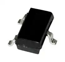
**Thyristors** Surface Mount – 200V  >   NYC0102BLT1G

~~RoHS Pb HFL_1@~~

## NYC0102BLT1G

## **Description**

This NYC0102 SCR thyristor has been designed for lowpower switching applications by implementing a sensitive gate triggered component.

## **Features**

- High dv/dt noise • RoHS compliant and immunity Halogen Free/BFR free,

- • Gating Current < 200 µA Lead-Free (micro amp)

- Miniature SOT−23 Package for High Density PCB

## **Functional Diagram**

## **Pin Out**

**3/A 1/K** % **2/G**

## **Additional Information**

**==> picture [199 x 55] intentionally omitted <==**

**----- Start of picture text -----**<br>
| [et] |<br>Datasheet Resources Samples<br>a<br>**----- End of picture text -----**<br>


© 2019 Littelfuse, Inc. Specifications are subject to change without notice. Revised: 07/15/19

**Thyristors** Surface Mount – 200V  >   NYC0102BLT1G

**==> picture [93 x 32] intentionally omitted <==**

**==> picture [506 x 608] intentionally omitted <==**

**----- Start of picture text -----**<br>
Maximum Ratings   (TJ = 25°C unless otherwise noted)<br>Rating Symbol Value Unit<br>Peak Repetitive Off−State Voltage (Note 1)(RGK = IK, TJ -40 to +110°C, Sine Wave, 50 to 60 Hz) VDRM  &  VRRM 200 V<br>On-State RMS Current  (All Conduction Angles; TC = 80°C) IT  (RMS)  0.25 A<br>Peak Non-Repetitive Surge Current (1/2 Cycle Sine Wave, 60 Hz, TA = 25°C) ITSM 7.0 A<br>Circuit Fusing Consideration (t = 8.3 ms) I [2] t 0.2 A²sec<br>Forward Peak Gate Power (Pulse Width ≤ 1.0 sec, TA = 25°C) PGM 0.1 W<br>Forward Average Gate Power (t = 8.3 ms, TA = 25°C) PGM (AV) 0.02 W<br>Forward Peak Gate Current  (Pulse Width ≤ 20 s, TA = 25°C) IFGM 0.5 A<br>Reverse Peak Gate Voltage  (Pulse Width ≤ 1.0 s, TA = 25°C) VRGM 8.0 V<br>Operating Junction Temperature Range @ Rated VRRM and VDRM TJ -40 to +125 °C<br>Storage Temperature Range Tstg -40 to +150 °C<br>Thermal Characteristics<br>Rating Symbol Value Unit<br>Total Component Dissipation FR−5 Board    TA = 25°C PD 225 mW<br>Thermal Resistance, Junction−to−Ambient R Ɵ JA 380 °C/W<br>Stresses exceeding Maximum Ratings may damage the component. Maximum Ratings are stress ratings only. Functional operation above the Recommended Operating Conditions is not<br>implied. Extended exposure to stresses above the Recommended Operating Conditions may affect component reliability.<br>1. VDRM and VRRM for all types can be applied on a continuous basis. Ratings apply for zero or negative gate voltage; however, positive gate voltage shall not be applied concurrent with negative DRM and VRRM for all types can be applied on a continuous basis. Ratings apply for zero or negative gate voltage; however, positive gate voltage shall not be applied concurrent with negative  and VRRM for all types can be applied on a continuous basis. Ratings apply for zero or negative gate voltage; however, positive gate voltage shall not be applied concurrent with negative RRM for all types can be applied on a continuous basis. Ratings apply for zero or negative gate voltage; however, positive gate voltage shall not be applied concurrent with negative for all types can be applied on a continuous basis. Ratings apply for zero or negative gate voltage; however, positive gate voltage shall not be applied concurrent with negative<br>potential on the anode. Blocking voltages shall not be tested with a constant current source such that the voltage ratings of the components are exceeded.<br>Electrical Characteristics - OFF<br>Characteristic Symbol Min Typ Max Unit<br>Peak Repetitive Forward Blocking Current  (Note 3) (VDRM =200V, RGK=1kΩ )  TTJJ = 125°C = 25°C IDRM -- -- 1001.0 μA<br>Peak Repetitive Reverse Blocking Current( VRRM=200V, RGK = 1 kΩ )  TTJJ = 125°C = 25°C IRRM -- -- 1001.0<br>Electrical Characteristics - ON (TJ = 25°C unless otherwise noted)<br>Characteristic Symbol Min Typ Max Unit<br>Peak Forward On-State Voltage   (ITM = 0.4 A, tp < 1 ms, TC = 25°C) VTM − − 1.7 V<br>Gate Trigger Current  (VD = 12 V, RL = 100 Ω, TC = 25°C) IGT − − 200 µA<br>Gate Trigger Voltage  (VD = 12 V, RL = 100 Ω, TC = 25°C) VGT − − 0.8 V<br>Holding Current  (IT = 50 mA, RGK = 1 kΩ, TC = 25°C) IH − − 6.0 mA<br>Gate Non−Trigger Voltage  (VD = VDRM, RL = 3.3 kΩ, TC = 125°C) VGD 0.1 _ − V<br>Latching Current  (IG = 1.0 mA, RGK = 1 kΩ, TC = 25°C) IL − − 7.0 mA<br>Gate Reverse Voltage  (IRG = 10 µA) VRG 8.0 _ − V<br>Dynamic Characteristics<br>Characteristic Symbol Min Typ Max Unit<br>Critical Rate-of-Rise of Off State Voltage dv/dt 200 − − V/µs<br>(RGK = 1 KΩ, TC = 125°C)<br>Critical Rate of Rise of On−State Current(IG = 2xIGT 60 Hz, tr < 100 ns, TJ = 125°C) di/dt − − 50 A/μs<br>**----- End of picture text -----**<br>


Stresses exceeding Maximum Ratings may damage the component. Maximum Ratings are stress ratings only. Functional operation above the Recommended Operating Conditions is not implied. Extended exposure to stresses above the Recommended Operating Conditions may affect component reliability.

1. VDRM and VRRM for all types can be applied on a continuous basis. Ratings apply for zero or negative gate voltage; however, positive gate voltage shall not be applied concurrent with negative DRM and VRRM for all types can be applied on a continuous basis. Ratings apply for zero or negative gate voltage; however, positive gate voltage shall not be applied concurrent with negative  and VRRM for all types can be applied on a continuous basis. Ratings apply for zero or negative gate voltage; however, positive gate voltage shall not be applied concurrent with negative RRM for all types can be applied on a continuous basis. Ratings apply for zero or negative gate voltage; however, positive gate voltage shall not be applied concurrent with negative for all types can be applied on a continuous basis. Ratings apply for zero or negative gate voltage; however, positive gate voltage shall not be applied concurrent with negative potential on the anode. Blocking voltages shall not be tested with a constant current source such that the voltage ratings of the components are exceeded.

© 2019 Littelfuse, Inc. Specifications are subject to change without notice. Revised: 07/15/19

**Thyristors** Surface Mount – 200V  >   NYC0102BLT1G

**==> picture [93 x 32] intentionally omitted <==**

## **Voltage/Current Characteristics of SCR**

**==> picture [245 x 323] intentionally omitted <==**

**----- Start of picture text -----**<br>
Symbol Parameter<br>VDRM Peak Repetitive Forward Off State Voltage<br>IDRM Peak Forward Blocking Current<br>VRRM Peak Repetitive Reverse Off State Voltage<br>IRRM Peak Reverse Blocking Current<br>VTM Maximum On State Voltage<br>IH Holding Current<br>Figure 1. Maximum Average Power vs. Average Current<br>0.25<br>0.2<br>0.15<br>0.1<br>0.05<br>0<br>0 .050 .1 0.15 0.2<br>IT, AVERAGE CURRENT (A)<br>P, AVERAGE POWER (W)<br>**----- End of picture text -----**<br>


**==> picture [243 x 19] intentionally omitted <==**

**----- Start of picture text -----**<br>
Figure 3. Surge Current ITSM vs. Number of Cycles<br>**----- End of picture text -----**<br>


**==> picture [244 x 170] intentionally omitted <==**

**----- Start of picture text -----**<br>
 (A)<br>ITSM<br>**----- End of picture text -----**<br>


**==> picture [244 x 559] intentionally omitted <==**

**----- Start of picture text -----**<br>
+Current<br>Anode+<br>VTM<br>IRRM at VRRM on state IH<br>+Voltage/Current<br>Reverse Blocking Region IDRM at VDRM<br>(off state)<br>Forward Blocking Region<br>Reverse Avalanche Region (off state)<br>Anode-<br>Figure 2. Current Derating<br>0.3<br>0.25<br>0.2<br>0.15<br>0.1<br>0.05<br>T, Temperature (°C)<br>Figure 4. Thermal Response<br>1<br>0.8<br>0.6<br>0.4<br>0.2<br>0<br>1 E-04 1 E-03 1 E-02 1 E-01 1 E+00 1 E+01 1 E+02 1 E+03<br>Pulse Duration (S)<br>, Average Current (A)IT<br>(Normalized)<br>Transient Resistance<br>**----- End of picture text -----**<br>


© 2019 Littelfuse, Inc. Specifications are subject to change without notice. Revised: 07/15/19

**Thyristors** Surface Mount – 200V  >   NYC0102BLT1G

**==> picture [93 x 32] intentionally omitted <==**

**==> picture [243 x 19] intentionally omitted <==**

**----- Start of picture text -----**<br>
Figure 5. On−State Characteristics<br>**----- End of picture text -----**<br>


**==> picture [243 x 170] intentionally omitted <==**

**----- Start of picture text -----**<br>
10<br>1<br>0<br>0.1 0.5 1 1.5 2 2.5<br> (A)<br>ITM<br>**----- End of picture text -----**<br>


**==> picture [244 x 194] intentionally omitted <==**

**----- Start of picture text -----**<br>
Figure 8. Gate Trigger Current vs. RGK<br>0.07<br>0.06<br>0.05<br>0.04<br>0.03<br>0.02<br>0.01<br>0<br>0 2 4 6 8 10 12<br>RGK (kΩ)<br> (mA)<br>IGT<br>**----- End of picture text -----**<br>


**==> picture [243 x 19] intentionally omitted <==**

**----- Start of picture text -----**<br>
Figure 10. dV/dt vs. RGK<br>**----- End of picture text -----**<br>


**==> picture [243 x 170] intentionally omitted <==**

**----- Start of picture text -----**<br>
dv/dt (V/µs)<br>**----- End of picture text -----**<br>


**==> picture [244 x 19] intentionally omitted <==**

**----- Start of picture text -----**<br>
Figure 6. Gate Trigger Current vs. TJ (Normalized to 25 C)<br>**----- End of picture text -----**<br>


**==> picture [244 x 380] intentionally omitted <==**

**----- Start of picture text -----**<br>
2<br>1.5<br>Ω<br>1<br>0.5<br>0<br>Figure 9. Holding and Latching Current vs.RGK<br>25<br>20<br>15<br>10<br>5.0<br>0<br>0 1 2 3 4 5 6 7 8 9 10<br>RGK (kΩ)<br> (mA),IILH<br>**----- End of picture text -----**<br>


**==> picture [244 x 197] intentionally omitted <==**

**----- Start of picture text -----**<br>
Figure 11. Gate Triggering Voltage vs. TJ<br>1.0<br>0.80<br>0.60<br>0.40<br>0.20<br>0<br>200 250 300 350 400<br>TJ (K)<br> (V)<br>GT<br>V<br>**----- End of picture text -----**<br>


© 2019 Littelfuse, Inc. Specifications are subject to change without notice. Revised: 07/15/19

**Thyristors** Surface Mount – 200V  >   NYC0102BLT1G

**==> picture [93 x 32] intentionally omitted <==**

**==> picture [245 x 19] intentionally omitted <==**

**----- Start of picture text -----**<br>
Dimensions<br>**----- End of picture text -----**<br>


**==> picture [215 x 145] intentionally omitted <==**

**----- Start of picture text -----**<br>
D<br>SEE VIEW C<br>3<br>E HE<br>c<br>12<br>b<br>e 0.25<br>A<br>L<br>A1<br>L1<br>VIEW C<br>**----- End of picture text -----**<br>


**==> picture [245 x 170] intentionally omitted <==**

**----- Start of picture text -----**<br>
Inches Millimeters<br>Dim<br>Min Nom Max Min Nom Max<br>A 0.035 0.041 0.046 0.89 1.03 1.17<br>A1 0.001 0.004 0.006 0.05 0.10 0.15<br>b 0.012 0.016 0.020 0.30 0.40 0.50<br>c 0.003 0.006 0.008 0.08 0.14 0.20<br>D 0.110 0.114 0.118 2.80 2.90 3.00<br>E 0.047 0.051 0.055 1.20 1.30 1.40<br>e --- 0.075 --- --- 1.90 ---<br>L 0.016 0.019 0.023 0.40 0.49 0.58<br>L1 0.018 0.022 0.025 0.46 0.55 0.64<br>HE 0.083 0.091 0.098 2.10 2.30 2.49<br>ø 0° --- 10° 0° --- 10°<br>**----- End of picture text -----**<br>


1. Diminishing and tolerancing per ANSI Y 14.5M, 1982.

2. Controlling Dimension: Inch

3. Maximum lead thickness includes lead finish thickness. Minimum lead thickness is the minimum thickness of base material.

4. Dimensions D and E do not include mold flash, protrusions, or gate burrs.

**==> picture [245 x 556] intentionally omitted <==**

**----- Start of picture text -----**<br>
Soldering Footprint<br>0.95<br>0.95 0.037<br>0.037<br>2.0<br>0.079<br>0.9<br>0.035<br>SCALE 10:1 inchesmm<br>0.8<br>0.031<br>Part Marking System<br>3<br>1<br>2 C2B YMA<br>1<br>CASE 318<br>STYLE 8<br>C2B= Specific Device Code<br>YMA= Date Code*<br>. Pb-Free Package<br>(Note: Microdot may be in either location)<br>*Date Code orientation and/or overbar may vary depending<br>upon manufacturing location.<br>Pin Assignment<br>1 Cathode<br>2 Gate<br>3 Anode<br>Ordering Information<br>Device Package Shipping<br>SOT-23<br>NYC0102BLT1G 3000/Tape & Reel/Box<br>(Pb-Free)<br>**----- End of picture text -----**<br>


**Disclaimer Notice** - Information furnished is believed to be accurate and reliable. However, users should independently evaluate the suitability of and test each product selected for their own applications. Littelfuse products are not designed for, and may not be used in, all applications. Read complete Disclaimer Notice at: www.littelfuse.com/disclaimer-electronics

© 2019 Littelfuse, Inc. Specifications are subject to change without notice. Revised: 07/15/19
Updated at June 10, 2026
Founded in 1927 and headquartered in Chicago, Illinois, Littelfuse is a premier global manufacturer of circuit protection, power control, and sensing technologies. Widely recognized for pioneering the first small, fast-acting protective fuse, the company has grown into an industry leader whose highly reliable components are essential to modern industrial, transportation, and consumer electronics applications worldwide. At the core of the Littelfuse portfolio is an expansive and industry-leading range of circuit protection solutions. This encompasses a massive selection of traditional fuses, fuse holders, and resettable PTC thermistor fuses designed to safely interrupt overcurrent conditions. To defend against electrical overstress, Littelfuse also provides advanced transient voltage suppression (TVS) technologies, including thousands of specialized TVS diodes, TVS varistors, and gas discharge tubes (GDTs) that ensure robust defense against voltage spikes and environmental hazards. Beyond its foundational protection components, Littelfuse manufactures a diverse array of discrete semiconductors, sensors, and switching devices. Engineers rely on their high-performance thyristors, including TRIACs and SCRs, alongside power-efficient Schottky diodes and MOSFETs for demanding power control applications. Complemented by precision proximity sensors and highly reliable reed and solid-state relays, Littelfuse delivers the critical building blocks required for secure, efficient, and complete system design.
About Novapart
Novapart is a B2B electronic component broker specialising in stock shortages and cost reduction. We source hard-to-find parts and identify compliant alternatives across a catalogue of 540,000+ components from 500+ manufacturers.
Learn more →Stock Shortage Specialist
When a component is unavailable, discontinued or has an unacceptable lead time, we tap into our network of vetted European and Asian distributors to source what you need — without compromising on quality or traceability.
Request a quote →Compliant Alternatives
We identify pin-to-pin, electrically equivalent substitutes that meet the same certifications (RoHS, AEC-Q100, REACH) as your original specification — validated against datasheets, not just part numbers. Often at a lower cost.
BOM Analysis service →