
Image not available
Illustrative purposes only

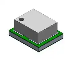
MUN3CAD03-JB
Non Isolated POL DC/DC Converter, Micro Module, 12 W, 600 mV, 4 V, 3 A
⚠️ Reference pricing provided. In case of supply shortages, we will connect you with our trusted procurement partners to ensure your project's continuity.
- Manufacturer: CYNTEC
- Product type: DC / DC Non Isolated Board Mount Converters - Adjustable Output
- SVHC: No SVHC (21-Jan-2025)
- Depth: 2.5mm
- Width: 2mm
- Height: 1.3mm
- Product Range: -
- Output Power Max: 12W
- Output Current Max: 3A
- Output Voltage Max: 4V
- Output Voltage Min: 600mV
- Input Voltage DC Max: 5.5V
- Input Voltage DC Min: 2.5V
- DC / DC Converter Type: Micro Module
- Power Supply Applications: -
- DC / DC Converter Output Type: Adjustable
| Delivery and price | |
|---|---|
| Units per pack | 500 |
| Price | 1.52 € |
| Current stock | 1000+ |
| Lead time | 30 days |
Datasheet

**MUN3CAD03-JB** **TYPICAL APPLICATION CIRCUIT & PACKAGE:** ## **uPOL MODULE** ## **3A, High Efficiency uPOL Module** ## **FEATURES:** ~~SS~~ - High Density Power Module - 3A Output Current - Up to 95% Efficiency - Input Voltage Range from 2.5V to 5.5V - 0.6V to 4V Adjustable Output Voltage - 100% Duty Cycle with Low Dropout - 2MHz with Forced PWM Mode - Enable Function - Hiccup Mode for Shot Circuit and Over-Load Protection - Internal Soft Start - Compact Size: 2.5mm*2.0mm*1.3mm - Pb-free for RoHS compliant - MSL 2, 260C Reflow ## **APPLICATIONS:** - Optical modules - Industrial PCs - PLCs ## **GENERAL DESCRIPTION:** The module is non-isolated dc-dc converter that can deliver up to 3A of output current. The PWM switching regulator, high frequency power inductor are integrated in one hybrid package. It only needs input/output capacitors and one voltage dividing resistor to perform properly. The module runs in forced-PWM maintaining a continuous conduction mode at all currents to minimize the output ripple, through constant on-time control, the module offers a simpler control loop and faster transient response. Other features include remote enable function, internal soft-start, non-latching over current protection, power good, input under voltage locked-out capability. The low profile and compact size package (2.5mm × 2.0mm x 1.3mm) is suitable for automated assembly by standard surface mount equipment. The MUN3CAD03-JB power module is Pb-free and RoHS compliance. **==> picture [463 x 220] intentionally omitted <==** **----- Start of picture text -----**<br> EN EN PG VPGOOD<br>VIN VIN VOUT VOUT<br>uPOL Module RFB_T CFB<br>1.3mm<br>CIN FB COUT<br>GND RFB_B (Max.)<br>GND GND<br>2.5mm<br>Ln @ 2.0mm<br>FIGURE 1 TYPICAL APPLICATION CIRCUIT FIGURE 2 HIGH DENSITY LOW PROFILE<br>uPOL MODULE<br>1 Rev.A0<br>**----- End of picture text -----**<br> Rev.A0 **MUN3CAD03-JB** > **ORDERING INFORMATION:** ~~TT~~ CAUTION: These devices have limited built-in ESD protection. The leads should be shorted together or the devices placed in conductive foam during the storage or handling to prevent electrostatic damage to internal circuit. **Ambient Temp. Range Package Part Number MSL Note (°C) (Pb-Free)** MHUN3CAD03JB -40 ~ +125 DFN Level 2 - **Order Code Packing Quantity** MUN3CAD03-JB Tape and reel 2000 ~~es~~ 2 Rev.A0 **MUN3CAD03-JB** **==> picture [461 x 14] intentionally omitted <==** **----- Start of picture text -----**<br> PIN CONFIGURATION: CT<br>**----- End of picture text -----**<br> **==> picture [289 x 190] intentionally omitted <==** **----- Start of picture text -----**<br> (1) VIN (10) GND<br>fo fo]<br>(2) VIN (9) GND<br>Ld Ld<br>CTT -T TF<br>(3) EN (8) FB<br>Lo _d| LH_ _|<br>rT TT<br>(4) PG (7) VOUT<br>| L |<br>rT TT<br>(5)VOUT (6) VOUT<br>**----- End of picture text -----**<br> **TOP THROUGH VIEW** > **PIN DESCRIPTION:** ~~|~~ |**Symbol**|**Pin No.**|**Description**| |---|---|---| |VIN|1, 2|Power input pin. It needs to be connected to input rail with input<br>capacitor. A 22uF capacitor at least for input.| |EN|3|On/Off control pin for module.<br>EN = LOW, the module is off.<br>EN = HIGH,the module is on.| |PGOOD|4|Power good output. It has an integrated the pull high internal 1 M<br>resistor to VIN.| |VOUT|5, 6, 7|Power output pin. Connect to output for the load with output capacitor. A<br>22uF capacitor at least for output.| |FB|8|Feedback input. Connect an external resistor divider to set the output<br>voltage.| |GND|9, 10|Power ground pin for signal, input, and output return path. This pin<br>needs to be connected to one or more ground plane directly. Connect to<br>thermal exposedpad of GND for heat transferring.| 3 Rev.A0 **MUN3CAD03-JB** G'eyntec **ELECTRICAL SPECIFICATIONS:** CAUTION: Do not operate at or near absolute maximum rating listed for extended periods of time. This stress may adversely impact product reliability and result in failures outside of warranty. **Parameter Description Min. Typ. Max. Unit** ~~a~~ ## **ELECTRICAL SPECIFICATIONS:** CAUTION: Do not operate at or near absolute maximum rating listed for extended periods of time. This stress may adversely impact product reliability and result in failures outside of warranty. |**Parameter**<br>~~a~~|**Description**<br>~~a~~|**Min.**<br>~~a~~|**Typ.**<br>~~a~~|**Max.**<br>~~a~~|**Unit**<br>~~a~~| |---|---|---|---|---|---| |◼<br>Absolute Maximum Ratings<br>~~a~~<br>~~ee~~|||||| |VIN to GND<br>~~ee~~<br>~~ee~~||-|-|-0.3 to +6|V| |VOUT to GND<br>~~ee~~<br>~~ee~~<br>~~ee~~||-|-|-0.3 to +6|V| |EN, PGOOD, FB to GND<br>~~ee~~<br>~~ee~~<br>~~ee~~||-|-|-0.3 to +6|V| |Tc<br>~~ee~~<br>~~ee~~<br>~~es~~|Case Temperature of Inductor|-|-|+125|°C| |Tj<br>~~ee~~<br>~~es~~<br>~~es~~|Junction Temperature<br>~~ee~~|-40<br>~~ee~~|-<br>~~ee~~|+150<br>~~ee~~|°C<br>~~ee~~| |Tstg<br>~~es~~<br>~~es~~|Storage Temperature<br>~~ee~~|-40<br>~~ee~~<br>~~es~~|-<br>~~ee~~<br>~~ee~~|+125<br>~~ee~~|°C<br>~~ee~~| |ESD Rating<br>~~es~~|Human Body Model (HBM)<br>~~ee~~|-<br>~~ee~~<br>~~es~~<br>~~es~~|-<br>~~ee~~<br>~~ee~~<br>~~ee~~|2k<br>~~ee~~<br>~~ee~~|V<br>~~ee~~| ||Machine Model (MM)<br>~~ee~~|-<br>~~es~~<br>~~ee~~<br>~~es~~<br>~~ee~~|-<br>~~ee~~<br>~~ee~~<br>~~ee~~<br>~~ee~~|200<br>~~ee~~<br>~~ee~~<br>~~ee~~|V<br>~~ee~~| ||Charge Device Model (CDM)<br>~~ee~~|-<br>~~es ~~<br>~~ee~~<br>~~ee~~|-<br> ~~ee~~<br>~~ee~~<br>~~ee~~|1k<br>~~ee~~<br>~~ee~~<br>~~ee~~|V<br>~~ee~~| |◼<br>Recommendation Operating Ratings<br>~~ee~~<br>~~ee~~<br>~~ee~~<br>~~a~~|||||| |VIN<br>~~es~~|Input Supply Voltage<br>~~es~~|+2.5<br>~~es~~|-<br>~~es~~|+5.5<br>~~es~~|V<br>~~es~~| |IOUT<br>~~es~~<br>~~es~~|Output Current Range<br>~~es~~|0<br>~~es~~|-<br>~~es~~|3<br>~~es~~|A<br>~~es~~| |Ta<br>~~es~~|Ambient Temperature|-40|-|+125|°C| |◼<br>Thermal Information<br>~~es~~<br>~~a~~|||||| |Rth(jchoke-a)|Thermal resistance from junction to<br>ambient. (Note 1)|-|34.8|-|°C/W| 4 Rev.A0 **MUN3CAD03-JB** Gioyntec **ELECTRICAL SPECIFICATIONS: (Cont.)** Conditions: TA = 25 ºC, unless otherwise specified. Test Board Information: 30mm×A = 25 ºC, unless otherwise specified. Test Board Information: 30mm×= 25 ºC, unless otherwise specified. Test Board Information: 30mm× 30mm× 1.6mm, 4 layers, 2oz. The output ripple and transient response are measured by short loop probing and limited to 20MHz bandwidth. Cin = 22uF/6.3V/0603*1, Cout = 22uF/6.3V/0603*1. **Symbol Parameter Conditions Min. Typ. Max. Unit** ~~a~~ ## **ELECTRICAL SPECIFICATIONS: (Cont.)** Conditions: TA = 25 ºC, unless otherwise specified. Test Board Information: 30mm×A = 25 ºC, unless otherwise specified. Test Board Information: 30mm×= 25 ºC, unless otherwise specified. Test Board Information: 30mm× 30mm× 1.6mm, 4 layers, 2oz. The output ripple and transient response are measured by short loop probing and limited to 20MHz bandwidth. Cin = 22uF/6.3V/0603*1, Cout = 22uF/6.3V/0603*1. |**Symbol**<br>~~a~~|**Symbol**<br>**Parameter**<br>~~a~~|**Conditions**<br>~~a~~|**Min. Typ. Max.**<br>~~a~~|**Min. Typ. Max.**<br>~~a~~|**Min. Typ. Max.**<br>~~a~~|**Min. Typ. Max.**<br>**Unit**<br>~~a~~| |---|---|---|---|---|---|---| |◼<br>Input Characteristics<br>~~a~~||||||| |IQ<br>~~a~~|Quiescent current<br>~~a~~|Iout=0,VFB=VREF*105%<br>~~a~~|-<br>~~a~~|500<br>~~a~~|-<br>~~a~~|uA<br>~~a~~| |ISD(IN)<br>~~a~~<br>~~—————EEEE~~|Input shutdown current<br>~~a~~<br>~~—————EEEE~~|Vin =3.3V, EN = GND<br>~~a~~<br>~~Eee~~|-<br>~~a~~<br>~~eee~~|0.1<br>~~a~~<br>~~eee~~|-<br>~~a~~<br>~~eee~~|uA<br>~~a~~<br>~~eee~~| |VUVLO<br>~~—————EEEE~~|Undervoltage lockout threshold<br>~~—————EEEE~~|Vin Increasing<br>~~Eee~~|2.3<br>~~eee~~<br>~~ee~~|2.4<br>~~eee~~<br>~~ee~~|2.5<br>~~eee~~<br>~~ee~~|V<br>~~eee~~| ||Undervoltage lockout hysteresis<br>~~—————EEEE~~<br>~~es~~|~~Eee~~<br>~~es~~|-<br>~~eee~~<br>~~es~~<br>~~ee~~<br>~~ee~~|250<br>~~eee~~<br>~~es~~<br>~~ee~~|-<br>~~eee~~<br>~~es~~<br>~~ee~~|mV<br>~~eee~~<br>~~es~~| |IS(IN)<br>~~—————EEEE~~|Input supply current<br>~~—————EEEE ~~|Vin =3.3V, EN = VIN<br> ~~Eee ~~<br>~~ee~~|-<br> ~~eee~~<br>~~ee~~<br>~~ee~~<br>~~ee~~<br>~~ee~~|-<br>~~eee~~<br>~~ee ~~<br>~~ee~~|-<br>~~eee~~<br> ~~ee~~<br>~~ee~~|-<br>~~eee~~<br>~~ee~~| |||Iout = 0A, Vout = 1.8V<br>~~ee~~|-<br>~~ee~~<br>~~ee~~<br>~~ee~~<br>~~ee~~|17<br>~~ee~~|-<br>~~ee~~|mA<br>~~ee~~| |||Iout = 3A, Vout = 1.8V<br>~~ee~~|-<br>~~ee~~<br>~~ee~~<br>~~ee~~|1.83<br>~~ee~~|-<br>~~ee~~|A<br>~~ee~~| |◼ Control Characteristics<br>~~ee~~<br>~~a~~||||||| |VFB<br>~~a~~<br>~~a~~|Feedback regulation voltage<br>~~a~~<br>~~a~~|PWM Mode<br>~~a~~<br>~~a~~|0.591<br>~~a~~<br>~~a~~|0.6<br>~~a~~<br>~~a~~|0.609<br>~~a~~<br>~~a~~|V<br>~~a~~<br>~~a~~| |FOSC<br>~~a~~<br>~~a~~<br>~~ee~~|Oscillator frequency<br>~~a~~<br>~~a~~<br>~~ee~~<br>~~ee ee~~|PWM Operation<br>~~a~~<br>~~a~~<br>~~ee~~<br>~~ee~~|-<br>~~a~~<br>~~a~~<br>~~ee~~|2.0<br>~~a~~<br>~~a~~<br>~~ee~~<br>~~eee~~|-<br>~~a~~<br>~~a~~<br>~~ee~~<br>~~eee~~|MHz<br>~~a~~<br>~~a~~<br>~~ee~~<br>~~eee~~| |VPG<br>~~ee~~|PGOOD threshold<br>~~ee ee~~|VPGrising<br>~~ee~~|88|90<br>~~eee~~|92<br>~~eee~~|%<br>~~eee~~| |||VPGfalling<br>~~ee~~<br>~~ee~~|-<br>~~ee~~|85<br>~~eee~~<br>~~ee~~|-<br>~~eee~~<br>~~ee~~|%<br>~~eee~~<br>~~ee~~| |RPG_PU<br>~~ee~~<br>~~ee~~|PGOOD pull-up resistor<br>~~ee ee~~<br>~~ee~~|Internal pull-up to Vin<br>~~ee~~<br>~~ee~~|-<br>~~ee~~|1<br>~~eee~~<br>~~ee~~|-<br>~~eee~~<br>~~ee~~|MΩ<br>~~eee~~<br>~~ee~~| |VPGL<br>~~ee~~|PGOOD output low<br>~~ee~~|VFB=0.5V, sink 1mA<br>~~ee~~|-<br>~~ee~~|0.2<br>~~ee~~|-<br>~~ee~~|V<br>~~ee~~| |tSS<br>~~aPf~~|Soft-start time<br>~~Pfff~~|~~ff~~|-<br>~~ff~~|600<br>~~ff~~|-<br>~~ff~~|us<br>~~ff~~| |VEN_TH<br>~~Pf~~<br>~~a~~|Enable rising threshold voltage<br>~~Pfff~~|~~ff~~|1.6<br>~~ff~~|-<br>~~ff~~|-<br>~~ff~~|V<br>~~ff~~| ||Enable falling threshold voltage<br>~~Pfff~~<br>~~ee~~<br>~~es~~|~~ff~~<br>~~ee~~<br>~~de~~|-<br>~~ff~~<br>~~ee~~<br>~~de~~|-<br>~~ff~~<br>~~ee~~<br>~~de~~|0.5<br>~~ff~~<br>~~ee~~<br>~~de~~|V<br>~~ff~~<br>~~ee~~<br>~~de~~| |REN_PD<br>~~Pf~~<br>~~a~~|EN internal pull down resistor<br>~~Pf ff~~<br>~~es~~|~~ff~~<br>~~de~~|-<br>~~ff~~<br>~~de~~|1<br>~~ff~~<br>~~de~~|-<br>~~ff~~<br>~~de~~|MΩ<br>~~ff~~<br>~~de~~| |TOTP<br>~~a~~<br>~~a~~|Over temp protection<br>~~es~~|~~de~~|-<br>~~de~~|160<br>~~de~~|-<br>~~de~~|°C<br>~~de~~| |OCP<br>~~a~~|Protection Output Current<br>~~eG~~|~~eG~~|-<br>~~eG~~|5<br>~~eG~~|-<br>~~eG~~|A<br>~~eG~~| 5 Rev.A0 **MUN3CAD03-JB** ## **TYPICAL PERFORMANCE CHARACTERISTICS: (3.3VOUT)** Conditions: TA = 25 ºC, unless otherwise specified. Test Board Information: 30mm× 30mm× 1.6mm, 4 layers. The output ripple and transient response are measured by short loop probing and limited to 20 MegHz bandwidth. Vin = 5.0V, Vout = 3.3V, unless otherwise noted. **==> picture [410 x 385] intentionally omitted <==** **----- Start of picture text -----**<br> FIGURE 3 Efficiency V.S. Load Current FIGURE 4 De-rating Curve at 5.0VIN<br>ee eee | lek Stop e e e e |<br>VOUT VOUT<br>INNA LN INOe AsANN a PNAPN Oe phod A A aA A aAO A A<br>+¥496.0000s“00ns 2506575100k points 2.167V +¥496.0000s“00ns 2506575100k points 2.36V7<br>FIGURE 5 Output Ripple at 5.0VIN FIGURE 6 Output Ripple at 5.0VIN<br>(IOUT=0A) (IOUT=3A)<br>Se ee | Tek Stop a es<br>VOUT EN<br>VOUT<br>IOUT<br>PG<br>50.0my 2.5A/us 4 400ys 25,0MS/s oO. Po<br>2.004 Gey-1.200000ms 100k points 1.604 @ 20" w& 400ys 25.0MS/s (3<br>81.0m¥ 2.00¥ & G+¥496.0000ys 100k points 1.96<br>-81,0m¥ V<br>FIGURE 7 Transient Response FIGURE 8 Turn-On<br>(VIN=5.0V,IOUT=0.3A~3A) (VIN=5.0V,IOUT=3A)<br>**----- End of picture text -----**<br> 6 Rev.A0 **MUN3CAD03-JB** ## **TYPICAL PERFORMANCE CHARACTERISTICS: (1.8VOUT)** Conditions: TA = 25 ºC, unless otherwise specified. Test Board Information: 30mm× 30mm× 1.6mm, 4 layers. The output ripple and transient response are measured by short loop probing and limited to 20 MegHz bandwidth. Vin = 3.3V, Vout = 1.8V, unless otherwise noted. **==> picture [422 x 385] intentionally omitted <==** **----- Start of picture text -----**<br> FIGURE 9 Efficiency V.S. Load Current FIGURE 10 De-rating Curve at 3.3VIN<br>—_————— 2 | Tek Stop, a<br>VOUT VOUT<br>PLN LON TN NN ON pM AAMAS A Aa<br>400ns 2.5068/s \ 400ns 2.5068/s \<br>G+0.000000s 100k points 1,04 U+¥0.000000s 100k points 1.04<br>FIGURE 11 Output Ripple at 3.3VIN FIGURE 12 Output Ripple at 3.3VIN<br>(IOUT=0A) (IOUT=3A)<br>Stop SS es | Tek Stop A<br>VOUT<br>EN<br>VOUT<br>IOUT<br>PG<br>@ 50.0my 2.5A/us v4 400ps 25.0MS/s oO. Po<br>@ 204 f G+Y-1,200000ims 100k points 2.08 A @ iv 4 400ys 25.0MS/s ef<br>@O ma 65,0mV 2,00 ¥ By G%496.0000) 100k points 1.36<br>@nxin -73,0mV<br>FIGURE 13 Transient Response FIGURE 14 Turn-On<br>(VIN=3.3V,IOUT=0.3A~3A) (VIN=3.3V,IOUT=3A)<br>**----- End of picture text -----**<br> 7 Rev.A0 **MUN3CAD03-JB** ## **TYPICAL PERFORMANCE CHARACTERISTICS: (1.0VOUT)** Conditions: TA = 25 ºC, unless otherwise specified. Test Board Information: 30mm× 30mm× 1.6mm, 4 layers. The output ripple and transient response are measured by short loop probing and limited to 20 MegHz bandwidth. Vin = 3.3V, Vout = 1.0V, unless otherwise noted. **==> picture [424 x 384] intentionally omitted <==** **----- Start of picture text -----**<br> FIGURE 15 Efficiency V.S. Load Current FIGURE 16 De-rating Curve at 3.3VIN<br>Prevu fg ee ek Stop fgee<br>VOUT VOUT<br>V/A pon \Ffs VS oo OVSAPN EMS NN VYANONONS" Pwaa Ah AalAedAN<br>Cr a 496.0000Co TSI100k points _2.36V7 Cs C0G7496,0000ps a100k points __200yV| 2<br>FIGURE 17 Output Ripple at 3.3VIN FIGURE 18 Output Ripple at 3.3VIN<br>(IOUT=0A) (IOUT=3A)<br>Stop Ses ae Tek Stop Ces | ee A<br>VOUT<br>EN<br>VOUT<br>IOUT<br>PG<br>@ 50.0my 2.5A/us v4 400ps 25.0MS/s oO. Po<br>@ 204 4 GY-1,200000ms 100k points _680mA @iov 4 400ys 25.0MS/s e/<br>Orme 49,0mV 2.00V G7496.0000ps 100k points 1.56<br>Orin -63.0mV<br>FIGURE 19 Transient Response FIGURE 20 Turn-On<br>(VIN=3.3V,IOUT=0.3A~3A) (VIN=3.3V,IOUT=3A)<br>**----- End of picture text -----**<br> 8 Rev.A0 **MUN3CAD03-JB** > **APPLICATIONS INFORMATION:** ~~CT~~ ## **REFERENCE CIRCUIT FOR GENERAL APPLICATION:** The Figure 21 shows the module application schematics for input voltage +5V or +3.3V and turn on by input voltage directly through enable resistor. **==> picture [352 x 102] intentionally omitted <==** **----- Start of picture text -----**<br> 100k Ω/ 0402 EN PG VPGOOD<br>VIN VIN VOUT VOUT<br>uPOL Module RFB_T 120pF/<br>50V/0402<br>FB<br>22uF/6.3V/0603<br>GND RFB_B Setting Output Voltage 22uF/6.3V/0603<br>GND GND<br>**----- End of picture text -----**<br> ## **FIGURE 21. GENERAL APPLICATION CIRCUIT WITH TURN-ON BY INPUT VOLTAGE** ## **SAFETY CONSIDERATIONS:** Certain applications and/or safety agencies may require fuses at the inputs of power conversion components. Fuses should also be used when there is the possibility of sustained input voltage reversal which is not current limited. For greatest safety, we recommend a fast blow fuse installed in the ungrounded input supply line. The installer must observe all relevant safety standards and regulations. For safety agency approvals, install the converter in compliance with the end-user safety standard. ## **INPUT FILTERING:** The module should be connected to a source supply of low AC impedance and high inductance in which line inductance can affect the module stability. An input capacitor must be placed as near as possible to the input pin of the module so to minimize input ripple voltage and ensure module stability. ## **OUTPUT FILTERING:** To reduce output ripple and improve the dynamic response as the step load changes, an additional capacitor at the output must be connected. Low ESR polymer and ceramic capacitors are recommended to improve the output ripple and dynamic response of the module. 9 Rev.A0 **MUN3CAD03-JB** e—eseses—‘“‘“‘ el > **APPLICATIONS INFORMATION:** ~~CT~~ ## **PROGRAMMING OUTPUT VOLTAGE:** The module has an internal 0.6V ± 1.5% reference voltage. The output voltage can be programmed by the dividing resistor (RFB_T and RFB_B). The output voltage can be calculated by Equation 1, resistor choice may be referred to TABLE 1. (EQ.1) **TABLE 1 Resistor values for common output voltages** |VOUT(V)|RFB_T(k)|RFB_B(k)| |---|---|---| |1.0|100|150| |1.2|100|100| |1.8|100|49.9| |3.3|100|22.1| ## **THERMAL CONSIDERATIONS:** All of thermal testing condition is complied with JEDEC EIJ/JESD 51 Standards. Therefore, the test board size is 30mm× 30mm× 1.6mm with 4 layers. The case temperature of module sensing point is shown as Figure 22. Then Rth(jchoke-a) is measured with the component mounted on an effective thermal conductivity test board on 0 LFM condition. The MUN3CAD03-JB modules are designed for using when the case temperature is below 125°C regardless the change of output current, input/output voltage or ambient temperature. Sensing point (Defined case temperature) **==> picture [160 x 137] intentionally omitted <==** **----- Start of picture text -----**<br> ZZ<br>as<br>**----- End of picture text -----**<br> **Figure 22. CASE TEMPERATURE SENSING POINT** 10 Rev.A0 **MUN3CAD03-JB** > **APPLICATIONS INFORMATION: (Cont.)** ~~|~~ ## **REFLOW PARAMETERS:** Lead-free soldering process is a standard of electronic products production. Solder alloys like Sn/Ag, Sn/Ag/Cu and Sn/Ag/Bi are used extensively to replace the traditional Sn/Pb alloy. Sn/Ag/Cu alloy (SAC) is recommended for this power module process. In the SAC alloy series, SAC305 is a very popular solder alloy containing 3% Ag and 0.5% Cu and easy to obtain. Figure 23 shows an example of the reflow profile diagram. Typically, the profile has three stages. During the initial stage from room temperature to 150°C, the ramp rate of temperature should not be more than 3°C/sec. The soak zone then occurs from 150°C to 200°C and should last for 60 to 120 seconds. Finally, keep at over 217°C for 60~150 seconds to melt the solder and make the peak temperature at the range from 255°C to 260°C (Do not exceed 30 sec). It is noted that the time of peak temperature should depend on the mass of the PCB board. The reflow profile is usually supported by the solder vendor and one should adopt it for optimization according to various solder type and various manufacturers’ formulae. ## **FIG.23 RECOMMENDATION REFLOW PROFILE*** ## **(Not to scale)** ## ***Refer to the Classification Reflow Profile of J-STD-020.** 11 Rev.A0 **MUN3CAD03-JB** > **PACKAGE OUTLINE DRAWING:** ~~ee~~ **==> picture [52 x 9] intentionally omitted <==** **----- Start of picture text -----**<br> Unit: mm<br>**----- End of picture text -----**<br> 12 Rev.A0 **==> picture [130 x 12] intentionally omitted <==** **----- Start of picture text -----**<br> MUN3CAD03-JB<br>**----- End of picture text -----**<br> **==> picture [461 x 609] intentionally omitted <==** **----- Start of picture text -----**<br> LAND PATTERN REFERENCE: Ln<br>Unit: mm<br>_——..=—oes<br>41 oT<br>===<br>1.55<br>RECOMMENDED LAND PATTERN<br>ms<br>oo 1) oo<br>SB |1.55 cE<br>RECOMMENDED STENCIL PATTERN*<br>*Based on 0.1~0.15mm thickness stencil (Reference only)<br>*Recommended solder paste coverage 55~100%<br>**----- End of picture text -----**<br> 13 Rev.A0 **MUN3CAD03-JB** > **PACKING REFERENCE:** ~~CT~~ **==> picture [332 x 29] intentionally omitted <==** **----- Start of picture text -----**<br> Unit: mm<br>Package In Tape Loading Orientation<br>**----- End of picture text -----**<br> ## **Tape Dimension** **==> picture [337 x 254] intentionally omitted <==** **----- Start of picture text -----**<br> P1 P0 P2 t<br>D0<br>E1<br>F / W |<br>B0<br>D1 A0 pulling direction K0<br>carrier cavity<br>ages<br>A0 2.30 E1 1.75<br>B0 2.75 K0 1.55<br>F 3.50 P0 4.00<br>W 8.00 P1 2.00<br>D0 φ1.50 P2 4.00<br>D1 φ1.0 t 0.20<br>**----- End of picture text -----**<br> 14 Rev.A0 **MUN3CAD03-JB** **==> picture [461 x 14] intentionally omitted <==** **----- Start of picture text -----**<br> PACKING REFERENCE: (Cont.) ee<br>**----- End of picture text -----**<br> **==> picture [384 x 353] intentionally omitted <==** **----- Start of picture text -----**<br> Unit: mm<br>Reel Dimension<br>See Detail A<br> 2.2± 0.5<br>Detail A<br>\ [) |<br>178± 2<br>——<br>|<br>————s 60± 0.5<br>Peel Strength of Top Cover Tape<br>The peel speed shall be about 300mm/min.<br>The peel force of top cover tape shall between 0.1N to 1.0N<br>0.15<br>0.5 ±<br>±<br>12<br> 9<br>**----- End of picture text -----**<br> 15 Rev.A0 **MUN3CAD03-JB** |**REVERSION HISTORY:**<br>~~|~~| |---| |**Date**<br>**Revision**<br>**Changes**| |2022.10.05<br>00<br>Initial released for preliminary datasheet.| |2024.12.16<br>A1<br>Synchronized with document management number| 16 Rev.A0
Updated at June 9, 2026
About Novapart
Novapart is a B2B electronic component broker specialising in stock shortages and cost reduction. We source hard-to-find parts and identify compliant alternatives across a catalogue of 410,000+ components from 500+ manufacturers.
Learn more →Stock Shortage Specialist
When a component is unavailable, discontinued or has an unacceptable lead time, we tap into our network of vetted European and Asian distributors to source what you need — without compromising on quality or traceability.
Request a quote →Compliant Alternatives
We identify pin-to-pin, electrically equivalent substitutes that meet the same certifications (RoHS, AEC-Q100, REACH) as your original specification — validated against datasheets, not just part numbers. Often at a lower cost.
BOM Analysis service →