
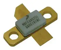


MRFE6VS25LR5
RF FET Transistor, 133 VDC, 1.8 MHz, 2000 MHz, NI-360
- Manufacturer: NXP
- Product type: RF FETs
- Channel Type: N Channel
- Transistor Mounting: Flange
- Transistor Case Style: NI-360
| Delivery and price | |
|---|---|
| Units per pack | 50 |
| Price | 55.51 € |
| Current stock | 200+ |
| Lead time | 7 days |
**NXP Semiconductors** Technical Data

Document Number: MRFE6VS25L Rev. 1, 03/2017

## **RF Power LDMOS Transistor** High Ruggedness N--Channel Enhancement--Mode Lateral MOSFET

RF power transistor designed for both narrowband and broadband ISM, broadcast and aerospace applications operating at frequencies from 1.8 to 2000 MHz. This device is fabricated using NXP’s enhanced ruggedness platform and is suitable for use in applications where high VSWRs are encountered.

## **MRFE6VS25L**

**1.8--2000 MHz, 25 W, 50 V WIDEBAND**

**RF POWER LDMOS TRANSISTOR Typical Performance:** VDD = 50 Vdc **Frequency Pout Gps** η **D IMD (MHz) Signal Type (W) (dB) (%) (dBc)** 1.8--30 **[(1,3)]** Two--Tone 25 PEP 25.0 50.0 --28 (10 kHz spacing) 30--512 **[(2,3)]** Two--Tone 25 PEP 17.3 32.0 --32 (200 kHz spacing) 512 **[(4)]** Pulse 25 Peak 25.9 74.0 — (100 μsec, 20% Duty Cycle) **NI--360H--2L** 512 **[(4)]** CW 25 26.0 75.0 — ~~aS~~ **Load Mismatch/Ruggedness Frequency Pin Test (MHz) Signal Type VSWR (W) Voltage Result** 30 **[(1)]** CW >65:1 0.11 50 No Device Gate 2 1 Drain at all Phase (3 dB Degradation Angles Overdrive) 512 **[(2)]** CW 0.95 (3 dB Overdrive) 512 **[(4)]** Pulse 0.14 Peak (Top View) (100 μsec, 20% (3 dB Note: The backside of the package is the Duty Cycle) Overdrive) source terminal for the transistor. 512 **[(4)]** CW 0.14 **Figure 1. Pin Connections** (3 dB ~~SAT~~ Overdrive) 1. Measured in 1.8--30 MHz broadband reference circuit. 2. Measured in 30--512 MHz broadband reference circuit.

3. The values shown are the minimum measured performance numbers across the indicated frequency range.

4. Measured in 512 MHz narrowband test circuit.

## **Features**

- Wide operating frequency range

- Extreme ruggedness

- Unmatched, capable of very broadband operation

- Integrated stability enhancements

- Low thermal resistance

- Extended ESD protection circuit

> © 2012, 2017 NXP B.V. **MRFE6VS25L** RF Device Data ~~—________~~ NXP Semiconductors 1 ~~NP~~

## **Table 1. Maximum Ratings**

|**Table 1. Maximum Ratings**|**Table 1. Maximum Ratings**|||||
|---|---|---|---|---|---|
|**Rating**||**Symbol**|**Value**||**Unit**|
|Drain--Source Voltage||VDSS|--0.5, +133||Vdc|
|Gate--Source Voltage||VGS|--6.0, +10||Vdc|
|Storage Temperature Range||Tstg|--65 to +150||°C|
|Case Operating Temperature Range||TC|--40 to +150||°C|
|Operating Junction Temperature Range **(1,2)**||TJ|--40 to +225||°C|
|**Table 2. Thermal Characteristics**||||||
|**Characteristic**||**Symbol**|**Value (2,3)**||**Unit**|
|Thermal Resistance, Junction to Case<br>CW: Case Temperature 81°C, 25 W CW, 50 Vdc, IDQ= 10 mA, 512 MHz||RθJC|1.4||°C/W|
|Thermal Impedance, Junction to Case<br>Pulse: Case Temperature 77°C, 25 W Peak, 100μsec Pulse Width,<br>20% Duty Cycle, 50 Vdc, IDQ= 10 mA, 512 MHz||ZθJC|0.32||°C/W|
|**Table 3. ESD Protection Characteristics**||||||
|**Test Methodology**|||**Class**|||
|Human Body Model (per JESD22--A114)|||2, passes 2000 V|||
|Machine Model (per EIA/JESD22--A115)|||B, passes 200 V|||
|Charge Device Model (per JESD22--C101)|||IV, passes 1200 V|||
|**Table 4. Electrical Characteristics** (TA= 25°C unless otherwise noted)||||||
|**Characteristic**|**Symbol**|**Min**|**Typ**|**Max**|**Unit**|
|**Off Characteristics**||||||
|Gate--Source Leakage Current<br>(VGS= 5 Vdc, VDS= 0 Vdc)|IGSS|—|—|400|nAdc|
|Drain--Source Breakdown Voltage<br>(VGS= 0 Vdc, ID= 50 mA)|V(BR)DSS|133|140|—|Vdc|
|Zero Gate Voltage Drain Leakage Current<br>(VDS= 50 Vdc, VGS= 0 Vdc)|IDSS|—|—|2|μAdc|
|Zero Gate Voltage Drain Leakage Current<br>(VDS= 100 Vdc, VGS= 0 Vdc)|IDSS|—|—|7|μAdc|
|**On Characteristics**||||||
|Gate Threshold Voltage<br>(VDS= 10 Vdc, ID= 85μAdc)|VGS(th)|1.5|2.0|2.5|Vdc|
|Gate Quiescent Voltage<br>(VDD= 50 Vdc, ID= 10 mAdc, Measured in Functional Test)|VGS(Q)|2.0|2.4|3.0|Vdc|
|Drain--Source On--Voltage<br>(VGS= 10 Vdc, ID= 210 mAdc)|VDS(on)|—|0.23|—|Vdc|
|**Dynamic Characteristics**||||||
|Reverse Transfer Capacitance<br>(VDS= 50 Vdc±30 mV(rms)ac @ 1 MHz, VGS= 0 Vdc)|Crss|—|0.17|—|pF|
|Output Capacitance<br>(VDS= 50 Vdc±30 mV(rms)ac @ 1 MHz, VGS= 0 Vdc)|Coss|—|14.7|—|pF|
|Input Capacitance<br>(VDS= 50 Vdc, VGS= 0 Vdc±30 mV(rms)ac @ 1 MHz)|Ciss|—|39.0|—|pF|


1. Continuous use at maximum temperature will affect MTTF.

2. MTTF calculator available at http://www.nxp.com/RF/calculators.

3. Refer to AN1955, _Thermal Measurement Methodology of RF Power Amplifiers._ Go to http://www.nxp.com/RF and search for AN1955. (continued)

**MRFE6VS25L**

RF Device Data NXP Semiconductors

2

**Table 4. Electrical Characteristics** (TA = 25°C unless otherwise noted) **(continued)**

|**Characteristic**|**Characteristic**|**Characteristic**|**Characteristic**|**Symbol**|**Min**|**Min**|**Typ**||**Max**|**Unit**|
|---|---|---|---|---|---|---|---|---|---|---|
|**Functional Tests**(In NXP Test Fixture, 50 ohm system) VDD= 50 Vdc, IDQ= 10 mA, Pout= 25 W Peak (5 W Avg.), f =<br>Pulse, 100μsec Pulse Width, 20% Duty Cycle|||||||||512 MHz,||
|Power Gain||||Gps|24.5||25.9||27.5|dB|
|Drain Efficiency||||ηD|70.0||74.0||—|%|
|Input Return Loss||||IRL||—|--16||--10|dB|
|**Load Mismatch/Ruggedness**(In NXP Test Fixture, 50 ohm system) IDQ=||||150 mA|||||||
|**Frequency**<br>**(MHz)**|**Signal**<br>**Type**|**VSWR**||**Pin**<br>**(W)**||**Test Voltage, VDD**|||**Result**||
|512|Pulse<br>(100μsec, 20% Duty Cycle)|>65:1<br>at all Phase Angles||0.14 Peak<br>(3 dB Overdrive)||50|||No Device<br>Degradation||
||CW|||0.14<br>(3 dB Overdrive)|||||||


## **Table 5. Ordering Information**

|**Device**|**Tape and Reel Information**|**Package**|
|---|---|---|
|MRFE6VS25LR5|R5 Suffix = 50 Units, 32 mm Tape Width, 13--inch Reel|NI--360H--2L|


**MRFE6VS25L**

RF Device Data NXP Semiconductors

3

## **TYPICAL CHARACTERISTICS**

**==> picture [497 x 176] intentionally omitted <==**

**----- Start of picture text -----**<br>
100 1.07<br>Ciss 1.06 I DQ  = 10 mA VDD = 50 Vdc<br>1.05<br>50 mA<br>Coss 1.04<br>1.03<br>10<br>1.02 100 mA<br>1.01<br>1 150 mA<br>0.99<br>0.98<br>1<br>0.97<br>0.96<br>Crss 0.95<br>0.94<br>Measured with ±30 mV(rms)ac @ 1 MHz, VGS = 0 Vdc<br>0.1 0.93<br>0 10 20 30 40 50 --50 --25 0 25 50 75 100<br>VDS, DRAIN--SOURCE VOLTAGE (VOLTS) TC, CASE TEMPERATURE (°C)<br>GS(Q)<br>NORMALIZED V<br>C, CAPACITANCE (pF)<br>**----- End of picture text -----**<br>


**Figure 2. Capacitance versus Drain--Source Voltage**

|**IDQ (mA)**|**Slope (mV/**°**C)**|
|---|---|
|10|--2.16|
|50|--1.79|
|100|--1.76|
|150|--1.68|


**Figure 3. Normalized VGS versus Quiescent Current and Case Temperature**

**==> picture [238 x 238] intentionally omitted <==**

**----- Start of picture text -----**<br>
10 [8]<br>ID = 0.55 Amps VDD = 50 Vdc<br>10 [7]<br>10 [6] 0.69 Amps<br>0.83 Amps<br>10 [5]<br>10 [4]<br>90 110 130 150 170 190 210 230 250<br>TJ, JUNCTION TEMPERATURE (°C)<br>Note:  MTTF value represents the total cumulative operating time<br>under indicated test conditions.<br>MTTF calculator available at http://www.nxp.com/RF/calculators.<br>NOTE :  For pulse applications or CW conditions, use the MTTF<br>calculator referenced above.<br>MTTF (HOURS)<br>**----- End of picture text -----**<br>


**Figure 4. MTTF versus Junction Temperature -- CW**

**MRFE6VS25L**

RF Device Data NXP Semiconductors

4

## **512 MHz NARROWBAND PRODUCTION TEST FIXTURE**

|**512 MHz NARROWBAND PRODUCTION TEST FIXTURE**|**512 MHz NARROWBAND PRODUCTION TEST FIXTURE**|**512 MHz NARROWBAND PRODUCTION TEST FIXTURE**|**512 MHz NARROWBAND PRODUCTION TEST FIXTURE**|
|---|---|---|---|
|**Figure 5. MRFE6VS25L Narrowband Test Circuit Component Layout — 512 MHz**<br>CUT OUT AREA<br>MRFE6VS25L<br>Rev. 3<br>C1<br>B1<br>C2<br>C3<br>L1<br>C4<br>C8<br>C7<br>C5<br>C6<br>L2<br>L3<br>C10<br>C9<br>C12<br>C13<br>C11<br>B2<br>C14<br>C15<br>**Table 6. MRFE6VS25L Narrowband Test Circuit Component Designations and Values — 512 MHz**||||
|**Part**|**Description**|**Part Number**|**Manufacturer**|
|B1, B2|Long Ferrite Beads|2743021447|Fair-Rite|
|C1|22μF, 35 V Tantalum Capacitor|T491X226K035AT|Kemet|
|C2, C9|0.1μF Chip Capacitors|CDR33BX104AKWS|AVX|
|C3, C10|0.01μF Chip Capacitors|C0805C103K5RAC|Kemet|
|C4, C12, C15|180 pF Chip Capacitors|ATC100B181JT500XT|ATC|
|C5|18 pF Chip Capacitor|ATC100B180JT500XT|ATC|
|C6|2.7 pF Chip Capacitor|ATC100B2R7BT500XT|ATC|
|C7|15 pF Chip Capacitor|ATC100B150JT500XT|ATC|
|C8|36 pF Chip Capacitor|ATC100B360JT500XT|ATC|
|C11|4.3 pF Chip Capacitor|ATC100B4R3CT500XT|ATC|
|C13|13 pF Chip Capacitor|ATC100B130JT500XT|ATC|
|C14|470μF, 63 V Electrolytic Capacitor|MCGPR63V477M13X26-RH|Multicomp|
|L1|33 nH Inductor|1812SMS-33NJLC|Coilcraft|
|L2|12.5 nH Inductor|A04TJLC|Coilcraft|
|L3|82 nH Inductor|1812SMS-82NJLC|Coilcraft|
|PCB|0.030″,εr= 2.55|AD255A|Arlon|


**MRFE6VS25L**

RF Device Data NXP Semiconductors

5

**==> picture [471 x 159] intentionally omitted <==**

**----- Start of picture text -----**<br>
L3 B2<br>VSUPPLY<br>B1 C12 +<br>VBIAS C9 C10 C14<br>+<br>C1 C2 C3 C4<br>L2<br>L1 RF<br>OUTPUT<br>Z11 Z12 Z13 Z14 Z15 Z16 Z17 Z18 Z19<br>RF<br>INPUT Z1 Z2 Z3 Z4 Z5 Z6 Z7 Z8 Z9 Z10 C15<br>C11 C13<br>C5<br>DUT<br>C6 C7 C8<br>**----- End of picture text -----**<br>


**Figure 6. MRFE6VS25L Narrowband Test Circuit Schematic — 512 MHz**

**Table 7. MRFE6VS25L Narrowband Test Circuit Microstrips — 512 MHz**

|**Microstrip**|**Description**|Z11<br>0.475″ ×0.270″Microstrip<br>Z12<br>0.091″ ×0.082″Microstrip<br>Z13<br>0.170″ ×0.082″Microstrip<br>Z14*<br>0.670″ ×0.082″Microstrip<br>Z15<br>0.280″ ×0.082″Microstrip<br>Z16*<br>0.413″ ×0.082″Microstrip<br>Z17*<br>0.259″ ×0.082″Microstrip<br>Z18<br>0.761″ ×0.082″Microstrip<br>Z19<br>0.341″ ×0.082″Microstrip<br>* Line length includes microstrip bends<br>**Description**<br>**Microstrip**|**Microstrip**|**Description**|
|---|---|---|---|---|
|Z1|0.235″ ×0.082″Microstrip||Z11|0.475″ ×0.270″Microstrip|
|Z2|0.042″ ×0.082″Microstrip||Z12|0.091″ ×0.082″Microstrip|
|Z3|0.682″ ×0.082″Microstrip||Z13|0.170″ ×0.082″Microstrip|
|Z4*|0.200″ ×0.060″Microstrip||Z14*|0.670″ ×0.082″Microstrip|
|Z5|0.324″ ×0.060″Microstrip||Z15|0.280″ ×0.082″Microstrip|
|Z6*|0.200″ ×0.060″Microstrip||Z16*|0.413″ ×0.082″Microstrip|
|Z7|0.089″ ×0.082″Microstrip||Z17*|0.259″ ×0.082″Microstrip|
|Z8|0.120″ ×0.082″Microstrip||Z18|0.761″ ×0.082″Microstrip|
|Z9|0.411″ ×0.082″Microstrip||Z19|0.341″ ×0.082″Microstrip|
|Z10|0.260″ ×0.270″Microstrip||||


* Line length includes microstrip bends

**MRFE6VS25L**

RF Device Data NXP Semiconductors

6

## **TYPICAL CHARACTERISTICS — 512 MHz**

**==> picture [237 x 174] intentionally omitted <==**

**----- Start of picture text -----**<br>
32<br>VDD = 50 Vdc, f = 512 MHz<br>28<br>24<br>20<br>Pin = 0.07 W Pin = 0.035 W<br>16<br>12<br>8<br>4<br>0<br>0 0.5 1 1.5 2 2.5 3 3.5<br>VGS, GATE--SOURCE VOLTAGE (VOLTS)<br>, OUTPUT POWER (WATTS)<br>out<br>P<br>**----- End of picture text -----**<br>


**Figure 7. CW Output Power versus Gate--Source Voltage at a Constant Input Power**

**==> picture [502 x 452] intentionally omitted <==**

**----- Start of picture text -----**<br>
46 30 90<br>VDD = 50 Vdc VDD = 50 Vdc, f = 512 MHz 10 mA 50 mA<br>44 f = 512 MHzIDQ = 10 mA 29 IDQ = 150 mA ηD 80<br>42 28 70<br>100 mA 100 mA<br>40 27 Gps 150 mA 60<br>50 mA<br>38 26 50<br>36 25 10 mA 40<br>34 24 30<br>32 23 20<br>10 12 14 16 18 20 22 2 10 50<br>Pin, INPUT POWER (dBm) Pout, OUTPUT POWER (WATTS)<br>f P1dB P3dB Figure 9. Power Gain and Drain Efficiency<br>(MHz) (W) (W) versus CW Output Power and Quiescent Current<br>512 28.7 31.6<br>Figure 8. CW Output Power versus Input Power<br>29 90 28<br>VDD = 50 Vdc --40 _ C 27<br>28 I DQ  = 10 mA ηD 80 26<br>27 f = 512 MHz 25 _ C 70 25<br>85 _ C 24<br>26 60 50 V<br>23<br>25 TC = --40 _ C Gps 50 2221 40 V 45 V<br>24 25 _ C 40 20 35 V<br>30 V<br>23 30 19<br>85 _ C 18 25 V IDQ = 10 mA, f = 512 MHz<br>22 20 17 Pulse Width = 100 μsec<br>21 10 16 VDD = 20 V 20% Duty Cycle<br>1 10 50 0 5 10 15 20 25 30 35<br>Pout, OUTPUT POWER (WATTS) Pout, OUTPUT POWER (WATTS) PEAK<br>Figure 10. Power Gain and Drain Efficiency Figure 11. Power Gain versus Output Power<br>versus CW Output Power and Drain--Source Voltage<br>, POWER GAIN (dB)<br>, OUTPUT POWER (dBm) Gps  DRAIN EFFICIENCY (%)D,<br>out η<br>P<br>, POWER GAIN (dB) , POWER GAIN (dB)<br>Gps  DRAIN EFFICIENCY (%)D, Gps<br>η<br>**----- End of picture text -----**<br>


**MRFE6VS25L**

RF Device Data NXP Semiconductors

7

## **512 MHz NARROWBAND PRODUCTION TEST FIXTURE**

**==> picture [272 x 185] intentionally omitted <==**

**----- Start of picture text -----**<br>
VDD = 50 Vdc, IDQ = 10 mA, Pout = 25 W Peak<br>f Zsource Zload<br>MHz Ω Ω<br>512 0.72 + j10.8 8.8 + j17.5<br>Zsource = Test circuit impedance as measured from<br>gate to ground.<br>Zload = Test circuit impedance as measured from<br>drain to ground.<br>Input Device Output<br>Matching Under Matching<br>Network Test Network<br>50 Ω 50 Ω<br>Zsource Zload<br>**----- End of picture text -----**<br>


**Figure 12. Narrowband Series Equivalent Source and Load Impedance — 512 MHz**

**MRFE6VS25L**

RF Device Data NXP Semiconductors

8

## **1.8--30 MHz HF BROADBAND REFERENCE CIRCUIT**

**Table 8. 1.8--30 MHz HF Broadband Performance** (In NXP Reference Circuit, 50 ohm system) VDD = 50 Vdc, IDQ = 100 mA

|VDD= 50 Vdc, IDQ= 100 mA||||||
|---|---|---|---|---|---|
|**Signal Type**|**Pout**<br>**(W)**|**f**<br>**(MHz)**|**Gps**<br>**(dB)**|η**D**<br>**(%)**|**IMD**<br>**(dBc)**|
|Two-Tone<br>(10 kHz spacing)|25 PEP|1.8|25.8|51.5|--28.7|
|||10|25.9|50.4|--33.9|
|||30|25.0|50.7|--31.1|


**Table 9. Load Mismatch/Ruggedness** (In NXP Reference Circuit)

|**Frequency**<br>**(MHz)**|**Signal Type**|**VSWR**|**Pin**<br>**(W)**|**Test Voltage, VDD**|**Result**|
|---|---|---|---|---|---|
|30|CW|>65:1<br>at all Phase<br>Angles|0.11<br>(3 dB Overdrive)|50|No Device<br>Degradation|


**MRFE6VS25L**

RF Device Data NXP Semiconductors

9

## **1.8--30 MHz HF BROADBAND REFERENCE CIRCUIT**

|**Figure 13. MRFE6VS25L HF Broadband Reference Circuit Component Layout — 1.8--30 MHz**<br>+<br>MRFE6VS25L/N<br>Rev. 0<br>CUT OUT AREA<br>C3<br>*C1 and C11 are mounted vertically.<br>C2<br>C4<br>C5<br>L1, E1<br>C1*<br>R1<br>C9<br>L2, E2<br>C11*<br>C10<br>C8<br>C7<br>C6<br>Q1<br>**Table 10. MRFE6VS25L HF Broadband Reference Circuit Component Designations and Values — 1.8--30 MHz**|**Figure 13. MRFE6VS25L HF Broadband Reference Circuit Component Layout — 1.8--30 MHz**<br>+<br>MRFE6VS25L/N<br>Rev. 0<br>CUT OUT AREA<br>C3<br>*C1 and C11 are mounted vertically.<br>C2<br>C4<br>C5<br>L1, E1<br>C1*<br>R1<br>C9<br>L2, E2<br>C11*<br>C10<br>C8<br>C7<br>C6<br>Q1<br>**Table 10. MRFE6VS25L HF Broadband Reference Circuit Component Designations and Values — 1.8--30 MHz**|**Figure 13. MRFE6VS25L HF Broadband Reference Circuit Component Layout — 1.8--30 MHz**<br>+<br>MRFE6VS25L/N<br>Rev. 0<br>CUT OUT AREA<br>C3<br>*C1 and C11 are mounted vertically.<br>C2<br>C4<br>C5<br>L1, E1<br>C1*<br>R1<br>C9<br>L2, E2<br>C11*<br>C10<br>C8<br>C7<br>C6<br>Q1<br>**Table 10. MRFE6VS25L HF Broadband Reference Circuit Component Designations and Values — 1.8--30 MHz**|**Figure 13. MRFE6VS25L HF Broadband Reference Circuit Component Layout — 1.8--30 MHz**<br>+<br>MRFE6VS25L/N<br>Rev. 0<br>CUT OUT AREA<br>C3<br>*C1 and C11 are mounted vertically.<br>C2<br>C4<br>C5<br>L1, E1<br>C1*<br>R1<br>C9<br>L2, E2<br>C11*<br>C10<br>C8<br>C7<br>C6<br>Q1<br>**Table 10. MRFE6VS25L HF Broadband Reference Circuit Component Designations and Values — 1.8--30 MHz**|
|---|---|---|---|
|**Part**|**Description**|**Part Number**|**Manufacturer**|
|C1, C5, C6, C9, C11|20K pF Chip Capacitors|ATC200B203KT50XT|ATC|
|C2|10μF, 35 V Tantalum Capacitor|T491D106K035AT|Kemet|
|C3|0.1μF Chip Capacitor|CDR33BX104AKWY|AVX|
|C4|2.2μF Chip Capacitor|C3225X7R1H225KT|TDK|
|C7|0.1μF Chip Capacitor|GRM319R72A104KA01D|Murata|
|C8|2.2μF Chip Capacitor|G2225X7R225KT3AB|ATC|
|C10|220μF, 100 V Electrolytic Capacitor|MCGPR100V227M16X26|-RH<br>Multicomp|
|E1|#43 Ferrite Toroid|5943001101|Fair--Rite|
|E2|#61 Ferrite Toroid|5961001101|Fair--Rite|
|L1|4 Turns, 22 AWG, Toroid Transformer with Ferrite E1|8077 Copper Magnetic Wi|re<br>Belden|
|L2|26 Turns, 22 AWG, Toroid Transformer with Ferrite E2|8077 Copper Magnetic Wi|re<br>Belden|
|Q1|RF Power LDMOS Transistor|MRFE6VS25L|NXP|
|R1|1 kΩ, 3 W Chip Resistor|CPF31K0000FKE14|Vishay|
|PCB|0.030″,εr= 4.8|S1000|Shenzhen Multilayer<br>PCB Technology|


**MRFE6VS25L**

RF Device Data NXP Semiconductors

10

**==> picture [458 x 163] intentionally omitted <==**

**----- Start of picture text -----**<br>
L1, E1 Z4 R1<br>VBIAS<br>+<br>C2 C3 C4 C5 Z8 VSUPPLY<br>Z3 +<br>C6 C7 C8 C10<br>C9<br>L2, E2<br>RF<br>Z7<br>OUTPUT<br>RF Z6 Z9 Z10<br>INPUT<br>Z1 Z2 Z5<br>C11<br>C1<br>DUT<br>**----- End of picture text -----**<br>


**Figure 14. MRFE6VS25L HF Broadband Reference Circuit Schematic — 1.8--30 MHz**

**Table 11. MRFE6VS25L HF Broadband Reference Circuit Microstrips — 1.8--30 MHz**

|**Microstrip**|**Description**||**Microstrip**|**Description**|
|---|---|---|---|---|
|Z1|0.141″ ×0.047″Microstrip||Z6|0.469″ ×0.263″Microstrip|
|Z2|0.625″ ×0.047″Microstrip||Z7|0.119″ ×0.063″Microstrip|
|Z3|0.119″ ×0.219″Microstrip||Z8|0.422″ ×0.241″Microstrip|
|Z4|0.422″ ×0.241″Microstrip||Z9|0.625″ ×0.047″Microstrip|
|Z5|0.469″ ×0.263″Microstrip||Z10|0.141″ ×0.047″Microstrip|


**MRFE6VS25L**

RF Device Data NXP Semiconductors

11

## **TYPICAL CHARACTERISTICS — 1.8--30 MHz HF BROADBAND REFERENCE CIRCUIT**

**==> picture [279 x 160] intentionally omitted <==**

**----- Start of picture text -----**<br>
30 130<br>28 V DD = 50 Vdc, P in = 0.15 W 120<br>IDQ = 25 mA<br>26 110<br>24 100<br>22 Gps 90<br>20 80<br>18 ηD 70<br>16 60<br>14 40<br>12 30<br>10 Pout 20<br>8 10<br>6 0<br>0 5 10 15 20 25 30 35<br>, DRAIN<br>D<br>η<br>EFFICIENCY (%)<br>, POWER GAIN (dB)<br>ps<br>G<br>, OUTPUT<br>out<br>P<br>POWER (WATTS)<br>**----- End of picture text -----**<br>


**==> picture [67 x 8] intentionally omitted <==**

**----- Start of picture text -----**<br>
f, FREQUENCY (MHz)<br>**----- End of picture text -----**<br>


**Figure 15. Power Gain, CW Output Power and Drain Efficiency versus Frequency at a Constant Input Power**

**==> picture [233 x 176] intentionally omitted <==**

**----- Start of picture text -----**<br>
40<br>VDD = 50 Vdc<br>Pin = 0.1 W<br>30<br>1.8 MHz<br>f = 10 MHz<br>20<br>10<br>30 MHz<br>0<br>0 1 2 3 4<br>VGS, GATE--SOURCE VOLTAGE (VOLTS)<br>, OUTPUT POWER (WATTS)<br>out<br>P<br>**----- End of picture text -----**<br>


**Figure 16. CW Output Power versus Gate--Source Voltage at a Constant Input Power**

**==> picture [232 x 175] intentionally omitted <==**

**----- Start of picture text -----**<br>
35<br>30 VPDDin = 0.05 W= 50 Vdc f = 10 MHz<br>25<br>1.8 MHz<br>20<br>30 MHz<br>15<br>10<br>5<br>0<br>0 1 2 3 4<br>VGS, GATE--SOURCE VOLTAGE (VOLTS)<br>, OUTPUT POWER (dBm)<br>out<br>P<br>**----- End of picture text -----**<br>


**Figure 17. CW Output Power versus Gate--Source Voltage at a Constant Input Power**

**MRFE6VS25L**

RF Device Data NXP Semiconductors

12

## **TYPICAL CHARACTERISTICS — 1.8--30 MHz HF BROADBAND REFERENCE CIRCUIT**

**==> picture [234 x 252] intentionally omitted <==**

**----- Start of picture text -----**<br>
48<br>VDD = 50 Vdc<br>IDQ = 25 mA<br>f = 10 MHz<br>44<br>1.8 MHz<br>40<br>30 MHz<br>36<br>32<br>8 12 16 20 24<br>Pin, INPUT POWER (dBm)<br>f P1dB P3dB<br>(MHz) (W) (W)<br>1.8 21.9 26.4<br>10 24.0 28.4<br>30 23.9 29.1<br>, OUTPUT POWER (dBm)<br>out<br>P<br>**----- End of picture text -----**<br>


**Figure 18. CW Output Power versus Input Power**

**==> picture [254 x 175] intentionally omitted <==**

**----- Start of picture text -----**<br>
30 75<br>VDD = 50 Vdc f = 1.8 MHz 10 MHz<br>28 IDQ = 25 mA 30 MHz 65<br>26 55<br>1.8 MHz<br>24 45<br>10 MHz<br>22 30 MHz 35<br>Gps<br>20 25<br>ηD<br>18 15<br>1 10 100<br>Pout, OUTPUT POWER (WATTS)<br>, POWER GAIN (dB)<br>ps  DRAIN EFFICIENCY (%)<br>G D,<br>η<br>**----- End of picture text -----**<br>


**Figure 19. Power Gain and Drain Efficiency versus CW Output Power**

**MRFE6VS25L**

RF Device Data NXP Semiconductors

13

## **TYPICAL CHARACTERISTICS — 1.8--30 MHz HF BROADBAND REFERENCE CIRCUIT — TWO--TONE[(1)]**

**==> picture [498 x 175] intentionally omitted <==**

**----- Start of picture text -----**<br>
--20 --20<br>--25 VDD = 50 Vdc, IDQ = 100 mA --25 VDD = 50 Vdc, IDQ = 100 mA<br>--30 f1 = 1.795 MHz, f2 = 1.805 MHz --30 f1 = 9.995 MHz, f2 = 10.005 MHz<br>Two--Tone Measurements Two--Tone Measurements<br>--35 --35<br>--40 --40<br>--45 --45<br>3rd Order 3rd Order<br>--50 --50<br>--55 5th Order --55 5th Order<br>--60 --60<br>--65 7th Order --65 7th Order<br>--70 --70<br>2 10 30 2 10 30<br>Pout, OUTPUT POWER (WATTS) PEP Pout, OUTPUT POWER (WATTS) PEP<br>IMD, INTERMODULATION DISTORTION (dBc) IMD, INTERMODULATION DISTORTION (dBc)<br>**----- End of picture text -----**<br>


**Figure 20. Intermodulation Distortion Products versus Output Power — 1.8 MHz**

**Figure 21. Intermodulation Distortion Products versus Output Power — 10 MHz**

**==> picture [236 x 175] intentionally omitted <==**

**----- Start of picture text -----**<br>
--20<br>--25 VDD = 50 Vdc, IDQ = 100 mA<br>--30 f1 = 29.995 MHz, f2 = 30.005 MHz<br>Two--Tone Measurements<br>--35<br>--40<br>3rd Order<br>--45<br>--50<br>--55<br>5th Order<br>--60<br>--65<br>7th Order<br>--70<br>2 10 30<br>Pout, OUTPUT POWER (WATTS) PEP<br>IMD, INTERMODULATION DISTORTION (dBc)<br>**----- End of picture text -----**<br>


**Figure 22. Intermodulation Distortion Products versus Output Power — 30 MHz**

1. The distortion products are referenced to one of the two tones and the peak envelope power (PEP) is 6 dB above the power in a single tone.

**MRFE6VS25L**

RF Device Data NXP Semiconductors

14

## **1.8--30 MHz HF BROADBAND REFERENCE CIRCUIT**

**==> picture [385 x 511] intentionally omitted <==**

**----- Start of picture text -----**<br>
Zo = 50 Ω<br>2 & FY SH RRL TL LATE aa’, REELS SE<br>21 fol FAHe LEE EE BLOL SSS<br>Agee:TES R EA<br>ate! | FAO tera ticeii eeu enanetityge LEE f = 1.8 MHz LPR ORES<br>z{° e e ere ee<br>j eave: anestnite ees LR! DIRE RL ES<br>Zsource<br>f = 1.8 MHz<br>naar bette LEP HET<br>f = 30 MHz<br>it [a] seer teiatice easeeereeacia [TAA Z PIR load EBI ES<br>23 PEESeeeltsiueaet EEEEEEeeen reneepemsTracers otofeenoeaaey!tals Hata f = 30 MHz HA PAaa et<br>olg erecta ce peseaeesttttitiy i SCE<br>z\e Sect eee Oe Hl seremeaaet<br>Abateae e A - FER AS<br>a\2\ | icoige menenae Saeeant S SS<br>t 2 Se<br>2\S eS SSS o KKAKKS cS <S SSOS<br>AWAN \2\YAS eeeeoo S e e<br>% : eeSSNSeeMesecesanecnns @earecnnail<br>aa ee eieterenSARL°eaennini{|<br>VDD = 50 Vdc, IDQ = 25 mA, Pout = 25 W CW<br>f Zsource Zload<br>MHz Ω Ω<br>1.8 42.4 + j9.5 47.1 - j1.6<br>5 44.3 + j3.0 46.8 - j1.2<br>10 44.2 + j0.4 47.2 - j2.1<br>15 44.4 - j0.5 47.5 - j3.2<br>20 44.6 - j1.3 47.7 - j4.3<br>25 44.8 - j2.0 47.8 - j5.2<br>30 44.9 - j2.5 47.7 - j6.1<br>Zsource = Test circuit impedance as measured from<br>gate to ground.<br>Zload = Test circuit impedance as measured from<br>drain to ground.<br>Input Device Output<br>Matching Under Matching<br>Network Test Network<br>50 Ω 50 Ω<br>Zsource Zload<br>**----- End of picture text -----**<br>


**Figure 23. HF Broadband Series Equivalent Source and Load Impedance — 1.8--30 MHz**

**MRFE6VS25L**

RF Device Data NXP Semiconductors

15

## **30--512 MHz BROADBAND REFERENCE CIRCUIT**

**Table 12. 30--512 MHz Broadband Performance** (In NXP Reference Circuit, 50 ohm system) VDD = 50 Vdc, IDQ = 100 mA

|VDD= 50 Vdc, IDQ= 100 mA||||||
|---|---|---|---|---|---|
|**Signal Type**|**Pout**<br>**(W)**|**f**<br>**(MHz)**|**Gps**<br>**(dB)**|η**D**<br>**(%)**|**IMD**<br>**(dBc)**|
|Two-Tone<br>(200 kHz spacing)|25 PEP|30|20.9|34.2|--32.3|
|||100|19.0|38.2|--31.5|
|||512|17.3|32.0|--36.1|


**Table 13. Load Mismatch/Ruggedness** (In NXP Reference Circuit)

|**Frequency**<br>**(MHz)**|**Signal Type**|**VSWR**|**Pin**<br>**(W)**|**Test Voltage, VDD**|**Result**|
|---|---|---|---|---|---|
|512|CW|>65:1<br>at all Phase<br>Angles|0.95<br>(3 dB Overdrive)|50|No Device<br>Degradation|


**MRFE6VS25L**

RF Device Data NXP Semiconductors

16

**30--512 MHz BROADBAND REFERENCE TEST FIXTURE**

|**Figure 24. MRFE6VS25L Broadband Reference Circuit Component Layout — 30--512 MHz**<br>MRFE6VS25L/N<br>Rev. 0<br>D1<br>C5<br>C6<br>R3<br>C7<br>L1<br>R2<br>C2<br>C1<br>C3<br>E1<br>Q1<br>E4<br>C4<br>E3<br>T2<br>T3<br>T1<br>E2, L2<br>C11<br>C10<br>C9<br>C8<br>R1<br>Note: See Figure 24a for a more detailed view of the semi--flex cables with shields and #61 multi--aperture cores.<br>**Table 14. MRFE6VS25L Broadband Reference Circuit Component Designations and Values — 30--512 MHz**||||||||C4<br>C10<br>C9<br>C8|C4<br>C10<br>C9<br>C8|E3<br>T2<br>C11|E3<br>T2<br>C11|E3<br>T2<br>C11||
|---|---|---|---|---|---|---|---|---|---|---|---|---|---|
|||D1<br>R1||||||C1||||||
|||||||||||||||
||||R3||C7<br>R2|E2, L2|||C9|||||
||||||||||C8|||||
|||C<br>C2|5<br>C6<br>L1|||||||||||
|||||||||||||||
|||||||||||||||
|||||||||||||||
|||C1|C3|||Q1||||||||
|||||||||||||||
|||E1<br>T1||||||||E4<br>T3||||
|||||||||||||||
|**Part**|||**Description**|||||**Part Number**|||**Manufacturer**|||
|C1, C3, C6, C7, C8<br>1,000 p|||F Chip Capacitors|||||ATC100B102JT50XT|||ATC|||
|C2<br>2.7 pF|||Chip Capacitor|||||ATC100B2R7BT500XT|||ATC|||
|C4<br>15 nF|||Chip Capacitor|||||C3225CH2A153JT|||TDK|||
|C5, C9<br>10 nF|||Chip Capacitors|||||GRM3195C1E103JA01|||Murata|||
|C10<br>1μF C|||hip Capacitor|||||C3225JB2A105KT|||TDK|||
|C11<br>220μF,|||100 V Electrolytic Capacitor|||||MCGPR100V227M16X26-RH|||Multicomp|||
|D1<br>8.2 V, 1|||W Zener Diode|||||1N4738A|||Fairchild Semiconductor|||
|E1, E3, E4<br>#61 Mu|||lti-aperture Cores|||||2861001502|||Fair-Rite|||
|E2<br>Ferrite|||Core Bead|||||21-201-J|||Ferronics|||
|L1<br>47 nH I|||nductor|||||1812SMS-47NJLC|||Coilcraft|||
|L2<br>4 Turns<br>Ferrite|||, 20 AWG, Toroid Transformer with<br>E2|||||8076 Copper Magnetic Wire|||Belden|||
|Q1<br>RF Po|||wer LDMOS Transistor|||||MRFE6VS25L|||NXP|||
|R1<br>5.6 KΩ|||, 1/4 W Chip Resistor|||||CRCW12065K60FKEA|||Vishay|||
|R2<br>15Ω, 1|||/4 W Chip Resistor|||||CRCW120615R0FKEA|||Vishay|||
|R3<br>5 kΩP|||otentiometer CMS Cermet Multi--turn|||||3224W-1-502E|||Bourns|||
|T1<br>25ΩS|||emi-flex Cable, 0.945″Shield Length|||||D260-4118-0000|||Microdot|||
|T2, T3<br>25ΩS|||emi-flex Cables, 1.340″Shield Length|||||D260-4118-0000|||Microdot|||
|PCB<br>0.030″,|||εr = 3.5|||||TC350|||Arlon|||


**MRFE6VS25L**

RF Device Data NXP Semiconductors

17

**==> picture [485 x 295] intentionally omitted <==**

**----- Start of picture text -----**<br>
Center conductor<br>T2<br>connection to PCB<br>E3<br>C2<br>Shield connection<br>C3 to PCB<br>C4<br>E1<br>T2<br>E3<br>E4<br>T1 S Z12 S<br>E1 T3<br>T3<br>T1 S S<br>E4<br>T3<br>NOT TO SCALE S S<br>S = Shield<br>**----- End of picture text -----**<br>


**Figure 24a. Detailed View of Semi--flex Cables with Shields and #61 Multi--aperture Cores**

**==> picture [489 x 155] intentionally omitted <==**

**----- Start of picture text -----**<br>
VSUPPLY<br>R1 +<br>C8 C9 C10 C11<br>L1<br>L2, E2<br>D1 R3<br>C5 C6 T2<br>C7 Z8 E3<br>Z9<br>Z12 RF<br>R2 OUTPUT<br>RF Z10 Z11 T3 Z14 Z15 Z16<br>INPUT<br>Z1 Z2 Z3 Z4 T1 Z6 Z7 C4 E4<br>E1 Z13<br>C1 C3<br>DUT<br>C2 Z5<br>**----- End of picture text -----**<br>


**Figure 25. MRFE6VS25L Broadband Reference Circuit Schematic — 30--512 MHz**

**Table 15. MRFE6VS25L Broadband Reference Circuit Microstrips — 30--512 MHz**

|**Microstrip**|**Description**||**Microstrip**|
|---|---|---|---|
|Z1|0.180″ ×0.080″Microstrip||Z9|
|Z2|0.080″ ×0.190″Microstrip||Z10|
|Z3|0.230″ ×0.190″Microstrip||Z11|
|Z4|0.150″ ×0.190″Microstrip||Z12|
|Z5|0.180″ ×0.190″Microstrip||Z13|
|Z6|0.220″ ×0.190″Microstrip||Z14|
|Z7|0.230″ ×0.260″Microstrip||Z15|
|Z8|0.140″ ×0.150″Microstrip||Z16|


**MRFE6VS25L**

RF Device Data NXP Semiconductors

18

## **TYPICAL CHARACTERISTICS — 30--512 MHz BROADBAND REFERENCE CIRCUIT**

**==> picture [377 x 396] intentionally omitted <==**

**----- Start of picture text -----**<br>
24 120<br>22 VDD = 50 Vdc, Pin = 0.8 W 110<br>IDQ = 25 mA<br>20 100<br>18 90<br>16 Gps 80<br>14 70<br>12 60<br>10 ηD 50<br>8 40<br>6 30<br>4 Pout 20<br>2 10<br>0 0<br>0 50 100 150 200 250 300 350 400 450 500 550<br>f, FREQUENCY (MHz)<br>Figure 26. Power Gain, CW Output Power and Drain<br>Efficiency versus Frequency at a Constant Input Power<br>40<br>f = 30 MHz VPDDin = 0.325 W = 50 Vdc f = 30 MHz 100 MHz<br>30<br>512 MHz<br>20<br>512 MHz<br>10<br>0<br>2 3 4 0 1 2 3 4<br>VGS, GATE--SOURCE VOLTAGE (VOLTS)<br>, POWER GAIN (dB)<br>ps<br>G , OUTPUT POWER (WATTS) , DRAIN EFFICIENCY (%)D<br>out η<br>P<br>, OUTPUT POWER (WATTS)<br>out<br>P<br>**----- End of picture text -----**<br>


**==> picture [230 x 175] intentionally omitted <==**

**----- Start of picture text -----**<br>
50<br>VDD = 50 Vdc<br>Pin = 0.65 W f = 30 MHz<br>40<br>30<br>20 100 MHz<br>512 MHz<br>10<br>0<br>0 1 2 3 4<br>VGS, GATE--SOURCE VOLTAGE (VOLTS)<br>, OUTPUT POWER (WATTS)<br>out<br>P<br>**----- End of picture text -----**<br>


**Figure 27. CW Output Power versus Gate--Source Voltage at a Constant Input Power**

**Figure 28. CW Output Power versus Gate--Source Voltage at a Constant Input Power**

**MRFE6VS25L**

RF Device Data NXP Semiconductors

19

## **TYPICAL CHARACTERISTICS — 30--512 MHz BROADBAND REFERENCE CIRCUIT**

**==> picture [234 x 250] intentionally omitted <==**

**----- Start of picture text -----**<br>
48<br>f = 30 MHz 100 MHz<br>44 512 MHz<br>40<br>36<br>32 VDD = 50 Vdc<br>IDQ = 25 mA<br>28<br>16 20 24 28 32 36<br>Pin, INPUT POWER (dBm)<br>f P1dB P3dB<br>(MHz) (W) (W)<br>30 33.4 40.2<br>100 35.6 44.6<br>512 32.7 37.7<br>, OUTPUT POWER (dBm)<br>out<br>P<br>**----- End of picture text -----**<br>


**Figure 29. CW Output Power versus Input Power**

**==> picture [254 x 175] intentionally omitted <==**

**----- Start of picture text -----**<br>
24 70<br>VDD = 50 Vdc f = 512 MHz<br>22 IDQ = 25 mA 60<br>100 MHz<br>20 50<br>30 MHz 30 MHz<br>18 40<br>100 MHz<br>16 30<br>512 MHz Gps<br>14 20<br>12 10<br>ηD<br>10 0<br>1 10 100<br>Pout, OUTPUT POWER (WATTS)<br>, POWER GAIN (dB)<br>ps  DRAIN EFFICIENCY (%)<br>G D,<br>η<br>**----- End of picture text -----**<br>


**Figure 30. Power Gain and Drain Efficiency versus CW Output Power**

**MRFE6VS25L**

RF Device Data NXP Semiconductors

20

## **TYPICAL CHARACTERISTICS — 30--512 MHz BROADBAND REFERENCE CIRCUIT — TWO--TONE[(1)]**

**==> picture [236 x 175] intentionally omitted <==**

**----- Start of picture text -----**<br>
--20<br>3rd Order<br>--30<br>--40<br>--50 5th Order<br>--60<br>--70 7th Order VDD = 50 Vdc, IDQ = 100 mA<br>f1 = 29.9 MHz, f2 = 30.1 MHz<br>Two--Tone Measurements<br>--80<br>1 10 40<br>Pout, OUTPUT POWER (WATTS) PEP<br>IMD, INTERMODULATION DISTORTION (dBc)<br>**----- End of picture text -----**<br>


**Figure 31. Intermodulation Distortion Products versus Output Power — 30 MHz**

**==> picture [236 x 175] intentionally omitted <==**

**----- Start of picture text -----**<br>
--20<br>--30 3rd Order<br>--40<br>--50<br>5th Order<br>--60<br>--70 VDD = 50 Vdc, IDQ = 100 mA<br>7th Order f1 = 99.9 MHz, f2 = 100.1 MHz<br>Two--Tone Measurements<br>--80<br>1 10 40<br>Pout, OUTPUT POWER (WATTS) PEP<br>IMD, INTERMODULATION DISTORTION (dBc)<br>**----- End of picture text -----**<br>


**Figure 32. Intermodulation Distortion Products versus Output Power — 100 MHz**

**==> picture [237 x 175] intentionally omitted <==**

**----- Start of picture text -----**<br>
--20<br>--26<br>3rd Order<br>--32<br>--38<br>--44<br>--50 5th Order<br>--56<br>--62<br>--68 7th Order VDD = 50 Vdc, IDQ = 100 mA<br>--74 f1 = 511.9 MHz, f2 = 512.1 MHz<br>Two--Tone Measurements<br>--80<br>1 10 40<br>Pout, OUTPUT POWER (WATTS) PEP<br>IMD, INTERMODULATION DISTORTION (dBc)<br>**----- End of picture text -----**<br>


**Figure 33. Intermodulation Distortion Products versus Output Power — 512 MHz**

1. The distortion products are referenced to one of the two tones and the peak envelope power (PEP) is 6 dB above the power in a single tone.

**MRFE6VS25L**

RF Device Data NXP Semiconductors

21

**30--512 MHz BROADBAND REFERENCE CIRCUIT**

|Zo= 25Ω<br>Zsource<br>f = 512 MHz<br>f = 30 MHz<br>Zload<br>f = 30 MHz<br>f = 512 MHz<br>Lif |<br>Efe/<br>LIS<br>tL fyPREY<br>ef<br>[hh fs<br>OR<br>: [~~a~~<br>=<br>isLH&.E~~E~~OXXD<br>i~~=~~ ~~2~~h~~e~~ee<br>aSEE ee<br>NS<br>1<br>At rece<br>Heath AQEL~~oe~~.<br>ae ~~ap~~<br>‘a~~P~~RR<br>ale seaeeeeertetice<br>cord apes<br>ry Mf<br>POON<br>ala~~ed~~entitat TEER<br>4\%~~e~~e<br>nae rst PH<br>a \\~~=~~<br>SeEe Beet<br>5 OSS~~2~~<br>~~=~~. Besse<br>OK<br><<br>KKKSSS<br>SS<br>3%<br>oO SSS<br>C—<br>KX<br>BPIXKXnRS4%SESSSSeS<br>Q<br>bY CE<br>CEE<br>LEE|Zo= 25Ω<br>Zsource<br>f = 512 MHz<br>f = 30 MHz<br>Zload<br>f = 30 MHz<br>f = 512 MHz<br>Lif |<br>Efe/<br>LIS<br>tL fyPREY<br>ef<br>[hh fs<br>OR<br>: [~~a~~<br>=<br>isLH&.E~~E~~OXXD<br>i~~=~~ ~~2~~h~~e~~ee<br>aSEE ee<br>NS<br>1<br>At rece<br>Heath AQEL~~oe~~.<br>ae ~~ap~~<br>‘a~~P~~RR<br>ale seaeeeeertetice<br>cord apes<br>ry Mf<br>POON<br>ala~~ed~~entitat TEER<br>4\%~~e~~e<br>nae rst PH<br>a \\~~=~~<br>SeEe Beet<br>5 OSS~~2~~<br>~~=~~. Besse<br>OK<br><<br>KKKSSS<br>SS<br>3%<br>oO SSS<br>C—<br>KX<br>BPIXKXnRS4%SESSSSeS<br>Q<br>bY CE<br>CEE<br>LEE|Zo= 25Ω<br>Zsource<br>f = 512 MHz<br>f = 30 MHz<br>Zload<br>f = 30 MHz<br>f = 512 MHz<br>Lif |<br>Efe/<br>LIS<br>tL fyPREY<br>ef<br>[hh fs<br>OR<br>: [~~a~~<br>=<br>isLH&.E~~E~~OXXD<br>i~~=~~ ~~2~~h~~e~~ee<br>aSEE ee<br>NS<br>1<br>At rece<br>Heath AQEL~~oe~~.<br>ae ~~ap~~<br>‘a~~P~~RR<br>ale seaeeeeertetice<br>cord apes<br>ry Mf<br>POON<br>ala~~ed~~entitat TEER<br>4\%~~e~~e<br>nae rst PH<br>a \\~~=~~<br>SeEe Beet<br>5 OSS~~2~~<br>~~=~~. Besse<br>OK<br><<br>KKKSSS<br>SS<br>3%<br>oO SSS<br>C—<br>KX<br>BPIXKXnRS4%SESSSSeS<br>Q<br>bY CE<br>CEE<br>LEE|Zo= 25Ω<br>Zsource<br>f = 512 MHz<br>f = 30 MHz<br>Zload<br>f = 30 MHz<br>f = 512 MHz<br>Lif |<br>Efe/<br>LIS<br>tL fyPREY<br>ef<br>[hh fs<br>OR<br>: [~~a~~<br>=<br>isLH&.E~~E~~OXXD<br>i~~=~~ ~~2~~h~~e~~ee<br>aSEE ee<br>NS<br>1<br>At rece<br>Heath AQEL~~oe~~.<br>ae ~~ap~~<br>‘a~~P~~RR<br>ale seaeeeeertetice<br>cord apes<br>ry Mf<br>POON<br>ala~~ed~~entitat TEER<br>4\%~~e~~e<br>nae rst PH<br>a \\~~=~~<br>SeEe Beet<br>5 OSS~~2~~<br>~~=~~. Besse<br>OK<br><<br>KKKSSS<br>SS<br>3%<br>oO SSS<br>C—<br>KX<br>BPIXKXnRS4%SESSSSeS<br>Q<br>bY CE<br>CEE<br>LEE|Zo= 25Ω<br>Zsource<br>f = 512 MHz<br>f = 30 MHz<br>Zload<br>f = 30 MHz<br>f = 512 MHz<br>Lif |<br>Efe/<br>LIS<br>tL fyPREY<br>ef<br>[hh fs<br>OR<br>: [~~a~~<br>=<br>isLH&.E~~E~~OXXD<br>i~~=~~ ~~2~~h~~e~~ee<br>aSEE ee<br>NS<br>1<br>At rece<br>Heath AQEL~~oe~~.<br>ae ~~ap~~<br>‘a~~P~~RR<br>ale seaeeeeertetice<br>cord apes<br>ry Mf<br>POON<br>ala~~ed~~entitat TEER<br>4\%~~e~~e<br>nae rst PH<br>a \\~~=~~<br>SeEe Beet<br>5 OSS~~2~~<br>~~=~~. Besse<br>OK<br><<br>KKKSSS<br>SS<br>3%<br>oO SSS<br>C—<br>KX<br>BPIXKXnRS4%SESSSSeS<br>Q<br>bY CE<br>CEE<br>LEE|Zo= 25Ω<br>Zsource<br>f = 512 MHz<br>f = 30 MHz<br>Zload<br>f = 30 MHz<br>f = 512 MHz<br>Lif |<br>Efe/<br>LIS<br>tL fyPREY<br>ef<br>[hh fs<br>OR<br>: [~~a~~<br>=<br>isLH&.E~~E~~OXXD<br>i~~=~~ ~~2~~h~~e~~ee<br>aSEE ee<br>NS<br>1<br>At rece<br>Heath AQEL~~oe~~.<br>ae ~~ap~~<br>‘a~~P~~RR<br>ale seaeeeeertetice<br>cord apes<br>ry Mf<br>POON<br>ala~~ed~~entitat TEER<br>4\%~~e~~e<br>nae rst PH<br>a \\~~=~~<br>SeEe Beet<br>5 OSS~~2~~<br>~~=~~. Besse<br>OK<br><<br>KKKSSS<br>SS<br>3%<br>oO SSS<br>C—<br>KX<br>BPIXKXnRS4%SESSSSeS<br>Q<br>bY CE<br>CEE<br>LEE|Zo= 25Ω<br>Zsource<br>f = 512 MHz<br>f = 30 MHz<br>Zload<br>f = 30 MHz<br>f = 512 MHz<br>Lif |<br>Efe/<br>LIS<br>tL fyPREY<br>ef<br>[hh fs<br>OR<br>: [~~a~~<br>=<br>isLH&.E~~E~~OXXD<br>i~~=~~ ~~2~~h~~e~~ee<br>aSEE ee<br>NS<br>1<br>At rece<br>Heath AQEL~~oe~~.<br>ae ~~ap~~<br>‘a~~P~~RR<br>ale seaeeeeertetice<br>cord apes<br>ry Mf<br>POON<br>ala~~ed~~entitat TEER<br>4\%~~e~~e<br>nae rst PH<br>a \\~~=~~<br>SeEe Beet<br>5 OSS~~2~~<br>~~=~~. Besse<br>OK<br><<br>KKKSSS<br>SS<br>3%<br>oO SSS<br>C—<br>KX<br>BPIXKXnRS4%SESSSSeS<br>Q<br>bY CE<br>CEE<br>LEE|
|---|---|---|---|---|---|---|
|||VDD= 50 Vdc, IDQ= 25 mA, Pout= 25 W CW|||||
|||**f**<br>**Zsource**<br>**Zload**|||||
|||**MHz**<br>Ω<br>Ω|||||
|||30<br>7.2 - j0.6<br>15.4 + j8.1|||||
|||64<br>8.2 - j1.7<br>18.1 + j5.4|||||
|||88<br>8.9 + j1.9<br>19.0 + j3.9|||||
|||98<br>9.2 + j2.2<br>19.3 + j3.9|||||
|||100<br>9.2 + j2.2<br>19.4 + j4.0|||||
|||108<br>9.4 + j2.4<br>19.8 + j4.1|||||
|||144<br>9.3 + j1.9<br>19.1 + j2.8|||||
|||170<br>9.8 + j2.2<br>20.0 + j2.6|||||
|||230<br>8.9 + j2.1<br>18.6 + j2.0|||||
|||352<br>7.8 + j3.5<br>19.2 + j2.6|||||
|||450<br>7.0 + j3.1<br>19.2 + j3.5|||||
|||512<br>6.7 + j5.0<br>20.5 + j5.3|||||
|||Zsource = Test circuit impedance as measured from|||||
|||gate to ground.|||||
|||Zload<br>= Test circuit impedance as measured from|||||
|||drain to ground.|||||
|||Input<br>Device<br>Output|||||
|||Matching<br>Network<br>Under<br>Test<br>Matching<br>Network<br>50Ω||||50Ω|
||||||||
||||||||
|||**Zsource**<br>**Zload**|||||


**Figure 34. Broadband Series Equivalent Source and Load Impedance — 30--512 MHz**

**MRFE6VS25L**

RF Device Data NXP Semiconductors

22

## **PACKAGE DIMENSIONS**

**MRFE6VS25L**

RF Device Data NXP Semiconductors

23

**MRFE6VS25L**

RF Device Data NXP Semiconductors

24

## **PRODUCT DOCUMENTATION, SOFTWARE AND TOOLS**

Refer to the following resources to aid your design process.

## **Application Notes**

- AN1908: Solder Reflow Attach Method for High Power RF Devices in Air Cavity Packages

- AN1955: Thermal Measurement Methodology of RF Power Amplifiers

## **Engineering Bulletins**

- EB212: Using Data Sheet Impedances for RF LDMOS Devices

## **Software**

- Electromigration MTTF Calculator

- RF High Power Model

- .s2p File

## **Development Tools**

- Printed Circuit Boards

For Software and Tools, do a Part Number search at http://www.nxp.com, and select the “Part Number” link. Go to the Software & Tools tab on the part’s Product Summary page to download the respective tool.

## **REVISION HISTORY**

The following table summarizes revisions to this document.

|**Revision**|**Date**|**Description**|
|---|---|---|
|0|Oct. 2012|•<br>Initial Release of Data Sheet|
|1|Mar. 2017|•<br>Figure 1 Pin Connections: corrected Drain (Pin 1) and Gate (Pin 2) to reflect correct pin numbers, p. 1<br>•<br>Table 14, 30--512 MHz Broadband Reference Circuit Component Designations and Values: added Q1 to<br>parts list, p. 17|


**MRFE6VS25L**

RF Device Data NXP Semiconductors

25

## _**How to Reach Us:**_

**Home Page:** nxp.com

**Web Support:** nxp.com/support

Information in this document is provided solely to enable system and software implementers to use NXP products. There are no express or implied copyright licenses granted hereunder to design or fabricate any integrated circuits based on the information in this document. NXP reserves the right to make changes without further notice to any products herein.

NXP makes no warranty, representation, or guarantee regarding the suitability of its products for any particular purpose, nor does NXP assume any liability arising out of the application or use of any product or circuit, and specifically disclaims any and all liability, including without limitation consequential or incidental damages. “Typical” parameters that may be provided in NXP data sheets and/or specifications can and do vary in different applications, and actual performance may vary over time. All operating parameters, including “typicals,” must be validated for each customer application by customer’s technical experts. NXP does not convey any license under its patent rights nor the rights of others. NXP sells products pursuant to standard terms and conditions of sale, which can be found at the following address: nxp.com/SalesTermsandConditions.

NXP, the NXP logo, Freescale, and the Freescale logo are trademarks of NXP B.V. All other product or service names are the property of their respective owners. E 2012, 2017 NXP B.V.

## **MRFE6VS25L**

RF Device Data NXP Semiconductors

Document Number: MRFE6VS25L 26Rev. 1, 03/2017
Updated at February 9, 2023
NXP Semiconductors is a global leader in secure connectivity solutions, driving innovation across the automotive, industrial, IoT, mobile, and communications infrastructure markets. By developing advanced, purpose-built technologies, NXP enables devices to sense, think, connect, and act intelligently, delivering rigorously tested components that make the connected world safer and more efficient. Within the semiconductor space, NXP is highly regarded for its extensive range of high-performance integrated circuits and discrete devices. The brand's portfolio excels in drivers and interfaces, featuring a comprehensive selection of I/O expanders designed to streamline complex system architectures. For demanding high-frequency and wireless applications, NXP provides industry-leading RF FETs and RF/PIN diodes engineered to deliver exceptional signal integrity, efficiency, and reliability. The NXP product lineup further extends to essential discrete components, including versatile bipolar transistors, JFETs, and small signal diodes optimized for precision switching and amplification. Additionally, the portfolio supports advanced automation and smart applications with precision IC sensors, such as MEMS accelerometers, alongside specialized power management solutions like AC/DC LED driver ICs and single MOSFETs for cutting-edge electronics design.
About Novapart
Novapart is a B2B electronic component broker specialising in stock shortages and cost reduction. We source hard-to-find parts and identify compliant alternatives across a catalogue of 410,000+ components from 500+ manufacturers.
Learn more →Stock Shortage Specialist
When a component is unavailable, discontinued or has an unacceptable lead time, we tap into our network of vetted European and Asian distributors to source what you need — without compromising on quality or traceability.
Request a quote →Compliant Alternatives
We identify pin-to-pin, electrically equivalent substitutes that meet the same certifications (RoHS, AEC-Q100, REACH) as your original specification — validated against datasheets, not just part numbers. Often at a lower cost.
BOM Analysis service →