


MRFE6VP6300HR3
RF FET Transistor, 130 V, 1.05 kW, 1.8 MHz, 600 MHz, NI-780S
- Manufacturer: NXP
- Product type: RF FETs
- No. of Pins: 4Pins
- Channel Type: N Channel
- Power Dissipation: 1.05kW
- RF Transistor Case: NI-780S
- Transistor Mounting: Flange
- Power Dissipation Pd: 1.05kW
- Transistor Case Style: NI-780S
- Operating Frequency Max: 600MHz
- Operating Frequency Min: 1.8MHz
- Drain Source Voltage Vds: 130V
- Operating Temperature Max: 225°C
| Delivery and price | |
|---|---|
| Units per pack | 1 |
| Price | 64.77 € |
| Current stock | 10+ |
| Lead time | 30 days |
**Freescale Semiconductor**
Document Number: MRFE6VP6300H Rev. 1, 7/2011
Technical Data
## **RF Power Field Effect Transistors** High Ruggedness N--Channel Enhancement--Mode Lateral MOSFETs
These high ruggedness devices are designed for use in high VSWR industrial (including laser and plasma exciters), broadcast (analog and digital), aerospace and radio/land mobile applications. They are unmatched input and output designs allowing wide frequency range utilization, between 1.8 and 600 MHz.
- Typical Performance: VDD = 50 Volts, IDQ = 100 mA
|**Signal Type**|**Pout**<br>**(W)**|**f**<br>**(MHz)**|**Gps**<br>**(dB)**|η**D**<br>**(%)**|**IRL**<br>**(dB)**|
|---|---|---|---|---|---|
|Pulsed (100μsec,<br>20% Duty Cycle)|300 Peak|230|26.5|74.0|--16|
|CW|300 Avg.|130|25.0|80.0|--15|
## **MRFE6VP6300HR3 MRFE6VP6300HSR3**
**==> picture [109 x 41] intentionally omitted <==**
**----- Start of picture text -----**<br>
1.8--600 MHz, 300 W, 50 V<br>LATERAL N--CHANNEL<br>BROADBAND<br>RF POWER MOSFETs<br>**----- End of picture text -----**<br>
- Capable of Handling a Load Mismatch of 65:1 VSWR, @ 50 Vdc, 230 MHz, at all Phase Angles
- 300 Watts CW Output Power
- 300 Watts Pulsed Peak Power, 20% Duty Cycle, 100 μsec
- Capable of 300 Watts CW Operation
## **Features**
**==> picture [96 x 27] intentionally omitted <==**
**----- Start of picture text -----**<br>
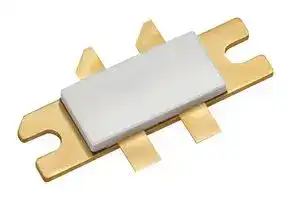
CASE 465M--01, STYLE 1<br>NI--780--4<br>MRFE6VP6300HR3<br>**----- End of picture text -----**<br>
- Unmatched Input and Output Allowing Wide Frequency Range Utilization
- Device can be used Single--Ended or in a Push--Pull Configuration
- Qualified Up to a Maximum of 50 VDD Operation
- Characterized from 30 V to 50 V for Extended Power Range
- Suitable for Linear Application with Appropriate Biasing
- Integrated ESD Protection
- Greater Negative Gate--Source Voltage Range for Improved Class C Operation
**==> picture [95 x 27] intentionally omitted <==**
**----- Start of picture text -----**<br>
CASE 465H--02, STYLE 1<br>NI--780S--4<br>MRFE6VP6300HSR3<br>**----- End of picture text -----**<br>
- Characterized with Series Equivalent Large--Signal Impedance Parameters
- • RoHS Compliant
- NI--780--4 in Tape and Reel. R3 Suffix = 250 Units, 56 mm Tape Width, 13 inch Reel. For R5 Tape and Reel options, see p. 14.
- NI--780S--4 in Tape and Reel. R3 Suffix = 250 Units, 32 mm Tape Width, 13 inch Reel. For R5 Tape and Reel options, see p. 14.
## **Table 1. Maximum Ratings**
|**Rating**|**Symbol**|**Value**|**Unit**|
|---|---|---|---|
|Drain--Source Voltage|VDSS|--0.5, +130|Vdc|
|Gate--Source Voltage|VGS|--6.0, +10|Vdc|
|Storage Temperature Range|Tstg|--65 to +150|°C|
|Case Operating Temperature|TC|150|°C|
|Total Device Dissipation @ TC= 25°C<br>Derate above 25°C|PD|1050<br>5.26|W<br>W/°C|
|Operating Junction Temperature **(1,2)**|TJ|225|°C|
**==> picture [144 x 82] intentionally omitted <==**
**----- Start of picture text -----**<br>
RFin/VGS 3 1 RFout/VDS<br>RFin/VGS 4 2 RFout/VDS<br>(Top View)<br>**----- End of picture text -----**<br>
**Figure 1. Pin Connections**
**Table 2. Thermal Characteristics**
|**Table 2. Thermal Characteristics**||||
|---|---|---|---|
|**Characteristic**|**Symbol**|**Value (2,3)**|**Unit**|
|Thermal Resistance, Junction to Case **(4)**<br>Pulsed: Case Temperature 75°C, 300 W Pulsed, 100μsec Pulse Width, 20% Duty Cycle,<br>50 Vdc, IDQ= 100 mA, 230 MHz<br>CW: Case Temperature 87°C, 300 W CW, 50 Vdc, IDQ= 1100 mA, 230 MHz|ZθJC<br>RθJC|0.05<br>0.19|°C/W|
1. Continuous use at maximum temperature will affect MTTF.
2. MTTF calculator available at http://www.freescale.com/rf. Select Software & Tools/Development Tools/Calculators to access MTTF calculators by product.
3. Refer to AN1955, _Thermal Measurement Methodology of RF Power Amplifiers._ Go to http://www.freescale.com/rf. Select Documentation/Application Notes -- AN1955.
4. Same test circuit is used for both pulsed and CW.
© Freescale Semiconductor, Inc., 2010--2011. All rights reserved.
**MRFE6VP6300HR3 MRFE6VP6300HSR3**
RF Device Data Freescale Semiconductor
1
## **Table 3. ESD Protection Characteristics**
|**Table 3. ESD Protection Characteristics**||
|---|---|
|**Test Methodology**|**Class**|
|Human Body Model (per JESD22--A114)|2 (Minimum)|
|Machine Model (per EIA/JESD22--A115)|B (Minimum)|
|Charge Device Model (per JESD22--C101)|IV (Minimum)|
## **Table 4. Electrical Characteristics** (TA = 25°C unless otherwise noted)
|**Characteristic**<br>**Symbol**<br>**Min**<br>**Typ**<br>**Max**<br>**Unit**|
|---|
|**Off Characteristics (1)**|
|Gate--Source Leakage Current<br>(VGS= 5 Vdc, VDS= 0 Vdc)<br>IGSS<br>—<br>—<br>1<br>μAdc<br>Drain--Source Breakdown Voltage<br>(VGS= 0 Vdc, ID= 50 mA)<br>V(BR)DSS<br>130<br>—<br>—<br>Vdc<br>Zero Gate Voltage Drain Leakage Current<br>(VDS= 50 Vdc, VGS= 0 Vdc)<br>IDSS<br>—<br>—<br>5<br>μAdc<br>Zero Gate Voltage Drain Leakage Current<br>(VDS= 100 Vdc, VGS= 0 Vdc)<br>IDSS<br>—<br>—<br>10<br>μAdc<br>~~EE~~|
|**On Characteristics**|
|Gate Threshold Voltage **(1)**<br>(VDS= 10 Vdc, ID= 480μAdc)<br>VGS(th)<br>1.7<br>2.2<br>2.7<br>Vdc<br>Gate Quiescent Voltage<br>(VDD= 50 Vdc, ID= 100 mAdc, Measured in Functional Test)<br>VGS(Q)<br>2.0<br>2.5<br>3.0<br>Vdc<br>Drain--Source On--Voltage **(1)**<br>(VGS= 10 Vdc, ID= 1 Adc)<br>VDS(on)<br>—<br>0.25<br>—<br>Vdc<br>~~ee~~|
|**Dynamic Characteristics (1)**<br>Reverse Transfer Capacitance<br>(VDS= 50 Vdc±30 mV(rms)ac @ 1 MHz, VGS= 0 Vdc)<br>Crss<br>—<br>0.8<br>—<br>pF<br>Output Capacitance<br>(VDS= 50 Vdc±30 mV(rms)ac @ 1 MHz, VGS= 0 Vdc)<br>Coss<br>—<br>76<br>—<br>pF<br>Input Capacitance<br>(VDS= 50 Vdc, VGS= 0 Vdc±30 mV(rms)ac @ 1 MHz)<br>Ciss<br>—<br>188<br>—<br>pF<br>**Functional Tests**(In Freescale Test Fixture, 50 ohm system) VDD= 50 Vdc, IDQ= 100 mA, Pout= 300 W Peak (60 W Avg.), f = 230 MHz,<br>Pulsed, 100μsec Pulse Width, 20% Duty Cycle<br>Power Gain<br>Gps<br>25.0<br>26.5<br>28.0<br>dB<br>Drain Efficiency<br>ηD<br>72.0<br>74.0<br>—<br>%<br>Input Return Loss<br>IRL<br>—<br>--16<br>--9<br>dB<br>**Load Mismatch**(In Freescale Application Test Fixture, 50 ohm system) VDD= 50 Vdc, IDQ= 100 mA<br>VSWR 65:1 at all Phase Angles<br>Pulsed: Pout= 300 W Peak (60 W Avg.), f = 230 MHz, Pulsed,<br>100μsec Pulse Width, 20% Duty Cycle<br>CW: Pout= 300 W Avg., f = 130 MHz<br>Ψ<br>No Degradation in Output Power<br>~~ne~~<br>~~——===~~<br>~~a~~|
|1. Each side of device measured separately.|
**MRFE6VP6300HR3 MRFE6VP6300HSR3**
RF Device Data Freescale Semiconductor
2
**==> picture [482 x 233] intentionally omitted <==**
**----- Start of picture text -----**<br>
VBIAS VSUPPLY<br>+ + + +<br>C8 L1 C9 C14 C15 C10 C11 C12 C13 C16<br>I ITII/|IITItit?<br>L2<br>RF<br>C4 C5 C6 C7 R1<br>OUTPUT<br>IIll Z8 Z9 Z10 Z11 Z12 Z13<br>RF<br>INPUT Z1 Z2 Z3 Z4 Z5 Z6 Z7 C20<br>C17 C18 C19<br>C1<br>DUT<br>C2 C3<br>Z1 0.352″ x 0.080″ Microstrip Z9 0.192″ x 0.170″ Microstrip<br>Z2* 1.780″ x 0.080″ Microstrip Z10* 0.366″ x 0.170″ Microstrip<br>Z3* 0.576″ x 0.080″ Microstrip Z11* 2.195″ x 0.170″ Microstrip<br>Z4 0.220″ x 0.220″ Microstrip Z12* 0.614″ x 0.170″ Microstrip<br>Z5 0.322″ x 0.220″ Microstrip Z13 0.243″ x 0.080″ Microstrip<br>Z6 0.168″ x 0.220″ Microstrip<br>Z7, Z8 0.282″ x 0.630″ Microstrip * Line length includes microstrip bends<br>**----- End of picture text -----**<br>
Note: Same test circuit is used for both pulsed and CW.
**Figure 2. MRFE6VP6300HR3(HSR3) Test Circuit Schematic**
**Table 5. MRFE6VP6300HR3(HSR3) Test Circuit Component Designations and Values**
|~~a~~|~~Ge~~|||
|---|---|---|---|
|**Part**<br>~~a~~|**Description**<br>~~Ge~~|**Part Number**|**Manufacturer**|
|C1, C20<br>~~a~~<br>~~a~~|15 pF Chip Capacitors<br>~~Ge~~<br>~~D~~|ATC100B150JT500XT<br>~~D~~|ATC<br>~~D~~|
|C2<br>~~a ~~<br>~~a~~|82 pF Chip Capacitor<br> ~~D~~<br>~~D~~|ATC100B820JT500XT<br>~~D~~<br>~~D~~|ATC<br>~~D~~<br>~~D~~|
|C3, C17<br>~~a ~~<br>~~a~~|91 pF Chip Capacitors<br> ~~D~~<br>|ATC100B910JT500XT<br>~~D~~<br>|ATC<br>~~D~~<br>|
|C4, C10<br>~~aeG~~|1000 pF Chip Capacitors<br>~~eG~~|ATC100B102JT50XT<br>~~eG~~|ATC<br>~~eG~~|
|C5, C11<br>~~eG~~<br>~~eG~~|10K pF Chip Capacitors<br>~~eG~~<br>~~eG~~|ATC200B103KT50XT<br>~~eG~~<br>~~eG~~|ATC<br>~~eG~~<br>~~eG~~|
|C6<br>~~eG~~<br>~~a~~<br>~~ne~~|0.1μF, 50 V Chip Capacitor<br>~~eG~~<br>~~D~~<br>~~G~~|CDR33BX104AKWS<br>~~eG~~<br>~~D~~<br>~~G~~|AVX<br>~~eG~~<br>~~D~~<br>~~G~~|
|C7<br>~~a ~~<br>~~ne~~<br>~~ne~~|2.2μF, 100 V Chip Capacitor<br> ~~D~~<br>~~G~~<br>~~G~~|HMK432B7225KM--T<br>~~D~~<br>~~G~~<br>~~G~~|Taiyo Yuden<br>~~D~~<br>~~G~~<br>~~G~~|
|C8<br>~~ne~~<br>~~ne~~<br>~~ne~~|10μF, 35 V Tantalum Capacitor<br>~~G~~<br>~~G~~<br>~~G~~|T491D106K035AT<br>~~G~~<br>~~G~~<br>~~G~~|Kemet<br>~~G~~<br>~~G~~<br>~~G~~|
|C9<br>~~ne~~<br>~~ne~~<br>~~ne~~|2.2μF, 100 V Chip Capacitor<br>~~G~~<br>~~G~~<br>~~G~~|G2225X7R225KT3AB<br>~~G~~<br>~~G~~<br>~~G~~|ATC<br>~~G~~<br>~~G~~<br>~~G~~|
|C12<br>~~ne~~<br>~~ne~~|0.1μF, 100 V Chip Capacitor<br>~~G~~<br>~~G~~|C1812F104K1RAC<br>~~G~~<br>~~G~~|Kemet<br>~~G~~<br>~~G~~|
|C13<br>~~ne~~<br>~~a~~|0.01μF, 100 V Chip Capacitor<br>~~G~~|C1825C103K1GAC<br>~~G~~|Kemet<br>~~G~~|
|C14, C15, C16<br>~~a ~~|220μF, 100 V Electolytic Capacitors<br> ~~eG~~|MCGPR100V227M16X26--RH<br>~~eG~~|Multicomp<br>~~eG~~|
|C18, C19<br>~~a ~~|18 pF Chip Capacitors<br> ~~eG~~|ATC100B180JT500XT<br>~~eG~~|ATC<br>~~eG~~|
|L1<br>~~a~~|120 nH Inductor|1812SMS--R12JLC|Coilcraft|
|L2<br>~~a~~|17.5 nH Inductor|GA3095--ALC|Coilcraft|
|R1<br>~~a~~|1000Ω, 1/2 W Chip Resistor|CRCW20101K00FKEF|Vishay|
|PCB<br>~~a~~|0.030″,εr= 2.55|AD255A|Arlon|
**MRFE6VP6300HR3 MRFE6VP6300HSR3**
RF Device Data Freescale Semiconductor
3
**==> picture [428 x 253] intentionally omitted <==**
**----- Start of picture text -----**<br>
C8 \ °<br>C14<br>C15<br>) Cf SSA<br>fo}° L1 (e}°°°pb C13 C16<br>°o|] ——= °|° 9 2° Ll,le)<br>C12<br>C6 oo° Lf C7 °i |}1°<br>oF : { C9 Llc C11<br>C1 @]] C5 of°of |||| C4 | °°[Seec0) Losqq Ooo0000 C10 [lo6°@ ©<br>(ome) FS 10 O00<br>oone) — fo) C18 o9000000<br>I\°sov C3 R1 i t L2 C17 oXN 2 NPof C20 _—a<br>60]oo | bes.Le lsssttosse e000 8 ot [| Jeooo<br>O° Oo C2 ° ° ° Oo. (Oo ue<br>fone)O° 53) ° 0000 o0000° ° oO ° C19 ‘o)<br>(ome) O ° ome) ©<br>fone) oO ° ome) °<br>° ° ° fo) °<br>e) ° ° 00 fe)<br>A ° °<br>So0000 °<br>° °<br>le} fe)<br>o) i) o) °eoa@ece®° o)<br>MRFE6VP6300H/HS<br>reescaleI Tm<br>semiconductor Rev. 2<br>CUT OUT AREA<br>**----- End of picture text -----**<br>
**Figure 3. MRFE6VP6300HR3(HSR3) Test Circuit Component Layout**
**MRFE6VP6300HR3 MRFE6VP6300HSR3**
RF Device Data Freescale Semiconductor
4
## **TYPICAL CHARACTERISTICS — PULSED**
**==> picture [501 x 650] intentionally omitted <==**
**----- Start of picture text -----**<br>
1000 60<br>P3dB = 56.0 dBm (398 W)<br>Ciss 59 Ideal<br>SSS ae<br>100 P2dB = 55.8 dBm (380 W)<br>a 58 Po KE<br>Coss<br>———S 57 P1dB = 55.4 dBm KIN Ht<br>10 (344 W)<br>56<br>Actual<br>1 eee ee ee eee ee Crss e 55 |=<br>Measured with ±30 mV(rms)ac @ 1 MHz 54 VDD = 50 Vdc, IDQ = 100 mA, f = 230 MHz<br>VGS = 0 Vdc Pulse Width = 100 μsec, 20% Duty Cycle<br>0.1 = —— 53<br>0 10 20 30 40 50 26 27 28 29 30 31 32 33 34<br>VDS, DRAIN--SOURCE VOLTAGE (VOLTS) Pin, INPUT POWER (dBm) PULSED<br>Note: Each side of device measured separately. Figure 5. Pulsed Output Power versus<br>Input Power<br>Figure 4. Capacitance versus Drain--Source Voltage<br>29 90 29<br>28 VPulse Width = 100DD = 50 Vdc, IDQ μ = 100 mA, f = 230 MHzsec, 20% Duty Cycle 80 28 VPulse Width = 100DD = 50 Vdc, IDQ μ = 100 mA, f = 230 MHzsec, 20% Duty Cycle<br>27<br>27 + 2 70 26 TF 2SS SS<br>26 Coa 60 «= 25 Gee se<br>50 V<br>E N 24 AC S<br>25 | 50 ON AGN<br>Gps FLA OLA 23 A N 40 V \ 45 V A<br>24 L 40 22 -<br>rte fF 21 ee 35 V<br>23 30<br>Pll ηD ee 20 —— VDD = 30 V +}<br>22 tte EL 20 19 Kt<br>20 100 600 0 50 100 150 200 250 300 350 400<br>Pout, OUTPUT POWER (WATTS) PULSED Pout, OUTPUT POWER (WATTS) PULSED<br>Figure 6. Pulsed Power Gain and Drain Efficiency Figure 7. Pulsed Power Gain versus<br>versus Output Power Output Power<br>90 29 90<br>80 VDD = 30 V 35 V 40 V 45 V 50 V 28 VPulse Width = 100DD = 50 Vdc, IDQ μ = 100 mA, f = 230 MHzsec, 20% Duty Cycle 85 _ C 25 _ C 80<br>70 T E E 27 Co Gps e --30 _ C 70<br>26 25 _ C 60<br>60<br>25 TC = --30 _ C 50<br>50<br>Wf 24 Z EW 40<br>40 2) / Wa 23 85 _ C LA _ F| 30<br>V/ VDD = 50 Vdc, IDQ = 100 mA, f = 230 MHz a<br>30 Za Pulse Width = 100 μsec, 20% Duty Cycle 22 a ge r ie 20<br>ηD<br>20 Foo7] 21 — |A|rveLET EEEE 10<br>0 50 100 150 200 250 300 350 400 10 100 600<br>Pout, OUTPUT POWER (WATTS) PULSED Pout, OUTPUT POWER (WATTS) PULSED<br>Figure 8. Pulsed Drain Efficiency versus Figure 9. Pulsed Power Gain and Drain Efficiency<br>Output Power versus Output Power<br>C, CAPACITANCE (pF)<br>, OUTPUT POWER (dBm) PULSED<br>out<br>P<br>, POWER GAIN (dB) , POWER GAIN (dB)<br>ps DRAIN EFFICIENCY (%) ps<br>G D, G<br>η<br>, POWER GAIN (dB)<br> DRAIN EFFICIENCY (%)ηD, Gps DRAIN EFFICIENCY (%)ηD,<br>**----- End of picture text -----**<br>
**MRFE6VP6300HR3 MRFE6VP6300HSR3**
RF Device Data Freescale Semiconductor
5
## **TYPICAL CHARACTERISTICS — TWO--TONE[(1)]**
**==> picture [501 x 410] intentionally omitted <==**
**----- Start of picture text -----**<br>
--10 --10<br>VDD = 50 Vdc, IDQ = 1600 mA, f1 = 230 MHz VDD = 50 Vdc, Pout = 250 W (PEP)/62.5 W Avg. per Tone<br>--20 f2 = 230.1 MHz, Two--Tone Measurements --20 IDQ = 1600 mA, Two--Tone Measurements<br>--30 Pt 3rd Order<br>--30<br>A tty<br>--40 Rime [|<br>3rd Order<br>--50 — AZze --40 r 5th Order e -<br>a ey eee |<br>--60 See 5th Order s --50 CT I 7th Order<br>--70 --60<br>ce e TT<br>7th Order<br>--80 Po LEA --70 EAM ELLEN<br>10 100 400 0.1 1 10 40<br>Pout, OUTPUT POWER (WATTS) PEP TWO--TONE SPACING (MHz)<br>Figure 10. Intermodulation Distortion Figure 11. Intermodulation Distortion<br>Products versus Output Power Products versus Two--Tone Spacing<br>30 --15<br>VDD = 50 Vdc, f1 = 230 MHz, f2 = 230.1 MHz<br>IDQ = 1600 mA --20 Two--Tone Measurements<br>29<br>1400 mA<br>--25<br>IDQ = 650 mA<br>28<br>1100 mA --30<br>) T O S EST<br>900 mA<br>27 900 mA a | || --35 Ee<br>--40 9am 1100 mA san<br>Pl ee 1400 mA<br>26<br>650 mA VDD = 50 Vdc, f1 = 230 MHz, f2 = 230.1 MHz --45<br>Two--Tone Measurements 1600 mA<br>25 u l --50 SE OO<br>5 10 100 500 10 100 400<br>Pout, OUTPUT POWER (WATTS) PEP Pout, OUTPUT POWER (WATTS) PEP<br>Figure 12. Two--Tone Power Gain versus Figure 13. Third Order Intermodulation<br>Output Power Distortion versus Output Power<br>IMD, INTERMODULATION DISTORTION (dBc) IMD, INTERMODULATION DISTORTION (dBc)<br>, POWER GAIN (dB)<br>ps IMD, THIRD ORDER<br>G<br>INTERMODULATION DISTORTION (dBc)<br>**----- End of picture text -----**<br>
1. The distortion products are referenced to one of the two tones and the peak envelope power (PEP) is 6 dB above the power in a single tone.
**MRFE6VP6300HR3 MRFE6VP6300HSR3**
RF Device Data Freescale Semiconductor
6
## **TYPICAL CHARACTERISTICS**
**==> picture [239 x 208] intentionally omitted <==**
**----- Start of picture text -----**<br>
10 [9]<br>SS SS SS SS SS SS<br>-—a — —ee— — — ee— eee— J VDD = 50 Vdc ——<br>10 [8] Pout = 300 W Avg.<br>_——Seneeee=a ee ee==| ηD = 80% ——<br>pf ft ft Na<br>10 [7] SSE<br>====5=>======——<br>aeeee ee<br>10 [6] PS<br>anne<br>aeE e ee<br>10 [5] eer<br>==<br>eeee ee ee<br>10 [4] ee<br>90 110 130 150 170 190 210 230 250<br>TJ, JUNCTION TEMPERATURE (°C)<br>MTTF calculator available at http://www.freescale.com/rf. Select<br>Software & Tools/Development Tools/Calculators to access MTTF<br>calculators by product.<br>MTTF (HOURS)<br>**----- End of picture text -----**<br>
**Figure 14. MTTF versus Junction Temperature — CW**
**MRFE6VP6300HR3 MRFE6VP6300HSR3**
RF Device Data Freescale Semiconductor
7
**==> picture [399 x 599] intentionally omitted <==**
**----- Start of picture text -----**<br>
D oooo "I a >[¥ 8, ONY<br>TL LT SSS<br>KgS(0 18 E Z E source N SSSaa ane,<br>| HY PES<br>f = 230 MHz se<br>[gh iger<br>SOS Y KVR een ene<br>EBS J on<br>Ses guen Ty<br>lh f fo LEE f = 230 MHz etre<br>Zload<br>lf befibye RRR Cage ese Hyean hh<br>f/f Ai LERERTREES Zo = 5 Ω<br>ff Ly REE<br>BLA = =<br>efef [el [f° AAbe Be e caeaasniss LLY LEERY LLKs SSK oOpietencemen<br>tel] (= FE 2 e [es] REE [|] RRLf<br>Is<br>i ee KORO?SeSSL<br>[f e<br>[| CHA LK ES<br>ole L e eeeeie Cty ctuncestinsiae a s CAL he!BRISORO<br>z [Geer] cE COMP.<br>F.}, oR CONDUCTANCE.<br>! 2 ee<br>! EH Sn eeeee coseeeeee<br>ald<br>sbebteceniticcat<br>ate eee eet +<br>@\o<br>a\%eee<br>Xa eS2 ewe CORR<br>a\5\ \ Vosee<br>*.t\ea TES AOS maenes:<br>\° — ASo S oiesSen ASSES os SS ..o' OO S c enceO ARO oO SS<br>\ e ”<br>ae — = eG<br>LALSSS KS SSS SoS<br>| S KNESEOSereScoATL E cammersaiiigeaiuiTCooLA e e<br>VDD = 50 Vdc, IDQ = 100 mA, Pout = 300 W Peak<br>f Zsource Zload<br>MHz Ω Ω<br>230 0.65 + j2.79 1.64 + j2.85<br>Zsource = Test circuit impedance as measured from<br>gate to ground.<br>Zload = Test circuit impedance as measured from<br>drain to ground.<br>Input Device Output<br>Matching Under Matching<br>Network Test Network<br>Zsource Zload<br>**----- End of picture text -----**<br>
**Figure 15. Series Equivalent Source and Load Impedance**
**MRFE6VP6300HR3 MRFE6VP6300HSR3**
RF Device Data Freescale Semiconductor
8
**==> picture [242 x 280] intentionally omitted <==**
**----- Start of picture text -----**<br>
||||||
|---|---|---|---|---|
|VDD = 50 Vdc, IDQ = 100 mA|
|f|Zsource|Zload|
|MHz|Ω|Ω|
|10|36.0 + j128|12.0 + j8.80|
|25|20.0 + j64.0|12.4 + j6.40|
|50|16.0 + j41.6|11.6 + j14.4|
|100|8.00 + j24.8|9.00 + j9.80|
|200|3.00 + j12.8|7.20 + j6.40|
|300|1.52 + j7.92|6.00 + j5.00|
|400|1.08 + j5.04|4.20 + j4.00|
|500|1.04 + j3.16|3.32 + j2.72|
|600|0.88 + j1.76|2.72 + j1.68|
|1.|Simulated performance at 1 dB gain compression.|
|Zsource|=|Source impedance presented from gate to gate.|
|Zload|=|Load impedance presented from drain to drain.|
|Device|
|Source|+|Under|--|Load|
|Test|
|Sb|--|+|e|l|
|Zsource|Zload|
**----- End of picture text -----**<br>
**Figure 16. Simulated Source and Load Impedances Optimized for IRL, Output Power and Drain Efficiency — Push--Pull**
**MRFE6VP6300HR3 MRFE6VP6300HSR3**
RF Device Data Freescale Semiconductor
9
## **PACKAGE DIMENSIONS**
**MRFE6VP6300HR3 MRFE6VP6300HSR3**
RF Device Data Freescale Semiconductor
10
**MRFE6VP6300HR3 MRFE6VP6300HSR3**
RF Device Data Freescale Semiconductor
11
**MRFE6VP6300HR3 MRFE6VP6300HSR3**
RF Device Data Freescale Semiconductor
12
**MRFE6VP6300HR3 MRFE6VP6300HSR3**
RF Device Data Freescale Semiconductor
13
## **PRODUCT DOCUMENTATION AND SOFTWARE**
Refer to the following documents to aid your design process.
## **Application Notes**
- AN1955: Thermal Measurement Methodology of RF Power Amplifiers
## **Engineering Bulletins**
- EB212: Using Data Sheet Impedances for RF LDMOS Devices
## **Software**
- Electromigration MTTF Calculator
- RF High Power Model
- .s2p File
For Software, do a Part Number search at http://www.freescale.com, and select the “Part Number” link. Go to the Software & Tools tab on the part’s Product Summary page to download the respective tool.
## **R5 TAPE AND REEL OPTION**
NI--780--4 = R5 Suffix = 50 Units, 56 mm Tape Width, 13 inch Reel. NI--780S--4 = R5 Suffix = 50 Units, 32 mm Tape Width, 13 inch Reel.
The R5 tape and reel option for MRFE6VP6300H and MRFE6VP6300HS parts will be available for 2 years after release of MRFE6VP6300H and MRFE6VP6300HS. Freescale Semiconductor, Inc. reserves the right to limit the quantities that will be delivered in the R5 tape and reel option. At the end of the 2 year period customers who have purchased these devices in the R5 tape and reel option will be offered MRFE6VP6300H and MRFE6VP6300HS in the R3 tape and reel option.
## **REVISION HISTORY**
The following table summarizes revisions to this document.
|**Revision**|**Date**|**Description**|
|---|---|---|
|0|Oct. 2010|•<br>Initial Release of Data Sheet|
|1|July 2011|•<br>Corrected pin 4 label from RFout/VGSto RFin/VGS, Fig. 1, Pin Connections, p. 1<br>•<br>Changed Drain--Source voltage from --0.5, +125 to --0.5, +130 in Maximum Ratings table, p. 1<br>•<br>Added Total Device Dissipation to Maximum Ratings table, p. 1<br>•<br>Changed V(BR)DSSMin value from 125 to 130 Vdc, Table 4, Off Characteristics, p. 2<br>•<br>Tightened VGS(th)Min limit from 1.5 to 1.7 Vdc and Max limit from 3.0 to 2.7 Vdc as a result of process<br>improvement, Table 4, On Characteristics, p. 2<br>•<br>Tightened VGS(Q)Min limit from 1.7 to 2.0 Vdc and Max limit from 3.2 to 3.0 Vdc as a result of process<br>improvement, Table 4, On Characteristics, p. 2<br>•<br>Added Load Mismatch table to Table 4. Electrical Characteristics, p. 2<br>•<br>MTTF end temperature on graph changed to match maximum operating junction temperature, Fig. 14,<br>MTTF versus Junction Temperature, p. 7<br>•<br>Added Fig. 16, Simulated Source and Load Impedances Optimized for IRL, Output Power and Drain<br>Efficiency — Push--Pull table, p. 9|
**MRFE6VP6300HR3 MRFE6VP6300HSR3**
RF Device Data Freescale Semiconductor
14
## _**How to Reach Us:**_
**Home Page:** www.freescale.com
## **Web Support:**
http://www.freescale.com/support
**USA/Europe or Locations Not Listed:** Freescale Semiconductor, Inc. Technical Information Center, EL516 2100 East Elliot Road Tempe, Arizona 85284 1--800--521--6274 or +1--480--768--2130 www.freescale.com/support
## **Europe, Middle East, and Africa:**
Freescale Halbleiter Deutschland GmbH Technical Information Center Schatzbogen 7 81829 Muenchen, Germany +44 1296 380 456 (English) +46 8 52200080 (English) +49 89 92103 559 (German) +33 1 69 35 48 48 (French) www.freescale.com/support
## **Japan:**
Freescale Semiconductor Japan Ltd. Headquarters ARCO Tower 15F 1--8--1, Shimo--Meguro, Meguro--ku, Tokyo 153--0064 Japan 0120 191014 or +81 3 5437 9125 support.japan@freescale.com
## **Asia/Pacific:**
Freescale Semiconductor China Ltd. Exchange Building 23F No. 118 Jianguo Road Chaoyang District Beijing 100022 China +86 10 5879 8000 support.asia@freescale.com
## _**For Literature Requests Only:**_
Freescale Semiconductor Literature Distribution Center 1--800--441--2447 or +1--303--675--2140 Fax: +1--303--675--2150 LDCForFreescaleSemiconductor@hibbertgroup.com
Information in this document is provided solely to enable system and software implementers to use Freescale Semiconductor products. There are no express or implied copyright licenses granted hereunder to design or fabricate any integrated circuits or integrated circuits based on the information in this document.
Freescale Semiconductor reserves the right to make changes without further notice to any products herein. Freescale Semiconductor makes no warranty, representation or guarantee regarding the suitability of its products for any particular purpose, nor does Freescale Semiconductor assume any liability arising out of the application or use of any product or circuit, and specifically disclaims any and all liability, including without limitation consequential or incidental damages. “Typical” parameters that may be provided in Freescale Semiconductor data sheets and/or specifications can and do vary in different applications and actual performance may vary over time. All operating parameters, including “Typicals”, must be validated for each customer application by customer’s technical experts. Freescale Semiconductor does not convey any license under its patent rights nor the rights of others. Freescale Semiconductor products are not designed, intended, or authorized for use as components in systems intended for surgical implant into the body, or other applications intended to support or sustain life, or for any other application in which the failure of the Freescale Semiconductor product could create a situation where personal injury or death may occur. Should Buyer purchase or use Freescale Semiconductor products for any such unintended or unauthorized application, Buyer shall indemnify and hold Freescale Semiconductor and its officers, employees, subsidiaries, affiliates, and distributors harmless against all claims, costs, damages, and expenses, and reasonable attorney fees arising out of, directly or indirectly, any claim of personal injury or death associated with such unintended or unauthorized use, even if such claim alleges that Freescale Semiconductor was negligent regarding the design or manufacture of the part.
Freescale t and the Freescale logo are trademarks of Freescale Semiconductor, Inc. All other product or service names are the property of their respective owners. © Freescale Semiconductor, Inc. 2011. All rights reserved.
>< **MRFE6VP6300HR3 MRFE6VP6300HSR3** rs ~~*treesc~~ ~~**a** le~~ e™
RF Device DataDocument Number: MRFE6VP6300H Freescale SemiconductorRev. 1, 7/2011
15
Updated at February 9, 2023
NXP Semiconductors is a global leader in secure connectivity solutions, driving innovation across the automotive, industrial, IoT, mobile, and communications infrastructure markets. By developing advanced, purpose-built technologies, NXP enables devices to sense, think, connect, and act intelligently, delivering rigorously tested components that make the connected world safer and more efficient. Within the semiconductor space, NXP is highly regarded for its extensive range of high-performance integrated circuits and discrete devices. The brand's portfolio excels in drivers and interfaces, featuring a comprehensive selection of I/O expanders designed to streamline complex system architectures. For demanding high-frequency and wireless applications, NXP provides industry-leading RF FETs and RF/PIN diodes engineered to deliver exceptional signal integrity, efficiency, and reliability. The NXP product lineup further extends to essential discrete components, including versatile bipolar transistors, JFETs, and small signal diodes optimized for precision switching and amplification. Additionally, the portfolio supports advanced automation and smart applications with precision IC sensors, such as MEMS accelerometers, alongside specialized power management solutions like AC/DC LED driver ICs and single MOSFETs for cutting-edge electronics design.
About Novapart
Novapart is a B2B electronic component broker specialising in stock shortages and cost reduction. We source hard-to-find parts and identify compliant alternatives across a catalogue of 410,000+ components from 500+ manufacturers.
Learn more →Stock Shortage Specialist
When a component is unavailable, discontinued or has an unacceptable lead time, we tap into our network of vetted European and Asian distributors to source what you need — without compromising on quality or traceability.
Request a quote →Compliant Alternatives
We identify pin-to-pin, electrically equivalent substitutes that meet the same certifications (RoHS, AEC-Q100, REACH) as your original specification — validated against datasheets, not just part numbers. Often at a lower cost.
BOM Analysis service →