
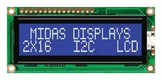


MC21605C6W-BNMLWI-V2
Alphanumeric LCD, 16 x 2, White on Blue, 5V, I2C, English, Japanese, Transmissive
- Manufacturer: MIDAS DISPLAYS
- Product type: Alphanumeric LCD Displays
- Character Count x Line:16 x 2; Display Appearance:White on Blue; Logic Voltage:5V; Interface Type:I2C; Font Set:English, Japanese; Display Mode:Transmissive; Character Size:5.55mm; LCD
- SVHC: No SVHC (25-Jun-2025)
- Font Set: English, Japanese
- Module Size: 80mm x 36mm
- Display Mode: Transmissive
- Logic Voltage: 5V
- Product Range: Mono COB Character LCDs Product Series
- Character Size: 5.55mm
- Interface Type: I2C
- LCD Display Type: BSTN
- Display Appearance: White on Blue
- Backlighting Colour: White
- Display Construction: COB
- Character Count x Line: 16 x 2
- Operating Temperature Max: 70°C
- Operating Temperature Min: -20°C
| Delivery and price | |
|---|---|
| Units per pack | 250 |
| Price | 12.25 € |
| Current stock | 50+ |
| Lead time | 30 days |
**Telephone +44 (0)1493 602602 Email:sales@midasdisplays.com Email:tech@midasdisplays.com www.midasdisplays.com**

**Sauls Wharf House Crittens Road Great Yarmouth Norfolk NR31 0AG**

**==> picture [522 x 323] intentionally omitted <==**

**----- Start of picture text -----**<br>
|||||
|---|---|---|---|
|MC21605C6W-BNMLWI-V2|2 x 16|5mm Character Height|LCD Module|
|Specification|
|Version:    1|Date:  29/07/2016|
|Revision|
|1|28/07/2016|First issue|
|OO|Display Features|
|Character Count|2 x 16|
|Appearance|White on blue|
|a|Logic Voltage|5V|
|Interface|I2C|
|Font Set|English / Japanese|
|Display Mode|Transmissive|
|Character Height|5.55mm|
|——a|ee|Dy|(Vaouscompliant|
|ee|LC Type|STN Blue|
|7|
|Module Size|80.00 x 36.00 x 13.50mm|
|——S|Operating Temperature|-20°C ~ +70°C|
|Construction|COB|Box Quantity|Weight / Display|
|LED Backlight|White|~|~|
|ee|SS|eeA|ae|

**----- End of picture text -----**<br>


* - For full design functionality, please use this specification in conjunction with the RW1063 specification. (Provided Separately)

Page 1 of 40

## **General Specification**

The Features is described as follow:

- Module dimension: 80.0 x 36.0 x 13.5 (max.) mm

- View area: 66.0 x 16.0 mm

- Active area: 56.20 x 11.5 mm

- Number of Characters: 16 characters x 2 Lines

- Dot size: 0.55 x 0.65 mm

- Dot pitch: 0.60 x 0.70 mm

- Character size: 2.95 x 5.55 mm

- Character pitch: 3.55 x 5.95 mm

- LCD type: STN Negative, Blue Transmissive,

- Duty: 1/16

- View direction: 6 o’clock

- Backlight Type: LED, White

Page 2 of 40

## **Interface Pin Function**

|**Pin No. Symbol**|**Pin No. Symbol**|**Level**|**Description**|
|---|---|---|---|
|1|VSS|0V|Ground|
|2|VDD|5.0V|Supply Voltage for logic|
|3|VO|(Variable) Operating voltage for LCD|(Variable) Operating voltage for LCD|
|4|NC|-|No connection|
|5|NC|-|No connection|
|6|NC|-|No connection|
|7|SA0|H/L|In IIC interface ,DB1(SA1) and DB0(SA0) are used<br>for Slave address, must be connect to VDD or VSS|
|8|SA1|H/L||
|9|NC|-|No connection|
|10|NC|-|No connection|
|11|NC|-|No connection|
|12|CSB|H/L|In IIC serial mode, used as chip selection input.<br>When CSB = “Low”, selected<br>When CSB = “High”, not selected.<br>(Low access enable)|
|13|SDA|H/L|serial input data|
|14|SCL|H/L|serial clock input|
|15|A|-|Power supply for B/L +|
|16|K|-|Power supply for B/L -|


Page 3 of 40

## **Contour Drawing &Block Diagram**

**==> picture [429 x 514] intentionally omitted <==**

**----- Start of picture text -----**<br>
80.0 : 0.5<br>4.95 71.2 1 Vss<br>— 7.55 f 66.0(VA) . Ff 2 Vdd<br>12.45 a 56.2(AA) 13.5Max aT 3 Vo<br>— 7.86 P2.54*15=38.1 _ aT<br>1.8 16- 1.0 PTH 8.9 4 NC<br>| | WPT J —— 5 NC<br>ry | 1 soasab e—! 16 ie s | Pf 6 NC<br>7 SA0<br>K<br>8 SA1<br>4 | f F ooooooochoooooo |Z! j aT<br>9 NC<br>A<br>10 NC<br>| Sree ] q —<br>11 NC<br>40.55 4- 2.5 PTH 1.6 12 CSB<br>2.5 | 75.0 : = 4- 5.0 PAD a aT 13 SDA<br>LED B/L<br>14 SCL<br>3.55<br>— 2.95 0.6 aT 15 A<br>0.6 16 K<br>0.55<br>ry cBorREE<br>Pa<br>LLL<br>— —— HHEH [[Ooo] [o] 4<br>DOT SIZE<br>SCALE 5/1<br>Vdd R=2.2K<br>Pull-high resistor<br>R R Com1~16<br>Sen SDA<br>MPU a SCL |: ( Controller/Com Driver manudacs 16X2 LCD |<br>IIC<br>|<br>Seg1~40<br>Vdd<br>Seg41~80<br>VR Vo D Seg Driver<br>10K~20K Vss<br>M<br>CL1<br>CL2<br>Vdd,Vss,V1~V5<br>External contrast adjustment.<br>Optional<br>5.7 10.3 12.55 2 2.5<br>18.3<br>0.5<br>25.2 11.5 31.0<br>36.0 16.0(VA)<br>0.7 0.65<br>5.95 5.55<br>0.4<br>Bias and Power Circuit<br>N.V. Generator<br>**----- End of picture text -----**<br>


Character located 1 2 3 4 5 6 7 8 9 10 11 12 13 14 15 16 DDRAM address 00 01 02 03 04 05 06 07 08 09 0A 0B 0C 0D 0E 0F DDRAM address 40 41 42 43 44 45 46 47 48 49 4A 4B 4C 4D 4E 4F

Page 4 of 40

## **Character Generator ROM Pattern**

Table.2

Page 5 of 40

|**Item**<br>W~~aste~~|**Symbol**<br>~~aste~~|**Condition**<br>~~aste~~|**Min**<br>~~aste~~|**Typ**<br>~~aste~~|**Max**<br>~~aste~~|**Unit**<br>~~aste~~|
|---|---|---|---|---|---|---|
|View Angle<br>W~~aste~~|θ<br>~~aste~~|CR≧2<br>~~aste~~|0<br>~~aste~~|-<br>~~aste~~|20<br>~~aste~~|ψ= 180°<br>~~aste~~|
||θ<br>~~aste~~|CR≧2<br>~~aste~~|0<br>~~aste~~|-<br>~~aste~~|40<br>~~aste~~|ψ= 0°<br>~~aste~~|
||θ<br>~~aste~~|CR≧2<br>~~aste~~|0<br>~~aste~~|-<br>~~aste~~|30<br>~~aste~~|ψ= 90°<br>~~aste~~|
||θ<br>~~aste~~|CR≧2<br>~~aste~~|0<br>~~aste~~|-<br>~~aste~~|30<br>~~aste~~|ψ= 270°<br>~~aste~~|
|Contrast Ratio|CR|-|-|3|-|-|
|Response Time|T rise|-|-|150|200|ms|
||T fall|-|-|150|200|ms|


## **Definition of Operation Voltage (Vop)**

## **Definition of Response Time ( Tr , Tf )**

**==> picture [442 x 164] intentionally omitted <==**

**----- Start of picture text -----**<br>
Non-selected Non-selected<br>Condition Condition<br>Intensity Selected Wave S elected Condition<br>100 % Non-selected Wave Intensity<br>10%<br>Cr Max<br>Cr = Lon / Loff 90%<br>100%<br>VN ! an<br>Vop<br>Driving Voltage(V) T r : = T f<br>[positive type] 【 Positive type 】<br>**----- End of picture text -----**<br>


## **Conditions :**

Operating Voltage : Vop Viewing Angle(θ,φ) : 0°, 0°

Frame Frequency : 64 HZ Driving Waveform : 1/N duty , 1/a bias

## **Definition of viewing angle(CR** ≧ **2)**

Page 6 of 40

**==> picture [257 x 152] intentionally omitted <==**

**----- Start of picture text -----**<br>
θ b<br>θ f φ = 180 °<br>θ l<br>— X. e _---- > L ata ae θ r -<br>Oa K | 7<br>i:: o n . 7 - ea ei<br>φ = 270 ° a meee ~ L  a ——_- ; Meee φ = 90 °<br>a a<br>7<br>7<br>φ = 0 °<br>**----- End of picture text -----**<br>


Page 7 of 40

## **Absolute Maximum Ratings**

|**Item**|**Symbol**|**Min**|**Typ**|**Max**|**Unit**|
|---|---|---|---|---|---|
|Operating Temperature|TOP|-20|-|+70|℃|
|Storage Temperature|TST|-30|-|+80|℃|
|Input Voltage|VIN|-0.3|-|VDD+0.3|V|
|Supply Voltage For Logic|VDD-VSS|-0.3|-|5.5|V|
|Supply Voltage For LCD|VDD-V0|VSS-0.3|-|VSS+7.0|V|


Page 8 of 40

## **Electrical Characteristics**

|**Item**|**Symbol**|**Condition**|**Min**|**Typ**|**Max**|**Unit**|
|---|---|---|---|---|---|---|
|Supply Voltage For Logic|Supply Voltage For Logic<br>VDD-VSS|-|4.5|5.0|5.5|V|
|Supply Voltage For LCD<br>*Note|VDD-V0|Ta=-20℃<br>Ta=25℃<br>Ta=70℃|-<br>3.6<br>3.2|-<br>3.7<br>-|5.2<br>3.8<br>-|V<br>V<br>V|
|Input High Volt.|VIH|-|2.5|-|VDD|V|
|Input Low Volt.|VIL|-|-0.3|-|0.55|V|
|Output High Volt.|VOH|-|3.9|-|VDD|V|
|Output Low Volt.|VOL|-|-|-|0.4|V|
|Supply Current|IDD|VDD=5.0V|1.0|1.2|1.5|mA|


* Note: Please design the VOP adjustment circuit on customer's main board

Vdd LCM Vo VR 10K~20K Module VSS

Page 9 of 40

## **Backlight Information**

## **Specification**

|**PARAMETER**|**SYMBOL MIN**|**SYMBOL MIN**|**TYP**|**MAX**|**UNIT**|**TEST** **CONDITION**|
|---|---|---|---|---|---|---|
|**Supply Current ILED**|**Supply Current ILED**|-|**32**|**40**|**mA**|**V=3.5V**|
|**Supply Voltage V**|**Supply Voltage V**|**3.4**|**3.5**|**3.6**|**V**|-|
|**Reverse Voltage VR**|**Reverse Voltage VR**|-|-|**5**|**V**|-|
|**Luminance**<br>**(Without LCD)**|**IV**|**496**|**620**|-|**CD/M2 ILED=32mA**|**ILED=32mA**|
|**LED Life Time**<br>**(For Reference**<br>**only)**|-|-|**50K**|-|**Hr.**|**ILED=32mA**<br>**25**℃**,50-60%RH,**<br>**(Note 1)**|
|**Color**|**White**||||||


## **Note: The LED of B/L is drive by current only, drive voltage is for reference only. drive voltage can make driving current under safety area (current between minimum and maximum).**

## **Note 1:50K hours is only an estimate for reference.**

Drive from pin15,pin16

**==> picture [175 x 69] intentionally omitted <==**

**----- Start of picture text -----**<br>
R R<br>pin15 A<br>B/L<br>K<br>pin16<br>LCM<br>**----- End of picture text -----**<br>


(Will never get Vee output from pin15)

Page 10 of 40

## **Reliability**

## **Content of Reliability Test (Wide temperature, -20** ℃ **~70** ℃ **)**

|**Content of Reliability Test (Wide temperature, -20**℃**~70**℃**)**|**Content of Reliability Test (Wide temperature, -20**℃**~70**℃**)**|**Content of Reliability Test (Wide temperature, -20**℃**~70**℃**)**|**Content of Reliability Test (Wide temperature, -20**℃**~70**℃**)**|
|---|---|---|---|
|**Environmental Test**||||
|**Test Item**|**Content of Test**|**Test Condition**|**Note**|
|High Temperature<br>storage|Endurance test applying the high storage temperature<br>for a longtime.|80℃<br>200hrs|2|
|Low Temperature<br>storage|Endurance test applying the low storage temperature<br>for a longtime.|-30℃<br>200hrs|1,2|
|High Temperature<br>Operation|Endurance test applying the electric stress (Voltage &<br>Current) and the thermal stress to the element for a<br>longtime.|70℃<br>200hrs|——|
|Low Temperature<br>Operation|Endurance test applying the electric stress under low<br>temperature for a longtime.|-20℃<br>200hrs|1|
|High Temperature/<br>Humidity storage|The module should be allowed to stand at<br>60℃,90%RH max<br>For 96hrs under no-load condition excluding the<br>polarizer,<br>Then takingit out and dryingit at normal temperature.|60℃,90%RH<br>96hrs|1,2|
|Thermal shock<br>resistance|The sample should be allowed stand the following 10<br>cycles of operation<br>-20℃25℃70℃<br>30min   5min<br>30min<br>1 cycle|-20℃/70℃<br>10 cycles|——|
|Vibration test|Endurance test applying the vibration during<br>transportation and using.|Total fixed amplitude :<br>1.5mm<br>Vibration Frequency :<br>10~55Hz<br>One cycle 60<br>seconds to 3<br>directions of X,Y,Z for<br>Each 15 minutes|Total fixed amplitude :<br>3|
|Static electricity test|Endurance test applying the electric stress to the<br>terminal.|VS=±600V(contact),<br>±800v(air),<br>RS=330Ω<br>CS=150pF<br>10 times|——|


**Note1: No dew condensation to be observed.**

**Note2: The function test shall be conducted after 4 hours storage at the normal Temperature and humidity after remove from the test chamber. Note3: The packing have to including into the vibration testing.**

Page 11 of 40

|NO<br>~~an~~|Item<br>~~an~~|Criterion<br>~~an~~|AQL<br>~~an~~|
|---|---|---|---|
|01<br>~~an~~|Electrical<br>Testing<br>~~an~~|1.1 Missing vertical, horizontal segment, segment contrast<br>defect.<br>1.2 Missing character , dot or icon.<br>1.3 Display malfunction.<br>1.4 No function or no display.<br>1.5 Current consumption exceeds product specifications.<br>1.6 LCD viewing angle defect.<br>1.7 Mixed product types.<br>1.8 Contrast defect.<br>~~an~~|0.65<br>~~an~~|
|02<br>~~an~~|Black or white<br>spots on LCD<br>(display only)<br>~~an~~|2.1 White and black spots on display≦0.25mm, no more than<br>three white or black spots present.<br>2.2 Densely spaced: No more than two spots or lines within 3mm<br>~~an~~|2.5<br>~~an~~|
|03<br>~~an~~|LCD black<br>spots, white<br>spots,<br>contamination<br>(non-display)<br>~~an~~|3.1 Round type : As following drawing<br>Φ=( x + y ) / 2<br>SIZE<br>Acceptable Q TY<br>Φ≦0.10<br>Accept no dense<br>0.10<Φ≦0.20<br>2<br>0.20<Φ≦0.25<br>1<br>0.25<Φ<br>0<br>~~an~~|2.5<br>~~an~~|
|||3.2 Line type : (As following drawing)<br>Length<br>Width<br>Acceptable Q TY<br>---<br>W≦0.02<br>Accept no dense<br>L≦3.0<br>0.02<W≦0.03<br>2<br>L≦2.5<br>0.03<W≦0.05<br>---<br>0.05<W<br>As round type|2.5|


Page 12 of 40

|04|Polarizer<br>bubbles|If bubbles are visible,<br>judge using black spot<br>specifications, not easy<br>to find, must check in<br>specify direction.<br>Size Φ<br>Acceptable Q TY<br>Φ≦0.20<br>Accept no dense<br>0.20<Φ≦0.50<br>3<br>0.50<Φ≦1.00<br>2<br>1.00<Φ<br>0<br>Total Q TY<br>3|2.5|
|---|---|---|---|


Page 13 of 40

|~~Pa~~||||
|---|---|---|---|
|NO<br>~~Pa~~|Item<br>|Criterion|AQL|
|05<br>~~Paa~~|Scratches<br>~~a~~|Follow NO.3 LCD black spots, white spots, contamination||
|06<br>~~a~~|Chipped<br>glass<br>~~a~~|Symbols Define:<br>x: Chip length<br>y: Chip width<br>z: Chip thickness<br>k: Seal width<br>t: Glass thickness  a: LCD side length<br>L: Electrode pad length:<br>6.1 General glass chip :<br>6.1.1 Chip on panel surface and crack between panels:<br>z: Chip thickness<br>y: Chip width<br>x: Chip length<br>Z≦1/2t<br>Not over viewing<br>area<br>x≦1/8a<br>1/2t<z≦2t<br>Not exceed 1/3k<br>x≦1/8a<br>☉If there are 2 or more chips, x is total length of each chip.<br>6.1.2 Corner crack:<br>z: Chip thickness<br>y: Chip width<br>x: Chip length<br>Z≦1/2t<br>Not over viewing<br>area<br>x≦1/8a<br>1/2t<z≦2t<br>Not exceed 1/3k<br>x≦1/8a<br>☉If there are 2 or more chips, x is the total length of each chip.|2.5|


Page 14 of 40

**==> picture [490 x 707] intentionally omitted <==**

**----- Start of picture text -----**<br>
NO  Item  Criterion<br>AQL<br>a<br>Symbols :<br>x: Chip length  y: Chip width  z: Chip thickness<br>k: Seal width   t: Glass thickness  a: LCD side length<br>L: Electrode pad length<br>6.2 Protrusion over terminal :<br>6.2.1 Chip on electrode pad :<br>Ss<br>y: Chip width  x: Chip length  z: Chip thickness<br>y ≦ 0.5mm  x ≦ 1/8a  0  < z  ≦  t<br>6.2.2 Non-conductive portion:<br>L L<br>Glass<br>06  2.5<br>crack<br>y: Chip width  x: Chip length  z: Chip thickness<br>y ≦  L  x ≦ 1/8a  0  < z  ≦  t<br>☉If the chipped area touches the ITO terminal, over 2/3 of the ITO<br>must remain and be inspected according to electrode terminal<br>specifications.<br>☉If the product will be heat sealed by the customer, the alignment<br>mark not be damaged.<br>6.2.3 Substrate protuberance and internal crack.<br>y: width  x: length<br>y ≦ 1/3L  x  ≦  a<br>pT<br>**----- End of picture text -----**<br>


Page 15 of 40

Page 16 of 40

|NO<br>~~a~~|Item|Criterion|AQL|
|---|---|---|---|
|07|Cracked glass The LCD with extensive crack is not acceptable.|Cracked glass The LCD with extensive crack is not acceptable.|2.5|
|08|Backlight<br>elements|8.1 Illumination source flickers when lit.<br>8.2 Spots or scratched that appear when lit must be judged.<br>Using LCD spot, lines and contamination standards.<br>8.3 Backlight doesn’t light or color wrong.|0.65<br>2.5<br>0.65|
|09|Bezel|9.1 Bezel may not have rust, be deformed or have fingerprints,<br>stains or other contamination.<br>9.2 Bezel must comply with job specifications.|2.5<br>0.65|
|10|PCB、COB|10.1 COB seal may not have pinholes larger than 0.2mm or<br>contamination.<br>10.2 COB seal surface may not have pinholes through to the IC.<br>10.3 The height of the COB should not exceed the height<br>indicated in the assembly diagram.<br>10.4 There may not be more than 2mm of sealant outside the<br>seal area on the PCB. And there should be no more than<br>three places.<br>10.5 No oxidation or contamination PCB terminals.<br>10.6 Parts on PCB must be the same as on the production<br>characteristic chart. There should be no wrong parts,<br>missing parts or excess parts.<br>10.7 The jumper on the PCB should conform to the product<br>characteristic chart.<br>10.8 If solder gets on bezel tab pads, LED pad, zebra pad or<br>screw hold pad, make sure it is smoothed down.<br>10.9 The Scraping testing standard for Copper Coating of PCB<br>~~**Y**~~<br>~~**X**~~<br>X * Y<=2mm2|2.5<br>2.5<br>0.65<br>2.5<br>2.5<br>0.65<br>0.65<br>2.5<br>2.5|
|11|Soldering|11.1 No un-melted solder paste may be present on the PCB.<br>11.2 No cold solder joints, missing solder connections, oxidation<br>or icicle.<br>11.3 No residue or solder balls on PCB.<br>11.4 No short circuits in components on PCB.|2.5<br>2.5<br>2.5<br>0.65|


Page 17 of 40

|NO|Item|Criterion|AQL|
|---|---|---|---|
|12|General<br>appearance|12.1 No oxidation, contamination, curves or, bends on interface<br>Pin (OLB) of TCP.<br>12.2 No cracks on interface pin (OLB) of TCP.<br>12.3 No contamination, solder residue or solder balls on product.<br>12.4 The IC on the TCP may not be damaged, circuits.<br>12.5 The uppermost edge of the protective strip on the interface<br>pin must be present or look as if it cause the interface pin to<br>sever.<br>12.6 The residual rosin or tin oil of soldering (component or chip<br>component) is not burned into brown or black color.<br>12.7 Sealant on top of the ITO circuit has not hardened.<br>12.8 Pin type must match type in specification sheet.<br>12.9 LCD pin loose or missing pins.<br>12.10 Product packaging must the same as specified on<br>packaging specification sheet.<br>12.11 Product dimension and structure must conform to product<br>specification sheet.<br>12.12 Visual defect outside of VA is not considered to be rejection.|2.5<br>0.65<br>2.5<br>2.5<br>2.5<br>2.5<br>2.5<br>0.65<br>0.65<br>0.65<br>0.65|


Page 18 of 40

## **Precautions in use of LCD Modules**

(1)Avoid applying excessive shocks to the module or making any alterations or modifications to it.

- (2)Don’t make extra holes on the printed circuit board, modify its shape or change the components of LCD module.

- (3)Don’t disassemble the LCM.

- (4)Don’t operate it above the absolute maximum rating.

- (5)Don’t drop, bend or twist LCM.

- (6)Soldering: only to the I/O terminals.

- (7)Storage: please storage in anti-static electricity container and clean environment.

(8) Midas have the right to change the passive components, including R3,R6 & backlight adjust resistors. (Resistors,capacitors and other passive components will have different appearance and color caused by the different supplier.)

(9)Midas have the right to change the PCB Rev. (In order to satisfy the supplying stability, management optimization and the best product performance...etc, under the premise of not affecting the electrical characteristics and external dimensions, Midas have the right to modify the version.)

- (10) To ensure the stability of the display screen, please apply screen saver after showing 30 mins of fixed display content.

Page 19 of 40

## **Material List of Components for RoHs**

1. Midas hereby declares that all of or part of products (with the mark “#”in code), including, but not limited to, the LCM, accessories or packages, manufactured and/or delivered to your company (including your subsidiaries and affiliated company) directly or indirectly by our company (including our subsidiaries or affiliated companies) do not intentionally contain any of the substances listed in all applicable EU directives and regulations, including the following substances.

Exhibit A:The Harmful Material List

|Material|(Cd)|(Pb)|(Hg)|(Cr6+)|PBBs|PBDEs|
|---|---|---|---|---|---|---|
|Limited<br>Value|100<br>ppm|1000<br>ppm|1000<br>ppm|1000<br>ppm|1000<br>ppm|1000<br>ppm|
|Above limited value is set upaccordingto RoHS.|||||||


## 2.Process for RoHS requirement:(only for RoHS inspection)

- (1) Use the Sn/Ag/Cu soldering surface;the surface of Pb-free solder is rougher than we used before.

- (2) Heat-resistance temp.:

Reflow:250 ℃ ,30 seconds Max.;

Connector soldering wave or hand soldering:320 ℃ , 10 seconds max.

- (3) Temp. curve of reflow, max. Temp.:235±5 ℃ ;

Recommended customer’s soldering temp. of connector:280 ℃ , 3 seconds.

Page 20 of 40

## **Recommendable Storage**

1. Place the panel or module in the temperature 25°C±5°C and the humidity below 65% RH

2. Do not place the module near organics solvents or corrosive gases.

3. Do not crush, shake, or jolt the module.

Page 21 of 40

## **Other (IC Information)**

## **1.Function Description**

## **SYSTEM INTERFACE (Parallel 8-bit bus and 4-bit bus)**

This chip has all four kinds interface type with MPU: IIC, 4SPI, 4-bit bus and 8-bit bus. Serial and parallel buses (4-bit/8-bit) are selected by IF1 and IF0 input pins, and 4-bit bus and 8-bit bus is selected by DL bit in the instruction register.

During read or write operation, two 8-bit registers are used. One is data register (DR); the other is instruction register (IR). The data register (DR) is used as temporary data storage place for being written into or read from DDRAM/CGRAM, target RAM is selected by RAM address setting instruction. Each internal operation, reading from or writing into RAM, is done automatically.

So to speak, after MPU reads DR data, the data in the next DDRAM/CGRAM address is transferred into DR automatically. Also after MPU writes data to DR, the data in DR is transferred into DDRAM/CGRAM automatically.

The Instruction register (IR) is used only to store instruction code transferred from MPU. MPU cannot use it to read instruction data.

IR: Instruction Register.

DR: Data Register.

|RS R/W|RS R/W|**Operation**|
|---|---|---|
|0|0|Instruction write operation(MPU writes Instruction code into IR)|
|0|1|Read busyflag (DB7)and address counter(DB0 - DB6)|
|1|0|Data write operation(MPU writes data into DR|
|1|1|Data read operation(MPU reads data from DR)|


## **BUSY FLAG (BF) (only support parallel 8-bit bus and 4-bit bus)**

When BF = "High", it indicates that the internal operation is being processed. So during this time the next instruction cannot be accepted. BF can be read, when RS = Low and R / W = High (Read Instruction Operation); through DB7 before executing the next instruction, be sure that BF is not High.

## **DISPLAY DATA RAM (DDRAM)**

DDRAM stores display data of maximum 80 x 8 bits (80 characters). DDRAM address is set in the address counter (AC) as a hexadecimal number. (Refer to Figure 1.)

Since DDRAM has 8 bits data. It is possible to access 256 CGROM/CGRAM fonts.

Page 22 of 40

## **1-line display (N = 0) (Figure 2)**

When there are fewer than 80 display characters, the display begins at the head position. For example, if using only the Controller, 8 characters are displayed. See Figure 3.

When the display shift operation is performed, the DDRAM address shifts. See Figure 3.

## **2-line display (N = 1) (Figure 4)**

Case 1: When the number of display characters is less than 40 x 2 lines, the two lines are displayed from the head. Note that the first line end address and the second line start address are not consecutive. For example, when just the Controller is used, 8 characters x 2 lines are displayed. See Figure 5.

When display shift operation is performed, the DDRAM address shifts. See Figure 5.

Page 23 of 40

Case 2: For a 16character x 12 -line display, the Controller can be extended using one 40-output extension driver. See Figure 6. When display shift operation is performed, the DDRAM address shifts. See Figure 6.

Page 24 of 40

## **TIMING GENERATION CIRCUIT**

Timing generation circuit generates clock signals for the internal operations.

## **ADDRESS COUNTER (AC)**

Address Counter (AC) stores DDRAM/CGRAM address, transferred from IR.

After writing into (reading from) DDRAM/CGRAM/SEGRAM, AC is automatically increased (decreased) by 1.

When RS = "Low" and R/W = "High", AC can be read through DB0-DB6

## **CURSOR/BLINK CONTROL CIRCUIT**

It controls cursor/blink ON/OFF and black/white inversion at cursor position.

## **LCD DRIVER CIRCUIT**

LCD Driver circuit has 16 common and 40 segment signals for 2-line display (N=1) or 8 common and 40 segments for 1-line display (N=0) for LCD driving.

Data from CGRAM/CGROM is transferred to 40 bit segment latches serially, and then it is stored to 40 bit shift latch.

## **CGROM (CHARACTER GENERATOR ROM)**

CGROM has 10,240 bits (256 characters x 5 x 8 dot)

## **CGRAM (CHARACTER GENERATOR RAM)**

character can be used (refer to Table 2).

## **5** x **8 dots Character Pattern**

## **Table 2. Relationship between Character Code (DDRAM) and Character Pattern (CGRAM)**

## Notes:

1. Character code bits 0 to 2 correspond to CGRAM address bits 3 to 5 (3 bits: 8 types).

2. CGRAM address bits 0 to 2 designate the character pattern line position. The 8th line is the cursor position and its display is formed by a logical OR with the cursor. Maintain the 8th line data, corresponding to the cursor display position, at 0 as the cursor display. If the 8th line data is 1, 1 bit will light up the 8th line regardless of the cursor presence.

Page 25 of 40

3. Character pattern row positions correspond to CGRAM data bits 0 to 4 (bit 4 being at the left). 4. As shown Table 2, CGRAM character patterns are selected when character code bits 4 to 7 are all 0 and MW=0. However, since character code bit 3 has no effect, the H display example above can be selected by either character code 00H or 08H.

5. 1 for CGRAM data corresponds to display selection and 0 to non-selection.

- “-“: Indicates no effect.

## **2.Instruction Table**

Page 26 of 40

## **Clear Display**

Clear all the display data by writing "20H" (space code) to all DDRAM address, and set DDRAM address to "00H" into AC (address counter). Return cursor to the original status; namely, bring the cursor to the left edge on first line of the display. Make entry mode increment (I/D = "1").

## **Return Home:**

Return Home is cursor return home instruction. Set DDRAM address to "00H" into the address counter. Return cursor to its original site and return display to its original status, if shifted. A content of DDRAM does not change.

## **Entry Mode Set:**

Set the moving direction of cursor and display.

## **I/D: Increment/decrement of DDRAM address (cursor or blink)**

I/D = 1: cursor/blink moves to right and DDRAM address is increased by 1.

I/D = 0: cursor/blink moves to left and DDRAM address is decreased by 1.

* CGRAM operates the same as DDRAM, when read/write from or to CGRAM

## **S: Shift of entire display**

When DDRAM read (CGRAM read/write) operation or S = "Low", shift of entire display is not performed.

If S= "High" and DDRAM write operation, shift of entire display is performed according to I/D value (I/D = "1”: shift left, I/D = "0”: shift right).

## **Display ON/OFF**

Control display/cursor/blink ON/OFF 1 bit register.

## **D: Display ON/OFF control bit.**

D = 1: entire display is turned on.

D = 0: display is turned off, but display data is remained in DDRAM.

Page 27 of 40

## **C: Cursor ON/OFF control bit.**

C = 1: cursor is turned on.

C = 0: cursor is disappeared in current display, but I/D register remains its data.

## **B: Cursor Blink ON/OFF control bit.**

B = 1: cursor blink is on, that performs alternate between all the high data and display character at the cursor position. If fosc has 540 kHz frequency, blinking has 185 ms interval. B = 0: blink is off.

## **Cursor or Display Shift**

Without writing or reading of display data, shift right/left cursor position or display. This

instruction is used to correct or search display data (refer to Table 4). During 2-line mode display, cursor moves to the 2nd line after 40th digit of 1st line.

Note that display shift is performed simultaneously by the shift enable instruction. When

displayed data is shifted repeatedly, all display lines shifted simultaneously. When display shift is performed, the contents of address counter are not changed.

**Table 4. Shift Patterns According to S/C and R/L Bits**

## **Function Set**

## **DL: Interface data length control bit**

When DL = "High", it means 8-bit bus mode with MPU.

When DL = "Low", it means 4-bit bus mode with MPU. So to speak, DL is a signal to select 8-bit or 4-bit bus mode.

When 4-bit bus mode, it needs to transfer 4-bit data by two times.

IF using IIC and 4-SPI interface、DL bit must be setting to “1”

## **N: Display line number control bit**

When N = "Low", it means 1-line display mode.

When N = "High", 2-line display mode is set.

## **F: Display font type control bit**

When F = "Low", it means 5 x 8 dots format display mode

When F = "High", 5 x11 dots format display mode.

Page 28 of 40

## **Set CGRAM Address**

Set CGRAM address to AC.

This instruction makes CGRAM data available from MPU.

## **Set DDRAM Address**

Set DDRAM address to AC.

This instruction makes DDRAM data available from MPU.

When 1-line display mode (N=0), DDRAM address is from “00H” to “4FH”

In 2-line display mode (NW = 0), DDRAM address in the 1st line is from "00H" - "27H", and DDRAM address in the 2nd line is from "40H" - "67H".

**Read Busy Flag and Address** (only support parallel 8-bit bus and 4 bit bus)

This instruction shows whether Controller is in internal operation or not. If the resultant BF is “high”, it means the internal operation is in progress and you have to wait until BF to be Low, and then the next instruction can be performed. In this instruction you can read also the value of address counter.

## **Write Data to RAM**

Write binary 8-bit data to DDRAM/CGRAM/SEGRAM.

The selection of RAM from DDRAM, CGRAM, is set by the previous address set instruction: DDRAM address set, CGRAM address set. RAM set instruction can also determine the AC direction to RAM.

After write operation, the address is automatically increased/decreased by 1, according to the entry mode.

Page 29 of 40

**Read Data from RAM** (only support parallel 8-bit bus and 4 bit bus)

Read binary 8-bit data from DDRAM/CGRAM.

The selection of RAM is set by the previous address set instruction. If address set instruction of RAM is not performed before this instruction, the data that read first is invalid, because the direction of AC is not determined.

If you read RAM data several times without RAM address set instruction before read operation, you can get correct RAM data from the second, but the first data would be incorrect, because there is no time margin to transfer RAM data.

In case of DDRAM read operation, cursor shift instruction plays the same role as DDRAM address set instruction: it also transfer RAM data to output data register. After read operation address counter is automatically increased/decreased by 1 according to the entry mode.

After CGRAM read operation, display shift may not be executed correctly.

* In case of RAM write operation, after this AC is increased/decreased by 1 like read operation. In this time, AC indicates the next address position, but you can read only the previous data by read instruction.

## **OUTLINE**

To overcome the speed difference between internal clock of Controller and MPU clock,

Controller performs internal operation by storing control information to IR (Instruction Register) or DR (data Register).

The internal operation is determined according to the signal from MPU, composed of read/write and data bus.

I Nstruction can be divided largely four kinds;

*Controller function set instructions (set display methods, set data length, etc.)

*Address set instructions to internal RAM

*Data transfer instructions with internal RAM

*Others

The address of internal RAM is automatically increased or decreased by 1.

**NOTE:** During internal operation, Busy Flag (DB7) is read high. Busy Flag check must be preceded the next instruction.

Busy flag check must be proceeded the next instruction.

When an MPU program with Busy Flag (DB7) checking is made, 1/2 Fosc (is necessary) for

executing the next instruction by the falling edge of the “E” signal after the Busy Flag (DB7) goes to “Low”.

Page 30 of 40

## **INTERFACE WITH MPU**

Controller can transfer data in bus mode (4-bit or 8-bit) or serial mode with MPU.

In case of 4-bit bus mode, data transfer is performed by two times to transfer 1 byte data. (jLWhen interfacing data lengths are 4 -bit, only 4 ports, from DB4 - DB7, are used as data bus. At first higher 4-bit (in case of 8-bit bus mode, the contents of DB4 - DB7) are transferred, and then lower 4- bit (in case of 8-bit bus mode, the contents of DB0 - DB3) are transferred. So transfer is performed by two times.

Busy Flag outputs "High" after the second transfer are ended.

(jLWhen interfacing data length are 8 -bit, transfer is performed at a time through 8 ports, from DB0 - DB7.

**Bonding Note for IF1, IF0** on Page 10)

## **INTERFACE WITH MPU IN BUS MODE**

## **Interface with 8-bit MPU**

If 8-bits MPU is used, Controller can connect directly with that. In this case, port E, RS, R/W and DB0 to DB7 need to interface each other. Example of timing sequence is shown below.

## **Interface with 4-bit MPU**

If 4-bit MPU is used, Controller can connect directly with this. In this case, port E, RS, R/W and DB4 - DB7 need to interface each other. The transfer is performed by two times. Example of timing sequence is shown below.

Page 31 of 40

## **For serial interface data, bus lines (DB5 to DB7) are used. 4-Line SPI**

If 4-Pin SPI mode is used, CSB (DB5), SID (DB7), SCLK (DB6), and RS are used. They are chip selection; serial input data, serial clock input, and data/instruction section, relatively. The example of timing sequence is shown below.

## **Example of timing sequence**

Note: Following is the master SPI clock mode of MPU.

Idle state for clock is a high level,data transmitted on rising edge of SCLK, and data is hold

during low level.

## **For serial interface data, bus lines (DB5(CSB)** 、 **DB6(SDA) and DB7(SCL)) are used.**

## **IIC interface**

The IIC interface receives and executes the commands sent via the IIC Interface. It also receives RAM data and sends it to the RAM.

The IIC Interface is for bi-directional, two-line communication between different ICs or modules.

Serial data line

SDA (DB6) and a Serial clock line SCL (DB7) must be connected to a positive supply via a pull-up resistor.

Data transfer may be initiated only when the bus is not busy.

*The CSB (DB5) Pin must be setting to “VSS”.

Page 32 of 40

* When IIC interface is selected, the DL register must be set to “1”.

Page 33 of 40

## **BIT TRANSFER**

One data bit is transferred during each clock pulse. The data on the SDA line must remain stable

during the

HIGH period of the clock pulse because changes in the data line at this time will be interpreted as a control

signal. Bit transfer is illustrated in Fig.9.1

## **START AND STOP CONDITIONS**

Both data and clock lines remain HIGH when the bus is not busy. A HIGH-to-LOW transition of the data line, while the clock is HIGH is defined as the START condition (S). A LOW-to-HIGH transition of the data line while the clock is HIGH is defined as the STOP condition (P). The START and STOP conditions are illustrated in

Fig.9.2

## **SYSTEM CONFIGURATION**

The system configuration is illustrated in Fig.9.3

- Transmitter: the device, which sends the data to the bus

- Receiver: the device, which receives the data from the bus

- Master: the device, which initiates a transfer, generates clock signals and terminates a transfer

- Slave: the device addressed by a master

- Multi-Master: more than one master can attempt to control the bus at the same time without corrupting the message

Page 34 of 40

- Arbitration: procedure to ensure that, if more than one master simultaneously tries to control the bus, only one is allowed to do so and the message is not corrupted

- Synchronization: procedure to synchronize the clock signals of two or more devices.

## **ACKNOWLEDGE**

Each byte of eight bits is followed by an acknowledge bit. The acknowledge bit is a HIGH signal put on the bus by the transmitter during which time the master generates an extra acknowledge related clock pulse. A slave receiver which is addressed must generate an Acknowledge after the reception of each byte. A master receiver must also generate an Acknowledge after the reception of each byte that has been clocked out of the slave transmitter. The device that acknowledges must pull-down the SDA line during the acknowledge clock pulse, so that the SDA line is stable LOW during the HIGH period of the Acknowledge related clock pulse (set-up and hold times must be taken into consideration). A master receiver must signal an end-of-data to the transmitter by not generating an Acknowledge on the last byte that has been clocked out of the slave. In this event the transmitter must leave the data line HIGH to enable the master to generate a STOP condition. Acknowledgement on the IIC Interface is illustrated in Fig.9.4

## **IIC Interface protocol**

The Controller supports command, data write addressed slaves on the bus.

Before any data is transmitted on the IIC Interface, the device, which should respond, is addressed first.

Four 7-bit slave addresses (0111100, 0111101, 0111110 and 0111111) are reserved for the

Page 35 of 40

Controller. The least significant bit of the slave address is set by connecting the input SA0 (DB0) and SA1 (DB1) to either logic 0 (VSS) or logic 1 (VDD).

The IIC Interface protocol is illustrated in Figure.9.5

The sequence is initiated with a START condition (S) from the IIC Interface master, which is followed by the slave address. All slaves with the corresponding address acknowledge in parallel, all the others will ignore the IIC Interface transfer. After acknowledgement, one or more command words follow which define the status of the addressed slaves.

A command word consists of a control byte, which defines Co and A0, plus a data byte. The last control byte is tagged with a cleared most significant bit (i.e. the continuation bit Co). After a control byte with a cleared Co bit, only data bytes will follow. The state of the A0 bit defines whether the data byte is interpreted as a command or as RAM data. All addressed slaves on the bus also acknowledge the control and data bytes. After the last control byte, depending on the A0 bit setting; either a series of display data bytes or command data bytes may follow. If the A0 bit is set to logic 1, these display bytes are stored in the display RAM at the address specified by the data pointer. The data pointer is automatically updated and the data is directed to the intended Controller device. If the A0 bit of the last control byte is set to logic 0, these command bytes will be decoded and the setting of the device will be changed according to the received commands. Only the addressed slave makes the acknowledgement after each byte. At the end of the transmission the IIC interface-bus master issues a STOP condition (P). If no acknowledge is generated by the master after a byte, the driver stops transferring data to the master.

Page 36 of 40

## **INITIALIZING**

## **INITIALIZING BY INTERNAL RESET CIRCUIT**

When the power is turned on, Controller is initialized automatically by power on reset circuit. During the initialization, the following instructions are executed, and BF (Busy Flag) is kept "High"(busy state) to the end of initialization.

## **Clear Display Instruction**

Write "20H" to all DDRAM

## **Set Functions Instruction**

DL = 1: 8-bit bus mode

N = 0: 1-line display

F = 0: 5 x 8 dot character font

## **Display ON/OFF Instruction**

D = 0: Display OFF

C = 0: Cursor OFF

B = 0: Blink OFF

## **Set Entry Mode Instruction**

I/D = 1: Increment by 1 S = 0: No entire display shift Note:

If the electrical characteristics conditions listed under the table Power Supply Conditions Using Internal Reset Circuit are not met, the internal reset circuit will not operate normally and will fail to initialize the Controller. For such a case, initialization must be performed by the MPU as explain by the following figure.

Page 37 of 40

3.Timing Characteristics

Page 38 of 40

## **4.Initializing of LCM**

## **Serial Interface Mode(Fosc=540KHz)**

Page 39 of 40

## **5. Recommended circuit diagram**

Without negative voltage (Reference)

**==> picture [402 x 213] intentionally omitted <==**

**----- Start of picture text -----**<br>
I2C Interface<br>VSS 1<br>VSS<br>VDD 2<br>VDD<br>3<br>VO<br>VR 4<br>NC<br>5<br>NC<br>6<br>NC<br>7<br>MCU SA0<br>8<br>SA1<br>9<br>NC<br>2.2K 2.2K 10<br>NC<br>11<br>NC<br>12<br>CSB<br>SDA 13<br>SDA<br>SCL 14<br>SCL<br>LB + 15<br>A/Vee<br>LB - 16<br>K<br>**----- End of picture text -----**<br>


Build in negative voltage (Reference)

2

3

Page 40 of 40
Updated at June 10, 2026
Midas Displays is a recognized specialist in the electronic display industry, dedicated to providing high-quality visual solutions tailored to a wide range of applications. Backed by a UK-based, in-house team of engineers, the company is known for its extensive technical knowledge and commitment to delivering fast, reliable service. This expertise ensures that designers and manufacturers receive best-in-class support when integrating displays into their projects. The core of the Midas Displays portfolio features an extensive selection of Liquid Crystal Displays (LCD). Ranging from standard character and graphic modules to advanced configurations, these LCD displays are engineered for exceptional clarity and durability. Designed to meet the rigorous demands of various industries, they provide reliable performance for both industrial and commercial applications requiring robust and cost-effective visual output. Complementing their primary LCD offerings, Midas Displays also provides a versatile range of Organic Light Emitting Diode (OLED) displays. These advanced modules deliver high-contrast, energy-efficient viewing solutions ideal for modern, compact electronic designs. To ensure seamless integration across all display types, the company supports its core products with a variety of complementary accessories, including touch screens, interconnects, and evaluation kits.
About Novapart
Novapart is a B2B electronic component broker specialising in stock shortages and cost reduction. We source hard-to-find parts and identify compliant alternatives across a catalogue of 410,000+ components from 500+ manufacturers.
Learn more →Stock Shortage Specialist
When a component is unavailable, discontinued or has an unacceptable lead time, we tap into our network of vetted European and Asian distributors to source what you need — without compromising on quality or traceability.
Request a quote →Compliant Alternatives
We identify pin-to-pin, electrically equivalent substitutes that meet the same certifications (RoHS, AEC-Q100, REACH) as your original specification — validated against datasheets, not just part numbers. Often at a lower cost.
BOM Analysis service →