


MAXM17624AMB+T
Non Isolated POL DC/DC Converter, Industrial, uSLIC-10, Module, 800 mV, 3.3 V, 1 A
- Manufacturer: ANALOG DEVICES
- Product type: DC / DC Non Isolated Board Mount Converters - Adjustable Output
- MSL: MSL 3 - 168 hours
- SVHC: No SVHC (04-Feb-2026)
- Depth: 2.6mm
- Width: 2.1mm
- Height: 1.3mm
- Topology: Synchronous Buck (Step Down)
- No. of Pins: 10Pins
- Product Range: MAXM17624 Series
- No. of Outputs: 1 Output
- Output Current: 1A
- Output Power Max: -
- Input Voltage Max: 5.5V
- Input Voltage Min: 2.9V
- Output Current Max: 1A
- Output Voltage Max: 3.3V
- Output Voltage Min: 800mV
- Switching Frequency: 4MHz
- Input Voltage DC Max: 5.5V
- Input Voltage DC Min: 2.9V
- DC / DC Converter Type: uSLIC-10, Module
- DC / DC Converter IC Case: µSLIC
- Operating Temperature Max: 125°C
- Power Supply Applications: Industrial
- DC / DC Converter Output Type: Adjustable
| Delivery and price | |
|---|---|
| Units per pack | 7500 |
| Price | 1.86 € |
| Current stock | 10+ |
| Lead time | 30 days |
**EVALUATION KIT AVAILABLE**
_Click_ _**here** for production status of specific part numbers._
## **MAXM17623/MAXM17624**
## **General Description**
The Himalaya series of voltage regulator ICs and power modules enable cooler, smaller, and simpler powersupply solutions. MAXM17623 and MAXM17624 are high-frequency synchronous step down DC-DC converter modules, with integrated MOSFETs, compensation components, and inductors, that operate over 2.9V to 5.5V input voltage range. MAXM17623 and MAXM17624 support up to 1A load current and allow use of small, lowcost input and output capacitors. The output voltage can be adjusted from 0.8V to 3.3V. The modules significantly reduce design complexity, manufacturing risks, and offer a true plug-and-play power supply solution, reducing timeto-market.
The MAXM17623 and MAXM17624 modules employ peak-current-mode control architecture under steady-state operation. To reduce input inrush current, the devices offer a fixed 1ms soft-start time. Both modules feature selectable PWM or PFM mode of operation at light loads. When PWM mode is selected, MAXM17623 operates at a fixed 2MHz switching frequency and MAXM17624 operates at a fixed 4MHz switching frequency. MAXM17623 offers output voltages from 0.8V to 1.5V and MAXM17624 offers output voltages from 1.5V to 3.3V.
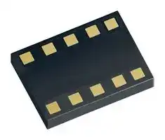
The MAXM17623 and MAXM17624 modules are available in a low profile, compact 10-pin, 2.6mm x 2.1mm x 1.3mm, uSLIC™ package.
## **Applications**
- Point of Load Power Supply
- Standard 5V Rail Supplies
- Battery Powered Applications
- Distributed Power Systems
- Industrial Sensors and Process Control
_**Ordering Information appears at end of data sheet.**_
## **2.9V to 5.5V, 1A Himalaya uSLIC Step-Down Power Modules**
## **Benefits and Features**
- Easy to Use
- 2.9V to 5.5V Input
- Adjustable 0.8V to 3.3V Output
- ±1% Feedback Accuracy
- Up to 1A Output Current
- Fixed 2MHz or 4MHz Operation
- 100% Duty-Cycle Operation
- Internally Compensated
- All Ceramic Capacitors
- High Efficiency
- Selectable PWM- or PFM-Mode of Operation
- Shutdown Current as Low as 0.1μA (typ)
- Flexible Design
- Internal Soft-Start and Prebias Startup
- Open-Drain Power Good Output (PGOOD Pin)
- Robust Operation
- Overtemperature Protection
- -40°C to +125°C Ambient Operating Temperature/
- -40°C to +150°C Junction Temperature
- Rugged
- Passes Drop, Shock, and Vibration Standards: JESD22-B103, B104, B111
## **Typical Application Circuit**
**==> picture [242 x 141] intentionally omitted <==**
**----- Start of picture text -----**<br>
MAXM17624<br>2.9V TO 5.5V<br>VIN IN OUTSNS<br>CIN 1.5V, 1A<br>2.2µF EN OUT VOUT<br>COUT<br>PGOOD PGND 10µF R1<br>33.2kΩ<br>MODE FB<br>R2<br>SGND LX 37.4kΩ<br>**----- End of picture text -----**<br>
**==> picture [125 x 31] intentionally omitted <==**
_19-100317; Rev 1; 2/19_
## MAXM17623/MAXM17624
## 2.9V to 5.5V, 1A Himalaya uSLIC Step-Down Power Modules
## **Absolute Maximum Ratings**
|**Absolute Maximum Ratings**||
|---|---|
|IN to PGND ...............................................................-0.3V to 6V|Junction Temperature (Note1) .........................................+150°C|
|EN, PGOOD, FB, OUTSNS to SGND .......................-0.3V to 6V|Storage Temperature Range ...............................-55°C to 125°C|
|MODE TO SGND .........................................-0.3V to (IN + 0.3V)|Lead Temperature (soldering,10s) ..................................+260°C|
|LX, OUT TO PGND ......................................-0.3V to (IN + 0.3V)|Soldering Temperature (reflow) ......................................+260°C|
|PGND TO SGND ....................................................-0.3V to 0.3V|Junction-to-Ambient Thermal Resistance .......................77°C/W|
|Output Short-Circuit Duration ....................................Continuous||
_Stresses beyond those listed under “Absolute Maximum Ratings” may cause permanent damage to the device. These are stress ratings only, and functional operation of the device at these or any other conditions beyond those indicated in the operational sections of the specifications is not implied. Exposure to absolute maximum rating conditions for extended periods may affect device reliability._
## **Package Information**
|**PACKAGE TYPE: 10-PIN uSIP**|**PACKAGE TYPE: 10-PIN uSIP**|
|---|---|
|Package Code|MA102A2+1|
|Outline Number|**21-100245**|
|Land Pattern Number|**90-100084**|
|**THERMAL RESISTANCE, FOUR-LAYER BOARD:**||
|Junction to Ambient (θJA)|77°C/W|
For the latest package outline information and land patterns (footprints), go to **www.maximintegrated.com/packages** . Note that a “+”, “#”, or “-” in the package code indicates RoHS status only. Package drawings may show a different suffix character, but the drawing pertains to the package regardless of RoHS status.
Package thermal resistances were obtained using the method described in JEDEC specification JESD51-7, using a four-layer board. For detailed information on package thermal considerations, refer to **www.maximintegrated.com/thermal-tutorial** .
## **Note 1:** Junction temperature greater than +125°C degrades operating lifetimes.
**Note 2:** Package thermal resistance is measured on an evaluation board with natural convection.
## **Electrical Characteristics**
(VIN = VEN = 3.6V, VSGND = VPGND = VMODE = VFB = VOUTSNS = 0V, LX = OUT = PGOOD = OPEN, TA = TJ = -40°C to +125°C, unless otherwise noted. Typical values are at TA = +25°C. All voltages are referenced to GND, unless otherwise noted.) (Note 3)
|**PARAMETER**|**SYMBOL**|**CONDITIONS**|**MIN**<br>**TYP**<br>**MAX**|**UNITS**|
|---|---|---|---|---|
|**INPUT SUPPLY (VIN)**|||||
|Input Voltage Range|VIN||2.9<br>5.5|V|
|Input Supply Current|IIN-SHDN|VEN= 0, Shutdown mode|0.1|µA|
||IQ-PFM|PFM Mode, No Load|40.0||
||IQ-PWM|PWM Mode, MAXM17623|4.5|mA|
|||PWM Mode, MAXM17624|6.0||
|Undervoltage Lockout<br>Threshold (UVLO)|VIN_UVLO|IN Rising|2.72<br>2.80<br>2.88|V|
|UVLO Hysteresis|VIN_UVLO_HYS||200|mV|
Maxim Integrated │ 2
www.maximintegrated.com
## MAXM17623/MAXM17624
## 2.9V to 5.5V, 1A Himalaya uSLIC Step-Down Power Modules
## **Electrical Characteristics (continued)**
(VIN = VEN = 3.6V, VSGND = VPGND = VMODE = VFB = VOUTSNS = 0V, LX = OUT = PGOOD = OPEN, TA = TJ = -40°C to +125°C, unless otherwise noted. Typical values are at TA = +25°C. All voltages are referenced to GND, unless otherwise noted.) (Note 3)
|**PARAMETER**|**SYMBOL**|**CONDITIONS**|**MIN**<br>**TYP**<br>**MAX**|**UNITS**|
|---|---|---|---|---|
|**ENABLE (EN)**|||||
|EN Low Threshold|VEN_LOW|EN Falling|0.8|V|
|EN High Threshold|VEN_HIGH|EN Rising|2|V|
|EN Input Leakage|IEN|EN = 5.5V, TA= TJ= 25°C|10<br>50|nA|
|**TIMING**|||||
|Switching Frequency|fSW|MAXM17623|1.92<br>2.00<br>2.08|MHz|
|||MAXM17624|3.84<br>4.00<br>4.16||
|Minimum ON time|tON_MIN||40|ns|
|Maximum Duty Cycle|DMAX||100|%|
|Soft-Start time|tSS||1|ms|
|**FEEDBACK (FB)**|||||
|FB Regulation Voltage|VFB-REG||0.8|V|
|FB Voltage Accuracy|VFB|PWM Mode|-1<br>+1|%|
|FB Input Bias Current|IFB|FB = 0.6V, TA= TJ= 25°C|50|nA|
|OUTSNS Input Bias Current|IOUTSNS-BIAS|VOUTSNS= 1.8V|10|μA|
|**POWER GOOD (PGOOD)**|||||
|PGOOD Rising Threshold|VPGOOD_RISE|FB Rising|91.5<br>93.5<br>95.5|%|
|PGOOD Falling Threshold|VPGOOD_FALL|FB Falling|88<br>90<br>92|%|
|PGOOD Output Low|VOL_PGOOD|IPGOOD = 5mA|200|mV|
|PGOOD Output Leakage<br>Current|ILEAK_PGOOD|PGOOD = 5.5V, TA= TJ= 25°C|100|nA|
|PGOOD Deassertion After<br>Soft-Start|||184|μs|
|**MODE**|||||
|MODE Pullup Current||VMODE= GND|5|μA|
|**THERMAL SHUTDOWN**|||||
|Thermal Shutdown Rising<br>Threshold|||165|°C|
|Thermal Shutdown Hysteresis|||10|°C|
**Note 3:** Electrical specifications are production tested at TA = +25°C. Specifications over the entire operating temperature range are guaranteed by design and characterization.
Maxim Integrated │ 3
www.maximintegrated.com
## MAXM17623/MAXM17624
## 2.9V to 5.5V, 1A Himalaya uSLIC
## Step-Down Power Modules
## **Typical Operating Characteristics**
(VIN = VEN = 5V, VSGND = VPGND = VMODE = VFB = VOUTSNS = 0V, LX = OUT = PGOOD = OPEN, TA = TJ = -40°C to +125°C, unless otherwise noted. Typical values are at TA = +25°C. All voltages are referenced to GND, unless otherwise noted. The circuit values for different output voltage applications are as in Table 1, unless otherwise noted.)
**==> picture [523 x 502] intentionally omitted <==**
**----- Start of picture text -----**<br>
MAXM17623 EFFICIENCY vs. LOAD CURRENT MAXM17623 EFFICIENCY vs. LOAD CURRENT MAXM17624 EFFICIENCY vs. LOAD CURRENT<br>(VOUT = 0.8V, PWM AND PFM MODE) (VOUT = 1.5V, PWM AND PFM MODE) (VOUT = 3.3V, PWM AND PFM MODE)<br>100 toc01 100 toc02 100 toc03<br>VIN = 3.3V, PFM MODE VIN = 3.3V, PFM MODEVIN = 5V, PFM MODE VIN = 5V, PFM MODE<br>90 pp VIN = 5V, PFM MODE 90 90<br>VIN = 5V, PWM MODE<br>80 80 80<br>VIN = 3.3V, PWM MODE<br>70 70 70<br>VIN = 3.3V, PWM MODE VIN = 5V, PWM MODE<br>VIN = 5V, PWM MODE<br>60 60 60<br>0.01 0.1 1 0.01 0.1 1 0.01 0.1 1<br>LOAD CURRENT (A) LOAD CURRENT (A) LOAD CURRENT (A)<br>MAXM17623 OUTPUT VOLTAGE vs. LOAD CURREN MAXM17623 OUTPUT VOLTAGE vs. LOAD CURRENT MAXM17624 OUTPUT VOLTAGE vs. LOAD CURRENT<br>0.810 (VOUT = 0.8V, PWM AND PFM MODE) toc04 1.505 (VOUT = 1.5V, PWM AND PFM MODE) toc05 3.335 (VOUT = 3.3V, PWM AND PFM MODE) toc06<br>VIN = 5V, PFM MODE<br>0.808 VIN = 3.3V, PFM MODE 1.503 3.330<br>VIN = 5V, PFM MODE<br>VIN = 3.3V, PFM MODE<br>0.806 S S) 1.501 — | VIN = 5V, PFM MODE | 3.325 ee ee<br>0.804 a oa 1.499 VIN = 5V, PWM MODE \V 3.320 |}<br>VIN = 5V, PWM MODE<br>0.802 VIN = 3.3V, PWM MODE \/ | 1.497 \ 3.315 FIN<br>VIN = 5V, PWM MODE<br>0.800 1.495 VIN = 3.3V, PWM MODE 3.310<br>0.01 0.1 1 0.01 0.1 1 0.01 0.1 1<br>LOAD CURRENT (A) LOAD CURRENT (A) LOAD CURRENT (A)<br>MAXM17623 LOAD TRANSIENT RESPONSE MAXM17623 LOAD TRANSIENT RESPONSE MAXM17623 LOAD TRANSIENT RESPONSE<br>(VIN = 3.3V, VOUT = 0.8V, PWM MODE) (VIN = 3.3V, VOUT = 0.8V, PWM MODE) (VIN = 3.3V, VOUT = 0.8V, PFM MODE)<br>(LOAD CURRENT STEPPED FROM 0A TO 0.5A) toc07 (LOAD CURRENT STEPPED FROM 0.5A TO 1A) toc08 (LOAD CURRENT STEPPED FROM 0A TO 0.5A) toc09<br>V(AC)OUT 20mV/div V(AC)OUT 20mV/div V(AC)OUT 20mV/div<br>500mA/div<br>IOUT 500mA/div IOUT IOUT 500mA/div<br>40µs/div 40µs/div 100µs/div<br>EFFICIENCY (%) EFFICIENCY (%) EFFICIENCY (%)<br>OUTPUT VOLTAGE (V) OUTPUT VOLTAGE (V) OUTPUT VOLTAGE (V)<br>**----- End of picture text -----**<br>
Maxim Integrated │ 4
www.maximintegrated.com
## MAXM17623/MAXM17624
## 2.9V to 5.5V, 1A Himalaya uSLIC
## Step-Down Power Modules
## **Typical Operating Characteristics (continued)**
**==> picture [507 x 564] intentionally omitted <==**
**----- Start of picture text -----**<br>
(VIN = VEN = 5V, VSGND = VPGND = VMODE = VFB = VOUTSNS = 0V, LX = OUT = PGOOD = OPEN, TA = TJ = -40°C to +125°C, un-<br>less otherwise noted. Typical values are at TA = +25°C. All voltages are referenced to GND, unless otherwise noted. The circuit values<br>for different output voltage applications are as in Table 1, unless otherwise noted.)<br>MAXM17623 LOAD TRANSIENT RESPONSE MAXM17623 LOAD TRANSIENT RESPONSE MAXM17623 LOAD TRANSIENT RESPONSE<br>(VIN = 5V, VOUT = 0.8V, PWM MODE) (VIN = 5V, VOUT = 0.8V, PWM MODE) (VIN = 5V, VOUT = 0.8V, PFM MODE)<br>(LOAD CURRENT STEPPED FROM 0A TO 0.5A) toc10 (LOAD CURRENT STEPPED FROM 0.5A TO 1A) toc11 (LOAD CURRENT STEPPED FROM 0A TO 0.5A) toc12<br>V(AC)OUT 20mV/div V(AC)OUT 20mV/div V(AC)OUT 20mV/div<br>500mA/div<br>IOUT 500mA/div IOUT IOUT 500mA/div<br>P| Fy f e<br>40µs/div 40µs/div 100µs/div<br>MAXM17623 LOAD TRANSIENT RESPONSE MAXM17623 LOAD TRANSIENT RESPONSE MAXM17623 LOAD TRANSIENT RESPONSE<br>(VIN = 5V, VOUT = 1.5V, PWM MODE) (VIN = 5V, VOUT = 1.5V, PWM MODE) (VIN = 5V, VOUT = 1.5V, PFM MODE)<br>(LOAD CURRENT STEPPED FROM 0A TO 0.5A) toc13 (LOAD CURRENT STEPPED FROM 0.5A TO 1A) toc14 (LOAD CURRENT STEPPED FROM 0A TO 0.5A) toc15<br>V(AC)OUT 50mV/div V(AC)OUT 50mV/div V(AC)OUT 50mV/div<br>500mA/div<br>IOUT 500mA/div IOUT IOUT 500mA/div<br>| ee<br>40µs/div 40µs/div 100µs/div<br>MAXM17624 LOAD TRANSIENT RESPONSE MAXM17624 LOAD TRANSIENT RESPONSE MAXM17624 LOAD TRANSIENT RESPONSE<br>(VIN = 5V, VOUT = 3.3V, PWM MODE) (VIN = 5V, VOUT = 3.3V, PWM MODE) (VIN = 5V, VOUT = 3.3V, PFM MODE)<br>(LOAD CURRENT STEPPED FROM 0A TO 0.5A) toc16 (LOAD CURRENT STEPPED FROM 0.5A TO 1A) toc17 (LOAD CURRENT STEPPED FROM 30mA TO 530mA) toc18<br>V(AC)OUT 50mV/div V(AC)OUT 50mV/div<br>VOUT 100mV/div<br>(AC)<br>500mA/div<br>IOUT 500mA/div IOUT IOUT 500mA/div<br>40µs/div<br>40µs/div 40µs/div<br>**----- End of picture text -----**<br>
Maxim Integrated │ 5
www.maximintegrated.com
## MAXM17623/MAXM17624
## 2.9V to 5.5V, 1A Himalaya uSLIC
## Step-Down Power Modules
## **Typical Operating Characteristics (continued)**
(VIN = VEN = 5V, VSGND = VPGND = VMODE = VFB = VOUTSNS = 0V, LX = OUT = PGOOD = OPEN, TA = TJ = -40°C to +125°C, unless otherwise noted. Typical values are at TA = +25°C. All voltages are referenced to GND, unless otherwise noted. The circuit values for different output voltage applications are as in Table 1, unless otherwise noted.)
**==> picture [488 x 153] intentionally omitted <==**
**----- Start of picture text -----**<br>
MAXM17623 STARTUP THROUGH ENABLE MAXM17623 STARTUP THROUGH ENABLE MAXM17624 STARTUP THROUGH ENABLE<br>(VIN = 5V, VOUT = 0.8V, ILOAD = 0A, PWM MODE) (VIN = 5V, VOUT = 0.8V, ILOAD = 1A, PWM MODE) (VIN = 5V, VOUT = 3.3V, ILOAD = 0A, PWM MODE)<br>toc19 toc20 toc21<br>5V/div 5V/div 5V/div<br>EN EN EN<br>= = Fe<br>LX 5V/div LX 5V/div LX 5V/div<br>500mV/div 500mV/div 2V/div<br>VOUT 5V/div VOUT 5V/div VOUT 5V/div<br>PGOOD PGOOD PGOOD<br>200µs/div 200µs/div 200µs/div<br>**----- End of picture text -----**<br>
**==> picture [499 x 317] intentionally omitted <==**
**----- Start of picture text -----**<br>
MAXM17624 STARTUP THROUGH ENABLE MAXM17623 SHUTDOWN THROUGH ENABLE MAXM17623 SHUTDOWN THROUGH ENABLE<br>(VIN = 5V, VOUT = 3.3V, ILOAD = 1A, PWM MODE) toc22 (VIN = 5V, VOUT = 0.8V, ILOAD = 0A, PWM MODE) toc23 (VIN = 5V, VOUT = 0.8V, ILOAD = 1A, PWM MODE)IN = 5V, VOUT = 0.8V, ILOAD = 1A, PWM MODE)= 5V, VOUT = 0.8V, ILOAD = 1A, PWM MODE)OUT = 0.8V, ILOAD = 1A, PWM MODE)= 0.8V, ILOAD = 1A, PWM MODE)LOAD = 1A, PWM MODE) = 1A, PWM MODE) toc24<br>5V/div<br>EN EN 5V/div EN 5V/div<br>LX 5V/div LX 5V/div LX 5V/div<br>2V/div<br>VOUT 5V/div VOUT 500mV/div VOUTOUT 500mV/div<br>PGOOD PGOOD 5V/div PGOOD 5V/div<br>200µs/div 4ms/div 10µs/div<br>MAXM17624 SHUTDOWN THROUGH ENABLE MAXM17624 SHUTDOWN THROUGH ENABLE MAXM17623 STARTUP THROUGH IN<br>(VIN = 5V, VOUT = 3.3V, ILOAD = 0A, PWM MODE) toc25 (VIN = 5V, VOUT = 3.3V, ILOAD = 1A, PWM MODE) toc26 (VIN = 5V, VOUT = 0.8V, ILOAD = 0A, PWM MODE) toc27<br>5V/div<br>EN 5V/div EN 5V/div IN<br>LX 5V/div LX 5V/div LX 5V/div<br>500mV/div<br>VOUT i 2V/div VOUT 2V/div VOUT 5V/div<br>PGOOD 5V/div PGOOD 5V/div PGOOD<br>2ms/div<br>**----- End of picture text -----**<br>
**==> picture [157 x 138] intentionally omitted <==**
**----- Start of picture text -----**<br>
MAXM17623 SHUTDOWN THROUGH ENABLE<br>(VIN = 5V, VOUT = 0.8V, ILOAD = 1A, PWM MODE)IN = 5V, VOUT = 0.8V, ILOAD = 1A, PWM MODE)= 5V, VOUT = 0.8V, ILOAD = 1A, PWM MODE)OUT = 0.8V, ILOAD = 1A, PWM MODE)= 0.8V, ILOAD = 1A, PWM MODE)LOAD = 1A, PWM MODE) = 1A, PWM MODE) toc24<br>EN 5V/div<br>LX 5V/div<br>VOUTOUT 500mV/div<br>PGOOD 5V/div<br>10µs/div<br>**----- End of picture text -----**<br>
> 20µs/div 200µs/div Maxim Integrated │ 6
www.maximintegrated.com
## MAXM17623/MAXM17624
## 2.9V to 5.5V, 1A Himalaya uSLIC Step-Down Power Modules
## **Typical Operating Characteristics (continued)**
(VIN = VEN = 5V, VSGND = VPGND = VMODE = VFB = VOUTSNS = 0V, LX = OUT = PGOOD = OPEN, TA = TJ = -40°C to +125°C, unless otherwise noted. Typical values are at TA = +25°C. All voltages are referenced to GND, unless otherwise noted. The circuit values for different output voltage applications are as in Table 1, unless otherwise noted.)
**==> picture [501 x 503] intentionally omitted <==**
**----- Start of picture text -----**<br>
MAXM17623 STARTUP THROUGH IN MAXM17624 STARTUP THROUGH IN MAXM17624 STARTUP THROUGH IN<br>(VIN = 5V, VOUT = 0.8V, ILOAD = 1A, PWM MODE) toc28 (VIN = 5V, VOUT = 3.3V, ILOAD = 0A, PWM MODE) toc29 (VIN = 5V, VOUT = 3.3V, ILOAD = 1A, PWM MODE) toc30<br>5V/div 5V/div 5V/div<br>IN IN IN<br>LX 5V/div LX 5V/div LX 5V/div<br>500mV/div 2V/div 2V/div<br>VOUT 5V/div VOUT 5V/div VOUT 5V/div<br>PGOOD PGOOD PGOOD<br>Sse<br>200µs/div 200µs/div 200µs/div<br>MAXM17623 SHUTDOWN THROUGH IN MAXM17623 SHUTDOWN THROUGH IN MAXM17624 SHUTDOWN THROUGH IN<br>(VIN = 5V, VOUT = 0.8V, ILOAD = 0A, PWM MODE) toc31 (VIN = 5V, VOUT = 0.8V, ILOAD = 1A, PWM MODE) toc32 (VIN = 5V, VOUT = 3.3V, ILOAD = 0A, PWM MODE) toc33<br>IN<br>IN 5V/div 5V/div IN 5V/div<br>LX 5V/div LX 5V/div LX 5V/div<br>VOUT 500mV/div VOUT 500mV/div VOUT 2V/div<br>PGOOD 5V/div PGOOD 5V/div PGOOD 5V/div<br>PS<br>10ms/div 20µs/div 2ms/div<br>MAXM17624 SHUTDOWN THROUGH IN MAXM17623 PERMANENT OUTPUT SHORT MAXM17623 PERMANENT OUTPUT SHORT<br>(VIN = 5V, VOUT = 3.3V, ILOAD = 1A, PWM MODE) toc34 (VIN = 5V, VOUT = 0.8V, ILOAD = 1A, PWM MODE) toc35 (VIN = 5V, VOUT = 1.5V, ILOAD = 1A, PWM MODE) toc36<br>5V/div 5V/div<br>SHORT SHORT<br>IN oo 5V/div<br>VOUT 500mV/div VOUT 500mV/div<br>LX 5V/div<br>VLX 5V/div VLX 5V/div<br>VOUT 2V/div<br>PGOOD 5V/div IOUT 1A/div IOUT 1A/div<br>= UEP = ME<br>40µs/div 4µs/div 4µs/div<br>**----- End of picture text -----**<br>
Maxim Integrated │ 7
www.maximintegrated.com
## MAXM17623/MAXM17624
## 2.9V to 5.5V, 1A Himalaya uSLIC Step-Down Power Modules
## **Typical Operating Characteristics (continued)**
(VIN = VEN = 5V, VSGND = VPGND = VMODE = VFB = VOUTSNS = 0V, LX = OUT = PGOOD = OPEN, TA = TJ = -40°C to +125°C, unless otherwise noted. Typical values are at TA = +25°C. All voltages are referenced to GND, unless otherwise noted. The circuit values for different output voltage applications are as in Table 1, unless otherwise noted.)
**==> picture [500 x 496] intentionally omitted <==**
**----- Start of picture text -----**<br>
MAXM17624 PERMANENT OUTPUT SHORT MAXM17623 TEMPORARY OUTPUT SHORT MAXM17623 TEMPORARY OUTPUT SHORT<br>(VIN = 5V, VOUT = 3.3V, ILOAD = 1A, PWM MODE) toc37 5V/div (VIN = 5V, VOUT = 0.8V, ILOAD = 1A, PWM MODE) toc38 (VIN = 5V, VOUT = 1.5V, ILOAD = 1A, PWM MODE) toc39<br>5V/div<br>SHORT SHORT 5V/div SHORT<br>500mV/div 1V/div<br>VOUT 2V/div VOUT VOUT<br>VLX ~ 5V/div VLX 5V/div VLX 5V/div<br>1A/div 1A/div<br>IOUT 1A/div IOUT IOUT<br>4µs/div 100µs/div 100µs/div<br>MAXM17624 TEMPORARY OUTPUT SHORT MAXM17623 BODE PLOT MAXM17623 BODE PLOT<br>SHORT (VIN = 5V, VOUT _ = 3.3V, ILOAD = 1A, PWM MODE) toc40 5V/div (V 5040 IN = 3.3V, V ST OUT = 0.8V, FULL LOAD, PWM MODE) TT TTT toc41 200160 (V 5040 IN = 5V, V Sooo OUT = 0.8V, FULL LOAD, PWM MODE) toc42 200160<br>2V/div 30 PPR CUT FETT 120 30 TSC 120<br>20 80 20 80<br>VOUT 10 perPATNTT TTT 40 10 PepeUSOTTT 40<br>MAGNITUDE MAGNITUDE<br>0 e DSS.C 0 0 pTTAPSCIN ESITH 0<br>PHASE PHASE<br>VLX 5V/div -10 NN -40 -10 IN -40<br>-20 -80 -20 -80<br>1A/div<br>-30 -120 -30 -120<br>IOUT -40 CH CROSSOVER FREQUENCY = 183.920kHz EA -160 -40 Cor CROSSOVER FREQUENCY = 198.339kHz -n -160<br>Let -50 dlCTT PHASE MARGIN = 53.103° NN -200 -50 ulCA PHASE MARGIN = 53.210° CoN -200<br>4µs/div 1000 10000 100000 1000000 1000 10000 100000 1000000<br>FREQUENCY (Hz) FREQUENCY (Hz)<br>MAXM17623 BODE PLOT MAXM17623 BODE PLOT<br>(VIN = 3.3V, VOUT = 1.5V, FULL LOAD, PWM MODE) (VIN = 5V, VOUT = 1.5V, FULL LOAD, PWM MODE)<br>50 toc43 200 50 toc44 200<br>40 O_o _ oo 160 40 SOM ooo 160<br>30 SST Cm 120 30 SU Co 120<br>20 peal UNCUT 80 20 ob 80<br>10 PT 40 10 UT TTT 40<br>MAGNITUDE<br>0 MAGNITUDE 0 0 0<br>-10 cr SSS PHASE CTT -40 -10 PAM PHASE SSN TH -40<br>-20-30 CCECHAM Ti illNNnt -80-120 -20-30 meP CO e na BD CoINN):CNN -80-120<br>-40 CROSSOVER FREQUENCY = 103.821kHz TN -160 -40 CH CROSSOVER FREQUENCY = 110.239kHz -160<br>PHASE MARGIN = 60.112° PHASE MARGIN = 55.713°<br>-50 -200 -50 -200<br>fs os calI llTH N<br>1000 10000 100000 1000000 1000 10000 100000 1000000<br>FREQUENCY (Hz) FREQUENCY (Hz)<br>GAIN MAGNITUDE (dB) O)GAIN PHASE ( GAIN MAGNITUDE (dB) º)GAIN PHASE (<br>º)GAIN PHASE ( º)GAIN PHASE (<br>GAIN MAGNITUDE (dB) GAIN MAGNITUDE (dB)<br>**----- End of picture text -----**<br>
Maxim Integrated │ 8
www.maximintegrated.com
## MAXM17623/MAXM17624
## 2.9V to 5.5V, 1A Himalaya uSLIC Step-Down Power Modules
## **Typical Operating Characteristics (continued)**
(VIN = VEN = 5V, VSGND = VPGND = VMODE = VFB = VOUTSNS = 0V, LX = OUT = PGOOD = OPEN, TA = TJ = -40°C to +125°C, unless otherwise noted. Typical values are at TA = +25°C. All voltages are referenced to GND, unless otherwise noted. The circuit values for different output voltage applications are as in Table 1, unless otherwise noted.)
**==> picture [342 x 337] intentionally omitted <==**
**----- Start of picture text -----**<br>
MAXM17623 OUTPUT CURRENT<br>MAXM17624 BODE PLOT vs. AMBIENT TEMPERATURE<br>(V 50 IN = 5V, VOUT = 3.3V, FULL LOAD, PWM MODE) toc45 200 1.2 (VIN = 3.3V, FULL LOAD, PWM MODE) toc46<br>40 160<br>Tn 1.0 TT<br>30 120<br>20 80<br>0.8<br>10 4a 40 2G<br>0 MAGNITUDE 0 0.6<br>-10 PHASE -40 VOUT = 1.5V<br>0.4<br>-20 -80<br>Sniiimettttmans | | VOUT = 0.8V AL<br>-30 CCI CT -120 0.2 Pt fy<br>-40 CROSSOVER FREQUENCY = 123.829kHz -160<br>-50 ee PHASE MARGIN = 63.213° ll -200 0.0 eel<br>1000 10000 100000 1000000 25 55 85 115<br>FREQUENCY (Hz) AMBIENT TEMPERATURE ( [o] C)<br>MAXM17623 OUTPUT CURRENT MAXM17624 OUTPUT CURRENT<br>vs. AMBIENT TEMPERATURE vs. AMBIENT TEMPERATURE<br>(VIN = 5V, FULL LOAD, PWM MODE) (VIN = 5V, FULL LOAD, PWM MODE)<br>1.2 toc47 1.2 toc48<br>1.0 1.0<br>0.8 VOUT = 1.5V 0.8<br>VOUT = 0.8V VOUT = 3.3V<br>0.6 Ff 0.6<br>0.4 Ff 0.4<br>0.2 Pot | [TU] 0.2<br>0.0 FT|| hi 0.0<br>25 55 85 115 25 55 85 115<br>AMBIENT TEMPERATURE ( [o] C) AMBIENT TEMPERATURE ( [o] C)<br>º)<br>GAIN PHASE ( LOAD CURRENT (A)<br>GAIN MAGNITUDE (dB)<br>LOAD CURRENT (A) LOAD CURRENT (A)<br>**----- End of picture text -----**<br>
**==> picture [156 x 144] intentionally omitted <==**
**----- Start of picture text -----**<br>
MAXM17623 STARTUP INTO PREBIAS<br>(VIN = 5V, VPREBIAS = 0.8V, VOUT = 1.5V, PWM MODE)<br>toc49<br>5V/div<br>EN 500mV/div<br>VOUT 2V/div<br>LX<br>5V/div<br>PGOOD<br>200µs/div<br>**----- End of picture text -----**<br>
**==> picture [150 x 145] intentionally omitted <==**
**----- Start of picture text -----**<br>
MAXM17624 STARTUP INTO PREBIAS<br>(VIN = 5V, VPREBIAS = 2.5V, VOUT = 3.3V, PWM MODE)<br>toc50<br>5V/div<br>EN<br>2V/div<br>VOUT<br>2V/div<br>LX<br>5V/div<br>PGOOD<br>200µs/div<br>**----- End of picture text -----**<br>
Maxim Integrated │ 9
www.maximintegrated.com
## MAXM17623/MAXM17624
## 2.9V to 5.5V, 1A Himalaya uSLIC Step-Down Power Modules
## **Pin Configuration**
**==> picture [504 x 246] intentionally omitted <==**
**----- Start of picture text -----**<br>
TOP VIEW<br>LX 1 10 IN<br>OUTSNS 2 9 PGND<br>MAXM17623/<br>MAXM17624<br>FB 3 8 SGND<br>PGOOD 4 7 EN<br>MODE 5 6 OUT<br>INDICATES PIN 1 OF THE MODULE<br>**----- End of picture text -----**<br>
## **Pin Description**
|**PIN**|**NAME**|**FUNCTION**|
|---|---|---|
|1|LX|Switching Node of the Inductor. No external connection.|
|2|OUTSNS|Sense Pin for Module VOUT. Connect to the positive terminal of the output capacitor COUTthrough a<br>kelvin connection.|
|3|FB|Output Feedback Connection. Connect FB to the center of the external resistor-divider from OUT to<br>GND to set the output voltage.|
|4|PGOOD|Open-Drain Power Good Output. Connect the PGOOD pin to the IN pin through an external pullup<br>resistor to generate a “high” level if the output voltage is above 93.5% of the target regulated voltage.<br>If not used, leave this pin unconnected. The PGOOD is driven low if the output voltage is below 90%<br>of the target regulated voltage.|
|5|MODE|PWM or PFM Mode Selection Input. Connect the MODE pin to GND to enable PWM-mode operation.<br>Leave the MODE pin unconnected to enable PFM mode operation.|
|6|OUT|Module Output Pin. Connect the output capacitor COUTfrom OUT to GND.|
|7|EN|Enable Input. Logic-high voltage on the EN pin enables the device, while logic-low voltage disables<br>the device.|
|8|SGND|Signal GND Pin|
|9|PGND|Power Ground Pin of the Converter. Connect externally to the power ground plane. Connect<br>the SGND and PGND pins together at the ground return path of the VINbypass capacitor. Refer<br>to the MAXM17632/MAXM17624 Evaluation Kit data sheet for a layout example.|
|10|IN|Power-Supply Input. Decouple the IN pin to PGND with a capacitor; place the capacitor close to the<br>IN and PGND pin.|
Maxim Integrated │ 10
www.maximintegrated.com
## MAXM17623/MAXM17624
## 2.9V to 5.5V, 1A Himalaya uSLIC Step-Down Power Modules
## **Functional Diagram**
## **Internal Diagram**
**==> picture [506 x 466] intentionally omitted <==**
**----- Start of picture text -----**<br>
MAXM17623/<br>MAXM17624<br>IN<br>HIGH-SIDE<br>DRIVER<br>EN +<br>LX<br>2V/0.8V -<br>1.5µH/<br>1µH<br>OSCILLATOR OUT<br>LOW-SIDE<br>CONTROLLER DRIVER<br>SOFT-START SGND<br>CONTROLLER<br>OUTSNS PGND<br>MODE LOGIC<br>MODE<br>SLOPE<br>MODE SELECTION<br>COMPENSATION<br>LOGIC<br>PGOOD<br>PGOOD<br>FB<br>LOGIC<br>**----- End of picture text -----**<br>
Maxim Integrated │ 11
www.maximintegrated.com
## MAXM17623/MAXM17624
## **Detailed Description**
MAXM17623 and MAXM17624 are high-frequency synchronous step down DC-DC converter modules, with integrated MOSFETs, compensation components, and inductors, that operate over a 2.9V to 5.5V input voltage range. MAXM17623 and MAXM17624 support up to 1A load current and allow use of small, low cost input and output capacitors. The output voltage can be adjusted from 0.8V to 3.3V.
When the EN pin is asserted, an internal power-up sequence ramps up the error-ampli fier reference, resulting in output-voltage soft-start. The FB pin monitors the output voltage through a resistor-divider. The devices select either PFM or forced-PWM mode depending on the state of the MODE pin at power-up. By pulling the EN pin to low, the devices enter shutdown mode and consume only 0.1μA (typ) of standby current.
The modules use an internally compensated, fixedfrequency, peak-current mode control scheme. On the falling edge of an internal clock, the high-side pMOSFET turns on, and continues to be on during normal operation until at least the rising edge of the clock (for 40ns). An internal error amplifier compares the feedback voltage to a fixed internal reference voltage and generates an error voltage. The error voltage is compared to a sum of the current-sense voltage and a slope-compensation voltage by a PWM comparator to set the on-time. During the on-time of the pMOSFET, the inductor current ramps up. For the remainder of the switching period (off-time), the pMOSFET is kept off and the low-side nMOSFET turns on. During the off-time, the inductor releases the stored energy as the inductor current ramps down, providing current to the output. Under overload conditions, the cycle-by-cycle current-limit feature limits the inductor peak current by turning off the high-side pMOSFET and turning on the low-side nMOSFET.
## **Mode Selection (MODE)**
The logic state of the MODE pin is latched after the EN pin goes above its rising threshold and all internal voltages are ready to allow LX switching. If the MODE pin is unconnected at power-up, the part operates in PFM mode at light loads. If the MODE pin is grounded at power-up, the part operates in con stant-frequency PWM mode at all loads. State changes on the MODE pin are ignored during normal operation.
## 2.9V to 5.5V, 1A Himalaya uSLIC Step-Down Power Modules
## **PWM Mode**
In PWM mode, the module output current is allowed to go negative. PWM operation is useful in frequency sensitive applications and provides fixed switching frequency operation at all loads. However, PWM-mode of operation gives lower efficiency at light loads compared to PFMmode of operation.
## **PFM Mode**
PFM mode of operation disables negative output current from the module and skips pulses at light loads for better efficiency. At low load currents, if the peak value of the inductor current is less than 350mA for 64 consecutive cycles, and the inductor current reaches zero, the part enters PFM mode. In PFM mode, When the FB pin voltage is below 0.8V, the high-side switch is turned-on until the inductor current reaches 500mA. After the high-side switch is turned OFF, the low-side switch is turned ON until the inductor current comes down to zero and LX enters a high-impedance state. If the FB pin voltage is greater than 0.8V for 3 consecutive CLK falling edges after LX enters a high-impedance state, the module continues to operate in PFM mode. In PFM mode, the part hibernates when the FB pin voltage is above 0.8V for 5 consecutive switching cycles after LX enters a highimpedance state. If the FB pin voltage drops below 0.8V within 3 consecutive CLK falling edges after LX enters a high-impedance state, the part comes out of PFM mode.
## **EN Input (EN), Soft-Start**
When EN voltage is above 2V (min), the internal erroramplifier reference voltage starts to ramp up. The duration of the soft-start ramp is 1ms (typ), allowing a smooth increase of the output voltage. Driving EN low disables both power MOSFETs, as well as other internal circuitry, and reduces IN quiescent current to below 0.1μA.
## **Power Good (PGOOD)**
The devices include an open-drain power good output that indicates the output voltage status. PGOOD goes high when the output voltage is above 93.5% of the target value, and goes low when the output voltage is below 90% of the target value. During start-up, the PGOOD pin goes high after 184μs of soft-start completion.
## **Startup into a Prebiased Output**
The devices are capable of soft-start into a prebiased output, without discharging the output capacitor in both the PFM and forced-PWM modes. Such a feature is useful in applications where digital integrated circuits with multiple rails are powered.
Maxim Integrated │ 12
www.maximintegrated.com
## MAXM17623/MAXM17624
## **Overcurrent Protection**
The MAXM17623/MAXM17624 are provided with a robust overcurrent protection (OCP) scheme that protects the modules under overload and output short-circuit conditions. When overcurrent is detected in the inductor, the switches are controlled by a mechanism, which detects both the high-side MOSFET and low-side MOSFET currents and compares them with the respective limits. Whenever the inductor current exceeds the internal peak current limit of 1.7A (typ), the high-side MOSFET is turned OFF and the low-side MOSFET is turned ON. The low side MOSFET is kept ON until the subsequent CLK rising edge after the inductor current drops below 1.4A (typ). The high-side MOSFET is turned ON after the low-side MOSFET is turned OFF and the cyclic operation continues. When the overload condition is removed, the part regulates output to the set voltage.
The MAXM17623/MAXM17624 are designed to support a maximum load current of 1A. The inductor ripple current is calculates as follows.
## 2.9V to 5.5V, 1A Himalaya uSLIC Step-Down Power Modules
## **Thermal Overload Protection**
Thermal overload protection limits the total power dissipation in the device. When the junction temperature exceeds +165°C, an on-chip thermal sensor shuts down the device, turns off the internal power MOSFETs, allowing the device to cool down. The thermal sensor turns the device on after the junction temperature cools by 10°C.
## **Applications Information**
## **Selection of Input Capacitor**
The input filter capacitor reduces peak currents drawn from the power source and reduces noise and voltage ripple on the input caused by the circuit’s switching.
The input capacitor RMS current requirement (IRMS) is defined by the following equation:
**==> picture [190 x 30] intentionally omitted <==**
For MAXM17623:
**==> picture [237 x 25] intentionally omitted <==**
For MAXM17624:
**==> picture [237 x 24] intentionally omitted <==**
Where:
VOUT = Steady-state output voltage
where IOUT(MAX) is the maximum load current. IRMS has a maximum value when the input voltage equals twice the output voltage (VIN = 2 x VOUT), so IRMS(MAX) = IOUT(MAX)/2.
Choose an input capacitor that exhibits less than +10°C temperature rise at the RMS input current for optimal long-term reliability. Use low-ESR ceramic capacitors with high-ripple-current capability at the input. X7R capacitors are recommended in industrial applications for their temperature stability. Calculate the input capacitance using the following equation:
**==> picture [163 x 26] intentionally omitted <==**
VIN = Operating input voltage
fSW = Switching Frequency
L = Power module output inductance (1.5μH ±20% for MAXM17623, 1μH ±20% for MAXM17624)
IOUT = Required output (load) current
The following condition should be satisfied at the desired load current (IOUT):
## where,
D = Duty ratio of the converter
fSW = Switching frequency ∆VIN = Allowable input voltage ripple
η = Efficiency
**==> picture [67 x 16] intentionally omitted <==**
Maxim Integrated │ 13
www.maximintegrated.com
## MAXM17623/MAXM17624
## 2.9V to 5.5V, 1A Himalaya uSLIC Step-Down Power Modules
## **Selection of Output Capacitor**
Small ceramic X7R-grade capacitors are sufficient and recommended for the device. The output capacitor has two functions. It filters the square wave generated by the device along with the internal inductor. It stores sufficient energy to support the output voltage under load transient conditions and stabilizes the device’s internal control loop. Usually the output capacitor is sized to support a step load of 50% of the maximum output current in the application, such that the output-voltage deviation is less than 3%. Derating of ceramic capacitors with DC-voltage must be considered while selecting the output capacitor. Refer to Table 1 for recommended output capacitors.
## **Adjusting the Output Voltage**
The MAXM17623/MAXM17624 output voltage can be programmed from 0.8V to 3.3V. Set the output voltage by connecting a resistor-divider from output to FB to GND (see Figure 2).
Choose R2 to be less than 37.4kΩ and calculate R1 with the following equation:
**==> picture [92 x 25] intentionally omitted <==**
**==> picture [242 x 115] intentionally omitted <==**
**----- Start of picture text -----**<br>
OUT<br>MAXM17623/ R1<br>MAXM17624<br>FB<br>R2<br>**----- End of picture text -----**<br>
_Figure 1. Setting the Output Voltage_
**==> picture [242 x 187] intentionally omitted <==**
**----- Start of picture text -----**<br>
MAXM17623/<br>LX 1 + MAXM17624 10 IN CIN<br>OUTSNS 2 9 PGND<br>FB 3 8 SGND COUT<br>PGOOD 4 7 EN<br>MODE 5 6 OUT<br>R2<br>R1<br>**----- End of picture text -----**<br>
_Figure 2. Layout Guidelines_
**Table 1. Selection of Components**
|**PART NUMBER**|**VIN(MIN)**<br>**(V)**|**VIN(MAX)**<br>**(V)**|**VOUT (V)**|**CIN**|**COUT**|**R1**|**R2**|
|---|---|---|---|---|---|---|---|
|MAXM17623|2.9|5.5|0.8|1 x 2.2μF 0603 10V<br>GRM188R71A225KE15|1 x 22μF 0805 6.3V<br>GRM21BZ70J226ME44#|0Ω|37.4kΩ|
||2.9|5.5|1.0|1 x 2.2μF 0603 10V<br>GRM188R71A225KE15|1 x 22μF 0805 6.3V<br>GRM21BZ70J226ME44#|9.53kΩ|37.4kΩ|
||2.9|5.5|1.2|1 x 2.2μF 0603 10V<br>GRM188R71A225KE15|1 x 22μF 0805 6.3V<br>GRM21BZ70J226ME44#|19.1kΩ|37.4kΩ|
||2.9|5.5|1.5|1 x 2.2μF 0603 10V<br>GRM188R71A225KE15|1 x 22μF 0805 6.3V<br>GRM21BZ70J226ME44#|33.2kΩ|37.4kΩ|
|MAXM17624|2.9|5.5|1.5|1 x 2.2μF 0603 10V<br>GRM188R71A225KE15|1 x 10μF 0805 16V<br>GRM21BZ71C106KE15#|33.2kΩ|37.4kΩ|
||2.9|5.5|1.8|1 x 2.2μF 0603 10V<br>GRM188R71A225KE15|1 x 10μF 0805 16V<br>GRM21BZ71C106KE15#|49.9kΩ|37.4kΩ|
||2.9|5.5|2.5|1 x 2.2μF 0603 10V<br>GRM188R71A225KE15|1 x 10μF 0805 16V<br>GRM21BZ71C106KE15#|86.6kΩ|37.4kΩ|
||3.6|5.5|3.3|1 x 2.2μF 0603 10V<br>GRM188R71A225KE15|1 x 10μF 0805 16V<br>GRM21BZ71C106KE15#|118kΩ|37.4kΩ|
Maxim Integrated │ 14
www.maximintegrated.com
## MAXM17623/MAXM17624
## 2.9V to 5.5V, 1A Himalaya uSLIC Step-Down Power Modules
## **Power Dissipation**
The power dissipation inside the module leads to an increase in the junction temperature of the MAXM17623 and MAXM17624. The power loss inside the modules at full load can be estimated as follows:
**==> picture [132 x 19] intentionally omitted <==**
Where η is the efficiency of the power module at the desired operating conditions. The junction temperature TJ of the module can be estimated at any given maximum ambient temperature TA from the following equation:
**==> picture [101 x 15] intentionally omitted <==**
For the MAXM17623/MAXM17624 evaluation board, the thermal resistance from Junction to Ambient (θJA) is 77[°] C/W. Operating the module at Junction temperatures greater than +125°C degrades operating lifetimes. An EE-SIM model is available for the MAXM17623/ MAXM17624, to simulate efficiency and power loss for the desired operating conditions.
## **PCB Layout Guidelines**
Careful PCB layout is critical to achieving low switching losses and clean, stable operation.
Use the following guidelines for good PCB layout:
- Keep the input capacitors as close as possible to the IN and PGND pins.
- Keep the output capacitors as close as possible to the OUT and PGND pins.
- Keep the resistive feedback divider as close as possible to the FB pin.
- Connect all of the PGND connections to a copper plane area as large as as possible on the top and bottom layers.
- Use multiple vias to connect internal PGND planes to the top layer PGND plane.
- Keep the power traces and load connections short. This practice is essential for high efficiency. Using thick copper PCBs (2oz vs. 1oz) can enhance fullload efficiency. Correctly routing PCB traces is a difficult task that must be approached in terms of fractions of centimeters, where a single mΩ of excess trace resistance causes a measurable efficiency penalty.
## **Typical Application Circuits**
## **Typical Application Circuit (0.8V, 1A)**
**==> picture [504 x 239] intentionally omitted <==**
**----- Start of picture text -----**<br>
MAXM17623<br>2.9V TO 5.5V<br>VIN IN OUTSNS<br>CIN 0.8V, 1A<br>2.2µF EN OUT VOUT<br>COUT<br>PGOOD PGND R1<br>22µF<br>0Ω<br>MODE FB<br>R2<br>SGND LX 37.4kΩ<br>**----- End of picture text -----**<br>
Maxim Integrated │ 15
www.maximintegrated.com
## MAXM17623/MAXM17624
## 2.9V to 5.5V, 1A Himalaya uSLIC Step-Down Power Modules
## **Typical Application Circuits (continued)**
## **Typical Application Circuit (1.5V, 1A)**
**==> picture [504 x 238] intentionally omitted <==**
**----- Start of picture text -----**<br>
MAXM17623<br>2.9V TO 5.5V<br>VIN IN OUTSNS<br>CIN 1.5V, 1A<br>2.2µF EN OUT VOUT<br>COUT<br>PGOOD PGND R1<br>22µF<br>33.2kΩ<br>MODE FB<br>R2<br>SGND LX 37.4kΩ<br>**----- End of picture text -----**<br>
## **Typical Application Circuit (1.5V, 1A)**
**==> picture [504 x 238] intentionally omitted <==**
**----- Start of picture text -----**<br>
MAXM17624<br>2.9V TO 5.5V<br>VIN IN OUTSNS<br>CIN 1.5V, 1A<br>2.2µF EN OUT VOUT<br>COUT<br>PGOOD PGND R1<br>10µF<br>33.2kΩ<br>MODE FB<br>R2<br>SGND LX 37.4kΩ<br>**----- End of picture text -----**<br>
Maxim Integrated │ 16
www.maximintegrated.com
## MAXM17623/MAXM17624
## 2.9V to 5.5V, 1A Himalaya uSLIC Step-Down Power Modules
## **Typical Application Circuits (continued)**
## **Typical Application Circuit (3.3V, 1A)**
**==> picture [504 x 238] intentionally omitted <==**
**----- Start of picture text -----**<br>
MAXM17624<br>3.6V TO 5.5V<br>VIN IN OUTSNS<br>CIN 3.3V, 1A<br>2.2µF EN OUT VOUT<br>COUT<br>PGOOD PGND R1<br>10µF<br>118kΩ<br>MODE FB<br>R2<br>SGND LX 37.4kΩ<br>**----- End of picture text -----**<br>
## **Ordering Information**
|**PART NUMBER**|**TEMP RANGE**|**PIN-PACKAGE**|**VOUT (V)**|
|---|---|---|---|
|MAXM17623AMB+|-40ºC to +125ºC|10-pin 2.6mm x 2.1mm x 1.35mm uSLIC package|0.8 to 1.5|
|MAXM17623AMB+T|-40ºC to +125ºC|10-pin 2.6mm x 2.1mm x 1.35mm uSLIC package|0.8 to 1.5|
|MAXM17624AMB+|-40ºC to +125ºC|10-pin 2.6mm x 2.1mm x 1.35mm uSLIC package|1.5 to 3.3|
|MAXM17624AMB+T|-40ºC to +125ºC|10-pin 2.6mm x 2.1mm x 1.35mm uSLIC package|1.5 to 3.3|
_+ Denotes a lead(Pb)-free/RoHS-compliant package._
_T Denotes tape-and-reel._
Maxim Integrated │ 17
www.maximintegrated.com
## MAXM17623/MAXM17624
## 2.9V to 5.5V, 1A Himalaya uSLIC Step-Down Power Modules
## **Revision History**
|**Revision**|**History**|||
|---|---|---|---|
|**REVISION**<br>**NUMBER**|**REVISION**<br>**DATE**|**DESCRIPTION**|**PAGES**<br>**CHANGED**|
|0|12/18|Initial release|—|
|1|2/19|Updated TOC05, TOC17, and Table 1|4–5, 14|
For pricing, delivery, and ordering information, please visit Maxim Integrated’s online storefront at https://www.maximintegrated.com/en/storefront/storefront.html.
_Maxim Integrated cannot assume responsibility for use of any circuitry other than circuitry entirely embodied in a Maxim Integrated product. No circuit patent licenses are implied. Maxim Integrated reserves the right to change the circuitry and specifications without notice at any time. The parametric values (min and max limits) shown in the Electrical Characteristics table are guaranteed. Other parametric values quoted in this data sheet are provided for guidance._
© 2019 Maxim Integrated Products, Inc. │ 18
Maxim Integrated and the Maxim Integrated logo are trademarks of Maxim Integrated Products, Inc.
Updated at April 10, 2026
Since its inception in 1965, Analog Devices has established itself as a global leader in the design and manufacturing of high-performance analog, mixed-signal, and digital signal processing (DSP) integrated circuits. The company is renowned for solving complex engineering challenges by providing critical technologies that seamlessly convert real-world phenomena into precise electrical signals for the industrial, automotive, communications, and consumer markets. Within its extensive portfolio, Analog Devices provides highly reliable clock, timing, and frequency management solutions, featuring a comprehensive array of precision timers, oscillators, and pulse generators. Complementing this core lineup is a robust offering of driver and interface ICs, particularly high-performance I/O expanders that enable seamless connectivity and streamline complex electronic system architectures. Beyond these foundational integrated circuits, Analog Devices leads the industry in sensor innovation, delivering advanced MEMS accelerometers and integrated MEMS modules designed for exceptional precision in motion sensing. To support complete hardware designs, the company's specialized offerings also encompass discrete bipolar transistors, sub-2.4GHz RF transceivers, temperature-compensated oscillators, and dedicated power management components such as DC/DC converters and LED driver ICs.
About Novapart
Novapart is a B2B electronic component broker specialising in stock shortages and cost reduction. We source hard-to-find parts and identify compliant alternatives across a catalogue of 410,000+ components from 500+ manufacturers.
Learn more →Stock Shortage Specialist
When a component is unavailable, discontinued or has an unacceptable lead time, we tap into our network of vetted European and Asian distributors to source what you need — without compromising on quality or traceability.
Request a quote →Compliant Alternatives
We identify pin-to-pin, electrically equivalent substitutes that meet the same certifications (RoHS, AEC-Q100, REACH) as your original specification — validated against datasheets, not just part numbers. Often at a lower cost.
BOM Analysis service →