
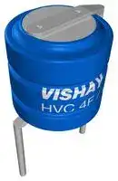


MAL219691215E3
Supercapacitor, Hybrid, 15 F, 7 V, Radial Leaded, -20%, +80%, 13 mm, 1000 hours @ 85°C
- Manufacturer: VISHAY
- Product type: EDLC - Electric Double Layer Capacitors
- ESR: 12.5ohm
- Capacitance: 15F
- Voltage(DC): 7V
- Lead Spacing: 13mm
- Product Height: 12.5mm
- Product Length: 12.5mm
- Product Diameter: 12mm
- Capacitor Mounting: Through Hole
- Capacitor Terminals: Radial Leaded
- Capacitance Tolerance: -20%, +80%
- Lifetime @ Temperature: 1000 hours @ 85°C
- Capacitor Case / Package: Radial Leaded
- Operating Temperature Max: 85°C
- Operating Temperature Min: -20°C
| Delivery and price | |
|---|---|
| Units per pack | 20 |
| Price | 3.77 € |
| Current stock | 10+ |
| Lead time | 30 days |
**196 HVC ENYCAP™** Vishay BCcomponents www.vishay.com ## **Hybrid Energy Storage Capacitors** ## **FEATURES** - Polarized energy storage capacitor with high capacity and energy density - Voltage flexibility: 1.4 V (single cell) to 2.8 V / 4.2 V / 5.6 V / 7.0 V / 8.4 V (multiple cells) - Available in stacked through-hole (STH, radial), surface-mount flat (SMF) and lay flat configurations (LFC) with wire and connectors - Useful life: up to 2000 h at 85 °C - No cell balancing necessary - Soft and low transient-voltage-controlled charging characteristic - Non-hazardous electrolyte - Maintenance-free, no service necessary - Evaluation kits for engineering are available under ordering code: MAL219699001E3 - Material categorization: for definitions of compliance please see www.vishay.com/doc?99912 ## **APPLICATIONS** - Power backup for memory controller, flash backup, RAID systems, SRAM, DRAM - Power failure and write cache protection for enterprise SSD and HDD - Real time clock power source - Burst power support for flash lights, wireless transmitters - Backup power for industrial PC’s and industrial controls - Storage device for energy harvesting - Emergency light and micro UPS power source ## **MARKING** Image is not to scale The capacitors are marked with the following information: - Rated capacitance (in F) - Rated voltage (in V) - Date code - Negative / positive terminal identification ## **PACKAGING** Supplied in ESD trays only Revision: 23-Jul-2018 Document Number: 28409 **1** For technical questions, contact: hybridstorage@vishay.com THIS DOCUMENT IS SUBJECT TO CHANGE WITHOUT NOTICE. THE PRODUCTS DESCRIBED HEREIN AND THIS DOCUMENT ARE SUBJECT TO SPECIFIC DISCLAIMERS, SET FORTH AT www.vishay.com/doc?91000 **196 HVC ENYCAP™** **==> picture [59 x 48] intentionally omitted <==** www.vishay.com ## Vishay BCcomponents |**QUICK REFERENCE DATA**||||||| |---|---|---|---|---|---|---| |**DESCRIPTION**|**VALUE**|||||| ||**SINGLE CELL**|**2 CELLS**|**3 CELLS**|**4 CELLS**|**5 CELLS**|**6 CELLS**| |Nominal case size (Ø D x L in mm)<br>Stacked Through-Hole (STH)|7 x 2.5<br>12 x 2.5<br>25 x 15 x 2.5<br>35 x 25 x 5|7 x 5<br>12 x 5<br>25 x 15 x 5<br>35 x 25 x 7.5|7 x 7.5<br>12 x 7.5<br>25 x 15 x 7.5<br>35 x 25 x 10|7 x 10<br>12 x 10<br>25 x 15 x 10<br>35 x 25 x 15|7 x 12.5<br>12 x 12.5<br>-<br>35 x 25 x 17.5|7 x 15<br>12 x 15<br>-<br>35 x 25 x 20| |Nominal case size (Ø W x L x H in mm)<br>Surface-Mount Flat (SMF)|7 x 7 x 2.5<br>12 x 12 x 2.5<br>-|7 x 14 x 2.5<br>12 x 24 x 2.5<br>-|13 x 14 x 2.5<br>22 x 24 x 2.5<br>-|14 x 14 x 2.5<br>24 x 24 x 2.5<br>-|-|-| |Nominal case size (W x L x H in mm)<br>Lay Flat (LFC)|14.5 x 12 x 2.5|14.5 x 24 x 2.5|14.5 x 36 x 2.5|14.5 x 48 x 2.5|14.5 x 60 x 2.5|14.5 x 72 x 2.5| |Rated capacitance range, CR|4.0 F<br>15.0 F<br>45.0 F<br>90.0 F|4.0 F<br>15.0 F<br>45.0 F<br>90.0 F|4.0 F<br>15.0 F<br>45.0 F<br>90.0 F|4.0 F<br>15.0 F<br>45.0 F<br>90.0 F|4.0 F<br>15.0 F<br>-<br>90.0 F|4.0 F<br>15.0 F<br>-<br>90.0 F| |Tolerance on CRat 20 °C|-20 % to +80 %|||||| |Rated voltage, UR|1.4 V|2.8 V|4.2 V|5.6 V|7.0 V|8.4 V| |Maximum surge voltage, US(max. 30 s)|1.6 V|3.2 V|4.8 V|6.4 V|8.0 V|9.6 V| |Minimum stored energy|4 Ws<br>17 Ws<br>50 Ws<br>115 Ws|9 Ws<br>35 Ws<br>100 Ws<br>230 Ws|13 Ws<br>52 Ws<br>150 Ws<br>345 Ws|18 Ws<br>70 Ws<br>200 Ws<br>460 Ws|22 Ws<br>87 Ws<br>-<br>575 Ws|27 Ws<br>105 Ws<br>-<br>690 Ws| |Energy density|9 Ws/gto 13 Ws/g|||||| |Category temperature range|4.0 F: -20 °C to +70 °C|||||| ||15.0 F / 45.0 F / 90.0 F: -20 °C to +85 °C|||||| |Storage temperature range|-40 °C to +85 °C|||||| |Useful life at UR|4.0 F:<br>at 70 °C: 1000 h<br>15.0 F:<br>at 85 °C: 1000 h<br>45.0 F,<br>90.0 F:<br>at 85 °C: 2000 h<br>at 55 °C: 2800 h<br>at 70 °C: 2800 h<br>at 70 °C: 5600 h<br>at 45 °C: 5600 h<br>at 60 °C: 5600 h<br>at 60 °C: 11 200 h|||||| |Shelf life|1000 h at upper category temperature|||||| |Climatic category IEC 60068|25 / 085 / 21|||||| |**SELECTION CHART FOR CR, UR, AND FORM AT UPPER CATEGORY TEMPERATURE(UCT)**|**SELECTION CHART FOR CR, UR, AND FORM AT UPPER CATEGORY TEMPERATURE(UCT)**|**SELECTION CHART FOR CR, UR, AND FORM AT UPPER CATEGORY TEMPERATURE(UCT)**|**SELECTION CHART FOR CR, UR, AND FORM AT UPPER CATEGORY TEMPERATURE(UCT)**|**SELECTION CHART FOR CR, UR, AND FORM AT UPPER CATEGORY TEMPERATURE(UCT)**|**SELECTION CHART FOR CR, UR, AND FORM AT UPPER CATEGORY TEMPERATURE(UCT)**|**SELECTION CHART FOR CR, UR, AND FORM AT UPPER CATEGORY TEMPERATURE(UCT)**|**SELECTION CHART FOR CR, UR, AND FORM AT UPPER CATEGORY TEMPERATURE(UCT)**| |---|---|---|---|---|---|---|---| |**CR**<br>**(F)**|**FORM**|**UR (V)**|||||| |||**1.4**|**2.8**|**4.2**|**5.6**|**7.0**|**8.4**| |4|A2|7.0 x 2.5|7.0 x 5.0|7.0 x 7.5|7.0 x 10.0|7.0 x 12.5|7.0 x 15.0| ||B2|7.0 x 2.5|7.0 x 5.0|7.0 x 7.5|7.0 x 10.0|7.0 x 12.5|7.0 x 15.0| ||B3||||||| ||C|7.0 x 7.0 x 2.5|-|-|-|-|-| ||D|7.0 x 7.0 x 2.5|-|-|-|-|-| ||E|-|7.0 x 14.0 x 2.5|13.0 x 14.0 x 2.5|14.0 x 14.0 x 2.5|-|-| |15|A2|12.0 x 2.5|12.0 x 5.0|12.0 x 7.5|12.0 x 10.0|12.0 x 12.5|12.0 x 15.0| ||B2|12.0 x 2.5|12.0 x 5.0|12.0 x 7.5|12.0 x 10.0|12.0 x 12.5|12.0 x 15.0| ||B3||||||| ||C|12.0 x 12.0 x 2.5|-|-|-|-|-| ||D|12.0 x 12.0 x 2.5|-|-|-|-|-| ||E|-|12.0 x 24.0 x 2.5|22.0 x 24.0 x 2.5|24.0 x 24.0 x 2.5|-|-| ||F|14.5 x 12.0 x 2.5|14.5 x 24.0 x 2.5|14.5 x 36.0 x 2.5|14.5 x 48.0 x 2.5|14.5 x 60.0 x 2.5|14.5 x 72.0 x 2.5| |45|I|25 x 15 x 2.5|25 x 15 x 5|25 x 15 x 7.5|25 x 15 x 10|-|-| ||K||||||| |90|G|35 x 25 x 5|35 x 25 x 7.5|35 x 25 x 10|35 x 25 x 15|35 x 25 x 17.5|35 x 25 x 20| ||H||||||| Revision: 23-Jul-2018 Document Number: 28409 **2** For technical questions, contact: hybridstorage@vishay.com THIS DOCUMENT IS SUBJECT TO CHANGE WITHOUT NOTICE. THE PRODUCTS DESCRIBED HEREIN AND THIS DOCUMENT ARE SUBJECT TO SPECIFIC DISCLAIMERS, SET FORTH AT www.vishay.com/doc?91000 **196 HVC ENYCAP™** Vishay BCcomponents www.vishay.com ## **DIMENSIONS** in millimeters **AND AVAILABLE FORMS** ## **STACKED THROUGH HOLE CONFIGURATION (STH): Examples VERTICAL MOUNT** **==> picture [276 x 260] intentionally omitted <==** **----- Start of picture text -----**<br> Ø Dmax.<br>- -<br>Lmax.<br> 6 (2 x)+ 0.5- 0.5 +<br>+ -<br>Ø 0.8 Ø 0.64<br>F<br> Fig. 1 - Form A2: Stacked Through Hole (example 4 cells, 2 pins) [(1)]<br>Ø Dmax. Lmax.<br>+ -<br>3.5 (2 x)+ 0.5- 0.5<br>© Bibi | | O<br>F<br>Ø 0.64<br>Fig. 2 - Form B2: Stacked Through Hole (example 5 cells, 2 pins) [(1)]<br>**----- End of picture text -----**<br> ## **STACKED THROUGH HOLE CONFIGURATION (STH): Examples HORIZONTAL MOUNT** **==> picture [241 x 110] intentionally omitted <==** **----- Start of picture text -----**<br> Ø Dmax. Lmax.<br>+ -<br>W T r | 3.5 (3 x)+ 0.5- 0.5<br>Ø 0.64 (3 x) F<br>F1<br>| LI<br>**----- End of picture text -----**<br> Fig. 3 - **Form B3:** Stacked Through Hole (example 4 cells, keyed polarity - 3 pins)[(1)] **Note** > (1) Bottom and top are not isolated ## **SURFACE MOUNT FLAT CONFIGURATION (SMF): Examples** **==> picture [348 x 95] intentionally omitted <==** **----- Start of picture text -----**<br> Lmax.<br>- 1<br>3.8 max. + 0.1 (2 x) Ø Dmax. 3 (2 x)<br>+ 0.5 0.5 (2 x) + 0.5<br>4 (2 x)- 0.5 ay 3.5 (2 x)- 0.5<br>Fig. 4 - Form C: Surface Mount Flat (single cell, keyed polarity)<br>**----- End of picture text -----**<br> Revision: 23-Jul-2018 Document Number: 28409 **3** For technical questions, contact: hybridstorage@vishay.com THIS DOCUMENT IS SUBJECT TO CHANGE WITHOUT NOTICE. THE PRODUCTS DESCRIBED HEREIN AND THIS DOCUMENT ARE SUBJECT TO SPECIFIC DISCLAIMERS, SET FORTH AT www.vishay.com/doc?91000 **196 HVC ENYCAP™** www.vishay.com Vishay BCcomponents **==> picture [398 x 184] intentionally omitted <==** **----- Start of picture text -----**<br> _ R1.5<br>(inner radius) 0 .75 (2 x)<br>0.5 Ø 7.5 max. 3 [+0.5] -0.5<br>+<br>1.35<br>8.9 (2 x)+0.5-0.5<br>Fig. 5 - Form D1: Surface Mount Flat (single cell, keyed polarity)<br>0.1 (2 x)<br>-<br>2.8 max. Ø 12.5 max. 3 [+ 0.5] - 0.5<br>+ 3.5 [+ 0.2] - 0.2<br>t es, Ø Dmax. Ger 1.0 (2 x)<br>Fig. 6 - Form D2: Surface Mount Flat (single cell, keyed polarity)<br>0.1 (2 x)<br>2.8 max.<br>(including tags thickness)<br>**----- End of picture text -----**<br> **==> picture [502 x 316] intentionally omitted <==** **----- Start of picture text -----**<br> 0.5 (2 x)<br>1 (2 x)<br>+ Ø Dmax. 3 (2 x) 3.8 max.<br>0.1 (2 x)<br>-<br>4 (2 x)+ 0.5- 0.5<br>Fig. 7 - Form E2: Surface Mount Flat<br>+ - 3 (2 x)<br>0.1 (2 x)<br>3.8 max. Hmax.<br>eT aap: Xe<br>0.5 (2 x)<br>1 (2 x)<br>4 ± 1 (2 x)<br>Lmax.<br>Fig. 8 - Form E3: Surface Mount Flat<br>3 (2 x)<br>1 (2 x)<br>+ 3.8 max. Hmax.<br>-<br>0.5 (2 x)<br>4 (2 x)+ 1- 1 0.1 (2 x)<br>Lmax.<br>**----- End of picture text -----**<br> **==> picture [132 x 8] intentionally omitted <==** **----- Start of picture text -----**<br> Fig. 9 - Form E4: Surface Mount Flat<br>**----- End of picture text -----**<br> Revision: 23-Jul-2018 Document Number: 28409 **4** For technical questions, contact: hybridstorage@vishay.com THIS DOCUMENT IS SUBJECT TO CHANGE WITHOUT NOTICE. THE PRODUCTS DESCRIBED HEREIN AND THIS DOCUMENT ARE SUBJECT TO SPECIFIC DISCLAIMERS, SET FORTH AT www.vishay.com/doc?91000 **196 HVC ENYCAP™** **==> picture [77 x 10] intentionally omitted <==** **----- Start of picture text -----**<br> www.vishay.com<br>**----- End of picture text -----**<br> Vishay BCcomponents ## **LAY FLAT CONFIGURATION (LFC) WITH CONNECTOR: Example 5 cells in series** **==> picture [472 x 594] intentionally omitted <==** **----- Start of picture text -----**<br> Red (AWG 28, UL 1061) + Pin 1: red<br>Ø Dmax.<br>Black (AWG 28, UL 1061) - Pin 2: black<br>Molex connector;<br>Housing: 51146-0200<br>Terminal: 50641-8041<br>3.5 max.<br>Lmax. 50 [+ 5] - 5<br>Fig. 10 - Form F: Lay Flat (example for 5 cells)<br>27 max.<br>-<br>Lmax. 15.5 max. - +<br>— =— —<br>= + 1 (2 x)+ 0.5- 0.5 @ 4 (3 x) . 0.25 (2 x)<br>= F<br>Ll F1 )<br>Fig. 11 - Form I: Stacked Through Hole Oval (PCBD)<br>27 max.<br>0.5<br>Lmax.<br>+ -<br>ep<br>0.2 (2 x)<br>5 + 0.5- 0.5 1 (3 x) F<br>F1<br>Fig. 12 - Form K: Stacked Through Hole Oval Horizontal<br>35 max.<br>-<br>Lmax. 25 max. - +<br>+ 1 (2 x)+ 0.5- 0.5<br>| XD 4 (3 x)<br>0.25 (2 x)<br>F1 F<br>a rd<br>—_ Fig. 13 - Form G: Stacked Through Hole Oval (PCBD) =<br>+ 0.5- 0.5<br>4 (2 x)<br>**----- End of picture text -----**<br> Revision: 23-Jul-2018 Document Number: 28409 **5** For technical questions, contact: hybridstorage@vishay.com THIS DOCUMENT IS SUBJECT TO CHANGE WITHOUT NOTICE. THE PRODUCTS DESCRIBED HEREIN AND THIS DOCUMENT ARE SUBJECT TO SPECIFIC DISCLAIMERS, SET FORTH AT www.vishay.com/doc?91000 **196 HVC ENYCAP™** **==> picture [77 x 10] intentionally omitted <==** **----- Start of picture text -----**<br> www.vishay.com<br>**----- End of picture text -----**<br> ## Vishay BCcomponents **==> picture [454 x 145] intentionally omitted <==** **----- Start of picture text -----**<br> 35 max.<br>0.5<br>Lmax.<br>+ -<br>5 + 0.5- 0.5 1 (3 x) 0.2 (2 x)<br>F1 F<br>Fig. 14 - Form H: Stacked Through Hole Oval Horizontal<br>+ 0.5 - 0.5<br>4 (2 x)<br>**----- End of picture text -----**<br> **Table 1** |**DIMENSIONS**in millimeters,**MASS AND PACKAGING QUANTITIES**<br>~~Cn~~<br>~~ee~~<br>~~eses~~<br>~~een Gs~~|**DIMENSIONS**in millimeters,**MASS AND PACKAGING QUANTITIES**<br>~~Cn~~<br>~~ee~~<br>~~eses~~<br>~~een Gs~~|**DIMENSIONS**in millimeters,**MASS AND PACKAGING QUANTITIES**<br>~~Cn~~<br>~~ee~~<br>~~eses~~<br>~~een Gs~~|**DIMENSIONS**in millimeters,**MASS AND PACKAGING QUANTITIES**<br>~~Cn~~<br>~~ee~~<br>~~eses~~<br>~~een Gs~~|**DIMENSIONS**in millimeters,**MASS AND PACKAGING QUANTITIES**<br>~~Cn~~<br>~~ee~~<br>~~eses~~<br>~~een Gs~~|**DIMENSIONS**in millimeters,**MASS AND PACKAGING QUANTITIES**<br>~~Cn~~<br>~~ee~~<br>~~eses~~<br>~~een Gs~~|**DIMENSIONS**in millimeters,**MASS AND PACKAGING QUANTITIES**<br>~~Cn~~<br>~~ee~~<br>~~eses~~<br>~~een Gs~~| |---|---|---|---|---|---|---| |**NOMINAL CASE SIZE**<br>**D x L x H(mm)**<br>~~Cn~~<br>~~ee~~<br>~~ns~~|**FORM**<br>~~es~~<br>~~GO~~|**Ø Dmax.**<br>~~es~~<br>~~GO~~|**Lmax.**<br>~~een Gs~~<br>~~GO~~|**L1max.**<br>~~Gs~~<br>~~GO~~|**Hmax.**<br>~~GO~~|**MASS**<br>**(g)**| |7.0 x 7.0 x 2.5<br>~~ee~~<br>~~ns~~<br>~~SS~~|A2,B2,B3<br>~~es ~~<br>~~GO~~<br>|7.5<br> ~~es~~<br>~~GO~~<br>|2.3 + 0.3<br>~~een Gs~~<br>~~GO~~<br>|7.0 + 0.5<br>~~Gs~~<br>~~GO~~<br>|-<br>~~GO~~<br>|0.5<br>| |7.0 x 7.0 x 2.5<br>~~ns~~<br>~~SS~~|C<br>~~GO~~<br>|7.5<br>~~GO~~<br>|7.0<br>~~GO~~<br>|7.0 + 8.0<br>~~GO~~<br>|-<br>~~GO~~<br>|0.5<br>| |7.0 x 7.0 x 2.5<br>~~SS~~<br>~~SS~~|D1<br><br>|7.5<br><br>|7.0<br><br>~~i~~<br>|7.0 + 4.0<br><br>|-<br><br>|0.5<br><br>| |7.0 x 7.0 x 5.0<br>~~SSi~~<br>~~SS~~|A2,B2,B3<br>~~i~~<br>|7.5<br>~~i~~<br>|4.2<br>~~i~~<br>~~i~~<br>|4.2 + 0.5<br>~~i~~<br>|-<br>~~i~~<br>|0.8<br>~~i~~<br>| |7.0 x 7.0 x 7.5<br>~~i~~<br>~~SS~~|A2,B2,B3<br>~~i~~<br>|7.5<br>~~i~~<br>|7.5<br>~~i~~<br>~~i~~<br>|7.8 + 0.5<br>~~i~~<br>|-<br>~~i~~<br>|1.5<br>~~i~~<br>| |7.0 x 7.0 x 10.0<br>~~SS~~|A2,B2,B3<br>|7.5<br>|10.5<br>~~i~~<br>|10.2 + 0.5<br>|-<br>|1.8<br>| |7.0 x 7.0 x 12.5<br>~~SS~~<br>~~SS~~|A2,B2,B3<br><br>|7.5<br><br>|12.5<br>~~i~~<br><br>~~i~~<br>|12.4 + 0.5<br><br>|-<br><br>|2.5<br><br>| |7.0 x 7.0 x 15.0<br>~~SSi~~<br>~~SS~~|A2,B2,B3<br>~~i~~<br>|7.5<br>~~i~~<br>|14.8<br>~~i~~<br>~~i~~<br>~~i~~<br>|14.8 + 0.5<br>~~i~~<br>|-<br>~~i~~<br>|3.0<br>~~i~~<br>| |12.0 x 12.0 x 2.5<br>~~i~~<br>~~SS~~|A2,B2,B3<br>~~i~~<br>|12.5<br>~~i~~<br>|2.3<br>~~i~~<br>~~i~~<br>|2.3 + 0.5<br>~~i~~<br>|-<br>~~i~~<br>|1.2<br>~~i~~<br>| |12.0 x 12.0 x 2.5<br>~~SS~~|C<br>|12.5<br>|12.5<br>~~i~~<br>|12.5 + 8.0<br>|-<br>|1.0<br>| |12.0 x 12.0 x 2.5<br>~~SS~~<br>~~SS~~|D2<br><br>|12.5<br><br>|12.5<br>~~i~~<br><br>~~i~~<br>|12.5 + 4.0<br><br>|-<br><br>|1.0<br><br>| |12.0 x 12.0 x 5.0<br>~~SSi~~<br>~~SS~~|A2,B2,B3<br>~~i~~<br>|12.5<br>~~i~~<br>|4.2<br>~~i~~<br>~~i~~<br>~~i~~<br>|4.2 + 0.5<br>~~i~~<br>|-<br>~~i~~<br>|2.2<br>~~i~~<br>| |12.0 x 12.0 x 7.5<br>~~i~~<br>~~SS~~|A2,B2,B3<br>~~i~~<br>|12.5<br>~~i~~<br>|8.0<br>~~i~~<br>~~i~~<br>|7.8 + 0.5<br>~~i~~<br>|-<br>~~i~~<br>|3.3<br>~~i~~<br>| |12.0 x 12.0 x 10.0<br>~~SS~~|A2,B2,B3<br>|12.5<br>|10.5<br>~~i~~<br>|10.5 + 0.5<br>|-<br>|4.0<br>| |12.0 x 12.0 x 12.5<br>~~SS~~<br>~~SS~~|A2,B2,B3<br><br>|12.5<br><br>|12.5<br>~~i~~<br><br>~~i~~<br>|12.5 + 0.5<br><br>|-<br><br>|5.4<br><br>| |12.0 x 12.0 x 15.0<br>~~SSi~~<br>~~SS~~|A2,B2,B3<br>~~i~~<br>|12.5<br>~~i~~<br>|14.8<br>~~i~~<br>~~i~~<br>~~i~~<br>|14.8 + 0.5<br>~~i~~<br>|-<br>~~i~~<br>|6.5<br>~~i~~<br>| |7.0 x 14.0 x 2.5<br>~~i~~<br>~~SS~~|E2<br>~~i~~<br>|7.5<br>~~i~~<br>|14.8<br>~~i~~<br>~~i~~<br>|14.8 + 8.0<br>~~i~~<br>|-<br>~~i~~<br>|1.0<br>~~i~~<br>| |12.0 x 24.0 x 2.5<br>~~SS~~|E2<br>|12.5<br>|24.0<br>~~i~~<br>|24.0 + 8.0<br>|-<br>|2.0<br>| |13.0 x 14.0 x 2.5<br>~~SS~~|E3<br>|14.0<br>|15.0<br>~~i~~<br>|14.8 + 8.0<br>|14.0<br>|1.2<br>| |22.0 x 24.0 x 2.5<br>~~SSth~~|E3<br>~~th~~|24.0<br>~~th~~|24.0<br>~~i~~<br>~~th~~|24.8 + 8.0<br>~~th~~|15.0<br>~~th~~|3.3<br>~~th~~| |14.0 x 14.0 x 2.5<br>~~th~~<br>~~SS~~|E4<br>~~th~~<br>|15.0<br>~~th~~<br>|15.0<br>~~th~~<br>|14.8 + 8.0<br>~~th~~<br>|22.5<br>~~th~~<br>|1.5<br>~~th~~<br>| |24.0 x 24.0 x 2.5<br>~~SS~~|E4<br>|24.0<br>|24.0<br>|24.8 + 8.0<br>|24.0<br>|4.4<br>| |14.5 x 12.0 x 2.5<br>~~SS~~<br>~~SS~~|F<br>|14.5<br>|12.0<br><br>~~i~~|12.0 + 50.0<br>|-<br>|1.0<br>| |14.5 x 24.0 x 2.5<br>~~SSi~~<br>~~SS~~|F<br>~~i~~|14.5<br>~~i~~|24.0<br>~~i~~<br>~~i~~|24.0 + 50.0<br>~~i~~|-<br>~~i~~|3.0<br>~~i~~| |14.5 x 36.0 x 2.5<br>~~i~~<br>~~SS~~|F<br>~~i~~|14.5<br>~~i~~|36.0<br>~~i~~<br>~~i~~|36.0 + 50.0<br>~~i~~|-<br>~~i~~|4.0<br>~~i~~| |14.5 x 48.0 x 2.5<br>~~SS~~|F|14.5|48.0<br>~~i~~|48.0 + 50.0|-|6.0| |14.5 x 60.0 x 2.5<br>~~SS~~|F|14.5|60.0<br>~~i~~|60.0 + 50.0|-|7.5| |14.5 x 72.0 x 2.5<br>~~SS~~<br>~~ns~~|F<br>~~GO~~|14.5<br>~~GO~~|72.0<br>~~i~~<br>~~GO~~|72.0 + 50.0<br>~~GO~~|-<br>~~GO~~|9.0| |25 x 15 x 2.5<br>~~ns~~<br>~~SS~~|I,K<br>~~GO~~|27 x 15.5<br>~~GO~~|3.0<br>~~GO~~|2.5 ± 0.5<br>~~GO~~|-<br>~~GO~~|1.5| |25 x 15 x 5.0<br>~~ns~~<br>~~SS~~|I,K<br>~~GO~~|27 x 15.5<br>~~GO~~|5.0<br>~~GO~~|5.0 ± 0.5<br>~~GO~~|-<br>~~GO~~|3.0| |25 x 15 x 7.5<br>~~SS~~|I,K|27 x 15.5|7.0|7.0 ± 0.5|-|4.5| |25 x 15 x 10.0<br>~~SS~~<br>~~ns~~|I,K<br>~~GO~~|27 x 15.5<br>~~GO~~|9.0<br>~~GO~~|9.0 ± 0.5<br>~~GO~~|-<br>~~GO~~|6.0| |35 x 25 x 5.0<br>~~ns~~|G,H<br>~~GO~~|35 x 25<br>~~GO~~|3.7<br>~~GO~~|3.6 ± 0.1<br>~~GO~~|-<br>~~GO~~|7.5| |35 x 25 x 7.5<br>~~ns~~|G,H<br>~~GO~~|35 x 25<br>~~GO~~|7.5<br>~~GO~~|7.5 + 0.5<br>~~GO~~|-<br>~~GO~~|15.0| |35 x 25 x 10.0<br>~~Pe~~|G,H<br>~~Pe~~|35 x 25<br>~~Pe~~|10.5<br>~~Pe~~|10.5 + 0.5<br>~~Pe~~|-<br>~~Pe~~|22.5<br>~~Pe~~| |35 x 25 x 15.0<br>~~Pe~~<br>~~ns~~|G,H<br>~~Pe~~<br>~~GO~~|35 x 25<br>~~Pe~~<br>~~GO~~|15.0<br>~~Pe~~<br>~~GO~~|14.5 + 0.5<br>~~Pe~~<br>~~GO~~|-<br>~~Pe~~<br>~~GO~~|30.0<br>~~Pe~~| |35 x 25 x 17.5<br>~~ns~~|G,H<br>~~GO~~|35 x 25<br>~~GO~~|17.8<br>~~GO~~|16.8 ± 1.0<br>~~GO~~|-<br>~~GO~~|45.0| |35 x 25 x 20.0<br>~~ns~~|G,H<br>~~GO~~|35 x 25<br>~~GO~~|21.1<br>~~GO~~|20.1 ± 1.0<br>~~GO~~|-<br>~~GO~~|50.0| Revision: 23-Jul-2018 Document Number: 28409 **6** For technical questions, contact: hybridstorage@vishay.com THIS DOCUMENT IS SUBJECT TO CHANGE WITHOUT NOTICE. THE PRODUCTS DESCRIBED HEREIN AND THIS DOCUMENT ARE SUBJECT TO SPECIFIC DISCLAIMERS, SET FORTH AT www.vishay.com/doc?91000 **196 HVC ENYCAP™** Vishay BCcomponents **==> picture [59 x 48] intentionally omitted <==** www.vishay.com |**ELECTRICAL DATA**|**ELECTRICAL DATA**| |---|---| |**SYMBOL**|**DESCRIPTION**| |CR|Rated capacitance, tolerance -20 % / +80 %,<br>measured byconstant current discharge method| |UCT|Upper categorytemperature| |IL|Max. leakage current after 24 h at UR| |RI|Max. internal resistance at 1 kHz| ## **ORDERING EXAMPLE** Hybrid Storage Capacitor 15 F / 1.4 V Nominal case size: Ø 12.0 mm x 2.5 mm; Form B3 Ordering code: MAL219691211E3 ## **Note** - Unless otherwise specified, all electrical values in Table 2 apply at Tamb = 20 °C, P = 86 kPa to 106 kPa and RH = 45 % to 75 % ## **Table 2** |**ELECTRICAL DATA AND ORDERING INFORMATION**|**ELECTRICAL DATA AND ORDERING INFORMATION**|**ELECTRICAL DATA AND ORDERING INFORMATION**|**ELECTRICAL DATA AND ORDERING INFORMATION**|**ELECTRICAL DATA AND ORDERING INFORMATION**|**ELECTRICAL DATA AND ORDERING INFORMATION**|**ELECTRICAL DATA AND ORDERING INFORMATION**|**ELECTRICAL DATA AND ORDERING INFORMATION**|**ELECTRICAL DATA AND ORDERING INFORMATION**|**ELECTRICAL DATA AND ORDERING INFORMATION**|**ELECTRICAL DATA AND ORDERING INFORMATION**|**ELECTRICAL DATA AND ORDERING INFORMATION**|**ELECTRICAL DATA AND ORDERING INFORMATION**|**ELECTRICAL DATA AND ORDERING INFORMATION**| |---|---|---|---|---|---|---|---|---|---|---|---|---|---| |**UR**<br>**(V)**|**CR**<br>**(F)**|**NOMINAL**<br>**CASE SIZE**<br>**Ø D x L**<br>**D x L x H**<br>**(mm)**|**CASE**<br>**CODE**|**FOR**<br>**M**|**F**<br>**(mm)**|**F1**<br>**(mm)**|**UCT**<br>**(°C)**|**IL**<br>**24 h**<br>**(mA)**|**ESR**<br>**AC(1)**<br>**1 kHz**<br>**(****)**|**ESR**<br>**DC(2)**<br>**(****)**|**MIN.**<br>**STORAGE**<br>**ENERGY**<br>**(Ws)**|**PACKAGING**<br>**QUANTITIES**|**ORDERING CODE**| |**STACKED THROUGH HOLE CONFIGURATION(STH) - VERTICAL MOUNT**|||||||||||||| |1.4|4|7.0 x 2.5|2pin|A2|7.5|-|70|0.03|2.5|7.5|4.6|80|MAL219691101E3| |2.8|4|7.0 x 5.0|2pin|A2|7.5|-|70|0.03|5.0|15.0|9.2|80|MAL219691102E3| |4.2|4|7.0 x 7.5|2pin|A2|7.5|-|70|0.03|7.5|22.5|13.8|80|MAL219691103E3| |5.6|4|7.0 x 10.0|2pin|A2|7.5|-|70|0.03|10.0|30.0|18.4|80|MAL219691104E3| |7.0|4|7.0 x 12.5|2pin|A2|7.5|-|70|0.03|12.5|37.5|23.0|84|MAL219691105E3| |8.4|4|7.0 x 15.0|2pin|A2|7.5|-|70|0.03|15.0|45.0|27.6|84|MAL219691106E3| |1.4|15|12.0 x 2.5|2pin|A2|12.5|-|85|0.12|0.6|2.5|17.5|80|MAL219691201E3| |2.8|15|12.0 x 5.0|2pin|A2|12.5|-|85|0.12|1.2|5.0|35.0|80|MAL219691202E3| |4.2|15|12.0 x 7.5|2pin|A2|12.5|-|85|0.12|1.8|7.5|52.5|80|MAL219691203E3| |5.6|15|12.0 x 10.0|2pin|A2|12.5|-|85|0.12|2.4|10.0|70.0|80|MAL219691204E3| |7.0|15|12.0 x 12.5|2pin|A2|12.5|-|85|0.12|3.0|12.5|87.5|90|MAL219691205E3| |8.4|15|12.0 x 15.0|2pin|A2|12.5|-|85|0.12|3.6|15.0|105.0|90|MAL219691206E3| |**STACKED THROUGH HOLE CONFIGURATION(STH) - HORIZONTAL MOUNT**|||||||||||||| |1.4|4|7.0 x 2.5|2pin|B2|3.2|-|70|0.03|2.5|7.5|4.6|100|MAL219691121E3| |2.8|4|7.0 x 5.0|2pin|B2|5.4|-|70|0.03|5.0|15.0|9.2|100|MAL219691122E3| |4.2|4|7.0 x 7.5|2pin|B2|7.5|-|70|0.03|7.5|22.5|13.8|96|MAL219691123E3| |5.6|4|7.0 x 10.0|2pin|B2|8.8|-|70|0.03|10.0|30.0|18.4|96|MAL219691124E3| |7.0|4|7.0 x 12.5|2pin|B2|12|-|70|0.03|12.5|37.5|23.0|60|MAL219691125E3| |8.4|4|7.0 x 15.0|2pin|B2|14.5|-|70|0.03|15.0|45.0|27.6|60|MAL219691126E3| |1.4|15|12.0 x 2.5|2pin|B2|3.2|-|85|0.12|0.6|2.5|17.5|100|MAL219691221E3| |2.8|15|12.0 x 5.0|2pin|B2|5.8|-|85|0.12|1.2|5.0|35.0|100|MAL219691222E3| |4.2|15|12.0 x 7.5|2pin|B2|8.3|-|85|0.12|1.8|7.5|52.5|80|MAL219691223E3| |5.6|15|12.0 x 10.0|2pin|B2|11.0|-|85|0.12|2.4|10.0|70.0|90|MAL219691224E3| |7.0|15|12.0 x 12.5|2pin|B2|13.4|-|85|0.12|3.0|12.5|87.5|40|MAL219691225E3| |8.4|15|12.0 x 15.0|2pin|B2|15.7|-|85|0.12|3.6|15.0|105.0|40|MAL219691226E3| |1.4|4|7.0 x 2.5|3pin|B3|2.8|2.5|70|0.03|2.5|7.5|4.6|100|MAL219691111E3| |2.8|4|7.0 x 5.0|3pin|B3|5.1|2.5|70|0.03|5.0|15.0|9.2|100|MAL219691112E3| |4.2|4|7.0 x 7.5|3pin|B3|7.5|2.5|70|0.03|7.5|22.5|13.8|96|MAL219691113E3| |5.6|4|7.0 x 10.0|3pin|B3|10.0|2.5|70|0.03|10.0|30.0|18.4|96|MAL219691114E3| |7.0|4|7.0 x 12.5|3pin|B3|12.0|2.5|70|0.03|12.5|37.5|23.0|60|MAL219691115E3| |8.4|4|7.0 x 15.0|3pin|B3|14.5|2.5|70|0.03|15.0|45.0|27.6|60|MAL219691116E3| |1.4|15|12.0 x 2.5|3pin|B3|3.2|5.0|85|0.12|0.6|2.5|17.5|100|MAL219691211E3| |2.8|15|12.0 x 5.0|3pin|B3|5.8|5.0|85|0.12|1.2|5.0|35.0|100|MAL219691212E3| |4.2|15|12.0 x 7.5|3pin|B3|8.0|5.0|85|0.12|1.8|7.5|52.5|80|MAL219691213E3| |5.6|15|12.0 x 10.0|3pin|B3|11.0|5.0|85|0.12|2.4|10.0|70.0|90|MAL219691214E3| |7.0|15|12.0 x 12.5|3pin|B3|13.0|5.0|85|0.12|3.0|12.5|87.5|40|MAL219691215E3| |8.4|15|12.0 x 15.0|3pin|B3|16.0|5.0|85|0.12|3.6|15.0|105.0|40|MAL219691216E3| Revision: 23-Jul-2018 **7** Document Number: 28409 For technical questions, contact: hybridstorage@vishay.com THIS DOCUMENT IS SUBJECT TO CHANGE WITHOUT NOTICE. THE PRODUCTS DESCRIBED HEREIN AND THIS DOCUMENT ARE SUBJECT TO SPECIFIC DISCLAIMERS, SET FORTH AT www.vishay.com/doc?91000 **196 HVC ENYCAP™** **==> picture [59 x 48] intentionally omitted <==** www.vishay.com ## Vishay BCcomponents |**ELECTRICAL DATA AND ORDERING INFORMATION**|**ELECTRICAL DATA AND ORDERING INFORMATION**|**ELECTRICAL DATA AND ORDERING INFORMATION**|**ELECTRICAL DATA AND ORDERING INFORMATION**|**ELECTRICAL DATA AND ORDERING INFORMATION**|**ELECTRICAL DATA AND ORDERING INFORMATION**|**ELECTRICAL DATA AND ORDERING INFORMATION**|**ELECTRICAL DATA AND ORDERING INFORMATION**|**ELECTRICAL DATA AND ORDERING INFORMATION**|**ELECTRICAL DATA AND ORDERING INFORMATION**|**ELECTRICAL DATA AND ORDERING INFORMATION**|**ELECTRICAL DATA AND ORDERING INFORMATION**|**ELECTRICAL DATA AND ORDERING INFORMATION**|**ELECTRICAL DATA AND ORDERING INFORMATION**| |---|---|---|---|---|---|---|---|---|---|---|---|---|---| |**UR**<br>**(V)**|**CR**<br>**(F)**|**NOMINAL**<br>**CASE SIZE**<br>**Ø D x L**<br>**D x L x H**<br>**(mm)**|**CASE**<br>**CODE**|**FOR**<br>**M**|**F**<br>**(mm)**|**F1**<br>**(mm)**|**UCT**<br>**(°C)**|**IL**<br>**24 h**<br>**(mA)**|**ESR**<br>**AC(1)**<br>**1 kHz**<br>**(****)**|**ESR**<br>**DC(2)**<br>**(****)**|**MIN.**<br>**STORAGE**<br>**ENERGY**<br>**(Ws)**|**PACKAGING**<br>**QUANTITIES**|**ORDERING CODE**| |**SURFACE MOUNT FLAT CONFIGURATION(SMF)**|||||||||||||| |1.4|4|7.0 x 7.0 x 2.5|2pin|C|-|-|70|0.03|2.5|7.5|4.6|50|MAL219691131E3| |1.4|15|12.0 x 12.0 x 2.5|2pin|C|-|-|85|0.12|0.6|2.5|17.5|100|MAL219691231E3| |1.4|4|7.0 x 7.0 x 2.5|2pin|D1|-|-|70|0.03|2.5|7.5|4.6|50|MAL219691141E3| |1.4|15|12.0 x 12.0 x 2.5|2pin|D2|-|-|85|0.12|0.6|2.5|17.5|100|MAL219691241E3| |2.8|4|7.0 x 14.0 x 2.5|2pin|E2|-|-|70|0.03|5.0|15.0|9.2|50|MAL219691152E3| |2.8|15|12.0 x 24.0 x 2.5|2pin|E2|-|-|85|0.12|1.2|5.0|35.0|50|MAL219691252E3| |4.2|4|13.0 x 14.0 x 2.5|3pin|E3|-|-|70|0.03|7.5|22.5|13.8|70|MAL219691153E3| |4.2|15|22.0 x 24.0 x 2.5|3pin|E3|-|-|85|0.12|1.8|7.5|52.5|35|MAL219691253E3| |5.6|4|14.0 x 14.0 x 2.5|4pin|E4|-|-|70|0.03|10.0|30.0|18.4|70|MAL219691154E3| |5.6|15|24.0 x 24.0 x 2.5|4pin|E4|-|-|85|0.12|2.4|10.0|70.0|35|MAL219691254E3| |**LAY FLAT CONFIGURATION(LFC)**|||||||||||||| |1.4|15|14.5 x 12.0 x 2.5|2pin|F|-|-|85|0.12|0.6|2.5|17.5|40|MAL219691261E3| |2.8|15|14.5 x 24.0 x 2.5|2pin|F|-|-|85|0.12|1.2|5.0|35.0|40|MAL219691262E3| |4.2|15|14.5 x 36.0 x 2.5|2pin|F|-|-|85|0.12|1.8|7.5|52.5|40|MAL219691263E3| |5.6|15|14.5 x 48.0 x 2.5|2pin|F|-|-|85|0.12|2.4|10.0|70.0|20|MAL219691264E3| |7.0|15|14.5 x 60.0 x 2.5|2pin|F|-|-|85|0.12|3.0|12.5|87.5|20|MAL219691265E3| |8.4|15|14.5 x 72.0 x 2.5|2pin|F|-|-|85|0.12|3.6|15.0|105.0|20|MAL219691266E3| |**STACKED THROUGH HOLE OVAL**|||||||||||||| |1.4|45|25 x 15 x 2.5|3pin|I|3.5|10|85|0.15|0.25|0.5|50.0|30|MAL219690206E3| |2.8|45|25 x 15 x 5.0|3pin|I|5|10|85|0.15|0.5|1.0|100.0|30|MAL219690203E3| |4.2|45|25 x 15 x 7.5|3pin|I|7.5|10|85|0.15|0.75|1.5|150.0|30|MAL219690201E3| |5.6|45|25 x 15 x 10.0|3pin|I|10|10|85|0.15|1.0|2.0|200.0|30|MAL219690202E3| |1.4|90|35 x 25 x 5.0|3pin|G|5|10|85|0.5|0.015|0.045|115.0|25|MAL219690106E3| |2.8|90|35 x 25 x 7.5|3pin|G|7.5|10|85|0.5|0.03|0.090|230.0|25|MAL219690103E3| |4.2|90|35 x 25 x 10.0|3pin|G|10|10|85|0.5|0.04|0.135|345.0|25|MAL219690101E3| |5.6|90|35 x 25 x 15.0|3pin|G|12.5|10|85|0.5|0.06|0.180|460.0|25|MAL219690102E3| |7.0|90|35 x 25 x 17.5|3pin|G|17.5|10|85|0.5|0.075|0.225|575.0|25|MAL219690107E3| |8.4|90|35 x 25 x 20.0|3pin|G|20.0|10|85|0.5|0.09|0.270|690.0|25|MAL219690108E3| |**STACKED THROUGH HOLE OVAL HORIZONTAL**|||||||||||||| |1.4|45|25 x 15 x 2.5|3pin|K|15|10|85|0.15|0.25|0.5|50.0|30|MAL219690216E3| |2.8|45|25 x 15 x 5.0|3pin|K|15|10|85|0.15|0.5|1.0|100.0|30|MAL219690213E3| |4.2|45|25 x 15 x 7.5|3pin|K|15|10|85|0.15|0.75|1.5|150.0|30|MAL219690211E3| |5.6|45|25 x 15 x 10.0|3pin|K|15|10|85|0.15|1.0|2.0|200.0|30|MAL219690212E3| |1.4|90|35 x 25 x 5.0|3pin|H|25|10|85|0.5|0.015|0.045|115.0|25|MAL219690116E3| |2.8|90|35 x 25 x 7.5|3pin|H|25|10|85|0.5|0.03|0.090|230.0|25|MAL219690113E3| |4.2|90|35 x 25 x 10.0|3pin|H|25|10|85|0.5|0.04|0.135|345.0|25|MAL219690111E3| |5.6|90|35 x 25 x 15.0|3pin|H|25|10|85|0.5|0.06|0.180|460.0|25|MAL219690112E3| |7.0|90|35 x 25 x 17.5|3pin|H|25|10|85|0.5|0.075|0.225|575.0|25|MAL219690117E3| |8.4|90|35 x 25 x 20.0|3pin|H|25|10|85|0.5|0.09|0.270|690.0|25|MAL219690118E3| ## **Notes** > (1) ESR AC 1 kHz are typical values > (2) ESR DC are typical values ## **Table 3** |**LOAD CURRENTS AND VOLTAGES**|**LOAD CURRENTS AND VOLTAGES**|**LOAD CURRENTS AND VOLTAGES**|**LOAD CURRENTS AND VOLTAGES**|**LOAD CURRENTS AND VOLTAGES**| |---|---|---|---|---| |**CR**<br>**(F)**|**RECOMMENDED**<br>**CHARGE CURRENT**|**MAX. CHARGE**<br>**CURRENT**|**MAX. DISCHARGE**<br>**CURRENT**|**LOWEST DISCHARGE**<br>**VOLTAGE(1)**| |4|2 mA to 8 mA|14 mA|25 mA|n x 0.8 V| |15|5 mA to 20 mA|50 mA|70 mA|n x 0.8 V| |45|30 mA to 300 mA|0.5 A|0.5 A|n x 0.8 V| |90|0.3 A to 1 A|1.5 A|3 A|n x 0.8 V| ## **Note** > (1) n... number of cells, permanent operation below lowest discharge voltage is not permitted Revision: 23-Jul-2018 Document Number: 28409 **8** For technical questions, contact: hybridstorage@vishay.com THIS DOCUMENT IS SUBJECT TO CHANGE WITHOUT NOTICE. THE PRODUCTS DESCRIBED HEREIN AND THIS DOCUMENT ARE SUBJECT TO SPECIFIC DISCLAIMERS, SET FORTH AT www.vishay.com/doc?91000 **196 HVC ENYCAP™** www.vishay.com **==> picture [59 x 48] intentionally omitted <==** ## Vishay BCcomponents ## **MEASURING OF CHARACTERISTICS** ## **CAPACITANCE (C)** Capacitance shall be measured by constant current discharge method. |**DISCHARGE CURRENT AS A FUNCTION OF**<br>**RATED CAPACITANCE**|**DISCHARGE CURRENT AS A FUNCTION OF**<br>**RATED CAPACITANCE**|**DISCHARGE CURRENT AS A FUNCTION OF**<br>**RATED CAPACITANCE**|**DISCHARGE CURRENT AS A FUNCTION OF**<br>**RATED CAPACITANCE**|**DISCHARGE CURRENT AS A FUNCTION OF**<br>**RATED CAPACITANCE**|**DISCHARGE CURRENT AS A FUNCTION OF**<br>**RATED CAPACITANCE**| |---|---|---|---|---|---| |**PARAMETER**|**VALUE**||||**UNIT**| |Rated capacitance,CR|4|15|45|90|F| |Discharge current,ID|4|15|45|90|mA| **==> picture [182 x 102] intentionally omitted <==** **----- Start of picture text -----**<br> U R Δ U 3<br>U 1<br>U 2<br>30 min t 1 t 2 (s)<br>**----- End of picture text -----**<br> Fig. 15 - Voltage Diagram for Capacitance Measurement Capacitance value CR is given by discharge current ID, time t and rated voltage UR, according to the following equation: - CR Rated capacitance, in F - UR Rated voltage, in V - U1 Starting voltage, in V - U2 Ending voltage, in V - U3 Voltage drop at internal resistance, in V - t1 reached, in sTime from start of discharge until voltage U1 is t2 reached, in sTime from start of discharge until voltage U2 is - ID Discharge current, in A CR F = I----------------------------------------------------------D AU x t1 V 2 - U s 2 - t V1 s For ID, U1, and U2 the following definitions have to be used: ## **Table 4** |**CAPACITANCE**|**CAPACITANCE**|**CAPACITANCE**|**CAPACITANCE**|**CAPACITANCE**|**CAPACITANCE**|**CAPACITANCE**| |---|---|---|---|---|---|---| |**C(F)**|**ID (A)**|**UR (V)**|**U1 (V)**|**U2 (V)**|**t1 (s)**|**t2 (s)**| |4|0.004|1.4|1.3|0.7|5|> 600| |4|0.004|2.8|2.7|1.9|5|> 600| |4|0.004|4.2|4.0|3.1|5|> 600| |4|0.004|5.6|5.4|4.4|5|> 600| |4|0.004|7.0|6.7|5.6|5|> 600| |4|0.004|8.4|8.1|6.9|5|> 600| |15|0.015|1.4|1.3|0.7|5|> 600| |15|0.015|2.8|2.7|1.9|5|> 600| |15|0.015|4.2|4.0|3.1|5|> 600| |15|0.015|5.6|5.4|4.4|5|> 600| |15|0.015|7.0|6.7|5.6|5|> 600| |15|0.015|8.4|8.1|6.9|5|> 600| |**CAPACITANCE**|**CAPACITANCE**|**CAPACITANCE**|**CAPACITANCE**|**CAPACITANCE**|**CAPACITANCE**|**CAPACITANCE**| |---|---|---|---|---|---|---| |**C(F)**|**ID (A)**|**UR (V)**|**U1 (V)**|**U2 (V)**|**t1 (s)**|**t2 (s)**| |45|0.045|1.4|1.3|0.7|5|> 600| |45|0.045|2.8|2.7|1.9|5|> 600| |45|0.045|4.2|4.0|3.1|5|> 600| |45|0.045|5.6|5.4|4.4|5|> 600| |90|0.090|1.4|1.3|0.7|5|> 600| |90|0.090|2.8|2.7|1.9|5|> 600| |90|0.090|4.2|4.0|3.1|5|> 600| |90|0.090|5.6|5.4|4.4|5|> 600| |90|0.090|7.0|6.7|5.6|5|> 600| |90|0.090|8.4|8.1|6.9|5|> 600| **==> picture [19 x 7] intentionally omitted <==** **----- Start of picture text -----**<br> Note<br>**----- End of picture text -----**<br> - For U2 see also Table 5 **==> picture [148 x 83] intentionally omitted <==** **----- Start of picture text -----**<br> A<br>Constant<br>+ current<br>V C<br>discharger<br>**----- End of picture text -----**<br> Fig. 16 - Test Circuit for Capacitance Measurement ## **INTERNAL RESISTANCE (RI) AT 1 kHz** RI = U----------------C V 10[-3] 1 mA A + C V 1 kHz Fig. 17 - Test Circuit for RI Measurement ## **LEAKAGE CURRENT (IL)** Leakage current shall be measured after 30 min application of rated voltage UR: **==> picture [210 x 145] intentionally omitted <==** **----- Start of picture text -----**<br> IL A = U--------------S V -<br>10 [-4]<br>V<br>RS 100 Ω<br>+ +<br>C<br>Fig. 18 - Test Circuit for Leakage Current<br>**----- End of picture text -----**<br> Revision: 23-Jul-2018 Document Number: 28409 **9** For technical questions, contact: hybridstorage@vishay.com THIS DOCUMENT IS SUBJECT TO CHANGE WITHOUT NOTICE. THE PRODUCTS DESCRIBED HEREIN AND THIS DOCUMENT ARE SUBJECT TO SPECIFIC DISCLAIMERS, SET FORTH AT www.vishay.com/doc?91000 **196 HVC ENYCAP™** **==> picture [59 x 48] intentionally omitted <==** www.vishay.com Vishay BCcomponents **==> picture [238 x 154] intentionally omitted <==** **----- Start of picture text -----**<br> 100 000<br>IL Curve 1: 90 F (1.4 V to 8.4 V)<br>(μA) Curve 2: 45 F (2.8 V to 5.6 V)<br>10 000 Curve 3: 15 F (1.4 V to 8.4 V)<br>Curve 4: 4 F (1.4 V to 8.4 V)<br>1000<br>1<br>100 2<br>3<br>10 4<br>1<br>0 10 20 30 40 50 60 70 80<br>Time (h)<br>**----- End of picture text -----**<br> Fig. 19 - Typical Leakage Current at 20 °C as a Function of Time **Table 5** |**VOLTAGE TO BE USED FOR SERIES CONNECTION**|**VOLTAGE TO BE USED FOR SERIES CONNECTION**|**VOLTAGE TO BE USED FOR SERIES CONNECTION**|**VOLTAGE TO BE USED FOR SERIES CONNECTION**| |---|---|---|---| |**N CELLS IN SERIES**|**UR (V)**|**U1 (V)**|**U2 (V)**| |1|1.4|1.3|0.7| |2|2.8|2.7|1.9| |3|4.2|4.0|3.1| |4|5.6|5.4|4.4| |5|7.0|6.7|5.6| |6|8.4|8.1|6.9| ## **DISCHARGE CHARACTERISTICS** Backup time of 196 HVC series capacitors depends on minimum memory holding voltage and discharge current (corresponding with the current consumption of the load). For minimum backup times of standard and vertical miniaturized series see Fig. 20 to Fig. 23 (charging time 24 h and CC-CV charging according to table 3). **==> picture [234 x 159] intentionally omitted <==** **----- Start of picture text -----**<br> 10 [5]<br>Backup<br>time<br>(s)<br>10 [4]<br>10 [3]<br>10 [2]<br>10<br>C = 4 F (1.4 V to 8.4 V)<br>1<br>0.1 1 10 100<br>Discharge current (mA)<br>**----- End of picture text -----**<br> Fig. 20 - Typical Backup Time as a Function of Discharge Current **==> picture [234 x 161] intentionally omitted <==** **----- Start of picture text -----**<br> 10 [6]<br>Backup<br>time<br>(s)<br>10 [5]<br>10 [4]<br>10 [3]<br>10 [2]<br>10<br>C = 15 F (1.4 V to 8.4 V)<br>1<br>0.1 1 10 100<br>Discharge current (mA)<br>**----- End of picture text -----**<br> Fig. 21 - Typical Backup Time as a Function of Discharge Current Revision: 23-Jul-2018 Document Number: 28409 **10** For technical questions, contact: hybridstorage@vishay.com THIS DOCUMENT IS SUBJECT TO CHANGE WITHOUT NOTICE. THE PRODUCTS DESCRIBED HEREIN AND THIS DOCUMENT ARE SUBJECT TO SPECIFIC DISCLAIMERS, SET FORTH AT www.vishay.com/doc?91000 **196 HVC ENYCAP™** **==> picture [59 x 48] intentionally omitted <==** www.vishay.com ## Vishay BCcomponents **==> picture [236 x 160] intentionally omitted <==** **----- Start of picture text -----**<br> 10 [6]<br>Backup<br>time<br>(s)<br>10 [5]<br>10 [4]<br>10 [3]<br>10 [2]<br>10<br>C = 45 F (2.8 V to 5.6 V)<br>1<br>0.1 1 10 100 1000<br>Discharge current (mA)<br>**----- End of picture text -----**<br> Fig. 22 - Typical Backup Time as a Function of Discharge Current **==> picture [235 x 160] intentionally omitted <==** **----- Start of picture text -----**<br> 10 [6]<br>Backup<br>time<br>(s)10 [5]<br>10 [4]<br>10 [3]<br>10 [2]<br>10<br>C = 90 F (1.4 V to 8.4 V)<br>1<br>1 10 100 1000 10 000<br>Discharge current (mA)<br>**----- End of picture text -----**<br> Fig. 23 - Typical Backup Time as a Function of Discharge Current ## **CHARGE CHARACTERISTICS** **==> picture [237 x 381] intentionally omitted <==** **----- Start of picture text -----**<br> Charge cc 4 mA/5.6 V and discharge 4 mA/3.2 V<br>6 10<br>Voltage<br>5 7.5<br>4 5<br>3 2.5<br>2 0<br>1 -2.5<br>Current<br>0 -5<br>0 5 10 15 20 25<br>t (min)<br>Fig. 24 - Constant Current (CC) with V-Limit Charging Method at RT<br>Typical Charge / Discharge Characteristics at RT: 4 F / 5.6 V<br>Charge cc 10 mA/5.6 V and discharge 15 mA/3.2 V<br>6 40<br>Voltage<br>5 30<br>4 20<br>3 10<br>2 0<br>1 -10<br>Current<br>0 -20<br>0 5 10 15 20 25 30 35 40 45 50<br>t (min)<br>Voltage (V)<br>Current (mA)<br>Voltage (V)<br>Current (mA)<br>**----- End of picture text -----**<br> Fig. 24 - Constant Current (CC) with V-Limit Charging Method at RT Typical Charge / Discharge Characteristics at RT: 4 F / 5.6 V Fig. 26 - Constant Current (CC) with V-Limit Charging Method at RT Typical Charge / Discharge Characteristics at RT: 15 F / 5.6 V **==> picture [237 x 409] intentionally omitted <==** **----- Start of picture text -----**<br> Charge cccv 4 mA/5.6 V + 30 min and discharge 4 mA/3.2 V<br>6 10<br>Voltage<br>5 7.5<br>4 5<br>3 2.5<br>2 0<br>1 -2.5<br>Current<br>0 -5<br>0 10 20 35 40 50 60 70 80<br>t (min)<br>Fig. 25 - Constant Current (CC)-Constant Voltage (CV)<br>Charging Method at RT<br>Typical Charge / Discharge Characteristics at RT: 4 F / 5.6 V<br>Charge cccv 10 mA/5.6 V + 30 min and discharge 15 mA/3.2 V<br>6 40<br>Voltage<br>5 30<br>4 20<br>3 10<br>2 0<br>1 Current -10<br>0 -20<br>0 10 20 35 40 50 60 70 80 90<br>t (min)<br>Fig. 27 - Constant Current (CC)-Constant Voltage (CV)<br>Charging Method at RT<br>Typical Charge / Discharge Characteristics at RT: 15 F / 5.6 V<br>Voltage (V)<br>Current (mA)<br>Voltage (V)<br>Current (mA)<br>**----- End of picture text -----**<br> ## **Note** - Charge and discharge cycles at room temperature (RT) - maximal 50 000 cycles at room temperature allowed! Revision: 23-Jul-2018 Document Number: 28409 **11** For technical questions, contact: hybridstorage@vishay.com THIS DOCUMENT IS SUBJECT TO CHANGE WITHOUT NOTICE. THE PRODUCTS DESCRIBED HEREIN AND THIS DOCUMENT ARE SUBJECT TO SPECIFIC DISCLAIMERS, SET FORTH AT www.vishay.com/doc?91000 **196 HVC ENYCAP™** **==> picture [59 x 48] intentionally omitted <==** ## www.vishay.com ## Vishay BCcomponents **==> picture [237 x 166] intentionally omitted <==** **----- Start of picture text -----**<br> Charge cc 30 mA / 5.6 V and discharge 200 mA / 3.2 V<br>6 200<br>150<br>5 Voltage<br>100<br>4 50<br>0<br>3<br>-50<br>2 -100<br>-150<br>1 Current<br>-200<br>0 -250<br>0 2 4 6 8 10 12 14 16 18 25<br>t (min)<br>Voltage (V)<br>Current (mA)<br>**----- End of picture text -----**<br> Fig. 28 - Constant Current (CC) with V-Limit Charging Method at RT Typical Charge / Discharge Characteristics at RT: 45 F / 5.6 V **==> picture [237 x 166] intentionally omitted <==** **----- Start of picture text -----**<br> Charge cccv 30 mA / 5.6 V + 30 min and discharge 200 mA / 3.2 V<br>6 200<br>150<br>5 Voltage<br>100<br>4 50<br>0<br>3 Current<br>-50<br>2 -100<br>-150<br>1<br>-200<br>0 -250<br>0 10 20 30 40 50 60<br>t (min)<br>Voltage (V)<br>Current (mA)<br>**----- End of picture text -----**<br> Fig. 29 - Constant Current (CC)-Constant Voltage (CV) Charging Method at RT Typical Charge / Discharge Characteristics at RT: 45 F / 5.6 V **==> picture [237 x 166] intentionally omitted <==** **----- Start of picture text -----**<br> Charge cc 300 mA / 5.6 V and discharge 1 A / 3.2 V<br>6 1500<br>Voltage<br>5 1000<br>4 500<br>3 0<br>2 -500<br>Current<br>1 -1000<br>0 -1500<br>0 2 4 6 8 10 12 14 16 18 20<br>t (min)<br>Voltage (V)<br>Current (mA)<br>**----- End of picture text -----**<br> Fig. 30 - Constant Current (CC) with V-Limit Charging Method at RT Typical Charge / Discharge Characteristics at RT: 90 F / 5.6 V **==> picture [237 x 166] intentionally omitted <==** **----- Start of picture text -----**<br> Charge cccv 300 mA / 5.6 V + 30 min and discharge 1 A / 3.2 V<br>6 1500<br>5 Voltage 1000<br>4 500<br>3 0<br>2 -500<br>Current<br>1 -1000<br>0 -1500<br>0 10 20 35 40 50 60<br>t (min)<br>Voltage (V)<br>Current (mA)<br>**----- End of picture text -----**<br> **==> picture [220 x 25] intentionally omitted <==** **----- Start of picture text -----**<br> Fig. 31 - Constant Current (CC)-Constant Voltage (CV)<br>Charging Method at RT<br>Typical Charge / Discharge Characteristics at RT: 90 F / 5.6 V<br>**----- End of picture text -----**<br> ## **Note** - Charge and discharge cycles at room temperature (RT) - maximal 50 000 cycles at room temperature allowed! |**CHARGING VOLTAGE AT DIFFERENT TEMPERATURES**|**CHARGING VOLTAGE AT DIFFERENT TEMPERATURES**|**CHARGING VOLTAGE AT DIFFERENT TEMPERATURES**|**CHARGING VOLTAGE AT DIFFERENT TEMPERATURES**|**CHARGING VOLTAGE AT DIFFERENT TEMPERATURES**| |---|---|---|---|---| |**OPERATING TEMPERATURE RANGE**|**0 °C UP TO +45 °C**||**+45 °C UP TO +60 °C**|**+60 °C UP TO +70 °C / +85 °C**| |Charge voltage|1 cell|UR+ 0.03 V|UR|UR- n(1)x 0.0015 x (T[°C] - 45)| ||2 cells|UR+ 0.06 V||| ||3 cells|UR+ 0.09 V||| ||> 4 cells|UR+ 0.10 V||| ## **Notes** - Capacitor is polarized, product will be damaged if reverse charged - Voltages higher than specified need to be avoided; otherwise reduction of life time, internal gas generation or damage of HVC hybrid capacitor will occur - For other operating temperatures, a temperature derating factor has to be considered for correct charging voltage - Surge voltage is only allowed a few seconds per day, but not as a charging process - (1) n... number of cells ## **DERATING** Working voltage at temperatures above 60 °C should be below rated voltage UR. A derating-factor of -1.5 mV/°C per cell is recommended. Revision: 23-Jul-2018 Document Number: 28409 **12** For technical questions, contact: hybridstorage@vishay.com THIS DOCUMENT IS SUBJECT TO CHANGE WITHOUT NOTICE. THE PRODUCTS DESCRIBED HEREIN AND THIS DOCUMENT ARE SUBJECT TO SPECIFIC DISCLAIMERS, SET FORTH AT www.vishay.com/doc?91000 **196 HVC ENYCAP™** Vishay BCcomponents **==> picture [59 x 48] intentionally omitted <==** www.vishay.com ## **PRODUCT AND MOUNTING CHARACTERISTICS** ## **Attention: parts are pre-charged at delivery - handle appropriate.** At delivery products are pre-charged and voltage over terminals is near nominal voltage. Short circuiting of product terminals is permitted. Do not short circuit permanently. Short circuiting of charged cells may heat up the cells. For printed circuit board mounting it has to be taken into account, that for certain form factors top and bottom of products may not be insulated. Capacitor disposal methods should be in accordance with local and state regulations. ## **Table 6.1** |**TEST PROCEDURES AND REQUIREMENTS**|**TEST PROCEDURES AND REQUIREMENTS**|**TEST PROCEDURES AND REQUIREMENTS**|**TEST PROCEDURES AND REQUIREMENTS**| |---|---|---|---| |**NAME OF TEST**|**ENYCAP**<br>**TESTS**<br>**SUBCLAUSE**|**PROCEDURE**<br>**(quick reference**)|**REQUIREMENTS(2)**| |Damp heat, steady state|4.12|500 h at 55 °C; RH 90 % to 95 %; no voltage applied|C/C: ± 30 %<br>RI 4 x spec. limit<br>IL 2 x spec. limit| |Endurance|4.13.1|Tamb= 70 °C / 85 °C; rated voltage URapplied;<br>4.0 F, 15 F: 1000 h<br>45 F,90 F: 2000 h|C/C: ± 30 %<br>RI 4 x spec. limit<br>IL 2 x spec. limit| |Useful life|4.13.2|Tamb= 70 °C / 85 °C; rated voltage URapplied;<br>4.0 F, 15 F: 1000 h<br>45 F, 90 F: 2000 h|C/C: ± 30 %<br>RI 4 x spec. limit<br>IL 2 x spec. limit| |Storage at upper category<br>temperature|4.17|Tamb= 70 °C / 85 °C; no voltage applied;<br>1000 h|C/C: ± 30 %<br>RI 4 x spec. limit<br>IL 2 x spec. limit| |Self discharge|4.1.5|24 h storage at room temperature after application<br>of URfor 1 h|Remaining voltage:(URx 0.9)| |Characteristics at high and<br>low temperature|4.19|Step 1: reference measurement at 20 °C of C, RI, and IL<br>Step 2: measurement at -20 °C<br>Step 3: measurement at +20 °C<br>Step 4: measurement at +70 °C<br>Step5: measurement at +20 °C|C/C: ± 30 % of +20 °C value<br>RI 5 x the +20 °C value<br>IL 4 x the +20 °C value| |Surge voltage|4.15|Max. 30 s at room temperature<br>US= n(1)x 1.6 V|No change of parameter!<br>After surge voltage, discharge<br>product below rated voltage| ## **Notes** - (1) n... number of cells - (2) RI equals ESRAC or ESRDC **Table 6.2: Stacked Through Hole configuration (STH), Surface Mount Flat configuration (SMF), and Lay Flat configuration with Connector** |**TEST PROCEDURES AND REQUIREMENTS**|**TEST PROCEDURES AND REQUIREMENTS**|**TEST PROCEDURES AND REQUIREMENTS**|**TEST PROCEDURES AND REQUIREMENTS**| |---|---|---|---| |**NAME OF TEST**|**ENYCAP**<br>**TESTS**<br>**SUBCLAUSE**|**PROCEDURE**<br>**(quick reference**)|**REQUIREMENTS(1)**| |Robustness of terminations|4.4|Tensile strength; application of load force in pin / tab<br>direction for 10 s:<br>10 N: for product size Ø8 mm<br>5 N: forproduct size Ø < 8 mm|No breaks| |Resistance to soldering heat|4.5|260 °C; 5 s|C/C: ± 10 %<br>RIand IL spec. limit| |Solderability|4.6|Solder bath; 236 °C; 2 s; onepin immersed|75 % tinning| |Vibration|4.8|10 Hz to 55 Hz; 1.5 mm; 3 directions;<br>2 hper direction|C/C: ± 10 %<br>RIand IL spec. limit| ## **Notes** - Robustness - bending limited to ± 15°, force in direction of tab / pin, no twisting allowed - Solder bath test: max. allowed case temperature during test is e.g. 85 °C or immersion of one (1) pad only - Wave soldering allowed - (1) RI equals ESRAC or ESRDC Revision: 23-Jul-2018 Document Number: 28409 **13** For technical questions, contact: hybridstorage@vishay.com THIS DOCUMENT IS SUBJECT TO CHANGE WITHOUT NOTICE. THE PRODUCTS DESCRIBED HEREIN AND THIS DOCUMENT ARE SUBJECT TO SPECIFIC DISCLAIMERS, SET FORTH AT www.vishay.com/doc?91000 **196 HVC ENYCAP™** Vishay BCcomponents **==> picture [59 x 48] intentionally omitted <==** www.vishay.com ## **SOLDERING** As a general principle, temperature and duration shall be the minimum necessary required to ensure good soldering connections. However, the maximum specified soldering time and case temperature should never be exceeded. ## **EVALUATION KIT** Evaluation kits are available under ordering code: MAL219699001E3. The engineering kit includes a charge and discharge demo board with different 196 HVC capacitor samples. For further details, please contact hybridstorage@vishay.com. _Statements about product lifetime are based on calculations and internal testing. They should only be interpreted as estimations. Also due to external factors, the lifetime in the field application may deviate from the calculated lifetime. In general, nothing stated herein shall be construed as a guarantee of durability._ Revision: 23-Jul-2018 Document Number: 28409 **14** For technical questions, contact: hybridstorage@vishay.com THIS DOCUMENT IS SUBJECT TO CHANGE WITHOUT NOTICE. THE PRODUCTS DESCRIBED HEREIN AND THIS DOCUMENT ARE SUBJECT TO SPECIFIC DISCLAIMERS, SET FORTH AT www.vishay.com/doc?91000 **Legal Disclaimer Notice** Vishay www.vishay.com **==> picture [59 x 48] intentionally omitted <==** ## **Disclaimer** ALL PRODUCT, PRODUCT SPECIFICATIONS AND DATA ARE SUBJECT TO CHANGE WITHOUT NOTICE TO IMPROVE RELIABILITY, FUNCTION OR DESIGN OR OTHERWISE. Vishay Intertechnology, Inc., its affiliates, agents, and employees, and all persons acting on its or their behalf (collectively, “Vishay”), disclaim any and all liability for any errors, inaccuracies or incompleteness contained in any datasheet or in any other disclosure relating to any product. Vishay makes no warranty, representation or guarantee regarding the suitability of the products for any particular purpose or the continuing production of any product. To the maximum extent permitted by applicable law, Vishay disclaims (i) any and all liability arising out of the application or use of any product, (ii) any and all liability, including without limitation special, consequential or incidental damages, and (iii) any and all implied warranties, including warranties of fitness for particular purpose, non-infringement and merchantability. Statements regarding the suitability of products for certain types of applications are based on Vishay’s knowledge of typical requirements that are often placed on Vishay products in generic applications. Such statements are not binding statements about the suitability of products for a particular application. It is the customer’s responsibility to validate that a particular product with the properties described in the product specification is suitable for use in a particular application. Parameters provided in datasheets and / or specifications may vary in different applications and performance may vary over time. All operating parameters, including typical parameters, must be validated for each customer application by the customer’s technical experts. Product specifications do not expand or otherwise modify Vishay’s terms and conditions of purchase, including but not limited to the warranty expressed therein. Except as expressly indicated in writing, Vishay products are not designed for use in medical, life-saving, or life-sustaining applications or for any other application in which the failure of the Vishay product could result in personal injury or death. Customers using or selling Vishay products not expressly indicated for use in such applications do so at their own risk. Please contact authorized Vishay personnel to obtain written terms and conditions regarding products designed for such applications. No license, express or implied, by estoppel or otherwise, to any intellectual property rights is granted by this document or by any conduct of Vishay. Product names and markings noted herein may be trademarks of their respective owners. _**© 2017 VISHAY INTERTECHNOLOGY, INC. ALL RIGHTS RESERVED**_ Revision: 08-Feb-17 Document Number: 91000 **1**
Updated at February 9, 2023
Vishay is a global leader in the manufacturing of discrete semiconductors and passive electronic components. Renowned for its exceptional quality and engineering expertise, the company produces highly reliable solutions that drive innovation across the industrial, automotive, telecommunications, and consumer electronics markets. From advanced factory automation to vehicle electrification, Vishay components provide the foundational building blocks for modern electronic design. The company's expansive portfolio is heavily focused on efficient power management, signal routing, and energy storage. Within its passive component lineup, Vishay is recognized for its extensive array of high-performance capacitors, including robust aluminium electrolytic, film, and polymer variants, alongside highly efficient power inductors. In the realm of discrete semiconductors, Vishay is a premier manufacturer of single and dual MOSFETs, as well as a vast selection of Schottky, Zener, and fast-recovery rectifier diodes designed for demanding power applications. Furthermore, Vishay delivers industry-leading circuit protection and thermal management solutions. With a broad offering of transient voltage suppressors (TVS diodes) and temperature-sensing NTC thermistors, these components are engineered to safeguard sensitive circuitry against both electrical and thermal overstress. By combining this vital mix of advanced discretes and passives, Vishay enables engineers to develop robust, space-saving, and highly resilient electronic systems.
About Novapart
Novapart is a B2B electronic component broker specialising in stock shortages and cost reduction. We source hard-to-find parts and identify compliant alternatives across a catalogue of 410,000+ components from 500+ manufacturers.
Learn more →Stock Shortage Specialist
When a component is unavailable, discontinued or has an unacceptable lead time, we tap into our network of vetted European and Asian distributors to source what you need — without compromising on quality or traceability.
Request a quote →Compliant Alternatives
We identify pin-to-pin, electrically equivalent substitutes that meet the same certifications (RoHS, AEC-Q100, REACH) as your original specification — validated against datasheets, not just part numbers. Often at a lower cost.
BOM Analysis service →