
Image not available
Illustrative purposes only

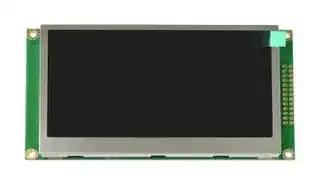
LMT043DNFFWD-NCN
TFT LCD, 4.3 ", 480 x 272 Pixels, Landscape, Black on White, 3.3V
⚠️ Reference pricing provided. In case of supply shortages, we will connect you with our trusted procurement partners to ensure your project's continuity.
- Manufacturer: INTELLIGENT DISPLAY SOLUTIONS
- Product type: TFT LCD Displays
- SVHC: No SVHC (25-Jun-2025)
- VGA Size: -
- Resolution: 480 x 272 Pixels
- Module Size: 121mm x 70mm x 12.2mm
- Touchscreen: -
- Display Size: 4.3"
- Logic Voltage: 3.3V
- Product Range: -
- Display Pinout: 26 Way Connector
- Interface Type: MCU, SPI
- Display Appearance: Black on White
- Display Brightness: 400cd/m²
- Display Orientation: Landscape
- Operating Temperature Max: 70°C
- Operating Temperature Min: -20°C
| Delivery and price | |
|---|---|
| Units per pack | 50 |
| Price | 32.92 € |
| Current stock | 10+ |
| Lead time | 30 days |
Datasheet

## **LMT043DNFFWD-NCN** LCD Module User Manual

|Prepared by:<br>**Li Keke**<br>Date: 2021-07-23|Checked by:<br>Date:|Approved by:<br>Date:|
|---|---|---|


|**Rev.**|**Descriptions**|**Release Date**|
|---|---|---|
|0.1|New release|2019-08-29|
|0.2|add SPI Mode Timing|2021-07-23|


Intelligent Display Solutions, Unit 2, Berkshire Business Centre, Berkshire Drive, Thatcham, Berkshire, RG19 4EW Telephone : +44 (0)1635 294600 Fax : +44 (0)1635 869200 Email: info@i-lcd.com www.i-lcd.com A division of Intelligent Group Solutions Ltd

Page: 1 of 16

LCD Module User Manual

LMT043DNFFWD-NCN

## **Table of Content**

**1. GENERAL SPECIFICATION......................................................................................................................................3 2. BLOCK DIAGRAM.......................................................................................................................................................3 3. TERMINAL FUNCTIONS............................................................................................................................................4 4. ABSOLUTE MAXIMUM RATINGS...........................................................................................................................4 5. ELECTRICAL CHARACTERISTICS........................................................................................................................5** 5.1 DC CHARACTERISTICS................................................................................................................................................5 **6. AC CHARACTERISTICS.............................................................................................................................................5** 6.1 8080 MODE TIMING....................................................................................................................................................5 6.2 SPI MODE TIMING......................................................................................................................................................6 6.3 RESET TIMING.............................................................................................................................................................8 **7. OPTICAL CHARACTERISTICS................................................................................................................................ 8 8. FUNCTION SPECIFICATIONS................................................................................................................................10** 8.1 COMMAND SUMMARY.............................................................................................................................................. 10 **9. LCD MODULE DESIGN AND HANDLING PRECAUTIONS..............................................................................13 10. CTP MOUNTING INSTRUCTIONS.......................................................................................................................14 11. RTP MOUNTING INSTRUCTIONS.......................................................................................................................15**

Intelligent Display Solutions, Unit 2, Berkshire Business Centre, Berkshire Drive, Thatcham, Berkshire, RG19 4EW Telephone : +44 (0)1635 294600 Fax : +44 (0)1635 869200 Email: info@i-lcd.com www.i-lcd.com A division of Intelligent Group Solutions Ltd

Intelligent Display Solutions, Unit 2, Berkshire Business Centre, Berkshire Drive, Thatcham, Berkshire, RG19 4EW Telephone : +44 (0)1635 294600 Fax : +44 (0)1635 869200 Email: info@i-lcd.com www.i-lcd.com A division of Intelligent Group Solutions Ltd

Page: 2 of 16

LCD Module User Manual

LMT043DNFFWD-NCN

## **1. General Specification**

Screen Size(Diagonal) : 4.3 inch Resolution : 480(RGB) x 272 Interface : 8bit MCU Interface Color Depth : 16.7M color (24bit) Dot Pitch : 0.198 x 0.198 (mm) Pixel Configuration : RGB Stripe Display Mode : Transmissive / Positive Surface Treatment : Anti-Glare Treatment Viewing Direction : 12 o’clock( gray scale inverse) Outline Dimension : 121.0x70.0x12.2 (mm) Active Area : 95.4 x 53.86 (mm) Backlight : LED, White Operating Temperature : -20 ~ +70°C Storage Temperature : -30 ~ +80°C

_Note: Backlight color may slightly change over temperature and driving voltage._

## **2. Block Diagram**

**==> picture [433 x 253] intentionally omitted <==**

**----- Start of picture text -----**<br>
Backlight Backlight<br>BL_ADJ Driver<br>/RD, /WR, /CS, A0<br>480(x3) x 272 pixels<br>D0~D7<br>TFT Panel<br>/RES, TE<br>SPI_EN<br>VDD, VSS Power Circuit Source Driver<br>S1D13L01<br>LCD Controller<br>Gate Driver<br>**----- End of picture text -----**<br>


Intelligent Display Solutions, Unit 2, Berkshire Business Centre, Berkshire Drive, Thatcham, Berkshire, RG19 4EW Telephone : +44 (0)1635 294600 Fax : +44 (0)1635 869200 Email: info@i-lcd.com www.i-lcd.com A division of Intelligent Group Solutions Ltd

Page: 3 of 16

LCD Module User Manual

LMT043DNFFWD-NCN

## **3. Terminal Functions**

## Terminal (K1)

|<br>**Pin**<br>**No.**|<br>**Pin**<br>**Name**|**I/O**|**8bit MCU Mode (Default)**<br>**Description**|**SPI Mode**<br>**Description**|
|---|---|---|---|---|
|1|VSS|Power Input|Power Supply GND (0V)||
|2|||||
|3|VDD|Power Input|Positive Power Supply(3.3V)||
|4|||||
|5|A0|Input|Access Mode<br>A0=High: Accessing Data<br>A0=Low: Accessing Address|Keep open|
|6|/CS|Input|Chip Select<br>/CS=Low: Data IO is enabled||
|7|/RES|Input|Reset<br>/RES=Low: Reset<br>/RES=High: Normal operation||
|8|D0(SI)|Bi-directional I/O|8-bit Bi-directional data bus|Serial input|
|9|D1(SO)|||Serial output|
|:|:|||Keepopen|
|14|D6|||Keepopen|
|15|D7|||Keepopen|
|16|TE|Output|TE Signal||
|17|/RD|Input|Read Enable, active Low|Keep open|
|18|/WR(SCK)|Input|Write Enable,active Low|Serial clock|
|19|BL_ADJ|Input|Backlight Driver enable signal, active High, PWM(*2)can be<br>possible||
|20|SPI_EN|Input|Keepopen|SPI Enable,active high|
|21|NC|-|No connection||
|22|NC|-|No connection||
|23|NC|-|No connection||
|24|NC|-|No connection||
|25|NC|-|No connection||
|26|NC|-|No connection||


Note. *1. Tear signal may leave open when not use

*2. The PWM frequency is between 200Hz and 500Hz.

*3. Pulled-up by internal resistor

## **4. Absolute Maximum Ratings**

|**Items**|**Symbol**|**Min.**|**Max.**|**Unit**|**Condition**|
|---|---|---|---|---|---|
|Supply Voltage|VDD|-0.2|3.7|V|VSS =0V|
|Input Voltage|VIN|-0.2|3.7|V|VSS =0V|
|OperatingTemperature|TOP|-20|+70|℃|No Condensation|
|Storage Temperature|TST|-30|+80|℃|No Condensation|


Caution:

Any Stresses exceeding the Absolute Maximum Ratings may cause substantial damage to the device. Functional operation of this device at other conditions beyond those listed in the specification is not implied and prolonged exposure to extreme conditions may affect device reliability.

Intelligent Display Solutions, Unit 2, Berkshire Business Centre, Berkshire Drive, Thatcham, Berkshire, RG19 4EW Telephone : +44 (0)1635 294600 Fax : +44 (0)1635 869200 Email: info@i-lcd.com www.i-lcd.com A division of Intelligent Group Solutions Ltd

Page: 4 of 16

LCD Module User Manual

LMT043DNFFWD-NCN

## **5. Electrical Characteristics**

## **5.1 DC Characteristics**

VSS=0V, VDD =3.3V, TOP =25℃

|**Items**<br>~~Gs~~<br>~~es~~<br>~~es~~|**Symbol**<br>~~Gs~~<br>~~Gs~~<br>|**MIN.**<br>~~Gs~~<br>~~Qs~~<br>~~Qe~~<br>|**TYP.**<br>~~Gs~~<br>~~Qs~~<br>~~QO~~<br>|**MAX.**<br>~~Gs~~<br>~~(~~<br>~~QO~~<br>|**Unit**<br>~~Gs~~|**Applicable Pin**<br>~~Gs~~|
|---|---|---|---|---|---|---|
|Operating Voltage<br>~~es~~<br>~~es~~<br>~~es~~|VDD<br>~~Gs~~<br>~~Gs~~<br>|2.8<br>~~Qs~~<br>~~Qe~~<br>~~Gere~~<br>|3.3<br>~~Qs~~<br>~~QO~~<br>~~QO~~<br>|3.6<br>~~(~~<br>~~QO~~<br>~~QO~~<br>|V|VDD|
|Input High Voltage<br>~~es~~<br>~~es~~<br>~~es~~<br>~~es~~|VIH<br>~~Gs~~<br>~~Gs~~<br>~~Gs~~<br>|-<br>~~Qs~~<br>~~Qe~~<br>~~Gere~~<br>~~Gere~~<br>|-<br>~~Qs~~<br>~~QO~~<br>~~QO~~<br>~~QO~~<br>|VDD<br>~~(~~<br>~~QO~~<br>~~QO~~<br>~~QO~~<br>|V|Input pins, Bi-direction pins|
|Input Low Voltage<br><br>~~es~~<br>~~es~~<br>~~es~~<br>~~es~~|VIL<br>~~Gs~~<br>~~Gs~~<br>~~Gs~~<br>~~Gs~~<br>|VSS<br>~~Qe ~~<br>~~Gere~~<br>~~Gere~~<br>~~Gere~~<br>|-<br> ~~QO~~<br>~~QO~~<br>~~QO~~<br>~~QO~~<br>|-<br>~~QO~~<br>~~QO~~<br>~~QO~~<br>~~QO~~<br>|V|Input pins, Bi-direction pins|
|Output High Voltage<br><br>~~es~~<br>~~es~~<br>~~es~~<br>~~es~~|VOH<br>~~Gs~~<br>~~Gs~~<br>~~Gs~~<br>~~**Gs**~~|2.6<br>~~Gere ~~<br>~~Gere~~<br>~~Gere~~<br>~~Gere~~|-<br> ~~QO~~<br>~~QO~~<br>~~QO~~<br>~~QO~~|-<br>~~QO~~<br>~~QO~~<br>~~QO~~<br>~~QO~~|V|Bi-direction pins (*1)|
|Output Low Voltage<br><br>~~es~~<br>~~es~~<br>~~es~~|VOL<br>~~Gs~~<br>~~Gs~~<br>~~**Gs**~~|-<br>~~Gere ~~<br>~~Gere~~<br>~~Gere~~<br>~~ne rs~~|-<br> ~~QO~~<br>~~QO~~<br>~~QO~~<br>~~rs~~|0.6<br>~~QO~~<br>~~QO~~<br>~~QO~~<br>~~(~~|V|Bi-direction pins (*2)|
|Operating Current<br><br>~~es~~<br>~~es~~|IDD<br>~~Gs~~<br>~~**Gs**~~|-<br>~~Gere ~~<br>~~Gere~~<br>~~ne rs~~|230<br> ~~QO~~<br>~~QO~~<br>~~rs~~|500<br>~~QO~~<br>~~QO~~<br>~~(~~|mA|On Backlight Power on status|


- *1. Never Apply logic signal before the VDD supply.

- *2. VDD setting should match the signals voltage

## **6. AC Characteristics**

## **6.1 8080 Mode Timing**

**==> picture [151 x 143] intentionally omitted <==**

**----- Start of picture text -----**<br>
A0<br>/CS Control<br>/CS<br>/WR<br>/RD FT<br>/RD,WR/ Control<br>/CS<br>el<br>/WR<br>= /RD<br>**----- End of picture text -----**<br>


**==> picture [38 x 10] intentionally omitted <==**

**----- Start of picture text -----**<br>
Figure 2<br>**----- End of picture text -----**<br>


|Symbol|Parameter|3.3 Volt<br>~~Po~~<br>~~eeeee~~|3.3 Volt<br>~~Po~~<br>~~eeeee~~|Units<br>~~eee~~|
|---|---|---|---|---|
|||Min<br>~~ee~~<br>~~GG~~|Max<br>~~eee~~<br>~~GG~~||
|t1<br>~~a~~|A0 setup time to /CS (/WR, /RD)<br>~~a~~|1<br>~~ee ~~<br>~~a~~<br>~~GG~~<br>~~GG~~|-<br> ~~eee~~<br>~~a~~<br>~~GG~~<br>~~GG~~|ns<br>~~eee~~<br>~~a~~|
|t2<br>~~a~~|/WR, /RD (/CS) setup time to /CS (/WR, /RD)<br>~~a~~|1<br>~~GG~~<br>~~a~~<br>~~GG~~<br>~~GG~~|-<br>~~GG~~<br>~~a~~<br>~~GG~~<br>~~GG~~|ns<br>~~a~~|
|t3<br>~~a~~|DB[7:0] setup time to /CS (/WR) rising edge: write cycle<br>~~a~~|1<br>~~GG~~<br>~~a~~<br>~~GG~~<br>~~GG~~|-<br>~~GG~~<br>~~a~~<br>~~GG~~<br>~~GG~~|ns<br>~~a~~|
|t4<br>~~a~~|DB[7:0] hold time from /CS (/WR) rising edge: write cycle<br>~~a~~|7<br>~~GG~~<br>~~a~~<br>~~GG~~<br>~~GG~~|-<br>~~GG~~<br>~~a~~<br>~~GG~~<br>~~GG~~|ns<br>~~a~~|
|t5w<br>~~a~~|/WR (/CS) hold time from /CS (/WR) rising edge: write cycle<br>~~a~~|3<br>~~GG~~<br>~~a~~<br>~~GG~~<br>~~GG~~|-<br>~~GG~~<br>~~a~~<br>~~GG~~<br>~~GG~~|ns<br>~~a~~|
|t5r<br>~~a~~|/RD (/CS) hold time from /CS (/RD) rising edge: read cycle<br>~~a~~|0<br>~~GG~~<br>~~a~~<br>~~GG~~<br>~~GG~~|-<br>~~GG~~<br>~~a~~<br>~~GG~~<br>~~GG~~|ns<br>~~a~~|
|t6<br>~~a~~|A0 hold time from /CS (/WR, /RD) rising edge<br>~~a~~|4<br>~~GG~~<br>~~a~~<br>~~GG~~<br>~~GG~~|-<br>~~GG~~<br>~~a~~<br>~~GG~~<br>~~GG~~|ns<br>~~a~~|
|t7<br>~~a~~|/CS (/RD) falling edge to DB[7:0] driven: read cycle<br>~~a~~|-<br>~~GG~~<br>~~a~~<br>~~GG~~<br>~~GG~~|15<br>~~GG~~<br>~~a~~<br>~~GG~~<br>~~GG~~|ns<br>~~a~~|
|t8<br>~~a~~|/CS (/RD) falling edge to valid Data: read cycle<br>~~a~~|-<br>~~GG~~<br>~~a~~<br>~~GG~~<br>~~GG~~|4xTmclk+17<br>~~GG~~<br>~~a~~<br>~~GG~~<br>~~GG~~|ns<br>~~a~~|
|t9<br>~~a~~|DB[7:0] hold time from /CS (/RD) rising edge: read cycle<br>~~a~~|2<br>~~GG~~<br>~~a~~<br>~~GG~~<br>~~GG~~|12<br>~~GG~~<br>~~a~~<br>~~GG~~<br>~~GG~~|ns<br>~~a~~|
|t10w<br>~~a~~|End of write to next read/write<br>~~a~~|5<br>~~GG~~<br>~~a~~<br>~~GG~~<br>~~GG~~|-<br>~~GG~~<br>~~a~~<br>~~GG~~<br>~~GG~~|ns<br>~~a~~|
|t10r<br>~~a~~<br>~~a~~|End of read to next read/write<br>~~a~~<br>|Tmclk+9<br>~~GG~~<br>~~a~~<br>~~GG~~<br>~~GG~~<br>|-<br>~~GG~~<br>~~a~~<br>~~GG~~<br>~~GG~~<br>|ns<br>~~a~~<br>|
|t11w<br>~~a~~<br>~~a~~|/CS (/WR) pulse width for write cycle<br>~~a~~<br>|3<br>~~GG~~<br>~~a~~<br>~~GG~~<br>|-<br>~~GG~~<br>~~a~~<br>~~GG~~<br>|ns<br>~~a~~<br>|
|t12w<br>~~a ~~|/CS (/WR) rise to next /CS (/WR) rise: write cycle<br> ~~GQ~~|3xTmclk+6<br>~~GG~~<br>~~GQ~~|-<br>~~GG~~<br>~~GQ~~|ns<br>~~GQ~~|


Intelligent Display Solutions, Unit 2, Berkshire Business Centre, Berkshire Drive, Thatcham, Berkshire, RG19 4EW Telephone : +44 (0)1635 294600 Fax : +44 (0)1635 869200 Email: info@i-lcd.com www.i-lcd.com A division of Intelligent Group Solutions Ltd

Page: 5 of 16

LCD Module User Manual

LMT043DNFFWD-NCN

Indirect 8-bit Function Select:

|A0|/WR|/RD|Comments|
|---|---|---|---|
|0|0|1|Command Write (register address)|
|1|0|1|Data (Parameter) Write|
|0|1|0|inhibit|
|1|1|1|Data (Parameter) Read|


## **6.2 SPI Mode Timing**

**==> picture [14 x 7] intentionally omitted <==**

**----- Start of picture text -----**<br>
/CS<br>**----- End of picture text -----**<br>


~~pO~~ 3.3 Volt Symbol Parameter Units ~~ee~~ Min ~~eee~~ Max ~~eG~~ t1 Chip select setup time 2 - ns ~~eG~~ t2 SI Data setup time 1 - ns ~~eG~~ t3 SI Data hold time 7 - ns ~~eG~~ t4 Serial clock pulse width low (high) 15 - ns ~~eG~~ t5 Serial clock pulse width high (low) 15 - ns ~~eG~~ t6 Serial clock period 30 - ns ~~eG~~ t7 Chip select hold time 7 - ns ~~eG~~ t8 Chip select de-assert to reassert 2 - ns ~~GO~~ t9 SCK falling edge to SO hold time 3 10 ns _Note: 1. CL = 10pF for SPI timing._ 2. Please refer to S1D13L01 datasheet for details. 3.SPI Function Select

|_1. CL = 10pF for SPI timing.L = 10pF for SPI timing. = 10pF for SPI timing._<br>2. Please refer to S1D13L01 datasheet for details.<br>3.SPI Function Select|_1. CL = 10pF for SPI timing.L = 10pF for SPI timing. = 10pF for SPI timing._<br>2. Please refer to S1D13L01 datasheet for details.<br>3.SPI Function Select|
|---|---|
|Command|Comments|
|10000000|8-bit Write|
|11000000|8-bit Read|
|10001000|16-bit Write|
|11001000|16-bit Read|
|the other|reserved|


Intelligent Display Solutions, Unit 2, Berkshire Business Centre, Berkshire Drive, Thatcham, Berkshire, RG19 4EW Telephone : +44 (0)1635 294600 Fax : +44 (0)1635 869200 Email: info@i-lcd.com www.i-lcd.com A division of Intelligent Group Solutions Ltd

Page: 6 of 16

LCD Module User Manual

LMT043DNFFWD-NCN

## Write Procedure:

SPI 8bit Write Sequence:

**==> picture [13 x 7] intentionally omitted <==**

**----- Start of picture text -----**<br>
/CS<br>**----- End of picture text -----**<br>


## SPI 16bit Write Sequence:

**==> picture [16 x 8] intentionally omitted <==**

**----- Start of picture text -----**<br>
/CS<br>**----- End of picture text -----**<br>


Read Procedure:

SPI 8bit Read Sequence:

**==> picture [16 x 7] intentionally omitted <==**

**----- Start of picture text -----**<br>
/CS<br>**----- End of picture text -----**<br>


Intelligent Display Solutions, Unit 2, Berkshire Business Centre, Berkshire Drive, Thatcham, Berkshire, RG19 4EW Telephone : +44 (0)1635 294600 Fax : +44 (0)1635 869200 Email: info@i-lcd.com www.i-lcd.com A division of Intelligent Group Solutions Ltd

Page: 7 of 16

LCD Module User Manual

LMT043DNFFWD-NCN

SPI 16bit Read Sequence:

**==> picture [14 x 7] intentionally omitted <==**

**----- Start of picture text -----**<br>
/CS<br>**----- End of picture text -----**<br>


Please refer to S1D13L01 datasheet for details.

## **6.3 Reset Timing**

|||t1|t2||||||
|---|---|---|---|---|---|---|---|
||/RES|t1|t2||||||
||||Figure 8|||||
|Symbol||Parameter|||Min|Max|Units|
|t1|Reset Pulse Width is ignored||||-|42|ns|
|t2|Active Reset Pulse Width (see Note)||||150|-|ns|


_Note: The Reset input should be held low for longer than 150ns to guarantee reset._ For more information and details please refer to LCD controller (S1D13L01) datasheet.

## **7. Optical Characteristics**

|**Item**|**Item**|**Symbol**|**Condition**|**MIN.**|**TYP.**|**MAX.**|**UNIT**|**Note.**|
|---|---|---|---|---|---|---|---|---|
|Viewing angle||θT|(CR≥10)|60|70|-|degree|Note 2|
|||θB||40|50|-|||
|||θL||60|70|-|||
|||θR||60|70|-|||
|Contrast ratio||CR|θ=0<br>o|400|500|-|-|Note 1,3|
|Response Time||Ton|25℃|-|20|30|msec|Note 1,4|
|||Toff|||||msec||
|Chromaticlty|White|X|Backlight<br>is on|0.265|0.315|0.365||Note 1,5|
|||Y||0.285|0.335|0.385|||
||Red|X||0.531|0.581|0.631|||
|||Y||0.295|0.345|0.395|||
||Green|X||0.298|0.348|0.395|||
|||Y||0.531|0.581|0.631|||
||Blue|X||0.103|0.153|0.203|||
|||Y||0.045|0.095|0.145|||
|NTSC||||-|50||%|Note 5|
|Luminance uniformity||U||-|75|-|%|Note 1,7|
|Luminance||L|||400|-|cd/m2||


> Intelligent Display Solutions, Unit 2, Berkshire Business Centre, Berkshire Drive, Thatcham, Berkshire, RG19 4EW Page: 8 of 16 Telephone : +44 (0)1635 294600 Fax : +44 (0)1635 869200 Email: info@i-lcd.com www.i-lcd.com A division of Intelligent Group Solutions Ltd

LCD Module User Manual

LMT043DNFFWD-NCN

## Note:

The parameter is slightly changed by temperature, driving voltage and materiel Please see the Notes for testing conditions

Note 1:

The data are measured after LEDs are turned on for 5 minutes. LCM displays full white. The brightness is the average value of 9 measured spots. Measurement equipment PR-705 (Φ8mm) Measuring condition: - Measuring surroundings: Dark room

- Measuring temperature: Ta=25℃.

- Adjust operating voltage to get optimum contrast at the center of the display. Measured value at the center point of LCD panel after more than 5 minutes while backlight turning on.

Note 2: reference Figure5 The luminance uniformity is calculated by using following formula. △Bp = Bp (Min.) / Bp (Max.)×100 (%) Bp (Max.) = Maximum brightness in 9 measured spots Bp (Min.) = Minimum brightness in 9 measured spots..

> Bp (Max.) = Maximum brightness in 9 measured Figure 9 spots Bp (Min.) = Minimum brightness in 9 measured spots.. Foe); 09 =0° 4 Note 3: reference Figure6 NZ The definition of viewing angle: Refer to the graph below marked by θ and Ф ee ‘LA

> Note 4: Down (6:00) The definition of contrast ratio (Test LCM using PR-705): =270° Figure 10 Contrast Luminance When LCD is at “White” state Brightness | | Ratio(CR)= Luminance When LCD is at “Black” state | (Contrast Ratio is measured in optimum common electrode Mp 7 voltage) | | Note 5: reference Figure7

> Definition of Response time. (Test LCD using DMS501): m on The output signals of photo detector are measured when the input signals are changed from Figure 11 “black” to “white”(falling time) and from “white” to “black”(rising time), respectively. The response time is defined as the time interval between the 10% and 90% of amplitudes.Refer to figure as below.

Note 6: reference Figure8 Definition of Color of CIE Coordinate and NTSC Ratio.

Color gamut: Area of RGB triangle S= X100% Area of NTSC triangle

Figure 12

Intelligent Display Solutions, Unit 2, Berkshire Business Centre, Berkshire Drive, Thatcham, Berkshire, RG19 4EW Telephone : +44 (0)1635 294600 Fax : +44 (0)1635 869200 Email: info@i-lcd.com www.i-lcd.com A division of Intelligent Group Solutions Ltd

Page: 9 of 16

LCD Module User Manual

LMT043DNFFWD-NCN

## **8. Function Specifications**

## **8.1 Command Summary**

|**Command**|**Para-**<br>**meter**|**HEX**|**A0**|**/CS**|**/WR**|**D7**|**D6**|**D5**|**D4**|**D3**|**D2**|**D1**|**D0**|**Descriptions**|
|---|---|---|---|---|---|---|---|---|---|---|---|---|---|---|
|Power Save|P1|60804|0|0|0|A[7:0]-> A[15:8]-> A[18:16]||||||||Power Save Configuration Register|
||P2|D[7:0]|1|0|0|n/a|n/a|n/a|n/a|n/a|n/a|Power Save||Bit[1:0] = 00 , PSM0 mode<br>Bit[1:0] = 01 , PSM1 mode<br>Bit[1:0]= 1x,NMM mode|
|||D[15:8]|1|0|0|n/a|n/a|n/a|n/a|n/a|n/a|n/a|n/a||
|Software<br>Reset|P1|60806|0|0|0|A[7:0]-> A[15:8]-> A[18:16]||||||||Software Reset Register(Write Only)|
||P2|D[7:0]|1|0|0|n/a|n/a|n/a|n/a|n/a|n/a|n/a|n/a|Bit[8] = 0 , no effect in hardware<br>Bit[8] = 1 , all registers are reset to default values|
|||D[15:8]|1|0|0|n/a|n/a|n/a|n/a|n/a|n/a|n/a|Softw<br>are<br>Rese<br>t||
|PLL Setting 0|P1|60810|0|0|0|A[7:0]-> A[15:8]-> A[18:16]||||||||PLL SettingRegister 0|
||P2|D[7:0]|1|0|0|n/a|n/a|n/a|n/a|n/a|n/a|PLL<br>Bypa<br>ss|PLL<br>Enabl<br>e|Bit[0] = 0 , the PLL is disabled<br>Bit[0] = 1 , the PLL enabled<br>Bit[1] = 0 , PLL is selected<br>Bit[1] = 1 , CLKI is selected<br>Bit[15] = 0 , the PLL output is not stable<br>Bit[15]= 1,the PLL output is stable|
|||D[15:8]|1|0|0|PLL<br>Lock<br>(RO)|n/a|n/a|n/a|n/a|n/a|n/a|n/a||
|PLL Setting 1|P1|60812|0|0|0|A[7:0]-> A[15:8]-> A[18:16]||||||||PLL SettingRegister 1|
||P2|D[7:0]|1|0|0|M-Divider||||||||Bit[9:0] 000h,001h … … 019h,020h : 1:1 ,2:1 … … 33:1(M-Divide Ratio).<br>021h to 13Fh: Reserved, PFDCLK = CLKI ÷ (M-Divider + 1)<br>Bit[13:10] , must be set to 0000|
|||D[15:8]|1|0|0|n/a|n/a|N-Counter||||M-Divider|||
|PLL Setting 2|P1|60814|0|0|0|A[7:0]-> A[15:8]-> A[18:16]||||||||PLL SettingRegister 2|
||P2|D[7:0]|1|0|0|L-Counter||||||||Bit[9:0] , must be set between 010h ~ 041h. , and get the M-Divide Ratio<br>from 17:1 to 66:1. POCLK = (L-Counter + 1) x (N-Counter + 1) x PFDCLK|
|||D[15:8]|1|0|0|n/a|n/a|n/a|n/a|n/a|n/a|L-Counter|||
|Internal Clock<br>Configuration|<br>P1|60816|0|0|0|A[7:0]-> A[15:8]-> A[18:16]||||||||Internal Clock Configuration Register|
||P2|D[7:0]|1|0|0|n/a|n/a|n/a|n/a|n/a|PCLK Divide Select|||Bit[3:0] = 0000b,0001b … … 1110b,1111b : 1:1 ,2:1 … … 16:1(MCLK to<br>PCLK Frequency Ratio)|
|||D[15:8]|1|0|0|n/a|n/a|n/a|n/a|n/a|n/a|n/a|n/a||
|Panel Setting<br>Miscellaneous|P1|60820|0|0|0|A[7:0]-> A[15:8]-> A[18:16]||||||||Panel SettingMiscellaneous Register|
||P2|D[7:0]|1|0|0|DE Polarity||PCL<br>K<br>Polari<br>ty|n/a|Panel<br>Data<br>Enabl<br>e|Panel Data<br>Width||Panel<br>Port<br>Enabl<br>e|Bit[0] = 0 , TFT panel is disable<br>Bit[0] = 1 , TFT panel is enable<br>Bit[2:1] = 01 , TFT 16-bit<br>Bit[2:1] = 10 , TFT 18-bit<br>Bit[2:1] = 11 , TFT 24-bit<br>Bit[3] = 0 , panel data is disable<br>Bit[3] = 1 , panel data is enable<br>Bit[5] = 0, the LCD data outputs transition on the rising edge of PCLK<br>Bit[5] = 1 , the LCD data outputs transition on the falling edge of PCLK<br>Bit[7:6] = 00 , DE Polarity Low active<br>Bit[7:6] = 01 , DE Polarity High active<br>Bit[7:6] = 10 , DE Polarity Fixed to Low<br>Bit[7:6]= 11,DE PolarityFixed to High|
|||D[15:8]|1|0|0|n/a|n/a|n/a|n/a|n/a|n/a|n/a|n/a||
|Display<br>Settings|P1|60822|0|0|0|A[7:0]-> A[15:8]-> A[18:16]||||||||DisplaySettings Register|
||P2|D[7:0]|1|0|0|TE<br>Statu<br>s<br>(RO)|TE Function||Displ<br>ay<br>Blank|n/a|Displ<br>ay<br>Blank<br>Polari<br>ty|SW<br>Video<br>Invert|Panel<br>Interf<br>ace<br>Enabl<br>es|Bit[0] = 0 , HS, VS, DE and PCLK are fixed to H or L and the display pipes<br>are disabled<br>Bit[0] = 1 , enable the panel output and display pipes<br>Bit[1] = 0 , video data is normal<br>Bit[1] = 1 , video data is inverted<br>Bit[2] = 0 , the display blank function operates normally<br>Bit[2] = 1 , the display blank function switches polarity<br>Bit[4] = 0 , the LCD data is masked<br>Bit[4] = 1 , all applicable LCD data outputs are forced to zero or one<br>Bit[6:5] = 00b , TE output is disabled and the pin output is low<br>Bit[6:5] = 01b , TE output is high (1) when the display is in the Vertical<br>Non-Display Period (VNDP) and low (0) when the display is in Vertical<br>Display Period (VDISP)<br>Bit[6:5] = 10b , Line Count<br>Bit[6:5] = 11b , Reserved<br>Bit[7] = 0 , the selected condition in not occurring<br>Bit[7] = 1 , the selected condition in not occurring<br>Bit[8] = 0 , TE is output<br>Bit[8]= 1, TE is not output<br> <br>|
|||D[15:8]|1|0|0|n/a|n/a|n/a|n/a|n/a|n/a|n/a|TE<br>Outp<br>ut Pin<br>Disab<br>le||
|HDISP|P1|60824|0|0|0|A[7:0]-> A[15:8]-> A[18:16]||||||||Horizontal DisplayWidth Register(HDISP)|
||P2|D[7:0]|1|0|0|n/a|Horizontal DisplayWidth|||||||Bit[6:0] = horizontal display width in pixels ÷ 8|
|||D[15:8]|1|0|0|n/a|n/a|n/a|n/a|n/a|n/a|n/a|n/a||
|HNDP|P1|60826|0|0|0|A[7:0]-> A[15:8]-> A[18:16]||||||||Horizontal Non-DisplayPeriod Register(HNDP)|
||P2|D[7:0]|1|0|0|n/a|Horizontal Non-DisplayPeriod|||||||Bit[6:0] = horizontal non-display period in PCLK’s|
|||D[15:8]|1|0|0|n/a|n/a|n/a|n/a|n/a|n/a|n/a|n/a||
|VDISP|P1|60828|0|0|0|A[7:0]-> A[15:8]-> A[18:16]||||||||Vertical DisplayHeight Register(VDISP)|
||P2|D[7:0]|1|0|0|Vertical DisplayHeight||||||||Bit[9:0] = vertical display height in lines|
|||D[15:8]|1|0|0|n/a|n/a|n/a|n/a|n/a|n/a|Vertical<br>Display<br>Height|||
|VNDP|P1|6082A|0|0|0|A[7:0]-> A[15:8]-> A[18:16]||||||||Vertical Non-DisplayPeriod Register(VNDP)|
||P2|D[7:0]|1|0|0|Vertical Non-DisplayPeriod||||||||Bit[7:0]= vertical non-display period in lines|


Intelligent Display Solutions, Unit 2, Berkshire Business Centre, Berkshire Drive, Thatcham, Berkshire, RG19 4EW Telephone : +44 (0)1635 294600 Fax : +44 (0)1635 869200 Email: info@i-lcd.com www.i-lcd.com A division of Intelligent Group Solutions Ltd

Page: 10 of 16

LCD Module User Manual

LMT043DNFFWD-NCN

> D[15:8] 1 0 0 n/a n/a n/a n/a n/a n/a n/a n/a

|**Command**|**Para-**<br>**meter**|**HEX**|**A0**|**/CS**|**/WR**|**D7**|**D6**|**D5**|**D4**|**D3**|**D2**|**D1**|**D0**|**Descriptions**|
|---|---|---|---|---|---|---|---|---|---|---|---|---|---|---|
|HSW|P1|6082C|0|0|0|A[7:0]-> A[15:8]-> A[18:16]||||||||HS Pulse Width Register(HSW)|
||P2|D[7:0]|1|0|0|HS<br>Pulse<br>Polari<br>ty|HS Pulse Width|||||||Bit[6:0] = HS pulse width in PCLK’s<br>Bit[7] = 0 , the horizontal sync signal is active low<br>Bit[7] = 1 , the horizontal sync signal is active high|
|||D[15:8]|1|0|0|n/a|n/a|n/a|n/a|n/a|n/a|n/a|n/a||
|HPS|P1|6082E|0|0|0|A[7:0]-> A[15:8]-> A[18:16]||||||||HS Pulse Start Position Register(HPS)|
||P2|D[7:0]|1|0|0|n/a|HS Pulse Start Position|||||||Bit[6:0] = HS pulse start position in PCLK’s|
|||D[15:8]|1|0|0|n/a|n/a|n/a|n/a|n/a|n/a|n/a|n/a||
|VSW|P1|60830|0|0|0|A[7:0]-> A[15:8]-> A[18:16]||||||||VS Pulse Width Register(VSW)|
||P2|D[7:0]|1|0|0|VS<br>Pulse<br>Polari<br>ty|n/a|VS Pulse Width||||||Bit[5:0] = VS pulse width in lines<br>Bit[7] = 0 , the vertical sync signal is active low<br>Bit[7] = 1 , the vertical sync signal is active high|
|||D[15:8]|1|0|0|n/a|n/a|n/a|n/a|n/a|n/a|n/a|n/a||
|VPS|P1|60832|0|0|0|A[7:0]-> A[15:8]-> A[18:16]||||||||VS Pulse Start Position Register(VPS)|
||P2|D[7:0]|1|0|0|VS Pulse Start Position||||||||Bit[7:0] = VS pulse start position in lines|
|||D[15:8]|1|0|0|n/a|n/a|n/a|n/a|n/a|n/a|n/a|n/a||
|TE Line Coun|t<br>P1|60834|0|0|0|A[7:0]-> A[15:8]-> A[18:16]||||||||TE Line Count Register|
||P2|D[7:0]|1|0|0|TE Line Count||||||||These bits specify the line count value that is compared with the internal<br>vertical line counter|
|||D[15:8]|1|0|0|n/a|n/a|n/a|n/a|n/a|n/a|TE Line<br>Count|||
|Main Layer<br>Setting|P1|60840|0|0|0|A[7:0]-> A[15:8]-> A[18:16]||||||||Main Layer SettingRegister|
||P2|D[7:0]|1|0|0|n/a|n/a|n/a|Main Layer<br>Rotation<br>Select||Main Layer Color<br>Depth|||Bit[2:0] = 000b, RGB 8:8:8 (default)<br>Bit[2:0] = 001b, RGB 5:6:5<br>Bit[2:0] = 010b/011b/111b, Reserved<br>Bit[2:0] = 100b, 24 bpp + LUT1<br>Bit[2:0] = 101b, 16 bpp + LUT1<br>Bit[2:0] = 110b, 8 bpp + LUT1<br>Bit[4:3] = 00b, 0° (Normal)<br>Bit[4:3] = 01b, 90°<br>Bit[4:3] = 10b, 180°<br>Bit[4:3] = 11b, 270°<br>Bit[8] = 0, Synchronous latching of multi-byte layer registers is enabled<br>Bit[8] = 1, Synchronous latching of multi-byte layer registers is disabled|
|||D[15:8]|1|0|0|n/a|n/a|n/a|n/a|n/a|n/a|n/a|Multi-<br>Byte<br>Layer<br>Regis<br>ters<br>Sync<br>hrono<br>us<br>Latch<br>ing<br>Disab<br>le||
|Main Layer<br>Start Address<br>0|P1|60842|0|0|0|A[7:0]-> A[15:8]-> A[18:16]||||||||Main Layer Start Address Register 0|
||<br>P2|D[7:0]|1|0|0|Main Layer Start Address||||||||Bit[15:0] is Bit[15:0] of Main Layer Start Address ,but Bit[1:0] must be set<br>to 00b|
|||D[15:8]|1|0|0|Main Layer Start Address|||||||||
|Main Layer<br>Start Address<br>1|P1|60844|0|0|0|A[7:0]-> A[15:8]-> A[18:16]||||||||Main Layer Start Address Register 1|
||<br>P2|D[7:0]|1|0|0|n/a||n/a|n/a|n/a|Main Layer Start<br>Address|||Bit[2:0] is Bit[18:16] of Main Layer Start Address|
|||D[15:8]|1|0|0|n/a|n/a|n/a|n/a|n/a|n/a|n/a|n/a||
|Main Layer<br>Width|P1|60846|0|0|0|A[7:0]-> A[15:8]-> A[18:16]||||||||Main Layer Width Register|
||P2|D[7:0]|1|0|0|Main Layer Width||||||||Read Only|
|||D[15:8]|1|0|0|n/a|n/a|n/a|n/a|n/a|n/a|Main Layer<br>Width|||
|Main Layer<br>Height|P1|60848|0|0|0|A[7:0]-> A[15:8]-> A[18:16]||||||||Main Layer Height Register|
||P2|D[7:0]|1|0|0|Main Layer Height||||||||Read Only|
|||D[15:8]|1|0|0|n/a|n/a|n/a|n/a|n/a|n/a|Main Layer<br>Height|||
|PIP Layer<br>Setting|P1|60850|0|0|0|A[7:0]-> A[15:8]-> A[18:16]||||||||PIP Layer SettingRegister|
||P2|D[7:0]|1|0|0|n/a|n/a|n/a|n/a|n/a|n/a|n/a|n/a|Bit[2:0] = 000b, RGB 8:8:8 (default)<br>Bit[2:0] = 001b, RGB 5:6:5<br>Bit[2:0] = 010b/011b/111b, Reserved<br>Bit[2:0] = 100b, 24 bpp + LUT1<br>Bit[2:0] = 101b, 16 bpp + LUT1<br>Bit[2:0] = 110b, 8 bpp + LUT1<br>Bit[4:3] = 00b, 0° (Normal)<br>Bit[4:3] = 01b, 90°<br>Bit[4:3] = 10b, 180°<br>Bit[4:3]= 11b,270°|
|||D[15:8]|1|0|0|n/a|n/a|n/a|PIP Layer<br>Rotation<br>Select||PIP Layer Color<br>Depth||||
|PIP Layer<br>Start Address<br>0|P1|60852|0|0|0|A[7:0]-> A[15:8]-> A[18:16]||||||||PIP Layer Start Address Register 0|
||<br>P2|D[7:0]|1|0|0|PIP Layer Start Address||||||||Bit[15:0] is Bit[15:0] of Main Layer Start Address ,but Bit[1:0] must be set<br>to 00b|
|||D[15:8]|1|0|0|PIP Layer Start Address|||||||||
|PIP Layer<br>Start Address<br>1|P1|60854|0|0|0|A[7:0]-> A[15:8]-> A[18:16]||||||||PIP Layer Start Address Register 1|
||<br>P2|D[7:0]|1|0|0|n/a|n/a|n/a|n/a|n/a|n/a|n/a|n/a|Bit[2:0] is Bit[18:16] of Main Layer Start Address|
|||D[15:8]|1|0|0|n/a|n/a|n/a|n/a|n/a|PIP Layer Start<br>Address||||
|PIP Layer<br>Width|P1|60856|0|0|0|A[7:0]-> A[15:8]-> A[18:16]||||||||PIP Layer Width Register|
||P2|D[7:0]|1|0|0|PIP Layer Width||||||||Bit[9:] = PIP Layer Horizontal Display Period in number of pixels PIP<br>Layer Horizontal Display Period in number of pixels|
|||D[15:8]|1|0|0|n/a|n/a|n/a|n/a|n/a|n/a|PIP Layer<br>Width|||


Intelligent Display Solutions, Unit 2, Berkshire Business Centre, Berkshire Drive, Thatcham, Berkshire, RG19 4EW Telephone : +44 (0)1635 294600 Fax : +44 (0)1635 869200 Email: info@i-lcd.com www.i-lcd.com A division of Intelligent Group Solutions Ltd

Page: 11 of 16

LCD Module User Manual

LMT043DNFFWD-NCN

|**Command**|**Para-**<br>**meter**|**HEX**|**A0**|**/CS**|**/WR**|**D7**|**D6**|**D5**|**D4**|**D3**|**D2**|**D1**|**D0**|**Descriptions**|
|---|---|---|---|---|---|---|---|---|---|---|---|---|---|---|
|PIP Layer<br>Height|P1|60858|0|0|0|A[7:0]-> A[15:8]-> A[18:16]||||||||PIP Layer Height Register|
||P2|D[7:0]|1|0|0|PIP Layer Height||||||||Bit[9:] = PIP Layer Vertical Display Period in number of lines|
|||D[15:8]|1|0|0|n/a|n/a|n/a|n/a|n/a|n/a|PIP Layer<br>Height|||
|PIP Layer X<br>Start Position|P1|6085A|0|0|0|A[7:0]-> A[15:8]-> A[18:16]||||||||PIP Layer X Start Position Register|
||P2|D[7:0]|1|0|0|PIP Layer X Start Position||||||||These bits specify X start position of the PIP Layer on the panel, in lines|
|||D[15:8]|1|0|0|n/a|n/a|n/a|n/a|n/a|n/a|PIP Layer X<br>Start<br>Position|||
|PIP Layer Y<br>Start Position|P1|6085C|0|0|0|A[7:0]-> A[15:8]-> A[18:16]||||||||PIP Layer Y Start Position Register|
||P2|D[7:0]|1|0|0|PIP Layer Y Start Position||||||||These bits specify Y start position of the PIP Layer on the panel, in lines|
|||D[15:8]|1|0|0|n/a|n/a|n/a|n/a|n/a|n/a|PIP Layer Y<br>Start<br>Position|||
|PIP Enable|P1|60860|0|0|0|A[7:0]-> A[15:8]-> A[18:16]||||||||PIP Enable Register|
||P2|D[7:0]|1|0|0|n/a|n/a|n/a|n/a|Blink/<br>Fade<br>Status<br>(RO)|Blink/Fade Effect|||Bit[2:0] = 000b, Blank<br>Bit[2:0] = 001b, Normal<br>Bit[2:0] = 010b, Blink 1<br>Bit[2:0] = 011b, Blink 2<br>Bit[2:0] = 100b, Fade Out<br>Bit[2:0] = 101b, Fade In<br>Bit[2:0] = 110b, Fade In/Out Continuous<br>Bit[2:0] = 111b, Reserved<br>Bit[3] = 0b, the PIP layer is not blinking or fading<br>Bit[3] = 1b, the PIP layer is in the process of blinking or fading<br>Bit[15:9]= blink/fadeperiod in frames – 1|
|||D[15:8]|1|0|0|Blink/Fade Period|||||||n/a||
|Alpha<br>Blending|P1|60862|0|0|0|A[7:0]-> A[15:8]-> A[18:16]||||||||Alpha BlendingRegister|
||P2|D[7:0]|1|0|0|n/a|Alpha BlendingRatio|||||||Bit[6:0] = 0000000b,0000001b… …0111111b,1000000b :<br>64:0 (no PIP),63:1 … … 1:63,0:64(full PIP) ;<br>1000001b ~ 1111111b : Reserved<br>Bit[9:8] = 00b, 1<br>Bit[9:8] = 01b, 2<br>Bit[9:8] = 10b, 4<br>Bit[9:8]= 11b,8|
|||D[15:8]|1|0|0|n/a|n/a|n/a|n/a|n/a|n/a|Alpha<br>Blending<br>Step|||
|Transparency|P1|60864|0|0|0|A[7:0]-> A[15:8]-> A[18:16]||||||||TransparencyRegister|
||P2|D[7:0]|1|0|0|n/a|n/a|n/a|n/a|n/a|n/a|n/a|Transp<br>arency<br>Enable|Bit[0] = 0b, transparency is disabled<br>Bit[0] = 1b, transparency is enabled|
|||D[15:8]|1|0|0|n/a|n/a|n/a|n/a|n/a|n/a|n/a|n/a||
|Transparency<br>Key Color 0|P1|60866|0|0|0|A[7:0]-> A[15:8]-> A[18:16]||||||||TransparencyKey Color Register 0|
||P2|D[7:0]|1|0|0|KeyColor Blue||||||||Bit[15:8] is Key Color Green bits [7:0]<br>Bit[7:0] is Key Color Blue bits [7:0]|
|||D[15:8]|1|0|0|KeyColor Green|||||||||
|Transparency<br>Key Color 1|P1|60868|0|0|0|A[7:0]-> A[15:8]-> A[18:16]||||||||TransparencyKey Color Register 1|
||P2|D[7:0]|1|0|0|KeyColor Red||||||||Bit[7:0] is Key Color Red bits [7:0]|
|||D[15:8]|1|0|0|n/a|n/a|n/a|n/a|n/a|n/a|n/a|n/a||
|GPIO<br>Configuration|P1|608D0|0|0|0|A[7:0]-> A[15:8]-> A[18:16]||||||||GPIO Configuration Register|
||P2|D[7:0]|1|0|0|GPIO7<br>Config|GPIO6<br>Config|GPIO5<br>Config|GPIO4<br>Config|GPIO3<br>Config|GPIO2<br>Config|GPIO1<br>Config|GPIO0<br>Config|Bit[15:0] = 0b (default), the corresponding GPIO pin is configured as an<br>input pin<br>Bit[15:0] = 1b , the corresponding GPIO pin is configured as an output<br>pin|
|||D[15:8]|1|0|0|GPIO15<br>Config|GPIO14<br>Config|GPIO13<br>Config|GPIO12<br>Config|GPIO11<br>Config|GPIO10<br>Config|GPIO9<br>Config|GPIO8<br>Config||
|GPIO Status<br>and Control|P1|608D2|0|0|0|A[7:0]-> A[15:8] -> A[18:16]||||||||GPIO Status and Control Register|
||P2|D[7:0]|1|0|0|GPIO7<br>Status|GPIO6<br>Status|GPIO5<br>Status|GPIO4<br>Status|GPIO3<br>Status|GPIO2<br>Status|GPIO1<br>Status|GPIO0<br>Status|When GPIOx is configured as an output:<br>Bit[15:0] = 0b, GPIOx low<br>Bit[15:0] = 1b, GPIOx high|
|||D[15:8]|1|0|0|GPIO15<br>Status|GPIO14<br>Status|GPIO13<br>Status|GPIO12<br>Status|GPIO11<br>Status|GPIO10<br>Status|GPIO9<br>Status|GPIO8<br>Status||
|GPIO Pull-<br>Down Control|P1|608D4|0|0|0|A[7:0]-> A[15:8]-> A[18:16]||||||||GPIO Pull-Down Control Register|
||<br>P2|D[7:0]|1|0|0|GPIO7<br>Pull-<br>down<br>Control|GPIO6<br>Pull-<br>down<br>Control|GPIO5<br>Pull-<br>down<br>Control|GPIO4<br>Pull-<br>down<br>Control|GPIO3<br>Pull-<br>down<br>Control|GPIO 2<br>Pull-<br>down<br>Control|GPIO1<br>Pull-<br>down<br>Control|GPIO0<br>Pull-<br>down<br>Control|Bit[15:0] = 0b, the pull-down resistor for the associated GPIO pin is<br>inactive.<br>Bit[15:0] = 1b, the pull-down resistor for the associated GPIO pin is<br>active.|
|||D[15:8]|1|0|0|GPIO15<br>Pull-<br>down<br>Control|GPIO14<br>Pull-<br>down<br>Control|GPIO13<br>Pull-<br>down<br>Control|GPIO12<br>Pull-<br>down<br>Control|GPIO11<br>Pull-<br>down<br>Control|GPIO10<br>Pull-<br>down<br>Control|GPIO9<br>Pull-<br>down<br>Control|GPIO8<br>Pull-<br>down<br>Control||


_Note: Access of PLL Setting 0, PLL Setting 1, PLL Setting 2 and Internal Clock Configuration is only possible in Power Save Mode PSM0._

For more information and details please refer to S1D13L01 datasheet.

Intelligent Display Solutions, Unit 2, Berkshire Business Centre, Berkshire Drive, Thatcham, Berkshire, RG19 4EW Telephone : +44 (0)1635 294600 Fax : +44 (0)1635 869200 Email: info@i-lcd.com www.i-lcd.com A division of Intelligent Group Solutions Ltd

Page: 12 of 16

LCD Module User Manual

LMT043DNFFWD-NCN

**9. LCD Module Design and Handling Precautions**

- Please ensure V0, VCOM is adjustable, to enable LCD module get the best contrast ratio under different temperatures, view angles and positions.

- Normally display quality should be judged under the best contrast ratio within viewable area. Unexpected display pattern may come out under abnormal contrast ratio.

- Never operate the LCD module exceed the absolute maximum ratings.

- Never apply signal to the LCD module without power supply.

- Keep signal line as short as possible to reduce external noise interference.

- IC chip (e.g. TAB or COG) is sensitive to light. Strong light might cause malfunction. Light sealing structure casing is recommended.

- Make sure there is enough space (with cushion) between case and LCD panel, to prevent external force passed on to the panel; otherwise that may cause damage to the LCD and degrade its display result.

- Avoid showing a display pattern on screen for a long time (continuous ON segment).

- LCD module reliability may be reduced by temperature shock.

- When storing and operating LCD module, avoids exposure to direct sunlight, high humidity, high or low temperature. They may damage or degrade the LCD module.

- Never leave LCD module in extreme condition (max./min storage/operate temperature) for more than 48hr.

- Recommend LCD module storage conditions is 0 C~40 C <80%RH.

- LCD module should be stored in the room without acid, alkali and harmful gas.

- Avoid dropping & violent shocking during transportation, and no excessive pressure press, moisture and sunlight.

- LCD module can be easily damaged by static electricity. Please maintain an optimum anti-static working environment to protect the LCD module. (eg. ground the soldering irons properly)

- Be sure to ground the body when handling LCD module.

- Only hold LCD module by its sides. Never hold LCD module by applying force on the heat seal or TAB.

- When soldering, control the temperature and duration avoid damaging the backlight guide or diffuser which might degrade the display result such as uneven display.

- Never let LCD module contact with corrosive liquids, which might cause damage to the backlight guide or the electric circuit of LCD module.

- Only clean LCD with a soft dry cloth, Isopropyl Alcohol or Ethyl Alcohol. Other solvents (e.g. water) may damage the LCD.

- Never add force to components of LCD module. It may cause invisible damage or degrade the module's reliability.

- When mounting LCD module, please make sure it is free from twisting, warping and bending.

- Do not add excessive force on surface of LCD, which may cause the display color change abnormally.

- LCD panel is made with glass. Any mechanical shock (e.g. dropping from high place) will damage the LCD module.

Intelligent Display Solutions, Unit 2, Berkshire Business Centre, Berkshire Drive, Thatcham, Berkshire, RG19 4EW Telephone : +44 (0)1635 294600 Fax : +44 (0)1635 869200 Email: info@i-lcd.com www.i-lcd.com A division of Intelligent Group Solutions Ltd

Page: 13 of 16

LCD Module User Manual

LMT043DNFFWD-NCN

- Protective film is attached on LCD screen. Be careful when peeling off this protective film, since static electricity may be generated.

- Polarizer on LCD gets scratched easily. If possible, do not remove LCD protective film until the last step of installation.

- When peeling off protective film from LCD, static charge may cause abnormal display pattern. The symptom is normal, and it will turn back to normal in a short while.

- LCD panel has sharp edges, please handle with care.

- Never attempt to disassemble or rework LCD module.

- If display panel is damaged and liquid crystal substance leaks out, be sure not to get any in your mouth, if the substance comes into contact with your skin or clothes promptly wash it off using soap and water.

## **10. CTP Mounting Instructions**

- 10.1 Bezel Mounting (Figure 1)

- The bezel window should be bigger than the CTP active area. It should be≥0.5mm each side.

- Gasket should be installed between the bezel and the CTP surface. The final gap should be about 0.5~1.0mm.

- It is recommended to provide an additional support bracket for backside support when necessary (e.g. slim type TFT module without mounding structure). They should only provide appropriate support and keep the module in place.

- The mounting structure should be strong enough to prevent external uneven force or twist act onto the module.

**==> picture [72 x 20] intentionally omitted <==**

**----- Start of picture text -----**<br>
Figure<br>1<br>**----- End of picture text -----**<br>


- 10.2 Surface Mounting (Figure 2)

- As the CTP assembling on the countersink area with double side adhesive.

   - The countersink area should be flat and clean to ensure the double side adhesive installation result.

- The Bezel is recommend to keep a gap ( ≥ 0.3mm each side) around the cover lens for tolerance.

- It is recommended to provide an additional support bracket with

Intelligent Display Solutions, Unit 2, Berkshire Business Centre, Berkshire Drive, Thatcham, Berkshire, RG19 4EW Telephone : +44 (0)1635 294600 Fax : +44 (0)1635 869200 Email: info@i-lcd.com www.i-lcd.com A division of Intelligent Group Solutions Ltd

Page: 14 of 16

LCD Module User Manual

LMT043DNFFWD-NCN

gasket for backside support when necessary (e.g. TFT module without mounding structure). They should only provide appropriate support and keep the module in place.

- The mounting structure should be strong enough to prevent external uneven force or twist act onto the module

Figure 2

## 10.3 Additional Cover Lens Mounting (Figure 3)

- For the case of additional cover Lens mounting, it is necessary to recheck with the CTP specification about the material and thickness to ensure the functionality.

- It should keep a 0.2~0.3mm gap between the cover lens and the CTP surface..

- The cover lens window should be bigger than the active area of the CTP.It should be≥0.5mm each side.

- It is recommended to provide an additional support bracket for backside support when necessary (e.g. slim type TFT module without mounding structure). They should only provide appropriate support and keep the module in place.

- The mounting structure should be strong enough to prevent external uneven force or twist act onto the module.

**==> picture [72 x 20] intentionally omitted <==**

**----- Start of picture text -----**<br>
Figure<br>3<br>**----- End of picture text -----**<br>


## **11. RTP Mounting Instructions**

- It should bezel touching the RTP Active Area (A.A.) to prevent abnormal touch.It should left gab D=0.2~0.3mm in between.

(Figure 4)

- Outer bezel design should take care about the area outside the A.A. Those areas contain circuit wires which is having different thickness. Touching those areas could de-form the ITO film. As a result bezel the ITO film be damaged and shorten its lifetime.

   - It is suggested to protect those areas with gasket (between the bezel and RTP).The suggested figures are B≥0.50mm; C≥0.50mm. (Figure 4)

Intelligent Display Solutions, Unit 2, Berkshire Business Centre, Berkshire Drive, Thatcham, Berkshire, RG19 4EW Telephone : +44 (0)1635 294600 Fax : +44 (0)1635 869200 Email: info@i-lcd.com www.i-lcd.com A division of Intelligent Group Solutions Ltd

Page: 15 of 16

LCD Module User Manual

LMT043DNFFWD-NCN

- The bezel side wall should keep space E= 0.2 ~ 0.3mm from the RTP. (Figure 4)

Figure 4

- In general design,

   - RTP V.A. should be bigger than the TFT V.A. and RTP A.A. should be bigger than the TFT A.A. (Figure 5)

**==> picture [34 x 9] intentionally omitted <==**

**----- Start of picture text -----**<br>
Figure 5<br>**----- End of picture text -----**<br>


## Warranty

This product has been manufactured to our company’s specifications as a part for use in your company’s general electronic products. It is guaranteed to perform according to delivery specifications. For any other use apart from general electronic equipment, we cannot take responsibility if the product is used in medical devices, nuclear power control equipment, aerospace equipment, fire and security systems, or any other applications in which there is a direct risk to human life and where extremely high levels of reliability are required. If the product is to be used in any of the above applications, we will need to enter into a separate product liability agreement.

- We cannot accept responsibility for any defect, which may arise form additional manufacturing of the product (including disassembly and reassembly), after product delivery.

- We cannot accept responsibility for any defect, which may arise after the application of strong external force to the product.

- We cannot accept responsibility for any defect, which may arise due to the application of static electricity after the product has passed our company’s acceptance inspection procedures.

- When the product is in CCFL models, CCFL service life and brightness will vary according to the performance of the inverter used, leaks, etc. We cannot accept responsibility for product performance, reliability, or defect, which may arise.

- We cannot accept responsibility for intellectual property of a third part, which may arise through the application of our product to our assembly with exception to those issues relating directly to the structure or method of manufacturing of our product.

Intelligent Display Solutions, Unit 2, Berkshire Business Centre, Berkshire Drive, Thatcham, Berkshire, RG19 4EW Telephone : +44 (0)1635 294600 Fax : +44 (0)1635 869200 Email: info@i-lcd.com www.i-lcd.com A division of Intelligent Group Solutions Ltd

Page: 16 of 16

**==> picture [53 x 40] intentionally omitted <==**

**==> picture [37 x 34] intentionally omitted <==**

**==> picture [35 x 51] intentionally omitted <==**

**==> picture [52 x 37] intentionally omitted <==**

**==> picture [95 x 66] intentionally omitted <==**

**==> picture [534 x 339] intentionally omitted <==**

**==> picture [534 x 39] intentionally omitted <==**

**==> picture [101 x 39] intentionally omitted <==**

+44 (0)1635 294600  |  info@i-lcd.com  |  www.i-lcd.com Intelligent Display Solutions, Unit 2, Berkshire Business Centre, Berkshire Drive, Thatcham, Berkshire, RG19 4EW A division of Intelligent Group Solutions Ltd

**==> picture [73 x 68] intentionally omitted <==**

**==> picture [101 x 63] intentionally omitted <==**

**==> picture [55 x 60] intentionally omitted <==**
Updated at April 23, 2026
About Novapart
Novapart is a B2B electronic component broker specialising in stock shortages and cost reduction. We source hard-to-find parts and identify compliant alternatives across a catalogue of 410,000+ components from 500+ manufacturers.
Learn more →Stock Shortage Specialist
When a component is unavailable, discontinued or has an unacceptable lead time, we tap into our network of vetted European and Asian distributors to source what you need — without compromising on quality or traceability.
Request a quote →Compliant Alternatives
We identify pin-to-pin, electrically equivalent substitutes that meet the same certifications (RoHS, AEC-Q100, REACH) as your original specification — validated against datasheets, not just part numbers. Often at a lower cost.
BOM Analysis service →