


L99LD21Q6TR
LED Driver AC/DC, Buck, Boost, 5.5V to 24V Input, 50V/1.5A Output Max, 450kHz, 2 Outputs, QFN-40
- Manufacturer: STMICROELECTRONICS
- Product type: AC / DC LED Driver ICs
- Device Topology:Buck, Boost; Input Voltage Min:5.5V; Input Voltage Max:24V; Output Voltage Max:50V; Output Current Max:1.5A; Switching Frequency:450kHz; No. of Outputs:2Outputs; IC
- MSL: MSL 3 - 168 hours
- SVHC: No SVHC (25-Jun-2025)
- Topology: Boost, Buck
- IC Mounting: Surface Mount
- No. of Pins: 40Pins
- Product Range: -
- Qualification: AEC-Q100
- No. of Outputs: 2Outputs
- Device Topology: Boost, Buck
- LED Driver Type: -
- Driver Case Style: QFN
- IC Case / Package: QFN
- Input Voltage Max: 24V
- Input Voltage Min: 5.5V
- Output Current Max: 1.5A
- Output Voltage Max: 50V
- Switching Frequency: 450kHz
- Switching Frequency Typ: 450kHz
- Operating Temperature Max: 150°C
- Operating Temperature Min: -40°C
- Automotive Qualification Standard: AEC-Q100
| Delivery and price | |
|---|---|
| Units per pack | 500 |
| Price | 2.12 € |
| Current stock | 10+ |
| Lead time | 30 days |
## **L99LD21**
## High power LED driver for automotive applications
**Datasheet** - **production data**
- Peak current control
- Constant VLED x TOFF architecture
- Protection and diagnostic
- Battery under voltage
- Temperature warning (2 thresholds)
- Overtemperature shutdown
## **Features**
- AEC-Q100 qualified
- LED voltage digital feedback through SPI
- – Buck outputs short circuit and open load protection
- General
- ST SPI communication v4.1
- 5.5 to 24 V Operating battery voltage range
- Load dump protected
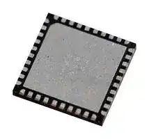
- QFN40L 6x6 (wettable flanks) with exposed pad
- Timeout watchdog and limp home function
- Low standby current
- Boost Section
- Fixed frequency architecture, programmable by SPI
- Peak current mode control
- Dual phase operation supported
- Input current limitation
- Soft start
- Overvoltage protection (OVP)
- Short feedback failure protection
-
- Constant voltage control
- Buck section
- Integrated switching mosfets
- Lossless current sensing without need of external components
- Very accurate LED current setting programming inductor's peak current and peak-to-peak current ripple
- Adjustable peak current by SPI
- Adjustable current ripple by SPI
- Integrated PWM generation unit with 10-bit resolution and phase shift
## **Applications**
- Low Beam
- High beam
- Daytime running light
- Turn indicator
- Position light
- Side marker
- Fog light
## **Description**
The L99LD21 is a flexible LED driver, which is specifically designed for the control of two independent high brightness LED strings for automotive front lighting applications. It consists of a high efficiency monolithic boost controller and a dual buck converter.
The boost controller integrates a high current gate driver for an external n-channel mosfet. It delivers a constant output voltage, up to 60 V, which supplies the inputs of the two integrated or external buck converters.
The boost controller of two devices can be stacked, in order to operate in dual phase for high power applications, with an interleaving pattern for an improved input current ripple.
The buck converters integrate n-channel mosfet which is driven by a bootstrap circuit.
DS11130 Rev 5
July 2018
1/73
This is information on a product in full production.
_www.st.com_
**Contents**
**L99LD21**
|**Contents**|**Contents**||
|---|---|---|
|**1**|**Introduction . . . . . . . . . . . . . . . . . . . . . . . . . . . . . . . . . . . . . . . . . . . . . . . . 8**||
||1.1|Typical application . . . . . . . . . . . . . . . . . . . . . . . . . . . . . . . . . . . . . . . . . . . 9|
|**2**|**Boost controller . . . . . . . . . . . . . . . . . . . . . . . . . . . . . . . . . . . . . . . . . . . . 13**||
||2.1|General description . . . . . . . . . . . . . . . . . . . . . . . . . . . . . . . . . . . . . . . . . 13|
||2.2|Frequency selection . . . . . . . . . . . . . . . . . . . . . . . . . . . . . . . . . . . . . . . . . 13|
||2.3|Output voltage setting . . . . . . . . . . . . . . . . . . . . . . . . . . . . . . . . . . . . . . . 13|
||2.4|Overvoltage protection . . . . . . . . . . . . . . . . . . . . . . . . . . . . . . . . . . . . . . . 13|
||2.5|Feedback failure protection . . . . . . . . . . . . . . . . . . . . . . . . . . . . . . . . . . . 14|
||2.6|Operation in dual phase interleaved mode . . . . . . . . . . . . . . . . . . . . . . . . 14|
||2.7|Soft start . . . . . . . . . . . . . . . . . . . . . . . . . . . . . . . . . . . . . . . . . . . . . . . . . . 16|
||2.8|Slope compensation . . . . . . . . . . . . . . . . . . . . . . . . . . . . . . . . . . . . . . . . . 16|
||2.9|Operation together with the buck converters . . . . . . . . . . . . . . . . . . . . . . 16|
|**3**|**Buck**|**converters . . . . . . . . . . . . . . . . . . . . . . . . . . . . . . . . . . . . . . . . . . . 18**|
||3.1|General description . . . . . . . . . . . . . . . . . . . . . . . . . . . . . . . . . . . . . . . . . 18|
||3.2|Bootstrap circuit . . . . . . . . . . . . . . . . . . . . . . . . . . . . . . . . . . . . . . . . . . . . 18|
||3.3|Peak and average current setting . . . . . . . . . . . . . . . . . . . . . . . . . . . . . . 18|
||3.4|Buck converter’s blank time . . . . . . . . . . . . . . . . . . . . . . . . . . . . . . . . . . . 20|
||3.5|Buck converter’s start-up . . . . . . . . . . . . . . . . . . . . . . . . . . . . . . . . . . . . . 21|
||3.6|Switching frequency . . . . . . . . . . . . . . . . . . . . . . . . . . . . . . . . . . . . . . . . . 21|
|**4**|**Functional description . . . . . . . . . . . . . . . . . . . . . . . . . . . . . . . . . . . . . . 22**||
||4.1|Operating modes . . . . . . . . . . . . . . . . . . . . . . . . . . . . . . . . . . . . . . . . . . . 22|
|||4.1.1<br>Standby mode . . . . . . . . . . . . . . . . . . . . . . . . . . . . . . . . . . . . . . . . . . . . 22|
|||4.1.2<br>Pre-standby mode . . . . . . . . . . . . . . . . . . . . . . . . . . . . . . . . . . . . . . . . . 23|
|||4.1.3<br>Reset mode . . . . . . . . . . . . . . . . . . . . . . . . . . . . . . . . . . . . . . . . . . . . . . 23|
|||4.1.4<br>Limp home . . . . . . . . . . . . . . . . . . . . . . . . . . . . . . . . . . . . . . . . . . . . . . . 23|
|||4.1.5<br>Active mode . . . . . . . . . . . . . . . . . . . . . . . . . . . . . . . . . . . . . . . . . . . . . . 24|
||4.2|Programmable functions . . . . . . . . . . . . . . . . . . . . . . . . . . . . . . . . . . . . . 25|
|||4.2.1<br>Activation of the buck output . . . . . . . . . . . . . . . . . . . . . . . . . . . . . . . . . 25|
|||4.2.2<br>PWM dimming . . . . . . . . . . . . . . . . . . . . . . . . . . . . . . . . . . . . . . . . . . . . 25|
DS11130 Rev 5
2/73
**Contents**
**L99LD21**
||4.3|Protections . . . . . . . . . . . . . . . . . . . . . . . . . . . . . . . . . . . . . . . . . . . . . . . . 26|
|---|---|---|
|||4.3.1<br>Temperature warning . . . . . . . . . . . . . . . . . . . . . . . . . . . . . . . . . . . . . . . 26|
|||4.3.2<br>Overtemperature shutdown . . . . . . . . . . . . . . . . . . . . . . . . . . . . . . . . . . 27|
|||4.3.3<br>VS under voltage lockout . . . . . . . . . . . . . . . . . . . . . . . . . . . . . . . . . . . . 27|
|||4.3.4<br>Buck TONminimum operation . . . . . . . . . . . . . . . . . . . . . . . . . . . . . . . . 27|
|||4.3.5<br>Buck output’s short circuit to GND . . . . . . . . . . . . . . . . . . . . . . . . . . . . . 27|
|||4.3.6<br>Buck TONmaximum operation . . . . . . . . . . . . . . . . . . . . . . . . . . . . . . . . 28|
|||4.3.7<br>Buck Open Load detection . . . . . . . . . . . . . . . . . . . . . . . . . . . . . . . . . . 28|
|**5**|**SPI**|**functional description . . . . . . . . . . . . . . . . . . . . . . . . . . . . . . . . . . . 29**|
||5.1|SPI protocol . . . . . . . . . . . . . . . . . . . . . . . . . . . . . . . . . . . . . . . . . . . . . . . 29|
||5.2|SPI communication . . . . . . . . . . . . . . . . . . . . . . . . . . . . . . . . . . . . . . . . . 29|
||5.3|Address mapping . . . . . . . . . . . . . . . . . . . . . . . . . . . . . . . . . . . . . . . . . . . 31|
||5.4|Registers description . . . . . . . . . . . . . . . . . . . . . . . . . . . . . . . . . . . . . . . . 33|
|||5.4.1<br>Control Register description . . . . . . . . . . . . . . . . . . . . . . . . . . . . . . . . . 33|
|||5.4.2<br>Status Register description . . . . . . . . . . . . . . . . . . . . . . . . . . . . . . . . . . 39|
|||5.4.3<br>Customer test and trimming registers description . . . . . . . . . . . . . . . . . 45|
|||5.4.4<br>Customer test and trimming procedure description . . . . . . . . . . . . . . . . 46|
|**6**|**Electrical specifications . . . . . . . . . . . . . . . . . . . . . . . . . . . . . . . . . . . . . 51**||
||6.1|Absolute maximum ratings . . . . . . . . . . . . . . . . . . . . . . . . . . . . . . . . . . . . 51|
||6.2|ESD protection . . . . . . . . . . . . . . . . . . . . . . . . . . . . . . . . . . . . . . . . . . . . . 52|
||6.3|Thermal characteristics . . . . . . . . . . . . . . . . . . . . . . . . . . . . . . . . . . . . . . 52|
||6.4|Electrical characteristics . . . . . . . . . . . . . . . . . . . . . . . . . . . . . . . . . . . . . . 53|
|||6.4.1<br>Supply . . . . . . . . . . . . . . . . . . . . . . . . . . . . . . . . . . . . . . . . . . . . . . . . . . 53|
|||6.4.2<br>Boost controller . . . . . . . . . . . . . . . . . . . . . . . . . . . . . . . . . . . . . . . . . . . 54|
|||6.4.3<br>Buck . . . . . . . . . . . . . . . . . . . . . . . . . . . . . . . . . . . . . . . . . . . . . . . . . . . 56|
|||6.4.4<br>SPI . . . . . . . . . . . . . . . . . . . . . . . . . . . . . . . . . . . . . . . . . . . . . . . . . . . . . 62|
|||6.4.5<br>Direct input . . . . . . . . . . . . . . . . . . . . . . . . . . . . . . . . . . . . . . . . . . . . . . . 63|
|||6.4.6<br>PWM dimming . . . . . . . . . . . . . . . . . . . . . . . . . . . . . . . . . . . . . . . . . . . . 64|
|||6.4.7<br>Digital timings . . . . . . . . . . . . . . . . . . . . . . . . . . . . . . . . . . . . . . . . . . . . 65|
|**7**|**Package and PCB thermal data . . . . . . . . . . . . . . . . . . . . . . . . . . . . . . . 66**||
||7.1|QFN-40L 6x6 thermal data . . . . . . . . . . . . . . . . . . . . . . . . . . . . . . . . . . . . 66|
|**8**|**Package information . . . . . . . . . . . . . . . . . . . . . . . . . . . . . . . . . . . . . . . . 67**||
DS11130 Rev 5
3/73
|**Contents**<br>**L99LD21**|
|---|
|8.1<br>QFN-40L 6x6 package information . . . . . . . . . . . . . . . . . . . . . . . . . . . . . 67|
|**9**<br>**Order codes . . . . . . . . . . . . . . . . . . . . . . . . . . . . . . . . . . . . . . . . . . . . . . . 69**|
|**Appendix A**<br>**Glossary . . . . . . . . . . . . . . . . . . . . . . . . . . . . . . . . . . . . . . . . . . . . . . . 70**|
|**Revision history . . . . . . . . . . . . . . . . . . . . . . . . . . . . . . . . . . . . . . . . . . . . . . . . . . . . 71**|
DS11130 Rev 5
4/73
**L99LD21**
**List of tables**
## **List of tables**
|Table|1.|Pin functionality. . . . . . . . . . . . . . . . . . . . . . . . . . . . . . . . . . . . . . . . . . . . . . . . . . . . . . . . . . 11|
|---|---|---|
|Table|2.|Reference voltage configuration . . . . . . . . . . . . . . . . . . . . . . . . . . . . . . . . . . . . . . . . . . . . . 13|
|Table|3.|Operating modes . . . . . . . . . . . . . . . . . . . . . . . . . . . . . . . . . . . . . . . . . . . . . . . . . . . . . . . . 24|
|Table|4.|DIN pin Map for Buck1 and Buck2 . . . . . . . . . . . . . . . . . . . . . . . . . . . . . . . . . . . . . . . . . . . 25|
|Table|5.|Command byte (8 bit) . . . . . . . . . . . . . . . . . . . . . . . . . . . . . . . . . . . . . . . . . . . . . . . . . . . . . 29|
|Table|6.|Data byte 2 . . . . . . . . . . . . . . . . . . . . . . . . . . . . . . . . . . . . . . . . . . . . . . . . . . . . . . . . . . . . . 29|
|Table|7.|Data byte 1 . . . . . . . . . . . . . . . . . . . . . . . . . . . . . . . . . . . . . . . . . . . . . . . . . . . . . . . . . . . . . 29|
|Table|8.|Data byte 0 . . . . . . . . . . . . . . . . . . . . . . . . . . . . . . . . . . . . . . . . . . . . . . . . . . . . . . . . . . . . . 30|
|Table|9.|Operation code definition . . . . . . . . . . . . . . . . . . . . . . . . . . . . . . . . . . . . . . . . . . . . . . . . . . 30|
|Table|10.|Global Status Byte . . . . . . . . . . . . . . . . . . . . . . . . . . . . . . . . . . . . . . . . . . . . . . . . . . . . . . . 30|
|Table|11.|Global Status Byte description . . . . . . . . . . . . . . . . . . . . . . . . . . . . . . . . . . . . . . . . . . . . . . 31|
|Table|12.|RAM memory map . . . . . . . . . . . . . . . . . . . . . . . . . . . . . . . . . . . . . . . . . . . . . . . . . . . . . . . 31|
|Table|13.|ROM memory map . . . . . . . . . . . . . . . . . . . . . . . . . . . . . . . . . . . . . . . . . . . . . . . . . . . . . . . 32|
|Table|14.|CR#1: Control Register 1 . . . . . . . . . . . . . . . . . . . . . . . . . . . . . . . . . . . . . . . . . . . . . . . . . . 33|
|Table|15.|CR#2: Control Register 2 . . . . . . . . . . . . . . . . . . . . . . . . . . . . . . . . . . . . . . . . . . . . . . . . . . 34|
|Table|16.|CR#3: Control Register 3 . . . . . . . . . . . . . . . . . . . . . . . . . . . . . . . . . . . . . . . . . . . . . . . . . . 35|
|Table|17.|CR#4: Control Register 4 . . . . . . . . . . . . . . . . . . . . . . . . . . . . . . . . . . . . . . . . . . . . . . . . . . 36|
|Table|18.|Constant VLED x TOFF selection. . . . . . . . . . . . . . . . . . . . . . . . . . . . . . . . . . . . . . . . . . . . 37|
|Table|19.|DIN map table for Buck Cell X . . . . . . . . . . . . . . . . . . . . . . . . . . . . . . . . . . . . . . . . . . . . . . 37|
|Table|20.|Boost clock selection . . . . . . . . . . . . . . . . . . . . . . . . . . . . . . . . . . . . . . . . . . . . . . . . . . . . . 37|
|Table|21.|Buck input voltage window . . . . . . . . . . . . . . . . . . . . . . . . . . . . . . . . . . . . . . . . . . . . . . . . . 38|
|Table|22.|SR#1: Status Register 1 . . . . . . . . . . . . . . . . . . . . . . . . . . . . . . . . . . . . . . . . . . . . . . . . . . . 39|
|Table|23.|SR#2: Status Register 2 . . . . . . . . . . . . . . . . . . . . . . . . . . . . . . . . . . . . . . . . . . . . . . . . . . . 41|
|Table|24.|SR#3: Status Register 3 . . . . . . . . . . . . . . . . . . . . . . . . . . . . . . . . . . . . . . . . . . . . . . . . . . . 44|
|Table|25.|Watchdog status . . . . . . . . . . . . . . . . . . . . . . . . . . . . . . . . . . . . . . . . . . . . . . . . . . . . . . . . . 44|
|Table|26.|CT: Ctm Trimming Register . . . . . . . . . . . . . . . . . . . . . . . . . . . . . . . . . . . . . . . . . . . . . . . . 45|
|Table|27.|Writing test conditions. . . . . . . . . . . . . . . . . . . . . . . . . . . . . . . . . . . . . . . . . . . . . . . . . . . . . 46|
|Table|28.|Testing procedure description . . . . . . . . . . . . . . . . . . . . . . . . . . . . . . . . . . . . . . . . . . . . . . 48|
|Table|29.|Default peak current selection for Buck Cell 1 . . . . . . . . . . . . . . . . . . . . . . . . . . . . . . . . . . 50|
|Table|30.|Default VLEDxTOFF Selection for Buck Cell 1. . . . . . . . . . . . . . . . . . . . . . . . . . . . . . . . . . 50|
|Table|31.|Absolute maximum ratings . . . . . . . . . . . . . . . . . . . . . . . . . . . . . . . . . . . . . . . . . . . . . . . . . 51|
|Table|32.|ESD protection . . . . . . . . . . . . . . . . . . . . . . . . . . . . . . . . . . . . . . . . . . . . . . . . . . . . . . . . . . 52|
|Table|33.|QFN40L 6x6 thermal resistance . . . . . . . . . . . . . . . . . . . . . . . . . . . . . . . . . . . . . . . . . . . . . 52|
|Table|34.|Thermal characteristics. . . . . . . . . . . . . . . . . . . . . . . . . . . . . . . . . . . . . . . . . . . . . . . . . . . . 52|
|Table|35.|Supply. . . . . . . . . . . . . . . . . . . . . . . . . . . . . . . . . . . . . . . . . . . . . . . . . . . . . . . . . . . . . . . . . 53|
|Table|36.|Boost gate driver. . . . . . . . . . . . . . . . . . . . . . . . . . . . . . . . . . . . . . . . . . . . . . . . . . . . . . . . . 54|
|Table|37.|Boost controller. . . . . . . . . . . . . . . . . . . . . . . . . . . . . . . . . . . . . . . . . . . . . . . . . . . . . . . . . . 54|
|Table|38.|Boost controller reference voltage . . . . . . . . . . . . . . . . . . . . . . . . . . . . . . . . . . . . . . . . . . . 55|
|Table|39.|Buck converter power stage . . . . . . . . . . . . . . . . . . . . . . . . . . . . . . . . . . . . . . . . . . . . . . . . 56|
|Table|40.|Inductor peak current selection. . . . . . . . . . . . . . . . . . . . . . . . . . . . . . . . . . . . . . . . . . . . . . 58|
|Table|41.|VLEDxTOFF constants. . . . . . . . . . . . . . . . . . . . . . . . . . . . . . . . . . . . . . . . . . . . . . . . . . . . 61|
|Table|42.|SPI signal description . . . . . . . . . . . . . . . . . . . . . . . . . . . . . . . . . . . . . . . . . . . . . . . . . . . . . 62|
|Table|43.|SPI timings . . . . . . . . . . . . . . . . . . . . . . . . . . . . . . . . . . . . . . . . . . . . . . . . . . . . . . . . . . . . . 62|
|Table|44.|Direct Input pin limits . . . . . . . . . . . . . . . . . . . . . . . . . . . . . . . . . . . . . . . . . . . . . . . . . . . . . 63|
|Table|45.|PWMCLK and Fall back PWM description . . . . . . . . . . . . . . . . . . . . . . . . . . . . . . . . . . . . . 64|
|Table|46.|Digital timings description . . . . . . . . . . . . . . . . . . . . . . . . . . . . . . . . . . . . . . . . . . . . . . . . . . 65|
|Table|47.|PCB properties . . . . . . . . . . . . . . . . . . . . . . . . . . . . . . . . . . . . . . . . . . . . . . . . . . . . . . . . . . 66|
|Table|48.|QFN-40L 6x6 mechanical data . . . . . . . . . . . . . . . . . . . . . . . . . . . . . . . . . . . . . . . . . . . . . . 68|
DS11130 Rev 5
5/73
**List of tables**
**L99LD21**
|Table|49.|Device summary . . . . . . . . . . . . . . . . . . . . . . . . . . . . . . . . . . . . . . . . . . . . . . . . . . . . . . . . . 69|
|---|---|---|
|Table|50.|Glossary . . . . . . . . . . . . . . . . . . . . . . . . . . . . . . . . . . . . . . . . . . . . . . . . . . . . . . . . . . . . . . . 70|
|Table|51.|Document revision history . . . . . . . . . . . . . . . . . . . . . . . . . . . . . . . . . . . . . . . . . . . . . . . . . 71|
DS11130 Rev 5
6/73
**L99LD21**
**List of figures**
## **List of figures**
|Figure|1.|Functional block diagram . . . . . . . . . . . . . . . . . . . . . . . . . . . . . . . . . . . . . . . . . . . . . . . . . . . 9|
|---|---|---|
|Figure|2.|Typical application schematic . . . . . . . . . . . . . . . . . . . . . . . . . . . . . . . . . . . . . . . . . . . . . . . 10|
|Figure|3.|Application diagram . . . . . . . . . . . . . . . . . . . . . . . . . . . . . . . . . . . . . . . . . . . . . . . . . . . . . . 10|
|Figure|4.|Connection diagram . . . . . . . . . . . . . . . . . . . . . . . . . . . . . . . . . . . . . . . . . . . . . . . . . . . . . . 11|
|Figure|5.|Pin connections in dual-phase boost controller . . . . . . . . . . . . . . . . . . . . . . . . . . . . . . . . . 15|
|Figure|6.|Slope compensation . . . . . . . . . . . . . . . . . . . . . . . . . . . . . . . . . . . . . . . . . . . . . . . . . . . . . . 16|
|Figure|7.|Peak current control principle . . . . . . . . . . . . . . . . . . . . . . . . . . . . . . . . . . . . . . . . . . . . . . . 19|
|Figure|8.|Inductor and mosfet current waveforms . . . . . . . . . . . . . . . . . . . . . . . . . . . . . . . . . . . . . . . 20|
|Figure|9.|Device state diagram . . . . . . . . . . . . . . . . . . . . . . . . . . . . . . . . . . . . . . . . . . . . . . . . . . . . . 22|
|Figure|10.|Testing flow chart . . . . . . . . . . . . . . . . . . . . . . . . . . . . . . . . . . . . . . . . . . . . . . . . . . . . . . . . 47|
|Figure|11.|IL_PEAK vs DAC code - Low Rdson . . . . . . . . . . . . . . . . . . . . . . . . . . . . . . . . . . . . . . . . . . . . . . . . . . . . .60|
|Figure|12.|IL_PEAK vs DAC code - High Rdson . . . . . . . . . . . . . . . . . . . . . . . . . . . . . . . . . . . . . . . . . . . . . . . . . . . . .60|
|Figure|13.|VLEDx TOFFvs DAC code . . . . . . . . . . . . . . . . . . . . . . . . . . . . . . . . . . . . . . . . . . . . . . . . . 61|
|Figure|14.|PWM clock failure and reset sequence . . . . . . . . . . . . . . . . . . . . . . . . . . . . . . . . . . . . . . . 64|
|Figure|15.|QFN-40L 6x6 on four-layers PCB. . . . . . . . . . . . . . . . . . . . . . . . . . . . . . . . . . . . . . . . . . . . 66|
|Figure|16.|QFN-40L 6x6 package dimensions . . . . . . . . . . . . . . . . . . . . . . . . . . . . . . . . . . . . . . . . . . 67|
DS11130 Rev 5
7/73
**Introduction**
**L99LD21**
## **1 Introduction**
The L99LD21 is a monolithic driver IC, which controls the current of two independent high power LED strings, whose forward current and voltage can reach up to 1.5 A (average) and up to 50V respectively.
This device has been designed with dedicated functions, in order to fulfill the stringent requirements of automotive front lighting applications.
The device offers a high level of flexibility, without any change of the external components, thanks to its programmability through the ST SPI interface. This feature support generic platform approaches, which require a software configurability of several parameters. This robust interface, offers a detailed diagnostic of the device itself, as well as of the controlled LED strings.
As the device potentially controls safety critical functions such as low beams and turn indicators, built-in features are integrated in order to support a high level of functional safety. The L99LD21 features a timeout watchdog, a monitoring of the watchdog counter, a limp home function and a direct input. The ST SPI protocol takes into account FMEA case.
The device consists of a boost controller, which controls the PWM of an external n-channel mosfet and provides a stabilized voltage (VBOOST). The input of the boost stage must be connected to the battery voltage through a reverse polarity protection.
The boost controllers of two L99LD21 can be combined to form a dual-phase, interleaved boost controller. Special care has been taken for the current balancing between the different phases and for the switching activity of the boost mosfets with 180° phase shift.
The output of the boost controller supplies the input of the two independent integrated buck converters, or any other external buck converters, whose input voltage is compatible with VBOOST. The integrated buck converters are based on constant off-time architecture (for a given LED output voltage) and control the peak current and the peak-to-peak current ripple of their respective inductors.
Operating in continuous conduction mode, the average of each LED string’s current, which is connected to the output of each buck converter, is tightly controlled.
This architecture, which consists of cascaded boost and buck stages (see _Figure 2_ ), allows the control of a wide range of LED strings, whose forward voltage is independent from the battery voltage.
With the aim of ensuring a wide operating inductor current range, the Buck mosfets can be set in low or high RDS_ON modes, so that two different inductor peak current (ILx_PEAK) ranges [0.179 A ÷ 0.849 A] or [0.362 A ÷ 1.695 A] can be selected.
The average LED current is controlled by setting the inductor's peak current and peak-topeak current ripple. Sensing of the peak current is integrated, not requiring any external shunt resistance, which saves cost and reduces the power dissipation.
Buck n-channel mosfet RDS_ON value depends on the operative conditions as junction temperature, Input voltage and LED string current. For example, at VBuckin = 45 V, Iled = 700 mA, Tj = 25 °C the maximum RDS_ON is 400 mΩ (low RDS_ON mode).
DS11130 Rev 5
8/73
**L99LD21**
**Introduction**
## **1.1 Typical application**
## **Figure 1. Functional block diagram**
DS11130 Rev 5
9/73
**Introduction**
**L99LD21**
## **Figure 2. Typical application schematic**
**Figure 3. Application diagram**
DS11130 Rev 5
10/73
**L99LD21**
**Introduction**
## **Figure 4. Connection diagram**
**Table 1. Pin functionality**
|||**Table 1. Pin functionalityy**|
|---|---|---|
|**Pin #**|**Name**|**Function**|
|1|V3V3|Output of the 3.3 V regulated internal supply. Connect a low ESR<br>capacitor (4.7 µF) close to this pin.|
|2|SYNC_I/O|Boost synchronization Input or Output. This pin generates the clock<br>signal for synchronizing another L99LD21 Boost in dual phase<br>configuration.|
|3|CSN|Chip Select Not (active low) for SPI communication. It is the selection pin<br>of the device. It is a CMOS compatible input.|
|4|PWMCLK|Clock input for the internal PWM dimming generator.|
|5|SGND|Signal Ground connection.|
|6|SCK|Serial Clock for SPI communication. It is a CMOS compatible input.|
|7|VSPI|Connection to external 3.3 V or 5 V supplies voltage.<br>The external supply powers SPI interface and the I/O signal pins to the<br>microcontroller. It is suggested to connect 100nF capacitor close to this<br>pin.|
|8|SDI|Serial Data Input for SPI communication. Data is transferred serially into<br>the device on SCK rising edge.|
|9|SDO|Serial Data Output for SPI communication. Data is transferred serially<br>out of the device on SCK falling edge.|
|10|DIN|Direct input pin.|
|16|LX2F|Connection to the switching source node of the buck2. This pin must be<br>connected to external free-wheeling diode.|
DS11130 Rev 5
11/73
**Introduction**
**L99LD21**
**Table 1. Pin functionality (continued)**
|||**Table 1. Pin functionality (continued)**|
|---|---|---|
|**Pin #**|**Name**|**Function**|
|17|LX2S|Kelvin connection to the switching source node of the buck2. This pin<br>has to be connected to external bootstrap capacitance.|
|18|BUCKIN2|Connection to the input of the buck channel 2|
|20|CBOOT2|Connection to the bootstrap capacitor (100nF) of the buck channel 2.|
|22, 38|PGND|Power Ground connection.|
|23|VLED2|Connection to the anode of the LED string for read back of the forward<br>voltage of the channel 2.|
|24|VLED1|Connection to the anode of the LED string for read back of the forward<br>voltage of the channel 1.|
|25|LX1F|Connection to the switching source node of the buck1. This pin must be<br>connected to external free-wheeling diode.|
|26|LX1S|Kelvin connection to the switching source node of the buck1. This pin<br>has to be connected to external bootstrap capacitance.|
|28|BUCKIN1|Connection to the input of the buck channel 1.|
|30|CBOOT1|Connection to the bootstrap capacitor (100 nF) of the buck channel 1.|
|31|VS|Input supply pin of the IC. Connect VS to the battery voltage.|
|32|V5V|Output of the 5V regulated internal supply. Connect a low ESR capacitor<br>(4.7 µF) close to this pin.|
|34|G0|Output of the boost gate driver for the external switching mosfet.|
|35|SP|Positive connection to the boost shunt resistor, in series to the boost<br>switching mosfet.|
|37|SN|Negative connection (Ground) to the boost shunt resistor, in series to the<br>boost switching mosfet.|
|39|COMP|Output of the error amplifier of the boost controller. Connect the<br>compensation network between this pin and SGND.|
|40|FB|Boost output voltage feedback. Connect the FB pin to the boost output<br>voltage, via a resistor divider.|
|11, 12, 13,<br>14, 15, 19,<br>21, 27, 29,<br>33, 36|NC|Not connected|
DS11130 Rev 5
12/73
**L99LD21**
**Boost controller**
## **2 Boost controller**
## **2.1 General description**
The L99LD21 integrates one boost controller, which is based on a fixed frequency, peak current mode architecture. It drives the gate of an external n-channel mosfet in order to step up the VS input voltage to a higher stabilized output voltage.
## **2.2 Frequency selection**
The boost controller operates at a fixed frequency which can range from 100 kHz to 450 kHz. The switching frequency is set by a SPI control register (CR#3<9:7>, see _Section 5.4: Registers description_ ).
## **2.3**
## **Output voltage setting**
The control loop regulates the voltage at the FB pin to a reference voltage, which value, according table 2, is configurable by the control register CR#3<11:10> (see _Section 5.4: Registers description_ ). Connect the resistor divider tap, top and bottom respectively to the FB pin, to output of the boost controller and to the bottom to SGND.
The resulting boost output voltage is given by:
**==> picture [151 x 26] intentionally omitted <==**
## **Table 2. Reference voltage configuration**
|**b1**|**b0**|**VFB_REF [V]**|
|---|---|---|
|0|0|0.596|
|0|1|0.895|
|1|0|1.242|
|1|1|1.496|
## **2.4**
## **Overvoltage protection**
The peak current mode requires a minimum on-time, because of the noise generated right after the turn-on of the switching mosfet. At light load (very low output current), this minimum on-time, in combination with the selected switching frequency is no longer able to regulate the output voltage to the requested voltage. The device enters in overvoltage protection (OVP), in order to prevent an excessive rise of the boost output voltage above the target voltage.
DS11130 Rev 5
13/73
**Boost controller**
**L99LD21**
This mode is activated when the voltage on FB pin is higher than the selected internal reference voltage of a specified threshold value (VFB_OV_ON).
The switching activity is resumed as soon as the voltage on FB pin decreases to the selected internal reference voltage (VFB_REF[xx]).
In case of FB voltage increases above VFB_OV_ON, an output digital flag, called BST_OVP, is set.
As soon as feedback voltage decreases down to target value (VFB_REF[xx]), the bit is reset after tBST_OVP_RST delay time. This delay time is implemented in order to eliminate the diagnostic ambiguity (toggling of the OVP flag) during permanent no load / light load operation.
BST_OVP bit is not set in case of boost disabled or boost feedback failure.
## **2.5 Feedback failure protection**
L99LD21 is protected in case of boost controller feedback pin failure. More in detail, a specific bit, called BST_FB_FAIL, is set in case of feedback pin is shorted to ground.
When this bit is set:
- If device is OFF, boost controller does not start;
- If device is ON in single phase configuration, boost controller is immediately switched OFF;
- If device is ON in dual phase configuration and it is in Active mode: both boost controllers are switched off when the failure is recognized on Master side; only Slave controller is switched off when the failure is recognized on Slave side while the Master is managed by the microcontroller;
- If device is ON in dual phase configuration and it is in Limp Home: both boost controllers are switched off when the failure is recognized on Master side; only Slave controller is switched off when the failure is recognized on Slave side, while the Master is forced to work at minimum duty cycle.
The reset of FB failure bit is demanded to the microcontroller (in Active mode) or to an autorestart function (in Limp Home) that cyclically clears this bit with a period equal to
## tAUTORESTART.
This bit is not set if L99LD21 internal boost controller is not used (in this case, BST_DIS bit is set).
If left floating, feedback pin will be pulled up internally. In this case, BST_OVP bit will be set permanently and boost gate driver will be permanently off. Since the feedback pin voltage is in any case high, N_PWR_GOOD flag is reset in such condition and shall be ignored.
_Note: Setting this bit doesn't imply any action on buck converters._
## **2.6 Operation in dual phase interleaved mode**
It is possible to combine the boost controllers of two L99LD21, for high power applications, in dual phase configuration. In this configuration, the switching mosfets of the boost controllers are driven at 180° out of phase. By sharing the current between two phases, the conduction losses (which are proportional the square of the conducted current) are reduced and the efficiency of the boost stage increases, in comparison to a single-phase.
DS11130 Rev 5
14/73
**L99LD21**
**Boost controller**
The effective switching frequency is doubled and the ripple cancellation effect results in a reduction of the input and output current ripple. This allows small input and output capacitances.
For an operation in dual-phase configuration, FB, COMP and SYNC_I/O pins must be respectively connected together as shown in _Figure 5_ .
**Figure 5. Pin connections in dual-phase boost controller**
One of the L99LD21 must be configured as the master and the other device must be configured as the slave (see bit <1> on _Table 15: CR#2: Control Register 2_ ). The SYNC_I/O of the master acts as an output, whilst the slave one respectively as an input. The master boost provides a clock signal to the slave, in order to achieve an interleaved switching activity of the slave boost controller, which is 180° out of phase to that of the master.
For a proper current balancing between the boost phases, the shunt resistors, which are placed in series to the source of the mosfets, and the inductors, must be identical.
DS11130 Rev 5
15/73
**Boost controller**
**L99LD21**
## **2.7 Soft start**
The L99LD21 features an internal soft start function, which gradually increases the boost mosfet current limit in 8 steps, in order to avoid a voltage overshoot of the boost output. The threshold of the current limitation reaches its nominal value after a specified soft start time (tSS).
A soft-start phase is initiated at the activation of the boost controller:
- after leaving standby mode;
- after deactivation of the boost controller due to a VS under voltage;
- after a previous de-activation of the boost by SPI (see bit <1> on _Table 16: CR#3: Control Register 3_ );
- after deactivation of the boost controller due to a BST_FB_FAIL.
## **2.8 Slope compensation**
Slope compensation is needed to ensure loop stability with all possible values of duty cycle: D = TON / T (0 < D < 1) especially when duty cycle is greater than 0.5. The slope of the additional ramp is proportional to converter inductor current slope during the turn off phase.
The L99LD21 generates an internal peak current value, ISLOPE, which is added to the sensing signal at the output of the OTA. The percentage of slope compensation is achieved by choosing a proper value of the RSC resistor (see _Figure 2_ for RSC resistor proper connection).
## **Figure 6. Slope compensation**
**==> picture [405 x 188] intentionally omitted <==**
**----- Start of picture text -----**<br>
�<br>��<br>��<br>��<br>���� ����������������������������������<br>�<br>�<br>���� �� ���<br>�<br>� � ���� ������������������<br>�����<br>��<br>�<br>�<br>�<br>�����������������<br>**----- End of picture text -----**<br>
## **2.9 Operation together with the buck converters**
Right after a power on reset (POR) of the device or after a fault event leading to a latch-off of the boost controller (VS under voltage), a soft start phase is initiated and the boost is activated.
DS11130 Rev 5
16/73
**L99LD21**
**Boost controller**
The buck converters activation depends on device status (see _Section 4.1: Operating modes_ ):
- Active mode: in this case, bucks are immediately operative. Their status will depend on DINMAP register configuration (see _Section 4.2.1_ );
- Limp Home:
- we have to distinguish two different cases:
Boost Enabled with output voltage higher than 92.5% of final target value. In this case, buck converters are immediately operative according to DIN_MAP register configuration;
Boost Disabled or Enabled with output voltage lower than 92.5 % of final target value. In this case, the buck converters are kept disabled for a specified time delay (tDELAY) independently from DINMAP status. Once this time elapses, bucks are operative according to DINMAP register configuration.
On the other hand, when boost and bucks are active and a VS undervoltage fault event occurs, buck converters are immediately disabled while the boost is kept alive for tDELAY before being switched off.
DS11130 Rev 5
17/73
**Buck converters**
**L99LD21**
## **3 Buck converters**
## **3.1 General description**
The L99LD21 features two independent buck converters with integrated switching mosfets with forward peak current as high as specified maximum ILx_PEAK (where x indicates Buckx peak current) 1.695 A. They are optimized to deliver a constant current to LED strings.
The RDS_ON of the n-channel mosfets can be set programming the appropriate bit in the control register (see bits <3:2> on _Table 14: CR#1: Control Register 1_ ): high RDS_ON mode (only one half power stage enabled) or low RDS_ON mode (both half power stages enabled).
This feature allows having two different inductor peak current ranges, 0.179 A ÷ 0.849 A or 0.362 A ÷ 1.695 A, respectively for high RDS_ON and low RDS_ON mode, so achieving the highest of current sense accuracy in the whole current range.
The buck converters are based on constant off-time architecture, which regulates the peak current in each inductor. The monitoring of the inductor peak current is done through integrated senseFETs. This results in a lossless high side current sensing, which does not require any external shunt resistor, and improves the system efficiency.
This architecture provides an inherent cycle-by cycle current limitation and a fast transient response, without any compensation of the control loop.
The average LED current in each LED string is configurable by the SPI, through configuration of the inductor peak current and peak-to-peak current.
The dimming of the LED strings can be realized through the direct input pin (DIN) or through the internal 10-bit PWM dimming generator.
## **3.2 Bootstrap circuit**
The L99LD21 has built-in high side n-channel switching mosfets, which are driven by gate drivers. Each gate driver uses a bootstrap circuit, consisting of an integrated diode and an external capacitor between the LX1S and CBOOT1 pins, respectively between the LX2S and CBOOT2 pins.
The buck converters impose a minimum off-time (TOFF_MIN) to ensure that the bootstrap capacitor recharges every cycle to a voltage which avoids the switching mosfet to operate in linear mode. TOFF_MIN restricts the maximum duty cycle of the buck converters for a given switching frequency. This effect is more pronounced at high switching frequencies and limits the maximum ratio between the buck input voltage (VBOOST) and the LED strings’ forward voltage. One way to overcome this limitation is reducing switching frequency, by selecting high constant VLED xTOFF and/or increase the inductance value.
## **3.3 Peak and average current setting**
In buck converters, the inductor is directly connected to the load during the complete switching cycle (see _Figure 7: Peak current control principle_ ). The average inductor current is equal to the average LED string current. Operating in continuous conduction mode (i.e. the inductor current never decays to zero during the off-phase), if the inductor current is tightly controlled, the LED current will be regulated as well.
DS11130 Rev 5
18/73
**L99LD21**
**Buck converters**
## **Figure 7. Peak current control principle**
At the beginning of a switching period the MOSFET M1 is turned on, and the inductor current IL1 increases. The mosfet is activated for a minimum on-time TON_MIN in order to avoid that the on-phase is ended up by spurious noise, which is caused by the switch-on.
During mosfet activation, the inductor current, IL1, increases until reaching a maximum value, IL1_PEAK, which is set through a dedicated control register (see bits <23:18> and bits <17:12> on _Table 15: CR#2: Control Register 2_ ). When IL1 reaches its peak value, the switching mosfet is turned off. The mosfet remains off for a time TOFF, which is derived from the configured constant VLED1xTOFF1 (see bits <11:8> and bits <7:4> on _Table 15: CR#2: Control Register 2_ ), where VLED1 is the forward voltage of the LED string, which is connected at the output of the buck converter 1.
During TOFF, the inductor current decreases by:
**==> picture [245 x 28] intentionally omitted <==**
**----- Start of picture text -----**<br>
Δ I = (--------------------------------------------- VLED1 – VF_D1 ) ⋅ T ∼ V ---------------------------------------- LED1 ⋅ TOFF1<br>L1_PP L OFF1 L<br>1 1<br>**----- End of picture text -----**<br>
DS11130 Rev 5
19/73
**Buck converters**
**L99LD21**
where Δ IL1_PP is the inductor peak to peak current and VF_D1 is the forward voltage of the diode D1. As D1 is a Schottky diode with a low forward voltage, VF_D1 can be in general neglected, compared to VLED1.
_Note: Once the VLEDxTOFF constant for a given buck converter is selected by SPI, the peak-topeak inductor current ripple is constant. In particular, it depends neither on the boost voltage nor on the LED forward voltage._
The ripple current through the LED strings is reduced by means of an external capacitor in parallel with the LEDs.
## **Figure 8. Inductor and mosfet current waveforms**
**==> picture [405 x 185] intentionally omitted <==**
**----- Start of picture text -----**<br>
���<br>�<br>�������<br>������������������� �������<br>����<br>� ���<br>�����������������<br>**----- End of picture text -----**<br>
Referring to the _Figure 7_ and _Figure 8_ the average LED current - valid for both Buck 1 and Buck 2 - is therefore:
**==> picture [343 x 24] intentionally omitted <==**
where IL1_PEAK* results from IL1_PEAK (see _Table 40_ ) corrected with loop delay (tloop_delay)
In order to achieve the best accuracy versus input voltage variation during current sensing process, a defined buck input voltage window must be selected, by means of a dedicated control register (see bits <5:4> and bits <3:2> on _Table 16: CR#3: Control Register 3_ ).
## **3.4 Buck converter’s blank time**
The buck converters have a minimum on-time TBLANK_BUCK. Although the inductor’s target peak current ILx_PEAK is reached before this time has elapsed, the switch is kept on. This delay is used as a leading-edge blank time, in order to avoid a premature end of the switching cycle, which might be caused by the noise, which results from the commutation of the buck’s mosfet.
DS11130 Rev 5
20/73
**L99LD21**
**Buck converters**
## **3.5 Buck converter’s start-up**
While the device and the system are protected against short circuit conditions of the buck’s output to GND, the device inhibits the detection of the short circuit during the startup phase TSTARTUP.
A startup phase is applied in the following conditions:
- If one of the buck converters is activated for the first time after a power on reset (POR), including buck activation after device wake-up;
- If one of the buck converters has been deactivated for more than tDELAY;
- If one of the buck converters has been latched off prior to a Read and Clear command;
- If one of the buck converters is re-activated after a VS under voltage event.
After these events, it is possible that the output capacitors of the buck converters are completely discharged. The charging of the buck output capacitors might lead switching cycles with short on-time (shorter than TON_MIN), which could potentially lead to a wrong detection of a shorted buck output. The introduction of this start-up phase avoids this wrong diagnostic.
## **3.6 Switching frequency**
For a given buck converter, the switching frequency depends on the buck input voltage (output of the boost controller) and the forward voltage of the LED string, which is connected to its output.
In continuous conduction mode, TOFF is given by:
**==> picture [124 x 24] intentionally omitted <==**
Where D is the buck converter’s duty cycle, T and FSW are respectively the switching period and frequency.
Neglecting the drop voltage across the mosfet, the inductor’s DC resistance and the diode’s forward voltage, compared to VBUCKIN and VLED, we have:
**==> picture [212 x 88] intentionally omitted <==**
For a given application (given inductance and VLED), it is possible to set ILEDx_AVG by selecting different combinations of ILx_PEAK and VLEDxTOFF in order to avoid critical frequency ranges such as the AM radio band.
To avoid buck operation at not allowed TON and/or TOFF times, frequency range has to be kept inside FSWmin and FSWmax, where:
FSWmin = 1/(TON_MAX_BUCK + TOFF_MAX_BUCK)
FSWmax = 1/(TON_MIN_BUCK + TOFF_MIN_BUCK)
DS11130 Rev 5
21/73
**Functional description**
**L99LD21**
## **4 Functional description**
## **4.1 Operating modes**
## **Figure 9. Device state diagram**
## **4.1.1 Standby mode**
The pre-requisite for this mode is:
- Device in Pre-Standby mode.
The device enters Standby mode under the following conditions:
- By default, once the device is powered (VS present);
- CSN High and DIN Low for more than tSTDBY
The Standby mode characteristics are:
- V3V3 < VPOR
- VSPI and VS low consumption
- SPI inactive
The device leaves this mode if:
- DIN High or CSN Low for a time t > tWAKEUP
DS11130 Rev 5
22/73
**L99LD21**
**Functional description**
_Note: Vs must be stable above minimum value specified (5.5 V) before rising edge on DIN or falling edge on CSN._
## **4.1.2 Pre-standby mode**
The device enters Pre-standby mode under the following conditions:
- upon the two following consecutive SPI frames setting:
- UNLOCK = 1
- (EN, GOSTBY) = (0, 1)
The Pre-standby mode characteristics are:
- V3V3 > VPOR
- Boost disabled
- Bucks disabled
- SPI active
The device leaves automatically Pre-standby mode entering standby:
- if CSN High and DIN Low for a time t > tSTDBY
## **4.1.3**
## **Reset mode**
The device enters Reset mode under the following conditions:
- By default, once the device leaves Standby mode;
- If device state is Active mode, when one of the following events occur:
- VSPI under voltage;
- Watchdog failure
- One SPI frame setting (EN,GOSTBY) = (0,0)
- Two consecutive SPI frames setting
- UNLOCK = 1
(EN,GOSTBY) = (1,1)
The Reset mode characteristics are:
- V3V3 > VPOR
- All the control and status registers set to their default values
- SPI inactive
The device leaves automatically Reset mode and enters Limp home after 400 ns (typical).
## **4.1.4 Limp home**
The device enters Limp Home automatically 400 ns after Reset mode.
DS11130 Rev 5
23/73
**Functional description**
**L99LD21**
Limp home characteristics are:
- Direct Input access enabled
- Boost active
- Buck1 according DIN
- Buck2 OFF
- SPI active:
- All SPI write operations must be allowed without any effects on the device behavior.
When the device leaves this mode, it can enter Standby or Active mode.
If the microcontroller sends to the device the following SPI frames sequence:
- The first SPI frame sets UNLOCK bit = 1
- (see bit <1> on _Table 14: CR#1: Control Register 1_ )
- The second consecutive SPI frame sets GOSTBY bit = 1 and EN bit = 0 (see bit <3> and bit <2> on _Table 15: CR#2: Control Register 2_ )
The device enters Standby mode.
If the microcontroller sends to the device the sequence of the following SPI frames:
- The first SPI frame sets UNLOCK bit = 1; (see bit <1> on _Table 14: CR#1: Control Register 1_ )
- The second consecutive SPI frame sets GOSTBY bit = 0 and EN bit = 1. (see bit <3> and bit <2> on _Table 15: CR#2: Control Register 2_ )
The device enters Active mode.
In Limp Home, after setting bit 27 on GSB (FE1, functional error bit), an auto restart procedure is implemented: every tAUTORESTART, functional error bit eventually set is automatically cleared.
## **4.1.5 Active mode**
The device enters the Active mode if the microcontroller sends the following SPI frames sequence:
- In a first SPI frame set the UNLOCK bit to 1 (see bit <1> on _Table 14: CR#1: Control Register 1_ )
- In a second frame, set EN bit to 1 and GOSTBY bit to “0” (see bit <2> and bit <3> on _Table 15: CR#2: Control Register 2_ )
**Table 3. Operating modes**
|**Operating**<br>**mode**|**Entering conditions**|**Leaving condition**|**Characteristics**|
|---|---|---|---|
|Standby<br>mode|– By default, once powered on (VS present);<br>– SPI active and micro sending following<br>consecutive frames:<br>UNLOCK = 1<br>(EN,GOSTBY) = (0,1)|DIN = High for tWAKEUP<br>and/or<br>CSN = Low for tWAKEUP|– V3V3 < VPOR;<br>– VSand VSPIlow<br>consumption;<br>– SPI inactive|
|Pre-standby<br>mode|– Under the following conditions:<br>Two following consecutive SPI frames setting:<br>UNLOCK = 1<br>(EN,GOSTBY) = (0,1)|CSN High and DIN Low<br>for a time t > tSTDBY|– V3V3 > VPOR<br>– Boost disabled<br>– Bucks disabled<br>– SPI active|
DS11130 Rev 5
24/73
**L99LD21**
**Functional description**
## **Table 3. Operating modes (continued)**
|**Operating**<br>**mode**|**Entering conditions**|**Leaving condition**|**Characteristics**|
|---|---|---|---|
|Reset mode|– By default, when device leaves Standby mode<br>– Under following condition, when device is in<br>Active mode:<br>VSPIUnder voltage<br>WD failure;<br>One SPI frame setting (EN,GOSTBY) = (0,0)<br>Two consecutive SPI frames setting:<br>UNLOCK = 1<br>(EN,GOSTBY) = (1,1)|Automatic transition after<br>400 ns|– All registers reset to<br>default values<br>– V3V3>VPOR<br>– SPI inactive|
|Limp Home|400 ns after Reset mode|– SPI sequence to enter<br>Active mode:<br>UNLOCK = 1<br>(EN,GOSTBY) = (1,0)<br>– SPI sequence to enter<br>Standby mode:<br>UNLOCK = 1<br>(EN,GOSTBY) = (0,1)|– Boost controller is<br>active<br>– DIN access enabled:<br>Buck1 is according to<br>DIN;<br>Buck2 is OFF<br>– SPI active|
|Active<br>mode|SPI sequence:<br>– UNLOCK = 1<br>– EN = 1 and GOSTBY = 0|– VSPIundervoltage<br>– WD failure<br>– SPI sequence to enter<br>Standby mode:<br>UNLOCK = 1<br>(EN,GOSTBY) = (0,1)|– Boost controller is<br>active<br>– Buck converters are<br>active<br>– SPI is active|
## **4.2 Programmable functions**
## **4.2.1 Activation of the buck output**
In Active mode, the activation of the Buck converters is performed according to the configuration of control register CR#3<15:14> for Buck1 and CR#3<13:12> for Buck2, as showed in the following table. See _Table 16: CR#3: Control Register 3_ .
## **Table 4. DIN pin Map for Buck1 and Buck2**
|**CR#3<15> or CR#3<13>**|**CR#3<14> or CR#3<12>**|**Buck1 and Buck2 status**|
|---|---|---|
|0|0|Buckx always OFF (default for Buck2)|
|0|1|Buckx attached to internal PWM<br>generator|
|1|0|Buckx always ON|
|1|1|Buckx controlled by DIN Input (default<br>for Buck1)|
## **4.2.2 PWM dimming**
The device allows modifying the brightness of the LEDs string simply managing the average current.
DS11130 Rev 5
25/73
**Functional description**
**L99LD21**
The PWM dimming could be achieved in two different ways:
- Through direct input, DIN
- With integrated PWM generator
## **Dimming with direct input**
The signal applies to buck1, buck2 or both, depending on DIN mapping bit configuration (see bits <15:14> and bits <13:12> on _Table 16: CR#3: Control Register 3_ ). If the control registers are configured accordingly, one (or both) buck converter(s) are activated and directly controlled by DIN pin.
The default configuration is set in order to allow direct driving only for buck1, whilst buck2 is turned off. In case of limp home function, the default conditions are applied.
PWM control through DIN has to take into account the DIN filter time (tDIN_FT, 32 µs typical) on rising edge to properly set the desired duty cycle.
## **Dimming with integrated PWM generator**
This function allows modifying the average current on the LEDs by means of a dedicated control register (see bits <23:14> and bits <13:4> on _Table 14: CR#1: Control Register 1_ ).
This function must be activated setting the right mapping bits configuration inside the control register 3, and in particular, CR#3<15:14> for Buck1 and CR#3<13:12> for Buck2.
To set duty cycle, a 10-bit number must be written in the corresponding register, resulting in a 1024 steps of resolution. The duty cycle is determined through the following equation:
**==> picture [86 x 20] intentionally omitted <==**
Where N is the 10-bit number.
The PWM frequency is depending on the PWM_CLK input signal with the following equation:
**==> picture [108 x 21] intentionally omitted <==**
Where PWM_LF is the LEDs dimming frequency.
If PWM signal fails, an error bit is reported in the STATUS register where PWMCLK fail is located. An internal fallback oscillator is enabled in order to provide a fixed PWM frequency clock signal (FFALLBACK_CLK), whilst no changes is applied on the duty cycle.
Once the external PWM is available again and after a read & clear operation on Status Register 2, the internal clock is disabled and PWM operation continues with the external clock (see _Figure 14_ ).
## **4.3 Protections**
## **4.3.1 Temperature warning**
The device integrates a temperature warning with two thresholds TW1 and TW2 in each buck’s mosfet. If the Tj of the buck mosfet1 or buck mosfet2 rises above TW1 or TW2, the status bit TWxy is set (x = 1 or x = 2, it stands for the buck1 or buck2, y = 1 or y = 2, it stands for the TW1 or TW2) . TWXY bit is set on the status registers: SR#1<4:3> for Buck1
DS11130 Rev 5
26/73
**L99LD21**
**Functional description**
and SR#2<22:21> for Buck2. Thermal warning is also reported in the Global Status Byte register, and in particular, bit 25 (GW) is set.
If the Tj drops below the temperature warning reset threshold 1 (TW1-TW1_HYS), respectively TW2 – TW2_HYS, the corresponding status bit is automatically reset.
As long as the Tj does not exceed the over temperature shutdown, the device does not latches off the buck mosfets, even if a temperature warning is detected.
## **4.3.2**
## **Overtemperature shutdown**
If the junction temperature of one of the buck mosfets rises above the shutdown temperature TTSD, an overtemperature event (OVT) is detected. The channel is switched off and the corresponding bit (OVT1 or OVT2) is set in the status register SR#1<5> for Buck1 and SR#2<23> for Buck2.
Overtemperature events are also reported in the Global Status Byte register and in particular bit 27 FE1 is set.
In normal mode the corresponding buck converter is latched off, until the following conditions are fulfilled:
1. TJX drops below the thermal shutdown reset threshold TTSD-TTSD_HYS.
2. Subsequently the microcontroller sends a read and clear command, in order to reset OVT1 or OVT2 bit located in the Status register SR#1<5> or SR#2<23>.
In fail safe mode (Limp Home), the device applies an auto restart of the fault buck converter with a period equal to tAUTORESTART, provided that the TJX falls below TSD reset threshold (TTSD-TTSD_HYS).
## **4.3.3**
## **VS under voltage lockout**
If the VS supply falls below VS_UV (VS under voltage threshold), the boost controller and the buck converters will be deactivated, regardless of the SPI control registers or DIN.
This feature is implemented, in order to avoid an operation of the external mosfet of the boost controller in linear mode, due to a too low gate driver supply.
## **4.3.4**
## **Buck TON minimum operation**
Buck minimum on time operation is detected when the corresponding failure counter counts N_Ton_min_fail switching cycles (also nonconsecutive), during which ILx_PEAK is reached between TBLANK_BUCK and TON_MIN_BUCK. In normal mode (Active mode), once minimum TON operation is validated, flag TON_MIN_OPx is set and the corresponding Buckx converter is latched off, until the microcontroller sends a frame and clears the corresponding status bit (SR#1<2> and SR#1<1>).
In fail safe mode (Limp Home), once a minimum TON violation is validated, the corresponding buck converter is latched off until automatically cleared by an auto-restart procedure, with a period equal to tAUTORESTART.
The failure counter is not incremented during the startup phase (TSTARTUP). The failure counter is reset if Nton_min_fail_reset consecutive pulses are detected with TON longer than T . ON_MIN_BUCK
DS11130 Rev 5
27/73
**Functional description**
**L99LD21**
## **4.3.5 Buck output’s short circuit to GND**
A shorted buck output to GND is detected when LED string voltage (VLED) is lower than a specified threshold (VLED_SHT) and the corresponding failure counter counts Nton_min_fail switching cycles (also nonconsecutive), during which ILx_PEAK is reached between TBLANK_BUCK and TON_MIN_BUCK. In normal mode (Active mode), once a short circuit is validated, flag SHTx is set and the corresponding Buckx converter is latched off, until the microcontroller sends a frame and clears the corresponding status bit (SR#1<7> and SR#1<6>).
In fail safe mode (Limp Home), once a short circuit is validated, the corresponding buck converter is latched off until automatically cleared by an auto-restart procedure, with a period equal to tAUTORESTART.
The failure counter is not incremented during the startup phase. The failure counter is reset if Nton_min_fail_reset consecutive pulses are detected with TON longer than TON_MIN_BUCK.
## **4.3.6**
## **Buck TON maximum operation**
Buck maximum on time operation is detected when switching on time is equal to tON_MAX_BUCK for two consecutive cycles.
Once maximum Ton operation is validated, flag TON_MAX_OPx is set and the corresponding Buckx converter is temporarily switched off for a Ttonmax_off.
Then, Buckx is enabled to switch on again while TON_MAX_OPx bit will be latched until a R&C command clears corresponding status bit (SR#2<20> or SR#2<19>).
In fail safe mode (Limp Home), once a maximum TON violation is validated, the corresponding buck converter is latched off until automatically cleared by an auto-restart procedure, with a period equal to tAUTORESTART.
## **4.3.7 Buck Open Load detection**
If one of the LED strings is disconnected, the converter will charge the output capacitor of the buck converter by regulating the peak current of the switch, until VLED is equal to the buck input voltage. From this point, since the output capacitor is charged at the maximum possible value, it cannot absorb any current despite the activation of the switch, and the target ILx_PEAK cannot be reached.
Upon these conditions, Buckx starts switching at maximum Ton: maximum Ton operation detection (described in _Section 4.3.6_ ) guarantees Open Load failure protection as well.
DS11130 Rev 5
28/73
**SPI functional description**
**L99LD21**
## **5 SPI functional description**
## **5.1 SPI protocol**
ST-SPI is a standard used in ST automotive ASSP devices. SPI protocol standardization here described defines a common structure of the communication frames and defines specific addresses for product and status information.
The ST-SPI will allow usage of generic software to operate the devices while maintaining the required flexibility to adapt it to the individual functionality of a particular product. In addition to that, fail safe mechanisms are implemented to protect the communication from external influence and wrong or unwanted usage.
## **5.2 SPI communication**
At the beginning of each communication the master can read the content of the <SPI Mode> register (ROM address 10h) of the slave device. This 8 bit register indicates the SPI frame length (32 bit) and the availability of additional features.
Each communication frame consists of a command byte which is followed by 3 data bytes.
The data returned on SDO within the same frame always starts with the <Global Status Byte>. It provides general status information about the device. It is followed by 3 data bytes (i.e. “in-frame-response”).
For write cycles the <Global Status Byte> is followed by the previous content of the addressed register.
**Table 5. Command byte (8 bit)**
||**Operating code**|**Operating code**|**Address**|**Address**|**Address**|**Address**|**Address**|**Address**|
|---|---|---|---|---|---|---|---|---|
|Bit|31|30|29|28|27|26|25|24|
|Name|OC1|OC0|A5|A4|A3|A2|A1|A0|
|**Table 6. Data byte 2**|||||||||
||**Data byte 2**||||||||
|Bit|23|22|21|20|19|18|17|16|
|Name|D23|D22|D21|D20|D19|D18|D17|D16|
|**Table 7. Data byte 1**|||||||||
||**Data byte 1**||||||||
|Bit|15|14|13|12|11|10|9|8|
|Name|D15|D14|D13|D12|D11|D10|D9|D8|
DS11130 Rev 5
29/73
**SPI functional description**
**L99LD21**
|**Table 8. Data byte 0**|**Table 8. Data byte 0**|**Table 8. Data byte 0**|**Table 8. Data byte 0**|**Table 8. Data byte 0**|**Table 8. Data byte 0**|**Table 8. Data byte 0**|**Table 8. Data byte 0**|**Table 8. Data byte 0**|
|---|---|---|---|---|---|---|---|---|
||**Data byte 0**||||||||
|Bit|7|6|5|4|3|2|1|0|
|Name|D7|D6|D5|D4|D3|D2|D1|D0|
Where:
OCx: Operation Code Ax : Address Dx: Data bit
## **Command Byte**
Each communication frame starts with a command byte. It consists of an operating code which specifies the type of operation (<Read>, <Write>, <Read and Clear>, <Read Device Information>) and a 6 bit address.
**Table 9. Operation code definition**
|||**Table 9. Operation code definition**|
|---|---|---|
|**OC1**|**OC0**|**Meaning**|
|0|0|<Write Mode>|
|0|1|<Read Mode>|
|1|0|<Read and Clear Mode>|
|1|1|<Read Device Information>|
The <Write Mode> and <Read Mode> operations allow access to the RAM of the device.
A <Read and Clear Mode> operation is used to read a status register and subsequently clears its content.
The <Read Device Information> allows access to the ROM area which contains device related information.
## **Global Status Byte**
According to the ST SPI 4.1 standard, the first byte on the SDO pad during each command reports the global status of the chip:
**Table 10. Global Status Byte**
||**Table 10. Global Status Byte**|**Table 10. Global Status Byte**|**Table 10. Global Status Byte**|**Table 10. Global Status Byte**|**Table 10. Global Status Byte**|**Table 10. Global Status Byte**|**Table 10. Global Status Byte**|**Table 10. Global Status Byte**|
|---|---|---|---|---|---|---|---|---|
||**Global Status Byte**||||||||
|Bit|31|30|29|28|27|26|25|24|
|Name|GSBN|RSTB|SPIE|FE2|FE1|DE|GW|FS|
DS11130 Rev 5
30/73
**SPI functional description**
**L99LD21**
**Table 11. Global Status Byte description**
|||**Table 11. Global Status Byte description**|
|---|---|---|
|**Bit**|**Name**|**Description**|
|31|GSBN|Global Status Bit Not<br>This bit is a NOR combination of the remaining bits of this register:<br>RSTB nor SPIE nor FE2 nor FE1 nor DE nor GW nor FS|
|30|RSTB|Reset Bit<br>The RSTB indicates a device reset. In case this bit is set, all internal_Control_<br>_Registers_are set to default and kept in that state until the bit is automatically<br>cleared by any valid SPI communication.|
|29|SPIE|SPI Error<br>The SPIE is a logical OR combination of errors related to a wrong SPI<br>communication (SDI stuck, wrong number of clock, parity check error)|
|28|FE2|Functional Error 2 (logic OR combination of errors which does not cause parts<br>of the device to be disabled)<br>TOFF1_MAX or TOFF2_MAX or TOFF1_MIN or TOFF2_MIN or<br>TON_MAX_OP1 or TON_MAX_OP2|
|27|FE1|Functional Error 1 (logic OR combination of critical errors which cause parts of<br>the device to be disabled)<br>VS_UV or OL1 or OL2 or OVT1 or OVT2 or SHT1 or SHT2 ot TON_MIN_OP1<br>or TON_MIN_OP2 or BST_FB_FAIL|
|26|DE|Device error<br>PWMCLK_FAIL or N_PWR_GOOD or BST_OVP|
|25|GW|Global warning<br>TW11 or TW12 or TW21 or TW22|
|24|FS|Fail safe<br>If this bit is set, the device is in limp home mode|
## **5.3 Address mapping**
**Table 12. RAM memory map**
|**Address**|**Name**|**Access**|**Content**|
|---|---|---|---|
|01h|Control Register 1|R/W|CR#1: 1stControl Register|
|02h|Control Register 2|R/W|CR#2: 2ndControl Register|
|03h|Control Register 3|R/W|CR#3: 3rdControl Register|
|04h|Control Register 4|R/W|CR#4: 4thControl Register|
|05h|Status Register 1|R/C|SR#1: 1stStatus Register|
|06h|Status Register 2|R/C|SR#2: 2ndStatus Register|
|07h|Status Register 3|R/C|SR#3: 3rdStatus Register|
DS11130 Rev 5
31/73
**SPI functional description**
**L99LD21**
**Table 12. RAM memory map (continued)**
|**Address**|**Name**|**Access**|**Content**|
|---|---|---|---|
|3Eh|Customer Trimming<br>Register|R/W<br>(W only when<br>EOT bit = 0)|CT: Customer Trimming Register|
|3Fh|Advanced Operation Code|Clear|A R&C operation to this address causes<br>all status registers to be cleared|
**Table 13. ROM memory map**
|**Address**|**Name**|**Access**|**Content**|**Comments**|
|---|---|---|---|---|
|00h|Company Code|R|00h|STMicroelectronics|
|01h|Device family|R|02h|LED product family|
|02h|Device number 1|R|55h|‘U’ in ASCII|
|03h|Device number 2|R|41h|‘A’ in ASCII|
|04h|Device number 3|R|52h|‘R’ in ASCII|
|05h|Device number 4|R|07h|‘7’ in hex|
|0Ah|Silicon version|R|04h|Fifth version|
|10h|SPI Mode|R|31h|Bit7 = 0, burst read is disabled<br>SPI data length = 32 bits<br>Bit6, DL2 = 0<br>Bit5, DL1 = 1<br>Bit4, DL0 = 1<br>Bit3, SPI8 = 0: 8 bit frame option not available<br>Bit2 =0<br>Parity check is used<br>Bit1, S1=0<br>Bit0, S0=1|
|11h|WD Type 1|R|4Ah|A WD is implemented<br>Bit7, WD1 =0<br>Bit6, WD0 =1<br>WD period 50 ms = 10 * 5 ms -> WT[5:0] = 0xA<br>Bit5, WT5 = 0<br>Bit4, WT4 = 0<br>Bit3, WT3 = 1<br>Bit2, WT2 = 0<br>Bit1, WT1 = 1<br>Bit0, WT0 = 0|
|13h|WD bit pos. 1|R|44h|Bit7, WB1 = 0<br>Bit6, WB2 = 1<br>WBA[5-0], Bit[5-0] = address of the configuration<br>register, where the WD bit is located = 04d =<br>000100b|
DS11130 Rev 5
32/73
**SPI functional description**
**L99LD21**
**Table 13. ROM memory map (continued)**
|**Address**|**Name**|**Access**|**Content**|**Comments**|
|---|---|---|---|---|
|14h|WD bit pos. 2|R|D7h|Bit7, WB1 = 1<br>Bit6, WB0 = 1<br>Bit position of the WD bit within the<br>corresponding configuration register = 23d =<br>010111b|
|20h|SPI CPHA Test|R|55h|Predefined by ST - SPI , it is used to verify that<br>the SCK Phase of the SPI master is set correctly|
|3Eh|GSB Options|R|00h|All bits of GSB are used|
|3Fh|Advanced<br>Operation Code|R|00h|Access to this address provokes a SW reset (all<br>control registers are set to their default values; in<br>addition, all status registers are cleared too).<br>Data field should not be all ones, otherwise an SDI<br>stuck occurs|
## **5.4 Registers description**
## **5.4.1 Control Register description**
## **CR#1: Control Register 1**
|23<br>22<br>21<br>20<br>19<br>18<br>17<br>16<br>15<br>14<br>13<br>12<br>11<br>10<br>9<br>8<br>7<br>6<br>5<br>4<br>3<br>2<br>1<br>0|23<br>22<br>21<br>20<br>19<br>18<br>17<br>16<br>15<br>14<br>13<br>12<br>11<br>10<br>9<br>8<br>7<br>6<br>5<br>4<br>3<br>2<br>1<br>0|23<br>22<br>21<br>20<br>19<br>18<br>17<br>16<br>15<br>14<br>13<br>12<br>11<br>10<br>9<br>8<br>7<br>6<br>5<br>4<br>3<br>2<br>1<br>0|23<br>22<br>21<br>20<br>19<br>18<br>17<br>16<br>15<br>14<br>13<br>12<br>11<br>10<br>9<br>8<br>7<br>6<br>5<br>4<br>3<br>2<br>1<br>0|23<br>22<br>21<br>20<br>19<br>18<br>17<br>16<br>15<br>14<br>13<br>12<br>11<br>10<br>9<br>8<br>7<br>6<br>5<br>4<br>3<br>2<br>1<br>0|23<br>22<br>21<br>20<br>19<br>18<br>17<br>16<br>15<br>14<br>13<br>12<br>11<br>10<br>9<br>8<br>7<br>6<br>5<br>4<br>3<br>2<br>1<br>0|
|---|---|---|---|---|---|
|DUTY1|DUTY2|HLEDCUR1|HLEDCUR2|UNLOCK|Parity bit|
|**Address:**<br>0x01h<br>**Type:**<br>R/W||||||
## **Table 14. CR#1: Control Register 1**
|**Bit**|**Default**|**Name**|**Description**|
|---|---|---|---|
|23÷14|1000000000|DUTY1|10 bit PWM duty cycle selection for Buck1 (from 0 to hex 3FF) Default<br>50%|
|13÷4|1000000000|DUTY2|10 bit PWM duty cycle selection for Buck2 (from 0 to hex 3FF) Default<br>50%|
|3|Set by OTP<br>(DEF_HLEDCUR)|HLEDCUR1|[1]: High LED current configuration selected for Buck1 (Low RON, both<br>half power stages enabled)<br>[0]: Low LED current configuration selected for Buck1 (High RON, only<br>one half power stage enabled)|
|2||HLEDCUR2|[1]: High LED current configuration selected for Buck2 (Low RON, both<br>half power stages enabled)<br>[0]: Low LED current configuration selected for Buck2 (High RON, only<br>one half power stage enabled)|
DS11130 Rev 5
33/73
**SPI functional description**
**L99LD21**
**Table 14. CR#1: Control Register 1 (continued)**
|**Bit**|**Default**|**Name**|**Description**|
|---|---|---|---|
|1|0|UNLOCK|[0]: bits GOSTBY, EN and BST_DIS cannot be set to 1<br>[1]: bits GOSTBY, EN and BST_DIS can be set to 1 with the next SPI<br>frame<br>If UNLOCK = 1, then it is always automatically reset with the next valid<br>SPI frame|
|0||Parity bit|ODD parity bit check|
## **CR#2: Control Register 2**
|23<br>22<br>21<br>20<br>19<br>18<br>17<br>16<br>15<br>14<br>13<br>12<br>11<br>10<br>9<br>8<br>7<br>6<br>5<br>4<br>3<br>2<br>1<br>0|23<br>22<br>21<br>20<br>19<br>18<br>17<br>16<br>15<br>14<br>13<br>12<br>11<br>10<br>9<br>8<br>7<br>6<br>5<br>4<br>3<br>2<br>1<br>0|23<br>22<br>21<br>20<br>19<br>18<br>17<br>16<br>15<br>14<br>13<br>12<br>11<br>10<br>9<br>8<br>7<br>6<br>5<br>4<br>3<br>2<br>1<br>0|23<br>22<br>21<br>20<br>19<br>18<br>17<br>16<br>15<br>14<br>13<br>12<br>11<br>10<br>9<br>8<br>7<br>6<br>5<br>4<br>3<br>2<br>1<br>0|23<br>22<br>21<br>20<br>19<br>18<br>17<br>16<br>15<br>14<br>13<br>12<br>11<br>10<br>9<br>8<br>7<br>6<br>5<br>4<br>3<br>2<br>1<br>0|23<br>22<br>21<br>20<br>19<br>18<br>17<br>16<br>15<br>14<br>13<br>12<br>11<br>10<br>9<br>8<br>7<br>6<br>5<br>4<br>3<br>2<br>1<br>0|23<br>22<br>21<br>20<br>19<br>18<br>17<br>16<br>15<br>14<br>13<br>12<br>11<br>10<br>9<br>8<br>7<br>6<br>5<br>4<br>3<br>2<br>1<br>0|23<br>22<br>21<br>20<br>19<br>18<br>17<br>16<br>15<br>14<br>13<br>12<br>11<br>10<br>9<br>8<br>7<br>6<br>5<br>4<br>3<br>2<br>1<br>0|
|---|---|---|---|---|---|---|---|
|IL1_PEAK|IL2_PEAK|VLED_TOFF1|VLED_TOFF2|GOSTBY|EN|MS|Parity bit|
**Address:** 0x02h
**Type:** R/W
**Table 15. CR#2: Control Register 2**
|**Bit**|**Default**|**Name**|**Description**|
|---|---|---|---|
|23÷18|Set by OTP<br>(see_Table 29_)|IL1_PEAK|Inductor Peak Current selection bits for Buck1|
|17÷12|100000|IL2_PEAK|Inductor Peak Current selection bits for Buck2|
|11÷8|Set by OTP<br>(see_Table 30_)|VLED_TOFF1|Constant VLEDxTOFF Selection bits for Buck1:<br>0000: 10 V*µs;<br>1111: 72 V*µs; see_Table 18_|
|7÷4|1111|VLED_TOFF2|Constant VLEDxTOFF Selection bits for Buck2:<br>0000: 10 V*µs;<br>1111: 72 V*µs; see_Table 18_|
|3|0|GOSTBY|Standby Mode Bit:<br>0: Device waked up<br>1: Standby (if EN = 0)<br>GOSTBY can be set to 1 only if UNLOCK = 1; in other words, trying to<br>set this bit to 1 when UNLOCK = 0 will have no effects and it will<br>maintain its previous value.<br>GOSTBY can be reset to 0 also when UNLOCK = 0.<br>To set Standby mode it is necessary to send two consecutive SPI<br>frames, as follows:<br>1stSPI write operation to set UNLOCK bit to 1 (CR#1, bit1)<br>2ndSPI write operation to set GOSTBY bit to 1 and EN bit to 0|
DS11130 Rev 5
34/73
**SPI functional description**
**L99LD21**
**Table 15. CR#2: Control Register 2 (continued)**
|**Bit**|**Default**|**Name**|**Description**|
|---|---|---|---|
|2|0|EN|Active mode Enable Bit:<br>0: Device stays in Limp Home (if GOSTBY = 0). This status is assumed<br>immediately after a wake up (CSN low or DIN High for a time ><br>tWAKE_UP)<br>1: Device Enabled for Active mode operation (if GOSTBY = 0).<br>EN can be set to 1 only if UNLOCK = 1; in other words, trying to set this<br>bit to 1 when UNLOCK = 0 will have no effects and it will maintain its<br>previous value.<br>EN can be reset to 0 also when UNLOCK = 0.<br>To set Active mode it is necessary to send two consecutive SPI frames<br>as follows:<br>1stSPI write operation to set UNLOCK bit to 1 (CR#1, bit1)<br>2ndSPI write operation to set GOSTBY bit to 0 and EN bit to 1|
|1|Set by OTP<br>(DEF_MS)|MS|Master/Slave bit<br>0: Device is Master (pin SYNC_IO is an output, providing a 180° phase<br>shifted replica of internal Boost clock)<br>1: Device is Slave (pin SYNC_IO is an input and it is used as a clock for<br>the Boost)|
|0||Parity bit|ODD parity bit check|
## **CR#3: Control Register 3**
|23<br>22<br>21<br>20<br>19<br>18<br>17<br>16<br>15<br>14<br>13<br>12<br>11<br>10<br>9<br>8<br>7<br>6<br>5<br>4<br>3<br>2<br>1<br>0|23<br>22<br>21<br>20<br>19<br>18<br>17<br>16<br>15<br>14<br>13<br>12<br>11<br>10<br>9<br>8<br>7<br>6<br>5<br>4<br>3<br>2<br>1<br>0|23<br>22<br>21<br>20<br>19<br>18<br>17<br>16<br>15<br>14<br>13<br>12<br>11<br>10<br>9<br>8<br>7<br>6<br>5<br>4<br>3<br>2<br>1<br>0|23<br>22<br>21<br>20<br>19<br>18<br>17<br>16<br>15<br>14<br>13<br>12<br>11<br>10<br>9<br>8<br>7<br>6<br>5<br>4<br>3<br>2<br>1<br>0|23<br>22<br>21<br>20<br>19<br>18<br>17<br>16<br>15<br>14<br>13<br>12<br>11<br>10<br>9<br>8<br>7<br>6<br>5<br>4<br>3<br>2<br>1<br>0|23<br>22<br>21<br>20<br>19<br>18<br>17<br>16<br>15<br>14<br>13<br>12<br>11<br>10<br>9<br>8<br>7<br>6<br>5<br>4<br>3<br>2<br>1<br>0|23<br>22<br>21<br>20<br>19<br>18<br>17<br>16<br>15<br>14<br>13<br>12<br>11<br>10<br>9<br>8<br>7<br>6<br>5<br>4<br>3<br>2<br>1<br>0|23<br>22<br>21<br>20<br>19<br>18<br>17<br>16<br>15<br>14<br>13<br>12<br>11<br>10<br>9<br>8<br>7<br>6<br>5<br>4<br>3<br>2<br>1<br>0|23<br>22<br>21<br>20<br>19<br>18<br>17<br>16<br>15<br>14<br>13<br>12<br>11<br>10<br>9<br>8<br>7<br>6<br>5<br>4<br>3<br>2<br>1<br>0|23<br>22<br>21<br>20<br>19<br>18<br>17<br>16<br>15<br>14<br>13<br>12<br>11<br>10<br>9<br>8<br>7<br>6<br>5<br>4<br>3<br>2<br>1<br>0|23<br>22<br>21<br>20<br>19<br>18<br>17<br>16<br>15<br>14<br>13<br>12<br>11<br>10<br>9<br>8<br>7<br>6<br>5<br>4<br>3<br>2<br>1<br>0|23<br>22<br>21<br>20<br>19<br>18<br>17<br>16<br>15<br>14<br>13<br>12<br>11<br>10<br>9<br>8<br>7<br>6<br>5<br>4<br>3<br>2<br>1<br>0|23<br>22<br>21<br>20<br>19<br>18<br>17<br>16<br>15<br>14<br>13<br>12<br>11<br>10<br>9<br>8<br>7<br>6<br>5<br>4<br>3<br>2<br>1<br>0|23<br>22<br>21<br>20<br>19<br>18<br>17<br>16<br>15<br>14<br>13<br>12<br>11<br>10<br>9<br>8<br>7<br>6<br>5<br>4<br>3<br>2<br>1<br>0|
|---|---|---|---|---|---|---|---|---|---|---|---|---|---|
|PH1||PH2||DIN_MAP1||DIN_MAP2|BST_REF|BST_FREQ|PWM_SYNC|B_IN_W1|B_IN_W2|BST_DIS|Parity bit|
|**Address:**<br>0x03h<br>**Type:**<br>R/W<br>**Table 16. CR#3: Control Register 3**||||||||||||||
|**Bit**|**Default**||**Name**||**Description**|||||||||
|23÷20|0000||PH1||4 bit phase selection for Buck1:<br>Phase shift = PH1 * 360 / 16|||||||||
|19÷16|0000||PH2||4 bit phase selection for Buck2:<br>Phase shift = PH1 * 360 / 16|||||||||
|15÷14|11||DIN_MAP1||Buck1 DIN map (see_Table 19_)|||||||||
|13÷12|00||DIN_MAP2||Buck2 DIN map (see_Table 19_)|||||||||
|11÷10|11||BST_REF||Boost Reference Voltage(1)<br>11: VFB_REF[11]<br>10: VFB_REF[10]<br>01: VFB_REF[01]<br>00: VFB_REF[00]|||||||||
DS11130 Rev 5
35/73
**SPI functional description**
**L99LD21**
**Table 16. CR#3: Control Register 3 (continued)**
|**Bit**|**Default**|**Name**|**Description**|
|---|---|---|---|
|9÷7|011|BST_FREQ|Boost Frequency Clock selection bits (see_Table 20_)|
|6|0|PWM_SYNC|PWMSYNC:<br>0: PWM Counter not reset;<br>1: PWM Counter Reset (note that this bit is automatically reset after<br>counter reset)|
|5÷4|00|B_IN_W1|Buck Input Voltage Window for Buck1 (see_Table 21_)|
|3÷2|00|B_IN_W2|Buck Input Voltage Window for Buck2 (see_Table 21_)|
|1|Set by OTP<br>(DEF_BSTDIS)|BST_DIS|BST_DIS can be set to 1 only if UNLOCK = 1; in other words, if the µC<br>tries to set this bit to 1 when UNLOCK = 0 it maintains its previous<br>value.<br>BST_DIS can be reset to 0 also when UNLOCK = 0<br>0: Boost enabled<br>1: Boost disabled:<br>For disabling the boost It is necessary to send two distinct SPI frame<br>as follows:<br>1stSPI Register write: set UNLOCK bit to 1<br>2ndSPI Register write: set BST_DIS to 1|
|0||Parity bit|ODD parity bit check|
1. See _Table 2_ .
## **CR#4: Control Register 4**
|23<br>22<br>21<br>20<br>19<br>18<br>17<br>16<br>15<br>14<br>13<br>12<br>11<br>10<br>9<br>8<br>7<br>6<br>5<br>4<br>3<br>2<br>1<br>0|23<br>22<br>21<br>20<br>19<br>18<br>17<br>16<br>15<br>14<br>13<br>12<br>11<br>10<br>9<br>8<br>7<br>6<br>5<br>4<br>3<br>2<br>1<br>0|23<br>22<br>21<br>20<br>19<br>18<br>17<br>16<br>15<br>14<br>13<br>12<br>11<br>10<br>9<br>8<br>7<br>6<br>5<br>4<br>3<br>2<br>1<br>0|23<br>22<br>21<br>20<br>19<br>18<br>17<br>16<br>15<br>14<br>13<br>12<br>11<br>10<br>9<br>8<br>7<br>6<br>5<br>4<br>3<br>2<br>1<br>0|
|---|---|---|---|
|WD_TRIG|Reserved|Unused|Parity bit|
**Address:** 0x04h
**Type:** R/W
**Table 17. CR#4: Control Register 4**
|**Bit**|**Default**|**Name**|**Description**|
|---|---|---|---|
|23|0|WD_TRIG|In order to keep device in Active mode, this bit must be cyclically<br>toggled within a period equal to tWDto refresh the watchdog.|
|22÷21|00|Reserved|Note: when writing on this register, bit 21 and 22 must be set to 00|
|20÷1||Unused||
|0||Parity bit|ODD parity bit check|
DS11130 Rev 5
36/73
**SPI functional description**
**L99LD21**
**Table 18. Constant VLED x TOFF selection**
|**VLED_TOFF**|**Constant VLED x TOFF [V x µs]**|
|---|---|
|0000|10|
|0001|12|
|0010|14|
|0011|16|
|0100|18|
|0101|20|
|0110|22|
|0111|24|
|1000|28|
|1001|32|
|1010|36|
|1011|40|
|1100|48|
|1101|56|
|1110|64|
|1111|72|
**Table 19. DIN map table for Buck Cell X**
|**DIN_MAP X**|**Status of Buck Cell X**|
|---|---|
|00|Always OFF|
|01|PWM dimming|
|10|Always ON|
|11|Controlled by DIN|
**Table 20. Boost clock selection**
|**Table 20. Boost**|**clock selection**|
|---|---|
|**BST_FREQ**|**Boost clock [kHz]**|
|000|100|
|001|151.5|
|010|200|
|011|250|
|100|303|
|101|357|
|110|400|
|111|454.5|
DS11130 Rev 5
37/73
**SPI functional description**
**L99LD21**
**Table 21. Buck input voltage window**
|**B_IN_W**|**Buck In voltage range [V]**|
|---|---|
|00|10÷25|
|01|25÷40|
|10|40÷50|
|11|50÷60|
DS11130 Rev 5
38/73
**SPI functional description**
**L99LD21**
## **5.4.2 Status Register description**
## **SR#1: Status Register 1**
**==> picture [462 x 77] intentionally omitted <==**
**----- Start of picture text -----**<br>
23 22 21 20 19 18 17 16 15 14 13 12 11 10 9 8 7 6 5 4 3 2 1 0<br>VLED1,ON VLED2,ON<br>R/C R R/C<br>SHT1 SHT2 OVT1 TW12 TW11<br>Parity bit<br>TON_MIN_OP1 TON_MIN_OP2<br>**----- End of picture text -----**<br>
**Address:** 0x05h
**Type:** R, R/C
**Table 22. SR#1: Status Register 1**
|**Bit**|**Default**|**Name**|**Description**|**Access**|
|---|---|---|---|---|
|23÷16|00000000|VLED1,ON|ADC conversion related to VLED1 (ranging from 0 V to 52.5 V),<br>sampled during on time of Buck1.<br>Note that in case of Buck1 controlled by DIN pin or by SPI, the<br>ADC is continuously refreshed during on-state, while, if<br>controlled by internal PWM dimming generator, ADC refresh<br>occurs only once per period just before the end of each PWM<br>on-cycle.|R/C|
|15÷8|00000000|VLED2,ON|ADC conversion related to VLED2 (ranging from 0 V to 52.5V),<br>sampled during on time of Buck2.<br>Note that in case of Buck2 controlled by DIN pin or by SPI, the<br>ADC is continuously refreshed during on-state, while, if<br>controlled by internal PWM dimming generator, ADC refresh<br>occurs only once per period just before the end of each PWM<br>on-cycle.|R/C|
|7|0|SHT1|VLED1 short circuit detection.<br>This bit is set when TON_MIN_OP1 is set too but only if, at the<br>same instant, average VLED1 voltage is lower than 1.5V.<br>When SHT1 = 1, Buck1 is disabled until a read and clear<br>command of this bit has been acknowledged.<br>In LHM, an auto restart procedure cyclically clears this bit with<br>a period equal to tAUTORESTART|R/C|
|6|0|SHT2|VLED2 short circuit detection.<br>This bit is set when TON_MIN_OP2 is set too but only if, at the<br>same instant, average VLED2 voltage is lower than 1.5V.<br>When SHT2 = 1, Buck2 is disabled until a read and clear<br>command of this bit has been acknowledged.|R/C|
DS11130 Rev 5
39/73
**SPI functional description**
**L99LD21**
**Table 22. SR#1: Status Register 1 (continued)**
|**Bit**|**Default**|**Name**|**Description**|**Access**|
|---|---|---|---|---|
|5|0|OVT1|Overtemperature for Buck1<br>(set when Tj ≥TTSDfor more than tOVT);<br>If this bit is set:<br>– in Active mode: Buck1 is latched OFF; reset is performed by<br>a R&C command, which will be successful only if Tj <TTSD-<br>TTSD_HYS(typ 140 °C). Then Buck1 is allowed to turn on<br>again.<br>– in LHM, after setting an OVT1, an auto restart procedure is<br>implemented: every tAUTORESTARTOVT1 bit is automatically<br>cleared and, if Tj <TTSD- TTSD_HYS, then Buck1 is allowed<br>to turn on again, otherwise OVT1 bit is set again.|R/C|
|4|0|TW12|Thermal warning 2 for Buck1.<br>This bit is set if Tj ≥TW2.<br>This is a read only and real time bit.<br>When Buck1 temperature decreases under a second threshold<br>(Tj< TW2 -TW2_HYS), this bit is cleared.|R|
|3|0|TW11|Thermal warning 1 for Buck1.<br>This bit is set if Tj ≥TW1<br>This is a read only and real time bit.<br>When Buck1 temperature decreases under a second threshold<br>(TW1 -TW1_HYS), this bit is cleared.|R|
|2|0|TON_MIN_OP1|Operation at minimum on-time for Buck1.<br>This bit is set when Buck1 runs at an on-time shorter than<br>tON_MIN_BUCKfor more than 32 (even not consecutive) cycles.<br>When TON_MIN_OP1 = 1, Buck1 is disabled until a read and<br>clear command of this bit has been acknowledged.<br>In LHM, an auto restart procedure cyclically clears this bit with<br>a period equal to tAUTORESTART.|R/C|
|1|0|TON_MIN_OP2|Operation at minimum on-time for Buck2.<br>This bit is set when Buck2 runs at an on-time shorter than<br>tON_MIN_BUCKfor more than 32 (even not consecutive) cycles.<br>When TON_MIN_OP2 = 1, Buck2 is disabled until a read and<br>clear command of this bit has been acknowledged.|R/C|
|0||Parity Bit|ODD parity bit check||
DS11130 Rev 5
40/73
**SPI functional description**
**L99LD21**
## **SR#2: Status Register 2**
|23<br>22<br>21<br>20<br>19<br>18<br>17<br>16<br>15<br>14<br>13<br>12<br>11<br>10<br>9<br>8<br>7<br>6<br>5<br>4<br>3<br>2<br>1<br>0|23<br>22<br>21<br>20<br>19<br>18<br>17<br>16<br>15<br>14<br>13<br>12<br>11<br>10<br>9<br>8<br>7<br>6<br>5<br>4<br>3<br>2<br>1<br>0|23<br>22<br>21<br>20<br>19<br>18<br>17<br>16<br>15<br>14<br>13<br>12<br>11<br>10<br>9<br>8<br>7<br>6<br>5<br>4<br>3<br>2<br>1<br>0|23<br>22<br>21<br>20<br>19<br>18<br>17<br>16<br>15<br>14<br>13<br>12<br>11<br>10<br>9<br>8<br>7<br>6<br>5<br>4<br>3<br>2<br>1<br>0|23<br>22<br>21<br>20<br>19<br>18<br>17<br>16<br>15<br>14<br>13<br>12<br>11<br>10<br>9<br>8<br>7<br>6<br>5<br>4<br>3<br>2<br>1<br>0|23<br>22<br>21<br>20<br>19<br>18<br>17<br>16<br>15<br>14<br>13<br>12<br>11<br>10<br>9<br>8<br>7<br>6<br>5<br>4<br>3<br>2<br>1<br>0|23<br>22<br>21<br>20<br>19<br>18<br>17<br>16<br>15<br>14<br>13<br>12<br>11<br>10<br>9<br>8<br>7<br>6<br>5<br>4<br>3<br>2<br>1<br>0|23<br>22<br>21<br>20<br>19<br>18<br>17<br>16<br>15<br>14<br>13<br>12<br>11<br>10<br>9<br>8<br>7<br>6<br>5<br>4<br>3<br>2<br>1<br>0|23<br>22<br>21<br>20<br>19<br>18<br>17<br>16<br>15<br>14<br>13<br>12<br>11<br>10<br>9<br>8<br>7<br>6<br>5<br>4<br>3<br>2<br>1<br>0|23<br>22<br>21<br>20<br>19<br>18<br>17<br>16<br>15<br>14<br>13<br>12<br>11<br>10<br>9<br>8<br>7<br>6<br>5<br>4<br>3<br>2<br>1<br>0|23<br>22<br>21<br>20<br>19<br>18<br>17<br>16<br>15<br>14<br>13<br>12<br>11<br>10<br>9<br>8<br>7<br>6<br>5<br>4<br>3<br>2<br>1<br>0|23<br>22<br>21<br>20<br>19<br>18<br>17<br>16<br>15<br>14<br>13<br>12<br>11<br>10<br>9<br>8<br>7<br>6<br>5<br>4<br>3<br>2<br>1<br>0|23<br>22<br>21<br>20<br>19<br>18<br>17<br>16<br>15<br>14<br>13<br>12<br>11<br>10<br>9<br>8<br>7<br>6<br>5<br>4<br>3<br>2<br>1<br>0|23<br>22<br>21<br>20<br>19<br>18<br>17<br>16<br>15<br>14<br>13<br>12<br>11<br>10<br>9<br>8<br>7<br>6<br>5<br>4<br>3<br>2<br>1<br>0|23<br>22<br>21<br>20<br>19<br>18<br>17<br>16<br>15<br>14<br>13<br>12<br>11<br>10<br>9<br>8<br>7<br>6<br>5<br>4<br>3<br>2<br>1<br>0|23<br>22<br>21<br>20<br>19<br>18<br>17<br>16<br>15<br>14<br>13<br>12<br>11<br>10<br>9<br>8<br>7<br>6<br>5<br>4<br>3<br>2<br>1<br>0|23<br>22<br>21<br>20<br>19<br>18<br>17<br>16<br>15<br>14<br>13<br>12<br>11<br>10<br>9<br>8<br>7<br>6<br>5<br>4<br>3<br>2<br>1<br>0|23<br>22<br>21<br>20<br>19<br>18<br>17<br>16<br>15<br>14<br>13<br>12<br>11<br>10<br>9<br>8<br>7<br>6<br>5<br>4<br>3<br>2<br>1<br>0|23<br>22<br>21<br>20<br>19<br>18<br>17<br>16<br>15<br>14<br>13<br>12<br>11<br>10<br>9<br>8<br>7<br>6<br>5<br>4<br>3<br>2<br>1<br>0|23<br>22<br>21<br>20<br>19<br>18<br>17<br>16<br>15<br>14<br>13<br>12<br>11<br>10<br>9<br>8<br>7<br>6<br>5<br>4<br>3<br>2<br>1<br>0|
|---|---|---|---|---|---|---|---|---|---|---|---|---|---|---|---|---|---|---|---|
|OVT2|TW22|TW21|TON_MAX_OP1|TON_MAX_OP2|PWMCLK_FAIL|VSPI_FAIL|WD_STATUS|WD_FAIL|VS_UV|TOFF_MIN1|TOFF_MIN2|TOFF_MAX1|TOFF_MAX2|N_PWR_GOOD|BST_OVP|BST_FB_FAIL|DIN_ST|Unused|Parity bit|
|R/C|R||R/C|||R||R/C|R|||||||R/C|R|||
**Address:** 0x06h
**Type:** R, R/C
**Table 23. SR#2: Status Register 2**
|**Bit**|**Default**|**Name**|**Description**|**Access**|
|---|---|---|---|---|
|23|0|OVT2|Overtemperature for Buck2 (set when Tj ≥TTSDfor more than<br>tOVT);<br>if this bit is set Buck2 is latched OFF; reset is performed by a<br>R&C command, which will be successful only if<br>Tj< TTSD- TTSD_HYS. Then Buck2 is allowed to turn on again.|R/C|
|22|0|TW22|Thermal warning 2 for Buck2.<br>This bit is set if Tj ≥TW2.<br>This is a read only and real time bit.<br>When Buck2 temperature decreases under a second threshold<br>(Tj< TW2 -TW2_HYS), this bit is cleared.|R|
|21|0|TW21|Thermal warning 1 for Buck2.<br>This bit is set if Tj ≥TW1.<br>This is a read only and real time bit.<br>When Buck2 temperature decreases under a second threshold<br>(TW1 -TW1_HYS), this bit is cleared.|R|
|20|0|TON_MAX_OP1|Operation at maximum on-time for Buck1.<br>This bit is set when Buck1 runs at an on-time equal to<br>tON_MAX_BUCKfor two consecutive cycles.<br>Every time this event occurs, Buck1 is temporarily switched off<br>for a tTON_MAX_OFFtime, then is enabled to switch on again.<br>Instead, TON_MAX_OP1 bit will be latched until a R&C.<br>In LHM, an auto restart procedure cyclically clears this bit with<br>a period equal to tAUTORESTART.|R/C|
|19|0|TON_MAX_OP2|Operation at maximum on-time for Buck2.<br>This bit is set when Buck2 runs at an on-time equal to<br>tON_MAX_BUCKfor two consecutive cycles.<br>Every time this event occurs, Buck2 is temporarily switched off<br>for a tTON_MAX_OFFtime, then is enabled to switch on again.<br>Instead, TON_MAX_OP2 bit will be latched until a R&C.|R/C|
DS11130 Rev 5
41/73
**SPI functional description**
**L99LD21**
## **Table 23. SR#2: Status Register 2 (continued)**
|**Bit**|**Default**|**Name**|**Description**|**Access**|
|---|---|---|---|---|
|18|0|PWMCLK_FAIL|When this bit is set, a PWM Clock Fail is detected.<br>This occurs FPWMCLK ≤FPWMCLK_FAIL. In this case PWMCLK<br>signal is bypassed by an internal fall back PWM frequency<br>clock (having a frequency equal to FFALLBACK_CLK).<br>PWMCLK normal operation will be restored after a R&C<br>operation, when PWMCLK frequency<br>FPWMCLK> FPWMCLK_FAIL.|R/C|
|17|0|VSPI_FAIL|VSPI failure bit<br>0: VSPI (external SPI Supply) present<br>1: VSPI not present (VSPI voltage lower than VSPI_UV): device<br>goes to Limp Home Mode|R|
|16÷15|00|WD_STATUS|Watchdog status bit: see_Table 25_|R|
|14|0|WD_FAIL|Watchdog failure bit:<br>0: watchdog OK;<br>1: watchdog failure in Active mode<br>When this bit is set, the device goes in Limp Home Mode|R/C|
|13|0|VS_UV|VS undervoltage bit<br>0: VS > VS_UV;<br>1: VS≤VS_UV|R|
|12|0|TOFF_MIN1|Minimum off-time operation for Buck1<br>0: Off-time≥tOFF_MIN_BUCK<br>1: Off-time < tOFF_MIN_BUCK|R|
|11|0|TOFF_MIN2|Minimum off-time operation for Buck2<br>0: Off-time≥tOFF_MIN_BUCK<br>1: Off-time < tOFF_MIN_BUCK|R|
|10|0|TOFF_MAX1|Maximum off-time operation for Buck1:<br>0: Off-time < tOFF_MAX_BUCK<br>1: Off-time≥tOFF_MAX_BUCK|R|
|9|0|TOFF_MAX2|Maximum off-time operation for Buck2:<br>0: Off-time < tOFF_MAX_BUCK<br>1: Off-time≥tOFF_MAX_BUCK|R|
|8|0|N_PWR_GOOD|This bit reflects the status of signal boost power good<br>(negative)<br>1: Output Boost voltage not reaching 92.5% of its target value<br>0: Output Boost voltage has reached 92.5% of its target value|R|
|7|0|BST_OVP|Boost Overvoltage Protection.<br>This bit is set when VFB> VFB_OV_ONfor more than tBST_OVP,<br>while is reset when VFB< VFB_OV_OFFfor more than<br>tBST_OVP_RST.<br>If BST_DIS = 1 then BST_OVP is not set.<br>If BST_FB_FAIL = 1 then BST_OVP is not set.|R|
DS11130 Rev 5
42/73
**SPI functional description**
**L99LD21**
## **Table 23. SR#2: Status Register 2 (continued)**
|**Bit**|**Default**|**Name**|**Description**|**Access**|
|---|---|---|---|---|
|6|0|BST_FB_FAIL|Boost feedback pin failure.<br>This bit is set when FB pin is shorted to ground.<br>When this bit is set:<br>– if Boost is in off-state, then it will not be allowed to start up;<br>– if Boost is in on-state, then it will immediately switched OFF;<br>– in both cases, no clock is delivered through SYNC_IO pin;<br>– in addiction, in Limp Home mode COMP pin will be pulled<br>down.<br>If BST_DIS = 1, BST_FB_FAIL bit will not be set.<br>When BST_FB_FAIL = 1, Boost is disabled until a read and<br>clear command of this bit has been acknowledged.<br>In LHM, an auto restart procedure cyclically clears<br>BST_FB_FAIL bit with a period equal to tAUTORESTART.|R/C|
|5|0|DIN_ST|Direct input status bit.<br>Filtered replica of logical level at DIN pin.<br>Filtering time is equal to tDIN_ST.|R|
|4÷1|0000|Unused|||
|0||Parity Bit|ODD Parity Bit Check||
DS11130 Rev 5
43/73
**SPI functional description**
**L99LD21**
## **SR#3: Status Register 3**
**==> picture [462 x 55] intentionally omitted <==**
**----- Start of picture text -----**<br>
23 22 21 20 19 18 17 16 15 14 13 12 11 10 9 8 7 6 5 4 3 2 1 0<br>VLED1,OFF VLED2,OFF Unused<br>R/C<br>Parity bit<br>**----- End of picture text -----**<br>
**Address:** 0x07h **Type:** R/C
**Table 24. SR#3: Status Register 3**
|**Bit**|**Default**|**Name**|**Description**|**Access**|
|---|---|---|---|---|
|23÷16|00000000|VLED1,OFF|ADC conversion related to VLED1 (rangin g from 0 V to<br>52.5 V), sampled during off-time of Buck1.<br>Note that in case of Buck1 controlled by DIN pin or by SPI, the<br>ADC is continuously refreshed during off-state, while, if<br>controlled by internal PWM dimming generator, ADC refresh<br>occurs only once per period just before the end of each PWM<br>off-cycle.|R/C|
|15÷8|00000000|VLED2,OFF|ADC conversion related to VLED2 (ranging from 0 V to 52.5 V),<br>sampled during off-time of Buck2.<br>Note that in case of Buck1 controlled by DIN pin or by SPI, the<br>ADC is continuously refreshed during off-state, while, if<br>controlled by internal PWM dimming generator, ADC refresh<br>occurs only once per period just before the end of each PWM<br>off-cycle.|R/C|
|7÷1|0000000|Unused|||
|0||Parity Bit|ODD Parity Bit Check||
**Table 25. Watchdog status**
|**WD_STATUS**|**WD timer status**|
|---|---|
|00|[0…24%]|
|01|[24% … 50%]|
|10|[50% … 74%]|
|11|[74% … 100%]|
DS11130 Rev 5
44/73
**SPI functional description**
**L99LD21**
## **5.4.3 Customer test and trimming registers description**
## **CT: Customer Trimming Register**
**==> picture [462 x 73] intentionally omitted <==**
**----- Start of picture text -----**<br>
23 22 21 20 19 18 17 16 15 14 13 12 11 10 9 8 7 6 5 4 3 2 1 0<br>Reserved<br>EOT<br>DEF_MS Parity bit<br>DEF_DAC1<br>DEF_BSTDIS<br>CTM_TRIM_COD DEF_HLEDCUR DEF_VLEDTOFF1<br>**----- End of picture text -----**<br>
**Address:** 0x3Eh
**Type:** R/W Write operation allowed only when CTM_TRIM_COD = 100 and EOT = 0
**Table 26. CT: Ctm Trimming Register**
|**Bit**|**Default**|**Name**|**Comment**|
|---|---|---|---|
|23÷21|000|CTM_TRIM_COD|Operation Code for Trimming Operation:<br>011: Execute blank check read<br>100: Execute selected bit burning<br>010: Execute margin mode read<br>011: Execute blank check read<br>111: Execute end of trimming<br>001: Execute standard read|
|20÷19|00|DEF_HLEDCUR||
|18÷17|00|DEF_DAC1||
|16÷15|00|DEF_VLEDTOFF1||
|14|0|DEF_MS||
|13|0|DEF_BSTDIS||
|12|0|EOT|End of Ctm Trimming|
|11÷1|00000000000|—|Reserved|
|0||Parity Bit|ODD Parity Bit Check|
DS11130 Rev 5
45/73
**SPI functional description**
**L99LD21**
## **5.4.4 Customer test and trimming procedure description**
## **General description**
The writing procedure is performed connecting the two terminals of the anti-fuse capacitor at 15 V and ground respectively. This is achieved by providing 15V on VS battery pin.
After this phase, the capacitor is burnt and behaves like a resistance; its value (the residual resistance) strictly depends on the effectiveness of the burning procedure. During physical reading operation, the residual resistance is compared with a fixed threshold. If the residual resistance is greater than threshold a bit 0 is given, and the OTP cell is considered unwritten, otherwise a bit 1 is given and the OTP cell is considered written.
Blank check reading is executed to verify that all anti-fuses are unwritten after fabrication, while margin mode, usually performed immediately after the burning process, is used to verify if burned cells are properly written. Executing a blank-check reading after all writing operations have been completed allows verifying that unwritten cells haven’t been degraded by burning processes.
## **Recommended test flow**
In _Figure 10_ and in _Table 28_ the recommended testing procedure is shown and described.
Testing procedure starts with a blank check read, to verify that all anti-fuse rows are unwritten. After this operation, it is possible to select the bits to be written and to start programming. Writing operation should be performed up to 3 times. At the end of programming, a reading procedure should be performed in Margin Mode.
At the end of the test, it is strongly recommended executing a blank-check read in order to verify that unwritten cells haven’t been degraded.
_Table 27_ summarizes the writing test conditions.
**Table 27. Writing test conditions**
|**Symbol**|**Parameter**|**Conditions**|**Min**|**Typ**|**Max**|**Unit**|
|---|---|---|---|---|---|---|
|VS|15 V supply|||15||V|
|IHV|HV current during<br>programming||||28|mA|
|—|Temperature||-40|27|150|°C|
|—|External capacitance||2|5|10|nF|
_Note: An external capacitance must be applied between VS and GROUND pins._
DS11130 Rev 5
46/73
**SPI functional description**
**L99LD21**
**==> picture [136 x 11] intentionally omitted <==**
**----- Start of picture text -----**<br>
Figure 10. Testing flow chart<br>**----- End of picture text -----**<br>
DS11130 Rev 5
47/73
**SPI functional description**
**L99LD21**
**Table 28. Testing procedure description**
|**Step**|**Description**|**Action**|**SPI Frames (binary, unless**<br>**otherwise specified)**|
|---|---|---|---|
|Blank Check<br>(load)|In this step, antifuses are compared<br>with a higher resistance than the<br>standard one - to be sure they are<br>initially unburned. Their content is<br>loaded into bits (20÷13) of CTM<br>register.|Send an SPI write to<br>CTM|00 111110 011<br>000000000000000000000|
|Blank Check<br>(read)|During previous step, the result of<br>Blank Check Read is loaded into bits<br>(20÷13) of CTM register. A read<br>operation is required this result.|Send an SPI read for<br>customer trimming<br>register and analyze<br>the SDO frame<br>received from device|01 111110 000<br>000000000000000000001|
|Blank Check<br>(decision)|A decision must be taken, based on<br>the previous result. If antifuses were<br>damaged, device must be discarded,<br>otherwise the flow can proceed.|If the answer to<br>previous SPI read is<br>different from<br>**xx0000xx**, then<br>device must be<br>discarded|-|
|Select bits to<br>write|Desired setting for default values of<br>some control bits must be chosen.<br>Let's assume that the chosen 8 bit<br>word is:_ctm_, corresponding to the 8<br>bits of CTM from 20 to 13<br>(DEF_HLEDCUR + DEF_DAC1 +<br>DEF_VLEDTOFF1 + DEF_MS +<br>DEF_BSTDIS).|Select 8 bit word to<br>write (_ctmd_)|-|
|Burn (X3)|In this step, selected word (i.e._ctmd_)<br>must be written in the OTPs.**This step**<br>**must be repeated three times**.<br>It it recommended to wait the<br>completion of a burn operation before<br>starting the following one. Time<br>required to burn one word depends on<br>the number of fuses to be burned and<br>it is equal to:**2.85 µs + 401 µs ***<br>**<number of selected bits>**|Prepare the right<br>external setup (see<br>Table 27, "Writing test<br>conditions").<br>Send an SPI write to<br>CTM. Selected word<br>must be placed in bits<br>(20÷13) of CTM.<br>Last bit depends on<br>odd parity check.|00 111110 100<br>[_ctmd_]000000000000x|
|End Of<br>Trimming<br>(X3)|In this step, end of trimming antifuse is<br>burned.**This step must be repeated**<br>**three times**.<br>It it recommended to wait the<br>completion of a burn operation before<br>starting the following one. Time<br>required to burn one bit is almost equal<br>to:**404µs**|Send an SPI write to<br>CTM|00 111110 111<br>000000000000000000001|
DS11130 Rev 5
48/73
**SPI functional description**
**L99LD21**
**Table 28. Testing procedure description (continued)**
|**Step**|**Description**|**Action**|**SPI Frames (binary, unless**<br>**otherwise specified)**|
|---|---|---|---|
|Margin Mode<br>(load)|In this step, antifuses are compared<br>with a lower resistance than the<br>standard one - to be sure selected bits<br>are properly burned. Their content is<br>loaded into CTM register.|Send an SPI write to<br>CTM|00 111110 010<br>000000000000000000000|
|Margin Mode<br>(read)|During previous step, the result of MM<br>Read is loaded into the most<br>significant 16 bits of each<br>corresponding trimming register. A<br>read operation is required to read this<br>result.|Send an SPI read for<br>customer trimming<br>register and analyze<br>the SDO frame<br>received from device|01 111110 000<br>000000000000000000001|
|Margin Mode<br>(decision)|A decision must be taken, based on<br>the previous result. If antifuses were<br>not correctly burned after three steps,<br>then device must be discarded,<br>otherwise the flow can proceed.|If the answer to SPI<br>read operation is<br>different from:<br>**xxxxxxxx**<br>**[****_ctmd_]100000000000**<br>**x**, then device must<br>be discarded.<br>Last bit depends on<br>odd parity check.|-|
|Final Blank<br>Check<br>(load)|In this step, antifuses are compared<br>with a higher resistance than the<br>standard one - to be sure unselected<br>bits are really unburned. Their content<br>is loaded in CTM register.|Send an SPI write to<br>CTM|00 111110 011<br>000000000000000000000|
|Final Blank<br>Check<br>(read)|During previous step, the result of<br>Blank Check Read is loaded into bits<br>(20÷13) of CTM register. A read<br>operation is required for each of them<br>to read this result.|Send an SPI read for<br>customer trimming<br>register and analyze<br>the SDO frame<br>received from device|01 111110 000<br>000000000000000000001|
|Final Blank<br>Check<br>(decision)|A decision must be taken, based on<br>the previous result. If antifuses were<br>damaged, device must be discarded,<br>otherwise the flow can proceed.|If the answer to SPI<br>read operation<br>operation is different<br>from:**xxxxxxxx**<br>**[****_ctmd_]100000000000**<br>**x**, then device must<br>be discarded.<br>Last bit depends on<br>odd parity check.|-|
DS11130 Rev 5
49/73
**SPI functional description**
**L99LD21**
**Table 29. Default peak current selection for Buck Cell 1**
|**DEF_DAC1**|**DAC1 (default value)**|**IL1_Peak[A]**<br>**(HLEDCUR1 = 1)**|**IL1_Peak[A]**<br>**(HLEDCUR1 = 0)**|
|---|---|---|---|
|00|100000|0.809|0.402|
|01|000000|0.362|0.179|
|10|110001|1.235|0.632|
|11|111111|1.695|0.849|
**Table 30. Default VLEDxTOFF Selection for Buck Cell 1**
|**DEF_VLEDTOFF1**|**VLED_TOFF1**|
|---|---|
|00|1111 (72 V*µs)|
|01|1011 (40 V*µs)|
|10|0101 (20 V*µs)|
|11|0000 (10 V*µs)|
DS11130 Rev 5
50/73
**L99LD21**
**Electrical specifications**
## **6 Electrical specifications**
## **6.1 Absolute maximum ratings**
Stressing the device above the rating listed in the _Table 31_ may cause permanent damage to the device. These are stress ratings only and operation of the device at these or any other conditions above those indicated in the operating sections of this specification is not implied. Exposure to absolute maximum rating conditions for extended periods may affect device reliability.
**Table 31. Absolute maximum ratings**
|**Symbol**|**Parameter**|**Value**|**Unit**|
|---|---|---|---|
|VS|Battery supply voltage|-0.3 to 40|V|
|VSPI|Supply voltage of the SPI interface|-0.3 to 6.5|V|
|V5V|5V Voltage Regulator Capacitor Output|-0.3 to 6.5|V|
|V3V3|3.3V Voltage Regulator Capacitor Output|-0.3 to 4.6|V|
|VCSN, VSDI,VSCK|SPI pins voltage|-0.3 to 6.5|V|
|VSDO|SPI pin voltage|-0.3 to VSPI+ 0.3|V|
|VCBOOT1, VCBOOT2|Buck-related high voltage pins|-0.3 to 65|V|
|VCBOOT1-VLX1,<br>VCBOOT2-VLX2|Buck MOSFET overdrive|-0.3 to 4.6|V|
|VBUCKIN1, VBUCKIN2,<br>VLED1, VLED2|Buck input and output pins voltage|-0.3 to 62|V|
|VLX1, VLX2|Buck switching node pins voltage|-1.0 to 62|V|
|IVLEDx|VLEDxpins maximum injected current|0.1|mA|
|VDIN|Direct input pin voltage|-0.3 to 6.5|V|
|VPWMCLK|Clock input pin (for internal PWM dimming<br>generator)|-0.3 to 6.5|V|
|VSYNC_I/O|Boost synchronization I/O pin|-0.3 to V3V3+0.3|V|
|VG0|Boost gate driver pin voltage|-0.3 to V5V+ 0.3|V|
|VSP|Boost sense positive pin voltage|-0.3 ÷ V3V3+ 0.3|V|
|VSN|Boost sense negative pin voltage|-0.3 ÷ 1|V|
|VCOMP|Boost compensation network pin voltage|-0.3 ÷ V3V3+ 0.3|V|
|VFB|Boost feedback pin voltage|-0.3 ÷ V3V3+ 0.3|V|
|Tj|Junction operating temperature|-40 to 150|°C|
|TSTG|Storage temperature|-55 to 150|°C|
DS11130 Rev 5
51/73
**Electrical specifications**
**L99LD21**
## **6.2 ESD protection**
**Table 32. ESD protection**
|**Table 32. ESDprotection**|||
|---|---|---|
|**Parameter**|**Value**|**Unit**|
|All pins(1)|±2|kV|
|All output pins(2)|±4|kV|
|All pins (Charge Device Model)|±500|V|
|Corner pins (Charge Device Model)|±750|V|
1. HBM (human body model, 100 pF, 1.5 kΩ) according to MIL 883C, Method 3015.7 or EIA/JESD22A114-A.
2. HBM with all none zapped pins grounded, output pins are VS, DIN, VLED1, VLED2.
## **6.3 Thermal characteristics**
**Table 33. QFN40L 6x6 thermal resistance**
|**Symbol**|**Parameter**|**Min**|**Typ**|**Max**|**Unit**|
|---|---|---|---|---|---|
|Rthj-amb<br>(1)|Thermal resistance junction to ambient (JEDEC JESD 51-2)|—|32|—|°C/W|
|Rthj-board|Thermal resistance junction to board (JEDEC JESD 51-8)|—|11|—|°C/W|
|Rthj-case|Junction-to-case thermal resistance|—|7.2|—|°C/W|
1. Device mounted on four layers 2s2p PCB (thermally enhanced, slug included).
**Table 34. Thermal characteristics**
|**Symbol**|**Parameter**|**Min**|**Typ**|**Max**|**Unit**|
|---|---|---|---|---|---|
|TJ_OP|Operating junction temperature|-40||150|°C|
|TW1|Junction temperature warning 1|120|130|140|°C|
|TW1_HYS|Temperature warning 1 hysteresis||30||°C|
|TW2|Junction temperature warning 2|130|140|150|°C|
|TW2_HYS|Temperature warning 2 hysteresis||10||°C|
|TTSD|Junction thermal shutdown|155|165|175|°C|
|TTSD_HYS|Junction thermal shutdown hysteresis||25||°C|
DS11130 Rev 5
52/73
**L99LD21**
**Electrical specifications**
## **6.4 Electrical characteristics**
5.5 V < VS < 24 V, -40 °C < Tj < 150 °C, unless otherwise specified.
The device is still operative and functional at higher temperatures (up to 175 °C).
_Note: Parameters limits at higher temperatures than 150°C may change respect to what is specified as per the standard temperature range._
_Device functionality at high temperature is guaranteed by characterization._
## **6.4.1 Supply**
**Table 35. Supply**
|||**Table 35. Supply**|||||
|---|---|---|---|---|---|---|
|**Symbol**|**Parameter**|**Test conditions**|**Min**|**Typ**|**Max**|**Unit**|
|VSPI|Digital I/O supply voltage||3.0||5.5|V|
|VSPI,UV|VSPIunder voltage||2.0|2.5|3.0|V|
|ISPI,STBY|VSPIstandby current|Device in standby mode<br>VSPI= 5.0 V||1|2|µA|
|ISPI,Q|VSPIquiescent current|Device operating<br>VSPI= 5.0 V|||3|mA|
|VS|Operating VSsupply voltage||5.5||24|V|
|VS,UV, L|VSunder voltage shutdown<br>low limit|VSPI= 5 V; Ramp on VS from<br>5.5 V to 4.4 V|4.5||5|V|
|VS,UV,H|VSunder voltage shutdown<br>high limit|VSPI= 5 V; Ramp on VS from<br>4.4 V to 5.85 V||5.3|5.6|V|
|VS,UV,HYST|VSunder voltage hysteresis|||0.5||V|
|IS|VSoperating current|VS= 13.5 V;<br>Boost ON at FSW= 250 KHz;<br>Buck1 and Buck2 ON;<br>VBUCKIN1= VBUCKIN2= VBOOST=<br>25 V<br>IOUT1= IOUT2= 250 mA||30||mA|
|IS,Q|VSquiescent current|VSPI= 5 V, VS= 13.5 V; Boost<br>and buck disabled||7|16|mA|
|IS,STBY|VSstandby current|Device in standby mode;<br>VS= 13.5 V||6|10|µA|
|VPOR,H|Power-on reset high state|Ramp on V3V3 from 3.3 V to 2 V|2.7|2.8|2.9|V|
|VPOR,L|Power-on reset low state|Ramp on V3V3 from 2 V to 3.3 V|2.65|2.75|2.85|V|
|VPOR,HYST|Power-on reset hysteresis|||0.05||V|
|V3V3|Output voltage of 3V3 LDO|VS= 13 V, Cout= 220 nF|3.1|3.3|3.5|V|
DS11130 Rev 5
53/73
**Electrical specifications**
**L99LD21**
## **6.4.2 Boost controller**
**Table 36. Boost gate driver**
|**Symbol**|**Parameter**|**Test conditions**|**Min**|**Typ**|**Max**|**Unit**|
|---|---|---|---|---|---|---|
|tG0|Gate driver output rise and fall<br>time|VS= 13 V; CG0 = 4.7 nF;<br>VGS_G0 rising from 10% ÷ 90%||25|75|ns|
|||VS= 13 V; CG0 = 4.7 nF;<br>VGS_G0 falling from 90% ÷ 10%||25|75|ns|
|VG0_H|Gate driver High output voltage||0.9 * V5V||V5V|V|
|VG0_L|Gate driver Low output voltage||||0.3|V|
|V5V|Output Voltage of 5V LDO|VS= 13 V; Cout= 4.7 µF,<br>External maximum load current:<br>Iload= 10 mA|4.75|5|5.25|V|
|I5V<br>(1)|Current capability of 5V LDO|VS= 13 V<br>Output of 5V LDO connected to<br>ground|30|45|60|mA|
|1.<br>I5V= Qtgate x Fboost_sw (external MOSFET total gate charge multiplied by boost switching frequency).|||||||
**Table 37. Boost controller**
||**Table**|**37. Boost controller**|||||
|---|---|---|---|---|---|---|
|**Symbol**|**Parameter**|**Test conditions**|**Min**|**Typ**|**Max**|**Unit**|
|FBOOST_SW_MAX|Boost maximum operative<br>switching frequency|CR#3<9:7> (000)b ÷ (111)b||450||kHz|
|FBOOST_SW_MIN|Boost minimum operative<br>switching frequency|CR#3<9:7> (000)b ÷ (111)b||100||kHz|
|FBOOST_STEP|Boost Switching Frequency<br>Step|||50||kHz|
|FBOOST_ACC|Boost Switching Frequency<br>accuracy|T = 125 °C|-5||5|%|
|VBOOST_LIM|Boost maximum current<br>sense differential voltage<br>(SP, SN pin) for current<br>limitation|VS= 13 V<br>Boost enabled|350|390|430|mV|
|tBOOST_MIN|Minimum boost on-time|VS= 13 V; SP pin = 3.3 V<br>Boost enabled||200|600|ns|
|DBOOST_MAX|Boost maximum duty cycle|VS= 13 V; SP pin = 0 V<br>Boost enabled||90||%|
|V5V_DROP|Min voltage drop of 5V LDO<br>respect to VS:<br>V5V_DROP= (VS – V5V)|I(5V5) = -1 mA||0.1|0.3|V|
|tSS|Soft start duration|Guaranteed by scan and<br>frequency oscillator (20 MHz,<br>typical)||8||ms|
DS11130 Rev 5
54/73
**L99LD21**
**Electrical specifications**
**Table 37. Boost controller (continued)**
|**Symbol**|**Parameter**|**Test conditions**|**Min**|**Typ**|**Max**|**Unit**|
|---|---|---|---|---|---|---|
|GM|Error amplifier trans<br>conductance gain|VFB - VFB_REF[11] = ±35 mV;<br>VCOMP= 1.5 V; VS= 13 V;<br>IOUT= ±20 µA||570||µΩ-1|
|ICOMP|Trans conductance amplifier<br>Output current|Sourcing into COMP pin;<br>VFB= 3.3 V; VS= 13 V||110||µA|
|||Sinking from COMP pin;<br>VFB= 0 V; VS= 13 V||-110||µA|
|GLA|Gain of linear amplifier|VS= 13 V; VSP= 250 mV;<br>VSN= 0 V||4.25||V/V|
|ISLOPE|Slope compensation current<br>value injected to SP pin|||20||A/s|
**Table 38. Boost controller reference voltage**
|**Symbol**|**Parameter**|**BOOSTREF [1:0]**|**Min**|**Typ**|**Max**|**Unit**|
|---|---|---|---|---|---|---|
|VFB_REF[00]|Boost feedback reference<br>voltage|[0,0]||0.596||V|
|VFB_REF[01]||[0,1]||0.895||V|
|VFB_REF[10]||[1,0]||1.242||V|
|VFB_REF[11]||[1,1]||1.496||V|
|VFB_REF_ACC|Boost feedback reference<br>voltage accuracy|all configuration|-2||2|%|
|VFB_OV_ON|Boost OV activation<br>threshold|[1,1]|Typ-3%|1.03 * VFB_REF[11]|Typ+3%|V|
|||[x,x]||1.05 * VFB_REF[xx]<br>(1)|||
|VFB_OV_OFF|Boost OV de-activation<br>threshold|[x,x]||VFB_REF[xx]||V|
|VBST_FB_FAIL_TH|Boost feedback pin failure -<br>threshold|Ramp on FB pin<br>from 1 V down to 0 V||90|130|mV|
1. “xx”<> “11”.
DS11130 Rev 5
55/73
**Electrical specifications**
**L99LD21**
## **6.4.3 Buck**
**Table 39. Buck converter power stage**
|**Symbol**|**Parameter**|**Test conditions**|**Min**|**Typ**|**Max**|**Unit**|
|---|---|---|---|---|---|---|
|VBUCKIN1<br>VBUCKIN2|Buck input voltage range||VS||60|V|
|ILx_PEAK|Accuracy of the inductor<br>peak current|Low RDSon Mode;<br>Tj ≥25 °C|-4.5||4.5|%|
|||Low RDSon Mode;<br>Tj< 25 °C<br>DAC code≥26|-6||6|%|
|||High RDSon Mode;<br>Tj ≥25 °C<br>DAC code≥26|-4.5||4.5|%|
|||High Rdson Mode;<br>Tj ≥25 °C<br>DAC code < 26|-6||6|%|
|||High Rdson Mode;<br>Tj ˂25 °C<br>DAC code≥26|||||
|VLED_SHT|Buck short circuit activation<br>threshold|Ramp on VLEDxfrom 52.5 V<br>to 0 V|1.2|1.7|2.2|V|
|RDSON|Buck MOSFET RDSON|High RDS_ONmode;<br>VBUCKINx= 45 V;<br>IOUT= 350 mA; Tj= 25 °C|||800|mΩ|
|||Low RDS_ONmode;<br>VBUCKINx= 45 V;<br>IOUT= 700 mA; Tj= 25 °C|||400|mΩ|
|RDSON|Buck MOSFET RDSON|High RDS_ONmode;<br>VBUCKINx= 45 V;<br>IOUT= 350 mA; Tj= 150 °C|||1300|mΩ|
|||Low RDS_ONmode;<br>VBUCKINx= 40 V;<br>IOUT= 700 mA; Tj= 150 °C|||650|mΩ|
|(dVLX/dt)ON|LX Turn on voltage slope|||2.4||V/ns|
|(dVLX/dt)OFF|LX Turn off voltage slope|||2.4||V/ns|
|tBlank_Buck|Buck Blanking Time|||200||ns|
|tSTARTUP|Buck startup phase<br>duration|||400||µs|
|N_ton_min_fail|Number of failure counter<br>cycle|||32|||
|N_ton_min_fail_reset|Reset of number of failure<br>counter cycle|||10|||
DS11130 Rev 5
56/73
**L99LD21**
**Electrical specifications**
**Table 39. Buck converter power stage (continued)**
|**Symbol**|**Parameter**|**Test conditions**|**Min**|**Typ**|**Max**|**Unit**|
|---|---|---|---|---|---|---|
|tTONMAX_OFF|Buck off time after<br>detection of two<br>consecutive TON_MAX<br>operation|||64||µs|
|tDELAY|Time delay before: to<br>switch on Buckx (Boost<br>Disable or No power good);<br>to switch off Boost (VS<br>undervoltage)|||10||ms|
|tLOOP_DELAY_BUCK|Buck loop delay|||190||ns|
|tON_MIN_BUCK|Operative Buck converter<br>minimum on-time||400|||ns|
|tON_MAX_BUCK|Operative Buck converter<br>maximum on-time|||20||µs|
|tOFF_MIN_BUCK|Operative Buck converter<br>minimum off-time||500|||ns|
|tOFF_MAX_BUCK|Operative Buck converter<br>maximum off-time|||10||µs|
|ILx_Peak|Inductor Peak Current<br>Reference Range (see<br>_Table 40_and figures_11_and<br>_12_)|Low ILx_PEAKcurrent range;<br>High RDSONmode|0.179||0.849|A|
|||High ILx_PEAKcurrent range;<br>Low RDSONmode|0.362||1.695||
|VLED_RES|VLED input impedance|||425||kΩ|
|ADC_RES|ADC resolution|||8||bits|
|ADC_CONV_TIME|VLED1 ADC refresh time|Full conversion of 8 bits<br>VS= 13.5 V<br>VSPI= 5 V<br>VLEDx= 10 V||3.6||µs|
||VLED2 ADC refresh time||||||
|ADC_FS|ADC full scale for VLED<br>measurement|||52.5||V|
|ADC_INL|ADC Integral Non Linearity||-2||2|LSB|
|ADC_DNL|ADC Differential Non<br>Linearity||-2||2|LSB|
DS11130 Rev 5
57/73
**Electrical specifications**
**L99LD21**
_Note: The values shown in the Table 40 are in accordance to the CR#2<23:18> and CR#2<17:12> configuration; see Section 5.4_
**Table 40. Inductor peak current selection**
|**DAC**<br>**code**|**DAC**<br>**code 5**|**DAC**<br>**code 4**|**DAC**<br>**code 3**|**DAC**<br>**code 2**|**DAC**<br>**code 1**|**DAC**<br>**code 0**|**IL_PEAK [A]**<br>**Low RDSON**|**IL_PEAK [A]**<br>**High RDSON**|
|---|---|---|---|---|---|---|---|---|
|0|0|0|0|0|0|0|0.362|0.179|
|1|0|0|0|0|0|1|0.369|0.183|
|2|0|0|0|0|1|0|0.376|0.186|
|3|0|0|0|0|1|1|0.384|0.19|
|4|0|0|0|1|0|0|0.392|0.194|
|5|0|0|0|1|0|1|0.401|0.198|
|6|0|0|0|1|1|0|0.41|0.203|
|7|0|0|0|1|1|1|0.419|0.208|
|8|0|0|1|0|0|0|0.429|0.213|
|9|0|0|1|0|0|1|0.44|0.218|
|10|0|0|1|0|1|0|0.451|0.223|
|11|0|0|1|0|1|1|0.462|0.229|
|12|0|0|1|1|0|0|0.474|0.235|
|13|0|0|1|1|0|1|0.487|0.243|
|14|0|0|1|1|1|0|0.499|0.248|
|15|0|0|1|1|1|1|0.513|0.255|
|16|0|1|0|0|0|0|0.527|0.261|
|17|0|1|0|0|0|1|0.542|0.269|
|18|0|1|0|0|1|0|0.557|0.276|
|19|0|1|0|0|1|1|0.572|0.284|
|20|0|1|0|1|0|0|0.588|0.292|
|21|0|1|0|1|0|1|0.598|0.297|
|22|0|1|0|1|1|0|0.615|0.305|
|23|0|1|0|1|1|1|0.632|0.314|
|24|0|1|1|0|0|0|0.649|0.322|
|25|0|1|1|0|0|1|0.668|0.332|
|26|0|1|1|0|1|0|0.686|0.34|
|27|0|1|1|0|1|1|0.706|0.35|
|28|0|1|1|1|0|0|0.725|0.36|
|29|0|1|1|1|0|1|0.745|0.37|
|30|0|1|1|1|1|0|0.766|0.38|
|31|0|1|1|1|1|1|0.787|0.39|
DS11130 Rev 5
58/73
**L99LD21**
**Electrical specifications**
**Table 40. Inductor peak current selection (continued)**
|**DAC**<br>**code**|**DAC**<br>**code 5**|**DAC**<br>**code 4**|**DAC**<br>**code 3**|**DAC**<br>**code 2**|**DAC**<br>**code 1**|**DAC**<br>**code 0**|**IL_PEAK [A]**<br>**Low RDSON**|**IL_PEAK [A]**<br>**High RDSON**|
|---|---|---|---|---|---|---|---|---|
|32|1|0|0|0|0|0|0.809|0.402|
|33|1|0|0|0|0|1|0.831|0.413|
|34|1|0|0|0|1|0|0.853|0.424|
|35|1|0|0|0|1|1|0.877|0.436|
|36|1|0|0|1|0|0|0.9|0.447|
|37|1|0|0|1|0|1|0.924|0.46|
|38|1|0|0|1|1|0|0.938|0.471|
|39|1|0|0|1|1|1|0.963|0.483|
|40|1|0|1|0|0|0|0.987|0.496|
|41|1|0|1|0|0|1|1.013|0.509|
|42|1|0|1|0|1|0|1.039|0.521|
|43|1|0|1|0|1|1|1.066|0.535|
|44|1|0|1|1|0|0|1.093|0.549|
|45|1|0|1|1|0|1|1.12|0.562|
|46|1|0|1|1|1|0|1.148|0.576|
|47|1|0|1|1|1|1|1.177|0.59|
|48|1|1|0|0|0|0|1.205|0.605|
|49|1|1|0|0|0|1|1.235|0.62|
|50|1|1|0|0|1|0|1.265|0.635|
|51|1|1|0|0|1|1|1.295|0.65|
|52|1|1|0|1|0|0|1.326|0.665|
|53|1|1|0|1|0|1|1.357|0.681|
|54|1|1|0|1|1|0|1.389|0.696|
|55|1|1|0|1|1|1|1.421|0.713|
|56|1|1|1|0|0|0|1.453|0.729|
|57|1|1|1|0|0|1|1.486|0.746|
|58|1|1|1|0|1|0|1.52|0.762|
|59|1|1|1|0|1|1|1.554|0.78|
|60|1|1|1|1|0|0|1.588|0.797|
|61|1|1|1|1|0|1|1.623|0.814|
|62|1|1|1|1|1|0|1.658|0.832|
|63|1|1|1|1|1|1|1.695|0.849|
DS11130 Rev 5
59/73
**Electrical specifications**
**L99LD21**
## **Figure 11. IL_PEAK vs DAC code - Low Rdson**
## **Figure 12. IL_PEAK vs DAC code - High Rdson**
DS11130 Rev 5
60/73
**L99LD21**
**Electrical specifications**
**Table 41. VLEDxTOFF constants**
|**Symbol**|**Parameter**|**Test conditions**|**Min**|**Typ**|**Max**|**Unit**|
|---|---|---|---|---|---|---|
|VLEDxTOFF1<br>OR<br>VLEDxTOFF2|Constant product led<br>output voltage off time<br>(see_Figure 13_-<br>parameter vs DAC<br>code)|CR#2<11:8> OR CR#2<7:4> = [0000]b|—|10|—|V*µs|
|||CR#2<11:8> OR CR#2<7:4> = [0001]b|—|12|—|V*µs|
|||CR#2<11:8> OR CR#2<7:4> = [0010]b|—|14|—|V*µs|
|||CR#2<11:8> OR CR#2<7:4> = [0011]b|—|16|—|V*µs|
|||CR#2<11:8> OR CR#2<7:4> = [0100]b|—|18|—|V*µs|
|||CR#2<11:8> OR CR#2<7:4> = [0101]b|—|20|—|V*µs|
|||CR#2<11:8> OR CR#2<7:4> = [0110]b|—|22|—|V*µs|
|||CR#2<11:8> OR CR#2<7:4> = [0111]b|—|24|—|V*µs|
|||CR#2<11:8> OR CR#2<7:4> = [1000]b|—|28|—|V*µs|
|||CR#2<11:8> OR CR#2<7:4> = [1001]b|—|32|—|V*µs|
|||CR#2<11:8> OR CR#2<7:4> = [1010]b|—|36|—|V*µs|
|||CR#2<11:8> OR CR#2<7:4> = [1011]b|—|40|—|V*µs|
|||CR#2<11:8> OR CR#2<7:4> = [1100]b|—|48|—|V*µs|
|||CR#2<11:8> OR CR#2<7:4> = [1101]b|—|56|—|V*µs|
|||CR#2<11:8> OR CR#2<7:4> = [1110]b|—|64|—|V*µs|
|||CR#2<11:8> OR CR#2<7:4> = [1111]b|—|72|—|V*µs|
|VLEDxTOFFx|Accuracy|VLED_SHTmin ≤VLEDx ≤5 V|-13|—|13|%|
|||5 V < VLEDx ≤7 V|-9.5|—|9.5||
|||VLEDx> 7 V|-8|—|8||
## **Figure 13. VLED x TOFF vs DAC code**
**==> picture [461 x 231] intentionally omitted <==**
**----- Start of picture text -----**<br>
��<br>��<br>��<br>��<br>��<br>��<br>��<br>��<br>�<br>� � � � � � � � � � �� �� �� �� �� ��<br>��������<br>����������������<br>��������������������<br>**----- End of picture text -----**<br>
DS11130 Rev 5
61/73
**Electrical specifications**
**L99LD21**
## **6.4.4 SPI**
## **Table 42. SPI signal description**
|**Symbol**|**Parameter**|**Test conditions**|**Min**|**Typ**|**Max**|**Unit**|
|---|---|---|---|---|---|---|
|CSN|Chip Select Not|High State|0.7 * V3V3|—|V3V3|V|
|||Low State|—|—|0.3 * V3V3||
|SCK|Serial Clock|High State|0.7 * V3V3|—|V3V3|V|
|||Low State|—|—|0.3 * V3V3||
|SDI|Serial data Input|High State|0.7 * V3V3|—|V3V3|V|
|||Low State|—|—|0.3 * V3V3||
|SDO|Serial data Output - High State|IOUT= -1 mA|VSPI-0.5|VSPI-0.2|—|V|
||Serial data Output - Low State|IOUT= 1 mA|—|0.2|0.5||
|ILK|Output leakage current|—|-1|—|1|µA|
_Note: See also Chapter 5: SPI functional description._
**Table 43. SPI timings**
|**Symbol**|**Parameter**|**Test conditions**|**Min**|**Typ**|**Max**|**Unit**|
|---|---|---|---|---|---|---|
|Tsck|Serial clock (SCK) period||250|||ns|
|THsck|SCK high time||100|||ns|
|TLsck|SCK low time||100|||ns|
|Trise_in|CSN, SCK, SDI rise time|Fsck= 4 MHz|||25|ns|
|Tfall_in|CSN, SCK, SDI fall time|Fsck= 4 MHz|||25|ns|
|THcsn|CSN high time||6|||µs|
|TScsn|CSN setup time, CSN low<br>before SCK rising||100|||ns|
|TSsck|SCK setup time, SCK low<br>before CSN rising||100|||ns|
|TSsdi|SDI setup time before SCK<br>rising||25|||ns|
|Thold_sdi|SDI hold time||25|||ns|
|Tcsn_v|CSN falling until SDO valid|Cout= 50 pF;<br>Iout= ±1 mA|||100|ns|
|Tcsn_v|CSN rising until SDO tristate|Cout= 50 pF;<br>Iout= ±4 mA|||100|ns|
|Tsck_v|SCK falling until SDO valid|Cout= 50 pF|||60|ns|
|TRsdo|SDO rise time|Cout= 50 pF;<br>Iout= -1 mA||50|100|ns|
DS11130 Rev 5
62/73
**L99LD21**
**Electrical specifications**
**Table 43. SPI timings (continued)**
|**Symbol**|**Parameter**|**Test conditions**|**Min**|**Typ**|**Max**|**Unit**|
|---|---|---|---|---|---|---|
|TFsdo|SDO fall time|Cout= 50 pF;<br>Iout= 1 mA||50|100|ns|
|Tcsn_low_t|CSN low timeout||20|35|50|ms|
## **6.4.5 Direct input**
## **Table 44. Direct Input pin limits**
|**Symbol**|**Parameter**|**Test conditions**|**Min**|**Typ**|**Max**|**Unit**|
|---|---|---|---|---|---|---|
|VDIN_L|DIN Low threshold|||—|0.3 * V3V3|V|
|VDIN_H|DIN High threshold||0.7 * V3V3|—|V3V3|V|
DS11130 Rev 5
63/73
**Electrical specifications**
**L99LD21**
## **6.4.6 PWM dimming**
|**Symbol**|**Parameter**|**Test conditions**|**Min**<br>**Typ**|**Max**|**Unit**|
|---|---|---|---|---|---|
|VPWMCLK_L|PWMCLK low threshold|||0.3 * V3V3|V|
|VPWMCLK_H|PWMCLK high threshold||0.7 * V3V3|V3V3|V|
|FPWMCLK|PWMCLK input frequency<br>range||102400|409600|Hz|
|FPWMCLK_FAIL|PWMCLK frequency fail<br>detection range||0|26500|Hz|
|FFALLBACK_CLK|Fall back PWM frequency<br>clock||190<br>200|210|KHz|
## **Figure 14. PWM clock failure and reset sequence**
DS11130 Rev 5
64/73
**L99LD21**
**Electrical specifications**
## **6.4.7 Digital timings**
**Table 46. Digital timings description**
|**Symbol**|**Parameter**|**Test conditions**|**Min**|**Typ**|**Max**|**Unit**|
|---|---|---|---|---|---|---|
|tWD|Watchdog timeout<br>period||45|50|55|ms|
|tCSN_TIMEOUT|CSN timeout||90|115|140|ms|
|tAUTORESTART|Autorestart time in limp<br>home mode||45|50|55|ms|
|tVS,UV|VS undervoltage filter<br>time|||32||µs|
|tDIN_FT<br>(1)|DIN Filter time|||32||µs|
|tDIN_ST|DIN status information<br>time|||12.8||µs|
|tSKEW|Timing skew for DIN||||2.5|µs|
|tVSPI_FT|VSPI Filtering Time|||32||µs|
|tWAKE_UP|Time for a complete<br>wake up (V3V3 ><br>VPOR_L)|CSN low or DIN high for<br>t > tWAKEUP<br>Cap on V3V3 = 4.7 µF<br>V3V3 > 3 V||190||µs|
|tSTDBY|Time needed for a<br>transition to standby<br>mode (V3V3 < VPOR_L)|DIN low<br>Cap on V3V3 = 4.7 µF<br>V3V3 < 2.5 V||1.6||ms|
|tOVT|Filtering time for<br>overtemperature (OVT<br>bit will be set if Tj><br>TTSDfor more than<br>tOVT)|guaranteed by<br>frequency oscillator<br>(20 MHz typical) and<br>scan||1.2||µs|
|tBST_OVP|BST_OVP flag set<br>filtering time|||32||µs|
|tBST_OVP_RST|BST_OVP flag reset<br>filtering time|||10||ms|
|tBOOST_FB_FAIL|BST_FB_FAIL flag set<br>filtering time|||1.6||µs|
1. Digital timings guaranteed by scan. WD and autorestart timings limits added to give indication on application cases.
DS11130 Rev 5
65/73
**Package and PCB thermal data**
**L99LD21**
## **7 Package and PCB thermal data**
## **7.1 QFN-40L 6x6 thermal data**
**==> picture [206 x 11] intentionally omitted <==**
**----- Start of picture text -----**<br>
Figure 15. QFN-40L 6x6 on four-layers PCB<br>**----- End of picture text -----**<br>
**Table 47. PCB properties**
|**Dimension**|**Value**|
|---|---|
|Board finish thickness|1.6 mm +/- 10%|
|Board dimension|129 mm x 60 mm|
|Board Material|FR4|
|Copper thickness (outer layers)|0.070 mm|
|Copper thickness (inner layers)|0.035 mm|
|Thermal vias separation|1.2 mm|
|Thermal via diameter|0.3 mm +/- 0.08 mm|
|Copper thickness on vias|0.025 mm|
66/73 DS11130 Rev 5 ~~ee 7~~
**L99LD21**
**Package information**
## **8 Package information**
In order to meet environmental requirements, ST offers these devices in different grades of ECOPACK[®] packages, depending on their level of environmental compliance. ECOPACK[®] specifications, grade definitions and product status are available at: www.st.com.
ECOPACK[®] is an ST trademark.
## **8.1 QFN-40L 6x6 package information**
**==> picture [246 x 12] intentionally omitted <==**
**----- Start of picture text -----**<br>
Figure 16. QFN-40L 6x6 package dimensions<br>**----- End of picture text -----**<br>
**==> picture [405 x 475] intentionally omitted <==**
**----- Start of picture text -----**<br>
�����������������<br>**----- End of picture text -----**<br>
**==> picture [63 x 8] intentionally omitted <==**
**----- Start of picture text -----**<br>
DS11130 Rev 5<br>**----- End of picture text -----**<br>
**==> picture [23 x 8] intentionally omitted <==**
**----- Start of picture text -----**<br>
67/73<br>**----- End of picture text -----**<br>
**Package information**
**L99LD21**
**Table 48. QFN-40L 6x6 mechanical data**
|**Symbol**|**Min**|**Typ**|**Max**|
|---|---|---|---|
|A|0.85|0.95|1.05|
|A1|0||0.05|
|A3||0.20||
|b|0.20|0.25|0.30|
|D|5.85|6.00|6.15|
|E|5.85|6.00|6.15|
|D2|3.95|4.10|4.25|
|E2|3.95|4.10|4.25|
|e||0.50||
|J||0.45||
|L|0.40|0.50|0.60|
|L1||0.20||
|L2||0.05||
|L3||0.20||
|L4||0.075||
|P||0.31||
|P1||0.18||
|P2||0.18||
|ddd||0.08||
DS11130 Rev 5
68/73
**Order codes**
**L99LD21**
## **9 Order codes**
**Table 49. Device summary**
||**Table 49. Device summary**|**Table 49. Device summary**|
|---|---|---|
|**Package**|**Order code**||
||**Tube**|**Tape and reel**|
|QFN-40L 6x6|L99LD21Q6|L99LD21Q6TR|
DS11130 Rev 5
69/73
**Glossary**
**L99LD21**
## **Appendix A Glossary**
**Table 50. Glossary**
||**Table 50. Glossary**|
|---|---|
|**Acronym**|**Description**|
|µC|Microcontroller|
|ADC|Analog / Digital converter|
|ASSP|Application Specific Standard Product|
|CPHA|Clock Phase|
|CPOL|Clock Polarity|
|CSN|Chip select not (normal low) (SPI)|
|CTRL|Control register|
|FE|Functional Error|
|FS|Fail Safe|
|GE|Device Error|
|GSB|Global Status Byte|
|GSBN|Global Status Bit Not|
|GW|Global Warning|
|I/O|Input /Output pins|
|DIN|Direct input|
|LH|Limp Home|
|LSB|Least Significant Bit|
|MCU|Mirocontroller|
|SDI|SPI Data Input (slave)|
|SDO|SPI Data Onput (slave)|
|MSB|Most Significant Bit|
DS11130 Rev 5
70/73
**L99LD21**
**Revision history**
## **Revision history**
**Table 51. Document revision history**
|**Date**|**Revision**|**Changes**|
|---|---|---|
|03-Jul-2015|1|Initial release.|
|28-Sep-2015|2|Updated_Features_and_Description_<br>Updated following sections:<br>– _Chapter 1: Introduction_<br>– _Section 1.1: Typical application_<br>– _Section 2.3: Output voltage setting_<br>– _Section 2.4: Overvoltage protection_<br>Added_Section 2.5: Feedback failure protection_<br>Updated following sections:<br>– _Section 2.6: Operation in dual phase interleaved mode_<br>– _Section 2.7: Soft start_<br>– _Section 2.8: Slope compensation_<br>– _Section 2.9: Operation together with the buck converters_<br>– _Section 3.1: General description_<br>– _Section 3.3: Peak and average current setting_<br>– _Section 3.4: Buck converter’s blank time_<br>– _Section 3.5: Buck converter’s start-up_<br>– _Section 3.6: Switching frequency_<br>– _Section 4.1: Operating modes_<br>– _Section 4.1.4: Limp home_<br>– _Section 4.2.2: PWM dimming_<br>– _Section 4.3.1: Temperature warning_<br>– _Section 4.3.2: Overtemperature shutdown_<br>Added following sections:<br>– _Section 4.3.4: Buck TON minimum operation_<br>– _Section 4.3.6: Buck TON maximum operation_<br>– _Section 4.3.7: Buck Open Load detection_<br>Removed “Open load” section<br>Updated following sections:<br>– _Chapter 5: SPI functional description_<br>– _Section 6.1: Absolute maximum ratings_<br>– _Chapter 6.3: Thermal characteristics_<br>– _Chapter 6.4: Electrical characteristics_<br>Added_Chapter 7: Package and PCB thermal data_<br>Added_Section 8.1: QFN-40L 6x6 package information_<br>Updated_Chapter 9: Order codes_|
DS11130 Rev 5
71/73
**Revision history**
**L99LD21**
**Table 51. Document revision history (continued)**
|**Date**|**Revision**|**Changes**|
|---|---|---|
|13-Mar-2018|3|Datasheet status promoted from preliminary data to production data.<br>Removed in cover page the image of the TQFP-48 package.<br>Updated:<br>– Features and description in cover page;<br>_– Section 1: Introduction on page 8;_<br>_– Figure 1: Functional block diagram on page 9;_<br>_– Figure 2: Typical application schematic on page 10_<br>_– added Figure 3: Application diagram on page 10;_<br>_– removed TQFP48 connection diagram;_<br>_– removed column “TQFP48” on Table 1: Pin functionality;_<br>_– Section 2.5: Feedback failure protection;_<br>_– Section 2.7: Soft start;_<br>_– Section 3.1: General description on page 18;_<br>_– Section 3.3: Peak and average current setting_<br>_– Section 4.1.1: Standby mode;_<br>_– Section 4.1.2: Pre-standby mode;_<br>_– Section 4.2.2: PWM dimming_<br>_– Table 13: ROM memory map;_<br>_– Section 5.4.1: Control Register description;_<br>_– Section 5.4.2: Status Register description;_<br>_– Section 5.4.3: Customer test and trimming registers description;_<br>_– Section 5.4.4: Customer test and trimming procedure description;_<br>_– Section 6: Electrical specifications_<br>_– removed “TQFP-48L thermal data” in Section 7: Package and_<br>_PCB thermal data;_<br>_– removed “TQFP-48L package information” in Section 8: Package_<br>_information;_<br>_– removed reference to TQFP48 package in Section 9: Order_<br>_codes._|
|10-May-2018|4|Updated equation in_Section 2.3: Output voltage setting_. Updated<br>_Table 37_.|
|25-Jul-2018|5|Updated_Figure 9: Device state diagram_.|
DS11130 Rev 5
72/73
**L99LD21**
## **IMPORTANT NOTICE – PLEASE READ CAREFULLY**
STMicroelectronics NV and its subsidiaries (“ST”) reserve the right to make changes, corrections, enhancements, modifications, and improvements to ST products and/or to this document at any time without notice. Purchasers should obtain the latest relevant information on ST products before placing orders. ST products are sold pursuant to ST’s terms and conditions of sale in place at the time of order acknowledgement.
Purchasers are solely responsible for the choice, selection, and use of ST products and ST assumes no liability for application assistance or the design of Purchasers’ products.
No license, express or implied, to any intellectual property right is granted by ST herein.
Resale of ST products with provisions different from the information set forth herein shall void any warranty granted by ST for such product.
ST and the ST logo are trademarks of ST. All other product or service names are the property of their respective owners.
Information in this document supersedes and replaces information previously supplied in any prior versions of this document.
© 2018 STMicroelectronics – All rights reserved
DocID028061 Rev 4
73/73
Updated at April 10, 2026
STMicroelectronics is a global leader in the semiconductor industry, recognized for developing highly integrated, energy-efficient solutions that power modern electronics. With a strong focus on innovation, ST provides a comprehensive portfolio of microelectronics that address the demanding requirements of industrial, automotive, communications, and consumer applications. Our extensive selection of STMicroelectronics components is built around a robust lineup of discrete semiconductors and circuit protection devices. We offer a wide variety of single MOSFETs, Schottky diodes, and fast and ultrafast recovery rectifier diodes, designed to deliver exceptional efficiency and thermal performance in power management and conversion systems. For robust circuit protection, our inventory features hundreds of transient voltage suppressors and TVS diodes that safeguard sensitive electronic components against destructive voltage spikes. In addition to core power discretes like TRIACs, SCRs, bipolar transistors, and single IGBTs, our STMicroelectronics range includes specialized integrated passive filters and MEMS sensors. Furthermore, ST offers advanced integrated passive devices, such as baluns and RF filters, which utilize high-quality monolithic RF IPD processes on glass or high-resistance silicon substrates. These components provide competitive cost structures, reduced power losses, and simplified RFIC-to-antenna matching, ensuring optimal system performance and delivering the reliability required for next-generation wireless and power designs.
About Novapart
Novapart is a B2B electronic component broker specialising in stock shortages and cost reduction. We source hard-to-find parts and identify compliant alternatives across a catalogue of 410,000+ components from 500+ manufacturers.
Learn more →Stock Shortage Specialist
When a component is unavailable, discontinued or has an unacceptable lead time, we tap into our network of vetted European and Asian distributors to source what you need — without compromising on quality or traceability.
Request a quote →Compliant Alternatives
We identify pin-to-pin, electrically equivalent substitutes that meet the same certifications (RoHS, AEC-Q100, REACH) as your original specification — validated against datasheets, not just part numbers. Often at a lower cost.
BOM Analysis service →