


IKA10N60TXKSA1
IGBT, 11.7 A, 1.5 V, 30 W, 600 V, TO-220FP, 3 Pins
- Manufacturer: INFINEON
- Product type: Single IGBTs
- DC Collector Current:11.7A; Collector Emitter Saturation Voltage Vce(on):1.5V; Power Dissipation Pd:30W; Collector Emitter Voltage V(br)ceo:600V; Transistor Case Style:TO-220FP; No. of Pins
- SVHC: No SVHC (25-Jun-2025)
- No. of Pins: 3Pins
- Product Range: TRENCHSTOP
- Power Dissipation: 30W
- Transistor Mounting: Through Hole
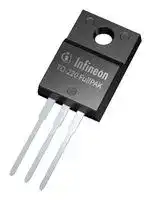
- Transistor Case Style: TO-220FP
- Operating Temperature Max: 175°C
- Continuous Collector Current: 11.7A
- Collector Emitter Voltage Max: 600V
- Collector Emitter Saturation Voltage: 1.5V
| Delivery and price | |
|---|---|
| Units per pack | 5000 |
| Price | 0.537 € |
| Current stock | 200+ |
| Lead time | 30 days |
IKA10N60T TRENCHSTOP™Series ## Low Loss DuoPack : IGBT in TRENCHSTOP™and Fieldstop technology with soft, fast recovery anti-parallel Emitter Controlled HE diode ## **Features:** - Very low VCE(sat) 1.5V (typ.) - Maximum Junction Temperature 175°C - Short circuit withstand time 5s - TRENCHSTOP™and Fieldstop technology for 600V applications offers : - very tight parameter distribution - high ruggedness, temperature stable behavior - very high switching speed - Low EMI - Very soft, fast recovery anti-parallel Emitter Controlled HE diode - Qualified according to JEDEC[1] for target applications - Pb-free lead plating; RoHS compliant **==> picture [61 x 105] intentionally omitted <==** **----- Start of picture text -----**<br> C<br>G<br>E<br>PG-TO220-3 (FullPak)<br>**----- End of picture text -----**<br> - Complete product spectrum and PSpice Models : http://www.infineon.com/igbt/ ## **Applications** - Washing Machine - Air Condition - Inverter and Variable Speed Drive |**Type**|_V_CE|_I_C|_V_CE(sat_),Tj=25°C_|_T_j,max|Marking Code|Package| |---|---|---|---|---|---|---| |IKA10N60T|600V|10A|1.5V|175C|K10T60|PG-TO220-3 (FullPAK)| ## **Maximum Ratings** |**Parameter**|**Symbol**<br>~~—~~<br>~~ee~~|**Value**<br>~~—~~<br>~~eee~~|**Unit**<br>~~—~~<br>~~eee~~| |---|---|---|---| |Collector-emitter voltage,_T_j≥ 25C|_V_C E<br>~~ee~~|600<br>~~eee~~|V<br>~~eee~~| |DC collector current, limited by_T_jmax<br>_T_C= 25C<br>_T_C= 100C|_I_C<br>~~ee ~~<br>~~Pf~~|11.7<br>7.2<br> ~~eee~~<br>~~Pf~~|A<br>~~eee~~<br>~~|~~<br>~~eee~~| |Pulsed collector current,_t_plimited by_T_jmax|_I_C p u l s<br>~~—--—————~~|30<br>~~—--—————~~|| |Turn off safe operating area,_V_CE= 600V,_T_j= 175C,_t_p= 1µs|_-_<br>~~—--—————~~|30<br>~~—--—————~~|| |Diode forward current, limited by_T_jmax<br>_T_C= 25C<br>_T_C= 100C|_I_F<br>~~|~~|11.9<br>7.4<br>~~|~~|| |Diode pulsed current,_t_plimited by_T_jmax|_I_F p u l s<br>~~|~~<br>~~ee~~|30<br>~~|~~<br>~~eee~~|| |Gate-emitter voltage<br>~~—~~|_V_G E<br>~~ee~~<br>~~—~~|20<br>~~eee~~<br>|V<br>~~eee~~<br>| |Short circuit withstand time2)<br>_V_GE= 15V,_V_CC400V,_T_j150C<br>~~—~~|_t_S C<br>~~ee ~~<br>~~—[|~~<br>~~ee~~|5<br> ~~eee~~<br>~~[|~~<br>~~eee~~|s<br>~~eee~~<br>~~[|~~<br>~~eee~~| |Power dissipation,_T_C= 25C<br>~~—~~|_P_t o t<br>~~—~~<br>~~ee~~|30<br><br>~~eee~~|W<br><br>~~eee~~| |Operating junction temperature|_T_j<br>~~ee ~~<br>~~|~~|-40...+175<br> ~~eee~~<br>~~|~~|C<br>~~eee~~<br>~~|~~| |Storage temperature|_T_s t g<br>~~|~~<br>~~ee~~|-55...+150<br>~~|~~<br>~~ee~~|| |Isolation voltage|_V_i s o l<br>~~ee~~|2500<br>~~ee~~|Vr ms| - 1 J-STD-020 and JESD-022 - 2) Allowed number of short circuits: <1000; time between short circuits: >1s. Rev. 2.5 20.09.2013 1 IFAG IPC TD VLS IKA10N60T **==> picture [145 x 64] intentionally omitted <==** ## TRENCHSTOP™Series ## **Thermal Resistance** |**Thermal Resistance**||||| |---|---|---|---|---| |**Parameter**|**Symbol**|**Conditions**|**Max. Value**|**Unit**| |**Characteristic**||||| |IGBT thermal resistance,<br>junction – case|_R_t hJC||5|K/W| |Diode thermal resistance,<br>junction – case|_R_t hJC D||5.8|| |Thermal resistance,<br>junction – ambient|_R_t hJA||80|| ## **Electrical Characteristic,** at _T_ j = 25 C, unless otherwise specified |**Electrical Characteristic,**at_T_j= 25|C, unless ot|herwise specified||||| |---|---|---|---|---|---|---| |**Parameter**|**Symbol**|**Conditions**||**Value**||**Unit**| ||||**min.**|**typ.**|**max.**|| |**Static Characteristic**||||||| |Collector-emitter breakdown voltage|_V_( BR )C ES|_V_G E=0V, _I_C=0.2mA|600|-|-|V| |Collector-emitter saturation voltage|_V_C E( sat )|_V_G E = 15V, _I_C=10A<br>_T_j=25C<br>_T_j=175C|-<br>-|1.5<br>1.8|2.05|| |Diode forward voltage|_V_F|_V_G E=0V, _I_F=10A<br>_T_j=25C<br>_T_j=175C|-<br>-|1.6<br>1.6|2.05<br>-|| |Gate-emitter threshold voltage|_V_G E( t h)|_I_C=0.3mA,_V_C E=_V_G E|4.1|4.6|5.7|| |Zero gate voltage collector current|_I_CE S|_V_C E=600V,<br>_V_G E=0V<br>_T_j=25C<br>_T_j=175C|-<br>-|-<br>-|40<br>1000|µA| |Gate-emitter leakage current|_I_GE S|_V_C E=0V,_V_G E=20V|-|-|100|nA| |Transconductance|_g_fs|_V_C E=20V, _I_C=15A|-|6|-|S| |Integratedgate resistor|_RG int_|||none||Ω| |**Dynamic Characteristic**||||||| |Input capacitance|_C_i ss|_V_C E=25V,<br>_V_G E=0V,<br>_f_=1MHz|-|551|-|pF| |Output capacitance|_C_os s||-|40|-|| |Reverse transfer capacitance|_C_rs s||-|17|-|| |Gate charge|_Q_Gat e|_V_C C=480V, _I_C=10A<br>_V_G E=15V|-|62|-|nC| |Internal emitter inductance<br>measured 5mm(0.197 in.)from case|_L_E||-|7|-|nH| |Short circuit collector current1)|_I_C( SC )|_V_G E=15V,_t_SC5s<br>_V_C C = 400V,<br>_T_j =<br>25C|-|100|-|A| > 1) Allowed number of short circuits: <1000; time between short circuits: >1s. Rev. 2.5 20.09.2013 2 IFAG IPC TD VLS IKA10N60T TRENCHSTOP™Series **==> picture [145 x 64] intentionally omitted <==** ## **Switching Characteristic, Inductive Load,** at _T_ j=25 C |**Parameter**|**Symbol**|**Conditions**||**Value**||**Unit**| |---|---|---|---|---|---|---| ||||**min.**|**typ.**|**max.**|| |**IGBT Characteristic**||||||| |Turn-on delaytime|_t_d( o n)|_T_j=25C,<br>_V_C C=400V,_I_C=10A,<br>_V_G E=0/15V,_r_G=23,<br>_L_=60nH,_C_=40pF<br>_L_, _C_from Fig. E<br>Energy losses include<br>“tail” and diode reverse<br>recovery.|-|12|-|ns| |Rise time|_t_r||-|8|-|| |Turn-off delaytime|_t_d( of f)||-|215|-|| |Fall time|_t_f||-|38|-|| |Turn-on energy|_E_o n||-|0.16|-|mJ| |Turn-off energy|_E_o ff||-|0.27|-|| |Total switchingenergy|_E_t s||-|0.43|-|| |**Anti-Parallel Diode Characteristic**||||||| |Diode reverse recoverytime|_t_rr|_T_j=25C,<br>_V_R=400V, _I_F=10A,<br>_di_F_/dt_=880A/s|-|115|-|ns| |Diode reverse recoverycharge|_Q_rr||-|0.38|-|µC| |Diodepeak reverse recoverycurrent|_I_rr m||-|10|-|A| |Diode peak rate of fall of reverse<br>recoverycurrent during_t_b|_di_rr_/dt_||-|680|-|A/s| ## **Switching Characteristic, Inductive Load,** at _T_ j=175 C |**Parameter**|**Symbol**|**Conditions**||**Value**||**Unit**| |---|---|---|---|---|---|---| ||||**min.**|**typ.**|**max.**|| |**IGBT Characteristic**||||||| |Turn-on delaytime|_t_d( o n)|_T_j=25C,<br>_V_C C=400V,_I_C=10A,<br>_V_G E=0/15V,_r_G=23,<br>_L_=60nH,_C_=40pF<br>_L_, _C_from Fig. E<br>Energy losses include<br>“tail” and diode reverse<br>recovery.|-|10|-|ns| |Rise time|_t_r||-|11|-|| |Turn-off delaytime|_t_d( of f)||-|233|-|| |Fall time|_t_f||-|63|-|| |Turn-on energy|_E_o n||-|0.26|-|mJ| |Turn-off energy|_E_o ff||-|0.35|-|| |Total switchingenergy|_E_t s||-|0.61|-|| |**Anti-Parallel Diode Characteristic**||||||| |Diode reverse recoverytime|_t_rr|_T_j=175C<br>_V_R=400V, _I_F=10A,<br>_di_F_/dt_=880A/s|-|200|-|ns| |Diode reverse recoverycharge|_Q_rr||-|0.92|-|µC| |Diodepeak reverse recoverycurrent|_I_rr m||-|13|-|A| |Diode peak rate of fall of reverse<br>recovery current during_t_b|_di_rr_/dt_||-|390|-|A/s| Rev. 2.5 20.09.2013 3 IFAG IPC TD VLS IKA10N60T **==> picture [145 x 64] intentionally omitted <==** ## TRENCHSTOP™Series **==> picture [228 x 219] intentionally omitted <==** **----- Start of picture text -----**<br> t p =1µs<br>10A<br>20µs<br>50µs<br>1A<br>500µs<br>5ms<br>100ms<br>0,1A<br>DC<br>1V 10V 100V 1000V<br>COLLECTOR CURRENT<br>I C,<br>**----- End of picture text -----**<br> **==> picture [233 x 211] intentionally omitted <==** **----- Start of picture text -----**<br> T C=80°C T C=110°C<br>30A<br>25A<br>20A<br>15A<br>10A I c<br>5A<br>I c<br>0A<br>10Hz 100Hz 1kHz 10kHz 100kHz<br>COLLECTOR CURRENT<br>I C,<br>**----- End of picture text -----**<br> **==> picture [107 x 9] intentionally omitted <==** **----- Start of picture text -----**<br> f , SWITCHING FREQUENCY<br>**----- End of picture text -----**<br> _V_ CE, COLLECTOR-EMITTER VOLTAGE ## **Figure 1. Collector current as a function of switching frequency** **Figure 2. Safe operating area** ( _D =_ 0, _T_ C = 25C, _T_ j 175C; _V_ GE=0/15V) ( _T_ j 175C, _D =_ 0.5, _V_ CE = 400V, _V_ GE = 0/15V, _r_ G = 23) **==> picture [229 x 210] intentionally omitted <==** **----- Start of picture text -----**<br> 30W<br>25W<br>20W<br>15W<br>10W<br>5W<br>0W<br>25°C 50°C 75°C 100°C 125°C 150°C<br>POWER DISSIPATION<br>tot,<br>P<br>**----- End of picture text -----**<br> **==> picture [225 x 202] intentionally omitted <==** **----- Start of picture text -----**<br> 10A<br>8A<br>6A<br>4A<br>2A<br>0A<br>25°C 75°C 125°C<br>COLLECTOR CURRENT<br>I C,<br>**----- End of picture text -----**<br> _T_ C, CASE TEMPERATURE **Figure 3. Power dissipation as a function of case temperature** ( _T_ j 175C) **==> picture [102 x 10] intentionally omitted <==** **----- Start of picture text -----**<br> T C, CASE TEMPERATURE<br>**----- End of picture text -----**<br> **Figure 4. Collector current as a function of case temperature** ( _V_ GE 15V, _T_ j 175C) Rev. 2.5 20.09.2013 4 IFAG IPC TD VLS IKA10N60T **==> picture [145 x 64] intentionally omitted <==** ## TRENCHSTOP™Series **==> picture [474 x 266] intentionally omitted <==** **----- Start of picture text -----**<br> 30A 30A<br>25A V GE =20V 25A V GE =20V<br>15V 15V<br>20A 20A<br>12V 12V<br>10V 10V<br>15A 15A<br>8V 8V<br>6V 6V<br>10A 10A<br>5A 5A<br>0A 0A<br>0V 1V 2V 3V 4V 0V 1V 2V 3V 4V 5V<br>V CE, COLLECTOR-EMITTER VOLTAGE V CE, COLLECTOR-EMITTER VOLTAGE<br>Figure 5. Typical output characteristic Figure 6. Typical output characteristic<br>( T j = 25°C) ( T j = 175°C)<br>COLLECTOR CURRENT COLLECTOR CURRENT<br>I C, I C,<br>**----- End of picture text -----**<br> **==> picture [477 x 284] intentionally omitted <==** **----- Start of picture text -----**<br> 3,0V<br>25A IC =20A<br>2,5V<br>20A<br>2,0V I C =10A<br>15A<br>1,5V<br>10A<br>1,0V I C =5A<br>5A T J = 175 °C<br>0,5V<br>25°C<br>0A 0,0V<br>0V 2V 4V 6V 8V 10V -50°C 0°C 50°C 100°C 150°C<br>V GE, GATE-EMITTER VOLTAGE T J, JUNCTION TEMPERATURE<br>Figure 7. Typical transfer characteristic Figure 8. Typical collector-emitter<br>(VCE=20V) saturation voltage as a function of<br>junction temperature<br>( V GE = 15V)<br>EMITT SATURATION VOLTAGE<br>-<br>COLLECTOR CURRENT<br>I C,<br> COLLECTOR<br>CE(sat),<br>V<br>**----- End of picture text -----**<br> Rev. 2.5 20.09.2013 IFAG IPC TD VLS 5 IKA10N60T **==> picture [145 x 64] intentionally omitted <==** ## TRENCHSTOP™Series **==> picture [229 x 209] intentionally omitted <==** **----- Start of picture text -----**<br> t<br>d(off)<br>100ns<br>t f<br>t<br>d(on)<br>10ns<br>t r<br>1ns<br>0A 5A 10A 15A 20A<br>SWITCHING TIMES<br>t,<br>**----- End of picture text -----**<br> **==> picture [105 x 10] intentionally omitted <==** **----- Start of picture text -----**<br> IC , COLLECTOR CURRENT<br>**----- End of picture text -----**<br> **Figure 9. Typical switching times as a function of collector current** (inductive load, _T_ J=175°C, _V_ CE = 400V, VGE = 0/15V, _r_ G = 23Ω, Dynamic test circuit in Figure E) **==> picture [233 x 210] intentionally omitted <==** **----- Start of picture text -----**<br> t<br>d(off)<br>100ns<br>t f<br>t<br>d(on)<br>10ns<br>t r<br>1ns<br> <br>SWITCHING TIMES<br>t,<br>**----- End of picture text -----**<br> **==> picture [84 x 10] intentionally omitted <==** **----- Start of picture text -----**<br> R G, GATE RESISTOR<br>**----- End of picture text -----**<br> **Figure 10. Typical switching times as a function of gate resistor** (inductive load, _T_ J = 175°C, _V_ CE= 400V, VGE = 0/15V, _I_ C = 10A, Dynamic test circuit in Figure E) **==> picture [229 x 210] intentionally omitted <==** **----- Start of picture text -----**<br> t d(off)<br>100ns<br>t f<br>t<br>d(on)<br>10ns<br>t r<br>1ns<br>25°C 50°C 75°C 100°C 125°C 150°C<br>SWITCHING TIMES<br>t,<br>**----- End of picture text -----**<br> **==> picture [119 x 10] intentionally omitted <==** **----- Start of picture text -----**<br> T J, JUNCTION TEMPERATURE<br>**----- End of picture text -----**<br> **Figure 11. Typical switching times as a function of junction temperature** (inductive load, _V_ CE = 400V, VGE = 0/15V, _I_ C = 10A, _r_ G=23Ω, Dynamic test circuit in Figure E) **==> picture [230 x 220] intentionally omitted <==** **----- Start of picture text -----**<br> 7V<br>6V<br>max.<br>5V typ.<br>4V<br>min.<br>3V<br>2V<br>1V<br>0V<br>-50°C 0°C 50°C 100°C 150°C<br>EMITT TRSHOLD VOLTAGE<br>-<br> GATEGE(th ) ,<br>V<br>**----- End of picture text -----**<br> **==> picture [119 x 10] intentionally omitted <==** **----- Start of picture text -----**<br> T J, JUNCTION TEMPERATURE<br>**----- End of picture text -----**<br> **Figure 12. Gate-emitter threshold voltage as a function of junction temperature** ( _I_ C = 0.3mA) Rev. 2.5 20.09.2013 6 IFAG IPC TD VLS IKA10N60T **==> picture [145 x 64] intentionally omitted <==** ## TRENCHSTOP™Series **==> picture [230 x 223] intentionally omitted <==** **----- Start of picture text -----**<br> *) E on and E ts include losses<br>due to diode recovery E ts*<br>0,8 mJ<br>0,6 mJ E<br>off<br>0,4 mJ E on *<br>0,2 mJ<br>0,0 mJ<br> <br>SWITCHING ENERGY LOSSES<br>E ,<br>**----- End of picture text -----**<br> **==> picture [235 x 231] intentionally omitted <==** **----- Start of picture text -----**<br> *) E on and E tsinclude losses<br>1,0mJ due to diode recovery E ts*<br>0,8mJ<br>E off<br>0,6mJ<br>0,4mJ<br>E on*<br>0,2mJ<br>0,0mJ<br>0A 5A 10A 15A<br>IC , COLLECTOR CURRENT<br>SWITCHING ENERGY LOSSES<br>E ,<br>**----- End of picture text -----**<br> **==> picture [84 x 10] intentionally omitted <==** **----- Start of picture text -----**<br> R G, GATE RESISTOR<br>**----- End of picture text -----**<br> - **Figure 13. Typical switching energy losses as a function of collector current** (inductive load, _T_ J = 175°C, _V_ CE = 400V, VGE = 0/15V, _r_ G = 23Ω, Dynamic test circuit in Figure E) **Figure 14. Typical switching energy losses as a function of gate resistor** (inductive load, _T_ J = 175°C, _V_ CE = 400V, VGE = 0/15V, _I_ C = 10A, Dynamic test circuit in Figure E) **==> picture [231 x 238] intentionally omitted <==** **----- Start of picture text -----**<br> *) E on and E ts include losses<br>0,6mJ due to diode recovery<br>0,5mJ E ts*<br>0,4mJ<br>0,3mJ E off<br>0,2mJ<br>0,1mJ E on*<br>0,0mJ<br>50°C 100°C 150°C<br>T J, JUNCTION TEMPERATURE<br>SWITCHING ENERGY LOSSES<br>E ,<br>**----- End of picture text -----**<br> ## **Figure 15. Typical switching energy losses as a function of junction temperature** - (inductive load, _V_ CE = 400V, VGE = 0/15V, _I_ C = 10A, _r_ G = 23Ω, Dynamic test circuit in Figure E) **==> picture [227 x 209] intentionally omitted <==** **----- Start of picture text -----**<br> *) E on and E ts include losses<br>due to diode recovery<br>0,8mJ<br>0,6mJ<br>E ts*<br>0,4mJ<br>E off<br>0,2mJ<br>E on*<br>0,0mJ<br>300V 350V 400V 450V 500V 550V<br>SWITCHING ENERGY LOSSES<br>E ,<br>**----- End of picture text -----**<br> **==> picture [149 x 10] intentionally omitted <==** **----- Start of picture text -----**<br> VCE , COLLECTOR-EMITTER VOLTAGE<br>**----- End of picture text -----**<br> **Figure 16. Typical switching energy losses as a function of collector emitter voltage** - (inductive load, _T_ J = 175°C, _V_ GE = 0/15V, _I_ C = 10A, _r_ G = 23Ω, Dynamic test circuit in Figure E) Rev. 2.5 20.09.2013 IFAG IPC TD VLS 7 IKA10N60T **==> picture [145 x 64] intentionally omitted <==** ## TRENCHSTOP™Series **==> picture [234 x 227] intentionally omitted <==** **----- Start of picture text -----**<br> 15V<br>120V<br>480V<br>10V<br>5V<br>0V<br>0nC 20nC 40nC 60nC<br>Q GE, GATE CHARGE<br>EMITTER VOLTAGE<br>-<br>GATE<br>GE,<br>V<br>**----- End of picture text -----**<br> **Figure 17. Typical gate charge** ( _I_ C=10 A) **==> picture [231 x 217] intentionally omitted <==** **----- Start of picture text -----**<br> 1nF<br>C iss<br>100pF<br>C oss<br>C rss<br>10pF<br>0V 10V 20V<br>CAPACITANCE<br>c,<br>**----- End of picture text -----**<br> **==> picture [149 x 10] intentionally omitted <==** **----- Start of picture text -----**<br> V CE, COLLECTOR-EMITTER VOLTAGE<br>**----- End of picture text -----**<br> **Figure 18. Typical capacitance as a function of collector-emitter voltage** ( _V_ GE=0V, _f_ = 1 MHz) **==> picture [466 x 216] intentionally omitted <==** **----- Start of picture text -----**<br> 12µs<br>150A<br>10µs<br>125A<br>8µs<br>100A<br>6µs<br>75A<br>4µs<br>50A<br>2µs<br>25A<br>0µs<br>0A 10V 11V 12V 13V 14V<br>12V 14V 16V 18V<br>COLLECTOR CURRENT<br>SHORT CIRCUIT WITHSTAND TIME<br>, short circuit ,<br>t SC<br>I C(sc)<br>**----- End of picture text -----**<br> _V_ GE, GATE-EMITTETR VOLTAGE **Figure 19. Typical short circuit collector current as a function of gateemitter voltage** ( _V_ CE 400V, _T_ j 150C) **==> picture [123 x 10] intentionally omitted <==** **----- Start of picture text -----**<br> V GE, GATE-EMITETR VOLTAGE<br>**----- End of picture text -----**<br> **Figure 20. Short circuit withstand time as a function of gate-emitter voltage** ( _V_ CE=400V _,_ start at _T_ J _=_ 25°C, _T_ Jmax<150°C) Rev. 2.5 20.09.2013 8 IFAG IPC TD VLS IKA10N60T **==> picture [145 x 64] intentionally omitted <==** ## TRENCHSTOP™Series **==> picture [237 x 224] intentionally omitted <==** **----- Start of picture text -----**<br> D =0.5<br>0.2<br>0 0K/W<br>0.1<br>R , ( K / W ) , ( s )<br>1.596 4.622 6<br>1.985 1.288<br>0.05 0.5623 5.066*10 [-2]<br>0.3324 4.152*10 [-3]<br>0 -1K/W 0.02 0.3531 6.059*10 [-4]<br>0.1730 7.863*10 [-5]<br>0.01 R 1 R 2<br>single pulse<br>C 1 =1 / R 1 C 2 =2 / R 2<br>0 -2K/W<br>10µs 100µs 1ms 10ms100ms 1s 10s<br>MPEDANCE<br> I<br>TRANSIENT THERMAL<br>thJC,<br>Z<br>**----- End of picture text -----**<br> _t_ P, PULSE WIDTH **Figure 21. IGBT transient thermal impedance** ( _D = t_ p / _T_ ) **==> picture [236 x 224] intentionally omitted <==** **----- Start of picture text -----**<br> D =0.5<br>0.2<br>10 0K/W R , ( K / W ) , ( s )<br>0.1 1.418 5.068 6<br>2.125 1.416<br>0.5890 6.455*10 [-2]<br>0.5424 5.732*10 [-3]<br>0.6311 1.019*10 [-3]<br>0.05 0.5061 1.499*10 [-4]<br>10 -1K/W 0.02 R 1 R 2<br>0.01<br>single pulse C 1 = 1 / R 1 C 2 = 2 / R 2<br>10 -2K/W<br>10µs 100µs 1ms 10ms100ms 1s 10s<br>TRANSIENT THERMAL IMPEDANCE<br>thJC,<br>Z<br>**----- End of picture text -----**<br> ## _t_ P, PULSE WIDTH **Figure 22. Diode transient thermal impedance as a function of pulse width** ( _D_ = _t_ P/ _T_ ) **==> picture [235 x 239] intentionally omitted <==** **----- Start of picture text -----**<br> 300ns<br>250ns<br>T =175°C<br>200ns J<br>150ns<br>100ns<br>T =25°C<br>J<br>50ns<br>0ns<br>200A/µs 400A/µs 600A/µs 800A/µs<br>di F /dt , DIODE CURRENT SLOPE<br>REVERSE RECOVERY TIME<br>t rr,<br>**----- End of picture text -----**<br> **Figure 23. Typical reverse recovery time as a function of diode current slope** ( _V_ R=400V, _I_ F=10A, Dynamic test circuit in Figure E) **==> picture [231 x 217] intentionally omitted <==** **----- Start of picture text -----**<br> 0,8µC T =175°C<br>J<br>0,7µC<br>0,6µC<br>0,5µC<br>0,4µC<br>T =25°C<br>0,3µC J<br>0,2µC<br>0,1µC<br>0,0µC<br>200A/µs 400A/µs 600A/µs 800A/µs<br>REVERSE RECOVERY CHARGE<br>rr,<br>Q<br>**----- End of picture text -----**<br> **==> picture [125 x 10] intentionally omitted <==** **----- Start of picture text -----**<br> di F /dt , DIODE CURRENT SLOPE<br>**----- End of picture text -----**<br> ## **Figure 24. Typical reverse recovery charge as a function of diode current slope** ( _V_ R = 400V, _I_ F = 10A, Dynamic test circuit in Figure E) Rev. 2.5 20.09.2013 9 IFAG IPC TD VLS IKA10N60T **==> picture [145 x 64] intentionally omitted <==** ## TRENCHSTOP™Series **==> picture [235 x 219] intentionally omitted <==** **----- Start of picture text -----**<br> 14A T =175°C<br>J<br>12A<br>10A<br>T =25°C<br>8A J<br>6A<br>4A<br>2A<br>0A<br>200A/µs 400A/µs 600A/µs 800A/µs<br>REVERSE RECOVERY CURRENT<br>I rr,<br>**----- End of picture text -----**<br> **==> picture [125 x 10] intentionally omitted <==** **----- Start of picture text -----**<br> di F /dt , DIODE CURRENT SLOPE<br>**----- End of picture text -----**<br> ## **Figure 25. Typical reverse recovery current as a function of diode current slope** - ( _V_ R = 400V, _I_ F = 10A, Dynamic test circuit in Figure E) **==> picture [235 x 210] intentionally omitted <==** **----- Start of picture text -----**<br> T =25°C<br>-700A/µs J<br>-600A/µs<br>-500A/µs<br>-400A/µs<br>T =175°C<br>J<br>-300A/µs<br>-200A/µs<br>-100A/µs<br>0A/µs<br>400A/µs 600A/µs 800A/µs<br>DIODE PEAK RATE OF FALL<br>/dt ,<br>rr<br>di OF REVERSE RECOVERY CURRENT<br>**----- End of picture text -----**<br> ## _di_ F _/dt_ , DIODE CURRENT SLOPE **Figure 26. Typical diode peak rate of fall of reverse recovery current as a function of diode current slope** ( _V_ R=400V, _I_ F=10A, Dynamic test circuit in Figure E) **==> picture [234 x 240] intentionally omitted <==** **----- Start of picture text -----**<br> 30A<br>T J =25°C<br>175°C<br>20A<br>10A<br>0A<br>0V 1V 2V<br>V F, FORWARD VOLTAGE<br>FORWARD CURRENT<br>I F,<br>**----- End of picture text -----**<br> **Figure 27. Typical diode forward current as a function of forward voltage** **==> picture [231 x 214] intentionally omitted <==** **----- Start of picture text -----**<br> 2,0V<br>IF =20A<br>1,5V 10A<br>5A<br>1,0V<br>0,5V<br>0,0V<br>-50°C 0°C 50°C 100°C 150°C<br>FORWARD VOLTAGE<br>F,<br>V<br>**----- End of picture text -----**<br> **==> picture [119 x 10] intentionally omitted <==** **----- Start of picture text -----**<br> T J, JUNCTION TEMPERATURE<br>**----- End of picture text -----**<br> **Figure 28. Typical diode forward voltage as a function of junction temperature** Rev. 2.5 20.09.2013 10 IFAG IPC TD VLS IKA10N60T TRENCHSTOP™Series ## PG-TO220-3 (FullPAK) A **Please refer to mounting instructions** Rev. 2.5 20.09.2013 11 IFAG IPC TD VLS IKA10N60T ## TRENCHSTOP™Series **Figure A. Definition of switching times** **==> picture [189 x 303] intentionally omitted <==** **----- Start of picture text -----**<br> i,v<br>di F /dt t r r =t S + t F<br>Q r r =Q S + Q F<br>t<br>I F / -——_ t S r r t F<br>I Q S Q F 10% I r r m t<br>r r m 90% I di r r /dt V R<br>r r m<br>Figure C. Definition of diodes<br>switching characteristics<br>1 2 n<br>r1 r 2 r n<br>Tj (t)<br>THO<br>p(t) r1 r 2 r n<br>.<br>©<br>TC<br>**----- End of picture text -----**<br> **Figure D. Thermal equivalent circuit** **Figure B. Definition of switching losses** Rev. 2.5 20.09.2013 12 IFAG IPC TD VLS IKA10N60T TRENCHSTOP™Series **==> picture [145 x 64] intentionally omitted <==** **Published by Infineon Technologies AG 81726 Munich, Germany © 2013 Infineon Technologies AG All Rights Reserved.** ## **Legal Disclaimer** The information given in this document shall in no event be regarded as a guarantee of conditions or characteristics. With respect to any examples or hints given herein, any typical values stated herein and/or any information regarding the application of the device, Infineon Technologies hereby disclaims any and all warranties and liabilities of any kind, including without limitation, warranties of non-infringement of intellectual property rights of any third party. ## **Information** For further information on technology, delivery terms and conditions and prices, please contact the nearest Infineon Technologies Office ( **www.infineon.com** ) **.** ## **Warnings** Due to technical requirements, components may contain dangerous substances. For information on the types in question, please contact the nearest Infineon Technologies Office. The Infineon Technologies component described in this Data Sheet may be used in life-support devices or systems and/or automotive, aviation and aerospace applications or systems only with the express written approval of Infineon Technologies, if a failure of such components can reasonably be expected to cause the failure of that life-support, automotive, aviation and aerospace device or system or to affect the safety or effectiveness of that device or system. Life support devices or systems are intended to be implanted in the human body or to support and/or maintain and sustain and/or protect human life. If they fail, it is reasonable to assume that the health of the user or other persons may be endangered. Rev. 2.5 20.09.2013 13 IFAG IPC TD VLS
Updated at June 9, 2026
Infineon Technologies is a globally recognized leader in semiconductor solutions, renowned for driving innovation in power management, energy efficiency, and modern mobility. With a strong legacy of engineering excellence, the company provides highly reliable components designed to meet the rigorous demands of industrial, automotive, and advanced commercial applications. The core of our Infineon portfolio is centered on their industry-leading discrete semiconductors. We offer an extensive selection of single and dual MOSFETs, alongside a robust range of single IGBTs and advanced IGBT modules. These flagship power transistors are essential for high-efficiency power conversion and motor control, providing engineers with superior thermal performance and minimized switching losses. Beyond advanced field-effect transistors, the selection includes a comprehensive array of diodes and rectifiers, heavily featuring Schottky diodes, as well as fast-recovery and RF/PIN diodes. This power foundation is further supported by bipolar transistors, intelligent power modules, and thyristor SCR modules, delivering the critical building blocks required for complex power system designs. To support broader system integration, the portfolio also encompasses specialized solutions such as solid-state relays, AC/DC LED driver ICs, and Bluetooth communications modules. From high-power industrial rectifiers to wireless connectivity adapters, Infineon equips designers with the precision components needed to build efficient, scalable, and fully connected electronic systems.
About Novapart
Novapart is a B2B electronic component broker specialising in stock shortages and cost reduction. We source hard-to-find parts and identify compliant alternatives across a catalogue of 410,000+ components from 500+ manufacturers.
Learn more →Stock Shortage Specialist
When a component is unavailable, discontinued or has an unacceptable lead time, we tap into our network of vetted European and Asian distributors to source what you need — without compromising on quality or traceability.
Request a quote →Compliant Alternatives
We identify pin-to-pin, electrically equivalent substitutes that meet the same certifications (RoHS, AEC-Q100, REACH) as your original specification — validated against datasheets, not just part numbers. Often at a lower cost.
BOM Analysis service →