


HS8MA2TCR1
Dual MOSFET, N and P Channel, 30 V, 30 V, 7 A, 7 A, 0.035 ohm
- Manufacturer: ROHM
- Product type: Dual MOSFETs
- MSL: -
- SVHC: No SVHC (25-Jun-2025)
- No. of Pins: 9Pins
- Channel Type: N and P Channel
- Product Range: -
- Qualification: -
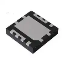
- Transistor Case Style: DFN3333
- Operating Temperature Max: 150°C
- Power Dissipation N Channel: 2W
- Power Dissipation P Channel: 2W
- Drain Source Voltage Vds N Channel: 30V
- Drain Source Voltage Vds P Channel: 30V
- Continuous Drain Current Id N Channel: 7A
- Continuous Drain Current Id P Channel: 7A
- Drain Source On State Resistance N Channel: 0.035ohm
- Drain Source On State Resistance P Channel: 0.08ohm
| Delivery and price | |
|---|---|
| Units per pack | 1000 |
| Price | 0.328 € |
| Current stock | 1000+ |
| Lead time | 30 days |
Datasheet

## HS8MA2

## 30V Pch+Nch Power MOSFET

## **l Outline**

**==> picture [186 x 95] intentionally omitted <==**

**----- Start of picture text -----**<br>
||||
|---|---|---|
|Symbol|Tr1:Pch|Tr2:Nch|
|VDSS|-30V|30V|
|RDS(on)(Max.)|80mΩ|35mΩ|
|ID|±5.5A|±7.0A|
|PD|4.0W|

**----- End of picture text -----**<br>


DFN3333-9DC HSML3333L9

## **l Features**

## **l Inner circuit**

- 1) Low on - resistance

2) Small Surface Mount Package

3) Pb-free plating ; RoHS compliant

- 4) Halogen Free

## **l Packaging specifications**

## **l Application**

Switching Motor Drive

**==> picture [235 x 119] intentionally omitted <==**

**----- Start of picture text -----**<br>
||||
|---|---|---|
|Embossed|
|Packing|
|Tape|
|Reel size (mm)|180|
|Tape width (mm)|12|
|Type|
|Quantity|(pcs)|1000|
|Taping code|TCR1|
|Marking|HS8MA2|

**----- End of picture text -----**<br>


## **l Absolute maximum ratings** (Ta = 25°C ,unless otherwise specified)

**==> picture [493 x 180] intentionally omitted <==**

**----- Start of picture text -----**<br>
|||||||
|---|---|---|---|---|---|
|Value|
|Parameter|Symbol|Unit|
|Tr1:Pch|Tr2:Nch|
|Drain - Source voltage|VDSS|-30|30|V|
|Continuous drain current|ID|[*1]|±5.5|±7.0|A|
|Pulsed drain current|IDP|[*2]|±30|±30|A|
|Gate - Source voltage|VGSS|±20|±20|V|
|PD|[*1]|4.0|
|Power dissipation|total|W|
|PD|[*3]|2.0|
|Junction temperature|Tj|150|℃|
|Operating|junction and storage temperature range|Tstg|-55 to +150|℃|

**----- End of picture text -----**<br>


www.rohm.com © 2019 ROHM Co., Ltd. All rights reserved.

**20191011 - Rev.001**

1/19

**HS8MA2**

Datasheet

## **l Thermal resistance**

|**lThermal resistance**||||||
|---|---|---|---|---|---|
|Parameter|Symbol|Values|||Unit|
|||Min.|Typ.|Max.||
|Thermal resistance, junction - ambient|RthJA*3|-|-|83.3|℃/W|


## **l Electrical characteristics (Ta = 25°C)**

|Parameter|Symbol|Type|Conditions|Values|Values|Values|Unit|
|---|---|---|---|---|---|---|---|
|||||Min.|Typ.|Max.||
|Drain - Source breakdown<br>voltage|V(BR)DSS|Tr1|VGS= 0V, ID= -1mA|-30|-|-|V|
|||Tr2|VGS= 0V, ID= 1mA|30|-|-||
|Breakdown voltage<br>temperature coefficient|ΔV(BR)DSS <br>  ΔTj|(BR)DSS Tr1|ID= -1mA,  referenced to 25℃|-|-22|-|mV/℃|
|||Tr2|ID= 1mA,  referenced to 25℃|-|21|-||
|Zero gate voltage<br>drain current|IDSS|Tr1|VDS= -30V, VGS= 0V|-|-|-1|μA|
|||Tr2|VDS= 30V, VGS= 0V|-|-|1||
|Gate - Source<br>leakage current|IGSS|Tr1|VGS= ±20V, VDS = 0V|-|-|±100|nA|
|||Tr2|VGS= ±20V, VDS = 0V|-|-|±100||
|Gate threshold<br>voltage|VGS(th)|Tr1|VDS= -10V, ID= -1mA|-1.0|-|-2.5|V|
|||Tr2|VDS= 10V, ID= 1mA|1.0|-|2.5||
|Gate threshold voltage<br>temperature coefficient|ΔVGS(th) <br>  ΔTj|Tr1|ID= -1mA, referenced to 25℃|-|2.9|-|mV/℃|
|||Tr2|ID= 1mA, referenced to 25℃|-|-3|-||
|Static drain - source<br>on - state resistance|RDS(on)*4|Tr1|VGS= -10V, ID= -5.5A|-|55|80|mΩ|
||||VGS= -4.5V, ID= -5.5A|-|80|115||
|||Tr2|VGS= 10V, ID= 7.0A|-|25|35||
||||VGS= 4.5V, ID= 7.0A|-|40|56||
|Gate resistance|RG|Tr1|f=1MHz, open drain|-|10|-|Ω|
|||<br>Tr2||-|3|-||
|Forward Transfer<br>Admittance||Yfs|*4|Tr1|VDS= -5V, ID= -3A|1.9|-|-|S|
|||Tr2|VDS= 5V, ID= 4.5A|1.4|-|-||


- *1 Pw ≤ 1s, Limited only by maximum temperature allowed.

- *2 Pw ≤ 10μs, Duty cycle ≤ 1%

- *3 Mounted on a ceramic board (30×30×0.8mm)

- *4 Pulsed

www.rohm.com © 2019 ROHM Co., Ltd. All rights reserved.

**20191011 - Rev.001**

2/19

**HS8MA2**

Datasheet

## **l Electrical characteristics** (Ta = 25°C)

## **<Tr1>**

|**<Tr1>**|||||||
|---|---|---|---|---|---|---|
|Parameter|Symbol|Conditions|Values|||Unit|
||||Min.|Typ.|Max.||
|Input capacitance|Ciss|VGS= 0V<br>VDS= -10V<br>f = 1MHz|-|320|-|pF|
|Output capacitance|Coss||-|68|-||
|Reverse transfer capacitance|Crss||-|54|-||
|Turn - on delay time|td(on)*4|VDD ⋍-15V, VGS= -10V<br>ID= -1.5A<br>RL= 10Ω<br>RG= 10Ω|-|7.9|-|ns|
|Rise time|tr*4||-|16.8|-||
|Turn - off delay time|td(off)*4||-|27.6|-||
|Fall time|tf*4||-|8.5|-||


## **<Tr2>**

|**<Tr2>**|||||||
|---|---|---|---|---|---|---|
|Parameter|Symbol|Conditions|Values|||Unit|
||||Min.|Typ.|Max.||
|Input capacitance|Ciss|VGS= 0V<br>VDS= 10V<br>f = 1MHz|-|365|-|pF|
|Output capacitance|Coss||-|62|-||
|Reverse transfer capacitance|Crss||-|50|-||
|Turn - on delay time|td(on)*4|VDD ⋍15V, VGS= 10V<br>ID= 2.2A<br>RL= 6.8Ω<br>RG= 10Ω|-|7.2|-|ns|
|Rise time|tr*4||-|8.0|-||
|Turn - off delay time|td(off)*4||-|12.0|-||
|Fall time|tf*4||-|5.7|-||


www.rohm.com © 2019 ROHM Co., Ltd. All rights reserved.

**20191011 - Rev.001**

3/19

**HS8MA2**

Datasheet

## **l Gate charge characteristics** (Ta = 25°C)

|**lGate charge characteristics**(Ta = 25°C)a = 25°C)= 25°C)|(Ta = 25°C)a = 25°C)= 25°C)||||
|---|---|---|---|---|
|**<Tr1>**|||||
|Parameter<br>Symbol<br>Conditions<br>Values<br>Unit<br>Min.<br>Typ.<br>Max.<br>Total gate charge<br>Qg*4<br>VDD ⋍-15V<br>ID= -3A<br>VGS= -10V<br>-<br>7.8<br>-<br>nC<br>VGS= -4.5V<br>-<br>4.3<br>-<br>Gate - Source charge<br>Qgs*4<br>-<br>1.6<br>-<br>Gate - Drain charge<br>Qgd*4<br>-<br>1.5<br>-<br>~~EE~~|||||
|**<Tr2>**|||||
|Parameter<br>Symbol<br>Conditions<br>Values<br>Unit<br>Min.<br>Typ.<br>Max.<br>Total gate charge<br>Qg*4<br>VDD ⋍15V<br>ID= 4.5A<br>VGS= 10V<br>-<br>8.4<br>-<br>nC<br>VGS= 4.5V<br>-<br>4.7<br>-<br>Gate - Source charge<br>Qgs*4<br>-<br>1.7<br>-<br>Gate - Drain charge<br>Qgd*4<br>-<br>1.6<br>-<br>~~EE~~|||||
|**lBody diode electrical characteristics**(Source-Drain) (Ta= 25°C)|||||
|**<Tr1>**|||||
|Parameter<br>Symbol<br>Conditions<br>Values<br>Unit<br>Min.<br>Typ.<br>Max.<br>Continuous forward current<br>IS<br>Ta= 25℃<br>-<br>-<br>-1.0<br>A<br>Pulse forward current<br>ISP*2<br>-<br>-<br>-30<br>Forward voltage<br>VSD*4<br>VGS= 0V, IS= -1.0A<br>-<br>-<br>-1.2<br>V<br>~~==~~|||||
|**<Tr2>**|||||
|Parameter<br>Symbol<br>Conditions<br>Values<br>Unit<br>Min.<br>Typ.<br>Max.<br>Continuous forward current<br>IS<br>Ta= 25℃<br>-<br>-<br>1.0<br>A<br>Pulse forward current<br>ISP*2<br>-<br>-<br>30<br>Forward voltage<br>VSD*4<br>VGS= 0V, IS= 1.0A<br>-<br>-<br>1.2<br>V<br>~~——=Seeeaere~~|||||
|www.rohm.com|||||
|© 2019 ROHM Co., Ltd. All rights reserved.|4/19|||**20191011 - Rev.001**|


**20191011 - Rev.001**

4/19

**HS8MA2**

Datasheet

## **l Electrical characteristic curves <Tr1>**

## Fig.1 Power Dissipation Derating Curve

Fig.3 Normalized Transient Thermal Resistance vs. Pulse Width

## Fig.2 Maximum Safe Operating Area

Fig.4 Single Pulse Maximum Power Dissipation

www.rohm.com © 2019 ROHM Co., Ltd. All rights reserved.

**20191011 - Rev.001**

5/19

**HS8MA2**

Datasheet

## **l Electrical characteristic curves <Tr1>**

Fig.5 Typical Output Characteristics(I)

Fig.6 Typical Output Characteristics(II)

Fig.7 Breakdown Voltage vs. Junction Temperature

www.rohm.com © 2019 ROHM Co., Ltd. All rights reserved.

**20191011 - Rev.001**

6/19

**HS8MA2**

Datasheet

## **l Electrical characteristic curves <Tr1>**

## Fig.8 Typical Transfer Characteristics

## Fig.9 Gate Threshold Voltage vs. Junction Temperature

## Fig.10 Forward Transfer Admittance vs. Drain Current

www.rohm.com © 2019 ROHM Co., Ltd. All rights reserved.

**20191011 - Rev.001**

7/19

**HS8MA2**

Datasheet

## **l Electrical characteristic curves <Tr1>**

Fig.11 Drain Current Derating Curve

Fig.12 Static Drain - Source On - State Resistance vs. Gate Source Voltage

Fig.13 Static Drain - Source On - State Resistance vs. Junction Temperature

www.rohm.com © 2019 ROHM Co., Ltd. All rights reserved.

**20191011 - Rev.001**

8/19

**HS8MA2**

Datasheet

## **l Electrical characteristic curves <Tr1>**

Fig.14 Static Drain - Source On - State Resistance vs. Drain Current (I)

Fig.15 Static Drain - Source On - State Resistance vs. Drain Current (II)

Fig.16 Static Drain - Source On - State Resistance vs. Drain Current (III)

www.rohm.com © 2019 ROHM Co., Ltd. All rights reserved.

**20191011 - Rev.001**

9/19

**HS8MA2**

Datasheet

## **l Electrical characteristic curves <Tr1>**

Fig.17 Typical Capacitances vs. Drain - Source Voltage

## Fig.19 Typical Gate Charge

Fig.18 Switching Characteristics

## Fig.20 Source Current vs. Source Drain Voltage

www.rohm.com © 2019 ROHM Co., Ltd. All rights reserved.

**20191011 - Rev.001**

10/19

**HS8MA2**

Datasheet

## **l Electrical characteristic curves <Tr2>**

Fig.1 Power Dissipation Derating Curve

Fig.3 Normalized Transient Thermal Resistance vs. Pulse Width

## Fig.2 Maximum Safe Operating Area

Fig.4 Single Pulse Maximum Power Dissipation

www.rohm.com © 2019 ROHM Co., Ltd. All rights reserved.

**20191011 - Rev.001**

11/19

**HS8MA2**

Datasheet

## **l Electrical characteristic curves <Tr2>**

Fig.5 Typical Output Characteristics(I)

Fig.6 Typical Output Characteristics(II)

Fig.7 Breakdown Voltage vs. Junction Temperature

www.rohm.com © 2019 ROHM Co., Ltd. All rights reserved.

**20191011 - Rev.001**

12/19

**HS8MA2**

Datasheet

## **l Electrical characteristic curves <Tr2>**

Fig.8 Typical Transfer Characteristics

Fig.9 Gate Threshold Voltage vs. Junction Temperature

Fig.10 Forward Transfer Admittance vs. Drain Current

www.rohm.com © 2019 ROHM Co., Ltd. All rights reserved.

**20191011 - Rev.001**

13/19

**HS8MA2**

Datasheet

## **l Electrical characteristic curves <Tr2>**

Fig.11 Drain Current Derating Curve

Fig.12 Static Drain - Source On - State Resistance vs. Gate Source Voltage

Fig.13 Static Drain - Source On - State Resistance vs. Junction Temperature

www.rohm.com © 2019 ROHM Co., Ltd. All rights reserved.

**20191011 - Rev.001**

14/19

**HS8MA2**

Datasheet

## **l Electrical characteristic curves <Tr2>**

Fig.14 Static Drain - Source On - State Resistance vs. Drain Current (I)

Fig.15 Static Drain - Source On - State Resistance vs. Drain Current (II)

Fig.16 Static Drain - Source On - State Resistance vs. Drain Current (III)

www.rohm.com © 2019 ROHM Co., Ltd. All rights reserved.

**20191011 - Rev.001**

15/19

**HS8MA2**

Datasheet

## **l Electrical characteristic curves <Tr2>**

Fig.17 Typical Capacitances vs. Drain - Source Voltage

## Fig.19 Typical Gate Charge

Fig.18 Switching Characteristics

Fig.20 Source Current vs. Source Drain Voltage

www.rohm.com © 2019 ROHM Co., Ltd. All rights reserved.

**20191011 - Rev.001**

16/19

**HS8MA2**

Datasheet

## **l Measurement circuits** <Tr1>

Fig.1-1 Switching Time Measurement Circuit

Fig.2-1 Gate Charge Measurement Circuit

## Fig.1-2 Switching Waveforms

Fig.2-2 Gate Charge Waveform

www.rohm.com © 2019 ROHM Co., Ltd. All rights reserved.

**20191011 - Rev.001**

17/19

**HS8MA2**

Datasheet

## **l Measurement circuits** <Tr2>

**==> picture [178 x 10] intentionally omitted <==**

**----- Start of picture text -----**<br>
Fig.3-1 Switching Time Measurement Circuit<br>**----- End of picture text -----**<br>


**==> picture [118 x 10] intentionally omitted <==**

**----- Start of picture text -----**<br>
Fig.3-2 Switching Waveforms<br>**----- End of picture text -----**<br>


Fig.4-1 Gate Charge Measurement Circuit

Fig.4-2 Gate Charge Waveform

## **l Notice**

This product might cause chip aging and breakdown under the large electrified environment. Please consider to design ESD protection circuit.

www.rohm.com © 2019 ROHM Co., Ltd. All rights reserved.

**20191011 - Rev.001**

18/19

**HS8MA2**

Datasheet

## **l Dimensions**

www.rohm.com © 2019 ROHM Co., Ltd. All rights reserved.

**20191011 - Rev.001**

19/19

**==> picture [539 x 801] intentionally omitted <==**
Updated at June 9, 2026
Founded with a steadfast commitment to a "Quality First" corporate policy, ROHM is a globally recognized leader in the design and manufacture of semiconductors and electronic components. Originally named for its foundational product, resistors, combined with the unit of resistance, the "R" in ROHM has evolved to represent the brand's enduring dedication to reliability. Today, the company is renowned for driving technological advancement and supplying high-performance, dependable solutions to engineers worldwide. The company's engineering excellence is most prominently showcased in its expansive portfolio of discrete semiconductors. ROHM provides an industry-leading selection of bipolar transistors, alongside a massive array of Zener single diodes, Schottky diodes, and small signal diodes. Engineered for rigorous efficiency and compact footprint requirements, these foundational components are critical for modern power management, precise signal processing, and high-speed switching applications. In addition to its core discrete offerings, ROHM delivers advanced power control and circuit protection solutions. This includes a highly trusted lineup of single and dual MOSFETs, single IGBTs, and transient voltage suppressors (TVS diodes) designed to safeguard sensitive circuitry. Complemented by intelligent power modules, precision sensors, and specialized ICs, ROHM equips designers with the premium components necessary to build the next generation of robust electronic infrastructure.
About Novapart
Novapart is a B2B electronic component broker specialising in stock shortages and cost reduction. We source hard-to-find parts and identify compliant alternatives across a catalogue of 410,000+ components from 500+ manufacturers.
Learn more →Stock Shortage Specialist
When a component is unavailable, discontinued or has an unacceptable lead time, we tap into our network of vetted European and Asian distributors to source what you need — without compromising on quality or traceability.
Request a quote →Compliant Alternatives
We identify pin-to-pin, electrically equivalent substitutes that meet the same certifications (RoHS, AEC-Q100, REACH) as your original specification — validated against datasheets, not just part numbers. Often at a lower cost.
BOM Analysis service →