
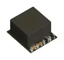


FS1525-0600-AL
POL DC/DC Converter, Non Isolated, Telecom/Networking/Data Centre/Industrial, VRM, 600mV - 1.8V, 25A
- Manufacturer: TDK
- Product type: DC / DC Non Isolated Board Mount Converters - Adjustable Output
- SVHC: No SVHC (25-Jun-2025)
- Depth: 7.65mm
- Width: 6.8mm
- Height: 3.82mm
- Product Range: -
- Output Power Max: -
- Output Current Max: 25A
- Output Voltage Max: 1.8V
- Output Voltage Min: 600mV
- Input Voltage DC Max: 16V
- Input Voltage DC Min: 4.5V
- DC / DC Converter Type: Voltage Regulator Module (VRM)
- Power Supply Applications: Telecom, Networking, Data Center, Storage, Industrial, Distributed POL Power Architecture
- DC / DC Converter Output Type: Adjustable
| Delivery and price | |
|---|---|
| Units per pack | 250 |
| Price | 7.33 € |
| Current stock | 1000+ |
| Lead time | 30 days |
## **FS1525 POL[™] µ**

**25A Stackable µPOL[™]** Regulator with Integrated Inductor and Digital Power System Management

## **DATASHEET**

## **Features**

## **Description**

- µPOL™ package with output inductor included

The FS1525 is an easy-to-use, fully integrated and highly efficient micro-point-of-load (µPOL™) voltage regulator. The on-chip pulse-width modulation (PWM) controller and integrated MOSFETs, plus incorporated inductor and capacitors, result in an extremely compact and accurate regulator. The low-profile package is suitable for automated assembly using standard surface-mount equipment.

- Small size: **6.80mm x 7.65mm x 3.82mm**

- Continuous 25A load capability

- Stackable up to **200A** (eight devices)

- Plug and play: no external compensation required

- True differential remote sensing

- Programmable operation using I[2] C and PMBus™

- Wide input voltage range: 4.5V–16V

- Adjustable output voltage up to 1.8V

Developed by a cross-functional engineering team, the design exemplifies best practice and uses classleading technologies. From early in the integrated circuit design phase, designers worked with application and packaging engineers to select compatible technologies and implement them in ways that reduce compromise. The ability to program aspects of the FS1525’s operation using the I[2] C and PMBus™ protocols is unique in this class of product. Developing and optimizing all these elements together has yielded the smallest, most efficient and fully featured 25A to 200A µPOL™ currently available.

- Enabled input, programmable under-voltage lock-out (UVLO) circuit

- Open-drain power-good indicator

- Built-in protection features

- Operating junction temperature from -40°C to +125°C

- Lead-free and halogen-free

- Compliant with EU Directives REACH and RoHS 6

## **Applications**

- Telecom and networking applications

- Data center applications

The built-in protection features include pre-biased start-up, soft-start protection, over-voltage protection, thermally compensated over-current protection with hiccup mode, thermal shut-down with auto-recovery.

- Storage applications

- Industrial applications

- Distributed point-of-load power architectures

- Computing peripheral voltage regulation

**==> picture [229 x 108] intentionally omitted <==**

**----- Start of picture text -----**<br>
PVIN VOUT<br>PVIN Cb SW1 VOUT<br>“T h VIN PV CC RSoFb<br>VCC L an> RS +<br>SDA —=I CLKOUT<br>SCL RS -<br>SALERT En<br>ADDR SYNC<br>PG<br>PS AGnd PGnd Ishare<br>**----- End of picture text -----**<br>


**==> picture [101 x 29] intentionally omitted <==**

**----- Start of picture text -----**<br>
PVIN = 12V, VOUT = 1.8V<br>No airflow, all losses included<br>**----- End of picture text -----**<br>


**Page 1**

**Rev 1.1, Nov 24, 2025**

Patent Protected: US 9,729,059 B1; US 10,193,442 B2 Copyright© 2022–25 TDK Corporation. All rights reserved. All registered trademarks and trademarks are the property of their respective owners. Data and specifications subject to change without notice.

## **FS1525 POL[™] µ**

## **Pin Configuration**

**==> picture [477 x 206] intentionally omitted <==**

**----- Start of picture text -----**<br>
miedenernndnnwei) {fC AO00CO0a08<br>[e e 1 e 35 35 1<br>ee 2 re e r ee 34 C 34 I = 2<br>So p hy p STGH , ~ HDEA G HU G A 4 A GIG OS | CJ<br>calrdi 3 ti rdrd t i ed e rderder d er d erder d ien 33 33 3<br>HSE 4 P us gs ! 1 4h 48 . 49 . 45 44 G4 G4 E E 32 C 32 I = 4<br>C oa rp ed ;, p e l e ly p e l e l e l e l e l e l e l yo C] LC]<br>5 31 31 5<br>La [ee ee Os Oe sO Os Oe Lo CJ O<br>a 6 a 66 EO 65 64 30 a 30 a 64 sD 65 cB 66 6<br>A 7 67 68 69 29 CO 29 Co) 69 Ce) 68 GE) 67 7<br>8 28 28 8<br>Lo rq7 ra rq rP.a T ra rq Lo CJ CJ<br>ca 9 Pr titddd ee | c7 27 27 9<br>ca Prridtdd Prrdtidd La CJ LC]<br>ca 10 Prtiddd oe | c7 26 26 10<br>a l ien brit dd Pritt us LJ LJ<br>PF. F117 77 Pritt PF. 67 7 Prt ttl P71<br>cyts e s te ee UU UU UUUU<br>36 37 38 39 40 41 42 43 44 45 46 47 48 49 50<br>63 62 61 60 59 58 57 56 55 54 53 52 51<br>23 22 21 17 16 15<br>25 24 20 19 18 14 13 12 11<br>50 49 48 47 46 45 44 43 42 41 40 39 38 37 36<br>51 52 53 54 55 56 57 58 59 60 61 62 63<br>15 16 17 21 22 23<br>11 12 13 14 18 19 20 24 25<br>**----- End of picture text -----**<br>


_**Figure 1 Pin layout (top view)**_

_**Figure 2 Pin layout (bottom view)**_

## **Pin Functions**

|**Pin Numbers Pin Name Pin Description**|**Pin Numbers Pin Name Pin Description**|**Pin Numbers Pin Name Pin Description**|
|---|---|---|
|44|NC|Test pin for Sync FET of phase 2.|
|8|VIN|Input supply to the internal LDO. Connect to PVINthrough a 2.7Ω resistor OR to VCCwhen<br>external 5V (Figure 6) is used to supply VCC(recommended for best performance).|
|25|En|Enable pin to turn the device ON and OFF. It can be used to set an external UVLO by using<br>two external resistors.|
|9|PVCC|Input supply for the drivers. Connect to VCCon the application board.|
|10|VCC|Input bias for an external VCCvoltage / Output of the internal LDO. Connect to VINwhen<br>using external 5V supply (recommended for best performance).|
|13|VFB|Feedback voltage to the device. Connect to VOUTon the application board if remote sensing<br>is not used, or to RSo if remote sensing is used.|
|64–69|AGnd|Signal ground for the internal reference and control circuitry. Connect to power ground<br>plane through vias.|
|21, 22, 23|VOUT1|Power output from regulator. VOUT1and VOUT2should be shorted by VOUTplane on PCB. Place<br>output capacitors between VOUTand PGnd.|
|15, 16, 17|VOUT2|Power output from regulator. VOUT1and VOUT2should be shorted by VOUTplane on PCB. Place<br>output capacitors between VOUTand PGnd.|
|30|PG|Power Good status pin. Output is an open drain. Connect a pull-up resistor (4.99kΩ)<br>between this pin and VCCor to an external bias voltage.|


**Page 2**

**Rev 1.1, Nov 24, 2025**

Patent Protected: US 9,729,059 B1; US 10,193,442 B2 Copyright © 2022–25 TDK Corporation. All rights reserved. All registered trademarks and trademarks are the property of their respective owners. Data and specifications subject to change without notice.

## **FS1525 POL[™] µ** ~~Pe~~

|~~{TDK~~|~~{TDK~~|**FS1525µPOL[™] **<br>~~Pe~~|
|---|---|---|
|**Pin Numbers Pin Name Pin Description**<br>~~a~~|**Pin Numbers Pin Name Pin Description**<br>~~a~~|**Pin Numbers Pin Name Pin Description**|
|12<br>~~a~~|ADDR<br>~~a~~|Program device address by connecting a resistor from this pin to ground; up to 16 address<br>offsets may be programmed (see page 19).|
|5<br>~~a~~<br>~~a~~|Boot1<br>~~a~~<br>~~a~~|Boot pin for phase 1 driver.|
|6<br>~~a~~<br>~~a~~|Boot2<br>~~a~~<br>~~a~~|Boot pin for phase 2 driver.|
|7<br>~~a~~|SYNC<br>~~a~~|Synchronizes device with external clock. If not used, it is recommended to ground this pin.|
|29<br>~~a~~<br>~~a~~|Clkout<br>~~a~~<br>~~a~~|Phase shifted clock out. Connect to sync of next slave in daisy chain.|
|27<br>~~a~~<br>~~a~~|SDA<br>~~a~~<br>~~a~~|I2C /PMBus™ Data Serial Input/Output line. Pull up to bus voltage with 4.99kΩ resistor.|
|26<br>~~a~~|SCL<br>~~a~~|I2C /PMBus™ Clock line. Pull up to bus voltage with 4.99kΩ resistor.|
|28<br>~~a~~|ALERT<br>~~a~~|SMBAlert# line. Pull up to bus voltage with 4.99kΩ resistor.|
|36–43<br>~~a~~|SW1<br>~~a~~|Drain of Sync FET of phase 1. External fly capacitors (2 x 4.7µF) should be connected<br>between this pin and Cb.|
|31-35, 56–63 PGnd<br>~~a~~<br>~~a~~|31-35, 56–63 PGnd<br>~~a~~<br>~~a~~|Power Ground. Serves as a separate ground for the MOSFETs and should be connected to<br>the system’s power ground plane.|
|45-50, 53,<br>54, 55<br>~~a~~|Cb<br>~~a~~|Connection for external fly capacitors (2 X 4.7µF). The capacitor connects between this pin<br>and VSW1and should be connected as close as possible to these pins.|
|18<br>~~a~~<br>~~a~~|RS+<br>~~a~~<br>~~a~~|Input of differential remote sense amplifier. Connect to VOUT.|
|19<br>~~a~~<br>~~a~~|RS-<br>~~a~~<br>~~a~~|Input of differential remote sense amplifier. Connect to remote or local ground.|
|14<br>~~a~~<br>~~ee~~|RSo<br>~~a~~<br>~~ee~~|Output of remote sensing amplifier.|
|11<br>~~ee~~|PS<br>~~ee~~|Phase setting pin. Connect resistor to AGnd to set Master/Slave, as well as number of<br>devices in parallel to determine relative phasing (see page 21).|
|24<br>~~ee~~<br>~~a~~|Fault#<br>~~ee~~<br>~~a~~|Tied together with Fault pins of other paralleled devices to share fault information. Pull up<br>to VCCor 5V supply with a 4.99kΩ resistor. Active low.|
|20<br>~~a~~|Ishare<br>~~a~~|Current share. The Ishare pins of all paralleled devices need to be tied together.|
|1–4, 51, 52<br>~~a~~<br>~~a~~|PVIN<br>~~a~~<br>~~a~~|Input supply for the power MOSFETs.|


**Page 3**

**Rev 1.1, Nov 24, 2025**

Patent Protected: US 9,729,059 B1; US 10,193,442 B2 Copyright © 2022–25 TDK Corporation. All rights reserved. All registered trademarks and trademarks are the property of their respective owners. Data and specifications subject to change without notice.

## **FS1525 POL[™] µ**

## **Block Diagram**

**==> picture [497 x 316] intentionally omitted <==**

**----- Start of picture text -----**<br>
VIN VCC PVCC<br>AGnd<br>Low Drop-Out VCC<br>(LDO) Regulator PVIN<br>Cb<br>SCL RSo Fb Fault PV IN<br>SDA PV CC<br>Reference<br>SALERT<br>(DAC)<br>SYNC Digital PulseGenerator SW1<br>Core and Soft Start for Pulse Width PWM Gate HDrv1<br>ADDR<br>Memory Modulation (PWM) drive HDrv2<br>PLL logic SW2<br>and LDrv1 Driver  and L2<br>PS dead Power Stage<br>-time<br>LDrv2<br>control<br>Fault<br>L1<br>VOUT<br>CLKOUT<br>HDrv1<br>Fault shut-downthermal VCC HDrv2<br>PGnd<br>Fault<br>Fb<br>Control SW2<br>En<br>and Fault RS+<br>PG Logic SW1<br>Remote  sense<br>Fb<br>amplifier RS-<br>power-on reset<br>RSo LDrv2<br>LDrv1 RSo<br>**----- End of picture text -----**<br>


_**Figure 3 FS1525 µPOL™**_

**Page 4**

**Rev 1.1, Nov 24, 2025**

Patent Protected: US 9,729,059 B1; US 10,193,442 B2 Copyright © 2022–25 TDK Corporation. All rights reserved. All registered trademarks and trademarks are the property of their respective owners. Data and specifications subject to change without notice.

**==> picture [481 x 620] intentionally omitted <==**

**----- Start of picture text -----**<br>
FS1525  POL [™]<br>µ<br>PV V<br>IN PV Cb SW1 V OUT<br>IN OUT<br>Fb<br>V<br>CC V<br>IN RSo<br>PV<br>VCC CC RS+<br>SYNC<br>CLKOUT<br>SDA<br>SCL En<br>SALERT<br>Fault<br>ADDR<br>RS-<br>PG<br>PS AGnd PGnd<br>a<br>PV V PV<br>IN Cb SW1 OUT SW1 Cb IN<br>PV V V PV<br>IN OUT OUT IN<br>VCC V Fb Fb PV V VCC<br>IN RSo RSo CC IN<br>PV<br>VCC CC RS+ RS+ VCC<br>SYNC CLKOUT<br>CLKOUT SYNC<br>SDA SDA<br>SCL En En SCL<br>SALERT SALERT<br>Fault Fault<br>ADDR ADDR<br>RS- RS-<br>PG PG<br>Ishare Ishare<br>PS AGnd PGnd PGnd AGnd PS<br>| Ee |<br>TTI W I T D<br>Figure 4 Applications circuits for single-phase and two-phase configuration<br>Note: The Fault pin needs to be pulled up to 5V through 4.99kΩ resistor for both single- and multi-phase applications.<br>**----- End of picture text -----**<br>


**Page 5**

**Rev 1.1, Nov 24, 2025**

Patent Protected: US 9,729,059 B1; US 10,193,442 B2 Copyright © 2022–25 TDK Corporation. All rights reserved. All registered trademarks and trademarks are the property of their respective owners. Data and specifications subject to change without notice.

**FS1525 POL[™] µ**

## **Absolute Maximum Ratings**

**Warning:** Stresses beyond those shown may cause permanent damage to the FS1525.

**Note:** Functional operation of the FS1525 is not implied under these or any other conditions beyond those stated in the FS1525 specification.

|**Reference**|**Range **|
|---|---|
|PVIN,VIN,En to PGnd,Cb to SW1|-0.3V to 18V|
|VCCto PGnd(Note 1)|-0.3V to 6V|
|SW1,SW2|-0.3V to 15V|
|Fb and other I/Os to AGnd(Note1)|-0.3V to VCC|
|PG to AGnd(Note 1)|-0.3V to VCC|
|PGnd to AGnd|-0.3V to +0.3V|
|ESD Classification(HBM JESD22-A114)|1.5kV|
|Moisture SensitivityLevel|MSL 3(per JEDEC J-STD-020D)|


**Thermal Information Range** Junction-to-Ambient Thermal Resistance ƟJA 10.5°C/W Junction to PCB Thermal Resistance ƟJ-PCB 1.4°C/W Storage Temperature Range -55°C to 150°C Junction Temperature Range -40°C to 150°C **Note:** ƟJA : FS1525 evaluation board and JEDEC specifications JESD 51-2A ƟJ-c (bottom) : JEDEC specification JESD 51-8 ~~a~~

**Page 6**

**Rev 1.1, Nov 24, 2025**

Patent Protected: US 9,729,059 B1; US 10,193,442 B2 Copyright © 2022–25 TDK Corporation. All rights reserved. All registered trademarks and trademarks are the property of their respective owners. Data and specifications subject to change without notice.

**FS1525 POL[™] µ** ~~ee~~

## **Order Information**

## **Package Details**

The FS1525 uses a µPOL™ 6.80mm x 7.65mm package delivered in tape-and-reel format, with 1250 devices on a reel.

## **Standard Part Number**

**VOUT Part number** 0.60 FS1525-0600-AL ~~ee~~

**Page 7**

**Rev 1.1, Nov 24, 2025**

Patent Protected: US 9,729,059 B1; US 10,193,442 B2 Copyright © 2022–25 TDK Corporation. All rights reserved. All registered trademarks and trademarks are the property of their respective owners. Data and specifications subject to change without notice.

**FS1525 POL[™] µ**

## **Recommended Operating Conditions**

|**Definition**|**Symbol**|**Min**|**Max**|**Units**|
|---|---|---|---|---|
|Input Voltage Range with External VCC (Note 3, Note 5)|PVIN|6*VOUT|16|V|
|Input Voltage Range with Internal LDO(Note 4, Note 5)|PVIN, VIN|6*VOUT|16||
|SupplyVoltage Range(Note 2)|VCC|4.5|5.5||
|Output Voltage Range|VOUT|0.6|1.8||
|Continuous Output Current Range|IO|0|25|A|
|OperatingJunction Temperature|TJ|-40|125|°C|


## **Electrical Characteristics**

|**ELECTRICAL CHARACTERISTICS**|**ELECTRICAL CHARACTERISTICS**|**ELECTRICAL CHARACTERISTICS**|**ELECTRICAL CHARACTERISTICS**|**ELECTRICAL CHARACTERISTICS**|**ELECTRICAL CHARACTERISTICS**|**ELECTRICAL CHARACTERISTICS**|
|---|---|---|---|---|---|---|
|**Unless otherwise stated, these specifications apply over: 6*VOUT <PVIN <16V, 4.5V < VIN < 16V, 0°C < T < 125°C**<br>**Typical values are specified at TA = 25°C**<br>~~a~~|||||||
|**Parameter**<br>~~a~~|**Symbol**<br>~~a~~|**Conditions**<br>~~a~~|**Min**<br>~~a~~|**Typ**<br>~~a~~|**Max**<br>~~a~~|**Unit**<br>~~a~~|
|**Supply Current**<br>~~SS~~|||||||
|VINSupplyCurrent(Standby)<br>~~SS~~|IIN(STANDBY)<br>~~SS~~|Enable low<br>~~SS~~|7<br>~~SS~~|8.2<br>~~SS~~|9.5<br>~~SS~~|mA<br>~~SS~~|
|VINSupplyCurrent(Static)<br>~~SS~~|IIN(STATIC)<br>~~SS~~|No switching,En = 2V<br>~~SS~~|8.8<br>~~SS~~|10.5 12.2<br>~~SS~~|10.5 12.2<br>~~SS~~||
|VINSupply Current (Dynamic)<br>~~SS~~|IIN (DYN)<br>~~SS~~|En high, VIN= 12V, FSW=625kHz,<br>Vcc=PVcc<br>~~SS~~|45.5 50<br>~~SS~~|45.5 50<br>~~SS~~|54.5<br>~~SS~~||
|**Soft-Start**|||||||
|Soft-Start time<br>~~—————=-e=~~|TON_RISE<br>~~—————=-e=~~|Default(Note 7),VOUT= 0.6V<br>~~—————=-e=~~|2.3<br>~~—————=-e=~~|3<br>~~—————=-e=~~|3.7<br>~~—————=-e=~~|ms<br>~~—————=-e=~~|
|**Output Voltage **<br>~~—————=-e=~~|||||||
|Output Voltage Range<br>~~—————=-e=~~|VOUT (default)<br>~~—————=-e=~~|~~—————=-e=~~|~~—————=-e=~~|0.6<br>~~—————=-e=~~|~~—————=-e=~~|V<br>~~—————=-e=~~|
||range<br>~~—————=-e=~~|~~—————=-e=~~|0.6<br>~~—————=-e=~~|~~—————=-e=~~|1.8<br>~~—————=-e=~~|V<br>~~—————=-e=~~|
|~~—————=-e=~~|Resolution<br>~~—————=-e=~~|~~—————=-e=~~|~~—————=-e=~~|5<br>~~—————=-e=~~|~~—————=-e=~~|mV<br>~~—————=-e=~~|
|Accuracy||TJ= 25°C,VOUT= 0.6V(Note 8)||±0.7|±0.7|%|
|||-40°C ≤ TJ≤ 105°C, VOUT= 0.6V<br>(Note 6,8)|-1.5||1.5||
|||TJ= 25°C, 0.7V ≤ VOUT≤ 1.8V<br>(Note 7,8)|-1||1||
|**On-Time Timer Control**<br>~~ee~~|||||||
|On-Time<br>~~ee~~|TON<br>~~ee~~<br>~~ee~~|VIN= 12V,VOUT= 0.6V,FSW= 625kHz 155<br>~~ee~~|= 625kHz 155<br>~~ee~~|180<br>~~ee~~|205<br>~~ee~~|ns<br>~~ee~~|
|Minimum On-Time<br>~~ee~~|TON(MIN)<br>~~ee~~<br>~~ee~~|(Note 7)<br>~~ee~~|~~ee~~|50<br>~~ee~~|~~ee~~||
|Minimum Off-Time<br>~~ee~~|TOFF(MIN)<br>~~ee~~<br>~~ee~~|TJ= 25°C, FSW= 625kHz,<br>VIN= VCC= PVCC= 4.5V<br>PVIN= 6V<br>~~ee~~|395<br>~~ee~~|430<br>~~ee~~|465<br>~~ee~~||
|**Internal Low Drop-Out(LDO) Regulator**<br>~~ee~~|||||||
|LDO Regulator Output Voltage<br>~~NN~~|VCC<br>~~NN~~|5.5V ≤ VIN= 16V,0 – 75mA<br>~~NN~~|4.9<br>~~NN~~|5.2<br>~~NN~~|5.5<br>~~NN~~|V<br>~~NN~~|
|||4.5V ≤ VIN< 5.5V,0 – 55mA<br>~~NN~~|4<br>~~NN~~|~~NN~~|~~NN~~||
|Line Regulation<br>~~NN~~|VLN<br>~~NN~~|5.5V < VIN= 16V,0 – 75mA<br>~~NN~~|0<br>~~NN~~|40<br>~~NN~~|110<br>~~NN~~|mV<br>~~NN~~|


**Rev 1.1, Nov 24, 2025**

**FS1525 POL[™] µ** ~~Pe~~

|**ELECTRICAL CHARACTERISTICS**<br>~~|~~|**ELECTRICAL CHARACTERISTICS**<br>~~|~~|**ELECTRICAL CHARACTERISTICS**<br>~~|~~|**ELECTRICAL CHARACTERISTICS**<br>~~|~~|**ELECTRICAL CHARACTERISTICS**<br>~~|~~|**ELECTRICAL CHARACTERISTICS**<br>~~|~~|**ELECTRICAL CHARACTERISTICS**<br>~~|~~|
|---|---|---|---|---|---|---|
|**Unless otherwise stated, these specifications apply over: 6*VOUT <PVIN <16V, 4.5V < VIN < 16V, 0°C < T < 125°C**<br>**Typical values are specified at TA = 25°C**<br>~~|~~<br>~~ee~~|||||||
|**Parameter**<br>~~ee~~|**Symbol**<br>~~ee~~|**Conditions**<br>~~ee~~|**Min**<br>~~ee~~|**Typ**<br>~~ee~~|**Max**<br>~~ee~~|**Unit**<br>~~ee~~|
|Load Regulation<br>~~OC~~<br>~~Pe~~|VLD<br>~~OC~~<br>|0 – 75mA<br>~~OC~~<br>|0<br>~~OC~~<br>|110<br>~~OC~~<br>|140<br>~~OC~~<br>|~~OC~~<br>|
|Short Circuit Current<br>~~Pe~~|ISHORT<br>|(Note 7)<br>|130<br>|151<br>|172<br>|mA<br>|
|**Thermal Shut-Down**<br>~~Pe|~~<br>~~eeoeae~~|||||||
|Thermal Shut-Down<br>~~es~~|Default<br>~~es~~|~~es~~<br>~~ee~~|~~es~~<br>~~ee~~|145<br>~~es~~<br>~~ee~~|~~es~~<br>~~oe~~|°C<br>~~es~~<br>~~ae~~|
|Hysteresis<br>~~es~~<br>~~GC~~|~~es~~<br>~~GC~~|~~es~~<br>~~ee~~<br>~~GC~~|~~es~~<br>~~ee~~<br>~~GC~~|25<br>~~es~~<br>~~ee~~<br>~~GC~~|~~es~~<br>~~oe~~<br>~~GC~~||
|**Under-Voltage Lock-Out**<br>~~ee oe ae~~<br>~~|~~|||||||
|VCCStart Threshold<br>~~|~~<br>~~GC~~<br>~~a~~|VCC_UVLO(START)<br>~~|~~<br>~~GC~~|VCCRisingTripLevel<br>~~|~~<br>~~GC~~<br>~~oe~~|4.0<br>~~|~~<br>~~GC~~<br>~~oe~~|4.2<br>~~|~~<br>~~GC~~<br>~~oe~~|4.4<br>~~|~~<br>~~GC~~<br>~~oe~~|V<br>~~|~~<br>~~oe~~|
|VCCStopThreshold<br>~~GC~~<br>~~a~~|VCC_UVLO(STOP)<br>~~GC~~|VCCFallingTripLevel<br>~~GC~~<br>~~oe~~|3.6<br>~~GC~~<br>~~oe~~|3.8<br>~~GC~~<br>~~oe~~|4.1<br>~~GC~~<br>~~oe~~||
|Enable Threshold<br>~~a~~|En(HIGH)|RampingUp<br>~~oe~~|1.14 1.20 1.36<br>~~oe~~|1.14 1.20 1.36<br>~~oe~~|1.14 1.20 1.36<br>~~oe~~||
||En(LOW)<br>~~es~~|RampingDown<br>~~oe~~<br>~~es~~|0.90 1.00 1.06<br>~~oe~~<br>~~es~~|0.90 1.00 1.06<br>~~oe~~<br>~~es~~|0.90 1.00 1.06<br>~~oe~~<br>~~es~~||
|Input Impedance<br>~~a~~<br>~~GC~~|REN<br>~~es~~<br>~~GC~~|~~oe~~<br>~~es~~<br>~~GC~~|500<br>~~oe~~<br>~~es~~<br>~~GC~~|1000 1500<br>~~oe~~<br>~~es~~<br>~~GC~~|1000 1500<br>~~oe~~<br>~~es~~<br>~~GC~~|kΩ<br>~~oe~~<br>~~GC~~|
|**Current Limit**<br>~~GC~~<br>~~a~~|||||||
|Current Limit Threshold<br>~~eG~~|IOC (default)<br>~~eG~~|TJ= 25°C,VOUT= 0.6V<br>~~eG~~|30.5 33<br>~~eG~~|30.5 33<br>~~eG~~|35.5<br>~~eG~~|A<br>~~eG~~|
|HiccupBlankingTime<br>~~eG~~<br>~~GC~~|TBLK(HICCUP)<br>~~eG~~<br>~~GC~~|~~eG~~<br>~~GC~~|~~eG~~<br>~~GC~~|20<br>~~eG~~<br>~~GC~~|~~eG~~<br>~~GC~~|ms<br>~~eG~~<br>~~GC~~|
|**Over-Voltage Protection**<br>~~GC~~<br>~~a~~<br>~~ee~~<br>~~ee~~|||||||
|Output Over-Voltage Protection<br>Threshold<br>~~a~~|VOVP(default)<br>~~a~~<br>~~ee~~|OVP Detect (Note 7)<br>~~a~~<br>~~ee~~|110<br>~~a~~|120<br>~~a~~|130<br>~~a~~|Fb%<br>~~a~~|
|Output Over-voltage Protection DelayT<br>~~GO~~|TOVPDEL<br>~~ee~~<br>~~GO~~|~~ee~~<br>~~GO~~|~~GO~~|5<br>~~GO~~|~~GO~~|µs<br>~~GO~~|
|**Remote Sense Differential Amplifier**<br>~~GO~~<br>~~a~~|||||||
|Differential Gain<br>~~a~~|Adiff<br>~~a~~|~~a~~<br>~~G~~|~~a~~|1<br>~~a~~|~~a~~|V/V<br>~~a~~|
|Input Offset Voltage<br>~~eG~~|VOS<br>~~eG~~|RSo=0.6V,No Load<br>~~eG~~|~~eG~~|0<br>~~eG~~|~~eG~~|mV<br>~~eG~~|
|Output Source Current<br>~~eG~~|ISRC<br>~~eG~~|RS+ = 2.3V,RS- = 0V,RSo = 1.8V<br>~~eG~~|~~eG~~|5.5<br>~~eG~~|~~eG~~|mA<br>~~eG~~|
|Output Sink Current<br>~~eG~~|ISNK<br>~~eG~~|RS+ = 0V,RS- = 0.5V,RSo = 0.5V<br>~~eG~~|~~eG~~|0.55<br>~~eG~~|0.55<br>~~eG~~|mA<br>~~eG~~|
|**Power Good(PG)**<br>~~aS~~<br>~~oe eee~~<br>~~a~~|||||||
|Power Good Upper Threshold<br>~~oo~~<br>~~a~~|VPG(UPPER) (default)V<br>~~oo~~|VOUTRising<br>~~oo~~|75<br>~~oo~~|85<br>~~oo~~<br>~~oe eee~~|95<br>~~oo~~<br>~~eee~~|Fb%<br>~~oo~~<br>~~eee~~|
|Power Good Hysteresis<br>~~oo~~<br>~~a~~|VPG(LOWER)<br>~~oo~~|VOUTFalling<br>~~oo~~|~~oo~~|5<br>~~oo~~<br>~~oe eee~~|~~oo~~<br>~~eee~~||
|Power Good Sink Current<br>~~a~~<br>~~eG~~<br>~~oO~~|IPG<br>~~eG~~|PG = 0.6V,En = 2V<br>~~eG~~|6.6<br>~~eG~~|8.8<br>~~oe eee~~<br>~~eG~~|11<br>~~eee~~<br>~~eG~~|mA<br>~~eee~~<br>~~eG~~|
|**Telemetry**<br>~~oO~~<br>~~Po~~<br>~~-~~|||||||
|Input voltage reporting accuracy<br>~~oO~~<br>~~Po~~|PVIN_report_pc<br>~~Po~~|PVIN=12V,TJ= 25°C|-0.8||0.8|%<br>~~-~~|
|||PVIN=12V, -40°C ≤TJ≤125°C (Note<br>6)<br>~~oo~~|-1<br>~~oo~~|~~oo~~|1<br>~~oo~~||
|Output voltage reporting accuracy<br>~~Po~~|VOUT_report_pc<br>~~Po~~|VOUT= VFB= 0.6V,TJ= 25°C<br>~~ee~~|-2.5<br>~~ee~~|~~ee~~|2.5<br>~~ee~~|%<br>~~-~~|
|||VOUT= VFB= 0.6V, -40°C ≤TJ≤125°C<br>(Note 6)<br>~~oo~~|-3.2<br>~~oo~~|~~oo~~|3.2<br>~~oo~~||
|||0.7 ≤ VOUT=VFB≤1.8V, TJ= 25°C<br>(Note 7)<br>~~oo~~<br>~~eo~~|-2<br>~~oo~~<br>~~eo~~|~~oo~~<br>~~eo~~|2<br>~~oo~~<br>~~eo~~||
|||0.7 ≤ VOUT=VFB≤1.8V, -40°C ≤TJ<br>≤125°C(Note 6)<br>~~eo~~<br>~~oo~~|-2.5<br>~~eo~~<br>~~oo~~|~~eo~~<br>~~oo~~|2.5<br>~~eo~~<br>~~oo~~||
|Output current reporting accuracy<br>~~ee~~|IOUT_report_acc<br>~~ee~~|PVIN= 12V, TJ= 25°C, VOUT= 0.6V,<br>IOUT= 0A<br>~~ee~~|0<br>~~ee~~|~~ee~~|2<br>~~ee~~|A<br>~~ee~~|


## **FS1525 POL[™] µ** ~~Pe~~

## **ELECTRICAL CHARACTERISTICS**

|**ELECTRICAL CHARACTERISTICS**|**ELECTRICAL CHARACTERISTICS**|**ELECTRICAL CHARACTERISTICS**|**ELECTRICAL CHARACTERISTICS**|**ELECTRICAL CHARACTERISTICS**|**ELECTRICAL CHARACTERISTICS**|**ELECTRICAL CHARACTERISTICS**|**ELECTRICAL CHARACTERISTICS**|
|---|---|---|---|---|---|---|---|
|**Unless otherwise stated, these specifications apply over: 6*VOUT < PVIN = VIN < 16V, 0°C < T < 125°C**<br>**Typical values are specified at TA = 25°C**<br>~~ee~~||||||||
|**Parameter**|**Symbol**|**Conditions**|**Fast-mode**||**Fast-mode Plus**||**Unit**|
|**I2C parameters**||**(Note 7 for all**<br>**parameters)**|**Min**|**Max**|**Min**|**Max**||
|I2C bus voltage<br>~~**S**~~|VBUS<br>~~**S**~~|~~**S**S~~|1.8<br>~~S~~|5.5<br>~~S~~|1.8<br>~~S~~|5.5<br>~~S~~|V<br>~~S~~|
|LOW-level input voltage<br>~~**S**~~|VIL<br>~~**S**~~|~~**S**S~~|−0.5<br>~~S~~|0.3VBUS<br>~~S~~|−0.5<br>~~S~~|0.3VBUS<br>~~S~~||
|HIGH-level input voltage<br>~~**S**~~|VIH<br>~~**S**~~|~~**S**S~~|0.7VBUS<br>~~S~~|~~S~~|0.7VBUS<br>~~S~~|~~S~~||
|Hysteresis<br>~~**S**~~|VHYS<br>~~**S**~~|~~**S**S~~|0.05VBUS<br>~~S~~|~~S~~|0.05VBUS<br>~~S~~|~~S~~||
|LOW-level output voltage 1<br>~~**S**~~<br>~~y~~|VOL1<br>~~**S**~~|(open-drain or open-<br>collector) at 3mA sink<br>current;VDD> 2V<br>~~**S**S~~|0<br>~~S~~|0.4<br>~~S~~|0<br>~~S~~|0.4<br>~~S~~||
|LOW-level output voltage 2<br>~~**S**~~<br>~~y~~|VOL2<br>~~**S**~~|(open-drain or open-<br>collector) at 2mA sink<br>current;VDD≤ 2V<br>~~**S**S~~|0<br>~~S~~|0.2VBUS<br>~~S~~|0<br>~~S~~|0.2VBUS<br>~~S~~||
|LOW-level output current<br>~~y~~<br>~~——————_~~|IOL<br>~~——————_~~|VOL= 0.4V<br>~~——————_~~|3<br>~~——————_~~|-<br>~~——————_~~|3<br>~~——————_~~|-<br>~~——————_~~|mA<br>~~——————_~~|
|||VOL= 0.6V<br>~~——————_~~|6<br>~~——————_~~|-<br>~~——————_~~|6<br>~~——————_~~|-<br>~~——————_~~||
|Output fall time<br>~~——————_~~<br>~~re~~|TOF<br>~~——————_~~<br>~~re~~|From VIHminto VILmax<br>~~——————_~~<br>~~re~~|20 ×(VBUS/5.5V)<br>~~——————_~~<br>~~ee~~|250<br>~~——————_~~<br>~~ee~~|20 ×(VBUS/5.5V)<br>~~——————_~~<br>~~ee~~|125<br>~~——————_~~<br>~~ee~~|ns<br>~~——————_~~<br>~~ee~~|
|Pulse width of spikes that<br>must be suppressed by the<br>input filter<br>~~re~~|TSP<br>~~re~~|~~re~~|0<br>~~ee~~|50<br>~~ee~~|0<br>~~ee~~|50<br>~~ee~~||
|Input current each I/Opin<br>~~re~~|II<br>~~re~~|~~re~~|−10<br>~~ee~~|10<br>~~ee~~|−10<br>~~ee~~|10<br>~~ee~~|μA<br>~~ee~~|
|Capacitance for each I/Opin<br>~~re~~|CI<br>~~re~~|~~re~~|-<br>~~ee~~|10<br>~~ee~~|-<br>~~ee~~|10<br>~~ee~~|pF<br>~~ee~~|
|SCL clock frequency<br>~~ee~~|FSCL<br>~~ee~~|~~ee~~|0<br>~~ee~~|400<br>~~ee~~|0<br>~~ee~~|1000<br>~~ee~~|kHz<br>~~ee~~|
|Hold time (repeated) START<br>condition<br>~~ee~~<br>~~SS~~|THD;STA <br>~~ee~~<br>~~SS~~|After this time, the first<br>clockpulse isgenerated<br>~~ee~~<br>~~SS~~|0.6<br>~~ee~~<br>~~SaSs~~|-<br>~~ee~~<br>~~SaSs~~|0.26<br>~~ee~~<br>~~SaSs~~|-<br>~~ee~~<br>~~SaSs~~|μs<br>~~ee~~<br>~~SaSs~~|
|LOWperiod of the SCL clock<br>~~ee~~<br>~~SS~~|TLOW<br>~~ee~~<br>~~SS~~|~~ee~~<br>~~SS~~|1.3<br>~~ee~~<br>~~SaSs~~|-<br>~~ee~~<br>~~SaSs~~|0.5<br>~~ee~~<br>~~SaSs~~|-<br>~~ee~~<br>~~SaSs~~||
|HIGHperiod of the SCL clock<br>~~ee~~<br>~~SS~~|THIGH<br>~~ee~~<br>~~SS~~|~~ee~~<br>~~SS~~|0.6<br>~~ee~~<br>~~SaSs~~|-<br>~~ee~~<br>~~SaSs~~|0.26<br>~~ee~~<br>~~SaSs~~|-<br>~~ee~~<br>~~SaSs~~||
|Set-up time for a repeated<br>START condition<br>~~SS~~|TSU;STA<br>~~SS~~|~~SS~~|0.6<br>~~SaSs~~|-<br>~~SaSs~~|0.26<br>~~SaSs~~|-<br>~~SaSs~~||
|Data hold time<br>~~SS~~|THD;DATI<br>~~SS~~|I2C-bus devices<br>~~SS ~~|0<br> ~~SaSs~~|-<br>~~SaSs~~|0<br>~~SaSs~~|-<br>~~SaSs~~||
|Data set-uptime<br>~~a~~|TSU;DAT||100|-|50|-|ns|
|Rise time of SDA and SCL<br>signals<br>~~a~~|TR||20|300|-|120||
|Fall time of SDA and SCL signals<br>~~a~~|nals<br>TF||20 ×(VCC/5.5V)|300|20 ×(VCC/5.5V)|120||


**Rev 1.1, Nov 24, 2025**

Patent Protected: US 9,729,059 B1; US 10,193,442 B2 Copyright © 2022–25 TDK Corporation. All rights reserved. All registered trademarks and trademarks are the property of their respective owners. Data and specifications subject to change without notice.

**Page 10**

**FS1525 POL[™] µ** ~~Pe~~

|**ELECTRICAL CHARACTERISTICS**<br>~~PC~~<br>~~Po~~|**ELECTRICAL CHARACTERISTICS**<br>~~PC~~<br>~~Po~~|**ELECTRICAL CHARACTERISTICS**<br>~~PC~~<br>~~Po~~|**ELECTRICAL CHARACTERISTICS**<br>~~PC~~<br>~~Po~~|**ELECTRICAL CHARACTERISTICS**<br>~~PC~~<br>~~Po~~|**ELECTRICAL CHARACTERISTICS**<br>~~PC~~<br>~~Po~~|**ELECTRICAL CHARACTERISTICS**<br>~~PC~~<br>~~Po~~|**ELECTRICAL CHARACTERISTICS**<br>~~PC~~<br>~~Po~~|
|---|---|---|---|---|---|---|---|
|**Unless otherwise stated, these specifications apply over: 6*VOUT < PVIN = VIN < 16V, 0°C < T < 125°C**<br>**Typical values are specified at TA = 25°C**<br>~~Po~~||||||||
|**Parameter**<br>~~ee~~<br>~~Co~~|**Symbol**<br>~~ee~~<br>|**Conditions**<br>~~ee~~<br>~~ee~~<br>|**Fast-mode**<br>~~ee~~<br>~~ee ee~~<br>||**Fast-mode Plus**<br>~~ee~~<br>~~ee~~<br>||**Unit**<br>~~:~~|
|**I2C parameters**<br>~~ee~~<br>~~Co~~||**(Note 7 for all**<br>**parameters)**<br>~~ee~~<br>~~ee~~<br>|**Min**<br>~~ee~~<br>~~ee ee~~<br>|**Max**<br>~~ee~~<br>~~ee~~<br>|**Min**<br>~~ee~~<br>~~ee~~<br>|**Max**<br>~~ee~~<br>||
|Set-uptime for STOP condition T<br>~~ee~~<br>~~Co~~|time for STOP condition TSU;STO<br>~~ee~~<br>|~~ee~~<br>~~ee~~<br>|0.6<br>~~ee~~<br>~~ee ee~~<br>|-<br>~~ee~~<br>~~ee~~<br>|0.26<br>~~ee~~<br>~~ee~~<br>|-<br>~~ee~~<br>|μs<br>~~:~~|
|Bus free time between a<br>STOP and START condition<br>~~Coa ee~~<br>~~Se~~|TBUF<br>~~ee~~<br>|~~ee~~<br>~~ee~~<br>|1.3<br>~~ee ee~~<br>~~ee~~<br>~~GG~~|-<br>~~ee~~<br>~~ee~~<br>~~GG~~|0.5<br>~~ee~~<br>~~ee~~<br>~~OO~~|-<br>~~ee~~<br>~~OO~~||
|Capacitive load for each bus line<br>~~Coa ee~~<br>~~eG~~<br>~~Se ee~~<br>~~po~~|acitive load for each bus line<br>CB<br>~~ee~~<br>~~eG~~<br>~~ee~~|~~ee~~<br>~~ee~~<br>~~eG~~<br>~~eee~~|-<br>~~ee ee~~<br>~~ee~~<br>~~eG~~<br>~~GG~~<br>~~ne~~|400<br>~~ee~~<br>~~ee~~<br>~~eG~~<br>~~GG~~|-<br>~~ee~~<br>~~ee~~<br>~~eG~~<br>~~OO~~|550<br>~~ee~~<br>~~eG~~<br>~~OO~~|pF<br>~~eG~~|
|Data valid time<br>~~Co~~<br>~~eG~~<br>~~Se ee~~<br>~~po~~|TVD;DAT<br><br>~~eG~~<br>~~ee~~|~~ee ~~<br><br>~~eG~~<br>~~eee~~|-<br> ~~ee ee~~<br><br>~~eG~~<br>~~GG~~<br>~~ne~~|0.9<br>~~ee~~<br><br>~~eG~~<br>~~GG~~|-<br>~~ee~~<br><br>~~eG~~<br>~~OO~~|0.45<br><br>~~eG~~<br>~~OO~~|μs<br>~~eG~~|
|Data valid acknowledge time<br>~~Se ee~~<br>~~po~~|TVD;ACK<br>~~ee~~|~~eee~~|-<br>~~GG~~<br>~~ne~~|0.9<br>~~GG~~|-<br>~~OO~~|0.45<br>~~OO~~||
|Noise margin at the LOW level<br>~~Se ee~~<br>~~po~~<br>~~**p**o~~|VNL<br>~~ee~~<br>~~o~~|For each connected device,<br>includinghysteresis<br>~~eee~~|0.1VCC<br>~~GG~~<br>~~ne~~<br>~~ee~~|-<br>~~GG~~<br>~~ee~~<br>~~ee~~|0.1VCC<br>~~OO~~<br>~~ee~~<br>~~ee~~|-<br>~~OO~~<br>~~ee~~|V|
|Noise margin at the HIGH level<br>~~**p**o~~|VNH<br>~~o~~||0.2VCC<br>~~ee~~|-<br>~~ee~~<br>~~ee~~|0.2VCC<br>~~ee~~<br>~~ee~~|-<br>~~ee~~||
|SDA timeout<br>~~**p**o~~|TTO<br>~~o~~|~~o~~|200<br>~~ee~~<br>~~o~~|~~ee~~<br>~~ee~~<br>~~o~~|200<br>~~ee~~<br>~~ee~~<br>~~o~~|~~ee~~<br>~~o~~|μs<br>~~o~~|


For supported PMBus™ commands, see page 40.

## **Notes**

- 1 PGnd pin and AGnd pin are connected together

- 2  Must not exceed 6V

- 3 VIN is connected to VCC to bypass the internal Low Drop-Out (LDO) regulator

- 4 VIN is connected to PVIN (for single-rail applications with PVIN=VIN=4.5V-16V)

- 5 Maximum switch node voltage should not exceed 15V

- 6 Performance over temperature guaranteed by correlation using statistical quality control but not tested in production

- 7  Guaranteed by design but not tested in production

- 8 Closed loop VOUT measurement that includes all tolerances (reference, offsets, remote sense, switching ripple)

**Rev 1.1, Nov 24, 2025**

**Page 11**

Patent Protected: US 9,729,059 B1; US 10,193,442 B2 Copyright © 2022–25 TDK Corporation. All rights reserved. All registered trademarks and trademarks are the property of their respective owners. Data and specifications subject to change without notice.

## **FS1525 POL[™] µ**

## **Temperature Characteristics**

**==> picture [89 x 10] intentionally omitted <==**

**----- Start of picture text -----**<br>
Output Voltage: 0.6V<br>**----- End of picture text -----**<br>


**==> picture [87 x 10] intentionally omitted <==**

**----- Start of picture text -----**<br>
Output Voltage: 0.7V<br>**----- End of picture text -----**<br>


**==> picture [87 x 9] intentionally omitted <==**

**----- Start of picture text -----**<br>
Output Voltage: 0.8V<br>**----- End of picture text -----**<br>


## **Output Voltage: 0.9V**

**==> picture [87 x 9] intentionally omitted <==**

**----- Start of picture text -----**<br>
Output Voltage: 1.0V<br>**----- End of picture text -----**<br>


**Output Voltage: 1.2V**

**Page 12**

**Rev 1.1, Nov 24, 2025**

Patent Protected: US 9,729,059 B1; US 10,193,442 B2 Copyright © 2022–25 TDK Corporation. All rights reserved. All registered trademarks and trademarks are the property of their respective owners. Data and specifications subject to change without notice.

## **FS1525 POL[™] µ**

## **Output Voltage: 1.5V**

## **Enable Start Threshold**

## **VCC Start Threshold**

**Page 13**

## **Output Voltage: 1.8V**

## **Enable Stop Threshold**

## **VCC Stop Threshold**

**Rev 1.1, Nov 24, 2025**

Patent Protected: US 9,729,059 B1; US 10,193,442 B2 Copyright © 2022–25 TDK Corporation. All rights reserved. All registered trademarks and trademarks are the property of their respective owners. Data and specifications subject to change without notice.

## **FS1525 POL[™] µ**

## **On Time**

## **Soft-Start Time**

## **Over-Current Protection**

**Page 14**

**==> picture [37 x 8] intentionally omitted <==**

**----- Start of picture text -----**<br>
Off Time<br>**----- End of picture text -----**<br>


## **VIN Supply Current (Dynamic)**

## **Switching Frequency**

**Rev 1.1, Nov 24, 2025**

Patent Protected: US 9,729,059 B1; US 10,193,442 B2 Copyright © 2022–25 TDK Corporation. All rights reserved. All registered trademarks and trademarks are the property of their respective owners. Data and specifications subject to change without notice.

**FS1525 POL[™] µ**

## **Efficiency Characteristics**

## **Typical efficiency and power loss at PVIN = 12V**

PVIN = 12V, internal LDO used, IOUT = 0A–25A, room temperature, no air flow, all losses included

**Page 15**

**Rev 1.1, Nov 24, 2025**

Patent Protected: US 9,729,059 B1; US 10,193,442 B2 Copyright © 2022–25 TDK Corporation. All rights reserved. All registered trademarks and trademarks are the property of their respective owners. Data and specifications subject to change without notice.

**FS1525 POL[™] µ**

## **Typical efficiency and power loss at PVIN = 12V**

PVIN = 12V, external VCC =5V, IOUT = 0A–25A, room temperature, no air flow, all losses included

**Page 16**

**Rev 1.1, Nov 24, 2025**

Patent Protected: US 9,729,059 B1; US 10,193,442 B2 Copyright © 2022–25 TDK Corporation. All rights reserved. All registered trademarks and trademarks are the property of their respective owners. Data and specifications subject to change without notice.

**FS1525 POL[™] µ**

## **Thermal Derating Curve**

**PVIN = 12V, no airflow, with external VCC = 5V, on FS1525 standard evaluation board**

**Page 17**

**Rev 1.1, Nov 24, 2025**

Patent Protected: US 9,729,059 B1; US 10,193,442 B2 Copyright © 2022–25 TDK Corporation. All rights reserved. All registered trademarks and trademarks are the property of their respective owners. Data and specifications subject to change without notice.

**FS1525 POL[™] µ** ~~Pe~~

## **Applications Information**

## **Overview**

The FS1525 is an easy-to-use, fully integrated and highly efficient DC/DC regulator. Aspects of its operation, including output voltage and system optimization parameters, can be programmed using the I[2] C/PMBus™ protocol. It uses a proprietary modulator to deliver fast transient responses. The modulator has internal stability compensation so that it can be used in a wide range of applications, with various types of output capacitors, without loop stability issues.

The FS1525 is a versatile device offering great flexibility for configuration and system monitoring using the I[2] C/PMBus™ interface. It allows standalone operation without any digital interface by making it easy for the designer to configure output voltages using simple resistor divider changes and to monitor the system using the Power Good output.

## **Operation And Topology**

The FS1525 uses a modified interleaved buck converter topology, employing a coupling capacitor (Cb) in the power path. These modifications reduce voltage stresses on the internal power devices, resulting in smaller size and switching losses comparable to an equivalently rated conventional interleaved buck converter. Other advantages include a higher on-time (2x) compared to an equivalent voltage conversion ratio in a conventional buck converter, and a natural current-sharing mechanism between the two phases provided by the coupling capacitor.

## **Bias Voltage**

The FS1525 has an integrated Low Drop-Out (LDO) regulator providing the DC bias voltage for the internal circuitry. The typical LDO regulator output voltage is 5.2V. For internally biased single-rail operation, the VIN pin should be connected to the PVIN pin (Figure 5). If an external bias voltage is used, the VIN pin should be connected to the VCC pin to bypass the internal LDO regulator (Figure 6). There is a separate pin to provide bias for the drivers (PVCC); this should be connected to VCC in the application circuit. It is recommended that VIN should have a minimum slew rate of 0.06V/ms. Note that PVIN has internal undervoltage detection that latches the device if PVIN drops below 4.2V.

The supply voltage (internal or external) rises with VIN and does not need to be enabled using the En pin. Consequently, I[2] C/PMBus™ communication can begin as soon as:

- VCC_UVLO start threshold is exceeded

- Memory contents are loaded

- Initialization is complete

- Address offset is read

The I[2] C bus may be pulled up either to VCC or to a system I[2] C bus voltage. The FS1525 offers two ranges for the I[2] C bus voltage, defined by the user register bit **Bus_voltage_sel** .

|**Register**|**Bits**|**Name/Description**|
|---|---|---|
|0x91|[2]|**Bus_voltage_sel**<br>0:1.8–2.5V,1: 3.3–5V|


**Page 18**

**Rev 1.1, Nov 24, 2025**

All registered trademarks and trademarks are the property of their respective owners. Data and specifications subject to change without notice.

Patent Protected: US 9,729,059 B1; US 10,193,442 B2 Copyright © 2022–25 TDK Corporation. All rights reserved.

## **FS1525 POL[™] µ** ~~Pe~~

**==> picture [20 x 12] intentionally omitted <==**

**----- Start of picture text -----**<br>
PV<br>IN<br>**----- End of picture text -----**<br>


**==> picture [225 x 452] intentionally omitted <==**

**----- Start of picture text -----**<br>
PV V<br>R IN IN<br>EN1<br>V<br>CC<br>En FS1525<br>T<br>REN2 PVCC<br>T<br>ta<br>Figure 5 Single supply configuration: internal LDO<br>regulator, adjustable PVIN_UVLO<br>PV Ext V<br>IN CC<br>PV V<br>IN IN<br>V<br>CC<br>En FS1525<br>PV<br>CC<br>f y<br>a<br>**----- End of picture text -----**<br>


_**Figure 6 Using an external bias voltage**_

## **I[2] C Base Address and Offsets**

The FS1525 has user registers to set its I[2] C base address and PMBus™ base address. The default I[2] C base address is 0x10, and the default PMBus™ base address is 0x70. An offset of 0–15 is then defined by connecting the ADDR pin to the AGnd pin, either directly or through a resistor. An address detector reads the resistance of the connection at startup and uses it to set the offset, which is added to the base I[2] C address to set the address at which the I[2] C master device will communicate with the FS1525. The same offset is added to the base PMBus™ address to determine the PMBus™ address at which PMBus™ communication will be established.

To select offsets of 0–15, connect the pins as follows:

- **0** – 0Ω (short ADDR to AGnd)

- **+1** – 1.13kΩ

- **+2** – 1.87kΩ

- **+3** – 2.61kΩ

- **+4** – 3.4kΩ

- **+5** – 4.12kΩ

- **+6** – 4.87kΩ

- **+7** – 5.62kΩ

- **+8** – 6.34kΩ

- **+9** – 7.15kΩ

- **+10** – 7.87kΩ

- **+11** – 8.66kΩ

- **+12** – 9.31kΩ

- **+13** – 10.2kΩ

- **+14** – 11kΩ

- **+15** – 12.1kΩ

**Note:** Do not use the 7-bit address 0x0C; this corresponds to the Alert Response Address in the SMBus™ protocol.

**Page 19**

**Rev 1.1, Nov 24, 2025**

Patent Protected: US 9,729,059 B1; US 10,193,442 B2 Copyright © 2022–25 TDK Corporation. All rights reserved. All registered trademarks and trademarks are the property of their respective owners. Data and specifications subject to change without notice.

## **FS1525 POL[™] µ** ~~Pe~~

**==> picture [494 x 251] intentionally omitted <==**

**----- Start of picture text -----**<br>
Soft-Start and Target Output Voltage<br>En<br>———<br>The FS1525 has an internal digital soft-start circuit<br>to control output voltage rise-time and limit current  Initialization done<br>surge at start-up. When VCC exceeds its start  _<br>threshold (VCC_UVLO(START)), the FS1525 exits reset<br>mode. This initiates loading of the contents of the  PG<br>non-volatile memory into the working registers and  + Target output voltage<br>calculates the address offset as described above.<br>Once initialization is complete, the internal soft<br>start begins to ramp towards the set reference  Internal VOUT<br>voltage at a rate determined by the TON_RISE  SS 0.85*VOUT<br>registers  (corresponding  to  the  TON_RISE<br>V<br>command), provided these conditions are met:  OUT<br>a) A valid enable signal is recognized (as defined  2<br>SS-Time<br>by the Enable pin, Operation register,<br>ON_OFF_CONFIG register, input voltage PVIN, IN, ,  Figure 7 Theoretical operational waveforms<br>and PVIN UVLO threshold corresponding to the IN UVLO threshold corresponding to the  UVLO threshold corresponding to the  during soft-start<br>**----- End of picture text -----**<br>


- a) A valid enable signal is recognized (as defined by the Enable pin, Operation register, ON_OFF_CONFIG register, input voltage PVIN, IN, , and PVIN UVLO threshold corresponding to the IN UVLO threshold corresponding to the  UVLO threshold corresponding to the VIN_ON and VIN_OFF registers).

Over-current protection (OCP) and over-voltage protection (OVP) are enabled during soft-start to protect the FS1525 from short circuits and excess voltages respectively.

- b) The flying capacitor Cb has been charged to PVIN/2 by the internal pre-charge circuit. This is necessary to ensure that when the device starts to switch, it does so with balanced PVIN/2 voltages across all FETs.

During initial start-up, the FS1525 operates with a minimum of high-drive (HDrv) pulses until the output voltage increases (see Minimum Values for On-time, Off-time on page 22). On-time is increased until VOUT reaches the target value defined by the VOUT_COMMAND registers. For proper start-up operation of the FS1525, fitting a 100Ω resistor in parallel with the output capacitors (COUT) is recommended (not mandatory).

**Page 20**

**Rev 1.1, Nov 24, 2025**

Patent Protected: US 9,729,059 B1; US 10,193,442 B2 Copyright © 2022–25 TDK Corporation. All rights reserved. All registered trademarks and trademarks are the property of their respective owners. Data and specifications subject to change without notice.

## **FS1525 POL[™] µ** ~~Pe~~

A resistor divider may be used with a standard FS1525-0600 device to set the desired output voltage (Figure 8). This gives system designers the flexibility to design all the power rails in the system across the entire output voltage range (0.6–1.8V) using a single part.

**==> picture [208 x 195] intentionally omitted <==**

**----- Start of picture text -----**<br>
V PV<br>OUT IN<br>PV V<br>R IN IN<br>TOP<br>V<br>CC<br>Fb FS1525<br>T<br>RBOTTOM PVCC<br>a<br>th<br>**----- End of picture text -----**<br>


## _**Figure 8 Setting the output voltage with an external resistor divider**_

The following equation may be used to set the output voltage, where RTOP and RBOTTOM are in kΩ:

**==> picture [129 x 39] intentionally omitted <==**

Recommendations: RTOP should be 1kΩ, with a feedforward capacitor of 2.7nF fitted in parallel.

Instead of an external resistor divider, the output voltage can be set using PMBus™ commands (see page 40) or the corresponding user registers. The FS1525 supports this command with a resolution of 1/1024V. Alternatively, the initial output voltage may be set using a resistor on the PS pin to select from a pre-programmed setting in one of eight user register pairs (see page 22).

## **Shut-down Mechanisms**

The FS1525 has two shut-down mechanisms:

- _Hard shut-down or decay according to load_ A valid hard-disable is recognized (as defined by the Enable pin, Operation register, ON_OFF_CONFIG register, input voltage PVIN, and PVIN UVLO threshold corresponding to the VIN_OFF registers). Both drivers switch off and soft-start is pulled down instantaneously.

- _Soft-Stop or controlled ramp down_ A valid soft-off request is recognized (as defined by the Enable pin, Operation register and ON_OFF_CONFIG register). Then, following a delay corresponding to the TOFF_DELAY registers, the SS signal falls to 0 in a time defined by the TOFF_FALL registers; the drivers are disabled only when it reaches 0. The output voltage follows the SS signal down to 0.

By default, the device is configured for hard shutdown. Shut-down with PVIN is always a hard shutdown.

## **Phase Setting Pin (PS)**

The PS pin on the FS1525 is a multi-function pin.

- a) In applications requiring multiple FS1525 devices to operate in parallel, the phase between adjacent devices (and hence the number of devices) may be selected by connecting an appropriate resistor from PS to AGnd (RPS). In such applications, this pin can also be used to assign “master” status to one of the parallel devices.

- b) Certain values of RPS can be used to set the desired switching frequency of operation as shown in the table below. It is recommended that the switching frequency be set dependent on the output voltage such that

## 700 𝑘𝐻𝑧× 𝑉𝑂𝑈𝑇 ≤𝐹𝑠𝑤 ≤1.1𝑀𝐻𝑧× 𝑉𝑂𝑈𝑇

An exception to this is for output voltages of 1.5V and 1.8V. A switching frequency of 1MHz is recommended for these two applications.

**Page 21**

**Rev 1.1, Nov 24, 2025**

Patent Protected: US 9,729,059 B1; US 10,193,442 B2 Copyright © 2022–25 TDK Corporation. All rights reserved. All registered trademarks and trademarks are the property of their respective owners. Data and specifications subject to change without notice.

## **FS1525 POL[™] µ** ~~Pe~~

- c) Certain values of RPS can be used to set the initial output voltage at startup as shown in the table below. Any subsequent PMBus™ commands that set the output voltage will then override this. Note that this refers to the feedback pin voltage. If a resistor divider is used from VOUT to the Fb pin, the voltages in the table must be scaled by the corresponding divider ratio.

|**RPS (kΩ)**|**Master/**<br>**Slave**|**Master/**<br>**Phase**<br>**(°)**|**VOUT (V)**|**FSW (MHz)**|
|---|---|---|---|---|
|0|Master|0|0.6|FSW table|
|1.13|Slave|180|0.6|Sync to master|
|1.87|Slave|120|0.6||
|2.61|Slave|90|0.6||
|3.4|Slave|72|0.6||
|4.12|Slave|60|0.6||
|4.87|Slave|51.4|0.6||
|5.62|Slave|45|0.6||
|6.34|Master|0|0.6|1.5|
|7.15|Master|0|1.2|1.25|
|7.87|Master|0|0.6|1.04|
|8.66|Master|0|0.6|0.892|
|9.31|Master|0|0.9|0.781|
|10.2|Master|0|0.85|0.694|
|11|Master|0|0.8|0.625|
|12.1|Master|0|0.7|0.568|


- d) If RPS is 0Ω, the switching frequency depends on output voltage as shown in the table below (set by the VOUT_COMMAND PMBus™ command or the corresponding registers).

**==> picture [211 x 54] intentionally omitted <==**

## **Minimum Values for On-time, Off-time and PVIN**

When input voltage is high relative to target output voltage, the Control MOSFETs are switched on for shorter periods. The shortest period for which it can reliably be switched on is defined by minimum on-time (TON(MIN)). During start-up, when the output voltage is very small, the FS1525 operates with minimum on-time.

The maximum conversion ratio is determined by two factors:

- a) When input voltage is low relative to target output voltage, the Control MOSFET is switched on for longer periods. The shortest period for which it can be switched off is defined by minimum off-time (TOFF(MIN)). The Synchronous MOSFET stays on during this period and its current is detected for over-current protection. The minimum off-time dictates the minimum input voltage that can still allow the device to regulate its output at the target voltage.

- b) To maintain balanced switching amplitudes in both phases (or to maintain the voltage on the Cb pin at 0.5*PVIN), this topology requires there to be no overlap between the high sides of the two phases (unlike a conventional buck topology). This effectively imposes theoretical maximums of 50% on the duty cycle of each phase and 25% on the conversion ratio; in practice, allowing for circuit delays and deadtimes, the conversion ratio must not exceed 16% at full load.

The maximum conversion ratio is affected by both system efficiency and load transient requirements. It is recommended that system designers validate the values in their own applications.

**Page 22**

**Rev 1.1, Nov 24, 2025**

Patent Protected: US 9,729,059 B1; US 10,193,442 B2 Copyright © 2022–25 TDK Corporation. All rights reserved. All registered trademarks and trademarks are the property of their respective owners. Data and specifications subject to change without notice.

## **FS1525 POL[™] µ** ~~Pe~~

## **Enable (En) Pin**

The Enable (En) pin has several functions:

- In the default setting of the ON_OFF_CONFIG command, it is used to switch the FS1525 on and off. It has a precise threshold, which is internally monitored by the UVLO circuit. If it is left floating, an internal 1MΩ resistor pulls it down to prevent the FS1525 being switched on unintentionally.

- It can be used to implement a precise input voltage UVLO. The input of the En pin is derived from the PVIN voltage by a set of resistive dividers, REN1 and REN2 (Figure 5). Users can program the UVLO threshold voltage by selecting different ratios. A useful feature that stops the FS1525 regulating when PVIN is lower than the desired voltage, this may be used for finer control over the PVIN UVLO voltage levels than is provided by the VIN_ON/VIN_OFF commands.

- • It can be used to monitor other rails for a specific power sequencing scheme (Figure 9).

**==> picture [211 x 240] intentionally omitted <==**

**----- Start of picture text -----**<br>
Rail #2 PV<br>IN<br>PV V<br>R IN IN<br>EN1<br>V<br>CC<br>En FS1525<br>REN2 PVCC<br>HE<br>Figure 9 En pin used to monitor other rails<br>for sequencing purposes<br>**----- End of picture text -----**<br>


## **Over-current Protection (OCP)**

Over-current protection (OCP) is provided by sensing the current through the RDS(on) of the Synchronous MOSFET. When this current exceeds the OCP threshold, a fault condition is generated. This method provides several benefits:

- Provides accurate over-current protection without reducing converter efficiency (the current sensing is lossless)

- Reduces cost by eliminating a current-sense resistor

- Reduces any layout-related noise issues.

The OCP threshold is defined by the IOUT_OC_ FAULT_LIMIT command (or the corresponding user registers). The over-current limit may be programmed in 0.5A steps, up to a maximum of 37.5A. The default setting is 33A.

The OCP threshold is internally compensated so that it remains almost constant at different ambient temperatures.

When the current exceeds the OCP threshold, the PG and SS signals are pulled low. The Synchronous MOSFET remains on until the current falls to 0, then the FS1525 enters hiccup mode (Figure 10). Both the Control MOSFET and the Synchronous MOSFET remain off for the hiccup-blanking time. After this time, the FS1525 tries to restart. If an over-current fault is still detected, the preceding actions are repeated. The FS1525 remains in hiccup mode until the over-current fault is remedied. Alternatively, the FS1525 can be reprogrammed to enter a latched shut-down mode in response to an over-current fault.

**Page 23**

**Rev 1.1, Nov 24, 2025**

Patent Protected: US 9,729,059 B1; US 10,193,442 B2 Copyright © 2022–25 TDK Corporation. All rights reserved. All registered trademarks and trademarks are the property of their respective owners. Data and specifications subject to change without notice.

## **FS1525 POL[™] µ** ~~Pe~~

**==> picture [213 x 159] intentionally omitted <==**

**----- Start of picture text -----**<br>
current limit<br>hiccup<br>blanking time<br>inductor current<br>HDrv<br>LDrv<br>PG | |<br>**----- End of picture text -----**<br>


_**Figure 10 Illustration of OCP in hiccup mode**_

## **Over-voltage Protection (OVP)**

Over-voltage protection (OVP) is provided by sensing the voltage at the FB pin. When FB exceeds the output OVP threshold for longer than the output OVP delay (typically 5μs), a fault condition is generated.

The OVP threshold is defined by the VOUT_OV_ FAULT_LIMIT command (or the corresponding user registers). This command allows the over-voltage level to be set relative to the output voltage, with a resolution of 1/1024V. However, internally, these are rounded to one of four settings as shown in the table below.

**==> picture [214 x 138] intentionally omitted <==**

**----- Start of picture text -----**<br>
HDrv<br>LDrv<br>VOUT 1.2*VOUT 1.15*VOUT<br>VOUT 0.85*VOUT<br>PG<br>OVP delay = 5μs<br>**----- End of picture text -----**<br>


_**Figure 11 Illustration of latched OVP**_

The FS1525 provides output over-voltage and under-voltage warnings, as well as output undervoltage fault protection. These are set by three commands, respectively: VOUT_OV_WARN_LIMIT, VOUT_UV_WARN_LIMIT and VOUT_UV_FAULT_LIMIT (or the corresponding user registers). The mechanism for these thresholds is different from the over-voltage protection mechanism: the former rely on a digital comparison of the digitized and processed VOUT telemetry to the thresholds, whereas the latter relies on an all-analog signal path and an internal high-speed comparator.

|**VOUT_OV_FAULT_LIMIT**<br>**(% of VOUT_COMMAND)**|**Actual OVP Threshold**<br>**(% of VOUT_COMMAND)**|
|---|---|
|100.0 < setting≤ 105.4|105|
|105.4 < setting≤ 110.1|110|
|110.1 < setting≤ 114.8|115|
|**setting ≤ 100; setting > 114.8**|**120**|


The default setting is 120%. All the MOSFETs are switched off immediately and the PG pin is pulled low.

The MOSFETs remain latched off until reset by cycling either VCC or En. Figure 11 shows a timing diagram for over-voltage protection.

**Page 24**

**Rev 1.1, Nov 24, 2025**

Patent Protected: US 9,729,059 B1; US 10,193,442 B2 Copyright © 2022–25 TDK Corporation. All rights reserved. All registered trademarks and trademarks are the property of their respective owners. Data and specifications subject to change without notice.

## ~~«<<~~

## **FS1525 POL[™] µ** ~~4x ———~~

The default is 85%, so the PG signal will be asserted when the voltage at the Fb pin exceeds 85% of the VOUT_COMMAND setting (default 0.51V).

## **Over-temperature Protection (OTP)**

Temperature sensing is provided inside the FS1525. A programmable threshold set to a resolution of 1°C using the OT_FAULT_LIMIT command (or the corresponding user registers). When set lower than the fixed analog threshold (145°C), the programmable threshold determines the temperature at which the device trips, making a digital comparison of reported temperature (READ_TEMPERATURE) and OT_FAULT_LIMIT. When the reported temperature exceeds the programmable threshold, the device either continues power conversion (default) or goes into a latched shutdown, a behavior selected by reprogramming the OT_FAULT_RESPONSE PMBus™ command (or corresponding registers). Recovery requires either cycling Enable or the Operation command.

Hysteresis of 5% is applied to this, giving a lower threshold. When the voltage at the Fb pin drops below this lower threshold, the PG signal is pulled low.

## **PGControl bit set to 1 (default)**

Figure 12 shows PG behavior in this situation.

**==> picture [229 x 107] intentionally omitted <==**

**----- Start of picture text -----**<br>
0.85*VOUT VOUT<br>VOUT 0.8*VOUT 0.85*VOUT<br>PG<br>P o p<br>**----- End of picture text -----**<br>


## _**Figure 12 PG signal when PGControl bit=1**_

An over-temperature warning threshold may also be set using the OT_WARN_LIMIT command. It is typically set below the over-temperature fault threshold and may be used to provide an alarm through the PMBus™ SALERT# pin and the STATUS_TEMPERATURE register.

The behavior is the same at start-up and during normal operation. The PG signal is asserted when:

- En and VCC are both above their thresholds

- No fault has occurred (including over-current, over-voltage and over-temperature)

## **Power Good (PG)**

- VOUT is within the target range (determined by continuously monitoring whether FB is above the PG threshold)

Power Good (PG) behavior is defined by the user (determined by continuously monitoring register bit PGControl **and** by the POWER_GOOD_ON whether FB is above the PG threshold) command. When the PGControl bit is set, the PMBus™ command may be used to set the upper **PGControl bit set to 0** power good threshold relative to the output Figure 13 shows PG behavior in this situation. voltage, with a resolution of 1/1024V. However, internally, these are rounded to one of four 0.85*VOUT VOUT settings as shown in the table below. **POWER_GOOD_ON Actual PG Threshold** VOUT 98% of target outp0.8*Vut voltaOUTge 0.85*VOUT **(% of VOUT_COMMAND) (% of VOUT_COMMAND)** Internal setting ≤ 79.6; setting > 95.1 80 SS **79.6 < setting ≤ 85.1 85** 85.1 < setting ≤ 89.8 90 89.81 < setting ≤ 95.1 95 PG ~~a~~

**Rev 1.1, Nov 24, 2025**

Patent Protected: US 9,729,059 B1; US 10,193,442 B2 Copyright © 2022–25 TDK Corporation. All rights reserved. All registered trademarks and trademarks are the property of their respective owners. Data and specifications subject to change without notice.

_**Figure 13 PG signal when PGControl bit=0**_

**Page 25**

## **FS1525 POL[™] µ** ~~Pe~~

In normal operation, the PG signal behaves in the same way as when the **PGControl** bit is 1.

At start-up, however, the PG signal is asserted after Fb is within 2% of target output voltage, not when Fb exceeds the upper PG threshold.

The FS1525 also integrates an additional PMOS in parallel to the NMOS internally connected to the PG pin (Figure 3). This PMOS allows the PG signal to stay at logic low, even if VCC is low and the PG pin is pulled up to an external voltage not VCC.

## **Remote Sensing (RS)**

The FS1525 offers high-performance true-differential remote sensing, which ensures output voltage accuracy by sensing across the actual load to compensate for any voltage drop due to high current. The remote sense amplifier is designed to have a fast slew rate with a source and sink current capability to respond to any transient event at the output. The output of the remote sense amplifier is monitored internally by an analog-to-digital converter (ADC) and can be read using the READ_VOUT PMBus™ command or by reading the registers 0xD6 (vout_report_lower[7:0]) and 0xD7 (vout_report_higher[7:0]). The reporting resolution is 1/1024V.

## **Parallel Operation**

FS1525 devices can operate in a parallel mode, with all devices connected to the output voltage. All devices, including slave devices, should have their RS+ pin connected to the output voltage and their RS- pin connected to the ground reference. For the master device, the RS+ and RS- inputs of the remote sense amplifier must be directly connected to the output voltage at the specific point of regulation. This ensures precise feedback and optimal circuit performance by compensating for voltage drops along the distribution path.

Slave devices primarily focus on current sharing, with the voltage loop playing a secondary role. As a result, there is more flexibility in the placement of their RS+ and RS- connections. While connecting these pins to the same remote sense point as the master device is ideal for consistency, it can be impractical due to the need for excessive board traces from the sense point. In such cases, connecting the RS+ and RS- pins of slave devices to the local output capacitors is the preferred alternative.

The Sync and Clkout pins are used to synchronize the devices, while the Ishare pin ensures current sharing between devices. The PS pin is used on the master device to set the switching frequency and on the slave devices to set the phase relationship between the Sync signal and the PWM clock, based on the number of devices operating in parallel. This allows interleaved operation with correct phase relationships between the parallel devices for optimum system-level performance.

If the master device is also synchronized to an external clock, the thresholds of the sync signal are 0.775*VCC (high) and 0.45*VCC (low). The clock frequency applied to the Sync pin must be twice the target PWM frequency, which should be from 568kHz to 1.5MHz.

The Fault pin on the FS1525 is both an input and output. It must be pulled up to VCC (or another 5V supply) for correct operation, even with a single device. In parallel operation, it plays a critical role in ensuring that any fault that shuts down one device is communicated to the other devices and shuts down those as well.

**Page 26**

All registered trademarks and trademarks are the property of their respective owners. Data and specifications subject to change without notice.

**Rev 1.1, Nov 24, 2025**

Patent Protected: US 9,729,059 B1; US 10,193,442 B2 Copyright © 2022–25 TDK Corporation. All rights reserved.

## **FS1525 POL[™] µ** ~~Pe~~

## **Design Example**

Let us now consider a simple design example, using the FS1525 for the following design parameters:

- PVIN = VIN = 12V

For VIN, which is the input to the LDO, it is recommended to use a 1μF capacitor very close to the pin. The VIN pin should be connected to PVIN through a 2.7Ω resistor. Together, the 2.7Ω resistor and 1μF capacitor filter noise on PVIN.

- VOUT = 0.8V

- FSW = 625kHz

- COUT = 10 x 47μF

- CIN = 4 x 22μF

- Ripple Voltage = ± 1% * VOUT

- ΔVOUT(MAX) = ±3% * VOUT (for 6A load transient @ 4A/μs)

## **Input Capacitor**

The input capacitor selected for this design must:

- Handle the peak and root mean square (RMS) input currents required by the FS1525

- Have low equivalent series resistance and inductance (ESR and ESL) to reduce input voltage ripple

MLCCs (multi-layer ceramic capacitors) are ideal. Typically, in 0805 case size, they can handle 2A RMS current with less than 5°C temperature rise.

For the FS1525 converter topology operating at duty cycle D and output current IO, the RMS value of the input current is:

**==> picture [124 x 15] intentionally omitted <==**

In this application, IO = 25A and 𝐷= 2×𝑉𝑂𝑈𝑇 = 0.133 , 𝑃𝑉𝐼𝑁 so IRMS = 4.25A.

Therefore, at least three 22μF 25V ceramic input capacitors are required. In our design, we use four C2012X5R1E226M125AC from TDK.

If the FS1525 is not located close to the 12V power supply, a bulk capacitor (68–330μF) may be used in addition to the ceramic capacitors.

## **Output Voltage and Output Capacitor**

The FS1525 is trimmed at the factory to provide a 0.6V output in closed loop. When using a resistor divider instead of I[2] C/PMBus™ commands, as in this design example, we select the values in accordance with the discussion on page 21. Therefore, RTOP = 1kΩ, RBOTTOM = 3.24kΩ and CFF = 2.7nF.

The design requires minimal output capacitance to meet the target output voltage ripple and target maximum output voltage deviation under load transient conditions. We use ten C2012X5R0J476M125AC from TDK (a 47μF MLCC, 0805 case size, rated at 6.3V). At 0.8V, accounting for DC bias and AC ripple derating, it has an equivalent capacitance of 33μF, with equivalent series resistance of 3mΩ and equivalent series inductance of 0.44nH. A 100Ω resistor should be added in parallel with the output capacitors.

Figure 14 to Figure 16 show the measured peak-topeak output voltage deviations for various load slew rates and step sizes for three different output voltages (0.8V, 1.0V and 1.2V) with 10x47µF output capacitors as described above.

## **VCC and PVCC Capacitor Selection**

FS1525 uses on-package capacitors for VCC as well as PVCC to ensure effective high-frequency bypassing. However, especially for applications that use an external VCC supply, it is recommended that system designers place 2.2μF/0603/X7R/10V capacitors on the application board as close as possible to the VCC and PVCC pins (Figure 17).

**Page 27**

**Rev 1.1, Nov 24, 2025**

Patent Protected: US 9,729,059 B1; US 10,193,442 B2 Copyright © 2022–25 TDK Corporation. All rights reserved. All registered trademarks and trademarks are the property of their respective owners. Data and specifications subject to change without notice.

## **FS1525 POL[™] µ**

_**Figure 14 Peak-to-peak voltage deviation (VOUT = 0.8V)**_

_**Figure 15 Peak-to-peak voltage deviation (VOUT = 1.0V)**_

_**Figure 16 Peak-to-peak voltage deviation (VOUT = 1.2V)**_

**Page 28**

**Rev 1.1, Nov 24, 2025**

Patent Protected: US 9,729,059 B1; US 10,193,442 B2 Copyright © 2022–25 TDK Corporation. All rights reserved. All registered trademarks and trademarks are the property of their respective owners. Data and specifications subject to change without notice.

## **FS1525 POL[™] µ** ~~Pe~~

**==> picture [459 x 193] intentionally omitted <==**

**----- Start of picture text -----**<br>
CB<br>C 0.8V<br>IN<br>12V PVIN Cb SW1 VOUT<br>2.7Ω<br>+ SYNC RTOP CFF<br>+t<br>V PG<br>IN<br>T Fb<br>ADDR R C<br>En BOTTOM OUT<br>RADDR VCC<br>SDA PV<br>SCL CC CPVcc CVcc<br>SALERT<br>AGnd PGnd<br>**----- End of picture text -----**<br>


**Values:** CIN 4 x 22µF/0805/16V COUT 10 x 47µF/0805/6.3V CVcc = CPVcc 2.2µF for external VCC configuration (do not place for internal LDO configuration) CB 2 x 4.7µF/0805/16V CFF 2.7nF RTOP 1kΩ RBOTTOM 3.24kΩ RADDR 0Ω (short ADDR to AGnd) for 0 address, I[2] C address 0x10, PMBus address 0x70

**Notes:** SCL, SDA, SALERT and PG require pull-up resistors when used. For external VCC configuration, short VIN to VCC. Connect AGnd to power ground plane through vias.

## _**Figure 17 Application circuit for a single supply (PVIN = 12V, VOUT = 0.8V, IOUT = 25A)**_

**Page 29**

**Rev 1.1, Nov 24, 2025**

Patent Protected: US 9,729,059 B1; US 10,193,442 B2 Copyright © 2022–25 TDK Corporation. All rights reserved. All registered trademarks and trademarks are the property of their respective owners. Data and specifications subject to change without notice.

**FS1525 POL[™] µ**

## **Typical Performance**

Figure 18 to Figure 28 show typical operating waveforms for the evaluation board, while Figure 29 and Figure 30 show thermal images of the board in operation. In all cases, the board is operating at room temperature with no airflow; PVIN is 12V, VOUT is 0.8V and IO is 0–25A.

_**Figure 18 Startup with no load (Ch1: PVIN, Ch2: Enable, Ch3: VCC, Ch4: VOUT, Ch5: PGood)**_

_**Figure 19 Startup with 25A load (Ch1: PVIN, Ch2: Enable, Ch3: VCC, Ch4: VOUT, Ch5: PGood)**_

**Page 30**

**Rev 1.1, Nov 24, 2025**

Patent Protected: US 9,729,059 B1; US 10,193,442 B2 Copyright © 2022–25 TDK Corporation. All rights reserved. All registered trademarks and trademarks are the property of their respective owners. Data and specifications subject to change without notice.

## **FS1525 POL[™] µ**

_**Figure 20 Shutdown with Enable de-assertion at 25A load**_

_**(Ch1: PVIN, Ch2: Enable, Ch3: VCC, Ch4: VOUT, Ch5: PGood)**_

_**Figure 21 Switch node waveforms at no load**_

**Page 31**

**Rev 1.1, Nov 24, 2025**

Patent Protected: US 9,729,059 B1; US 10,193,442 B2 Copyright © 2022–25 TDK Corporation. All rights reserved. All registered trademarks and trademarks are the property of their respective owners. Data and specifications subject to change without notice.

## **FS1525 POL[™] µ**

_**Figure 22 Switch node waveforms at 25A**_

_**Figure 23 VOUT ripple at 0A (Ch7: VOUT, Ch8: IO), peak-peak VOUT ripple = 5.8mV**_

## **Page 32**

## **Rev 1.1, Nov 24, 2025**

Patent Protected: US 9,729,059 B1; US 10,193,442 B2 Copyright © 2022–25 TDK Corporation. All rights reserved. All registered trademarks and trademarks are the property of their respective owners. Data and specifications subject to change without notice.

## **FS1525 POL[™] µ**

_**Figure 24 VOUT ripple at 25A (Ch7: VOUT, Ch8: IO), peak-peak VOUT ripple = 7.6mV**_

_**Figure 25 OCP Recovery to 25A (Ch1: PVIN, Ch2: Enable, Ch3: VCC, Ch4: VOUT, Ch5: PGood)**_

## **Page 33**

**Rev 1.1, Nov 24, 2025**

Patent Protected: US 9,729,059 B1; US 10,193,442 B2 Copyright © 2022–25 TDK Corporation. All rights reserved. All registered trademarks and trademarks are the property of their respective owners. Data and specifications subject to change without notice.

## **FS1525 POL[™] µ**

_**Figure 26 Startup into 80% Prebias (Ch1: PVIN, Ch2: Enable, Ch3: VCC, Ch4: VOUT, Ch5: PGood)**_

_**Figure 27 Transient response 10–16A (Ch1:  IOUT, Ch8: VOUT), peak-peak deviation = 45mV, load slew rate = 4A/µs**_

**Page 34**

**Rev 1.1, Nov 24, 2025**

Patent Protected: US 9,729,059 B1; US 10,193,442 B2 Copyright © 2022–25 TDK Corporation. All rights reserved. All registered trademarks and trademarks are the property of their respective owners. Data and specifications subject to change without notice.

## **FS1525 POL[™] µ**

_**Figure 28 Transient response 19–25A (Ch1: IOUT, Ch8: VOUT), peak-peak deviation = 40.3mV, load slew rate = 4A/µs**_

_**Figure 29 Thermal image at PVIN = 12V, VOUT = 0.8V, IO = 25A, room temperature, no airflow, using Internal LDO, FS1525 maximum temperature rise = 36.5°C**_

**Page 35**

**Rev 1.1, Nov 24, 2025**

Patent Protected: US 9,729,059 B1; US 10,193,442 B2 Copyright © 2022–25 TDK Corporation. All rights reserved. All registered trademarks and trademarks are the property of their respective owners. Data and specifications subject to change without notice.

## **FS1525 POL[™] µ** ~~Pe~~

_**Figure 30 Thermal image at PVIN = 12V, VOUT = 0.8V, IO = 25A, room temperature, no airflow, using external VCC (5V), FS1525 maximum temperature rise = 33.5°C**_

**Page 36**

**Rev 1.1, Nov 24, 2025**

Patent Protected: US 9,729,059 B1; US 10,193,442 B2 Copyright © 2022–25 TDK Corporation. All rights reserved. All registered trademarks and trademarks are the property of their respective owners. Data and specifications subject to change without notice.

## **FS1525 POL[™] µ** ~~Pe~~

## **Layout Recommendations**

FS1525 is a highly integrated device with very few external components, which simplifies PCB layout. However, to achieve the best performance, these general PCB design guidelines should be followed:

- Place capacitors and feedback sensing components as close as possible to the relevant pins on the FS1525.

- Place at least two input capacitors on the top layer and the others on the bottom layer.

- Place at least two output capacitors on the top layer and the others on the top or bottom layer.

- Place coupling capacitors between the Cb and SW1 pins on the top layer and make sure the metal connections to them are adequate.

- Place coupling capacitors next to the VIN, VCC and PVCC pins, on the top or bottom layer.

- Place as many vias as possible on the PVIN, VOUT, PGnd and AGnd pins, using vias in pads plated over (VIPPO).

- Place at least two vias next to the PGnd and VOUT terminals of each input and output coupling capacitor.

- Place VOUT remote sensing traces away from noisy signals.

- Make SCL and SDA traces at least 10mil wide with 20–30mil spacing.

For more detailed guidance, refer to the FS1525 Layout Checklist.

## **Thermal Considerations**

The FS1525 has been thermally tested and modeled in accordance with JEDEC specifications JESD 51-2A and JESD 51-8. It has been tested using a 4-layer application PCB, with thermal vias under the device to assist cooling (for details of the PCB, refer to the application notes).

The FS1525 has two significant sources of heat:

- The power MOSFET section of the IC

- The inductor

The IC is well coupled to the PCB, which provides its primary cooling path. Although the inductor is also connected to the PCB, its primary cooling path is through convection. The cooling process for both heat sources is ultimately through convection. The PCB can be seen as a heat-spreader or, to some degree, a heat-sink.

Inductor Thermal Output

**==> picture [162 x 161] intentionally omitted <==**

**----- Start of picture text -----**<br>
Inductor<br>IC<br>——<br>ba<br>IC Thermal Output<br>**----- End of picture text -----**<br>


_**Figure 31 Heat sources in the FS1525**_

**Page 37**

**Rev 1.1, Nov 24, 2025**

Patent Protected: US 9,729,059 B1; US 10,193,442 B2 Copyright © 2022–25 TDK Corporation. All rights reserved. All registered trademarks and trademarks are the property of their respective owners. Data and specifications subject to change without notice.

## **FS1525 POL[™] µ** ~~Pe~~

Figure 32 shows the thermal resistances in the FS1525, where:

- **ϴ** JA is the measure of natural convection from the assembled test sample within a confined enclosure of approximately 30x30x30cm. The air is passive within this environment and the only air movement is due to convection from the device on test.

- **ϴ** JCbottom is the heat flow from the IC to the bottom of the package, to which it is well coupled. The testing method adopts the method outlined in JESD 51-8, where the test PCB is clamped between cold plates at defined distances from the device.

- **ϴ** JCtop is theoretically the heat flow from the IC to the top of the package. This is not representative for the FS1525 for two reasons: firstly, it is not the primary conduction path of the IC and, more importantly, the inductor is positioned directly over the IC. As the inductor is a heat source, generating a similar amount of heat to the IC, a meaningful value for junction-to-case (top) cannot be derived.

The values of the thermal resistances are:

- **ϴ** JA = 10.5°C/W

- **ϴ** JCbottom = 1.4°C/W

Although these values indicate how the FS1525 compares with similar point-of-load products tested using the same conditions and specifications, they cannot be used to predict overall thermal performance. For accurate modeling of the µPOL™’s interaction with its environment, computational fluid dynamics (CFD) simulation software is needed to calculate combined routes of conduction and convection simultaneously.

Note: In all tests, airflow has been considered as passive or static; applications using forced air may achieve a greater cooling effect.

**==> picture [235 x 154] intentionally omitted <==**

**----- Start of picture text -----**<br>
Junction Ambient<br>Junction-to-case (top) Top-to-ambient<br>ϴ ϴ<br>JCtop topA<br>[low contribution] [low contribution]<br>Junction- Bottom- PCB-<br>to-case to-PCB to-ambient<br>(bottom) (solder) (PCB)<br>ϴ<br>JCbottom<br>_=——<br>µPOL™ device External<br>Figure 32 Thermal resistances of the FS1525<br>**----- End of picture text -----**<br>


**Page 38**

**Rev 1.1, Nov 24, 2025**

Patent Protected: US 9,729,059 B1; US 10,193,442 B2 Copyright © 2022–25 TDK Corporation. All rights reserved. All registered trademarks and trademarks are the property of their respective owners. Data and specifications subject to change without notice.

## **FS1525 POL[™] µ** ~~Pe~~

## **Protocols**

**==> picture [468 x 447] intentionally omitted <==**

**----- Start of picture text -----**<br>
S  = Start bit  W  = Write bit (‘0’)  White bits  = Issued by master<br>P  = Stop bit  R  = Read (‘1’)  Grey bits  = Sent by slave (FS1525)<br>A  = Ack  Sr  = Repeated start<br>N  = Nack<br>I [2] C<br>Write transaction<br>1  7  1  1  8  1  8  1  1<br>[LTTT S Slave Address W  PT A  Register Address A  Data Byte A  P<br>Read transaction<br>1  7  1  1  8  1  1  7  1  1  8  1  1<br>S Slave Address W  A  Register Address  A Sr Slave Address R  A  Data Byte  N P<br>[LTT PT<br>SMBus™/PMBus™<br>Send byte<br>1  7  1 1  8  1 1<br>S  Slave Address  W  A  Command Code  A P<br>[TE TT<br>Write byte<br>1  7  1 1  8  1  8  1 1<br>[TT S Slave Address W  A  Command Code A  Data Byte A P<br>Write word<br>1  7  1  1  8  1  8  1  1  8  1  1<br>[TEPT S Slave Address W  A  Command Code  A  Data Byte Low  A  P  Data Byte High  TT A P<br>Read byte<br>1  7  1  1  8  1  1  7  1  1  8  1  1<br>S Slave Address W  A  Command Code  A Sr Slave Address R  A  Data Byte  A P<br>[LT PE Pp<br>Read word<br>1  7  1  1  8  1  1  7  1  1  8  1  8  1  1<br>S Slave Address W  A  Command Code  A Sr Slave Address R  A  Data Byte Low  A  Data Byte High  A P<br>[Tf Tt UE<br>**----- End of picture text -----**<br>


**Page 39**

**Rev 1.1, Nov 24, 2025**

Patent Protected: US 9,729,059 B1; US 10,193,442 B2 Copyright © 2022–25 TDK Corporation. All rights reserved. All registered trademarks and trademarks are the property of their respective owners. Data and specifications subject to change without notice.

## **FS1525 POL[™] µ** ~~Pe~~

## **Supported PMBus™ Commands**

|**Code**<br>~~pO~~|**Name**|**# bytes**|**R/W**|**Format**|**Resolution**|**Range**|
|---|---|---|---|---|---|---|
|01<br>~~pO~~<br>~~a~~|OPERATION<br>~~GG~~|1<br>~~GG~~|R/W<br>~~GG~~|~~GG~~|~~GG~~|~~GG~~|
|02<br>~~a~~|ON_OFF_CONFIG<br>~~GG~~|1<br>~~GG~~|R/W<br>~~GG~~|~~GG~~|~~GG~~|~~GG~~|
|03<br>~~a~~|CLEAR_FAULTS<br>~~GG~~|~~GG~~|~~GG~~|~~GG~~|~~GG~~|~~GG~~|
|10<br>~~a~~<br>~~a~~|WRITE_PROTECT<br>~~GG~~<br>~~Ge~~|~~GG~~<br>~~Ge~~|R/W<br>~~GG~~<br>~~SG~~|~~GG~~<br>~~SG~~|~~GG~~<br>~~SG~~|00,20,40,80<br>~~GG~~<br>~~SG~~|
|15<br>~~a~~<br>~~a~~|STORE_USER_ALL<br>~~Ge~~<br>~~Ge~~|~~Ge ~~<br>~~Ge~~|~~SG~~<br>~~SG~~|~~SG~~<br>~~SG~~|~~SG~~<br>~~SG~~|~~SG~~<br>~~SG~~|
|16<br>~~a~~<br>~~a~~|RESTORE_USER_ALL<br>~~Ge~~<br>~~Ge~~|~~Ge ~~<br>~~Ge~~|~~SG~~<br>~~SG~~|~~SG~~<br>~~SG~~|~~SG~~<br>~~SG~~|~~SG~~<br>~~SG~~|
|19<br>~~a~~<br>~~a~~|CAPABILITY<br>~~Ge~~<br>~~Ge~~|1<br>~~Ge ~~<br>~~Ge~~|Read<br> ~~SG~~<br>~~SG~~|Return 30<br>~~SG~~<br>~~SG~~|~~SG~~<br>~~SG~~|~~SG~~<br>~~SG~~|
|1B<br>~~a~~<br>~~a~~|SMBALERT_MASK<br>~~Ge~~<br>~~eG~~|~~Ge ~~<br>~~eG~~|Write word /<br>Block read<br>process call<br> ~~SG~~<br>~~GO~~|~~SG~~<br>~~GO~~|~~SG~~|~~SG~~|
|20<br>~~a~~<br>~~a~~|VOUT_MODE<br>~~eG~~<br>~~eG~~|1<br>~~eG~~<br>~~eG~~|R<br>~~GO~~<br>~~GO~~|Return 96<br>~~GO~~<br>~~GO~~|||
|21<br>~~a~~<br>~~a~~<br>~~a~~|VOUT_COMMAND<br>~~eG~~<br>~~eG~~<br>~~eG~~|2<br>~~eG~~<br>~~eG~~<br>~~eG~~|R/W<br>~~GO~~<br>~~GO~~<br>~~GO~~|L16<br>~~GO~~<br>~~GO~~<br>~~GO~~|1/1024||
|24<br>~~a~~<br>~~a~~|VOUT_MAX<br>~~eG~~<br>~~eG~~|2<br>~~eG~~<br>~~eG~~|R/W<br>~~GO~~<br>~~GO~~|L16<br>~~GO~~<br>~~GO~~|1/1024||
|25<br>~~a~~<br>~~a~~|VOUT_MARGIN_HIGH<br>~~eG~~<br>~~a~~|2<br>~~eG~~|R/W<br>~~GO~~|L16, 1.3<br>relative format<br>~~GO~~|1/1024||
|26<br>~~a~~<br>~~a~~|VOUT_MARGIN_LOW<br>~~a~~<br>~~a~~|2|R/W|L16, 1.3<br>relative format|1/1024||
|27<br>~~a~~|VOUT_TRANSITION_RATE<br>~~a~~<br>~~GG~~|2<br>~~GG~~|R/W<br>~~GG~~|L11<br>~~GG~~|0.25 mV/µs<br>~~GG~~|0–31.75 mV/µs<br>~~GG~~|
|29<br>~~a~~|VOUT_SCALE_LOOP<br>~~a~~|2|R/W|L11|1, 0.5, 0.25<br>(default)||
|35<br>~~a~~|VIN_ON<br>~~a~~<br>~~GG~~|2<br>~~GG~~|R/W<br>~~GG~~|L11<br>~~GG~~|0.5V<br>~~GG~~|0–15.5V<br>~~GG~~|
|36<br>~~a~~|VIN_OFF<br>~~GG~~|2<br>~~GG~~|R/W<br>~~GG~~|L11<br>~~GG~~|0.5V<br>~~GG~~|0–15.5V<br>~~GG~~|
|39<br>~~a~~|IOUT_CAL_OFFSET<br>~~GG~~|2<br>~~GG~~|R/W<br>~~GG~~|L11<br>~~GG~~|1/16A<br>~~GG~~|~~GG~~|
|40<br>~~a~~|VOUT_OV_FAULT_LIMIT<br>~~a~~|2|R/W|L16, 1.3<br>relative format|5%|105–120%|
|41<br>~~a~~<br>~~a~~|VOUT_OV_FAULT_RESPONSE<br>~~a~~<br>~~a~~<br>~~GOO~~|1<br>~~GOO~~|R/W<br>~~GOO~~|~~GOO~~|~~GOO~~|00,80,C0<br>~~GOO~~|
|42<br>~~a~~<br>~~a~~|VOUT_OV_WARN_LIMIT<br>~~a~~<br>~~GOO~~<br>~~a~~|2<br>~~GOO~~|R/W<br>~~GOO~~|L16, 1.3<br>relative format<br>~~GOO~~|1/1024<br>~~GOO~~|~~GOO~~|
|43<br>~~a~~<br>~~a~~|VOUT_UV_WARN_LIMIT<br>~~a~~<br>~~a~~|2|R/W|L16, 1.3<br>relative format|1/1024||
|44<br>~~ee~~|VOUT_UV_FAULT_LIMIT<br>~~ee~~|2<br>~~ee~~|R/W<br>~~ee~~|L16, 1.3<br>relative format<br>~~ee~~|1/1024<br>~~ee~~|~~ee~~|
|45<br>~~a~~|VOUT_UV_FAULT_RESPONSE<br>~~GG~~|1<br>~~GG~~|R/W<br>~~GG~~|L16<br>~~GG~~|~~GG~~|00,80<br>~~GG~~|
|46<br>~~a~~|IOUT_OC_FAULT_LIMIT<br>~~GG~~|2<br>~~GG~~|R/W<br>~~GG~~|L11<br>~~GG~~|0.5A<br>~~GG~~|22–37.5A<br>~~GG~~|
|47<br>~~a~~|IOUT_OC_FAULT_RESPONSE<br>~~GG~~|1<br>~~GG~~|R/W<br>~~GG~~|~~GG~~|~~GG~~|C0,F8<br>~~GG~~|
|4A<br>~~a~~|IOUT_OC_WARN_LIMIT<br>~~GO~~|2<br>~~GO~~|R/W<br>~~GO~~|L11<br>~~GO~~|0.5A<br>~~GO~~|~~GO~~|
|4F<br>~~a~~<br>~~a~~<br>~~a~~|OT_FAULT_LIMIT<br>~~GO~~<br>~~OO~~<br>|2<br>~~GO~~<br>~~OO~~<br>|R/W<br>~~GO~~<br>~~OO~~<br>|L11<br>~~GO~~<br>~~OO~~<br>~~GO~~<br>|1°C<br>~~GO~~<br>~~OO~~<br>~~GO~~<br>|149°C max<br>~~GO~~<br>~~OO~~<br>|
|50<br>~~a~~<br>~~a~~<br>~~a~~|OT_FAULT_RESPONSE<br>~~OO~~<br>~~GG~~<br>|1<br>~~OO~~<br>~~GG~~<br>|R/W<br>~~OO~~<br>~~GG~~<br>|~~OO~~<br>~~GG~~<br>~~GO~~<br>|~~OO~~<br>~~GG~~<br>~~GO~~<br>|00,80,C0<br>~~OO~~<br>~~GG~~<br>|
|51<br>~~a~~|OT_WARN_LIMIT<br>~~OO~~|2<br>~~OO~~|R/W<br>~~OO~~|L11<br>~~GO~~<br>~~OO~~|1°C<br>~~GO~~<br>~~OO~~|149°C max<br>~~OO~~|
|55<br>~~a~~|VIN_OV_FAULT_LIMIT<br>~~OO~~|2<br>~~OO~~|R/W<br>~~OO~~|L11<br>~~OO~~|1V<br>~~OO~~|18V max<br>~~OO~~|
|56<br>~~a~~|VIN_OV_FAULT_RESPONSE<br>~~OO~~|1<br>~~OO~~|R/W<br>~~OO~~|~~OO~~|~~OO~~|00,80<br>~~OO~~|
|58<br>~~a~~|VIN_UV_WARN_LIMIT<br>~~DF~~|2<br>~~DF~~|R/W<br>~~DF~~|L11<br>~~DF~~|0.5V<br>~~DF~~|0–15.5V<br>~~DF~~|


**Rev 1.1, Nov 24, 2025**

Patent Protected: US 9,729,059 B1; US 10,193,442 B2 Copyright © 2022–25 TDK Corporation. All rights reserved. All registered trademarks and trademarks are the property of their respective owners. Data and specifications subject to change without notice.

**Page 40**

## **FS1525 POL[™] µ** ~~Pe~~

|**Code**<br>~~pO~~|**Name**<br>|**# bytes**<br>|**R/W**<br>|**Format**<br>|**Resolution**<br>|**Range**<br>|
|---|---|---|---|---|---|---|
|5E<br>~~pOa~~|POWER_GOOD_ON<br>~~a~~|2<br>~~a~~|R/W<br>~~a~~|L16, 1.3<br>relative format<br>~~a~~|1/1024<br>~~a~~|-80% to -95%<br>~~a~~|
|60<br>~~a~~|TON_DELAY<br>~~a~~<br>~~GG~~|2<br>~~a~~<br>~~GG~~|R/W<br>~~a~~<br>~~GG~~|L11<br>~~a~~<br>~~GG~~|0.5ms<br>~~a~~<br>~~GG~~|0–127.50ms<br>~~a~~<br>~~GG~~|
|61<br>~~a~~|TON_RISE<br>~~GG~~|2<br>~~GG~~|R/W<br>~~GG~~|L11<br>~~GG~~|0.25ms<br>~~GG~~|0–127.75ms<br>~~GG~~|
|62<br>~~a~~|TON_MAX_FAULT_LIMIT<br>~~GG~~|2<br>~~GG~~|R/W<br>~~GG~~|L11<br>~~GG~~|0.25ms<br>~~GG~~|0–127.75ms<br>~~GG~~|
|63<br>~~a~~|TON_MAX_FAULT_RESPONSE<br>~~GG~~|1<br>~~GG~~|R/W<br>~~GG~~|L16<br>~~GG~~|~~GG~~|00,80<br>~~GG~~|
|64<br>~~a~~|TOFF_DELAY<br>~~GG~~|2<br>~~GG~~|R/W<br>~~GG~~|L11<br>~~GG~~|0.5ms<br>~~GG~~|0–127.50ms<br>~~GG~~|
|65<br>~~a~~<br>~~a~~|TOFF_FALL<br>~~GG~~<br>~~Ge~~|2<br>~~GG~~<br>~~Ge~~|R/W<br>~~GG~~<br>~~SG~~|L11<br>~~GG~~<br>~~SG~~|0.25ms<br>~~GG~~<br>~~SG~~|0–127.75ms<br>~~GG~~<br>~~SG~~|
|78<br>~~a~~<br>~~a~~|STATUS_BYTE<br>~~Ge~~<br>~~Ge~~|1<br>~~Ge ~~<br>~~Ge~~|R<br> ~~SG~~<br>~~SG~~|~~SG~~<br>~~SG~~|~~SG~~<br>~~SG~~|~~SG~~<br>~~SG~~|
|79<br>~~a~~<br>~~a~~|STATUS_WORD<br>~~Ge~~<br>~~Ge~~|2<br>~~Ge ~~<br>~~Ge~~|R<br> ~~SG~~<br>~~SG~~|~~SG~~<br>~~SG~~|~~SG~~<br>~~SG~~|~~SG~~<br>~~SG~~|
|7A<br>~~a~~<br>~~a~~|STATUS_VOUT<br>~~Ge~~<br>~~Ge~~|1<br>~~Ge ~~<br>~~Ge~~|R/W<br> ~~SG~~<br>~~SG~~|~~SG~~<br>~~SG~~|~~SG~~<br>~~SG~~|~~SG~~<br>~~SG~~|
|7B<br>~~a~~<br>~~a~~<br>~~a~~|STATUS_IOUT<br>~~Ge~~<br>~~Ge~~<br>|1<br>~~Ge ~~<br>~~Ge~~<br>|R/W<br> ~~SG~~<br>~~SG~~<br>|~~SG~~<br>~~SG~~<br>~~GO~~<br>|~~SG~~<br>~~SG~~<br>|~~SG~~<br>~~SG~~<br>|
|7C<br>~~a~~<br>~~a~~<br>~~a~~|STATUS_INPUT<br>~~Ge~~<br>~~GG~~<br>|1<br>~~Ge ~~<br>~~GG~~<br>|R/W<br> ~~SG~~<br>~~GG~~<br>|~~SG~~<br>~~GG~~<br>~~GO~~<br>|~~SG~~<br>~~GG~~<br>|~~SG~~<br>~~GG~~<br>|
|7D<br>~~a~~|STATUS_TEMPERATURE<br>~~GG~~|1<br>~~GG~~|R/W<br>~~GG~~|~~GO~~<br>~~GG~~|~~GG~~|~~GG~~|
|7E<br>~~a~~|STATUS_CML<br>~~GG~~|1<br>~~GG~~|R/W<br>~~GG~~|~~GG~~|~~GG~~|~~GG~~|
|88<br>~~a~~<br>~~a~~|READ_VIN<br>~~GO~~<br>~~eG~~|2<br>~~GO~~<br>~~eG~~|R<br>~~GO~~<br>~~GO~~|L11<br>~~GO~~<br>~~GO~~|1/16<br>~~GO~~|~~GO~~|
|8B<br>~~a~~<br>~~a~~<br>~~a~~|READ_VOUT<br>~~GO~~<br>~~eG~~<br>~~eG~~|2<br>~~GO~~<br>~~eG~~<br>~~eG~~|R<br>~~GO~~<br>~~GO~~<br>~~GO~~|L16<br>~~GO~~<br>~~GO~~<br>~~GO~~|1/1024<br>~~GO~~|~~GO~~|
|8C<br>~~a~~<br>~~a~~<br>~~a~~|READ_IOUT<br>~~eG~~<br>~~eG~~<br>~~eG~~|2<br>~~eG~~<br>~~eG~~<br>~~eG~~|R<br>~~GO~~<br>~~GO~~<br>~~GO~~|L11<br>~~GO~~<br>~~GO~~<br>~~GO~~|1/16A or 1/4A||
|8D<br>~~a~~<br>~~a~~<br>~~a~~|READ_TEMPERATURE<br>~~eG~~<br>~~eG~~<br>~~eG~~|2<br>~~eG~~<br>~~eG~~<br>~~eG~~|R<br>~~GO~~<br>~~GO~~<br>~~GO~~|L11<br>~~GO~~<br>~~GO~~<br>~~GO~~|1°C||
|98<br>~~a~~<br>~~a~~<br>~~a~~|PMBUS_REVISION<br>~~eG~~<br>~~eG~~<br>~~eG~~|1<br>~~eG~~<br>~~eG~~<br>~~eG~~|R<br>~~GO~~<br>~~GO~~<br>~~GO~~|~~GO~~<br>~~GO~~<br>~~GO~~|||
|99<br>~~a~~<br>~~a~~<br>~~a~~|MFR_ID<br>~~eG~~<br>~~eG~~<br>~~eG~~|4<br>~~eG~~<br>~~eG~~<br>~~eG~~|Block R/W<br>~~GO~~<br>~~GO~~<br>~~GO~~|~~GO~~<br>~~GO~~<br>~~GO~~|||
|9A<br>~~a~~<br>~~a~~<br>~~a~~|MFR_MODEL<br>~~eG~~<br>~~eG~~<br>~~eG~~|2<br>~~eG~~<br>~~eG~~<br>~~eG~~|Block R/W<br>~~GO~~<br>~~GO~~<br>~~GO~~|~~GO~~<br>~~GO~~<br>~~GO~~|||
|9B<br>~~a~~<br>~~a~~<br>~~a~~|MFR_REVISION<br>~~eG~~<br>~~eG~~<br>~~eG~~|2<br>~~eG~~<br>~~eG~~<br>~~eG~~|Block R/W<br>~~GO~~<br>~~GO~~<br>~~GO~~|~~GO~~<br>~~GO~~<br>~~GO~~|||
|AD<br>~~a~~<br>~~a~~|IC_DEVICE_ID<br>~~eG~~<br>~~eG~~|2<br>~~eG~~<br>~~eG~~|Block R/W<br>~~GO~~<br>~~GO~~|~~GO~~<br>~~GO~~|||
|AE<br>~~a~~<br>~~DF~~|IC_DEVICE_REV<br>~~eG~~<br>~~DF~~|2<br>~~eG~~<br>~~DF~~|Block R/W<br>~~GO~~<br>~~DF~~|~~GO~~<br>~~DF~~|~~DF~~|~~DF~~|


**Rev 1.1, Nov 24, 2025**

**Page 41**

Patent Protected: US 9,729,059 B1; US 10,193,442 B2 Copyright © 2022–25 TDK Corporation. All rights reserved. All registered trademarks and trademarks are the property of their respective owners. Data and specifications subject to change without notice.

**FS1525 POL[™] µ** ~~ee~~ **Package Description**

The FS1525 is designed for use with standard surfacemount technology (SMT) population techniques. It has a positive (raised) footprint, with the pads being higher than the surrounding substrate. The finish on the pads is ENEPIG (Electroless Nickel Electroless Palladium Immersion Gold).

The footprint design is the first of a new generation for µPOL® called Stiletto™. It has been extensively researched and delivers many benefits for products of this type and class. As a result, the package works extremely well in lead-free environments. The surface wets easily and the positive footprint accommodates processing variations.

Note: The symbol, footprint and 3D model for this device is available from ultralibrarian.com

**==> picture [389 x 362] intentionally omitted <==**

**----- Start of picture text -----**<br>
6.00 0.25<br>1.50 1.50<br>at. J.<br>fic<br>0.40<br>Dimensions subject to tolerances of:<br>±0.100mm on three decimal places<br>7.650 ±0.200mm on two decimal places<br>Some inductors do not have ejector pin marks<br>6.00 6.10<br>_<br>To<br>Ø 3.10 pick area 2 x Ø 1.50<br>0.35<br>0.35<br>1.80<br>6.10 6.800<br>1.80<br>Pin 1<br>0.35<br>0.93<br>3.82<br>**----- End of picture text -----**<br>


Some inductors do not have ejector pin marks

## _**Figure 33 Dimensioned drawings**_

**Page 42**

**Rev 1.1, Nov 24, 2025**

Patent Protected: US 9,729,059 B1; US 10,193,442 B2 Copyright © 2022–25 TDK Corporation. All rights reserved. All registered trademarks and trademarks are the property of their respective owners. Data and specifications subject to change without notice.

## **FS1525 POL[™] µ** ~~Pe~~

**==> picture [514 x 304] intentionally omitted <==**

**----- Start of picture text -----**<br>
7.65<br>3.500  Typ. 3.500  Typ.<br>15 x (0.25 x 0.60) 0.500  Typ. * 18 x (0.25 x 0.45)<br>13 x (0.20 x 2.00)** 2 x (0.25 x 0.30)<br>* All pads are on a 0.500mm pitch<br>Pin1 0.30<br>** Detail:<br>pseeeese) | LiF<br>0.20<br>9 x (0.25 x 0.45) 2.000 2.000<br>6 x (1.60 x 0.25)<br>_t<br>6 x (0.25 x 1.80)<br>3.000<br>1.250<br>6.80<br>2.400 0.500  Typ.<br>3.075<br>0.25<br>2.00<br>0.400 0.350<br>**----- End of picture text -----**<br>


_**Figure 34 Package footprint**_

**Page 43**

**Rev 1.1, Nov 24, 2025**

Patent Protected: US 9,729,059 B1; US 10,193,442 B2 Copyright © 2022–25 TDK Corporation. All rights reserved. All registered trademarks and trademarks are the property of their respective owners. Data and specifications subject to change without notice.

## **FS1525 POL[™] µ**

## **Board Layout**

## **Solder Mask**

The recommended design (Figure 35) uses mainly non-solder-mask-defined pads, with some exceptions. As the design has been tested with good results, deviations from it should be considered carefully. However, the solder mask may need some adjustments to comply with PCB design rules.

In particular, there are solder mask dams between the perimeter pads and the inner pads (Figure 36). Removing these dams can allow solder to migrate around the pads and result in some pads being incorrectly soldered (Figure 37).

**==> picture [230 x 221] intentionally omitted <==**

**----- Start of picture text -----**<br>
3.500 3.500<br>1.30 x 2.10 2.738 0.500  Typ.<br>0.775 x 2.10 1.500 1.238<br>13 x (0.35 x 0.70) 3.775 x 2.10<br>Nr II<br>Pin 1<br>Ui JL ie<br>2 x (0.40 x 0.35) 2 x (1.35 x 1.90)<br>18 x (0.55 x 0.35) 1.000 i 2.000 5.70 x 0.85<br>9 x (0.35 x 0.55)<br>3.000<br>1.250<br> Typ.<br>2.400 0.400 0.500<br>3.075 0.650<br>**----- End of picture text -----**<br>


_**Figure 35 Solder mask**_

**==> picture [163 x 6] intentionally omitted <==**

**----- Start of picture text -----**<br>
Solder mask dams here are important Solder mask<br>**----- End of picture text -----**<br>


_**Figure 36 Solder mask dams**_

_**Figure 37 X-ray showing incorrectly soldered pads**_

**Page 44**

**Rev 1.1, Nov 24, 2025**

Patent Protected: US 9,729,059 B1; US 10,193,442 B2 Copyright © 2022–25 TDK Corporation. All rights reserved. All registered trademarks and trademarks are the property of their respective owners. Data and specifications subject to change without notice.

## **FS1525 POL[™] µ**

## **Copper Pads and Tracks**

The copper areas on the top surface of the board should be the same size as the device footprint (Figure 38). The PVIN pads and PGnd pads should be grouped into single areas of copper as shown (Figure 39). They are not connected in the package.

For best results, the grouped PGnd pads and the adjacent grouped PVIN[*] pads should be connected through to the inner layers of the PCB using filledvia technology, µVia technology or intrusive reflow technology. Using the PCB to dissipate the thermal energy from the device is extremely effective.

- Effective thermal use of PVIN requires the PVIN pad to be connected to one or more of the inner layers.

**==> picture [82 x 70] intentionally omitted <==**

**----- Start of picture text -----**<br>
On the PCBcopper, join together<br>all areas hatched in the same colour:<br>C__| PVIN<br>VOUT1 Y__| PGnd<br>A VOUT2 Wf AGnd |<br>CB YA SW1 _|<br>**----- End of picture text -----**<br>


_**Figure 39 Pad groupings**_

**==> picture [339 x 282] intentionally omitted <==**

**----- Start of picture text -----**<br>
7.65<br>18 x (0.25 x 0.45) 15 x (0.25 x 0.60)<br>3.500 Typ. 3.500 Typ.<br>2 x (0.25 x 0.30) 0.500 Typ. 13 x (0.20 x 2.00)<br>WM nnn<br>VL VA<br>Hatched areas<br>link grouped<br>EZA IAIMICIAINIGIAICIIGI A copper pads<br>= |  — Y—- ——— _ - Fh a ot Es<br>ey Bel,A lagiAAI] | oo&<br>staalalboalalan<br>THEO Wi HIG EH GZ AoE<br>9 x (0.25 x 0.45)<br>6 x (1.60 x 0.25) 2.000 2.000 6 x (0.25 x 1.80)<br>3.000<br>6.80<br>3.075<br>1.250<br>2.400 0.400 0.500 Typ.<br>**----- End of picture text -----**<br>


_**Figure 38 Copper pads and tracks**_

**Page 45**

**Rev 1.1, Nov 24, 2025**

Patent Protected: US 9,729,059 B1; US 10,193,442 B2 Copyright © 2022–25 TDK Corporation. All rights reserved. All registered trademarks and trademarks are the property of their respective owners. Data and specifications subject to change without notice.

**FS1525 POL[™] µ**

## **Solder Stencil**

The design shown in Figure 40 is based on a stencil thickness of 0.100mm; it should also work adequately for a thickness of 0.125mm.

As many factors affect soldering performance, experimentation with solder volume may be required to achieve perfect results.

_**Figure 40 Solder stencil**_

**Page 46**

**Rev 1.1, Nov 24, 2025**

Patent Protected: US 9,729,059 B1; US 10,193,442 B2 Copyright © 2022–25 TDK Corporation. All rights reserved. All registered trademarks and trademarks are the property of their respective owners. Data and specifications subject to change without notice.

## **FS1525 POL[™] µ**

## **Tape and Reel Information**

## **Reel Dimensions**

**==> picture [120 x 35] intentionally omitted <==**

**----- Start of picture text -----**<br>
Reel Diameter  Reel Width<br>A (mm) W1 (mm)<br>330  12.8<br>**----- End of picture text -----**<br>


## **Tape Dimensions**

|**Dimension**|**(mm)**|
|---|---|
|P1|12.00|
|W|16.00|
|A0|7.10|
|B0|7.95|
|K0|4.20|


## **Pin 1 Orientation in Carrier Tape**

**Page 47**

**Rev 1.1, Nov 24, 2025**

Patent Protected: US 9,729,059 B1; US 10,193,442 B2 Copyright © 2022–25 TDK Corporation. All rights reserved. All registered trademarks and trademarks are the property of their respective owners. Data and specifications subject to change without notice.

**FS1525 POL[™] µ**

## **REMINDERS FOR USING THESE PRODUCTS**

Before using these products, be sure to request the delivery specifications.

## SAFETY REMINDERS

Please pay sufficient attention to the warnings for safe designing when using these products.

## **REMINDER** po

The products listed on this specification sheet are intended for use in general electric equipment (AV equipment, telecommunication equipment, home appliances, amusement equipment, computer equipment, personal equipment, office equipment, measurement equipment, industrial robots) under a normal condition and use condition.

The products are not designed or warranted to meet the requirements of the applications listed below, whose performance and/or quality require a more stringent level of safety or reliability, or whose failure, malfunction or trouble could cause serious damage to sociality, person or property. Please understand that we are not responsible for any damage or liability caused by use of the products in any of the applications below or for any other use exceeding the range or conditions set forth in this specification sheet.

1. Aerospace/Aviation equipment

2. Transportation equipment (cars, electric trains, ships, etc.)

3. Medical equipment

4. Power-generation control equipment

5. Atomic energy related equipment

6. Seabed equipment

7. Transportation control equipment

8. Public Information-processing equipment

9. Military equipment

10. Electric heating apparatus, burning equipment

11. Disaster prevention/crime prevention equipment 12. Safety equipment

13. Other applications that are not considered general-purpose applications

When using this product in general-purpose application, you are kindly requested to take into consideration securing protection circuit/ equipment or providing backup circuits, etc., to ensure higher safety.

**Page 48**

**Rev 1.1, Nov 24, 2025**

Patent Protected: US 9,729,059 B1; US 10,193,442 B2 Copyright © 2022–25 TDK Corporation. All rights reserved. All registered trademarks and trademarks are the property of their respective owners. Data and specifications subject to change without notice.
Updated at April 26, 2026
TDK Corporation is a globally recognized leader in electronic components and magnetic materials. Founded in 1935 to commercialize ferrites, the Tokyo-based company has evolved into a comprehensive manufacturer of high-performance passive components, sensors, and power electronics. TDK’s advanced materials technology serves as the foundation for its extensive portfolio, driving innovation across automotive, industrial, consumer electronics, and communication technologies. Our selection of TDK components heavily features their industry-leading passive components, with a primary focus on magnetics. TDK excels in manufacturing reliable inductive solutions, offering a vast array of power inductors and RF inductors optimized for demanding power management and high-frequency applications. Furthermore, their expertise in electromagnetic compatibility is showcased through a comprehensive range of EMC and RFI suppression products. This includes common mode chokes, power line filters, and specialized shielding materials designed to ensure superior signal integrity in complex designs. Beyond inductors and filtering components, TDK provides robust circuit protection and sensing solutions essential for modern engineering. The portfolio includes precision temperature sensing and compensation NTC thermistors, alongside TVS varistors and inrush current limiting components that safeguard sensitive electronics. Complemented by fixed value inductors, supercapacitors, and charging coils, TDK's versatile product offering delivers the reliability and performance required for sophisticated circuit design.
About Novapart
Novapart is a B2B electronic component broker specialising in stock shortages and cost reduction. We source hard-to-find parts and identify compliant alternatives across a catalogue of 410,000+ components from 500+ manufacturers.
Learn more →Stock Shortage Specialist
When a component is unavailable, discontinued or has an unacceptable lead time, we tap into our network of vetted European and Asian distributors to source what you need — without compromising on quality or traceability.
Request a quote →Compliant Alternatives
We identify pin-to-pin, electrically equivalent substitutes that meet the same certifications (RoHS, AEC-Q100, REACH) as your original specification — validated against datasheets, not just part numbers. Often at a lower cost.
BOM Analysis service →