
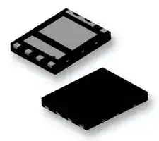


FDMS3660S
Dual MOSFET, N Channel, 30 V, 30 V, 60 A, 60 A, 1300 µohm
- Manufacturer: ONSEMI
- Product type: Dual MOSFETs
- Transistor Polarity:Dual N Channel; Continuous Drain Current Id:60A; Drain Source Voltage Vds:30V; On Resistance Rds(on):0.0013ohm; Rds(on) Test Voltage Vgs:10V; Threshold Voltage
- MSL: MSL 1 - Unlimited
- SVHC: Lead (25-Jun-2025)
- No. of Pins: 8Pins
- Channel Type: N Channel
- Product Range: -
- Qualification: -
- Transistor Case Style: Power 56
- Operating Temperature Max: 150°C
- Power Dissipation N Channel: 2.5W
- Power Dissipation P Channel: 2.5W
- Drain Source Voltage Vds N Channel: 30V
- Drain Source Voltage Vds P Channel: 30V
- Continuous Drain Current Id N Channel: 60A
- Continuous Drain Current Id P Channel: 60A
- Drain Source On State Resistance N Channel: 1300µohm
- Drain Source On State Resistance P Channel: 1300µohm
| Delivery and price | |
|---|---|
| Units per pack | 1000 |
| Price | 0.775 € |
| Current stock | 1000+ |
| Lead time | 30 days |
## **Is Now Part of**

**To learn more about ON Semiconductor, please visit our website at www.onsemi.com**

ON Semiconductor and the ON Semiconductor logo are trademarks of Semiconductor Components Industries, LLC dba ON Semiconductor or its subsidiaries in the United States and/or other countries. ON Semiconductor owns the rights to a number of patents, trademarks, copyrights, trade secrets, and other intellectual property. A listing of ON Semiconductor’s product/patent coverage may be accessed at www.onsemi.com/site/pdf/Patent-Marking.pdf. ON Semiconductor reserves the right to make changes without further notice to any products herein. ON Semiconductor makes no warranty, representation or guarantee regarding the suitability of its products for any particular purpose, nor does ON Semiconductor assume any liability arising out of the application or use of any product or circuit, and specifically disclaims any and all liability, including without limitation special, consequential or incidental damages. Buyer is responsible for its products and applications using ON Semiconductor products, including compliance with all laws, regulations and safety requirements or standards, regardless of any support or applications information provided by ON Semiconductor. “Typical” parameters which may be provided in ON Semiconductor data sheets and/or specifications can and do vary in different applications and actual performance may vary over time. All operating parameters, including “Typicals” must be validated for each customer application by customer’s technical experts. ON Semiconductor does not convey any license under its patent rights nor the rights of others. ON Semiconductor products are not designed, intended, or authorized for use as a critical component in life support systems or any FDA Class 3 medical devices or medical devices with a same or similar classification in a foreign jurisdiction or any devices intended for implantation in the human body. Should Buyer purchase or use ON Semiconductor products for any such unintended or unauthorized application, Buyer shall indemnify and hold ON Semiconductor and its officers, employees, subsidiaries, affiliates, and distributors harmless against all claims, costs, damages, and expenses, and reasonable attorney fees arising out of, directly or indirectly, any claim of personal injury or death associated with such unintended or unauthorized use, even if such claim alleges that ON Semiconductor was negligent regarding the design or manufacture of the part. ON Semiconductor is an Equal Opportunity/Affirmative Action Employer. This literature is subject to all applicable copyright laws and is not for resale in any manner.

## **February 2015**

## **FDMS3660S PowerTrench[®] Power Stage**

## **Asymmetric Dual N-Channel MOSFET**

## **General Description**

## **Features**

Q1: N-Channel

This device includes two specialized N-Channel MOSFETs in a dual PQFN package. The switch node has been internally connected to enable easy placement and routing of synchronous buck converters. The control MOSFET (Q1) and synchronous SyncFET[TM] (Q2) have been designed to provide optimal power efficiency.

Max rDS(on) = 8 mΩ at VGS = 10 V, ID = 13 A

Max rDS(on) = 11 mΩ at VGS = 4.5 V, ID = 11 A

Q2: N-Channel

Max rDS(on) = 1.8 mΩ at VGS = 10 V, ID = 30 A

Max rDS(on) = 2.2 mΩ at VGS = 4.5 V, ID = 27 A

## **Applications**

Low inductance packaging shortens rise/fall times, resulting in lower switching losses

Computing

**==> picture [471 x 449] intentionally omitted <==**

**----- Start of picture text -----**<br>
MOSFET integration enables optimum layout for  Communications<br>lower circuit inductance and reduced switch node<br>General Purpose Point of Load<br>ringing<br>Notebook VCORE<br>RoHS Compliant<br>| @!<br>Pin 1 G1<br>D1<br>Pin 1<br>D1 D1 D1 S2 5 Q2 4 D1<br>PHASE S2 6 PHASE 3 D1<br>(S1/D2)<br>G2 S2 7 2 D1<br>S2<br>eo S2 Kin S2 G2 7 8 Q1 5 1 G1<br>Top Power 56 Bottom<br>MOSFET Maximum Ratings TA = 25 °C unless otherwise noted<br>Symbol Parameter Q1 Q2 Units<br>VDS Drain to Source Voltage 30 30 V<br>VGS Gate to Source Voltage                                                                                  (Note 3) ±20 ±12 V<br>Drain Current      -Continuous  (Package limited)                                   TC = 25 °C 30 60<br>ID                              -Continuous                                                                    T                             -Continuous  (Silicon limited)                                       TCA = 25 °C= 25 °C 1360 [1a] 30145 [1b] A<br>                           -Pulsed 40 120<br>EAS a Single Pulse Avalanche Energy 33 [4] 86 [5] mJ<br>PD Power DissiPower Dissippation for Sination for Singgle Ole Opperation                                                  Teration                                                  TA A = 25 °C= 25 °C 2.21 [1c][1a] 2.51 [1d][1b] W<br>EE TJ, TSTG ——— Operating and Storage Junction Temperature Range -55 to +150 ° C<br>Thermal Characteristics<br>RθJA Thermal Resistance, Junction to Ambient                                             57 [1a] 50 [1b]<br>RθJA Thermal Resistance, Junction to Ambient                                              125 [1c] 120 [1d] °C/W<br>——————————— RθJC Thermal Resistance, Junction to Case                                                      2.9 2.2<br>Package Marking and Ordering Information<br>Device Marking Device Package Reel Size Tape Width Quantity<br>22CF<br>FDMS3660S Power 56 13 ” 12 mm 3000 units<br>07OD<br>a<br>**----- End of picture text -----**<br>


**1**

www.fairchildsemi.com

©2012 Fairchild Semiconductor Corporation FDMS3660S Rev.C4

## **Electrical Characteristics** TJ = 25 °C unless otherwise noted

|**Electrica**|**l Characteristics**TJ= 25 °C u|nless otherwise noted||||||||
|---|---|---|---|---|---|---|---|---|---|
|**Symbol**|**Parameter**|**Test Conditions**|**Type**|**Min**||**Typ**|**Max**||**Units**|
|**Off Characteristics**||||||||||
|BVDSS|Drain to Source Breakdown Voltage|ID= 250μA, VGS= 0 V<br>ID= 1 mA, VGS= 0 V|Q1<br>Q2|30<br>30|||||V|
|ΔBVDSS<br>ΔTJ|Breakdown Voltage Temperature<br>Coefficient|ID= 250μA, referenced to 25 °C<br>ID= 10 mA, referenced to 25 °C|Q1<br>Q2|||16<br>24|||mV/°C|
|IDSS|Zero Gate Voltage Drain Current|VDS= 24 V, VGS= 0 V|Q1<br>Q2||||1<br>500||μA<br>μA|
|IGSS|Gate to Source Leakage Current|VGS= 20 V, VDS= 0 V<br>VGS= 12 V, VDS= 0 V|Q1<br>Q2||||100<br>100||nA<br>nA|
|**On Characteristics**||||||||||
|VGS(th)|Gate to Source Threshold Voltage|VGS= VDS,  ID= 250μA<br>VGS= VDS,  ID= 1 mA|Q1<br>Q2|1.1<br>1.1||1.9<br>1.5|2.7<br>2.2||V|
|ΔVGS(th)<br>ΔTJ|Gate to Source Threshold Voltage<br>Temperature Coefficient|ID= 250μA, referenced to 25 °C<br>ID= 10 mA, referenced to 25 °C|Q1<br>Q2|||-6<br>-3|||mV/°C|
|rDS(on)|Drain to Source On Resistance|VGS= 10 V,  ID= 13 A<br>VGS= 4.5 V,  ID= 11 A<br>VGS= 10 V,  ID= 13 A , TJ= 125 °C|Q1|||4<br>6<br>5.7|8<br>11<br>8.7||mΩ|
|||VGS= 10 V,  ID= 30 A<br>VGS= 4.5 V,  ID= 27 A<br>VGS= 10 V,  ID= 30 A , TJ= 125 °C|Q2|||1.3<br>1.5<br>1.86|1.8<br>2.2<br>2.6|||
|gFS|Forward Transconductance|VDS= 5 V,  ID= 13 A<br>VDS= 5 V,  ID= 30 A|Q1<br>Q2|||62<br>231|||S|
|**Dynamic Characteristics**||||||||||
|Ciss|Input Capacitance|Q1:<br>VDS= 15 V, VGS= 0 V, f = 1 MHZ<br>Q2:<br>VDS= 15 V, VGS= 0 V, f = 1 MHZ|Q1<br>Q2|||1325<br>4130|1765<br>5493||pF|
|Coss|Output Capacitance||Q1<br>Q2|||466<br>915|620<br>1220||pF|
|Crss|Reverse Transfer Capacitance||Q1<br>Q2|||46<br>124|70<br>185||pF|
|Rg|Gate Resistance||Q1<br>Q2|0.2<br>0.2||0.6<br>0.8|2<br>3||Ω|
|**Switching Characteristics**||||||||||
|td(on)|Turn-On Delay Time|Q1:<br>VDD= 15 V, ID= 13 A,  RGEN= 6Ω<br>Q2:<br>VDD= 15 V, ID= 30 A,  RGEN= 6Ω|Q1<br>Q2|||7.7<br>11||15<br>20|ns|
|tr|Rise Time||Q1<br>Q2|||2.2<br>5||10<br>10|ns|
|td(off)|Turn-Off Delay Time||Q1<br>Q2|||19<br>40||34<br>64|ns|
|tf|Fall Time||Q1<br>Q2|||1.8<br>3.9||10<br>10|ns|
|Qg|Total Gate Charge|VGS= 0  V to 10 V|Q1<br>Q2|||21<br>62||29<br>87|nC|
|Qg|Total Gate Charge|VGS= 0  V to 4.5 V|Q1<br>Q2|||9.5<br>29||13<br>41|nC|
|Qgs|Gate to Source Gate Charge||Q1<br>Q2|||3.9<br>9|||nC|
|Qgd|Gate to Drain “Miller” Charge||Q1<br>Q2|||2.6<br>7|||nC|


©2012 Fairchild Semiconductor Corporation FDMS3660S Rev.C4

www.fairchildsemi.com

**2**

|**Electrical Characteristics**TJ= 25 °C unless otherwise noted<br>**Drain-Source Diode Characteristics**<br>**Symbol**<br>**Parameter**<br>**Test Conditions**<br>**Type**<br>**Min**<br>**Typ**<br>**Max**<br>**Units**<br>VSD<br>Source to Drain Diode  Forward Voltage<br>VGS= 0 V, IS= 13 A           (Note 2)<br>VGS= 0 V, IS= 2 A             (Note 2)<br>VGS= 0 V, IS= 30 A           (Note 2)<br>VGS = 0 V, IS = 2 A(Note 2)<br>Q1<br>Q1<br>Q2<br>Q2<br>0.8<br>0.7<br>0.8<br>0.6<br>1.2<br>1.2<br>1.2<br>1.2<br>V<br>trr<br>Reverse Recovery Time<br>Q1:<br>IF= 13 A, di/dt = 100 A/μs<br>Q2:<br>IF= 30 A, di/dt = 300 A/μs<br>Q1<br>Q2<br>26<br>29<br>42<br>46<br>ns<br>Qrr<br>Reverse Recovery Charge<br>Q1<br>Q2<br>10<br>32<br>20<br>50<br>nC<br>**Notes:**<br>**1:** RθJAis determined with the device mounted on a 1 in2pad 2 oz copper pad on a 1.5 x 1.5 in. board of FR-4 material. RθJCis guaranteed by design whileRθCA is determined<br>by the user's board design.<br>~~Po~~|
|---|


**==> picture [361 x 218] intentionally omitted <==**

**----- Start of picture text -----**<br>
b. 50 °C/W when mounted on<br>a. 57 °C/W when mounted on      a 1 in [2 ] pad of  2 oz  copper     a 1 in [2 ] pad of  2 oz  copper<br>c. 125 °C/W when mounted on  a d. 120 °C/W when mounted on  a<br>    minimum pad of 2 oz copper     minimum pad of 2 oz copper<br>il i<br>G DF DS SF SS G DF DS SF SS<br>G DF DS SF SS<br>G DF DS SF SS<br>**----- End of picture text -----**<br>


- **2:** Pulse Test: Pulse Width < 30 0 μs, Duty cycle < 2.0%.

- **3:** As an N-ch device, the negative Vgs rating is for low duty cycle pulse ocurrence only. No continuous rating is implied with the negative Vgs rating.

- **4:** EAS of 33 mJ is based on starting TJ = 25[o] C; N-ch: L = 1.9 mH, IAS = 6 A, VDD = 27 V, VGS = 10 V. 100% test at L= 0.1 mH, IAS = 16 A.

- **5:** EAS of 86 mJ is based on starting TJ = 25[o] C; N-ch: L = 0.6 mH, IAS = 17 A, VDD = 27 V, VGS = 10 V. 100% test at L= 0.1 mH, IAS = 31 A.

©2012 Fairchild Semiconductor Corporation FDMS3660S Rev.C4

www.fairchildsemi.com

**3**

## **Typical Characteristics (Q1 N-Channel)** TJ = 25 °C unless otherwise noted

**==> picture [469 x 576] intentionally omitted <==**

**----- Start of picture text -----**<br>
40 4<br>VGS = 10 V PULSE DURATION = 80  μ s<br>DUTY CYCLE = 0.5% MAX<br>30 3<br>VGS = 6 V VGS = 3.5 V<br>20 VGS = 4.5 V 2 V GS  = 4 V<br>VGS = 4 V<br>VGS = 3.5 V<br>10 1<br>PULSE DURATION = 80  μ s VGS = 4.5 V VGS = 6 V VGS = 10 V<br>DUTY CYCLE = 0.5% MAX<br>0 0<br>0.0 0.2 0.4 0.6 0.8 1.0 0 10 20 30 40<br>VDS, DRAIN TO SOURCE VOLTAGE (V) ID, DRAIN CURRENT (A)<br>Figure 1.  On Region Characteristics Figure 2.      Normalized On-Resistance<br>vs Drain Current and Gate Voltage<br>1.6 20<br>ID = 13 A PULSE DURATION = 80  μ s<br>VGS = 10 V DUTY CYCLE = 0.5% MAX<br>1.4 16<br>ID = 13 A<br>1.2 12<br>TJ = 125 [ o] C<br>1.0 8<br>0.8 4<br>TJ = 25  [o] C<br>0.6 0<br>-75 -50 -25 0 25 50 75 100 125 150 2 4 6 8 10<br>TJ, JUNCTION TEMPERATURE ( [o] C) VGS, GATE TO SOURCE VOLTAGE (V)<br>Figure 3.  Normalized  On  Resistance                                         Figure 4.   On-Resistance vs  Gate to<br>vs Junction Temperature Source Voltage<br>40 40<br>PULSE DURATION = 80 DUTY CYCLE = 0.5% MAX μ s 10 VGS = 0 V<br>30<br>VDS = 5 V 1 T J  = 150  [o] C<br>TJ = 150  [o] C<br>20<br>0.1 TJ = 25 [ o] C<br>TJ = 25  [o] C<br>10<br>TJ = -55  [o] C 0.01 TJ = -55  [o] C<br>0 0.001<br>1.5 2.0 2.5 3.0 3.5 4.0 0.0 0.2 0.4 0.6 0.8 1.0 1.2<br>VGS, GATE TO SOURCE VOLTAGE (V) VSD, BODY DIODE FORWARD VOLTAGE (V)<br>Figure 5.  Transfer Characteristics Figure 6.    Source to Drain  Diode<br>Forward Voltage vs Source Current<br>NORMALIZED<br>, DRAIN CURRENT (A)<br>ID<br>DRAIN TO SOURCE ON-RESISTANCE<br>)<br>Ω<br>m<br>(<br>DRAIN TO<br>NORMALIZED rDS(on),<br>SOURCE ON-RESISTANCE<br> DRAIN TO SOURCE ON-RESISTANCE<br>, DRAIN CURRENT (A)<br>ID<br>, REVERSE DRAIN CURRENT (A)<br>IS<br>**----- End of picture text -----**<br>


©2012 Fairchild Semiconductor Corporation FDMS3660S Rev.C4

www.fairchildsemi.com

**4**

**Typical Characteristics (Q1 N-Channel)** TJ = 25 °C unless otherwise noted

**==> picture [472 x 594] intentionally omitted <==**

**----- Start of picture text -----**<br>
10 2000<br>ID = 13 A VDD = 10 V 1000 Ciss<br>8<br>6 VDD = 15 V Coss<br>VDD = 20 V<br>100<br>4<br>2 Crss<br>f = 1 MHz<br>VGS = 0 V<br>0 10<br>0 5 10 15 20 25 0.1 1 10 30<br>Qg, GATE CHARGE (nC) VDS, DRAIN TO SOURCE VOLTAGE (V)<br>Figure 7.  Gate Charge Characteristics Figure 8.      Capacitance vs Drain<br>to Source Voltage<br>100 80<br>R θ JC = 2.9  [o] C/W<br>60 V GS  = 10 V<br>TJ = 25 [ o] C<br>10 40 V GS = 4.5 V<br>T J  = 100 [ o] C<br>20<br>Limited by Package<br>T J  = 125  [o] C<br>1 0<br>0.001 0.01 0.1 1 10 100 25 50 75 100 125 150<br>tAV, TIME IN AVALANCHE (ms) TC, CASE TEMPERATURE (oC)<br>Figure 9.  Unclamped Inductive                                  Figure 10.  Maximum Continuous Drain<br>Switching Capability Current vs Case Temperature<br>100<br>1000<br>SINGLE PULSE<br>100  μ s<br>R θ JA  = 125 [ o] C/W<br>10<br>100<br>1 ms<br>1 THIS AREA IS  10<br>LIMITED BY rDS(on) 10 ms<br>100 ms<br>SINGLE PULSE<br>0.1 RTJ θ JA= MAX RATED= 125  [o] C/W 1 s 10 sDC 1<br>TA = 25  [o] C<br>0.01<br>0.01 0.1 1 10 100200 0.110-4 10-3 10-2 10-1 1 10 100 1000<br>VDS, DRAIN to SOURCE VOLTAGE (V) t, PULSE WIDTH (sec)<br>Figure 11.  Forward Bias Safe                                  Figure 12.   Single Pulse Maximum                                Power<br>Operating Area  Dissipation<br>CAPACITANCE (pF)<br>, GATE TO SOURCE VOLTAGE (V)<br>GS<br>V<br>DRAIN CURRENT (A)<br>,<br>ID<br>, AVALANCHE CURRENT (A)<br>IAS<br>, DRAIN CURRENT (A)<br>ID<br>, PEAK TRANSIENT POWER (W)P)(PK<br>**----- End of picture text -----**<br>


www.fairchildsemi.com

©2012 Fairchild Semiconductor Corporation FDMS3660S Rev.C4

**5**

**==> picture [347 x 12] intentionally omitted <==**

**----- Start of picture text -----**<br>
Typical Characteristics (Q1 N-Channel)  TJ = 25 °C unless otherwise noted<br>**----- End of picture text -----**<br>


**==> picture [468 x 189] intentionally omitted <==**

**----- Start of picture text -----**<br>
2<br>DUTY CYCLE-DESCENDING ORDER<br>1<br>D = 0.5<br>0.1        0.2        0.1 PDM<br>       0.05<br>       0.02<br>       0.01 t 1<br>0.01 SINGLE PULSE t 2<br>NOTES:<br>R θ JA  = 125  [o] C/W DUTY FACTOR: D = t1/t2<br>(Note 1c)  PEAK T J  = P DM  x Z θJA  x R θJA  + T A<br>0.00110-4 10-3 10-2 10-1 1 10 100 1000<br>t, RECTANGULAR PULSE DURATION (sec)<br>Figure 13.  Junction-to-Ambient Transient Thermal Response Curve<br>Z JA θ<br>IMPEDANCE,<br>NORMALIZED THERMAL<br>**----- End of picture text -----**<br>


©2012 Fairchild Semiconductor Corporation FDMS3660S Rev.C4

www.fairchildsemi.com

**6**

## **Typical Characteristics (Q2 N-Channel)** TJ =  25[o] C unlenss otherwise noted

**==> picture [468 x 568] intentionally omitted <==**

**----- Start of picture text -----**<br>
120 4<br>VGS = 10 V PULSE DURATION = 80  μ s<br>DUTY CYCLE = 0.5% MAX<br>100<br>VGS = 4.5 V<br>3<br>80 VGS = 3.5 V VGS = 2.5 V<br>VGS = 3 V<br>60 2 V GS  = 3 V<br>40<br>PULSE DURATION = 80  μ s 1<br>20 DUTY CYCLE = 0.5% MAX VGS = 3.5 V VGS = 4.5 V VGS = 10 V<br>VGS = 2.5 V<br>0 0<br>0.0 0.2 0.4 0.6 0.8 1.0 0 20 40 60 80 100 120<br>VDS, DRAIN TO SOURCE VOLTAGE (V) ID, DRAIN CURRENT (A)<br>Figure 14. On-Region Characteristics Figure 15. Normalized on-Resistance vs Drain<br>Current and Gate  Voltage<br>1.6 8<br>IVDGS = 30 A = 10 V PULSE DURATION = 80 DUTY CYCLE = 0.5% MAX μ s<br>1.4<br>6<br>ID = 30 A<br>1.2<br>4<br>1.0<br>TJ = 125 [ o] C<br>2<br>0.8<br>TJ = 25  [o] C<br>0.6 0<br>-75 -50 -25 0 25 50 75 100 125 150 2 4 6 8 10<br>TJ, JUNCTION TEMPERATURE ( [o] C) VGS, GATE TO SOURCE VOLTAGE (V)<br>Figure 16. Normalized On-Resistance  Figure 17. On-Resistance vs Gate to<br>vs Junction Temperature Source Voltage<br>120 100<br>PULSE DURATION = 80  μ s VGS = 0 V<br>DUTY CYCLE = 0.5% MAX<br>100<br>10<br>VDS = 5 V TJ = 125 [o] C<br>80<br>TJ = 125  [o] C 1<br>60<br>40 TJ = 25  [o] C 0.1 TJ = 25 [ o] C<br>20 TJ = -55  [o] C 0.01 TJ = -55  [o] C<br>0 0.001<br>1.0 1.5 2.0 2.5 3.0 0.0 0.2 0.4 0.6 0.8 1.0<br>VGS, GATE TO SOURCE VOLTAGE (V) VSD, BODY DIODE FORWARD VOLTAGE (V)<br>NORMALIZED<br>, DRAIN CURRENT (A)<br>ID<br>DRAIN TO SOURCE ON-RESISTANCE<br>)<br>Ω<br>m<br>(<br>DRAIN TO<br>NORMALIZED rDS(on),<br>SOURCE ON-RESISTANCE<br> DRAIN TO SOURCE ON-RESISTANCE<br>, DRAIN CURRENT (A)<br>ID<br>, REVERSE DRAIN CURRENT (A)<br>IS<br>**----- End of picture text -----**<br>


**Figure 18. Transfer Characteristics**

**Figure 19. Source to Drain Diode Forward Voltage vs Source Current**

©2012 Fairchild Semiconductor Corporation FDMS3660S Rev.C4

www.fairchildsemi.com

**7**

**Typical Characteristics (Q2 N-Channel)** TJ = 25[o] C unless otherwise noted

**==> picture [470 x 588] intentionally omitted <==**

**----- Start of picture text -----**<br>
10 10000<br>ID = 30 A<br>8 C iss<br>VDD = 10 V<br>1000<br>6<br>VDD = 15 V C oss<br>4<br>VDD = 20 V 100 Crss<br>2<br>f = 1 MHz<br>VGS = 0 V<br>0 10<br>0 10 20 30 40 50 60 70 0.1 1 10 30<br>Qg, GATE CHARGE (nC) VDS, DRAIN TO SOURCE VOLTAGE (V)<br>Figure 20. Gate Charge Characteristics Figure 21. Capacitance vs Drain<br>to Source Voltage<br>100<br>160<br>VGS = 10 V R θ JC = 2.2  [o] C/W<br>120<br>TJ = 25 [ o] C<br>VGS = 4.5 V<br>10 TJ = 100 [ o] C 80<br>TJ = 125  [o] C 40<br>Limited by Package<br>1<br>0<br>0.001 0.01 0.1 1 10 100 1000 25 50 75 100 125 150<br>tAV, TIME IN AVALANCHE (ms) TC, CASE TEMPERATURE (oC)<br>Figure 22. Unclamped Inductive                         Figure 23. Maximun Continuous Drain<br>Switching Capability Current vs Case Temperature<br>200<br>2000<br>100 1000 SINGLE PULSE<br>100  μ s R θ JA = 120 [ o] C/W<br>10<br>100<br>1 ms<br>10 ms<br>1 THIS AREA IS<br>LIMITED BY rDS(on) 100 ms<br>SINGLE PULSE 1s 10<br>0.1 TJ = MAX RATED 10s<br>R θ JA = 120  [o] C/W DC<br>T A = 25  [o] C 1<br>0.01<br>0.01 0.1 1 10 100200 0.510-4 10-3 10-2 10-1 1 10 100 1000<br>VDS, DRAIN to SOURCE VOLTAGE (V)<br>t, PULSE WIDTH (sec)<br>Figure 24.  Forward Bias Safe                                   Figure 25. Single  Pulse Maximum<br>Operating Area Power Dissipation<br>CAPACITANCE (pF)<br>, GATE TO SOURCE VOLTAGE (V)<br>GS<br>V<br>DRAIN CURRENT (A)<br>,<br>ID<br>, AVALANCHE CURRENT (A)<br>IAS<br>, DRAIN CURRENT (A)<br>ID<br>, PEAK TRANSIENT POWER (W)P)(PK<br>**----- End of picture text -----**<br>


©2012 Fairchild Semiconductor Corporation FDMS3660S Rev.C4

www.fairchildsemi.com

**8**

**==> picture [469 x 216] intentionally omitted <==**

**----- Start of picture text -----**<br>
Typical Characteristics (Q2 N-Channel) TJ = 25  [o] C unless otherwise noted<br>2<br>DUTY CYCLE-DESCENDING ORDER<br>1<br>D = 0.5<br>       0.2<br>0.1<br>       0.1<br>       0.05 PDM<br>       0.02<br>0.01        0.01<br>t1<br>SINGLE PULSE t 2<br>NOTES:<br>0.001 R θ JA = 120  [o] C/W DUTY FACTOR: D = t1/t2<br>(Note 1d)  PEAK TJ = PDM x Z θJA  x R θJA  + TA<br>0.000110-4 10-3 10-2 10-1 1 10 100 1000<br>t, RECTANGULAR PULSE DURATION (sec)<br>Z JA θ<br>IMPEDANCE,<br>NORMALIZED THERMAL<br>**----- End of picture text -----**<br>


**Figure 26.  Junction-to-Ambient Transient Thermal Response Curve**

**==> picture [137 x 14] intentionally omitted <==**

**----- Start of picture text -----**<br>
©2012 Fairchild Semiconductor Corporation<br>FDMS3660S Rev.C4<br>**----- End of picture text -----**<br>


**==> picture [72 x 6] intentionally omitted <==**

**----- Start of picture text -----**<br>
www.fairchildsemi.com<br>**----- End of picture text -----**<br>


**9**

## **Typical Characteristics** (continued)

## **SyncFET[TM] Schottky body diode Characteristics**

Fairchild’s SyncFET[TM] process embeds a Schottky diode in parallel with PowerTrench MOSFET. This diode exhibits similar characteristics to a discrete external Schottky diode in parallel with a MOSFET. Figure 27 shows the reverse recovery characteristic of the FDMS3660S.

Schottky barrier diodes exhibit significant leakage at high temperature and high reverse voltage. This will increase the power in the device.

**==> picture [470 x 187] intentionally omitted <==**

**----- Start of picture text -----**<br>
35 10-2<br>30 TJ = 125  [o] C<br>25 10-3<br>didt = 300 A/ μ s<br>20 T J  = 100  [o] C<br>15 10-4<br>10<br>5 10-5<br>0 T J  = 25  [o] C<br>-5 10-6<br>0 100 200 300 400 0 5 10 15 20 25<br>TIME (ns) VDS, REVERSE VOLTAGE (V)<br>CURRENT (A)<br>, REVERSE LEAKAGE CURRENT (A)<br>IDSS<br>**----- End of picture text -----**<br>


**Figure 27. FDMS3660S SyncFET[TM ] body diode reverse recovery characteristic**

**Figure 28. SyncFET[TM] body diode reverse leakage  versus drain-source voltage**

©2012 Fairchild Semiconductor Corporation FDMS3660S Rev.C4

www.fairchildsemi.com

**10**

## **Application Information**

## **1. Switch Node Ringing Suppression**

Fairchild’s Power Stage products incorporate a proprietary design* that minimizes the peak overshoot, ringing voltage on the switch node (PHASE) without the need of any external snubbing components in a buck converter. As shown in the figure 29, the Power Stage solution rings significantly less than competitor solutions under the same set of test conditions.

> 1||I }ty | lI | | i[ !| Chl Sov M20.0neS0G54 IT 8.0nehx M20.Onr 5.005% IT B.Opetat AChi + SOY AChI5.0" **Power Stage Device                                                          Competitors solution**

*Patent Pending

©2012 Fairchild Semiconductor Corporation FDMS3660S Rev.C4

www.fairchildsemi.com

**11**

## **2. Recommended PCB Layout Guidelines**

As a PCB designer, it is necessary to address critical issues in layout to minimize losses and optimize the performance of the power train. Power Stage is a high power density solution and all high current flow paths, such as VIN (D1), PHASE (S1/D2) and GND (S2), should be short and wide for better and stable current flow, heat radiation and system performance. A recommended layout procedure is discussed below to maximize the electrical and thermal performance of the part.

**==> picture [189 x 10] intentionally omitted <==**

©2012 Fairchild Semiconductor Corporation FDMS3660S Rev.C4

**==> picture [9 x 6] intentionally omitted <==**

**----- Start of picture text -----**<br>
12<br>**----- End of picture text -----**<br>


www.fairchildsemi.com

## **Following is a guideline, not a requirement which the PCB designer should consider:**

1.  Input ceramic bypass capacitors C1 and C2 must be placed close to the D1 and S2 pins of Power Stage to help reduce parasitic inductance and high frequency conduction loss induced by switching operation. C1 and C2 show the bypass capacitors placed close to the part between D1 and S2.  Input capacitors should be connected in parallel close to the part. Multiple input caps can be connected depending upon the application.

2. The PHASE copper trace serves two purposes; In addition to being the current path from the Power Stage package to the output inductor (L), it also serves as heat sink for the lower FET in the Power Stage package. The trace should be short and wide enough to present a low resistance path for the high current flow between the Power Stage and the inductor. This is done to minimize conduction losses and limit temperature rise. Please note that the PHASE node is a high voltage and high frequency switching node with high noise potential. Care should be taken to minimize coupling to adjacent traces. The reference layout in figure 31 shows a good balance between the thermal and electrical performance of Power Stage.

3. Output inductor location should be as close as possible to the Power Stage device for lower power loss due to copper trace resistance. A shorter and wider PHASE trace to the inductor reduces the conduction loss. Preferably the Power Stage should be directly in line (as shown in figure 31) with the inductor for space savings and compactness.

4. The PowerTrench[®] Technology MOSFETs used in the Power Stage are effective at minimizing phase node ringing. It allows the part to operate well within the breakdown voltage limits. This eliminates the need to have an external snubber circuit in most cases. If the designer chooses to use an RC snubber, it should be placed close to the part between the PHASE pad and S2 pins to dampen the high-frequency ringing.

5. The driver IC should be placed close to the Power Stage part with the shortest possible paths for the High Side gate and Low Side gates through a wide trace connection. This eliminates the effect of parasitic inductance and resistance between the driver and the MOSFET and turns the devices on and off as efficiently as possible. At higher-frequency operation this impedance can limit the gate current trying to charge the MOSFET input capacitance. This will result in slower rise and fall times and additional switching losses. Power Stage has both the gate pins on the same side of the package which allows for back mounting of the driver IC to the board. This provides a very compact path for the drive signals and improves efficiency of the part.

6. S2 pins should be connected to the GND plane with multiple vias for a low impedance grounding. Poor grounding can create a noise transient offset voltage level between S2 and driver ground. This could lead to faulty operation of the gate driver and MOSFET.

7. Use multiple vias on each copper area to interconnect top, inner and bottom layers to help smooth current flow and heat conduction. Vias should be relatively large, around 8 mils to 10 mils, and of reasonable inductance. Critical high frequency components such as ceramic bypass caps should be located close to the part and on the same side of the PCB. If not feasible, they should be connected from the backside via a network of low inductance vias.

©2012 Fairchild Semiconductor Corporation FDMS3660S Rev.C4

www.fairchildsemi.com

**13**

**==> picture [208 x 174] intentionally omitted <==**

**----- Start of picture text -----**<br>
5.10<br>0.10 C 4.90 A<br>(2X) PKG B<br>CL<br>8 5<br>PKG CL 6.255.90<br>1 4 0.10 C<br>PIN # 1<br>INDICATOR (2X)<br>TOP VIEW<br>**----- End of picture text -----**<br>


**==> picture [41 x 18] intentionally omitted <==**

**----- Start of picture text -----**<br>
SEE<br>DETAIL A<br>**----- End of picture text -----**<br>


**==> picture [95 x 40] intentionally omitted <==**

**==> picture [210 x 214] intentionally omitted <==**

**----- Start of picture text -----**<br>
4.00<br>CL<br>1.27 TYP<br>0.65 TYP<br>8 7  6  5<br>0.63<br>2.52<br>1.60<br>2.15 KEEP OUT AREA<br>0.00 CL<br>4.16<br>1.21<br>2.13<br>2.31<br>3.15<br>1 2  3  4<br>0.63<br>0.59<br>3.18<br>5.10<br>2.00<br>0.00<br>1.18<br>**----- End of picture text -----**<br>


RECOMMENDED LAND PATTERN FOR SAWN / PUNCHED TYPE

SIDE VIEW

**==> picture [212 x 236] intentionally omitted <==**

**----- Start of picture text -----**<br>
0.10 C A B<br>0.05 C<br>0.65 3.16 0.70<br>0.38 2.80 0.36<br>0.45<br>0.25 1 2 3 4 1.34<br>(6X) 1.12<br>0.66±.05<br>2.25<br>4.08 2.05<br>3.70<br>1.02<br>0.65 8 7 6 5 0.82<br>0.38<br>0.44 0.61<br>(8X)<br>0.24 0.31<br>1.27<br>3.81<br>**----- End of picture text -----**<br>


**==> picture [204 x 119] intentionally omitted <==**

**----- Start of picture text -----**<br>
0.10 C<br>8X<br>0.08 C<br>0.35 0.05 C<br>1.10<br>0.90 0.15 0.00 SEATING<br>  PLANE<br>(SCALE: 2X)<br>**----- End of picture text -----**<br>


BOTTOM VIEW

**==> picture [433 x 206] intentionally omitted <==**

**----- Start of picture text -----**<br>
5.10<br>0.10 C<br>4.90<br>(2X) SEE<br>PKG DETAIL B 0.35<br>CL 0.15<br>8 5<br>0.28<br>0.08<br>10°<br>PKG CL 6.25 5.90<br>5.90 5.70<br>1 4 0.10 C (SCALE: 2X)<br>(2X)<br>0.41<br>0.21 [(8X)]<br>TOP VIEW<br>**----- End of picture text -----**<br>


**==> picture [388 x 115] intentionally omitted <==**

**----- Start of picture text -----**<br>
5.00<br>4.80<br>SEE 0.10 C<br>DETAIL C<br>0.35<br>0.15<br>8X<br>0.08 C<br>C<br>SIDE VIEW<br>1.10 SEATING<br>0.90   PLANE<br>(SCALE: 2X)<br>**----- End of picture text -----**<br>


**==> picture [247 x 228] intentionally omitted <==**

**----- Start of picture text -----**<br>
0.65 3.16 0.70 0.10 C A B<br>0.38 2.80 0.36 0.05 C<br>0.45<br>0.25<br>1 2 3 4 1.34<br>(6X) 1.12<br>0.66±.05<br>4.08 2.25<br>3.70 2.05<br>1.02<br>0.65 8 7 6 5 0.82<br>0.38<br>0.44 0.61<br>(8X)<br>0.24 0.31<br>1.27<br>3.81<br>BOTTOM VIEW<br>**----- End of picture text -----**<br>


NOTES: UNLESS OTHERWISE SPECIFIED

A) PACKAGE STANDARD REFERENCE:

JEDEC REGISTRATION, MO-240, VARIATION AA.

- B)  ALL DIMENSIONS ARE IN MILLIMETERS.

- C)  DIMENSIONS DO NOT INCLUDE BURRS OR MOLD FLASH. MOLD FLASH OR BURRS DOES NOT EXCEED 0.10MM.

- D)  DIMENSIONING AND TOLERANCING PER ASME Y14.5M-1994.

- E)  IT IS RECOMMENDED TO HAVE NO TRACES OR VIAS WITHIN THE KEEP OUT AREA.

- F)  DRAWING FILE NAME: PQFN08EREV6.

- G) FAIRCHILD SEMICONDUCTOR

ON Semiconductor and      are trademarks of Semiconductor Components Industries, LLC dba ON Semiconductor or its subsidiaries in the United States and/or other countries. ON Semiconductor owns the rights to a number of patents, trademarks, copyrights, trade secrets, and other intellectual property. A listing of ON Semiconductor’s product/patent coverage may be accessed at www.onsemi.com/site/pdf/Patent−Marking.pdf. ON Semiconductor reserves the right to make changes without further notice to any products herein. ON Semiconductor makes no warranty, representation or guarantee regarding the suitability of its products for any particular purpose, nor does ON Semiconductor assume any liability arising out of the application or use of any product or circuit, and specifically disclaims any and all liability, including without limitation special, consequential or incidental damages. Buyer is responsible for its products and applications using ON Semiconductor products, including compliance with all laws, regulations and safety requirements or standards, regardless of any support or applications information provided by ON Semiconductor. “Typical” parameters which may be provided in ON Semiconductor data sheets and/or specifications can and do vary in different applications and actual performance may vary over time. All operating parameters, including “Typicals” must be validated for each customer application by customer’s technical experts. ON Semiconductor does not convey any license under its patent rights nor the rights of others. ON Semiconductor products are not designed, intended, or authorized for use as a critical component in life support systems or any FDA Class 3 medical devices or medical devices with a same or similar classification in a foreign jurisdiction or any devices intended for implantation in the human body. Should Buyer purchase or use ON Semiconductor products for any such unintended or unauthorized application, Buyer shall indemnify and hold ON Semiconductor and its officers, employees, subsidiaries, affiliates, and distributors harmless against all claims, costs, damages, and expenses, and reasonable attorney fees arising out of, directly or indirectly, any claim of personal injury or death associated with such unintended or unauthorized use, even if such claim alleges that ON Semiconductor was negligent regarding the design or manufacture of the part. ON Semiconductor is an Equal Opportunity/Affirmative Action Employer. This literature is subject to all applicable copyright laws and is not for resale in any manner.

## **PUBLICATION ORDERING INFORMATION**

**N. American Technical Support** : 800−282−9855 Toll Free **ON Semiconductor Website** : **www.onsemi.com** USA/Canada

## **LITERATURE FULFILLMENT** :

Literature Distribution Center for ON Semiconductor

**Order Literature** : http://www.onsemi.com/orderlit For additional information, please contact your local Sales Representative

19521 E. 32nd Pkwy, Aurora, Colorado 80011 USA **Europe, Middle East and Africa Technical Support: Phone** : 303−675−2175 or 800−344−3860 Toll Free USA/Canada Phone: 421 33 790 2910 **Fax** : 303−675−2176 or 800−344−3867 Toll Free USA/Canada **Japan Customer Focus Center Email** : orderlit@onsemi.com Phone: 81−3−5817−1050

© Semiconductor Components Industries, LLC

www.onsemi.com

**www.onsemi.com**

**1**
Updated at June 9, 2026
onsemi is a premier global supplier of intelligent power and sensing technologies, driving disruptive innovations across the automotive, industrial, and cloud infrastructure markets. Recognized for their commitment to sustainability and reliable supply chains, the company accelerates advancements in vehicle electrification, industrial automation, and 5G networks by solving the industry's most complex design challenges. At the core of their portfolio is an industry-leading selection of discrete semiconductors. This extensive range features thousands of high-performance bipolar transistors, single and dual MOSFETs, and a comprehensive array of diodes, including Zener, Schottky, and fast-recovery rectifiers. Engineered for superior thermal performance and energy efficiency, these foundational components are critical for demanding power conversion, switching, and signal conditioning applications. Beyond essential discretes, onsemi provides a robust suite of advanced power management and circuit protection solutions. Their lineup includes intelligent power modules, single IGBTs, and transient voltage suppression (TVS) diodes designed to safeguard sensitive circuitry. Complimented by integrated passive filters, AC/DC LED driver ICs, and specialized sub-2.4GHz RF transceivers, onsemi equips engineers with the scalable, high-quality technologies needed to build a cleaner, smarter, and more connected world.
About Novapart
Novapart is a B2B electronic component broker specialising in stock shortages and cost reduction. We source hard-to-find parts and identify compliant alternatives across a catalogue of 410,000+ components from 500+ manufacturers.
Learn more →Stock Shortage Specialist
When a component is unavailable, discontinued or has an unacceptable lead time, we tap into our network of vetted European and Asian distributors to source what you need — without compromising on quality or traceability.
Request a quote →Compliant Alternatives
We identify pin-to-pin, electrically equivalent substitutes that meet the same certifications (RoHS, AEC-Q100, REACH) as your original specification — validated against datasheets, not just part numbers. Often at a lower cost.
BOM Analysis service →