
Image not available
Illustrative purposes only

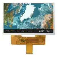
DMT070WVNTNT0-1A
TFT LCD, 7
⚠️ Reference pricing provided. In case of supply shortages, we will connect you with our trusted procurement partners to ensure your project's continuity.
- Manufacturer: DENSITRON
- Product type: TFT LCD Displays
- Resolution: 800 x 480 Pixels
- Module Size: 165.4mm x 104.59mm
- Touchscreen: No Touchscreen
- Display Size: 7"
- Logic Voltage: 5V
- Display Pinout: 40 Way Connector
- Interface Type: RGB
- Display Appearance: RGB
- Display Brightness: 450cd/m²
- Display Orientation: Landscape
- Operating Temperature Max: 85°C
- Operating Temperature Min: -30°C
| Delivery and price | |
|---|---|
| Units per pack | 1 |
| Price | 15.31 € |
| Current stock | 10+ |
| Lead time | 30 days |
Datasheet

## **LIQUID CRYSTAL DISPLAY MODULE**
## **Product Specification**
**==> picture [357 x 245] intentionally omitted <==**
**----- Start of picture text -----**<br>
CUSTOMER Standard<br>CUSTOMER PART<br>NUMBER<br>PRODUCT<br>DMT070WVNTNT0‐1A<br>NUMBER<br>Authorised By Created By<br>Luo Luo Eric Wan<br>Date: 14‐Nov‐17 Date: 04‐Nov‐17<br>**----- End of picture text -----**<br>
Product No.
DMT070WVNTNT0‐1A REV. 1.0 Page 1 / 23
© 2017 DENSITRON TECHNOLOGIES Ltd– PROPRIETARY DATA – ALL RIGHTS RESERVED
## **TABLE OF CONTENTS**
|**1**|**MAIN FEATURES ............................................................................................................ 4**|
|---|---|
|**2**|**MECHANICAL SPECIFICATION ........................................................................................ 5**|
||2.1<br>MECHANICAL CHARACTERISTICS .................................................................................. 5|
||2.2<br>MECHANICAL DRAWING............................................................................................... 6|
|**3**|**ELECTRICAL SPECIFICATION ........................................................................................... 7**|
||3.1<br>ABSOLUTE MAXIMUM RATINGS ................................................................................... 7|
||3.2<br>DC ELECTRICAL CHARACTERISTICS ............................................................................... 7|
||3.3<br>INTERFACE PIN ASSIGNMENT ....................................................................................... 8|
||3.4<br>TIMING CHARACTERISTICS ......................................................................................... 10|
||3.5<br>POWER SEQUENCE ..................................................................................................... 12|
|**4**|**OPTICAL SPECIFICATION ...............................................................................................13**|
||4.1<br>OPTICAL CHARACTERISTICS ........................................................................................ 13|
|**5**|**BACKLIGHT SPECIFICATION ...........................................................................................15**|
||5.1<br>LED DRIVING CONDITIONS ......................................................................................... 15|
||5.2<br>LED CIRCUIT ................................................................................................................ 15|
|**6**|**QUALITY ASSURANCE SPECIFICATION ...........................................................................16**|
||6.1<br>DELIVERY INSPECTION STANDARDS ........................................................................... 16|
||6.2<br>DEALING WITH CUSTOMER COMPLAINTS .................................................................. 21|
|**7**|**RELIABILITY SPECIFICATION ..........................................................................................22**|
||7.1<br>RELIABILITY TESTS ....................................................................................................... 22|
|**8**|**HANDLING PRECAUTIONS ............................................................................................23**|
Product No. DMT070WVNTNT0‐1A REV. 1.0 Page 2 / 23 ~~a | ee~~
© 2017 DENSITRON TECHNOLOGIES Ltd – PROPRIETARY DATA – ALL RIGHTS RESERVED
## **REVISION RECORD**
|**Rev.**|**Date**|**Page**|**Chapt.**||**Comment**|**ECN no.**|
|---|---|---|---|---|---|---|
|1.0|04‐Nov‐17|||Initial Release|||
Product No. DMT070WVNTNT0‐1A REV. 1.0 Page 3 / 23 ~~a | ee~~
© 2017 DENSITRON TECHNOLOGIES Ltd – PROPRIETARY DATA – ALL RIGHTS RESERVED
## **1 MAIN FEATURES**
|**1 MAIN FEATURES**||
|---|---|
|**ITEM**|**CONTENTS**|
|Screen Size|7.0” Diagonal|
|Display Format|800 x RGB x 480 Dots|
|N° of Colour|65K/262K/16.7M|
|TFT Active Area|152.40 mm (H) x 91.44 mm (V)|
|LCD Type|TFT|
|Mode|Transmissive / Normally Black|
|Viewing Direction|ALL|
|TFT Interface|16/18/24‐bit RGB interface|
|TFT Driver IC|SC5004 and SC5005|
|Backlight Type|LED|
|Operating Temperature|‐30°C ~ +85°C|
|Storage Temperature|‐40°C ~ +90°C|
|RoHS compliant|Yes|
Product No. DMT070WVNTNT0‐1A REV. 1.0 Page 4 / 23 ~~a | ee~~
© 2017 DENSITRON TECHNOLOGIES Ltd – PROPRIETARY DATA – ALL RIGHTS RESERVED
## **2 MECHANICAL SPECIFICATION**
## _**2.1 MECHANICAL CHARACTERISTICS**_
|**ITEM**|**CHARACTERISTIC**|**UNIT**|
|---|---|---|
|Overall Dimensions|165.4 mm (H) x 104.59 mm (V) x 5.8 mm (D)|mm|
|pixel Pitch|0.1905(H) x 0.1905 (V)|mm|
|Weight|124|g|
Product No. DMT070WVNTNT0‐1A REV. 1.0 Page 5 / 23 ~~a | ee~~
© 2017 DENSITRON TECHNOLOGIES Ltd – PROPRIETARY DATA – ALL RIGHTS RESERVED
## _**2.2 MECHANICAL DRAWING**_
**==> picture [459 x 567] intentionally omitted <==**
**----- Start of picture text -----**<br>
丝印白色记号线<br>Product No. DMT070WVNTNT0‐1A REV. 1.0 Page 6 / 23<br>a | ee<br>AK<br>CIRCUIT DIAGRAM<br>BL0702702 FZ:XXX<br>Stiffener<br>Conduct<br>1<br>109<br>7.0"TFT ALL Sighi<br>800(RGB)*480 1<br>omponent Area<br>C<br>R.G.B<br>109<br>Display type:TFT Display Mode:Transmissive/Normally Black color depth: Interface Type: 16/18/24 BIT Wide viewing: ALL Driver IC:SC5004(Source),SC5005(Gate) VDD:3.3V,VCC:5V Backlight: White Backlight 27 LED TYP:Vf=9.9V If=180mA Operating temprature: -30°C ~ +85°C Storage temprature: -40°C ~ +90°C ROHS COMPLIANT PRODUCT<br>**----- End of picture text -----**<br>
© 2017 DENSITRON TECHNOLOGIES Ltd – PROPRIETARY DATA – ALL RIGHTS RESERVED
## **3 ELECTRICAL SPECIFICATION**
## _**3.1 ABSOLUTE MAXIMUM RATINGS**_
|**Item**|**Symbol**|**Condition**|**Min**|**Max**|**Unit**|**Note**|
|---|---|---|---|---|---|---|
|Power Supply Voltage1|VDD||‐0.3|4.0|V||
|Power Supply Voltage2|VCC||‐0.3|7.0|V||
|Operating Temperature|TOP||‐30|85|°C|1|
|Storage Temperature|TST||‐40|90|°C|1,2,3|
- Note 1. 90 % RH Max for Ta<50 °C, and 60% RH for Ta≥50°C.
- Note 2. In case of below 0°C, the response time of liquid crystal (LC) becomes slower and the colour of panel becomes darker than normal one. Level of retardation depends on temperature, because of LC's characteristic.
- Note 3. Only operation is guaranteed at operating temperature. Contrast, response time, another display quality are evaluated at +25°C.
## _**3.2 DC ELECTRICAL CHARACTERISTICS**_
**==> picture [467 x 226] intentionally omitted <==**
**----- Start of picture text -----**<br>
Item Symbol Condition Min Typ Max Unit Note<br>es ee<br>Power Supply Voltage1 VDD Ta=25˚C 3.0 3.3 3.6 V<br>esrs eres ne rs<br>Power Supply Voltage2 VCC Ta=25˚C 3.3 5.0 5.5 V<br>esrs eres ne rs<br>VIH 0.7VDD ‐ VDD V<br>Input Voltage for Logic<br>VIL GND ‐ 0.3 VDD V<br>oe| eeeee ee<br>VOH 0.8VDD ‐ VDD V<br>Output Voltage for Logic<br>VOL GND ‐ 0.2VDD V<br>ee| ff |<br>Current Consumption 1 IDD ‐ 11 ‐ mA 1<br>ee<br>Current Consumption 2 ICC 113 mA 2<br>es eeee es ee es ee<br>Note 1: The specified power consumption is under the conditions of VDD=3.3V.<br>Note 2: The specified power consumption is under the conditions of VCC=5.0V.<br>**----- End of picture text -----**<br>
Product No. DMT070WVNTNT0‐1A REV. 1.0 Page 7 / 23 ~~es | ee~~
© 2017 DENSITRON TECHNOLOGIES Ltd – PROPRIETARY DATA – ALL RIGHTS RESERVED
## _**3.3 INTERFACE PIN ASSIGNMENT**_
|**NO.**<br>~~ns~~<br>~~Ss~~|**SYMBOL**|**SYMBOL**|**DISCRIPTION**|**DISCRIPTION**|**DISCRIPTION**|**DISCRIPTION**|**DISCRIPTION**||
|---|---|---|---|---|---|---|---|---|
|1<br>~~ns~~<br>~~Ss~~<br>~~es~~|LEDK||Cathode pin of backlight||||||
|2<br>~~Ss~~<br>~~es~~<br>~~es~~|LEDA||Anode pin of backlight||||||
|3<br>~~es~~<br>~~es~~|GND||Ground.||||||
|4<br>~~es~~<br>~~Ss~~|VDD||Supply voltage(3.3V).||||||
|5<br>~~Ss~~<br>~~es~~|R0||Red data input.||||||
|6<br>~~Ss~~<br>~~es~~<br>~~es~~|R1||Red data input.||||||
|7<br>~~es~~<br>~~es~~|R2||Red data input.||||||
|8<br>~~es~~<br>~~Ss~~|R3||Red data input.||||||
|9<br>~~Ss~~<br>~~es~~|R4||Red data input.||||||
|10<br>~~Ss~~<br>~~es~~<br>~~es~~|R5||Red data input.||||||
|11<br>~~es~~<br>~~es~~|R6||Red data input.||||||
|12<br>~~es~~<br>~~Ss~~|R7||Red data input.||||||
|13<br>~~Ss~~<br>~~es~~|G0||Green data input.||||||
|14<br>~~Ss~~<br>~~es~~<br>~~es~~|G1||Green data input.||||||
|15<br>~~es~~<br>~~es~~|G2||Green data input.||||||
|16<br>~~es~~<br>~~Ss~~|G3||Green data input.||||||
|17<br>~~Ss~~<br>~~es~~|G4||Green data input.||||||
|18<br>~~Ss~~<br>~~es~~<br>~~es~~|G5||Green data input.||||||
|19<br>~~es~~<br>~~es~~|G6||Green data input.||||||
|20<br>~~es~~<br>~~Ss~~|G7||Green data input.||||||
|21<br>~~Ss~~<br>~~es~~|B0||Blue data input.||||||
|22<br>~~Ss~~<br>~~es~~<br>~~es~~|B1||Blue data input.||||||
|23<br>~~es~~<br>~~es~~|B2||Blue data input.||||||
|24<br>~~es~~<br>~~Ss~~|B3<br>||Blue data input.<br>||||||
|25<br>~~Ss~~|B4<br>||Blue data input.<br>||||||
|26<br>~~Ssss~~|B5<br>~~ss~~||Blue data input.<br>~~ss~~||||||
|Product No.<br>~~|~~||DMT070WVNTNT0‐1A<br>~~|~~||REV. 1.0<br>~~|~~|~~|~~<br>~~a~~|Page<br>~~a~~|8/23<br>~~a~~||
© 2017 DENSITRON TECHNOLOGIES Ltd – PROPRIETARY DATA – ALL RIGHTS RESERVED
|||a<br>Densitron|
|---|---|---|
|27|B6|Blue data input.|
|28|B7|Blue data input.|
|29|GND|Ground.|
|30|PCLK|Clock signal. Latching data at the rising edge|
|31|DISP|Standby setting for testing, it should be connected to VDD in<br>normal operation mode.<br>If connected to GND,the IC is in standbymode.|
|32|HSYNC|Horizontal Sync input. Negative polarity.|
|33|VSYNC|Vertical Sync input. Negative polarity.|
|34|DE|Data input Enable. Active High to enable the data input Bus<br>under “DE Mode”.|
|35|VCC|Supply voltage for DC booster circuit (5.0V).|
|36|GND|Ground.|
|37|XR(NC)|Resistive touch panel Right Glass Terminal(Not Connected)|
|38|YD(NC)|Resistive touch panel Bottom Film Terminal(Not Connected)|
|39|XL(NC)|Resistive touch panel Left Glass Terminal(Not Connected)|
|40|YU(NC)|Resistive touch panel Top Film Terminal(Not Connected)|
Product No. DMT070WVNTNT0‐1A REV. 1.0 Page 9 / 23 ~~a | ee~~
© 2017 DENSITRON TECHNOLOGIES Ltd – PROPRIETARY DATA – ALL RIGHTS RESERVED
## _**3.4 TIMING CHARACTERISTICS**_
## **3.4.1 Display RGB (DPI) Interface Timing**
Product No. DMT070WVNTNT0‐1A REV. 1.0 Page 10 / 23
- © 2017 DENSITRON TECHNOLOGIES Ltd – PROPRIETARY DATA – ALL RIGHTS RESERVED
## **3.4.2 Parallel RGB Interface Timing Characteristics**
Product No. DMT070WVNTNT0‐1A REV. 1.0 Page 11 / 23
© 2017 DENSITRON TECHNOLOGIES Ltd – PROPRIETARY DATA – ALL RIGHTS RESERVED
## _**3.5 POWER SEQUENCE**_
## **3.5.1 Power on/off Sequence**
Product No. DMT070WVNTNT0‐1A REV. 1.0 Page 12 / 23 ~~a ee~~
© 2017 DENSITRON TECHNOLOGIES Ltd – PROPRIETARY DATA – ALL RIGHTS RESERVED
## **4 OPTICAL SPECIFICATION**
## _**4.1 OPTICAL CHARACTERISTICS**_
**==> picture [458 x 410] intentionally omitted <==**
**----- Start of picture text -----**<br>
Item Symbol Condition MIN TYP MAX Unit Note<br>ee<br>Response Time TR+TF θ=Ф=0° ‐ 35 40 ms 2<br>Normal Viewing<br>Contrast Ratio CR Angle ‐‐ 1000 ‐ 3<br>ptfdL ftttt| ft<br>Left θL ‐ 85 ‐ deg<br>SL ot ft<br>Right θR ‐ 85 ‐ deg<br>SL tf ft<br>CR ≥ 10<br>Up φU ‐ 85 ‐ deg 4<br>SL tf ft<br>Down φD ‐ 85 ‐ deg<br>fe | ff<br>Rx 0.619 0.639 0.659 ‐<br>Red<br>Ry 0.318 0.338 0.358 ‐<br>PR J<br>Gx 0.307 0.327 0.347 ‐<br>Green<br>Gy 0.558 0.578 0.598 ‐<br>PE J<br>CR ≥ 10<br>Bx 0.123 0.143 0.163 ‐<br>Blue<br>By 0.047 0.067 0.087 ‐ 5<br>Wx 0.287 0.307 0.347 ‐<br>White<br>Wy 0.306 0.346 0.386 ‐<br>= Eee<br>Centre Brightness If=180mA 400 450 ‐ cd/m² 6<br>ee<br>Brightness Distribution 80 ‐ %<br>7<br>ee eee<br>Viewing Angle<br>Colour Chromaticity<br>**----- End of picture text -----**<br>
Product No. DMT070WVNTNT0‐1A REV. 1.0 Page 13 / 23 ~~a | a~~
© 2017 DENSITRON TECHNOLOGIES Ltd – PROPRIETARY DATA – ALL RIGHTS RESERVED
## **4.1.1 Test Method**
|Note|Item|Test method|
|---|---|---|
|1|Setup|The display should be stabilised at a given temperature for 30 minutes to avoid abrupt<br>temperature change during measuring. In order to stabilise the luminance, measurements<br>should be executed after lighting the backlight for 30 minutes in a windless room.<br>Oisplay<br>{ LOD Panel<br>Prolometer<br>Certerof theSareen<br>(TOPCON6M-7<br>Fas-)<br>LY<br>-- | eeeee<br>| |<br>AleldofView=2<br>Light Shieldom<br>300mm<br>(Amblent Luminance<1ha}|
|2<br>~~sj;~~|Response time<br>~~sj;~~<br>~~|~~|Measure output signal waveform by the luminance meter when raster of window pattern is<br>changed from white to black and from black to white.<br>White<br>Black<br>White<br>White<br>100%<br>90%<br>10%<br>0%<br>Black<br>~~—~~|
|3<br>~~sj;~~|Contrast ratio<br>~~sj;~~<br>~~|~~|Measure maximum brightness and minimum brightness at the centre of the screen by<br>displaying raster or window pattern. Then calculate the ratio between these two values.<br>Brightness of unselected position (white)<br>Contrast Ratio (CR) =<br>Brightness of selected position (black)<br>~~—~~|
|4<br>~~sj;~~|Viewing angle<br>Horizontal θ<br>Vertical Ø<br>~~sj;~~<br>~~|~~|Move the luminance meter from right to left and up and down and determinate the angles<br>where contrast ratio is 10<br>~~—~~<br>8=o=0°<br>Te)<br>qu<br>So'’cloce<br>x-<br>hy<br>—~/<br>LZo’cloc<<br>és.<br>7 ;<br>.<br>ar<br>yt<br>aay<br>“Noe<br>y<br>@<br>“Silyro2<br>€o'clock<br>y- 7<br>Se<br>3 o'clock<br>~~aoe~~|
|5|Colour chromaticity|Measure chromaticitycoordinates x andyof CIE1931 colorimetric system<br>~~a oe~~|
|6|Centre brightness|Measure the brightness at the centre of the screen|
|7|Brightness<br>distribution|(Brightness distribution)= 100 x B/A %<br>A: max. brightness of the 9 points<br>B: min. brightness of the 9 points|
Product No. DMT070WVNTNT0‐1A REV. 1.0 Page 14 / 23
© 2017 DENSITRON TECHNOLOGIES Ltd– PROPRIETARY DATA – ALL RIGHTS RESERVED
## **5 BACKLIGHT SPECIFICATION**
## _**5.1 LED DRIVING CONDITIONS**_
## **The back light system is edge‐lighting type with 27 chips White LED**
|Item|Symbol|Condition|Min|Typ|Max|Unit|
|---|---|---|---|---|---|---|
|Forward Current|IF|Ta=25 °C,|170|180|‐|mA|
|Forward Voltage|VF|Ta= 25°C,||9.9||V|
|LED life time|Hr|Ta= 25°C,|‐|50K|‐|Hour|
## Note:
- The lifetime of the LED is defined as a period till the brightness of the LED decreases to the half of its initial value.
- This figure is given as a reference purpose only, and not a guarantee.
- This figure is estimated for an LED operating alone. The performance of an LED may differ when assembled as a monitor together with a TFT panel due to different environmental temperature.
- Estimated lifetime could vary on a different temperature and usually higher temperature could reduce the life significantly.
## _**5.2 LED CIRCUIT**_
Product No. DMT070WVNTNT0‐1A REV. 1.0 Page 15 / 23
© 2017 DENSITRON TECHNOLOGIES Ltd – PROPRIETARY DATA – ALL RIGHTS RESERVED
## **6 QUALITY ASSURANCE SPECIFICATION**
## _**6.1 DELIVERY INSPECTION STANDARDS**_
## **6.1.1 Inspection Conditions**
Inspection distance: 30 cm ± 2 cm Viewing angle: ±45°
## **6.1.2 Environmental Conditions**
Ambient temperature: 25°C ±5°C Ambient humidity: 65±10% RH Ambient illumination: 300~700 lux
## **6.1.3 Sampling Conditions**
1. Lot size: quantity of shipment lot per model
2. Sampling method:
|2. Sampling method:|2. Sampling method:||
|---|---|---|
|Sampling Plan||GB/T 2828‐2003|
|||Normal inspection, Single Sampling, ClassП|
|AQL|Major Defect|0.65%|
||Minor Defect|1.5%|
Product No. DMT070WVNTNT0‐1A REV. 1.0 Page 16 / 23
© 2017 DENSITRON TECHNOLOGIES Ltd – PROPRIETARY DATA – ALL RIGHTS RESERVED
## **6.1.4 Definition of Area**
## **6.1.5 Basic Principle**
A set of sample to indicate the limit of acceptable quality level shall be discussed should a dispute occur.
Product No. DMT070WVNTNT0‐1A REV. 1.0 Page 17 / 23
© 2017 DENSITRON TECHNOLOGIES Ltd – PROPRIETARY DATA – ALL RIGHTS RESERVED
## **6.1.6 Inspection Criteria**
Product No. DMT070WVNTNT0‐1A REV. 1.0 Page 18 / 23
© 2017 DENSITRON TECHNOLOGIES Ltd – PROPRIETARY DATA – ALL RIGHTS RESERVED
Product No. DMT070WVNTNT0‐1A REV. 1.0 Page 19 / 23
© 2017 DENSITRON TECHNOLOGIES Ltd – PROPRIETARY DATA – ALL RIGHTS RESERVED
## Criteria ( functional items)
## **6.1.7 Classification of Defects**
Visual defects (except no or wrong label) are treated as minor defects, while electrical defects are treated as major defects.
Two minor defects are equal to one major defect in lot sampling inspection.
## **6.1.8 Identification / Marking criteria**
Any unit with illegible / wrong / double or no marking / label shall be rejected.
Product No.
DMT070WVNTNT0‐1A REV. 1.0 Page 20 / 23
© 2017 DENSITRON TECHNOLOGIES Ltd – PROPRIETARY DATA – ALL RIGHTS RESERVED
## _**6.2 DEALING WITH CUSTOMER COMPLAINTS**_
## **6.2.1 Non‐conforming analysis**
Purchaser should supply Densitron with detailed data of non‐conforming sample. After accepting it, Densitron should complete the analysis in two weeks from receiving the sample.
If the analysis cannot be completed on time, Densitron must inform the purchaser.
## **6.2.2 Handling of non‐conforming displays**
If any non‐conforming displays are found during customer acceptance inspection which Densitron is clearly responsible for, return them to Densitron.
Both Densitron and customer should analyse the reason and discuss the handling of non‐ conforming displays when the reason is not clear.
Equally, both sides should discuss and come to agreement for issues pertaining to modification of Densitron quality assurance standard.
Product No. DMT070WVNTNT0‐1A REV. 1.0 Page 21 / 23 ~~a | ee~~
© 2017 DENSITRON TECHNOLOGIES Ltd – PROPRIETARY DATA – ALL RIGHTS RESERVED
## **7 RELIABILITY SPECIFICATION**
## _**7.1 RELIABILITY TESTS**_
|**Test Item**|**Test Item**|**Test Condition**|**Test Condition**|
|---|---|---|---|
|Durability Test|High Temperature Storage|Ta= 90˚C|96h|
||Low Temperature Storage|Ta= ‐40˚C|96h|
||Temperature Cycle Storage|‐30°C85°C ON/OFF, 20 cycles. ON time over 10<br>seconds,OFF time over 10 seconds||
||High Temperature Operation|Tp= 85°C|96h|
||Low Temperature Operation|Tp= ‐30°C|96h|
||High Temperature & Humidity<br>Operation|Tp= 60°C RH= 70% 96h<br>Non condensing||
||ESD Test|150Pf, 330Ω, ±6KV (Contact)/±8KV (Air), 5<br>Points/panel,10 times/point||
||Thermal Shock Resistance|The sample should be allowed to stand the following<br>5 cycles of operation: TSTL for 30 minutes ‐> normal<br>temperature for 5 minutes ‐> TSTH for 30 minutes ‐><br>normal temperature for 5 minutes, as one cycle,<br>then taking it out and drying it at normal<br>temperature,and allowingit stand for 24 hours||
||Box Drop Test|1 Corner 3 Edges 6 faces, 66 cm (Medium Box)||
Note: Ta=ambient temperature Tp= Panel temperature
## Notes:
## 1. No dew condensation to be observed.
2. The function test shall be conducted after 4 hours storage at the normal temperature and humidity after removed from the test chamber.
3. No cosmetic or functional defects should be allowed.
4. Total current consumption should be less than twice the initial value.
Product No. DMT070WVNTNT0‐1A REV. 1.0 Page 22 / 23 ~~a | ee~~
© 2017 DENSITRON TECHNOLOGIES Ltd – PROPRIETARY DATA – ALL RIGHTS RESERVED
## **8 HANDLING PRECAUTIONS**
## _**Safety**_
If the LCD panel breaks, be careful not to get the liquid crystal fluid in your mouth or in your eyes. If the liquid crystal touches your skin or clothes, wash it off immediately using soap and plenty of water.
## _**Mounting and Design**_
Place a transparent plate (e.g. acrylic, polycarbonate or glass) on the display surface to protect the display from external pressure. Leave a small gap between the transparent plate and the display surface.
When assembling with a zebra connector, clean the surface of the pads with alcohol and keep the surrounding air very clean.
Design the system so that no input signal is given unless the power supply voltage is applied.
## _**Caution during LCD cleaning**_
Lightly wipe the display surface with a soft cloth soaked with Isopropyl alcohol, Ethyl alcohol or Trichlorotriflorothane.
Do not wipe the display surface with dry or hard materials that will damage the polariser surface. Do not use aromatic solvents (toluene and xylene), or ketonic solvents (ketone and acetone).
## _**Caution against static charge**_
As the display uses C‐MOS LSI drivers, connect any unused input terminal to VDD or VSS. Do not input any signals before power is turned on. Also, ground your body, work/assembly table and assembly equipment to protect against static electricity.
## _**Packaging**_
Displays use LCD elements, and must be treated as such. Avoid strong shock and drop from a height. To prevent displays from degradation, do not operate or store them exposed directly to sunshine or high temperature/humidity.
## _**Caution during operation**_
It is indispensable to drive the display within the specified voltage limit since excessive voltage shortens its life. Direct current causes an electrochemical reaction with remarkable deterioration of the display quality. Give careful consideration to prevent direct current during ON/OFF timing and during operation. Response time is extremely delayed at temperatures lower than the operating temperature range while, at high temperatures, displays become dark. However, this phenomenon is reversible and does not mean a malfunction or a display that has been permanently damaged. If the display area is pushed on hard during operation, some graphics will be abnormally displayed but returns to a normal condition after turning off the display once. Even a small amount of condensation on the contact pads (terminals) can cause an electro‐chemical reaction which causes missing rows and columns. Give careful attention to avoid condensation.
## _**Storage**_
Store the display in a dark place where the temperature is 25°C ± 10°C and the humidity below 50%RH. Store the display in a clean environment, free from dust, organic solvents and corrosive gases.
Do not crash, shake or jolt the display (including accessories).
Product No. DMT070WVNTNT0‐1A REV. 1.0 Page 23 / 23 ~~a | ee~~
© 2017 DENSITRON TECHNOLOGIES Ltd – PROPRIETARY DATA – ALL RIGHTS RESERVED
Updated at February 9, 2023
About Novapart
Novapart is a B2B electronic component broker specialising in stock shortages and cost reduction. We source hard-to-find parts and identify compliant alternatives across a catalogue of 410,000+ components from 500+ manufacturers.
Learn more →Stock Shortage Specialist
When a component is unavailable, discontinued or has an unacceptable lead time, we tap into our network of vetted European and Asian distributors to source what you need — without compromising on quality or traceability.
Request a quote →Compliant Alternatives
We identify pin-to-pin, electrically equivalent substitutes that meet the same certifications (RoHS, AEC-Q100, REACH) as your original specification — validated against datasheets, not just part numbers. Often at a lower cost.
BOM Analysis service →