
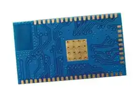


DA16600MOD-AAC4WA32
WLAN Module, Wi-Fi+Bluetooth, RF 2.4GHz, I2C, SPI, UART, -40 °C to 85 °C
- Manufacturer: RENESAS
- Product type:
- SVHC: No SVHC (25-Jun-2025)
- Frequency RF: 2.4GHz
- Product Range: -
- Module Interface: I2C, SPI, UART
- Module Applications: Wireless Connectivity
| Delivery and price | |
|---|---|
| Units per pack | 250 |
| Price | 8.56 € |
| Current stock | 25+ |
| Lead time | 30 days |
**DA16600MOD Series**

**==> picture [123 x 37] intentionally omitted <==**

## **Ultra-Low Power Wi-Fi + Bluetooth[®] LE Combo Module**

## **General Description**

The DA16600 series is a highly integrated ultra-low-power Wi-Fi + Bluetooth[®] Low Energy Combo Module solution. This module includes the DA16200 that has an 802.11b/g/n radio (PHY), a baseband processor, a media access controller (MAC), on-chip memory, and a host networking application processor. DA16600 also has a DA14531 that has a 2.4 GHz transceiver and an Arm[®] Cortex-M0+[® ] microcontroller with a RAM of 48 kB and a One-Time Programmable (OTP) memory of 32 kB. The radio transceiver, the baseband processor, and the qualified Bluetooth[® ] low energy stack is fully compliant with the Bluetooth Low Energy 5.1 standard.

The DA16600 is a synthesis of breakthrough ultra-low-power technologies, which enables an extremely low power operation in the module. The DA16200 and DA14531 shut down every micro element of the chip that is not in use, which creates a power consumption that is near zero when not actively transmitting or receiving data. Such low power operation can extend the battery life up to a year or more depending on the application. The DA16600 also enables ultra-low power transmission and reception modes when the SoC needs to be awake to exchange information with other devices. Advanced algorithms enable sleep mode until the exact moment when wake up is required to transmit or receive data.

## **Module Features**

## ■ Module Variants

   - DA16600MOD-AAC4WA32 (Chip Antenna)

   - DA16600MOD-AAE4WA32 (u.FL Connector)

- Dimensions

   - 14.3 mm × 24.3 mm × 3.0 mm, 51-Pins

- Ambient operating temperature range

   - -40 °C to 85 °C

- Regulatory certifications:

   - FCC

   - IC

   - CE

   - TELEC

## **Wi-Fi Features**

- Highly integrated ultra-low power Wi-Fi[®] system on a chip

- RF Performance

   - Tx Power: +18 dBm, 1 Mbps DSSS

   - Rx Sensitivity: -97.5 dBm, 1 Mbps DSSS

- Full offload: SoC runs full networking OS and TCP/IP stack

- Hardware accelerators

   - General HW CRC engine

   - HW zeroing function for fast booting

   - Pseudo random number generator (PRNG)

   - Wi-Fi processor

      - IEEE 802.11b/g/n, 1x1, 20 MHz channel bandwidth, 2.4 GHz

      - Wi-Fi security: WPA/WPA2Enterprise/Personal, WPA2 SI, WPA3 SAE, and OWE

      - Vendor EAP types: EAPTTLS/MSCHAPv2, PEAPv0/EAPMSCHAPv2, PEAPv1, EAP-FAST, and EAP-TLS

      - Operating modes: Station, Soft AP

      - WPS-PIN/PBC for easy Wi-Fi provisioning

      - Fast Wi-Fi connections

- SPI flash Memory

**Datasheet**

**Revision 3.0**

**23-Feb-2021**

© 2021 Dialog Semiconductor

CFR0011-120-00

1 of 26

**DA16600MOD Series**

**==> picture [123 x 37] intentionally omitted <==**

## **Ultra-Low Power Wi-Fi + Bluetooth[®] LE Combo Module**

□ 32 M-bit / 4 M-byte

■ Supports various interfaces

■ Complete software stack □ Comprehensive networking software stack □ Provides TCP/IP stack in the form of

□ Two UARTs

□ SPI Master/Slave interface

network socket APIs

□ I2C Master/Slave interface

■ CPU core subsystem

□ I2S for digital audio streaming □ Arm[®] Cortex[®] -M4F core with clock □ 4-channel PWM frequency of 30~160 MHz □ Individually programmable, multiplexed □ ROM: 256 KB, SRAM: 512 KB, OTP: 8 GPIO pins KB, Retention Memory: 48 KB □ JTAG and SWD Advanced security ■ Built-in 2-channel auxiliary ADC for sensor □ Secure booting interfaces □ Secure debugging using JTAG/SWD and □ 12-bit SAR ADC: single-ended two UART ports channels □ Secure asset storage ■ Supply Built-in hardware crypto engines for advanced □ Operating voltage: 2.1 V to 3.6 V (typical: security 3.3 V) □ TLS/DTLS security protocol functions □ 2 Digital I/O Supply Voltage: 1.8 V / 3.3 V □ Crypto engine for key deliberate generic □ Black-out and brown-out detector security functions: AES (128,192,256), ■ Power management unit DES/3DES, SHA1/224/256, RSA, DH, ECC, CHACHA, and TRNG □ On-Chip RTC □ Wake-up control of fast booting or full booting with minimal initialization time

- Advanced security

- Built-in hardware crypto engines for advanced security

□ Supports three ultra-low power sleep modes

## **Bluetooth Features**

■ Bluetooth □ Compatible with Bluetooth[®] v5.1, ETSI EN 300 328 and EN 300 440 Class 2 (Europe), FCC CFR47 Part 15 (US) and ARIB STD-T66 (Japan) core

■ Radio □ Programmable RF transmit power □ -93 dBm receiver sensitivity ■ Interfaces □ 2 channel 11-bit ENOB ADC □ 2 general purpose timers with PWM □ 5 GPIOs □ SPI □ 2x UART, 1-wire UART support □ I2C ■ Power management

□ Supports up to 3 connections ■ Processing and memories

□ 16 MHz 32-bit Arm[®] Cortex-M0+ with SWD interface

□ 48 Kbytes RAM □ 144 Kbytes ROM □ 32 Kbytes OTP ■ Current Consumption □ 2 mA RX at VBAT = 3V

□ Operating range (1.8 V - 3.3 V) □ Inrush current control ■ Other

□ 4 mA TX at VBAT = 3 V and 0 dBm

□ 1.8 uA at sleep with all RAM retained

- Real Time Clock

□ Trimmed 32 MHz Crystal

**Datasheet**

**Revision 3.0**

**23-Feb-2021**

© 2021 Dialog Semiconductor

CFR0011-120-00

2 of 26

**DA16600MOD Series**

**==> picture [123 x 37] intentionally omitted <==**

## **Ultra-Low Power Wi-Fi + Bluetooth[®] LE Combo Module**

## **Contents**

|**1**|**References ..................................................................................................................................... 5**|**References ..................................................................................................................................... 5**|
|---|---|---|
|**2**|**Block**|**Diagram ............................................................................................................................... 6**|
|**3**|**Pinout ............................................................................................................................................. 7**||
||3.1|Pinout Description (51-pins) .................................................................................................. 7|
||3.2|Pin Multiplexing ................................................................................................................... 10|
|**4**|**Electrical Specification ............................................................................................................... 11**||
||4.1|Absolute Maximum Ratings ................................................................................................ 11|
||4.2|Recommended Operating Conditions ................................................................................. 11|
||4.3|Electrical Characteristics ..................................................................................................... 11|
|||4.3.1<br>DC Parameters, 1.8 V IO ..................................................................................... 11|
|||4.3.2<br>DC Parameters, 3.3 V IO ..................................................................................... 12|
|||4.3.3<br>DC Parameters for RTC Block ............................................................................ 12|
||4.4|Radio Characteristics .......................................................................................................... 13|
|||4.4.1<br>Wi-Fi Characteristics ............................................................................................ 13|
|||4.4.2<br>Bluetooth®LE Characteristics .............................................................................. 14|
||4.5|Current Consumption .......................................................................................................... 14|
|||4.5.1<br>Wi-Fi Characteristics ............................................................................................ 14|
|||4.5.2<br>Bluetooth®LE Characteristics .............................................................................. 15|
||4.6|Radiation Performance ....................................................................................................... 16|
||4.7|ESD Ratings ........................................................................................................................ 16|
|**5**|**Power-on Sequence .................................................................................................................... 17**||
|**6**|**Applications Schematic .............................................................................................................. 18**||
||6.1|Typical Application .............................................................................................................. 18|
|**7**|**Package Information ................................................................................................................... 19**||
||7.1|Dimension: DA16600MOD-AAC ......................................................................................... 19|
||7.2|Dimension: DA16600MOD-AAE ......................................................................................... 19|
||7.3|PCB Land Pattern ............................................................................................................... 20|
||7.4|4-layer PCB Example .......................................................................................................... 22|
||7.5|Soldering Information .......................................................................................................... 23|
|||7.5.1<br>Recommended Condition for Reflow Soldering .................................................. 23|
|**8**|**Ordering Information .................................................................................................................. 24**||
|**Revision**||**History ................................................................................................................................ 25**|


**Datasheet**

**Revision 3.0**

**23-Feb-2021**

© 2021 Dialog Semiconductor

CFR0011-120-00

3 of 26

**DA16600MOD Series**

**==> picture [123 x 37] intentionally omitted <==**

## **Ultra-Low Power Wi-Fi + Bluetooth[®] LE Combo Module**

## **Figures**

Figure 1: DA16600 Block Diagram ........................................................................................................ 6 Figure 2: DA16600MOD 51-Pins Pinout Diagram (Top View) .............................................................. 7 Figure 3: TIS 3D .................................................................................................................................. 16 Figure 4: TRP 3D ................................................................................................................................. 16 Figure 5: Power On Sequence ............................................................................................................ 17 Figure 6: Typical Application ............................................................................................................... 18 Figure 7: AAC Module Dimension ....................................................................................................... 19 Figure 8: AAE Module Dimension ....................................................................................................... 20 Figure 9: PCB Land Pattern (Top View) .............................................................................................. 20 Figure 10: PCB Land Pattern (Bottom View)....................................................................................... 21 Figure 11: 4-Layer PCB Example ........................................................................................................ 22 Figure 12: Reflow Condition ................................................................................................................ 23

## **Tables**

Table 1: Pin Description ........................................................................................................................ 8 Table 2: DA16200 Pin Multiplexing ..................................................................................................... 10 Table 3: Absolute Maximum Ratings ................................................................................................... 11 Table 4: Recommended Operating Conditions ................................................................................... 11 Table 5: DC Parameters, 1.8 V IO ...................................................................................................... 11 Table 6: DC Parameters, 3.3 V IO ...................................................................................................... 12 Table 7: DC Parameters for RTC block, 3.3 V VBAT .......................................................................... 12 Table 8: DC Parameters for RTC block, 2.1 V VBAT .......................................................................... 12 Table 9: Wi-Fi Receiver Characteristics .............................................................................................. 13 Table 10: Wi-Fi Transmitter Characteristics ........................................................................................ 13 Table 11: Radio 1 Mb/s – AC Characteristics ..................................................................................... 14 Table 12: Current Consumption in Active State .................................................................................. 14 Table 13: Current Consumption in Low Power Operation ................................................................... 14 Table 14: DC Characteristics............................................................................................................... 15 Table 15: ESD Performance................................................................................................................ 16 Table 16: Power On Sequence Timing Requirements ........................................................................ 17 Table 17: Coexistence Connection ..................................................................................................... 18 Table 18: Component Value ................................................................................................................ 18 Table 19: Typical Reflow Profile (Lead Free): J-STD-020C ................................................................ 23 Table 20: Ordering Information (Samples) .......................................................................................... 24 Table 21: Ordering Information (Production) ....................................................................................... 24

**Datasheet**

**Revision 3.0**

**23-Feb-2021**

© 2021 Dialog Semiconductor

CFR0011-120-00

4 of 26

**DA16600MOD Series**

**==> picture [123 x 37] intentionally omitted <==**

**Ultra-Low Power Wi-Fi + Bluetooth[®] LE Combo Module**

## **1 References**

DA16600MOD consist of a DA16200 and a DA14531 chipset. Please see the respective chipset and module datasheets for details.

- [1] DA16200 Datasheet, Dialog Semiconductor

- [2] DA16200MOD Datasheet, Dialog Semiconductor

   - (available at https://www.dialog-semiconductor.com/products/connectivity/wi-fi)

- [3] DA14531, Datasheet, Dialog Semiconductor

- [4] DA14531MOD Datasheet, Dialog Semiconductor

(available at https://www.dialog-semiconductor.com/products/connectivity/bluetooth-lowenergy/products/da14530-and-da14531)

**Datasheet**

**Revision 3.0**

**23-Feb-2021**

© 2021 Dialog Semiconductor

CFR0011-120-00

5 of 26

**DA16600MOD Series**

## **Ultra-Low Power Wi-Fi + Bluetooth[®] LE Combo Module**

## **2 Block Diagram**

The DA16600 provides a high level of integration for a battery used wireless system, with integrated IEEE 802.11 b/g/n and Bluetooth V5.1. The DA16600 is designed to address the needs of battery used devices that require minimal power consumption and reliable operation.

Figure 1 shows the interconnection of all the physical blocks in DA16600MOD.

**==> picture [389 x 267] intentionally omitted <==**

**----- Start of picture text -----**<br>
32 MHz<br>Crystal<br>|<br>DA14531<br>Matching<br>GPIO Multiplexing<br>Circuit Low power<br>BLE SoC<br>U.FL<br>connector  SPDT for<br>or antenna  UART<br> Chip  switching<br>antenna<br>~ HS DA16200 GPIO Multiplexing<br>2.4GHz<br>BPF &<br>RTC control<br>Matching  Low power  |<br>Circuit<br>Wi-Fi SoC<br>UART for debug<br>_  = |<br>4MByte  40 MHz 32.768<br>Serial  KHz<br>Flash Crystal Crystal<br>ae<br>**----- End of picture text -----**<br>


**Figure 1: DA16600 Block Diagram**

**Datasheet**

**Revision 3.0**

**23-Feb-2021**

© 2021 Dialog Semiconductor

CFR0011-120-00

6 of 26

**DA16600MOD Series**

**==> picture [123 x 37] intentionally omitted <==**

## **Ultra-Low Power Wi-Fi + Bluetooth[®] LE Combo Module**

## **3 Pinout**

## **3.1 Pinout Description (51-pins)**

||||||||||||||||||||||||
|---|---|---|---|---|---|---|---|---|---|---|---|---|---|---|---|---|---|---|---|---|---|---|
|||||||||||||||||||||VBAT_BLE|51||
||||||||DA16600|||||||||||||P0_10|50||
|||||||MOD Series||||||||||||||P0_11|49||
||||||||||||||||||||||||
|||||||||||||||||||||P0_5|48||
||||||||||||||||||||||||
||1|NC||||||||||||||||||P0_7|47||
||||||||||||||||||||||||
||2|P0_2||||||||||||||||||P0_8|46||
||||||||||||||||||||||||
||3|P0_6||||||||||||||||||P0_9|45||
||||||||||||||||||||||||
||4|GND||||||||||||||||||TP|44||
||||||||||||||||||||||||
||5|TEST or NC||||||||||||||||||TP|43||
||||||||||||||||||||||||
||6|GND||||||||||||||||||GPIOA2|42||
||||||||||||||||||||||||
||7|RTC_PWR_KEY||||||||||||||||||GPIOA3|41||
||||||||||||||||||||||||
||8|TP||||||||||||||||||VDD_DIO1|40||
||||||||||||||||||||||||
||9|RTC_GPO||||||||||||||||||TP|39||
||||||||||||||||||||||||
||10|TMS||||||||GND||||||||||TP|38||
||||||||||||||||||||||||
||11|TCLK||||||||||||||||||GPIOA6|37||
||||||||||||||||||||||||
||12|GPIOC_8||||||||||||||||||GPIOA7|36||
||||||||||||||||||||||||
||13|GPIOC_7||||||||||||||||||GPIOA8|35||
||||||||||||||||||||||||
||14|GPIOC_6||||||||||||||||||GPIOA9|34||
||||||||||||||||||||||||
||15|UART0_TXD||||||||||||||||||GPIOA10|33||
||16<br>17<br>18|UART0_RXD<br>VDD_DIO2<br>TP<br>TP|||GND||GND||TP||TP||TP||RTC_WAKE_UP2||GND||VBAT_3V3|GND<br>GND<br>GPIOA11|32<br>31<br>30||
||19|TP|20||21||22||23||24||25||26||27||28|GND|29||
||||||||||||||||||||||||


**Figure 2: DA16600MOD 51-Pins Pinout Diagram (Top View)**

**Datasheet**

**Revision 3.0**

**23-Feb-2021**

© 2021 Dialog Semiconductor

CFR0011-120-00

7 of 26

**DA16600MOD Series**

**==> picture [123 x 37] intentionally omitted <==**

## **Ultra-Low Power Wi-Fi + Bluetooth[®] LE Combo Module**

**Table 1: Pin Description**

|**#Pin**|**Pin Name**|**Type**|**Drive(mA)**|**Reset**<br>**State**|**Related**<br>**Device**|**Description**|
|---|---|---|---|---|---|---|
|1|NC|AI|||DA14531|Not Connect|
|2|P0_2|DIO|||DA14531|General Purpose I/O|
|3|P0_6|DIO|||DA14531|Internally connected to<br>RF switch<br>Note 1|
|4|GND|GND|||Common|Ground|
|5|TEST or NC|AI|||Common|Chip antenna type:<br>RF_Test<br>u.FL connector type: NC|
|6|GND|GND|||Common|Ground|
|7|RTC_PWR_KEY|DI|||DA16200|RTC block enable signal|
|8|TP|DNC|||DA16200|RTC block wake up<br>signal is internally<br>connected<br>Note 1|
|9|RTC_GPO|DO|||DA16200|Sensor control signal|
|10|TMS|DIO|2/4/8/12|I-PU|DA16200|JTAG I/F, SWDIO|
|11|TCLK|DIO|2/4/8/12|I-PD|DA16200|JTAG I/F, SWCLK,<br>General Purpose I/O|
|12|GPIOC_8|DIO|2/4/8/12|I-PD|DA16200|General Purpose I/O|
|13|GPIOC_7|DIO|2/4/8/12|I-PD|DA16200|General Purpose I/O|
|14|GPIOC_6|DIO|2/4/8/12|I-PD|DA16200|General Purpose I/O|
|15|UART0_TXD|DO|2/4/8/12|O|DA16200|UART transmit data|
|16|UART0_RXD|DI|2/4/8/12|I|DA16200|UART receive data|
|17|VDD_DIO2|VDD|||DA16200|Supply power for digital<br>I/O<br>GPIOC6~GPIOC8,<br>TMS/TCLK, TXD/RXD|
|18|TP|DNC|||DA16200|F_IO0 is internally<br>connected to Flash<br>Memory|
|19|TP|DNC|||DA16200|F_CLK is internally<br>connected to Flash<br>Memory|
|20|TP|DNC|||DA16200|F_IO3 is internally<br>connected to Flash<br>Memory|
|21|GND|GND|||Common|Ground|
|22|GND|GND|||Common|Ground|
|23|TP|DNC|||DA16200|F_IO1 is internally<br>connected to Flash<br>Memory|
|24|TP|DNC|||DA16200|F_CSN is internally<br>connected to Flash<br>Memory|


**Datasheet**

**23-Feb-2021**

**Revision 3.0**

© 2021 Dialog Semiconductor

CFR0011-120-00

8 of 26

**DA16600MOD Series**

**==> picture [123 x 37] intentionally omitted <==**

## **Ultra-Low Power Wi-Fi + Bluetooth[®] LE Combo Module**

|**#Pin**|**Pin Name**|**Type**|**Drive(mA)**|**Reset**<br>**State**|**Related**<br>**Device**|**Description**|
|---|---|---|---|---|---|---|
|25|TP|DNC|||DA16200|F_IO2 is internally<br>connected to Flash<br>Memory|
|26|RTC_WAKE_UP2|DI|||DA16200|RTC block wake-up<br>signal|
|27|GND|GND|||Common|Ground|
|28|VBAT_3V3|VDD|||DA16200|Supply power for internal<br>DC-DC, DIO_LDO, and<br>Analog IP of DA16200|
|29|GND|GND|||Common|Ground|
|30|GND|GND|||Common|Ground|
|31|GND|GND|||Common|Ground|
|32|GPIOA11|DIO|2/4/8/12|I-PD|DA16200|General Purpose I/O|
|33|GPIOA10|DIO|2/4/8/12|I-PD|DA16200|General Purpose I/O|
|34|GPIOA9|DIO|2/4/8/12|I-PD|DA16200|General Purpose I/O|
|35|GPIOA8|DIO|2/4/8/12|I-PD|DA16200|General Purpose I/O|
|36|GPIOA7|DIO|2/4/8/12|I-PD|DA16200|General Purpose I/O|
|37|GPIOA6|DIO|2/4/8/12|I-PD|DA16200|General Purpose I/O|
|38|TP|DNC|2/4/8/12|I-PD|Common|GPIOA5 of DA16200 is<br>internally connected to<br>P0_3 of DA14531Note 1|
|39|TP|DNC|2/4/8/12|I-PD|Common|GPIOA4 of DA16200 is<br>internally connected to<br>P0_4 of DA14531Note 1|
|40|VDD_DIO1|VDD|||DA16200|Supply power for digital<br>I/O<br>GPIOA0~GPIOA11|
|41|GPIOA3|AI/DIO|2/4/8/12|I-PD|DA16200|Aux. ADC input/General<br>Purpose I/O|
|42|GPIOA2|AI/DIO|2/4/8/12|I-PD|DA16200|Aux. ADC input/General<br>Purpose I/O|
|43|TP|DNC|2/4/8/12|I-PD|Common|GPIOA1 of DA16200 is<br>internally connected to<br>P0_0 of DA14531Note 1|
|44|TP|DNC|2/4/8/12|I-PD|Common|GPIOA0 of DA16200 is<br>internally connected to<br>P0_1 of DA14531Note 1|
|45|P0_9|DIO|3.5 / 0.3|I-PD|DA14531|General Purpose I/O|
|46|P0_8|DIO|3.5 / 0.3|I-PD|DA14531|General Purpose I/O|
|47|P0_7|DIO|3.5 / 0.3|I-PD|DA14531|General Purpose I/O|
|48|P0_5|DIO|3.5 / 0.3|I-PD|DA14531|General Purpose I/O|
|49|P0_11|DIO|3.5 / 0.3|I-PD|DA14531|General Purpose I/O|
|50|P0_10|DIO|3.5 / 0.3|I-PD|DA14531|General Purpose I/O|
|51|VBAT_BLE|VDD|||DA14531|Supply power for<br>DA14531|


**Datasheet**

**Revision 3.0**

**23-Feb-2021**

© 2021 Dialog Semiconductor

CFR0011-120-00

9 of 26

**DA16600MOD Series**

## **Ultra-Low Power Wi-Fi + Bluetooth[®] LE Combo Module**

**Note 1** Pin3, Pin8, Pin 38, Pin 39, Pin 43, and Pin 44 are connected internally so these pins can`t be used as GPIO or as wake up input in application system.

## **3.2 Pin Multiplexing**

This device provides various interfaces to support many kinds of applications.

In DA16200, it is possible to control each pin according to the required application in reference to the pin multiplexing illustrated in Table 2 Pin control can be realized through register setting.

In DA14531, I/O pin assignment can be configured by the SW and is organized into the Port 0.

Please refer the datasheet and user manual of DA16200 and DA14531 respectively for detail information.

**Table 2: DA16200 Pin Multiplexing**

Several pins are internally connected in the module, so these pins can’t be used as GPIO. These pins are described as TP (test point) except P0_6 in DA16600MOD. Because of internally used pins, several interfaces of DA16200 – SDIO, SDeMMC and UART1– are not possible on DA16600MOD.

- DA16200: GPIOA0, GPIOA1, GPIOA4, GPIOA5

- DA14531: P0_0, P0_1, P0_3, P0_4, P0_6

P0_6 of DA14531 is internally connected to RF switch and need to be connected externally to GPIO_A9 or GPIO_A10 of DA16200 for coexistence, so this pin can’t be used as other purpose of GPIO too.

**Datasheet**

**Revision 3.0**

**23-Feb-2021**

© 2021 Dialog Semiconductor

CFR0011-120-00

10 of 26

**DA16600MOD Series**

**==> picture [123 x 37] intentionally omitted <==**

## **Ultra-Low Power Wi-Fi + Bluetooth[®] LE Combo Module**

## **4 Electrical Specification**

## **4.1 Absolute Maximum Ratings**

Stresses beyond those listed under Absolute Maximum Ratings may cause permanent damage to the device. These are stress ratings only, so functional operation of the device at these or any other conditions beyond those indicated in the operational sections of the specification are not implied. Exposure to Absolute Maximum Rating conditions for extended periods may affect device reliability.

**Table 3: Absolute Maximum Ratings**

|**Parameter**|**#Pins**|**Min**|**Max**|**Units**|
|---|---|---|---|---|
|VBAT_3V3|28|-0.1<br>|3.9<br>|V|
|VDD_DIO1|40|-0.1<br>|3.9<br>|V|
|VDD_DIO2|17|-0.1<br>|3.9<br>|V|
|VBAT_BLE|51|-0.1<br>|3.6<br>|V|


## **4.2 Recommended Operating Conditions**

**Table 4: Recommended Operating Conditions**

|**Parameter**|**#Pins**|**Min**|**Typ**|**Max**|**Units**|
|---|---|---|---|---|---|
|VBAT_3V3|28|2.1||3.6|V|
|VDD_DIO1|40|1.62||3.6|V|
|VDD_DIO2|17|1.62||3.6|V|
|VBAT_BLE|51|1.8||3.3|V|
|Ambient operating temperature range<br>(TA)||-40||+85|°C|


## **4.3 Electrical Characteristics**

## **4.3.1 DC Parameters, 1.8 V IO**

**Table 5: DC Parameters, 1.8 V IO**

|**Symbol**|**Parameter**|**Condition**|**Min**|**Typ**|**Max**|**Units**|
|---|---|---|---|---|---|---|
|VIL|Input Low Voltage|Guaranteed logic Low<br>level<br>Note 1|VSS||0.3 ×<br>DVDD|V|
|VIH|Input High Voltage|Guaranteed logic High<br>level|0.7 ×<br>DVDD||DVDD|V|
|VOL|Output Low Voltage|DVDD=Min.|VSS||0.2 ×<br>DVDD|V|
|VOH|Output High Voltage|DVDD=Min.|0.8 ×<br>DVDD||DVDD|V|
|RPU|Pull-up Resistor|VPAD=VIH, DIO=Min.|||32.4|kΩ|
|RPD|Pull-down Resistor|VPAD=VIL, DIO=Min.|||32.4||


**Note 1** DVDD = 1.8V, VDD_DIO1, VDD_DIO2 Logic Level.

**Datasheet**

**Revision 3.0**

**23-Feb-2021**

© 2021 Dialog Semiconductor

CFR0011-120-00

11 of 26

**DA16600MOD Series**

**==> picture [123 x 37] intentionally omitted <==**

## **Ultra-Low Power Wi-Fi + Bluetooth[®] LE Combo Module**

## **4.3.2 DC Parameters, 3.3 V IO**

**Table 6: DC Parameters, 3.3 V IO**

|**Symbol**|**Parameter**|**Condition**|**Min**|**Typ**|**Max**|**Units**|
|---|---|---|---|---|---|---|
|VIL|Input Low Voltage|Guaranteed logic Low<br>level<br>Note 2|VSS||0.8|V|
|VIH|Input High Voltage|Guaranteed logic High<br>level|2.0||DVDD|V|
|VOL|Output Low Voltage|DVDD=Min.|VSS||0.4|V|
|VOH|Output High Voltage|DVDD=Min.|2.4||DVDD|V|
|RPU|Pull-up Resistor|VPAD=VIH, DIO=Min.|||19.4|kΩ|
|RPD|Pull-down Resistor|VPAD=VIL, DIO=Min.|||16.0||


**Note 2** DVDD= 3.3 V, VDD_DIO1, VDD_DIO2 Logic Level.

## **4.3.3 DC Parameters for RTC Block**

There are several control pins in RTC block.

**Table 7: DC Parameters for RTC block, 3.3 V VBAT**

|**Symbol**|**Parameter**|**Condition**|**Min**|**Typ**|**Max**|**Units**|
|---|---|---|---|---|---|---|
|VIL|Input Low Voltage|Guaranteed logic Low<br>level|VSS||0.6|V|
|VIH|Input High Voltage|Guaranteed logic High<br>level|2.2||VBAT|V|


(RTC block: RTC_PWR_KEY, RTC_WAKE_UP2)

**Table 8: DC Parameters for RTC block, 2.1 V VBAT**

|**Symbol**|**Parameter**|**Condition**|**Min**|**Typ**|**Max**|**Units**|
|---|---|---|---|---|---|---|
|VIL|Input Low Voltage|Guaranteed logic Low<br>level|VSS||0.3|V|
|VIH|Input High Voltage|Guaranteed logic High<br>level|1.6||VBAT|V|


(RTC block: RTC_PWR_KEY, RTC_WAKE_UP2)

**Datasheet**

**Revision 3.0**

**23-Feb-2021**

© 2021 Dialog Semiconductor

CFR0011-120-00

12 of 26

**DA16600MOD Series**

**==> picture [123 x 37] intentionally omitted <==**

## **Ultra-Low Power Wi-Fi + Bluetooth[®] LE Combo Module**

## **4.4 Radio Characteristics**

## **4.4.1 Wi-Fi Characteristics**

- TA = +25 °C, VBAT = 3.3 V, CH1 (2412 MHz)

**Table 9: Wi-Fi Receiver Characteristics**

|**Parameter**|**Condition**|**Min**|**Typ**|**Max**|**Units**|
|---|---|---|---|---|---|
|Sensitivity<br>(8% PER for 11b rates, 10%<br>PER for 11g/11n rates)|1 Mbps DSSS|-98.5|-97.5|-95.5|dBm|
||2 Mbps DSSS|-94|-93|-91||
||11 Mbps CCK|-89|-88|-86||
||6 Mbps OFDM|-90|-89|-87||
||9 Mbps OFDM|-90|-89|-87||
||18 Mbps OFDM|-88|-87|-85||
||36 Mbps OFDM|-81|-80|-78||
||54 Mbps OFDM|-75|-74|-72||
||MCS0(GF)|-90|-89|-87||
||MCS7(GF)|-72|-71|-69||
|Maximum input level<br>(8% PER for 11b rates, 10%<br>PER for 11g/11n rates)|802.11b|-4|0|0||
||802.11g|-10|-4|-3||


## **Table 10: Wi-Fi Transmitter Characteristics**

|**Parameter**|**Condition**|**Min**|**Typ**|**Max**|**Units**|
|---|---|---|---|---|---|
|Maximum Output Power<br>measured form IEEE<br>spectral mask and EVM|1 Mbps DSSS|15|18|19|dBm|
||2 Mbps DSSS|15|18|19||
||5.5 Mbps CCK|15|18|19||
||11 Mbps CCK|15|18|19||
||6 Mbps OFDM|14|17|18||
||9 Mbps OFDM|14|17|18||
||12 Mbps OFDM|14|17|18||
||18 Mbps OFDM|14|17|18||
||24 Mbps OFDM|13|16|17||
||36 Mbps OFDM|13|16|17||
||48 Mbps OFDM|11.5|14.5|15.5||
||54 Mbps OFDM|10.5|13.5|14.5||
||MCS0 OFDM|14|17|18||
||MCS7 OFDM|10.5|13.5|14.5||
|Transmit center frequency<br>accuracy||-25||+25|ppm|


**Datasheet**

**Revision 3.0**

**23-Feb-2021**

© 2021 Dialog Semiconductor

CFR0011-120-00

13 of 26

**DA16600MOD Series**

**==> picture [123 x 37] intentionally omitted <==**

## **Ultra-Low Power Wi-Fi + Bluetooth[®] LE Combo Module**

## **4.4.2 Bluetooth[®] LE Characteristics**

**Table 11: Radio 1 Mb/s – AC Characteristics**

|**Parameter**|**Description**|**Condition**|**Min**|**Typ**|**Max**<br>|**Unit**|
|---|---|---|---|---|---|---|
|PSENS_CLEAN|sensitivity level|Dirty Transmitter disabled;<br>DC-DC converter disabled;<br>PER = 30.8 %;<br>Note 1||-93||dBm|
|PSENS_EPKT|sensitivity level|Extended packet size<br>(255 octets)<br>Note 1||-90||dBm|


**Note 1** Measured according to Bluetooth[®] Low Energy Test Specification RF-PHY.TS/5.1.0

## **4.5 Current Consumption**

## **4.5.1 Wi-Fi Characteristics**

TA = +25 °C, VBAT = 3.3 V, w/ CPU clock is 80 MHz.

**Table 12: Current Consumption in Active State**

|**Parameter**||**Condition**|**Condition**|**Min**|**Typ**|**Max**|**Units**|
|---|---|---|---|---|---|---|---|
|ACTIVE|TX|1 Mbps DSSS|@ 18.0 dBm|260|280|320|mA|
|||6 Mbps OFDM|@ 17.0 dBm|240|260|300||
|||54 Mbps OFDM|@ 13.5 dBm|180|200|240||
|||MCS7|@ 13.5 dBm|180|200|240||
||RX|No signalNote 1||25|29|51||
|||1 Mbps DSSSNote 1||26.5|30.5|53||
|||1 Mbps DSSS||27|37.5|54||
|||54 Mbps OFDM||29|38.5|54||
|||MCS7||29|38.5|54||


**Note 1** Low Power Mode & CPU clock 30 MHz.

TA = +25 °C, VBAT = 3.3 V

**Table 13: Current Consumption in Low Power Operation**

|**Parameter**|**Condition**|**Min**|**Typ**|**Max**|**Units**|
|---|---|---|---|---|---|
|Low Power<br>Operation|Sleep 1||5.2<br>Note 1||µA|
||Sleep 2||6.8<br>Note 1|||
||Sleep 3||8.5<br>Note 1|||


**Note 1** RF switch current consumption is included. VDD of RF switch is connected to VBAT_3V3 for DA16200 and typical current consumption of RF switch is 5 µA.

**Datasheet**

**Revision 3.0**

**23-Feb-2021**

© 2021 Dialog Semiconductor

CFR0011-120-00

14 of 26

**DA16600MOD Series**

**==> picture [123 x 37] intentionally omitted <==**

## **Ultra-Low Power Wi-Fi + Bluetooth[®] LE Combo Module**

## **4.5.2 Bluetooth[®] LE Characteristics**

## **Table 14: DC Characteristics**

|**Parameter**|**Description**|**Conditions**|**Min**|**Typ**|**Max**|<br>**Units**|
|---|---|---|---|---|---|---|
|IBAT_ACTIVE|Battery supply current|||0.4||mA|
|IBAT_BLE_ADV_100ms|Average battery supply<br>current with system in<br>Advertising state (3<br>channels) every 100ms<br>and extended sleep with<br>all RAM retained.|||80||µA|
|IBAT_BLE_CONN_30ms|Average battery supply<br>current with system in a<br>connection state with<br>30ms connection interval<br>and extended sleep with<br>all RAM retained.|||92||µA|
|IBAT_HIBERN|Battery supply current<br>with system shut down|||0.6||µA|
|IBAT_RF_RX|Battery supply current|Continuous Rx||2.3||mA|
|IBAT_RF_TX_+2|Battery supply current|Continuous Tx; Output<br>power at 2dBm<br>Note 1||4.3||mA|
|IBAT_RF_TX_-1|Battery supply current|Continuous Tx; Output<br>power at -1dBm<br>Note 2||3.6||mA|
|IBAT_RF_TX_-4|Battery supply current|Continuous Tx; Output<br>power at -4dBm||2.8||mA|


**Note 1** All Bluetooth applications run on DA16200, so DA16200 should be active to handle Bluetooth data (e.g. Bluetooth Connection Request coming from a Bluetooth peer), in which case, Rx active current of DA16200 is added to the total current consumption.

**Note 2** The actual Tx output power is slightly different than the one indicated in the parameter name.

**Datasheet**

**Revision 3.0**

**23-Feb-2021**

© 2021 Dialog Semiconductor

CFR0011-120-00

15 of 26

**DA16600MOD Series**

## **Ultra-Low Power Wi-Fi + Bluetooth[®] LE Combo Module**

## **4.6 Radiation Performance**

**Figure 3: TIS 3D**

**Figure 4: TRP 3D**

## **4.7 ESD Ratings**

**Table 15: ESD Performance**

|**Reliability Test**|**Standards**|**Test Conditions**|**Result**|
|---|---|---|---|
|Human Body Model (HBM)|ANSI/ESDA/JEDEC JS-001-2017|± 2,000 V|Pass|
|Charge Device Mode (CDM)|ANSI/ESDA/JEDEC JS-002-2018|± 500 V|Pass|


**Datasheet**

**Revision 3.0**

**23-Feb-2021**

© 2021 Dialog Semiconductor

CFR0011-120-00

16 of 26

**DA16600MOD Series**

## **Ultra-Low Power Wi-Fi + Bluetooth[®] LE Combo Module**

## **5 Power-on Sequence**

The sequence after the initial switching from power-off to power-on of DA16200 is shown in Figure 5.

The RTC_PWR_KEY is a pin that enables the RTC block of DA16200. Once RTC_PWR_KEY is enabled after VBAT power is supplied, all the internal regulators are switched on automatically in the sequence pre-defined by the RTC block.

Once RTC_PWR_KEY is switched on, LDOs for both XTAL and digital I/O are switched on shortly and then the DC-DC regulator is switched on according to the pre-defined interval. The enabling intervals can also be modified in the register settings after initial power-up.

**==> picture [182 x 130] intentionally omitted <==**

**----- Start of picture text -----**<br>
VBAT 50% VBAT<br>T0<br>IO Voltage 50% IO<br>POWER_KEY 50% VBAT<br>CLK_32K — U<br>T1 T2 T3<br>**----- End of picture text -----**<br>


**Figure 5: Power On Sequence**

**Table 16: Power On Sequence Timing Requirements**

|**Name**|**Description**|**Min**|**Typ**|**Max**|**Unit**|
|---|---|---|---|---|---|
|T0|VBAT power-on time from 10 % to 90 % of VBAT||||ms|
|T1|IO voltage and VCC supply||0||ms|
|T2|RTC_PWR_KEY turn-on time from 50 % VBAT to 50<br>% POWER_KEY *Note 3||5*T0||ms|
|T3|Internal RC oscillator wake-up time||217||µs|


**Note 3** If the T0 = 10 ms to switch on VBAT, the recommended T2 is 50 ms for the safe booting operation. It would be externally controlled by MCU or it would be implemented using RC filter at the input of RTC_PWR_KEY. The recommended C is 470 nF or 1 uF (not to exceed 1 uF) and R value is chosen to have T2 delay. For example, R and C values will be 82 kΩ and 1uF when T0 = 10 ms.

**Datasheet**

**Revision 3.0**

**23-Feb-2021**

© 2021 Dialog Semiconductor

CFR0011-120-00

17 of 26

**DA16600MOD Series**

## **Ultra-Low Power Wi-Fi + Bluetooth[®] LE Combo Module**

## **6 Applications Schematic**

## **6.1 Typical Application**

**==> picture [467 x 289] intentionally omitted <==**

**----- Start of picture text -----**<br>
10uF<br>DA16600 VBAT_BLE Ss 51 Hk VBAT_BLE<br>MOD Series P0_10P0_11 = 4950 P0_10P0_11<br>P0_5 SS 48 P0_5<br>1 NC P0_7 47 P0_7<br>P0_2 0  = 2 P0_2 P0_8 = 46 BLE_Debug /GPIO<br>P0_6 3 P0_6 P0_9 45 Interface<br>Note: Remove R1 and C1 when  a= 4 GND TP = 44 )<br>MCU control RTC_PWR_KEY. 5 TEST or NC TP 43<br>R1 6 GND GPIOA_2 42 GPIO Interface<br>External Power Control ca fe 7 RTC_PWR_KEY GPIOA_3 siK— 41 )<br>C1 8 TP VDD_DIO1 40 VDD_DIO1<br>9 RTC_GPO TP 39<br>1uF<br>JTAG Interface 10 TMS GND TP 38<br>=0 11 TCLK GPIOA_6 = 37<br>12 GPIOC_8 GPIOA_7 36 GPIO Interface<br>GPIO Interface<br>13 GPIOC_7 GPIOA_8 35 GPIOA_8<br>(= e 14 GPIOC_6 GPIOA_9 = 34 —? GPIOA_9<br>UART Interface for debug 15 UART0_TX GPIOA_10 33 GPIOA_10<br>C= 16 UART0_RX GPIOA_11 = 32 GPIO Interface<br>VDD_DIO2 17 VDD_DIO2 31<br>= 18 = 30 {4<br>1uF 19 29<br>r = (000008 =><br>-i<br>" 4.7K  Daag 10uF<br>External Wake- up Control VBAT_3V3<br>RTC_WAKE_UP2<br>20 21 22 23 24 25 26 27 28<br>**----- End of picture text -----**<br>


**Figure 6: Typical Application**

**Table 17: Coexistence Connection**

|**DA14531 part**|**DA16200 part**|**Function**|
|---|---|---|
|P0_5|GPIOA_8|Wi-Fi_ACT|
|P0_6|GPIOA_9|BT_ACT|
|P0_7|GPIOA_10|BT_PRIO|


**Table 18: Component Value**

|**Part Reference**|**Value**|**Description**|
|---|---|---|
|R1|470 kΩ|Remove R1 when MCU control ‘RTC_PWR_KEY’.<br>This value should be chosen by customer application to achieve<br>the enough delay time depending on the power-on time of VBAT.<br>For detail information, see Section5.|
|C1|1 uF|Remove C1 when MCU control ‘RTC_PWR_KEY’.<br>This value should be chosen by customer application to achieve<br>the enough delay time depending on the power-on time of VBAT.<br>Not to exceed 1uF. For detail information, see Section5.|


**Datasheet**

**Revision 3.0**

**23-Feb-2021**

© 2021 Dialog Semiconductor

CFR0011-120-00

18 of 26

**DA16600MOD Series**

## **Ultra-Low Power Wi-Fi + Bluetooth[®] LE Combo Module**

## **7 Package Information**

## **7.1 Dimension: DA16600MOD-AAC**

Unit: millimeters (mm)

Tolerance : 14.3 (±0.2) x 24.3 (±0.2) x 3.0 (±0.1)

**Figure 7: AAC Module Dimension**

## **7.2 Dimension: DA16600MOD-AAE**

Unit: millimeters (mm)

Tolerance : 14.3 (±0.2) x 24.3 (±0.2) x 3.0 (±0.1)

**Datasheet**

**Revision 3.0**

**23-Feb-2021**

© 2021 Dialog Semiconductor

CFR0011-120-00

19 of 26

**DA16600MOD Series**

## **Ultra-Low Power Wi-Fi + Bluetooth[®] LE Combo Module**

**Figure 8: AAE Module Dimension**

## **7.3 PCB Land Pattern**

Unit: millimeters (mm)

**Figure 9: PCB Land Pattern (Top View)**

**Datasheet**

**Revision 3.0**

**23-Feb-2021**

© 2021 Dialog Semiconductor

CFR0011-120-00

20 of 26

**DA16600MOD Series**

**Ultra-Low Power Wi-Fi + Bluetooth[®] LE Combo Module**

**Figure 10: PCB Land Pattern (Bottom View)**

Ant GND is only needed on the bottom of the PCB. GND must be removed for all layers including the inner layer except the bottom. See Figure 11 for details.

**Datasheet**

**Revision 3.0**

**23-Feb-2021**

© 2021 Dialog Semiconductor

CFR0011-120-00

21 of 26

**DA16600MOD Series**

**Ultra-Low Power Wi-Fi + Bluetooth[®] LE Combo Module**

**7.4 4-layer PCB Example**

**==> picture [278 x 195] intentionally omitted <==**

**----- Start of picture text -----**<br>
Top Layer  layer 2<br>|<br>|<br>layer 3  Bottom layer<br>**----- End of picture text -----**<br>


**Figure 11: 4-Layer PCB Example**

**Datasheet**

**Revision 3.0**

**23-Feb-2021**

© 2021 Dialog Semiconductor

CFR0011-120-00

22 of 26

**DA16600MOD Series**

## **Ultra-Low Power Wi-Fi + Bluetooth[®] LE Combo Module**

## **7.5 Soldering Information**

## **7.5.1 Recommended Condition for Reflow Soldering**

The reflow profile depends on the solder paste being used and the recommendations from the paste manufacturer should be followed to determine the proper reflow profile.

**Table 19: Typical Reflow Profile (Lead Free): J-STD-020C**

|**Profile Feature**|**Lead Free SMD**|
|---|---|
|Average ramp up rate (Tsmaxto Tp)|3 °C/s Max.|
|Preheat||
|●<br>Temperature Min (Tsmin)<br>●<br>Temperature Max (Tsmax)<br>●<br>Time (Tsmaxto Tsmin)|●<br>150 °C<br>●<br>200 °C<br>●<br>60 to 180 seconds|
|Time maintained above||
|●<br>Temperature (TL)<br>●<br>Time (tL)|●<br>217 °C<br>●<br>60 to 150 seconds|
|Peak/Classification temperature (Tp)|260 °C|
|Time within 5 °C of peak temperature (tp)|20 to 40 seconds|
|Ramp down rate|6 °C/s Max.|
|Time from 25 °C to peak temperature|8 minutes Max.|


**Figure 12: Reflow Condition**

**Datasheet**

**Revision 3.0**

**23-Feb-2021**

© 2021 Dialog Semiconductor

CFR0011-120-00

23 of 26

**DA16600MOD Series**

**==> picture [123 x 37] intentionally omitted <==**

## **Ultra-Low Power Wi-Fi + Bluetooth[®] LE Combo Module**

## **8 Ordering Information**

The order number consists of the part number followed by a suffix that indicates the packing method. For details and availability, please consult Dialog Semiconductor’s website at https://www.dialogsemiconductor.com/products/da16600-modules or your local sales representative.

**Table 20: Ordering Information (Samples)**

|Part Number|Pins|Size (mm)|Shipment Form|Pack Quantity|
|---|---|---|---|---|
|DA16600MOD-AAC4WA32|51|14.3 x 24.3 x 3.0|Reel||
|DA16600MOD-AAE4WA32|51|14.3 x 24.3 x 3.0|Reel||
|**able 21: Ordering Information (Production)**|||||
|Part Number|Pins|Size (mm)|Shipment Form|Pack Quantity|
|DA16600MOD-AAC4WA32|51|14.3 x 24.3 x 3.0|Reel|500|
|DA16600MOD-AAE4WA32|51|14.3 x 24.3 x 3.0|Reel|500|


## **Table 21: Ordering Information (Production)**

## **Part Number Legend:**

DA16600MOD-AAC4WA32

AA: Module revision number

- C: Select module type

[C] Chip antenna, [E] u.FL connector

- 4: Flash memory

[4] 4Mbyte, [2] 2 Mbyte

- W: Voltage range

[W] 3.3 V, [L] 1.8 V

A3: Package No.

- 2: T&R packing

**Datasheet**

**Revision 3.0**

**23-Feb-2021**

© 2021 Dialog Semiconductor

CFR0011-120-00

24 of 26

**DA16600MOD Series**

**==> picture [123 x 37] intentionally omitted <==**

## **Ultra-Low Power Wi-Fi + Bluetooth[®] LE Combo Module**

## **Revision History**

|**Revision**|**Date**|**Description**|
|---|---|---|
|3.0|23-Feb-2020|Official release|
|1.4|26-Oct-2020|Modified application schematic|
|1.3|15-July-2020|Modified application schematic|
|1.2|22-May-2020|Added ESD performance,Table 15|
|1.1|29-April-2020|Preliminary datasheet|


**Datasheet**

**Revision 3.0**

**23-Feb-2021**

© 2021 Dialog Semiconductor

CFR0011-120-00

25 of 26

**DA16600MOD Series**

**==> picture [123 x 37] intentionally omitted <==**

## **Ultra-Low Power Wi-Fi + Bluetooth[®] LE Combo Module**

## **Status Definitions**

|**Revision**|**Datasheet Status**|**Product Status**|**Definition**|
|---|---|---|---|
|1.<n>|Target|Development|This datasheet contains the design specifications for product development.<br>Specifications may be changed in any manner without notice.|
|2.<n>|Preliminary|Qualification|This datasheet contains the specifications and preliminary characterization<br>data for products in pre-production. Specifications may be changed at any<br>time without notice in order to improve the design.|
|3.<n>|Final|Production|This datasheet contains the final specifications for products in volume<br>production. The specifications may be changed at any time in order to<br>improve the design, manufacturing and supply. Major specification changes<br>are communicated via Customer Product Notifications. Datasheet changes<br>are communicated viawww.dialog-semiconductor.com.|
|4.<n>|Obsolete|Archived|This datasheet contains the specifications for discontinued products. The<br>information is provided for reference only.|


## **Disclaimer**

Unless otherwise agreed in writing, the Dialog Semiconductor products (and any associated software) referred to in this document are not designed, authorized or warranted to be suitable for use in life support, life-critical or safety-critical systems or equipment, nor in applications where failure or malfunction of a Dialog Semiconductor product (or associated software) can reasonably be expected to result in personal injury, death or severe property or environmental damage. Dialog Semiconductor and its suppliers accept no liability for inclusion and/or use of Dialog Semiconductor products (and any associated software) in such equipment or applications and therefore such inclusion and/or use is at the customer’s own risk.

Information in this document is believed to be accurate and reliable. However, Dialog Semiconductor does not give any representations or warranties, express or implied, as to the accuracy or completeness of such information. Dialog Semiconductor furthermore takes no responsibility whatsoever for the content in this document if provided by any information source outside of Dialog Semiconductor.

Dialog Semiconductor reserves the right to change without notice the information published in this document, including, without limitation, the specification and the design of the related semiconductor products, software and applications. Notwithstanding the foregoing, for any automotive grade version of the device, Dialog Semiconductor reserves the right to change the information published in this document, including, without limitation, the specification and the design of the related semiconductor products, software and applications, in accordance with its standard automotive change notification process.

Applications, software, and semiconductor products described in this document are for illustrative purposes only. Dialog Semiconductor makes no representation or warranty that such applications, software and semiconductor products will be suitable for the specified use without further testing or modification. Unless otherwise agreed in writing, such testing or modification is the sole responsibility of the customer and Dialog Semiconductor excludes all liability in this respect.

Nothing in this document may be construed as a license for customer to use the Dialog Semiconductor products, software and applications referred to in this document. Such license must be separately sought by customer with Dialog Semiconductor.

All use of Dialog Semiconductor products, software and applications referred to in this document is subject to Dialog Semiconductor’s Standard Terms and Conditions of Sale, available on the company website (www.dialog-semiconductor.com) unless otherwise stated.

Dialog, Dialog Semiconductor and the Dialog logo are trademarks of Dialog Semiconductor Plc or its subsidiaries. All other product or service names and marks are the property of their respective owners.

© 2021 Dialog Semiconductor. All rights reserved.

## **Reach and RoHS Compliance**

Dialog Semiconductor’s suppliers certify that its products are in compliance with the requirements of REACH and Directive 2015/863/EU of the European Parliament on the restriction of the use of certain hazardous substances in electrical and electronic equipment. RoHS certificates from our suppliers are available on request. Module doesn`t have to be HF.

## **Contacting Dialog Semiconductor**

United Kingdom (Headquarters) North America Hong Kong China (Shenzhen) _Dialog Semiconductor (UK) LTD Dialog Semiconductor Inc. Dialog Semiconductor Hong Kong Dialog Semiconductor China_ Phone: +44 1793 757700 Phone: +1 408 845 8500 Phone: +852 2607 4271 Phone: +86 755 2981 3669 Germany Japan Korea China (Shanghai) _Dialog Semiconductor GmbH Dialog Semiconductor K. K. Dialog Semiconductor Korea Dialog Semiconductor China_ Phone: +49 7021 805-0 Phone: +81 3 5769 5100 Phone: +82 2 3469 8200 Phone: +86 21 5424 9058 The Netherlands Taiwan _Dialog Semiconductor B.V. Dialog Semiconductor Taiwan_ Phone: +31 73 640 8822 Phone: +886 281 786 222 Email: Web site: enquiry@diasemi.com www.dialog-semiconductor.com

**Datasheet**

**Revision 3.0**

**23-Feb-2021**

© 2021 Dialog Semiconductor

CFR0011-120-00

26 of 26
Updated at March 31, 2026
Renesas Electronics is a premier global supplier of advanced semiconductor solutions, driving innovation across automotive, industrial, infrastructure, and Internet of Things (IoT) applications. Recognized for a comprehensive portfolio that spans the entire signal chain, Renesas empowers engineers to design secure, intelligent, and highly efficient embedded systems for a rapidly evolving technological landscape. Our selection of Renesas components features a strong emphasis on precision timing and frequency management solutions. We offer a robust range of standard oscillators, timers, and pulse generators engineered to deliver exceptional accuracy and stability. These reliable clocking devices are essential for synchronizing complex digital operations and ensuring optimal performance in demanding circuit designs. In addition to timing components, our inventory includes essential discrete semiconductors and interface solutions. This encompasses high-performance single MOSFETs and bipolar transistors for efficient power routing, alongside versatile I/O expanders that simplify system connectivity. To support modern wireless integration, we also provide select Renesas RF transceivers, WLAN adaptors, and Bluetooth modules, equipping developers with the critical building blocks needed for advanced communication systems.
About Novapart
Novapart is a B2B electronic component broker specialising in stock shortages and cost reduction. We source hard-to-find parts and identify compliant alternatives across a catalogue of 410,000+ components from 500+ manufacturers.
Learn more →Stock Shortage Specialist
When a component is unavailable, discontinued or has an unacceptable lead time, we tap into our network of vetted European and Asian distributors to source what you need — without compromising on quality or traceability.
Request a quote →Compliant Alternatives
We identify pin-to-pin, electrically equivalent substitutes that meet the same certifications (RoHS, AEC-Q100, REACH) as your original specification — validated against datasheets, not just part numbers. Often at a lower cost.
BOM Analysis service →