
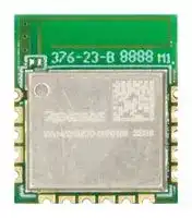


DA14535MOD-00F01002
Bluetooth Module, Bluetooth LE 5.3, -92.5 dBm, 1.8 to 3.6 V Supply, -40 °C to 85 °C
- Manufacturer: RENESAS
- Product type: Bluetooth Modules & Adaptors
- SVHC: No SVHC (25-Jun-2025)
- Interfaces: I2C, SPI, UART
- Product Range: DA14535MOD Series
- Certifications: ANATEL, CE, FCC, IC, MIC, MSIP, NBTC, NCC, RCM, SRRC, WPC
- Bluetooth Class: Class 2
- Supply Voltage Range: 1.8 V to 3.6 V
- Receiver Sensitivity Rx: -92.5 dBm
- Operating Temperature Range: -40 °C to 85 °C
| Delivery and price | |
|---|---|
| Units per pack | 250 |
| Price | 3.78 € |
| Current stock | 500+ |
| Lead time | 30 days |
Datasheet ## **DA14535MOD** SmartBond TINY Bluetooth[®] LE Module ## **General Description** The DA14535MOD is a lowest-power consumption, low-cost, fully self-contained Bluetooth[®] Low Energy v5.3 Module that is world-wide certified and ideal for a range of applications, including fast-upgrade projects to wirelessly connect your product to a smartphone for quick-and-simple commissioning/control/alerts/data collection. The DA14535MOD is a pin-equivalent and functional-equivalent alternative to the DA14531MOD, with both modules offering Cortex[®] -M0+, clocking at 16 MHz and on-die RAM, ROM, and OTP with integrated 1-Mbit Flash, 32-MHz crystal, power inductor, RF matching, and printed antenna. Both modules also have castellated pins for easy prototype soldering. The DA14535MOD differs from the DA14531MOD in the following key features: - Transmit Pout up to +3 dBm - 64 kB RAM, 160 kB ROM, 12 kB OTP - Compliance with BT5.3 - 2-wire UART support for Host-MCU based operation* *This feature is supported by the inclusion of a secondary boot loader in Flash during factory programming. For applications where a host MCU SoC is also present, this feature permits use of the host MCU’s memory to store and download DA14535MOD code for a Bluetooth LE data-pump. This feature can also remove the need for DA14535MOD factory programming during end-product production test. SmartBond TINY[TM] Modules are supported by a range of applications software, including a configurable DSPS (serial port service) and next generation Codeless software, making projects fast and easy, to the point where advanced programming skills and even knowledge of Bluetooth[®] is not required in many cases. The combination of affordable price, lowest power consumption and ease of use makes the DA14535MOD an ideal product for the broad market, including lower volume, or prototyping customers. R18DS0042EE0300 Revision 3.0 June 21, 2024 Page 1 © 2024 Renesas Electronics CFR0011-120-00 **SmartBond TINY Bluetooth® LE Module** **==> picture [153 x 6] intentionally omitted <==** ## **Key Features** ## ▪ Bluetooth - Compatible with Bluetooth[®] v5.3 - ETSI EN 300 328 and EN 300 440 Class 2 (Europe), FCC CFR47 Part 15 (US) and ARIB STD-T66 (Japan) - Supports up to three Bluetooth[®] LE connections - Renesas registered BD address preprogrammed in OTP ## ▪ Processing and memories - 16 MHz 32-bit Arm[®] Cortex[®] M0+ with SWD interface - 128 kB onboard Flash - 64 kB RAM - 160 kB ROM - 12 kB OTP - Current Consumption - 2.7 mA RX at VBAT = 3 V - 2.6 mA TX at VBAT = 3 V and 0 dBm - 1.7 µA at sleep with all RAM retained ## ▪ Radio - Programmable RF transmit power from -18 to +3 dBm - -92.5 dBm receiver sensitivity - Interfaces - Quadrature decoder with 3 channels - Channel 10-bit ADC - 2 general purpose timers with PWM - 9 GPIOs - SPI - 2x UART, 1-wire UART support - I2C - Power Management - Operating range (1.8 V-3.6 V) - Inrush current control - Other - SUOTA support - Battery Life Estimation - Data Rate Monitoring - Real-Time Power Profiling - Production Line Testing - Standards Conformance - BT SIG QDID 216526 - Europe (CE/RED) - UK (UKCA) - US (FCC) - Canada (IC) - Japan (MIC) - South Korea (MSIP) - Taiwan (NCC) - Brazil (ANATEL) - South Africa (ICASA) - China (SRRC) - Thailand (NBTC) - India (WPC) - Australia/New Zealand (ACMA) ## **Applications** - Beacons - Remote Controls - Proximity tags - Low Power Sensors - Commissioning/Provisioning - RF pipe - Toys - Industrial applications - Data acquisition - Wellness - Infotainment - IoT - Robotics - Gaming - Real Time Clock - Trimmed 32 MHz Crystal ## ▪ Packaging - 12.5 mm x 14.5 mm x 2.8 mm package - Module Software Development Kit - Configurable DSPS - Codeless v2.0 - SDK6 support - Module Software Tools - Flash/OTP programmer R18DS0042EE0300 Revision 3.0 June 21, 2024 Page 2 CFR0011-120-00 **SmartBond TINY Bluetooth® LE Module** ## **Contents** |**Contents**|**Contents**| |---|---| |**General Description ............................................................................................................................................... 1**|| |**Key**|**Features .......................................................................................................................................................... 2**| |**Applications ........................................................................................................................................................... 2**|| |**Contents ................................................................................................................................................................. 3**|| |**Figures .................................................................................................................................................................... 4**|| |**Tables ...................................................................................................................................................................... 4**|| |**1.**|**Terms and Definitions ................................................................................................................................... 6**| |**2.**|**References...................................................................................................................................................... 6**| |**3.**|**Block Diagram ................................................................................................................................................ 7**| |**4.**|**Pinout .............................................................................................................................................................. 8**| |**5.**|**Characteristics ............................................................................................................................................. 10**| ||5.1<br>Absolute Maximum Ratings ................................................................................................................. 10| ||5.2<br>Recommended Operating Conditions ................................................................................................. 10| ||5.3<br>Device Characteristics ......................................................................................................................... 10| |**6.**|**Mechanical Specifications .......................................................................................................................... 13**| ||6.1<br>Mechanical Dimensions and Land Pattern .......................................................................................... 13| ||6.2<br>Marking ................................................................................................................................................ 13| |**7.**|**BOM ............................................................................................................................................................... 14**| |**8.**|**Packaging Information ................................................................................................................................ 15**| ||8.1<br>Tape and Reel ..................................................................................................................................... 15| ||8.2<br>Labeling ............................................................................................................................................... 16| |**9.**|**Application Information .............................................................................................................................. 18**| ||9.1<br>Hardware Considerations .................................................................................................................... 18| ||9.2<br>Software Considerations ..................................................................................................................... 18| |**10.**|**Design Guidelines ....................................................................................................................................... 20**| ||10.1 Installation Location ............................................................................................................................. 20| ||10.2 Antenna Graphs ................................................................................................................................... 22| ||10.3 Radiation Pattern ................................................................................................................................. 23| |**11.**|**Soldering ...................................................................................................................................................... 25**| |**12.**|**Moistrure Sensitivity Label ......................................................................................................................... 26**| |**13.**|**Ordering Information ................................................................................................................................... 26**| |**14.**|**Regulatory Information ............................................................................................................................... 27**| ||14.1 CE (Radio Equipment Directive 2014/53/EU (RED)) – (Europe) ........................................................ 28| ||14.2 FCC – (U.S.A.) ..................................................................................................................................... 28| ||14.2.1<br>List of Applicable FCC Rules ................................................................................................ 28| ||14.2.2<br>Summarize the Specific Operational Use Conditions ........................................................... 28| ||14.2.3<br>Limited Module Procedures .................................................................................................. 28| ||14.2.4<br>Trace Antenna Designs ......................................................................................................... 28| ||14.2.5<br>RF Exposure Considerations ................................................................................................ 28| ||14.2.6<br>Antennas ............................................................................................................................... 28| ||14.2.7<br>Label and Compliance Information ....................................................................................... 28| ||14.2.8<br>Information on Test Modes and Additional Testing Requirements ....................................... 29| ||14.2.9<br>Additional Testing, Part 15 Subpart B Disclaimer ................................................................. 29| ||14.3 IC (Canada) ......................................................................................................................................... 29| R18DS0042EE0300 Revision 3.0 June 21, 2024 Page 3 CFR0011-120-00 **SmartBond TINY Bluetooth® LE Module** **==> picture [153 x 6] intentionally omitted <==** 14.4 UKCA (UK) .......................................................................................................................................... 30 14.5 NCC (Taiwan) ...................................................................................................................................... 31 14.6 MSIP (South Korea)............................................................................................................................. 31 14.7 ICASA (South Africa) ........................................................................................................................... 31 14.8 ANATEL (Brazil) .................................................................................................................................. 32 14.9 SRRC (China) ...................................................................................................................................... 32 14.10 MIC (Japan) ......................................................................................................................................... 32 14.11 NBTC (Thailand) .................................................................................................................................. 33 14.12 WPC (India) ......................................................................................................................................... 34 14.13 Australia/New Zealand......................................................................................................................... 34 14.14 WEEE Directive (2012/19/EU) ............................................................................................................. 34 **15. Bluetooth SIG Qualification ........................................................................................................................ 35 Revision History .................................................................................................................................................. 36** ## **Figures** Figure 1. DA14535 SmartBond TINY[TM] module block diagram .............................................................................. 7 Figure 2. Pinout diagram (top view) ......................................................................................................................... 8 Figure 3. Module shield marking ........................................................................................................................... 13 Figure 4. Tape and reel ......................................................................................................................................... 15 Figure 5. Reel labeling ........................................................................................................................................... 16 Figure 6. EU-UK directives conformity labels ........................................................................................................ 16 Figure 7. CMIIT label ............................................................................................................................................. 16 Figure 8. ICASA (S. Africa) label ........................................................................................................................... 17 Figure 9. Example of connecting a sensor to the SPI bus and an MCU to RST and UART ................................. 18 Figure 10. Default boot sequence ......................................................................................................................... 19 Figure 11. Installation locations for optimum antenna performance ..................................................................... 20 Figure 12. Antenna performance in proximity of copper (left), laminate (middle), and laminate under antenna (right) ...................................................................................................................................................................... 21 Figure 13. DA14535 TINY[TM] module evaluation board ......................................................................................... 21 Figure 14. VSWR installed in the upper left corner (position #1) of evaluation board........................................... 22 Figure 15. VSWR with module installed in center (position #2) of the evaluation board....................................... 22 Figure 16. VSWR with module installed in the upper right corner (position #3) of the evaluation board .............. 22 Figure 17. Measurement plane definition .............................................................................................................. 23 Figure 18. Radiation pattern for XY-plane, horizontal polarization ........................................................................ 24 Figure 19. Radiation pattern for XY-plane, vertical polarization ............................................................................ 24 Figure 20. Radiation pattern for XZ-plane, horizontal polarization ........................................................................ 24 Figure 21. Radiation pattern for XZ-plane, vertical polarization ............................................................................ 24 Figure 22. Radiation pattern for YZ-plane, horizontal polarization ........................................................................ 24 Figure 23. Radiation pattern for YZ-plane, vertical polarization ............................................................................ 24 Figure 24. Recommended reflow profile for lead free solder ................................................................................ 25 ## **Tables** Table 1: Pin description ........................................................................................................................................... 8 Table 2: Absolute maximum ratings ...................................................................................................................... 10 Table 3: Recommended operating conditions ....................................................................................................... 10 Table 4: DC characteristics .................................................................................................................................... 10 Table 5: XTAL32M - Recommended operating conditions .................................................................................... 11 Table 6: Digital I/O - Recommended operating conditions .................................................................................... 11 Table 7: Digital I/O - DC characteristics ................................................................................................................ 12 R18DS0042EE0300 Revision 3.0 June 21, 2024 Page 4 CFR0011-120-00 **SmartBond TINY Bluetooth® LE Module** **==> picture [153 x 6] intentionally omitted <==** Table 8: Radio - AC characteristics ....................................................................................................................... 12 Table 9: Bill of materials ........................................................................................................................................ 14 Table 10: Reel specifications ................................................................................................................................. 15 Table 11: Antenna efficiency vs TINY[TM] module positions .................................................................................... 20 Table 12: Reflow profile specification .................................................................................................................... 25 Table 13: MSL level vs floor lifetime ...................................................................................................................... 26 Table 14: Ordering information (samples) ............................................................................................................. 26 Table 15: Ordering information (production) .......................................................................................................... 26 Table 16: Standards conformance ........................................................................................................................ 27 R18DS0042EE0300 Revision 3.0 June 21, 2024 Page 5 CFR0011-120-00 **SmartBond TINY Bluetooth® LE Module** **==> picture [153 x 6] intentionally omitted <==** ## **1. Terms and Definitions** ADC Analog-to-Digital Converter DIO Digital Input-Output I-PD Input-Pulled Down I-PU Input-Pulled Up GND Ground MSL Moisture Sensitivity Level NTC Negative Temperature Coefficient PCB Printed Circuit Board PWR Power RDS Reduced Driving Strength VSWR Voltage Standing Wave Ratio ## **2. References** [1] DA14535, Datasheet, Renesas Electronics. [2] UM-B-119: DA14585/DA14531 SW Platform Reference Manual, Renesas Electronics. [3] UM-B-171: Renesas SmartBoot Bootloader Reference Manual, Renesas Electronics. **Note 1** References are for the latest published version, unless otherwise indicated. R18DS0042EE0300 Revision 3.0 June 21, 2024 Page 6 CFR0011-120-00 **SmartBond TINY Bluetooth® LE Module** **==> picture [153 x 6] intentionally omitted <==** ## **3. Block Diagram** The DA14535 SmartBond TINY™ Module is based on the Renesas DA14535 SoC configured in buck mode. With an integrated 1 Mbit NOR Flash, 32 MHz XTAL and a printed antenna, the module enables a faster time to market at reduced development costs. The module, as seen in Figure 1, consists of: - 1 Mbit SPI Flash - 32 MHz XTAL - 2 decoupling capacitors - A power inductor - A CLC filter and matching components for the printed antenna. **==> picture [378 x 243] intentionally omitted <==** **----- Start of picture text -----**<br> VBAT<br>J7 J12 (RST)<br>L1<br>C2 C1<br>C3<br>P25Q11U<br>P0_0<br>1Mbit<br>J10J14 P0_2P0_5 P0_1P0_3 NOR-SPI<br>J5 P0_6 PROJECT P0_4 Data Flash<br>J13 P0_7 NAME U2<br>J16 P0_8 DA14535<br>J15 P0_9<br>J9 P0_10<br>J8 P0_11 RF Filter &<br>Matching<br>L2, C4, C5, C7, C9<br>U1<br>X1<br>J2, J3, J4,<br>J6, J11, (J1)<br>VBAT_LOW Lx VBAT_HIGH<br>GND<br>**----- End of picture text -----**<br> **Figure 1. DA14535 SmartBond TINY[TM] module block diagram** R18DS0042EE0300 Revision 3.0 June 21, 2024 Page 7 CFR0011-120-00 **SmartBond TINY Bluetooth® LE Module** ## **4. Pinout** **==> picture [329 x 325] intentionally omitted <==** **----- Start of picture text -----**<br> ANTENNA AREA<br>n.c. J1 J16 P0_8<br>GND J2 J15 P0_9<br>GND J3 MARKING AREA J14 P0_5/RxTx<br>GND J4 J13 P0_7<br>P0_6 J5 J12 P0_0/RST<br>J6 J7 J8 J9 J10 J11<br>GND VBAT P0_11 P0_10/SWDIO P0_2/SWCLK GND<br>**----- End of picture text -----**<br> **Figure 2. Pinout diagram (top view)** Note that J1 has no internal connection. J1 should be connected to the ground. **Table 1: Pin description** |**Pin #**|**Pin Name**|**Type**|**Reset**<br>**State**|**Description**| |---|---|---|---|---| |J1|n.c|||Not internally connected. Recommended to be<br>connected to ground externally.| |J2|GND|GND||Ground.| |J3|GND|GND||Ground.| |J4|GND|GND||Ground.| |J5|P0_6|DIO<br>(Type A)<br>Note 1|I-PD|INPUT/OUTPUT with selectable pull-up/down<br>resistors. Pull-down enabled during and after<br>reset. General purpose I/O port bit or alternate<br>function nodes. Contains a state retention<br>mechanism during power down.| |J6|GND|GND||Ground.| |J7|VBAT|PWR||POWER. Battery connection. IO supply| |J8|P0_11|DIO<br>(Type A)|I-PD|INPUT/OUTPUT with selectable pull-up/down<br>resistors. Pull-down enabled during and after<br>reset. General purpose I/O port bit or alternate<br>function nodes. Contains a state retention<br>mechanism during power down.| R18DS0042EE0300 Revision 3.0 June 21, 2024 Page 8 CFR0011-120-00 **SmartBond TINY Bluetooth® LE Module** **==> picture [153 x 6] intentionally omitted <==** |**Pin #**|**Pin Name**|**Type**|**Reset**<br>**State**|**Description**| |---|---|---|---|---| |J9|P0_10|DIO (Type A)|I-PD|INPUT/OUTPUT with selectable pull-up/down<br>resistors. Pull-down enabled during and after<br>reset. General purpose I/O port bit or alternate<br>function nodes. Contains a state retention<br>mechanism during power down.| ||SWDIO|||INPUT/OUTPUT. SWI Data input/output.<br>Bidirectional data and control communication<br>(by default).| |J10|P0_2|DIO<br>(Type B)|I-PD|INPUT/OUTPUT with selectable pull-up/down<br>resistors. Pull-down enabled during and after<br>reset. General purpose I/O port bit or alternate<br>function nodes. Contains a state retention<br>mechanism during power-down.| ||SWCLK|||INPUT SWI clock signal (by default).| |J11|GND|GND||Ground.| |J12|P0_0|DIO<br>(Type B)<br>Note 2|I-PD|INPUT/OUTPUT with selectable pull-up/down<br>resistors. Pull-down enabled during and after<br>reset. General purpose I/O port bit or alternate<br>function nodes. Contains a state retention<br>mechanism during power-down.| ||RST|||RST active high hardware reset (default).| |J13|P0_7|DIO<br>(Type A)|I-PD|INPUT/OUTPUT with selectable pull-up/down<br>resistors. Pull-down enabled during and after<br>reset. General purpose I/O port bit or alternate<br>function nodes. Contains a state retention<br>mechanism during power down.| |J14|P0_5|DIO<br>(Type B)|I-PD|INPUT/OUTPUT with selectable pull-up/down<br>resistors. Pull-down enabled during and after<br>reset. General purpose I/O port bit or alternate<br>function nodes. Contains a state retention<br>mechanism during power down.| |J15|P0_9|DIO<br>(Type A)|I-PD|INPUT/OUTPUT with selectable pull-up/down<br>resistors. Pull-down enabled during and after<br>reset. General purpose I/O port bit or alternate<br>function nodes. Contains a state retention<br>mechanism during power down.| |J16|P0_8|DIO<br>(Type A)|I-PD|INPUT/OUTPUT with selectable pull-up/down<br>resistors. Pull-down enabled during and after<br>reset. General purpose I/O port bit or alternate<br>function nodes. Contains a state retention<br>mechanism during power down.| **Note 1** There are two types of pads, namely Type A and Type B. Type A is a normal IO pad with a Schmitt trigger on input while Type B has an extra RC Filter with a cutoff frequency of 100 kHz. **Note 2** This pin is also used for communication to the onboard SPI Flash. R18DS0042EE0300 Revision 3.0 June 21, 2024 Page 9 CFR0011-120-00 **SmartBond TINY Bluetooth® LE Module** **==> picture [153 x 6] intentionally omitted <==** ## **5. Characteristics** All MIN/MAX specification limits are guaranteed by design, production testing, and/or statistical characterization. Typical values are based on characterization results at default measurement conditions and are informative only. Default measurement conditions (unless otherwise specified): VBAT = 3.0 V, TA = 25 °C. All radio measurements are done with standard RF measurement equipment. ## **5.1 Absolute Maximum Ratings** Stresses beyond those listed under Absolute Maximum Ratings may cause permanent damage to the device. These are stress ratings only, so functional operation of the device at these or any other conditions beyond those indicated in the operational sections of the specification are not implied. Exposure to Absolute Maximum Rating conditions for extended periods may affect device reliability. **Table 2: Absolute maximum ratings** |**Parameter**|**Description**|**Conditions**|**Min**|**Max**|**Unit**| |---|---|---|---|---|---| |VBAT_LIM|Limiting battery supply voltage||-0.2|3.6|V| ## **5.2 Recommended Operating Conditions** **Table 3: Recommended operating conditions** |**Parameter**|**Description**|**Conditions**|**Min**|**Typ**|**Max**|**Unit**| |---|---|---|---|---|---|---| |VBAT|Battery supply voltage|Voltage range within FLASH<br>programming is possible|1.65||3.6|V| |VBAT_NOM|Nominal battery supply voltage|||3||V| |VPIN|Voltage on a pin||-0.2||3.6|V| |TA|Ambient operating temperature||-40|25|85|°C| ## **5.3 Device Characteristics** **Table 4: DC characteristics** |**Parameter**|**Description**|**Conditions**|**Min**|**Typ**|**Max**|**Unit**| |---|---|---|---|---|---|---| |IBAT_ACTIVE|Battery supply current|CPU running CoreMark from<br>RAM at 16 MHz.||0.47||mA| |IBAT_BLE_ADV_<br>100ms|Average battery supply current|System in Advertising state (3<br>channels) every 100 ms and<br>extended sleep with all RAM<br>retained. TX output power at 3<br>dBm. FLASH is off.||79||μA| |IBAT_BLE_CONN<br>_30ms|Average battery supply current|System in a connection state<br>with 30 ms connection interval<br>and extended sleep with all<br>RAM retained. TX output<br>power at 3 dBm. FLASH is off.||105||μA| |IBAT_FLASH|Battery supply current|CPU fetching code from serial<br>FLASH. RF is off.||0.6||mA| |IBAT_HIBERN|Battery supply current|System shut down<br>(Hibernation or shipping<br>mode). FLASH is off.||0.9||μA| |IBAT_IDLE|Battery supply current|CPU in Wait for Interrupt<br>Mode. FLASH is off.||0.22||mA| R18DS0042EE0300 Revision 3.0 June 21, 2024 Page 10 CFR0011-120-00 **SmartBond TINY Bluetooth® LE Module** **==> picture [153 x 6] intentionally omitted <==** |**Parameter**|**Description**|**Conditions**|**Min**|**Typ**|**Max**|**Unit**| |---|---|---|---|---|---|---| |IBAT_SLP_32KB|Battery supply current|System in extended sleep<br>mode and 32 kB RAM<br>retained.||1.4||μA| |IBAT_SLP_64KB|Battery supply current|System in extended sleep<br>mode and all RAM retained.||1.7||μA| |IBAT_RF_RX|Battery supply current|Continuous RX; FLASH in<br>sleep mode; DCDC converter<br>is on||2.7||mA| |IBAT_RF_TX_+3d<br>Bm|Battery supply current|Continuous TX; FLASH in<br>sleep mode; DCDC converter<br>is on; Output power setting =<br>12.<br>Note 1||3.2||mA| |IBAT_RF_TX_0d<br>Bm|Battery supply current|Continuous TX; FLASH in<br>sleep mode; DCDC converter<br>is on; Output power setting =<br>8.<br>Note 1||2.6||mA| |IBAT_RF_TX_-<br>3dBm|Battery supply current|Continuous TX; FLASH in<br>sleep mode; DCDC converter<br>is on; Output power setting =<br>6.<br>Note 1||2.3||mA| |IBAT_RF_TX_-<br>6dBm|Battery supply current|Continuous TX; FLASH in<br>sleep mode; DCDC converter<br>is on; Output power setting =<br>4.<br>Note 1||2||mA| |IBAT_RF_TX_-<br>18dBm|Battery supply current|Continuous TX; FLASH in<br>sleep mode; DCDC converter<br>is on; Output power setting =<br>1.<br>Note 1||1.3||mA| **Note 1** The nominal ouput power level might slightly deviate from the actual value. **Table 5: XTAL32M - Recommended operating conditions** |**Parameter**|**Description**|**Conditions**|**Min**|**Typ**|**Max**|**Unit**| |---|---|---|---|---|---|---| |fXTAL(32M)|Crystal oscillator frequency|||32||MHz| |ΔfXTAL(32M)|Crystal frequency tolerance|After optional trimming;<br>including aging and<br>temperature drift<br>Note 1|-20||20|ppm| **Note 1** Using the internal varicaps a wide range of crystals can be trimmed to the required tolerance. **Table 6: Digital I/O - Recommended operating conditions** |**Parameter**|**Description**|**Conditions**|**Min**|**Typ**|**Max**|**Unit**| |---|---|---|---|---|---|---| |VIH|HIGH level input voltage|VDD= 0.9 V|0.7*VD<br>D|||V| R18DS0042EE0300 Revision 3.0 June 21, 2024 Page 11 CFR0011-120-00 **SmartBond TINY Bluetooth® LE Module** **==> picture [153 x 6] intentionally omitted <==** |**Parameter**|**Description**|**Conditions**|**Min**|**Typ**|**Max**|**Unit**| |---|---|---|---|---|---|---| |VIL|LOW level input voltage|VDD= 0.9 V|||0.3*VD<br>D|V| **Table 7: Digital I/O - DC characteristics** |**Parameter**|**Description**|**Conditions**|**Min**|**Typ**|**Max**|**Unit**| |---|---|---|---|---|---|---| |IIH|HIGH level input current|VI=VBAT= 3.0 V|-10||10|μA| |IIL|LOW level input current|VI=VSS= 0 V|-10||10|μA| |IIH_PD|HIGH level input current|VI=VBAT= 3.0 V|60||180|μA| |IIL_PU|LOW level input current|VI=VSS= 0 V, VBAT= 3.0 V|-180||-60|μA| |VOH|HIGH level output voltage|IO= 3.5 mA, VBAT= 1.7 V|0.8*VB<br>AT|||V| |VOL|LOW level output voltage|IO= 3.5 mA, VBAT= 1.7 V|||0.2*VB<br>AT|V| |VOH_LOWDRV|HIGH level output voltage|IO= 0.3 mA, VBAT= 1.7 V|0.8*VB<br>AT|||V| |VOL_LOWDRV|LOW level output voltage|IO= 0.3 mA, VBAT= 1.7 V|||0.2*VB<br>AT|V| **Table 8: Radio - AC characteristics** |**Parameter**|**Description**|**Conditions**|**Min**|**Typ**|**Max**|**Unit**| |---|---|---|---|---|---|---| |PSENS_CLEAN|Sensitivity level|Dirty Transmitter disabled;<br>DC-DC converter disabled;<br>PER = 30.8%.<br>Note 1||-92.5||dBm| |PSENS_EPKT|Sensitivity level|Extended packet size (255<br>octets)||-89.5||dBm| **Note 1** Measured according to Bluetooth[®] Low Energy Test Specification. R18DS0042EE0300 Revision 3.0 June 21, 2024 Page 12 CFR0011-120-00 **SmartBond TINY Bluetooth® LE Module** ## **6. Mechanical Specifications** ## **6.1 Mechanical Dimensions and Land Pattern** The module’s dimensions are accessible from the Renesas website - 16-Module. ## **6.2 Marking** The module’s shield marking is shown in Figure 3. **==> picture [333 x 294] intentionally omitted <==** **----- Start of picture text -----**<br> Antenna Area<br>J1 O Ce€ UK |“oe J16<br>CA (fess<br>J2 2tENESAS : J15<br>DA14535MOD-00F0100 yyww<br>J3 FCC ID : Y82-DA14535MOD J14<br>IC<br>J4 : 9576A-DA14535MOD J13<br>ANATEL : 05421-24-16689<br>CMIIT<br>J5 ID : 2023DP16498 J12<br>J6 J7 J8 J9 J10 J11<br><_ 10.30 ± .10 (mm) ——<br>8.90 ± .10 (mm)<br>**----- End of picture text -----**<br> **Figure 3. Module shield marking** Marking Legend: DA14535MOD-00F0100 yyww yy: production year ww: production week All dimensions in mm. Tolerance 0.4 mm. R18DS0042EE0300 Revision 3.0 June 21, 2024 Page 13 CFR0011-120-00 **SmartBond TINY Bluetooth® LE Module** ## **7. BOM** **Table 9: Bill of materials** |**#**|**Designator**|**Type**|**Value**|**Description**|**Manufacturer**|**MPN**| |---|---|---|---|---|---|---| |1|U1|IC|DA14535-00000FX2|Bluetooth Low Energy DA14535 FCGQFN24|Renesas|DA14535-00000FX2| |2|U2|NOR Flash|P25Q11U-UXH-IR|FLASH 1MBIT SPI 104 MHZ 8USON 3x2x0.55 mm|Puya Semiconductor|P25Q11U-UXH-IR| |3|X1|Crystal Oscillator|32 MHz 6 pF 10 ppm|SMD 32 MHz, 6 pF, 10 ppm|Tai-Saw|TZ3375C| |4|L1|Inductor|2.2 uH|FIXED IND 2.2 µH 20% 1.5 A 160 mΩ|Taiyo Yuden|MAKK2016T2R2M| |5|L2|Inductor|2.8 nH|INDUCTOR 2.8 nH ±0.1 nH 500 mA 0201|Murata|LQP03TN2N8B02D| |6|C1|Capacitor|2.2 µF|CAP CER 2.2 µF 25 V 20% X5R 0402|Murata|GRM155R61E225ME15D| |7|C2|Capacitor|10 µF|CAP CER 10 µF 6V3 20% X5R 0402|Murata|GRM155R60J106ME15D| |8|C3|Capacitor|1 µF|CAP CER 1 µF 6V3 20% X7R 0402|Murata|GRM155R70J105MA12D| |9|C4|Capacitor|1.6 pF|CAP CER 1p6 50 V 0.25 pF NP0 0201|Murata|GRM0335C1H1R6CA01D| |10|C5|Capacitor|1.8 pF|CAP CER 1p8 50 V 0.25 pF NP0 0201|Murata|GRM0335C1H1R8CA01D| |11|C7|Capacitor|0.8 pF|CAP CER 0p8 50 V ±0.1 pF NP0 0201|Murata|GRM0335C1HR80BA01| |12|C9|Capacitor|10 pF|CAP CER 10PF 50 V ±5% NP0 0201|Murata|GRM0335C1H100JA01J| R18DS0042EE0300 Revision 3.0 June 21, 2024 Page 14 CFR0011-120-00 **SmartBond TINY Bluetooth® LE Module** ## **8. Packaging Information** ## **8.1 Tape and Reel** **Figure 4. Tape and reel** The reel specifications are shown in Table 10. **Table 10: Reel specifications** |**Parameter**|**Value**| |---|---| |Diameter|13 inches| |Reel tape width|24 mm| |Tape material|Antistatic| |Qty/Reel|100/1000 pcs| |Leader|400 mm + 10%| |Trailer|160 mm + 10%| R18DS0042EE0300 Revision 3.0 June 21, 2024 Page 15 CFR0011-120-00 **SmartBond TINY Bluetooth® LE Module** ## **8.2 Labeling** Figure 5 presents the label found on a typical reel. **Figure 5. Reel labeling** The directives labels show information regarding directives conformity as in Figure 6, Figure 7, and Figure 8. **==> picture [434 x 135] intentionally omitted <==** **----- Start of picture text -----**<br> Manufacturer : Renesas Design Netherlands B.V.<br>Het Zuiderkruis 53, 5215 MV s-Hertogenbosch Imported by: Renesas Electronics Operations<br>THE NETHERLANDS Services Limited<br>Product name : DA14535MOD Dukes Meadow, Millboard Road, Bourne End,<br>Model No. : DA14535MOD-00F0100 SL8 5FH, United Kingdom<br> Manufacturer : Renesas Design Netherlands B.V.<br> Het Zuiderkruis 53, 5215 MV s-Hertogenbosch<br>THE NETHERLANDS<br>Product name: DA14535MOD<br>Model No. : DA14535MOD-00F0100<br>< —+____—_ 67mm > <<. 67mm —_____5 »<br>42 mm 42 mm<br>**----- End of picture text -----**<br> **Figure 6. EU-UK directives conformity labels** **==> picture [168 x 30] intentionally omitted <==** **----- Start of picture text -----**<br> DA14535MOD-00F0100<br>CMIIT ID: 2023DP16498<br>**----- End of picture text -----**<br> **Figure 7. CMIIT label** R18DS0042EE0300 Revision 3.0 June 21, 2024 Page 16 CFR0011-120-00 **SmartBond TINY Bluetooth® LE Module** **Figure 8. ICASA (S. Africa) label** R18DS0042EE0300 Revision 3.0 June 21, 2024 Page 17 CFR0011-120-00 **SmartBond TINY Bluetooth® LE Module** ## **9. Application Information** ## **9.1 Hardware Considerations** There are some special considerations for the use of the TINY[TM] module, namely: - The RST signal is shared with the MOSI input of the NOR Flash. For this reason, RST must not be driven to GND. When the onboard Flash is in use, the reset functionality is not available. - The SPI Bus of DA14535 SoC is used for communication with the NOR Flash at boot time. Three of the four signals are not driven to external module pins. For this reason, a sensor that utilizes the SPI bus must be assigned (by software) to the module pins to communicate with after the boot is completed and when NOR Flash is no longer in use. An example is given in Figure 9. **==> picture [445 x 165] intentionally omitted <==** **----- Start of picture text -----**<br> VBAT<br>J5 P0_2 J10 UTX<br>SCK P0_6<br>J14<br>J13 P0_5 URX External<br>P0_7 MCU<br> Sensor J16 P0_10 J9<br>/CS J15 P0_8 DA14535PROJECT NAME J12 GPIO<br>MOSI P0_9 P25Q11U<br>J8 P0_0/RST MOSI<br>MISO P0_11 P0_1 /CS 1Mbit<br>P0_3 MISO NOR<br>P0_4 SCK Flash<br>DA14535 TINY Module<br>J1, J2, J3, J4, J6, J11<br>GND<br>**----- End of picture text -----**<br> **Figure 9. Example of connecting a sensor to the SPI bus and an MCU to RST and UART** Note that the P0_0/RST pin (J12) should not be driven while the TINY[TM] module boots from its internal SPI Flash. ## **9.2 Software Considerations** The DA14535 SmartBond TINY™ Module comes with the SmartBoot bootloader preloaded by default in the intergraded SPI NOR Flash. The SmartBoot bootloader executes after the primary bootloader and determines which application code needs to be loaded into RAM based on a the SmartBoot header and, optionally, on pin state or the magic word address. For more information aboout SmartBoot, see Ref. [3]. The default boot sequence is shown in Figure 10. R18DS0042EE0300 Revision 3.0 June 21, 2024 Page 18 CFR0011-120-00 **SmartBond TINY Bluetooth® LE Module** **==> picture [426 x 526] intentionally omitted <==** **----- Start of picture text -----**<br> Default clock is Boot Start<br>RC32K<br>Enabled already Switch to RC32MHz Required to be<br>by PWR FSM able to read from<br>OTP<br>Boost<br>Yes Enable DCDC<br>mode?<br>No<br>Enable OTP<br>Initialize UART baudrate @ 115200<br>DCDC in buck<br>Execute Configuration Script could be enabled<br>here<br>Read OTP Application Flags<br>Is App Switch to<br>Yes programmed No XTAL32M OK Yes XTAL32M<br>?<br>Length Register<br>will be Magic Number<br>automatically identified<br>read by the OTP<br>controller after No<br>wake up Read and Prog. DMA<br>length<br>Yes Boot specific Yes Initialize Peripheral<br>Start copy of OTP to flag = 0xAA? Devices<br>SRAM<br>Read serial<br>No configuration<br>No Disable OTP All Boot Steps<br>protected by a<br>Copy Disable OTP Timeout<br>CPU is polling done? Boot Step 1<br>OTPC_STAT_REG (ext SPIM) Switch to<br>Boot from Fail XTAL32M before<br>Yes UART Success Boot Step 2 using UART<br>Disable OTP Fail ( 1w UART-1)<br>Success<br>Boot Step 3<br>Fail Fail (1w UART-2)<br>Configure<br>SPI pins Success Boot Step 4<br>Boot from ext Fail (2w UART)<br>SPIS Success Boot Step 5<br>Fail (ext SPIS)<br>Fail, Goto Success<br>Boot Step 1 Success Boot Step 6 (I2C)<br>Fail<br>Remap SysRAM to addr 0x00 and SW Enable JTAG Download Code to SRAM Dis_JTAG=FALSE Dis_JTAG=TRUE Flag should be updated while CS<br>execution<br>reset Dis_JTAG=FALSE Enable JTAG<br>Dis_JTAG=<br>Boot End TRUE Switch back to Endless loop<br>RC32M<br>NORMAL MODE<br>DEVELOPMENT MODE<br>**----- End of picture text -----**<br> **Figure 10. Default boot sequence** R18DS0042EE0300 Revision 3.0 June 21, 2024 Page 19 CFR0011-120-00 **SmartBond TINY Bluetooth® LE Module** ## **10. Design Guidelines** The DA14535 SmartBond TINY™ Module comes with an integrated PCB trace antenna. The antenna area is 12x4 mm. The antenna’s Voltage Standing Wave Ratio (VSWR) and efficiency depend on the installation location. The radiation performance of the PCB trace antenna depends on the host PCB layout. The maximum antenna gain is -0.5 dBi when installed on a 50x50 mm reference board, as shown in Figure 22. The radiation pattern is omnidirectional. The RF front end is optimized to achieve the maximum possible efficiency for various installation positions of the module on a host PCB. To obtain a similar performance, follow the guidelines described in the following sections. ## **10.1 Installation Location** For optimum performance, install the module at the edge of a host PCB with the antenna edge facing out. The module can be located on either of the outer corners or the middle of the host PCB with equivalent performance. The antenna should have 4 mm free space in all directions. Copper or laminate in the proximity of the PCB trace antenna will affect the efficiency of the antenna. Laminate or copper under the antenna should be avoided as it severely affects the performance of the antenna. The antenna keep-out area can be seen in Figure 12. Metals close to the antenna will degrade the antenna’s performance. The amount of degradation depends on the host system’s characteristics. Table 11 summarizes the antenna efficiency at different installation locations on a host PCB as shown in Figure 11. **Table 11: Antenna efficiency vs TINY[TM] module positions** ||**Position # 1 (Left)**|**Position # 1 (Left)**|**Position # 2 (Middle)**|**Position # 2 (Middle)**|**Position # 3 (Right)**|**Position # 3 (Right)**| |---|---|---|---|---|---|---| |**Freq**|**Antenna efficiency**||**Antenna efficiency**||**Antenna efficiency**|| |[MHz]|[%]|[dB]|[%]|[dB]|[%]|[dB]| |2405|52|-2,8|40|-4,0|40|-4,0| |2440|46|-3,4|34|-4,7|41|-3,9| |2480|50|-3,0|40|-4,0|52|-2,8| **Figure 11. Installation locations for optimum antenna performance** R18DS0042EE0300 Revision 3.0 June 21, 2024 Page 20 CFR0011-120-00 **SmartBond TINY Bluetooth® LE Module** ## ~~——~~ > SePc 5 38 ae 8 <6 ss 5 3 <8<8.. SS =% SS sees6% _ oe - 6% es > |.| **=** \ , i **-** oS ves<05 Seca Sees sees“0 *%et * 8SF["0] -. *. “0 oe :.2-=]|~-“7esa7SS **y** of SS -= **.** =“Vy.7esVvr **a** t e[|][_] _—Becece Seesse<358=“ oe.“<esesee58\,asec..s< **e** Se **.** K3<e<2ra“ eS<8.<3% **e Figure 12. Antenna performance in proximity of copper (left), laminate (middle), and laminate under antenna (right)** The actual TINY[TM] module evaluation board layout that has been used to conduct measurements is shown in Figure 13. 43.[—] Soseeoe > ecos x staeee: **[|]** 4 % ae 5S -x[Se][ %] m m ee[oe] secs 5 2 :[—] 4 i aSeeeoS04 segoe 8 se<:[_] a[_] aiSF¢ AL nis< ie*tiebs :g 8 oes og ss oe oe ve <8‘<s oS es:[:][|] %x[_] <8<3 $8oS 88 50m[oS] < oe.[_] <%.: me<3~~%[<] 9[—] _ “8 es5“ gece[38] eoS <3SS<e_ :<3 38<3 oe[_] es[oS] — .ees<38 %e<3<<e[_] < 8 xo xo sees oo **_** _<3 <3 se xe 38 ceoS 38. <3< 9 % see<_ <8< iM<8<[SS] on33 oS <3 <8ses see <8 <8BR es 3 3 x[as] 8 =se oe<S" **_** oSee **<8** " **_** — **<** e oes[2] “6% see‘te <ocesS ei[sess] osS08e **e** stegee im m[ae][ee][ ee][.] **Figure 13. DA14535 TINY[TM] module evaluation board** R18DS0042EE0300 Revision 3.0 June 21, 2024 Page 21 CFR0011-120-00 **SmartBond TINY Bluetooth® LE Module** ## **10.2 Antenna Graphs** The antenna VSWR measurements for the three installation positions are shown in the following figures. **Figure 14. VSWR installed in the upper left corner (position #1) of evaluation board** **Figure 15. VSWR with module installed in center (position #2) of the evaluation board** **Figure 16. VSWR with module installed in the upper right corner (position #3) of the evaluation board** R18DS0042EE0300 Revision 3.0 June 21, 2024 Page 22 CFR0011-120-00 **SmartBond TINY Bluetooth® LE Module** ## **10.3 Radiation Pattern** The antenna radiation pattern measurements are carried out in an anechoic chamber. Radiation patterns are presented for three measurement planes: XY-, XZ-, and YZ- planes with horizontal and vertical polarization of the receiving antenna. **Figure 17. Measurement plane definition** R18DS0042EE0300 Revision 3.0 June 21, 2024 Page 23 CFR0011-120-00 **SmartBond TINY Bluetooth® LE Module** Measurements are carried out for the module installed in the upper-right corner on the reference board with no laminate below the antenna trace. ## **Radiation Pattern for Antenna Trace** **==> picture [412 x 191] intentionally omitted <==** **----- Start of picture text -----**<br> Horizontal polarization Vertical polarization<br>ss Ol we Horizontal polarization S88 OF ae Vertical polarization<br>‘i Ui WY 6 Freq [MHz] Gain [dBi] aSe M a6 Freq [MHz] Gain [dBi]<br>Peak Average = emi Retk verses<br> i " —— 2405: -8,8 dBi -13,8 dBi 3 aay NSo DO —— 2805: 2,4 481-4808<br>225iZZ PP sags -9,1 dBi -13,4 dBi 3= a = ==i ZK ~~22232a=: -1,7 dBi -4,5 dBi<br>SS —— 2480: -9,0 dBi -13,8 dBi E = = ES es = 5 "Saw ssa spe<br>Hi INS 2° i 1 223/77 rll \\ XS” 235 } ;<br>380 - = id 195 ~~ =— =<br>Azimuth (deg) SS 180 Azimuth (deg) Ze<br>Figure 19. Radiation pattern for XY-plane, vertical<br>polarization polarization<br>**----- End of picture text -----**<br> **==> picture [227 x 23] intentionally omitted <==** **----- Start of picture text -----**<br> Figure 18. Radiation pattern for XY-plane, horizontal<br>polarization<br>**----- End of picture text -----**<br> **Figure 20. Radiation pattern for XZ-plane, horizontal polarization** **Figure 21. Radiation pattern for XZ-plane, vertical polarization** **==> picture [225 x 22] intentionally omitted <==** **----- Start of picture text -----**<br> Figure 22. Radiation pattern for YZ-plane, horizontal<br>polarization<br>**----- End of picture text -----**<br> **Figure 23. Radiation pattern for YZ-plane, vertical polarization** R18DS0042EE0300 Revision 3.0 June 21, 2024 Page 24 CFR0011-120-00 **SmartBond TINY Bluetooth® LE Module** ## **11. Soldering** The successful reflow soldering of the DA14535 TINY[TM] Module on a PCB depends on several parameters such as the thickness of the stencil, the pads solder paste aperture, the solder paste characteristics, the reflow soldering profile, size of the PCB, and so on. The volume of solder paste applied to the board is mainly determined by the aperture size and stencil thickness. An initial solder paste aperture for the pads is provided on the solder paste layer of the PCB footprint. This aperture is modified by the assembly process experts according to stencil thickness, solder paste, and available assembly equipment. The solder profile depends on the solder paste type used. For example, the soldering profile of a lead-free solder paste, Sn3Ag0.5Cu with no clean Flux (ROL0) and Solder Powder Type 4, is shown in Figure 24. No clean flux is recommended because washing must not be applied after assembly to avoid moisture being trapped under the shield. **Figure 24. Recommended reflow profile for lead free solder** **Table 12: Reflow profile specification** |**Statistic Name**|**Low Limit**|**High Limit**|**Units**| |---|---|---|---| |Slope1 (Target = 2.0) Between 30.0 and 70.0|1|3|Degrees/Second| |Slope2 (Target = 2.0) Between 70.0 and 150.0|1|3|Degrees/Second| |Slope3 (Target = -2.8) Between 220.0 and 150.0|-5|-0.5|Degrees/Second| |Preheat time 110-190C|60|120|Seconds| |Time above reflow at 220C|30|65|Seconds| |Peak temperature|235|250|Degrees Celsius| |Total time above at 235C|10|30|Second| Solderability reflow check of five cycles was performed, applying the procedures mentioned in the JESD-A113E standard. R18DS0042EE0300 Revision 3.0 June 21, 2024 Page 25 CFR0011-120-00 **SmartBond TINY Bluetooth® LE Module** ## **12. Moistrure Sensitivity Label** The MSL is an indicator for the maximum allowable time period (floor lifetime) in which a moisture-sensitive plastic device, when removed from the dry bag, can be exposed to an environment with a maximum temperature of 30 °C and a maximum relative humidity of 60% RH before the solder reflow process. The DA14535 TINY Module is qualified for MSL 3. **Table 13: MSL level vs floor lifetime** |**MSL Level**|**Floor Lifetime**| |---|---| |MSL 4|72 hours| |MSL 3|168 hours| |MSL 2A|4 weeks| |MSL 2|1 year| |MSL 1|Unlimited at 30 °C/85%RH| ## **13. Ordering Information** The ordering number consists of the part number followed by a suffix that indicates the packing method. For details and availability, consult your Renesas local sales representative. **Table 14: Ordering information (samples)** |**Part Number**|**Size (mm)**|**Shipment Form**|**Pack Quantity**|**MOQ**| |---|---|---|---|---| |DA14535MOD-00F0100C|12.5 x 14.5 x 2.8|Reel|100|3| |**Table 15: Ordering information (production)**||||| |**Part Number**|**Size (mm)**|**Shipment Form**|**Pack Quantity**|**MOQ**| |DA14535MOD-00F01002|12.5 x 14.5 x 2.8|Reel|1000|1| R18DS0042EE0300 Revision 3.0 June 21, 2024 Page 26 CFR0011-120-00 **SmartBond TINY Bluetooth® LE Module** ## **14. Regulatory Information** This section outlines the regulatory information for the DA14535 SmartBond TINY[TM] Module. The module is certified for the global market. This facilitates the market entry of the end product. Note that the end product would need to apply for the end product certification, however, the module certification listed below will facilitate that procedure. When the user sends the end product to those markets, the end product may need to follow additional requirements according to the specific market regulation. For example, some markets have additional testing and/or certification like Korea EMC, South Africa SABS EMC and some have the requirement to put on the end product label a modular approval ID or mark that consists of an approved Bluetooth[®] Low Energy modular ID on host label directly, like Japan, Taiwan, Brazil. A list of the Conformance Standards that the DA14535 SmartBond TINY[TM] Module meets is shown in Table 16. **Table 16: Standards conformance** |**Area**|**Item**|**Service**|**Standard**|**Certificate ID**| |---|---|---|---|---| |Global|Safety for<br>module|CB|IEC 62368-1:2018<br>EN IEC 62368-<br>1:2020+A11:2020, BS EN IEC<br>62368‑1:2020+A11:2020|SG ITS-33804<br>Note 1| |Europe|Wireless|RED|EN 300 328 v2.2.2<br>EN 62479:2010|SE-RED-2301331 Ed.1| ||Safety for<br>module||EN IEC 62368-1: 2020+A11: 2020|| ||EMC||EN 301 489-1 v2.2.3<br>EN 301 489-17 v3.2.4|| |UK|Wireless|UKCA|EN 300 328 v2.2.2<br>EN 62479:2010|UK-RER-442| ||Safety for<br>module||BS EN IEC 62368-1: 2020+A11: 2020|| ||EMC||EN 301 489-1 V2.2.3<br>EN 301 489-17 V3.2.4|| |US/CA|Wireless|FCC ID|47 CFR PART 15 Subpart C: 2021<br>section 15.247|Y82-DA14535MOD| |||IC ID|RSS-247 Issue 2: February 2017<br>RSS-Gen Issue 5: April 2018+A1: March<br>2019+A2: February 2021|9576A-DA14535MOD| |Japan|Wireless|MIC|JRL|012-230026| |Taiwan|Wireless|NCC|LP0002|CCAG23Y10080T7| |South Korea|Wireless|MSIP|방송통신표준<br>KS X 3123 "무선 설비 적합성 평가 시험<br>방법"<br>KN 301 489|R-R-8DL-DA14535MOD| |South Africa|Wireless|ICASA|Based on RED|TA-2023/2817| |Brazil|Wireless|Anatel|ATO No.14448/2017<br>Resolution No.680|05421-14-16689| |China|Wireless|SRRC|信部无【2002】353|2023DP16498| |Thailand|Wireless|NBTC|NBTC TS 1035-2562|SD03391-23| |India|Wireless|WPC|Based on RED|ETA-SD-20231110128| |Australia/<br>New Zealand|Wireless|ACMA|Based on RED|-| **Note 1** Include national differences of the US/Canada/Japan/China/Korea/Europe/Australia/South Africa/Taiwan/Brazil/Thailand. R18DS0042EE0300 Revision 3.0 June 21, 2024 Page 27 CFR0011-120-00 **SmartBond TINY Bluetooth® LE Module** ## **14.1 CE (Radio Equipment Directive 2014/53/EU (RED)) – (Europe)** ## **Model no. DA14535MOD-00F0100** The DA14535 SmartBond TINY[TM] Module is a Radio Equipment Directive (RED) assessed radio that is CE marked. The module has been manufactured and tested with the intention of being a subassembly to a final product. The module has been tested to RED 2014/53/EU Essential Requirements for Health, Safety, and Radio. The applicable standards are: - **Radio: EN 300 328 V2.2.2 (2019-07)** - **Health: (SAR) EN 62479:2010** - **Safety: EN 62368-1:2018, EN IEC 62368-1:2020+A11:2020** - **EMC: EN 301 489-1 v2.2.3, EN 301 489-17 v3.2.4** End product will need to perform the radio EMC tests according to EN 301 489. The conducted tests can be inherited from the module test report. It is recommended to repeat the EN 300 328 radiated testing with the end product assembly. ## **Simplified Declaration of Conformity** Hereby, Renesas Design Netherlands B.V declares that radio type equipment DA14535MOD-00F0100 is in compliance with Directive 2014/53/EU. The full text of the EU declaration of conformity is available at the following internet address: www.renesas.com ## **14.2 FCC – (U.S.A.)** ## **Model no. DA14535MOD-00F0100** ## **FCC ID: Y82-DA14535MOD** ## **14.2.1 List of Applicable FCC Rules** The module complies with FCC Part 15.247. ## **14.2.2 Summarize the Specific Operational Use Conditions** The module has been certified for Portable applications. This transmitter must not be co-located or operating in conjunction with any other antenna or transmitter. ## **14.2.3 Limited Module Procedures** Not applicable. ## **14.2.4 Trace Antenna Designs** Not applicable. ## **14.2.5 RF Exposure Considerations** This equipment complies with FCC’s RF radiation exposure limits set forth for an uncontrolled environment. The antenna(s) used for this transmitter must not be collocated or operating in conjunction with any other antenna or transmitter. ## **14.2.6 Antennas** |**Type**|**Gain**|**Impedance**|**Application**| |---|---|---|---| |PCB Antenna|-0.5 dBi|50Ω|Fixed| The antenna is permanently attached, cannot be replaced. ## **14.2.7 Label and Compliance Information** This device complies with part 15 of the FCC rules. Operation is subject to the following two conditions: 1. This device may not cause harmful interference. R18DS0042EE0300 Revision 3.0 June 21, 2024 Page 28 CFR0011-120-00 **SmartBond TINY Bluetooth® LE Module** 2. This device must accept any interference received, including interference that may cause undesired operation. ## **Note** The manufacturer is not responsible for any radio or TV interference caused by unauthorized modifications or changes to this equipment. Such modifications or changes could void the user’s authority to operate the equipment. **Warning** Changes or modifications to this unit not expressly approved by the party responsible for compliance could void the user’s authority to operate the equipment. **==> picture [500 x 147] intentionally omitted <==** **----- Start of picture text -----**<br> Note<br>This equipment has been tested and found to comply with the limits for a Class B digital device, pursuant to part 15 of the<br>FCC Rules. These limits are designed to provide reasonable protection against harmful interference in a residential<br>installation. This equipment generates uses and can radiate radio frequency energy and, if not installed and used in<br>accordance with the instructions, may cause harmful interference to radio communications. However, there is no<br>guarantee that interference will not occur in a particular installation. If this equipment does cause harmful interference to<br>radio or television reception, which can be determined by turning the equipment off and on, the user is encouraged to try<br>to correct the interference by one or more of the following measures:<br>● Reorient or relocate the receiving antenna.<br>● Increase the separation between the equipment and receiver.<br>● Connect the equipment into an outlet on a circuit different from that to which the receiver is connected.<br>● Consult the dealer or an experienced radio/TV technician for help.<br>**----- End of picture text -----**<br> The system integrator must place an exterior label on the outside of the final product housing the DA14535MOD00F0100 Module. Below are the contents that must be included on this label. ## **OEM Labeling Requirements:** ## **Notice** The OEM must make sure that FCC labeling requirements are met. This includes a clearly visible exterior label on the outside of the final product housing that displays the contents shown in below: Model: DA14535MOD-00F0100 Contains FCC ID: Y82-DA14535MOD ## **14.2.8 Information on Test Modes and Additional Testing Requirements** When testing host product, the host manufacture should follow FCC KDB Publication 996369 D04 Module Integration Guide for testing the host products. The host manufacturer may operate their product during the measurements. In setting up the configurations, if the pairing and call box options for testing do not work, then the host product manufacturer should coordinate with the module manufacturer for access to test mode software. ## **14.2.9 Additional Testing, Part 15 Subpart B Disclaimer** The modular transmitter is only FCC authorized for the specific rule parts (FCC Part 15.247) list on the grant, and that the host product manufacturer is responsible for compliance to any other FCC rules that apply to the host not covered by the modular transmitter grant of certification. The final host product still requires Part 15 Subpart B compliance testing with the modular transmitter installed when contains digital circuity. ## **14.3 IC (Canada)** ## **Model no. DA14535MOD-00F0100** ## **IC ID: 9576A-DA14535MOD** The DA14535 SmartBond TINY[TM] Module is certified for the IC as a single-modular transmitter. The module meets IC modular approval and labeling requirements. The IC follows the same testing and rules as the FCC regarding certified modules in authorized equipment. R18DS0042EE0300 Revision 3.0 June 21, 2024 Page 29 CFR0011-120-00 **SmartBond TINY Bluetooth® LE Module** The module has been tested according to the following standards: ▪ Radio: RSS-247 Issue 2: February 2017, RSS-Gen Issue 5: April 2018+A1: March 2019+A2: February 2021 ▪ Health: RSS-102 Issue 5:2015 This device contains licence-exempt transmitter(s)/receiver(s) that comply with Innovation, Science and Economic Development Canada’s licence-exempt RSS(s). Operation is subject to the following two conditions: (1) This device may not cause interference. (2) This device must accept any interference, including interference that may cause undesired operation of the device. L’émetteur/récepteur exempt de licence contenu dans le présent appareil est conforme aux CNR d’Innovation, Sciences et Développement économique Canada applicables aux appareils radio exempts de licence. L’exploitation est autorisée aux deux conditions suivantes: 1) L’appareil ne doit pas produire de brouillage; 2) L’appareil doit accepter tout brouillage radioélectrique subi, même si le brouillage est susceptible d’en compromettre le fonctionnement. ## **RF Exposure Statement** This device complies with IC radiation exposure limits set forth for an uncontrolled environment and meets RSS102 of the IC radio frequency (RF) Exposure rules. This transmitter must not be co-located or operating in conjunction with any other antenna or transmitter. Le présent appareil est conforme à l'exposition aux radiations IC définies pour un environnement non contrôlé et répond aux RSS-102 de la fréquence radio (RF) IC règles d'exposition. L'émetteur ne doit pas être colocalisé ni fonctionner conjointement avec à autre antenne ou autre émetteur. ## **OEM Responsibilities to comply with IC Regulations** OEM integrator is responsible for testing their end product for any additional compliance requirements needed for the module installation like IC ES003 (EMC). This can be combined with the FCC Part 15B test. ## **End product labeling** The DA14535 SmartBond TINY[TM] Module is labeled with its own IC ID: **9576A-DA14535MOD** . If the IC ID is not visible when the module is installed inside another device, then the host product must be labelled to display the ISED certification number for the module, preceded by the word "contains" or similar wording expressing the same meaning, as follows: Contains IC: **9576A-DA14535MOD** .” ## **14.4 UKCA (UK)** ## **Model no. DA14535MOD-00F0100** The module has been tested and found to comply with the standards harmonized with the regulations listed below according to UKCA-Radio Equipment Regulations 2017-CHAPTER 1 6(1)(a) Health, 6(1)(b) & 6(2). The applicable standards are: ● **Radio: EN 300 328 V2.2.2 (2019-07)** - **Health: (SAR) EN 62479:2010** - **Safety: EN 62368-1:2018, BS EN IEC 62368-1: 2020+A11: 2020** - **EMC: EN 301 489-1 v2.2.3, EN 301 489-17 v3.2.4** End-product will need to perform the radio EMC tests according to EN 301 489. The conducted tests can be inherited from the module test report. It is recommended to repeat the EN 300 328 radiated testing with the endproduct assembly. **Simplified Declaration of Conformity** Hereby, Renesas Design Netherlands B.V declares that radio type equipment DA14535MOD-00F0100 is in compliance with Radio Equipment Regulations 2017. The full text of the UK declaration of conformity is available at the following internet address: www.renesas.com ~~ee~~ R18DS0042EE0300 Revision 3.0 June 21, 2024 Page 30 CFR0011-120-00 **SmartBond TINY Bluetooth® LE Module** ## **14.5 NCC (Taiwan)** ## **Model no. DA14535MOD-00F0100** ## **NCC ID: CCAG23Y10080T7** The DA14535 SmartBond TINY[TM] Module has received compliance approval in accordance with the Telecommunications Act. The module has been tested according to the following standard: ▪ Radio: Low Power Radio Frequency Devices Technical Regulations (LP0002) End product may need to follow additional requirements according to the regulation EMC. `注意!` `取得審驗證明之低功率射頻器材,非經核准,公司、商號或使用者均不得擅自變更頻率、加大功率或變更原設計 之特性及功能。低功率射頻器材之使用不得影響飛航安全及干擾合法通信;經發現有干擾現象時,應立即停用, 並改善至無干擾時方得繼續使用。前述合法通信,指依電信管理法規定作業之無線電通信。低功率射頻器材須忍 受合法通信或工業、科學及醫療用電波輻射性電機設備之干擾。` ## **End product labeling** The NCC ID can be applied directly to the end product's label. ## **14.6 MSIP (South Korea)** ## **Model no. DA14535MOD-00F0100** ## **MSIP ID: R-R-8DL-DA14535MOD** DA14535 SmartBond TINY[TM] Module has received certification of conformity in accordance with Radio Waves Act. The module has been tested according to the following standard: ▪ Radio: Ministry of Science and ICT Notice No. 2019-105 For the end product wireless test, you can refer to Renesas' own certification report so that the lab knows the module itself has passed although it still needs to be tested. ## **Additionally, EMC for wireless (KN301489).** ## **End product labeling** The MSIP ID can be applied directly to the end product's label. The ID should be clearly visible on the final end product. The integrator of the module should refer to the labeling requirements for Korea available on the Korea Communications Commission (KCC) website. ## **14.7 ICASA (South Africa)** ## **Model no. DA14535MOD-00F0100** ## **ICASA ID: TA-2023/2817** South Africa certification is based on RED(CE) approval. R18DS0042EE0300 Revision 3.0 ~~_ OOF~~ RENESAS June 21, 2024 CFR0011-120-00 ~~OOOO~~ Page 31 Page 31 CFR0011-120-00 **SmartBond TINY Bluetooth® LE Module** **==> picture [72 x 50] intentionally omitted <==** **----- Start of picture text -----**<br> TA-2023/2817<br>APPROVED<br>**----- End of picture text -----**<br> Approval is granted to print labels for the products as described below: 1. For use as Label on the product size: 80 mm (W) X 40 mm (H). To be printed on the product. 2. For use as Label on the package size: 80 mm (W) X 40 mm (H). To be printed on the package. End product may need to follow additional requirements according to the regulation EMC. ## **14.8 ANATEL (Brazil)** **Model no. DA14535MOD-00F0100 ANATEL ID: 05421-24-16689** **==> picture [64 x 8] intentionally omitted <==** **----- Start of picture text -----**<br> 05421-24-16689<br>**----- End of picture text -----**<br> The module has been tested and found to be compliant according to the following Category II standards: ▪ ATO (Act) No 14448/2017 End product may need to follow additional requirements according to the regulation EMC. “Este equipamento não tem direito à proteção contra interferência prejudicial e não pode causar interferência em sistemas devidamente autorizados. Para mais informações consulte o site da ANATEL www.anatel.gov.br” ## **Translation of the text:** "This equipment is not entitled to protection against harmful interference and must not cause interference in duly authorized systems. For more information, consult the ANATEL website www.anatel.gov.br" ## **14.9 SRRC (China)** ## **Model no. DA14535MOD-00F0100** ## **CMIIT ID: 2023DP16498** The module has been tested and found to be compliant according to the following standards: ▪ 信部无【2002】353号 End product may need to follow additional requirements according to the regulation EMC. ## **14.10 MIC (Japan)** ## **Model no. DA14535MOD-00F0100** ## **MIC ID: 012-230026** R18DS0042EE0300 Revision 3.0 June 21, 2024 Page 32 CFR0011-120-00 **SmartBond TINY Bluetooth® LE Module** The DA14535 SmartBond TINY[TM] Module has received type certification as required to conform to the technical standards regulated by the Ministry of Internal Affairs and Communications (MIC) of Japan pursuant to the Radio Act of Japan. ## **The module has been tested according to the following standard:** ▪ Radio: JRL “Article 49-20 and the relevant articles of the Ordinance Regulating Radio” Equipment End product may need to follow additional requirements according to the regulation EMC. ## **End product labeling** The MIC ID can be applied directly to the end product's label. **The end product may bear the GITEKI mark and certification number so that is clear that the end product contains a certified radio module. The following note may be shown next to, below, or above the GITEKI mark and certification number in order to indicate the presence of a certified radio module:** ## `当該機器には電波法に基づく、技術基準適合証明等を受けた特定無線設備を装着している。` ## **Translation of the text:** “This equipment contains specified radio equipment that has been certified to the Technical Regulation Conformity Certification under the Radio Law.” ## **14.11 NBTC (Thailand)** ## **Model no. DA14535MOD-00F0100** ## **NBTC SDoC ID** : **SD03391-23** "This telecommunication equipment conforms to the technical standards or requirements of NBTC." End product may need to follow additional requirements according to the regulation EMC. ## **End product labeling** End products will have their own ID and labeling requirements. R18DS0042EE0300 Revision 3.0 June 21, 2024 Page 33 CFR0011-120-00 **SmartBond TINY Bluetooth® LE Module** (Translation of content: This radiocommunication equipment is exempted to possess license, user license, or radiocommunication station license as per NBTC notification regarding radiocommunication equipment and radiocommunication station has been exempted for license according to radio communication act B.E.2498) ## **14.12 WPC (India)** ## **Model no. DA14535MOD-00F0100** ## **Registration No: ETA-SD-20231110128** India certification is based on RED(CE) approval/reports. There are no **marking/labeling requirements.** End product may need to follow additional requirements according to the regulation EMC. ## **14.13 Australia/New Zealand** ## **Model no. DA14535MOD-00F0100** Certification is based on RED(CE) approval. ## **14.14 WEEE Directive (2012/19/EU)** ## **The Waste Electrical and Electronic Equipment Regulations 2013** ## **For Customers in the UK and European Union** The WEEE (Waste Electrical and Electronic Equipment) regulations put responsibilities on producers for the collection and recycling or disposal of electrical and electronic waste. Return of WEEE under these regulations is applicable in the UK and European Union. This equipment (including all accessories) is not intended for household use. After use, the equipment cannot be disposed of as household waste, and the WEEE must be treated, recycled, and disposed of in an environmentally sound manner. Renesas Electronics Europe GmbH can take back the end of life equipment. Register for this service at: https://www.renesas.com/eu/en/support/regional-customer-support/weee R18DS0042EE0300 Revision 3.0 June 21, 2024 Page 34 CFR0011-120-00 **SmartBond TINY Bluetooth® LE Module** ## **15. Bluetooth SIG Qualification** The DA14535 SmartBond TINY[TM] Module is listed on the Bluetooth[®] SIG website as a qualified product. The customers can refer to the following QDIDs to qualify their product: - QDID 216708 for Host Subsystem - QDID 216526 for Controller Subsystem. R18DS0042EE0300 Revision 3.0 June 21, 2024 Page 35 CFR0011-120-00 **SmartBond TINY Bluetooth® LE Module** ## **Revision History** |**Revision**|**Date**|**Description**| |---|---|---| |3.0|June 21, 2024|Datasheet status: Final, Product Status: Production| |2.0|Nov 17, 2023|Datasheet status: Preliminary, Product Status: Qualification| |1.0|June 22, 2023|Datasheet status: Target, Product Status: Development| R18DS0042EE0300 Revision 3.0 June 21, 2024 Page 36 CFR0011-120-00 **SmartBond TINY Bluetooth® LE Module** ## **Status Definitions** |**Revision**|**Datasheet Status**|**Product Status**|**Definition**| |---|---|---|---| |1.<n>|Target|Development|This datasheet contains the design specifications for product development.<br>Specifications may be changed in any manner without notice.| |2.<n>|Preliminary|Qualification|This datasheet contains the specifications and preliminary characterization data for<br>products in pre-production. Specifications may be changed at any time without notice<br>in order to improve the design.| |3.<n>|Final|Production|This datasheet contains the final specifications for products in volume production.<br>The specifications may be changed at any time in order to improve the design,<br>manufacturing and supply. Major specification changes are communicated via<br>Customer Product Notifications.| ## **RoHS Compliance** Renesas Electronic's suppliers certify that its products are in compliance with the requirements of Directive 2011/65/EU of the European Parliament on the restriction of the use of certain hazardous substances in electrical and electronic equipment. RoHS certificates from our suppliers are available on request. R18DS0042EE0300 Revision 3.0 June 21, 2024 Page 37 CFR0011-120-00 ## **IMPORTANT NOTICE AND DISCLAIMER** RENESAS ELECTRONICS CORPORATION AND ITS SUBSIDIARIES (“RENESAS”) PROVIDES TECHNICAL SPECIFICATIONS AND RELIABILITY DATA (INCLUDING DATASHEETS), DESIGN RESOURCES (INCLUDING REFERENCE DESIGNS), APPLICATION OR OTHER DESIGN ADVICE, WEB TOOLS, SAFETY INFORMATION, AND OTHER RESOURCES “AS IS” AND WITH ALL FAULTS, AND DISCLAIMS ALL WARRANTIES, EXPRESS OR IMPLIED, INCLUDING, WITHOUT LIMITATION, ANY IMPLIED WARRANTIES OF MERCHANTABILITY, FITNESS FOR A PARTICULAR PURPOSE, OR NON-INFRINGEMENT OF THIRD-PARTY INTELLECTUAL PROPERTY RIGHTS. These resources are intended for developers who are designing with Renesas products. You are solely responsible for (1) selecting the appropriate products for your application, (2) designing, validating, and testing your application, and (3) ensuring your application meets applicable standards, and any other safety, security, or other requirements. These resources are subject to change without notice. Renesas grants you permission to use these resources only to develop an application that uses Renesas products. Other reproduction or use of these resources is strictly prohibited. No license is granted to any other Renesas intellectual property or to any third-party intellectual property. Renesas disclaims responsibility for, and you will fully indemnify Renesas and its representatives against, any claims, damages, costs, losses, or liabilities arising from your use of these resources. Renesas' products are provided only subject to Renesas' Terms and Conditions of Sale or other applicable terms agreed to in writing. No use of any Renesas resources expands or otherwise alters any applicable warranties or warranty disclaimers for these products. (Disclaimer Rev.1.01) ## **Corporate Headquarters** TOYOSU FORESIA, 3-2-24 Toyosu, Koto-ku, Tokyo 135-0061, Japan www.renesas.com ## **Contact Information** For further information on a product, technology, the most up-to-date version of a document, or your nearest sales office, please visit www.renesas.com/contact-us/. ## **Trademarks** Renesas and the Renesas logo are trademarks of Renesas ~~Electronics Corporation. All trademarks and registered~~ trademarks are the property of their respective owners. © 2026 Renesas Electronics Corporation. All rights reserved.
Updated at April 28, 2026
Renesas Electronics is a premier global supplier of advanced semiconductor solutions, driving innovation across automotive, industrial, infrastructure, and Internet of Things (IoT) applications. Recognized for a comprehensive portfolio that spans the entire signal chain, Renesas empowers engineers to design secure, intelligent, and highly efficient embedded systems for a rapidly evolving technological landscape. Our selection of Renesas components features a strong emphasis on precision timing and frequency management solutions. We offer a robust range of standard oscillators, timers, and pulse generators engineered to deliver exceptional accuracy and stability. These reliable clocking devices are essential for synchronizing complex digital operations and ensuring optimal performance in demanding circuit designs. In addition to timing components, our inventory includes essential discrete semiconductors and interface solutions. This encompasses high-performance single MOSFETs and bipolar transistors for efficient power routing, alongside versatile I/O expanders that simplify system connectivity. To support modern wireless integration, we also provide select Renesas RF transceivers, WLAN adaptors, and Bluetooth modules, equipping developers with the critical building blocks needed for advanced communication systems.
About Novapart
Novapart is a B2B electronic component broker specialising in stock shortages and cost reduction. We source hard-to-find parts and identify compliant alternatives across a catalogue of 410,000+ components from 500+ manufacturers.
Learn more →Stock Shortage Specialist
When a component is unavailable, discontinued or has an unacceptable lead time, we tap into our network of vetted European and Asian distributors to source what you need — without compromising on quality or traceability.
Request a quote →Compliant Alternatives
We identify pin-to-pin, electrically equivalent substitutes that meet the same certifications (RoHS, AEC-Q100, REACH) as your original specification — validated against datasheets, not just part numbers. Often at a lower cost.
BOM Analysis service →