
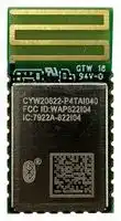


CYW20822P4TAI040XUMA1
Bluetooth Module, BLE 5.0, Class 2, 2 Mbps, -101 dBm, 1.1 to 3.3 V, -45 °C to 85 °C
- Manufacturer: INFINEON
- Product type: Bluetooth Modules & Adaptors
- SVHC: No SVHC (25-Jun-2025)
- Interfaces: I2C, SPI, UART
- Product Range: -
- Certifications: CE, FCC, ISED, MIC
- Bluetooth Class: Class 2
- Bluetooth Version: Bluetooth LE 5.0
- Supply Voltage Range: 1.1 V to 3.3 V
- Receiver Sensitivity Rx: -101 dBm
- Operating Temperature Range: -45 °C to 85 °C
| Delivery and price | |
|---|---|
| Units per pack | 250 |
| Price | 3.08 € |
| Current stock | 200+ |
| Lead time | 30 days |
## **CYW20822-P4TAI040, CYW20822-P4EPI040** A/™ **Bluetooth® Low Energy module** ## **General description** The Infineon CYW20822-P4xxI040 is a fully integrated Bluetooth® Low Energy wireless module. It includes an onboard crystal oscillator, passive components, flash memory, and the CYW20822 silicon device. CYW20822-P4xxI040 supports peripheral functions (ADC and PWM), UART, I[2] C, and SPI communication, and a PDM interface. CYW20822-P4xxI040 includes a royalty-free Bluetooth® stack compatible with Bluetooth® 5.0 core spec in a 20.2 × 10.5 × 2.3 mm package. CYW20822-P4xxI040 includes 1 MB of embedded flash memory and is pre-loaded with EZ-Serial firmware. CYW20822-P4xxI040 is fully qualified by Bluetooth® SIG and is targeted at applications requiring cost-optimized Bluetooth® wireless connectivity. CYW20822-P4xxI040 is offered in two certified versions: CYW20822-P4TAI040 and CYW20822-P4EPI040. CYW20822-P4TAI040 includes an integrated trace antenna. CYW20822-P4EPI040 supports an external antenna through a RF solder pad output. ## **Features** CYW20822-P4xxI040 provides all necessary components required to operate Bluetooth® Low Energy communication standards. - Proven ready-to-use hardware design - Cost optimized for applications without space constraints - Non-volatile memory for self-sufficient operation and over-the-air updates - Bluetooth® SIG listed with QDID and declaration ID - Fully certified module eliminates the time needed for design, development, and certification processes - Pre-loaded EZ-Serial firmware provides an easy-to-use command interface to configure and use the module ## • **Module description** - Module size: 20.2 × 10.5 × 2.3 mm - Bluetooth® 5.0 core specification qualified module - Declaration ID: **D065177** - Supports Bluetooth® 2 Mbps, 1 Mbps, 500 kbps, and 125 kbps - Supports Bluetooth® Low-Energy long-range (LE-LR) - Certified to FCC, ISED, MIC, and CE regulations - Castelated solder pad connections for ease-of-use - 1-MB embedded on-module serial flash memory - Up to 12 GPIOs - Temperature range: –45°C to +85°C - 16-MHz Arm® Cortex®-M0 microcontroller unit MCU - Maximum TX output power - +4 dBm for Bluetooth® Low Energy - Bluetooth® LE connection range of up to 250 meters at 4 dBm[[1]] - RX sensitivity: - Bluetooth® Low Energy: –101 dBm @ 125 kbps ## • **Power consumption** - Bluetooth® LE current consumption - RX current: 1.3 mA @ -95 dBm - TX current: 3 mA @ 0 dBm Please read the Important Notice and Warnings at the end of this document page 1 Datasheet www.infineon.com 002-38449 Rev. *C 2024-03-01 **Bluetooth® Low Energy module** ## Features • Retention: 2 µA @ 32 KB RAM Hibernation: 0.8 µA ## • **Functional capabilities** - 8 × 16-bit PWMs - 12 × GPIOs - Quadrature decoder - Analog comparator - 2× peripheral UART - 2× SPI - 2× I2C - ADC (10-bit application ADC with one differential input or three single-ended inputs) - Hardware security engine ## **Note** > 1. Connection range tested module-to-module in full line-of-sight environment, free of obstacles or interference sources with output power of +4 dBM @ 125 kbps. Actual range will vary based on end product design, environment, receive sensitivity, and transmit output power of the central device. Datasheet 002-38449 Rev. *C 2 2024-03-01 ## **Bluetooth® Low Energy module** Table of contents ## **Table of contents** **General description ...........................................................................................................................1 Features ...........................................................................................................................................1 Table of contents...............................................................................................................................3 1 Overview .......................................................................................................................................4** 1.1 Functional block diagram.......................................................................................................................................4 1.2 Module description.................................................................................................................................................4 1.2.1 Module dimensions and drawing........................................................................................................................4 **2 Pad connection interface.................................................................................................................6 3 Recommended host PCB layout........................................................................................................8 4 Functional description ..................................................................................................................11** 4.1 Power management unit (PMU)...........................................................................................................................11 4.1.1 PMU configurations ...........................................................................................................................................12 4.1.2 4.1.2 32.768 kHz Crystal.....................................................................................................................................13 **5 Pin assignments ...........................................................................................................................14** 5.1 CYW20822-P4XXI040 module pinout....................................................................................................................14 **6 Electrical characteristics ...............................................................................................................16 7 PCB antenna performance.............................................................................................................17** 7.1 Trace antenna specifications ...............................................................................................................................17 7.2 Trace antenna performance.................................................................................................................................17 **8 Environmental specifications ........................................................................................................18** 8.1 Environmental compliance..................................................................................................................................18 8.2 RF certification......................................................................................................................................................18 8.3 Safety certification................................................................................................................................................18 8.4 Environmental conditions....................................................................................................................................18 8.5 ESD and EMI protection........................................................................................................................................18 **9 Regulatory information.................................................................................................................19** 9.1 FCC.........................................................................................................................................................................19 9.2 ISED........................................................................................................................................................................20 9.3 European declaration of conformity....................................................................................................................21 9.4 MIC Japan..............................................................................................................................................................22 **10 Packaging ..................................................................................................................................23 11 Ordering information ..................................................................................................................25 12 Acronyms ...................................................................................................................................26 13 Document conventions................................................................................................................30** 13.1 Units of measure.................................................................................................................................................30 **14 References .................................................................................................................................31 Revision history ..............................................................................................................................32** Datasheet 002-38449 Rev. *C 3 2024-03-01 **Bluetooth® Low Energy module** Overview ## **1 Overview** ## **1.1 Functional block diagram** **Figure 1** illustrates CYW20822-P4xxI040 functional block diagram. **==> picture [317 x 148] intentionally omitted <==** **----- Start of picture text -----**<br> 2x UART<br>2x SPI<br>CYW20822<br>2x 12C<br>Silicon device<br>PDM<br>ADC<br>UP to 8 PWMs<br>Passive components 1 MB 16 MHz<br>UP to 12 GPIOs (RES, CAP, IND) Embedded flash XTAL<br>32kHz LPO_In<br>(mandatory)<br>**----- End of picture text -----**<br> ## **Figure 1 Functional block diagram (GPIOs)** ## **1.2 Module description** CYW20822-P4xxI040 module is a complete module designed to be soldered to the application’s main board. ## **1.2.1 Module dimensions and drawing** Infineon reserves the right to select components from various vendors to achieve the Bluetooth® module functionality. Such selections will still guarantee that all mechanical specifications and module certifications are maintained. Designs should be held within the physical dimensions shown in the mechanical drawings in **Figure 2** . All dimensions are in millimeters (mm). ## **Table 1 Module design dimensions** |**Table 1**<br>**Module design dimensions**|**Table 1**<br>**Module design dimensions**|| |---|---|---| |**Dimension item**||**Specification**| |Module dimensions|Length (X)<br>~~—~~|10.5 ± 0.15 mm| ||Width (Y)<br>~~—~~<br>~~OS~~|20.2 ± 0.15 mm| |Antenna connection location dimensions|Length (X)<br>~~OS~~|10.6 mm| ||Width (Y)<br>~~OS~~|6.35 mm| |PCB thickness|Height (H)<br>~~—~~|0.80 ± 0.05 mm| |Shield height|Height (H)<br>~~—~~|1.45-mm typical| |Maximum component height|Height (H)<br>~~OS~~|1.45-mm typical| |Total module thickness (bottom of module to highest<br>component)|Height (H)<br>~~oe~~|2.3-mm typical| Datasheet 002-38449 Rev. *C 4 2024-03-01 **Bluetooth® Low Energy module** Overview See **Figure 2** for the mechanical reference drawing for CYW20822-P4xxI040. **Figure 2 Module mechanical drawing** Datasheet 002-38449 Rev. *C 5 2024-03-01 **Bluetooth® Low Energy module** Pad connection interface ## **2 Pad connection interface** As shown in the bottom view of **Figure 2** , CYW20822-P4xxI040 connects to the host board via solder pads on the backside of the module. **Table 2** and **Figure 3** detail the solder pad length, width, and pitch dimensions of CYW20822-P4xxI040 module. ## **Table 2 Connection description** |**Part number**|**Name **|**Connections**|**Connection type**|**Pad length**<br>**dimension**|**Pad width**<br>**dimension**|**Pad pitch**| |---|---|---|---|---|---|---| |CYW20822-P4TAI040|SP|27|Solder pads|1.05 mm|0.7 mm|1.25 mm| |CYW20822-P4EPI040|SP|27|Solder pads|1.05 mm|0.7 mm|1.25 mm| ## **Figure 3 Solder pad dimensions (seen from bottom)** To maximize RF performance, the host layout should follow these recommendations: 1. Antenna Area Keepout: The host board directly below the antenna area of the module (see **Figure 2** ) must not contain ground or signal traces. This keepout area requirement applies to all layers of the host board. 2. Module Placement: The ideal placement of the Bluetooth® module is in a corner of the host board with the PCB trace antenna located at the far corner. This placement minimizes the additional recommended keepout area stated in item 2. See **AN96841** for module placement best practices. Datasheet 002-38449 Rev. *C 6 2024-03-01 ## **Bluetooth® Low Energy module** Pad connection interface **Figure 4 Recommended host PCB keepout area around the CYW20822-P4xxI040 antenna** Datasheet 002-38449 Rev. *C 7 2024-03-01 **Bluetooth® Low Energy module** Recommended host PCB layout ## **3 Recommended host PCB layout** **Figure 5** , **Figure 6** , **Figure 7** , and **Table 3** provide details that can be used for the recommended host PCB layout pattern for the CYW20822-P4xxI040. Dimensions are in millimeters unless otherwise noted. The pad length of 1.26 mm (0.64 mm from center of the pad on either side) shown in **Figure 4** is the minimum recommended host pad length. The host PCB layout pattern can be completed using either **Figure 5** , **Figure 6** , or **Figure 7** . It is not necessary to use all figures to complete the host PCB layout pattern. **Figure 5 CYW20822-P4xxI040 host layout (dimensioned)** **Figure 6 CYW20822-P4xxI040 host layout (relative to origin)** Datasheet 002-38449 Rev. *C 8 2024-03-01 ## **Bluetooth® Low Energy module** Recommended host PCB layout **Table 3** provides the center location for each solder pad on the CYW20822-P4xxI040. All dimensions are referenced to the center of the solder pad. See **Figure 7** for the location of each module solder pad. |**Solder pad**<br>**(center of pad)**|**Location (X,Y) from**<br>**origin (mm)**<br>~~ee~~|**Dimension from**<br>**origin (mil)**| |---|---|---| |1|(0, 7.10)<br>~~ee~~<br>~~—_.—~~|(0, 279.53)| |2|(0, 8.35)<br>~~>~~|(0, 328.74)| |3|(0, 9.6)<br>~~>~~|(0, 377.95)| |4|(0, 10.85)<br>~~>~~<br>~~—_.—~~|(0, 427.16)| |5|(0, 12.10)<br>~~>~~|(0, 476.38)| |6<br>~~—_~~|(0, 13.35)<br>~~>~~<br>~~—_~~|(0, 525.59)| |7<br>~~—_~~|(0, 14.60)<br>~~>~~<br>~~—_TT~~|(0, 574.80)| |8<br>~~—_~~|(0, 15.85)<br>~~—_~~<br>~~>~~|(0, 624.01)| |9<br>~~—_~~|(0, 17.10)<br>~~>~~<br>~~—_~~|(0, 673.23)| |10<br>~~—_~~|(0, 18.35)<br>~~>~~<br>~~—_TT~~|(0, 722.44)| |11<br>~~—_~~|(1.5,20.20)<br>~~—_~~<br>~~>~~|(59.06, 795.27)| |12<br>~~—_~~|(2.75,20.20)<br>~~>~~<br>~~—_~~|(108.27, 795.27)| |13<br>~~—_~~|(4.00,20.20)<br>~~—_TT~~|(157.48, 795.27)| |14<br>~~—_~~|(5.25,20.20)<br>~~—_~~<br>~~>~~|(206.69, 795.27)| |15<br>~~—_~~|(6.50,20.20)<br>~~>~~<br>~~—_~~|(255.91, 795.27)| |16<br>~~—_~~|(7.75,20.20)<br>~~—_TT~~|(305.12, 795.27)| |17<br>~~—_~~|(9.00,20.20)<br>~~—_~~<br>~~>~~|(354.33, 795.27)| |18<br>~~—_~~|(10.5,18.35)<br>~~>~~<br>~~—_~~|(413.39, 722.44)| |19<br>~~—_~~|(10.5,17.10)<br>~~—_TT~~|(413.39, 673.23)| |20<br>~~—_~~|(10.5,15.85)<br>~~—_~~<br>~~>~~|(413.39, 624.01)| |21<br>~~—_~~|(10.5,14.60)<br>~~>~~<br>~~—_~~|(413.39, 574.80)| |22<br>~~—_~~|(10.5,13.35)<br>~~—_TT~~|(413.39, 525.59)| |23<br>~~—_~~|(10.5,12.10)<br>~~—_~~<br>~~>~~|(413.39, 476.38)| |24<br>~~—_~~|(10.5,10.85)<br>~~>~~<br>~~—_~~|(413.39, 427.16)| |25<br>~~—_~~|(10.5,9.6)<br>~~—_TT~~|(413.39, 377.95)| |26<br>~~—_~~|(10.5,8.35)<br>~~—_~~<br>~~>~~|(413.39, 328.74)| |27|(10.5,7.10)<br>~~>~~|(413.39, 279.53)| Datasheet 002-38449 Rev. *C 9 2024-03-01 **Bluetooth® Low Energy module** Recommended host PCB layout **Figure 7 Solder pad reference location** Datasheet 002-38449 Rev. *C 10 2024-03-01 **Bluetooth® Low Energy module** Functional description ## **4 Functional description** CYW20822-P4XXI040 module is based on the CYW20822 SoC, which includes a Bluetooth® 5 solution and an RF wakeup receiver. The block diagram of the CYW20822-P4XXI040 module is shown in **Figure 8** . **Figure 8 Module block diagram** ## **4.1 Power management unit (PMU)** The PMU provides I/O power supplies to the CYW20822 module. It generates power supply outputs: VDDIOP, and an auxiliary supply VAUX used internally by the PMU (see **Table 4** ). **Table 4 PMU external pins** |**Pin**|**Description**| |---|---| |VBATT|Battery input. Battery voltages from 1.1 V to 3.3 V can be used. Must be connected to a<br>battery or external supply.| |VDDIOP|VDDIOPis PMU generated 1.8 V IO supply output| |VAUX|Auxiliary supply output of typical value 3.2 V, used internally by the PMU| |VDDIO|Power supply input for digital and analog I/O circuits| The PMU provides multiple brownout interrupts to enable more reliable operation. Datasheet 002-38449 Rev. *C 2024-03-01 11 **Bluetooth® Low Energy module** Functional description ## **4.1.1 PMU configurations** Configure the PMU correctly to ensure correct operation. The following modes of operation are supported by the PMU: - One external power supply or battery with external I/O supply: - For applications that cannot support fixed 1.8 V I/O supply (see **Figure 9** ). - Connect VBATT to VDDIO - Connect VAUX to VDDIOP - Disable I/O supply generation GPIO voltage = VBATT VBATT min = 1.8 V VBATT max = 3.3 V ## **Figure 9 Regular battery, External I/O supply** - One external power supply or battery with internally generated I/O supply: - For applications that can use a fixed 1.8 V I/O supply for better power consumption or VBATT ≤ 1.8 V (see **Figure 10** ). - Connect VDDIOP to VDDIO GPIO voltage = 1.8 V VBATT min = 1.1 V VBATT max = 3.3 V **Figure 10 Regular battery, internal I/O supply** Datasheet 002-38449 Rev. *C 12 2024-03-01 ## **Bluetooth® Low Energy module** Functional description ## **4.1.2 4.1.2 32.768 kHz Crystal** The 32.768 kHz crystal MUST be used, ECS-.327-7-12R-TR from ECS (+/-20 ppm tolerance, 7 pF load capacitance, 70 kΩ maximum ESR) or alternate parts with same parameters. Datasheet 002-38449 Rev. *C 13 2024-03-01 **Bluetooth® Low Energy module** Pin assignments ## **5 Pin assignments** ## **5.1 CYW20822-P4XXI040 module pinout** **Figure 11 Module pin definition** ## **Table 5 Pin type definitions** |**Table 5**<br>**Pin type definitions**|| |---|---| |**Pin type**|**Definition**| |I/O|Signal input output| |RF|Radio frequency| |PWR|Power supply| |A|Analog| |NC|No connection, must be open| |GND|Ground| Datasheet 002-38449 Rev. *C 2024-03-01 14 ## **Bluetooth® Low Energy module** Pin assignments |**Pin number**|**Name**<br>~~eee~~<br>~~eee~~|**Type**<br>~~eee~~<br>~~eee~~|**Description**<br>~~eee~~<br>~~eee~~| |---|---|---|---| |1|GND<br>~~eee ~~<br>~~eee~~|PWR<br> ~~eee~~<br>~~eee~~|Ground reference<br>~~eee~~<br>~~eee~~| |2|WURX<br>~~eee ~~<br>~~eee~~<br>~~eee~~|RF<br> ~~eee~~<br>~~eee~~<br>~~eee~~|Wakeup receiver RF input<br>~~eee~~<br>~~eee~~| |3|VBATT<br>~~eee~~<br>~~eee~~|PWR<br>~~eee~~<br>~~eee~~|Battery supply<br>~~eee~~| |4|P11<br>~~eee ~~<br>~~of~~|I/O<br> ~~eee~~<br>~~of~~|Programmable digital I/O<br>ADC Input<br>The default definition is UART0_CTS<br>~~eee~~| |5|P10<br>~~of~~|I/O<br>~~of~~|Programmable Digital I/O<br>ADC input<br>The default definition is SPIO_CS.| |6|P9<br>~~of~~|I/O<br>~~of~~|Programmable digital I/O<br>ADC Input<br>The default definition is I2C0_SCK| |7|PWD<br>~~FT~~|I/O<br>~~FT~~|Power down input (Active High)<br>Must connect to a 1 MΩ pull-down resistor| |8|SWD_CLK<br>~~——~~|I/O<br>~~——~~|Serial wire debug clock| |9|SWD_IO<br>~~——~~<br>~~ee~~|I/O<br>~~——~~<br>~~eee~~|Serial wire debug data<br>~~eee~~| |10|GND<br>~~ee~~<br>~~eee~~|PWR<br>~~eee~~<br>~~eee~~|Ground reference<br>~~eee~~<br>~~eee~~| |11|VDDIO<br>~~ee ~~<br>~~eee~~|PWR<br> ~~eee~~<br>~~eee~~|Digital I/O power supply input<br>~~eee~~<br>~~eee~~| |12|VDDIOP<br>~~eee ~~<br>~~FT~~|PWR<br> ~~eee~~<br>~~FT~~|1.8 V I/O power supply output generated by switcher, connected to VAUX if<br>unused<br>~~eee~~| |13|VAUX<br>~~——~~|PWR<br>~~——~~|Reserved for switching regulator internal use| |14|XTALO_32k<br>~~——~~<br>~~eee~~|A<br>~~——~~<br>~~eee~~|32.768 kHz crystal oscillator output<br>~~eee~~| |15|XTALI_32k<br>~~eee~~|A<br>~~eee~~|32.768 kHz crystal oscillator input<br>~~eee~~| |16|P13<br>~~eee ~~<br>~~FT~~|I/O<br> ~~eee~~<br>~~FT~~|Programmable digital I/O<br>The default definition is SPI0_MISO<br>~~eee~~| |17|P20<br>~~FT~~|I/O<br>~~FT~~|Programmable digital I/O<br>The default definition is SPIO_CLK.| |18|GND<br>~~eee~~|PWR<br>~~eee~~|Ground reference| |19|P22<br>~~FT~~|I/O<br>~~FT~~|Programmable digital I/O<br>The default definition is SPIO_MOSI| |20|P23<br>~~FT~~|I/O<br>~~FT~~|Programmable digital I/O<br>The default definition is UART0_TX| |21|P24<br>~~FT~~|I/O<br>~~FT~~|Programmable digital I/O<br>The default definition is UART0_RTS| |22|P25<br>~~FT~~|I/O<br>~~FT~~|Programmable digital I/O<br>The default definition is UART0_RX| |23|P30<br>~~FT~~|I/O<br>~~FT~~|Programmable digital I/O<br>The default definition is I2C0_SDA| |24|P32<br>~~FT~~|I/O<br>~~FT~~|Programmable digital I/O<br>BBoot , must connect to a 1 MΩ pull-down resistor| |25|P33<br>~~FT~~<br>~~eee~~|I/O<br>~~FT~~<br>~~eee~~|Programmable digital I/O<br>The default definition is UART1_TX, to provide SW debug message output<br>~~eee~~| |26|GND<br>~~eee~~|PWR<br>~~eee~~|Ground reference<br>~~eee~~| |27|NC (RFIO)<br>~~eee ~~<br>~~of~~|NC<br> ~~eee~~<br>~~of~~|No connection<br>Reserved for 2.4 GHz Single-ended RF I/O for Bluetooth® radio external<br>antenna connection (50 Ω)<br>~~eee~~| Datasheet 002-38449 Rev. *C 15 2024-03-01 **Bluetooth® Low Energy module** Electrical characteristics ## **Electrical characteristics** |**Electrical characteristics**|**Electrical characteristics**|||||||| |---|---|---|---|---|---|---|---|---| |**6**<br>**Electrical characteristics**|**Electrical characteristics**|||||||| |**Table 7**<br>**Maximum electrical ratings**||||||||| |**Parameter**<br>**Description**<br>**Min**<br>**Typ**<br>**Max**<br>**Unit**<br>VBATT<br>Battery supply[2]<br>–0.2<br>–<br>3.4<br>V<br>VDDIO<br>I/O supply<br>–0.2<br>–<br>3.4<br>V<br>VIO<br>I/O pin<br>–0.2<br>–<br>3.4<br>V<br>TSTORE<br>Storage temperature<br>–40<br>–<br>+85<br>°C<br>~~cess~~||||||||| |**Table 8**<br>**Recommended operating conditions**||||||||| |**Parameter**<br>**Description**<br>**Min**<br>**Typ**<br>**Max**<br>**Unit**<br>VDDIO<br>I/O supply<br>1.7<br>1.8<br>3.3<br>V<br>VBATT<br>Battery supply<br>1.1[3]<br>–<br>3.3<br>V<br>VPP25<br>OTP programmingvoltage[4]<br>2.3<br>2.5<br>2.7<br>V<br>VIO<br>I/O pin<br>–0.2<br>VDDIO+ 0.2<br>V<br>Crystal Osc - 32.768 kHz<br>–500<br>500<br>ppm<br>TJ<br>Operatingjunction temperature<br>–40<br>25<br>+85<br>°C<br>~~ceoeee~~||||||||| |**Table 9**<br>**GPIO characteristics**||||||||| |**Parameter**<br>**Description**<br>**Min**<br>**Typ**<br>**Max**<br>**Unit**<br>VIH<br>Input<br>VIO–0.5<br>VIO<br>VIO<br>V<br>VIL<br>Input<br>–0.2<br>0<br>0.2<br>VOH<br>Output (2 mA load)<br>–<br>VIO–0.2<br>–<br>VOL<br>Output (2 mA load)<br>–<br>0.2<br>–<br>~~ceee~~||||||||| |**Table 10**<br>**Power consumption**||||||||| |**Parameter**<br>**Conditions**||**Min**|**Typ**|||**Max**||**Unit**| |Active RX<br>Sensitivity at -95 dBm||–|1.3|||–||mA| |Active TX @ 4 dBm<br>Output power at 4 dBm||–|4|||–||mA| |Active TX @ 0 dBm<br>Output power at 0 dBm||–|3|||–||mA| |Active TX @ -10 dBm<br>Output power at -10 dBm||–|1.4|||–||mA| |Retention (32-KB RAM)<br>1-second connection interval in||–|2|||–||μA| |low power idle mode||||||||| |Hibernation<br>–||–|0.8|||–||μA| |Hibernation with wakeup||–|0.95|||–||μA| |receiver||||||||| |SoC off||–|300|||–||μA| ## **Notes** 2. VBATT minimum slew rate is 0.3 V/ms. 3. VBATT minimum supply after boot is 1.0 V. 4. VPP25 is physically connected to VDDIO. Set VDDIO to within VPP25 range when programming the OTP. Datasheet 002-38449 Rev. *C 2024-03-01 16 **Bluetooth® Low Energy module** PCB antenna performance ## **7 PCB antenna performance** ## **7.1 Trace antenna specifications** |**Item**|**Description**| |---|---| |Frequency range|2400-2500 MHz| |Peak gain|4.21-dBi typical| |Return loss|10 dB minimum| ## **7.2 Trace antenna performance** **Figure 12 CYW20822-P4XXI040 PCB antenna radiation pattern and characteristics** ## **External antenna performance** **Table 7-1 External antenna performance: pulse W1010** |**External antenna performance: pulse W1010**|**External antenna performance: pulse W1010**|**External antenna performance: pulse W1010**||| |---|---|---|---|---| |**Gain (dBi)**|**Impedance (nom)**|**VSWR**|**Polarization**|**Electric length**| |2|50 Ω|≤ 2.0|Vertical|1/4, Di-pole| Datasheet 002-38449 Rev. *C 17 2024-03-01 **Bluetooth® Low Energy module** Environmental specifications ## **8 Environmental specifications** ## **8.1 Environmental compliance** CYW20822-P4xxI040 Bluetooth® LE module is produced in compliance with the Restriction of Hazardous substances (RoHS) and halogen-free (HF) directives. The Infineon module and components used to produce this module are RoHS and HF-compliant. ## **8.2 RF certification** CYW20822-P4xxI040 module will be certified under the following RF certification standards at production release. - FCC: WAP822I04 - CE - ISED: 7922A-822I04 - MIC: 218-230142 ## **8.3 Safety certification** CYW20822-P4xxI040 module complies with the following safety regulations: - Underwriters Laboratories, Inc. (UL): Filing E331901 - CSA - TUV ## **8.4 Environmental conditions** **Table 11** describes the operating and storage conditions for the Bluetooth® LE module. |**Description**<br>~~——~~<br>~~—~~|**Minimum specification**<br>~~——~~<br>~~—~~|**Maximum specification**| |---|---|---| |Operatingtemperature<br>~~—~~|–45°C<br>~~—~~|85°C| |Operatinghumidity (relative, non-condensation)<br>~~—ST~~|5%<br>~~—ST~~|85%| |Thermal ramp rate<br>~~oy~~|–<br>~~oy~~|3°C/minute| |Storage temperature<br>~~oy~~<br>~~oo~~<br>~~—~~|–40 °C<br>~~oy~~<br>~~oo~~<br>~~—~~|85°C| |Storage temperature and humidity<br>~~—~~|–<br>~~—~~|85°C at 85%| |ESD: Module integrated into end system<br>components[5]<br>~~—a~~|–<br>~~—a~~|15 kV Air<br>2.0 kV Contact| ## **8.5 ESD and EMI protection** The exposed components require special attention to ESD and electromagnetic interference (EMI). A grounded conductive layer inside the device enclosure is suggested for EMI and ESD performance. Any openings in the enclosure near the module should be surrounded by a grounded conductive layer to provide ESD protection and a low-impedance path to ground. **Device handling** : Proper ESD protocol must be followed in manufacturing to ensure component reliability. 5. This does not apply to the RF pins (ANT). **Note** Datasheet 002-38449 Rev. *C 18 2024-03-01 **Bluetooth® Low Energy module** Regulatory information ## **9 Regulatory information** ## **9.1 FCC** ## FCC NOTICE: The device CYW20822-P4xxI040 complies with Part 15 of the FCC Rules. The device meets the requirements for modular transmitter approval as detailed in FCC public Notice DA00-1407.transmitter Operation is subject to the following two conditions: (1) This device may not cause harmful interference, and (2) This device must accept any interference received, including interference that may cause undesired operation. ## CAUTION: The FCC requires the user to be notified that any changes or modifications made to this device that are not expressly approved by Infineon may void the user’s authority to operate the equipment. This equipment has been tested and found to comply with the limits for a Class B digital device, pursuant to Part 15 of the FCC Rules. These limits are designed to provide reasonable protection against harmful interference in a residential installation. This equipment generates uses and can radiate radio frequency energy and, if not installed and used in accordance with the instructions, may cause harmful interference to radio communications. However, there is no guarantee that interference will not occur in a particular installation. If this equipment does cause harmful interference to radio or television reception, which can be determined by turning the equipment off and on, the user is encouraged to try to correct the interference by one or more of the following measures: - Reorient or relocate the receiving antenna. - Increase the separation between the equipment and receiver. - Connect the equipment into an outlet on a circuit different from that to which the receiver is connected. - Consult the dealer or an experienced radio/TV technician for help This module is only FCC authorized for the specific rule FCC 15.247 listed on the grant, and that the host product manufacturer is responsible for compliance to any other FCC rules that apply to the host not covered by the modular transmitter grant of certification, final host product requires Part 15 Subpart B compliance testing with the modular transmitter installed. ## LABELING REQUIREMENTS: The Original Equipment Manufacturer (OEM) must ensure that FCC labeling requirements are met. This includes a clearly visible label on the outside of the OEM enclosure specifying the appropriate Infineon FCC identifier for this product as well as the FCC Notice above. The FCC identifier is FCC ID: WAP822I04. In any case the end product must be labeled exterior with “Contains FCC ID: WAP822I04”. ## ANTENNA WARNING: This device is tested with a standard SMA connector and with the antenna listed in **Table 7** . When integrated in the OEMs product, these fixed antennas require installation preventing end-users from replacing them with non-approved antennas. Any antenna not in the following table must be tested to comply with FCC Section 15.203 for unique antenna connectors and Section 15.247 for emissions. Datasheet 002-38449 Rev. *C 19 2024-03-01 **Bluetooth® Low Energy module** Regulatory information ## RF EXPOSURE: To comply with FCC RF Exposure requirements, the Original Equipment Manufacturer (OEM) must ensure to install the approved antenna in the previous. The preceding statement must be included as a CAUTION statement in manuals, for products operating with the approved antenna in **Table 7** , to alert users on FCC RF Exposure compliance. Any notification to the end user of installation or removal instructions about the integrated radio module is not allowed. The radiated output power of CYW20822-P4xxI040 with the trace antenna is far below the FCC radio frequency exposure limits. Nevertheless, use CYW20822-P4xxI040 in such a manner that minimizes the potential for human contact during normal operation. SAR is not required for this module if the distance is greater than 10 mm from the user. End users may not be provided with the module installation instructions. OEM integrators and end users must be provided with transmitter operating conditions for satisfying RF exposure compliance. This equipment complies with FCC radiation exposure limits set forth for an uncontrolled environment. This equipment should be installed and operated with minimum distance 10 mm between the radiator and your body. ## **9.2 ISED** ## **Innovation, Science and Economic Development Canada (ISED) Certification** CYW20822-P4xxI040 is licensed to meet the regulatory requirements of Innovation, Science and Economic Development Canada (ISED), License: IC: 7922A-822I04 Manufacturers of mobile, fixed, or portable devices incorporating this module are advised to clarify any regulatory questions and ensure compliance for SAR and/or RF exposure limits. Users can obtain Canadian information on RF exposure and compliance from **www.ic.gc.ca** . This device has been designed to operate with the antennas listed in **Table 7** , having a maximum gain of –0.5 dBi. Antennas not included in this list or having a gain greater than –0.5 dBi are strictly prohibited for use with this device. The required antenna impedance is 50 ohms. The antenna used for this transmitter must not be co-located or operating in conjunction with any other antenna or transmitter. ## ISED NOTICE: The device CYW20822-P4xxI040 including the built-in trace antenna complies with Canada RSS-GEN Rules. The device meets the requirements for modular transmitter approval as detailed in RSS-GEN. Operation is subject to the following two conditions: (1) This device may not cause harmful interference, and (2) This device must accept any interference received, including interference that may cause undesired operation. L'appareil CYW20822-P4xxI040, y compris l'antenne intégrée, est conforme aux Règles RSS-GEN de Canada. L'appareil répond aux exigences d'approbation de l'émetteur modulaire tel que décrit dans RSS-GEN. L'opération est soumise aux deux conditions suivantes: (1) Cet appareil ne doit pas causer d'interférences nuisibles, et (2) Cet appareil doit accepter toute interférence reçue, y compris les interférences pouvant entraîner un fonctionnement indésirable. ## ISED INTERFERENCE STATEMENT FOR CANADA The antenna of this transmitter must provide a separation distance of at least 10 mm from all persons. Installers and end-users must be provided with antenna installation instructions and transmitter operating conditions and instructions for satisfying RF exposure compliance. Compliance of this device in all final product configurations is the responsibility of the Grantee. Installation of this device into specific final products may require the submission of a Class II permissive change application, containing data pertinent to RF Exposure, emissions and host/module authentication, or new appli- Datasheet 002-38449 Rev. *C 2024-03-01 20 **Bluetooth® Low Energy module** Regulatory information cation if appropriate. The final product operating with this transmitter must include operating instructions and antenna installation instructions, for end-users and installers to satisfy RF exposure compliance requirements. L'antenne de cet émetteur doit fournir une distance de séparation d'au moins 10 mm par rapport à toutes les personnes. Les installateurs et les utilisateurs finaux doivent recevoir les instructions d'installation de l'antenne ainsi que les conditions d'utilisation de l'émetteur et les instructions pour satisfaire à la conformité à l'exposition aux radiofréquences. La conformité de cet appareil dans toutes les configurations de produit final est la responsabilité du bénéficiaire. L'installation de cet appareil dans des produits finaux spécifiques peut nécessiter la soumission d'une demande de modification permissive de classe II, contenant des données pertinentes sur l'exposition RF, les émissions et l'authentification hôte / module, ou une nouvelle application, le cas échéant. Le produit final fonctionnant avec cet émetteur doit inclure des instructions d'utilisation et des instructions d'installation de l'antenne, pour les utilisateurs finaux et les installateurs afin de satisfaire aux exigences deconformité en matière d'exposition aux RF. Cet appareil est conforme à la norme sur l'innovation, la science et le développement économique (ISED) norme RSS exempte de licence. L'exploitation est autorisée aux deux conditions suivantes : (1) l'appareil ne doit pas produire de brouillage, et (2) l'utilisateur de l'appareil doit accepter tout brouillage radioélectrique subi, même si le brouillage est susceptible d'en compromettre le fonctionnement. ## ISED RADIATION EXPOSURE STATEMENT FOR CANADA This equipment complies with ISED radiation exposure limits set forth for an uncontrolled environment. This equipment should be installed and operated with a minimum distance of 15 mm between the radiator and your body. Cet équipement est conforme aux limites d'exposition aux radiations ISED prévues pour un environnement incontrôlé. Cet équipement doit être installé et utilisé avec un minimum de 15 mm de distance entre la source de rayonnement et votre corps. ## LABELING REQUIREMENTS: The Original Equipment Manufacturer (OEM) must ensure that ISED labeling requirements are met. This includes a clearly visible label on the outside of the OEM enclosure specifying the appropriate Infineon IC identifier for this product as well as the ISED Notices above. The IC identifier is 7922A-822I04. In any case, the end product must be labeled in its exterior with “Contains IC: 7922A-822I04“ ## **9.3 European declaration of conformity** Hereby, Infineon declares that the Bluetooth® module CYW20822-P4xxI040 complies with the essential requirements and other relevant provisions of Directive 2014. As a result of the conformity assessment procedure described in Annex III of the Directive 2014, the end-customer equipment should be labeled as follows: All versions of the CYW20822-P4xxI040 in the specified reference design can be used in the following countries: Austria, Belgium, Cyprus, Czech Republic, Denmark, Estonia, Finland, France, Germany, Greece, Hungary, Ireland, Italy, Latvia, Lithuania, Luxembourg, Malta, Poland, Portugal, Slovakia, Slovenia, Spain, Sweden, The Netherlands, the United Kingdom, Switzerland, and Norway. Datasheet 002-38449 Rev. *C 21 2024-03-01 **Bluetooth® Low Energy module** Regulatory information ## **9.4 MIC Japan** CYW20822-P4xxI040 is certified as a module (certification number 218-230142). End products that integrate CYW20822-P4xxI040 do not need additional MIC Japan certification for the end product. End product can display the certification label of the embedded module. **Figure 13 MIC label** Datasheet 002-38449 Rev. *C 22 2024-03-01 **Bluetooth® Low Energy module** Packaging ## **10 Packaging** ## **Table 12 Solder reflow peak temperature** |**Module part**<br>**number**|**Package**|**Maximum peak**<br>**temperature**|**Maximum time at peak**<br>**temperature**|**No. of cycles**| |---|---|---|---|---| |CYW20822-P4TAI040|27-pad SMT|260°C|30 s|2| |CYW20822-P4EPI040|27-pad SMT|260°C|30 s|2| |**Table 13**<br>**Package moisture sensitivity level (MSL), IPC/JEDEC J-STD-2**|**Table 13**<br>**Package moisture sensitivity level (MSL), IPC/JEDEC J-STD-2**|**Table 13**<br>**Package moisture sensitivity level (MSL), IPC/JEDEC J-STD-2**| |---|---|---| |**Module part number**|**Package**|**MSL**| |CYW20822-P4TAI040|27-pad SMT|MSL 3| |CYW20822-P4EPI040|27-pad SMT|MSL 3| The CYW20822-P4xxI040 is offered in tape and reel packaging. **Figure 14** details the tape dimensions used for the CYW20822-P4xxI040. **Figure 14 CYW20822-P4xxI040 tape dimensions** **Figure 15** details the orientation of the CYW20822-P4xxI040 in the tape as well as the direction for unreeling. **Figure 15** **==> picture [268 x 12] intentionally omitted <==** **----- Start of picture text -----**<br> Component orientation in tape and unreeling direction<br>**----- End of picture text -----**<br> Datasheet 002-38449 Rev. *C 23 2024-03-01 **Bluetooth® Low Energy module** Packaging **Figure 16** details reel dimensions used for the CYW20822-P4xxI040. **Figure 16 Reel dimensions** Datasheet 002-38449 Rev. *C 24 2024-03-01 **Bluetooth® Low Energy module** Ordering information ## **11 Ordering information** **Table 14** lists the CYW20822-P4xxI040 part number and features. **Table 15** lists the reel shipment quantities for the CYW20822-P4xxI040. ## **Table 14 Ordering information** |**CPU**<br>**speed**<br>**(MHz)**|**Flash**<br>**size**<br>**(MB)**|**RAM**<br>**size**<br>**(KB)**|**UART**|**I2C **|**PWM**|**Antenna **|**Package **| |---|---|---|---|---|---|---|---| |16|1|128|Yes|Yes|8|Trace|27-SMT| |16|1|128|Yes|Yes|8|Pad|27-SMT| ## **Table 15 Tape and reel package quantity and minimum order amount** |**Description**|**Minimum**<br>**reel quantity**|**Maximum**<br>**reel quantity**|**Comments**| |---|---|---|---| |Reel quantity|500|500|Ships in 500 unit reel quantities| |Minimum order<br>quantity (MOQ)|500|–|–| |Order increment (OI)|500|–|–| CYW20822-P4xxI040 is offered in tape and reel packaging. CYW20822-P4xxI040 ships in a reel size of 500. Datasheet 002-38449 Rev. *C 25 2024-03-01 **Bluetooth® Low Energy module** Acronyms ## **12 Acronyms** |**Acronym**|**Description**| |---|---| |ADC|analog-to-digital converter| |ADV|advertising| |ALU|arithmetic logic unit| |AMUXBUS|analog multiplexer bus| |API|application programminginterface| |Arm®|advanced RISC machine, a CPU architecture| |BLE|Bluetooth® Low Energy| |Bluetooth® SIG|Bluetooth® Special Interest Group| |BW|bandwidth| |CAN|Controller Area Network, a communications protocol| |CE|European Conformity| |CMRR|common-mode rejection ratio| |CPU|central processingunit| |CRC|cyclic redundancy check, an error-checkingprotocol| |CSA|Canadian Standards Association| |ECC|error correctingcode| |ECO|external crystal oscillator| |EEPROM|electrically erasable programmable read-only memory| |EMI|electromagnetic interference| |EMIF|external memory interface| |EOC|end of conversion| |EOF|end of frame| |ESD|electrostatic discharge| |FCC|Federal Communications Commission| |FET|field-effect transistor| |FIR|finite impulse response, see also IIR| |FPB|flash patch and breakpoint| |FS|full-speed| |GPIO|general-purpose input/output, applies to a PSoC pin| |HCI|host controller interface| |HVI|high-voltage interrupt, see also LVI, LVD| |I/O|input/output, see also GPIO, DIO, SIO, USBIO| |I2C, or IIC|Inter-Integrated Circuit, a communications protocol| |IC|integrated circuit| |IC|Industry Canada| |IDAC|current DAC, see also DAC, VDAC| |IDE|integrated development environment| |IIR|infinite impulse response, see also FIR| Datasheet 002-38449 Rev. *C 26 2024-03-01 ## **Bluetooth® Low Energy module** Acronyms **Table 16 Acronyms used in this document** _(continued)_ |**Acronym**|**Description**| |---|---| |ILO|internal low-speed oscillator, see also IMO| |IMO|internal main oscillator, see also ILO| |INL|integral nonlinearity, see also DNL| |IPOR|initial power-on reset| |IPSR|interrupt program status register| |IRQ|interrupt request| |ITM|instrumentation trace macrocell| |KC|Korea Certification| |LCD|liquid crystal display| |LIN|Local Interconnect Network, a communications protocol.| |LNA|low noise amplifier| |LR|link register| |LUT|lookup table| |LVD|low-voltage detect, see also LVI| |LVI|low-voltage interrupt, see also HVI| |LVTTL|low-voltage transistor-transistor logic| |MAC|multiply-accumulate| |MCU|microcontroller unit| |MIC|Ministry of Internal Affairs and Communications (Japan)| |MISO|master-in slave-out| |NC|no connect| |NMI|nonmaskable interrupt| |NRZ|non-return-to-zero| |NVIC|nested vectored interrupt controller| |NVL|nonvolatile latch, see also WOL| |Opamp|operational amplifier| |PA|power amplifier| |PAL|programmable array logic, see also PLD| |PC|program counter| |PCB|printed circuit board| |PGA|programmable gain amplifier| |PHUB|peripheral hub| |PHY|physical layer| |PICU|port interrupt control unit| |PLA|programmable logic array| |PLD|programmable logic device, see also PAL| |PLL|phase-locked loop| |PMDD|package material declaration data sheet| |POR|power-on reset| |PRES|precise power-on reset| Datasheet 002-38449 Rev. *C 27 2024-03-01 ## **Bluetooth® Low Energy module** Acronyms **Table 16 Acronyms used in this document** _(continued)_ |**Acronym**|**Description**| |---|---| |PRS|pseudo random sequence| |PS|port read data register| |PSoC®|Programmable System-on-Chip| |PSRR|power supply rejection ratio| |PWM|pulse-width modulator| |QDID|qualification design ID| |RAM|random-access memory| |RISC|reduced-instruction-set computing| |RMS|root-mean-square| |RTC|real-time clock| |RTL|register transfer language| |RTR|remote transmission request| |RX|receive| |S/H|sample and hold| |SAR|successive approximation register| |SC/CT|switched capacitor/continuous time| |SCL|I2C serial clock| |SDA|I2C serial data| |SINAD|signal to noise and distortion ratio| |SIO|special input/output, GPIO with advanced features. See GPIO.| |SMT|surface-mount technology; a method for producing electronic circuitry in which the<br>components are placed directly onto the surface of PCBs| |SOC|start of conversion| |SOF|start of frame| |SPI|Serial Peripheral Interface, a communications protocol| |SR|slew rate| |SRAM|static random access memory| |SRES|software reset| |STN|super twisted nematic| |SWD|serial wire debug, a test protocol| |SWV|single-wire viewer| |TD|transaction descriptor, see also DMA| |THD|total harmonic distortion| |TIA|transimpedance amplifier| |TN|twisted nematic| |TRM|technical reference manual| |TTL|transistor-transistor logic| |TUV|Germany: Technischer Überwachungs-Verein (Technical Inspection Association)| |TX|transmit| |UART|Universal Asynchronous Transmitter Receiver, a communications protocol| Datasheet 002-38449 Rev. *C 28 2024-03-01 ## **Bluetooth® Low Energy module** Acronyms **Table 16 Acronyms used in this document** _(continued)_ |**Acronym**|**Description**| |---|---| |UDB|universal digital block| |USB|Universal Serial Bus| |USBIO|USB input/output, PSoC pins used to connect to a USB port| |VDAC|voltage DAC, see also DAC, IDAC| |WDT|watchdogtimer| |WOL|write once latch, see also NVL| |WRES|watchdogtimer reset| |XRES|external reset I/O pin| |XTAL|crystal| Datasheet 002-38449 Rev. *C 2024-03-01 29 **Bluetooth® Low Energy module** Document conventions |**13**|**Document conventions**|**Document conventions**| |---|---|---| |**13.1**|**Units of measure**|| |**Table 17**|**Units of measure**|| |**Symbol**||**Unit of measure**| |°C||degrees celsius| |dB||decibel| |dBm||decibel-milliwatts| |fF||femtofarads| |Hz||hertz| |KB||1024 bytes| |kbps||kilobits per second| |Khr||kilohour| |kHz||kilohertz| |k||kilo ohm| |ksps||kilosamples per second| |LSB||least significant bit| |Mbps||megabits per second| |MHz||megahertz| |M||mega-ohm| |Msps||megasamples per second| |µA||microampere| |µF||microfarad| |µH||microhenry| |µs||microsecond| |µV||microvolt| |µW||microwatt| |mA||milliampere| |ms||millisecond| |mV||millivolt| |nA||nanoampere| |ns||nanosecond| |nV||nanovolt| |||ohm| |pF||picofarad| |ppm||parts per million| |ps||picosecond| |s||second| |sps||samples per second| |sqrtHz||square root of hertz| |V||volt| Datasheet 002-38449 Rev. *C 30 2024-03-01 **Bluetooth® Low Energy module** References ## **14 References** Infineon provides a wealth of data at **www.infineon.com** to help you to select the right module for your design, and to help you to quickly and effectively integrate the module into your design. - Module: - **CYW20822-P4TAI040** - **CYW20822-P4EPI040** - Development kits: - **CYW920822M2P4TAI040-EVK** , CYW20822-P4TAI040 evaluation board - **CYW920822M2P4EPI040-EVK** , CYW20822-P4EPI040 evaluation board - EZ-Serial firmware: - User guide of EZ-Serial firmware for CYW20822-P4xxI040 - Knowledge base articles - **KBA97095** - AIROC™ Bluetooth® module placement - **KBA213976** - FAQ for Bluetooth® LE and regulatory certifications with EZ-BLE modules - **KBA210802** - Queries on Bluetooth® LE qualification and declaration processes - **KBA218122** - 3D Model Files for EZ-BLE/EZ-BT modules - Technical support Visit **Infineon community** the developer community offers you a place to learn, share, and engage with both Infineon experts and other embedded engineers around the world. Visit our **support** page and contact a **local sales representatives** . Datasheet 002-38449 Rev. *C 2024-03-01 31 **Bluetooth® Low Energy module** Revision history ## **Revision history** |**Document**<br>**revision**|**Date**|**Description of changes**| |---|---|---| |*B|2023-10-12|Publish to web.| |||Updated the following:| |*C|2024-03-01|• **General description**| |||• **Module description**| |||• **References**| Datasheet 002-38449 Rev. *C 32 2024-03-01 ## **Trademarks** All referenced product or service names and trademarks are the property of their respective owners. The Bluetooth® word mark and logos are registered trademarks owned by Bluetooth SIG, Inc., and any use of such marks by Infineon is under license. ## **IMPORTANT NOTICE** ## **WARNINGS** **Edition 2024-03-01** The information given in this document shall in no Due to technical requirements products may contain event be regarded as a guarantee of conditions or dangerous substances. For information on the types **Published by** characteristics (“Beschaffenheitsgarantie”). in question please contact your nearest Infineon Technologies office. **Infineon Technologies AG** With respect to any examples, hints or any typical values stated herein and/or any information Except as otherwise explicitly approved by Infineon **81726 Munich, Germany** regarding the application of the product, Infineon Technologies in a written document signed by Technologies hereby disclaims any and all authorized representatives of Infineon warranties and liabilities of any kind, including Technologies, Infineon Technologies’ products may without limitation warranties of non-infringement of not be used in any applications where a failure of the **© 2024 Infineon Technologies AG.** intellectual property rights of any third party. product or any consequences of the use thereof can reasonably be expected to result in personal injury. **All Rights Reserved.** In addition, any information given in this document is subject to customer’s compliance with its **Do you have a question about this** obligations stated in this document and any **document?** applicable legal requirements, norms and standards concerning customer’s products and any use of the **Email:** product of Infineon Technologies in customer’s **erratum@infineon.com** applications. The data contained in this document is exclusively **Document reference** intended for technically trained staff. It is the responsibility of customer’s technical departments **002-38449 Rev. *C** to evaluate the suitability of the product for the intended application and the completeness of the product information given in this document with respect to such application.
Updated at April 28, 2026
Infineon Technologies is a globally recognized leader in semiconductor solutions, renowned for driving innovation in power management, energy efficiency, and modern mobility. With a strong legacy of engineering excellence, the company provides highly reliable components designed to meet the rigorous demands of industrial, automotive, and advanced commercial applications. The core of our Infineon portfolio is centered on their industry-leading discrete semiconductors. We offer an extensive selection of single and dual MOSFETs, alongside a robust range of single IGBTs and advanced IGBT modules. These flagship power transistors are essential for high-efficiency power conversion and motor control, providing engineers with superior thermal performance and minimized switching losses. Beyond advanced field-effect transistors, the selection includes a comprehensive array of diodes and rectifiers, heavily featuring Schottky diodes, as well as fast-recovery and RF/PIN diodes. This power foundation is further supported by bipolar transistors, intelligent power modules, and thyristor SCR modules, delivering the critical building blocks required for complex power system designs. To support broader system integration, the portfolio also encompasses specialized solutions such as solid-state relays, AC/DC LED driver ICs, and Bluetooth communications modules. From high-power industrial rectifiers to wireless connectivity adapters, Infineon equips designers with the precision components needed to build efficient, scalable, and fully connected electronic systems.
About Novapart
Novapart is a B2B electronic component broker specialising in stock shortages and cost reduction. We source hard-to-find parts and identify compliant alternatives across a catalogue of 410,000+ components from 500+ manufacturers.
Learn more →Stock Shortage Specialist
When a component is unavailable, discontinued or has an unacceptable lead time, we tap into our network of vetted European and Asian distributors to source what you need — without compromising on quality or traceability.
Request a quote →Compliant Alternatives
We identify pin-to-pin, electrically equivalent substitutes that meet the same certifications (RoHS, AEC-Q100, REACH) as your original specification — validated against datasheets, not just part numbers. Often at a lower cost.
BOM Analysis service →