
Image not available
Illustrative purposes only

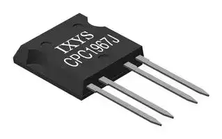
CPC1909J
MOSFET RELAY, SPST-NO, 15A, 60V, THT
⚠️ Reference pricing provided. In case of supply shortages, we will connect you with our trusted procurement partners to ensure your project's continuity.
- Manufacturer: IXYS SEMICONDUCTOR
- Product type: MOSFET Solid State Relays
- Contact Form:SPST-NO (1 Form A); Load Type:AC / DC; Load Voltage Max:60V; Load Current:15A; MOSFET Relay Package Style:ISOPLUS-264; Relay Mounting:Through Hole; R 30K7141
- Load Type: AC / DC
- Contact Form: SPST-NO (1 Form A)
- Load Current: 15A
- Product Range: OptoMOS Series
- Relay Mounting: Through Hole
- Relay Terminals: PC Pin
- Load Voltage Max: 60V
- Isolation Voltage: 2.5kV
- I/O Capacitance Typ: 1pF
- On State Resistance Max: 0.1ohm
- MOSFET Relay Package Style: ISOPLUS-264
- Off State Leakage Current Max: 1µA
| Delivery and price | |
|---|---|
| Units per pack | 250 |
| Price | 6.6 € |
| Current stock | 10+ |
| Lead time | 30 days |
Datasheet

**CPC1909 60V Single-Pole, Normally Open Power Relay** > I CIIXYS NTEGRATED CIRCUITS DIVISION ## **Characteristics** |**Parameter**|**Rating**|**Units**| |---|---|---| |Blocking Voltage|60|VP| |Load Current, TA=25°C:<br>With 5°C/W Heat Sink<br>No Heat Sink|15|Arms/ ADC| ||6.5|| |On-Resistance (max)|0.1|| |Thermal Impedance,<br>Junction-to-case,JC|0.3|°C/W| ## **Features** - 15Arms Load Current with 5°C/W Heat Sink - Low 0.1 On-Resistance - 60VP Blocking Voltage - 2500Vrms Input/Output Isolation ## **Description** IXYS Integrated Circuits brings OptoMOS® technology, reliability and compact size to a new family of high-power Solid State Relays. As part of this family, the CPC1909 single-pole normally open (1-Form-A) Solid State Power Relay is rated for up to 15Arms continuous load current with a 5°C/W heat sink. The CPC1909 employs optically coupled MOSFET technology to provide 2500Vrms of input to output isolation. The optically coupled outputs, that use patented OptoMOS architecture, are controlled by a highly efficient infrared LED. The combination of low on-resistance and high load current handling capability makes this relay suitable for a variety of high performance switching applications. - Low Thermal Impedance: JC = 0.3 °C/W - Isolated, Low Thermal Impedance Ceramic Pad for Heat Sink Applications - Low Drive Power Requirements - Arc-Free With No Snubbing Circuits - No EMI/RFI Generation - Flammability Rating UL 94 V-0 ## **Applications** - Industrial Controls / Motor Control - Robotics The unique ISOPLUS-264 package pioneered by IXYS allows Solid State Relays to achieve the highest load current and power ratings. This package features a unique IXYS process where the silicon chips are soft soldered onto the Direct Copper Bond (DCB) substrate instead of the traditional copper leadframe. The DCB ceramic, the same substrate used in high power modules, not only provides 2500Vrms isolation but also very low junction-to-case thermal impedance (0.3 °C/W). - Medical Equipment—Patient/Equipment Isolation - Instrumentation ## **Ordering Information** - Multiplexers - Data Acquisition - Electronic Switching - I/O Subsystems - Meters (Watt-Hour, Water, Gas) - Transportation Equipment **Part Description** CPC1909J ISOPLUS-264 Package (25 per tube) ~~———~~ ## **Switching Characteristics** - Aerospace/Defense ## **Approvals** - UL 508 Certified Component: File E69938 **Pin Configuration** **==> picture [150 x 98] intentionally omitted <==** **----- Start of picture text -----**<br> Form-A<br>I<br>F<br>90%<br>10%<br>I<br>LOAD<br>t t<br>on off<br>**----- End of picture text -----**<br> **==> picture [20 x 15] intentionally omitted <==** **----- Start of picture text -----**<br> e3<br>**----- End of picture text -----**<br> DS-CPC1909-R09 **www.ixysic.com** 1 **CPC1909** INTEGRATED CIRCUITS DIVISION ## **1 Specifications** ## **1.1 Absolute Maximum Ratings @ 25°C** |**Symbol**|**Ratings**|**Units**| |---|---|---| |Blocking Voltage|60|VP| |Reverse Input Voltage|5|V| |Input Control Current<br>Peak (10ms)|100|mA| ||1|A| |Input Power Dissipation|150|mW| |Isolation Voltage, Input to Output|2500|Vrms| |Operational Temperature|-40 to +85|°C| |Storage Temperature|-40 to +125|°C| _Absolute maximum ratings are stress ratings. Stresses in excess of these ratings can cause permanent damage to the device. Functional operation of the device at conditions beyond those indicated in the operational sections of this data sheet is not implied._ _Typical values are characteristic of the device at +25°C, and are the result of engineering evaluations. They are provided for information purposes only, and are not part of the manufacturing testing requirements._ ## **1.2 Electrical Characteristics @ 25°C** |**Parameter**|**Conditions**|**Symbol**|**Minimum**|**Typical**|**Maximum**|**Units**| |---|---|---|---|---|---|---| |**Output Characteristics**<br>~~|~~||||||| |Load Current1<br>Peak<br>Continuous<br>Continuous<br>Continuous<br>~~eS~~|t10ms<br>~~eS~~|IL<br>~~eS~~|-<br>~~eS~~<br>~~|~~|-<br>~~eS~~<br>~~|~~|25<br>~~eS~~|AP<br>~~eS~~| ||No Heat Sink<br>~~eS~~||||6.5<br>~~eS~~|Arms/ ADC<br>~~eS~~| ||TC=25°C<br>~~eS~~||||15<br>~~eS~~|| ||TC=99°C<br>~~eS~~|IL(99)<br>~~eS~~|||7.85<br>~~eS~~|| |On-Resistance2<br>~~eS~~|IF=10mA, IL=1A<br>~~eS~~|RON<br>~~eS~~|-<br>~~eS~~<br>~~|~~|0.05<br>~~eS~~<br>~~|~~|0.1<br>~~eS~~|<br>~~eS~~| |Off-State Leakage Current<br>~~eS~~<br>~~Pf~~|VL=60VP<br>~~eS~~<br>~~Pf~~|ILEAK<br>~~eS~~<br>~~Pf~~|-<br>~~eS~~<br>~~|~~<br>~~Pf~~|-<br>~~eS~~<br>~~|~~<br>~~Pf~~|1<br>~~eS~~<br>~~Pf~~|A<br>~~eS~~<br>~~Pf~~| |Switching Speeds<br>Turn-On<br>Turn-Off<br>~~Pf~~|IF=20mA, VL=10V<br>~~Pf~~|ton<br>~~Pf~~|-<br>~~Pf~~|15<br>~~Pf~~|25<br>~~Pf~~|ms<br>~~Pf~~| |||toff<br>~~Pf~~|-<br>~~Pf~~|0.3<br>~~Pf~~|10<br>~~Pf~~|| |Output Capacitance<br>~~Pf~~|IF=0mA, VL=25V, f=1MHz<br>~~Pf~~|Cout<br>~~Pf~~|-<br>~~Pf~~|4000<br>~~Pf~~|-<br>~~Pf~~|pF<br>~~Pf~~| |**Input Characteristics**<br>~~Pf~~||||||| |Input Control Current to Activate3|IL=1A|IF|-|-|10|mA| |Input Control Current to Deactivate|-|IF|0.6|-|-|mA| |Input Voltage Drop|IF=10mA|VF|0.9|1.35|1.56|V| |Reverse Input Current|VR=5V|IR|-|-|10|A| |**Input/Output Characteristics**||||||| |Capacitance, Input-to-Output|VIO=0V, f=1MHz|CIO|-|1|-|pF| 1 Higher load currents possible with proper heat sinking. 2 Measurement taken within 1 second of on-time. 3 For applications requiring high temperature operation (TC > 60ºC) an LED drive current of 20mA is recommended. R09 **www.ixysic.com** 2 **CPC1909** INTEGRATED CIRCUITS DIVISION ## **2 Thermal Characteristics** |**Parameter**|**Conditions**|**Symbol**|**Rating**|**Units**| |---|---|---|---|---| |Thermal Impedance (Junction to Case)|-|JC|0.3|°C/W| |Thermal Impedance (Junction to Ambient)|Free Air|JA|33|°C/W| |Junction Temperature (Operating)|-|TJ|-40 to +100|°C| ## **2.1 Thermal Management** Device high current characterization was performed using Kunze heat sink KU 1-159, phase change thermal interface material KU-ALC 5, and transistor clip KU 4-499/1. This combination provided an approximate junction-to-ambient thermal impedance of 12.5°C/W. ## **2.2 Heat Sink Calculation** Higher load currents are possible by using lower thermal impedance heat sink combinations. ## **Heat Sink Rating** **==> picture [144 x 37] intentionally omitted <==** - TJ = Junction Temperature (°C), TJ ≤ 100°C * - TA = Ambient Temperature (°C) - IL(99) = Load Current with Case Temperature @ 99°C (ADC) - IL = Desired Operating Load Current (ADC), IL ≤ IL(MAX) - θ JC = Thermal Impedance, Junction to Case (°C/W) = 0.3°C/W - θ CA = Thermal Impedance of Heat Sink & Thermal Interface Material , Case to Ambient (°C/W) PD(99) = Maximum power dissipation with case temperature held at 99ºC = 3.33W - Elevated junction temperature reduces semiconductor lifetime. **NOTE:** The exposed surface of the DCB substrate is not to be soldered. **www.ixysic.com** R09 3 **CPC1909** INTEGRATED CIRCUITS DIVISION ## **3 Performance Data*** Unless otherwise specified, all performance data was acquired without the use of a heat sink. **==> picture [469 x 122] intentionally omitted <==** **----- Start of picture text -----**<br> Typical LED Forward Voltage Drop Typical Turn-On Time Typical Turn-Off Time<br>(N=50, IF=10mA, IL=1ADC) (N=50, IF=20mA, IL=1ADC) (N=50, IF=20mA, IL=1ADC)<br>3530 3530 L L 25<br>20<br>25 25<br>20 20 SEES)FTelP 15 Eg<br>15 15 | | 10 2<br>10 10<br>5<br>5 5 =| oe] || 2<br>0 0 | Enninin 0 mii il tf<br>1.30 1.31 1.32 1.33 1.34 10.0 12.5 15.0 17.5 20.0 22.5 0.17 0.23 0.29 0.35 0.41 0.47<br>LED Forward Voltage (V) Turn-On Time (ms) Turn-Off Time (ms)<br>Device Count (N) Device Count (N) Device Count (N)<br>**----- End of picture text -----**<br> **==> picture [142 x 121] intentionally omitted <==** **----- Start of picture text -----**<br> Typical On-Resistance Distribution<br>(N=50, IF=10mA, IL=1ADC)<br>3530 Td<br>25 POEL LL<br>20151050 t|1)-moom_ i!oe=ho<br>0.033 0.037 0.041 0.045 0.049 0.053<br>On-Resistance ( Ω )<br>Device Count (N)<br>**----- End of picture text -----**<br> **==> picture [478 x 274] intentionally omitted <==** **----- Start of picture text -----**<br> Typical Turn-On Time Typical Turn-Off Time<br>Typical LED Forward Voltage Drop vs. LED Forward Current vs. LED Forward Current<br>vs. Temperature (IL=1ADC) (IL=1ADC)<br>1.8 120 0.45<br>0.40<br>1.6 KET TELL 100 FLT ET TT TT 0.35 eee<br>80 0.30<br>1.4<br>1.2 SER ATT IIFF=50mA=20mA 60 Beep ee 0.250.20 EEE<br>IF=10mA 40 0.15<br>1.0 St 20 PNCEELELLE = 0.10 eS<br>SEeeEn PUNSEPP 0.05 PEE<br>0.8 F L LL ELL 0 b ial al bchobbohkho 0.00 Foot<br>-40 -20 0 20 40 60 80 100 120 0 5 10 15 20 25 30 35 40 45 50 0 5 10 15 20 25 30 35 40 45 50<br>Temperature (ºC) LED Forward Current (mA) LED Forward Current (mA)<br>Typical IF for Switch Operation<br>vs. Temperature Typical Turn-On Time vs. Temperature Typical Turn-Off Time vs. Temperature<br>(IL=1ADC) (IL=1ADC) (IL=1ADC)<br>5.0 42 0.48<br>4.5 oe 36 FDL LLI IF=10mA 0.42 TEDL LLLI<br>4.03.5 30 0.36 IF=20mA<br>SESS Ebr rreeey PPE<br>3.0 24 0.30<br>2.52.0 ee= 18 oe IF=20mA 0.24 eeSELLE<br>1.5 eee 12 ae 0.18 SLL IF=10mA<br>1.0<br>0.5 = 6 F [tt tt 0.12 2<br>0 ve ee 0 7 0.06 7<br>-40 -20 0 20 40 60 80 100 -40 -20 0 20 40 60 80 100 -40 -20 0 20 40 60 80 100<br>Temperature (ºC) Temperature (ºC) Temperature (ºC)<br>Turn-On Time (ms) Turn-Off Time (ms)<br>LED Forward Voltage Drop (V)<br>Turn-Off Time (ms)<br>LED Current (mA) Turn-On Time (ms)<br>**----- End of picture text -----**<br> - Unless otherwise noted, data presented in these graphs is typical of device operation at 25ºC. - For guaranteed parameters not indicated in the written specifications, please contact our application department. R09 **www.ixysic.com** 4 **CPC1909** INTEGRATED CIRCUITS DIVISION **==> picture [480 x 131] intentionally omitted <==** **----- Start of picture text -----**<br> Typical On-Resistance Typical Load Current Maximum Load Current<br>vs. Temperature vs. Load Voltage vs. Temperature with Heat Sink<br>(IF=10mA, IL=1ADC) (IF=10mA) (IF=20mA)<br>0.060 10 20<br>0.058 fF [| | | | | fT 8 Ff of of ff |<br>6 1ºC/W<br>0.056 15<br>4<br>0.054 eA 2 SSS<br>0.052 0 10 5ºC/W<br>0.050 SFEREER) -2 EeRAEE<br>-4 10ºC/W<br>0.048 5<br>-6<br>0.046 See -8 Eee No Heat Sink<br>0.044 PzT Lt Lt -10 PEEES 0<br>-40 -20 0 20 40 60 80 100 -0.54 -0.36 -0.18 0 0.18 0.36 0.54 0 20 40 60 80 100<br>Temperature (ºC) Load Voltage (V) Temperature (ºC)<br>On-resistance () Ω Load Current (A) Load Current (A)rms<br>**----- End of picture text -----**<br> **==> picture [477 x 130] intentionally omitted <==** **----- Start of picture text -----**<br> Typical Leakage vs. Temperature<br>Normalized Blocking Voltage Measured Across Pins 1&2 Energy Rating Curve<br>vs. Temperature (VL=60VP) Free Air, No Heat Sink<br>84 0.014 30<br>82 PFET, 0.012 Fee) 25 6a<br>80 0.010<br>20<br>78 eee 0.008 OR Oo<br>76 15<br>ee a 0.006 ee alee SUTTONS<br>74<br>72 cs 0.004 [cen] | 10 0 0 TT<br>7068 SToeH 0.0020 eoEIT 50 n<br>-40 -20 0 20 40 60 80 100 -40 -20 0 20 40 60 80 100 10µs 100µs 1ms 10ms 100ms 1s 10s 100s<br>Temperature (ºC) Temperature (ºC) Time<br>)P<br>)P<br>A)<br>μ<br>Leakage (<br>Load Current (A<br>Blocking Voltage (V<br>**----- End of picture text -----**<br> * Unless otherwise noted, data presented in these graphs is typical of device operation at 25ºC. For guaranteed parameters not indicated in the written specifications, please contact our application department. **www.ixysic.com** R09 5 **CPC1909** INTEGRATED CIRCUITS DIVISION ## **4 Manufacturing Information** ## **4.1 Moisture Sensitivity** All plastic encapsulated semiconductor packages are susceptible to moisture ingression. IXYS Integrated Circuits classifies its plastic encapsulated devices for moisture sensitivity according to the latest version of the joint industry standard, **IPC/JEDEC J-STD-020** , in force at the time of product evaluation. We test all of oy our products to the maximum conditions set forth in the standard, and guarantee proper operation of our devices when handled according to the limitations and information in that standard as well as to any limitations set forth in the information or standards referenced below. Failure to adhere to the warnings or limitations as established by the listed specifications could result in reduced product performance, reduction of operable life, and/or reduction of overall reliability. This product carries a **Moisture Sensitivity Level (MSL)** classification as shown below, and should be handled according to the requirements of the latest version of the joint industry standard **IPC/JEDEC J-STD-033** . |**Device**<br>~~eS~~|**Moisture Sensitivity Level (MSL) Classification**<br>~~eS~~| |---|---| |CPC1909J<br>~~eS~~|MSL 1<br>~~eS~~| ## **4.2 ESD Sensitivity** This product is **ESD Sensitive** , and should be handled according to the industry standard **JESD-625** . ## **4.3 Soldering Profile** Provided in the table below is the Classification Temperature (TC) of this product and the maximum dwell time the body temperature of this device may be (TC - 5)ºC or greater. The classification temperature sets the Maximum Body Temperature allowed for this device during lead-free reflow processes. For through-hole devices, and any other processes, the guidelines of **J-STD-020** must be observed. **Device Classification Temperature (TC) Dwell Time (tp) Max Reflow Cycles** CPC1909J 245°C 30 seconds 1 ~~————~~ ## **NOTE:** The exposed surface of the DCB substrate is not to be soldered. ## **4.4 Board Wash** IXYS Integrated Circuits recommends the use of no-clean flux formulations. Board washing to reduce or remove flux residue following the solder reflow process is acceptable provided proper precautions are taken to prevent damage to the device. These precautions include but are not limited to: using a low pressure wash and providing a follow up bake cycle sufficient to remove any moisture trapped within the device due to the washing process. Due to the variability of the wash parameters used to clean the board, determination of the bake temperature and duration necessary to remove the moisture trapped within the package is the responsibility of the user (assembler). Cleaning or drying methods that employ ultrasonic energy may damage the device and should not be used. Additionally, the device must not be exposed to flux or solvents that are Chlorine- or Fluorine-based. **==> picture [22 x 18] intentionally omitted <==** **----- Start of picture text -----**<br> e3<br>**----- End of picture text -----**<br> R09 **www.ixysic.com** 6 **CPC1909** INTEGRATED CIRCUITS DIVISION **==> picture [495 x 342] intentionally omitted <==** **----- Start of picture text -----**<br> 4.5 Mechanical Dimensions<br>5.029 ± 0.127<br>(0.198 ± 0.005) 1.181 ± 0.076<br>19.914 ± 0.254 (0.047 ± 0.003)<br>(0.784 ± 0.010) 1.930 ± 0.381 17.221 ± 0.254<br>(0.678 ± 0.010)<br>(0.076 ± 0.015)<br>26.162 ± 0.254<br>oe W o<br>(1.030 ± 0.010) 20.600 ± 0.254<br>(0.811 ± 0.010)<br>DCB Substrate<br>NOTE: Not to be soldered<br>2.362 ± 0.381<br>(0.093 ± 0.015)<br>20.396 ± 0.508<br>(0.803 ± 0.020) DIMENSIONS<br>mm<br>(inches)<br>ais<br>3.810 ± 0.254<br>(0.150 ± 0.010) 0.635 ± 0.076<br>15.240 ± 0.508 (0.025 ± 0.003) 2.794 ± 0.127 1.270 TYP<br>mr| (0.600 ± 0.020) W S +L| (0.110 ± 0.005) om (0.050 TYP)<br>NOTE: Metallized external surface of DCB substrate maintains 2500V<br> isolation to device internal structure and all external pins. rms<br>**----- End of picture text -----**<br> ## **For additional information please visit our website at: www.ixysic.com** IXYS Integrated Circuits makes no representations or warranties with respect to the accuracy or completeness of the contents of this publication and reserves the right to make changes to specifications and product descriptions at any time without notice. Neither circuit patent licenses nor indemnity are expressed or implied. Except as set forth in IXYS Integrated Circuits’ Standard Terms and Conditions of Sale, IXYS Integrated Circuits assumes no liability whatsoever, and disclaims any express or implied warranty, relating to its products including, but not limited to, the implied warranty of merchantability, fitness for a particular purpose, or infringement of any intellectual property right. The products described in this document are not designed, intended, authorized or warranted for use as components in systems intended for surgical implant into the body, or in other applications intended to support or sustain life, or where malfunction of IXYS Integrated Circuits’ product may result in direct physical harm, injury, or death to a person or severe property or environmental damage. IXYS Integrated Circuits reserves the right to discontinue or make changes to its products at any time without notice. Specification: DS-CPC1909-R09 ©Copyright 2018, IXYS Integrated Circuits All rights reserved. Printed in USA. 8/20/2018 **www.ixysic.com** R09 7
Updated at April 22, 2026
About Novapart
Novapart is a B2B electronic component broker specialising in stock shortages and cost reduction. We source hard-to-find parts and identify compliant alternatives across a catalogue of 410,000+ components from 500+ manufacturers.
Learn more →Stock Shortage Specialist
When a component is unavailable, discontinued or has an unacceptable lead time, we tap into our network of vetted European and Asian distributors to source what you need — without compromising on quality or traceability.
Request a quote →Compliant Alternatives
We identify pin-to-pin, electrically equivalent substitutes that meet the same certifications (RoHS, AEC-Q100, REACH) as your original specification — validated against datasheets, not just part numbers. Often at a lower cost.
BOM Analysis service →