
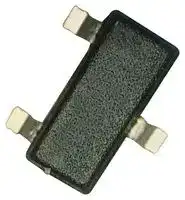


CDM2319DS
Power MOSFET, P Channel, 40 V, 2.3 A, 0.07 ohm, SOT-23, Surface Mount
- Manufacturer: MULTICOMP PRO
- Product type: Single MOSFETs
- MSL: -
- SVHC: No SVHC (25-Jun-2025)
- No. of Pins: 3Pins
- Channel Type: P Channel
- Product Range: Multicomp Pro MOSFETs P-Channel
- Qualification: -
- Power Dissipation: 750mW
- Transistor Mounting: Surface Mount
- Rds(on) Test Voltage: 10V
- Transistor Case Style: SOT-23
- Drain Source Voltage Vds: 40V
- Operating Temperature Max: 150°C
- Continuous Drain Current Id: 2.3A
- Drain Source On State Resistance: 0.07ohm
- Gate Source Threshold Voltage Max: 3V
| Delivery and price | |
|---|---|
| Units per pack | 5000 |
| Price | 0.191 € |
| Current stock | 1000+ |
| Lead time | 30 days |
## **P Channel MOSFET**

## **Feature**

• Trench FET Power MOSFET

## **Absolute Maximum Ratings** (Ta = 25°C Unless otherwise specified)

|**Parameter**|**Parameter**|**Parameter**|**Symbol**|**Value**|**Unit**|
|---|---|---|---|---|---|
|Drain-Source Voltage|||Vds|40|V|
|Gate-Source Voltage|||Vgs|±20||
|Continuous Drain Current|Steady<br>State|Ta = 25°C|Id|2.3|A|
|||Ta = 70°C||1.85||
|Maximum Power Dissipation1|Steady<br>State|Ta = 25°C|Pd|0.75|W|
|||Ta = 70°C||0.48||
|Pulsed Drain Current2|||Idm|12|A|
|Source Current(BodyDiode) 1|||Is|0.62||
|Junction Temperature|||Tj|150|°C|
|Storage Temperature|||Tstg|-55 to +150||


## **Thermal Resistance**

|**Thermal Resistance**|**Thermal Resistance**|||||
|---|---|---|---|---|---|
|**Parameter**||**Symbol**|**Typ.**|**Max.**|**Unit**|
|Maximum Junction-to-Ambient1||RthJA|75|100|°C/W|
|Maximum Junction-to-Ambient3|(SteadyState)||120|166||
|Maximum Junction-to-Foot(Drain)|(SteadyState)|RthJA|40|50||


**Electrical Characteristics at** (Ta = 25 °C Unless otherwise specified)

|**Parameter**<br>~~ee~~|**Symbol**<br>~~ee~~|**Test Conditions**<br>~~ee~~|**Value**<br>**Min.**<br>**Typ.**<br>**Max.**<br>~~ee~~|**Value**<br>**Min.**<br>**Typ.**<br>**Max.**<br>~~ee~~|**Value**<br>**Min.**<br>**Typ.**<br>**Max.**<br>~~ee~~|**Unit**<br>~~ee~~|
|---|---|---|---|---|---|---|
|||||**Typ.**<br>~~ee~~|**Max.**<br>~~ee~~||
|Drain-Source Breakdown Voltage<br>~~es~~|V(BR)DSS<br>~~es~~|Vgs = 0V, Id = 250μA<br>~~es~~|40<br>~~es~~|-<br>~~es~~|-<br>~~es~~|V<br>~~|~~|
|Gate-Threshold Voltage4<br>~~es~~|VGS(th)<br>~~es~~|Vds = VGS, Id = 250μA<br>~~es~~|1<br>~~es~~|-<br>~~es~~|3<br>~~es~~||
|Gate-bodyLeakage current<br>~~GG~~|less<br>~~GG~~|Vds = 0V, Vgs = ±20V<br>~~GG~~|-<br>~~GG~~|-<br>~~GG~~|±100<br>~~GG~~|nA<br>~~GG~~|
|Zero Gate Voltage Drain Current<br>~~er~~|Idss<br>~~er~~|Vds = 40V, Vgs = 0V<br>~~er~~|-<br>~~er~~<br>~~ee~~|-<br>~~er~~<br>~~ee~~|1<br>~~er~~|μA<br>~~er~~|
|||Vds = 40V,Vgs = 0V,Tj = 55°C<br>~~er~~<br>~~ee~~|-<br>~~er~~<br>~~ee~~<br>~~ee~~|-<br>~~er~~<br>~~ee~~<br>~~ee~~|10<br>~~er~~<br>~~ee~~||
|On-State Drain Current<br>~~GG~~<br>~~ee~~|ID(on)<br>~~GG~~<br>~~nes~~|Vds ≤ 5V, Vgs = 10V<br>~~GG~~<br>~~nes~~|6<br>~~ee~~<br>~~GG~~<br>~~nesee~~|-<br>~~ee~~<br>~~GG~~<br>~~ee~~|-<br>~~GG~~<br>~~ee~~|A<br>~~GG~~<br>~~ee~~|
|Drain-Source On-Resistance4<br>~~ee~~|RDS(on)<br>~~nes~~|Vgs = 10V, Id = 3A<br>~~nes~~|-<br>~~nesee~~<br>~~ee~~|70<br>~~ee~~|82<br>~~ee~~|mΩ<br>~~ee~~|
|||Vgs = 4.5V, Id = 2.4A<br>~~nes~~<br>~~ee~~|-<br>~~nesee~~<br>~~ee~~<br>~~ee~~|95<br>~~ee~~<br>~~ee~~|130<br>~~ee~~<br>~~ee~~||


03/01/23 V1.0

Page <1>

## **P Channel MOSFET**

|||~~ee~~|~~ee ee~~|~~ee ee~~|~~ee ee~~||
|---|---|---|---|---|---|---|
|**Parameter**<br>~~ee~~|**Symbol**<br>~~ee~~|**Test Conditions**<br>~~ee~~<br>~~ee~~|**Value**<br>~~ee~~<br>~~ee ee~~|||**Unit**|
||||**Min.**<br>~~ee~~<br>~~ee ee~~|**Typ.**<br>~~ee~~<br>~~ee~~|**Max.**<br>~~ee~~<br>~~ee~~||
|Forward Trans conductance4<br>~~QO~~<br>~~ee~~<br>~~es~~|gfs<br>~~QO~~|Vds = 5V, Id = 3A<br>~~ee~~<br>~~QO~~|-<br>~~ee ee~~<br>~~QO~~<br>~~a~~|7<br>~~ee~~<br>~~QO~~<br>~~a~~<br>~~ee~~|-<br>~~ee~~<br>~~QO~~<br>~~a~~<br>~~ee~~|S<br>~~QO~~<br>~~ee~~|
|Input Capacitance<br>~~ee~~<br>~~es~~<br>~~ee~~|Ciss|Vgs = 0V<br>Vds = -20V<br>f = 1MHz|-<br>~~a~~|470<br>~~a~~<br>~~ee~~<br>~~ee~~|-<br>~~a~~<br>~~ee~~|pF<br>~~ee~~<br>~~ee~~|
|Output Capacitance<br>~~ee~~<br>~~es~~<br>~~ee~~|Coss||-<br>~~a~~<br>~~a~~|85<br>~~a~~<br>~~ee~~<br>~~a~~<br>~~ee~~|-<br>~~a~~<br>~~ee~~<br>~~a~~||
|Reverse Transfer Capacitance<br>~~es~~<br>~~ee~~<br>~~ee~~<br>~~ee~~|Crss||-<br>~~**a**~~|65<br>~~ee ~~<br>~~ee~~<br>~~a~~<br>~~ee~~|-<br> ~~ee~~<br>~~ee~~||
|Totalgate charge<br>~~ee~~<br>~~ee~~<br>~~ee~~<br>~~ee~~|Qg|Vgs = 10V,<br>Id = 3A,<br>Vds = 20V|-<br>~~**a**~~<br>~~a~~|11.3<br>~~ee~~<br>~~a~~<br>~~ee~~<br>~~ee~~|17<br>~~ee~~|nC<br>~~ee~~<br>~~ee~~|
|Gate-source charge<br>~~ee~~<br>~~ee~~<br>~~ee~~|Qgs||-<br>~~**a** ~~<br>~~a~~|1.7<br> ~~a~~<br>~~ee~~<br>~~ee~~|-<br>~~ee~~||
|Gate-drain charge<br>~~ee~~<br>~~ee~~<br>~~ee~~<br>~~ee~~|Qgd||-<br>~~a~~<br>~~**a**~~|3.3<br>~~ee ~~<br>~~ee~~<br>~~a~~<br>~~ee~~|-<br> ~~ee~~<br>~~ee~~||
|Turn-on delaytime<br>~~ee~~<br>~~ee~~<br>~~ee~~<br>~~ee~~|td(on)|Vdd = 20V, Id = 1A,<br>Rg = 6Ω, Vgen = 4.5V<br>Rl = 20Ω|-<br>~~a ~~<br>~~**a**~~|7<br> ~~ee~~<br>~~a~~<br>~~ee~~<br>~~a~~|15<br>~~ee~~|ns<br>~~ee~~|
|Rise time<br>~~ee~~<br>~~ee~~<br>~~ee~~<br>~~ee~~|tr||-<br>~~**a** ~~<br>~~a~~|15<br> ~~a~~<br>~~ee~~<br>~~a~~<br>~~a~~<br>~~ee~~|25<br>~~ee~~<br>~~a~~||
|Turn-off delaytime<br>~~ee~~<br>~~ee~~<br>~~ee~~<br>~~a~~|td(off)||-<br>~~a~~|25<br>~~ee ~~<br>~~a~~<br>~~a~~<br>~~ee~~<br>~~ee~~|40<br> ~~ee~~<br>~~a~~||
|Fall time<br>~~ee~~<br>~~ee~~<br>~~a~~|tf||-<br>~~a~~|25<br>~~a~~<br>~~ee~~<br>~~a~~<br>~~ee~~|40<br>~~a~~||
|Diode Forward Voltage4<br>~~ee~~<br>~~a~~|Vsd|Is = 1.25A, Vgs = 0V|-|0.8<br>~~ee~~<br>~~ee~~|1.2|V|


## **Notes:**

- 1 Surface Mounted on FR4 Board.t ≤ 5s.

- 2 Pulse width limited by maximum junction temperature.

- 3 Surface Mounted on FR4 Board.

- 4 Pulse test: PW ≤ 300 μs, duty cycle ≤ 2%.

- 5 For PNP device voltage and current values will be negative (-).

## **Recommended Reflow Solder Profiles**

The recommended reflow solder profiles for Pb and Pb-free devices are shown below.

Figure 1 shows the recommended solder profile for devices that have Pb-free terminal plating, and where a Pb free solder is used.

Figure 2 shows the recommended solder profile for devices with Pb-free terminal plating used with leaded solder, or for devices with leaded terminal plating used with a leaded solder.

Newark.com/multicomp-pro Farnell.com/multicomp-pro sg.element14.com/b/multicomp-pro

03/01/23 V1.0

Page <2>

## **P Channel MOSFET**

## **Reflow Profiles in Tabular Form**

|**Profile Feature**|**Sn-Pb System**|**Pb-Free System**|
|---|---|---|
|Average Ramp-UpRate|~3°C/second|~3°C/second|
|**Preheat**<br>Temperature Range<br>Time|150-170°C<br>60-180 seconds|150-200°C<br>60-180 seconds|
|**Time maintained above:**<br>Temperature<br>Time|200°C<br>30-50 seconds|217°C<br>60-150 seconds|
|Peak Temperature|235°C|260°C max.|
|Time within +0 -5°C of actual Peak|10 seconds|40 seconds|
|Ramp-Down Rate|3°C/second max.|6°C/second max.|


## **Recommended Wave Solder Profiles**

The Recommended solder Profile For The Recommended solder Profile For Devices Devices with Pb-free terminal plating with Pb-free terminal plating used with leaded where a Pb-free solder is used solder, or for devices with leaded terminal plating used with leaded solder

## **Wave Profiles in Tabular Form**

|**Profile Feature**|**Sn-Pb System**|**Pb-Free System**|
|---|---|---|
|Average Ramp-UpRate|~200°C/second|~200°C/second|
|Heatingrate during preheat|Typical 1-2, Max 4°C/sec|Typical 1-2, Max 4°C/Sec|
|Finalpreheat Temperature|Within 125°C of Solder Temp.|Within 125°C of Solder Temp.|
|Peak Temperature|235°C|260°C max.|
|Time within +0 -5°C of actual Peak|10 seconds|10 seconds|
|Ramp-Down Rate|5°C/second max.|5°C/second max.|


Newark.com/multicomp-pro Farnell.com/multicomp-pro sg.element14.com/b/multicomp-pro

03/01/23 V1.0

Page <3>

## **P Channel MOSFET**

## **Typical Characteristics Curves**

Newark.com/multicomp-pro Farnell.com/multicomp-pro sg.element14.com/b/multicomp-pro

03/01/23 V1.0

Page <4>

## **P Channel MOSFET**

## **Diagram**

## **SOT-23 SMD Package**

**==> picture [309 x 130] intentionally omitted <==**

**----- Start of picture text -----**<br>
Suggested Pad Layout<br>my<br>lo<br>-1- 2<br>! Pin configuration<br>1<br>o<br>2<br>o<br>' 1<br>1 1<br>-Lj----- eb el - 1. Gate<br>' H<br>11 2. Source<br>3. Drain<br>**----- End of picture text -----**<br>


## **Part Number Table**

## Dimensions : Millimetres

|**Part Number Table**||
|---|---|
|**Description**|**Part Number**|
|P Channel Plastic Encapsulate MOSFET, SOT 23|CDM2319DS|


**Important Notice :** This data sheet and its contents (the “Information”) belong to the members of the AVNET group of companies (the “Group”) or are licensed to it. No licence is granted for the use of it other than for information purposes in connection with the products to which it relates. No licence of any intellectual property rights is granted. The Information is subject to change without notice and replaces all data sheets previously supplied. The Information supplied is believed to be accurate but the Group assumes no responsibility for its accuracy or completeness, any error in or omission from it or for any use made of it. Users of this data sheet should check for themselves the Information and the suitability of the products for their purpose and not make any assumptions based on information included or omitted. Liability for loss or damage resulting from any reliance on the Information or use of it (including liability resulting from negligence or where the Group was aware of the possibility of such loss or damage arising) is excluded. This will not operate to limit or restrict the Group’s liability for death or personal injury resulting from its negligence. Multicomp Pro is the registered trademark of Premier Farnell Limited 2019.

## Newark.com/multicomp-pro

Farnell.com/multicomp-pro

sg.element14.com/b/multicomp-pro

03/01/23 V1.0

Page <5>
Updated at April 11, 2026
Multicomp Pro is a trusted manufacturer of high-quality electronic components, built upon the rich heritage of established industry names such as SPC Technology, Tenma, Duratool, and Pro Power. Developed to provide engineers and procurement professionals with exceptional value, the brand offers an extensive portfolio of rigorously lab-tested products. By combining strict quality assurance with cost-effective manufacturing, Multicomp Pro delivers premium reliability while providing significant savings compared to leading industry alternatives. The brand's comprehensive lineup is anchored by a vast selection of passive components and essential circuit protection devices. Engineers consistently rely on Multicomp Pro for aluminum electrolytic capacitors, film capacitors, and power inductors designed for demanding applications. The protection portfolio is equally robust, featuring hundreds of standard fuses, resettable fuses, and transient voltage suppression (TVS) diodes to safeguard critical circuitry. Furthermore, the company is a major provider of precision timing solutions, including a wide array of reliable crystals and standard oscillators. Beyond passives and board-level protection, Multicomp Pro offers extensive solutions in power management, discrete semiconductors, and connectivity. This includes highly efficient AC/DC converters, bridge rectifiers, bipolar transistors, and a versatile selection of wire-to-board terminal blocks. Backed by comprehensive factory audits, continuous laboratory testing, and a strong commitment to ethical sourcing, Multicomp Pro ensures that every component consistently meets stringent international safety and performance standards.
About Novapart
Novapart is a B2B electronic component broker specialising in stock shortages and cost reduction. We source hard-to-find parts and identify compliant alternatives across a catalogue of 410,000+ components from 500+ manufacturers.
Learn more →Stock Shortage Specialist
When a component is unavailable, discontinued or has an unacceptable lead time, we tap into our network of vetted European and Asian distributors to source what you need — without compromising on quality or traceability.
Request a quote →Compliant Alternatives
We identify pin-to-pin, electrically equivalent substitutes that meet the same certifications (RoHS, AEC-Q100, REACH) as your original specification — validated against datasheets, not just part numbers. Often at a lower cost.
BOM Analysis service →