
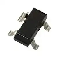


BFP780H6327XTSA1
Bipolar - RF Transistor, NPN, 6.6 V, 20 GHz, 600 mW, 120 mA, SOT-343
- Manufacturer: INFINEON
- Product type: Bipolar RF Transistors
- No. of Pins: 4Pins
- Power Dissipation: 600mW
- RF Transistor Case: SOT-343
- DC Current Gain hFE: 85hFE
- Transistor Mounting: Surface Mount
- Transistor Polarity: NPN
- DC Collector Current: 120mA
- Power Dissipation Pd: 600mW
- Transition Frequency: 20GHz
- Transistor Case Style: SOT-343
- DC Current Gain hFE Min: 85hFE
- Operating Temperature Max: 150°C
- Continuous Collector Current: 120mA
- Collector Emitter Voltage Max: 6.6V
- Collector Emitter Voltage V(br)ceo: 6.6V
| Delivery and price | |
|---|---|
| Units per pack | 1000 |
| Price | 0.843 € |
| Current stock | 10+ |
| Lead time | 30 days |
## BFP780

200 mW High Gain RF Driver Amplifier

## Data Sheet

Revision 3.0, 2015-07-08

RF & Protection Devices ~~eee~~

## **Edition 2015-07-08**

**Published by Infineon Technologies AG 81726 Munich, Germany © 2015 Infineon Technologies AG All Rights Reserved.**

## **Legal Disclaimer**

The information given in this document shall in no event be regarded as a guarantee of conditions or characteristics. With respect to any examples or hints given herein, any typical values stated herein and/or any information regarding the application of the device, Infineon Technologies hereby disclaims any and all warranties and liabilities of any kind, including without limitation, warranties of non-infringement of intellectual property rights of any third party.

## **Information**

For further information on technology, delivery terms and conditions and prices, please contact the nearest Infineon Technologies Office ( **www.infineon.com** ).

## **Warnings**

Due to technical requirements, components may contain dangerous substances. For information on the types in question, please contact the nearest Infineon Technologies Office.

Infineon Technologies components may be used in life-support devices or systems only with the express written approval of Infineon Technologies, if a failure of such components can reasonably be expected to cause the failure of that life-support device or system or to affect the safety or effectiveness of that device or system. Life support devices or systems are intended to be implanted in the human body or to support and/or maintain and sustain and/or protect human life. If they fail, it is reasonable to assume that the health of the user or other persons may be endangered.

**BFP780**

**==> picture [131 x 63] intentionally omitted <==**

## **BFP780, 200 mW High Gain RF Driver Amplifier**

**Revision History: 2015-07-08, Revision 3.0**

|**Page**|**Subjects (major changes since last revision)**|
|---|---|
||Final data sheet Rev. 3.0 replaces preliminary data sheet Rev. 2.0|
|||
|||


## **Trademarks of Infineon Technologies AG**

AURIX™, C166™, CanPAK™, CIPOS™, CIPURSE™, EconoPACK™, CoolMOS™, CoolSET™, CORECONTROL™, CROSSAVE™, DAVE™, DI-POL™, EasyPIM™, EconoBRIDGE™, EconoDUAL™, EconoPIM™, EconoPACK™, EiceDRIVER™, eupec™, FCOS™, HITFET™, HybridPACK™, I²RF™, ISOFACE™, IsoPACK™, MIPAQ™, ModSTACK™, my-d™, NovalithIC™, OptiMOS™, ORIGA™, POWERCODE™; PRIMARION™, PrimePACK™, PrimeSTACK™, PRO-SIL™, PROFET™, RASIC™, ReverSave™, SatRIC™, SIEGET™, SINDRION™, SIPMOS™, SmartLEWIS™, SOLID FLASH™, TEMPFET™, thinQ!™, TRENCHSTOP™, TriCore™.

## **Other Trademarks**

Advance Design System™ (ADS) of Agilent Technologies, AMBA™, ARM™, MULTI-ICE™, KEIL™, PRIMECELL™, REALVIEW™, THUMB™, µVision™ of ARM Limited, UK. AUTOSAR™ is licensed by AUTOSAR development partnership. Bluetooth™ of Bluetooth SIG Inc. CAT-iq™ of DECT Forum. COLOSSUS™, FirstGPS™ of Trimble Navigation Ltd. EMV™ of EMVCo, LLC (Visa Holdings Inc.). EPCOS™ of Epcos AG. FLEXGO™ of Microsoft Corporation. FlexRay™ is licensed by FlexRay Consortium. HYPERTERMINAL™ of Hilgraeve Incorporated. IEC™ of Commission Electrotechnique Internationale. IrDA™ of Infrared Data Association Corporation. ISO™ of INTERNATIONAL ORGANIZATION FOR STANDARDIZATION. MATLAB™ of MathWorks, Inc. MAXIM™ of Maxim Integrated Products, Inc. MICROTEC™, NUCLEUS™ of Mentor Graphics Corporation. MIPI™ of MIPI Alliance, Inc. MIPS™ of MIPS Technologies, Inc., USA. muRata™ of MURATA MANUFACTURING CO., MICROWAVE OFFICE™ (MWO) of Applied Wave Research Inc., OmniVision™ of OmniVision Technologies, Inc. Openwave™ Openwave Systems Inc. RED HAT™ Red Hat, Inc. RFMD™ RF Micro Devices, Inc. SIRIUS™ of Sirius Satellite Radio Inc. SOLARIS™ of Sun Microsystems, Inc. SPANSION™ of Spansion LLC Ltd. Symbian™ of Symbian Software Limited. TAIYO YUDEN™ of Taiyo Yuden Co. TEAKLITE™ of CEVA, Inc. TEKTRONIX™ of Tektronix Inc. TOKO™ of TOKO KABUSHIKI KAISHA TA. UNIX™ of X/Open Company Limited. VERILOG™, PALLADIUM™ of Cadence Design Systems, Inc. VLYNQ™ of Texas Instruments Incorporated. VXWORKS™, WIND RIVER™ of WIND RIVER SYSTEMS, INC. ZETEX™ of Diodes Zetex Limited.

Last Trademarks Update 2011-11-11

Data Sheet

3

Revision 3.0, 2015-07-08

**BFP780**

**==> picture [131 x 63] intentionally omitted <==**

## **Table of Contents**

## **Table of Contents**

||**Table of Contents**. . . . . . . . . . . . . . . . . . . . . . . . . . . . . . . . . . . . . . . . . . . . . . . . . . . . . . . . . . . . . . . .  4|
|---|---|
||**List of Figures**. . . . . . . . . . . . . . . . . . . . . . . . . . . . . . . . . . . . . . . . . . . . . . . . . . . . . . . . . . . . . . . . . . .  5|
||**List of Tables**. . . . . . . . . . . . . . . . . . . . . . . . . . . . . . . . . . . . . . . . . . . . . . . . . . . . . . . . . . . . . . . . . . . .  6|
|**1**|**Product Brief**. . . . . . . . . . . . . . . . . . . . . . . . . . . . . . . . . . . . . . . . . . . . . . . . . . . . . . . . . . . . . . . . . . . .  7|
|**2**|**Features**. . . . . . . . . . . . . . . . . . . . . . . . . . . . . . . . . . . . . . . . . . . . . . . . . . . . . . . . . . . . . . . . . . . . . . . .  8|
|**3**|**Absolute Maximum Ratings**. . . . . . . . . . . . . . . . . . . . . . . . . . . . . . . . . . . . . . . . . . . . . . . . . . . . . . . .  9|
|**4**|**Recommended Operating Conditions**. . . . . . . . . . . . . . . . . . . . . . . . . . . . . . . . . . . . . . . . . . . . . .  10|
|**5**|**Thermal Characteristics**. . . . . . . . . . . . . . . . . . . . . . . . . . . . . . . . . . . . . . . . . . . . . . . . . . . . . . . . . .  11|
|**6**|**Electrical Performance in Application**. . . . . . . . . . . . . . . . . . . . . . . . . . . . . . . . . . . . . . . . . . . . . .  12|
|**7**|**Electrical Performance in Test Fixture**. . . . . . . . . . . . . . . . . . . . . . . . . . . . . . . . . . . . . . . . . . . . . .  13|
|7.1|DC Parameter Table . . . . . . . . . . . . . . . . . . . . . . . . . . . . . . . . . . . . . . . . . . . . . . . . . . . . . . . . . . . . . .  13|
|7.2|AC Parameter Tables . . . . . . . . . . . . . . . . . . . . . . . . . . . . . . . . . . . . . . . . . . . . . . . . . . . . . . . . . . . . .  14|
|7.3|Characteristic DC Diagrams . . . . . . . . . . . . . . . . . . . . . . . . . . . . . . . . . . . . . . . . . . . . . . . . . . . . . . . .  17|
|7.4|Characteristic AC Diagrams . . . . . . . . . . . . . . . . . . . . . . . . . . . . . . . . . . . . . . . . . . . . . . . . . . . . . . . .  19|
|**8**|**Simulation Data**. . . . . . . . . . . . . . . . . . . . . . . . . . . . . . . . . . . . . . . . . . . . . . . . . . . . . . . . . . . . . . . . .  26|
|**9**|**Package Information SOT343-4-2**. . . . . . . . . . . . . . . . . . . . . . . . . . . . . . . . . . . . . . . . . . . . . . . . . .  27|


Data Sheet

Revision 3.0, 2015-07-08

4

**BFP780**

**==> picture [131 x 63] intentionally omitted <==**

## **List of Figures**

## **List of Figures**

|Figure|5-1|Absolute Maximum Power Dissipation_P_diss,maxvs._T_s. . . . . . . . . . . . . . . . . . . . . . . . . . . . . . . . . .  11|
|---|---|---|
|Figure|7-1|BFP780 Testing Circuit. . . . . . . . . . . . . . . . . . . . . . . . . . . . . . . . . . . . . . . . . . . . . . . . . . . . . . . . . .  15|
|Figure|7-2|Collector Current_I_Cvs._V_CE,_I_B= Parameter . . . . . . . . . . . . . . . . . . . . . . . . . . . . . . . . . . . . . . . . . .  17|
|Figure|7-3|DC Current Gain_h_FEvs._I_Cat_V_CE= 5 V. . . . . . . . . . . . . . . . . . . . . . . . . . . . . . . . . . . . . . . . . . . . .  17|
|Figure|7-4|Collector Emitter Breakdown Voltage_BV_CERvs. Resistor_R_BE. . . . . . . . . . . . . . . . . . . . . . . . . . . .  18|
|Figure|7-5|Transition Frequency_f_Tvs._I_C,_V_CE= Parameter . . . . . . . . . . . . . . . . . . . . . . . . . . . . . . . . . . . . . .  19|
|Figure|7-6|Collector Base Capacitance_C_CBvs._I_Cat_f_= 1 GHz,_V_CE= Parameter . . . . . . . . . . . . . . . . . . . . .  19|
|Figure|7-7|Gain_G_ms,_G_ma, I_S_21I² vs._f_at_V_CE= 5 V,_I_C= 90 mA . . . . . . . . . . . . . . . . . . . . . . . . . . . . . . . . . . . .  20|
|Figure|7-8|Maximum Power Gain_G_maxvs._I_Cat_V_CE= 5 V,_f_= Parameter . . . . . . . . . . . . . . . . . . . . . . . . . . .  20|
|Figure|7-9|Maximum Power Gain_G_maxvs._V_CEat_I_C= 90 mA,_f_= Parameter. . . . . . . . . . . . . . . . . . . . . . . . .  21|
|Figure|7-10|Output Reflection Coefficient_S_22vs._f_at_V_CE= 5 V,_I_C= Parameter  . . . . . . . . . . . . . . . . . . . . . . .  21|
|Figure|7-11|Input Reflection Coefficient_S_11vs._f_at_V_CE= 5 V,_I_C= Parameter . . . . . . . . . . . . . . . . . . . . . . . . .  22|
|Figure|7-12|Source Impedance_Z_Soptfor Minimum Noise Figure vs._f_at_V_CE= 5 V,_I_C= Parameter . . . . . . . . .  22|
|Figure|7-13|Noise Figure_NF_minvs._f_at_V_CE= 5 V,_Z_S=_Z_Sopt,_I_C= Parameter  . . . . . . . . . . . . . . . . . . . . . . . . .  23|
|Figure|7-14|Noise Figure_NF_minvs._I_Cat_V_CE= 5 V,_Z_S=_Z_Sopt,_f_= Parameter  . . . . . . . . . . . . . . . . . . . . . . . . .  23|
|Figure|7-15|Noise Figure_NF_50vs._I_Cat_V_CE= 5 V,_Z_S= 50 Ω,_f_= Parameter. . . . . . . . . . . . . . . . . . . . . . . . . .  24|
|Figure|7-16|Load Pull Contour_OP_1dB[dBm] at_V_CE= 5 V,_I_C= 90 mA,_f_= 0.9 GHz,_Z_I =_Z_opt. . . . . . . . . . . . . .  24|
|Figure|7-17|Load Pull Contour_OIP_3 [dBm] at_V_CE= 5 V,_I_C= 90 mA,_f_= 0.9 GHz,_Z_I =_Z_opt. . . . . . . . . . . . . .  25|
|Figure|7-18|_P_out, Gain,_I_C, PAE vs._P_inat_V_CE= 5 V,_f_= 0.9 GHz,_Z_I=_Z_opt,_R_1= 270 Ω,_R_2= 8 kΩ. . . . . . . . .  25|
|Figure|9-1|Package Outline . . . . . . . . . . . . . . . . . . . . . . . . . . . . . . . . . . . . . . . . . . . . . . . . . . . . . . . . . . . . . . .  27|
|Figure|9-2|Package Footprint. . . . . . . . . . . . . . . . . . . . . . . . . . . . . . . . . . . . . . . . . . . . . . . . . . . . . . . . . . . . . .  27|
|Figure|9-3|Marking Example (Marking BFP780: R1s) . . . . . . . . . . . . . . . . . . . . . . . . . . . . . . . . . . . . . . . . . . .  27|
|Figure|9-4|Tape Dimensions . . . . . . . . . . . . . . . . . . . . . . . . . . . . . . . . . . . . . . . . . . . . . . . . . . . . . . . . . . . . . .  27|


Data Sheet

Revision 3.0, 2015-07-08

5

**BFP780**

**==> picture [131 x 63] intentionally omitted <==**

**List of Tables**

## **List of Tables**

|Table|3-1|Absolute Maximum Ratings at_T_A= 25 °C (unless otherwise specified)  . . . . . . . . . . . . . . . . . . . . .  9|
|---|---|---|
|Table|4-1|Recommended Operating Conditions  . . . . . . . . . . . . . . . . . . . . . . . . . . . . . . . . . . . . . . . . . . . . . .  10|
|Table|5-1|Thermal Resistance   . . . . . . . . . . . . . . . . . . . . . . . . . . . . . . . . . . . . . . . . . . . . . . . . . . . . . . . . . . .  11|
|Table|6-1|Application Notes . . . . . . . . . . . . . . . . . . . . . . . . . . . . . . . . . . . . . . . . . . . . . . . . . . . . . . . . . . . . . .  12|
|Table|7-1|DC Characteristics at_T_A= 25 °C   . . . . . . . . . . . . . . . . . . . . . . . . . . . . . . . . . . . . . . . . . . . . . . . . .  13|
|Table|7-2|General AC Characteristics at_T_A= 25 °C . . . . . . . . . . . . . . . . . . . . . . . . . . . . . . . . . . . . . . . . . . .  14|
|Table|7-3|AC Characteristics,_V_CE= 5 V,_f_= 0.9 GHz . . . . . . . . . . . . . . . . . . . . . . . . . . . . . . . . . . . . . . . . . .  15|
|Table|7-4|AC Characteristics,_V_CE= 5 V,_f_= 1.8 GHz . . . . . . . . . . . . . . . . . . . . . . . . . . . . . . . . . . . . . . . . . .  15|
|Table|7-5|AC Characteristics,_V_CE= 5 V,_f_= 2.6 GHz . . . . . . . . . . . . . . . . . . . . . . . . . . . . . . . . . . . . . . . . . .  16|
|Table|7-6|AC Characteristics,_V_CE= 5 V,_f_= 3.5 GHz . . . . . . . . . . . . . . . . . . . . . . . . . . . . . . . . . . . . . . . . . .  16|


Data Sheet

6

Revision 3.0, 2015-07-08

**BFP780**

**==> picture [131 x 63] intentionally omitted <==**

**Product Brief**

## **1 Product Brief**

The BFP780 is a single stage 200 mW high gain driver amplifier. The device is not internally matched and hence provides flexibility to be used for any application where high linearity is key. There are several application notes available, most of them for LTE frequencies. The device is based on Infineon's reliable and cost effective NPN silicon germanium technology running in very high volume. The technology comprises low ohmic substrate contacts so that emitter bond wires can be omitted. Thereby the emitter inductance is minimized and the power gain optimized.

The data sheet describes the device mainly at 90 mA collector current IC, operated in Class A mode. Under these conditions the BFP780 provides 200 mW RF power and highest linearity. If energy efficiency is in the focus it is recommended to operate the device in class AB mode. That means to adjust a quiescent current Icq lower than 90 mA and use the self biasing effect to get high linearity and efficiency when the input RF power is high. Please refer to figure 7-18, where as an example an Icq of 70 mA is adjusted.

For the BFP780 a large signal compact model in SGP format is available. Further information please find in chapter 8.

The BFP780 is very rugged. The special design of the emitter-base diode makes the input robust and yields a high maximum RF input power. The maximum RF input power is 20 dBm (matched condition). The collector design allows safe operation with a single 5 V supply.

The chip is housed in a halogen free industry standard package SOT343. The high thermal conductivity of the silicon substrate and the low thermal resistance of the package add up to a thermal resistance of only 95 K/W, what leads to moderate junction temperatures even at high dissipated DC power values. Recommended operating conditions can be found in chapter 4. The proper die attach with good thermal contact is tested 100%, so that there is a minimum variation of thermal properties. The devices are 100% DC and RF tested

Data Sheet

Revision 3.0, 2015-07-08

7

**BFP780**

**Features**

## **2 Features**

- High 3rd order intercept point OIP3 of 34.5 dBm @ 5 V, 90 mA

- High compression point OP1dB of 23 dBm @ 5 V, 90 mA corresponding to 45 % collector efficiency

- Low minimum noise figure of 1.2 dB @ 900 MHz, 5 V, 30 mA

- Single stage, intended for external matching

- High maximum RF input power PRFinmax of 20 dBm

- Safe operation with single 5 V supply

- 100% test of proper die attach for reproducible thermal contact

**==> picture [106 x 36] intentionally omitted <==**

**----- Start of picture text -----**<br>
3<br>2<br>4<br>1<br>**----- End of picture text -----**<br>


- 100% DC and RF tested

- Easy to use large signal compact model available

- Cost effective NPN SiGe technology running in very high volume

- Easy to use Pb-free (RoHS compliant) and halogen-free industry standard package SOT343, low RTHJS of 95 K/W

## **Applications**

As

- High linearity driver or pre-driver in the transmit chain

- 2nd or 3rd stage LNA in the receive chain

- IF or LO buffer amplifier

In

- Commercial / industrial wireless infrastructure / basestations

- Repeaters

- Automated test equipment

For

- Cellular, PCS, DCS, UMTS, LTE, CDMA, WCDMA, GSM, GPRS

- WLAN, WiMAX, WLL and MMDS

- ISM, AMR

- UHF television, CATV, DBS

_**Attention: ESD-class 1a (Electrostatic discharge) sensitive device, observe handling precautions**_

**Product Name Package Pin Configuration Marking** BFP780 SOT343-4-2 1 = B 2 = E 3 = C 4 = E R1s ~~ro~~

Data Sheet

8

Revision 3.0, 2015-07-08

**BFP780**

**Absolute Maximum Ratings**

**==> picture [131 x 63] intentionally omitted <==**

## **3 Absolute Maximum Ratings**

**Table 3-1 Absolute Maximum Ratings at** _**T**_ **A = 25 °C (unless otherwise specified)**

|**Parameter**|**Symbol**|**Values**|**Values**|**Unit**|**Note / Test Condition**|
|---|---|---|---|---|---|
|||**Min.**|**Max.**|||
|Collector emitter voltage|_V_CE||6.1<br>5.1|V|_T_A= 25 °C<br>_T_A= -40 °C|
|Collector base voltage|_V_CB||15|V|_T_A= 25 °C|
|Instantaneous total collector current|_i_C|–|240|mA|DC + RF swing|
|DC collector current|_I_C|–|120|mA||
|DC base current|_I_B|-1|5|mA||
|RF input power|_P_RFin|–|20|dBm|In- and output matched|
|Dissipated power|_P_diss|–|600|mW|_T_S≤ 93°C1), regard<br>derating curve in<br>**Figure 5-1**|
|Junction temperature|_T_J|–|150|°C||
|Operating case temperature|_T_A|-40|1052)|°C||
|Storage temperature|_T_Stg|-55|150|°C||


1) _T_ S is the soldering point temperature. _T_ S is measured on the emitter lead at the soldering point of the pcb.

2) At the same time regard _T_ J,max.

_**Attention: Stresses above the max. values listed here may cause permanent damage to the device. Exposure to absolute maximum rating conditions for extended periods may affect device reliability. Maximum ratings are absolute ratings; exceeding only one of these values may cause irreversible damage to the integrated circuit.**_

Data Sheet

9

Revision 3.0, 2015-07-08

**BFP780**

**==> picture [131 x 63] intentionally omitted <==**

**Recommended Operating Conditions**

## **4 Recommended Operating Conditions**

This following table shows examples of recommended operating conditions. As long as maximum ratings are regarded operation outside these conditions is permitted, but increases failure rate and reduces lifetime. For further information refer to the quality report available on the BFP780 internet page.

## **Table 4-1 Recommended Operating Conditions**

|**Operating**<br>**Mode**|**Ambient**<br>**Tempera-**<br>**ture1)**|**Collector**<br>**Current**|**DC**<br>**Power2)**|**RF Output**<br>**Power3)**|**Efficiency**<br>**4)**|**Dissipated**<br>**Power5)**|**Thermal**<br>**Resistance**<br>**of pcb6)**|**Junction**<br>**Tempera-**<br>**ture7)**|
|---|---|---|---|---|---|---|---|---|
||_T_A <br>[°C]|_I_C <br>[mA]|_P_DC <br>[mW]|_P_RFout <br>[mW] (dBm)|η<br>[%]|_P_diss <br>[mW]|_R_THSA <br>[K/W]|_T_J <br>[°C]|
|Compression|55|90|450|200 (23)|45|250|120|110|
|Final stage|55|90|450|115 (20.5)|25|340|70|110|
|High_T_A|85|50|250|75 (19)|30|175|35|110|
|Maximum_T_A|105|20|100|45 (16.5)|45|55|35|110|
|Linear|55|50|250|20 (13)|8|230|120|110|
|Very Linear|55|90|450|23 (13.5)|5|430|35|110|


- 1) Is the operating case temperature respectively of the heatsink.

- 2) _P_ DC = _V_ CE _* I_ C with _V_ CE = 5 V.

- 3) RF power delivered to the load _, P_ RFout = η * _P_ DC.

- 4) Efficiency of the conversion from DC power to RF power, η = _P_ RFout / _P_ DC (collector efficiency).

- 5) _P_ diss = _P_ DC - _P_ RFout. The RF output power _P_ RFout delivered to the load reduces the power _P_ diss to be dissipated by the device. This means a good output match is recommended.

- 6) _R_ THSA is the thermal resistance of the pcb including heat sink, that is between the soldering point S and the ambient A. Regard the impact of RTHSA on the junction temperature TJ, see below. The thermal design of the pcb, respectively _R_ THSA, has to be adjusted to the intended operating mode.

- 7) _T_ J = _T_ A + _P_ diss * _R_ THJA. _R_ THJA = _R_ THJS + _R_ THSA.

_R_ THJA is the thermal resistance between the transistor junction J and the ambient A.

- _R_ THJS is the combined thermal resistance of die and package, which is 95 K/W for the BFP780, see **Chapter 5** .

Data Sheet

10

Revision 3.0, 2015-07-08

**BFP780**

**==> picture [131 x 63] intentionally omitted <==**

## **Thermal Characteristics**

## **5 Thermal Characteristics**

## **Table 5-1 Thermal Resistance**

**==> picture [498 x 354] intentionally omitted <==**

**----- Start of picture text -----**<br>
Parameter Symbol Values Unit Note / Test Condition<br>Min. Typ. Max.<br>Junction - soldering point R THJS – 95 – K/W –<br>700<br>600<br>500<br>400<br>300<br>200<br>100<br>0<br>0 25 50 75 100 125 150<br>T  [°C]<br>S<br> [mW]<br>diss,max<br>P<br>**----- End of picture text -----**<br>


**Figure 5-1 Absolute Maximum Power Dissipation** _**P**_ **diss,max vs.** _**T**_ **s**

_Note: In the horizontal part of the derating curve the maximum power dissipation is given by P diss,max_ ≈ _V CE,max* I C,max. In this part the junction temperature T J is lower than T J,max. In the declining slope it is T J = T J,max , P diss,max has to be reduced according to the curve in order not to exceed T J,max. It is T J,max = T S+ P diss,max* R THJS._

Data Sheet

11

Revision 3.0, 2015-07-08

**BFP780**

**==> picture [131 x 63] intentionally omitted <==**

**Electrical Performance in Application**

## **6 Electrical Performance in Application**

The table shows the most important results of the application notes available for the BFP780. The matching is approximately 10 dB, the isolation is better than 20 dB and the stability factor is above 1 at _V_ CC = 5 V. For more detailed informations please refer to the BFP780 internet page. Application notes for Class AB operating mode respectively lower quiescent currents _I_ Cq are in development.

## **Table 6-1 Application Notes**

|**Application**<br>**Note**|**Frequency**|**OP1dB**|**OIP3**|**Gain**|**Operating**<br>**Mode**|**ICq**|
|---|---|---|---|---|---|---|
|#|[MHz]|[dBm]|[dBm]|[dB]||[mA]|
|AN410|2600|22|34.7|14.4|Class A|80|
|AN390|1805 - 1880|22|34|18|Class A|90|
|AN413|900|23|34.7|22|Class A|80|


Data Sheet

12

Revision 3.0, 2015-07-08

**BFP780**

**==> picture [131 x 63] intentionally omitted <==**

**Electrical Performance in Test Fixture**

## **7 Electrical Performance in Test Fixture**

## **7.1 DC Parameter Table**

## **Table 7-1 DC Characteristics at** _**T**_ **A = 25 °C**

|**Table 7-1**<br>**DC Characteristics at****_T_A**|**= 25 °C**||||||
|---|---|---|---|---|---|---|
|**Parameter**|**Symbol**|**Values**|||**Unit**|**Note / Test Condition**|
|||**Min.**|**Typ.**|**Max.**|||
|Collector emitter breakdown voltage|_V_(BR)CEO|6.1|6.6|–|V|_I_C= 1 mA, open base|
|Collector emitter leakage current|_I_CES|–|11)<br>0.1|40<br>3|nA<br>µA|_V_CE= 8 V,_V_BE= 0<br>_V_CE= 18 V,_V_BE= 0<br>E-B short circuited|
|Collector base leakage current|_I_CBO|–|11)|40|nA|_V_CB= 8 V,_I_E= 0<br>Open emitter|
|Emitter base leakage current|_I_EBO|–|–|10|µA|_V_EB= 0.5 V,_I_C= 0<br>Open collector|
|DC current gain|_h_FE|85|160|230||_V_CE= 5 V,_I_C= 90 mA<br>Pulse measured2)|


1) Accuracy of typcial value limited by the cycle time of the 100% test.

2) Test duration 14 ms, duty cycle 46%. Regard that the current gain _h_ FE depends on the junction temperature _T_ J and _T_ J amongst others from the thermal resistance _R_ THSA of the pcb, see notes on **Table 4-1** . Hence the _h_ FE specified in this data sheet must not be the same as in the application. It is recommended to apply circuit design techniques to make the collector current _I_ C independent on the _h_ FE production variation and temperature effects.

Data Sheet

13

Revision 3.0, 2015-07-08

**BFP780**

**==> picture [131 x 63] intentionally omitted <==**

**Electrical Performance in Test Fixture**

## **7.2 AC Parameter Tables**

**Table 7-2 General AC Characteristics at** _**T**_ **A = 25 °C**

|**Parameter**|**Symbol**|**Values**|**Values**|**Values**|**Unit**|**Note / Test Condition**|
|---|---|---|---|---|---|---|
|||**Min.**|**Typ.**|**Max.**|||
|Transition frequency|_f_T|–|20|–|GHz|_V_CE= 5 V,_I_C= 90 mA|
|Collector base capacitance|_C_CB|–|0.37|–|pF|_V_CB= 5 V,_V_BE= 0<br>_f_= 1 MHz<br>Emitter grounded|
|Collector emitter capacitance|_C_CE|–|1.4|–|pF|_V_CE= 5 V,_V_BE= 0<br>_f_= 1 MHz<br>Base grounded|
|Emitter base capacitance|_C_EB|–|3.3|–|pF|_V_EB= 0.5 V,_V_CB= 0<br>_f_= 1 MHz<br>Collector grounded|


Data Sheet

14

Revision 3.0, 2015-07-08

**BFP780**

**==> picture [131 x 63] intentionally omitted <==**

## **Electrical Performance in Test Fixture**

Measurement setup for the AC characteristics shown in **Table 7-3** to **Table 7-6** is a test fixture with Bias T’s and tuners to adjust the source and load impedances in a 50 Ω system, _T_ A = 25 °C.

**==> picture [392 x 172] intentionally omitted <==**

**----- Start of picture text -----**<br>
VCC<br>Output-Tuner<br>ZL Out<br>VBB E C Bias-T<br>DUT<br>Input-Tuner B E<br>In ZS<br>Bias-T<br>**----- End of picture text -----**<br>


**Figure 7-1 BFP780 Testing Circuit**

**Table 7-3 AC Characteristics,** _**V**_ **CE = 5 V,** _**f**_ **= 0.9 GHz**

|**Table 7-3**<br>**AC Characteristics,****_V_CE**|**= 5 V,****_f_ = 0**|**.9 GHz**|**.9 GHz**|**.9 GHz**|||
|---|---|---|---|---|---|---|
|**Parameter**|**Symbol**|**Values**|||**Unit**|**Note / Test Condition**|
|||**Min.**|**Typ.**|**Max.**|||
|**Power gain**<br>Maximum power gain<br>Transducer gain|_G_ms<br>|_S_21|2|–<br>–|27<br>21.5|–<br>–|dB|_I_C= 90 mA<br>_I_C= 90 mA|
|**Minimum Noise Figure**<br>Minimum noise figure|_NF_min|–|1.2|–|dB|_Z_S=_Z_Sopt<br>_I_C= 30 mA|
|**Linearity**<br>1 dB compression point at output<br>3rd order intercept point at output|_OP1dB_<br>_OIP3_|–<br>–|23<br>34.5|–<br>–|dBm|_Z_L=_Z_Lopt<br>_I_C= 90 mA<br>_I_C= 90 mA|


**Table 7-4 AC Characteristics,** _**V**_ **CE = 5 V,** _**f**_ **= 1.8 GHz**

|**Parameter**|**Symbol**|**Values**|**Values**|**Values**|**Unit**|**Note / Test Condition**|
|---|---|---|---|---|---|---|
|||**Min.**|**Typ.**|**Max.**|||
|**Power gain**<br>Maximum power gain<br>Transducer gain|_G_ma<br>|_S_21|2|–<br>–|22<br>15|–<br>–|dB|_I_C= 90 mA<br>_I_C= 90 mA|
|**Minimum Noise Figure**<br>Minimum noise figure|_NF_min|–|1.4|–|dB|_Z_S=_Z_Sopt<br>_I_C= 30 mA|


Data Sheet

15

Revision 3.0, 2015-07-08

**BFP780**

**==> picture [131 x 63] intentionally omitted <==**

**Electrical Performance in Test Fixture**

**Table 7-4 AC Characteristics,** _**V**_ **CE = 5 V,** _**f**_ **= 1.8 GHz** (cont’d)

|**Parameter**|**Symbol**|**Values**|**Values**|**Values**|**Unit**|**Note / Test Condition**|
|---|---|---|---|---|---|---|
|||**Min.**|**Typ.**|**Max.**|||
|**Linearity**<br>1 dB compression point at output<br>3rd order intercept point at output|_OP1dB_<br>_OIP_3|–<br>–|22<br>34|–<br>–|dBm|_Z_L=_Z_Lopt<br>_I_C= 90 mA<br>_I_C= 90 mA|


## **Table 7-5 AC Characteristics,** _**V**_ **CE = 5 V,** _**f**_ **= 2.6 GHz**

|**Table 7-5**<br>**AC Characteristics,****_V_CE**|**= 5 V,****_f_ = 2**|**.6 GHz**|**.6 GHz**|**.6 GHz**|||
|---|---|---|---|---|---|---|
|**Parameter**|**Symbol**|**Values**|||**Unit**|**Note / Test Condition**|
|||**Min.**|**Typ.**|**Max.**|||
|**Power gain**<br>Maximum power gain<br>Transducer gain|_G_ma<br>|_S_21|2|–<br>–|18<br>12|–<br>–|dB|_I_C= 90 mA<br>_I_C= 90 mA|
|**Minimum Noise Figure**<br>Minimum noise figure|_NF_min|–|1.7|–|dB|_Z_S=_Z_Sopt<br>_I_C= 30 mA|
|**Linearity**<br>1 dB compression point at output<br>3rd order intercept point at output|_OP1dB_<br>_OIP_3|–<br>–|22<br>34|–<br>–|dBm|_Z_L=_Z_Lopt<br>_I_C= 90 mA<br>_I_C= 90 mA|


## **Table 7-6 AC Characteristics,** _**V**_ **CE = 5 V,** _**f**_ **= 3.5 GHz**

|**Table 7-6**<br>**AC Characteristics,****_V_CE**|**= 5 V,****_f_ = 3**|**.5 GHz**|**.5 GHz**|**.5 GHz**|||
|---|---|---|---|---|---|---|
|**Parameter**|**Symbol**|**Values**|||**Unit**|**Note / Test Condition**|
|||**Min.**|**Typ.**|**Max.**|||
|**Power gain**<br>Maximum power gain<br>Transducer gain|_G_ma<br>|_S_21|2|–<br>–|15<br>8.5|–<br>–|dB|_I_C= 90 mA<br>_I_C= 90 mA|
|**Minimum Noise Figure**<br>Minimum noise figure|_NF_min|–|2.4|–|dB|_Z_S=_Z_Sopt<br>_I_C=30 mA|
|**Linearity**<br>1 dB compression point at output<br>3rd order intercept point at output|_OP1dB_<br>_OIP_3|–<br>–|22<br>33.5|–<br>–|dBm|_Z_L=_Z_Lopt<br>_I_C= 90 mA<br>_I_C= 90 mA|


Data Sheet

16

Revision 3.0, 2015-07-08

**BFP780**

**==> picture [131 x 63] intentionally omitted <==**

**Electrical Performance in Test Fixture**

## **7.3 Characteristic DC Diagrams**

**==> picture [352 x 270] intentionally omitted <==**

**----- Start of picture text -----**<br>
180<br>160<br>140<br>1.1mA<br>120<br>1mA<br>0.9mA<br>100 0.8mA<br>0.7mA<br>0.6mA<br>80<br>0.5mA<br>0.4mA<br>60<br>0.3mA<br>40 0.2mA<br>0.1mA<br>20<br>0mA<br>0<br>0 1 2 3 4 5 6 7<br>VCE [V]<br> [mA]<br>IC<br>**----- End of picture text -----**<br>


**Figure 7-2 Collector Current** _**I**_ **C vs.** _**V**_ **CE,** _**I**_ **B = Parameter**

_Note: Regard absolute maximum ratings for I_ **C** _, V_ **CE** _and P_ **diss**

**==> picture [352 x 270] intentionally omitted <==**

**----- Start of picture text -----**<br>
3<br>10<br>2<br>10<br>1<br>10<br> 0.1    1   10  100 1000<br>Ic [mA]<br>FE<br>h<br>**----- End of picture text -----**<br>


**Figure 7-3 DC Current Gain** _**h**_ **FE vs.** _**I**_ **C at** _**V**_ **CE = 5 V**

Data Sheet

17

Revision 3.0, 2015-07-08

**BFP780**

**Electrical Performance in Test Fixture**

**==> picture [317 x 258] intentionally omitted <==**

**----- Start of picture text -----**<br>
24<br>Cea coon oon mM<br>C<br>22 ORR | ii<br>SS B i<br>CTI Ii<br>20<br>CT on on E il<br>R<br>CO Eon BE ii<br>18<br>Se<br>16 HSSAN<br>14 HS A<br>A<br>ST<br>12<br>A<br>CCTTo<br>10<br>CTI SCT<br>8 ATS<br>Ns<br>COC<br>6 St<br>2 3 4 5 6 7<br>10 10 10 10 10 10<br>RBE[Ohm]<br>[V]<br>CER<br>BV<br>**----- End of picture text -----**<br>


**Figure 7-4 Collector Emitter Breakdown Voltage** _**BV**_ **CER vs. Resistor** _**R**_ **BE**

- _Note: The above figure shows the collector-emitter breakdown voltage BVCER with a resistor R BE between base and emitter. Only for very high R BE values ("open base") the breakdown voltage BVCER is as low as BVCEO (here 6.6 V). With decreasing R BE values BVCER increases, e.g. at R BE = 10 kOhm to BVCER = 10 V. In the application the biasing base resistance together with block capacitors take over the function of R BE and allows the RF voltage amplitude to swing up to voltages much higher than BVCEO, no clipping occurs. Due to this effect the transistor can be biased at VCE = 5 V and still high RF output powers achieved, see the OP1dB values reported in_ _**Chapter 7.2** ._

Data Sheet

18

Revision 3.0, 2015-07-08

**BFP780**

**==> picture [131 x 63] intentionally omitted <==**

**Electrical Performance in Test Fixture**

## **7.4 Characteristic AC Diagrams**

**==> picture [354 x 274] intentionally omitted <==**

**----- Start of picture text -----**<br>
25<br> 2.00V<br> 3.00V<br> 4.00V<br>20<br> 5.00V<br>15<br>10<br>5<br>0<br>0 20 40 60 80 100 120 140<br>I  [mA]<br>C<br> [GHz]<br>fT<br>**----- End of picture text -----**<br>


**Figure 7-5 Transition Frequency** _**f**_ **T vs.** _**I**_ **C** , _**V**_ **CE = Parameter**

**==> picture [356 x 275] intentionally omitted <==**

**----- Start of picture text -----**<br>
800<br>700<br>600<br> 2.00V<br>500<br> 3.00V<br> 4.00V<br>400<br> 5.00V<br>300<br>200<br>0 20 40 60 80 100 120 140<br>I  [mA]<br>C<br> [fF]<br>CB<br>C<br>**----- End of picture text -----**<br>


**Figure 7-6 Collector Base Capacitance** _**C**_ **CB vs.** _**I**_ **C at** _**f**_ **= 1 GHz,** _**V**_ **CE = Parameter**

Data Sheet

19

Revision 3.0, 2015-07-08

**BFP780**

**==> picture [131 x 63] intentionally omitted <==**

**Electrical Performance in Test Fixture**

**==> picture [497 x 594] intentionally omitted <==**

**----- Start of picture text -----**<br>
40<br>35<br>G<br>ms<br>30<br>25<br>20<br>G<br>ma<br>15<br>10<br>|S21| [2]<br>5<br>0<br>0 1 2 3 4 5 6<br>f [GHz]<br>Figure 7-7 Gain  G ms,  G ma, I S 21I² vs.  f  at  V CE = 5 V,  I C = 90 mA<br>32<br>  0.45GHz<br>30<br>28<br>  0.90GHz<br>26<br>24<br>22<br>  1.80GHz<br>20<br>18<br>  2.60GHz<br>16<br>  3.50GHz<br>14<br>12<br>0 20 40 60 80 100 120 140<br>I  [mA]<br>C<br>G [dB]<br> [dB]<br>max<br>G<br>**----- End of picture text -----**<br>


**Figure 7-8 Maximum Power Gain** _**G**_ **max vs.** _**I**_ **C at** _**V**_ **CE = 5 V,** _**f**_ **= Parameter**

Data Sheet

20

Revision 3.0, 2015-07-08

**BFP780**

**==> picture [131 x 63] intentionally omitted <==**

**Electrical Performance in Test Fixture**

**==> picture [354 x 274] intentionally omitted <==**

**----- Start of picture text -----**<br>
32<br> 0.45GHz<br>30<br>28<br> 0.90GHz<br>26<br>24<br>22  1.80GHz<br>20<br>18  2.60GHz<br>16<br> 3.50GHz<br>14<br>12<br>0 1 2 3 4 5 6<br>V  [V]<br>CE<br>G [dB]<br>**----- End of picture text -----**<br>


**Figure 7-9 Maximum Power Gain** _**G**_ **max vs.** _**V**_ **CE at** _**I**_ **C = 90 mA,** _**f**_ **= Parameter**

**==> picture [356 x 264] intentionally omitted <==**

**----- Start of picture text -----**<br>
1<br>1.5<br>0.5 2<br>0.4 8.0 9.0 10.0 11.0 12.0<br>7.0 3<br>0.3<br>6.0 4<br>0.2 5.0 5<br>4.0 0.03 to 12 GHz<br>0.1 10<br>3.0<br>0 0.1 0.2 0.3 0.4 0.52.0 1 1.5 2 3 4 5<br>1.0<br>−0.1 0.03 −10<br>−0.2 −5<br>−4<br>−0.3<br>−3<br>−0.4<br>−0.5 −2<br>−1.5 90mA<br>−1 30mA<br>**----- End of picture text -----**<br>


**Figure 7-10 Output Reflection Coefficient** _**S**_ **22 vs.** _**f**_ **at** _**V**_ **CE = 5 V,** _**I**_ **C = Parameter**

Data Sheet

21

Revision 3.0, 2015-07-08

**BFP780**

**==> picture [131 x 63] intentionally omitted <==**

**Electrical Performance in Test Fixture**

**==> picture [356 x 262] intentionally omitted <==**

**----- Start of picture text -----**<br>
1<br>1.5<br>0.5 2<br>0.4 5.0 6.0 7.0 8.0 9.0 10.011.0<br>4.0 12.0 3<br>0.3<br>3.0 4<br>0.2 5<br>2.0 0.03 to 12 GHz<br>0.1 10<br>0 0.1 0.21.0 0.3 0.4 0.5 1 1.5 2 3 4 5<br>−0.1 0.03 0.03 −10<br>−0.2 −5<br>−4<br>−0.3<br>−3<br>−0.4<br>−0.5 −2<br>−1.5 90mA<br>−1 30mA<br>**----- End of picture text -----**<br>


**Figure 7-11 Input Reflection Coefficient** _**S**_ **11 vs.** _**f**_ **at** _**V**_ **CE = 5 V,** _**I**_ **C = Parameter**

**==> picture [356 x 265] intentionally omitted <==**

**----- Start of picture text -----**<br>
1<br>1.5<br>0.5 2<br>0.4<br>3<br>0.3<br>4<br>0.2 5<br>0.45 to 4 GHz<br>0.1 10<br>0 0.1 0.2 0.3 0.40.5 0.5 0.9 0.5 1 1.5 2 3 4 5<br>1.5<br>1.8<br>0.9<br>−0.1 1.5 2.4 −10<br>1.8<br>3.0<br>2.4<br>−0.2 3.0 3.5 −5<br>3.5 −4<br>−0.3<br>−3<br>−0.4<br>−0.5 −2<br>−1.5   30mA<br>−1   90mA<br>**----- End of picture text -----**<br>


**Figure 7-12 Source Impedance** _**Z**_ **Sopt for Minimum Noise Figure vs.** _**f**_ **at** _**V**_ **CE = 5 V,** _**I**_ **C = Parameter**

Data Sheet

22

Revision 3.0, 2015-07-08

**BFP780**

**==> picture [131 x 63] intentionally omitted <==**

**Electrical Performance in Test Fixture**

**==> picture [356 x 274] intentionally omitted <==**

**----- Start of picture text -----**<br>
4<br>3.5<br>3<br>2.5<br>2<br>1.5<br>I  =   90mA<br>C<br>I  =   30mA<br>1 C<br>0.5<br>0<br>0 0.5 1 1.5 2 2.5 3 3.5 4<br>f [GHz]<br> [dB]<br>min<br>NF<br>**----- End of picture text -----**<br>


**Figure 7-13 Noise Figure** _**NF**_ **min vs.** _**f**_ **at** _**V**_ **CE = 5 V,** _**Z**_ **S =** _**Z**_ **Sopt,** _**I**_ **C = Parameter**

**==> picture [360 x 277] intentionally omitted <==**

**----- Start of picture text -----**<br>
4<br>3.5<br>3<br>2.5<br>2<br>1.5<br>f = 3.5GHz<br>f = 2.6GHz<br>1 f = 1.8GHz<br>f = 1.5GHz<br>f = 0.9GHz<br>0.5<br>f = 0.45GHz<br>0<br>0 20 40 60 80 100<br>I  [mA]<br>C<br> [dB]<br>min<br>NF<br>**----- End of picture text -----**<br>


**Figure 7-14 Noise Figure** _**NF**_ **min vs.** _**I**_ **C at** _**V**_ **CE = 5 V,** _**Z**_ **S =** _**Z**_ **Sopt,** _**f**_ **= Parameter**

Data Sheet

23

Revision 3.0, 2015-07-08

**BFP780**

**==> picture [131 x 63] intentionally omitted <==**

**Electrical Performance in Test Fixture**

**==> picture [356 x 274] intentionally omitted <==**

**----- Start of picture text -----**<br>
6<br>5<br>4<br>3<br>2 f = 3.5GHz<br>f = 2.6GHz<br>f = 1.8GHz<br>f = 1.5GHz<br>1<br>f = 0.9GHz<br>f = 0.45GHz<br>0<br>0 20 40 60 80 100<br>I  [mA]<br>C<br> [dB]<br>50<br>NF<br>**----- End of picture text -----**<br>


**Figure 7-15 Noise Figure** _**NF**_ **50 vs.** _**I**_ **C at** _**V**_ **CE = 5 V,** _**Z**_ **S = 50 Ω,** _**f**_ **= Parameter**

**==> picture [356 x 261] intentionally omitted <==**

**----- Start of picture text -----**<br>
1<br>1.5<br>0.5 2<br>15<br>0.4<br>17.5<br>3<br>0.3 18.8<br>4<br>0.2 19.6 5<br>0.1 10<br>22.6<br>23<br>21.7<br>0.1 0.2 0.3 0.4 0.5 1 1.5 2 20.53 4 5<br>0<br>−0.1 −10<br>−0.2 −5<br>−4<br>−0.3<br>−3<br>−0.4<br>−0.5 −2<br>−1.5<br>−1<br>**----- End of picture text -----**<br>


**Figure 7-16 Load Pull Contour** _**OP**_ **1dB [dBm] at** _**V**_ **CE = 5 V,** _**I**_ **C = 90 mA,** _**f**_ **= 0.9 GHz,** _**Z**_ **I =** _**Z**_ **opt**

Data Sheet

24

Revision 3.0, 2015-07-08

**BFP780**

**Electrical Performance in Test Fixture**

**==> picture [331 x 556] intentionally omitted <==**

**----- Start of picture text -----**<br>
1<br>1.5<br>0.5 2<br>20.5<br>0.4 25<br>27.3 3<br>0.3<br>29.5 4<br>0.2 31 5<br>0.1 32.5 10<br>34<br>0.1 0.2 0.3 0.4 0.5 1 1.5 2 3 4 5<br>0<br>34.7<br>−0.1 −10<br>−0.2 −5<br>−4<br>−0.3<br>−3<br>−0.4<br>−0.5 −2<br>−1.5<br>−1<br>OIP 3 [dBm] at  V CE = 5 V,  = 5 V,  I C = 90 mA,  = 90 mA,  f  = 0.9 GHz,  Z I =  Z<br>100 85<br>C IP1dB<br>R<br>1<br>80 B 80<br>R<br>2<br>E  IC<br>60 75<br>PAE<br>40 70<br> Pout<br>20 65<br>+  Gain<br>a o<br>0 60<br>−20 −15 −10 −5 0 5 10<br>Pin [dBm]<br> [mA]<br>IC<br>Gain [dB], Pout [dBm], PAE [%]<br>**----- End of picture text -----**<br>


**Figure 7-17 Load Pull Contour** _**OIP**_ **3 [dBm] at** _**V**_ **CE = 5 V,  = 5 V,** _**I**_ **C = 90 mA,  = 90 mA,** _**f**_ **= 0.9 GHz,** _**Z**_ **I =** _**Z**_ **opt**

**Figure 7-18** _**P**_ **out, Gain,** _**I**_ **C, PAE vs.** _**P**_ **in  at** _**V**_ **CE = 5 V,** _**f**_ **= 0.9 GHz,** _**Z**_ **I =** _**Z**_ **opt,** _**R**_ **1 = 270** Ω, _**R**_ **2 = 8 k** Ω

_Note: The curves shown in this chapter have been generated using typical devices but shall not be understood as a guarantee that all devices have identical characteristic curves. T_ A = 25 °C.

Data Sheet

25

Revision 3.0, 2015-07-08

**BFP780**

**==> picture [131 x 63] intentionally omitted <==**

**Simulation Data**

## **8 Simulation Data**

For the SPICE Gummel Poon (GP) model as well as for the S-parameters (including noise parameters) please refer to our internet website. Please consult our website and download the latest versions before actually starting your design.

You find the BFP780 SPICE GP model in the internet in the section Development Support / Simulation Data, from where you can download the circuit simulation data very quickly and conveniently. The model already contains the package parasitics and is ready to use for DC and high frequency simulations. The terminals of the model circuit correspond to the pin configuration of the device.

The model parameters have been extracted and verified up to 10 GHz using typical devices. The BFP780 SPICE GP model reflects the typical DC- and RF-performance within the limitations which are given by the SPICE GP model itself. Besides the DC characteristics all S-parameters in magnitude and phase, as well as noise parameters (including NFmin, optimum source impedance and equivalent noise resistance) and intermodulation have been extracted.

Data Sheet

26

Revision 3.0, 2015-07-08

**BFP780**

**Package Information SOT343-4-2**

## **9**

## **Package Information SOT343-4-2**

**==> picture [218 x 138] intentionally omitted <==**

**----- Start of picture text -----**<br>
0.9 ±0.1<br>2 [±0.2]<br>0.1 MAX.<br>oo 1.3<br>0.1<br>A<br>4 3<br>—=  x a<br>0.15<br>> G E<br>1 2<br>0.3 [+0.1] -0.05 0.15 [+0.1] -0.05<br>4x 0.6 -0.05+0.1<br>0.1 M Te T— 0.2 e M A e<br>SOT343-PO   V08<br>±0.1 ±0.1<br>2.1 0.1 MIN. 1.25<br>**----- End of picture text -----**<br>


**Figure 9-1 Package Outline**

**==> picture [82 x 116] intentionally omitted <==**

**----- Start of picture text -----**<br>
0.6<br>“ TI<br>1.15<br>0.9<br>SOT343-FP   V08<br>0.8<br>1.6<br>**----- End of picture text -----**<br>


**Figure 9-2 Package Footprint**

**==> picture [201 x 92] intentionally omitted <==**

**----- Start of picture text -----**<br>
Type code<br>Date code (YM) Be Manufacturer<br>2005, June XYs<br>z=] [=<br>Pin 1<br>56<br>**----- End of picture text -----**<br>


**Figure 9-3 Marking Example (Marking BFP780: R1s)**

**==> picture [182 x 115] intentionally omitted <==**

**----- Start of picture text -----**<br>
4 0.2<br>a |<br>Pin 1 2.15 1.1<br>SOT323-TP   V02<br>8<br>3<br>2.<br>**----- End of picture text -----**<br>


**Figure 9-4 Tape Dimensions**

Data Sheet

27

Revision 3.0, 2015-07-08

w w w . i n f i n e o n . c o m

Published by Infineon Technologies AG
Updated at February 9, 2023
Infineon Technologies is a globally recognized leader in semiconductor solutions, renowned for driving innovation in power management, energy efficiency, and modern mobility. With a strong legacy of engineering excellence, the company provides highly reliable components designed to meet the rigorous demands of industrial, automotive, and advanced commercial applications. The core of our Infineon portfolio is centered on their industry-leading discrete semiconductors. We offer an extensive selection of single and dual MOSFETs, alongside a robust range of single IGBTs and advanced IGBT modules. These flagship power transistors are essential for high-efficiency power conversion and motor control, providing engineers with superior thermal performance and minimized switching losses. Beyond advanced field-effect transistors, the selection includes a comprehensive array of diodes and rectifiers, heavily featuring Schottky diodes, as well as fast-recovery and RF/PIN diodes. This power foundation is further supported by bipolar transistors, intelligent power modules, and thyristor SCR modules, delivering the critical building blocks required for complex power system designs. To support broader system integration, the portfolio also encompasses specialized solutions such as solid-state relays, AC/DC LED driver ICs, and Bluetooth communications modules. From high-power industrial rectifiers to wireless connectivity adapters, Infineon equips designers with the precision components needed to build efficient, scalable, and fully connected electronic systems.
About Novapart
Novapart is a B2B electronic component broker specialising in stock shortages and cost reduction. We source hard-to-find parts and identify compliant alternatives across a catalogue of 410,000+ components from 500+ manufacturers.
Learn more →Stock Shortage Specialist
When a component is unavailable, discontinued or has an unacceptable lead time, we tap into our network of vetted European and Asian distributors to source what you need — without compromising on quality or traceability.
Request a quote →Compliant Alternatives
We identify pin-to-pin, electrically equivalent substitutes that meet the same certifications (RoHS, AEC-Q100, REACH) as your original specification — validated against datasheets, not just part numbers. Often at a lower cost.
BOM Analysis service →