
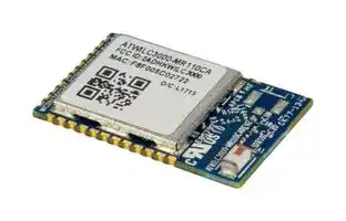


ATWILC3000-MR110UA
Controller Module, 2.412 to 2.472 GHz, SPI, SDIO, UART, Bluetooth 5.0, 2.5 to 4.2V Supply, Module
- Manufacturer: MICROCHIP
- Product type:
- SVHC: No SVHC (04-Feb-2026)
- Frequency RF: 2.472GHz
- Product Range: ATWILC3000-MR110xA Series
- Module Interface: SPI, SDIO, UART
- Module Applications: Low-Power Mobile
| Delivery and price | |
|---|---|
| Units per pack | 250 |
| Price | 8.07 € |
| Current stock | 50+ |
| Lead time | 30 days |
**IEEE[®] 802.11 b/g/n Link Controller Module with Integrated Bluetooth[®] 5.0 ATWILC3000-MR110xA**

Product Page Links

## **Introduction**

The ATWILC3000-MR110xA module is an IEEE[®] 802.11 b/g/n RF/Baseband/Medium Access Control (MAC) link controller and Bluetooth[®] 5.0 compliant module[(1)] , optimized for low-power mobile applications. This module supports single stream 1x1 IEEE 802.11n mode providing up to 72 Mbps PHY rate. The ATWILC3000-MR110xA module features small form factor when integrating Power Amplifier (PA), Low Noise Amplifier (LNA), Transmit/ Receive switch and Power Management. The ATWILC3000-MR110CA integrates a chip antenna while the ATWILC3000-MR110UA adds a micro co-ax (u.FL) connector for connecting to an external antenna. This module offers very low power consumption while simultaneously providing high performance. This module contains all circuitry required including a 26 MHz crystal, PMU circuitry and a chip antenna or a micro co-ax (u.FL) RF connector. The ATWILC3000-MR110xA module requires a 32.768 kHz clock for sleep operation.

The ATWILC3000-MR110xA module utilizes highly optimized IEEE 802.11 Bluetooth coexistence protocols and provides Serial Peripheral Interface (SPI) and Secure Digital Input Output (SDIO) for interfacing with the host controller.

The references to the ATWILC3000-MR110xA module include the following devices:

- ATWILC3000-MR110CA

- ATWILC3000-MR110UA

## **Features**

## **IEEE 802.11**

- IEEE 802.11 b/g/n, Single Stream (1x1) 20 MHz Bandwidth WLAN Link

   - Compatible with Wi-Fi[®] 6/7 Access Points/Routers at 2.4 GHz

- IEEE 802.11 b/g/n (1x1) for Up to 72 Mbps PHY Rate

- Single Spatial Stream in 2.4 GHz ISM Band

- Integrated PA and T/R Switch

- Integrated Chip Antenna or U.FL Micro Co-ax Connector for Connecting to an External Antenna

- Superior Sensitivity and Range Via Advanced PHY Signal Processing

- Advanced Equalization and Channel Estimation

- Advanced Carrier and Timing Synchronization

- Supports Soft-AP

- Supports IEEE 802.11 WEP, WPA, WPA2 and WPA2 Enterprise Security

- Superior MAC Throughput Through Hardware Accelerated Aggregate A-MPDUs/A-MDSU Frame Reception and Block Acknowledgment

- On-Chip Memory Management Engine to Reduce Host Load

- SPI and SDIO Host Interfaces

Data Sheet

DS70005327D - 1

© 2025 Microchip Technology Inc. and its subsidiaries

**ATWILC3000-MR110xA**

- Operating Conditions:

   - Input/output operating voltage (VDDIO): 1.62V to 3.6V

   - Power supply for DC/DC convertor (VBAT): 2.5V to 4.2V

   - Operating temperature: -40°C to +85°C

- Wi-Fi Alliance[®] Certified for Connectivity and Optimizations:

   - ID: WFA72428

## **Bluetooth[®]**

- Bluetooth 5.0 (Basic Rate, Enhanced Data Rate and Bluetooth Low Energy)[(1)]

- Frequency Hopping

- Host Control Interface (HCI) Through High-Speed UART

- Integrated PA and T/R Switch

- Superior Sensitivity and Range

- Bluetooth SIG 5.0 Certification:

   - Declaration ID: D039158

## **Note:**

1. Bluetooth SIG QDID qualification is for Bluetooth Low Energy only.

Data Sheet

DS70005327D - 2

© 2025 Microchip Technology Inc. and its subsidiaries

**ATWILC3000-MR110xA**

## **Table of Contents**

|**Table of Contents**|**Table of Contents**|
|---|---|
|Introduction...........................................................................................................................................................................1||
|Features................................................................................................................................................................................. 1||
|1.|Ordering Information and Module Marking.............................................................................................................. 5|
|2.|Block Diagram................................................................................................................................................................6|
|3.|Pinout and Package Information.................................................................................................................................7|
||3.1.<br>Package Description.......................................................................................................................................... 9|
|4.|Electrical Characteristics.............................................................................................................................................10|
||4.1.<br>Absolute Maximum Ratings............................................................................................................................10|
||4.2.<br>Recommended Operating Conditions...........................................................................................................10|
||4.3.<br>DC Characteristics............................................................................................................................................10|
||4.4.<br>IEEE 802.11 b/g/n Radio Performance.......................................................................................................... 11|
||4.5.<br>Bluetooth Radio Performance........................................................................................................................14|
||4.6.<br>Timing Characteristics.....................................................................................................................................15|
|5.|Power Management....................................................................................................................................................19|
||5.1.<br>Device States.................................................................................................................................................... 19|
||5.2.<br>Controlling Device States................................................................................................................................ 19|
||5.3.<br>Power-Up/Down Sequence.............................................................................................................................20|
||5.4.<br>Digital I/O Pin Behavior During Power-Up Sequences................................................................................ 22|
|6.|Clocking........................................................................................................................................................................ 23|
||6.1.<br>Low-Power Clock..............................................................................................................................................23|
|7.|CPU and Memory Subsystem.................................................................................................................................... 24|
||7.1.<br>Processor.......................................................................................................................................................... 24|
||7.2.<br>Memory Subsystem.........................................................................................................................................24|
||7.3.<br>Nonvolatile Memory (eFuse).......................................................................................................................... 24|
|8.|WLAN Subsystem........................................................................................................................................................ 26|
||8.1.<br>MAC................................................................................................................................................................... 26|
||8.2.<br>PHY.................................................................................................................................................................... 27|
||8.3.<br>Radio..................................................................................................................................................................27|
|9.|Bluetooth®Subsystem............................................................................................................................................... 29|
||9.1.<br>Bluetooth®5.0 Features................................................................................................................................. 29|
||9.2.<br>Features............................................................................................................................................................ 29|
|10.|External Interfaces...................................................................................................................................................... 30|
||10.1. Interfacing with the Host Microcontroller.................................................................................................... 30|
||10.2. SDIO Client Interface....................................................................................................................................... 31|
||10.3. SPI Client Interface...........................................................................................................................................32|
||10.4. I2C Client Interface...........................................................................................................................................33|
||10.5. UART Interface................................................................................................................................................. 33|
||10.6. GPIOs.................................................................................................................................................................34|


Data Sheet

DS70005327D - 3

© 2025 Microchip Technology Inc. and its subsidiaries

**ATWILC3000-MR110xA**

10.7. Internal Pull-Up Resistors............................................................................................................................... 34 11. Application Reference Design....................................................................................................................................35 11.1. Host Interface - SPI.......................................................................................................................................... 35 11.2. Host Interface - SDIO ......................................................................................................................................36 12. Package Outline Drawings......................................................................................................................................... 37 13. Design Considerations................................................................................................................................................42 13.1. Module Placement and Routing Guidelines................................................................................................. 42 13.2. Antenna Performance of ATWILC3000-MR110CA....................................................................................... 43 13.3. ATWILC3000-MR110UA Placement and Routing Guidelines...................................................................... 46 13.4. Approved Antenna Types................................................................................................................................47 13.5. Reflow Profile Information..............................................................................................................................48 13.6. Module Assembly Considerations................................................................................................................. 49 13.7. Conformal Coating...........................................................................................................................................49 14. Appendix A: Regulatory Approval............................................................................................................................. 50 14.1. United States.................................................................................................................................................... 50 14.2. Canada.............................................................................................................................................................. 52 14.3. Europe...............................................................................................................................................................54 14.4. Japan..................................................................................................................................................................55 14.5. Korea................................................................................................................................................................. 56 14.6. Taiwan............................................................................................................................................................... 56 14.7. China..................................................................................................................................................................57 14.8. Other Regulatory Information........................................................................................................................57 15. Reference Documentation.........................................................................................................................................58 16. Document Revision History....................................................................................................................................... 59 Microchip Information....................................................................................................................................................... 62 Trademarks..................................................................................................................................................................62 Legal Notice..................................................................................................................................................................62 Microchip Devices Code Protection Feature............................................................................................................62 Product Page Links............................................................................................................................................................. 63

Data Sheet

DS70005327D - 4

© 2025 Microchip Technology Inc. and its subsidiaries

**ATWILC3000-MR110xA Ordering Information and Module Marking**

## **1. Ordering Information and Module Marking**

The following table provides the ordering details for the ATWILC3000-MR110xA module.

**Table 1-1.** Ordering Details

|**Model Number**|**Ordering Code**|**Package**|**Description**|**Regulatory**<br>**Information(1)**|
|---|---|---|---|---|
|ATWILC3000-<br>MR110CA|ATWILC3000-<br>MR110CA|22.4 x 14.7 x 2.0 mm|Certifed module with<br>ATWILC3000-MU IC and chip<br>antenna|FCC, ISED, CE,<br>MIC, KCC, NCC,<br>SRRC|
|ATWILC3000-<br>MR110UA|ATWILC3000-<br>MR110UA|22.4 x 14.7 x 2.0 mm|Certifed module with<br>ATWILC3000-MU IC and u.FL<br>connector|FCC, ISED, CE|


## **Note:**

1. For additional details, refer to Appendix A: Regulatory Approval. The following figure illustrates the ATWILC3000-MR110xA module marking information.

**Figure 1-1.** Marking Information

|Device name<br>MR: Industrial|MR<br>1<br>1<br>0<br>x<br>ATWILC3000|ATWILC3000|MR|1|1|1|1|0|0|x|x|||||
|---|---|---|---|---|---|---|---|---|---|---|---|---|---|---|---|
|||||||||||||||||
|||||||||||||||||


1: No OTA/with shield

1: Reserved

0: Reserved

C: Chip antenna U: u.FL connector

Revision letter Blank: Tray Packing T : Tape and Reel

Data Sheet

DS70005327D - 5

© 2025 Microchip Technology Inc. and its subsidiaries

**ATWILC3000-MR110xA Block Diagram**

## **2. Block Diagram**

The following figure shows the block diagram of the ATWILC3000-MR110xA module.

## **Figure 2-1.** ATWILC3000-MR110xA Module Block Diagram

**==> picture [78 x 41] intentionally omitted <==**

**----- Start of picture text -----**<br>
Chip Antenna<br>or<br>u.FL Connector for<br>External Antenna<br>**----- End of picture text -----**<br>


Data Sheet

DS70005327D - 6

© 2025 Microchip Technology Inc. and its subsidiaries

**ATWILC3000-MR110xA Pinout and Package Information**

## **3. Pinout and Package Information**

This package contains an exposed paddle that must be connected to the system board ground. The ATWILC3000-MR110xA module pin assignment is shown in following figure.

**Figure 3-1.** ATWILC3000-MR110xA Module Pin Assignment

The following table provides the ATWILC3000-MR110xA module pin description.

**Table 3-1.** ATWILC3000-MR110xA Module Pin Description

|**Pin #**|**Pin Name**|**Pin Type**|**Description**|
|---|---|---|---|
|1|GND|GND|Ground|
|2|SDIO/SPI CFG|Digital Input|Connect to VDDIO through a 1 MΩ resistor to<br>enable SPI interface. Connect to GND to enable<br>SDIO interface|


Data Sheet

DS70005327D - 7

© 2025 Microchip Technology Inc. and its subsidiaries

**ATWILC3000-MR110xA Pinout and Package Information**

**Table 3-1.** ATWILC3000-MR110xA Module Pin Description (continued)

|**Table 3-1.**ATWILC3000-MR110xA Module Pin Descripton (contnued)|**Table 3-1.**ATWILC3000-MR110xA Module Pin Descripton (contnued)|**Table 3-1.**ATWILC3000-MR110xA Module Pin Descripton (contnued)|**Table 3-1.**ATWILC3000-MR110xA Module Pin Descripton (contnued)|
|---|---|---|---|
|**Pin #**|**Pin Name**|**Pin Type**|**Description**|
|3|NC|—|No connection|
|4|NC|—|No connection|
|5|NC|—|No connection|
|6|NC|—|No connection|
|7|RESETN|Digital Input|Active-low hard Reset. When this pin is asserted<br>low, the module is placed in the Reset state. When<br>this pin is asserted high, the module is out of Reset<br>and functions normally. Connect to a host output<br>that defaults low on power-up. If the host output is<br>tri-stated, add a 1 MΩ pull down resistor to ensure<br>a low level at power-up|
|8|BT_TXD|Digital I/O, Programmable pull<br>up|Bluetooth UART transmits data output. Connect to<br>UART_RXD of host|
|9|BT_RXD|Digital I/O, Programmable pull<br>up|Bluetooth UART receives data input. Connect to<br>UART_TXD of host|
|10|BT_RTS/I2C_SDA_S|Digital I/O, Programmable pull<br>up|I2C Client data. Used only for debug development<br>purposes. It is recommended to add a test point<br>for this pin. I2C will be the default confguration. If<br>fow control is enabled, this pin will be confgured<br>as UART RTS|
|11|BT_CTS/I2C_SCL_S|Digital I/O, Programmable pull<br>up|I2C Client clock. Used only for debug development<br>purposes. It is recommended to add a test point<br>for this pin. I2C will be the default confguration. If<br>fow control is enabled, this pin will be confgured<br>as UART CTS|
|12|VDDIO|Power|Digital I/O power supply|
|13|GND|GND|Ground|
|14|GPIO3|Digital I/O, Programmable pull<br>up|GPIO_3(1)|
|15|GPIO4|Digital I/O, Programmable pull<br>up|GPIO_4(1)|
|16|UART_TXD|Digital I/O, Programmable pull<br>up|Wi-Fi®UART TxD output. Used only for debug<br>development purposes. It is recommended to add<br>a test point for this pin|
|17|UART_RXD|Digital I/O, Programmable pull<br>up|Wi-Fi UART RxD input. Used only for debug<br>development purposes. It is recommended to add<br>a test point for this pin|
|18|VBAT|Power|Power supply pin for DC/DC converter and PA|
|19|CHIP_EN|Digital Input|PMU enable. High level enables the module and<br>the low level places the module in Power- Down<br>mode. Connect to a host output that defaults low<br>at power-up. If the host output is tri-stated, add a 1<br>MΩ pull down resistor if necessary to ensure a low<br>level at power-up|
|20|RTC_CLK|Digital I/O, Programmable pull<br>up|RTC Clock input. Connect to a 32.768 kHz clock<br>source|
|21|GND|GND|Ground|
|22|SD_CLK/GPIO8|Digital I/O, Programmable pull<br>up|SDIO clock line from the ATWILC3000-MR110xA,<br>when the module is confgured for SDIO|
|23|SD_CMD/SPI_SCK|Digital I/O, Programmable pull<br>up|SDIO CMD line from ATWILC3000-MR110xA, when<br>the module is confgured for SDIO. SPI clock<br>from ATWILC3000-MR110xA, when the module is<br>confgured for SPI|


Data Sheet

DS70005327D - 8

© 2025 Microchip Technology Inc. and its subsidiaries

**ATWILC3000-MR110xA Pinout and Package Information**

**Table 3-1.** ATWILC3000-MR110xA Module Pin Description (continued)

|**Table 3-1.**ATWILC3000-MR110xA Module Pin Descripton (contnued)|**Table 3-1.**ATWILC3000-MR110xA Module Pin Descripton (contnued)|**Table 3-1.**ATWILC3000-MR110xA Module Pin Descripton (contnued)|**Table 3-1.**ATWILC3000-MR110xA Module Pin Descripton (contnued)|
|---|---|---|---|
|**Pin #**|**Pin Name**|**Pin Type**|**Description**|
|24|SD_DAT0/SPI_MISO|Digital I/O, Programmable pull<br>up|SDIO Data Line 0 from the ATWILC3000-MR110xA,<br>when the module is confgured for SDIO. SPI MISO<br>(Host In Client Out) pin from the ATWILC3000-<br>MR110xA, when the module is confgured for SPI|
|25|SD_DAT1/SPI_SSN|Digital I/O, Programmable pull<br>up|SDIO Data Line 1 from the ATWILC3000-MR110xA,<br>when the module is confgured for SDIO. Active-low<br>SPI SSN (Client Select) pin from the ATWILC3000-<br>MR110xA, when the module is confgured for SPI|
|26|SD_DAT2/SPI_MOSI|Digital I/O, Programmable pull<br>up|SDIO Data Line 2 from the ATWILC3000-MR110xA,<br>when the module is confgured for SDIO. SPI MOSI<br>(Host Out Client In) pin from the ATWILC3000-<br>MR110xA, when the module is confgured for SPI|
|27|SD_DAT3/GPIO7|Digital I/O, Programmable pull<br>up|SDIO Data Line 3 from the ATWILC3000-MR110xA,<br>when the module is confgured for SDIO|
|28|GND|GND|Ground|
|29|GPIO17|Digital I/O, Programmable pull<br>up|GPIO_17(1)|
|30|GPIO18|Digital I/O, Programmable pull<br>up|GPIO_18(1)|
|31|GPIO19|Digital I/O, Programmable pull<br>up|GPIO_19(1)|
|32|GPIO20|Digital I/O, Programmable pull<br>up|GPIO_20(1)|
|33|IRQN|Digital output, Programmable<br>pull up|ATWILC3000-MR110xA module interrupt output.<br>Connect to a host interrupt pin|
|34|GPIO 21|Digital I/O, Programmable pull<br>up|GPIO_21(1)|
|35|GPIO 0|Digital I/O, Programmable pull<br>up|GPIO_0(1)|
|36|GND|GND|Ground|
|37|PADDLE VSS|Power|Connect to the system board ground|


## **Note:**

1. Usage of the GPIO functionality is not supported by the firmware. The data sheet will be updated once the support for this feature is added.

## **3.1. Package Description**

The following table provides the ATWILC3000-MR110xA module package dimensions.

**Table 3-2.** ATWILC3000-MR110xA Module Package Information

|**Parameter**|**Value**|**Unit**|
|---|---|---|
|Pad count|37|—|
|Package size|22.43 x 14.73||
|Total thickness|2.09|mm|
|Pad pitch|1.20||
|Pad width|0.81||
|Exposed pad size|4.4 x 4.4||


Data Sheet

DS70005327D - 9

© 2025 Microchip Technology Inc. and its subsidiaries

**ATWILC3000-MR110xA Electrical Characteristics**

## **4. Electrical Characteristics**

This chapter provides an overview of the electrical characteristics of the ATWILC3000-MR110xA module.

## **4.1. Absolute Maximum Ratings**

The following table provides the absolute maximum ratings for the ATWILC3000-MR110xA module.

**Table 4-1.** ATWILC3000-MR110xA Module Absolute Maximum Ratings

|**Characteristic**|**Symbol**|**Min.**|**Max.**|**Unit**|
|---|---|---|---|---|
|I/O Supply Voltage|VDDIO|-0.3|5.0||
|Battery Supply Voltage|VBAT|-0.3|5.0|V|
|Digital Input Voltage|VIN(1)|-0.3|VDDIO||
|ESD|VESD(2)|—|±4|kV|
|Storage Temperature|TA|-65|150|ºC|
|Junction Temperature|—|—|125||
|RF input power max.|—|—|10|dBm|


1. VIN corresponds to all the digital pins.

2. Horizontal Coupling Plane (HCP) and Vertical Coupling Plane (VCP) discharge methods are used.

**Info** Stresses beyond those listed under “Absolute Maximum Ratings” cause permanent damage to the device. This is a stress rating only. The functional operation of the device at those or any other conditions above those indicated in the operation listings of this specification is not implied. Exposure to maximum rating conditions for extended periods affects the device reliability.

## **4.2. Recommended Operating Conditions**

The following table provides the recommended operating conditions for the ATWILC3000-MR110xA module.

**Table 4-2.** ATWILC3000-MR110xA Module Recommended Operating Conditions

|**Characteristic**|**Symbol**|**Min.**|**Typ.**|**Max.**|**Units**|
|---|---|---|---|---|---|
|I/O Supply Voltage Low Range|VDDIOL(2)|1.62|1.80|2.00||
|I/O Supply Voltage Mid Range|VDDIOM(2)|2.00|2.50|3.00|V|
|I/O Supply Voltage High Range|VDDIOH(2)|3.00|3.30|3.60||
|Battery Supply Voltage|VBAT|2.5(3)|3.30|4.20||
|Operating Temperature|—|-40|—|85|ºC|


## **Notes:**

1. The battery supply voltage is applied to the VBAT pin.

2. The I/O supply voltage is applied to the VDDIO pin.

3. The ATWILC3000-MR110xA module is functional across this range of voltages; however, optimal RF performance is ensured for VBAT in the range ≥ 3.0V VBAT ≤ 4.2V.

## **4.3. DC Characteristics**

The following table provides the DC characteristics for the ATWILC3000-MR110xA module digital pads.

Data Sheet

DS70005327D - 10

© 2025 Microchip Technology Inc. and its subsidiaries

**ATWILC3000-MR110xA Electrical Characteristics**

**Table 4-3.** DC Electrical Characteristics

|**VDDIO Condition**|**Characteristic**|**Min.**|**Typ.**|**Max.**|**Unit**|
|---|---|---|---|---|---|
|VDDIOL|Input Low Voltage (VIL)|-0.30|—|0.60||
||Input High Voltage (VIH)|VDDIO -0.60|—|VDDIO+0.30|V|
||Output Low Voltage (VOL)|—|—|0.45||
||Output High Voltage (VOH)|VDDIO -0.50|—|—||
|VDDIOM|Input Low Voltage (VIL)|-0.30|—|0.63||
||Input High Voltage (VIH)|VDDIO -0.60|—|VDDIO+0.30||
||Output Low Voltage (VOL)|—|—|0.45||
||Output High Voltage (VOH)|VDDIO -0.50|—|—||
|VDDIOH|Input Low Voltage (VIL)|-0.30|—|0.65||
||Input High Voltage (VIH)|VDDION -0.60|—|VDDIO+0.30 (up<br>to 3.60)||
||Output Low Voltage (VOL)|—|—|0.45||
||Output High Voltage (VOH)|VDDIO -0.50|—|—||
|All|Output Loading|—|—|20|F|
||Digital Input Load|—|—|6|p|
|VDDIOL|Pad Driver Strength|1.7|2.4|—||
|VDDIOM|Pad Driver Strength|3.4|6.5|—|mA|
|VDDIOH|Pad Driver Strength|10.6|13.5|—||


## **4.4. IEEE 802.11 b/g/n Radio Performance**

## **4.4.1. Receiver Performance**

The receiver performance under nominal conditions are:

- VBAT = 3.3V

- VDDIO = 3.3V

- Temperature = 25 °C

- Measured after RF matching network

- WLAN Channel 6 (2437 MHz)

The following table provides the receiver performance characteristics for the ATWILC3000-MR110xA module.

**Table 4-4.** IEEE 802.11 Receiver Performance Characteristics

|**Parameter**|**Description**|**Min.**|**Typ.**|**Max.**|**Unit**|
|---|---|---|---|---|---|
|Frequency|—|2,412|—|2,472|MHz|
||1 Mbps DSSS|—|-95.0|—||
|Sensitivity<br>802.11b|2 Mbps DSSS|—|-93.5|—|dBm|
||5.5 Mbps DSSS|—|-90.0|—||
||11 Mbps DSSS|—|-86.0|—||


Data Sheet

DS70005327D - 11

© 2025 Microchip Technology Inc. and its subsidiaries

**ATWILC3000-MR110xA Electrical Characteristics**

**Table 4-4.** IEEE 802.11 Receiver Performance Characteristics (continued)

|**Table 4-4.**IEEE 802.11|Receiver Performance Characteristcs (contnued)|Receiver Performance Characteristcs (contnued)|Receiver Performance Characteristcs (contnued)|Receiver Performance Characteristcs (contnued)|Receiver Performance Characteristcs (contnued)|
|---|---|---|---|---|---|
|**Parameter**|**Description**|**Min.**|**Typ.**|**Max.**|**Unit**|
||6 Mbps OFDM|—|-90.0|—||
|Sensitivity<br>802.11g|9 Mbps OFDM|—|-88.5|—|dBm|
||12 Mbps OFDM|—|-86.0|—||
||18 Mbps OFDM|—|-84.5|—||
||24 Mbps OFDM|—|-82.0|—||
||36 Mbps OFDM|—|-78.5|—||
||48 Mbps OFDM|—|-74.5|—||
||54 Mbps OFDM|—|-73.0|—||
||MCS 0|—|-89.0|—||
|Sensitivity<br>802.11n<br>(BW = 20 MHz, 800 ns<br>GI)|MCS 1|—|-87.0|—|dBm|
||MCS 2|—|-84.0|—||
||MCS 3|—|-81.5|—||
||MCS 4|—|-78.0|—||
||MCS 5|—|-74.0|—||
||MCS 6|—|-72.0|—||
||MCS 7|—|-70.0|—||
||1-11 Mbps DSSS|—|0|—||
|Maximum Receive<br>Signal Level|6-54 Mbps OFDM|—|0|—|dBm|
||MCS 0 – 7 (800ns GI)|—|0|—||
||1 Mbps DSSS (30 MHz ofset)|—|50|—||
|Adjacent Channel<br>Rejection|11 Mbps DSSS (25 MHz ofset)|—|43|—|dB|
||6 Mbps OFDM (25 MHz ofset)|—|40|—||
||54 Mbps OFDM (25 MHz ofset)|—|25|—||
||MCS 0 – 20 MHz BW (25 MHz ofset)|—|40|—||
||MCS 7 – 20 MHz BW (25 MHz ofset)|—|20|—||


## **4.4.2. Transmitter Performance**

The transmitter performance under nominal conditions are:

- VBAT = 3.3V

- VDDIO = 3.3V

- Temperature = 25 °C

The following table provides the transmitter performance characteristics for the ATWILC3000MR110CA module.

**Table 4-5.** IEEE 802.11 Transmitter Performance Characteristics of ATWILC3000-MR110CA

|**Parameter**|**Description**|**Minimum**|**Typical**|**Max.**|**Unit**|
|---|---|---|---|---|---|
|Frequency|—|2,412|—|2,472|MHz|
||802.11b 1 Mbps|—|17.0(1)|—||
|Output Power|802.11b 11 Mbps|—|18.5(1)|—|dBm|
||802.11g OFDM 6 Mbps|—|17.5(1)|—||
||802.11g OFDM 54 Mbps|—|16.0(1)|—||
||802.11n HT20 MCS 0 (800ns GI)|—|17.0(1)|—||
||802.11n HT20 MCS 7 (800ns GI)|—|13.0(1)|—||
|TX Power Accuracy|—|—|±1.5(2)|—|dB|
|Carrier Suppression|—|—|30.0|—|dBc|


Data Sheet

DS70005327D - 12

© 2025 Microchip Technology Inc. and its subsidiaries

**ATWILC3000-MR110xA Electrical Characteristics**

**Table 4-5.** IEEE 802.11 Transmitter Performance Characteristics of ATWILC3000-MR110CA (continued)

|**Table 4-5.**IEEE 802.11 Tran|smiter Performance Characteristcs of ATWILC3000-MR110CA (contnued)|smiter Performance Characteristcs of ATWILC3000-MR110CA (contnued)|smiter Performance Characteristcs of ATWILC3000-MR110CA (contnued)|smiter Performance Characteristcs of ATWILC3000-MR110CA (contnued)|smiter Performance Characteristcs of ATWILC3000-MR110CA (contnued)|
|---|---|---|---|---|---|
|**Parameter**|**Description**|**Minimum**|**Typical**|**Max.**|**Unit**|
|Harmonic Output Power<br>|2nd|—|—|-41||
|(Radiated, Regulatory<br>mode)|3rd|—|—|-41|dBm/MHz|


## **Notes:**

1. Measured at IEEE 802.11 specification compliant EVM/Spectral mask.

2. Measured after RF matching network.

3. The operating temperature range is -40°C to +85°C. RF performance is ensured at a room temperature of 25°C with a 2-3 dB change at boundary conditions.

4. With respect to TX power, different (higher/lower) RF output power settings may be used for specific antennas and/or enclosures, in which case, re-certification may be required.

5. The availability of some specific channels and/or operational frequency bands are countrydependent and must be programmed at the Host product factory to match the intended destination. Regulatory bodies prohibit exposing the settings to the end user. This requirement needs to be taken care of via Host implementation.

6. The Host product manufacturer must ensure that the RF behavior adheres to the certification (for example, FCC, ISED) requirements when the module is installed in the final Host product.

The following table provides the transmitter performance characteristics for the ATWILC3000MR110UA module.

**Table 4-6.** IEEE 802.11 Transmitter Performance Characteristics of ATWILC3000-MR110UA

|**Parameter**|**Description**|**Minimum**|**Typical**|**Max.**|**Unit**|
|---|---|---|---|---|---|
|Frequency|—|2,412|—|2,472|MHz|
||802.11b 1 Mbps|—|15.5(1)|—||
|Output Power|802.11b 11 Mbps|—|16.5(1)|—|dBm|
||802.11g OFDM 6 Mbps|—|17.0(1)|—||
||802.11g OFDM 54 Mbps|—|14.0(1)|—||
||802.11n HT20 MCS 0 (800 ns GI)|—|17.0(1)|—||
||802.11n HT20 MCS 7 (800 ns GI)|—|10.5(1)|—||
|TX Power Accuracy|—|—|±1.5(2)|—|dB|
|Carrier Suppression|—|—|30.0|—|dBc|
|Harmonic Output Power<br>|2nd|—|—|-41||
|(Radiated, Regulatory<br>mode)|3rd|—|—|-41|dBm/MHz|


## **Notes:**

1. Measured at IEEE 802.11 specification compliant EVM/Spectral mask.

2. Measured after RF matching network.

3. The operating temperature range is -40°C to +85°C. RF performance is ensured at room temperature of 25°C with a 2-3 dB change at boundary conditions.

4. With respect to TX power, different (higher/lower) RF output power settings may be used for specific antennas and/or enclosures, in which case, re-certification may be required.

5. The availability of some specific channels and/or operational frequency bands are countrydependent and must be programmed at the Host product factory to match the intended destination. Regulatory bodies prohibit exposing the settings to the end user. This requirement needs to be taken care of via Host implementation.

Data Sheet

DS70005327D - 13

© 2025 Microchip Technology Inc. and its subsidiaries

**ATWILC3000-MR110xA Electrical Characteristics**

6. The Host product manufacturer must ensure that the RF behavior adheres to the certification (for example, FCC, ISED) requirements when the module is installed in the final Host product.

## **4.5. Bluetooth Radio Performance**

## **4.5.1. Receiver Performance**

The receiver performance under nominal conditions are:

- VBAT = 3.3V

- VDDIO = 3.3V

- Temperature = 25 °C

- Measured after RF matching network.

The following table provides the Bluetooth receiver performance characteristics for the ATWILC3000-MR110xA module.

**Table 4-7.** Bluetooth Receiver Performance Characteristics

|**Parameter**|**Description**|**Min.**|**Typ.**|**Max.**|**Unit**|
|---|---|---|---|---|---|
|Frequency|—|2,402|—|2,480|MHz|
||GFSK 1Mbps – Basic Rate(1)|—|-91.5|—||
|Sensitivity<br>Ideal TX|π/4 DQPSK 2Mbps(1)|—|-89.0|—|dBm|
||8DPSK 3Mbps(1)|—|-86.0|—||
||BLE (GFSK)|—|-92.5|—||
|Maximum Receive Signal Level|BLE (GFSK)|—|0|—||
||Co-channel|—|9|—||
|Interference performance(BLE)|Adjacent + 1 MHz|—|-3|—|dB|
||Adjacent - 1 MHz|—|0|—||
||Adjacent + 2 MHz(image frequency)|—|-28|—||
||Adjacent - 2 MHz|—|-44|—||
||Adjacent + 3 MHz (adjacent to image)|—|-38|—||
||Adjacent - 3 MHz|—|-38|—||
||Adjacent + 4 MHz|—|-48|—||
||Adjacent - 4 MHz|—|-33|—||
||Adjacent + 5 MHz|—|-37|—||
||Adjacent - 5 MHz|—|-33|—||


## **Note:**

1. The data is preliminary.

## **4.5.2. Transmitter Performance**

The transmitter performance under nominal conditions are:

- VBAT = 3.3V

- VDDIO = 3.3V

- Temperature = 25 °C

- Measured after RF matching network.

The following table provides the Bluetooth transmitter performance characteristics for the ATWILC3000-MR110xA module.

Data Sheet

DS70005327D - 14

© 2025 Microchip Technology Inc. and its subsidiaries

**ATWILC3000-MR110xA Electrical Characteristics**

**Table 4-8.** Bluetooth Transmitter Performance Characteristics

|**Parameter**<br>~~es~~|**Description**<br>~~ee~~|**Min.**|**Typ.**|**Max.**|**Unit**|
|---|---|---|---|---|---|
|Frequency<br>~~es~~|—<br>~~ee~~|2,402|—|2,480|MHz|
|Output Power|GFSK 1Mbps – Basic Rate(1)|—|1.8|—|dBm|
||π/4 DQPSK 2Mbps(1)|—|1.8|—||
||8DPSK 3Mbps(1)|—|1.8|—||
||BLE (GFSK)|—|1.5|—||
|In-band Spurious Emission<br>(BLE)|N + 2 (Image Frequency)|—|-32|—||
||N + 3 (Adjacent to Image frequency)|—|-36|—||
||N - 2|—|-52|—||
||N - 3|—|-54|—||


## **Note:**

1. The data is preliminary.

## **4.6. Timing Characteristics**

## **4.6.1. I[2] C Client Timing**

The I[2] C Client timing diagram for the ATWILC3000-MR110xA module is shown in the following figure.

**Figure 4-1.** I[2] C Client Timing Diagram

The following table provides the I[2] C Client timing parameters for the ATWILC3000-MR110xA module.

**Table 4-9.** I[2] C Client Timing Parameters

|**Parameter**<br>~~es~~|**Symbol**<br>~~es~~<br>~~Ge es~~|**Min.**<br>~~es~~<br>~~es es~~|**Max.**<br>~~es~~<br>~~es~~|**Units**<br>~~es~~<br>~~es~~|**Remarks**<br>~~es~~|
|---|---|---|---|---|---|
|SCL Clock Frequency|fSCL<br>~~Ge es~~|0<br>~~es es~~|400<br>~~es~~|kHz<br>~~es~~|—|
|SCL Low Pulse Width|tWL|1.3|—|µs|—|
|SCL High Pulse Width|tWH|0.6|—||—|
|SCL, SDA Fall Time|tHL|—|300|ns|—|
|SCL, SDA Rise Time|tLH|—|300||This is dictated by external<br>components|
|START Setup Time|tSUSTA|0.6|—|µs|—|
|START Hold Time|tHDSTA|0.6|—||—|
|SDA Setup Time|tSUDAT|100|—|ns|—|


Data Sheet

DS70005327D - 15

© 2025 Microchip Technology Inc. and its subsidiaries

**ATWILC3000-MR110xA**

**Electrical Characteristics**

**Table 4-9.** I ~~[2]~~ C Client Timing Parameters (continued)

|**Table 4-9.**I~~[2]~~C Client Timing Parameters (continued)<br>**Parameter**<br>**Symbol**<br>**Min.**<br>**Max.**<br>**Units**<br>**Remarks**<br>~~ee~~<br>esesSe|**Table 4-9.**I~~[2]~~C Client Timing Parameters (continued)<br>**Parameter**<br>**Symbol**<br>**Min.**<br>**Max.**<br>**Units**<br>**Remarks**<br>~~ee~~<br>esesSe|**Table 4-9.**I~~[2]~~C Client Timing Parameters (continued)<br>**Parameter**<br>**Symbol**<br>**Min.**<br>**Max.**<br>**Units**<br>**Remarks**<br>~~ee~~<br>esesSe|**Table 4-9.**I~~[2]~~C Client Timing Parameters (continued)<br>**Parameter**<br>**Symbol**<br>**Min.**<br>**Max.**<br>**Units**<br>**Remarks**<br>~~ee~~<br>esesSe|**Table 4-9.**I~~[2]~~C Client Timing Parameters (continued)<br>**Parameter**<br>**Symbol**<br>**Min.**<br>**Max.**<br>**Units**<br>**Remarks**<br>~~ee~~<br>esesSe|**Table 4-9.**I~~[2]~~C Client Timing Parameters (continued)<br>**Parameter**<br>**Symbol**<br>**Min.**<br>**Max.**<br>**Units**<br>**Remarks**<br>~~ee~~<br>esesSe|
|---|---|---|---|---|---|
|SDA Hold Time|tHDDAT<br>es|0<br> es|—<br> Se|ns|Client and Host Default|
|||40|—|µs|Host Programming Option|
|STOP Setup Time|tSUSTO|0.6|—|µs|—|
|Bus Free Time Between STOP and<br>START|tBUF|1.3|—||—|
|Glitch Pulse Reject|tPR|0|50|ns|—|


## **4.6.2. SPI Client Timing**

The SPI Client timing for the ATWILC3000-MR110xA module is provided in the following figures.

**Figure 4-2.** SPI Client Timing Diagram

The following table provides the SPI Client timing parameters for the ATWILC3000-MR110xA module.

**Table 4-10.** SPI Client Timing Parameters[(1)]

~~ee~~ **Parameter** ~~ee~~ **Symbol** ~~ee~~ **Min. Max. Unit** Clock Input Frequency[(2)] fSCK — 48 MHz

Data Sheet

DS70005327D - 16

© 2025 Microchip Technology Inc. and its subsidiaries

**ATWILC3000-MR110xA**

**Electrical Characteristics**

**Table 4-10.** SPI Client Timing Parameters ~~[(1)]~~ (continued)

|**Table 4-10.**SPI Client Timing Parameters~~[(1)]~~ (continued)<br>**Parameter**<br>**Symbol**<br>**Min.**<br>**Max.**<br>**Unit**<br>~~es~~<br>esGs|**Table 4-10.**SPI Client Timing Parameters~~[(1)]~~ (continued)<br>**Parameter**<br>**Symbol**<br>**Min.**<br>**Max.**<br>**Unit**<br>~~es~~<br>esGs|**Table 4-10.**SPI Client Timing Parameters~~[(1)]~~ (continued)<br>**Parameter**<br>**Symbol**<br>**Min.**<br>**Max.**<br>**Unit**<br>~~es~~<br>esGs|**Table 4-10.**SPI Client Timing Parameters~~[(1)]~~ (continued)<br>**Parameter**<br>**Symbol**<br>**Min.**<br>**Max.**<br>**Unit**<br>~~es~~<br>esGs|**Table 4-10.**SPI Client Timing Parameters~~[(1)]~~ (continued)<br>**Parameter**<br>**Symbol**<br>**Min.**<br>**Max.**<br>**Unit**<br>~~es~~<br>esGs|
|---|---|---|---|---|
|Clock Low Pulse Width|tWL<br>es|6<br>Gs|—|ns|
|Clock High Pulse Width|tWH|4|—||
|Clock Rise Time|tLH|0|7||
|Clock Fall Time|tHL|0|7||
|TXD Output Delay(3)|tODLY|3|9 from SCK fall||
|RXD Input Setup Time|tISU|3|—||
|RXD Input Hold Time|tIHD|5|—||
|SSN Input Setup Time|tSUSSN|5|—||
|SSN Input Hold Time|tHDSSN|5|—||


## **Notes:**

1. The timing is applicable to all SPI modes.

2. The maximum clock frequency specified is limited by the SPI Client interface internal design; the actual maximum clock frequency can be lower and depends on the specific PCB layout.

3. The timing is based on 15 pF output loading. Under all conditions, tLH + tWH + tHL + tWL must be less than or equal to 1/ fSCK.

## **4.6.3. SDIO Client Timing**

The SDIO Client interface timing for ATWILC3000-MR110xA module is shown in the following figure.

**Figure 4-3.** SDIO Client Timing Diagram

The following table provides the SDIO Client timing parameters for the ATWILC3000-MR110xA module.

**Table 4-11.** SDIO Client Timing Parameters

|**Parameter**<br>~~a~~|**Symbol**<br>~~Re~~|**Min.**|**Max.**|**Units**|
|---|---|---|---|---|
|Clock Input Frequency(1)<br>~~a~~|fPP<br>~~Re~~|—|50|MHz|


Data Sheet

DS70005327D - 17

© 2025 Microchip Technology Inc. and its subsidiaries

**ATWILC3000-MR110xA Electrical Characteristics**

**Table 4-11.** SDIO Client Timing Parameters (continued)

|**Table 4-11.**SDIO Client Timing Parameters (contnued)|**Table 4-11.**SDIO Client Timing Parameters (contnued)|**Table 4-11.**SDIO Client Timing Parameters (contnued)|**Table 4-11.**SDIO Client Timing Parameters (contnued)|**Table 4-11.**SDIO Client Timing Parameters (contnued)|
|---|---|---|---|---|
|**Parameter**|**Symbol**|**Min.**|**Max.**|**Units**|
|Clock Low Pulse Width|tWL|6|—||
|Clock High Pulse Width|tWH|7|—|ns|
|Clock Rise Time|tLH|0|5||
|Clock Fall Time|tHL|0|5||
|Input Setup Time|tISU|6|—||
|Input Hold Time|tIH|8|—||
|Output Delay(2)|tODLY|3|11||


## **Notes:**

1. The maximum clock frequency specified is limited by the SDIO Client interface internal design; the actual maximum clock frequency can be lower and depends on the specific PCB layout.

2. The timing is based on 15 pF output loading.

Data Sheet © 2025 Microchip Technology Inc. and its subsidiaries

DS70005327D - 18

**ATWILC3000-MR110xA Power Management**

## **5. Power Management**

## **5.1. Device States**

The ATWILC3000-MR110xA module has multiple device states, based on the state of the IEEE 802.11 and Bluetooth subsystems. It is possible for both subsystems to be active at the same time. To simplify the device power consumption breakdown, the following basic states are defined. One subsystem can be active at a time:

- WiFi_ON_Transmit – Device actively transmits IEEE 802.11 signal

- WiFi_ON_Receive – Device actively receives IEEE 802.11 signal

- BT_ON_Transmit – Device actively transmits Bluetooth signal

- BT_ON_Receive – Device actively receives Bluetooth signal

- Doze – Device is powered on but it does not actively transmit or receive data

- Power_Down – Device core supply is powered off

## **5.2.**

## **Controlling Device States**

The following table shows different device states and their power consumption for the ATWILC3000MR110xA. The device states can be switched using the following:

- CHIP_EN – Module pin (pin 19) enables or disables the DC/DC converter

- VDDIO – I/O supply voltage from external supply

In the ON states, VDDIO is ON and CHIP_EN is high (at VDDIO voltage level). To change from the ON states to Power_Down state, connect the RESETN and CHIP_EN pin to logic low (GND) by following the power-down sequence mentioned in Figure 5-1. When VDDIO is OFF and CHIP_EN is low, the chip is powered off with no leakage.

**Table 5-1.** Device States Current Consumption

|**Device State**|**Code Rate**|**Output Power**<br>**(dBm)**|**Current Consumption(1)**|**Current Consumption(1)**|
|---|---|---|---|---|
||||**IVBAT**|**IVDDIO**|
||802.11b 1 Mbps|17.0|272 mA|23.9 mA|
|ON_WiFi_Transmit|802.11b 11 Mbps|18.5|269 mA|23.9 mA|
||802.11g 6 Mbps|17.5|281 mA|23.9 mA|
||802.11g 54 Mbps|16.0|234 mA|23.9 mA|
||802.11n MCS 0|17.0|280 mA|23.9 mA|
||802.11n MCS 7|13.0|229 mA|23.9 mA|
||802.11b 1 Mbps|N/A|60.5 mA|23.6 mA|
|ON_WiFi_Receive|802.11b 11 Mbps|N/A|60.5 mA|23.6 mA|
||802.11g 6 Mbps|N/A|60.5 mA|23.6 mA|
||802.11g 54 Mbps|N/A|60.5 mA|23.6 mA|
||802.11n MCS 0|N/A|60.5 mA|23.6 mA|
||802.11n MCS 7|N/A|60.5 mA|23.6 mA|
|ON_BT_Transmit|BLE 1 Mbps|1.5|98.6 mA|2.5 mA|
|ON_BT_Receive|BLE 1 Mbps|N/A|69.1 mA|2.5 mA|
|Doze (Bluetooth Low<br>Energy Low Power)|N/A|N/A|1.4 mA(2)||
|Power_Down|N/A|N/A|1.25 µA(2)||


Data Sheet

DS70005327D - 19

© 2025 Microchip Technology Inc. and its subsidiaries

**ATWILC3000-MR110xA Power Management**

## **Notes:**

1. Conditions: VBAT = 3.3V, VDDIO = 3.3V, at 25°C.

2. The current consumption mentioned for these states is the sum of the current consumed in the VDDIO and VBAT voltage rails.

When power is not supplied to the device (DC/DC converter output and VDDIO are OFF, at ground potential), voltage cannot be applied to the ATWILC3000-MR110xA module pins because each pin contains an ESD diode from the pin to supply. This diode turns on when voltage higher than one diode-drop is supplied to the pin.

If voltage must be applied to the signal pads when the chip is in a low-power state, the VDDIO supply must be ON, so the Power_Down state must be used. Similarly, to prevent the pin-to-ground diode from turning ON, do not apply voltage that is more than one diode-drop below the ground to any pin.

## **5.3. Power-Up/Down Sequence**

The following figure illustrates the power-up/down sequence for the ATWILC3000-MR110xA.

**Figure 5-1.** Power-Up/Down Sequence

The following table provides power-up/down sequence timing parameters.

**Table 5-2.** Power-Up/Down Sequence Timing

|**Parameter**<br>~~ee~~|**Min.**<br>~~ee~~|**Max.**<br>ee|**Units**<br>ee|**Description**<br>~~es~~|**Notes**|
|---|---|---|---|---|---|
|tA<br>~~ee~~|0<br>~~ee ~~|—<br> ee|ms<br> ee|VBAT rise to VDDIO rise <br>~~es~~|VBAT and VDDIO can rise simultaneously or connected<br>together. VDDIO must not rise before VBAT.|
|tB|0|—|ms|VDDIO rise to CHIP_EN<br>rise|CHIP_EN must not rise before VDDIO. CHIP_EN must be<br>driven high or low and must not be left floating.|
|tC|5|—|ms|CHIP_EN rise to<br>RESETN rise|This delay is required to stabilize the XO clock before RESETN<br>removal. RESETN must be driven high or low and must not be<br>left floating.|
|tA’|0|—|ms|VDDIO fall to VBAT fall|VBAT and VDDIO must fall simultaneously or be connected<br>together. VBAT must not fall before VDDIO.|
|tB’|0|—|ms|CHIP_EN fall to VDDIO<br>fall|VDDIO must not fall before CHIP_EN. CHIP_EN and RESETN<br>must fall simultaneously.|


Data Sheet

DS70005327D - 20

© 2025 Microchip Technology Inc. and its subsidiaries

**ATWILC3000-MR110xA Power Management**

**Table 5-2.** Power-Up/Down Sequence Timing (continued)

|**Table 5-2.**Power-Up/Down Sequence Timing (contnued)|**Table 5-2.**Power-Up/Down Sequence Timing (contnued)|**Table 5-2.**Power-Up/Down Sequence Timing (contnued)|**Table 5-2.**Power-Up/Down Sequence Timing (contnued)|**Table 5-2.**Power-Up/Down Sequence Timing (contnued)|**Table 5-2.**Power-Up/Down Sequence Timing (contnued)|
|---|---|---|---|---|---|
|**Parameter**|**Min.**|**Max.**|**Units**|**Description**|**Notes**|
|tC’|0|—|ms|RESETN fall to VDDIO<br>fall|VDDIO must not fall before RESETN. RESETN and CHIP_EN fall<br>simultaneously.|


Data Sheet

DS70005327D - 21

© 2025 Microchip Technology Inc. and its subsidiaries

**ATWILC3000-MR110xA Power Management**

## **5.4. Digital I/O Pin Behavior During Power-Up Sequences**

The following table represents the digital I/O pin states corresponding to the device power modes.

**Table 5-3.** Digital I/O Pin Behavior in Different Device States

|**Device State**|**VDDIO**|**CHIP_EN**|**RESETN**|**Output Driver**|**Input**<br>**Driver**|**Pull-Up/Down**<br>**Resistor (96 kΩ)**|
|---|---|---|---|---|---|---|
|Power_Down: Core Supply Of|High|Low|Low|Disabled<br>(High-Z)|Disabled|Disabled|
|Power-on Reset: Core Supply and<br>Hard Reset On|High|High|Low|Disabled<br>(High-Z)|Disabled|Enabled|
|Power-on Default: Core Supply<br>On, Device Out of Reset and Not<br>Programmed|High|High|High|Disabled<br>(High-Z)|Enabled|Enabled|
|On_Doze/On_Transmit/<br>On_Receive: Core Supply On,<br>Device Programmed by Firmware|High|High|High|Programmed by<br>Firmware for Each<br>Pin: Enabled or<br>Disabled|Opposite<br>of Output<br>Driver<br>State|Programmed by<br>Firmware for Each<br>Pin: Enabled or<br>Disabled|


Data Sheet

DS70005327D - 22

© 2025 Microchip Technology Inc. and its subsidiaries

**ATWILC3000-MR110xA Clocking**

## **6. Clocking**

## **6.1. Low-Power Clock**

The ATWILC3000-MR110xA module requires an external 32.768 kHz clock to be supplied at the module pin 20. This clock is used during the sleep operation. The frequency accuracy of this external clock must be within ±500 ppm.

Data Sheet

DS70005327D - 23

© 2025 Microchip Technology Inc. and its subsidiaries

**ATWILC3000-MR110xA CPU and Memory Subsystem**

## **7. CPU and Memory Subsystem**

## **7.1. Processor**

The ATWILC3000-MR110xA module has two Cortus APS3 32-bit processors, one is used for Wi-Fi and the other is used for Bluetooth. In IEEE 802.11 mode, the processor performs many of the MAC functions, including but not limited to: association, authentication, power management, security key management and MSDU aggregation/de-aggregation. In addition, the processor provides flexibility for various modes of operation, such as Station (STA) and Access Point (AP) modes. In Bluetooth mode, the processor handles multiple tasks of the Bluetooth protocol stack.

## **7.2. Memory Subsystem**

The APS3 core uses a 256 KB instruction/boot ROM (160 KB for IEEE 802.11 and 96 KB for Bluetooth), along with a 420 KB instruction RAM (128 KB for IEEE 802.11 and 292 KB for Bluetooth) and a 128 KB data RAM (64 KB for IEEE 802.11 and 64 KB for Bluetooth). In addition, the device uses a 160 KB shared/exchange RAM (128 KB for IEEE 802.11 and 32 KB for Bluetooth), accessible by the processor and MAC, which allows the processor to perform various data management tasks on the TX and RX data packets.

## **7.3. Nonvolatile Memory (eFuse)**

The ATWILC3000-MR110xA modules have 768 bits of nonvolatile eFuse memory that can be read by the CPU after a device reset. The eFuse is partitioned into six 128-bit banks (Bank 0 – Bank 5). Each bank has the same bit map (see the following figure). The purpose of the first 108 bits in each bank is fixed and the remaining 20 bits are general-purpose software dependent bits, or reserved for future use. Currently, the Bluetooth address is derived from the Wi-Fi MAC address such that the Bluetooth address = the Wi-Fi MAC address + 1.

This nonvolatile one-time-programmable (OTP) memory can be used for storing the following customer-specific parameters:

- MAC address

- Calibration information (crystal frequency offset and so on)

- Other software-specific configuration parameters

Each bank can be programmed independently, which allows for several updates of the device parameters following the initial programming. For example, if the MAC address is currently programmed in Bank 1, and to update the new MAC address, perform the following steps:

1. Invalidate the contents of Bank 1 by programming the Bank Invalid bit field of Bank 1.

2. Program Bank 2 with the new MAC address along with the values of ADC Calib (if used in Bank 1), Frequency Offset (from Bank 1), IQ Amp Correction (from Bank 1) and IQ Pha Correction (from Bank 1). The Used bit field for each corresponding value bit field must also be programmed.

3. Validate the contents of Bank 2 by programming the Bank Used bit field of Bank 2.

Each bit field (i.e., MAC Address, ADC Calibration, Frequency Offset, IQ Amp Correction, and IQ Pha Correction) has its corresponding Used bit field. Each Used bit field indicates the firmware that the value in the related bit field is valid. A value of '0' in the Used bit field indicates that the following bit field is invalid and a value of '1' programmed to the Used bit field indicates that the corresponding bit field is valid and can be used by firmware. By default, ATWILC3000-MR110xA modules are programmed with the MAC address, ADC Calib, Frequency Offset bits, IQ Amp and IQ Phase fields of Bank 1.

Data Sheet

DS70005327D - 24

© 2025 Microchip Technology Inc. and its subsidiaries

**ATWILC3000-MR110xA CPU and Memory Subsystem**

## **Figure 7-1.** Bit Map for ATWILC3000-MR110xA eFuse Bank

**==> picture [458 x 134] intentionally omitted <==**

**----- Start of picture text -----**<br>
Width 1 1 3 2 1 48 1 7 1 15 1 13 1 13 20<br>Bit 31 30 29:27 26:25 24 23:0 31:8 7 6:0 31 30:16 15 14:2 1 0 - 31:20 19 0<br>Word Word 0 Word 1 Word 2 Word 3<br>Version<br>Bank Used Bank Invalid Reserved Mac Addr ADC Calib Freq Offset IQ Amp Used IQ Pha Used Reserved<br>Mac Addr Used ADC Calib Used Freq Offset Used IQ Amp Correction IQ Pha Correction<br>**----- End of picture text -----**<br>


**Note:** The bit map was updated with bit fields IQ Amp correction and IQ Pha Correction fields from the firmware version 15.3 for WILC Linux and 4.5 for WILC RTOS onwards. Earlier, these bit fields were reserved for future use. For customers using firmware older than 15.3 for WILC Linux and 4.5 for WILC RTOS, IQ Amp correction and IQ Pha Correction bit fields will not be used by the firmware.

The matrix table below provides details on how different versions of the firmware would handle the IQ Amp Used, IQ Amp Correction, IQ Pha Used and IQ Pha Correction bit fields during Initialization.

|**Firmware Version Used by**<br>**Customer**|**IQ Amp Used and IQ Pha Used Bit Status**|**IQ Amp Used and IQ Pha Used Bit Status**|
|---|---|---|
||**Device with IQ Amp Used and IQ Pha Used Bits**<br>**with Value ‘1’**|**Device with IQ Amp Used and IQ Pha Used**<br>**Bits with Value ‘0’**|
|15.3 or later for WILC Linux<br>4.5 or later for WILC RTOS|The frmware loads the IQ calibration values from<br>the IQ Amp Correction and IQ Pha Correction<br>bit felds of the corresponding eFuse bank and<br>proceeds with Initialization.|The frmware ignores the values in the IQ<br>Amp Correction and IQ Pha Correction bit<br>felds and proceeds with Initialization.|
|Prior to 15.3 for WILC Linux<br>Prior to 4.5 for WILC RTOS|The frmware does not check for the IQ Amp Used and IQ Pha Used bit felds and proceeds<br>with Initialization.||


Data Sheet © 2025 Microchip Technology Inc. and its subsidiaries

DS70005327D - 25

**ATWILC3000-MR110xA WLAN Subsystem**

## **8. WLAN Subsystem**

The WLAN subsystem is composed of the Media Access Controller (MAC), Physical Layer (PHY) including the radio.

## **8.1. MAC**

The ATWILC3000-MR110xA module is designed to operate at low power, while providing high data throughput. The IEEE 802.11 MAC functions are implemented with a combination of dedicated datapath engines, hardwired control logic and a low power, high-efficiency microprocessor. The combination of dedicated logic with a programmable processor provides optimal power efficiency and real-time response while providing the flexibility to accommodate evolving standards and future feature enhancements.

The dedicated datapath engines are used to implement datapath functions with heavy computational requirements. For example, a Frame Check Sequence (FCS) engine checks the Cyclic Redundancy Check (CRC) of the transmitting and receiving packets and a cipher engine performs all the required encryption and decryption operations for the WEP, WPA-TKIP, WPA2 CCMP-AES and WPA2 Enterprise security requirements.

Control functions, which have real-time requirements, are implemented using hardwired control logic modules. These logic modules offer a real-time response while maintaining configurability through the processor. Examples of hardwired control logic modules are the channel access control module (implements EDCA, Beacon TX control, interframe spacing and so on), protocol timer module (responsible for the Network Access vector, back-off timing, timing synchronization function and slot management), MAC Protocol Data Unit (MPDU) handling module, aggregation/ deaggregation module, block ACK controller (implements the protocol requirements for burst block communication) and TX/RX control Finite State Machine (FSM) (coordinates data movement between PHY and MAC interface, cipher engine and the Direct Memory Access (DMA) interface to the TX/RX FIFOs).

The following are the characteristics of the MAC functions implemented solely in the software on the microprocessor:

- Functions with high memory requirements or complex data structures. Examples include association table management and power save queuing.

- Functions with low computational load or without critical real-time requirements. Examples include authentication and association.

- Functions that require flexibility and upgradeability. Examples include beacon frame processing and QoS scheduling.

## **Features**

The ATWILC3000-MR110xA MAC supports the following functions:

- IEEE 802.11b/g/n

- IEEE 802.11e WMM QoS EDCA Multiple Access Categories

- Advanced IEEE 802.11n Features:

   - Reception of aggregated MPDUs (A-MPDU)

   - Reception of aggregated MSDUs (A-MSDU)

   - Immediate block acknowledgment

   - Reduced Interframe Spacing (RIFS)

- IEEE 802.11i and WFA Security with Key Management:

   - WEP 64/128

   - WPA-TKIP

Data Sheet

DS70005327D - 26

© 2025 Microchip Technology Inc. and its subsidiaries

**ATWILC3000-MR110xA WLAN Subsystem**

   - 128-bit WPA2 CCMP (AES)

   - WPA2 Enterprise

- Advanced Power Management:

   - Standard IEEE 802.11 power save mode

   - Wi-Fi Alliance[®] WMM-PS (U-APSD)

- RTS-CTS and CTS-Self Support

- Either STA or AP Mode in the Infrastructure Basic Service Set Mode

- Concurrent Mode of Operation

## **8.2. PHY**

The ATWILC3000-MR110xA module WLAN PHY is designed to achieve reliable and power-efficient physical layer communication specified by IEEE 802.11 b/g/n in single stream mode with 20 MHz bandwidth. The advanced algorithms are used to achieve maximum throughput in a real-world communication environment with impairments and interference. The PHY implements all the required functions such as Fast Fourier Transform (FFT), filtering, Forward Error Correction (FEC) that is a Viterbi decoder, frequency, timing acquisition and tracking, channel estimation and equalization, carrier sensing, clear channel assessment and automatic gain control.

## **Features**

The IEEE 802.11 PHY supports the following functions:

- Single antenna 1x1 stream in 20 MHz channels

- Supports IEEE 802.11b DSSS-CCK modulation: 1, 2, 5.5 and 11 Mbps

- Supports IEEE 802.11g OFDM modulation: 6, 9, 12,18, 24, 36, 48 and 54 Mbps

- Supports IEEE 802.11n HT modulations MCS0-7, 20 MHz, 800 and 400ns guard interval: 6.5, 7.2, 13.0, 14.4, 19.5, 21.7, 26.0, 28.9, 39.0, 43.3, 52.0, 57.8, 58.5, 65.0 and 72.2 Mbps[(1)]

- IEEE 802.11n mixed mode operation

- Per packet TX power control

- Advanced channel estimation/equalization, automatic gain control, CCA, carrier/symbol recovery and frame detection

## **Note:**

1. Currently, short GI is not supported by the firmware. The data sheet will be updated when the feature is supported.

## **8.3. Radio**

This section presents information describing the properties and characteristics of the ATWILC3000MR110xA and Wi-Fi[®] radio transmit and receive performance capabilities of the device.

The performance measurements are taken at the RF pin assuming 50Ω impedance; the RF performance is ensured for a room temperature of 25 °C with a derating of 2–3 dB at the boundary conditions.

The measurements were taken under typical conditions: VBATT = 3.3V; VDDIO = 3.3V; temperature: +25 ºC

**Table 8-1.** Features and Properties

|**Feature**|**Description**|
|---|---|
|Part Number|ATWILC3000-MR110xA|
|WLAN Standard|IEEE 802.11 b/g/n, Wi-Fi®Compliant|


Data Sheet

DS70005327D - 27

© 2025 Microchip Technology Inc. and its subsidiaries

**ATWILC3000-MR110xA WLAN Subsystem**

**Table 8-1.** Features and Properties (continued)

|**Table 8-1.**Features and Propertes (contnued)||
|---|---|
|**Feature**|**Description**|
|Host Interface|SPI, SDIO|
|Dimension|22.4 × 14.7 × 2.0 mm|
|Frequency Range|2.412 GHz ~ 2.472 GHz (2.4 GHz ISM Band)|
|Number of Channels|11 for North America and 13 for Europe and Japan|
|Modulation|802.11b: DQPSK, DBPSK, CCK<br>802.11g/n: OFDM /64-QAM,16-QAM, QPSK, BPSK|
|Data Rate|802.11b: 1, 2, 5.5, 11 Mbps|
||802.11g: 6, 9, 12, 18, 24, 36, 48, 54 Mbps|
|Data Rate<br>(20 MHz, normal GI, 800 ns)|802.11n: 6.5, 13, 19.5, 26, 39, 52, 58.5, 65 Mbps|
|Data Rate<br>(20 MHz, short GI, 400 ns)1|802.11n: 7.2, 14.4, 21.7, 28.9, 43.3, 57.8, 65,72.2 Mbps|
|Operating Temperature|-40 to +85 °C|


## **Note:**

1. Currently, short GI is not supported by the firmware. The data sheet will be updated when the feature is supported.

Data Sheet © 2025 Microchip Technology Inc. and its subsidiaries

DS70005327D - 28

**ATWILC3000-MR110xA Bluetooth[®] Subsystem**

## **9.**

## **Bluetooth[®] Subsystem**

The Bluetooth Subsystem implements all the mission critical real-time functions required for full compliance with specification of the Bluetooth System, v5.0, Bluetooth SIG. The baseband controller consists of a modem and a Medium Access Controller (MAC) which encodes/decodes HCI packets, constructs baseband data packages and manages and monitors connection status, slot usage, data flow, routing, segmentation and buffer control.

The Bluetooth Subsystem performs Link Control Layer management supporting the following states:

- Standby

- Connection

- Page and Page Scan

- Inquiry and Inquiry Scan

- Sniff

## **9.1.**

## **Bluetooth[®] 5.0 Features**

- Extended Inquiry Response (EIR)

- Encryption Pause/Resume (EPR)

- Sniff Sub-Rating (SSR)

- Secure Simple Pairing (SSP)

- Link Supervision Timeout (LSTO)

- Link Management Protocol (LMP)

- Quality of Service (QOS)

## **9.2. Features**

- Supports different device roles: Broadcaster, Central, Observer, Peripheral

- Supports Frequency Hopping

- Handles Advertising/Data/Control packet types

- Supports Encryption (AES-128, SHA-256)

- Supports Bitstream processing (CRC, whitening)

Data Sheet

DS70005327D - 29

© 2025 Microchip Technology Inc. and its subsidiaries

**ATWILC3000-MR110xA External Interfaces**

## **10. External Interfaces**

The ATWILC3000-MR110xA module supports the following external interfaces:

- SPI client and SDIO client for IEEE 802.11 control and data transfer

- BT_UART for Bluetooth[®] control and data transfer

- I[2] C client for control

- Wi-Fi[®] UART for IEEE 802.11 debug logs

- SPI host for external Flash

- General Purpose Input/Output (GPIO) pins[(1)]

## **Note:**

1. Usage of the GPIO functionality is not supported by the firmware. The data sheet will be updated once the support for this feature is added.

## **10.1. Interfacing with the Host Microcontroller**

This section describes how to interface the ATWILC3000-MR110xA module with the host microcontroller. The interface comprises of a Client SPI/SDIO and additional control signals, as shown in the figure. Additional control signals are connected to the GPIO/IRQ interface of the microcontroller.

**Figure 10-1.** Interfacing with the Host Microcontroller

**==> picture [308 x 196] intentionally omitted <==**

**----- Start of picture text -----**<br>
Host MCU/MPU ATWILC3000-MR110xA<br>SDIO/SPI Host SDIO/SPI Client (Wi-Fi)<br>UART UART with optional HW<br>flow control (Bluetooth)<br>IRQ (Interrupt GPIO) IRQN<br>GPIO CHIP_EN<br>GPIO RESETN<br>**----- End of picture text -----**<br>


**Table 10-1.** Host Microcontroller Interface Pins

|**Module Pin#**|**Function(1)**|
|---|---|
|7|RESETN|
|33|IRQN|
|19|CHIP_EN|
|25|SD_DAT1/SPI_SSN|
|26|SD_DAT2/SPI_MOSI|
|24|SD_DAT0/SPI_MISO|
|23|SD_CMD/SPI_SCK|
|27|SD_DAT3|


Data Sheet

DS70005327D - 30

© 2025 Microchip Technology Inc. and its subsidiaries

**ATWILC3000-MR110xA External Interfaces**

**Table 10-1.** Host Microcontroller Interface Pins (continued)

|**Table 10-1.**Host Microcontroller Interface Pins (contnued)|**Table 10-1.**Host Microcontroller Interface Pins (contnued)|
|---|---|
|**Module Pin#**|**Function(1)**|
|22|SD_CLK|
|8|BT_TXD|
|9|BT_RXD|
|10|BT_RTS|
|11|BT_CTS|


## **Notes:**

1. Logic input for module pin SDIO/SPI_CFG(#2) determines whether SDIO or SPI Client interface is enabled.

   - Connect SDIO/SPI_CFG to VDDIO through a 1 MΩ resistor to enable the SPI interface.

   - Connect SDIO_SPI_CFG to ground to enable SDIO interface.

2. Adding test points for module pins BT_TXD (#8), BT_RXD (#9), BT_RTS (#10), BT_CTS (#11), UART_TXD (#16) and UART_RXD (#17) in the design is recommended.

## **10.2. SDIO Client Interface**

The ATWILC3000-MR110xA module SDIO Client is a full speed interface. This interface supports the 1-bit/4-bit SD transfer mode at the clock range of 0-50 MHz. The Host can use this interface to read and write from any register within the chip, as well as, configure the ATWILC3000-MR110xA module for DMA data transfer. To use this interface, pin 2 (SDIO_SPI_CFG) must be connected to the ground. The following table provides the SDIO Client pins mapped in the ATWILC3000-MR110xA module.

**Table 10-2.** SDIO Interface Pin Mapping

|**Pin #**|**SPI Function**|
|---|---|
|2|CFG: Must be connected to ground|
|27|DAT3: Data 3|
|26|DAT2: Data 2|
|25|DAT1: Data 1|
|24|DAT0: Data 0|
|23|CMD: Command|
|22|CLK: Clock|


When the SDIO card is inserted into an SDIO-aware Host, the detection of the card is through the means described in the SDIO specification. During the normal initialization and interrogation of the card by the Host, the card identifies itself as an SDIO device. The Host software obtains the card information in a tuple (linked list) format and determines if that card’s I/O function(s) are acceptable to activate. If the card is acceptable, it is allowed to power up fully and start the I/O function(s) built into it.

The SD memory card communication is based on an advanced 9-pin interface (clock, command, 4 data lines and 3 power lines) designed to operate at a maximum operating frequency of 50 MHz.

## **Features**

- Supports SDIO card specification version 2.0

- Host clock rate is variable between 0 and 50 MHz

- Supports 1-bit/4-bit SD bus modes

- Allows card to interrupt Host

- Responds to direct read/write (IO52) and extended read/write (IO53) transactions

- Supports suspend/resume operation

Data Sheet

DS70005327D - 31

© 2025 Microchip Technology Inc. and its subsidiaries

**ATWILC3000-MR110xA External Interfaces**

## **10.3. SPI Client Interface**

The ATWILC3000-MR110xA module provides a Serial Peripheral Interface (SPI) that operates as an SPI Client. The SPI Client interface can be used for control and for serial I/O of IEEE 802.11 data. The SPI client pins are mapped as shown in the following table. The RXD pin is the same as Host Output, Client Input (MOSI) and the TXD pin is the same as Host Input, Client Output (MISO). The SPI Client is a full-duplex, client-synchronous serial interface that is available immediately following reset when pin 2 (SDIO_SPI_CFG) is tied to VDDIO.

**Table 10-3.** SPI Client Interface Pin Mapping

|**Pin #**|**SPI Function**|
|---|---|
|2|CFG: Must be connected to VDDIO|
|25|SSN: Active Low Client Select|
|23|SCK: Serial Clock|
|26|RXD: Serial Data Receive (MOSI)|
|24|TXD: Serial Data Transmit (MISO)|


When the SPI is not selected (i.e., when the SSN is high), the SPI interface will not interfere with the data transfers between the serial host and the other serial client devices. When the serial client is not selected, its transmitted data output is buffered, resulting in a high impedance drive onto the serial host receive line.

The SPI Client interface responds to a protocol that allows an external Host to read or write any register in the chip and initiate DMA data transfers.

## **10.3.1. SPI Client Mode**

The SPI Client interface supports four standard modes as determined by the Clock Polarity (CPOL) and Clock Phase (CPHA) settings. These modes are given in the following table and figure. In the following figure, the red lines correspond to Clock Phase = 0 and the blue lines correspond to Clock Phase = 1.

**Table 10-4.** SPI Client Mode

|**Mode**|**CPOL**|**CPHA**|
|---|---|---|
|0|0|0|
|1|0|1|
|2|1|0|
|3|1|1(1)|


## **Note:**

1. The ATWILC3000-MR110xA firmware uses “SPI MODE 0” to communicate with the host.

Data Sheet

DS70005327D - 32

© 2025 Microchip Technology Inc. and its subsidiaries

**ATWILC3000-MR110xA External Interfaces**

**Figure 10-2.** SPI Client Clock Polarity and Clock Phase Timing

## **10.4. I[2] C Client Interface**

The I[2] C Client interface is a two-wire serial interface consisting of a Serial Data Line (SDA) on module pin 10 and a serial clock line (SCL) on module pin 11. This interface is used for debugging of the ATWILC3000-MR110xA module. I[2] C Client responds to the 7-bit address value 0x60. The ATWILC3000-MR110xA module I[2] C supports I[2] C bus Version 2.1 - 2000 and can operate in standard mode (with data rates up to 100 kbps) and fast mode (with data rates up to 400 kbps).

**Note:** For specific information on the I[2] C bus, refer to the Philips Specification entitled “The I[2] C-Bus Specification, Version 2.1”.

The I[2] C Client is a synchronous serial interface. The SDA line is a bidirectional signal and changes only while the SCL line is low, except for STOP, START and RESTART conditions. The output drivers are open-drain to perform wire-AND functions on the bus. The maximum number of devices on the bus is limited by only the maximum capacitance specification of 400 pF. Data is transmitted in byte packages.

## **10.5. UART Interface**

The ATWILC3000-MR110xA module provides Universal Asynchronous Receiver/Transmitter (UART) interfaces for serial communication in both IEEE 802.11 and Bluetooth subsystems.

- The Bluetooth subsystem has one UART interface: a 4-pin interface for control and data transfer (BT UART).

- The IEEE 802.11 subsystem has one 2-pin UART interface (Wi-Fi UART) that can be used for debugging.

The UART interfaces are compatible with the RS-232 standard, and the ATWILC3000-MR110xA module operates as a Data Terminal Equipment (DTE) type device. The 2-pin UART uses receive and transmit pins (RXD and TXD). The 4-pin UART uses two pins for data (TXD and RXD) and two pins for flow control/handshaking: Request To Send (RTS) and Clear To Send (CTS).

Bluetooth UART is available in module pins 8 (BT_TXD), 9 (BT_RXD), 10 (BT_RTS) and 11 (BT_CTS). Wi-Fi UART is available in module pins 16 (UART_TXD) and 17 (UART_RXD).

The following is the default configuration for the Wi-Fi UART interface of the ATWILC3000-MR110xA:

- Baud rate: 115200

- Data: 8-bit

- Parity: None

- Stop bit: 1-bit

Data Sheet

DS70005327D - 33

© 2025 Microchip Technology Inc. and its subsidiaries

**ATWILC3000-MR110xA External Interfaces**

- Flow control: None

   - **Important:** The RTS and CTS pins of BT UART are used for hardware flow control. These pins must be connected to the Host MCU UART and could be optionally enabled.

An example of UART receiving or transmitting a single packet is shown in the following figure. This example shows 7-bit data (0x45), odd parity and two stop bits.

**Figure 10-3.** Example of UART RX or TX Packet

## **10.6. GPIOs**

The ten General Purpose Input/Output (GPIO) pins, labeled GPIO 0, GPIO 3-4, GPIO 7-8 and GPIO 17-21, are allowed to perform specific functions of an application. Each GPIO pin can be programmed as an input (the value of the pin can be read by the Host or internal processor) or as an output (the output values can be programmed by the host or internal processor), where the default mode after power-up is input. GPIOs 7 and 8 are only available when the Host does not use the SDIO interface, which shares two of its pins with these GPIOs. Therefore, for SDIO-based applications, eight GPIOs (0, 3-4 and 17-21) are available.

## **Note:**

1. Usage of the GPIO functionality is not supported by the firmware. The data sheet will be updated once the support for this feature is added.

## **10.7. Internal Pull-Up Resistors**

The ATWILC3000-MR110xA provides programmable pull-up resistors on various pins. The purpose of these resistors is to keep any unused input pins from floating, which can cause excess current to flow through the input buffer from the VDDIO supply. Any unused pin on the device must leave these pull-up resistors enabled so the pin will not float.

The default state at power-up is with the pull-up resistor enabled. However, any pin that is used must have the pull-up resistor disabled. This is because if any pins are driven to a low level while the device is in the low power sleep state, current will flow from the VDDIO supply through the pull-up resistors, increasing the current consumption of the module.

The current through any pull-up resistor that is being driven low will be VDDIO/100k because the value of the pull-up resistor is approximately 100 kΩ. For VDDIO = 3.3V, the current is approximately 33 µA. Pins that are used and have had the programmable pull-up resistor disabled must always be actively driven to either a high or low level and not be allowed to float.

Data Sheet

DS70005327D - 34

© 2025 Microchip Technology Inc. and its subsidiaries

**ATWILC3000-MR110xA Application Reference Design**

## **11. Application Reference Design**

The ATWILC3000-MR110xA module application schematics for different supported host interfaces are shown in this section.

## **11.1. Host Interface - SPI**

## **Figure 11-1.** ATWILC3000-MR110xA Reference Schematic for SPI Operation

**Note:** Adding test points for module pins 8, 9, 10, 11, 16 and 17 in the design is recommended. The following table provides the reference Bill of Material details for the ATWILC3000-MR110xA module with the SPI as the host interface.

**Table 11-1.** ATWILC3000-MR110xA Reference Bill of Materials for SPI Operation

|**Item**|**Quantity**|**Reference**|**Value**|**Description**|**Manufacturer**|**Part Number**|**Footprint**|
|---|---|---|---|---|---|---|---|
|1|1|U1|ATWILC3000-<br>MR110xA|Wi-Fi/<br>Bluetooth/BLE<br>Combo Module|Microchip<br>Technology Inc.®|ATWILC3000-<br>MR110xA|Custom|
|2|1|U2|ASH7KW-32.768k<br>HZ-L-T|Oscillator, 32.768<br>kHz, +0/-175<br>ppm, 1.2V-5.5V,<br>-40°C - +85°C,<br>3.2x1.5 mm|Abracon®<br>Corporation|ASH7KW-32.76<br>8kHZ-L-T|OSCCC320X15<br>0X100-4N|
|3|1|R1|1M|RESISTOR, Thick<br>Film, 1 MΩ, 0201|Panasonic|ERJ-1GEJ105C|RS0201|
|4|13|R2-R14|0|RESISTOR, Thick<br>Film, 0Ω, 0201|Panasonic|ERJ-1GN0R00C|RS0201|


Data Sheet

DS70005327D - 35

© 2025 Microchip Technology Inc. and its subsidiaries

**ATWILC3000-MR110xA Application Reference Design**

## **11.2. Host Interface - SDIO**

**Figure 11-2.** ATWILC3000-MR110xA Application Schematic for SDIO Operation

**Note:** Adding test points for module pins 8, 9, 10, 11, 16 and 17 in the design is recommended.

The following table provides SDIO reference Bill of Material details for the ATWILC3000-MR110xA module with SDIO as the host interface.

**Table 11-2.** ATWILC3000-MR110xA Reference Bill of Materials for SDIO operation

|**Item**|**Quantity**|**Reference**|**Value**|**Description**|**Manufacturer**|**Part Number**|**Footprint**|
|---|---|---|---|---|---|---|---|
|1|1|U1|ATWILC3000-<br>MR110xA|Wi-Fi®/<br>Bluetooth®/BLE<br>Combo Module|Microchip<br>Technology Inc.®|ATWILC3000-<br>MR110xA|Custom|
|2|1|U3|ASH7KW-32.7<br>68kHZ-L-T|Oscillator,<br>32.768 kHz,<br>+0/-175 ppm,<br>1.2V to 5.5V,<br>-40°C to +85°C,<br>3.2x1.5 mm|Abracon®<br>Corporation|ASH7KW-32.768<br>kHZ-L-T|OSCCC320X15<br>0X100-4N|
|3|13|R2-R14|0|RESISTOR, Thick<br>Film, 0 Ω, 0201|Panasonic|ERJ-1GN0R00C|RS0201|


Data Sheet

DS70005327D - 36

© 2025 Microchip Technology Inc. and its subsidiaries

**ATWILC3000-MR110xA Package Outline Drawings**

## **12. Package Outline Drawings**

The ATWILC3000-MR110xA package details are outlined in this section.

## **36-Lead PCB Module (LDB) - 22.4x14.7 mm Body for ATWILC3000-MR110UA And ATWINC3400-MR210UA; Atmel Legacy Global Package Code RCJ**

**Note:** For the most current package drawings, please see the Microchip Packaging Specification located at http://www.microchip.com/packaging

**==> picture [439 x 236] intentionally omitted <==**

**----- Start of picture text -----**<br>
22.428<br>1.981 RF CONNECTOR 3.64 1.30<br>13 1<br>14 2.72<br>1.346<br>14.732<br>1.204<br>PITCH<br>24<br>25 36<br>1.341 METAL<br>1.204 PITCH 0.787<br>SHIELD<br>TOP VIEW 2.09<br>**----- End of picture text -----**<br>


**==> picture [104 x 18] intentionally omitted <==**

**----- Start of picture text -----**<br>
THIS PAD MUST BE<br>SOLDERED TO GROUND<br>**----- End of picture text -----**<br>


**==> picture [57 x 9] intentionally omitted <==**

**----- Start of picture text -----**<br>
SIDE VIEW<br>**----- End of picture text -----**<br>


**==> picture [286 x 200] intentionally omitted <==**

**----- Start of picture text -----**<br>
25 26 27 28 29 30 31 32 33 34 35 36<br>24<br>23 5.21<br>22<br>21<br>20<br>19 4.40<br>18<br>17<br>16<br>15 0.94<br>14<br>13 12 11 10 9 8 7 6 5 4 3 2 1<br>4.40<br>6.13<br>**----- End of picture text -----**<br>


**==> picture [77 x 9] intentionally omitted <==**

**----- Start of picture text -----**<br>
BOTTOM VIEW<br>**----- End of picture text -----**<br>


Microchip Technology Drawing  C04-21306-UA-LDB Rev D Sheet 1 of 2

Data Sheet

DS70005327D - 37

© 2025 Microchip Technology Inc. and its subsidiaries

**ATWILC3000-MR110xA Package Outline Drawings**

## **36-Lead PCB Module (LDB) - 22.4x14.7 mm Body for ATWILC3000-MR110UA And ATWINC3400-MR210UA; Atmel Legacy Global Package Code RCJ**

**Note:** For the most current package drawings, please see the Microchip Packaging Specification located at http://www.microchip.com/packaging

## RECOMMENDED LAND PATTERN

**==> picture [375 x 271] intentionally omitted <==**

**----- Start of picture text -----**<br>
1.204 SILK<br>6.128<br>PITCH SCREEN<br>4.400<br>13 1<br>1.880<br>14<br>5.118<br>4.400 14.732<br>12.045<br>EDGE OF<br>PC BOARD<br>5.214<br>24<br>25 36<br>1.985 0.813<br>13.244<br>22.428<br>**----- End of picture text -----**<br>


Microchip Technology Drawing  C04-21306-UA-LDB Rev D Sheet 2 of 2

Data Sheet

DS70005327D - 38

© 2025 Microchip Technology Inc. and its subsidiaries

**ATWILC3000-MR110xA Package Outline Drawings**

## **36-Lead PCB Module (LDB) - 22.4x14.7 mm Body for ATWILC3000-MR110CA And ATWINC3400-MR210CA; Atmel Legacy Global Package Code RCJ**

**Note:** For the most current package drawings, please see the Microchip Packaging Specification located at http://www.microchip.com/packaging

**==> picture [436 x 235] intentionally omitted <==**

**----- Start of picture text -----**<br>
22.428<br>1.981 METAL SHIELD 1.30<br>13 1<br>14<br>1.346<br>14.732<br>1.204<br>PITCH<br>24<br>25 36<br>1.341<br>1.204 PITCH ANTENNA 0.787<br>TOP VIEW 2.09<br>**----- End of picture text -----**<br>


**==> picture [285 x 220] intentionally omitted <==**

**----- Start of picture text -----**<br>
THIS PAD MUST BE<br>SOLDERED TO GROUND<br>25 26 27 28 29 30 31 32 33 34 35 36<br>24<br>23 5.21<br>22<br>21<br>20<br>19 4.40<br>18<br>17<br>16<br>15 0.94<br>14<br>13 12 11 10 9 8 7 6 5 4 3 2 1<br>4.40<br>6.13<br>**----- End of picture text -----**<br>


**==> picture [56 x 9] intentionally omitted <==**

**----- Start of picture text -----**<br>
SIDE VIEW<br>**----- End of picture text -----**<br>


BOTTOM VIEW

Microchip Technology Drawing  C04-21306-CA-LDB Rev D Sheet 1 of 2

Data Sheet

DS70005327D - 39

© 2025 Microchip Technology Inc. and its subsidiaries

**ATWILC3000-MR110xA Package Outline Drawings**

## **36-Lead PCB Module (LDB) - 22.4x14.7 mm Body for ATWILC3000-MR110CA And ATWINC3400-MR210CA; Atmel Legacy Global Package Code RCJ**

**Note:** For the most current package drawings, please see the Microchip Packaging Specification located at http://www.microchip.com/packaging

**==> picture [116 x 133] intentionally omitted <==**

**==> picture [79 x 107] intentionally omitted <==**

## RECOMMENDED LAND PATTERN

**==> picture [381 x 276] intentionally omitted <==**

**----- Start of picture text -----**<br>
1.204 SILK<br>6.128<br>PITCH SCREEN<br>4.400<br>13 1<br>1.880<br>14<br>5.118<br>4.400 14.732<br>12.045<br>EDGE OF<br>PC BOARD<br>5.214<br>24<br>25 36<br>1.985 0.813<br>13.244<br>22.428<br>**----- End of picture text -----**<br>


Microchip Technology Drawing  C04-21306-CA-LDB Rev D Sheet 2 of 2

Data Sheet

DS70005327D - 40

© 2025 Microchip Technology Inc. and its subsidiaries

**ATWILC3000-MR110xA Package Outline Drawings**

## **Notes:**

1. Dimensions are in mm.

2. Having a 5×5 grid of GND vias solidly connecting the exposed GND paddle of the module to the ground plane on the inner/other layers of the host board is recommended. This will provide a good ground and thermal transfer for the ATWILC3000-MR110xA module.

Data Sheet

DS70005327D - 41

© 2025 Microchip Technology Inc. and its subsidiaries

**ATWILC3000-MR110xA Design Considerations**

## **13. Design Considerations**

This chapter provides the guidelines on module placement and routing to achieve the best performance.

## **13.1. Module Placement and Routing Guidelines**

It is critical to follow the recommendations listed below to achieve the best RF performance:

- The module must be placed on the host board, and the chip antenna area must not overlap with the host board. The portion of the module containing the antenna must not stick out over the edge of the host board. Figure 13-2 shows the best, poor and worst case module placements in the host board.

**Note:** Do not place the module in the middle of the host board or far away from the host board edge.

- Follow the mechanical recommendations as shown in Figure 13-1. The antenna is specifically tuned to the mechanical recommendations depicted in Figure 13-1. The host PCB must have a thickness of 1.5mm.

- Follow the module placement and keepout recommendation, as shown in Figure 13-1. – Avoid routing any traces in the highlighted region on the top layer of the host board, which will be directly below the module area.

   - Follow the electrical keepout layer recommendation, as shown in Figure 13-1. There must be no copper in all layers of the host board in this region. Avoid placing any components (like mechanical spacers, bumpon, etc.) in the area above the line indicated in the Figure 13-1.

   - Place the GND polygon pour below the module with the recommended boundary in the top layer of the host board, as shown in Figure 13-1. Do not have any breaks in this GND plane. The GND polygon pour in the top layer of the host board must have a minimum area of 20 x 40 mm.

   - Place sufficient GND vias in the highlighted area below the module for better RF performance.

   - Having a 5x5 grid of GND vias solidly connecting the exposed GND paddle of the module to the ground plane on the inner/other layers of the host board is recommended. This will act as a good ground and thermal conduction path for the ATWILC3000-MR110xA module. The GND vias must have a minimum via hole size of 0.2 mm.

   - The antenna on the module must not be placed in direct contact or close proximity to plastic casing/objects. Keep a minimum clearance of > 7 mm in all directions around the chip antenna.

- Do not enclose the antenna within a metal shield.

- Keep any components that may radiate noise or signals within the 2.4 GHz to 2.5 GHz frequency band away from the antenna and, if possible, shield those components. Any noise radiated from the host board in this frequency band will degrade the sensitivity of the module.

- Make sure the width of the traces routed to GND, VDDIO and VBAT rails are sufficiently larger for handling the peak TX current consumption.

Data Sheet

DS70005327D - 42

© 2025 Microchip Technology Inc. and its subsidiaries

**ATWILC3000-MR110xA Design Considerations**

**Figure 13-1.** ATWILC3000-MR110CA Placement Reference

**Figure 13-2.** ATWILC3000-MR110CA Placement Examples

## **13.2. Antenna Performance of ATWILC3000-MR110CA**

The ATWILC3000-MR110CA uses a chip antenna that is fed via matching network. The table below lists the technical specifications of the chip antenna.

**Table 13-1.** Chip Antenna Specification

|**Parameter**|**Value**|
|---|---|
|Peak gain|0.5 dBi|
|Operating Frequency|2400 - 2500 MHz|
|Antenna P/N|AT3216-B2R7HAA|
|Antenna vendor|ACX|


## **Antenna Radiation Pattern**

The following figures illustrate the antenna radiation pattern measured for the ATWILC3000MR110CA module mounted in the ATWILC3000-SHLD evaluation kit. During the measurement, the

Data Sheet

DS70005327D - 43

© 2025 Microchip Technology Inc. and its subsidiaries

**ATWILC3000-MR110xA Design Considerations**

chip antenna is placed in the XZ plane with the Y axis being perpendicular to the module and pointing to the back of the module.

**Figure 13-3.** Antenna Radiation Pattern When Phi = 0 Degrees

Data Sheet

DS70005327D - 44

© 2025 Microchip Technology Inc. and its subsidiaries

**ATWILC3000-MR110xA Design Considerations**

## **Figure 13-4.** Antenna Radiation Pattern When Phi = 90 Degrees

Data Sheet

DS70005327D - 45

© 2025 Microchip Technology Inc. and its subsidiaries

**ATWILC3000-MR110xA Design Considerations**

**Figure 13-5.** Antenna Radiation Pattern When Theta = 90 Degrees

## **13.3. ATWILC3000-MR110UA Placement and Routing Guidelines**

The ATWILC3000-MR110UA module has a micro co-ax (u.FL) RF connector for the external antenna. The choice of antenna is limited to the antenna types for which the module was tested and approved.

An approved list of external antennas tested and certified with ATWILC3000-MR110UA module is shown in Table 13-2.

It is critical to follow the recommendations listed below to achieve the best RF performance:

1. Avoid routing any traces on the top layer of the host board, which is directly below the module area.

2. Place the GND polygon pour below the complete module area. Do not have any breaks in this GND plane.

3. Place sufficient GND vias in the GND polygon pour below the module area for better RF performance.

4. Having a 5x5 grid of GND vias solidly connecting the exposed GND paddle of the module to the inner layer ground plane of the host board is recommended. This will act as a good ground and thermal conduction path for the ATWILC3000-MR110UA module. The GND vias must have a minimum via hole size of 0.2 mm.

5. Keep large metal objects away from external antenna to avoid electromagnetic field blocking.

6. Do not enclose the external antenna within a metal shield.

Data Sheet

DS70005327D - 46

© 2025 Microchip Technology Inc. and its subsidiaries

**ATWILC3000-MR110xA Design Considerations**

7. Keep any components that may radiate noise or signals within the 2.4 GHz – 2.5 GHz frequency band away from the external antenna and, if possible, shield those components. Any noise radiated from the host board in this frequency band will degrade the sensitivity of the module.

8. Make sure the width of the traces routed to GND, VDDIO and VBAT rails are sufficiently larger for handling the peak TX current consumption.

9. Depending on the location of the antenna; the antenna must be placed at a distance greater than 5 cm away from the module.

## **13.4. Approved Antenna Types**

The ATWILC3000-MR110UA is tested and approved to use with the antennas listed in following table. It is permissible to use a different antenna, provided the same antenna type, antenna gain (equal or less than), similar in-band and out-of-band characteristics (refer to specification sheet for cutoff frequencies).

If other antenna types are used, the OEM installer must authorize the antenna with the respective regulatory agencies and ensure its compliance.

**Table 13-2.** List of Approved External Antennas

|**Sl.**<br>**No.**|**Part Number**|**Manufacturer**|**Antenna Gain @**<br>**2.4GHz Band**|**Antenna**<br>**Type**|**ATWILC3000-**<br>**MR110UA(1)**|**ATWILC3000-**<br>**MR110UA(1)**|**Cable Length/**<br>**Remarks**|
|---|---|---|---|---|---|---|---|
||||||**FCC(2)(3)/**<br>**ISED**|**CE**||
|1|W3525B039|Pulse Electronics<br>Corporation|2 dBi|PCB|X|X|100 mm|
|2|RFDPA870920IMLB3<br>01|WALSIN|1.84 dBi|Dipole|X|X|200 mm|
|3|RFA-02-P33|Aristotle|2 dBi|PCB|X|X|150 mm|
|4|RN-SMA-S|Microchip|0.56 dBi|Dipole|X|X|SMA to u.FL<br>cable length of<br>100 mm(2)(3)|
|5|RFA-02-D3|Aristotle|2dBi|Dipole|X|X|150 mm|
|6|RFA-02-G03|Aristotle|2dBi|Metal Stamp|X|X|150 mm|
|7|RFA-02-L2H1|Aristotle|2 dBi|Dipole|X|X|150 mm|
|8|RFA-02-P05|Aristotle|2 dBi|PCB|X|X|150 mm|
|9|RFA-02-C2M2|Aristotle|2 dBi|Dipole|X|X|SMA to u.FL<br>cable length of<br>100 mm(2)(3)|
|10|86254|Delock|2 dBi|PCB|—|X|50 mm|


## **Notes:**

1. X = Covered under the certification.

2. If the end product using the module is designed to have an antenna port that is accessible to the end user, then a unique (nonstandard) antenna connector (refer to FCC KDB 353028) must be used; for example, Reverse Polarity – SMA.

3. If an RF coaxial cable is used between the module RF output and the enclosure, then a unique (nonstandard) antenna connector must be used in the enclosure wall for interfacing with the antenna.

4. Contact the antenna vendor for detailed antenna specifications to review its suitability to the end-product operating environment and to identify alternatives.

## **13.4.1. Antenna Placement Recommendations for ATWILC3000-MR110UA**

The following recommendations must be applied for the placement of the antenna and its cable:

Data Sheet

DS70005327D - 47

© 2025 Microchip Technology Inc. and its subsidiaries

**ATWILC3000-MR110xA Design Considerations**

- The antenna cable must not be routed over circuits generating electrical noise on the host board or alongside or underneath the module. It is preferable that the cable be routed straight out of the module.

- The antenna must not be placed in direct contact or in close proximity of the plastic casing/ objects.

- Do not enclose the antenna within a metal shield.

- Keep any components that may radiate noise, signals or harmonics within the 2.4 GHz to 2.5 GHz frequency band away from the antenna and, if possible, shield those components. Any noise radiated from the host board in this frequency band degrades the sensitivity of the module.

- It is recommended that the antenna be placed at a distance greater than 5 cm away from the module. The following figure shows the antenna keepout area indication; where the antenna must not be placed in this area.

This recommendation is based on an open-air measurement and does not take into account any metal shielding of the customer end product. When a metal enclosure is used, the antenna can be located closer to the ATWILC3000-MR110UA module.

The drawing provides an option for routing the antenna cable, depending on the location of the antenna with respect to the ATWILC3000-MR110UA PCB. There are two possible options for the optimum routing of the cable.

**Figure 13-6.** ATWILC3000-MR110UA Antenna Placement Guidelines

**==> picture [308 x 232] intentionally omitted <==**

**----- Start of picture text -----**<br>
aS go Sowers a<br>Preferred antenna<br>Vv 19% as It fl<br>cable routing  TERY<br>direction (Geena PS AIM WOOT Tue0O0ED<br>a¢e<br>a<br>S38<6fee is<br>se=oSsa= 2a we0sa a|c<br>5 cm ae 5 cm<br>Serse w |<br>aaa > i i<br>g2o8s Bl me<br>22203 EVE) | Antenna keep out area<br>5 cm<br>direction<br>cable routing<br>Preferred antenna<br>**----- End of picture text -----**<br>


**Note:** These are generic guidelines and it is recommended that customers check and fine-tune the antenna positioning in the final host product based on RF performance.

## **13.5. Reflow Profile Information**

For information on the reflow process guidelines, refer to the “Solder Reflow Recommendation” Application Note (AN233).

Data Sheet

DS70005327D - 48

© 2025 Microchip Technology Inc. and its subsidiaries

**ATWILC3000-MR110xA Design Considerations**

## **13.6. Module Assembly Considerations**

The ATWILC3000-MR110xA module is assembled with an EMI shield to ensure compliance with EMI emission and immunity rules. The EMI shield is made of a tin-plated steel (SPTE) and is not hermetically sealed. Solutions such as IPA and similar solvents can be used to clean this module. Cleaning solutions containing acid must never be used on the module.

## **13.7. Conformal Coating**

The modules are not intended for use with a conformal coating and the customer assumes all risks (such as the module reliability, performance degradation and so on) if a conformal coating is applied to the modules.

Data Sheet

DS70005327D - 49

© 2025 Microchip Technology Inc. and its subsidiaries

**ATWILC3000-MR110xA Appendix A: Regulatory Approval**

## **14.**

## **Appendix A: Regulatory Approval**

The ATWILC3000-MR110CA and ATWILC3000-MR110UA modules have received regulatory approval for the following countries:

- ATWILC3000-MR110CA

   - United States/FCC ID: 2ADHKWILC3000

   - Canada/ISED:

      - IC: 20266-ATWILC3000

      - HVIN: ATWILC3000-MR110CA

      - PMN: ATWILC3000-MR110CA

   - Europe/CE

   - Japan/MIC: 005-101536

   - Korea/KCC: MSIP-CRM-mcp-WILC3000MR110C

   - Taiwan/NCC: CCAJ16LP4160T4

   - China/SRRC: CMIIT ID: 2016DJ2596

- ATWILC3000-MR110UA

   - United States/FCC ID: 2ADHKWILC3000U

   - Canada/ISED:

      - IC: 20266-WILC3000UA

      - HVIN: ATWILC3000-MR110UA

      - PMN: ATWILC3000-MR110UA

   - Europe/CE

   - Japan/MIC: 005-101536

## **Gain Table for Individual Regulatory Region**

The ATWILC3000-MR110CA module has received regulatory approvals for many regions in the world. The default firmware for ATWILC3000-MR110CA uses a common gain table that meets IEEE 802.11 specifications, and the certified regulatory regions. This common gain table is recommended to be used for ATWILC3000-MR110CA.

The ATWILC3000-MR110UA has received regulatory approvals for United States/FCC, Canada/ ISED and Europe/CE. The default firmware uses a common gain table that meets IEEE 802.11 specifications, and regulatory regions as noted above.

In some cases, the output power is limited by the regulatory region with the most stringent transmit power limits. To optimize performance, and if end products’ destination is known, the specific gain table for that region can be optionally embedded into the firmware.

The regulatory region certified gain table for individual regulatory region is available on ATWILC3000-MR110UA product page. Customers can update the gain table in firmware by following the instructions in section 6. Updating Application Gain Table into WILC3000 of _ATWILC3000 – Deriving Application Gain Table Application Note_ .

## **14.1. United States**

The ATWILC3000-MR110CA and ATWILC3000-MR110UA modules have received Federal Communications Commission (FCC) CFR47 Telecommunications, Part 15 Subpart C “Intentional Radiators” single-modular approval in accordance with Part 15.212 Modular Transmitter approval. Single-modular transmitter approval is defined as a complete RF transmission sub-assembly, designed to be incorporated into another device, that must demonstrate compliance with FCC rules and policies independent of any host. A transmitter with a modular grant can be installed

Data Sheet

DS70005327D - 50

© 2025 Microchip Technology Inc. and its subsidiaries

**ATWILC3000-MR110xA Appendix A: Regulatory Approval**

in different end-use products (referred to as a host, host product or host device) by the grantee or other equipment manufacturer, then the host product may not require additional testing or equipment authorization for the transmitter function provided by that specific module or limited module device.

The user must comply with all of the instructions provided by the Grantee, which indicate installation and/or operating conditions necessary for compliance.

A host product itself is required to comply with all other applicable FCC equipment authorization regulations, requirements, and equipment functions that are not associated with the transmitter module portion. For example, compliance must be demonstrated: to regulations for other transmitter components within a host product; to requirements for unintentional radiators (Part 15 Subpart B), such as digital devices, computer peripherals, radio receivers, etc.; and to additional authorization requirements for the non-transmitter functions on the transmitter module (i.e., Suppliers Declaration of Conformity (SDoC) or certification) as appropriate (e.g., Bluetooth and Wi-Fi transmitter modules may also contain digital logic functions).

## **14.1.1. Labeling and User Information Requirements**

The ATWILC3000-MR110CA and ATWILC3000-MR110UA modules have been labeled with its own FCC ID number, and if the FCC ID is not visible when the module is installed inside another device, then the outside of the finished product into which the module is installed must display a label referring to the enclosed module. This exterior label must use the following wording:

- For ATWILC3000-MR110CA

Contains Transmitter Module FCC ID: 2ADHKWILC3000

or Contains FCC ID: 2ADHKWILC3000

**This device complies with Part 15 of the FCC Rules. Operation is subject to the following two conditions: (1) this device may not cause harmful interference, and (2) this device must accept any interference received, including interference that may cause undesired operation** .

- For ATWILC3000-MR110UA

Contains Transmitter Module FCC ID: 2ADHKWILC3000U

or Contains FCC ID: 2ADHKWILC3000U

**This device complies with Part 15 of the FCC Rules. Operation is subject to the following two conditions: (1) this device may not cause harmful interference, and (2) this device must accept any interference received, including interference that may cause undesired operation** .

The user's manual for the finished product must include the following statement:

This equipment has been tested and found to comply with the limits for a Class B digital device, pursuant to part 15 of the FCC Rules. These limits are designed to provide reasonable protection against harmful interference in a residential installation. This equipment generates, uses and can radiate radio frequency energy, and if not installed and used in accordance with the instructions, may cause harmful interference to radio communications. However, there is no guarantee that interference will not occur in a particular installation. If this equipment does cause harmful interference to radio or television reception, which can be determined by turning the equipment off and on, the user is encouraged to try to correct the interference by one or more of the following measures:

- Reorient or relocate the receiving antenna

- Increase the separation between the equipment and receiver

- Connect the equipment into an outlet on a circuit different from that to which the receiver is connected

- Consult the dealer or an experienced radio/TV technician for help

Additional information on labeling and user information requirements for Part 15 devices can be found in KDB Publication 784748, which is available at the FCC Office of Engineering and Technology (OET) Laboratory Division Knowledge Database (KDB) apps.fcc.gov/oetcf/kdb/index.cfm.

Data Sheet

DS70005327D - 51

© 2025 Microchip Technology Inc. and its subsidiaries

**ATWILC3000-MR110xA Appendix A: Regulatory Approval**

## **14.1.2. RF Exposure**

All transmitters regulated by FCC must comply with RF exposure requirements. KDB 447498 General RF Exposure Guidance provides guidance in determining whether proposed or existing transmitting facilities, operations or devices comply with limits for human exposure to Radio Frequency (RF) fields adopted by the Federal Communications Commission (FCC).

From the FCC Grant: Output power listed is conducted. This grant is valid only when the module is sold to OEM integrators and must be installed by the OEM or OEM integrators. This transmitter is restricted for use with the specific antenna(s) tested in this application for Certification and must not be co-located or operating in conjunction with any other antenna or transmitters within a host device, except in accordance with FCC multi-transmitter product procedures.

ATWILC3000-MR110CA and ATWILC3000-MR110UA: These modules are approved for installation into mobile or/and portable host platforms.

## **14.1.3. Approved External Antennas**

To maintain modular approval in the United States, only the antenna types that have been tested shall be used. It is permissible to use different antenna, provided the same antenna type, antenna gain (equal to or less than), with similar in-band and out-of band characteristics (refer to specification sheet for cutoff frequencies).

Testing of the ATWILC3000-MR110CA module was performed with the integral chip antenna.

Testing of the ATWILC3000-MR110UA module was performed with the antenna types listed in table mentioned below in the Related Links.

## **Related Links**

Approved Antenna Types

## **14.1.4. Module Integration in the Host Product**

Host products are to ensure continued compliance as per KDB 996369 Module Integration Guide.

## **14.1.5. Helpful Web Sites**

- Federal Communications Commission (FCC): www.fcc.gov.

- FCC Office of Engineering and Technology (OET) Laboratory Division Knowledge Database (KDB) apps.fcc.gov/oetcf/kdb/index.cfm.

## **14.2. Canada**

The ATWILC3000-MR110CA and ATWILC3000-MR110UA been certified for use in Canada under Innovation, Science and Economic Development Canada (ISED, formerly Industry Canada) Radio Standards Procedure (RSP) RSP-100, Radio Standards Specification (RSS) RSS-Gen and RSS-247. Modular approval permits the installation of a module in a host device without the need to recertify the device.

## **14.2.1. Labeling and User Information Requirements**

Labeling Requirements (from RSP-100 - Issue 12, Section 5): The host product shall be properly labeled to identify the module within the host device.

The Innovation, Science and Economic Development Canada certification label of a module shall be clearly visible at all times when installed in the host device; otherwise, the host product must be labeled to display the Innovation, Science and Economic Development Canada certification number of the module, preceded by the word “Contains” or similar wording expressing the same meaning, as follows:

- For ATWILC3000-MR110CA

Data Sheet

DS70005327D - 52

© 2025 Microchip Technology Inc. and its subsidiaries

**ATWILC3000-MR110xA Appendix A: Regulatory Approval**

- **Contains IC:** 20266-ATWILC3000

- • For ATWILC3000-MR110UA **Contains IC:** 20266-WILC3000UA

User Manual Notice for License-Exempt Radio Apparatus (from Section 8.4 RSS-Gen, Issue 5, February 2021): User manuals for license-exempt radio apparatus shall contain the following or equivalent notice in a conspicuous location in the user manual or alternatively on the device or both:

**This device contains license-exempt transmitter(s)/receiver(s) that comply with Innovation, Science and Economic Development Canada’s license-exempt RSS(s). Operation is subject to the following two conditions:**

**(1) This device may not cause interference;**

**(2) This device must accept any interference, including interference that may cause undesired operation of the device.**

**L’émetteur/récepteur exempt de licence contenu dans le présent appareil est conforme aux CNR d’Innovation, Sciences et Développement économique Canada applicables aux appareils radio exempts de licence. L’exploitation est autorisée aux deux conditions suivantes:**

**1. L’appareil ne doit pas produire de brouillage;**

**2. L’appareil doit accepter tout brouillage radioélectrique subi, même si le brouillage est susceptible d’en compromettre le fonctionnement.**

Transmitter Antenna (From Section 6.8 RSS-GEN, Issue 5, February 2021): User manuals, for transmitters shall display the following notice in a conspicuous location:

**This radio transmitter [IC: 20266-ATWILC3000 and IC: 20266-WILC3000UA] has been approved by Innovation, Science and Economic Development Canada to operate with the antenna types listed below, with the maximum permissible gain indicated. Antenna types not included in this list that have a gain greater than the maximum gain indicated for any type listed are strictly prohibited for use with this device.**

**Le présent émetteur radio [IC: 20266-ATWILC3000 and IC: 20266-WILC3000UA] a été approuvé par Innovation, Sciences et Développement économique Canada pour fonctionner avec les types d'antenne énumérés cidessous et ayant un gain admissible maximal. Les types d'antenne non inclus dans cette liste, et dont le gain est supérieur au gain maximal indiqué pour tout type figurant sur la liste, sont strictement interdits pour l'exploitation de l'émetteur.**

Immediately following the above notice, the manufacturer shall provide a list of all antenna types approved for use with the transmitter, indicating the maximum permissible antenna gain (in dBi) and required impedance for each.

## **14.2.2. RF Exposure**

All transmitters regulated by Innovation, Science and Economic Development Canada (ISED) must comply with RF exposure requirements listed in RSS-102 - Radio Frequency (RF) Exposure Compliance of Radiocommunication Apparatus (All Frequency Bands).

This transmitter is restricted for use with a specific antenna tested in this application for certification, and must not be co-located or operating in conjunction with any other antenna or transmitters within a host device, except in accordance with Canada multi-transmitter product procedures.

ATWILC3000-MR110CA and ATWILC3000-MR110UA: The device operates at an output power level which is within the ISED SAR test exemption limits at any user distance.

## **Exposition aux RF**

Tous les émetteurs réglementés par Innovation, Sciences et Développement économique Canada (ISDE) doivent se conformer à l'exposition aux RF. exigences énumérées dans RSS-102 - Conformité à l'exposition aux radiofréquences (RF) des appareils de radiocommunication (toutes les bandes de fréquences).

Cet émetteur est limité à une utilisation avec une antenne spécifique testée dans cette application pour la certification, et ne doit pas être colocalisé ou fonctionner conjointement avec une

Data Sheet

DS70005327D - 53

© 2025 Microchip Technology Inc. and its subsidiaries

**ATWILC3000-MR110xA Appendix A: Regulatory Approval**

autre antenne ou émetteur au sein d'un appareil hôte, sauf conformément avec les procédures canadiennes relatives aux produits multi-transmetteurs.

Les appareils fonctionnent à un niveau de puissance de sortie qui se situe dans les limites du DAS ISED. tester les limites d’exemption à toute distance d’utilisateur supérieure à 20 cm.

## **14.2.3. Approved Antenna Types**

For the ATWILC3000-MR110CA, the approval is received using the integral chip antenna.

For the ATWILC3000-MR110UA, approved antenna types are listed in table mentioned below in the Related Links.

## **Related Links**

Approved Antenna Types

## **14.2.4. Helpful Web Sites**

Innovation, Science and Economic Development Canada (ISED): www.ic.gc.ca/.

## **14.3. Europe**

The ATWILC3000-MR110xA module is a Radio Equipment Directive (RED) assessed radio module that is CE marked and has been manufactured and tested with the intention of being integrated into a final product.

The ATWILC3000-MR110CA and ATWILC3000-MR110UA modules have been tested to RED 2014/53/EU Essential Requirements mentioned in the following European Compliance table.

**Table 14-1.** European Compliance

|**Certifcation**|**Standards**|**Article**|
|---|---|---|
|Safety|EN 60950 / EN 62368|3.1a|
|Health|EN 300 328 / EN 62311 / EN 62479||
|EMC|EN 301 489|3.1b|
|Radio|EN 300 328|3.2|


The ETSI provides guidance on modular devices in the “ _Guide to the application of harmonised standards covering articles 3.1b and 3.2 of the RED 2014/53/EU (RED) to multi-radio and combined radio and non-radio equipment_ ” document available at http://www.etsi.org/deliver/etsi_eg/ 203300_203399/20 3367/01.01.01_60/eg_203367v010101p.pdf.

**Note:** To maintain conformance to the standards listed in the preceding European Compliance table, the module shall be installed in accordance with the installation instructions in this data sheet and shall not be modified. When integrating a radio module into a completed product, the integrator becomes the manufacturer of the final product and is therefore responsible for demonstrating compliance of the final product with the essential requirements against the RED.

## **14.3.1. Labeling and User Information Requirements**

The label on the final product that contains the ATWILC3000-MR110xA must follow CE marking requirements.

## **14.3.2. Conformity Assessment**

From ETSI Guidance Note EG 203367, section 6.1, when non-radio products are combined with a radio product:

If the manufacturer of the combined equipment installs the radio product in a host non-radio product in equivalent assessment conditions (i.e. host equivalent to the one used for the assessment of the radio product) and according to the installation instructions for the radio product, then no additional assessment of the combined equipment against article 3.2 of the RED is required.

Data Sheet

DS70005327D - 54

© 2025 Microchip Technology Inc. and its subsidiaries

**ATWILC3000-MR110xA Appendix A: Regulatory Approval**

## **14.3.2.1. Simplified EU Declaration of Conformity**

Hereby, Microchip Technology Inc. declares that the radio equipment type ATWILC3000-MR110xA is in compliance with Directive 2014/53/EU.

The full text of the EU declaration of conformity for this product is available at www.microchip.com/ wwwproducts/en/ATWILC3000 (available under _Documents > Certifications_ ).

## **14.3.3. Approved Antenna Types**

For the ATWILC3000-MR110CA, the approval is received using the integral chip antenna.

For the ATWILC3000-MR110UA, approved antenna types are listed in table mentioned below in the Related Links.

## **Related Links**

Approved Antenna Types

## **14.3.4. Helpful Websites**

A document that can be used as a starting point in understanding the use of Short Range Devices (SRD) in Europe is the European Radio Communications Committee (ERC) Recommendation 70-03 E, which can be downloaded from the European Communications Committee (ECC) at: docdb.cept.org/.

Additional helpful web sites are:

- Radio Equipment Directive (2014/53/EU): https://ec.europa.eu/growth/single-market/european-standards/harmonised-standards/red_en

- European Conference of Postal and Telecommunications Administrations (CEPT): http://www.cept.org

- European Telecommunications Standards Institute (ETSI): http://www.etsi.org

- The Radio Equipment Directive Compliance Association (REDCA): http://www.redca.eu/

## **14.4. Japan**

The ATWILC3000-MR110CA and ATWILC3000-MR110UA modules have received type certification and is required to be labeled with its own technical conformity mark and certification number as required to conform to the technical standards regulated by the Ministry of Internal Affairs and Communications (MIC) of Japan pursuant to the Radio Act of Japan.

Integration of this module into a final product does not require additional radio certification provided installation instructions are followed and no modifications of the module are allowed. Additional testing may be required:

- If the host product is subject to electrical appliance safety (for example, powered from an AC mains), the host product may require Product Safety Electrical Appliance and Material (PSE) testing. The integrator should contact their conformance laboratory to determine if this testing is required

- There is an voluntary Electromagnetic Compatibility (EMC) test for the host product administered by VCCI: www.vcci.jp/vcci_e/index.html

## **14.4.1. Labeling and User Information Requirements**

The label on the final product which contains the ATWILC3000-MR110CA and ATWILC3000-MR110UA modules have module(s) must follow Japan marking requirements. The integrator of the module should refer to the labeling requirements for Japan available at the Ministry of Internal Affairs and Communications (MIC) website.

Data Sheet

DS70005327D - 55

© 2025 Microchip Technology Inc. and its subsidiaries

**ATWILC3000-MR110xA Appendix A: Regulatory Approval**

For the ATWILC3000-MR110CA module, due to a limited module size, the technical conformity logo and ID is displayed in the data sheet and/or packaging and cannot be displayed on the module label. The final product in which this module is being used must have a label referring to the type certified module inside:

## 005-101536

## **14.4.2. Helpful Web Sites**

- Ministry of Internal Affairs and Communications (MIC): www.tele.soumu.go.jp/e/index.htm.

- Association of Radio Industries and Businesses (ARIB): www.arib.or.jp/english/.

## **14.5. Korea**

The ATWILC3000-MR110CA received certification of conformity in accordance with the Radio Waves Act. Integration of this module into a final product does not require additional radio certification provided installation instructions are followed and no modifications of the module are allowed.

## **14.5.1. Labeling and User Information Requirements**

The label on the final product which contains the ATWILC3000-MR110CA module(s) must follow KC marking requirements. The integrator of the module should refer to the labeling requirements for Korea available on the Korea Communications Commission (KCC) website.

For the ATWILC3000-MR110CA module, due to a limited module size, the KC mark and ID are displayed in the data sheet and/or packaging and cannot be displayed on the module label. The final product requires the KC mark and certificate number of the module:

## **MSIP-CRM-mcp-WILC3000MR110C**

## **14.5.2. Helpful Websites**

- Korea Communications Commission (KCC): www.kcc.go.kr.

- National Radio Research Agency (RRA): rra.go.kr.

## **14.6. Taiwan**

The ATWILC3000-MR110CA module received compliance approval in accordance with the Telecommunications Act. Customers seeking to use the compliance approval in their product should contact Microchip Technology sales or distribution partners to obtain a Letter of Authority.

Integration of this module into a final product does not require additional radio certification provided installation instructions are followed and no modifications of the module are allowed.

## **14.6.1. Labeling and User Information Requirements**

For the ATWILC3000-MR110CA module, due to the limited module size, the NCC mark and ID are displayed in the data sheet only and cannot be displayed on the module label:

Data Sheet

DS70005327D - 56

© 2025 Microchip Technology Inc. and its subsidiaries

**ATWILC3000-MR110xA Appendix A: Regulatory Approval**

## CCAJ16LP4160T4

The user's manual should contain following warning (for RF device) in traditional Chinese: 根據 NCC LP0002 低功率射頻器材技術規範 _ 章節 3.8.2 :

取得審驗證明之低功率射頻器材,非經核准,公司、商號或使用者均不得擅自變更頻率、加大功率或變更 原設計之特性及功能。

低功率射頻器材之使用不得影響飛航安全及干擾合法通信;經發現有干擾現象時,應立即停用,並改善至 無干擾時方得繼續使用。

前述合法通信,指依電信管理法規定作業之無線電通信。

低功率射頻器材須忍受合法通信或工業、科學及醫療用電波輻射性電機設備之干擾。

此模組於取得認證後將依規定於模組本體標示審驗合格標籤,並要求平台廠商於平台上標示本產品內含發 射器模組

## **14.6.2. Helpful Web Sites**

National Communications Commission (NCC): www.ncc.gov.tw

## **14.7. China**

The ATWILC3000-MR110CA has/have received certification of conformity in accordance with the China MIIT Notice 2014-01 of State Radio Regulation Committee (SRRC) certification scheme under Full Modular Approval (FMA). Integration of this module into a final product does not require additional radio certification, provided installation instructions are followed and no modifications of the module are allowed. Refer to the SRRC certificate available on the ATWILC3000-MR110CA product page under “Regulatory Approval Documentation Package” for the expiry date.

## **14.7.1. Labeling and User Information Requirements**

The ATWILC3000-MR110CA module is labeled with its own CMIIT ID as follows:

CMIIT ID: 2016DJ2596 Equipment Name 设备名称: 2.4 GHz 无线局域网 / 蓝牙模块 Equipment Type 设备型号: ATWILC3000-MR110CA CMIT ID 核准代码: 2016DJ2596

When the host system (end product) equipped with Full Modular Approval (FMA) module, the end product label or user manual should bear CMIIT ID information in Simplied Chinese ( 本设备包含型号核准代码 ( 分别 ) 为 :CMIIT ID: 2016DJ2596 的无线 电发射模块。 ).

## **14.8. Other Regulatory Information**

- For information about other countries' jurisdictions, refer to Worldwide Regulatory Compliance Listing for ATWILC3000-MR110CA or www.microchip.com/wwwproducts/en/ATWILC3000 (available under _Documents > Certifications_ ).

- If other regulatory jurisdiction certification is required by the customer or the customer needs to recertify the module for other reasons, contact Microchip for the required utilities and documentation

Data Sheet

DS70005327D - 57

© 2025 Microchip Technology Inc. and its subsidiaries

**ATWILC3000-MR110xA Reference Documentation**

## **15. Reference Documentation**

The following table provides the set of collateral documents to ease integration and device ramp.

**Table 15-1.** Reference Documents

|**Document Title**|**Content**|
|---|---|
|ATWILC1000/ATWILC3000 Wi-Fi Link<br>Controller Linux®User Guide|This user guide describes how to run Wi-Fi on the ATWILC1000 SD card and to<br>run Wi-Fi/BLE on the ATWILC3000 Shield board on the SAMA5D4 Xplained Ultra<br>running with the Linux kernel 4.9.|
|ATWILC3000A Datasheet|Data sheet for the ATWILC3000A Wi-Fi with Integrated Bluetooth IC|
|ATWILC1000/ATWILC3000 Devices Linux<br>Porting Guide|This user guide describes how to port the ATWILC1000 and ATWILC3000 Linux<br>drivers to another platform and contains all the required modifcations for<br>driver porting.|
|ATWILC1000/ATWILC3000 Baremetal Wi-<br>Fi®/BLE Link Controller Software Design<br>Guide|This design guide helps the user in integrating ATWILC1000/ATWILC3000 in the<br>application using RTOS from Advanced Software Framework (ASF).|
|MCHPRT2 User’s Guide|This document provides detailed information about the MCHPRT2 tool, which<br>allows the user to confgure, evaluate and test an RF system based on the<br>ATWILC3000 amongst other devices.|
|ATWILC3000A/ATWILC3000-MR110xA<br>Errata|This document details on the anomalies identifed in the ATWILC3000 family of<br>devices.|
|ATWILC3000A – Deriving Application Gain<br>Table Application Note|This application note describes the Wi-Fi gain table structure and procedure to<br>derive the application gain table. This document provides further details on the<br>steps to update the device with the gain table.|


**Note:** For a complete listing of development-support tools and documentation, visit www.microchip.com/wwwproducts/en/ATWILC3000 or refer to the Customer Support section to locate your nearest Microchip field representative.

Data Sheet

DS70005327D - 58

© 2025 Microchip Technology Inc. and its subsidiaries

**ATWILC3000-MR110xA Document Revision History**

## **16. Document Revision History**

|**Revision**|**Date**|**Section**|**Description**|
|---|---|---|---|
|D|09/2025|Features|Added Compatible with Wi-Fi®6/7 Access Points/Routers<br>at 2.4 GHz.|
|||Radio|Editorial update.|
|||Package Outline Drawings|Editorial update.|
|||Appendix A: Regulatory Approval|Updated the section.|
|C|02/2025|Ordering Information and Module<br>Marking|Updated the fgure|
|||Features|•<br>Added compatibility for Wi-Fi®6/7 2.4 GHz band<br>•<br>Removed “Wi-Fi Direct” information<br>•<br>Updated Superior MAC throughput information|
|||WLAN Subsystem|Editorial update|
|||MAC|Removed HCCA, PCF, Trafc Scheduling, Transmission and<br>Independent Basic Service Set (IBSS) information in the<br>feature section|
|||Package Outline Drawings|Updated the package outline drawings|
|||Appendix A: Regulatory Approval|•<br>Added regulatory approval details for Japan<br>•<br>Removed regulatory approval details for the<br>ATWILC3000-MR110UA forKorea,TaiwanandChina|
|||Other Regulatory Information|Updated the reference information|


Data Sheet

DS70005327D - 59

© 2025 Microchip Technology Inc. and its subsidiaries

**ATWILC3000-MR110xA Document Revision History**

## **Document Revision History** (continued)

|**Document Revision History**(contnued)|**Document Revision History**(contnued)|**Document Revision History**(contnued)|**Document Revision History**(contnued)|
|---|---|---|---|
|**Revision**|**Date**|**Section**|**Description**|
|B|11/2020|Document|•<br>Support for Bluetooth®SIG 5.0<br>•<br>Added<br>–<br>ATWILC3000-MR110UA Placement and Routing<br>Guidelines<br>–<br>Approved External Antennas<br>–<br>Approved Antenna Types<br>•<br>Updated Master and Slave with Host and Client as per<br>Corporate Social Responsibility (CSR) adoption|
|||Pinout and Package Information|Updated<br>•<br>Figure 3-1,Table 3-1, and Added Note<br>•<br>Updated pin description of Pin 14, 15, 29, 30, 31, 32,<br>34 and 35|
|||Transmitter Performance|AddedTable 4-6|
|||SPI Client Timing|•<br>Updated<br>•<br>Added Note and moved SPI Slave Clock Polarity and<br>Clock Phase Timing fgure|
|||Nonvolatile Memory (eFuse)|Updated|
|||WLAN Subsystem|Added footnotes for Short GI feature|
|||External Interfaces|Added Note|
|||SPI Client Mode|Added Note|
|||Table 5-1|Updated|
|||GPIOs|Added Note|
|||Application Reference Design|Updated<br>•<br>Figure 11-1<br>•<br>Figure 11-2|
|||Package Outline Drawings|Updated and added|
|||SPI Master Timing, SPI Master<br>Interface, PCM Interface|Removed these sections|
|||Appendix A: Regulatory Approval|•<br>AddedGain Table for Individual Regulatory Region<br>•<br>UpdatedUnited StatesandCanadawith the details of<br>antennas used for approval<br>•<br>RevampedEurope<br>•<br>For ATWILC3000-MR110CA module, added regulatory<br>approval received forJapan,Korea,TaiwanandChina<br>•<br>For ATWILC3000-MR110UA module, added regulatory<br>approval forUnited States,CanadaandEurope|
|||Reference Documentation|Updated|
|A|08/2017|Document|•<br>Removed references to WAPI<br>•<br>Added WFA certifcation details<br>•<br>Updated block diagram inBlock Diagram<br>•<br>Updated Pin description inTable 3-1<br>•<br>Removed Crystal oscillator parameters as the module<br>contains an built-in 26MHz crystal<br>•<br>Revised the description inProcessor|


Data Sheet

DS70005327D - 60

© 2025 Microchip Technology Inc. and its subsidiaries

**ATWILC3000-MR110xA Document Revision History**

|**Document Revision History**(contnued)|**Document Revision History**(contnued)|**Document Revision History**(contnued)|**Document Revision History**(contnued)|
|---|---|---|---|
|**Revision**|**Date**|**Section**|**Description**|
||||•<br>Revised the description inNonvolatile Memory (eFuse)<br>•<br>Revised the numbers inTransmitter Performance,<br>Receiver Performance<br>•<br>Removed performance data for Bluetooth classic<br>•<br>AddedInterfacing with the Host Microcontroller<br>•<br>Updated reference schematic for SPI interface inHost<br>Interface - SPI<br>•<br>AddedDesign Considerations<br>•<br>AddedAppendix A: Regulatory Approval<br>•<br>AddedReference Documentation<br>•<br>Updated from Atmel to Microchip template<br>•<br>Assigned a new Microchip document number.<br>Previous version is Atmel 42569 revision A|


Data Sheet

DS70005327D - 61

© 2025 Microchip Technology Inc. and its subsidiaries

**ATWILC3000-MR110xA**

## **Microchip Information**

**==> picture [44 x 40] intentionally omitted <==**

## **Trademarks**

The “Microchip” name and logo, the “M” logo, and other names, logos, and brands are registered and unregistered trademarks of Microchip Technology Incorporated or its affiliates and/or subsidiaries in the United States and/or other countries (“Microchip Trademarks”). Information regarding Microchip Trademarks can be found at https://www.microchip.com/en-us/about/legalinformation/microchip-trademarks.

ISBN: 979-8-3371-1543-6

## **Legal Notice**

This publication and the information herein may be used only with Microchip products, including to design, test, and integrate Microchip products with your application. Use of this information in any other manner violates these terms. Information regarding device applications is provided only for your convenience and may be superseded by updates. It is your responsibility to ensure that your application meets with your specifications. Contact your local Microchip sales office for additional support or, obtain additional support at www.microchip.com/en-us/support/design-help/ client-support-services.

THIS INFORMATION IS PROVIDED BY MICROCHIP “AS IS”. MICROCHIP MAKES NO REPRESENTATIONS OR WARRANTIES OF ANY KIND WHETHER EXPRESS OR IMPLIED, WRITTEN OR ORAL, STATUTORY OR OTHERWISE, RELATED TO THE INFORMATION INCLUDING BUT NOT LIMITED TO ANY IMPLIED WARRANTIES OF NON-INFRINGEMENT, MERCHANTABILITY, AND FITNESS FOR A PARTICULAR PURPOSE, OR WARRANTIES RELATED TO ITS CONDITION, QUALITY, OR PERFORMANCE.

IN NO EVENT WILL MICROCHIP BE LIABLE FOR ANY INDIRECT, SPECIAL, PUNITIVE, INCIDENTAL, OR CONSEQUENTIAL LOSS, DAMAGE, COST, OR EXPENSE OF ANY KIND WHATSOEVER RELATED TO THE INFORMATION OR ITS USE, HOWEVER CAUSED, EVEN IF MICROCHIP HAS BEEN ADVISED OF THE POSSIBILITY OR THE DAMAGES ARE FORESEEABLE. TO THE FULLEST EXTENT ALLOWED BY LAW, MICROCHIP’S TOTAL LIABILITY ON ALL CLAIMS IN ANY WAY RELATED TO THE INFORMATION OR ITS USE WILL NOT EXCEED THE AMOUNT OF FEES, IF ANY, THAT YOU HAVE PAID DIRECTLY TO MICROCHIP FOR THE INFORMATION.

Use of Microchip devices in life support and/or safety applications is entirely at the buyer’s risk, and the buyer agrees to defend, indemnify and hold harmless Microchip from any and all damages, claims, suits, or expenses resulting from such use. No licenses are conveyed, implicitly or otherwise, under any Microchip intellectual property rights unless otherwise stated.

## **Microchip Devices Code Protection Feature**

Note the following details of the code protection feature on Microchip products:

- Microchip products meet the specifications contained in their particular Microchip Data Sheet.

- Microchip believes that its family of products is secure when used in the intended manner, within operating specifications, and under normal conditions.

- Microchip values and aggressively protects its intellectual property rights. Attempts to breach the code protection features of Microchip products are strictly prohibited and may violate the Digital Millennium Copyright Act.

- Neither Microchip nor any other semiconductor manufacturer can guarantee the security of its code. Code protection does not mean that we are guaranteeing the product is “unbreakable”. Code protection is constantly evolving. Microchip is committed to continuously improving the code protection features of our products.

Data Sheet

DS70005327D - 62

© 2025 Microchip Technology Inc. and its subsidiaries

**ATWILC3000-MR110xA**

## **Product Page Links**

ATWILC3000

Data Sheet

DS70005327D - 63

© 2025 Microchip Technology Inc. and its subsidiaries
Updated at March 31, 2026
Microchip Technology Inc. is a leading global provider of smart, connected, and secure embedded control solutions. Known for enabling engineers to design with confidence, the company delivers a comprehensive product portfolio that reduces total system costs and accelerates time to market across the industrial, automotive, communications, and computing sectors. Our extensive selection of Microchip components highlights the manufacturer's strength in both discrete semiconductors and advanced wireless connectivity. We carry a robust lineup of highly efficient single MOSFETs and Schottky diodes tailored for demanding power management and switching applications. Alongside these essential discretes, engineers can source a wide array of ready-to-use networking modules, prominently featuring Bluetooth and WLAN adapters that streamline the development of modern IoT and connected devices. Rounding out the offering is a diverse range of Microchip integrated circuits and specialized components. This includes versatile I/O expanders for simplified system integration, precision timing solutions such as MEMS oscillators and pulse generators, as well as AC/DC LED driver ICs and sub-2.4GHz RF transceivers. Backed by Microchip's renowned commitment to exceptional quality and reliable performance, these components provide scalable, dependable building blocks for complex electronic designs.
About Novapart
Novapart is a B2B electronic component broker specialising in stock shortages and cost reduction. We source hard-to-find parts and identify compliant alternatives across a catalogue of 410,000+ components from 500+ manufacturers.
Learn more →Stock Shortage Specialist
When a component is unavailable, discontinued or has an unacceptable lead time, we tap into our network of vetted European and Asian distributors to source what you need — without compromising on quality or traceability.
Request a quote →Compliant Alternatives
We identify pin-to-pin, electrically equivalent substitutes that meet the same certifications (RoHS, AEC-Q100, REACH) as your original specification — validated against datasheets, not just part numbers. Often at a lower cost.
BOM Analysis service →