
Image not available
Illustrative purposes only

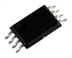
AP9928GEO-HF-3TR
Dual MOSFET, N Channel, 20 V, 5 A, 0.023 ohm, TSSOP, Surface Mount
⚠️ Reference pricing provided. In case of supply shortages, we will connect you with our trusted procurement partners to ensure your project's continuity.
- Manufacturer: ADVANCED POWER ELECTRONICS CORP
- Product type: Dual MOSFETs
- No. of Pins: 8Pins
- Channel Type: N Channel
- Transistor Mounting: Surface Mount
- Transistor Polarity: N Channel
- Power Dissipation Pd: 1W
- Rds(on) Test Voltage: 4.5V
- On Resistance Rds(on): 0.023ohm
- Transistor Case Style: TSSOP
- Drain Source Voltage Vds: 20V
- Operating Temperature Max: 150°C
- Continuous Drain Current Id: 5A
- Power Dissipation N Channel: 1W
- Power Dissipation P Channel: 1W
- Gate Source Threshold Voltage Max: 500mV
- Drain Source Voltage Vds N Channel: 20V
- Drain Source Voltage Vds P Channel: 20V
- Continuous Drain Current Id N Channel: 5A
- Continuous Drain Current Id P Channel: 5A
- Drain Source On State Resistance N Channel: 0.023ohm
- Drain Source On State Resistance P Channel: 0.023ohm
| Delivery and price | |
|---|---|
| Units per pack | 5000 |
| Price | 0.225 € |
| Current stock | 10+ |
| Lead time | 30 days |
Datasheet

**AP9928GEO Pb Free Plating Product Advanced Power** _**N-CHANNEL ENHANCEMENT MODE**_ **Electronics Cor .** _**POWER MOSFET**_ **p ▼ Low on-resistance S2 G2** BVDSS 20V **D2[S2] ▼ Capable of 2.5V gate drive** RDS(ON) 23mΩ **G1 S1 ▼** ~~_—_~~ **Optimal DC/DC battery application TSSOP-8 D1 S1** ~~_—~~ ID 5A **Description** D1 D2 The Advanced Power MOSFETs from APEC provide the designer with the best combination of fast switching, G1 G2 ruggedized device design, ultra low on-resistance and cost-effectiveness.

**==> picture [135 x 63] intentionally omitted <==**

**----- Start of picture text -----**<br>
D1 D2<br>G1 G2<br>S1 S2<br>**----- End of picture text -----**<br>


## **Absolute Maximum Ratings**

|Symbol|Parameter|Rating|Units|
|---|---|---|---|
|VDS|Drain-Source Voltage|20|V|
|VGS|Gate-Source Voltage|±12|V|
|ID@TA=25℃|Drain Current3, VGS@ 4.5V|5|A|
|ID@TA=70℃|Drain Current3, VGS@ 4.5V|3.5|A|
|IDM|Pulsed Drain Current1|25|A|
|PD@TA=25℃|Total Power Dissipation|1|W|
||Linear DeratingFactor|0.008|W/℃|
|TSTG|Storage Temperature Range|-55 to 150|℃|
|TJ|OperatingJunction Temperature Range|-55 to 150|℃|


## **Thermal Data**

|Symbol|Parameter|Value|Unit|
|---|---|---|---|
|Rthj-a|Thermal Resistance Junction-ambient3<br>Max.|125|℃/W|


_Data and specifications subject to change without notice_

_**200206031**_

## **AP9928GEO**

**==> picture [33 x 32] intentionally omitted <==**

## **Electrical Characteristics@Tj=25[o] C(unless otherwise specified)**

|Symbol|Parameter|Test Conditions|Min.|Typ.|Max.|Units|
|---|---|---|---|---|---|---|
|BVDSS|Drain-Source Breakdown Voltage|VGS=0V, ID=250uA|20|-|-|V|
|ΔBVDSS/ΔTj|Breakdown Voltage Temperature Coefficient|Reference to 25℃, ID=1mA|-|0.02|-|V/℃|
|RDS(ON)|Static Drain-Source On-Resistance2|VGS=4.5V, ID=5A|-|-|23|mΩ|
|||VGS=2.5V, ID=2A|-|-|29|mΩ|
|VGS(th)|Gate Threshold Voltage|VDS=VGS, ID=250uA|0.5|-|-|V|
|gfs|Forward Transconductance|VDS=10V, ID=5A|-|21|-|S|
|IDSS|Drain-Source Leakage Current (Tj=25oC)|VDS=20V, VGS=0V|-|-|1|uA|
||Drain-Source Leakage Current (Tj=70oC)|VDS=20V ,VGS=0V|-|-|25|uA|
|IGSS|Gate-Source Leakage|VGS=±12V|-|-|±10|uA|
|Qg|Total Gate Charge2|ID=5A<br>VDS=10V<br>VGS=4.5V|-|15.9|-|nC|
|Qgs|Gate-Source Charge||-|1.5|-|nC|
|Qgd|Gate-Drain("Miller")Charge||-|7.4|-|nC|
|td(on)|Turn-on DelayTime2|VDS=10V<br>ID=1A<br>RG=3.3Ω,VGS=4.5V<br>RD=10Ω|-|6.2|-|ns|
|tr|Rise Time||-|9|-|ns|
|td(off)|Turn-off DelayTime||-|30|-|ns|
|tf|Fall Time||-|11|-|ns|
|Ciss|Input Capacitance|VGS=0V<br>VDS=20V<br>f=1.0MHz|-|530|-|pF|
|Coss|Output Capacitance||-|245|-|pF|
|Crss|Reverse Transfer Capacitance||-|125|-|pF|


## **Source-Drain Diode**

|Symbol|Parameter|Test Conditions|Min.|Typ.|Max.|Units|
|---|---|---|---|---|---|---|
|IS|Continuous Source Current ( Body Diode )|VD=VG=0V,VS=1.2V|-|-|0.83|A|
|VSD|Forward On Voltage2|Tj=25℃,IS=5A,VGS=0V|-|-|1.2|V|


## **Notes:**

1.Pulse width limited by Max. junction temperature.

2.Pulse width <300us , duty cycle <2%.

3.Surface mounted on 1 in[2] copper pad of FR4 board ; 208℃/W when mounted on Min. copper pad.

**AP9928GEO**

**==> picture [33 x 33] intentionally omitted <==**

**==> picture [425 x 188] intentionally omitted <==**

**----- Start of picture text -----**<br>
40 35<br>35 T A  =25 [o] C 4.5V 30 T A =150 [o] C 4.5V<br>3.5V 3.5V<br>30 3.0V 25 3.0V<br>2.5V 2.5V<br>25<br>20<br>20<br>15<br>15<br>10 10 V  G =2.0V<br>V G =2.0V<br>5 5<br>0 0<br>0 1 2 3 4 0 1 2 3 4<br>V DS  , Drain-to-Source Voltage (V) V DS  , Drain-to-Source Voltage (V)<br> , Drain Current (A)<br>ID  , Drain Current (A)ID<br>**----- End of picture text -----**<br>


**Fig 1. Typical Output Characteristics**

**Fig 2. Typical Output Characteristics**

**==> picture [202 x 192] intentionally omitted <==**

**----- Start of picture text -----**<br>
95<br> I  D  = 5A<br>T A =25 [o] C<br>65<br>35<br>5<br>1 2 3 4 5<br>V GS  , Gate-to-Source Voltage (V)<br>Ω )<br> (m<br>DS(ON)<br>R<br>**----- End of picture text -----**<br>


**Fig 3. On-Resistance  v.s. Gate Voltage**

**==> picture [201 x 191] intentionally omitted <==**

**----- Start of picture text -----**<br>
1.9<br>  I D  = 5A<br>V  G = 4.5V<br>1.5<br>1.1<br>0.7<br>0.3<br>-50 0 50 100 150<br>T j  , Junction Temperature ( [o] C)<br>DS(ON)<br>Normalized R<br>**----- End of picture text -----**<br>


**Fig 4. Normalized On-Resistance**

**==> picture [200 x 188] intentionally omitted <==**

**----- Start of picture text -----**<br>
10<br>1<br>T j =150 [o] C<br>0.1<br>0.01<br>0.2 0.5 0.8 1.1<br>V SD  , Source-to-Drain Voltage (V)<br> (A)IS<br>**----- End of picture text -----**<br>


**Fig 5. Forward Characteristic of Reverse Diode**

**==> picture [204 x 188] intentionally omitted <==**

**----- Start of picture text -----**<br>
1.6<br>1.2<br>0.8<br>0.4<br>0<br>-50 0 50 100 150<br>T j  , Junction Temperature ( [o] C)<br> (V)<br>GS(th)<br>V<br>**----- End of picture text -----**<br>


**Fig 6. Gate Threshold Voltage v.s. Junction Temperature**

## **AP9928GEO**

**==> picture [34 x 32] intentionally omitted <==**

**==> picture [437 x 201] intentionally omitted <==**

**----- Start of picture text -----**<br>
f=1.0MHz<br>8 1000<br> I D = 5A<br>C iss<br>6 V V DSDS  =10V  =15V C  oss<br>V DS =20V C rss<br>4 100<br>2<br>0 10<br>0 5 10 15 20 25 1 7 13 19 25<br>Q G  , Total Gate Charge (nC) V DS  , Drain-to-Source Voltage (V)<br>C (pF)<br> , Gate to Source Voltage (V)<br>GS<br>V<br>**----- End of picture text -----**<br>


**Fig 7. Gate Charge Characteristics**

**Fig 8. Typical Capacitance Characteristics**

**==> picture [438 x 189] intentionally omitted <==**

**----- Start of picture text -----**<br>
100 1<br>Duty factor = 0.5<br>10 100us 0.2<br>0.1 0.1<br>1ms<br>0.05<br>1 10ms 0.02<br>100ms 0.01 PDM<br>0.01 t<br>Single Pulse T<br>0.1 T A =25 [o] C 1s Duty Factor = t/T<br>Single Pulse DC Peak T Rthja=208 j = P [o] C/W DM x Rthja + Ta<br>0.01 0.001<br>0.1 1 10 100 0.0001 0.001 0.01 0.1 1 10 100 1000<br>V DS  , Drain-to-Source Voltage (V) t , Pulse Width (s)<br>)thja<br>(A)<br>ID<br>Normalized Thermal Response (R<br>**----- End of picture text -----**<br>


**Fig 9. Maximum Safe Operating Area**

**Fig 10. Effective Transient Thermal Impedance**

**==> picture [171 x 149] intentionally omitted <==**

**----- Start of picture text -----**<br>
VDS<br>90%<br>10%<br>VGS<br>td(on) [t] r td(off) tf<br>**----- End of picture text -----**<br>


**==> picture [171 x 149] intentionally omitted <==**

**----- Start of picture text -----**<br>
VG<br>QG<br>5V<br>QGS QGD<br>Charge Q<br>**----- End of picture text -----**<br>


**Fig 11. Switching Time Waveform**

**Fig 12. Gate Charge Waveform**
Updated at February 9, 2023
About Novapart
Novapart is a B2B electronic component broker specialising in stock shortages and cost reduction. We source hard-to-find parts and identify compliant alternatives across a catalogue of 410,000+ components from 500+ manufacturers.
Learn more →Stock Shortage Specialist
When a component is unavailable, discontinued or has an unacceptable lead time, we tap into our network of vetted European and Asian distributors to source what you need — without compromising on quality or traceability.
Request a quote →Compliant Alternatives
We identify pin-to-pin, electrically equivalent substitutes that meet the same certifications (RoHS, AEC-Q100, REACH) as your original specification — validated against datasheets, not just part numbers. Often at a lower cost.
BOM Analysis service →