
Image not available
Illustrative purposes only

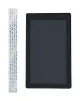
AES-ACC-DISP-5INCH
TFT LCD, 5 ", 720 x 1280 Pixels, Portrait, Black on White, 2.8V
⚠️ Reference pricing provided. In case of supply shortages, we will connect you with our trusted procurement partners to ensure your project's continuity.
- Manufacturer: AVNET
- Product type: TFT LCD Displays
- SVHC: No SVHC (25-Jun-2025)
- VGA Size: -
- Resolution: 720 x 1280 Pixels
- Module Size: 132.09mm x 79.4mm
- Touchscreen: Projected Capacitive Touch
- Display Size: 5"
- Logic Voltage: 2.8V
- Product Range: -
- Display Pinout: 40 Way Connector
- Interface Type: MIPI, I2C
- Display Appearance: Black on White
- Display Brightness: 360cd/m²
- Display Orientation: Portrait
- Operating Temperature Max: 70°C
- Operating Temperature Min: -20°C
| Delivery and price | |
|---|---|
| Units per pack | 1 |
| Price | 97.88 € |
| Current stock | 10+ |
| Lead time | 30 days |
Datasheet

## **Specifications for LCD module**
|**Customer**|**Avnet USA**|
|---|---|
|**Customer part no.**|**AES-ACC-DISP-5INCH**|
|**Ampire part no.**|**AM-7201280KTZQW-T02H**|
|**Approved by**||
|**Date**|November 18, 2024|
## **Preliminary Specification**
**Formal Specification**
## **AMPIRE CO., LTD.**
**4F., No.116, Sec. 1, Xintai 5th Rd., Xizhi Dist., New Taipei City221, Taiwan (R.O.C.)**
新北市汐止區新台五路一段 **116** 號 **4** 樓 **(** 東方科學園區 **A** 棟 **) TEL:886-2-26967269 , FAX:886-2-26967196 or 26967270**
|Approved by|Checked by|Organized by|
|---|---|---|
|Kokai|Mark|Lawlite|
This Specification is subject to change without notice.
Date: 2024/ 11/13
AMPIRE CO., LTD.
1
## **RECORD OF REVISION**
|||**RECORD OF REVISION**||
|---|---|---|---|
|Revision<br>Date|Page|Contents|Editor|
|2023/03/27<br>2023/06/21<br>2023/07/28<br>2024/01/08<br>2024/03/19<br>2024/07/30<br>2024/11/13|-<br>3,33<br>31<br>3.33<br>31<br>32<br>32<br>32|New Release<br>Add Type-C cable<br>Bridge board add more function<br>Cancel Type-C Cable<br>Bridge board add more function<br>Bridge board reduces some functions<br>TFT-7201280-12-2 rename to<br>AM-7201280KTZQW-T02H<br>Update PCB drawing<br>Update PCB drawing<br>Update PCB drawing|Mantle<br>Mantle<br>Mantle<br>Lawlite<br>Lawlite<br>Lawlite<br>Jessica|
Date: 2024/ 11/13 AMPIRE CO., LTD. 2
## **1. General Descriptions**
## **1.1 Introduction**
This is a color active matrix thin film transistor (TFT) liquid crystal display (LCD) single chip and sub sheet that use amorphous silicon TFT as a switching device. This TFT LCD panel has a 4.99 inch diagonally measured active display area with HD resolution (720 horizontal by 1280 vertical pixels array).
## **1.2 Features**
- (1) 4.99 Inch TFT-LCD Panel
- (2) MIPI Interface
- (3) Touch panel
- IC controller: ST1633i-N48
- Interface: I2C
- (4) Cover glass
- Thickness:1.1mm
## **1.3 Customize**
- (1) Bridge board
- (2) 30 Pin FFC
Date: 2024/ 11/13 AMPIRE CO., LTD. 3
## **1.3 Product Summary**
|**Items**|**Specifications**|**Unit**|
|---|---|---|
|Screen Diagonal|5.0|Inch|
|Number of pixel|720 x 1280|-|
|Pixel Pitch (H x V)|0.08625 x 0.08625|mm|
|Pixel Arrangement|R.G.B. Vertical Stripe|-|
|Display Mode|Normally Black, IPS|-|
|White Luminance|**360**(Typ.)|cd /m2|
|Electrical Interface (Logic)|MIPI|-|
Date: 2024/ 11/13 AMPIRE CO., LTD. 4
## **2. Absolute Maximum Ratings**
|**Item**|**Symbol**|**Min**|**Max**|**Unit**|**Conditions**|
|---|---|---|---|---|---|
|System power supply Voltage|IOVCC|-0.3|3.8|V|(1),(2)|
|Power supply VSP|VSP|-0.3|7.0|V|(1),(2)|
|Power supply VSN|VSN|-7.0|0.3|V|(1),(2)|
|Operating Temperature|TOP|**-20**|**70**|℃|(3),(4),(5),(6)|
|Storage Temperature|TST|**-30**|**80**|℃||
- Note(1) All the parameters specified in the table are absolute maximum rating values that may cause faulty operation or unrecoverable damage, if exceeded. It is recommended to follow the typical value.
- Note(2) All the contents of electro-optical specifications and display fineness are guaranteed under Normal Conditions. Normal conditions are defined as: Temperature: 25 ℃ , Humidity: 55± 10%RH.
- Note(3) Unpredictable results may occur when it was used in extreme conditions. Ta= Ambient Temperature, Tgs= Glass Surface Temperature. All the display fineness should be inspected under normal conditions.
- Note(4) Wet bulb temperature should be lower than 58 ℃ , and no condensation of water. Besides, protect the module from static electricity.
Date: 2024/ 11/13 AMPIRE CO., LTD. 5
## **3. Electrical Characteristics**
## **3.1 TFT LCD Module**
|**Item**|**Symbol**|**Min.**|**Typ.**|**Max.**|**Unit**|**Note**|
|---|---|---|---|---|---|---|
|Power supply voltage|IOVCC|1.65|2.8|3.6|V||
|Supply Voltage|VSP|4.5|--|6.6|V||
|Supply Voltage|VSN|-4.5|--|-6.6|V||
Note(1) fV =60Hz , Ta=25℃ , Display pattern : All White.
Note(2) *:Will be reference only
## **3.2 Backlight Unit**
|**Parameter**|**Symbol**|**Min.**|**Typ.**|**Max.**|**Unit**|**Note**|
|---|---|---|---|---|---|---|
|LED Voltage|VAK|16.8|18.0|19.2|V||
|LED current|IAK|--|40|--|mA|(2)|
|Life time|Hrs.|50K|--|--|Hours|(1)(2)|
Note(1) LED life time (Hr) can be defined as the time in which it continues to operate under the condition: Ta=25±3 ℃ , typical IAK value indicated in the above table until the brightness becomes less than 50%.
Note(2) When LCM is operated over 40 ℃ ambient temperature, the **IAK** should be follow :
Date: 2024/ 11/13 AMPIRE CO., LTD. 6
## **4. Optical Characteristics**
The optical characteristics are measured under stable conditions as following notes
|**Item**|**Conditions**|**Conditions**|**Min.**|**Typ.**|**Max.**|**Unit**|**Note**|
|---|---|---|---|---|---|---|---|
|Viewing Angle<br>(CR>10)|Horizontal|θ x+|80|85|-|degree|(1),(2)|
|||θ x-|80|85|-|||
||Vertical|θ y+|80|85|-|||
|||θ y-|80|85|-|||
|Contrast Ratio|Center||900|1200|-|-|(1),(3)<br>θx=θ y=0°|
|Response<br>Time|Rising + Falling||-|35|40|ms|(1),(4),(6),(7),(8)<br>θx=θ y=0°|
|NTSC|CIE1931||65|70|-|%|Under<br>C-light<br>(1),(5)<br>θx=θy=0°|
|Color<br>Chromaticity<br>(CIE1931)|Red|x|Typ.<br>-0.05|TBD|Typ.<br>+0.05|-||
||Red|y||TBD||-||
||Green|x||TBD||-||
||Green|y||TBD||-||
||Blue|x||TBD||-||
||Blue|y||TBD||-||
||White|x||TBD||-||
||White|y||TBD||-||
|White<br>Luminance|Center||**288**|**360**|-|cd/m^2|(1),(2)<br>θx=θy=0°|
|Luminance<br>Uniformity|9Points||-|TBD|-|%|(1),(2),(6)<br>θx=θy=0°|
Date: 2024/ 11/13 AMPIRE CO., LTD. 7
## Note(1) Measurement Setup:
The LCD module should be stabilized at given temperature (25°C) for 30 minutes to avoid abrupt temperature change during measuring. In order to stabilize the luminance, the measurement should be executed after lighting backlight for 30 minutes in a windless room.
Note(2) Definition of Viewing Angle
## Note(3) Definition Of Contrast Ratio (CR)
The contrast ratio can be calculated by the following expression Contrast Ratio (CR) = L255 / L0
L255: Luminance of gray level 255, L0: Luminance of gray level 0
Date: 2024/ 11/13 AMPIRE CO., LTD. 8
Note(4) Definition Of Response Time (TR, TF)
Note(5) Definition of Brightness Luminance
Note(6) Definition of Brightness Luminance Active area is divided into 9 measuring areas (Refer to bellow figure). Every measuring point is placed at the center of each measuring area. Bmin
Luminance Uniformity (Yu) = Bmax
L ----- Active area length W ----- Active area width
Bmax: The measured maximum luminance of all measurement position. Bmin: The measured minimum luminance of all measurement position.
Date: 2024/ 11/13 AMPIRE CO., LTD. 9
## **5. Interface**
|**No.**|**Symbol**|**Functions**|
|---|---|---|
|1|IOVCC(1.8V)|Power input 1.8V for logicpower|
|2|IOVCC(1.8V)|Power input 1.8V for logicpower|
|3|IOVCC(1.8V)|Power input 1.8V for logicpower|
|4|NC|No Connection|
|5|NC|No Connection|
|6|NC|No Connection|
|7|NC|No Connection|
|8|NC|No Connection|
|9|GND|Ground|
|10|DATA2_P<br>(D2_P)|MIPI SDI differential data pair|
|11|DATA2_N<br>(D2_N)|MIPI SDI differential data pair|
|12|GND|Ground|
|13|DATA1_P<br>(D1_P)|MIPI SDI differential data pair|
|14|DATA1_N<br>(D1_N)|MIPI SDI differential data pair|
|15|GND|Ground|
|16|STB_P<br>(CLK_P)|MIPI SDI differential CLK pair|
|17|STB_N<br>(CLK_N)|MIPI SDI differential CLK pair|
|18|GND|Ground|
|19|DATA0_P<br>(D0_P)|MIPI DSI differential data pair|
|20|DATA0_N<br>(D0_N)|MIPI DSI differential data pair|
|21|GND|Ground|
|22|DATA3_P<br>(D3_P)|MIPI SDI differential data pair|
|23|DATA3_N<br>(D3_N)|MIPI SDI differential data pair|
|24|GND|Ground|
|25|GND|Ground|
|26|GND|Ground|
|27|GND|Ground|
|28|TE|Tearingeffect output|
|29|RESET|Reset signal,low active|
|30|NC|No Connection|
|31|LEDK|Power for LED backlight cathode|
Date: 2024/ 11/13 AMPIRE CO., LTD. 10
|32|LEDK|Power for LED backlight cathode|
|---|---|---|
|33|LEDA|Power for LED backlight anode|
|34|LEDA|Power for LED backlight anode|
|35|GND|Ground|
|36|VSN|Power Supply;connect an externalpower|
|37|VSN|Power Supply;connect an externalpower|
|38|VSP|Power Supply;connect an externalpower|
|39|VSP|Power Supply;connect an externalpower|
|40|GND|Ground|
Date: 2024/ 11/13 AMPIRE CO., LTD. 11
## **6. AC Characteristics**
## **High Speed Mode – Clock Channel Timing**
Date: 2024/ 11/13 AMPIRE CO., LTD. 12
**High Speed Mode – Data Clock Channel Timing**
Date: 2024/ 11/13 AMPIRE CO., LTD. 13
## **High Speed Mode – Rising and Falling Timings**
Date: 2024/ 11/13 AMPIRE CO., LTD. 14
## **Low Speed Mode – Bus Turn Around**
Lower Power Mode and its State Periods on the Bus Turnaround (BTA) from the MCU to the
Display Module
(ILI9881C-04) are illustrated for reference purposes below
Figure 108: BTA from the MCU to the Display Module
Date: 2024/ 11/13 AMPIRE CO., LTD. 15
## **Data Lanes from Low Power Mode to High Speed Mode**
Date: 2024/ 11/13 AMPIRE CO., LTD. 16
## **Data Lanes from High Speed Mode to Low Power Mode**
Date: 2024/ 11/13 AMPIRE CO., LTD. 17
## **DSI Clock Burst – High Speed Mode to/from Low Power Mode**
Date: 2024/ 11/13 AMPIRE CO., LTD. 18
## **Timing for DSI video mode**
Date: 2024/ 11/13 AMPIRE CO., LTD. 19
Note:
1. Lanenum: Date lane of MIPI-DSI.
2. Pixel Format: Please reference to “4.1DSI System Interface”.
3. The formula exists slightly error because of the host-transmission way.
4. The best frame rate setting: 2 data lanes:50~60 Hz / 3 data lanes:50~70 Hz / 4 data lanes:50~70 Hz.
5. Please reference to “Table 39: Limited Clock Channel Speed”.
6. The minimum values of this table mean the limitation of IC without considering the panel GIP. The actual values
of VSA, VBP and VFP will be changed by different panel GIP setting.
Date: 2024/ 11/13 AMPIRE CO., LTD. 20
## **7. Touch Panel Specification**
## **7.1 Basic Characteristic**
|**Item**|**Specification**|
|---|---|
|Type|Projective Capacitive Touch Panel|
|Activation|5-fingers or Single-finger|
|X/Y Position Reporting|Absolute Position|
|Touch Force|No contact pressure required|
|Calibration|No need for calibration|
|Report Rate|Approx. 60 points/sec|
|Control IC|ST1633i-N48|
## **7.2 Capacitive Touch Panel FPC Descriptions**
|**No.**|**Symbol**|**Description**|
|---|---|---|
|1|GND|Ground.|
|2|SDA|I2C Interface.|
|3|SCL||
|4|VDD|Power Supply for TP controller.|
|5|INT|IRQ Terminal.|
|6|XRES|Terminal of Reset TP controller.|
Date: 2024/ 11/13 AMPIRE CO., LTD. 21
## **7.3 I2C Slave Interface**
## **7.4 Default I2C Address**
I2C address is default to **0x55** (7-bits address) for Sitronix Touch IC. If the I2C address is conflict with another I2C device’s address on same bus, user can change I2C address by TTK PC Utility.
## **7.5 Register Read**
For reading register value from I2C device, host has to tell I2C device the _Start Register Address_ before reading corresponding register value.
Sitronix Touch IC I2C host interface protocol supports Repeated Register Read. That is, once the Start Register Address has been set by host, consequent I2C Read(R) transactions will directly read register values starting from the Start Register Address without setting address first, as shown in Figure
Date: 2024/ 11/13 AMPIRE CO., LTD. 22
## **7.6 Register Write**
For writing register to I2C device, host has to tell I2C device the Start Register Address in each I2C Register Write transaction. Register values to the I2C device will be written to the address starting from the Start Register Address described in Register Write I2C transaction as shown in Figure
## **7.7 Sample Codes**
## **typedef struct {**
**u8 y_h: 3, reserved: 1,**
**x_h: 3, valid: 1; u8 x_l; u8 y_l; u8 z;**
**} xyz_data_t;**
## **typedef struct {**
**u8 fingers: 4, reserved: 4; u8 keys; xyz_data_t xyz_data[10];**
## **} stx_report_data_t;**
- // I2C Master sends _count_ bytes data stored in _buf_ to I2C Slave. // I2C package: | S | I2C Addr | W | Data (buf) | P |
## _**extern int i2c_master_send(const char *buf, int count);**_
// I2C Master reads _count_ bytes data to _buf_ from I2C Slave.
- // I2C package: | S | I2C Addr | R | Data (buf) | Nak | P |
_**extern int i2c_master_recv(char *buf, int count);**_
Date: 2024/ 11/13 AMPIRE CO., LTD. 23
## **4-4-8 Read XY Coordinates**
The function, get_coordinates(), reads XY Coordinate registers from I2C Slave, extracts XY information from data buffer and returns to upper layer. This function shall be called from ISR each time when host receives and INT from device.
**static int get_coordinates(u8 *count, u32 *x0, u32 *y0, u32 *x1, u32 *y1)**
## **{**
**u8 buf[42];**
**stx_report_data_t *pdata;**
**int ret = 0;**
***count = 0; // Set point detected count to 0.**
**if (i2c_master_recv(buf, sizeof(buf))) // Read Coordinates from default Reg. address 0x10.**
**goto err;**
**pdata = (stx_report_data_t *) buf;**
**if (pdata->fingers) {**
**if (pdata->xy_data[0].valid) {**
***x0 = pdata->xy_data[0].x_h << 8 | pdata->xy_data[0].x_l;**
***y0 = pdata->xy_data[0].y_h << 8 | pdata->xy_data[0].y_l;**
**(*count)++;**
**}**
**if (pdata->xy_data[1].valid) {**
***x1 = pdata->xy_data[1].x_h << 8 | pdata->xy_data[1].x_l;**
***y1 = pdata->xy_data[1].y_h << 8 | pdata->xy_data[1].y_l;**
**(*count)++;**
**}**
**}**
**err:**
**return ret;**
**}**
Date: 2024/ 11/13 AMPIRE CO., LTD. 24
## **8. Reliability Conditions**
|**Test Item**|**Test Conditions**|**Note**|
|---|---|---|
|High Temperature Operation|70±3°C , Dryt=240 hrs||
|Low Temperature Operation|-20±3°C , Dryt=240 hrs||
|High Temperature Storage|80±3°C , Dryt=240 hrs|1,2|
|Low Temperature Storage|-30±3°C , Dryt=240 hrs|1,2|
|Vibration Test (Packing)|Sweep frequency : 10 ~ 55 ~ 10 Hz/1min<br>Amplitude : 0.75mm<br>Test direction : X.Y.Z/3 axis<br>Duration : 30min/each axis|2|
- Note(1) Condensation of water is not permitted on the module.
- Note(2) The module should be inspected after 1 hour storage in normal conditions (15-35°C, 45-65%RH).
- Note(3) The module shouldn’t be tested more than one condition, and all the test conditions are independent.
- Note(4) All the reliability tests should be done without protective film on the module.
Definitions of life end point:
- Current drain should be smaller than the specific value.
- Function of the module should be maintained.
- Appearance and display quality should not have degraded noticeably.
- Contrast ratio should be greater than 50% of the initial value.
Date: 2024/ 11/13 AMPIRE CO., LTD. 25
## **9. Use Precautions**
## **9.1 Handling precautions**
- (1) The polarizing plate may break easily so be careful when handling it. Do not touch, press or rub it with a hard-material tool like tweezers.
- (2) Do not touch the polarizing plate surface with bare hands so as not to make it dirty. If the surface or other related part of the polarizing plate is dirty, soak a soft cotton cloth or chamois leather in benzine and wipe off with it. Do not use chemical liquids such as acetone, toluene and isopropyl alcohol. Failure to do so may bring chemical reaction phenomena and deteriorations.
- (3) Remove any spit or water immediately. If it is left for hours, the suffered part may deform or decolorize.
- (4) If the LCD element breaks and any LC stuff leaks, do not suck or lick it. Also if LC stuff is stuck on your skin or clothing, wash thoroughly with soap and water immediately.
## **9.2 Installing precautions**
- (1) The PCB has many ICs that may be damaged easily by static electricity. To prevent breaking by static electricity from the human body and clothing, earth the human body properly using the high resistance and discharge static electricity during the operation. In this case, however, the resistance value should be approx. 1MΩ and the resistance should be placed near the human body rather than the ground surface. When the indoor space is dry, static electricity may occur easily so be careful. We recommend the indoor space should be kept with humidity of 60% or more. When a soldering iron or other similar tool is used for assembly, be sure to earth it.
- (2) When installing the module and ICs, do not bend or twist them. Failure to do so may crack LC element and cause circuit failure.
- (3) To protect LC element, especially polarizing plate, use a transparent protective plate (e.g., acrylic plate, glass etc) for the product case.
- (4) Do not use an adhesive like a both-side adhesive tape to make LCD surface (polarizing plate) and product case stick together. Failure to do so may cause the polarizing plate to peel off.
Date: 2024/ 11/13 AMPIRE CO., LTD. 26
## **9.3 Storage precautions**
- (1) Avoid a high temperature and humidity area. Keep the temperature between 0°C and 35°C and also the humidity under 60%.
- (2) Choose the dark spaces where the product is not exposed to direct sunlight or fluorescent light.
- (3) Store the products as they are put in the boxes provided from us or in the same conditions as we recommend.
## **9.4 Operating precautions**
- (1) Do not boost the applied drive voltage abnormally. Failure to do so may break ICs. When applying power voltage, check the electrical features beforehand and be careful. Always turn off the power to the LC module controller before removing or inserting the LC module input connector. If the input connector is removed or inserted while the power is turned on, the LC module internal circuit may break.
- (2) The display response may be late if the operating temperature is under the normal standard, and the display may be out of order if it is above the normal standard. But this is not a failure; this will be restored if it is within the normal standard.
- (3) The LCD contrast varies depending on the visual angle, ambient temperature, power voltage etc. Obtain the optimum contrast by adjusting the LC dive voltage.
- (4) When carrying out the test, do not take the module out of the low-temperature space suddenly. Failure to do so will cause the module condensing, leading to malfunctions.
- (5) Make certain that each signal noise level is within the standard (L level: 0.2 IOVCC or less and H level: 0.8 IOVCC or more) even if the module has functioned properly. If it is beyond the standard, the module may often malfunction. In addition, always connect the module when making noise level measurements.
- (6) The CMOS ICs are incorporated in the module and the pull-up and pull-down function is not adopted for the input so avoid putting the input signal open while the power is ON.
- (7) The characteristic of the semiconductor element changes when it is exposed to light emissions, therefore ICs on the LCD may malfunction if they receive light emissions. To prevent these malfunctions, design and assemble ICs so that they are shielded from light emissions.
Date: 2024/ 11/13 AMPIRE CO., LTD. 27
- (8) Crosstalk occurs because of characteristics of the LCD. In general, crosstalk occurs when the regularized display is maintained. Also, crosstalk is affected by the LC drive voltage. Design the contents of the display, considering crosstalk.
## **9.5 Mechanism**
- (1) Please mount LCD module by using mounting holes arranged in four corners tightly.
- (2) Please hold the LCD module properly when you use or store it.
- (3) The square adhesive tape which is between the touch panel and display can’t provide well supporting in the long term and high ambient temperature condition. Whether upright or horizontal position the support holder which is in the back side of the display is needed. Do not let the display floating.
Date: 2024/ 11/13
AMPIRE CO., LTD.
28
- (4) TP needs to work in environment with stable stray capacitance. In order to minimize the variation in stray capacitance, all conductive mechanical parts must not be floating. Intermittent floating any conductive part around the touch sensor may cause significant stray capacitance change and abnormal touch function. It is recommended to keep all conductive parts having same electrical potential as the GND of the touch controller module.
GND1, GND2 and GND3 should be connected together to have the same ground
## **9.6 Other**
- (1) Do not disassemble or take the LC module into pieces. The LC modules once disassembled or taken into pieces are not the guarantee articles.
- (2) Do not keep the LCD at the same display pattern continually. The residual image will happen and it will damage the LCD. Please use screen saver
- (3) AMIPRE will provide one year warrantee for all products and three months warrantee for all repairing products.
Date: 2024/ 11/13 AMPIRE CO., LTD. 29
## **10. Outline Dimension**
Date: 2024/ 11/13 AMPIRE CO., LTD. 30
Date: 2024/ 11/13
AMPIRE CO., LTD. 31
## **11. Bridge Board**
## **11.1 PCB Outline 109*69.4mm 2L 1.6T**
**==> picture [443 x 630] intentionally omitted <==**
Date: 2024/ 11/13
AMPIRE CO., LTD.
32
## **11.2 Interface**
(1). CN1: Connect to LCM FPC(MIPI interface)
(2). CN2: Connect to LCM TP FPC(I2C)
(3). CN3: CSF-2481-301R/P0.5 30PIN or equivalent.
|Pin|Signal name|Description|
|---|---|---|
|1|GND|Ground|
|2|DSI_DP3|MIPI DSItransmit differentialsignal3 pairpositive|
|3|DSI_DN3|MIPI DSItransmit differentialsignal3 pair negative|
|4|GND|Ground|
|5|DSI_DP2|MIPI DSI transmit differential signal 2 pair positive|
|6|DSI_DN2|MIPI DSItransmit differentialsignal 2pair negative|
|7|GND|Ground|
|8|DSI_DP1|MIPI DSItransmit differentialsignal 1pairpositive|
|9|DSI_DN1|MIPI DSItransmit differentialsignal 1pair negative|
|10|GND|Ground|
|11|DSI_DP0|MIPI DSItransmit differentialsignal0 pairpositive|
|12|DSI_DN0|MIPI DSI transmit differential signal 0 pair negative|
|13|GND|Ground|
|14|DSI_CKP|MIPI DSIclockdifferentialsignalpairpositive|
|15|DSI_CKN|MIPI DSIclockdifferentialsignalpair negative|
|16|GND|Ground|
|17|DSI_TS_RST|Touchscreen reset output|
|18|DSI_TS_nINT|Touchscreen interruptinput|
|19|I2C4_SDA|I2C port 4 data|
|20|I2C4_SCL|I2C port 4 clock|
|21|DSI_EN|MIPI DSIbacklight enable output|
|22|DSI_BL_PWM|MIPI DSIbacklightPWMoutput|
|23|GND|Ground|
|24|NC|No connection|
|25|NC|No connection|
|26|GND|Ground|
|27|NC|No connection|
|28|VSYS|5V poweroutput|
|29|VSYS|5V poweroutput|
|30|VSYS|5V poweroutput|
Date: 2024/ 11/13 AMPIRE CO., LTD. 33
## **12. FFC**
## **P0.5xL 150mm 30pin**
Connect bridge board CN3 and customer board mipi connector.
Date: 2024/ 11/13 AMPIRE CO., LTD. 34
Updated at April 23, 2026
About Novapart
Novapart is a B2B electronic component broker specialising in stock shortages and cost reduction. We source hard-to-find parts and identify compliant alternatives across a catalogue of 410,000+ components from 500+ manufacturers.
Learn more →Stock Shortage Specialist
When a component is unavailable, discontinued or has an unacceptable lead time, we tap into our network of vetted European and Asian distributors to source what you need — without compromising on quality or traceability.
Request a quote →Compliant Alternatives
We identify pin-to-pin, electrically equivalent substitutes that meet the same certifications (RoHS, AEC-Q100, REACH) as your original specification — validated against datasheets, not just part numbers. Often at a lower cost.
BOM Analysis service →