


ADXL314WBCPZ-RL
MEMS Accelerometer, ± 200g, X, Y, Z, I2C, SPI, LFCSP-EP, 32 Pins, 20.48LSB/g
- Manufacturer: ANALOG DEVICES
- Product type: MEMS Accelerometers
- SVHC: No SVHC (04-Feb-2026)
- No. of Pins: 32Pins
- Sensing Axis: X, Y, Z
- Product Range: -
- Qualification: AEC-Q100
- Sensitivity Typ: 20.48LSB/g
- Output Interface: I2C, SPI
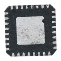
- Sensor Case Style: LFCSP-EP
- MEMS Sensor Output: Digital
- Supply Voltage Max: 3.6V
- Supply Voltage Min: 2V
- Sensor Case / Package: LFCSP-EP
- Operating Temperature Max: 125°C
- Operating Temperature Min: -40°C
- Sensing Range - Accelerometer: ± 200g
- Automotive Qualification Standard: AEC-Q100
| Delivery and price | |
|---|---|
| Units per pack | 500 |
| Price | 5.55 € |
| Current stock | 1000+ |
| Lead time | 30 days |
Data Sheet

**ADXL314**

**==> picture [111 x 32] intentionally omitted <==**

## ±200 _g_ Range, 3-Axis Digital Accelerometer

## **FEATURES**

- ±200 _g_ measurement range

- Low power: 170 µA in measurement mode and 17 µA in standby mode at VS = 2.5 V (typical)

- User selectable bandwidth up to 3200 Hz ODR

- Fixed 13-bit output resolution

- Supply voltage range: 2.0 V to 3.6 V

- Embedded memory management system with FIFO technology minimizes host processor load

- Shock event detection

## **SIMPLIFIED FUNCTIONAL BLOCK DIAGRAM**

**==> picture [200 x 115] intentionally omitted <==**

- Activity/inactivity monitoring

- SPI (3- or 4-wire) and I[2] C digital interfaces

- Wide temperature range: −40 to +125°C

- 10,000 _g_ shock survival

- Pb free and RoHS compliant

- Small and thin: 32-lead, 5 mm × 5 mm × 1.45 mm LFCSP

- AEC-Q100 qualified for automotive applications

## **APPLICATIONS**

- Tire and battery pack monitoring

- High force event detection

_**Figure 1. Simplified Functional Block Diagram**_

## **GENERAL DESCRIPTION**

The ADXL314 is a ±200 _g_ range, 13-bit resolution, 3-axis digital accelerometer. The digital output data is formatted as 16-bit, twos complement data and is accessible through a serial peripheral interface (SPI), 3-wire or 4-wire, or an I[2] C digital interface.

An integrated memory management system with a 32 level, first in, first out (FIFO) buffer can store data to minimize host processor activity and lower overall system power consumption.

Low power modes enable intelligent motion-based power management with threshold sensing and active acceleration measurement at low power dissipation, typically 65 μA for VS = 2.5 V at a 100 Hz output data rate (ODR).

The ADXL314 is supplied in a small, thin 5 mm × 5 mm × 1.45 mm, 32-lead LFCSP.

**Rev. A**

Information furnished by Analog Devices is believed to be accurate and reliable "as is". However, no responsibility is assumed by Analog Devices for its use, nor for any infringements of patents or other rights of third parties that may result from its use. Specifications subject to change without notice. No license is granted by implication or otherwise under any patent or patent rights of Analog Devices. Trademarks and registered trademarks are the property of their respective owners.

**DOCUMENT FEEDBACK TECHNICAL SUPPORT**

Data Sheet

**ADXL314**

## **TABLE OF CONTENTS**

Features................................................................ 1 Applications........................................................... 1 Simplified Functional Block Diagram.....................1 General Description...............................................1 Specifications........................................................ 3 Absolute Maximum Ratings...................................5 Thermal Resistance........................................... 5 Solder Profile......................................................5 Electrostatic Discharge (ESD) Ratings...............5 ESD Caution.......................................................5 Pin Configuration and Function Descriptions........ 6 Typical Performance Characteristics.....................7 Theory of Operation.............................................10 Power Sequencing........................................... 10 Power Savings................................................. 10 FIFO Buffer.......................................................11 Interrupts.......................................................... 12 Self Test............................................................13 Serial Communications........................................14 Serial Port Input and Output Default States..... 14

SPI....................................................................14 I[2] C.................................................................... 17 Register Map....................................................... 19 Register Definitions.......................................... 19 Applications Information...................................... 23 Power Supply Requirements ...........................23 Mechanical Considerations for Mounting......... 23 Threshold......................................................... 23 Link Mode.........................................................23 Sleep Mode vs. Low Power Mode....................23 Offset Compensation........................................24 Using Self Test................................................. 24 Asynchronous Data Readings..........................24 Data Formatting at Output Data Rate of 3200 Hz and 1600 Hz.....................................24 Axes of Acceleration Sensitivity....................... 25 Outline Dimensions............................................. 26 Ordering Guide.................................................26 Evaluation Boards............................................ 26 Automotive Products........................................ 27

## **REVISION HISTORY**

**10/2022—Rev. 0 to Rev. A** Moved Solder Profile Section, Figure 2, and Table 4.......................................................................................5 Change to Figure 3.......................................................................................................................................... 6 Change to Power Sequencing Section.......................................................................................................... 10 Changes to Table 16......................................................................................................................................19 Changed Enable Bits Section to Entries Bits Section....................................................................................22 Changes to Entries Bits Section.................................................................................................................... 22

## **5/2022—Revision 0: Initial Version**

**Rev. A | 2 of 27**

**analog.com**

Data Sheet

**ADXL314**

## **SPECIFICATIONS**

TA = 25°C, VS = 2.5 V, VDD I/O = 2.5 V, acceleration = 0 _g_ , VS capacitance (CVS) = 1 μF tantalum, VDD I/O capacitance (CVDDI/O) = 0.1 μF, and ODR = 100 Hz, unless otherwise noted.

_**Table 1. Specifications**_

|**_Table 1. Specifications_**|**_Table 1. Specifications_**|**_Table 1. Specifications_**|**_Table 1. Specifications_**|
|---|---|---|---|
|**Parameter**<br>**Test Conditions/Comments**<br>**Min1**<br>**Typ2**<br>**Max1**<br>**Unit**||||
|SENSOR INPUT<br>Measurement Range<br>Nonlinearity<br>Cross-Axis Sensitivity3<br>Sensor Resonant Frequency|Each axis<br>Percentage of full scale|±200<br>±0.5<br>±2.5<br>16|_g_<br>%<br>%<br>kHz|
|OUTPUT RESOLUTION<br>All Operation Modes|Each axis|13|Bits|
|SENSITIVITY<br>Sensitivity<br>Scale Factor<br>Scale Factor Calibration Error<br>Sensitivity Change due to Temperature|All axes<br>ODR = 100 Hz<br>ODR = 100 Hz<br>−40°C ≥ TA≤ +25°C or +25°C ≥ TA≤ +125°C|20.48<br>48.83<br>±10<br>8|LSB/_g_<br>_mg_/LSB<br>%<br>%|
|0_g_OFFSET<br>0_g_Output<br>0_g_Offset Change due to Temperature|X-axis and Y-axis<br>Z-axis<br>−40°C to +105°C<br>105°C to +125°C|−7<br>±1<br>+7<br>−7<br>±3<br>+7<br>±20<br>±100|_g_<br>_g_<br>_mg_/°C<br>_mg_/°C|
|NOISE PERFORMANCE (RMS)<br>Noise Density<br>X-Axis and Y-Axis<br>Z-Axis<br>Noise Density Change with Temperature (All Axes)||5.65<br>6.8<br>0.5|_mg/√Hz_<br>_mg/√Hz_<br>_mg/√Hz/°C_|
|OUTPUT DATA RATE AND BANDWIDTH4,5<br>Measurement Rate|User-selectable|6.25<br>3200|Hz|
|SELF TEST6<br>Self Test Change<br>Self Test Change vs. Temperature|Z-axis only<br>At 100 Hz ODR, −40°C ≥ TA≤ +125°C|0.1<br>4<br>8<br>−12.5|_g_<br>m_g_/°C|
|POWER SUPPLY<br>Operating Voltage Range (VS)<br>Interface Voltage Range (VDD I/O)<br>Supply Current<br>Measurement Mode<br>Low Power Mode<br>Standby Mode<br>Turn-On and Wake-up Time7|ODR ≥ 100 Hz, −40°C to +125°C<br>ODR ≤ 10 Hz, −40°C to +125°C<br>ODR = 100 Hz, −40°C to +125°C<br>25°C<br>−40°C to 125°C|2.0<br>3.6<br>2.0<br>VS<br>70<br>170<br>20<br>50<br>22<br>65<br>0.1<br>17<br>1.4|V<br>V<br>µA<br>µA<br>µA<br>µA<br>µA<br>ms|
|||||


**Rev. A | 3 of 27**

**analog.com**

Data Sheet

**ADXL314**

## **SPECIFICATIONS**

_**Table 1. Specifications**_

|**_Table 1. Specifications_**|**_Table 1. Specifications_**|**_Table 1. Specifications_**|**_Table 1. Specifications_**|
|---|---|---|---|
|**Parameter**<br>**Test Conditions/Comments**<br>**Min1**<br>**Typ2**<br>**Max1**<br>**Unit**||||
|TEMPERATURE (T)<br>Operating Temperature Range||−40<br>+125|°C|


- 1 Minimum and maximum specifications represent the worst case of mean ± 3 σ distribution and are guaranteed in production.

- 2 Typical specifications are for at least 68% of the population of parts and are based on the worst case of mean ± 1 σ distribution, except for sensitivity, which represents the target value.

- 3 Cross-axis sensitivity is defined as coupling between any two axes.

- 4 The output format for the 1600 Hz and 3200 Hz output data rates is different from the output format for the other output data rates. For more information, see the Data Formatting at Output Data Rate of 3200 Hz and 1600 Hz section.

- 5 Bandwidth is the −3 dB frequency and is half the output data rate: bandwidth = ODR/2.

- 6 Self test change is defined as the output ( _g_ ) when the SELF_TEST bit = 1 (DATA_FORMAT register, Address 0x31) minus the output ( _g_ ) when the SELF_TEST bit = 0. Due to device filtering, the output reaches its final value after 4 × τ when enabling or disabling self test, where τ = 1/(data rate). For the self test to operate correctly, the device must be in normal power operation (LOW_POWER bit = 0 in the BW_RATE register, Address 0x2C).

- 7 The turn-on time and wake-up time are determined by the user-defined bandwidth. At a 100 Hz data rate, the turn-on time and wake-up time are each approximately 11.1 ms. For other data rates, the turn-on time and wake-up time are each approximately τ + 1.1 ms, where τ = 1/(data rate).

**Rev. A | 4 of 27**

**analog.com**

Data Sheet

**ADXL314**

## **ABSOLUTE MAXIMUM RATINGS**

_**Table 2.**_

|**Parameter**<br>**Rating**|**Parameter**<br>**Rating**|
|---|---|
|Acceleration, Any Axis<br>Unpowered<br>Powered<br>VS<br>VDD I/O<br>All Other Pins<br>Output Short-Circuit Duration<br>(Any Pin to Ground)<br>Temperature Range<br>Unpowered<br>Powered|10,000_g_for 0.1 ms<br>10,000_g_for 0.1 ms<br>−0.3 V to +3.9 V<br>−0.3 V to +3.9 V<br>−0.3 V to VDD I/O+ 0.3 V or +3.9 V, whichever is<br>less<br>Indefinite<br>−40°C to +125°C<br>−40°C to +125°C|


Stresses at or above those listed under Absolute Maximum Ratings may cause permanent damage to the product. This is a stress rating only; functional operation of the product at these or any other conditions above those indicated in the operational section of this specification is not implied. Operation beyond the maximum operating conditions for extended periods may affect product reliability.

## **THERMAL RESISTANCE**

Thermal performance is directly linked to printed circuit board (PCB) design and operating environment. Careful attention to PCB thermal design is required.

θJA is the natural convection junction-to-ambient thermal resistance measured in a one cubic foot sealed enclosure. θJC is the junctionto-case thermal resistance.

_**Table 3. Thermal Resistance**_

|**_Table 3. Thermal Resistance_**|**_Table 3. Thermal Resistance_**|**_Table 3. Thermal Resistance_**|**_Table 3. Thermal Resistance_**|
|---|---|---|---|
|**Package Type**<br>**θJA**<br>**θJC**<br>**Unit**||||
|CP-32-17|150|85|°C/W|


## **SOLDER PROFILE**

_**Table 4. Recommended Soldering Profile[1][, ][2]**_

|**_Table 4. Recommended Soldering Profile1, 2_**|**_Table 4. Recommended Soldering Profile1, 2_**|**_Table 4. Recommended Soldering Profile1, 2_**|
|---|---|---|
|**Profile Feature**<br>**Condition**<br>**Sn63/Pb37**<br>**Pb-Free**|||
|Average Ramp Rate (TLto TP)|3°C/sec maximum||
|Preheat<br>Minimum Temperature (TSMIN)<br>Maximum Temperature (TSMAX)<br>Time (TSMINto TSMAX) (tS)|100°C<br>150°C<br>60 sec to 120<br>sec|150°C<br>200°C<br>60 sec to 180<br>sec|
|TSMAXto TL<br>Ramp-Up Rate|3°C/sec||
|Time Maintained Above Liquidous (TL)<br>Liquidous Temperature (TL)<br>Time (tL)|183°C<br>60 sec to 150<br>sec|217°C<br>60 sec to 150<br>sec|
|Peak Temperature (TP)|240°C + 0°C/<br>−5°C|260°C + 0°C/<br>−5°C|
|Time Within 5°C of Actual Peak Temperature<br>(tP)|10 sec to 30<br>sec|20 sec to 40<br>sec|
|Ramp-Down Rate|6°C/sec maximum||
|Time 25°C to Peak Temperature|6 min maximum|8 min<br>maximum|


## **ELECTROSTATIC DISCHARGE (ESD) RATINGS**

The following ESD information is provided for handling of ESD-sensitive devices in and ESD-protected area only.

Human body model (HBM) per ANSI/ESDA/JEDEC JS-001.

Field induced charged-device model (FICDM) per ANSI/ESDA/JEDEC JS-002.

## **ESD Rating for the ADXL314**

_**Table 5. ADXL314, 32-Lead LFCSP**_

|**ESD Model**|**Withstand Threshold (V)**|**Class**|
|---|---|---|
|FICDM|±1250|Not applicable|
|HBM|±2000|2|


## **ESD CAUTION**

**ESD (electrostatic discharge) sensitive device** . Charged devices and circuit boards can discharge without detection. Although this product features patented or proprietary protection circuitry, damage may occur on devices subjected to high energy ESD. Therefore, proper ESD precautions should be taken to avoid performance degradation or loss of functionality.

_**Figure 2. Recommended Soldering Profile**_

**Rev. A | 5 of 27**

**analog.com**

Data Sheet

**ADXL314**

## **PIN CONFIGURATION AND FUNCTION DESCRIPTIONS**

**==> picture [116 x 59] intentionally omitted <==**

_**Figure 3. Pin Configuration (Top View)**_

_**Table 6. Pin Function Descriptions**_

|**_Table 6. Pin Function Descriptions_**|**_Table 6. Pin Function Descriptions_**|**_Table 6. Pin Function Descriptions_**|
|---|---|---|
|**Pin No.**<br>**Mnemonic**<br>**Description**|||
|1<br>2<br>3<br>4<br>5<br>6<br>7<br>8 to 19<br>20<br>21<br>22<br>23<br>24<br>25<br>26<br>27 to 30<br>31<br>32|GND<br>Reserved<br>GND<br>GND<br>VS<br>CS<br>Reserved<br>NC<br>INT1<br>INT2<br>Reserved<br>SDO/ALT ADDRESS<br>SDA/SDI/SDIO<br>NC<br>SCL/SCLK<br>NC<br>VDD I/O<br>NC<br>EP|This pin must be connected to ground.<br>Reserved. This pin must be connected to VSor left open.<br>This pin must be connected to ground.<br>This pin must be connected to ground.<br>Supply Voltage.<br>Chip Select.<br>Reserved. This pin must be left open.<br>No Connect. Do not connect to this pin.<br>Interrupt 1 Output.<br>Interrupt 2 Output.<br>Reserved. This pin must be connected to GND or left open.<br>Serial Data Out (SDO), or Alternate I2C Address Select (ALT ADDRESS).<br>Serial Data (SDA, I2C), Serial Data In (SDI, SPI 4-Wire), or Serial Data In/Out (SDIO, SPI 3-Wire).<br>No Connect. Do not connect to this pin.<br>Serial Clock Line for I2C (SCL). Serial Clock Line for SPI (SCLK).<br>No Connect. Do not connect to this pin.<br>Digital Interface Supply Voltage.<br>No Connect.<br>Exposed Pad. The exposed pad must be soldered to the ground plane.|


**Rev. A | 6 of 27**

**analog.com**

Data Sheet

**ADXL314**

## **TYPICAL PERFORMANCE CHARACTERISTICS**

**==> picture [176 x 166] intentionally omitted <==**

_**Figure 4. X-Axis Zero g Offset at 25°C, VS = 2.5 V**_

**==> picture [176 x 165] intentionally omitted <==**

_**Figure 5. Y-Axis Zero g Offset at 25°C, VS = 2.5 V**_

**==> picture [183 x 165] intentionally omitted <==**

_**Figure 6. Z-Axis Zero g Offset at 25°C, VS = 2.5 V**_

**==> picture [175 x 165] intentionally omitted <==**

_**Figure 7. X-Axis Sensitivity Deviation at 25°C, VS = 2.5 V**_

**==> picture [176 x 165] intentionally omitted <==**

_**Figure 8. Y-Axis Sensitivity Deviation at 25°C, VS = 2.5 V**_

**==> picture [183 x 165] intentionally omitted <==**

_**Figure 9. Z-Axis Sensitivity Deviation at 25°C, VS = 2.5 V**_

**Rev. A | 7 of 27**

**analog.com**

Data Sheet

**ADXL314**

## **TYPICAL PERFORMANCE CHARACTERISTICS**

**==> picture [208 x 163] intentionally omitted <==**

_**Figure 10. X-Axis Zero g Offset Deviation from 25°C vs. Temperature, VS = 2.5 V**_

**==> picture [208 x 163] intentionally omitted <==**

**==> picture [207 x 163] intentionally omitted <==**

_**Figure 13. X-Axis Sensitivity Deviation from 25°C vs. Temperature, VS = 2.5 V**_

**==> picture [207 x 163] intentionally omitted <==**

_**Figure 14. Y-Axis Sensitivity Deviation from 25°C vs. Temperature, VS = 2.5 V**_

_**Figure 11. Y-Axis Zero g Offset Deviation from 25°C vs. Temperature, VS = 2.5 V**_

**==> picture [208 x 163] intentionally omitted <==**

**==> picture [207 x 163] intentionally omitted <==**

_**Figure 15. Z-Axis Sensitivity Deviation from 25°C vs. Temperature, VS = 2.5 V**_

_**Figure 12. Z-Axis Zero g Offset Deviation from 25°C vs. Temperature, VS = 2.5 V**_

**Rev. A | 8 of 27**

**analog.com**

Data Sheet

**ADXL314**

## **TYPICAL PERFORMANCE CHARACTERISTICS**

**==> picture [176 x 166] intentionally omitted <==**

_**Figure 16. Z-Axis Self Test Response at 25°C, VS = 2.5 V**_

**==> picture [183 x 164] intentionally omitted <==**

_**Figure 19. Clock Frequency Deviation from Ideal at 25°C, VS = 2.5 V**_

**==> picture [176 x 164] intentionally omitted <==**

_**Figure 17. Measurement Mode Current Consumption at 25°C, VS = 2.5 V**_

**==> picture [176 x 164] intentionally omitted <==**

_**Figure 18. Standby Mode Current Consumption at 25°C, VS = 2.5 V**_

**Rev. A | 9 of 27**

**analog.com**

Data Sheet

**ADXL314**

## **THEORY OF OPERATION**

The ADXL314 is a complete 3-axis acceleration measurement system with a measurement range of ±200 _g_ . The device measures both dynamic accelerations resulting from motion or shock and static accelerations, such as gravity.

The sensor is a polysilicon, surface-micromachined structure built on top of a silicon wafer. Polysilicon springs suspend the structure over the surface of the wafer and provide resistance against forces due to applied acceleration.

Deflection of the structure is measured using differential capacitors that consist of independent fixed plates and plates attached to the moving mass. Acceleration deflects the proof mass and unbalances the differential capacitor, resulting in a sensor output whose amplitude is proportional to acceleration. Phase sensitive demodulation is used to determine the magnitude and polarity of the acceleration.

## **POWER SEQUENCING**

Power can be applied to VS or VDD I/O in any sequence without damaging the ADXL314.

All possible power-on modes are summarized in Table 7. The interface voltage level is set with the interface supply voltage, VDD I/O, which must be present to ensure that the ADXL314 does not create a conflict on the communication bus. For single-supply operation, VDD I/O can be the same as the main supply, VS. In a dual-supply application, however, VDD I/O can differ from VS to accommodate the desired interface voltage, as long as VS is greater than or equal to VDD I/O.

After VS is applied, the device enters standby mode, where power consumption is minimized and the device waits for VDD I/O to be applied and for the command to enter measurement mode to be received. (This command can be initiated by setting the measure bit in the POWER_CTL register (Address 0x2D).) In addition, any register can be written to or read from to configure the device while the device is in standby mode. It is recommended to configure the device in standby mode and then to enable measurement mode. Clearing the measure bit returns the device to standby mode.

_**Table 7. Power Sequencing**_

|**_Table 7. Power Sequencing_**|**_Table 7. Power Sequencing_**|**_Table 7. Power Sequencing_**|**_Table 7. Power Sequencing_**|
|---|---|---|---|
|**Condition**<br>**VS**<br>**VDD I/O**<br>**Description**||||
|Power Off<br>Bus Disabled<br>Bus Enabled<br>Standby or<br>Measurement|Off<br>On<br>Off<br>On|Off<br>Off<br>On<br>On|The device is completely off, but there is a<br>potential for a communication bus conflict.<br>The device is on in standby mode, but<br>communication is unavailable and creates a<br>conflict on the communication bus. Minimize the<br>duration of this state during power-up to prevent<br>a conflict.<br>No functions are available, but the device does<br>not create a conflict on the communication bus.<br>The device is in standby mode, awaiting a<br>command to enter measurement mode, and<br>all sensor functions are off. After the device<br>is instructed to enter measurement mode, all<br>sensor functions are available.|


## **POWER SAVINGS**

## **Power Modes**

The ADXL314 automatically modulates its power consumption in proportion to its output data rate, as outlined in Table 8. If additional power savings are desired, a lower power mode is available. In this mode, the internal sampling rate is reduced, allowing for power savings in the 12.5 Hz to 400 Hz data rate range at the expense of slightly greater noise. To enter low power mode, set the LOW_POWER bit (Bit 4) in the BW_RATE register (Address 0x2C). The current consumption in low power mode is shown in Table 9 for cases where there is an advantage to using low power mode. Use of low power mode for a data rate not shown in Table 9 does not provide any advantage over the same data rate in normal power mode. Therefore, it is recommended that only data rates shown in Table 9 be used in low power mode. The current consumption values shown in Table 8 and Table 9 are for a VS of 2.5 V.

_**Table 8. Current Consumption vs. Data Rate (TA = 25°C, VS = VDD I/O = 2.5 V)**_

|**_Table 8. Current Consumption vs. Data Rate(TA = 25°C, VS = VDD I/O = 2.5 V)_**|**_Table 8. Current Consumption vs. Data Rate(TA = 25°C, VS = VDD I/O = 2.5 V)_**|**_Table 8. Current Consumption vs. Data Rate(TA = 25°C, VS = VDD I/O = 2.5 V)_**|**_Table 8. Current Consumption vs. Data Rate(TA = 25°C, VS = VDD I/O = 2.5 V)_**|
|---|---|---|---|
|**Output Data Rate (Hz)**<br>**Bandwidth (Hz)**<br>**Rate Code**<br>**IDD (µA)**||||
|3200<br>1600<br>800<br>400<br>200<br>100<br>50<br>25<br>12.5<br>6.25|1600<br>800<br>400<br>200<br>100<br>50<br>25<br>12.5<br>6.25<br>3.125|1111<br>1110<br>1101<br>1100<br>1011<br>1010<br>1001<br>1000<br>0111<br>0110|170<br>115<br>170<br>170<br>170<br>170<br>115<br>82<br>65<br>57|


_**Table 9. Current Draw vs. Data Rate, Low Power Mode (TA = 25°C, VS = VDD I/O = 2.5 V)**_

|**Output Data Rate (Hz)**<br>**Bandwidth (Hz)**<br>**Rate Code**<br>**IDD (µA)**|**Output Data Rate (Hz)**<br>**Bandwidth (Hz)**<br>**Rate Code**<br>**IDD (µA)**|**Output Data Rate (Hz)**<br>**Bandwidth (Hz)**<br>**Rate Code**<br>**IDD (µA)**|**Output Data Rate (Hz)**<br>**Bandwidth (Hz)**<br>**Rate Code**<br>**IDD (µA)**|
|---|---|---|---|
|400<br>200<br>100<br>50<br>25<br>12.5|200<br>100<br>50<br>25<br>12.5<br>6.25|1100<br>1011<br>1010<br>1001<br>1000<br>0111|115<br>82<br>65<br>57<br>50<br>43|


## **Autosleep Mode**

Additional power savings can be accomplished by having the ADXL314 automatically switch to sleep mode during periods of inactivity. To enable this feature, set the THRESH_INACT register (Address 0x25) to an acceleration threshold value. Levels of acceleration below this threshold are regarded as no activity levels. Set TIME_INACT (Address 0x26) to an appropriate inactivity time period. Then, set the AUTO_SLEEP bit and the link bit in the POWER_CTL register (Address 0x2D). If the device does not detect a level of acceleration in excess of THRES_INACT for TIME_INACT seconds, the device is transitioned to sleep mode automatically.

**Rev. A | 10 of 27**

**analog.com**

Data Sheet

**ADXL314**

## **THEORY OF OPERATION**

Current consumption at the sub 8 Hz data rates used in this mode is typically 30 µA for a VS of 2.5 V.

## **Standby Mode**

For even lower power operation, standby mode can be used. In standby mode, current consumption is reduced to 0.1 µA (typical). In this mode, no measurements are made. Standby mode is entered by clearing the measure bit (Bit 3) in the POWER_CTL register (Address 0x2D). Placing the device into standby mode preserves the contents of the FIFO.

## **FIFO BUFFER**

The ADXL314 contains patented technology for an embedded memory management system with a 32-level FIFO buffer that can be used to minimize host processor burden. This buffer has four modes: bypass, FIFO, stream, and trigger. Each mode can be selected by setting the FIFO_MODE bits (Bits[D7:D6]) in the FIFO_CTL register (Address 0x38; see Table 10).

_**Table 10. FIFO Modes (FIFO_CTL Register, Address 0x38)**_

|**_Table 10. FIFO Modes(FIFO_CTL Register, Address 0x38)_**|**_Table 10. FIFO Modes(FIFO_CTL Register, Address 0x38)_**|**_Table 10. FIFO Modes(FIFO_CTL Register, Address 0x38)_**|**_Table 10. FIFO Modes(FIFO_CTL Register, Address 0x38)_**|
|---|---|---|---|
|**Setting**<br>**FIFO**<br>**Mode**<br>**Description**<br>**D7**<br>**D6**||||
|0<br>0<br>1<br>1|0<br>1<br>0<br>1|Bypass<br>FIFO<br>Stream<br>Trigger|The FIFO buffer is bypassed.<br>The FIFO buffer collects up to 32 samples and then<br>stops collecting data. The FIFO buffer only collects<br>new data when the buffer is not full.<br>The FIFO buffer holds the last 32 samples. When<br>the FIFO buffer is full, the oldest data is overwritten<br>with newer data.<br>The FIFO buffer holds the last samples before the<br>trigger event and continues to collect data until full.<br>New data is collected only when the FIFO buffer is<br>not full.|


For an in-depth description of the FIFO buffer and FIFO modes, see the AN-1025 Application Note, _Utilization of the First In, First Out (FIFO) Buffer in Analog Devices, Inc., Digital Accelerometers_ .

## **Bypass Mode**

In bypass mode, the FIFO buffer is not operational and, therefore, remains empty. Data is erased when switching from other FIFO modes to bypass mode.

## **FIFO Mode**

In FIFO mode, data from measurements of the x-axis, y-axis, and z-axis is stored in the FIFO buffer. When the number of samples in the FIFO buffer equals the level specified by the samples bits of the FIFO_CTL register (Address 0x38), the watermark interrupt is set (see the Watermark section). The FIFO buffer continues to accumulate samples until it is full (32 samples from measurements of the x-axis, y-axis, and z-axis) and then stops collecting data.

After the FIFO buffer stops collecting data, the device continues to operate; therefore, features such as shock detection can be used after the FIFO buffer is full. The watermark interrupt bit remains set until the number of samples in the FIFO buffer is less than the value stored in the samples bits of the FIFO_CTL register.

## **Stream Mode**

In stream mode, data from measurements of the x-axis, y-axis, and z-axis is stored in the FIFO buffer. When the number of samples in the FIFO buffer equals the level specified by the samples bits of the FIFO_CTL register (Address 0x38), the watermark interrupt is set (see the Watermark section). The FIFO buffer continues to accumulate samples; the buffer stores the latest 32 samples from measurements of the x-axis, y-axis, and z-axis, discarding older data as new data arrives. The watermark interrupt bit remains set until the number of samples in the FIFO buffer is less than the value stored in the samples bits of the FIFO_CTL register.

## **Trigger Mode**

In trigger mode, the FIFO buffer accumulates samples, storing the latest 32 samples from measurements of the x-axis, y-axis, and z-axis. After a trigger event occurs, an interrupt is sent to the INT1 or INT2 pin (determined by the trigger bit in the FIFO_CTL register), and the FIFO_TRIG bit (Bit D7) is set in the FIFO_STATUS register (Address 0x39).

The FIFO buffer keeps the last n samples (n is the value specified by the samples bits in the FIFO_CTL register) and then operates in FIFO mode, collecting new samples only when the FIFO buffer is not full. A delay of at least 5 µs must elapse between the occurrence of the trigger event and the start of data read back from the FIFO buffer to allow the buffer to discard and retain the necessary samples.

Additional trigger events cannot be recognized until the device is reset to trigger mode. To reset the device to trigger mode, take the following steps:

**1.** If desired, read data from the FIFO buffer (see the Retrieving Data from the FIFO Buffer section). Before resetting the device to trigger mode, read back the FIFO data; placing the device into bypass mode clears the FIFO buffer.

**2.** Configure the device for bypass mode by setting Bits[D7:D6] at Address 0x38 to 00.

**3.** Configure the device for trigger mode by setting Bits[D7:D6] at Address 0x38 to 11.

## **Retrieving Data from the FIFO Buffer**

When the FIFO buffer operates in FIFO, stream, or trigger mode, FIFO data can be read from the data registers (Address 0x32 to Address 0x37). Each time data is read from the FIFO buffer, the oldest x-axis, y-axis, and z-axis data is moved into the DATAXx, DATAYx, and DATAZx registers.

**Rev. A | 11 of 27**

**analog.com**

Data Sheet

**ADXL314**

## **THEORY OF OPERATION**

If a single-byte read operation is performed, the remaining bytes of data for the current FIFO sample are lost. Therefore, data for all axes of interest must be read in a burst (multiple byte) read operation. To ensure that the FIFO buffer is empty (that is, all new data has moved into the data registers), an interval of at least 5 µs must elapse between the end of the read back from the data registers and the start of a new read of the data registers or the FIFO_STATUS register (Address 0x39). The end of a read operation from the data registers is signified by the transition from Register 0x37 to Register 0x38 or by the CS pin going high.

When SPI operation is enabled at a frequency of 1.6 MHz or lower, the register addressing portion of the transmission provides a sufficient delay to ensure that the FIFO buffer has completely emptied. When SPI operation is enabled at a frequency higher than 1.6 MHz, the CS pin must be deasserted to ensure a total delay of 5 µs; otherwise, the delay is not sufficient. When SPI operation is enabled at 5 MHz, the total delay necessary is at most 3.4 µs.

When I[2] C mode is enabled on the device, the communication rate is low enough to ensure a sufficient delay between FIFO reads.

## **INTERRUPTS**

The ADXL314 provides two output pins for driving interrupts: INT1 and INT2. Both interrupt pins are push-pull, low impedance pins with output specifications shown in Table 11. The default configuration of the interrupt pins is active high. This configuration can be changed to active low by setting the INT_INVERT bit in the DATA_FORMAT (Address 0x31) register. All functions can be used simultaneously, with the only limiting feature being that some functions may need to share interrupt pins.

Interrupts are enabled by setting the appropriate bit in the INT_ENABLE register (Address 0x2E) and are mapped to either the INT1 or INT2 pin based on the contents of the INT_MAP register (Address 0x2F). When initially configuring the interrupt pins, it is recommended that the functions and interrupt mapping be done before enabling the interrupts. When changing the configuration of an interrupt, it is recommended that the interrupt be disabled first, by clearing the bit corresponding to that function in the INT_ENABLE register, and then the function be reconfigured before enabling the interrupt again. Configuration of the functions while the interrupts are disabled helps to prevent the accidental generation of an interrupt before desired.

The interrupt functions are latched and cleared by either reading the data registers (Address 0x32 to Address 0x37) until the interrupt condition is no longer valid for the data-related interrupts or by reading the INT_SOURCE register (Address 0x30) for the remaining interrupts. This section describes the interrupts that can be set in the INT_ENABLE register and monitored in the INT_SOURCE register.

## **DATA_READY**

The DATA_READY bit is set when new data is available and is cleared when no new data is available.

## **Activity**

The activity bit is set when acceleration greater than the value stored in the THRESH_ACT register (Address 0x24) is experienced.

## **Inactivity**

The inactivity bit is set when acceleration of less than the value stored in the THRESH_INACT register (Address 0x25) is experienced for more time than is specified in the TIME_INACT register (Address 0x26). The maximum value for TIME_INACT is 255 sec.

## **Watermark**

The watermark bit is set when the number of samples in FIFO equals the value stored in the samples bits (Register FIFO_CTL, Address 0x38). The watermark bit is cleared automatically when FIFO is read, and the content returns to a value less than the value stored in the samples bits.

## **Overrun**

The overrun bit is set when new data replaces unread data. The precise operation of the overrun function depends on the FIFO mode. In bypass mode, the overrun bit is set when new data replaces unread data in the DATAX, DATAY, and DATAZ registers (Address 0x32 to Address 0x37). In all other modes, the overrun bit is set when FIFO is filled. The overrun bit is automatically cleared when the FIFO content is read.

_**Table 11. Interrupt Pin Digital Output**_

|**_Table 11. Interrupt Pin Digital Output_**|**_Table 11. Interrupt Pin Digital Output_**|||
|---|---|---|---|
|**Parameter**<br>**Test Conditions**||**Limit1**<br>**Unit**<br>**Min**<br>**Max**||
|Digital Output<br>Low Level Output Voltage (VOL)<br>High Level Output Voltage (VOH)<br>Low Level Output Current (IOL)<br>High Level Output Current (IOH)<br>Pin Capacitance|IOL= 300 µA<br>IOH= −150 µA<br>VOL= VOL, max<br>VOH= VOH, min<br>Input frequency (fIN) = 1 MHz,<br>input voltage (VIN) = 2.5 V|0.2 × VDD I/O<br>0.8 × VDD I/O<br>300<br>−150<br>8|V<br>V<br>µA<br>µA<br>pF|


**Rev. A | 12 of 27**

**analog.com**

Data Sheet

**ADXL314**

## **THEORY OF OPERATION**

_**Table 11. Interrupt Pin Digital Output**_

|**_Table 11. Interrupt Pin Digital Output_**|**_Table 11. Interrupt Pin Digital Output_**|||
|---|---|---|---|
|**Parameter**<br>**Test Conditions**||**Limit1**<br>**Unit**<br>**Min**<br>**Max**||
|Rise Time and Fall Time<br>Rise Time (tR)2<br>Fall Time (tF)3|Load capacitance (CLOAD) =<br>150 pF<br>CLOAD= 150 pF|210<br>150|ns<br>ns|


> 1 Limits based on characterization results, not production tested.

> 2 The rise time is measured as the transition time from VOL, max to VOH, min of the interrupt pin.

> 3 The fall time is measured as the transition time from VOH, min to VOL, max of the interrupt pin.

## **SELF TEST**

The ADXL314 incorporates a self test feature that effectively tests its mechanical and electronic systems simultaneously. When the self test function is enabled (via the SELF_TEST bit in the DATA_FORMAT register, Address 0x31), an electrostatic force is exerted on the mechanical sensor.

This electrostatic force moves the mechanical sensing element in the same manner as acceleration, and it is additive to the external acceleration experienced by the device. This added electrostatic force results in an output change in the x-axis, y-axis, and z-axis. Because the electrostatic force is proportional to VS2, the output change varies with VS.

The self test response exhibits bimodal behavior in all axes. However, the z-axis self test change can be used to effectively perform a self test check. For the self test function to operate correctly, the device must be in normal power operation (LOW_POWER bit = 0 in the BW_RATE register, Address 0x2C) and be configured for a data rate from 100 Hz to 800 Hz, or for a data rate of 3200 Hz.

The self test response cannot be used as a reliable indicator of potential shift in device sensitivity.

For more information about the self test feature, see the Using Self Test section.

**Rev. A | 13 of 27**

**analog.com**

Data Sheet

**ADXL314**

## **SERIAL COMMUNICATIONS**

The ADXL314 can communicate via I[2] C and SPI digital communications interfaces. In both cases, the ADXL314 operates as a subordinate. If I[2] C is the desired interface for the application, tie the CS pin directly to VDD I/O as shown in Figure 26. If SPI is the desired interface for the application, drive the CS pin with an external controller, as demonstrated in Figure 20 and Figure 21.

Because the I[2] C interface is enabled any time the CS pin is brought up to VDD I/O, there is a potential for bus conflicts to occur when the ADXL314 is implemented into a SPI network. Refer to the Preventing Bus Traffic Errors section for information on how to avoid such conditions. In both SPI and I[2] C modes of operation, ignore data transmitted from the ADXL314 to the controller device during writes to the ADXL314.

Note that throughout this section, multifunction pins, such as SDA/SDI/SDIO, are referred to either by the entire pin name or by a single function of the pin, for example, SDA, when only that function is relevant.

## **SERIAL PORT INPUT AND OUTPUT DEFAULT STATES**

Ensure that all serial port inputs and outputs are in a defined state and that pins are not allowed to float when they are not in use. These two conditions are applicable to all serial port inputs and outputs, regardless of SPI or I[2] C operation.

For I[2] C applications, always tie the pin high to VDD I/O. Connect the SCL and SDA pins to an external controller, with pull-up resistors implemented according to the _UM10204 I[2] C-Bus Specification and User Manual_ , Rev. 03—19 June 2007, available from NXP Semiconductor. The ALT ADDRESS pin must be tied to either VDD I/O or ground, thereby selecting the desired I[2] C address for the ADXL314.

If SPI is the intended communications interface, drive the CS pin with an external controller, as shown in Figure 20 and Figure 21. When communications with the ADXL314 are suspended (CS = VDD I/O), ensure that the SCLK, SDI/SDIO, and SDO pins are not floating.

For either SPI or I[2] C operation, not taking these precautions may result in an inability to communicate with the device or excessive current consumption.

## **SPI**

For the SPI, either 3-wire or 4-wire configuration is possible, as shown in the connection diagrams in Figure 20 and Figure 21. Clearing the SPI bit in the DATA_FORMAT register (Address 0x31) selects 4-wire mode, whereas setting the SPI bit in the DATA_FOR‑ MAT register (Address 0x31) selects 3 wire mode. The maximum SPI clock speed is 5 MHz with 100 pF maximum loading, and the timing scheme follows clock polarity (CPOL) = 1 and clock phase (CPHA) = 1. If power is applied to the ADXL314 before the clock polarity and phase of the host processor are configured, bring the pin high before changing the clock polarity and phase.

When using 3-wire SPI, pull the SDO pin up to VDD I/O or down to ground via a 10 kΩ resistor, as shown in Figure 20.

CS is the serial port enable line and is controlled by the SPI controller. This line must go low at the start of a transmission and high at the end of a transmission, as shown in Figure 23. SCLK is the serial port clock and is supplied by the SPI controller. SDI and SDO are the serial data input and output, respectively.

**==> picture [207 x 117] intentionally omitted <==**

_**Figure 20. 3-Wire SPI Connection Diagram**_

**==> picture [78 x 93] intentionally omitted <==**

**==> picture [79 x 93] intentionally omitted <==**

_**Figure 21. 4-Wire SPI Connection Diagram**_

To read or write multiple bytes in a single transmission, the multiple byte bit, located after the R/W bit in the first byte transfer (MB in Figure 23 to Figure 25), must be set. After the register addressing and the first byte of data, each subsequent set of clock pulses (eight clock pulses) causes the ADXL314 to point to the next register for a read or write. This shifting continues until the clock pulses cease and CS is deasserted. To perform reads or writes on different nonsequential registers, CS must be deasserted between transmissions, and the new register must be addressed separately.

The timing diagram for 3-wire SPI reads or writes is shown in Figure 25. The 4-wire equivalents for SPI writes and reads are shown in Figure 23 and Figure 24, respectively. For correct operation of the device, the logic thresholds and timing parameters in Table 12 and Table 13 must be met at all times.

Use of the 3200 Hz and 1600 Hz output data rates is only recommended with SPI communication rates greater than or equal to 2 MHz. The 800 Hz output data rate is recommended only for communication speeds greater than or equal to 400 kHz, and the remaining data rates scale proportionally. For example, the minimum recommended communication speed for a 200 Hz output data rate is 100 kHz. Operation at an output data rate less than

**Rev. A | 14 of 27**

**analog.com**

Data Sheet

**ADXL314**

## **SERIAL COMMUNICATIONS**

the recommended minimum may result in undesirable effects on the acceleration data, including missing samples or additional noise.

## **Preventing Bus Traffic Errors**

The ADXL314 pin initiates SPI transactions and enables I[2] C mode. When the ADXL314 is used on a SPI bus with multiple devices, its pin is held high while the controller communicates with the other devices. There may be conditions where a SPI command transmitted to another device looks like a valid I[2] C command. In this case, the ADXL314 interprets this as an attempt to communicate in I[2] C mode and may interfere with other bus traffic. Unless bus traffic can be adequately controlled to ensure such a condition never occurs, it is recommended to add a logic OR gate in front of the SDI pin, as shown in Figure 22.

This OR gate holds the SDA line high when CS is high to prevent bus traffic at the ADXL314 from appearing as an I[2] C start command.

**==> picture [72 x 86] intentionally omitted <==**

**==> picture [73 x 86] intentionally omitted <==**

_**Figure 22. Recommended SPI Connection Diagram when Using Multiple SPI Devices on a Single Bus**_

## _**Table 12. SPI Digital Input and Output**_

|**_Table 12. SPI Digital Input and Output_**|**_Table 12. SPI Digital Input and Output_**|||
|---|---|---|---|
|**Parameter**<br>**Test Conditions**||**Limit1**<br>**Unit**<br>**Min**<br>**Max**||
|Digital Input<br>Low Level Input Voltage (VIL)<br>High Level Input Voltage (VIH)<br>Low Level Input Current (IIL)<br>High Level Input Current (IIH)<br>Digital Output<br>Low Level Output Voltage (VOL)<br>High Level Output Voltage (VOH)<br>Low Level Output Current (IOL)<br>High Level Output Current (IOH)<br>Pin Capacitance|VIN= VDD I/O<br>VIN= 0 V<br>IOL= 10 mA<br>IOH= −4 mA<br>VOL= VOL, max<br>VOH= VOH, min<br>fIN= 1 MHz, VIN= 2.5 V|0.3 × VDD I/O<br>0.7 × VDD I/O<br>0.1<br>−0.1<br>0.2 × VDD I/O<br>0.8 × VDD I/O<br>10<br>−4<br>8|V<br>V<br>µA<br>µA<br>V<br>V<br>mA<br>mA<br>pF|


> 1 Limits based on characterization results, not production tested.

_**Table 13. SPI Timing (TA = 25°C, VS = VDD I/O = 3.3 V)[1]**_

|**_Table 13. SPI Timin_**|**_g (TA = 25C, VS = VDD I/O = 3.3 V)_**|**_g (TA = 25C, VS = VDD I/O = 3.3 V)_**|**_g (TA = 25C, VS = VDD I/O = 3.3 V)_**|
|---|---|---|---|
|**Parameter**|**Limit2, 3**<br>**Unit**<br>**Description**<br>**Min**<br>**Max**|||
|fSCLK<br>tSCLK<br>tDELAY<br>tQUIET<br>tDIS<br>tCS,DIS<br>tS<br>tM<br>tSETUP<br>tHOLD<br>tSDO<br>tR<br>4<br>tF<br>4|5<br>200<br>5<br>5<br>10<br>150<br>0.3 × tSCLK<br>0.3 × tSCLK<br>5<br>5<br>40<br>20<br>20|MHz<br>ns<br>ns<br>ns<br>ns<br>ns<br>ns<br>ns<br>ns<br>ns<br>ns<br>ns<br>ns|SPI clock frequency<br>1/(SPI clock frequency) mark-space ratio for the SCLK input is 40/60 to 60/40<br>CS falling edge to SCLK falling edge<br>SCLK rising edge to<br>CS rising edge<br>CS rising edge to SDO disabled<br>CS deassertion between SPI communications<br>SCLK low pulse width (space)<br>SCLK high pulse width (mark)<br>SDI valid before SCLK rising edge<br>SDI valid after SCLK rising edge<br>SCLK falling edge to SDO/SDIO output transition<br>SDO/SDIO output high to output low transition<br>SDO/SDIO output low to output high transition|


> 1 Limits based on characterization results, characterized with fSCLK = 5 MHz and bus load capacitance of 100 pF; not production tested.

> 2 The timing values are measured corresponding to the input thresholds (VIL and VIH) given in Table 12.

**Rev. A | 15 of 27**

**analog.com**

Data Sheet

**ADXL314**

## **SERIAL COMMUNICATIONS**

> 3 Output rise and fall times measured with capacitive load of 150 pF.

_**Figure 23. SPI 4-Wire Write**_

_**Figure 24. SPI 4-Wire Read**_

_**Figure 25. SPI 3-Wire Read and Write**_

**Rev. A | 16 of 27**

**analog.com**

Data Sheet

**ADXL314**

## **SERIAL COMMUNICATIONS**

## **I[2] C**

With CS tied high to VDD I/O, the ADXL314 is in I[2] C mode, requiring a simple 2-wire connection as shown in Figure 26. The ADXL314 conforms to the _UM10204 I[2] C-Bus Specification and User Manual_ , Rev. 03—19 June 2007, available from NXP Semiconductor. It supports standard (100 kHz) and fast (400 kHz) data transfer modes if the bus parameters given in Table 14 and Table 15 are met. Single-byte or multiple-byte reads and writes are supported, as shown in Figure 27. With the ALT ADDRESS pin high, the 7-bit I[2] C address for the device is 0x1D, followed by the R/W bit, which translates to 0x3A for a write and 0x3B for a read. An alternate I[2] C address of 0x53 (followed by the R/W bit) can be chosen by grounding the ALT ADDRESS pin (Pin 23), which translates to 0xA6 for a write and 0xA7 for a read.

**==> picture [207 x 136] intentionally omitted <==**

_**Figure 26. I[2] C Connection Diagram (Address 0x53)**_

If other devices are connected to the same I[2] C bus, the nominal operating voltage level of these other devices cannot exceed VDD I/O by more than 0.3 V. External pull-up resistors, RP, are necessary for proper I[2] C operation. Refer to the _UM10204 I[2] C-Bus Specification and User Manual_ , Rev. 03—19 June 2007, when selecting pull-up resistor values to ensure proper operation.

_**Table 14. I[2] C Digital Input and Output**_

|**_Table 14. I2C Digital Input and Output_**|**_Table 14. I2C Digital Input and Output_**|||
|---|---|---|---|
|**Parameter**<br>**Test Conditions**||**Limit1**<br>**Unit**<br>**Min**<br>**Max**||
|Digital Input<br>Low Level Input Voltage (VIL)<br>High Level Input Voltage (VIH)<br>Low Level Input Current (IIL)<br>High Level Input Current (IIH)<br>Digital Output<br>Low Level Output Voltage (VOL)<br>Low Level Output Current (IOL)<br>Pin Capacitance|VIN= VDD I/O<br>VIN= 0 V<br>VDD I/O< 2 V, IOL= 3 mA<br>VDD I/O≥ 2 V, IOL= 3 mA<br>VOL= VOL, max<br>fIN= 1 MHz, VIN= 2.5 V|0.3 × VDD I/O<br>0.7 × VDD I/O<br>0.1<br>−0.1<br>0.2 × VDD I/O<br>400<br>3<br>8|V<br>V<br>µA<br>µA<br>V<br>mV<br>mA<br>pF|


> 1 Limits based on characterization results; not production tested.

**==> picture [359 x 102] intentionally omitted <==**

_**Figure 27. I[2] C Device Addressing**_

_**Table 15. I[2] C Timing (TA = 25°C, VS = VDD I/O = 3.3 V)**_

**Limit[1][, ][2]**

|**_Table 15. I2C Timing (TA = 25°C, VS = VDD I/O = 3.3 V)_**<br>**Limit1, 2**|**_Table 15. I2C Timing (TA = 25°C, VS = VDD I/O = 3.3 V)_**<br>**Limit1, 2**|**_Table 15. I2C Timing (TA = 25°C, VS = VDD I/O = 3.3 V)_**<br>**Limit1, 2**|**_Table 15. I2C Timing (TA = 25°C, VS = VDD I/O = 3.3 V)_**<br>**Limit1, 2**|
|---|---|---|---|
|**Parameter**<br>**Unit**<br>**Description**<br>**Min**<br>**Max**||||
|fSCL<br>t1<br>|400<br>k<br>2.5<br>µ|Hz<br>s|SCL clock frequency<br>SCL cycle time|


**Rev. A | 17 of 27**

**analog.com**

Data Sheet

**ADXL314**

## **SERIAL COMMUNICATIONS**

_**Table 15. I[2] C Timing (TA = 25°C, VS = VDD I/O = 3.3 V)**_

|**_Table 15. IC Timing (TA = 25_**|**_C, VS = VDD I/O = 3.3 V)_**|**_C, VS = VDD I/O = 3.3 V)_**|**_C, VS = VDD I/O = 3.3 V)_**|
|---|---|---|---|
|**Parameter**|**Limit1, 2**<br>**Unit**<br>**Description**<br>**Min**<br>**Max**|||
|t2<br>t3<br>t4<br>t5<br>t6<br>3,4,5,6<br>t7<br>t8<br>t9<br>t10<br>t11<br>Cb|0.6<br>1.3<br>0.6<br>100<br>0<br>0.9<br>0.6<br>0.6<br>1.3<br>300<br>0<br>250<br>300<br>20 + 0.1 Cb<br>7<br>400|µs<br>µs<br>µs<br>ns<br>µs<br>µs<br>µs<br>µs<br>ns<br>ns<br>ns<br>ns<br>ns<br>pF|tHIGH, SCL high time<br>tLOW, SCL low time<br>tHD, STA, start/repeated start condition hold time<br>tSU, DAT, data setup time<br>tHD, DAT, data hold time<br>tSU, STA, setup time for repeated start<br>tSU, STO, stop condition setup time<br>tBUF, bus-free time between a stop condition and a start condition<br>tR, rise time of both SCL and SDA when receiving<br>tR, rise time of both SCL and SDA when receiving or transmitting<br>tF, fall time of SDA when receiving<br>tF, fall time of both SCL and SDA when transmitting<br>tF, fall time of both SCL and SDA when transmitting or receiving<br>Capacitive load for each bus line|


- 1 Limits based on characterization results, with fSCL = 400 kHz and a 3 mA sink current; not production tested.

- 2 All values referred to the VIH and the VIL levels given in Table 14.

- 3 t6 is the data hold time that is measured from the falling edge of SCL. It applies to data in transmission and acknowledge.

- 4 A transmitting device must internally provide an output hold time of at least 300 ns for the SDA signal (with respect to VIH(min) of the SCL signal) to bridge the undefined region of the falling edge of SCL.

> 5 The maximum t6 value must be met only if the device does not stretch the low period (t3) of the SCL signal.

- 6 The maximum value for t6 is a function of the clock low time (t3), the clock rise time (t10), and the minimum data setup time (t5(min)). This value is calculated as t6(max) = t3 − t10 − t5(min).

- 7 Cb is the total capacitance of one bus line in picofarads.

_**Figure 28. I[2] C Timing Diagram**_

**Rev. A | 18 of 27**

**analog.com**

Data Sheet

**ADXL314**

## **REGISTER MAP**

_**Table 16. Register Map**_

|**_Table 16. Register Map_**|**_Table 16. Register Map_**|**_Table 16. Register Map_**|**_Table 16. Register Map_**|**_Table 16. Register Map_**|
|---|---|---|---|---|
|**Address (Hex)**<br>**Name**<br>**Type**<br>**Reset Value (Hex)**<br>**Description**|||||
|0x00<br>0x01 to 0x1D<br>0x1E<br>0x1F<br>0x20<br>0x21<br>0x22<br>0x23<br>0x24<br>0x25<br>0x26<br>0x27<br>0x28<br>0x29<br>0x2A<br>0x2B<br>0x2C<br>0x2D<br>0x2E<br>0x2F<br>0x30<br>0x31<br>0x32<br>0x33<br>0x34<br>0x35<br>0x36<br>0x37<br>0x38<br>0x39|DEVID<br>Reserved<br>OFSX<br>OFSY<br>OFSZ<br>Reserved<br>Reserved<br>Reserved<br>THRESH_ACT<br>THRESH_INACT<br>TIME_INACT<br>ACT_INACT_CTL<br>Reserved<br>Reserved<br>Reserved<br>Reserved<br>BW_RATE<br>POWER_CTL<br>INT_ENABLE<br>INT_MAP<br>INT_SOURCE<br>DATA_FORMAT<br>DATAX0<br>DATAX1<br>DATAY0<br>DATAY1<br>DATAZ0<br>DATAZ1<br>FIFO_CTL<br>FIFO_STATUS|R<br>R/<br>W<br>R/<br>W<br>R/<br>W<br>R/<br>W<br>R/<br>W<br>R/<br>W<br>R/<br>W<br>R/<br>W<br>R/<br>W<br>R/<br>W<br>R/<br>W<br>R<br>R/<br>W<br>R<br>R<br>R<br>R<br>R<br>R<br>R/<br>W<br>R|0xE5<br>0x00<br>0x00<br>0x00<br>0x00<br>0x00<br>0x00<br>0x00<br>0x0A<br>0x00<br>0x00<br>0x00<br>0x02<br>0x0B<br>0x00<br>0x00<br>0x00<br>0x00<br>0x00<br>0x00<br>0x00<br>0x00|Device ID.<br>Reserved. Do not access.<br>X-axis offset.<br>Y-axis offset.<br>Z-axis offset.<br>Reserved. Do not access.<br>Reserved. Do not access.<br>Reserved. Do not access.<br>Activity threshold.<br>Inactivity threshold.<br>Inactivity time.<br>Axis enable control for activity and inactivity detection.<br>Reserved. Do not access.<br>Reserved. Do not access.<br>Reserved. Do not access.<br>Reserved. Do not access.<br>Data rate and power mode control.<br>Power-saving features control.<br>Interrupt enable control.<br>Interrupt mapping control.<br>Source of interrupts.<br>Data format control.<br>X-Axis Data 0.<br>X-Axis Data 1.<br>Y-Axis Data 0.<br>Y-Axis Data 1.<br>Z-Axis Data 0.<br>Z-Axis Data 1.<br>FIFO control.<br>FIFO status.|


## **REGISTER DEFINITIONS**

## **Register 0x00—DEVID (Read Only)**

|**Register 0x00—DEVID (Read Only)**|**Register 0x00—DEVID (Read Only)**|**Register 0x00—DEVID (Read Only)**|**Register 0x00—DEVID (Read Only)**|**Register 0x00—DEVID (Read Only)**|**Register 0x00—DEVID (Read Only)**|**Register 0x00—DEVID (Read Only)**|**Register 0x00—DEVID (Read Only)**|
|---|---|---|---|---|---|---|---|
|**_Table 17. Register 0x00_**||||||||
|**D7**<br>**D6**<br>**D5**<br>**D4**<br>**D3**<br>**D2**<br>**D1**<br>**D0**||||||||
|1|1|1|0|0|1|0|1|


## **Register 0x24—THRESH_ACT (Read/Write)**

The THRESH_ACT register is eight bits and holds the threshold value for detecting activity. The data format is unsigned; therefore, the magnitude of the activity event is compared with the value in the THRESH_ACT register. The scale factor is 784 m _g_ /LSB. A value of 0 may result in undesirable behavior if the activity interrupt is enabled.

The DEVID register holds a fixed device ID code of 0xE5.

## **Register 0x25—THRESH_INACT (Read/Write)**

## **Register 0x1E, Register 0x1F, Register 0x20— OFSX, OFSY, OFSZ (Read/Write)**

The OFSX, OFSY, and OFSZ registers are each eight bits and offer user-set offset adjustments in twos complement format with a scale factor of 195 m _g_ /LSB. The value stored in the offset registers is automatically added to the acceleration data, and the resulting value is stored in the output data registers.

The THRESH_INACT register is eight bits and holds the threshold value for detecting inactivity. The data format is unsigned; therefore, the magnitude of the inactivity event is compared with the value in the THRESH_INACT register. The scale factor is 784 m _g_ /LSB. A value of 0 may result in undesirable behavior if the inactivity interrupt is enabled.

**Rev. A | 19 of 27**

**analog.com**

Data Sheet

**ADXL314**

## **REGISTER MAP**

## **Register 0x26—TIME_INACT (Read/Write)**

The TIME_INACT register is eight bits and contains an unsigned time value representing the amount of time that acceleration must be less than the value in the THRESH_INACT register for inactivity to be declared. The scale factor is 1 sec/LSB. Unlike the other interrupt functions, which use unfiltered data (see the Threshold section), the inactivity function uses filtered output data. At least one output sample must be generated for the inactivity interrupt to be triggered. This results in the function appearing unresponsive if the TIME_INACT register is set to a value less than the time constant of the output data rate. A value of 0 results in an interrupt when the output data is less than the value in the THRESH_INACT register.

## **Register 0x27—ACT_INACT_CTL (Read/Write)**

_**Table 18. Register 0x27—Bits[D7:D4]**_

|**_Table 18. Register 0x27—Bits[D7:D4]_**|**_Table 18. Register 0x27—Bits[D7:D4]_**|**_Table 18. Register 0x27—Bits[D7:D4]_**|**_Table 18. Register 0x27—Bits[D7:D4]_**|
|---|---|---|---|
|**D7**<br>**D6**<br>**D5**<br>**D4**||||
|ACT ac/dc|ACT_X enable|ACT_Y enable|ACT_Z enable|
|**_Table 19. Register 0x27—Bits[D3:D0]_**||||
|**D3**<br>**D2**<br>**D1**<br>**D0**||||
|INACT ac/dc|INACT_X enable|INACT_Y enable|INACT_Z enable|


## **ACT AC/DC and INACT AD/DC Bits**

A setting of 0 selects dc-coupled operation, and a setting of 1 enables ac-coupled operation.

In dc-coupled operation, the current acceleration magnitude is compared directly with THRESH_ACT and THRESH_INACT to determine whether activity or inactivity is detected.

In ac-coupled operation for activity detection, the acceleration value at the start of activity detection is taken as a reference value. New samples of acceleration are then compared to this reference value and, if the magnitude of the difference exceeds the THRESH_ACT value, the device triggers an activity interrupt.

Similarly, in ac-coupled operation for inactivity detection, a reference value is used for comparison and is updated whenever the device exceeds the inactivity threshold. After the reference value is selected, the device compares the magnitude of the difference between the reference value and the current acceleration with THRESH_INACT. If the difference is less than the value in THRESH_INACT for the time in TIME_INACT, the device is considered inactive and the inactivity interrupt is triggered.

## **ACT_x Enable Bits and INACT_x Enable Bits**

A setting of 1 enables x-axis, y-axis, or z-axis participation in detecting activity or inactivity. A setting of 0 excludes the selected axis from participation. If all axes are excluded, the function is disabled. For activity detection, all participating axes are logically OR’ed, causing the activity function to trigger when any of the participating axes exceeds the threshold. For inactivity detection,

all participating axes are logically AND’ed, causing the inactivity function to trigger only if all participating axes are less than the threshold for the specified period of time.

## **Register 0x2C—BW_RATE (Read/Write)**

|**Register 0x2C—BW_RATE (Read/Write)**|**Register 0x2C—BW_RATE (Read/Write)**|**Register 0x2C—BW_RATE (Read/Write)**|**Register 0x2C—BW_RATE (Read/Write)**|**Register 0x2C—BW_RATE (Read/Write)**|
|---|---|---|---|---|
|**_Table 20. Register 0x2C_**|||||
|**D7**<br>**D6**<br>**D5**<br>**D4**<br>**D3**<br>**D2**<br>**D1**<br>**D0**|||||
|0|0|0|LOW_POWER|Rate|


## **LOW_POWER Bit**

A setting of 0 in the LOW_POWER bit selects normal operation, and a setting of 1 selects reduced power operation, which has somewhat higher noise (see the Power Modes section for details).

## **Rate Bits**

The rate bits select the device bandwidth and output data rate (see Table 8 and Table 9 for details). The default value is 0x0A, which translates to a 100 Hz output data rate. An output data rate must be selected that is appropriate for the communication protocol and frequency selected. Selecting too high of an output data rate with a low communication speed results in samples being discarded.

## **Register 0x2D—POWER_CTL (Read/Write)**

|**Register 0x2D—POWER_CTL (Read/Write)**|**Register 0x2D—POWER_CTL (Read/Write)**|**Register 0x2D—POWER_CTL (Read/Write)**|**Register 0x2D—POWER_CTL (Read/Write)**|**Register 0x2D—POWER_CTL (Read/Write)**|**Register 0x2D—POWER_CTL (Read/Write)**|**Register 0x2D—POWER_CTL (Read/Write)**|
|---|---|---|---|---|---|---|
|**_Table 21. Register 0x2D_**|||||||
|**D7**<br>**D6**<br>**D5**<br>**D4**<br>**D3**<br>**D2**<br>**D1**<br>**D0**|||||||
|0|0|Link|AUTO_SLEEP|Measure|Sleep|Wakeup|


## **Link Bit**

A setting of 1 in the link bit with both the activity and inactivity functions enabled delays the start of the activity function until inactivity is detected. After activity is detected, inactivity detection begins, preventing the detection of activity. This bit serially links the activity and inactivity functions.

When this bit is set to 0, the inactivity and activity functions are concurrent. Additional information can be found in the Link Mode section.

When clearing the link bit, it is recommended that the device be placed into standby mode and then set back to measurement mode with a subsequent write. This recommendation is advised to ensure that the device is properly biased if sleep mode is manually disabled. Otherwise, the first few samples of data after the link bit is cleared may have additional noise, especially if the device was asleep when the bit was cleared.

## **AUTO_SLEEP Bit**

If the link bit is set, a setting of 1 in the AUTO_SLEEP bit sets the ADXL314 to switch to sleep mode when inactivity is detected (that is, when acceleration has been less than the THRESH_INACT value for at least the time indicated by TIME_INACT). A setting of 0

**Rev. A | 20 of 27**

**analog.com**

Data Sheet

**ADXL314**

## **REGISTER MAP**

disables automatic switching to sleep mode. See the description of the sleep bit in the Sleep Bit section for more information.

When clearing the AUTO_SLEEP bit, it is recommended that the device be placed into standby mode and then set back to measurement mode with a subsequent write. This recommendation is advised to ensure that the device is properly biased if sleep mode is manually disabled. Otherwise, the first few samples of data after the AUTO_SLEEP bit is cleared may have additional noise, especially if the device was asleep when the bit was cleared.

## **Measure Bit**

A setting of 0 in the measure bit places the device into standby mode, and a setting of 1 places the device into measurement mode. The ADXL314 powers up in standby mode with minimum power consumption.

## **Sleep Bit**

A setting of 0 in the sleep bit puts the device into the normal mode of operation, and a setting of 1 places the device into sleep mode. Sleep mode suppresses DATA_READY (see Register 0x2E, Register 0x2F, and Register 0x30), stops transmission of data to FIFO, and switches the sampling rate to one specified by the wake-up bits. In sleep mode, only the activity function can be used.

When clearing the sleep bit, it is recommended that the device be placed into standby mode and then set back to measurement mode with a subsequent write. This recommendation is advised to ensure that the device is properly biased if sleep mode is manually disabled. Otherwise, the first few samples of data after the sleep bit is cleared may have additional noise, especially if the device was asleep when the bit was cleared.

## **Wake-Up Bits**

These bits control the frequency of readings in sleep mode as described in Table 22.

_**Table 22. Frequency of Readings in Sleep Mode**_

|**_Table 22. Frequency of Readings in Sleep Mode_**|**_Table 22. Frequency of Readings in Sleep Mode_**|**_Table 22. Frequency of Readings in Sleep Mode_**|
|---|---|---|
|**Setting**<br>**Frequency (Hz)**<br>**D1**<br>**D0**|||
|0<br>0<br>1<br>1|0<br>1<br>0<br>1|8<br>4<br>2<br>1|


## **Register 0x2E—INT_ENABLE (Read/Write)**

_**Table 23. Register 0x2E—Bits[D7:D4]**_

|**_Table 23. Register 0x2E—Bits[D7:D4]_**|**_Table 23. Register 0x2E—Bits[D7:D4]_**|**_Table 23. Register 0x2E—Bits[D7:D4]_**|**_Table 23. Register 0x2E—Bits[D7:D4]_**|
|---|---|---|---|
|**D7**<br>**D6**<br>**D5**<br>**D4**||||
|DATA_READY|Not applicable|Not applicable|Activity|
|**_Table 24. Register 0x2E—Bits[D3:D0]_**||||
|**D3**<br>**D2**<br>**D1**<br>**D0**||||
|Inactivity|Not applicable|Watermark|Overrun|


Setting bits in this register to 1 enables their respective functions to generate interrupts, whereas setting bits in this register to 0 prevents the functions from generating interrupts. The DATA_READY, watermark, and overrun bits enable only the interrupt output; the functions are always enabled. It is recommended that interrupts be configured before enabling their outputs.

## **Register 0x2F—INT_MAP (Read/Write)**

_**Table 25. Register 0x2F—Bits[D7:D4]**_

|**_Table 25. Register 0x2F—Bits[D7:D4]_**|**_Table 25. Register 0x2F—Bits[D7:D4]_**|**_Table 25. Register 0x2F—Bits[D7:D4]_**|**_Table 25. Register 0x2F—Bits[D7:D4]_**|
|---|---|---|---|
|**D7**<br>**D6**<br>**D5**<br>**D4**||||
|DATA_READY|Not applicable|Not applicable|Activity|
|**_Table 26. Register 0x2F—Bits[D3:D0]_**||||
|**D3**<br>**D2**<br>**D1**<br>**D0**||||
|Inactivity|Not applicable|Watermark|Overrun|


Any bits set to 0 in this register send their respective interrupts to the INT1 pin, whereas bits set to 1 in this register send their respective interrupts to the INT2 pin. All selected interrupts for a given pin are OR’ed.

## **Register 0x30—INT_SOURCE (Read Only)**

_**Table 27. Register 0x30—Bits[D7:D4]**_

|**_Table 27. Register 0x30—Bits[D7:D4]_**|**_Table 27. Register 0x30—Bits[D7:D4]_**|**_Table 27. Register 0x30—Bits[D7:D4]_**|**_Table 27. Register 0x30—Bits[D7:D4]_**|
|---|---|---|---|
|**D7**<br>**D6**<br>**D5**<br>**D4**||||
|DATA_READY|Not applicable|Not applicable|Activity|
|**_Table 28. Register 0x30—Bits[D3:D0]_**||||
|**D3**<br>**D2**<br>**D1**<br>**D0**||||
|Inactivity|Not applicable|Watermark|Overrun|


Bits set to 1 in this register indicate that their respective functions have triggered an event, whereas bits set to 0 indicate that the corresponding event has not occurred. The DATA_READY, watermark, and overrun bits are always set if the corresponding events occur, regardless of the INT_ENABLE register settings, and are cleared by reading data from the DATAX, DATAY, and DATAZ registers. Other bits, and the corresponding interrupts, are cleared by reading the INT_SOURCE register.

## **Register 0x31—DATA_FORMAT (Read/Write)**

_**Table 29. Register 0x31**_

|**_Table 29. Register 0x31_**|**_Table 29. Register 0x31_**|**_Table 29. Register 0x31_**|**_Table 29. Register 0x31_**|**_Table 29. Register 0x31_**|**_Table 29. Register 0x31_**|**_Table 29. Register 0x31_**|**_Table 29. Register 0x31_**|
|---|---|---|---|---|---|---|---|
|**D7**<br>**D6**<br>**D5**<br>**D4**<br>**D3**<br>**D2**<br>**D1**<br>**D0**||||||||
|SELF_TEST|SPI|INT_INVERT|0|1|Justify|1|1|


The DATA_FORMAT register controls the presentation of data to Register 0x32 through Register 0x37.

## **SELF_TEST Bit**

A setting of 1 in the SELF_TEST bit applies a self test force to the sensor, causing a shift in the output data. A value of 0 disables the self test force. For more information about the self test function, see the Self Test section and the Using Self Test section.

**Rev. A | 21 of 27**

**analog.com**

Data Sheet

**ADXL314**

## **REGISTER MAP**

## **SPI Bit**

Set the SPI bit to 1 to set the device to 3-wire SPI mode, and set the SPI bit to 0 to set the device to 4-wire SPI mode.

## **Trigger Bit**

A value of 0 in the trigger bit links the trigger event of trigger mode to INT1, and a value of 1 in the trigger bit links the trigger event to INT2.

## **INT_INVERT Bit**

Set the INT_INVERT bit to 1 to set the interrupts to active high, and set the INT_INET bit to 1 to set the interrupts to active low.

## **Justify Bit**

A setting of 1 in the justify bit selects left (MSB) justified mode, and a setting of 0 in the justify bit selects right justified mode with a sign extension.

## **Samples Bits**

The function of the samples bits depends on the FIFO mode selected (see Table 32). Entering a value of 0 in the samples bits immediately sets the watermark status bit in the INT_SOURCE register, regardless of which FIFO mode is selected. Undesirable operation may occur if a value of 0 is used for the samples bits when trigger mode is used.

_**Table 32. Samples Bits Functions**_

## **Register 0x32 to Register 0x37—DATAX0, DATAX1, DATAY0, DATAY1, DATAZ0, DATAZ1 (Read Only)**

These six bytes (Register 0x32 to Register 0x37) are eight bits each and hold the output data for each axis. Register 0x32 and Register 0x33 hold the output data for the x-axis, Register 0x34 and Register 0x35 hold the output data for the y-axis, and Register 0x36 and Register 0x37 hold the output data for the z-axis.

The output data is twos complement, with DATAx0 as the least significant byte, and DATAx1 as the most significant byte, where x represent X, Y, or Z. The DATA_FORMAT register (Address 0x31) controls the format of the data. It is recommended that a multiplebyte read of all registers be performed to prevent a change in data between reads of sequential registers.

## **Register 0x38—FIFO_CTL (Read/Write)**

_**Table 30. Register 0x38**_

|**_Table 30. Register 0x38_**|**_Table 30. Register 0x38_**|**_Table 30. Register 0x38_**|
|---|---|---|
|**D7**<br>**D6**<br>**D5**<br>**D4**<br>**D3**<br>**D2**<br>**D1**<br>**D0**|||
|FIFO_MODE|Trigger|Samples|


## **FIFO_MODE Bits**

The FIFO_MODE bits set the FIFO mode, as described in Table 31.

_**Table 31. FIFO Modes**_

|**_Table 31. FIFO Modes_**|**_Table 31. FIFO Modes_**|**_Table 31. FIFO Modes_**|**_Table 31. FIFO Modes_**|
|---|---|---|---|
|**Setting**<br>**Mode**<br>**Function**<br>**D7**<br>**D6**||||
|0<br>0<br>1<br>1|0<br>1<br>0<br>1|Bypass<br>FIFO<br>Stream<br>Trigger|The FIFO buffer is bypassed.<br>The FIFO buffer collects up to 32 values and then<br>stops collecting data. The FIFO buffer only collects<br>new data when the FIFO buffer is not full.<br>The FIFO buffer holds the last 32 data values. When<br>the FIFO buffer is full, the oldest data is overwritten<br>with newer data.<br>When triggered by the trigger bit, the FIFO buffer<br>holds the last data samples before the trigger event<br>and then continues to collect data until full. New data<br>is collected only when the FIFO buffer is not full.|


|**_Table 32. Samples Bits Functions_**|**_Table 32. Samples Bits Functions_**|
|---|---|
|**FIFO Mode**<br>**Samples Bits Function**||
|Bypass<br>FIFO<br>Stream<br>Trigger|None.<br>Specifies how many FIFO entries are needed to trigger a<br>watermark interrupt.<br>Specifies how many FIFO entries are needed to trigger a<br>watermark interrupt.<br>Specifies how many FIFO samples are retained in the FIFO<br>buffer before a trigger event.|


## **Register 0x39—FIFO_STATUS (Read Only)**

|**Register 0x39—FIFO_STATUS (Read Only)**|**Register 0x39—FIFO_STATUS (Read Only)**|**Register 0x39—FIFO_STATUS (Read Only)**|
|---|---|---|
|**_Table 33. Register 0x39_**|||
|**D7**<br>**D6**<br>**D5**<br>**D4**<br>**D3**<br>**D2**<br>**D1**<br>**D0**|||
|FIFO_TRIG|0|Entries|


## **FIFO_TRIG Bit**

A 1 in the FIFO_TRIG bit corresponds to a trigger event occurring, and a 0 means that a FIFO trigger event has not occurred.

## **Entries Bits**

The entries bits report how many data values are stored in the FIFO. Access to collect the data from the FIFO is provided through the DATAX, DATAY, and DATAZ registers. The FIFO reads must be done in burst or multiple-byte mode because each FIFO level is cleared after any read (single- or multiple-byte) of the FIFO. The FIFO stores a maximum of 32 entries, which equates to a maximum of 33 entries available at any given time because an additional entry is available at the output filter of the device.

**Rev. A | 22 of 27**

**analog.com**

Data Sheet

**ADXL314**

## **APPLICATIONS INFORMATION**

## **POWER SUPPLY REQUIREMENTS**

The ADXL314 operates using supply voltage rails ranging from 2.0 V to 3.9 V. The operating voltage range (VS) specified in Table 1 ranges from 2.0 V to 3.6 V to account for inaccuracies and transients of up to ±10% on the supply voltage.

When powering up the ADXL314, the VS and VDD I/O rise time must be linear and within 250 µs to reach 2.0 V. When powering down, VS and VDD I/O must be fully discharged to ground level (0 V) for at least 200 ms before the device is powered back up. To enable supply discharge, it is recommended to power the device from a microcontroller general-purpose input and output (GPIO), connect a shutdown discharge switch to the supply, or use a voltage regulator with a shutdown discharge feature.

A 1 µF tantalum capacitor (CS) at VS and a 0.1 µF ceramic capacitor (CI/O) at VDD I/O placed close to the ADXL314 supply pins are recommended to adequately decouple the accelerometer from noise on the power supply. If additional decoupling is necessary, a resistor or ferrite bead (no larger than 100 Ω) in series with VS may be helpful. Additionally, increasing the bypass capacitance on VS to a 10 µF tantalum capacitor in parallel with a 0.1 µF ceramic capacitor may also improve noise performance.

Make sure that the connection from the ADXL314 ground to the power supply ground has low impedance because noise transmitted through ground has an effect similar to noise transmitted through VS. It is recommended that VS and VDD I/O be separate supplies to minimize digital clocking noise on the VS supply. If it is not possible to use separate supplies, additional filtering of the supplies, as previously mentioned, may be necessary.

**==> picture [94 x 97] intentionally omitted <==**

_**Figure 29. Application Diagram**_

## **MECHANICAL CONSIDERATIONS FOR MOUNTING**

Mount the ADXL314 on the PCB in a location close to a hard mounting point of the PCB to the case. Mounting the ADXL314 at an unsupported PCB location, as shown in Figure 30, may result in large, apparent measurement errors due to undampened PCB vibration. Locating the accelerometer near a hard mounting point ensures that any PCB vibration at the accelerometer is above the mechanical sensor resonant frequency of the accelerometer and is, therefore, effectively invisible to the accelerometer. Multiple mounting points, close to the sensor, and/or a thicker PCB also help

to reduce the effects of system resonance on the performance of the sensor.

**==> picture [82 x 75] intentionally omitted <==**

_**Figure 30. Incorrectly Placed Accelerometers**_

## **THRESHOLD**

The lower output data rates are achieved by decimating a common sampling frequency inside the device. The activity detection function is performed using undecimated data. Because the bandwidth of the output data varies with the data rate and is lower than the bandwidth of the undecimated data, the high frequency and high _g_ data that determine activity may not be present if the output of the accelerometer is examined, which can result in functions triggering when acceleration data does not appear to meet the conditions set by the user for the corresponding function.

## **LINK MODE**

The function of the link bit is to reduce the number of activity interrupts that the processor must service by setting the device to look for activity only after inactivity. For proper operation of this feature, the processor must still respond to the activity and inactivity interrupts by reading the INT_SOURCE register (Address 0x30) and, therefore, clearing the interrupts. If an activity interrupt is not cleared, the device cannot go into autosleep mode.

## **SLEEP MODE VS. LOW POWER MODE**

In applications where a low data rate and low power consumption are desired (at the expense of noise performance), it is recommended that low power mode be used. The use of low power mode preserves the functionality of the DATA_READY interrupt and the FIFO for postprocessing of the acceleration data. Sleep mode, while offering a low data rate and power consumption, is not intended for data acquisition.

However, when sleep mode is used in conjunction with the autosleep mode and the link mode, the device can automatically switch to a low power, low sampling rate mode when inactivity is detected. To prevent the generation of redundant inactivity interrupts, the inactivity interrupt is automatically disabled and activity is enabled. When the ADXL314 is in sleep mode, the host processor can also be placed into sleep mode or low power mode to save significant system power. Once activity is detected, the accelerometer automatically switches back to the original data rate of the application and provides an activity interrupt that can be used to wake up the host processor. Similar to when inactivity occurs, detection of activity events is disabled and inactivity is enabled.

**Rev. A | 23 of 27**

**analog.com**

Data Sheet

**ADXL314**

## **APPLICATIONS INFORMATION**

## **OFFSET COMPENSATION**

Accelerometers are mechanical structures containing elements that are free to move. These moving parts can be sensitive to mechanical stresses, much more so than solid state electronics.

The 0 _g_ bias, or offset, is an important accelerometer metric because it defines the baseline for measuring acceleration. Additional stresses can be applied during assembly of a system containing an accelerometer. These stresses can come from, but are not limited to, component soldering, board stress during mounting, and application of any compounds on or over the component. If offset compensation is deemed necessary, it is recommended that it be performed after system assembly.

## **USING SELF TEST**

The self test change is defined as the difference between the acceleration output of an axis with self test enabled and the acceleration output of the same axis with self test disabled. Due to device filtering, the output reaches its final value after 4 × τ when enabling or disabling self test, where τ = 1/(data rate). This definition assumes that the sensor does not move between these two measurements; if the sensor moves, a nonself test related shift corrupts the test.

The self test response in all axes exhibits bimodal behavior. However, performing the self test check in the z-axis is a reliable way to corroborate the integrity of the sensor.

Proper configuration of the ADXL314 is necessary for an accurate self test measurement. To configure the device for self test, take the following steps:

**1.** Set the data rate from 100 Hz to 800 Hz, or set the data rate to 3200 Hz by writing to the rate bits (Bits[D3:D0]) in the BW_RATE register (Address 0x2C). Write a value from 0x0A to 0x0D, or write 0x0F to the BW_RATE register.

**2.** Configure the device for normal power operation by clearing the LOW_POWER bit (Bit D4) in the BW_RATE register (Address 0x2C).

**3.** Retrieve samples of z-axis acceleration data from the sensor and average them together. Averaging at least 10 samples is recommended.

**4.** Store the averaged value and label it as ZST_OFF.

**5.** Enable self test by setting the SELF_TEST bit (Bit D7) in the DATA_FORMAT register (Address 0x31). Note that the output

requires approximately four samples to settle after self test is enabled.

**6.** Retrieve samples of z-axis acceleration data and average them together. Averaging at least 10 samples is recommended.

**7.** Store the averaged value and label it as ZST_ON.

**8.** Disable self test by clearing the SELF_TEST bit (Bit D7) in the DATA_FORMAT register (Address 0x31).

With the stored value for self test enabled and disabled, the self test change is as follows:

## _ZST_ = _ZST_ON_ − _ZST_OFF_

This value can be converted to _g_ by multiplying by the 48.83 m _g_ /LSB scale factor.

If the self test change is within the valid range, the test is considered successful. Generally, a device is considered to pass if the minimum magnitude of change is achieved. However, a device that changes by more than the maximum magnitude is not necessarily a failure.

Another effective method for using the self test to verify that accelerometer functionality is to toggle the self test at a certain rate and then perform an FFT on the output. The FFT must have a corresponding tone at the frequency where the self test was toggled. Using an FFT in this way removes the dependency of the test on supply voltage and self test magnitude, which can vary within a rather wide range.

## **ASYNCHRONOUS DATA READINGS**

Asynchronous readings of acceleration data can lead to accessing the acceleration data registers while they are being updated. To avoid this, it is recommended to either enable FIFO stream mode or to synchronize a SPI/I[2] C transaction to the DATA_READY interrupt functionality, so that the host processor samples immediately after the DATA_READY interrupt goes high.

## **DATA FORMATTING AT OUTPUT DATA RATE OF 3200 HZ AND 1600 HZ**

When using the 3200 Hz or 1600 Hz output data rate, the LSB of the output data-word is always 0. When the data is right justified, the LSB corresponds to Bit D0 of the DATAx0 register, and when the data is left justified, the LSB corresponds to Bit D3 of the DATAx0 register.

**Rev. A | 24 of 27**

**analog.com**

Data Sheet

**ADXL314**

## **APPLICATIONS INFORMATION**

## **AXES OF ACCELERATION SENSITIVITY**

_**Figure 31. Axes of Acceleration Sensitivity (Corresponding Output Voltage Increases When Accelerated Along the Sensitive Axis)**_

**==> picture [129 x 136] intentionally omitted <==**

_**Figure 32. Output Response vs. Orientation to Gravity**_

**Rev. A | 25 of 27**

**analog.com**

Data Sheet

**ADXL314**

## **OUTLINE DIMENSIONS**

**==> picture [56 x 70] intentionally omitted <==**

**==> picture [117 x 114] intentionally omitted <==**

_**Figure 33. 32-Lead Lead Frame Chip Scale Package [LFCSP] 5 mm × 5 mm Body and 1.45 mm Package Height (CP-32-17) Dimensions shown in millimeters**_

**==> picture [109 x 109] intentionally omitted <==**

_**Figure 34. Sample Solder Pad Layout (Land Pattern)**_

## **ORDERING GUIDE**

|**ORDERING GUIDE**|**ORDERING GUIDE**|**ORDERING GUIDE**|**ORDERING GUIDE**|**ORDERING GUIDE**|
|---|---|---|---|---|
|**Model1, 2**<br>**Temperature Range**<br>**Package Description**<br>**Packing Quantity**<br>**Package Option**|||||
|ADXL314WBCPZ-RL|−40°C to +125°C|32-Lead Lead Frame Chip Scale Package [LFCSP]|Reel, 4000|CP-32-17|


- 1 Z = RoHS Compliant Part.

- 2 W = Qualified for Automotive Applications.

## **EVALUATION BOARDS**

|**EVALUATION BOARDS**|**EVALUATION BOARDS**|
|---|---|
|**Model1**<br>**Description**||
|EVAL-ADXL314Z|Evaluation Board|


- 1 Z = RoHS Compliant Part.

**Rev. A | 26 of 27**

**analog.com**

Data Sheet

**ADXL314**

## **OUTLINE DIMENSIONS**

## **AUTOMOTIVE PRODUCTS**

The ADXL314W model is available with controlled manufacturing to support the quality and reliability requirements of automotive applications. Note that this automotive model may have specifications that differ from the commercial models; therefore, designers should review the Specifications section of this data sheet carefully. Only the automotive grade product shown is available for use in automotive applications. Contact your local Analog Devices account representative for specific product ordering information and to obtain the specific Automotive Reliability reports for these models.

I[2] C refers to a communications protocol originally developed by Philips Semiconductors (now NXP Semiconductors).

**==> picture [111 x 32] intentionally omitted <==**

©2022 Analog Devices, Inc. All rights reserved. Trademarks and registered trademarks are the property of their respective owners. One Analog Way, Wilmington, MA 01887-2356, U.S.A.

**Rev. A | 27 of 27**
Updated at April 28, 2026
Since its inception in 1965, Analog Devices has established itself as a global leader in the design and manufacturing of high-performance analog, mixed-signal, and digital signal processing (DSP) integrated circuits. The company is renowned for solving complex engineering challenges by providing critical technologies that seamlessly convert real-world phenomena into precise electrical signals for the industrial, automotive, communications, and consumer markets. Within its extensive portfolio, Analog Devices provides highly reliable clock, timing, and frequency management solutions, featuring a comprehensive array of precision timers, oscillators, and pulse generators. Complementing this core lineup is a robust offering of driver and interface ICs, particularly high-performance I/O expanders that enable seamless connectivity and streamline complex electronic system architectures. Beyond these foundational integrated circuits, Analog Devices leads the industry in sensor innovation, delivering advanced MEMS accelerometers and integrated MEMS modules designed for exceptional precision in motion sensing. To support complete hardware designs, the company's specialized offerings also encompass discrete bipolar transistors, sub-2.4GHz RF transceivers, temperature-compensated oscillators, and dedicated power management components such as DC/DC converters and LED driver ICs.
About Novapart
Novapart is a B2B electronic component broker specialising in stock shortages and cost reduction. We source hard-to-find parts and identify compliant alternatives across a catalogue of 410,000+ components from 500+ manufacturers.
Learn more →Stock Shortage Specialist
When a component is unavailable, discontinued or has an unacceptable lead time, we tap into our network of vetted European and Asian distributors to source what you need — without compromising on quality or traceability.
Request a quote →Compliant Alternatives
We identify pin-to-pin, electrically equivalent substitutes that meet the same certifications (RoHS, AEC-Q100, REACH) as your original specification — validated against datasheets, not just part numbers. Often at a lower cost.
BOM Analysis service →