
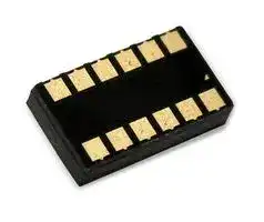


ADIS16006CCCZ
MEMS Accelerometer, ± 5g, X, Y, SPI, LGA, 12 Pins, 256LSB/g
- Manufacturer: ANALOG DEVICES
- Product type: MEMS Accelerometers
- MSL: MSL 3 - 168 hours
- SVHC: Lead (04-Feb-2026)
- No. of Pins: 12Pins
- Sensing Axis: X, Y
- Product Range: -
- Qualification: -
- Sensitivity Max: 272LSB/g
- Sensitivity Min: 242LSB/g
- Sensitivity Typ: 256LSB/g
- Output Interface: SPI
- Sensor Case Style: LGA
- MEMS Sensor Output: Digital
- Supply Voltage Max: 5.25V
- Supply Voltage Min: 3V
- Sensor Case / Package: LGA
- Operating Temperature Max: 125°C
- Operating Temperature Min: -40°C
- Sensing Range - Accelerometer: ± 5g
| Delivery and price | |
|---|---|
| Units per pack | 100 |
| Price | 42.32 € |
| Current stock | 10+ |
| Lead time | 30 days |
**==> picture [159 x 45] intentionally omitted <==**

## **Data Sheet**

## **Dual-Axis ±5 Accelerometer** _**g**_ **with SPI Interface ADIS16006**

## **FEATURES**

## **Dual-axis accelerometer SPI digital output interface Internal temperature sensor Highly integrated; minimal external components Bandwidth externally selectable**

**1.9 m** _**g**_ **resolution at 60 Hz**

**Externally controlled electrostatic self-test 3.0 V to 5.25 V single-supply operation Low power: <2 mA 3500** _**g**_ **shock survival**

**7.2 mm × 7.2 mm × 3.7 mm package**

## **APPLICATIONS**

**Industrial vibration/motion sensing Platform stabilization Dual-axis tilt sensing Tracking, recording, analysis devices Alarms and security devices**

## **GENERAL DESCRIPTION**

The ADIS16006 is a low cost, low power, complete dual-axis accelerometer with an integrated serial peripheral interface (SPI). An integrated temperature sensor is also available on the SPI interface. The ADIS16006 measures acceleration with a fullscale range of ±5 _g_ (minimum). The ADIS16006 can measure both dynamic acceleration (vibration) and static acceleration (gravity).

The typical noise floor is 200 µ _g_ /√Hz, allowing signals below 1.9 m _g_ (60 Hz bandwidth) to be resolved.

The bandwidth of the accelerometer is set with optional capacitors, CX and CY, at the XFILT pin and the YFILT pin. Digital output data for both axes is available via the serial interface.

An externally driven self-test pin (ST) allows the user to verify the accelerometer functionality.

The ADIS16006 is available in a 7.2 mm × 7.2 mm × 3.7 mm, 12-terminal LGA package.

## **FUNCTIONAL BLOCK DIAGRAM**

**==> picture [306 x 207] intentionally omitted <==**

**----- Start of picture text -----**<br>
VCC<br>ADIS16006<br>SCLK<br>DUAL-AXIS±5 g SERIAL DIN<br>ACCELEROMETER INTERFACE DOUT<br>CS<br>CDC<br>TCS<br>TEMP<br>SENSOR<br>COM ST YFILT XFILT<br>CY CX<br>Figure 1.<br>05975-001<br>**----- End of picture text -----**<br>


**Document Feedback**

**Rev. C Document Feedback Information furnished by Analog Devices is believed to be accurate and reliable. However, no responsibility is assumed by Analog Devices for its use, nor for any infringements of patents or other rights of third parties that may result from its use. Specifications subject to change without notice. No license is granted by implication or otherwise under any patent or patent rights of Analog Devices. Trademarks and registered trademarks are the property of their respective owners.**

**One Technology Way, P.O. Box 9106, Norwood, MA 02062-9106, U.S.A. Tel: 781.329.4700 ©2006–2013 Analog Devices, Inc. All rights reserved. Technical Support www.analog.com**

**ADIS16006**

**Data Sheet**

## **TABLE OF CONTENTS**

Features .............................................................................................. 1 Applications ....................................................................................... 1 General Description ......................................................................... 1 Functional Block Diagram .............................................................. 1 Revision History ............................................................................... 2 Specifications ..................................................................................... 3 Timing Specifications .................................................................. 4 Circuit and Timing Diagrams ..................................................... 5 Absolute Maximum Ratings ............................................................ 6 ESD Caution .................................................................................. 6 Pin Configuration and Function Descriptions ............................. 7 Typical Performance Characteristics ............................................. 8 Theory of Operation ...................................................................... 11

Accelerometer Data Format ...................................................... 11 Self-Test ....................................................................................... 11 Serial Interface ............................................................................ 11 Accelerometer Serial Interface.................................................. 11 Temperature Sensor Serial Interface ........................................ 12 Power Supply Decoupling ......................................................... 12 Setting the Bandwidth ............................................................... 13 Selecting Filter Characteristics: The Noise/Bandwidth TradeOff ................................................................................................. 13 Applications ..................................................................................... 15 Second Level Assembly.............................................................. 15 Outline Dimensions ....................................................................... 16 Ordering Guide .......................................................................... 16

## **REVISION HISTORY**

## **2/13—Rev. B to Rev. C**

Changes to Figure 23 ...................................................................... 14

## **3/12—Rev. A to Rev. B**

Added Accelerometer Data Format Section ............................... 11 Added Table 6; Renumbered Sequentially .................................. 11

## **10/07—Rev. 0 to Rev. A**

Changes to Features and General Description ............................. 1 Added Note 6 to Table 2 .................................................................. 4 Changes to Figure 5 .......................................................................... 6 Changes to Accelerometer Control Register Section ................. 11 Changes to Layout .......................................................................... 13 Changes to Layout .......................................................................... 14 Deleted Figure 24 and Table 11..................................................... 14 Edited Second-Level Assembly Section ....................................... 15 Updated Outline Dimensions ....................................................... 16 Changes to Ordering Guide .......................................................... 16

**3/06—Revision 0: Initial Version**

Rev. C | Page 2 of 16

**ADIS16006**

**Data Sheet**

## **SPECIFICATIONS**

TA = −40°C to +125°C, VCC = 5 V, CX = CY = 0 µF, acceleration = 0 _g_ , unless otherwise noted. All minimum and maximum specifications are guaranteed. Typical specifications are not guaranteed.

## **Table 1.**

|**Table 1.**||||
|---|---|---|---|
|**Parameter**|**Conditions**|**Min**<br>**Typ**<br>**Max**|**Unit**|
|ACCELEROMETER SENSOR INPUT<br>Measurement Range1<br>Nonlinearity<br>Package Alignment Error<br>Alignment Error<br>Cross-Axis Sensitivity|Each axis<br>% of full scale<br>X sensor to Y sensor|±5<br>±0.5<br>±2.5<br>±1.5<br>±0.1<br>±1.5<br>±3|_g_<br>%<br>Degrees<br>Degrees<br>%|
|ACCELEROMETER SENSITIVITY<br>Sensitivity at XFILT, YFILT<br>SensitivityChange due to Temperature2|Each axis<br>Delta from 25°C|242<br>256<br>272<br>±0.3|LSB/_g_<br>%|
|ZERO_g_BIAS LEVEL<br>0_g_Voltage at XFILT, YFILT<br>0_g_Offset vs. Temperature|Each axis|1905<br>2048<br>2190<br>±0.1|LSB<br>LSB/°C|
|ACCELEROMETER NOISE PERFORMANCE<br>Noise Density|At 25°C|200|µ_g_/√Hz rms|
|ACCELEROMETER FREQUENCY RESPONSE3, 4<br>CX, CYRange<br>RFILTTolerance<br>Sensor Bandwidth<br>Sensor Resonant Frequency|CX= 0 µF, CY= 0 µF|0<br>10<br>24<br>32<br>40<br>2.26<br>5.5|µF<br>kΩ<br>kHz<br>kHz|
|ACCELEROMETER SELF-TEST<br>Logic Input Low<br>Logic Input High<br>ST Input Resistance to COM<br>Output Change at XOUT, YOUT5|Self-Test 0 to Self-Test 1|0.2 × VCC<br>0.8 × VCC<br>30<br>50<br>102<br>205<br>307|V<br>V<br>kΩ<br>LSB|
|TEMPERATURE SENSOR<br>Accuracy<br>Resolution<br>Update Rate<br>Temperature Conversion Time|VCC= 3 V to 5.25 V|±2<br>10<br>400<br>25|°C<br>Bits<br>µs<br>µs|
|DIGITAL INPUT<br>Input High Voltage (VINH)<br>Input Low Voltage (VINL)<br>Input Current<br>Input Capacitance|VCC= 4.75 V to 5.25 V<br>VCC= 3.0 V to 3.6 V<br>VCC= 3.0 V to 5.25 V<br>VIN= 0 V or VCC|2.4<br>2.1<br>0.8<br>−10<br>+1<br>+10<br>10|V<br>V<br>V<br>µA<br>pF|
|DIGITAL OUTPUT<br>Output High Voltage (VOH)<br>Output Low Voltage (VOL)|ISOURCE= 200 µA, VCC= 3.0 V to 5.25 V<br>ISINK= 200µA|VCC− 0.5<br>0.4|V<br>V|


Rev. C | Page 3 of 16

**Data Sheet**

## **ADIS16006**

|**Parameter**|**Conditions**|**Min**<br>**Typ**<br>**Max**|**Unit**|
|---|---|---|---|
|POWER SUPPLY<br>Operating Voltage Range<br>Quiescent Supply Current<br>Power-Down Current<br>Turn-On Time6|fSCLK= 50 kSPS<br>CX, CY= 0.1µF|3.0<br>5.25<br>1.5<br>1.9<br>1.0<br>20|V<br>mA<br>mA<br>ms|


- 1 Guaranteed by measurement of initial offset and sensitivity.

2 Defined as the output change from ambient-to-maximum temperature or ambient-to-minimum temperature.

3 Actual bandwidth response controlled by user-supplied external capacitor (CX, CY).

- 4 See the Setting the Bandwidth section for more information on how to reduce the bandwidth.

5 Self-test response changes as the square of VCC.

6 Larger values of CX and CY increase turn-on time. Turn-on time is approximately (160 × (0.0022 + CX or CY) + 4) in milliseconds, where CX and CY are in µF.

## **TIMING SPECIFICATIONS**

TA = −40°C to +125°C, acceleration = 0 _g_ , unless otherwise noted.

**Table 2.**

|**Table 2.**|||||
|---|---|---|---|---|
|**Parameter**1, 2|**VCC = 3.3 V**|**VCC = 5 V**|**Unit**|**Description**|
|fSCLK3<br>tCONVERT<br>tACQ<br>t1<br>t24<br>t34<br>t4<br>t5<br>t6<br>t7<br>t85<br>t96|10<br>2<br>14.5 × tSCLK<br>1.5 × tSCLK<br>10<br>60<br>100<br>20<br>20<br>0.4 × tSCLK<br>0.4 × tSCLK<br>80<br>5|10<br>2<br>14.5 × tSCLK<br>1.5 × tSCLK<br>10<br>30<br>75<br>20<br>20<br>0.4 × tSCLK<br>0.4 × tSCLK<br>80<br>5|kHz min<br>MHz max<br>ns min<br>ns max<br>ns max<br>ns min<br>ns min<br>ns min<br>ns min<br>ns max<br>µs typ|Throughput time = tCONVERT+ tACQ= 16 × tSCLK<br>TCS<br>/CS<br>to SCLK setup time<br>Delay from TCS<br>/CS<br>until DOUT three-state disabled<br>Data access time after SCLK falling edge<br>Data setup time prior to SCLK rising edge<br>Data hold time after SCLK rising edge<br>SCLK high pulse width<br>SCLK low pulse width<br>TCS<br>/CS<br>rising edge to DOUT high impedance<br>Power-uptime from shutdown|


1 Guaranteed by design. All input signals are specified with tR and tF = 5 ns (10% to 90% of VCC) and timed from a voltage level of 1.6 V. The 3.3 V operating range spans from 3.0 V to 3.6 V. The 5 V operating range spans from 4.75 V to 5.25 V.

- 2 See Figure 3 and Figure 4.

3 Mark/space ratio for the SCLK input is 40/60 to 60/40.

4 Measured with the load circuit in Figure 2 and defined as the time required for the output to cross 0.4 V or 2.0 V with VCC = 3.3 V and time for an output to cross 0.8 V or 2.4 V with VCC = 5.0 V.

5 t8 is derived from the measured time taken by the data outputs to change 0.5 V when loaded with the circuit in Figure 2. The measured number is then extrapolated back to remove the effects of charging or discharging the 50 pF capacitor. This means that the time, t8, quoted in the Timing Specifications is the true bus relinquish time of the part and is independent of the bus loading.

6 Shutdown recovery time denotes the time it takes to start producing samples and does not account for the recovery time of the sensor, which is dependent on the overall bandwidth.

Rev. C | Page 4 of 16

**ADIS16006**

**Data Sheet**

## **CIRCUIT AND TIMING DIAGRAMS**

**==> picture [146 x 86] intentionally omitted <==**

**----- Start of picture text -----**<br>
200µA IOL<br>TO OUTPUT 1.6V<br>PIN<br>CL<br>50pF<br>200µA IOH<br>05975-002<br>**----- End of picture text -----**<br>


_Figure 2. Load Circuit for Digital Output Timing Specifications_

**==> picture [501 x 258] intentionally omitted <==**

**----- Start of picture text -----**<br>
tACQ tCONVERT<br>CS<br>t1 t6<br>SCLK 1 2 3 4 5 6 15 16<br>t2 t7 t3 t8<br>DOUT THREE-STATE 4 LEADING ZEROS DB11 DB10 DB9 DB0 THREE-STATE<br>t4<br>t5<br>DIN DON’TCARE ZERO ZERO ZERO ADD0 ONE ZERO PM0<br>Figure 3. Accelerometer Serial Interface Timing Diagram<br>TCS<br>t1 t6<br>SCLK 1 2 3 4 11 15 16<br>THREE- t3 t7 t8<br>DOUT STATE LEADINGZERO DB9 DB8 DB0 THREE-STATE<br>DIN<br>05975-003<br>05975-004<br>**----- End of picture text -----**<br>


_Figure 4. Temperature Serial Interface Timing Diagram_

Rev. C | Page 5 of 16

**Data Sheet**

## **ADIS16006**

## **ABSOLUTE MAXIMUM RATINGS**

## **Table 3.**

|**Table 3.**||
|---|---|
|**Parameter**|**Rating**|
|Acceleration (Any Axis, Unpowered)<br>Acceleration (Any Axis, Powered)<br>VCC<br>All Other Pins<br>Output Short-Circuit Duration<br>(Any Pin to Common)<br>Operating Temperature Range<br>Storage Temperature Range|3500_g_<br>3500_g_<br>−0.3 V to +7.0 V<br>(COM − 0.3 V) to (VCC+ 0.3 V)<br>Indefinite<br>−40°C to +125°C<br>−65°C to +150°C|


Stresses above those listed under Absolute Maximum Ratings may cause permanent damage to the device. This is a stress rating only; functional operation of the device at these or any other conditions above those indicated in the operational section of this specification is not implied. Exposure to absolute maximum rating conditions for extended periods may affect device reliability.

**Table 4. Package Characteristics**

**==> picture [256 x 192] intentionally omitted <==**

**----- Start of picture text -----**<br>
Package Type  θJA θJC Device Weight<br>12-Terminal LGA   200°C/W  25°C/W  0.3 grams<br>3.1865<br>8×<br>1.797<br>8×<br>0.670<br>8×<br>6.373 3.594<br>2× 4×<br>0.500<br>1.127 12×<br>12×<br>7.2mm × 7.2mm STACKED LGA. ALL DIMENSIONS IN mm. 05975-005<br>**----- End of picture text -----**<br>


_Figure 5. Second-Level Assembly Pad Layout_

## **ESD CAUTION**

**==> picture [242 x 61] intentionally omitted <==**

Rev. C | Page 6 of 16

**ADIS16006**

**Data Sheet**

## **PIN CONFIGURATION AND FUNCTION DESCRIPTIONS**

**==> picture [163 x 171] intentionally omitted <==**

**----- Start of picture text -----**<br>
12 11 10<br>TCS 1 9 XFILT<br>ADIS16006<br>TOP VIEW<br>DOUT 2 (Not to Scale) 8 YFILT<br>DIN 3 7 NC<br>4 5 6<br>NC = NO CONNECT<br>Figure 6. Pin Configuration<br>05975-006<br>SCLK VCC CS<br>COM NC ST<br>**----- End of picture text -----**<br>


## **Table 5. Pin Function Descriptions**

|**Pin No.**|**Mnemonic**|**Description**|
|---|---|---|
|1<br>2<br>3<br>4<br>5, 7<br>6<br>8<br>9<br>10<br>11<br>12|TCS<br>DOUT<br>DIN<br>COM<br>NC<br>ST<br>YFILT<br>XFILT<br>CS<br>VCC<br>SCLK|Temperature Chip Select. Active low logic input. This input frames the serial data transfer for the temperature<br>sensor output.<br>Data Out, Logic Output. The conversion of theADIS16006is provided on this output as a serial data stream.<br>The bits are clocked out on the falling edge of the SCLK input.<br>Data In, Logic Input. Data to be written into the control register of theADIS16006is provided on this input and<br>is clocked into the register on the rising edge of SCLK.<br>Common. Reference point for all circuitry on theADIS16006.<br>No Connect.<br>Self-Test Input. Active high logic input. Simulates a nominal 0.75_g_test input for diagnostic purpose.<br>Y-Channel Filter Node. Used in conjunction with an optional external capacitor to band limit the noise<br>contribution from the accelerometer.<br>X-Channel Filter Node. Used in conjunction with an optional external capacitor to band limit the noise<br>contribution from the accelerometer.<br>Chip Select. Active low logic input. This input provides the dual function of initiating the accelerometer<br>conversions on theADIS16006and framing the serial data transfer for the accelerometer output.<br>Power Supply Input. The VCCrange for theADIS16006is 3.0 V to 5.25 V.<br>Serial Clock, Logic Input. SCLK provides the serial clock for accessing data from the part and writing serial data to<br>the control register. This clock input is also used as the clock source for the conversionprocess of theADIS16006.|


Rev. C | Page 7 of 16

**ADIS16006**

**Data Sheet**

## **TYPICAL PERFORMANCE CHARACTERISTICS**

**==> picture [221 x 376] intentionally omitted <==**

**----- Start of picture text -----**<br>
262<br>261<br>B3-Y<br>B3-X<br>260<br>B1-Y<br>B5-X<br>259 B2-X<br>B1-X<br>258<br>B5-Y<br>257 B4-X<br>B2-Y<br>256 B4-Y<br>255<br>254<br>–50 –25 0 25 50 75 100 125 150<br>TEMPERATURE (°C)<br>Figure 7. Sensitivity vs. Temperature (±1  g  Stimulus)<br>2048<br>5.25V<br>2046 AVG AT 5.25V<br>AVG AT 4.75V<br>2044<br>AVG AT 3.60V<br>2042<br>AVG AT 3.30V<br>AVG AT 3.00V<br>2040<br>2038<br>–40 –20 0 20 40 60 80 100 120<br>TEMPERATURE (°C)<br>) g<br>SENSITIVITY (LSB/<br>05975-007<br>BIAS LEVEL (LSB)<br>05975-008<br>**----- End of picture text -----**<br>


_Figure 8. X-Axis 0_ g _Bias vs. Temperature_

**==> picture [220 x 169] intentionally omitted <==**

**----- Start of picture text -----**<br>
2048<br>2047<br>2046<br>+125°C<br>2045<br>2044<br>+25°C<br>2043<br>2042<br>–40°C<br>2041<br>2040<br>2039<br>2038<br>3.0 3.5 4.0 4.5 5.0 5.5<br>VCC (V)<br>BIAS LEVEL (LSB)<br>05975-009<br>**----- End of picture text -----**<br>


_Figure 9. X-Axis 0_ g _Bias vs. Supply Voltage_

**==> picture [216 x 174] intentionally omitted <==**

**----- Start of picture text -----**<br>
25<br>AVERAGE = 2040.66<br>STANDARD DEVIATION = 23.19<br>20<br>15<br>10<br>5<br>0<br>OUTPUT (LSB)<br>PERCENT OF POPULATION (%)<br>1995 2000 2005 2010 2015 2020 2025 2030 2035 2040 2045 2050 2055 2060 2065 2070 2075 2080 2085 2090<br>05975-010<br>**----- End of picture text -----**<br>


_Figure 10. X-Axis 0_ g _Bias at 25°C_

**==> picture [216 x 390] intentionally omitted <==**

**----- Start of picture text -----**<br>
40<br>AVERAGE = 2055.875<br>STANDARD DEVIATION = 6.464<br>35<br>30<br>25<br>20<br>15<br>10<br>5<br>0<br>OUTPUT (LSB)<br>Figure 11. Y-Axis 0  g  Bias at 25°C<br>60<br>50<br>40<br>30<br>20<br>10<br>0<br>80 85 90 95 100 105 110 115 120 125 130 135 140<br>NOISE (µ g /  Hz)<br>Figure 12. Noise (X-Axis) at VCC = 5 V, 25°C<br>PERCENT OF POPULATION (%)<br>1995 2000 2005 2010 2015 2020 2025 2030 2035 2040 2045 2050 2055 2060 2065 2070 2075 2080 2085 2090<br>05975-011<br>PERCENT OF POPULATION (%)<br>05975-012<br>**----- End of picture text -----**<br>


Rev. C | Page 8 of 16

**ADIS16006**

**Data Sheet**

**==> picture [216 x 168] intentionally omitted <==**

**----- Start of picture text -----**<br>
45<br>40<br>35<br>30<br>25<br>20<br>15<br>10<br>5<br>0<br>80 85 90 95 100 105 110 115 120 125 130 135 140<br>NOISE (µ g /  Hz)<br>PERCENT OF POPULATION (%)<br>05975-013<br>**----- End of picture text -----**<br>


_Figure 13. Noise (Y-Axis) at VCC = 5 V, 25°C_

**==> picture [216 x 366] intentionally omitted <==**

**----- Start of picture text -----**<br>
40<br>AVERAGE = 202.2137<br>STANDARD DEVIATION = 12.09035<br>35<br>30<br>25<br>20<br>15<br>10<br>5<br>0<br>110 130 150 170 190 210 230 250 270 290<br>OUTPUT (LSB)<br>Figure 14. X-Axis Self-Test at VCC = 5 V, 25°C<br>40<br>AVERAGE = 82.89281<br>STANDARD DEVIATION = 4.908012<br>35<br>30<br>25<br>20<br>15<br>10<br>5<br>0<br>40 45 50 55 60 65 70 75 80 85 90 95 100 105 110<br>OUTPUT (LSB)<br>PERCENT OF POPULATION (%)<br>05975-014<br>PERCENT OF POPULATION (%)<br>05975-015<br>**----- End of picture text -----**<br>


_Figure 15. X-Axis Self-Test at VCC = 3.3 V, 25°C_

**==> picture [221 x 168] intentionally omitted <==**

**----- Start of picture text -----**<br>
250<br>AVG AT 5.25V<br>AVG AT 5.00V<br>200<br>AVG AT 4.75V<br>150<br>AVG AT 3.60V<br>100<br>AVG AT 3.30V<br>AVG AT 3.00V<br>50<br>0<br>–50 0 50 100 150<br>TEMPERATURE (°C)<br>SELF TEST (LSB)<br>05975-016<br>**----- End of picture text -----**<br>


_Figure 16. Self-Test X-Axis vs. Temperature_

**==> picture [220 x 369] intentionally omitted <==**

**----- Start of picture text -----**<br>
250<br>230<br>+125°C<br>210<br>190<br>+25°C<br>170<br>–40°C<br>150<br>130<br>110<br>90<br>70<br>50<br>3.0 3.5 4.0 4.5 5.0 5.5<br>VCC (V)<br>Figure 17. Self-Test X-Axis vs. Supply Voltage<br>1.8<br>+125°C<br>1.7<br>1.6<br>+25°C<br>1.5<br>1.4<br>–40°C<br>1.3<br>1.2<br>1.1<br>1.0<br>3.0 3.5 4.0 4.5 5.0 5.5<br>VCC (V)<br>SELF TEST (LSB)<br>05975-017<br>SUPPLY CURRENT (mA)<br>05975-018<br>**----- End of picture text -----**<br>


_Figure 18. Supply Current vs. Supply Voltage_

Rev. C | Page 9 of 16

**ADIS16006**

**Data Sheet**

**==> picture [216 x 168] intentionally omitted <==**

**----- Start of picture text -----**<br>
45<br>VCC = 5.0V<br>VCC = 3.3V<br>35<br>25<br>15<br>5<br>–5<br>1.15 1.19 1.23 1.27 1.31 1.35 1.39 1.43 1.47 1.51 1.55 1.59<br>CURRENT (mA)<br>PERCENT OF POPULATION (%)<br>05975-023<br>**----- End of picture text -----**<br>


_Figure 19. Supply Current at 25°C_

**==> picture [216 x 168] intentionally omitted <==**

**----- Start of picture text -----**<br>
60<br>VCC = 5.0V<br>50 VCC = 3.3V<br>40<br>30<br>20<br>10<br>0<br>0.70 0.74 0.78 0.82 0.86 0.90 0.94 0.98 1.02 1.06 1.10<br>CURRENT (mA)<br>PERCENT OF POPULATION (%)<br>05975-019<br>**----- End of picture text -----**<br>


_Figure 20. Power-Down Supply Current_

**==> picture [220 x 168] intentionally omitted <==**

**----- Start of picture text -----**<br>
1.3<br>1.2<br>1.1<br>+125°C<br>1.0<br>+25°C<br>0.9<br>–40°C<br>0.8<br>0.7<br>0.6<br>3.0 3.5 4.0 4.5 5.0 5.5<br>VCC (V)<br>POWER-DOWN SUPPLY CURRENT (mA)<br>05975-020<br>**----- End of picture text -----**<br>


_Figure 21. Power-Down Supply Current vs. Supply Voltage_

**==> picture [217 x 180] intentionally omitted <==**

**----- Start of picture text -----**<br>
0.6<br>0.4<br>0.2<br>0<br>–0.2<br>–0.4<br>–0.6<br>–0.8<br>–1.0<br>1 10 100<br>SAMPLE RATE (kSPS)<br>Figure 22. Sampling Error vs. Sampling Frequency<br>SAMPLING ERROR (dB)<br>05975-024<br>**----- End of picture text -----**<br>


Rev. C | Page 10 of 16

**ADIS16006**

**Data Sheet**

## **THEORY OF OPERATION**

The ADIS16006 is a low cost, low power, complete dual-axis accelerometer with an integrated serial peripheral interface (SPI) and an integrated temperature sensor whose output is also available on the SPI interface. The ADIS16006 is capable of measuring acceleration with a full-scale range of ±5 _g_ (minimum). The ADIS16006 can measure both dynamic acceleration (vibration) and static acceleration (gravity).

## **ACCELEROMETER DATA FORMAT**

The accelerometer data is in a 12-bit, offset binary format. See Table 6 for examples of this data format.

**Table 6. Acceleration Data Format Examples**

|**Acceleration (****_g_) **|**Decimal**|**Hex**|**Binary**|
|---|---|---|---|
|+5<br>+2/256<br>+1/256<br>0<br>−1/256<br>−2/256<br>−5|3328<br>2050<br>2049<br>2048<br>2047<br>2046<br>768|0xD00<br>0x802<br>0x801<br>0x800<br>0x7FF<br>0x7FE<br>0x300|1101 0000 0000<br>1000 0000 0010<br>1000 0000 0001<br>1000 0000 0000<br>0111 1111 1111<br>0111 1111 1110<br>0011 0000 0000|


## **SELF-TEST**

The ST pin controls the self-test feature. When this pin is set to VCC, an electrostatic force is exerted on the beam of the accelerometer. The resulting movement of the beam allows the user to test if the accelerometer is functional. The typical change in output is 801 m _g_ (corresponding to 205 LSB) for VCC = 5.0 V. This pin can be left open-circuit or connected to common in normal use. The ST pin should never be exposed to voltage greater than VCC + 0.3 V. If the system design is such that this condition cannot be guaranteed (for example, multiple supply voltages are present), a low VF clamping diode between ST and VCC is recommended.

## **SERIAL INTERFACE**

The serial interface on the ADIS16006 consists of five wires: CS, TCS, SCLK, DIN, and DOUT. Both accelerometer axes and the temperature sensor data are available on the serial interface. The CS and TCS are used to select the accelerometer or temperature sensor outputs, respectively. CS and TCS cannot be active at the same time.

The SCLK input accesses data from the internal data registers.

## **ACCELEROMETER SERIAL INTERFACE**

Figure 3 shows the detailed timing diagram for serial interfacing to the accelerometer in the ADIS16006. The serial clock provides the conversion clock. CS initiates the conversion process and data transfer and frames the serial data transfer for the accelerometer output. The accelerometer output is sampled on the second rising edge of the SCLK input after the falling edge of CS. The conversion requires 16 SCLK cycles to complete. The rising edge of CS puts the bus back into three-state. If CS remains

low, the next digital conversion is initiated. The details for the control register bit functions are shown in Table 7.

## _**Accelerometer Control Register**_

|**MSB**|||||||**LSB**|
|---|---|---|---|---|---|---|---|
|DONTC|ZERO|ZERO|ZERO|ADD0|ONE|ZERO|PM0|


## **Table 7. Accelerometer Control Register Bit Functions**

|**Bit**|**Mnemonic**|**Comments**|
|---|---|---|
|7<br>6, 5, 4<br>3<br>2<br>1<br>0|DONTC<br>ZERO<br>ADD0<br>ONE<br>ZERO<br>PM0|Don’t care. Can be 1 or 0.<br>These bits should be held low.<br>This address bit selects the x-axis or y-axis<br>outputs. A 0 selects the x-axis; a 1 selects<br>the y-axis.<br>This bit should be held high.<br>This bit should be held low.<br>This bit selects the operation mode for<br>the accelerometer; set to 0 for normal<br>operation and 1 forpower-down mode.|


## _**Power-Down**_

By setting PM0 to 1 when updating the accelerometer control register, the ADIS16006 goes into shutdown mode. The information stored in the control register is maintained during shutdown. The ADIS16006 changes modes as soon as the control register is updated. If the part is in shutdown mode and PM0 is changed to 0, the part powers up on the 16th SCLK rising edge.

## _**ADD0**_

By setting ADD0 to 0 when updating the accelerometer control register, the x-axis output is selected. By setting ADD0 to 1, the y-axis output is selected.

## _**ZERO**_

ZERO is defined as the Logic low level.

## _**ONE**_

ONE is defined as the Logic high level.

## _**DONTC**_

DONTC is defined as don’t care and can be a low or high logic level.

## _**Accelerometer Conversion Details**_

Every time the accelerometer is sampled, the sampling function discharges the internal CX or CY filtering capacitors by up to 2% of their initial values (assuming no additional external filtering capacitors are added). The recovery time for the filter capacitor to recharge is approximately 10 µs. Therefore, sampling the accelerometer at a rate of 10 kSPS or less does not induce a sampling error. However, as sampling frequencies increase above 10 kSPS, one can expect sampling errors to attenuate the actual acceleration levels.

Rev. C | Page 11 of 16

**Data Sheet**

## **ADIS16006**

## **TEMPERATURE SENSOR SERIAL INTERFACE**

## _**Read Operation**_

Figure 4 shows the timing diagram for a serial read from the temperature sensor. The TCS line enables the SCLK input. Ten bits of data and a leading zero are transferred during a read operation. Read operations occur during streams of 16 clock pulses. The serial data can be received into two bytes to accommodate the entire 10-bit data stream. If only eight bits of resolution are required, the data can be received into a single byte. At the end of the read operation, the DOUT line remains in the state of the last bit of data clocked out until TCS goes high, at which time the DOUT line from the temperature sensor goes three-state.

## _**Write Operation**_

Figure 4 also shows the timing diagram for the serial write to the temperature sensor. The write operation takes place at the same time as the read operation. Data is clocked into the control register on the rising edge of SCLK. DIN should remain low for the entire cycle.

## _**Temperature Sensor Control Register**_

|**MSB**|||||||**LSB**|
|---|---|---|---|---|---|---|---|
|ZERO|ZERO|ZERO|ZERO|ZERO|ZERO|ZERO|ZERO|


**Table 8. Temperature Sensor Control Register Bit Functions**

|**Bit**|**Mnemonic**|**Comments**|
|---|---|---|
|7 to 0|ZERO|All bits should be held low.|


## _**ZERO**_

ZERO is defined as the Logic low level.

## _**Output Data Format**_

The output data format for the temperature sensor is twos complement. Table 9 shows the relationship between the temperature and the digital output.

**Table 9. Temperature Sensor Data Format**

|**Temperature**|**Digital Output (DB9 … DB0)**|
|---|---|
|−40°C<br>−25°C<br>−0.25°C<br>0°C<br>+0.25°C<br>+10°C<br>+25°C<br>+50°C<br>+75°C<br>+100°C<br>+125°C|11 0110 0000<br>11 1001 1100<br>11 1111 1111<br>00 0000 0000<br>00 0000 0001<br>00 0010 1000<br>00 0110 0100<br>00 1100 1000<br>01 0010 1100<br>01 1001 0000<br>01 1111 0100|


## _**Temperature Sensor Conversion Details**_

The ADIS16006 features a 10-bit digital temperature sensor that allows an accurate measurement of the ambient device temperature to be made.

The conversion clock for the temperature sensor is internally generated; therefore, no external clock is required except when reading from and writing to the serial port. In normal mode, an internal clock oscillator runs the automatic conversion sequence. A conversion is initiated approximately every 350 µs. At this time, the temperature sensor wakes up and performs a temperature conversion. This temperature conversion typically takes 25 µs, at which time the temperature sensor automatically shuts down. The result of the most recent temperature conversion is available in the serial output register at any time. Once the conversion is finished, an internal oscillator starts counting and is designed to time out every 350 µs. The temperature sensor then powers up and does a conversion.

If the TCS is brought low every 350 µs (±30%) or less, the same temperature value is output onto the DOUT line every time without changing. It is recommended that the TCS line not be brought low every 350 µs (±30%) or less. The ±30% covers process variation. The TCS should become active (high to low) outside this range.

The device is designed to autoconvert every 350 µs. If the temperature sensor is accessed during the conversion process, an internal signal is generated to prevent any update of the temperature value register during the conversion. This prevents the user from reading back spurious data. The design of this feature results in this internal lockout signal being reset only at the start of the next autoconversion. Therefore, if the TCS line goes active before the internal lockout signal is reset to its inactive mode, the internal lockout signal is not reset. To ensure that no lockout signal is set, bring TCS low at a greater time than 350 µs (±30%). As a result, the temperature sensor is not interrupted during a conversion process.

In the automatic conversion mode, every time a read or write operation takes place, the internal clock oscillator is restarted at the end of the read or write operation. The result of the conversion is typically available 25 µs later. Reading from the device before conversion is complete provides the same set of data.

## **POWER SUPPLY DECOUPLING**

The ADIS16006 integrates two decoupling capacitors that are 0.047 µF in value. For local operation of the ADIS16006, no additional power supply decoupling capacitance is required. However, if the system power supply presents a substantial amount of noise, additional filtering can be required. If additional capacitors are required, connect the ground terminal of each of these capacitors directly to the underlying ground plane. Finally, note that all analog and digital grounds should be referenced to the same system ground reference point.

Rev. C | Page 12 of 16

**ADIS16006**

**Data Sheet**

## **SETTING THE BANDWIDTH**

The ADIS16006 has provisions for band limiting the accelerometer. Capacitors can be added at the XFILT pin and the YFILT pin to implement further low-pass filtering for antialiasing and noise reduction. The equation for the 3 dB bandwidth is

_f−3dB_ = 1/(2π(32 kΩ) × ( _C(XFILT, YFILT)_ + 2200 pF))

or more simply,

_f−3dB_ = 5 µF/( _C(XFILT, YFILT)_ + 2200 pF)

The tolerance of the internal resistor (RFILT) can vary typically as much as ±25% of its nominal value (32 kΩ); thus, the bandwidth varies accordingly.

A minimum capacitance of 0 pF for CXFILT and CYFILT is allowable.

**Table 10. Filter Capacitor Selection, CXFILT and CYFILT**

|**Bandwidth (Hz)**|**Capacitor (µF)**|
|---|---|
|1<br>10<br>50<br>100<br>200<br>400<br>2250|4.7<br>0.47<br>0.10<br>0.047<br>0.022<br>0.01<br>0|


## **SELECTING FILTER CHARACTERISTICS: THE NOISE/BANDWIDTH TRADE-OFF**

The accelerometer bandwidth selected ultimately determines the measurement resolution (smallest detectable acceleration). Filtering can be used to lower the noise floor, which improves the resolution of the accelerometer. Resolution is dependent on the analog filter bandwidth at XFILT and YFILT.

The ADIS16006 has a typical bandwidth of 2.25 kHz with no external filtering. The analog bandwidth can be further decreased to reduce noise and improve resolution.

The ADIS16006 noise has the characteristics of white Gaussian noise, which contributes equally at all frequencies and is described in terms of µ _g_ /√Hz (that is, the noise is proportional to the square root of the bandwidth of the accelerometer). The user should limit bandwidth to the lowest frequency needed by the application to maximize the resolution and dynamic range of the accelerometer.

With the single-pole, roll-off characteristic, the typical noise of the ADIS16006 is determined by

_rmsNoise_ = (200 µ _g_ /√Hz) × (√( _BW_ × 1.57))

At 100 Hz, the noise is

_rmsNoise_ = (200 µ _g_ /√Hz) × (√(100 × 1.57)) = 2.5 m _g_

Often, the peak value of the noise is desired. Peak-to-peak noise can only be estimated by statistical methods. Table 11 is useful for estimating the probabilities of exceeding various peak values, given the rms value.

**Table 11. Estimation of Peak-to-Peak Noise**

|**Peak-to-Peak Value**|**Percentage of Time Noise Exceeds**<br>**Nominal Peak-to-Peak Value (%)**|
|---|---|
|2 × rms<br>4 × rms<br>6 × rms<br>8 × rms|32<br>4.6<br>0.27<br>0.006|


Rev. C | Page 13 of 16

**ADIS16006**

**Data Sheet**

**==> picture [380 x 370] intentionally omitted <==**

**----- Start of picture text -----**<br>
12 11 10<br>ay<br>ax<br>DIGITAL OUTPUT (IN LSBs)<br>X-AXIS: 1792<br>Y-AXIS: 2048<br>4 5 6<br>9 8 7 3 2 1<br>ax<br>ay<br>DIGITAL OUTPUT (IN LSBs) DIGITAL OUTPUT (IN LSBs)<br>X-AXIS: 2048 Top View X-AXIS: 2048<br>Y-AXIS: 2304 Not to Scale Y-AXIS: 1792<br>ay<br>ax<br>1 2 3 7 8 9<br>6 5 4<br>DIGITAL OUTPUT (IN LSBs) DIGITAL OUTPUT (IN LSBs)<br>X-AXIS: 2304 X-AXIS: 2048<br>Y-AXIS: 2048 Y-AXIS: 2048<br>ax<br>ay<br>10 11 12<br>1 9<br>2 8<br>3 7<br>10 6 4 12<br>11 5 5 11<br>12 4 6 10<br>7 3<br>8 2<br>9 1<br>05975-021<br>**----- End of picture text -----**<br>


_Figure 23. Output Response vs. Orientation_

Rev. C | Page 14 of 16

**ADIS16006**

**Data Sheet**

## **APPLICATIONS**

## **SECOND LEVEL ASSEMBLY**

The ADIS16006 can be attached to the second level assembly board using SN63 (or equivalent) or lead-free solder. IPC/ JEDEC J-STD-020 and J-STD-033 provide standard handling procedures for these types of packages.

Rev. C | Page 15 of 16

**ADIS16006**

**Data Sheet**

## **OUTLINE DIMENSIONS**

**==> picture [295 x 248] intentionally omitted <==**

**----- Start of picture text -----**<br>
3.594<br>BSC<br>1.797 (4 × ) PIN 1<br>7.35 BSC INDICATOR<br>MAX (8 × )<br>1.00 BSC<br>10 12 (12 × )<br>9 1<br>6 .373<br>7.20 BSC<br>TYP (2 ×)<br>7 3 0.797 BSC<br>6 4 (8 × )<br>TOP VIEW 0.200 BOTTOM VIEW 0.373 BSC<br>MIN (12 × )<br>(ALL SIDES )<br>5.00<br>TYP<br>3.70<br>MAX<br>SIDE VIEW<br>Figure 24. 12-Terminal Land Grid Array [LGA]<br>(CC-12-1)<br>Dimensions shown in millimeters<br>**----- End of picture text -----**<br>


**==> picture [4 x 18] intentionally omitted <==**

**----- Start of picture text -----**<br>
092407-C<br>**----- End of picture text -----**<br>


|**ORDERING GUIDE**||||
|---|---|---|---|
|**Model1**|**Temperature Range **|**Package Description**|**Package Option**|
|ADIS16006CCCZ<br>ADIS16006/PCBZ|−40°C to +125°C|12-Terminal Land Grid Array (LGA)<br>Evaluation Board|CC-12-1|


1 Z = RoHS Compliant Part.

**©2006–2013 Analog Devices, Inc. All rights reserved. Trademarks and registered trademarks are the property of their respective owners.**

**D05975-0-2/13(C)**

Rev. C | Page 16 of 16
Updated at April 28, 2026
Since its inception in 1965, Analog Devices has established itself as a global leader in the design and manufacturing of high-performance analog, mixed-signal, and digital signal processing (DSP) integrated circuits. The company is renowned for solving complex engineering challenges by providing critical technologies that seamlessly convert real-world phenomena into precise electrical signals for the industrial, automotive, communications, and consumer markets. Within its extensive portfolio, Analog Devices provides highly reliable clock, timing, and frequency management solutions, featuring a comprehensive array of precision timers, oscillators, and pulse generators. Complementing this core lineup is a robust offering of driver and interface ICs, particularly high-performance I/O expanders that enable seamless connectivity and streamline complex electronic system architectures. Beyond these foundational integrated circuits, Analog Devices leads the industry in sensor innovation, delivering advanced MEMS accelerometers and integrated MEMS modules designed for exceptional precision in motion sensing. To support complete hardware designs, the company's specialized offerings also encompass discrete bipolar transistors, sub-2.4GHz RF transceivers, temperature-compensated oscillators, and dedicated power management components such as DC/DC converters and LED driver ICs.
About Novapart
Novapart is a B2B electronic component broker specialising in stock shortages and cost reduction. We source hard-to-find parts and identify compliant alternatives across a catalogue of 410,000+ components from 500+ manufacturers.
Learn more →Stock Shortage Specialist
When a component is unavailable, discontinued or has an unacceptable lead time, we tap into our network of vetted European and Asian distributors to source what you need — without compromising on quality or traceability.
Request a quote →Compliant Alternatives
We identify pin-to-pin, electrically equivalent substitutes that meet the same certifications (RoHS, AEC-Q100, REACH) as your original specification — validated against datasheets, not just part numbers. Often at a lower cost.
BOM Analysis service →