
Image not available
Illustrative purposes only

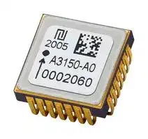
3-A3150-A0
MEMS Accelerometer, AXO315, Digital, X, ± 14g, 4.75 V, 5.25 V, SMD
⚠️ Reference pricing provided. In case of supply shortages, we will connect you with our trusted procurement partners to ensure your project's continuity.
- Manufacturer: TRONICS
- Product type: MEMS Accelerometers
- No. of Pins: 28Pins
- Measurement Axis: X
- Sensor Case Style: SMD
- Acceleration Range: ± 14g
- MEMS Sensor Output: Digital
- Supply Voltage Max: 5.25V
- Supply Voltage Min: 4.75V
| Delivery and price | |
|---|---|
| Units per pack | 1 |
| Price | 542.24 € |
| Current stock | 10+ |
| Lead time | 7 days |
Datasheet

**Tronic’s Microsystems S.A.** 98 rue du Pré de l’Horme, 38920 Crolles, France Phone: +33 (0)4 76 97 29 50 Email: support@tronicsgroup.com www.tronicsgroup.com
**AXO315** Datasheet
## **Features**
- ±14 g range in-plane linear single axis accelerometer
- • Hermetic SMD ceramic package for reliable assembly on FR4
- Fully hard-coded electronic, no embedded software
- Built-in temperature compensation and self-test
- Complementarity with GYPRO® high performance gyros which share the same digital interface
- Best in-class 1 year composite bias repeatability of 1mg under -55°C to 105°C and > 4g environment
- Unmatched vibration rejection of 20µg/g²
- Excellent 1 year composite scale factor repeatability of 600ppm over temperature
- Very low noise of 15µg/√Hz, non-linearity of 100ppm
- Non classified under dual-use export control
## **Table of Contents**
## **General Description**
AXO®315 **high performance** , closed-loop, MEMS accelerometer offers a precision-equivalent alternative to incumbent analog force-rebalance quartz and mechanical accelerometers at a fraction of their size weight and cost. Its hermetic full SMD package combined with its digital 24 bits SPI interface eases its integration and reduces the e-BOM.
With a **1 year composite bias repeatability** of **1mg** under demanding temperature and vibrations conditions, the AXO®315 overpasses all commercially available MEMS accelerometers. AXO®315 is **free from dual-use export control** , according to Annex 1 of Council Regulation (EC) No 428/2009, as well as **REACH** and **RoHS compliant.**
AXO® is ideally complemented by GYPRO® high performance digital gyrometers.
AXO®315 is a very low noise sensor which provides an excellent linearity and 600 ppm 1 year composite scale factor repeatability over -55°C to +105°C extended temperature range.
Our AXO® & GYPRO® products families are well suited to precision attitude, guidance and motion control and GNSSaided positioning applications in demanding industrial, land, railway and naval environments.
All AXO® & GYPRO® products sensors are factory calibrated and compensated for temperature effects to provide highaccuracy digital output over a broad temperature range. Raw data output can be also chosen to enable customer-made compensations.
|Features ................................................................................. 1<br>General Description ............................................................... 1|
|---|
|Table of Contents ................................................................... 1|
|Disclaimer............................................................................... 1|
|Block diagram ..................................................................... 2|
|Overall Dimensions ............................................................ 2|
|1.<br>Specifications .............................................................. 3|
|2.<br>Maximum Ratings ....................................................... 5|
|3.<br>Typical performances .................................................. 6<br>4.<br>Interface ...................................................................... 8<br>4.1.<br>Pinout, Sensitive Axis identification ........................ 8<br>4.2.<br>Application circuit ................................................... 8<br>4.3.<br>Input/Output Pin Definitions .................................. 9<br>5.<br>Soldering Recommendations .................................... 10<br>6.<br>Digital SPI interface ................................................... 11|
|6.1.<br>Electrical and Timing Characteristics .................... 11|
|6.2.<br>SPI frames description .......................................... 12|
|6.3.<br>Acceleration readings ........................................... 12<br>6.4.<br>Temperature readings .......................................... 12<br>6.5.<br>Advanced use of SPI registers ............................... 13<br>7.<br>Acceleration calibration procedure ........................... 15<br>7.1.<br>Algorithm overview .............................................. 15|
|7.2.<br>Programming of the new coefficients .................. 16|
|7.3.<br>Switch to uncompensated data output ................ 17|
|8.<br>Temperature Sensor Calibration Procedure ............. 18|
|8.1.<br>Temperature sensor calibration model ................ 18|
|8.2.<br>Recommended Procedure .................................... 18<br>9.<br>Device Identification ................................................. 19<br>10.<br>Internal construction and Theory of Operation ........ 20<br>11.<br>Available Tools and Resources .................................. 21|
## **Disclaimer**
_Information furnished by Tronics is believed to be accurate and reliable. However, no responsibility is assumed by Tronics for its use, nor for any infringements of patents or other rights of third parties that may result from its use. Specification subject to change without notice._
_No license is granted by implication or otherwise under any patent or patent rights of Tronics. Trademarks and registered trademarks are the property of their respective owner._
**ref. : MCD018-G**
Copyright 2022 Tronic’s Microsystems S.A. All rights reserved. Specification subject to change without notice.
**Page 1**
**AXO315** Datasheet
**Tronic’s Microsystems S.A.** 98 rue du Pré de l’Horme, 38920 Crolles, France Phone: +33 (0)4 76 97 29 50 Email: support@tronicsgroup.com **www.tronicsgroup.com**
## Block diagram
Overall dimensions (with MEMS transducer gravity center in blue)
**ref. : MCD018-G**
Copyright 2022 Tronic’s Microsystems S.A. All rights reserved. Specification subject to change without notice.
**Page 2**
**Tronic’s Microsystems S.A.** 98 rue du Pré de l’Horme, 38920 Crolles, France Phone: +33 (0)4 76 97 29 50 Email: support@tronicsgroup.com www.tronicsgroup.com
**AXO315** Datasheet
## **1. Specifications**
|**Parameter**|**Unit**|**Typ.**|**Max(2)**|**Notes**|
|---|---|---|---|---|
|**Measurement Ranges**|||||
|Full Scale range|g||±14|Electronic clamping is applied and sensors will saturate|
|||||before ±15g|
|Temperature range|°C|-55 to +105|||
|**Bias**|||||
|1 Year Composite bias|mg|1||Total bias drift per year, quadratic sum of all bias errors|
|repeatability|||||
|Bias instability|µg|4|15|Lowest point of Allan variance curve at room temperature|
|Bias in-run (short term) stability|Bias in-run (short term) stability<br>µg|15|45|Standard deviation of the 1 second filtered output over 1 hour|
|||||at room temperature, after 30 min of stabilization|
|Residual bias temperature|mg|±0.5|±1.5|Maximum variation of the bias over the specified temperature|
|error, calibrated(1)(3)(5)||||range|
|Bias repeatability|µg|±220||See note(4)|
|Bias long term stability|mg|0.4||Drift per year, based on Allan variance extrapolation|
|Warm-up bias drift|µg|50||Bias drift during initial sensor self-heating after power on at 0g|
|Vibration rectification error|µg/g²|20||Bias rectification under operating vibrations; root mean|
|||||square of all axis|
|**Scale Factor**|||||
|Scale factor(1)|LSB/g||500 000|500 000<br>Nominal scale factor|
|1 Year Composite scale factor|ppm|600||Total scale factor drift per year, quadratic sum of all scale|
|repeatability||||factor errors|
|Residual scale factor|ppm|±400|±1000|Maximum variation of the scale factor over the specified|
|temperature error, calibrated||||temperature range|
|(1)(3)|||||
|Scale factor repeatability|ppm|±280||See note(4)|
|Scale factor long term stability|ppm|350||Drift per year, based on Allan variance extrapolation|
|**Linearity, Noise**|||||
|Non linearity(1)|ppm|100|350|Maximum deviation of the output from the expected value|
|||||using a best fit straight line over the [0g ; 8g] range, at room|
|||||temperature|
|Noise density(1)|µg/√Hz|15|20|Over the [0 - 300] Hz frequency range, at room temperature|
|Velocity Random Walk|m/s/√h|0.006||-1/2 slope tangent, based on Allan Variance at 1s|
|**Frequency response**|||||
|Bandwidth|Hz|>300||Defined as the frequency for which attenuation is equal to -|
|||||3dB|
|Data Rate|Hz|2500||Refresh rate of the output data at room temperature|
|Latency|ms|1||Time delay between the physical acceleration (input) and the|
|||||output signal|
|Start-up Time|ms|400||Time interval between the application of power and the|
|||||presence of a usable output, i.e. at least 90% of the input, at|
|||||room temperature|
**ref. : MCD018-G**
Copyright 2022 Tronic’s Microsystems S.A. All rights reserved. Specification subject to change without notice.
**Page 3**
**Tronic’s Microsystems S.A.** 98 rue du Pré de l’Horme, 38920 Crolles, France Phone: +33 (0)4 76 97 29 50 Email: support@tronicsgroup.com **www.tronicsgroup.com**
**AXO315** Datasheet
|**Parameter (2)**|**Unit**|**Typ.**||||**Max**|**Notes**|
|---|---|---|---|---|---|---|---|
|**Axis alignment**||||||||
|Axis misalignment|mrad|||||20|By design|
|**Environmental**||||||||
|Storage temperature range|°C|-55 to +125||||||
|Component shelf life|Years|5||||||
|Humidity at 45°C|%|<98||||||
|Moisture Sensitivity Level|--|1|||||Unlimited (hermetic package)|
|(MSL)||||||||
|Shock (operating)|g | ms||50 | 6||50 | 6|50 | 6|Half sine|
|Shock (survival)|g | ms|2000 | 0.3|||2000 | 0.3|||
|Vibrations (operating)|grms||4.12||||DO-160G standard , curve C|
|Vibrations (survival)|grms|||20||20|Random acceleration, applied on any axis within 20Hz to 2kHz|
||||||||during 10min|
|**Electrical**||||||||
|Power Supply Voltage|V|4.75 to 5.25||4.75 to 5.25||4.75 to 5.25||
|Current consumption|mA|||||<30|Tested at room temperature|
|(normal mode)(1)||||||||
|Current consumption|µA|||||<5|Power down mode is activated by switching EN pin to GND, at|
|(power down mode)|||||||room temperature|
|Power supply rejection|µg/V|130||||||
|ratio||||||||
|**Temperature sensor**||||||||
|Scale Factor (raw data)|LSB/°C|85|||||Temperature sensor is not factory-calibrated|
|25°C typical output (raw|LSB|8 000|8 000||||Temperature sensor is not factory-calibrated|
|data)||||||||
|Refresh rate|Hz|6||||||
|**Reliability**||||||||
|MTBF|h|>1 000 000|>1 000 000|||>1 000 000|Predictive elapsed time between inherent failures of the|
||||||||sensor during normal system operation for 50°C use|
||||||||temperature|
**Table 1: Specifications**
- (1) 100% tested in production.
- (2) Unless otherwise specified, max values are ±3 sigma variation limits from validation test population.
- (3) Temperature range of -53°C to +105°C.
- (4) Bias and scale factor repeatabilities include the following parameters:
- Turn On to Turn Off repeatability at constant temperature and constant accelerations,
- Repeatability over temperature, at constant acceleration,
- Repeatability over acceleration, at constant temperature,
- Day to day repeatability, over ten days.
- (5)Due to the sigma delta architecture, there is a dead band of 200µg around zero input level.
**ref. : MCD018-G**
Copyright 2022 Tronic’s Microsystems S.A. All rights reserved. Specification subject to change without notice.
**Page 4**
**Tronic’s Microsystems S.A.** 98 rue du Pré de l’Horme, 38920 Crolles, France Phone: +33 (0)4 76 97 29 50 Email: support@tronicsgroup.com www.tronicsgroup.com
**AXO315** Datasheet
## **2. Maximum Ratings**
Stresses at or exceeding the maximum ratings listed below may cause permanent damage to the device, or affect its reliability. Exposure to maximum ratings conditions for extended periods may also affect device reliability.
Functional operation is not guaranteed once stresses exceeding the maximum ratings have been applied.
|**Parameter**|**Unit**|**Min**|**Max**|
|---|---|---|---|
|Supply Voltage|V|-0.5|+7|
|Electrostatic Discharge (ESD) protection, any pin, Human Body Model|Electrostatic Discharge (ESD) protection, any pin, Human Body Model<br>kV|--|±2|
|Storage temperature range|°C|-55|+125|
|Shock survival, half sine|g|--|2000|
|Vibrations survival, 20-2000Hz|grms|--|20|
|Ultrasonic cleaning||Not allowed|Not allowed|
**Table 2: Maximum ratings**
## **Caution!**
The product may be damaged by ESD, which can cause performance degradation or device failure! We recommend handling the device only on a static safe work station. Precaution for the storage should also be taken.
The sensor MUST be powered-on _before_ any SPI operation, as shown in Figure 1 below. Having the SPI pads, VDDIO or EN at a high level while VDD is at a low level could damage the sensor, due to ESD protection diodes and buffers.
**Figure 1: Recommended voltage sequence**
**ref. : MCD018-G**
Copyright 2022 Tronic’s Microsystems S.A. All rights reserved. Specification subject to change without notice.
**Page 5**
**Tronic’s Microsystems S.A.** 98 rue du Pré de l’Horme, 38920 Crolles, France Phone: +33 (0)4 76 97 29 50 Email: support@tronicsgroup.com **www.tronicsgroup.com**
**AXO315** Datasheet
## **3. Typical performances**
**==> picture [242 x 396] intentionally omitted <==**
**----- Start of picture text -----**<br>
25%20% LEEE7 EEE LLL<br>15% zz<br>10%<br>=<br>5%<br>0%<br>Residual bias temperature error [mg]<br>Figure 2: Residual bias temperature error distribution,<br> absolute value<br>50%<br>45%<br>40%35% {|| | Bm | |<br>30%<br>25%<br>20%<br>15%<br>10% |<br>5%<br>0%<br>Residual scale factor temperature error [ppm]<br>Population [%]<br>0 0,1 0,2 0,3 0,4 0,5 0,6 0,7 0,8 0,9 1 1,1 1,2 1,3 1,4 1,5<br>Population [%]<br>0 100 200 300 400 500 600 700 800<br>**----- End of picture text -----**<br>
**Figure 3: Residual scale factor temperature error distribution, absolute value**
**Figure 5: Residual bias temperature error (5 samples)**
**Figure 6: Residual scale factor temperature error (5 samples)**
**==> picture [216 x 164] intentionally omitted <==**
**----- Start of picture text -----**<br>
35<br>30 Pt ty tt ttt<br>25<br>20<br>15<br>10 Cf|<br>PT<br>5 ft aa<br>0<br>Scale factor non linearity [ppm]<br>Population [%]<br>0 25 50 75 100 125 150 175 200 225<br>**----- End of picture text -----**<br>
**Figure 4: Scale Factor non linearity distribution (room temperature)**
**Figure 7: Allan variance (5 samples at 35°C)**
**ref. : MCD018-G**
Copyright 2022 Tronic’s Microsystems S.A. All rights reserved. Specification subject to change without notice.
**Page 6**
**AXO315** Datasheet
**Tronic’s Microsystems S.A.** 98 rue du Pré de l’Horme, 38920 Crolles, France Phone: +33 (0)4 76 97 29 50 Email: support@tronicsgroup.com www.tronicsgroup.com
**==> picture [215 x 161] intentionally omitted <==**
**----- Start of picture text -----**<br>
25<br>20<br>15<br>10<br>5<br>0<br>Noise density [µg/√Hz]<br>Population (%)<br>10 11 12 13 14 15 16 17 18 19 20<br>**----- End of picture text -----**<br>
**Figure 8: Noise density distribution (room temperature)**
**Figure 9: Frequency response (3 samples at room temperature)**
**Figure 10: Vibration rectification error (5 samples, frequency sweep [50-2000Hz], root mean square of all axis)**
**Figure 11: Noise density (room temperature)**
**ref. : MCD018-G**
Copyright 2022 Tronic’s Microsystems S.A. All rights reserved. Specification subject to change without notice.
**Page 7**
**Tronic’s Microsystems S.A.** 98 rue du Pré de l’Horme, 38920 Crolles, France Phone: +33 (0)4 76 97 29 50 Email: support@tronicsgroup.com **www.tronicsgroup.com**
## **AXO315** Datasheet
## **4. Interface**
## 4.1. Pinout, Sensitive Axis identification
## 4.2. Application circuit
**Figure 14: Recommended Application Schematic**
## Notes:
**Figure 12: How to locate Pin 1 and Sensitive Axis**
- All capacitances of Figure 14 should be placed as close as possible to their corresponding pins, except the 100nF capacitance between VDD and GND, which should be as close as possible to the board’s supply input.
- The 100µF filtering capacitance between LVREF and GND should have low Equivalent Series Resistance (ESR < 1Ω) and low leakage current (< 6µA).
- The digital pads maximum ratings are GND-0.3V and VDD+0.3V.
**Figure 13: AXO315 Sensors Pinout (BOTTOM VIEW)**
**Figure 15: Recommended Pad Layout (dimensions in mm)**
**ref. : MCD018-G**
Copyright 2022 Tronic’s Microsystems S.A. All rights reserved. Specification subject to change without notice.
**Page 8**
**Tronic’s Microsystems S.A.** 98 rue du Pré de l’Horme, 38920 Crolles, France Phone: +33 (0)4 76 97 29 50 Email: support@tronicsgroup.com www.tronicsgroup.com
**AXO315** Datasheet
## 4.3. Input/Output Pin Definitions
|**Pin name**|**Pin number**|**Pin type**|**Pin**|**Pin levels**|**Function**|
|---|---|---|---|---|---|
||||**direction**|||
||1, 2, 3, 5, 10,|||||
|**GND**|14, 15, 16, 21,|Supply|n/a|0V|Power Ground|
||23,25|||||
|**VDD**|4,22,24|Supply|n/a|+5V|Power Supply|
|**MISO**|6|Digital|Output|VDDIO|Master Input Slave Output signal|
|**MOSI**|7|Digital|Input|VDDIO|Master Output Slave Input signal|
|**SCLK**|8|Digital|Input|VDDIO|SPI clock signal|
|**SSB**|9|Digital|Input|VDDIO|Slave Selection signal. Active low|
||||||Data Ready flag. Generates a pulse|
|**DRY**|11|Digital|Output|VDDIO|when a new acceleration data is|
||||||available|
|**VDDIO**|12|Supply|n/a|+1.8V to +5V|Reference voltage for the SPI signals<br>and DRY,RSTB wires|
|**RSTB**|13|Digital|Input|VDDIO with pull-<br>upof 100kΩ|Reset. Reloads the internal<br>calibration data|
||||||Self-test status high when the sensor|
|**ST**|17|Digital|Output|+5V|is properly operating|
||||||See 6.3.3 for details|
|**EN**|26|Digital|Input|+5V|Enable command. Active high|
||||||External decoupling pad. MUST be|
|**LVREF**|28|Analog|n/a|4.4V|connected to the board’s VSS<br>through a 100µF external capacitor,|
||||||in order to ensure low noise|
||||||Do Not electrically Connect.|
||||||These pins provide additional|
|**DNC**|18, 19, 20, 27|--|--|--|mechanical fixing to the Host System|
||||||and should be soldered to an|
||||||unconnectedpad.|
**Table 3: Pin Functions**
**ref. : MCD018-G**
Copyright 2022 Tronic’s Microsystems S.A. All rights reserved. Specification subject to change without notice.
**Page 9**
**Tronic’s Microsystems S.A.** 98 rue du Pré de l’Horme, 38920 Crolles, France Phone: +33 (0)4 76 97 29 50 Email: support@tronicsgroup.com **www.tronicsgroup.com**
**AXO315** Datasheet
## **5. Soldering Recommendations**
Please note that the reflow profile to be used does not depend only on the sensor. The whole populated board characteristics shall be taken into account.
**IMPORTANT NOTES: The package leads are gold-plated. To obtain a reliable soldering, it is recommended to eliminate the excess gold, by performing a pre-tinning step.**
**If you are using flux cleaner after soldering, please avoid spreading the sticker, so that it stays readable.**
**Figure 16: Reflow Profile, according to IPC/JEDEC J-STD-020D.1**
|**Profile Feature**|**Sn-Pb Eutectic Assembly**|
|---|---|
|**Time maintained above**||
|Temperature (TL)|183°C|
|Time(tL)|60-150 sec|
|Peak Temperature(Tp)|240°C(+/-5°C)|
|Time within 5°C of Actual Peak Temperature(tp)|10-30 sec|
**Table 4: Reflow Profile Details, according to IPC/JEDEC J-STD-020D.1**
**ref. : MCD018-G**
Copyright 2022 Tronic’s Microsystems S.A. All rights reserved. Specification subject to change without notice.
**Page 10**
**Tronic’s Microsystems S.A.** 98 rue du Pré de l’Horme, 38920 Crolles, France Phone: +33 (0)4 76 97 29 50 Email: support@tronicsgroup.com www.tronicsgroup.com
**AXO315** Datasheet
## **6. Digital SPI interface**
## 6.1. Electrical and Timing Characteristics
The device acts as a slave supporting only SPI “mode 0” (clock polarity CPOL=0, clock phase CPHA=0).
**Figure 17: SPI timing diagram**
|**Symbol**|**Parameter**|**Condition**|**Unit**|**Min**|**Typ**|**Max**|
|---|---|---|---|---|---|---|
|**Electrical characteristics**|||||||
|VIL|Low level input voltage||VDDIO|0||0.1|
|VIH|High level input voltage||VDDIO|0.8||1|
|VOL|Low level output voltage|ioL=0mA (Capacitive Load)|V||GND||
|VOH|High level output voltage|High level output voltage<br>ioH=0mA (Capacitive Load)|V||VDDIO||
|Rpull_up|Pull-up resistor|Internal pull-up resistance to VDD|kΩ||100||
|Rpull_down|Pull-down resistor|Internal pull-down resistance to GND|kΩ||-||
|**Timing parameters**|||||||
|Fspi|SPI clock input frequency|SPI clock input frequency<br>Maximal load 25pF on MOSI or MISO|MHz||0.2|8|
|T_low_sclk|SCLK low pulse||ns|62.5|||
|T_high_sclk|SCLK high pulse||ns|62.5|||
|T_setup_mosi|T_setup_mosi<br>MOSI setup time||ns|10|||
|T_hold_mosi|MOSI hold time||ns|5|||
|T_delay_miso|T_delay_miso<br>MISO output delay|Load 25pF|ns|||40|
|T_setup_ssb|SSB setup time||Tsclk|1|||
|T_hold_ssb|SSB hold time||Tsclk|1|||
**Table 5: SPI timing parameters**
The MISO pin is kept in high impedance when the SSB level is high, which allows sharing the SPI bus with other components.
## **IMPORTANT NOTE: It is forbidden to keep SPI pads at a high level while VDD is at 0V due to ESD protection diodes and buffers.**
**ref. : MCD018-G**
Copyright 2022 Tronic’s Microsystems S.A. All rights reserved. Specification subject to change without notice.
**Page 11**
**Tronic’s Microsystems S.A.** 98 rue du Pré de l’Horme, 38920 Crolles, France Phone: +33 (0)4 76 97 29 50 Email: support@tronicsgroup.com **www.tronicsgroup.com**
**AXO315** Datasheet
## 6.2. SPI frames description
The SPI frames used for the communication through the SPI Register are composed of an instruction followed by arguments. The SPI instruction is composed of 1 byte, and the arguments are composed of 2, 4 or 8 bytes, depending on the cases, as can be seen in Table 6 below.
|-14.0000 g|-14.0000 g||1001 0101 0011 0000 0011 1111|
|---|---|---|---|
||||..|
|-0.000004|g||1111 1111 1111 1111 1111 1110|
|-0.000002|g||1111 1111 1111 1111 1111 1111|
|0.000000|g||0000 0000 0000 0000 0000 0000|
|+0.000002|g||0000 0000 0000 0000 0000 0001|
|+0.000004|g||0000 0000 0000 0000 0000 0010|
||||..|
|+14.0000|g||0110 1010 1100 1111 1100 0000|
**Table 7: Conversion table for calibrated acceleration output**
**Figure 18: SPI Message Structure**
## 6.3.2. Data Ready (DRY) bit
|**Instruction**|**Instruction**<br>**Argument**|**Meaning**|
|---|---|---|
|0x50|0x00000000 (n=4)|Read Acceleration|
|0x54|0x0000 (n=2)|Read Temperature|
|0x58|0x00000000 (n=4)|Advanced commands.|
|0x78|0xXXXXXXXX (n=8)|See Section 6.5 for more|
|0x7C|0xXXXX (n=2)|details.|
**Table 6: Authorized SPI commands**
## 6.3. Acceleration readings
From the 32-bits (4 bytes) frame obtained after the “Read acceleration” command, the 24-bits word of acceleration data (ACC) must be extracted as shown below in Figure 19.
DRY and ST are respectively the “data ready” and “self-test” bits, also directly available on Pins 11 and 17 of the sensor.
The Data Ready bit is a flag which is raised when a new acceleration data is available. The flag stays raised until the data is read.
Similarly to the Data Ready pin, the Data Ready bit signal can be used as an interrupt signal to optimize the delays between newly available data and their readings.
## 6.3.3. Self-Test (ST) bit
AXO provides both an initial self-test, done during the sensor start-up to check the ASIC digital blocks integrity, and a continuous self-test in operation. The continuous self-test checks the integrity of the SPI communication as well as the closed-loop operation: the MEMS mobile mass is at its equilibrium position and the force feedback is operating nominally.
The self-test procedure is running in parallel with the main functions of the sensor. The self-test status is available at the same time as the sensor output.
The ST bit contains the same information as the ST pin. It is updated at the sensor data rate. The ST pin can be connected to an interrupt input.
## 6.4. Temperature readings
**Figure 19: Acceleration reading frames and data organization**
The temperature data is an unsigned integer, 14-bits word (TEMP). It must be extracted from the 2 bytes of read data, as shown below in Figure 20.
## 6.3.1. Acceleration (ACC) output
The 24-bit accelerometer output is coded in two’s complement (Table 7).
- If the temperature compensation is not enabled (A_COMP_ON=0), then the user should perform scale factor measurements.
**Figure 20: Temperature reading frames and data organization**
By default the temperature sensor is _not_ factory-calibrated (TOUT_SEL=0).
- If the temperature compensation of the acceleration output is enabled (default case), dividing the 24-bit value by a factor **500 000** results in the acceleration in g, as shown in Table 7.
**ref. : MCD018-G**
Copyright 2022 Tronic’s Microsystems S.A. All rights reserved. Specification subject to change without notice.
**Page 12**
**Tronic’s Microsystems S.A.** 98 rue du Pré de l’Horme, 38920 Crolles, France Phone: +33 (0)4 76 97 29 50 Email: support@tronicsgroup.com www.tronicsgroup.com
**AXO315** Datasheet
## 6.5. Advanced use of SPI registers
SPI registers can also be used to access the System register or the MTP (Multi-Time-Programmable memory) by writing the corresponding SPI command. The following subsections (6.5.1. and 6.5.2.) describe the detailed processes to access them by read and write command.
## 6.5.1. R/W access to the System Registers
**IMPORTANT NOTE:** Modifications to the system registers are **reversible** . Modified registers will _not_ be restored after a RESET. There is no limitation to the number of times the system registers can be modified.
**Figure 21: Sequence of instructions to READ address MM of the system registers**
**Figure 22: Sequence of instructions to WRITE ‘0xXXXXXXXX’ to address ‘0xMM’ of the system registers**
## 6.5.2. R/W access to the MTP
**IMPORTANT NOTE:** Modifications to the MTP are **non-reversible** . Modified parameters will be restored, even after a RESET, and previous values of the MTP cannot be accessed anymore. The maximum number of times the MTP can be written depends on the address:
- 5 times for the acceleration calibration coefficients (not described in this document; please contact Tronics if you need more information about this topic)
- Only 1 time for all the other coefficients, including the temperature sensor calibration coefficients.
**Figure 23: Sequence of instructions to READ address 0xMM of the MTP**
**ref. : MCD018-G**
Copyright 2022 Tronic’s Microsystems S.A. All rights reserved. Specification subject to change without notice.
**Page 13**
## **AXO315** Datasheet
**Tronic’s Microsystems S.A.** 98 rue du Pré de l’Horme, 38920 Crolles, France Phone: +33 (0)4 76 97 29 50 Email: support@tronicsgroup.com **www.tronicsgroup.com**
**Figure 24: Sequence of instructions to WRITE data ‘0xXXXXXXXX’ to address ‘0xMM’ of the MTP**
## 6.5.3. Useful Sensor Parameters
The instructions given in Sections 6.5.1 and 6.5.2 can be used to read and/or to modify the sensor’s useful parameters given in below.
|**Parameter**|**Address M**|**Bits**|**Encoding**|**Meaning**|
|---|---|---|---|---|
||(System||||
||Register &||||
||MTP)||||
|**Sensor Identification**|||||
|UID|0x03|[31:1]|Decimal|Sensor ‘Unique Identification’ number|
|**Temperature output compensation**|||||
|TOUT_SEL|0x04|3|0**|Disable the calibrated temperature output|
||||1|Enable the calibrated temperature output|
|O|0x04|[31:18] *|0x0000 **|Offset calibration of temperature sensor|
||||See section 8||
|G|0x04|[17:4] *|0x0800 **|Gain calibration of temperature sensor|
||||See section 8||
|**Acceleration output compensation**|||||
|GOUT_SEL|0x3D|31*|0|Disable the calibrated acceleration output|
||||1**|Enable the calibrated acceleration output|
|MTPSLOTNB|0x3D|[12:8]*|0b00000|Unprogrammed part|
||||0b00001|Programmed once, 4 slots remaining|
||||0b00011|Programmed twice, 3 slots remaining|
||||0b00111|Programmed 3 times, 2 slots remaining|
||||0b01111|Programmed 4 times, 1 slot remaining|
||||0b11111|Programmed 5 times,no slot remaining|
|SF4|0x48|[18:0]*|See Table 9|Scale Factor 4th order coefficient(calibrated acceleration)|
|SF3|0x46|[19:0]*|See Table 9|Scale Factor 3rd order coefficient(calibrated acceleration)|
|SF2|0x44|[20:0]*|See Table 9|Scale Factor 2nd order coefficient(calibrated acceleration)|
|SF1|0x42|[29:0]*|See Table 9|Scale Factor 1st order coefficient(calibrated acceleration)|
|SF0|0x3F|[30:0]*|See Table 9|Scale Factor constant coefficient(calibrated acceleration)|
|B4|0x47|[18:0]*|See Table 9|Bias 4th order coefficient(calibrated acceleration)|
|B3|0x45|[19:0]*|See Table 9|Bias 3rd order coefficient(calibrated acceleration)|
|B2|0x43|[19:0]*|See Table 9|Bias 2nd order coefficient(calibrated acceleration)|
|B1|0x41|[29:0]*|See Table 9|Bias 1st order coefficient(calibrated acceleration)|
|B0|0x3E|[23:0]*|See Table 9|Bias constant coefficient(calibrated acceleration)|
|TMID|0x40|[19:0]*|See Table 9|Mid-temperature calibrationpoint|
**Table 8: Useful parameters information**
## Notes:
* The other bits at those addresses shall remain unchanged. Please make sure that you write them with no modification! ** Default Value
**ref. : MCD018-G**
Copyright 2022 Tronic’s Microsystems S.A. All rights reserved. Specification subject to change without notice.
**Page 14**
**Tronic’s Microsystems S.A.** 98 rue du Pré de l’Horme, 38920 Crolles, France Phone: +33 (0)4 76 97 29 50 Email: support@tronicsgroup.com www.tronicsgroup.com
**AXO315** Datasheet
## **7. Acceleration calibration procedure**
## 7.1. Algorithm overview
After filtering, the raw acceleration sensor output is temperature compensated based on the on-chip temperature sensor output and the stored temperature compensation parameters.
## 7.1.1. Acceleration output calibration model
The formula below models the link between raw and compensated acceleration outputs:
## 7.1.2. Recommended procedure
1. Set GOUT_SEL to 0 in the System Registers (disable the calibration)
**==> picture [195 x 22] intentionally omitted <==**
where:
- ACC is the acceleration output converted in g;
- ACCCOMP is the calibrated acceleration output;
- SFsetting is the constant conversion factor from LSB to g for the calibrated acceleration output. Default value for this parameter is SFsetting = 500 000;
2. Place the sensor on a rate table in a thermal chamber and implement temperature profile according to Figure 25[1]
3. Perform continuous acquisition of the acceleration output with the following pattern:
- Rest position (0g input) to evaluate the BIAS parameter
- + 1g input then -1g input to evaluate the SF parameter[2]
- ACCRAW is the raw data acceleration output;
- **BIAS** is a polynomial (4[th] degree) temperaturevarying coefficient to model the sensor’s bias temperature variations;
- **SF** is a polynomial (4[th] degree) temperature-varying coefficient to model the sensor’s Scale Factor temperature variations.
4. Calculate the coefficients of BIAS and SF polynomials:
**==> picture [98 x 59] intentionally omitted <==**
where
- TRAW is the raw output of the temperature sensor **multiplied by 64** ;
- TMID is the mid-value of TRAW;
- b0 to b4 are the 5 coefficients of BIAS polynomial;
- sf0 to sf4 are the 5 coefficients of SF polynomial.
5. Convert TMID, bi and sfi parameters to their binary values according to Table 9 below:
**Figure 25: Recommended Temperature profile for calibration**
_________________________________________________
- **1** Temperature profile can be adapted to be in line with
- customer applications.
- **2** Rate applied can be adapted to be in line with customer
- applications.
|**Parameter**|**Value(decimal)**|**Format**|
|---|---|---|
|SF4|sf4. 292 /SFsetting|signed 2’s comp|
|SF3|s32. 272 /SFsetting|signed 2’s comp|
|SF2|sf2. 255 /SFsetting|signed 2’s comp|
|SF1|sf1. 246 /SFsetting|signed 2’s comp|
|SF0|sf0. 227 /SFsetting|signed 2’s comp|
|B4|b4. 273|signed 2’s comp|
|B3|b3. 253|signed 2’s comp|
|B2<br>B1|b2. 232<br>b1. 220|signed 2’s comp<br>signed 2’s comp|
|B0|b0|signed 2’s comp|
|TMID|TMID|unsigned|
|**Table 9: Acceleration calibration parameters**|**Table 9: Acceleration calibration parameters**||
> **ref. : MCD018-G**
Copyright 2022 Tronic’s Microsystems S.A. All rights reserved. Specification subject to change without notice.
**Page 15**
**Tronic’s Microsystems S.A.** 98 rue du Pré de l’Horme, 38920 Crolles, France Phone: +33 (0)4 76 97 29 50 Email: support@tronicsgroup.com **www.tronicsgroup.com**
**AXO315** Datasheet
## 7.2. Programming of the new coefficients
**IMPORTANT NOTE:** The following steps are **non-reversible** . The previous values of the coefficients will not be accessible anymore. The temperature compensation coefficients can be re-programmed up to 4 additional times on the IC.
The programming procedure consists in three major steps:
- Checking the available MTP slot status
- Programming the coefficients
- Updating the available MTP slot status
An overview of the procedure is given in Figure 26.
9. Write SF0 in the system register
10. Program SF0 in the MTP
11. Write B4 in the system register
12. Program B4 in the MTP
13. Write B3 in the system register
14. Program B3 in the MTP
15. Write B2 in the system register
16. Program B2 in the MTP
17. Write B1 in the system register
18. Program B1 in the MTP
19. Write B0 in the system register
20. Program B0 in the MTP
21. Write TMID in the system register
22. Program TMID
## 7.2.1. Checking the MTP slot status
The first step is to check the number of remaining MTP slots (MTPSLOTNB), in other words, checking how many times the chip has been programmed before.
The detailed SPI commands are given in section 6.5. The detailed information about each coefficient is given in Table 8.
The detailed information of MTPSLOTNB register content is given in Table 8. The sequence of instructions to read the register is given in section 6.5.
The MTP slot number (MTPSLOTNB) re-programming iteration is given in the following table:
|**Iteration**|**Correspondence**|**MTP number**|**MTP number**|
|---|---|---|---|
|||**Value**|**Value**<br>**Binary**|
|0|Unprogrammedpart|0|00000|
|1|Programmed once|1*|00001|
|2|Programmed twice|3|00011|
|3|…|7|00111|
|4||15|01111|
|5|Cannot be further|31|11111|
||programmed|||
**Table 10: MTPSLOTNB iterations**
* Default value
**Figure 26: Procedure to program new calibration parameters**
## 7.2.2. Programming the coefficients
This step describes the procedure for programming the calculated coefficients (temperature compensation of acceleration output). The programming procedure is:
1. Write SF4 in the system register
2. Program SF4 in the MTP
3. Write SF3 in the system register
4. Program SF3 in the MTP
5. Write SF2 in the system register
6. Program SF2 in the MTP
7. Write SF1 in the system register
8. Program SF1 in the MTP
## 7.2.3. Updating MTP slot status
This section describes the procedure for programming the updated status of the MTP slots.
## **If this step is not performed properly, the new compensation coefficients will not be effective.**
1. Read the MTPSLOTNB as described in section 6.5.2
2. Increment MTPSLOTNB according Table 10.
3. Write the updated MTPSLOTNB in the system register.
4. Program the updated MTPSLOTNB in the MTP.
5. After a reset, the new coefficients will be available.
## **Page 16**
**ref. : MCD018-G**
Copyright 2022 Tronic’s Microsystems S.A. All rights reserved. Specification subject to change without notice.
**Tronic’s Microsystems S.A.** 98 rue du Pré de l’Horme, 38920 Crolles, France Phone: +33 (0)4 76 97 29 50 Email: support@tronicsgroup.com www.tronicsgroup.com
**AXO315** Datasheet
## 7.3. Switch to uncompensated data output
To optimize the thermal compensation of the acceleration output, it is possible to disable the on-chip compensation and use the uncompensated (raw) output to perform an external thermal compensation.
## **IMPORTANT NOTE:** This step is **non-reversible** . The previous values of the coefficients will not be accessible anymore.
To switch the acceleration output to uncompensated data, the procedure is exactly the same as describe in section 7.2, but the coefficients given in Table 9 must be replaced by the coefficients given below in Table 11.
|**Parameter**|**Parameter**<br>**Value(hexadecimal)**|
|---|---|
|SF4|0x0|
|SF3|0x0|
|SF2|0x0|
|SF1|0x0|
|SF0|0x0800 0000|
|B4|0x0|
|B3|0x0|
|B2|0x0|
|B1|0x0|
|B0|0x0|
|TMID|0x0|
**Table 11: Acceleration compensation coefficients to obtain raw data**
**ref. : MCD018-G**
Copyright 2022 Tronic’s Microsystems S.A. All rights reserved. Specification subject to change without notice.
**Page 17**
**Tronic’s Microsystems S.A.** 98 rue du Pré de l’Horme, 38920 Crolles, France Phone: +33 (0)4 76 97 29 50 Email: support@tronicsgroup.com **www.tronicsgroup.com**
**AXO315** Datasheet
## **8. Temperature Sensor Calibration Procedure**
The temperature output of AXO315 sensors is _not_ factory-calibrated, since only the raw temperature information is needed by the acceleration calibration blocks. However, it is possible to perform a first-order polynomial calibration of the temperature sensor, in order to output the absolute temperature information.
This section shows how to get and store temperature calibration parameters for the temperature output.
## 8.1. Temperature sensor calibration model
The formula below models the link between raw and calibrated acceleration outputs:
T[°C] = TCOMP_OUT[LSB] =[GAIN. T][RAW][[LSB]][ −𝐎𝐅𝐅𝐒𝐄𝐓][[LSB]] GAINsetting[LSB⁄°C] GAINsetting[LSB⁄°C]
where:
- **T** is the output temperature converted in °C;
- **TCOMP_OUT** is the calibrated temperature output;
- **GAINsetting** is the constant conversion factor from LSB to °C for the calibrated temperature output. This gain is set to 85LSB/°C;
- **TRAW** is the raw data temperature output;
3. Calculate the GAIN and OFFSET coefficients according to formula above
**==> picture [164 x 20] intentionally omitted <==**
OFFSET = GAIN𝑠𝑒𝑡𝑡𝑖𝑛𝑔 . T1𝐴𝐵𝑆[°C] − GAIN .T1𝑅𝐴𝑊[LSB]
where:
- T1ABS is the absolute temperature of T1 in °C;
- T2ABS is the absolute temperature of T2 in °C;
- T1RAW is the raw output temperature of T1 in LSB;
- T2RAW is the raw output temperature of T2 in LSB;
4. Convert GAIN and OFFSET to their binary values according
to Table 12 below:
- **OFFSET** is a constant coefficient to tune the offset;
- **GAIN** is a constant coefficient to tune gain.
The **OFFSET** and **GAIN** parameters will be obtained and written in the IC through the following calibration procedure.
**Parameter Value (decimal) Format** G GAIN . 2[11] Unsigned ~~|~~ O OFFSET Unsigned **Table 12: Temperature calibration parameters**
## 8.2. Recommended Procedure
1. Check that TOUT_SEL = 0. If not, set it to 0 in the System Registers.
2. Measure the temperature output with at least 2 temperature points T1 and T2.
5. [Optional step: Write GAIN and OFFSET in the System Registers and repeat step 2. to check for the new calibration accuracy.]
6. Write GAIN and OFFSET in the MTP according to instructions of Section 6.5.2. Meanwhile, set TOUT_SEL to 1 during this step, so that the new calibration parameters are effective after a RESET.
**ref. : MCD018-G**
Copyright 2022 Tronic’s Microsystems S.A. All rights reserved. Specification subject to change without notice.
**Page 18**
**Tronic’s Microsystems S.A.** 98 rue du Pré de l’Horme, 38920 Crolles, France Phone: +33 (0)4 76 97 29 50 Email: support@tronicsgroup.com www.tronicsgroup.com
**AXO315** Datasheet
## **9. Device Identification**
## 9.1. Device information
AXO315 tracking information is accessible on the label, as shown in the next figure.
**Figure 27: AXO315 label.**
## 9.2. Ordering information
**Figure 28: Ordering information**
* Custom version or specific requirement can be addressed upon request.
|**Product**|**Ordering code**|
|---|---|
|**AXO315**|3-A3150-A0|
|**AXO315-EVB3**|4-A3150-A0|
**ref. : MCD018-G**
Copyright 2022 Tronic’s Microsystems S.A. All rights reserved. Specification subject to change without notice.
**Page 19**
**Tronic’s Microsystems S.A.** 98 rue du Pré de l’Horme, 38920 Crolles, France Phone: +33 (0)4 76 97 29 50 Email: support@tronicsgroup.com **www.tronicsgroup.com**
**AXO315** Datasheet
## **10. Internal construction and Theory of Operation**
AXO315 sensor is using the dominant architecture for high performance MEMS accelerometers, namely the “In-plane Force-rebalance” design. A symmetric silicon proof mass is suspended by pairs of opposing spring flexures on either side of the proof mass. An applied acceleration acts on the proof mass. This in-plane motion is counterbalanced by applying voltages that generate electrostatic forces to rebalance the proof mass (closed-loop operation). The applied voltage is directly proportional to the input acceleration.
In details, each sensor consists in a MEMS transducer and an integrated circuit (IC) packaged in a 28-pins J-leaded Ceramic Package.
The MEMS transducer is manufactured using Tronics’ hermetic wafer-level packaging technology where the microstructure is micro-machined thick single crystal silicon for its mechanical reliability.
The “Power Management” block manages the power supply of the sensor from a single 5V supply between the VDD and GND pins. It includes a power on reset as well as an external reset pin (RSTB) to start or restart operation using default configuration. An enable pin (EN) with power-down capability is also available.
The sensor is powered with a single 5V DC power supply through pins VDD and GND. Although the sensor contains three separate VDD pins, the sensor is supplied by a single 5V voltage source. It is recommended to supply the three VDD pins in a star connection with appropriate decoupling capacitors. Regarding the sensor grounds, all the GND pins are internally shorted. The GND pins redundancy is used for multiple bonds in order to reduce the total ground inductance. It is therefore recommended to connect all the GND pins to the ground.
The MEMS die is located on the left part of the block diagram. Differential detection and actuation are used for efficient common mode rejection. The sensor is factory calibrated and compensated for temperature effects to provide high-accuracy digital output over a broad temperature range.
Raw data output can be also chosen to enable customer-made compensations.
The IC is located on the right part of the block diagram. The IC is designed to interface the MEMS sensing element. It is fully hard-coded and includes no firmware or software. Its 24-bit digital SPI output suppresses the need for costly high resolution A/D converter at the systems level.
It includes ultra-low noise capacitive to voltage converters (C2V) followed by high resolution voltage digitization (ADC). Excitation voltage required for capacitance sensing circuits is generated on the common electrode node. 1-bit force feedbacks (DAC) are used for electrostatic actuation.
The digital part implements digital control loop and processes the acceleration output based on the on-chip temperature sensor output. The system controller manages the interface between the SPI registers, the system register and the nonvolatile memory (OTP). The non-volatile memory provides the accelerometer settings, in particular the coefficients for acceleration temperature compensation. On power up, the settings are transferred from the OTP to the system registers and output data are available in the SPI registers. The acceleration output and the temperature sensor output are available in the SPI registers. The SPI registers are available through the SPI interface (SSB, SCK, MOSI, MISO). The self-test and the data ready are available respectively on the external pin ST and DRY.
The “References” block generates the required biasing currents and voltages for all blocks as well as the low-noise reference voltage for critical blocks.
**ref. : MCD018-G**
Copyright 2022 Tronic’s Microsystems S.A. All rights reserved. Specification subject to change without notice.
**Page 20**
**Tronic’s Microsystems S.A.** 98 rue du Pré de l’Horme, 38920 Crolles, France Phone: +33 (0)4 76 97 29 50 Email: support@tronicsgroup.com www.tronicsgroup.com
**AXO315** Datasheet
## **11. Available Tools and Resources**
The following tools and resources are available on the AXO® product page of our **website**
**Description Item Documentation & technical notes** ~~|~~ **AXO315 - Datasheet GYPRO2300 series - Datasheet** ~~CS~~ **GYPRO3300 series - Datasheet** ~~Se~~ **Mechanical tool** ~~Be~~ **AXO315 - 3D model GYPRO2300/GYPRO3300 - 3D model Evaluation kit** ~~Cee~~ **Tronics EVB3** – Evaluation board _Evaluation board for AXO315, compatible with Arduino Leonardo_ **Tronics EVB2** – Evaluation board _Evaluation board for GYPRO2300 series and GYPRO3300 series, compatible with Arduino Leonardo_ **Tronics Evaluation Tool** – Software **Tronics EVB3** – User manual ~~ee~~ **Tronics EVB2** – User manual ~~ee~~ **Tronics Evaluation Kit** – Quick Start Guide ~~eee~~ **Tronics Evaluation Tool** – Software User Manual **Tronics Evaluation Tool** – Arduino Firmware
**ref. : MCD018-G**
Copyright 2022 Tronic’s Microsystems S.A. All rights reserved. Specification subject to change without notice.
**Page 21**
Updated at February 9, 2023
About Novapart
Novapart is a B2B electronic component broker specialising in stock shortages and cost reduction. We source hard-to-find parts and identify compliant alternatives across a catalogue of 410,000+ components from 500+ manufacturers.
Learn more →Stock Shortage Specialist
When a component is unavailable, discontinued or has an unacceptable lead time, we tap into our network of vetted European and Asian distributors to source what you need — without compromising on quality or traceability.
Request a quote →Compliant Alternatives
We identify pin-to-pin, electrically equivalent substitutes that meet the same certifications (RoHS, AEC-Q100, REACH) as your original specification — validated against datasheets, not just part numbers. Often at a lower cost.
BOM Analysis service →