
Image not available
Illustrative purposes only

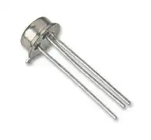
2N3866
Bipolar - RF Transistor, NPN, 30 V, 800 MHz, 5 W, 400 mA, TO-39
⚠️ Reference pricing provided. In case of supply shortages, we will connect you with our trusted procurement partners to ensure your project's continuity.
- Manufacturer: SOLID STATE
- Product type: Bipolar RF Transistors
- Transistor Polarity:NPN; Collector Emitter Voltage V(br)ceo:30V; Transition Frequency ft:800MHz; Power Dissipation Pd:5W; DC Collector Current:400mA; DC Current Gain hFE:10hFE; RF Trans
- MSL: -
- SVHC: No SVHC (27-Jun-2024)
- No. of Pins: 3Pins
- Product Range: -
- Qualification: -
- Power Dissipation: 5W
- Transistor Mounting: Through Hole
- Transistor Polarity: NPN
- Transition Frequency: 800MHz
- Transistor Case Style: TO-39
- DC Current Gain hFE Min: 10hFE
- Operating Temperature Max: 200°C
- Continuous Collector Current: 400mA
- Collector Emitter Voltage Max: 30V
| Delivery and price | |
|---|---|
| Units per pack | 1000 |
| Price | 2.45 € |
| Current stock | 10+ |
| Lead time | 23 days |
Datasheet

## 2N3066 (SILICON) S 46 FARRAND STREET 2nd866A BLOOMFIELD, NEW JERSEY 07003

## www.solidstateinc.com

|2N3066 (SILICON)(SILICON) S 46 FARRAND STREET46 FARRAND STREETFARRAND STREETSTREET<br>BLOOMFIELD, NEW JERSEY 07003NEW JERSEY 07003JERSEY 0700307003<br>www.solidstateinc.com<br>2nd866A|2N3066 (SILICON)(SILICON) S 46 FARRAND STREET46 FARRAND STREETFARRAND STREETSTREET<br>BLOOMFIELD, NEW JERSEY 07003NEW JERSEY 07003JERSEY 0700307003<br>www.solidstateinc.com<br>2nd866A|2N3066 (SILICON)(SILICON) S 46 FARRAND STREET46 FARRAND STREETFARRAND STREETSTREET<br>BLOOMFIELD, NEW JERSEY 07003NEW JERSEY 07003JERSEY 0700307003<br>www.solidstateinc.com<br>2nd866A|2N3066 (SILICON)(SILICON) S 46 FARRAND STREET46 FARRAND STREETFARRAND STREETSTREET<br>BLOOMFIELD, NEW JERSEY 07003NEW JERSEY 07003JERSEY 0700307003<br>www.solidstateinc.com<br>2nd866A|2N3066 (SILICON)(SILICON) S 46 FARRAND STREET46 FARRAND STREETFARRAND STREETSTREET<br>BLOOMFIELD, NEW JERSEY 07003NEW JERSEY 07003JERSEY 0700307003<br>www.solidstateinc.com<br>2nd866A|2N3066 (SILICON)(SILICON) S 46 FARRAND STREET46 FARRAND STREETFARRAND STREETSTREET<br>BLOOMFIELD, NEW JERSEY 07003NEW JERSEY 07003JERSEY 0700307003<br>www.solidstateinc.com<br>2nd866A|2N3066 (SILICON)(SILICON) S 46 FARRAND STREET46 FARRAND STREETFARRAND STREETSTREET<br>BLOOMFIELD, NEW JERSEY 07003NEW JERSEY 07003JERSEY 0700307003<br>www.solidstateinc.com<br>2nd866A|2N3066 (SILICON)(SILICON) S 46 FARRAND STREET46 FARRAND STREETFARRAND STREETSTREET<br>BLOOMFIELD, NEW JERSEY 07003NEW JERSEY 07003JERSEY 0700307003<br>www.solidstateinc.com<br>2nd866A|2N3066 (SILICON)(SILICON) S 46 FARRAND STREET46 FARRAND STREETFARRAND STREETSTREET<br>BLOOMFIELD, NEW JERSEY 07003NEW JERSEY 07003JERSEY 0700307003<br>www.solidstateinc.com<br>2nd866A|2N3066 (SILICON)(SILICON) S 46 FARRAND STREET46 FARRAND STREETFARRAND STREETSTREET<br>BLOOMFIELD, NEW JERSEY 07003NEW JERSEY 07003JERSEY 0700307003<br>www.solidstateinc.com<br>2nd866A|
|---|---|---|---|---|---|---|---|---|---|
|NPN silicon transistor, designed for amplifier, fre-||||||||||
|quency-multiplier,|||or oscillator||applications|||in|mili-|
|\\<br>taryand industrial equipment.<br>Suitable foruses as out-<br>CASE 79 \,<br>' put, driver, or pre-driver stages in VHF and UHF||||||||||
|(TO-39)<br>equipment.||||||||||
|Collector connected to case||||||||||
|MAXIMUM RATINGS (Ta = 25°C unless otherwise noted)||||||||||
|ating||||symt|||||||
|Total Device Dissipation<br>@ Te =25°C|||||5.0||Watts|||
|Derate above 25°C|||||28.6||mw|/°C||
|Operating and StorageJunction|||Ty, Tstg|-65|to +200||¢|||
|Temperature Range||||||||||
|ELECTRICAL CHARACTERISTICS (T, = 25°C unless otherwise noted)<br>[Characteristic<br>SS<br>—«d:CSSymbol_ Min | <br>OFF CHARACTERISTICS||||||Typ [| Max||[Une||
|Collector-Emitter Breakdown Voltage|||BVCER|55|||||Vde|
|(I¢ = 5.0 mAdc, Rge = 10ohms)||||||||||
|Collector-Emitter Sustaining Voltage|||BVCEO(sus)|30|||||Vde|
|(1¢ = 5.0 mAdg, Ig = 0)||||||||||
|Collector-Base Breakdown Voltage|||BVcgO|55|||||Vde|
|(I¢ = 0, Ic = 0.1 mAdc)||||||||||
|Emitter-Base Breakdown Voltage|||BVEBO|3.5|||||Vdc|
|(Ig = 0.1 mAdc, Ic = O)||||||||||
|Collector Cutoff Current|||ICEO||||20||HA|
|(VCE = 28 Vdc, Ig = 0)||||||||||
|Collector Cutoff Current|||ICEX||||100||uAdc|
|(VceE = 55 Vde, Vege = 1.5 Vde)||||||||||
|ON CHARACTERISTICS||||||||||
|DC Current Gain|||hFE|||||||
|(Ic = 0.36 Adc, VcE = 5.0 Vdc)||||5.0|||-|||
|(Ic = 0.05 Adc, Vcg = 5.0 Vdc) 2N3866||||10|||200|||
|(1¢ = 50 mAdc, VcE = 5.0 Vde) 2N3866A||||25|||200|||
|Collector-Emitter Saturation Voltage|||VCE(sat)||||||Vdc|
|(1¢ = 100 mAdc, |g = 20 mAdc)||||||||||
|DYNAMIC CHARACTERISTICS||||||||||
|Current-Gain — Bandwidth Product|||fr||||||MHz|
|(I¢<br>= 50mAdc,VceE= 15Vdc,<br>f= 200MHz)|2N3866<br>2N3866A|||500<br>800||800<br>-||||
|Output Capacitance|||Cob|||2.0|3.0||pF|
|(Veg = 30Vdc, |e =<br>0,f = 1.0MHz)||||||||||
|FUNCTIONAL TEST||||||||||
|—<br>f = 400 MHz, Tc|=|25°C|a||||||x|


## 2N3866, 2N3866A (continued)

FIGURE 1 — 400 MHz RF AMPLIFIER CIRCUIT FOR POWER-OUTPUT TEST

**==> picture [443 x 616] intentionally omitted <==**

**----- Start of picture text -----**<br>
oe R ieQ<br>Ls CO)<br>IRs oyQ 60 (- RFC<br>@ Ch. ~<br>li 097<br>335 RFC<br>Ly: 2 turns No. 18 Capacitor values in pF .<br>wire, %” ID, unless otherwise<br>Ls: 2%Y%" long.turns, No. 18 wire indicated.Tuning capacitors fe?& —<br>Ya" ID, 3/16” long. are air variable, Vee = ~28V ~<br>FIGURE 2 — POWER OUTPUT versus FREQUENCY FIGURE 4 — PARALLEL INPUT RESISTANCE AND<br>(Class C) CAPACITANCE versus FREQUENCY (Class C)<br>25vemav] || NOTE: COMMON-EMITTER; 200 50<br>a EMITTER TECHNIQUES EMITTER GROUNDED DIRECTLY TO CHASSIS<br>Eses ef | eK <<br>= rh ~~ S 120 an x20 =<br>=<br>PNR NN E LLIS LE<br>=<br>a tooK RK Is z 8 NI ~ SO 0 ¢<br>a ETA 5 sO ,P JRANTSan],PS is wahs<br>~*——> FL<br>ear) 200 300 400 500 600 ° 100200 300400500600 700 00°<br>f, FREQUENCY (MHz) {, FREQUENCY (MHz)<br>FIGURE 3 — POWER OUTPUT versus POWER INPUT FIGURE 5 — PARALLEL OUTPUT CAPACITANCE<br>(Class C) versus FREQUENCY (Class C)<br>25 10.0<br>ajar toc fess —} Ff} — bo puribe catwwoEl acc To cuss<br>E L -<br>VES CIN<br>oJcee) od, Na<br>2876.86 >=—- eer<br>“| 77 +7 | | | | | » S—=<br>A i<br>%[fAPee10 2030| iat| tTeee60tT 70tlht80 ht9 100 OL% 100 200EE4300 |400 |500 1.0600WATT 700 800<br>Pia, POWER INPUT (mW) {, FREQUENCY (MHz)<br>**----- End of picture text -----**<br>


## 2N3866, 2N3866A (continued)

**==> picture [436 x 606] intentionally omitted <==**

**----- Start of picture text -----**<br>
FIGURE 6 — SMALL-SIGNAL CURRENT GAIN FIGURE 7 — OUTPUT CAPACITANCE<br>versus FREQUENCY versus COLLECTOR VOLTAGE<br>24 7.0<br>aSSO on | | |ff<br>2CoSNOTINemtetme TT) By<br>0gSs |<br>5 MCT NIL _TsS PTT} ge<br>2 tw TS cro tA TT<br>gSpe, ETTTTee PINTSong}Se3 PeetTTfta<br>= ee |<br>ons<br>40 60 80 100 200 — 400 600 800 1000 Lit 0 5 |10 |15tf20 25 30<br>f, FREQUENCY (MHz) Vos, COLLECTOR-BASE VOLTAGE (Vdc)<br>FIGURE 8 — f; versus COLLECTOR CURRENT ~<br>1000<br>a: ——=—=ESESES=——S=_—_—__SSS<br>(lA |<br>ao PP<br>= 200<br>0 20 40 60 80 100<br>Ic, COLLECTOR CURRENT (mAdc)<br>FIGURE 10 — DC CURRENT GAIN<br>FIGURE 9 — r,’C. versus COLLECTOR CURRENT versus COLLECTOR CURRENT<br>2520P|| pee | ot100<br>80 a<br>ef wt ef | tb] gee<br>Creer)o 0 10 20 30 40 50 Deere% 20 40 60 80 100<br>Io, COLLECTOR CURRENT (mAdc) Ic, COLLECTOR CURRENT (mAdc)<br>**----- End of picture text -----**<br>


## 2N3866, 2N3866A (continued)

## y PARAMETER VARIATIONS

**==> picture [444 x 514] intentionally omitted <==**

**----- Start of picture text -----**<br>
FIGURE 11 — SMALL-SIGNAL INPUT ADMITTANCE FIGURE 13 — SMALL-SIGNAL FORWARD TRANSFER<br>versus COLLECTOR CURRENT ADMITTANCE versus COLLECTOR CURRENT<br>100 280<br>Pt ttt ty tt 240Pt tt et yt<br>oe ee;SS ae wice__TP<br>PIN | tT} Tt et to:SE}<br>SSSR eee eee<br>et]Prt? PerretTt tt ett ||) opeeg INTtt tTEetttT ET I<br>atCCE| | | tt tt ty| CESS8SsePt | tt<br>Ic, COLLECTOR CURRENT (mAdc) Ic, COLLECTOR CURRENT (mAdc)<br>FIGURE 12 — SMALL-SIGNAL REVERSE TRANSFER = FIGURE 14 — SMALL-SIGNAL OUTPUT ADMITTANCE<br>ADMITTANCE versus COLLECTOR CURRENT versus COLLECTOR CURRENT<br>5 Pt tt} tt tt yl 20 Pt ttt tt tt<br>Jt Lt [verte | Ffft}<br>i PPP Speen ; "TT TEL| vceSani ne LY ]<br>:i ++tt} ttt to pottttt tt tt<br>PCrsaute“CO >et tii]FERRRSSSSEi | ty to<br>eLiteLi ttt?SEPP)tittttttt?)tt) ¢Lt_tittttttttttt t ttft<br>Cee<br>Ic, COLLECTOR CURRENT (mAdc) Ic, COLLECTOR CURRENT (mAdc)<br>DESIGN NOTE<br>Figures 11through18 show small-signal admittance-parameter data. This data can be used for<br>Class A amplifier designs.<br>**----- End of picture text -----**<br>


For Class C power-amplifier designs, the small-signal parameters are not applicable. Figures 4 and 5 give parallel output capacitance and the parallel input resistance and capacitance for Class C poweramplifier operation.

The parallel resistive portion of the collector load impedance for a power amplifier, R,’, may be computed by assuming a peak voltage swing equal to Vcc, and using the expression

## R’ = Noe!

where P — RF power output. The computed R,’ may then be combined with the data in Figures 2 and 3 to comprise complete device impedance data for Class C power amplifier design.

2N3866, 2N3866A (continued)

**==> picture [167 x 10] intentionally omitted <==**

**----- Start of picture text -----**<br>
y PARAMETER VARIATIONS<br>**----- End of picture text -----**<br>


(Vce = 15 Vdc, Ic = 80 mAdc, Ta = 25°C)

**==> picture [442 x 510] intentionally omitted <==**

**----- Start of picture text -----**<br>
FIGURE 15 — SMALL-SIGNAL INPUT ADMITTANCE FIGURE 17 — SMALL-SIGNAL FORWARD TRANSFER<br>versus FREQUENCY ADMITTANCE versus FREQUENCY<br>80ToL LI 800, rT]<br>eho | | LY) eso<br>= = IN ><br>. z<br>NU Eee EE<br>UE PS<br>50 70 100 EL200 300EEN,600 50 70 100 200Et300 600<br>f, FREQUENCY (MHz) f, FREQUENCY (MHz)<br>FIGURE 16 — SMALL-SIGNAL REVERSE TRANSFER FIGURE 18 — SMALL-SIGNAL OUTPUT ADMITTANCE<br>ADMITTANCE versus FREQUENCY versus FREQUENCY<br>6LUE EYWi 24LE EE)<br>2PTI ELLg\/ LEE ELL<br>4 Ws € 16 A<br>PU Le LEO<br>: 3 VA E 12 Z|<br>PLLz POY elu LYLL<br>y A | Le, Atty<br>LTE0coll [a] | 4A Ler0 pitteeeanaTid|<br>50 70 100 200 300 600 50 70 100 200 300 600<br>f, FREQUENCY (MHz) f, FREQUENCY (MHz)<br>**----- End of picture text -----**<br>


**==> picture [174 x 602] intentionally omitted <==**

**----- Start of picture text -----**<br>
A<br>R B<br>|<br>eae<br>te L |<br>F K<br>SEATING |<br>PLANE ——--O<br>Q rs<br>Aid,oO.<br>3!<br>M \0~rN J<br>PAS<br>oom MILLIMETERS |INCHES|<br>| A | 8.89 | 9.40 | 0.350| 0.370<br>| B | 8.00 [8.51 | 0.315| 0.335<br>| C | 6.10 | 6.60 | 0.240] 0.260<br>| €|| Fdo |[|0.406] [0.229]] 0.406 | 0.5333.180.483 |||0.016 [0.016] 0.009{ ||0.125 0.0210.019 | ||<br>| GH | 40 . 71183 | 5.33 | 00 . 028190 | 0.2100.034 |<br>| 0.737 | 1.02 | [0.029|] 0.040 |<br>Y kK [12.70 [ - | 0500] - |<br>|| tM |{|45°NOM_635 | - [| [0.250{45°NOM__|- |<br>| P [| - [1.27 | - {0.050 |<br>| Q@R [{ | 254]90°NOM- [ool90° NOM- |<br>All JEDEC dimensions and notes apply.<br>STYLE 1<br>PIN 1. EMITTER<br>2. BASE<br>3. COLLECTOR<br>TO-39<br>**----- End of picture text -----**<br>
Updated at March 17, 2026
About Novapart
Novapart is a B2B electronic component broker specialising in stock shortages and cost reduction. We source hard-to-find parts and identify compliant alternatives across a catalogue of 540,000+ components from 500+ manufacturers.
Learn more →Stock Shortage Specialist
When a component is unavailable, discontinued or has an unacceptable lead time, we tap into our network of vetted European and Asian distributors to source what you need — without compromising on quality or traceability.
Request a quote →Compliant Alternatives
We identify pin-to-pin, electrically equivalent substitutes that meet the same certifications (RoHS, AEC-Q100, REACH) as your original specification — validated against datasheets, not just part numbers. Often at a lower cost.
BOM Analysis service →