
Image not available
Illustrative purposes only

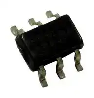
ZLLS2000
Small Signal Schottky Diode, Single, 40 V, 1.16 A, 640 mV, 36 A, 150 °C
⚠️ Reference pricing provided. In case of supply shortages, we will connect you with our trusted procurement partners to ensure your project's continuity.
- Manufacturer: DIODES INC.
- Product type:
- Diode Configuration:Single; Repetitive Reverse Voltage Vrrm Max:40V; Forward Current If(AV):1.16A; Forward Voltage VF Max:640mV; Forward Surge Current Ifsm Max:36A; Operating Temperature Max:15
- SVHC: No SVHC (25-Jun-2025)
- No. of Pins: 6Pins
- Product Range: -
- Qualification: -
- Diode Mounting: Surface Mount
- Diode Case Style: SOT-23
- Diode Configuration: Single
- Forward Voltage Max: 640mV
- Forward Surge Current: 36A
- Reverse Recovery Time: 6ns
- Average Forward Current: 1.16A
- Operating Temperature Max: 150°C
- Repetitive Peak Reverse Voltage: 40V
| Delivery and price | |
|---|---|
| Units per pack | 5000 |
| Price | 0.248 € |
| Current stock | 1000+ |
| Lead time | 30 days |
Datasheet

**ZLLS2000**
**40V HIGH CURRENT LOW LEAKAGE SCHOTTKY DIODE**
## **Product Summary**
|**Product Summaryy**|**Product Summaryy**|**Product Summaryy**|**Product Summaryy**|
|---|---|---|---|
|**VRRM (V)**<br>**IO(A)**<br>**VF Max (V)**<br>**@ +25°C**<br>**IR Max (****A)**<br>**@ 30V +25°C**<br>40<br>2<br>0.54<br>40||||
|**VRRM (V)**<br>40|**IO(A)**|**VF Max (V)**<br>**@ +25°C**|**IR Max (****A)**<br>**@ 30V +25°C**|
||2|0.54|40|
## **Features and Benefits**
- Low Equivalent on Resistance
- Extremely Low Leakage
- Low VF, Fast Switching Schottky
- Package Thermally Rated to +150°C
- **Totally Lead-Free & Fully RoHS Compliant (Notes 1 & 2)**
- **Halogen and Antimony Free. “Green” Device (Note 3)**
- **Qualified to AEC-Q101 Standards for High Reliability**
## **Mechanical Data**
## **Description and Applications**
A surface mount Schottky Barrier Diode featuring low forward voltage drop suitable for high frequency rectification and reverse voltage protection.
- DC – DC Converters
- Strobes
- Mobile Phones
- Case: SOT26
- Case Material: Molded Plastic, “Green” Molding Compound; UL Flammability Classification Rating 94V-0
- Moisture Sensitivity: Level 1 per J-STD-020
- Terminals: Matte Tin Finish Annealed over Copper Leadframe; (Lead-Free Plating) Solderable per MIL-STD-202, Method 208
- Weight: 0.016 grams (Approximate)
- Charging Circuits
- Motor Control
SOT-26
Top View
**==> picture [219 x 105] intentionally omitted <==**
**----- Start of picture text -----**<br>
Cc<br>C C<br>C C<br>A -_ A<br>7 _|° ||<br>A<br>Device Symbol Top View<br>Pin Out<br>**----- End of picture text -----**<br>
## **Ordering Information**
|**Device**|**Packaging**|**Shipping**|
|---|---|---|
|ZLLS2000TA|SOT26|3,000/Tape &Reel|
|ZLLS2000TC|SOT26|10,000/Tape & Reel|
Notes: 1. No purposely added lead. Fully EU Directive 2002/95/EC (RoHS) & 2011/65/EU (RoHS 2) compliant.
2. See http://www.diodes.com/quality/lead_free.html for more information about Diodes Incorporated’s definitions of Halogen- and Antimony-free, "Green" and Lead-free.
3. Halogen- and Antimony-free "Green” products are defined as those which contain <900ppm bromine, <900ppm chlorine (<1500ppm total Br + Cl) and <1000ppm antimony compounds.
4. For Packaging Details, go to our website at http:// www.diodes.com/products/packages.html.
## **Marking Information**
LL20 = Product Type Marking Code YM = Date Code Marking Y or Y = Year (ex: D = 2016) M or M = Month (ex: 9 = September)
Date Code Key
|**Year**||**2016**|**2016**|||**2017**|**2017**|||**2018**||**2019**|**2020**||**2021**||**2022**|**2022**|||**2023**|**2023**|||**2024**|**2024**||**2025**||**2026**|
|---|---|---|---|---|---|---|---|---|---|---|---|---|---|---|---|---|---|---|---|---|---|---|---|---|---|---|---|---|---|---|
|**Code**||D|||||E|||F||G|H||I||J||||K|||||L||M||N|
||||||||||||||||||||||||||||||||
|**Month**||||**Jan**||||**Feb**||**Mar**||**Apr**|**May**||**Jun**||**Jul**||**Aug**||||**Sep**|||**Oct**||**Nov**||**Dec**|
|**Code**||||1||||2||3||4|5||6||7|||8|||9|||O||N||D|
1 of 5 **www.diodes.com**
ZLLS2000 Document number DS32060 Rev. 7 – 2
July 2016 © Diodes Incorporated
**ZLLS2000**
**Maximum Ratings** (@TA = +25°C, unless otherwise specified.)
|**Maximum Ratingsgss** (@TA = +25°C, unless otherwise specified.)@TA = +25°C, unless otherwise specified.)A = +25°C, unless otherwise specified.)= +25°C, unless otherwise specified.)pecified.)ecified.))|**Maximum Ratingsgss** (@TA = +25°C, unless otherwise specified.)@TA = +25°C, unless otherwise specified.)A = +25°C, unless otherwise specified.)= +25°C, unless otherwise specified.)pecified.)ecified.))|**Maximum Ratingsgss** (@TA = +25°C, unless otherwise specified.)@TA = +25°C, unless otherwise specified.)A = +25°C, unless otherwise specified.)= +25°C, unless otherwise specified.)pecified.)ecified.))|**Maximum Ratingsgss** (@TA = +25°C, unless otherwise specified.)@TA = +25°C, unless otherwise specified.)A = +25°C, unless otherwise specified.)= +25°C, unless otherwise specified.)pecified.)ecified.))|
|---|---|---|---|
|||||
|**Characteristic**|**Symbol**|**Value**|**Unit**|
|Continuous Reverse Voltage|VRRM|40|V|
|Forward Current|IF|2.2|A|
|Peak Repetitive Forward Current<br>Rectangular Pulse DutyCycle|IFPK|3.55|A|
|Non Repetitive Forward Current<br>t ≤ 100μs<br>t ≤ 10ms|IFSM|36<br>12|A<br>A|
## **Thermal Characteristics**
|**Thermal Characteristics**||||
|---|---|---|---|
|**Characteristic**<br>~~OO~~|**Symbol**<br>~~OO~~|**Value**<br>~~OO~~|**Unit**<br>~~OO~~|
|Power Dissipation @TA= +25°C<br>Single Die Continuous<br>Single Die Measured at t < 5 secs|PD|-<br>1.1<br>1.71|-<br>W<br>W|
|Junction to Ambient(Note 5)<br>~~a~~|RθJA<br>~~C~~|113<br>~~C~~|°C/W|
|Junction to Ambient(Note 6)<br>~~a~~<br>~~GG~~|RθJA<br>~~GG~~|73<br>~~GG~~|°C/W|
|Storage Temperature Range<br>~~a~~<br>~~GG~~|TSTG<br>~~GG~~|-55 to +150<br>~~GG~~|°C|
|Junction Temperature<br>~~fd~~|TJ<br>~~fd~~|+150<br>~~fd~~|°C<br>~~fd~~|
Notes: 5. For a device surface mounted on 25mm x 25mm FR-4 PCB with high coverage of single sided 1oz copper, in still air conditions. 6. For a device mounted on FR-B PCB measured at t < 5secs.
**==> picture [430 x 157] intentionally omitted <==**
**----- Start of picture text -----**<br>
120<br>7] T AMB =25 O C TL Le 1.2 a a<br>100 :Z Rectangular Pulse 0 NN a 1.0 PoyTT te<br>80 AT CT ame CTT DN<br>D=0.5 Cer ae 0.8<br>60 pr eA Nee<br>Fase LLM HT Mga 0.6 P|] | NO | | Lt<br>mnAM<br>40 D=0.2 0.4<br>crm CZ Single Pulse P| | | INC |] Ud<br>20 eeeSeer oer D=0.05 Ilwl — 0.2 {[]1) INCE\<br>retEanLU) D=0.1 COHa 0.0 Py oy oT dT dT UIN \ TT<br>100μ 1m 10m 100m 1 10 100 1k 0 20 40 60 80 100 120 140 160<br>Pulse Width (s) Temperature (OC)<br>Transient Thermal Impedance<br>Derating Curve<br>Thermal Resistance ( Max Power Dissipation (W)<br>C/W)<br>O<br>**----- End of picture text -----**<br>
**Electrical Characteristics** (@TA = +25°C, unless otherwise specified.)
|**Electrical Characteristics**(@TA = +25°C, unless otherwise specified.)A = +25°C, unless otherwise specified.)= +25°C, unless otherwise specified.)|**Electrical Characteristics**(@TA = +25°C, unless otherwise specified.)A = +25°C, unless otherwise specified.)= +25°C, unless otherwise specified.)|**Electrical Characteristics**(@TA = +25°C, unless otherwise specified.)A = +25°C, unless otherwise specified.)= +25°C, unless otherwise specified.)|**Electrical Characteristics**(@TA = +25°C, unless otherwise specified.)A = +25°C, unless otherwise specified.)= +25°C, unless otherwise specified.)|**Electrical Characteristics**(@TA = +25°C, unless otherwise specified.)A = +25°C, unless otherwise specified.)= +25°C, unless otherwise specified.)|**Electrical Characteristics**(@TA = +25°C, unless otherwise specified.)A = +25°C, unless otherwise specified.)= +25°C, unless otherwise specified.)|**Electrical Characteristics**(@TA = +25°C, unless otherwise specified.)A = +25°C, unless otherwise specified.)= +25°C, unless otherwise specified.)|
|---|---|---|---|---|---|---|
|~~a~~<br>~~SO~~<br>~~OS(~~|||||||
|**Characteristic**<br>~~a~~|**Symbol**<br>~~SO~~|**Min**<br>~~SO~~<br>~~a~~|**Typ**<br>~~GG~~|**Max**<br>~~OS(~~<br>~~GG~~|**Unit**<br>~~OS(~~<br>~~GG~~|**Test Condition**|
|Reverse Breakdown Voltage<br>~~a~~<br>~~NG~~|V(BR)R<br>~~SO~~<br>~~NG~~|40<br>~~SO~~<br>~~NG~~<br>~~a~~<br>~~ee~~|-<br>~~NG~~<br>~~GG~~<br>~~ee~~<br>|-<br>~~OS(~~<br>~~NG~~<br>~~GG~~<br>|V<br>~~OS(~~<br>~~NG~~<br>~~GG~~<br>|IR= 1mA<br>~~NG~~<br>~~pO~~<br>|
|Forward Voltage (Note 7)|VF<br>~~es~~|-<br>~~a~~<br>~~ee~~<br>~~a~~|285<br>~~GG~~<br>~~ee~~<br>~~ee~~|-<br>~~GG~~<br>~~eee~~|mV<br>~~GG~~<br> <br>|IF= 50mA<br>~~pO~~<br>~~pO~~|
|||-<br>~~ee~~<br>~~a~~<br>~~a~~|305<br>~~ee~~<br>~~ee~~<br>~~ee~~|-<br>~~eee~~||IF= 100mA<br>~~pO~~<br>~~pO~~<br>~~pO~~|
|||-<br>~~ee ~~<br>~~a~~<br>~~a~~<br>~~a~~|335<br>~~ee~~<br> ~~ee ~~<br>~~ee~~<br>~~ee~~|-<br> ~~eee ~~||IF= 250mA<br>~~pO~~<br> ~~pO~~<br>~~pO~~<br>~~po~~|
|||-<br>~~a~~<br>~~a~~<br>~~ee~~|365<br>~~ee~~<br>~~ee~~<br>~~ee~~<br>|390<br>||IF= 500mA<br>~~pO~~<br>~~po~~<br>~~pO~~<br>|
|||-<br>~~a~~<br>~~ee~~<br>~~a~~|403<br>~~ee~~<br>~~ee~~<br>~~ee~~|430<br>~~eee~~||IF= 1A<br>~~po~~<br>~~pO~~<br>~~pO~~|
|||-<br>~~ee~~<br>~~a~~<br>~~a~~|433<br>~~ee~~<br>~~ee~~<br>~~ee~~|490<br>~~eee~~||IF= 1.5A<br>~~pO~~<br>~~pO~~<br>~~**p**O~~|
|||-<br>~~ee ~~<br>~~a~~<br>~~a~~|461<br>~~ee~~<br> ~~ee ~~<br>~~ee~~<br>~~ee~~|540<br> ~~eee ~~||IF= 2A<br>~~pO~~<br> ~~pO~~<br>~~**p**O~~<br>~~o~~|
|||-<br>~~a~~|509<br>~~ee~~<br>~~ee~~|600||IF= 3A<br>~~**p**O~~<br>~~o~~|
|||-|450<br>~~ee~~|-||IF= 2A,TA= +100°C<br>~~o~~|
|Reverse Current<br>~~es~~|IR<br>~~es~~<br>~~es~~|-<br>-<br>~~es~~|10<br>0.6<br>~~es~~|40<br>-<br>~~es~~|μA<br>mA<br>~~es~~|VR= 30V<br>VR= 30V,TA= +85°C<br>~~es~~|
|Diode Capacitance|CD<br>~~es~~<br>~~ee~~|-<br>~~ee~~|65<br>~~ee~~|-<br>~~ee~~|pF|f = 1MHz,VR= 30V|
|Reverse Recovery Time<br>Reverse Recovery Charge<br>~~es~~|tRR<br>QRR<br>~~es~~<br>~~ee~~|-<br>-<br>~~es~~<br>~~ee~~|6<br>685<br>~~es~~<br>~~ee~~|-<br>-<br>~~es~~<br>~~ee~~|ns<br>nC<br>~~es~~|Switched from IF= 500mA to VR= 5.5V<br>Measured @ IR50mA. di /dt = 500mA/ ns.<br>RSOURCE= 6Ω;RLOAD= 10Ω<br>~~es~~|
2 of 5 **www.diodes.com**
ZLLS2000 Document number DS32060 Rev. 7 – 2
July 2016 © Diodes Incorporated
**ZLLS2000**
**==> picture [447 x 549] intentionally omitted <==**
**----- Start of picture text -----**<br>
101 eeerr a ae eee 100m10m a ee— —=ee<br>1m +150 o C<br>100m<br>10m 150oC 100μ100μ10μ10μ +85oC<br>1m 85oC 1μ1μ +25oC<br>100μ100μ (Af 25 o C 100n<br>10μ10μ = -55oC 10n -15oC al<br>1n<br>1μ1μ 100p -55 o C<br>100n SF 10p Td | | Tt |<br>0.0 0.2 0.4 0.6 0 10 20 30 40<br>VF - Forward Voltage (V) VR - Reverse Voltage (V)<br>I v V I v V<br>F F R R<br>160<br>a 1.0 T =150 o C |<br>140 J<br>Senreememon up dlRrNINN Rectangular Pulse aaa|<br>120 an D = 1 POY 0.8 neea A<br>Pr =A OANT mi<br>D = 0.5 D = 1<br>100 popt D = 0.2 TENNTAN OA 0.6 |=| D = 0.5 SALTSu Ep<br>80 anPr D = 0.1D = 0.05 oeSat TNVACANA 0.4 r | D = 0.2 D = 0.1 DenSeasSAWieAD<br>60 PISEtiiiomA\e Ge ih he r_|= D = 0.05 naeliyOTAa ae A<br>40 R th =113 o C/W VAY 0.2 = LIL)<br>20 Rectangular Pulse SUSEH AAAWa OHA VAY 0.0 MYeee|<br>0.01 0.1 1 10 0.01 0.1 1 10<br>I - Peak Fwd Current (A) I - Peak Fwd Current (A)<br>F(PK) F(PK)<br>T v I P v I<br>C F(AV) F(AV) F(PK)<br>160<br>Pt | 400 Peet] | CT TTT} CT TE TTT<br>140 ————__===_—— SS f = 1MHz<br>350<br>PT SSRN PTE NET TT im<br>120 o rt SAR 300 Nine<br>T J =150 C P| er LL ONANAX PreneEN ETT TTT<br>100 ES ONIN 250 PCN<br>80 Rth(j-a) = 10Rth(j-a) = 50Rth(j-a) = 113 oo C/WC/WoC/W INNeae“CA amit| NY 200150 HINPCTCOANSTET<br>60 o 624i ee | ee<br>Rth(j-a) = 200 C/W ao 100 ee<br>40 Rth(j-a) = 300oC/W<br>50<br>Ht TN HEEE<br>20 ee [ee][ ee] $+ | 0 PiUHEHE<br>1 10 100m 1 10<br>VR - Continuous Reverse Voltage (V) VR - Reverse Voltage (V)<br>T v V C v V<br>A R D R<br>C)<br>o<br> - Max Ambient Temp (<br>A<br>T<br> - Forward Current (A)<br>IF - Reverse Current (A)IR<br> - Avg Power Diss (W)<br>F(AV)<br> - Initial Junction Temp (A) P<br>J<br>T<br> - Diode Capacitance (pF)<br>D<br>C<br>**----- End of picture text -----**<br>
3 of 5 **www.diodes.com**
ZLLS2000 Document number DS32060 Rev. 7 – 2
July 2016 © Diodes Incorporated
**ZLLS2000**
## **Package Outline Dimensions**
Please see http://www.diodes.com/package-outlines.html for the latest version.
**==> picture [463 x 221] intentionally omitted <==**
**----- Start of picture text -----**<br>
SOT26<br>D<br>SOT26<br>E1 aoc E Dim Min Max Typ<br>A1 0.013 0.10 0.05<br>A2 1.00 1.30 1.10<br>A3 0.70 0.80 0.75<br>b 0.35 0.50 0.38<br>c 0.10 0.20 0.15<br>7 b D 2.90 3.10 3.00<br>a1<br>e - - 0.95<br>e1<br>e1 - - 1.90<br>E 2.70 3.00 2.80<br>E1 1.50 1.70 1.60<br>A2 L 0.35 0.55 0.40<br>A3 A1 a - - 8°<br>a1 - - 7°<br>Seating Plane a All Dimensions in mm<br>L<br>e c<br>**----- End of picture text -----**<br>
## **Suggested Pad Layout**
Please see http://www.diodes.com/package-outlines.html for the latest version.
**SOT26**
**==> picture [140 x 135] intentionally omitted <==**
**----- Start of picture text -----**<br>
C1<br>Y1 G C<br>Y<br>000 X |<br>**----- End of picture text -----**<br>
**==> picture [107 x 67] intentionally omitted <==**
**----- Start of picture text -----**<br>
Dimensions Value (in mm)<br>C 2.40<br>C1 0.95<br>G 1.60<br>X 0.55<br>Y 0.80<br>Y1 3.20<br>**----- End of picture text -----**<br>
4 of 5 **www.diodes.com**
ZLLS2000 Document number DS32060 Rev. 7 – 2
July 2016 © Diodes Incorporated
**ZLLS2000**
## **IMPORTANT NOTICE**
DIODES INCORPORATED MAKES NO WARRANTY OF ANY KIND, EXPRESS OR IMPLIED, WITH REGARDS TO THIS DOCUMENT, INCLUDING, BUT NOT LIMITED TO, THE IMPLIED WARRANTIES OF MERCHANTABILITY AND FITNESS FOR A PARTICULAR PURPOSE (AND THEIR EQUIVALENTS UNDER THE LAWS OF ANY JURISDICTION).
Diodes Incorporated and its subsidiaries reserve the right to make modifications, enhancements, improvements, corrections or other changes without further notice to this document and any product described herein. Diodes Incorporated does not assume any liability arising out of the application or use of this document or any product described herein; neither does Diodes Incorporated convey any license under its patent or trademark rights, nor the rights of others. Any Customer or user of this document or products described herein in such applications shall assume all risks of such use and will agree to hold Diodes Incorporated and all the companies whose products are represented on Diodes Incorporated website, harmless against all damages.
Diodes Incorporated does not warrant or accept any liability whatsoever in respect of any products purchased through unauthorized sales channel. Should Customers purchase or use Diodes Incorporated products for any unintended or unauthorized application, Customers shall indemnify and hold Diodes Incorporated and its representatives harmless against all claims, damages, expenses, and attorney fees arising out of, directly or indirectly, any claim of personal injury or death associated with such unintended or unauthorized application.
Products described herein may be covered by one or more United States, international or foreign patents pending. Product names and markings noted herein may also be covered by one or more United States, international or foreign trademarks. This document is written in English but may be translated into multiple languages for reference. Only the English version of this document is the final and determinative format released by Diodes Incorporated.
## **LIFE SUPPORT**
Diodes Incorporated products are specifically not authorized for use as critical components in life support devices or systems without the express written approval of the Chief Executive Officer of Diodes Incorporated. As used herein:
- A. Life support devices or systems are devices or systems which:
1. are intended to implant into the body, or
2. support or sustain life and whose failure to perform when properly used in accordance with instructions for use provided in the labeling can be reasonably expected to result in significant injury to the user.
B. A critical component is any component in a life support device or system whose failure to perform can be reasonably expected to cause the failure of the life support device or to affect its safety or effectiveness.
Customers represent that they have all necessary expertise in the safety and regulatory ramifications of their life support devices or systems, and acknowledge and agree that they are solely responsible for all legal, regulatory and safety-related requirements concerning their products and any use of Diodes Incorporated products in such safety-critical, life support devices or systems, notwithstanding any devices- or systems-related information or support that may be provided by Diodes Incorporated. Further, Customers must fully indemnify Diodes Incorporated and its representatives against any damages arising out of the use of Diodes Incorporated products in such safety-critical, life support devices or systems.
Copyright © 2016, Diodes Incorporated
**www.diodes.com**
5 of 5 **www.diodes.com**
ZLLS2000 Document number DS32060 Rev. 7 – 2
July 2016 © Diodes Incorporated
Updated at April 29, 2026
About Novapart
Novapart is a B2B electronic component broker specialising in stock shortages and cost reduction. We source hard-to-find parts and identify compliant alternatives across a catalogue of 410,000+ components from 500+ manufacturers.
Learn more →Stock Shortage Specialist
When a component is unavailable, discontinued or has an unacceptable lead time, we tap into our network of vetted European and Asian distributors to source what you need — without compromising on quality or traceability.
Request a quote →Compliant Alternatives
We identify pin-to-pin, electrically equivalent substitutes that meet the same certifications (RoHS, AEC-Q100, REACH) as your original specification — validated against datasheets, not just part numbers. Often at a lower cost.
BOM Analysis service →