
Image not available
Illustrative purposes only

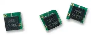
ZEN132V075A48LM
Zener Single Diode, 13.4 V, 700 mW, SMD, 3 Pins, 85 °C, Surface Mount
⚠️ Reference pricing provided. In case of supply shortages, we will connect you with our trusted procurement partners to ensure your project's continuity.
- Manufacturer: Raychem
- Product type: Zener Single Diodes
- No. of Pins: 3Pins
- Product Range: ZEN13
- Diode Mounting: Surface Mount
- Diode Case Style: SMD
- Power Dissipation: 700mW
- Zener Voltage Nom: 13.4V
- Power Dissipation Pd: 700mW
- Operating Temperature Max: 85°C
| Delivery and price | |
|---|---|
| Units per pack | 1 |
| Price | 0.33 € |
| Current stock | 10+ |
| Lead time | 30 days |
Datasheet

5

## ~~**PolyZen Devices**~~

## ~~Polymer Protected Zener Diode~~

PolyZen devices are polymer enhanced precision Zener diode micro-assemblies that help protect sensitive electronics from damage caused by inductive voltage spikes, voltage transients, use of incorrect power supplies and reverse bias.

The PolyZen micro-assembly incorporates a stable Zener diode for precise voltage clamping and a resistively non-linear, polymeric positive temperature coefficient (PPTC) layer that responds to either diode heating or overcurrent events by transitioning from a low to high resistance state.

PolyZen devices help provide resettable protection against damage caused by multi-watt fault events and require only 0.7W power dissipation. In the event of sustained high power conditions, the PPTC element of the device “trips” to limit current and generate voltage drop. This functionality helps protect both the Zener and the follow-on electronics, effectively increasing the diode’s power handling capacity.

## **Benefits**

- Helps shield downstream electronics from overvoltage and reverse bias

- Trip events shut out overvoltage and reverse bias sources

- Analog nature of trip events minimize upstream inductive spikes

- Helps reduce design costs with single component placement and minimal heat sinking requirements

## **Features**

- RoHS compliant

- Overvoltage transient suppression

- Hold currents up to 2.3A

- Time delayed, overvoltage trip

- Time delayed, reverse bias trip

- Power handling on the order of 30 watts

- Integrated device construction

## **Applications**

- Portable media players

- Global positioning systems

- Hard disk drives 5V & 12V bus

- Solid State Drives (SSD) 5V bus

- Cellphone charger port and USB power

- Automotive peripheral input power

- DC power port protection

- Industrial handheld POS

**31**

~~A~~ **Figure PZ1 Typical Application Block Diagram for PolyZen Devices**

5

**==> picture [331 x 104] intentionally omitted <==**

**----- Start of picture text -----**<br>
Power Supply<br>(External or internal) Protected Electronics<br>GND<br>2<br>VIN PolyZen<br>1<br>Device<br>+ 3 VOUT<br>Regulated RLOAD<br>Output<br>Protected downstream<br>electronics<br>**----- End of picture text -----**<br>


## **Table PZ1 Electrical Characteristics for PolyZen Devices** mm **(Performance ratings @ 25°C unless otherwise specified)**

|ZEN056V130A24LS<br>5.45<br>5.60<br>5.75<br>0.10<br>1.30<br>0.12<br>0.16<br>24V<br>3A<br>+10/-40<br>+24/-16V<br>ZEN059V130A24LS†<br>5.80<br>5.90<br>6.00<br>0.10<br>1.30<br>0.12<br>0.15<br>24V<br>3A<br>+6/-40<br>+24/-16V<br>**Part Number**<br>**VZ(V)**<br>**Min.**<br>**Typ.**<br>**Max.**<br>**IZt**<br>**(A)**<br>**IHOLD**<br>**@ 20°C**<br>**(A)**<br>**RTyp**<br>**(**Ω**)**<br>**R1MAX**<br>**(**Ω**)**<br>**VINT MAX**<br>**Test**<br>**VINT MAX**<br>**Current**<br>**(V)**<br>**(A)**<br>**IFLT MAX**<br>**Test**<br>**IFLT MAX**<br>**Voltage**<br>**(A)**<br>**(V)**<br>~~ee~~<br>~~ee~~|ZEN056V130A24LS<br>5.45<br>5.60<br>5.75<br>0.10<br>1.30<br>0.12<br>0.16<br>24V<br>3A<br>+10/-40<br>+24/-16V<br>ZEN059V130A24LS†<br>5.80<br>5.90<br>6.00<br>0.10<br>1.30<br>0.12<br>0.15<br>24V<br>3A<br>+6/-40<br>+24/-16V<br>**Part Number**<br>**VZ(V)**<br>**Min.**<br>**Typ.**<br>**Max.**<br>**IZt**<br>**(A)**<br>**IHOLD**<br>**@ 20°C**<br>**(A)**<br>**RTyp**<br>**(**Ω**)**<br>**R1MAX**<br>**(**Ω**)**<br>**VINT MAX**<br>**Test**<br>**VINT MAX**<br>**Current**<br>**(V)**<br>**(A)**<br>**IFLT MAX**<br>**Test**<br>**IFLT MAX**<br>**Voltage**<br>**(A)**<br>**(V)**<br>~~ee~~<br>~~ee~~|ZEN056V130A24LS<br>5.45<br>5.60<br>5.75<br>0.10<br>1.30<br>0.12<br>0.16<br>24V<br>3A<br>+10/-40<br>+24/-16V<br>ZEN059V130A24LS†<br>5.80<br>5.90<br>6.00<br>0.10<br>1.30<br>0.12<br>0.15<br>24V<br>3A<br>+6/-40<br>+24/-16V<br>**Part Number**<br>**VZ(V)**<br>**Min.**<br>**Typ.**<br>**Max.**<br>**IZt**<br>**(A)**<br>**IHOLD**<br>**@ 20°C**<br>**(A)**<br>**RTyp**<br>**(**Ω**)**<br>**R1MAX**<br>**(**Ω**)**<br>**VINT MAX**<br>**Test**<br>**VINT MAX**<br>**Current**<br>**(V)**<br>**(A)**<br>**IFLT MAX**<br>**Test**<br>**IFLT MAX**<br>**Voltage**<br>**(A)**<br>**(V)**<br>~~ee~~<br>~~ee~~|ZEN056V130A24LS<br>5.45<br>5.60<br>5.75<br>0.10<br>1.30<br>0.12<br>0.16<br>24V<br>3A<br>+10/-40<br>+24/-16V<br>ZEN059V130A24LS†<br>5.80<br>5.90<br>6.00<br>0.10<br>1.30<br>0.12<br>0.15<br>24V<br>3A<br>+6/-40<br>+24/-16V<br>**Part Number**<br>**VZ(V)**<br>**Min.**<br>**Typ.**<br>**Max.**<br>**IZt**<br>**(A)**<br>**IHOLD**<br>**@ 20°C**<br>**(A)**<br>**RTyp**<br>**(**Ω**)**<br>**R1MAX**<br>**(**Ω**)**<br>**VINT MAX**<br>**Test**<br>**VINT MAX**<br>**Current**<br>**(V)**<br>**(A)**<br>**IFLT MAX**<br>**Test**<br>**IFLT MAX**<br>**Voltage**<br>**(A)**<br>**(V)**<br>~~ee~~<br>~~ee~~|ZEN056V130A24LS<br>5.45<br>5.60<br>5.75<br>0.10<br>1.30<br>0.12<br>0.16<br>24V<br>3A<br>+10/-40<br>+24/-16V<br>ZEN059V130A24LS†<br>5.80<br>5.90<br>6.00<br>0.10<br>1.30<br>0.12<br>0.15<br>24V<br>3A<br>+6/-40<br>+24/-16V<br>**Part Number**<br>**VZ(V)**<br>**Min.**<br>**Typ.**<br>**Max.**<br>**IZt**<br>**(A)**<br>**IHOLD**<br>**@ 20°C**<br>**(A)**<br>**RTyp**<br>**(**Ω**)**<br>**R1MAX**<br>**(**Ω**)**<br>**VINT MAX**<br>**Test**<br>**VINT MAX**<br>**Current**<br>**(V)**<br>**(A)**<br>**IFLT MAX**<br>**Test**<br>**IFLT MAX**<br>**Voltage**<br>**(A)**<br>**(V)**<br>~~ee~~<br>~~ee~~|ZEN056V130A24LS<br>5.45<br>5.60<br>5.75<br>0.10<br>1.30<br>0.12<br>0.16<br>24V<br>3A<br>+10/-40<br>+24/-16V<br>ZEN059V130A24LS†<br>5.80<br>5.90<br>6.00<br>0.10<br>1.30<br>0.12<br>0.15<br>24V<br>3A<br>+6/-40<br>+24/-16V<br>**Part Number**<br>**VZ(V)**<br>**Min.**<br>**Typ.**<br>**Max.**<br>**IZt**<br>**(A)**<br>**IHOLD**<br>**@ 20°C**<br>**(A)**<br>**RTyp**<br>**(**Ω**)**<br>**R1MAX**<br>**(**Ω**)**<br>**VINT MAX**<br>**Test**<br>**VINT MAX**<br>**Current**<br>**(V)**<br>**(A)**<br>**IFLT MAX**<br>**Test**<br>**IFLT MAX**<br>**Voltage**<br>**(A)**<br>**(V)**<br>~~ee~~<br>~~ee~~|ZEN056V130A24LS<br>5.45<br>5.60<br>5.75<br>0.10<br>1.30<br>0.12<br>0.16<br>24V<br>3A<br>+10/-40<br>+24/-16V<br>ZEN059V130A24LS†<br>5.80<br>5.90<br>6.00<br>0.10<br>1.30<br>0.12<br>0.15<br>24V<br>3A<br>+6/-40<br>+24/-16V<br>**Part Number**<br>**VZ(V)**<br>**Min.**<br>**Typ.**<br>**Max.**<br>**IZt**<br>**(A)**<br>**IHOLD**<br>**@ 20°C**<br>**(A)**<br>**RTyp**<br>**(**Ω**)**<br>**R1MAX**<br>**(**Ω**)**<br>**VINT MAX**<br>**Test**<br>**VINT MAX**<br>**Current**<br>**(V)**<br>**(A)**<br>**IFLT MAX**<br>**Test**<br>**IFLT MAX**<br>**Voltage**<br>**(A)**<br>**(V)**<br>~~ee~~<br>~~ee~~|ZEN056V130A24LS<br>5.45<br>5.60<br>5.75<br>0.10<br>1.30<br>0.12<br>0.16<br>24V<br>3A<br>+10/-40<br>+24/-16V<br>ZEN059V130A24LS†<br>5.80<br>5.90<br>6.00<br>0.10<br>1.30<br>0.12<br>0.15<br>24V<br>3A<br>+6/-40<br>+24/-16V<br>**Part Number**<br>**VZ(V)**<br>**Min.**<br>**Typ.**<br>**Max.**<br>**IZt**<br>**(A)**<br>**IHOLD**<br>**@ 20°C**<br>**(A)**<br>**RTyp**<br>**(**Ω**)**<br>**R1MAX**<br>**(**Ω**)**<br>**VINT MAX**<br>**Test**<br>**VINT MAX**<br>**Current**<br>**(V)**<br>**(A)**<br>**IFLT MAX**<br>**Test**<br>**IFLT MAX**<br>**Voltage**<br>**(A)**<br>**(V)**<br>~~ee~~<br>~~ee~~|ZEN056V130A24LS<br>5.45<br>5.60<br>5.75<br>0.10<br>1.30<br>0.12<br>0.16<br>24V<br>3A<br>+10/-40<br>+24/-16V<br>ZEN059V130A24LS†<br>5.80<br>5.90<br>6.00<br>0.10<br>1.30<br>0.12<br>0.15<br>24V<br>3A<br>+6/-40<br>+24/-16V<br>**Part Number**<br>**VZ(V)**<br>**Min.**<br>**Typ.**<br>**Max.**<br>**IZt**<br>**(A)**<br>**IHOLD**<br>**@ 20°C**<br>**(A)**<br>**RTyp**<br>**(**Ω**)**<br>**R1MAX**<br>**(**Ω**)**<br>**VINT MAX**<br>**Test**<br>**VINT MAX**<br>**Current**<br>**(V)**<br>**(A)**<br>**IFLT MAX**<br>**Test**<br>**IFLT MAX**<br>**Voltage**<br>**(A)**<br>**(V)**<br>~~ee~~<br>~~ee~~|ZEN056V130A24LS<br>5.45<br>5.60<br>5.75<br>0.10<br>1.30<br>0.12<br>0.16<br>24V<br>3A<br>+10/-40<br>+24/-16V<br>ZEN059V130A24LS†<br>5.80<br>5.90<br>6.00<br>0.10<br>1.30<br>0.12<br>0.15<br>24V<br>3A<br>+6/-40<br>+24/-16V<br>**Part Number**<br>**VZ(V)**<br>**Min.**<br>**Typ.**<br>**Max.**<br>**IZt**<br>**(A)**<br>**IHOLD**<br>**@ 20°C**<br>**(A)**<br>**RTyp**<br>**(**Ω**)**<br>**R1MAX**<br>**(**Ω**)**<br>**VINT MAX**<br>**Test**<br>**VINT MAX**<br>**Current**<br>**(V)**<br>**(A)**<br>**IFLT MAX**<br>**Test**<br>**IFLT MAX**<br>**Voltage**<br>**(A)**<br>**(V)**<br>~~ee~~<br>~~ee~~|ZEN056V130A24LS<br>5.45<br>5.60<br>5.75<br>0.10<br>1.30<br>0.12<br>0.16<br>24V<br>3A<br>+10/-40<br>+24/-16V<br>ZEN059V130A24LS†<br>5.80<br>5.90<br>6.00<br>0.10<br>1.30<br>0.12<br>0.15<br>24V<br>3A<br>+6/-40<br>+24/-16V<br>**Part Number**<br>**VZ(V)**<br>**Min.**<br>**Typ.**<br>**Max.**<br>**IZt**<br>**(A)**<br>**IHOLD**<br>**@ 20°C**<br>**(A)**<br>**RTyp**<br>**(**Ω**)**<br>**R1MAX**<br>**(**Ω**)**<br>**VINT MAX**<br>**Test**<br>**VINT MAX**<br>**Current**<br>**(V)**<br>**(A)**<br>**IFLT MAX**<br>**Test**<br>**IFLT MAX**<br>**Voltage**<br>**(A)**<br>**(V)**<br>~~ee~~<br>~~ee~~|ZEN056V130A24LS<br>5.45<br>5.60<br>5.75<br>0.10<br>1.30<br>0.12<br>0.16<br>24V<br>3A<br>+10/-40<br>+24/-16V<br>ZEN059V130A24LS†<br>5.80<br>5.90<br>6.00<br>0.10<br>1.30<br>0.12<br>0.15<br>24V<br>3A<br>+6/-40<br>+24/-16V<br>**Part Number**<br>**VZ(V)**<br>**Min.**<br>**Typ.**<br>**Max.**<br>**IZt**<br>**(A)**<br>**IHOLD**<br>**@ 20°C**<br>**(A)**<br>**RTyp**<br>**(**Ω**)**<br>**R1MAX**<br>**(**Ω**)**<br>**VINT MAX**<br>**Test**<br>**VINT MAX**<br>**Current**<br>**(V)**<br>**(A)**<br>**IFLT MAX**<br>**Test**<br>**IFLT MAX**<br>**Voltage**<br>**(A)**<br>**(V)**<br>~~ee~~<br>~~ee~~|ZEN056V130A24LS<br>5.45<br>5.60<br>5.75<br>0.10<br>1.30<br>0.12<br>0.16<br>24V<br>3A<br>+10/-40<br>+24/-16V<br>ZEN059V130A24LS†<br>5.80<br>5.90<br>6.00<br>0.10<br>1.30<br>0.12<br>0.15<br>24V<br>3A<br>+6/-40<br>+24/-16V<br>**Part Number**<br>**VZ(V)**<br>**Min.**<br>**Typ.**<br>**Max.**<br>**IZt**<br>**(A)**<br>**IHOLD**<br>**@ 20°C**<br>**(A)**<br>**RTyp**<br>**(**Ω**)**<br>**R1MAX**<br>**(**Ω**)**<br>**VINT MAX**<br>**Test**<br>**VINT MAX**<br>**Current**<br>**(V)**<br>**(A)**<br>**IFLT MAX**<br>**Test**<br>**IFLT MAX**<br>**Voltage**<br>**(A)**<br>**(V)**<br>~~ee~~<br>~~ee~~|
|---|---|---|---|---|---|---|---|---|---|---|---|---|
||ZEN065V130A24LS|6.35|6.50|6.65|0.10|1.30|0.12|0.16|24V|3A|+6/-40|+24/-16V|
||ZEN098V130A24LS|9.60|9.80|10.00|0.10|1.30|0.12|0.16|24V|3A|+3.5/-40|+24/-16V|
||ZEN132V130A24LS|13.20|13.40|13.60|0.10|1.30|0.12|0.16|24V|3A|+2/-40|+24/-16V|
||ZEN164V130A24LS|16.10|16.40|16.60|0.10|1.30|0.12|0.16|24V|3A|+1.25/-40|+24/-16V|
||ZEN056V230A16LS|5.45|5.60|5.75|0.10|2.30|0.04|0.06|16V|5A|+5/-40|+16/-12V|
||ZEN065V230A16LS|6.35|6.50|6.65|0.10|2.30|0.04|0.06|16V|5A|+3.5/-40|+16/-12V|
||ZEN098V230A16LS|9.60|9.80|10.00|0.10|2.30|0.04|0.06|16V|5A|+3.5/-40|+16/-12V|
||ZEN132V230A16LS|13.20|13.40|13.60|0.10|2.30|0.04|0.06|16V|5A|+2/-40|+20/-12V|
||ZEN056V075A48LS|5.45|5.60|5.75|0.10|0.75|0.28|0.45|48V|3A|+10/-40|+48/-16V|
||ZEN132V075A48LS|13.20|13.40|13.60|0.10|0.75|0.28|0.45|48V|3A|+2/-40|+48/-16V|
||ZEN056V115A24LS|5.45|5.60|5.75|0.10|1.15|0.15|0.18|24V|3A|+10/-40|+24/-16V|
||ZEN056V130A24GS*|5.45|5.60|5.75|0.10|1.30|0.12|0.18|24V|3A|+6/-40|+24/-16V|


* Module height is 1.25mm. Module height of all other part numbers is 2.0mm. † Typical operating current is 500µA @ 5.0V which meets USB suspend mode requirement.

## ~~ne~~ **Table PZ2 Definitions of Terms for PolyZen Devices**

|VZ|Zener clamping voltage measured at current IZtand 20°C.||Polymer PTC|Polymer PTC|||
|---|---|---|---|---|---|---|
|IZt<br>IHOLD|Test current at which VZis measured.<br>Maximum steady state current IPTCthat will not generate a trip event at the specified temperature.|VIN||||VOUT|
||Ratings assume IFLT= 0A.||Zener<br>Diode||||
|RTyp|Typical resistance between VINand VOUTpins when the device is at room temperature.||||||
|R1MAX|The maximum resistance between VINand VOUTpins, at room temperature, one hour after first trip||GND||||
|IFLT<br>IFLT MAX<br>VINT MAX|or after reflow soldering.<br>Current flowing through the Zener diode.<br>Maximum RMS fault current the Zener diode component of the device can withstand and remain<br>resettable; testing is conducted at rated voltage with no load connected to VOUT.<br>The voltage (VIN- VOUT“post trip”) at which typical qualification devices (98% devices, 95%<br>confidence) survived at least 100 trip cycles and 24 hours trip endurance when “tripped” at the<br>specified voltage and current (IPTC).|VIN|IPTC<br>IOUT<br>IFLT<br>~~ap~~|||VOUT|
|IPTC|Current flowing through the PTC portion of the circuit.||GND||||
|IOUT|Current flowing out the VOUTpin of the device.||||||
|Trip Event|A condition where the PTC transitions to a high resistance state, thereby limiting IPTC, and||||||
||significantly increasing the voltage drop between VINand VOUT.||||||


**32** RoHS Compliant, ELV Compliant

**Figure PZ2-PZ9 Typical Performance Curves for PolyZen Devices** ~~a~~

5

**==> picture [493 x 674] intentionally omitted <==**

**----- Start of picture text -----**<br>
Figure PZ2 Figure PZ3<br>VOUT Peak vs IFLT RMS (IOUT = 0) Time-to-Trip vs IFLT RMS (IOUT = 0)<br>22.0 10<br>20.0 F AB = ZEN056V1= ZEN059V130A24LSyyA24LS/GS AB = ZEN056V1yyA24LS/GS= ZEN059V130A24LS<br>18.0 C = ZEN065V130A24LS C = ZEN065V130A24LS<br>16.0 E D = ZEN098V130A24LS D = ZEN098V130A24LS<br>14.0 E = ZEN132V130A24LS 1 E = ZEN132V130A24LS<br>12.0 D F = ZEN164V130A24LS F = ZEN164V130A24LS<br>10.0<br>F<br>8.0 C B A 0.1 —<br>6.0 E D C B<br>4.0 A<br>2.0<br>0 0 Be 1 2 3 4 5 6 7 8 9 10 0.01 0 oo 1 2 3 4 5 6 7 8 9 10<br>IFLT RMS (A) IFLT RMS (A)<br>DS Figure PZ4 as Figure PZ5<br>VOUT Peak vs IFLT RMS (IOUT = 0) Time-to-Trip vs IFLT RMS (IOUT = 0)<br>22.0 100<br>A = ZEN056V230A16LS A = ZEN056V230A16LS<br>20.0<br>B = ZEN065V230A16LS B = ZEN065V230A16LS<br>18.016.0 D C = ZEN098V230A16LS D = ZEN132V230A16LS 10 C = ZEN098V230A16LSD = ZEN132V230A16LS<br>14.0<br>12.0 C 1<br>10.0<br>8.0 B<br>6.0 A 0.1 D CB A<br>4.0<br>2.0<br>0 = 0 Se 1 2 3 4 ~ 5 6 7 8 9 10 0.01 0 a 1 2 3 4 5 6 7 8 9 10<br>IFLT RMS (A) IFLT RMS (A)<br>DS Figure PZ6 Ds Figure PZ7<br>VOUT Peak vs IFLT RMS (IOUT = 0) Time-to-Trip vs IFLT RMS (IOUT = 0)<br>0.0 100<br>A = ZENxxxV1yyA24LS/GS A = ZENxxxV1yyA24LS/GS<br>-0.2 B = ZENxxxV230A16LS B = ZENxxxV230A16LS<br>C = ZENxxxV075A48LS 10 C = ZENxxxV075A48LS<br>-0.4<br>1<br>-0.6 1 i|<br>0.1<br>-0.8<br>B<br>0.01<br>-1.0 A<br>A<br>-1.2 a= B C e 0.001 C<br>-50 -40 -30 -20 -10 0 -50 -40 -30 -20 -10 0<br>IFLT RMS (A) IFLT RMS (A)<br>Figure PZ8 Figure PZ9<br>Temperature Effect on IHOLD (IFLT = 0) Time-to-Trip vs IPTC RMS (IFLT = 0)<br>3.5 10<br>A = ZENxxxV130A24LS/GS A = ZENxxxV1yyA24LS/GS<br>3.0 B B = ZENxxxV230A16LS B = ZENxxxV230A16LS<br>2.5 ——— i CD = ZENxxxV115A24LS= ZENxxxV075A48LS 1 Ww C = ZENxxxV075A48LS<br>2.0 A<br>0.1<br>1.5 NN D RO<br>1.0<br>C 0.01 B<br>0.5<br>A<br>C<br>0.0 SS 0.001 SS<br>-40 -20 0 20 40 60 80 100 0 5 10 15 20 25 30 35 40 45<br>AmbientTemperature (˚C) IPTC RMS (A)<br> Peak (V)<br>OUT<br>V<br>Time-to-Trip (Sec)<br> Peak (V)<br>OUT<br>V<br>Time-to-Trip (Sec)<br> Peak (V)<br>OUT<br>V<br>Time-to-Trip (Sec)<br> (A)<br>IHOLD<br>Time-to-Trip (Sec)<br>**----- End of picture text -----**<br>


**33**

RoHS Compliant, ELV Compliant

5

## ~~Me~~ **Table PZ3 General Characteristics for PolyZen Devices**

Operating temperature range -40° to +85°C Storage temperature -40° to +85°C ESD withstand 15kV Human body model Diode capacitance 4200pF Typical @ 1MHz, 1V RMS Construction RoHS compliant

## **Figure PZ10-PZ23 Basic Operation Examples for PolyZen Devices** ~~a~~

**==> picture [528 x 557] intentionally omitted <==**

**----- Start of picture text -----**<br>
ss Figure PZ10<br>Hot-Plug Response<br>ZEN056V130A24LS vs a 22V/120W Universal Power Supply<br>35 350<br>C Capacitive A = VIN<br>30 Current Spike B = V OUT 300<br>Supply Voltage<br>Supply Voltage returns to normal C = CURRENT (IFLT)<br>25 Current Pulled to — dropped by current — D = POWER 250<br>GND via diode A<br>20 200<br>7. D<br>15 a PPTC switches to Output Voltage 150<br>high resistance remains clamped<br>10 A 100<br>——- a oe<br>B<br>5 B 50<br>0 ee VOUT Peak C D 0<br>0 0.01 0.02 0.03 0.04 0.05 0.06 0.07 0.08<br>Time (Sec)<br>Figure PZ11 Figure PZ12<br>_—— a<br>Typical Fault Response: ZEN056V1xxA24LS Typical Fault Response: ZEN059V130A24LS<br>20V, 3.5A Current Limited Source (IOUT=0) 24V / 6A Current Limited Source (IOUT=0)<br>20 24<br>18 A = VIN (V) A 22 A = VIN (V) A<br>B = VOUT (V) 20 B = VOUT (V)<br>16<br>C = IFLT (A) 18 C = IFLT (A)<br>14 — i ===<br>16<br>12 a 14 ee<br>10 ee ee 12 el<br>8 10<br>6 oe B 8 ee ee B<br>6<br>4<br>4<br>2 2<br>C C<br>0 ————ee One 0 —_—e_—Ten<br>-0.02 0.02 0.06 0.10 0.14 0.18 0.02 0.05 0.10 0.15<br>Time (s) Time (s)<br>aI Figure PZ13 Figure PZ14<br>Typical Fault Response: ZEN065V130A24LS Typical Fault Response: ZEN098V130A24LS<br>24V, 5.0A Current Limited Source (IOUT=0) 24V, 3.5A Current Limited Source (IOUT=0)<br>26 24<br>A<br>24 A = V IN  (V) 22 A = VIN (V)<br>A<br>22 B = V OUT  (V) 20 B = VOUT (V)<br>20 C = IFLT (A) 18 C = IFLT (A)<br>18 16<br>16<br>14<br>14 a 12 ae B<br>12<br>10<br>10<br>8 B 8<br>6 ———————— 6 es<br>4 4<br>2 C 2 C<br>0 0 ===. 0.01 0.02 0.03 0.04 0.05 0.06 0.07  == 0.08 0.09 0.10 0 0 eee 0.05 0.10 Cee 0.15<br>Time (s) Time (s)<br>Power (Watts)<br>Voltage (V) and Current (A)<br>Voltage (V) or Current (A) Voltage (V) or Current (A)<br>Voltage (V) or Current (A) Voltage (V) or Current (A)<br>**----- End of picture text -----**<br>


**34**

RoHS Compliant, ELV Compliant

~~a~~ **Figure PZ16-PZ23 Basic Operation Examples for PolyZen Devices** Cont’d

5

**==> picture [514 x 676] intentionally omitted <==**

**----- Start of picture text -----**<br>
| Figure PZ15 Typical Fault Response: ZEN132V130A24LS Figure PZ16 Typical Fault Response: ZEN164V130A24LS<br>24V, 2.0A Current Limited Source (IOUT=0) 24V, 1.0A Current Limited Source (IOUT=0)<br>30 30<br>A = VIN (V) A = VIN (V)<br>25 B = VOUT (V) A 25 B = VOUT (V) A<br>C = IFLT (A) C = IFLT (A)<br>ee _—_______.<br>20 Et | | pr 20 Sa B<br>B<br>15 15<br>pf | pe Tt OO<br>10 10<br>PT} yt tt | Tt ey a<br>5 5<br>Pt | tt tT | tt oe<br>0 eet | C 0 po C<br>0 0.05 0.10 0.15 0.20 0.25 0.30 0.35 0.40 0.45 0.50 0 0.10 0.20 0.30 0.40 0.50<br>Time (s) Time (s)<br>es Figure PZ17 ss Figure PZ18<br>Typical Fault Response: ZEN056V230A16LS Typical Fault Response: ZEN065V230A16LS<br>16V, 5.0A Current Limited Source (IOUT=0) 16V, 3.5A Current Limited Source (IOUT=0)<br>20 20<br>A = VIN (V) A = VIN (V)<br>B = VOUT (V) A B = VOUT (V) A<br>15 C = I FLT  (A) 15 C = I FLT  (A)<br>yy ——<br>10 ee 10<br>B<br>B<br>5 J 5<br>0 ee C 0 C<br>0 0.10 0.20 0.30 0 0.10 0.20 0.30<br>Time (s) Time (s)<br>ss Figure PZ19 as Figure PZ20<br>Typical Fault Response: ZEN098V230A16LS Typical Fault Response: ZEN132V230A16LS<br>16V, 3.5A Current Limited Source (IOUT=0) 20V, 2.0A Current Limited Source (IOUT=0)<br>18 22<br>16 A = VIN (V) A 20 A = VIN (V) A<br>B = VOUT (V) 18 B = VOUT (V)<br>14 C = I FLT (A) rd 16 —_——— C = IFLT (A) B<br>12 B 14<br>10 ——| 12 fee<br>8 10<br>8<br>6<br>6<br>4 a<br>4<br>2 2<br>C C<br>0 0<br>0 es 0.05 0.10 ee 0.15 0.20 0 0.05 0.10 0.15 0.20 0.25 0.30<br>Time (s) Time (s)<br>ess Figure PZ21 es Figure PZ22<br>Typical Fault Response: ZEN056V075A48LS Typical Fault Response: ZEN132V075A48LS<br>48V, 10.0A Current Limited Source (IOUT=0) 48V, 2.0A Current Limited Source (IOUT=0)<br>50 50<br>A = VIN (V) A 45 lem A = V IN (V) A<br>40 B = VOUT (V) 40 B = VOUT (V)<br>C = IFLT (A) C = IFLT (A)<br>35<br>30 30<br>25<br>20 a) 20 a| | | | er<br>B<br>15<br>10 ee B 10 eee<br>5<br>0 aa C 0 C<br>0 0.01 0.02 0.03 | 0.04 | 0 GEGEEEEEFE 0.02 0.04 0.06 0.08 0.10 0.12 0.14 0.16 0.18 0.20<br>Time (s) Time (s)<br>Voltage (V) or Current (A) Voltage (V) or Current (A)<br>Voltage (V) or Current (A) Voltage (V) or Current (A)<br>Voltage (V) or Current (A) Voltage (V) or Current (A)<br>Voltage (V) or Current (A) Voltage (V) or Current (A)<br>**----- End of picture text -----**<br>


**35**

RoHS Compliant, ELV Compliant

**Figure PZ16-PZ23 Basic Operation Examples for PolyZen Devices** ~~————~~

Cont’d

5

**==> picture [227 x 156] intentionally omitted <==**

**----- Start of picture text -----**<br>
Figure PZ23<br>Typical Fault Response: ZEN056V130A24GS<br>24V, 1.0A Current Limited Source (IOUT=0)<br>24<br>A<br>22 A = VIN (V)<br>20 B = VOUT (V)<br>18 C = IFLT (A)<br>16<br>14<br>12<br>10<br>8<br>6 B<br>4<br>2<br>C<br>0<br>0 0.1 0.2 0.3 0.4 0.5 0.6 0.7 0.8 0.9 1.0<br>Time (s)<br>Voltage (V) or Current (A)<br>**----- End of picture text -----**<br>


## I **Table PZ4 Packaging and Marking Information for PolyZen Devices** ~~MM~~

|**Part Number**|**Bag Quantity**|**Tape & Reel Quantity**|**Standard Package**|
|---|---|---|---|
|ZENxxxVyyyAzzLS|-|3,000|15,000|
|ZENxxxVyyyAzzGS|-|4,000|20,000|


## ~~Meee~~ **Table PZ5 Dimensions for PolyZen Devices in Millimeters (Inches)**

|**ZENxxxVyyyAzzLS Devices**<br>~~ee~~|**ZENxxxVyyyAzzLS Devices**<br>~~ee~~|**ZENxxxVyyyAzzLS Devices**<br>~~ee~~|**ZENxxxVyyyAzzLS Devices**<br>~~ee~~|**ZENxxxVyyyAzzLS Devices**<br>~~ee~~|**ZENxxxVyyyAzzLS Devices**<br>~~ee~~|**ZENxxxVyyyAzzLS Devices**<br>~~ee~~|**ZENxxxVyyyAzzLS Devices**<br>~~ee~~|
|---|---|---|---|---|---|---|---|
|**A**||**B**||**C**||||
|**Min.**<br>**Max.**|**Min.**|**Max.**|**Min.**|**Max.**||||
|mm<br>3.85<br>4.15<br>3.85<br>4.15<br>1.40<br>2.00<br>inch<br>(0.152)<br>(0.163)<br>(0.152)<br>(0.163)<br>(0.055)<br>(0.081)<br>~~OO~~||||||C<br>|||
||||||A|||
||||||B|||


## ~~EEE~~ **ZENxxxVyyyAzzGS Devices**

|||**L**|||**W**|||**H**||||~~W~~|||
|---|---|---|---|---|---|---|---|---|---|---|---|---|---|---|
||**Min.**||**Max.**|**Min.**||**Max.**|**Min.**||**Max.**||||||
|mm|3.85||4.15|3.85||4.15|1.16||1.25||||||
|inch|(0.152)||(0.163)|(0.152)|(0.163)||(0.046)||(0.049)|L|||||
|||||||||||H<br>~~—~~|||||


**36**

RoHS Compliant, ELV Compliant

5

## **Table PZ6 Pad Layout and Configuration Information for PolyZen Devices**

|**Pin Number**|**Pin Name**|**Pin Function**|**Pin Function**|
|---|---|---|---|
|1|VIN|VIN|= Protected input to Zener diode|
|2|GND|GND|= Ground|
|3|VOUT|VOUT|= Zener regulated voltage output|


**==> picture [453 x 115] intentionally omitted <==**

**----- Start of picture text -----**<br>
Pin Configuration<br>(Top View) Pad Dimensions<br>0.94mm<br>2 GND (0.037”)<br>VIN 1 2.21mm(0.087”) 0.33mm(0.013”)<br>0.94mm<br>3 VOUT (0.037”)<br>Ta-<br>a<br>0.56mm 2.88mm 0.56mm<br>(0.022”) (0.1135”) (0.022”)<br>**----- End of picture text -----**<br>


**==> picture [514 x 15] intentionally omitted <==**

**----- Start of picture text -----**<br>
LT Solder Reflow and Rework Recommendation for PolyZen Devices<br>**----- End of picture text -----**<br>


|**Classification Reflow Profiles**<br>~~T~~|**Classification Reflow Profiles**<br>~~T~~|
|---|---|
|**Profile Feature**|**Pb-Free Assembly**|
|**Average ramp up rate (TsMAX toTp)**|3°C/second max.|
|**Preheat**||
|• Temperature min. (TsMIN)|150°C|
|• Temperature max. (TsMAX)|200°C|
|• Time (tsMINto tsMAX)|60-180 seconds|
|**Time maintained above:**||
|• Temperature (TL)|217°C|
|• Time (tL)|60-150 seconds|
|**Peak/Classification temperature (Tp)**|260°C|
|**Time within 5°C of actual peak temperature**||
|Time (tp)|20-40 seconds|
|**Ramp down rate**|6°C/second max.|
|**Time 25°C to peak temperature**|8 minutes max.|


**Note:** All temperatures refer to topside of the package, measured on the package body surface.

**==> picture [264 x 153] intentionally omitted <==**

**----- Start of picture text -----**<br>
Jp Figure PZ24<br>tp<br>Tp Critical Zone<br>Ramp up TL to Tp<br>TL TsMAX tL<br>TsMIN<br>ts<br>Preheat Ramp down<br>25<br>t 25˚C to Peak<br>Reflow Profile Time<br>Temperature<br>**----- End of picture text -----**<br>


**37**

RoHS Compliant, ELV Compliant

~~eee~~ **Tape and Reel Specifications for PolyZen Devices (in Millimeters)**

5

**==> picture [503 x 242] intentionally omitted <==**

**----- Start of picture text -----**<br>
SS Figure PZ25 EIA Referenced Taped Component Dimensions for PolyZen Devices (in Millimeters)<br>Description ZENxxxVyyyAzzLS Devices ZENxxxVyyyAzzGS Devices<br>A0 4.35 4.35<br>B0 4.35 4.35<br>K0 2.30 1.80<br>8.00<br>ø1.5 + 0.1 / -0.0<br>4.00 [Note 1]<br>ø1.50 Min<br>0.35 ± 0.05 ao 2.00 ± 0.05 [Note 3] “ Tr 0.25 R _ A 1.75 ± 0.10 a<br>R 0.3 Max<br>5.50 ± 0.05 [Note 3]<br>B0<br>12.0 ± 0.3<br>u ae ae<br>t K t 0 > A 0 0.25 a + A<br>Notes:<br>1. 10 sprocket hole pitch cumulative tolerance ±0.2<br>2. Camber in compliance with EIA 481<br>**----- End of picture text -----**<br>


3. Pocket position relative to sprocket hole measured as true position of pocket, not pocket hole

## **Figure PZ26gure PZ26ure PZ26** ~~a~~

## **Figure PZ26gure PZ26ure PZ26 Reel Dimensions for PolyZen Devices (in Millimeters)**

**==> picture [488 x 159] intentionally omitted <==**

**----- Start of picture text -----**<br>
Matte Finish These Area<br>Description Dimension (mm) Lock Feature (6 places)<br>AMax 330<br>NMin 102<br>W1 8.4<br>W2 11.1 ø20.0 Min AMax NMin<br>330.0  [+0.25] –4.00 102.0 Ref<br>ø13.0  [+0.5] –0.2<br>2.0 +/– 0.5<br>i L r\<br>Detail A<br>See “Detail A”<br>ant W1 (measured at hub)<br>+ W2 (measured at hub)<br>**----- End of picture text -----**<br>


## ~~eae~~ **Part Numbering System for PolyZen Devices**

**==> picture [314 x 133] intentionally omitted <==**

**----- Start of picture text -----**<br>
ZEN 056V 130A 24 LS & GS<br>Special Labeling<br>LS = Module Height of 2.0mm<br>GS = Module Height of 1.25mm<br>VINT Max Rating (24 = 24V)<br>PPTC Hold Current Group (130 = 1.3A)<br>Zener Voltage Group (056 = 5.6V)<br>**----- End of picture text -----**<br>


**PolyZen Series**

**38**

RoHS Compliant, ELV Compliant

5

## ~~LT~~ **Part Marking System for PolyZen Devices**

~~ae~~ **ZENxxxVyyyAzzLS Devices Zener Diode Voltage Rating** nnn = 056 (5.6V) nnn = 059 (5.9V) nnn = 065 (6.5V) nnn = 098 (9.8V) nnn = 132 (13.4V) **tnnn** nnn = 164 (16.4V) **12345 Batch Number** ~~7~~

## —————————eeeeeeeeeeeeeee **ZENxxxVyyyAzzGS Devices**

**Zener Diode Voltage Rating** nnn = 056 (5.6V) **tnnn 1234567 Batch Number**

## ~~DB~~ **Warning :**

All information, including illustrations, is believed to be accurate and reliable. Users, however, should independently evaluate the suitability of and test each product selected for their application. Tyco Electronics Corporation and/or its Affiliates in the TE Connectivity Ltd. family of companies (“TE”) makes no warranties as to the accuracy or completeness of the information, and disclaims any liability regarding its use.TE’s only obligations are those in the TE Standard Terms and Conditions of Sale for this product, and in no case will TE be liable for any incidental, indirect, or consequential damages arising from the sale, resale, use, or misuse of the product. Specifications are subject to change without notice. In addition,TE reserves the right to make changes to materials or processing that do not affect compliance with any applicable specification without notification to Buyer.

**39**

RoHS Compliant, ELV Compliant

5

**40**
Updated at February 9, 2023
About Novapart
Novapart is a B2B electronic component broker specialising in stock shortages and cost reduction. We source hard-to-find parts and identify compliant alternatives across a catalogue of 420,000+ components from 500+ manufacturers.
Learn more →Stock Shortage Specialist
When a component is unavailable, discontinued or has an unacceptable lead time, we tap into our network of vetted European and Asian distributors to source what you need — without compromising on quality or traceability.
Request a quote →Compliant Alternatives
We identify pin-to-pin, electrically equivalent substitutes that meet the same certifications (RoHS, AEC-Q100, REACH) as your original specification — validated against datasheets, not just part numbers. Often at a lower cost.
BOM Analysis service →