
Image not available
Illustrative purposes only

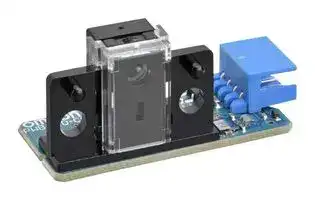
Z4D-C01
Micro Displacement Sensor, 6.5mm, Analogue, 4.5 to 5.5VDC
⚠️ Reference pricing provided. In case of supply shortages, we will connect you with our trusted procurement partners to ensure your project's continuity.
- Manufacturer: OMRON / PARTNER STOCK
- Product type:
- SVHC: To Be Advised
- IP Rating: -
- Output Type: Analogue - Voltage
- Sensor Type: Micro Displacement Sensors
- Light Source: LED
- Product Range: -
- Qualification: -
- Sensing Method: Triangulation
- Connection Method: Connector
- Sensing Range Max: 6.5mm
- Sensor Output Type: Analogue
- Supply Voltage Max: 5.5V
- Supply Voltage Min: 4.5V
- Sensing Distance Max: 6.5mm
- Supply Voltage DC Max: 5.5V
- Supply Voltage DC Min: 4.5V
- Operating Temperature Max: 65°C
- Operating Temperature Min: -10°C
| Delivery and price | |
|---|---|
| Units per pack | 6 |
| Price | 57.09 € |
| Current stock | 100+ |
| Lead time | 30 days |
Datasheet

**Microphotonic Devices (Micro-displacement Sensor) Z4D-C01** ## **Micro-displacement Sensor** - Enable to detect ±10 m level displacement, applicable to detect duplicated paper feeding or deflection amount. - Displacement output changes by object colors are stabilized with signal divider circuit. - Operating area = 6.5 ±1 mm. **Be sure to read** _**Safety Precautions on page 3.**_ ## **Ordering Information** ## **Micro-displacement Sensor** |**Appearance**|**Sensing**<br>**method**|**Connecting method**|**Sensing distance**|**Output type**|**Model**| |---|---|---|---|---|---| |15<br>35.5<br>16<br>~~a~~<br>se<br>\—|Triangulation|Connector|6.5 ±1 mm|Analog output|Z4D-C01| ## **Ratings, Characteristics and Exterior Specifications** ## **Absolute Maximum Ratings (Ta = 25** °C **)** |**Item**|**Symbol**|**Rated value**|**Unit**|**Remarks**| |---|---|---|---|---| |**Supply voltage**|VCC|7|V|---| |**LED pulse light**<br>**emission control signal**|PLS|7|V|LED| |**LED light emission pulse**|tFP|100|ms|Please refer Pulsed Forward<br>Current Rated Curve| |**Operating temperature**|Topr|-10 to +65|°C|No freezingor condensation| |**Storage temperature**|Tstg|-25 to +80|°C|---| **Note:** Refer to Pulsed Forward Current Rated Curve. ## **Characteristics (Ta = 25** °C **)** Object: N8.5 Munsell paper with a reflection factor of 70%. |**Item**|**Value**| |---|---| |**Operating area*1**<br>6.5 ±1 mm|6.5 ±1 mm| |**Sensitivity variation*2**<br>-1.4 mV/|-1.4 mV/m ±10% max.| |**Resolution*3**<br>±10|±10m max.| |**Linearity *4**<br>2% F.S.|2% F.S.(full scale)max.| - *1. Distance from Mounting Reference Plane to Target. ## **Exterior Specification** |**Connecting**<br>**method**|**Weight (g)**|**Material**|**Material**|**Material**| |---|---|---|---|---| |||**Case**|**Cover**|**Lens**| |Connector|3.6|Polycarbonate|Polycarbonate|PMMA| ## **Electrical and Optical Characteristics (Ta = -10°C to 65°C)** |**Item**|**Symbol**|**Rated value**|**Remarks**| |---|---|---|---| |**Power supply voltage**|VCC|5 V ±10%|Ripple (p-p): 10 mV<br>p-pmax.| |**Output voltage**|OUT|0.2 V to(VCC- 0.3)V|*1| |**Response delay**<br>**time**|tr1|100s max.|*2| ||tr2|500s max.|*3| |**LED pulse light**<br>**emission control**<br>**signal voltage**|PLS|3.5 V to VCC|---| - *1. Load impedance (between OUT-GND) is set at more than 10 k . - *2. tr1: Rise time of output voltage from 10% to 90%. - *3. tr2: Setup time from PLS rising edge to measured output value rising edge. - *2. The sensitivity is defined as slope of the line and it represents the variation in the output voltage per unit length between different products. |Sensitivity|Sensitivity|Sensitivity<br>V1- V0||V0: Output voltage at the point d0| |---|---|---|---|---| |variation =||2000|(mV/m)|V1: Output voltage at the point d1<br>d0,d1: Distance between datum clamp| |||||face and detective object| |d0||5.5 mm||| |d1||7.5 mm||| - *3. This is the value of the electrical noise width in the output signal converted to a distance under the following conditions. - (1) Noise width is measured in a waveform after the four times average with an oscilloscope. - (2) Ripple noise in the power supply voltage (Vcc): 10 mVp-p max. - (3) Distance from mounting reference plane to target: 6.5 mm - (4) Resolution is measured by the voltage of response delay time (tr2). - *4. This is the peak-to-peak value of the deviation of the signal output from a straight line. - A linearity of 2% F.S. indicates the following value: - (1) Distance full-scale converted value: 2 mm × 0.02 = 0.04 mm (40 m) - (2) Output voltage converted value: 1.4 mV/ m × 40 m = 56 mV (for a sensor with a sensitivity of 1.4 mV/ m) **1** omRon ~~a~~ **Z4D-C01** ## **Engineering Data (Reference value)** **Fig 1. Operating Distance Fig 2. Dependency of Object Characteristics (Typical) on Reflection Factor (Typical)** **Fig 3. Temperature Fig 4. Pulsed Forward Characteristics (Typical) Current Rated Curve** **==> picture [500 x 120] intentionally omitted <==** **----- Start of picture text -----**<br> 5 5040 10080 Vcc = 5 VDistance: 6.5 mm (ms)100 Duty ratio (%)= tFPT ×100<br>4 30 60 tFP<br>3 20100 FESaSS 40200 EOE 10 Recommended T<br>operating area<br>2 -10 -20<br>-20 PREER -40 b 1 yy,<br>1 -30 -60<br>-40 -80<br>0 -50 EERE -100 HEE 0.1 PAT<br>5 5.5 6 6.5 7 7.5 8 0 RTS 20 40 60 |} 80 100 -40 EEE -20 0 20 40 60 80 100 0 LL 20 40 60 80<br>Operating distance (mm) Reflection factor of object (%) Ambient temperature (°C) Duty ratio (%)<br>)FP<br>Output voltage (V) Pulse width (t<br>Sensitivity change ratio (%) Output change ratio (mV)<br>**----- End of picture text -----**<br> ## **Circuit diagram/Connection diagram** **==> picture [274 x 118] intentionally omitted <==** **----- Start of picture text -----**<br> CPU<br>PSD<br>ConversionI/V Amplifier ConversionA/D Division V1 ConversionD/A OUT A/Dport Output<br>V1 + V2<br>Digital output<br>| GOO LED G 5 V e<br>Object PLS<br>D port Timer<br>GND<br>Se _<br>Microprocessor<br>JI (User)<br>Micro-displacement Sensor User<br>**----- End of picture text -----**<br> - Output voltage signal is obtained by applying the pulse signal at PLS terminal. Please be careful, it is not obtained by DC voltage applying. ## **Pulse Input and Sensor Output** <Pulse Input> Voltage <Sensor Output> **==> picture [213 x 82] intentionally omitted <==** **----- Start of picture text -----**<br> Waitingtime Setup Output Waitingtime ・・・<br>Voltage<br>tr2<br>*<br>tr1<br>**----- End of picture text -----**<br> - Output voltage depends on input. After setup time tr2, output signal is obtained according to the distance. - After setup, output signal is updated every 80 micro seconds. - Update every 80 micro seconds. Output signal is reset at pulse input signal falling low level, and start setup over again after next input signal applying. ## **Application Examples** **==> picture [235 x 95] intentionally omitted <==** **----- Start of picture text -----**<br> Detecting Paper Detecting Two Sheets of Paper<br>Thickness in Printers<br>Paper<br>Micro-displacement Sensor<br>Cal<br>Displacement<br>Roller Sensor<br>**----- End of picture text -----**<br> **==> picture [111 x 86] intentionally omitted <==** **----- Start of picture text -----**<br> Detecting Sheet Micro-displacementSensor<br>Thickness<br>Roller<br>Shaft<br>Sheet<br>**----- End of picture text -----**<br> **2** omron ~~a~~ **Z4D-C01** ## **Safety Precautions** **To ensure safe operation, be sure to read and follow the Instruction Manual provided with the Sensor.** ~~Sf~~ **CAUTION** ~~|~~ **Precautions for Correct Use This product is not designed or rated for ensuring Do not use the product in atmospheres or safety of persons either directly or indirectly. Do not environments that exceed product ratings. use it for such purposes.** **Do not use the product in atmospheres or environments that exceed product ratings. This product is for surface mounting. Refer to Soldering Information, Storage and Baking for details.** ## ~~|~~ **Precautions for Safe Use Do not use the product with a voltage or current that exceeds the rated range.** **Dispose of this product as industrial waste.** Applying a voltage or current that is higher than the rated range may result in explosion or fire. **Do not miswire such as the polarity of the power supply voltage.** Otherwise the product may be damaged or it may burn. **This product does not resist water. Do not use the product in places where water or oil may be sprayed onto the product.** ## **Dimensions** **(Unit: mm)** ## **Micro-displacement Sensor** **==> picture [38 x 8] intentionally omitted <==** **----- Start of picture text -----**<br> Z4D-C01<br>**----- End of picture text -----**<br> **==> picture [381 x 230] intentionally omitted <==** **----- Start of picture text -----**<br> 16±0.2<br>9.1±0.2<br>35.5 2×2.3 dia. +0.1<br>2-292250-4 2-M3<br>(Tyco Electronics)<br>13<br>40±0.3<br>Mounting reference plane 22 14.5<br>16±0.05 9.2 Mounting hole dimensions<br>2×3.5 dia. 9.8 0.4<br>8.4±0.3<br>2×2 dia. +0.05- 0.15<br>2×1 dia. Note: Values in parentheses are for reference.<br>2.5 11.5 8.8<br>1.8 2<br>PIN Symbol<br>1 PLS<br>Emitter axis 2 Vcc<br>3 OUT<br>4 GND<br>(0.5) 1 Terminal arrangement<br>Center of<br>Detector<br>5.7±0.2<br>5±0.2<br>8.2±0.2<br>15.7±0.2<br>5±0.05<br>4.8<br>10<br>5.8<br>(6.3) (1.3) 1.2<br>15<br>10<br>5<br>**----- End of picture text -----**<br> Recommended Mating Connectors: Tyco Electronics 179228-4 (crimp-type connector) 173977-4 (insulation displacement crimp connector) **3** omron ~~a~~ - Application examples provided in this document are for reference only. In actual applications, confirm equipment functions and safety before using the product. - Consult your OMRON representative before using the product under conditions which are not described in the manual or applying the product to nuclear control systems, railroad systems, aviation systems, vehicles, combustion systems, medical equipment, amusement machines, safety equipment, and other systems or equipment that may have a serious influence on lives and property if used improperly. Make sure that the ratings and performance characteristics of the product provide a margin of safety for the system or equipment, and be sure to provide the system or equipment with double safety mechanisms. **Note: Do not use this document to operate the Unit.** **OMRON Corporation Electronic and Mechanical Components Company** **Contact: www.omron.com/ecb** **Cat. No. E453-E1-03** 1117(0816)(O)
Updated at April 27, 2026
About Novapart
Novapart is a B2B electronic component broker specialising in stock shortages and cost reduction. We source hard-to-find parts and identify compliant alternatives across a catalogue of 410,000+ components from 500+ manufacturers.
Learn more →Stock Shortage Specialist
When a component is unavailable, discontinued or has an unacceptable lead time, we tap into our network of vetted European and Asian distributors to source what you need — without compromising on quality or traceability.
Request a quote →Compliant Alternatives
We identify pin-to-pin, electrically equivalent substitutes that meet the same certifications (RoHS, AEC-Q100, REACH) as your original specification — validated against datasheets, not just part numbers. Often at a lower cost.
BOM Analysis service →