


Z0405MF 1AA2
Triac, 600 V, 4 A, TO-202, 1.3 V, 20 A, 5 mA
- Manufacturer: STMICROELECTRONICS
- Product type: Thyristors - TRIACs
- No. of Pins: 3Pins
- Peak Gate Power: 200mW
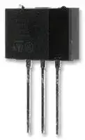
- Triac Case Style: TO-202
- Thyristor Mounting: Through Hole
- Holding Current Max: 5mA
- On State RMS Current: 4A
- Peak On State Voltage: 2V
- Gate Trigger Voltage Max: 1.3V
- Operating Temperature Max: 125°C
- Peak Non Repetitive Surge Current: 20A
- Peak Repetitive Off State Voltage: 600V
- Gate Trigger Current Max (QI), Igt: 5mA
| Delivery and price | |
|---|---|
| Units per pack | 500 |
| Price | 0.527 € |
| Current stock | 10+ |
| Lead time | 30 days |
**Z04**

**==> picture [61 x 39] intentionally omitted <==**

## Standard

## 4 A Triacs

## **Main features**

|**Symbol**|**Value**|**Unit**|
|---|---|---|
|**IT(RMS)**|4|A|
|**VDRM/VRRM**|600 to 800|V|
|**IGT (Q**1**)**|3 to 25|mA|


## **Description**

The **Z04** series is suitable for general purpose AC switching applications. They can be found in applications such as home appliances (electrovalve, pump, door lock, small lamp control), fan speed controllers,...

Different gate current sensitivities are available, allowing optimized performances when controlled directly from microcontrollers.

**==> picture [87 x 156] intentionally omitted <==**

**----- Start of picture text -----**<br>
A2<br>G<br>A1<br>A1<br>A2<br>G<br>TO202-3<br>**----- End of picture text -----**<br>


## **Order codes**

|**Order codes**||
|---|---|
|**Part Number**|**Marking**|
|Z04xxyF(1)|Z04xxyF(1)|


1. xx = sensitivity,  y = voltage

## **Table 1. Absolute maximum ratings**

|**Symbol**|**Parameter**|||**Value**|**Unit**|
|---|---|---|---|---|---|
|IT(RMS)|RMS on-state current (full sine wave)||Tamb= 25° C<br>Tl= 30° C|4|A|
|ITSM|Non repetitive surge peak on-state current<br>(full cycle, Tjinitial = 25° C)|F = 50 Hz|t = 20 ms|20|A|
|||F = 60 Hz|t = 16.7 ms|21||
|I²t|I²t Value for fusing|tp= 10 ms||2.2|A²s|
|dI/dt|Critical rate of rise of on-state current IG=<br>2 x IGT, tr ≤100 ns|F = 120 Hz|Tj= 125° C|20|A/µs|
|IGM|Peak gate current|tp= 20 µs|Tj= 125° C|1.2|A|
|PG(AV)|Average gate power dissipation||Tj= 125° C|0.2|W|
|Tstg<br>Tj|Storage junction temperature range<br>Operating junction temperature range|||- 40 to + 150<br>- 40 to + 125|° C|


1/8

May 2006

Rev 7

_www.st.com_

**Characteristics**

**Z04**

## **1 Characteristics**

## **Table 2. Electrical Characteristics (Tj = 25° C, unless otherwise specified)**

|**Symbol**|**Test Conditions**|**Quadrant**||**Z04**|**Z04**|**Z04**|**Z04**|**Unit**|
|---|---|---|---|---|---|---|---|---|
|||||**02**|**05**|**09**|**10**||
|IGT<br>(1)|VD= 12 V   RL= 30Ω|I - II - III - IV|MAX<br>.|3|5|10|25|mA|
|VGT||ALL|MAX<br>.|1.3||||V|
|VGD|VD= VDRMRL= 3.3 kΩ<br>Tj= 125° C|ALL|MIN.|0.2||||V|
|IH<br>(2)|IT= 50 mA||MAX<br>.|3|5|10|25|mA|
|IL|IG= 1.2 IGT|I - III - IV|MAX<br>.|6|10|15|25|mA|
|||II||12|15|25|50||
|dV/dt<br>(2)|VD=  6 % VDRMgate open Tj= 110° C||MIN.|10|20|100|200|V/µs|
|(dV/dt)c<br>(2)|(dI/dt)c = 1.8 A/ms    Tj= 110° C||MIN.|0.5|1|2|5|V/µs|
|1.<br>minimum IGT is guaranted at 5% of IGT max.|||||||||


2. for both polarities of A2 referenced to A1.

## **Table 3. Static Characteristics**

|**Symbol**|**Test Conditions**|**Test Conditions**|**Test Conditions**|**Value**|**Unit**|
|---|---|---|---|---|---|
|VTM<br>(1)|ITM= 5.5 A        tp= 380 µs|Tj= 25° C|MAX.|2.0|V|
|Vto<br>(1)|Threshold voltage|Tj= 125° C|MAX.|0.95|V|
|Rd<br>(1)|Dynamic resistance|Tj= 125° C|MAX.|180|mΩ|
|IDRM<br>IRRM|VDRM= VRRM|Tj= 25° C|MAX.|5|µA|
|||Tj= 125° C||0.5|mA|


1. for both polarities of A2 referenced to A1.

## **Table 4. Thermal resistances**

|**Table 4.**|**Thermal resistances**|||
|---|---|---|---|
|**Symbol**|**Parameter**|**Value**|**Unit**|
|Rth(j-I)|Junction to lead (AC)|15|° C/W|
|Rth(j-a)|Junction to ambient|100|° C/W|


2/8

**Characteristics**

**Z04**

## **Figure 1. Maximum power dissipation versus RMS on-state current (full cycle)**

## **Figure 2. RMS on-state current versus ambient temperature (full cycle)**

**==> picture [462 x 352] intentionally omitted <==**

**----- Start of picture text -----**<br>
P(W) IT(RMS)(A)<br>7 4.5<br>Rth(j-a) = Rth(j-l)<br>4.0<br>6<br>3.5<br>5<br>3.0<br>4 2.5<br>3 2.0<br>1.5 Rth(j-a) = 100°C/W<br>2<br>1.0<br>1<br>0.5<br>IT(RMS)(A) Tamb (°C)<br>0 0.0<br>0.0 0.5 1.0 1.5 2.0 2.5 3.0 3.5 4.0 0 25 50 75 100 125<br>Figure 3. Relative variation of thermal  Figure 4. Relative variation of gate trigger<br>impedance versus pulse  current, holding current and<br>duration latching current versus junction<br>temperature (typical values)<br>K=[Zth(j-a)/Rth(j-a) []] IGT, IH, IL [T ] /j IGT, IH, IL [T =25°C]j<br>1E+0 2.5<br>2.0<br>1E-1<br>1.5 IGT<br>IH & IL<br>1.0<br>1E-2<br>0.5<br>tp(s) Tj (°C)<br>1E-3 0.0<br>1E-3 1E-2 1E-1 1E+0 1E+1 1E+2 5E+2 -40 -20 0 20 40 60 80 100 120 140<br>**----- End of picture text -----**<br>


**Figure 5. Surge peak on-state current versus number of cycles**

**Figure 6. Non-repetitive surge peak on-state current for a sinusoidal pulse with width tp < 10 ms and corresponding value of I[2] t**

**==> picture [462 x 146] intentionally omitted <==**

**----- Start of picture text -----**<br>
ITSM (A) ITSM (A), I2t (A2s)<br>25 500<br>Tj initial = 25°C<br>20 t=20ms<br>One cycle 100<br>15 dI/dt limitation:20A/µs ITSM<br>Non repetitive<br>Tj initial = 25°C<br>10 TambRepetitive= 25°C 10<br>5 I2t<br>0 Number of cycles 1 tp (ms)<br>1 10 100 1000 0.01 0.10 1.00 10.00<br>**----- End of picture text -----**<br>


3/8

**Characteristics**

**Z04**

## **Figure 7. On-state characteristics (maximum values)**

**==> picture [205 x 125] intentionally omitted <==**

**----- Start of picture text -----**<br>
ITM(A)<br>20.0<br>10.0<br>Tj = Tjmax.<br>1.0<br>Tj = 25°C<br>T =max.j<br>Vt0=0.95 V<br>VTM (V) Rd=180 mΩ<br>0.1<br>0.0 0.5 1.0 1.5 2.0 2.5 3.0 3.5 4.0 4.5 5.0<br>**----- End of picture text -----**<br>


## **Figure 8. Relative variation of critical rate of decrease of main current versus (dV/dt)c (typical values)**

**==> picture [203 x 121] intentionally omitted <==**

**----- Start of picture text -----**<br>
(dI/dt)c [(dV/dt)c] / Specified (dI/dt)c<br>2.6<br>2.4<br>2.2<br>2.0<br>1.8<br>1.6<br>1.4 Z0410<br>1.2<br>1.0<br>0.8 Z0409<br>0.6 Z0402<br>0.4 Z0405<br>0.2 (dV/dt)c (V/µs)<br>0.0<br>0.1 1.0 10.0 100.0<br>**----- End of picture text -----**<br>


## **Figure 9. Relative variation of critical rate of decrease of main current versus junction temperature**

**==> picture [204 x 123] intentionally omitted <==**

**----- Start of picture text -----**<br>
(dI/dt)c [T ] /j (dI/dt)c [Tj Specified]<br>6<br>5<br>4<br>3<br>2<br>1<br>Tj (°C)<br>0<br>0 25 50 75 100 125<br>**----- End of picture text -----**<br>


4/8

**Ordering information scheme**

**Z04**

## **2 Ordering information scheme**

**==> picture [297 x 201] intentionally omitted <==**

**----- Start of picture text -----**<br>
Z   04   xx   y   F [BLANK] 0AA2<br>Triac series<br>Current<br>04 = 4A<br>Sensitivity<br>02 = 3mA<br>05 = 5mA<br>09 = 10mA<br>10 = 25mA<br>Voltage<br>M = 600V<br>S = 700V<br>N = 800V<br>Package<br>F = TO202-3<br>Packing mode<br>0AA2 = Tube<br>**----- End of picture text -----**<br>


**Table 5. Product selector**

|**Part Number**|**Voltage**|**Voltage**|**Voltage**|**Sensitivity**|**Type**|**Package**|
|---|---|---|---|---|---|---|
||**600 V**|**700 V**|**800 V**||||
|Z0402MF|X|||3 mA|Standard|TO202-3|
|Z0402SF||X||3 mA|||
|Z0402NF|||X|3 mA|||
|Z0405MF|X|||5 mA|||
|Z0405SF||X||5 mA|||
|Z0405NF|||X|5 mA|||
|Z0409MF|X|||10 mA|||
|Z0409SF||X||10 mA|||
|Z0409NF|||X|10 mA|||
|Z0410MF|X|||25 mA|||
|Z0410SF||X||25 mA|||
|Z0410NF|||X|25 mA|||


5/8

**Package information**

**Z04**

## **3 Package information**

|||||||||||||||||||||||**DIMENSIONS**|**DIMENSIONS**|||
|---|---|---|---|---|---|---|---|---|---|---|---|---|---|---|---|---|---|---|---|---|---|---|---|---|---|
||||||||||||||||||||**REF.**|**Millimeters**||||**Inches**||
|||||||||||||||||||||**Min.**|**Typ.**|**Max.**|**Min.**|**Typ.**|**Max.**|
||||||||||||||||||||A|||10.1|||0.398|
||||||**A**||||||||||||||C||7.3|||0.287||
|||||||||||||||||||||||||||
||||||||||||||||||||D||10.5|||0.413||
|||||||||||||**C**|||||||F|||1.5|||0.059|
|||||||||||||||||||||||||||
||**O**||||||||||||||||||H||0.51|||0.020||
||**P**||||||||||**F**|**D**|**J**||||**H**||J<br>M||1.5<br>4.5|||0.059<br>0.177||
|||||||**N1**|||||||||||||N|||5.3|||0.209|
|||||||||||||||||||||||||||
||||||**N**||||||||||**M**||||N1||2.54|||0.100||
||||||||||||||||||||O|||1.4|||0.055|
||||||||||||||||||||P|||0.7|||0.028|


In order to meet environmental requirements, ST offers these devices in ECOPACK® packages. These packages have a lead-free second level interconnect. The category of second level interconnect is marked on the package and on the inner box label, in compliance with JEDEC Standard JESD97. The maximum ratings related to soldering conditions are also marked on the inner box label. ECOPACK is an ST trademark. ECOPACK specifications are available at: www.st.com.

6/8

**Ordering information**

**Z04**

## **4 Ordering information**

|**Ordering type**|**Marking**|**Weight**|**Base qty**|**Delivery mode**|
|---|---|---|---|---|
|Z04xxyF 0AA2(1)|Z04xxyF(1)|0.8 g|50|Tube|


1. xx = sensitivity,  y = voltage

## **5 Revision history**

|**Date**|**Revision**|**Description of Changes**|
|---|---|---|
|Oct-2001|4|Last update.|
|13-Feb-2006|5|TO202-3 delivery mode changed from bulk to tube.<br>ECOPACK statement added.|
|31-Mar-2006|6|Reformatted to current standard. Lead marking changed<br>on page 1|
|12-05-2006|7|Typographical error for (dV/dt)c corrected in Table 2.|


7/8

**Z04**

## **Please Read Carefully:**

Information in this document is provided solely in connection with ST products. STMicroelectronics NV and its subsidiaries (“ST”) reserve the right to make changes, corrections, modifications or improvements, to this document, and the products and services described herein at any time, without notice.

All ST products are sold pursuant to ST’s terms and conditions of sale.

Purchasers are solely responsible for the choice, selection and use of the ST products and services described herein, and ST assumes no liability whatsoever relating to the choice, selection or use of the ST products and services described herein.

No license, express or implied, by estoppel or otherwise, to any intellectual property rights is granted under this document. If any part of this document refers to any third party products or services it shall not be deemed a license grant by ST for the use of such third party products or services, or any intellectual property contained therein or considered as a warranty covering the use in any manner whatsoever of such third party products or services or any intellectual property contained therein.

**UNLESS OTHERWISE SET FORTH IN ST’S TERMS AND CONDITIONS OF SALE ST DISCLAIMS ANY EXPRESS OR IMPLIED WARRANTY WITH RESPECT TO THE USE AND/OR SALE OF ST PRODUCTS INCLUDING WITHOUT LIMITATION IMPLIED WARRANTIES OF MERCHANTABILITY, FITNESS FOR A PARTICULAR PURPOSE (AND THEIR EQUIVALENTS UNDER THE LAWS OF ANY JURISDICTION), OR INFRINGEMENT OF ANY PATENT, COPYRIGHT OR OTHER INTELLECTUAL PROPERTY RIGHT.**

**UNLESS EXPRESSLY APPROVED IN WRITING BY AN AUTHORIZE REPRESENTATIVE OF ST, ST PRODUCTS ARE NOT DESIGNED, AUTHORIZED OR WARRANTED FOR USE IN MILITARY, AIR CRAFT, SPACE, LIFE SAVING, OR LIFE SUSTAINING APPLICATIONS, NOR IN PRODUCTS OR SYSTEMS, WHERE FAILURE OR MALFUNCTION MAY RESULT IN PERSONAL INJURY, DEATH, OR SEVERE PROPERTY OR ENVIRONMENTAL DAMAGE.**

Resale of ST products with provisions different from the statements and/or technical features set forth in this document shall immediately void any warranty granted by ST for the ST product or service described herein and shall not create or extend in any manner whatsoever, any liability of ST.

ST and the ST logo are trademarks or registered trademarks of ST in various countries.

Information in this document supersedes and replaces all information previously supplied.

The ST logo is a registered trademark of STMicroelectronics. All other names are the property of their respective owners.

© 2006 STMicroelectronics - All rights reserved

## STMicroelectronics group of companies

Australia - Belgium - Brazil - Canada - China - Czech Republic - Finland - France - Germany - Hong Kong - India - Israel - Italy - Japan - Malaysia - Malta - Morocco - Singapore - Spain - Sweden - Switzerland - United Kingdom - United States of America

**www.st.com**

8/8
Updated at February 9, 2023
STMicroelectronics is a global leader in the semiconductor industry, recognized for developing highly integrated, energy-efficient solutions that power modern electronics. With a strong focus on innovation, ST provides a comprehensive portfolio of microelectronics that address the demanding requirements of industrial, automotive, communications, and consumer applications. Our extensive selection of STMicroelectronics components is built around a robust lineup of discrete semiconductors and circuit protection devices. We offer a wide variety of single MOSFETs, Schottky diodes, and fast and ultrafast recovery rectifier diodes, designed to deliver exceptional efficiency and thermal performance in power management and conversion systems. For robust circuit protection, our inventory features hundreds of transient voltage suppressors and TVS diodes that safeguard sensitive electronic components against destructive voltage spikes. In addition to core power discretes like TRIACs, SCRs, bipolar transistors, and single IGBTs, our STMicroelectronics range includes specialized integrated passive filters and MEMS sensors. Furthermore, ST offers advanced integrated passive devices, such as baluns and RF filters, which utilize high-quality monolithic RF IPD processes on glass or high-resistance silicon substrates. These components provide competitive cost structures, reduced power losses, and simplified RFIC-to-antenna matching, ensuring optimal system performance and delivering the reliability required for next-generation wireless and power designs.
About Novapart
Novapart is a B2B electronic component broker specialising in stock shortages and cost reduction. We source hard-to-find parts and identify compliant alternatives across a catalogue of 540,000+ components from 500+ manufacturers.
Learn more →Stock Shortage Specialist
When a component is unavailable, discontinued or has an unacceptable lead time, we tap into our network of vetted European and Asian distributors to source what you need — without compromising on quality or traceability.
Request a quote →Compliant Alternatives
We identify pin-to-pin, electrically equivalent substitutes that meet the same certifications (RoHS, AEC-Q100, REACH) as your original specification — validated against datasheets, not just part numbers. Often at a lower cost.
BOM Analysis service →