


XRCGE25M000F3A1BR0
Crystal, XRCGE Series, 25 MHz, 30 ppm, 35 ppm, 8 pF
- Manufacturer: MURATA
- Product type: Crystals
- SVHC: No SVHC (04-Feb-2026)
- Frequency Nom: 25MHz
- Product Range: XRCGE Series
- Load Capacitance: 8pF
- Crystal Frequency: 25MHz
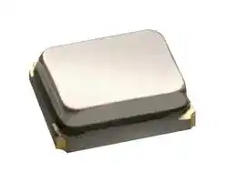
- Crystal Case / Package: SMD, 2mm x 1.6mm
- Frequency Stability + / -: 35ppm
- Frequency Tolerance + / -: 30ppm
- Operating Temperature Max: 125°C
- Operating Temperature Min: -40°C
| Delivery and price | |
|---|---|
| Units per pack | 1000 |
| Price | 0.189 € |
| Current stock | 1000+ |
| Lead time | 30 days |
Document No. JGC49-5041
P. 1/19
## 製品仕様書
## Specification of Crystal Unit
決定年月日 Issue Date : December 25, 2023
## 1. 品番 Part Number
当 社 品 番 Murata Part Number
XRCGE25M000F3A1BR0 (Frequency: 25.0000MHz / Size: 2.0 x 1.6mm)
## 2. `適 用` Scope
当製品仕様書は、車載用マイクロコンピュータ等のクロック発生回路に使用する水晶振動子について 規定します。この用途以外にご使用の場合には事前に当社へご連絡ください。 This product specification is applied to the crystal unit used for time base oscillator in a microcomputer for automotive. Please contact us when using this product for any other applications than described in the above.
3. 外観 及び 寸法 Appearance and Dimensions
- 3-1 外観 : 目視によって表示識別可能であり、汚れ等がありません。 Appearance : No illegible marking. No visible dirt.
- 3-2 外形寸法図 : 製品単体の形状を項目 6 に示します。 Dimensions of component : Please refer to item 6 for component dimensions.
- 3-3 構造 : `アルミナ基板に、水晶素子を接着し、金属キャップで蓋 をしております。`
- Construction then metal cap covers over the element.
`株式会社 村 田 製 作 所` Murata Manufacturing Co.,Ltd.
Document No. JGC49-5041
P. 2/19
**==> picture [468 x 218] intentionally omitted <==**
**----- Start of picture text -----**<br>
4. 定格 Rating<br>項 目 Item 規 格 Specification<br>4-1 動作温度範囲<br>-40 to +125°C<br>Operating Temperature Range<br>4-2 保存温度範囲<br>-55 to +125°C<br>Storage Temperature Range<br>4-3 励振レベル<br>300 μ W 以下 /max.<br>Drive Level<br>4-4 直流印加電圧<br>D.C.6V 以下 /max.<br>D.C. Voltage<br>4-5 入力信号振幅<br>15Vp-p 以下 /max.<br>A.C. Voltage<br>4-6 耐電圧 D.C.100V 以下 /max.<br>Withstanding Voltage 5s 以内 /max.<br>**----- End of picture text -----**<br>
**==> picture [469 x 238] intentionally omitted <==**
**----- Start of picture text -----**<br>
5. 電気的性能 Electrical Characteristics<br>項 目 Item 規 格 Specification<br>5-1 公称周波数<br>25.0000MHz<br>Nominal Frequency<br>5-2 周波数許容偏差 *1<br>± 30ppm 以内 /max.<br>Frequency Tolerance *1<br>5-3 周波数温度依存性 ± 35ppm 以内 /max. (-40 to 125°C)<br>Frequency Shift by Temperature (初期値に対し /from initial value )<br>5-4 周波数エージング ±10ppm 以内 /15 年<br>Frequency aging max./15years<br>5-5 等価直列抵抗 *1<br>100 Ω 以下 /max.<br>Equivalent Series Resistance *1<br>5-6 絶縁抵抗 *2 500M Ω 以上 /min. (D.C.10V 印加時 )<br>Insulation Resistance *2 (Applied D.C.10V)<br>5-7 負荷容量 (Cs) *1<br>8.0pF<br>Load Capacitance *1<br>**----- End of picture text -----**<br>
- *1 `周波数および等価直列抵抗の測定方法は項目` 8 `を参照ください。` Please refer to item 8 for measuring method of frequency and Equivalent Series Resistance.
- *2 `端子相互間での抵抗を示します。` This characteristic shows the resistance between terminals.
`株式会社 村 田 製 作 所` Murata Manufacturing Co.,Ltd.
Document No. JGC49-5041
P. 3/19
## 6. 外形寸法図 Dimensions
**==> picture [472 x 660] intentionally omitted <==**
**----- Start of picture text -----**<br>
周波数表示 内外部接続電極<br>Frequency Marking Through electrode<br>天面<br>W<br>Top View<br>(4) (3)<br>* W : 2.0 ± 0.1<br>L : 1.6 ± 0.1<br>T : 0.65 ± 0.05<br>(1) (2)<br>側面 (1.8) (0.3)<br>Side View<br>周波数表示 : L<br>Frequency<br>(0.2) (0.2) Marking<br>0.5±0.1 * : 製造年月日<br>底面<br>Bottom View (1) (2) EIAJ Monthly Code<br>単位 : mm<br>Unit<br>( ) : 参考値<br>Reference<br>(4) (3)<br>1.3±0.1<br>端子番号 (1) 入出力<br>Terminal Crystal terminal<br>製品端子に極性はありません。 Number (2) (4) ノーコネクト<br>No polarity in the terminal. No connect<br>(3) 入出力<br>(推奨ランド寸法) Crystal terminal<br>(Recommendable Land Pattern)<br>0.75 0.60 0.75<br>第 1 図 外形寸法図<br>Figure 1. Dimensions<br>)<br>(0.2<br>L<br>1.4)<br>(<br>0.2)<br>(<br>T<br>.5±0.1<br>0 0.9±0.1<br>0.70<br>0.30<br>0.70<br>**----- End of picture text -----**<br>
`株式会社 村 田 製 作 所` Murata Manufacturing Co.,Ltd.
Document No. JGC49-5041
P. 4/19
**==> picture [463 x 118] intentionally omitted <==**
**----- Start of picture text -----**<br>
月 Month<br>1 2 3 4 5 6 7 8 9 10 11 12<br>年 Year<br>2011, 2015, 2019, 2023 a b c _ d e f g h j k l m<br>2012, 2016, 2020, 2024 n p q r s t u v w x y z<br>2013, 2017, 2021, 2025 A B C D E F G H J K L M<br>2014, 2018, 2022, 2026 N P Q R S T U V W X Y Z<br>**----- End of picture text -----**<br>
- 製造年月度 / EIAJ Monthly Code
- `(注)4年で1サイクルとなります。` / (note) The number is cycled by 4years.
7. テーピング品包装規格 Packaging Standard (Taping)
- 7-1 `テープは右巻き` ( `テープの端を手前に取り出した時、送り穴が右側になる向き` ) `とします。` The tape for components shall be wound clockwise. The feeding holes shall be to the right side as the tape is pulled toward the user.
- 7-2 `チップは、` 1 `リール` 3,000 `個収納します。` A reel shall contain 3,000pcs of components.
- 7-3 `プラスチックテープの外形寸法図を第` 2 `図に示します。` Dimensions of plastic tape are shown in Figure 2.
- 7-4 `プラスチックリールの外形寸法図を第` 3 `図に示します。` Dimensions of plastic reel are shown in Figure 3.
`株式会社 村 田 製 作 所` Murata Manufacturing Co.,Ltd.
Document No. JGC49-5041
P. 5/19
**==> picture [486 x 706] intentionally omitted <==**
**----- Start of picture text -----**<br>
4.0±0.1<br>2.0±0.1 +0.1<br>Φ1.5 -0.0<br>天面<br>Top View<br>(3) (2)<br>(4) (1)<br>1.85±0.1<br>引きはがし強度 0.1~0.7N Φ1.0±0.1<br>T he cover film peel strength force 0.1 to 0.7N 4.0±0.1<br>引きはがしスピード 300mm/分<br>T he cover film peel speed 300mm/min.<br>側面 カバーテープ<br>Side View C over film (5°)<br>10°<br>Top<br>↑<br>引き出し方向<br>D irection of Feed<br>単位: mm<br>Unit : mm<br>第 2 図 プラスチックテープの外形寸法図<br>Figure 2. Dimensions of Plastic Tape<br>トレーラー部<br>Trailer リーダー部<br>160~190 Leader<br>160 to 190 カバーテープ<br>Cover Film<br>空部 チップ装着部 空部<br>Empty Components Empty<br>160 以上/min.<br>400~560mm<br>400 to 560mm<br>Φ13.0±0.2<br>2.0±0.5<br>9.0 [+1.0] 単位:mm<br>0<br>in mm<br>13.0±1.0<br>第 3 図 プラスチックリールの外形寸法図<br>Figure 3. Dimensions of Plastic Reel<br>1.75±0.1<br>3.5±0.1<br>.0±0.28<br>(5.5) .25±0.12<br>0.25±0.1 1.00±0.1 (1.6max.)<br>0 1.5<br>-<br>Φ180<br>**----- End of picture text -----**<br>
`株式会社 村 田 製 作 所` Murata Manufacturing Co.,Ltd.
Document No. JGC49-5041
P. 6/19
8. 測定方法 Measuring Method
- 8-1 `周波数測定方法` :
- 5 `、` 9 `、` 10 `項で示す周波数は、第` 4-1 `図で示す回路とネットワークアナライザ` (S&A 250B `も`
- `しくは相当品` ) `にて測定した負荷共振周波数を示します。測定機器の違いにより、周波数ズ レが発生する可能性があります。` Frequency measuring method:
Frequency which is mentioned in item 5, 9 and 10 means the load resonance frequency measured by network analyzer (S&A 250B or the equivalent) and the circuit in Figure. 4-1. Measured frequency may be changed by using different measurement equipment.
**==> picture [212 x 114] intentionally omitted <==**
**----- Start of picture text -----**<br>
Network Analyzer<br>OUT IN<br>66.2 Ω 66.2 Ω<br>DUT<br>159 Ω 14.2 Ω 14.2 Ω 159 Ω<br>**----- End of picture text -----**<br>
`第` 4-1 `図 周波数測定回路`
Figure 4-1 Frequency measuring circuit
- 8-2 `等価直列抵抗` : 5 `項に示す等価直列抵抗` (ESR) `は、第` 4-1 `図で示す回路と ネットワークアナライザ` (S&A 250B `もしくは相当品` ) `に て測定します。` DUT `は第` 4-2 `図に示します。`
- Equivalent series resistance : The equivalent series resistance (ESR) which is mentioned in item 5 is measured by network analyzer (S&A 250B or equivalent) and the circuit in Figure. 4-1. DUT is shown in Figure 4-2.
**==> picture [146 x 69] intentionally omitted <==**
**----- Start of picture text -----**<br>
C1 L1 R1<br>=<br>Co<br>**----- End of picture text -----**<br>
`第` 4-2 `図` DUT `(被測定デバイス)` Figure 4-2 DUT `(` Device Under Test `)`
- 8-3 `測定条件` : `温度` +25 `±` 3 `℃、湿度` 25 `~` 75%R.H. `を標準測定状態とします。` Measuring Condition : Standard conditions for the measurement shall be +25±3°C and 25 to 75%R.H.
`株式会社 村 田 製 作 所` Murata Manufacturing Co.,Ltd.
Document No. JGC49-5041
P. 7/19
## 9. `機械的性能` Physical Characteristics
**==> picture [457 x 623] intentionally omitted <==**
**----- Start of picture text -----**<br>
試験後の規格<br>項 目 試 験 条 件<br>Specification<br>Item Test Condition<br>After Test<br>9-1 衝撃 製品を試験用基板に実装した状態で、加速度 表 3 及び 5-5 を満足しま<br>100G(980m/s [2] ) 、作用時間 6ms の衝撃を 6 面に各 3 回 す。<br>加えた後、測定します。試験方法は AEC-Q200 REV<br>D に準拠します。<br>Mechanical Component shall be soldered on the test board. The measured values<br>Shock Then it shall be measured after being applied 3 shall meet Table 3<br>successive shocks, 100G(980m/s [2] ) for 6ms in the and Item 5-5.<br>directions of 6 sides. Testing procedure is in<br>accordance with AEC-Q200 REV D.<br>9-2 振動 製品を試験用基板に実装した状態で、振動周波数 表 3 及び 5-5 を満足しま<br>10 ~ 2000Hz 、 5G(49m/s [2] ) の振動を X,Y,Z の 3 方向に す。<br>各 4 時間加えた後、測定します。試験方法は AEC-<br>Q200 REV D に準拠します。<br>Vibration Component shall be soldered on the test board. The measured values<br>Then it shall be measured after being applied shall meet Table 3<br>vibration of 5G(49m/s [2] ) with 10 to 2000Hz band of and Item 5-5.<br>vibration frequency to each of 3 perpendicular<br>direction for 4 hours. Testing procedure is in<br>accordance with AEC-Q200 REV D.<br>9-3 基板たわみ 第 5 図に示すたわみ試験用基板に実装し、たわみ量 表 3 及び 5-5 を満足しま<br>2mm になるまで毎秒 0.5mm の速さで加圧し、 60+5/- す。<br>0 秒間保持します。試験方法は AEC-Q200 REV D に<br>準拠します。<br>Board Flex Component shall be soldered on the test board The measured values<br>shown in Figure 5. Then apply pressure in vertical shall meet Table 3<br>direction shown in following figure at a rate of and Item 5-5.<br>about 0.5mm/s until bent width reaches 2mm and<br>hold for 60+5/-0 seconds. Testing procedure is in<br>accordance with AEC-Q200 REV D.<br>加 圧棒<br>加圧<br>Stick L oad<br>20 10<br>PCB<br>たわみ<br>R 10 D eflection<br>φ φ 5 Supporter 5 支持台 部品 P art ±± 11 Off-Center セ ンターズレ<br>45 45<br>2<br>**----- End of picture text -----**<br>
`株式会社 村 田 製 作 所` Murata Manufacturing Co.,Ltd.
Document No. JGC49-5041
P. 8/19
||||||
|---|---|---|---|---|
||9-4|はんだ耐熱<br>Resistance to<br>Soldering Heat<br>(1)リフロー方式<br>(1) Re-flow<br>Soldering<br>製品単品状態でリフロー炉(ピーク温度260±5℃、<br>1.0±0.5 秒、その他条件は12-5-2 項を参照)に2 回<br>通した後、室温に取り出し、24 時間放置した後、測定<br>します。試験方法はIEC60068-2-58に準拠します。<br>Component shall be measured after 2 times re-<br>flow soldering and leaving at room temperature for<br>24 hours. For soldering profile, refer to item 12-5-2<br>(Peak temperature is 260±5°C for 1.0±0.5s).<br>Testing procedure is in accordance with<br>IEC60068-2-58.<br>表1および5-5を満足し<br>ます。<br>The measured values<br>shall meet table 1 and<br>item 5-5|||
|||(2)コテ付け方式<br>(2)Soldering<br>with iron<br>PCB上にて温度+350±5℃で5.0±0.5秒間はんだ付<br>けを行い、室温に24時間放置した後、測定します。但<br>し、はんだこて先は電極部に直接接触しない事としま<br>す。試験方法はIEC60068-2-58に準拠します。(12-5-<br>3項を参照)<br>Component shall be measured after soldering on<br>PCB at +350±5°C for 5.0±0.5s and leaving at room<br>temperature for 24 hours. The soldering iron shall<br>not touch the component while soldering. Testing<br>procedure is accordance with IEC60068-2-58.<br>(Refer to item 12-5-3)<br>外観に異常がなく、表2<br>および5-5を満足しま<br>す。<br>No<br>visible<br>damage<br>and<br>the<br>measured<br>values<br>shall<br>meet<br>Table 2 and item 5-5.|||
|||(3)はんだディッ<br>プ方式<br>(3)Solder Dip|製品端子部を+260±5゚Cの溶融はんだ中に10±1秒<br>間浸した後、室温に取り出し、24時間放置した後、測<br>定します。試験方法はJESD22-B106に準拠します。<br>The terminals of component shall be immersed in<br>a soldering bath at +260±5゚C for 10±1s by only to<br>level to cover. Component shall be measured after<br>leaving at room temperature for 24 hours. Testing<br>procedure is in accordance with JESD22-B106.|<br> <br> <br> <br>表3 および5-5 を満足<br>します。<br>The measured values<br>shall meet Table 3<br>and Item 5-5.|
||||||
`株式会社 村 田 製 作 所` Murata Manufacturing Co.,Ltd.
Document No. JGC49-5041
P. 9/19
|9-5|はんだ付性<br>Solderability|無鉛はんだ(Sn-3.0Ag-0.5Cu)<br>PCT装置にて温度+105℃、湿度100%R.H.、4時間の<br>エージングをし、端子部分をロジンメタノール液に5秒<br>浸した後、+245±5℃の溶融はんだ中に3±0.5秒間<br>浸します。試験方法はIEC60068-2-58に準拠します。<br>Lead free solder (Sn-3.0Ag-0.5Cu)<br>After being kept in pressure cooker at +105°C<br>and 100%R.H. for 4 hours, and being placed in a<br>rosin-methanol for 5s, the terminals of component<br>shall be immersed in a soldering bath at +245±5°C<br>for 3±0.5s. Testing procedure is accordance with<br>IEC60068-2-58.|and 100%R.H. for 4 hours, and being placed in a<br>rosin-methanol for 5s, the terminals of component<br>端子の95%以上にはん<br>だが付着します。<br>The solder shall coat<br>at least over ninety<br>five (95) % of the<br>terminal surface.|
|---|---|---|---|
||はんだ付性(2)<br>Solderability(2)|PCT装置にて温度+105℃、湿度100%R.H.、4時間の<br>エージングをし、第1図に示す当社推奨ランドに実装し<br>ます。実装条件は12-5-1、12-5-2項に従います。<br>After being kept in pressure cooker at +105°C<br>and 100%R.H. for 4 hours, component shall be<br>mounted on recommended land pattern shown in<br>Figure 1. For soldering conditions and profile, refer<br>to item 12-5-1 and 12-5-2.|and 100%R.H. for 4 hours, component shall be<br>mounted on recommended land pattern shown in<br>Figure 1. For soldering conditions and profile, refer<br>基板側面電極、1/4t以<br>上はんだが濡れます。<br>The solder shall wet a<br>side<br>of<br>substrate<br>more over 1/4t (t is a<br>thickness<br>of<br>substrate.)|
|9-6|固着強度|R0.5の引っかき治具を使用して、矢印の方向に17.6N|表3及び5-5 を満足し|
|||の静荷重を加えて60秒間保持します。試験方法は|ます。|
|||AEC-Q200 REV Dに準拠します。||
||Terminal|Component shall be soldered on the test PCB.|Component shall be soldered on the test PCB.<br>The measured values|
||Strength|Then a static load of 17.6N using a R 0.5 scratch|Then a static load of 17.6N using a R 0.5 scratch<br>shall meet Table 3|
|||tool shall be applied on the core of the component|tool shall be applied on the core of the component<br>and Item 5-5.|
|||and in the direction of the arrow and held for|and in the direction of the arrow and held for|
|||60s.Testing procedure is in accordance with AEC-||
|||Q200 REV D.||
|||Scratch<br>tool<br>Po<br>Fa<br>ho<br>an<br>=||
`株式会社 村 田 製 作 所` Murata Manufacturing Co.,Ltd.
Document No. JGC49-5041
P. 10/19
10. `耐候性能` Environmental Characteristics
||項 目<br>Item|試 験 条 件<br>Test Condition<br>試験後の規格<br>Specification<br>After Test|試 験 条 件<br>Test Condition<br>試験後の規格<br>Specification<br>After Test|
|---|---|---|---|
|10-1|高温放置<br>High<br>Temperature<br>Exposure<br>(Storage)|製品を試験用基板に実装した状態で、温度+125℃<br>の恒温槽中に1000時間保持した後、室温に取り出<br>し、24時間放置した後、測定します。試験方法は<br>AEC-Q200 REV Dに準拠します。<br>Component shall be soldered on the test board.<br>Then it shall be kept in a chamber at +125°C for<br>1000 hours. And then it shall be measured after<br>leaving at room temperature for 24 hours. Testing<br>procedure is in accordance with AEC-Q200 REV<br>D.<br>`表`4`及び`5-5を満足しま<br>す。<br>The measured values<br>shall meet Table 4<br>and Item 5-5.||
|10-2|低温放置<br>Cold<br>(Storage)|製品を試験用基板に実装した状態で、温度-55℃の<br>恒温槽中に1000時間保持した後、室温に取り出し、<br>24時間放置した後、測定します。試験方法は<br>IEC60068-2-1に準拠します。<br>Component shall be soldered on the test board.<br>Then it shall be kept in a chamber at -55°C for<br>1000 hours. And then it shall be measured after<br>leaving at room temperature for 24 hours. Testing<br>procedure is accordance with IEC60068-2-1.<br>`表`4`及び`5-5を満足しま<br>す。<br>The measured values<br>shall meet Table 4<br>and Item 5-5.||
|10-3|高温高湿通電<br>Biased Humidity|製品を試験用基板に実装した状態で、温度+85℃,<br>湿度85%R.H.の恒温恒湿槽にD.C.6Vを印加しなが<br>ら1000時間保持した後、室温に取り出し、24時間放<br>置した後、測定します。試験方法はAEC-Q200 REV<br>Dに準拠します。<br>Component shall be soldered on the test board.<br>Then it shall be kept in a chamber at +85°C,<br>85%R.H. on loading D.C.6V for 1000 hours. And<br>then it shall be measured after leaving at room<br>temperature for 24 hours. Testing procedure is in<br>accordance with AEC-Q200 REV D.|<br> <br> <br> <br> <br> <br>`表`4`及び`5-5を満足しま<br>す。<br>The measured values<br>shall meet Table 4<br>and Item 5-5.|
`株式会社 村 田 製 作 所` Murata Manufacturing Co.,Ltd.
Document No. JGC49-5041
P. 11/19
|10-4|熱衝撃<br>Temperature<br>Cycling|製品を試験用基板に実装した状態で、温度-55℃の<br>恒温槽中に30分間保持後、温度+125℃の恒温槽中<br>に直ちに移し、30分間保持する。これを1サイクルと<br>し、1000サイクル行った後、室温に取り出し、24時間<br>放置した後、測定します。試験方法はAEC-Q200<br>REV Dに準拠します。<br>Component shall be soldered on the test board.<br>After performing 1000 cycles of thermal test (-<br>55°C for 30 minutes to +125°C for 30minutes), it<br>shall be measured after leaving at room<br>temperature for 24 hours. Testing procedure is in<br>accordance with AEC-Q200 REV D.|AEC-Q200<br>Component shall be soldered on the test board.<br>55°C for 30 minutes to +125°C for 30minutes), it<br>shall be measured after leaving at room<br>temperature for 24 hours. Testing procedure is in<br>表4及び5-5を満足しま<br>す。<br>The measured values<br>shall meet Table 4<br>and Item 5-5.|
|---|---|---|---|
|10-5|高温通電<br>Operational Life|製品を試験用基板に実装した状態で、温度+125℃<br>の恒温槽中にD.C,6Vを印加しながら1000時間保持<br>した後、室温に取り出し、24時間放置した後、測定し<br>ます。試験方法はAEC-Q200 REV Dに準拠します。<br>Component shall be soldered on the test board.<br>Then it shall be kept in a chamber at +125°C on<br>loading D.C.6V for 1000 hours. And then it shall<br>be measured after leaving at room temperature<br>for 24 hours. Testing procedure is in accordance<br>with AEC-Q200 REV D.|Component shall be soldered on the test board.<br>Then it shall be kept in a chamber at +125°C on<br>loading D.C.6V for 1000 hours. And then it shall<br>be measured after leaving at room temperature<br>for 24 hours. Testing procedure is in accordance<br>表4 及び5-5 を満足<br>します。<br>The measured values<br>shall meet Table 4<br>and Item 5-5.|
|10-6|耐静電性|下記の回路において、電圧EでコンデンサCに蓄えら|表4 及び5-5 を満足|
|||れた電荷を、抵抗Rを介し各端子間に放電した後、|します。|
|||測定します。試験方法はAEC-Q200 REV Dに準拠||
|||します。||
||Electro Statics|E=±500V , C=150pF , R=2.0kΩ,Direct Contact|The measured values|
||Discharge|Component shall be measured after applying|Component shall be measured after applying<br>shall meet Table 4|
|||surge voltage (E) by discharging capacitor (C)|surge voltage (E) by discharging capacitor (C)<br>and Item 5-5.|
|||through resistor (R). Testing procedure is in|through resistor (R). Testing procedure is in|
|||accordance with AEC-Q200 REV D.||
`株式会社 村 田 製 作 所` Murata Manufacturing Co.,Ltd.
Document No. JGC49-5041
P. 12/19
**==> picture [346 x 680] intentionally omitted <==**
**----- Start of picture text -----**<br>
表 1 Table 1.<br>周波数変動量 ± 5ppm 以内 ( 初期値に対し )<br>Frequency deviation ± 5ppm max. (from initial value)<br>表 2 Table 2.<br>周波数変動量 ± 10ppm 以内 ( 初期値に対し )<br>Frequency deviation ± 10ppm max. (from initial value)<br>表 3 Table 3.<br>周波数変動量 ± 25ppm 以内 ( 初期値に対し )<br>Frequency deviation ± 25ppm max. (from initial value)<br>表 4 Table 4.<br>周波数変動量 ± 40ppm 以内 ( 初期値に対し )<br>Frequency deviation ± 40ppm max. (from initial value)<br>100<br>es<br>|<br>| 単位: mm<br>in mm<br>Component mounted/#+ 223<br>基板材質 ガラスエポキシ( FR4 )<br>Board Material Glass Epoxy(FR4)<br>基板厚み<br>1.6mm<br>Board Thickness<br>第 5 図 たわみ試験用基板<br>Figure 5. Test Board for Bending Strength Test<br>es 12 ed<br>oid<br>L|L<br>|<br>i<br>i<br>i<br>i<br>] Vv<br>単位: mm<br>基板材質 ガラスエポキシ( FR4 ) in mm<br>Board Material Glass Epoxy(FR4)<br>基板厚み<br>1.0mm<br>Board Thickness<br>第 6 図 試験用基板<br>Figure6. Test Board<br>8<br>**----- End of picture text -----**<br>
`株式会社 村 田 製 作 所` Murata Manufacturing Co.,Ltd.
Document No. JGC49-5041
P. 13/19
11. ! 注意 Cautions
## 11-1 用途の限定 Limitation of Applications
当製品について、その故障や誤動作が人命または財産に危害を及ぼす恐れがある等の理由により、高 信頼性が要求される以下の用途でのご使用をご検討の場合は、必ず事前に当社までご連絡下さい。 ①航空機器 ②宇宙機器 ③海底機器 ④発電所制御機器 ⑤医療機器 ⑥輸送機器 ( 自動車、列車、船舶等 ) ⑦交通用信号機器 ⑧防災/防犯機器 ⑨情報処理機器 ⑩その他上記機器と同等の機器
Please contact us before using our products for the applications listed below which require especially high reliability for the prevention of defects which might directly cause damage to the third party’s life, body or property.
① Aircraft equipment
② Aerospace equipment
③ Undersea equipment
④ Power plant control equipment
⑤ Medical equipment
⑥ Transportation equipment (vehicles, trains, ships, etc.)
- ⑦ Traffic signal equipment
⑧ Disaster prevention / crime prevention equipment
- ⑨ Data-processing equipment
⑩ Applications of similar complexity and/or with reliability requirements to the applications listed in the above
## 11-2 `フェールセーフ機能の付加` Fail-safe
```
当製品に万が一異常や不具合が生じた場合でも、二次災害防止のために完成品に適切なフェ
ールセーフ機能を必ず付加して下さい。
```
Be sure to provide an appropriate fail-safe function on your product to prevent a second damage that may be caused by the abnormal function or the failure of our product.
`株式会社 村 田 製 作 所` Murata Manufacturing Co.,Ltd.
Document No. JGC49-5041
P. 14/19
## 12. 使用上の注意 Caution for Use
## 12-1
```
過大な機械衝撃が印加された場合、不具合を生じることがありますので取り扱いには充分ご
注意下さい。
```
The component may be damaged if excess mechanical stress is applied.
## 12-2
```
ご使用IC及び発振回路条件により、発振不具合(異常発振あるいは発振停止)が発生する
場合がありますので、回路条件を充分ご確認の上ご使用下さい。
```
Please confirm the circuit conditions on your set, because irregular or stop oscillation may occur under unmatched circuit conditions.
## 12-3
```
当製品は、画像認識タイプの位置決め機構実装機に対応しています。但し、実装条件によっ
ては過大な衝撃が加わり製品本体を破損する場合がありますので事前に使用される実装機で
必ず評価確認をして下さい。なお、メカチャック機構タイプの実装機での実装は避けて下さ
い。詳細については事前に当社までお問い合わせ下さい。
```
The component is recommended with placement machines employing optical placement capabilities. The component might be damaged by mechanical force depending on placement machine and condition. Make sure that you have evaluated by using placement machines before going into mass production. Do not use placement machines employing mechanical positioning. Please contact Murata for details beforehand.
## 12-4
`実装後に基板から取り外した製品は再使用しないで下さい。` Do not reuse components once mounted onto a circuit board.
`株式会社 村 田 製 作 所` Murata Manufacturing Co.,Ltd.
Document No. JGC49-5041
P. 15/19
12-5 `はんだ付けに関する注意事項` Caution for Soldering
`この製品はリフロー方式で実装をお願いします。` Please mount components on a circuit board by the re-flow soldering
12-5-1 `推奨するフラックスおよびはんだ` Recommendable Flux and Solder
`ロジン系フラックスをお使いください。水溶性フラックスは使用 フラックス しないでください。` Flux Please use rosin based flux, but do not use water soluble flux. Sn-3.0Ag-0.5Cu `組成のはんだをご使用ください。 はんだ クリームはんだ塗布厚は、` 0.10 `~` 0.15mm `の範囲でお願いします。` Solder Please use solder(Sn-3.0Ag-0.5Cu) under the following condition. Standard thickness of soldering paste : 0.10 to 0.15mm
## 12-5-2 `推奨はんだ条件` Recommendable Soldering Profile
**==> picture [276 x 274] intentionally omitted <==**
**----- Start of picture text -----**<br>
ピーク<br>Peak<br>260<br>245<br>220<br>加熱部<br>180 Heating<br>150<br>予熱<br>(220°C 以上 /min.)<br>Pre-heating<br>(150-180°C) 徐冷<br>Gradual<br>Cooling<br>Ls<br>60 ~ 120s 30 ~ 60s<br>標準プロファイル<br>Standard soldering profile<br>予熱 150 ° C to 180 ° C<br>Pre-heating 60s to 120s<br>加熱部 220 ° C 以上 /min.<br>Heating 30s to 60s<br>ピーク温度 245 ℃以上 /min. 260 ° C 以下 /max.<br>Peak temperature 5s 以内 /max.<br>Temperature (°C)<br>度<br>温<br>**----- End of picture text -----**<br>
- `温度は部品表面付近で測定します。`
- *Temperature shall be measured on the surface of component.
`株式会社 村 田 製 作 所` Murata Manufacturing Co.,Ltd.
Document No. JGC49-5041
P. 16/19
## 12-5-3 `こて付け条件` Reworking with soldering iron
```
やむを得ずはんだこてを使用して製品をはんだ付け・修正する場合は、以下の点に注意
して行って下さい。
```
Please solder with soldering iron noting to the following conditions.
||`条 件`<br>condition|
|---|---|
|`予熱温度`<br>Pre-heating|150°C 60s|
|`はんだこてのこて先温度`<br>Heatingof the solderingiron|350°C`以下`/max.|
|`はんだこてのワット数`<br>Watt|30W`以下`/max.|
|`はんだこてのこて先形状`<br>Shape of the solderingiron|`φ`3mm`以下`/max.|
|`はんだ付け時間`<br>SolderingTime|5s`以内`/max.|
|`はんだ`<br>Solder|Sn-3.0Ag-0.5Cu|
|`注意事項`<br>Caution|`製品に直接こて先がふれないようにしてください。こ`<br>`て先が製品に直接触れて過剰な熱が加わった場合、圧`<br>`電素子の特性劣化や製品電極の破損につながる恐れが`<br>`あります。`<br>Please do not directly touch the components with<br>soldering iron, because the terminals of components<br>or electrical characteristics may be damaged if excess<br>thermalstressis applied.|
## 12-5-4 `はんだ盛り量` Solder Volume
`はんだ盛り量は基板の高さ以下にしてください。基板を超えた場合、キャップと基板の封 止部が破損する可能性があります。` Please keep the solder volume below the height of the substrate. When exceeding the substrate, the damage of sealing part between the metal cap and the substrate may occur.
**==> picture [366 x 127] intentionally omitted <==**
**----- Start of picture text -----**<br>
金属キャップ<br>Metal Cap<br>基板厚み<br>Thickness of t はんだ盛り量<br>substrate Solder volume<br>基板<br>Substrate<br>**----- End of picture text -----**<br>
12-6 `製品洗浄に関する注意事項` Caution for washing
```
塩素系洗浄剤、石油系洗浄剤、アルカリ系洗浄剤での洗浄により不具合が発生することが
ありますので、ご使用はお避け下さい。
```
The component may be damaged if it is washed with chlorine, petroleum or alkalicleaning solvent.
`株式会社 村 田 製 作 所` Murata Manufacturing Co.,Ltd.
Document No. JGC49-5041
P. 17/19
12-8 `製品コーティングに関する注意事項` Caution for coating
`当製品は気密構造ではありません。そのため、樹脂で製品をコーティング` / `成形することを保 証しておりません。`
```
コーティング樹脂を使用する際は、事前に当社までご連絡ください。
```
The component is not hermetically sealed. So, it is not guarantee in use case of coating or molding the products with the resin.
Please contact us before using our products with resin coating or molding.
`株式会社 村 田 製 作 所` Murata Manufacturing Co.,Ltd.
Document No. JGC49-5041
P. 18/19
13. `製品保管上の注意` Notice on product storage
## 13-1
`温度` -10 `~` +40 `℃、相対湿度` 15 `~` 85% `で、急激な温湿度変化のない室内で保管下さい。` Please store the products in room where the temperature / humidity is stable. And avoid such places where there are large temperature changes. Please store the products under the following conditions : Temperature : -10 to +40 C Humidity : 15 to 85% R.H.
## 13-2
`製品保管期限は未開梱、未開封状態にて、納入後` 6 `ヶ月間です。納入後` 6 `ヶ月以内でご使用下 さい。` 6 `ヶ月を越える場合ははんだ付け性等をご確認の上、ご使用下さい。`
Expire date (Shelf life) of the products is 6 months after delivery under the conditions of an unopened package. Please use the products within 6 months after delivery.
If you store the products for a long time ( more than 6 months ), use carefully because the products may be degraded in the solder-ability and/or rusty. Please confirm solder-ability and characteristics for the products regularly.
## 13-3
```
酸、アルカリ、塩、有機ガス、硫黄等の化学的雰囲気中で保管されますとはんだ付け性の劣
化不良等の原因となりますので、化学的雰囲気中での保管は避けて下さい。
```
Please do not store the products in a chemical atmosphere (Acids, Alkali, Bases, Organic gas, Sulfides and so on), because the characteristics may be reduced in quality, and/or be degraded in the solder-ability due to the storage in a chemical atmosphere.
## 13-4
`湿気、塵等の影響を避けるため、床への直置きは避けて保管下さい。` Please do not put the products directly on the floor without anything under them to avoid damp places and/or dusty places.
## 13-5
```
直射日光、熱、振動等が加わる場所での保管は避けて下さい。
```
Please do not store the products in the places under direct sunlight, heat and vibration.
## 13-6
```
開梱、開封後、長期保管された場合、保管状況によっては、はんだ付け性等が劣化する可能
性があります。開梱、開封後は速やかにご使用下さい。
```
Please use the products immediately after the package is opened, because the characteristics may be reduced in quality, and/or be degraded in the solder-ability due to storage under the poor condition.
## 13-7
```
製品落下により、製品内部の圧電素子の割れ等の原因となりますので、容易に落下しない状
態での保管とお取扱いをお願い致します。
```
Please do not drop the products to avoid cracking of piezoelectric element.
`株式会社 村 田 製 作 所` Murata Manufacturing Co.,Ltd.
Document No. JGC49-5041
P. 19/19
14. ! `お願い` Note:
14-1
```
ご使用に際しましては、貴社製品に実装された状態で必ず評価して下さい。
```
Please make sure that your product has been evaluated in view of your specifications with our product being mounted to your product.
## 14-2
```
当製品を当製品仕様書の記載内容を逸脱して使用しないで下さい。
```
You are requested not to use our product deviating from this product specification.
`株式会社 村 田 製 作 所` Murata Manufacturing Co.,Ltd.
Updated at April 22, 2026
Established in Kyoto in 1944, Murata has grown into a global leader in the design and manufacture of advanced electronic components, specializing in ceramic passive components, wireless connectivity modules, and power conversion technologies. Renowned for its foundational work in materials science and process innovation, Murata delivers solutions that drive the evolution of modern electronics across telecommunications, mobility, industrial, and healthcare applications. This extensive portfolio is anchored by a broad selection of high-performance passive components, heavily focused on inductive solutions. Engineers can choose from hundreds of specialized RF inductors and power inductors engineered for exceptional reliability, efficiency, and miniaturization. The range also features robust EMC and RFI suppression solutions, highlighted by industry-leading common mode chokes and power line filters designed to ensure signal integrity and strict regulatory compliance in demanding circuit environments. Beyond inductive and filtering components, the offering encompasses a comprehensive array of critical circuit protection, timing, and power devices. Murata's precision NTC and PTC thermistors provide essential temperature sensing and thermal management, while its robust lineup of ceramic resonators and quartz crystals ensures highly accurate frequency control. Supported by premium non-rechargeable batteries, polymer capacitors, and advanced sensing transducers, Murata equips designers with the versatile building blocks required for next-generation technological development.
About Novapart
Novapart is a B2B electronic component broker specialising in stock shortages and cost reduction. We source hard-to-find parts and identify compliant alternatives across a catalogue of 410,000+ components from 500+ manufacturers.
Learn more →Stock Shortage Specialist
When a component is unavailable, discontinued or has an unacceptable lead time, we tap into our network of vetted European and Asian distributors to source what you need — without compromising on quality or traceability.
Request a quote →Compliant Alternatives
We identify pin-to-pin, electrically equivalent substitutes that meet the same certifications (RoHS, AEC-Q100, REACH) as your original specification — validated against datasheets, not just part numbers. Often at a lower cost.
BOM Analysis service →