


XLH736250.000000I
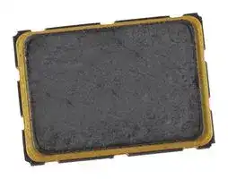
Standard Oscillator, 250MHz, 25ppm, HCMOS, 3.3V, -40°C to 85°C, SMD, 7mm x 5mm
- Manufacturer: RENESAS
- Product type: Standard Oscillators
- SVHC: No SVHC (25-Jun-2025)
- Frequency Nom: 250MHz
- Product Range: XL Series
- Supply Voltage Nom: 3.3V
- Frequency Stability + / -: 25ppm
- Operating Temperature Max: 85°C
- Operating Temperature Min: -40°C
- Oscillator Case / Package: SMD, 7mm x 5mm
- Oscillator Output Compatibility: HCMOS
| Delivery and price | |
|---|---|
| Units per pack | 500 |
| Price | 1.43 € |
| Current stock | 100+ |
| Lead time | 7 days |
XL Family of Low Phase Noise Quartz-based PLL Oscillators

XL Datasheet

## Description

The Renesas XL devices (XO and VCXO options) are ultra-precision crystal oscillators with 750 to 890fs typical phase jitter over 12kHz to 20MHz bandwidth. Available in a wide frequency range from 0.750MHz to 1350MHz, the XL series crystal oscillators utilize a family of proprietary ASICs, with a key focus on noise reduction technologies.

The 3rd order Delta Sigma Modulator reduces noise to the levels that are comparable to traditional Bulk Quartz and SAW oscillators. With short lead-time, low cost, low noise, wide frequency range, excellent ambient performance, the XL devices are an excellent choice over the conventional technologies. The XL (XO option) devices have stabilities as tight as ±20ppm and the XL (VCXO option) devices have ±50ppm APR. Either option provides extremely quick delivery for both standard and custom frequencies.

## Pin Assignments

## Features

- Output types: LVDS, LVPECL, LVCMOS

- Phase jitter (12kHz to 20MHz): 750fs to 890fs typical

- Supply voltage: 2.5V or 3.3V

- Package options:

   - 3.2 × 2.5 × 1.0 mm (not available for VCXO)

   - 5.0 × 3.2 × 1.2 mm

   - 7.0 × 5.0 × 1.3 mm

- Operating temperature: -20°C to +70°C

   - Frequency stability options: ±20, ±25, ±50, or ±100 ppm (XO only)

   - ±50ppm APR (VCXO only)

- Operating temperature: -40°C to +85°C

   - Frequency stability options: ±25, ±50, or ±100 ppm (XO only)

   - ±50ppm APR (VCXO only)

- Operating temperature: -40°C to +105°C (XO only)

## (XO Option)

**NOTE** : To minimize power supply line noise, a 0.01μF bypass capacitor should be placed between VDD (Pin 6) and GND (Pin 3).

   - Frequency stability options: ±50 or ±100 ppm

- kV of 85ppm/volt typical from 0.5VDC to VDD (VCXO only)

   - Better than ±10% linearity for Vc range

**==> picture [88 x 121] intentionally omitted <==**

**----- Start of picture text -----**<br>
6 5 4<br>1 2 3<br>VDD OUT2 OUT<br>E/D / NC NC / E/D GND<br>**----- End of picture text -----**<br>


## (VCXO Option)

**NOTE** : To minimize power supply line noise, a 0.01μF bypass capacitor should be placed between VDD (Pin 6) and GND (Pin 3).

**==> picture [84 x 113] intentionally omitted <==**

**----- Start of picture text -----**<br>
6 5 4<br>1 2 3<br>VDD OUT2 OUT<br>Vc E/D GND<br>**----- End of picture text -----**<br>


©2021 Renesas Electronics Corporation

1

January 19, 2021

XL Datasheet

## Pin Descriptions

## Table 1.  XO Pin Description

|**Number**|**Name**|**Description**|
|---|---|---|
|1|E/D<br>NC|Enable/Disable[a][b]<br>No connect|
|2|NC<br>E/D|No connect<br>Enable/Disable[a][b]|
|3|GND|Connect to ground|
|4|OUT|Output|
|5|OUT2|Complementary output[c]|
|6|VDD|Supply voltage|


- [a] Pulled high internally.

## Table 2.  VCXO Pin Description

|**Number**|**N**~~**am**~~**e**|**Description**|
|---|---|---|
|1|Vc|Voltage control|
|2|E/D|Enable/Disable[a][b]|
|3|GND|Connect to ground|
|4|OUT|Output|
|5|OUT2|Complementary output (NC LVCMOS)|
|6|VDD|Supply voltage|


[a] Pulled high internally.

[b] Low = output disabled.

See Ordering Information (VCXO) for more details.

- [b] Low = output disabled.

[c] Do not connect for LVCMOS. For XLVCMOS, both OUT and OUT2 are ON and in opposite phase.

See Ordering Information (XO) for more details.

©2021 Renesas Electronics Corporation

2

January 19, 2021

XL Datasheet

## Contents

Description . . . . . . . . . . . . . . . . . . . . . . . . . . . . . . . . . . . . . . . . . . . . . . . . . . . . . . . . . . . . . . . . . . . . . . . . . . . . . . . . . . . . . . . . . . . . . . . . . . . . . . 1 Pin Assignments. . . . . . . . . . . . . . . . . . . . . . . . . . . . . . . . . . . . . . . . . . . . . . . . . . . . . . . . . . . . . . . . . . . . . . . . . . . . . . . . . . . . . . . . . . . . . . . . . . 1 (XO Option) . . . . . . . . . . . . . . . . . . . . . . . . . . . . . . . . . . . . . . . . . . . . . . . . . . . . . . . . . . . ~~.~~ . . . . . . . . . . . . . . . . . . . . . . . . . . . . . . . . . . . . . 1 (VCXO Option)  . . . . . . . . . . . . . . . . . . . . . . . . . . . . . . . . . . . . . . . . . . . . . . . . . . . . . . . . . . . . . . . . . . . . . . . . . . . . . . . . . . . . . . . . . . . . . . 1 Features . . . . . . . . . . . . . . . . . . . . . . . . . . . . . . . . . . . . . . . . . . . . . . . . . . . . . . . . . . . . . . . . . . . . . . . . . . . . . . . . . . . . . . . . . . . . . . . . . . . . . . . . 1 Pin Descriptions . . . . . . . . . . . . . . . . . . . . . . . . . . . . . . . . . . . . . . . . . . . . . . . . . . . . . . . . . . . . . . . . . . . . . . . . . . . . . . . . . . . . . . . . . . . . . . . . . . 2 Absolute Maximum Ratings . . . . . . . . . . . . . . . . . . . . . . . . . . . . . . . . . . . . . . . . . . . . . . . . . . . . . . . . . . . . . . . . . . . . . . . . . . . . . . . . . . . . . . . . . 4 ESD Compliance . . . . . . . . . . . . . . . . . . . . . . . . . . . . . . . . . . . . . . . . . . . . . . . . . . . . . . . . . . . . . . . . . . . . . . . . . . . . . . . . . . . . . . . . . . . . . . . . . 4 Mechanical Testing  . . . . . . . . . . . . . . . . . . . . . . . . . . . . . . . . . . . . . . . . . . . . . . . . . . . . . . . . . . . . . . . . . . . . . . . . . . . . . . . . . . . . . . . . . . . . . . . 4 Solder Reflow Profile . . . . . . . . . . . . . . . . . . . . . . . . . . . . . . . . . . . . . . . . . . . . . . . . . . . . . . . . . . . . . . . . . . . . . . . . . . . . . . . . . . . . . . . . . . . . . . 4 DC Electrical Characteristics . . . . . . . . . . . . . . . . . . . . . . . . . . . . . . . . . . . . . . . . . . . . . . . . . . . . . . . . . . . . . . . . . . . . . . . . . . . . . . . . . . . . . . . . 5 AC Electrical Characteristics . . . . . . . . . . . . . . . . . . . . . . . . . . . . . . . . . . . . . . . . . . . . . . . . . . . . . . . . . . . . . . . . . . . . . . . . . . . . . . . . . . . . . . . . 8 Output Waveforms – LVDS . . . . . . . . . . . . . . . . . . . . . . . . . . . . . . . . . . . . . . . . . . . . . . . . . . . . . . . . . . . . . . . . . . . . . . . . . . . . . . . . . . . . . . . . 11 Output Waveforms – LVPECL . . . . . . . . . . . . . . . . . . . . . . . . . . . . . . . . . . . . . . . . . . . . . . . . . . . . . . . . . . . . . . . . . . . . . . . . . . . . . . . . . . . . . . 11 Output Waveforms – LVCMOS  . . . . . . . . . . . . . . . . . . . . . . . . . . . . . . . . . . . . . . . . . . . . . . . . . . . . . . . . . . . . . . . . . . . . . . . . . . . . . . . . . . . . . 12 Package Outline Drawings . . . . . . . . . . . . . . . . . . . . . . . . . . . . . . . . . . . . . . . . . . . . . . . . . . . . . . . . . . . . . . . . . . . . . . . . . . . . . . . . . . . . . . . . . 13 Marking Diagrams  . . . . . . . . . . . . . . . . . . . . . . . . . . . . . . . . . . . . . . . . . . . . . . . . . . . . . . . . . . . . . . . . . . . . . . . . . . . . . . . . . . . . . . . . . . . . . . . 13 Ordering Information (XO) . . . . . . . . . . . . . . . . . . . . . . . . . . . . . . . . . . . . . . . . . . . . . . . . . . . . . . . . . . . . . . . . . . . . . . . . . . . . . . . . . . . . . . . . . 14 Ordering Information (VCXO). . . . . . . . . . . . . . . . . . . . . . . . . . . . . . . . . . . . . . . . . . . . . . . . . . . . . . . . . . . . . . . . . . . . . . . . . . . . . . . . . . . . . . . 14 Revision History . . . . . . . . . . . . . . . . . . . . . . . . . . . . . . . . . . . . . . . . . . . . . . . . . . . . . . . . . . . . . . . . . . . . . . . . . . . . . . . . . . . . . . . . . . . . . . . . . 15

©2021 Renesas Electronics Corporation

3

January 19, 2021

XL Datasheet

## Absolute Maximum Ratings

Stresses above the ratings listed below can cause permanent damage to the device. These ratings, which are standard values for Renesas commercially rated parts, are stress ratings only. Functional operation of the device at these or any other conditions above those indicated in the operational sections of the specifications is not implied. Exposure t ~~o~~ absolute maximum rating conditions for extended periods can affect product reliability. Electrical parameters are guaranteed only over the recommended operating temperature range.

Table 3.  Absolute Maximum Ratings

|**Item**|**Rating**|**Rating**|**Rating**|**Rating**|**Rating**||
|---|---|---|---|---|---|---|
|VDD|-0.5 to +5.0V||||||
|E/D|-0.5V to VDD+ 0.5V||||||
|OUT|-0.5V to VDD+ 0.5V||||||
|Storage Temperature|-55°C to 125°C||||||
|Maximum Junction Temperature|125°C||||||
|Core Current|65mA maximum||||||
|Theta JA|JU6<br>7.0 × 5.0 × 1.3 mm|75.9 °C/W|JS6<br>5.0 × 3.2 × 1.2 mm|89.6 °C/W|JX6<br>3.2 × 2.5 × 1.0 mm|94.7 °C/W|
|Theta JB||48.6°C/W||54.3 °C/W||66.8 °C/W|


## ESD Compliance

## Table 4.  ESD Compliance

|ESD Compliance<br>Table 4.  ESD Compliance||
|---|---|
|Human Body Model (HBM|1000V|
|Machine Model (MM)|150V|


## Mechanical Testing

## Table 5.  Mechanical Testing

|**Parameter**|**Test Method**|
|---|---|
|Mechanical Shock|Drop from 75cm to hardwood surface–3 times.|
|Mechanical Vibration|10–55Hz, 1.5mm amplitude, 1 minute sweep; 2 hours each in 3 directions (X, Y, Z).|
|High Temperature Burn-in|Under power at 125°C for 2000 hours.<br>|
|Hermetic Seal|He pressure: 4 ±1kgf/cm22 hour soak.|


## Solder Reflow Profile

**==> picture [403 x 165] intentionally omitted <==**

**----- Start of picture text -----**<br>
tP 10 seconds Max within<br>5°C of 260°C peak<br>260°C<br>Ramp up 3°C/s Max<br>225°C Ramp down not<br>50 ±10  to exceed 6°C/s<br>180°C seconds<br>above 225°C<br>reflow area<br>160°C 120 ±20 seconds<br>in pre-heating<br>area<br>25°C<br>400 seconds MAX from +25°C to 260°C peak<br>**----- End of picture text -----**<br>


©2021 Renesas Electronics Corporation

January 19, 2021

4

XL Datasheet

## DC Electrical Characteristics

## Table 6.  3.3V IDD DC Electrical Characteristics

VDD = 3.3V ±5%, TA = -20°C to +70°C; -40°C to +85°C, -40°C to +105°C.

|**Symbol**|**Parameter**|**Output Type**|**Conditions**|**Minimum**|**Typical**|**Maximum**|**Units**|
|---|---|---|---|---|---|---|---|
|IDD|Power Supply Current|LVDS|0.75MHz to 40MHz.<br>40+MHz to 220MHz.<br>220+MHz to 630MHz.<br>630+MHz to 1350MHz.|—|32|37|mA|
|||||—|40|47||
|||||—|49|57||
|||||—|72|100||
|||LVPECL[a]|0.75MHz to 40MHz.<br>40+MHz to 220MHz.<br>220+MHz to 630MHz.<br>630+MHz to 1350MHz.|—|26|31||
|||||—|38|45||
|||||—|56|64||
|||||—|96|120||
|||LVCMOS|0.75MHz to 20MHz.<br>20+MHz to 50MHz.<br>50+MHz to 130MHz.<br>130+MHz to 200MHz.<br>200+MHz to 250MHz.|—|27|32||
|||||—|32|35||
|||||—|43|47||
|||||—|48|55||
|||||—|48|60||


[a] Without termination resistors.

## Table 7.  2.5V IDD DC Electrical Characteristics

VDD = 2.5V ±5%, TA = -20°C to +70°C; -40°C to +85°C, -40°C to +105°C.

|**Symbol**|**Parameter**|**Output Type**|**Conditions**|**Minimum**|**Typical**|**Maximum**|**Units**|
|---|---|---|---|---|---|---|---|
|IDD|Power Supply Current|LVDS|0.75MHz to 20MHz.|—|24|26|mA|
||||20+MHz to 220MHz.|—|29|34||
||||220+MHz to 630MHz.|—|36|44||
||||630+MHz to 1000MHz.|—|46|65||
|||LVPECL[a]|0.75MHz to 20MHz.|—|20|33||
||||20+MHz to 220MHz.|—|28|41||
||||220+MHz to 630MHz.|—|41|63||
||||630+MHz to 1000MHz.|—|56|72||
|||LVCMOS|0.75MHz to 20MHz.|—|17|22||
||||20+MHz to 50MHz.|—|23|25||
||||50+MHz to 100MHz.|—|28|29||
||||100+MHz to 130MHz.|—|30|32||
||||130+MHz to 160MHz.|—|32|35||
||||160+MHz to 180MHz.|—|33|37||


[a] Without termination resistors.

©2021 Renesas Electronics Corporation

January 19, 2021

5

XL Datasheet

## Table 8.  LVDS DC Electrical Characteristics

VDD = 3.3V, 2.5V ±5%, TA = -20°C to +70°C; -40°C to +85°C, -40°C to +105°C. Below are guaranteed for listed standard frequencies.

|**Symbol**|**Parameter**|**Conditions**|**Minimum**|**Typical**|**Maximum**|**Units**|
|---|---|---|---|---|---|---|
|VOD|Differential Output Voltage|VDD= 3.3V ±5%.|—|—|0.6|V|
|||VDD= 2.5V ±5%.|—|—|0.4||
|VOS|Output Offset Voltage|VDD= 3.3V ±5%.|—|—|1.3||
|||VDD= 2.5V ±5%.|—|—|1.25||
|VIH|Enable/Disable Input High Voltage<br>(Output enabled)|—|70% VDD|—|—||
|VIL|Enable/Disable Input Low Voltage<br>(Output disabled)|—|—|—|30% VDD||


## Table 9.  LVPECL DC Electrical Characteristics

VDD = 3.3V, 2.5V ±5%, TA = -20°C to +70°C; -40°C to +85°C, -40°C to +105°C. Below are guaranteed for listed standard frequencies.

|**Symbol**|**Parameter**|**Conditions**|**Minimum**|**Typical**|**Maximum**|**Units**|
|---|---|---|---|---|---|---|
|VOD|Differential Output Voltage|VDD= 3.3V ±5%.|2.055||2.405|V|
|||VDD= 2.5V ±5%.|—|1.4|—||
|VOS|Output Offset Voltage|VDD= 3.3V ±5%.|1.305||1.65||
|||VDD= 2.5V ±5%.|—|0.68|—||
|VIH|Enable/Disable Input High Voltage<br>(Output enabled)|—|70% VDD|—|—||
|VIL|Enable/Disable Input Low Voltage<br>(Output disabled)|—|—|—|30% VDD||


©2021 Renesas Electronics Corporation

6

January 19, 2021

XL Datasheet

## Table 10.  LVCMOS DC Electrical Characteristics

VDD = 3.3V, 2.5V ±5%, TA = -20°C to +70°C; -40°C to +85°C, -40°C to +105°C. Below are guaranteed for listed standard frequencies.

|**Symbol**|**Parameter**|**Conditions**|**Conditions**|**Minimum**|**Typical**|**Maximum**|**Units**|
|---|---|---|---|---|---|---|---|
|VOH|Output High Voltage|VDD= 3.3V ±5%.|0.75MHz to 150MHz.|90% VDD|—|—|V|
||||150+MHz to 250MHz.|80% VDD|—|—||
|||VDD= 2.5V ±5%.|0.75MHz to 160MHz.|90% VDD|—|—||
||||160+MHz to 180MHz.|80% VDD|—|—||
|VOL|Output Low Voltage|VDD= 3.3V ±5%.|0.75MHz to 150MHz.|—|—|10% VDD||
||||150+MHz to 250MHz.|—|—|20% VDD||
|||VDD= 2.5V ±5%.|0.75MHz to 160MHz.|—|—|10% VDD||
||||160+MHz to 180MHz.|—|—|20% VDD||
|VIH|Enable/Disable Input High Voltage<br>(Output enabled)|—|—|70% VDD|—|—||
|VIL|Enable/Disable Input Low Voltage<br>(Output disabled)|—|—|—|—|30% VDD||


©2021 Renesas Electronics Corporation

January 19, 2021

7

XL Datasheet

## AC Electrical Characteristics

## Table 11.  3.3V AC Electrical Characteristics

VDD = 3.3V ±5%, TA = -20°C to +70°C; -40°C to +85°C, -40°C to +105°C.

|**Symbol**|**Parameter**|**Test Condition**|**Test Condition**|**Minimum**|**Typical**|**Maximum**|**Units**|
|---|---|---|---|---|---|---|---|
|F|Output Frequency Range|LVDS.||0.75|—|1350|MHz|
|||LVPECL.||0.75|—|1350||
|||LVCMOS.||0.75|—|250||
||Frequency Stability|Temperature = -20°C to +70°C.||±20|—|±100|ppm|
|||Temperature = -40°C to +85°C.||±25|—|±100|ppm|
|||Temperature = -40°C to +105°C.||±50|—|±100|ppm|
||Aging (1st year)|TA= 25°C.||—|—|±3|ppm|
||Aging (10 years)|TA= 25°C.||—|—|±10|ppm|
||Output Load|LVDS.|Differential.|—|100|—|Ω|
|||LVPECL.|VDD- 2.0V.|—|50|—||
|||LVCMOS.|To GND.|—|15|—|pF|
|TST|Start-up Time|Output valid time after VDDmeets minimum<br>specified level.||—|—|10|ms|
|tR|Output Rise Time|LVDS.|20% to 80% Vpp.|—|—|400|ps|
|||LVPECL.||—|—|400||
|||LVCMOS.|10% to 90% VDD.|—|—|3|ns|
|tF|Output Fall Time|LVDS.|80% to 20% Vpp.|—|—|400|ps|
|||LVPECL.||—|—|400||
|||LVCMOS.|90% to 10% VDD.|—|—|3|ns|
|ODC|Output Clock Duty Cycle|LVDS.||45|—|55|%|
|||LVPECL.||45|—|55||
|||LVCMOS.|FOUT<<br>62.5MHz.|45|—|55||
||||FOUT> 62.5MHz.|40|—|60||
|TOE|Output Enable/ Disable Time||—|—|—|100|ns|
|JPER|Period Jitter, RMS|LVDS.||—|3|—|ps|
|||LVPECL.||—|5.8|—||
|||LVCMOS.|FOUT= 125MHz.|—|5|—||
|RJ|Random Jitter|LVDS.||—|1.3|—|ps|
|||LVPECL.||—|1.29|—||
|||LVCMOS.|FOUT= 125MHz.|—|0.6|—||
|DJ|Deterministic Jitter|LVDS.||—|5.8|—|ps|
|||LVPECL.||—|9.3|—||
|||LVCMOS.|FOUT= 125MHz.|—|10|—||


©2021 Renesas Electronics Corporation

8

January 19, 2021

XL Datasheet

## Table 11.  3.3V AC Electrical Characteristics (Cont.)

VDD = 3.3V ±5%, TA = -20°C to +70°C; -40°C to +85°C, -40°C to +105°C.

|**Symbol**|**Parameter**|**Test Condition**|**Test Condition**|**Minimum**|**Typical**|**Maximum**|**Units**|
|---|---|---|---|---|---|---|---|
|TJ|Total Jitter|LVDS.||—|23.6|—|ps|
|||LVPECL.||—|27.7|—||
|||LVCMOS.|FOUT= 125MHz.|—|19|—||
|fJITTER|Phase Jitter (12kHz–20MHz)|LVDS.||—|890|—|fs|
|||LVPECL.||—|860|—||
|||LVCMOS.|FOUT= 125MHz.|—|750|—||


## Table 12.  2.5V AC Electrical Characteristics

VDD = 2.5V ±5%, TA = -20°C to +70°C; -40°C to +85°C, -40°C to +105°C.

|**Symbol**|**Parameter**|**Test Condition**|**Test Condition**|**Minimum**|**Typical**|**Maximum**|**Units**|
|---|---|---|---|---|---|---|---|
|F|Output Frequency Range|LVDS.||0.75|—|1000|MHz|
|||LVPECL.||0.75|—|1000||
|||LVCMOS.||0.75|—|180||
||Frequency Stability|Temperature = -20°C to +70°C.||±20|—|±100|ppm|
|||Temperature = -40°C to +85°C.||±25|—|±100|ppm|
|||Temperature = -40°C to +105°C.||±50|—|±100|ppm|
||Aging (1st year)|TA= 25°C.||—|—|±3|ppm|
||Aging (10 years)|TA= 25°C.||—|—|±10|ppm|
||Output Load|LVDS.|Differential.|—|100|—|Ω|
|||LVPECL.|VDD- 2.0V.|—|50|—||
|||LVCMOS.|To GND.|—|15|—|pF|
|TST|Start-up Time|Output valid time after VDDmeets minimum<br>specified level.||—|—|10|ms|
|tR|Output Rise Time|LVDS.|20% to 80% Vpp.|—|—|400|ps|
|||LVPECL.||—|—|400||
|||LVCMOS.|10% to 90% VDD.|—|—|3.5|ns|
|tF|Output Fall Time|LVDS.|80% to 20% Vpp.|—|—|400|ps|
|||LVPECL.||—|—|400||
|||LVCMOS.|90% to 10% VDD.|—|—|3|ns|
|ODC|Output Clock Duty Cycle|LVDS.||45|—|55|%|
|||LVPECL.||45|—|55||
|||LVCMOS.||45|—|55||
|TOE|Output Enable/ Disable Time|—||—|—|100|ns|


©2021 Renesas Electronics Corporation

9

January 19, 2021

XL Datasheet

## Table 12.  2.5V AC Electrical Characteristics (Cont.)

VDD = 2.5V ±5%, TA = -20°C to +70°C; -40°C to +85°C, -40°C to +105°C.

|**Symbol**|**Parameter**|**Test Condition**|**Test Condition**|**Minimum**|**Typical**|**Maximum**|**Units**|
|---|---|---|---|---|---|---|---|
|JPER|Period Jitter, RMS|LVDS.||—|4|—|ps|
|||LVPECL.||—|5.12|—||
|||LVCMOS.|FOUT= 125MHz.|—|3.3|—||
|RJ|Random Jitter|LVDS.||—|1.4|—|ps|
|||LVPECL.||—|1.36|—||
|||LVCMOS.|FOUT= 125MHz.|—|1.3|—||
|DJ|Deterministic Jitter|LVDS.||—|9.2|—|ps|
|||LVPECL.||—|10|—||
|||LVCMOS.|FOUT= 125MHz.|—|6.7|—||
|TJ|Total Jitter|LVDS.||—|29.2|—|ps|
|||LVPECL.||—|29.3|—||
|||LVCMOS.|FOUT= 125MHz.|—|25.6|—||
|fJITTER|Phase Jitter (12kHz–20MHz)|LVDS.||—|1040|—|fs|
|||LVPECL.||—|1200|—||
|||LVCMOS.|FOUT= 125MHz.|—|850|—||


Notes for all AC Electrical Characteristics tables:

1 All jitter values provided at 156.25MHz, unless noted otherwise.

©2021 Renesas Electronics Corporation

10

January 19, 2021

XL Datasheet

## Output Waveforms – LVDS

## **Output Levels/Rise Time/Fall Time Measurements**

**==> picture [406 x 271] intentionally omitted <==**

**----- Start of picture text -----**<br>
TR TF<br>OUTPUT 2<br>20% to 80% VPP 50% VPP VOS VOD<br>OUTPUT 1<br>Oscillator Symmetry<br>Ideally, Symmetry should be 50/50 for ½ period –Other expressions are 45/55 or 55/45<br>OUTPUT 2 VOH<br>50% VPP<br>OUTPUT 1 VOL<br>½ Period<br>Period<br>**----- End of picture text -----**<br>


## Output Waveforms – LVPECL

## **Rise Time/Fall Time Measurements**

**==> picture [346 x 253] intentionally omitted <==**

**----- Start of picture text -----**<br>
TR TF<br>OUTPUT 2 VOH<br>20% to 80% VPP<br>OUTPUT 1 VOL<br>Oscillator Symmetry<br>OUTPUT 2 VOH<br>50% VPP<br>OUTPUT 1 VOL<br>½ Period<br>Period<br>**----- End of picture text -----**<br>


©2021 Renesas Electronics Corporation

11

January 19, 2021

XL Datasheet

## Output Waveforms – LVCMOS

©2021 Renesas Electronics Corporation

12

January 19, 2021

XL Datasheet

## Package Outline Drawings

The package outline drawings (JS6, JX6, JU6) are appended at the end of this document. The package information is the most current data available.

## Marking Diagrams

## **JX6 3.2 × 2.5 mm Package Option** (example based on XLH320010.000000I)

## ▪ Line 1:

- “010” denotes last three digits to the left of the decimal point as shown in the above example. This number will vary depending upon the frequency value selected in the orderable part number.

- “YW” denotes the last digit of the year and work week the part was assembled.

## **JS6 5.0 × 3.2 mm Package Option** (example based on XLH536210.380000I)

## ▪ Line 1:

- “XL” = family; “H” = output type; “5” = package size; “3” = voltage; “6” = precision level. This number will vary depending upon the output type, voltage, and precision values selected in the orderable part number.

## ▪ Line 2:

- “210” denotes last three digits to the left of the decimal point as shown in the above example. This number will vary depending upon the frequency value selected in the orderable part number.

- “YW” denotes the last digit of the year and work week the part was assembled.

## **JU6 7.0 × 5.0 mm Package Option** (example based on XLH735004.915200X)

## ▪ Line 1:

- “XL” = family; “H” = output type; “7” = package size; “3” = voltage; “5” = precision level. This number will vary depending upon the output type, voltage, and precision values selected in the orderable part number.

## ▪ Line 2:

- “004” denotes last three digits to the left of the decimal point as shown in the above example. This number will vary depending upon the frequency value selected in the orderable part number.

- “YW” denotes the last digit of the year and work week the part was assembled.

©2021 Renesas Electronics Corporation

13

January 19, 2021

XL Datasheet

## Ordering Information (XO)

||||||||||||||||||||
|---|---|---|---|---|---|---|---|---|---|---|---|---|---|---|---|---|---|---|
|||**XL**|**L**||**5**||||**3**|||**5**||**125.000000**||**I**|||
||Family and ASIC||Output Type||Package||||Voltage|||Precision||Frequency|Temperature Range||||
||||||||||||||||||||
||||||||||||||||||||
||||||||||||||||||||
||||||||||**2:**2.5 VDC ±5%|||||||**I:**Industrial range: ‐ 40 to +85 °C|||
||||||||||**3:**3.3 VDC ±5%|||||||**K:**Extended industrial range : ‐40 to +105 °C|||
|||||||||||||||||**X:**Extended commercial range : ‐20 to +70 °C|||
||||||**3:**3.2 x 2.5 mm||||||||||||||
||||||**5:**5.0 x 3.2 mm||||||||||||||
||||||**7:**7.0 x 5.0 mm|||||||||**125.000000  listed in MHz**|||**as example**||
|||||||||||||||3 digits before decimal and   6 digits after decimal|||||
|||**H:** LVCMOS Enable/Disable Pin 1||||||||||||**000.750000  to 000.999999**75kHz to 999.999kHz|||||
|||**J:**LVCMOS Enable/Disable Pin 2||||||||||||**001.000000  to 009.999999**1MHz to 9.999999MHz|||||
|||**L:**LVDS Enable/Disable Pin 1||||||||||||**010.000000  to 099.999999**10MHz to 99.999999MHz|||||
|||**M:**LVDS Enable/Disable Pin 2||||||||||||**100.000000  to 999.999999**100MHz to 999.999999MHz|||||
|||**P:**LVPECL Enable/Disable Pin 1|||||||||||||||||
|||**Q:**LVPECL Enable/Disable Pin 2||||||||||||**A00.000000**||**to A99.999999**1000MHz to 1099.999MHz|||
|||**X:**XLVCMOS Comp HCMOS Enable/Disable Pin 1*||||||||||||**B00.000000**||**to B99.999999**1100MHz to 1199.999MHz|||
|||**Y:**XLVCMOS Comp HCMOS Enable/Disable Pin 2*||||||||||||**C00.000000  to C99.999999**1200MHz to 1299.999MHz|||||
|||* XLVCMOS: Complimentary HCMOS where both||||||||||||**D00.000000**||**to D50.000000**1300MHz to 1350MHz|||
|||outputs are ON and in opposite phase.|||||||||||||||||
|||||||||||||||**0:**±100ppm**|||||
||**XL:**|1,000 fs jitter||||||||||||**5:**±50ppm**|||||
|||||||||||||||**6:**±25ppm|||||
|||||||||||||||**8:**±20ppm*|||||
||||||||||||||* ±20ppm for X (‐20° to +70°C) only.||||||
||||||||||||||** ±100ppm and ±50ppm for K (‐40°C to +105°C) only.||||||


## Ordering Information (VCXO)

**==> picture [546 x 228] intentionally omitted <==**

**----- Start of picture text -----**<br>
XL L 5 3 125.000000 I<br>V<br>Family and ASIC Output Type Package Voltage Frequency Temperature Range<br> 2:  2.5 VDC ±5%  I:  Industrial range: ‐ 40 to +85 °C<br> 3:  3.3 VDC ±5%  X:  Extended commercial range : ‐20 to +70 °C<br> 5:  5.0 x 3.2 mm<br> 7:  7.0 x 5.0 mm 125.000000  listed in MHz as example<br>3 digits before decimal and   6 digits after decimal<br>000.750000  to 000.999999   75kHz to 999.999kHz<br> H: LVCMOS Enable/Disable 001.000000  to 009.999999   1MHz to 9.999999MHz<br> L:  LVDS Enable/Disable 010.000000  to 099.999999   10MHz to 99.999999MHz<br> P:  LVPECL Enable/Disable 100.000000  to 999.999999   100MHz to 999.999999MHz<br>A00.000000  to A99.999999   1000MHz to 1099.999MHz<br> XL:   1,000 fs jitter<br>B00.000000  to B99.999999   1100MHz to 1199.999MHz<br>C00.000000  to C99.999999   1200MHz to 1299.999MHz<br>D00.000000  to D50.000000   1300MHz to 1350MHz<br>  V:  VCXO option<br>**----- End of picture text -----**<br>


©2021 Renesas Electronics Corporation

14

January 19, 2021

XL Datasheet

## Revision History

|**Revision Date**|**Description of Change**|
|---|---|
|January 19, 2021|▪Removed 4-pin package description table, figure, and pac~~k~~age drawing references.<br>▪Added footnote for pin 5 in Table 1.<br>▪Added footnote under “Output Type” in XO Ordering Information.|
|January 12, 2021|Added Marking Diagrams section and updated Package Outline Drawings links.|
|October 27, 2020|Added pin counts to Output Type in XO ordering table.|
|September 21, 2020|Added typical IDD to tables. Added more frequency ranges to IDD tables. Updated H to be LVCMOS in order<br>code.|
|April 27, 2020|Updated ODC parameter. 2nd LVCMOS row to be changed from <= to > 62.5 MHz.|
|September 7, 2018|Updated frequency stability options value from ±20ppm to ±25ppm for -40°C to +85°C XO only.|
|June 25, 2018|▪Updated Package Outline Drawings section.|
|May 4, 2018|▪Added XO and VCXO options.<br>▪Updated description and Features sections.<br>▪Updated Package Outline Drawings section.<br>▪Added VCXO Ordering Information decoder diagram.|
|January 12, 2018|Initial release.|


©2021 Renesas Electronics Corporation

15

January 19, 2021

**==> picture [32 x 129] intentionally omitted <==**

**==> picture [82 x 59] intentionally omitted <==**

**==> picture [540 x 775] intentionally omitted <==**

**==> picture [37 x 83] intentionally omitted <==**

**==> picture [103 x 69] intentionally omitted <==**

**==> picture [82 x 119] intentionally omitted <==**

**==> picture [72 x 57] intentionally omitted <==**

**==> picture [77 x 51] intentionally omitted <==**

**==> picture [54 x 81] intentionally omitted <==**

**==> picture [50 x 120] intentionally omitted <==**

**==> picture [37 x 120] intentionally omitted <==**

## **IMPORTANT NOTICE AND DISCLAIMER**

RENESAS ELECTRONICS CORPORATION AND ITS SUBSIDIARIES (“RENESAS”) PROVIDES TECHNICAL SPECIFICATIONS AND RELIABILITY DATA (INCLUDING DATASHEETS), DESIGN RESOURCES (INCLUDING REFERENCE DESIGNS), APPLICATION OR OTHER DESIGN ADVICE, WEB TOOLS, SAFETY INFORMATION, AND OTHER RESOURCES “AS IS” AND WITH ALL FAULTS, AND DISCLAIMS ALL WARRANTIES, EXPRESS OR IMPLIED, INCLUDING, WITHOUT LIMITATION, ANY IMPLIED WARRANTIES OF MERCHANTABILITY, FITNESS FOR A PARTICULAR PURPOSE, OR NON-INFRINGEMENT OF THIRD PARTY INTELLECTUAL PROPERTY RIGHTS.

These resources are intended for developers skilled in the art designing with Renesas products. You are solely responsible for (1) selecting the appropriate products for your application, (2) designing, validating, and testing your application, and (3) ensuring your application meets applicable standards, and any other safety, security, or other requirements. These resources are subject to change without notice. Renesas grants you permission to use these resources only for development of an application that uses Renesas products. Other reproduction or use of these resources is strictly prohibited. No license is granted to any other Renesas intellectual property or to any third party intellectual property. Renesas disclaims responsibility for, and you will fully indemnify Renesas and its representatives against, any claims, damages, costs, losses, or liabilities arising out of your use of these resources. Renesas' products are provided only subject to Renesas' Terms and Conditions of Sale or other applicable terms agreed to in writing. No use of any Renesas resources expands or otherwise alters any applicable warranties or warranty disclaimers for these products.

(Rev.1.0 Mar 2020)

## **Corporate Headquarters**

TOYOSU FORESIA, 3-2-24 Toyosu, Koto-ku, Tokyo 135-0061, Japan www.renesas.com

## **Contact Information**

For further information on a product, technology, the most up-to-date version of a document, or your nearest sales office, please visit: www.renesas.com/contact/

## **Trademarks**

~~Renesas and the Renesas logo are trademarks of Renesas~~ Electronics Corporation. All trademarks and registered trademarks are the property  of their respective owners.

© 2020 Renesas Electronics Corporation. All rights reserved.
Updated at March 11, 2026
Renesas Electronics is a premier global supplier of advanced semiconductor solutions, driving innovation across automotive, industrial, infrastructure, and Internet of Things (IoT) applications. Recognized for a comprehensive portfolio that spans the entire signal chain, Renesas empowers engineers to design secure, intelligent, and highly efficient embedded systems for a rapidly evolving technological landscape. Our selection of Renesas components features a strong emphasis on precision timing and frequency management solutions. We offer a robust range of standard oscillators, timers, and pulse generators engineered to deliver exceptional accuracy and stability. These reliable clocking devices are essential for synchronizing complex digital operations and ensuring optimal performance in demanding circuit designs. In addition to timing components, our inventory includes essential discrete semiconductors and interface solutions. This encompasses high-performance single MOSFETs and bipolar transistors for efficient power routing, alongside versatile I/O expanders that simplify system connectivity. To support modern wireless integration, we also provide select Renesas RF transceivers, WLAN adaptors, and Bluetooth modules, equipping developers with the critical building blocks needed for advanced communication systems.
About Novapart
Novapart is a B2B electronic component broker specialising in stock shortages and cost reduction. We source hard-to-find parts and identify compliant alternatives across a catalogue of 410,000+ components from 500+ manufacturers.
Learn more →Stock Shortage Specialist
When a component is unavailable, discontinued or has an unacceptable lead time, we tap into our network of vetted European and Asian distributors to source what you need — without compromising on quality or traceability.
Request a quote →Compliant Alternatives
We identify pin-to-pin, electrically equivalent substitutes that meet the same certifications (RoHS, AEC-Q100, REACH) as your original specification — validated against datasheets, not just part numbers. Often at a lower cost.
BOM Analysis service →