
Image not available
Illustrative purposes only

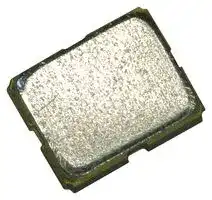
X1G006221000711
Oscillator, 156.25 MHz, HCSL, 2.5 V, SMD, 2mm x 1.6mm, SG2016HGN Series
⚠️ Reference pricing provided. In case of supply shortages, we will connect you with our trusted procurement partners to ensure your project's continuity.
- Manufacturer: EPSON
- Product type: Standard Oscillators
- SVHC: No SVHC (25-Jun-2025)
- Frequency Nom: 156.25MHz
- Product Range: SG2016HGN Series
- Supply Voltage Nom: 2.5V
- Frequency Stability + / -: -
- Operating Temperature Max: 105°C
- Operating Temperature Min: -40°C
- Oscillator Case / Package: SMD, 2mm x 1.6mm
- Oscillator Output Compatibility: HCSL
| Delivery and price | |
|---|---|
| Units per pack | 250 |
| Price | 12.48 € |
| Current stock | 10+ |
| Lead time | 30 days |
Datasheet

## **Crystal Oscillator (SPXO)**

- Package size (2.0 mm × 1.6 mm × 0.63 mm)

- Fundamental mode SPXO

· Output: HCSL

- Reference weight Typ. 7.6 mg

## [ 1 ] Product Number / Product Name / Marking

- (1-1) Product Number / Ordering Code

## **X1G0062210007xx**

Last 2 digits code( **xx** ) defines Quantity.

The standard is "15", 2 000 pcs/Reel.

(1-2)  Product Name / Model Name

## **SG2016HGN  156.250000MHz  DDHPZA**

## [ 2 ] Operating Range

|[ 2 ]2 ]] Operating Rangerating Rangeating Rangeing Rangeg RangeRangeangengege|||||||
|---|---|---|---|---|---|---|
|Parameter|Symbol|Specifications|||Unit|Conditions|
|||Min.|Typ.|Max.|||
|Supply voltage|VCC|2.375|2.5|2.625|V|-|
||GND|0|-|0|V|-|
|Input voltage|VIN|0|-|VCC|V|-|
|Operatingtemperature range|T_use|-40|-|+105|°C|-|
|HCSL load condition|L_HCSL|-|50|-|Ω|Terminated to GND|


## [ 3 ] Frequency Characteristics

|Parameter|Symbol|Specifications|Specifications|Specifications|Unit|Conditions|
|---|---|---|---|---|---|---|
|||Min.|Typ.|Max.|||
|Output frequency|fo|-|156.250000|-|MHz|-|
|Frequencytolerance *1|f_tol|-25|-|+25|×10-6|T_use|


*1 Frequency tolerance includes Initial frequency tolerance, Frequency / temperature characteristics, Frequency / voltage coefficient and aging (10 years, +25 ºC).

[ 4 ] Electrical Characteristics

(Unless stated otherwise [ 2 ] Operating Range)

|Parameter<br>~~a~~|Symbol<br>~~a~~|Specifications<br>~~a~~|Specifications<br>~~a~~|Specifications<br>~~a~~|Unit<br>~~pf~~|Conditions<br>~~pf~~|
|---|---|---|---|---|---|---|
|||Min.<br>~~a~~|Typ.<br>~~a~~|Max.<br>~~a~~|||
|Start-uptime<br>~~a~~|t_str<br>~~GG~~|-<br>~~GG~~|-<br>~~GG~~|10<br>~~GG~~|ms<br>~~GG~~|t = 0 at 90 % Vcc<br>~~GG~~|
|Current consumption<br>~~a~~|ICC|-<br>~~GO~~|-<br>~~GO~~|35<br>~~QO~~|mA<br>~~QO~~||
|Disable current<br>~~a~~<br>~~ee~~|I_dis<br>~~ee~~|-<br>~~GO~~<br>~~ee~~|-<br>~~GO~~|25<br>~~GO~~|mA<br>~~GO~~<br>~~ee~~|OE = GND<br>~~ee~~|
|Output voltage<br>~~ee~~|VOH<br>~~ee~~|0.5<br>~~ee~~|-|0.7|V<br>~~ee~~|~~ee~~|
||VOL<br>~~ee~~<br>~~a~~|-0.15<br>~~ee~~|-|0.15|V<br>~~ee~~|~~ee~~|
|Differential swing<br>~~ee ~~<br>~~a~~|VSW<br> ~~ee ~~|0.7<br> ~~ee~~<br>~~GO~~|-<br>~~GO~~|1.4<br>~~QO~~|V<br>~~ee~~<br>~~QO~~|Differential output peak to peak voltage<br>~~ee~~|
|Rise time / Fall time<br>~~a~~|tr/tf|-<br>~~GO~~|-<br>~~GO~~|0.7<br>~~GO~~|ns<br>~~GO~~|20 % - 80 % of (VOH- VOL)|
|Differential output<br>rise slew rate /fallslew rate|Rr/Rf|2|-|10|V/ns|Between -0.15 V and 0.15 V<br>of differential output|
|Symmetry<br>~~a~~|SYM|45<br>~~GO~~|50<br>~~GO~~<br>~~ee~~|55<br>~~QO~~|%<br>~~QO~~|At output crossing point|
|Input voltage<br>~~ee~~|VIH<br>~~ee~~|70 % Vcc<br>~~ee~~|-<br>~~ee~~<br>~~ee~~|-<br>~~ee~~|V<br>~~ee~~|OE terminal<br>~~ee~~|
||VIL<br>~~ee~~<br>~~es~~|-<br>~~ee~~<br>~~es~~|-<br>~~ee~~<br>~~ee~~<br>~~es~~|30 % Vcc<br>~~ee~~<br>~~es~~|V<br>~~ee~~<br>~~es~~|OE terminal<br>~~ee~~<br>~~es~~|
|Output disable time(OE)<br>~~a~~|tstp_oe|-<br>~~Ge~~|-<br>~~ee~~<br>~~Ge~~|100<br>~~QO~~|ns<br>~~QO~~|OE terminal HIGH → LOW|
|Output enable time(OE)<br>~~po~~|tsta_oe<br>~~po~~|-<br>~~po~~<br>~~GG~~|-<br>~~po~~<br>~~GG~~|500<br>~~po~~<br>~~GG~~|ns<br>~~po~~|OE terminal LOW → HIGH<br>~~po~~|
|Phasejitter<br>~~es~~|tPJ<br>~~es~~|-<br>~~es~~<br>~~GG~~|-<br>~~es~~<br>~~GG~~|70<br>~~es~~<br>~~GG~~|fs<br>~~es~~|Offset freq.: 12 kHz to 20 MHz<br>~~es~~|
|Jitter<br>~~po~~|tC-C<br>~~po~~|-<br>~~GG~~<br>~~po~~<br>~~ee~~|-<br>~~GG~~<br>~~po~~<br>~~ee~~|60<br>~~GG~~<br>~~po~~<br>~~ee~~|ps<br>~~po~~<br>~~ee~~|Cycle to cycle jitter (Peak to Peak)<br>~~po~~<br>~~eee~~|
|PCIe jitter limits<br>for CC architecture<br>~~ee~~|-<br>~~ee~~|-<br>~~ee~~<br>~~ee~~|-<br>~~ee~~<br>~~ee~~|0.1<br>~~ee~~<br>~~ee~~|ps<br>~~ee~~<br>~~ee~~|For PCIe Gen5<br>~~ee~~<br>~~eee~~|
|||-<br>~~ee~~<br>~~ee~~<br>~~se~~|-<br>~~ee~~<br>~~ee~~<br>~~se~~|0.06<br>~~ee~~<br>~~ee~~<br>~~se~~|ps<br>~~ee~~<br>~~ee~~<br>~~se~~|For PCIe Gen6<br>~~ee~~<br>~~eee~~<br>~~se~~|


## **[ For other general specifications, please refer to the attached Full Data Sheet below ]**

1 / 25 Page

2025/12/23

## **Low Phase Jitter Crystal Oscillator: SG2016HGN/SG2520HGN**

## **Features**

- Crystal oscillator (SPXO)

   - 25 MHz to 500 MHz HCSL

- Frequency range (fo):

- Output:

- Supply voltage: 2.5 V Typ. / 3.3 V Typ. ●    Frequency tolerance: ±25 × 10[-6] / ±50 × 10[-6] ●    Operating temperature: -40 °C to +105 °C ● Low phase jitter: 60 fs Typ. (fo = 100 MHz)

- PCIe Gen5, 6 jitter specification compliant

**==> picture [135 x 16] intentionally omitted <==**

**----- Start of picture text -----**<br>
SG2016HGN SG2520HGN<br>2.0  ×  1.6 mm   2.5  ×  2.0 mm<br>**----- End of picture text -----**<br>


## **Applications**

- Communication equipment using PCIe Gen5 or 6 (SSD, Network card, etc)

## **Description**

Epson's  SG2016HGN / SG2520HGN, SG2016HHN / SG2520HHN product family supports HCSL (High Speed Current Steering Logic) and meets timing compliance jitter requirements up to PCIe Gen6. With 90 ps maximum phase jitter, and supporting frequencies from 25 MHz to 500 MHz, the product group covers the system requirements of most networking, data center and communication applications.

## **Outline Drawing and Terminal Assignment**

**==> picture [175 x 8] intentionally omitted <==**

**----- Start of picture text -----**<br>
SG2016HGN                          SG2520HGN<br>**----- End of picture text -----**<br>


## **Typical Performance**

Phase Noise (fo = 100 MHz)

Phase Jitter (12 kHz to 20 MHz): 60 fs Typ.

**==> picture [71 x 67] intentionally omitted <==**

**----- Start of picture text -----**<br>
Pin Connection<br>1 OE/S̅T̅<br>2 N.C. (Open or VCC)<br>3 GND<br>4 OUT<br>5 O̅U̅T̅<br>6 VCC<br>**----- End of picture text -----**<br>


**Spec No : SGxxxxHGN_E_Ver2.0**

**Page 2 / 25**

[ 1 ] Product Number / Product Name

(1-1) Product Number

SG2016HGN: X1G006221xxxx15 SG2520HGN: X1G005891xxxx15

(Please contact Epson for details)

(1-2) Product Name (Standard Form)

SG2016 HGN 100.000000MHz C J G P Z A

`①   ② ③ ④⑤⑥⑦⑧⑨`

`①` Model

`②` Output (H: HCSL) `③` Frequency

`④` Supply voltage `⑥` Operating temperature D 2.5 V Typ. G -40 °C to +85 °C C 3.3 V Typ. H -40 °C to +105 °C

`④` Supply voltage

`⑤` Frequency tolerance `⑤` Frequency tolerance `⑦` Function `⑥` Operating temperature D ±25 × 10[-6] P Output Enable `⑦` Function ~~———~~ J ±50 × 10[-6] ~~———~~ S Standby `⑧` Output disable status (Z: High impedance) `⑨` Output option `⑨` Output option A VSW = 0.7 V to 1.4 V ~~—~~ B VSW = 0.8 V to 1.6 V

## [ 2 ] Absolute Maximum Ratings

|[ 2 ] Absolute Maximum Ratings] Absolute Maximum RatingsAbsolute Maximum Ratingsgss||~~—~~|~~—~~|~~—~~|B<br>VSW = 0.8 V to 1.6 VSW = 0.8 V to 1.6 V= 0.8 V to 1.6 V<br>~~—~~|VSW = 0.8 V to 1.6 VSW = 0.8 V to 1.6 V= 0.8 V to 1.6 V<br>~~—~~|
|---|---|---|---|---|---|---|
|Parameter|Symbol|Specification|||Unit|Conditions|
|||Min.|Typ.|Max.|||
|Maximum supplyvoltage|VCC|-0.3|-|4.0|V||
|Input voltage|Vin|-0.3|-|VCC+ 0.5|V|OE/S̅ T̅  terminal|
|Storage temperature range|T_stg|-55|-|+125|°C||


## [ 3 ] Operating Range

|[ 3 ] Operating Range] Operating RangeOperating Rangeperating Rangeerating Rangeg RangeRangegee|||||||
|---|---|---|---|---|---|---|
|Parameter|Symbol|Specification|||Unit|Conditions|
|||Min.|Typ.|Max.|||
|Supply voltage|VCC|2.375|2.5|2.625|V||
|||3.135|3.3|3.465|V||
|Supplyvoltage|GND|0.0|0.0|0.0|V||
|Operating temperature range|T_use|-40|+25|+85|°C||
|||-40|+25|+105|°C||
|HCSL load condition|L_HCSL|50|||Ω||
|* Power supplystartuptime(0 %VCC→90 %VCC)should be more than 150 μs<br>* A 0.1μF and a 10μF bypass capacitor should be connected between VCCand GND pins located close to the device|||||||


* Power supply startup time (0 %VCC → 90 %VCC) should be more than 150 μs

- A 0.1 μF and a 10 μF bypass capacitor should be connected between VCC and GND pins located close to the device

**Spec No : SGxxxxHGN_E_Ver2.0**

**Page 3 / 25**

|Parameter|Symbol|Specification|Specification|Specification|Unit|Conditions|
|---|---|---|---|---|---|---|
|||Min.|Typ.|Max.|||
|Output frequency*1|fo|25|-|500|MHz||
|Frequency tolerance *2|f_tol|-25|-|+25|×10-6||
|||-50|-|+50|×10-6||
|*1 Please contact Epson for available frequencies|||||||
|*2 Frequencytolerance includes Initial frequencytolerance, Frequency / temperature characteristics, Frequency / voltage coefficient and aging (10 years, +25 °C).|||||||


|Parameter<br>~~**a**~~|Symbol<br>~~ec~~|Specification<br>~~ec~~<br>~~ee~~|Specification<br>~~ec~~<br>~~ee~~|Specification<br>~~ec~~<br>~~ee~~|Unit<br>~~|~~<br>~~ee~~|Conditions<br>~~|~~|
|---|---|---|---|---|---|---|
|||Min.<br>~~ec~~|Typ.<br>~~ec~~|Max.<br>~~ee~~|||
|Startup time<br>~~**a** ~~|t_str<br> ~~ec~~|-<br>~~ec~~<br>~~ee~~|-<br>~~ec~~<br>~~ee~~|10<br>~~ee ~~<br>~~ee~~|ms<br>~~|~~<br> ~~ee~~<br>~~ee~~|t = 0 at 90 % VCC<br>~~|~~<br>~~ee~~|
|Current consumption<br>~~ss~~|ICC<br>~~ss~~|-<br>~~ss~~<br>~~ee~~|-<br>~~ss~~<br>~~ee~~|35<br>~~ss~~<br>~~ee~~|mA<br>~~ss~~<br>~~ee~~|fo ≤ 212 MHz<br>~~ss~~<br>~~ee~~|
|||-<br>~~ss~~<br>~~ee~~<br>~~a~~|-<br>~~ss~~<br>~~ee~~<br>~~a~~|40<br>~~ss~~<br>~~ee~~|mA<br>~~ss~~<br>~~ee~~|fo > 212 MHz<br>~~ss~~<br>~~ee~~|
|Disable current<br>~~a~~|I_dis<br>~~a~~|-<br>~~ee ~~<br>~~ee~~|-<br> ~~ee~~<br>~~ee~~|25<br>~~ee ~~<br>~~ee~~|mA<br> ~~ee~~<br>~~ee~~|OE = GND<br>~~ee~~<br>~~ee~~|
|Stand-by current<br>~~ss~~|I_std<br>~~ss~~|-<br>~~ss~~<br>~~ee~~|-<br>~~ss~~<br>~~ee~~|30<br>~~ss~~<br>~~ee~~|μA<br>~~ss~~<br>~~ee~~|S̅ T̅  = GND, T_use Max. = +85 °C<br>~~ss~~<br>~~ee~~|
|||-<br>~~ss~~<br>~~ee~~<br>~~a~~|-<br>~~ss~~<br>~~ee~~<br>~~a~~|60<br>~~ss~~<br>~~ee~~|μA<br>~~ss~~<br>~~ee~~|S̅ T̅  = GND, T_use Max. = +105 °C<br>~~ss~~<br>~~ee~~|
|Rise time / Fall time<br>~~a~~|tr / tf<br>~~ee~~|-<br>~~ee ~~<br>~~ee~~|-<br> ~~ee~~<br>~~ee~~|0.7<br>~~ee ~~<br>~~ee~~|ns<br> ~~ee~~<br>~~ee~~|20 % - 80 % (VOH- VOL)<br>~~ee~~|
|Differential output<br>rise slew rate /fallslew rate<br>~~ae~~|Rr / Rf<br>~~ae~~<br>~~ee~~|2<br>~~ae~~<br>~~ee~~|-<br>~~ae~~<br>~~ee~~|10<br>~~ae~~<br>~~ee~~|V/ns<br>~~ae~~<br>~~ee~~|Between -0.15 V and 0.15 V of<br>differential output<br>~~ae~~|
|Symmetry<br>~~a~~|SYM<br>~~ee~~<br>~~a~~|45<br>~~ee ~~<br>~~a~~|50<br> ~~ee~~<br>~~a~~|55<br>~~ee ~~<br>~~a~~|%<br> ~~ee~~<br>~~a~~|At output crossing point<br>~~a~~|
|Output voltage|VOH|0.5<br>~~a~~|-<br>~~a~~<br>~~a~~|0.7<br>~~a~~|V<br>~~a~~|Output option: A, fo ≤ 212 MHz<br>~~a~~|
|||0.4<br>~~aa~~|-<br>~~aa~~|0.65<br>~~aa~~|V|Output option: A, fo > 212 MHz|
|||0.6<br>~~a~~|-<br>~~a~~<br>~~a~~|0.8|V|Output option: B, fo ≤ 212 MHz|
|||0.5<br>~~a ~~|-<br> ~~a~~|0.75|V|Output option: B, fo > 212 MHz|
||VOL<br>~~a~~<br>~~ee~~|-0.15<br>~~ee~~|-<br>~~ee~~|0.15<br>~~ee~~|V<br>~~ee~~||
|Differential swing<br>~~Ny~~|VSW<br>~~Ny~~<br>~~ee~~|0.7<br>~~Ny~~<br>~~ee~~|-<br>~~Ny~~<br>~~ee~~|1.4<br>~~Ny~~<br>~~ee~~|V<br>~~Ny~~<br>~~ee~~|Output option: A<br>~~Ny~~|
|||0.8<br>~~Ny~~<br>~~ee~~<br>~~a ~~|-<br>~~Ny~~<br>~~ee~~<br> ~~a~~|1.6<br>~~Ny~~<br>~~ee~~|V<br>~~Ny~~<br>~~ee~~|Output option: B<br>~~Ny~~|
|Input voltage<br>~~sees~~|VIH<br>~~ee~~<br>~~sees~~|70 % VCC<br>~~ee~~<br>~~sees~~|-<br>~~ee ~~<br>~~sees~~|-<br> ~~ee ~~<br>~~sees~~|V<br> ~~ee~~<br>~~sees~~|OE/S̅ T̅  terminal<br>~~sees~~|
||VIL<br>~~sees~~<br>~~a ~~<br>~~ae~~|-<br>~~sees~~<br> ~~a~~<br>~~ee~~|-<br>~~sees~~<br>~~ee~~|30 % VCC<br>~~sees~~<br>~~ee~~|V<br>~~sees~~||
|Output disable time (OE)<br>~~ee~~|tstp_oe<br>~~ee~~<br>~~ae~~<br>~~ee~~|-<br>~~ee~~<br>~~ee~~<br>~~ee~~|-<br>~~ee~~<br>~~ee~~<br>~~ee~~|100<br>~~ee~~<br>~~ee~~<br>~~ee~~|ns<br>~~ee~~<br>~~ee~~|Measured from the time OE pin<br>crosses 30 % VCC<br>~~ee~~|
|Output disable time (ST)<br>~~a~~<br>~~a~~|tstp_st<br>~~ae ~~<br>~~a~~<br>~~ee~~<br>~~ae~~|-<br> ~~ee ~~<br>~~a~~<br>~~ee~~<br>~~ee~~|-<br> ~~ee~~<br>~~a~~<br>~~ee~~<br>~~ee~~|100<br>~~ee~~<br>~~a~~<br>~~ee~~<br>~~ee~~|ns<br>~~a~~<br>~~ee~~<br>~~ee~~|Measured from the time S̅ T̅  pin<br>crosses 30 % VCC<br>~~a~~|
|Output enable time (OE)<br>~~ee~~<br>~~a~~|tsta_oe<br>~~ee~~<br>~~ee~~<br>~~ae~~<br>~~ee~~|-<br>~~ee ~~<br>~~ee~~<br>~~ee~~<br>~~ee~~|-<br> ~~ee~~<br>~~ee~~<br>~~ee~~<br>~~ee~~|500<br>~~ee ~~<br>~~ee~~<br>~~ee~~<br>~~ee~~|ns<br> ~~ee~~<br>~~ee~~<br>~~ee~~<br>~~ee~~|Measured from the time OE pin<br>crosses 70 % VCC<br>~~ee~~|
|Output enable time (ST)<br>~~a~~|tsta_st<br>~~ae ~~<br>~~ee~~|-<br> ~~ee~~<br>~~ee~~|-<br>~~ee ~~<br>~~ee~~|10<br> ~~ee ~~<br>~~ee~~|ms<br> ~~ee~~<br>~~ee~~|Measured from the time S̅ T̅  pin<br>crosses 70 % VCC|
|Phase jitter<br>Offset frequency<br>fo < 50 MHz: 12 kHz to 5 MHz<br>fo ≥ 50 MHz: 12 kHz to 20 MHz|tPJ<br>~~ee~~<br>~~eS~~|-<br>~~ee ~~<br>~~a~~|-<br> ~~ee~~|200<br>~~ee ~~|fs<br> ~~ee~~|fo < 100 MHz|
|||-<br>~~a~~|-<br>~~a~~|90|fs|100 MHz ≤ fo ≤ 156 MHz|
|||-<br>~~aa~~|-<br>~~aa~~|70<br>~~aa~~|fs<br>~~aa~~|156 MHz < fo ≤ 212 MHz|
|||-<br>~~a~~|-<br>~~a~~<br>~~a~~|60|fs|212 MHz < fo ≤ 391 MHz|
|||-<br>~~a~~|-<br>~~a~~|50|fs|fo > 391 MHz|
|Jitter|tp-p<br>~~eS~~|-<br>~~a~~|-<br>~~a~~|60|ps|Peak to Peak Jitter|
||tc-c<br>~~eS~~<br>~~a~~<br>~~se~~|-<br>~~a ~~<br>~~se~~|-<br> ~~a~~|60|ps<br>~~ee~~|Cycle to cycle jitter<br>(Peak to Peak)<br>~~ee~~|
|PCIe jitter limits for CC architecture<br>~~es~~|-<br>~~es~~<br>~~se~~|-<br>~~es~~<br>~~se~~|-<br>~~es~~|0.1<br>~~es~~|ps<br>~~es~~<br>~~ee~~|For PCIe Gen5<br>~~es~~<br>~~ee~~|
|||-<br>~~es~~<br>~~se~~<br>~~a~~|-<br>~~es~~|0.06<br>~~es~~|ps<br>~~es~~<br>~~ee~~|For PCIe Gen6<br>~~es~~<br>~~ee~~|


**Spec No : SGxxxxHGN_E_Ver2.0**

**Page 4 / 25**

[ 7 ] Typical Performance Characteristics  (For reference only)

The following data shows typical performance characteristics (7-1) Frequency / Temperature Characteristics

fo = 156.25 MHz,  -40 °C to +105 °C, reference at nominal frequency n = 50 pcs

(7-2) Current Consumption

Output option:A, Frequency Dependency

Output option:B, Frequency Dependency

Output option:A, VCC = 2.25 V, Temp. Characteristic

Output option:A, VCC = 3.63 V, Temp. Characteristic

Output option:B, VCC = 2.25 V, Temp. Characteristic

Output option:B, VCC = 3.63 V, Temp. Characteristic

**Spec No : SGxxxxHGN_E_Ver2.0**

**Page 5 / 25**

(7-3) Rise Time / Fall Time Temperature Characteristic fo = 25 MHz

Output option:A, Rise Time

Output option:B, Rise Time

fo = 100 MHz Output option:A, Rise Time

Output option:B, Rise Time

**==> picture [108 x 10] intentionally omitted <==**

**----- Start of picture text -----**<br>
Output option:A, Fall Time<br>**----- End of picture text -----**<br>


Output option:B, Fall Time

## Output option:A, Fall Time

Output option:B, Fall Time

**Spec No : SGxxxxHGN_E_Ver2.0**

**Page 6 / 25**

fo = 212.5 MHz Output option:A, Rise Time

## Output option:B, Rise Time

fo = 491.52 MHz Output option:A, Rise Time

## Output option:B, Rise Time

**==> picture [108 x 10] intentionally omitted <==**

**----- Start of picture text -----**<br>
Output option:A, Fall Time<br>**----- End of picture text -----**<br>


Output option:B, Fall Time

## Output option:A, Fall Time

Output option:B, Fall Time

**Spec No : SGxxxxHGN_E_Ver2.0**

**Page 7 / 25**

(7-4) Differential Output Rise Slew Rate / Fall Slew Rate Temperature Characteristic fo = 25 MHz

Output option:A, Rise Slew Rate

## Output option:A, Fall Slew Rate

Output option:B, Rise Slew Rate

Output option:B, Fall Slew Rate

## fo = 100 MHz

Output option:A, Rise Slew Rate

## Output option:A, Fall Slew Rate

Output option:B, Rise Slew Rate

Output option:B, Fall Slew Rate

**Spec No : SGxxxxHGN_E_Ver2.0**

**Page 8 / 25**

## fo = 212.5 MHz

## Output option:A, Rise Slew Rate

Output option:B, Rise Slew Rate

**==> picture [129 x 10] intentionally omitted <==**

**----- Start of picture text -----**<br>
Output option:A, Fall Slew Rate<br>**----- End of picture text -----**<br>


Output option:B, Fall Slew Rate

## fo = 491.52 MHz

Output option:A, Rise Slew Rate

Output option:B, Rise Slew Rate

## Output option:A, Fall Slew Rate

Output option:B, Fall Slew Rate

**Spec No : SGxxxxHGN_E_Ver2.0**

**Page 9 / 25**

(7-5) Symmetry Temperature Characteristic fo = 25 MHz Output option:A

fo = 100 MHz Output option:A

fo = 212.5 MHz Output option:A

fo = 491.52 MHz Output option:A

**==> picture [65 x 10] intentionally omitted <==**

**----- Start of picture text -----**<br>
Output option:B<br>**----- End of picture text -----**<br>


## Output option:B

Output option:B

Output option:B

**Spec No : SGxxxxHGN_E_Ver2.0**

**Page 10 / 25**

(7-6) Output Voltage Temperature Characteristic fo = 25 MHz

Output option:A, VOH

## Output option:B, VOH

fo = 100 MHz Output option:A, VOH

## Output option:B, VOH

Output option:A, VOL

## Output option:B, VOL

Output option:A, VOL

Output option:B, VOL

**Spec No : SGxxxxHGN_E_Ver2.0**

**Page 11 / 25**

## fo = 212.5 MHz

## Output option:A, VOH Output option:A, VOL 0.80 0.20 TTT Sener || °CEEE ELL

## Output option:B, VOH Output option:B, VOL 0.80 0.20 © TTT TTLEE |) Gocco

## fo = 491.52 MHz

Output option:A, VOH Output option:A, VOL 0.80 0.20 SCOPTTT Sener] || CCCEE EEE ELL ee a P eee eeven] | eSCCC fostes OO111)OOT TT TTT rrr || gcc“eeOGpein eS Peee “EEE ss cee 04040 30 20 40 0 10 20 30 40 50 60 70 80 90 100 0700 20-20 40 0 10 20 80 40 50 60 70 60 00 100 Temperature [°C] Temperature [°C] Output option:B, VOH Output option:B, VOL 0.80TTTTTT ttt |}0.20 ccc

**Spec No : SGxxxxHGN_E_Ver2.0**

**Page 12 / 25**

(7-7) Differential Swing Temperature Characteristic fo = 25 MHz Output option:A

fo = 100 MHz Output option:A

fo = 212.5 MHz Output option:A

fo = 491.52 MHz Output option:A

**==> picture [65 x 10] intentionally omitted <==**

**----- Start of picture text -----**<br>
Output option:B<br>**----- End of picture text -----**<br>


**==> picture [65 x 10] intentionally omitted <==**

**----- Start of picture text -----**<br>
Output option:B<br>**----- End of picture text -----**<br>


Output option:B

Output option:B

**Spec No : SGxxxxHGN_E_Ver2.0**

**Page 13 / 25**

(7-8) Crossing Voltage Temperature Characteristic fo = 25 MHz

Output option:A

fo = 100 MHz Output option:A

fo = 212.5 MHz Output option:A

Output option:B

Output option:B

Output option:B

fo = 491.52 MHz

Output option:A

Output option:B

**Spec No : SGxxxxHGN_E_Ver2.0**

**Page 14 / 25**

**==> picture [145 x 35] intentionally omitted <==**

**----- Start of picture text -----**<br>
(7-9) Phase Noise and Phase Jitter<br>fo = 25 MHz<br>Output option:A<br>**----- End of picture text -----**<br>


|VCC|Phase Jitter*|
|---|---|
|2.25 V|116 fs|
|3.63 V|117 fs|


|Output option:B|Output option:B|
|---|---|
||ie)<br>20<br>N<br>3 60<br>ll<br>n=)<br>2“<br>snl<br>B 420 |g<br>PS<br>Hee<br>a -<br>is<br>“160<br>a<br>“480<br>A<br>100<br>1k|
||VCC<br>Phase Jitter*|
||2.25 V<br>110 fs|
||3.63 V<br>110 fs|


- Offset frequency: 12 kHz to 5 MHz

## fo = 100 MHz

**==> picture [65 x 10] intentionally omitted <==**

**----- Start of picture text -----**<br>
Output option:A<br>**----- End of picture text -----**<br>


|VCC|Phase Jitter*|
|---|---|
|2.25 V|60 fs|
|3.63 V|61 fs|


## Output option:B

VCC Phase Jitter* 2.25 V 58 fs 3.63 V 59 fs * Offset frequency: 12 kHz to 20 MHz

## fo = 212.5 MHz

## Output option:A

|VCC|Phase Jitter*|
|---|---|
|2.25 V|26 fs|
|3.63 V|25 fs|


## Output option:B

VCC Phase Jitter* 2.25 V 25 fs 3.63 V 25 fs * Offset frequency: 12 kHz to 20 MHz

**Spec No : SGxxxxHGN_E_Ver2.0**

**Page 15 / 25**

**==> picture [102 x 178] intentionally omitted <==**

**----- Start of picture text -----**<br>
fo = 491.52 MHz<br>Output option:A<br>20ie)<br>nw -40<br>x=<br>n=]<br>‘> 7-80 P<br>B 60 et<br>Zz -100<br>&Boa -140a0-120<br>100 1k<br>VCC Phase Jitter*<br>2.25 V 22 fs<br>3.63 V 22 fs<br>**----- End of picture text -----**<br>


**==> picture [220 x 180] intentionally omitted <==**

**----- Start of picture text -----**<br>
Output option:B<br>20ie) nll<br>nw -40<br>x= — Vcc = 3.63 V<br>n=)<br>> -80<br>2<br>a 60<br>ZzS -100<br>&Boa -140“480-120 ati~~ A<br>100 1k 10k 100k 1M 10M<br>Offset frequency [Hz]<br>VCC Phase Jitter*<br>2.25 V 21 fs<br>3.63 V 21 fs<br>* Offset frequency: 12 kHz to 20 MHz<br>**----- End of picture text -----**<br>


**Spec No : SGxxxxHGN_E_Ver2.0**

**Page 16 / 25**

## [ 8 ] Test Circuit

(8-1) Output Frequency and Current Consumption Test Setup

**==> picture [402 x 303] intentionally omitted <==**

**----- Start of picture text -----**<br>
A<br>Bypass<br>capacitor 2  VCC OUT  OUT<br>50 Ω<br>VCC 0.1 μF<br>Power  OE/S̅T̅ NC  GND  Frequency counter<br>supply  50 Ω<br>OE/S̅T̅ pin<br>Bypass<br>capacitor 1<br>f y a St<br>* To measure Disable current or Stand-by current, OE/S̅T̅  terminal is connected to GND<br>Rs = 33 Ω<br>Bypass  Coaxial cable<br>capacitor 2  VCC OUT  OUT  Z0 = 50 Ω<br>2.0 V  Oscilloscope<br>(50 Ω<br>OE/S̅T̅ NC  GND<br>Power   t ermination)<br>supply 1<br>OE/S̅T̅ pin  Bypass<br>capacitor 1<br>-(VCC - 2 V)<br>+ Lit<br>Power<br>supply 2<br>**----- End of picture text -----**<br>


(8-2) Waveform Observation Test Setup

* Each output trace should be same length

(8-3) Conditions

## (1) Oscilloscope

The bandwidth should be a minimum of 5 times the measurement frequency

- (2) A 0.1 μF and a 10 μF bypass capacitor should be connected between VCC and GND pins located close to the device

- (3) Use a current meter with a low internal impedance

## (4) Power Supply

Power supply startup time (0 % VCC→90 % VCC) should be more than 150 μs

Power supply impedance should be as low as possible

**Spec No : SGxxxxHGN_E_Ver2.0**

**Page 17 / 25**

- (8-4) Timing Chart (1) Output Waveform and Level OUT, O̅ U̅ T̅  Waveform

**==> picture [86 x 9] intentionally omitted <==**

**----- Start of picture text -----**<br>
 SYM = tw / t × 100 [%]<br>**----- End of picture text -----**<br>


**==> picture [366 x 105] intentionally omitted <==**

**----- Start of picture text -----**<br>
Differential Output Waveform<br>fan t2<br>1|I|<br>1| 1 |<br>11| 1 1<br>1 AH ———\j—-}+. —-—-———_-— -—--—---¢~ —<br>4015V ————-—-—-4-f---------| t----f---_| Vsw ------<br>-0.15V —————~—~—f~-— —— ~~ — — ~~ — ~~ f — ~~ 4 Ef<br>/ ) _v¥_<br>OV see<br>Rr = 0.3 / t1<br>Rf = 0.3 / t2<br>**----- End of picture text -----**<br>


## (2) Output Frequency Timing

**==> picture [266 x 99] intentionally omitted <==**

**----- Start of picture text -----**<br>
| t_str | Output Stable<br>Perr<br>VCC 90 %VCC /\ _ A I|<br>|<br>| [|]<br>0 V | |<br>OUT<br>0 V<br>**----- End of picture text -----**<br>


## (3) OE/S̅T̅  Function and Timing

|OE/S̅ T̅  Terminal||Osc. Circuit||||Output status|
|---|---|---|---|---|---|---|
|“H” or OPEN||Oscillation||||Specified frequencyis output: Enable|
||OE: Oscillation||||||
|“L”|S̅ T̅ : Oscillation stop|||||Output becomes high impedance: Disable|
|OE/S̅ T̅|||VIH|||Enable|
||VIL|Disable|||||
|*1<br>tstp_oe||tsta_oe<br>*2|||||
|/ tstp_st||/ tsta_st|||||
|OUT|||||||
|||high impedance|||||
|________|||||||
|OUT|||||||


- *1  The period from OE/S̅T̅  = VIL to OUT = High impedance (Disable)

- *2  The period from OE/S̅T̅= VIH to OUT = Enable

- OE/S̅T̅  terminal voltage level should not exceed supply voltage when using OE/S̅T̅  function. Please note that OE/S̅T̅  rise time should not exceed supply voltage rise time at the start-up.

**Spec No : SGxxxxHGN_E_Ver2.0**

**Page 18 / 25**

## [ 9 ] Outline Drawing and Recommended Footprint

(9-1) SG2016HGN

Units: mm

For stable operation, it is recommended that 0.1 µF and 10 µF bypass capacitors should be connected between VCC and GND and placed as close to the VCC pin as possible.

Terminal coating: Au plating

Reference Weight Typ.: 7.6 mg

Terminal Assignment Pin # Connection Function ~~Rs~~ OE/S̅T̅  terminal / active high OE/S̅T̅  Terminal Osc. Circuit Output status ~~rs~~ #1 OE/S̅T̅ “H” or OPEN Oscillation Specified frequency is output: Enable ~~es~~ OE: Oscillation “L” Output becomes high impedance: Disable ~~=e|~~ S̅T̅: Oscillation stop ~~a~~ #2 NC - ~~a~~ #3 ~~a~~ GND GND terminal ~~aa~~ #4 OUT Output terminal (Positive) ~~a~~ #5 O̅U̅T̅ Output terminal (Negative) ~~a~~ #6 ~~a~~ V ~~rs~~ CC VCC terminal

Marking

**==> picture [300 x 92] intentionally omitted <==**

**----- Start of picture text -----**<br>
Frequency [MHz]<br>100.0 H Output (H: HCSL)<br>Location of Pin #1 ○ 94A1A<br>Production lot number<br>**----- End of picture text -----**<br>


**Spec No : SGxxxxHGN_E_Ver2.0**

**Page 19 / 25**

**==> picture [78 x 10] intentionally omitted <==**

**----- Start of picture text -----**<br>
(9-2) SG2520HGN<br>**----- End of picture text -----**<br>


**==> picture [42 x 8] intentionally omitted <==**

**----- Start of picture text -----**<br>
Units: mm<br>**----- End of picture text -----**<br>


For stable operation, it is recommended that 0.1 µF and 10 µF bypass capacitors should be connected between VCC and GND and placed as close to the VCC pin as possible.

Terminal coating: Au plating

Reference Weight Typ.: 11.8 mg

|Terminal Assignment|||
|---|---|---|
|Pin #<br>Connection<br>Function<br>~~|~~|||
|OE/S̅ T̅  Terminal<br>Osc. Circuit<br>Output status<br>“H” or OPEN<br>Oscillation<br>Specified frequencyis output: Enable<br>OE: Oscillation<br>S̅ T̅ : Oscillation stop<br>#1<br>OE/S̅ T̅<br>OE/S̅ T̅  terminal / active high<br>“L”<br>Output becomes high impedance: Disable<br>~~pT~~<br>~~a~~<br>~~ES~~<br>~~po~~|||
|#2<br>NC<br>-<br>~~aa~~|||
|#3<br>GND<br>~~a~~<br>~~a~~|GND terminal||
|#4<br>OUT<br>Output terminal(Positive)<br>~~aa~~|||
|#5<br>O̅ U̅ T̅<br>~~a~~<br>~~a~~|Output terminal(Negative)||
|#6<br>VCC<br>~~a~~<br>~~a~~|VCCterminal||
|Marking|||
||Frequency [MHz]||
||100.0 H<br>Output(H: HCSL)||
|Location of Pin #1<br>○94A1A|||
||Production lot number||


**Spec No : SGxxxxHGN_E_Ver2.0**

**Page 20 / 25**

[ 10 ] Moisture Sensitivity Level

|Parameter|Specification||Conditions|
|---|---|---|---|
|MSL|LEVEL 1|IPC/JEDEC J-STD-020D.1||


## [ 11 ] Reflow Profile

IPC/JEDEC J-STD-020D.1

**Spec No : SGxxxxHGN_E_Ver2.0**

**Page 21 / 25**

## [ 12 ] Packing Information

(12-1) SG2016HGN

## (1) Packing Quantity

The last two digits of the Product Number (X1G006221 **xx** ) are a code that defines the packing quantity. The standard is "15" for a 2 000 pcs/Reel.

## (2) Taping Specification

Subject to EIA-481, IEC-60286 and JIS C0806

- 1) Tape Dimensions

Carrier Tape Material: Black conductive PS (Polystyrene)

Top Tape Material: Antistatic PET (Polyethylene Terephthalate) + PE (Polyethylene)

**==> picture [42 x 8] intentionally omitted <==**

**----- Start of picture text -----**<br>
Units: mm<br>**----- End of picture text -----**<br>


**==> picture [314 x 159] intentionally omitted <==**

**----- Start of picture text -----**<br>
4 .0 ±0 .1 1 .0±0 .1<br>+0 .1<br>2 .0±0 .1 φ1 .5 0 0 .25±0 .05<br>a<br>CTP TOT OTe, eer<br>+0 .1<br>User direction of feed φ1 .0 0<br>| 4 .0±0 .1 | ———_-><br>1 .85±0 .1<br>=<br>○ Epson ○ Epson<br>1 .75±0 .1<br>3 .5±0 .1<br>8 .0±0 .2<br>2 .25±0 .1<br>**----- End of picture text -----**<br>


## 2) Reel Dimensions

Reel Material: Black conductive PS (Polystyrene)

Units: mm

- The window shape of reel is a reference example

## 3) Storage Environment

We recommend to keep at normal temperature and normal humidity in a packed condition.

**Spec No : SGxxxxHGN_E_Ver2.0**

**Page 22 / 25**

(12-2) SG2520HGN

## (1) Packing Quantity

The last two digits of the Product Number (X1G005891xxxx **xx** ) are a code that defines the packing quantity. The standard is "15" for a 2 000 pcs/Reel.

## (2) Taping Specification

Subject to EIA-481, IEC-60286 and JIS C0806

- 1) Tape Dimensions

Carrier Tape Material: Black conductive PS (Polystyrene)

Top Tape Material: Antistatic PET (Polyethylene Terephthalate) + PE (Polyethylene)

**==> picture [296 x 125] intentionally omitted <==**

**----- Start of picture text -----**<br>
Units: mm<br>40.040.1 - 1150.1<br>2 0.2540.005<br>ae - -<br>User direction of feed<br>○ ○<br>Epson Epson<br>**----- End of picture text -----**<br>


## 2) Reel Dimensions

Reel Material: Black conductive PS (Polystyrene)

Units: mm

- The window shape of reel is a reference example

## 3) Storage Environment

We recommend to keep at normal temperature and normal humidity in a packed condition.

**Spec No : SGxxxxHGN_E_Ver2.0**

**Page 23 / 25**

## [ 13 ] Handling Precautions

Prior to using this product, please carefully read the section entitled “Precautions” on our Web site (https://www5.epsondevice.com/en/information/#precaution) for instructions on how to handle and use the product properly to ensure optimal performance of the product in your equipment. Before using the product under any conditions other than those specified therein,

please consult with us to verify and confirm that the performance of the product will not be negatively affected by use under such conditions.

In addition to the foregoing precautions, in order to avoid the deteriorating performance of the product, we strongly recommend that you DO NOT use the product under ANY of the following conditions:

- (1)    Do not expose this product to excessive mechanical shock or vibration.

- (2)    This product can be damaged by mechanical shock during the soldering process depending on the equipment used, process conditions, and any impact forces experienced. Always follow appropriate procedures, particularly when changing the assembly process in any way and be sure to follow applicable process qualification standards before starting production.

- (3)    These devices are sensitive to ESD, use appropriate precautions during handling, assembly, test, shipment, and installation.

- (4)    The use of ultrasonic technology for cleaning, bonding, etc. can damage the Xtal unit inside this product. Please carefully check for this consideration before using ultrasonic equipment for volume production with this product.

- (5)    Noise and ripple on the power supply may have undesirable affects on operation and cause degradation of phase noise characteristics. Evaluate the operation of this device with appropriate power supplies carefully before use.

- (6)    When applying power, ensure that the supply voltage increases monotonically for proper operation. On power down, do not reapply power until the supplies, bypass capacitors, and any bulk capacitors are completely discharged since that may cause the unit to malfunction.

- (7)    Aging specifications are estimated from environmental reliability tests and expected frequency variation over time. They do not provide a guarantee of aging over the product lifecycle.

- (8)    The metal cap on top of the device is directly connected to the GND terminal (pin #2). Take necessary precautions to prevent any conductor not at ground potential from contacting the cap as that could cause a short circuit to GND.

- (9)    To avoid any issues due to interference of other signal lines, please take care not to place signal lines near the product as this may have an adverse affect on the performance of the product.

- (10)  A bypass capacitor of the recommended value(s) must be connected between the VCC and GND terminals of the product. Whenever possible, mount the capacitor(s) on the same side of the PCB and as close to the product as possible to keep the routing traces short.

- (11)  Power supply connections to VCC and GND pins should be routed as thick as possible while keeping the high frequency impedance low in order to get the best performance.

- (12)  The use of a filter or similar element in series with the power supply connections to protect from electromagnetic radiation noise may increase the high frequency impedance of the power supply line and may cause the oscillator to not operate properly. Please verify the design to ensure sufficient operational margin prior to use.

- (13)  Keep PCB routing from the output terminal(s) to the load as short as possible for best performance.

- (14)  The Enable (OE or S̅T̅) input terminal is high impedance and so susceptible to noise. Connect it to a low impedance source

when used and when not used it is recommended to connect it to Vcc for active high inputs and GND for active low inputs.

- (15)  Do not short the output to GND as that will damage the product. Always use with an appropriate load resistor connected.

- (16) This product should be reflowed no more than 3 times.

If rework is needed after reflow, please correct it with a soldering

iron with the tip set for a temperature of +350 °C or less and only

- contact each terminal once and for no more than 5 seconds.

If this product is mounted on the bottom of the board during a reflow

- please check that it soldered down properly afterwards.

## [Availability of mounting conditions]

|[Availability of mounting conditions]vailability of mounting conditions]<br>Reflow on the board|[Availability of mounting conditions]vailability of mounting conditions]<br>Avallable|
|---|---|
|Reflow under the board|The parts may fall.<br>Please judge whether it is<br>possible toimplement.|
|Soldering pot/bath (Dip<br>soldering system, Flow<br>soldering system)|**Not Avallable**|
|Solderingiron|Avallable|


- (17)  Product failures during the warranty period only apply when the product is used according to the recommended operating conditions described in the specifications. Products that have been opened for analysis or damaged will not be covered. It is recommended to store and use in normal temperature and humidity environments described in the specifications to ensure frequency accuracy and prevent moisture condensation. If the product is stored for more than one year, please confirm the pin solderability prior to use.

- (18)  If the oscillation circuit is exposed to condensation, the frequency may change or oscillation may stop. Do not use in any conditions where condensation occurs.

- (19)  Do not store or use the product in an environment where it can be exposed to chemical substances that are corrosive to metal or plastics such as salt water, organic solvents, chemical gasses, etc. Do not use the product when it is exposed to sunlight, dust, corrosive gasses, or other materials for long periods of time.

- (20)  When using water-soluble solder flux make sure to completely remove the flux residue after soldering.

   - Pay particular attention when the residues contain active halogens which will negatively affect the product and its performance.

- (21)  Terminals on the side of the product are internally connected to the IC, be careful not to cause short-circuits or reduce the insulation resistance of them in any way.

- (22)  Should any customer use the product in any manner contrary to the precautions and/or advice herein, such use shall be done at the customer’s own risk.

**Spec No : SGxxxxHGN_E_Ver2.0**

**Page 24 / 25**

## **PROMOTION OF ENVIRONMENTAL MANAGEMENT SYSTEM CONFORMING TO INTERNATIONAL STANDARDS**

At Seiko Epson, all environmental initiatives operate under the Plan-Do-Check-Action (PDCA) cycle designed to achieve continuous improvements. The environmental management system (EMS) operates under the ISO 14001 environmental management standard. All of our major manufacturing and non-manufacturing sites, in

ISO 14000 is an international standard for environmental management that was established by the International Standards Organization in 1996 against the background of growing concern regarding global warming, destruction of the ozone layer, and global deforestation.

Japan and overseas, completed the acquisition of ISO 14001 certification.

## **WORKING FOR HIGH QUALITY**

In order provide high quality and reliable products and services than meet customer needs, Seiko Epson made early efforts towards obtaining ISO9000 series certification and has acquired ISO9001 for all business establishments in Japan and abroad. We have also acquired IATF 16949 certification that is requested strongly by major manufacturers as standard.

IATF 16949 is the international standard that added the sector-specific supplemental requirements for automotive industry based on ISO9001.

■ Explanation of marks used in this datasheet

● **Pb free.** ● **Complies with EU RoHS directive.** *About the products without the Pb-free mark. Contains Pb in products exempted by EU RoHS directive (Contains Pb in sealing glass, high melting temperature type solder or other) ~~|~~

**==> picture [273 x 6] intentionally omitted <==**

**----- Start of picture text -----**<br>
NOTICE :  PLEASE READ CAREFULLY BELOW BEFORE THE USE OF THIS DOCUMENT<br>**----- End of picture text -----**<br>


- ―――――――――――――――――――――――――――――――――――――――――――――――――――― 1. The content of this document is subject to change without notice. Before purchasing or using Epson products, please contact with sales representative of Seiko Epson Corporation (“Epson”) for the latest information and be always sure to check the latest information published on Epson’s official web sites and resources.

2. This document may not be copied, reproduced, or used for any other purposes, in whole or in part, without Epson’s prior consent.

3. Information provided in this document including, but not limited to application circuits, programs and usage, is for reference purpose only. Epson makes no guarantees against any infringements or damages to any third parties’ intellectual property rights or any other rights resulting from the information. This document does not grant you any licenses, any intellectual property rights or any other rights with respect to Epson products owned by Epson or any third parties.

4. Epson has prepared this document carefully to be accurate and dependable, but Epson does not guarantee that the information is always accurate and complete.  Epson assumes no responsibility for any damages you incurred due to any misinformation in this document.

5. No dismantling, analysis, reverse engineering, modification, alteration, adaptation, reproduction, etc., of Epson products is allowed. regarding Epson products (including, but not limited to this document, specifications, data sheets, manuals, and Epson’s web site). Using technical contents such as product data, graphic and chart, and technical information, including programs, algorithms and application circuit examples under this document, you shall evaluate your products thoroughly both in stand-alone basis and within your overall systems. You shall be solely responsible for deciding whether to adopt/use Epson products with your products.

6. Epson assumes no responsibility for any damages (whether direct or indirect) caused by or in relation with your non-compliance with the terms and conditions in this document or for any damages (whether direct or indirect) incurred by any third party that you give, transfer or assign Epson products.

7. For more details or other concerns about this document, please contact our sales representative.

8. Company names and product names listed in this document are trademarks or registered trademarks of their respective companies.

## ●Disclaimer

1. Epson products are designed for use in general electronic equipment applications that do not require extremely high reliability or safety.

2. Epson does not represent or warrant that its products will not cause a failure for any particular application, except for cases where the failure is a direct result caused by defects in materials and workmanship of this product.

- If a product fails due to defects in materials and workmanship, to the maximum extent permitted by law, we will, at our sole discretion, refund or replace the affected product.

3. When products for used directly or indirectly in certain devices or applications (ex. Nuclear power, aerospace, infrastructure facilities, medical equipment, etc.) which are connected to or affect safety of human life or property, Customer is solely responsible for determining Customer shall implement necessary and proper safety design and measures (including redundant design, malfunction prevention design, etc.) to ensure reliability and safety before using the products in/with customer’s Equipment.

4. No dismantling, analysis, reverse engineering, modification, alteration, adaptation, reproduction, etc., of Epson products is allowed. Furthermore, any defects caused by this are not covered by the warranty.

- ©Seiko Epson Corporation 2025

**Spec No : SGxxxxHGN_E_Ver2.0**

**Page 25 / 25**
Updated at April 25, 2026
About Novapart
Novapart is a B2B electronic component broker specialising in stock shortages and cost reduction. We source hard-to-find parts and identify compliant alternatives across a catalogue of 410,000+ components from 500+ manufacturers.
Learn more →Stock Shortage Specialist
When a component is unavailable, discontinued or has an unacceptable lead time, we tap into our network of vetted European and Asian distributors to source what you need — without compromising on quality or traceability.
Request a quote →Compliant Alternatives
We identify pin-to-pin, electrically equivalent substitutes that meet the same certifications (RoHS, AEC-Q100, REACH) as your original specification — validated against datasheets, not just part numbers. Often at a lower cost.
BOM Analysis service →