
Image not available
Illustrative purposes only

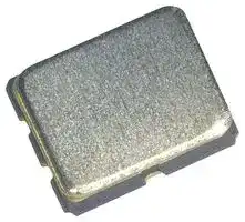
X1G006151001411
Oscillator, 100 MHz, CMOS, 3.3 V, SMD, 2.5mm x 2mm, SG2520CBN Series
⚠️ Reference pricing provided. In case of supply shortages, we will connect you with our trusted procurement partners to ensure your project's continuity.
- Manufacturer: EPSON
- Product type: Standard Oscillators
- SVHC: No SVHC (25-Jun-2025)
- Frequency Nom: 100MHz
- Product Range: SG2520CBN Series
- Supply Voltage Nom: 3.3V
- Frequency Stability + / -: -
- Operating Temperature Max: 125°C
- Operating Temperature Min: -40°C
- Oscillator Case / Package: SMD, 2.5mm x 2mm
- Oscillator Output Compatibility: CMOS
| Delivery and price | |
|---|---|
| Units per pack | 500 |
| Price | 0.736 € |
| Current stock | 10+ |
| Lead time | 30 days |
Datasheet

## **Crystal Oscillator (SPXO)** - Package size (2.5 mm × 2.0 mm × 0.74 mm) - Fundamental mode SPXO - Output: CMOS - Reference weight Typ.12 mg ## [ 1 ] Product Number / Product Name (1-1) Product Number / Ordering Code ## **X1G0061510014xx** Last 2 digits code( **xx** ) defines Quantity. The standard is "16", 3 000 pcs/Reel. (1-2) Product Name / Model Name ## **SG2520CBN 100.000000MHz TJJPA** ## [ 2 ] Operating Range |[ 2 ]2 ]] Operating Rangerating Rangeating Rangeing Rangeg RangeRangeangengege||||||| |---|---|---|---|---|---|---| |Parameter|Symbol|Specifications|||Unit|Conditions| |||Min.|Typ.|Max.||| |Supply voltage|VCC|1.62|-|3.63|V|-| ||GND|0|0|0|V|-| |Operatingtemperature range|T_use|-40|+25|+125|°C|-| |CMOS load condition|L_CMOS|-|-|15|pF|-| ## [ 3 ] Frequency Characteristics |Parameter|Symbol|Specifications|Specifications|Specifications|Unit|Conditions| |---|---|---|---|---|---|---| |||Min.|Typ.|Max.||| |Output frequency|fo|-|100.000000|-|MHz|-| |Frequencytolerance *1|f_tol|-50|-|+50|×10-6|T_use| *1 Frequency tolerance includes Initial frequency tolerance, Frequency / temperature characteristics, Frequency / voltage coefficient Frequency / load coefficient and frequency aging (+25 °C. First year) |Parameter<br>~~SS~~|Symbol<br>~~SS —————~~|Specifications<br>~~————~~<br>~~—————~~|Specifications<br>~~————~~<br>~~—————~~|Specifications<br>~~————~~<br>~~—————~~|Unit<br>~~————~~|Conditions<br>~~————~~| |---|---|---|---|---|---|---| |||Min.<br>~~————~~<br>~~—————~~|Typ.<br>~~————~~<br>~~—————~~|Max.<br>~~————~~<br>~~—————~~||| |Start-uptime<br><br>~~ee~~|t_str<br>~~—————~~<br>~~ee~~|-<br>~~—————~~<br>~~ee~~|-<br>~~—————~~<br>~~ee~~|3<br>~~—————~~<br>~~ee~~|ms<br>~~ee~~|t = 0 at 90 % Vcc<br>~~ee~~| |Current consumption<br>~~po~~<br>~~po~~|ICC<br>~~po~~|-<br>~~po~~|8.7<br>~~po~~|11.6<br>~~po~~|mA<br>~~po~~|No load condition, Vcc = 3.3 V<br>~~po~~| |Disable current<br>~~po~~<br>~~—————————~~|I_dis<br>~~—————————~~|-<br>~~—————————~~|6.3<br>~~—————————~~|10<br>~~—————————~~|mA<br>~~—————————~~|OE = GND, Vcc = 3.3 V<br>~~—————————~~| |Output voltage<br>~~po~~<br>~~—————————~~|VOH<br>~~—————————~~|90 % VCC<br>~~—————————~~|-<br>~~—————————~~|-<br>~~—————————~~|V<br>~~—————————~~|Ioʜ = -1 mA<br>~~—————————~~| ||VOL<br>~~—————————~~<br>~~ee~~|-<br>~~—————————~~<br>~~ee~~|-<br>~~—————————~~<br>~~ee~~|10 % VCC<br>~~—————————~~<br>~~ee~~|V<br>~~—————————~~<br>~~ee~~|Ioʟ = 1 mA<br>~~—————————~~<br>~~eee~~| |Rise/Fall time<br>~~—————————~~<br>~~ee~~|tr/tf<br>~~—————————~~<br>~~ee~~<br>~~ee~~|-<br>~~—————————~~<br>~~ee~~<br>~~ee~~|-<br>~~—————————~~<br>~~ee~~<br>~~ee~~|2.5<br>~~—————————~~<br>~~ee~~<br>~~ee~~|ns<br>~~—————————~~<br>~~ee~~<br>~~ee~~|20 % - 80 % Vcc level,<br>L_CMOS = 15pF<br>~~—————————~~<br>~~ee~~<br>~~eee~~| |Symmetry<br>~~po~~<br>~~SS~~|SYM<br>~~ee ~~<br>~~po~~<br>|45<br> ~~ee ~~<br>~~po~~<br>~~——————~~|-<br> ~~ee ~~<br>~~po~~<br>~~——————~~|55<br> ~~ee ~~<br>~~po~~<br>~~——————~~|%<br> ~~ee ~~<br>~~po~~<br>~~——————~~|50 % Vcc level, L_CMOS≤15 pF<br> ~~eee~~<br>~~po~~<br>~~——————~~| |Input voltage<br>~~SS~~|VIH<br><br>~~a~~|70 % VCC<br>~~——————~~<br>~~ee~~|-<br>~~——————~~<br>~~ee~~|-<br>~~——————~~<br>~~ee~~|V<br>~~——————~~<br>~~ee~~|#1pin<br>~~——————~~| ||VIL<br><br>~~a~~|-<br>~~——————~~<br>~~ee~~|-<br>~~——————~~<br>~~ee~~|30 % VCC<br>~~——————~~<br>~~ee~~|V<br>~~——————~~<br>~~ee~~|#1pin<br>~~——————~~| |Output disable time (OE)<br>~~SS ~~|tstp_oe<br> <br>~~a~~|-<br> ~~——————~~<br>~~ee~~|-<br>~~——————~~<br>~~ee~~|1<br>~~——————~~<br>~~ee~~|μs<br>~~——————~~<br>~~ee~~|Measured from the time OE<br>pin crosses 30 % Vcc<br>~~——————~~| |Output enable time (OE)|tsta_oe|-|-|100 ns<br>+ 2 clock<br>cycles|-|Measured from the time OE<br>pin crosses 70 % Vcc| |Phasejitter<br>~~po~~|tPJ<br>~~po~~|-<br>~~po~~|-<br>~~po~~|0.6<br>~~po~~|ps<br>~~po~~|-<br>~~po~~| ## **[ For other general specifications, please refer to the attached Full Data Sheet below ]** 2025/06/11 1 / 26 Page ## **High Frequency and Low Jitter Crystal Oscillator: SG2016CBN, SG2520CBN** ## **Features** - Crystal oscillator - Output frequency: - Frequency range: - Output: - 5 standard frequencies - 75 MHz to 170 MHz - CMOS - Supply voltage: 1.62 V to 3.63 V - Frequency tolerance, Operating temperature: - ±15 × 10[-6] / -40 °C to +105 °C **==> picture [172 x 17] intentionally omitted <==** **----- Start of picture text -----**<br> SG2016CBN SG2520CBN<br>(2.0 × 1.6 × 0 .6 mm ) (2.5 × 2.0 × 0 .74 mm )<br>**----- End of picture text -----**<br> - ±25 × 10[-6] , ±50 × 10[-6] / -40 °C to +125 °C - Phase jitter: 0.3 ps Typ. (Offset frequency: 12 kHz to 20 MHz) ## **Description** SG2016CBN and SG2520CBN utilize Epson’s new low noise Integer-N PLL technology. They can support the high frequency from 75 MHz to 170 MHz with narrow frequency tolerance of ±15 × 10[-6] , wide operating temperature range up to 125 °C, and low jitter characteristics of 0.3 ps Typical. SG2016CBN and SG2520CBN are ideal for applications that require high frequency, low jitter clocks, such as network equipment and image/audio transmission. ## **Outline Drawing and Terminal Assignment** **==> picture [52 x 8] intentionally omitted <==** **----- Start of picture text -----**<br> SG2016CBN<br>**----- End of picture text -----**<br> **==> picture [49 x 7] intentionally omitted <==** **----- Start of picture text -----**<br> SG2520CBN<br>**----- End of picture text -----**<br> Terminal Assignment |Pin #|Name|Function|Function| |---|---|---|---| |#1|OE|Output Enable|High*1or Open:<br>Specified frequencyoutput from OUTpin| ||||Low:<br>OUTpin is low(pull down with 500 kΩ), onlyoutput driver is disabled| ||O̅ E̅|Output Enable|Low*2or Open:<br>Specified frequencyoutput from OUTpin| ||||High:<br>OUTpin is low(pull down with 500 kΩ), onlyoutput driver is disabled| ||S̅ T̅|Standby|High*1 *3:<br>Specified frequencyoutput from OUTpin| ||||Low:<br>OUT pin is low (pull down with 500 kΩ)<br>Devicegoes to standbymode. Supplycurrent reduces to the least as I_std| ||ST|Standby|Low*2 *3:<br>Specified frequencyoutput from OUTpin| ||||High:<br>OUT pin is low (pull down with 500 kΩ)<br>Devicegoes to standbymode. Supplycurrent reduces to the least as I_std| |#2|GND|Ground|| |#3|OUT|Clock output|| |#4|VCC|Power supply|| - *1 If fixing it at High, please connect to V CC directly. - *2 If fixing it at Low , please connect to GND directly. - *3 If necessary to use Open, please select Output Enable function. **Spec No : SGxxxxCBN_E_Ver2.0** **Page 2 / 26** ## [ 1 ] Product Name / Product Number (1-1) Product Name (Standard Form) SG2016CBN: X1G006161xxxx15 SG2520CBN: X1G006151xxxx15 (Please contact Epson for details) ## (1-2) Product Number / Ordering Code SG2016CBN 156.250000MHz T J J P A a b c d e f g h |(1-2) Product Number / Ordering Code<br>SG2016CBN<br>156.250000MHz<br>T<br>J<br>J<br>P<br>A<br>f|(1-2) Product Number / Ordering Code<br>SG2016CBN<br>156.250000MHz<br>T<br>J<br>J<br>P<br>A<br>f||||| |---|---|---|---|---|---| |a b<br>c<br>d e f g h|||||| |a: Model b: Output (C: CMOS) c: Frequency d: Supply voltage (T: 1.8 V to 3.3 V Typ.)|||||| |e: Frequencytolerance f: Operatingtemperature g: Function h: Rise||erature g: Function h: Rise/Fall time|||| |e: Frequency tolerance||g: Function||h: Rise/Fall time|| |/ f: Operatingtemperature||P<br>Output enable (#1pin=OE)||A|Default| |BH ±15×10-6/-40°C to +105°C||Q<br>Output enable (#1pin=O̅ E̅ )||B|Faster| |DJ ±25×10-6/-40°C to +125°C||S<br>Standby (#1pin=S̅ T̅ )||C|Fast| |JJ ±50×10-6/-40°C to +125°C||T<br>Standby (#1pin=ST)|||| ## [ 2 ] Absolute Maximum Ratings |Parameter|Symbol|Specification|Specification|Specification|Unit|Conditions| |---|---|---|---|---|---|---| |||Min.|Typ.|Max.||| |Maximum supplyvoltage|GND-VCC|-0.3|-|4|V|GND = 0 V| |Input voltage|VIN|GND - 0.3|-|VCC+ 0.3|V|#1 pin| |Storage temperature range|T_stg|-55|-|+125|°C|| |Parameter<br>~~**a**~~<br>~~a~~|Symbol<br>~~ee~~<br>~~GG~~|Specification<br>~~eeee eee~~|Specification<br>~~eeee eee~~|Specification<br>~~eeee eee~~|Unit<br>~~pp~~<br>~~GG~~|Conditions<br>~~pp~~<br>~~GG~~| |---|---|---|---|---|---|---| |||Min.<br>~~ee~~<br>~~GG~~|Typ.<br>~~ee eee~~<br>~~GG~~|Max.<br>~~eee~~<br>~~GO~~||| |Supplyvoltage<br>~~**a**~~<br>~~a~~|VCC<br>~~ee~~<br>~~GG~~<br>~~CC~~|1.62<br>~~ee ~~<br>~~GG~~<br>~~CC~~|-<br> ~~ee eee~~<br>~~GG~~<br>~~CC~~|3.63<br>~~eee~~<br>~~GO~~<br>~~CGO~~|V<br>~~pp~~<br>~~GG~~<br>~~CGO GO~~|~~pp~~<br>~~GG~~<br>~~GO~~| |Supplyvoltage<br>~~a~~|GND<br>~~GG~~<br>~~CC~~|0.0<br>~~GG~~<br>~~CC~~|0.0<br>~~GG~~<br>~~CC~~|0.0<br>~~GO ~~<br>~~CGO~~|V<br> ~~GG~~<br>~~CGO GO~~|~~GG~~<br>~~GO~~| |Input voltage<br>~~pT~~<br>~~ee~~|VIN<br>~~CC~~<br>~~pT~~<br>~~ee~~|GND<br>~~CC~~<br>~~pT~~<br>~~ee cee~~|-<br>~~CC~~<br>~~pT~~<br>~~cee~~|VCC<br>~~CGO~~<br>~~pT~~<br>~~ee~~|V<br>~~CGO GO~~<br>~~pT~~<br>~~ee~~|#1 pin<br>~~GO~~<br>~~pT~~<br>~~eee~~| |Operating temperature range<br>~~ee~~|T_use<br>~~ee~~|-40<br>~~ee cee~~|+25<br>~~cee~~|+105<br>~~ee~~|°C<br>~~ee~~|~~eee~~| |||-40<br>~~ee cee~~<br>~~po~~|+25<br>~~cee~~<br>~~po~~|+125<br>~~ee~~<br>~~po~~|°C<br>~~ee~~<br>~~po~~|~~eee~~<br>~~po~~| |CMOS load condition<br>~~ee~~<br>~~pf~~|L_CMOS<br>~~ee~~<br>~~pf~~|-<br>~~ee cee~~<br>~~pf~~|-<br>~~cee ~~<br>~~pf~~|15<br> ~~ee ~~<br>~~pf~~|pF<br> ~~ee~~<br>~~pf~~|~~eee~~<br>~~pf~~| |* Power supplystartuptime(0 %VCC →90 %VCC) should be between 5 μs and 500 ms<br>* A 0.01µF to 0.1µF or over bypass capacitor should be connected between VCCand GND pins located close to the device||||||| * Power supply startup time (0 %VCC → 90 %VCC) should be between 5 μs and 500 ms * A 0.01 µF to 0.1 µF or over bypass capacitor should be connected between VCC and GND pins located close to the device |Parameter<br>~~eee~~|Symbol<br>~~eee~~|Specification<br>~~eee~~|Specification<br>~~eee~~|Specification<br>~~eee~~|Unit<br>~~pf~~|Conditions<br>~~pf~~|Conditions<br>~~pf~~| |---|---|---|---|---|---|---|---| |||Min.<br>~~eee~~|Typ.<br>~~eee~~|Max.<br>~~eee~~|||| |Output frequency<br>~~a~~|fo<br>~~a~~|75<br>~~ees~~|~~ees~~|170<br>~~ees~~|MHz<br>~~ee~~|Please contact us for frequency other than the standard frequencies.<br>~~ee~~|| |||76.8,100,125,150,156.25<br>~~ees~~<br>~~GG~~<br>~~ee~~<br>~~eeee~~|||MHz<br>~~ee~~<br>~~GG~~<br>~~Ge~~|Standard frequencies<br>~~ee~~<br>~~GG~~<br>~~ee~~|| |Frequency tolerance *1<br>~~a ~~<br>~~CC~~|f_tol<br> ~~a~~<br>~~po~~<br>~~CC~~|-15<br>~~ees~~<br>~~ee~~|-<br>~~ees~~<br>~~ee~~|+15<br>~~ees ~~<br>~~ee~~|×10-6<br> ~~ee~~<br>~~Ge~~|Included 1 year aging<br>~~ee~~<br>~~ee~~|TBH**<br>T_use = -40 °C to +105 °C<br>~~ee~~<br><br>~~a~~| |||-20<br>~~ee~~<br>~~a~~<br>~~a~~|-<br>~~ee~~<br>|+20<br>~~ee~~<br>|×10-6<br>~~Ge~~<br><br>~~ee~~|Included 10 years aging<br>~~ee~~<br><br>~~eee a~~|| |||-25<br>~~ee~~<br>~~ee~~<br>~~a~~|-<br>~~ee ~~<br>~~ee~~|+25<br> ~~ee ~~<br>~~ee~~|×10-6<br> ~~Ge~~<br>~~ee~~<br>~~ee~~|Included 1 year aging<br>~~ee~~<br>~~ee~~<br>~~eee a~~|TDJ**<br>T_use = -40 °C to +125 °C<br>~~ee~~<br>~~a~~| |||-30<br>~~ee~~<br>~~a~~<br>~~ee~~|-<br>~~ee~~<br>~~ee~~|+30<br>~~ee~~<br>~~ee~~|×10-6<br>~~ee~~<br>~~ee~~<br>~~ee~~|Included 10 years aging<br>~~ee~~<br>~~eee a~~<br>~~es~~|| |||-50<br>~~a~~<br>~~ee~~<br>~~po~~|-<br>~~ee~~|+50<br>~~ee~~|×10-6<br>~~ee ~~<br>~~ee~~|Included 1 year aging<br> ~~eee a~~<br>~~es~~|TJJ**<br>T_use = -40 °C to +125 °C<br>~~a~~<br>~~GO~~| |||-55<br>~~ee~~<br>~~po~~<br>~~CC~~|-<br>~~ee~~<br>~~CC~~|+55<br>~~ee~~<br>~~CC~~|×10-6<br>~~ee~~<br>~~CC G~~|Included 10 years aging<br>~~es~~<br>~~G~~|| |Frequencyaging*2<br>~~CC~~|f_age<br>~~po~~<br>~~CC~~|Included in frequencytolerance<br>~~ee~~<br>~~ee ee ~~<br>~~po~~<br>~~CC~~|||×10-6<br> ~~ee~~<br>~~CC G~~|+25 °C, 1 year or 10 years<br>~~es~~<br>~~GO~~|| |*1 Frequencytolerance includes initial frequencytolerance,frequency/ temperature characteristics,frequency/ voltage coefficient,<br>frequency/ load coefficient and frequencyaging (+25 °C,firstyear or 10years)<br>~~CC GO~~|||||||| |frequency/ load coefficient and frequencyaging (+25 °C,firstyear or 10years)|||||||| - *2 Frequency aging is estimated from environmental reliability tests; expected amount of the frequency variation. This is not intended to be a guarantee of the product life cycle. **Spec No : SGxxxxCBN_E_Ver2.0** **Page 3 / 26** [ 5 ] Electrical Characteristics |Parameter<br>~~fe~~<br>~~rT~~<br>~~O™~—C~~|Symbol<br>~~fe~~<br>~~Y—S—<C~S™YSS—<—~SédYCS~~|Specification<br>~~fe~~|Specification<br>~~fe~~|Specification<br>~~fe~~|Unit<br>~~SE~~<br>~~CSCC~~|Conditions<br>~~SE~~<br>~~TS~~|Conditions<br>~~SE~~<br>~~TS~~|Conditions<br>~~SE~~<br>~~TS~~|Conditions<br>~~SE~~<br>~~TS~~| |---|---|---|---|---|---|---|---|---|---| |||Min.<br>~~fe~~<br>~~Y—S—<C~S™YSS—<—~SédYCS~~|Typ.<br>~~fe~~<br>~~Y—S—<C~S™YSS—<—~SédYCSCSCC~~|Max.<br>~~fe~~<br>~~CSCC~~|||||| |Start-uptime<br>~~rT~~<br>~~O™~—C~~|t_str<br>~~Y—S—<C~S™YSS—<—~SédYCS~~|-<br>~~Y—S—<C~S™YSS—<—~SédYCS~~<br>~~ee~~|-<br>~~Y—S—<C~S™YSS—<—~SédYCSCSCC~~<br>~~es~~|3<br>~~CSCC~~|ms<br>~~CSCC~~|t = 0 at VCC> 1.62 V<br>~~TS~~<br>~~Pe~~|||| |Current consumption<br>(No load)<br>VCC= 1.62 V to 1.98 V<br>~~rT~~<br>~~O™~—C~~|ICC<br>~~Y—S—<C~S™YSS—<—~SédYCS~~|-<br>~~Y—S—<C~S™YSS—<—~SédYCS~~<br>~~ee~~<br>~~ee~~|6.8<br>~~Y—S—<C~S™YSS—<—~SédYCS CSCC~~<br>~~es~~<br>~~es~~|9.1<br>~~CSCC~~|mA<br>~~CSCC~~|75 MHz ≤ fo ≤ 100 MHz<br>~~TS~~<br>~~Pe~~<br>~~Pe~~|||| |||-<br>~~ee~~<br>~~ee~~<br>~~ee~~|7.6<br>~~es~~<br>~~es~~<br>~~es~~|9.8||100 MHz < fo ≤ 125 MHz<br>~~Pe~~<br>~~Pe~~<br>~~Pe~~|||| |||-<br>~~ee~~<br>~~ee~~<br>~~ee~~|8.6<br>~~es~~<br>~~es~~<br>~~es~~|12.0||125 MHz < fo ≤ 170 MHz<br>~~Pe~~<br>~~Pe~~<br>~~Pe~~|||| |Current consumption<br>(No load)<br>VCC= 2.25 V to 2.75 V||-<br>~~ee~~<br>~~ee~~<br>~~ee~~|7.6<br>~~es~~<br>~~es~~<br>~~es~~|10.2|mA|75 MHz ≤ fo ≤ 100 MHz<br>~~Pe~~<br>~~Pe~~<br>~~Pe~~|||| |||-<br>~~ee~~<br>~~ee~~<br>~~ee~~|8.7<br>~~es~~<br>~~es~~<br>~~es~~|11.3||100 MHz < fo ≤ 125 MHz<br>~~Pe~~<br>~~Pe~~<br>~~Pe~~|||| |||-<br>~~ee~~<br>~~ee~~<br>~~ee~~|10.1<br>~~es~~<br>~~es~~<br>~~es~~|13.9||125 MHz < fo ≤ 170 MHz<br>~~Pe~~<br>~~Pe~~<br>~~Pe~~|||| |Current consumption<br>(No load)<br>VCC= 2.97 V to 3.63 V||-<br>~~ee~~<br>~~ee~~<br>~~ee~~|8.7<br>~~es~~<br>~~es~~<br>~~es~~|11.6|mA|75 MHz ≤ fo ≤ 100 MHz<br>~~Pe~~<br>~~Pe~~<br>~~Pe~~|||| |||-<br>~~ee~~<br>~~ee~~<br>~~ee~~|10.0<br>~~es~~<br>~~es~~<br>~~ee~~|13.2||100 MHz < fo ≤ 125 MHz<br>~~Pe~~<br>~~Pe~~<br>~~Pe~~|||| |||-<br>~~ee~~<br>~~ee~~<br>~~ee~~|12.3<br>~~es~~<br>~~ee~~<br>~~es~~|16.6||125 MHz < fo ≤ 170 MHz<br>~~Pe~~<br>~~Pe~~<br>~~Pe~~|||| |Disable current|I_dis|-<br>~~ee~~<br>~~ee~~<br>~~ee~~|6.1<br>~~ee~~<br>~~es~~<br>~~es~~|10.0|mA|VCC= 1.62 V to 1.98 V<br>~~Pe~~<br>~~Pe~~<br>~~Pe~~|||| |||-<br>~~ee~~<br>~~ee~~<br>~~ee~~|6.2<br>~~es~~<br>~~es~~<br>~~ee~~|10.0||VCC= 2.25 V to 2.75 V<br>~~Pe~~<br>~~Pe~~<br>~~Pe~~|||| |||-<br>~~ee~~<br>~~ee~~<br>~~ee~~|6.3<br>~~es~~<br>~~ee~~<br>~~es~~|10.0||VCC= 2.97 V to 3.63 V<br>~~Pe~~<br>~~Pe~~<br>~~Pe~~|||| |Stand-by current<br>~~aS~~|I_std<br>~~aS~~|-<br>~~ee~~<br>~~ee~~<br>~~ee~~|0.3<br>~~ee~~<br>~~es~~<br>~~es~~|15.0|µA<br>~~ee~~|VCC= 1.62 V to 1.98 V<br>~~Pe~~<br>~~Pe~~<br>~~Pe~~|||| |||-<br>~~ee~~<br>~~ee~~<br>~~ee~~|0.4<br>~~es~~<br>~~es~~<br>~~ee~~|15.0<br>~~ee~~||VCC= 2.25 V to 2.75 V<br>~~Pe~~<br>~~Pe~~<br>~~Pe~~|||| |||-<br>~~ee~~<br>~~ee~~|0.5<br>~~es~~<br>~~ee~~|15.0<br>~~ee~~||VCC= 2.97 V to 3.63 V<br>~~Pe~~<br>~~Pe~~|||| |Output voltage<br>(DC characteristics)<br>~~aS~~|VOH<br>~~aS~~|90 % VCC<br>~~ee~~|-<br>~~ee~~|-<br>~~ee~~|V<br>~~ee~~|Other Options<br>~~Pe~~|IOH<br>~~Pe~~||IOL<br>~~Pe~~| |||||||'B'<br>~~Pe~~|-2.0 mA<br>~~Pe~~||2.0 mA<br>~~Pe~~| ||VOL<br>~~aS~~|-<br>~~ee~~|-<br>~~ee~~|10 % VCC<br>~~ee~~<br>~~QO~~|V<br>~~ee~~<br>~~QO~~||||| |||||||'C'<br>~~Pe~~<br>~~QO~~|-1.0 mA<br>~~Pe~~<br>~~QO~~||1.0 mA<br>~~Pe~~<br>~~QO~~| |Symmetry<br>~~aS~~<br>~~GO~~|SYM<br>~~aS~~<br>~~GO~~|45<br>~~ee ~~<br>~~GO~~|50<br> ~~ee ~~<br>~~GO~~|55<br> ~~ee~~<br>~~GO~~<br>~~QO~~|%<br>~~ee ~~<br>~~GO~~<br>~~QO~~|50 % VCClevel, L_CMOS≤15 pF<br> ~~Pe~~<br>~~GO~~<br>~~QO~~|||| |Rise/Fall time<br>~~ae~~<br>~~ee~~|tr/tf<br>~~ae~~|-<br>~~ae~~<br>~~ee~~|-<br>~~ae~~<br>~~ee~~|2.0<br>~~QO ~~<br>~~ae~~|ns<br> ~~QO~~<br>~~ae~~|fo > 125 MHz<br>~~QO~~<br>~~ae~~<br>~~fe~~||20 % - 80 % VCC,<br>L_CMOS = 15 pF<br>~~QO~~<br>~~ae~~|| |||-<br>~~ae~~<br>~~ee~~|-<br>~~ae~~<br>~~ee~~|2.5<br>~~ae~~||fo≤125 MHz<br>~~ae~~<br>~~fe~~|||| |Input voltage<br>~~ee~~|VIH<br>~~es~~|70 % VCC<br>~~ee~~<br>~~ee~~|-<br>~~ee~~|-|V|#1 pin<br>~~fe~~|||| ||VIL<br>~~es~~|-<br>~~ee~~<br>~~ee~~|-<br>~~ee~~|30 % VCC<br>~~QO~~|V<br>~~QO~~||||| |Input capacitance<br>~~ee~~<br>~~GO~~|CIN<br>~~es ~~<br>~~GO~~|-<br>~~ee~~<br> ~~ee~~<br>~~GO~~|3<br>~~ee~~<br>~~GO~~|5<br>~~GO~~<br>~~QO~~|pF<br>~~GO~~<br>~~QO~~|#1 pin<br>~~fe~~<br>~~GO~~|||| |Inputpull upresistance(OE)<br>~~ee~~<br>~~ee~~<br>~~ee~~|RUP1<br>~~ee~~<br>~~ee~~|-<br>~~ee ~~<br>~~ee~~<br>~~ee~~|40<br> ~~ee~~<br>~~ee~~<br>~~ee~~|-<br>~~QO~~<br>~~ee~~<br>~~ee~~|kΩ<br>~~QO~~<br>~~ee~~<br>~~ee~~|~~fe~~<br>~~ee~~<br>~~ee~~|||| |Input pull up resistance (S̅ T̅ )<br>~~ee~~<br>~~es~~<br>~~es~~|RUP1<br>~~ee~~<br>~~ee~~<br>|-<br>~~ee~~<br>~~es~~<br>|40<br>~~ee~~<br>~~es~~<br>|-<br>~~ee~~<br>~~es~~<br>|kΩ<br>~~ee~~<br>|S̅ T̅ = 70 % VCC<br>~~ee~~<br>|||| ||RUP2<br>~~ee~~<br>~~ee~~<br>~~Gs~~<br>|-<br>~~ee~~<br>~~es~~<br>~~Rs~~<br>|10<br>~~ee~~<br>~~es~~<br>~~GD~~<br>|-<br>~~ee~~<br>~~es~~<br>~~ID~~|MΩ<br>~~ee~~<br>~~(~~|S̅ T̅ = 30 % VCC<br>~~ee~~<br>~~(~~|||| |Inputpull upresistance(ST)<br>~~ee~~<br>~~es~~<br>~~es~~<br>~~PC~~|RUP1<br>~~ee~~<br>~~ee~~<br>~~Gs~~<br>~~ee~~|-<br>~~ee~~<br>~~es~~<br>~~Rs~~<br>~~es~~|40<br>~~ee~~<br>~~es~~<br>~~GD~~<br>~~Ge~~|-<br>~~ee~~<br>~~es~~<br>~~ID~~|kΩ<br>~~ee~~<br>~~(~~|~~ee~~<br>~~(~~|||| |Input pull down resistance (O̅ E̅ )<br>~~es~~<br>~~es~~<br>~~PC~~|RDN1<br>~~ee~~<br>~~Gs~~<br>~~ee~~|-<br>~~es ~~<br>~~Rs~~<br>~~es~~|40<br> ~~es~~<br>~~GD~~<br>~~Ge~~|-<br>~~es~~<br>~~ID~~|kΩ<br>~~(~~|~~(~~|||| |Outputpull down resistance<br><br>~~es ~~<br>~~PC~~<br>~~ee~~|RDN<br>~~Gs~~<br> ~~ee~~<br>~~es~~|-<br>~~Rs~~<br>~~es~~<br>~~ns~~|500<br>~~GD ~~<br>~~Ge~~<br>~~es~~|-<br> ~~ID~~<br>~~ns~~|kΩ<br>~~(~~<br>~~ns~~|~~(~~|||| |Output disable time (OE)<br> <br>~~PC~~<br>~~ee~~<br>~~es Os~~|tstp_oe<br> ~~ee ~~<br>~~es~~<br>~~Os Gs~~|-<br> ~~es ~~<br>~~ns~~<br>~~Gs~~|-<br> ~~Ge~~<br>~~es~~|1<br>~~ns~~|µs<br>~~ns~~|Measured from the time OE pin crosses 30 % VCC<br>or measured from the time O̅ E̅ pin crosses 70 % VCC|||| |Output disable time (ST)<br>~~ee~~<br>~~es Os~~<br>~~ee~~|tstp_st<br>~~es~~<br>~~Os Gs~~<br>~~es~~|-<br>~~ns~~<br>~~Gs~~<br>~~ns~~|-<br>~~es~~<br>~~es~~|1<br>~~ns~~<br>~~ns~~|µs<br>~~ns~~<br>~~ns~~|Measured from the time S̅ T̅ pin crosses 30 % VCC<br>or measured from the time ST pin crosses 70 % VCC|||| |Output enable time (OE)<br>~~es Os~~<br>~~ee~~<br>~~es Os~~|tsta_oe<br>~~Os Gs~~<br>~~es~~<br>~~Os Gs~~|-<br>~~Gs~~<br>~~ns~~<br>~~Gs~~|-<br>~~es~~|100 ns<br>+ 2 clock cycles<br>~~ns~~|-<br>~~ns~~|Measured from the time OE pin crosses 70 % VCC<br>or measured from the time O̅ E̅ pin crosses 30 % VCC|||| |Output enable time (ST)<br>~~ee~~<br>~~es Os~~<br>~~Pr~~|tsta_st<br>~~es~~<br>~~Os Gs~~<br>~~ef~~|-<br>~~ns~~<br>~~Gs~~<br>~~ef~~|-<br>~~es~~<br>~~ef~~|3<br>~~ns~~|ms<br>~~ns~~|Measured from the time S̅ T̅ pin crosses 70 % VCC<br>or measured from the time ST pin crosses 30 % VCC|||| |Phasejitter<br>~~es Os~~<br>~~Pr~~|tPJ<br>~~Os Gs~~<br>~~ef~~|-<br>~~Gs~~<br>~~ef~~|-<br>~~ef~~|0.6|ps|Offset frequency: 12 kHz to 20 MHz|||| |*1 Default 'A' Rise/Fall time is dependent on programmed frequency<br>~~Pr~~<br>~~ef~~|||||||||| **Spec No : SGxxxxCBN_E_Ver2.0** **Page 4 / 26** ## [ 6 ] Thermal Resistance (For Reference Only) |Parameter|Symbol|Specification|Specification|Specification|Unit|Conditions| |---|---|---|---|---|---|---| |||Min.|Typ.|Max.||| |Junction temperature|Tj|-|-|+150|°C|| |Junction to case|θjc|-|129|-|°C/W|SG2016CBN| |||-|121|-|°C/W|SG2520CBN| |Junction to ambient|θja|-|257|-|°C/W|SG2016CBN| |||-|208|-|°C/W|SG2520CBN| ## [ 7 ] Typical Performance Characteristics (For Reference Only) The following data shows typical performance characteristics (7-1) Frequency / Temperature Characteristics n = 10 pcs **Spec No : SGxxxxCBN_E_Ver2.0** **Page 5 / 26** (7-2) Current Consumption Temperature Characteristic (No load) fo = 76.8 MHz **==> picture [61 x 8] intentionally omitted <==** **----- Start of picture text -----**<br> fo = 98.304 MHz<br>**----- End of picture text -----**<br> **==> picture [50 x 8] intentionally omitted <==** **----- Start of picture text -----**<br> fo = 100 MHz<br>**----- End of picture text -----**<br> **==> picture [50 x 8] intentionally omitted <==** **----- Start of picture text -----**<br> fo = 125 MHz<br>**----- End of picture text -----**<br> fo = 150 MHz fo = 156.25 MHz Frequency Dependency (T_use = +25 °C) No load L_CMOS = 15 pF The actual current consumption is the total of the current under the condition of no load and the current to drive the output load (fo × L_CMOS × VCC). To reduce the current consumption, it is effective to use lower frequency, lower supply voltage and lower output load. **Spec No : SGxxxxCBN_E_Ver2.0** **Page 6 / 26** ## (7-3) Rise/Fall Time Temperature Characteristic (20 % - 80 %VCC, L_CMOS = 15 pF) fo = 76.8 MHz, Rise/Fall time: A (Default) or C (Fast) ## fo = 98.304 MHz, Rise/Fall time: A (Default) or C (Fast) fo = 100 MHz, Rise/Fall time: A (Default) or C (Fast) fo = 125 MHz, Rise/Fall time: A (Default) or C (Fast) **Spec No : SGxxxxCBN_E_Ver2.0** **Page 7 / 26** (7-3) Rise/Fall Time [cont'd] Temperature Characteristic (20 % - 80 %VCC, L_CMOS = 15 pF) fo = 150 MHz, Rise/Fall time: A (Default) or B (Faster) fo = 156.25 MHz, Rise/Fall time: A (Default) or B (Faster) **Spec No : SGxxxxCBN_E_Ver2.0** **Page 8 / 26** (7-4) Symmetry Temperature Characteristic (L_CMOS = 15 pF) fo = 76.8 MHz, Rise/Fall time: A (Default) or C (Fast) fo = 100 MHz, Rise/Fall time: A (Default) or C (Fast) fo = 150 MHz, Rise/Fall time: A (Default) or B (Faster) fo = 98.304 MHz, Rise/Fall time: A (Default) or C (Fast) fo = 125 MHz, Rise/Fall time: A (Default) or C (Fast) fo = 156.25 MHz, Rise/Fall time: A (Default) or B (Faster) **Spec No : SGxxxxCBN_E_Ver2.0** **Page 9 / 26** (7-5) Output Voltage Temperature Characteristic (L_CMOS = 15 pF) fo = 76.8 MHz, Rise/Fall time: A (Default) or C (Fast) ## fo = 98.304 MHz, Rise/Fall time: A (Default) or C (Fast) fo = 100 MHz, Rise/Fall time: A (Default) or C (Fast) fo = 125 MHz, Rise/Fall time: A (Default) or C (Fast) **Spec No : SGxxxxCBN_E_Ver2.0** **Page 10 / 26** (7-5) Output Voltage [cont'd] Temperature Characteristic (L_CMOS = 15 pF) fo = 150 MHz, Rise/Fall time: A (Default) or B (Faster) ## fo = 156.25 MHz, Rise/Fall time: A (Default) or B (Faster) **Spec No : SGxxxxCBN_E_Ver2.0** **Page 11 / 26** ## (7-6) Output Waveform fo = 76.8 MHz, L_CMOS = 15 pF, T_use = +25 °C, Rise/Fall time: A (Default) or C (Fast) VCC = 3.3 V VCC = 2.5 V **==> picture [43 x 9] intentionally omitted <==** **----- Start of picture text -----**<br> VCC = 1.8 V<br>**----- End of picture text -----**<br> fo = 98.304 MHz, L_CMOS = 15 pF, T_use = +25 °C, Rise/Fall time: A (Default) or C (Fast) VCC = 3.3 V VCC = 2.5 V **==> picture [43 x 9] intentionally omitted <==** **----- Start of picture text -----**<br> VCC = 1.8 V<br>**----- End of picture text -----**<br> **Spec No : SGxxxxCBN_E_Ver2.0** **Page 12 / 26** ## (7-6) Output Waveform [cont'd] **==> picture [322 x 21] intentionally omitted <==** **----- Start of picture text -----**<br> fo = 100 MHz, L_CMOS = 15 pF, T_use = +25 °C, Rise/Fall time: A (Default) or C (Fast)<br>VCC = 3.3 V VCC = 2.5 V<br>**----- End of picture text -----**<br> **==> picture [43 x 9] intentionally omitted <==** **----- Start of picture text -----**<br> VCC = 1.8 V<br>**----- End of picture text -----**<br> fo = 125 MHz, L_CMOS = 15 pF, T_use = +25 °C, Rise/Fall time: A (Default) or C (Fast) VCC = 3.3 V VCC = 2.5 V **==> picture [43 x 9] intentionally omitted <==** **----- Start of picture text -----**<br> VCC = 1.8 V<br>**----- End of picture text -----**<br> **Spec No : SGxxxxCBN_E_Ver2.0** **Page 13 / 26** ## (7-6) Output Waveform [cont'd] fo = 150 MHz, L_CMOS = 15 pF, T_use = +25 °C, Rise/Fall time: A (Default) or B (Faster) VCC = 3.3 V VCC = 2.5 V **==> picture [43 x 9] intentionally omitted <==** **----- Start of picture text -----**<br> VCC = 1.8 V<br>**----- End of picture text -----**<br> fo = 156.25 MHz, L_CMOS = 15 pF, T_use = +25 °C, Rise/Fall time: A (Default) or B (Faster) VCC = 3.3 V VCC = 2.5 V **==> picture [43 x 9] intentionally omitted <==** **----- Start of picture text -----**<br> VCC = 1.8 V<br>**----- End of picture text -----**<br> **Spec No : SGxxxxCBN_E_Ver2.0** **Page 14 / 26** (7-7) Phase Noise and Phase Jitter fo = 76.8 MHz, T_use = +25 °C |VCC|Phasejitter*| |---|---| |1.8 V|0.37ps| |2.5 V|0.36ps| |3.3 V|0.36ps| - Offset frequency: 12 kHz to 20 MHz ## fo = 98.304 MHz, T_use = +25 °C |VCC|Phasejitter*|| |---|---|---| |1.8 V|0.36ps|| |2.5 V|0.33ps|| |3.3 V|0.33ps|| ||* Offset frequency: 12 kHz to 20 MHz|* Offset frequency: 12 kHz to 20 MHz| ## fo = 100 MHz, T_use = +25 °C |VCC|Phasejitter*|| |---|---|---| |1.8 V|0.36ps|| |2.5 V|0.33ps|| |3.3 V|0.33ps|| ||* Offset frequency: 12 kHz to 20 MHz|* Offset frequency: 12 kHz to 20 MHz| ## fo = 125 MHz, T_use = +25 °C |VCC|Phasejitter*|| |---|---|---| |1.8 V|0.31ps|| |2.5 V|0.3ps|| |3.3 V|0.3ps|| ||* Offset frequency: 12 kHz to 20 MHz|* Offset frequency: 12 kHz to 20 MHz| **Spec No : SGxxxxCBN_E_Ver2.0** **Page 15 / 26** (7-7) Phase Noise and Phase Jitter [cont'd] fo = 150 MHz, T_use = +25 °C |VCC|Phasejitter*| |---|---| |1.8 V|0.3ps| |2.5 V|0.31ps| |3.3 V|0.33ps| - Offset frequency: 12 kHz to 20 MHz ## fo = 156.25 MHz, T_use = +25 °C |VCC|Phasejitter*| |---|---| |1.8 V|0.35ps| |2.5 V|0.36ps| |3.3 V|0.37ps| - Offset frequency: 12 kHz to 20 MHz **Spec No : SGxxxxCBN_E_Ver2.0** **Page 16 / 26** - [ 8 ] Test Circuit (8-1) Waveform Observation (1) #1 pin = OE/S̅T̅ ## (2) #1 pin = O̅E̅/ST (8-2) Current Consumption Test ## (1) #1 pin = OE/S̅T̅ ## (2) #1 pin = O̅E̅/ST - Disable current test should be OE = GND. Stand-by current test should be S̅T̅ = GND. - Disable current test should be O̅E̅ = VCC. Stand-by current test should be ST = VCC. - (8-3) Jitter (Peak to Peak, RMS, Cycle to Cycle) (1) #1 pin = OE/S̅T̅ ## (2) #1 pin = O̅E̅/ST - *1 Signal Source Analyzer: Keysight: E5052B, Minimum frequency = 10 MHz (8-4) Condition ## (1) Oscilloscope The bandwidth should be minimum 5 times wider than measurement frequency The probe ground should be placed closely to the test point and the lead length should be as short as possible - It is recommended to use miniature socket. (Don’t use earth lead.) ## (2) L_CMOS includes probe capacitance. - (3) A 0.01 μF to 0.1 μF bypass capacitor should be connected between VCC and GND pins located close to the device - (4) Use a current meter with a low internal impedance ## (5) Power Supply Power supply startup time (0 %VCC → 90 %VCC) should be between 5 μs and 500 ms Power supply impedance should be as low as possible and GND line should be as short as possible **Spec No : SGxxxxCBN_E_Ver2.0** **Page 17 / 26** ## [ 9 ] Timing Chart (9-1) Output Waveform and Level ## (9-2) OE/S̅T̅ Function and Timing **==> picture [339 x 227] intentionally omitted <==** **----- Start of picture text -----**<br> OE terminal Osc. circuit Output status<br>High or Open Oscillation Specified frequency: Enable<br>Low Oscillation Low (Weak pull down [*3] ): Disable<br>S̅T̅ terminal Osc. circuit Output status<br>High Oscillation Specified frequency: Enable<br>Low Oscillation stop Low (Weak pull down [*3] ): Disable<br>Enable<br>VIH<br>OE/ST<br>VIL Disable<br>*1 *2<br>tstp_oe tsta_oe<br>/tstp_st /tsta_st<br>OUT Weak *3<br>pull down<br>wt h y<br>**----- End of picture text -----**<br> *1 The period from OE/S̅T̅ = VIL to OUT = Disable (Low, weak pull down) - *2 The period from OE/S̅T̅ = VIH to OUT = Enable - *3 Pulled down with Output pull down resistance (RDN) - Judging the start of output when output waveform is observed. - OE/S̅T̅ terminal voltage level should not exceed supply voltage when using OE/S̅T̅ function. Please note that OE/S̅T̅ rise time should not exceed supply voltage rise time at the start-up. - Please do not use the S̅T̅ terminal with the open state. - If output should be enabled with the open state, please use Output Enable function. **Spec No : SGxxxxCBN_E_Ver2.0** **Page 18 / 26** (9-3) O̅E̅/ST Function and Timing **==> picture [339 x 212] intentionally omitted <==** **----- Start of picture text -----**<br> O̅E̅ terminal Osc. circuit Output status<br>Low or Open Oscillation Specified frequency: Enable<br>High Oscillation Low (Weak pull down [*3] ): Disable<br>ST terminal Osc. circuit Output status<br>Low Oscillation Specified frequency: Enable<br>High Oscillation stop Low (Weak pull down [*3] ): Disable<br>Disable<br>VIH<br>OE/ST<br>VIL Enable<br>*1 *2<br>tstp_oe tsta_oe<br>/tstp_st /tsta_st<br>OUT Weak *3<br>pull down<br>**----- End of picture text -----**<br> - *1 The period from O̅E̅/ST = VIH to OUT = Disable (Low, weak pull down) - *2 The period from O̅E̅/ST = VIL to OUT = Enable - *3 Pulled down with Output pull down resistance (RDN) - Judging the start of output when output waveform is observed. - O̅E̅/ST terminal voltage level should not exceed supply voltage when using O̅E̅/ST function. - Please do not use the ST terminal with the open state. - If output should be enabled with the open state, please use Output Enable function. **Spec No : SGxxxxCBN_E_Ver2.0** **Page 19 / 26** [ 10 ] Outline Drawing and Recommended Footprint (10-1) SG2016CBN **==> picture [42 x 8] intentionally omitted <==** **----- Start of picture text -----**<br> Units: mm<br>**----- End of picture text -----**<br> Terminal coating: Au plating 0.05 For stable operation, it is recommended that 0.01 µF to 0.1 µF bypass capacitor should be connected between VCC and GND and placed as close to the VCC pin as possible. Reference Weight Typ.: 7.3 mg ## Terminal Assignment |Pin #|Name|Function|Function| |---|---|---|---| |#1|OE|Output Enable|High*1or Open:<br>Specified frequencyoutput from OUTpin| ||||Low:<br>OUTpin is low(pull down with 500 kΩ), onlyoutput driver is disabled| ||O̅ E̅|Output Enable|Low*2or Open:<br>Specified frequencyoutput from OUTpin| ||||High:<br>OUTpin is low(pull down with 500 kΩ), onlyoutput driver is disabled| ||S̅ T̅|Standby|High*1 *3:<br>Specified frequencyoutput from OUTpin| ||||Low:<br>OUT pin is low (pull down with 500 kΩ)<br>Devicegoes to standbymode. Supplycurrent reduces to the least as I_std| ||ST|Standby|Low*2 *3:<br>Specified frequencyoutput from OUTpin| ||||High:<br>OUT pin is low (pull down with 500 kΩ)<br>Devicegoes to standbymode. Supplycurrent reduces to the least as I_std| |#2|GND|Ground|| |#3|OUT|Clock output|| |#4|VCC|Power supply|| - *1 If fixing it at High, please connect to V CC directly. - *2 If fixing it at Low , please connect to GND directly. *3 If necessary to use Open, please select Output Enable function. **==> picture [33 x 10] intentionally omitted <==** **----- Start of picture text -----**<br> Marking<br>**----- End of picture text -----**<br> **==> picture [256 x 94] intentionally omitted <==** **----- Start of picture text -----**<br> Output frequency Frequency tolerance<br>1 5 6 . 2 B<br>Production lot number<br>B D 4 5 K<br>Location of Pin #1<br>Model<br>en<br>**----- End of picture text -----**<br> **Spec No : SGxxxxCBN_E_Ver2.0** **Page 20 / 26** Units: mm (10-2) SG2520CBN Terminal coating: Au plating For stable operation, it is recommended that 0.01 µF to 0.1 µF bypass capacitor should be connected between VCC and GND and placed as close to the VCC pin as possible. Reference Weight Typ.: 12 mg ## Terminal Assignment |Pin #|Name|Function|Function| |---|---|---|---| |#1|OE|Output Enable|High*1or Open:<br>Specified frequencyoutput from OUTpin| ||||Low:<br>OUTpin is low(pull down with 500 kΩ), onlyoutput driver is disabled| ||O̅ E̅|Output Enable|Low*2or Open:<br>Specified frequencyoutput from OUTpin| ||||High:<br>OUTpin is low(pull down with 500 kΩ), onlyoutput driver is disabled| ||S̅ T̅|Standby|High*1 *3:<br>Specified frequencyoutput from OUTpin| ||||Low:<br>OUT pin is low (pull down with 500 kΩ)<br>Devicegoes to standbymode. Supplycurrent reduces to the least as I_std| ||ST|Standby|Low*2 *3:<br>Specified frequencyoutput from OUTpin| ||||High:<br>OUT pin is low (pull down with 500 kΩ)<br>Devicegoes to standbymode. Supplycurrent reduces to the least as I_std| |#2|GND|Ground|| |#3|OUT|Clock output|| |#4|VCC|Power supply|| - *1 If fixing it at High, please connect to V CC directly. - *2 If fixing it at Low , please connect to GND directly. *3 If necessary to use Open, please select Output Enable function. **==> picture [33 x 10] intentionally omitted <==** **----- Start of picture text -----**<br> Marking<br>**----- End of picture text -----**<br> **==> picture [266 x 96] intentionally omitted <==** **----- Start of picture text -----**<br> Output frequency Frequency tolerance<br>1 5 6 . 2 B<br>Production lot number<br>G 5 Q 1 K<br>Location of Pin #1<br>Model<br>n a} —<br>**----- End of picture text -----**<br> **Spec No : SGxxxxCBN_E_Ver2.0** **Page 21 / 26** [ 11 ] Moisture Sensitivity Level |Parameter|Specification||Conditions| |---|---|---|---| |MSL|LEVEL 1|IPC/JEDEC J-STD-020D.1|| ## [ 12 ] Reflow Profiles IPC/JEDEC J-STD-020D.1 **Spec No : SGxxxxCBN_E_Ver2.0** **Page 22 / 26** ## [ 13 ] Packing Information (13-1) SG2016CBN ## (1) Packing Quantity The last two digits of the Product Number (X1G006161xxxx **xx** ) are a code that defines the packing quantity. The standard is "15" for a 2 000 pcs/Reel. ## (2) Taping Specification Subject to EIA-481, IEC-60286 and JIS C0806 - 1) Tape Dimensions Carrier Tape Material: PS (Polystyrene) Top Tape Material: PET (Polyethylene Terephthalate) + PE (Polyethylene) Units: mm **==> picture [311 x 142] intentionally omitted <==** **----- Start of picture text -----**<br> 4 .0 ±0 .1 1 .0±0 .1<br>+0 .1<br>2 .0±0 .1 φ1 .5 0 0 .25±0 .05<br>+0 .1<br>φ1 .0 0<br>4 .0±0 .1<br>1 .85±0 .1<br>User direction of feed<br>○Epson ○Epson<br>1 .75±0 .1<br>3 .5±0 .1<br>8 .0±0 .2<br>2 .25±0 .1<br>**----- End of picture text -----**<br> ## 2) Reel Dimensions Reel Material: PS (Polystyrene) Units: mm ## 3) Storage Environment - We recommend to keep less than +30 °C and 85 %RH of humidity in a packed condition, and to use it less than 6 months after delivery. **Spec No : SGxxxxCBN_E_Ver2.0** **Page 23 / 26** (13-2) SG2520CBN ## (1) Packing Quantity The last two digits of the Product Number (X1G006151xxxx **xx** ) are a code that defines the packing quantity. The standard is "15" for a 2 000 pcs/Reel. ## (2) Taping Specification Subject to EIA-481, IEC-60286 and JIS C0806 ## 1) Tape Dimensions Carrier Tape Material: PS (Polystyrene) Top Tape Material: PET (Polyethylene Terephthalate) + PE (Polyethylene) **==> picture [444 x 155] intentionally omitted <==** **----- Start of picture text -----**<br> Units: mm<br>10 P: 400.1<br>2.00.1 4.00.1 1.150.1<br>Φ1.5 [+0.1 ]<br>-0 0.250.005<br>ana ann nn Onn SEE TE SEC Oe en a<br>4.00.1<br>Φ1.0+0.1/-0 LL 2.30.1<br>=U<br>○ ○<br>Epson Epson<br>0.1<br><br>1.75<br>0.1<br>3.5 0.2 0.1<br>8.0 <br>2.8<br>**----- End of picture text -----**<br> ## 2) Reel Dimensions Reel Material: PS (Polystyrene) Units: mm ## 3) Storage Environment - We recommend to keep less than +30 °C and 85 %RH of humidity in a packed condition, and to use it less than 6 months after delivery. **Spec No : SGxxxxCBN_E_Ver2.0** **Page 24 / 26** ## [ 14 ] Handling Precautions Prior to using this product, please carefully read the section entitled “Precautions” on our Web site (https://www5.epsondevice.com/en/information/#precaution) for instructions on how to handle and use the product properly to ensure optimal performance of the product in your equipment. Before using the product under any conditions other than those specified therein, please consult with us to verify and confirm that the performance of the product will not be negatively affected by use under such conditions. In addition to the foregoing precautions, in order to avoid the deteriorating performance of the product, we strongly recommend that you DO NOT use the product under ANY of the following conditions: - (1) Do not expose this product to excessive mechanical shock or vibration. - (2) This product can be damaged by mechanical shock during the soldering process depending on the equipment used, process conditions, and any impact forces experienced. Always follow appropriate procedures, particularly when changing the assembly process in any way and be sure to follow applicable process qualification standards before starting production. - (3) These devices are sensitive to ESD, use appropriate precautions during handling, assembly, test, shipment, and installation. - (4) The use of ultrasonic technology for cleaning, bonding, etc. can damage the Xtal unit inside this product. Please carefully check for this consideration before using ultrasonic equipment for volume production with this product. - (5) Noise and ripple on the power supply may have undesirable affects on operation and cause degradation of phase noise characteristics. Evaluate the operation of this device with appropriate power supplies carefully before use. - (6) When applying power, ensure that the supply voltage increases monotonically for proper operation. On power down, do not reapply power until the supplies, bypass capacitors, and any bulk capacitors are completely discharged since that may cause the unit to malfunction. - (7) Aging specifications are estimated from environmental reliability tests and expected frequency variation over time. They do not provide a guarantee of aging over the product lifecycle. - (8) The metal cap on top of the device is directly connected to the GND terminal. Take necessary precautions to prevent any conductor not at ground potential from contacting the cap as that could cause a short circuit to GND. - (9) To avoid any issues due to interference of other signal lines, please take care not to place signal lines near the product as this may have an adverse affect on the performance of the product. - (10) A bypass capacitor of the recommended value(s) must be connected between the VCC and GND terminals of the product. Whenever possible, mount the capacitor(s) on the same side of the PCB and as close to the product as possible to keep the routing traces short. - (11) Power supply connections to VCC and GND pins should be routed as thick as possible while keeping the high frequency impedance low in order to get the best performance. - (12) The use of a filter or similar element in series with the power supply connections to protect from electromagnetic radiation noise may increase the high frequency impedance of the power supply line and may cause the oscillator to not operate properly. Please verify the design to ensure sufficient operational margin prior to use. - (13) Keep PCB routing from the output terminal(s) to the load as short as possible for best performance. - (14) The Enable (OE/O̅E̅/S̅T̅ /ST) input terminal is high impedance and so susceptible to noise. Connect it to a low impedance source when used and when not used it is recommended to connect it to Vcc for OE/S̅T̅ inputs and GND for O̅E̅/ST inputs. - (15) Do not short the output to GND as that will damage the product. Always use with an appropriate load resistor connected. - (16) This product should be reflowed no more than 3 times. - [Availability of mounting conditions] If rework is needed after reflow, please correct it with a soldering iron with the tip set for a temperature of +350 °C or less and only contact each terminal once and for no more than 5 seconds. If this product is mounted on the bottom of the board during a reflow please check that it soldered down properly afterwards. - (17) Product failures during the warranty period only apply when the product is used according to the recommended operating conditions described in the specifications. Products that have been opened for analysis or damaged will not be covered. It is recommended to store and use in normal temperature and humidity environments described in the specifications to ensure frequency accuracy and prevent moisture condensation. If the product is stored for more than one year, please confirm the pin solderability prior to use. - (18) If the oscillation circuit is exposed to condensation, the frequency may change or oscillation may stop. Do not use in any conditions where condensation occurs. - (19) Do not store or use the product in an environment where it can be exposed to chemical substances that are corrosive to metal or plastics such as salt water, organic solvents, chemical gasses, etc. Do not use the product when it is exposed to sunlight, dust, corrosive gasses, or other materials for long periods of time. - (20) When using water-soluble solder flux make sure to completely remove the flux residue after soldering. Pay particular attention when the residues contain active halogens which will negatively affect the product and its performance. - (21) Terminals on the side of the product are internally connected to the IC, be careful not to cause short-circuits or reduce the insulation resistance of them in any way. - (22) Should any customer use the product in any manner contrary to the precautions and/or advice herein, such use shall be done at the customer’s own risk. **Spec No : SGxxxxCBN_E_Ver2.0** **Page 25 / 26** **PROMOTION OF ENVIRONMENTAL MANAGEMENT SYSTEM CONFORMING TO INTERNATIONAL STANDARDS** At Seiko Epson, all environmental initiatives operate under the Plan-Do-Check-Action (PDCA) cycle designed to achieve continuous ISO 14000 is an international standard for environmental management that was improvements. The environmental management system (EMS) established by the International Standards Organization in 1996 against the operates under the ISO 14001 environmental management standard. background of growing concern regarding global warming, destruction of the ozone layer, and global deforestation. All of our major manufacturing and non-manufacturing sites, in Japan and overseas, completed the acquisition of ISO 14001 certification. — **WORKING FOR HIGH QUALITY** In order provide high quality and reliable products and services than meet customer needs, Seiko Epson made early efforts towards IATF 16949 is the international standard that added the sector-specific supplemental obtaining ISO9000 series certification and has acquired ISO9001 for requirements for automotive industry based on ISO9001. all business establishments in Japan and abroad. We have also acquired IATF 16949 certification that is requested strongly by major manufacturers as standard. ■ Explanation of marks used in this datasheet ● **Pb free.** ● **Complies with EU RoHS directive.** *About the products without the Pb-free mark. Contains Pb in products exempted by EU RoHS directive (Contains Pb in sealing glass, high melting temperature type solder or other) ~~|~~ NOTICE : PLEASE READ CAREFULLY BELOW BEFORE THE USE OF THIS DOCUMENT - ―――――――――――――――――――――――――――――――――――――――――――――――――――― 1. The content of this document is subject to change without notice. Before purchasing or using Epson products, please contact with sales representative of Seiko Epson Corporation (“Epson”) for the latest information and be always sure to check the latest information published on Epson’s official web sites and resources. - 2. This document may not be copied, reproduced, or used for any other purposes, in whole or in part, without Epson’s prior consent. 3. Information provided in this document including, but not limited to application circuits, programs and usage, is for reference purpose only. Epson makes no guarantees against any infringements or damages to any third parties’ intellectual property rights or any other rights resulting from the information. This document does not grant you any licenses, any intellectual property rights or any other rights with respect to Epson products owned by Epson or any third parties. - 4. Epson has prepared this document carefully to be accurate and dependable, but Epson does not guarantee that the information is always accurate and complete. Epson assumes no responsibility for any damages you incurred due to any misinformation in this document. - 5. No dismantling, analysis, reverse engineering, modification, alteration, adaptation, reproduction, etc., of Epson products is allowed. regarding Epson products (including, but not limited to this document, specifications, data sheets, manuals, and Epson’s web site). Using technical contents such as product data, graphic and chart, and technical information, including programs, algorithms and application circuit examples under this document, you shall evaluate your products thoroughly both in stand-alone basis and within your overall systems. You shall be solely responsible for deciding whether to adopt/use Epson products with your products. 6. Epson assumes no responsibility for any damages (whether direct or indirect) caused by or in relation with your non-compliance with the terms and conditions in this document or for any damages (whether direct or indirect) incurred by any third party that you give, transfer or assign Epson products. 7. For more details or other concerns about this document, please contact our sales representative. 8. Company names and product names listed in this document are trademarks or registered trademarks of their respective companies. ●Disclaimer 1. Epson products are designed for use in general electronic equipment applications that do not require extremely high reliability or safety. 2. Epson does not represent or warrant that its products will not cause a failure for any particular application, except for cases where the failure is a direct result caused by defects in materials and workmanship of this product. If a product fails due to defects in materials and workmanship, to the maximum extent permitted by law, we will, at our sole discretion, refund or replace the affected product. 3. When products for used directly or indirectly in certain devices or applications (ex. Nuclear power, aerospace, infrastructure facilities, medical equipment, etc.) which are connected to or affect safety of human life or property, Customer is solely responsible for determining Customer shall implement necessary and proper safety design and measures (including redundant design, malfunction prevention design, etc.) to ensure reliability and safety before using the products in/with customer’s Equipment. 4. No dismantling, analysis, reverse engineering, modification, alteration, adaptation, reproduction, etc., of Epson products is allowed. Furthermore, any defects caused by this are not covered by the warranty. ©Seiko Epson Corporation 2025 **Spec No : SGxxxxCBN_E_Ver2.0** **Page 26 / 26**
Updated at April 25, 2026
About Novapart
Novapart is a B2B electronic component broker specialising in stock shortages and cost reduction. We source hard-to-find parts and identify compliant alternatives across a catalogue of 410,000+ components from 500+ manufacturers.
Learn more →Stock Shortage Specialist
When a component is unavailable, discontinued or has an unacceptable lead time, we tap into our network of vetted European and Asian distributors to source what you need — without compromising on quality or traceability.
Request a quote →Compliant Alternatives
We identify pin-to-pin, electrically equivalent substitutes that meet the same certifications (RoHS, AEC-Q100, REACH) as your original specification — validated against datasheets, not just part numbers. Often at a lower cost.
BOM Analysis service →