
Image not available
Illustrative purposes only

X1G0051410004
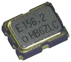
Oscillator, 100 MHz, HCSL, SMD, 3.2mm x 2.5mm, 3.3 V, SG3225HBN Series
⚠️ Reference pricing provided. In case of supply shortages, we will connect you with our trusted procurement partners to ensure your project's continuity.
- Manufacturer: EPSON
- Product type: Standard Oscillators
- SVHC: To Be Advised
- Frequency Nom: 100MHz
- Product Range: SG3225HBN Series
- Supply Voltage Nom: 3.3V
- Frequency Stability + / -: -
- Operating Temperature Max: 85°C
- Operating Temperature Min: -40°C
- Oscillator Case / Package: SMD, 3.2mm x 2.5mm
- Oscillator Output Compatibility: HCSL
| Delivery and price | |
|---|---|
| Units per pack | 1 |
| Price | 14.61 € |
| Current stock | 10+ |
| Lead time | 30 days |
Datasheet

**==> picture [527 x 60] intentionally omitted <==**

**----- Start of picture text -----**<br>
fj Crystal oscillator SEIKO EPSON CORPORATION<br>ws<br>Pb RoHS Product Number<br>CRYSTAL OSCILLATOR (SPXO) &., in X1G008141xxxx00<br>OUTPUT : HCSL ree CompliantL<br>**----- End of picture text -----**<br>


**==> picture [525 x 314] intentionally omitted <==**

**----- Start of picture text -----**<br>
eFrequency range : 100 MHz to 325 MHz<br>eSupply voltage : 2.5V,3.3V<br>eOutput : HCSL<br>eFunction : Output enable (OE)<br>eExternal dimensions : 3.2 x 2.5 x 1.05mm<br>ePhase jitter : 85 fs Typ (fo = 156.25MHz)<br>WH Specifications (characteristics)<br>Conditions / Remarks<br>Quputtequensy range 400 MHz to 325 MHz inarequencies. contact us for inquiries regarding available<br>D:2.5V+0.125V,C:3.3V+0.165V PT<br>-55 °C to +125 °C Store as bare product.<br>Operating temperature G: -40 °C to +85 °C, H: -40 °C to +105 °C Po<br>di+ 50 x 10° Includes initial frequency tolerance, temperature<br>Frequency tolerance f_tol (Not available H : -40 °C to +105 °C) variation, supply voltage change and 10 years<br>L: + 100 x 10° aging(+25 °C)<br>[Disable current | dis, [MA25 mA Typ. 35Max, mA Max. OE =RGND Vcc, with output load<br>45 % to 55 %<br>Output 0.75V Typ., 0.66V to 0.85V a .<br> voltage OV Typ., -0.15 V to 0.15V DC characteristics, single output<br>0.25V to 0.55V PT<br>Output load condition7 eSL_HCSL FCN C“S=sSTZLZ<br>Input 70 % Vee Min. ;<br> voltage 30 % Voc Max. OE terminal<br>citfoceimialtise slew rate/altifall slew rate Rr/ Rf 1 Vins to 4 Vins Between -0.15 V and 0.15 V of differential output<br>Time at minimum supply voltage to be 0's<br>i Phase Jitter<br>Outeut 100 MH 25 MH 56.25 MH 200 MHz ——|322.265625 MHz| Supply vol<br>Pere GTS Zz 1 Zz 156. z z : Z| Supply voltage<br>Phase Jitter [fs] -<br>**----- End of picture text -----**<br>


**==> picture [407 x 48] intentionally omitted <==**

**----- Start of picture text -----**<br>
Product Name SG3225 HBN 156.250000MHz C JGA (©©: Not Available code JH)<br>(Standard form) ® 2) ©) @©OO@<br>@Model (@)Output (H: HCSL) (@)Frequency @Supply voltage (D: 2.5 V Typ. , C: 3.3 V Typ.)<br>@Frequency tolerance (J: +50 x 10° L:+100 x 10°)<br>@0Operating temperature (G:-40 to +85°C, H:-40 to +105°C) M@)nternal identification code(“A” is default)<br>**----- End of picture text -----**<br>


**==> picture [521 x 181] intentionally omitted <==**

**----- Start of picture text -----**<br>
WB External dimensions (Unit:mm) [il Footprint (Recommended) (Unit:mm)<br>:<br>£ 3.2040,20 1,050.15 0.80 0.92<br>ee | Pin map >| kK<br>o| ffl | (0.25)<br>ieei [ef Vec ~<br>3 Note: 2.58<br>= OE pin = HIGH or “Open” : Specified frequency output.<br>V7 VY D2; OE pin = LOW: Output is high impedance<br>~oto 50 [fooa 5 so. ~ — recommendedIn order to achievethat theoptimumcapacitorjitter (0.1performance,pF + 10 ituF)is<br>— —— between Vcc and GND pin should be placed as close to<br>the Vec pin as possible.<br>**----- End of picture text -----**<br>


**==> picture [500 x 187] intentionally omitted <==**

**----- Start of picture text -----**<br>
NN<br>PROMOTION OF ENVIRONMENTAL MANAGEMENT SYSTEM<br>CONFORMING TO INTERNATIONAL STANDARDS<br>At Seiko Epson, all environmental initiatives operate under the<br>Plan-Do-Check-Action (PDCA) cycle designed to achieve continuous ISO 14000 is an international standard for environmental<br>improvements. The environmental management system (EMS) management that was established by the International<br>operates under the ISO 14001 environmental management standard. Standards Organization in 1996 against the background of<br>All of our major manufacturing and non-manufacturing sites, in growing concern regarding global warming, destruction of<br>Japan and overseas, completed the acquisition of ISO 14001 the ozone layer, and global deforestation.<br>certification. L—<br>nnn<br>WORKING FOR HIGH QUALITY<br>In order provide high quality and reliable products and services<br>than meet customer needs, Seiko Epson made early efforts towards IATF 16949 is the international standard that added the<br>obtaining ISO9000 series certification and has acquired ISO9001 for sector-specific supplemental requirements for automotive<br>all business establishments in Japan and abroad. We have also industry based on ISO9001.<br>acquired IATF 16949 certification that is requested strongly by major al<br>automotive manufacturers as standard.<br>**----- End of picture text -----**<br>


**==> picture [358 x 105] intentionally omitted <==**

**----- Start of picture text -----**<br>
> Explanation of the mark that are using it for the catalog<br>FrFree > Pb free.<br>Gm> Complies with EU RoHS directive.<br>*About the products without the Pb-free mark.<br>Compliant Contains Pb in products exempted by EU RoHS directive.<br>Contains Pb in sealing glass, high melting temperature type solder or other.<br>For Automotive<br>**----- End of picture text -----**<br>


**==> picture [495 x 49] intentionally omitted <==**

**----- Start of picture text -----**<br>
NOTICE : PLEASE READ CAREFULLY BELOW BEFORE THE USE OF THIS DOCUMENT @©Seiko Epson Corporation 2020<br>1. The content of this document is subject to change without notice. | Before purchasing or using Epson products, please contact with sales<br>representative of Seiko Epson Corporation (“Epson”) for the latest information and be always sure to check the latest information<br>published on Epson’s official web sites and resources.<br>**----- End of picture text -----**<br>


2. This document may not be copied, reproduced, or used for any other purposes, in whole or in part, without Epson’s prior consent.

3. Information provided in this document including, but not limited to application circuits, programs and usage, is for reference purpose only. Epson makes no guarantees against any infringements or damages to any third parties’ intellectual property rights or any other rights resulting from the information. This document does not grant you any licenses, any intellectual property rights or any other rights with respect to Epson products owned by Epson or any third parties.

4. Using Epson products, you shall be responsible for safe design in your products; that is, your hardware, software, and/or systems shall be designed enough to prevent any critical harm or damages to life, health or property, even if any malfunction or failure might be caused by Epson products. In designing your products with Epson products, please be sure to check and comply with the latest information regarding Epson products (including, but not limited to this document, specifications, data sheets, manuals, and Epson’s web site). Using technical contents such as product data, graphic and chart, and technical information, including programs, algorithms and application circuit examples under this document, you shall evaluate your products thoroughly both in stand-alone basis and within your overall systems. You shall be solely responsible for deciding whether to adopt/use Epson products with your products.

5. Epson has prepared this document carefully to be accurate and dependable, but Epson does not guarantee that the information is always accurate and complete. Epson assumes no responsibility for any damages you incurred due to any misinformation in this document.

6. No dismantling, analysis, reverse engineering, modification, alteration, adaptation, reproduction, etc., of Epson products is allowed. 7. Epson products have been designed, developed and manufactured to be used in general electronic applications and specifically designated applications (“Anticipated Purpose”). Epson products are NOT intended for any use beyond the Anticipated Purpose that requires particular quality or extremely high reliability in order to refrain from causing any malfunction or failure leading to critical harm to life and health, serious property damage, or severe impact on society, including, but not limited to listed below (“Specific Purpose”). Therefore, you are strongly advised to use Epson products only for the Anticipated Purpose. | Should you desire to purchase and use Epson products for Specific Purpose, Epson makes no warranty and disclaims with respect to Epson products, whether express or implied, including without limitation any implied warranty of merchantability or fitness for any Specific Purpose. Please be sure to contact our sales representative in advance, if you desire Epson products for Specific Purpose: Space equipment (artificial satellites, rockets, etc.)/ Transportation vehicles and their control equipment (automobiles, aircraft, trains, ships, etc.) / Medical equipment/ Relay equipment to be placed on sea floor/ Power station control equipment / Disaster or crime prevention equipment/Traffic control equipment/ Financial equipment Other applications requiring similar levels of reliability as the above

8. Epson products listed in this document and our associated technologies shall not be used in any equipment or systems that laws and regulations in Japan or any other countries prohibit to manufacture, use or sell. Furthermore, Epson products and our associated technologies shall not be used for the purposes of military weapons development (e.g. mass destruction weapons), military use, or any other military applications. If exporting Epson products or our associated technologies, please be sure to comply with the Foreign Exchange and Foreign Trade Control Act in Japan, Export Administration Regulations in the U.S.A (EAR) and other export-related laws and regulations in Japan and any other countries and to follow their required procedures.

9. Epson assumes no responsibility for any damages (whether direct or indirect) caused by or in relation with your non-compliance with the terms and conditions in this document or for any damages (whether direct or indirect) incurred by any third party that you give, transfer or assign Epson products.

10. For more details or other concerns about this document, please contact our sales representative.

11. Company names and product names listed in this document are trademarks or registered trademarks of their respective companies.

Seiko Epson Corporation
Updated at April 25, 2026
About Novapart
Novapart is a B2B electronic component broker specialising in stock shortages and cost reduction. We source hard-to-find parts and identify compliant alternatives across a catalogue of 410,000+ components from 500+ manufacturers.
Learn more →Stock Shortage Specialist
When a component is unavailable, discontinued or has an unacceptable lead time, we tap into our network of vetted European and Asian distributors to source what you need — without compromising on quality or traceability.
Request a quote →Compliant Alternatives
We identify pin-to-pin, electrically equivalent substitutes that meet the same certifications (RoHS, AEC-Q100, REACH) as your original specification — validated against datasheets, not just part numbers. Often at a lower cost.
BOM Analysis service →