
Image not available
Illustrative purposes only

X1G004131000912
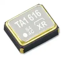
Oscillator, TXCO, GPS, 19.2 MHz, 0.5 ppm, SMD, 2mm x 1.6mm, 3.3 V, TG-5006CJ Series
⚠️ Reference pricing provided. In case of supply shortages, we will connect you with our trusted procurement partners to ensure your project's continuity.
- Manufacturer: EPSON
- Product type: Standard Oscillators
- Frequency Nom: 19.2MHz
- Product Range: TG-5006CJ
- Oscillator Case: SMD, 2mm x 1.6mm
- Supply Voltage Nom: 3.3V
- Frequency Stability + / -: 0.5ppm
- Operating Temperature Max: 85°C
- Operating Temperature Min: -30°C
- Oscillator Output Compatibility: Clipped Sinewave
| Delivery and price | |
|---|---|
| Units per pack | 100 |
| Price | 0.764 € |
| Current stock | 10+ |
| Lead time | 30 days |
Datasheet

## TCXO ## TG-5006CJ ## TG-5006CJ-18H 19.200000 MHz X1G0041310009xx ## Product name Product Number / Ordering code Please refer to the 10.Packing information about xx (last 2 digits) Output waveform Clipped sine wave Pb free / Complies with EU RoHS directive ## Reference weight Typ.9.1mg |**1.Absolute maximum ratings**|**1.Absolute maximum ratings**||||||| |---|---|---|---|---|---|---|---| |Parameter||Symbol|Min.|Typ.|Max.|Unit|Conditions / Remarks| |Maximum supply voltage||VCC-GND|-0.3|-|4|V|Vcc terminal| |Storage temperature||T_stg|-40|-|90|ºC|Storage as single product| ||||||||| |**2.Operating Conditions**|||||||| |Parameter||Symbol|Min.|Typ.|Max.|Unit|Conditions / Remarks| |Supply voltage||Vcc|1.7|-|3.3|V|GND = 0V| |||||-|-||-| |Operating temperature||T_use|-30|25|85|ºC|-| |Output load condition||Load_R|9|10|11|kΩ|-| |||Load_C|9|10|11|pF|DC cut capacitor=0.01µF| DC-cut capacitor is not included in this TCXO. Please attach an external DC-cut capacitor (0.01 μF Min.) to the out pin. (Vcc=1.8, 2.8, 3.0, 3.3 V, Vc=1.65 V, GND=0.0 V, Load 10 kΩ//10 pF(DC cut), T_use=+25ºC) |**3.Frequency Characteristics**<br>~~fC~~|**3.Frequency Characteristics**<br>~~fC~~|**3.Frequency Characteristics**<br>~~fC~~|**3.Frequency Characteristics**<br>~~fC~~|**3.Frequency Characteristics**<br>~~fC~~|**3.Frequency Characteristics**<br>~~fC~~|**3.Frequency Characteristics**<br>~~fC~~| |---|---|---|---|---|---|---| |**3.Frequency Characteristics**<br>Parameter<br>~~fCCC~~|**3.Frequency Characteristics**<br>Symbol<br>~~CC~~|Min.<br>~~CC~~|Typ.<br>~~CC~~|Max.<br>~~CC~~|Unit<br>~~CC~~|Conditions / Remarks<br>~~CC~~| |Output frequency<br>~~GO~~|Symbol<br>f0<br>~~GO~~|-<br>~~GO~~|Typ.<br>19.2000<br>~~GO~~|-<br>~~GO~~|MHz<br>~~GO~~|~~GO~~| |Frequency tolerance|f_tol|-2.0<br>-|-<br>-|2.0<br>-|x10-6|T_use = +25ºC, Reflow 2 times| |temperature characteristics<br>Frequency /|f0-Tc|-0.5<br>-|-<br>-|0.5<br>-|x10-6|T_use = -30 ºC to +85 ºC<br>-| |Frequency / load coefficient<br>~~SY~~|f0-Load<br>~~SY~~|-0.2<br>~~SY~~|-<br>~~SY~~|0.2<br>~~SY~~|x10-6<br>~~SY~~|10 kΩ // 10pF +/- 10%<br>~~SY~~| |Frequency / voltage coefficient|f0-Vcc|-0.2|-|0.2|x10-6|Vcc +/- 5 %| |Frequency slope|-|-<br>-<br>-|-<br>-<br>-|-<br>-<br>-|x10-6/ ºC|-<br>-<br>-| |Frequency aging|f_age|-1.0<br>-<br>-|-<br>-<br>-|1.0<br>-<br>-|x10-6|1st year, T_use=25degC<br>-<br>-| - *1 Include initial frequency tolerance and frequency deviation after reflow cycles. *2 Measured in the elapse of 24 hours after reflow soldering. *3 Vcc +/- 5% must be in operating supply voltage range (1.7 V to 3.47 V) (Vcc=1.8, 2.8, 3.0, 3.3 V, Vc=1.65 V, GND=0.0 V, Load 10 kΩ//10 pF(DC cut), T_use=+25ºC) |**4.Electrical Characteristics**<br>~~fp~~|**4.Electrical Characteristics**<br>~~fp~~|**4.Electrical Characteristics**<br>~~fp~~|**4.Electrical Characteristics**<br>~~fp~~|**4.Electrical Characteristics**<br>~~fp~~|**4.Electrical Characteristics**<br>~~fp~~|**4.Electrical Characteristics**<br>~~fp~~| |---|---|---|---|---|---|---| |Parameter<br>~~fp~~|Symbol<br><br>~~ee~~|Min.<br><br>~~ee~~|Typ.<br><br>~~ee~~|Max.<br><br>~~ee~~|Unit<br>|Conditions / Remarks<br>| |Current consumption<br>~~a~~|Symbol<br>Icc<br>~~a~~<br>~~ee~~|-<br>~~a~~<br>~~ee~~|Typ.<br>-<br>~~a~~<br>~~ee~~|1.5<br>~~a~~<br>~~ee~~<br>~~YD~~|mA<br>~~a~~<br>~~YD~~|T_Use = +25ºC , 10 kΩ//10pF<br>~~a~~| |Symmetry<br>~~DD~~|SYM<br>~~ee ~~<br>~~DD~~|40<br> ~~ee~~<br>~~DD~~|-<br>~~ee ~~<br>~~DD~~|60<br> ~~ee~~<br>~~DD~~<br>~~YD~~|%<br>~~DD~~<br>~~YD~~|GND Level<br>~~DD~~| |Output voltage<br>~~————~~|Vp-p<br>~~ee~~<br>|0.8<br>~~ee~~<br>|-<br>~~ee~~<br>|1.5<br>~~YD~~<br>~~ee~~<br>|V<br>~~YD~~|Peak topeak 10 kΩ//10pF +/- 10%| |Harmonics<br>~~a~~<br>~~———— ——_——ee—~~|Vpp<br>-<br>~~a~~<br>~~ee~~<br>~~——_——ee—~~|-<br>-<br>~~a~~<br>~~ee~~<br>~~——_——ee—~~|-<br>-<br>~~a~~<br>~~ee~~<br>~~——_——ee—~~|-8<br>-<br>~~a~~<br>~~ee~~<br>~~——_——ee—~~|dBc<br>~~a~~|-<br>-<br>~~a~~<br>~~eee~~| |start up time<br>~~———— ——_——ee—~~|tosc<br>~~ee~~<br>~~——_——ee—~~|-<br>~~ee~~<br>~~——_——ee—~~|-<br>~~ee~~<br>~~——_——ee—~~|2.0<br>~~ee~~<br>~~——_——ee—~~|ms|Within 90% of final amp.<br>~~eee~~| |||-<br>~~ee~~<br>~~——_——ee—~~<br>~~a~~|-<br>~~ee~~<br>~~——_——ee—~~<br>|2.0<br>~~ee~~<br>~~——_——ee—~~<br>|ms<br>|ΔF = +/- 1.0 x 10⁻⁶<br>~~eee~~<br>| |Phase noise<br>~~———— ——_——ee—~~|L(f)<br>~~ee ~~<br>~~——_——ee—~~|-<br> ~~ee~~<br>~~——_——ee—~~<br>~~pT~~|-<br>~~ee ~~<br>~~——_——ee—~~<br>~~pT~~|-87<br> ~~ee~~<br>~~——_——ee—~~<br>~~pT~~|dBc/Hz<br>~~pT~~|Offset:10 Hz<br>~~eee~~<br>~~pT~~| |||-<br>~~a~~|-<br>|-113<br>|dBc/Hz<br>|Offset:100 Hz<br>| |||-<br>~~pO~~|-<br>~~pO~~|-135<br>~~pO~~|dBc/Hz<br>~~pO~~|Offset:1 kHz<br>~~pO~~| |||-<br>~~a~~|-<br>|-147<br>|dBc/Hz<br>|Offset:10 kHz<br>| |||-<br>~~pO~~<br>~~RS~~|-<br>~~pO~~<br>~~es~~|-148<br>~~pO~~<br>~~GQ~~|dBc/Hz<br>~~pO~~<br>~~GQ~~|Offset:100 kHz<br>~~pO~~<br>~~GQ~~| |||-<br>~~RS~~|-<br>~~es~~|-148<br>~~GQ~~|dBc/Hz<br>~~GQ~~|Offset:1 MHz<br>~~GQ~~| 1 Page ## **5.Timing chart** Output waveform (Clipped sine wave output) **==> picture [201 x 92] intentionally omitted <==** **----- Start of picture text -----**<br> Vp-p<br>GND<br>tW<br>t<br>SYM=tw/t×100 %<br>**----- End of picture text -----**<br> ## **6.Test circuit for TCXO** 1) Output Load : 10 kΩ//10 pF **==> picture [426 x 213] intentionally omitted <==** **----- Start of picture text -----**<br> 0.01 Test Point<br>VCC OUT<br>N.C GND<br>Supply<br>By-pass<br>Voltage Capacitor 10 pF 10 kΩ<br>0.01 mF<br>2) Current consumption<br>0.01<br>A VCC OUT<br>N.C GND<br>Supply<br>By-pass<br>Voltage Capacitor 10 pF 10 kΩ<br>0.01 mF<br>**----- End of picture text -----**<br> ## 3) Conditions 1. Oscilloscope: Impedance Min. 1 MΩ Input capacitance Max. 10 pF Band width Min. 300 MHz Impossible to measure both frequency and wave form at the same time.(In case of using oscilloscope's amplifier output, possible to measure both at the same time.) 2. Load_C includes probe capacitance. 3. A capacitor (By-pass:0.01 to 0.1 uF) is placed between VCC and GND,and closely to TCXO. 4. Use the current meter whose internal impedance value is small. 5. Power Supply Impedance of power supply should be as low as possible. 2 Page **==> picture [250 x 269] intentionally omitted <==** **----- Start of picture text -----**<br> 7.External dimensions (Unit: mm)<br>2.0±0<br>1.58<br>| #1 <Bottom View> #2<br>a |<br>ant C0.15<br>#4 1.2 #3<br>Pin map<br>OF<br>[4] = vec sd”<br>ee 9.Reflow profile<br>0.1<br>±<br>1.18 0.40<br>1.6<br>0.27<br>0.07<br>±<br>0.73<br>**----- End of picture text -----**<br> **==> picture [247 x 231] intentionally omitted <==** **----- Start of picture text -----**<br> 8.Footprint(Recommended) (Unit: mm)<br>0.6<br>ii 1.65 |<br>To maintain stable operation, provide a 0.01uF to 0.1uF<br>by-pass capacitor at a location as near as possible to the<br>power source terminal of the crystal product (between Vcc<br>- GND).<br>0.75<br>1.13<br>**----- End of picture text -----**<br> **==> picture [324 x 168] intentionally omitted <==** **----- Start of picture text -----**<br> Temperature [C ]<br>300<br>TP ; +260C<br>+255C<br>tp ; 20 s to 40 s<br>250 Avg. Ramp-up<br>200 TL Ts max ;; +217+200CC 3 C / s Max. (60+217s totL C 150over s) 6Ramp-down C / s Max.<br>150 Ts min ; +150 C 60 s tots 180 s<br>( +150C to +200C )<br>100<br>50<br>Time +25 C to Peak<br>0 60 120 180 240 300 360 420 480 540 600 660 720 780<br>Time [ s ]<br>**----- End of picture text -----**<br> **10.Packing information** [ 1 ]Product number last 2 digits code(xx) description The recommended code is "00" X1G0041310009xx Code Condition Code Condition 00 12000pcs / Reel 14 1000pcs / Reel 01 Any Q'ty vinyl bag(Tape cut) 15 2000pcs / Reel 11 Any Q'ty / Reel 16 3000pcs / Reel ~~=n~~ 3 Page **==> picture [465 x 527] intentionally omitted <==** **----- Start of picture text -----**<br> [ 2 ] Taping specification<br>Subject to EIA-481 & IEC-60286<br>(1) Tape dimensions TE0804L<br>Material of the Carrier Tape : PS<br>Material of the Top Tape : PET+PE Unit: mm<br>4 .0 ±0 .1 1 .0±0 .1<br>+0 .1<br>2 .0±0 .1 φ 1 .5 0 0 .25±0 .05<br>+0 .1<br>φ 1 .0 0<br>_ 4 .0±0 .1<br>Sen 1 .85±0 .1 a)<br>=—<br>(2) Reel dimensions<br> Center material : PS<br>13.4 1. 0<br> Material of the Reel : PS<br>9 . 4 1 . 0<br>2.0 0 . 5<br>e a<br>0.2 2. 0<br> <br>100.0<br>13.0<br>φ 330.0<br>φ<br>φ<br>1 .75±0 .1<br>3 .5±0 .1<br>8 .0±0 .2<br>2 .25±0 .1<br>**----- End of picture text -----**<br> 4 Page **11.Handling precautions** Prior to using this product, please carefully read the section entitled “Precautions” on our Web site ( http://www5.epsondevice.com/en/quartz/tech/precaution/ ) for instructions on how to handle and use the product properly to ensure optimal performance of the product in your equipment. Before using the product under any conditions other than those specified therein, please consult with us to verify and confirm that the performance of the product will not be negatively affected by use under such conditions. In addition to the foregoing precautions, in order to avoid the deteriorating performance of the product, we strongly recommend that you DO NOT use the product under ANY of the following conditions: (1) Mounting the product on a board using water-soluble solder flux and using the product without removing the residue of the flux completely from the board. The residue of such flux that is soluble in water or water-soluble cleaning agent, especially the residues which contains active halogens, will negatively affect the performance and reliability of the product. (2) Using the product in any manner that will result in any shock or impact to the product. (3) Using the product in places where the product is exposed to water, chemicals, organic solvent, sunlight, dust, corrosive gasses, or other materials. (4) Using the product in places where the product is exposed to static electricity or electromagnetic waves. (5) Applying ultrasonic cleaning without advance verification and confirmation that the product will not be affected by such a cleaning process, because it may damage the crystal, IC and/or metal line of the product. (6) Touching the IC surface with tweezers or other hard materials directly. (7) Using the product under any other conditions that may negatively affect the performance and/or reliability of the product. (8) Using the product with power line ripple exceeding 50 mV(p-p) level. Should any customer use the product in any manner contrary to the precautions and/or advice herein, such use ~~aan~~ 5 Page ## **Notice** - This material is subject to change without notice. - Any part of this material may not be reproduced or duplicated in any form or any means without the written permission of Seiko Epson. · The information about applied data,circuitry, software, usage, etc. written in this material is intended for reference only. Seiko Epson does not assume any liability for the occurrence of customer damage or infringing on any patent or copyright of a third party. This material does not authorize the licensing for any patent or intellectual copyrights. · When exporting the products or technology described in this material, you should comply with the applicable export control laws and regulations and follow the procedures required by such laws and regulations. · You are requested not to use the products (and any technical information furnished, if any) for the development and/or manufacture of weapon of mass destruction or for other military purposes. You are also requested that you would not make the products available to any third party who may use the products for such prohibited purposes. · These products are intended for general use in electronic equipment. When using them in specific applications that require extremely high reliability, such as the applications stated below, you must obtain permission from Seiko Epson in advance. / Space equipment (artificial satellites, rockets, etc.) / Transportation vehicles and related (automobiles, aircraft, trains, vessels, etc.) / Medical instruments to sustain life / Submarine transmitters / Power stations and related / Fire work equipment and security equipment / Traffic control equipment - / And others requiring equivalent reliability. ## **Contact us** http://www5.epsondevice.com/en/contact/ 6 Page
Updated at February 9, 2023
About Novapart
Novapart is a B2B electronic component broker specialising in stock shortages and cost reduction. We source hard-to-find parts and identify compliant alternatives across a catalogue of 410,000+ components from 500+ manufacturers.
Learn more →Stock Shortage Specialist
When a component is unavailable, discontinued or has an unacceptable lead time, we tap into our network of vetted European and Asian distributors to source what you need — without compromising on quality or traceability.
Request a quote →Compliant Alternatives
We identify pin-to-pin, electrically equivalent substitutes that meet the same certifications (RoHS, AEC-Q100, REACH) as your original specification — validated against datasheets, not just part numbers. Often at a lower cost.
BOM Analysis service →