
Image not available
Illustrative purposes only

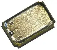
X1A000191000211
Crystal, FC1610BN Series, 32.768 kHz, 20 ppm, 9 pF
⚠️ Reference pricing provided. In case of supply shortages, we will connect you with our trusted procurement partners to ensure your project's continuity.
- Manufacturer: EPSON
- Product type: Crystals
- ESR: 70kohm
- SVHC: No SVHC (25-Jun-2025)
- No. of Pins: 2Pins
- Crystal Type: -
- Product Range: FC1610BN Series
- Qualification: -
- Crystal Mounting: SMD
- Load Capacitance: 9pF
- Crystal Frequency: 32.768kHz
- Crystal Dimensions: -
- Crystal Case / Package: SMD, 1.6mm x 1mm
- Frequency Stability + / -: -
- Frequency Tolerance + / -: 20ppm
- Operating Temperature Max: 105°C
- Operating Temperature Min: -40°C
| Delivery and price | |
|---|---|
| Units per pack | 500 |
| Price | 0.712 € |
| Current stock | 10+ |
| Lead time | 30 days |
Datasheet

## **kHz Range Crystal unit** - Package size (1.6 mm × 1.0 mm × 0.5 mm) · Fundamental mode - Reference weight Typ.2.6 mg ## [ 1 ] Product Number / Product Name / Marking (1-1) Product Number / Ordering Code ## **X1A0001910002xx** Last 2 digits code( **xx** ) defines Quantity. The standard is "18", 5 000 pcs/Reel. (1-2) Product Name / Model Name ## FC1610BN 32.768000 kHz 9.0 +20.0-20.0 ## [ 2 ] Absolute maximum ratings ||~~ee~~|~~eee~~|~~eee~~|~~eee~~||| |---|---|---|---|---|---|---| |Parameter<br>~~re~~|Symbol<br>~~re~~<br>~~ee~~|Specifications<br>~~re~~<br>~~eee~~|||Unit<br>~~ot~~|Conditions<br>~~ot~~| |||Min.<br>~~re~~<br>~~eee~~|Typ.<br>~~re~~<br>~~eee~~|Max.<br>~~re~~<br>~~eee~~||| |Nominal frequency<br>~~eG~~|f_nom<br>~~ee ~~<br>~~eG~~<br>~~ss~~|-<br> ~~eee~~<br>~~eG~~<br>~~ss~~|32.768000<br>~~eee~~<br>~~eG~~|-<br>~~eee~~<br>~~eG~~|kHz<br>~~eG~~|~~eG~~| |Operatingtemperature<br>~~es~~|T_use<br>~~es~~<br>~~ss~~|-40<br>~~es~~<br>~~ss~~|-<br>~~es~~|+105<br>~~es~~|ºC<br>~~es~~|~~es~~| |Level of drive<br>~~GQ~~|DL<br>~~ss~~<br>~~GQ~~<br>~~ss~~|-<br>~~ss~~<br>~~GQ~~<br>~~ss~~|0.1<br>~~GQ~~|0.5<br>~~GQ~~|µW<br>~~OO~~|~~OO~~| |Frequencytolerance<br>~~es~~|f_tol<br>~~es~~<br>~~ss~~|-20<br>~~es~~<br>~~ss~~|-<br>~~es~~|+20<br>~~es~~|x 10-6<br>~~es~~|+25 ºC DL = 0.1µW<br>~~es~~| |Turnover temperature<br>~~GQ~~|Ti<br>~~ss~~<br>~~GQ~~<br>~~es es~~|+20<br>~~ss~~<br>~~GQ~~<br>~~es~~|+25<br>~~GQ~~|+30<br>~~GQ~~|ºC<br>~~OO~~|~~OO~~| |Parabolic coefficient<br>~~es~~|B<br>~~es~~<br>~~es es~~|-<br>~~es~~<br>~~es~~|-<br>~~es~~|-0.04<br>~~es~~|x 10-6/ºC2<br>~~es~~|~~es~~| |Load capacitance<br>~~QO~~|CL<br>~~es es~~<br>~~QO~~|-<br>~~es~~<br>~~QO~~<br>~~rr~~|9.0<br>~~QO~~<br>~~ee~~|-<br>~~QO~~|pF<br>~~OO~~|~~OO~~<br>~~PO~~| |Motional resistance (ESR)|R1|-<br>~~rr~~<br>~~a~~|45<br>~~ee~~<br>~~ee~~|-|kΩ|+25 ºC<br>~~PO~~<br>~~Po~~| |||-<br>~~rr~~<br>~~a~~<br>~~rr~~|-<br>~~ee~~<br>~~ee~~<br>~~ee~~|60||-40 ºC to +85 ºC<br>~~PO~~<br>~~Po~~<br>~~Po~~| |||-<br>~~a~~<br>~~rr~~|-<br>~~ee~~<br>~~ee~~|70||-40 ºC to +105 ºC<br>~~Po~~<br>~~Po~~| |Motional capacitance<br>~~QO~~|C1<br>~~QO~~<br>~~es~~|-<br>~~rr~~<br>~~QO~~|7.8<br>~~ee~~<br>~~QO~~|-<br>~~QO~~|fF<br>~~OO~~|~~Po~~<br>~~OO~~| |Shunt capacitance<br>~~es~~|C0<br>~~es~~<br>~~es~~|-<br>~~es~~|1.5<br>~~es~~|-<br>~~es~~|pF<br>~~es~~|~~es~~| |Motional inductance<br>~~QO~~|L1<br>~~es~~<br>~~QO~~<br>~~es es~~|-<br>~~QO~~<br>~~es~~|3.0<br>~~QO~~|-<br>~~QO~~|kH<br>~~OO~~|~~OO~~| |Frequencyaging<br>~~es~~|f_age<br>~~es~~<br>~~es es~~|-3<br>~~es~~<br>~~es~~|-<br>~~es~~|+3<br>~~es~~|x10-6/year <br>~~es~~|+25 ºC,Firstyear<br>~~es~~| ## **[ For other general specifications, please refer to the attached Full Data Sheet below ]** 2025/7/15 1 / 8 Page ## **Low ESR, 1.6 x 1.0 mm size 32.768 kHz Crystal unit: FC1610BN** ## **Features** - Package size: 1.6 x 1.0 mm, t = 0.5 mm Max. - Nominal frequency range: 32.768 kHz - Frequency tolerance: ±20 x 10[-6] (+25 °C) - Operating temperature: -40 °C to +105 °C - ESR: 45 kΩ Typ. (+25 °C) - 60 kΩ Max. (-40 °C to +85 °C) 70 kΩ Max. (-40 °C to +105 °C) **==> picture [129 x 19] intentionally omitted <==** **----- Start of picture text -----**<br> FC1610BN<br>(1.6 x 1.0 mm, t = 0.5 mm Max.)<br>**----- End of picture text -----**<br> ## **Applications** - Wearable products - MCUs for sub-clock - Wireless modules for sub-clock - FA equipment ## **Description** FC1610BN is a small size (1.6 mm x 1.0 mm) and low ESR (70 kΩ) 32.768 kHz crystal unit. Ideal for IoT (BLE, LPWA, etc.) sleep clocks that require small size and low power, clocks for wearable devices, sub clocks for microcomputers, etc. The operating temperature range is supported up to +105ºC. Epson is a leading supplier of kHz-band crystal units and offers a lineup of oscillators with built-in oscillator circuit ICs and real-time clock modules with built-in real-time clock ICs, in addition to crystal units. Epson is committed to providing the lowest power solution for our customers. ## **Outline Drawing and Terminal Assignment** **==> picture [269 x 197] intentionally omitted <==** **----- Start of picture text -----**<br> 1.6 ± 0.1<br>Internal<br>Connection<br>0.72 0.4<br>#1 #2<br>ae TU<br>Pin Connection<br>#1 #2 #1 X'tal<br>#2 X'tal<br>1.0 ± 0.1<br>0.5 Max.<br>0.86<br>**----- End of picture text -----**<br> **Document No FC1610BN_E_Ver2.0** **Page 2 / 8** ## [ 1 ] Product Number / Product Name ## (1-1) Product Number - X1A000191xxxx18 (Please contact Epson for details) ## (1-2) Product Name (Standard Form) ## FC1610BN 32.768000kHz 12.5 +20.0-20.0 a b c d a: Model b: Frequency c: Load capacitance (pF) d: Frequency tolerance (x10[-6] , +25 °C) ## [ 2 ] Absolute Maximum Ratings |Item|Symbol|Rating value|Rating value|Rating value|Unit|Note| |---|---|---|---|---|---|---| |||Min.|Typ.|Max.||| |Storage temperature range|T_stg|-55|-|+125|°C|| |Maximum level of drive|GL|-|-|0.5|μW|| ## [ 3 ] Operating Conditions |[ 33 ] Operatingratingatingingg Conditionsnditionsditionsitionstionsionsonsnss||||||| |---|---|---|---|---|---|---| |Item|Symbol|Rating value|||Unit|Note| |||Min.|Typ.|Max.||| |Operating temperature range|T_use|-40|-|+105|°C|| |Level of drive|DL|0.01|0.1|0.5|μW|| |Load capacitance|CL|7.0, 9.0, 12.5|||pF|Please contact us for other<br>CL values| ## [ 4 ] Static Characteristics |[ 4 ]] Staticicc Characteristicsharacteristicsaracteristicsracteristicsacteristicsristicssticsicscs||||| |---|---|---|---|---| |Item<br>~~a~~|Symbol|Specifications|Unit|Condition / Remarks| |Nominal frequency range<br>~~a~~|f_nom|32.768|kHz|| |Frequency tolerance|f_tol|±20|x10-6|T_use = +25 °C ± 3 °C<br>DL = 0.1 μW<br>Does not include<br>frequency aging| |Turnover temperature<br>~~es~~|Ti<br>~~es~~<br>~~es~~|+25 ± 5<br>~~es~~|°C<br>~~es~~|~~es~~| |Parabolic coefficient<br>~~ee~~|B<br>~~ee~~<br>~~es~~|-0.04 Max.<br>~~ee~~|x10-6/ °C2<br>~~ee~~|~~ee~~| |Motional resistance (ESR)|R1<br>~~es~~|45 Typ.<br>(+25 °C)|kΩ|Measuring instrument:<br>Keysight 4294A<br>DL = 0.5 μW| |||60 Max.<br>(-40 °C to +85 °C)||| |||70 Max.<br>(-40 °C to +105 °C)||| |Motional capacitance<br>~~ee~~|C1<br>~~ee~~<br>~~es~~|7.8 Typ.<br>~~ee~~|fF<br>~~ee~~|~~ee~~| |Shunt capacitance<br>~~ee~~|C0<br>~~ee~~<br>~~es~~|1.5 Typ.<br>~~ee~~|pF<br>~~ee~~|~~ee~~| |Isolation resistance<br>~~ee~~|IR<br>~~es~~<br>~~ee~~|200 Min.<br>~~ee~~|MΩ<br>~~ee~~|~~ee~~| |Frequency aging|f_age|±3|x10-6|T_use = +25 °C ± 3 °C,<br>First year, DL = 0.1 μW| **Document No FC1610BN_E_Ver2.0** **Page 3 / 8** ## [ 5 ] Frequency vs. Temperature Characteristics **==> picture [225 x 141] intentionally omitted <==** **----- Start of picture text -----**<br> n = 22 n = 22<br>100<br>90<br>80<br>70 Bane<br>G 60 UT<br>x<br>2 50<br>OOO—r<br>\ uw<br>\ 30<br>\, 20 Typ.45kΩ<br>**----- End of picture text -----**<br> ## [ 6 ] Marking Description **==> picture [298 x 79] intentionally omitted <==** **----- Start of picture text -----**<br> Internal ID<br>Frequency symbol<br>A: 32.768 kHz A A 9T<br>Internal ID<br>0 8 8<br>Year of manufacture Month of manufacture<br>(Last digit of the year) (Table 1.)<br>**----- End of picture text -----**<br> Table 1. Month of manufacture |Month|Month Jan|Feb|Mar|Apr|May|Jun|Jul|Aug|Sep|Oct|Nov|Dec| |---|---|---|---|---|---|---|---|---|---|---|---|---| |Code|1|2|3|4|5|6|7|8|9|X|Y|Z| **Document No FC1610BN_E_Ver2.0** **Page 4 / 8** ## [ 7 ] Outline Drawing and Recommended Footprint **==> picture [398 x 228] intentionally omitted <==** **----- Start of picture text -----**<br> Unit: mm<br>1.1<br>1.6 ± 0.1<br>— ——ae<br>ai i oi<br>0.5<br>—i Do not design any circuit<br>patterns in the shaded area.<br>oe 0.72 0.4 Pin Connection<br>Internal<br>#1 #2 Connection #1 X'tal<br>#2 X'tal<br>#1 #2<br>1.0<br>1.0 ± 0.1<br>0.5 Max.<br>0.86<br>**----- End of picture text -----**<br> Reference weight: Typ.2.6 mg Terminal coating: Au plating |[ 8 ] Moisture Sensitivity Level<br>Parameter<br>MSL<br>[ 9 ] Reflow Profile (IPC/JEDEC J-STD-020D.1)<br>~~ee~~|[ 9 ] Reflow Profile (IPC/JEDEC J-STD-020D.1)<br>Specification<br>LEVEL1|Conditions<br>IPC/JEDEC J-STD-020D.1| |---|---|---| ## [ 9 ] Reflow Profile (IPC/JEDEC J-STD-020D.1) **==> picture [274 x 185] intentionally omitted <==** **----- Start of picture text -----**<br> Temperature [ C ]<br>300 TP ; +260 C [OVER]<br>+255 C<br>tp ; at least 30 s<br>250 Ramp-up rate<br>TL ; +217 C +3 °C/s Max. tL Ramp-down rate<br>-6 °C/s Max.<br>200 Ts max ; +200 C 60 s to 150 s<br>Ts min ; +150 C ts<br>150<br>60 s to 120 s<br>100<br>50<br>Time +25 C to Peak<br>0 60 120 180 240 300 360 420 480 540 600 660 720 780<br>Time [ s ]<br>**----- End of picture text -----**<br> **Document No FC1610BN_E_Ver2.0** **Page 5 / 8** ## [ 10 ] Packing Information ## (1) Packing Quantity The last two digits of the Product Number (X1A000191xxxx18) are a code that defines the packing quantity The standard is "18" for a 5 000 pcs/Reel. - (2) Taping Specification Compliant to EIA-481, IEC 60286 - (2-1) Tape Dimensions Carrier Tape Material : PS (Polystyrene) Top Tape Material : PET (Polyethylene Terephthalate) +PE (Polyethylene) **==> picture [330 x 153] intentionally omitted <==** **----- Start of picture text -----**<br> Unit : mm<br>10P 40±0.15<br>2.0±0.05 4.0±0.1 0.65±0.1<br>+0.1<br>Φ1.5 -0<br>0.25±0.05<br>+0.1 4.0±0.1<br>Φ0.5-0 | 1.3±0.05 ——_—_<br>User direction of feed<br>1.75±0.1<br>3.5±0.05<br>Epson 8.0±0.2 1.9±0.05<br>**----- End of picture text -----**<br> - (2-2) Reel Dimensions Center Material : PS (Polystyrene) Reel Material : PS (Polystyrene) **==> picture [242 x 226] intentionally omitted <==** **----- Start of picture text -----**<br> Unit : mm<br>Φ180 +0<br>-3.0 11.4 ± 1<br>9 ± 0.3<br>|} || SNNN \<br>| | ~~ \<br>NN \ \<br>eVIN NK)\ \ Ty<br>2±0.5<br>Φ10 Φ13±0 .2<br>— J / ! i<br>| | “A } a<br>Φ21±0.8<br>Φ60<br>**----- End of picture text -----**<br> **Document No FC1610BN_E_Ver2.0** **Page 6 / 8** ## [ 11 ] Handling Precautions Please review the "Handling Precautions" on our website for proper handling and behavior to ensure the performance of your equipment/product. (https://www5.epsondevice.com/en/information/#precaution) In addition to the "Handling Precautions" on the website, please also pay attention to the following to avoid deterioration of product performance. 1. Max three (3) times reflow is allowed. - In case of rework by soldering iron, its condition should be +350 ºC max. + within 5 sec. 2. Applying excessive shock or vibration to the crystal unit may causes deterioration damage. The product may be damaged depends on the condition such as shock in assembly machine. Please check if your condition is safe in advance. - And in case of assembly condition change, please check it again in advance. 3. Shortest line pattern on PCB is recommended. Too long line on PCB may causes abnormal oscillation. 4. Failures covered by free warranty period are limited to the cases where the product is used under the usage and environment described in the specifications. In addition, products that have been opened (including partially opened, modified, or intended to be opened) are not covered. In order to ensure frequency accuracy and prevent moisture condensation due to sudden temperature changes, - it is recommended to store and use in normal room temperature and humidity. If the product is stored for a long period (one year or more), please check solderability of the terminals before use. 5. Ultrasonic cleaning may cause resonant damage of the crystal unit depend on its condition. - Since we are unable to specify the conditions (type of cleaning unit, power, time, condition inside the bath, etc.) - at your company, we cannot guarantee the performance of the product when it is cleaned by ultrasonic cleaner. 6. Condensation on oscillator circuit board may causes frequency shift or oscillation stop. Please use the product under the condition there is no condensation. 7. If excessive drive level is applied to the crystal unit, it may cause performance deterioration and damages. Please design appropriate drive level on the circuit. 8. Characteristics differences between our measurement and your company’s measurement may occur depending on measurement method and conditions. Please check it thoroughly before use. 9. Do not place signal lines, power lines, or GND lines in mounting area of the product, its inner layer, or its back side. In order to avoid malfunction due to induction of other signal lines, please do not place signal lines near the product. It may affect product characteristics. - 10.If there is no margin in negative resistance of the oscillator circuit, the crystal unit may not oscillate or may take a long time to oscillate. Therefore, negative resistance in the oscillator circuit should be at least five times of the crystal unit’s equivalent series resistance. Please follow this circuit design rule. - 11.Aging specifications are estimated value of frequency shift from reliability test results. It does not mean to guarantee product lifecycle. - 12.If customer wants to use our product contrary to this caution and advice, please use it at your own risk. <How to check the negative resistance> **==> picture [146 x 108] intentionally omitted <==** **----- Start of picture text -----**<br> Rf<br>RD<br>r<br>L X'tal L<br>CG CD<br>**----- End of picture text -----**<br> - 1) Insert a pure resistance " r " in series with the crystal oscillator. - 2) Adjust " r " to find the maximum " r " value that starts oscillation - 3) Look at the value of "r " in the oscillation state of 2). Negative resistance of the circuit |-R| = r + crystal unit series resistance value R1 Guideline for negative resistance |-R|: |-R| > R1 Max. x 5 **Document No FC1610BN_E_Ver2.0** **Page 7 / 8** tS **PROMOTION OF ENVIRONMENTAL MANAGEMENT SYSTEM CONFORMING TO INTERNATIONAL STANDARDS** At Seiko Epson, all environmental initiatives operate under the ISO 14000 is an international standard for environmental Plan-Do-Check-Action (PDCA) cycle designed to achieve continuous management that was established by the International Standards improvements. The environmental management system (EMS) Organization in 1996 against the background of growing concern operates under the ISO 14001 environmental management standard. regarding global warming, destruction of the ozone layer, and global All of our major manufacturing and non-manufacturing sites, in deforestation. Japan and overseas, completed the acquisition of ISO 14001 certification. — Eee **WORKING FOR HIGH QUALITY** In order provide high quality and reliable products and services than meet customer needs, Seiko Epson made early efforts towards IATF 16949 is the international standard that added the sector-specific obtaining ISO9000 series certification and has acquired ISO9001 for supplemental requirements for automotive industry based on ISO9001. all business establishments in Japan and abroad. We have also acquired IATF 16949 certification that is requested strongly by major manufacturers as standard. ■ Explanation of marks used in this datasheet Pb ● **Pb free.** FS... ● **Complies with EU RoHS directive.** RoHS *About the products without the Pb-free mark. Contains Pb in products exempted by EU RoHS directive (Contains Pb in sealing glass, high melting temperature type solder or other) NOTICE `:` PLEASE READ CAREFULLY BELOW BEFORE THE USE OF THIS DOCUMENT - ―――――――――――――――――――――――――――――――――――――――――――――――――――― 1. The content of this document is subject to change without notice. Before purchasing or using Epson products, please contact with sales representative of Seiko Epson Corporation (“Epson”) for the latest information and be always sure to check the latest infor mation published on Epson’s official web sites and resources. - 2. This document may not be copied, reproduced, or used for any other purposes, in whole or in part, without Epson’s prior consent. 3. Information provided in this document including, but not limited to application circuits, programs and usage, is for reference purpose only. Epson makes no guarantees against any infringements or damages to any third parties’ intellectual property rights or any other rights resulting from the information. This document does not grant you any licenses, any intellectual property rights or any other rights with respect to Epson products owned by Epson or any third parties. - 4. Epson has prepared this document carefully to be accurate and dependable, but Epson does not guarantee that the information is always accurate and complete. Epson assumes no responsibility for any damages you incurred due to any misinformation in this document. - 5. Epson products listed in this document and our associated technologies shall not be used in any equipment or systems that laws and regulations in Japan or any other countries prohibit to manufacture, use or sell. Furthermore, Epson products and our associated technologies shall not be used for the purposes of military weapons development (e.g. mass destruction weapons), military use, or any other military applications. If exporting Epson products or our associated technologies, please be sure to comply with the Foreign Exchange and Foreign Trade Control Act in Japan, Export Administration Regulations in the U.S.A (EAR) and other export-related laws and regulations in Japan and any other countries and to follow their required procedures. - 6. Epson assumes no responsibility for any damages (whether direct or indirect) caused by or in relation with your non-compliance with the terms and conditions in this document or for any damages (whether direct or indirect) incurred by any third party that you give, transfer or assign Epson products. - 7. For more details or other concerns about this document, please contact our sales representative. 8. Company names and product names listed in this document are trademarks or registered trademarks of their respective companies. `●` Disclaimer 1. Epson products are designed for use in general electronic equipment applications that do not require extremely high reliability or safety. 2. Epson does not represent or warrant that its products will not cause a failure for any particular application, except for cases where the failure is a direct result caused by defects in materials and workmanship of this product. If a product fails due to defects in materials and workmanship, to the maximum extent permitted by law, we will, at our sole discretion, refund or replace the affected product. - 3. When products for used directly or indirectly in certain devices or applications (ex. Nuclear power, aerospace, infrastructure facilities, medical equipment, etc.) which are connected to or affect safety of human life or property, Customer is solely responsible for determining if the products and respective specifications are suitable for the intended use in particular customer applications. Customer shall implement necessary and proper safety design and measures (including redundant design, malfunction prevention design, etc.) to ensure reliability and safety before using the products in/with customer’s Equipment. - 4. No dismantling, analysis, reverse engineering, modification, alteration, adaptation, reproduction, etc., of Epson products is allowed. Furthermore, any defects caused by this are not covered by the warranty. - ©Seiko Epson Corporation 2025 **Document No FC1610BN_E_Ver2.0** **Page 8 / 8**
Updated at April 28, 2026
About Novapart
Novapart is a B2B electronic component broker specialising in stock shortages and cost reduction. We source hard-to-find parts and identify compliant alternatives across a catalogue of 410,000+ components from 500+ manufacturers.
Learn more →Stock Shortage Specialist
When a component is unavailable, discontinued or has an unacceptable lead time, we tap into our network of vetted European and Asian distributors to source what you need — without compromising on quality or traceability.
Request a quote →Compliant Alternatives
We identify pin-to-pin, electrically equivalent substitutes that meet the same certifications (RoHS, AEC-Q100, REACH) as your original specification — validated against datasheets, not just part numbers. Often at a lower cost.
BOM Analysis service →