
Image not available
Illustrative purposes only

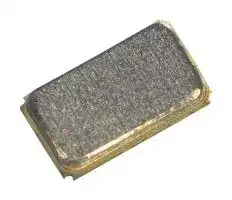
X1A0001710001
Crystal, 32.768 kHz, 20 ppm, 12.5 pF
⚠️ Reference pricing provided. In case of supply shortages, we will connect you with our trusted procurement partners to ensure your project's continuity.
- Manufacturer: EPSON
- Product type: Crystals
- SVHC: To Be Advised
- Frequency Nom: 32.768kHz
- Product Range: -
- Load Capacitance: 12.5pF
- Crystal Frequency: 32.768kHz
- Crystal Case / Package: SMD, 2.05mm x 1.2mm
- Frequency Stability + / -: -
- Frequency Tolerance + / -: 20ppm
- Operating Temperature Max: 105°C
- Operating Temperature Min: -40°C
| Delivery and price | |
|---|---|
| Units per pack | 500 |
| Price | 0.463 € |
| Current stock | 10+ |
| Lead time | 30 days |
Datasheet

## **kHz Range Crystal unit** - Package size (2.05 mm × 1.2 mm × 0.6 mm) · Fundamental mode - Reference weight Typ.4.3 mg ## [ 1 ] Product Number / Product Name / Marking (1-1) Product Number / Ordering Code ## **X1A0001710001xx** Last 2 digits code( **xx** ) defines Quantity. The standard is "18", 5 000 pcs/Reel. (1-2) Product Name / Model Name ## FC2012AN 32.768000 kHz 12.5 +20.0-20.0 ## [ 2 ] Absolute maximum ratings ||~~ee~~|~~eee~~|~~eee~~|~~eee~~||| |---|---|---|---|---|---|---| |Parameter<br>~~re~~|Symbol<br>~~re~~<br>~~ee~~|Specifications<br>~~re~~<br>~~eee~~|||Unit<br>~~ot~~|Conditions<br>~~ot~~| |||Min.<br>~~re~~<br>~~eee~~|Typ.<br>~~re~~<br>~~eee~~|Max.<br>~~re~~<br>~~eee~~||| |Nominal frequency<br>~~eG~~|f_nom<br>~~ee ~~<br>~~eG~~<br>~~ss~~|-<br> ~~eee~~<br>~~eG~~<br>~~ss~~|32.768000<br>~~eee~~<br>~~eG~~|-<br>~~eee~~<br>~~eG~~|kHz<br>~~eG~~|~~eG~~| |Operatingtemperature<br>~~es~~|T_use<br>~~es~~<br>~~ss~~|-40<br>~~es~~<br>~~ss~~|-<br>~~es~~|+105<br>~~es~~|ºC<br>~~es~~|~~es~~| |Level of drive<br>~~GQ~~|DL<br>~~ss~~<br>~~GQ~~<br>~~ss~~|-<br>~~ss~~<br>~~GQ~~<br>~~ss~~|-<br>~~GQ~~|0.5<br>~~GQ~~|µW<br>~~OO~~|~~OO~~| |Frequencytolerance<br>~~es~~|f_tol<br>~~es~~<br>~~ss~~|-20<br>~~es~~<br>~~ss~~|-<br>~~es~~|+20<br>~~es~~|x 10-6<br>~~es~~|+25 ºC DL = 0.1µW<br>~~es~~| |Turnover temperature<br>~~GQ~~|Ti<br>~~ss~~<br>~~GQ~~<br>~~es es~~|+20<br>~~ss~~<br>~~GQ~~<br>~~es~~|+25<br>~~GQ~~|+30<br>~~GQ~~|ºC<br>~~OO~~|~~OO~~| |Parabolic coefficient<br>~~es~~|B<br>~~es~~<br>~~es es~~|-<br>~~es~~<br>~~es~~|-<br>~~es~~|-0.04<br>~~es~~|x 10-6/ºC2<br>~~es~~|~~es~~| |Load capacitance<br>~~QO~~|CL<br>~~es es~~<br>~~QO~~|-<br>~~es~~<br>~~QO~~<br>~~rr~~|12.5<br>~~QO~~<br>~~ee~~|-<br>~~QO~~|pF<br>~~OO~~|~~OO~~<br>~~PO~~| |Motional resistance (ESR)|R1|-<br>~~rr~~<br>~~a~~|35<br>~~ee~~<br>~~ee~~|-|kΩ|+25 ºC<br>~~PO~~<br>~~Po~~| |||-<br>~~rr~~<br>~~a~~<br>~~rr~~|-<br>~~ee~~<br>~~ee~~<br>~~ee~~|50||-40 ºC to +85 ºC<br>~~PO~~<br>~~Po~~<br>~~Po~~| |||-<br>~~a~~<br>~~rr~~|-<br>~~ee~~<br>~~ee~~|60||-40 ºC to +105 ºC<br>~~Po~~<br>~~Po~~| |Motional capacitance<br>~~QO~~|C1<br>~~QO~~<br>~~es~~|-<br>~~rr~~<br>~~QO~~|8.4<br>~~ee~~<br>~~QO~~|-<br>~~QO~~|fF<br>~~OO~~|~~Po~~<br>~~OO~~| |Shunt capacitance<br>~~es~~|C0<br>~~es~~<br>~~es~~|-<br>~~es~~|1.6<br>~~es~~|-<br>~~es~~|pF<br>~~es~~|~~es~~| |Motional inductance<br>~~QO~~|L1<br>~~es~~<br>~~QO~~<br>~~es es~~|-<br>~~QO~~<br>~~es~~|2.8<br>~~QO~~|-<br>~~QO~~|kH<br>~~OO~~|~~OO~~| |Frequencyaging<br>~~es~~|f_age<br>~~es~~<br>~~es es~~|-3<br>~~es~~<br>~~es~~|-<br>~~es~~|+3<br>~~es~~|x10-6/yea <br>~~es~~|+25 ºC,Firstyear<br>~~es~~| ## **[ For other general specifications, please refer to the attached Full Data Sheet below ]** 2021/3/24 1 / 9 Page ## **Low ESR 50 kΩ Max. 32.768 kHz Crystal Unit: FC2012AN** ## **Features** - Package size: 2.05 x 1.2 mm, t = 0.6 mm Max. - Nominal frequency range: 32.768 kHz - Frequency tolerance: ±20 x 10[-6] (+25 °C ± 5 °C) - Operating temperature: -40 °C to +105 °C - ESR: 35 kΩ Typ. (+25 °C) - 50 kΩ Max. (-40 °C to +85 °C) 60 kΩ Max. (-40 °C to +105 °C) **==> picture [134 x 20] intentionally omitted <==** **----- Start of picture text -----**<br> FC2012AN<br>(2.05 x 1.2 mm, t = 0.6 mm Max.)<br>**----- End of picture text -----**<br> ## **Applications** - Wearable products - Low power MCUs for sub-clock - Wireless modules for sub-clock ## **Description** The FC2012AN is a 32.768 kHz crystal unit with low ESR in compact package. This is equipped with a fully redesigned element based on our design and production technology know-how for tuning-fork crystal devices built up over many years. It is ideal for applications that require low current consumption, such as the expected growth of the IoT. It supports an operating temperature range of up to +105 ºC Epson is a leading supplier of kHz-band crystal units and offers a lineup of oscillators with built-in oscillator circuit ICs and real-time clock modules with built-in real-time clock ICs, in addition to crystal units. Epson is committed to providing the lowest power solution for our customers. ## **Outline Drawing and Terminal Assignment** ## **Typical Performance** **==> picture [65 x 8] intentionally omitted <==** **----- Start of picture text -----**<br> Low ESR<br>**----- End of picture text -----**<br> **==> picture [152 x 178] intentionally omitted <==** **----- Start of picture text -----**<br> 2.05 ± 0.1<br>|<br>—————<br>0.1<br>tf<br>0.85 0.5<br>#1 #2<br>0.1<br>±<br>1. 2<br>0.6 Max.<br>1.0<br>**----- End of picture text -----**<br> **==> picture [97 x 221] intentionally omitted <==** **----- Start of picture text -----**<br> n = 10<br> Characteristics (ESR)<br>\<br>35 kΩ Typ.<br>at +25 °C<br>**----- End of picture text -----**<br> |#1|#1<br>#2<br>1.0<br>—_||| |---|---|---|---| ||Internal|Pin|Connection| |Connection||#1|X'tal| |#1|#1<br>#2<br>poco<br>I<br>I<br>——~~[]H-~~<br>u—-Ll|#2|X'tal| **Page 2 / 9** 文書 **No FC2012AN_E_Ver1.1** ## [ 1 ] Product Number / Product Name ## (1-1) Product Number X1A000171xxxx18 (Please contact Epson for details) ## (1-2) Product Name (Standard Form) FC2012AN 32.768000kHz 12.5 +20.0-20.0 ① ② ③ ④ ①Model ②Frequency ③Load capacitance (pF) ④Frequency tolerance (x10[-6] , +25 °C) ## [ 2 ] Absolute Maximum Ratings |Item|Symbol|Rating value|Rating value|Rating value|Unit|Note| |---|---|---|---|---|---|---| |||Min.|Typ.|Max.||| |Storage temperature range|T_stg|-55|-|+125|°C|| |Maximum level of drive|GL|-|-|0.5|μW|| ## [ 3 ] Operating Conditions |[ 4] Static Characteristics||||| |---|---|---|---|---| |Item<br>~~a~~<br>~~a~~|Symbol|Specifications|Unit|Condition / Remarks| |Nominal frequency range<br>~~a~~|f_nom|32.768|kHz|| |Frequency tolerance<br>~~a~~|f_tol<br>~~es~~|±20|x10-6|T_use = +25 °C ± 3 °C<br>DL = 0.1 μW<br>Does not include<br>frequency aging| |Turnover temperature<br>~~ee~~|Ti<br>~~ee~~<br>~~es~~|+25 ± 5<br>~~ee~~|°C<br>~~ee~~|~~ee~~| |Parabolic coefficient<br>~~es~~|B<br>~~es~~<br>~~es~~|-0.04 Max.<br>~~es~~|x10-6/ °C2<br>~~es~~|~~es~~| |Motional resistance<br>(ESR)|R1<br>~~es~~|35 Typ.<br>(+25 °C)|kΩ|Measuring instrument:<br> Keysight 4294A<br>DL = 0.5 μW| |||50 Max.<br>(-40 °C to +85 °C)||| |||60 Max.<br>(-40 °C to +105 °C)||| |Motional capacitance<br>~~ee~~|C1<br>~~ee~~<br>~~es~~|8.4 Typ.<br>~~ee~~|fF<br>~~ee~~|~~ee~~| |Shunt capacitance<br>~~ee~~|C0<br>~~es~~<br>~~ee~~<br>~~es~~|1.6 Typ.<br>~~ee~~|pF<br>~~ee~~|~~ee~~| |Load capacitance<br>~~ee~~|CL<br>~~ee~~<br>~~es~~|9, 12.5<br>~~ee~~|pF<br>~~ee~~|~~ee~~| |Isolation resistance<br>~~ee~~|IR<br>~~es~~<br>~~ee~~|200 Min.<br>~~ee~~|MΩ<br>~~ee~~|~~ee~~| |Frequency aging|f_age|±3|x10-6|T_use = +25 °C,<br>First year, DL = 0.1 μW| ## [ 4 ] Static Characteristics **Page 3 / 9** 文書 **No FC2012AN_E_Ver1.1** n = 10 ## [ 5 ] Frequency and ESR vs. Temperature Characteristics n = 10 **==> picture [49 x 23] intentionally omitted <==** **----- Start of picture text -----**<br> 35 kΩ Typ.<br>at +25 °C<br>**----- End of picture text -----**<br> **Page 4 / 9** 文書 **No FC2012AN_E_Ver1.1** [ 6 ] Marking Description **==> picture [297 x 78] intentionally omitted <==** **----- Start of picture text -----**<br> internal ID<br>Frequency symbol<br>A: 32.768 kHz A A 9T<br>Date of manufacture<br>0 8 8 (Table 2.)<br>Year of manufacture Month of manufacture<br>(Last digit of the year) (Table 1.)<br>**----- End of picture text -----**<br> Table 1. Month of manufacture Month Jan Feb Mar Apr May Jun Jul Aug Sep Oct Nov Dec Code 1 2 3 4 5 6 7 8 9 X Y Z ~~eee~~ Table 2. Date of manufacture **==> picture [418 x 351] intentionally omitted <==** **----- Start of picture text -----**<br> |||||||||||||| |---|---|---|---|---|---|---|---|---|---|---|---|---| |Date|1st|2nd|3rd|4th|5th|6th|7th|8th|9th|10th|11th|12th| |Code|1|2|3|4|5|6|7|8|9|A|B|C| |Date|13th|14th|15th|16th|17th|18th|19th|20th|21st|22nd|23rd|24th| |Code|D|E|F|G|H|J|K|L|M|N|P|Q| |Date|25th|26th|27th|28th|29th|30th|31st| |Code|R|S|T|U|V|W|X| |[ 7 ] Outline Drawing and Recommended Footprint| |0.8| |2.05|±|0.1|Unit: mm| |a|_| |i| |0.1| |1.4| |Do not design any circuit| |patterns in the shaded area.| |i:|I.|—| |0.85|0.5| |f*| |Pin|Connection| |Internal| |Connection|#1|X'tal| |#1|#2|#2|X'tal| |#1|#2| **----- End of picture text -----**<br> Reference weight Typ.: 4.3 mg Terminal coating: Au plating **Page 5 / 9** 文書 **No FC2012AN_E_Ver1.1** ## [ 8 ] Moisture Sensitivity Level |Parameter|Specification|Conditions| |---|---|---| |MSL|LEVEL1|IPC/JEDEC J-STD-020D.1| ## [ 9 ] Reflow Profile (IPC/JEDEC J-STD-020D.1) **==> picture [274 x 186] intentionally omitted <==** **----- Start of picture text -----**<br> Temperature [ C ]<br>300 TP ; +260 C [OVER]<br>+255 C<br>tp ; at least 30 s<br>250 Ramp-up rate<br>TL ; +217 C +3 °C/s Max. 4 tL Ramp-down rate<br>-6 °C/s Max.<br>200 Ts max ; +200 C 60 s to 150 s<br>Ts min ; +150 C ts<br>150<br>60 s to 120 s<br>100<br>50<br>Time +25 C to Peak<br>0 Vaa 60 120 180 240 300 360 420 480 540 600 n 660 720 780<br>Time [ s ]<br>**----- End of picture text -----**<br> **Page 6 / 9** 文書 **No FC2012AN_E_Ver1.1** ## [ 10 ] Packing Information ## (1) Packing Quantity The last two digits of the Product Number (X1A000171xxxx18) are a code that defines the packing quantit The standard is "18" for a 5 000 pcs/Reel. ## (2) Taping Specification Compliant to EIA-481, IEC 60286 and JIS C0806 (2-1) Tape Dimensions Carrier Tape Material : PS (Polystyrene) Top Tape Material : PET (Polyethylene Terephthalate) +PE (Polyethylene) **==> picture [327 x 145] intentionally omitted <==** **----- Start of picture text -----**<br> Unit : mm<br>10P : 40±0.15<br>2.0±0.05 4.0±0.1 0.75±0.1<br>+0.1<br>Φ1.5 -0<br>0.25±0.05<br>4.0±0.1<br>Φ1.0±0.1 ol 1.45±0.1 id<br>User direction of feed<br>1.75±0.1<br>3.5±0.05<br>Epson 8.0±0.2 2.25±0.1<br>**----- End of picture text -----**<br> - (2-2) Reel Dimensions Center Material : PS (Polystyrene) Reel Material : PS (Polystyrene) **==> picture [286 x 211] intentionally omitted <==** **----- Start of picture text -----**<br> Φ180 +0 ><br>-1.5 11.4 ± 1<br>9 +3 -0<br>| | / (\ \<br>J Na \\<br>a a ~~— \\ \\<br>/ ) NAL \ “—~) |<br>| (CC 4 |<br>2±0.5<br>\VEYVasJ 6 YI7 [ | ); ||<br>Φ 3 Φ13±0 .2<br>YS / E<br>Φ21±0.8<br>Φ160<br>Φ76<br>Φ60<br>**----- End of picture text -----**<br> **Page 7 / 9** 文書 **No FC2012AN_E_Ver1.1** ## [ 11 ] Handling Precautions Prior to using this product, please carefully read the section entitled “Precautions” on our Web site (https://www5.epsondevice.com/en/information/#precaution) for instructions on how to handle and use the product properly to ensure optimal performance of the product in your system. Before using the product under any conditions other than those specified therein, please consult with us to verify and confirm that the performance of the product will not be negatively affected by usage under such conditions. In addition to the foregoing precautions, in order to avoid the deteriorating performance of the product, we strongly recommend that you DO NOT use the product under ANY of the following conditions: 1. This product should be reflowed no more than 3 times. If rework is needed after reflow, please correct it with a soldering iron with the tip set for a temperature of +350 `°` C or less and only contact each terminal once and for no more than 5 seconds. If this product is mounted on the bottom of the board during a reflow please check that it soldered down properly afterwards. 2. This product can be damaged by mechancial shock during the soldering process depending on the equipment used, process conditions, and any impact forces experienced. Always follow appropriate procedures, particularly when changing the assembly process in anyway and be sure to follow applicable process qualification standards before starting production. 3. Product failures during the warranty period only apply when the product is used according to the recommended operating conditions described in the specifications. Products that have been opened for analysis or damaged will not be covered. It is recommended to store and use in normal temperature and humidity environments described in the specifications to ensure frequency accuracy and prevent moisture condensation. If the product is stored for more than one year, please confirm the pin solderability prior to use. 4. Keep PCB routing from the output terminal(s) to the load as short as possible for best performance. 5. The use of ultrasonic technology for cleaning, bonding, etc. can damage the Xtal unit inside this product. Please carefully check for this consideration before using ultrasonic equipment for volume production with this product. 6. If the oscillation circuit is exposed to condensation, the frequency may change or oscillation may stop. Do not use in any conditions where condensation occurs. 7. If an excessive excitation is applied to the crystal unit, the characteristics may be degraded or destruction may occur. Design the oscillation circuit so that the excitation level is appropriate. 8. Depending on the method and conditions used to measure characteristic values such as frequency, deviation from our measured values may occur. Please check and verify the characterisitics before use. 9. Do not route any signal lines, supply voltage lines, or GND lines underneath the area where the oscillators are mounted including any internal layers and on the opposite side of the PCB. To avoid any issues due to interference of other signal lines, please take care not to place signal lines near the product as this may have an adverse affect on the performance of the product. 10. If sufficient negative resistance is not provided by the oscillation circuit, the Xtal may not oscillate or take a long time to start. Please design the circuit as follows: How to check the negative resistance. **==> picture [378 x 131] intentionally omitted <==** **----- Start of picture text -----**<br> Rf<br>(1) Connect the resistance (R) to the circuit in series<br>with the crystal resonator.<br>(2) Adjust (R) so that oscillation can start (or stop).<br>(2) above.<br>Rd<br>(4) Get the negative resistance<br>X'tal R<br>-R = R + R1 value.<br>(5) Recommended -R<br>-R > R1 x 5<br>|<br>Cg Cd<br>**----- End of picture text -----**<br> - (3) Measure (R) when oscillation just start (or stop) per instruction in **Page 8 / 9** 文書 **No FC2012AN_E_Ver1.1** tS **PROMOTION OF ENVIRONMENTAL MANAGEMENT SYSTEM CONFORMING TO INTERNATIONAL STANDARDS** At Seiko Epson, all environmental initiatives operate under the Plan-Do-Check-Action (PDCA) cycle designed to achieve continuous improvements. The environmental management system (EMS) operates under the ISO 14001 environmental management standard. All of our major manufacturing and non-manufacturing sites, in deforestation. Japan and overseas, completed the acquisition of ISO 14001 certification. — OT Eee **WORKING FOR HIGH QUALITY** In order provide high quality and reliable products and services than meet customer needs, Seiko Epson made early efforts towards obtaining ISO9000 series certification and has acquired ISO9001 for all business establishments in Japan and abroad. We have also acquired IATF 16949 certification that is requested strongly by major manufacturers as standard. ISO 14000 is an international standard for environmental management that was established by the International Standards Organization in 1996 against the background of growing concern regarding global warming, destruction of the ozone layer, and global deforestation. IATF 16949 is the international standard that added the sector-specific supplemental requirements for automotive industry based on ISO9001. ■ Explanation of marks used in this datasheet - **Pb free.** - ● **Complies with EU RoHS directive.** *About the products without the Pb-free mark. Contains Pb in products exempted by EU RoHS directive (Contains Pb in sealing glass, high melting temperature type solder or other) - NOTICE : PLEASE READ CAREFULLY BELOW BEFORE THE USE OF THIS DOCUMENT ©Seiko Epson Corporation 2020 1. The content of this document is subject to change without notice. Before purchasing or using Epson products, please contact with sales representative of Seiko Epson Corporation (“Epson”) for the latest information and be always sure to check the latest information published on Epson’s official web sites and resources. 2. This document may not be copied, reproduced, or used for any other purposes, in whole or in part, without Epson’s prior consent. 3. Information provided in this document including, but not limited to application circuits, programs and usage, is for reference purpose only. Epson makes no guarantees against any infringements or damages to any third parties’ intellectual property rights or any other rights resulting from the information. This document does not grant you any licenses, any intellectual property rights or any other rights with respect to Epson products owned by Epson or any third parties. 4. Using Epson products, you shall be responsible for safe design in your products; that is, your hardware, software, and/or systems shall be designed enough to prevent any critical harm or damages to life, health or property, even if any malfunction or failure might be caused by Epson products. In designing your products with Epson products, please be sure to check and comply with the latest information regarding Epson products (including, but not limited to this document, specifications, data sheets, manuals, and Epson’s web site). Using technical contents such as product data, graphic and chart, and technical information, including programs, algorithms and application circuit examples under this document, you shall evaluate your products thoroughly both in stand-alone basis and within your overall systems. You shall be solely responsible for deciding whether to adopt/use Epson products with your products. 5. Epson has prepared this document carefully to be accurate and dependable, but Epson does not guarantee that the information is always accurate and complete. Epson assumes no responsibility for any damages you incurred due to any misinformation in this document. 6. No dismantling, analysis, reverse engineering, modification, alteration, adaptation, reproduction, etc., of Epson products is allowed. 7. Epson products have been designed, developed and manufactured to be used in general electronic applications and specifically requires particular quality or extremely high reliability in order to refrain from causing any malfunction or failure leading to critical harm to life and health, serious property damage, or severe impact on society, including, but not limited to listed below (“Specific Purpose”). Therefore, you are strongly advised to use Epson products only for the Anticipated Purpose. Should you desire to purchase and use Epson products for Specific Purpose, Epson makes no warranty and disclaims with respect to Epson products, whether express or implied, including without limitation any implied warranty of merchantability or fitness for any Specific Purpose. Please be sure to contact our sales representative in advance, if you desire Epson products for Specific Purpose: Space equipment (artificial satellites, rockets, etc.)/ Transportation vehicles and their control equipment (automobiles, aircraft, trains, ships, etc.) / Medical equipment/ Relay equipment to be placed on sea floor/ Power station control equipment / Disaster or crime prevention equipment/Traffic control equipment/ Financial equipment Other applications requiring similar levels of reliability as the above 8. Epson products listed in this document and our associated technologies shall not be used in any equipment or systems that laws and regulations in Japan or any other countries prohibit to manufacture, use or sell. Furthermore, Epson products and our associated technologies shall not be used for the purposes of military weapons development (e.g. mass destruction weapons), military use, or any other military applications. If exporting Epson products or our associated technologies, please be sure to comply with the Foreign Exchange and Foreign Trade Control Act in Japan, Export Administration Regulations in the U.S.A (EAR) and other export-related laws and regulations in Japan and any other countries and to follow their required procedures. 9. Epson assumes no responsibility for any damages (whether direct or indirect) caused by or in relation with your non-compliance with the terms and conditions in this document or for any damages (whether direct or indirect) incurred by any third party that you give, transfer or assign Epson products. 10. For more details or other concerns about this document, please contact our sales representative. 11. Company names and product names listed in this document are trademarks or registered trademarks of their respective companies. **Page 9 / 9** 文書 **No FC2012AN_E_Ver1.1**
Updated at April 28, 2026
About Novapart
Novapart is a B2B electronic component broker specialising in stock shortages and cost reduction. We source hard-to-find parts and identify compliant alternatives across a catalogue of 410,000+ components from 500+ manufacturers.
Learn more →Stock Shortage Specialist
When a component is unavailable, discontinued or has an unacceptable lead time, we tap into our network of vetted European and Asian distributors to source what you need — without compromising on quality or traceability.
Request a quote →Compliant Alternatives
We identify pin-to-pin, electrically equivalent substitutes that meet the same certifications (RoHS, AEC-Q100, REACH) as your original specification — validated against datasheets, not just part numbers. Often at a lower cost.
BOM Analysis service →