


X0202MA 1BA2
Thyristor, 600 V, 200 µA, 800 mA, 1.25 A, TO-92, 3 Pins
- Manufacturer: STMICROELECTRONICS
- Product type: Thyristors - SCRs
- Peak Repetitive Off-State Voltage, Vdrm:600V; Gate Trigger Current Max, Igt:200µA; Current It av:800mA; On State RMS Current IT(rms):1.25A; Thyristor Case Style:TO-92; No. of Pins:3Pins; Pe
- MSL: -
- SVHC: No SVHC (25-Jun-2025)
- No. of Pins: 3Pins
- Product Range: -
- Thyristor Mounting: Through Hole
- Holding Current Max: 5mA
- On State RMS Current: 1.25A
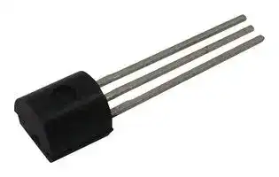
- Thyristor Case Style: TO-92
- Average On State Current: 800mA
- Gate Trigger Current Max: 200µA
- Gate Trigger Voltage Max: 800mV
- Operating Temperature Max: 125°C
- Peak Non Repetitive Surge Current: 22.5A
- Peak Repetitive Off State Voltage: 600V
| Delivery and price | |
|---|---|
| Units per pack | 5000 |
| Price | 0.096 € |
| Current stock | 1000+ |
| Lead time | 30 days |
**X02**

1.25 A sensitive ate SCR g

**==> picture [61 x 39] intentionally omitted <==**

## **Features**

- on-state rms current: 1.25 A

- repetitive peak off-state voltage: 600 V and 800 V

- gate triggering current: 50 and 200 µA

## **Applications**

- ground fault circuit interrupters

- overvoltage crowbar protection in power supplies

- capacitive ignition circuits

## **Description**

The X02 SCR can be used as the on/off function in applications where topology does not offer high current for gate triggering.

This device is optimized in forward voltage drop and inrush current capabilities for reduced power losses and high reliability in harsh environments.

**==> picture [168 x 259] intentionally omitted <==**

**----- Start of picture text -----**<br>
A<br>G<br>K<br>A<br>G A<br>A K G<br>K<br>SOT-223 TO-92<br>X02xxN X02xxA<br>A<br>K<br>G<br>SMBflat-3L<br>X0202NUF<br>**----- End of picture text -----**<br>


**Table 1. Device summary**

|**Order code**|**Voltage**|**Voltage**|**Sensitivity µA**|**Package**|
|---|---|---|---|---|
||**600 V**|**800 V**|||
|X0202MA|Y||200|TO-92|
|X0202MN|Y||200|SOT-223|
|X0202NA||Y|200|TO-92|
|X0202NN||Y|200|SOT-223|
|X0205MA|Y||50|TO-92|
|X0205NA||Y|50|TO-92|
|X0202NUF||Y|200|SMBflat-3L|


1/11

January 2011

Doc ID 7480 Rev 4

_www.st.com_

**Characteristics**

**X02**

## **1 Characteristics**

## **Table 2. Absolute ratings (limiting values, TJ = 25 °C unless otherwise specified)**

|**Symbol**|**Parameter**|||**Value**|**Unit**|
|---|---|---|---|---|---|
|IT(RMS)|On-state rms current (180 °Conduction angle)|TO-92|TL= 63 °C|1.25|A|
|||SOT-223|Ttab= 99 °C|||
|||SMBflat-3L|Ttab= 111 °C|||
|IT(AV)|Average on-state current (180 °Conduction angle)|TO-92|TL= 63 °C|0.8|A|
|||SOT-223|Ttab= 99 °C|||
|||SMBflat-3L|Ttab= 111 °C|||
|ITSM|Non repetitive surge peak on-state current|tp= 8.3 ms|Tj= 25 °C|25|A|
|||tp= 10 ms||22.5||
|I²t|I²t Value for fusing|tp= 10 ms|Tj= 25 °C|2.5|A2s|
|di/dt|Critical rate of rise of on-state current<br>IG= 2 x IGT, tr ≤100 ns|F = 60 Hz|Tj= 125 °C|50|A/µs|
|IGM|Peak gate current|tp= 20 µs|Tj= 125 °C|1.2|A|
|PG(AV)|Average gate power dissipation||Tj= 125 °C|0.2|W|
|Tstg<br>Tj|Storage junction temperature range<br>Operating junction temperature range|||- 40 to + 150<br>- 40 to + 125|°C|


## **Table 3. Electrical characteristics (TJ = 25 °C unless otherwise specified)**

|**Symbol**|**Test conditions**|**Test conditions**||**X0202**|**X0205**|**Unit**|
|---|---|---|---|---|---|---|
|IGT|VD= 12 V, RL= 140Ω||Min.||20|µA|
||||Max.|200|50||
|VGT|||Max.|0.8||V|
|VGD|VD= VDRM,RL= 3.3 kΩ, RGK= 1 kΩ|Tj= 125 °C|Min.|0.1||V|
|VRG|IRG= 10 µA||Min.|8||V|
|IH|IT= 50 mA, RGK= 1 kΩ||Max.|5||mA|
|IL|IG= 1 mA, RGK= 1 kΩ||Max.|6||mA|
|dV/dt|VD=  67% VDRM,RGK= 1 kΩ|Tj= 110 °C|Min.|10|15|V/µs|


## **Table 4. Static electrical characteristics**

|**Table 4.**|**Static electrical characteristics**|**Static electrical characteristics**|**Static electrical characteristics**||||
|---|---|---|---|---|---|---|
|**Symbol**|**Test conditions**|||**X0202**|**X0205**|**Unit**|
|VTM|ITM= 2.5 A, tp= 380 µs|Tj= 25 °C|Max.|1.45||V|
|VTO|Threshold voltage|Tj= 125 °C||0.9||V|
|Rd|Dynamic resistance|||200||mΩ|
|IDRMIRRM|VDRM= VRRM,RGK= 1 kΩ|Tj= 25 °C||5||µA|
|||Tj= 125 °C||500||µA|


2/11

Doc ID 7480 Rev 4

**Characteristics**

**X02**

**Table 5. Thermal resistances**

|**Table 5.**|**Thermal resistances**|**Thermal resistances**|||||
|---|---|---|---|---|---|---|
|**Symbol**|**Parameter**||||**Value**|**Unit**|
|Rth(j-l)|Junction to leads (DC)||TO-92|Max.|60|°C/W|
|Rth(j-t)|Junction to tab (DC)||SOT-223||25||
|Rth(j-t)|Junction to tab (DC)||SMBflat-3L||14||
|Rth(j-a)|Junction to ambient (DC)||TO-92||150||
|||S = 5 cm2|SOT-223||60||
||||SMBflat-3L||75||


## **Figure 1. Maximum average power dissipation versus average on-state current (full cycle)**

**Figure 2. Average and DC on-state current versus tab (SOT-223, SMBflat-3L) or lead (TO-92) temperature**

**==> picture [462 x 146] intentionally omitted <==**

**----- Start of picture text -----**<br>
P(W) 1.4 IT(AV)(A)<br>1.21.0 360° α = 180° 1.2 D.C. (TO-92) D.C. (SOT-223) D.C. (SMBflat-3L)<br>1.0<br>0.8 α<br>0.8<br>α = 180° (TO-92)<br>0.6<br>0.6<br>0.4<br>0.4 α = 180° (SOT-223)<br>0.2<br>0.0 IT(AV)(A) 0.20.0 Tlead or Ttab (°C) α = 180° (SMBflat-3L)<br>0 0.1 0.2 0.3 0.4 0.5 0.6 0.7 0.8 0 25 50 75 100 125<br>**----- End of picture text -----**<br>


## **Figure 3. Average and DC on-state current versus ambient temperature**

## **Figure 4. Relative variation of thermal impedance junction to ambient versus pulse duration**

**==> picture [462 x 147] intentionally omitted <==**

**----- Start of picture text -----**<br>
1.4 IT(AV)(A) 1.00 K=[Zth(j-a)/Rth(j-a) TO-92 []]<br>1.2 D.C. (SOT-223) SMBflat-3L<br>1.0 D.C. (SMBflat-3L)<br>0.8<br>D.C. (TO-92) 0.10<br>0.6 SOT-223<br>0.4 α = 180° (TO-92)<br>α = 180° (SOT-223)<br>0.2 α = 180° (SMBflat-3L)<br>Tamb(°C) tp(s)<br>0.0<br>0.01<br>0 25 50 75 100 125<br>1.E-02 1.E-01 1.E+00 1.E+01 1.E+02 1.E+03 1.E+04 1.E+05<br>**----- End of picture text -----**<br>


3/11

Doc ID 7480 Rev 4

**Characteristics**

**X02**

**Figure 5. Relative variation of triggering, Figure 6. Relative variation of holding holding and latching current versus current versus gate-cathode junction temperature resistance (typical values)**

**==> picture [462 x 146] intentionally omitted <==**

**----- Start of picture text -----**<br>
IGT,IH,IL[T ] /j IGT,IH,IL[T =25°C]j<br>1.50<br>Typical values IH[RGK] / IH[RGK=1k Ω ]<br>4.0<br>1.25<br>Tj=25<br>3.5<br>1.00 3.0<br>2.5<br>0.75 RGKIH & I= 1kL Ω 2.0<br>1.5<br>0.50<br>IGT 1.0<br>0.5<br>0.25 RGK(k Ω )<br>T (°C)j 0.01.E-02 1.E-01 1.E+00 1.E+01<br>0.00<br>-40 -20 0 20 40 60 80 100 120 140<br>**----- End of picture text -----**<br>


## **Figure 7. Relative variation of dV/dt immunity Figure 8. Relative variation of dV/dt immunity versus gate-cathode resistance versus gate-cathode capacitance (typical values) (typical values)**

**==> picture [462 x 147] intentionally omitted <==**

**----- Start of picture text -----**<br>
dV/dt[RGK] / dV/dt[RGK=1k Ω ] dV/dt[CGK] / dV/dt[RGK=1k Ω ]<br>10.0 20<br>VD = 0.67 x VTj = 125°CDRM 18 VD = 0.67 x VTj = 125°CDRM<br>16 RGK = 1kΩ<br>14<br>12<br>1.0 10<br>8<br>6<br>4<br>RGK(k Ω ) 2 CGK(nF)<br>0.1 0<br>0.0 0.2 0.4 0.6 0.8 1.0 1.2 1.4 1.6 1.8 2.0 0 2 4 6 8 10 12 14 16 18 20 22<br>**----- End of picture text -----**<br>


**Figure 9. Surge peak on-state current versus number of cycles**

**Figure 10. Non repetitive surge peak on state current for a sinusoidal pulse and corresponding value of I[2] T**

**==> picture [462 x 135] intentionally omitted <==**

**----- Start of picture text -----**<br>
ITSM(A) ITSM(A), I t (A s)2 2<br>25 300<br>Tj initial = 25°C<br>20 tp=10ms 100 dI/dt limitation ITSM<br>One cycle<br>15 Non repetitive<br>Tj initial=25°C<br>10 10<br>Repetitive<br>Tamb=25°C<br>5 I t2<br>0 Number of cycles 1 tp(ms)<br>1 10 100 1000 0.01 0.10 1.00 10.00<br>**----- End of picture text -----**<br>


4/11

Doc ID 7480 Rev 4

**Ordering information scheme**

**X02**

**Figure 11. On-state characteristics (maximum Figure 12. Thermal resistance junction to values) ambient versus copper surface under tab (SOT-223, SMBflat-3L)**

**==> picture [462 x 135] intentionally omitted <==**

**----- Start of picture text -----**<br>
ITM(A) Rth(j-a)(°C/W)<br>3E+1 170<br>Tj max.: 160 Epoxy printed circuit board FR4,<br>1E+1 RVd=200mt0=0.9VΩ 150 copper thickness 35 µm<br>140<br>Tj=max 130<br>120<br>110<br>100<br>1E+0 T =25°Cj 90 SMBF3L (typical)<br>80<br>SOT-223<br>70 (maximum)<br>60 S(cm²)<br>1E-1 VTM(V) 50<br>0.5 1.0 1.5 2.0 2.5 3.0 3.5 4.0 4.5 0 1 2 3 4 5<br>**----- End of picture text -----**<br>


## **2 Ordering information scheme**

## **Figure 13. Ordering information scheme**

**==> picture [347 x 210] intentionally omitted <==**

**----- Start of picture text -----**<br>
X   02   02   M   ZBlank 1BA2<br>Sensitive SCR series<br>Current<br>02 = 1.25 A<br>Sensitivity<br>02 = 200 µA<br>05 = 50 µA<br>Voltage<br>M = 600 V<br>N = 800 V<br>Package<br>A = TO-92 (A"Blank")<br>N = SOT-223 (N"No Blank”)<br>UF = SMBF3L<br>Packing mode<br>1BA2 = Bulk<br>2BL2 = Ammopack<br>5BA4 = Tape and reel 7” (SOT-223)<br>Blank = Tape and reel 13” (SMBflat-3L)<br>**----- End of picture text -----**<br>


5/11

Doc ID 7480 Rev 4

**Package information**

**X02**

## **3 Package information**

- Epoxy meets UL94, V0

- Lead-free packages

In order to meet environmental requirements, ST offers these devices in different grades of ECOPACK[®] packages, depending on their level of environmental compliance. ECOPACK[®] specifications, grade definitions and product status are available at: www.st.com. ECOPACK[®] is an ST trademark.

**Table 6. TO-92 dimensions**

|**A**<br>**F**<br>**C**<br>**B**||||**a**<br>**E**|**Ref**|**Dimensions**|**Dimensions**|**Dimensions**|**Dimensions**|**Dimensions**|**Dimensions**|
|---|---|---|---|---|---|---|---|---|---|---|---|
|||||||**Millimeters**|||**Inches**|||
|||||||**Min.**|**Typ.**|**Max.**|**Min.**|**Typ.**|**Max.**|
|||||||||||||
||||||A<br>B||1.35|4.70||0.053|0.185|
||||||C||2.54|||0.100||
||||||D|4.40|||0.173|||
||||**D**|||||||||
||||||E|12.70|||0.500|||
||||||F|||3.70|||0.146|
||||||a|||0.50|||0.019|


6/11

Doc ID 7480 Rev 4

**Package information**

**X02**

## **Table 7. SOT-223 dimensions**

|**A**<br>**A**<br>**H**|||||||**c**|**c**|**c**|**Ref.**|**Dimensions**|**Dimensions**|**Dimensions**|**Dimensions**|**Dimensions**|**Dimensions**|
|---|---|---|---|---|---|---|---|---|---|---|---|---|---|---|---|---|
||||||||||||**Millimeters**|||**Inches**|||
|||||||**V**|||||**Min.**|**Typ.**|**Max.**|**Min.**|**Typ.**|**Max.**|
||**1**|**e1**<br>**D**||||||||A|||1.80|||0.071|
||||||||||||||||||
|||||||||||A1||0.02|0.10||0.001|0.004|
|||||||||||B|0.60|0.70|0.85|0.024|0.027|0.033|
|||**B1**||||||||B1|2.90|3.00|3.15|0.114|0.118|0.124|
|||||||||||c<br>|0.24|0.26|0.35|0.009|0.010|0.014|
||**E**||**4**|||||||D(1)|6.30|6.50|6.70|0.248|0.256|0.264|
|||**1**|**2**|**3**||||||e||2.3|||0.090||
|||**e**||||||||e1||4.6|||0.181||
||||||||||||||||||
|||||||||||E(1)|3.30|3.50|3.70|0.130|0.138|0.146|
|||||||||||H|6.70|7.00|7.30|0.264|0.276|0.287|
||||||||||||||||||
|||||||||||V|10° max||||||


1. Do not include mold flash or protrusions. Mold flash or protrusions shall not exceed 0.15mm (0.006inches)

## **Figure 14. SOT-223 footprint**

**==> picture [200 x 194] intentionally omitted <==**

**----- Start of picture text -----**<br>
3.25<br>1.32<br>5.16 7.80<br>1.32<br>2.30 0.95<br>**----- End of picture text -----**<br>


7/11

Doc ID 7480 Rev 4

**Package information**

**X02**

## **Table 8. SMBflat-3L dimensions**

|E<br>E1||||A|||||L2<br>L1<br>L1<br>L2 2x<br>c<br>b 2x|**Ref.**|**Dimensions**|**Dimensions**|**Dimensions**|**Dimensions**|**Dimensions**|**Dimensions**|
|---|---|---|---|---|---|---|---|---|---|---|---|---|---|---|---|---|
||||||||||||**Millimeters**|||**Inches**|||
||||||||||||**Min. **|**Typ.**|**Max.**|**Min.**|**Typ.**|**Max.**|
|||||||||||A|0.90||1.10|0.035||0.043|
|||||||<br>e||||b|0.35||0.65|0.014||0.026|
|||||||||||b4|1.95||2.20|0.07||0.087|
|||E1||||<br>||||c|0.15||0.40|0.006||0.016|
|||||||||||D|3.30||3.95|0.130||0.156|
|||||||||||E|5.10||5.60|0.201||0.220|
|||||||b4||||E1|4.05||4.60|0.156||0.181|
|||||||||||L|0.75||1.50|0.030||0.059|
||||||||||||||||||
|||||||||||L1||0.40|||0.016||
|||||||||||L2||0.60|||0.024||
|||||||||||e||1.60|||0.063||


## **Figure 15. SMBflat-3L footprint dimensions**

**==> picture [178 x 131] intentionally omitted <==**

**----- Start of picture text -----**<br>
5.84<br>0.51 (0.230)<br>(0.020)<br>2.07 2.07<br>(0.082) (0.082)<br>0.51<br>(0.020)<br>1.20 3.44 1.20<br>(0.047) (0.136) (0.047)<br>millimeters<br>(inches)<br>**----- End of picture text -----**<br>


8/11

Doc ID 7480 Rev 4

**Package information**

**X02**

## **Figure 16. Footprint and connectors for SOT-223 or SMBflat-3L (dimensions in mm)**

**==> picture [367 x 378] intentionally omitted <==**

**----- Start of picture text -----**<br>
5.84<br>3.42<br>3.25<br>2.92<br>SOT-223<br>Solder resist<br>1.35<br>1.30 1.20<br>1.20<br>1.08 1.08<br>SMBF3L Solder lands<br>SMBF3L<br>SMBF3L<br>Solder paste<br>Connector line<br>SOT-223 SOT-223 SOT-223<br>0.85<br>0.95<br>1.10<br>2.30<br>2.07<br>1.50 1.32 1.19<br>0.61 0.51 0.46<br>1.95 2.07 2.22 7.80<br>1.47 1.32 1.19<br>**----- End of picture text -----**<br>


9/11

Doc ID 7480 Rev 4

**Ordering information**

**X02**

## **4 Ordering information**

## **Table 9. Ordering information**

|**Order code**|**Marking**|**Package**|**Weight**|**Base qty**|**Delivery mode**|
|---|---|---|---|---|---|
|X0202MA 1BA2|X0202 MA|TO-92|0.2 g|2500|Bulk|
|X0202MA 2BL2|X0202 MA|TO-92|0.2 g|2000|Ammopack|
|X0202MN5BA4|X2M|SOT-223|0.12 g|1000|Tape and reel|
|X0202NA 1BA2|X0202 NA|TO-92|0.2 g|2500|Bulk|
|X0202NA 2BL2|X0202 NA|TO-92|0.2 g|2000|Ammopack|
|X0202NN5BA4|X2N|SOT-223|0.12 g|1000|Tape and reel|
|X0205MA 1BA2|X0205 MA|TO-92|0.2 g|2500|Bulk|
|X0205MA 2BL2|X0205 MA|TO-92|0.2 g|2000|Ammopack|
|X0205NA 1BA2|X0205 NA|TO-92|0.2 g|2500|Bulk|
|X0202NUF|X2N|SMBflat-3L|46.914 mg|5000|Tape and reel|


## **5 Revision history**

## **Table 10. Document revision history**

|**Date**|**Revision**|**Changes**|
|---|---|---|
|Sep-2000|3|Previous issue|
|14-Jan-2011|4|Added SMBflat-3L package and ECOPACK statement.|


10/11

Doc ID 7480 Rev 4

**X02**

## **Please Read Carefully:**

Information in this document is provided solely in connection with ST products. STMicroelectronics NV and its subsidiaries (“ST”) reserve the right to make changes, corrections, modifications or improvements, to this document, and the products and services described herein at any time, without notice.

All ST products are sold pursuant to ST’s terms and conditions of sale.

Purchasers are solely responsible for the choice, selection and use of the ST products and services described herein, and ST assumes no liability whatsoever relating to the choice, selection or use of the ST products and services described herein.

No license, express or implied, by estoppel or otherwise, to any intellectual property rights is granted under this document. If any part of this document refers to any third party products or services it shall not be deemed a license grant by ST for the use of such third party products or services, or any intellectual property contained therein or considered as a warranty covering the use in any manner whatsoever of such third party products or services or any intellectual property contained therein.

**UNLESS OTHERWISE SET FORTH IN ST’S TERMS AND CONDITIONS OF SALE ST DISCLAIMS ANY EXPRESS OR IMPLIED WARRANTY WITH RESPECT TO THE USE AND/OR SALE OF ST PRODUCTS INCLUDING WITHOUT LIMITATION IMPLIED WARRANTIES OF MERCHANTABILITY, FITNESS FOR A PARTICULAR PURPOSE (AND THEIR EQUIVALENTS UNDER THE LAWS OF ANY JURISDICTION), OR INFRINGEMENT OF ANY PATENT, COPYRIGHT OR OTHER INTELLECTUAL PROPERTY RIGHT.**

**UNLESS EXPRESSLY APPROVED IN WRITING BY AN AUTHORIZED ST REPRESENTATIVE, ST PRODUCTS ARE NOT RECOMMENDED, AUTHORIZED OR WARRANTED FOR USE IN MILITARY, AIR CRAFT, SPACE, LIFE SAVING, OR LIFE SUSTAINING APPLICATIONS, NOR IN PRODUCTS OR SYSTEMS WHERE FAILURE OR MALFUNCTION MAY RESULT IN PERSONAL INJURY, DEATH, OR SEVERE PROPERTY OR ENVIRONMENTAL DAMAGE. ST PRODUCTS WHICH ARE NOT SPECIFIED AS "AUTOMOTIVE GRADE" MAY ONLY BE USED IN AUTOMOTIVE APPLICATIONS AT USER’S OWN RISK.**

Resale of ST products with provisions different from the statements and/or technical features set forth in this document shall immediately void any warranty granted by ST for the ST product or service described herein and shall not create or extend in any manner whatsoever, any liability of ST.

ST and the ST logo are trademarks or registered trademarks of ST in various countries.

Information in this document supersedes and replaces all information previously supplied.

The ST logo is a registered trademark of STMicroelectronics. All other names are the property of their respective owners.

© 2011 STMicroelectronics - All rights reserved

## STMicroelectronics group of companies

Australia - Belgium - Brazil - Canada - China - Czech Republic - Finland - France - Germany - Hong Kong - India - Israel - Italy - Japan - Malaysia - Malta - Morocco - Philippines - Singapore - Spain - Sweden - Switzerland - United Kingdom - United States of America

**www.st.com**

11/11

Doc ID 7480 Rev 4
Updated at April 28, 2026
STMicroelectronics is a global leader in the semiconductor industry, recognized for developing highly integrated, energy-efficient solutions that power modern electronics. With a strong focus on innovation, ST provides a comprehensive portfolio of microelectronics that address the demanding requirements of industrial, automotive, communications, and consumer applications. Our extensive selection of STMicroelectronics components is built around a robust lineup of discrete semiconductors and circuit protection devices. We offer a wide variety of single MOSFETs, Schottky diodes, and fast and ultrafast recovery rectifier diodes, designed to deliver exceptional efficiency and thermal performance in power management and conversion systems. For robust circuit protection, our inventory features hundreds of transient voltage suppressors and TVS diodes that safeguard sensitive electronic components against destructive voltage spikes. In addition to core power discretes like TRIACs, SCRs, bipolar transistors, and single IGBTs, our STMicroelectronics range includes specialized integrated passive filters and MEMS sensors. Furthermore, ST offers advanced integrated passive devices, such as baluns and RF filters, which utilize high-quality monolithic RF IPD processes on glass or high-resistance silicon substrates. These components provide competitive cost structures, reduced power losses, and simplified RFIC-to-antenna matching, ensuring optimal system performance and delivering the reliability required for next-generation wireless and power designs.
About Novapart
Novapart is a B2B electronic component broker specialising in stock shortages and cost reduction. We source hard-to-find parts and identify compliant alternatives across a catalogue of 540,000+ components from 500+ manufacturers.
Learn more →Stock Shortage Specialist
When a component is unavailable, discontinued or has an unacceptable lead time, we tap into our network of vetted European and Asian distributors to source what you need — without compromising on quality or traceability.
Request a quote →Compliant Alternatives
We identify pin-to-pin, electrically equivalent substitutes that meet the same certifications (RoHS, AEC-Q100, REACH) as your original specification — validated against datasheets, not just part numbers. Often at a lower cost.
BOM Analysis service →