
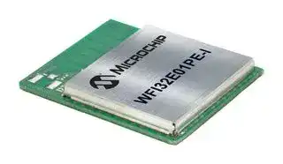


WFI32E01PE-I
WLAN Module, PCB Antenna, 2.5 GHz
- Manufacturer: MICROCHIP
- Product type:
- SVHC: No SVHC (04-Feb-2026)
- Frequency RF: 2.5GHz
- Product Range: WFI32E01 Series
- Module Interface: CAN, CAN-FD, I2C, I2S, JTAG, SPI, SQI, UART, USB
- Module Applications: Radio, RF Communications, Wireless Connectivity WiFi
| Delivery and price | |
|---|---|
| Units per pack | 250 |
| Price | 4.41 € |
| Current stock | 10+ |
| Lead time | 30 days |
**==> picture [100 x 52] intentionally omitted <==**
**----- Start of picture text -----**<br>
S®<br>MICROCHIP<br>**----- End of picture text -----**<br>
## PIC32MZ W1 and WFI32E01 Family
## Del
## PIC32MZ1025W104 MCU and WFI32E01 Module with Wi-Fi® and Hardware-based Security Accelerator Data Sheet
## a
- INTRODUCTION - Four 64-bit accumulators . .
- The - Single-cycle MAC, saturating and fractional math is a generalPIC32MZpurpose, W1 Familylow-cost, (PIC32MZ1025W32-bit Microcontroller104132 devices)(MCU) « Kiadi:olfisienidisccrdicossendGhgrandfibectane with the Wi-Fi and network connectivity, hardware-based On-Chip Flash and SRAM security accelerator, transceiver and Power ManagementUnit * 1 MB Flash Program Memory (PMU). It supports interface to an External Front-End Module. * 64 KB Boot Program Flash The WFI32E01 is a fully RF certified wireless module that con* 256 KB SRAM (Program and Data) tains the PIC32MZ1025W104 SoC and an integrated Front¢ 64 KB Data Buffer (DBF) end Module (FEM) with following antenna options: * Dedicated Buffer for Peripherals * PCB Antenna (WFI32E01PC/WFI32E01PE) Power Management and System Recovery ¢ U.FL Connector (WFI32E01UC/WFI32E01UE) for External * Low-Power Modes (Dream and Sleep) Antenna + Integrated Power-on Reset (POR) and Brown-out Reset
- The PIC32MZ W1 Family supports rich set of standard PIC32 (BOR) peripherals such as Wi-Fi, Ethernet MAC, USB, CAN, CAN* Secondary Oscillator and Fail Safe Clock Switch FD, SPI, I?C, SQI, UART and JTAG. ¢ Fast Power-up and Brown-out Recovery TCP/IP based connectivity protocols along with SSL support Security enables a low-cost, low complexity system to obtain full-featured internet connectivity and reliable information exchange. * Hardware Accelerated Security Modes (with Built-in DMA Support)
- x
- PIC32MZ W1 Family FEATURES * CryptoTeEngine in Data with Encryption/decryption True Random Numberand Generator Authentication The following section lists the PIC32MZ1025W104 related (AGS, BES Shs Mls ane MAD) features. > AES Modes: .
- Wireless Interfaces - Electronic Codebook (ECB) - Cypher Block Chaining (CBC)
- * PHY: - Counter Mode (CTR)
- - ae ane b/g/n WLAN link - Cypher Feedback Mode (CFB) - Single spatial stream of 20 MHz crane! bandwidth - Output Feedback Mode (OFB) - External FEM support for Power Amplifier (PA), Low - Galois/Counter Mode (GCM) ae LED, WebsiteRES SREPey ¢ Hardware Accelerated Public Key Cryptography with Support for:
- - 2.4 GHz (2400 ~ 2483.5 MHz) ISM band =a : ;
- a ; -- 256-bit16-DSPECC/ECDH/ECDSA/Curve25519multipliers configuration - Infrastructure BSS luis rental - 256-bit Ed25519 ~ Seft-AP mosie functionality - 512-bit ECC/ECDH/ECDSA generation - Active and passive scanning - Transmit power control support over temperature and Clock Management voltage * 40 MHz Primary Oscillator (POSC)
- * Security: * 32.768 kHz Secondary Oscillator (SOSC) - WPA3 personal (SAE and PMF-802.11w) * Power-up Timer (PWRT) and Oscillator Start-up Timer - WPA2 personal, with options for WPA compatibility and (OST) PMF * Programmable PLLs and Oscillator Clock Sources
- - WEP * Fail-Safe Clock Monitor (FSCM)
- * Harmony Networking: * On-chip Clock Sources: - Out of box support for MPLAB® Harmony v3 TCP/IP - 8 MHz Fast RC (FRC) oscillator Stack - 32.768 kHz Low-Power RC (LPRC) oscillator
- - TLS v1.2 with symmetric/asymmetric crypto * Programmable PLLs and Oscillator Clock Sources acceleration ¢ Independent Watchdog Timer (WDT) and Deadman Timer
- 200 MHz, MIPS32® M-Class Microprocessor Core (DMT) » 16 KB I-Cache, 16 KB D-Cache * Gast ake-op aid Saat up + Fixed Mapping Translation (FMT) based MMU for * Support for Precise Reference Clocks to External Devices Optimum Embedded OS Execution
- * microMIPS™ Mode for Up to 35% Smaller Code Size * DSP-enhanced Core: eee © 2020 Microchip Technology Inc. Preliminary Data Sheet DS70005425A-page 1
**==> picture [457 x 638] intentionally omitted <==**
**----- Start of picture text -----**<br>
PIC32MZ W1 and WFI32E01 Family<br>seman<br>Direct Memory Access (DMA) Software and Tools Support<br>* Eight Channels with Automatic Data Size Detection * C/C++ Compiler with Native DSP/fractional<br>* Programmable 32-bit Cyclic Redundancy Check (CRC) + MPLAB™ Harmony Integrated Software Framework:<br>7 . cae<br>Advanced Analog Vid Aedoa and mTouch™ Middleware<br>* eee eee Bros— Express Logic ThreadX, FreeRTOS™<br>- 2 MSPS with two Sample and Hold (S&H) circuits (one OPENRTOS®, Micriym® uC/OS™ and SEGGER<br>dedicated and one shared) embos®<br>- Unitaetanelegins + Supports Over-the-Air (OTA) and Over-the-Host (OTH)<br>- Sleep and Idle mode operations Firmware Update Modes<br>- Multiple trigger sources Pack do ti Conditi<br>- Two digital comparators and two digital filters acKkage an perauing Conditions<br>- Supports Touch Interface a PaESSDE:<br>- Size-10x10x0.9mm<br>Cc ommunication- 20 Analogicati Channelssitetintertaces - 132-pin DQFN<br>* Operating conditions:<br>* Up to Two CAN Modules (CAN and CAN-FD) - 2.97V to 3.63V, -40°C to +105°C, DC to 200 MHz<br>- 2.0B Active with DeviceNet™ addressing support<br>¢ IEEE 1588 Precision Time Protocol (PTP)<br>¢ Up to Three UART Modules (10 Mbps): WFI32E01 MODULE FEATURES<br>- Supports RS-232, RS-485, LIN 2.1 and IrDA Protocols The following section lists the WFI32E01 module related fea-<br>* One Ethernet MAC Module (10/100 Mbps) with RMII Inter- tures, , which complements SoC features.<br>face and Dedicated DMA:<br>- Time synchronization support between Wi-Fi and Antneed Onti“Pp sons<br>Ethernet ¢ PCB Antenna Variants:<br>¢ Up to Two SPI (one 4-wire, one 3-wire) Modules with - WFI32E01PC<br>Speed up to 40 MHz - WFI32E01PE<br>* SQlI Configurable as an Additional SPI Module (40 MHz) * External Antenna Variants:<br>* One Full-Speed USB 2.0 OTG Interface with Dedicated - WFI32E01UC<br>DMA - WFI32E01UE<br>* Two I2C Modules (Up to 1 Mbaud) with SMBus Support Wireless Feature<br>Timers/Output Compare/Input Capture * On-board FEM/PA to Meet the TX Power Requirements<br>¢ Seven 16-bit or up to Three 32-bit Timers/Counters Security<br>* Four Output Compare (OC) Modules * Integrated Trust&GO<br>¢ Four Input Capture (IC) Modules Clock Management<br>* Low-power Precision Real-Time Clock and Calendar » Integrated 40 MHz POSC<br>(RTCC)<br>Input/Output Aevanesd ae<br>+ High Current Source/Sink (up to 25 mA) on All I/O Pins nalog “nanne's<br>* Configurable Open-Drain, Pull-up, Pull-down and Slew Input/Output<br>Rate Controls * 37 GPIO Pins<br>¢ External interrupts on all I/O Pins Package and Operating Conditions<br>* Peripheral Pin Select (PPS) to Enable Function Remap * Package:<br>* 64 GPIO Pins - 54-pin SMD package with Shield CAN<br>Peripheral Trigger Generator (PTG) - Size - 24.5 x 20.5x 2.5mm<br>* PTG with 8-bit User Command for Scheduling Complex * Operating conditions:<br>Sequences - 3.0V to 3.6V, -40°C to +85°C, DC to 200 MHz<br>Qualification and Class B Support Certifications<br>* Class B Safety Library, IEC 60730 ¢ WFI32E01 Module Certified to FCC, ISED and CE Radio<br>Debugger Development Support Regulations ;<br>¢ In-circuit and In-application Programming * RoHS and REACH Compliant<br>+ 4-wire MIPS® Enhanced JTAG Interface<br>¢ Unlimited Software, 8 Instruction and 4 Data Complex<br>Hardware Breakpoints<br>¢ IEEE 1149.2-Compatible (JTAG) Boundary Scan<br>¢ iFlowtrace functionality support:<br>- Off-chip Buffering of iFlowTrace Messages<br>**----- End of picture text -----**<br>
renner eee e rereerence eee eee DS70005425A-page 2 Preliminary Data Sheet © 2020 Microchip Technology Inc.
PIC32MZ W1 and WFI32E01 Family
## ee
||eee|<br>>||suondoeuuoyuy 13/3] 15|<br>a ees|
|---|---|---|---|
||||ovir<br>yleloty|
||suld O/I<br>3<br>| ovwiewons<br>|,<br>90LY<br>|>-|<br>je<br>>||eft<br>(oom<br>oe<br>moe<br>me)<br>Laem|
||eeee|eeee||
||N|||
||eeee <br>GADpecueyugoaVv |<br>|S <br>sjauueydOaV<br>iAq<br>(pajyesipaq<br>yorqeuruesBo1g)||ee ee<br>Si9LO0°?asn<br>|-|-|-|-<br> |<br>Adpasueyugsay |. =.|ss.<br>ee<br>| ees|
||ONYL<br>Is<br>OovIsniL<br>lz<br>odAlgsujawWwAsy >||payesipeq<br>/ajqewwesbo1q)<br>sjauueydWING<br>ONaL<br>>|>|>]>||
|G$|_(varnvo<br>|_|<br>2<br>sands<br>[|_|<br>&<br>{awn<br>fa<br>2<br>N<br>Q<br>aiedwoy<br>s<br>(erence<br>=<br>£<br>/SJOULL<br>Lt<br>é<br>ase<br>Sudajqeddeway 13|<br>Or,<br>WW| &| (2H) ma reuueud))<br>no<br>N<br>>|<br>3||ee<br>|SESESS<br>(a/v 0'z)NWO<br>|-|-|-|-|<br>n<br>)<br>5|@vasnvo<br>|||||_|<br>2<br>-frfrfe<br>=<br>3<br>Szl/lds<br>| _lele<br>oe<br>gf<br>tin<br>atalala|<br>S<br>preduiop<br>&<br>(YEmde<br>Z)s|/s|z<br>E<br>jssoully<br>=/E(EI=<br>o|™<br>sulg ajqeddeway<br>|[wo |ow]<br>wo| wo||
|a<br>u/6/q LLzo8<br>y<br>ui|=<br>3<br>irs<br>(gy)<br>Aioway<br>4<br>USe}4J00g<br>=<br>abeyoeg<br>z<br>=)<br>S<br>=<br>s|om<br>N<br>S|<br>(ay)owen<br>eyea I<br>N<br>=<br>=|<br>eum<br>fs} <br>AN<br>weiboldg<br>3<br>G<br>4<br>o<br>a.<br>y<br>2<br>5||©)<br>uw |(zw<br>auueyd||o|<br>o| colo<br>|e | Hw ma<br>reuvevol/e<br>la|a] a|<br>e|<br>a<br>o<br>-<br>cl<J<clJe<br>nl<br>S|<br>wGiarweo8<br>1k]<br>&] &] &<br>Ww) sWad Pueoc-uo |<br>Ww =<br>sacnmaeiiiiiialiatal [>[>[>[>|<br>=<br>(ay)Aiowayy<br>=<br>use]400g<br>3<br>3|3<br>ETS<br>Ss<br>abeyoeg<br>4 2 B =<br>**=**<br>5/G|5|o<br> Bow<br>(sis/s[a)<br>x<br>Z|<br>evAowenera |[8/81818<br>NI NITNITN<br>=<br>(ay) Aioway<br>tl/xlals<br>weibolg<br>S|d/ala<br>2/2/22||
|ES|wo<br>sWeN90S<br>S|AN|& 5 S|
|=<br>g<br><|a<br>3<br>c||=<br>a<br><<|SWeNaNpoW<br>a w 4 a<br>clelcle<br>=/=|5|5|
ee © 2020 Microchip Technology Inc. Preliminary Data Sheet DS70005425A-page 3
PIC32MZ W1 and WFI32E01 Family
## seman
**==> picture [291 x 8] intentionally omitted <==**
**----- Start of picture text -----**<br>
TABLE 3: PIN NAMES FOR 132-PIN PIC32MZ1025W104 SoC<br>**----- End of picture text -----**<br>
**==> picture [171 x 9] intentionally omitted <==**
**----- Start of picture text -----**<br>
132-PIN DQFN (TOP AND BOTTOM VIEW)<br>**----- End of picture text -----**<br>
**==> picture [278 x 452] intentionally omitted <==**
**----- Start of picture text -----**<br>
A72 Al<br>=<br>B60 =, B1<br>2yo3 “ee%es<br>,miR<br>%C<br>ve, mx<br>SAbs 2<br>OOOCOCOOCOCOCCSY<br>es 1OCB1/RB1<br>**----- End of picture text -----**<br>
Note 1: The RPn pins can be used by re-mappable peripherals. Refer to Section 13.4 “Peripheral Pin Select (PPS)” for details.
- 2: Every I/O port pin (RAX-RKx) can be used as a change notification pin (CNAx-CNKx). See 13.0 “I/O Ports” for more information. 3: Shaded pins are 5V tolerant.
- 4: Do not use Buck/MLDO output to drive any other device.
- 5: A58 and A59 pins can be configured as GPI as an alternate function.
- 6: Exact connection for each pin is available in the reference design package. Contact the Microchip Sales/Support Team for the package.
eee eee Preliminary Data Sheet © 2020 Microchip Technology Inc.
renner eee e rereerence DS70005425A-page 4
PIC32MZ W1 and WFI32E01 Family
**==> picture [457 x 4] intentionally omitted <==**
**----- Start of picture text -----**<br>
smn<br>**----- End of picture text -----**<br>
**==> picture [457 x 320] intentionally omitted <==**
**----- Start of picture text -----**<br>
TABLE 3: PIN NAMES FOR 132-PIN PIC32MZ1025W104 SoC<br>132-PIN DQFN (TOP AND BOTTOM VIEW)<br>A72 Al<br>B60 ms B1<br>wySo—“%ees<br>, mx<br>0, eX<br>ey, ee<br>x ‘oy AY 4<br>ae ferent an emmnw<br>AM [BUKBKIXTSCiBDSINCTT<br>[ao [SQICSCICVDTI7IRPADIOCAORAD=|<br>lso___[SabvovorzimPcenoccamcs<br>|<br>**----- End of picture text -----**<br>
- Note 1: |The RPn pins can be used by re-mappable peripherals. Refer to Section 13.4 “Peripheral Pin Select (PPS)” for details. 2: Every I/O port pin (RAX-RKx) can be used as a change notification pin (CNAx-CNKx). See 13.0 “I/O Ports” for more information. 3: Shaded pins are 5V tolerant.
- 4: Do not use Buck/MLDO output to drive any other device.
- 5: A58 and A59 pins can be configured as GPI as an alternate function.
- 6: Exact connection for each pin is available in the reference design package. Contact the Microchip Sales/Support Team for the package.
reer reer rereeee eee ee © 2020 Microchip Technology Inc. Preliminary Data Sheet DS70005425A-page 5
|PIC32MZW1 and WFI32E01 Family||
|---|---|
|seman||
|Table of Contents||
|TINTS OM 2, pannelManthennsanclbenMeMienananalilpliladWenrnnsbinenanandliueila**n**:Uae**n**naanc**i**lnll**a**ndt**i**enansndite**e**<br>Badman bahathe a ienE hepanant en a Mn nmaand na thenanenaananan nt 1||
|1.0 Ordering INfOrMatiON «0.0...<br>eeeeececcceeeeeeeeeeeeeeseeneeeeeceeeeeaaeaaaeeeeeeseseeeceseeeeaeeeeeeeeeeeaeeeeeeeeeeceeeeeeeeeeeeaeeeseseeeeeteeeeeesesettteesesesseesseeeee|11|
|2.0 PIC32MZ1025W104 SoC DeSCription ..............ccescceecceeeeeceeeeececseceeeecaeeceececseecaeecaeecseeceaeeeseeceaeseseeeneeseaeseseseaeseeeeseesetetstetereeeeee|13|
|3.0 WFI32E01 Module DeSCription<br>..........cccccccccccecccceececeeeeeeeeeeeeeeeeeeeeeceaeeeeeeeeececeeeeeeeeececeeeeeeeceeececececececeeececececceesececececeeeeececeteeeesessseessee|2D|
|5.0 Flash Program Memory ............:cccccsseccesseeeeeseeceeseeeceeeecesueceeaeeeesaeeecsseeecesueeecaeeeesaeeeesseeeseeeesecseecessaeeseeseeeeseeesesseeesstteeessteeesssstteees|OL|
|BiO\MEMOFY ORGANIZATION:<br>up c.cts ieee cobbeaiioreesctbalbeclionnnsssbebbeubiorsnesscscieenecsnelbechsoeneensbietberblaenssecssebbechsseserssbuetberbterssecsseblechioeseccnseree|Lil|
|PIONRCS CESS<br>ser cccr ceeees eesti re<br>raceme ect ares ara trae eR<br>Sr<br>a<br>a Rr<br>a Earner<br>ETE aerearueairae OM||
|B.0'CPU Exceptions aind INTE ilipt COntOUe? .W.2....dccscercecencsoihecntoneechasebebharneonenarsiebubbansendisentoneisenesenhecneenensentvenbscnnennesesnvetsseneeneeseeneens|1D|
|9.0 Prefetch MOdule ...........cccccccesceceseseeeeeeeeeeeseeeeseneeeesenecesaeeeceeeceeaeecaeeeeesaeeseueeesesaeees eeaeeeseeesecaeeeseeeeseeaeeseeaeeeeeseeeesseeesttsetstteeeeeeses|13D|
|10.0 Direct Memory Access (DMA) Controller<br>..........ccccccccecceessecesseeeceeeeeseeeceaececnseeecsceueeeesseeeesaeesseaeeeeseeeesssaeeeeseeeesssseessseeeessteeesees|1414|
|11.0 Oscillator CONfIQguration .......... ccc cecccccesseeeesseecesseeeesseeecssaeecesaeecseeeceeesseeecaeeecssaeecesaeeeesseeecesaeeeeseeesesseeseseeeessseeetseeessseessstteees|105|
|1210) PUESPeed USB OnaMNS=6Gi (OMG) esti eset ccstnied ibsedat cock<br>aie Bd aha wietadel Hcl beaten Uae beta<br>ha wate oe|ABT.|
|13.0 WO Ports<br>2.2... ccecceecceeecceeceeeceeeseecenecsneceaeecseeceaeccaeecacecsaaeccaeeesaesaeecsecscecsaeecaeesaeeseaeeaasesneseaeeeseeseaseeaseceaeeeaeeseeseaeeeeereeeteetesseeeteeteees|213|
|14.0 Peripheral Trigger Generator (PTG)<br>.......ceeececceeeccessceceenseeeeeaeeceeeeeessaeecenaeeesesaeeeeaeesessueesseaeeeceaeesseaeesseeeeessseeessseeesseesssseesees<br>249||
|RUSSONU<br>TUN re rr<br>sm<br>rs<br>OO<br>roe aereeseaer eae|OO|
|16.0 Timer2/3, Timer4/5, ANd Time r6/7 ........ cece cccccceeeeeccccccceesescecccececsecssssecccessusesseecseseeccccseuusecccessuueseecccesseueecccssssssecccssssseeceessseseees|21D|
|FAA) ES AATRAPA TATA (CTIA)hse crc SIR at<br>ask ASSaidccd NE<br>on GESE<br>ck<br>SSEI<br>RE a<br>i|wa|
|18:0 Watchdog Timer (WDD)! sss<br>eraser rane eeieenneni eee eenEE:|ZO|
|ASLO<br>nput Capture: scenesseranmareenwsereecien ey varnenenene varmeneeeimne rae eran esee reneeernie|DOO|
|20:0 Output! Compare sssexzesseevcvesssereressarsereesensresseenscenseausseceseereea<br>eresnetiarucneuiansceeeewEees eeereset Eres erateeaes TeeseeeTENCE TET:ZOD<br>21.0 Serial Peripheral Interface (SPI) and Inter-IC Sound (I2S) sisruraueesonmueseouneea mmeuuee reaceeeeeeectiermenireed ZOE||
|22.0 Serial|\Quad Interface (SOI) wreceecwe: cee esaserry ey arveee eye yeeeeeeueeetear eeee urayeee aeerate peteoe eee ures coat even eEEreer:|CON|
|23.0 Inter-Integrated Circuit (I2C) 1s eee a ere os ermeene<br>ee oe ane te eto cee<br>eeae tueota<br>et eer<br>a eenoe eee eee|ODO|
|25.0 Real-Time Clock and Calendar (RTCC) ............cccccccssscccceeeeeeneeeceeeeeeneeeeeeeeesnaaeeeeeceseeeaeeceeeecseaaeeeesesesseeeeseesessssteeeeeeesssstteeeeeees|OAT|
|26.0 Asymmetric Crypto Engine ...............cccccccccssssseeceeeesssnaeseceessssnaneecensnessaeeeseceessueeeeeeeesssneseeeeeesescaeeeeeesesseceeeeeeessessneeeeesessssssscssseess|OOD|
|27.0 Symmetric Crypto Engine) ssssccressersccuveceurrosssruceucsrarsuveseurseursruy<br>cenavsraewersees pee erouewes exer reneseecevts preveueeurecresesreuseeeuressessueexecessmensmeceess|OOO|
|28:0 True Random'Number'Generator (TIRNG) ssccccevessuszvecsecesevsseusseseserneoesces<br>coveseneseeaeresreese Cots seesRRSeEEPORE BRR BRETT|OOO|
|29.0 12-bit High-Speed Successive Approximation Register (SAR)ADC ou.....eecececcceceessseeeesseeeeeeeeesseeecenseeeeeeeeessaeeeesseeessstseesssees|OG|
|30.0 Controller Area Network (CAN) ........::::cccccsssesseceeeeeeeeneenneeeeeeeeesaeeececenaeeeecececeneaeeeseeesceaaeeceesecennaaeeeeeeeseeeeeeseseessetteeeeeessssttetssteee|443|
|31.0 Controller Area Network-Flexible Data-Rate (CAN-FD) Module .00.............cecccceccccecessseeeeeeeeeeeseeeeeeeeeesseeeeeeeeeesessteeeeessessstteeeeeees|471|
|32.0 WI-FI Controller sssesesevsseusrssseneeeestorssersserseeessensvenisanennaion<br>tesseeseeesnges eeaeeeeeeaee niet eneeetssens eenseeeeeeeieReaeeeeee:O21|O21|
|33.0 Ethernet Controller ............ccccccccecsseceeseeeeseneeeeeneeeeeaeeeceaaeessaeeeesaeesceaeeceaeeeseaeecenseeeenaeeesenaeeseeaeeesenaeesseaeeseeaeesesaeeessteeetstseeseesttes|O2O|
|34.0 Enhanced Capacitive Voltage Divider (CVD) Controller ...........ccccccccccsscceeseseeeesseceesseeeceseeeeenaeeecseeecesaeeeseeeeesseeeeestseesstseessteees|DOD|
|35.0 Power Management<br>Unit(PMU) ...........cceeccccsseceesseecesseeeeeseeeceseecessseccesseeecssaeeceaueecesseeeeesseecesieeeesaeesecseecesseeesesseeeesteeeeesteeessssssDOO||
|36.0 Power-Saving Features ...............cccsssccccceessssnceeeeeecsssneneceeecessesssuseceesssanececeeseseaeeeeeeeessseaeeeececsssseaeseceeeesssceseceresessseeseeeesessssscesssseees|OO|
|37.0 Special Features oo...cccccccccccccsssseceeceeeeseneeeeeeeeseseeesaaeeeeeseeeeeeeceeeeaeeeeeeseeeeaeeeeeeeseneeaeeceeeeeseseaeeeeeseseseeeeeeseessssseeeeesssssttststeees|O13|
|ZBJOMMSUMICTON SEF<br>......-ncznekincthatherdienncastbbaltiesBhanceentthabhestieanenaneasnentthaiterdthsasnentbhatbectbenocesdbhettesthancnenchroMbacBhacecesdbbettenthesenenchnebtactheesseensanetiO29||
|39.0 Development SUPPOrt «0.0.0...ccccceececceeeseneeeeeeeeeeseaeeeeeeeecaaeeeecesaesasaeeeeeeeceseaeeeeeeseeseaeeececeeseceeeeeeeeeessseeeeeeeeeesetsseeesesssssttsssttees<br>OOT||
|40.0 Electrical Specifications<br>..............ccccccssssssccceeesssseeeceeesessneseceesesssaeecesceseessaeeeeeeeesesnaeseceeeessecaneeeeeesesseaeseeesesseseseeeeesessseseeeesssssessssss|OOO|
|41.0 Packaging INFOrmation<br>...........cceecccccccceeeneceeeeeeenneeeeeeeeceeeesaeeeeceecnseeeeeeeeaaaeeeeeeeceseaeeceseeseceeeeeeeseeeeeeaeeeeeeesesseeeeeesessssteeesessseessssss|OLD|
|Appendix A: Regulatory Approvals<br>...........ccccccccccccessseceeeeeeeeseeeeeneeeeeeeseseeceeseesaaeeeeeeseeseeeeeceeececeeeeeeeceesseeeeeeeeeesseseeeeeessssttseteesessesssssss<br>OOO||
|Appendix B: Document Revision History<br>..............ccccccccccceeceeeeseneeeeceeeeseeceeeeeeneeeeeeeeceeseeeeeeeeeceseeeeeeeeeeeseeeeeeeeeeseeseeeeeeessssttseeeesessssssesss|OOG|
|TNE: MIGFOCHIPNVED SHE...<br>ti ennnvensbabbechhenwnnrnibelilechbalilacthennseashballlaschhenateceballlesthennsenceballlanbeensneranbelbachhvennaesitelbechhenanascitalllesbienansccensae<br>OGM||
|Customer Change Notification SEPVICE<br>q................-0c.cc-nsereeennsernecnnsrerssenunsesenbarnecennansusenbannesnneansusnnbannesnnesnsnennannssensanenennsannesensaneseses|ODT|
|Customer SUPPOrt «0.0.0...cccceseeccceeesssseeeeceeeesseeeeecesesaueeeeceeeceeesuaueeecsaaueeecececsusuaeeeeecececseeeeeeseesesseeeeescesssseeeceseessstsseeseesessssseeesseesees|O91|
|WorldwideSalesandService<br>...............:csccseceseeesneeseeeseenesecensceescneenecseesseesesesenceseseeescenscenseceescensecenssenscesesesescesteesessensserseetesserseersesserss|OGD|
renner eee e rereerence eee eee DS70005425A-page 6 Preliminary Data Sheet © 2020 Microchip Technology Inc.
PIC32MZ W1 and WFI32E01 Family smn
**==> picture [173 x 10] intentionally omitted <==**
**----- Start of picture text -----**<br>
TO OUR VALUED CUSTOMERS<br>**----- End of picture text -----**<br>
**==> picture [445 x 28] intentionally omitted <==**
**----- Start of picture text -----**<br>
It is our intention to provide our valued customers with the best documentation possible to ensure successful use of your Microchip<br>products. To this end, we will continue to improve our publications to better suit your needs. Our publications will be refined and<br>enhanced as new volumes and updates are introduced.<br>**----- End of picture text -----**<br>
**==> picture [445 x 55] intentionally omitted <==**
**----- Start of picture text -----**<br>
If you have any questions or comments regarding this publication, please contact the Marketing Communications Department via<br>E-mail at docerrors@microchip.com. We welcome your feedback.<br>Most Current Data Sheet<br>To obtain the most up-to-date version of this data sheet, please register at our Worldwide Web site at:<br>http:/;www.microchip.com<br>**----- End of picture text -----**<br>
**==> picture [445 x 27] intentionally omitted <==**
**----- Start of picture text -----**<br>
You can determine the version of a data sheet by examining its literature number found on the bottom outside corner of any page.<br>The last character of the literature number is the version number, (e.g., DS30000000A is version A of document DS30000000).<br>Errata<br>**----- End of picture text -----**<br>
**==> picture [445 x 25] intentionally omitted <==**
**----- Start of picture text -----**<br>
An errata sheet, describing minor operational differences from the data sheet and recommended workarounds, may exist for current<br>devices. As device/documentation issues become known to us, we will publish an errata sheet. The errata will specify the revision<br>of silicon and revision of document to which it applies.<br>**----- End of picture text -----**<br>
**==> picture [445 x 52] intentionally omitted <==**
**----- Start of picture text -----**<br>
To determine if an errata sheet exists for a particular device, please check with one of the following:<br>* Microchip’s Worldwide Web site; http://www.microchip.com<br>* Your local Microchip sales office (see last page)<br>When contacting a sales office, please specify which device, revision of silicon and data sheet (include literature number) you are<br>using.<br>**----- End of picture text -----**<br>
**==> picture [124 x 9] intentionally omitted <==**
**----- Start of picture text -----**<br>
Customer Notification System<br>**----- End of picture text -----**<br>
Register on our web site at www.microchip.com to receive the most current information on all of our products.
**==> picture [456 x 68] intentionally omitted <==**
**----- Start of picture text -----**<br>
Referenced Sources ual”. These documents should be considered as the<br>This device data sheet is based on the following general reference for the operation of a particular mod-<br>individual sections of the “PIC32 Family Reference ule or device feature.<br>Manual” and “PIC32MZ W1 Family Reference Man-<br>browse the documentation section of the<br>Microchip website (www.microchip.com).<br>**----- End of picture text -----**<br>
- ¢ Section 5. “Flash Program Memory with Support for Live Update” (DS60001640) * Section 6. “Memory Organization and Permissions” (DS60001641)
- Section 7. “Resets” (DS60001118)
- Section 8. “Interrupts” (DS60001108)
- Section 9. “Prefetch Module for Devices with L1 CPU Cache” (DS60001649)
- Section 9. “Watchdog, Deadman, and Power-up Timers” (DS60001114)
- Section 10. “Power-Saving Modes” (DS60001130)
- Section 12. “I/O Ports” (DS60001120)
- ¢ Section 14. “Timers” (DS60001105)
- Section 15. “Input Capture” (DS60001122)
- * Section 16. “Output Compare” (DS60001111)
- Section 21. “UART” (DS60001107)
- Section 22. “12-bit High-Speed Successive Approximation Register (SAR) Analog-to-Digital Converter (ADC)” (DS60001344)
- ¢ Section 23. “Serial Peripheral Interface (SPI)” (DS60001106) * Section 24. “Inter-Integrated Circuit (I2c)” (DS60001116)
- Section 27. “USB On-The-Go (OTG)” (DS61126)
- Section 29. “Real-Time Clock and Calendar (RTCC)” (DS60001125)
- * Section 31. “DMA Controller” (DS60001117) * Section 32. “Configuration” (DS60001124)
- Section 33. “Programming and Diagnostics” (DS60001129)
- Section 34. “Controller Area Network (CAN)” (DS60001154)
- ¢ Section 35. “Ethernet Controller” (DS60001155)
reer reer rereeee eee ee © 2020 Microchip Technology Inc. Preliminary Data Sheet DS70005425A-page 7
PIC32MZ W1 and WFI32E01 Family
seman
- Section 42. “Oscillators with Enhanced PLL” (DS60001250)
- Section 46. “Serial Quad Interface (SQI)” (DS60001244)
- Section 49. “Crypto Engine and Random Number Generator (RNG)” (DS60001246)
- Section 50. “CPU for Devices with MIPS32® microAptiv™ and M-Class Cores” (DS60001192)
- Section 56. “Controller Area Network with Flexible Data-rate (CAN FD)” (DS60001549)
renner eee e rereerence eee eee DS70005425A-page 8 Preliminary Data Sheet © 2020 Microchip Technology Inc.
PIC32MZ W1 and WFI32E01 Family
## smn
## 1.0 ORDERING INFORMATION
This chapter provides the ordering information of the PIC32MZ1025W104 SoC and WFI32E01 module.
## 1.1 PIC32MZ1025W104 SoC Ordering Information
The following table describes the ordering information of the PIC32MZ1025W104 SoC.
TABLE 1-1: PIC32MZ1025W104 SOC ORDERING DETAILS
PIC32MZ1025W104 | 132-pin and DQFN | 32-bit MCU with Network Connec- |PIC32MZ1025W104132-V/NX (10x10x0.9 mm) tivity and Security Accelerator The following figure illustrates the details of PIC32MZ1025W104 SoC ordering information.
**==> picture [422 x 288] intentionally omitted <==**
**----- Start of picture text -----**<br>
FIGURE 1-1: PIC32MZ1025W104 SOC ORDERING INFORMATION<br>[ese |[wz][s0_a5][woo isa] fr [ax<br>Microchip Brand |<br>Architecture<br>Memory Size<br>10 = 1024 KB<br>RAM Size<br>25 = 256 KB<br>Family<br>W1 = WLAN<br>Key Feature Set<br>Pin Count<br>132 Pin Device<br>Packing Specification<br>Tray<br>Temperature Range<br>| = Induistrial (-40°C to +85°C)<br>V = Various (-40°C to +105°C)<br>Packaging Information<br>132-Lead (10x10x0.9 mm) DQFN<br>Pattern Information<br>QTP, SQTP, Code and Special Requirements<br>ES = Engineering Sample<br>**----- End of picture text -----**<br>
reer reer rereeee eee ee © 2020 Microchip Technology Inc. Preliminary Data Sheet DS70005425A-page 9
## PIC32MZ W1 and WFI32E01 Family
## seman
## 1.2 WFI32E01 Module Ordering Information
The following table describes the ordering information of the WFI32E01 module.
TABLE 1-2: WF132E01 MODULE ORDERING INFORMATION
**==> picture [451 x 100] intentionally omitted <==**
**----- Start of picture text -----**<br>
Model No. Module SoC Description CertificationReguInIery Onerinig Cage<br>[WFIS2E01PEWFI32E01PC | PICS2MZT025W104132-VINX | WFIG2WFI32 E01 modmod ule w ithith PCPG B antenna and|| FC OC , ISE D,D, CECE |WFIS2E01PE-1|WFI32E01PC - |<br>Trust&GO<br>WF132E01UE WFI32E01 module with U.FL connector for |FCC, ISED, CE |WFI32E01UE - |<br>external antenna<br>WFI32E01UC WFI32E01 module with U.FL connectorfor |FCC, ISED, CE | [WFI32E01UC] [-] |<br>external antenna and Trust&GO<br>**----- End of picture text -----**<br>
The following figure illustrates the details of the WFI32E01 module ordering information.
## FIGURE 1-2: WF132E01 MODULE ORDERING INFORMATION
**==> picture [26 x 19] intentionally omitted <==**
**----- Start of picture text -----**<br>
ec}<br>**----- End of picture text -----**<br>
**==> picture [119 x 162] intentionally omitted <==**
**----- Start of picture text -----**<br>
Microchip Brand<br>Architecture<br>32 = Embedded 32-bit MCU Core<br>Family<br>E01 = WLAN Connectivity<br>Antenna<br>P = PCB Antenna<br>U = U.FL Connector<br>Encryption<br>E = Encryption<br>C = Trust&Go + Encryption<br>Temperature Range<br>| = Industrial (-40°C to +85°C)<br>FW Version/Custom Designations<br>**----- End of picture text -----**<br>
renner eee e rereerence DS70005425A-page 10
eee eee Preliminary Data Sheet © 2020 Microchip Technology Inc.
PIC32MZ W1 and WFI32E01 Family
## smn
## 2.0 PIC32MZ1025W104 SOC DESCRIPTION
## 2.1 Block Diagram
**==> picture [455 x 588] intentionally omitted <==**
**----- Start of picture text -----**<br>
DESCRIPTION The following figure illustrates the block diagram of the<br>core and peripheral modules in the<br>Note: This- data sheet summarizes- the features PIC32MZ1025W104 SoC.<br>of the PIC32MZ1025W104 SoC. It is not<br>intended to be a comprehensive refer-<br>ence source. To complement the informa-<br>tion in this data sheet, refer to the “P/C32<br>Family Reference Manual’, which is avail-<br>able from the Microchip website<br>(www.microchip.com/PIC32).<br>This chapter contains device-specific information for<br>PIC32MZ1025W104104 SoC.<br>FIGURE 2-1: PIC32MZ1025W104 SoC BLOCK DIAGRAM<br>XTAL_OUT/XTAL_IN X]<br>SOSCO/SOSCI PX<br>FRC/LPRC [X] Veo, Avoo, Vss,<br>Oscillators P <] MCLR<br>Timer<br>Precision Band Gap<br>SYSCLK Reference<br>PBxCLK<br>Generation<br><> [ae |<br>MIPS32® fe) @ Ss as<br>a 6 RAM RAM £s<br>o 3 Bank1| |Bank2] | & 2 )| ag<br>Bus<br>4<br>- tt 4 44<br>£9 4 13,14 110 712 16 T8 113 713 TH T2 112 T9 14 111 «112<br>7? a Vive vy vvy<br>T6 12 T5 T4 Io 18 iv T11<br>Vv 17<br>Peripheral Peripheral<br>ontroller Cache rs 2 5 Seu<br>| = Initiator T = Target<br>**----- End of picture text -----**<br>
This chapter contains device-specific information for PIC32MZ1025W104104 SoC.
reer reer rereeee eee ee © 2020 Microchip Technology Inc. Preliminary Data Sheet DS70005425A-page 11
## PIC32MZ W1 and WFI32E01 Family
## seman
## 2.2 Function-wise Pinout Description
The following tables provide the function-wise pinout descriptions for the PIC32MZ1025W104 SoC and WFI32E01 module pins.
## TABLE 2-1: ADC PINOUT DESCRIPTION
|[Pinname [PinNumber[PinName _[PinNumber [Pe<br>[Twn<br>fANO<br>jose<br>[—<br>«(|=<br>—*i{|<br>[Analog __|ADAnalog InputChannels<br>jant_[aez_fani_fs<br>—+<br>[Analog __—|<br>(a<br>jana<br>fast sf SS<br>Sd<br>=iArto<br>jane<br>_[850_—*[AN’f2—~—~«d—=«*d<br>Analog<br>jans_feas—*aNs—ifs2?——S—S«<br>=**i** **A**ng ——*d<br>jane<br>[ee7faNe<br>‘(ae =i<br>=<br>nalog<br>jan7_[as7_fan7__(faa——«it—=«d<br>Analog ——_—=d<br>jans_[eas—ifans—ifar———S«d(<br>=iAng——*d<br>jane<br>[ass —faNS (48ST SC=*dAnalog<br>fata [asa<br>[——[——~+idr_—Araog<br>fant _feas [Si SSS~*dS~=*dAnalog —_—=d<br>javz_[aso [=<br>Sid<br>—=*d ao<br>janis [aes<br>SS<br>Sid<br>=iArto<br>ania<br>[pat<br>ania [4a<br>Analog<br>fants [ass<br>_faNIS—[a2———=idT<br>=iAnalog<br>janie _[eao[——*[—<br>+<br>[Analog __|<br>jani7 [ese<br>_[aNT?_—iat_——=«dSSS~*d<br>Analog =<br>janie [ese [SSS SSS*dS—=«*dnao<br>java [ass<br>**[**=<br>Sid =i log<br>fanaa [asi<br>ANAD_[45_—+[i__[<br>Analog ||
|---|
|fANNo<br>[Bai<br>[ANNO [ae<br>—‘(|—*dAnalog<br>fawn [aes<br>[annt [a2 ‘i<br>‘Analog<br>Legend:<br>Analog =Analog input<br>| = Input|
|TABLE 2-2:<br>OSCILLATOR PINOUT DESCRIPTION|
|Pin<br>Baar<br>Description|
|PTALIN, [A<br>[=<br>ids<br>__—«(A MHzPrimary Oscilator Crystalinput<br>petatour [aso<br>[=<br>[=<br>|__|— __|40 i Primary Oseilator Crystal Output |<br>Pn oR<br>OPee<br>SOSCI<br>A59<br>SOSCI<br>53<br>Input<br>Paa<br>SOSCO<br>A58<br>SOSCO<br>54<br>Output<br>rReri__[PPS___|REF|<br>[PPS [I<br>|—<br>[Reference GlockGeneratorinput _—_—|<br>freror_[pps__[reror___|pps__jo|—_|
|prero2_fpps__—'|Reroz_—ipps_—io—i[———+t<br>Reros_[pps__|ReFos<br>pps fo [—_|<br>[REFO4 ss[PPS)—s—“‘ié‘iTREFCC~—s[PPS [OS<br>C*”F Reference ClockGeneratorOutputs 1-4|
|Legend:<br>O=<br>Output<br>|=Input<br>PPS=PeripheralPinSelect|
renner eee e rereerence eee eee DS70005425A-page 12 Preliminary Data Sheet © 2020 Microchip Technology Inc.
PIC32MZ W1 and WFI32E01 Family
smn
TABLE 2-3: IC¢1 THROUGH IC4 PINOUT DESCRIPTION
**==> picture [458 x 389] intentionally omitted <==**
**----- Start of picture text -----**<br>
||||||||||||||||||
|---|---|---|---|---|---|---|---|---|---|---|---|---|---|---|---|---|
|ict|PPS|SGA|
|icz|—SC«*qPPS—~sz)~—~S~=*diST___ Input Capture inputs 1-4|
|ics|Sides|ica|CST|Cd|
|ica|SiS|Citic|SCidPPS)|SSTOC|
|Legend:|SiSST|=|Schmitt|TriggerCittainput|withSCS)CMOS|levels|||=|InputCSCSPPS|=|Peripheral|Pin|Select|
|TABLE|2-4:|OC1|THROUGH|OC4|PINOUT|DESCRIPTION|
|Pin Name __||PinNumber||PinName|__| Pin Number||T¥P®_|TyPe|Description|
|PPS—=C«gOGT_—~C*«zgPPS’—=«d(O._—~«-__]|Output Compare|Outputs|14|
|oct|
|SCijoca—SiéidPs~—SsifSSC*dSSSC:t‘C*d|
|focs|SiS|
|oo:joca——S~=~iPPSSSC=i(ASSC~*‘iPPs~SSCidONC*d#S(“‘(‘CC“oe ee|
|ocrA_—-([pPS__—=*fOcrA|
|core|——=«iPPS——=«(OcrB|iPS[psi_—*r__—_—*(ST[ST|__|_||OutputCom|pareFautAinputpare|FautB Input‘||
|joorc___'|PPS_—‘[ooro_—‘|pPS___(ii____|ST|
|ocro|[Output|Compare FautCinput____—_—||
|Legend:|srsST|=|Schmitt|Trigger——ifocroinput|with|CMOS«PPSlevels|—i___—‘|STO|=|Output|[Output|Compare||=|InpFa|u|tlt|Input___—_—||
|PPS|=|Peripheral|Pin|Select|
|TABLE|2-5:|EXTERNAL|INTERRUPTS|PINOUT|DESCRIPTION|
|INTO|fe8oSSINTOO|Sd|[SSC*dST_—=sddetemmalinterupt]|
||PPS___[INT?___[PPS___—‘|___|ST____[€xternalinteruptt|
|INT!|SSCSSS|
|INT2_[PPS__—i(INT2__[PPSi|__‘(ST____|extemalinterupt2|
|_[PPS__(INT3__[PPS_—‘|____|ST____[€xternalinteruptS|
|INTs|
|—ifi___—‘(ST___[Extemalinterupt@|
|INTs|_‘pPS—=idINTA|[PPS|
|Legend:|ST|=|Schmitt|Trigger|input|with|CMOS|levels|||=|Input|PPS =|Peripheral|Pin|Select|
**----- End of picture text -----**<br>
reer reer rereeee eee ee © 2020 Microchip Technology Inc. Preliminary Data Sheet DS70005425A-page 13
## PIC32MZ W1 and WFI32E01 Family
## seman
TABLE 2-6: PORTA THROUGH PORTC AND PORTK PINOUT DESCRIPTION
**==> picture [414 x 402] intentionally omitted <==**
**----- Start of picture text -----**<br>
|||||||||||||||||
|---|---|---|---|---|---|---|---|---|---|---|---|---|---|---|---|
|[PORTA]|[Digital][ 0]|
|RAO|«(ee|Sd|«dt|[~——~*(vO_[DIGIST__[]|
|Ra2CdAS|
|Rasa|SCTCI|[SSCSC~i—SC~C~i‘O_f]|SSC|—SC~CS~O_ J DIGGisIST_ _|
|Ras—iete|
|SCT|SSC|~—S~«d_[ DiGi|_||
|RA7_*(Aa?SSSCd|
|ras|SSC|SCSCS~«~dON|IST _]|
|Ras|ier?ijaz2|iCT—SS|S|CiSC~S~OC*dIST._S~dO|is _||
|——Ssd([————~*diwo_—ifoiesT_||
|Raia|[eo|—«[—|
|Raise|
|SSCS*iO|GIST _||
|Reo|«ese|SCT|Sid|~——~*«z«©_|DIGIST_||PORTE|Digital v0|
|resists|
|SSC|—S~«*i_ fis _||
|Re1o|fase|SC|
|—Ssd[—~—S—~—~«(_|
|Ren|(ea|—s(—|SSC~dO_—ifGST_|fois _||
|Reis|feas|CC|SSSCSC~dO iS|
|Reafrets|jaca|~SSCidT—~SCS~iO_fiis _||
|Legend:|fasDIG =|Digital—irersinput|STfea_——~«i{r~—~S=«idiG@asT_=|Schmitt|Trigger|input|with|CMOS|levels|O|=|Output|||=|Input|
**----- End of picture text -----**<br>
renner eee e rereerence eee eee DS70005425A-page 14 Preliminary Data Sheet © 2020 Microchip Technology Inc.
PIC32MZ W1 and WFI32E01 Family
smn
TABLE 2-6: PORTA THROUGH PORTC AND PORTK PINOUT DESCRIPTION (CONTINUED)
**==> picture [413 x 402] intentionally omitted <==**
**----- Start of picture text -----**<br>
||||||||||||||||
|---|---|---|---|---|---|---|---|---|---|---|---|---|---|---|
|Roo|ASC|Sid|—S~«*zO|DIGIT _[ PORTO|Digital V0|
|SCSSC~d—~SCSC~S~diO_[|
|Rot|es|DIG|_|
|reat|
|rcs|ips|CISCC= SSSSC~dO|Cif|
|Roa|iBto|SCI|SSCSCS~*O_—CfIGT._~——S~*i_— fics|
|Rosi?|
|SSC|—S~—O_ fis|_||
|Rom_fass|
|irc}|—(fs@—SC=*idO_—iGIsT_||
|Rois|[aes—«RCIs_—[s|——~=«diWO._—=«diGisT_||
|[PORTK]|[Digital]|[10]|
|RKO|«AMT|SSCS|[——=*d*O._[DIGIST__]]|
|Re|SC|[SSSC~«dO_—CDIGST_|]|
|Ke|fe2t|(SSC|[SSC~dO_[DIGT_|]|
|RKe—CidfASSSC*SSC~iSCSCS~*iON_~=C*dIGITT_|
|RKO|sea|SC|SSSC~dO|fC|_||
|Rese?|
|SSC|S~*iO_ [iG|_||
|exisLegend:|DIG[ass__—«iPkis =|Digital|input|STfea=|Schmitt——=«dtn)SSC=«idG@asT_Trigger|input with|CMOS|levels|O|=|Output|||=|Input|
**----- End of picture text -----**<br>
reer reer rereeee eee ee © 2020 Microchip Technology Inc. Preliminary Data Sheet DS70005425A-page 15
PIC32MZ W1 and WFI32E01 Family
## seman
TABLE 2-7: TIMER1 THROUGH TIMER7 AND RTCC PINOUT DESCRIPTION
|Trick<br>SPS<br>——=«dMGK——=«PPS—~=«zYSC*dgST.__|imer<br>EvternalClockinput<br>rack<br>___(PPS_—_—*«(T2ck_—_—*|PPS___—iii’__|ST___|Timer2<br>ExternalClockinput_____—<br>Tack<br>—_—+(pPs——=«dTSCK—~=«iPPS——=«it~—=«dST__|imerS<br>extemalGlockinput ——=d<br>rack<br>——=«dPPS——~S=*dtTHCK——~=«diPPS——=«ti_—=«dST___|<br>mera ExtemalGlockinput__——=d<br>Teck __(PPS__‘|TSCK [PPS<br>|l___|ST___|Timer ExternalClockinput___—<br>Teck<br>——«ipPs——=«(reck—_—=«iPPS_—‘|i__|ST___|Timer®Extemal<br>Clockinput__—_—<br>rex ___—‘|pps—~«dt7cK<br>—_—*PPS_—_—*ii__|ST___|mer7<br>extemalGlockinput _—_—=d|
|---|
|RToc<br>eas<br>SRTOO~«*diSDSC*~“‘~*ON’”CNC#*@CSSC~*C*dRT<br>CCOutput ock—SSSCSC~S~C~*<br>Legend:<br>ST = Schmitt Trigger input with CMOS levels<br>O = Output<br>| = Input|
|PPS=PeripheralPinSelect|
TABLE 2-8: UART1 (DEDICATED) PINOUT DESCRIPTION
uictsn ste Sd[SS~*rECSCSC*zST.__UART1] |A21 DIG UART1 Baud Clock oo inrsmurscuxU1RTSn/U1BCLK **f** ar tars pCle **a** rusto S **e** nd CTS) nput—_| luinx——set7_—SiquaRX—=«isOS~S~S~dYSCSCS*d lux STUART Recewe SSCS Legend: DIG = aanDigital input fuxST = SchmittieTrigger input«dSwith CMOS—«*dlevels «(ARTIO = OutputTransmit| = Input
TABLE 2-9: UART1 THROUGH UART3 PINOUT DESCRIPTION
|Description<br>PinName __| PinNumber |PinName __|PinNumber |T¥Pe__|TyPe|
|---|
|luictsn<br>PPS<br>——sjurorsn_—[PPS_—=«dt—SCS=*dST.—~C*«dqUARTVGTSinpat!——S<br>JUIRTSNUTCLK|PPS____|UIRTSn _[PPS_____[O_|DIG__|UART1 RTS OutputlUART! Baud Clock,<br>uiRxsPPS—SsquIRX—*pPs—=«i)~SS=*dST—_—C(UART#<br>Revove<br>ur<br>—iers idx ‘pps<br>—«(O—~«4dibIG—=«(UART<br>Transmit|
|luactsn<br>«PPS<br>———sjuacTsn_—[PPS_—=«it_—~S~=«sST’.——=«qUART@CTSinat!———S<br>JU2RTSN/UZBCLK|PPS___[U2RTSn<br>[PPS [0<br>|DIG__|UART2RTS Outpul/UART2 Baud Clock|<br>uaRx—sPPS—~=«(U2RX—=«PPS<br>=i) SS=*dST._—_C*(UANRT2Recene<br>CS<br>luarx__|PPS_—fuatx_pps__‘fo_‘[oIG__[UARTaTransmt|
|usctsn——s[PPS——=sjuscTsn_[PPS—=sii)—SC*~=*zST.——C*«zqUANRTSCTSimput——SSSCS~C*d<br>JUSRTSn/USBCLK|PPS<br>__[USRTSn__[PPS____|O<br>[DIG___[UART RTS OulpulUARTS Baud Clock,<br>luaRx—[PPS—=«USRX—«pPS—sfi_—~=«dST._—‘([UARTSReceve<br>lustx__|pps_—justx__|pps__‘fo<br>[OIG [ARTSTransmt<br>Legend:<br>DIG= Digital input<br>ST = Schmitt Trigger inputwith CMOS levels<br>O = Output<br>| = Input|
|PPS=PeripheralPinSelect|
renner eee e rereerence eee eee DS70005425A-page 16 Preliminary Data Sheet © 2020 Microchip Technology Inc.
PIC32MZ W1 and WFI32E01 Family
smn
TABLE 2-10: SPI1 (DEDICATED) PINOUT DESCRIPTION
**==> picture [455 x 78] intentionally omitted <==**
**----- Start of picture text -----**<br>
|||||||||||||||||||
|---|---|---|---|---|---|---|---|---|---|---|---|---|---|---|---|---|---|
|SCK1|B11|SCK1|21|ie)|DIG/ST|Input/Output|
|scx:|fos|scar|aro|ovist|input|
|son|SATS|Css|[SidSC*dSS*dSTC*d(SPV]|
|Fs|Data|SSCS|
|A14|SS1/CS1|20|ie)|DIG/ST|Sync|(active-low)|
|sso$S1/CS1|awSossvesT|foo|vo __ovastSl|Syretactvern)|
|Legend:|DIG =|Digital|input|ST|=|Schmitt|Trigger|input|with|CMOS|levels|O|=|Output|||=|Input|
**----- End of picture text -----**<br>
TABLE 2-11: SPI1 THROUGH SPI 2 PINOUT DESCRIPTION
**==> picture [457 x 195] intentionally omitted <==**
**----- Start of picture text -----**<br>
|||||||||||||||||||
|---|---|---|---|---|---|---|---|---|---|---|---|---|---|---|---|---|---|
|Pin Name|__||PinNumber|[Pin Name _||PinNumber||"vPe__[TyPe|Description|
|SCK1|B11|SCK1|21|ie)|DIG/ST|Input/Output|
|sox:|fo|focmr|aro|_forast|[mpwoupr|||
|son|‘ips|ison|—~=diPPS|Sd)|[SS«*dSTCd(SPINDatain]|SSCS|
|soor_—*([PPS——~sbo1_—sjPPS—=«dO~C*di@>IGS~—=*«d(SPNDatacotSSSSCS|
|SS1/CS1|PPS|SS1/CS1|PPS|VO|DIG/ST|(active-low)|
|siete|fasvcst|foes|io|foros|mem|||
|SCK2|A47|SCK2|43|VO|DIG/ST|Input/Output|
|coxa|aur|faces|fio|fovast|[mpaoupe|
|so2_—iipPS—=«d(so@—=édiPPSSSid)SSC*diST. ——~C*dSPIDatam—SCSC~S~SCSY|
|sooz___—‘iPes_—isooz__—sirs|
|PPS|$S2/CS2|PPS|ie)|DIG/ST|(active-low)|
|sses$S2/CS2|fers|fasacse|ers|=Ofio _fovast=«di>IG~—=*iSPI2DataOtaceon|SCS||
|Legend:|DIG =|Digital|input|ST|=|Schmitt|Trigger|input|with|CMOS|levels|O|=|Output|||=|Input|
|PPS|=|Peripheral|Pin|Select|
**----- End of picture text -----**<br>
reer reer rereeee eee ee © 2020 Microchip Technology Inc. Preliminary Data Sheet DS70005425A-page 17
## PIC32MZ W1 and WFI32E01 Family seman
## TABLE 2-12: 12C1 THROUGH I2C2 PINOUT DESCRIPTION
|Description<br>PinName_[PinNumber|Pin<br>Name_[Pin<br>Number|TvP°_|TyPe<br>Inter-Integrated Circuit 1|
|---|
|SCL1<br>SCL1<br>DIG/I2C/SMB__|12C1 Synchronous Serial Clock Input/Output|
|SDA1<br>SDA1<br>DIG/I2C/SMB_|12C1 Data Input/Output|
|Inter-Integrated Circuit 2|
|SCL2<br>Ais<br>[SC<br>ti(ié‘iTSsSs™sSYOSs[ DIGI2C/SMB_[I12C2 Synchronous Serial Clock Input/Output<br>SDA2<br>B40 (= SsDIGI2C/SMB<br>|12C2 Data Input/Output|
|Legend:<br>DIG = Digital input<br>O = Output<br>| = Input|
|TABLE 2-13:<br>USB PINOUT DESCRIPTION|
|Description<br>[PinName [PinNumber_[PinName [PinNumber |TyPe___|Type<br>USBVBUSInputSignal(5V);canbeleft|
|VBUS<br>A65<br>VBUS<br>4<br>open when USB not in use|
|¢<br>USB Internal Transceiver Supply|
|Voltage (3.3V). If the USB is not|
|used, this pin can be connected to|
|VSS. When connected to VSS, the|
|shared pin functions on USBID will|
|VUSB3V3<br>B54<br>not be available<br>ussOr |e——~«iO—=«d~——=*rS<br>D-‘aes——ijusBp- 5<br>—S~=*wi~C«dSSS~=*dSB<br>USBID<br>ussip<br>fy<br>S~*dE<br>«dS _ [USBOTS IDinput<br>USB transceiver interface output enable|
|USBOEN<br>A61<br>DIG<br>state<br>Veuson _[A62_____|veuson<br>[30<br>DIG___ [USBONsignalforextemalVBUSsource<br>Legend:<br>DIG = Digital input<br>ST = Schmitt Trigger input with CMOS levels<br>O = Output<br>| = Input|
|P = Power|
|TABLE 2-14:<br>CAN AND CAN-FD PINOUT DESCRIPTION|
|PIC32MZ1025W104<br>WFI32E01<br>Pin<br>Buffer<br>Description<br>PinName__|PinNumber_|PinName<br>__|Pin Number _|TvPe__|TyPe<br>CTTX<br>Pes<br>*[CTTx<br>Pes [Of_—*CANT BusTransmitPin<br>CIRX<br>Pes_—‘(ciRX—«iPPS.———=«i)~—SSS=«*ST____| CANT Bus Recetve Pin<br>cam<br>PPS<br>[o2tx__|PPs____—‘[O_|~[CANBusTransmit Pin<br>C2RX_|PPS__—ii____|ST____|CAN2 Bus Receive Pin|
|Legend:<br>ST = Schmitt Trigger input with CMOS levels<br>O = Output<br>| = Input|
|PPS=PeripheralPinSelect|
Note: The CAN1 bus supports only the CAN interface, and the CAN2 bus supports both the CAN and CAN-FD interfaces.
renner eee e rereerence eee eee DS70005425A-page 18 Preliminary Data Sheet © 2020 Microchip Technology Inc.
PIC32MZ W1 and WFI32E01 Family
smn
TABLE 2-15: ETHERNET RMII PINOUT DESCRIPTION
**==> picture [457 x 313] intentionally omitted <==**
**----- Start of picture text -----**<br>
|||||||||||||||||||
|---|---|---|---|---|---|---|---|---|---|---|---|---|---|---|---|---|---|
|PinName|__[PinNumber_|PinName|__[PinNumber|T¥Pe__[TyPe|Description|
|ERXDO—=«jASS—~SCSC*dERXDO—~*dgSS*~“~*é~iSCSC*‘“‘“*‘*dSS.~~—~C*dHemmet|
|ReceWve Data|—_—||
|ERXOT_‘(es7_—«d(ERXDT_——=«ditO—~=«iTSSSSC=*dST_[EthermetRecelve|
|Data|||
|ERXERR_(B5_——~=«*iERXERR—~«(f8_—S~=«dSS*S*~«*dST~~C*«*dStHemmetRecelve|
|ERXOV|_[A6_———~«dERXOV.———=«ditS|~SSC=*dSSCS*«dST!__thermet|Receive|DataError Valid ———=éd_||
|ETxo1_—((e2_——S—=ideTxt——=«dit3ETHCLKOUTero|SASSO _|B58__——~‘[ETH.CLKLOUTSC*dASS*dO——~C*diDIG~—~=*dthe[12~—S~=*d~S~*«*diIG—~=*dthemetTransmitDatat|ST_____[|Ethe|r|netmetTransmitDataoClock|Output (60|MH2)_||||
|ETXEN_([A69_———S(ETXEN—(B_—SSS*O|
|«(DIG|_—_—*Ethernet|TransmittEnable|
|Ewoc_([e4_—‘emoc|
||i?|o|_|DIG____|| Ethemet|Management|Data Clock||
|Legend:|DIG =|Digital|input|ST|=|Schmitt|Trigger|input|with|CMOS|levels|O|=|Output|||=|Input|
|TABLE|2-16:|SQI1|PINOUT|Description|
|sackPinName|[__|PinNumber_|PinName]|__|Pin Number|_|T¥P°__|TyPe|Description|
|sacso|faraped|[SCSC~—SCSC~C~O~~C~*zi]|fo|forest|[sarc|
|Bacsy|IG SSC~C*«*diS|CHIP Sees|CCS|
|SCOCSC~C*~dSC“C*~‘“*SC*S~SC“‘C;C*rO.C*‘ié|
|samo|fas|Cid|SS~dOSCS~*diIGS|~S—SCSCS~*éSQUCHp|Select|CS|
|—idge@SSCidSC~C—‘iSSCSC~iON~C~=*dz|
|sor|I|GT. —_C(SQDAtAIOVT|=i SN Datatn|]|—CSCSS|C|*d’S|
|sapaSAOCdSC*dSSSCSC~*~dIN~C=*d@|
|sapsLegend:|DIG—idBS =|Digital|inputCCCST|=|Schmitt|TriggerSCSC~N-—C*dzIGIST._—_Cé(SQNinput|with|CMOS|levels|IGS.O —_—=s(=|OutputSQNDM]Data]||=|Input|
**----- End of picture text -----**<br>
reer reer rereeee eee ee © 2020 Microchip Technology Inc. Preliminary Data Sheet DS70005425A-page 19
PIC32MZ W1 and WFI32E01 Family
## seman
TABLE 2-17: POWER, GROUND, AND VOLTAGE REFERENCE PINOUT DESCRIPTION
**==> picture [458 x 390] intentionally omitted <==**
**----- Start of picture text -----**<br>
||||||||||||
|---|---|---|---|---|---|---|---|---|---|---|
|VPMULVDDP———=«*ATO|
|BOO|——S—SC~d—S~*d|[||nut Supply Voltage|(S.3V) to PMU|
|pmuvooiovewu|vooc|er|[>|LoInputBackup SupplyBattery VoltagVoltage|e|(3.3V)and toShould PMU|
|Be|Connected|to|Input|Supply|Volt-|
|ee|
|aoeBB|UK|_MDLO_OUTBKIX|fpB59|-|||||[EenectMLDO to Output VoltagAny External Circuit|e|(1.5V), for|
|posPMULVSENSEwussReOAMAZA3,A46, A67,A11,|A25, B3,|SS—=~dSCd|—SS|S|—=*dCS*~*d~SSC*d_—=S((|_| Buck OutputFeedbackcetVoltageto|External to|PMULC Fiter| ||
|Avooss|C«dBA|CO|SC*|SSSS=*d|[= _[USB Input Supply|Voltage (3.30)|_||
|SC~«dBASSSSSCSC*dSSSSCSC~SSSCSC~d|
|Aves|BAZ|C=|SS=*d|Cd[= _—~*[|A|naa|log|InputGroundSupply|Voltage (3.30) ||
|voors|acon feInput Supply Voltage (1.5V) from|
|OVODRFSCASABS|
|RXRRIQVoDIs|AADCI|[SCSCiSSCS~d]|SC*SSSC*dSSC*—=CdESDVIMputOC|Voltage|SV)|CC|
|RXRFET_VoDIs—«(BsSSSCCiSCCSCSC*iSSSCSC~d|
|Cd|C*'|
|RXRFEZVODTS—(es2CSC~idSSC~d|
|COC”!|
|SyN_SD_vbDIs|ASDC|Cd|SSCS~d|COC”!|
|SyYNvCO_voDIs_—+(ASSSC*dSSCSC~iSCSSCSC~dSSCi|
|CS”!|
|TALVODIs—iBOACSC~dSCSCSC~d|
|TXRIPAVODISrxR_UMXvopTs|(ese|[AACS]|SSSC~dSSCS~dCOCCOC|CS!C*'|
|BCC|
|spLvopis|CdCCSC*~SC~|d|P|COCCd|CS”!C*'|
|(=|
|2222|
|AFEVODIS|ARB|=|——«d|[= _|RF Supply Voltage (1.5V) from PMU|
|LVDIN|A52|Analog||Input|
|won|fase|fat [it|
|[eNDDBSC~GNDSSCCC*dC|
|Legend:|P=|Power|Analog|= Analog|input|COC||=|InputTC~d|TUCO|TTC|
**----- End of picture text -----**<br>
renner eee e rereerence eee eee DS70005425A-page 20 Preliminary Data Sheet © 2020 Microchip Technology Inc.
PIC32MZ W1 and WFI32E01 Family
## smn
|TABLE 2-18:<br>JTAG, TRACE,AND PROGRAMMING/DEBUGGING PINOUT DESCRIPTION|
|---|
|Description<br>PinName ___|PinNumber_|PinName [Pin Number<br>_[TvPe_|TyPe|
|Tok<br>BASCTOK<br>«dA?<br>«dN._[ST__[TAG TestClock/Programming Clock Input_|<br>ror<br>«ASS<br>*dTOSC«*dAB<br>~*~ _=ST__|JTAG TestData/Programming Data Input_|<br>roo<br>——=*daS?——Ss=éd(TDO——=«éda®~—=SCS*«d~=*diDIG—_—=*(STAG<br>TestData Output=<br>™s_—‘ieay_——sdtwS——=«d#S—SSS«*d)SS=«dST’<br>[STAG TestModeSelectinput|
|TRouK BAT<br>SC*dSCSCSC~*dON~=*IGS ~—=Cd raceCock<br>SSC~“~*~*~*~S~C*d<br>moo<br>MSCSSC~iSCSCSC~dN<br>Ci CY<br>mor<br>ASDCCC~C~YN_C*d(@IS<br>CS<br>mo<br>eSCC~C~—SC*‘“;*~*~*rCC*‘IG'”C@d’|
|moe |e<br>rere set |srem<br>MCLR<br>A23<br>MCLR<br>26<br>ST<br>low)<br>Peciemuct last —[-<br>Ss ————=dY =i<br>|I@SP™ProgrammingGlock<br>PocientrY_[Aet——s[—<br>«(= ————*i'_'|St__|TestModeenty Clock<br>Pecaemucz|ss0___—‘pcca_——«i2——S—S=*d<br>«dS |IGSP™Programming Glock =<br>PoczenTRY [B50<br>[—<br>[=———i'__—'(ST__|TestModeenty<br>Clock i<br>Pecaemuca [pas<br>—«iipGos—ita?——SSS=«d<br>«ST. ICSP™ProgrammingGlock<br>Pocaentry |p4e_ «|<br>Ss———=dT——=dST_|Test<br>ModeEnty Glock<br>Pepvemuot fests[— sd<br>——_—*(_[DIGIST |ICSP™ProgrammingData<br>PeDieNTRY_[Bst_—S«[—<br>Ss SSSSCSCS~*dCSC*diST._[TestModeEntryData|
|PeozenTRY [eas<br>[— SSSSS—~*i~S=«*dST__[Test<br>ModeEntryData|
|Popaentry_|ase_—«|— Ss———«dYS—=*d(ST__|TestModetntyData<br>i<br>Legend:<br>DIG = Digital input<br>ST = Schmitt Trigger input with CMOS levels<br>O = Output<br>| = Input|
|PPS=PeripheralPinSelect|
reer reer rereeee eee ee © 2020 Microchip Technology Inc. Preliminary Data Sheet DS70005425A-page 21
PIC32MZ W1 and WFI32E01 Family
## seman
**==> picture [454 x 236] intentionally omitted <==**
**----- Start of picture text -----**<br>
TABLE 2-19: WI-FI© INTERFACE PINOUT DESCRIPTION<br>PIC32MZ1025W104 WFI32E01 Pin Buffer Description<br>PinName__|PinNumberRF_FE_1 =f|PinName _|Pin Number |TvPe_| Type<br>RF_FE_2 arr S*dO «CIT<br>RF_FE_3 pasaaa ——=«RELFE2SS*idO_IGISTDIGIST<br>RF_FE_5 aa Ci [SSSC~*~iO_DIGIST]<br>RF_FE_6 a a a (STS<br>RF_FET a a oe (Co (SSIS<br>RF_FE_8 Ae<br>ANALOG_TEST_(A3t_——«d[— «dO _DIGIST _|RF Front-End Control<br>«i ——S—S—~*dO | _[Analog Test Output<br>TSSI (Transmitter Signal Strength<br>IN_TSSI B27 Indication) Input<br>MBS_EXTRAAK [Bot_—«i[—<br>RXR_IN a asda———«*d |=]9SST Output Band Gap vottage)<br>TRLPAVOUT [ass Sd —«d (| Transmitter Output<br>Legend: DIG = Digital input ST = Schmitt Trigger input with CMOS levels O = Output | = Input<br>Note 1: A44 and A45 pins are used for controlling the FEM on the WFI32E01 module. Microchip recommends using these pins<br>as described in the reference design package. Contact the Microchip Sales/Support Team for the reference package.<br>**----- End of picture text -----**<br>
TABLE 2-20: _WI-FI® BLUETOOTH® COEXISTENCE")
PIC32MZ1025W104 WFI32E01 Pin Buffer Description Pinname __|PinNumber_|PinName ___([PinNumber _|TvPe _|TyPe C(BT_CLIKOUT [2a BT_CLK_OUTPTA_BT_ACTIVE Bt PTA_BT_ACTIVE C*(DD **IG** /ST—(| BlutoTH®Packet Traffic Clock Arbitra- Out PTA_BT_PRIO A24——=«(TALBT_PRIO[25__——*(O___|DIGIST_|tion (PTA) three-wire interface for Wi-Fi® and Bluetooth® co-exisPTA_WLAN_ACTIVE B19 PTA_WLAN_ACTIVE| 27 ie) DIG/ST tence Legend: DIG = Digital input ST = Schmitt Trigger input with CMOS levels O = Output | = Input Note 1: This feature is currently not supported and should not be used in an end-product design. Microchip plans to support this feature in the future.
renner eee e rereerence eee eee DS70005425A-page 22 Preliminary Data Sheet © 2020 Microchip Technology Inc.
PIC32MZ W1 and WFI32E01 Family
## smn
TABLE 2-21: CVD PINOUT DESCRIPTION
**==> picture [421 x 273] intentionally omitted <==**
**----- Start of picture text -----**<br>
||||||||||
|---|---|---|---|---|---|---|---|---|
|[Pin|Name|[Pin|Number|[Pin|Name|[Pin Number _ Pin Type|Buffer Type|Description|
|fevoi|faery?|(SO|S*DIG|«(ADC CVD Controller Output|
|fevereves|fat|esi—ijewor2—i7—~—S=~s~*idie[-|SCS|
|fovea|[aso|—SSCid—Ss~—<C~SsUC‘izcMSC*d|
|fovos|[eas—ievos——OiaSSC~‘iOC*‘ézgOWGT’SC‘“‘*‘*‘*’—ifevos|sz|io|ios|—~«s|
|fevos_[ear_—ifevos—ias—~=S~=é‘iOC~*~*éisOGTSCSC*d|
|fevor__[asr—ievor—=«iw®—~SC~=~iO~*éisSSSC*d|
|jovos|ews|—ijows—ija7_—=S=isfO~—=*deSCS|
|jevos_fass—ijevos.—iws—S=~=“*éirO:COW#*#éd‘i®}I@jsSC*~C*‘*d|
|fevown|fase|[-|[SSCd—SsC~<CS~sUC*‘zcOIS]|
|fevon|CS|
|jovore|jes||-|~+(|-|—+ie|ioe|is|
|SsCi~r—SCC~<C~i!.C‘éziONS|
|evorsfovea|[eat[aweaso|-[-[-|—~i-~—|ie|—~dioe|SCSCd|
|_—iovois—ijaz——~—S=SiO~=édie|
|jovorsjevors|few[ass—ifevowa—iwa——~S~=éidf~*‘ziG’SCSC*di|-———~«if-~———~«dio.-—CiézosSCS|
|—ievowy—sda_—SC=~“‘iz£N’COW#*i*|
|fovoryfevers|[ese|Sg SSC*”Cd|
|—S«d-—SsS—~—CS?~—~*‘i|
|jevorsLegend:|[assessDIG =|Digital|inputif-[—|O+i=|Output|ie|ioe|CSSCS|
**----- End of picture text -----**<br>
TABLE 2-22: ENHANCED CVD PINOUT DESCRIPTION
**==> picture [434 x 273] intentionally omitted <==**
**----- Start of picture text -----**<br>
|||||||||||
|---|---|---|---|---|---|---|---|---|---|
|[Pin Name|[Pin Number||PinName|[Pin|Number _| Pin Type|Buffer Type|Description|
|fevori_[Aez——«[CVORT——«[3|OIG|«ADC CVD Controler RX Output|
|fevore_[est_—ifevore__'7——S=S=~diOS~*iSSCSC*d|
|fevers|fas|[- SS|[—SS—~d-C~C*‘ézgONS.]|
|—~—~S=«édiOS~*~éisOGs|
|fevorsfovors|[pao[eso|—-fevora|ia|SSCSCid|
|——=io—=idie|
|jovors|eer—‘fevors_f—jovor|s|2_——~ijo—=«ieiGSCSC*”(ae|SSCS|
|fevorr_[asr__jevor7__—ias——=S~=«éidiOS~S~*~éiss|
|—ijovore—ia7—=S=«diO~S~*di|
|fevors|[B46|SSCS|
|_jovora_|as_——=sijo—=idie|
|fovorejevorto|[ass[ase|[Ss SSdSSC~C~SNC~C‘zcOIGCSCS|
|~———Ss<«i?-—SCiézisSSC*d|
|fevers|jes|[-|«i=|CS|
|jovorta_aso[-|
|—~«i-~——S—~diO._Ciézos|
|jevortsfevoria|[eat[wo|—'fevorta-[-|~i[-faa|ie|ioe|Cd—+t|
|fovorts|—ifo—~=«zieGSCSC*d|
|jovorts|[ass|_ovoris|azo|—~ioe|SCS|
|fovori7|[|eseeo||—|—~i[-|ie|ioe|SCS|
|jovorte|—ifevori7_ai_——ijo—~=zisSC*d|
|jovorta|ess||—|—=—~i[-|ie|=i|SCS|
|Legend:|[aisDIG =|Digital|input[-|O|—~i-=|Output|io|ioe|SCS|
**----- End of picture text -----**<br>
reer reer rereeee eee ee © 2020 Microchip Technology Inc. Preliminary Data Sheet DS70005425A-page 23
PIC32MZ W1 and WFI32E01 Family
## seman
TABLE 2-22: ENHANCED CVD PINOUT DESCRIPTION (CONTINUED)
|rinName [Pin Number [PinName [PinNumber_|PinType<br>BufferType<br>Description<br>fevoro[as7_—sfovoTo.<br>«48<br>S*DIG<br>«(ADCCVDController TX Output<br>fevers_f**ea**r_—ifevorn,~—sias~SC~*~‘iOC*~*~éisO@’,SSCSC*d<br>jevora [<br>s<br>—ievora__—iez—~—~S~=éziO~*éiosSSSC*d<br>fevers [eso _ovors (2——sijo—=sdie<br>SSCS<br>fovea fa**st** fCSC—C~N-C*“‘zcOIC;”SCd’<br>fevers fe—ijevors—iy~=S=*~=“‘é‘idO™C*‘égOW@’SC*d<br>fevers [aca _fovors. is<br>—ijo joe —|<br>every es<br>_—ijovor7—«is<br>Si<br>~C*édi@ SCS<br>fevers _[ss7_—ifevors.~—sito~SS~*=~idSC*‘iGSSSSCd'<br>fevers _|ass__jovora<br>fe jo joe _—|<br>fevorio **[**e**s**e **—**ije**vor**io [2<br>**—**~**i**fo =i’SSCS<br>fever<br>a s<br>fe<br>n fe<br>' jo joe<br>—*s<br>fevoria_[e2—ifevora<br>fs —ijo iesSSCS<br>fevorrs [**a**a foots raja —=sdieSSCS<br>fovorta f s<br>—ifevorm its<br>—=s«dfo~C*idoGs<br>SSCS<br>fevorss fas<br>—ijevorss ite<br>—~SC=*éidOC~*~*éiso@sSSSC*d<br>fevorte [ea<br>—ifevors i?<br>—S—=iédfOS~S~*idGs<br>SSCS<br>ever? jes<br>i[—isi<br>ioe SCS”<br>vote[aa SC~r—SC‘“‘~;~*~*'~CV'C*CézNGS:~SSC*d<br>fevortsfos<br>i[-—~i-§~ —~«ie—ijes —=«d<br>fovorea [ao<br>-i[-—~i-~———~«ie—ijoe—=*”<br>evort_fee<br>[-<br>—S«i-—Ss—~sN-~C*‘ézcWS:<br>Cd<br>fevora [eo<br>|——-+i[-—~*+io—ies<br>—is<br>fevers fare<br>[-<br>~+([-<br>jo joe —t<br>Legend:<br>DIG= Digital input<br>O = Output|
|---|
|TABLE 2-23:<br>CTRT PINOUT DESCRIPTION|
|CC<br>[PinName<br>[Pinnumber_[PinName _[PinNumber|<br>[|<br>ferrrmo fess<br>fcTRTMO [41<br>[t<br>«ST<br>«|CTRExternal Trigger<br><< ———<br>Legend:<br>= ST = Schmitt Trigger input with CMOS levels<br>| = Input|
|TABLE 2-24:<br>PTG PINOUT DESCRIPTION|
|fprczs<br>«(PPS =iTG2s «(PPS ——*[O__[— | Peripheral TriggerGeneratoroutput|
|fercso_—+iPPs_——iercso___<br>fers —ijo—*i[-—S—*'F<br>erest_—i[pps__—ijeresi___<br>ppsio—(i[———izs<br>Legend:<br>O=<br>Output<br>PPS=PeripheralPinSelect|
renner eee e rereerence eee eee DS70005425A-page 24 Preliminary Data Sheet © 2020 Microchip Technology Inc.
PIC32MZ W1 and WFI32E01 Family
## 3.0 WFI32E01 MODULE DESCRIPTION
The WFI32E01 is a fully certified module that contains the PIC32MZ1025W104 SoC, an integrated FEM, and Trust&GO with following antenna options:
The Trust&GO is a pre-configured and pre-provisioned secure element of Microchip’s family of securityfocused devices. Figure 3-1 represents the WFI32E01 module block diagram.
- ¢ PCB antenna (WFI32E01PC/WFI32E01PE)
- ¢ U.FL connector (WFI32E01UC/WF132E01UE) for external antenna
## FIGURE 3-1: WFI32E01 MODULE BLOCK DIAGRAM
**==> picture [421 x 227] intentionally omitted <==**
**----- Start of picture text -----**<br>
WFI32E01 Module |¢——— WMCLR (Reset)<br>em stacicse™<br>PCB Antantenna POSC (40 MHz) q—_12-bit-bi ADC (12 Ch.)l<br>——— [| mmm) Ethernet (RMI!)<br>VY (am) 5?!<br>RF Front-end (aumm=> USB 2.0 OTG (FS)<br>Module and Pic32Mz1025w104 Soc hmmm ae<br>Matching Circuit — CVD<br>(mm) =CAN-FD<br>(am) CAN<br>Trust&GO (Optional) (mm ART<br>(mm) cPIO<br>—_—. Vo (3V3)<br>iw. SOS (32.768 kHz)<br>**----- End of picture text -----**<br>
© 2020 Microchip Technology Inc.
Preliminary Data Sheet
DS70005425A-page 25
PIC32MZ W1 and WFI32E01 Family
## seman
## 3.1 Pinout Details
The following figure illustrates the module pinout diagram.
**==> picture [438 x 469] intentionally omitted <==**
**----- Start of picture text -----**<br>
FIGURE 3-2: WFI32E01 MODULE PINOUT DIAGRAM<br>wo<br>&<br>Sa“<br>x &<br>eG<br>a 6<br>ee +8 5s<br>~~ << Q2z<br>N g£ & 2 Zz<br>Ww Wwyy =et mw a-! =<br>99 ge% 45 508 Ed al<br>6626622765556 6<br>DOSE eeooee<br>AN17 / CVD17 / CVDR17 / INTO / RPA10 MCLR<br>AN15/ANN1 / CVD15/ CVDR15 / RPA13 PTA_BT_PRIO / RPK6<br>SCK2 / RPA(1 BT_CLK_OUT/ RPK4<br>AN14 / ANNO / CVD14 / CVDR14 / RPA14 } SDO1/ RPC8<br>ANAO/ RPB12 ® GND<br>TMS / ANG / CVD6 / CVDR6 / RPB6 SCK1/ RPC6<br>TCK / PGC4 / AN8 / CVD8 / CVDR8 / RPB8 WFI32E01 _—___SPICS<br>/ RPA<br>TDI / PGD4/ ANS / CVD9 / CVDR9/ RPB9 SDI1/ RPC7<br>TDO / AN7 / CVD7 / CVDR7/ RPB7 CVDT7<br>/ ERXERR / RPC9<br>voD CVDT16/ EMDC / RPK14<br>VDD CVDT15<br>/ EMDIO / RPK13<br>PGD2/ ANS / CVDS / CVDRS/CvDT2/ RTCC/RPBS | Ey CVDT14 / ERXDV / RPK12<br>e<br>pets t eds ped deh off a fief is fis]<br>aSERBa~ o2aa&égqgpeereeag@axt= 5 5aeaeeaor82-¢e¢f@ERS!= erreeeBw<br>PZ ge = Ee:<br>Q 0 o 2 a > oo 2<br>SOSCI/PB15 3 2 > kK & ® OF A<br>o a 2 oi 0 Gi vu b<br>54]by} 5too¢ arfe~ >t 8~ ><br>~=SOSCO/PK15 8 6 3 5 8 8 zee<br>> 8 a o 8° o 23 3<br>a==<br>>oO x S E<br>3 a o a<br>z >6 a= 3<br>~ Oa =<br>an > 2<br>Bs:>:Z<x<br><<<br>Note 1: For details on the exact pin placement and dimensions, refer to 41.0 “Packaging Information”.<br>2: For pin descriptions, refer to Table 3-1.<br>**----- End of picture text -----**<br>
renner eee e rereerence eee eee DS70005425A-page 26 Preliminary Data Sheet © 2020 Microchip Technology Inc.
PIC32MZ W1 and WFI32E01 Family
smn
TABLE 3-1: WFI32E01 MODULE PIN DESCRIPTION
**==> picture [460 x 598] intentionally omitted <==**
**----- Start of picture text -----**<br>
|||||||||
|---|---|---|---|---|---|---|---|
|ModulePin|||SoC|Pin|Pin|a|a|
|ramoee|||Mocoee ||Peeme|[yin]|neeton|
|p=|SOND’|SC—~—SCSCSCSCSC‘*S|
|ANe|«d(T SS~*dAraloginpot|
|fovea|«iO|—SC‘“‘“*S*~*|
|fevors||_|—~[ADCOVDeontoleroutut——SSCSC~S~S~SCSY|
|SOS|
|fevers||_|AA|D|C OVDeontoler™XCOVDeontolerRX_SSOSC~S|
|ovo|——=«fO—~[ADC CVD|
|OVDeontolerRXSSCSC~C~C~C~*|
|fovort__—~(|O|[ADCcontoleroutput——SSSCSC~—~“‘*~“‘—~*~*~*~*~S~*Y|
|fovoTe——«4fO—~fADCOVDeontolerT™x—SSCS~C~“—~*~*~*~*~—~S~S~SCS|
|VBUSON|[0|[USBON|signalfor extemal VBUS source|SSCS|
|a|[Aes|__|VBUS||__| USB VBUS|signal input|(V), can be left|open when USB|notin use _||
|SSC~—~sSCSCSCSCSCSCSY|
|je|_iasé—ifusso»|——~=«iWO~=«di Sets|
|fevoz|[©|[ADC OVD|contoleroutput|
|fevor2|SSCS|
||_|ADCOVDeontoler™XSSOSC~SCS|
|fevers|[0|_|ADCVDeontolerRX|SSCSC~“~*~S~SCS|
|jussID—SC~«dSSC*USB|
|OTE|Wit|SSCSC~—CSCSCSCSY|
|———SSSCSCS~CS|
|ETXEN|[0|[Ethernet|ransmitenable output|
|feRxoO___—«I___[EthemetRMllrecehedatabtOSSCSC~S~S~™|
|SSCS|
|feRxo1|____|I____||Ethernet RMll|receive databiet|
|SSC~—C—sSOSCC‘(|
|im|[—|—ifenn——S=~«di|Sidon|
|pest|||series termination resistor|
|————SSSOSCSC~S~SCS|
|fETXDI|____~[O|[Ethernet RMIltranemitdatabit|
**----- End of picture text -----**<br>
reer reer rereeee eee ee © 2020 Microchip Technology Inc. Preliminary Data Sheet DS70005425A-page 27
PIC32MZ W1 and WFI32E01 Family
## seman
TABLE 3-1: WFI32E01 MODULE PIN DESCRIPTION (CONTINUED)
|ModulePin | SoC Pin<br>Pin<br>—<br>ramoe | tangee |_Peeme |yin]<br>teton<br>4<br>Aa<br>[overs<br>———«fO—[ADCCVDoontrolerT™<br>fevxD0<br>[© | EthernetRMIreceivedatabitO<br>SSCS|
|---|
|FERXDV<br>[I | EthernetRMIreceivedatavali@<br>SSCS|
|fewDc<br>[|Ethemetmanagementdatacook——SSCSC~S~S~SCS|
|FERXERR<br>[I ___|EthernetRMllrecelveenor<br>SSCS|
|ee|
|fe<br>|<br>sien<br>SS~S~*~*RSCS*C*idongs<br>ss<br>SSC~—C—sSSOCCC‘(S|
|tooth® and Wi-Fi®coexistence”)|
|257<br>faze —*(MCLR<br>|__|Reset signal,Actvedow,requiresextemalROcraut<br>=|
|pe<br>fae<br>juix<br>«ilo _‘|UARTItanmt<br>—SSOSC~—CSCSCSCS~S~S™<br>oer<br>fuiex<br>Sid SC*dUARTHreeves<br>SSC~—“—S*S*S*S*~—C“‘—C—CSsSsCSCSCSY<br>rennereeeerereerence<br>eee<br>eee|
|DS70005425A-page28<br>PreliminaryDataSheet<br>©2020MicrochipTechnologyInc.|
PIC32MZ W1 and WFI32E01 Family
smn
**==> picture [460 x 624] intentionally omitted <==**
**----- Start of picture text -----**<br>
|||||||||
|---|---|---|---|---|---|---|---|
|TABLE|3-1:|WFI32E01|MODULE|PIN|DESCRIPTION|(CONTINUED)|
|ModulePin|||SoC|Pin|Pin|ae|
|firambe” [tance«GND ||Povame|[penGrund||[_____setton]|||
|SS|
|eS [-|[SsiGNDSS~*~RCSSC*dGmong—]|
|7|ss|SSC~—SSSOCSC‘*d|
|if|
|sa|ifeno.—S=«diP~~SCéd@ngSSC~—~—SSSCSCSCTCTCC.CC‘(C|
|fo|[—|[—SieNDSCSC~*~iSC*‘id@engS]|—*diNC|—SC*d_—|test|pad only fortactoyuse)|SSCS|
|SOS~—~—SSSCSCSCSCSCSCSSY|
|jo|[—|[end|——~«diP|Sided|sO|SCSC~C—sSSCSCCCSY|
|jovory_—~=«dfO—~«(ADC|
||_|ADCCVDeontwolerRX|
|fovort?|OVDcontolerouipt——SSCSC~“~*~*~“~*~S~S|
|interuptinput—SSSCS~S~S~SCS|
|into|——~S«*d~——=*di|Eterna|out|—SSSC~*~S~SCS|
|ANNT|«dt|=i Anloginput|
|fevers|«dO|—*ADC——SOCSC~—~—CSCSCVD|
|OvDeontolerRXSSSC~SCSCS|
|fevorts|[0|[ADCcontoleroupat——SSCSC~C~S~S~CS|
|ee|—————————————|
|_‘|I__[Analoginput————SSOSCSCS~SCS|
|ANNO|
|fovoré—~(O|[ADC|OVD|
|fovorté|[0|[__[ADCOVDeontolerRX]|contolerouipat———S|S|SSC~—~*~‘“‘~*~*~S~SSSCSC~C~S~C~C*S|
|ane|«dt|—~*dAnaloginput|SS|
|fovos|«df|—~[ADCSSCSC~—~—SCS OVD|
|SSCSC~S~S~S~S~SCS|
|OvORS__—*(fO|[ADCcontoleroutput——SSCSC~—~*~S~SCS OVDeontolerRX|
**----- End of picture text -----**<br>
reer reer rereeee eee ee © 2020 Microchip Technology Inc. Preliminary Data Sheet DS70005425A-page 29
## PIC32MZ W1 and WFI32E01 Family seman
**==> picture [413 x 517] intentionally omitted <==**
**----- Start of picture text -----**<br>
TABLE 3-1: WFI32E01 MODULE PIN DESCRIPTION (CONTINUED)<br>ModulePin | SoC Pin Pin Description<br>Number Number Type) P<br>47 B46 ITCK JTAG test cock/programming clock input<br>PGC4 Hh ICSP™ programming clock<br>CVD8 1O ~~ [ [ADC] [CVD] [controller] [output]<br>[CVD] [controller] [RX]<br>CVDR8 }O—— [| [ADC]<br>RPB8 Remappable peripheral(2)<br>48 A56 ‘To JTAG test data/programming data input<br>PGD4 ICSP™ programming data<br>CVD9 lo ADC CVD controller output<br>[CVD] [controller] [RX]<br>CVDRQ }O ~~ | [ADC]<br>RPB9 Remappable peripheral(2)<br>49 AST [TIO~=——i(itsté‘*ON':C*CU STAG ‘test data output<br>CVD7 1O == [ [ADC] [CVD] [controller] [output]<br>CVDR7 }O.|ADC CVD controller RX<br>RPB7 Remappable peripheral?)<br>52 B49 PGD2 ICSP™ programming data<br>CVD5 [os |ADC. CVD controller output<br>CVDR5 [O——_—-| ADC CVD controller RX<br>[CVD] [controller] [TX]<br>CVDT2 1O ~~ [ [ADC]<br>RTCC |O——_-| RTCC output clock<br>RPB5 Remappable peripheral(2)<br>53 A59 SOSCI [|_| Secondary oscillator input<br>PB15 || | PORTB digital input<br>54 A58 SOSCO lo Secondary oscillator output<br>PK15 ||| PORTK digital input<br>61-63) a ee ee Exposed GND pads, should be soldered on the host board<br>Note 1: Legend:<br>¢ | = Input pin<br>**----- End of picture text -----**<br>
¢ O = Output pin
- ¢ I/O = Input/Output pin
+ P = Power pin 2: These pins can be configured for any of the supported peripheral functions based on the user's requirement. For more details, refer to 13.4 “Peripheral Pin Select (PPS)”.
3: Every I/O port pin (RAx-RKx) can be used as a change notification pin (CNAx-CNKx). See 13.0 “I/O Ports” for more information.
- 4: Shaded pins are 5V tolerant pins.
- 5: Pins 26 through 30 are critical pins, and Microchip recommends to add series resistors in the host board.
- 6: For the placement of pins 55 through 63, refer to 41.2 “WFI32E01 Module Packaging Information”.
- 7: The PTA features is currently not supported and should not be used in an end-product design. Microchip plans to support this feature in the future.
Mees DS70005425A-page 30 Preliminary Data Sheet © 2020 Microchip Technology Inc.
PIC32MZ W1 and WFI32E01 Family smn
Note: For module related recommended operating values and electrical characteristics, refer to Section 40.2, WFI132E01 Module Electrical Specifications.
3.2 Basic Connection Requirement The WFI32E01 module requires attention to a minimal set of device pin connections before proceeding with development.
**==> picture [285 x 8] intentionally omitted <==**
**----- Start of picture text -----**<br>
FIGURE 3-3: WFI32E01 MODULE BASIC CONNECTIONS<br>**----- End of picture text -----**<br>
**==> picture [287 x 261] intentionally omitted <==**
**----- Start of picture text -----**<br>
+3.3V<br>C1 C2<br>22uF O.4uF<br>| | +3.3V<br>GND ao<br>+33 reve Ss se<br><_PGD2 > | 19> R R6<br>“0k vi WFIS2E01 peor ees Le, + ar<br>an 28) OLR EENREC<br>3 VBUSON/RPB1 ETXD4/RPC14ExDieCe [as RI<br>GND USBID/RPB2 ETH_CLK<_OUTIRFCI2 Le rr $<br><< RPB6 > e TMS/AN@RPBE EMDIOIRAETS<br>ERGB st SOSCI/PB15seems SCK 2/RPARpeySDait11 [28 RIT AQW22R RS<br>38 NC ANAGREBISAN17/RPA10<br>jiasiiim<br>GND<br>**----- End of picture text -----**<br>
Note 1: The mentioned resistance values are only for the guidance. For details on the application schematics, refer to the PIC32 WFI32E Curiosity Board User’s Guide (DS50003028).
3.2.1 POWER PINS 3.2.2 MASTER CLEAR (MCLR) PIN It is recommended to add a bulk and a decoupling The MCLR pin provides for two specific device capacitor at the input supply pin (VDD and GND pins) functions: of the WFI32E01 module. * Device! Rasat FIGURE 3-4: RECOMMENDED ¢ Device programming and debuggin coe oo ees a MODULE POWER Pulling the MCLR pin low generates a device Reset. SUPPLY CONNECTIONS Figure 3-5 illustrates a typical MCLR circuit. During device programming and debugging, the resistance and capacitance that can be added to the pin must WFI32E01 be considered. Device programmers and debuggers Module drive the MCLR pin. Consequently, specific voltage VpD levels (VIH and VIL) and fast signal transitions must c(t) colt) not be adversely affected. Therefore, specific values [2 uF i 0.1 uF of R and C need to be adjusted based on the appli= = cation and PCB requirements. GND GND For example, as_ illustrated in Figure 3-5, it is Note 1: Value of the C1 and C2 capacitors may vary based on recommended that capacitor C be isolated from the ine apblealiprorequiremment. MCLR pin during programming and debugging 2: The C1 and C2 capacitors should be placed close to operations the module pin. . reer reer rereeee eee ee © 2020 Microchip Technology Inc. Preliminary Data Sheet DS70005425A-page 31
**==> picture [457 x 716] intentionally omitted <==**
**----- Start of picture text -----**<br>
PIC32MZ W1 and WFI32E01 Family<br>seman<br>Place the components illustrated in Figure 3-5 within « “Using MPLAB® REAL ICE™ Emulator” (poster)<br>one-quarter inch (6 mm) from the MCLR pin. (DS50001749)<br>FIGURE 3-5: EXAMPLE OF MCLR PIN a6 HIRG<br>CONNECTIONS Note: This is an optional interface for the<br>VD WFI32E01 module. JTAG can be used<br>based on the selection of the debugger<br>R¢ 10k R11) and programing interface.<br>0.1 pF)2 —-¢ 1ka MCLR The TMS,. TDO, TDI and; TCK pins. : are used for;<br>I WFI32E01 programming and debugging according to the Joint<br>l = Test Action Group (JTAG) standard. Pull-up resistors<br>are recommended on these lines for JTAG<br>2 Pecx!) functionality. For remappable functionality, the discrete<br>7 PGDx®) component value needs to be considered based on<br>Q 3 Niss application.<br>NC It is recommended to keep the trace length between<br>the JTAG connector and the JTAG pins on the<br>Note 1: 470Q<R1<1 kQ limits any current flowing into WFI32E01 module as short as possible. If the JTAG<br>MCLRMCLRpinfrom breakdown,the external duecapacitor to ElectrostaticC, in the Dischargeevent of cannienior Is. expesied te experience: an.ES0 ever a<br>(ESD) or Electrical Overstress(EOS). Ensure that the series resistor is recommended, with the value in the<br>MCLR pin VIH and VIL specifications are met without range of a few tens of Os, not to exceed 1000.<br>2: eBThelnfetieangesetscapacitorfrom Withbrief thecancitiieae Debug/Riegraninehglitchesbe sized orto topreventextend tals:unintentionalthe device- requirements.Refer. to. the'in theAC/DCrespectivemi characteristics- ; device._ specificationand_ __ .timingfor<br>Reset period during POR. information on capacitive loading limits and pin input<br>3: No pull-ups or bypass capacitors are allowed on voltage high (VIH) and input voltage low (VIL)<br>active debug/program PGCx and PGDx pins. requirements.<br>3.2.5 UNUSED I/O PINS<br>3.2.3 ICSP PINS Unused I/O pins should not be allowed to float as<br>The PGCx/PGECx and PGDx/PGEDx pins are used inputs. They can be configured as outputs and driven<br>for ICSP and debugging purposes. It is recom- to a logic-low state.<br>cla to hed eae ae PGD2 for the WFIS2E01 Alternatively, inputs can be reserved by connecting the<br>eee ie nen See UNe ean raneaNy pin to Vss through a 1 kQ to 10 kQ resistor and config-<br>Keep the trace length between the ICSP pins of the uring the pin as an input.<br>WFI32E01 module and the ICSP header as short as<br>possible. If the ICSP connector is expected to expe- 3.2.5.1 GPIO Pins/PPS Functions<br>rience an ESD event, a series resistor is recom- Most of the WFI32E01 module pins can be configured<br>mended with the value in the range of a few tens of as GPIOs pins or for PPS functionality. To find the func-<br>Qs, not to exceed 1000. tionality supported by each of these GPIOs, refer to<br>Ensure that the Communication Channel Select Table 3-1.<br>Seis wheal = ae ee It is recommended to add a series resistor on the host<br>impair tect ima IB 4 eriMPlad BEAL Kee™ dependsboard foronall theGPIOs.actualThepinvalueconfiguraof t heion.seriesTheseresire s toris-<br>: tors must be placed close to the module. Figure 3-10<br>For more information on MPLAB ICD 3/MPLAB ICD 4, illustrates the placement of series resistor.<br>and MPLAB REAL ICE in-circuit emulator connection<br>requirements, refer to the following documents avail-<br>able from the Microchip website.<br>*« “MPLAB® ICD4 In-Circuit Debugger Quick Start<br>Guide” (DS50002538)<br>« “MPLAB® ICD4 In-Circuit Debugger User's<br>Guide” (DS50002596)<br>* “Using MPLAB® ICD 3” (poster) (D$50001765)<br>* “MPLAB® ICD 3 Design Advisory” (DS50001764)<br>* “MPLAB® REAL ICE™ In-Circuit Debugger<br>User’s Guide” (DS50001616)<br>renner eee e rereerence eee eee<br>DS70005425A-page 32 Preliminary Data Sheet © 2020 Microchip Technology Inc.<br>**----- End of picture text -----**<br>
## PIC32MZ W1 and WFI32E01 Family
## smn
- 3.3 WFI32E01 Module Placement Guidelines
- * For any Wi-Fi product, the antenna placement affects the performance of the whole system. The antenna requires free space to radiate RF signals and it must not be surrounded by the ground plane. Thus, for best PCB antenna performance, the WFI32E01PC/WFI32E01PE module should be placed at the edge of the host board.
- The WFI32E01PC/WFI32E01PE module ground outline edge should be aligned with the edge of the host board ground plane (see Figure 3-6).
- extended beyond the minimum recommendation as aion. for the host board EMC and noise reduc-
- For best performance, keep metal structures and components (such as mechanical spacers, bumpon, and so on) at least 31.75 mm away from the PCB trace antenna as illustrated in Figure 3-6.
- * The antenna on the WFI32E01 module should not be placed in direct contact with or close proximity to plastic casing or objects. Keep a minimum clearance of 10 mm in all directions around the PCB antenna (see Figure 3-6).
- ¢« Alow-impedance ground plane for the WFI32E01 module will ensure the best radio performance (best range and lowest noise). The ground plane can be
**==> picture [425 x 368] intentionally omitted <==**
**----- Start of picture text -----**<br>
FIGURE 3-6: WFI32E01PC/WFI32E01PE MODULE PLACEMENT (TOP VIEW)<br>Keepout area around antenna t<br>(approximately 31.75 mm) E Edge of the WFI32E01 Module<br>from metallic structures g<br>o 31 75 mm->|<br>| + <2°™™ — Edge of the Host PCB<br>Module Ground *) J<br>Outline 6.2 mm ; %<br>Edge of the TT amend 1 ("Jaz wd~<br>Host PCB<br>Ground Plane ° Edge of the Host<br>ONY PCB Ground Plane<br>Vv<br>Host PCB<br>Ground Plane<br>¢ The module should be flush mounted to the host<br>board (see Figure 3-7).<br>FIGURE 3-7: WFI32E01 MOUNTING GUIDELINES RECOMMENDATION (SIDE VIEW)<br>WFI132E01 Module<br>Host PCB Flush mounted on the host PCB<br>i (No Gap)<br>**----- End of picture text -----**<br>
## me
© 2020 Microchip Technology Inc. Preliminary Data Sheet
DS70005425A-page 33
## PIC32MZ W1 and WFI32E01 Family
## seman
- The WFI32E01UC/WFI32E01UE module on the ¢ APCB cutout is required under RF test point (see host board can be placed aligned to each other (see Figure 41-6). Figure 3-8). * Copper keepout areas are required on the top layer
- * Three Exposed GND pads (61-63) on the bottom of under voltage test points (55-60) (see Figure 41-6). the WFI32E01 module should be soldered to the host board (see Figure 41-6).
- FIGURE 3-8: WFI132E01UC/WFI32E01UE MODULE PLACEMENT (TOP VIEW) Edge of the WFI32E01 Module Edge of the Host PCB a &
- Host PCB va Ground Plane =
ES DS70005425A-page 34 Preliminary Data Sheet © 2020 Microchip Technology Inc.
PIC32MZ W1 and WFI32E01 Family smn
The following figure illustrates the examples of WFI32E01PC/WFI32E01PE module placement on a host board with a ground plane. Refer to Figure 3-6 for placement specific guidance.
FIGURE 3-9: EXAMPLES OF WFI32E01PC/WFI32E01PE MODULE PLACEMENTS ON THE HOST BOARD
**==> picture [309 x 217] intentionally omitted <==**
**----- Start of picture text -----**<br>
S S<br>Good Case Best Case<br>SS<br>Poor Case onde aco<br>:<br>es 4 At<br>Ss 8<br>Poor Case SS<br>SSSY No Copper Area Ground Plane<br>**----- End of picture text -----**<br>
## 3.4 WFI32E01 Module Routing Guidelines
- ¢ Use the multi-layer host board for routing signals on the inner layer and the bottom layer.
- ¢ The top layer (underneath the module) of the host board must be ground with as many GND vias as possible (see, Figure 3-10 and Figure 41-8).
- ¢ Avoid fan-out of the signals under the module or antenna area. Usea via to fan-out signals to the edge of the WFI32E01 module.
## PCB.
- ¢ USB differential pair signals are 902 impedance matched on the WFI32E01 module PCB and the same should be followed on the host board.
- SOSC crystal (32.768 kHz) on host board should be placed close to the WFI32E01 module and follow the shortest trace routing length with minimum number of vias (See, Figure 3-10 and Figure 3-11).
- ¢ For better GND connection to the WFI32E01 module, solder the exposed GND pads of the WFI32E01 module on the host board.
- ¢« For module GND pad, use a GND via of a minimum 10 mil (hole diameter) for good ground to all the layers and thermal conduction path.
- It is recommended to have a series resistor on the host board for all GPIOs. These resistors must be placed close to the WFI32E01 module. Refer to Figure 3-10 for the placement of the series resistor. Pin 26 through pin 30 on the WFI32E01 module are critical pins to have series resistors. For more details on these pins, refer to Table 3.
- ¢ All Ethernet TX and RX signals trace lengths (RMII interface) are matched on the WFI32E01 module
reer reer rereeee eee ee © 2020 Microchip Technology Inc. Preliminary Data Sheet DS70005425A-page 35
## PIC32MZ W1 and WFI32E01 Family
## seman
**==> picture [446 x 531] intentionally omitted <==**
**----- Start of picture text -----**<br>
FIGURE 3-10: EXAMPLE OF THE HOST BOARD TOP LAYER<br>Module Outline<br>Host Board Outline No Signal or Via on<br>\ 70° A® lo GZ ° ZOEf 2, Antenna Side<br>eo“5 lo co em © _6jon?© 0 [dj 0°<br>> el 9° Oo os | °° i<br>oe aa e d Pp tes | Signals to Inner Layer from<br>Mounting PAD ° |9 boo . So © 0 © 2° ojo > Module Mounting PADs<br>ounting 4 > e ob oo o 00.0 0 do | a<br>on Host Board ~ill 5 a oe he lo ae<br>z | of Po < , “NN 5 ® ” MS x<br>SOSC is | 9] ae a ce @ . he |e = Continuous Ground<br>Crystal 4 >” = «ff mad 4 | with Distributed Via<br>Placement =~—_] Ie d Om y 3° | ><br>‘8 eat° e e i —-Q Signals Going Out from<br>oo | yo Z uid | P| <— | Module Mounting PADs<br>| 4 ° 0 0 %eo D q<br>| aa ° | | °<br>é tlWoosclccl- te JILE ' | ° qa<br>e Oo .<br>° - o ie aL |= o ieOe) AO, Series: Resistor;<br>in SIS! 26] (RABI Boe sal<br>7,<br>PCB Cutout for RF Test Point g Keepout Area for Test Points e Exposed GND Area<br>Note 1: For WFI32E01UC/UE module, edges of the host board and module can be aligned with continuous<br>ground and ground vias (see Figure 3-8).<br>2: For recommended WFI32E01 module footprint, refer to Figure 41-8.<br>FIGURE 3-11: PLACEMENT AND ROUTING OF SOSC CRYSTAL<br>32.768 kHz Crystal<br>Module,PADs<br>Routing at the 0<br>bottomJayer<br>**----- End of picture text -----**<br>
Note 1: For WFI32E01UC/UE module, edges of the host board and module can be aligned with continuous ground and ground vias (see Figure 3-8). 2: For recommended WFI32E01 module footprint, refer to Figure 41-8.
renner eee e rereerence eee eee DS70005425A-page 36 Preliminary Data Sheet © 2020 Microchip Technology Inc.
PIC32MZ W1 and WFI32E01 Family
## smn
## 3.5 WFI32E01 Module RF Considerations
## 3.6 WFI32E01 Module Antenna Considerations
The overall performance of the system, RF and Wi-Fi is 3.6.1 PCB ANTENNA significantly affected by the product design, environment and application. The product designer must For the WFIS2E01PC/WFIS2E01PE module, the PCB ensure system level shielding (if required) and verify antenna is fabricated on the top copper layer and covthe performance of the product features and applicaered in solder mask. The layers below the antenna do tions. not have copper trace. It is recommended that the mod. . ae . _. Consider ule is mounted on the edge of the host board and to the following guidelines for optimal Wi-Fi perhave no PCB material below the antenna structure of formance: the module and no copper traces or planes on the host * The WFI32E01 module must be positioned in a board in that area. noise-free RF environment and must be kept far The following table lists the technical specification of away irony High requency clogk signals ame amy the PCB antenna and tested with the WFI32E01 mod. other sources of RF energy ded ule mounted on a Carrier/Evaluation Board. abject must not be shielded by any metal TABLE 3-2: PCB ANTENNA . SPECIFICATIONS ¢ Power supply must be clean and noise-free ¢ Make sure that the width of the traces routed to Specification GND, VDD rails are sufficiently large for handling peak TX current consumption. : : 2.51 dBi at 2450 MHz Note: The WFI32E01 module includes RF Efficiency (avg.) shielding on top of the board as a standard feature. 3.6.1.1 PCB Antenna Radiation Pattern The following figures illustrate the PCB antenna radiation pattern.
reer reer rereeee eee ee © 2020 Microchip Technology Inc. Preliminary Data Sheet DS70005425A-page 37
PIC32MZ W1 and WFI32E01 Family
## seman
**==> picture [395 x 330] intentionally omitted <==**
**----- Start of picture text -----**<br>
FIGURE 3-12: PHI = 0 DEGREE ANTENNA RADIATION PATTERN<br>Odeg<br>Legend<br>——2400.00(MHz) 5-00dp<br>—— 2412. 00(MH2) tas<br>——2437.00[MHz2]<br>——2462.00(MHz) ; ae :<br>aioe bamet Se SS Sa’<br>——2500,00(MHz) yA ae CS SSS<br>ff a ve or on ae se “he % See<br>| are oe ee ee<br>A) if ol = OB 5s eh, eran Wh x<br>hyi / i : / enhese iS res oef * aneoes 4\ ite5 \fi ‘a<br>— |: : ah a<br>\ee aSa eeoe 4; a seeefY oP f<br>180deg<br>**----- End of picture text -----**<br>
renner eee e rereerence eee eee DS70005425A-page 38 Preliminary Data Sheet © 2020 Microchip Technology Inc.
PIC32MZ W1 and WFI32E01 Family
smn
FIGURE 3-13: PHI = 90 DEGREE ANTENNA RADIATION PATTERN
**==> picture [338 x 313] intentionally omitted <==**
**----- Start of picture text -----**<br>
Legend Oees<br>—— 2400. 00(MHz2)<br>————2412.00(MHz])2437. 00(MHz] 5-008<br>—— 2500. 00(MHz) AB SS B00da_ ee<br>eee ont go y;<br>ty Coe _peeees 40,0008. SSK<br>7 A oy eet we<br>: ‘ f ¢ PF ss ODE, | : :<br>90deg ‘ae : : c. : : HM oN<br>3 i fer ~ oxy 7 sal : a Fal yo 3 Hg f<br>aay N Ma 7 ce ee eo / if ee.<br>180deg<br>**----- End of picture text -----**<br>
reer reer rereeee eee ee © 2020 Microchip Technology Inc. Preliminary Data Sheet DS70005425A-page 39
PIC32MZ W1 and WFI32E01 Family
## seman
FIGURE 3-14: THETA = 90 DEGREE ANTENNA RADIATION PATTERN
**==> picture [342 x 311] intentionally omitted <==**
**----- Start of picture text -----**<br>
Legend Odeg<br>——2400.00(MH2)<br>—— 2412.00(MH2) 5-004.<br>——2437,D0(MH2) <a<br>ip gee ie ae oS Wes. *<br>‘i i ee OO eo Wy<br>i i) : Me ae Pe ria. oa ‘ . We og<br>iW SO eee ets ee | 4<br>7<br>' | tig C) | any Ee 270deq<br>pT ‘ Me Ae 2 ae ee a eo ve | 2 ~<br>NX a : oe we A an<br>vi Pee — ES a a<br>180deqg<br>**----- End of picture text -----**<br>
renner eee e rereerence DS70005425A-page 40
eee eee Preliminary Data Sheet © 2020 Microchip Technology Inc.
- PIC32MZ W1 and WFI32E01 Family
- smn 3.6.2 EXTERNAL ANTENNA PLACEMENT * The antenna should preferably be placed at a disRECOMMENDATIONS tance greater than 5 cm away from the module. The
- The following recommendations must be applied for Follevanig cBurSSneS Peaitiehinel fey Galt Snes the placement of the antenma andiits cable:, indication where the antenna must not be placed. i, These recommendations are based on an open-air
- ¢ The antenna cable must not be routed over circuits measurement and does not take into account an qanerating alschical. nalse-oniiie host heen iar metal shielding of the customer end-product. When 3 alongside or underneath the module. It is preferred a” is ’ thatthe cable Is routed straight oubof the module metal enclosure is used, the antenna can be located : closer to the WFI32E01UC/WFI32E01UE module.
- ¢ The antenna must not be placed in direct contact or in close proximity of the plastic casing/objects. Note: These are generic guidelines and it is rec-
- * Do not enclose the antenna within a metal shield. ommended that customers check and * Keep any components which may radiate noise, sigfine-tune the antenna positioning in the nals or harmonics within the 2.4 GHz to 2.5 GHz frefinal host product based on RF perforquency band away from the antenna and, if mance. possible, shield those components. Any noise radiThe following figure provides an indication on how the ated from the host board in this frequency band antenna cable should be routed depending on the locadegrades the sensitivity of the module. tion of the antenna with respect to the WFI32E01UC/ WFI32E01UE PCB, there are two possible options for the optimum routing of the cable.
FIGURE 3-15: WFI32E01UC/WFI32E01UE ANTENNA PLACEMENT GUIDELINES
**==> picture [342 x 180] intentionally omitted <==**
**----- Start of picture text -----**<br>
Preferred antenna 5<br>cable routing pi<br>direction<br>Preferred antenna i<br>cable routing ae<br>direction pene<br>5 cm ——_> 5 cm —————_><br>Antenna keep out area<br>Vv<br>**----- End of picture text -----**<br>
3.6.2.1 External Antennas It is permissible to use different antenna, provided the The WFI32E01UC/WFI32E01UE modules have an Seiae HEE ype, ERIC iaigaln feqpalar RSs Mian), uilfte-small surface rouat UiEL connector tor an exderand similar in-band and out-of-band characteristics are nal antenna connection. The choice of antenna is limpresent (refer to specification sheet for cutoff frequenited to the antenna types for which the module is tested aes). and approved. If other antenna types are used, the OEM installer must The WEI32E01UC/WEI32E01UE modules are conduct the necessary assessments and authorize the approved to use with the antennas listed in Table 3-3. antenna with respective regulatory agencies and ensure compliance.
reer reer rereeee eee ee © 2020 Microchip Technology Inc. Preliminary Data Sheet DS70005425A-page 41
## PIC32MZ W1 and WFI32E01 Family seman
**==> picture [456 x 300] intentionally omitted <==**
**----- Start of picture text -----**<br>
TABLE 3-3: LIST OF APPROVED EXTERNAL ANTENNAS<br>Regulatory<br>Part Antenna | antenna Authority”ity (1 Cable Length/<br> Number Gaini Type FCC Rowan<br>Pi [RFAG2LOHT _—_—‘[Alead/Arstotle| 2 | Dipole | x | x | x |ts0mm |<br>[4 [RFDPAB7OS20IMLB301 |WALSIN<br>| 6 |RFDPRFDP A8 70920IMAB305__|70920IMAB302 | WALSIN 200 mm/ BlackGrey<br>7_[RFOPAS7OS10IMAB308__|WALSIN<br>RFA-02-C2M2 Alead/Aristotle 2 Dipole x x x |RP-SMA®)() to<br>U.FL cable length<br>of 100 mm<br>RFA-02-C2M2-SMA-D034 | Alead/Aristotle 2 Dipole x SMA to U.FL<br>cable length of<br>100 mm<br>10 |RN-SMA-S-RP Microchip 0.56 Dipole x x x |RP-SMA) to<br>U.FL cable length<br>of 100 mm<br>11 |RN-SMA-S Microchip 0.56 Dipole x SMA to U.FL<br>cable length of<br>100 mm<br>**----- End of picture text -----**<br>
- Note 1: ‘x’ denotes the antennas covered under the certification.
- 2: If the end-product using the Module is designed to have an antenna port that is accessible to the end-user than a unique (non-standard) antenna connector (as permissible by FCC) must be used (e.g., RP (Reverse Polarity)-SMA socket).
- 3: If an RF coaxial cable is used between the module RF output and the enclosure, than a unique (non-standard) antenna connector must be used in the enclosure wall to interface with antenna.
- 4: Contact the antenna vendor for detailed antenna specifications to review its suitability to the end-product operating environment and to identify alternatives.
3.7 WFI32E01 Module Reflow Profile flows, apply the module on the final flow. Information 3.7.1 CLEANING The WFI32E01 module was assembled using the IPC/ The Exposed GND pad helps to self-align the module, JEDEC J-STD-020 Standard lead free reflow profile. avoiding pad misalignment. The use of no clean solder The WFI32E01 module can be soldered to the host pastes is recommended. Full drying of no-clean paste board using standard leaded or lead free solder reflow fluxes as a result of the reflow process must be profiles. To avoid damaging the module, adhere to the ensured. This may require longer reflow profiles and/or following recommendations: peak temperatures toward the high end of the process ¢ For Solder Reflow Recommendations, refer to the window as recommended by the solder paste vendor. Solder Reflow Recommendation Application Note The uncured flux residues may lead to corrosion and/or (AN233). shorting in accelerated testing and possibly the field.
- ¢ Do not exceed a peak temperature (TP) of 250°C.
* Refer to the solder paste data sheet for specific 3.8 WFI32E01 Module Assembly reflow profile recommendations from the vendor. Considerations ¢ Use no-clean flux solder paste. ; ; * Do not wash as moisture can be trapped under the The WFI32E01 module IS assembled with an EMI shield. shield to ensure compliance with EMI emission and » Use only one flow. If the PCB requires multiple immunity rules. The EMI shield is made of a tin-plated renner eee e rereerence eee eee DS70005425A-page 42 Preliminary Data Sheet © 2020 Microchip Technology Inc.
PIC32MZ W1 and WFI32E01 Family
smn
steel (SPTE) and is not hermetically sealed. Solutions such as IPA and similar solvents can be used to clean this module. Cleaning solutions containing acid must never be used on the module.
## 3.8.1 CONFORMAL COATING
The modules are not intended for use with a conformal coating and the customer assumes all risks (Such as the module reliability, performance degradation and so on) if a conformal coating is applied to the modules.
reer reer rereeee eee ee © 2020 Microchip Technology Inc. Preliminary Data Sheet DS70005425A-page 43
PIC32MZ W1 and WFI32E01 Family
DS70005425A-page 44
Preliminary Data Sheet © 2020 Microchip Technology Inc.
PIC32MZ W1 and WFI32E01 Family
## smn
- 4.0 CPU - Separate priority and vector generation. Note 1: This- data sheet summarizes- the fea-« iardWare.assisheommbined16-bit vector address is provided.withitheuse of HORE of the PIC32MZ W1 family of shadow register sets to reduce interrupt devices. It is not intended to be a latency during the prologue and epilogue of comprehensive reference source. To an interrupt ; complement the information in this data . . . sheet. refer to Section 50. “CPU for Devices with MIPS32® microAptiv™ - AnSPS interrupt arereturn eae with automated interrupt and M-Class Cores” (DS60001192) of impreses Inieruptiatengy:, = the “PIC32 Family Reference Manual”, - Supports optional interrupt chaining. which is available from the Microchip - Two memory-to-memory atomic read-modifywebsite (www.microchip.com/PIC32). write instructions (ASET and ACLR) eases
- 5: The Series § Warlor'lWielass CPL wars commonly used semaphore manipulation in . FeROlITGES are available at MCU applications. Interrupts are automati. cally disabled during the operation to main-
- www.imgtec.com . . : tain coherency.
- The MIPS32® M-Class Microprocessor Core is the ¢ MMU with simple FMT mechanism: heart of the PIC32MZ W1. The CPU fetches instruc- FMT performs virtual-to-physical address tions, decodes each instruction, fetches source opertranslation ands, axeoules eacdnsinustion! ang! writes Heireselts - Provides attributes for the different segments of instruction execution to the proper destinations. . . Key features ;include: * -Separate16 KbyteL14 waydata andset associativeinstruction caches:instruction cache ¢ 5-stage pipeline (Il-Cache) ¢ 32-bit address and data paths - 16 Kbyte 4 way set associative data cache (D« MIPS32 enhanced architecture (release 5): Cache) - Multiply-accumulate and multiply-subtract * Autonomous Multiply/Divide Unit (MDU): instructions - Maximum issue rate of one 32x32 multiply per clock
- - Targeted multiply instruction - Early-in iterative divide. Minimum 12 and - Zero/onedetectinstructions maximum 38 clock latency (dividend (rs) sign - WATT instruction extension-dependent) - Conditional move instructions (MOVN, MOVZ) . Pawer control: - Vectored interrupts - Minimum frequency: 0 MHz - Programmable exception vector base - Low-Power mode (triggered by WATT instruction) - Atomic interrupt enable/disable - Extensive use of local gated clocks - GPR shadow registers to minimize latency for » EJTAG debug ane hasieiasaaual trace: interrupt handlers - Support for single stepping
- - Bit field manipulation instructions - Virtual instruction and data address/value - Virtual memory support preskpaiits ;
- + microMIPS™ compatible instruction set:; - Hardware breakpoint supports both address ; . . match and address range triggering.
- - Improves code size density over MIPS32, while ; : : maintaining MIPS32 performance. - Eight instruction and four data complex
- - Supports all MIPS32 instructions (except branch. breakpointsi ® . . likely instructions) ¢ iFlowtrace~ version 2.0 support:
- - Fifteen additional 32-bit instructions and thirty° Rearime IpSHUBHES pieeran cuniel nine 16-bit instructions corresponding to com- Special events trace capability monly-used MIPS32 instructions - Two performance counters with 34 user-
- - Stack Pointer implicit in instruction selectable countable events - MIPS32 assembly and Application Binary Inter- Disabled if the processor enters Debug mode face (ABI) compatible - Program counter sampling
- ¢« MIPS32 ISA mode for legacy compatibility ¢ Eight watch registers: * MCU ASE 1(Application Specific Extension 1): - Instruction, data read, data write options - Increases the number of interrupt hardware - Address match masking options inputs from 6 to 8 for Vectored Interrupt (VI) « DSP ASE extension: mode, and from 63 to 255 for External - Native fractional format data type operations Interrupt Controller (EIC) mode. - Register Single Instruction Multiple Data (SIMD)
reer reer rereeee eee ee © 2020 Microchip Technology Inc. Preliminary Data Sheet DS70005425A-page 45
## PIC32MZ W1 and WFI32E01 Family seman
operations (add, subtract, multiply, and shift)
- GPR-based shift
- - Bit manipulation - Compare-pick - DSP control access - Indexed-load
- Branch
- Multiplication of complex operands
- - Variable bit insertion and extraction - Virtual circular buffers - Arithmetic saturation and overflow handling - Zero-cycle overhead saturation and rounding operations
A block diagram of the PIC32MZ W1 processor core is shown in Figure 4-1.
## FIGURE 4-1: PIC32MZ W1 MICROPROCESSOR CORE BLOCK DIAGRAM
**==> picture [420 x 223] intentionally omitted <==**
**----- Start of picture text -----**<br>
ff OO "M-Class Microprocessor Core. To \<br>| |<br>SYS_CLK- | (MIPs32%micromips™), LI]microMIPS Controllerome |<br>|<br>|Execution Unit (1,2,4,8,162 A816 sets) MMU BIU |<br>| (FMT) <> System Bus<br>| Atomic/LdStALU/Shift Enhanced(with DSP MDU ASE) |<br>| DSP ASE |<br>D-Cache<br>| Controller |<br>| Debug/Profiling |<br>System System Break Points |<br>Interface Coprocessor iFlowtrace<br>Interrupt | PerformanceFast Debug ChannelCounters |<br>Interface Sampling Management |<br>Secure Debug<br>% 7<br>2-wire Debug<br>**----- End of picture text -----**<br>
4.1 Architecture Overview thirty-two 32-bit GPRs used for integer operations and . . The address calculation. Seven additional register file MIPS32 M-Class Microprocessor Core in ; shadow sets (containing 32 registers) are added to PIC32MZ W1 contains several logic blocks working minimize context switching overhead during interrupt/ together in parallel, providing an efficient high-perforexception processing. The register file consists of two mance computing engine. The following blocks are read ports and one write port and is fully bypassed to included with the core: minimize operation latency in the pipeline.
- Execution unit
- ° ss a gchaae it ach — lb pasiivicte nits )
- ¢ System control coprocessor (CPO)
- Memory Management Unit (MMU)
- Instruction/data cache controllers
- ¢ Power management
- Instructions and data caches
- microMIPS support
- Enhanced JTAG (EJTAG) controller
## 4.1.1 EXECUTION UNIT
The execution unit includes:
- ¢ 32-bit adder for calculating the data address ¢ Address unit for calculating the next instruction
- address
- ¢ Logic for branch determination and branch target address calculation
- e Load aligner
- Trap condition comparator
- Bypass multiplexers for avoiding stalls when executing instruction streams where data producing instructions are followed closely by results
The processor core execution unit implements a load/ store architecture with single-cycle Arithmetic Logic Unit (ALU) operations (logical, shift, add, subtract) and an autonomous multiply/divide unit. The core contains
**==> picture [457 x 19] intentionally omitted <==**
**----- Start of picture text -----**<br>
renner eee e rereerence eee eee<br>DS70005425A-page 46 Preliminary Data Sheet © 2020 Microchip Technology Inc.<br>**----- End of picture text -----**<br>
PIC32MZ W1 and WFI32E01 Family
## smn
« Leading zero/one detect unit for implementing the ber shown (‘32’ of 32x32) represents the rs operand. CLZ and CLO instructions The second number (‘32’ of 32x32) represents the rt ¢ ALU for performing arithmetic and bitwise logical operand. * operations . The MDU supports execution of one multiply or Shifter and store aligner ; multiply-accumulate operation every clock cycle. * DSP ALU and logic block for performing DSP Divide operations are implemented with a simple 1-bitinstructions, such as arithmetic/shift/compare per-clock iterative algorithm. An early-in detection operations checks the sign extension of the dividend (rs) operand. 4.1.2 If rs is 8 bits wide, 23 iterations are skipped. For a 16MULTIPLY/DIVIDE UNIT bit wide rs, 15 iterations are skipped and for a 24-bit The processor core includes an MDU that contains a wide rs, 7 iterations are skipped. Any attempt to issue separate pipeline for multiply and divide operations, a subsequent MDU instruction while a divide is still and DSP ASE multiply instructions. This pipeline operactive causes an IU pipeline stall until the divide ates in parallel with the Integer Unit (IU) pipeline and operation is completed. does not stall when the IU pipeline stalls. This allows Table 4-1 lists the repeat rate (peak issue rate of cycles MDU operations to be partially masked by system stalls until the operation can be reissued) and latency (numand/or other integer unit instructions. ber of cycles until a result is available) for the processor The high-performance MDU consists of a 32x32 booth core multiply and divide instructions. The approximate recoded multiplier, four pairs of result/accumulation latency and repeat rates are listed in terms of pipeline registers (HI and LO), a divide state machine, and the clocks. necessary multiplexers and control logic. The first num-
## 4.1.2
TABLE 4-1: MIPS32® M-CLASS MICROPROCESSOR CORE HIGH-PERFORMANCE INTEGER MDU LATENCIES AND REPEAT RATES MSUB/MSUBU (HULO destination) [32 bits NUL (GPR destination 16 bits 32 bits pIv/DIvo 12114 124 16 bits 20/22 20/22 24 bits 28/30 28/30 32 bits 36/38 36/38 The MIPS architecture defines that the result of a The MDU also implements various shift instructions multiply or divide operation be placed in one of four operating on the HI/LO register and multiply instrucpairs of HI and LO registers. Using the Move-From-HI tions as defined in the DSP ASE. The MDU supports all (MFHI) and Move-From-LO (MFLO) instructions, these of the data types required for this purpose and includes values can be transferred to the GPR. three extra HI/LO registers as defined by the ASE. In addition to the HI/LO targeted operations, the Table 4-2 lists the latencies and repeat rates for the MIPS32 architecture also defines a Multiply instrucDSP multiply and dot-product operations. The approxition (MUL), which places the least significant results mate latencies and repeat rates are listed in terms of in the primary register file instead of the HI/LO regispipeline clocks. ter pair. By avoiding the explicit MFLO instruction required when using the LO register, and by supportTABLE 4-2: DSP-RELATED LATENCIES ing multiple destination registers, the throughput of AND REPEAT RATES multiply-intensive operations is increased. Two . . . Repeat other instructions, Multiply-Add (MADD) and Opcode Latency] pate Multiply-Subtract (MSUB), are used to perform the —————S————==—=—_—_— multiply-accumulate and multiply-subtract operations. Multiply and dot-product without The MADD instruction multiplies two numbers and then saturation after accumulation adds the product to the current contents of the HI and Multiply and dot-product with 5 1 LO registers. Similarly, the MSUB instruction multiplies saturation after accumulation two operands and then subtracts the product from the Multiply without accumulation HI and LO registers. The MADD and MSUB operations are commonly used in DSP algorithms. reer reer rereeee eee ee © 2020 Microchip Technology Inc. Preliminary Data Sheet DS70005425A-page 47
## PIC32MZ W1 and WFI32E01 Family
## seman
4.1.3 SYSTEM CONTROL disabled. Configuration information, such as cache COPROCESSOR (CP0) size and set associativity, and the presence of options In the MIPS architecture, CPO is responsible for the ie mnisroM FS = ales availabe by aooRBsing allies : : : registers, as listed in Table 4-3. Refer to the Series 5 ViNUalcols, the6: paiieleaexceptionESBScontrol hetisiauenianiasystem, the eensprocessor’s RGIS Warrior: M-class: CPU core resources‘ which: are availdiagnostics capability, the operating modes (Kernel, BEE SL Sr aaeeROn EN OFS Ilene, User and Debug) and whether interrupts are enabled or TABLE 4-3: COPROCESSOR 0 REGISTERS Register Register : (MPUony,SSSCSCSCS~C~*@d PO [index __[indexinto the TLB array UserLocal User information that can be written by privileged software and read through the RDHWR instruction. [6 [WirPag **e** Graind | ofControls 1 KB pagesthe number in the TLB (MPUof fxed (Le, only). wired) TLB entries (MPU ony). ——SSSSSC—=*S Non-privileged mode. —C—“‘*~C‘“‘C;*~* [8 [Count [Processorcyclecount. 2 extracting or inserting that bit from/to the Status register. set number to use when servicing such an interrupt. 3 exception. 4 | [RsamaeDs — [eaaha the tear og coUna ia aia ar We cnenramapn — 15 [PRID_____|Processoridentification andrevision CS renner eee e rereerence eee eee DS70005425A-page 48 Preliminary Data Sheet © 2020 Microchip Technology Inc.
PIC32MZ W1 and WFI32E01 Family
## smn
## TABLE 4-3: COPROCESSOR 0 REGISTERS (CONTINUED)
|Register|Register|Register|Register||'|
|---|---|---|---|---|---|
||16|||||
||23|||||
|2A——<br>25|||||es|
|||||(MPU only).||
|||31|Fess—||[Serene<br>erated||
## 4.2 Power Management
The processor core offers a number of power management features, including low-power design, active power management and power-down modes of operation. The core is a static design that supports slowing or halting the clocks, which reduces system power consumption during Idle periods.
## 4.2.2 LOCAL CLOCK GATING
The majority of the power consumed by the processor core is in the clock tree and clocking registers. The PIC32MZ W1 family makes extensive use of local gated-clocks to reduce this dynamic power consumption.
## 4.3 L1 Instruction and Data Caches
4.2.1 INSTRUCTION-CONTROLLED POWER MANAGEMENT 4.3.1 INSTRUCTION CACHE (I-CACHE) The mechanism for invoking Power-Down mode is The I-Cache is an On CoreneEMOny, block of 16 Kbytes. through execution of the WAIT/SLEEP instruction. For As the I-Cache is virtually indexed, the Virtual-tomore information on power management, see physical address translation occurs in parallel with the Section 36.0 “Power-Saving Features”. cache access rather than having to wait for the physical address translation. The tag holds 22 bits of physical address, a valid bit, and a lock bit. The Least Recently Used (LRU) replacement bits are stored in a separate array. reer reer rereeee eee ee © 2020 Microchip Technology Inc. Preliminary Data Sheet DS70005425A-page 49
## PIC32MZ W1 and WFI32E01 Family seman
The I-Cache block also contains and manages the standard JTAG instructions, special instructions instruction line fill buffer. Besides accumulating data to defined in the EJTAG specification specify which be written to the cache, instruction fetches that referregisters are selected and how they are used. ence data in the line fill buffer are serviced either by a bypass of that data, or data coming from the external 4.5 MIPS DSP ASE Extension a He Series eee sarees The MIPS DSP ASE Revision 2 is an extension to the . MIPS32 architecture. This extension comprises new The processor core supports I-Cache locking. Cache integer instructions and states that include new HI/LO locking allows critical code or data segments to be accumulator register pairs and a DSP control register. locked into the cache on a per-line basis, enabling the This extension is crucial in a wide range of DSP, system programmer to maximize the efficiency of the multimedia, and DSP-like algorithms covering audio system cache. and video processing applications. The extension The cache locking function is always available on all supports native fractional format data type operations, |-Cache entries. Entries can then be marked as register SIMD operations, such as add, subtract, locked or unlocked on a per entry basis using the multiply, and shift. In addition, the extension includes CACHE instruction. the following features that are essential in making DSP algorithms computationally efficient: 4.3.2 DATA CACHE (D-CACHE) ¢ Support for multiplication of complex operands The D-Cache is an on-core memory block of ¢ Variable bit insertion and extraction 16 Kbytes. This virtually indexed, physically tagged * Implementation and use of virtual circular buffers cache is protected. As the D-Cache is virtually indexed, » Arithmetic saturation and overflow handling the virtual-to-physical address translation occurs in support parallel with the cache access. The tag holds 22 bits of . . physical address, a valid bit, and a lock bit. There is an ous cycle venice’ satanalia and nsereding additional array holding dirty bits and LRU replacement poisons algorithm bits for each set of the cache. . In addition. to |-Cache locking,; the processor core also 4.6 microMIPS ISA supports a D-Cache locking mechanism identical to the The processor core supports the microMIPS ISA, |-Cache. Critical data segments are locked into the which contains all MIPS32 ISA instructions (except for cache ona per-line basis. The locked contents can be branch-likely instructions) in a new 32-bit encoding updated on a store hit, but cannot be selected for scheme, with some of the commonly used instructions replacement on a cache miss. also available in 16-bit encoded format. This ISA The D-Cache locking function is always available on improves code density through the additional 16-bit all D-Cache entries. Entries can then be marked as instructions while maintaining a performance similar to locked or unlocked on a per-entry basis using the MIPS2 made: In mioMiPs meds, 1é-bi. or 32-bit CACHE instruction. instructions will be fetched and recoded to legacy MIPS32 instruction opcodes in the pipeline’s | stage, so 4.3.3 ATTRIBUTES that the processor core can have the same microAptiv The processor core I-Cache and D-Cache attributes UP microarchitecture. The microMIPS[_][instruction] are listed in the Configuration registers (see stream can be intermixed with 16-bit halfword or 32-bit Register 4-1 through Register 4-4). word size instructions on halfword or word boundaries, additional logic is in place to address the word mis4.4 EJTAG Debug Support alignment issues, thus minimizing performance loss. The processor core provides for an Enhanced JTAG (EJTAG) interface for use in the software debug of application and kernel code. In addition to standard User mode and Kernel modes of operation, the processor core provides a Debug mode that is entered after a debug exception (derived from a hardware breakpoint, single-step exception, and so on) is taken and continues until a Debug Exception Return (DERET) instruction is executed. During this time, the processor executes the debug exception handler routine.
The EJTAG interface operates through the Test Access Port (TAP), a serial communication port used for transferring test data in and out of the core. In addition to the
renner eee e rereerence eee eee DS70005425A-page 50 Preliminary Data Sheet © 2020 Microchip Technology Inc.
PIC32MZ W1 and WFI32E01 Family smn
## 4.7 M-Class Core Configuration
Register 4-1 through Register 4-4 show the default configuration of the M-Class core, which is included on the PIC32MZ W1.
## REGISTER 4-1: CONFIG: CONFIGURATION REGISTER; CPO REGISTER 16, SELECT 0
**==> picture [456 x 156] intentionally omitted <==**
**----- Start of picture text -----**<br>
Range | 31/23/15/7 | 30/22/14/6 | 29/21/13/5 | 28/20/12/4 | 27/19/11/3 | 26/18/10/2 | 25/17/9/1 | 24/16/8/0<br>ecey Seee ee ee<br>| a a<br>yg@a ROeeeUT: ORO CUT RAT RO Rt CT RO RO<br>ea ae[BETeee a ae<br>Legend: r = Reserved bit<br>R = Readable bit W = Writable bit U = Unimplemented bit, read as ‘0’<br>-n = Value at POR ‘1’ = Bit is set ‘0’ = Bit is cleared x = Bit is unknown<br>**----- End of picture text -----**<br>
- bit 31 Reserved: This bit is hardwired to '1' to indicate the presence of the Config1 register. bit 30-25 Unimplemented: Read as ‘0’.
- bit 24 ISP: Instruction Scratch Pad RAM bit
- 0 = Instruction scratch pad RAM is not implemented
- bit 23 DSP: Data Scratch Pad RAM bit
- 0 = Data scratch pad RAM is not implemented
- bit 22 UDI: User-defined bit 0 = CorExtend user-defined instructions are not implemented
- bit 21 SB: SimpleBE bit 1 = Only simple byte enables are allowed on the internal bus interface
- bit 20 MDU: Multiply/Divide Unit bit 0 = Fast, high-performance MDU
- 1 = Iterative, area-efficient MDU
- bit 19 Unimplemented: Read as ‘0’ bit 18-17 MM[1:0]: Merge Mode bits 10 = Merging is allowed x1 = Reserved
- bit 16 BM: Burst Mode bit
- 0 = Burst order is sequential
- bit 15 BE: Endian Mode bit
- 0 = Little-endian
- bit 14-13 AT[1:0]: Architecture Type bits 00 = MIPS32
- bit 12-10 AR[2:0]: Architecture Revision Level bits 001 = MIPS32 release 2
- bit 9-7 MT[2:0]: MMU Type bits 011 = Fixed Mapping
- bit 6-3 Unimplemented: Read as ‘0’
reer reer rereeee eee ee © 2020 Microchip Technology Inc. Preliminary Data Sheet DS70005425A-page 51
PIC32MZ W1 and WFI32E01 Family
## seman
## REGISTER 4-1: CONFIG: CONFIGURATION REGISTER; CPO REGISTER 16, SELECT 0 (CONTINUED)
- bit 2-0 KO[2:0]: KsegO Coherency Algorithm bits
- 011 = Cacheable, non-coherent, write-back, write allocate 010 = Uncached
- 001 = Cacheable, non-coherent, write-through, write allocate
- 000 = Cacheable, non-coherent, write-through, no write allocate
All other values are not used and mapped to other values. 100, 101, and 110 are mapped to 010. 111 is mapped to 010.
renner eee e rereerence eee eee DS70005425A-page 52 Preliminary Data Sheet © 2020 Microchip Technology Inc.
PIC32MZ W1 and WFI32E01 Family
## smn
## REGISTER 4-2: CONFIG1L: CONFIGURATION REGISTER 1
**==> picture [458 x 171] intentionally omitted <==**
**----- Start of picture text -----**<br>
Bit Bit Bit Bit Bit Bit Bit Bit Bit<br>Range | 31/23/15/7 | 30/22/14/6 | 29/21/13/5 | 28/20/12/4 | 27/19/11/3 | 26/18/10/2 | 25/17/9/1 | 24/16/8/0<br>sivg LRT ROT ROT RO | RO TROT RO | RO<br>a a eeee<br>P Rt ROeePF Rt of RtRo | ROT RtRA TRRo<br>| ise PRO | ee ee Te<br>- pai [| voy] uo [ at] et] Ro | ma || [RO]<br>[| ro | pa ro |e ea|<br>Legend: r = Reserved bit<br>R = Readable bit W = Writable bit U = Unimplemented bit, read as ‘0’<br>-n = Value at POR ‘1’ = Bit is set ‘0’ = Bit is cleared x = Bit is unknown<br>**----- End of picture text -----**<br>
- bit 31 Reserved: This bit is hardwired to a ‘1’ to indicate the presence of the Config2 register. bit 30-25 Unimplemented: Read as ‘0’ bit 24-22 IS[2:0]: Instruction Cache Sets bits Ox2: 256 Ox5 - 0x7: Reserved
- bit 21-19 IL[2:0]: Instruction-Cache Line bits 000 = No I-Cache present 011 = Contains instruction cache line size of 16 bytes 0x1, Ox2, 0x4 - 0x7: Reserved
- bit 18-16 IA[2:0: Instruction-Cache Associativity bits 0x00 - 0x02: Reserved 0x3: 4-way 0x4 - 0x7: Reserved
- bit 15-13 DS[2:0]: Data-Cache Sets bits Ox2: 256 0x5 - 0x7: Reserved
- bit 12-10 DL[2:0]: Data-Cache Line bits 0x0: No D-Cache present 0x3: 16 bytes 0x1, Ox2, 0x4 - 0x7: Reserved
- bit 9-7 DA[2:0]: Data-Cache Associativity bits 0x00 - 0x02: Reserved 0x3: 4-way 0x4 - 0x7: Reserved
- bit 6-5 Unimplemented: Read as ‘0’ bit 4 PC: Performance Counter bit 1 = The processor core contains
- bit 3 WR: Watch Register Presence bit 1 = No Watch registers are present
- 1 = The processor core contains performance counters
- bit 2 CA: Code Compression Implemented bit 0 = No MIPS 16e® present
- bit 1 EP: EJTAG Present bit
- 1 = Core implements EJTAG
- bit 0 FP: Floating Point Unit bit 0 = No FPU
reer reer rereeee eee ee © 2020 Microchip Technology Inc. Preliminary Data Sheet DS70005425A-page 53
PIC32MZ W1 and WFI32E01 Family
## seman
## REGISTER 4-3: CONFIG3: CONFIGURATION REGISTER 3; CPO REGISTER 16, SELECT 3
|Bit|Bit|Bit|Bit<br>Bit|Bit<br>Bit<br>Bit<br>Bit|
|---|---|---|---|---|
|com|a<br> (AR {RE<br>Seen<br>ico<br>IsONEXT |||||
|pro|**P**_isaor™ue [_RxT__[_sep[s**e**p[Oi mC!<br>ee fet fs fe fe<br>fee<br>Pura [vec fv<br>[SO<br>S|~comm |<br>|<br>| COU||||
|Legend:|||r = Reserved bit|y = Value set from Configuration bits on POR|
|R = Readable bit|||W = Writable bit|U = Unimplemented bit, read as ‘0’|
|-n=ValueatPOR|||‘1’=Bitisset|‘0’=Bitiscleared<br>x=Bitisunknown|
bit 31 Reserved: This bit is hardwired as ‘1’ to indicate the presence of the Config4 register. bit 30-23 Unimplemented: Read as '0'
- bit 22-21 IPLW[1:0]: Width of the Status IPL and Cause RIPL bits 01 = |IPL and RIPL bits are 8-bits in width
- Others = Reserved
- bit 20-18 MMAR[2:0]: microMIPS Architecture Revision Level bits
- 000 = Release 1
- Others = Reserved
- bit 17 MCU: MIPS® MCU™ ASE Implemented bit 0 = MCU ASE is not implemented 1 = MCU ASE is implemented
- bit16 | ISAONEXC: ISA on Exception bit() 1 = microMIPS is used on entrance to an exception vector
- 0 = MIPS32 ISA is used on entrance to an exception vector
- bit 15-14 ISA[1:0]: Instruction Set Availability bits‘)
- 00 = Only MIPS32 is implemented
- 01 = Only microMIIPS is implemented
- 11 = Both MIPS32 and microMIPS are implemented; microMIPS is used when coming out of Reset
- 10 = Both MIPS32 and microMIPS are implemented; MIPS32 ISA used when coming out of Reset
- bit 13 ULRI: UserLocal Register Implemented bit 1 = UserLocal Coprocessor 0 register is implemented
- bit 12 RXI: RIE and XIE Implemented in PageGrain bit 0 = RIE and XIE bits are not implemented
- 1 =RIE and XIE bits are implemented
- bit 11 DSP2P: MIPS DSP ASE Revision 2 Presence bit 1 = DSP revision 2 is present
- bit 10 DSPP: MIPS DSP ASE Presence bit 1 = DSP is present
- bit 9 Unimplemented: Read as '0' bit 8 ITL: Indicates that iFlowtrace® hardware is present 1 =iFlowtrace® is implemented in the core
- bit 7 LPA: Denotes the presence of support for large physical addresses on MIPS64 processors. Not used by MIPS32 processors and returns zero on read.
- 0 = Large physical address support is not implemented
- bit 6 VEIC: External Vector Interrupt Controller bit
- 1 = Support for an external interrupt controller is implemented
- bit 5 VINT: Vector Interrupt bit
- 1 = Vector interrupts are implemented
Note 1: These bits are set based on the value of the BOOTISA Configuration bit (BCFGO[3]).
renner eee e rereerence eee eee DS70005425A-page 54 Preliminary Data Sheet © 2020 Microchip Technology Inc.
PIC32MZ W1 and WFI32E01 Family
## REGISTER 4-3: CONFIG3: CONFIGURATION REGISTER 3; CPO REGISTER 16, SELECT 3 (CONTINUED)
bit 4 Unimplemented: Read as '0' bit 3 CDMM: Common Device Memory Map bit 0 = CDMM is not implemented 1 = CDMM is implemented bit 2-1 Unimplemented: Read as '0' bit 0 TL: Trace Logic bit 1 = Trace logic is implemented Note 1: These bits are set based on the value of the BOOTISA Configuration bit (BCFGO[3]).
© 2020 Microchip Technology Inc. Preliminary Data Sheet
DS70005425A-page 55
PIC32MZ W1 and WFI32E01 Family
## seman
REGISTER 4-4: CONFIG5: CONFIGURATION REGISTER 5; CPO REGISTER 16, SELECT 5
Bit Bit Bit Bit Bit Bit Bit Bit Bit Range | 31/23/15/7 | 30/22/14/6 | 29/21/13/5 | 28/20/12/4 | 27/19/11/3 | 26/18/10/2 | 25/17/9/1 | 24/16/8/0 a a pe ee Oe Ee ee _ bE es ee Ee es esses Legend: r = Reserved R = Readable bit W = Writable bit U = Unimplemented bit, read as ‘0’ -n = Value at POR ‘1’ = Bit is set ‘0’ = Bit is cleared x = Bit is unknown
bit 31 M: This bit is reserved to indicate that a Config5 register is present. With the current architectural definition, this bit should always read as a 0.
bit 30-1 Unimplemented: Read as '0' bit 0 NF: Nested Fault bit 1 = Nested Fault feature is implemented
REGISTER 4-5: CONFIG7: CONFIGURATION REGISTER 7; CPO REGISTER 16, SELECT 7
**==> picture [457 x 188] intentionally omitted <==**
**----- Start of picture text -----**<br>
Bit Bit Bit Bit Bit Bit Bit Bit Bit<br>Range | 31/23/15/7 | 30/22/14/6 | 29/21/13/5 | 28/20/12/4 | 27/19/11/3 | 26/18/10/2 | 25/17/9/1 | 24/16/8/0<br>[ae |! eS ee Ee Eee Se<br>8) eee [ee]<br>Legend:<br>R = Readable bit W = Writable bit U = Unimplemented bit, read as ‘0’<br>-n = Value at POR ‘1’ = Bit is set ‘0’ = Bit is cleared x = Bit is unknown<br>**----- End of picture text -----**<br>
bit 31 WII: Wait IE Ignore bit 1 = Indicates that this processor will allow an interrupt to unblock a WAIT instruction bit 30-0 Unimplemented: Read as ‘0’
renner eee e rereerence eee eee DS70005425A-page 56 Preliminary Data Sheet © 2020 Microchip Technology Inc.
PIC32MZ W1 and WFI32E01 Family
## smn
## 5.0 FLASH PROGRAM MEMORY
- Note: This data sheet summarizes the features of the PIC32MZ W1 family of devices. It is not intended to be a comprehensive reference source. To complement the information in this data sheet, refer to Section 5. Flash Programming (DS60001640) in the “PIC32MZ W1 Family Reference Manual”, which is available from the Microchip web site (www.microchip.com/PIC32).
: : : PIC32MZ W1 device contains an internal Flash program memory for executing user code, which includes the following features:
RTSP is performed by software, executing from either Flash or RAM memory. Information about RTSP techniques is available in Section 5. Flash Programming (DS60001640) in the “PIC32MZ W1 Family Reference Manual”. EJTAG is performed using the EJTAG port of the device and an EJTAG capable programmer. ; ; ; ; ICSP is performed using a serial data connection to the device and allows much faster programming times than RTSP.
The EJTAG and ICSP methods are described in the “PIC32 Flash Programming Specification” (DS60001145), which is available for download from the Microchip web site (www.microchip.com).
- ¢ Write protection for program and boot Flash
- ¢ Error-correction code (ECC) support
- Supports chip and page erase
- Supports Single Word, Quad Word and row program options
- « Flash page size is 4 Kbytes (1K Instruction Word (IW))
- ¢ Row size is 1 KB (256 IW)
The user can program this memory using the following methods:
- ¢ Run-Time Self-Programming (RTSP)
- Enhanced JTAG (EJTAG) programming
- ¢ In-Circuit Serial Programming™ (ICSP™)
reer reer rereeee eee ee © 2020 Microchip Technology Inc. Preliminary Data Sheet DS70005425A-page 57
**==> picture [458 x 701] intentionally omitted <==**
**----- Start of picture text -----**<br>
seman<br>oy Kod 8 Ren Kot Ron Kon Ket Kot Kod Kot Kod Kot Kea Kod Kot Ke Kat Ko Ko Ket Ke Ken Ko Ke Ke) Ko ko Se SS ee<br>syosoy IV oO]OFOlO;Jo]oXP oa]a] OlLOLOl]OLOPLOTOLOLOsLOS/OLOLC]/Os]/OLTO;/O},CTOTxXLOLO]LOLOLTOLO]LoO]LoOLoO]o]o{[o]ToO}]Ol] ClO, OT Cl Ol Of, OT Ol] Ol] ClO] OyOf] o]o}]ojfTo]Cl] CoC] O/C]Oyo] OO],COC]OJ oO]O] OFOC]OJ otoOCO] ] OfCf]©] Of] Of] of]Of&] &]&]S|] wo]&]Of &]&]S| &] o o]f & &<br>GlolLlo<br>2 ajSjass<br>© =|S|/=|=<br>a o/9)o/2<br>a}/7)5)]2 Ss<br>SSS:<br>= ala2jasje& =<br>N toy =|S/=/= 2<br>= 2 n|a|nm}2 ic<br>bes69 ct pa 5 > @<br>5 ro]<br>s Zila Dilan} Lian E<br>o= 2| PS= ajsjajs}SlS/S/=] £=<br>2)= feas}/-15]>iva] mo a sw”<br>n<br>2 Do]alalale@Lio irS<br>a =|/S/=/= ><br>© o oS o}D}ao}2 <<br>Sc J a) 5|2 no]<br>oO a c<br>< =a| se)xJE] Qlye/2]aJalelals| hewo<br>Sa =a OooO =|S/=|=aa/4}5]>a a o 7)indzl><br>o<br>re) A[a}al2]S]olQ]L2 «”<br>5 S|S/S/2| =<br>N ml|2\)o}2 <<br>sa/—|]s}]> 2<br>3<br>clolxlo n<br>© alejajs} 3<br>N =/S/S]/=) &<br>N a/9;a/Smo a >—<br>= as 2<br>2<br>= 3<br>is (=) N N Q<br>Pa ~|/slelelselselselaselsa|leale S/E/Qla} 3s<br># ga =02=) oSIWd= ro)ee9self0== 0=l|asilis!la o=I 0=Files+ oee9) 9=ao) o = i x2,a 2=es6 wow}s|=|S] a)4o)}m)9= =5 Ooa<br>Fa] Yilja}lala]a}]alelea/S/e/e/e/e] 2] 2] <x2) 2]x 2]S (5)a pl(eye §5<br>= Ss $ a fa fa fa fa a a fa 4 g Ole we &<br>) o|o Ss = = = = = = = = oO a Alalyela]e 4<br>= 2)By} wy]4 S S =2/2/2/]2> > > >z/2/|2> > >2 Zz> Ss$ aj@jajso=|S/=/s ro)+<br>E]oOl< < ayS/2)5/5 8<br>am = Es<br>raroo)N =rd for)o=|a= o218olo||=/2¢QloSI£a oo2©©2<br><3<br>° olc<br>o = ~-|2oa&<br>=g aa}al als|eg3<br>21$ 35<br>= $|5+ id<br>oa< 5= S|a| ||S|S|&le25<br>= * ao)= |S)e=2<br>>/3 @<br>a<br>Ee = Bi @ a}= Jal©&a<br>g Q| Jz a| |a|&<br>7) 2<br>ro} 2 > =| [-|82<br>WwWwox g= inSlo}]o“|& |e5@ 3|=2a| ‘||=)e}5>jalsols3Ei222<br>~n@® 4O := a}wu)&QD |%= +*| +/eR|z|£2=|>5<br>” oS = =i m= [ea] 1o<br>—_ -_ = >| | 2<br>o 6 g=<br>o (Ss) rte) x we <x/2/x/H1oite) 0/868<br>_ 2 x } 18} |S/lslale<br>° g<br>5 oO= “ = =)= me> >/S/515}e2/S/2)2/5 &8<br>cc —8<br>LL abuey 1g TISILHKISPESlElSlTlSlelSl=fSlelSlelSl=alS]<br>(6) ? SOL SL Glo] OlHK[ Glo] GSlHK[ ole GK olHK/ Golo] GO] co[KlSlGS] o[SIS] GS] ElSl=ElSl=elSl=clSl=ulel=eoc] GS] oc] GS) oc/ GS) H/ GS) H/ 615 sF<br>orl ojelojrjojeloir[oielolelole|oiejojr|ole|ole|ole|ale|/ole|olr|ole|c2<br>o . s/e/-/elzlzle/e/zlelelzlecl Flelele= =~ xlie<br>Bs. awen Zzoe}; S9}/2)/8)/e)/a EJ/E;JE]ET]E]sEe/a) a) e/a) Eea] E SS] aSF) S] 3) eleun 2<br>es) Ja}sibay 1) Q = = Q Q Qa Q Q Q c Q/}sa| 2 = a 5<br>! = = S/F] t;2]/2];/2])2 22 = S|}s¢d| 5s a = 2<br>Ww > 2 Zz Ss > = > > > > > >/z2 Ss = < <<br>al = 2 2 S Zz Zz Zz Zz Z Z Zz a S >4 S Zigc aa<br>ld LSS2zPPV enn 83g<br>renner eee e rereerence eee eee<br>DS70005425A-page 58 Preliminary Data Sheet © 2020 Microchip Technology Inc.<br>**----- End of picture text -----**<br>
PIC32MZ W1 and WFI32E01 Family
## smn
**==> picture [316 x 8] intentionally omitted <==**
**----- Start of picture text -----**<br>
REGISTER 5-1: NVMCON: PROGRAMMING CONTROL REGISTER<br>**----- End of picture text -----**<br>
**==> picture [448 x 164] intentionally omitted <==**
**----- Start of picture text -----**<br>
Range | 31/23/15/7 | 30/22/14/6 29/21/13/5 =| 28/20/12/4 | 27/19/11/3 | 26/18/10/2 | 25/17/9/1 | 24/16/8/0<br>a a es ee<br>EEE ES ESS Es eee Ee Es es<br>Pwr [wren | wrerr® | woerr[— | — | = _| HToPw |<br>orc<br>Legend: HC = Hardware Set HC = Hardware Cleared<br>R = Readable bit W = Writable bit U = Unimplemented bit, read as ‘0’<br>-n = Value at POR ‘1’ = Bit is set ‘0’ = Bit is cleared x = Bit is unknown<br>**----- End of picture text -----**<br>
bit 31-16 Unimplemented: Read as ‘0’
- bit15 | WR: Write Control Bit!
- 1 = Initiate a Flash operation. Hardware clears this bit when the operation completes. 0 = Flash operation complete or inactive. Note: This field can only be modified when WREN = 1, TEMP = 1, and the NVMKEY unlock sequence is satisfied.
- bit14. = WREN: Write Enable Bit")
- 1 = Enables writes to WR
- 0 = Disables writes to WR
- bit13 = WRERR: Write Error Bit!)
- 1 = Program or erase sequence does not complete successfully
- 0 = Program or erase sequence completed normally
- Note: Cleared by setting NVMOP == 0000b and initiating a Flash operation (WR).
- bit12 | LWVDERR: Low-voltage Detect Error Bit") The error is only captured for programming/erase operations (when WR= 1).
- 1 = Low-voltage is detected (possible data corruption if WRERR is set) 0 = Normal voltage is detected
- Note: Cleared by setting NVMOP == 0000b and initiating a Flash operation (WR).
- bit 11-9 Unimplemented: Read as ‘0’
- bit 8 HTDPGM: High Temperature Detected during Program/Erase Operation bit This status is only captured for programming/erase operations (when WR= 1). 1 = High temperature is detected (possible data corruption, verify operation) 0 = High temperature is not detected
- Note: Cleared by setting NVMOP == 0000b and initiating a Flash operation (WR)
- bit 7-4 Unimplemented: Read as ‘0’
- Note 1: These bits are only reset by a POR and are not affected by other Reset sources.
- 2: This operation results in a No Operation (NOP) when the Dynamic Flash ECC Configuration bits = 00 (FECCCON|[1:0] (CFGCONO[299:28])), which enables ECC at all times. For all other FECCCON[1:0] bit settings, this command will execute, but will not write the ECC bits for the Word and can cause DED errors if dynamic Flash ECC is enabled (FECCCON[1:0] = 01).
reer reer rereeee eee ee © 2020 Microchip Technology Inc. Preliminary Data Sheet DS70005425A-page 59
## PIC32MZ W1 and WFI32E01 Family
## seman
## REGISTER 5-1: NVMCON: PROGRAMMING CONTROL REGISTER (CONTINUED)
bit 3-0 NVMOPJ[3:0]: NVM Operation bits These bits are only writable when WREN = 0.
- 1111 = Reserved
1000 = Reserved
0111 = Program erase operation: erase all of program Flash memory (all pages must be unprotected) 0110 = Upper program Flash memory erase operation: erases only the upper mapped region of program Flash (all pages in that region must be unprotected)
0101 = Lower program Flash memory erase operation: erases only the lower mapped region of program Flash (all pages in that region must be unprotected)
- 0100 = Page erase operation: erases page selected by NVMADDR,, if it is not write-protected 0011 = Row program operation: programs row selected by NVMADDR,, if it is not write-protected 0010 = Quad Word (256-bit) program operation: programs the 256-bit Flash Word selected by NVMADDR,, if it is not write-protected 0001 = Word program operation: programs Word selected by NVMADDER,, if it is not write-protected(2) 0000 = No operation
- Note 1: These bits are only reset by a POR and are not affected by other Reset sources.
- 2: This operation results in a No Operation (NOP) when the Dynamic Flash ECC Configuration bits = 00 (FECCCON[1:0] (CFGCONO[299:28])), which enables ECC at all times. For all other FECCCON[1:0] bit settings, this command will execute, but will not write the ECC bits for the Word and can cause DED errors if dynamic Flash ECC is enabled (FECCCON[1:0] = 01).
renner eee e rereerence eee eee DS70005425A-page 60 Preliminary Data Sheet © 2020 Microchip Technology Inc.
PIC32MZ W1 and WFI32E01 Family
## smn
**==> picture [327 x 8] intentionally omitted <==**
**----- Start of picture text -----**<br>
REGISTER 5-2: NVMCON2: PROGRAMMING CONTROL2 REGISTER<br>**----- End of picture text -----**<br>
|Bit<br>Bit<br>Bit<br>Bit<br>Bit<br>Bit<br>Bit<br>Bit<br>Bit|
|---|
|Range | 31/23/15/7 | 30/22/14/6 | 29/21/13/5 |28/20/12/4 | 27/19/11/3 | 26/18/10/2 | 25/17/9/1 | 24/16/8/0|
|“i<br>ee<br>SS~—“—tCS*ésSC“‘“ SSS Cd<br>CdYCS|
|es<br>esG2)|
|° [>=] tewe J oreani_[vrei|<br>| SOOd)|
|Legend:<br>HC = Hardware Set<br>HC = Hardware Cleared|
|R = Readable bit<br>W = Writable bit<br>U = Unimplemented bit, read as ‘0’|
|-n=ValueatPOR<br>‘1’=Bitisset<br>‘0’=Bitiscleared<br>x=Bitisunknown|
- bit 31-28 ERS[3:0]: Erase Retry State
These bits are used by software to track the software state of the erase retry procedure in the event of a system Reset (MCLR) or brown out Reset event.
- bit 27-25 Unimplemented: Read as ‘0’
- bit 24 SLEEP: Power Down in Sleep bit 1 = Configures Flash for power down when the system is in Sleep mode
- 0 = Configures Flash for standby when the system is in Sleep mode
- Note: This field can only be modified when the NVMKEY unlock sequence is satisfied.
- bit 23-21 Unimplemented: Read as ‘0’
- bit 20-16 WS[4:0]: Flash Access Wait State Control for VREAD1 = 1 11111 = 31 wait states (32 total system clocks) 11110 = 30 wait states (31 total system clocks)
00010 = 2 wait states (3 total system clocks)
00001 = 1 wait state (2 total system clocks) 00000 = 0 wait state (1 total system clock)
- Note 1: When VREAD1 = 1, WSJ] only affects the panel containing NVMADDRJ].
- 2: This field can only be modified when the NVMKEY unlock sequence is satisfied.
- bit 15 Unimplemented: Read as ‘0’
- bit 14 TEMP: Operating Temperature Control bit
- 1 = Configures Flash for standard temperature, low latency reads
- 0 = Configures Flash for high temperature, high latency reads
- Note 1: When TEMP= 0, all NVMOP Operations are disabled because NVMWR cannot be written to ‘1’. 2: When TEMP= 0, firmware must adjust Flash wait state control at the system level. 3: This field can only be modified when NVMCON.WR == 0 and the NVMKEY unlock sequence is satisfied.
- bit 13 CREAD1: Compare Read of Logic 1 bit
- Compare read 1 causes all bits in a Flash Word (including ECC if it exists) to be evaluated during the read. If all bits are 1, the lowest Word in the Flash Word evaluates to 0x0000_0001, all other Words are 0x0001_ 0000. If any bit is 0, the read evaluates to Ox0000_0000 for all Words in the Flash Word.
- 1 = Compare read enabled, only if VREAD1 = 1
- 0 = Compare read disabled
- Note 1: When using erase retry in an ECC Flash system, CREAD1 = 1 must be used.
- 2: This field can only be modified when the NVMKEY unlock sequence is satisfied.
reer reer rereeee eee ee © 2020 Microchip Technology Inc. Preliminary Data Sheet DS70005425A-page 61
## PIC32MZ W1 and WFI32E01 Family
## seman
## REGISTER 5-2: NVMCON2: PROGRAMMING CONTROL2 REGISTER (CONTINUED)
- bit 12 VREAD1: Verify Read of Logic 1 Control bit 1 = Selects erase retry procedure with verify read
- 0 = Selects single erase without verify read
- Note 1: When VREAD1 = 1, Flash wait state control is from WS{] for the panel containing NVMADDRJ]. 2: Using erase retry and verify read procedure increase life of Flash panel(s).
- 3: This field can only be modified when NVMCON.WR == 0 and the NVMKEY unlock sequence is satisfied.
- bit 11 Unimplemented: Read as ‘0’ bit 10 Unimplemented: Read as ‘0’
- bit 9-8 RETRY[1:0]: Erase Retry Control bit, only used when VREAD1 = 1 11 = Erase strength for last retry cycle 10 = Erase strength for third retry cycle
- 01 = Erase strength for second retry cycle 00 = Erase strength for first retry cycle
- Note: This field can only be modified when NVMCON.WR == 0.
- bit 7-0 Unimplemented: Read as ‘0’
renner eee e rereerence eee eee DS70005425A-page 62 Preliminary Data Sheet © 2020 Microchip Technology Inc.
PIC32MZ W1 and WFI32E01 Family
smn
## REGISTER 5-3: NVMKEY: PROGRAMMING UNLOCK REGISTER
|Bit|Bit|Bit|Bit|Bit|Bit|Bit||Bit|Bit|
|---|---|---|---|---|---|---|---|---|---|
|Range | 31/23/15/7 |30/22/14/6 | 29/21/13/5 |28/20/12/4 |27/19/11/3 | 26/18/10/2|||||||25/17/9/1||24/16/8/0|
|:||||||||||
|v6<br>:||||||||||
|as<br>:||||||||||
|-<br>:||||||||||
|Legend:||||||||||
|R = Readable bit||W|= Writable bit|U|= Unimplemented bit, read as ‘0’|||||
|-n=ValueatPOR||‘1’|=Bitisset|‘0’|=Bitiscleared||x=|Bitisunknown||
bit 31-0 NVMKEY[31:0]: Unlock Register bits
These bits are write only and read ‘0’ on any read.
Note: This register is used as part of the unlock sequence to prevent inadvertent writes to the program Flash.
reer reer rereeee eee ee © 2020 Microchip Technology Inc. Preliminary Data Sheet DS70005425A-page 63
PIC32MZ W1 and WFI32E01 Family
seman
REGISTER 5-4: NVMADDR: FLASH ADDRESS REGISTER
|Bit<br>Bit|Bit<br>Bit|Bit<br>Bit|Bit|Bit|Bit|
|---|---|---|---|---|---|
|Range | 31/23/15/7 |30/22/14/6 | 29/21/13/5 |28/20/12/4 |27/19/11/3 | 26/18/10/2||||25/17/9/1|24/16/8/0|
|—<br>:||||||
|as<br>:||||||
|-<br>:||||||
|Legend:||||||
|R = Readable bit|W = Writable bit|U = Unimplemented bit,||read as ‘0’||
|-n=ValueatPOR|‘1’=Bitisset|‘0’=Bitiscleared||x=Bitisunknown||
bit 31-0 _NVMADDR[31:0]: Flash (Word) Address bits
|NVMOP{[3:0] Selection|Flash Address Bits (NVMADDR[31:0])|Flash Address Bits (NVMADDR[31:0])|
|---|---|---|
||Address identifies the page to erase.||
||Address identifies the row to program.||
|DoubleWord program|Address identifies the 64-bit DWord to program.||
||NVMADDR[2:0] bits are ignored.||
|Quad DoubleWord program _||Address identifies the 256-bitQuad DWord|to program. NVMADDR[4:0]|
||bits are ignored.||
|Note1:<br>HardwarepreventswritingtothisregisterwhenNVMCON.WR=||1.|
- 2: For all other NVMOP[3:0] bit settings, the Flash address is ignored. See the NVMCON register (Register 5-1) for additional information on these bits.
- 3: The bits in this register are only reset by a POR and are not affected by other Reset sources.
renner eee e rereerence eee eee DS70005425A-page 64 Preliminary Data Sheet © 2020 Microchip Technology Inc.
PIC32MZ W1 and WFI32E01 Family
smn
|REGISTER 5-5:|NVMDATAx: FLASH PROGRAM DATA REGISTER|NVMDATAx: FLASH PROGRAM DATA REGISTER|NVMDATAx: FLASH PROGRAM DATA REGISTER|(x = 0-7)||||
|---|---|---|---|---|---|---|---|
|Bit<br>Bit|Bit<br>Bit|Bit|Bit|Bit||Bit|Bit|
|Range | 31/23/15/7||30/22/14/6 | 29/21/13/5 |28/20/12/4|||27/19/11/3 | 26/18/10/2||25/17/9/1||24/16/8/0|
|:||||||||
|:||||||||
|:||||||||
||||||||||
|Legend:||||||||
|R = Readable bit|W = Writable bit||U = Unimplemented bit, read as ‘0’|||||
|-n=ValueatPOR|‘1’=Bitisset||‘0’=Bitiscleared||X=|Bitisunknown||
## bit 31-0 NVMDATAx[31:0]: Flash Programming Data bits
The value in this register is written to Flash when a program operation is commanded.
Single Double Word program (64-bit)
Writes NVMDATA1:NVMDATAO to the target Flash address defined in NVMADDR.
## Quad Double Word program (256-bit)
Writes NVMDATA7:NVMDATA6:NVMDATAS:NVMDATA4:NVMDATA3:NVMDATA2:NVMDATA1 :NVMDATAO to the target Flash address defined in NVMADDR. NVMDATAO contains the Least Significant Instruction Word.
Note: Hardware prevents writing to this register when NVMCON.WR= 1.
reer reer rereeee eee ee © 2020 Microchip Technology Inc. Preliminary Data Sheet DS70005425A-page 65
PIC32MZ W1 and WFI32E01 Family
## seman
## REGISTER 5-6: NVMSRCADDR: SOURCE DATA ADDRESS REGISTER
|Bit|Bit|Bit|Bit|Bit|Bit|Bit||Bit|Bit|
|---|---|---|---|---|---|---|---|---|---|
|Range | 31/23/15/7 |30/22/14/6 | 29/21/13/5 |28/20/12/4 |27/19/11/3 | 26/18/10/2|||||||25/17/9/1||24/16/8/0|
||||||||||||
|:||||||||||
|:||||||||||
|:||||||||||
|Legend:||||||||||
|R = Readable bit||W|= Writable bit|U|= Unimplemented bit,||read as ‘0’|||
|-n=ValueatPOR||‘1’|=Bitisset|‘0’|=Bitiscleared||x=|Bitisunknown||
- bit 31-0 _NVMSRCADDRJ[31:0]: Source Data (Word) Address bits This is the system physical Word address of the data (in DRM) to be programmed into the Flash when NVMCON.NVMOP is set to row programming.
- Note: Hardware prevents writing to this register when NVMCON.WR= 1.
renner eee e rereerence eee eee DS70005425A-page 66 Preliminary Data Sheet © 2020 Microchip Technology Inc.
PIC32MZ W1 and WFI32E01 Family
## smn
|REGISTER 5-7:|NVMPWPLT: FLASH PROGRAM WRITE PROTECT LOWER REGISTER|
|---|---|
|Range<br>31/23/15/7 =|30/22/14/6 |29/21/13/5 |28/20/12/4 |27/19/11/3 | 26/18/10/2 | 25/17/9/1 | 24/16/8/0||
|P wock [= | = | = | = | = | = | = |||
|Legend:||
|R = Readable bit|W = Writable bit<br>U = Unimplemented bit, read as ‘0’|
|-n=ValueatPOR|‘1’=Bitisset<br>‘0’=Bitiscleared<br>x=Bitisunknown|
- bit 31 ULOCK: NVMPWPLT Register Unlock bit 1 =NVMPWPLT register is not locked and can be modified
- 0 =NVMPWPLT register is locked and cannot be modified
- Note 1: This field can only be modified when the NVMKEY unlock sequence is satisfied.
- 2: This field can be cleared at the same time as writing to PWPLT[23:0].
- bit 30-24 Unimplemented: Read as ‘0’
- bit 23-0 PWPLT[23:0]: Flash Program Write Protect Less Than Address Pages at Flash addresses less than this value are write protected.
- Note 1: This field can only be modified when the NVMKEY unlock sequence is satisfied, and ULOCK = 1.
- 2: This is a byte address force to align to page boundaries.
reer reer rereeee eee ee © 2020 Microchip Technology Inc. Preliminary Data Sheet DS70005425A-page 67
## PIC32MZ W1 and WFI32E01 Family
## seman
**==> picture [457 x 192] intentionally omitted <==**
**----- Start of picture text -----**<br>
REGISTER 5-8: NVMPWPGTE: FLASH PROGRAM WRITE PROTECT GREATER REGISTER<br>Range 31/23/15/7 = | 30/22/14/6 | 29/21/13/5 | 28/20/12/4 | 27/19/11/3 | 26/18/10/2 | 25/17/9/1 24/16/8/0<br>Pwo [= | = | = | = | = | = | — |<br>Legend: r = Reserved<br>R = Readable bit W = Writable bit U = Unimplemented bit, read as ‘0’<br>-n = Value at POR ‘1’ = Bit is set ‘0’ = Bit is cleared x = Bit is unknown<br>**----- End of picture text -----**<br>
bit 31 ULOCK: NVMPWPGTE Register Unlock bit
- 1 = NVMPWPGTE register is not locked and can be modified
- 0 = NVMPWPGTE register is locked and cannot be modified
- Note 1: This field can only be modified when the NVMKEY unlock sequence is satisfied.
- 2: This field can be cleared at the same time as writing to PWPGTE[23:0].
- bit 30-24 Unimplemented: Read as ‘0’
- bit 23-0 PWPGTE[23:0]: Flash Program Write Protect Address bits
Pages at Flash addresses greater than or equal to this value are write protected.
- Note 1: This field can only be modified when the NVMKEY unlock sequence is satisfied, and ULOCK = 1.
- 2: This is a byte address force to align to page boundaries.
renner eee e rereerence eee eee DS70005425A-page 68 Preliminary Data Sheet © 2020 Microchip Technology Inc.
PIC32MZ W1 and WFI32E01 Family
smn
**==> picture [448 x 192] intentionally omitted <==**
**----- Start of picture text -----**<br>
REGISTER 5-9: NVMLBWP: FLASH LOWER BOOT WRITE PROTECT REGISTER<br>Range 31/23/15/7 =| 30/22/14/6 | 29/21/13/5 | 28/20/12/4 | 27/19/11/3 | 26/18/10/2 | 25/17/9/1 24/16/8/0<br>| utock | = | = | Uv UT hh TCU TO<br>Legend: r = Reserved<br>R = Readable bit W = Writable bit U = Unimplemented bit, read as ‘0’<br>-n = Value at POR ‘1’ = Bit is set ‘0’ = Bit is cleared X = Bit is unknown<br>**----- End of picture text -----**<br>
- bit 31 ULOCK: Lower Boot Write Protect (LBWPn) Unlock bit 1 = LBWPn bits are not locked and can be modified 0 = LBWPn bits are locked and cannot be modified
- Note 1: This field can only be modified when the NVMKEY unlock sequence is satisfied. 2: This field can be cleared at the same time as writing to LBWP[msb:Isb].
- bit 30-24 Unimplemented: Read as ‘0’
- bit 23-0 LBWP[23:0]: Lower Boot Pages Write Protect bits
- LBWP)n] = 1: Erase and write protection for upper boot page n is enabled LBWP)[n] = 0: Erase and write protection for upper boot pagen is disabled
- Note: This field can only be modified when the NVMKEY unlock sequence is satisfied, and ULOCK = 1.
reer reer rereeee eee ee © 2020 Microchip Technology Inc. Preliminary Data Sheet DS70005425A-page 69
PIC32MZ W1 and WFI32E01 Family
seman
REGISTER 5-10: NVMUBWP: FLASH UPPER BOOT WRITE PROTECT REGISTER
**==> picture [453 x 166] intentionally omitted <==**
**----- Start of picture text -----**<br>
Range 31/23/15/7 | 30/22/14/6 | 29/21/13/5 | 28/20/12/4 | 27/19/11/3 | 26/18/10/2 | 25/17/9/1 24/16/8/0<br>| wok [SS Se Ss eee ee ee<br>Legend: r = Reserved<br>R = Readable bit W = Writable bit U = Unimplemented bit, read as ‘0’<br>-n = Value at POR ‘1’ = Bit is set ‘0’ = Bit is cleared x = Bit is unknown<br>**----- End of picture text -----**<br>
- bit 31 ULOCK: Upper Boot Write Protect (UBWPn) Register Unlock bit 1 = UBWPn bits are not locked and can be modified 0 = UBWPn bits are locked and cannot be modified
- Note 1: This field can only be modified when the NVMKEY unlock sequence is satisfied. 2: This field can be cleared at the same time as writing to UBWP[msb:Isb].
bit 30-24 Unimplemented: Read as ‘0’
- bit 23-0 UBWP[23:0]: Upper Boot Pages Write Protect bits UBWP)Jn] = 1: Erase and write protection for upper boot page n is enabled UBWP)In] = 0: Erase and write protection for upper boot pagen is disabled
- Note: This field can only be modified when the NVMKEY unlock sequence is satisfied, and ULOCK = 1.
renner eee e rereerence eee eee DS70005425A-page 70 Preliminary Data Sheet © 2020 Microchip Technology Inc.
## PIC32MZ W1 and WFI32E01 Family
## smn
## 6.0 MEMORY ORGANIZATION
## 6.1 Memory Layout
Note: This data sheet summarizes the features PIC32MZ W1 MCUs implement two address schemes: of the PIC32MZ W1 family of devices. It is virtual and physical. All hardware resources, such as not intended to be a comprehensive program memory, data memory and peripherals, are reference source. For detailed informalocated at their respective physical addresses. Virtual tion, refer to Section 6. “Memory Organiaddresses are exclusively used by the CPU to fetch zation and Permissions” (DS60001641) and execute instructions as well as access peripherals. in the “PIC32MZ W1 Family Reference Physical addresses are used by bus master peripherManual’, which is available from the als, such as DMA and the Flash controller, that access Microchip web site (www.microchip.com/ memory independently of the CPU. PIC32). The main memory maps for the PIC32MZ W1 device is : : PIC32MZ illustrated in Figure 6-1, which provides memory map memory W1 MCUs provide 4 GB of unified virtual information for boot Flash and boot alias. program,address space. All memory regions, including Table 6-1 provides memory map information for Speters, residedatain memory,this address SFRsspace and Configurationat their respectiveregiscial Function Registers (SFRs). unique addresses. The program and data memories can be optionally partitioned into user and kernel memories. In addition, PIC32MZ W1 device allows execution from data memory.
## Key features include:
- ¢ 32-bit native data width
- Separate User (KUSEG) and Kernel (KSEGO/ KSEG1) mode address space
- ¢« Separate boot Flash memory for protected code
- ¢ Robust bus exception handling to intercept runaway code
- Cacheable (KSEGO) and non-cacheable (KSEG1) address regions
- *« Read/Write permission access to predefined memory regions
reer reer rereeee eee ee © 2020 Microchip Technology Inc. Preliminary Data Sheet DS70005425A-page 71
## PIC32MZ W1 and WFI32E01 Family
## seman
**==> picture [447 x 22] intentionally omitted <==**
**----- Start of picture text -----**<br>
FIGURE 6-1: MEMORY MAP FOR DEVICES WITH 1024 KBYTE OF PROGRAM MEMORY, 256<br>KBYTE RAM, AND 64 KBYTE DATA BUFFER (DBF)'":2)<br>**----- End of picture text -----**<br>
**==> picture [412 x 604] intentionally omitted <==**
**----- Start of picture text -----**<br>
Virtual Memory Map<br>OxFFFFFFFF<br>OxBEFEFFFF Physical Memory Map<br>zeserve!;<br>OxBFC58000OxBFC5FFFF | eet sehbiebbeal<br>Boot Flash (4)<br>0xBFC00000<br>Reserved<br>OxBF93FFFF (5)<br>SFRs<br>OxBF800000<br>OxBF7FFFFF<br>Recened _ 0x1FC58000<br>0xB0900000 Fa Ox1FC57FFF<br>OxBO8FFFFF Program Flash nae Boot Flash (4)<br>0xB0800000 (Peripherals) om<br>OxBO7FFFFF @ G) 0x1FC000000<br>OxBOOFFFFF @ Rbeoned 0x1F940000<br>Program Flash 6) 0x1F93FFFF<br>(CPU) SFRs<br>0xB0000000 0x1F800000<br>Reserved Ox1F7FFFFF<br>OxA004FFFF 0x10900000<br>Program Flash<br>0xA0040000 DBF 0x108FFFFF<br>OxA007FFFF npPeripherals ) 0x10800000<br>RAM() 0x107FFFFF<br>0xA0000000 0x100FFFFF<br>Reserved<br>Ox9FC57FFFOx9FC58000 | Resened | ened(CPU)<br>rm<br>Boot Flash 0x10000000<br>Ox9FC00000 0x00050000<br>0x0004FFFF<br>Ox908FFFFF0x90800000 Program(Peripherals)Flesh _ 0x0003FFFFx!<br>0x907FFFFF 9 3<br>Ox900FFFFF ® a<br>Program Flash = o 0x00000000<br>(CPU) a<br>0x90000000<br>0x80050000<br>0x8004FFFF<br>0x80040000 BF<br>0x8007FFFF<br>RAM®)<br>0x80000000<br>0x00000000<br>Note 1: Memory areas are not shown to scale.<br>2: The Cache and MMU (FMT) are initialized by compiler start-up code.<br>3: RAM memory is divided into two equal banks: RAM Bank 1 and RAM Bank 2 on a half boundary.<br>4: Refer to Figure 6-2.<br>5: Refer to Table 6-1.<br>**----- End of picture text -----**<br>
renner eee e rereerence eee eee DS70005425A-page 72 Preliminary Data Sheet © 2020 Microchip Technology Inc.
PIC32MZ W1 and WFI32E01 Family
## smn
**==> picture [216 x 418] intentionally omitted <==**
**----- Start of picture text -----**<br>
FIGURE 6-2: BOOT AND ALIAS<br>MEMORY MAP<br>Physical M Map”<br>ysical' memary Map<br>Ox1FC7FFFF<br>0x1FC57000<br>5 , (2)<br>Configuration Space<br>Ox1FC54FFF<br>Reserved<br>Upper Boot Alias<br>Reserved<br>Ox ECOFFF<br>0x1FCOFFFF<br>Lower Boot Alias,<br>oxircooooo |<br>Note 1: Memory areas are not shown to scale.<br>2: This calibration area space cannot be mod-<br>ie<br>fied by user.<br>3: Refer to Section 6.1.1 “Boot Flash And<br>Configuration” for more information.<br>**----- End of picture text -----**<br>
- 4: This configuration space cannot be used forTheseexecuting memorycode locationsin the areupper usedboot to initial-alias. ize Configuration registers (see Section 37.2 “Special Features Registers”.
**==> picture [160 x 9] intentionally omitted <==**
**----- Start of picture text -----**<br>
TABLE 6-1: SFR MEMORY MAP<br>**----- End of picture text -----**<br>
**==> picture [212 x 483] intentionally omitted <==**
**----- Start of picture text -----**<br>
Virtual Address<br>Peripheral;<br>Base<br>: ; OxBF900000<br>PORTK 0x0300<br>poe<br>en<br>CAN 0x2000<br>ae aceon<br>OMADMA foxioooOxi000 |<br>0xBF810000<br>Note 1: Refer to Section 6.3 “System Bus Arbi-<br>tration” for important legal information.<br>**----- End of picture text -----**<br>
- 2: This configuration space cannot be modified by the user.
reer reer rereeee eee ee © 2020 Microchip Technology Inc. Preliminary Data Sheet DS70005425A-page 73
## PIC32MZ W1 and WFI32E01 Family
## seman
**==> picture [160 x 104] intentionally omitted <==**
**----- Start of picture text -----**<br>
TABLE 6-1: SFR MEMORY MAP<br>(CONTINUED)<br>:<br>0xBF800000<br>**----- End of picture text -----**<br>
## 6.1.1 BOOT FLASH AND CONFIGURATION
PIC32MZ W1 on device Reset, reads Boot Flash Configuration Word information before allowing system to boot.
Every time=device Reset or NMI event occurs, the CFGPG.CPUPG[1:0] bits are reset to ‘0’. This helps the user to strictly control some regions. Boot code to use the CFGPG registers to define regions that are only accessible by group 0. Once the boot code is finished with data or code operations, it must set the CFGPG.CPUPG[1:0] to a value other than ‘o’.
- Note 1: Refer to Section 6.3 “System Bus Arbitration” for important legal information.
- 2: This configuration space cannot be modified by the user.
renner eee e rereerence eee eee DS70005425A-page 74 Preliminary Data Sheet © 2020 Microchip Technology Inc.
|smn|smn|
|---|---|
|Rok<br>18<br>JE<br>JEIE<br>[EE<br>7e<br>|e<br>YE<br>syesey IIV<br>%<br>*<br>%<br>%<br>%<br>*%<br>%<br>x%<br>~<br>x<br>%<br>x<br>*<br>x“<br>*<br>*<br>x<br>x<br>x<br>x<br>x<br>*|YE<br>%<br>x|
|=<br>|S<br>|z<br>=)<br>Hm<br>|O<br>Ww<br>o<br>xrjx<<br>10<br>oy<br>=<br>5<br>!<br>Qa<br>=<br>a<br>ey<br>o |<br>|_|<br><<br>2<br>gwla<br>“6<br>14<br>=<br>Zale<br>slo<br>s<br>Bolx<br>=<br>7<br>a5|,,!<br>or<br>oO<br>Ee<br>Ss<br>=z<br>4:<br>rN<br>a |<br>&<br>oo<br>oO<br>|”<br>E||
|=<br>ai<br>wzwi<br>5<br>Og<br>©<br>S<br>Na<br>=<br>O=<br>xt<br>=<br>QoO]rn<br>a<br>B|IS<br>7 alo<br>i<br>Ss<br>a<br>My<br>2 |. s|9<br><<br>Ww<br>S |e ala<br>S<br>><br>o<br>a S|O<br>N<br>=.a<br>Z |O3/®<br>im<br>=<br>z<br>a<br>[6<br>reed<br><<br>jz<br>|2@<br>la<br>9<br>=<br>(3)<br>a2<br>(2<br>16<br>7)<br>=N<br>O<br>1S<br>|x<br>E<br>wye<br>iF<br>jo<br>h<br>2<br>x<br>{OQ<br>no<br>©<br>a<br>|9<br>a<br>N<br>=<br>[5<br>zZ<br>a<br>=<br>toy<br>x,<br>Zz<br>Zz<br>2)<br>5<br>2<br>|o<br>pl<br>o<br>g<br>o<br>|g<br>6<br>5<br>if<br>=<br>=<br>wala<br>z<br>i|_ {|e<br>2<br>a 5/2<br>Ww<br>|S<br>|e<br>52/8]<br>2 |i \5<br>“|<br>*<br>1/2<br>Jo<br>.<br>|<br>l2<br>2<br>48<br>Bwle<br>|B<br>Pe<br>as<br>zal<br>Oo<br>NET<br>tr<br>x<br>fl<br>'<br>—_**|**a<br>!<br>ra<br>2<br>19/8<br>|F B o<br>dg<br>3<br>ows<br>Jit<br>|Q=<br>—_ (|=<br>a4<br>§<br>E=|S<br>an|ca<br>S<br>|H0<br>=<br>ol|/=<br>ja<br>|a<br>=<br>jar<br>a2<br>|e<br>[°<br>Q<br>=<br>ja)<br>oO<br>5<br>=<br>=<br>|2<br>n<br>=<br>49/5<br>2<br>Ee<br>|<br>a<br>=<br>a =/0<br>Q<br>2<br>lo<br>i<br>ae<br>a<br>=<br>=<br>N<br>(o)<br>no<br>[ag<br>ET<br>Ww}<br>2<br>B<br>(e)<br>s<br>og<br>=<br>S|<br>lo<br>|E<br>la<br>oz<br>2<br>0.<br>3<br>5<br>|6 |<br>|i<br>=<br>O<br>3<br>re)<br>Ss<br>la<br>><br>IE<br>19<br>lo<br>o<br>=<br>><br>|a<br>D<br>+a<br>“<br>=<br>|S<br>=<br>}2<br>|o<br>|?<br>on<br><<br>Z<br>(|<br>a<br>|o<br>mo<br>wz<br>5)<br>fa<br>®<br>D<br>is)<br>x<br>Zz<br>o<br>2)<br>z<br>(Ss)<br>s)<br>Ww<br>n<br>“x<br>©<br>=<br>o)<br>uw<br>16<br>o<br>fy<br>p—4<br>Ss<br>=<br>LL<br>=<br>77)<br>Ww<br>cL<br>N<br>®<br>a)<br>2)<br>S<br>& 2<br>*<br>5<br>s<br>te)<br>re<br>-<br>Z<br>lo|a<br>2<br>t<br>£<br>:<br>®<br>Q<br>a<br>&<br>2<br>®<br>B<br>=)<br>2<br>Ss<br>aS<br>6<br>5<br>S|a§<br>ele8<br>218 o<br>"lee<br>|<br>5 8<br>=<br>= 2<br>©<br>—= ©<br>—<br>ce<br>a<br>£<br>©<br>35<br>e<br>=o fn<br>c<br>Ho ©<br>&<br>ok<br>x)<br>ar)<br>8<br>n<br>oO<br>=<br>a.<br>g<br>$9<br>2<br>3<br>O<br>ao)<br>=<br>oO<br>®<br>ir<br>wa<br>Ww<br>- 8<br>2<br>(=)<br>ae<br>E<br>ae)<br>z<br>o><br>zs<br>®<br>Zz<br>ea<br>6<br>3<br>O<br>210<br>2<br>fe)<br>of<br>Oo<br>EO<br>.<br>oO<br>y<br>2<br>3<br>£O<br>re)<br>ewe<br>3<br>Tr<br>rs}|
|Ss<br>=x<br>Ss<br>=<br>2<br>g<br>H<br>|Q<br>an<br>wn<br>=<br>F<br>|S<br>a<br>x<br>19<br>=<br><<br>wis<br>o<br>|”<br><<br>fl<br>2<br><<br>g<br>Gi<br>z<br>|Z<br>oO<br>id<br>><br>Oo<br>|9<br>PI<br>ip<br>jw<br>oO<br>=<br>os<br>S<br>ire<br>ia<br>a<br>5<br>me<br>e=<br>@<br>|°<br>S<br>|2<br>|3<br>cc O<br>Z<br>a<br>a<br>|9<br>12<br>” O<br>0<br>=<br>&<br>ma<br>obuey yg<br>2<br>8<br><<br>8 < S<br>= S <<br>S S <br>te<br>:<br>%<br>2<br>o<br>2<br>lm<br>[2<br>SIZ<br>15<br>[Pie<br>5<br>s<br>1s<br>|3s<br>{8s | <br>°<br>A<br>re<br>re<br>(rid<br>re<br>me<br>&<br>3}<br>jue<br>S<br>|] 8 | §<br>|g]<br>8 | <br>ul<br>|<br>Bh |<br>Bh]<br>BB |<br>dB]<br>BB |<br>a0<br>0<br>ra<br>ra<br>5<br>o<br>ma<br>=<br>°<br>xt<br>fee)<br>oO<br>[sJ<br>N<br><q<br>(464S $94)<br>38<br>3<br>i)<br>)<br>=<br>OL<br>SS2!PPV IEnHIA<br>8<br>8<br>8<br>g<br>8|ws 3<br>z<br>8 oa<br>(e)<br>2s<br>)<br>< 3<br>ua<br>9<br>seas<br>©<br>o<br>oO Ed<br>oO<br>25 .52n=<br>=<br>§ PSBIZzzZzzZ<br>re)<br>e ES99909090<br> S s8OSoeeoke<br>[l/s<br>oOuKUULHO<br> 8<br>|bs2sees28<br>feee2e2ee2<br>re<br>§<br>oor nedto<br> §<br>|xFSossssy<br>BL<br>Ugesssse<br>a<br>jpoBoonoe§<br>+<br>5 Poe<br>o E<br>=<br>>afoOonngnoamn€<br>8S<br>|Si2:<br>« ok<br>Se B|
|reerreer rereeee<br>eee<br>ee||
|©2020MicrochipTechnologyInc.<br>PreliminaryData|Sheet<br>DS70005425A-page75|
PIC32MZ W1 and WFI32E01 Family
## seman
TABLE 6-1: BOOT FLASH CODE PROTECTION REGISTER SUMMARY MAP
**==> picture [458 x 86] intentionally omitted <==**
**----- Start of picture text -----**<br>
|||||||||||||||||||||||
|---|---|---|---|---|---|---|---|---|---|---|---|---|---|---|---|---|---|---|---|---|---|
|7)|
|3c|its|
|=o|—_|co)|2|
|36|a&|©|||34/15 | 30/14||29/43 | 28/12 | 27/11|||26/10|| 25/9 ||24/8 | 23/7|||22/6|| 21/5}|20/4|| 19/3|| 18/2|| 171|| 16/0||©|
|Ps|“Zz|i|<|
|so|
|ca|| seDever|EaFe—||||—|||—|||—|||—|||=||=||=||=||=||=)|=\| =||— ||—SS|| —|| Fy|
**----- End of picture text -----**<br>
REGISTER 6-2: BFDEVCP: BOOT FLASH CODE PROTECTION REGISTER
**==> picture [458 x 178] intentionally omitted <==**
**----- Start of picture text -----**<br>
||||||||||||||||||||
|---|---|---|---|---|---|---|---|---|---|---|---|---|---|---|---|---|---|---|
|Bit|Bit|Bit|Bit|Bit|Bit|Bit|Bit|Bit|
|Range|||31/23/15/7|| 30/22/14/6|||29/21/13/5|| 28/20/12/4|| 27/19/11/3|||26/18/10/2|25/17/9/1|24/16/8/0|
|ru.moe|Lo||||uouo||if|Uouo]||RP]RP|||Uouo||TCT]uo|||uo|||Uo|||
|pei|__— _||—_ ||—|(Mey,|
|ss|SeSS Se|e|e|ee|
|Legend:|
|R|=|Readable|bit|W|=|Writable|bit|U|=|Unimplemented|bit,|read|as|‘0’|
|-n|=|Value|at|POR|‘1’|=|Bit|is|set|‘0’|=|Bit|is|cleared|P|=|Programmable|Bit|
**----- End of picture text -----**<br>
bit 31-29 Unimplemented: Read as ‘0’ bit 28 CP: Code Protect bit 0 = Protection Disabled
1 = Protection Enabled
bit 27-0 Unimplemented: Read as ‘0’
renner eee e rereerence eee eee DS70005425A-page 76 Preliminary Data Sheet © 2020 Microchip Technology Inc.
PIC32MZ W1 and WFI32E01 Family
smn
TABLE 6-3: BOOT FLASH SIGN REGISTER SUMMARY MAP
**==> picture [458 x 86] intentionally omitted <==**
**----- Start of picture text -----**<br>
|||||||||||||||||||||||||||
|---|---|---|---|---|---|---|---|---|---|---|---|---|---|---|---|---|---|---|---|---|---|---|---|---|---|
|n|
|Bc|is|
|a)|Le|co)|2|
|a6|Ba|©|| 3415 | 30/14 | 29/13 | 28/12 | 27/11 | 26/10|| 25/9|||24/8|| 23/7|| 22/6|| 21/5 ||20/4|| 19/3|||18/2}|174|||16/0||&|
|FS a|a4|fo|<|
|so|
|SS|SSS|Se|
|SIN|[150|||=|||=|||=|||=|||=|||=|[=]|=]|=|J|=|[=f|=|[=|[=|J|= J|[ee]|
**----- End of picture text -----**<br>
REGISTER 6-4: BFDEVSIGN: BOOT FLASH SIGN REGISTER
**==> picture [457 x 179] intentionally omitted <==**
**----- Start of picture text -----**<br>
||||||||||||||||||||
|---|---|---|---|---|---|---|---|---|---|---|---|---|---|---|---|---|---|---|
|Bit|Bit|Bit|Bit|Bit|Bit|Bit|Bit|Bit|
|Range|||31/23/15/7|| 30/22/14/6|||29/21/13/5|| 28/20/12/4|| 27/19/11/3|||26/18/10/2|25/17/9/1|24/16/8/0|
|=|DESDE|DES|DEN|DES|sDsSsy|
|ee|a|a|a|
|pss|PS|Sq|ee|ee|
|Legend:|
|R|=|Readable|bit|W|=|Writable|bit|U|=|Unimplemented|bit,|read|as|‘0’|
|-n|=|Value|at|POR|‘1’|=|Bit|is|set|‘0’|=|Bit|is|cleared|P|=|Programmable|Bit|
**----- End of picture text -----**<br>
bit 31 SIGN: Flash SIGN bit 1 = Unsigned 0 = Signed
bit 30-0 Unimplemented: Read as ‘0’
_OOOO © 2020 Microchip Technology Inc. Preliminary Data Sheet DS70005425A-page 77
## PIC32MZ W1 and WFI32E01 Family
## seman
## 6.3 System Bus Arbitration
Note: The System Bus interconnect implements one or more instantiations of the SonicsSX® interconnect from Sonics, Inc. This document contains materials that are (c) 2003-2015 Sonics, Inc., and that constitute proprietary information of Sonics, Inc. SonicsSX is a registered trademark of Sonics, Inc. All such materials and trademarks are used under license from Sonics, Inc. As shown in the PIC32MZ W1 family block diagram (see Figure 2-1), there are multiple initiator modules (1 through 113) in the system that can access various target modules (T1 through T13). Table 6-3 lists the initiator and its corresponding access target. The System Bus supports simultaneous access to targets by initiators, so long as the initiators are accessing different targets. The System Bus will perform arbitration if multiple initiators attempt to access the same target.
renner eee e rereerence eee eee DS70005425A-page 78 Preliminary Data Sheet © 2020 Microchip Technology Inc.
PIC32MZ W1 and WFI32E01 Family
smn
|||a||||||||||
|---|---|---|---|---|---|---|---|---|---|---|---|
|||Sl||||||||||
|||&<br>BF|IIx<br>|<<br>|x|<br>x|||||||||
|||iu||||||||||
|||°<br>2||||||||||
|||S||<<br>}<<br>|<<br>|x|||||||||
|||(6)||||||||||
|||Qa||||||||||
|||u<br>Zz|||\<x|<}]x<<br>|x|||||||||
|||<||||||||||
|||oO||||||||||
|||za|||<}x<|<]|x<|||||||||
|||oO||||||||||
|||o||||||||||
||~||Q||lx|lx|x]x|||||||||
|||<||||||||||
|||@<br>WT<br>=|p< |><<br>p<<br>[><|||||||||
|||25<br>=<br>8<br>i||P<|<]<|X|x | «x<br>|<}|x||x]|«x||x}||||
|||=||||||||||
|||2<br>go<br>BS<br>Ls°||/<|x<|x|x | «x<br>|<}|x||x]|«x||x}x<||||
|2<br>ro)<br>Y<br>=<br><x<br>5<br>A<br>2)<br>n¢<br>2<br>”<br>rs)<br>oO||><br>BPs|prspssPs}|rs<br>|<<br>p<<br>><<br>pos]<br>>< fox fox<br>a<br>y<br>o<br>e<br>sS<br>o<br>o<br>ri<br>E|<br>3<br>=<br>el<br>£<br>2<br>~<br>=<br>c<br>—<br>n<br>9°<br>fo}<br>oO<br>a!<br>6<br>°<br>D><br>-|<br>2<br>o<br>O<br>iP)<br>=<br>2<br>a<br>P|<br>©<br>3<br>ae}<br>x<br>fal<br>=<br>=||||||||
|~<br>Ww<br>o<br>2<br>els<br>E|s<br>=||||=<br>z<br>P|<br>s<br>o|<br>O<br>:<br>5<br>=<br>2<br>5|<br>6<br>|<br>6<br>21<br>8<br>e|<br><|||=<br>3<br>(e)<br>pus<br>(o)<br>ts)<br>f<br>2)<br>i|||=<br>g<br>&<br>oc =<br>i=<br>—<br>£&<br>oo<br>cs||
|-<br>oe<br>fo)<br>Ma<br><<br>_<br>E<br>z<br>=<br>a|||3|<br>&<br>oi<br>~|<br>¥<br>g<br>a<br>5<br>=<br>i<br>D<br>a<br>nd<br>a<br>8)<br>y-<br>-<br>ra<br>Fal<br>tH}<br>B]<br>o<br>;<br>s|ole!<br>Is<br>mM<br>E/E}s|<br>|8<br>S|<br>5<br>be<br>G)O/E<br>ma)/-elna<br>ts<br>Ot<br>2!2|3|<br>|2|sSlsa]<br>[35]<br>[a><br>zizlal<br>Jel2ei2e]<br>J28]<br>|Z<br>el/e|/2<br>5/8<br>5/8<br>wQ<br>S<br>S|<br>Sslsl.<br>®5|f<br>fal,<br>/s<br>mjo}a|s|/=/2°/}2 cl@l25|c/25|||||||s2<br>$8<br>7 0<br>€¢ 6<br>=<br>@<br>ec<br>Qe<br>29<br>= 0<br>©<br>Oo<br>az<br>cu<br>Oo<br>w<br>£ v<br>oD||
|Ww<br>al<br>=<br>E|3<br>De<br>a<br>ai||elelalcju|e@ulee|S[eelolaXlzlal..<br>§ B<br>SQ s<br>Er<br>©<br>H[nlo}st]o<br>N<br>Sle<br>pid|Da ax o<br>®<br>a.|||||||||
|reerreer rereeee|||||||eee||||ee|
|©2020||MicrochipTechnology||Inc.|||Preliminary|||DataSheet|DS70005425A-page79|
PIC32MZ W1 and WFI32E01 Family seman The System Bus arbitration scheme implements a non6.4 Permission Access and System programmable, Least Recently Serviced (LRS) priority, Bus Registers which provides Quality Of Service (QOS) for most initiators. However, some initiators can use Fixed High The System Bus on PIC32MZ W1 family of MCUs Priority (HIGH) arbitration to guarantee their access to provide access control capabilities for the transaction data. initiators on the System Bus. The arbitration scheme for the available initiators is The System Bus divides the entire memory space into shown in Table 6-4. 14 target regions and permits access to each target by initiators through permission groups. Four TABLE 6-4: INITIATOR ID AND QOS Permission Groups (0 through 3) can be assigned to | Name | wD | Qos | eachof theinitiatoothe **r** .s E **a** ndch permissioncan have groupexclusiveis independentor shared HIGH(1,2) Using the CFGPG register (see Register 37-6 in Flash Controller LRSM) Section 37.0 “Special Features”), Boot firmware can FlashDMA Controller [4A a(1.2) assignmake requestsa permission on thegroup Systemto Bus.each initiator, which can Read The available targets and their regions, as well as the DMA Read | 6 HIGH 2) associated control registers to assign protection, are DMA Write LRs() described and listed in Table 6-5. DMA Write | 8s HIGH'1,2) Register 6-5 through Register 6-12 are used for setting ICD - JTAG | =o] RS and controlling access permission groups and regions. To change these registers, they must be unlocked in faAbc.SS™~é<‘iTS*<‘ié“TSCS*#*dTSCtCRSSADC a LRS hardware.PGLOCK ConfigurationThe register bitlock(CFGCON[11]).is controlled bySettingthe PGLOCK prevents writes to the control registers; CAN-FD clearing PGLOCK allows writes. Crypto Engine To set or clear the PGLOCK bit, an unlock sequence Ethernet Write must be executed. Refer to Oscillators with Enhanced Ethernet Read PLL in the "PIC32 Family Reference Manual" for more details.
- Note 1: When accessing SRAM, the DMAPRI bit (CFGCONOJ6]), the FCPRI bit (CFGCONO[5]), and the EXLPRI bit (CFGCONO[7]) provide arbitration control for the DMA, FC, and CPU (when servicing an_ interrupt (EXL = _ §1)), respectively, by selecting the use of LRS or HIGH. When using HIGH, the DMA, FC, and CPU get arbitration preference over all initiators using LRS.
- 2: Using HIGH arbitration can have serious negative effects on other initiators. Therefore, it is recommended to not enable this type of arbitration for an initiator that uses significant system bandwidth. HIGH arbitration is intended to be used for low bandwidth applications that require low latency, such as LCC graphics applications.
a DS70005425A-page 80 Preliminary Data Sheet © 2020 Microchip Technology Inc.
**==> picture [459 x 716] intentionally omitted <==**
**----- Start of picture text -----**<br>
PIC32MZ W1 and WFI32E01 Family<br>smn<br>ee<br>QLQePNrs SCloloslolololo}laslololo}jJojo<br>s)/2953555 S|S| S| So] So] cS] So] os] do] sc] o]alo ra<br>S/EBZSrzS/S(SlSlSISIEISLE LSPS eleseseleseseseseieiels] = $<br>2& SErROCLeoRORS) Clelelelelel|el|el|el|ol|olSo|oe od Roe RoeS| S| S| S| S| S| S|Rod Rod Rol Rod Rod Rod Rod Slolole]Rol Eo} & io5<br>><br>s& " s<br>rama)no OCIPTSISlSlSlSlSlSlESlEIEIELElECleleleleleleloeleleloeleljeleleloeleleleleleloeloe}]KILKLKHINININIEJEJEJTETEITETEJEFEJETETalan{/njanijoal/ao}ol/ol/onl/oni[a|[ajani|ai|/al}o]}/o}/o}/oa|/a}/a}a]}mo}]DALD/ INTOHD] HLHTSK [AITOH|H|/H][H|HD/HD/H/HD/HD/H/H/HD!|HD]|H|/OD]O]HO]a0] MI MIMISH IANQICITI STINTTI TFPLOLOPLTOLOLTHOLMOLTHOI]NOI]MO]MO!]©oOEJ CINATET EITEIEITETEJEJEIEIEITE]ES MISTEle EleLILO elelelelEel]Rm |] CIQIirs/ co io}o=«x=&om se]saSs3><br>no<br>Soe60 ceS - - |< 2<br>2~logt@oaaale|e le le le le le le le le le le le Je le JE IE IE IEE le lele |e] gs<br>2 8 OS RaSlSlSISlSISISISIEISISISISISISIEISISIEIEIS ISIS = ry<br>oe SI|co lo] “lo lols —<br>g EeP2000oo ols sls ele leleleleleleleleleleleicleici(cleleoe fom fo) - ]o {oO lel & gso 2<br>> ec2<br>Q 5s<br>Eea olelalotlelalolelalolelalolalals|/wlolnlolaleloAlasasalalasasasasasalslasals/alasasasasasasasasa}] —a 2265<br>n Clelelelelelelelyelel|el|eljel(el|elelel\e|el|el|elel\ec}]KILL KINININ MOL OlLM tT (TI TL OLSMOLMO;TMO/O;/MO/MO/HO]MmO]MO]oO «oO 7ToSa<br>EJEJEJETEITEIJEJEFJEJETEIEIJETEIEIEITEITEJEJEIEIEITE]alan{/an|ani|aliaol}/ol/ol/al/ni[ai[aijan|[al|/al}ol}/o}o}/om|/a}[a}a]}m}]DIDI HHL H|H|H|HD|/H|H|H/D|/H/HD|H]H!/VD!|HD|H|HD/|HD]H/|a0] @&o £e&>58<br>22<br>25 8<br>93 ol ol ol ol HLH ININTNININITNIT SN o oe<br>| ® 2<br>a gx<br>——Bo 3S akEe<br>oso& fe |e fe fe |] le o1 =FS<br>"2) i Bu<br>~ os a raps<br>wi 7 2 2 ® a a x) =e 20on<br>in= SeoN |lslsls|slelslalslelslslslelslsY¥ISl/SlX/SlsleS> > = = s|F S|¥/|> és2/22 so88Bo<br>on ol/f&@l/elo|xziax eljrljSjer|e|jS\/el/e ol © |?<br>(0)im a a= is= Pst+ = - is= oO£o 5S~ c6<br>e = ® i.<br>Sl3s| 28NSé >~ gus888<br>O|$|EF |o Qneis z/el e |cele\eleoa [2/2 |e |em |e]| om2/2/e| ls iva12/2ad ind=| ose228Bess «#<br>4al idEC)o> cfot = #sDeeZot2= a£2a)S<br>Oo; (=) ° ° ° f-) S ioe) 622 =<br>ow a - o =) fo) fo) fo) S °S <A SH GHe<br>aols| | x geSe 8(lslelelslelelsleleislelstslsls5 i) iS) 8 8SteirS 228aeBogss<br>Wwa 7) £OU3a23sa < f=}Si[eljejSileie}/SjejrjSijejerjSjeleelrlrleleleleSo (=) ioe)= elrlr= o|i]= >« lo£ veso2ececaolsco yD<br>Ee {=}x fs)x (=)x fo)x {=}x Sx< reada noZRe8252<br>zt 6 L282 £<br>os @> tgBSESEa]<br>” c Se S| S/S s/s s/s Sis SleoO Zoos> n<br>tp) ouaf raed= w@)\slioe e|e= s/se|e iraeeilena >ei |=sFS.259°Ns<br><x De© XO> 2o2oDE0G 2<br>= #e Bet ges<br>agelog<br>zZ< BgeetsHe) ~<br>- OL/OLSOLO/OSOIOslOLO/OJSOlSO/OLSOSOSO/O}]O!/O}/OslOsO!O] O ueooe2e<br>Ww WOOelKLKLrHINININITele lelelelele|Ooo ooo osoleeroso lelelr|el|eloso osolososos e rlelerl|rlr}]l o soso)e oer |2--seofg Fa ostos<br>© ML MIMI TI TIP TFLPOLOPTOILOLTMOILMOLMOI]NOI]MO]MO!]©o i<o} — < oR aes<br>4 M}/a}\on;/m/m\o}o|/m/m}m\n\njm]/mio}/m}m|/m}o\/mnl/ml}ol}o)Pye IEEE TEE Re ee Ee eee eee eee Je) omEF IS|SHSot- 2 O D5 GBy<br>< D1|D1|H1H1H|H|H|H|H|H|H|H|H|H]o|o|Ho|H|H|H|H|M|H| » |B° sS7ag<br>Ee ¥ etoesecs9 35S ><br>” 2 un 2 Ogeeeg<br>2 BO ee<br>oO s&2§ =g® ee$66,-Falsae2323982g&825¢eoe<br>= 2 > > 2e = eo 2@ZEQEuQa ow<br>o 5 5 5 > = 2 Ses| Eoes52<br>> : 5: : ep | é 8 -0f8| S22825<br>on a3 = N= 2G >8 >8 Hogacn|se zbwseor8NZodH<br>2Dp x x o € = =ExeE/S< = >SPN=~OSEjaa)<br>5 c c & oO oO SScel® saeco<br>rs) F a a a 2 2 @O22|* Book eo o<br>ois inz= | ow2/8= Q© | oS2iL sEiL a5d5anerpage eer reer®ccdodoc<br>Ww #5 grais+ee<br>al o29 =<br><| F2 bie<br>E<br>reer reer rereeee eee ee<br>© 2020 Microchip Technology Inc. Preliminary Data Sheet DS70005425A-page 81<br>**----- End of picture text -----**<br>
**==> picture [506 x 716] intentionally omitted <==**
**----- Start of picture text -----**<br>
PIC32MZ W1 and WFI32E01 Family<br>smn<br>~|optoaniOMNIS =S g<br>@l\eEceee|églEfseeeqlE2500 &= |X|[2/215& oOS = ara 495<br>Ss> fo) fo) o};jx<]C oO©<br>Ee ° el ele= Ssx clei“s|/s|s 35<br>o kKi olEFIlLEalt=JE == -|[oleEIEIE <7><br>oO Oo} o}m oO o}m|m ze)<br>oO n1n 10 7) a|n1o ~<br>no<br>© Soe x2)<br>~loptoodOMNr Oo = ole =«| = le le 3(0)<br>2)/aeHn255D5 = =/= {ec = SlSls o<br>g}|D EXerr @ van ®2<br>> geooo ° ge2<br>a 5<br>ara ° elolhf=) [o}5 (=)Blala(=) 22<br>e Q a1|aler w eClrej;oe ie)<br>8 ze leleie|= == —ll[=(Sisie| 23<br>= o=0 O1nEleOo} o}]m10JE oO7)= QD|nN1HEIEIEolm|m zo558<br>Wu - 240OG<br>5 2s Bg<br>zE==a° >@O oO 25o2<br>za o . 2%Ss<br>Oo Po 2 @y<br>S) 5a o $s<br>= ea Wo git<br>TT%e a= 2© £|2| 2ol L£© £© ol}.oa© SN§u:<br>” oo i B/ 2/2 ry 8\s SI2 oR<br>oa© oNon ee)x ¥|¥olaoly|Z xel xol/f€|<1PSl2 ec8H<br>Ww i -N aa}alg =A re)N ve© Ss~ 6<br>~ é =ec +6.gag<br>z No > Bw @<br>5| a8 338<br>O/%| sie = CES |<br>Slé| se * sen ®<br>Ww} Ok i<br>ol A)> ai = i£L£ES2 goO<br>O|# gs igigis| gs |g] igi 238,42<br>|x rj Dn S S fo) Sled ELCTL<br>o|h See 2 6|/S|{s 8 S -|° DegZs<br>a 7) LNsaal>r sD ve)inea iLoOo]co | ingco im|fe ive}nmzt nmwl/S}ufnOly !|ol|owie ousFeesecvsrsgi<br>uuq a < S= S|=l|colsS128 &= &= S|£at BRSSODSSyB<br>< s 8e5ns<br>re)” on&ws2 B@© <gsEesZ5eRsSH3Z°DB<br>” cps =Ss £& =@coheBoz<br><x LHa a “2°x SELL!eR eo<br>a ao BEX Bes<br>z Be Else<br>n”< =) olo 8 ro} 8 a) 8 SREQ no} s%<br>= 2 u08kSs<br>ir ©B leeoO} 0 iS)|w tu© |&/eisleceululu) n&Zolesess<br>o i ola l= = ~—[el[<fin 622<br>a a a a a ao;o;o HF ok O_-<br>aw E Ele |e = EIE Fle "-28 55 &<br>< no O1n 10 7) ©|9|%|/8*.2sE5a8<br>e 3 eoeessBOo 2 6 a 2S<br>7) ¢ 25 " sgo55= 7)<br>= ~=s Nae)to os‘uw S2anRsze4:5 28i)<br>= a4 om a 2eonr<br>Ss 5 as = os gEZSED<br>Ww a ~Z nn OZEQ EL<br>5 =a oeCs . 2i) SS2GL25Fagg so<br>> a® AaZao to~ oOLO“5 7 oa,ONS oorgoo<br>2) ~7) OaOOO OOZO OOO22 DTaenu=2K2Sa4 2 © axX<br>=D — So =H =boO o No [2]<br>FeGI SaagO© O5a =i faOo.oO bk faOotySr ~.o—7 ro® ZSaOne tvxeooLED<br>- Sct 8}- |So]f |§508 "g22a082<br>looo EELS|sSen— EJ4 }SOlX[SEB JeESCs]—_=TE] DOZ [ze1B le rerFraene<br>o<br>m re NS = = = -|2o<br>4 6 as<br>Ee FS2 aoZoo<br>reer reer rereeee eee ee<br>© 2020 Microchip Technology Inc. Preliminary Data Sheet DS70005425A-page 82<br>**----- End of picture text -----**<br>
## seman
|sjesoy<br>**S**OL**O**POTOLO]C]CIO]| KI] KI] MY] xX] KY] XY] KY] XT XY] MY] XT KY] MY] KY KY] MY] KY] xX<br>LOTOTOLO]CO]CIO]|<br>**KI]** X**I]** XM**]** XT] **MY]** X**Y]** **KT** **XT** **XY]** **MY]** X**T** X**Y]** **MY]** **K**T K**Y]** **M**e**]** **KY** xX<br>Iv<br>CLOTOTOL[O]CO]CIO]|<br>K<br>MY<br>MT<br>M<br>M<br>M<br>T] M<br>Y<br>x<br>CLOPOTOLO]TOC]CIO]|<br>*] xX] x] KY] MY] MY] KI] XT XY] MY] KT KY] MY] KT x] MY] KY Xx|
|---|
|oO<br>oO<br>Oo<br>oO<br>oO<br>Oo<br>a<br>a<br>oa<br>a<br>(oe<br>a<br>a<br>[a<br>J<br>_<br><<br><<br>><br>5<br>oS<br>><br>=)<br>=)<br>S<br>Sy<br>|<br>pad)<br>| pg<br>O|<br>110<br>O|<br>1}5<br>ou<br>Ke)<br>=<br>re)<br>re)<br>a<br>vd<br>ina<br>ina<br>na<br>wa<br>wy<br>oO<br>oO<br>oO<br>oO<br>oO<br>oO<br>><br>=<br>—<br>la<br>—a<br>=<br>S<br>9<br>o<br>o<br>a<br>o<br>a<br>a<br>=<br>al<br>x<br>=|<br>=<br>=<br>=**)**<br>=<br>a<br>8<br>Ny)<br>1}<br>oy<br>Ke)<br>fo)<br>fe<br>O|<br>I}<br>Q<br>m4<br>x“<br>ina<br>ina<br>x“<br>mw<br>S<br>oO<br>oO<br>oO<br>(2)<br>(S)<br>(o)|
|N<br>N<br>N<br>N<br>N<br>N|
|o<br>a<br>o<br>o<br>a<br>o<br>g<br>=)<br>=]<br>><br>=]<br>=><br>><br>o<br>fo<br>ae)<br>O|<br>110<br>5|<br>110<br>4<br>x<br>na<br>ina<br>x<br>mw<br>(0)<br>(0)<br>oO<br>oO<br>(0)<br>(0)|
|se)<br>se)<br>oO<br>oO<br>oO<br>oO<br>a<br>a<br>a<br>a<br>a<br>a<br>2<br>=)<br>=)<br>=)<br>><br>><br>=)<br>S<br>O|<br>110<br>O|<br>110<br>O|<br>110<br>x<br>iva<br>4<br>4<br>ia<br>4<br>(0)<br>1)<br>oO<br>oO<br>10)<br>(0)|
|o|
|N|
|+<br>st<br>t+<br>g<br>=<br>i<br>im<br>im<br>N<br>iy<br>N<br>N<br>N<br>=<br>a<br>an<br>2)|
|fe)|
|0)<br>©<br>Ww<br>a<br>a|
|oC<br>oC<br>o|
|8<br>N<br>N<br>A<br>N<br>—<br>pr<br>pF<br>iv<br>ig<br>i<br>Q<br>n<br>7)<br>xt<br><t<br><x<br>=<br>ira)<br>ira)<br>ira)<br>2<br>g<br>5<br>aq<br>a<br>8<br>al<br>5<br>o<br>-<br>2<br>£<br>Ww<br>c<br>in<br>&<br>lis<br>5<br>=<br>9,<br>iS<br>uw<br>@<br>ry<br>ll<br>fa**)**<br>**o**<br>®<br>*<<br>o<br>{e<br>a<br>=<br>1S)<br>2<br>><br>a<br>A<br>=)<br>ray<br><q<br>io)<br>7)<br>><br>3)<br>=<br>3<br>a<br>—_<br>oO<br>o<br>fa<br>=<br>=)<br>x<br>S<br>Lu<br>~<br>Ss<br>=<br>3<br>-<br>»<br>a<br>£<br>o<br>2)<br>**=**<br>%<br>s<br>=<br>3<br>©<br>~<br>=z<br>_<br>_<br>-<br>=<br>8<br>Lu<br>=<br>S<br>iS)<br>i)<br>2<br>0<br>ow<br>o<br>19,<br>6,<br>6,<br>os<br>©<br>N<br>wi<br>rT]<br>Ww<br>x)<br>x3)<br>E<br>g<br>g<br>Z<br>5<br>2<br>ia<br>oO<br>faa}<br>fea}<br>=<br>FE<br>U)<br>**a**y<br>r=<br>2<br>4z<br>3<br><<br>i<br>5=<br>"<br>.<br>x<br>a<br>st<br>|<br>8<br>@<br>=<br>#88883<br>Ss<br>P.eo<br>oo se<br>a<br>o<br>GSONMT SE<br>& ® wlolen!<br>**o**l<br>rs<br>E<br>S8S8S8<br>=<br>jes<br>5<br>S08LbnL Ss<br>wi<br>5<br>|2<br>g2eggg-<br>o<br>at ae<br>n|
|oO<br>oO<br>oO<br>oO<br>Oo<br>Oo<br>Oo<br>oO<br>oO<br>oO<br>oO<br>oO<br>oO<br>P<br>ebuey<br>yu<br>Se<br>ae Se<br>es elas|ele eB ESE BS SIE LSE<br>LB Ele Els<br>ls low 8 2 @ o's<br>a<br>ae SERERBEEREEEREREREREREEREE<br>TE<br>£533333<br>~<br>3)<br>0<br>3}<br>0<br>z<br>°<br>=<br>S<br>=<br>=<br>-<br>nN<br>a<br>vy<br>|§SBTTGC<br>OY<br>oO<br>a<br>x<br>oO<br>a<br>w<br>oO<br>a<br>x<br>Ooz=z==a<br>..<br>Oo<br>ie}<br>—<br>—<br>am<br>mf<br>am<br>nPSssss<br>o<br>owen<br>s<br>=)<br>S)<br>6)<br>Wd<br>**e**a<br>=<br>w<br>4<br>=<br>ir<br>x<br>S/i,8&2222°2<br>ri<br>49}s16a)<br>i<br>1<br>a<br>Ww<br>x<br>S<br>*<<br>x<br>tay<br>tas<br>x<br>i<br>is<br>ZEEE|
|Oo<br>oO<br>Oo<br>ira)<br>ao<br>7)<br>7)<br>a<br>oO<br>oO<br>a<br>oO<br>oO<br>LUoNOT,,<br>|<br>o|@|o/a|®<br>°<br>=<br>me<br>ee<br>=<br>2<br>Sooo|
|Ee lsseppvienuia!<br>S |s]}|]s}|s<br>1S<br>]}]se}ts}t_s}ts{s{<br>sis}<br>sjss....|
|rennereeeerereerence<br>eee<br>eee|
|DS70005425A-page83<br>PreliminaryDataSheet<br>©2020MicrochipTechnologyInc.|
## smn
**==> picture [508 x 672] intentionally omitted <==**
**----- Start of picture text -----**<br>
sjasey OJCOJToOfTos;o];]o]}]O}o;]oyol oy;oy; oo]co} co]oO] of]co] of]oy] KI]xX] x]KX] xX]XI] xXY] XIx) xm]x] OMxX x)x) x]x] xx x]x] x]x] XxXx x]x] x]x] x]MT XM]x] XTXM] XY]xX] XxXx<br>Iv OCJO}o;]oy;ol]OJ Ol]o;Toy;yol oy;oy; o}]o}] co]co] of]of] of]of] KI]KI] x]x] KI]KI] xx x)boi mM]ee x x)i x]es xa x]eex] Xx x]x] x]x] MxM]x] xX]xX] XTKT XY]MY] XxxX<br>a Oo oO oO oO oO oO<br>J a oa a a a a a<br>S S= <uj Wi< fe)=) fe)=] fe)= fe)=) fe)=) =)fe)<br>= re) rs) V4 wa ina a oe wa<br>a o) (2) 2) (2) (2) (2)<br>> 9=] o= o= a= a= a= a=<br>= a ac =) =) =) =) =) =)<br>Li = 1} [e) @) oO © oO (@)<br>Q x x ia x wz x<br>=(S) o) ©) ©) @) ©) ©)<br>NNNNN<br>g oa a a ao a<br>2 =)fe) fe)= fe)> fe)=) fe)=) >fe)<br>x x ina x 4 x<br>oO oO oO [o) oO ©<br>2 ise)o2) oOa=) oOa=) oOa=) oOa> oOa5<br>Ss fe) fe) fe) fe) fe) fe)<br>v4 a 4 iw in x<br>oO oO oO oO oO oO<br>So<br>N<br>2i st, a a =<br>A =oy4im7)N7)i ima 77)mm<br>fe)<br>© woO<br>q ~<br>o o o o<br>N paig —iv inoue’in —i<br>4 a O)<o )<oo Q<oO aooO< =E<br>a x“ 5<br>if 2ivix<br>2<br>g £<br>wo c<br>N Ss 2<br>Sek &<br>—) a o $<br>5 oO 8 $<br>ti. {e) =<br><x N 30<br>= oe$3<br>o = > $s=}<br>Ww = t=) “re<br>- s S = 8<br>Q ™ Ea £gso<br>©2><br>~<br>Wu _ _ _ _|g5<br>aw =o 19,S 0,S 19,2 6)oS} 25 ©<br>ntE N imoO¢ imPra¢ oOZmy uw]oyeEr2| 2®©o5 © 3<br>4 © a<br>4 5 ES<br>rai<br><x a ES<br>bso” 3 iT]| “ye3<br>> = as<br>3 Di<br>= wo 5= FcoO 8®®<br>Ww= ==o pall5= 22ogo 2<br>2) [vi<br>7)RG ssuewsa~ |slf|[2le-8 [e le N5 lel2/ele/ele/elelelelelelelelelelelelelelelalelelelelfe)z noar =x Fle]oO© elelPfaoO ls]oO4Peles]-© ral Plsle=x eleN9 l aeNa le |e]le/elelelesN& el] Ss]!eoO Zo2So=|e=oO<br>S awen = a oO e) re) in = ac Ss a s 2<br>|1 JaysiBay iDi mmip To)w iwip Ww ©0 aid3) rr)2 orte) “hk3) pe6 To}& ri3) re)2 ryeTe)<br>5 |i | alo] e|a|8|8)a/8)/a}a|8)]8] ea<br>= oO 7) 7) o rr)a 7) ” o n o an ao bs<br>zc= Ss ) 8] 8) 8) 8)e)/8)/8)/s}s)s) es] es] sgCo ies© ..<br>reer reer rereeee eee ee<br>© 2020 Microchip Technology Inc. Preliminary Data Sheet DS70005425A-page 84<br>**----- End of picture text -----**<br>
## seman
**==> picture [527 x 673] intentionally omitted <==**
**----- Start of picture text -----**<br>
sjasay x % % x % % x % tal tal x x % % x % % tal x% % x x % x x% x % x% x x x x%<br>hyd xx %% %% xx %% %% xx %% %% taltal %% x%x %% %% x% %% %% talx x%% %% bal% xx %% x% x%% %% tal% x%x xx %x tal% x%x%<br>x % bd x x td x % td tal % x % ta ta % * tad x bd bad x x x x x * x x % x x<br>oO oO oO oO oO oO oO oO oO oO oO<br>S£ 5@)a {e)Qa=] ie>@) {eoa= ) jae=@ ) Qa(e)5 a=e ) {e)a=) (e)a=) Qa{e)=) a=){e)<br>04 (v4 04 a a“ 04 04 (v4 0 v4 v4<br>=i 2)Qa=5oO fe)(olo)=5 2)[e)=a=) io)fe)=)=a o)=a=e ) joo)=5oO ©=a5e) Qafe)©5= ©=a5oO 2)Qafe)=5 ©=jo>oO<br>ir (v4 ir © a“ 3 4 (v4 « v4 ir<br>©) ©) ©) ©) O) ©) o) ©) ©) ©) ©)<br>NNNNNN<br>o<br>g a o o oO o o a o a a<br>2 =){e) {e)=| [e= ) (3)> =)Oo 5]{e) (e)> {e)> fe= ) =){e) =}(S)<br>4 (v4 ir (v4 3 04 « (v4 « ir v4<br>oO oO oO oO Oo oO oO oO oO oO oO<br>2 oOa se)a oOao ise)a oOo oOa aooO Ooa oOoO oOa oOao<br>2 5e)4 {e)4=] =){e)4 =)e)a re)52 5e)4 =)fe)« {e)=)4 (e)52 {e)=)4 =){e)2<br>oO oO oO oO (0) oO oO oO oO oO oO<br>So<br>N<br>i [s] x +, , +, x, ,<br>N Ni imN imN Ni Ni<br>7) a) a) 7) )<br>N<br>N<br>g<br>5, 5. 5. 5 5<br>Ww7)<uw7)4Wwn<uw7) uw7)<br>aa a a a oO<br>2 =<br>a| | * 3<br>s<br>wi Ooc<br>= a 3<br>re)z S.of<br>oO o a2<br>o.= =8 23 &<br><x GO<br>= oe> oO<br>Wwo == ae$s= |<br>e 5 8<br>2) s Sres<br>oO gs<br>Wu = S S S Ss S 2H<br>aw EA 19, 0, ‘9, 6, 6, gO<br>Ww N im w im wi im Qo<br>HTEe co)< faa)O)< coO)< aoQO< coo)< are}erGo<br>wD) 2 Be<br>mz}< ) 8” =ahi<br>= i “ye<br>no |<br>2 = ak<br>a 8S GoQ<br>= <3<br>= a2<br>Ww wo c oO<br>Ps i cies<br>2) ssuewna /Plelelelelelelelstelslelelelelelsielstelslelslelelelelelelelstelwe ®<br>” 22<br>. P58 Mi Oo ee MO Oo Oe Oe Oe Oe Oo OO ee Pe Oc ed ed Od ed oO<br>Son<br>i) ise) m4 st x a lo re) 2 © oO = = S a re) a4SaxoO<br>. Ae12£/e8]/ea/e/1/8}]e]2]81/E2/]/ 8/8] a] 8/82] girs<br>a aweN oe = w oe = w ina = id oe = x ina = id oe 9<br>©1 Ja}sibay EKit) Eein re) ite)E inE re) EKir) ipEe ‘9 ir)E ioEe ‘9 EBTS) in= re toEe xu<br>Ww oO oO Ps oO Oo Ps oO re Be oO oO rs o oO BF oO<br>—- n n i) n n oO n 7) oO n n on n n o 2) .<br>a (ooos esse) || 8 | 8 | 8S | 8] B e/@l/siele2{([esis/slilse/eiss2<br>fe |sseppvienuia| 8 g S S S 2 8 S = S = S S 3 5 |33<br>renner eee e rereerence eee eee<br>DS70005425A-page 85 Preliminary Data Sheet © 2020 Microchip Technology Inc.<br>**----- End of picture text -----**<br>
## smn
||syesey|x<br>%<br>%<br>x<br>MPR)<br>RK]<br>MP|x<br>%<br>%<br>x<br>MPR)<br>RK]<br>MP|%<br>%<br>RT<br>RL|tal<br>%<br>%<br>x<br>%<br>x<br>%<br>i<br>xP<br>RY]<br>Re]<br>RT<br>RY]<br>RT<br>RT||
|---|---|---|---|---|---|---|
||lv|M]<br>ta|XM]<br>RM]<br>MX]<br>%<br>x<br>ta|MP<br>RL<br>x<br>bd|RY]<br>RY]<br>RY)<br>RY]<br>RY<br>RY]<br>RT<br>&<br>tad<br>x<br>*<br>x<br>tl<br>tad<br>%<br>x||
||i)<br>S||oO<br>a<br>5<br>fe)<br>«<br>O)<br>=|oO<br>ai<br>><br>oo<br>2<br>o)<br>=|oO<br>Oo<br>Oo<br>jae<br>oo<br>a<br>=)<br>=)<br>=)<br>ae)<br>O|<br>|}o<br>«<br>ow<br>ira<br>0)<br>©<br>Oo<br>=<br>=<br>=||
||=<br>8||Qa<br>=)<br>fe)<br>©<br>)|a<br>><br>fe)<br>«©<br>©)|a<br>ao<br>a<br>=)<br>=<br>=)<br>(a)<br>fo)<br>fe)<br>©<br>©<br>na<br>O)<br>0)<br>O||
||||N<br>N<br>N<br>N<br>N||||
||||a<br>a<br>a<br>a<br>a||||
||N<br>2||=]<br>fe)<br>12<br>O)|=)<br>fe)<br>2<br>0)|=)<br>=)<br>—<br>fe)<br>fo)<br>fe)<br>«<br>©<br>©<br>(0)<br>(0)<br>o)||
||2<br>S||oO<br>a<br>5<br>fe)<br>©<br>(0)|oO<br>a<br>><br>oo<br>©<br>o)|oO<br>ise)<br>ise)<br>a<br>a<br>a<br>=)<br>5<br>=)<br>ee)<br>ronnie<br>©<br>&<br>&<br>o)<br>(0)<br>o)||
||o||||||
||N||||||
||S<br>A||+<br>wy<br>N<br>a)||t+<br>i<br>N<br>7)||
||N||||||
||N||||||
||||oO||oO||
||N||pa<br>uw<br>7)<br><||par<br>uw<br>7)<br><<br>at||
||||a||a<br>oO||
|_|2<br>NAN||||5<br>oO||
|53<br>S<br>Pa<br>£<br>—<br>re}<br>¢£<br>=<br>N<br>3<br>z<br>5.<br>e)<br>oo<br>oO<br>)<br>o 2<br>=<br>=<br>gs<br>oS<br>(0)<br>Q.<br>nN<br>3%<br>4<br>$3<br>=<br>oo<br>o<br>=<br>$s<br>=<br>rame|<br>Wi<br>S<br>_ 9<br>ke<br>So<br>2)<br>as|||||||
|©<br>Ww<br>fa<br>‘i<br>-<br>lu<br>oO<br>a<br><<br>E<br>o<br>2<br>=<br>Ww<br>=<br>2<br>”<br>we<br>ec]<br>1<br>©<br>Ww<br>ml<br>o<br>f|=<br>3<br>N<br>0<br>=<br>r2)<br>‘i<br>=<br>5<br>0<br>=<br>o<br>.<br>wees<br>own<br>6<br>deysibey<br>.<br>=<br>(ooos 64a) <br> [SSUPPVIENHIA||ge<br>Ss<br>Ss<br>20<br>6,<br>19,<br>gO<br>im<br>im<br>Qo<br>2<br>Z<br>5 8<br>iva]<br>rea)<br>er<br>ge<br>=<br>Eo<br>o<br>a<br>f *<br>a k<br>3<br>Oo<br>wc<br><3<br>i 2<br>Bon<br>S}o[eleleloleleletelelelele| £2<br>elelelelsl@(ellslelsleislel<br>ec<br>o<br>09<br>oD<br>9<br>0<br>69<br>7<br>3%<br>foe)<br>soz)<br>oO<br>fo>)<br>2<br>i=)<br>So<br>= 8<br>©<br>a<br>9<br>©<br>Oo<br>a<br>elas<br>|| F] 2}<br>ee}<br>e/a}<br>e]<br>us<br>Lo<br>io<br>if)<br>ao<br>iT)<br>x<br>E<br>io<br>Ee<br>Ee<br>ite)<br>2<br>m0<br>i<br>fey<br>m<br>E<br>BF<br>es<br>a<br>oO<br>a<br>a<br>BB<br>i]<br>n<br>7)<br>2)<br>7)<br>ao]<br>© ..<br> || 2<br>g<br>S<br>©<br>8<br>3<br>2<br>|os<br>S<br>5<br>=<br>5<br>5<br>5<br>5/32|||||
|reerreer rereeee<br>eee||||||ee|
|©|2020MicrochipTechnology|||Inc.|PreliminaryDataSheet|DS70005425A-page86|
## seman
||ssay<br>Thr|ssay<br>Thr|§|1S/S/S/S]S}S]SlS]<br>x] S) X**]** EI]SI<br>SJLOJOJOJOJO]O]oO|] KX] KI x<br>x] x] x<br>SCJLOJOJOJOJO];oO]o|]<br>KX] Kl x] x] xT x||
|---|---|---|---|---|
|||°<br>Ss<br>-<br>x<br>8|oO<br>oO<br>ing<br>in<br>a<br>a<br>_<br><<br><<br>5)<br>E=)<br>S<br>Ww<br>Ww<br>ro)<br>ro)<br>et<br>ail<br>mar<br>x<br>©<br>=<br>re)<br>Oo<br>&<br>)<br>)<br>=<br>=<br>a<br>&<br>S|,<br>/5<br>N<br>oO<br>fe)<br>fe)<br>fa<br>4<br>4<br>3<br>oO<br>oO||
||||NN||
||||a<br>ao||
|||8<br>v|3|<br>1/3<br>i<br>v4<br>oO<br>oO||
|||2<br>2<br>oa<br>=|oO<br>oO<br>5},<br>/5<br>fe)<br>{e)<br>in<br>a<br>ro)<br>oO||
|||o|||
|||N|||
||||S||
|||ed<br>bw|t+<br>=<br>nm<br>oa<br>N||
||||z||
||||fe)||
|||Na|||
|||N|||
||||o||
|||N|Ss||
||||Ww||
||||7)||
|= <br>a<br>oie<br>-<br>o<br>7<br>“i<br>wR<br>rT<br>x<br>a?<br><<br>=||a<br>a<br> %E<br>+<br>[s)<br>aq<br>2<br>G<br>FS<br>2<br>£<br>wo<br>=<br>a<br>|e<br>g<br>hel<br>s<br>.<br>uw<br>ie<br>wo<br>a<br>e<br>$s<br>i)<br>Q<br>o<br>=<br>—<br>(S)<br>Q<br>g<br>S<br>$ 3<br>N<br>aS<br>§<br>8<br>3<br>we<br>ce<br>()<br>oO|||
|im)<br>=<br>iS<br>=<br>8<br>=<br>N<br>a<br>-<br>oO<br>2<br>E<br>8<br>=|||||
|a<br>x<br>-—<br>Wi) <br>i|||=<br>Ps<br>=<br>ae<br>Fa<br>TH<br>Z<br>2<br>y<br>5<br>-<br>oo<br>i=<br>r=<br>2<br>2<br>ra<br>£<br>@|||
|”<br>=]<br>a<br>s<br>Lu<br>a<br>2)<br>a| <br>o<br>-<br>0<br>@)<br>w<br>_l|wv<br>=<br>Ss<br>69<br>oe<br>=<br>=<br>Eee<br> ebueuwa <br>siiie<br>N<br>Jasibey||oo<br>oOx<br>z~yssSsesKX<br>®fFS600M0<br>ZBonaa<br>| 128<br>Pa<br>lol la 2<br>|<br>TeSesers<br>a<br>of®ULU<br>Mm ®<br>=)<br>Onmnaxx2<br>|<br>2ESSSOC8<br>Clol©lolSlolSlolSlolSlolelof/Ssunnhb<br>ys<br>ihba<br>Cn<br> YElGlElolE/S/Ele/ElelElo/E/o/ssgegaggs<br>=<br>—<br>=<br>=<br>=<br>=<br>-/25<br>ge<br>ce)<br>2)<br>o<br>o<br>o<br>ce)<br>ce)<br>SELL YLSaz<br>SS eeeRs8<br>=<br>N<br>no<br>—<br>o1o/2@)/2]8]e]e [S888 825<br>fe)<br>Oo}<br>a<br>a<br>i<br>fe)<br>S [usSS8e25<br>id<br>7<br>i<br>°<br>«<br>x<br>x<br>|XPEEPEesu<br>x<br>Xx<br>x<br>| Rk]<br>x]<br>ee]<br>SSS25<br>o|mi|m<br>|b |ala<br>|<br>wRoare..<br>a|o|oa]o | ®<br>°<br>\5533a<br>aN<br>3<br>DDODOD<br>i=<br>ee ef||
|Ee (sseppviemia]|||S | S|]<br>s]|]se{s}]s}]s]82.....||
|rennereeeerereerence<br>eee||||eee|
|DS70005425A-page87<br>PreliminaryDataSheet||||©2020MicrochipTechnologyInc.|
## smn
||syasoy<br>Thvd|S/1S/S]S]S]S]s}s]<br>S| &) ¥] S] 8]<br>OJ<br>O}o}]<br>oy;<br>o]o]<br>co]<br>co]<br>KX]<br>x]<br>KI]<br>x]<br>KY]<br>x<br>COLO}<br>o;]<br>oy;<br>ol]<br>of]<br>oo]<br>oc]<br>x]<br>x]<br>KI]<br>x]<br>KY]<br>x|S/1S/S]S]S]S]s}s]<br>S| &) ¥] S] 8]<br>OJ<br>O}o}]<br>oy;<br>o]o]<br>co]<br>co]<br>KX]<br>x]<br>KI]<br>x]<br>KY]<br>x<br>COLO}<br>o;]<br>oy;<br>ol]<br>of]<br>oo]<br>oc]<br>x]<br>x]<br>KI]<br>x]<br>KY]<br>x|S/1S/S]S]S]S]s}s]<br>S| &) ¥] S] 8]<br>OJ<br>O}o}]<br>oy;<br>o]o]<br>co]<br>co]<br>KX]<br>x]<br>KI]<br>x]<br>KY]<br>x<br>COLO}<br>o;]<br>oy;<br>ol]<br>of]<br>oo]<br>oc]<br>x]<br>x]<br>KI]<br>x]<br>KY]<br>x|S/1S/S]S]S]S]s}s]<br>S| &) ¥] S] 8]<br>OJ<br>O}o}]<br>oy;<br>o]o]<br>co]<br>co]<br>KX]<br>x]<br>KI]<br>x]<br>KY]<br>x<br>COLO}<br>o;]<br>oy;<br>ol]<br>of]<br>oo]<br>oc]<br>x]<br>x]<br>KI]<br>x]<br>KY]<br>x|S/1S/S]S]S]S]s}s]<br>S| &) ¥] S] 8]<br>OJ<br>O}o}]<br>oy;<br>o]o]<br>co]<br>co]<br>KX]<br>x]<br>KI]<br>x]<br>KY]<br>x<br>COLO}<br>o;]<br>oy;<br>ol]<br>of]<br>oo]<br>oc]<br>x]<br>x]<br>KI]<br>x]<br>KY]<br>x|S/1S/S]S]S]S]s}s]<br>S| &) ¥] S] 8]<br>OJ<br>O}o}]<br>oy;<br>o]o]<br>co]<br>co]<br>KX]<br>x]<br>KI]<br>x]<br>KY]<br>x<br>COLO}<br>o;]<br>oy;<br>ol]<br>of]<br>oo]<br>oc]<br>x]<br>x]<br>KI]<br>x]<br>KY]<br>x|S/1S/S]S]S]S]s}s]<br>S| &) ¥] S] 8]<br>OJ<br>O}o}]<br>oy;<br>o]o]<br>co]<br>co]<br>KX]<br>x]<br>KI]<br>x]<br>KY]<br>x<br>COLO}<br>o;]<br>oy;<br>ol]<br>of]<br>oo]<br>oc]<br>x]<br>x]<br>KI]<br>x]<br>KY]<br>x|||
|---|---|---|---|---|---|---|---|---|---|---|
||°<br>S<br>=<br>=<br>=|><br>&<br>a<br>a||oc<br>—|,|<|<br>S<br>mi<br><<br>nl<br>Es<br>oO<br>fe)<br>&||ina<br>,|<<br>mi<br>|<br>oO||Oo<br>Oo<br>S|<br>5<br>ra)<br>fe)<br>na<br>v4<br>oO<br>O<br>a<br>a<br>=]<br>=)<br>&|<br>|e<br>©)<br>©)|||
|||||||||NN|||
|||||||||ao|||
||3|||||||3/1}3<br>m4<br>V4<br>1)<br>oO|||
||ra<br>ro)<br>=|||||||se)<br>ise)<br>5]<br>(5<br>fe)<br>fe)<br>4<br>v4<br>(U)<br>oO|||
||So||||||||||
||N||||||||||
|||||||||Ss|||
||ES<br>N|a<br>2<br>ico}<br>z||||||Tt<br>iw<br>N<br>Oo|||
||fe)<br>oO<br>J<br>uw<br>Ea°EOGEEE<br>N||EOGEEE|||||LOnE|||
||5<br>N||||||oC<br>N<br>—||||
||||||||i||||
||||||||7)<br>xt<br>ira)||=<br>©||
||A||||||||)8x||
||||||||||2||
|o<br>=<br>=<br>[4<br>uw<br>ee<br>”<br>©<br>Lu<br>w<br>So|2<br>Te}<br>N<br>—)<br>=<br>a<br>=<br>~<br>2<br>oa<br>=<br>o<br>N|oS<br>$9,<br>uw<br>Q<br>{e)<br>|e<br>=<br>2<br>_<br>.<br>E<br>z<br>=|||||_<br>S<br>@,<br>iit||£<br>c<br>=<br>2<br>D<br>ys<br>eo<br>G<br>g 5<br>3%<br>S 8<br>zo)<br>2S<br>® ©<br>ow 3<br>8<br>az<br>“Ws<br>3S<br>o =<br>gf<br>5O<br>3 @||
|-<br>aT||||||||oO|&<br>=||
|2)<br>Ee<br>oe<br>N<br>52<br>FE<br>Wye<br>|<br>&<br>72)<br>z<br>ak<br>2<br>Ss<br>—_<br>ma<br>9<br>© ®<br>a)<br>=<br>ire)<br>-<br>< @<br>wi<br>=<br>5<br>o2<br>=<br>><br>|<br>3 2<br>”<br>©<br>©<br>oO<br>©<br>©<br>oO<br>oO<br>@5<br>S| abuey<br>3<br>SlesFpelSiel[SjelSlelSielSjel24<br>ave<br>HPS<br>ofef oles<br>oles] ole] eles<br>$ ”<br>ol;<br>{[m{[<br>{ol<br>{|mm]<br>{ol<br>[mm]<br>[ol] ae<br><<br>oO<br>=<br>N<br>n<br>S<br>Zz 8<br>9|S9|ala)os)|)g]<br>@g<br>{se<br>.<br>awe<br>bar<br>I<br>©<br>re)<br>Ae<br>x<br>=<br>re)<br>o<br>N<br>a<br>i<br>w<br>i<br>a<br>S<br>6<br>|xu<br>1<br>JaysiBay<br>Ss<br>°<br>iS<br>o<br>=<br>=<br>=<br>o<br>=—<br>=—<br>=-<br>=<br>-<br>be<br>ke<br>a<br>b<br>kb<br>kK<br>oO<br>a<br>a<br>Ww<br>oO<br>a<br>oO<br>faa]<br>ra)<br>2)<br>o<br>J<br>2)<br>2)<br>2)<br>2)<br>cs]<br>=<br>©...<br>=<br>(ooov e634) || S<br>x<br>g<br>2<br>g<br>2<br>2<br>188<br>S\ssoppvieml<br>S | S|<br>S|<br>si}<br>si}<br>sis<br>iss|||||||||||
|reerreer rereeee||||||||eee||ee|
|©2020MicrochipTechnologyInc.||||||||Preliminary|DataSheet|DS70005425A-page88|
## smn
||sjasay<br>Thvd|Sto]<br>o}Toy]<br>Oo]<br>Cy]<br>OJ<br>OToOT<br>oy<br>COI]<br>Coy]<br>OJ<br>OToOT<br>oy<br>COI]<br>Coy]<br>CLOT<br>oOToy;ToO][<br>oy]|Ct]<br>Co]<br>Cy]<br>oy]|eC]<br>oy]<br>oCy]<br>oy]|KI<br>KY]<br>MI<br>KX]|KI]<br>x]<br>KI<br>x]<br>KY]<br>KY]<br>Xx]<br>KY]<br>XY]<br>KY]<br>xX<br>MT<br>KY<br>MT<br>KT<br>XT<br>MY]<br>MT<br>XY]<br>XT<br>OXY<br>OX<br>MT<br>KY]<br>MT<br>KT<br>KT<br>MY]<br>MT<br>XY]<br>XT<br>OXY<br>x<br>xX]<br>Ky]<br>x]<br>KT]<br>XT<br>KT<br>MT<br>KM]<br>KY]<br>XY<br>Xx|
|---|---|---|---|---|---|---|
||Ss<br>S<br>=<br>=|ina<br>—<br>ft<br>S<br>uy<br>al<br>S)<br>a<br>=]<br>><br>9<br>ifs}<br>]5<br>ay<br>=<br>oO||in<br>xt<br>Wj<br>re)||Oo<br>Oo<br>oO<br>oO<br>a<br>a<br>a<br>a<br>=)<br>a)<br>=<br>2<br>fe)<br>fe)<br>5<br>fe)<br>ow<br>V4<br>wa<br>ia<br>1S)<br>o<br>oO<br>oO<br>=<br>=<br>=<br>=<br>o<br>o<br>a<br>a<br>3}<br>1/8<br>3}<br>1/3<br>ira<br>rd<br>4<br>rd<br>(e)<br>oO<br>oO<br>oO|
|||||||N<br>N<br>N<br>N|
||g<br>o|||||o<br>o<br>o<br>o<br>=)<br>=)<br>><br>><br>fe)<br>fe)<br>fe)<br>fe)<br>ow<br>4<br>wa<br>wa<br>oO<br>oO<br>oO<br>oO|
||2<br>Ss|||||se)<br>ise)<br>oO<br>oO<br>a<br>o<br>oO<br>a<br>3<br>a]<br>=<br>=<br>fe)<br>fe)<br>fe)<br>fe)<br>a<br>4<br>wz<br>wa<br>oO<br>oO<br>oO<br>oO|
||So||||||
||N||||||
||=<br>N|5<br>ad<br>2<br>Zz||||Tt<br>t+<br>wu<br>iW<br>N<br>N<br>7)<br>7)|
|||fe)|||||
||oO<br>o<br>Ww<br>q~||||||
||&<br>©<br>©<br>g<br>A<br>A<br>N<br>—<br>—||||||
|Nw|iv)||||i<br>iim<br>7)<br>1)<br>xt<br><t<br>=i<br>a<br>a<br>£||
|o<br>"<br><<br>WW<br>w<br>wi<br>z=<br>=<br>+<br>a:<br><x<br>=<br>aw<br>Lu<br>-<br>2)<br>oO<br>Ww<br>a<br>‘a<br>-<br>Ww<br>4|mo<br>2<br>a<br>2<br>s<br>g<br>=<br>és<br>™<br>=<br>o<br>N<br>-<br>5|ry<br>oO<br>5,<br>al<br>{19<br>oO<br>S<br>KR<br>a<br>E<br>2||||ne)<br>8<br>E<br>s<br>2<br>2<br>g<br>=<br>3<br>8<br>=<br>=<br>B<br>@<br>7)<br>><br>3)<br>3<br>a<br>é<br>$s<br>—<br>2<br>Se<br>®<br>8<br>£<br>8<br>s<br>oy<br>oy<br>2<br>©<br>19,<br>19,<br>os<br>©<br>w<br>wi<br>2<br>x)<br>¢<br>Z<br>5<br>&<br>fea}<br>a<br>&<br>ie<br>@<br>2<br>a<br>E<br>5|
|E||||||TT<br>"x<br>%|
|5<br>ran}<br>=<br>nm<br>=<br>(7p)<br>a <br>”<br>5<br>o<br>=<br>1<br>©<br>wi<br>—|S<br>o<br>re)<br>ae<br>o<br> | abueuws<br>owen<br>JaysiBay|eeso-<br>390<br>18<br>Yr 2<br>1o<br>=<br><8 SL 3<br>|<br>o8ox2<br>S<br>SDs<br>n<br>no}<br>uo<br>Clol@elol@elolelolelolelolelolslolelolelol|/F<br>1438<br>EPS)ESE)G/E/S/E/S/E/S/E/G/E/G/E]s/E)s/s**s**3s<br>(Ses<br>MRE<br>oes<br>Ms<br>kes<br>MR<br>ke<br>RE<br>ke<br>ER<br>Kes<br>MR<br>ccc<br>RE<br>ces<br>ke<br>ER<br>ke<br>3 = Os 3<br>&> 3 g a<br>o<br>o<br>©<br>z<br>8<br>2<br>i)<br>o<br>=<br>~<br>|SS®ox<br>re)<br>fo)<br>J<br>i<br>i<br>Q<br>x<br>in<br>Q<br>ng<br>1esss<br>ni<br>=I<br>oO<br>[S)<br>in<br>=<br>[ad<br>=<br>C5<br>0<br>i<br>x<br>ina<br>x<br>xFESu<br>WwW<br>WW<br>W<br>WwW<br>x<br>iS<br>x<br>x<br>fad<br>x<br>= ><br>Flel/elel<br>a]<br>&)]a)]a)]<br>8]<br>2<br>—<br>Oo<br>ira)<br>ira)<br>oO<br>3<br>o<br>7)<br>3<br>7)<br>7)<br>MO<br>es<br>2)<br>n<br>7)<br>7)<br>-S Bpn<br>2<br>PD|||||
|Ke|[ssupPvienuiA!|S<br>Ss<br>s||8||8<br>S<br>iS)<br>8<br>iS<br>eo<br>|S$2..|
|reerreer rereeee||||||eee<br>ee|
|©2020Microchip||TechnologyInc.||||PreliminaryDataSheet<br>DS70005425A-page89|
## PIC32MZ W1 and WFI32E01 Family
## seman
**==> picture [457 x 188] intentionally omitted <==**
**----- Start of picture text -----**<br>
REGISTER 6-5: SBTxELOG1: SYSTEM BUS TARGET ‘x’ ERROR LOG REGISTER 1<br>(‘x’ = 0-13)<br>Bit Bit Bit Bit Bit Bit Bit Bit Bit<br>Range | 31/23/15/7 | 30/22/14/6 | 29/21/13/5 | 28/20/12/4 | 27/19/11/3 | 26/18/10/2 | 25/17/9/1 24/16/8/0<br>ae CODER]<br>x46<br>ge Ro [Ro | Ro | Ro | Ro OT ROT RT RT<br>19:8 INITID[7:0]<br>7p [RO [| Ro | Ro [| Ro | vo | ro {| Ro | Ro |<br>REGIONJ3:0] | CMD[2:0]<br>Legend: C = Clearable bit<br>R = Readable bit W = Writable bit U = Unimplemented bit, read as ‘0’<br>-n = Value at POR ‘1’ = Bit is set ‘0’ = Bit is cleared<br>**----- End of picture text -----**<br>
bit 31 MULTI: Multiple Permission Violations Status bit This bit is cleared by writing a ‘1’.
1 = Multiple errors have been detected
0 = No multiple errors have been detected
- bit 30-28 Unimplemented: Read as ‘0’
bit 27-24 CODE[3:0]: Error Code bits
Indicates the type of error that was detected. These bits are cleared by writing a ‘1’.
1111 = Reserved
1101 = Reserved
0011 = Permission violation
0010 = Reserved 0001 = Reserved 0000 = No error
bit 23-16 Unimplemented: Read as ‘0’
Note: Refer to Table 6-5 for the list of available targets and their descriptions.
renner eee e rereerence eee eee DS70005425A-page 90 Preliminary Data Sheet © 2020 Microchip Technology Inc.
PIC32MZ W1 and WFI32E01 Family
## smn
REGISTER 6-5: SBTxELOG1: SYSTEM BUS TARGET ‘x’ ERROR LOG REGISTER 1 (‘x’ = 0-13) (CONTINUED)
bit 15-8 INITID[7:0]: Initiator ID of Requester bits
11111111 = Reserved
|||00010011 = Reserved|
|---|---|---|
|||00010010<br>= USB|
|||00010001 = SQI|
|||00010000 = Ethernet Read|
|||00001111 = Ethernet Write|
|||00001110 = Crypto Engine|
|||00001101 = CAN-FD|
|||00001100 = CAN|
|||00001011 =ADC|
|||00001010 = Wi-Fi|
|||00001001 =JTAG|
|||00001000<br>= DMA Write (DMAPRI (CFGCONOJ6]) = 1)|
|||00000111 = DMAWrite (DMAPRI (CFGCONO[6]) = 0)|
|||00000110 = DMA Read (DMAPRI (CFGCONOJ[6)) = 1)|
|||00000101 =DMA Read (DMAPRI (CFGCONDOJ[6)) = 0)|
|||00000100 =Flash Controller (FCPRI(CFGCONO[5)) = 0)|
|||00000011 =Flash Controller (FCPRI(CFGCONO[5]) = 0)|
|||00000010 = CPU (CPUPRI (CFGCONOJ7]) = 1)|
|||00000001 = CPU (CPUPRI (CFGCONOJ7]) = 0)|
|||00000000 = Reserved|
|bit|7-4|REGION[3:0]: Requested Region Number bits|
|||1111 - 0000 = Target’s region that reported a permission group violation|
|bit|3|Unimplemented: Read as ‘0’|
|bit||CMD[2:0]: Transaction Command ofthe Requester bits|
|||111 = Reserved|
|||110 = Reserved|
|||101 = Write (a non-posted write)|
|||100 = Reserved|
|||011 = Read (a locked read caused by a Read-Modify-Write transaction)|
|||010 = Read|
|||001 = Write|
|||000=Idle|
Note: Refer to Table 6-5 for the list of available targets and their descriptions.
reer reer rereeee eee ee © 2020 Microchip Technology Inc. Preliminary Data Sheet DS70005425A-page 91
## PIC32MZ W1 and WFI32E01 Family
## seman
|REGISTER 6-6:|SBTxELOG2: SYSTEM BUSTARGET|SBTxELOG2: SYSTEM BUSTARGET|TARGET ‘x’ERRORLOG REGISTER2|TARGET ‘x’ERRORLOG REGISTER2|(‘x’ = 0-13)|
|---|---|---|---|---|---|
|Bit<br>Bit|Bit|Bit|Bit|Bit<br>Bit<br>Bit|Bit|
|Range | 31/23/15/7|| 30/22/14/6 |29/21/13/5 | 28/20/12/4|||| 27/19/11/3 | 26/18/10/2 | 25/17/9/1|24/16/8/0|
|—||||||
||EEE||Ee<br>Ee||Ee Ee Ee ee||
|a<br>—~t|<br>=|| = | = |||= | = [ = [ _ GRovPito)|||
|Legend:||||||
|R = Readable bit||W = Writable bit||U = Unimplemented bit, read as ‘0’||
|-n=ValueatPOR||‘1’=Bitisset||‘0’=Bitiscleared||
bit 31-3. Unimplemented: Read as ‘0’
bit 1-0 GROUP[1:0]: Requested Permissions Group bits 11 = Group 3 10 = Group 2 01 = Group 1 00 = Group 0
Note: Refer to Table 6-5 for the list of available targets and their descriptions.
**==> picture [457 x 201] intentionally omitted <==**
**----- Start of picture text -----**<br>
REGISTER 6-7: SBTxECON: SYSTEM BUS TARGET ‘x’ ERROR CONTROL REGISTER<br>(‘x’ = 0-13)<br>Bit Bit Bit Bit Bit Bit Bit Bit Bit<br>Range | 31/23/15/7 | 30/22/14/6 | 29/21/13/5 | 28/20/12/4 | 27/19/11/3 | 26/18/10/2 | 25/17/9/1 24/16/8/0<br>“ip. | = | = | = | = | = [| = | ERR<br>aed<br>~{[ = | = | = | = | = [| = | = [| = |<br>ESE Ee Ee ee ee eee eee<br>Legend:<br>R = Readable bit W = Writable bit U = Unimplemented bit, read as ‘0’<br>-n = Value at POR ‘1’ = Bitis set ‘0’ = Bit is cleared<br>**----- End of picture text -----**<br>
bit 31-25 Unimplemented: Read as ‘0’ bit 24 ERRP: Error Control bit
- 1 = Report protection group violation errors
- 0 = Do not report protection group violation errors
bit 23-0 Unimplemented: Read as ‘0’
Note: Refer to Table 6-5 for the list of available targets and their descriptions.
renner eee e rereerence eee eee DS70005425A-page 92 Preliminary Data Sheet © 2020 Microchip Technology Inc.
PIC32MZ W1 and WFI32E01 Family
## smn
REGISTER 6-8: SBTxECLRS: SYSTEM BUS TARGET ‘x’ SINGLE ERROR CLEAR REGISTER
(‘x’ = 0-13)
|(‘x’ = 0-13)||||||
|---|---|---|---|---|---|
|Bit<br>Bit<br>Bit|Bit|Bit|Bit|Bit<br>Bit|Bit|
|Range | 31/23/15/7 | 30/22/14/6||29/21/13/5 | 28/20/12/4||| 27/19/11/3|| 26/18/10/2 | 25/17/9/1|24/16/8/0|
|EE<br>EEE|EE|Ee|ee|Ee ee ee||
|sate<br>fo<br>= | =|| = ||=|[| =|| = | =|[| = ||
|~[<br>= | = | = |<br>a<br>a<br>A<br>—t|<br>= | =<br>| = |||=~ <br> =|| =<br> | =|[| = | =<br>[| = |<br>[| = [| = _ | CLEAR||
|Legend:||||||
|R = Readable bit|W = Writable bit||U = Unimplemented bit, read as ‘0’|||
|-n=ValueatPOR|‘1’=Bitisset||‘0’=Bitiscleared|||
## bit 31-1 Unimplemented: Read as ‘0’
bit 0 CLEAR: Clear Single Error on Read bit Asingle error as reported via SBTxXELOG1 and SBTXELOG2 is cleared by a read of this register.
Note: Refer to Table 6-5 for the list of available targets and their descriptions.
REGISTER 6-9: SBTxECLRM: SYSTEM BUS TARGET ‘x’ MULTIPLE ERROR CLEAR REGISTER (‘x’ = 0-13)
||(‘x’ = 0-13)|||||
|---|---|---|---|---|---|
|Bit<br>Bit|Bit<br>Bit|Bit|Bit<br>Bit<br>Bit||Bit|
|Range | 31/23/15/7|| 30/22/14/6 |29/21/13/5 |28/20/12/4||| 27/19/11/3 | 26/18/10/2 | 25/17/9/1||24/16/8/0|
|“i-|[| = | = [||=|[| =<br>[| =<br>[| =|[||= ||
|vate<br>t=||<br>= | = ||=|| =<br>[| = | =|[||= ||
|~{[<br>= <br>- Le <br>**E**S|| = | = | <br> | we | vw |<br>ee<br>EE|= <br>vw <br>Ee|| =<br>[| = | =<br>[| <br> | vw<br>[| vw [ vw | <br> ee eee||= |<br> ro |<br>cura|
|Legend:||||||
|R = Readable bit|W = Writable bit||U = Unimplemented bit, read as ‘0’|||
|-n=ValueatPOR|‘1’?=Bitisset||‘0’=Bitiscleared|||
bit 31-1 Unimplemented: Read as ‘0’ bit 0 CLEAR: Clear Multiple Errors on Read bit
Multiple errors as reported via SBTxELOG1 and SBTxELOG2 is cleared by a read of this register.
Note: Refer to Table 6-5 for the list of available targets and their descriptions.
reer reer rereeee eee ee © 2020 Microchip Technology Inc. Preliminary Data Sheet DS70005425A-page 93
PIC32MZ W1 and WFI32E01 Family
## seman
|REGISTER|6-10:|SBTxREGy: SYSTEM BUS TARGET ‘x’ REGION ‘y’ REGISTER|
|---|---|---|
|||(‘x’=0-13;‘y’=0-10)|
|Range|| 31/23/15/7 |30/22/14/6 |29/21/13/5 |28/20/12/4 | 27/19/11/3|| 31/23/15/7 |30/22/14/6 |29/21/13/5 |28/20/12/4 | 27/19/11/3|| 26/18/10/2 | 25/17/9/1|24/16/8/0|
|---|---|---|---|---|
|;<br>od<br>| 79|LRwo [ ewo [| rwo | rwo <br> eg|| rwo|| ewo | Ro | uo<br>ee||
|Legend:|||||
|R = Readable bit<br>W = Writable bit||U = Unimplemented bit, read as ‘0’|||
|-n = Value at POR<br>‘1’ = Bit is set||‘0’ = Bit is cleared|||
|bit 31-10|BASE[21:0]: Region BaseAddress bits||||
|bit 9|PRI: Region Priority Level bit||||
||1 =Level 2||||
||0 = Level 1||||
|bit 8|Unimplemented: Read as ‘0’||||
|bit 7-3|SIZE[4:0]: Region Size bits||||
||Permissionsfora region are onlyactive is theSIZE is non-zero.<br>11111 = Region size = 2(SIZE-1) x 49024 (bytes)||||
||00001 = Region size = 2(S'ZE- 1) x 1024 (bytes)||||
||00000 = Region is not present||||
|bit 2-0|Unimplemented: Read as ‘0’||||
|Note<br>1:|Refer to Table 6-5 for the list of available targets and their descriptions.||||
|2:|Forsome target regions, certain bits in this register are read-only with preset values. See Table 6-5 for||||
||moreinformation.||||
renner eee e rereerence eee eee DS70005425A-page 94 Preliminary Data Sheet © 2020 Microchip Technology Inc.
PIC32MZ W1 and WFI32E01 Family
smn
REGISTER 6-11: SBTxRDy: SYSTEM BUS TARGET ‘x’ REGION ‘y’ READ PERMISSIONS REGISTER (‘x’ = 0-13; ‘y’ = 0-10)
Bit Bit Bit Bit Bit Bit Bit Bit Bit Range | 31/23/15/7 | 30/22/14/6 | 29/21/13/5 | 28/20/12/4 | 27/19/11/3 | 26/18/10/2 | 25/17/9/1 24/16/8/0 sate ~[ = | = | = | = | = [| = | = [| = | -° (= = = frerours [erour2 | Grourt | Grouro
Legend:
R = Readable bit W = Writable bit U = Unimplemented bit, read as ‘0’ -n = Value at POR ‘1’ = Bit is set ‘0’ = Bit is cleared
- bit 31-4 Unimplemented: Read as ‘0’
- bit 3 Group3: Group3 Read Permissions bits 1 = Privilege Group 3 has read permission
- 0 = Privilege Group 3 does not have read permission
- bit 2 Group2: Group2 Read Permissions bits 1 = Privilege Group 2 has read permission
- 0 = Privilege Group 2 does not have read permission
- bit 1 Group1: Group1 Read Permissions bits 1 = Privilege Group 1 has read permission
- 0 = Privilege Group 1 does not have read permission
- bit 0 Group0: Group0 Read Permissions bits 1 = Privilege Group 0 has read permission
- 0 = Privilege Group 0 does not have read permission
- Note 1: Refer to Table 6-5 for the list of available targets and their descriptions.
- 2: For some target regions, certain bits in this register are read-only with preset values. See Table 6-5 for more information.
reer reer rereeee eee ee © 2020 Microchip Technology Inc. Preliminary Data Sheet DS70005425A-page 95
PIC32MZ W1 and WFI32E01 Family
## seman
REGISTER 6-12: SBTxWRy: SYSTEM BUS TARGET ‘x’ REGION ‘y’ WRITE PERMISSIONS REGISTER (‘x’ = 0-13; ‘y’ = 0-10)
|Bit<br>Bit|Bit|Bit|Bit|Bit<br>Bit<br>Bit|Bit|
|---|---|---|---|---|---|
|Range | 31/23/15/7 | 30/22/14/6 |29/21/13/5 | 28/20/12/4 | 27/19/11/3 | 26/18/10/2 | 25/17/9/1|||||24/16/8/0|
|sate||||||
|=|DESDE DESDE<br>SEs SEES|||||
|-||||||
|Legend:||||||
|R = Readable bit||W = Writable bit||U = Unimplemented bit, read as ‘0’||
|-n=ValueatPOR||‘1’=Bitisset||‘0’=Bitiscleared||
bit 31-4 Unimplemented: Read as ‘0’
|bit|3|Group3: Group 3 Write Permissions bits|
|---|---|---|
|||1 = Privilege Group 3 has write permission|
|||0 = Privilege Group 3 does not have write permission|
|bit|2|Group2: Group 2 Write Permissions bits|
|||1 = Privilege Group 2 has write permission|
|||0 = Privilege Group 2 does not have write permission|
|bit|1|Group1: Group 1 Write Permissions bits|
|||1 = Privilege Group 1 has write permission|
|||0 = Privilege Group 1 does not have write permission|
|bit|0|Group0: Group 0 Write Permissions bits|
|||1 = Privilege Group 0 has write permission|
|||0=PrivilegeGroup0doesnothavewritepermission|
- Note 1: Refer to Table 6-5 for the list of available targets and their descriptions. 2: For some target regions, certain bits in this register are read-only with preset values. See Table 6-5 for more information.
renner eee e rereerence eee eee DS70005425A-page 96 Preliminary Data Sheet © 2020 Microchip Technology Inc.
PIC32MZ W1 and WFI32E01 Family
## smn
## 7.0 RESETS
The device Reset sources are as follows:
- Power-on Reset (POR)
- ats : Thisis datadata sheshe **e** tt summarizes: fe. the featuresal —— * Blaster lear REsencl
- of the PIC32MZ W1 family of devices. It is not intended to be a comprehensive refer* Software Reset (SWR) ence source. To complement the informa« Watchdog Timer Reset tion in this data sheet, refer to Section 7. ¢ Brown-out Reset (BOR) Resetamily Reference ee caamaaaeManual”, enwhich are oi?is avail*.. Configuration:: Mismatch able from the Microchip web site DeSean Ret Rese Ret Rese Rese Onalis) (www.microchip.com/PIC32). A simplified block diagram illustrated in Figure 7-1.
- The Reset module combines all Reset sources and controls the device master Reset signal, SYSRST.
- « Watchdog Timer Reset (WDTR)
- ¢ Brown-out Reset (BOR) *.. Configuration:: Mismatch Reset (CMR) DeSean Ret Rese Ret Rese Rese Onalis)
- A simplified block diagram of the Reset module is illustrated in Figure 7-1.
**==> picture [248 x 8] intentionally omitted <==**
**----- Start of picture text -----**<br>
FIGURE 7-1: SYSTEM RESET BLOCK DIAGRAM<br>**----- End of picture text -----**<br>
**==> picture [422 x 280] intentionally omitted <==**
**----- Start of picture text -----**<br>
MCLR<br>Xx} MCLR<br>Sleep or Idle e DMTR/WDTR<br>Time-out Time-out<br>DMT<br>Time-out<br>Voltage Regulator Enabled Timer qdPape SYSRST<br>VDD<br>xKS VDDDetectRise<br>Reset<br>Configuration<br>Mismatch<br>Reset CMR<br>Software Reset SWR<br>**----- End of picture text -----**<br>
reer reer rereeee eee ee © 2020 Microchip Technology Inc. Preliminary Data Sheet DS70005425A-page 97
## PIC32MZ W1 and WFI32E01 Family seman
**==> picture [265 x 637] intentionally omitted <==**
**----- Start of picture text -----**<br>
oO;JO;TOy;oOo;o;o<br>ssey liv []S/SIS/S|Sls<br>SClolosoJsJolo o<br>fe)<br>= £<br>o é oO 2 ne<br>> |= 2<br>2<br>= O|a@ vil a<br>Kt a|/oO O 4<br>= oo | =<br>a Zz<br>no}<br>N w Q &<br>2 a 3 ff<br>no<br>2 a. |<br>z Wwaa =Z|o | oO&fe<br>2<br><o ig gi<j<br>R<br>Q3<br>o<br>© g se<br>N 2 o<br>Qa 2xs)<br>oO<br>o<br>©a®<br>Nna to)x<br>oO<br>— KJ<br>bg]N x<fi Sis|= &x<br>eo e)— eIZzIoo=| 2<br>2 Ww EFJOJES<br>a = Q|S/5 2<br>> = S/25<br>4 a 2)<br><x ra)&S<br>2 maT 2} je3<br>6 S|/= Ss =a<br>N S10 ra a<br>a =o<br>a 58<br>ee | ate<br>3 O| ©<br>N Lyo n<br>ola og<br>ao ct<br>= im $2<br>~ Oo es<br>N uo 7 8<br>Fd opnod<br>©<br>a 2S<br>a BzcD<br>qt o 2 &<br>= 5 ot<br>N Qe<br>n & en<br>in Lu Ww =<br>oF ¢ a is)<br>n 2 = {8 | 2<br>‘a 9 % 5 ge<br>o W & 88<br>7 aw “oO<br>o” 0 fe) sf<br>oF = & 08<br>= Ww oo) a 29<br>=o $3<br>(o) Ww ©lole©lolelo ar .<br>Oo « aBueyy@ |[EjolElolE|/6/s5 §<br>ad bl |e|“|o|"|2s2<br>2 on kK 5 cheaks<br>oc‘| aweNn 5/12]n 0 i|xZ=<br>wer siBay e) = S<br>Ww ina n Zz<br>al 2 oc | eragus<br>Oo oa J So<br>Noe ssaippy jenywia|| = = - (93<br>**----- End of picture text -----**<br>
renner eee e rereerence eee eee DS70005425A-page 98 Preliminary Data Sheet © 2020 Microchip Technology Inc.
PIC32MZ W1 and WFI32E01 Family
## smn
## REGISTER 7-1: RCON: RESET CONTROL REGISTER
Range | 31/23/15/7 | 30/22/14/6 | 29/21/13/5 | 28/20/12/4 | 27/19/11/3 | 26/18/10/2 25/17/9/1 24/16/8/0 PoRIO® [PORCORE™T| = |= | BCFGERR | BCFGFAIL_ | _NVMLTA | NVMEOL_| Po=POR | VBAT a a CO PexrR | Swe | owro | woro | sueep | ioe | sor | Por | Legend: HS = Hardware Set HC = Hardware Cleared R = Readable bit W = Writable bit U = Unimplemented bit, read as ‘0’ -n = Value at POR ‘1’ = Bit is set ‘0’ = Bit is cleared x = Bit is unknown
- bit31 PORIO: IO Voltage POR Flag bit")
- 1 = Power-up Reset occurs due to IO voltage 0 = Power-up Reset does not occur due to IO voltage Set by hardware at detection of an IO POR event.
- Note: | User may write this bit to '1'". Does not cause a POR_IO.
- bit30 | PORCORE: Core Voltage POR Flag bit!)
- 1 = Power-up Reset occurs due to core voltage 0 = Power-up Reset does not occur due to core voltage Set by hardware at detection of a core POR event.
- Note: | User may write this bit to '1'. Does not cause a POR_CORE.
- bit 29-28 Unimplemented: Read as ‘0’
- bit 27 BCFGERR: BCFG Error Flag bit 1 = BCFG error occurs
- 0 = BCFG error does not occur A primary BCFG value had an error but the secondary BCFG value was valid and used.
- bit 26 BCFGFAIL: BCFG Failure Flag bit 1 = BCFG failure occurs
- 0 = BCFG failure does not occur
- bit 25 NVMLTA: NVM Life Time Alert Flag bit 1 = NVM LTA error occurs 0 = NVM LTA error does not occur NVM Life Time Alert - due to charge leakage the NVM is nearing End of Life (EOL).
- bit 24 NVMEOL: NVM EOL Flag bit 1 = NVM EOL failure occurs
- 0 = NVM EOL failure does not occur NVM EOL - may not be visible since the part does not come out of Reset if the bit is asserted.
- bit 23-18 Unimplemented: Read as ‘0’
- bit 17 VBPOR: VBPOR Mode Flag bit
- 1 = VBAT domain POR occurs
- 0 = VBAT domain POR does not occur
- Note: User may write this bit to '1'. Does not cause a VBPOR event.
- bit 16 VBAT: VBAT Mode Flag bit 1 = POR exit from VBAT occurs. A true POR must be established with the valid VBAT voltage level on the VBAT pin.
- 0 = POR exit from VBAT does not occur
Note: | User may write this bit to '1'". Does not cause a VBAT event.
bit 15-11 Unimplemented: Read as '0'
reer reer rereeee eee ee © 2020 Microchip Technology Inc. Preliminary Data Sheet DS70005425A-page 99
## PIC32MZ W1 and WFI32E01 Family seman
|REGISTER 7-1:<br>RCON: RESET CONTROL REGISTER|REGISTER 7-1:<br>RCON: RESET CONTROL REGISTER|(CONTINUED)|
|---|---|---|
|bit10|| DPSLP: Deep Sleep Mode Flag bit!)||
||1 = Deep Sleep mode occurs||
||0 = Deep Sleep mode does not occur||
||Set by hardware at time of entry into Deep Sleep mode.||
||Note:<br>| Usermay write this bit to '1'. Does notcause|a DPSLP event.|
|bit 9|CMR: Configuration Mismatch Reset Flag bit||
||1 = Configuration mismatch Reset event occurs||
||0 = Configuration mismatch Reset event does notoccur||
||Note:<br>User may write this bit to '1'. Does notcause|a mismatch Reset.|
|bit 8|Unimplemented: Read as ‘0’||
|bit 7|EXTR: External Reset (MCLR) Pin Flag bit||
||1 = MCLR occurs||
||0 = MCLR does not occur||
||Note:<br>| Usermay write this bit to '1'. Does notcause|a MCLR.|
|bit 6|SWR: Software Reset Flag bit||
||1 = SWR is executed||
||0 = SWR is not executed||
||Note:<br>| Usermay write this bit to '1'. Does notcause|SWR.|
|bit 5|DMTO: Deadman TimerTime-Out Flag bit||
||1 = DMT time-out occurs and causes a Reset||
||0 = DMT time-out does not occur||
||Note:<br>| Usermaywrite this bit to '1'. Does notcause|DMT Reset.|
|bit4|WDTO: Watchdog Timer Time-Out Flag bit||
||1 = WDT time-out occurs and causes a Reset||
||0 = WDT time-out does not occur||
|bit 3|SLEEP: Wake from Sleep Flag bit||
||1 = Device is in Sleep mode||
||0 = Device is not in Sleep mode||
||Note:<br>| Usermay write this bit to '1'. Does not invoke|Sleep mode.|
|bit 2|IDLE: Wake from Idle Flag bit||
||1 = Device in Idle mode||
||0 = Device in not in Idle mode||
||Note:<br>| Usermaywrite this bit to '1'. Does not invoke|Idle mode.|
|bit 1|BOR: Brown-out Reset Flag bit!)||
||1 = Brown-out Reset occurs||
||0 = Brown-out Reset does not occur||
||Set by hardware at detection of<br>a BOR event.||
||Note:<br>| Usermay write this bit to '1'. Does notcause|a BOR.|
|bit0|POR: Power-On Reset Flag bit")||
||1 = Power-up Reset occurs||
||0 = Power-up Reset does not occur||
||Set by hardware at detection of<br>a POR event.||
||Note:<br>Usermaywritethisbitto'1'.Doesnotcause|aPOR.|
Note 1: User software must clear this bit to view the next detection.
renner eee e rereerence eee eee DS70005425A-page 100 Preliminary Data Sheet © 2020 Microchip Technology Inc.
PIC32MZ W1 and WFI32E01 Family
smn
## REGISTER 7-2: RSWRST: SOFTWARE RESET REGISTER
|Bit|Bit<br>Bit|Bit<br>Bit<br>Bit<br>Bit<br>Bit<br>Bit|
|---|---|---|
|Range|| 31/23/15/7 |30/22/14/6 ||29/21/13/5 |28/20/12/4 |27/19/11/3 | 26/18/10/2<br>25/17/9/1<br>24/16/8/0|
|psa <br>pee <br>oe|PS<br> SE<br> Eee|EE<br>EES<br>ee ee<br> ee ee EE|
|7:0|ee|12<br>SWRST"2 ||
|Legend:||HC = Hardware Cleared|
|R = Readable bit||W = Writable bit<br>U = Unimplemented bit, read as ‘0’|
|-n=ValueatPOR||‘1’=Bitisset<br>‘0’=Bitiscleared<br>x=Bitisunknown|
- bit 31-1 Unimplemented: Read as ‘0’ bit SWRST: Software Reset Trigger bit'"-2) 1 = Enable SWR event 0 = No effect
- Note 1: The system unlock sequence must be performed before the SWRST bit can be written. Refer to Oscillators with Enhanced PLL in the “PIC32 Family Reference Manual” for details. Once this bit is set, any read of the RSWRST register triggers a Reset.
reer reer rereeee eee ee © 2020 Microchip Technology Inc. Preliminary Data Sheet DS70005425A-page 101
PIC32MZ W1 and WFI32E01 Family
## seman
REGISTER 7-3: RNMICON: NON-MASKABLE INTERRUPT (NMI) CONTROL REGISTER
|Bit|Bit|Bit|Bit|Bit|Bit|Bit|Bit|Bit|
|---|---|---|---|---|---|---|---|---|
|Range|| 31/23/15/7||30/22/14/6|| 29/21/13/5 |28/20/12/4|||27/19/11/3 | 26/18/10/2||25/17/9/1|24/16/8/0|
|“t=|||<br>=|| =<br>||=|| = [|= | oto||| wor ||
|oie<br>8|[sw|[rrr<br>wots|||||||
|-<br>:|||||||||
|-<br>:|||||||||
|Legend:|||||||||
|R = Readable bit|||W = Writable bit||U = Unimplemented bit, read as ‘0’||||
|-n=ValueatPOR|||‘1’=Bitisset||‘0’=Bitiscleared||x=Bitisunknown||
- bit 31-26 Unimplemented: Read as ‘0’
- bit 25 DMTO: Deadman Timer Time-Out Flag bit This causes a Reset when NMICNT expires. 1 = DMT time-out occurs and causes a NMI 0 = DMT time-out does not occur Note: | User may write this bit to '1'. Does cause a user initiated DMT NMI event and NMICNT start.
- bit 24 WDTR: Watchdog Timer Time-Out in Run Flag bit This may cause a Reset if NMICNT expires. 1 = WDT time-out occurs and causes a NMI 0 = WDT time-out does not occur Note: User may write this bit to '1'. Does cause a user initiated WDT NMI event and NMICNT start.
- bit 23 SWNMI: Software NMI Trigger bit 1 = Writing a ‘1’ to this bit causes an NMI to be generated 0 = Writing a ‘0’ to this bit does not have any effect
- bit 22-20 Unimplemented: Read as ‘0’ bit 19 GNMI: External/Generic NMI Event bit 1 = Generic NMI event is detected and causes an NMI 0 = Generic NMI event is not detected Note: User may write this bit to '1'". Does cause a user initiated External/Generic NMI event.
- bit 18 LVD: Low-voltage Detect Event bit 1 = LVD detects a Low-voltage condition and causes an NMI 0 =LVD does not detect a Low-voltage condition Note: | User may write this bit to '1'. Does cause a user initiated LVD NMI event.
- bit 17 CF: Clock Fail Detect bit (read/clearable by application) 1 = FSCM detects clock failure and causes an NMI 0 = FSCM does not detect clock failure Note 1: Writing a ‘1’ to the CF bit causes a user initiated clock failure NMI event, but does not actually cause a clock switch.
- 2: Reset when a valid clock switching sequence is initiated by the clock switch state machine set when clock fail detected.
- Note: Thesystem unlock sequence must be performed before the SWRST bit can be written. Refer to Oscillators with Enhanced PLL in the “PIC32 Family Reference Manual” for details.
- bit 16 WDTS: WDTS: Watch-Dog Timer Time-Out in Sleep Flag bit 1 = WDT time-out occurs during Sleep mode and causes a wake-up from sleep 0 = WDT time-out does not occur during Sleep mode
- Note: | User may write this bit to '1'. Does cause a user initiated WDT NMI event.
renner eee e rereerence eee eee DS70005425A-page 102 Preliminary Data Sheet © 2020 Microchip Technology Inc.
PIC32MZ W1 and WFI32E01 Family
smn
## REGISTER 7-3: RNMICON: NON-MASKABLE INTERRUPT (NMI) CONTROL REGISTER (CONTINUED)
- bit 15-0 NMICNT[15:0]: NMI Reset Counter bit
- This bit field specifies the reload value used by the NMI Reset counter. 1111111111111111-0000000000000001 = Number of SYSCLK cycles before a device Reset occurs), If the NMI event is cleared before the counter reached zero, then device Reset is not asserted. 0000000000000000 = No delay between NMI assertion and device Reset event
- Note 1: The system unlock sequence must be done before this register can be written. 2: When a WDT NMI event (when not in Sleep mode) or a DMT NMI event is triggered, the NMICNT starts decrementing. When NMICNT reaches zero, the device is Reset. This NMI Reset counter is only applicable to these two specific NMI events.
Note: |The system unlock sequence must be performed before the SWRST bit can be written. Refer to Oscillators with Enhanced PLL in the “PIC32 Family Reference Manual” for details.
reer reer rereeee eee ee © 2020 Microchip Technology Inc. Preliminary Data Sheet DS70005425A-page 103
PIC32MZ W1 and WFI32E01 Family
DS70005425A-page 104
Preliminary Data Sheet © 2020 Microchip Technology Inc.
## PIC32MZ W1 and weri32E01 Family
## smn 8.0 CPU EXCEPTIONS AND The CPU handles interrupt events as part of the the excepINTERRUPT CONTROLLER tion ‘heared mechanism, whit is described in
The CPU handles interrupt events as part of the the exception ‘heared mechanism, whit is described in Section 8.1 “CPU Exceptions”. The Interrupt Controller module includes the following features:
- Note: This data sheet summarizes the features of the PIC32MZ W1 family of devices. It is not intended to be a comprehensive reference source. To complement the information in this data sheet. refer to Section 8. “Interrupts” (DS60001108) and Section 50. “CPU for Devices with MIPS32® microAptiv™ and M-Class Cores” (DS60001192) of the “P/IC32 Family Reference Manual”, which is available from the Microchip web site (www.microchip.com/PIC32).
- PIC32MZ W1 device generates interrupt requests in response to interrupt events from peripheral modules. The Interrupt Controller module exists outside of the CPU and prioritizes the interrupt events before presenting them to the CPU.
- ;
- ¢ Up to 126 interrupt sources. . * Seven user selectable priority levels with four subpriority levels within a priority level
- + Fixed priority within a specified user sub-priority level
- ¢ Unique interrupt offset for each source
- Single vector mode with interrupt number status “registerfwifi”
- * Software can generate any peripheral interrupt * Seven shadow register sets that can be used for any priority level, eliminating software context switch and reducing interrupt latency
- * Five external interrupts with edge polarity control Figure 8-1 shows the block diagram for the Interrupt Controller and CPU exceptions.
**==> picture [445 x 7] intentionally omitted <==**
**----- Start of picture text -----**<br>
FIGURE 8-1: CPU EXCEPTIONS AND INTERRUPT CONTROLLER MODULE BLOCK DIAGRAM<br>**----- End of picture text -----**<br>
**==> picture [353 x 99] intentionally omitted <==**
**----- Start of picture text -----**<br>
2 Vector Number and Offset<br>s<br>io”<br>oci)®= Interrupt Controller Boos CPU Core<br>5 (Exception Handling)<br>~ic Shadow Set Number<br>SYSCLK<br>**----- End of picture text -----**<br>
reer reer rereeee eee ee © 2020 Microchip Technology Inc. Preliminary Data Sheet DS70005425A-page 105
**==> picture [457 x 716] intentionally omitted <==**
**----- Start of picture text -----**<br>
PIC32MZ W1 and weri32E01 Family<br>seman<br>fei} S| fe1 ie1 gi1 rel1<br>£ © © © © © ©<br>o “ a i “ny ” a<br>z cefe) fe)< fe)S rs]fe) <° gro)<br>5c rs)- osp -dp rs)-d -dp -dyp<br>$ o 6} oO 6 O o' o | o<br>2 4 3) ) 3) 3) 9) 3)<br>rss qo y: x) O)x a)x oOx xo xoO<br>i plo oO |e | | |<br>Oo o| o ral © 4 qo qo od — 4<br>o a| ov © 2 w w © © © ©<br>x Oo} o a a 4 4 4 4 4 4<br>i | fy ) o ) ) ) )<br>| - sula u]}au eu euleis<br>a|eq = (0) Oo] 0 0] 0 Oo oO Oo OO OMS)<br>on Ike) q ® ad} oad} od Od ad! od<br>| | Yn ie) ie} hice} xe} |S ie}<br>Ww<br>a<br>(e)<br>oO 1<br>o ro)[o) Sost {ce}|o 160oO foa) Soxt |6ite)<br>ff Sox< fox< Sx< oes)x x< r=)x< Sox< Sx<<br>”n<br>£<br>a .<br>~ fo)<br>noso” = iW<br>3 o |Z oa<br>a Q;aO aoa<br>=ao oO| joc* ie= bo<br>no; Ww) z jn<br>w| £2 >|> 4 > iu) a fou Ja 4 oa |<br>oO. On io ji w i o& | 5! x< x< x< < x< x<<br>> o};o w ow|/2 i i fy i i ff<br>e ° e]o fou lo) °o A o]O ro) °o ° ro] ro) °<br>z 2 DPIS|S 00 | 00 fo) i omnce) ice) ioe) ice) ce) ice) ice)<br>Oo rn ElSl|o tiv o © to ro) ise) Se) + oO Se)<br>E 8 oa on to) fon ro) oS © fon ro) rol ° S ° So ro)<br>o/ oI alo'lo! Jolla! eo Is lol | | o| jo! Jo fo<br>wi 2 |le|oJO |d]o oO |© JOJO |o Jo Oo 10 [0 |O<br>(s) o ainegire ra ire re i re re re re re re<br>owe = oo <|/a;a| Xx | x amx ;a| Xx {aa}x ® m;ax | x ax faa)x ax ax ax ax<br>Ewe ft +=(S|S oro) S no ono) S ro) ) (=) =) =)<br>26 Oo 1<br>-=nga8go Wwoe Gs heoSD iDa $0)e x0)|€<br>x >S (e) a a 2 oa) (e) o |e<br>a8oOOvaccCs=](e) [S)ro)w -'OSaCcoxa =co=)5 no}|sle|/3le-|Q~ >fe)adDEfo)i- jo2 ~?Ea[4 |$Io0) |e18<br>C55 7) 58 &© cars 2 'o£& 2 -6 ./S |2<br>S Po ih 8 PJi oG Elo5 =o= 2. —|» |S38lo—~| O n|e<br>Efs . So - |ale sf /c JEalse {8<br>ZsC2 2 [e) cwoc S fadO|2£ o£ Oo a4fe) Oo 5/02€ =<br>© Oo w =D a 215 = — Q + .<br>p= = al <« 2s 6 |sls S= |2 |e2@ealo |g<br>cS 2s 3 p=} Oo oat o<br>SB Oo; = 3 Oo 2 ysl coe |8 |I$e\|5 |S<br>==£55O © oOw —25 a®: oog> ©Ss |5/92= = £2Sic=O’.oa (ee IVsis6 oO].ree -je.<br>G58o = a3 ; | 2 : o 2 Sd n)soO : Bo SLis <~© Oe =<br>oBe =| 3 Cie Idlos S&S |Fl2 [5 |@e2aic |oo/o |2<br>=5's a n| 9° Plo |fles Is Ia Jol JE [$2 8]2 Jasle PS;[5<br>Leeskfe) ”* a:ed g\e¢O12 5 cD xoO oOS|& oOoO = = illxX! beg nm®clEo}O E<br>35 0 Ol# DIOL |” © e\2 3 2 8\e £515 4|2<br>» asof =. ajO|®| @ oD] DOA=.2/Z c5 D2 a6vle co7 Dgo|® IOlvEl|oS/Fwo<br>£ > dD = D/|D LO} a 2/9 0/2 Oo >D|5 © Oo Hn D|2<br>© 228'6 @ 2/0 2/27 6/56 ie) a/es on) ) 4 © O|O<br>—~~Qo +82oO£56£95O .?)oOaN oO]6s©|ocfcOo oO|OIit[Sj/Buric—“-wWloSolsne) ne)©<c© |2ISBIsjO/f>/eISne} Oo]e4 BEa|SSSealeSooa Ue{e)a) [A|OSIVE/Sft =!Sloecoao @lO2/5®o/eekwoBwn<br>rs}x SoS§ #2eZ = O!|M EJE L& oO Ho —!|F/2Le\e pa = su ® ES2/B</605<br>wm O°538= = <t/<me) wyw2|> xoOo sit2/ oH Cfcjwiju® | 2/0 3/2Vj tfectjwcoM|x WOojtI> w/o LIN6/25®<br>Heo Os -<br>a wn$8tset =l/ses Z<br>SC EC2eoar t aoE25=“ £6)2 x o c5 a<br>eo8xXs wi/ofes ® ay og a<br>ogoa °0 3/2x o52 ooO |x ol5b == = aOo >® afaa) !4 |M<br>So Deg od o;w es Q |= Zz © uw ® oO uw Lu<br>o eeeeOWsodO 6S]e 2 lela [Ala —= lolz ga |e ja |2 |<br>renner eee e rereerence eee eee<br>DS70005425A-page 106 Preliminary Data Sheet © 2020 Microchip Technology Inc.<br>**----- End of picture text -----**<br>
PIC32MZ W1 and wei32E01 Family
## smn
||||||||
|---|---|---|---|---|---|
||Fi<br>Q<br>&<br>£||||||
||©<br>a|||||
||=<br>lla<br>5p<br>=Q,<br>oO<br>oO<br>5<br>|x<br>ir<br>oF<br>nN<br>8<br>|I"o<br>x<br>4)|||||
||a<br>4g|||||
||0<br>oO|||||
||Od|||||
|||S|||||
||Wwa|||||
||3)<br>NR<br><x<br>{IS<br>Wi<br>S|||||
|=|<br>|<br>=|<br>Z|<br>—|n<br>#2<br>Ss<br>32<br>a<br>oO<br>Qo<br>a<br>a|oa<br>;<br>fa oO<br>a= <br>|=a <br>|9q <br>QO0||o<br> 2<br> 2<br> a<br>.caf||
|5<br>OO}|=<br>$a|||||
|o<br>w|<br>a|(2)<br>Om<br>lx<br>Lu|||||
|>-<br>Zz;<br>fe)<br>ra<br>oO<br>Ww<br>Ss)<br><<br>Ww|°<br>°<br>o)<br>*<br>|ie<br>|S<br>8<br>ro)<br>oO<br>s<br>o!<br>|<br><<br>O<br>Oo<br>©<br>re<br>re<br>oO<br>[aa]<br>a<br>5<br>|S|2°<br>|¥<br>S<br>o!<br>O<br>re<br>a<br>|S|||2<br>ie<br>&<br>~<br>8<br>=<br>3<br>-|
|Lu||||||
|a<br>|<br>5S<br>a<br>8<br>2<br>E<br>n”<br>a]<br>us<br>3L<br>2<br>©<br>o|<br>§<br>&||||||
|Oo;<br>i=<br>ow<br>2<br>a<br>oO<br>5<br>x<br>.<br>=<br>8<br>2<br>o<br>&<br>=<br>2<br>g<br>5<br>”<br>4<br>o.<br>”<br>©<br>|2<br>ls<br>-<br>o<br>o<br>ki<br>oe<br>I<br>|5<br>wn<br>Oo<br>a<br>9<br>B<br>ls<br>|&<br>=<br>0)<br>ao<br>a<br>g<br>8<br>ls<br>.|§<br>2<br>som<br>mne)<br>BE<br>fe ale<br>a<br>ne}<br>=<br>§<br>[56/5<br>a<br>w ofw||||||
||o|||||
|o/5°%<br>wg =e<br>ay<br>mn xXol|u<br>ia<br>|" Lolm<br>|a<br>E<br>Ee<br>ja)<br>a|||x<br>|a<br>O||||
reer reer rereeee eee ee © 2020 Microchip Technology Inc. Preliminary Data Sheet DS70005425A-page 107
|PIC32MZ W1 and|weri32E01 Family|
|---|---|
|ee||
|Ly38<br>=<br>” ©<br>5 2<br>£g<br>oE<br>=<br>.<br>2<br>3, 0<br>c<br>oS<br>® &<br>2<br>oc<br>2 ><br>®<br>a7<br>Ocr<br>=<br>O§&<br>£<br>=:<br>of<br>£<br>£<br>ira}<br>c<br>=<br>oN<br>an<br>Oo<br>= oD<br>&<br>&<br>sO<br>Fi<br>ea<br>Oo<br>2<br>gos<br>cs)<br>3<br>No<br>2<br>®<br>oS<br>x<br>z<br>co<br>eo<br>()<br>o 2<br>o<br>=|<br>oS<br>5<br>S| ><br>DO<br>2<br>si =<br>5 Er<br>fo)<br>3/6<br><i<br>5<br>|=<br>aes<br>®<br>io | &<br>2S<br>><br>Fe)<br>:<br>a<br>88<br>ze<br>Oud<br>J<br>o<br>so<br>UelC«d<br>n<br>5<br>£<br>eS<br>CE<br>re)<br>Ae)<br>Qs<br>e<br>SE<br>©<br>go<br>§<br>> 5<br>n<br>3)<br>@e<br>Bo)<br>ce<br>><br>5 os<br>2<br>as<br>a.|0] Oo} 2] Bl ol colo] 8} lo<br>QI Blo<br>2) %<br>o|o|o<br>o| ©<br>o| ®<br>ORR)<br>©} ®<br>Z(Z/>)/>/Z2Z/Z2/Z2/>)>/2<br>~l[>+]|Sa<br>>~|><br>Z\/Z2z\/Zz<br>—|o<br>—|—o<br>|.<br>—|—o<br>—|o<br>o|T| H/o<br>ol}y<br>oly<br>oO)<br>oO) +<br>oO!<br>| SS 5.<br>aloof TIN SolTIN<br>Sol KINI SI SOIT I NISSI TIN<br>SO OIE] ib SIN<br>SISIR wBISIVIR[ BISILSIR] BISSIX oOlSlVjK[wolSl/SlHjnloye<br>[ESIOISX/QISIBCIAISJOlKINH/OlEINK/OlEINK|OlislOlG/L<br>SIS|S|S[HIH/ Hl HKIAIN| NIA<br>Ol]O/O/OI TIS]FITIOLO]O]Olas/o<br>OlOJOJGJOJOJO/OJ[OJOLOJOSGO/O/O/GO/G/O/OsOs/OsO/alal=H|a<br>O/OjA Aajayaaajajajajayajajajajajajoayajyay 7)—<br>~<br>—|—<br>=<br>=|)<br>Joao}<br>Joioi/o}<br>Jojo}<br>Joo)<br>J] eye] —/o<br>S|<br>|<br>©<br>S|0] ©<br>o'| 0] ©<br>S| a} oO<br>o| o'| ©<br>SIT ININI =<br>SITTIN<br>SIS ICINIST<br>CIN<br>SIS SISISISI CIN SI SI]Oolalsio<br>NIN<br>S| aINIA|SlOININIS]OININ|S]aOININ|<br>S|aININ|NINIGOIN<br>SS] QE]QS YN QS] SN<br>SY] YQ SY SY NYNYS SY yO]OyRS<br>SIS/SIS(HIHI HK]KININ|AINA]O/O/OIFIF/FITIOLO/O;/O]as/oO<br>OLOJSOSOLOJSOLOJSOLOI[OLOJSOSOJSOSOSLOJSOSLOJSO/OSOS/O Ala H|a<br>QAPA AAAyaaypayayajayayayayajajayajyajyayay |)—<br>~<br>—|—o| ao] oH} oI I<br>J<br>I Sc cISS SS CO SS SI OI CO So<br>s/=|s]e/e/2|s/s/2/2/2/=/S/<br>2S/ESIS/EISISINSISS<br>SIS|ISISISIS|SISIS|Slalalalalsta<br>GISISISISISISIZISIGlO/S/O{O]OJO/O/O/OI/S/G/G/G/O/G/o<br>fy<br>ff mf epA]eeepcpp)<br>ss] ol elmeme]ems eal nelgee peel eee]senda peepeer]<br>S/E/S/S/=/S/S/<br>ESS S/ES/SIS/E/SIEISIS/S/NINIA/**a**)2<br>SIS|SISISIS|SISIS|S|SIS|Slal la<br>D|D|DAD<br>DA D|D/H<br>DID|DIDIDI D|DIA D|DIDIDID| D|A|O<br>Sa an ee eee<br>i i i<br>le eeOe<br>_<br>SY YTTt<br>SIS**S**IE**S**<br>SE]S]SIST ISIESTEE]S/S]S/S/S/ ) 5)5/5|
|s*.<br>Be 0<br>a<br>Do &<br>9°<br>ne}<br>= 2<br>ar}<br>.f&6 &<br>.<br>ome)<br>©<br>2<br>LSseSte|2/S/S)S/S) S/S)S) S|SS] SS) S/S<br>SS] SS) S| S|] SS] S| SL] S|SS)<br>CISIH| VIO<br>TFIO/S|] oa]S| H|/N/a]F/G S|] aa S| H| N/a | FI/S<br>EISIOIS/SIS/S/S/S/SJOlEefEfefHefefHfHEfElElEl|AlaAlAIA;<br>A/a<br>LISISISISISIS/SISISISIO/SISG/SGJOlGISG/S]GJoO]S}G]|G]a]}ajo<br>pa Ng<br>ee<br>Oe<br>ee<br>ee<br>ee<br>ee<br>roy ag<br>OO<br>BIOJOLOSO/OJSO/O!OJO!O!OJO!OSO/OJSO/O}/O/O}O;O}/OJ;OJ/O}]O/o|
||@)|
|<9<br>oo<br>DG<br>z<br>£368<br>6<br>~2o<br>=<br>g_6&<br>Ee<br>6b wa<br>=$2<br>Oo<br>o<br>© @<br>O|<br>€£<br>22?<br>aA<br>c<br>ca ks<br>zm<br>rFa®<br>E<br>.<br>o><br>}<br>oes<br>8)<br>8H<br>Cc<br>62s<br>QD<br>g<br>oD<br>Zz<br>Qac><br>=a<br>N<br>DSc<br>a ed<br>sEso<br>wv]<br>Q<br>Q2QQa<br>x<<br>680<br>O<br>fo,<br>&<br>sae<br>wu<br>£ oO<br>£ ®<br>><br>QI<br>:<br>0 2o<br>C<br>HES<br>© 5<br>ao<br>o 8c<br>=<br>o,.<br>§&<br>-<br>ae<br>oO<br>as<br>o<br>~<br>ole<br>a<br>> od<br>“|<br>Nex<br>Ww<br>rs)<br>on<br>2352<br>_<br>5<br>~ 285<br>zm<br>**3**<br>Qa<br>a0<br>=|3<br>r7<br>oc<br>ag<br>a<br>a<br>0)<br>Ss<br>a<br>2<br>=<br>iS<br>2<br>O<br>O<br>O<br>O<br>=<br>wu<br>x<br>wu<br>w<br>nm<br>w<br>nm<br>x<br>ao |oc<br>><br>e)<br>><br>Oo<br>><br>()<br>><br>oO<br>onKe)<br>Wore<br>Worse<br>Wocje<br>Vole<br>Fie<br>XIO}oO<br>XIO}oO<br>XIO!}oO<br>X)O}0O<br>a<br>O]O<br>O;F|w<br>OJF}w<br>O/F]w<br>O/;E}]w<br>oO<br>wu | Wu<br>“x);oO|><br>x\;o|><br>x\}o|><br>“y)o|><br>Ee<br>e)>|F le<br>yw) ie<br>yw] lle<br>Cw) ie<br>Clyw)<br>le<br>oO<br>ola! _!<br>wu}>|-<br>wl>|~N<br>wi|>}0<br>u}>|s<br>im<br>felei-ie)<br>Avie]<br>falctate)<br>levalalel<br>[etclalel<br>|<br>NIN<br>loom oe)<br>tiv<br>Olmfwlola|<br>delola| Maloofa} Od<br>ae ola] Ty<br>Si aelola|_|<br>WOH PW OW<br>WI) CPW OW WycPW OW JW clwWIO;WiwWi/ciWIOl;S<br>AIXLIS/SfR[HlaejaySlF jejajaysie ielrjolsielee lassie|e<br>SIS}olDIlP]S/_JoOl>D/Pl=EI]<br>|olPIAIlSlQ4o]DIDISISole<br>CIFIE/SGIEIE/Ol“IGIEIEIO/S/DIEIF[O/eIG/EIElals)/alb<br>Wifi)<br>| Sfoaja<br>Wyola<br>VSlaja<br>VWSlaja<br>VS<br>=a ol rol =a ball <4 <4 ead Od<br>a el-<br>a<br>-o ietaao e<br>FIa/a/ZIH/O/O/E|ZIN/O/O/E|Z M/O/O/E|Z| +) O/OjE]2/0] 9,<br>wllw SIS<br>lela GIO<br>E Ela SISele lalGleele la|Slajz<br>eloele<br>w}/>]>D<br>w)>}D<br>w|>]>D<br>w|/>}]D<br>wi<br>| 2<br>b<br>El-E<br>Ele<br>Ele<br>Ele<br>2<br>O}OlO]x/ZzISISia/xjSiSjSiajxjHiSl[Sjalxks/=lSi/Flalx/S)/S<br>O/O/O/HFlZ/Z/O/mJFl/Z/Z/ojm/FAlZ/Z/OlG/FlZ/Z/olOseiz<br>ee ee<br>YG<br>|<br>TD<br>YG<br>TK<br>| TYG<br>ol<<br>aa<br>ala<br>ra<br>3/5<br>i<br>.<br>ro<br>.<br>0)<br>SIEsE<br>fe)<br>fe)<br>fe)<br>(S)<br>>|
|SC Suv<br>a<br>~<br>poke<br>5<br>2 PGER RE<br>=<br>iS<br>©OB<br>2<br>=<br>NQr-250] £<br>os =o wl<br>|<br>are, a<br>Fst a<br>N<br>22@eu_g<br>OoirPEsSOF|EJcClela<br>Ww<br>o|/o<br>uu<br>o|a<br>Ww<br>o|a<br>uw<br>o|/o<br>D><br>@|—|=|5<br>|=] 5] 5<br>n|n] 5] 5<br>lo] 5] 5<br>vi[+}5] 5<br>&<br>c/2;2ye<br>o|o}]s}&<br>o|o|]/sf&<br>o}o|a]<br>o|o]a]<br>=<br>—| S|g\2<br>SlsieE|2<br>5/s/eE}2<br>5/s/eE\|2<br>5/s/eEl/2<br>=<br>| 2/2/£<br>SlElol/E]<br>[SlSloss<br>S/s/o/=<br>S/s|o/£<br>o<br>Elolols<br>B| C10]<br>B| C}O1><br>B| o|O/5<br>B| B|O]S<br>D<br>FID|OD) clrlOO] sf} ecl/AQ/OJO] si}cl/elOJsO]s] clTlOClO]s]c}e] ea<br>©} ©} 2) o| S/S)5] Sf] Oo] S/S]S/S] 0] S/S]Ss] ES]0] S/S} Ss] 2] oa}e/o<br>Oo] of o]/X/El alalyS/R] EE; al/alySsiRX E;a;as/Ss/RX/E}alajs]/RiElo<br>OLOlLOIWIFEIELEIOIWIELELEI/OIWIELE/E/O<br>WIFE] S/£/Oljwiele|
|ee||
|DS70005425A-page108|PreliminaryDataSheet<br>©2020MicrochipTechnologyInc.|
## PIC32MZ W1 and wei32E01 Family
## smn
**==> picture [459 x 668] intentionally omitted <==**
**----- Start of picture text -----**<br>
an<br>s 5<br>brQE SILI] NIN)O]@] nN)Oo] non!©] n| S| 2} ANID!oO] oO} NI©] DI| NDI©] o|NI NIO| nN!©| oO]nNInIno| NI®| N|n|n0] o| © 3 3<br>og >~|>|>|>]> >~|>] >] >] >] >] >} ] >>] > ~|>]|>|><br>oc<br>aS<br>2>l= ole olsl<|-l2|Flal2] s/ ele -| 21 F1-| I e|F}-|/ |e<br> lSlsolalelalslal SiS Sl Sle lS SlelelSlelels/Slalelalslaye|(seljslaye<br>OlislElSlIXCIBIKCI SIC SISIAIN[OLSIAIR/OLAIN| SLElalK[oOlHlalR[wolH|/Hlain<br>EIQISISISIGISSS\AlelSix/QS] SH] xl Maa) S| S/o] N]s]oloI/A/olR|R] =<br>SIS(OlO/R/S(O/O/S/ASISISISISISIHIH/SlIVILISIS|T/TISlS/LILISlSIoIe<br>£/1Olal/al/O;Olas/a}]O;Oa |= a aE a) GOSS yayaOlo Aalaj/OsJO;alsOJsJOJ;ap/P fa jaySlafalS|SlalalS|Fjalale|S|SyaO;O a};O|O oO<br>s5<br>re SO= BdSaload RO od Slplpl]—o|S}]a a dS ed a e| 0Oo]0da) eedoO]oweda] oO]C0 rdo'|} edao} oO]0300)—]o]Bed a]Bed oO}0 00| BedS]a]o}]bet (0 10d| Wo}Ded Bw<br>SI SIS SIEISIS| S/S] S/S) So] S]Q)QP SH] SQN) S| NSS) NN) io} SQN Oy<br>el E[R[OlE(@B/BlO/RIBIBISFISISISISIHPHPHIPSlSjSlHlTITITS/LI/LISISIS|EIE<br>Fla lolzl/Ol/OlOlzZs]Ol]O|O<br>oO Ou a LBIOJOJO/AlOJSOJO/OJOJO}]as]O/OJO};alOsOsOJ]a}a}o}o<br>s APTS JS pop Ayo lA )=lalajay=jajajajajajaj—lajajay=jajajay=|=jala<br>2=<br>8/2 —|_/s/Slels/e|=/e|e/s|2/=/S/E/S|E/E/EIS/S/S|S/S/S/S/S/8/SSle|_| _y_]_}_y_y_y _y_ J Jf) =) fT) TJ TJ] J) yy<br>= oo re re re re re re re Oe re re Bed ell ed ell ell all ell el el all ol el ll 6 dl oe sige<br>SIOWd] IOIGISISISIGIGIGIGlO/SOlOlOlololololololololololololol9lGpf a pp) pp) a) PyEle<br>o| 2/=|/ NS) |S) Slo SSH l[S/VIT ISA lA Ala Al Al SlalSiS|o]eo<br>B|D||2)2|515|5||>1D15lalala|n|a|alalo|o|o|mA al alalo|o|o| 22/2 [2<br>A arg rg rls rg lg rg lg lg rg rg re<br>th~ SISSIESRIN IN IR IRIN PELEPRIN LE]S]S]E]SIE]STS]STE/S/S/S/S/E/S) IR IR IRI RIM IRR IR IR IR IR IRIN IR IRINEELS IR IRINSlSS]S]S]= IRR IR IR YR<br>fe] (SSIS)TINIMITSTLOLOSM]ODIDLOl S/S) S/S) S/S) S/S)KINI5) S/S)MITIOLOIMNIMNI5) S/S) 5/5)TIOLOLWRL/OADIDIOITINIY!I+T}/O!IAIO5/5/55) 5) 5/5/25) 5] 5)/=)/ 5) S)/=<br>=| 8 |S/SIS/SIS/S/SlS/Sls/Ss/SlSis/S/SiSISiIS/SI/S/Sl/S/S|/S/S/SiSiSisisis<br>a g Ce ee ee ee ee ree rm erie re Te ee ee ee ee ee ee ee re re rere re<br>Ww Le a ea a ee ee Oe ee eee 0 ee ee ee<br>=) OJOJSOJSO[OSOLOJ]OSOJSOSOLOLOLOJSOJSO!O!LOJSOJSOJLO/OsSOJSOJSO}]/O]/OJSOJ/O/O};OJO<br>4<br>-<br>za TD I ANIMITSTILLOLMOPM! M O LLO[Mm]ODIHDILOlTIANI[MOITIWOSOIMIYM/DTILOLOIMIO!]OoMIM! OPO; at st tpt ptP TPT lPTPOLMO;sMO;woO;wMoO];wo]wo O!}oO!|o|]oTIANTO!]ST ~oO<br>re)<br>O<br>—<br>z<br>Qo<br>=<br>iS)rasx| ()s£ O}]}O/O/OO/O}]O}oo|E/EIEoc}oc |IEo<br>E| = 3 ae 3 ab<br>QO}mm) 2rs) |x o eo)Be Clo|& le} (SEOlo]/<}m]o;<!1o0om [x] 2O|&}a rakeyOo teloO|&}ac<br>zi} >2 |0EIS O[KICJLIFIE/OE O/OJL IE l ayolSfwlwiwlwio/LiaeiMlElPyOsooy a We OlOIZIEIOISIolo<br>ql oaS [2l5lae| |WISlOlFAOlS[Eg] A Sfo/ololmlOlO/JofolE|al>|7Ololelele/WIWIElY<br>i: jo SIR IEIE MIM IOS lr lElJEIEIEISI/RKIE]H] ol] m}O]> |) Ww}<br>we} &olen S/uWlo}a>l—lole mala}oO s|a] >}a Ww VWW/OlO/Ol/Ol- Vale]oO s >> Ww Vu)o Slrle(EO;OJ;OEE<br>Oo olOlmlOlSa adi771 Z/IAeae lo SPSteeyd Aeh 5es7 A S/S ol Zlolreresiisiis<8] lolol ao<br>O = Slolololo 1 pe<br>Ww wyO} Siu ye ie | a) on) = LIKIEINININID|DA!Slolo]o]i a<br>> wool oy eee] oy ay ZZ) 272] EEE] EEE olla<br>CGal WISTOPMICelo }E}Hlajojo/</</SJOsOlql[T|T| JH PH Lye ISIS|HlO/SiLi/</LIQITi zTlajajal|</</c/OjOl|Ol}<xj<ei<c/SliSlz NIN Leen nyyiaeloejae ici cis<br>fw AJA!TGK/IH)O)O)IDIDI—Hee | | |NIN ||)OlOl;OlsOl| ala! nmYTDD JDBIQINQINjoajoa}a}asalsaTT | | |<br>=<br>o<br>2ew; a | a | ee |<br>Wi}a] =% =| | jelelelea/ a} a}/a 7<br>Bl=| 2g8 ls 2/2) iF5 E/EJEEg/ 2/2) 8 i5<br>@8 lg sl [2/2] (si8lelelelalalaisl j2le 3}c|_ le 5<br>= ~ ) O| 9 a O/eElolelel/cje O18 5/=/2/E] o 5 |=<br>aijo| £§2> |slalsle|slolSls|eo/elxle=l!+/9|qQ}aQ} ra2/2/38]9) =} o|S)2/2)a) 2)olU)-/SO/S/OJo] s/O]5] 'a| S)eio| a) 2lslslslslHlal> 2)2)/s)2o |S}qQ|sa S]|Zl Elo]5} 3][21E/2/2 S/O] eloja]_15)/| Sia} e/SlElo/SO| > jez}28) e|a/a}o §/oixisQEel else<br>wy = eel Bls|s/sjfjaje| sie) es) a) alas s/s] sje eis) a) siwieir| s/s) s<br>ma S IGElSlslelclclcleleElf fclelH-f-|-/alolSlSfSPSlSPLielels[apsja l olSl/e}e/elGlolselclc<br><x= QOSlr]|L/O([WDIDIPIDID[DIANIANAlolalajalpm{|OD{[WIDSIDSI[DIAINIA/S{[D|[DS/aljalaoO] ofaialaici ci elOl/O/O][cI SISISIS(ol ol oj ojajaljaljaei/xel/el/OCs/Cs/Os/cl/aeliclsjeljeSIS QElElZ(SIS | Zlele|\<|</<<br>reer reer rereeee eee ee<br>© 2020 Microchip Technology Inc. Preliminary Data Sheet DS70005425A-page 109<br>**----- End of picture text -----**<br>
## PIC32MZ W1 and weri32E01 Family
## ee
|cw<br>52<br>BE lolololole<br>©] 8] 8lo] 818181 8lols<br>°<br>°<br>°<br>oo<br>o}olo<br>°<br>o> |Z2|Z/Z2/Z/2<br>ZIVIS 22/2) 2]2l2\2<br>Zz<br>Zz<br>Zz<br>z|z<br>z\|z|2<br>Zz<br>of|
|---|
|es|
|Ply) o/<br>|<br>oO| FS] o) oF] a) S/O]Ss]<br>GO] +] BO] FS] Bo] So] Bo] BS) oO] SF] Bo) oO] SF) Bo] Bo]<br>EINTSPOEITINISLSINIS]/<br>SLE NIS/SIKINISLEKIN**I**S][SClSlSlrIAQISlEINISSAN<br>OPOYSAPS[OSSOPTIAIP/L<br>SIP@AIMOlH<br>Ie|oOlres@lej@lIm|oOyeje|olrjalr]}o<br>EIN alo;<br>Qa) o|Ql SHS) H]SQA a] SIN) ao] SNS] S] Oo] oO] SIN<br>SO] SI ISS]SN<br>EIE/515/2]215/8]S/518]5/5/8/S] 9/8/98]8) 8/8/S]9/S]8] 8/3]8]8/3 /S15/5<br>LZQlolclclololalalOlalal/Olola [ac /OlOlal/OlOlalalalcl/OlOlal/O/Olal/a}]olo<br>(77s os<br>Oa<br>a<br>De oO|
|c|
|2<br>oOo} —| S|] a] oO} —] —] oO} —| S|]<br>Oo} —| So] ao]oO] —] oO} 0] —| oO] KIS] ao] oO] Jo] ao] |S]alo<br>©<br>AQINTSITEININIAININ<br>TPE AINSI SIAINCIAINTSINS SCI NIN S| NIN] Sl o]s|
|SlSINS QIQlalyolQS) lQINya]SN) oo) MN) SS) wp NINO]NINE<br>INN.<br>= [RL—**l**LOlO!O/KHINI**O**IALHK IKILHINININININIOMLOINITINIOL**O**LOINIOLOINI**NI**NIN<br>S| EF lKlO H=l[HK]HKl lLOIAITOINIANINIOINIANTNIOLNINIT ILNIOINI**N**INIOIN|<br>A TO<br>AIAN<br>O/*/O/Ll/Os/O/OfalLIO;ALI/O/OC/OlaAs/OsSOs/OlalOsOlal/O]A/Os/O/O;A]/O;/O;Al/O};OJo<br>“i<br>YTPQQ yA pHPHP PHpalapayHPapayaymHpAyaymjaymHpajayaymjaya<br>ajo};o|
|2<br>=<br>—| | ll =| lel ololol<br>|<br>|<br>|<br>| Cl]sl =]<br>| I] II IJ slel-lolelo<br>2) 3EISISISIEIS/**S**ISIS|N/NI<br>NISSAN|N/A) lo/SlE|S)Slee)ele)SSSiSye<br>=<br>SIOSOIS(SIS/S/[S{8[S/S1S/S{S{3/S/S/S/S/9/S/S/9/9/9/9/S/G/S/S{a/S<br>ff<br>| EE ee ee fe ef) pf YY fp<br>py|
|E/S/S/SlElS/SSS SINISE SISlSlS/S/S/SlEslSlE/S2/z/2<br>wr arl ar} =] |S] SS] Sa] NL NL]NL<br>LY] NL] NL] NL] NY 9) 09) Se) So) Sof Ol eS<br>| SS]<br>DIDIDIQNIQNIQINIAINININITNINT NI NI NINININ<br>HIAlLALDAIMD] dH] S| S2162] 6216212<br>D|D|D| HD HD HD Dl HD HD Dl Dl Hl al al nla<br>D\D|<br>A)Ala]a<br>SPSPS<br>pp pe<br>ee<br>SYSPERS PE eyo epeeyee|
|$ RIMINI RETRINR PRINTRRIRERINTRRIRRIR RRINR RRRYRIRR RRRPRIN<br>e<br>ISIS SIS SSS SSS SS Sass) SSS) S/S)SSS]SSS)Sls<br>9°<br>TINIMITILOSOLOL/OL/TIOLOLRI/DIDlOl[TIN/STIOLOIRNIOITINIMD/T<br>SOIR IOD/ODIJoOl]~—<br>om<br>3)<br>MmIMIMIMIMIM]DO/DOD/DD] D] WD]DDIH/IDIAD/ HDIHDIDIDIO!/Ol/OD/OD/OD/O/;/ODIJOJ;/OI;Jrli[—<br>Q<br>oO<br>DIOLOLOLOSLOLOLlOLOLOlLOSLOlLOlLlOSOlLOlOl/OlSOlOsOI ro rp ry rp rprly rfp ripe<br>><br>Ce<br>ee ee ee re rie rie ari rie re Te re ee ae ee ee ee ee ee ee<br>ee ee ee<br>Ww<br>Le ea a a a es a ee Oe ee 0<br>ee0 ee ee<br>ee<br>=)<br>OJOJSOSOSOSOLOJSOJSO/OSOSO!/OJSOJSOLOSO/O!LOJSOJSOJSO!/O!OJSOJOsJO}/OJ;OJ;OsO/]O<br>z|
|E<br><<br><<br>Slr IAN/O/H+lO/NRJol@alo}e|
|re)|
|Oo|
|—|
|z|
|2}=<br>Oo<br>ted)<br>o)<br>£<br>al<br>©<br>E| *<br>2<br>oc<br>welol|elel|olo<br>a<br>=<br>wlo<br>ke<br>a<br>Oo<br>O/O}O/O/}O]O<br>a|<br>3<br>ole<br>O<br>O|a<br>wielolate|SIO/OISIFIERIE<br>le<br>=|<br>=<br>ololclal|Dlelelele!l<br>i/o}<br>[CISISISISCIPIBIB5IEloleloleolojo<br>tl<br>8<br>falaelalales|ElE|O|o|><br>DIi5l|~lololb|p|z<br>| Sa)pe<br>|<br>8<br>[S/S/G[O/OlOISO[EIE|-HElE<br>IE lBsola/GISl9lola/BIS|Slmla|F)F)F]>]><br>aw<br>se<br>FIFIEIJEJE|w}w}O!o<br>Wo Sy<br>SS | HY call col] et!<br>x<br>ZIOJOJO}**O**IT<br>IS<br>>/>I>/**>**)h<br>fe)<br>OJOJO/O/<br>[>S/<br>(WW<br>oyoyoposo;mAe]ayo<br>ay<br>|e | Cl ce] ce]acc [ajc<br>E<br>WM<br>PRISISIS IS SlelwlOlsiA|[e|s[S/@/O/O/SJeljelelejele<br>SIS lSlehelor<br>ey!<br>|G] Ay<br>fo M/O;Olu In|clo}a/ae/S\aicjacicjaic<br>oO<br>Voy<br>ol Vo**l**e<br>|LIS]_SlslQ]2l_yole/ajasasasusm)<)**o**sjayasayalajasa<br>Ss<br>21]2/V/F\H/W SIS|ElZlZIZIEIZ/Elol ol olololfolololol lolollololfolfo'<br>-<br>SIS/S/S/S/ZI2IC(TIE Leelee clalasasalasalasasasalalajaslasjasa<br>re<br>OJAJASASAJFJE)a|aejolajajalaejole|c|cq/c]etici]cqicicqicicicic(aciciaje<br>4<br>7)<br>A<br>|<br>A<br>TT<br>TT<br>TG aT a a<br>| a|
|=<br>ne}|
|@<br>=<br>><br>ear<br>“|<br>><br>ic<br>2<br>IN<br>A)c<br>Ww<br>rs)<br>oO<br>=)<br>ele<br>5|2<br>=<br>3<br>in<br>e)<br>2/2<br>Bie|
|a ie<br>=<br>—-INIS<br>ra<br>5**|**5/2lalalalaiele|<br>j22lsislel<br>|Rl8la<br>f<br>jol+}mfoln<br>S S\'o<br>a]W<br>EFEIS/SIE<br>2/219)<br>|_|allelic<br>ws<br>=<br>=la|alala<br>mlm} ®}OPTINI] Ow<br>8] S| =|F=] Sl clxel“C/2@|SISFIS/S/HI¥#<br>ry<br>=<br>©| 0] 0] Oo] oO<br>YlslslslslXLlo<br>O/OJEIJZIElS<br>2)<br>o<br>c|c;}/c|e]/c<br>O}1O<br>O| O| Oo] ©<br>—|/—/=—/=—/=]/<br>2] 6] D>] LS] 6] wo] wo] wo] wo] wo]<br>oo}<br>£<br>SIS|S|SIS<br>S/<) 2)EEE E] 2/2] 8) S|S|S/S]s]2/8] 8/0] se] |e]o| w]e<br>wl<br>SlZlLlelel<br>|<br>[®/=SlE(E(EIEIE]E/S/ S|] 9] o) 5) 5) 2/0] 2)8/e/O/ajajajaja<br>i<br>O/O/O/OJ/O/S|Tlele/Flelelele|'p/e|<br>aeajalajalu|m|<|s|“|<\/<|</<|</<<br>a<br>SPspspspy SySHE SfHlElElLlGSIlElOs/OsOJO/O]/O/O/O/OJO/O/OJOJ/OJO]O<br>=<br>S/2/S/2/2/ £) E/2/4] S/S/S] **S/S]** SJSlalas**a**sasasjasasasjasasasjasasasasa<br>E<br>OOOO OlFIEISIS/OlS/SI/<br>OlSlclel cleiclcleiclelaelciclclelcle|
|ee|
|DS70005425A-page110<br>PreliminaryDataSheet<br>©2020MicrochipTechnologyInc.|
**==> picture [458 x 716] intentionally omitted <==**
**----- Start of picture text -----**<br>
PIC32MZ W1 and wei32E01 Family<br>ee<br>an<br>8<br>br® = |olo ° colo o|o o|olo NIN) NI NIN o}o N| on) on<br>@ 6 |2/2|2|2 zZz|z Z(Z/Z2/Z2/2/2/2/2) 2/2/29 z|z LIL2/2<br>oc<br>2.5<br>2P|—| oo] FS] ) S| Oo] F] S| S/o] FS] S] So] SF] S| Slo] S] SB] BS] Oo] S| S/o] SF] SB] SJ) oOo} SF] 2<br>QIDIAlE OPTI BEPOPSYAe OPS A|Ale OSAMA SlAM/oOlrSjQyme)ors<br>EFSSlololR18Qaa/TIQSo}|o}/DIQ821818 (8 /SisialslalsloloSH] SH] XIN A] siSI QIslelssieslsisiessisis S| SO] SI ao] oa] SIN a] a} SJ QI =<br>SlalclOlOlaelclOlOlalalOlolalc/ololalalG/olalz/Olalz/Ol/Glalalojola<br>(7 Den en en eS De ed Oe ed<br>ro<br>2 —}S'| 0} oO] —|S'] 0} oO} —| S|] 0} ©} —| SO] ao] oO} —1 S|] oO] Oo] S| SO] 0] —| oO] a} Oo] —| oa] ao] oO} —<br>© NIK {ICINQIQNTSSIQINTSITIQIQTSIETIQIQISI SIQIQU SI SINTEI SI QINT SII QIN<br>OFS lol QIN a] =|] QIN So] =] QQ HS] QL] NV] A) | QV] oO] SI No} SY] NN ao} =] | QS<br>HLJal ELOINIANINTOINININ[G(QlnlalalaIN|/DID/aA/M/S/S/S/MlHlHl/Hl O|AloOloOloOlol|N|alalalalal|alolol]+<br>Olt A/OLO/O/LIOSOlOlaA/OO/OlA/O/GO/O/LZIO/O/GOlaA/OlOsLIO]Os/O]a]/GOsoOsolaOOOO] O[ Ol OOM MOIMIOD/M/MI G/M] OM/M]O/M!lF+Il+tlO<br>= TQ yQ ApH Papaya yH papaya yTH ayaa ;H~A jaya; jaja; jajajajaja say—<br>e Se ae see ee eee seca =a aeaieeacees<br>= S| J SS NL NL] QL] NY] A QL QL] QE G2) 09] Se] ee) SS Se] Se] NN A] QL YN ee ee<br>£ 6] 2] OD] 9] OD] OD] OD! 02] DB] D1! | V1 or 1] 11S) SIT] TIT] TI TIT] TI TIT TSI SIS<br>O/OJOJSIDIG/G/G/G/G/G/G]O]OJO]/AI/GIOlA/a]olosolosololosololOlOlP<br>nn ene nn an ne ae nn a an nn nn an a et et nn nnn nn ee ne ae Coat eee<br>ORO SIS|H|NO| FT| SIS|E| OS) S| Hl SsixolT|O/SIR| A T/O/O|R|Slo|aqlalse<br>SJ Sl] SS NL QL] QL] NY] QL QL LY] NY NL] 2) 22] Se) Se SY SY Sa] SY] NY LY NY QL LY NY NY ee ey<br>DID/DDIDl’ D|D/ DD ol a] a al oa|a)ol/ojo|o|o] FT SSITISITISITIFITITITITIS BIG<br>Me DD YYDDD DD/HD D/H ODpyD/ P| Pl nl al n| Dl alniEJS a] nM] a) n| a ] P] P|?HJ =<br>$ RIR IRR IRIN IR IR ERI RI RI R PRIN IRR IR IRI RIN INR INR RI RRR IRR INR IRIN<br>. S/S SS S| SS Sa SS SY SY SY SS SY SI SI S| SI SIS SI SS SIS) SS] SS] SS] SS] SJ<br>° AO/FIO|S|K a alS|H| N/a] FIG O|L|olal|a|a|FISAA F/OlO|L | a]S|a] st<br>— do TIT PTI TIP TI TIT TILT INI NIN INI NI NI NIT NI NIN TIT ITE TIL OPTOTOLTOLTOILMOLMOLO;O!]oO<br>Qawi a4oO SatPAa Da eetaa eta OeTOOreliBe 0 ee Del Oe0 Orela O e Oreo Oe Oe Oe Oe Oe OcoeeOO0 eee 0 Oe el Oe Oe OO elOEed 0 edd Old Dd<br>=) OCOJOLOJSOSOIOSOLOLOJSOLOS[O!O!SOSOLO/[OSO/OJSO!/OlOJSO]OJO};SOJOJO}]O;]OJ;O!O<br>z<br>E N}o}]+t}olol|nlalalol<|alm|[+/wolol/nlolalalal+}ololanlal+}/Mmlolnialols<br>z SIE [S|S SSL ES |S SS SS SS ae SSS SS SSS 22 2/2212<br>[e)<br>Ss)<br>—<br>z2 O<br>= 5<br>< ras<br>(S) o Oo] 7!<br>re) £ Elz<br>=| 5 |<br>EFMO} zPo CCC ee eel eleleerle >|O<br>F |L[HKiK/K\O/SISIDID/D/OlO|O/O/G/O]Glo ow) [ely |e}ojala}!<br>Q re) OJOJOIOIFIFIFIFIFJEIFIFJEJEJEIeJEIe w fe) OlolOlOJOJOlzZzI5<br>Z| ® IFIFIFIFIO/JOlOlOlOolOololOoloOlolo]ololo ele FIQIFIE IE IE |S|2 le<br>5 [Sigjgjefele<br>TSrS) SISlSfS lala seesaaais eieyeieiergietme XOeeler fol SleWw |yesieie/eie|s/a]sS| IS|SIS|S)Olal5<br>[ag JOON ole|aloalt{ololN}olololcin|m/O}msm]~]o)71 | | |<br>Oo x Ol JO/MIEfHlefElfefHlHfKlElElAlAlSIAlelSlSlolPlal_Jolx|afo/sjEe wu<br>F flo] op x] <[c| cfc] cpcl< pc} cpcjacyciaiejol 5/5 wi 5|/Ololo/o|%|e|=<br>oO Blalalalalalalalalaeff fff fee fe Sf S El S l EIL/S/X/Salala l OIES|EEIE/Klalzalalalala l o<br>re) aay Tal S/ eye] ayaa ye<br>> Wu a a aa a a a a tet arfata| lololololojo}Wy wa<br>im OIOJOJSOIOSOIOSOIOSOSOSOIOIOJSOSOOLO/ZIZIZIZI=IlOl/O/Os/O/O/@/eL/4Il><br>(e} CicloAlAIAIAIASAIASAIASASASASASASASAIAIAI/LILILILIGQIEJEJEIEIJEJE;/O/O;aei ol ele Pei elec i ei ei eci acy aeyecl/ejOl/OJsO/OD]asalsasajsajsajyol;ojso<br>w 2D a aT TY aT aT a a a Ta a Te eT YK<br>=<br>a<br>Z<br>“| = ele<br>Ww > L215<br>ke re) rou od Woe roe s o| ><br>z °5 S|Elelelelaa|o/ Sle fo)ro) |WO}/—l<<br>- n QI LILILlSiLleE E|Llo<br>pte cle] cl c}/L2lOl=alol-|nJom]<br>rom Ol<|n}ol[t+]mloln}|ololol<|atm|/=l=l=l=l]Slafel]5] El] ><br>ts =] Ole OO elefe fr frie le [e |e [TE IAQIQIAIN/ S/O] SIS] E] E] a] co}O] c]O] el]oO} c}]oO] ealCO] ey asyu —<br>|Of gs= FE|s/slslsisisisisis|s\s|s|/sils/s/slsis|Sl5/5/5/ClO/E/E/E] SE | ee | He | ae | | ge | dE] SE] SE SESE] EPH! OS] SO) O/B) So] §]o] 2/2/2121a) ala) oa) El-/5 of 2<br>waa =EF |AJAJAJASAJAJAJSAsasasaAsaAsasraPararearardrarardrarardrdrOl Gl GT] GG] G) GO) GB) OG] GO) GO)ariGO) GO)aratalonlonlontodOG) B/EFS]El} ElS| Ele]5]ira5] (olo] a / ba B] SIFI|FIFI|F/sasasaso] P=4|Poga} Poa] Parads/s)SI] Bals S|<br>_ AIAIAIASASASASASASAJAJAJAAJASAlAlAs<L/LILILIGIFIFIFIJEJEIE]O/O/O/OJO/O/OJ/O/OJSOJ/OlOJSO/O/Ol/O/O/Oj/Z/ZIZ/ZI=JO}/O/OlOs/Oso]Llals<br>Ee xoclc tcl tee ee Ce ey ei efi CjOlOlOIO[MJojoajoajoajajajyoOjusjo6] 6] 2<br>ee<br>© 2020 Microchip Technology Inc. Preliminary Data Sheet DS70005425A-page 111<br>**----- End of picture text -----**<br>
## PIC32MZ W1 and wei32E01 Family
## seman
|cw<br>s 6<br>2<br>E<br>/8/8/8ls<br>og<br>|>|>|>|
|---|
|oc|
|oo|
|~<br>=}|
|2/Sjyeyey=<br>ie el<br>elS|sls|3<br>2<br>O|O<br>a |=lela|=|
|5|
|o|£&|dilslols<br>91<br>5 [DINa<br>o/o2);=JS/Hl4<br>2/Elst+ist]st]0O<br>o/* }Oo/ojOle<br>~<br>Ojo};a};=<br>rod<br>o7yo);2|
|=]<br>=<br>—|—]<br>—|<br>2<br>19.)<br>2)Rh) 2,<br>c<br>TeMRTMRon Eo)<br>_<br>O1O;/O010<br>Mfa | us||
|aE<br>DO}<br>| | tO<br>NIN) OD)<br>a|
|s<br>(SISOS)e<br>°<br>—~|<br>€<br>|6/8/6\/3/2<br>QO}<br>£<br>[iyiyejoeye<br>Ww<br>W/W]o><br>2<br>O}O/}O/O!s<br>2<br>(e)<br>El<br>lelglelels<br>wJel[<|<-|5<br>je)<br>©<br>oO<br>Zz|
|zo|
|o:<br>=<br>ai<br>Bs)<br>o<br>ie}<br>£<br>oc<br>al<br>©<br>fo)<br>-|<br><<br>FE<br>—<br>oe<br>oO a<br>a<br>ae)<br>ow<br>Lu<br>s)<br>>]<br>a<br>eo<br>{O/C<br>Ie<br>Zz)<br>=<br>loleisye<br>qq;<br>wIOl2 >,<br>x)<br>| lases<br>©<br>Wy}<br>| w<br>Z|O|/O!|><br>Oo<br>WClEJE}Ww<br>Bw)<br>BIEN |o'<br>A<br>aa<br>Co<br>W)O}O}O,<br>a|
|_|
|a|
|=)oS|
|is<br>c<br>z<br>o}<br>2<br>~<br>=<br>oO<br>3<br>3<br>a<br>|x<br>=<br>5<br>is)<br>2<br>a|<br>§&<br>|2<br>i=<br>1<br>L£<br>oO<br>7<br>©<br>c<br>ce<br>c<br>=<br>—<br>o<br>Wu<br>o|o!},_|><br>|<br>cy coc);cy<br>c3<br>2/g}a|9<br><<br>mMcaEaKS|
renner eee e rereerence eee eee DS70005425A-page 112 Preliminary Data Sheet © 2020 Microchip Technology Inc.
**==> picture [491 x 718] intentionally omitted <==**
**----- Start of picture text -----**<br>
PIC32MZ W1 and wei32E01 Family<br>smn<br>swsoyty JJe|eleloleloleleolTelolelelelololeolelolTeleolTeleleoleleoleleleleoleleleleslslelslslslslslslslslsl/s|sjs|/slislsljsls]sls|slsele]}sje]}sjS}SlStslsls]s]s]s]s]sls] sys] s]s]s]sisls1s]s]s]s]s]s]s] s ]}s]ess}s}sys<br>8/S}/S/S}s]/s}s]/sis]s!1s]s]s]s}s|/s}s]s}Ss]ls]Ss]s]s}s]s]s]s]s]s]s]s]s<br>2S= awi° °D wo]O1Fwo onaS)elulx/S/z}EISO|RIEIB/a]a}awly=l|ewhlj=j/sS]/=wyufu wale| w wyaelwiz}S|alxkI|aO/EIFEIBISo]s]awi/—-—|=wllwi w]wsi = oOoo<br>5 oO O]lo Sl[Fl2/5/91/2/9 S]lo SlF/e21Aq/Q9/2/2 :<br>Z x 2/2)a/<!90 ia 212)a)}<4]/9 =<br>a <}Ol< a <}Ol]< G<br>2<br>o a wfeP pe iii wf) fe 3<br>Rn= cle= ro) 6/88 te}e rs) a}z/aO}1<]/o O/aiB ec2) (3) a}z}/aO}=z]o 2£<br>EARS al « Q/a}o]a bod be « e)a}o}a ~<br>a < < < < iS)<br>Q<br>ww xti uw Ww 2}<br>== ayo{ifsNy wpeela wils o8 o;wiwBlelsli|sw 38 O°2}=) (oe)=&<br>Pas= Z]O 5 a< a}Z]o= 5 fa)< a= ro)x<br>Ww x<br>gS°a mT]ao8 = icz|s| “15n}/oWis Ww= a “ywol#is| w asn]owisWw fayWwryIR uwrs) —oOto)<br>ss ZzE =)S = |'Sz 10Bie S)a aIFIErs Zz Z|o | i cs)fa) arm 2o<br>= toa ia < a <x 4<br>za iWaE no& im.uwe)SIF wywRlaolKklSslexJelZielslarJ=/slo}omypuw “ywFlal#}elolew wy)wSlolelolex/elg/elalaSr l=zlsl/oloWw) wrn iWwi=| 522a<br>zZ = o;yeyala;a o]= olthia;a}sa ro) oF<br>O|ae «|< QO)a <}/< a<br>Liswpe wy w]w wy noQ<br>lo= LlHlGIXlBl=l=Els| eu MIXWiSfaj;wi=Slelels w Qo<br>N Si(H(S/Ele]s/ So] 4 EISIFISIE/H] ss] o]a = x2<br>fgs|e “12/B/S/FlPlo aa]<i\< wIOPO/B els /a/a/89/90 <}/< a=<br>AL : z 2<br>©2 ol=rar Slee= S lSlalS/O]emle lel> = woe= e wlw|a}>oe= ui= =><br>g Sls|slZlzls/B/<ls e(S[o|sl/H#lZ/s/8]z]s a =<br>O|=|/a}/>/“4l1slalo|? &£lol~lol/ 2/4 /s]a]ol]@ a cal<br>7) a <|2 1S) oO ao <19 ro) =<br>= wfulxsJElels|e]aLe i wfas L=Wywywis<|wIelelalsWw Ww w]e=) >= Wwaw e3<br>a _ Z/Osja]5S]uE/O|S/zele/</3/56/-|e}9/2la(3) fAF/S/8/s/£/e/</3/5Z/Ojal]S]{eo/?|e@1912)6ro) e|& 2Di)<br>ols x <<br>Els a ules ia wpe a<br>°4 SeluselelslalSlzlala= —4 zi-ia2 wlwfwlYZfal#]slal&2 we npx =<br>a E/=FI E Slslrlolxls|"|2/5/5/6IF(ZIS|S|E / 32 /8 B/O}r<]8}/51<jo 3 SIT]MIXISISIGIOIeEP/EISIEIE/S2/5/5/£/a/8/3/8 13/513< 8a—€8 5U08es<br>13 rm 4 w Ww <=) 2w S502w<br>26N =)>N iy&a weale|5le|s}8wpea Sl[ki[soix ZS wlwixlaale|=|2/<2|4 fle lalele2o|= Ee= ==e<br>[s) a Fis/Qia]2/8 o FinlQ/E/2/2 (o) eo<br>a id Sje;O}?2 r oe ee a el =e r 2D<br>e\e a cz 2e<br>° (Sic (eels w wl) 3 = 6<br>5 a|a wee els /Slsle wile olelolslz2 = a<br>z 8/8 SIE/Z/E/2/al8 le wlEIZ(Ele alas an<br>zg 8)5/8/e/3/8/8/8S) < o “15/815rs) /8 <i“2/212 2 g85 [.]<br>~<br>® £<br>Oo ©& 3590os<br>w w Ww Ww © - go<br>= wfelmluse)e/S wlwlo|w|2)“4)= r eect<br>==na SsnCYu|=. LlalS/Olsl/slaleNInN]J=/O];x</aO/d15“!s/8/2/5/8/2/°ig Slolels<) to Ylo;S/Ols/=laleNIn/l/e=f/o;<]aO1815“!s/8/2/5/8]9]eig Sloleols<) “Ja =-5& Zero@®6£E9OSSESSEGO<br>= 8 XSeo<br><x w i w w GOT So<br>= x o uf&lusul,uo |elaleslk&la wi“lwlw]fje|s/2w slHla 2®@ eeeoSHE<br>fad oO= wu2 O1S/Z/E/LlaleleaISlclolSslalefe OISIZlalLlo]/elsNISlelolSslalaye i. aeSoRR<br>Q5 wi N = Olalol<~ a|/aso<|<|5 Olwl/ol<= ala]oel <le G6£ <>LOO3s<br>o oe : i 2 $233=]<br>~~2 ee” 2 mli" |e elu2] ls| a wisw |e Bywls2) ole E—£€ agss8Mcce<br>— © Ns slo Y}a]a3) 3)alls S}a/ao|4 0/8a/2/5 n35 o@x DOG<br>Dmo wx oaa|a&| 8,is z Ngq (6) aQl<leaQ}o z qs ro) a2{/</5a}|o | S200eo@5as© o<br>>ec, 5/2n| a ae= wlols ow aE= wu5|e auw gs3 =eseSitu<br>°so Oo =Ss aie raPlF|/81g/oono rll ol RSial ia)g|zo|e z=< Bl“lalsleOIFIS|4Zloo)w a a|3a| 8 Zz=< w$8 ©,-006SeaaBwwv<br>= 2& ° = P1°]}oa<| a}|< 3 & am hon al<| a/s|<|< 3 eo5 oF8H 2aoS<br>o « w ula w wi ww w $ 255<br>(6) LuE ”= ufuseiuysnl/a|x}/<e/& a|NIA8 xa wlw)m}/o|x|/2]e2) wl as alaq|s xa es> S235o22<br>-~ Zw 5o 18/5/4218]2/O1Sjorsg !|a}o|a}9 lis= elelzi2zi8ilisjollisa}O!1Slolae a] = 2Ss £539oo2e<br>aes < < 3 < < 3) 6 OMe<br>5 e 2256<br>fn=o obuey6 ig LlolLlolPjo]ele]elel[elelelol/eleleljolelolelelelelelelelolelol/eljol=E/Oleloeleloelelefeles/eloeselel/eloelefoeleloelel}eleloe}elelelelelel/elo]sogass<br>-_ _1 e(2 lel lalE /e! lal lel loalr lal lel ler lel lal |e/~|o|/~/o|~jo/ |,x LOFE-~-pe2e@<br>=—_i= }*0 (yeWeN 8 Q® <xF a= 8 a— Na oOB 3 B Oors) ray= 3)N oO3) vtre) woOo =ocec<br>Ww 4a3}s16ay E x E Fe re re uw o me ina wu ity iit iit w o = 5 xe<br>cy z a Zz 3 _ _ _ _ _ _ _ _ a = NOD<br>oe) faa] wad- |sle¢!]s}|si]¢]s]s}e]e]s]s]8 2e|s|e|seeS<br>oe mserevemml 818] 8s] 8] es} s/s] 3] 3s] 8] 28] 8 s|5|5 412|? 38<br>reer reer rereeee eee ee<br>© 2020 Microchip Technology Inc. Preliminary Data Sheet DS70005425A-page113<br>**----- End of picture text -----**<br>
## PIC32MZ W1 and weri32E01 Family
## seman
||sasoyty|sasoyty|eloleolelelelelelelelelelelelelelelelelelelelelelelelelelelelele<br> Jo]S|SlSlSis**l**slsisls]s]s**]**s]s]<br>sls]s]s]s]s]s]sl}s]s)s]s s]s]s]s]sls<br>sls{[slsls}lslselsls]s]s]s<br>s/sls]s]}sjsls]s]s]sl}s}s}s]sls]lelsjejysise<br>Ss1s{s{s]{s]s]sisis]{s]s]<br>sls}sis]s]}s]s]s]s]s]s}s]s]}s]{s]s]s}s}s]s]s|
|---|---|---|---|
||||**®**|
|||4<br>s<br>2<br>slola<br>ey<br>=<br>><br>=<br>vf<br>SlelslslSlelslelelelelel<br>tele]<br>JelSlele**l**Z**l**Flelele|<br>JZle**l**ere]<br>[2<br>><br>Sle lHls/ Sle/2/=|Slala/=<br>es |<br>SIS (=(2 a s]S]=/2<br>Sla ala<br>=<br>Q<br>o|5|o|S)212/5|2]2/o/2/2)<br>|S)2)<br>1/2/28]a|x|SlZialaix_elala/2<br>le)<br>2<br>17I=/2I/ol=/Slalelal=|a<br>Z)a<br>Oo/wle;S(X/ols]e<br>Fo TT<br>eS<br>=)<br>Q®IOIJOIEINQIEIFISIEISIOoIa<br>elo<br>o<br>SITEIOLEI]Z/2/9<br>alX/210<br>oO<br>oO<br>_<br>3)<br>S<br>o|Z2<br>o}Z}/2]o]}e<br>rg<br>2/2/5}a/8}5/5/oJa<br>S}>]5]8<br>$s<br>Q<br>=<br>oO<br>7)<br>n<br>177)<br>Nn<br>oO<br>Ss<br>2||
||||1S)x|
||||56|
||||no]|
||||=|
|||s©<br>=g||
||||Oo|
|||3<br>=|a<br>=<br>_<br>‘<br>=<br>Sslel—<br>5<br>=<br>Ss<br>=<br>vt<br>a<br>_<br>=|=<br>=—|=—|—|o]=<br>=<br>slal-/81Slolsis!2<br>ol=-|=—|e<br>S<br>Slolslaolel/elayel/erselelse<br>ole<br>SI—(Soln<br>alSl1eleina<br>SISlela<br>:<br>x<br>S/Slal|SISIS/SISIS] als/s<br>S|<br>NI/2/ala]Si2ia)ata<br>NJalal=<br>Nx<br>So<br>Qlajayey2 2laf)f2lojaye<br>S/o<br>a}Olal<|/2)2lajals<br>aye}E]&<br>a<br>5<br>flalelslelSlelelslelsisie|<br>lelel<br>[BIS/EIEISlEISISIS!<br>IEISISIS|<br>JE]<br>2<br>SBLOISIFlSIZIFlo]/zZISlo6ls<br>Fle<br>S5/F15]a]/8)slolsfa<br>§}5]5]/&8<br>$ o<br>re<br>Oo<br>Oo<br>=<br>2)<br>a<br>te|
||||fo}|
|||Ms<br>g|72)<br>2<br>a.|
||||Oy|
||||®nn®|
|||x<br>=|ce)<br>no]|
||||io)<br>P=|<br>£|
||||—|
|||sa<br>N<br>oO&||
||||3|
||||n|
|||RK<br>3<br>=|2<br>2<br>2B<br>Da2|
||||>|
||g<br>a}|&<br>*<br>g<br>N|=<br>a2<br>2<br>i<br>E 2<br>s<br>=|=<br>—|—<br>=<br>sl=lelelslsl_|—_lelselselselelse<br>=<br>slelalSlalslSlelslelele<br>@<br>SIB)/SIElS/Slelsl/Zle]e)e)e]e<br>8<br>©<br>SlslHlal[HSlZ/=Hl/slelHi/xle<br>i<br>FIQIS(O**/**SIFILIEILOISlSIFSlSla<br>De<br>O|a a|G/F/S|2|a|HSlalaly<br>vd<br>D/S/G)2 21G)a a|2)2/2)a/a/e<br>@ tp<br>SlolHlulal/Zlalal/Zlalsls<br>a<br>WIEISIELSISlSlagl/E]e]Six|xl=<br>oo<br>EIB(SlolSlAlBlele(Slels<br>rTJElE/S/S]2/42/8(S/8/S18]8<br>ie<br>Z/O/0/O]=<br>onF4<br>o;2]/=<br>thy<br>S/S s[s]oloOlssG]s]|S]S/s<br>ec &<br>eo<br>oD<br>Qe<br>&|
|=|<br>a|||©<br>=<br>2|ro)<br>$3<br>n<br>g 8<br>28<br>i]|
|z2<br>=—<br>e<br>ro)<br>(Ss)<br>=<br>a<br><<br>Ss<br>~<br>Lu<br>=<br>”<br>_<br>oO<br>Lu<br>ir<br>=<br>a<br>><br>[aa<br>rd<br>o<br>=<br>Zz|6<br>obuey|=<br>=<br>S <br>i<br>PI<br>o<br>a<br>“<br>s<br>N<br>=<br>=<br>8<br>=<br>**=**<br>><br> Wg|=<br>&<br>.2<br>®o &<br>os<br>silsloelelels<br>Slselselelels<br>2. So<br>slselsolela=|/—loelelilselola<br>=<br>SIslSleolSlsisclislSlelelslssse<br>®<br>3<br>STe1eislelelsysjerelsse<br>o<br>wl |S/2£/S/8/S/S/S81a]a}s]sl]s<br>rv<br>ve<br>SISPS SlSpalSl S s/s S]a<br>x<br>alcolflaojacye S|flajajalasja<br>7<br>& & O<br>Spee yeeyayS<br>|Sjayssfie<br>=<br>Dlol<|X|]slalS|/&/Xlolalx/xls<br>=<br>©: 5 £0<br>imi<br>=|<br>=<br>WIlOlTX<<br>=/a<br>wloaolx|x|=<br>f=)<br>°<br>2<br>olsl=<br>a**l**s<br>N<br>a**l**t+s<br>mm<br>HSfO**l**e**lE**ElH1¥/2l]Riasiale**l**e|a<br>—<br>Os<br>Q<br> HEB SlslS alslelels ela<br>fe!<br>[E(S E<br>lSlolziZ2/s/S|Sis sls<br>» BBZze<br>Zz<br>O}]=<br>Q|JzZ<br>Z2)=<br>a<br>G|KIDSIFISIS/ClO|S]a]S}s]sia<br>eoofc<br>5<br>HTEOO<br>8 XQos<br>©Cuw=55<br>go82e2<br>2 oO<br>Ss sess<br>SOonNn<br>£ OS090<br>®<br>¢;<br>99<br>2223s<br>=<br>ea ee<br>mE<br>5<br>5 X06<br>"<br>Sy oa<br>|<br>@5aa<br>S258<br>gs ese<br>9258S<br>6<br>FERG<br>x<br>Swww<br>2,-00<br>cc QycCf<br>So SHeew<br>sare<br>2 =eEMoO<br>s Sage<br>QQ<br>><br>c9%nQoD<br>© Heo<br>2 ©<br>on<br>o =<br>8 $855<br>222<br>Dew<br>SlolPlolefoleleselelelelelelelelelel/eloleleleleleleleleleie/ele/é a§BB<br>=fefe]SlHe[elelefe[eleleleleselelelelelelesele/esl=l[esel/elel/el**=**al/"S15<br>oS 04<br>=<br>=<br>=<br>=<br>=<br>=<br>=<br>=<br>=<br>=<br>2<br>=<br>=<br>=<br>=<br>)|
|i]<br>bed<br>Ww<br>a|(jen<br>Jaysi6oy||x<br>°<br>ao<br>N<br>ro)<br>ite)<br>o<br>N<br>fo)<br>Q<br>S<br>=<br>2<br>xt<br>ad<br>©<br>rs)<br>oO<br>3)<br>3)<br>3<br>3)<br>rs)<br>3)<br>3)<br>re)<br>5<br>5<br>5<br>5<br>5<br>5<br>B<br>a<br>a<br>ee<br>a<br>a<br>p<br>B.<br>ES<br>B<br>a<br>a<br>a<br>a<br>a<br>a<br>=<br>2s<br>3|
|fea)<br>lsc|=<br>eel<br>ssouppy /enyl,||i<j<br>°<br>f=)<br>fo}<br>[=]<br>°<br>o<br>¢ | 8] 8]<br>e]s]}<br>es}<br>2]<br>2)<br>s)/a]}/e}/e;e]}s]<br>se]<br>e¢}ees<br>=<br>=<br>=<br>=<br>=<br>=<br>=<br>=<br>=<br>=<br>=<br>=<br>q<br>a<br>q<br>q<br>3<br>6|
|rennereeeerereerence<br>eee<br>eee||||
|DS70005425A-page114<br>PreliminaryDataSheet<br>©2020MicrochipTechnologyInc.||||
**==> picture [459 x 716] intentionally omitted <==**
**----- Start of picture text -----**<br>
PIC32MZ W1 and wei32E01 Family<br>smn<br>eleloleoleoleleleoleleleleleleleleleleleleleleleleleleolelelelelele<br>Sslels|s]silsls]s]slslsls]s]s}sls|slislsls]s]s]s}isls]s]s]s]s}s}sls<br>s}/s{[s|{s]sisis]s]{s]{s}s]s]s]{sls]s|sis}s]s]s]is]s}is}s]s]s]s]s}s}s]s<br>®<br>Py =lslels ~ B<br>= slsye|e = —|FZ/EIZIel2ls SISlSlSsysysysyslslselajsyssse ey s<br>a 2/2V/Vyzlolol=a) a|o =2 =|2/2/3/KlzISlElel8l5So a ly]2@/2/— Q\|G|2\a\a|a|a|a|a|a|a\a|a/a\aLicicleB/</S/S/LIS/S/S/SfSj=ElEl=lSleTIANlLOlLO/NI/SOl/oO!]+{[o]o aNnQ Ssg3<br>= ala/z/e IE FJElEle&lclsle B/ayaosalalasasalalja}sa}sasalsaja fa) a<br>5 e|e}5|a}|e Pacaratarerat dt atdaatatatata < 2o<br>g<br>5S<br>2<br>s w<br>& foe)x<br>Oo<br>eyalalsls|ed en jel jelsl[slelslelslolsl|olo|oSIS;elaoy;ey— olslolslsetisotstslslstlsotlstsltsico[S/slele/s/sisisisisisislsls/elSISTSIS(S/S/S/S/S|/S/S/al/alaolsa r=)=se] TtS“|<br>™2 alalalaFIZ; )S &A A/Z)2/G/2/2/2SlSslo al5|2 Qloya/a}ayayacyayarlzlclslolz]sjalelals|sl/z]slaaye jaya jaja aa —ro)<br>o g(e1elz 3 Kl=(S(Elel8ls wIE/KISIL2/Sis/S/SlSlESjESl=lsls a os<br>2(/2/2/2 e FID JE/E&lclsl< alafasalesalalasalalsalalsasasa fal oO<br>xle|5|e|]2 aka aid ididi-a@idtatdai-atdi-aiai-< < Z<br>fe}<br>z 2)<br>g 2a<br>o<br>®<br>n<br>n<br>ry i)®<br>= no]<br>io}<br>P=}<br>=<br>© N<br>ro)<br>KR BS)n2<br>3 2B<br>for)<br>©<br>><br>g = 2<br>a| 2 7 -lelels =|-le aa<br>aq slslsele| S| ee |e gS= SIlZlal|=|>Ssysyejsye SfofSpselses S/S/H/H/S/Sl/=/HleleSlSlsjslsrsyersyelse =2/3&4<br>SS ole Q QIGD!|=~|a|2 Dia|21a QDI\D|D|D|DA|/Q|GD|D|ala @/Or<br>212)/2)2 rs) ={S5|/8l]als Q/o|@l= slalolx|ol=|Rl]ol=|oa o}]S w<br>c<j/ot}acl<e = Z2(Wlo|zZ1a a ae SISISISISf=Ss=Ll=EI]SIs= Nilo oO<br>o 2|2/2/2 2 wlelslels Syals]a alasjaslal/alasalalala 6|/=<br>$sN ca ejol/e}a/e2 Z)<|2l< <{/<]/<]<}<cl<]<j<j<j< afc&<br>EO<br>S 2<br>&2<br>= ©o 96><br>~ z ge<br>[= 209=<br>wi oO<br>=) 3g 2Q 2o<br>z— slslsle _s —!l—Je|lileels1alele =|—lo]Sle|Sle —|—}—}o}oslelslslslslelelela—|—}—]o _s|8o£ot SBos<br>i Pe x AM )a] |S oe ES NINN] N/A I N/A] A] |S Slygs 3<br>z = al |e}o|o=|nlo a) aja=Elslole2ig ya|aye ayo}Slaol@l=lao aja}ajaolalalj/El/al=El|Rloelel|a jajajaja jase a lej" S SEoct<br>= 2l/zlz/zV = 2|Glolzia a|«x|/Ole SISi[S{[SlefEl/Hl=e]asl= S/° 2256<br>fe) N 2|212|2 tg GIe|slils= e o/=alol/s5]a= SIEVE8lojalaE l HElHElaElHlel=eajalalajaja 6/g= —p&ae<br>rea elolcla race < </<l<l<l/<c]}<}<aj<cl<l< < LESS<br>— faa <x < co} —<br>o XLQoG<br>a= ®SF w=H55Sas<br>Ss a 32 oseeoO<br>= SsEs5<br>tr o SON”<br>Ee 8 Qo5 =oOvss238<br>0)”— °5 ee35 ee2606HSS<br>Lu & '| OPoooe ee<br>a 2522<br>= «228%<br>a = S9enusf© £08<br>=) 5 YoSo 8Gtas<br>[aa a cohceo ~ A222<br>6 SAts<br>- = > ¢c2%sad<br>=3o;Lui] obueywun6 o [wg] eloOSlolPJlooleTsetoels}/s}/s])/s}s)}s)}slolmlalice) l Lloleleolelelelelelolel[elelolejoleleleleloleloseloelfoal fol~ folrfol~lol-fol-folrfolrloal[elo] ele/eleleles/e1s) e sa)l|elele l )] l /}/el/e}/es/eles/eal e loleleolelelelo/é8) r-jalmlalrloalolefoe818]= l 8eo]s= =zs2ix £822665ageeare0os&a§BseasG2Oo yoa®<br>ao}<br>al | asibeu a a a a a a a a a a a a a a a ao = NS<br>faa]lsc ssoiJppyeel= /enyl N$1 ist81s}a iste)e)}e)2)s)a)}e)e}38)e]s8]ist A nN a q Nn aq a © oO oO8] o oi=ia8eo 0<br>| od i=) Oo oO Oo =) Oo Oo Oo i=) Oo o o o Oo oO Oo 1 2<br>reer reer rereeee eee ee<br>© 2020 Microchip Technology Inc. Preliminary Data Sheet DS70005425A-page 115<br>**----- End of picture text -----**<br>
## PIC32MZ W1 and wei32E01 Family
## seman
**==> picture [458 x 674] intentionally omitted <==**
**----- Start of picture text -----**<br>
eleleleoleleleleoleleleleleleloleleleleleleleolelelelelelelelelele<br>sjse|ls|s|]s|slslslsls]s]slsls]s]slsls|]slisls]s]s]slslsls]s]sls}s]s<br>s}/s{s]{s]{s|{s}is}s]s{s]{s}isis}s]s]sisis]s}sis]s]{s]sis}s]s]s]s}s]s]s<br>i}Ss7)= Ssa toy2a]=19 o|eJZl=]=1 =0 olsJZ/2wa) Se =Sls]py es |sle|a leet Jel= Jelae iSJe] je]= jel]= beje] jeZz n=®fo)i<br>5 Sle_isia_isi$_IiZl@LisleLjeLitLitLitLitLiee_ie g<br>= R12 rae «|e E]e aA ir ic ir ira rag ra ra $<br>KRSs-= (3)z& re)91d2|9~< Elo©|aa oa8 igEISol2al= a}wO|O| Sie3/9> Tife}> rmfe)> Tife}> fe}mm> fe)L> fe)L> fe)L> 8oQ2oO<br>So<br>x<br>Oo<br>no}<br>s—<br>=2<br>oO<br>S =alol1slSl=|5 =als _a ase i x~<br>23 Sa alsx |S a)are ayaalo SIs]ala ima <S<br>= Zz=<ro)= zZro)e/oN16a a oeEIB0/3FEa};| 2)Ww|e ely=Ol?ESa a Eleo}]oirome)o ra(So)3 Pa3°2®o<br>fo}<br>Msg 22)row<br>a<br>co)<br>nn<br>®o<br>x 3<br>= ne]<br>io}<br>wo4NN ae=2>aoO=<br>.= =<br>ro)<br>n2<br>“ ny<br>><br>Zl.“| a=z =IIs = -Il5Sle} =lis =3 7a' ea aae & Be32Tt<br>pa 2 || | or ha oy re) re) rte) ire) re) 6 ire) olo ©<br>y 5 we zie ale a 6666s sR<br>es a z\|6 21/2 Ww) rs rm rm vs rm i i uw) S w<br>$x $ E = are) fe | fe} fe) fe) fe} fe} fe) fe) o|5<br>rr)gN 3)< z3) olaolsEle oOo}oa i (6)ocali > > S > > > > DS |ce=< &ayos<br>eoocoD<br>2s<br>o2<br>S oOo<br>_ NSs onoo£2<br>Q 28<br>uw g .<br>=) sf ,;2<br>> s _ sls! le Ss on £ 23<br>= iS a a] & Ale ay oe 3e<br>- a x, aye a) als ry i.ot<br>za = oex aN s15«|/o elsa/a w}ao[= ~o ZODSEo2<br>(6)°— Siz=S re)a Zz 2ye|-l=a|b jele|F]oa a OojeEx-la -—a8 mazeDSSESSxfc ECO<br>ou ouess<br>~¢ osSF wH55OOD<br>Ss~ =xo 5® SONSESSoof<br>Ww a ae@QlQuneeGc;£ COf9GO99<br>” = ~~ OT<br>—= Oe) c Qa<br>(u) ce3 S xofcecDod<br>Lu & ' O2oo<br>a || S286@5aa<br>- oo S=T8<br>oa st= 9SeosS258s<br>> 8 x 2,-96<br>[a (= Qyoce<br>[a4 S5 22aL2Ove<br>Ww= =2 3=> £522c9¥nn<br>Zz =e<br>_- 2 22255soaee<br>aBbueyya [EJSClolLlofeLlolPJlo]elo]elolelol[Llo]elolelolelol[elo]elo]elol]elolelolzElSlElSlElSlElGelE]elElelE]slElelE]SlE]elE]selE]elE]slE}alelo/sBoxePygrer<br>as<br>oO ale foap~r foal faprpalm}oaprpolm palm palm palm palm palm fa} poalmfolmfolr |] a —~g922<br>oo} x LHFE<br>ywn | 8/8] 5)/a8}s{e¢}s]|e]/23}s]8]3)}s) 3) 3] 8<br>Ww 1 IB: rs) (3) s) Ss) 8) ) 3 3 2 ira ira ira 2 ina ira 2<br>a} 493sIDoy =a =a =a =a =a =a =a esa fe}ma fe)L fo)L fo)rm fo}L fe)re fo)L oL | == Je<br><a | ssouppy(#= L84a)renu i)ge|s|/]s]/2]e]8)])8]8]¢e¢]3]82]/2]8]852) oO 3 oO o 2 I Ney ey o oS rr3) re) rts)18/8482B i<jo3 6<br>renner eee e rereerence eee eee<br>DS70005425A-page 116 Preliminary Data Sheet © 2020 Microchip Technology Inc.<br>**----- End of picture text -----**<br>
PIC32MZ W1 and wei32E01 Family
## smn
**==> picture [459 x 674] intentionally omitted <==**
**----- Start of picture text -----**<br>
elelolelelelolelelelelelelelelelelelololelelelelelelelelelelele<br>sesedllv [1S/S/Silsilsis]sisls/slslslslislisls/s]s|slslsisis]js|sjslslsis]jsys]s<br>Ss/S/S/S]s}sisis|/s]s]sls]lsisis]s]s]}s]/s]s]/si1sis]s]sisls]s}s]s]s]s<br>o 3<br>oS a _ _ - _ _ _ _ - _ _ _ - _ _ _ on<br>- o oO oO oO oO oO oO oO oO oO oO © © © © oO a<br>S R S re Ss RK Rn RK re R rs R S S RK Ss ©<br>x ircuwfe} irWwfe) icWwfe) fe}icWw Wwie}ic irirafe) irWwfe) Wwfe)ic ircfe}Ww irWwfe) irWwfe} irWwfe) fe}ir| ragWwfe) icWwfe) irfe}w éOo@<br>~~5 > > > > > > > > > > > > > > > > o7)2<br>re)<br>S<br>no}<br>N—<br>gSo<br>r £2<br>2<br>te<br>fo}<br>z 2)<br>g 2a<br>a<br>oO<br>a<br>no<br>BY= 3no}®<br>o<br>r=]<br>wo2N —_o>ic<br>=]<br>aoO<br>RK 2n2<br>3 2<br>Oo fo)<br>2)<br>><br>z2 =©z = fa = = = = =] = = = = = = =! = =|&aézno}<<br>Wwfe)ra$ irWwfe}> icfe}2> icWwfe)> irWwfe)> Wwfe}rey> icWwfe}> LLfe)i> irefe)ra> Wwfe)rcS vaWwfe}> fe}iraw> irLWfe)> icWwfe)> irfe}ira> Wwrlso|/5Suc!x< tyoos<br>ire)2 =<< «4<br>N eo<br>$2<br>& 8<br>°= oOS38Q<br>= & gf<br>[= = 9<br>Ww i]<br>2 => $© 2-<br>= 2 6 O35<br>—_ $= 38<br>z = oeo 25EQ2-9€f<br>s) “ 8 SESS<br>ed =So XLQanPEGO<br>a otSF eEwwwH5s<br>4 ~ OP 29<br>= es 5® S&S5ob<br>~ o SS5a2n<br>®B@ cz OO<br>Ww & £a OO0O8f990> ><br>” ° ra Ole oS<br>oOro) 5a 31 266o@<br>Ww co 1 0).o<br>a || $205e5aa<br>a 8 Ens<br>o. = e 2556<br>=) a$ xc ohoofss<br>aw cS oooc<br>uw~= 2 —oeg3 oa 2ro5fnHn2%fdazOok= ~&<br>z— Be= =Ooe«Ss £5"2=+-66ao22eomeom<br>abueywea [JESLlolLlolPlol]Plol[eloleLlo]eflolelofelo{[elolelolelolePlolLlo/elol/elolzElolE]SlElGSlElslElelElelelasElssElelE]selel|elE]slEl}elEl]sle}/s/sBoxeePser<br>ae <x<br>o al foal foalr foal pollo; lol tolr fale foal yal jal jal foal }oal jo!) 4 =g22<br>©O] = jawen 3 S 5 5 5 = 5 5 5 5 5 5 g x s s<br>wi irs Ww uw iw im LW Ww ima ir ir irs im Ww ir iT Ww<br>a Jaysi6ay fe)m7 fe)i fe)iL fo)i fe)i fe)i fe)i fe)iL fe)i fe)i fe)i fo)i fe)rs fe)7 fo)m7 Qoi |. =— Ss<br>faa] wid= oi=<br>< | ssouppy jeny, ire)sl ire)sigisietslelelslisl]s}]sisis]e]siserey ire) te) ite) ite) iB ire) ire) ire) 68 o ob ro) 3 s 0<br>reer reer rereeee eee ee<br>© 2020 Microchip Technology Inc. Preliminary Data Sheet DS70005425A-page 117<br>**----- End of picture text -----**<br>
## PIC32MZ W1 and wei32E01 Family seman
|||||ololofololo]oleleleleleolelelelolololololeo]e]e]le]elelelolololololo]o|ololofololo]oleleleleleolelelelolololololeo]e]e]le]elelelolololololo]o|ololofololo]oleleleleleolelelelolololololeo]e]e]le]elelelolololololo]o|ololofololo]oleleleleleolelelelolololololeo]e]e]le]elelelolololololo]o|ololofololo]oleleleleleolelelelolololololeo]e]e]le]elelelolololololo]o|ololofololo]oleleleleleolelelelolololololeo]e]e]le]elelelolololololo]o|ololofololo]oleleleleleolelelelolololololeo]e]e]le]elelelolololololo]o|ololofololo]oleleleleleolelelelolololololeo]e]e]le]elelelolololololo]o|ololofololo]oleleleleleolelelelolololololeo]e]e]le]elelelolololololo]o|ololofololo]oleleleleleolelelelolololololeo]e]e]le]elelelolololololo]o|ololofololo]oleleleleleolelelelolololololeo]e]e]le]elelelolololololo]o|ololofololo]oleleleleleolelelelolololololeo]e]e]le]elelelolololololo]o|ololofololo]oleleleleleolelelelolololololeo]e]e]le]elelelolololololo]o|ololofololo]oleleleleleolelelelolololololeo]e]e]le]elelelolololololo]o|ololofololo]oleleleleleolelelelolololololeo]e]e]le]elelelolololololo]o|ololofololo]oleleleleleolelelelolololololeo]e]e]le]elelelolololololo]o|ololofololo]oleleleleleolelelelolololololeo]e]e]le]elelelolololololo]o|
|---|---|---|---|---|---|---|---|---|---|---|---|---|---|---|---|---|---|---|---|---|
||sesediV|||TIS|S/SISisls|s]s]s]sls]sis]sl]s/s]ls]ls]s}s}s]sls]S]s]s}s}s]s]s]s]slsts|||||||||||||||||
|||||S}1s/s]s]/s]s|]s]s]s]s]/s]}s]s]/s}s]}/s]slis]s}s]s]|||||||||Ss]|Ss]|Ss]|Ss]<br>Ss]|Ss}<br>Ss]|s}s}|sls]|ss|
||||i=}<br>oS<br>=<br>c<br>n<br>Ss|o<br>K<br>iT<br>ihe<br>fe)<br>=|o<br>iS<br>re<br>Ww<br>fe}<br>>|o<br>KR<br>7<br>Ww<br>fe)<br>>|o<br>iS<br>Te<br>Ww<br>(e)<br>>|o<br>K<br>ic<br>Ww<br>(e)<br>>|o<br>C<br>ic<br>mw<br>fe)<br>>|o<br>R<br>i<br>Ww<br>fe)<br>>|o<br>XK<br>i<br>Ww<br>ie)<br>>|o<br>o<br>o<br>C<br>K<br>C<br>ic<br>{rag<br>ic<br>uw<br>Ww<br>Ww<br>fe)<br>fe)<br>fe)<br>><br>=<br>>||o<br>iS<br>ra<br>Ww<br>(e)<br>>||co<br>iS<br>i<br>Ww<br>fe)<br>>|co<br>iS<br>i<br>Ww<br>fe)<br>>|co<br>iS<br>ra<br>Ww<br>fe}<br>>|oc<br>K<br>ry<br>Ww<br>fe)<br>>|3<br>on<br>o<br>s<br>K<br>2<br>v7<br>.<br>Ww<br>oO<br>fe)<br>2)<br>><br>a<br>®<br>2|
|||||||||||||||||||||oO|
|||||||||||||||||||||&|
|||||||||||||||||||||no}|
|||||||||||||||||||||=|
||||x|x|x|x|x|x|x|x|x|x|x|x|x|x|x|x|x|xo|
|||||||||||||||||||||g|
|||||||||||||||||||||+|
|||||||||||||||||||||5|
||||g<br>re)||||||||||||||||||
||||=|=|=|=|=|=|=|=|=|=|=|=|=|=|=|=|=|=**2**|
|||||||||||||||||||||t|
|||||||||||||||||||||fo}|
||||=<br>g|||||||||||||||||o<br>2<br>a|
|||||||||||||||||||||a|
|||||||||||||||||||||o|
|||||||||||||||||||||no|
|||||||||||||||||||||n|
|||||||||||||||||||||®o|
||||©<br>=|||||||||||||||||5<br>no}|
|||||||||||||||||||||ro)|
|||||||||||||||||||||=I<br>=}|
||||wo<br><<br>x|||||||||||||||||—_<br>><br>£<br>2|
|||||||||||||||||||||ae|
|||||||||||||||||||||oO|
|||||||||||||||||||||no|
||||KR<br>3<br>mn|||||||||||||||||2<br>=<br>2<br>fo)<br>2)|
|||||||||||||||||||||>|
||Zl.<br>=<br>S<br>3|||=|=|=)|=|=|=|=I|=|=)<br>a|=||=|=|=|fa)|(as)|az<br>no}<br>=|&<br>=|
|a| <br>Ww<br>2<br>z<br>_<br>Ee<br>z<br>fe)<br>oO<br>=<br>a<br>4<br>=<br>~<br>Lu<br>=<br>n<br>—=<br>(u)<br>Lu<br>a<br>KE<br>a<br>=)<br>[a<br>w<br>Ww<br>Ke<br>2<br>_<br>as<br>o|| <br>obuew||2<br>ire)<br>N<br>=<br>=<br> 8<br>.<br>=<br>K<br>N<br>s<br>&<br>o<br>ce<br>3<br>N<br>_<br>=<br>3<br>2<br>"<br>=<br>2<br> 1g|ic<br>ic<br>i<br>ic<br>ic<br>ic<br>iv<br>iv<br>r<br>ic<br>ic<br>ic<br>rc<br>rc<br>ic<br>rc<br>rls<br>ty<br>Ww<br>2<br>Ww<br>Ww<br>Ww<br>ims<br>Ww<br>Ww<br>ime<br>Ww<br>Ww<br>Ww<br>ira<br>Ww<br>Ww<br>Ww<br>irs<br>x<<br>fe)<br>fe)<br>(e)<br>fe)<br>fe)<br>fe)<br>(e)<br>(e)<br>ie}<br>fe)<br>fe)<br>fe)<br>fe)<br>@)<br>fe)<br>fe)<br>o]o<br>oO<br>><br>><br>><br>><br>><br>><br>=<br>><br>><br>=<br>><br>><br>><br>=<br>><br>><br>Sc<br>os<br><<br>&<br>=<br>eo<br>Ss 2<br>&8<br>©6<br>o<br>2<br>g 8<br>3 0<br>g°é<br>><br>o<br>3<br>~<br>Ss<br>-2<br>®o<br>&<br>o5<br>$£<br>38<br>me<br>.8e<br>: oO<br>3 BSE<br>Sp Z**o**FB<br>=eZaQ<br>no m<br>><br>eo oEete<br>o TEOO<br>8 XLoo<br>© w=55<br>~ OVEs<br>® oO<br>5 SEs<br>=<br>£ O893<br>®<br>cc;<br>O99<br>a Oe<br>> ><br>£ $520<br>c= Dw oo<br>S o@ce<br>x DOO<br>" Cro<br>| @5aa<br>| £255<br>ss<br>Z==<br>2e5S8<br>Gg 2.59©<br>x oss<br>c nico<br>So<br>8H<br>o HNL<br>Ove<br>ZS<br>=EMoOoO<br>¢ das<br>£F><br>DD<br>© re<br>@ Oo<br>=<br>gore<br>2<br>2255<br>e<br>2<br>LClolPlolPlol]Plol[Llolelo]Plo/Plolelolelolelo][eloleloleJolelol/Llo/elolz Boxe<br>ELGJE/SELGlE]SlE]e6lElseselesElelelsle]slels]e]<br>else] elE]sse}s/ejssye}s|/s5 Perr<br>a[T<br>foal<br>fal<br>fal<br>foal lolrpoal<br>foal<br>pol<br>lal<br>jo]<br>lal<br>jm! }m! lo; loa;rjoalr]<br>| =g22<br>=x|||||||||||||||||
|[oo}<br>Ww<br>oa<br>a<br>lsc|oWweN<br>(Ly<br>4a}s|6oy<br>=<br>eel<br>ssoippy /enyl,|||N<br>oO<br>oO<br>oO<br>f=)<br>fo)<br>fo}<br>f=)<br>irs<br>Ww<br>Ww<br>Ww<br>rm<br>rm<br>rm<br>iL<br>fe)<br>fo)<br>fe)<br>fo)<br>2121818<br>fre)<br>ire)<br>wo<br>re}||||oO<br>oO<br>o<br>oO<br>oO<br>oO<br>oO<br>Tt<br>Tt<br>Tt<br>Tt<br>Tt<br>+<br>f=)<br>fo)<br>f=)<br>f=}<br>f=)<br>fo)<br>fo}<br>oS<br>oS<br>oS<br>oS<br>fo)<br>oS<br>aw<br>ire<br>a<br>w<br>nw<br>L<br>w<br>Ww<br>w<br>iT<br>Ww<br>Ww<br>uw<br>L<br>ra<br>ira<br>ira<br>ira<br>rm<br>ra<br>mm<br>im<br>im<br>mm<br>Tm<br>irs<br>=5<br>ao<br>°<br>fo)<br>C)<br>fe)<br>3°<br>(3)<br>fe)<br>fe)<br>°<br>°<br>ro)<br>fe)<br>oO<br>|g =<br>i=<br>o<br>1s!}sis}alal}e)]s]e]e]e]e]e]eleeg<br>re)<br>oO<br>oO<br>ire)<br>pre)<br>ie)<br>ire)<br>oO<br>ire)<br>io)<br>wo<br>oO<br>ite}<br>o<br>oO|||||||||||||
|rennereeeerereerence|||||||||||eee|||||eee|||||
|DS70005425A-page118||||||||||PreliminaryDataSheet|||||||©|2020|MicrochipTechnologyInc.||
||||||||||||||||||||PIC32MZW1|PIC32MZW1|PIC32MZW1|PIC32MZW1|PIC32MZW1|and|and|and|wei32E01 Family|wei32E01 Family|wei32E01 Family|
|---|---|---|---|---|---|---|---|---|---|---|---|---|---|---|---|---|---|---|---|---|---|---|---|---|---|---|---|---|---|
|smn||||||||||||||||||||||||||||||
||||eloleololeleleololofofolo]ofe]e]ef|||||||||||||ofo]e]e]e]e]eoleolofoflo]olo]eofe]eleleleolo||||||||||||||
||ssed lly||11S5/S]/S]S}s}sis|/s|s|s|sl}sls]s]s]s]s]s]sls]s}s|]s|s]s]s}sis]s]s]s]s}sls]s]s|||||||||||||||||||||||||||
||||S||S|Ss|||S||Ss]||Ss]Ss]s}s}s]s]s]s]s]s]s}s]|s]s]s]s|s|s}s]}s}s}s]s]s]s]s]s]s}sjsis|||||||||||||||||||||
|||i=]<br>JoS<br>=|o||o||o|||oc|co|co|o|o||o<br>co||o|o||o|co|oc|oc||o||o|3<br>no<br>si|
|||<<br>bey|C<br>ic<br>uw<br>fe)<br>>||K<br>ic<br>uw<br>fe)<br>>||C<br>i<br>Ww<br>°<br>>|||C<br>i<br>Ww<br>fe)<br>>|K<br>i<br>Ww<br>fe)<br>>|K<br>Ta<br>Ww<br>fe)<br>>|K<br>i<br>u<br>fe)<br>>|K<br>(ry<br>a<br>fe)<br>>||K<br>K<br>7<br>i<br>Ww<br>Ww<br>fe)<br>fe)<br>><br>>.||K<br>7<br>LW<br>fe)<br>>|K<br>ic<br>Ww<br>fe)<br>>||K<br>ic<br>Ww<br>fe)<br>>|K<br>i<br>Ww<br>fe)<br>>|K<br>ra<br>Ww<br>fe)<br>>|K<br>ra<br>Ww<br>fe)<br>>||K<br>i<br>Ww<br>fe)<br>>||K<br>i<br>Ww<br>fe)<br>>|@<br>.<br>Oo<br>2!<br>a<br>5|
||||||||||||||||||||||||||||||oO|
||||||||||||||||||||||||||||||x|
||||||||||||||||||||||||||||||fo}|
||||||||||||||||||||||||||||||no}|
||||||||||||||||||||||||||||||Cc|
|||x|||||||||||||||||||||||||||o|
|||L--)=|||||||||||||||||||||||||||g|
||||||||||||||||||||||||||||||oO|
||||||||||||||||||||||||||||||+x|
||||||||||||||||||||||||||||||oO|
|||g|||||||||||||||||||||||||||So|
|||r|r|r|r|r|r|r|r|r|r|r|r|r|r|r|r|r|r|r|r|r|r|r|r|r|r|r|r**2**|
||||||||||||||||||||||||||||||t|
||||||||||||||||||||||||||||||°o|
|||z<br>g|||||||||||||||||||||||||||o<br>2<br>a|
||||||||||||||||||||||||||||||Oy|
||||||||||||||||||||||||||||||o|
||||||||||||||||||||||||||||||no|
||||||||||||||||||||||||||||||n|
|||BS<br>=|||||||||||||||||||||||||||®o<br>i)<br>no}|
||||||||||||||||||||||||||||||io}|
||||||||||||||||||||||||||||||=I|
|||wo<br>2<br>N|||||||||||||||||||||||||||=<br>><br>£<br>oO|
||||||||||||||||||||||||||||||i=<br>s|
||||||||||||||||||||||||||||||oe|
||||||||||||||||||||||||||||||oO|
||||||||||||||||||||||||||||||no<br>2|
|||5|5|5|5|5|5|5|5|5|5|5|5|5|5|5|5|5|5|5|5|5|5|5|5|5|5|5|52|
||||||||||||||||||||||||||||||D|
||||||||||||||||||||||||||||||2|
||||||||||||||||||||||||||||||>|
||z<br>2|©<br>=<br>3||=||=|||=|=|=)|=|i=||=|=|=||=|=|=|=|=||a)|||=|aéz<br>no}<br>=|&<br>=|
|||||clr<br>ire<br>ire<br>fe)<br>fe)<br>><br>>|||||cL<br>ire<br>fe)<br>>|Ieee<br>ire<br>ire<br>im<br>fe)<br>fe)<br>(e)<br>><br>><br>=|||eLJet_yel_fi<br>im<br>Ww<br>Ww<br>Ww<br>fe)<br>fe)<br>{e)<br>fe)<br>><br>><br>><br>>|||||ic<br>Ww<br>fe)<br>>||ic<br>ire<br>fe)<br>>|ic<br>ire<br>fe)<br>>|cL<br>ire<br>fe)<br>>|JrL_Jji<br>ire<br>ire<br>fe)<br>fe)<br>><br>>||||ic<br>ire<br>3<br>>||rls<br>ire<br>x<<br>O15<br>oO<br>=|<br>os|
|a} <br>Ww<br>2<br>Zz<br>—<br>_<br>z<br>(e)<br>oO<br>—<br>a|||2<br>ro)<br>N<br>=<br>Ss<br>*<br>=<br>=<br>=<br>N|||||||||||||||||||||||||||<<br>=<br>Eo<br>os 2<br>&8<br>©6<br>o 2<br>a o<br>oS<br>g°<br>><br>©<br>:<br>- S<br>i:<br>g 8<br>$3<br>o-<br>39<br>ere .of<br>«= DOEO<br>o ,OF2<br>~<br>=eZa<br>2 OSes<br>eo oete<br>o TEOO<br>So<br>XLQan<br>oXtEvL.<br>SF<br>LHss|
|=||eS|||||||||||||||||||||||||||-Oodsd<br>B oS<br>Ee SESS<br>=|
|uu<br>=<br>72)<br>—<br>(u)<br>w<br>ao<br>|<br>a<br>=)<br>a<br>E<br>r4<br>—<br>ae<br>o|”<br>pd<br>a<br>Ge<br>t<br>=<br>3<br>a<br>=<br>S<br>a<br>2<br>abueyya||Clo]PloleloleLlo]elo]<br>elo]Plo]e]o]elofe}o] Plo] <br>(JE) oe) El)elEe) El Sle] S/o]ele] se]EelEfe] Ee] es)E|ele]Gye)<br>Co Dae Deco nee Oc Dm ed<br>Do oD<br>De 0c DD De<br>0 D0|||||||||||||||||a ous<br>£ 2720<br>= Gweec<br>§ ¢62cce<br>x DOO<br>" Cro<br>| e5aa<br>| £255<br># c235<br>Pz<br>9 2.59©<br>x oss<br>caices<br>6 fn24<br>Ore<br>SZ =EMOO<br>S Sage<br><<br>£2 oD<br>©<br>Gree ©<br>Sepaee<br>©2255<br>e 2<br> efolelolelo]/e}olelo]/elolelol/= Boxe<br>Gye)s/Elee]s]e}e)el]ele}s|/s5 PgQer<br> eo<br>De<br>Ded De<br>0d DD =g22<br>=?||||||||||
|foo)<br>Ww<br>a|WEN<br>(Ly<br>Bo<br>49}s1Ib3y|||+<br>oS<br>o<br>rm<br>fe)||t+<br>o<br>rm<br>rm<br>fe)||po}<br>oS<br>a<br>rm<br>fe)||Q<br>So<br>a<br>rm<br>fo)|fro}<br>fo)<br>o<br>rm<br>fo)|Q<br>fo)<br>a<br>rm<br>fo)|Q<br>fo)<br>a<br>(nq<br>fo)||fs}<br>fo)<br>a<br>rm<br>fo)|9)<br>f~)<br>nm<br>im<br>le)|o<br>f=)<br>ire<br>ira<br>fe)|©<br>f=)<br>irs<br>ira<br>°|oO<br>oS<br>irs<br>rm<br>3°||©<br>fo}<br>re<br>im<br>°|©<br>So<br>a<br>ra<br>°|©<br>oS<br>ao<br>iT<br>fo)||oO<br>oS<br>ao<br>iT<br>°||=<br>i=)<br>re<br>L<br>{e)|Nn<br>[=<br>rs<br>iT<br>eo|=e<br>ee<br>ao<br>|g =|
|faa]<br><||=<br>wad<br> ssouppy jeny,||||e<br>re!||c<br>o<br>lelz!/el2e}s]/sls}leigslsila/]sie¢is/sia]elae<br>ire)<br>oO<br>oO<br>oO<br>oO<br>oO<br>oO<br>&<br>©<br>©<br>©<br>3S<br>o<br>oO<br>oO<br>oO<br>oO<br>os<br>0||||||||||||||||||||||||
|reerreer rereeee|||||||||||||eee||||||||||ee|||||||
|©2020||Microchip||Technology|||||Inc.||||PreliminaryDataSheet|||||||||||||DS70005425A-page119||||
## PIC32MZ W1 and wei32E01 Family eee
||ololololeolelololofofolo]co]e]e]lelofofo]e]ele]oleolofoflo]<br>ole]<br>ofe]elelelelo|ololololeolelololofofolo]co]e]e]lelofofo]e]ele]oleolofoflo]<br>ole]<br>ofe]elelelelo|
|---|---|---|
||ssed ily<br>15/5]<br>S]S}sl}sls]s]s|s]|s}sls]s]s]s]s}s]|s]s]s}s]s]s]s]s}s}s]s]s]s]s}s}s]s]s||
|||S|<br>Ss|s|S|S]Ss]s]s}s}s]s]s]s]s]s]s}s}s}s]s]s]s|s}s]}s}s}]s]s]s]s]s]s]s}sjsis|
|||o|
|||28<br>=<br>o<br>o<br>oO<br>o<br>oO<br>o<br>o<br>o<br>o<br>o<br>o<br>o<br>o<br>o<br>o<br>o<br>o<br>o<br>~<br>C<br>K<br>K<br>c<br>c<br>K<br>K<br>RK<br>K<br>iS<br>K<br>K<br>K<br>K<br>K<br>K<br>K<br>K<br>@<br>iT<br>i<br>i<br>=<br>(iia<br>i<br>Te<br>i<br>(ray<br>ic<br>ic<br>i<br>ic<br>i<br>Tes<br>TEs<br>i<br>ra<br>R<br>Ww<br>vm<br>Ww<br>Ww<br>Ww<br>ira<br>Ww<br>,<br>Ww<br>Ww<br>Ww<br>Ww<br>Ww<br>Ww<br>Ww<br>Ww<br>iL<br>Ww<br>Oo<br>°<br>fe)<br>fe)<br>fe)<br>fe)<br>fe)<br>fe)<br>fe)<br>fe)<br>i)<br>fe)<br>fe)<br>fe)<br>°<br>fe)<br>fe)<br>fe)<br>fe)<br>®:<br>c<br>=<br>><br>><br>><br>><br>><br>><br>><br>><br>><br>><br>><br>><br>><br>><br>><br>><br>><br>9<br>nn<br>®<br>Ss<br>2|
|||oOx|
|||S|
|||ce|
|||=|
|||xo<br>=Z|
|||S|
|||+x|
|||S<br>ey<br>-<br>a°|
|||=2|
|||2<br>c=3|
|||no<br>=<br>2<br>g<br>a|
|||a|
|||o|
|||no|
|||no|
|||x<br>ie)<br>=<br>ae}|
|||io}<br>P= I<br>2|
|||=<br>wo<br>><br><<br>Fal<br>No|
|||s|
|||&|
|||no|
|||2<br>KR<br>2<br>3<br>2B<br>=<br>D2|
|||>|
||Zl.<br>a Z<br>=<br>no}<br>a<br>3<br>=<br>=<br>=<br>=<br>=)<br>=<br>=<br>=<br>=<br>=|<br>=<br>=<br>=<br>=<br>a<br>=<br>=)<br>=|£<br>c<br>SB)<br>[eS]<br>|S}<br>[sl<br>[Sy<br>Js)<br>|e?<br>fs]<br>fs!<br>fs)<br>[Ss<br>fs]<br>Js)<br>Ps)<br>[es]<br>Js]<br>fs!<br>[slo<br>&<br>rhLyeL_je_jr_ii_je_<br>fel<br>eLye<br>eLe_e_e_de_dje_dje_Lyer_deys §<br>ire<br>ire<br>ire<br>ire<br>ire<br>ire<br>Ww<br>we<br>rs<br>Ww<br>Ww<br>ire<br>ire<br>ire<br>ire<br>Ww<br>Le<br>ire<br>x<<br>fe)<br>fe)<br>fe)<br>fe)<br>fe)<br>(e)<br>(e)<br>{e)<br>fe)<br>(e)<br>{e)<br>fe)<br>fe)<br>fe)<br>fe)<br>fe)<br>fe)<br>O15<br>oO<br>><br>><br>><br>><br>><br>><br>=<br>><br>><br>><br>><br>><br>><br>><br>><br>><br>=<br>S|£<br>os||
|~~<br>Q<br>Lu<br>2||2<br><<br>6<br>eg<br>N<br>Sie<br>o 2<br>& 8<br>°**o**<br>g<br>**=**3<br>n<br>oO<br>4<br>®<br>5<br>268<br>o<br>><br>o<br>:<br>-<br>S<br>.2<br>9%<br>G5|
|—<br>z<br>(e)<br>oO<br>—<br>a<br>§<br>Ss<br>~<br>Lu<br>'<br>o<br>7<br>e)<br>Lu<br>rad<br>—_<br>a<br>=)<br>[a<br>w<br>a<br>=<br>4<br>_<br>_<br>9<br>i]<br>[oo}<br>Ww<br>oa<br>a<br><|ssouppy|re<br>.o€t<br>c<br>~~<br>OFE£<br>=<br>ow 8<br>ie}<br>=<br>co<br>ZSFEQ<br>Kn<br>2era<br>N<br>n<br>OSa ><br>eo oFte<br>o<br>tTEOO<br>o<br>X2ag<br>2 ress<br>zy OLe9d<br>2 008s<br>PI<br>5 SESS<br>oO<br>BOLMQ<br>a<br>£ CLG<br>®<br>cz QQ<br>22833<br>£ 2200<br>=<br>5 2555<br>g<br>1<br>oo<br>”<br>a2<br>| @5aa<br>S286<br>o S=38<br>ag<br>S#u5$ =<br>o<br>25 0G<br>s<br>xo tss<br>°<br>Cc ohcc<br>oS<br>8G<br>a HNL<br>Bae,<br>Es hee<br>=<br>BS eau22<br>=<br>><br>¢O%sd<br>o<br>© FeO ©<br>2<br>Sea Fe<br>2<br>2255<br>e<br>2<br>GDlolPlolelole@lo}]elol elo] elol elo] elolP@lolelolelolelolelo]elolelolelolelo|< Bere<br>abuerwa<br>|[=Jo] =]ol=|ele] o]=lelEl ele)Sle]olE[ ele]sla Sle] Sle]S)=E|Sle]slE}sl=E}sse]s)S Pees<br>*<br>=<br>=<br>=<br>=<br>=<br>=<br>=<br>=<br>=<br>=<br>=<br>=<br>=<br>=<br>=<br>=<br>=<br>=<br>s<br>alr<br>[alr falrrfalrfalr[a;rpa;rpalrfa;rpalrlalrfalrfalrfal<br>lal<br>lal<br>lal<br>pal)<br>7<br>= 6 2.2<br>x ZOE<br>N<br>oO<br>t+<br>wo<br>o<br>t=)<br>oO<br>wt<br>oO<br>oOo<br>y<br>eo<br>Q<br>So<br>me<br>N<br>Tr<br>wo<br>WEN<br>R<br>Ld<br>i<br>i<br>i<br>[<2]<br>i-2)<br>ie)<br>i-°)<br>eo<br>eo<br>o<br>©<br>Q<br>Q<br>bo2)<br>a<br>Q<br>(Ly<br>oO<br>oS<br>f=)<br>f=}<br>f=)<br>f=)<br>fo)<br>fo)<br>oS<br>fo)<br>oO<br>oO<br>fo)<br>oS<br>oS<br>oS<br>oS<br>oS<br>6<br>ms<br>ms<br>Ts<br>rs<br>a<br>mS<br>o<br>re<br>o<br>ing<br>ma<br>rm<br>He<br>rs<br>rs<br>re<br>rs<br>rm<br>se<br>ee ee<br>da}sIbay<br>rm<br>rm<br>Le<br>rm<br>rm<br>rm<br>rm<br>(rig<br>rm<br>iva<br>in<br>iL<br>L<br>im<br>ny<br>x<br>Tm<br>ao<br>fe)<br>fe)<br>fe)<br>fe)<br>fo)<br>fo)<br>fo)<br>fo)<br>fo)<br>3°<br>e)<br>°<br>°<br>°<br>fe)<br>ro)<br>fo)<br>o-<br>Lag ©<br>=<br><<br>o<br>wi<br>lgisisi/sgie}ls|/sisial]eis}e2e]ze}]2}]e¢]e2]a]e<br>{ae<br>ssouppy renu<br>3<br>8<br>3<br>$ &<br>6<br>8<br>3<br>S<br>3<br>8<br>S<br>S<br>S<br>3s<br>©<br>©<br>ois<br>0||
|SN)|||
|DS70005425A-page120<br>PreliminaryDataSheet<br>©2020MicrochipTechnologyInc.|||
## PIC32MZ W1 and wei32E01 Family smn
||ssed lly|ssed lly|ssed lly|eleleleleoleleoleleleleleleoleleolelelelelelel<br>ele]elelelelelelelelelelelele<br>11S5/S]/S]S}s}sis|/s|s|s|sl}sls]s]s]s]s]s]sls]s}s|]s|s]s]s}sis]s]s]s]s}sls]s]s|eleleleleoleleoleleleleleleoleleolelelelelelel<br>ele]elelelelelelelelelelelele<br>11S5/S]/S]S}s}sis|/s|s|s|sl}sls]s]s]s]s]s]sls]s}s|]s|s]s]s}sis]s]s]s]s}sls]s]s|eleleleleoleleoleleleleleleoleleolelelelelelel<br>ele]elelelelelelelelelelelele<br>11S5/S]/S]S}s}sis|/s|s|s|sl}sls]s]s]s]s]s]sls]s}s|]s|s]s]s}sis]s]s]s]s}sls]s]s|eleleleleoleleoleleleleleleoleleolelelelelelel<br>ele]elelelelelelelelelelelele<br>11S5/S]/S]S}s}sis|/s|s|s|sl}sls]s]s]s]s]s]sls]s}s|]s|s]s]s}sis]s]s]s]s}sls]s]s|eleleleleoleleoleleleleleleoleleolelelelelelel<br>ele]elelelelelelelelelelelele<br>11S5/S]/S]S}s}sis|/s|s|s|sl}sls]s]s]s]s]s]sls]s}s|]s|s]s]s}sis]s]s]s]s}sls]s]s|eleleleleoleleoleleleleleleoleleolelelelelelel<br>ele]elelelelelelelelelelelele<br>11S5/S]/S]S}s}sis|/s|s|s|sl}sls]s]s]s]s]s]sls]s}s|]s|s]s]s}sis]s]s]s]s}sls]s]s|eleleleleoleleoleleleleleleoleleolelelelelelel<br>ele]elelelelelelelelelelelele<br>11S5/S]/S]S}s}sis|/s|s|s|sl}sls]s]s]s]s]s]sls]s}s|]s|s]s]s}sis]s]s]s]s}sls]s]s|eleleleleoleleoleleleleleleoleleolelelelelelel<br>ele]elelelelelelelelelelelele<br>11S5/S]/S]S}s}sis|/s|s|s|sl}sls]s]s]s]s]s]sls]s}s|]s|s]s]s}sis]s]s]s]s}sls]s]s|eleleleleoleleoleleleleleleoleleolelelelelelel<br>ele]elelelelelelelelelelelele<br>11S5/S]/S]S}s}sis|/s|s|s|sl}sls]s]s]s]s]s]sls]s}s|]s|s]s]s}sis]s]s]s]s}sls]s]s|eleleleleoleleoleleleleleleoleleolelelelelelel<br>ele]elelelelelelelelelelelele<br>11S5/S]/S]S}s}sis|/s|s|s|sl}sls]s]s]s]s]s]sls]s}s|]s|s]s]s}sis]s]s]s]s}sls]s]s|eleleleleoleleoleleleleleleoleleolelelelelelel<br>ele]elelelelelelelelelelelele<br>11S5/S]/S]S}s}sis|/s|s|s|sl}sls]s]s]s]s]s]sls]s}s|]s|s]s]s}sis]s]s]s]s}sls]s]s|eleleleleoleleoleleleleleleoleleolelelelelelel<br>ele]elelelelelelelelelelelele<br>11S5/S]/S]S}s}sis|/s|s|s|sl}sls]s]s]s]s]s]sls]s}s|]s|s]s]s}sis]s]s]s]s}sls]s]s|eleleleleoleleoleleleleleleoleleolelelelelelel<br>ele]elelelelelelelelelelelele<br>11S5/S]/S]S}s}sis|/s|s|s|sl}sls]s]s]s]s]s]sls]s}s|]s|s]s]s}sis]s]s]s]s}sls]s]s|eleleleleoleleoleleleleleleoleleolelelelelelel<br>ele]elelelelelelelelelelelele<br>11S5/S]/S]S}s}sis|/s|s|s|sl}sls]s]s]s]s]s]sls]s}s|]s|s]s]s}sis]s]s]s]s}sls]s]s|eleleleleoleleoleleleleleleoleleolelelelelelel<br>ele]elelelelelelelelelelelele<br>11S5/S]/S]S}s}sis|/s|s|s|sl}sls]s]s]s]s]s]sls]s}s|]s|s]s]s}sis]s]s]s]s}sls]s]s|eleleleleoleleoleleleleleleoleleolelelelelelel<br>ele]elelelelelelelelelelelele<br>11S5/S]/S]S}s}sis|/s|s|s|sl}sls]s]s]s]s]s]sls]s}s|]s|s]s]s}sis]s]s]s]s}sls]s]s|eleleleleoleleoleleleleleleoleleolelelelelelel<br>ele]elelelelelelelelelelelele<br>11S5/S]/S]S}s}sis|/s|s|s|sl}sls]s]s]s]s]s]sls]s}s|]s|s]s]s}sis]s]s]s]s}sls]s]s|eleleleleoleleoleleleleleleoleleolelelelelelel<br>ele]elelelelelelelelelelelele<br>11S5/S]/S]S}s}sis|/s|s|s|sl}sls]s]s]s]s]s]sls]s}s|]s|s]s]s}sis]s]s]s]s}sls]s]s|eleleleleoleleoleleleleleleoleleolelelelelelel<br>ele]elelelelelelelelelelelele<br>11S5/S]/S]S}s}sis|/s|s|s|sl}sls]s]s]s]s]s]sls]s}s|]s|s]s]s}sis]s]s]s]s}sls]s]s|eleleleleoleleoleleleleleleoleleolelelelelelel<br>ele]elelelelelelelelelelelele<br>11S5/S]/S]S}s}sis|/s|s|s|sl}sls]s]s]s]s]s]sls]s}s|]s|s]s]s}sis]s]s]s]s}sls]s]s|eleleleleoleleoleleleleleleoleleolelelelelelel<br>ele]elelelelelelelelelelelele<br>11S5/S]/S]S}s}sis|/s|s|s|sl}sls]s]s]s]s]s]sls]s}s|]s|s]s]s}sis]s]s]s]s}sls]s]s|
|---|---|---|---|---|---|---|---|---|---|---|---|---|---|---|---|---|---|---|---|---|---|---|---|---|
|||||8|S}s]S}s]S}s|s}s]s}s]s}s]s}s]s}s]s]s]s]s]s}]s|s}s]s}s]s}s]s}s]s]s]s]s]s|||||||||||||||||||||
||||i=]|||||||||||||||||||||3|
||||SsS<br>=<br>x|co<br>=<br>ic<br>uw<br>fe)<br>a||co<br>K<br>ic<br>uw<br>fe)<br>=|Foy<br>=<br>i<br>Ww<br>fe)<br>>||co<br>=<br>i<br>Ww<br>fe)<br>>|oe<br>C<br>i<br>Ww<br>fe<br>>||oe<br>K<br>Ta<br>Ww<br>fe<br>>|oe<br>iS<br>i<br>u<br>fe}<br>>||oc<br>S<br>(ry<br>a<br>fe)<br>=|oe<br>x<br>7<br>Ww<br>fe)<br>>|oy<br>=<br>i<br>Ww<br>°<br>>|os<br>oc<br>iS<br>x<br>7<br>ic<br>LW<br>Ww<br>fe)<br>fe)<br>>|so<br>iS<br>ic<br>Ww<br>fe)<br>>|oe<br>K<br>i<br>Ww<br>fe}<br>>|oS<br>oc<br>K<br>KC<br>ra<br>ra<br>Ww<br>Ww<br>fe}<br>fe}<br>><br>>|roy<br>co<br>XK<br>x<br>i<br>i<br>Ww<br>Ww<br>fe}<br>fe)<br>><br>=||oO<br>i<br>@<br>.<br>Oo<br>**2**|
||||e|||||||||||||||||||||5|
|||||||||||||||||||||||||oOx|
|||||||||||||||||||||||||6|
|||||||||||||||||||||||||no}|
|||||||||||||||||||||||||=|
||||x|x|x|x|x|x|x|x|x|x|x|x|x|x|x|x|x|x|x|x|x|xo|
||||o<br>=g||||||||||||||||||||||
|||||||||||||||||||||||||oO|
|||||||||||||||||||||||||¥x|
|||||||||||||||||||||||||oO|
||||g|||||||||||||||||||||So|
||||r|r|r|r|r|r|r|r|r|r|r|r|r|r|r|r|r|r|r|r|r|r**2**|
|||||||||||||||||||||||||Pa|
|||||||||||||||||||||||||°o|
||||MS<br>g|||||||||||||||||||||o<br>2<br>a|
|||||||||||||||||||||||||Oy|
|||||||||||||||||||||||||o|
|||||||||||||||||||||||||no|
|||||||||||||||||||||||||n|
||||BS<br>=|||||||||||||||||||||®o<br>i)<br>no}|
|||||||||||||||||||||||||rod|
|||||||||||||||||||||||||=I|
||||wo<br>ad<br>N|||||||||||||||||||||=<br>><br>a<br>oO|
|||||||||||||||||||||||||i=<br>s|
|||||||||||||||||||||||||os|
|||||||||||||||||||||||||oO|
|||||||||||||||||||||||||no<br>B|
||||5|5|5|5|5|5|5|5|5|5|5|5|5|5|5|5|5|5|5|5|5|52|
|||||||||||||||||||||||||D|
|||||||||||||||||||||||||2|
|||||||||||||||||||||||||>|
|ai <br>Ww<br>2<br>Zz<br>—<br>_<br>z<br>(e)<br>(o)<br>—<br>a<br>=|z<br>2<br>|||©<br>=<br>x<br>2<br>ro)<br>N<br>2<br>Ss<br> *<br>c<br>=<br>=<br>N<br>eS||=<br>=<br>wl]<br>yey<br>clr<br>i.<br>irs<br>fe)<br>fe)<br>><br>>|||=<br>je]<br>cL<br>Ww<br>fe}<br>>||=)<br>=<br>=<br>je!)<br>12<br>2 <br>Ieee<br>Ww<br>ire<br>Ww<br>fe)<br>ie)<br>fe)<br>><br>><br>>|||||4<br>=<br>=<br>=<br>oa<br>=<br> Se)<br>2<br>2 oS<br>eLJet_yel_fi<br>ic<br>ic<br>Ww<br>Ww<br>mw<br>Ww<br>Ww<br>Ww<br>s<br>fe)<br>fe)<br>fe)<br>fe)<br>fe)<br>><br>><br>><br>><br>><br>>|||||=<br>2<br>ic<br>irs<br>fe}<br>>|-<br>=<br>=<br>oy<br>|e)<br>|e<br>cL<br>JrL_Jji<br>Ww<br>Ww<br>Ww<br>fe}<br>fe)<br>fe)<br>><br>><br>>||=<br>wl]<br>ic<br>Ww<br>fe}<br>>||aéz<br>no}<br>=|&<br>a<br>slo ©<br>rls<br>we<br>x<<br>o|o<br>a<br>So<br>os<br><&<br>=<br>Eo<br>os 2<br>&8<br>©6<br>So<br>a o<br>25<br>g°<br>><br>©<br>:<br>= $ 2<br>g<br>8<br>$3<br>o-<br>39<br>ere .of<br>~~ OFF<br>o Zete<br>~<br>=eZa<br>2 OSes<br>o oete<br>5<br>FTEOO<br>So<br>XLQan<br>O@ Meas<br>SF LHss<br>><br>Owdood<br>B oS<br>EeSESS<br>_=|
|uu<br>=<br>72)<br>—<br>(u)<br>w<br>a|||”<br>pd<br>a<br>Ge|||||||||||||||||||||a ous<br>€ 2500<br>= Gweec<br>§ ¢62cce<br>x DOO<br>" Cro<br>| e5aa<br>|<br>S288|
||<br>a<br>=)<br>a<br>E<br>r4<br>—<br>ae<br>o||t<br>=<br>3<br>a<br>=<br>S<br>a<br>2<br>abueyya||Pz<br>9 2.59©<br>x oss<br>caices<br>6 fn24<br>ee<br>aaral<br>SZ =EMOO<br>S Sage<br><<br>£2 oD<br>©<br>Gree ©<br>Sepaee<br>©2255<br>2<br>2<br>©loleloleloleleleleleloleloleslolelolelolsloleleleleclelolelolslolslele/olz<br>S2sse#<br>(JE) oe) El)elEe) El Sle] S/o]ele] se]EelEfe] Ee] es)E|ele]Gye)s/Elee]s]e}e)el]ele}s|/s5 PgQer<br>Co Dae Deco nee Oc Dm ed Do oD<br>De 0c DD<br>De<br>0 D0 eo<br>De<br>Ded De 0d<br>DD =g22<br>=?|||||||||||||||||||||
|CO)<br>w<br>og<br>aa]<br><||= (jawen<br>Ja\sibay<br>=<br>(#184)<br>ssouppyjeny,||||3<br>ie<br>fe)<br>So<br>3)|3<br>it<br>fe}<br>xt<br>g||=<br>tt<br>fe<br>2°<br>2|=<br>ic<br>fo)<br>xt<br>a||=<br>ir<br>fe)<br>(os)<br>B|=<br>ir<br>fe)<br>[e)<br>a|=<br>tc<br>fo)<br>fo}<br>imi<br>©||=<br>i<br>fo)<br>ive}<br>lu<br>©|=<br>i<br>fe)<br>ie)<br>Pa|=<br>ir<br>fo)<br>°<br>oS|=<br>=<br>rd<br>i<br>fo)<br>fe)<br>+<br>fo)<br>oS<br>6|=<br>i<br>fe)<br>(6)<br>&|=<br>ir<br>(0)<br>°<br>R|=<br>=<br>ik<br>rm<br>fe)<br>fo)<br>st<br>roe)<br>R<br>R|= | <br>i<br>fo)<br>ro)<br>=|=<br>i<br>®<br>°<br>=<br>5|a<br>eee<br>|<br>=<br>c<br>o<br>oo<br>|3Bo|
reer reer rereeee eee ee © 2020 Microchip Technology Inc. Preliminary Data Sheet DS70005425A-page 121
## PIC32MZ W1 and wei32E01 Family seman
**==> picture [458 x 674] intentionally omitted <==**
**----- Start of picture text -----**<br>
eleleleolelefele]eoleleleleleleleleleleleleleleleleleleleleleleleleleleleo<br>ssed lv |/S/S]S]Ss}s|s]s]s]s}s]s]s]s]s}s}s]s]sl}s|s]s]s]s}s}s]s]s}s}s]s]s]s]s}s}s]s<br>S}s|s]s]{S}s}s}3s]s]s}s}s]s]s]s]s}s]s]sis] s]s]s]s]s]s]s]s]s}s}s]s]s]sjsls<br>oO<br>=<br>o so os o oy o so oy oy o o co o os o os o o ac<br>R = = R = = = < < R < < < R R = = = g<br>Wwira vmi Wwi Wwiv Wwir iraic Wwi ,ic Wwir iraWw Wwic Wwi Wwir Wwi Wwi Wwic iLic Wwiv =Oo<br>r ° fe) fe) 3 fe) fe) fe) fe) fe) fe) fe) fe) fe) fe) fe) fe) fe) fe) o<br>nnSs > > > > > > > > > > > > > > > > > > D2®<br>oO<br>x<br>Oo<br>no}<br>s=<br>=2<br>oO<br>¥<br>x<br>oO<br>@<br>a [°]<br>=<br>fe}<br>Msg 2noa<br>aw<br>oO<br>no<br>n<br>®<br>x 3<br>= no}<br>od<br>=PR = )I<br>N oO<br>s<br>ro)<br>no<br>KRs=222<br>Zl.a =z = = = = = = = =| = =| = = = = = = = =|—a Zno}2<br>iraWwfe)SB)> irWwfe)[eS]> irairefe)|S}> iraWwfe)[sl> iraWwfe)[Sy> iraWwfe}>Js) iraWwfe}>|e? irWwfe}>fs] iraWwfe)fs!> iraWwfe}>fs) iraWwfe}>[Ss iraWwfe)fs]> iraWwfe)Js)> iraWwfe)Ps)> iraWwfe}>[es] iraWwfe)Js]> irafe}irafs!> [slorlswlo]5=]x tya&ae<br>wo2 =<.«<br>N Sie<br>oe<br>& 8<br>e Be<br>_ =Ss Oo2 QDo<br>Q N 268of<br>Lu2 =i]> $© 2:<br>o & oS<br>— ree ot<br>z = = 26 Ee<br>(e) xN <2 LapOsageo<br>oO— gag6 oFte- OO<br>a o2ufssXLQon<br>< go82e2<br>Ss i 2 008s<br>PI Ss sEs5<br>~ .<br>Lu g ®£5538cc; O99<br>ol a Ones<br>” £€ 6520<br>—_ —£ @2Zo0Ts<br>oO bys €3S 8@cce206<br>Lu & "| OY @5aaeo<br>a S200<br>_ gs SOss8<br>a ag= ©QPezuosfSFCG<br>=) * see2e<br>[a- ccooS5 28GPePO Leocaa<br>Ud= =2 =+s522> pias¢O%sdnn<br>4 2o ©SeaFeOFe©<br>= 2 2255<br>abueyya (JU)elolelolelolslolelelelolelolelolslolslolslolslelelcleloleloleslolslele/clzoe) Epo El] eS) EP SlE] Sle] elle] Ele lle] E] es) El ele] Gye) es) Elel/E] ele} slel[ele}e)/s5 2s#e#PgQe2r<br>o8 oOl/Tlolrloalrfalr}oalrfoal[r}alrlol rm lal rfoal lol lal-, alla] [alla] fal] ol oo== 60).2.2<br>1 ~|lelofleflzstlalelse|elelsrlelels ls Je [8 S. | Ie<br>foo) (yeweNn = a = Qa N N a N N is N N N By 2 pe @ re)<br>Wu} = 423si6eu mm i i tk tk tk tk tk tk ik ik tk i hye Z Z m7 = &é<br>a} fe) fe) fo) fe) fe) fe) fe) fo) fe) fe} fe} fe) fe) |e i. s fo) 3<br><qa ssouppy@issda |en4yl, KRHe KRle/e!1ste;/es}esislisi|sisie¢le}elele!|lsiNK i i i KR KR K K KR Nn x K Ky KR KR Kyeseoo Oo<br>renner eee e rereerence eee eee<br>DS70005425A-page 122 Preliminary Data Sheet © 2020 Microchip Technology Inc.<br>**----- End of picture text -----**<br>
**==> picture [459 x 716] intentionally omitted <==**
**----- Start of picture text -----**<br>
PIC32MZ W1 and wei32E01 Family<br>smn<br>elelelelelelelTeleoleleleleoleleoleleolelelelelelele<br>ssed lly [1S]S]S]S}s}sls]s]s]|s]s}sls]s]s]s]s]s]sls}|sls]s]s<br>8|S}Ss|S}s|]S}s]s}s]s}s]s}s]s}s]s}s]s]s]s]s]s}s]is<br>oO<br>=<br>co co Foy co oe oe oe oc oe oy os oc ><br>c K C C K K K K K K K K @<br>irirs irL irTi irTi Lae.ic ragme iei imiv ims imic irms irime oatOo<br>r fe} fe} fe} fe} fe) fe) fe) fe) fe) fe) fe) fe) iD)<br>ne > > > > > > > > > > > > 7)®2<br>Oo<br>&<br>3<br>No =Oo<br>= 2<br>oO<br>ir<br>ws =&<br>a fo}<br>=<br>te<br>°<br>z no<br>g =a<br>oO<br>oO<br>no<br>n<br>oO<br>8 3<br>= no}<br>od<br>=<br>=<br>Ss© >a<br>N 1)<br>c=&<br>=io]<br>KR 2n2<br>3 2<br>Oo aD<br>2<br>2<br>a| $N8 =A NG= bon= =s ae= hae= i)= =wi Se= ue)= =el =|£=1OEo2<br>= e = = bd pad 3 = wd J 2 Scie oo<br>i.reg dv dr Dd iv rlsty<br>fe)> irsfe)S Wwfe}> Wwfe)> ireie)> Wwfe)> Wws> Wwfe)> mwfe)> Wwfe)> Wwfe}> WwO16S [aex< #<br>2 < &<br>wo =<br>N eo<br>$2<br>&8<br>o<br>= oF2 Oo<br>~~ © n oO<br>[= N re)OE<br>Wu=) 32os> Oo os:<br>= 2 6 O53<br>E eeg= .o£f38<br>z == =ea 4952BSEo<br>oO * PEGO<br>a. ~ S088<br>=~ =S 3c=2D SESS—]o5ss&sam<br>Lu & £ COf090<br>- 2 ee22<br>n— ° ieaon@ ies<br>© pda S ofZccx DOO<br>uu N " Oro<br>ne a| 228%2588<br>a : goO a?S285ed<br>2 ° (3 osree<br>a“ So By<br>~ 95S 2LOLsearearel<br>a 2 e5aee<br>- = > c2osn<br>Zz— abueyye=2 JE)Clo]oe) P]ol[Plo]eLlo]elolePlolPfo]e}ofelo]elo]/elo]e}ol/z E| eS) os) El Sle] GS] E] ele] Ge] El slE]s]E}slele/Eyse}/s=<Ooee= SEBoxe2=+-66oo2eOMePyQee2rPo<br>ae ae Oecd De Oo De Do DoD De DD 0 De 0 De =g22<br>ory rT 2 st Q ico) h nN i) —= Q %= Sz= eS=z OIE<br>© (j)PWEN = 2 ~ 2 ~ = x 2 ©} - oO oO<br>Wi} 423si6eu i m4 i i tk i m4 c | i i | i i SS gee<br>og fe) fe} fe fo) fe) fe) fo) Oo; o/s S|<br>fea (#a L84@) 2°21z2z/2]e2!]s]at}es]/e!]e]a!]eaesseisest re) ro) ° st foe) 3) ° x re) Oo o<br>ssoJppy /eEny!, i y i Nn KR KR i= i R Re Re KR o Oo<br>reer reer rereeee eee ee<br>© 2020 Microchip Technology Inc. Preliminary Data Sheet DS70005425A-page 123<br>**----- End of picture text -----**<br>
## PIC32MZ W1 and weri32E01 Family
## seman
## REGISTER 8-1: INTCON: INTERRUPT CONTROL REGISTER
Range | 31/23/15/7 | 30/22/14/6 | 29/21/13/5 | 28/20/12/4 | 27/19/11/3 | 26/18/10/2 | 25/17/9/1 24/16/8/0 a a a oA a Legend: R = Readable bit W = Writable bit U = Unimplemented bit, read as ‘0’ -n = Value at POR ‘1’ = Bit is set ‘0’ = Bit is cleared x = Bit is unknown
bit 31-24 NMIKEY[7:0]: Non-maskable Interrupt Key bits When the correct key (0x4E) is written, a software NMI is generated. The status is indicated by the GNMI bit (RNMICON[19]).
|||bit (RNMICON[19]).|bit (RNMICON[19]).|
|---|---|---|---|
|bit|23-13|Unimplemented: Read as ‘0’||
|bit|12|MVEC: Multi-vector Configuration bit||
|||1 =|Interrupt Controller configured for Multi-vector mode|
|||0 =|Interrupt Controller configured for Single Vector mode|
|bit|11|Unimplemented: Read as ‘0’||
|bit|10-8|TPC[2:0]: Interrupt Proximity Timer Control bits||
|||111|= Interrupts ofgroup priority 7 or lower start the interrupt proximity timer|
|||110|= Interrupts ofgroup priority 6 or lower start the interrupt proximity timer|
|||101|= Interrupts of group priority 5 or lower start the interrupt proximity timer|
|||100|= Interrupts ofgroup priority 4 or lower start the interrupt proximity timer|
|||011|= Interrupts ofgroup priority 3 or lower start the interrupt proximity timer|
|||010|= Interrupts ofgroup priority 2 or lower start the interrupt proximity timer|
|||001|= Interrupts ofgroup priority 1 start the interrupt proximity timer|
|||000|= Disables interrupt proximity timer|
|bit|7-5|Unimplemented: Read as ‘0’||
|bit|4|INT4EP: External Interrupt<br>4 Edge Polarity Control bit||
|||1 =|Rising edge|
|||0 =|Falling edge|
|bit|3|INT3EP: External Interrupt 3 Edge Polarity Control bit||
|||1 =|Rising edge|
|||0 =|Falling edge|
|bit|2|INT2EP: External Interrupt<br>2 Edge Polarity Control bit||
|||1 =|Rising edge|
|||0 =|Falling edge|
|bit|1|INT1EP: External Interrupt<br>1 Edge Polarity Control bit||
|||1 =|Rising edge|
|||0 =|Falling edge|
|bit|0|INTOEP: External Interrupt<br>0 Edge Polarity Control bit||
|||1 =|Rising edge|
|||0=|Fallingedge|
renner eee e rereerence eee eee DS70005425A-page 124 Preliminary Data Sheet © 2020 Microchip Technology Inc.
PIC32MZ W1 and weri32E01 Family
## smn
|REGISTER 8-2:|PRISS: PRIORITY SHADOW|PRISS: PRIORITY SHADOW|SELECT REGISTER|||
|---|---|---|---|---|---|
|Bit<br>Bit<br>Range | 31/23/15/7|Bit<br> |30/22/14/6|Bit<br>Bit<br>Bit<br> | 29/21/13/5 | 28/20/12/4 |27/19/11/3 |||Bit<br>Bit<br>Bit<br> 26/18/10/2 | 25/17/9/4 | 24/16/8/0||
|2||||||
|vase<br>:||||||
|-<br>:||||||
|-<br>° rissa<br>80||||||
|Legend:||||||
|R = Readable bit||W = Writable bit|U = Unimplemented||bit, read as ‘0’|
|-n=ValueatPOR||‘1’=Bitisset|‘0’=Bitiscleared||x=Bitisunknown|
- bit 31-28 PRI7SS[3:0]: Interrupt with Priority Level 7 Shadow Set bits!) 1xxx = Reserved (by default, an interrupt with a priority level of 7 uses Shadow Set 0) 0111 = Interrupt with a priority level of 7 uses Shadow Set 7 0110 = Interrupt with a priority level of 7 uses Shadow Set 6
- 0001 = Interrupt with a priority level of 7 uses Shadow Set 1 0000 = Interrupt with a priority level of 7 uses Shadow Set 0
- bit 27-24 PRI6SS[3:0]: Interrupt with Priority Level 6 Shadow Set bits!) 1xxx = Reserved (by default, an interrupt with a priority level of 6 uses Shadow Set 0) 0111 = Interrupt with a priority level of 6 uses Shadow Set 7 0110 = Interrupt with a priority level of 6 uses Shadow Set 6
- 0001 = Interrupt with a priority level of 6 uses Shadow Set 1 0000 = Interrupt with a priority level of 6 uses Shadow Set 0
- bit 23-20 PRI5SS[3:0]: Interrupt with Priority Level 5 Shadow Set bits") 1xxx = Reserved (by default, an interrupt with a priority level of 5 uses Shadow Set 0) 0111 = Interrupt with a priority level of 5 uses Shadow Set 7 0110 = Interrupt with a priority level of 5 uses Shadow Set 6
- 0001 = Interrupt with a priority level of 5 uses Shadow Set 1 0000 = Interrupt with a priority level of 5 uses Shadow Set 0
- bit 19-16 PRI4SS[3:0]: Interrupt with Priority Level 4 Shadow Set bits!) 1xxx = Reserved (by default, an interrupt with a priority level of 4 uses Shadow Set 0) 0111 = Interrupt with a priority level of 4 uses Shadow Set 7 0110 = Interrupt with a priority level of 4 uses Shadow Set 6
0001 = Interrupt with a priority level of 4 uses Shadow Set 1 0000 = Interrupt with a priority level of 4 uses Shadow Set 0
Note 1: These bits are ignored if the MVEC bit (INTCON[12]) = o.
reer reer rereeee eee ee © 2020 Microchip Technology Inc. Preliminary Data Sheet DS70005425A-page 125
## PIC32MZ W1 and weri32E01 Family
## seman
|REGISTER 8-2:<br>PRISS: PRIORITYSHADOW SELECT REGISTER (CONTINUED)|REGISTER 8-2:<br>PRISS: PRIORITYSHADOW SELECT REGISTER (CONTINUED)|REGISTER 8-2:<br>PRISS: PRIORITYSHADOW SELECT REGISTER (CONTINUED)|REGISTER 8-2:<br>PRISS: PRIORITYSHADOW SELECT REGISTER (CONTINUED)|
|---|---|---|---|
|bit 15-12||PRI3SS[3:0]: Interrupt with Priority Level<br>3 Shadow Set bits!)||
|||1xxx = Reserved (by default, an interrupt with a priority level of|3 uses Shadow Set 0)|
|||0111 = Interrupt with a priority level of<br>3 uses Shadow Set 7||
|||0110<br>= Interrupt with a priority level of<br>3 uses Shadow Set 6||
|||0001 = Interrupt with a priority level of<br>3 uses Shadow Set 1||
|||0000 = Interrupt with a priority level of<br>3 uses Shadow Set 0||
|bit 11-8|||PRI2SS[3:0]: Interruptwith Priority Level<br>2ShadowSet bits!)||
|||1xxx = Reserved (by default, an interrupt with a priority level of|2 uses Shadow Set 0)|
|||0111 = Interrupt with a priority level of<br>2 uses Shadow Set 7||
|||0110 = Interrupt with a priority level of<br>2 uses Shadow Set 6||
|||0001 = Interrupt with a priority level of<br>2 uses Shadow Set 1||
|||0000 = Interrupt with a priority level of<br>2 uses Shadow Set 0||
|bit7-4||| PRI1SS[3:0]: Interruptwith Priority Level<br>1 Shadow Set bits‘)||
|||1xxx = Reserved (by default, an interrupt with a priority level of|1 uses Shadow Set 0)|
|||0111<br>= Interrupt with a priority level of<br>1 uses Shadow Set 7||
|||0110 = Interrupt with a priority level of<br>1 uses Shadow Set 6||
|||0001 = Interrupt with a priority level of<br>1 uses Shadow Set 1||
|||0000 = Interrupt with a priority level of<br>1 uses Shadow Set 0||
|bit 3-1||Unimplemented: Read as ‘0’||
|bit 0||SS0: Single Vector Shadow Register Set bit||
|||1 = Single vector is presented with a shadow set||
|||0 = Single vector is not presented with a shadow set||
|Note|1:|ThesebitsareignorediftheMVECbit(INTCON[12])=0.||
renner eee e rereerence eee eee DS70005425A-page 126 Preliminary Data Sheet © 2020 Microchip Technology Inc.
PIC32MZ W1 and weri32E01 Family
ee
## REGISTER 8-3: INTSTAT: INTERRUPT STATUS REGISTER
|Bit<br>Bit|Bit<br>Bit<br>Bit<br>Bit<br>Bit<br>Bit<br>Bit|
|---|---|
|Range | 31/23/15/7|| 30/22/14/6 | 29/21/13/5 | 28/20/12/4 | 27/19/11/3 |26/18/10/2 |25/17/9/1 | 24/16/8/0|
|poe Se<br>a<br>a<br>isp<br>( vo<br>| vo | uo OT uo | to TROT RO RO<br>— eee<br>=SRO<br>79<br>L Ro [| Ro |<br>Ro | Ro | Ro<br>[| Ro | RO | RO |<br>:||
|Legend:||
|R = Readable bit|W = Writable bit<br>U = Unimplemented bit, read as ‘0’|
|-n=ValueatPOR|‘1’=Bitisset<br>‘0’=Bitiscleared<br>X=Bitisunknown|
## bit 31-11 Unimplemented: Read as ‘0’
bit 10-8 SRIPL[2:0]: Requested Priority Level bits for Single Vector mode bits!) 111-000 = The priority level of the latest interrupt presented to the CPU bit 7-6 Unimplemented: Read as ‘0’ bit 7-0 SIRQ[7:0]: Last Interrupt Request Serviced Status bits 11111111-00000000 = The last interrupt request number serviced by the CPU
Note 1: This value should only be used when the Interrupt Controller is configured for Single Vector mode.
## REGISTER 8-4: IPTMR: INTERRUPT PROXIMITY TIMER REGISTER
|Bit|Bit|Bit|Bit|Bit|Bit|Bit|Bit|Bit|
|---|---|---|---|---|---|---|---|---|
|Range | 31/23/15/7|30/22/14/6|29/21/13/5 |28/20/12/4 | 27/19/11/3 | 26/18/10/2 | 25/17/9/1||||||||24/16/8/0|
|:|||||||||
|:|||||||||
|:|||||||||
|:|||||||||
|Legend:|||||||||
|R = Readable bit|||W = Writable bit||U = Unimplemented bit,||read as ‘0’||
|-n=ValueatPOR|||‘1’=Bitisset||‘0’=Bitiscleared||x=Bitisunknown||
bit31-0 IPTMR[31:0]: Interrupt Proximity Timer Reload bits
Used by the interrupt proximity timer as a reload value when the interrupt proximity timer is triggered by an interrupt event.
ee
© 2020 Microchip Technology Inc. Preliminary Data Sheet
DS70005425A-page 127
PIC32MZ W1 and weri32E01 Family
seman
## REGISTER 8-5: IFSx: INTERRUPT FLAG STATUS REGISTER
|Bit|Bit|Bit|Bit|Bit|Bit|Bit|Bit|Bit|
|---|---|---|---|---|---|---|---|---|
|Range| 31/23/15/7 | 30/22/14/6|||| 29/21/13/5 | 28/20/12/4 | 27/19/11/3 | 26/18/10/2||||| 25/17/9/1|| 24/16/8/0|
|:|||||||||
|one<br>:|||||||||
|:|||||||||
|7<br>||||||||||
|Legend:|||||||||
|R = Readable bit|||W = Writable bit||U = Unimplemented bit, read as ‘0’||||
|-n=ValueatPOR|||‘1’=Bitisset||‘0’=Bitiscleared||xX=Bitisunknown||
bit 31-0 IFS31-IFSO: Interrupt Flag Status bits
1 = Interrupt request has occurred
0 = No interrupt request has occurred
Note: This register represents a generic definition of the IFSx register. Refer to Table 8-2 for the exact bit definitions.
REGISTER 8-6: IECx: INTERRUPT ENABLE CONTROL REGISTER
|Bit|Bit|Bit|Bit|Bit|Bit|Bit|Bit|Bit|Bit|
|---|---|---|---|---|---|---|---|---|---|
|Range | 31/23/15/7 | 30/22/14/6 | 29/21/13/5 | 28/20/12/4 | 27/19/11/3 | 26/18/10/2 | 25/17/9/1|||||||||24/16/8/0|
|:||||||||||
|:||||||||||
||:|||||||||
|:||||||||||
|Legend:||||||||||
|R =|Readable bit|||W = Writable bit||U = Unimplemented bit,||read as ‘0’||
|-n=|ValueatPOR|||‘1’=Bitisset||‘0’=Bitiscleared||x=Bitisunknown||
bit 31-0 IEC31-IECO: Interrupt Enable bits 1 = Interrupt is enabled
0 = Interrupt is disabled
Note: This register represents a generic definition of the IFSx register. Refer to Table 8-2 for the exact bit definitions.
renner eee e rereerence eee eee DS70005425A-page 128 Preliminary Data Sheet © 2020 Microchip Technology Inc.
PIC32MZ W1 and weri32E01 Family
smn
## REGISTER 8-7: IPCx: INTERRUPT PRIORITY CONTROL REGISTER
Range | 31/23/15/7 | 30/22/14/6 | 29/21/13/5 | 28/20/12/4 | 27/19/11/3 | 26/18/10/2 | 25/17/9/1 | 24/16/8/0 a a a Ca) CE a C0 a a Oa) CE) a a a) Legend: R = Readable bit W = Writable bit U = Unimplemented bit, read as ‘0’ -n = Value at POR ‘1’ = Bit is set ‘0’ = Bit is cleared x = Bit is unknown
bit 31-29 Unimplemented: Read as ‘0’
- bit 28-26 IP3[2:0]: Interrupt Priority bits 111 = Interrupt priority is 7
010 = Interrupt priority is 2
001 = Interrupt priority is 1 000 = Interrupt is disabled
- bit 25-24 1$3[1:0]: Interrupt Subpriority bits 11 = Interrupt subpriority is 3
- 10 = Interrupt subpriority is 2
- 01 = Interrupt subpriority is 1 00 = Interrupt subpriority is 0
- bit 23-21 Unimplemented: Read as ‘0’
- bit 20-18 IP2[2:0]: Interrupt Priority bits 111 = Interrupt priority is 7
010 = Interrupt priority is 2
001 = Interrupt priority is 1 000 = Interrupt is disabled
- bit 17-16 1I$2[1:0]: Interrupt Subpriority bits 11 = Interrupt subpriority is 3
- 10 = Interrupt subpriority is 2
- 01 = Interrupt subpriority is 1
- 00 = Interrupt subpriority is 0
- bit 15-13 Unimplemented: Read as ‘0’
- bit 12-10 1IP1[2:0]: Interrupt Priority bits 111 = Interrupt priority is 7
010 = Interrupt priority is 2
001 = Interrupt priority is 1
000 = Interrupt is disabled
Note: This register represents a generic definition of the IPCx register. Refer to Table 8-2 for the exact bit definitions.
reer reer rereeee eee ee © 2020 Microchip Technology Inc. Preliminary Data Sheet DS70005425A-page 129
## PIC32MZ W1 and weri32E01 Family
## seman
## REGISTER 8-7: IPCx: INTERRUPT PRIORITY CONTROL REGISTER (CONTINUED)
|bit|9-8|1S1[1:0]: Interrupt Subpriority bits|
|---|---|---|
|||11 = Interrupt subpriority is 3|
|||10 = Interrupt subpriority is 2|
|||01 = Interrupt subpriority is 1|
|||00 = Interrupt subpriority is 0|
|bit|7-5|Unimplemented: Read as ‘0’|
|bit|4-2|IPO[2:0]: Interrupt Priority bits|
|||111 = Interrupt priority is 7|
|||010 = Interrupt priority is 2|
|||001 = Interrupt priority is 1|
|||000 = Interrupt is disabled|
|bit|1-0|ISO[1:0]: Interrupt Subpriority bits|
|||11 = Interrupt subpriority is 3|
|||10 = Interrupt subpriority is 2|
|||01 = Interrupt subpriority is 1|
|||00=Interruptsubpriorityis0|
Note: This register represents a generic definition of the IPCx register. Refer to Table 8-2 for the exact bit definitions.
renner eee e rereerence eee eee DS70005425A-page 130 Preliminary Data Sheet © 2020 Microchip Technology Inc.
PIC32MZ W1 and weri32E01 Family
smn
REGISTER 8-8: OFFx: INTERRUPT VECTOR ADDRESS OFFSET REGISTER (x = 0-167)
|Bit<br>Bit<br>Range| 34/23/15/7|Bit<br>Bit<br>Bit<br>Bit<br>Bit<br>Bit<br>Bit<br> |30/22/14/6 | 29/21/13/5 | 28/20/12/4 | 27/19/11/3 |26/18/10/2 | 25/17/9/1<br>24/16/8/0|
|---|---|
|ws(=<br>=<br>=<br>=<br>EK||
|vate<br>~<br>| =|| = =F)|
|a<br>|||
|-2)||
|Legend:||
|R = Readable bit|W = Writable bit<br>U = Unimplemented bit, read as ‘0’|
|-n=ValueatPOR|‘1’=Bitisset<br>‘0’=Bitiscleared<br>x=Bitisunknown|
bit 31-16 Unimplemented: Read as ‘0’
bit 17-1 VOFF[17:1]: Interrupt Vector ‘x’ Address Offset bits bit 0 Unimplemented: Read as ‘0’
Note: x maynotbe continuous. Refer to Table 8-2 for available registers.
——— © 2020 Microchip Technology Inc. Preliminary Data Sheet
DS70005425A-page 131
PIC32MZ W1 and wei32E01 Family
seman
_————————————OOOO DS70005425A-page 132 Preliminary Data Sheet © 2020 Microchip Technology Inc.
## PIC32MZ W1 and WFI32E01 Family
## smn
## 9.0 PREFETCH MODULE
The prefetch module holds a subset of PFM in temporary holding spaces known as lines. Each line contains a tag and data field. Normally, the lines hold a copy of what is currently in memory to make instructions or data available to the CPU without Flash Wait states.
- Note: This data sheet summarizes the features of the PIC32MZ W1 family of devices. It is not intended to be a comprehensive reference source. To complement the information in this data sheet, refer to Section 9. “Prefetch Module for Devices with L1 CPU Cache” (DS60001649) in the “PIC32MZ W1 Family Reference Manual”, which is available from the Microchip web site (www.microchip.com/PIC32).
The following are key features of the prefetch module:
- 12x32 byte fully associative lines
- 4 lines for CPU instructions
- ¢ 4 lines for CPU data
- 4 lines for peripheral data
The prefetch module is a performance enhancing module that is included in the PIC32MZ W1 family of devices. When running at high-clock rates, Wait states must be inserted into Program Flash Memory (PFM) read transactions to meet the access meet the access the access access time of the of the the PFM. Wait states can be hidden to the core by prefetching and storing instructions in a temporary holding area that the CPU can access quickly. Although the data path to the CPU is 32 bits wide, the data path to the PFM is 256 bits wide. This wide data path provides the same bandwidth to the CPU as a 32-bit path running at eight times the frequency.
- 32 byte cache lines (256 bits) parallel memory fetch
**==> picture [423 x 355] intentionally omitted <==**
**----- Start of picture text -----**<br>
When running at high-clock rates, Wait states * True/pseudo LRU replacement policy<br>inserted into Program Flash Memory (PFM) ¢ Configurable predictive prefetch<br>to meet the access meet the access the access access time of the of the the PFM. + Flash ECC support<br>can be hidden to the core by prefetching oo ; .<br>instructions in a temporary holding area A simplified block diagram of the prefetch module is<br>CPU can access quickly. Although the data shown in Figure 9-1.<br>the CPU is 32 bits wide, the data path to the<br>bits wide. This wide data path provides the<br>to the CPU as a 32-bit path running at<br>the frequency.<br>9-1: PREFETCH MODULE BLOCK DIAGRAM<br>SYSCLK<br>Bus Control Teg Data<br>oO O<br>x PrefetchLine Control Buffer _ ><br>Program Flash Memory<br>**----- End of picture text -----**<br>
**==> picture [265 x 8] intentionally omitted <==**
**----- Start of picture text -----**<br>
FIGURE 9-1: PREFETCH MODULE BLOCK DIAGRAM<br>**----- End of picture text -----**<br>
**==> picture [457 x 2] intentionally omitted <==**
**----- Start of picture text -----**<br>
me<br>**----- End of picture text -----**<br>
© 2020 Microchip Technology Inc. Preliminary Data Sheet
DS70005425A-page 133
**==> picture [457 x 701] intentionally omitted <==**
**----- Start of picture text -----**<br>
seman<br>wom EEESTETSTSTSTSTSTS<br>oO is] (=) oO Lm} [oe] oO [o] 5<br>° fe)oo e<br>S im 2<br>pi} S=ai<br>zx 2g<br>= Q ><br>= ri ow<br>- ry}o ><br>B| (7p)& 2—<br>S| Ss= os]&<br>siz" fr<br>= (5) Q<br>or ind<br>Ww pa<br>& co)<br>o is)=¥ o:<br>a i=<br>z 5 5<br>= ty 3<br>o l=oO DS noa<br>Sale} |e :<br>=1Z2 a o<br>>[uWw -a<br>2 Z|o|&w P=g<br>=N wo ra)oO<br>8 &<br>a 2<br>rey iw ES<br>aNax2=<br>a2<br>Zz —_ —_ oOes<br>& wi e\sl|eio xX<br>icns 7)o= uflofu]oFIE]o/@I..of) ]o]s 5oS=<br>iro z/ZlSl=lswyYM)GyHye 2<br>Z O/PSlGISlo@riLizl/Ll[s 0°c«<br>g z Bb oo<br>a i} s x §<br>N z|s £6<br>LW “=<br>z 63<br>Q Hi G @<br>w ows<br>x 18 ae=<br>= 2<br>° i a So<br>= = oO 2 8<br>6 Oo = ®<br>N ao ir 2 o<br>ra 7 “r D<br>a 38<br>==é Wwa= ao)o>2 =<br>a = a $85 26<br>” ~= i): fio 5apar<br>7o Ww iN uwIr =Oroe<br>» &w ra] ED2s<br>a Ge 33<br>ro) (o) 5 "og<br>o W a |<br>eo « e.5<br>rans) vt a Ss<br>S : Ue<br>= ow- ° o£co &oO<br>oSy == =232<br>WwW = c=g 2<br>£ a elslelslelslele 2 =| Ss,<br>2 S5E<br>oz ra z E a |" BS<br>= + aweNn 8 E = s |x p&<br>a oo [sibey w Ww Ww wy =<br>| a a x o o ce} <—<br>i=) (=) r=} fo} =<br>or ais | A<br>_————————————OOOO<br>DS70005425A-page 134 Preliminary Data Sheet © 2020 Microchip Technology Inc.<br>**----- End of picture text -----**<br>
PIC32MZ W1 and WFI32E01 Family
## smn
**==> picture [455 x 203] intentionally omitted <==**
**----- Start of picture text -----**<br>
REGISTER 9-1: PRECON: PREFETCH MODULE CONTROL REGISTER<br>Bit Bit Bit Bit Bit Bit Bit Bit Bit<br>Range | 31/23/15/7 | 30/22/14/6 | 29/21/13/5 | 28/20/12/4 | 27/19/11/3| 26/18/10/2 | 25/17/9/1 | 24/16/8/0<br>8 2]<br>ern ren | TCHEEN<br>'° [= Trercrenv | ooneny | icney [= [PERCHECOH| BcHECOR | IGHECOR |<br>i a Ga<br>° [pemsecen|— | _pRereNnoy «SSCS<br>Legend: HC = Hardware Cleared —=HS = Hardware Set<br>R = Readable bit W = Writable bit U = Unimplemented bit, read as ‘0’<br>S = Settable bit ‘1’ = Bit is set ‘0’ = Bit is cleared x = Bit is unknown<br>**----- End of picture text -----**<br>
bit 31-27 Unimplemented: Read as ‘0’
- bit 26, PERCHEEN: Peripheral Data Cache Enable bit 1 = Caching enabled
- 0 = Caching disabled (and all lines invalidated)
- bit 25 DCHEEN: Data Cache Enable bit 1 = Caching enabled 0 = Caching disabled (and all lines invalidated)
- bit 24 ICHEEN: Instruction Cache Enable bit 1 = Caching enabled
- 0 = Caching disabled (and all lines invalidated)
- bit 23 Unimplemented: Read as ‘0’
- bit 22 PERCHEINV: Manual Invalidate Control for Peripheral Data Cache 1 = Force invalidate cache/invalidate busy 0 = Cache invalidation follows CHECOH/invalid complete
- Note 1: PFB is included with iCache invalidate.
- 2: Hardware auto clears this bit when cache invalidate completes. Bits may clear at different times.
- bit 21 DCHEINV: Manual Invalidate Control for Data Cache 1 = Force invalidate cache/invalidate busy 0 = Cache invalidation follows CHECOH/invalid complete
- Note 1: PFB is included with iCache invalidate.
- 2: Hardware auto clears this bit when cache invalidate completes. Bits may clear at different times.
bit 20 ICHEINV: Manual Invalidate Control for Instruction Cache 1 = Force invalidate cache/invalidate busy 0 = Cache invalidation follows CHECOH/invalid complete
- Note 1: PFB is included with iCache invalidate.
- 2: Hardware auto clears this bit when cache invalidate completes. Bits may clear at different times.
bit 19 Unimplemented: Read as ‘0’
Note 1: For the Wait states to SYSCLK relationship, refer to 40.0 “Electrical Specifications”.
reer reer rereeee eee ee © 2020 Microchip Technology Inc. Preliminary Data Sheet DS70005425A-page 135
## PIC32MZ W1 and WFI32E01 Family
## seman
## REGISTER 9-1: PRECON: PREFETCH MODULE CONTROL REGISTER (CONTINUED)
|bit 18|PERCHECOH: Auto Cache Coherency Control for Peripheral Data Cache|
|---|---|
||1 =Auto invalidate cache on a programming event|
||0 = No auto invalidated cache on a programming event|
||Note:<br>|CHECOH must be stable before initiation ofprogramming to ensure correct inval-|
||idation of data.|
|bit 17|DCHECOH: Auto Cache Coherency Control for Data Cache|
||1 =Auto invalidate cache on a programming event|
||0 = No auto invalidated cache on a programming event|
||Note:<br>©CHECOH must bestable before initiation ofprogramming toensure correct invalidation ofdata.|
|bit 16|ICHECOH: Auto Cache Coherency Control for Instruction Cache|
||1 =Auto invalidate cache on a programming event|
||0 = No auto invalidated cache on a programming event|
||Note:<br>|CHECOH must bestable before initiation ofprogramming toensure correct invalidation ofdata.|
|bit 15-13|Unimplemented: Read as ‘0’|
|bit 12|CHEPERFEN: Cache Performance Counters Enable|
||1 = Performance counters is enabled|
||0 = Performance counters is disabled|
||Note:<br>Performance counters are reseton 0 to1 transition of this bit.|
|bit 11-9|Unimplemented: Read as ‘0’|
|bit 8|PFMAWSEN: Address Wait State Enable|
||Total Flash wait states areADRWS + PFMWS.|
||1 =Add 1 address Wait state - allowing for higher clock frequencies|
||0 =Add 0 address Wait states - allowing for higher performance at lower clock frequencies|
|bit 7|PFMSECEN: Flash Single-bit Error Corrected (SEC) Interrupt Enable bit|
||1 = Generate an interrupt when PFMSEC is set|
||0 = Do not generate an interruptwhen PFMSEC is set|
|bit 6|Unimplemented: Read as ‘0’|
|bit 5-4|PREFEN|[1:0]: Instruction Predictive Prefetch Enable|
||01 = Instruction predictive prefetch enabled for cacheable regions only|
||00 = Instruction predictive prefetch disabled|
||Other values are unavailable.|
|bit3-0 ||PFMWS[3:0]: PFMAccess Time Defined inTerms ofSYSCLKWait States bits!)|
||Total Flash Wait states areADRWS + PFMWS.|
||1111 = Fifteen Wait states|
||1110 = Fourteen Wait states|
||0001 = One Wait state|
||0000 = Zero Wait state|
||Note:<br>ThisisnottheWaitstateseenbytheCPU.|
Note 1: For the Wait states to SYSCLK relationship, refer to 40.0 “Electrical Specifications”.
renner eee e rereerence eee eee DS70005425A-page 136 Preliminary Data Sheet © 2020 Microchip Technology Inc.
PIC32MZ W1 and WFI32E01 Family
smn
REGISTER 9-2: PRESTAT: PREFETCH MODULE STATUS REGISTER
|REGISTER 9-2:|PRESTAT: PREFETCH MODULE STATUS REGISTER||
|---|---|---|
|Bit<br>Bit<br>Range | 31/23/15/7|Bit<br>Bit<br>Bit<br>Bit<br>Bit<br>Bit<br> |30/22/14/6 | 29/21/13/5 | 28/20/12/4 | 27/19/11/3 | 26/18/10/2 | 25/17/9/4|Bit<br>24/16/8/0|
|—f|<br>=<br>| =<br>| =<br>[| = { Prmeo | rrusec | =<br>| =<br>pte |See<br>88 Se ee ee|||
|7<br>||||
|Legend:|HC = Hardware Cleared<br>HS = Hardware Set||
|R = Readable bit|W = Writable bit<br>U = Unimplemented bit, read as ‘0’||
|S=Settablebit|‘1’=Bitisset<br>‘0’=Bitiscleared<br>x=Bitisunknown||
## bit 31-28 Unimplemented: Read as ‘0’
- bit 27 PFMDED: Flash Double-bit Error Detected (DED) Status bit 1 =An error has occurred 0 =An error has not occurred
- Note: DED errors are reported in-band with the data using the bus error protocol. When reported for CPU reads they are seen as bus exception errors by the CPU.
- bit 26 PFMSEC: Flash Single-bit Error Corrected (SEC) Status bit
- 1 =A SEC error occurred when PFMSECCNT[7:0] was equal to zero
- 0 =ASEC error has not occurred Note: The error event is reported to the CPU via using the prefetch module interrupt event.
- bit 25-8 Unimplemented: Read as ‘0’
- bit 7-0 PFMSECCNT[7:0]: Flash SEC Count bits Decrements (by 1) its count value each time an SEC error occurs. Holds at zero. When an SEC error occurs when PFMSECCNT is Zero, the PFMSEC status is set. If PFMSECEN is also set, a pCache interrupt event is generated.
- Note: This field counts all SEC errors and is not limited to SEC errors on unique addresses.
reer reer rereeee eee ee © 2020 Microchip Technology Inc. Preliminary Data Sheet DS70005425A-page 137
PIC32MZ W1 and WFI32E01 Family
ne
## REGISTER 9-3: PREHIT: PREFETCH MODULE HIT STATISTICS REGISTER
|Range | 34/23/15/7 | 30/22/14/6 | 29/21/13/5 | 28/20/12/4 | 27/19/11/3 |26/18/10/2 | 25/17/9/1<br>24/16/8/0<br>oe LRneo [RHO | anoo |amoo | Amoo | RNcO | RNCD | RCO ||
|---|
|Legend:<br>HC = Hardware Cleared<br>HS = Hardware Set|
|R = Readable bit<br>W = Writable bit<br>U = Unimplemented bit, read as ‘0’|
|S=Settablebit<br>‘1’=Bitisset<br>‘0’=Bitiscleared<br>x=Bitisunknown|
- bit 31-0 CHEHIT[31:0]: Instruction Cache Hit Count bits When CHECON.CHEPERF = 1, CHEHIT increments once per iCache or PFB hit. Note: = CHEHIT is reset on 0 to 1 transition of CHECON.CHEPERF.
OOOO___ DS70005425A-page 138 Preliminary Data Sheet © 2020 Microchip Technology Inc.
PIC32MZ W1 and WFI32E01 Family
ee
**==> picture [456 x 59] intentionally omitted <==**
**----- Start of picture text -----**<br>
|||||||||||||||
|---|---|---|---|---|---|---|---|---|---|---|---|---|---|
|REGISTER|9-4:|PREMIS:|PREFETCH|MODULE|MISS|STATISTICS|REGISTER|
|Range|||34/23/15/7|| 30/22/14/6|||29/21/13/5|||28/20/12/4|||27/19/11/3|| 26/18/10/2|||25/17/9/1|24/16/8/0|
|—,|Lawoo_||awoo|| awoo|| amoo|[aco|| amoo|||awoo|||aNco|||
**----- End of picture text -----**<br>
**==> picture [421 x 36] intentionally omitted <==**
**----- Start of picture text -----**<br>
Legend: HC = Hardware Cleared HS = Hardware Set<br>R = Readable bit W = Writable bit U = Unimplemented bit, read as ‘0’<br>S = Settable bit ‘1’ = Bit is set ‘0’ = Bit is cleared x = Bit is unknown<br>**----- End of picture text -----**<br>
bit 31-0 CHEMIS[31:0]: Instruction Cache Miss Count bits
When CHECON.CHEPERF = 1, CHEMIS increments once per iCache or PFB miss. Note: CHEMIS is reset on 0 to 1 transition of CHECON.CHEPERF.
OOOO___ © 2020 Microchip Technology Inc. Preliminary Data Sheet DS70005425A-page 139
PIC32MZ W1 and WFI32E01 Family
DS70005425A-page 140
Preliminary Data Sheet © 2020 Microchip Technology Inc.
PIC32MZ W1 and WFI32E01 Family
## smn
## 10.0 DIRECT MEMORY ACCESS ACCESS (DMA) CONTROLLER
- DIRECT MEMORY ACCESS ACCESS ¢ Fixed priority channel arbitration (DMA) CONTROLLER ¢ Flexible DMA channel operating modes: - Manual (software) or automatic (interrupt) DMA
- Note: This data sheet summarizes the features requests of the PIC32MZ W1 device. It is not - One-shot or Auto-repeat Block Transfer modes intended to be a comprehensive - Channel-to-channel chaining reference source. To complement the . . . _ : information in this data sheet, refer to ¢ Flexible DMA requests: Section 31. “Direct Memory Access - ADMA request can be selected from any of the (DMA)“PIC32 Controller”Family Reference(DS60001117)Manual”, whichin the - peripheralEach channelinterruptcan selectsourcesany (appropriate). is available from the Microchip web site observable interrupt as its DMA request source (www.microchip.com/PIC32). - ADMA transfer abort can be selected from any
- DMA Controller Controller .isis a bus master module module useful for - ofUptheto 2-byteperipheralpatterninterrupt(data)sourcesmatch transfer tertransfers between different devices without CPU mination
- intervention. The source and destination of a DMA : : can be any of the memory mapped modules ¢ Multiple DMA channel status interrupts:: in the device such device such such as SPI, UART, and and so on, or - DMA channel block transfer complete itself. Peripherals like SQI, ADC, and so on - Source empty or half empty
- dedicated DMA can also access the generic - Destination full or half full DMA. - DMA transfer aborted due to an external event
- following are key features of the the DMA Controller: - Invalid DMA address generated
- Eight identical channels: « DMA debug support features: Auto-increment source and destination - Most recent error address accessed by a DMA address registers channel Source and destination pointers - Most recent DMA channel to transfer data Memory to memory and memory to * CRC generation module:
The DMA Controller Controller .isis a bus master module module useful for data transfers between different devices without CPU intervention. The source and destination of a DMA transfer can be any of the memory mapped modules existent in the device such device such such as SPI, UART, and and so on, or memory itself. Peripherals like SQI, ADC, and so on with dedicated DMA can also access the generic system DMA. The following are key features of the the DMA Controller:
- Eight identical channels: - Auto-increment source and destination address registers
- - Source and destination pointers - Memory to memory and memory to peripheral transfers
- CRC module can be assigned to any of the available channels
- - CRC module is highly configurable
- « Automatic Word-size detection: - Transfer granularity, down to byte level - Bytes need not be word-aligned at source and destination
FIGURE 10-1: DMA BLOCK DIAGRAM
**==> picture [429 x 192] intentionally omitted <==**
**----- Start of picture text -----**<br>
INT Controller System IRQ<br>rT TTT TT TT i|<br>DMA |«@— SsYSCLK<br>||<br>| oY Bus ystem Bus + Bus Arbitration<br>| Interface<br>| ] lg |<br>| |<br>(DMACON) oe<br>| |<br>| Channel Priority |<br>|<br>**----- End of picture text -----**<br>
reer reer rereeee eee ee © 2020 Microchip Technology Inc. Preliminary Data Sheet DS70005425A-page 141
**==> picture [458 x 701] intentionally omitted <==**
**----- Start of picture text -----**<br>
seman<br>syaseutiv OlJO;,oOT;To];o;]o||SIS|S|S/S/S}| &. ssedliv O};O};]O};JO;,o];]Co|]S/S|SlS]Ss|s| =5<br>oOJO;oOo;To;o];]o RrRn O;/O;/o};Jo];,o];o win®<br>©3<br>-oD © ><br>= so>2 &=Z - i)=wi w>z=<br>= 9ag< 3&‘i =8= Ss)3Soa be)Eo<br>a ty7) &6) n“<br>x ‘ rd<br>o |rr X<br>i2<br>0<br>o 2c ©<br>a & 2 2<br>al So o (s)<br>i) - o<br>8<br>gg<br>stSN re=® SIS o>oO<br>Jg cS =[s)<br>wo2 8 2 a =<br>N ~ = (5) Oo<br>Oo N ina x<br>g O =<br>no} =<br>© & a 2<br>g ros) = < =<br>N x N (Ss) S<br>fo) N wx ‘a<br>Tv S) t<br>& raoO<br>5 = Zlolalol— ro)<br>Sls} 6 RK mILjSlelo 2<br>N a Ie) o rm) Oje[L]} u]o o<br>alll pg N KJalojelx| g<br>e|&|. % Ol<lS]x]&)_. 6<br>Ol|Sls c El<l/O|Qla<br>2) alQleH a O|}x|xXles2<br>N< S|2)0alos3/2/38 a3 ez |[2}=| |Z/e/e|5|8I5/Olo]S|sa O]- 3«a<br>oO Nn a AalOlalolso 8goO<br>o=wo; £3$8coph coz)=wox £2s2|=e<br>n= o><br>° 6o 2> ==) aso<br>= osws 2= pi o =<br>qn ss S i $s<br>ow N = we<br>> 28 a 29<br>() OS o [2]<br>= 2 3 @ c fo) 8 8<br>5 a a> = ile ape<br>N S s zZ N = oZ<br>fal > os a<br>a os & 2<br>Oo.< “ Zzwi BE N Be<br>= N5 8a, oyow =& _S gO,2<br>x a £& ou = 2x<br>Ww 6 O < 2 55<br>ke cya 5ED© = 9 > ED<br>” = 2 = = a 2e<br>g 22 a g 22<br>o- w 5s be $3<br>t ne 2) un 2<br>a]25 2 | 8 © -= | =8<br>no ¢ ° 3 8 ma S 3°<br>2 a os os<br>~ oO_! it) oe £cc a ("4oO ty roca<br>—fe) oO o= a= $2.$ = Oo ms= 2ow8 |:<br>,— aw aa Ssfo} SecG+o<br>Oo QA] abueyzg el[2lxl2j<]e2]2Slelflal=lolaClolLlolLlo Fi2sas QO} abuey yg SleleleielelaElwel/E}olE]o!eo © ice} gen<br>Oo Bel lel 2 ae Sl" |S]"[e|"/2 wegs<br>ray= Toos [peek 5oO xoO jag a |i35x is<E09 @® XNoa. {pouen ro)9 faa)xtE 6x fu5Sx <tE£5oo<br>- sibay = = zt = sibay 2 2 4<br>Ww a a - wc BS Ww 12) ro) OF |] es<br>= _I ot _I a a Olge<br>eS=— FEe (ssmppvienual](#_L848) 8S/2!1silse© | © | S182c =|E [sseppvienuial](#1848)_ 8|¢|s8= | = | = (8scse<br>renner eee e rereerence eee eee<br>DS70005425A-page 142 Preliminary Data Sheet © 2020 Microchip Technology Inc.<br>**----- End of picture text -----**<br>
**==> picture [473 x 701] intentionally omitted <==**
**----- Start of picture text -----**<br>
smn<br>OLJOThlOlSOLSOLTO;SOLOLOLOLOTLTOLOLOLOSlOLOLTOTOLOLOLOLO]LTO;,oO] Hylos,o;,o}]os;oy;losyo ae<br>CLOlLOl] hy OPOsSO!]OLOLOLOLOLOLOLOLO!]OLOLOILOPLOLOLOLO]LOLOLO]HlosSos,os;o];oyso =<br>CLOLOl][ hlLOL oOlJO]OLOJslOLOJLOLOILOILOJLO]LOLOIOLOJLOLOLOLO]LOLOLoO] HlloLoj,ojJojojto z<br>UW) wy §<br>S_<br>=<br>e ag | 2 r|r e<br>= IK) = O|O 4<br>faa x ><br>a w]e = wf =z<br>= j </< 5 <|< 3<br>N FJE Ele 5<br>= rlx ae | ars 5<br>O/O O/O i<br>rN lar wu] FE Wu} 7)><br>=oO wuW sire)O}JO wuA 3/0O]JO (S)|<br>x= ryt = = | ac =<br>S) O10 o O}O Ge)<br>© Fad | oe io Sc<br>3 5|9]a|/2 5|S|2|2 g<br>= SESEaF lq eas 3<br>a}]<|O]O eimai 7)<br>v4 ir ®<br>x zl<{Zfwye zlj<|Z|wle B<br>S wIcyWir|r wyryWiryr s,<br>N L/O!Sloja Ly/O}Slola =<br>x eyr|=x = e)r|=x g<br>1S) HAlOl;oO oO DH/O}O s<br>oO<br>© z} jofw]e zl jzjwye B<br>= Ba m/a}a = wjojo ©<br>N oO E/Q!;a oO &/aQ;aQ =<br>Ee KjJZI= ae L/Z\= (3)<br>oO O|O oO O}O &<br>o a) |Riywye al {eywye no]5<br>a Ww | ac WwW o/zl=<br>N <| 9}2/2/27) <zr} jaQ/2I27) g&<br>Ss) O|O}O 1o) O]OJO £<br>z i Ww S<br>=“ W) (£13lalololeo|R|s Ss S Sosist= lel= elite2 r=) Helilet= = Zz#! [S/alalalaleo|B|s Sy oy ie)o2<br>6) (SlSIS/EISIElS] JS] [Ss] [S] fe} fel fs) jel fo] [slSlSlelslzls] 2<br>cyz Oo=z o|/SlolSLISLISLISL2)<}si(aisyH|2)/aQ}9oO =)2oO nISTn StQa v4yeyoOo irrayISLJeloO re)nISL(Sh oe6)ISLS(elo (a)Elfa Zzfo= |2)<1S/<lGlanOHI2)aQ/SS)o}s>) 2,oO Ee625aro]<br>a4 N S)rt O}PJoTityritB/5/O =OC; =1O! SlsTo} JOT aeJO} oeJo] IJo OoFe TIZITILI5OJPJOJO)sOHO]8 o¢<br>= o oO 2s£8<br>“ 2 £3<br>= .w cnx32<br>Wwht 32 nD5 2<br>~ N o%<br>XN= Zz z =2S Dn25<br>Ww = ii8] TT)— on 2><br><= =S KRsizS|x}'|e KRoe=ls a_iKRsiiSyx] KR—_ise rsPeozoo<br>qos Soe a2<br>5 eh a=. n— a= QD— 5ofSf<br>a i ae ae c aim<br>x =<br>© FS 5 a Oo So ) ge20<br>wi z= SiO<br>oO im a<br>awke= go=NoOZzoO===rzmoOa 28GE£esoD<br>(=) © Oo 3 8<br>4 ioe<br>= | 8<br>nT =<br>z Ss =oO<br>a<br>E 8 > > Bses®o<br>5 a 8 82) cB<br>= || (2 22;<br>= ro) 1S) >zsc+2s<br>QO} abueyyei LJejflelSlelLjelSlejSle/SjelejelSjajSlelSljalSjalPlejSljaljalSlaljSlojsSe<br>|= teed ded rd ed Ee cd et ed ded ded ded ded ed ed ed edd ed ded dea st ed ed od Pd ed P=2 Ds<br>(=)?oef zS1/Sl/El/SIG)/alGl/EIELaolE]E]SO/S/E]G]ZzO Zz < N N xo ino N inaOo PaK z Zze) =z alu< 328x <E&do2<br>~} {arin SQlomojs}]S;}se;/4e};eata}ya}yesia};]se]e uj=a}| @;a<br>Ww ioe Try els slels el Elz eles] /=2/5151 38<br>_ aS/5/8}8/8)/S9}/8]}o,o];7S}a a a (a) a a a a o}e}/a}s];ea}]Qa a a es]a egOlge.<br>a (#1844) fo) f=) fo) (=) So fo] f=) =} fo fo) f=) oO fo) (=) (Ss) fo) (=) 5 ©<br>< 8/s/s]/s}/s}s]}s}s /s sl eT TEs] FE]E]2] 2 /Ps5<br>Ee lsseppvienmal] =| | = | S|} S}e};e];e2e7; 2727/2}, 2] =] E{[=]eP}] Ee] = {3s<br>reer reer rereeee eee ee<br>© 2020 Microchip Technology Inc. Preliminary Data Sheet DS70005425A-page 143<br>**----- End of picture text -----**<br>
PICSZ2MZ W'1 and WFIS2E01 Family
|s:<br>oO<br>ywsoyiy<br>|lele|elsls|sls|s<br>Ble ee Ele**lel**al**ele**i**alele**<br>S|<br>| 2/e(a<br>e|<br>l<br>lelslale<br>FERRE EE**E** **R**ERREE<br>S)<br>Slo<br>a Ke)<br>S}e]e<br>i=}<br>FR<br>EE **EB**RERREE**RE**<br>o<br>SF R<br>BEBBE<br>**E**REE<br>—<br>aERAR R EERE<br>wu<br>e/s/sis}s}s/s|s|sisis<br>Aa<br>aye<br>Sle lelelele=<br>2<br>=<br>fava a<br>o|c<br>zi<br>2<br>Wu | WwW<br>7)<br>=<br>baal<br>rit<br>g<br>Da<br>=|<br>| els<br>é<br>Ele<br>><br>3<br>5|S<br>=<br>-<br>—_<br>£<br>| |<br>[els<br>:<br>O}O<br>r<br>9|9<br>a<br>oO<br>xrlyLx<br>A,<br>O|O<br>ind<br>3<br>ag<br>2|
|---|
|©<br>a<br>~<br>slolSl&<br>Ole (2/2<br>x<br>K/S)E/4<br>Ss<br>ol<rjO|O<br>=<br>]<br>i<br>zlele<br>ra]<br>**<**¢<br>uw<br>Z| /o|=!=<br>8<br>2lolalala<br>x=<br>7|2|/9<br>g<br>red<br>ol<br>lalolo<br>7)<br>=<br>oO|/O<br>)<br>*<br>><br>z|<br>\élala<br>g<br>{S)<br>Q<br>o<br>x=<br>rated<br>oO<br>©<br>5]<br>JESIS<br>a<br>ray<br>a<br>2<br>2<br>a<br>rm<br>oO}<br>fe|e{e<br>g<br>><br>=<br>ol|zj=z<br>oO<br>x=<br>m|2)<br>ne]<br>z<br>i<br>(6)<br>acjxojx=<br><<br>=<br>o<br>O|O|O<br>o<br>z<br>“<br>cy<br>a<br>sy<br>=<br>Ww<br>&<br>ite<br>“<br>=<br>i=}<br>=<br>=<br>Zz<br>o/eye<br>=]<br>[e)<br>a<br>=<br>2<br>re)<br>Z<br>2<br>Ss<br>wi<br>r**l**ala<br>=<br>(Ss)<br>N<br>N<br>wz =<br>—<br>es)<br>reat<br>x<br>O|2|2/e<br>et<br>x<br>~—<br>©<br>no<br>on<br>=<br>a<br>=<br>x<br>1S)<br>O rizl2/S]e**]e**<br>_!<br>S<br>~<br>oO<br>ie)<br>= N x<br>EISISI=|SlEls<br>oS =<br><i<br>5<br>o<br>=<br>ee<br>a<br>oO<br>o<br>a<br>i<br>4<br>T}elul<br>iD<br>2<br>2<br>So<br>—<br>~<br>s<br>(5)<br>x<br>22<br>a<br>S)<br>o.<br>f**a**}<br>n<br>2)SS]oo)=<br>=<br>oO<br>rte}<br>is<br>ro)<br>2<br>S) x<br>=<br>r<br>Oo<br>Zz<br>radians<br>S|<br>[=|<br>|S<br>IS<br>wo<br>2<br>=<br>O|<br>Jo<br>a<br>=<br>5|B/G|@<br>SH<br>SH<br>EH<br>EWE<br>2<br>S)<br>pe<br>H\2<br>N<br>w<br>am<br>Pa<br>1)<br>oO<br>12)<br>a<br>Yn<br>=<br>5<br>Ss)<br>A)PI1O<br>©<br>ie<br>fe<br>N<br>=<br>rit<br>(an)<br>o.<br>ao<br>ola 3<br>iS<br>Bl(O/SO|<br>1S]<br>5<br>|<br>|S]<br>Iolea<br>Oo<br>Ss)<br>x<br>r<br>gE 2<br>{S)<br>ro)<br>ols<br>«<br>og<br>3g<br>6<br>2<br>to|
|[ag<br>3<br>Ww<br>a<br>e<br>2)<br>se<br>O<br>)<br>Ww<br>=<br>[14<br>Ss<br>em<br>N<br>cs<br>-<br>gs<br>al<br>Qe<br>—<br>ao ><br><a<br>or<br>z<br>=<br>2 oO<br>Zz<br>bt<br>z<br>os<br><<br>Wy<br>8<br>=<br>slel<br>ile<br>a.<br>oO<br>ary<br>|<br>so<br>nN<br>ales<br>nN<br>o 2<br>5<br>3<br>qo<br>g 8<br>o<br>10)<br><)<br>oO<br>N<br>a<br>x<br>r><br>=<br>=<br>**2**<br>oZ<br>iS<br>2 2<br>=<br>2<br>®<br>&<br>=<br>2<br>Z<br>8 ti<br>=<br>N<br>i<br>£2<br>i—)<br>a<br>(e)<br>g&<br>al<br>oO<br>EO<br>w}<br>|<br>=<br>:<br>_<br>2<br>S<br>O<br>a<br>So<br>2<br>=<br><<br>=<br><=<br>5<br>2<br>no 2<br>oO<br>=<br>£<br><<br>5<br>”<br>|<br>8<br>an)<br>®<br>=<br>g<br>Bs<br>QO)<br>a6<br>©<br>a<br>© o<br>dewta |E(2) H(ZlSlZl=<br>5<br>~<br>2<br>.<br>=/3/**=**/8/=|S/E/S=|8]=|**8**)**=**<br>Do<br>o2<br>9<br>ede odFedei dd ede oded<br>$2.<br>fy<br>N<br>=/3]=/ / |8] **=**/8/E1**8**]**=**|S**]**2|**8/=**<br>2¢¢<br>=<br>ou<br>S|<br>SR|ELE<br>=/3] |S]**=**/ ) **/3** **=**/<br>|3/=/3/**=**<br>©<br>S=2<br>~<br>{sib<br>%| a blo<br>N|<br>fF<br>/<br>5/8218] |S]=/8/=|8|=<br><- £3<br>w<br>bey<br>=<br>o<br>oO a<br>no a<br>od z<br>Zz<br>oO =/8/=|S/=|S|e|S|z|8]2 2s<br>—<br>z/s5<br>|=<br>|= 8/5<br>}4]<br>8<br>S|<br>1/1814<br>al2lsl2lsl2|2 22<br>Q | 9<br>=elile|=z<br>Sio|/z|/8|8 NTN | @<br>£2e<br>fea)<br>=<br>a<br>9<br>=r<br>rc<br>N<br>uw<br>q<br>no<br>7)<br>ao<br>o<br>a<br>8/8<br>Oo<br>gS ] a<br>Q<br>o | &<br>N12 2<br><<br>(# 184@)<br>a<br>Q9lales<br>S|<br>5|%<br>os<br>ee<br>3/4/35<br>-<br>|<br>=a5.<br>|<br>sseupp<br>ei1s|s<br>s<br>9/5]8]8 Ssla}oe}a8]s<br>S)<br>Ze<br>VlenHIAl|<br>=<br>2<br>ro)<br>gz<br>°<br>S<br>a<br>a<br>5<br>s)<br>5<br>r<br>q<br>a<br>Oo<br>x Ze<br>=<br>=<br>=<br>a<br>oO<br>B<br>oO<br>S<br>a<br>ral<br>1S) 5 = =<br>esleT ETSTEL TELETETSTELSTSTELSTSTEI<br>=<br>=<br>[eat<br>S<br>2<br>S<br>=<br>S<br>ade:<br>E/S/S|S[S]<br>sl<br>818<br>B=<br>oO<br>“J=1=1* HELE<br>=<br>N |o<br>©<br>oz|
|BStiiogeeAspaae<br>Prelimiinary Data Sheet<br>© 2020<br>MiicrochipTechnologyInc.|
**==> picture [457 x 4] intentionally omitted <==**
**----- Start of picture text -----**<br>
smn<br>**----- End of picture text -----**<br>
|||OF CO] Of] OF CLOT kJOSoOLOTO;SO]OLoOLTO;SOLOLOLOLOLOTO;LOlOLOLOLOILoO] CFO]kyo;Joso<br>ae|
|---|---|---|
|||CO] CO] Of Of CLOT OPT hJOlLO]OfLOLOlOl]OLOLOLOLOLOLOLOLO]/OLOLOLOILO}]<br>OCF OCO]O;]hyJojyo<br>=<br>CO] Of] Of Of CLOJLOL HlLolLoOloLo],TosloloJoOLoOLoOJLOJLOLOLOLO]LOLOLOLOILO}]<br>OJ CO]O] kl ojo<br>s<br>WW)<br>wy<br>§|
||o<br>=<br>=<br>©<br>5<br>Pale<br>8<br>r/xr}<br>@<br>=<br>O]O<br>=<br>oO]O<br>(i<br>x<br>=<br>2<br>wi|<br>=<br>wy<br><<br>=<br><|<<br>ala<br>a]<br>=<br>8<br>es<br>5<br>EIS}<br>§<br>=<br>rlx<br>reafw<br>o<br>O/O<br>oO]<br>K<br>a<br>fh<br>ww]<br>HT<br>i<br>N<br>fa)<br>O}]O<br>fa)<br>O}O<br>=|<br>o<br>w<br>O|O<br>uw<br>O}O<br>oO<br>a<br>I<br>xrl/x<br>—<br>xryxt<br>=<br>5<br>O]O<br>rs)<br>O]O<br>”<br>©<br>Z|wf<br>Zluju}<br>o<br>|<br>oO<br>pl<br>O}O<br>°<br>a<br>5|9/2]a<br>o|S\a}a<br>6<br>=<br>MESESe<br>MESES<br>8<br>al<]O]O<br>a|<lO}]O<br>7)<br>v4<br>ir<br>2<br>z|<|Z}w]u<br>zl<|Z\wje|<br>3<br>NI<br>wW)rjW)E)=r<br>|r<br>=|<br>i,<br>S<br>L}O/Sloja<br>LlO/Slojo}<br>=<br>N<br>=<br>clr jx<br>x=<br>eir|xr<br>g<br>1S)<br>AlO|O<br>1o)<br>HOO<br>8||
|||3)|
||re<br>=<br>N|Z|<br>Jojwye<br>Z|<br>Jo[wle|<br>ao<br>aT<br>m/ao}a<br>=<br>m/aja<br>®<br>(S)<br>E/alja<br>e)<br>bE/aQ}/a<br>=<br>nm<br>LIzZI=<br>ae<br>KlZl=z<br>(S)<br>cS)<br>O|O<br>re)<br>SKS)<br>&|
|~~<br>im<br>><br>z<br>=<br>=<br>z<br>Oo<br>oO<br>~<br>o<br><<br>=<br>fad<br>=<br>ke<br>/2)<br>=<br>oO<br>Lu<br>~<br>N<br>ij<br>Ww<br>z<br>z<br><<br>I<br>oO<br><=<br>S<br>fe)<br>wz<br>FE<br>ro)<br>4<br>rT<br>z<br>z<br>5<br><<br>=<br>QO}<br>8<br>)<br>fi<br>o<br>vr<br>Ww|oO<br>qa<br>N<br>Ee<br>s<br>N<br>2<br>zt<br>N<br>2<br>‘<br>°<br>S<br>Ss<br>N<br>=<br>=<br>rR<br>ns<br>ey<br>5<br>=<br>2<br>=<br>oO<br>n<br>z<br>Ss<br>2<br>=<br>5<br>abueyiag<br>°<br>aweNn<br>LNSIB<br>siboy|no]<br>al<br>{eywye<br>o|<br>Jejwie|<br>§<br>Ww<br>aD |ae<br>wW<br>|e<br><|<br>|Qlalo<br><|<br>|Qljeju|<br>&<br>=<br>xc/Ljz<br>=<br><xjLljz<br>—)<br>=e<br>°!<br>jelele!<br>zo}<br>[Spmye<br>o|<br>([Blwlel<br>=<br>im<br>-_<br>i<br>xe/Q|/9]_<br>_<br>=<br>_<br>_<br>=<br>wi<br>“|/Q}9<br>2<br>°<br>5<br>ae<br>O/2/2/SlSlelsl<br>lis}<br>tysy<br>lye<br>ro)<br>S|<br>'1e<br>S<br>aE<br>0|2|2<br>$ ib<br>a<br>)<br>re<br>ee ee<br>ag<br>mS<br>o<br>wo<br>s<br>io<br>i<br>)<br>w|L|=<br>2<br>=|<br>|=<br>SfOfoyeiSley2}<br>fe)<br>JS)<br>f=}<br>fst<br>JZ<br>Js<br>j=<br>S{OfO|<br>¥<br>fad<br>=<br>©.) 1) C2.)<br>N<br>N<br>or<br>a<br>N<br>ao<br>E<br>El<br>|</<br>[o<br><i}siaysr<br>IST<br>Sy<br>dey<br>Ter<br>(Sy<br>del<br>lst<br>lo<br>=o<br>o<br>a<br>Zz<br>DIAI®A<br>n<br>Q<br>o<br>oa<br>n<br>a<br>Q<br>Zz<br>6 5<br>)<br>a<br>r<br>n/2)a;9<br>Q<br>fa<br>7)<br>a<br>oO<br>(S)<br>a<br>r<br>—&a<br>fe<br>..<br>re<br>LSIZI5<br>=<br>=<br>a.<br>oa<br>=<br>=<br>I<br>re)<br>og<br>cS)<br>S)<br>=<br>O1P}O<br>O;<br>JO}<br>Jo]<br>Jo!<br>JO}<br>Jo]<br>Jo<br>Be<br>£ go<br>s<br>°<br>2 3<br>2s<br>a<br>=<br>oz<br>5<br>><br>i=<br>23<br>a=<br>nD<br>os<br>=<br>Wn<br>><br>2<br>2<br>=<br>i<br>i<br>o 2<br>=<br>—<br>an ><br>EE<br>_<br>—|E<br>a<br>®o®o<br>S|<]<br>15<br>Six}<br>lle<br>es<br>S)=<br>=<br>SJ}<br>IS<br>= Zz<br>Z|O<br>ej<br>2/0<br>G<br>as)<br>Oo<br>a<br>1]<br>a<br>oS<br>a<br>D<br>a<br>O<br>zis<br>5] 1]<br>1/5<br>Sl<br>IPS] 1] 1]s &<br>= 0<br>ae<br>a<br>a<br>2S<br>=<br>a<br>© £<br>1)<br>oO<br>at<br>t<br>a<br>Es<br><a<br>2<br>o)<br>3 8<br>toe<br>=<br>|<br>8<br>=<br>Oo<br>% &<br>a<br>(9)<br>><br>><br>ra<br>g<br>3<br>es<br>-<br>2<br>22s<br>rs)<br>rs)<br>sce<br>zs<br>Spel Sfolepejlle]SjelSjelSlesSlejSlelSjalSjajSle/SjeleliolSlejSlalSjolzsVE<br>al=lsl"lol"lal"l5|"(e|"(e|"(5/"(5/"(5/"[5/"l5|"lel"la|"ls/"(s|"lal=|2 22<br>a> 00<br>Fl<br>El<br>S1Sle/slalS(S/E/EIBILEle]<br>3]<br>6/6 [a 28<br>o<br>a<br>o}/Z2;/8/482/1/82;82}a},a]T<br>@Qyars<br>O|}Z {x Ze<br>O<br>a<br>o|a|s<br>9/A};laA!G!}O}1ao]}]&<br>Qlu]s<br>=<<br>ise)<br>oS<br>oO<br>iS)<br>ro)<br>oO<br>oO<br>o<br>2)<br>oO<br><a<br>=<br>ao<br>am<br>2<br>5<br>ou<br>om<br>Te<br>ae<br>r<br>-<br>om<br>ei<br>ae<br>=<br><<br>3<br>)<br>Si+eSyotat<br>Sys<br>Tes<br>ey;aolTol]St{Jo}Ssyelola<br>.|
|o<br>EL|—<br>(# Lesa)<br> ss@ppvienwial||i=<br>s/s/2¢|/a/s|/a/G/F/ss/F}sl]s}]e]/8]}]s]}8]<br>8 ise<br>=<br>=<br>N<br>YN;<br>a |vs<br>=<br>2<br>2<br>2<br>2<br>2<br>2<br>2]{2<br>ies|
|reerreer rereeee<br>eee<br>ee|||
|©2020Microchip||TechnologyInc.<br>PreliminaryDataSheet<br>DS70005425A-page145|
||32MZ|32MZ|32MZ|32MZ|32MZ|W1||||m<br>.|||||
|---|---|---|---|---|---|---|---|---|---|---|---|---|---|---|
||||a lV|||3<br>oO<br>HEBEE<br>SABRE<br>SIs<br>AE<br>BEBE<br>(=)<br>3|8<br>:<br>T<br>;<br>3<br>e|s|sis<br>FBAER**EE**<br>qBB<br>EE<br>3<br>oO<br>SBEEREEE<br>a/2/S (sles<br>ele<br>sisis<br>SEE<br>;<br>Eliel&<br>3|3/8<br>2/8|2/s|2/s|2||||||Mi<br>7<br>BlBl<br>=<br>|<br>£|||
|||||;<br>o||||||ab|||||
|||||||||||=<br>i<br>O|O|||||
|||||||||||z||||3|
|||||:<br>:||||||:|||||
|||||:|||||||||||
|||||=|||||||||||
|||||||||||:|||||
|||||N<br>:<br>a<br>2<br>Z<br>:||||||im<br>Q<br>5<br>:<br>B15<br>Pt=r<br>o|O<br>!<br>a|3|3|3<br>i"<br>:<br>:<br>z|Z<br>:<br>z/</5|4<br><<br>Glz|z<br><|35/9]5|d<br>'<br>n<br>5<br>O|O||||7)<br>:<br>:<br>:<br>:<br>®o<br>Oo|
|||||Ed<br>=<br>N||||||:<br>: i<br>5<br>wi}O)o<br>)<br>:<br>:<br>,||||:<br>Q<br>:<br>:<br>oO|
|a||||a<br>:|||||||<br>a<br>ow|W<br>1<br>:<br>et<br>i<br>(Ss)||||:<br>:<br>,<br>:<br>=<br>2|
||<br>|<br>z<br>,<br>E<br>z<br>[e)<br>i<br>Oo<br>a<br><||||KR<br>g<br>tn)<br>=<br>a||cele<br>~ 22/2<br>il<br>Bele =<br>=|21><br><15|S105<br>BIBI2/4<br>3/8)8/2<br>Zl5|S15<br>oO|.<br>|<br>|8<br>=<br>:<br>=<br>re)<br>CoS<br>5<br>N<br>n<br>7**)**<br>2)<br>19<br>1S)<br><<br>(S||:<br>2<br>By}<br>=<br>o<br>bs<br>Oo<br>=z|S<br>q<br>wo<br>(=)<br>=<br>=<br>wo<br>3<br>3<br>:<br>fe<br>eo)<br>1S<br>2<br>z<br>lal<br>o<br>N<br>iva<br>=<br>a<br>Slee<br>a<br>7)<br>fF<br>&<br>-<br>Sf<br>|<br>i<br>:<br>|<br>:<br>E<br>oles|2|8/2<br>e) =<br>(Ss) a<br>rr**)**<br>Fellsle<br>oO<br>z<br>o<br>Zz<br>AEE<br>oO<br>x=<br>**=**<br>alElsl=<br>oO<br>(S<br>ESE<br>r<br>Z15/S] 0<br>PARA PARA<br>a{2/al2<br>z15|2|3<br>oO/P|:<br>:<br>2<br>2<br>e<br>N<br>:<br>N<br>=<br>B<br>z<br>(2)<br>no<br>5<br>2<br>H <br>=|||,<br>;<br>:<br>io<br>za)<br>5<br>a<br>5<br>a5<br> |<br>G)E So<br>|<br>i<br>:<br>||
|||||||||||||||:|
|~<br>Lu<br>ke<br>2)<br>=<br>©<br>Ww<br>:||||fa}<br>re)<br>:<br>o<br>:<br>Ss<br>:||||||||||:a<br>|<br>| a<br>os<br>:<br>||
|=<br>Ww<br>z<br>z<br><_<<br>x=<br>oO<br>z| <br>rs)<br>aw<br>—c<br>i—)<br>al<br>Lu<br>z<br>z|||||=<br>:<br>~<br>8<br>=<br>-<br>o<br>=<br>:<br>5<br>=<br>-|||||||<br>i<br>|<br>i<br>,<br>5}e<br>es<br>|<br>|<br>|<br>|<br>|<br>:<br>)<br>:<br>|<br>:||||i<br>!<br>:<br>:<br>|<br>|5<br>|<br>|<br>ge<br>2<br>|<br>os<br>oe<br>|<br>8<br>=<br>oO<br>22|
|4<br>=<br>rs)<br>:<br>a<br>ea<br>ro)<br>°}<br>a|=<br>3<br>-<br>va<br>=(ZIs<br>TIZIESIE<br>=|3/5 8/5/38|**=**<br>:<br>EERE EEE<br>n<br>=<br><<br>-<br>/3/**=/**8**/**E|**8**|**=**<br>Fa<br>"<br>5<br>:<br>.<br>3 =/ / |8|=<br>pe<br>:<br>EEEEEEEE<br>Ss)<br>56 5 ¢ B<br>Ee EEEGEGe<br>:<br>|=] =|<br>-<br>:<br>z<br>i<br>=<br>oD<br>ay<br>N<br>=/8/=|S]=]**/**8**]=**<br>i ao<br>:<br>:<br>:<br>g<br>(7)<br>a<br>=/Sle S<br>Baa<br>~<br>:<br>z<br>a<br>a)<br>bE<br>TISIEISIE<br>oO<br>=<br>;<br>:<br>S<br>x<br>t+<br>1S)<br>oo<br>bE<br>= 3/ /8]E**/8**|**=**<br>o*~<br>vl2 |<br>a<br>ol 6<br>=| $ ES<br>Zz BERGHE<br>be<br>i<br>oO<br>ma<br>Oo<br>a<br>Oo<br>Sy<br>x<br>zt<br>[e)<br>fo)<br>= / /3]=|S]**=**<br>i<br>s|s|8<br>3 a/a x|6 9/9 b BUEEEEEHEIEL<br>=/ele<<br>ge<br>ar<br>=e<br>a<br>8<br>5<br>Ww)<br>6<br>< | 5<br>|S/**=|**3/8 **3**5<br>:<br>:<br>:<br>s<br>A<br>=<br>=<br>12)<br>12)<br>N<br>£|e<br>2<br>BITES]<br>s<br>5] 8 g/8| 2 : qi<br>|<br>S<br>S|5/5<br>ar: in<br>=<br>t<br>3<br>a)<br>s)<br>5<br>=<br>g a<br>+ | +<br><<br>——<br>aE<br>"<br>-<br>=<br>g<br>:<br>:<br>=<br>a<br>g<br>§<br>:<br>|<br>1<br>Z<br>:<br>=<br>—<br>=—<br>oo<br>S2||||||||||||||
|||||||||||———|||||
|z|||=||-page<br>1<br>46|||||Preli<br>relimi<br>nary D<br>ataShi<br>eet<br>© 2020<br>M**i**<br>Mcrochip||||Technolo:gyInc.|
## smn
||OLOPLTOTOSOLOLTOLO] OF CO] BLOPTOLOLOlOLOLOLOTO;SOLOLOLSOJLOLOLOLO]LTO;]oO;]oO;,o]<br>co] o<br>Pa|
|---|---|
||CDLOLOLOLOLOLOLO]<br>COL COL Ol] HJoOlLOLOs]/OLOPLOPLOLO]/OLOLOLOLOLOLOLOLO]/OJO]O}]<br>OJ co<br>=<br>CLOJLOLOLO]LOILOILO] COL OJ O]THlLolosloO]OJOLO]LOJLO]OLOJLOLOLOLOLOILOI]LO]OLOJo}] ojo<br>”<br>Wy We<br>o<br>4<br>om |&<br>3<br>oS<br>=><br>wi | Ww<br>=><br>D<br>=<br>S<br>r|=z<br>2<br>®<br>=<br>Ojo<br>=}<br>&<br>(a<br>ow<br>><br>a<br>w]e<br>a}<br>2<br>=<br>5<br><|<<br>5|<br>2<br>=<br>Ele<br>:<br>is<br>OKS)<br>-<br>Ww|
||re<br>Wy<br>[pes<br>4<br>fo<br>Ww}<br>Ww<br>we<br>N<br>fa)<br>O|O<br>Q<br>at<br>o<br>wu<br>O]O<br>Ww<br>(Ss)<br>=<br>io0<br>ryt<br>=r<br>=<br>S)<br>o|O<br>re)<br>9<br>©<br>2}uw)<br>e<br>2<br>=13/919<br>i)<br>a<br>S|S}a|a<br>3<br>=<br>SCSESe<br>8<br>eisai<br>7)<br>ao<br>=<br>o<br>Z(<jGis<br>Zz<br>o<br>x<br>i |=<br>r/=<br>i<br>=<br>S<br>£}O/Sjoja<br><x<br>=<br>N<br>aL<br>Clrir<br>oo<br>2<br>oO<br>H|O}O<br>oO<br>s|
||a<br>Zz<br>zypwyk<br>z<br>8<br>uy<br>r<br>{aja<br>aa<br>®<br>=<br>oO<br>b/aQ/a<br>oO<br>_<br>N<br>oe<br>ZlzZl=z<br>a<br>oO<br>)<br>SITS)<br>CO}<br>&|
|—<br>a<br>Ww<br>=)<br>z<br><<br>=<br>z<br>re)<br>1S)<br>—<br>a<br>4<br>=<br>oe<br>ud|no]<br>P<br>a)<br>/El|z<br>a)<br>§<br>r|=<br>q<br><}<br>[Qlala<br><}|<br>@<br>N<br>x=<br>acjol[=<br>co<br>is]<br>O<br>O/O]O<br>)<br><=<br>5<br>uw<br>z<br>o|S/#<br>z<br>re)<br>Ee<br>_<br>_<br>=<br>i<br>x|Q}/9|_<br>_<br>=<br>=<br>en<br>ii<br>im<br>es<br>3<br>S|<br>lley<br>l/s}<br>l/s<br>Zl<br>[O/2|2jeljayeyay<br>Hye}<br>'ysy<br>lye}<br>yey<br>tysy<br>tye]<br>lis<br>|<br>©<br>ite}<br>ib<br>ite)<br>re)<br>6)<br>LISIS[Elolel|s<br>ib<br>io<br>rts)<br>rte}<br>iD<br>te)<br>6<br>Oo<br>a<br>=<br>YS<br>—<br>=<br>ro)<br>olclol=.<br>=<br>x<br>=<br>=<br>=<br>=<br>=<br>5<br>FIN<br>IEl<br>el<br>lo<br><\si<js1<br>(SPINE<br>IE<br>IN|<br>IE]<br>_(s|<br>lal=g<br>o<br>n<br>O<br>a<br>Zz<br>DH)21H|2<br>Q<br>Q<br>o<br>o<br>Q<br>o<br>ra<br>z\|s5<br>r<br>ol,<br>{O]<br>Jol<br>Jal<br>|<br>A\2IQlS}<br>14)<br>JO]<br>Jal<br>Jol<br>Jol<br>Jol<br>Jal<br>Jelea<br>=<br>=<br>I<br>co<br>a<br>aod<br>ba<br>=<br>aly<br>a<br>mf<br>(S)<br>re)<br>oO<br>a<br>aa<br>ae<br>O19«a<br>mM<br>CO}<br>JO}<br>JO]<br>Jo<br>ae<br>O/Plo<br>OF<br>JO}<br>Jo]<br>Jo!<br>JO}<br>Jo]<br>Jo<br>x|So<br>o<br>ols2<br>2s<br>2<br>28<br> a*|
|rr<br>ht<br>~|a<br>><br>wy &<br>=<br>ef<br>[To]<br>nD wz<br>N<br>oo<br>—|
|=!<br>Ww<br>z<br>z<br>=<br>12)<br>=<br>oO|Zz<br>Zz<br>£<br>rm<br>w/o2<br>=<br>a<br>e/s8<br>iS<br>Sl<|<br>le<br>Sl<las<br>N<br>SJ] +<br>nN<br>Riz]s2<br>Zz<br>Zz<br>oF<br>6}<br>4<br>S22<br>a<br>o<br>n<br>oa<br>5 8<br>ia<br>aq<br>au<br>cs<br>oe<br>s<br>o<br>o<br>So}<br>|}e2 w<br>N<br>-:<br>S®|
|fe)<br>wz<br>E<br>iS<br>4<br>nT <br>=<br>E<br>3<br><<br>=<br>O|<br>6<br>i<br>o<br>=<br>Ww<br>ai |<br>oO;<br>EL|mm<br>ti}2 °<br>i)<br>Zz<br>Z\/EQO<br>=<br>Go£<br>5<br>oO<br>Ole<br>n<br>B/E5<br>5<br>o1§&<br>1<br>2<br>=<br> z|<br>8<br>=<br>i<br>oO<br>ig<br>Bs<br>7<br>®o<br>><br>><br>ral<br>2<br>3<br>g\es<br>a<br>=<br>oO<br>al}S 2.<br>®<br>5<br>Zils £5<br>D9<br>- £8<br>sbueuna HESIEISlElS/Elel HS ElSlelSie Sissielse Siclsieigicigieigicigitigl/ao&<br>I<br>8 add aed fd dd Bd cdBd<br>dO ddd ded<br>dlodd cd dd fd od ed cd dec ed 8 =<br>S =<br>FO T ET<br>EL<br>SITS<br>ie<br>lal<br>aL<br>RI<br>RITE<br>ELST<br>Ele]<br>Bie E8<br>o/2}las}s<br>1] QO]o5]2/4%)]9%/]a0/]0)]F<br>|e]<br>ao}a}]sz]oQ<br>=<br>oWeN<br>a<br>oO<br>(6)<br>a)<br>Oo<br>o<br>a<br>a<br>n<br>(a)<br>n<br>fa)<br>(S)<br>(6)<br>=<br>oO<br>x <E<br>i<br>re}<br>2<br>©<br>ie<br>s<br>©<br>©<br>©<br>©<br>©<br>©<br>=<br>sibey<br>2<br>au<br>2<br>x<br>zr<br>2<br>7<br>a0<br>r<br>r<br>a0<br>£<br>£<br>1S<br>Sa<br>x=<br>BE<br>S'18/8)ea}s]syaesala}sf<br>sel}<br>slslsl}slsa]<br>Bilge<br>[ay<br>[ay<br>A<br>a<br>ja)<br>a<br>gr<br>7<br>=|<br>fo}<br>oO<br>So<br>oO<br>So<br>ww<br>(2)<br>8)/8}s/eg}/el/s;els)/s)/e/slsl/e]s]s]<br>sise<br> ss@ppvienwial|<br>=<br>=|]<br>a<br>=<br>=|<br>2<br>=<br>© |<br>nes<br>2<br>2<br>2 | 2<br>=<br>2183|
|reerreer rereeee<br>eee<br>ee||
|©|2020MicrochipTechnologyInc.<br>PreliminaryDataSheet<br>DS70005425A-page147|
## amily
|||mlOoOToOoy;TO;JO;,oOoy;,oO;Joy;o;]o;]o|
|---|---|---|
||r=]<br>©<br>o<br>=|Wyue<br>g<br>we|x<br>2<br>£<br>wi| wi<br>=<br>rl|x<br>8|
||=<br>=|wu<br>z<br><|<<br>3<br>eJE<br>z<br>allfa<br>&<br>O|SO<br>EK<br>Ww|
||QN<br>oS|wi].<br>z<br>Oo]<br>a<br>o/o<br>rs)<br>=|x<br>2<br>O|O<br>°|
||2<br>o<br><=<br>Na<br>S<br>N|Zfw)<br>—|819]5<br>6<br>S<br>ao**|**a<br>=<br>R/LIZI =<br>9<br>B|<}O]O<br>D<br>fe<br>7)<br>qlzjwie<br>®<br>Sli|r|=<br>B<br>OlSjala<br>:<br>Er)<br>3<br>a<br>(3)<br>N/O}O<br>=S|
||2 <br>“|i|zilwye<br>a<br> |<br>\ela|2<br>é<br>ae<br>J3|
|=<br>a<br>a<br>=)<br>z<br>=<br>=<br>Zz<br>ro)<br>O<br>—<br>i,<br>a<br>=|o<br>S<br>Lo<br>3<br>o<br>4<br>x<br>=|Paes<br>z<br>ojzL/=<br>&<br>@/2/2<br>8<br>SizI/=z<br>=)<br>O|O}O<br>ir<br>a<br>Tt<br>eae<br>S<br>wyaA\a<br>2<br>6/2|2/Slslels}<br>list<br>lla]<br>lel<br>lel<br>l/s}<br>le}<br>le<br>O/2/2/SjslSla}<br>Selle<br>el<br>lsi<br>te<br>leila,<br>¢<br>55/5|elelelel<br>2] lel lel je [el |e lz) 2<br>akebake<br>N<br>N<br>w<br>iv”<br>N<br>iw<br>=<br>°<br>BIB<br>| ®<br>wo<br>oO<br>Ee<br>a<br>a<br>Ee<br><tj/—= o<br>HI2}1GQ}Q<br>oO<br>a<br>oO.<br>oO<br>a<br>Q;}s 5<br>LISIIIS<br>a<br>=<br>2<br>2<br>4<br>a<br>aye o<br>(S)<br>6)<br>oO<br>oO<br>oO<br>)<br>oO<br>6)<br>O18 $ n<br>=3<br>8<br>25|
|-<br>o<br>TT<br>&<br>=e<br><<<br>E<br>= §<br>2<br>§|||
|oO|)||
|~<br>a<br>=<br>TF<br>z<br>z<br><<br>=<br>rs)<br>x<br>ro}<br>><br>©<br>=<br>F<br>al<br>Ww<br>z<br>2<br><=<br>5<br>0<br><<br>QO]<br>.<br>6<br>“<br>3}<br>=<br>Ww|nN<br>=<br>x<br>N<br>e<br>N<br>a<br>2<br>2<br>5<br>3<br>=<br>4<br>vo)<br>=<br>abue<br>2 =|<br>gun<br>Ssibey|8%<br>gs<br>So<br>3 2<br>ey<br>g<br>8<br>oO<br>ge<br>iS<br>e<br>S<br>2<br>g<br>ae<br>x<br>ge<br>D<br>3°<br>ae<br>Z**e**<br>6)<br>8 i<br>a<br>Bo<br>=<br>Jj<br>ao<br>nD<br>GE<br>av<br>£6<br>Qa<br>rn:<br>Hoe<br>|<br>8<br>@<br>8 8<br>Oo<br>o£<br><3<br>5 8<br>oo.<br>wes<br>LlolPlolPfjal[LfolLJolPlolPfjol/PJolLJol/L/ol/e<br>at:<br>=(lee =le| belles elelel=(else ce|=Kele ae<br>OL<br>(se)<br>allel lal"lol-lal"lal-lal=|o[=|al"|2 22<br>Sl|E|SISIMIBILEILE<br>|S<br>|e<br>pale<br>Ls.|<br>N<br>=<br>N<br>Ee<br>=| &<br>||8)<br>2/2)/2/<br>8181/5<br>/8/<br>8)<br>8]<br>6 |xze<br>x<br>r<br>=<br>5<br>7<br>S<br>Rg<br>=<br>2)<br>Ss]s<br>a EE<br>isis<br>/s/s/5/51/5)/5)3]<br>8<br>27|
|b <br>Pas|7<br>fo}<br>fo}<br>oO<br> x: bea) Bn B/f2}/e/slel/s]}s]e]sB<br>& 2<br>ppyremial]<br>2|2]<br>2}<br>e]e6}]e}e|;/e}]e)<br>es]<br>e/es<br>itz||
ee DS70005425A-page 148 Preliminaryy Da Data Sheet © 2020 Microchipi i Technology Inc.
PIC32MZ W1 and WFI32E01 Family
smn
## REGISTER 10-1: DMACON: DMA CONTROLLER CONTROL REGISTER
|Bit|Bit<br>Bit|Bit|Bit|Bit|Bit<br>Bit<br>Bit|
|---|---|---|---|---|---|
|Range|| 31/23/15/7 | 30/22/14/6 |29/21/13/5 |28/20/12/4||28/20/12/4|| 27/19/11/3|| 26/18/10/2 | 25/17/9/1 | 24/16/8/0|
||SES BES|SENSES||BES|SESS sess|
||SS<br>ee|ET|EE|ee|ee<br>ee eee|
|°|[on [=|=|susreno|| omasusy|| — | — | — ||
|Legend:||||||
|R = Readable bit||W = Writable|bit|U = Unimplemented bit, read as ‘0’||
|-n=ValueatPOR||‘1’=Bitisset||‘0’=Bitiscleared<br>X=Bitisunknown||
bit 31-16 Unimplemented: Read as ‘0’
- bit 15 ON: DMA On bit 1 = DMA module is enabled 0 = DMA module is disabled
- bit 14-13 Unimplemented: Read as ‘0’
- bit 12 SUSPEND: DMA Suspend bit 1 = DMA transfers are suspended to allow CPU uninterrupted access to data bus 0 = DMA operates normally
- bit 11 DMABUSY: DMA Module Busy bit 1 = DMA module is active and is transferring data 0 = DMA module is disabled and not actively transferring data
- bit 10-0 Unimplemented: Read as ‘0’
mE
© 2020 Microchip Technology Inc. Preliminary Data Sheet
DS70005425A-page 149
PIC32MZ W1 and WFI32E01 Family
## ee
## REGISTER 10-2: DMASTAT: DMA STATUS REGISTER
|Bit<br>Bit<br>Bit|Bit<br>Bit<br>Bit<br>Bit<br>Bit|Bit|
|---|---|---|
|Range | 31/23/15/7 | 30/22/14/6|| 29/21/13/5 | 28/20/12/4 |27/19/11/3 | 26/18/10/2 | 25/17/9/1|24/16/8/0|
|TooLR<br>| uo | oC]<br>OC]<br>| CT]<br>]<br>“<br>[| RowR [| =<br>| = | = | = | = | = | <br>pene |Se<br>pe SE Se<br>ee ee||CY<br> = J|
|° (enc|||
|Legend:|||
|R = Readable bit|W = Writable bit<br>U = Unimplemented bit, read as ‘0’||
|-n=ValueatPOR|‘1’=Bitisset<br>‘0’=Bitiscleared<br>x=Bitisunknown||
bit 31 RDWR: Read/Write Status bit 1 =Last DMA bus access when an error was detected was a read 0 =Last DMA bus access when an error was detected was a write bit 30-3 Unimplemented: Read as ‘0’
bit 2-0 | DMACH[2:0]: DMA Channel bits These bits contain the value of the most recent active DMA channel when an error is detected.
REGISTER 10-3: DMAADDR: DMA ADDRESS REGISTER
|Bit<br>Bit<br>Bit<br>Bit<br>Bit<br>Bit<br>Bit<br>Bit|Bit|
|---|---|
|Range| 31/23/15/7 | 30/22/14/6 | 29/21/13/5 | 28/20/12/4 | 27/19/11/3 | 26/18/10/2 | 25/17/9/1|24/16/8/0|
|—————————————<br>}ante PRP Le |e |e ef ee |e |e<br>| ase B21 ne | ne |<br>ee ee<br>| ro | #2_1_ee<br>ke_[_eee fe |e |e||
|Legend:||
|R = Readable bit<br>W = Writable bit<br>U = Unimplemented bit, read as ‘0’||
|-n=ValueatPOR<br>‘1’=Bitisset<br>‘0’=Bitiscleared<br>x=Bitisunknown||
bit 31-0 DMAADDR[31:0]: DMA Module Address bits These bits contain the address of the most recent DMA access when an error is detected. Note: |The DMAEADDR register will be cleared when its contents are read. If more than one error occurs at the same time, the read transaction will be recorded. Additional later transfers with an error will not update this register until it has been read or cleared.
ee DS70005425A-page 150 Preliminary Data Sheet © 2020 Microchip Technology Inc.
PIC32MZ W1 and WFI32E01 Family smn
|REGISTER 10-4:<br>DCRCCON: DMA CRC CONTROL REGISTER|REGISTER 10-4:<br>DCRCCON: DMA CRC CONTROL REGISTER|
|---|---|
|Bit|Bit<br>Bit<br>Bit<br>Bit<br>Bit<br>Bit<br>Bit<br>Bit|
|Range|| 31/23/15/7 | 30/22/14/6 | 29/21/13/5 | 28/20/12/4 |27/19/11/3 |26/18/10/2 | 25/17/9/1 | 24/16/8/0|
|4|Se<br>ror)<br>sot [dro_|
|8|ete|
|°|[Tercen[ercare™[crore [| — | — | ———cRoHR<br>CS|
|Legend:||
|R = Readable bit<br>W = Writable bit<br>U = Unimplemented bit, read as ‘0’||
|-n=ValueatPOR<br>‘1’=Bitisset<br>‘0’=Bitiscleared<br>x=Bitisunknown||
- bit 31-30 Unimplemented: Read as ‘0’
- bit 29-28 BYTO[1:0]: CRC Byte Order Selection bits
- 11 = Endian byte swap on half-word boundaries (in other words, source half-word order with reverse source byte order per half-word)
- 10 = Swap half-words on word boundaries (in other words, reverse source half-word order with source byte order per half-word)
- 01 = Endian byte swap on word boundaries (in other words, reverse source byte order)
- 00 = No swapping (i.e., source byte order)
- bit27 | WBO: CRC Write Byte Order Selection bit!)
- 1 = Source data is written to the destination re-ordered as defined by BYTO[1:0]
- 0 = Source data is written to the destination unaltered
- bit 26-25 Unimplemented: Read as ‘0’
- bit 24 BITO: CRC Bit Order Selection bit
- When CRCTYP (DCRCCONJS]) = 1 (CRC module is in IP Header mode):
- 1 = The IP header checksum is calculated Least Significant bit (LSb) first (in other words, reflected)
- 0 = The IP header checksum is calculated Most Significant bit (MSb) first (in other words, not reflected)
- When CRCTYP (DCRCCONJ5]) = 0 (CRC module is in LFSR mode):
- 1 = The LFSR CRC is calculated Least Significant bit first (in other words, reflected)
- 0 = The LFSR CRC is calculated Most Significant bit first (in other words, not reflected)
- bit 23-13 Unimplemented: Read as ‘0’ bit 12-8 PLEN[4:0]: Polynomial Length bits‘) When CRCTYP (DCRCCONJ5]) = 1 (CRC module is in IP Header mode): These bits are unused.
- When CRCTYP (DCRCCONJ5)) = 0 (CRC module is in LFSR mode): Denotes the length of the polynomial — 1.
- bit 7 CRCEN: CRC Enable bit
- 1 = CRC module is enabled and channel transfers are routed through the CRC module
- 0 = CRC module is disabled and channel transfers proceed normally
Note 1: When WBO = 1, unaligned transfers are not supported and the CRCAPP bit cannot be set.
reer reer rereeee eee ee © 2020 Microchip Technology Inc. Preliminary Data Sheet DS70005425A-page 151
## PIC32MZ W1 and WFI32E01 Family
## seman
## REGISTER 10-4: DDCRCCON: DMA CRC CONTROL REGISTER (CONTINUED) bit 6 CRCAPP: CRC Append Mode bit!)
|bit|6|CRCAPP: CRC AppendAppend Mode bit!)|CRCAPP: CRC AppendAppend Mode bit!)|
|---|---|---|---|
|||1 = DMAtransfers data from the source into the CRC but not to the destination. When a block transfer com-||
|||pletes the DMAwrites the calculated CRC value to the location given by CHxDSA.||
|||0 = DMA transfers data from the source through the CRC obeying WBO as|it writes the data to the|
|||destination.||
|bit|5|CRCTYP: CRC Type Selection bit||
|||1 = The CRC module calculates an IP header checksum||
|||0 = The CRC module calculates<br>a LFSR CRC||
|bit|4-3|Unimplemented: Read as ‘0’||
|bit|2-0|CRCCH[2:0]: CRC Channel Select bits||
|||111 = CRC is assigned to Channel 7||
|||110 = CRC is assigned to Channel 6||
|||101 = CRC is assigned to Channel 5||
|||100 = CRC is assigned to Channel 4||
|||011 = CRC is assigned to Channel 3||
|||010 = CRC is assigned to Channel 2||
|||001 = CRC is assigned to Channel 1||
|||000=CRCisassignedtoChannel0||
## Note 1: When WBO =
1, unaligned transfers are not supported and the CRCAPP bit cannot be set.
renner eee e rereerence eee eee DS70005425A-page 152 Preliminary Data Sheet © 2020 Microchip Technology Inc.
PIC32MZ W1 and WFI32E01 Family
## smn
## REGISTER 10-5: DCRCDATA: DMA CRC DATA REGISTER
**==> picture [446 x 174] intentionally omitted <==**
**----- Start of picture text -----**<br>
Bit Bit Bit Bit Bit Bit Bit Bit Bit<br>Range | 31/23/15/7 | 30/22/14/6 | 29/21/13/5 | 28/20/12/4 | 27/19/11/3 | 26/18/10/2 | 25/17/9/1 | 24/16/8/0<br>:<br>:<br>,<br>|<br>Legend:<br>R = Readable bit W = Writable bit U = Unimplemented bit, read as ‘0’<br>-n = Value at POR ‘1’ = Bit is set ‘0’ = Bit is cleared x = Bit is unknown<br>**----- End of picture text -----**<br>
## bit 31-0 DCRCDATA[31:0]: CRC Data Register bits
Writing to this register will seed the CRC generator. Reading from this register returns the current value of the CRC. Bits greater than PLEN will return ‘0’ on any read.
When CRCTYP (DCRCCONJ5]) = 1 (CRC module is in IP Header mode):
Only the lower 16 bits contain IP header checksum information. The upper 16 bits are always ‘0’. Data written to this register is converted and read back in 1’s complement form (in other words, current IP header checksum value).
When CRCTYP (DCRCCONJ5]) = 0 (CRC module is in LFSR mode): Bits greater than PLEN returns ‘0’ on any read.
reer reer rereeee eee ee © 2020 Microchip Technology Inc. Preliminary Data Sheet DS70005425A-page 153
PIC32MZ W1 and WFI32E01 Family
seman
## REGISTER 10-6: DCRCXOR: DMA CRCXOR ENABLE REGISTER
|Bit|Bit|Bit|Bit|Bit|Bit|Bit|Bit|Bit|Bit|
|---|---|---|---|---|---|---|---|---|---|
|Range| 31/23/15/7 | 30/22/14/6|||||29/21/13/5 | 28/20/12/4 |27/19/11/3 | 26/18/10/2 | 25/17/9/1|||||| 24/16/8/0|
|:||||||||||
|:||||||||||
||:|||||||||
|:||||||||||
|Legend:||||||||||
|R =|Readable bit|||W = Writable bit||U = Unimplemented bit,||read as ‘0’||
|-n=|ValueatPOR|||‘1’=Bitisset||‘0’=Bitiscleared||x=Bitisunknown||
- bit 31-0 DCRCXOR[31:0]: CRC XOR Register bits
- When CRCTYP (DCRCCONJS}) = 1 (CRC module is in IP Header mode): This register is unused.
When CRCTYP (DCRCCONJ5]) = 0 (CRC module is in LFSR mode):
- 1 = Enable the XOR input to the Shift register
- 0 = Disable the XOR input to the Shift register; data is shifted in directly from the previous stage in the register
renner eee e rereerence eee eee DS70005425A-page 154 Preliminary Data Sheet © 2020 Microchip Technology Inc.
PIC32MZ W1 and WFI32E01 Family
## smn
**==> picture [324 x 8] intentionally omitted <==**
**----- Start of picture text -----**<br>
REGISTER 10-7: DCHxCON: DMA CHANNEL x CONTROL REGISTER<br>**----- End of picture text -----**<br>
|Bit|Bit<br>Bit|Bit<br>Bit<br>Bit<br>Bit<br>Bit<br>Bit|
|---|---|---|
|Range|| 31/23/15/7 |30/22/14/6|| 29/21/13/5 |28/20/12/4 | 27/19/11/3 | 26/18/10/2 | 25/17/9/1 | 24/16/8/0|
|:|||
|°<br>7<br>—[|[ensusy[=<br>FL RwO | Rwo <br>cHEN® | cHaeD|[cuirenen[=| cupaten[>< —_—'| CHHNSTT |<br> | Rwo | Rwo | uo | Ro | Rwo [ Rwo |<br> | cHcHN<br>[| cHAeEN |<br>| CHEDET |<br>CHPRIIO]|
|Legend:|||
|R = Readable bit||W = Writable bit<br>U = Unimplemented bit, read as ‘0’|
|-n=ValueatPOR||‘1’=Bitisset<br>‘0’=Bitiscleared<br>X=Bitisunknown|
- bit 31-24 CHPIGN[7:0]: Channel Register Data bits Pattern Terminate mode:
- Any byte matching these bits during a pattern match may be ignored during the pattern match determination when the CHPIGNEN bit is set. If a byte is read that is identical to this data byte, the pattern match logic will treat it as a “don’t care” when the pattern matching logic is enabled and the CHPIGEN bit is set.
- bit 23-16 Unimplemented: Read as ‘0’
- bit 15 CHBUSY: Channel Busy bit
- 1 = Channel is active or enabled
- 0 = Channel is inactive or disabled
- bit 14 Unimplemented: Read as ‘0’
- bit 13 CHPIGNEN: Enable Pattern Ignore Byte bit
- 1 = Treat any byte that matches the CHPIGN[7:0] bits as a “don’t care” when pattern matching is enabled 0 = Disable this feature
- bit 12 Unimplemented: Read as ‘0’
- bit 11 CHPATLEN: Pattern Length bit
- 1 =2 byte length
- 0 = 1 byte length
- bit 10-9 Unimplemented: Read as ‘0’ bit 8 CHCHNS: Chain Channel Selection bit!) 1 = Chain to channel lower in natural priority (CH1 is enabled by CH2 transfer complete) 0 = Chain to channel higher in natural priority (CH1 is enabled by CHO transfer complete)
- bit 7 CHEN: Channel Enable bit!) 1 = Channel is enabled
- 0 = Channel is disabled
- bit 6 CHAED: Channel Allow Events If Disabled bit 1 = Channel start/abort events are registered, even if the channel is disabled
- 0 = Channel start/abort events are ignored if the channel is disabled
- bit 5 CHCHN: Channel Chain Enable bit 1 =Allow channel to be chained 0 = Do not allow channel to be chained
- Note 1: The chain selection bit takes effect when chaining is enabled (in other words, CHCHN = 1). 2: When the channel is suspended by clearing this bit, the user application should poll the CHBUSY bit (if available on the device variant) to see when the channel is suspended, as it may take some clock cycles to complete a current transaction before the channel is suspended.
## mE
© 2020 Microchip Technology Inc. Preliminary Data Sheet
DS70005425A-page 155
## PIC32MZ W1 and WFI32E01 Family
## seman
## REGISTER 10-7: DCHxCON: DMA CHANNEL x CONTROL REGISTER (CONTINUED)
bit 4 CHAEN: Channel Automatic Enable bit
|bit|4|CHAEN: Channel Automatic Enable bit|
|---|---|---|
|||1 = Channel is continuously enabled, and not automatically disabled after a block transfer is complete|
|||0 = Channel is disabled on block transfer complete|
|bit|3|Unimplemented: Read as ‘0’|
|bit|2|CHEDET: Channel Event Detected bit|
|||1 =An event has been detected|
|||0 = No events have been detected|
|bit|1-0|CHPRI[1:0]: Channel Priority bits|
|||11 = Channel has priority 3 (highest)|
|||10 = Channel has priority 2|
|||01 = Channel has priority 1|
|||00=Channelhaspriority0|
- Note 1: The chain selection bit takes effect when chaining is enabled (in other words, CHCHN = 1). 2: When the channel is suspended by clearing this bit, the user application should poll the CHBUSY bit (if available on the device variant) to see when the channel is suspended, as it may take some clock cycles to complete a current transaction before the channel is suspended.
renner eee e rereerence eee eee DS70005425A-page 156 Preliminary Data Sheet © 2020 Microchip Technology Inc.
PIC32MZ W1 and WFI32E01 Family
## smn
**==> picture [366 x 8] intentionally omitted <==**
**----- Start of picture text -----**<br>
REGISTER 10-8: DCHxECON: DMA CHANNEL x EVENT CONTROL REGISTER<br>**----- End of picture text -----**<br>
**==> picture [454 x 153] intentionally omitted <==**
**----- Start of picture text -----**<br>
Range | 31/23/15/7 | 30/22/14/6 | 29/21/13/5 | 28/20/12/4 | 27/19/11/3 | 26/18/10/2 | 25/17/9/1 | 24/16/8/0<br>a ee<br>° _[Perorce | casort | paten | SiROEN [ AGEN [| — | — | — |<br>Legend: S = Settable bit<br>R = Readable bit W = Writable bit U = Unimplemented bit, read as ‘0’<br>-n = Value at POR ‘1’ = Bit is set ‘0’ = Bit is cleared X = Bit is unknown<br>**----- End of picture text -----**<br>
- bit 31-24 Unimplemented: Read as ‘0’ bit 23-16 CHAIRQ[7:0]: Channel Transfer Abort IRQ bits!)
11111111 = Interrupt 255 aborts any transfers in progress and set CHAIF flag
00000001 = Interrupt 1 aborts any transfers in progress and set CHAIF flag
- 00000000 = Interrupt O aborts any transfers in progress and set CHAIF flag
- bit 15-8 CHSIRQ[7:0]: Channel Transfer Start IRQ bits(") 11111111 = Interrupt 255 initiates a DMA transfer
- 00000001 = Interrupt 1 initiates a DMA transfer 00000000 = Interrupt 0 initiates a DMA transfer
- bit 7 CFORCE: DMA Forced Transfer bit 1 =A DMA transfer is forced to begin when this bit is written to a ‘1’ 0 = This bit always reads ‘0’
- bit 6 CABORT: DMA Abort Transfer bit 1 =A DMA transfer is aborted when this bit is written to a ‘1’ 0 = This bit always reads ‘0’
- bit 5 PATEN: Channel Pattern Match Abort Enable bit 1 =Abort transfer and clear CHEN on pattern match 0 = Pattern match is disabled
- bit 4 SIRQEN: Channel Start IRQ Enable bit 1 = Start channel cell transfer if an interrupt matching CHSIRQ occurs
- 0 = Interrupt number CHSIRQ is ignored and does not start a transfer
- bit 3 AIRQEN: Channel Abort IRQ Enable bit 1 = Channel transfer is aborted if an interrupt matching CHAIRQ occurs 0 = Interrupt number CHAIRQ is ignored and does not terminate a transfer
- bit 2-0 Unimplemented: Read as ‘0’
- Note 1: See Table 8-2 for the list of available interrupt IRQ sources.
reer reer rereeee eee ee © 2020 Microchip Technology Inc. Preliminary Data Sheet DS70005425A-page 157
## PIC32MZ W1 and WFI32E01 Family
## seman
## REGISTER 10-9: DCHxINT: DMA CHANNEL x INTERRUPT CONTROL REGISTER
|Bit|Bit<br>Bit<br>Bit<br>Bit||Bit|Bit||Bit|Bit|
|---|---|---|---|---|---|---|---|
|Range | 31/23/15/7 | 30/22/14/6 |29/21/13/5 | 28/20/12/4 |27/19/11/3||27/19/11/3 |||26/18/10/2|| 25/17/9/1 |||24/16/8/0|
|pai|EE ee|ee||||eo||
|ae<br>|||||||||
|ss|Se eS<br>Se|||||||
|:||||||||
|Legend:||||||||
|R = Readable bit<br>W = Writable bit||U =|Unimplemented bit, read|||as ‘0’||
|-n = Value at POR<br>‘1’ = Bit is set||‘0’ =|Bit is cleared||x =|Bit is unknown||
|bit 31-24|Unimplemented: Read as ‘0’|||||||
|bit 23|CHSDIE: Channel Source Done Interrupt Enable bit|||||||
||1 = Interrupt is enabled|||||||
||0 = Interrupt is disabled|||||||
|bit 22|CHSHIE: Channel Source Half Empty Interrupt Enable|bit||||||
||1 = Interrupt is enabled|||||||
||0 = Interrupt is disabled|||||||
|bit 21|CHDDIE: Channel Destination Done Interrupt Enable bit|||||||
||1 = Interrupt is enabled|||||||
||0 = Interrupt is disabled|||||||
|bit 20|CHDHIE: Channel Destination Half Full Interrupt Enable bit|||||||
||1 = Interrupt is enabled|||||||
||0 = Interrupt is disabled|||||||
|bit 19|CHBCIE: Channel Block Transfer Complete Interrupt Enable bit|||||||
||1 = Interrupt is enabled|||||||
||0 = Interrupt is disabled|||||||
|bit 18|CHCCIE: Channel Cell Transfer Complete Interrupt Enable||bit|||||
||1 = Interrupt is enabled|||||||
||0 = Interrupt is disabled|||||||
|bit 17|CHTAIE: Channel TransferAbort Interrupt Enable bit|||||||
||1 = Interrupt is enabled|||||||
||0 = Interrupt is disabled|||||||
|bit 16|CHERIE: Channel Address Error Interrupt Enable bit|||||||
||1 = Interrupt is enabled|||||||
||0 = Interrupt is disabled|||||||
|bit 15-8|Unimplemented: Read as ‘0’|||||||
|bit 7|CHSDIF: Channel Source Done Interrupt Flag bit|||||||
||1 = Channel Source Pointer has reached end of source (CHSPTR =|||CHSSIZ)||||
||0 = No interrupt is pending|||||||
|bit 6|CHSHIF: Channel Source Half Empty Interrupt Flag bit|||||||
||1 = Channel Source Pointer has reached midpoint of source (CHSPTR = CHSSIZ/2)|||||||
||0=Nointerruptispending|||||||
Meeeaa DS70005425A-page 158 Preliminary Data Sheet © 2020 Microchip Technology Inc.
PIC32MZ W1 and WFI32E01 Family
## smn
## REGISTER 10-9: DCHxINT: DMA CHANNEL x INTERRUPT CONTROL REGISTER (CONTINUED)
- bit 5 CHDDIF: Channel Destination Done Interrupt Flag bit
- 1 = Channel Destination Pointer has reached end of destination (CHDPTR = CHDSIZ) 0 = No interrupt is pending
- bit 4 CHDHIF: Channel Destination Half Full Interrupt Flag bit 1 = Channel Destination Pointer has reached midpoint of destination (CHDPTR = CHDSIZ/2) 0 = No interrupt is pending
- bit 3 CHBCIF: Channel Block Transfer Complete Interrupt Flag bit 1 =A block transfer has been completed (the larger of CHSSIZ/CHDSIZ bytes has been transferred), or a pattern match event occurs
- 0 = No interrupt is pending
- bit 2 CHCCIF: Channel Cell Transfer Complete Interrupt Flag bit
- 1 =Acell transfer has been completed (CHCSIZ bytes have been transferred) 0 = No interrupt is pending
- bit 1 CHTAIF: Channel Transfer Abort Interrupt Flag bit 1 = An interrupt matching CHAIRQ has been detected and the DMA transfer has been aborted 0 = No interrupt is pending
- bit 0 CHERIF: Channel Address Error Interrupt Flag bit 1 =Achannel address error has been detected; either the source or the destination address is invalid 0 = No interrupt is pending
reer reer rereeee eee ee © 2020 Microchip Technology Inc. Preliminary Data Sheet DS70005425A-page 159
PIC32MZ W1 and WFI32E01 Family
seman
REGISTER 10-10: DCHxSSA: DMA CHANNEL x SOURCE START ADDRESS REGISTER
31/23/15/7 | 30/22/14/6 | 29/21/13/5 | 28/20/12/4 | 27/19/11/3 | 26/18/10/2 | 25/17/9/1 | 24/16/8/0
Legend: R = Readable bit W = Writable bit U = Unimplemented bit, read as ‘0’ -n = Value at POR ‘1’ = Bit is set ‘0’ = Bit is cleared x = Bit is unknown
bit 31-0 CHSSAJ[31:0] Channel Source Start Address bits
Note: This must be the physical address of the source.
**==> picture [449 x 36] intentionally omitted <==**
**----- Start of picture text -----**<br>
REGISTER 10-11: DCHxDSA: DMA CHANNEL x DESTINATION START ADDRESS REGISTER<br>Range | 31/23/15/7 | 30/22/14/6 | 29/21/13/5 | 28/20/12/4 | 27/19/11/3 | 26/18/10/2 | 25/17/9/1 24/16/8/0<br>**----- End of picture text -----**<br>
**==> picture [425 x 35] intentionally omitted <==**
**----- Start of picture text -----**<br>
Legend:<br>R = Readable bit W = Writable bit U = Unimplemented bit, read as ‘0’<br>-n = Value at POR ‘1’ = Bit is set ‘0’ = Bit is cleared x = Bit is unknown<br>**----- End of picture text -----**<br>
bit 31-0 CHDSA[31:0]: Channel Destination Start Address bits
Note: This must be the physical address of the destination.
renner eee e rereerence eee eee DS70005425A-page 160 Preliminary Data Sheet © 2020 Microchip Technology Inc.
PIC32MZ W1 and WFI32E01 Family
smn
## REGISTER 10-12: DCHxSSIZ: DMA CHANNEL x SOURCE SIZE REGISTER
|Bit|Bit|Bit<br>Bit||Bit||Bit<br>Bit||Bit|Bit|
|---|---|---|---|---|---|---|---|---|---|
|Range|| 31/23/15/7 | 30/22/14/6 | 29/21/13/5 |||28/20/12/4 |27/19/11/3 |26/18/10/2 | 25/17/9/1 | 24/16/8/0|||||||
||BE|EE|ee||ee ee||ee||ee|
||BEE EE<br>EE||EE||Ee<br>Ee||Ee||ee|
|:||||||||||
|7<br>:||||||||||
|Legend:||||||||||
|R = Readable bit||W = Writable|bit||U =|Unimplemented bit, read||as ‘0’||
|-n = Value at POR||‘1’ = Bit is set|||‘0’ =|Bit is cleared|X = Bit is unknown|||
|bit 31-16|Unimplemented: Read as ‘0’|||||||||
|bit 15-0|CHSSIZ[15:0]: Channel Source Size bits|||||||||
||1111111111111111 = 65,535 byte source|||size||||||
||0000000000000010 = 2 byte source size|||||||||
||0000000000000001 = 1 byte source size|||||||||
||0000000000000000 = 65,536 byte source|||size||||||
|REGISTER|REGISTER 10-13:|DCHxDSIZ: DMA CHANNEL||x DESTINATION SIZE REGISTER||||||
|Bit|Bit|Bit<br>Bit||Bit|Bit<br>Bit|||Bit|Bit|
|Range|| 31/23/15/7|| 30/22/14/6 | 29/21/13/5 ||28/20/12/4 |27/19/11/3 | 26/18/10/2 | 25/17/9/1 | 24/16/8/0|||||||
|“|DES|SEN SEA|SEN||S-ASEASEAPsEws|||||
|—_<br>—~to|=|[| = | = |||= |||= | = |||= | = |||
|a<br>:||||CHDSIZ[15:8]||||||
|-<br>.||||CHDSIZ[7:0]||||||
|Legend:||||||||||
|R = Readable bit||W = Writable|bit||U =|Unimplemented bit, read||as ‘0’||
|-n=ValueatPOR||‘1’=Bitisset|||‘0’=|Bitiscleared|x=|Bitisunknown||
## REGISTER 10-13: DCHxDSIZ: DMA CHANNEL x DESTINATION SIZE REGISTER
bit 31-16 Unimplemented: Read as ‘0’
bit 15-O CHDSIZ[15:0]: Channel Destination Size bits 1111111111111111 = 65,535 byte destination size
0000000000000010 = 2 byte destination size 0000000000000001 = 1 byte destination size 0000000000000000 = 65,536 byte destination size
reer reer rereeee eee ee © 2020 Microchip Technology Inc. Preliminary Data Sheet DS70005425A-page 161
PIC32MZ W1 and WFI32E01 Family
## seman
REGISTER 10-14: DCHxSPTR: DMA CHANNEL x SOURCE POINTER REGISTER
|Bit|Bit<br>Bit<br>Bit|Bit|Bit<br>Bit<br>Bit|Bit|
|---|---|---|---|---|
|Range|| 31/23/15/7 | 30/22/14/6 | 29/21/13/5 | 28/20/12/4|||27/19/11/3 | 26/18/10/2 | 25/17/9/1 | 24/16/8/0||
||ai||||
|isp <br>es|a<br>ee es<br> [RO<br>[| Ro [ Ro [ <br> ES<br>SS|Ro<br>[| ro [ Ro | Ro<br> Se||[| RO ||
|Legend:|||||
|R = Readable bit<br>W = Writable bit|||U = Unimplemented bit, read as ‘0’||
|-n=ValueatPOR<br>‘1’=Bitisset|||‘0’=Bitiscleared<br>x=Bitisunknown||
bit 31-16 Unimplemented: Read as ‘0’ bit 15-O CHSPTR[15:0]: Channel Source Pointer bits
1111111111111111 = Points to byte 65,535 of the source
0000000000000001 = Points to byte 1 of the source
0000000000000000 = Points to byte O of the source
Note: | When in Pattern Detect mode, this register is reset on a pattern detect.
REGISTER 10-15: DCHxDPTR: DMA CHANNEL x DESTINATION POINTER REGISTER
|Bit|Bit|Bit|Bit|Bit<br>Bit|Bit|Bit<br>Bit|
|---|---|---|---|---|---|---|
|Range|| 31/23/15/7|| 30/22/14/6 | 29/21/13/5 | 28/20/12/4 |27/19/11/3 |26/18/10/2|||26/18/10/2 | 25/17/9/1 | 24/16/8/0||
|‘|hE|Ee|ee|ee ee|eee eee ee||
|x6<br>7|||||||
||Pp Ro|| ROT oT||| RT<br>CHDPTR[15:8]||RTeR|
|SPsc<br>.|sc<br>CHDPTR[7:0]||||||
|Legend:|||||||
|R = Readable bit|||W = Writable bit|U = Unimplemented||bit, read as ‘0’|
|-n=ValueatPOR|||‘1’=Bitisset|‘0’=Bitiscleared||x=Bitisunknown|
bit 31-16 Unimplemented: Read as ‘0’
bit 15-O CHDPTR[15:0]: Channel Destination Pointer bits
1111111111111111 = Points to byte 65,535 of the destination
0000000000000001 = Points to byte 1 of the destination
0000000000000000 = Points to byte 0 of the destination
renner eee e rereerence eee eee DS70005425A-page 162 Preliminary Data Sheet © 2020 Microchip Technology Inc.
PIC32MZ W1 and WFI32E01 Family
smn
## REGISTER 10-16: DCHxCSIZ: DMA CHANNEL x CELL-SIZE REGISTER
|Bit<br>Bit|Bit<br>Bit|Bit<br>Bit<br>Bit|Bit|Bit|
|---|---|---|---|---|
|Range | 31/23/15/7 | 30/22/14/6 | 29/21/13/5 | 28/20/12/4 |27/19/11/3 |26/18/10/2 | 25/17/9/1||||| 24/16/8/0|
|ee <br>pes|S|ee ee <br> Se|ee|||
|:|||||
|7<br>:|||||
|Legend:|||||
|R = Readable bit|W = Writable bit|U = Unimplemented bit, read as ‘0’|||
|-n=ValueatPOR|‘1’=Bitisset|‘0’=Bitiscleared|x=Bitisunknown||
bit 31-16 Unimplemented: Read as ‘0’
bit 15-0 CHCSIZ[15:0]: Channel Cell-Size bits 1111111111111111 = 65,535 bytes transferred on an event
0000000000000010 = 2 bytes transferred on an event 0000000000000001 = 1 byte transferred on an event 0000000000000000 = 65,536 bytes transferred on an event
## REGISTER 10-17: DCHxCPTR: DMA CHANNEL x CELL POINTER REGISTER
|Bit<br>Bit<br>Bit|Bit|Bit|Bit<br>Bit|Bit<br>Bit|
|---|---|---|---|---|
|Range | 31/23/15/7 | 30/22/14/6||29/21/13/5 | 28/20/12/4|||27/19/11/3 | 26/18/10/2|| 25/17/9/1 | 24/16/8/0|
|ee a<br>ee<br>pate|<br>ee <br>ig<br>EF RO [| ro<br>[| Ro<br>[| Ro<br>:|||ee<br>[| Ro | Ro|[| Ro<br>[| Ro ||
|| mo | eet se|| Se||ee||
|Legend:|||||
|R = Readable bit|W = Writable bit||U = Unimplemented bit,|read as ‘0’|
|-n=ValueatPOR|‘1’=Bitisset||‘0’=Bitiscleared|x=Bitisunknown|
bit 31-16 Unimplemented: Read as ‘0’
bit 15-0 CHCPTR[15:0]: Channel Cell Progress Pointer bits 1111111111111111 = 65,535 bytes have been transferred since the last event
0000000000000001 = 1 byte has been transferred since the last event 0000000000000000 = 0 bytes have been transferred since the last event
Note: When in Pattern Detect mode, this register is reset on a pattern detect.
reer reer rereeee eee ee © 2020 Microchip Technology Inc. Preliminary Data Sheet DS70005425A-page 163
PIC32MZ W1 and WFI32E01 Family
seman
REGISTER 10-18: DCHxDAT: DMA CHANNEL x PATTERN DATA REGISTER
Bit Bit Bit Bit Bit Bit Bit Bit Bit Range | 31/23/15/7 | 30/22/14/6 | 29/21/13/5 | 28/20/12/4 | 27/19/11/3 | 26/18/10/2 | 25/17/9/1 | 24/16/8/0 pt PS pee See eT : : Legend: R = Readable bit W = Writable bit U = Unimplemented bit, read as ‘0’ -n = Value at POR ‘1’ = Bit is set ‘0’ = Bit is cleared x = Bit is unknown
bit 31-16 Unimplemented: Read as ‘0’ bit 15-0 ©CHPDAT[15:0]: Channel Data Register bits
Pattern Terminate mode: Data to be matched must be stored in this register to allow terminate on match.
All other modes: Unused.
renner eee e rereerence eee eee DS70005425A-page 164 Preliminary Data Sheet © 2020 Microchip Technology Inc.
PIC32MZ W1 and WFI32E01 Family
## smn
## 11.0 OSCILLATOR CONFIGURATION
- Note: This data sheet summarizes _ the features of the PIC32MZ W1 family of devices. It is not intended to be a comprehensive reference source. To complement the information in this data sheet, refer to Section 42. “Oscillators with Enhanced PLL” (DS60001250) in the “PIC32 Family Reference Manual”, which is available from the Microchip web site (www.microchip.com/PIC32).
The PIC32MZ W1 oscillator system has the following modules and features:
- ¢ Four external and internal oscillator options as clock sources
- Four on-chip PLLs with user-selectable input divider, multiplier and output divider to boost operating frequency on select internal and external oscillator sources
- On-chip user-selectable divisor postscaler on select oscillator sources
- ¢ Software-controllable switching between various clock sources
- « Dedicated on-chip PLL for USB, Wi-Fi/Ethernet and Bluetooth modules
- Flexible reference clock output
- ¢ Multiple clock branches for peripherals for better performance flexibility
* Clock switch/slew control with output divider A block diagram of the oscillator system is shown in Figure 11-1. The clock distribution is provided in Table 11-1.
## me
© 2020 Microchip Technology Inc.
Preliminary Data Sheet
DS70005425A-page 165
## PIC32MZ W1 and WFI32E01 Family ne
**==> picture [420 x 591] intentionally omitted <==**
**----- Start of picture text -----**<br>
pewPt ec ETHCLKOUT EN<br>| OR.a _ | . Ethernet Clock(ECLK)<br>FRC || - Ew BWSEL q | dl || EWBYPASS<br>Foose} ewrttrostoiva |<br>= " , | ewicik<br>| EWPLLREFDIV<br>EWICLK| an : f Four | WiFi Subsystem Clock (WCLK)<br>| oe i l<br>| EWPLLFBDIV ewaoses, | EWBYPASS<br>||<br>||<br>j| UsePt Posc FRC USB Clock (USBCLK)<br>|| | UFRCEN<br>posc_ || x- :—j »D &F 7. at a.- . | UBYPASS<br>| J q = d<br>| UPLLREFDIV ——- UPLLPOSTDIV1<br>| pen | ECLK<br>| Tt ! oe<br>| UPLLFBDIV MICU | - sik |<br>bo REFCLKI DJ | areal |<br>[svstemPtL Posc ! |<br>| |SPLLICLK PRG ROTRIM |<br>POsC, re |_ : a || LPRC | ON OE II<br> |, fe og »o an. mo > + [2x (N#M/512)] f>—x |<br>| = aaa) eS | sosc I REFCLKO |<br>| SPLLREFDIV SPLLPOSTDIV1 | SBYPASS! pay cik | Fe |<br>SPLLCLK | f—. I | RODIV |<br>| ey | SYSCLK | |<br>L SPLLFBDIV | UPLL<br>SPLL<br>ROSEL<br>Primary Oscillator<br>(Posc) SPL<br>om Xtal_in POSC SYSCLK<br>SsberAL Re logic<br>Rs USBCLK<br>we Xtal_out4) | |<br>— | Peripheral Bus Clock n |<br>a<br>| 8 Miz typicalTUN | ’ FRCDIV— BTPLL || oonS eae)— PBCLK ,|<br>Secondary Oscillator —Oscillatorcee | LPRC ||| myPBnDIV |||<br>(sosc) ———— | |<br>sosco sosc TTTTTT TTT<br>SOSCEN SOSCSEL Ect<br>—<br>sosci WCLK<br>FNOSC<br>Timer1, RTCC, WOT<br>t Bluetooth PLL 7 Timer1, RTCC<br>i] BTPLLICLK<br>Pose | sWiskt, | BTCLKOUTEN<br>Fe]i OO Se be P PO =Fou Bluetooth Clock (BTCLK)<br>FRC | oa s ad = |<br>BTICLK IeTPLLREFDIV BTPLLPOSTDIV | BIBYPASS<br>| - ] |<br>TT<br>| BTPLLFBDIV |<br>SSeSoe el<br>Notes: 1. Aseries resistor, Rs, may be required for AT strip cut crystals, or to eliminate clipping.<br>2. The internal feedback resistor, RF, is typically1 MQ.<br>3. Refer to Oscillators with Enhanced PLL (DS60001250) in the “PIC32 Family Reference Manual for help in determining the best<br>oscillator components.<br>4. Refer to 41.0 “Packaging Information” for frequency limitations.<br>**----- End of picture text -----**<br>
EE DS70005425A-page 166 Preliminary Data Sheet © 2020 Microchip Technology Inc.
PIC32MZ W1 and WFI32E01 Family
SSS
TABLE 11-1: SYSTEM AND PERIPHERAL CLOCK DISTRIBUTION
|r<br><[<|/<|/el/[el}y<br>x<br>Peripheral<br>=<br>=<br>Q<br>oO<br>rs)<br>rs) 3 5 5 5<br>=<br>@|<br>od<br>=|
|---|
|a eee<br>AsymmetricCrypto] [|<br>{|<br>|<br>|<br>|<br>|<br>[x}<br>{<br>|<br>|<br>|<br>|<br>|<br>| [|<br>por<br>tT TT<br>|<br>Txt<br>| TT<br>|<br>TT TtTt<br>CCT<br>Ooee<br>ean<br>tT TE<br>x TE TT<br>Cn<br>eee eee<br>erpus<br>EE TT TE<br>tT<br>tT TT xt Tt fT<br>evo<br>UT Txtx] txt<br>fT tT<br>|<br>ft txt<br>|<br>ft<br>Ca<br>ee<br>eee<br>CeOO Oe<br>ee<br>CS eee<br>oswoT<br>tT<br>| Txt<br>|<br>| TT TT Tt<br>xt<br>ethemet | Txt<br>|<br>|<br>|<br>txt<br>tT<br>|<br>tT<br>|<br>|<br>tT<br>| TT<br>Co<br>OOeee<br>FlashController | [|x{ {x}<br>{<br>|<br>|<br>|<br>|<br>|<br>|<br>|<br>|<br>|<br>ft ft<br>Co<br>reeee<br>aca<br>TT<br>TE<br>tT<br>tT Txt<br>| ET TT<br>tT TT Tt<br>cap?<br>|<br>tT TT TT Txt TT tT TT ET<br>|<br>a<br>A<br>OOee<br>caps<br>| TTT TE Txt TT<br>TT<br>Tt<br>SO OO ee<br>poo<br>TEEx<br>jocmet, | TT TE TE xt TTT TT<br>aOe<br>Ca<br>OO Oeee<br>aeee<br>my<br>Txt TT ET<br>|<br>xt fT tT<br>porTA<br>TT<br>| TT txt<br>fT TP<br>tT tT<br>| TT<br>cel<br>OO<br>Oa<br>ropre, | tT<br>|<br>|<br>dT Txt<br>|<br>tT<br>|<br>tT<br>|<br>rT TT<br>|<br>rorTK,<br>| OT oT TT txt<br>|<br>tT<br>|<br>tT<br>|<br>rT ET<br>|<br>pest TE x TT ET<br>[PretetcnCache | {|<br>|<br>[|<br>|<br>|<br>|<br>|<br>|<br>|<br>|<br>|<br>|<br>ft<br>7<br>txt |<br>ers<br>| Tx<br>Ext TT TT TT<br>xt<br>xt<br>rroo<br>| TT Tx TT xt TT TT Txt<br>spn<br>Ex<br>xt<br>Sc<br>ee<br>eeeeee|
eee © 2020 Microchip Technology Inc. Preliminary Data Sheet DS70005425A-page 167
PIC32MZ W1 and WFI32E01 Family
## SSS
TABLE 11-1: SYSTEM AND PERIPHERAL CLOCK DISTRIBUTION (CONTINUED)
|ase fEeyAyAayajyayala|s<br>2<br>a|\%\za<br>jE |*/ij/al/al/al\/alalase<br>te<br>a|>|><br>a<br>a a ee<br>ee eee eee<br>saltEX<br>x<br>[Symmetric<br>Crypto|<br>|<br>|<br>|<br>|<br>|<br>|<br>| txt<br>{<br>|<br>|<br>|<br>|<br>|<br>| ff<br>ftimert<br>| TT Txt<br>|<br>TE tt<br>|<br>tT tTTT<br>xt<br>a<br>OO OOee|
|---|
|a<br>OOeee<br>rreee<br>fimerS<br>TT TT Txt<br>| TE tT TT<br>rreee<br>La eee<br>art?<br>|<br>TE x TT xt Tt Tx<br>xt<br>xt<br>uarT2<br>|<br>tT Xx TT xt TT Txt TT x<br>uarTs<br>| TEx<br>txt<br>|<br>|<br>tT<br>| Txt TT Txt<br>CS eee<br>wor<br>| TT xx<br>|<br>tT |<br>tT<br>wir?<br>|<br>xTxtxt fT txt<br>fT txt ft<br>tT xt<br>SS<br>OO|
_————————————OOOO DS70005425A-page 168 Preliminary Data Sheet © 2020 Microchip Technology Inc.
**==> picture [464 x 716] intentionally omitted <==**
**----- Start of picture text -----**<br>
PIC32MZ W1 and WFI32E01 Family<br>smn<br>O;FOoOT;To];o};yo;o o};|oO oO};oO o};o OFOTOSOSOLOITOLOILTOLO]]yOYLyO;ToyO;]OCOy]yCO]oyo<br>OFOTo;oy;yo;o o};o oO};oO lo3 R=) OCOLOTOTOLTOLTOFLTOILOILOLOLTOLTOLTO;,O;,oO;o;oyo<br>Pa<br>o Ww<br>rr)== =- 7<br>°eS S ad g g<br>2 Ni,=) SN,a) id& ou+ E5<br>= o Q @ Q Q §<br>=- fe)Q as Q= re= fe=n = = = = S<br>a a iat ar a S S S S .<br>z 4x 4a a Zla ©,= &,<4 %,= 9,a 2aD<br>N i Oo 5 = = mm iw w iim o<br>o rs) a i no 1) a 7) 4<br>= © _ fe) fe) to} fe) ><br>7 Ss Ss Ss i=) 4 a a a Zz<br>= 5 5 2 2 at<br>S|> = =| 2 z z 5<br>S/o} Z |o| Z |B] 6 jal a =<br>ive)=ga reOo Siu]Flay}Z\|a|aa]a adas2 aaajuJa)|a a=julsa eesa/aJa} a] aays}Ll ia5= 7)ayS3 my7)rae><br>6) a& 5) otea || & =|lB] a& =a 34<br>a > a iu ai io<br>sSoNWwa°4 oe8<br>oa<br>a 7)<br>»= a2 aogf<br>N x =<br>< S<br>= ad<br>S a => oO<br>i, S S 2 o:<br>4 6, 2 2 Q<br>N =a S$a Q= 2= i)=<br>el lel lel /& &<br>8 8 fo) ie) ne]<br>2/X8 a, aq o4 ajoFai S= —S JS <S<br>koaN wlios|s oaaOo a5a a5 aSis|== Ss== ==S === 2Sx<br>a|=rars) wafo) (e)a fo)a fafo) yt3x<br>ir © © ir a<br>go+ =3S =z f=6 Ss10, Ww= Wwra w2 Wwa 2<br>nN =2 2 ES2 2 rmSs) -) =) )FE Z<br>Ss 6 a A re < < < < S<br>os wi im wi ir z Zz = = as 2<br>SsTe} a S ina= ina| & a a o imSs ww= TT= TT= 3sce aww<br>N r a y a a E = >® >2) >2) a= ZB6 go<br>o. WigO1ay(3) e ” ° oO ° \ = a= = S= £5oS =s 8<br>=< = fe)2) 40]y x J40]1 NE [a0]ae 4 ox[50 £&c s ,<br>~ SsN 2 Onmee)pay irspmo)— Eoon20 saoioO =o¢.h6UcE§ >$$ 3OoUg<br>Ww aa 5Q k®> wx°<br>o = ra we « & oy oy TR = £|}ge8 s<br>e)— =N =a aa aa ag n/o| <0, HISx} o. an1Sx1o an12| <0, =O}s5 a5 ag<br>wu G =) fo fi = = = = a}2 3 5<br>“ ir ir itd ir 2 D> &<br>z N FfEB Gi5 9« 5)& i)& iS)& ©ge 32G2an<br>(e)= = 3 fe) Ww uw uw Wu r e G=<br>-— © x 5 co) fe) ° fo) o» 2€ g<br>no N =I| rs) |F 3ho s 83<br>=-_oOny o=Lb Ge)Fe=N Ssi)_ Sss>= g==& oS5S|2 Ss2>= or)=a ra7)= raa7) 7)aa nol26—&6 aOOo£7 1)QSjo}<br>® fe)2 77)& ir6 aOyeypual je] a& aE 3c.ok8<br>~ (®) + ro)ro) alax a Jo]Ss] 42 ja]Jo] 3Zz 5 ame 2<br>—(eo) a ==9 Claasd| 0 a}5/23 a{a oo= al5} i= i efs}ae)a2<br>5c Ee0 ° aG abl alm= 22g| &Oo sos=<br>ro) a | 6 ao> a> fo& foal> fe)Z| ©c ©o@ ¢«@<br>Ps}ll == at| a i afl 4 | Zz Zz >}= so +s8 ¢(9)<br>aoO ® = 5}4 |5|4 Ear|e]a im|ez re) (e) e)s9; §$¢ 2g& ®&<br>—oc O elofefelel e [ele [fe] e [2] 2 [elelslelslelelelslelelelelelslelgle] & oi8s2B<br>— obuewy 1g Hfoflepole] © Jel] © fe] © Je] © JEfoseloSfeloleloe/eloe/eloleloe/eloluso 5 Bes<br>Ss) ao. SIHfsSlrlo] <- 1S] <- 1S] <- [SS] < [SIH [SIT [SIK S/H [Sl lS] [Sl lal [ol == mes@EQ<br>o N Zz z z 2 z 2 z 2 = 2 un =<br>(e) -9 SUWIeN oO6/3/85= ro) ro)/]8/8o | °8 |8lzEl/8lz/8/z2/8]/z2]2)*° E 9 5 Ss) 5 ) EF a 28a<br>= i si6ay 1o) oO a = a i (eo) (e) (e) (e) (e) {o) fe) fo] in<br>w oO 7) a a oa re ra rng rg re (ri re re o. is =<br>| (oe) {e) Oo 5 = s im wi ui wi ui w Wi Ww = AW<br>bl — a iff] a ind aoO a[=] ao i ina ina Pe=<br>— - ([Sseppvienial| = = = = = = = = By a = = = = = = 3<br>reer reer rereeee eee ee<br>© 2020 Microchip Technology Inc. Preliminary Data Sheet DS70005425A-page 169<br>**----- End of picture text -----**<br>
## seman
**==> picture [492 x 669] intentionally omitted <==**
**----- Start of picture text -----**<br>
oe =) oO;oO Oo lo) to) oO Oo oO oO oO oO Oo oO lo) to} oO<br>spsedIV lonH]SISIS/S/S/SIS/S/S/SlS]sSlslsR=) lon Ro) Oo Oo oO oO oO oO oO oO oO Oo Oo|slsis]soO oO oO<br>©e >3| alir12> oaeenl<br>as ri awn fe}<br>=<br>< Zz 40> oS\ 25<br>5= slaZz aXoS Be7" vfe<br>= fa an 8<br>iN= ehS=B18)>~1a)o|5 ' (23loro oSrasLO 2we>Zz>5<br>nol<br>> a 54<br>2 =| lal lel Isl Is a 2 He<br>& Sy2 KaSt se]¢ g,fe} ©,se rd= D3) r7i<br>= = 2 2 = a. a oc<br>ra a ra a (oe a a a fQa a 5 = 37o<br>< B> =o) ba<br>g on ar 5<br>a nn Ss<br>oO<br>oo<br>L 7)<br>xN oOaryor fo)54 a>oOo<br>a s<br>5 = 8g<br>S ir (4 8<br>a a 2. @ 2<br>| =a~a Wwrero ro)2ne}x<br>et oOCc<br>Lad a> foo}x<br>_— a 20 o<br>a N Ex x<br>wd== [3] Sa Ww+0be2%> o3€32<br>= = 2 . 2<br>i) q wt 2<br>Oo— nNw gemeySlay| Hee, jaf Ss 3<br>oO o/s>a 2) 292 so<br><x ayo > = 5<br>= ° g ia) £ &<br>~ PSN zno a e| folgs §— 3Q8<br>Lue >) I> > S) £o Ss6 @¢3<br>= 2) lel le} {2} |2 S ps<br>2© =nN [a48[a Besea a a eaOza| =nogs—5 2<br>LU a a aaa a a n> ~> 2Ds<br>aw ®8 co)D ¢o<br>N sos 2. 2<br>5 cr >ez<br>= 5 o 2 Ss<br>< * BES= S<br>[4 8 ti »B<br>52 no}~~ OOow7 €[o)<br>iL g5 fasE 2 6<br>z ® £ §<br>e) e 2 9<br>Oo z Fee7 £ g<br>of | oO 5<br>re s 5 s<br>Ee<q 79 oO6 §<br>—! z z z z z eo<br>—! ier e)2 23° 2©) fe)2 fe)2 oSc 8so ¢@<br>= = a a a ra ra 2 % 8D<br>(®) o i oO + ito} ice) 2 = o<br>o” a a a a a © s =<br>ie) a a a a a = ¢ &<br>abueyya ClolLlo[LlolePlo[LlolLlofe] o [Llolelo s 8c$<br>J[EfolE fee GlEl GE} e/E]elE] 6 E}s/E) 6 | & Fes<br>~~ ol Tol [o{ oT f[m{ i[m]{ f[m{ [mom] 7 Jjo| Tio] — s OES<br>° z 1 SF o@<br>- >/>/2z]/2]/2/ea] & IZ Q » ZEe<br>“| {gouen fal a a a (a Q D 3% Qa ~<br>Ww soy || S| e)/s]/s8)s)/e] 2 {sas| g<br>_l o a a a a a= Ooa fe)Q rs)a 3 = w<br>, = ° ° &<br>FE [ssuppwienwial|(#-084@) 2s3/¢|/s8]s]s8]82 <2 = 2 = =S 2< 2a 2% $s2<br>renner eee e rereerence eee eee<br>DS70005425A-page 170 Preliminary Data Sheet © 2020 Microchip Technology Inc.<br>**----- End of picture text -----**<br>
PIC32MZ W1 and WFI32E01 Family
smn
## REGISTER 11-1: OSCCON: CRU OSCILLATOR CONTROL REGISTER
**==> picture [456 x 186] intentionally omitted <==**
**----- Start of picture text -----**<br>
|||||||||||||||||||||
|---|---|---|---|---|---|---|---|---|---|---|---|---|---|---|---|---|---|---|---|
|Bit|Bit|Bit|Bit|Bit|Bit|Bit|Bit|Bit|
|:|
|er|ee|ee|ee|nn|
|||
|ee|
|a|EEE|Ne|ee|
|reuxtock[|—|||—|||suPen ||oF|||uFRCEN|||SoscEN|||OSWEN ||
|Legend:|HC|=|Hardware|Cleared|HS|=|Hardware|Set|
|R|=|Readable|bit|W|=|Writable|bit|U|=|Unimplemented|bit,|read|as|‘0’|
|-n|=|Value|at|POR|‘1’|=|Bit|is|set|‘0’|=|Bit|is|cleared|x|=|Bit|is|unknown|
|L|=|Value|set from|Configuration|bits|on|POR|
**----- End of picture text -----**<br>
- bit 31-27 Unimplemented: Read as ‘0’
- bit 26-24 FRCDIV[2:0]: Fast RC Clock Divider bits 000 = FRC divided by 1 (default value) 001 = FRC divided by 2 010 = FRC divided by 4 011 = FRC divided by 8 100 = FRC divided by 16 101 = FRC divided by 32 110 = FRC divided by 64 111 = FRC divided by 256
- bit 23 DRMEN: Enable Dream Mode bit 1 = When SLPEN = 1, DMA transfer complete causes Sleep mode to be entered 0 = DMA transfer has no effect
- bit 22 Unimplemented: Read as ‘0’ bit 21 WAKE2SPD: 2-Speed startup enabled in Sleep mode bit 1 = When the device exits Sleep mode, the SYS_CLK is from FRC until the selected clock is ready 0 = When the device exits Sleep mode, the SYS_CLK is from the selected clock
- bit 20-16 Unimplemented: Read as ‘0’
- bit 15-12 COSC[3:0]: Current Oscillator Selection bits (Read-only)
- 0000 = Fast RC Oscillator (FRC) divided by OSCCON.FRCDIV (supports FRC/16 and FRC/1) 0001 = System PLL (SPLL module) (input clock and divider set by SPLLCON) 0010 = Primary Oscillator (POSC) 0011 = USB PLL (UPLL module) (input clock and divider set by UPLLCON) 0100 = Secondary Oscillator (SOSC) 0101 = Low-Power RC Oscillator (LPRC) 0110 = BT PLL (input clock and divider set by BTPLLCON) 0111 = EWPLL Ethernet clock (input clock and divider set by EWPLLCON) 1000 = EWPLL Wi-Fi clock (input clock and divider set by EWPLLCON)
Note 1: Loaded with NOSC[3:0] at the completion of a successful clock switch.
2: Set to FRC value (0000) when FSCM detects a failure and switches clock to FRC.
Note: The system unlock sequence must be done before this register can be written.
reer reer rereeee eee ee © 2020 Microchip Technology Inc. Preliminary Data Sheet DS70005425A-page 171
## PIC32MZ W1 and WFI32E01 Family
## seman
## REGISTER 11-1: OSCCON: CRU OSCILLATOR CONTROL REGISTER (CONTINUED)
## bit 11-8 NOSC[3:0]: New Oscillator Selection bits
|bit|11-8|NOSC[3:0]: New Oscillator Selection bits|
|---|---|---|
|||0000 = FRC divided by OSCCON. FRCDIV (supports FRC/16 and FRC/1)|
|||0001 = SPLL module (input clock and divider set by SPLLCON)|
|||0010 = POSC|
|||0011 = UPLL mode (input clock divider set by UPLLCON), was POSC with PLL|
|||0100<br>= SOSC|
|||0101<br>=LPRC|
|||0110 = BT PLL (input clock and divider set by BTPLLCON)|
|||0111 = EWPLL Ethernet clock (input clock and divider set by EWPLLCON)|
|||1000 = EWPLL Wi-Fi clock (input clock and divider set by EWPLLCON)|
|bit|7|CLKLOCK: Clock Lock Enabled bit|
|||1 =All clock and PLL configuration registers are locked. These include OSCCON, OSCTRIM,|
|||SPLLCON, UPLLCON, and PBxDIV.|
|||0 = Clock and PLL selection registers are not locked, configurations may be modified|
|||Note 1:<br>Once set, this bit can only be cleared via a device Reset.|
|||2:<br>When active, this bit prevents writes to the following registers: NOSC[3:0], and OSWEN.|
|bit|6-5|Unimplemented: Read as ‘0’|
|bit|4|SLPEN: Enable Sleep Mode bit|
|||1 = When a WAIT instruction is executed, device enters Sleep mode|
|||0 = When a WAIT instruction is executed, device enters Idle mode|
|bit|3|CF: Clock Fail Detect bit (readable/writable/clearable by application)|
|||1 = FSCM detects clock failure|
|||0 = FSCM does not detect clock failure|
|||Note 1:<br>Writing a ‘1’ to this bitcauses a clock switching sequence to be initiated bythe clock switch state|
|||machine.|
|||2:<br>Resetwhen a valid clock switching sequence is initiated by the clock switch state machine.|
|||3:<br>This bit is set when clock fail event detected.|
|bit|2|UFRCEN: USB FRC Clock Enable bit|
|||1 = Enable FRC as the clock source for the USB clock source|
|||0 = Use the primary oscillator or UPLL as the USB clock source|
|bit|1|SOSCEN: 32 kHz Secondary (LP) Oscillator Enable bit|
|||1 = Enable SOSC|
|||0 = Disable SOSC|
|bit|0|OSWEN: Oscillator Switch Enable bit|
|||1 = Request oscillator switch to selection specified by NOSC[3:0] bits|
|||0 = Oscillator switch is complete|
|||Note1:<br>AWriteofvalue‘0’hasnoeffect.|
- 2: This bit is cleared by hardware after a successful clock switch; after redundant clock switch (NOSC = COSC) and when FSCM switches the oscillator to Fail-Safe Clock Source (FRC).
Note: The system unlock sequence must be done before this register can be written.
renner eee e rereerence eee eee DS70005425A-page 172 Preliminary Data Sheet © 2020 Microchip Technology Inc.
PIC32MZ W1 and WFI32E01 Family
## smn
**==> picture [247 x 8] intentionally omitted <==**
**----- Start of picture text -----**<br>
REGISTER 11-2: OSCTUN: FRC TUNING REGISTER<br>**----- End of picture text -----**<br>
|Bit<br>Bit|Bit<br>Bit<br>Bit<br>Bit<br>Bit<br>Bit|Bit|
|---|---|---|
|Range|31/23/15/7||30/22/14/6 | 29/21/13/5 | 28/20/12/4 | 27/19/11/3 | 26/18/10/2 | 25/17/9/1|24/16/8/0|
|Frese [ee <br>jis [ve <br>7:0<br>70|[nefoo fue fefev<br> [se {uo [ve fue {uo fue <br>|<br>ag|ve<br> {uo|
|Legend:|L = Value set from Configuration bits on POR||
|R = Readable bit|W = Writable bit<br>U = Unimplemented bit, read as ‘0’||
|-n=ValueatPOR|‘1’=Bitisset<br>‘0’=Bitiscleared<br>x=Bitisunknown||
bit 31-6 Unimplemented: Read as ‘0’
- bit 5-0 TUN[5:0]: Internal FRC Oscillator Tuning bits This bit field specifies the user tuning capability for the internal FRC oscillator. 011111 =Center frequency +2% 011110=
000001 =
- 000000 =Center frequency, oscillator is running at calibrated frequency (8MHz) 111111=
- 111110=
100001 =
100000 =Center frequency -2%
- Note 1: The system unlock sequence must be done before this register can be written.
- 2: OSCTUN functionality has been provided to help customers compensate for temperature effects on the FRC frequency over a wide range of temperatures. The tuning step size is an approximation, and is neither characterized nor tested.
reer reer rereeee eee ee © 2020 Microchip Technology Inc. Preliminary Data Sheet DS70005425A-page 173
## PIC32MZ W1 and WFI32E01 Family
## seman
- REGISTER 11-3: SPLLCON: SPLL CONTROL REGISTER Range | 31/23/15/7 | 30/22/14/6 | 29/21/13/5 | 28/20/12/4 | 27/19/11/3 | 26/18/10/2 | 25/17/9/1 24/16/8/0 SPuLReFoMa—|
- seus [seu [ | — |S
- Legend: L = Value set from Configuration bits on POR R = Readable bit W = Writable bit U = Unimplemented bit, read as ‘0’ -n = Value at POR ‘1’ = Bit is set ‘0’ = Bit is cleared x = Bit is unknown bit 31 SPLL_BYP: SPLL Bypass bit; when this bit is set, the input clock REF bypasses PLL to PLLOUTx. Note: Recommendation is to setup SPLL first before setting up other PLLs especially when using SYSPLL for generating main system clock. Reset value must be 1, because PLL needs setup in SW for generating desired frequency.
- bit 30 SPLLICLK: Source Input Clock Selection bit: 0 = POSC is the SPLL input clock source 1 = FRC is the SPLL input clock source Note: The Reset value must be 1, because the POSC is not available upon Reset.
- bit 29-28 Unimplemented: Read as ‘0’ bit 27-22 SPLLREFDIV[5:0]: Reference Frequency Divide bit,1 ? SPLLDIVR ? 63, value of 0 is unused. bit 21-12 SPLLFBDIV[9:0]: PLL Feedback Divider bit, 16 ? SPLLFBDIV ? 1023, values of 0 to 15 are unused. bit 11 SPLLRST: System PLL Reset bit 1 =Assert the Reset to the SPLL 0 = De-assert the Reset to the SPLL
- bit 10 SPLLFLOCK: System PLL Force Lock bit 1 = Force the SPLL lock signal to be asserted 0 = Do not force the SPLL lock signal to be asserted
- bit 9-4 SPLLPOSTDIV1[5:0]: First Post Divide Value bit. 1 ? SPLLPOSTDIV1 ? 63, value of 0 is unused. bit 3 SPLLPWDN: PLL Power Down Register bit 1 = PLLis powered down 0 = PLLis active
- bit 2-0 SPLLBSWSEL[2:0]: PLL Bandwidth Select bit Use the frequency range that matches the PLL closed loop bandwidth as based on the reference frequency divided by REFDIV to be set to allow the PLL loop filter to work with the post-reference divider frequency.
Note: The system unlock sequence must be done before this register can be written.
renner eee e rereerence eee eee DS70005425A-page 174 Preliminary Data Sheet © 2020 Microchip Technology Inc.
——
PIC32MZ W1 and WFI32E01 Family
## REGISTER 11-4: UPLLCON: UPLL CONTROL REGISTER
Range | 31/23/15/7 | 30/22/14/6 | 29/21/13/5 | 28/20/12/4 | 27/19/11/3 | 26/18/10/2 | 25/17/9/1 24/16/8/0 1 Legend: L = Value set from Configuration bits on POR R = Readable bit W = Writable bit U = Unimplemented bit, read as ‘0’ -n = Value at POR ‘1’ = Bit is set ‘0’ = Bit is cleared x = Bit is unknown
- bit 31 UPLL_BYP: UPLL Bypass; when this bit is set, the input clock REF bypasses PLL to PLLOUTx. Note: Recommendation is to setup SPLL first before setting up other PLLs especially when using SYSPLL for generating main system clock. Reset value must be 1, because PLL needs setup in SW for generating desired frequency.
bit 30-28 Unimplemented: Read as ‘0’
bit 29-28 Unimplemented: Read as ‘0’
- bit 27-22 UPLLREFDIV[5:0]: Reference Frequency Divide, 1 ? UPLLDIVR ? 63, value of 0 is unused. bit 21-12 UPLLFBDIV[9:0]: PLL Feedback Divider, 16 ? UPLLFBDIV ? 1023, values of0 to 15 are unused. bit 11 UPLLRST: USB PLL Reset 1 = Assert the reset to the UPLL 0 = De-assert the reset to the UPLL
- bit 10 UPLLFLOCK: USB PLL Force Lock 1 = Force the UPLL lock signal to be asserted 0 = Do not force the UPLL lock signal to be asserted
- bit 9-4 UPLLPOSTDIV1[5:0]: First Post Divide Value, 1 ? UPLLPOSTDIV1 ? 63, value of 0 is unused. bit 3 UPLLPWDN: PLL Power Down Register bit 1 = PLL is powered down 0 = PLL is active
- bit 11 UPLLRST: USB PLL Reset 1 = Assert the reset to the UPLL 0 = De-assert the reset to the UPLL
- bit 10 UPLLFLOCK: USB PLL Force Lock 1 = Force the UPLL lock signal to be asserted 0 = Do not force the UPLL lock signal to be asserted
bit2-0 |UPLLBSWSEL[2:0]: PLL Bandwidth Select Use the frequency range that matches the PLL closed loop bandwidth as based on the reference frequency divided by REFDIV to be set to allow the PLL loop filter to work with the post-reference divider frequency.
- Note: The system unlock sequence must be done before this register can be written.
SS © 2020 Microchip Technology Inc. Preliminary Data Sheet DS70005425A-page 175
## PIC32MZ W1 and WFI32E01 Family
## seman
## REGISTER 11-5: BTPLLCON: BTPLL CONTROL REGISTER
|Range | 31/23/15/7 |30/22/14/6 |29/21/13/5 | 28/20/12/4<br>27/19/11/3<br>26/18/10/2<br>|25/17/9/1 | 24/16/8/0|
|---|
|jereupve[ereucix| — [erououren| _—BTPLUREFOMA<br>||
|Legend:<br>L = Value set from Configuration bits on POR|
|R = Readable bit<br>W = Writable bit<br>U = Unimplemented bit, read as ‘0’|
|-n=ValueatPOR<br>‘1’=Bitisset<br>‘0’=Bitiscleared<br>x=Bitisunknown|
- bit 31 BTPLL_BYP: BTPLL Bypass; when this bit is set, the input clock REF bypasses PLL to PLLOUTx. Note: Recommendation is to setup SPLL first before setting up other PLLs especially when using SYSPLL for generating main system clock. Reset value must be 1, because PLL needs setup in SW for generating desired frequency.
- bit 30 BTPLLICLK: Source Input Clock Selection bit:
- 0 = POSC is the BTPLL input clock source
- 1 = FRC is the BTPLL input clock source
- Note: The Reset value must be 1, because the POSC is not available upon Reset.
- bit 29 Unimplemented: Read as ‘0’
- bit 28 BTCLKOUTEN: BT Clock Out pin Enable bit 1 = BT_CLK_OUT Pin is enabled 0 = BT_CLK_OUT Pin is disabled
- bit27-22 BTPLLREFDIV[5:0]: Reference Frequency Divide, 1 ? BTPLLDIVR? 63, value of 0 is unused. bit 21-12 BTPLLFBDIV[9:0]: PLL Feedback Divider, 16 ? BTPLLFBDIV ? 1023, values of 0 to 15 are unused. bit 11 BTPLLRST: BT PLL Reset 1 =Assert the reset to the BTPLL 0 = De-assert the reset to the BTPLL
- bit 10 BTPLLFLOCK: BT PLL Force Lock 1 = Force the BTPLL lock signal to be asserted 0 = Do not force the BTPLL lock signal to be asserted
- bit9-4 BTPLLPOSTDIV1[5:0]: First Post Divide Value, 1 ? BTPLLPOSTDIV1 ? 63, value of 0 is unused. bit 3 BTPLLPWDN: PLL Power Down Register bit 1 = PLLis powered down 0 = PLL is active
- bit2-0 BTPLLBSWSEL[2:0]: PLL Bandwidth Select Use the frequency range that matches the PLL closed loop bandwidth as based on the reference frequency divided by REFDIV to be set to allow the PLL loop filter to work with the post-reference divider frequency.
- Note: The system unlock sequence must be done before this register can be written.
renner eee e rereerence eee eee DS70005425A-page 176 Preliminary Data Sheet © 2020 Microchip Technology Inc.
PIC32MZ W1 and WFI32E01 Family
## smn
**==> picture [286 x 8] intentionally omitted <==**
**----- Start of picture text -----**<br>
REGISTER 11-6: EWPLLCON: EWPLL CONTROL REGISTER<br>**----- End of picture text -----**<br>
**==> picture [462 x 174] intentionally omitted <==**
**----- Start of picture text -----**<br>
Bit Bit Bit Bit Bit Bit Bit Bit Bit<br>Range | 31/23/15/7 | 30/22/14/6 | 29/21/13/5| 28/20/12/4 27/19/11/3 26/18/10/2 | 25/17/9/1 | 24/16/8/0<br>°% [eweuevefeweucixk]<br>— [eTHoLKouTen| __—EWPLUREFOWBa) «|<br>:<br>:<br>:<br>Legend: L = Value set from Configuration bits on POR<br>R = Readable bit W = Writable bit U = Unimplemented bit, read as ‘0’<br>-n = Value at POR ‘1’ = Bit is set ‘0’ = Bit is cleared x = Bit is unknown<br>**----- End of picture text -----**<br>
- bit 31 EWPLL_BYP: EWPLL Bypass; when this bit is set, the input clock REF bypasses PLL to PLLOUTx. Note: Recommendation is to setup SPLL first before setting up other PLLs especially when using SYSPLL for generating main system clock. Reset value must be 1, because PLL needs setup in SW for generating desired frequency.
- bit 30 EWPLLICLK: Source Input Clock Selection bit:
- 0 = POSC is the EWPLL input clock source
- 1 = FRC is the EWPLL input clock source
- Note: The Reset value must be 1, because the POSC is not available upon Reset. For Wi-Fi operation this bit must be set to 0. For Ethernet when providing reference clock to external PHY this bit must be set to 0.
- bit 29 Unimplemented: Read as ‘0’
- bit 28 ETHCLKOUTEN: Ethernet Clock Out pin Enable bit 1 = ETH_CLK_OUT pin is enabled
- 0 = ETH_CLK_OUT pin is disabled
- bit 27-22 EWPLLREFDIV[5:0]: Reference Frequency Divide, 1 ? EWPLLDIVR ? 63, value of 0 is unused. bit 21-12 EWPLLFBDIV[9:0]: PLL Feedback Divider, 16 ? EWPLLFBDIV ? 1023, values of 0 to 15 are unused.
- bit 11 EWPLLRST: EW PLL Reset
- 1 = Assert the reset to the EWPLL
- 0 = De-assert the reset to the EWPLL
- bit 10 EWPLLFLOCK: EW PLL Force Lock
- 1 = Force the EWPLL lock signal to be asserted
- 0 = Do not force the EWPLL lock signal to be asserted
- bit 9-4 EWPLLPOSTDIV1[5:0]: First Post Divide Value, 1 ? EWPLLPOSTDIV1 ? 63, value of 0 is unused.
- bit 3 EWPLLPWDN: PLL Power Down Register bit
- 1 = PLLis powered down
- 0 = PLLis active
- bit 2-0 EWPLLBSWSEL[2:0]: PLL Bandwidth Select
- Use the frequency range that matches the PLL closed loop bandwidth as based on the reference frequency divided by REFDIV to be set to allow the PLL loop filter to work with the post-reference divider frequency.
- Note: The system unlock sequence must be done before this register can be written.
reer reer rereeee eee ee © 2020 Microchip Technology Inc. Preliminary Data Sheet DS70005425A-page 177
PIC32MZ W1 and WFI32E01 Family
## seman
|REGISTER 11-7:|REGISTER 11-7:|REFOxCON: REFERENCE|OSCILLATOR 1 CONTROL REGISTER||
|---|---|---|---|---|
|||(x = 1-4)|||
|Range|| 31/23/15/7||30/22/14/6 | 29/21/13/5 | 28/20/12/4 |27/19/11/3 | 26/18/10/2 | 25/17/9/1||24/16/8/0|
||a1c)|1c)|||
||PONTOS<br>|||ERP | = ___i|_C*DIVSWEN | ACTIVE _|||
||a|a|a<br>6-0)||
|Legend:||HC = Hardware|Cleared<br>HS = Hardware Set||
|R = Readable bit||W = Writable bit|U = Unimplemented bit, read as ‘0’||
|-n=ValueatPOR||‘1’=Bitisset|‘0’=Bitiscleared<br>x=Bitisunknown||
- bit 31 Unimplemented: Read as ‘0’ Reserved for expansion of RODIV[15]
- bit 30-16 RODIV[14:0] Reference Clock Divider bits
- Specifies 1/2 period of reference clock in the source clocks.
- 111111111111111 = REFO clock is base clock frequency divided by 65,534 (32,767 *2) 111111111111110 = REFO clock is base clock frequency divided by 65,532 (32,766 * 2)
000000000000011 = REFO clock is base clock frequency divided by 6 (3*2)
000000000000010 = REFO clock is base clock frequency divided by 4 (2*2) 000000000000001 = REFO clock is base clock frequency divided by 2 (1*2) 000000000000000 = REFO clock is same frequency as base clock (no divider)
- bit 15 ON: Output Enable bit
- 1 = Reference oscillator module enabled 0 = Reference oscillator module disabled
- bit 14 Unimplemented: Read as ‘0’ bit 13 SIDL: Peripheral Stop in Idle Mode bit 1 = Discontinue module operation when device enters Idle mode
- 0 = Continue module operation in Idle mode
- bit 12 OE: Reference Clock Output Enable bit 1 = Reference clock is driven out on REFO pin 0 = Reference clock is not driven out on REFO pin
- bit 11 RSLP: Reference Oscillator Run in Sleep bit 1 = Reference oscillator output continues to run in Sleep mode 0 = Reference oscillator output is disabled in Sleep mode Note: This bit is ignored when ROSEL[3:0] = (0000 or 0001).
- bit 10 Unimplemented: Read as ‘0’ bit 9 DIVSWEN: Clock RODIV/ROTRIM switch enabled 1 = Clock divider switching currently in progress 0 = Clock divider switching is completed
- bit 8 ACTIVE: Reference Clock Request Status bit
- 1 = Reference clock request is active (user should not update this REFOCON register) 0 = Reference clock request is not active (user can update this REFOCON register)
- bit 7-4 Unimplemented: Read as ‘0’ Note 1: ©REFOCON.ROSEL should not be written while the REFOCON.ACTIVE bit is “1” - undefined behavior will result. 2: REFOCON should not be written when REFOCON[ON] != REFOCON[ACTIVE] - undefined behavior will result..
renner eee e rereerence eee eee DS70005425A-page 178 Preliminary Data Sheet © 2020 Microchip Technology Inc.
PIC32MZ W1 and WFI32E01 Family
smn
## REGISTER 11-7: REFOXCON: REFERENCE OSCILLATOR 1 CONTROL REGISTER (x = 1-4) (CONTINUED)
- bit 3-0 ROSEL[3:0]: Reference Clock Source Select bits Select one of various clock sources to be used as the reference clock. 1012 - 1111 = Reserved 1011 = REFI Pin 1010 = BTPLL clock(2) 1001 = EWPLL Wi-Fi clock 1000 = EWPLL Ethernet clock 0111 = System PLL 0110 = USB PLL 0101 = SOSC 0100 = LPRC 0011 = FRC 0010 = POSC
- 0001 = Peripheral clock (reference clock reflects any peripheral clock switching) 0000 = System clock (reference clock reflects any device clock switching)
- Note 1: REFOCON.ROSEL should not be written while the REFOCON.ACTIVE bit is “1” - undefined behavior will result. 2: ©REFOCON should not be written when REFOCON[ON] != REFOCON[ACTIVE] - undefined behavior will result.
reer reer rereeee eee ee © 2020 Microchip Technology Inc. Preliminary Data Sheet DS70005425A-page 179
PIC32MZ W1 and WFI32E01 Family
## seman
|REGISTER 11-8:|REGISTER 11-8:|REFOXTRIM:|REFERENCE OSCILLATOR 1 TRIM REGISTER (x = 1-4)|REFERENCE OSCILLATOR 1 TRIM REGISTER (x = 1-4)|REFERENCE OSCILLATOR 1 TRIM REGISTER (x = 1-4)|REFERENCE OSCILLATOR 1 TRIM REGISTER (x = 1-4)||
|---|---|---|---|---|---|---|---|
|Bit|Bit|Bit|Bit|Bit|Bit<br>Bit|Bit|Bit|
|Range|31/23/15/7 | 30/22/14/6|||29/21/13/5 | 28/20/12/4 | 27/19/11/3 |26/18/10/2 | 25/17/9/1||||| 24/16/8/0|
|:||||||||
|sso|**a**<br> |e_| se <br>ee||[ef|vo fo foo||foo fe||
||a|ee||||||
|Legend:||||||||
|R = Readable bit|||W = Writable bit||U = Unimplemented bit, read as ‘0’|||
|-n=ValueatPOR|||‘1’=Bitisset||‘0’=Bitiscleared|x=Bitisunknown||
bit 31-23 ROTRIM[8:0] Trim bits - Provides fractional additive to RODIV value for 1/2 period of REFO1 clock 0000 0000 0 =0/512 (0.0) divisor added to RODIV value 0000 0000 1 = 1/512 (0.001953125) divisor added to RODIV value 0000 0001 _0 = 2/512 (0.00390625) divisor added to RODIV value
100000000 = 256/512 (0.5000) divisor added to RODIV value
1111_1111_0 = 510/512 (0.99609375) divisor added to RODIV value 1111 1111 1 =511/512 (0.998046875) divisor added to RODIV value
Note: ROTRIM values greater than zero are only valid when RODIV values are greater than 0. bit 22-0 Unimplemented: Read as ‘0’
Note: REFOxTRIM should not be written when REFOXCON[ON] ! = REFOxCON[ACTIVE] - Undefined behavior will result.
renner eee e rereerence eee eee DS70005425A-page 180 Preliminary Data Sheet © 2020 Microchip Technology Inc.
PIC32MZ W1 and WFI32E01 Family
smn
|REGISTER 11-9:|PBxDIV: PERIPHERAL BUS|‘x’CLOCK DIVISOR CONTROL REGISTER (x = 1-6)|
|---|---|---|
|Bit<br>Bit|Bit<br>Bit|Bit<br>Bit<br>Bit<br>Bit<br>Bit|
|Range | 31/23/15/7|| 30/22/14/6 | 29/21/13/5 |28/20/12/4 | 27/19/11/3 |26/18/10/2 | 25/17/9/1<br>24/16/8/0||
|eeee<br>ee||ee|
|a|i||
|* [revo|[= [= [= | Peowroy[=<br>[| = | = |||
|a<br>es0)|||
|Legend:|||
|R = Readable bit|W = Writable bit|U = Unimplemented bit, read as ‘0’|
|-n=ValueatPOR|‘1’=Bitisset|‘0’=Bitiscleared<br>x=Bitisunknown|
- bit 31-16 Unimplemented: Read as ‘0’ bit 15 PBxDIVON: Peripheral Bus ‘x’ Output Clock Enable bit 1 = Output clock is enabled 0 = Output clock is disabled
- Note 1: PB1DIV[PB1DIVON] bit cannot be written to a ‘0’, as this clock is used by CRU.
- 2: PB6DIV[PB6DIVON] bit cannot be written to a ‘0’, as this clock is used by CPU. 3: PB3DIV[PB3DIVON] bit cannot be written to a ‘0’, as this clock is used by Wi-Fi subsystem. 4: PB4DIV[PB4DIVON] bit cannot be written to a ‘0’, as this clock is used by Deep Sleep Controller.
- bit 14-12 Unimplemented: Read as ‘0’ bit 11 PBDIVRDY: Peripheral Bus ‘x’ Clock Divisor Ready bit 1 = Clock divisor logic is not switching divisors and the PBxDIV[6:0] bits may be written 0 = Clock divisor logic is currently switching values and the PBxDIV[6:0] bits cannot be written
- bit 10-7 Unimplemented: Read as ‘0’ bit 6-0 PBDIV[6:0]: Peripheral Bus ‘x’ Clock Divisor Control bits 1111111 = PBCLKx is SYSCLK divided by 128 1111110 = PBCLKx is SYSCLK divided by 127
0000011 = PBCLKx is SYSCLK divided by 4 0000010 = PBCLKx is SYSCLK divided by 3 0000001 = PBCLKx is SYSCLK divided by 2 0000000 = PBCLKx is SYSCLK divided by 1
Note: The system unlock sequence must be done before this register can be written.
reer reer rereeee eee ee © 2020 Microchip Technology Inc. Preliminary Data Sheet DS70005425A-page 181
## PIC32MZ W1 and WFI32E01 Family
## seman
## REGISTER 11-10: SLEWCON: SLEW RATE CONTROL FOR CLOCK SWITCHING
REGISTER
**==> picture [451 x 184] intentionally omitted <==**
**----- Start of picture text -----**<br>
Bit Bit Bit Bit Bit Bit Bit Bit Bit<br>Range | 31/23/15/7 | 30/22/14/6 | 29/21/13/5 | 28/20/12/4 | 27/19/11/3 | 26/18/10/2 | 25/17/9/1 | 24/16/8/0<br>i OO<br>a<br>* =<br>oe<br>° ren<br>en sy<br>Legend: cfg- Configurable at Reset<br>R = Readable bit W = Writable bit U = Unimplemented bit, read as ‘0’<br>-n = Value at POR ‘1’ = Bit is set ‘0’ = Bit is cleared x = Bit is unknown<br>**----- End of picture text -----**<br>
- bit 31-28 Unimplemented: Read as ‘0’
- bit 27-24 SLWDLY[3:0]: Number of clocks generated at each slew step for a clock switch 0000 = 1 clock is generated at each slew step 0001 = 2 clocks is generated at each slew step
1111 = 16 clocks is generated at each slew step
- bit 19-16 SYSDIV[3:0]: PBx Peripheral Clock Divisor Control bit
- 1111 = SYSCLK is divided by 16
- 1110 = SYSCLK is divided by 15
- 0010 = SYSCLK is divided by 3
- 0001 = SYSCLK is divided by 2 0000 = SYSCLK is not divided
- bit 15-11 Unimplemented: Read as ‘0’.
- bit 10-8 SLWDIV[2:0]: Slew Divisor Steps Control bits These bits control the maximum division steps used when slewing during a frequency change.
- 111 = Steps are divided by 128, 64, 32, 16, 8, 4, 2, and then no divisor 110 = Steps are divided by 64, 32, 16, 8, 4, 2, and then no divisor
- 101 = Steps are divided by 32, 16, 8, 4, 2, and then no divisor
- 100 = Steps are divided by 16, 8, 4, 2, and then no divisor
- 011 = Steps are divided by 8, 4, 2, and then no divisor
- 010 = Steps are divided by 4, 2, and then no divisor
- 001 = Steps are divided by 2, and then no divisor
- 000 = No divisor is used during slewing
Note: [Each divisor step lasts 4 clocks.
bit 7-3 Unimplemented: Read as ‘0’
- Note 1: The system unlock sequence must be done before this register can be written.
- 2: Updates to this register do not take affect until OSCCON[OSWEN] is set.
renner eee e rereerence eee eee DS70005425A-page 182 Preliminary Data Sheet © 2020 Microchip Technology Inc.
PIC32MZ W1 and WFI32E01 Family
smn
## REGISTER 11-10: SLEWCON: SLEW RATE CONTROL FOR CLOCK SWITCHING REGISTER (CONTINUED)
- bit 2 UPEN: Upward Slew Enable bit Enable clock slew for switching up to faster clocks
- 1 = Slewing enabled for switching to a higher frequency
- 0 = Slewing disabled for switching to a higher frequency
- bit 1 DNEN: Downward Slew Enable bit Enable clock slew for switching down to slower clocks
- 1 = Slewing enabled for switching to a lower frequency
- 0 = Slewing disabled for switching to a lower frequency
- bit 0 BUSY: Clock Switch Slewing Active Status bit (Read-only) 0 = Clock switch has reached its final value
- 1 = Clock frequency is actively slewed
- Note 1: The system unlock sequence must be done before this register can be written. 2: Updates to this register do not take affect until OSCCON[OSWEN] is set.
reer reer rereeee eee ee © 2020 Microchip Technology Inc. Preliminary Data Sheet DS70005425A-page 183
PIC32MZ W1 and WFI32E01 Family
## seman
## REGISTER 11-11: CLKSTAT: CLOCK STATUS REGISTER
|Range | 31/23/15/7 |30/22/14/6|29/21/13/5 |28/20/12/4 | 27/19/11/3 | 26/18/10/2|Range | 31/23/15/7 |30/22/14/6|29/21/13/5 |28/20/12/4 | 27/19/11/3 | 26/18/10/2|Range | 31/23/15/7 |30/22/14/6|29/21/13/5 |28/20/12/4 | 27/19/11/3 | 26/18/10/2|Range | 31/23/15/7 |30/22/14/6|29/21/13/5 |28/20/12/4 | 27/19/11/3 | 26/18/10/2|Range | 31/23/15/7 |30/22/14/6|29/21/13/5 |28/20/12/4 | 27/19/11/3 | 26/18/10/2|25/17/9/1|24/16/8/0|
|---|---|---|---|---|---|---|
|a|ee|es|||||
|a<br>|98|a|a<br>ee<br>ee<br>eee<br>avscarmar |reve oY[SPLAT|||ee<br>[SPLAT|ee<br>|EO|
|Legend:||HC = Hardware|Set|HC = Hardware Cleared|||
|R = Readable bit||W = Writable bit||U = Unimplemented bit, read as ‘0’|||
|-n=ValueatPOR||‘1’=Bitisset||‘0’=Bitiscleared|x=Bitisunknown||
bit 31-12 Unimplemented: Read as ‘0’
- bit 11 SYSCLKRDY: System Clock Ready Status bit 0 = SYSCLK is not stable and not ready 1 =SYSCLK is stable and ready
- bit 10 PB1CLKRDY: PB1 Clock Ready Status bit 0 = PB1CLK is not stable and not ready 1 = PB1CLK is stable and ready
- bit 9 SPLLALTRDY: System PLL Ready Status bit 0 = SPLL alternate output is not stable and not ready 1 = SPLL alternate output is stable and ready
- bit 8 WIFICLKRDY: Wi-Fi Clock Ready Status bit 0 = WIFICLK is not stable and not ready 1 = WIFICLK is stable and ready
- bit 7 ETHPLLRDY: ETHPLL Ready Status bit 0 = ETHPLL is not stable and not ready 1 = ETHPLL is stable and ready
- bit 6 BTPLLRDY: Bluetooth PLL Ready Status bit 0 = BTPLL is not stable and not ready 1 = BTPLL is stable and ready
- bit 5 LPRCRDY: LPRC Ready Status bit 0 = LPRC is not stable and not ready 1 = LPRC is stable and ready
- bit 4 SOSCRDY: SOSC Ready Status bit 0 = SOSC is not stable and not ready 1 = SOSC is stable and ready
- bit 3 UPLLRDY: USB PLL Ready Status bit 0 = UPLL is not stable and not ready 1 = UPLL is stable and ready
renner eee e rereerence eee eee DS70005425A-page 184 Preliminary Data Sheet © 2020 Microchip Technology Inc.
PIC32MZ W1 and WFI32E01 Family
smn
## REGISTER 11-11: CLKSTAT: CLOCK STATUS REGISTER (CONTINUED)
- bit 2 POSCRDY: Primary Oscillator Ready Status bit
- 0 = POSC is not stable and not ready
- 1 = POSC is stable and ready
- bit 1 SPLLRDY: System PLL Ready Status bit 0 = SPLL Primary output is not stable and not ready
- 1 = SPLL Primary output is stable and ready
- bit 0 FRCRDY: FRC Ready Status bit 0 = FRC is not stable and not ready
- 1 = FRC is stable and ready
reer reer rereeee eee ee © 2020 Microchip Technology Inc. Preliminary Data Sheet DS70005425A-page 185
PIC32MZ W1 and WFI32E01 Family
## seman
## REGISTER 11-12: CLKDIAG: USER CLOCK DIAGNOSTICS CONTROL REGISTER
|Bit<br>Bit<br>Bit<br>Bit<br>Bit<br>Bit<br>Bit<br>Bit<br>Bit|
|---|
|Range|31/23/15/7 | 30/22/14/6 | 29/21/13/5 | 28/20/12/4 | 27/19/11/3 |26/18/10/2 | 25/17/9/1<br>24/16/8/0|
|TSCM<br>SCdTtiSC*édE:‘C‘(itéDCOC*SCUCéO):~C*ésG«C‘“‘(itséUOOC*dT«Ci“‘(wscos~C*ézE:C‘(‘<iéitSC*d(C‘(<‘i‘i‘iCd<br>ee a a<br>peeP**S**<br>oe S ET ET|
|° [= [etieutsror [uruisror | seusror |cerostor | Frostop |Soscsror |POScsToP ||
|Legend:|
|R = Readable bit<br>W = Writable bit<br>U = Unimplemented bit, read as ‘0’|
|-n=ValueatPOR<br>‘1’=Bitisset<br>‘0’=Bitiscleared<br>x=Bitisunknown|
- bit 31-15 Unimplemented: Read as ‘0’ bit 6 ETHPLLSTOP: ETHPLL Clock Stop Control bit 0 = ETHPLL clock source runs as normal 1 = ETHPLL clock source is stopped
- bit 5 UPLLSTOP: UPLL Clock Stop Control bit 0 = UPLL clock source runs as normal 1 = UPLL clock source is stopped
- bit 4 SPLLSTOP: SPLL Clock Stop Control bit 0 = SPLL clock source runs as normal 1 = SPLL clock source is stopped
- bit 3 LPRCSTOP: LPRC Clock Stop Control bit 0 =LPRC clock source runs as normal 1 = LPRC clock source is stopped
- bit 2 FRCSTOP: FRC Clock Stop Control bit 0 = FRC clock source runs as normal 1 = FRC clock source is stopped
- bit 1 SOSCSTOP: SOSC Clock Stop Control bit 0 = SOSC clock source runs as normal 1 = SOSC clock source is stopped
- bit 0 POSCSTOP: POSC Clock Stop Control bit 0 = POSC clock source runs as normal 1 = POSC clock source is stopped
- Note: The system unlock sequence must be done before this register can be written.
renner eee e rereerence eee eee DS70005425A-page 186 Preliminary Data Sheet © 2020 Microchip Technology Inc.
PIC32MZ W1 and weri32E01 Family
## smn 12.0 FULL-SPEED USB ON-THE-GO The PIC32 USB module has the following features: (OTG) + USB full-speed support for host and and device Note 1: This data sheet summarizes the features * Low-speed host support support
- + USB full-speed support for host and and device * Low-speed host support support ‘ USOT sinoUPPO! * Integrated signaling resistors ¢ Integrated analog comparators for VBUS monitoring
- ¢ Integrated USB transceiver * Transaction handshaking performed by hardware ¢ Endpoint buffering anywhere in system RAM Integrated DMA to access system RAM and Flash Note: The implementation and use of the USB specifications, as well as other third-party specifications or technologies, may require licensing; including, but not limited to, USB Implementers Forum, Inc. (USBIF). The user is fully responsible for investigating and satisfying any applicable licensing obligations.
- 1: This data sheet summarizes the features of the PIC32MZ W1 of family of devices. It is not intended to be a comprehensive reference source. To complement the information in this data sheet, refer to Section 27. “USB On-The-Go (OTG)” (DS61126) of the “PIC32 Family ReferMiersicrochipManual oowe Sitesite twwww.micro- from the chip.com/PIC32).
- 2: Some registers and associated bits described in this section may not be available on all devices. Refer to Section 6.0 “Memory Organization” in this data sheet for device-specific register and bit information.
- The Universal Serial Bus (USB) module contains analog and digital components to provide a USB 2.0 full-speed and low-speed embedded host, full-speed device, and OTG implementation with minimum external components. This module in Host mode is intended for use as an embedded host and therefore does not implement a UHCI or OHCI controller.
The USB module consists of the following:
- Clock generator
- ¢ USB voltage comparators
- Transceiver
- Serial Interface Engine (SIE)
- « USB DMA controller ¢ Pull-up and pull-down resistors
- ¢ Register interface The interface diagram of the PIC32 USB OTG module is illustrated in Figure 12-1.
The clock generator provides the 48 MHz clock required for USB full-speed and _ low-speed communication. The voltage comparators monitor the voltage on the Vgys pin to determine the state of the bus. The transceiver provides the analog translation between the USB bus and the digital logic. The SIE is a state machine that transfers data to and from the endpoint buffers, and generates the hardware protocol for data transfers. The USB DMA controller transfers data between the data buffers in RAM and the SIE. The integrated pull-up and pull-down resistors eliminate the need for external signaling components. The register interface allows the CPU to configure and communicate with the module.
reer reer rereeee eee ee © 2020 Microchip Technology Inc. Preliminary Data Sheet DS70005425A-page 187
## PIC32MZ W1 and weri32E01 Family
## seman
**==> picture [422 x 619] intentionally omitted <==**
**----- Start of picture text -----**<br>
FIGURE 12-1: PIC32 USB INTERFACE DIAGRAM<br>USBEN—>|<br>USBNotSuspend—3} B<br>POSCSleep 73>}| )<br>Primary Oscillator<br>eee) Ld<br>XTAL_IN SZ oo UFRCEN?)<br>_INX f<br>Uz UPLLIDIV) UPLLEN®)<br>XTAL_OUT [X] +4aan USB Suspend > SleepTo Clockor Idle Generator for Core and Peripherals<br>|<br>!USB Module |<br>| USB |<br>VBUS EN | SRP Discharge Comparators |<br>| 48 MHz USB Clock‘®) |<br>|<br>Full v |<br>Speed Pull-up |<br>p+) XJSJ] | > Registers ||<br>and<br>| Control |<br>| Host Pull-down SIE Interface |<br>| Vv Transceiver |<br>| Low Speed Pull-up |<br>| |<br>p- J , | System<br>| DMA RAM<br>| Host Pull-down |<br>I<br>|ID |<br>| Pull-up |<br>iD) |<br>Veuson™? |<br> hx] l |<br>| |<br>Vuse hx] Transceiver Power 3.3V |<br>be eee eee<br>Note 1: Pins can be used as digital inputs when USB is not enabled.<br>2: This bit field is contained in the OSCCON register.<br>3: This bit field is contained in the OSCTRM register.<br>4: USB PLL UFIN requirements: 4 MHz.<br>5: This bit field is contained in the CFGCONO register.<br>6: A48 MHz clock is required for proper USB operation.<br>7: Pins can be used as GPIO when the USB module is disabled.<br>**----- End of picture text -----**<br>
**==> picture [457 x 19] intentionally omitted <==**
**----- Start of picture text -----**<br>
renner eee e rereerence eee eee<br>DS70005425A-page 188 Preliminary Data Sheet © 2020 Microchip Technology Inc.<br>**----- End of picture text -----**<br>
**==> picture [459 x 716] intentionally omitted <==**
**----- Start of picture text -----**<br>
PIC32MZ W1 and wei32E01 Family<br>smn<br>oO oO oO oO oO oO eS Oo oO oO oO Co oO oO oO oO oO oO oO oO oO oO oO oO l=) oO oO oO<br>oO oO oO oO oO oO Lae Oo oO oO oO [o) oO oO oO oO oO oO oO oO oO oO oO oO l=) oO lo} oO<br>o;oO o;Oo];oO o;oO o;o;oy;o]C o;oO o;OoO];O o;oO oO oe Ro) on Rom Re) on Rom Ro)<br>rsa wymy a n ind we. rm(= wi Wwa<br>=o > fa)> b aa = =/rEIlG —Elo| le my WWWw paww) Ww 22<br>~ We lat>2) fatg® fal=4) fal>Z al8]> n|<Z(SEa nz|Sle|a | a= | | ral= oo]313 z=<br>= x= — Ww u WwW<br>~ oO}, | ra x wy) pe yw fe oe<br>2) Oo or oe o{s% O15 oO a<br>a 2 3) S) o 2<br>Qauera WwWw a uo Ww Ww o=<br>iN© 2| 12|, la|,(@za fF rd uu© uw© _a = sc<br>= rm im o © fe) re) Oo o o: n oS<br>nomi twn WW ro)= no i?) a a = WwW oD<br>oO oO a S) Oo a 6<br>re S| o<br>fa) w a Zz uw WwW Z o| 2<br>a- aig> fan)>ig Ssao ce)a2)a| Zz=& WwZzfe WwoeZz= WwZzue2 uwfe)EeQn alealQa) =o<br>ao 7) 1 >g a a a = <|a] 3Qa3<br>= = w = in ue Ww LL im 5 ra<br>SsN Pa(e)< (é)>~< raia5& 7)O)aa>falia= fali== faos°i ie)a=a oeZzano 9o=x<br>a<br>rT zi" Ww R<br>wo= # fT p! = =a =i iT WW l= o}2ale i)a<br>N E<{lJe}/= oOlj} al/s n5 =7) ES= ES= Sfay BIg“|x ro)<br>n n a a uw w a a is ajO S<br>a4 zatul a5 “re Ww“ ba=ie F =a@<br>% ro) 5) = = = aT it Zz = %<br>NNMJ Ww7)== Wwo== ao=5 1S)=zEc EFS)<= x<=a x<=co Ww WwoO2) aQa<br>c = a < < ao<br>al = =| 3<br>5oON wa= |) ralfw= a=)a= [2]belzntahlahlo ZzeS<x —< im2)= ll WwEB4n <<me= oO|eao}o©<br>aa 1S)<x Oo 5 a ca ce)oO paiQD) —3<br>= =<br>=a. Ss32oO5<br>Eee<br>oOs5oO2) 8‘<br>par] yl<br>ryN 2sg2B44 fo}&8<br>sZ3s oS2<br>o oo §<br>= caioO oo<br>o gE o<br>N 20Sw owhi<br>Oo . 2)<br>>a D<br>= Bo wf<br>= eo LS<br>N ae eZ<br>Se ee<br>N ge 38<br>= 5 8 Ze<br>oo of®©Q owee?<br>i M i Ty<br>o = Be EA<br>oO Ss bo<br>© a) oe Vo<br>” gj= | §N Ssp28 oeus :<br>—an ” esEo B52ov<br>o t 7,£ 825<br>ao w = 2-852<br>—_ SsoO 1o5228 a022 =><br>° 2 geege2<br>5 0 82EsG5<br>= ws em-Legw<br>c Ww a5 cPfe ts<br>oe = oeeess<br>Oo ° S8E8a5<br>O 2 Suara €}jelelelejeleiei¢iei¢] 2 |e} 2 [¢] e I€l e [Slele] e [Sleleseees<br>5 aYe Tele lale allel= lel ie] ~ lel = le] = [el = Jelels| = [sl |8eeoO2 3<br>mo « = w | & z © _ en fee<br>Aa= ge/o/£/S8le] s ut a w s| Zz & jt oee2S 2<br>2 awen Oo 4 a ro) = 4 a a i < 9 Q |xHmFee<br>< Ja}sibay 5 fe) o 5 a = 5 S = 2) = x<br>Ww 2 =)<br>-_ai- olal- sseippy# 4—, JenvIA]) =5/7?|e |S}+ +=)};2})5s)s)|sl+ ] >+ sgt =t+ at es+ >|s|+ 2+ | 8+ grosclemBNOs<br>reer reer rereeee eee ee<br>© 2020 Microchip Technology Inc. Preliminary Data Sheet DS70005425A-page 189<br>**----- End of picture text -----**<br>
**==> picture [459 x 716] intentionally omitted <==**
**----- Start of picture text -----**<br>
PIC32MZ W1 and wei32E01 Family<br>seman<br>i=) lo} oO oO lo} oO = i=) lo} Bod oO oO oO a oO oO oO oO oO oO oO oO oO oO oO oO oO oO oO oO oO i=}<br>j=) lo} oO oO lo} oO b=) j=) lo} oO oO oO oO of oO oO oO oO oO oO oO oO oO oO oO oO oO oO oO oO oO oO<br>o;OoO;oCO OFJoOo;Jo;FO;Jo;o;,o;,yo;,oy;o;yo;soy;yoy;yoyo o|;o o;OoO TO o;o lo) oe Ro) oO o};yOo!;Co<br>=o amy< N4sr NaLy ais< Naart Naa 4a ae<) ss3<br>2 an o rnO =nO osn n= no= no= noa —=<br>a a a Qa a a a a c<br>Ww Ww Ww Ww Ww Ww Ww Ww s<br>=<br>bed 4 4 4 = 4 4 af a) g<br>= = zl} f<| lz] Jz] Jz, lzl Jz], lz] 2<br>RS = i - = iE Ee Ee = E Ee] &<br>= = = na na raln oOn aon na wna na] rs)¢$<br>a 9 wi wi wi wi wi wi Ww w “<br>ir ise) :<br>Wwim Zz Zz Zz Zz Zz Zz ae z aic<br>~N WWx< Ww4 Wwx< Wwx< Wwx< Wwx< lux< Ww<x! =s36<br>) jonbE jamE Ea bEa Ea -a QaE bEa 3)o<br>Ww Ww Ww Ww Ww Ww Ww Ww 77)<br>oO<br>rs o®<br>Poys Ww aeWw rsuw ZzWw ratWw Wwag ZzWw eeWw ns<br>& ro) oy Ss ina4 in4 we4 in4 4x in4 inx x|r| 32g<br>gh Ss >, SS wi wi Ww wi wu wu uw Ww 2<br>=|Mz ‘S a =) fom<br>gg E/ J£| JE] Jul fel Je] Jel fel] Je] Jel fe] fel s<br>x Fed Zz a a a fa) fa) [al (a) a a a a Me<br>SsN Kea Te S) Ea ia aa Zz6) re)Zz {e)Zz {e)z {e)z Zzre) @)z Z|O| oO&<br>F Oo re) re) e) fe) (e) re) e) 3)<br>Ee = jam im Qa Qa oa a a Qa BS]<br>a Ww Ww Ww Ww Ww Ww Ww Ww o<br>csN o woa oOeZ<br>2 > te)<br>2, Q<br>o az = 5 nOal 2fo}<br>~ S > a<br>N im[e) lux= 2a5<br>> ae ooO<br>aa oO2<br>= >| 12 3<br>ie)N Lu=a oO4 nel_—oOoO<br>=<br>@ geEoFa<br>=a "5EeeRPfeoO os<br>2s<br>ryN 2sgf2 &2fe)<br>i3s ba2<br>= pe Oe<br>= So De S<br>ae<br>im N owfn Dis<br>=)2 Nn== reo-DomSo LS£5QZ; Oo<br>Ecz oepane) Be=<br>° of 3,-<br>e) =3 38fg 2225<br>= N = 0 TY<br>7 o Enteef ye<br>< oO oO<br>= =N sfES of.“5<br>eS oF<br>He t+ aE2i] & ==028o>=@<br>uuen— SsoO SOECGCV®mEe| 2iav2235so¢ole><br>oO CESa2sSOES* 5<br>[aa) = cBELSE= (2)<br>co =° wetoo252805Soe> e2s8<br>3) sowuna [e/g [22/2/38 /2 (E/E 8/2/82 (sls (Elsie gles (Eig le(slfls aisle isleseeess =<br>° Sl jel jel lel jel jel jel fel jel el jel jal lel jel jel lel |ssege 8<br>ite a |e €8R fee<br>* rc 2) 2 N ise) bm SOR HS<br>N P)sl/e/S/S]/@/@]/2}]e2ele};a}e/z}el]e]s es8Zee<br>-wi areneS1b8y Q= z=ms zw Ee=5 7)5 Q= Q= Zz2 wi=> my== wi== wi==) wi==) Ww=)= im—= uw=ss) jxwercr<br>_J =) 5 5 =) =) D ol5 Risse<br>b (#-yeaa) £l1sisize<}/sea}si/sleBy;sl;els]}sl}1Eg)]s]sisé° ° 2 ° ° iss&<br>Ee Lssuppvienwali SF | F | FS} FS] FS ~s]_ se} SPS |e] Se] SF] Fe | SF | | UF lS<br>renner eee e rereerence eee eee<br>DS70005425A-page 190 Preliminary Data Sheet © 2020 Microchip Technology Inc.<br>**----- End of picture text -----**<br>
## PIC32MZ W1 and wei32E01 Family smn
|||oO<br>Ls<br>oO<br>oO<br>=<br>oO<br>lo}<br>oO<br>oO<br>oO<br>lo}<br>oO<br>b=)<br>oO<br>lo}<br>oO|oO<br>oO<br>oO<br>a<br>i=)<br>lo}<br>Oo<br>oO<br>oO<br>oO<br>oO<br>of<br>j=)<br>lo}<br>Oo<br>oO||
|---|---|---|---|---|
|||o;Oo;oO<br>o;OoO;o;OoO];oO|OoO;JOoO;o;O;ToO;o;oy;o||
||o<br>=<br>©|<<br>N4<br>x<br><<br>x=<br>ba<br>i<br>yay<br>nO<br>no<br>no<br>nO<br>—<br>z<br>aay<br>—<br>a<br>Qa<br>oO<br>jm<br>lu<br>Ww<br>ira<br>Ww|<<br><<br><<br>Z|<br>as<br>pin<br>x=<br>x=<br>ks<br>3<br>n<br>n<br>n**o**<br>on<br>=<br>aa<br>x=<br>a<br>ac<br>3<br>a<br>jel<br>a<br>a<br>=<br>Ww<br>Wu<br>pra}<br>Ww<br>os=||
||==<br>=|am<br>ll<br>maf<br>cere |<br>zl<br>fz],<br>Jz|,<br>lz},<br>=<br>E<br>-<br>E<br>ep)<br>i?p)<br>i?p)<br>n<br>a<br>oO<br>a<br>a<br>lu<br>lw<br>Ww<br>Ww|_<br>a |<br>if<br>a<br>lel,<br>Jz]<br>lzl<br>Jz}<br>e&<br>e<br>Ee<br>-<br>Ee]<br>&<br>n<br>n<br>n<br>Yn<br>rs)<br>a<br>a<br>a<br>ja<br>iy<br>Ww<br>Ww<br>Ww<br>Lu<br>Py3||
||N<br>S$ cs)|z<br>z<br>z<br>z<br>Wu<br>Lu<br>WW<br>Lu<br>x<br>x<br>4<br>4<br>=<br>-<br>-<br>BR<br>a<br>[al<br>Oo<br>jam<br>Ww<br>Ww<br>WwW<br>Ww|z<br>z<br>z<br>2|<br>lu<br>Ww<br>Wu<br>Lu<br>36<br>4<br>4<br>4<br>x}<br>£<br>-<br>E<br>E<br>Fl<br>oO<br>jam<br>a<br>a<br>oO<br>o<br>Ww<br>Ww<br>Ww<br>Ww<br>n||
||||oO||
||ie)<br>g<br>@|fie<br>Zz<br>P<<br>Zz<br>lu<br>Ww<br>Lu<br>Lu<br>x<br>x<br>x<br>x<br>ina<br>ira<br>x<br>ina<br>a<br>ao<br>o<br>ao<br>Ww<br>Ww<br>Ww<br>Ww|o<br>mat<br>Zz<br>Zz<br>z<br>no<br>Lu<br>Lu<br>lu<br>Lu<br>xs<br>x<br>x<br>x<br>x|<br>2<br>ina<br>ina<br>ina<br>xr}<br>g<br>a<br>a<br>a<br>ao<br>s<br>Wu<br>Ww<br>Ww<br>Ww<br>8||
||||Qa||
||x<br>Ss<br>N|2)<br>Q<br>Q<br>2<br>(a]<br>a<br>a<br>fa)<br>z<br>z<br>Zz<br>z<br>fe)<br>fo)<br>fo)<br>fe)<br>Oo<br>re)<br>re)<br>Oo<br>oO<br>oO<br>oO<br>oO<br>Ww<br>Ww<br>WW<br>Ww|Q<br>Q<br>2)<br>|<br>3<br>a<br>a<br>(a)<br>fay<br>2<br>z<br>z<br>z<br>z<br>Oo<br>fe)<br>fe)<br>fe)<br>O|<br>&<br>e)<br>O<br>e)<br>Oo<br>a<br>a<br>a<br>[ol<br>Z<br>Ww<br>Ww<br>Ww<br>Ww<br>o||
||R<br>Oo<br>my<br>.<br>=x<br>N<br>Oo||||
||||S||
||||2||
||||2||
||o°||||
||©<br>Ng<br>s<br>a||||
||||ae||
||||2<br>no||
||S<br>Oo<br>N||a<br>no}<br>oO||
||||ict=||
||co<br>gS<br>N||><br>es<br>ge<br>®||
||5||Bo<br>x 2<br>3<br>oo<br>®<br>Se<br>pad<br>=<br>°<br>ep<br>&||
|—_<br>Qo<br>=<br>=)<br>2<br>Zz<br>E<br>5<br>S)<br>=<br>=<br>v4<br><x<br>Ss<br>”<br>wz<br>uu<br>ke|o<br>=<br>=<br>o<br>N<br>=<br>=<br>5<br>'<br>=<br>3<br>2<br>o<br>=<br>g<br>tT<br>=<br>a||22<br>3<br>oo<br>-<br>te be<br>oO<br>oO<br>i<br>gE<br>on<br>Sy<br>oO<br>sO<br>6%<br>%<br>4B<br>86<br>¢F<br>Do<br>LS<br>ec<br>BZ<br>ce 82<br>ae<br>20<br>oO<br>=u<br>fg<br>20<br>28 §<br>Be ia<br>gS<br>ye<br>®<br>oO<br>EL ws<br>2g<br>AD<br>Po Sod<br>es B52<br>Se<br>BSS<br>&<br>SEom<br>1ge8es<br>LGav-||
|—=<br>=<br>©<br>geeses<br>=<br>n<br>Lu<br>**=**<br>cSELSE<br>[aa<br>Sg @cQ.||||=<br>=|
|a<br>=<br>os<br>—<br>Nn<br>=<br>w|SSEWPo<br>oo8<br>><br>aae<br>daca<br>Elelejelelelejeleielelelslelelelessees<br>aM isl lal lal lel" ls["(sl [sl 5|" (8 se oe 8<br>£228e2<br>Qe<br>°<br>=<br>nN<br>°<br>+<br>wo<br>|> 8a25o<br>oo)<br>D<br>—<br>_<br>_<br>—<br>as<br>c<br>"x Odectec<br>aweN<br>o<br>o<br>a<br>a<br>a<br>a<br>a<br>a<br>|xmercer<br>6<br>uw<br>W<br>wu<br>uw<br>wi<br>mi]<br>wi<br>ui<br>Ja)sibay<br>5<br>5<br>=<br>w<br>=<br>=<br>|e<br>=<br>=)<br>m0|<br>=<br>D2<br>2D||||
|o<br>Ee|=<br>(# v8aa)<br> [ssuppvienmial||°<br>f=]<br>°<br>fo)<br>fos)<br>So<br>|§<br>$|/8|<¢/sa]/S8/8<br>|G]<br>Ee<br>{ge<br>S | S| S|<br>ei]<br>es | = | F< | F<br>jeg|||
|reerreer rereeee|||eee|ee|
|©|2020Microchip|TechnologyInc.|PreliminaryDataSheet|DS70005425A-page191|
## PIC32MZ W1 and weri32E01 Family
## seman
**==> picture [456 x 156] intentionally omitted <==**
**----- Start of picture text -----**<br>
|||||||||||||||||
|---|---|---|---|---|---|---|---|---|---|---|---|---|---|---|---|
|REGISTER|12-1:|U1OTGIR:|USB|OTG|INTERRUPT|STATUS|REGISTER|
|Bit|Bit|Bit|Bit|Bit|Bit|Bit|Bit|Bit|
|Range|||31/23/15/7|||30/22/14/6|||29/21/13/5|||28/20/12/4|||27/19/11/3|| 26/18/10/2|||25/17/9/1|||24/16/8/0|
|de|ee|
|ei|SS|Se|
|ee|ce|es|
|*|[or|||riser|||tstarerr [ace|||sesvorr ||sesenoir|[=||vausvor ||
**----- End of picture text -----**<br>
Legend:
R = Readable bit W = Writable bit P = Programmable bit r = Reserved bit U = Unimplemented bit K = Write ‘1’ to clear -n = Bit Value at POR: (0, 1, x = unknown)
- bit 31-8 Unimplemented: Read as ‘0’
- bit 7 IDIF: ID State Change Indicator bit Write a ‘1’ to this bit to clear the interrupt. 1 = Change in ID state detected 0 = Nochange in ID state detected
- bit 6 T1MSECIF: 1 Millisecond Timer bit Write a ‘1’ to this bit to clear the interrupt. 1 =1 millisecond timer has expired 0 = 1 millisecond timer has not expired
- bit 5 LSTATEIF: Line State Stable Indicator bit Write a ‘1’ to this bit to clear the interrupt. 1 = USB line state is stable for 1 ms, but different from last time 0 = USB line state is not stable for 1 ms
- bit 4 ACTVIF: Bus Activity Indicator bit Write a ‘1’ to this bit to clear the interrupt. 1 =Activity on the D+, D-, ID or Vays pins has caused the device to wake up 0 = Activity has not been detected
- bit 3 SESVDIF: Session Valid Change Indicator bit Write a ‘1’ to this bit to clear the interrupt. 1 = Vgus voltage has dropped below the session end level
- 0 = Vgus voltage has not dropped below the session end level
- bit 2 SESENDIF: B-Device Vays Change Indicator bit Write a ‘1’ to this bit to clear the interrupt. 1 =Achange on the session end input was detected
- 0 = No change on the session end input was detected
- bit 1 Unimplemented: Read as ‘0’
- bit 0 VBUSVDIF: A-Device Vgys Change Indicator bit Write a ‘1’ to this bit to clear the interrupt. 1 = Change on the session valid input detected
- 0 = No change on the session valid input detected
renner eee e rereerence eee eee DS70005425A-page 192 Preliminary Data Sheet © 2020 Microchip Technology Inc.
PIC32MZ W1 and weri32E01 Family
## smn
## REGISTER 12-2: U1OTGIE: USB OTG INTERRUPT ENABLE REGISTER
**==> picture [456 x 156] intentionally omitted <==**
**----- Start of picture text -----**<br>
Range | 31/23/15/7 | 30/22/14/6 | 29/21/13/5 | 28/20/12/4 | 27/19/11/3 | 26/18/10/2 | 25/17/9/1 | 24/16/8/0<br>a a | || | |g |<br>| oo eeGe ee e e ee nomeee B ee Seanee eeeaE ee<br>Legend:<br>R = Readable bit W = Writable bit P = Programmable bit r = Reserved bit<br>U = Unimplemented bit -n = Bit Value at POR: (‘0’, ‘1’, x = Unknown)<br>**----- End of picture text -----**<br>
bit 31-8 Unimplemented: Read as ‘0’
- bit 7 IDIE: ID Interrupt Enable bit 1 = ID interrupt enabled
- 0 = ID interrupt disabled
- bit 6 T1MSECIE: 1 Millisecond Timer Interrupt Enable bit 1 =1 millisecond timer interrupt enabled
- 0 = 1 millisecond timer interrupt disabled
- bit 5 LSTATEIE: Line State Interrupt Enable bit 1 = Line state interrupt enabled
- 0 = Line state interrupt disabled
- bit 4 ACTVIE: Bus Activity Interrupt Enable bit 1 = Bus activity interrupt enabled 0 = Bus activity interrupt disabled
- bit 3 SESVDIE: Session Valid Interrupt Enable bit 1 = Session valid interrupt enabled 0 = Session valid interrupt disabled
- bit 2 SESENDIE: B-Session End Interrupt Enable bit 1 = B-session end interrupt enabled 0 = B-session end interrupt disabled
- bit 1 Unimplemented: Read as ‘0’
- bit 0 VBUSVDIE: A-Vgys Valid Interrupt Enable bit 1 =A-Vepuys valid interrupt enabled 0 =A-Vepus valid interrupt disabled
reer reer rereeee eee ee © 2020 Microchip Technology Inc. Preliminary Data Sheet DS70005425A-page 193
## PIC32MZ W1 and weri32E01 Family
## seman
## REGISTER 12-3: U1OTGSTAT: USB OTG STATUS REGISTER
**==> picture [457 x 290] intentionally omitted <==**
**----- Start of picture text -----**<br>
Bit Bit Bit Bit Bit Bit Bit Bit Bit<br>Range | 31/23/15/7 | 30/22/14/6 | 29/21/13/5 | 28/20/12/4 | 27/19/11/3 | 26/18/10/2 | 25/17/9/1 | 24/16/8/0<br>us [= = == = =<br>pate | 2 ee<br>ee ee a<br>ro Po [[RO] | | [RO] stare [=|P| uoU0 TROsesvo_[sesendPRO [|| uo ROvausvo<br>Legend:<br>R = Readable bit W = Writable bit P = Programmable bit r = Reserved bit<br>U = Unimplemented bit -n = Bit Value at POR: (‘0’, ‘1’, x = Unknown)<br>bit 31-8 Unimplemented: Read as ‘0’<br>bit 7 ID: ID Pin State Indicator bit<br>1 = No cable is attached or a type B cable has been plugged into the USB receptacle<br>0 =A “type A” OTG cable has been plugged into the USB receptacle<br>bit 6 Unimplemented: Read as ‘0’<br>bit 5 LSTATE: Line State Stable Indicator bit<br>1 = USB line state (U1CON[SEO] and U1CON[JSTATE]) has been stable for the last 1 ms<br>0 = USB line state (U1 CON[SE0] and U1CON[JSTATE]) has not been stable for the last 1 ms<br>bit 4 Unimplemented: Read as ‘0’<br>**----- End of picture text -----**<br>
- bit 3 SESVD: Session Valid Indicator bit
- 1 = Veus voltage is above Session Valid on the A or B device
- 0 = Vgus voltage is below Session Valid on the A or B device
- bit 2 SESEND: B-Session End Indicator bit
- 1 = Vgus voltage is below Session Valid on the B device
- 0 = Vgus voltage is above Session Valid on the B device
- bit 1 Unimplemented: Read as ‘0’
- bit 0 VBUSVD: A-Vpys Valid Indicator bit 1 = Vgus voltage is above Session Valid on the A device
- 0 = Vgus voltage is below Session Valid on the A device
renner eee e rereerence eee eee DS70005425A-page 194 Preliminary Data Sheet © 2020 Microchip Technology Inc.
PIC32MZ W1 and weri32E01 Family
smn
## REGISTER 12-4: U1OTGCON: USB OTG STATUS REGISTER
|Bit||Bit<br>Bit<br>Bit<br>Bit<br>Bit<br>Bit|Bit|Bit|
|---|---|---|---|---|
|Range|||31/23/15/7 |30/22/14/6 | 29/21/13/5 |28/20/12/4 | 27/19/11/3 |26/18/10/2 | 25/17/9/1 | 24/16/8/0|||
|ee <br>paste <br>pee|<br> | <br> ||ee ee<br>ee ee<br> WS<br>ee ee<br> SeSee ee|||
|-<br>||||||
Legend:
R = Readable bit W = Writable bit P = Programmable bit r = Reserved bit U = Unimplemented bit -n = Bit Value at POR: (‘0’, ‘1’, x = Unknown)
bit 31-8 Unimplemented: Read as ‘0’
- bit 7 DPPULUP: D+ Pull-Up Enable bit 1 = D+ data line pull-up resistor is enabled 0 = D+ data line pull-up resistor is disabled
- bit 6 DMPULUP: D- Pull-Up Enable bit 1 = D- data line pull-up resistor is enabled 0 = D- data line pull-up resistor is disabled
- bit 5 DPPULDWN: D+ Pull-Down Enable bit 1 = D+ data line pull-down resistor is enabled 0 = D+ data line pull-down resistor is disabled
- bit 4 DMPULDWN: D- Pull-Down Enable bit 1 = D- data line pull-down resistor is enabled 0 = D- data line pull-down resistor is disabled
- bit 3 VBUSON: Vgus Power-on bit 1 = Vgus line is powered 0 = Vgus line is not powered
- bit 2 OTGEN: OTG Functionality Enable bit 1 = DPPULUP, DMPULUP, DPPULDWN and DMPULDWN bits are under software control 0 = DPPULUP, DMPULUP, DPPULDWN and DMPULDWN bits are under USB hardware control
- bit 1 VBUSCHG: Vays Charge Enable bit 1 = Vgus line is charged through a pull-up resistor 0 = Veus line is not charged through a resistor
- bit O VBUSDIS: Vpys Discharge Enable bit 1 = Vgus line is discharged through a pull-down resistor
- 0 = Vgus line is not discharged through a resistor
reer reer rereeee eee ee © 2020 Microchip Technology Inc. Preliminary Data Sheet DS70005425A-page 195
## PIC32MZ W1 and weri32E01 Family
## seman
## REGISTER 12-5: U1PWRC: USB POWER CONTROL REGISTER
- Bit Bit Bit Bit Bit Bit Bit Bit Bit
- Range 31/23/15/7 30/22/14/6 | 29/21/13/5 | 28/20/12/4 | 27/19/11/3 | 26/18/10/2 | 25/17/9/1 | 24/16/8/0
- 2p pate | SS ee ee pes |S qe ee eo -° [uacteno [= ister | Usesusy™ | = [uss Pend | UsBPwe |
- Legend: HS = Cleared by hardware HW = Set by hardware R = Readable bit W = Writable bit P = Programmable bit r = Reserved bit U = Unimplemented bit K = Write ‘1’ to clear -n = Bit Value at POR: (0, 1, x = unknown) bit 31-8 Unimplemented: Read as ‘0’ bit 7 UACTPND: USB Activity Pending bit 1 = USB bus activity has been detected; but an interrupt is pending, it has not been generated yet 0 = An interrupt is not pending
- bit 6-5 |Unimplemented: Read as ‘0’ bit 4 USLPGRD: USB Sleep Entry Guard bit 1 = Sleep entry is blocked if USB bus activity is detected or if a notification is pending 0 = USB OTG module does not block Sleep entry
- bit 3 USBBUSY: USB OTG module Busy bit!) 1 = USB OTG module is active or disabled, but not ready to be enabled 0 = USB OTG module is not active and is ready to be enabled Note: When USBPWR = 0 and USBBUSY= 1, status from all other registers is invalid and writes to all USB OTG module registers produce undefined results.
- bit 2 Unimplemented: Read as ‘0’ bit 1 USUSPEND: USB Suspend Mode bit 1 = USB OTG module is placed in Suspend mode (The 48 MHz USB clock is gated off. The transceiver is placed in a low-power state.) 0 = USB OTG module operates normally
- bit 0 USBPWR: USB Operation Enable bit 1 = USB OTG module is turned on 0 = USB OTG module is disabled (Outputs held inactive, device pins not used by USB, analog features are shut down to reduce power consumption.)
Note 1: This bit is not available on all devices. Refer to the specific device data sheet for details.
renner eee e rereerence eee eee DS70005425A-page 196 Preliminary Data Sheet © 2020 Microchip Technology Inc.
PIC32MZ W1 and weri32E01 Family
## smn
**==> picture [247 x 9] intentionally omitted <==**
**----- Start of picture text -----**<br>
REGISTER 12-6: U1IR: USB INTERRUPT REGISTER<br>**----- End of picture text -----**<br>
**==> picture [452 x 168] intentionally omitted <==**
**----- Start of picture text -----**<br>
Range | 31/23/15/7 | 30/22/14/6 | 29/21/13/5 | 28/20/12/4 | 27/19/11/3 |26/18/10/2 | 25/17/9/1 24/16/8/0<br>es Se ee ee ee Ee eee ee<br>a reee<br>a | | | | || |<br>STALLIF | ATTACHIF) | RESUMEIF)) = IDLEIF | TRNIF®) SOFIF UERRIF()<br>Legend:<br>R = Readable bit W = Writable bit P = Programmable bit r= Reserved bit<br>U = Unimplemented bit K = Write ‘1’ to clear -n = Bit Value at POR: (0, 1, x = unknown)<br>**----- End of picture text -----**<br>
- bit 31-8 Unimplemented: Read as ‘0’ bit 7 STALLIF: STALL Handshake Interrupt bit Write a ‘1’ to this bit to clear the interrupt.
- 1 = In Host mode, a STALL handshake was received during the handshake phase of the transaction. In Device mode, a STALL handshake was transmitted during the handshake phase of the transaction.
- 0 = STALL handshake has not been sent
- bit 6 ATTACHIF: Peripheral Attach Interrupt bit)
- Write a ‘1’ to this bit to clear the interrupt.
- 1 = Peripheral attachment was detected by the USB OTG module
- 0 = Peripheral attachment was not detected
- bit 5 RESUMEIF: Resume Interrupt bit'2) Write a ‘1’ to this bit to clear the interrupt.
- 1 = K-State is observed on the D+ or D- pin for 2.5 us
- 0 = K-State is not observed
- bit 4 IDLEIF: Idle Detect Interrupt bit Write a ‘1’ to this bit to clear the interrupt.
- 1 = Idle condition detected (constant Idle state of 3 ms or more) 0 = No Idle condition detected
- bit 3 TRNIF: Token Processing Complete Interrupt bit’)
- Write a ‘1’ to this bit to clear the interrupt.
- 1 = Processing of current token is complete; a read of the U1STAT register provides endpoint information
- 0 = Processing of current token not complete
- bit 2 SOFIF: SOF Token Interrupt bit Write a ‘1’ to this bit to clear the interrupt. 1 = SOF token received by the peripheral or the SOF threshold reached by the host 0 = SOF token was not received nor threshold reached
- Note 1: This bit is valid only if the HOSTEN bit is set (see Register 12-11), there is no activity on the USB for 2.5 us, and the current bus state is not SEO.
- 2: When not in Suspend mode, this interrupt should be disabled.
- 3: Clearing this bit will cause the STAT FIFO to advance.
- 4: Only error conditions enabled through the U1EIE register will set this bit.
- 5: Device mode.
- 6: Host mode.
reer reer rereeee eee ee © 2020 Microchip Technology Inc. Preliminary Data Sheet DS70005425A-page 197
## PIC32MZ W1 and weri32E01 Family
## seman
## REGISTER 12-6: U1IR: USB INTERRUPT REGISTER (CONTINUED) bit 1 UERRIF: USB Error Condition Interrupt bit'4) Write a ‘1’ to this bit to clear the interrupt.
- 1 = Unmasked Error condition has occurred 0 = Unmasked Error condition has not occurred
- bit 0 URSTIF: USB Reset Interrupt bit (Device mode)(®) 1 = Valid USB Reset has occurred 0 = No USB Reset has occurred DETACHIF: USB Detach Interrupt bit (Host mode)!®) 1 = Peripheral detachment was detected by the USB OTG module 0 = Peripheral detachment was not detected
- Note 1: This bit is valid only if the HOSTEN bit is set (see Register 12-11), there is no activity on the USB for 2.5 us, and the current bus state is not SEO.
- 2: When not in Suspend mode, this interrupt should be disabled. 3: Clearing this bit will cause the STAT FIFO to advance. 4: Only error conditions enabled through the U1EIE register will set this bit. 5: Device mode.
- 6: Host mode.
renner eee e rereerence eee eee DS70005425A-page 198 Preliminary Data Sheet © 2020 Microchip Technology Inc.
PIC32MZ W1 and weri32E01 Family
## smn
## REGISTER 12-7: U1IE: USB INTERRUPT ENABLE REGISTER")
|REGISTER 12-7:<br>U1IE: USB INTERRUPT ENABLE REGISTER")||
|---|---|
|Bit<br>Bit<br>Bit<br>Bit<br>Bit<br>Bit|Bit<br>Bit<br>Bit|
|Range<br>31/23/15/7 =| 30/22/14/6 |29/21/13/5 |28/20/12/4|27/19/11/3||26/18/10/2 |25/17/9/1 | 24/16/8/0|
|a ee eeeeee<br>ee<br>eeEeEeyEEeE—>EeE—EeE——E—————E—EE<br>8=Flac nc nuee[ car pee [oefm TO<br>STALLIE<br>ATTACHIE |RESUMEIE<br>IDLEIE<br>TRNIE<br>SOFIE<br>UERRIE||
|Legend:||
R = Readable bit W = Writable bit P=Programmable bit r= Reserved bit U = Unimplemented bit -n = Bit Value at POR: (‘0’, ‘1’, x = Unknown)
- bit 31-8 Unimplemented: Read as ‘0’
- bit 7 STALLIE: STALL Handshake Interrupt Enable bit 1 = STALL interrupt enabled
- 0 = STALL interrupt disabled
- bit 6 ATTACHIE: ATTACH Interrupt Enable bit 1 = ATTACH interrupt enabled
- 0 = ATTACH interrupt disabled
- bit 5 RESUMEIE: RESUME Interrupt Enable bit 1 = RESUME interrupt enabled
- 0 = RESUME interrupt disabled
- bit 4 IDLEIE: Idle Detect Interrupt Enable bit 1 = Idle interrupt enabled
- 0 = Idle interrupt disabled
- bit 3 TRNIE: Token Processing Complete Interrupt Enable bit 1 = TRNIF interrupt enabled
- 0 = TRNIF interrupt disabled
- bit 2 SOFIE: SOF Token Interrupt Enable bit 1 = SOFIF interrupt enabled 0 = SOFIF interrupt disabled
- bit 1 UERRIE: USB Error Interrupt Enable bit 1 = USB Error interrupt enabled
- 0 = USB Error interrupt disabled
- bit 0 URSTIE: USB Reset Interrupt Enable bit(?) 1 = URSTIF interrupt enabled 0 = URSTIF interrupt disabled DETACHIE: USB Detach Interrupt Enable bit!) 1 = DATTCHIF interrupt enabled 0 = DATTCHIF interrupt disabled
- Note 1: Foran interrupt to propagate to the USBIF bit (IFS1[25]), the UERRIE bit (U1IE[1]) must be set.
- 2: Device mode.
- 3: Host mode.
reer reer rereeee eee ee © 2020 Microchip Technology Inc. Preliminary Data Sheet DS70005425A-page 199
## PIC32MZ W1 and weri32E01 Family
## seman
**==> picture [332 x 8] intentionally omitted <==**
**----- Start of picture text -----**<br>
REGISTER 12-8: U1EIR: USB ERROR INTERRUPT STATUS REGISTER<br>**----- End of picture text -----**<br>
- Bit Bit Bit Bit Bit Bit Bit Bit Bit
- Range | 31/23/15/7 | 30/22/14/6 | 29/21/13/5 | 28/20/12/4 | 27/19/11/3 | 26/18/10/2 | 25/17/9/1 | 24/16/8/0
- ee eee ee ee ee ee eae ee nr cna a 8) Ep ee BTSEF BMXEF DMAEF"1) BTOEF!) DFN8EF CRC16EF PIDEF
- Legend: R = Readable bit W = Writable bit P = Programmable bit r = Reserved bit U = Unimplemented bit K = Write ‘1’ to clear -n = Bit Value at POR: (‘0’, ‘1’, x = unknown) bit 31-8 | Unimplemented: Read as ‘0’ bit 7 BTSEF: Bit Stuff Error Flag bit Write a ‘1’ to this bit to clear the interrupt. 1 = Packet rejected due to bit stuff error 0 = Packet accepted
- bit 6 BMXEF: Bus Matrix Error Flag bit Write a ‘1’ to this bit to clear the interrupt. 1 = The base address of the BDT or the address of an individual buffer pointed to by a BDT entry, is invalid.
- 0 = No address error
- bit 5 DMAEF: DMA Error Flag bit") Write a ‘1’ to this bit to clear the interrupt. 1 = USB DMA error condition detected 0 = No DMA error
- bit 4 BTOEF: Bus Turnaround Time-Out Error Flag bit?) Write a ‘1’ to this bit to clear the interrupt. 1 = Bus turnaround time-out has occurred 0 = No bus turnaround time-out
- bit 3 DFNS8EF: Data Field Size Error Flag bit Write a ‘1’ to this bit to clear the interrupt. 1 = Data field received is not an integral number of bytes 0 = Data field received is an integral number of bytes
- Note 1: This type of error occurs when the module’s request for the DMA bus is not granted in time to service the module’s demand for memory, resulting in an overflow or underflow condition, and/or the allocated buffer size is not sufficient to store the received data packet causing it to be truncated.
- 2: This type of error occurs when more than 16-bit-times of Idle from the previous End-of-Packet (EOP) has elapsed.
- 3: This type of error occurs when the module is transmitting or receiving data and the SOF counter has reached zero.
- 4: Device mode.
- 5: Host mode.
renner eee e rereerence eee eee DS70005425A-page 200 Preliminary Data Sheet © 2020 Microchip Technology Inc.
PIC32MZ W1 and weri32E01 Family
## smn
|REGISTER 12-8:<br>U1EIR: USB ERROR INTERRUPT STATUS REGISTER (CONTINUED)|REGISTER 12-8:<br>U1EIR: USB ERROR INTERRUPT STATUS REGISTER (CONTINUED)|REGISTER 12-8:<br>U1EIR: USB ERROR INTERRUPT STATUS REGISTER (CONTINUED)|
|---|---|---|
|bit 2||CRC16EF: CRC16 Failure Flag bit|
|||Write a ‘1’ to this bit to clear the interrupt.|
|||1 = Data packet rejected due to CRC16 error|
|||0 = Data packet accepted|
|bit 1||CRC5EF: CRC5 Host Error Flag bit'?-4)|
|||Write a ‘1’ to this bit to clear the interrupt.|
|||1 = Token packet rejected due to CRC5 error|
|||0 = Token packet accepted|
|||EOFEF: EOF Error Flag bit!)|
|||1 = EOF error condition detected|
|||0 = No EOF error condition|
|bit 0||PIDEF: PID Check Failure Flag bit|
|||1 = PID check failed|
|||0 = PID check passed|
|Note|1:|This type of error occurswhen the module’s request for the DMAbus is not granted in time to|
|||service the module’s demand for memory, resulting in an overflow or underflow condition,|
|||and/or the allocated buffer size is not sufficient to store the received data packet causing it to|
|||be truncated.|
||2:|This type of error occurswhen more than 16-bit-times of Idle from the previous End-of-Packet|
|||(EOP) has elapsed.|
||3:|This type of error occurswhen the module is transmitting or receiving data and the SOF|
|||counter has reached zero.|
||4:|Device mode.|
||5:|Hostmode.|
reer reer rereeee eee ee © 2020 Microchip Technology Inc. Preliminary Data Sheet DS70005425A-page 201
## PIC32MZ W1 and weri32E01 Family
## seman
## REGISTER 12-9: U1EIE: USB ERROR INTERRUPT ENABLE REGISTER")
|Bit<br>Bit|Bit|Bit|Bit<br>Bit|Bit<br>Bit|Bit|
|---|---|---|---|---|---|
|Range | 31/23/15/7 | 30/22/14/6 | 29/21/13/5 | 28/20/12/4 | 27/19/11/3 |26/18/10/2 | 25/17/9/1||||||24/16/8/0|
|ee <br>eer <br>8) PS|ee ee <br> cee<br> ee||a<br>ee<br>a a a Ga<br>eee|||
|BTSEE|BMXEE|DMAEE|BTOEE<br>DFN8EE|CRC16EE|PIDEE|
|Legend:||||||
|R = Readable bit|W = Writable bit||P = Programmable bit|r = Reserved bit||
|U=Unimplementedbit|-n=BitValueat|POR:(‘0’,|‘1’,x=Unknown)|||
**==> picture [158 x 11] intentionally omitted <==**
**----- Start of picture text -----**<br>
bit 31-8 | Unimplemented: Read as ‘0’<br>**----- End of picture text -----**<br>
- bit 7 BTSEE: Bit Stuff Error Interrupt Enable bit 1 = BTSEF interrupt enabled 0 = BTSEF interrupt disabled
- bit 6 BMXEE: Bus Matrix Error Interrupt Enable bit 1 = BMXEF interrupt enabled 0 = BMXEF interrupt disabled
- bit 5 DMAEE: DMA Error Interrupt Enable bit 1 = DMAEF interrupt enabled 0 = DMAEF interrupt disabled
- bit 4 BTOEE: Bus Turnaround Time-Out Error Interrupt Enable bit 1 = BTOEF interrupt enabled 0 = BTOEF interrupt disabled
- bit 3 DFN8EE: Data Field Size Error Interrupt Enable bit 1 = DFN8EF interrupt enabled 0 = DFN8EF interrupt disabled
- bit 2 CRC16EE: CRC16 Failure Interrupt Enable bit 1 = CRC16EF interrupt enabled 0 = CRC16EF interrupt disabled
- bit 1 CRCS5EE: CRC5 Host Error Interrupt Enable bit!?) 1 = CRC5SEF interrupt enabled 0 = CRC5SEF interrupt disabled EOFEE: EOF Error Interrupt Enable bit') 1 = EOF interrupt enabled 0 = EOF interrupt disabled
- Note 1: Foran interrupt to propagate USBIF bit (IFS1[25]), the UERRIE bit (U1IE[1]) must be set.
- 2: Device mode.
- 3: Host mode.
renner eee e rereerence eee eee DS70005425A-page 202 Preliminary Data Sheet © 2020 Microchip Technology Inc.
PIC32MZ W1 and weri32E01 Family
## smn REGISTER 12-9: U1EIE: USB ERROR INTERRUPT ENABLE REGISTER") (CONTINUED)
- bit O PIDEE: PID Check Failure Interrupt Enable bit 1 = PIDEF interrupt enabled
- 0 = PIDEF interrupt disabled
- Note 1: Foran interrupt to propagate USBIF bit (IFS1[25]), the UERRIE bit (U1IE[1]) must be set. 2: Device mode.
- 3: Host mode.
**==> picture [251 x 11] intentionally omitted <==**
**----- Start of picture text -----**<br>
REGISTER 12-10: U1STAT: USB STATUS REGISTER")<br>**----- End of picture text -----**<br>
**==> picture [456 x 184] intentionally omitted <==**
**----- Start of picture text -----**<br>
Bit Bit Bit Bit Bit Bit Bit Bit Bit<br>Range | 31/23/15/7 | 30/22/14/6 | 29/21/13/5 | 28/20/12/4 | 27/19/11/3 | 26/18/10/2 | 25/17/9/1 | 24/16/8/0<br>a a OG<br>pe OE ee eee<br>oe Se ee<br>=<br>Legend:<br>R = Readable bit W = Writable bit P = Programmable bit r = Reserved bit<br>U = Unimplemented bit -n = Bit Value at POR: (‘0’, ‘1’, x = Unknown)<br>**----- End of picture text -----**<br>
- bit 31-8 Unimplemented: Read as ‘0’
- bit 7-4 ENDPT[3:0]: Encoded Number of Last Endpoint Activity bits (Represents the number of the BDT, updated by the last USB transfer.) 1111 = Endpoint 15 1110 = Endpoint 14
- 0001 = Endpoint 1 0000 = Endpoint0
- bit 3 DIR: Last BD Direction Indicator bit
- 1 = Last transaction was a TX
- 0 = Last transaction was a RX
- bit 2 PPBI: Ping-pong BD Pointer Indicator bit 1 = Last transaction was to the ODD BD bank
- 0 = Last transaction was to the EVEN BD bank
- bit 1-0 Unimplemented: Read as ‘0’
- Note 1: The U1STAT register is a window into a 4 byte FIFO maintained by the USB OTG module. U1STAT value is only valid when the TRNIF bit (U1IR[8]) is active. Clearing the TRNIF bit (U1IR[3]) advances the FIFO. Data in register is invalid when the TRNIF bit (U1IR[3]) = 0.
reer reer rereeee eee ee © 2020 Microchip Technology Inc. Preliminary Data Sheet DS70005425A-page 203
## PIC32MZ W1 and weri32E01 Family
## seman
## REGISTER 12-11: U1CON: USB CONTROL REGISTER
**==> picture [454 x 140] intentionally omitted <==**
**----- Start of picture text -----**<br>
||||||||||||||
|---|---|---|---|---|---|---|---|---|---|---|---|---|
|Bit|Bit|Bit|Bit|Bit|Bit|Bit|Bit|Bit|
|Range|31/23/15/7|||30/22/14/6|||29/21/13/5|||28/20/12/4|||27/19/11/3|| 26/18/10/2|| 25/17/9/1|| 24/16/8/0|
|ee ee|ee|eee|ee|ee|
|pe|qe|eee|
|8|pee|
|JSTATE|SEO|USBRST|||HOSTEN?)|| RESUME®)|||PPBRST|
**----- End of picture text -----**<br>
## Legend:
R = Readable bit W = Writable bit P = Programmable bit r = Reserved bit U = Unimplemented bit -n = Bit Value at POR: (‘0’, ‘1’, x = Unknown)
bit 31-8 Unimplemented: Read as ‘0’
- bit 7 JSTATE: Live Differential Receiver JSTATE flag bit 1 = JSTATE detected on the USB 0 = No JSTATE detected
- bit 6 SEO: Live Single-Ended Zero flag bit 1 = Single-Ended Zero detected on the USB 0 = No Single-Ended Zero detected
- bit 5 PKTDIS: Packet Transfer Disable bit) 1 = Token and packet processing disabled (set upon SETUP token received) 0 = Token and packet processing enabled TOKBUSY: Token Busy Indicator bit'"5) 1 = Token being executed by the USB OTG module 0 = No token being executed
- bit 4 USBRST: Module Reset bit‘) 1 = USB Reset generated 0 = USB Reset terminated
- bit 3 HOSTEN: Host Mode Enable bit!) 1 = USB host capability enabled 0 = USB host capability disabled
- bit 2 RESUME: RESUME Signaling Enable bit'*) 1 = RESUME signaling activated 0 = RESUME signaling disabled
- Note 1: Software is required to check this bit before issuing another token command to the U1TOK register, see Register 12-15.
- 2: All host control logic is reset any time that the value of this bit is toggled.
- 3: Software must set RESUME for 10 ms if the part is a function, or for 25 ms if the part is a host, and then clear it to enable remote wake-up. In Host mode, the USB OTG module will append a low-speed EOP to the RESUME signaling when this bit is cleared.
- 4: Device mode.
- 5: Host mode.
renner eee e rereerence eee eee DS70005425A-page 204 Preliminary Data Sheet © 2020 Microchip Technology Inc.
PIC32MZ W1 and weri32E01 Family
## smn
## REGISTER 12-11: U1CON: USB CONTROL REGISTER (CONTINUED)
bit 1 PPBRST: Ping-Pong Buffers Reset bit
- 1 = Reset all Even/Odd buffer pointers to the EVEN BD banks
- 0 = Even/Odd buffer pointers not being Reset
bit 0 USBEN: USB OTG Module Enable bit‘*)
- 1 = USB OTG module and supporting circuitry enabled
- 0 = USB OTG module and supporting circuitry disabled SOFEN: SOF Enable bit'®) 1 = SOF token sent every 1 ms 0 = SOF token disabled
- Note 1: Software is required to check this bit before issuing another token command to the U1TOK register, see Register 12-15.
- 2: All host control logic is reset any time that the value of this bit is toggled.
- 3: Software must set RESUME for 10 ms if the part is a function, or for 25 ms if the part is a host, and then clear it to enable remote wake-up. In Host mode, the USB OTG module will append a low-speed EOP to the RESUME signaling when this bit is cleared.
- 4: Device mode.
- 5: Host mode.
## REGISTER 12-12: U1ADDR: USB ADDRESS REGISTER
|Bit<br>Bit|Bit<br>Bit|Bit|Bit<br>Bit|Bit|Bit|
|---|---|---|---|---|---|
|Range | 31/23/15/7 | 30/22/14/6 | 29/21/13/5 | 28/20/12/4 | 27/19/11/3 | 26/18/10/2 |25/17/9/1 |24/16/8/0||||||
|eeee<br>ee<br>Ga <br>8) eS|||a a<br>eee|||
||||||||
|Legend:||||||
|R = Readable bit|W = Writable bit<br>P =|Programmable bit<br>r = Reserved bit||||
|U=Unimplementedbit|-n=BitValueatPOR:(‘0’,‘1’,x|=Unknown)||||
bit 31-8 Unimplemented: Read as ‘0’
bit 7 LSPDEN: Low-Speed Enable Indicator bit 1 = Next token command to be executed at low-speed
- 0 = Next token command to be executed at full-speed
bit6-O | DEVADDR[6:0]: 7-bit USB Device Address bits
reer reer rereeee eee ee © 2020 Microchip Technology Inc. Preliminary Data Sheet DS70005425A-page 205
PIC32MZ W1 and weri32E01 Family
## seman
## REGISTER 12-13: U1FRML: USB FRAME NUMBER LOW REGISTER
|Bit<br>Bit|Bit<br>Bit<br>Bit<br>Bit|Bit|Bit|Bit|
|---|---|---|---|---|
|Range | 31/23/15/7|| 30/22/14/6 | 29/21/13/5 | 28/20/12/4 | 27/19/11/3 | 26/18/10/2 |25/17/9/1 |24/16/8/0||||
|ee ee ee<br>a<br>a<br>qe ee<br>8 pe eee|||||
|||||||
|Legend:|||||
|R = Readable bit|W = Writable bit<br>P = Programmable bit|r = Reserved bit|||
|U=Unimplementedbit|-n=BitValueatPOR:(‘0’,‘1’,x<br>=Unknown)||||
bit 31-8 Unimplemented: Read as ‘0’ bit 7-0 FRML[7:0]: 11-bit Frame Number Lower bits The register bits are updated with the current frame number whenever a SOF TOKEN is received.
## REGISTER 12-14: U1FRMH: USB FRAME NUMBER HIGH REGISTER
|Bit||Bit<br>Bit<br>Bit<br>Bit<br>Bit<br>Bit<br>Bit<br>Bit|
|---|---|---|
|Range|||31/23/15/7 | 30/22/14/6 | 29/21/13/5 | 28/20/12/4 |27/19/11/3 |26/18/10/2 | 25/17/9/1 | 24/16/8/0|
|ta <br>ee <br>8||<br>|eSee<br>Seee|
|i||a|
## Legend:
R = Readable bit W = Writable bit P = Programmable bit r = Reserved bit U = Unimplemented bit -n = Bit Value at POR: (‘0’, ‘1’, x = Unknown)
bit 31-3. Unimplemented: Read as ‘0’
bit 2-0 FRMH[2:0]: Upper 3 bits of the Frame Number bits The register bits are updated with the current frame number whenever a SOF TOKEN is received.
renner eee e rereerence eee eee DS70005425A-page 206 Preliminary Data Sheet © 2020 Microchip Technology Inc.
PIC32MZ W1 and weri32E01 Family
## smn
## REGISTER 12-15: U1TOK: USB TOKEN REGISTER
|Bit<br>Bit<br>Bit|Bit<br>Bit<br>Bit|Bit|Bit|Bit|
|---|---|---|---|---|
|Range | 31/23/15/7 | 30/22/14/6 | 29/21/13/5 | 28/20/12/4 | 27/19/11/3 | 26/18/10/2 | 25/17/9/1 | 24/16/8/0|||||
|ee<br>re ee eee ee ee<br>eeee eeGee ce<br>8) ee|||||
|:|||||
|Legend:|||||
|R = Readable bit<br>W = Writable bit|P = Programmable bit|r = Reserved bit|||
|U=Unimplementedbit<br>-n=BitValueat|POR:(‘0’,‘1’,x<br>=Unknown)||||
bit 31-8 | Unimplemented: Read as ‘0’
- bit 7-4 PID[3:0]: Token Type Indicator bits‘)
- 0001 = OUT (TX) token type transaction
- 1001 = IN (RX) token type transaction
- 1101 = SETUP (TX) token type transaction
- Note: All other values are reserved and must not be used.
- bit 3-0 EP[3:0]: Token Command Endpoint Address bits The four bit value must specify a valid endpoint.
Note 1: All other values are reserved and must not be used.
reer reer rereeee eee ee © 2020 Microchip Technology Inc. Preliminary Data Sheet DS70005425A-page 207
PIC32MZ W1 and weri32E01 Family
seman
## REGISTER 12-16: U1SOF: USB SOF THRESHOLD REGISTER
|Bit<br>Bit<br>Bit|Bit<br>Bit<br>Bit<br>Bit<br>Bit|Bit|
|---|---|---|
|Range | 31/23/15/7 |30/22/14/6 | 29/21/13/5 | 28/20/12/4 | 27/19/11/3 | 26/18/10/2 | 25/17/9/1||24/16/8/0|
|pa<br>eeee<br>8)Ee|ee ee<br>a<br>cna a a<br>eee||
**==> picture [2 x 2] intentionally omitted <==**
**----- Start of picture text -----**<br>
:<br>**----- End of picture text -----**<br>
Legend:
R = Readable bit W = Writable bit P = Programmable bit r = Reserved bit U = Unimplemented bit -n = Bit Value at POR: (‘0’, ‘1’, x = Unknown)
bit31-8 | Unimplemented: Read as ‘0’
bit 7-0 CNT[7:0]: SOF Threshold Value bits Typical values of the threshold are: 0100 1010 = 64-byte packet 0010 1010 = 32-byte packet 0001 1010 = 16-byte packet 0001 0010 =8-byte packet
renner eee e rereerence eee eee DS70005425A-page 208 Preliminary Data Sheet © 2020 Microchip Technology Inc.
PIC32MZ W1 and weri32E01 Family
smn
## REGISTER 12-17: U1BDTP1: USB BDT REGISTER
|Bit|Bit<br>Bit<br>Bit|Bit<br>Bit<br>Bit<br>Bit|Bit|
|---|---|---|---|
|Range||31/23/15/7 | 30/22/14/6 | 29/21/13/5 | 28/20/12/4 | 27/19/11/3 |26/18/10/2 | 25/17/9/1||24/16/8/0|
|ee <br>0 <br>8)|ee ee eeee<br> Se<br>PE|ee<br>ee||
**==> picture [2 x 2] intentionally omitted <==**
**----- Start of picture text -----**<br>
i<br>**----- End of picture text -----**<br>
## Legend:
R = Readable bit W = Writable bit P = Programmable bit r = Reserved bit U =Unimplemented = -n = Bit Value at POR: (‘0’, ‘1’, x = Unknown) bit
bit 31-8 Unimplemented: Read as ‘0’
- bit 7-1 BDTPTRL[15:9]: BDT Base Address Low bits This 7-bit value provides address bits 15 through 9 of the BDT base address, which defines the BDT’s starting location in the system memory. The 32-bit BDT base address is 512 byte aligned.
bit 0 Unimplemented: Read as ‘0’
## REGISTER 12-18: U1BDTP2: USB BDT PAGE 2 REGISTER
|Bit||Bit||Bit||Bit||Bit||Bit||Bit||Bit|Bit|
|---|---|---|---|---|---|---|---|---|---|---|---|---|---|---|---|
|Range|||31/23/15/7||30/22/14/6|30/22/14/6||29/21/13/5|29/21/13/5|||28/20/12/4|||27/19/11/3||26/18/10/2|26/18/10/2|||25/17/9/1|24/16/8/0|
**==> picture [2 x 2] intentionally omitted <==**
**----- Start of picture text -----**<br>
i<br>**----- End of picture text -----**<br>
Legend:
R = Readable bit W = Writable bit P = Programmable bit r = Reserved bit U = Unimplemented bit -n = Bit Value at POR: (‘0’, ‘1’, x = Unknown)
## bit 31-8 | Unimplemented: Read as ‘0’
- bit 7-0 BDTPTRH[23:16]: BDT Base Address High bits This 8-bit value provides address bits 23 through 16 of the BDT base address, which defines the BDT’s starting location in the system memory.
The 32-bit BDT base address is 512 byte aligned.
reer reer rereeee eee ee © 2020 Microchip Technology Inc. Preliminary Data Sheet DS70005425A-page 209
## PIC32MZ W1 and weri32E01 Family
## seman
## REGISTER 12-19: U1BDTP3: USB BDT PAGE 3 REGISTER
|Bit|Bit|Bit|Bit<br>Bit<br>Bit|Bit|Bit|Bit|
|---|---|---|---|---|---|---|
|Range|| 31/23/15/7 | 30/22/14/6 | 29/21/13/5 | 28/20/12/4 | 27/19/11/3 |26/18/10/2 | 25/17/9/1 | 24/16/8/0||||||
|°|(eorereusiayC—“—~stsSC‘*d||||||
|Legend:|||||||
|R = Readable bit||W = Writable bit|P = Programmable bit|r = Reserved bit|||
|U=Unimplementedbit||-n=BitValueat|POR:(‘0’,‘1’,x<br>=Unknown)||||
bit31-8 | Unimplemented: Read as ‘0’
bit 7-0 BDTPTRU[31:24]: BDT Base Address Upper bits This 8-bit value provides address bits 31 through 24 of the BDT base address, which defines the BDT’s starting location in the system memory.
The 32-bit BDT base address is 512 byte aligned.
renner eee e rereerence eee eee DS70005425A-page 210 Preliminary Data Sheet © 2020 Microchip Technology Inc.
PIC32MZ W1 and weri32E01 Family
## smn
## REGISTER 12-20: U1CNFG1: USB CONFIGURATION 1 REGISTER
|Bit<br>Bit<br>Bit<br>Bit<br>Bit<br>Bit<br>Bit<br>Bit|Bit|
|---|---|
|Range | 31/23/15/7 |30/22/14/6 | 29/21/13/5 |28/20/12/4|27/19/11/3|26/18/10/2| 25/17/9/1|24/16/8/0|
|°_[oteve|worwon|userez[uses[=[=|—||UAsuseno_||
## Legend:
R = Readable bit W = Writable bit P = Programmable bit r= Reserved bit
U = Unimplemented bit -n = Bit Value at POR: (‘0’, ‘1’, x = Unknown)
- bit 31-8 Unimplemented: Read as ‘0’
- bit 7 UTEYE: USB Eye-Pattern Test Enable bit 1 = Eye-Pattern test enabled
- 0 = Eye-Pattern test disabled
- bit 6 UOEMON: USB OE Monitor Enable bit 1 = OE signal is active; it indicates intervals during which the D+/D- lines are driving 0 = OE signal is inactive
- bit 5 USBFRZ: Freeze in Debug Mode bit
- 1 = When emulator is in Debug mode, module freezes operation
- 0 = When emulator is in Debug mode, module continues operation
- bit 4 USBSIDL: Stop in Idle Mode bit
- 1 = Discontinue module operation when device enters Idle mode
- 0 = Continue module operation in Idle mode
- bit 3-1 Unimplemented: Read as ‘0’
- bit 0 UASUSPND: Automatic Suspend Enable bit
- 1 = USB OTG module automatically suspends upon entry to Sleep mode. See the USUSPEND bit (U1PWRC[1]) in Register 12-5.
- 0 = USB OTG module does not automatically suspend upon entry to Sleep mode. Software must use the USUSPEND bit (U1PWRC[1]) to suspend the module, including the USB 48 MHz clock
**==> picture [457 x 2] intentionally omitted <==**
**----- Start of picture text -----**<br>
mE<br>**----- End of picture text -----**<br>
© 2020 Microchip Technology Inc. Preliminary Data Sheet
DS70005425A-page 211
## PIC32MZ W1 and weri32E01 Family
## seman
## REGISTER 12-21: U1EP0-U1EP15: USB ENDPOINT CONTROL REGISTERS
**==> picture [456 x 140] intentionally omitted <==**
**----- Start of picture text -----**<br>
||||||||||||||||||
|---|---|---|---|---|---|---|---|---|---|---|---|---|---|---|---|---|
|Bit|Bit|Bit|Bit|Bit|Bit|Bit|Bit|Bit|
|Range|||31/23/15/7|||30/22/14/6|||29/21/13/5|||28/20/12/4|||27/19/11/3|||26/18/10/2|||25/17/9/1|||24/16/8/0|
|ee|ee|ee|ee|ee|ee|
|pe|Ee|
|8|PE|
|°|[7 tse|[retavos [=|| EPconois|||EPRXEN|||EPTXEN|| EPSTALL|||EPHSHK ||
**----- End of picture text -----**<br>
Legend:
R = Readable bit W = Writable bit P = Programmable bit r = Reserved bit U = Unimplemented bit -n = Bit Value at POR: (‘0’, ‘1’, x = Unknown)
## bit 31-8 Unimplemented: Read as ‘0’
- bit 7 LSPD: Low-Speed Direct Connection Enable bit (Host mode and U1EP0 only) 1 = Direct connection to a low-speed device enabled
- 0 = Direct connection to a low-speed device disabled; hub required with PRE_PID
- bit 6 RETRYDIS: Retry Disable bit (Host mode and U1EP0 only)
- 1 = Retry NAK’d transactions disabled
- 0 = Retry NAK’d transactions enabled; retry done in hardware
- bit 5 Unimplemented: Read as ‘0’
- bit 4 EPCONDIS: Bidirectional Endpoint Control bit lf EPTXEN = 1 and EPRXEN = 1: 1 = Disable endpoint n for control transfers; only TX and RX transfers are allowed 0 = Enable endpoint n for control (SETUP) transfers; TX and RX transfers are also allowed Otherwise, this bit is ignored.
- bit 3 EPRXEN: Endpoint Receive Enable bit
- 1 = Endpoint n receive enabled
- 0 = Endpoint n receive disabled
- bit 2 EPTXEN: Endpoint Transmit Enable bit 1 = Endpoint n transmit enabled
- 0 = Endpoint n transmit disabled
- bit 1 EPSTALL: Endpoint Stall Status bit 1 = Endpoint n is stalled 0 = Endpoint n is not stalled
- bit 0 EPHSHK: Endpoint Handshake Enable bit 1 = Endpoint handshake enabled 0 = Endpoint handshake disabled (typically used for isochronous endpoints)
renner eee e rereerence eee eee DS70005425A-page 212 Preliminary Data Sheet © 2020 Microchip Technology Inc.
## PIC32MZ W1 and WFI32E01 Family smn 13.0 I/O PORTS Some of the key features of the I/O ports are:
- ¢ Individual output pin open-drain enable/disable
- Noo **t** e: Thisis datadata cheatsheet summarizeshe the feaea **t** ures a . . . . :
- of the PIC32MZ W1 family of devices. It is ¢ Individualae eeeeinput pin weak Baepull-up and eepull-down not intended to be a comprehensive refer¢ Monitor selective inputs and generate interrupt ence source. To complement the :informawhen change‘ .in pin state is detected tion in this data sheet, refer to Section 12. * Operation during Sleep and Idle modes “110 Ports” (DS60001120) in the “PIC32 ¢ Fast bit manipulation using CLR, SET and INV Family Reference Manual”, which is availregisters able from the Microchip web site Figure 13-1 illustrates a block diagram of a typical (www.microchip.com/PIC32). multiplexed 1/O port.
General purpose I/O pins allow the PIC32MZ W1 family of devices to monitor and control other devices. To add flexibility and functionality, some pins are multiplexed with alternate function(s). These functions depend on which peripheral features are on the device. In general, when a peripheral is functioning, that pin may not be used as a GPIO pin.
**==> picture [447 x 409] intentionally omitted <==**
**----- Start of picture text -----**<br>
FIGURE 13-1: BLOCK DIAGRAM OF A TYPICAL MULTIPLEXED PORT STRUCTURE<br>Peripheral Module<br>Peripheral Module Enable<br>PIO [Module] PeripheralPeripheral OutputOutput DataEnable r— |<br>RD ODC 4<br>il PB2_CLK<br>PB2_CLK. | CK _<br>WR ODC q<br>RD TRIS a } | VO Cell<br>CK _<br>utput Multiplexers<br>WRTRIS a e Jui makin<br>CK _<br>EN @<br>WRWR PORTLAT D> <]<br>eat UA Po<br>Sleep (]@| Q cKDFa@ Le onDH |<br>PB2_CLK: ———e———_,<br>Peripheral Input <R| Synchronization<br>Peripheral Input Buffer<br>Legend: R= Peripheral input buffer types may vary. Refer to Table 3 for peripheral details.<br>Note: This block diagram is a general representation of a shared port/peripheral structure for illustration purposes only. The actual structure<br>for any specific port/peripheral combination may be different than it is shown here.<br>**----- End of picture text -----**<br>
reer reer rereeee eee ee © 2020 Microchip Technology Inc. Preliminary Data Sheet DS70005425A-page 213
## PIC32MZ W1 and WFI32E01 Family seman
## 13.1. Parallel I/O (PIO) Ports
## 13.1.3 1/0 PORT WRITE/READ TIMING
All port pins have up to 14 registers directly associated with their operation as digital I/O. The data direction register (TRISx) determines whether the pin is an input or an output. If the data direction bit is a ‘1’, then the pin is an input. All port pins are defined as inputs after a Reset. Reads from the latch (LATx) read the latch. Writes to the latch write the latch. Reads from the port (PORTx) read the port pins, while writes to the port pins write the latch. 13.1.1 OPEN-DRAIN CONFIGURATION
One instruction cycle is required between a port direction change or port write operation and a read operation of the same port. Typically this instruction would be an NoP. 13.1.4 INPUT CHANGE NOTIFICATION The input change notification function of the I/O ports allows the PIC32MZ W1 family of devices to generate interrupt requests to the processor in response to a detectchange-of-stateinput change-of-states on selected inputeve pi **n** s. Thisin Sleep featuremode, can when the clocks are disabled. Every I/O port pin can be selected (enabled) for generating an interrupt request on a change-of-state.
In addition to the PORTx, LATx, and TRISx registers for data control, some port pins can also be individually configured for either digital or open-drain output. This is controlled by the Open-Drain Control register, ODCx, associated with each port. Setting any of the bits configures the corresponding pin to act as an open-drain output.
controlled by the Open-Drain Control register, ODCx, Seven control registers are associated with the Change associated with each port. Setting any of the bits conNotice (CN) functionality of each I/O port. The CNENx/ figures the corresponding pin to act as an open-drain CNNEx registers contain the CN interrupt enable conoutput. trol bits for each of the input pins. Setting any of these The open-drain feature allows the generation of outbits enables a CN interrupt for the corresponding pins. puts higher than Vpp (for example, 5V) on any desired CNENx enables a mismatch CN interrupt condition 5V tolerant pins by using external pull-up resistors. The when the EDGEDETECT bit (CNCONx<11>) is not set. maximum open-drain voltage allowed is the same as When the EDGEDETECT bit is set, CNNEx controls the maximum VIH specification. For pin names, refer to the negative edge while CNENx controls the positive. Table 3. The CNSTATX/CNFx registers indicate the status of 13.1.2 CONFIGURING ANALOG AND changeEDGEDETECTnotice bit.basedIf the EDGEDETECTon the settingbit isofsettheto DIGITAL PORT PINS ‘0’, the CNSTATx register indicates whether a change The ANSELx register controls the operation of the occurred on the corresponding pin since the last read analog port pins. The port pins that are to function as of the PORTx bit. If the EDGEDETECT bit is set to ‘1’, analog inputs must have their corresponding ANSEL the CNFx register indicates whether a change has and TRIS bits set. In order to use port pins for I/O occurred and through the CNNEx/CNENx registers the functionality with digital modules, such as timers, edge type of the change that occurred is also indicated. UARTs, and so on, the corresponding ANSELx bit must Each I/O pin also has a weak pull-up and a weak be cleared. pull-down connected to it. The pull-ups act as a The ANSELx register has a default value of OxFFFF; current source or sink source connected to the pin, therefore, all pins that share analog functions are and eliminate the need for external resistors when analog (not digital) by default. push-button or keypad devices are connected. The if the TRIS bit|is cleared (output) while. the ANSELx bit; thepull-upsCNPUxand andpull-downsthe CNPDxare enabledregisters,separatelywhich containusing is set, the digital output level (VOH or VOL) is converted the control bits for each of the pins. Setting any of by an analog peripheral, such as the ADC module or the control bits enables the weak pull-ups and/or Comparator module. pull-downs for the corresponding pins. When the PORT register is read, all pins configured as analog input channels are read as cleared (a low level). wg gs . notification pins should always’ be Pins configured as digital inputs do not convert an disabled when theport pin is configured as analog input. Analog levels on any pin defined as a a digital output. digital input (including the ANx pins) can cause the input buffer to consume current that exceeds the An additional control register (CNCONx) is shown in device specifications. Register 13-3.
renner eee e rereerence eee eee DS70005425A-page 214 Preliminary Data Sheet © 2020 Microchip Technology Inc.
PIC32MZ W1 and WFI32E01 Family smn 13.2 Registers for Slew Rate Control PPS configuration provides an alternative to these Some choices by enabling peripheral set selection and their slew I/O pins can be configured for various types of placement on a wide range of I/O pins. By increasing rate control on its associated port. This is the pinout options available on a particular device, controlled by the Slew Rate Control bits in the users can better tailor the device to their entire withSRCONeach1x I/Oandport.SRCONOxThe slew registersrate control that areis associatedconfigured application,the device. rather than trimming the application to fit using the corresponding bit in each register, as shown . . . in Table 13-1. The PPS configuration feature operates over a fixed As subset of digital I/O pins. Users may independently an example, writing 0x0001, 0x0000 to SRCON1A map the input and/or output of most digital peripherals and SRCONOA, respectively, will enable slew rate to these I/O pins. PPS is performed in software and control on the RAO pin and sets the slew rate to the generally does not require the device to be reproslow edge rate. grammed. Hardware safeguards are included that preTABLE 13-1: SLEW RATE CONTROL BIT vent accidental or spurious changes to the peripheral SETTINGS") mapping once it has been established. 1 1 Slew rate control is enabled The number of available pins is dependent on the and is set to the slowest particular device and its pin count. Pins that support the edge rate. PPS feature include the designation “RPn” in their full 1 Slew rate control is enabled pin designation, where “RP” designates a remappable and is set to the slow edge peripheral and “n” is the remappable port number. rate. 1 Siamurate eanttal is enabled 13.4.2 AVAILABLE PERIPHERALS and is set to the medium The peripherals managed by the PPS are all digitaledge rate. only peripherals. These include general _ serial Slew rate control is disabled communications (UART, SPI, and CAN), general purand is set to the fastest pose timer clock inputs, timer-related peripherals (input edge rate. capture and output compare), interrupt-on-change Note 4: By default, all of the port pins are set to inputs, and reference clocks (input and output). the fastest edge rate. In comparison, some digital-only peripheral modules are never included in the PPS feature. This is because 13.3 CLR, SET, and INV Registers the peripheral's function requires special V/O circuitry on a specific port and cannot be easily connected to Every I/O module register has a corresponding CLR multiple pins. These modules include I2C among oth(clear), SET (set) and INV (invert) register designed to ers. A similar requirement excludes all modules with provide fast atomic bit manipulations. As the name of analog inputs, such as the ADC. the register implies, a value written to a SET, CLR or Akey difference between remappable and non-remapINV register effectively performs the implied operation, pable peripherals is that remappable peripherals are but only on the corresponding base register and only not associated with a default I/O pin. The peripheral bits specified as ‘1’ are modified. Bits specified as ‘0’ must always be assigned to a specific I/O pin before it are not modified. can be used. In contrast, non-remappable peripherals Reading SET, CLR and INV registers return undefined are always available on a default pin, assuming that the values. To see the affects ofa write operation to a SET, peripheral is active and not conflicting with another CLR or INV register, the base register must be read. peripheral. When a remappable peripheral is active on a given I/O 13.4 Peripheral Pin Select (PPS) pin, it takes priority over all other digital I/O and digital ap eee. ges. a eee Bee . esas. eres. communicatPriority is g **i** venon regardlessperipheralsof theassociatedtype of withperipheralthe thatpin. ing the largest possible set of peripheral features while . y i R 9 bl ioh 4 P a" a minimizing the conflict of features on I/O pins. The chalcpl inl ila eager = Erne lenge is: even greater on low pin-count: devices.: In an over any analog functions associated with the pin. application where more than one peripheral needs to be assigned to a single pin, inconvenient workarounds in application code or a complete redesign may be the only option. reer reer rereeee eee ee © 2020 Microchip Technology Inc. Preliminary Data Sheet DS70005425A-page 215
## PIC32MZ W1 and WFI32E01 Family seman
13.4.3 CONTROLLING PERIPHERAL PIN SELECT PPS features are controlled through two sets of SFRs: one to map peripheral inputs, and one to map outputs. As they are separately controlled, a particular peripheral’s input and output (if the peripheral has both) can be placed on any selectable function pin without constraint.
The association of a peripheral to a peripheral-selectable pin is handled in two different ways, depending on whether an input or output is being mapped.
## 13.4.5 VIRTUAL INPUT PINS
Included in the input pin mappings are special inputs taken from nodes within the device. These nodes include outputs from built-in digital noise filters. These inputs may be used to filter a pin input before presenting that signal to another module like a ICAP or UART input. This is accomplished by configuring a particular module to use PTG30 or PTG31 (which come from the PTG module) instead of a device pin, using the mapping.
13.4.4 INPUT MAPPING
The inputs of the PPS options are mapped on the basis of the peripheral. That is, a control register associated with a peripheral dictates the pin it will be mapped to. The [pin name]R registers, where [pin name] refers to the peripheral pins listed in Table 13-2, are used to configure peripheral input mapping (see Register 13-1). Each register contains set of 4-bit fields. Programming these bit fields with an appropriate value maps the RPn pin with the corresponding value to that peripheral. For any given device, the valid range of values for any bit field is shown in Table 13-2.
For example, Figure 13-2 illustrates the remappable pin selection for the U1RX input.
**==> picture [187 x 20] intentionally omitted <==**
**----- Start of picture text -----**<br>
FIGURE 13-2: REMAPPABLE INPUT<br>EXAMPLE FOR U1RX<br>**----- End of picture text -----**<br>
**==> picture [238 x 216] intentionally omitted <==**
**----- Start of picture text -----**<br>
U1RXR<3:0><br>LX\Z 0<br>RPA2<br>Wd\Z 1<br>RPA10<br>NX] 2 U1RX input<br>RPB2 to peripheral<br>ee<br>ee<br>e e<br>XJKA n<br>RPn<br>Note: For input only, PPS functionality does not<br>have priority over TRISx settings. Therefore,<br>when configuring RPn pin for input, the<br>corresponding bit in the TRISx register must<br>also be configured for input (set to ‘1’).<br>**----- End of picture text -----**<br>
renner eee e rereerence eee eee DS70005425A-page 216 Preliminary Data Sheet © 2020 Microchip Technology Inc.
PIC32MZ W1 and WFI32E01 Family eC
TABLE 13-2: INPUT PIN SELECTION
|Peripheral Pin|[pin name]R SFR|[pin name]R bits|[pin name]R Value to RPn Pin Selection|
|---|---|---|---|
|INT4|INT4R|INT4R<3:0>|4’b0000 = RPAO|
|INTO<br>T1CK|INTOR<br>T1ICKR|INTOR<3:0><br>T1CKR<3:0>|4’b0001 = RPA4<br>4’b0010 = RPA12<br>4’b0011 = RPBO|
|T5CK|T5CKR|T5CKR<3:0>|4’b0100 = RPB4|
||||4’b0110 = RPB12|
|U3RX|U3RXR|U3RXR<3:0>|4’b0111 = RPCO|
|SDI1|SDR|SDI4R<3:0>|4’b1000 = RPC4|
|ECOL|ECOLR|ECOLR<3:0>|4’b1001 = RPC9<br>eae|
|ETXCLK|ETXCLKR|ETXCLKR<3:0>|4’b1011 = RPKO|
|REFI<br>OCFD|REFIR<br>OCFDR|REFIR<3:0><br>OCFDR<3:0>|4’b1100 = RPK4<br>4’b1100 = RPK8<br>4°b1101 = RPK12|
||||4’b1111 = Reserved|
|INT3|INT3R|INT3R<3:0>|4’b0000 = RPA1|
|T2CK|T2CKR|T2CKR<3:0>|4’b0001 = RPAS|
||||4’b0010 = RPA13|
|T6CK|T6CKR|T6CKR<3:0>|4°b0011 = RPB1|
||IC3R|IC3R<3:0>|4’b0100 = RPB5|
|U1CTS|U1CTSR|U1CTSR<3:0>|4'b0101 = RPB9Y|
||||4’b0110 = RPB13|
|U2RX|U2RXR|U2RXR<3:0>|4’b0111 = RPC1|
|SDI2|SDI2R|SDI2R<3:0>|4’b1000 = RPC5|
|FERXDS—[ERXDSR[ERXDSRe30>JAP<br>ERXD3<br>ERXD3R<br>ERXD3R<3:0>|||JAP cay<br>Wb1010 = RPC14|
|OCFC|OCFCR|OCFCR<3:0>|4’b1011 = RPK1|
||||4’b1100 = RPK5|
||||4’b1100 = RPKQ|
||||4’b1101 = RPK13|
||||4’b1111 = Reserved|
|INT2|INT2R|INT2R<3:0>|4’b0000 = RPA2|
|T3CK|T3CKR|T3CKR<3:0>|4’b0001 = RPA10|
||||4’b0010 = RPA14|
|T7CK|T7CKR|:<br>T7CKR<3:0>|4°b0014 = RPB2|
||IC1R|IC1R<3:0>|4’b0100 = RPB6|
|U1RX|U1RXR|U1RXR<3:0>|4'b0101 = RPB10|
||||4’b0110 = RB14|
|U2CTSn|U2CTSnR|U2CTSnR<3:0>|#b0111 = RPC2|
|C1RX|C1RXR|C1RXR<3:0>|4’b1000 = RPC6|
|ECRS[ECRSR[ECRSR<S.0>I ce<br>ECRS<br>ECRSR<br>ECRSR<3:0><br>aeai-Eeche||||
|ERXD2|ERXD2R|ERXD2R<3:0>|4’b1011 = RPK2|
|OCFB|OCFBR|OCFBR<3:0>|4’b1100 = RPK10<br>NLi=BE|
||||4’b1111=PTG30|
eee © 2020 Microchip Technology Inc. Preliminary Data Sheet DS70005425A-page 217
PIC32MZ W1 and WFI32E01 Family
## seman
TABLE 13-2: INPUT PIN SELECTION (CONTINUED)
|Peripheral|Pin|[pin name]R SFR|[pin name]R bits|[pin|name]R Value to RPn Pin Selection|
|---|---|---|---|---|---|
|INT1||INT1R|INT1R<3:0>|4’b0000|= RPA3|
|T4CK||T4CKR|TACKR<3:0>|4'b0001|= RPA11|
|||||4’b0010|= RPA15|
|||IC2R|IC2R<3:0>|JeDGA)|mie|
|U3CTSn||U3CTSnR|U3CTSnR<3:0>|4’b0100|= RPB7|
|||ben|,<br>eeehce>|4’b0101 <br>4’b0110|= RPB11<br> = Reserved|
|C2RX||C2RXR|C2RXR<3:0>|4’b0111|= RPC3|
|OCFA||OCFAR|OCFAR<3:0>|4’b1000|= RPC7|
|||||4’b1001|= RPC8|
|||||4’b1010|= RPC12|
|||||4’b1011|= RPK3|
|||||4’b1100|= RPK7|
|||||4’b1100|= RPK11|
|||||4’b1101|= Reserved|
|||||4’b1111|=PTG31|
——— DS70005425A-page 218
Preliminary Data Sheet
© 2020 Microchip Technology Inc.
PIC32MZ W1 and WFI32E01 Family
## smn
## 13.4.6 OUTPUT MAPPING
In contrast to inputs, the outputs of the PPS options are mapped on the basis of the pin. In this case, a control register associated with a particular pin dictates the peripheral output to be mapped. The RPnR registers (Register 13-2) are used to control output mapping. Like the [pin name]R registers, each register contains set of 4-bit fields. The value of the bit field corresponds to one of the peripherals, and that peripherals output is mapped to the pin (see Table 13-3 and Figure 13-3).
A null output is associated with the output register Reset value of iid‘0’. Thisaa is done to ensure that remappable outputs remain disconnected from all output pins by default.
## 13.4.7.1 Control Register Lock
Under normal operation, writes to the RPnR and [pin name]R registers are not allowed. Attempted writes appear to execute normally, but the contents of the registers remain unchanged. To change these registers, they must be unlocked in hardware. The register lock is controlled by the IOLOCK Configuration bit (CFGCONO<13>). Setting IOLOCK prevents writes to the control registers; clearing IOLOCK allows writes.
- snnengll aciecindingneicnsimmncnnnees Leiigneinens sequence: must4 be: executed.: Refer to a pl aoe rac allll PLL” in: the “PIC32. Family Reference Manual” for details.
## FIGURE 13-3: EXAMPLE OF MULTIPLEXING OF REMAPPABLE OUTPUT FOR RPAO
RPAOR<3:0>
**==> picture [169 x 113] intentionally omitted <==**
**----- Start of picture text -----**<br>
Default<br>0<br>U1TX Output 1<br>U2RTS Output 2<br>RPAO<br>@ | Output Data<br>e<br>14<br>REFCLKO1<br>15<br>**----- End of picture text -----**<br>
- 13.4.7 CONTROLLING CONFIGURATION CHANGES
Some restrictions on peripheral remapping are needed to prevent accidental configuration changes as the peripheral remapping can be changed during run time. PIC32MZ W1 family of devices include two features to prevent alterations to the peripheral map:
- Control register lock sequence
- Configuration bit select lock
reer reer rereeee eee ee © 2020 Microchip Technology Inc. Preliminary Data Sheet DS70005425A-page 219
PIC32MZ W1 and WFI32E01 Family
## SSS
TABLE 13-3: OUTPUT PIN SELECTION
|500000|=|No Connect|
|---|---|---|
|ale||end|
|5’b10010|=|REFO1|
|Sein||STB|
|51500000|=|No Gonned|
|5'b00101|=|OC2|
|Pare <br>5’b10011|<br> =|ees<br> PTG29|
|5'b10110|=|ETXERR|
eee DS70005425A-page 220 Preliminary Data Sheet © 2020 Microchip Technology Inc.
PIC32MZ W1 and WFI32E01 Family
SSS
TABLE 13-3: OUTPUT PIN SELECTION (CONTINUED)
|5700000|=|No Connect|
|---|---|---|
|5’b00101|=|OC3|
|51500000|=|No Connect|
|5’b00100|=|SS2|
eee © 2020 Microchip Technology Inc. Preliminary Data Sheet DS70005425A-page 221
PIC32MZ W1 and WFI32E01 Family —ne)
13.5 Function Priority for Device Pins Device pins have an associated priority order in which functionality is brought out on it. Availability of PPS functionality is impacted by this priority order. For example, if high-speed UART is enabled, pins PA6, PA7, PA8, and PAY are given priority to be used as UART pins instead of PORT pins.
Refer to 2.0 “PIC32MZ1025W104 SoC Description” forbers.mapping of device pin name to package pin numNote: Refer to corresponding reference
Refer to Table 13-4, Table 13-5, Table 13-6, and Table 13-7 for the priority in which functions are brought out on each device pin. TABLE 13-4: PRIORITY FOR DEVICE PINS PA(N) (N = 0-15) [____PinName | Functions in Pronty Order | __Relerence Peripheral |
**==> picture [15 x 8] intentionally omitted <==**
**----- Start of picture text -----**<br>
PAA<br>**----- End of picture text -----**<br>
ES DS70005425A-page 222 Preliminary Data Sheet © 2020 Microchip Technology Inc.
PIC32MZ W1 and WFI32E01 Family
SSS
TABLE 13-4: PRIORITY FOR DEVICE PINS PA(N) (N = 0-15) (CONTINUED) (___Pinname __| _ Functions Priory Order | __Reference Peripheral | SS ——_
eee © 2020 Microchip Technology Inc. Preliminary Data Sheet DS70005425A-page 223
PIC32MZ W1 and WFI32E01 Family
SSS
TABLE 13-4: PRIORITY FOR DEVICE PINS PA(N) (N = 0-15) (CONTINUED) fF ___Pinwiame | Functions m Priory rder | __Reference Peripheral __|
TABLE 13-5: PRIORITY FOR DEVICE PINS PB(N) (N = 0-15) [___PinName | Functions i Priory Order__| Reference Peripheral __|
eee DS70005425A-page 224 Preliminary Data Sheet © 2020 Microchip Technology Inc.
PIC32MZ W1 and WFI32E01 Family
SSS
TABLE 13-5: PRIORITY FOR DEVICE PINS PB(N) (N = 0-15) (CONTINUED) fF __Pinname __| Functions im Priory Order__| Reference Peripheral
eee © 2020 Microchip Technology Inc. Preliminary Data Sheet DS70005425A-page 225
PIC32MZ W1 and WFI32E01 Family
SSS
TABLE 13-5: PRIORITY FOR DEVICE PINS PB(N) (N = 0-15) (CONTINUED) [___PinName ___| Functions inProrty Order | __Reference Peripheral |
|ee
eee DS70005425A-page 226 Preliminary Data Sheet © 2020 Microchip Technology Inc.
PIC32MZ W1 and WFI32E01 Family
SSS
TABLE 13-6: PRIORITY FOR DEVICE PIN PC(N) (N = 0-15) fF ___PinName __| Functions mPrionty Order __Reference Peripheral
eee © 2020 Microchip Technology Inc. Preliminary Data Sheet DS70005425A-page 227
PIC32MZ W1 and WFI32E01 Family
SSS
TABLE 13-6: PRIORITY FOR DEVICE PIN PC(N) (N = 0-15) (CONTINUED) fF ___Piname ___| Functions im Pronty Order_| __Reference Peripheral
eee DS70005425A-page 228 Preliminary Data Sheet © 2020 Microchip Technology Inc.
PIC32MZ W1 and WFI32E01 Family
SSS
TABLE 13-7: PRIORITY FOR DEVICE PIN PK(N) (N = 0-15) fF ___Pinname | _ Functions nPriorty Oder | __Refeence Peripheral
eee © 2020 Microchip Technology Inc. Preliminary Data Sheet DS70005425A-page 229
PIC32MZ W1 and WFI32E01 Family
## SSS
TABLE 13-7: PRIORITY FOR DEVICE PIN PK(N) (N = 0-15) (CONTINUED) | ___Pinniame ___| Functions in Priory Order | __Reference Peripheral __|
eerr
eee DS70005425A-page 230 Preliminary Data Sheet © 2020 Microchip Technology Inc.
## ee
**==> picture [458 x 660] intentionally omitted <==**
**----- Start of picture text -----**<br>
sjyesoy (=)Solofofoflfo;TaotlTao~f~oaofo}la}tfofoftTao}tTolatlofofo}tTo}ja}a}lfa}taofooO oO oO oO oO oO oO oO oO 24 oO oO = oO oO oO lo} lo} fo} oO oO oO j=)<br>oO lo} oO oO oO oO lo} oO oO oO oO oO oO oO oO oO oO oO oO oO oO oO oO oO<br>S<br>oO<br>=<br>x=<br>Nn<br>=<br>n &= &2 &= &2 &= &= é =3 & é é é<br>3 ¥v v ¥ v ¥ v x Ny vy uy v y<br>= ow ind na ing (4 oc o a HA oe & ra<br>z x Bg < = < = = = = , =<br>2 x © x a ram am £ «£ £ <£ <£ x<br>2 a a a ac ac a a w ir ind ing a<br>i=}<br>N<br>=<br>N<br>N<br>N<br>aed<br>N<br>B<br>S<br>a8<br>oO<br>x<br>2<br>a fez) £<br>< Pa g<br>= 2<br>owWw 53 B2<br>ke = n<br>2 n ®<br>(U) 8~<br>wi = 2<br>aw ~5 wc®<br>a no<br>= N ©<br>=)2 aq5 3®<br>= 3<br>oO 2 2s<br>n ot . 2<br>a~5z=i” =- 5i<br>oD oo 8 |<br>o | zs<br>me oO<br>= 2 g<br>ol CU wo= efi)<br>=Ss woo bas 5<br>o & 2<br>Oo vy ro<br>wi LlpelfSyesllel/SlreslfelLlfle1ffelLlieiffelLlelSlelLie}Zz<br>2) aBuey Wg EPoOfleloefuel sep ele ele lel} oeflulelueleful oe ule] us] oe] ule §<br>5 a [coke nan DoW GS (opi IE Moo MERE (i or EE ao MRE Moo IEEE ool MIE op RE Oo RE oo a S<br>ro} <<br>Oo #|o. wus | owfF) 2)w 8)x ow8 ad)2) faa8) ee)© ee;a [eg jiee],2e]e2r~ ~ 2<br>= BsiBoy a a a a a oa x « «& « «x x *<br>- a a oe ns o a ow ow o oe ow ow<br>Ww 3<br>o a — fo) x foc) [o) ° + [o<} [S) fs) + foe} 1S) c<br>o> m (# 084) S S S 3S = = N q o % 8 % o<br>- «|& ssaippyrennia || = < s < = =S = x = = < < =13<br>ee<br>© 2020 Microchip Technology Inc. Preliminary Data Sheet DS70005425A-page 231<br>**----- End of picture text -----**<br>
## seman
**==> picture [534 x 628] intentionally omitted <==**
**----- Start of picture text -----**<br>
||||||||||||||||||||||||||||
|---|---|---|---|---|---|---|---|---|---|---|---|---|---|---|---|---|---|---|---|---|---|---|---|---|---|---|
|sjesoy|SoloO|o|fofoftfo}/atToaofoaofofo}alfJofTo}ao}lalafoftoO|oO|Qo|oO|24|oO|oO|Qo|oO|oO|oO|oO|oO|oO|l|o|}|}a}a}lfa}lJoao}fo]foalo}|oO|lo}|oO|oO|oO|oO|
|oO|oO|lo}|oO|oO|oO|oO|lo}|oO|oO|oO|oO|oO|oO|oO|oO|oO|Oo|oO|oO|oO|oO|oO|oO|
|o|
|=|
|Ly|
|AAAAAAA|
|N|SS|o|9S|2|2|2|S|9|S|od|od|
|co=|ir+Vv|oc+Vv|in+Vv|oc+Vv|orVv+|oc+Vv|oc+Vv|ind+Vv|in+Vv|oc+Vv|fady&|Psx|
|=)|=|N|oD|+|To)|oO|~|io)|D|=|=|
|a|a|a|a|a|{aa}|a|a|a|a|fon]|fea]|
|g©|felloc|(olyiv|oca|oeAY|oOa|weoO|oao|idQ|oca|[oloc|ida|oca|
|2|
|i=}|
|N|
|=|
|N|
|N|
|N|
|5|
|a|a|
|lw|
|=|a|
|=|8J|5oO|
|z|“|3|
|fe)(®)|ic3|
|=|a|s|
|oa|ra|c|
|<|3|
|=|B|
|oO|
|=|=g|8|
|”|rc|
|m7(v)|->|
|Ww~|=5|ocOoQ|
|E|
|~a|o|
|a|N|©|
|a)|S|se}|
|e)|a|os®|
|ke{S)|‘5|5oO|
|WwaTuw”z|Rg=<¢|£roi=)Q5i=|
|°|
|oO|s|nm|
|<{|3|
|a|=|a|
|Ww|xc|cc|
|<=|©|°o|
|z|
|a.|o|
|©)|ssuyya|[UK||ZH|ZlElZlSlelelZlelelelelelelelesieleleleiei|ele|
|=|:|slelslelslelslelsl<elslelslelsl<|slelsl<-lsleils]<|2<<|
|<|
|3||
|youre|ei/elelsis|s}s|le]|se]|el]|es]|ia|
|©|a)|Bi N|ao|oa]|a]|aa|ra]|a|oO|i]|a|ao|fo|oy|x|
|—|sibey|a|a|a|a|a|a|a|a|a|a|ao|a|
|Ww|id|oc|oe|a|oe|id|oc|oc|oc|oc|rr|rid|ig|
|a|—|rt|a|fo}|fo)|st|ive)|fo)|st|ive)|2|
|ra]|(#0844)|S|3|5|g|8|3|8|8|8|&|8|3||s|
|<|sselppy [enylA|<|=|=|=|=|=|=|=|=|=|=|=||e|
**----- End of picture text -----**<br>
renner eee e rereerence eee eee DS70005425A-page 232 Preliminary Data Sheet © 2020 Microchip Technology Inc.
## smn
**==> picture [476 x 660] intentionally omitted <==**
**----- Start of picture text -----**<br>
sjyesoy Sotlofofoftfo}/aotfaofoflfofaotfofofTo}alaflofoftfo}]a}a]}]a]offoftoaooO oO oO oO oO oO oO oO oO oO oO 24 oO oO oO oO oO (=) lo} oO fo} oO (=) oO<br>oO oO lo} oO oO oO oO lo} oO oO oO oO oO oO oO oO oO oO oO oO oO oO oO oO<br>S<br>oO<br>=<br>nN<br>=<br>AAA<br>S<br>N 2 is 3 } 3 3} 3 3 $ 3 3<br>© F v y a + + + + a + + +<br>= nd& owo ingOe ocVv oeVv orVv ocve ingVv Vvoe ocVv aoVv ocVv<br>ay ae aul ro) = N oo) t ive) oO N ioe)<br>fo fo io e) oO Oo ro) re) oO re) Oo oO<br>2 o oO o a a a a a a a a a<br>o rr rv w o a ow oe id oc oe id nd<br>=<br>i=}<br>N<br>=<br>N<br>N<br>N<br>=<br>a a<br>lu<br>= a<br>= sgt E[S)<br>z “ 3<br>fe)(©)—@=3<br>a<br>A<br>Ef ra noc<br>~ ° 2<br>LU = o<br>E g 8<br>ia(0)2) o~><br>[14Ww 5= w®oO<br>- os<br>=) °<br>= == 2<br>> q ®<br>eo) 3<br>oOek x=$5 5o®o<br>Ww a2) £<br>a N 2<br>Lu Ea<br>2) = ES=<br>z s ul<br>a°<br>z%<br>o<br>Ww xc= cei=<br><= o ra)fo}<br>a Z<br>©) ssuyye |X| ZIHlZlEl Zl Sleleleleleleleleleleleslielelel<br>. : slrlselrelslelel<|sl<lslrlslelsl<|sl/<)sl/Fls] aiciAlls] ele=] 2oa<br>ae<br>=<br>|<br>owe & | 65/2] e5)"2)/e)] Re] el] se] se] eq sia<br>ooOo (eeeen i ma a 8 a)— 8 S) ) re) ) e) 6 |x<br>< bey Wdo ira ivoo inda owia inda oca (avdo inda aond aa oo<br>Ww ei<br>a ae Oo T+ ioe) fo} Tt ioe] So Tt foe] oO 2<br>co (# 08a) 8 5 8 8 3 8 8 8 3 8 eI < |S<br>= ssalppy /enyiA o = = = = = = = = = = = ig<br>reer reer rereeee eee ee<br>© 2020 Microchip Technology Inc. Preliminary Data Sheet DS70005425A-page 233<br>**----- End of picture text -----**<br>
## ee
**==> picture [534 x 660] intentionally omitted <==**
**----- Start of picture text -----**<br>
sjesoy S}/olol/ao}]al/alaoflfaj}fTota}]afo}fao}la}Ta]la}laola]tToO o oO oO Qo oO 24 oO oO Qo oO oO oO oO oO oO lo} lo} oOa} lo}a] oOa] oOoffa}]oO o O<br>oO oO lo} oO oO oO oO lo} oO oO oO oO oO oO oO oO oO Oo oO oO oO oO oO oO<br>o<br>=<br>Kn<br>=<br>&333333<br>)<br>Be Oo rs) eS) S) oO<br>g ao oea oc(ei oeam oea wea oea id a 2 & a<br>2<br>i=}<br>N<br>=<br>N<br>N<br>N<br>5<br>a a<br>lw<br>=4 =<br>= 8J :oO<br>z N 3<br>fe)(®) iS3<br>= a s<br>oa ra c<br><q 3<br>=<br>~<br>5 i<br>Ww ) “a<br>= g 8<br>2 8<br>O<br>Ww —= x)Q<br>(=)<br>~<br>a= N ©<br>=) 5 3<br>oO N 38<br>ke{S) ‘5 5oO<br>Ww = Q<br>e<br>”wl Rg =5<br>z < cS<br>° |<br>oO s nm<br>_ o<br><x 3<br>a = a<br>Ww — c<br>x o gfo}<br>rv) o<br>aw sBuey ug SlelSlelSye;/Ssjes/Ssye]yfsel2fel/2lerSrel1FlelSreyelerz<br>= : slelslelslelslelsl<-lslelslelsl<|lslelsl<lsl ells] =< 2<br>&<br>ae w a a ao oc ind ind 5ta<br>-*) owen R = = wl 2 = 2 S = iS 5 g "<br>«0 sibay: f& iS) iS) Oo S) Oo iS) a cm i a im 8<br>= a ram a & am a a a a a Fra a<br>Ww a oe a oe id oe a<br>— - + ee) oO fo) st foe) 1S) fo) st ioe) oO fo) 2<br>a (# 084) $ s < a a o oO re) O° ro) OQ a o<br>< ssalppy [enulA es s Bs es & is = = =< = < S |e<br>ee<br>DS70005425A-page 234 Preliminary Data Sheet © 2020 Microchip Technology Inc.<br>**----- End of picture text -----**<br>
## ee
**==> picture [414 x 628] intentionally omitted <==**
**----- Start of picture text -----**<br>
||||||||||||||||||||||
|---|---|---|---|---|---|---|---|---|---|---|---|---|---|---|---|---|---|---|---|---|
|sjyesoy|Solotfofol/o}/aolao}l/ao}lfo;lolofl/ofo}fo}ala}lo]fofa}jooO|oO|oO|oO|oO|oO|oO|oO|oO|oO|oO|24|oO|oO|oO|oO|oO|(=)|lo}|f=)|
|llid|oOoO|fo}oO|foo}lo}|oOoO|oOoO|oOoO|fo}oO|foo}lo}|oOoO|oOoO|oOoO|lo}oO|oOoO|lo)oO|oOoO|coO|fo}oO|oOoO|oOoO|oOoO|
|S|
|oO|
|=|
|nN|
|=|
|$|v|v|v|v|v|v|v|Vv|v|v|
|=|oe|a|oc|a|a|&|a|e|&|o|
|LIS|_Ie_|ie;|eg}|jet|tet|ete|ete|
|a|NZ|NZ|NZ|x|Nz|
|2|id|a|a|ed|oca|aa|idoa|oca|aa|
|co|
|i=}|
|N|
|=|
|N|
|N|
|N|
|=|
|a|a|
|lu|
|=|=|
|z)|
|a3|
|(e)|oO|
|re)|2x|
|=|2|<|
|Pm|”|2|
|Lu|s|0|
|e|N|g|
|2|3|
|(0)Ww|=|~ogo|
|~|5|we|
|2)|
|=)|nN|8|
|a|3|
|ae|=|=|
|(Ss)|=|€|
|uu|a|G|
|77|roi|
|Lw”|£Cc|
|z|-|5|
|a|s°|u||
|a|¥|
|xt|&|
|Lu~|x=wo|te|
|a|S|o6|
|a—oO|
|~|LPolSlesyLlseol/LleslfejLlfe1ffe/Lllelfle][Lle]Z|
|.|ue|slelslelslelslelslelslelslelslelslelsi=|2|
|2|
|=|w|w|w|w|w|a|oc|o|ing|ew||D|
|(oe)|@weN|8|S|5|©|g|=|=|a|2|ae|
|o|SBsiou|x|x|x|Nz|N72|x|
|=|:|-|a|a|oe|oa|a|a|a|a|a|
|Ww|a|oc|o|a|oc|oe|ow|oe|in|ow|a|
|—|_|+|re)|oO|°|+|0|oO|°|+|o||e|
|a|(#|0844)|Q|Q|a|iw|Ww|Ww|im|i|Mi|b/s|
|<|sseuppy [enulA|=|ms|<|=|=|=|<|=|eS|=||8|
**----- End of picture text -----**<br>
ee © 2020 Microchip Technology Inc. Preliminary Data Sheet DS70005425A-page 235
## seman
||sjyesoy<br>lv|**o**O<br>oO<br>|;|o<br>oO<br>oO<br>ola<br>lo}<br>oO|**o**O<br>oO<br>|;|o<br>oO<br>oO<br>ola<br>lo}<br>oO|oO<br>()<br>oO<br>°<br>oO|**o**O<br>**o**O<br>oO<br>oO<br>;/ };]o]to<br>Oo<br>oO<br>oO<br>oO<br>o]l/oflotoa<br>oO<br>oO<br>lo}<br>oO|**o**O<br>**o**O<br>oO<br>oO<br>;/ };]o]to<br>Oo<br>oO<br>oO<br>oO<br>o]l/oflotoa<br>oO<br>oO<br>lo}<br>oO|oO<br>()<br>oO<br>°<br>oO|**o**O<br>oO<br>oO<br>**o**O<br>;}/o};]o]<br>Oo<br>oO<br>fo}<br>oO<br>e|<br>oe | oa]<br>«2<br>oO<br>oO<br>oO<br>oO|**o**O<br>oO<br>oO<br>**o**O<br>;}/o};]o]<br>Oo<br>oO<br>fo}<br>oO<br>e|<br>oe | oa]<br>«2<br>oO<br>oO<br>oO<br>oO|oO<br>)<br>oO<br>3<br>oO|**o**O<br>oO<br>oO<br>**o**O<br>;}o];]o]<br>oO<br>oO<br>oO<br>Oo<br>o}]ololto<br>oO<br>oO<br>oO<br>oO|**o**O<br>oO<br>oO<br>**o**O<br>;}o];]o]<br>oO<br>oO<br>oO<br>Oo<br>o}]ololto<br>oO<br>oO<br>oO<br>oO|oO<br>(S)<br>oO<br>°<br>oO|S&S<br>(2)<br>oO<br>°o<br>oO|oO<br>()<br>Oo<br>f)<br>oO|oO<br>lo}<br>o|o<br>Oo<br>Oo<br>S<br>|:<br>oO<br>oO|oO<br>lo}<br>o|o<br>Oo<br>Oo<br>S<br>|:<br>oO<br>oO|
|---|---|---|---|---|---|---|---|---|---|---|---|---|---|---|---|---|---|
||o|||||||||||||||||
||=|||||||||||||||||
||me|||||||=|A||A|A|A||A||A|
||5<br>=||eye<br>Oo<br>PI<br>IEL<br><<br><|||Ve)<br>N<br>IIE<br><|ee)<br>oO<br>ZU<br>E]<br>=<br>=||Vv<br>Te<br>Ep<br><<br>E||Vv<br>Vv<br>er<br>ey;<br>ystrfsi<br>E<br>E||Vv<br>ef<br>yet<br>-||Vv<br>Vv<br>e/g<br>agi<br>iye<br>EF<br>Fe|||
||2|||||||||||||||||
||oO|||||||||||||||||
||=|||||||||||||||||
||=|||||||||||||||||
||o|||||||||||||||||
||N|||||||||||||||||
||=|||||||||||||||||
||N|||||||||||||||||
||J|||||||||||||||||
||N|||||||||||||||||
||N|||||||||||||||||
||oO|||||||||||||||||
||N|||||||||||||||||
||||||||||||||||||o|
||J|J|J|J|J|J|J|J|J|J|J|J|J|J|J|J|J£|
||a<br>(3)<br>a<br>g|||||||||||||||||
||||||||||||||||||oOx|
||||||||||||||||||2|
|ou<br><x<br>Ss|3<br>N<br>2<br>om||||||||||||||||[=<br>c<br>=<br>2<br>G<br>2<br>&<br>n|
|~|~|~|~|~|~|~|~|~|~|~|~|~|~|~|~|~|~g|
|n<br>-<br>3<br>oO<br>=<br>©||||||||||||||||||
|o|||||||||||||||||°|
|-E<br>=|<br>a<br>z<br>-<br>3S)<br>Ww<br>_!<br>uw<br>n<br>z<br>ao<br>za<br><x<br>ia<br>WW<br>**a**|S<br>2<br>N<br>2<br>3<br>i<br><<br>=<br>=<br>=<br>=<br>2||||||||||||||||6<br>ao]<br>8<br>|4<br>3<br>2<br>G<br>E<br>ral<br>£i=<br>iS<br>u<br>|<br>ra<br>3<br>x<br>5<br>ro)|
|=<br>—<br>oO||||||||||||||||||
|~<br>ee|ClolllolLflofeG}lolLlolelof[elol<br>elo}<br>eloleS}lo}]elo]2<br>wwe telflelelel2lslelslFlslFlslFlslFlslFlslels|<br>2] ésg=|||||||||||||||||
|1<br>for)<br>o|<br>=|(yeweNn<br>oy || <br>!||a<br> F <br>=|||o<br> F)<br>=|ina<br>7<br>fe<br>oe<br><<br>FEES)<br>=<br>=<br>=<br>=<br>BF|||||ina<br>4<br>eg)<br>&|ina<br>oc<br>m4<br><<br>es)e)]<br>F<br>-||oe<br>oe<br><<br><<br>ee<br>F<br>-|||2<br>"<br>is|
|m|<br><|(#ogsa)<br> ssaippy [enulA||3<br>es||3<br>2|8<br>2|3<br>©|S<br>=<br>2<br>2|||=<br>ee|=<br>2|g<br>2|BY<br>2||&<br>2||<br>@|
|rennereeee||erereerence||||||eee||||eee||||||
|DS70005425A-page236|||||||PreliminaryData||Sheet||||©|2020|MicrochipTechnologyInc.|||
## smn
|oO<br>oO<br>oO<br>can |<br>oO<br>oO<br>oO<br>oO<br>can |<br>oO<br>f=)<br>oo.<br>t=)<br>oO<br>oO<br>i=]<br>oO<br>lo}<br>oO<br>oO<br>oO<br>=<br>oO<br>oO<br>sjesoy<br>o;|o;]o<br>()<br>o;}o};]o]to<br>()<br>oy};o;o<br>(=)<br>()<br>oy;o]o<br>o}|o<br>(2)<br>o|o<br>o|o<br>oO oO oO oO i=) oO oO oO oO i=) oO Oo oO oO oO Oo Oo oO oO Oo oO oO oO<br>fo}<br>| vam /afefefefefefefsfsfefefele/e/ee lalallala<br>oO<br>Oo<br>oO<br>oO<br>oO<br>oO<br>oO<br>oO<br>oO<br>oO<br>oO<br>oO<br>oO<br>oO<br>oO<br>oO<br>oO<br>oO<br>oO<br>oO<br>oO<br>oO<br>oO<br>oO|
|---|
|o|
|=|
|x<br>A<br>A<br>A<br>A<br>A<br>A<br>a<br>A<br>n<br>fo)<br>A<br>A<br>A<br>A<br>fo)<br>(=)<br>S<br>9<br>ro)<br>rs<br>f-)<br>i<br>oO<br>od<br>9<br>2<br>isd<br>+<br>+<br>+<br>+<br>+<br>BE<br>+<br>v<br>¥<br>v<br>v<br>¥<br>&<br>na<br>&<br>a<br>&<br>~<br>&<br>&<br>a<br>x<br>iva<br>w<br><<br>ao<br>re)<br>O<br>x<br>a<br>x<br>Nn<br>oO<br>x<br>AN<br>9<br>xt<br>Le<br>im<br>re<br>ri<br>id<br>=<br>x<br>o<br>~<br>iS)<br>iS)<br>9<br>iS)<br>Ss)<br>S)<br>oO<br>Oo<br>=<br>oO<br>A<br>©<br>=<br>ra<br>re)<br>re)<br>ro)<br>=)<br>5<br>2|
|oO|
|=|
|x|
|i=}N|
|=|
|N|
|N|
|N|
||<br>eal<br>o|
|N|
|_|
|a<br>=<br>Lu<br>o<br>><br>@<br>£<br>z<br>x3<br>—<br>N<br>co}|
|oO<br>£<br>oO<br>s<br>£<br>wo<br>=<br>=<br>Fa<br>=|
|-5<br>=<br>°<br>2<br>oe<br>3<br>2<br>oO<br>IT<br>N<br>a<br>F$ a<br>=<br>3<br>lw<br>5<br>S<br>oe<br>S<br>no<br>5<br>9<br>=<br>g|
|7B|
|5<br>Ee<br>wu<br>g<br>G<br>=<br>a|
|a<br>Ec<br>z<br>:<br>ry<br>=<br>Ss<br>i]<br>au<br>2)<br>||
|2<br>3<br>®<br>wo<br>ti<br>S<br>t<br>°<br><=<br>m<br>©<br>a3<br>—<br>[ol<br>o<br>o<br>oO<br>o<br>o<br>Ke)<br>o<br>oO<br>o<br>oO<br>oO<br>oO<br>><br>Sy) ssueave<br>[E(SlEISlElSlElSlElSlElSlElSlElslElslFlsl=flslelsls<br>ou<br>ao;<br>T™<br>Tal<br>Tal<br>T™lT ol;<br>T~T<br>ol,<br>Tal]<br>TT<br>al]<br>TTP<br>ol}<br>aol]<br>}y ao}<br>}<br>ao]<br>pao]<br>Q|
|<|
|=)<br>=<br>a<br>o<br>a<br>in<br>we<br>a<br>fe<br>oO<br>aweN<br>&<br>oc<br>[nd<br>ao<br>oc<br><<br>oO<br>(6)<br>(a)<br>x<<br>o<br>x<<br>"<br>1<br>(1)<br>rs}<br>=<br>N<br>09<br>st<br>ra<br>LL<br>iL<br>re<br>re<br>5<br>aa<br>x<br>o<br>Jaysibay<br>Rm<br>S)<br>(S)<br>o)<br>Oo<br>(S)<br>@]<br>ro)<br>ro)<br>=<br>o<br>N<br>-<br>Ec<br>=<br>=<br>=<br>=<br>io)<br>fe)<br>fo)<br>fe)<br>><br>=<br>5<br>an<br>3<br>—<br>foe)<br>fo)<br>st<br>°<br>st<br>ioe)<br>=)<br>st<br>a<br>(# o84a)<br>8<br>3<br>S<br>ba<br>z<br>eB<br>2<br>©<br>2<br>2<br>S<br>S<br>o<br><<br>sseippy enuia|| 2<br>=<br>2<br>=<br>=<br>=<br>=<br>=<br>=<br>ES<br>2<br>=<br>|e|
|reerreer rereeee<br>eee<br>ee|
|©2020MicrochipTechnologyInc.<br>PreliminaryDataSheet<br>DS70005425A-page237|
seman
||oO<br>oO<br>oO<br>oO<br>oO<br>oO<br>oO<br>oO<br>oO<br>oO<br>oO<br>oO<br>oO<br>oO<br>oO<br>oO<br>oO<br>oO<br>oO<br>S&S<br>oO<br>oO<br>lo}<br>co}<br>sjesoy<br>o;|o!]o<br>()<br>o;/o};]o]to<br>()<br>o;}/o};]o]o<br>)<br>o;}o];]o]o<br>(S)<br>(2)<br>()<br>o;|/o|]o<br>oO<br>oO<br>oO<br>oO<br>Oo<br>oO<br>oO<br>oO<br>oO<br>Oo<br>oO<br>fo}<br>oO<br>oO<br>oO<br>oO<br>oO<br>Oo<br>oO<br>oO<br>Oo<br>Oo<br>Oo<br>Oo<br>Vv<br>°<br>Ss<br>°o<br>eo<br>°o<br>°<br>Ss<br>°o<br>eo<br>°o<br>°<br>=<br>°o<br>°o<br>eo<br>f=<br>O°<br>°o<br>°o<br>°o<br>t=}<br>°o<br>°<br>°<br>oO<br>lo}<br>oO<br>oO<br>oO<br>oO<br>lo}<br>oO<br>oO<br>oO<br>oO<br>oO<br>oO<br>oO<br>oO<br>oO<br>oO<br>oO<br>oO<br>oO<br>oO<br>oO<br>oO<br>oO|
|---|---|
||o|
||=|
||<<br>A<br>A<br>A<br>A<br>A<br>A<br>A<br>A<br>A<br>A<br>x<br>=<br>J<br>=<br>od<br>od<br>$ o<br>&<br>9<br>3<br>8<br>3<br>a<br>Vv<br>v<br>Vv,<br>Vv<br>Vv.<br>+<br>T<br>+<br>T<br>i<br>YT<br>t<br>w<br>&<br>a<br>ow<br>a<br>y<br>a<br>v<br>x<br>na<br>a<br>y<br>wn<br>Ss<br>no<br>=)<br>=<br>ao<br>Zz<br>a<br>Z<br>Se<br>5<<br>a<br>nN<br>EK<br>ra<br>K<br>se)<br>ie)<br>=<br>=<br>N<br>=<br>we<br>we<br>iL<br>3<br>oO<br>oO<br>oO<br>oO<br>()<br>fal<br>=<br>a<br>N<br>a<br>ai<br>Wi<br>e<br>q<br>ise)<br>E<br>E<br>7)<br>Q<br>7)<br>n<br>ow<br>a<br>2<br>2<br>5<br>o<br>ao<br>ao<br>ao<br>oO<br>oO|
||oO|
||=|
||z|
||o|
||N|
||=|
||N|
||N|
||N|
||[a|
||ie)|
||N|
|-_-||
|Q<br>=<br>Lu<br>©<br>><br>@<br>E<br>=<br>a2<br>E||
|Zz<br>fe)<br>oO<br>=<br>=;<br>=<br>Ww<br>~|2<br>c<br>c-2)<br>=<br>6<br>=<br>iG<br>=<br>3<br>0)<br>2<br>2<br>:<br>oO<br>N<br>$s<br>~$|
|”<br>-<br>3<br>O)<br>=<br>©||
||[=)|
|5|on<br> 2:<br>=g|
|=|nod|
|oO<br>©<br>2<br>5<br>2<br>os<br>€<br>Ww<br>fo)J<br>N2<br>7<br>)e<br>=<br>n<br>+<br>iS<br>Zz<br>=<br>ul<br>oO<br>&<br>|||
|q|g<br>3)|
|z|<br>—|=<br>fe}<br>1°<br>ro|
|©)<br>o<br>a.<br>ro)<br>©<br>-|sueyna<br>(Cleielelitisielielifiesseleitieiflelictieitieicieletiele<br>~<br>|lef=fal=[al=fele[al=fslelalefslslalelslelslelsl=]2<br>z<br>ira<br>oc<br>ina<br>a<br>=<br>ow<br>a<br>a<br>a<br>ao<br>(SWEN<br>o<br>x<br>2<br>8<br>”<br>=<br>Z<br>&<br>z<br>*s<br>*s<br>=<br>Ne<br>Jaysibay<br>oO<br>7<br>oO<br>10)<br>10)<br>a<br>a<br>ra)<br>N<br>a<br>x<br>wi<br>!<br>a<br>o<br>Ee<br>a<br>7)<br>Q<br>7)<br>2<br>a<br>5<br>=)<br>5<br>oa<br>oO<br>oO<br>ao<br>oO<br>Oo|
|=<br>m|<br>=|><br>2<br>ail<br>foe)<br>So<br>Oo<br>foe}<br>t+<br>foe}<br>t+<br>ioe)<br>(#ossa)<br>Ss<br>R<br>3<br>2<br>3<br>8<br>3<br>x<br>2<br>3<br>8<br>So<br>|<br>ssoJppy [enyiA<br>=<br>2<br>=<br>=<br>=<br>=<br>2<br>2<br>=<br>2<br>2<br>2<br>@|
|rennereeeerereerence<br>eee<br>eee||
|DS70005425A-page238<br>PreliminaryDataSheet<br>©2020MicrochipTechnologyInc.||
PIC32MZ W1 and WFI32E01 Family smn
|||vam<br>sjesoy<br>Iv||afefefefefifsfalale<br>o;|/o]o<br>()<br>o;}o};]o]to<br>()<br>()<br>**o**O<br>oO<br>oO<br>oO<br>Oo<br>oO<br>oO<br>oO<br>oO<br>Oo<br>lolo<br>fo)<br>So}/oflotlo<br>fo)<br>a)<br>oO<br>oO<br>oO<br>oO<br>oO<br>oO<br>oO<br>oO<br>oO<br>oO|||
|---|---|---|---|---|
||o||||
||=<br>x<br>-<br>N<br>oO<br>-|A<br>A<br>A<br>A<br>A<br>oO<br>2<br>°<br>¥<br>x<br>=<br>v1<br>Jet<br>Tel<br>iz<br>d3<br>or<br>oc<br>4<br>x<br>x<br>5<br>2<br>zs<br>fal<br>fal<br>fe)<br>ing<br>S<br>Xx<br>Xx<br>oO)<br>o)<br>x<<br>ing<br>a<br>rt]<br>iri<br>5<br>ti<br>TT}|||
||©||||
||3||||
||i=}||||
||N||||
||4||||
||N||||
||a||||
||N||||
||i||||
||2)||||
||N||||
|a<br>Lu|||:<br>rs)||
|z=<br>a<br>g<br>E<br>8<br>Zz<br>2<br>4<br>fz)<br>£<br>il<br>8<br>$ o<br>5<br>S<br>:<br>SG<br>=<br>n<br>ti<br>S<br>E<br>be<br>$ 2)<br>-<br>e<br>ti<br>S<br>c<br>oe<br>S<br>aS<br>a<br>: bebepipe :<br>o<br>”<br>2<br>=<br>g<br>5<br>2<br>5<br>Ww<br>3<br>£<br>—<br>ns<br>ral<br>a<br>£<br>i=<br>3<br>Zz<br>=<br>fT<br>o.<br>a<br>||||||
|o|©||©||
|Ww<br>a<br>=<br>ee<br>a.<br>x<br>Ww<br>abuey1g<br>ou<br>..<br>><br>(,)SWEN<br>o<br>Jeysibay<br>i<br>-<br>Ww<br>alow<br>|<br>(# ossa)<br>< ssaippy[enulA||c<br>°<br>ro<br>ClolL}lolelolL}lo]efo|<br>2<br>El<br>GlE]oSlE]<br>os]<br>Ee]s]/el]ay]s§<br>ao;<br>™1oal<br>tal]<br>loa;<br>™t}yoal]<br>oe&=<br>ng<br>=)<br>oa<br>oa<br>a<br>=<br>e<br>A<br>a<br>a | 3<br>Q<br>p<br>9<br>x<br>x<br>i<br>(2)<br>oO<br>x<<br>wr<br>we<br>Ww<br>Ww<br>i<br>Ww<br>wu<br>i<br>2<br>N<br>R<br>Rg<br>2<br>Ss<br>|S<br>=<br>2<br>2<br>2<br>2<br>o|||
|reerreer rereeee<br>eee||||ee|
|©2020MicrochipTechnologyInc.<br>PreliminaryDataSheet||||DS70005425A-page239|
## PIC32MZ W1 and WFI32E01 Family
## seman
**==> picture [457 x 665] intentionally omitted <==**
**----- Start of picture text -----**<br>
IV ° ° roy ° ° ° ° roy ° ° 3S ° ° ° ° ° ° ° ° °o °o roy FS<br>2<br>5 2 ° 2° 4 gz 4 < g D®<br>=o S)i)elils]i}Slije2]= x a a aile SD) i Qsfoe) z1/8) f=2)<br>fe s a ro)z ro)2 (S) oOz csOo x®<br>2<br>= = = = = x = < <| 3<br>rro Ooelx =© Ee<< PayAa =|az2 fa)az SSiZ ar]QE¢Zz ZzwiS 3c©<br>Fe oO Oo 6 ro) ro) S] iz<br>XN a<br>NS s gy Pe“ NXs S$2 gA XNS Ea< ~| o4<br>+ xa 2 in)< ro}a rao Zza SZ Zzge Zzz =rs)<br>Pr 6) 6) ° re) re) :<br>oc<br>2 2 © 2 Bd g 2 < g =<br>2)= iraard Ge)Ps xt&<s P a s ba=)a 3a& 2hy5 ZzgsSe S$uss A):3<br>a o rs) cS) ° o re) 3<br>a<br>x t - + = t $ = + ‘5<br>> $ z < Pas = 6 a x i ®<br>g FdFE7) x2 Ee< [e)3)Q Se) SS) WwZz° S$QEZ rs)2 no=>a<br>2s<br>iQ<br>Ng iva& g sg= a5 Zz> Zz8 7aS| joe)Ze S$1/8] @¢<br>FE [e) re) 6 Oo (Ss) re) 4<br>2 {co} oO : © go<br>aa 3 g =© 93 <5 <a 2i Ee< <a| 2<br>N x~ 2 =s 3)a Zze &Z 3z gs2 =Z co©<br>B S) S) oO S) &<br>is bs ~ S re NS= x> & == =Nn vt&<br>oON pceB zg x o8 =)a aa ui> < Zzwi xSo<br>iw g a z Zz 2 Q Zz PE<br>- oO rs) 1S) S 5 %<br>CO co oo) o wo=<br>= B < sg 3 2 & uw < 2/82<br>N ae a ie 5 Zz 2 2 Q Z\/502<br>e) o ° 1o)e Oo}sx.a<br>23<br>g 2 2 2 Qx Q<x 2 <1 Q| HSo<br>re}N ieir5 2g id<< 38a ia2 6a2 Zzi> Dez < wesZila2/22<br>F ) 2) ° .) oleo 2&<br>o ° ° S ° = Ss (s) 5 Claor>a<br>=s =g3 =éi °=2 E=< =sA <=]a <aa =a= bexoZe <o/S5Z/s =0<br>z| |& 8| |4| |é 6| [6 a|s 2<br>= 33<br>we = = == = = == BLu = é = z|es<= 2<br>=N= iv<| =a< xgE <9a SsaZ aaZ moOowar Zznt> Bsgr< iezitZ/°2Z<br>a ) S) w ° OlasGe<br>N nN aloe<br>x 2 = a a = x x = ga =|Sh<br>5 Ps 5 x < S > a wi Qe wl =o<br>a Zz ir ind < Q a a Zz Ze 2/3<br><x FE = fo) 6 6 (3) ° o)/2a<br>5<br>a o oo 6 2) o o sd o ED<br>= °° = Ms Co) Ge = =x =x =x = </os<br>= ra)= S$} 1} 4]= 1] = EZ}i}S}ife}ilea a Ss= < ZIEEZz )/£ 5<br>w A z (v4 or ni 5 = z 2 9 Z/£oe<br>rr =a S) ) oe rs} O|2 @<br>Fe a x+ =s = x< ¢= z x z= 4 i +] aue18<br>= = < x = x S Ss 4S iS BS a/o<br>) S n noS <x Ee& iS) a a — ze< Zz Qn ic]<br>Ww 4 2 irBF ir s {e)a regS re)3 ro)=a 3 oS l ]oeo<br><xa rs) Te) ire) © ite) woell wobad re) ‘ woQl o 2r8<br>rEro)a or=> Zz=52 Fra=5a= lordx aidsg< ptisa8 =xa)x2) es(S)xa2 ©=aS2 rayOXZeLio al/s2.wl/eEesg/72/c£%3OlS uees<br>oO abuew GlolLlo|l/f&fJof 2los/e2ilo;j/2lo];je2]o]e ° 2ilo] 2 ° 2lo E2s= 2<br>o Wg oESE]~ o ~sle]o ~Ss] oOelse]~ oe] ~ele]oO ~sy oel] ~ses} ol] ~s]e]s]/e]o _ o _sa]e]/alo “1Deseoo<br>oO=: aweN a< z = < = <3 ra< S” <2 ‘<=< <mr "xf=e<br>bal {sigay Q x 5 4 a & a s) w D 2<br>Lu e Zz< = a o) rs) re) z rs) 2 re) aS.<br>all re) ) =<br>EZiehsseippy= |enHIA i)2} t=)§) i)8] =)ei]e)]2i)ei=) 3 i) ro)s | =)ei] =)8 | Ssg Zz5[88®<br>renner eee e rereerence eee eee<br>DS70005425A-page 240 Preliminary Data Sheet © 2020 Microchip Technology Inc.<br>**----- End of picture text -----**<br>
PIC32MZ W1 and WFI32E01 Family
**==> picture [457 x 4] intentionally omitted <==**
**----- Start of picture text -----**<br>
smn<br>**----- End of picture text -----**<br>
**==> picture [459 x 674] intentionally omitted <==**
**----- Start of picture text -----**<br>
sjesey s|s|s}]s]és]se S sy9seu S| S]s]s!}s]s]s]s] sis S<br>Ivi=)= lo)eolao]loao}]a]f[a]oO=]4 Oo =<?oO° ve] (=)°¢a -x222Iv(=)oS oOSo|ao]}/o}|Ooaa Oo OoSa2)af fo)ao] Oo°aco] OoS| Soa=SJ] OooT OoSo°aoO = 2 QomS<br>- S)2 &7) m7) wo ~ z =F “ Ss 3) idQ<br>> = = = ><br>x > * = Bi 1 /8lilslil@lils| =<br>- 2i 26 = Zz xF aw < a 3©<br>oO Ee Ka<br>Ww N Na infa] i.) Na mt)<br>N Q : Es Sl IP Zyl BlIyel lyst e<br>% e)xtx FI2¢ = < e fe) fada$<br>”<br>a) 2 a a 2 2 a ”<br>roy a QD Q ree) E oO Co)<br>=a 22re _fe) - Zz< iaF ia <x= Qa° =)<br>S) ed ad<br>xSsN tta 7)no3)®oo om=o Zzan&+ Ttra12)ns~ +aa a=<s ro)+a19)Q n”3)o®o®<br>6) >‘ >:<br>xo) a)<br>#oO re) a woa re) ry ra &=><br>re)2= ri2 37 AQ= o2 12)iraFE oca =s (S)a is)2Q<br>N 2 o o<br>oO - -<br>© oO 1S)3 Soa oa7) OoaQ ©a B= rea)oOoO 1S)S<br>g xt 2 N Z x i < a ao]<br>N é S < = eo) S<br>oO foo)Oox. i tb . & ioe)OoxA<br>~q Nu(5)rat= 73 t=g—ois)x &oOnN ZzB< FE(ne)2)ax aaoe fa< QaOoa°ola €2to~x6a)<br>P] © e) ra al 7 m|o<br>= 2 ES = Q ) a f oles<br>N ir Oo w N zZ ina a < Q/°9 »<br>Fe 2oa5 < E {e) 2Soa<br>x - 4 »<br>oO Nn ©<br>fy £3 2! |g | |gl=8<br>for) [== fz) a 2 fo) a a of<br>ib ai cs5 iba Zza xa iva <x= (s)a|l|csso<br>= Ss £35© < - 7 | £228<br>opo's= o S 2 = i) e);e2sazE<br>° 2 oe = a a 5 a a|/° g<br>= = 3S g 2 rd a & a|s=<br>nN as) 25GY> 5 < = Ss o/{2¢GY= od<br>OB OB<br>~Q oa DoD ‘o = <a -a = -7 -|$2a/¢&o<br>= = cae = B D Pa e Q|ts<br>Wu2 ~5 o)ZziL =oF®on D> NSN 7 we ow < a 3fean ><br>—z Oon© fs ne]@on z<br>KE a N Bi nN NN N= di N NS/ se<br>za Jo t © Ww = oO faa} = nm a 2 Ww<br>[e) x -” r-} 2) a a = 2) -Y<br>oO g ro)z Oi2xcS ow Q Zz< Fx x 4& o|;2£ea4alo?= ut<br>— BO 2o<br>ax pulo 0=x =€52as£ a<¢ oO= o=a booa o= o<a %era/}2s| [=£or &2<br>= sa ue Evie = oaa a peeo a] EB Ole =<br>w a 2 i= 6 a z x oc s Q)}=z6<br>Ww ° 2 a ~ % r °;5 a<br>= ¥ weI 8 Wu= ue| 8<br>pd2) = =xt ©o@o o”— st= =a+ acy a += SsnD+ T=a}1oo| a3 °o@<br>1o) Ss x 2 (v) s 2 7 a E Qle2e<br>Ww oO 2 oc oO Zz x x < agqjoe<br>a< = oOz ary526oo,g aet) 0 < 197= ms be= O|;a58fo)$a.§><br>De x = = os 2<br>& © c=<br>a5 abuey°= Slo!l/fLle!|/f£&lelssa6a SBEsSE52)©£32 rE5a °= Slol/Llie!iL£lel£le!|f&lelesa=2) ™a Ss= cfseeeSESnG 2<br>& Wa alEloe/E|]slel/[a] ~|e|-]5sje sesBo Be abuew Wg E]selE]/Sei~}e|~]s]Ee] se] |e]el] se]}e}ses/e8e| 5] -]5 Bo<br>== =o= = =e}=<br>Ge)1 aweN mn s5 é< x<eE oe)1 qpowen aa aa fe= ra a2 x<E<br>ca SBsiom ta o Oo . r sibay 2 tg o s 2 .<br>Ww [ra a as Tey x a agi<br>a 2 a . _ 2<br>¢ (# ze4a) g fs 8 |o2 7 (# zea) 8 = 8 3 @ [og<br>| SseuPPv lenvin s 8 8 |Sz Fe | Sseppv lenuiA 5 5 5 5 Ss |S2<br>reer reer rereeee eee ee<br>© 2020 Microchip Technology Inc. Preliminary Data Sheet DS70005425A-page 241<br>**----- End of picture text -----**<br>
## PIC32MZ W1 and WFI32E01 Family seman
||sjasey|s/|/s]/s]s]s}]s]s]}s]s]<br>oO<br>Oo<br>Oo<br>fo)<br>Oo<br>fo)<br>Oo<br>fo)<br>fo)|s/|/s]/s]s]s}]s]s]}s]s]<br>oO<br>Oo<br>Oo<br>fo)<br>Oo<br>fo)<br>Oo<br>fo)<br>fo)|s/|/s]/s]s]s}]s]s]}s]s]<br>oO<br>Oo<br>Oo<br>fo)<br>Oo<br>fo)<br>Oo<br>fo)<br>fo)|s/|/s]/s]s]s}]s]s]}s]s]<br>oO<br>Oo<br>Oo<br>fo)<br>Oo<br>fo)<br>Oo<br>fo)<br>fo)|s/|/s]/s]s]s}]s]s]}s]s]<br>oO<br>Oo<br>Oo<br>fo)<br>Oo<br>fo)<br>Oo<br>fo)<br>fo)|s/|/s]/s]s]s}]s]s]}s]s]<br>oO<br>Oo<br>Oo<br>fo)<br>Oo<br>fo)<br>Oo<br>fo)<br>fo)|s/|/s]/s]s]s}]s]s]}s]s]<br>oO<br>Oo<br>Oo<br>fo)<br>Oo<br>fo)<br>Oo<br>fo)<br>fo)|s/|/s]/s]s]s}]s]s]}s]s]<br>oO<br>Oo<br>Oo<br>fo)<br>Oo<br>fo)<br>Oo<br>fo)<br>fo)|s/|/s]/s]s]s}]s]s]}s]s]<br>oO<br>Oo<br>Oo<br>fo)<br>Oo<br>fo)<br>Oo<br>fo)<br>fo)|s]s]<br>es]<br>fo)<br>fo)<br>Oo|s]s]<br>es]<br>fo)<br>fo)<br>Oo|sj]<br>Oo|sa<br>5<br>fo)<br>=||
|---|---|---|---|---|---|---|---|---|---|---|---|---|---|---|---|
||=)<br>rr}<br>=||fan)<br>=)<br>oo<br>2<br>rs)||co<br>a<br>ao<br>Zz<br>oO||||fo)<br>a<br>Ww<br>ra<br>©)||E<br>es<br>On<br>z<br>6|a<br>Ww<br>Zo<br>Z<br>rs)||[a<br>°<br>®<br>a<br>7<br>o<br>=<br>2<br>D<br>oO<br>©a||
||=<br>nN<br>=||a<br>=)<br>aoc<br>=<br>Oo||a<br>Qa<br>av<br>Zz<br>ro)||||=<br>fal<br>Ww<br>Z<br>S)||ke<br><<br>On<br>Zz<br>6|fra<br>im<br>Ze<br>Zz<br>So)||=<br>2<br>co<br>é<br>im<br>=<br>z<br>°c<br>5||
||N<br>o<br>=<br>ie)<br>3<br>—||fee)<br>~<br>an<br>Zz<br>s)<br>is)<br>a<br>5<br>a<br>z<br>Oo||a<br>(a)<br>aon<br>Zz<br>to)<br>isp)<br>a<br>fa)<br>a<br>Zz<br>)||||N<br>ao<br>Ww<br>z<br>re)<br>o<br>a<br>a<br>2<br>oO||4<br>E<br>Om<br>Zz<br>re)<br>Kk<br>a<br>EF<br>OB<br>Z<br>oO|a<br>Ww<br>Zn<br>z2<br>°<br>oO<br>faa)<br>rm<br>bd<br>Zz<br>)||NX<br>fi<br>a<br>o<br>uo<br>4<br>Z<br>oe<br>2<br>=<br>Oo<br>o<br>3<br>a<br>be)<br>2<br>re<br>3<br>6<br>a<br>c2||
||z<br>Ss<br>N||a<br>5<br>a<br>Zz<br>S)||a<br>Q<br>(id<br>Zz<br>S)||||vt<br>fu<br>Ss<br>Z<br>o||&<br>><br>Q<br>5|a<br>td<br>Zz<br>Z<br>S)||vr<br>o<br>co<br>77)<br>®<br>s<br>®<br>2)>||
||©<br>—<br>N||><br>a<br>2<br>S)||Q<br>a<br>z<br>)||||fr<br>—<br>ra<br>2)||Ew<br>oa<br>2<br>(6)|i<br>=z<br>Zz<br>()||o<br>3<br>(0)<br>Fa<br>Q<br>Q&<br>_||
||ey<br>~<br>N<br>N<br>&<br>ie]<br>N||oO<br>es<br>D<br>a<br>Zz<br>°O<br>fe<br>5<br>a<br>Zz<br>ro)<br>ee)<br>a||©<br>om<br>Q<br>a<br>a<br>S)<br>i<br>a<br>a<br>Zz<br>oO<br>ee)<br>a||||B<br>i]<br>=<br>2<br>oO<br>ts<br>fra<br>=<br>Zz<br>Ss)<br>0||e<br><x<br>re<br>Q<br>S<br>5<br>&<br>=<br>7)<br>Zz<br>Ss<br>(oo)<br>ao|o<br>i<br>Ww<br>Zz<br>Zz<br>S)<br>fs<br>iy<br>z<br>S<br>6<br>foe)<br>a||oO<br>9<br>x<br>i<br>o<br>Zz<br>ne}<br>6<br>c<br>o<br>©x<br>s|<br>¥<br>mo<br>x<br>oO<br>Zz<br>=<br>°o<br>to)<br>-<br>2<br>te<br>=6s<br>a||
||N||g<br>cs)||g<br>)||||Zz<br>.)||a<br>6|S<br>cs)||ZO &<br>2 Os<br>oa||
||=<br>=<br>Ss<br>N||a<br>=}<br>iam<br>Z<br>rs)<br>(=)<br>=)<br>s<br>a<br>Zz<br>S)||ry<br>a<br>a<br>Z<br>rs)<br>(=)<br>e<br>a<br>o<br>Zz<br>S)||||2<br>g<br>Z<br>)<br>°<br>9<br>S<br>Zz<br>o||a<br>E<br><<br>ho<br>2<br>5<br>bad<br>m<br>Zo<br>7A<br>2<br>rs)|ra<br>im<br>Zz<br>2<br>ro)<br>i=)<br>=<br>i<br>z<br>S$ ro)||ow<br>el<br>8<br>Olee<br>aha<br>PAF<br>a8<br>s§<br>2 =<br>ae<br>o|% »<br>ae<br>re<br>2 =<br>a 0<br>>9||
|—<br>a<br>ww<br>=><br>z<br>_<br>=<br>Oo<br>(Ss)|=<br>=<br>~<br>i)<br>a<br>=<br>xo<br>N||=<br>oO<br>5<br>a<br>Zz<br>6)<br>nN<br>i<br>=]<br>a<br>Zz<br>6||=<br>i<br>a<br>a<br>zZ<br>S)<br>N<br>i<br>f**a**a)<br>Zz<br>6||iii<br>Qk<br>WO<br>ow<br>ar<br>w||=<br>=<br>Fey<br>Z<br>3<br>S)<br>n<br>5<br>Ww<br>><br>ma<br>Oo||=<br>fp<br>Ee<br>i<br>2)<br>5<br>faa)<br>F<br>Ea<br>eo =<br>Z<br>5|=<br>Pa<br>im<br>Zz<br>2<br>6)<br>nN<br>ia<br>Ww<br>Zz<br>Zz<br>)||~<br>2<br>% Q<br>-1o ><br>aly 2<br>Be | a=<br>5\|oz<br>a<br>gz<br>oo<br>S185<br>o/s<br>5/5<br>oy<br>o;2a<br>i<br>ue||
|||||||||||||||DO||
|=<br>w<br>TT<br>e<br>2)<br>—<br>(b)<br>a|=<br>a<br>N<br>t+<br>=<br>S<br>°||a<br>]<br>a<br>Z<br>re)<br>x<br>fea]<br>=)<br>a<br>Zz<br>rs)||a<br>ra<br>a<br>z<br>e)<br>st<br>oO<br>fa)<br>a<br>zZ<br>rs)||||fa<br>a<br>S<br>+<br>bb<br>Ww<br>—<br>Zz<br>)||Zon<br>7<br>g<br>6<br>fo<br>Be<br>ge<br>2<br>6|a<br>Ww<br>z<br>Z<br>)<br>2<br>oa<br>wy<br>z<br>S<br>ro)||p<br>a<br>m|/o%<br>wBlES<br>6 = 2.<br>3 0<br>u 2<br>«/<br>18<br>= || es<br>cas<br>aQ)os<br>L12<br>@<br>S Oc<br>os o<br>os||
|=<br>x<br>)<br>a<br>ma<br>em<br>—<br>!<br>©<br>=<br>wi<br>al<br>co<br>=|its)<br>=<br>><br>°<br>abueyyg<br>i aweN<br>HsiBoy<br>(# ze4q)<br>ssalppy[enHIA|o<br>El]<br>=|o<br>o<br>ele]<br>=<br>S<br>a<br>2<br>Zz<br>S)<br>3<br>3||°<br>o<br>oe]le)<br>=<br>Da<br>a<br>a<br>Zz<br>S)<br>3<br>3||o<br>sl<br>=<br>2<br>fo)<br>S)<br>rs)<br>2<br>3S|o<br>°<br>o<br>ejysyl]<br>o<br>|]<br>%<br>a<br>Z<br>z<br>3)<br>3<br>3S|||°<br>es]<br>x<br>ao<br>Ee<br><<br>Q<br>Fa<br>rs)<br>8<br>3|So.<br>i<br>sze<br>Soe<br>2 PE=<br>o<br>oO<br>o<br>o/s £9<br>te]<br>slt}sl/ess<br>oOo]<br>—<br>o1~<br>!|D oo<br>22<br>to<br>a<br>a<br>x<E<br>Bl<br>iL<br>2<br>6<br>.<br>)<br>ae<br>3<br>5<br>z<br>&<br>|o2<br>S<br>S<br>Ss||||
|rennereee|||eeeerereerence||||||||eee||||eee|
|DS70005425A-page||242|||||||Preliminary|||DataSheet|||©2020MicrochipTechnologyInc.|
**==> picture [459 x 716] intentionally omitted <==**
**----- Start of picture text -----**<br>
PIC32MZ W1 and WFI32E01 Family<br>smn<br>syasoy S/s]|s]se]s]s}s}]s]s]s}]s] s]s]s}]s]}]s}]s}] s]s]s]s]s S<br>fo) fo) oO Oo (2) fo) fo) oO Oo fo) t=) fo) Oo Oo Oo f=} Oo Oo Oo Oo Oo oO _—<br>§<br>° o oO f=} f—} ° Oo f=} ° Sd<br>So 12Ss ) oO° Ee8 is}oO aS o2 Wwo Fo< z8 ireo| 2f=)<br>= ira a < a Zz Zz Zz 9 Z 2 2<br>F ° rs) o S) 6 6 oO ><br>= ™ = = TF = -| z<br>— oO = 5 oO S 2 O° < 9 oO a]<br>S 2 o E S a a x 25 z a 5<br>- oe a g a Zz Zz Zz z z 2 6<br>F () 6 re) (5) Ss) rs) Oo 17<br>No8 rzQ. v4NS) 2<s| ral|g]S) =]{3anZ 50Sa| N S|wz featHNgo Zz|gwuZn S|oOre2 aocal<br>EF a {e) oO (6) 6) (6) S) o<br>i) oO oO oO i<br>2 8) tel tsl,{s8},{8ro) 8 ie)8) Efz.1,/8],]/8]re) re)2<br>ro) 2) 18) E 12) a a Hu Qo z o <<br>= x a ‘a a Z Zz 4 Zz Ss 2 fs)<br>FE fe) 6 6 S) cS} rs) oO 3<br>x oa<br>z ri8 Bs 2)xt cS3 35 3a 3 e< rm5 Ps° o®®<br>Ss n Oo E 1S) ww o<br>nN ia a g a oaZz Zza z =2) ZzS 2 ”:<br>FE ° 6 re) S) Z ro) oO =><br>Ss) ©<br>oat<br>2 2) lo te) ra) 8 9) b 8 in °<br>= A 8 2) 8 =) a a Fo wi fe) a<br>N Q 1S) Ee 15) a o Ww nO 2 uo QD<br>x a ‘a’ a z Zz Zz Zz z 2 )<br>FE {e) 6 6 S) 6) ro) oO i<br>8<br>© © © © 8 8 io) hed 8 © is)<br>a e) © rs) (S) S 2 (S) we 9 8 a<br>N n oO Ee (3) a a Ww Fo Zz ire iS<br>a a < a Zz Zz 2 2g S a ©<br>= te) re) re) (5) 6 re) 2<br>Oo<br>y Nn Nm 3) i vt<br>& NR i Re Dn x<br>oaN 9Q 5S) ‘=s) iS)Q 3z a= aw <= mmi S)re =S<br>ia a si a 2 Zz z 2) S S °<br>= e) ) S) Oo S o 2<br>(oe) =<br>(ce) = °<br>-)< o) re) rs) roe)3) bsS bee re)3) OoiF 2° of/F&cS/o o<br>N 2 9 Ee i) ri = w & 3 x] oo<br>xe a ba fo)a Z2ra) ra)Z Zz3) 7)(Ss)2 6)S z/i32© | bee©<br>re.)raN e)2D 8 o2 QS 3)2 re)S oOQw E&oOEo rs)fo2 fo)2/828£2= so<br>irq a g 8 rd 2 3S 2 4 6|2s<br>Fe Oo re) o 6 re) 3 $<br>ot<br>S) ° ° S J ° oO 2S o|/®5 2o<br>S 5 ° 5 S re) 3) ra) e S) o|a=<br>S 2 2 Ee 2 a a w ro oa w/so<br>x ira < ie Zz z 3 2 = 5)|$ 2<br>E rs) S) Q re) ° <2<br>9%<br>eS=K Oo3= =5 ==© Ps)=8 S)=S e)=a ulaAaS =ey° °< 9S=) Ps-|28S| ss=<br>N oa= & Esg a Zza Zza owar ZzS ZzQe ZzS z/°zZSBlo0=<br>e ° 6 rs) m1 ) ré) 6 oo<br>so ix5x ov 5a ay3N 8< as =5a Za& ‘=i is=5] a|eewKb<br>a irQ oOrg us< ro)a Zza ZOoa wwz QDSZ zn2 Lilo”Zlo,<br>- 4 {e) Oo 6) (5) s) Ole a<br>2<br>oe é 2 o ee 2 Be ae 2 &~ 7 o2|®= 2<br>jag= 5N Bx4 5a Oo23 io)8a Zz°2 fe)Zz9 oOraw Zon2 OoyS Zzrae6/£8ceaeOo<br>LJ F ° 6 ro) S) re) 6) 2un @Oo<br>DD— st = = = 5 5 = S 5 = 8E<br>rG)Lu 5” Ooira2= we9= sge5 ra)8a ZzzS)a Zza)a re)w=2 noSw2 ¥°z2 Zz2)3o/s® =2oO<br>a FE ° 6 rs) ro) Fs rs) O}|a ><br>§ 2<br>- ire) oO =<br>x el fe 22c¢<br>[aa = Q .S) 2 ° a” 20 w ne Zo RISEE<br>fe) Cy inaF a <xal ro)Q 6)z oa re)Zz Zz6 OoZz ZzOo|¢g-—cH8<br>a sé<br>ms abuey Wg SGlrol/Ll&lo;/L2]Jo;/f2@le]@2Tfwoele}ese}elljelse]e}]r}]° so) °sel]go °e]l}ses)/l}O2@lo;] & °s}l]s)/i}sl/ege£9: ° ©lols a<br>N elrlal lal elal et lal ela] ela] e}ale]sl etal] e]aslF|5 ©eo2<br>aT: oO (2) 2) ° oO fe) (2) .zex<br>o aweN 9 ) 8 5 a S z < w °<br>a {sigay ir o < a e o cS) w D s Z<br>Wwa F io - ° rs) Ss) re)4 é) rs)4 6) ° 3< =<br>atFe | sszppvweet=2822) lenin =8 a8 z8 S8 28 8 58 z8 iE8 SsS 23 |sizoo2%<br>reer reer rereeee eee ee<br>© 2020 Microchip Technology Inc. Preliminary Data Sheet DS70005425A-page 243<br>**----- End of picture text -----**<br>
**==> picture [458 x 716] intentionally omitted <==**
**----- Start of picture text -----**<br>
PIC32MZ W1 and WFI32E01 Family<br>seman<br>sjasoy sisisis 5 sjasoy s/sis;s]sis;s| si sls Ss<br>lIv lo) fo) fo) oO ad fo) Oo Oo t=) Oo fo) fo) [2] Oo Oo j=<br>$ ° fo}° o fo)o brsy0®Iv o o o SsoO Oo oO oO °oOo °o °ooS Py4 [®]<br>© Sl il/2] ® 3 5 g = S| @<br>- x x iv < Q oO<br>o o| « ~ - = o| «<br>= bs<br>< < = x x = N7 x =<br>x oO oO ao} 8 2 x E 1S) g<br>E cs) = < = z iva < Qa<br>La} a % E© = = (e) K=<br>nN Ww N “ 3) u<br>x Q Oo]N i N= gg x2 >]a 4= a|x<br>2 ran z=n a = < & EF 5 abs<br>o o i) oO oO o<br>ooS 3 8 2: )a QQ x2) 0x = 16)< 2<br>= 3S = c o ms x a a 8 c<br>on noa = z)6 Ee =s°Oo<br>oO o<br>x 8 st xx st tx RA4 ”<br>S 3 3 z Ss 2 rd EE 9 3<br>a Ooor5 7)oca ASS nN irF ir < 4 Ps)>‘<br>5g - 2 | 3S<br>® woQ ce)wo (5)a ire)= 7)x LZive) ~Y 6x @LS)<br>xN Bln IlE|on 3oOa x E) 1F| |S] |8] 3i<br>oOx © © o)<<br>¢ j=) © x o 4 x oO<br>a 2o 8 glllel/'/&]!'/8|F Ss ro) 2©<br>foe) ce<br>x< x<<br>Oo oO<br>+ NS S yt<br>5N S2x 5N aoFE & g $Ea {e)81& §%°x<br>oO no<br>© Oo oO<br>Ec Ec<br>9G © £ © 2 L}os<br>$3Siaio Nn5 ina2E ga Es 8/83o|/ga=<br>® ow<br>oD on<br>co c ©<br>a cs o @ 2 e/cs<br>rr) Ea) 3 7) g a Oo} 6<br>N gso— 8. xF i =| [&|32qa|2s<br>ot o£<br>os© QuoO<br>= os i=) Zz ° = va<br>6 20 = a S x s$|25<br>N gy g x ir < a|ee<br>33® e il o) P a d®<br>a=—inay < - |ey 8<br>2 NR= SS2 EeN (z2 7< Eb= |o|-2ese<br>z= sao o N xE x Ss< o|seZQO/ata2<br>z kK b<br>[e) aoO gootii ai= gx os= SNj eo;S|5fu<br>oO— x 2a a irao a <s a|ia:<br>a 5 a Olsd<br><z o o E o> a & ><br>= a2 fo)5 =~/|Ec5\25 =< 0c 2x 62 N7© elas</J/Ec<br>[4 g ira eles > w N74 - oles<br>Ww o 9/5ug2 Wwfaa N rg iv < alsug<br>D - =| Jz|48 D Lefe}<br>= = oO olo @ = = x Tloe<br>Lu Ssoo 3Sax 218x«j/os| oe 2oO Lu pLSs 7)irx N7iva= iENy4< oloe~|B2a|/ax oO<br>“ 522 ra id = =] ro) 622<br>oOis lo = LISa.§ < 1 o 7” ¥Y Sa.s<br>a »= S|8 |ElessSjses §& =5 reli|/z|ijeeFe} tet | BESeft<br>a O9o5SOE a LSyol1L}o};elole2]e}]P]}e/e8asSonE<br>sbuew a ClolelolEgge obuey Wg =Joel =r] oe]leEloel el] s/f] eo}/Eege2<br>. eB T=| = ‘6 Llole ge . S = 3 = = = o - o -|<e tS<br>N STE eee (ee ves<br>Ti 2 S x<E v aweN Bt rax haiE x x x<eE<br>~ euleN 5 5 it sibs B ina & = 8<br>Ww {sie is)a v43) a=zs Ww= anes Zz - & Ss fe) a=3<br>—_ n n no}a _l no)c<br>=O/ ssalppyzssa)- [enulA 8g 8N |Sz|o8o ©]< sselppy(#zssa)- [enyiA {=}cS)8 (=)cS)= [=s3 [=]3=) i=)g$Ss ||933oa2<br>renner eee e rereerence eee eee<br>DS70005425A-page 244 Preliminary Data Sheet © 2020 Microchip Technology Inc.<br>**----- End of picture text -----**<br>
|||||||||||||PIC32MZW1|PIC32MZW1|PIC32MZW1|W1|W1|and WFI32E01 Family|and WFI32E01 Family|
|---|---|---|---|---|---|---|---|---|---|---|---|---|---|---|---|---|---|---|
|smn|||||||||||||||||||
||sjasay<br>IV|S|<br>(2)<br>°|s]}s}se]s]}<br>fo)<br>Oo<br>Oo<br>oO<br>°o<br>°<br>°o<br>°o||||s]s]}]s}]}s]<br>oO<br>oO<br>to)<br>fo)<br>°o<br>im)<br>°<br>°o||||s]s]<br>Ss}<br>Oo<br>fo)<br>Oo<br>°o<br>°o<br>°o||s]s]s}]s}]<br>fo)<br>Oo<br>fo)<br>fo)<br>°<br>°o<br>°<br>°||||.<br>sls<br>Ke}<br>Oo<br>fo)<br>eH<br>°<br>°o<br>*n<br>2||
||S<br>rr]<br>=||x<br>5<br>lo<br>Zz<br>Oo||ao<br>2x<br>60||||oO<br><<br>Ww<br>2<br>ro)||rf<br>Bo<br>aL<br>Zz<br>os)|x<br>rm<br>Zo<br>Zz<br>1S)||fo<br>x<br>i“<br>Zz<br>Oo||||o<br>a<br>a<br>D<br>oO<br>ina|
||x<br>x<br>-<br>N<br>o<br>2||Na<br>5<br>a-<br>z<br>(6)<br>x<br>5<br>an<br>Zz<br>o)||q<br>SX<br>oa<br>aa<br>zx<br>60||||ZS<br>x<br>wi<br>Zz<br>S)<br>9g<br><<br>uw<br>2<br>re)||.<br><<br>be<br>Zz<br>re)<br>rE<br><<br>ag<br>Zz<br>6|4<br>ii<br>Ze<br>Zz<br>(S)<br>Be<br>i<br>Zn<br>2<br>rs)||_<br>x<br>iL<br>2<br>is)<br>XN<br>g<br>im<br>ra<br>5||||z<br>—<br>=)<br>c<br>o<br>th<br>na<br>oe<br>zs<br>a|
||2<br>oO<br>=||2<br>x<br>D><br>o<br>z<br>6)||i)<br>x<br>Q<br>oa<br>Pd<br>S)||||2<br>if<br>=<br>ra<br>oO||kt<br>Le<br>Nx<br>2<br>S)|2<br>a<br>Ww<br>Zz<br>2<br>(o)||2<br>Ee<br>z<br>S)||||oe)<br>:<br>o<br><=<br>5<br>°<br>=|
||+<br>=<br>S<br>N||x<br>5<br>a<br>2<br>rs)||x<br>fa)<br>o<br>z<br>6)||||NI<br>i<br>><br>2<br>o||E<br><t<br>Fe<br>7)<br>2<br>)|x<br>iw<br>Zz<br>a<br>ro)||3<br>fre<br>3<br>©||||7)<br>©<br>®<br>oO<br>‘<br>=|
|||||||||||||||||||oO|
||rte)<br>=<br>N||g<br>5<br>a<br>Zz<br>S)||g<br>fal<br>a<br>Zz<br>S)||||e|<br>i<br>=<br>Zz<br>o|||<br>Ei<br>Ox<br>Z<br>e)|@<br>ig<br>Ps<br>Zz<br>S)||2<br>x<br>zm<br>6||||3<br>3<br>Qa<br>Q<br>©|
||=<br>N<br>N||{ce}<br>Xx<br>=|<br>a<br>z<br>)||©<br>x<br>**a**<br>z<br>)||||g<br>u<br>2<br>oO||x<<br>E<br><<br>he<br>2<br>re)|©<br>xX<br>iw<br>=<br>2<br>S)||©<br>x<<br>&<br>S||||ro)<br>3<br>z<br>=<br>cox|
|||||||||||||||||||o|
||~<br>oO<br>N||Nn<br>2<br>=|<br>a<br>Zz<br>rs)||S<br><<br>a<br>a<br>Z<br>is)||||=<br>in<br>=<br>Zz<br>-)||7<br>-<br><<br>=<br>7)<br>5|N<br>x<br>wi<br>Zz<br>S<br>5||&<br>ic<br>2<br>9||||+<br>x<br>is)<br>a<br>3<br>3<br>a|
|||||||||||||||||||= &|
||re)<br>2<br><<br>N||Cc<br>x<br>5<br>a<br>Zz<br>5||co<br>x<br>fal<br>a<br>Zz<br>o)||||2<br>im<br>S<br>4<br>oO||ire}<br>=<br><<br>id<br>Dn<br>4<br>Oo|eo<br>4<br>wi<br>z<br>Zz<br>5||rs)<br>Ee<br>5<br>6||||aS<br>=<br>£ G<br>Oo<br>oS<br>oo<br>ey<br>Ot)<br>ca)|
||a5<br>g<br>Ww<br>N||o<br>z<br>=)<br>a<br>Zz<br>ro)||o<br>xz<br>Q<br>a<br>Zz<br>ro)||||2<br>wi<br>—<br>2<br>o)||¥<br>me<br>py<br>an”?<br>2<br>5|o<br>4<br>Ww<br>Zz<br>Zz<br>6||g<br>i<br>Zz<br>o||||ca<br>ex<br>= 6<br>(one<br>i=<br>Oo<br>o 3<br>=<br>Dis|
|_<br>a<br>=<br>=)<br>Zz<br>=<br>i<br>z<br>fe)<br>(6)<br>=<br>a<br><<br>=<br>~<br>Ww<br>ke<br>o<br>oO<br>Ww<br>aw<br><<br>m4|~<br>=<br>So<br>N<br>=<br>=<br>é<br>N<br>n<br>s<br>3s<br>w<br>2<br>=<br>ra)<br>a<br><<br>=<br>Ss<br>5<br>=<br>—<br>5<br>o||2<br>5<br>a<br>Zz<br>rs)<br>=<br>NZ<br>5<br>a.<br>Zz<br>S)<br>=<br>7<br>eal<br>a<br>Zz<br>)<br>g<br>5<br>a<br>2<br>5)<br>+<br>x<br>-)<br>a<br>S<br>Ss)||=<br>a<br>a<br>Zz<br>oO<br>=<br>x<br>a<br>a<br>Zz<br>oO<br>Cem<br>1/38<br>Z&<br>oo<br>g<br>a<br>a<br>2<br>oO<br>x<br>x<br>a<br>a<br>S<br>Ss)||ii<br>Ok<br>WO<br>ow<br>ar<br>Ww<br>z<br>6||°<br>x<br>S<br>3<br>=<br>Ni<br>ia<br>><br>2<br>S)<br>N<br>S<br>e)<br>wi<br>ZS<br>s)<br>a<br>in<br>w<br>Z<br>rs)<br>+<br>Ni<br>ii<br>><br>z<br>i.)||=<br>¥<br>Zo<br>oO<br>2<br>6<br>=<br>YZ<br>=<br>——<br>a<br>z<br>6<br>E**e**<br>l s}<br>QE<br>Zz<br>Ss)<br>o<br>Fe<br><<br>Ee<br>7)<br>42<br>Oo<br>NZ<br>Ee<br>ow<br>Q<br>rs)|S<br>°<br>ii<br>¥<br>Zz<br>3<br>Zz<br>6<br>5)<br>=<br><<br>Ny<br>=<br>wi<br>x<br>Zz<br>=<br>2<br>6<br>ro)<br>=<br>LY<br>x<br>[Bal<br>it £<br>z<br>rm<br>Zz<br>2<br>rs)<br>e)<br>Sela<br>w<br>ix<br>z<br>E<br>Zz<br>5<br>o)<br>=<br>+<br>xy<br>=<br>it<br>x<br>Zz<br>z<br>z<br>S)<br>o||||ela<br>&<br>eS<br>6<br>+<br>=<br>NZ<br>=<br>4||a<br>9g 2<br>33<br>Go<br>> 5<br>Ba<br>fo)<br>®<br>x2<br>=<br>os<br>a<br>Qo<br>=<br>is]<br>By<br>=<br>2<br>3<br>e@<br>Sa<br>E fo)<br>glee<br>£/E5<br>~|f£<br>6<br>|> 2<br>1<br>®<br>=<br>| 8<br>+~/3 o<br>sal<br>Q<br>¥/26<br>x<br>£<br>Paar<br>cs<br>o's<br>oo<br>sec<br>a**i**<br>ses<br>c se|
|me<br>©<br>v<br>©<br>=<br>Ww<br>al<br>co<br>=a<br>E|abuey yg<br>aweN<br>H)<br>Bi<br>SIDeY<br>. 3<br>(# 2844)<br>ssolppy Jen,|J<br>pa<br>oO|A<br>ire)<br>=<br>x<br>5<br>a<br>Z<br>S)<br>3<br>ise)<br>fo)|=<br>pe<br>oO|ed<br>oO<br>=<br>x<br>a<br>a<br>Pa<br>S)<br>3<br>ise)<br>fo)|=<br>nae<br>oO|2<br>ire)<br>=<br>=<br>5<br>S<br>S$ 6<br>e<br>ise)<br>fo)|=<br>pe<br>oO]|id<br>ire)<br>=]<br>x<br>Fa<br>im<br>Z2<br>ro)<br>3<br>ise)<br>So|=<br>ae<br>o|°<br>oO<br>=<br>x<br><x<br>Ee<br>2)<br>2<br>Oo<br>8<br>ise)<br>fo)|=<br>2<br>—<br>wo<br>oO<br>=<br>x<br>wi<br>z<br>2<br>S)<br>So<br>z<br>oO<br>fo)|=<br>oe<br>of]<br>=<br>=<<br>&<br>rs)<br>[=]<br>B<br>oO<br>So|2<br>=<br>wo<br>ae<br>elo]||oS<br>wo<br>x<br>S<br>Zz<br>fe)<br>9<br>v4<br>oO<br>Oo<br>8<br>oO<br>So|=<br>as<br>fo]|isd<br>DS<br>0<br>s ze<br>E><br>2.<br>21<br>x<br>—<br>=<br>YE<br>z<br>(e)<br>rs)<br>ia<br>.:<br>oO a<br><<br>i=]<br>a<br>|a2<br>ise)<br>o<br>Oo<br>fo)<br>az|
|reerreer rereeee|||||||||eee||||||||ee||
|©|2020MicrochipTechnology|||Inc.|||||Preliminary|||DataSheet||||||DS70005425A-page245|
PIC32MZ W1 and WFI32E01 Family
seman
## REGISTER 13-1: = [pin name]R: PERIPHERAL PIN SELECT INPUT REGISTER
|Bit<br>Bit<br>Bit|Bit|Bit<br>Bit|Bit|Bit<br>Bit|
|---|---|---|---|---|
|Range | 31/23/15/7 |30/22/14/6 ||29/21/13/5 |28/20/12/4 |27/19/11/3 |||26/18/10/2|25/17/9/1<br>24/16/8/0|
|ee<br>ee ne ee ee<br>pee SE Se ee<br>ss SeSee|||ee<br>EE<br> eee||
|a<br>a<br>a|||||
|Legend:|||||
|R = Readable bit|W = Writable bit|U = Unimplemented bit,||read as ‘0’|
|-n=ValueatPOR|‘1’=Bitisset|‘0’=Bitiscleared||x=Bitisunknown|
bit 31-4 Unimplemented: Read as ‘0’
bit 3-0 [pin name]R<4:0>: Peripheral Pin Select Input bits Where [pin name] refers to the pins that are used to configure peripheral input mapping. See Table 13-2 for input pin selection values.
Note: Register values can only be changed if the IOLOCK Configuration bit (CFGCON<13>) = 0.
## REGISTER 13-2: RPnR: PERIPHERAL PIN SELECT OUTPUT REGISTER
|Bit|Bit<br>Bit||Bit<br>Bit<br>Bit<br>Bit<br>Bit<br>Bit|
|---|---|---|---|
|Range|| 31/23/15/7 |30/22/14/6|||29/21/13/5 |28/20/12/4 |27/19/11/3 | 26/18/10/2<br>25/17/9/1<br>24/16/8/0|
|pe <br>pie <br>ss|EE <br> SS<br> Sp||SE<br>ee<br>ee ee<br>ee ee|
|—|to =<br>| =|| =PP||
|Legend:||||
|R = Readable bit|||W = Writable bit<br>U = Unimplemented bit, read as ‘0’|
|-n=ValueatPOR|||‘1’=Bitisset<br>‘0’=Bitiscleared<br>x=Bitisunknown|
bit 31-4 Unimplemented: Read as ‘0’
bit 3-0 RPnR<4:0>: Peripheral Pin Select Output bits See Table 13-3 for output pin selection values.
Note: Register values can only be changed if the IOLOCK Configuration bit (CFGCON<13>) = 0.
renner eee e rereerence eee eee DS70005425A-page 246 Preliminary Data Sheet © 2020 Microchip Technology Inc.
PIC32MZ W1 and WFI32E01 Family
smn
REGISTER 13-3: CNCONx: CHANGE NOTICE CONTROL FOR PORTx REGISTER (x = A/B/C/K)
|Bit|Bit<br>Bit|Bit|Bit|Bit<br>Bit<br>Bit<br>Bit|
|---|---|---|---|---|
|Range|| 31/23/15/7 |30/22/14/6 | 29/21/13/5 |28/20/12/4||28/20/12/4|27/19/11/3<br>26/18/10/2 | 25/17/9/1 | 24/16/8/0|
||eeee<br>ee eee eee||||
||SS|eS|eS|eee<br>eee eee eee|
|i|= A|nO||=)=|
|Legend:|||||
|R = Readable bit||W = Writable|bit|U = Unimplemented bit, read as ‘0’|
|-n=ValueatPOR||‘1’=Bitisset||‘0’=Bitiscleared<br>x=Bitisunknown|
bit 31-16 Unimplemented: Read as ‘0’
bit 15 ON: CN Control ON bit
1 = CNis enabled
0 = CN is disabled
- bit 14-12 Unimplemented: Read as ‘0’
bit 11 EDGEDETECT: Change Notification Style bit 1 = Edge style. Detect edge transitions (CNFx used for CN event). 0 = Mismatch style. Detect change from last PORTx read (CNSTATx used for CN event).
bit 10-0 Unimplemented: Read as ‘0’
reer reer rereeee eee ee © 2020 Microchip Technology Inc. Preliminary Data Sheet DS70005425A-page 247
PIC32MZ W1 and WFI32E01 Family
DS70005425A-page 248
Preliminary Data Sheet © 2020 Microchip Technology Inc.
PIC32MZ W1 and WFI32E01 Family
## smn
## 14.0 PERIPHERAL TRIGGER GENERATOR (PTG)
- PTG does not synchronize its clock sources. Use the withsame anotherclock modulesource for(forcoordinated example, ADC).operation of PTG PTG module has the following key features: -
The PTG provides a means to schedule complex highPTG module has the following key features: speed peripheral operations that would be difficult to - achieve using software. The PIC32MZ W1 device has * Multiple clock sources single PTG module. The PTG module uses thirty-two 8- * Four 16-bit general purpose timers bit commands, called as step, that the user writes to the * Two 16-bit general limit counters PTG Queue registers (PTGQUE0-PTGQUE7). Each * Configurable for rising or falling edge triggering 8-bit step is made up of a four bit command code and * PTG generated processor interrupts include: a four bit parameter field. The commands perform . . operations such as wait for an input trigger signal, gen~ (Retin ceaniig inate (pRaSsOr IMEX erate an output trigger signal, and wait for the timer. - poe on a step event in Single Step Ping - Interrupt on a PTG WDT time-out
- ¢ Receives trigger signals from following peripherals:
- ADC
- ICAP
- - OCMP
- Generates trigger or synchronize to following peripherals:
- ADC
- ICAP
- - OCMP
reer reer rereeee eee ee © 2020 Microchip Technology Inc. Preliminary Data Sheet DS70005425A-page 249
## PIC32MZ W1 and WFI32E01 Family
## eee
**==> picture [194 x 8] intentionally omitted <==**
**----- Start of picture text -----**<br>
FIGURE 14-1: PTG BLOCK DIAGRAM<br>**----- End of picture text -----**<br>
**==> picture [407 x 512] intentionally omitted <==**
**----- Start of picture text -----**<br>
PTGHOL a i _ r=<br>PTGSDLIM<15:0> ||<br>|<br>Pig Geom PTG Loop PTGStep | |<br>Step Command TimerxUrpose Counter x Delay Timer |<br>—<br>PTGBTE<15:0><br>PTGCONS<15:0> Step Command<br>PTGDIV<4:0> PTGO9<br>2 PTGO12<br>2 PTGO13<br>S —] PTGO15<br>a a PTG28<br>i 2 PTG29<br>a pb_clb clk is PTG31PTG30<br>a cru_sys_clk<br>ae fre_clk<br>a ref_clk_outputealtmr2_clktmr3_clk + | PTG Control Logic. Step Command<br>tmr5_clk<br>tmr7_clk Step Command . —_—<br>ocmp1_out 5<br>ocmp2_out & .<br>ocmp3_out i= .<br>ocmp4_out o a<br>icap_intr[2]icap_intr[1] Ft7) Ea PTG6IF<br>icap_intr[3] £<br>icap_intr[4] 5<br>upbs_adc_event[99] 2<br>upbs_adc_event[100] = AD1CHS0<15:0><br>upbs_adc_event[101]<br>1'bO<br>1'bO<br>1'bO<br>1'bO<br>PTG Watchdog<br>4 PTGWDTIF<br>| erat _[——+}<br>PTGQUE4PTGQUE2PTGQUE3 || CommandDecoder<br>|<br>[preques_}|——»<br>[Preaues_|——<br>PTGSTEPIF<br>Note 1: This is a dedicated WDT for the PTG module and is independent of the device WDT.<br>**----- End of picture text -----**<br>
**==> picture [456 x 18] intentionally omitted <==**
**----- Start of picture text -----**<br>
a<br>DS70005425A-page 250 Preliminary Data Sheet © 2020 Microchip Technology Inc.<br>**----- End of picture text -----**<br>
**==> picture [457 x 19] intentionally omitted <==**
**----- Start of picture text -----**<br>
PIC32MZ W1 and WFI32E01 Family<br>smn<br>**----- End of picture text -----**<br>
**==> picture [459 x 673] intentionally omitted <==**
**----- Start of picture text -----**<br>
OLTOTO;LTOLSO;SOLOILTOLSOLOLOLOLOPLOSlOILOLOLOLOLSOPJOLOLOLOLOJOJOLO;OCO;JO;],oO;oO ©<br>} OLOLTOLOLSOLSOLOLTOILOLOLOLOLOILOIlOLOLOILOLOLOPLOPLOILOLOLOJOJOLO;LoO;,oO;]o]o Ee<br>OLTOTOTOLOISOLOLOPLOLOPLOPLOILOLOLOPLOILOLOPLOLOLOLOLOPLOILOLOLoOLO;LoO;yoO;]yo Io fo}<br>=<br>i)oSo rn6 6oO2<br>= g &<br>Vv i.<br>2<br><=F©§<br>7 A 2<br>eSwi 6A 2P<br>N beNV it)Vv =><br>o a in Zz<br>= =o) xso =ne}<br>oi o 5]<br>0°2a7)indii<br>= AlalalalAlalAIAIATA a<br>SISISISIRISISleleyel Oo<br>VITIVIViSlvisialslol «<br>stx N/S]Ol+/SlO2)olojola o /SINI2ye laja l ea pes=<br>R wuBlo|o|a|\slolelals\s| sua7) woen|n|n}H 23)<br>7)<br>=nNw 5 |Oa 1aPa> Boo‘<br>ole ><br>Vv jo co)<br>8 2<br>=|0o 1)<br>© ale 2<br>a oO a<br>N rls210 ®-<br>E<br>a g<br>oO<br>5 KelAla 4 & ra & 8 & A A ne]&<br>r=)N BS lelelyaaa ire) fel= eefel psl= yet- st_ atefe] ive)ietsre oo3<br>DO lol] y Vv v v Vv v Vv i eed x<br>Fivim| (o} j2] l2} f2] (2) fe] IS} lx ae<br>wy 5 4 a a a a Q S ot<br>o= o}oO x oOE -= a7) f=)(S) Sy= oOx ro) ESec Xx<br>2 |O 0) (O] 0) (U) 0) oO E r o =<br>z SIEVE JEL IE El El lel del lal]. ]& eS)<br>N edOjo a Oo a a a o oex 2)<br>a EE<br>Zz Ss<br>Q o = 2<br>rr A) = 3<br>N oO 2 oe<br>Ee = *<br>ao w<br>a 2<br>o aE+ oOno}<br>= VIO gs<br>S >|0 38<br>N ale So<br>oo = a<br>Eeo ye3 ><br>aa ge2<br>SN S/S]LILISILIDILIFITITIVI[.S/S/S/SlSlolsslsAJAJTATA ®2<br>VIVIVIMIS|¥ISISIoIX]<br>oa ol<|[m}oOlCJo/2iSlIfihjaPl Ze ze@<br><x J WYISitlalalals =<br>Ss ‘gj (o) SlolblblElDlElEIElEl©pp oP©<br>a xs= ic)fe) o n|n|olo!=BZ+<br>WwW N he gz<br>i is =o oO©<br>” al £ ©<br>ro) oo ral ar<br>oO = 7) a wl<br>Ww a oO EE<br>n N Pas 5 a<br>- )ai i Oo<br>-_ = me ano}<br>DE © “ 3<br>xoz6 ro2 ||Alo8 =582=<br>6° 5 E z 2<br>59= 2 oSs><br>cf apieNTg jel eele elses leleleieig cles ieeelees ieleligisigitigitigl== 2<br>Ps fl oj}= joel=|SI=[el] lol= joelmakejal fol= lol=| |iol lol= = joel= je}= lel]= lol= lal= jel= "|Szc 3oD8<br>ru)= Sio.' owen (e)Oz feEwu e ] | ie)G9 | 32= 21/2/2;2/2/o/F£a= rf= a ) a3 2= az a o f=)/8]/n/85 5 N5 ise)1/85 +i5 as|xSi0.——<2<br>+ yaisiba oO oO x Ee ke Q O Oo oO Oo So So ie) So 2] (je) =<br>qos Ws1b8Y e E Oo ©) ) oO e) © Ee Pi 1) 1) oO o o oO<br>Ww r o a = a Ee e = a i ~ = = = Ee<br>al a a a oa a ja a oa a a a A ue<br>E po<br>~,St a (# 0844) i=)sislaslslslisBlsis/si1else/]e]Oo fo} fo} =] j=) jo} oO i= | fo} Oo i=) Soa] oOo81soO 3 9<br>- -<<] ssauppyrenuia|| © S;e)/e)re;e);Se)/es el e2;e;2e2,e2/;e)/ea a2& 6<br>reer reer rereeee eee ee<br>© 2020 Microchip Technology Inc. Preliminary Data Sheet DS70005425A-page 251<br>**----- End of picture text -----**<br>
## seman
**==> picture [250 x 634] intentionally omitted <==**
**----- Start of picture text -----**<br>
oO jo} oO jo} feu} oO Ee<br>OoO;JoOToy;To;o;o 2£to)<br>g:<br>r&<br>s<br>v<br>Sg<br>=Q<br>Lo2)<br>®<br>(4<br>><br>Q Zz<br>. z<br>oO<br>ae<br>3) 7)Ww<br>J<br>= S1e1e/el1ele8AIAJTATATAIAee ae a I6)<<br>N/CloO|+t]o]oVIVIVIVIVIYV be<br>=< aQyajaoj;ajyaANIAIN| ANTONjo -©<br>= TO TT AON TT TR OTT) c<br>a ElElElElEIe 6<br>D/D|H)a]n]o 2(3)<br>o<br>7)<br>re= 7)3<br>“ ><br>oO<br>2<br>aa)<br>o3<br>x [g]<br>(oy<br>x<br>Oo<br>ne]<br>& =oO<br>3<br>Nx<br>_2°<br>2© 5®o va<br>N2B<br>o£<br>£ Oo<br>oj =<br>” 2°<br>iBN £2 8Oo<br>-_~ Do<br>(a) o oO no<br>Wu © 5<br>=) = B-o<br>Zz S a&<br>ke 3<br>z a5<br>fe) ® 2<br>oOesc =5 |ialalalalalal|=LICILICIL/L|S =@<br>oO Olc|rR[olrlo/gNINININIOINVIVIVIVIVIV Iw 2no©<br>< ajojojolalajo 6<br>Ss nN— EleH|O|N|H}nJo!=WWWIE IJE|E|JF/®oo) oss&®<br>Lu~ =% Bez<br>- c 2<br>”— = De2ao WwW©<br>oO 3 IE<br>Ww N sx<br>x "oOo<br>rs) =- s| 2<br>~ —} ~~ 0<br>= ° 2 5<br>5 io “xo< 2<br>oO =S Zo2 8<br>oO o ><br>- > &<br>O} oabueyyg Clol[LlolLlol§J[EJSIE/SlElel2ol §~w<br>lo[ lo] = £7)<br>pal=x1 Ja}siba’owenysiBexy ieOye)o | ieoO] weiglx ogze<=<br>Ww — E E<br>al a a oa coon<br>b PPV= IEN}IA ir<br>E ssal(# 0844)enyl 182 | iS| =3 |8io|o 22©<br>**----- End of picture text -----**<br>
renner eee e rereerence eee eee DS70005425A-page 252 Preliminary Data Sheet © 2020 Microchip Technology Inc.
PIC32MZ W1 and WFI32E01 Family
## smn
## REGISTER 14-1: PTGCON: PTG CONTROL REGISTER
|Bit<br>Bit|Bit<br>Bit|Bit|Bit<br>Bit<br>Bit<br>Bit|
|---|---|---|---|
|Range |31/23/15/7||30/22/14/6 | 29/21/13/5 |28/20/12/4|||27/19/11/3 |26/18/10/2 | 25/17/9/1<br>24/16/8/0|
|:||||
|°<br>eres|||dren|
|° [Pree <br>-|[7 = |Presiot_[preroat™|revo_|_preswr_|<br>pressen®| prawis |<br>Pronsnc[ uo | uo | vo | Ro<br>|RO|||
|Legend:|HC = Hardware|Cleared|HS = Hardware Set|
|R = Readable bit|W = Writable bit||U = Unimplemented bit, read as ‘0’|
|-n=ValueatPOR|‘1’=Bitisset||‘0’=Bitiscleared<br>x=Bitisunknown|
- bit 31-19 PTGCLK<2:0>: PTG Module Clock Source Select bits‘) 111 = PTG module clock source will be REF_CLK 110 = PTG module clock source will be TMR7_CLK 101 = PTG module clock source will be TMR5_CLK 100 = PTG module clock source will be TMR3_CLK 011 = PTG module clock source will be TMR1_CLK 010 = PTG module clock source will be FRC_CLK 001 = PTG module clock source will be SYS_CLK 000 = PTG module clock source will be PB1_CLK
- bit 28-24 PTGDIV<4:0>: PTG Module Clock Prescaler (Divider) bits‘) 11111 = Divide by 32 11110 = Divide by 31
00001 = Divide by 2 00000 = Divide by 1
- bit 23-20 PTGPWD<3:0>: PTG Trigger Output Pulse Width bits‘)
1111 =All trigger outputs are 16 PTG clock cycles wide 1110 =All trigger outputs are 15 PTG clock cycles wide
0001 =All trigger outputs are 2 PTG clock cycles wide 0000 =All trigger outputs are 1 PTG clock cycle wide
- bit 19 Unimplemented: Read as ‘0’
- Note 1: These bits are read only when the module is executing step command (PTGSTRT = 1). 2: The PTGSSEN bit may only be written when in Debug mode, and will otherwise always read ‘0’. The PTGSSEN bit (internal) value is preserved independent of Debug mode.
reer reer rereeee eee ee © 2020 Microchip Technology Inc. Preliminary Data Sheet DS70005425A-page 253
## PIC32MZ W1 and WFI32E01 Family seman
## REGISTER 14-1: PTGCON: PTG CONTROL REGISTER (CONTINUED) bit 18-16 PTGWDT<2:0>: PTG Watchdog Time-Out Count Value Select bits!)
- 111 = Watchdog will timeout after 512 PTG clocks 110 = Watchdog will timeout after 256 PTG clocks 101 = Watchdog will timeout after 128 PTG clocks 100 = Watchdog will timeout after 64 PTG clocks 011 = Watchdog will timeout after 32 PTG clocks 010 = Watchdog will timeout after 16 PTG clocks 001 = Watchdog will timeout after 8 PTG clocks 000 = Watchdog disabled
- bit 15 PTGON: Module Enable bit 1 = PTG module is enabled 0 = PTG module is disabled
- bit 14 Unimplemented: Read as '0' bit 13 PTGSIDL: Stop in Idle Mode bit 1 = Discontinue module operation when device enters Idle mode (act as if in Sleep mode) 0 = Continue module operation when device enters Idle mode
- bit12 | PTGTOGL: TRIG Output Toggle Mode bit!) 1 = Toggle state of the PTGOx for each execution of the PTGTRIG command 0 = Each execution of the PTGTRIG command will generate a single PTGOx pulse determined by the value in the PTGPWDx bits
- bit 11 Unimplemented: Read as '0' bit 10 PTGSWT: Software Trigger bit This control bit enables the application software to interact with the PTG module via the “Wait for software trigger’ step commands (PTGCTRL SWTRGE or PTGCTRL SWTRGL). The PTGCTRL SWTRGE command is only sensitive to a 0 to 1 transition of the PTGSWT bit that occurs during execution of the command. The PTGCTRL SWTRGL command is sensitive to a logic 1 state of the PTGSWT bit that is present prior to and during, or occurs during, execution of the command. 1 = If the PTG state machine is executing the PTGCTRL SWTRGE command and PTGSWT = 0 prior to the bit set operation, the command will complete and execution will continue. If PTGSWT = 1 prior to the bit set operation, no action.
- If the PTG state machine is executing the PTGCTRL SWTRGL command, the command will complete and execution will continue irrespective of when the bit set operation occurred. 0 = No action other than to clear the bit'2).
- Note 1: Software may write ‘1’ to the PTGSWT bit to initiate the software trigger. Writing ‘0’ (at any time) will have no effect.
- 2: PTGSWT is automatically cleared by hardware when the PTGCTRL SWTRGE command completes after the associated step delay, if any (when the subsequent command starts). PTGSWT is not automatically cleared by hardware when the PTGCTRL SWTRGL command completes.
- 3: PTGSWT is cleared when PTGON = 0.
- bit 9 PTGSSEN: Enable Single Step bit!?) If in Debug mode:
- 1 = Enable command Single Step mode
- 0 = Disable command Single Step mode
Otherwise, the PTGSSEN bit will have no effect.
- Note: The PTGSSEN bit may only be written when in Debug mode, and will otherwise always read ‘0’.
- Note 1: These bits are read only when the module is executing step command (PTGSTRT = 1).
- 2: The PTGSSEN bit may only be written when in Debug mode, and will otherwise always read ‘0’. The PTGSSEN bit (internal) value is preserved independent of Debug mode.
## a
DS70005425A-page 254 Preliminary Data Sheet © 2020 Microchip Technology Inc.
PIC32MZ W1 and WFI32E01 Family smn
- REGISTER 14-1: PTGCON: PTG CONTROL REGISTER (CONTINUED) bit 8 PTGIVIS: Counter/Timer Internal Visibility Control bit!) 1 = SFR read of the PTGSDLIM, PTGCnLIM or PTGTnLIM registers will yield the contents of the corresponding internal timer/counter (PTGSD, PTGCn or PTGTn, respectively) 0 = SFR read of the PTGSDLIM, PTGCnLIM or PTGTnLIM registers will yield the contents of the associated SFR register, and represents the value previously written to the target register.
- The register read will be either the UPB or internal register as determined by the PTGSTART bit. Note 1: The PTGIVIS bit enables the user to “debug” the setup and operation of the PTG module in an application.
- bit 7 PTGSTRT: Start PTG Sequencer bit
- If not in Single Step mode:
- 1 = Start PTG sequencer and sequentially execute commands (Continuous mode)
- 0 = Stop PTG sequencer and place in Halt state
- If in Single Step mode:
- 1 = Start PTG sequencer and execute one step command, and then halt
- Note: Single step enable must be set (PTGSSEN = 1) prior to the bit set operation of PTGSTRT.
- 0 = Stop PTG sequencer and place in HALT state
- Note 1: In Single Step mode (PTGSSEN = 1), PTGSTRT is automatically cleared by hardware when the target command completes after the associated step delay, if any (when the subsequent command starts).
- 2: PTGSTRT is cleared when PTGON = 0.
- 3: This bit can be hardware clearable by the PTG WDT.
- bit 6 PTGWDTO: PTG State Machine Watchdog Timeout Status bit!)
- 1 = PTG state machine watchdog has timed out
- 0 = PTG state machine watchdog has not timed out
- Note: PTGWDTO is automatically set by hardware but must be cleared by the user or by disabling the module (PTGON = 0).
- bit 5 PTGBUSY: PTG State Machine Busy bit
- 1 = PTG state machine is running on the selected PTG clock source instructions - No SFR writes are allowed to PTGCLK and PTBDIV bit fields.
- 0 = PTG state machine is NOT running.
- Note: PTGBUSY is asserted when PTGON= 1 to indicate PTG is busy running, it will be cleared by HW once sequencer has completed all the tasks when PTGON is cleared.
- bit 4-2 Unimplemented: Read as '0' bit1-0 | PTGITM<1:0>: Selects PTG Input Trigger Command Operating Mode bits‘)
- 11 = Test input state once per step delay, exit when (level) true and complete command without step delay.
- 10 = Test input state once per step delay, exit when (level) true to step delay prior to command completion. 01 = Test input state continuously, exit when valid edge detected (during execution) and complete command without step delay.
- 00 = Test input state continuously, exit to step delay when valid edge detected (during execution), prior to command completion.
## Note 1:
- 1: These bits are read only when the module is executing step command (PTGSTRT = 1). 2: The PTGSSEN bit may only be written when in Debug mode, and will otherwise always read ‘0’. The PTGSSEN bit (internal) value is preserved independent of Debug mode.
reer reer rereeee eee ee © 2020 Microchip Technology Inc. Preliminary Data Sheet DS70005425A-page 255
PIC32MZ W1 and WFI32E01 Family
## seman
## REGISTER 14-2: PTGBTE: PTG BROADCAST TRIGGER ENABLE REGISTER
|Bit|Bit|Bit|Bit|Bit|Bit||Bit|Bit|Bit|
|---|---|---|---|---|---|---|---|---|---|
|Range | 31/23/15/7 | 30/22/14/6 | 29/21/13/5 | 28/20/12/4|||||27/19/11/3|26/18/10/2 | 25/17/9/1||||24/16/8/0|
|:||||||||||
|:||||||||||
|:||||||||||
|:||||||||||
|Legend:||||||||||
|R = Readable bit||W|= Writable bit||U = Unimplemented||bit, read as ‘0’|||
|-n=ValueatPOR||‘1’|=Bitisset||‘0’=Bitiscleared||x|=Bitisunknown||
bit 31-0 PTGBTE<31:0>: Broadcast Trigger Enable Register bits")
- Each bit corresponds to a individual trigger output. If a bit is set in the PTGBTE register, the corresponding individual trigger output will be generated if a step broadcast command is executed.
Note 1: These bits are read only when the module is executing step commands (PTGSTRT = 1).
renner eee e rereerence eee eee DS70005425A-page 256 Preliminary Data Sheet © 2020 Microchip Technology Inc.
PIC32MZ W1 and WFI32E01 Family
smn
## REGISTER 14-3: PTGHOLD: PTG HOLD REGISTER
|Bit<br>Bit|Bit|Bit|Bit<br>Bit|Bit<br>Bit|Bit|
|---|---|---|---|---|---|
|Range | 31/23/15/7 | 30/22/14/6 |||29/21/13/5 | 28/20/12/4 |27/19/11/3 | 26/18/10/2 | 25/17/9/1 ||||24/16/8/0|
|aea||||||
|ae (eT =|||=<br>=|=||
|:||||||
|:||||||
|Legend:||||||
|R = Readable bit||W = Writable bit|U = Unimplemented bit, read as ‘0’|||
|-n=ValueatPOR||‘1’=Bitisset|‘0’=Bitiscleared|x=Bitisunknown||
## bit 31-16 Unimplemented: Read as ‘0’
- bit 15-0 PTGHOLD<15:0>: General Purpose Hold Register bits!)
- Preserves a copy of user supplied data for re-initializing one of the following registers, PTGTOLIM, PTGT1LIM, PTGCOLIM, PTGC1LIM, PTGSDLIM, and PTGLO via a step command.
Note 1: These bits are read only when the module is executing step commands (PTGSTRT = 1).
reer reer rereeee eee ee © 2020 Microchip Technology Inc. Preliminary Data Sheet DS70005425A-page 257
PIC32MZ W1 and WFI32E01 Family
seman
## REGISTER 14-4: PTGTOLIM: PTG TIMERO LIMIT REGISTER
|Bit|Bit|Bit|Bit|Bit|Bit|Bit|Bit|Bit|
|---|---|---|---|---|---|---|---|---|
|Range | 31/23/15/7 | 30/22/14/6 | 29/21/13/5 | 28/20/12/4 |27/19/11/3 | 26/18/10/2|||||||| 25/17/9/1|| 24/16/8/0|
|ae|||||||||
|a||eae|eeGe||a||||
|:|||||||||
|:|||||||||
|Legend:|||||||||
|R = Readable bit|||W = Writable bit||U = Unimplemented bit, read as ‘0’||||
|-n=ValueatPOR|||‘1’=Bitisset||‘0’=Bitiscleared||x=Bitisunknown||
bit 31-16 Unimplemented: Read as ‘0’ bit 15-0 PTGTOLIM<15:0>: PTG (GP) Timer0 Limit Register bits‘
General Purpose Timer0 Limit register (effective only with a “Wait for GP Timer0” step command).
Note 1: These bits are read only when the module is executing step commands (PTGSTRT = 1).
renner eee e rereerence eee eee DS70005425A-page 258 Preliminary Data Sheet © 2020 Microchip Technology Inc.
PIC32MZ W1 and WFI32E01 Family
## smn
REGISTER 14-5: PTGT1LIM: PTG TIMER1 LIMIT REGISTER
|Bit<br>Bit<br>Bit<br>Bit<br>Bit<br>Bit<br>Bit<br>Bit<br>Bit|
|---|
|Range | 31/23/15/7 | 30/22/14/6 | 29/21/13/5 | 28/20/12/4 |27/19/11/3 | 26/18/10/2 | 25/17/9/1 | 24/16/8/0|
|aea<br>pase Se ee ee|
|:|
|:|
|Legend:|
|R = Readable bit<br>W = Writable bit<br>U = Unimplemented bit, read as ‘0’|
|-n=ValueatPOR<br>‘1’=Bitisset<br>‘0’=Bitiscleared<br>x=Bitisunknown|
bit 31-16 Unimplemented: Read as ‘0’ bit31-0 PTGT1LIM<15:0>: PTG (GP) Timer1Limit Register bits
General Purpose Timer1 Limit register (effective only with a “Wait for GP Timer1” step command).
Note 1: These bits are read only when the module is executing step commands (PTGSTRT = 1).
reer reer rereeee eee ee © 2020 Microchip Technology Inc. Preliminary Data Sheet DS70005425A-page 259
PIC32MZ W1 and WFI32E01 Family
seman
## REGISTER 14-6: PTGSDLIM: PTG STEP DELAY LIMIT REGISTER
|Bit<br>Bit|Bit<br>Bit|Bit<br>Bit|Bit<br>Bit|Bit|
|---|---|---|---|---|
|Range | 31/23/15/7 | 30/22/14/6 | 29/21/13/5 | 28/20/12/4 |27/19/11/3 | 26/18/10/2 | 25/17/9/1||||| 24/16/8/0|
|ae|||||
|158<br>||||||
|7<br>||||||
|Legend:|||||
|R = Readable bit|W = Writable bit|U = Unimplemented bit, read as ‘0’|||
|-n=ValueatPOR|‘1’=Bitisset|‘0’=Bitiscleared|x=Bitisunknown||
- bit 31-6 Unimplemented: Read as ‘0’
bit 15-0 PTGSDLIM<15:0>: PTG Step Delay Limit Register bits‘)
Holds a PTG step delay value representing the number of additional PTG clocks between the start of a step command, and the completion of the step command.
A base delay of a command is one PTG clock period, and the PTG step delay value is added to this minimum command delay to create the total step command duration. That is, if PTGSDLIM = 0x0006, the resultant step command duration will be 7 PTG clocks.
Note 1: These bits are read only when the module is executing step commands (PTGSTRT = 1).
Meeeaa DS70005425A-page 260 Preliminary Data Sheet © 2020 Microchip Technology Inc.
PIC32MZ W1 and WFI32E01 Family
## smn
## REGISTER 14-7: PTGCOLIM: PTG COUNTER ‘0’ LIMIT REGISTER
|Bit<br>Bit<br>Bit<br>Bit|Bit<br>Bit<br>Bit<br>Bit|Bit|Bit<br>Bit<br>Bit<br>Bit|
|---|---|---|---|
|Range | 31/23/15/7 | 30/22/14/6 | 29/21/13/5 | 28/20/12/4 |27/19/11/3 |26/18/10/2 | 25/17/9/1 | 24/16/8/0||||
|ae<br>a<br>pee Se|ee||eT|
|:||||
|:||||
|Legend:||||
|R = Readable bit|W = Writable bit||U = Unimplemented bit, read as ‘0’|
|-n=ValueatPOR|‘1’=Bitisset||‘0’=Bitiscleared<br>x=Bitisunknown|
## bit 31-16 Unimplemented: Read as ‘0’
bit 15-0 PTGCOLIM<15:0>: PTG Counter ‘0’ Limit Register bits()
These bits can be used to specify the loop count for the PTGJMPCO step command, or as a general purpose counter limit register.
Note 1: These bits are read only when the module is executing step commands (PTGSTRT = 1).
reer reer rereeee eee ee © 2020 Microchip Technology Inc. Preliminary Data Sheet DS70005425A-page 261
PIC32MZ W1 and WFI32E01 Family
## seman
## REGISTER 14-8: PTGC1LIM: PTG COUNTER ‘1’ LIMIT REGISTER
|Bit<br>Bit|Bit<br>Bit|Bit<br>Bit<br>Bit<br>Bit<br>Bit|
|---|---|---|
|Range | 31/23/15/7 | 30/22/14/6 | 29/21/13/5 | 28/20/12/4 |27/19/11/3 | 26/18/10/2 | 25/17/9/1 | 24/16/8/0|||
|A (== == =<br>=<br>pase<br>qeSee ee|||
|:|||
|:|||
|Legend:|||
|R = Readable bit|W = Writable bit|U = Unimplemented bit, read as ‘0’|
|-n=ValueatPOR|‘1’=Bitisset|‘0’=Bitiscleared<br>X=Bitisunknown|
bit 31-16 Unimplemented: Read as ‘0’
bit 31-0 PTGC1LIM<31:0>: PTG Counter ‘1’ Limit Register bits(")
These bits can be used to specify the loop count for the PTGJMPC1 step command, or as a general purpose counter limit register.
Note 1: These bits are read only when the module is executing step commands (PTGSTRT = 1).
renner eee e rereerence eee eee DS70005425A-page 262 Preliminary Data Sheet © 2020 Microchip Technology Inc.
PIC32MZ W1 and WFI32E01 Family
smn
## REGISTER 14-9: PTGADJ: PTG ADJUST REGISTER
|Bit<br>Bit|Bit|Bit|Bit|Bit<br>Bit|Bit|Bit|
|---|---|---|---|---|---|---|
|Range | 31/23/15/7 | 30/22/14/6 | 29/21/13/5 | 28/20/12/4 |27/19/11/3 |26/18/10/2|||||| 25/17/9/1|| 24/16/8/0|
|aees|es|ee a||Ga|||
|||||||||
|Legend:|||||||
|R = Readable bit||W = Writable bit||U = Unimplemented bit, read as ‘0’|||
|-n=ValueatPOR||‘1’=Bitisset||‘0’=Bitiscleared|x=Bitisunknown||
bit 31-16 Unimplemented: Read as ‘0’
bit 15-0 PTGADJ<15:0>: PTG Adjust Register bits!)
Aregister that is used by the PTGADD step command to adjust the contents of one ofthe following registers, PTGTOLIM, PTGT1LIM, PTGCOLIM, PTGC1LIM, PTGSDLIM, and PTGLO. The PTGADD step command adds the contents of the PTGADJ<15:0> register to the target register, and then writes it back to the target register.
Note 1: These bits are read only when the module is executing step commands (PTGSTRT = 1).
reer reer rereeee eee ee © 2020 Microchip Technology Inc. Preliminary Data Sheet DS70005425A-page 263
PIC32MZ W1 and WFI32E01 Family
seman
## REGISTER 14-10: PTGLO: PTG LITERAL REGISTER
|Bit<br>Bit|Bit|Bit|Bit<br>Bit|Bit|Bit|Bit|
|---|---|---|---|---|---|---|
|Range | 31/23/15/7 | 30/22/14/6 | 29/21/13/5 | 28/20/12/4 |27/19/11/3 | 26/18/10/2|||||| 25/17/9/1|| 24/16/8/0|
|ae|||||||
|a ee|eae|ee|a||||
|:|||||||
|:|||||||
|Legend:|||||||
|R = Readable bit||W = Writable bit|U = Unimplemented bit, read as ‘0’||||
|-n=ValueatPOR||‘1’=Bitisset|‘0’=Bitiscleared||x=Bitisunknown||
bit 31-16 Unimplemented: Read as ‘0’
bit 15-0 PTGLO<15:0>: PTG Literal Register bits')
This register holds the 16-bit literal value that is strobed when the PTGCTRL STRBLO command is executed.
Note 1: These bits are read only when the module is executing step commands (PTGSTRT = 1).
renner eee e rereerence eee eee DS70005425A-page 264 Preliminary Data Sheet © 2020 Microchip Technology Inc.
PIC32MZ W1 and WFI32E01 Family
smn
## REGISTER 14-11: PTGQPTR: PTG STEP QUEUE POINTER REGISTER
|Bit<br>Bit<br>Bit<br>Bit<br>Bit<br>Bit<br>Bit<br>Bit<br>Bit|
|---|
|Range | 31/23/15/7 | 30/22/14/6 | 29/21/13/5 | 28/20/12/4 |27/19/11/3 | 26/18/10/2 | 25/17/9/1 | 24/16/8/0|
|pst SP ee<br>pp SS<br>Se See ee<br>se SS ye<br>ee ee|
|i<br>a|
|Legend:|
|R = Readable bit<br>W = Writable bit<br>U = Unimplemented bit, read as ‘0’|
|-n=ValueatPOR<br>‘1’=Bitisset<br>‘0’=Bitiscleared<br>x=Bitisunknown|
## bit 31-5 Unimplemented: Read as ‘0’
bit 4-0 | PTGQPTR<4:0>: PTG Step Queue Pointer Register bits!) This register points to the currently active step command in the step queue.
Note 1: These bits are read only when the module is executing step commands (PTGSTRT = 1).
reer reer rereeee eee ee © 2020 Microchip Technology Inc. Preliminary Data Sheet DS70005425A-page 265
PIC32MZ W1 and WFI32E01 Family
## seman
## REGISTER 14-12: PTGQUEn: PTG STEP QUEUE ‘n’ REGISTER (‘n’ = 0-7)
Range | 31/23/15/7 | 30/22/14/6 | 29/21/13/5 | 28/20/12/4 | 27/19/11/3 | 26/18/10/2 | 25/17/9/1 | 24/16/8/0 :
Legend:
R = Readable bit W = Writable bit U = Unimplemented bit, read as ‘0’ -n = Value at POR ‘1’ = Bit is set ‘0’ = Bit is cleared x = Bit is unknown
## bit 31-24 STEP[4n+3]<7:0>: STEP[4n+3] Command Byte bits()
- A queue location for storage of the STEP[4n+3] command byte.
- bit 23-16 STEP[4n+2]<7:0>: STEP[4n+2] Command Byte bits!)
- A queue location for storage of the STEP[4n+2] command byte.
- bit 15-8 STEP[4n+1]<7:0>: STEP[4n+1] Command Byte bits!
- A queue location for storage of the STEP[4n+1] command byte.
- bit 7-0 | STEP[4n]<7:0>: STEP[4n] Command Byte bits!) A queue location for storage of the STEP command byte.
Note 1: These bits are read only when the module is executing step commands (PTGSTRT = 1).
renner eee e rereerence eee eee DS70005425A-page 266 Preliminary Data Sheet © 2020 Microchip Technology Inc.
PIC32MZ W1 and WFI32E01 Family
SSS
TABLE 14-2: PTG OUTPUT DESCRIPTION
Note: PTGO28 to PTGO31 are available on PPS. Refer to Table 13-3.
eee © 2020 Microchip Technology Inc. Preliminary Data Sheet DS70005425A-page 267
PIC32MZ W1 and WFI32E01 Family
DS70005425A-page 268
Preliminary Data Sheet © 2020 Microchip Technology Inc.
PIC32MZ W1 and WFI32E01 Family smn
- 15.0 TIMER1 The following modes are supported by Timer1: : :
- Note: This data sheet summarizes the ¢ Synchronous Internal Timer mode features of the PIC32MZ W1 family of - SynchTOS USESES IntTiS | SeeGated Tieerd eee devices. It is not intended to be a ¢ Synchronous External Timer mode comprehensive reference source. To « Asynchronous External Timer mode complement the information in this data Timer has the following key features: sheet, refer to Section 14. “Timers” (D$60001105) in the “PIC32 Family * Selectable clock prescaler Reference Manual”, which is available ¢ Timer operation during Sleep and Idle modes from the Microchip web site ¢ Fast bit manipulation using CLR, SET and (www.microchip.com/PIC32). registers
- PIC32MZ W1 device features one synchronous/ ° Raynchrenaus mee a mee a a be uses mitre mitre BOSC asynchronous 16-bit2 timer that can operate as a to function as a real-time.. clock free-running interval timer for various timing applications . ADS (CVD) event trigger trigger and counting external events. This timer can also be * Timer can be used as a wake wake up source from used with the low-power SOSC for real-time clock appliSleep mode cations.
- Selectable clock prescaler
- ¢ Timer operation during Sleep and Idle modes ¢ Fast bit manipulation using CLR, SET and INV registers
- ° Raynchrenaus mee a mee a a be uses mitre mitre BOSC to function as a real-time.. clock
- . ADS (CVD) event trigger trigger * Timer can be used as a wake wake up source from the Sleep mode
**==> picture [206 x 8] intentionally omitted <==**
**----- Start of picture text -----**<br>
FIGURE 15-1: TIMER1 BLOCK DIAGRAM<br>**----- End of picture text -----**<br>
**==> picture [432 x 244] intentionally omitted <==**
**----- Start of picture text -----**<br>
V ~ ee LLL<br>: Equal r 7<br>Trigger to ADC | 16-bit Comparator || TSYNC‘ ||<br>Reset TMR1 |<br>| a |<br>T1IF 0 L 4<br>o | 7-7 T TTT TT<br>TGATE TECS <p =<br>i ; ON<br>sosco [\“ 0 ><br>| | T1CK>1 Gate +) Prescaler<br>| /\ Syne | 410 1, 8, 64, 256<br>| NA | LPRC+2<br>SOBs xX | PB1_CLK<br>SOSCEN") - my 2<br>es | TCKPS<1:0><br>Note 1: The default state of the SOSCEN bit (OSCCON<1>) during a device Reset is controlled by the SOSCEN bit in<br>Configuration Word and CFGCON4.<br>**----- End of picture text -----**<br>
reer reer rereeee eee ee © 2020 Microchip Technology Inc. Preliminary Data Sheet DS70005425A-page 269
## seman
**==> picture [458 x 670] intentionally omitted <==**
**----- Start of picture text -----**<br>
sseuliv COJoOsJoO;oO;o]&(|S|}S/S/S/Sje] =5<br>CLoOJos,o;o]& v<br>£<br>@<br>S f=2)<br>oo<br>=id<br>><br>Z<br>no}<br>x n 5<br>n (S) a<br>= - i<br>7)<br>0 *<br>CoN=z>n(Ss)2<br>aoO<br>2<br>i=<br>2<br>2 r)<br>2 o<br>oO<br>a<br>== A >(3)a<br>Vv<br>©<br>ia 8<br>Rd 5 ro)<br>N F ro)4<br>ne}<br>fo:<br>oO<br>a SRg<br>is —3(eo)<br>Ww as2)<br>& Ela 2<br>R o(2/S/SlalA 5<br>FlueyoOlsolol< blsao 28<br>VIMIOIV)E &<br>bar ej-|>D (3) =<br>@ EjSlx/x]s 8<br>zN oAJFIF IT) | 2oO &oO<br>¥ a<br>re.) 8 <3<br>6 Ww = @<br>N F 2etan ><br>oO &<br>og<br>o osoO<br>5 32<br>N e. 2<br>o2<br>8 [3]<br>=a2<br>== S= 20oZ<br>cs) - & 2<br>at<br>=N <2) 3%“<br>5<br>N S Bo<br>a F oOeo<br>< 52<br>a e a E 5<br>o = (a) =<br>~~ Ww a a 5 o<br>at] ” uw| 28<br>n= 3<br>awo Oow =Ss OBos= @<br>— « a xo<br>[o) c OQ<br>~~= wv i $S Oi2 2<br>— w = SES<br>Sz 5 22s<br>OF s gE<br>vv(= o © © SBEQo<br>oO .. abuey Wa E/GIE[GBlEl/G1S(=) f=) o|¥ 2cPo<br>= 7s oy jot oy tn Zo<br>= Zz - x <E<br>F< @weN fe) a Y<br>wiI{esiGey=1S)LF= ia |3<br>is te<br>- 2- ssoippvienuiA||)(# o84a) | Ss2S| Sf=™ | Q=OS |aiz}a5 26<br>renner eee e rereerence eee eee<br>DS70005425A-page 270 Preliminary Data Sheet © 2020 Microchip Technology Inc.<br>**----- End of picture text -----**<br>
PIC32MZ W1 and WFI32E01 Family
## smn
## REGISTER 15-1: T1CON: TYPE A TIMER CONTROL REGISTER
|Bit|Bit|Bit|Bit|Bit|Bit<br>Bit<br>Bit<br>Bit|
|---|---|---|---|---|---|
|Range|| 31/23/15/7 | 30/22/14/6 |||29/21/13/5 | 28/20/12/4 |27/19/11/3 | 26/18/10/2 | 25/17/9/1 | 24/16/8/0|||
|=|pon|= ||sm|twos||Ro<br>|<br> [we [| CTeCSet>|
|°|[Freate[=||toxescte [=<br>tevnc [tes[=|||
|Legend:||||||
|R = Readable bit|||W = Writable bit||U = Unimplemented bit, read as ‘0’|
|-n=ValueatPOR|||‘1’=Bitisset||‘0’=Bitiscleared<br>x=Bitisunknown|
bit 31-16 Unimplemented: Read as ‘0’
- bit 15 ON: TMR1 bit 1 = TMR71 is enabled 0 = TMR71 is disabled
- bit 14 Unimplemented: Read as ‘0’ bit 13 SIDL: Stop in Idle Mode bit 1 = Discontinue operation when device enters Idle mode 0 = Continue operation even in Idle mode
- bit 12 TWDIS: Asynchronous Timer Write Disable bit 1 = Writes to TMR1 are ignored until pending write operation completes 0 = Back-to-back writes are enabled (legacy asynchronous timer functionality)
- bit 11 TWIP: Asynchronous Timer Write in Progress bit In Asynchronous Timer mode: 1 = Asynchronous write to TMR1 register in progress 0 = Asynchronous write to TMR1 register complete In Synchronous Timer mode: This bit is read as ‘0’.
- bit 10 Unimplemented: Read as ‘0’ bit 9-8 TECS<1:0>: TMR1 Extended Clock Select bits 11= Reserved 10=LPRC 01= T1CK pin 00= SOSC
- bit 7 TGATE: Timer Gated Time Accumulation Enable bit When TCS = 1: This bit is ignored. When TCS = 0: 1 = Gated time accumulation is enabled 0 = Gated time accumulation is disabled
- bit 6 Unimplemented: Read as ‘0’
reer reer rereeee eee ee © 2020 Microchip Technology Inc. Preliminary Data Sheet DS70005425A-page 271
## PIC32MZ W1 and WFI32E01 Family
## seman
## REGISTER 15-1: T1CON: TYPE A TIMER CONTROL REGISTER (CONTINUED)
- bit 5-4 TCKPS<1:0>: Timer Input Clock Prescale Select bits
- 11 = 1:256 prescale value
- 10 = 1:64 prescale value
- 01 = 1:8 prescale value
- 00 = 1:1 prescale value
- bit 3 Unimplemented: Read as ‘0’ bit 2 TSYNC: Timer External Clock Input Synchronization Selection bit When TCS = 1:
- 1 = External clock input is synchronized
- 0 = External clock input is not synchronized When TCS = 0: This bit is ignored.
- bit 1 TCS: Timer Clock Source Select bit 1 = External clock from TECS 0 = Internal peripheral clock
- bit 0 Unimplemented: Read as ‘0’
renner eee e rereerence eee eee DS70005425A-page 272 Preliminary Data Sheet © 2020 Microchip Technology Inc.
PIC32MZ W1 and WFI32E01 Family
## smn
- 16.0 TIMER2/3, TIMER4/5, AND Three 32-bit synchronous timers are available by TIMERG6/7 combining Timer2 with Timer3, Timer4 with Timer5, Timer6 with Timer7.
- Note: This data sheet summarizes the features The 32-bit timers can operate in one of three modes: of the PIC32MZ W1 family of devices. It is a: : :
- not intended to be a comprehensive refer* Synchronous Internal 32-bit. Timer mode. ence source. To complement the informa¢ Synchronous Internal act Gulsad Timer mode tion in this data sheet, refer to Section 14. * Synchronous External 32-bit Timer mode “Timers” (DS60001105) of the “P/C32 These timers have the following key features: Family Reference Manual”, which is avail: . :
- able from the Microchip web site * Selectable. clock; prescaler; (www.microchip.com/PIC32). * Timers operational during CPU Idle mode * Time base for input capture and output compare
- synchronous 16-bit timers (default) that can operate * ADC event trigger (Timer3 and Timer5 only) as @ free-free-runninging intinlerval | tiamer ffor variousi timitiming + Fast bit. manipulation: : using' CLR, SET, and INV applications and counting external events. . registers
- The following modes are supported: * Synchronous Internal 16-bit Timer mode * Synchronous Internal 16-bit Gated Timer mode ¢ Synchronous External 16-bit Timer mode FIGURE 16-1: TIMER2 THROUGH TIMER7 BLOCK DIAGRAM (16-BIT) V
- Equal fi
- °
- TXIFx EventventFlFlag _— | <p
- 1 a TGATE
- TGATE es ON
- TxCK xX > x1 Syne 1,2, 4, 8, 16,
- eet Prescaler
- PB1_CLK oy ad00 32, 64, 256 3
- TCKPS
reer reer rereeee eee ee © 2020 Microchip Technology Inc. Preliminary Data Sheet DS70005425A-page 273
## PIC32MZ W1 and WFI32E01 Family
**==> picture [456 x 4] intentionally omitted <==**
**----- Start of picture text -----**<br>
seman<br>**----- End of picture text -----**<br>
**==> picture [399 x 301] intentionally omitted <==**
**----- Start of picture text -----**<br>
FIGURE 16-2: TIMER2/3, TIMER4/5, AND TIMER6/7, BLOCK DIAGRAM (32-BIT)<br>Reset>| tury”! Tyrx?<br>oe<br>r q MS Half Word {) Ls Half Word<br>| ADC Event Trigger Equal 32-bit Comparator<br>a<br>PRy) ' pRx(t)<br>TyIF Event Flag!) ° _— |<br><p<br>1 - TGATE<br>TGATE 1s<br>ON<br>Txck(") S<] => xi<br>reeGate 1,Prescaler2,4, 8, 16,<br>PB1_CL a 1000 32, 64, 256<br>3<br>TCKPS<br>Note 1: In this diagram, ‘x’ represents Timer2, 4, or 6, and ‘y’ represents Timer3, 5, or 7.<br>**----- End of picture text -----**<br>
renner eee e rereerence eee eee DS70005425A-page 274 Preliminary Data Sheet © 2020 Microchip Technology Inc.
smn
**==> picture [490 x 671] intentionally omitted <==**
**----- Start of picture text -----**<br>
CLOLOlOsl/Of LT HloloOofPoOlT oso] hlJoOl COL OsOlOP Hl OlOJOPOsLSOL RJoso;,osJo;Jo}]Hjyojo =<br>CLOLOlOlLO LT hloOlOslOlL Oslo] hloOl Ol OslOslOfT hlOlSOlOJPOLOL Rlosos,os,os,o;]hjljojo -<br>CLOPOTOlOfThelolofloO;,o];o], myo; olOlOs;o] myloOosoOlO,Os,O] mloOo;oO;O;,oO;o;[myosto v<br>= a2]2®D<br>=id<br>><br>Zz<br>no}<br>© n n n 2) n 2) 5<br>= oO Oo 6) re) re) oO =<br>= - - i - - - 7<br>7)<br>a<br>al<br>s<br>=be<br>o<br>=<br>i<j<br>6<br>© N n a 3<br>oO oD oO oO<br>oO<br>ail : she ! see ! on b ele ! it :a<br>-<br>2AA A A A A ><br>Ai 2 2 [= 2 2 o<br>wo A Ci A ix) ix) =<br>=N Vvnoa VvoOa oooOv Vv7)a Vvnoa Vvnoa oOS4<br>v4 4 x < x < 3<br>)-ae)F)E) oO oO <<br>2 ro)<br>N<br>™5<br>3S<br>bh fi f Hs i iw H) 3<br>oa <x A <x A x A <x A < A < £<br>x) vL_I? vig vList yiL_I¢% vL_I¢ £3<br>ce)oo VvnN fe i)Vv © Vvst fe te)Vv ge Vv© =Ooa<br>0= S|F |& S|- (& =|- (& =- lal S|- |= sG28<br>N x<br>oe<br>£s<br>cw<br>co<br>coz) 28oO<br>N a ><br>Oo<br>< ° os<br>s 5 ae<br>N rome)<br>- ee<br>” = es<br>oO sie= oZgz<br>—<br>”o- oNte N no}3?8<br>2 & Fa BX<br>plyoS 50a<br>n= DBE<br>oF oO = ell a ak J alee<br>er s a a a a a Oye<br>—_ a 7) a) 7) 7) OD H|Sg<br>° oO s a®<br>> noe<br>23 :—<br>o & = ~~a8Oo<br>oz= 3 gsoO<br>=a oecs<br>® ~ wo 23 MaoD<br>Lu= = =SEGCc<br>r= 5 25%<br>1 . Sve<br>N & $32605<br>i abueyya ISIS ISISISISISISISISISISISISISISISISISISlSlSlSlSlSlElglElglElglé<br>——; ° Sl<lSl< ls <lel lel lel lel lel lel lel lel lel lel lelclelcieic| as =&o£8<br>= z ~ Zz a Zz t z to Zz Oo Zz i|x<te<br>= SweN (2) w [e) x [e) a x re) ia 2 [e) aw fe)<br>wi Isi6a Oo/S/F/Q9l/S/Fl1SlelEl/QE/S/2£/ 9/5 s)<br>J ee SN )/F; Ct] Oe; ere} et) se |e], et] epee] et] ele iS ..<br>©Seeee! SIE |SISIElSIE/E/S/2/8/8/2121818 leeoerc<br>- -| ssaippy enviar rr] N N nN “ N “ N N N N N NA N N a 4|@ 2<br>reer reer rereeee eee ee<br>© 2020 Microchip Technology Inc. Preliminary Data Sheet DS70005425A-page 275<br>**----- End of picture text -----**<br>
## PIC32MZ W1 and WFI32E01 Family
## seman
||we|we|we|lon<br>Rok<br>Kon<br><7)<br>i<br> EEE<br>O;/oO]Oo]<br>&<br>v|||
|---|---|---|---|---|---|---|
|||||g|||
|||||2}|||
||||=D||||
||||o<br>®||||
||||=|ir|||
|||||Z|||
|||||mo]|||
||||=|KE|||
|||||im|||
|||||o|||
|||||oe|||
||||-/<br>NX<br>9<br>=9||||
|||||©|||
|||||=|||
|||||6|||
||||=<br>o||||
|||||10)|||
|||||()|||
||no<br>eal !<br>;<br>—<br>2<br>N<br>xe)<br>3)a<br>wn||||||
|||||2|||
||||=x||||
||||N<br>Oo||||
|||||TZ|||
|||||_—|||
|||||oO|||
||||2|Rg<br>ro)|||
||||N.<br>N<br>xX||||
|||||Oo|||
|||||=|||
|||||(eo)|||
|||||2)|||
||||nN<br>—<br>a|oO<br>A<br>n<br>e|'|s].. 3<br>w<br>ols<br>8|||
|—~<br>=<br>Ww<br>i)<br>=<br>i<br>z<br>[e)<br>Oo<br>—||||©<br>+<br>2<br>a<br>N|by3<br>=|<br>|Z|= 3<br>ke<br>gS<br>Go<br>£ 3<br>4<br>3 8<br>oS<br>oe =<br>o 2|||
|a<br><x<br>s|||°<br>=<br>3<br>N|$ o<br>3<br>o<br>2<br>2) ©<br>Oo 2|||
|ke<br>1<br>n<br>=<br>oz<br>—<br>NN<br>~<br>©<br>a<br>gz<br>Ww<br>xo]<br>2<br>o bi<br>i<br>a<br>as<br>o<br>g<br>25<br>Lu<br>® O<br>=5<br>2|||||||
|x<br>5<br>-8<br>o<br>nN<br>i)<br>5<br>u<br>ro)<br>|<br>8|||||||
|<<br>s<br>ex<br>o<br>5<br>‘3<br>iwi<br>aw<br>Ga.<br>Ww<br>=<br>3 E§<br>=<br>”<br>§ mae<br>ke<br>095<br>Clololol& oe<br>6<br>-(2l=lel/t<br>ot<br>..|<br>Bueyya<br>YPE|SIE<br>S/S Bo<br>=<br>(Se<br>BA<br>ocd<br>Re<br>ee)<br>7=<br>=<br>x <tE<br>=|<br>gee<br>|<br>|e<br>LW<br>meu<br>i<br>ln<br>oe<br>ot|||||||
|<|ssol|enyUL<br>PpvienuiAl]||e}<br>J | x<br>|e 8|||
|rennereeeerereerence|||||eee|eee|
|DS70005425A-page276|||||PreliminaryDataSheet|©2020MicrochipTechnologyInc.|
PIC32MZ W1 and WFI32E01 Family
## smn
## REGISTER 16-1: TxCON: TYPE B TIMER CONTROL REGISTER (x = 2-7)
|Bit|Bit|Bit|Bit|Bit<br>Bit<br>Bit<br>Bit<br>Bit|
|---|---|---|---|---|
|Range|31/23/15/7 | 30/22/14/6||| 29/21/13/5 | 28/20/12/4 |27/19/11/3 | 26/18/10/2 | 25/17/9/1 | 24/16/8/0||
|ae||=DO|||
|° _[Freare™||||rexpscaost)|[re<br>tos|
|Legend:|||||
|R = Readable bit|||W = Writable bit|U = Unimplemented bit, read as ‘0’|
|-n=Value|atPOR||‘1’=Bitisset|‘0’=Bitiscleared<br>x=Bitisunknown|
|bit 31-16|Unimplemented: Read as ‘0’|
|---|---|
|bit 15|ON: Timer On bit!)|
||1 = Module is enabled|
||0 = Module is disabled|
|bit 14|Unimplemented: Read as ‘0’|
|bit 13|SIDL: Stop in Idle Mode bit(?)|
||1 = Discontinue operation when device enters Idle mode|
||0 = Continue operation even in Idle mode|
|bit 12-8|Unimplemented: Read as ‘0’|
|bit 7|TGATE: Timer Gated TimeAccumulation Enable bit")|
||When TCS = 1:|
||This bit is ignored and is read as ‘0’.|
||When TCS= 0:|
||1 = Gated time accumulation is enabled|
||0 = Gated time accumulation is disabled|
|bit6-4|| TCKPS<2:0>: Timer Input Clock Prescale Select bits!)|
||111 = 1:256 prescale value|
||110 = 1:64 prescale value|
||101 = 1:32 prescale value|
||100 = 1:16 prescale value|
||011 = 1:8 prescale value|
||010 = 1:4 prescale value|
||001 = 1:2 prescale value|
||000 = 1:1 prescale value|
|bit 3|T32: 32-Bit Timer Mode Select bit)|
||1 = Odd numbered and even numbered timers form a 32-bit timer|
||0=Oddnumberedandevennumberedtimersformseparate16-bittimers|
- bit 2 Unimplemented: Read as ‘0’ Note 1: While operating in 32-bit mode, this bit has no effect for odd numbered timers (Timer1, Timer3, Timer5, and Timer7). All timer functions are set through the even numbered timers.
- 2: While operating in 32-bit mode, this bit must be cleared on odd numbered timers to enable the 32-bit timer in Idle mode.
- 3: This bit is available only on even numbered timers (Timer2, Timer4, and Timer6).
reer reer rereeee eee ee © 2020 Microchip Technology Inc. Preliminary Data Sheet DS70005425A-page 277
## PIC32MZ W1 and WFI32E01 Family
## seman
## REGISTER 16-1: TxCON: TYPE B TIMER CONTROL REGISTER (x = 2-7) (CONTINUED)
- bit 1 TCS: Timer Clock Source Select bit!) 1 = External clock from TxCK pin 0 = Internal peripheral clock
- bit 0 Unimplemented: Read as ‘0’
- Note 1: While operating in 32-bit mode, this bit has no effect for odd numbered timers (Timer1, Timer3, Timer5, and Timer7). All timer functions are set through the even numbered timers.
- 2: While operating in 32-bit mode, this bit must be cleared on odd numbered timers to enable the 32-bit timer in Idle mode.
- 3: This bit is available only on even numbered timers (Timer2, Timer4, and Timer6).
renner eee e rereerence eee eee DS70005425A-page 278 Preliminary Data Sheet © 2020 Microchip Technology Inc.
## PIC32MZ W1 and WFI32E01 Family
## smn 17.0 DEADMAN TIMER (DMT) The DMT DMT is typically used in mission critical and safety
17.0 DEADMAN TIMER (DMT) The DMT DMT is typically used in mission critical and safety critical applications, where any single failure of the Note: This data sheet summarizes the features software functionality and sequencing must be of the PIC32MZ W1 family of devices. It is detected. not intended to be a comprehensive The DMT is enabled by setting the reference source. To complement the CFGCON2.DMTEN Configuration register bit or information in this data sheet, refer to DMTCON.ON register bit. Adevice Reset is required to Section 9. “Watchdog, Deadman, and disable the DMT Power-up Timers” (DS60001114) in the Oo “PIC32 Family Reference Manual”, which DMT has the following key features: is available from the Microchip web site * 32-bit configurable count-limit based upon (www.microchip.com/PIC32). counting instructions fetched The primary function of DMT is to reset the processor ° dcahmcian asin Se ee ; in the event of a software malfunction. The DMT is a * Two instruction sequence to clear timer free-running instruction fetch timer, which is clocked * 32-bit configurable window to clear timer whenever an instruction fetch occurs until a count ¢ Timer “instruction fetched” counter may be read match occurs. Instructions are not fetched when the Figure 17-1 shows the block diagram of the DMT modprocessor is in Sleep mode. ule The DMT consists of a 32-bit counter with a time-out count match value as specified by the DMTCNT[4:0] bits in the CFGCON2 Configuration register.
**==> picture [195 x 8] intentionally omitted <==**
**----- Start of picture text -----**<br>
FIGURE 17-1: DMT BLOCK DIAGRAM<br>**----- End of picture text -----**<br>
**==> picture [443 x 350] intentionally omitted <==**
**----- Start of picture text -----**<br>
Improper Sequence Flag ) ) |)<br>ON<br>Instruction Fetched Strobe<br>S|} ie<br>a<br>Proper Clear Sequence Flag )<br>_ )) DMT Count Reset Load )) | DMT Event<br>to NMI()<br>System Reset d><br>Window Interval Open<br>Note 1: DMT Max Count is controlled by the DMTCNT[4:0] bits in the CFGCON2 Configuration register.<br>2: DMT Window Interval is controlled by the DMTINTV[2:0] bits in the CFGCON2 Configuration register.<br>3: Refer to 7.0 “Resets” for more information.<br>**----- End of picture text -----**<br>
**==> picture [459 x 19] intentionally omitted <==**
**----- Start of picture text -----**<br>
reer reer rereeee eee ee<br>© 2020 Microchip Technology Inc. Preliminary Data Sheet DS70005425A-page 279<br>**----- End of picture text -----**<br>
## seman
|||||CLOJOTOJOSoO]sTolo]lo]o]o]<br>Kx/o]<br>x|CLOJOTOJOSoO]sTolo]lo]o]o]<br>Kx/o]<br>x|CLOJOTOJOSoO]sTolo]lo]o]o]<br>Kx/o]<br>x|CLOJOTOJOSoO]sTolo]lo]o]o]<br>Kx/o]<br>x|CLOJOTOJOSoO]sTolo]lo]o]o]<br>Kx/o]<br>x|CLOJOTOJOSoO]sTolo]lo]o]o]<br>Kx/o]<br>x|CLOJOTOJOSoO]sTolo]lo]o]o]<br>Kx/o]<br>x||
|---|---|---|---|---|---|---|---|---|---|---|---|
||||ssa ily|1S/S/S!1S]S]S}S]S}s]Ss]slSsjs]s||||||||
|||||o||MLOTOLOLSOLTOSOL]OL,O;JO;/o;,o]o||||||
||||s<br>=||||||&<br>fe)<br>z|||
||||||||||Ss|||
||||=|||||||||
||||mw|||||||||
||||=|||||||||
||||oe|||||||||
||||=|||||||||
||||o<br>=|||||2<br>nN||||
|||||||||VvN||||
|||||||||oO||||
||||BS<br>N|||||pu<br>B||||
||||||||||E|||
||||2<br>N||||||Gi<br>ci<br>E=|||
||||||||||fay|||
||||§<br>iN<br>3<br>r)<br>+<br>N||||||N<br>3<br>iva] SIA<br>al<br>fa<br>Oo<br>=/B/S/4/2]S<br>leerlely<br>FIE SIZIEIS<br>oO<br>Z(ZIG/O/ZIZIE<br>5/2/H/215/2]<br>O/Qjo}t}ajo}se<br>OO<br>oO<br>x|||
||||||||||||0)|
||||||||||||=|
||||||||||||£|
||||oO||||||||=|
||||N||||||||oo|
||||||||||||no|
||||=<br>o||||||||5<br>3<br>5|
||||No|||||||||
||||||||||||>|
||||||||||||o|
||||=8<br>=<br>A<br>ao|||||||||
||||5<br>N||||2<br>i<br>KN<br>a<br>:‘|||||
|||||||||-wn||||
||||N<br>3S<br>N||||a<br>WwW<br>&||||oO<br>2<br>8<br>=|
||||||||||||no}|
||||||||||||2|
||a||=<br>a<br>N||||||||o<br>£<br>o<br>a|
||<E|||||||||||
|=<br>” =<br>st<br>il<br>o<br>«<br>S<br>5<br>Ww<br>8<br>I<br>i<br>®<br>mn<br>2<br>3<br>rr)<br>oc<br>Pod<br>0)<br>=<br>c<br>Ww<br>S<br>6<br>oe<br>=<br>=<br>-&<br>©<br>©<br>oO<br>©<br>©<br>©<br>©<br>g<br>= S| abuenn<br>SJelsfelSlelSjelSjejSlejSjel]=<br>c<br>toate<br>[ed eed eed oa ed od dodad0dcdc<br>To)<br>Qa<br>o<br>o<br>oO<br>oO<br>oO<br>oO<br>oO<br>3<br>‘<br>z<br>a<br>«lele|<br>2<br>E<br>7<br>=<br>sue<br>oO};<br>oa<br>=<br>Z|<br>2/95<br>2<br>|u<br>=<br>1<br>N<br>(S)<br>id<br>oO<br>no<br>oO<br>no<br>no<br>x<br>xR<br>Jaysibay<br>E<br>a<br>(iy<br>E<br>Be<br>o<br>a<br>QA-<br>°<br>=<br>E<br>2<br>=<br>2<br>E<br>E<br>a<br>S<br>a<br>ral<br>a<br>=<br>=<br>Ww<br>a<br>oO | 6<br>}..<br>mo}<br><-<br>=<br>c||||||||||||
|—|-|LSSePPVIENHIAT!|||SO||S|S|S|So<br>iS<br>os|{3|
renner eee e rereerence eee eee DS70005425A-page 280 Preliminary Data Sheet © 2020 Microchip Technology Inc.
PIC32MZ W1 and WFI32E01 Family
smn
|REGISTER|REGISTER|17-1:<br>DMTCON: DEADMAN TIMER CONTROL REGISTER|17-1:<br>DMTCON: DEADMAN TIMER CONTROL REGISTER|17-1:<br>DMTCON: DEADMAN TIMER CONTROL REGISTER|||
|---|---|---|---|---|---|---|
|Bit Range<br>9||Bit<br>Bit<br>Bit<br>Bit<br>31/23/15/7 |30/22/14/6 |29/21/13/5|28/20/12/4|Bit<br>Bit<br>Bit<br>Bit<br> |27/19/11/3|26/18/10/2 | 25/17/9/1 | 24/16/8/0||||
|||Poo=<br>| = | = | =|||=<br>| = | =<br>[|||= ||
|||a<br>ee ee es|||||
||||ON|||||
|Legend:|||y = Value set from Configuration bits on|||POR|
|R = Readable bit<br>W = Writable bit|||U =|Unimplemented bit, read as ‘0’|||
|-n = Value|at|POR<br>‘1’ = Bit is set|‘0’ =|Bit is cleared|x = Bit is unknown||
|bit 31-16||Unimplemented: Read as ‘0’|||||
|bit 15||ON: DMT Module Enable bit!)|||||
|||1 = DMT module is enabled|||||
|||0 = DMT module is disabled|||||
|||The Reset value of this bit is determined by the setting of the DMTEN bit (CFGCON2<3>).|||||
|bit 13-0||Unimplemented: Read as ‘0’|||||
|Note<br>1:|This bit only has control when DMTEN (CFGCON2<3>) = 0.||||||
|REGISTER||17-2:<br>DMTPRECLR: DEADMAN TIMER PRECLEAR REGISTER|||||
|Bit Range<br>g||Bit<br>Bit<br>Bit<br>Bit<br>31/23/15/7 |30/22/14/6 |29/21/13/5|28/20/12/4|Bit<br>Bit<br>Bit<br>Bit<br> |27/19/11/3|26/18/10/2 | 25/17/9/1 | 24/16/8/0||||
|ee <br>pose||ee ee ee<br>ee<br> YE ES Ee<br>EE EEEES|||||
|:|||||||
|Legend:|||||||
|R = Readable bit<br>W = Writable bit|||U =|Unimplemented bit, read as ‘0’|||
|-n = Value|at|POR<br>‘1’ = Bit is set|‘0’ =|Bit is cleared|x = Bit is unknown||
|bit 31-16||Unimplemented: Read as ‘0’|||||
|bit 15-8||STEP1<7:0>: Preclear Enable bits|||||
|||01000000 = Enables the DMT preclear (Step 1)|||||
|||All other write patterns = Set BAD1 flag.|||||
|||These bits are cleared when a DMT Reset event occurs.||STEP1<7:0> is also|cleared if the||
|||STEP2<7:0> bits are loaded with the correct value in the||correct sequence.|||
|bit7-0||Unimplemented:Readas‘0’|||||
reer reer rereeee eee ee © 2020 Microchip Technology Inc. Preliminary Data Sheet DS70005425A-page 281
PIC32MZ W1 and WFI32E01 Family
## seman
|REGISTER 17-3:|DMTCLR: DEADMAN TIMER CLEAR REGISTER||
|---|---|---|
|Bit Range<br>Bit<br>Bit<br>Bit<br>Bit<br>Bit<br>Bit<br>9<br>31/23/15/7 | 30/22/14/6 |29/21/13/5|28/20/12/4 |27/19/11/3|26/18/10/2||Bit<br>Bit<br> | 25/17/9/1 | 24/16/8/0|
|a<br>pote eee ee<br>a<br>eeee eeer||ee|
|-<br>||||
|Legend:|||
|R = Readable bit|W = Writable bit<br>U = Unimplemented bit,|read as ‘0’|
|-n=ValueatPOR|‘1’=Bitisset<br>‘0’=Bitiscleared|x=Bitisunknown|
bit 31-8 Unimplemented: Read as ‘0’ bit 7-0 STEP2<7:0>: Clear Timer bits 00001000 = Clears STEP1<7:0>, STEP2<7:0> and the DMT if, and only if, preceded by correct loading of STEP1<7:0> bits in the correct sequence. The write to these bits may be verified by reading DMTCNT and observing the counter being reset.
All other write patterns = Set BAD2 bit, the value of STEP1<7:0> will remain unchanged, and the new value being written STEP2<7:0> will be captured. These bits are also cleared when a DMT Reset event occurs. If the STEP2<7:0> bits are written without preceding with a correct loading of STEP1<7:0> bits, the BAD1 bit is set.
renner eee e rereerence eee eee DS70005425A-page 282 Preliminary Data Sheet © 2020 Microchip Technology Inc.
PIC32MZ W1 and WFI32E01 Family
## smn
**==> picture [455 x 178] intentionally omitted <==**
**----- Start of picture text -----**<br>
REGISTER 17-4: DMTSTAT: DEADMAN TIMER STATUS REGISTER<br>Bit Range Bit Bit Bit Bit Bit Bit Bit Bit<br>9 31/23/15/7 | 30/22/14/6 | 29/21/13/5 | 28/20/12/4 | 27/19/11/3 | 26/18/10/2 | 25/17/9/1 | 24/16/8/0<br>ee ee ee ee ee ee ee<br>ee ee ee ee ee<br>ps Se eo ee<br>-© [sant [ab Pomrevenr[CNP<br>Legend: HC = Hardware Cleared HS = Hardware Set<br>R = Readable bit W = Writable bit U = Unimplemented bit, read as ‘0’<br>-n = Value at POR ‘17’ = Bit is set ‘0’ = Bit is cleared x = Bit is unknown<br>**----- End of picture text -----**<br>
- bit 31-8 Unimplemented: Read as ‘0’ bit 7 BAD1: Bad STEP1<7:0> Value Detect bit 1 = Incorrect STEP1<7:0> value or out of sequence write to STEP2<7:0> is detected 0 = Incorrect STEP1<7:0> value is not detected
- bit 6 BAD2: Bad STEP2<7:0> Value Detect bit 1 = Incorrect STEP2<7:0> value is detected
- 0 = Incorrect STEP2<7:0> value is not detected
- bit 5 DMTEVENT: DMT Event bit
- 1 = DMT event is detected (counter expired or bad STEP1<7:0> or STEP2<7:0> value is entered prior to counter increment)
- 0 = DMT even is not detected
- bit 4-1 Unimplemented: Read as ‘0’ bit 0 WINOPN: DMT Clear Window bit 1 = DMT clear window is open 0 = DMT clear window is not open
reer reer rereeee eee ee © 2020 Microchip Technology Inc. Preliminary Data Sheet DS70005425A-page 283
PIC32MZ W1 and WFI32E01 Family
seman
REGISTER 17-5: DMTCNT: DEADMAN TIMER COUNT REGISTER
|Bit Range<br>Bit<br>9<br>31/23/15/7|Bit<br>Bit<br>Bit<br>Bit<br>Bit<br>Bit<br>Bit<br> |30/22/14/6 |29/21/13/5 |28/20/12/4|27/19/11/3 |26/18/10/2 | 25/17/9/1 | 24/16/8/0|
|---|---|
|| size<br>RD LR)<br>ee OU<br>16<br>[Ro<br>[| Ro | Ro<br>[| Ro<br>[| Ro [ RO [ RO | RO |<br>:ee<br>v7<br>~ RO [ Ro | Ro [ Ro<br>[| RO | RO | RO<br>[| RO |||
|Legend:||
|R = Readable bit|W = Writable bit<br>U = Unimplemented bit, read as ‘0’|
|-n=ValueatPOR|‘1’=Bitisset<br>‘0’=Bitiscleared<br>x=Bitisunknown|
bit 31-0 COUNTER<31:0>: Read current contents of DMT counter
REGISTER 17-6: DMTPSCNT: POST STATUS CONFIGURE DMT COUNT STATUS REGISTER Bit Range Bit Bit Bit Bit Bit Bit Bit Bit g 31/23/15/7 | 30/22/14/6 | 29/21/13/5 | 28/20/12/4 | 27/19/11/3 | 26/18/10/2 | 25/17/9/1 | 24/16/8/0 a | ase | ROL Re | eee Ee eg OL RO ROT ROT ROT ROT ROT RO TRO pro [RO Ree | ed ed Legend: y = Value set from Configuration bits on POR R = Readable bit W = Writable bit U = Unimplemented bit, read as ‘0’ -n = Value at POR ‘1’ = Bit is set ‘0’ = Bit is cleared x = Bit is unknown
bit 31-0 PSCNT<31:0>: DMT Instruction Count Value Configuration Status bits This is always the value of the DMTCNT<4:0> bits in the CFGCON2 Configuration register.
_————————————OOOO DS70005425A-page 284 Preliminary Data Sheet © 2020 Microchip Technology Inc.
PIC32MZ W1 and WFI32E01 Family
smn
|REGISTER|17-7:<br>DMTPSINTV: POST STATUS CONFIGURE DMT INTERVAL STATUS REGISTER|
|---|---|
|Bit Range<br>9|Bit<br>Bit<br>Bit<br>Bit<br>Bit<br>Bit<br>Bit<br>Bit<br>31/23/15/7 |30/22/14/6 |29/21/13/5|28/20/12/4 |27/19/11/3|26/18/10/2 | 25/17/9/1 | 24/16/8/0|
|—————————————<br>o16<br>[RO<br>[| Ro | Ro<br>[| Ro<br>[| RO [ RO<br>[| RO<br>[| RO |<br>:||
|| ise <br>pro|| RO<br>ee<br> [RR RO<br>ee|
|Legend:|y = Value setfrom Configuration bits on POR|
|R = Readable bit<br>W = Writable bit<br>U = Unimplemented bit, read as ‘0’||
|-n=Valueat|POR<br>‘1’=Bitisset<br>‘0’=Bitiscleared<br>x=Bitisunknown|
bit 31-0 PSINTV<31:0>: DMT Window Interval Configuration Status bits This is always the value of the DMTINTV<2:0> bits in the CFGCON2 Configuration register.
OOOO___ © 2020 Microchip Technology Inc. Preliminary Data Sheet DS70005425A-page 285
PIC32MZ W1 and WFI32E01 Family
DS70005425A-page 286
Preliminary Data Sheet © 2020 Microchip Technology Inc.
- PIC32MZ W1 and WFI32E01 Family
- smn 18.0 WATCHDOG TIMER (WDT) The key features of the WDT module are: . .
- Note: ofThis thedataPIC32MZsheet W1summarizesfamily of devices.the featuresIt is *. ConfigurationUp BMGto 32Oe COREEfi or softwareTADble tiEecontrolleder1 PeEAesperiod not intended to be a comprehensive ¢ Can wake the device from Sleep or Idle mode reference source. To complement the ¢ Independent Run and Sleep mode counters information in this data sheet, refer to Sec¢ WDT may use alternate clock source and tion 9. “Watchdog, Deadman, and postscaler for Run mode counter Power-up Timers” (DS60001114) in the * Independent 5-bit postscalers for Run and Sleep “PIC32 Family Reference Manual”, which mode counters is available from the Microchip web site = Geyrreeses erescberdiene: exesitiesl (www.microchip.com/PIC32). * Two clock sources
- When enabled, the WDT operates from the internal ¢ Windowed WDT LPRC clock source and can be used to detect system Note: When the CPU is running on the same software malfunctions by resetting the device if the WDT ;is not cleared periodicallyii :in software. Various. clock or clock frequency as the WDT WDT time-out: periods. can be selected using. the WDT (LPRC), the lowest pre-scale values: may postscaler.[The][WDT][can][also][be][used][to][wake][the] not allow the CPU to have: enough. time to . reset the WDT before it expires.
- device from Sleep or Idle mode. FIGURE 18-1: WDT BLOCK DIAGRAM PB1_CLKLPRC es Clock
- WDTCLRKEY<15:0> = 0x5743 32 ON
- Wake B | 0 at WDT Event —ON WDT Counter Reset 1 _ | NV
- Reset Event Power Save
RUNDIV<4:0> (WDTCON<12:8>)
Note 1: Refer to 7.0 “Resets” for more information.
## 18.1 WDT Configuration
The WDT is configured using the following config register bits/fields:
- Window size (CFGCON2.FWINSZ[1:0])
- ¢ Windowing disable (CFGCON2.WINDIS)
- ¢ Post-scaler selection (CFGCON2.WDTPS[4:0])
reer reer rereeee eee ee © 2020 Microchip Technology Inc. Preliminary Data Sheet DS70005425A-page 287
PIC32MZ W1 and WFI32E01 Family
## seman
## 18.2 WDT Control Registers
TABLE 18-1: WDT REGISTER MAP
**==> picture [456 x 316] intentionally omitted <==**
**----- Start of picture text -----**<br>
g is<br>2 ro o 2}<br>oF Lo 2 2<br><3} 66 |e 4<br>3 L£ e2 = 31/15| 30/14 | 29/13 |28/12| 27/11 |26/10] 25/9 | 24/8 | 23/7 | 22/6 | 21/5 | 20/4 | 19/3 | 18/2 | 17/1 16/0 a<x<br>&<br>eT sol ON] —[— |] RUNDWeao> «| — | — |] — | — ] — | — | — WoTwinenfnx00|<br>Legend: x = unknown value on Reset; — = unimplemented, read as ‘0’. Reset values are shown in hexadecimal.<br>Note 1: This register has corresponding CLR, SET and INV registers at its virtual address, plus an offset of 0x4, 0x8 and OxC, respectively. See<br>13.0 “I/O Ports” for more information.<br>REGISTER 18-1: WDTCON: WATCHDOG TIMER CONTROL REGISTER<br>Bit Bit Bit Bit Bit Bit Bit Bit Bit<br>Range | 31/23/15/7 | 30/22/14/6 |29/21/13/5 | 28/20/12/4 | 27/19/11/3 | 26/18/10/2 | 25/17/9/1 24/16/8/0<br>:<br>:<br>fon |RN<br>—t = [| = | = | = | = | = [= {| worwnen |<br>Legend: y = Values set from Configuration bits on POR<br>R = Readable bit W = Writable bit U = Unimplemented bit, read as ‘0’<br>-n = Value at POR ‘1’ = Bit is set ‘0’ = Bit is cleared x = Bit is unknown<br>**----- End of picture text -----**<br>
REGISTER 18-1: WDTCON: WATCHDOG TIMER CONTROL REGISTER
## bit 31-16 WDTCLRKEY<16:0>: Watchdog Timer Clear Key bits
To clear the WDT to prevent a time-out, software must write the value 0x5743 to this location using a single 16-bit write. bit15 ON: Watchdog Timer Enable bit') 1 = WDT is enabled 0 = WDT is disabled bit 14-13 Unimplemented: Read as ‘0’ bit 12-8 RUNDIV<4:0>: Watchdog Timer Postscaler Value bits On Reset, these bits are set to the values of the WDTPS<4:0> Configuration bits in CFGCON2. bit 7-1 Unimplemented: Read as ‘0’ bit 0 WDTWINEN: Watchdog Timer Window Enable bit 1 = Enable windowed WDT 0 = Disable windowed WDT
Note 1: This bit only has control when the WDTEN bit (CFGCON2<23>) = 0.
renner eee e rereerence eee eee DS70005425A-page 288 Preliminary Data Sheet © 2020 Microchip Technology Inc.
PIC32MZ W1 and WFI32E01 Family
## smn
## 19.0 INPUT CAPTURE
- -
- Note: This data sheet summarizes the features of the PIC32MZ W1 family of devices. It is not intended to be a comprehensive reference source. To complement the information in this data sheet, refer to Section 15. “Input Capture” (DS60001122) of the “PIC32 Family Reference Manual”, which _ is available(SsaaLetathe oP) web site
- The input capture module is useful in applications requiring frequency (period) and pulse measurement. . .
- This Time moduleBase registerscaptureswhenthe 16-bitan eventvalueoccursof theatselectedthe ICx pin.
- The* Captureinput captureevery rising_moduleandhasfalling the. followingedge features: * Capture every 4" and 16" rising edge ¢ Capture timer values based on internal or external clocks
- ¢ TMR2 or TMR3 time-based selection
- Device wakes up from capture pin during Sleep and Idle modes
- + Interrupt on input capture event ¢ 4-word FIFO buffer for capture values; interrupt optionally generated after 1, 2, 3, or 4 buffer locations are filled
- ¢ Input capture can also be used to provide additional sourcesN of external. interrupts
- * Capability to trigger PTG
**==> picture [252 x 8] intentionally omitted <==**
**----- Start of picture text -----**<br>
FIGURE 19-1: INPUT CAPTURE BLOCK DIAGRAM<br>**----- End of picture text -----**<br>
**==> picture [417 x 305] intentionally omitted <==**
**----- Start of picture text -----**<br>
|<br>|| Specified/Every| FEDGE ICM<2:0>.<br>Edge Mode 110 |<br>| AX |<br>| PB3_CLK<br>| Prescaler Mode 101 | timerx(@ Timery@)<br>(16th Rising Edge) ee 2 —— L —4<br>| £<br>| C32/ICTMR MZ u |<br>Prescaler Mode 100 |<br>| (4th Rising Edge) I )<br>FIFO Control a<br>| ft Capture Event [socom To CPUIPTG<br>| Rising Edge Mode 011 |<br>| icx() Kx]“ ft J |<br>| P|<br>l Falling Edge Mode} 010 rT FIFO<br>| x [<br>ICI<1:0> |<br>| Edge Detection 001 ICM<2:0> |<br>| Mode |<br>| f xX IN | Set Flag ICxIF()<br>| Wake-upSleep/idieMode (In IFSx Register)<br>| ra |<br>bee eeeeee eee eee eee<br>Note 1: An‘x’ina signal, register or bit name denotes the number of the capture channel.<br>2: See Table 19-1 for TimerX and TimerY selections.<br>**----- End of picture text -----**<br>
reer reer rereeee eee ee © 2020 Microchip Technology Inc. Preliminary Data Sheet DS70005425A-page 289
PIC32MZ W1 and WFI32E01 Family
seman
The timer source for each input capture module depends on the setting of the IC_ACLK bit in the CFGCONDO register. The available configurations are shown in Table 19-1.
When IC_ACLK= 0, all ICAP may choose between the same 2 timer sources. When IC_ACLK = 1, groups of ICAP may choose between a variation of timer sources.
TABLE 19-1: ICAP CLOCK SOURCES
|eee|.<br>eee|X(MSB)<br>clock/data|Y(MSB)<br>clock/data|
|---|---|---|---|
|jOSSCSC~sICAPT-SSCTWRSYTMR||||
|1|ICAP 1-2|TMR5|TMR4|
||ICAP3-4|TMR7|TMR6|
renner eee e rereerence eee eee DS70005425A-page 290 Preliminary Data Sheet © 2020 Microchip Technology Inc.
PIC32MZ W1 and WFI32E01 Family
## smn
||||CL OL xX] XICOIO]L KX] X[OLO] xX] xM]CO]O] XI x<br>CLOLR] xXlClO] xX] xX[COlO] xX]xX]O]O] xX] x||
|---|---|---|---|---|
|||=<br>eo)<br>baa|0)<br>o<br>£<br>i=<br>oO<br>Ke}||
|||=<br>=<br>=|A<br>A<br>A<br>A<br>or)<br>2<br>=]<br>9<br>2<br>oO<br>N<br>N<br>N<br>N<br>.<br>Vv<br>Vv<br>Vv<br>Vv<br>2<br>=<br>=<br>=<br>=<br>><br>)<br>(8)<br>S)<br>)<br>iid||
|||><br>Zz<br>al<br>!<br>!<br>!<br>:<br>2<br><<br>=<br>o<br>E<br>Ww|||
|||2<br>a<br>am|Ww<br>Ww<br>Ww<br>Ww<br>O<br>Zz<br>z<br>Zz<br>Zz<br>a“<br>oO<br>oO<br>oO<br>0<br>—j<br>)<br>Qo<br>e)<br>re)<br>°||
||||o||
|||zsx<br>AN|><br>><br>be<br>><br>a<br>fe<br>fe)<br>8<br>Q<br>6<br>ie)<br>ie)<br>ce)<br>iS)<br>5o||
||||7.)||
||||o||
||||oO||
|||Sa<br>N<br>A<br>A<br>A<br>A<br>=<br>i)<br>2<br>)<br>2g<br>g<br>-<br>=<br>=<br>—<br>=]|||
|||v<br>v<br>v<br>v<br>Ba<br>S)<br>()<br>(a)<br>(}<br>a<br>g<br>~<br>i<br>7<br>~<br>8<br>N<br>o<br>Na|||
||||8||
||||oO||
||o<br><<br>=<br>[a<br>Lu<br>e<br>o<br>—<br>9<br>fa<br>i<br>Ww<br>aw<br>=<br>a<br><<br>oO|&<br>3<br>0°<br>2<br>z<br>N<br>2<br>6<br>=<br>~<br>S<br>Nn|ia<br>x<br>fa<br>iu<br>B<br>SA<br>SA<br>SIA<br>SA<br>S<br>FISIS/HEISIS/EISISI IEIe|S]<br>“ISIS_LFISIE_LFIsi€_LElsiei_ ¢<br>V LY<br>VY<br>V LY<br>VIV Ia<br>Le<br>we<br>w/oTt<br>uw |S<br>ue |S<br>ue|S<br>ws)2 x<br>la<br>Slap<br>Dla<br>=I)<br>Njas2<br>Nao<br>Na<br>Nia<br>rs}<br>SIRIS|<br>LISIIS]<br>LserlBl<br>sistas<br>o|2<br>O|F<br>O|Y<br>Ol|=|soO<br>=<br>_—<br>=<br>—<br>x Nn<br>2%<br>Ww<br>Ww<br>Ww<br>uw<br>£ ec<br>Q<br>Q<br>Q<br>oO<br><i =<br>a<br>a<br>ra<br>Qa<br>= 8<br>#<br>i<br>te<br>BH] | |2 6<br>B ys<br>©<br>8<br>or<br>28<br>(0)<br>358<br>7<br>22<br>oS||
||a<br>z<br>=_=<br>i<br>2)|fi<br>N<br>5|a<br>3 8<br>2 3<br>@B<br>3D<br>ae||
||||gz||
|~<br>a<br>a<br>fn<br>toy)<br>e<br>Pod<br>=<br>6<br>Ss<br>5<br>=<br>cre<br>0.8<br>Oo <<br>o<br>—_—<br>—_<br>><br>3D<br>J<br>qo<br>o<br>z<br>O<br>oar<br>><br>A<br>fou N<br>c<br>oO<br>_<br>Ww<br>=<br>=<br>s 0<br>—<br>fp||o<br>=<br>a<br>a<br>bl<br>S<br>°<br>©<br>=<br>Ps<br>abuew yg<br>Swen<br>JaysiBay<br>iss<br>(¢ veda)<br> lsszppwienuial]|cD<br>o<br>S<br>a<br>**a**<br>=|<br>|<br>are<br>Q<br>a<br>fa)<br>ow<br>=<br>=<br>=<br>=<br>7)<br>7)<br>7)<br>7)<br>—Eo<br>=<br>oe<br>=<br>"3<br>| 2<br>gs<br>Re<br>og<br>xo<br>a}<br>$6<br>2@o<br>32<br>$ esae<br>Llol2lolelolelolelolelolelolelols25<br>wl<br>Ole [OleOlelolafole[olelols<br>os<br>el ollol lol le -lel lellolz os<br>=<br>=<br>=<br>=<br>395<br>S<br>a<br>LIS<br>u<br>|S<br>uw jl ce<br>>)<br>><br>><br>S<br>|xFE<br>Ol/ml]!O}mu/O/]}anu/]Ola<br>S)<br>5<br>Oo<br>N<br>9<br>8<br>Q<br>s<br>of<br>=<br>/os/F/6/2]}/8]*F<br>|. -<br>=<br>=<br>=<br>=<br>ion<br>i=<br>SIEISlelslel]sle<br>ise<br>| | 2<br>|S<br>|S<br>=/Zz<br>ie<br>{Fc<br>iss||
|reerreer rere|||reer rereeee<br>eee|ee|
|©2020||MicrochipTechnologyInc.<br>PreliminaryDataSheet||DS70005425A-page291|
## PIC32MZ W1 and WFI32E01 Family
## seman
## REGISTER 19-1: ICXCON: INPUT CAPTURE x CONTROL REGISTER
|Bit|Bit<br>Bit<br>Bit|Bit||Bit|Bit|Bit|Bit|
|---|---|---|---|---|---|---|---|
|Range|31/23/15/7 | 30/22/14/6 | 29/21/13/5 | 28/20/12/4 |27/19/11/3 |26/18/10/2 ||||||25/17/9/1 | 24/16/8/0||
||a<br>ee<br>ee|||||ee|ee||
||hE<br>EE EE<br>Ee||Ee||ee|ee<br>eee||
|| 70|[on [= | so [| <br>| RA}<br>dno}|— | <br> 9||— ||— |Fenée[ c32__<br>de Lo|||
|Legend:||||||||
|R = Readable bit<br>W = Writable bit|||U =|Unimplemented bit||||
|-n = BitValue at POR: (‘0’, ‘1’,<br>x<br>= unknown)|||P =|Programmable bit<br>r = Reserved bit||||
|bit 31-16|Unimplemented: Read as ‘0’|||||||
|bit 15|ON: Input Capture Module Enable bit|||||||
||1 = Module is enabled|||||||
||0 = Disable and Reset module, disable clocks, disable||interrupt generation and allow SFR modifications|||||
|bit 14|Unimplemented: Read as ‘0’|||||||
|bit 13|SIDL: Stop in Idle Control bit|||||||
||1 = Halt in CPU Idle mode|||||||
||0 = Continue to operate in CPU Idle mode|||||||
|bit12-10|Unimplemented: Read as ‘0’|||||||
|bit 9|FEDGE: First Capture Edge Select bit (only|used in mode||6, ICM<2:0> = 110)||||
||1 = Capture rising edge first|||||||
||0 = Capture falling edge first|||||||
|bit 8|C32: 32-bit Capture Select bit|||||||
||1 = 32-bit timer resource capture|||||||
||0 = 16-bit timer resource capture|||||||
|bit 7|ICTMR: Timer Select bit (Does not affect timer selectionwhen C32 (ICXCON<8>)|||||is ‘1’)()||
||0 = Timery is the counter source for capture|||||||
||1 = Timerx is the counter source for capture|||||||
|bit 6-5|ICI<1:0>: Interrupt Control bits|||||||
||11 =<br>Interrupt on every fourth capture event|||||||
||10 =<br>Interrupt on every third capture event|||||||
||01 =<br>Interrupt on every second capture event|||||||
||00 =<br>Interrupt on every capture event|||||||
|bit 4|ICOV: Input Capture Overflow Status Flag bit (read-only)|||||||
||1 = Input capture overflow is occurred|||||||
||0 = No input capture overflow is occurred|||||||
|bit 3|ICBNE: Input Capture Buffer Not Empty Status bit (read-only)|||||||
||1 = Input capture buffer is not empty; at least one more capture value can be read|||||||
||0 = Input capture buffer is empty|||||||
|bit 2-0|ICM<2:0>: Input Capture Mode Select bits|||||||
||111 =<br>Interrupt-Only mode (only supported|while in Sleep||mode or Idle mode)||||
||110 = Simple Capture Event mode — every|edge, specified edge first and every edge thereafter||||||
||101 = Prescaled Capture Event mode — every sixteenth rising edge|||||||
||100 = Prescaled Capture Event mode — every fourth rising edge|||||||
||011 = Simple Capture Event mode — every|rising edge||||||
||010 = Simple Capture Event mode — every|falling edge||||||
||001 = Edge Detect mode — every edge (rising and falling)|||||||
||000=<br>InputCapturemoduleisdisabled|||||||
Note 1: Refer to Table 19-1 for TimerX and TimerY selections.
renner eee e rereerence eee eee DS70005425A-page 292 Preliminary Data Sheet © 2020 Microchip Technology Inc.
PIC32MZ W1 and WFI32E01 Family
## smn
## 20.0 OUTPUT COMPARE
- OUTPUT COMPARE The output compare module has the following features: . .
- Note: This data sheet summarizes the features ¢ Multiple output compare modules in a device of the PIC32MZ W1 device. It is not . Pprogramme islee treinterrupt t generationti on compare intended to be a comprehensive refera ence source. To complement the informa* Single and Dual Compare modes tion in this data sheet, refer to Section 16. ¢ Single and continuous output pulse generation “Output Compare” (DS60001111) in the * Glitchless Pulse Width Modulation (PWM) mode PIC32 Family Reference Manual”, which - with fault protection input
- is available from the Microchip web site - oo : :
- (www.microchip.com/PIC32). - without fault protection input ¢ Interrupt on output compare/PWM event
- output compare module is used to generate a ¢ Interrupt on PWMfault detect condition pulse or a a train of pulses pulses in response to selected * Programmable selection of 16-bit or 32-bit time
- base events. bases
The output compare module is used to generate a single pulse or a a train of pulses pulses in response to selected time base events.
For all modes of operation, the output compare module * Can operate from either of two available 16-bit compares the values stored in the OCxR and/or the time bases or a single 32-bit time base OCxRS registers to the value in the selected timer. * ADC event trigger When a match occurs, the output compare module * Capability to triqger PTG generates an event based on the selected mode of P y 99 operation. Operating modes are determined by setting the OCxM bits. Note that the OCxM bits must be switched through the OCxM = 000, before the next mode is selected.
## FIGURE 20-1: OUTPUT COMPARE MODULE BLOCK DIAGRAM
**==> picture [459 x 397] intentionally omitted <==**
**----- Start of picture text -----**<br>
cs|<br>| Set Flag bit OCxIF() |<br>|Trigger to PTG/Trigger to ADC |<br>|| , xMW.v |<br>\/ (1) fe) SA |<br>a|| ———/L | cos utput OutputEnableS$ _Q| OutputeeeLogic Enable (1) ||<br>OCFA<br>| Mode Select SZ |<br>| ZA oes |<br>| fi OCTSEL OCFCOCFD |<br>| |<br>16 16<br>| |<br>pO _ — _— — ee eee eee<br>PBCLK3 Timerx(2) TimerY (2) Timerx'2)— TimerY(?)<br>Rollover Rollover<br>Note 1: Where ‘x’ is shown, reference is made to the registers associated with the respective output compare channels,<br>1 through 4.<br>2: Refer to Table 20-1 for TimerX and TimerY selections.<br>reer reer rereeee eee ee<br>© 2020 Microchip Technology Inc. Preliminary Data Sheet DS70005425A-page 293<br>**----- End of picture text -----**<br>
PIC32MZ W1 and WFI32E01 Family seman
The timer source for each output compare module depends on the setting of the OC_ACLK bit in the CFGCONDO register. The available configurations are shown in Table 20-1.
When OC_ACLK = 0, all OCMP may choose between the same 2 timer sources. When OC_ACLK= 1, groups of OCMP may choose between a variation of timer sources.
TABLE 20-1: OCMP CLOCK SOURCES
||Oc_ACLK|OCMP Instance|X(MSB)<br>Clock/Data|Y(MSB)<br>Clock/Data|
|---|---|---|---|---|
|jo<br>1|SSCSC™~SCPTACR<br>OCMP1-2<br>TMRS5<br>TMR4||||
|||OCMP3-4|TMR7|TMR6|
OOOO___ DS70005425A-page 294 Preliminary Data Sheet © 2020 Microchip Technology Inc.
## ee
**==> picture [458 x 670] intentionally omitted <==**
**----- Start of picture text -----**<br>
spseu CJC] x] xX] xX] XP COTO] XM] KX] xX] XM] COLO] KI XM] xX] XL O]O] KX] x] XI x Oo<br>iv []S}S] 2] 2] &] S/S] Sl] XS] 8] S] R/S] Sl €) x] R] R]S]S] S) Ss) SPR] OF<br>O/oO] KX xX] xX] XL OO] oO] x] KL x] Xx] OLoO] KI xX] KL x] O]O] x] xX] XI x v<br>=i 2%jou)<br>S rd<br>><br>A A A A =<br>2S 2 2 2 ne]<br>x ? v y Y =f6<br>= ro)= )= =2] 3)= EiW<br>fe) ) fe) fe) a<br>ir<br>ad<br>$ 9°<br>= oO<br>oO<br>hed<br>=| asf il mi) £<br>~ mt] im im Ww ne]<br>2 7) n 7) 7) 5<br>a KE naa KE bE ®<br>* | 8 8 8 oO<br>oO<br>o<br>+ a i ar a ><br>Ss Ww Le Le Le Q<br>a 1S) ( (S) © =<br>fo) fe fe) fo) 3<br>a<br>io.wo oO a aN Q oOal<br>x i'soO oO8 io)8 goO oOg<br>A |<br>S<br>g<br>Tt<br>x<<br>= :<br>a Q<br>=2 gBR Slalels|A | slaleis|A if i/slaleis|A i} ifsialeis)A 2D<br>© slelelyLt lelsiely_t lelsieiyitlsis|ely|s3<br>| ©) 2) x ead ea ta ao |% |) a rata<br>uu © Slol=is NI Ola] N 2] 05] 09 | 62 TIOlSITIOtol id Bod<br>ow = S/O/a|8 roto keds: O/O}S/8 S/O/SIS|Svw<br>os q o|° 6|° O|° OJOlZ2 3%<br>Lu o<br>Oe 2 cs<br>3 5 5<br>ao <8<br>S oe<br>= =<br>KE <2<br>= a g§®D<br>> ooLo?)<br>° = rs<br>rT N3 bzao<br>»n O oooc<br>-oO 5 N oreo w<br>ameae] | N& 2a3<br>S SE o<br>wer o a aa a a 2é<br>—oO Ww ~= Q Q Q Q E i=]<br>= 3 D o ra) DB <- 3<br>~ a on<br>< un 2<br>caos + | fo}8<br>(S) = o 8<br>eoi (oe)oO °o eton ©(3)<br>6 5 2<br>a) o s 2<br>e o = 22c<br>8 [5] &= 2 en+o<br>+ Oo SE<br>=} abuey Wg LlalPlolLjalLJolLlelPlalPja/Plo]S/S(E/GlE/La]LlolLlo/Lole2 Ls<br>a. alrfalcfalcfo[cle[cle[cle[clolc[orloltl[alSESE GlElSIE| SIE] S| LSE SE] S/o s]=e Se<br>© [or] sS Bo<br>2 ANhb Zz ro) Zz n Zz 7) z 7) “io=<br>6 awen Q1}e;ye}/Q;} ele} Q;ye)ue}]Q}e] ae |x <t<br>ON Wesey SlJols]R/ol1agtys]o}se};e1als<br>W ’ So | oO o|8Oo | oO o|8Oo | Oo o|8Oo] oOo Oo |.go..<br>= =<br>N F&F ssoippy fenyviA N N N N N N N N N N N N azo 9<br>ee<br>© 2020 Microchip Technology Inc. Preliminary Data Sheet DS70005425A-page 295<br>**----- End of picture text -----**<br>
PIC32MZ W1 and WFI32E01 Family
## seman
|REGISTER 20-1:|OCxCON: OUTPUT COMPARE ‘x’CONTROL REGISTER (x=1-4)|OCxCON: OUTPUT COMPARE ‘x’CONTROL REGISTER (x=1-4)|
|---|---|---|
|Bit<br>Bit|Bit<br>Bit<br>Bit|Bit<br>Bit<br>Bit<br>Bit|
|Range | 31/23/15/7 | 30/22/14/6 | 29/21/13/5 | 28/20/12/4 |27/19/11/3 | 26/18/10/2 | 25/17/9/1 | 24/16/8/0|||
|— foo|[| = | sm |<br>=~|{| = |<br>=~<br>[| =<br>[| = ||
|°<br>(P=TT|TT =<br>cc<br>ocr|fects]CMa|
|Legend:|||
|R = Readable bit|W = Writable bit|U = Unimplemented bit, read as ‘0’|
|-n=ValueatPOR|‘1’=Bitisset|‘0’=Bitiscleared<br>x=Bitisunknown|
- bit 31-16 Unimplemented: Read as ‘0’
- bit 15 ON: Output Compare Peripheral On bit 1 = Output compare peripheral is enabled 0 = Output compare peripheral is disabled
- bit 14 Unimplemented: Read as ‘0’ bit 13 SIDL: Stop in Idle Mode bit 1 = Discontinue operation when CPU enters Idle mode 0 = Continue operation in Idle mode
- bit12-6 Unimplemented: Read as ‘0’ bit 5 OC32: 32-bit Compare Mode bit 1 = OCxR<31:0> and/or OCxRS<31:0> are used for comparisons to the 32-bit timer source 0 = OCxR<15:0> and OCxRS<15:0> are used for comparisons to the 16-bit timer source
- bit 4 OCFLT: PWM Fault Condition Status bit") 1 = PWM Fault condition has occurred (cleared in hardware only) 0 = No PWM Fault condition has occurred
- bit 3 OCTSEL: Output Compare Timer Select bit'2) 1 = TimerY is the clock source for this output compare module 0 = TimerX is the clock source for this output compare module
- bit 2-0 OCM<2:0>: Output Compare Mode Select bits 111 = PWM mode on OCx; fault pin is enabled 110 = PWM mode on OCx; fault pin is disabled 101 = Initialize OCx pin low; generate continuous output pulses on OCx pin 100 = Initialize OCx pin low; generate single output pulse on OCx pin 011 = Compare event toggles OCx pin 010 = Initialize OCx pin high; compare event forces OCx pin low 001 = Initialize OCx pin low; compare event forces OCx pin high 000 = Output compare peripheral is disabled but continues to draw current
- Note 1: This bit is only used when OCM<2:0> = ‘111’. It is read as ‘0’ in all other modes.
- 2: Refer to Table 20-1 for TimerX and TimerY selections.
renner eee e rereerence eee eee DS70005425A-page 296 Preliminary Data Sheet © 2020 Microchip Technology Inc.
**==> picture [457 x 70] intentionally omitted <==**
**----- Start of picture text -----**<br>
PIC32MZ W1 and WFI32E01 Family<br>smn<br>21.0 SERIAL PERIPHERAL The following are key features of the the SPI module:<br>INTERFACE (SPI) AND * Native 32-bit peripheral bus architecture, scalable<br>INTER-IC SOUND (I7S) toeSeS 16-bittete ae and 8-bita eea ee ee<br>**----- End of picture text -----**<br>
- The following are key features of the the SPI module: * Native 32-bit peripheral bus architecture, scalable toeSeS 16-bittete ae and 8-bita eea ee ee
- « Master and Slave mode support
**==> picture [434 x 593] intentionally omitted <==**
**----- Start of picture text -----**<br>
Note: This data sheet summarizes the features * Full-duplex operation with 8/16/32-bit<br>of the PIC32MZ W1 device. It is not communication<br>intended to be a comprehensive refer- * Status bit to indicate activity of SPI<br>ence source. To complement the informa- ¢ Four different clock formats<br>tion in this data sheet, refer to Section 23. + Interrupt event on every byte/half-word/word<br>“Serial Peripheral Interface (SPI)” received<br>(DS60001106) in the “PIC32 Family Refer- * Separate transmit and receive buffer events<br>ence Manual”, which is available from the + Framed SPI protocol support<br>a web site (www.microchip.com/ * DMA support<br>) ¢« SDO pin disable option<br>SPI/I2S module is a a synchronous serial interface that is * 16 byte deep enhanced buffer operation<br>useful for communicating communicating with external peripherals and * Persistent Interrupt events based on internal<br>other MCU devices, as well as digital audio devices. status bits<br>These peripheral devices may be Serial EEPROMs, *« Enhanced FSYNC operation<br>Shift registers, display drivers, « Audio CODEC support<br>ADCs, and so on. = 2s protocol<br>SPI1 has two paths to device pins. One using PPS - Left justified<br>(slower operation) and another using dedicated pins - Right justified<br>(faster operation). The dedicated pins can operate ata - PCM<br>maximum of 40 MHz whereas PPS pins (slower SPI)<br>can operate up to 20 20 MHz. SPI2 supports single path to<br>device pins using PPS.<br>FIGURE 21-1: SPI/I2S MODULE BLOCK DIAGRAM<br>—_———y et<br>| Data Bus<br>Read ee<br>r—-- il — os Write—--4F FIFOs Share Address SPIXBUF<br>| SPIXRXB FIFO SPIxTXB FIFO a<br>||<br>||<br>LH _— — —— Al<br>/\ \ / —Transmit<br>Receive— /\ \/<br>x}—_><br>x] <a<br>SDOx Shift MCLKSEL<br>Control<br>Slave Select Clock Edge<br>SSx/FsYnc | Syne Control REFCLKO1<br>xi + Baud Rate<br>ae PB3_CLK<br>Note: Access SPIXTXB and SPIxRXB FIFOs via SPIXBUF register. MSTEN<br>**----- End of picture text -----**<br>
SPI/I2S module is a a synchronous serial interface that is useful for communicating communicating with external peripherals and other MCU devices, as well as digital audio devices. These peripheral devices may be Serial EEPROMs, Shift registers, display drivers,
ADCs, and so on. SPI1 has two paths to device pins. One using PPS (slower operation) and another using dedicated pins (faster operation). The dedicated pins can operate ata maximum of 40 MHz whereas PPS pins (slower SPI) can operate up to 20 20 MHz. SPI2 supports single path to device pins using PPS.
reer reer rereeee eee ee © 2020 Microchip Technology Inc. Preliminary Data Sheet DS70005425A-page 297
**==> picture [456 x 4] intentionally omitted <==**
**----- Start of picture text -----**<br>
seman<br>**----- End of picture text -----**<br>
||sso|lV<br>S<br>=<br>=<br>R<br>=|OLOLTO]@aMILoO;LToy;,OLO]O}]Os;LOy;]Oy;]OTLTas;]oO;oy; Oy; oOy;]oT;o<br>no}<br>|1S/S)S/S/S!}S]S]S}s]S]S}s]sS]Ss}s}s]s]s]s]s<br>&<br>OJOPLOLOPOTOLOLOLOLOYLOLOy;,O;, OFT Oy; O;O;oO;oy;oO<br>E<br>LL<br>L<br>Ww<br>LL<br>Ww<br>|<br>a)<br>A<br>ee]<br>[2<br>ole2)<br>|e<br>e|<br>2(V)<br>|<br>VIZ(V|<br>|&<br>Ml<br>fl<br>aay<br>(7)<br>a<br>aul.<br>no<br>a<br>win<br>ota<br>fe)<br>9<br>w|2<br>LL<br>=|w}/2<br>ia<br>=<br>Gr)<br>iL|<br>a<br>O)u|x<br>co<br>Q<br>a)<br>az<br>E<br>Da<br>E<br>=)<br>=<br>ao<br>a<br>L1G)?<br>Oo.<br><<br><<br>Oo<br>oO<br>6||
|---|---|---|---|---|
|||N<br>oo<br>=<br>Cel<br>a<br>=|+<br>+<br>®<br>Mi<br>v<br>a<br>4/=<br>S/=<br>®<br>slo<br>li<br>2<br>aa<br>aa<br>Ee<br>il a<br>oT<br>Hla<br>o|<br>3<br>7)<br>oO<br>©<br>=|><}w<br>2<br>|<}w<br>z<br>><br><|F|a<br>(e)<br><I]ca<br>fo)<br>r—<br>BH]<br>[E<br>Sl<br>lio]<br>JE<br>=<br>3<br>a<br>ra<br>a<br>fa)<br>(at<br>7)<br>2<br>o<br>2<br>2||
|||«ad<br>=<br>&<br>re)<br>=<br>N|a)<br>5<br>A<br>g<br>7)<br>1)<br>2<br>oS<br>®<br>2<br>v<br>e<br>i)<br>a)<br>©)<br>@<br>Fa<br>g<br>z<br>Ww<br>z<br>Ww<br>°o<br>im<br>a<br>Wu<br>a<br>e<br>Ey]<br>||<br>Fl ||&<br>x<br>S|<br>15<br>S|<br>1G<br>5||
||||a||
|||Re)<br>q<br>N<br>bt<br>3<br>a|><br>><br>2<br>a<br>9<br>A<br>&<br>9<br>o=<br>4<br>a<br>‘a<br>A<br>&<br>3<br>S)<br>a<br>NA<br>S)<br>o<br>g<br>n<br>Vv<br>7)<br>ail<br>oO<br>%<br>mn<br>a|<br>|z|a<br>z|<br>3<br>ola|<br>|S<br>Hlo|Z}<br>|S<br>iu<br>a<br>{uw<br>=<br>ajZY|w<br>=<br>a<br>8<br>|<br>a<br>a<br>5)/2/2<br>a<br>5<br>ad<br>O|®<br>|,<br>z|O!1?<br>o<br><x<br>3S<br>=<br>o|S<br>2<br>&<br>©||
|a<br><x<br>Ss<br>“t<br>ke<br>2)<br>—<br>e)<br>uw<br>”<br>~<br>a<br>og =<br>=)<br>2<br>@<br>2<br>9<br>Pod<br>z<br><q<br>—<br>of<br>ca<br>2G<br>rs)<br>oO<br>..<br>—<br>=—|abuey|elsl<<br>i<br>ao| »<br>ele S<br>r-)<br>Ww<br>S|v.|¥<br>=)<br>Ww<br>3|<br>&<br>-2|E=<br>=<br><|<br>JEl«c/<<br>Ee<br><|<br>JE]€<br>b/s><br>nN<br>rs)<br>alel/<<br>2<br>©<br>a} <<br>Z/o&<br>79 Panne)<br>2}<br>o| a<br>O;o@<br>A<br>A<br>5<br>Oo<br>o<br>~<br>s<br>3/9<br>AE<br>2)<br>vio<br>Aaa<br>oe2<br>6<br>z\|=<br>“|>5|s<br>x)=o<br>N<br>O|o<br>Z2/6[0<br>4|52<br>=<br>Q\s<br>2/6><br>a<br>A<br>a<br>A<br>=<br>rm<br>9<br>zp<br>io<br>Zzl°5<br>old<br>i<br>Olt<br>w|®<br>J<br>iu| x<br>oc<br>iu} <<br>“la=<br>5<br>al<br>=|<br>|o|5<br>alee<br>=<br>Q\2<br>=|<br>|S|#<br>a|35<br>=]<br>2)<br>S<br>O|o<br>=I<br>/&<br>zl=/,/&<br>zieiw<br>XN<br>><br>oN<br>><br>=<br>Q}o/L1H<br>Wlalo|X)<br>LO<br>=<br>>-|w<br>=<br>6/3)<br>5<br>ale &<br>=<br>n/O<br>oO<br>rjZ|o<br>oO<br>rl\t 5<br>Neg}<br>13<br>alx|S}<br>15<br>aloo<br>iL<br>o<br>ars<br>”<br>a|°2<br>gs<br>z<br>z<br><<br>ind<br>i<br>ied<br>ilo6<br>n<br>219)<br>|e<br>xlZ\Q|<br>Io<br>“l/s2<br>w}ao<br>w}a<br>on<br>=<br>n\n)<br>|w<br>Tiaja}<br>jw<br>FIleo<br>&<br>lS}<br>lz<br>S/2/2|<br>lez<br>Wl5<br>=lo0<br>Le<br>e|=|5<br>iz<br>z\2 8<br>o><br>ra<br>a<br>£ o<br>o<br>Ol<br>Oo} 4<br>Oo o£<br>aes<br>ao<br>a<br>a<br>=<br>a<br>a<br>aw<br>q<br>ra<br>irae<br>ER<br>=<br>Le<br>SxXe¢<br>9<br>9<br>1<br>2<br>st<br>2%<br>=<br>|la<br>b<br>as:<br>Ss<br>Ss<br>2<br>S<br>"le<br>E<br>8 35<br>@<br>:<br>ele 28<br>z<br>islz<br>milo BE<br>ea<br>Wu<br>z\w<br>Z|2 wos<br>=<br>=<br>ol|=<br>Oo|2<br>2-2<br>°<br>a<br>H|om<br>o|S =:<br>1<br>a|%<br>aj- £9<br>2<br>2/8 82<br>Llol/Plo[Slo]LlolPlol/ejo[elo/e/ole/olejo/2<br>2g<br> Wg<br>elOle|Olefolelolefwolelolelole}olelolelol/¥ 2s<br>olTjo{[ [m{ fo{ [o[ fol je[ lo| fol [o|~|§ Pa<br>N<br>xn<br>Ju =><br>z<br>ES<br>uw<br>{o)<br>z<br>loa<br>uw<br>oO<br>=|||
|N|<br>Ww<br>||{Bsisoy||2)<br>2)<br>S/2y/e72]/e}a1/8]}<br>a]<br>a]<br>8g<br>oO<br>**o**<br>o.<br>o<br>a<br>o<br>o<br>o.<br>o<br>a<br>.<br>oO<br>O<br>2)<br>(a)<br>oO<br>(7)<br>no<br>2)<br>(7)<br>oloe||
|—|=||J||
|AN<br>F|LSSePPVIENHIAT!||S<br>oS<br>6<br>6<br>6<br>S)<br>S)<br>i)<br>iS)<br>o<br>1% s||
|rennereeee|||erereerence<br>eee|eee|
|DS70005425A-page298|||PreliminaryDataSheet|©2020MicrochipTechnologyInc.|
PIC32MZ W1 and WFI32E01 Family
## smn
## REGISTER 21-1: SPIxCON: SPI CONTROL REGISTER
|Bit<br>Bit|Bit|Bit|Bit|Bit<br>Bit|Bit<br>Bit|
|---|---|---|---|---|---|
|vase<br>[2818ees<br>ET||||||
|° [on|[=] sot||bisspo®"|| wopes2_| monet|| swp| cKee|
|Legend:||||||
|R = Readable bit||W = Writable|bit|U = Unimplemented bit,|read as ‘0’|
|-n=ValueatPOR||‘1’=Bitisset||‘0’=Bitiscleared|X=Bitisunknown|
- bit 31 FRMEN: Framed SPI Support bit
- 1 = Framed SPI support is enabled (SSx pin used as FSYNC input/output)
- 0 = Framed SPI support is disabled
- bit 30 FRMSYNC: Frame Sync Pulse Direction Control on SSx pin bit (Framed SPI mode only) 1 = Frame sync pulse input (Slave mode)
- 0 = Frame sync pulse output (Master mode)
- bit 29 FRMPOL: Frame Sync/Slave Select Polarity bit (Framed SPI or Master Transmit modes only) 1 = Frame pulse or SSx pin is active-high 0 = Frame pulse or SSx is active-low
- bit 28 MSSEN: Master Mode Slave Select Enable bit__ 1 = Slave select SPI support is enabled. The SS pin is automatically driven during transmission in Master mode. Polarity is determined by the FRMPOL bit.
- 0 = Slave select SPI support is disabled.
- bit 27 FRMSYPW: Frame Sync Pulse Width bit 1 = Frame sync pulse is one character wide
- 0 = Frame sync pulse is one clock wide
- bit 26-24 FRMCNT<2:0>: Frame Sync Pulse Counter bits. Controls the number of data characters transmitted per pulse. This bit is only valid in Framed mode.
- 111 = Reserved
- 110 = Reserved
- 101 = Generates a frame sync pulse on every 32 data characters
- 100 = Generates a frame sync pulse on every 16 data characters
- 011 = Generates a frame sync pulse on every 8 data characters
- 010 = Generates a frame sync pulse on every 4 data characters
- 001 = Generates a frame sync pulse on every 2 data characters
- 000 = Generates a frame sync pulse on every data character
- bit23 MCLKSEL: Master Clock Enable bit")
- 1 = REFCLKO‘1 is used by the Baud Rate Generator
- 0 = PBCLK3 is used by the Baud Rate Generator
- bit 22-18 Unimplemented: Read as ‘0’
- Note 1: This bit can only be written when the ON bit = 0. Refer to Section 40.0 “Electrical Specifications” for maximum clock frequency requirements.
- 2: This bit is not used in the Framed SPI mode. The user should program this bit to ‘0’ for the Framed SPI mode (FRMEN = 1).
- 3: When AUDEN= 1, the SPI/I2S module functions as if the CKP bit is equal to ‘1’, regardless of the actual value of the CKP bit.
- 4: This bit present for legacy compatibility and is superseded by PPS functionality on these devices (see Section 13.4 “Peripheral Pin Select (PPS)” for more information).
reer reer rereeee eee ee © 2020 Microchip Technology Inc. Preliminary Data Sheet DS70005425A-page 299
## PIC32MZ W1 and WFI32E01 Family seman
|REGISTER 21-1:<br>SPIxCON: SPI CONTROL REGISTER (CONTINUED)|REGISTER 21-1:<br>SPIxCON: SPI CONTROL REGISTER (CONTINUED)|REGISTER 21-1:<br>SPIxCON: SPI CONTROL REGISTER (CONTINUED)|
|---|---|---|
|bit 17||SPIFE: Frame Sync Pulse Edge Select bit (Framed SPI mode only)|
|||1 = Frame synchronization pulse coincides with the first bit clock|
|||0 = Frame synchronization pulse precedes the first bit clock|
|bit16|||ENHBUF: Enhanced Buffer Enable bit!)|
|||1 = Enhanced Buffer mode is enabled|
|||0 = Enhanced Buffer mode is disabled|
|bit 15||ON: SPI/I2S Module On bit|
|||1 = SPI/I?S module is enabled|
|||0 = SPI/I?S module is disabled|
|bit 14||Unimplemented: Read as ‘0’|
|bit 13||SIDL: Stop in Idle Mode bit|
|||1 = Discontinue operation when CPU enters in Idle mode|
|||0 = Continue operation in Idle mode|
|bit12||DISSDO: Disable SDOx pin bit"4)|
|||1 = SDOx pin is not used by the module. Pin is controlled by associated PORT register.|
|||0 = SDOx pin is controlled by the module|
|bit 11-10||MODE<32,16>: 32/16-Bit Communication Select bits|
|||WhenAUDEN=<br>1:|
|||MODE32<br>MODE16<br>Communication|
|||1<br>1<br>24-bit Data, 32-bit FIFO, 32-bit Channel/64-bit Frame|
|||1<br>0<br>32-bit Data, 32-bit FIFO, 32-bit Channel/64-bit Frame|
|||0<br>1<br>16-bit Data, 16-bit FIFO, 32-bit Channel/64-bit Frame|
|||0)<br>0)<br>16-bit Data, 16-bit FIFO, 16-bit Channel/32-bit Frame|
|||WhenAUDEN=<br>0:|
|||MODE32<br>MODE16<br>Communication|
|||1<br>x<br>32-bit|
|||0<br>1<br>16-bit|
|||0)<br>0)<br>8-bit|
|bit 9||SMP: SPI Data Input Sample Phase bit|
|||Master mode (MSTEN=<br>1):|
|||1 = Input data sampled at end of data output time|
|||0 = Input data sampled at middle of data output time|
|||Slave mode (MSTEN=<br>0):|
|||SMP value is ignored when SPI is used in Slave mode. The module always uses SMP = 0.|
|bit 8||CKE: SPI Clock Edge Select bit(2)|
|||1 = Serial output data changes on transition from active clock state to Idle clock state (see CKP bit)|
|||0 = Serial output data changes on transition from Idle clock state to active clock state (see CKP bit)|
|bit 7||SSEN: Slave Select Enable (Slave mode) bit|
|||1 = SSx pin is used for Slave mode|
|||0 = SSx pin is not used for Slave mode, pin is controlled by the port function.|
|bit6||CKP: Clock Polarity Select bit’)|
|||1 =<br>Idle state for clock is a high level; active state is a low level|
|||0 =<br>Idle state for clock is a low level; active state is a high level|
|bit 5||MSTEN: Master Mode Enable bit|
|||1 =<br>Master mode|
|||0 = Slave mode|
|Note|1:|This bit can only be written when the ON bit = 0. Refer to Section 40.0 “Electrical Specifications” for|
|||maximum clock frequency requirements.|
||2:|This bit is not used in the Framed SPI mode. The user should program this bit to ‘0’ for the Framed SPI|
|||mode (FRMEN=<br>1).|
||3:|WhenAUDEN= 1, the SPI/I2S module functionsas iftheCKP bit isequal to ‘1’, regardless ofthe actual|
|||value of the CKP bit.|
||4:|This bit present for legacy compatibility and is superseded by PPS functionality on these devices (see|
|||Section13.4“PeripheralPinSelect(PPS)”formoreinformation).|
renner eee e rereerence eee eee DS70005425A-page 300 Preliminary Data Sheet © 2020 Microchip Technology Inc.
PIC32MZ W1 and WFI32E01 Family
smn
## REGISTER 21-1: SPIxCON: SP! CONTROL REGISTER (CONTINUED)
- bit 4 DISSDI: Disable SDI bit)
- 1 = SDI pin is not used by the SPI module (pin is controlled by PORT function) 0 = SDI pin is controlled by the SPI module
- bit 3-2 STXISEL<1:0>: SPI Transmit Buffer Empty Interrupt Mode bits 11 = Interrupt is generated when the buffer is not full (has one or more empty elements)
- 10 = Interrupt is generated when the buffer is empty by one-half or more 01 = Interrupt is generated when the buffer is completely empty 00 = Interrupt is generated when the last transfer is shifted out of SPISR and transmit operations are complete
- bit 1-0 SRXISEL<1:0>: SPI Receive Buffer Full Interrupt Mode bits
- 11 = Interrupt is generated when the buffer is full
- 10 = Interrupt is generated when the buffer is full by one-half or more 01 = Interrupt is generated when the buffer is not empty 00 = Interrupt is generated when the last word in the receive buffer is read (in other words buffer is empty)
- Note 1: This bit can only be written when the ON bit = 0. Refer to Section 40.0 “Electrical Specifications” for maximum clock frequency requirements.
- 2: This bit is not used in the Framed SPI mode. The user should program this bit to ‘0’ for the Framed SPI mode (FRMEN = 1).
- 3: When AUDEN = 1, the SPI/I2S module functions as if the CKP bit is equal to ‘1’, regardless of the actual value of the CKP bit.
- 4: This bit present for legacy compatibility and is superseded by PPS functionality on these devices (see Section 13.4 “Peripheral Pin Select (PPS)” for more information).
reer reer rereeee eee ee © 2020 Microchip Technology Inc. Preliminary Data Sheet DS70005425A-page 301
## PIC32MZ W1 and WFI32E01 Family
## seman
REGISTER 21-2: SPIxCON2: SP! CONTROL REGISTER 2
|Range|| 31/23/15/7 | 30/22/14/6 |29/21/13/5 | 28/20/12/4|27/19/11/3<br>26/18/10/2 |25/17/9/1 |24/16/8/0|
|---|---|---|
||Se<br>Se ee<br>ee|ee<br>ee<br>eee ee|
||hn ES<br>ee|ee<br>ee eee ee|
|a|SPISGNEXT|— | — |FRMERREN | SPIROVEN |SPITUREN|IGNROV|IGNTUR|<br> era eeee<br>ee||
|Legend:|||
|R=Readablebit<br>W=Writablebit||U=Unimplementedbit,readas‘0’|
## bit 31-16 Unimplemented: Read as ‘0’
- bit 15 SPISGNEXT: Sign Extend Read Data from the RX FIFO bit 1 = Data from RX FIFO is sign extended 0 = Data from RX FIFO is not sign extended
- bit 14-13 Unimplemented: Read as ‘0’ bit 12 FRMERREN: Enable Interrupt Events via FRMERR bit 1 = Frame error overflow generates error events 0 = Frame error does not generate error events
- bit 11 SPIROVEN: Enable Interrupt Events via SPIROV bit 1 = Receive overflow generates error events 0 = Receive overflow does not generate error events
- bit 10 SPITUREN: Enable Interrupt Events via SPITUR bit 1 = Transmit underrun generates error events 0 = Transmit underrun does not generates error events
- bit 9 IGNROV: Ignore Receive Overflow bit (for audio data transmissions) 1 =A ROV is not a critical error; during ROV data in the FIFO is not overwritten by receive data 0 =A ROV is a critical error which stop SPI operation
- bit 8 IGNTUR: Ignore Transmit Underrun bit (for audio data transmissions) 1 =A TUR is not a critical error and zeros are transmitted until the SPIxTXB is not empty 0 =A TUR is a critical error which stop SPI operation
- bit 7 AUDEN: Enable Audio CODEC Support bit!) 1 = Audio protocol is enabled 0 = Audio protocol is disabled
- bit 6-5 Unimplemented: Read as ‘0’ bit 3 AUDMONO: Transmit Audio Data Format bit!) 1 = Audio data is mono (each data word is transmitted on both left and right channels) 0 = Audio data is stereo
- bit 2 Unimplemented: Read as ‘0’ bit 1-0 | AUDMOD<1:0>: Audio Protocol Mode bit!:2) 11 = PCM/DSP mode 10 = Right Justified mode 01 = Left Justified mode 00 = |S mode
- Note 1: This bit can only be written when the ON bit = 0. 2: This bit is only valid for AUDEN = 1.
renner eee e rereerence eee eee DS70005425A-page 302 Preliminary Data Sheet © 2020 Microchip Technology Inc.
PIC32MZ W1 and WFI32E01 Family
## smn
## REGISTER 21-3: SPIxSTAT: SP! STATUS REGISTER
Bit Bit Bit Bit Bit Bit Bit Bit Bit Range | 31/23/15/7 | 30/22/14/6 | 29/21/13/5 | 28/20/12/4 | 27/19/11/3 | 26/18/10/2 | 25/17/9/1 | 24/16/8/0 giogae Le RROROT ROR p auo |OSvo | uo | Ro | PRO Po BELO 15:8 Po | uo | vo |rcons] ro | uo | vo | RO | = river [seeusy | — | | smu | ° [-sewr[spirov_[ sree [| — | sermee | — | serrer | sPiRer_| Legend: C = Clearable bit HS = Set in hardware R = Readable bit W = Writable bit U = Unimplemented bit, read as ‘0’ -n = Value at POR ‘1’ = Bit is set ‘0’ = Bit is cleared x = Bit is unknown
## bit 31-29 Unimplemented: Read as ‘0’
bit 28-24 RXBUFELM<4:0>: Receive Buffer Element Count bits (valid only when ENHBUF = 1) bit 23-21 Unimplemented: Read as ‘0’
- bit 20-16 TXBUFELM<4:0>: Transmit Buffer Element Count bits (valid only when ENHBUF = 1)
- bit 15-13 Unimplemented: Read as ‘0’
- bit 12 FRMERR: SPI Frame Error status bit
- 1 = Frame error is detected 0 = No Frame error is detected
- This bit is only valid when FRMEN = 1.
- bit 11 SPIBUSY: SPI Activity Status bit 1 = SPI peripheral is currently busy with some transactions 0 = SPI peripheral is currently idle
- bit 10-9 Unimplemented: Read as ‘0’
- bit 8 SPITUR: Transmit Under Run bit 1 = Transmit buffer has encountered an Underrun condition 0 = Transmit buffer has no Underrun condition This bit is only valid in Framed Sync mode; the Underrun condition must be cleared by disabling/re-enabling the module.
- bit 7 SRMT: Shift Register Empty bit (valid only when ENHBUF = 1)
- 1 = When SPI module shift register is empty
- 0 = When SPI module shift register is not empty
- bit 6 SPIROV: Receive Overflow Flag bit 1 =A new data is completely received and discarded. The user software has not read the previous data in the SPIXBUF register.
- 0 = No overflow has occurred This bit is set in hardware; can only be cleared (= 0) in software.
- bit 5 SPIRBE: RX FIFO Empty bit (valid only when ENHBUF = 1) 1 = RX FIFO is empty (CRPTR = SWPTR)
- 0 = RX FIFO is not empty (CRPTR # SWPTR)
- bit 4 Unimplemented: Read as ‘0’
reer reer rereeee eee ee © 2020 Microchip Technology Inc. Preliminary Data Sheet DS70005425A-page 303
## PIC32MZ W1 and WFI32E01 Family
## seman
**==> picture [409 x 281] intentionally omitted <==**
**----- Start of picture text -----**<br>
|||||||||||||||
|---|---|---|---|---|---|---|---|---|---|---|---|---|---|
|REGISTER|21-3:|SPIxSTAT:|SP!|STATUS|REGISTER|(CONTINUED)|
|bit|3|SPITBE:|SPI|Transmit|Buffer|Empty|Status|bit|
|1|=|Transmit|buffer,|SPIXTXB|is|empty|
|0|=|Transmit|buffer,|SPIxXTXB|is|not|empty|
|Automatically|set|in|hardware|when|SPI|transfers|data|from|SPIXTXB|to|SPIXSR.|
|Automatically|cleared|in|hardware|when|SPIxBUF|is|written|to,|loading|SPIxTXB.|
|bit|2|Unimplemented:|Read|as|‘0’|
|bit|1|SPITBF:|SPI|Transmit|Buffer|Full|Status|bit|
|1|=|Transmit|is|not|yet|started,|SPITXB|is|full|
|0|=|Transmit|buffer|is|not|full|
|Standard|Buffer|mode:|
|Automatically|set|in|hardware|when|the|core|writes|to|the|SPIBUF|location,|loading|SPITXB.|
|Automatically|cleared|in|hardware|when|the|SPI|module|transfers|data|from|SPITXB|to|SPISR.|
|Enhanced|Buffer|mode:|
|Set when|CWPTR|+|1|=|SRPTR;|cleared|otherwise|
|bit|0|SPIRBF:|SPI|Receive|Buffer|Full|Status|bit|
|1|=|Receive|buffer,|SPIxRXB|is|full|
|0|=|Receive|buffer,|SPIXRXB|is|not|full|
|Standard|Buffer|mode:|
|Automatically|set|in|hardware|when|the|SPI|module|transfers|data|from|SPIXSR|to|SPIxRXB.|
|Automatically|cleared|in|hardware|when|SPIXBUF|is|read|from,|reading|SPIxRXB.|
|Enhanced|Buffer|mode:|
|Set when|SWPTR|+|1|=|CRPTR,;|cleared|otherwise|
**----- End of picture text -----**<br>
renner eee e rereerence eee eee DS70005425A-page 304 Preliminary Data Sheet © 2020 Microchip Technology Inc.
PIC32MZ W1 and WFI32E01 Family
© 2020 Microchip Technology Inc.
Preliminary Data Sheet
DS70005425A-page 305
PIC32MZ W1 and WFI32E01 Family
DS70005425A-page 306
Preliminary Data Sheet © 2020 Microchip Technology Inc.
PIC32MZ W1 and WFI32E01 Family
## smn
## 22.0 SERIAL QUAD INTERFACE (SQl)
- Supports Single, Dual, and Quad Lane modes
- ¢ Supports Single Data Rate (SDR) mode
- Programmable command sequence
**==> picture [436 x 455] intentionally omitted <==**
**----- Start of picture text -----**<br>
Note: This data sheet summarizes the features * Does not support Execute-in-Place (XIP) over<br>of the PIC32MZ W1 device. It is not SQI interface<br>intended to be a _ comprehensive .<br>reference source. To complement the ¢ Data transfer:<br>information in this data sheet, refer to F Programmed VO mode (PIO)<br>Section 46. “Serial Quad Interface - Buffer descriptor DMA<br>(SQI)”, (DS60001244) in the “P/IC32 * Supports SPI Mode 0 and Mode 3<br>Family Reference Manual”, which is * Programmable Clock Polarity (CPOL) and Clock<br>available from the Microchip web site Phase (CPHA) bits<br>(www.microchip.com/PIC32). * Supports up to two chip selects<br>SQI module is a synchronous serial interface that * Supports up to four bytes of Flash address<br>access to serial Flash memories and other ¢ Programmable interrupt thresholds<br>devices. The SQI module supports Single Lane * 32-byte transmit data buffer<br>to SPI), Dual Lane, and Quad Lane modes. * 32-byte receive data buffer<br>following are key features of the SQI module: ¢ A-word controller buffer<br>22-1: SQI MODULE BLOCK DIAGRAM<br>PB3_CLK(2)<br>REFCLKO2") nx<br>(TBC) oe Control oo sGIbs<br>; Buffer 7<br>Iy I —X SQID1<br>II<br>1<br>!<br>Control and —X SQiD2<br>Status 7ransmit<br>Registers HX] saps<br>(PIO) 7 SQI Master<br>L Interface Xx] SQICLK<br>Receive x] Seiaee<br>Bus Master DMA Buffer _<br>—X] Saicst<br>Note 1: When configuring the REFCLKO2 clock source, a value of ‘0’ for the ROTRIM<8:0> bits must be selected.<br>2: This clock source is only used for SQI Special Function Register (SFR) access.<br>**----- End of picture text -----**<br>
The SQI module is a synchronous serial interface that provides access to serial Flash memories and other serial devices. The SQI module supports Single Lane (identical to SPI), Dual Lane, and Quad Lane modes. The following are key features of the SQI module:
**==> picture [235 x 8] intentionally omitted <==**
**----- Start of picture text -----**<br>
FIGURE 22-1: SQI MODULE BLOCK DIAGRAM<br>**----- End of picture text -----**<br>
reer reer rereeee eee ee © 2020 Microchip Technology Inc. Preliminary Data Sheet DS70005425A-page 307
## seman
**==> picture [457 x 671] intentionally omitted <==**
**----- Start of picture text -----**<br>
oO OJO;TOTOToO;]O;]Oy;JO;]o]oO oO oO io) OCOLJOLTOTOLTOLTO;/OF,yOL,OFJO,SO;Oy;oO;oO oO oO};}oTo<br>oO O;JO;oOT;TOT;TOCO;]OCO];oy;oO;]oOy]oO oO io) fo} COLJOlTOTOTOLSO;/O,yO,OFJO;O;O;oO};oO lo} o};}oTo<br>Oo OJO;JoOToy;To;o;oy;yoy;oy,o Oo oO Oo OLOLTOTOToOLOJoO;oOLToO;,O;,sO;oOy;,oy,o oO o};]OoOToO<br>(=) b Qw Le= Zz rai<br>$= Wwuw12] lalg | lz KELs IKE= SE:=|Xa|2 WwS (3)<<<br>ao V Vv fan) =<br>a " uw Ww Ee iC)<br>Siz} |& mS<br>=8 Qrl|wlo|FENB25)V|5u Ss= |Qa| Olwvia|Zl<a[Sle=©) xFaleam)z|5 x L[oeJ nOQ)5alx|!]a21 z=[2 ga2<_b<br>3 ao)Sel] |2|a xaz|)|xzw u 8|4zie ft e<br>2 xxare 7y a -ol a- w|aev FEo<br>Qa Wi2<br>fe) ia<br>SLl<lz A ¥ > 5/2 =]<br>gs QH|xrlzim go & waa *E> are Qa 4<br>rota baa is a Pe ro o twa sd a 3<br>otyo x)= .S|e i fi ai | lhe wuy<br>al |E <<br>= a = 5 uw ue x= D5<br>N A [Ola 6) R roan so = a<br>2 16|Z el jx S| ° |S 8 a<br>Vv \, aa<br>ai nm<br>< g Ww WL aN<br>mu LL = —<br>S Qa< {w/ajaojw Yrxz 2s &T aQo<br>4 F E oP)<br>& w L<br>© im zs zs B<br>N<br>SY o 85] '|85 al<br>< 7 oP? D<br>= A Ww we 814<br>Fa6 2a 46=) z>Sa}= Zr=laAlalalal|Salejsieja <19H{[S1S]aelvi=|2 S}A ro)lls<br>7) MdE iu= SyejeSl[el[eDOI Tloly veijal<|2OIelyV re)— =Vv<br>z VIvIV IY a V Vv ra<br>vio5 xl<lacl[<EIEISIE asO}a}=$/e/S/8 z5 ro)9<br>o x 510wx ze|w |ZelolQ/olew/</S/</5 rlae|2lefla] Oo]Q} ISJa<br>= z A tle O& OLX |) X18 5}/>/a/a im fo)<br>Ss s =2 O |xIF Of] JOLIFIF\|e A Ba / 9O|B\a 9<br>ti coz) Pai w) | 2¥ 7<br>rm Pe os Qz/||9z2Ww Ww <=<br>2)= N fo)rst (e)a ><<br>fe)<br>e) Zz<br>= =) Q a x 7<br>nl— 5 3 gSoa I|¥eeo<br>e]” N * o| | ©<br>_ < K w L<br>“ fo} A Ww Ww<br>1S)< N= Si<i lye}BA Ie lye =< =<<br>LL ed fe 2 a) a<br>[aa Seis<br>= a o Q E<br>kez s: Fewe> 3] Pas1/8) (a11<br>— a<br>Ww<br>a °<br>~ Bul<br>F RQ3<br>Px<br>® QA st<br>2s 3<br>2s ©<br>“e— <xr.|a ©me<br>or %<br>=o<br>5 7 S [ofSfelLle|SlelLlelL] e ISI 9 [Lle}FLlel[LlelSlelLlelSlelLle] S JelLle<br>oO... abuey yg =oO [OleOle[fol [oe] oOleloesefose[mM] f[m{[ jo ] ~© foJe ] ©© fo]JEfO fe lolelGlelolelSlel]eSlel] je] je] je] jm] je ] o]|] uc© [ Ti[oele l o<br>2= NST' aweN Ooo 58 |sQlszlsz|Zz « in s@ | s€&- |skl/sk/seil/st|sso}]ae< < zl]aS|aa¢|(a) a e a|agz<br>N Ja}sibay zi = |S92Z/Sa/SE] SE BH |GG0/S0/SE/SGE/G9/Er)EuW] SF /Ea<br>wi tol Go |PA|®S/%E| 2 DE DX | PX )%D|%H 2A183/|92| GJ" |Go<br>| n 2) 1S) oO = = oc e) oO a<br>-> ©} (#3839)=, 9 9;e|z|eg o q a/a/g/3]3a]8]8 + g<br>N Sssoppvemmj} Sf | s}e;e;e] & se l=|Zif#ile|2/ 2/2] 2 |e<br>renner eee e rereerence eee eee<br>DS70005425A-page 308 Preliminary Data Sheet © 2020 Microchip Technology Inc.<br>**----- End of picture text -----**<br>
## smn
**==> picture [459 x 671] intentionally omitted <==**
**----- Start of picture text -----**<br>
O;o];]o];o oO oO;]o oO (= ] OTo!]o<br>sesedIV HSIS|S/S/S|Sls|OoO;JoO;]oy;To;o;]o;o OoSs |}S/s}s]slon Rok Ron no)<br>2<br>s aa 3<br>= Ea Vv<br>ah) |e<br>7a a |<<br>=E dianFal| Sleliele<br>2A A iL5 Liofai}<br>vl 2|¥ idA wil5a<br>a |b) |2 Yi lx 2], /2la<br>cS= rs) s)mg WwoO ear S/2al<br>5} |5 4 Fl JOlu<br>a a = &<br>x< x m7 EF<br>ied FISlelsNv tv =< D iaa<br>= Vvz zVv a: E c<br>wy =<br>5) |5 ~<br>zt a a my 8<br>Ss& || naFR2[8] ocir=|g ea52Be3| | nndE|E<br>wo wl 1sre<br>= aa}naEl |2<br>a<br>im 5<br>= © zo 2<br>a A os iE<br>el IF<br>y N O5 <<br>z Ww<br>e= 5zw 2A<br>z<br>x 3 & 6<br>oOa oiw <6Vv<br>o @ zo E<br>~ v¥ e)<br>F<br>Ss nN o£ a<br>7<br>tu g ow<br>2 Py az<br>rm<br>ie :<br>[a4 = A ba A<br>=—— rr}S &2 3- vilpars 2<br>og N VaoO io) fo)a} [>nf)<br>2 E E qo<br>uu e| |é a] [2<br>(Ss) = aes iW s<br>Ww<{ 5 FE fag a3 Oo<br>a<br>Lu =<br>= g<br>2a<br>Lu<br>= S<br>i) =<br>E a<br>ao<br>=<br>=; st<br>i) 2<br>Co<br>al<br>< z<br>[a4 *<br>Lu<br>n LyofLlolLfolL] o JLJosLlo<br>abuey yg SPOlE/GSlelolel] o Jelwosuelo<br>— OL Lo] [ml] jo] ~ [me {[ [oO]<br>aN1 awe af<|ae|Oy b a EE] =ew |Z2 |/<-O}]Zz erEext<br>WN N =cN}]/=O FE =. Oo 2)<br>wi Ja}sibay aolaqo! 5 =O Ssao S| S<br>_ ox|ax|FE a n Qa le< =iu<br>©} (#3839) Gigi 2 9] 8g<br>= sseippylenwial! © | S | S 3 s/s<br>reer reer rereeee eee ee<br>© 2020 Microchip Technology Inc. Preliminary Data Sheet DS70005425A-page 309<br>**----- End of picture text -----**<br>
## PIC32MZ W1 and WFI32E01 Family
## seman
## REGISTER 22-1: SQI1CFG: SQ] CONFIGURATION REGISTER
|Bit<br>Bit<br>Bit|Bit<br>Bit<br>Bit<br>Bit<br>Bit<br>Bit|
|---|---|
|Range | 31/23/15/7 | 30/22/14/6 | 29/21/13/5 | 28/20/12/4 | 27/19/11/3 | 26/18/10/2 | 25/17/9/1 | 24/16/8/0||
|4<br>eTsense<br>23:16a<br>ee<br>ee<br>ee||
|8 eT|arse<br>owe|
|° (=|ser foro [ora[MODE|
|Legend:|HC = Hardware Cleared<br>_r = Reserved|
|R = Readable bit|W = Writable bit<br>U = Unimplemented bit, read as ‘0’|
|-n=ValueatPOR|‘1’=Bitisset<br>‘0’=Bitiscleared<br>x=Bitisunknown|
- bit 31-26 Unimplemented: Read as ‘0’ bit 25-24 CSEN<1:0>: Chip Select Output Enable bits 11 = Chip Select 0 and Chip Select 1 are used 10 = Chip Select 1 is used (Chip Select 0 is not used) 01 = Chip Select 0 is used (Chip Select 1 is not used) 00 = Chip Select 0 and Chip Select 1 are not used
- bit 23 SQIEN: SQI Enable bit 1 = SQI module is enabled 0 = SQI module is disabled
- bit 22 Unimplemented: Read as ‘0’ bit 21-20 DATAEN<1:0>: Data Output Enable bits 11 = Reserved 10 = SQID3-SQIDO outputs are enabled 01 = SQID1 and SQIDO data outputs are enabled 00 = SQIDO data output is enabled
- bit 19 CONFIFORST: Control FIFO Reset bit 1 =A reset pulse is generated clearing the control FIFO 0 =A reset pulse is not generated
- bit 18 RXFIFORST: Receive FIFO Reset bit 1 =Areset pulse is generated clearing the receive FIFO 0 =A reset pulse is not generated
- bit 17 TXFIFORST: Transmit FIFO Reset bit 1 =A reset pulse is generated clearing the transmit FIFO 0 =A reset pulse is not generated
- bit 16 RESET: Software Reset Select bit This bit is automatically cleared by the SQI module. All of the internal state machines and FIFO pointers are reset by this reset pulse. 1 =Areset pulse is generated 0 =A reset pulse is not generated
- bit 15 Unimplemented: Read as ‘0’ bit 14-13 Reserved: Must be programmed as ‘0’
Note 1: This bit must be programmed as ‘1’.
renner eee e rereerence eee eee DS70005425A-page 310 Preliminary Data Sheet © 2020 Microchip Technology Inc.
PIC32MZ W1 and WFI32E01 Family
## smn
## REGISTER 22-1: SQI1CFG: SQ] CONFIGURATION REGISTER (CONTINUED) bit12 | BURSTEN: Burst Configuration bit)
|||1 = Burst is enabled|
|---|---|---|
|||0 = Burst is not enabled|
|bit|11|Reserved: Must be programmed as ‘0’|
|bit|10|HOLD: Hold bit|
|||In Single Lane or Dual Lane mode, this bit is used to drive the SQID3 pin, which can be used for devices|
|||with a HOLD input pin. The meaning of the values for this bit will depend on the device to which SQID3 is|
|||connected.|
|bit|9|WP: Write Protect bit|
|||In Single Lane or Dual Lane mode, this bit is used to drive the SQID2 pin, which can be used with devices|
|||with a write-protect pin. The meaning of the values for this bit will depend on the device to which SQID2 is|
|||connected.|
|bit|8-6|Unimplemented: Read as ‘0’|
|bit|5|LSBF: Data Format Select bit|
|||1 = LSB is sent or received first|
|||0 = MSB is sent or received first|
|bit4|4|CPOL: Clock Polarity Select bit|
|||1 =Active-low SQICLK (SQICLK high is the Idle state)|
|||0 =Active-high SQICLK (SQICLK low is the Idle state)|
|bit|3|CPHA: Clock Phase Select bit|
|||1 = SQICLK starts toggling at the start of the first data bit|
|||0 = SQICLK starts toggling at the middle of the first data bit|
|bit|2-0|MODE<2:0>: Mode Select bits|
|||111 = Reserved|
|||100 = Reserved|
|||011 = Reserved|
|||010 = DMA mode is selected|
|||001 = CPU mode is selected (the module is controlled by the CPU in PIO mode.|
|||000=Reserved|
Note 1: This bit must be programmed as ‘1’.
reer reer rereeee reer rereeeeeee
reer reer rereeee reer rereeeeeee eee ee © 2020 Microchip Technology Inc. Preliminary Data Sheet DS70005425A-page 311
## PIC32MZ W1 and WFI32E01 Family
## seman
**==> picture [257 x 9] intentionally omitted <==**
**----- Start of picture text -----**<br>
REGISTER 22-2: SQI1CON: SQI CONTROL REGISTER<br>**----- End of picture text -----**<br>
|Bit|Bit<br>Bit<br>Bit<br>Bit|Bit<br>Bit<br>Bit<br>Bit||Bit|Bit||Bit|Bit|
|---|---|---|---|---|---|---|---|---|
|Range | <br>rg<br>ae|31/23/15/7 | 30/22/14/6 |29/21/13/5 | 28/20/12/4 | <br>=<br>=O<br>a<br>a a||27/19/11/3 | 26/18/10/2 | 25/17/9/1 | 24/16/8/0<br>CO =<br>a<br>Boa||||||
|‘8<br>[7= Poassert| Devseiio> | LANEMODE<10> ||||||||OMDINIT=10> |||
|:|||||||||
|:|||||||||
|Legend:|r = Reserved||||||||
|R = Readable bit<br>W = Writable bit|||U|= Unimplemented bit, read as ‘0’|||||
|-n = Value|at POR<br>‘1’ = Bit is set||‘0’ = Bit is cleared|||x =|Bit is unknown||
|bit 31-26|Unimplemented: Read as ‘0’||||||||
|bit 25|Reserved: Must be programmed as ‘0’||||||||
|bit 24|SCHECK: Flash Status Check bit||||||||
||1 = Check the status of the Flash||||||||
||0 = Do not check the status of the Flash||||||||
|bit 23|Unimplemented: Read as ‘0’||||||||
|bit 22|DASSERT: Chip SelectAssert bit||||||||
||1 = Chip Select is deasserted after transmission or reception of the specified number of bytes||||||||
||0 = Chip Select is not deasserted after transmission or||reception of the specified|||number of bytes|||
|bit 21-20|DEVSEL<1:0>: SQI Device Select bits||||||||
||11 = Reserved||||||||
||10 = Reserved||||||||
||01 = Select Device 1||||||||
||00 = Select Device 0||||||||
|bit 19-18|LANEMODE<1:0>: SQI Lane Mode Select bits||||||||
||11 = Reserved||||||||
||10 = Quad Lane mode||||||||
||01 = Dual Lane mode||||||||
||00 = Single Lane mode||||||||
|bit 17-16|CMDINIT<1:0>: Command Initiation Mode Select bits||||||||
||If it is Transmit, commands are initiated based on a write to the transmit||||register or the contents ofTX|||TX|
||FIFO. IfCMDINIT is Receive, commands are initiated based on reads to||||the read register or RX FIFO||||
||availability.||||||||
||11 = Reserved||||||||
||10 = Receive||||||||
||01 = Transmit||||||||
||00 =Idle||||||||
|bit 15-O|TXRXCOUNT<15:0>: Transmit/Receive Count|bits|||||||
||Thesebitsspecifythetotalnumberofbytestotransmitorreceive(basedonCMDINIT).||||||||
renner eee e rereerence eee eee DS70005425A-page 312 Preliminary Data Sheet © 2020 Microchip Technology Inc.
PIC32MZ W1 and WFI32E01 Family
smn
## REGISTER 22-3: SQI1CLKCON: SQI CLOCK CONTROL REGISTER
|Bit<br>Bit<br>Bit<br>Bit|Bit|Bit<br>Bit|Bit<br>Bit|
|---|---|---|---|
|Range | 31/23/15/7 | 30/22/14/6 | 29/21/13/5 | 28/20/12/4|||27/19/11/3 | 26/18/10/2 | 25/17/9/1 | 24/16/8/0||
|23:16<br>pa SS eee|||we|
|:||||
|—|<br>= | = [ = [|=|[| =<br>[| =|[ smasie | oe|
|Legend:||||
|R = Readable bit<br>W = Writable bit||U = Unimplemented bit, read as ‘0’||
|-n=ValueatPOR<br>‘1’=Bitisset||‘0’=Bitiscleared|x=Bitisunknown|
bit 31-19 Unimplemented: Read as ‘0’
- bit 18-8 CLKDIV<10:0>: SQI Clock Tsai Frequency Select bit!) 10000000000 = Base clock TBC is divided by 2048 01000000000 = Base clock TBC is divided by 1024 00100000000 = Base clock TBC is divided by 512 00010000000 = Base clock TBC is divided by 256 00001000000 = Base clock TBC is divided by 128 00000100000 = Base clock TBC is divided by 64 00000010000 = Base clock TBC is divided by 32 00000001000 = Base clock TBC is divided by 16 00000000100 = Base clock TBC is divided by 8 00000000010 = Base clock TBC is divided by 4 00000000001 = Base clock TBC is divided by 2 00000000000 = Base clock TBC
- Setting these bits to ‘00000000000’ specifies the highest frequency of the SQI clock.
- bit 7-2 Unimplemented: Read as ‘0’
- bit 1 STABLE: Tsal Clock Stable Select bit This bit is set to ‘1’ when the SQI clock, Tsal, is stable after writing a ‘1’ to the EN bit. 1 = Tsal clock is stable 0 = Tsal clock is not stable
- bit 0 EN: Tsal Clock Enable Select bit
- When clock oscillation is stable, the SQI module will set the STABLE bit to ‘1’. 1 = Enable the SQI clock (Tsal) (when clock oscillation is stable, the SQI module sets the STABLE bit to ‘1’) 0 = Disable the SQI clock (Tsal) (the SQI module should stop its clock to enter a low power state); SFRs can still be accessed, as they use PB3_CLK
Note 1: Refer to 40.0 “Electrical Specifications” for the maximum clock frequency specifications.
reer reer rereeee eee ee © 2020 Microchip Technology Inc. Preliminary Data Sheet DS70005425A-page 313
## PIC32MZ W1 and WFI32E01 Family
## seman
## REGISTER 22-4: SQI1CMDTHR: SQI COMMAND THRESHOLD REGISTER
|Bit<br>Bit|Bit|Bit|Bit|Bit<br>Bit<br>Bit|Bit|
|---|---|---|---|---|---|
|Range | 31/23/15/7 | 30/22/14/6 | 29/21/13/5 | 28/20/12/4 |27/19/11/3 | 26/18/10/2 | 25/17/9/1 ||||||24/16/8/0|
|us (Fe<br>=<br>=<br>=<br>= =<br>pase<br>qeSee ee||||||
|:||||||
|:||||||
|Legend:||||||
|R = Readable bit||W = Writable bit||U = Unimplemented bit, read as ‘0’||
|-n=ValueatPOR||‘1’=Bitisset||‘0’=Bitiscleared<br>X=Bitisunknown||
## bit 31-13 Unimplemented: Read as ‘0’
bit 15-8 TXCMDTHR<7:0>: Transmit Command Threshold bits
In transmit initiation mode, the SQI module performs a transmit operation when transmit command threshold bytes are present in the TX FIFO. These bits should usually be set to ‘1’ for normal Flash commands, and set to a higher value for page programming. For 16-bit mode, the value should be a multiple of 2. bit7-0 | RXCMDTHR<7:0>: Receive Command Threshold bits!)
In receive initiation mode, the SQI module attempts to perform receive operations to fetch the receive command threshold number of bytes in the receive buffer. If space for these bytes is not present in the FIFO, the SQI will not initiate a transfer. For 16-bit mode, the value should be a multiple of2.
If software performs any reads, thereby reducing the FIFO count, hardware would initiate a receive transfer to make the FIFO count equal to the value in these bits. If software would not like any more words latched into the FIFO, command initiation mode needs to be changed to Idle before any FIFO reads by software.
Note 1: These bits should only be programmed whena receive is not active (i.e., during Idle mode or a transmit).
renner eee e rereerence eee eee DS70005425A-page 314 Preliminary Data Sheet © 2020 Microchip Technology Inc.
PIC32MZ W1 and WFI32E01 Family
## smn
## REGISTER 22-5: SQI1INTTHR: SQI INTERRUPT THRESHOLD REGISTER
|Bit<br>Bit<br>Bit<br>Bit<br>Bit<br>Bit<br>Bit<br>Bit<br>Bit|
|---|
|Range | 31/23/15/7 | 30/22/14/6 | 29/21/13/5 | 28/20/12/4 |27/19/11/3 | 26/18/10/2 | 25/17/9/1 | 24/16/8/0<br>[ooEpa<br>pase SeSe ee|
|:|
|:|
|Legend:|
|R = Readable bit<br>W = Writable bit<br>U = Unimplemented bit, read as ‘0’|
|-n=ValueatPOR<br>‘1’=Bitisset<br>‘0’=Bitiscleared<br>x=Bitisunknown|
## bit 31-13 Unimplemented: Read as ‘0’
- bit 15-8 TXINTTHR<7:0>: Transmit Interrupt Threshold bits
- A transmit interrupt is set when the transmit FIFO has more space than the set number of bytes. For 16-bit mode, the value should be a multiple of 2.
- bit 7-0 RXINTTHR<7:0>: Receive Interrupt Threshold bits
- Areceive interrupt is set when the receive FIFO count is larger than or equal to the set number of bytes. For 16-bit mode, the value should be multiple of 2.
reer reer rereeee eee ee © 2020 Microchip Technology Inc. Preliminary Data Sheet DS70005425A-page 315
## PIC32MZ W1 and WFI32E01 Family
## seman
## REGISTER 22-6: SQIINTEN: SQI INTERRUPT ENABLE REGISTER
Range | 31/23/15/7 | 30/22/14/6 | 29/21/13/5 | 28/20/12/4| 27/19/11/3 | 26/18/10/2 | 25/17/9/1 | 24/16/8/0 | PTCOMPIE | BDDONETE | GONTHRIE | Legend: HS = Hardware Set R = Readable bit W = Writable bit U = Unimplemented bit, read as ‘0’ -n = Value at POR ‘1’ = Bit is set ‘0’ = Bit is cleared x = Bit is unknown
|bit|31-12|Unimplemented: Read as ‘0’|
|---|---|---|
|bit|11|DMAEIE: DMA Bus Error Interrupt Enable bit|
|||1 = Interrupt is enabled|
|||0 = Interrupt is disabled|
|bit|10|PKTCOMPIE: DMA Buffer Descriptor Packet Complete Interrupt Enable bit|
|||1 = Interrupt is enabled|
|||0 = Interrupt is disabled|
|bit|9|BDDONEIE: DMA Buffer Descriptor Done Interrupt Enable bit|
|||1 = Interrupt is enabled|
|||0 = Interrupt is disabled|
|bit|8|CONTHRIE: Control Buffer Threshold Interrupt Enable bit|
|||1 = Interrupt is enabled|
|||0 = Interrupt is disabled|
|bit|7|CONEMPTYIE: Control Buffer Empty Interrupt Enable bit|
|||1 = Interrupt is enabled|
|||0 = Interrupt is disabled|
|bit|6|CONFULLIE: Control Buffer Full Interrupt Enable bit|
|||This bit enables an interruptwhen the receive FIFO buffer is full.|
|||1 = Interrupt is enabled|
|||0 = Interrupt is disabled|
|bit|5|RXTHRIE: Receive Buffer Threshold Interrupt Enable bit|
|||1 = Interrupt is enabled|
|||0 = Interrupt is disabled|
|bit4|4|RXFULLIE: Receive Buffer Full Interrupt Enable bit|
|||1 = Interrupt is enabled|
|||0 = Interrupt is disabled|
|bit|3|RXEMPTYIE: Receive Buffer Empty Interrupt Enable bit|
|||1 = Interrupt is enabled|
|||0 = Interrupt is disabled|
|bit|2|TXTHRIE: Transmit Threshold Interrupt Enable bit|
|||1 = Interrupt is enabled|
|||0 = Interrupt is disabled|
|bit|1|TXFULLIE: Transmit Buffer Full Interrupt Enable bit|
|||1 = Interrupt is enabled|
|||0 = Interrupt is disabled|
|bit|0|TXEMPTYIE: Transmit Buffer Empty Interrupt Enable bit|
|||1 = Interrupt is enabled|
|||0=Interruptisdisabled|
renner eee e rereerence eee eee DS70005425A-page 316 Preliminary Data Sheet © 2020 Microchip Technology Inc.
PIC32MZ W1 and WFI32E01 Family
## smn
## REGISTER 22-7: SQIHINTSTAT: SQI INTERRUPT STATUS REGISTER
**==> picture [445 x 187] intentionally omitted <==**
**----- Start of picture text -----**<br>
Bit Bit Bit Bit Bit Bit Bit Bit Bit<br>Range | 31/23/15/7 | 30/22/14/6 | 29/21/13/5 | 28/20/12/4 | 27/19/11/3 | 26/18/10/2 | 25/17/9/1 | 24/16/8/0<br>Sd<br>aie | SS Se ee<br>15:8 DMA PKT BD CON<br>EIF COMPIF DONEIF THRIF<br>70|<br>Legend: HS = Hardware Set<br>R = Readable bit W = Writable bit U = Unimplemented bit, read as ‘0’<br>-n = Value at POR ‘1’ = Bit is set ‘0’ = Bit is cleared x = Bit is unknown<br>**----- End of picture text -----**<br>
bit 31- Unimplemented: Read as ‘0’ 12
- bit 11 DMAEIF: DMA Bus Error Interrupt Flag bit 1 = DMA bus error has occurred
- 0 = DMA bus error has not occurred
- bit10 |PKTCOMPIF: DMA Buffer Descriptor Processor Packet Completion Interrupt Flag bit
- 1 = DMABD packet is complete
- 0 = DMABD packet is in progress
- bit 9 BDDONEIF: DMA Buffer Descriptor Done Interrupt Flag bit
- 1 = DMABBD process is done
- 0 = DMABBD process is in progress
- bit 8 CONTHRIF: Control Buffer Threshold Interrupt Flag bit
- 1 = The control buffer has more than THRES words of space available
- 0 = The control buffer has less than THRES words of space available
- bit 7 CONEMPTYIF: Control Buffer Empty Interrupt Flag bit
- 1 = Control buffer is empty
- 0 = Control buffer is not empty
- bit 6 CONFULLIF: Control Buffer Full Interrupt Flag bit
- 1 = Control buffer is full
- 0 = Control buffer is not full
- bit5 | RXTHRIF: Receive Buffer Threshold Interrupt Flag bit") 1 = Receive buffer has more than RXINTTHR words of space available
- 0 = Receive buffer has less than RXINTTHR words of space available
- bit 4 RXFULLIF: Receive Buffer Full Interrupt Flag bit 1 = Receive buffer is full
- 0 = Receive buffer is not full
- bit 3 RXEMPTYIF: Receive Buffer Empty Interrupt Flag bit 1 = Receive buffer is empty 0 = Receive buffer is not empty
- Note 1: This bit will be set to a ‘1’, immediately after a POR until a read request on the System Bus is received.
- 2: The bits in the register are cleared by writing a '1' to the corresponding bit position.
reer reer rereeee eee ee © 2020 Microchip Technology Inc. Preliminary Data Sheet DS70005425A-page 317
## PIC32MZ W1 and WFI32E01 Family
## seman
|REGISTER 22-7:<br>SQI1INTSTAT: SQI INTERRUPT STATUS REGISTER (CONTINUED)|REGISTER 22-7:<br>SQI1INTSTAT: SQI INTERRUPT STATUS REGISTER (CONTINUED)|
|---|---|
|bit 2|TXTHRIF: Transmit Buffer Threshold Interrupt Flag bit|
||1 = Transmit buffer has more than TXINTTHR words ofspace available|
||0 = Transmit buffer has less than TXINTTHR words of space available|
|bit 1|TXFULLIF: Transmit Buffer Full Interrupt Flag bit|
||1 = The transmit buffer is full|
||0 = The transmit buffer is not full|
|bit 0|TXEMPTYIF: Transmit Buffer Empty Interrupt Flag bit|
||1 = The transmit buffer is empty|
||0=Thetransmitbufferhascontent|
- Note 1: This bit will be set to a ‘1’, immediately after a POR until a read request on the System Bus is received. 2: The bits in the register are cleared by writing a '1' to the corresponding bit position.
renner eee e rereerence eee eee DS70005425A-page 318 Preliminary Data Sheet © 2020 Microchip Technology Inc.
PIC32MZ W1 and WFI32E01 Family
smn
## REGISTER 22-8: SQI1TXDATA: SQI TRANSMIT DATA BUFFER REGISTER
|Bit|Bit|Bit|Bit|Bit|Bit|Bit|Bit|Bit|
|---|---|---|---|---|---|---|---|---|
|Range | 31/23/15/7 | 30/22/14/6 | 29/21/13/5 | 28/20/12/4 |27/19/11/3 | 26/18/10/2 | 25/17/9/1||||||||| 24/16/8/0|
|:|||||||||
|:|||||||||
|:|||||||||
|:|||||||||
|Legend:|||||||||
|R = Readable bit||W|= Writable bit|U|= Unimplemented bit, read as ‘0’||||
|-n=ValueatPOR||‘1’|=Bitisset|‘0’|=Bitiscleared|x|=Bitisunknown||
- bit31-0 TXDATA<31:0>: Transmit Command Data bits
- Data is loaded into this register before being transmitted. Prior to the data transfer, the data in TXDATA is loaded into the shift register (SFDR).
Multiple writes to TXDATA can occur while a transfer is in progress. There can be a maximum of eight commands that can be queued.
## REGISTER 22-9: SQI1RXDATA: SQI RECEIVE DATA BUFFER REGISTER
|Bit|Bit|Bit|Bit|Bit|Bit<br>Bit<br>Bit<br>Bit|
|---|---|---|---|---|---|
|Range|| 31/23/15/7|| 30/22/14/6|| 29/21/13/5 | 28/20/12/4|||27/19/11/3 | 26/18/10/2 | 25/17/9/1 | 24/16/8/0|
|ging|Fe RO|RO|RO<br>RO||ROT ROT ROR|
|sie<br>:|| RO|| ro|| Ro ||Ro|| Ro | Ro | ROT RO|
|ie<br>:|( RO|[| ro|[| ro [||ro|[| ro [| Ro | Ro [ Ro ||
|7|(Ro|[| ro|| ro ||Ro|[| ro [| Ro | Ro [ Ro ||
|Legend:||||||
|R = Readable bit|||W = Writable bit||U = Unimplemented bit, read as ‘0’|
|-n=ValueatPOR|||‘1’=Bitisset||‘0’=Bitiscleared<br>x=Bitisunknown|
- bit31-0 RXDATA<31:0>: Receive Data Buffer bits
- At the end of a data transfer, the data in the shift register is loaded into the RXDATA register. This register works like a FIFO. The depth of the receive buffer is eight words.
reer reer rereeee eee ee © 2020 Microchip Technology Inc. Preliminary Data Sheet DS70005425A-page 319
PIC32MZ W1 and WFI32E01 Family
## seman
## REGISTER 22-10: SQI1STAT1: SQI STATUS REGISTER 1
|Bit|Bit<br>Bit<br>Bit<br>Bit<br>Bit<br>Bit<br>Bit<br>Bit|
|---|---|
|Range|| 31/23/15/7 | 30/22/14/6 | 29/21/13/5 | 28/20/12/4 |27/19/11/3 | 26/18/10/2 | 25/17/9/1 | 24/16/8/0|
|\<br>o16 <br>8Sr<br>pe <br>yn<br>°|EE<br>ee ee ee ee ee ee<br>eee<br> Lo | uo | Ro | Ro [ RO<br>[| RO | RO [ RO |<br>Sr<br>irorreessos<br> Se<br>LL ve | vo [ Ro<br>[| Ro | Ro | RO [ RO | RO |<br> (FONTS|
|Legend:||
|R = Readable bit<br>W = Writable bit<br>U = Unimplemented bit, read as ‘0’||
|-n=ValueatPOR<br>‘1’=Bitisset<br>‘0’=Bitiscleared<br>x=Bitisunknown||
bit 31-22 Unimplemented: Read as ‘0’ bit 21-16 TXFIFOFREE<5:0>: Transmit FIFO Available Word Space bits bit 15-6 Unimplemented: Read as ‘0’ bit 5-0 RXFIFOCNT<5:0>: Number of words of read data in the FIFO
renner eee e rereerence eee eee DS70005425A-page 320 Preliminary Data Sheet © 2020 Microchip Technology Inc.
PIC32MZ W1 and WFI32E01 Family
## smn
## REGISTER 22-11: SQI1STAT2: SQI STATUS REGISTER 2
**==> picture [459 x 111] intentionally omitted <==**
**----- Start of picture text -----**<br>
||||||||||||
|---|---|---|---|---|---|---|---|---|---|---|
|Range|31/23/15/7|30/22/14/6|| 29/21/13/5|| 28/20/12/4|| 27/19/11/3|| 26/18/10/2|||25/17/9/1|||24/16/8/0|
|a= EeEe|Eee|
|||se |aSS Se___|__|_)|oe|
|oe|oF|ES|ET|conrvaticesSSS|
|conavait<o>|||sais_[|saioz_||saint|_[|sao [—|||RwNn|||Tov _||
**----- End of picture text -----**<br>
## Legend:
R = Readable bit W = Writable bit U = Unimplemented bit, read as ‘0’ -n = Value at POR ‘1’ = Bit is set ‘0’ = Bit is cleared x = Bit is unknown
bit 31-18 Unimplemented: Read as ‘0’
- bit 17-16 CMDSTAT<1:0>: Current Command Status bits
- These bits indicate the current command status. 11 = Reserved 10 = Receive 01 = Transmit 00 =Idle
- bit 15-12 Unimplemented: Read as ‘0’
- bit 11-7 CONAVAIL<4:0>: Control FIFO Space Available bits These bits indicate the available control Word space. 11111 = 32 bytes are available 11110 = 31 bytes are available
- 00001 = 1 byte is available 00000 = No bytes are available
- bit 6 SQID3: SQID3 Status bit 1 = Data is present on SQID3
- 0 = Data is not present on SQID3
- bit 5 SQID2: SQID2 Status bit 1 = Data is present on SQID2 0 = Data is not present on SQID2
- bit 4 SQID1: SQID1 Status bit 1 = Data is present on SQID1
- 0 = Data is not present on SQID1
- bit 3 SQIDO: SQIDO Status bit 1 = Data is present on SQIDO
- 0 = Data is not present on SQIDO
- bit 2 Unimplemented: Read as ‘0’
- bit 1 RXUN: Receive FIFO Underflow Status bit 1 = Receive FIFO Underflow has occurred
- 0 = Receive FIFO underflow has not occurred
- bit 0 TXOV: Transmit FIFO Overflow Status bit 1 = Transmit FIFO overflow has occurred 0 = Transmit FIFO overflow has not occurred
reer reer rereeee eee ee © 2020 Microchip Technology Inc. Preliminary Data Sheet DS70005425A-page 321
## PIC32MZ W1 and WFI32E01 Family
## seman
## REGISTER 22-12: SQI1BDCON: SQI BUFFER DESCRIPTOR CONTROL REGISTER
|Bit<br>Bit<br>Bit<br>Bit<br>Bit<br>Bit<br>Bit<br>Bit<br>Bit|
|---|
|Range | 31/23/15/7 | 30/22/14/6 | 29/21/13/5 | 28/20/12/4 |27/19/11/3 | 26/18/10/2 | 25/17/9/1 | 24/16/8/0|
|paEe<br>pie<br>qeSee ee<br>pss SS Se ee|
|° (estar<br>nt [Maen|
|Legend:|
|R = Readable bit<br>W = Writable bit<br>U = Unimplemented bit, read as ‘0’|
|-n=ValueatPOR<br>‘1’=Bitisset<br>‘0’=Bitiscleared<br>X=Bitisunknown|
## bit 31-3. Unimplemented: Read as ‘0’ bit 2 START: Buffer Descriptor Processor Start bit
- 1 = Start the buffer descriptor processor
- 0 = Disable the buffer descriptor processor
- bit 1 POLLEN: Buffer Descriptor Poll Enable bit 1 = BDP poll is enabled
- 0 = BDP poll is not enabled
- bit 0 DMAEN: DMA Enable bit 1 = DMAis enabled 0 = DMA is disabled
REGISTER 22-13: SQI1BDCURADD: SQI BUFFER DESCRIPTOR CURRENT ADDRESS REGISTER
|Bit<br>Bit<br>Bit<br>Bit<br>Bit<br>Bit<br>Bit<br>Bit<br>Bit|
|---|
|Range | 31/23/15/7 | 30/22/14/6 | 29/21/13/5 | 28/20/12/4 |27/19/11/3 |26/18/10/2 | 25/17/9/1 | 24/16/8/0|
|jorge PRORR<br>} care Ret re |e |<br>ee ee<br>eee<br>| ro - Be tee | ne | oe ee|
|Legend:|
|R = Readable bit<br>W = Writable bit<br>U = Unimplemented bit, read as ‘0’|
|-n=ValueatPOR<br>‘1’=Bitisset<br>‘0’=Bitiscleared<br>x=Bitisunknown|
## bit 31-0 BDCURRADDR<31:0>: Current Buffer Descriptor Address bits
- These bits contain the address of the current descriptor being processed by the Buffer Descriptor Processor.
renner eee e rereerence eee eee DS70005425A-page 322 Preliminary Data Sheet © 2020 Microchip Technology Inc.
PIC32MZ W1 and WFI32E01 Family
## smn
|REGISTER 22-14:|SQI1BDBASEADD: SQI BUFFER|SQI1BDBASEADD: SQI BUFFER|DESCRIPTOR BASE ADDRESS REGISTER|DESCRIPTOR BASE ADDRESS REGISTER|
|---|---|---|---|---|
|Bit<br>Bit|Bit<br>Bit|Bit|Bit<br>Bit<br>Bit|Bit|
|Legend:|||||
|R = Readable bit|W = Writable bit||U = Unimplemented bit, read as ‘0’||
|-n=ValueatPOR|‘1’=Bitisset||‘0’=Bitiscleared<br>x=Bitis|unknown|
- bit 31-0 _BDADDR<31:0>: DMA Base Address bits
These bits contain the physical address of the root buffer descriptor. This register should be updated only when the DMAis idle.
## REGISTER 22-15: SQI1BDSTAT: SQi BUFFER DESCRIPTOR STATUS REGISTER
|Bit<br>Bit|Bit|Bit|Bit|Bit<br>Bit<br>Bit|Bit|
|---|---|---|---|---|---|
|EE <br>| 26,|p|EE|Ee Ee **e**e ee ee eee<br>—<br>— ee<br>—<br>a||||
|Legend:||||||
|R = Readable bit||W = Writable bit||U = Unimplemented bit, read as ‘0’||
|-n=ValueatPOR||‘1’=Bitisset||‘0’=Bitiscleared<br>x=Bitisunknown||
- bit 31-22 Unimplemented: Read as ‘0’
- bit 21-18 BDSTATE<3:0>: DMA Buffer Descriptor Processor State Status bits These bits return the current state of the buffer descriptor processor:
- 5 = Fetched buffer descriptor is disabled
- 4 = Descriptor is done
- 3 = Data phase
- 2 = Buffer descriptor is loading
- 1 = Descriptor fetch request is pending 0 = Idle
bit 17 DMASTART: DMA Buffer Descriptor Processor Start Status bit 1 = DMA has started
- 0 = DMAhas not started
- bit 16 DMAACTV: DMA Buffer Descriptor Processor Active Status bit 1 = Buffer Descriptor Processor is active
- 0 = Buffer Descriptor Processor is idle
- bit 15-0 _BDCON<15:0>: DMA Buffer Descriptor Control Word bits These bits contain the current buffer descriptor control word.
reer reer rereeee eee ee © 2020 Microchip Technology Inc. Preliminary Data Sheet DS70005425A-page 323
## PIC32MZ W1 and WFI32E01 Family
## seman
## REGISTER 22-16: SQI1BDPOLLCON: SQI BUFFER DESCRIPTOR POLL CONTROL REGISTER
|Range|| 31/23/15/7 | 30/22/14/6 | 29/21/13/5 | 28/20/12/4 |27/19/11/3 | 26/18/10/2 | 25/17/9/1 | 24/16/8/0|
|---|---|
||es ee eG|
||esee|
Legend:
R = Readable bit W = Writable bit U = Unimplemented bit, read as ‘0’ -n = Value at POR ‘1’ = Bit is set ‘0’ = Bit is cleared X = Bit is unknown
bit 31-16 Unimplemented: Read as ‘0’
bit 15-0 _POLLCON<15:0>: Buffer Descriptor Processor Poll Status bits
These bits indicate the number of cycles the BDP would wait before refetching the descriptor control word if the previous descriptor fetched was disabled.
REGISTER 22-17: SQI1BDTXDSTAT: SQ] BUFFER DESCRIPTOR DMA TRANSMIT STATUS REGISTER
**==> picture [529 x 166] intentionally omitted <==**
**----- Start of picture text -----**<br>
Range | 31/23/15/7 | 30/22/14/6 | 29/21/13/5 | 28/20/12/4 | 27/19/11/3 | 26/18/10/2 | 25/17/9/1 | 24/16/8/0<br>aaa=<br>aa a<br>BES BES SES SES SES BES SEs sss<br>Legend:<br>R = Readable bit W = Writable bit U = Unimplemented bit, read as ‘0’<br>-n = Value at POR ‘1’ = Bit is set ‘0’ = Bit is cleared x = Bit is unknown<br>**----- End of picture text -----**<br>
bit 31-29 Unimplemented: Read as ‘0’
bit 28-25 TXSTATE<3:0>: Current DMA Transmit State Status bits
These bits provide information on the current DMA receive states. bit 24-21 Unimplemented: Read as ‘0’
bit 20-16 TXBUFCNT<4:0>: DMA Buffer Byte Count Status bits
These bits provide information on the internal FIFO space.
bit 15-8 Unimplemented: Read as ‘0’ bit 7-0 TXCURBUFLEN<X<7:0>: Current DMA Transmit Buffer Length Status bits These bits provide the length of the current DMA transmit buffer.
renner eee e rereerence eee eee DS70005425A-page 324 Preliminary Data Sheet © 2020 Microchip Technology Inc.
PIC32MZ W1 and WFI32E01 Family
smn
## REGISTER 22-18: SQI1BDRXDSTAT: SQI BUFFER DESCRIPTOR DMA RECEIVE STATUS REGISTER
|Bit<br>Bit<br>Bit|Bit|Bit|Bit<br>Bit|Bit<br>Bit|
|---|---|---|---|---|
|Range | 31/23/15/7 | 30/22/14/6 | 29/21/13/5 | 28/20/12/4||||27/19/11/3 | 26/18/10/2 ||25/17/9/1 | 24/16/8/0|
|ae<br>a<br>a<br>a<br>=<br>23716<br>pee SS<br>Ee<br>ee<br>pss Se eee|||||
|:|||||
|Legend:|||||
|R = Readable bit|W = Writable bit||U = Unimplemented bit, read as ‘0’||
|-n=ValueatPOR|‘1’=Bitisset||‘0’=Bitiscleared|x=Bitisunknown|
bit 31-29 Unimplemented: Read as ‘0’
bit 28-25 RXSTATE<3:0>: Current DMA Receive State Status bits
These bits provide information on the current DMA receive states.
- bit 24-21 Unimplemented: Read as ‘0’
bit 20-16 RXBUFCNT<4:0>: DMA Buffer Byte Count Status bits
These bits provide information on the internal FIFO space.
- bit 15-8 Unimplemented: Read as ‘0’
bit 7-0 RXCURBUFLEN<7:0>: Current DMA Receive Buffer Length Status bits These bits provide the length of the current DMA receive buffer.
## REGISTER 22-19: SQI1THR: SQ]l THRESHOLD CONTROL REGISTER
|Bit<br>Bit<br>Bit<br>Bit<br>Bit|Bit<br>Bit|Bit<br>Bit|
|---|---|---|
|Range | 31/23/15/7 | 30/22/14/6 | 29/21/13/5 | 28/20/12/4 |27/19/11/3|27/19/11/3 |26/18/10/2 | 25/17/9/1 | 24/16/8/0||
|er ee<br>ee ee ee<br>pp SE SS ee<br>pe Seee||EEE<br>ee|
|i<br>a=|||
|Legend:|||
|R = Readable bit<br>W = Writable bit|U = Unimplemented|bit, read as ‘0’|
|-n=ValueatPOR<br>‘1’=Bitisset|‘0’=Bitiscleared|X=Bitisunknown|
bit 31-5 Unimplemented: Read as ‘0’
bit 4-0 THRES<4:0>: SQI Control Threshold Value bits The SQI control threshold interrupt is asserted when the amount of space indicated by THRES<4:0> is available in the SQI control buffer.
reer reer rereeee eee ee © 2020 Microchip Technology Inc. Preliminary Data Sheet DS70005425A-page 325
## PIC32MZ W1 and WFI32E01 Family
## seman
## REGISTER 22-20: SQI1INTSIGEN: SQI INTERRUPT SIGNAL ENABLE REGISTER
Range | 31/23/15/7 | 30/22/14/6 | 29/21/13/5 | 28/20/12/4 | 27/19/11/3 | 26/18/10/2 | 25/17/9/1 | 24/16/8/0 15:8 PKT BD CON jo [== ase [ae [ate [ae EMPTYISE FULLISE THRISE FULLISE EMPTYISE THRISE FULLISE EMPTYISE Legend: R = Readable bit W = Writable bit U = Unimplemented bit, read as ‘0’ -n = Value at POR ‘1’ = Bit is set ‘0’ = Bit is cleared x = Bit is unknown
bit 31-12 Unimplemented: Read as ‘0’
- bit 11 DMAEISE: DMA Bus Error Interrupt Signal Enable bit 1 = Interrupt signal is enabled 0 = Interrupt signal is disabled
- bit 10 PKTDONEISE: Receive Error Interrupt Signal Enable bit 1 = Interrupt signal is enabled 0 = Interrupt signal is disabled
- bit 9 BDDONEISE: Transmit Error Interrupt Signal Enable bit 1 = Interrupt signal is enabled
- 0 = Interrupt signal is disabled
- bit 8 CONTHRISE: Control Buffer Threshold Interrupt Signal Enable bit 1 = Interrupt signal is enabled 0 = Interrupt signal is disabled
- bit 7 CONEMPTYISE: Control Buffer Empty Interrupt Signal Enable bit 1 = Interrupt signal is enabled 0 = Interrupt signal is disabled
- bit 6 CONFULLISE: Control Buffer Full Interrupt Signal Enable bit 1 = Interrupt signal is enabled 0 = Interrupt signal is disabled
- bit 5 RXTHRISE: Receive Buffer Threshold Interrupt Signal Enable bit 1 = Interrupt signal is enabled 0 = Interrupt signal is disabled
- bit 4 RXFULLISE: Receive Buffer Full Interrupt Signal Enable bit 1 = Interrupt signal is enabled 0 = Interrupt signal is disabled
- bit 3 RXEMPTYISE: Receive Buffer Empty Interrupt Signal Enable bit 1 = Interrupt signal is enabled 0 = Interrupt signal is disabled
- bit 2 TXTHRISE: Transmit Buffer Threshold Interrupt Signal Enable bit 1 = Interrupt signal is enabled 0 = Interrupt signal is disabled
- bit 1 TXFULLISE: Transmit Buffer Full Interrupt Signal Enable bit 1 = Interrupt signal is enabled 0 = Interrupt signal is disabled
- bit 0 TXEMPTYISE: Transmit Buffer Empty Interrupt Signal Enable bit 1 = Interrupt signal is enabled 0 = Interrupt signal is disabled
renner eee e rereerence eee eee DS70005425A-page 326 Preliminary Data Sheet © 2020 Microchip Technology Inc.
PIC32MZ W1 and WFI32E01 Family
smn
## REGISTER 22-21: SQI1TAPCON: SQI TAP CONTROL REGISTER
|Bit<br>Bit<br>Bit<br>Bit|Bit<br>Bit<br>Bit|Bit<br>Bit|
|---|---|---|
|Range | 31/23/15/7 | 30/22/14/6 | 29/21/13/5 ||28/20/12/4 |27/19/11/3 | 26/18/10/2 | 25/17/9/1 | 24/16/8/0||
|Se eeee<br>pase<br>eS|ee<br>ee|ee|
|8 Eee<br>eens|||
|-<br>:|||
|Legend:|||
|R = Readable bit<br>W = Writable|bit<br>U = Unimplemented|bit, read as ‘0’|
|-n=ValueatPOR<br>‘1’=Bitisset|‘0’=Bitiscleared|x=Bitisunknown|
bit 31-14 Unimplemented: Read as ‘0’
- bit 13-8 CLKINDLY<5:0>: SQI Clock Input Delay bits
- These bits are used to add fractional delays to SQI Clock Input while sampling the incoming data. 111111 = 64 taps added on clock input 111110 = 63 taps added on clock input
000001 = 2 taps added on clock input 000000 =1 tap added on clock input
- bit 7-4 DATAOUTDLY<3:0>: SQI Data Output Delay bits
- These bits are used to add fractional delays to SQI Data Output while writing the data to the Flash. 1111 = 16 taps added on clock output 1110 = 15 taps added on clock output
0001 = 2 taps added on clock output 0000 =1 tap added on clock output
- bit 3-0 CLKOUTDLY<3:0>: SQI Clock Output Delay bits
- These bits are used to add fractional delays to SQI Clock Output while writing the data to the Flash. 1111 = 16 taps added on clock output 1110 = 15 taps added on clock output
0001 = 2 taps added on clock output 0000 =1 tap added on clock output
reer reer rereeee eee ee © 2020 Microchip Technology Inc. Preliminary Data Sheet DS70005425A-page 327
PIC32MZ W1 and WFI32E01 Family
## ee
## REGISTER 22-22: SQI1MEMSTAT: SQI MEMORY STATUS REGISTER
|Bit<br>Bit|Bit|Bit|Bit|Bit|Bit<br>Bit<br>Bit|
|---|---|---|---|---|---|
|Range | 31/23/15/7 | 30/22/14/6 | 29/21/13/5 | 28/20/12/4 |27/19/11/3 | 26/18/10/2 | 25/17/9/1 | 24/16/8/0||||||
|psi SS|See|||||
|8 =||starros[startvrecio><br>| stareytes<t0>||||
|:||||||
|:||||||
|Legend:||||||
|R = Readable bit||W = Writable bit||U = Unimplemented bit, read as ‘0’||
|-n=ValueatPOR||‘1’=Bitisset||‘0’=Bitiscleared|x=Bitisunknown|
## bit 31-21 Unimplemented: Read as ‘0’
- bit 20 STATPOS: Status Bit Position in Flash bit Indicates the BUSY bit position in the Flash Status register. This bit is added to support all Flash types (with BUSY bit at 0 and at 7).
- 1 = BUSY bit position is bit 7 in status register
- 0 = BUSY bit position is bit 0 in status register
- bit 19-18 STATTYPE<1:0>: Status Command/Read Lane Mode bits 11 = Reserved
- 10 = Status command and read are executed in Quad Lane mode 01 = Status command and read are executed in Dual Lane mode
- 00 = Status command and read are executed in Single Lane mode
- bit 17-16 STATBYTES<1:0>: Number of Status Bytes bits
- 11 = Reserved
- 10 = Status command/read is 2 bytes long 01 = Status command/read is 1 byte long 00 = Reserved
- bit 15-8 STATDATA<7:0>: Status Data bits These bits contain the status value of the Flash device
bit 7-0 STATCMD<7:0>: Status Command bits The status check command is written into these bits
ee
DS70005425A-page 328
Preliminary Data Sheet © 2020 Microchip Technology Inc.
PIC32MZ W1 and WFI32E01 Family
## smn
## 23.0 INTER-INTEGRATED CIRCUIT (I7C)
- Note: This data sheet summarizes the feateres rf Ne RISEN ue” Hany ‘at devices. It is not intended to be a comprehensive reference source. To complement the information in this data sheet, refer to Section 24. “InterIntegrated Circuit (I2C)” (DS60001116) in the “PIC32 Family Reference Manual”, which is available from the Microchip web site (www.microchip.com/ PIC32).
The I2C module provides. complete hardware support for both Slave and Multi-Master modes of the I?C serial communication standard.
Each I2C module has a 2-pin interface: » SCix Bin is aloek
¢« SDAx pin is data
- Each I?C module offers the following key features: - |?C interface supporting both master and slave operation
- + I?C Slave mode supports 7-bit and 10-bit addressing + ?C Master mode supports 7-bit and 10-bit addressing 2 _ ;
- ¢ I*C port allows bidirectional transfers between master and slaves
- * Serial clock synchronization for the I2C Port can be used as a handshake mechanism to Suspend and Resume Serial Transfer (SCLREL control)
- - 2c supports multi-master operation; detects bus collision and arbitrates accordingly
- Provides support for Slave mode address bit uniteki
- SMbus support
- Supports up to 1 MHz operation
## TABLE 23-1: 12C PB CLOCK MAPPING
||Ic|Instance|PB|Clock|
|---|---|---|---|---|
|12C1|||PB2_CLK||
|I2C2|||PB3_CLK||
Figure 23-1 illustrates the 12C module connection diagram.
reer reer rereeee eee ee © 2020 Microchip Technology Inc. Preliminary Data Sheet DS70005425A-page 329
PIC32MZ W1 and WFI32E01 Family
## seman
**==> picture [422 x 569] intentionally omitted <==**
**----- Start of picture text -----**<br>
FIGURE 23-1: 12 CONNECTION DIAGRAM<br>Internal<br>Data Bus<br>I2CxRCV ><br>Read<br>MZ<br>SCLxx] > K<br>wa I2CxRSRPe<br>Xx ><br>SDAx Address Match :<br>Write Read<br>Read<br>Bit Detect<br>Write<br>ST Start and Stop <|<br><| Bit Generation I2CxSTAT rm al<br>> Read<br>Detect =Cc<br>S “i<br>< Acknowledge ><br>pa< I GenerationStretchingClock _ ; Read<br>Write<br>LSB e;<br>P Read<br>><br><| BRG Down Counter <| I2CxBRG rss |<br>Read<br>PB2_CLK/PB3_CLK<br>**----- End of picture text -----**<br>
renner eee e rereerence eee eee DS70005425A-page 330 Preliminary Data Sheet © 2020 Microchip Technology Inc.
## smn
||ssaIV<br>)<br>J<br>2<br>©<br>x<br>=<br>nN<br>C)<br>=|CO] oO] oOo] oOo]; o]yo];yoyos;oy;yol;yoy;yoyoyo<br>no}c<br>[]S/S|/S/S|S|/SlSlSlS/S!lS!lS]sis}<br>«<br>co) edRodRodRod RodRodRod RolRodRodRod Rod Eo)<br>EE<br>a<br>Ziz]<br>Ju<br>we<br>im<br>rj)<br>1)<br>bay<br>rata)<br>|<br>o<br>”<br>zlz<br>0<br>omy)<br>ys<br>z<br>zl}<br>|<br>8<br>3<br>Ww<br>”<br>a}z|<br>j=<br>a<br>Oy;<br>s<br>®<br>ele)<br>(fe<br>‘<br>as<br>><br>os!<br>is}<br>S$||s}9S8u IV<br>s<br>7<br>=<br>=<br>a<br>2|o;oy;yo;]o;o;o<br>no}<br>el1elele}lelse<br>=<br>olalolo|lolo<br>pie<br>lw<br>z<br>3<br>><br>wi} 4<br>a<br>ao<br>oOo<br>zl<br>=<br>DB<br>Ee<br>o)<br>a<br>2<br>z\|z<br>=<br>GG)<br>la<br>5<br>a|z}<br>|&<br>3<br>o<br>”<br>Ww<br>8<br>|[Slz]<br>3<br>3<br>ao;o<br>wz<br>><br>a<br>g|
|---|---|---|---|---|---|
||a<br>=<br>z<br>5<br>N<br>a<br>2<br>w<br>N|cars<br>n<br>a!<br>i)<br>a<br>a<br>ina<br>oO<br>Q<br>Ale<br>oy<br>ce)<br>lx}<br>38<br>-~L|<br>2<br>=<br>©<br>=<br>Q<br>S<br>S<br>oO<br>2<br>‘Dy<br>2<br>oO<br>x<br>z|a<br>a7)<br>®<br>=<br>S|<br>Ss<br>imi<br>a , |oe<br>s<br>®<br>3<br>Why<br>BI<br>AS<br>Ellje]<br>m|2<br>i<br>a<br>eal<br>S|<br>©<br>a<br>=<br>ng<br>x<br>g<br>oe<br>o<br>55<br>Oo<br>o<br>n<br>a<br>wl]<br>fal<br>{3}<br>{8<br>Q}<br>y-|<br>x<br>=<br>x<br>5S<br>OS<br>a<br>SS<br>-<br>0/2<br>a<br><<br>6<br>al<br>|=<br>2||2°<br>=<br>ca)<br>a<br>x<br>S<br>©<br>ae<br>=<br>N|E =<br>a<br>Ww<br>o<br>7)<br>aK)<br>~<br>3<br>g|&<br>=<br>4<br>gQ<br>Q<br>i)<br>=<br>D<br>3<br>Zz<br>)<br>a|o<br>ev}<br>2<br>OQ 3<br>no<br>&<br>ale<br>3<br>2<br>ne}<br>i=)<br>Ss<br>ie<br>wl 6<br><|<br>x<br>=<br><x<br>—<br>O|x<<br>A<br>a<br>ad<br>HI|O<br>a<br>5<br><<br><<br>Q|
||©<br>q|z|<br>|>]<br>|S]<br>|S<br>5<br>Wy ii<br>35<br>=<br>5<br>a<br>°<br>O/£1<br>1]o<br>x] 1}s<br>g<br>Aa]<br>|X<br>2<br>a||2<br>a|wlio}<br>{3}<br>JS]<br>€<br>Pat<br>ied<br>()<br>3<br>RIE]<br>'IS<br>a<br>i)<br>=<br>a|
|oO<br><<br>=<br>Y<br>o<br>wW<br>~<br>2a<br>> 0<br>Oo<br>w<br>Cer<br>a<br>9<br>5<br>a<br>c=<br>fe)<br>O<br>..<br>o &<br>re)<br>i<br>Ww<br>=<br>oa<br>as o<br>AN<br>-|iS<br>a<br>2<br>vt<br>AN<br>a<br>rr)<br>g<br>i)<br>=<br>a<br>=<br>x<br>N<br>N<br>=<br>r-)<br>N<br>a)<br>5<br>a<br>st<br>s<br>i)<br>2<br>rte)<br>=<br>S<br>ue<br>abuey Wg<br>!<br>eweN<br>{i sioy<br>'<br>(# ze4q)<br>LssePpwienuial||aa<br>=<br>o<br>a|<br>,|O<br>g<br>g<br>Q|<br>11S<br>5<br>a<br>°o<br>=<br>5<br>©<br>(0)<br>a8<br>z|<br>|c<br>2<br>—e:<br>mm<br>a<br>©<br>o><br>ao<br>®@ +<br>=<br>a<br>3<br>Oo<br>(7p)<br><x<br>S<br>oo<br>=)<br>x +<br>o<br>a<br>faa}<br>=<br>Es<br>ini<br>c 2<br>ca]<br><<br>U)<br>£5<br>)<br>|)<br>4<br>$2<br>3)<br>18<br>5<br>=e<br>a<br>oO<br>a<br>s 2<br>~<br>oe<br>=z<br>S<br>e<br>o =<br>oO<br>5)<br>no<br>=<br>os<br>x}<br>|%<br>2<br>8<br>oh<br>Sh<br>=<br>Se<br>S)<br>eo<br>ow<br>7 O<br>5<br>me)<br>way<br>se<br>6 oO<br>=<br>c<br>Ww<br>A Q<br>ind<br>© 2<br>a<br>ie<br>B<br>7)<br>38<br>= oO<br>Ss<br>os<br>a<br>=<br>£8<br>=<br>o£<br>QI<br>I|&<br>aS<br>n<br>©)<br>€ oO<br><x<br>ea.<br>xc<br>,OSs<br>ik<br>as<br><<br>| ss<br>bb<br>1 @e<br>ws Os<br>f<br>8 LE<br>OG<br>oo<br>ee<br><a09<br>i<br>OBE<br>2)<br>© os<br>4<br>ia 2.6<br>Ss)<br>Go;<br><<br>22<br>ClolSlolSlolSlolSlolelolelol =<br>vo S<br>Tslclsltloltilsltisltcisltcisle<br>o 2<br>=[SJE]Sla] e/a]e]efelajejupe)2 22<br>ise)<br>ise)<br>ise)<br>oO<br>oO<br>oO<br>oO<br>~ 2G<br>=<br>S Pa<br><<br>bent!<br>Sl1£l}ala]}e2]2/5<br>|" s2<br>oloa]<t|/f{]ale]al*<=<br>=<br>a<br>=<br>—<br>=<br>=<br>oO<br>(o)<br>oO<br>(S)<br>{S)<br>oO<br>oO<br>aA}a]|/sx]/sx]}/a]ala<br>N<br>-s]_<br>28<br>2°<br>| 8/2/s/8/¢]s]<br>else<br>3<br>oO<br>o<br>fo)<br>fo}<br>fo)<br>o<br>)<br>S15 za|oa<br><x<br>=<br>fad<br>Ww<br>-<br><2)<br>oO<br>Ww<br>“<br>N<br>|<br>Pe<br>=<br>7<br>°<br>re)<br>A<br>Ww<br>—<br>a<br>E|Rh<br>3<br>N<br>ea<br>=<br>nN<br>fo2<br>a<br>N<br>o<br>pas<br>o<br>N<br>a<br>=<br>“<br>nN<br><=<br>oO<br>N<br>£<br>r2)<br>N<br>i<br>=<br>=<br>3<br>re)<br>=<br>o<br>MSueanwae<br>{eeiban<br>sibey<br>—,<br>(#ves)<br>ssaippy [enul,A|pe<br>|<br>Tt<br>fe)<br>3<br>o| |]9<br>8<br>o|<br>|S<br>3<br>=<br>©<br>Zz<br>2<br>a<br>§<br>2<br>Q<br>£2<br>a<br>a<br>oS<br>><br><<br>“<br>Bs<br>S &<br>=<br>Lael<br>x<br>3<br><4<br>o +<br>ke<br>oc<br>@<br>a)<br>!18<br>=<br>#<br>®<br>3<br>=<br>oO<br>a<br>o<br>=<br>2<br>ee<br>Ss<br>™<br>5<br>©<br>=)<br>ro)<br>o><br>=]<br>a<br>oe<br><<br>o =<br>> =<br>5<br>&<br>5<br>ae<br>)<br>Sr<br>f<br>5B<br>o<br>Be<br>we<br>ai<br>4<br>a ©<br>rm<br>SD<br>a<br>no =<br>—<br>fo) Ez<br>3)<br>37<br>6<br>n<br>G<br>o<br>2<br>8<br>=<br>co E<br>=<br>rat<br>Ee<br>£8<br>aD<br>=<<br>6<br>oO<br>2)<br>S)<br>Ee 2<br><<br>oc<br>**2**<br>3<br>KE<br>E ©<br>EE<br>So OQ<br>no<br>a<br>xc<br>id<br>un Og<br>N<br>&<br>i 22<br>z &5<br>-E<br>®o of<br><<br>Q xe<br>®<br>ve oo<br>o@<br>5<br>5 2e2<br><<br>o =<br>S25<br>2 22<br>Clolelolelol] § ==<br>[El ele]elefs}|e<br>£§<br>olT}o]rlol/<br>|e 2s<br>oo<br>8<br>§ BD<br>c og<br>Zz<br>&<br>Qa<br>|5 se<br>iT] =<br>Oo]<br>&]<br><<br>|x ZZ<br>N<br>N<br>s<br>_<br>9<br>Oo<br>9<br>=<br>N<br>=<br>eos<br>re<br>(=)<br>(2)<br>(=<br>5<br>S/2|/s<br>|se<br>Ss<br>5S<br>35<br>jo 2|
|reerreer rereeee<br>eee<br>ee||||||
|©2020|MicrochipTechnologyInc.<br>PreliminaryData||Sheet||DS70005425A-page331|
## seman
**==> picture [459 x 666] intentionally omitted <==**
**----- Start of picture text -----**<br>
syseu [IIV] [=S}s|s|s|sls]s]s| oO oO oO oO oO [=| oO Ts&<br>oO oO Oo oO oO oO fo} oO KK<br>Ww<br>7)<br>SsSs= oeod8<br>be<br>o<br>=<br>=5 A)c<br>~ rs)<br>o<br>o<br>o<br>g o<br>oo= = = =:<br>$_]2} &<br>D D [S)<br>(3) oO<br>2 2 Pa 8<br>o ¢ 8 2<br>+axE© o® 5a<br>Sg s|I|5] §<br>=n Fg= 1S)x roe)x<br>n oO oO Oo<br>re) 3iQ =a aQ fix<br>N= gzSS3<br>a<br>< 22<br>© O 5 5<br>N = OD 2)<br>N DB =|<br>Oo Qa<br>‘ g<br>5 8iS} 8Q<br>2<br>oO es&<br>rs)<2%oS£<br>Nse]a BexoS<br>& s 2<br>f-2) (oa) 6 =<br>iT.) ~—oO £E 2)<br>a ce<br>Ss) = 2<br>J N 2oO -=<br>Fs= o>sz<br>: Si<br>nN goweo<br>Yr 4<br>=—~ .. O<br>[=) n Sp<br>Ww>N5 36 Ss<br>z<br>= =gS 238<br>z288<br>5<br>= g §a 8g<br>Oo. aES<br>< wv= ae¢ © wz<br>= =~8 In OLxc<br>[a NG<br>Lu =| wege<br>= Oo of<br>o”i pes2) 8 Xsa)<br>= ro<br>® 5 ge<br>tu oOc¢ oOon =<br>rs)N abuey yg Elol=foel=e]oel=e]e}e2 2 2 SO)? = ci<br>A olla] fol m}oly 3 3<br>& 2D<br>ie 4 U) z > |5 ga<br>Po] geueN Si[o]/f | 2 |" 22<br>neN peu S)NN 3)NN OoNN 3)NN _<br>Wu =<br>—- ay Oo oO Oo Oo a<br>a (# vga) © z ® 3/32<br>= ssaippy jenui, || 3 3 3 S$ 12 3<br>I<br>DS70005425A-page 332 Preliminary Data Sheet © 2020 Microchip Technology Inc.<br>**----- End of picture text -----**<br>
PIC32MZ W1 and WFI32E01 Family
## smn
**==> picture [456 x 180] intentionally omitted <==**
**----- Start of picture text -----**<br>
REGISTER 23-1: I2CxCON: I2C CONTROL REGISTER<br>Range | 31/23/15/7 | 30/22/14/6 | 29/21/13/5 | 28/20/12/4 | 27/19/11/3 | 26/18/10/2 | 25/17/9/1 | 24/16/8/0<br>= i ee a a ee ee a<br>P= Pc [sce [Ben | spant | sBcbe | AHEN | DHEN<br>[on [| — | sil soxre. [strict [atom | DIssiw | SMEN |<br>Legend: HC = Hardware Cleared<br>R = Readable bit W = Writable bit U = Unimplemented bit, read as ‘0’<br>-n = Value at POR ‘1’ = Bit is set ‘0’ = Bit is cleared x = Bit is unknown<br>**----- End of picture text -----**<br>
- bit 31-23 Unimplemented: Read as ‘0’ bit 22 PCIE: Stop Condition Interrupt Enable bit (I2C Slave mode only)
- 1 = Enable interrupt on detection of Stop condition
- 0 = Stop detection interrupts are disabled
- bit 21 SCIE: Start Condition Interrupt Enable bit (l2C Slave mode only) 1 = Enable interrupt on detection of Start or Restart conditions
- 0 = Start detection interrupts are disabled
- bit 20 BOEN: Buffer Overwrite Enable bit (I? Slave mode only) 1 = I2CxRCV is updated and ACK is generated for a received address/data byte, ignoring the state of the I2COV bit (IZCxSTAT<6>)only if the RBF bit (I2CxSTAT<2>) = 0
- 0 = I2CxRCV is only updated when the I2COV bit (IZCxSTAT<6>) is clear
- bit 19 SDAHT: SDA Hold Time Selection bit 1 = Minimum of 300 ns hold time on SDA after the falling edge of SCL
- 0 = Minimum of 100 ns hold time on SDA after the falling edge of SCL
- Note: This bit is not supported for 1 MHz.
- bit 18 SBCDE: Slave Mode Bus Collision Detect Enable bit (I2C Slave mode only)
- 1 = Enable slave bus collision interrupts
- 0 = Slave bus collision interrupts are disabled
- bit 17 AHEN: Address Hold Enable bit (Slave mode only) 1 = Following the 8th falling edge of SCL for a matching received address byte; SCKREL bit will be cleared and the SCL will be held low.
- 0 = Address holding is disabled
- bit 16 DHEN: Data Hold Enable bit (2c Slave mode only)
- 1 = Following the 8th falling edge of SCL for a received data byte; slave hardware clears the SCKREL bit and SCL is held low
- 0 = Data holding is disabled
- bit 15 ON: I7C Enable bit
- 1 = Enables the I2C module and configures the SDA and SCL pins as serial port pins
- 0 = Disables the I2C module; all Ic pins are controlled by PORT functions
- bit 14 Unimplemented: Read as ‘0’
- bit 13 SIDL: Stop in Idle Mode bit
- 1 = Discontinue module operation when device enters Idle mode
- 0 = Continue module operation in Idle mode
reer reer rereeee eee ee © 2020 Microchip Technology Inc. Preliminary Data Sheet DS70005425A-page 333
## PIC32MZ W1 and WFI32E01 Family seman
|REGISTER 23-1:<br>I2CxCON: I2C CONTROL REGISTER (CONTINUED)|REGISTER 23-1:<br>I2CxCON: I2C CONTROL REGISTER (CONTINUED)|||
|---|---|---|---|
|bit 12|SCLREL: SCLx Release Control bit (when operating as ae slave)|||
||In I2C Slave mode only; module resetand (ON = 0) sets SCLREL= 1.|||
||If STREN = 0:|||
||1 = Release clock|||
||0 = Force clock low (clock stretch)|||
||Bit is automatically cleared to ‘0’ at beginning of slave transmission.|||
||If STREN = 1:|||
||1 = Release clock|||
||0 = Holds clock low (clock stretch)|||
||Usermay program this bit to ‘0’ to force a clock stretch at the next SCLx low. Bit is automatically cleared to|||
||‘0’ at beginning of slave transmission; automatically cleared to ‘0’ at end of slave||reception.|
|bit 11|STRICT: Strict I2C Reserved Address Rule Enable bit|||
||1 =<br>Strict reserved addressing isenforced. Devicedoes not respond to reserved address space orgenerate|||
||addresses in reserved address space.|||
||0 = Strict IC reserved address rule is not enabled|||
|bit 10|A10M: 10-bit Slave Address bit|||
||1 = 12CxADD is a 10-bit slave address|||
||0 = I2CxADD is a 7-bit slave address|||
|bit 9|DISSLW: Disable Slew Rate Control bit|||
||1 = Slew rate control is disabled|||
||0 = Slew rate control is enabled|||
|bit 8|SMEN: SMBus Input Levels bit|||
||1 = Enable I/O pin thresholds compliant with SMBus specification|||
||0 = Disable SMBus input thresholds|||
|bit 7|GCEN: General Call Enable bit (when operating as 2c slave)|||
||1 = Enable interruptwhen a general call address is received in the I2CxRSR|||
||(module is enabled for reception)|||
||0 = General call address is disabled|||
|bit6|STREN: SCLx Clock Stretch Enable bit (when operating as 2c slave)|||
||Used in conjunction with SCLREL bit.|||
||1 = Enable software or receive clock stretching|||
||0 = Disable software or receive clock stretching|||
|bit 5|ACKDT:Acknowledge Data bit (when operating as ae master, applicable during||master receive)|
||Value that is transmitted when the software initiates an Acknowledge sequence.|||
||1 = SendNACK during acknowledge|||
||0 = SendACK during acknowledge|||
|bit4|ACKEN: Acknowledge Sequence Enable bit|||
||(when operating as ae master, applicable during master receive)|||
||1 = InitiateAcknowledge sequence on SDAx and SCLx pins and transmit|ACKDT|data bit.|
||Hardware clear at end of masterAcknowledge sequence.|||
||0 =Acknowledge sequence not in progress|||
|bit 3|RCEN: Receive Enable bit (when operating as me master)|||
||1 = Enables Receive mode for I2C. Hardware clear atend of eighth bit ofmaster||receive data byte.|
||0 = Receive sequence not in progress|||
|bit2|PEN: Stop Condition Enable bit (when operating as 2c master)|||
||1 = Initiate Stop condition on SDAx and SCLx pins. Hardware clear at end|ofmaster Stop sequence.||
||0 = Stop condition not in progress|||
|bit 1|RSEN: Repeated Start Condition Enable bit (when operating as 2c master)|||
||1 = Initiate repeated Start condition on SDAxand SCLx pins. Hardware clear atend ofmasterrepeated Start|||
||sequence.|||
||0 = Repeated Start condition not in progress|||
|bit 0|SEN: Start Condition Enable bit (when operating as ae master)|||
||1 = Initiate Start condition on SDAx and SCLx pins. Hardware clear at end|ofmaster Start sequence.||
||0=Startconditionnotinprogress|||
renner eee e rereerence eee eee DS70005425A-page 334 Preliminary Data Sheet © 2020 Microchip Technology Inc.
PIC32MZ W1 and WFI32E01 Family
## smn
|REGISTER 23-2:|1I2CxSTAT: I2C STATUS REGISTER|||
|---|---|---|---|
|Bit<br>Bit|Bit<br>Bit<br>Bit|Bit<br>Bit<br>Bit|Bit|
|Range | 31/23/15/7 | 30/22/14/6 | 29/21/13/5 | 28/20/12/4 |27/19/11/3||27/19/11/3 | 26/18/10/2 | 25/17/9/1 | 24/16/8/0||
|ee<br>ee ee ee ee<br>esee ee||||
|8<br>[Packstar|[tester [ack | — | — (| ect | costar |||ano10 ||
|° [wea|[woo [ oa [| e | s | aw | rer |||tor ||
|Legend:|HS = HardwareSet|HC = Hardware Cleared<br>SC = Software Cleared||
|R = Readable bit|W = Writable bit|U = Unimplemented bit, read as ‘0’||
|-n=ValueatPOR|‘1’=Bitisset|‘0’=Bitiscleared<br>C=Clearable|bit|
- bit 31-16 Unimplemented: Read as ‘0’
- bit 15 ACKSTAT: Acknowledge Status bit (when operating as 12C master, applicable to master transmit operation)
- 1 = NACK received from slave
- 0 =ACK received from slave
- Hardware set or cleared at the end of slave acknowledge.
- bit 14 TRSTAT: Transmit Status bit (when operating as 2c master, applicable to master transmit operation) 1 = Master transmit is in progress (8 bits + ACK) 0 = Master transmit is not in progress
- Hardware set at beginning of master transmission. Hardware cleared at the end of slave acknowledge.
- bit 13 ACKTIM: Acknowledge Time Status bit (Valid in I2C Slave mode only) 1 = 17C bus is in an Acknowledge sequence, set on the eight falling edge of SCL clock 0 = Not an Acknowledge sequence, cleared on 9th rising edge of SCL clock
- bit 12-11 Unimplemented: Read as ‘0’
- bit 10 BCL: Master Bus Collision Detect bit 1 =A bus collision is detected during a master operation
- 0 = No collision Hardware set at detection of bus collision.
- bit 9 GCSTAT: General Call Status bit
- 1 = General call address is received
- 0 = General call address is not received
- Hardware set when address matches general call address. Hardware cleared at stop detection.
- bit 8 ADD10: 10-bit Address Status bit 1 = 10-bit address is matched
- 0 = 10-bit address is not matched Hardware set at match of 2nd byte of matched 10-bit address. Hardware cleared at stop detection.
- bit 7 IWCOL: Write Collision Detect bit 1 =An attempt to write the I2CxTRN register failed because the 12C module is busy 0 = No collision Hardware set at occurrence of write to I2CxTRN while busy (cleared by software).
- bit 6 I2COV: Receive Overflow Flag bit 1 =A byte is received while the I2CxRCV register is still holding the previous byte 0 = No overflow Hardware set at attempt to transfer I2CxRSR to I2CxRCV (cleared by software).
reer reer rereeee eee ee © 2020 Microchip Technology Inc. Preliminary Data Sheet DS70005425A-page 335
## PIC32MZ W1 and WFI32E01 Family
## seman
**==> picture [428 x 308] intentionally omitted <==**
**----- Start of picture text -----**<br>
||||||||||||||
|---|---|---|---|---|---|---|---|---|---|---|---|---|
|REGISTER|23-2:|12CxSTAT:|I2C|STATUS|REGISTER|(CONTINUED)|
|bit|5|D_A:|Data/Address|bit (when|operating|as|2c|slave)|
|1|=|Indicates|that|the|last|byte|received|is|data|
|0|=|Indicates|that|the|last|byte|received|is|device|address|
|Hardware|cleared|at|device|address|match.|Hardware|set|by|reception|of|slave|byte.|
|bit|4|P:|Stop|bit|
|1|=|Indicates|that|a|Stop|bit|is|detected|last|
|0|=|Stop|bit|is|not|detected|last|
|Hardware|set|or|cleared|when|start,|repeated|start|or|stop|detected.|
|bit|3|S:|Start|bit|
|1|=|Indicates|that|a|start|(or|repeated|start)|bit|is|detected|last|
|0|=|Start|bit|is|not|detected|last|
|Hardware|set|or|cleared|when|start,|repeated|start|or|stop|detected.|
|bit 2|R_W:|Read/Write|Information|bit|(when|operating|as|ae|slave)|
|1|=|Read|—|indicates|data|transfer|is|output from|slave|
|0|=|Write|—|indicates|data|transfer|is|input|to|slave|
|Hardware|set|or cleared|after|reception|of|12C|device|address|byte.|
|bit|1|RBF:|Receive|Buffer|Full|Status|bit|
|1|=|Receive|complete,|I2CxRCV|is|full|
|0|=|Receive|not|complete,|I2CxRCV|is|empty|
|Hardware|set when|I2CxRCV|is|written|with|received|byte.|Hardware|cleared|when|software|
|reads|I2CxRCV.|
|bit|0|TBF:|Transmit|Buffer|Full|Status|bit|
|1|=|Transmit|in|progress,|I2CxTRN|is|full|
|0|=|Transmit|complete,|I2CxTRN|is|empty|
|Hardware|set when|software|writes|I2CxTRN.|Hardware|cleared|at|completion|of data|transmission.|
**----- End of picture text -----**<br>
renner eee e rereerence eee eee DS70005425A-page 336 Preliminary Data Sheet © 2020 Microchip Technology Inc.
PIC32MZ W1 and WFI32E01 Family
smn
To compute the Baud Rate Generator (BRG) reload value, use the formula in Equation 23-1:
## EQUATION 23-1: BRG RELOAD VALUE CALCULATION
I2CxBRG -ff_llars| Trap) PBCLK | _ 2
TABLE 23-4: 12C CLOCK RATE WITH BRG
|aa||Approximate Fsc,<br>I2CxBRG<br>(two rollovers of<br>BFG) (kHz)|
|---|---|---|
|so|fox? [ior[400||
|||0xoc2|
|Note|1:|The typical value of the Pulse Gobbler|
|||Delay (PGD) is 104 ns. Refer to the I2Cx|
|||Bus<br>Data<br>Timing<br>Requirements<br>in|
|||Table 40-28<br>and<br>Table 40-29<br>for<br>more|
|||information.|
|Note:||Equation 23-1 and Table 23-4 are|
|||provided as design<br>guidelines.<br>Due<br>to|
|||system-dependent<br>parameters,<br>the|
|||actual baud rate may differ slightly. Test-|
|||ing is required to confirm that the actual|
|||baud<br>rate<br>meets<br>the<br>system<br>require-|
|||ments. Otherwise, the value of the I2Cx-|
|||BRGregistermayneedtobeadjusted.|
**==> picture [457 x 2] intentionally omitted <==**
**----- Start of picture text -----**<br>
mE<br>**----- End of picture text -----**<br>
© 2020 Microchip Technology Inc. Preliminary Data Sheet
DS70005425A-page 337
PIC32MZ W1 and WFI32E01 Family
DS70005425A-page 338
Preliminary Data Sheet © 2020 Microchip Technology Inc.
PIC32MZ W1 and WFI32E01 Family
## smn
## 24.0 UART
- UART To enable High-speed mode on UART1, CFGCON1.HSUARTEN register bit needs to be set.
- Note: This data sheet summarizes the features UART2 and UART3 are only available through PPS of the PIC32MZ W1 family of devices. It is pads (I/O remap), therefore can achieve up to 5 Mbps not intended to be a comprehensive speed. reference SOUICE. To complement the The primary features of theUART module are: Sectioninformation21.in“UART”this data(DS60001107)sheet, refer toin + Full-duplex, 8-bit; or 9-bit; data transmission. the “PIC32 Family Reference Manual”, ¢ Even, odd or no parity options (for 8-bit data) which is available from the Microchip web * One or two stop bits Site Guwncmieroehipcon Ies2). ¢ Hardware flow control option with CTS and RTS
- Universal Asynchronous Receiver Transmitter pins module is one of the serial I/O modules avail¢ Fully integrated baud rate generator with 16-bit
- in the PIC32MZ W1 W1 family of devices. The UART prescaler
- full-duplex, asynchronous communication channel channel * Supports Up to 10 Mbps communicates with peripheral devices and per; ; ; computers through protocols, such as RS-232, Note: Baud clock of 160 MHz is required to obtain LIN, and IrDA®. The module also supports 10 Mbps speed.
- hardware flow control option, with UxCTS ¢ Four clock source inputs, asynchronous UxRTS pins, and also includes an IrDA encoder clocking decoder. * 8-character deep transmit data buffer device has three UART modules (UART 1-3). ¢ 8-character deep receive data buffer supports high-speed operation up to 10 Mbps . : . :
- fOrPPS pins. On|PPS pins UART (143) speed is Parity, framing and buffer sialiies error detection to 5 Mbps. All three UARTs are capable of 2-pin 2-pin * IrDA encoder and decoder logic UxRX) or 4-pin 4-pin (UxRX, UxTX, UxRTS, UxCTS) * 16x baud clock output for IrDA support * Support for interrupt on address detect
- 24-1: UART SIMPLIFIED BLOCK DIAGRAM PB1_CL o a ae S<]— Hardware | LX] UxRTSIBCLKx Flow Control | OE ~
- Se ai DX] UxcTs
The Universal Asynchronous Receiver Transmitter (UART) module is one of the serial I/O modules avail¢ able in the PIC32MZ W1 W1 family of devices. The UART isa full-duplex, asynchronous communication channel channel * that communicates with peripheral devices and personal computers through protocols, such as RS-232, RS-485, LIN, and IrDA®. The module also supports the hardware flow control option, with UxCTS ¢ and UxRTS pins, and also includes an IrDA encoder and decoder. * The device has three UART modules (UART 1-3). ¢ UART1 supports high-speed operation up to 10 Mbps . 6h fOrPPS pins. On|PPS pins UART (143) speed is limited to 5 Mbps. All three UARTs are capable of 2-pin 2-pin * (UxTX, UxRX) or 4-pin 4-pin (UxRX, UxTX, UxRTS, UxCTS) * operation. * FIGURE 24-1: UART SIMPLIFIED BLOCK DIAGRAM
Note 1: The PB clock PB1_CLK is used by UART3. The PB clock PB3_CLK is used by UART1 and UART2.
reer reer rereeee eee ee © 2020 Microchip Technology Inc. Preliminary Data Sheet DS70005425A-page 339
## seman
**==> picture [491 x 675] intentionally omitted <==**
**----- Start of picture text -----**<br>
OLlOLTOLTOLSOLOLOIlOPOLOLOPLOILOLOLOILOPLOLOsoOLO]CyPYOSOLSOs;SO;,O;Oy;O;O;oO 1<br>o lala]OCOlLOLTOTOLOLOLOILOLOILOLOPLOILOILOLOILOLOPLOsOoOL,oO]L|S Blai| |S Blai|OLO;So;os;o;,o;so;oy;yo;o|S Re)2S<br>S= raSteFe) fadx EI]Sle a xa ela>| 4= oO5=<br>oO}? 2 o|” 2 oO}? 2 a<br>g<br>= [ag w x<br>= BlaH/o] orjw &" Bla=|o &= Bla=]o; orjw &= @©<br>Vio (2) 22) Vio for) vio fe) >) ><br>am} Vv ma Vv im a Vv iy<br>a P12<|a x aoze} |2a<|a xe ralze} |e<|a © foO >2<br>()= zaoO]o Wwote => |oO] oaiewi N| =|oe Wwoa oO= =az<br>KE<br>© = oe = oc x a 7)Ww<br>$ O|, |x O| , |x O|, |x eS<br>= lol Paes iw rio] bar<br>ayc A A aye A A ay A A rs)<br>My S 2 My ° 2 My 2 2 z<br>a v| IX O v| |X O v| | 3<br>< SIQl4] Jo] lo Slal4] Jo] Jo Z/al4) [ol lo 2<br>R xO] le) le 5/8] ye) Ne 5/18] le] le 5<br>“ ac es x x ac m x x ac o 4 x S<br>= we = ina = (na 2<br>ro= a> mT= 5= 5- a= im= N5 N5 a5 =i =)oO oO> ”o4®<br>AQ a]< aQ rr]<x Qa oO= Qa oOs<br>< < <x < < < =<br>2<br>J w}X< w}x< w}x< 8<br>N 2=|2 An 2|2 A 2|2 A 2<br>N ElaOla 2< Elaolf o= Elao|f 2= 82<br><¢ N. = Vv xt Vv -<br>“| Ji “| la “| la g<br>Z 2) 2) Oo Sx<<br>& iw iq Ziw od Z lw x<br>g és!wy Es)|§ Slalz|a|iils |gs Slalz|a|Wi< es§ S)A 2s<br>an|= Lla|e Lla|= = R<br>0 - coa E raa E oye“|ex<br>=s A ao= == A =a i)NX A ao= a13/2oO S9—<br>So} |F S| |e S| |e a)<br>- = = x OX<br>a % 3 2%<br>coz)2 Ww> aLW Ww5 Wwa Ww| aL “=c co©<br>iD x< x< x< Cw<br>N & bE a = 3<br>5 5 5 86<br>5 &<br>Oo nn<br>gS imz iz iz os= o<br>a fs és rs $8<br><z N = 5 5 a=<br>= $8<br>a al |x a} |x al |x & =<br>Ww ~~= a |,|2< a|,|2n x< ig2|,|ox< raw e<br>- N bISlF- bIeSIF bel — &<br>o”7 eyv, |5 eiIr|5Vv eyeVv I15 °o 2<br>e) nN zis3 Zz z z 3 z 3g3o<br>wii =a f/=|Xa a z\<als|¥a oe z\<Z|$|8a a o>8 f=)8<br>0 a 5 > ae<br>Pe 2 > > > cpsoc<br>= al |Z al |Z al |Z ae<br>z a] |e a} |e a| |e ey<br>a<br>=. = =~ 5 5 = Eo<br>£ 2 [9] 2x -S55x1a<br>aOo ) a U — — 5<br>® ia y, Li V, o. =<br>I — mall 4 2 6<br>ez am1 aw DWw = &a<br>a 2 E fs z 5 §<br>re = 2 a) > go: 6<br>Ooa49 ST owuna |2leelelelelelelelel£2 Fle eleielelelelelelelelelelelelelé82=<br>i l e lel FSS Sse! 68 SPSS lls eres &<br>ez = = zs zo<br>qt DIE l|Sl/ABleoelBle lB laloelbie | BlBloleee<br>5 xz 49}s1594aweNn al;/fg£lae}lel/el/a}el/elele!}a|elael]aeleQro|l|K]E1]2]/2]a0}xe% 12818 GOloa|* |e] B lies~<br>N S/2/Ee}/s|el/R/8/e]s]}e/8]}6]8]8<br>wi 5 2 ) i) S 2 3 i) Ss 2 = =) ——<br>I ge<br>. o<br>Ae PPW IENHIA 83<br>renner eee e rereerence eee eee<br>DS70005425A-page 340 Preliminary Data Sheet © 2020 Microchip Technology Inc.<br>**----- End of picture text -----**<br>
PIC32MZ W1 and WFI32E01 Family
## smn
## REGISTER 24-1: UxMODE: UARTx MODE REGISTER
|Bit|Bit|Bit|Bit|Bit<br>Bit<br>Bit||Bit|Bit|
|---|---|---|---|---|---|---|---|
|Range|| 31/23/15/7|30/22/14/6|29/21/13/5 |28/20/12/4|27/19/11/3 | 26/18/10/2||||25/17/9/1||24/16/8/0|
|UM|(Fa|=||=||=||
|‘8|[sen [actve||[| — ||— | — |<br>akseiao||||ovros ||
|8|on [=||sien [atsmo[||||CUNO||
|,||||||||
|Legend:||||||||
|R = Readable bit|||W = Writable bit|U = Unimplemented bit, read|as|‘0’||
|-n = Value at POR|||‘{’=Bitis setat|Reset<br>‘0’ = Bit is cleared at Reset||||
|HC=HardwareCleared|||HS=Hardware|Set<br>x=BitisunknownatReset||||
Example: R/W - 0 indicates the bit is both readable and writable, and reads ‘0’ after a Reset.
bit 31-24 Unimplemented: Read as ‘0’
- bit 23 SLPEN: Run during Sleep Enable bit 1 = UART BRG clock runs during Sleep mode
- 0 =UART BRG clock is turned off during Sleep mode
- Note: This assumes that the UART is not driven by system clock that is turned off during sleep.
- bit 22 ACTIVE: UART Running Status bit 1 = UART clock request is active
- 0 = UART clock request is not active
- bit 21-19 Unimplemented: Read as ‘0’
- bit 18-17 CLK_SEL: UARTx Baud Clock Selection bits 11 = UART BRG clock is the external REFO1 clock. 10 = UART BRG clock is the external FRC clock. 01 =UART BRG clock is the external SYS clock. 00 = UART BRG clock is the internal UPBM clock
- Note 1: These bits can only be changed when UxMODE.ON = 0.
- 2: Aclock frequency of 160 MHz is required for obtaining 10 Mbps speed.
- bit 16 OVFDIS: Run during Overflow Condition Mode bit 1 = When OERR is detected, shift register continues to run to remain synchronized 0 = When OERR is detected, shift register stops accepting new data
- bit 15 ON: UARTx Enable bit
- 1 = UARTx is enabled; UARTx pins are controlled by UARTx as defined by UEN<1:0> and UTXEN control bits.
- 0 = UARTx is disabled; all VARTx pins are controlled by corresponding bits in the control bits PORTx, TRISx and LATx registers; UARTx power consumption is minimal.
- bit 14 Unimplemented: Read as ‘0’
- bit 13 SIDL: Stop in Idle Mode bit 1 = Discontinue module operation when device enters Idle mode 0 = Continue module operation in Idle mode
- Note 1: These bits are present for legacy compatibility, and are superseded by PPS functionality on these devices. For additional information, see Section 13.4 “Peripheral Pin Select (PPS)”.
reer reer rereeee eee ee © 2020 Microchip Technology Inc. Preliminary Data Sheet DS70005425A-page 341
## PIC32MZ W1 and WFI32E01 Family
## seman
|REGISTER 24-1:<br>UxMODE: UARTx MODE REGISTER (CONTINUED)|REGISTER 24-1:<br>UxMODE: UARTx MODE REGISTER (CONTINUED)|||
|---|---|---|---|
|bit 12|IREN: IrDA Encoder and Decoder Enable bit|||
||1<br>= IrDA enabled|||
||0<br>= IrDA disabled|||
||Note:<br>This feature is only available for Standard mode (UXMODE.BRGH=|‘0’).||
|bit 11|RTSMD: Mode Selection for UxRTS Pin bit|||
||1 =UxRTS pin in Simplex mode|||
||0<br>= UxRTS pin in Flow Control mode|||
|bit 10|Unimplemented: Read as ‘0’|||
|bit9-8|| UEN<1:0>: UARTx Enable bits!)|||
||11<br>= UxTX, UxRX and UxBCLK pins are enabled and used; UxCTS pin is controlled by corresponding bits|||
||in the PORTx register|||
||10<br>= UxTX, UxRX, UxCTS and UxRTS pins are enabled and used|||
||01<br>=UxTX, UxRX and UxRTS pins are enabled and used; UxCTS pin is controlled by corresponding bits|||
||in the PORTX register|||
||00 =UxTX and UxRX pins are enabled and used; UxCTS and UxRTS/UxBCLK pins are controlled by cor-|||
||responding bits in the PORTx register|||
|bit 7|WAKE: Enable Wake-up on Start bit Detect During Sleep Mode bit|||
||1<br>= Wake-up is enabled|||
||0<br>= Wake-up is disabled|||
||Note:<br>Hardware clear has priority over software.|||
|bit 6|LPBACK: UARTx Loopback Mode Enable bit|||
||1<br>= Enabled|||
||0<br>= Disabled|||
|bit 5|ABAUD: Auto Baud Enable bit|||
||1<br>= Enable baud rate measurement on the next character — requires reception|of|a SYNCH field (55h);|
||cleared in hardware upon completion|||
||0<br>= Baud rate measurement disabled or completed|||
|bit 4|RXINV: Receive Polarity Inversion bit|||
||1<br>= RX Idle state is ‘0’|||
||0<br>= RX Idle state is ‘1’|||
|bit 3|BRGH: High Baud Rate Enable bit|||
||1<br>= UxBRG generates 4 shift clocks per bit period (4x baud clock, High-speed mode)|||
||0<br>= UxBRG generates 16 shift clocks per bit period (16x baud clock, Standard|mode)||
|bit 2-1|PDSEL<1:0>: Parity and Data Selection bits|||
||11 = 9-bit data, no parity|||
||10 = 8-bit data, odd parity|||
||01 = 8-bit data, even parity|||
||00 = 8-bit data, no parity|||
|bit 0|STSEL: Stop Selection bit|||
||1 = 2 Stop bits|||
||0 =<br>1 Stop bit|||
|Note|1:<br>These bits are present for legacy compatibility, and are superseded by PPS functionality on these devices.|||
||Foradditionalinformation,seeSection13.4“PeripheralPinSelect(PPS)”.|||
renner eee e rereerence eee eee DS70005425A-page 342 Preliminary Data Sheet © 2020 Microchip Technology Inc.
PIC32MZ W1 and WFI32E01 Family
## smn
## REGISTER 24-2: UxSTA: UARTx STATUS AND CONTROL REGISTER
Range | 31/23/15/7 | 30/22/14/6 | 29/21/13/5 | 28/20/12/4 | 27/19/11/3 | 26/18/10/2 25/17/9/1 24/16/8/0 ise [ee awe Tawa ave fewone [awe Pa Fa ng ee eee ene ee | pe fe fo Legend: R = Readable bit W = Writable bit U = Unimplemented bit, read as ‘0’ -n = Value at POR ‘{’=Bitis setat Reset ‘0’= Bit is cleared at Reset HC = Hardware Cleared HS = Hardware Set x = Bit is unknown at Reset
Example: R/W - 0 indicates the bit is both readable and writable, and reads ‘0’ after a Reset.
- bit 31-24 MASK<7:0>: Address Match Mask bits
- Used to mask the UxSTAT.ADM_ADDRJ7:0] bits. For ADM_MASK[In]: 1 =ADM_ADDR)Jn] is used to detect the address match 0 =ADM_ADDR)Jn] is not used to detect the address match
- bit 23-16 ADDR<7:0>: Address Detect Task Offload bits
- Used with UxSTAT.ADM_EN to offload the task of detecting the address character from the processor during Address Detect mode.
- bit 15-14 UTXISEL<1:0>: Transmission Interrupt Mode Selection bits
- 11 = Reserved, do not use
- 10 = Interrupt is persistent when the transmit buffer is empty
- (The Transmit Shift register may or may not be empty.)
- 01 = Interrupt is persistent when both the transmit buffer and Transmit Shift register are empty
- (This indicates that all characters have been transmitted).
- 00 = Interrupt is persistent when the transmit buffer is not full
- (This means there is space for at least one character in the transmit buffer).
- bit 13 UTXINV: Transmit Polarity Inversion bit If UxMODE.IREN = 0:
1 = TX ldle state is ‘0’
- 0 = TX Idle state is ‘1’
- If UXMODE.IREN = 1:
1 = IrDA encoded TX Idle state is ‘1’ 0 = IrDA encoded TX Idle state is ‘0’
- bit12 —_URXEN: Receive Enable bit")
- 1 = Receive enabled, characters seen on the RX pin and captured by the UARTx 0 = Receive disabled, the RX pin is ignored by the UARTx. RX pin is controlled by PORT.
- bit11 — UTXBRK: Transmit Break bit 1 = Send SYNCH BREAK on next transmission — Start bit, followed by twelve ‘0’ bits, followed by Stop bit; cleared by hardware upon completion 0 = SYNCH BREAK transmission disabled or completed
- bit10 = UTXEN: Transmit Enable bit
- 1 = UARTX transmitter is enabled. UxTX pin is controlled by UARTx (if ON = 1)
- 0 = UARTX transmitter is disabled. Any pending transmission is aborted and buffer is reset
reer reer rereeee eee ee © 2020 Microchip Technology Inc. Preliminary Data Sheet DS70005425A-page 343
## PIC32MZ W1 and WFI32E01 Family
## seman
|REGISTER 24-2:<br>UxSTA: UARTx STATUS AND CONTROL REGISTER (CONTINUED)|REGISTER 24-2:<br>UxSTA: UARTx STATUS AND CONTROL REGISTER (CONTINUED)|REGISTER 24-2:<br>UxSTA: UARTx STATUS AND CONTROL REGISTER (CONTINUED)|
|---|---|---|
|bit 9|UTXBF: Transmit Buffer Full Status bit||
||1<br>=|Transmit buffer is full|
||0<br>=|Transmit buffer is not full, at least one more character can be written|
|bit 8|TRMT: Transmit Shift Register Empty bit||
||1<br>=|Transmit shift register is empty and transmit buffer is empty (The last transmission has completed)|
||0 =|Transmit shift register is not empty, a transmission is in progress or queued|
|bit7-6|URXISEL<1:0>: Receive Interrupt Mode Selection bit||
||11|= Reserved, do not use|
||10|= Interrupt is persistentwhen the receive buffer has 6 or more data characters|
||01|= Interrupt is persistentwhen the receive buffer has 4 or more data characters|
||00|=Interrupt ispersistent<br>when the receive bufferhas 1 ormoredata characters (in otherwords, notempty)|
|bit 5|ADDEN: Address Character Detect bit (Bit 8 of received data = 1)||
||1 =|Address Detect mode is enabled. If 9-bit mode is not selected, this control bit has no effect.|
||0 =|Address Detect mode is disabled|
|bit 4|RIDLE: Receiver Idle bit||
||1 =|Receiver is idle|
||0 =|Receiver is active|
|bit 3|PERR: Parity Error Status bit||
||1 =|Parity error has been detected for the current character (Character at the top ofthe receive FIFO)|
||0 =|Parity error has not been detected|
|bit 2|FERR: Framing Error Status bit||
||1 =|Framing error has been detected for the current character (Character at the top of the receive FIFO)|
||0 =|Framing error has not been detected|
|bit 1|OERR: Receive Buffer Overrun Error Status bit||
||1 =|Receive buffer has overflowed|
||0 =|Receive buffer has not overflowed|
||Note<br>1: When RUNOVF=<br>0, clearing a previously setOERR bit (1 ? 0 transition) resets the receiver buf-||
|||fer and the RSR to the empty state.|
|||2: When RUNOVF=<br>1, clearing a previously set OERR bit (1 ? 0 transition) does not reset the|
|||receive buffer or RSR.|
|bit 0|URXDA: Receive Buffer Data Available bit||
||1 =|Receive buffer has data, at least one more character can be read|
||0=|Receivebufferisempty|
Note 1: Clearing UxSTAT.RXEN will not reset the receive buffer. Clearing UxMODE.ON will reset the receive buffer.
renner eee e rereerence eee eee DS70005425A-page 344 Preliminary Data Sheet © 2020 Microchip Technology Inc.
PIC32MZ W1 and WFI32E01 Family
smn
## 24.2 Receive and Transmit Timing for UART Module
Figure 24-2 and Figure 24-3 illustrate the typical receive and transmit timing for the UART module.
**==> picture [495 x 526] intentionally omitted <==**
**----- Start of picture text -----**<br>
FIGURE 24-2: UART RECEPTION<br>IIIl<br>|Char 1 | Char 2-4 | | Char 5-10 | Char 11-13 |<br>I I I I I I<br>Read to 5 5 5 5 | |<br>UxRXREG<br>Start 1 Stop Start 2 Stop 4 Start5 — Stop 10 Start 11 Stop 13<br>URX — XX XXX><br>RIDLE a a<br>Cleared by<br>OERR aff Software<br>7395 Cleared by<br>UxRXIF ee ee rn ee \ rs a «(Software<br>URXISEL = 00<br>Cleared by<br>ia Software<br>UxRXIF ee %<br>URXISEL = 01<br>UxRXIF ee ge le rs<br>URXISEL = 10<br>FIGURE 24-3: UART TRANSMISSION (8-BIT OR 9-BIT DATA)<br>8 into TxBUF<br>Write to<br>UxTXREG<br>TSR<br>BCLK/16 7 TT Pull from Buffer<br>(Shift Clock) \<br>UxTX ) XX [_Stop]<br>UTXISELUxTXIF = 00 ya Va<br>UTXISELUxTXIF.= 01 ———,a<br>UxTXIF ———<br>UTXISEL = 10 a<br>**----- End of picture text -----**<br>
reer reer rereeee eee ee © 2020 Microchip Technology Inc. Preliminary Data Sheet DS70005425A-page 345
PIC32MZ W1 and WFI32E01 Family
DS70005425A-page 346
Preliminary Data Sheet © 2020 Microchip Technology Inc.
## PIC32MZ W1 and WFI32E01 Family smn 25.0 REAL-TIME CLOCK AND ¢ Alarm intervals are configurable for half of of a second, CALENDAR (RTCC) one second, 10 seconds, one seconds, one one minute, 10 minutes,
- ¢ Alarm intervals are configurable for half of of a second, one second, 10 seconds, one seconds, one one minute, 10 minutes, one hour, one day, one week, one month, and one year.
- ¢ Alarm repeat with decrementing counter ¢ Alarm with indefinite repeat: Chime * Year range: 2000-2099 » Leap year correction ¢« BCD format for smaller firmware. overhead * Optimized for long-term battery operation * Fractional second synchronization * User calibration of the clock frequency with parinelic euke-celluet
- ° See within £2.64 seconds error per month * Calibrates up to 260 ppm of crystal error ¢ Uses external 32.768 kHz crystal or 32.768 kHz internal oscillator
- Note: This data sheet summarizes the features of the PIC32MZ W1 family of devices. It is not intended to be a comprehensive reference source. To complement the information in this data sheet, refer to Section 29. “Real-Time Clock and Calendar (RTCC)” (DS60001125) in the “PIC32 Family Reference Manual”, which is available from the Microchip web site (www.microchip.com/PIC32).
- The RTCC module is intended for applications in which accurate time must be maintained for extended periods of time with minimal or no CPU intervention. Lowpower optimization provides extended battery lifetime while keeping track of time.
The following are key features of the the RTCC module:
- The following are key features of the the RTCC module: * Alarm pulse or seconds clock output on RTCC pin * Time: hours, minutes, and seconds The RTCC reference clock is obtained from either the + 24-hour format (military time) SOSC or LPRC oscillator. The user is responsible to . Visibility of half d _ enable the oscillator using the OSCCON[SOSCEN] bit isi Hliy-o one-half second perio if the SOSC is used.
- ¢ Provides calendar: weekday, date, month, and year
**==> picture [201 x 8] intentionally omitted <==**
**----- Start of picture text -----**<br>
FIGURE 25-1: RTCC BLOCK DIAGRAM<br>**----- End of picture text -----**<br>
**==> picture [430 x 303] intentionally omitted <==**
**----- Start of picture text -----**<br>
RTCCLKSEL<1:0><br>32.768 kHz Input from :<br>Secondary Oscillator (SOSC)<br>32.768 kHz Input from —><br>Internal Oscillator (LPRC) TRTC<br>ee eee | |<br>| | |<br>[ercotiner<br>| Jeera RTCA | p><br>| Aa Z |<br>Event<br>!_<br>|1 |<br>| ALRMVAL |<=> WKDAY<br>| | | | HR, MIN, SEC<br>| [Repeat ouer Jee!|||<br>| : RTCC Interrupt<br>|| RTCC Interrupt Logic Algom Pulse S NZxX<br>RTCC Pin<br>| | RTCOE<br>bee ees|<br>RTCOUTSEL<1:0><br>**----- End of picture text -----**<br>
reer reer rereeee eee ee © 2020 Microchip Technology Inc. Preliminary Data Sheet DS70005425A-page 347
## seman
|COLO] O]T oO] X¥} OC] XJ CO] xX} OT] KI x<br>fee<br>oO]/O;O;]oO<br>j= |<br>[ox }<br>oO<br>oO<br>ssed liv<br>|]S)S/S]S]<br>2] 3) 21212)S/S]e] 2<br>COJO}]O];oC] xX] x] KI x] x) XLOTK<br>i.||
|---|---|
|S<br>Oo<br>><br>=<br>e<br>e<br>z||
|><br>oO<br>2<br>rx<br>a<br>A<br>A<br>—<br>S<br>uw<br>A<br>S18]a<br>218<br>5||
|icp}<br>~|Vio<br>~|V<br>it<br>Am<br>Vv<br>olxlVv<br>ol|x<br>7)<br>1S)<br>=<br>TISis<br>T'S<br>><br>z<br>S|<br>JElz/S|<br>JElz|<br>&<br>x<br>|<br>Sl,|<br>|Z)<br>[EIS/2I<br>/zlal<br>3<br>a)<br>2<br>3)<br>g\=<br>Sle}:<br>EB<br>”<br>zZ<br>2<br>x<br>=<br>oO<br>=<br>A<br>9<br>-<br>(S)<br>foo)<br>®<br>Ee<br>x<br>iG?<br>x}<br>|v<br>e<br>A<br>7)<br>s+<br>jog<br>><br>Ss<br>A<br><<br>oO<br>N<br>(=)<br>2<br>y<br>2<br>xt<br>n<br>2<br>1/0<br>8<br>alil<br>&<br>x<br>7||
|o|<br>{S|<br>lol<br>{si<br>| s<br>Vv<br>=<br>Vv<br>=<br>no!<br>z<br>(=)<br>=<br>=)<br>**=**<br>=<br>fe)<br>S<br>E<br>5<br>©<br>©<br>wa<br>=<br>Zz<br>=<br>z<br>2<br>S$ a<br>=|<br>1/0]<br>|/=]<br>1 /o<br>&<br>A<br>3<br>=<br>=<br>tz<br>"4<br>=||
|B<br>%<br>Fa<br>:<br>Z<br>N<br>x<br>6<br>oO||
|@<br>3<br>B2<br>+<br>es)<br>a<br>A<br>=<br>xX ow<br>x<br>on<br>£o||
|cs<br>A<br>=<br>sts<br>Oo<br>co<br>for)<br>a<br>A<br>re)<br>Vil<br>Sfalalelalalal<br>lalas<br>TT]<br>V**I**O] PLVISP|]?<br>Olant<br>OAH<br>V LIs|tivj/SY<br>ES]<br>o ><br>x<br>BIS|eIZlolsle<br>ols2<br>a|<br>[<IZl/OlEl=|e2/O}]<br>[=|<br>G=<br>So<br>rs)<br>Cloltlaci“\o<br>ql<br>Q —<br>=<br>2|=x<br>uw<br>=<br>© ®<br>3S<br>Oo<br>=z<br>awa<br>7)<br>a|s<br>N<br>5<br>4<br>(r<br>> 2<br>~~<br>Oo<br>3 2<br>co)<br>=<br>ge<br>=<br>_<br>Pe<br>oZ||
|no}<br>[)<br>& §<br>Zz<br>co)<br>nN<br>><br>oF<br>Q<br>o<br>eu<br>o<br>S<br>ma)<br>N<br>ind<br>Ba<br>Z<br>50<br>o||
|EoD<br>=<br>=<br>a<br>><br>AJA] A<br>A<br>al2s<br><<br>5<br>Q)<br>I EI**SI**S**I**S**I**S**ISI**S] HS] 2<br>n<br>=<br>N<br>V ¥ P<br>V|<br>[Pie&<br>faa<br>olSl=/Slole<br>**S**O] > o<br>g<br>i<br>SIOlEIS|=|G<br>le<br>wi} a<br><<br>oc<br>re)<br>Oe<br>x<br>SER OIS/Ele!<br>lay!s<br>o<br>=<br>=<br>><br>uo<br>5)<br>S<br>xr<br>® ><br>o ©<br>=<br>o<br>gs<br>aw<br>=o<br>uu<br>xo)<br>z<br>co<br>rs}<br>a<br>1<br>rm<br>o 8<br>4<br>=<br>=<br>Gao.<br>5<br>O<br>o<br>a<br>BES<br>=<br>if<br>z<br>a<br>Clolelolelolslolelolelol/z<br>VE<br>Oo =<br>abueyya [Elo E|ole] ele]elElolEls]2<br>2s<br><<br><<br><<br><<br><<br><<br>CmRe<br>Oo<br>ol jol lo] ol [ol lol |e oF<br>oe<br>en)<br>O =<br>z/z/wlH<br>lS<br>elves<br>Ke<br>ww<br>aweNn<br>Q<br>a<br>=<br><<br>i<br>ao<br>|*<te&<br>fad<br>{L<br>oO<br>=x<br>ke<br>O<br>N<br>sibay<br>ay<br>Pa)<br>oO<br>oO<br>=<br>=<br>wi<br>E<br>FIE]E]S5]«&<br>“<br>“j<br>~Le<br>l=]<br>|<br>ezlezler<br>—<br>—<br><<br>-<br>©)<br>(#2844)<br>s/2e/as]s8}]318<br>]se<br>nM<br><«<br>ro)<br>So<br>ro**)**<br>3<br>ay<br>O**o**<br>135<br>AN<br>F<br>LSSePPVIENHIA}!<br>oO<br>fo)<br>f=<br>ro)<br>ro)<br>S<br>IiS2||
|_————————————<br>OOOO||
|DS70005425A-page348<br>PreliminaryDataSheet|©2020MicrochipTechnologyInc.|
PIC32MZ W1 and WFI32E01 Family
smn
REGISTER 25-1: RTCCON: REAL-TIME CLOCK AND CALENDAR CONTROL REGISTER
|Bit|Bit||Bit|Bit<br>Bit<br>Bit<br>Bit<br>Bit<br>Bit|
|---|---|---|---|---|
|Range|31/23/15/7|30/22/14/6|||29/21/13/5| 28/20/12/4 |27/19/11/3 |26/18/10/2|25/17/9/1<br>24/16/8/0|
|“St**o**|=|||=|| = | =<br>| =<br>| = J<br>case|
|||||||
|8|[wt|||soarcs<br>[rrcoursere® ||
|°|_[Rrcourser<o>@[Rrcctxon®<br>| — | — | RTOWREN®| RTcsyNc [HALrsEC®] RTCOE |||||
|Legend:|||||
|R = Readable bit||||W = Writable bit<br>U = Unimplemented bit, read as ‘0’|
|-n=ValueatPOR||||‘1’=Bitisset<br>‘0’=Bitiscleared<br>x=Bitisunknown|
## bit 31-26 Unimplemented: Read as ‘0’
bit 25-16 CAL<9:0>: Real-Time Clock Drift Calibration bits, which contain a signed 10-bit integer value 0111111111 = Maximum positive adjustment, adds 511 real-time clock pulses every one minute
0000000001 = Minimum positive adjustment, adds 1 real-time clock pulse every one minute 0000000000 = No adjustment 1111111111 = Minimum negative adjustment, subtracts 1 real-time clock pulse every one minute
- 1000000000 = Maximum negative adjustment, subtracts 512 real-time clock pulses every one minute
- bit15 | ON: RTCC On bit!)
- 1 = RTCC module is enabled 0 = RTCC module is disabled
- bit 14 Unimplemented: Read as ‘0’ bit13 SIDL: Stop in Idle Mode bit 1 = Disables RTCC operation when CPU enters Idle mode 0 = Continue normal operation when CPU enters Idle mode
bit 12-11 Unimplemented: Read as ‘0’
- bit 10-9 RTCCLKSEL<1:0>: RTCC Clock Select bits When a new value is written to these bits, the Seconds Value register should also be written to properly reset the clock prescalers in the RTCC. 11 = Reserved 10 = Reserved 01 =RTCC uses the external 32.768 kHz SOSC 00 = RTCC uses the internal 32.768 kHz LPRC
- Note 1: The ON bit is only writable when RTCWREN = 1. 2: Requires RTCOE = 1 (RTCCON<O>) for the output to be active.
- 3: The RTCWREN bit can be set only when the Write sequence is enabled.
- 4: This bit is read-only. It is cleared to ‘0’ on a write to the seconds bit fields (RTCTIME<14:8>).
- 5: This bit is undefined when RTCCLKSEL<1:0> = 00 (LPRC is the clock source). 6: This register is reset only on a POR.
reer reer rereeee eee ee © 2020 Microchip Technology Inc. Preliminary Data Sheet DS70005425A-page 349
## PIC32MZ W1 and WFI32E01 Family
## seman
|REGISTER 25-1:<br>RTCCON: REAL-TIME CLOCK AND CALENDAR CONTROL REGISTER|REGISTER 25-1:<br>RTCCON: REAL-TIME CLOCK AND CALENDAR CONTROL REGISTER|REGISTER 25-1:<br>RTCCON: REAL-TIME CLOCK AND CALENDAR CONTROL REGISTER|
|---|---|---|
|||(CONTINUED)|
|bit 8-7||RTCOUTSEL<1:0>: RTCC Output Data Select bits!)|
|||11 = Reserved|
|||10 = Reserved|
|||01 = Seconds Clock is presented on the RTCC pin|
|||00 = Alarm Pulse is presented on the RTCC pin when the alarm interrupt is triggered|
|bit 6||RTCCLKON: RTCC Clock Enable Status bit"®)|
|||1 = RTCC Clock is actively running|
|||0 = RTCC Clock is not running|
|bit 5-4||Unimplemented: Read as ‘0’|
|bit 3||RTCWREN: Real-Time Clock Value Registers Write Enable bit'*)|
|||1 = Real-Time Clock Value registers can be written to by the user|
|||0 = Real-Time Clock Value registers are locked outfrom being written to by the user|
|bit 2||RTCSYNC: Real-Time Clock Value Registers Read Synchronization bit|
|||1 = Real-time clock value registers can change while reading (due to a rollover ripple that results in an invalid|
|||data read). Ifthe register is read twice and results in thesame data, the data can be assumed to be valid.|
|||0 = Real-time clock value registers can be read without concern abouta rollover ripple|
|bit 1||HALFSEC: Half-Second Status bit'4)|
|||1 = Second half period of a second|
|||0 =<br>First half period of<br>a second|
|bit 0||RTCOE: RTCC Output Enable bit|
|||1 = RTCC output is enabled|
|||0 = RTCC output is disabled|
|Note|1:|TheON bit is only writable when RTCWREN=<br>1.|
||2:|Requires RTCOE = 1 (RTCCON<O>) for the output to be active.|
||3:|The RTCWREN bit can be set only when the Write sequence is enabled.|
||4:|This bit is read-only. It is cleared to ‘0’ on a write to the seconds bit fields (RTCTIME<14:8>).|
||5:|This bit is undefined when RTCCLKSEL<1:0> = 00 (LPRC is the clock source).|
||6:|ThisregisterisresetonlyonaPOR.|
renner eee e rereerence eee eee DS70005425A-page 350 Preliminary Data Sheet © 2020 Microchip Technology Inc.
PIC32MZ W1 and WFI32E01 Family
## smn
## REGISTER 25-2: RTCALRM: REAL-TIME CLOCK ALARM CONTROL REGISTER
|Bit<br>Bit<br>Bit|Bit<br>Bit<br>Bit<br>Bit<br>Bit<br>Bit|
|---|---|
|a<br>ee<br>ee<br>Pawo | Rwo <br>15:8<br>186 aneneer cree|es<br>ee<br> | rwo |<br>Ro | Rwo | Ro | Rwo | RWO |<br> — pet [aesaS|
|Legend:||
|R = Readable bit|W = Writable bit<br>U = Unimplemented bit, read as ‘0’|
|-n=ValueatPOR|‘1’=Bitisset<br>‘0’=Bitiscleared<br>x=Bitisunknown|
## bit 31-16 Unimplemented: Read as ‘0’ bit15 | ALRMEN: Alarm Enable bit*-2)
- 1 = Alarm is enabled 0 = Alarm is disabled
- bit14. | CHIME: Chime Enable bit(?)
- 1 = Chime is enabled — ARPT<7:0> is allowed to rollover from 0x00 to OxFF
- 0 = Chime is disabled - ARPT<7:0> stops once it reaches 0x00
- bit13 PIV: Alarm Pulse Initial Value bit'2) When ALRMEN= 0, PIV is writable and determines the initial value of the Alarm Pulse. When ALRMEN= 1, PIV is read-only and returns the state of the Alarm Pulse.
- bit 12 ALRMSYNC: Alarm Sync bit
- 1 = ARPT</7:0> and ALRMEN may change as a result of a half second rollover during a read. The ARPT must be read repeatedly until the same value is read twice. This must be done since multiple
- bits may be changing.
- 0 = ARPT<7:0> and ALRMEN can be read without concerns of rollover because the prescaler is more than 32 real-time clocks away from a half-second rollover
- bit 11-8 AMASK<3:0>: Alarm Mask Configuration bits'?)
- 0000 = Every half-second
- 0001 = Every second
- 0010 = Every 10 seconds
- 0011 = Every minute
- 0100 = Every 10 minutes
- 0101 = Every hour
- 0110 = Once a day
- 0111 = Once a week
- 1000 = Once a month
- 1001 = Once a year (except when configured for February 29, once every four years) 1010 = Reserved
- 1011 = Reserved 11xx = Reserved
- Note 1: Hardware clears the ALRMEN bit anytime the alarm event occurs, when ARPT<7:0> = 00 and CHIME = 0.
- 2: This field should not be written when the RTCC ON bit = ‘1’ (RTCCON<15>) and ALRMSYNC= 1. 3: This register is reset only on a POR.
reer reer rereeee eee ee © 2020 Microchip Technology Inc. Preliminary Data Sheet DS70005425A-page 351
PIC32MZ W1 and WFI32E01 Family
## seman
REGISTER 25-2: RTCALRM: REAL-TIME CLOCK ALARM CONTROL REGISTER (CONTINUED) bit 7-0 | ARPT<7:0>: Alarm Repeat Counter Value bits!)
11111111 = Alarm will trigger 256 times
- 00000000 = Alarm will trigger one time The counter decrements on any alarm event. The counter only rolls over from 0x00 to OxFF if CHIME = 1.
- Note 1: Hardware clears the ALRMEN bit anytime the alarm event occurs, when ARPT<7:0> = 00 and CHIME = 0.
- 2: This field should not be written when the RTCC ON bit = ‘1’ (RTCCON<15>) and ALRMSYNC = 1. 3: This register is reset only on a POR.
ES DS70005425A-page 352 Preliminary Data Sheet © 2020 Microchip Technology Inc.
PIC32MZ W1 and WFI32E01 Family
smn
## REGISTER 25-3: RTCTIME: REAL-TIME CLOCK TIME VALUE REGISTER
**==> picture [446 x 166] intentionally omitted <==**
**----- Start of picture text -----**<br>
Range | 31/23/15/7 | 30/22/14/6 | 29/21/13/5 | 28/20/12/4 | 27/19/11/3 | 26/18/10/2 | 25/17/9/1 | 24/16/8/0<br>a ee<br>Legend:<br>R = Readable bit W = Writable bit U = Unimplemented bit, read as ‘0’<br>-n = Value at POR ‘1’ = Bit is set ‘0’ = Bit is cleared X = Bit is unknown<br>**----- End of picture text -----**<br>
bit 31-28 HR10<3:0>: Binary-Coded Decimal Value of Hours bits, 10 digits; contains a value from 0 to 2 bit 27-24 HR01<3:0>: Binary-Coded Decimal Value of Hours bits, 1 digit; contains a value from 0 to 9 bit 23-20 MIN10<3:0>: Binary-Coded Decimal Value of Minutes bits, 10 digits; contains a value from 0 to 5 bit 19-16 MIN01<3:0>: Binary-Coded Decimal Value of Minutes bits, 1 digit; contains a value from 0 to 9 bit 15-12 SEC10<3:0>: Binary-Coded Decimal Value of Seconds bits, 10 digits; contains a value from 0 to 5 bit 11-8 SEC01<3:0>: Binary-Coded Decimal Value of Seconds bits, 1 digit; contains a value from 0 to 9 bit 7-0 Unimplemented: Read as ‘0’
Note: This register is only writable when RTCWREN = 1 (RTCCON<3>).
reer reer rereeee eee ee © 2020 Microchip Technology Inc. Preliminary Data Sheet DS70005425A-page 353
PIC32MZ W1 and WFI32E01 Family
## seman
## REGISTER 25-4: RTCDATE: REAL-TIME CLOCK DATE VALUE REGISTER
Range | 31/23/15/7 | 30/22/14/6 | 29/21/13/5 | 28/20/12/4 | 27/19/11/3 | 26/18/10/2 | 25/17/9/1 | 24/16/8/0 a a a Legend: R = Readable bit W = Writable bit U = Unimplemented bit, read as ‘0’ -n = Value at POR ‘1’ = Bit is set ‘0’ = Bit is cleared x = Bit is unknown
bit 31-28 YEAR10<3:0>: Binary-Coded Decimal Value of Years bits, 10 digits bit 27-24 YEAR01<3:0>: Binary-Coded Decimal Value of Years bits, 1 digit bit 23-20 MONTH10<3:0>: Binary-Coded Decimal Value of Months bits, 10 digits; contains a value from 0 to 1 bit 19-16 MONTH01<3:0>: Binary-Coded Decimal Value of Months bits, 1 digit; contains a value from 0 to 9 bit 15-12 DAY10<3:0>: Binary-Coded Decimal Value of Days bits, 10 digits; contains a value from 0 to 3 bit 11-8 DAY01<3:0>: Binary-Coded Decimal Value of Days bits, 1 digit; contains a value from 0 to 9 bit 7-4 Unimplemented: Read as ‘0’ bit 3-0 WDAY01<3:0>: Binary-Coded Decimal Value of Weekdays bits,1 digit; contains a value from 0 to 6
Note: This register is only writable wnen RTCWREN = 1 (RTCCON<3>).
renner eee e rereerence eee eee DS70005425A-page 354 Preliminary Data Sheet © 2020 Microchip Technology Inc.
PIC32MZ W1 and WFI32E01 Family
smn
## REGISTER 25-5: ALRMTIME: ALARM TIME VALUE REGISTER
Range | 31/23/15/7 | 30/22/14/6 | 29/21/13/5 | 28/20/12/4 | 27/19/11/3 | 26/18/10/2 | 25/17/9/1 | 24/16/8/0 a ee Legend: R = Readable bit W = Writable bit U = Unimplemented bit, read as ‘0’ -n = Value at POR ‘1’ = Bit is set ‘0’ = Bit is cleared x = Bit is unknown
bit 31-28 HR10<3:0>: Binary Coded Decimal value of hours bits, 10 digits; contains a value from 0 to 2 bit 27-24 HR01<3:0>: Binary Coded Decimal value of hours bits, 1 digit; contains a value from 0 to 9 bit 23-20 MIN10<3:0>: Binary Coded Decimal value of minutes bits, 10 digits; contains a value from 0 to 5 bit 19-16 MIN01<3:0>: Binary Coded Decimal value of minutes bits, 1 digit; contains a value from 0 to 9 bit 15-12 SEC10<3:0>: Binary Coded Decimal value of seconds bits, 10 digits; contains a value from 0 to 5 bit 11-8 SEC01<3:0>: Binary Coded Decimal value of seconds bits, 1 digit; contains a value from 0 to 9 bit 7-0 Unimplemented: Read as ‘0’
reer reer rereeee eee ee © 2020 Microchip Technology Inc. Preliminary Data Sheet DS70005425A-page 355
PIC32MZ W1 and WFI32E01 Family
## seman
|REGISTER 25-6:|ALRMDATE: ALARM DATE|ALRMDATE: ALARM DATE|ALRMDATE: ALARM DATE|VALUE REGISTER||
|---|---|---|---|---|---|
|Range | 31/23/15/7|| 30/22/14/6 |29/21/13/5||28/20/12/4 =|27/19/11/3 |26/18/10/2 | 25/17/9/1 | 24/16/8/0|||
|a|a|ee||||
|a|a|a||a||
|Legend:||||||
|R = Readable bit||W = Writable|bit|U = Unimplemented bit, read as ‘0’||
|-n=ValueatPOR||‘1’=Bitisset||‘0’=Bitiscleared|x=Bitisunknown|
bit 31-24 Unimplemented: Read as ‘0’ bit 23-20 MONTH10<3:0>: Binary Coded Decimal value of months bits, 10 digits; contains a value from 0 to 1 bit 19-16 MONTH01<3:0>: Binary Coded Decimal value of months bits, 1 digit; contains a value from 0 to 9 bit 15-12 DAY10<3:0>: Binary Coded Decimal value of days bits, 10 digits; contains a value from 0 to 3 bit 11-8 DAY01<3:0>: Binary Coded Decimal value of days bits, 1 digit; contains a value from 0 to 9 bit 7-4 Unimplemented: Read as ‘0’ bit 3-0 WDAY01<3:0>: Binary Coded Decimal value of weekdays bits, 1 digit; contains a value from 0 to 6
renner eee e rereerence eee eee DS70005425A-page 356 Preliminary Data Sheet © 2020 Microchip Technology Inc.
PIC32MZ W1 and WFI32E01 Family
## smn
## 26.0 ASYMMETRIC CRYPTO ENGINE
The ney iio Gives EOltis prohidies \nalairene acceleration to support Public Key (PK) cryptography functions, needed during authentication and key negotiation sessions. The PK Crypto Engine is based on a scalable array of dual-field processing elements that can be used to execute all operations and algorithms required for PK crypto-systems.
The Asymmetric Crypto Engine supports the following:
- Algorithms
- 256/512-bit crypto engines
- °° Elliptic-curveiit curve viecryptographyvaline ecbH)(ECC aa mene
- . Elliptic Curve Digital Signature Algorithm
- - 256-bit Ed25519
- ¢ Applications:
- Digital signature applications
- - Digital right management
- IPSec - Internet Key Exchange (IKE)
- Transport Layer Security/Secure Sockets Layer (TLS/SSL) gateways
- The following are key features of the Asymmetric Crypto Engine: yP g -
- Supports microcode based sequence
- ¢ Dedicated DMA for write back from crypto memory to shared memory
- Flexible microcode update using the crypto engine SRAM
The asymmetric crypto module interfaces with three memory modules as shown in Table 26-1.
**==> picture [203 x 71] intentionally omitted <==**
**----- Start of picture text -----**<br>
RBBEE GH ASVMMEIRE Carle<br>MEMORIES<br>Shared Crypto RAM 304 (Words) x 64 (Bits)<br>(SCM)<br>**----- End of picture text -----**<br>
1440 (Words) x 18 (Bits) Tightly coupled memory 256 (Words) x 64 (Bits)
- Key exchange protocol
## FIGURE 26-1: ASYMMETRIC CRYPTO ENGINE BLOCK DIAGRAM
**==> picture [459 x 385] intentionally omitted <==**
**----- Start of picture text -----**<br>
ee ee ee ee ee ee ee ee|<br>|<br>|<br>| [|]<br>|<br>|Tightly Coupled<br>Memory |<br>|<br>|<br>|<br>| [|]<br>|<br>| [|]<br>|<br>:<br>|<br>|Shared I<br>Processor Memory Crypto Controller<br>|<br>|<br>|<br>| [I]<br>|<br>| [|]<br>|<br>| [|]<br>| |<br>Microcode SRAM<br>|<br>|<br>| [|]<br>| I<br>Pot<br>reer reer rereeee eee ee<br>© 2020 Microchip Technology Inc. Preliminary Data Sheet DS70005425A-page 357<br>**----- End of picture text -----**<br>
## PIC32MZ W1 and WFI32E01 Family
## seman
||OJOPJOPTFO;JoO;SO;LTO;so;o;o<br>ow EEE<br>OJoOo;JoO;To;o;oy;,o;o;oyo||
|---|---|---|
||rl><br>i=)<br>o||
||n}|a||
||E<br>3||
||ala<br>9||
||219<br>a<br>a3<br>S<br>a<br>Olt<br><x<br>©<br>elo<br>WwW||
||=<br>=<br>A||
||a/a|<br>|S<br>oO<br>O|O<br>2<br>©2<br>F<br>8<br>f<br>e<br>oO<br>Ww<br>(e)<br><<br>°<br>9]<br>|S<br>a<br>Z|<br>'|o||
||a||
||Re<br>=<br>Na||
||z<br>©>||
||N<br>alta)||
||=f||
||&<br>9<br>$ fx)<br>Ww<br>z<br>my<br>L<br>2a||
||ic}||
||=<br>3<br>N8||
|.<br><x<br>=<br>aw<br>cw<br>o<br>-~<br>”<br>26<br>fe))<br>lu<br>(7)<br>nd<br>w~<br>Ww<br>o 2<br>—_<br>=<br>~<br>O<br>cz<br>oO<br>w<br>oO<br>re)<br>o<br>-<br>ca<br>oO<br>><br>c<br>~|3<br>2<br>=<br>fo2)<br>$ &<br>ir)<br>Zz<br>c<br>N<br>o)<br>2<br>&<br>2<br>6<br>+<br>2<br>2<br>e<br>a<br>sim<br>|e<br>Ss<br>a<br>FF<br>®<br>“Le<br>s||<br>(8<br>ro)<br>2<br>><br>@<br>=<br>&<br>Z|<br>(4/38<br>=<br>NC<br>Zz<br>nv<br>[&<br>n<br>MH<br>Qo}<br>|elo<br>MI<br>Zz<br>oe<br>ke<br>7)<br>"<br>>/c<br>S<br>5<br>4<br>Be<br>o<br>=<br>©<br>N<br>f<br>Fe<br>3<br>x<br>=<br>=<br>2<br>2<br>3<br>o<br>xo)<br>N<br>7)<br>Ss<br><<br>+<br>a<br>a||
|°o<br>O<br>domi<br>a<br>[aa<br>= =<br>o<br>Ww<br>oF<br>2 =<br>BSB GH| <br><b)<br>4<br>5<br>=<br>is<br>> N<br>nN<br>6<br>ar<br>Lu<br>—<br>“ma<br>—<br>=|°<br>a<br>=e<br>oO<br>7)<br>©<br>&<br>a<br>=<br>oC<br>«<br>i<br>8<br>:<br>Llo[Ljol/LJjols[LjolLlo 3<br> Suede<br>ElSlElel/ElelElele]e]e<br>ol<br>[ole<br>[m[ = [ols [ol<br>3<br>o|Z/oa<br>la |zZ<br>iz<br>zl/<zile]s|]oqs<br>aweN<br>zZz/2/;6|2]2<br>In<br>Ja}sibay<br>8<br>=<br>6<br>Ee<br>ii<br>| x<br>¥<lo;/O]<¥]¢<br>a<br>x<br>x<br>a<br>a<br>a<br>o<br>ey<br>z<br>(# 7644)<br>S<br>s<br>9<br>9<br>ef<br>|<br>ssaippy lenyia|| S<br>2<br>=<br>S<br>Ss<br>|s||
|rennereeeerereerence<br>eee||eee|
|DS70005425A-page358<br>PreliminaryDataSheet||©2020MicrochipTechnologyInc.|
PIC32MZ W1 and WFI32E01 Family
## smn
## REGISTER 26-1: PKCONFIG: PUBLIC KEY CRYPTO ENGINE CONFIGURATION REGISTER
|Bit<br>Bit|Bit<br>Bit|Bit|Bit|Bit|Bit|Bit|
|---|---|---|---|---|---|---|
|Range | 31/23/15/7 ||30/22/14/6 | 29/21/13/5 ||28/20/12/4 |27/19/11/3 | 26/18/10/2 | 25/17/9/1||||| 24/16/8/0|
|eeee<br>23:16a|ee|ee<br>aa|||||
|i<br>a|a||||||
|i|Cn||||||
|Legend:|||||||
|R = Readable bit|W = Writable|bit|U = Unimplemented bit, read as ‘0’||||
|-n=ValueatPOR|‘1’=Bitisset||‘0’=Bitiscleared||x=Bitisunknown||
- bit 31-21 Unimplemented: Read as ‘0’
- bit 20-16 OPPTRC<4:0>: Operand Pointer C(1:2) When executing primitive arithmetic operations, this pointer defines the location where the result is stored in memory.
- bit 15-13 Unimplemented: Read as ‘0’
- bit 12-8 OPPTRB<4:0>: Operand Pointer B{"-2) When executing primitive arithmetic operations, this pointer defines where operand B is located in memory.
- bit 7-5 Unimplemented: Read as ‘0’ bit4-0 | OPPTRA<4:0>: Operand Pointer A't:2) When executing primitive arithmetic operations, this pointer defines where operand A is located in memory.
- Note 1: When executing primitive arithmetic operations, pointers define locations where operands and results are stored in the shared crypto memory. Even locations only can be accessed with pointers. Relationship between pointers and location numbers: OpPtr[4:0] = LocationNumber[4:0]
- Depending on the operand size, pointers are mapped to corresponding addresses: OpPtr[4:0] = A[9:5] in 256-bit configuration OpPtr[4:0] = A[10:6] in 512-bit configuration OpPtr[4:0] = A[11:7] in 1024-bit configuration OpPtr[4:0] = A[12:8] in 2048-bit configuration OpPtr[4:0] = A[13:9] in 4096-bit configuration
- 2: DH supports only up to 512-bit configuration.
reer reer rereeee eee ee © 2020 Microchip Technology Inc. Preliminary Data Sheet DS70005425A-page 359
PIC32MZ W1 and WFI32E01 Family
## seman
## REGISTER 26-2: PKCOMMAND: PUBLIC KEY CRYPTO ENGINE COMMAND REGISTER
**==> picture [450 x 167] intentionally omitted <==**
**----- Start of picture text -----**<br>
Range | 31/23/15/7 | 30/22/14/6 | 29/21/13/5 | 28/20/12/4 | 27/19/11/3 | 26/18/10/2 | 25/17/9/1 | 24/16/8/0<br>| ste [tees [one —| ron |<br>a a es<br>Legend:<br>R = Readable bit W = Writable bit U = Unimplemented bit, read as ‘0’<br>-n = Value at POR ‘1’ = Bit is set ‘0’ = Bit is cleared x = Bit is unknown<br>**----- End of picture text -----**<br>
- bit 31 CALCR2:
This bit indicates if the module has to calculate R? mod N for the next operation. This bit must be set to '1' when a new prime number has been programmed. This bit is automatically cleared when R? mod N has been calculated.
- 1 = Forces the module to re-calculate R? mod N
- 0 = No effect
- bit 30 SIGNB: Sign of parameter B in equation y2 = x3+Ax+B 1 =B is negative 0 = Bis positive
bit 29 SIGNA: Sign of parameter Ain equation y2 = x3+Ax+B 1 =Ais negative
- 0 =Ais positive
bit 28-16 Unimplemented: Read as ‘0’
renner eee e rereerence eee eee DS70005425A-page 360 Preliminary Data Sheet © 2020 Microchip Technology Inc.
PIC32MZ W1 and WFI32E01 Family
smn
## REGISTER 26-2: PKCOMMAND: PUBLIC KEY CRYPTO ENGINE COMMAND REGISTER (CONTINUED)
- bit 15-8 OPSIZE<7:0>: Size of operands in shared crypto memory
- This field defines the size (= number of 64-bit double words) of the operands for the current operation. Possible values are limited by the maximum supported operand size. Arbitrary data/key size from 128 up to 4096 are supported: 0x02 (02d) ? 128-bit Data/Key size
## 0x40 (64d) ? 4096-bit Data/Key size
## RSA-DSA:
* 0x10 ? 1024-bit RSA-DSA
- 0x20 ? 2048-bit RSA-DSA
- 0x40 ? 4096-bit RSA-DSA
> ECC-ECDSA- Prime Field F(p)
* 0x04 ? 256-bit (Curves P-192, P-224 and P-256)
- 0x06 ? 384-bit (Curve P-384)
- Ox0A ? 640-bit (Curve P-521)
- ECC-ECDSA- Binary Field F(2m)
- 0x04 ? 256-bit (Curve K-163 and K-233)
- 0x06 ? 384-bit (Curve K-283)
- ¢ 0x08 ? 512-bit (Curve K-409)
- Ox0A ? 640-bit (Curve K-571)
## Curve25519-Ed25519:
- ¢ 0x04 ? 256-bit
Note:
Depending on the configuration, the following sizes are supported:
- ¢ 4 Xers: 0x01, 0x02, 0x4, Ox6... ? 64, 128 and multiples of 128 bits
- 16 Xers: 0x01, 0x02, 0x4, Ox8... ? 64, 128, 256 and multiples of 256 bits
- 64 Xers: 0x02, 0x04, Ox8, 0x10... ? 128, 256, 512 and multiples of 512 bits
- ¢ 256 Xers: 0x04, 0x08, 0x10, 0x20... ? 256, 512, 1024 and multiples of 1024 bits, except 256 bits exponentiation based operations (RSA, CRT, DSA, RM and Ed25519) which are not supported
bit 7
## FIELD:
- 0 = Field is F(p)
- 1 = Field is F(2m)
reer reer rereeee eee ee © 2020 Microchip Technology Inc. Preliminary Data Sheet DS70005425A-page 361
## PIC32MZ W1 and WFI32E01 Family
## seman
REGISTER 26-2: PKCOMMAND: PUBLIC KEY CRYPTO ENGINE COMMAND REGISTER (CONTINUED) bit6-O OPERATIONK<6:0>: Primitive Arithmetic Operations F(p) and F(2m) [6:4] = 0x0 [3:0] = 0x0 ? Reserved 0x1 ? Modular Addition C =A +B mod N 0x2 ? Modular Subtraction C =A- B mod N 0x3 ? Modular Multiplication (Odd N) C =A* B mod N 0x4 ? Modular Reduction (Odd N) C = B mod N 0x5 ? Modular Division (Odd N) C = A/B mod N Ox6 ? Modular Inversion (Odd N) C = 1/B mod N 0x7 ? Reserved 0x8 ? Multiplication (F(p) only) C =A*B Ox9 ? Modular Inversion (Even N and F(p) only)) C = 1/B mod N OxA ? Modular Reduction (Even N and F(p) only) others ? Reserved C=BmodN High-level RSA, CRT and DSA Operations - F(p) only ([7] forced to '0') [6:4] = 0x1 [3:0] = 0x0 ? Modular Exponentiation (C=A*B mod N) 0x1 ? Private Key Generation 0x2 ? CRT - Key Parameter Generation 0x3 ? CRT - Decryption 0x4 ? RSA - Encryption 0x5 ? RSA - Decryption 0x6 ? RSA - Signature Generation Ox7 ? RSA - Signature Verification 0x8 ? DSA - Key Gen 0x9 ? DSA - Signature Generation OxA ? DSA - Signature Verification OxC ? SRP - Client session key generation others ? Reserved
renner eee e rereerence eee eee DS70005425A-page 362 Preliminary Data Sheet © 2020 Microchip Technology Inc.
PIC32MZ W1 and WFI32E01 Family
## smn
## REGISTER 26-2: PKCOMMAND: PUBLIC KEY CRYPTO ENGINE COMMAND REGISTER (CONTINUED)
Primitive ECC and Check Point Operations F(p) and F(2m) [6:4] = 0x2 [3:0] = 0x0 ? Point Doubling (Projective coordinates) 0x1 ? Point Addition (Projective coordinates) Ox2 ? Point Multiplication (Projective coordinates) 0x3 ? Check_AB (ECDSA) 0x4 ? Check_n (ECDSA) 0x5 ? Check_Couple_Less_Prime (ECDSA) 0x6 ? Check_Point_On_Curve Ox7 ? Reserved Ox8 ? Curve25519 Point Multiplication 0x9 ? Ed25519 Xrecover OxA ? Ed25519 ScalarMult OxB ? Ed25519 CheckValid OxC ? Check_Point_On_Curve Ed25519 others ? Reserved
High-level ECC - ECDSA Operations F(p) and F(2m) [6:4] = 0x3 [3:0] = High-level ECC - ECDSA Operations F(p) and F(2m) [6:4] = 0x3 [3:0] = 0x0 ? ECDSA- Signature Generation 0x1 ? ECDSA - Signature Verification 0x2 ? ECDSA- Domain Parameters Validation 0x3 ? EC-KCDSA- Public Key Generation 0x4 ? EC-KCDSA - Signature Generation 0x5 ? EC-KCDSA- Signature Verification others ? Reserved [6:4] = 0x4,0x5, 0x6, Ox7 ? Reserved
reer reer rereeee eee ee © 2020 Microchip Technology Inc. Preliminary Data Sheet DS70005425A-page 363
## PIC32MZ W1 and WFI32E01 Family
## seman
## REGISTER 26-3: PKCONTROL: PUBLIC KEY CRYPTO ENGINE CONTROL REGISTER
|Bit<br>Bit|Bit|Bit|Bit|Bit<br>Bit|Bit|Bit|
|---|---|---|---|---|---|---|
|Range | 31/23/15/7|| 30/22/14/6|| 29/21/13/5 | 28/20/12/4|||27/19/11/3 | 26/18/10/2|| 25/17/9/1 | 24/16/8/0||
|—|<br>=|| =|[| = [|=|[| = [| =|[| =|| starr|
|Legend:|||||||
|R = Readable bit||W = Writable bit||U = Unimplemented bit,|read as ‘0’||
|-n=ValueatPOR||‘1’=Bitisset||‘0’=Bitiscleared|X=Bitisunknown||
## bit 31-1 Unimplemented: Read as ‘0’
bit 0 START:
The START signal is activated when all data and key inputs have been loaded in the external Shared Crypto Memory and are available for processing. This signal is active high and is sampled on the rising edge of clock. When this signal goes high, the PK Command present in the PKCOMMAND register is initiated and executed. The START signal is ignored when the core is already processing data and is automatically cleared when the operation is finished.
renner eee e rereerence eee eee DS70005425A-page 364 Preliminary Data Sheet © 2020 Microchip Technology Inc.
PIC32MZ W1 and WFI32E01 Family smn
**==> picture [456 x 192] intentionally omitted <==**
**----- Start of picture text -----**<br>
REGISTER 26-4: PKSTATUS: PUBLIC KEY CRYPTO ENGINE STATUS REGISTER<br>Bit Bit Bit Bit Bit Bit Bit Bit Bit<br>Range | 31/23/15/7 | 30/22/14/6 | 29/21/13/5 | 28/20/12/4 | 27/19/11/3 | 26/18/10/2 | 25/17/9/1 | 24/16/8/0<br>EE EE EE Ee ee ee eee sy<br>15:8 Poouo | uo | oT Ro] Ro | Ro | ROT<br>Po | = |= Pie | Noninv | Pasinval | sicinval | — |<br>|<br>Legend:<br>R = Readable bit W = Writable bit U = Unimplemented bit, read as ‘0’<br>-n = Value at POR ‘1’ = Bit is set ‘0’ = Bit is cleared x = Bit is unknown<br>**----- End of picture text -----**<br>
## bit 31-17 Unimplemented: Read as ‘0’
- bit 16 BUSY: This status signal indicates that the core is processing data. This signal is active high and goes low when the This status signal indicates that the core is processing data. This signal is active high and goes low when the selected algorithm is finished.
- bit 15-13 Unimplemented: Read as ‘0’
- bit 12 PRIME: Primality Test Result bit
- After the Miller-Rabin primality test, this flag is:
- Set to 'o' when the random number under test is probably prime
- ¢ Cleared to '1' when the random number under test is composite
- bit 11 NONINV: Not Invertible bit This flag is set to '1' when executing a modular inversion (PKCOMMANDJ[3:0] = 0x6 or 0x9) if the operand is not invertible.
- bit 10 PABINVAL: Status signal set to '1' when parametersA and B are not valid, i.e 4A*+ 27B? = 0. This flag is updated after execution of the Check AB command.
- bit 9 SIGINVAL: This flag indicates if the signature can be accepted or must be rejected. This flag is set to '1' when the signature is not valid and is updated after execution of the ECDSA Generation, ECDSA Verification, DSAGeneration, DSAVerification, and Ed25519 CheckValid commands.
- bit 8 Unimplemented: Read as ‘0’ bit 7 PNINVAL: Status signal set to '1' wnen Parameter n is not valid. This flag is updated after execution of the Check_n command.
- bit 6 CPLINVAL: Status signal set to ''1' when couple x, y is not valid (i.e. not smaller than the prime). This flag is updated after execution of the CheckCoupleLess Prime command.
- bit 5 PXINF: Status signal set to '1' when Point Px is at the infinity. This flag is updated after execution of an ECC operation.
- bit 4 PXNOC: Status signal set to '1' when Point Px is not on the defined EC. This flag is updated after execution of the Check Point OnCurve command.
- bit 3-0 EADDR<3:0>: Fail Address bits Address of the last point detected as not on curve, not valid or at the infinity.
reer reer rereeee eee ee © 2020 Microchip Technology Inc. Preliminary Data Sheet DS70005425A-page 365
PIC32MZ W1 and WFI32E01 Family
## seman
REGISTER 26-5: PKVERSION: PUBLIC KEY CRYPTO ENGINE VERSION REGISTER
|Bit<br>Bit<br>Bit|Bit|Bit|Bit<br>Bit<br>Bit|Bit|
|---|---|---|---|---|
|Range | 31/23/15/7 | 30/22/14/6 | 29/21/13/5 | 28/20/12/4||||27/19/11/3 | 26/18/10/2 | 25/17/9/1 | 24/16/8/0||
|ee ee eee<br>ee<br>pate SS eo<br>| sePRO<br>yy<br>RO | Ro [ Ro<br>[| <br>:||ee ee<br>ee<br> Ro<br>[| Ro | RO [ RO||| RO ||
|Legend:|||||
|R = Readable bit|W = Writable bit||U = Unimplemented bit, read as ‘0’||
|-n=ValueatPOR|‘1’=Bitisset||‘0’=Bitiscleared<br>x=Bitisunknown||
## bit 31-16 Unimplemented: Read as ‘0’
bit 15-8 HWVER: Hardware Version bits Version of crypto hardware to be read via CPU interface.
- bit 7-0 SWVER: Software Version bits
Version of Crypto software to be read via CPU interface.
renner eee e rereerence eee eee DS70005425A-page 366 Preliminary Data Sheet © 2020 Microchip Technology Inc.
- PIC32MZ W1 and WFI32E01 Family
- smn 27.0 SYMMETRIC CRYPTO ENGINE The Symmetric Crypto Engine processes the data rate on the basis of the following factors:
- Note: This data sheet summarizes the * Which algorithm/engine is in use features of the PIC32MZ W1 family of . . : JE0IGSS. "TH 1S BBE InkeidEd @ be a . Whether the algorithms/engines are used in parallel comprehensive reference source. To SPIN SSeS complement the information in this data * Demand on source and destination memories by sheet, refer to Section 49. “Crypto other parts of the system (CPU, DMA, and so on.) Engine (CE) and Random Number * The speed of PB5_CLK, which drives the Generator (RNG)” (DS60001246) in Symmetric Crypto Engine the “PIC32 Family Reference Manual’, Table 27-1 shows typical performance for various which is available from the Microchip engines. web site (www.microchip.com/PIC32).
- The Symmetric; Crypto Engineoois intended to TABLE 27-1: SYMMETRICPERFORMANCECRYPTO ENGINE accelerate applications that need cryptographic funcmodule, software overhead is reduced and actions, Engine/ Factor Maximum Mbps such as encryption, decryption, and authentication Algorithm | (Mbps/MHz) | (PB5_CLK= 100 MHz) tions.can execute By execm **u** ting thesech more quickly. functions in the hardware Ss The Symmetric Crypto Engine uses an_ internal descriptor-based DMA for efficient programming of [TOES = 66 —t—“‘<‘T COC‘ COC‘*@d the Security Association (SA) data and packet pointJAES-128 /90 |900 | ers (allowing scatter/gather data fetching). An intellilowenginesstatebasedmachineon theschedulesprotocoltheselectionSymmetricand packetCrypto boundaries. The hardware engines can perform the encryption and authentication in sequence or in paralll,
- The following are key features of the Symmetric Crypto Engine: * Bulk ciphers. and hash engines. . Integrated CRDMAto off-load processing:
- Buffer Descriptor (BD) -based
- - Secure association per buffer descriptor
- * Some functions can execute in parallel
Note: When using the engines sequentially, the throughput degrades. Throughput is also negatively affected by other bus activity, specifically if the CPU and/or peripherals have high activity to the same SRAM target as the CRDMA.
Bulk ciphers that are handled by the Symmetric Crypto Engine include:
¢ AES:
- 128-bit, 192-bit, and 256-bit key sizes
- CBC, ECB, CTR, CFB, and OFB modes
- DES/TDES: - CBC, ECB, CFB, and OFB modes
Authentication engines that are available through the Symmetric Crypto Engine include:
- SHA-1
- SHA-256
- ¢ MD-5
- « AES-GCM
- « AES-CBC
- ¢ HMAC operation (for all authentication engines)
- ¢ SFR interface:
- 32-bit Read/Write only
- - No 8-bit or 16-bit access
reer reer rereeee eee ee © 2020 Microchip Technology Inc. Preliminary Data Sheet DS70005425A-page 367
PIC32MZ W1 and WFI32E01 Family
FIGURE 27-1: SYMMETRIC CRYPTO ENGINE BLOCK DIAGRAM
**==> picture [374 x 124] intentionally omitted <==**
**----- Start of picture text -----**<br>
INB Packet<br>System FIFO RD<br>Bus<br>DMA Crypto a<br>Controller FSM 8<br>fe} a<br>System<br>FIFO WR<br>PB5_CLK<br>**----- End of picture text -----**<br>
DS70005425A-page 368
Preliminary Data Sheet
© 2020 Microchip Technology Inc.
## smn
**==> picture [459 x 670] intentionally omitted <==**
**----- Start of picture text -----**<br>
OLJOTLTOFTOLOLOLOILOFLTOILOLOLOLOyLTOLSO;OoOy;yO;,yOy;OoO;oO<br>OCOLlOLTOLTOILOLOLOILTOFLTOLSOLSOLOSOFLJOLSO;SO;,O;,yoO;oO;oO<br>COLOLOTLTOLOLOILOLOLOILOILOLOILloOLToOs;so;oy;,oy;,oyo;,o<br>rr)=© z< ¥!i= ] falZz[s] fal|gZz<br>ra= {S)x Wwa WwWa<br>: i 7 Li: Ww<br>- zaoa 217)i |i o6)l a l ileas)<br>®<br>ea 2 wy} fw<br>co)= oOa & Ex<<br>a Qa ol<br>2 & 3A LLiol ) Wwla Al 1S<br>= S oO a mw KR tS<br>Vv AN < < Vv Vv<br>z a z z<br>oO= <xt Ww| WwI<br>RStSoNl Ww2S naa ie&a oeZzhe<br>: i<br>= Z<br>* Ss<br>HB<br>Kk<br>~ 7)0<br>N =<br>7)<br>HISlS/SlS]A A A Ja eA<br>b OlElelel2] 13 2<br>Oo A a KIOlV oO Vv<br>N 2 LIV IMINi ge v z<br>ite) Sle|eZ|Lla Ni S<br>7 aIo/S\Bla fe O<br>=) 2(<I<|Slalo a 3<br>2x BlajelZi2I8a }yw a £<br>B/2/<\as/¥|™ 2 8<br>xt x<br>= 2<br>NY<br>a:<br>£n<br>a °o 2<br><x Ss ©<br>=a ‘ . g<br>Y w = A SV o2<br>o -& = = a ®<br>~7) #” S aV [e) oOo<br>aly O 5z=a a<br>x> Ww= Nn= lz2 Ww -_:<br>_fe) = a 4 82<br>i =| -<br>~ O ° 5<br>c 2 = =<br>fo) Ww a o<br>oO o & 5<br>® fe) Ai» rsa<br>—=c faa>a s©t= Ww2a £sci]<br>Ww Oo ndx . |<br>2° Ww a<br>fe 2 §<br>fe bs a<br>= aa<br>Wu o oO oO o <e} oO oO oO oOo o ia<br>OS| abueyya =JE(SlElS(=(SIE(S(=/Slx/Sl/E(S/=/B(=a/B/=/e|oO = oO a oO < oO ee oO < oO oe Oo = oO = oO = o;]o3<br>S oc z 3<br>is «/z|/S/8l/e/2)/e/8 | 4] 4 |g<br>EW: awen6 Wwa2/o/a/2}]o]/6fe) a < < 7) pw)2)/ea/]2]g 4 a2 1§[a<br>eS daysiboy iu Ww oO Qa uw 2 = (@) au =<br>Oo} 6 O Wi S)<br>- C/So)/Rle/o)e) s/s) 8] |*<br>a a}<br>x | (#3844)= s/s/s/8/2/F2/8 1/28 ]8]8 18c<br>N < SSOIPPV IENHIA| = + + ¢ +t +t + + + + 13<br>reer reer rereeee eee ee<br>© 2020 Microchip Technology Inc. Preliminary Data Sheet DS70005425A-page 369<br>**----- End of picture text -----**<br>
PIC32MZ W1 and WFI32E01 Family
## seman
REGISTER 27-1: CEVER: CRYPTO ENGINE REVISION, VERSION, AND ID REGISTER
Bit Bit Bit Bit Bit Bit Bit Bit Bit Range | 31/23/15/7 | 30/22/14/6 | 29/21/13/5 | 28/20/12/4 | 27/19/11/3 | 26/18/10/2 | 25/17/9/1 | 24/16/8/0 jorge RO SO | sre BP Lee | ke | Oe eee | ise Ret ee |e | ee te ee | ro | Bet ne | ge |e ee | ee [| ne |g Legend: R = Readable bit W = Writable bit U = Unimplemented bit, read as ‘0’ -n = Value at POR ‘1’ = Bit is set ‘0’ = Bit is cleared x = Bit is unknown
bit 31-24 REVISION<7:0>: Crypto Engine Revision bits bit 23-16 VERSION<7:0>: Crypto Engine Version bits bit 15-0 ID<15:0>: Crypto Engine Identification bits
renner eee e rereerence eee eee DS70005425A-page 370 Preliminary Data Sheet © 2020 Microchip Technology Inc.
PIC32MZ W1 and WFI32E01 Family
## smn
## REGISTER 27-2: CECON: CRYPTO ENGINE CONTROL REGISTER
|Bit<br>Bit|Bit|Bit|Bit<br>Bit<br>Bit<br>Bit<br>Bit|
|---|---|---|---|
|Range | 31/23/15/7 ||30/22/14/6 |29/21/13/5 | 28/20/12/4 | 27/19/11/3 | 26/18/10/2 | 25/17/9/1 | 24/16/8/0|||
|°<br>[swaroen | swrst| swaPen [||||— | — | s0ecusT | BDPPLEN| DMAEN||
|Legend:|||HC = Hardware Cleared|
|R = Readable bit||W = Writable bit|U = Unimplemented bit, read as ‘0’|
|-n=ValueatPOR||‘1’=Bitisset|‘0’=Bitiscleared<br>x=Bitisunknown|
- bit 31-8 Unimplemented: Read as ‘0’
- bit 7 SWAPOEN: Swap Output Data Enable bit
- 1 = Output data is byte swapped when written by dedicated DMA 0 = Output data is not byte swapped when written by dedicated DMA
- bit 6 SWRST: Software Reset bit
- 1 = Initiate a software reset of the Crypto Engine 0 = Normal operation
- bit 5 SWAPEN: Input Data Swap Enable bit 1 = Input data is byte swapped when read by dedicated DMA 0 = Input data is not byte swapped when read by dedicated DMA
- bit 4-3 Unimplemented: Read as ‘0’
- bit 2 BDPCHST: Buffer Descriptor Processor (BDP) Fetch Enable bit This bit should be enabled only after all DMA descriptor programming is completed. 1 = BDP descriptor fetch is enabled 0 = BDP descriptor fetch is disabled
- bit 1 BDPPLEN: Buffer Descriptor Processor Poll Enable bit This bit should be enabled only after all DMA descriptor programming is completed.
- 1 = Poll for descriptor until valid bit is set 0 = Do not poll
- bit 0 DMAEN: DMA Enable bit 1 = Crypto Engine DMA is enabled 0 = Crypto Engine DMA is disabled
reer reer rereeee eee ee © 2020 Microchip Technology Inc. Preliminary Data Sheet DS70005425A-page 371
## PIC32MZ W1 and WFI32E01 Family
## seman
## REGISTER 27-3: CEBDADDR: CRYPTO ENGINE BUFFER DESCRIPTOR REGISTER
|Bit<br>Bit<br>Bit|Bit|Bit<br>Bit<br>Bit|Bit<br>Bit|
|---|---|---|---|
|Range | 31/23/15/7 | 30/22/14/6|| 29/21/13/5 | 28/20/12/4 |27/19/11/3 | 26/18/10/2||| 25/17/9/1 | 24/16/8/0|
|SS<br>| aarp | BP Lee | ke | <br>ig FRO T Ro<br>[| ro<br>|||ee eee<br> Ro [ ro | Ro<br>[| Ro [ Ro |||
|7<br>| Ro | ro<br>||[| Ro ||ro [ ro | Ro|[ ro | Ro ||
|Legend:||||
|R = Readable bit|W = Writable bit|U = Unimplemented bit,|read as ‘0’|
|-n=ValueatPOR|‘1’=Bitisset|‘0’=Bitiscleared|X=Bitisunknown|
bit 31-0 _BDPADDR<31:0>: Current Buffer Descriptor Process Address Status bits These bits contain the current descriptor address that is being processed by the BDP.
## REGISTER 27-4: CEBDPADDR: CRYPTO ENGINE BUFFER DESCRIPTOR PROCESSOR REGISTER
|Bit<br>Bit|Bit|Bit<br>Bit|Bit<br>Bit<br>Bit<br>Bit|
|---|---|---|---|
|Range | 31/23/15/7 <br>soeLRM<br>:|| 30/22/14/6 <br>| RM|| 29/21/13/5 | 28/20/12/4 <br>| RM<br>| RW||27/19/11/3 |26/18/10/2 | 25/17/9/1 | 24/16/8/0<br>| RM<br>| RW | RMD | RMCO|
|:||||
|:||||
|:||||
|Legend:||||
|R = Readable bit||W = Writable bit|U = Unimplemented bit, read as ‘0’|
|-n=ValueatPOR||‘1’=Bitisset|‘0’=Bitiscleared<br>x=Bitisunknown|
bit31-0 BASEADDR<31:0>: Buffer Descriptor Base Address bits
These bits contain the physical address of the first buffer descriptor in the buffer descriptor chain. When enabled, the Crypto DMA begins fetching buffer descriptors from this address.
renner eee e rereerence eee eee DS70005425A-page 372 Preliminary Data Sheet © 2020 Microchip Technology Inc.
PIC32MZ W1 and WFI32E01 Family
## ee
REGISTER 27-5: CESTAT: CRYPTO ENGINE STATUS REGISTER
|Bit|Bit<br>Bit<br>Bit|Bit|Bit|Bit|Bit<br>Bit|
|---|---|---|---|---|---|
|Range|| 31/23/15/7 | 30/22/14/6 | 29/21/13/5 | 28/20/12/4|||27/19/11/3 |26/18/10/2|26/18/10/2|| 25/17/9/1 | 24/16/8/0|
|siog<br>||LF ROE RO TRO TROT ROT|||ROT ROT ROT||
|o16 <br>8 <br>ig <br>||Lo |<br>vo | Ro | <br> =<br> FRO | Ro | RO<br>[||Ro<br>[| RO<br>[| <br>ostarecaios<br> RO | RO |||RO<br>[| RO [ RO |<br>start [ACTIVE_|<br>RO | RO<br>[| RO |||
|ro<br>:|(FRO ft Ro | RO [|Ro|| Ro<br>[||RO|{| RO | RO ||
|Legend:||||||
|R = Readable bit<br>W = Writable bit|||U = Unimplemented bit,||read as ‘0’|
|-n=ValueatPOR<br>‘1’=Bitisset|||‘0’=Bitiscleared||x=Bitisunknown|
bit 31-29 ERRMODE<2:0>: Internal Error Mode Status bits
111 = Reserved 110 = Reserved 101 = Reserved 100 = Reserved 011 = CEK operation 010 = KEK operation 001 = Preboot authentication 000 = Normal operation
- bit 28-26 ERROP<2:0>: Internal Error Operation Status bits
111 = Reserved 110 = Reserved 101 = Reserved 100 = Authentication 011 = Reserved 010 = Decryption 001 = Encryption 000 = Reserved
- bit 25-24 ERRPHASE<1:0>: Internal Error Phase of DMA Status bits 11 = Destination data 10 = Source data 01 = Security Association (SA) access 00 = Buffer Descriptor (BD) access
- bit 23-22 Unimplemented: Read as ‘0’
- bit 21-18 BDSTATE<3:0>: Buffer Descriptor Processor State Status bits The current state of the BDP: 1111 = Reserved
0111 = Reserved 0110 = SA[fetch] 0101 = Fetch BDP is disabled 0100 = Descriptor is done 0011 = Data phase 0010 = BDP is loading 0001 = Descriptor fetch request is pending 0000 = BDP is idle bit 17 START: DMA Start Status bit 1 = DMA start has occurred 0 = DMA start has not occurred
## oe
© 2020 Microchip Technology Inc. Preliminary Data Sheet
DS70005425A-page 373
PIC32MZ W1 and WFI32E01 Family
## REGISTER 27-5: CESTAT: CRYPTO ENGINE STATUS REGISTER (CONTINUED)
- bit 16 ACTIVE: Buffer Descriptor Processor Status bit
- 1 = BDP is active
- 0 = BDP is idle
- bit 15-O BDCTRL<15:0>: Descriptor Control Word Status bits These bits contain the Control Word for the current BD.
DS70005425A-page 374
Preliminary Data Sheet
© 2020 Microchip Technology Inc.
PIC32MZ W1 and WFI32E01 Family
## smn
## REGISTER 27-6: CEINTSRC: CRYPTO ENGINE INTERRUPT SOURCE REGISTER
|Bit|Bit|Bit|Bit|Bit|Bit<br>Bit<br>Bit<br>Bit|
|---|---|---|---|---|---|
|Range|| 31/23/15/7 | 30/22/14/6 | 29/21/13/5 | 28/20/12/4|||||27/19/11/3 | 26/18/10/2 | 25/17/9/1 | 24/16/8/0|
|7||Ro<br>| RO |<br>| Ro | RO |<br>Po<br>reiki [cee [PEN ||||||
|Legend:||||||
|R = Readable bit|||W = Writable bit||U = Unimplemented bit, read as ‘0’|
|-n=ValueatPOR|||‘1’=Bitisset||‘0’=Bitiscleared<br>x=Bitisunknown|
- bit 31-4 Unimplemented: Read as ‘0’
- bit 3 AREIF: Access Response Error Interrupt bit 1 = Error occurred trying to access memory outside the Crypto Engine
- 0 = No error has occurred
- bit 2 PKTIF: DMA Packet Completion Interrupt Status bit 1 = DMA packet was completed
- 0 = DMA packet was not completed
- bit 1 CBDIF: BD Transmit Status bit
- 1 = Last BD transmit was processed
- 0 = Last BD transmit has not been processed
- bit O PENDIF: Crypto Engine Interrupt Pending Status bit
- 1 = Crypto Engine interrupt is pending (this value is the resultof an OR of all interrupts in the Crypto Engine) 0 = Crypto Engine interrupt is not pending
reer reer rereeee eee ee © 2020 Microchip Technology Inc. Preliminary Data Sheet DS70005425A-page 375
PIC32MZ W1 and WFI32E01 Family
## seman
## REGISTER 27-7: CEINTEN: CRYPTO ENGINE INTERRUPT ENABLE REGISTER
|Bit<br>Bit<br>Bit<br>Bit<br>Bit<br>Bit<br>Bit<br>Bit<br>Bit|
|---|
|Range | 31/23/15/7 | 30/22/14/6 | 29/21/13/5 | 28/20/12/4 |27/19/11/3 | 26/18/10/2 | 25/17/9/1 | 24/16/8/0|
|pa ES<br>eee|
|pss SS<br>ee ee|
|° (oe<br>arieerie [rie [Pennie ||
|Legend:|
|R = Readable bit<br>W = Writable bit<br>U = Unimplemented bit, read as ‘0’|
|-n=ValueatPOR<br>‘1’=Bitisset<br>‘0’=Bitiscleared<br>x=Bitisunknown|
bit 31-4 Unimplemented: Read as ‘0’
- bit 3 AREIE: Access Response Error Interrupt Enable bit 1 = Access response error interrupts are enabled
- 0 = Access response error interrupts are not enabled
- bit 2 PKTIE: DMA Packet Completion Interrupt Enable bit 1 = DMA packet completion interrupts are enabled 0 = DMA packet completion interrupts are not enabled
- bit 1 BDPIE: DMA Buffer Descriptor Processor Interrupt Enable bit 1 = BDP interrupts are enabled 0 = BDP interrupts are not enabled
- bit 0 PENDIE: Master Interrupt Enable bit!)
- 1 = Crypto Engine interrupts are enabled
- 0 = Crypto Engine interrupts are not enabled
Note 1: The PENDIE bit is a global enable bit and must be enabled together with the other interrupts desired.
renner eee e rereerence eee eee DS70005425A-page 376 Preliminary Data Sheet © 2020 Microchip Technology Inc.
PIC32MZ W1 and WFI32E01 Family
smn
## REGISTER 27-8: CEPOLLCON: CRYPTO ENGINE POLL CONTROL REGISTER
Bit Bit Bit Bit Bit Bit Bit Bit Bit Range | 31/23/15/7 | 30/22/14/6 | 29/21/13/5 | 28/20/12/4 | 27/19/11/3 | 26/18/10/2 | 25/17/9/1 | 24/16/8/0 pee[ooteeeSe Se ee eepee |
Legend:
R = Readable bit W = Writable bit U = Unimplemented bit, read as ‘0’ -n = Value at POR ‘1’ = Bit is set ‘0’ = Bit is cleared x = Bit is unknown
- bit 31-16 Unimplemented: Read as ‘0’
bit 15-0 BDPPLCON<15:0>: Buffer Descriptor Processor Poll Control bits
- These bits determine the number of SYSCLK cycles that the crypto DMA would wait before refetching the descriptor control word if the BD fetched was disabled.
reer reer rereeee eee ee © 2020 Microchip Technology Inc. Preliminary Data Sheet DS70005425A-page 377
PIC32MZ W1 and WFI32E01 Family
## seman
REGISTER 27-9: CEHDLEN: CRYPTO ENGINE HEADER LENGTH REGISTER
|Bit<br>Bit<br>Bit<br>Bit<br>Bit<br>Bit<br>Bit<br>Bit<br>Bit|
|---|
|Range | 31/23/15/7 | 30/22/14/6 | 29/21/13/5 | 28/20/12/4 |27/19/11/3 | 26/18/10/2 | 25/17/9/1 | 24/16/8/0|
|pa ES<br>eee<br>pase<br>qeSee<br>ee<br>pss SeSe ee|
|:|
|Legend:|
|R = Readable bit<br>W = Writable bit<br>U = Unimplemented bit, read as ‘0’|
|-n=ValueatPOR<br>‘1’=Bitisset<br>‘0’=Bitiscleared<br>x=Bitisunknown|
bit 31-8 Unimplemented: Read as ‘0’ bit 7-0 HDRLEN<7:0>: DMA Header Length bits For every packet, skip this length of locations and start filling the data.
REGISTER 27-10: CETRLLEN: CRYPTO ENGINE TRAILER LENGTH REGISTER
|Bit<br>Bit|Bit<br>Bit<br>Bit|Bit<br>Bit<br>Bit<br>Bit|
|---|---|---|
|Range | 31/23/15/7 | 30/22/14/6 | 29/21/13/5 | 28/20/12/4 |27/19/11/3||27/19/11/3 |26/18/10/2 | 25/17/9/1 | 24/16/8/0|
|pa | 2 Se<br>eo<br>pee ee Ee ee<br>EEE<br>ps Se<br>ee|||
|:|||
|Legend:|||
|R = Readable bit|W = Writable bit|U = Unimplemented bit, read as ‘0’|
|-n=ValueatPOR|‘1’=Bitisset|‘0’=Bitiscleared<br>x=Bitisunknown|
bit 31-8 Unimplemented: Read as ‘0’ bit 7-0 TRLRLEN<7:0>: DMA Trailer Length bits For every packet, skip this length of locations at the end of the current packet and start putting the next packet.
renner eee e rereerence eee eee DS70005425A-page 378 Preliminary Data Sheet © 2020 Microchip Technology Inc.
PIC32MZ W1 and WFI32E01 Family
smn
## 27.2 Crypto Engine Buffer Descriptors
Host software creates a linked list of BDs and the hardware updates them. Table 27-3 provides a list of the Crypto Engine BDs, followed by format descriptions of each BD (see Figure 27-2 to Figure 27-9).
## TABLE 27-3: CRYPTO ENGINE BUFFER DESCRIPTORS
**==> picture [406 x 20] intentionally omitted <==**
**----- Start of picture text -----**<br>
pst] — ‘[sarercHenf — [| — | tast_80 | Lem _[PkT_nt_eN|c80_INT_eN|<br>**----- End of picture text -----**<br>
Note 1: The BD must be allocated in memory on a 64-bit boundary.
reer reer rereeee eee ee © 2020 Microchip Technology Inc. Preliminary Data Sheet DS70005425A-page 379
## PIC32MZ W1 and WFI32E01 Family
## seman
## FIGURE 27-2: FORMAT OF BD_CTRL
**==> picture [432 x 436] intentionally omitted <==**
**----- Start of picture text -----**<br>
Bit Bit Bit Bit Bit Bit Bit Bit Bit<br>Panes [DESCENT — | CRY. MODE2O> | — | — | — |<br>a aEN _EN<br>bit 31 DESC_EN: Descriptor Enable<br>1 = The descriptor is owned by hardware. After processing the BD, hardware resets this bit to ‘0’.<br>0 = The descriptor is owned by software<br>bit 30 Unimplemented: Must be written as ‘0’<br>bit 29-27 CRY_MODE<2:0>: Crypto Mode<br>111 = Reserved<br>110 = Reserved<br>101 = Reserved<br>100 = Reserved<br>011 = CEK operation<br>010 = KEK operation<br>001 = Preboot authentication<br>000 = Normal operation<br>bit 22 SA_FETCH_EN: Fetch Security Association From External Memory<br>1 = Fetch SA from the SA pointer. This bit needs to be set to ‘1’ for every new packet.<br>0 = Use current fetched SA or the internal SA<br>bit 21-20 Unimplemented: Must be written as ‘0’<br>bit 19 LAST_BD: Last Buffer Descriptors<br>1 = Last BD in the chain<br>0 = More BDs in the chain<br>After the last BD, the CEBDADDR goes to the base address in CEBDPADDR.<br>bit 18 LIFM: Last In Frame<br>In case of Receive Packets (from H/W-> Host), this field is filled by the Hardware to indicate whether the<br>packet goes across multiple BDs. In case of transmit packets (from Host -> H/W), this field indicates<br>whether this BD is the last in the frame.<br>bit 17 PKT_INT_EN: Packet Interrupt Enable<br>Generate an interrupt after processing the current BD, if it is the end of the packet.<br>bit 16 CBD_INT_EN: CBD Interrupt Enable<br>Generate an interrupt after processing the current BD.<br>bit15-O BD_BUFLEN<15:0>: Buffer Descriptor Length<br>This field contains the length of the buffer and is updated with the actual length filled by the receiver.<br>**----- End of picture text -----**<br>
**==> picture [457 x 19] intentionally omitted <==**
**----- Start of picture text -----**<br>
renner eee e rereerence eee eee<br>DS70005425A-page 380 Preliminary Data Sheet © 2020 Microchip Technology Inc.<br>**----- End of picture text -----**<br>
PIC32MZ W1 and WFI32E01 Family
smn
FIGURE 27-3: FORMAT OF BD_SADDR
|Bit|Bit|Bit|Bit|Bit|Bit|Bit|Bit|Bit|
|---|---|---|---|---|---|---|---|---|
|Range|31/23/15/7|30/22/14/6|29/21/13/5|28/20/12/4|27/19/11/3|26/18/10/2|25/17/9/1|24/16/8/0|
bit31-0 BD_SAADDR<31:0>: Security Association IP Session Address The sessions’ SA pointer has the keys and IV values.
FIGURE 27-4: FORMAT OF BD_SRCADDR
|Bit|Bit|Bit|Bit|Bit|Bit|Bit|Bit<br>Bit|
|---|---|---|---|---|---|---|---|
|Range|31/23/15/7|30/22/14/6|29/21/13/5|28/20/12/4|27/19/11/3|26/18/10/2|25/17/9/1<br>24/16/8/0|
|Pareyp<br>SCSC™C~™~™~CSCCSCRSRCADDRTIS<br>CS||||||||
## bit31-0 _BD_SRCADDR: Buffer Source Address
The source address of the buffer that needs to be passed through the PE-CRDMA for encryption or authentication. This address must be on a 32-bit boundary.
FIGURE 27-5: FORMAT OF BD_DSTADDR
**==> picture [432 x 42] intentionally omitted <==**
**----- Start of picture text -----**<br>
Bit Bit Bit Bit Bit Bit Bit Bit Bit<br>Range 31/23/15/7 30/22/14/6 29/21/13/5 28/20/12/4 27/19/11/3 26/18/10/2 25/17/9/1 24/16/8/0<br>poreTTBODSTADDRGI<br>**----- End of picture text -----**<br>
bit 31-0 _BD_DSTADDR: Buffer Destination Address
The destination address of the buffer that needs to be passed through the PE-CRDMA for encryption or authentication. This address must be on a 32-bit boundary.
reer reer rereeee eee ee © 2020 Microchip Technology Inc. Preliminary Data Sheet DS70005425A-page 381
PIC32MZ W1 and WFI32E01 Family
## seman
FIGURE 27-6: FORMAT OF BD_NXTADDR
|Bit|Bit|Bit|Bit|Bit|Bit|Bit|Bit|Bit|
|---|---|---|---|---|---|---|---|---|
|Range|31/23/15/7|30/22/14/6|29/21/13/5|28/20/12/4|27/19/11/3|26/18/10/2|25/17/9/1|24/16/8/0|
bit 31-0 BD_NXTADDR: Next BD Pointer Address Has Next Buffer Descriptor The next buffer can be a next segment of the previous buffer or a new packet. This address must be on a 64-bit boundary.
FIGURE 27-7: FORMAT OF BD_UPDPTR
**==> picture [433 x 123] intentionally omitted <==**
**----- Start of picture text -----**<br>
Bit Bit Bit Bit Bit Bit Bit Bit Bit<br>Range 31/23/15/7 30/22/14/6 29/21/13/5 28/20/12/4 27/19/11/3 26/18/10/2 25/17/9/1 24/16/8/0<br>PareSSCSC™C™~™CSCSCSCRLUPDADDRDIS | SSCS<br>bit 31-0 _BD_UPDADDR: UPD Address Location<br>The update address has the location where the CRDMA results are posted. The updated results are<br>the ICV values, key output values as needed.<br>**----- End of picture text -----**<br>
FIGURE 27-8: FORMAT OF BD_MSG_LEN
**==> picture [429 x 124] intentionally omitted <==**
**----- Start of picture text -----**<br>
Bit Bit Bit Bit Bit Bit Bit Bit Bit<br>Range 31/23/15/7 30/22/14/6 29/21/13/5 28/20/12/4 27/19/11/3 26/18/10/2 25/17/9/1 24/16/8/0<br>Para]SC™~™~™CCCCCCCCCCSSGLENGTINCTDSSSCSC“‘“S*S*S*S~S~*Y<br>bit 31-0 _MSG_LENGTH: Total Message Length<br>Total message length for the hash and HMAC algorithms in bytes. Total number of crypto bytes in<br>case of GCM algorithm (LEN-C).<br>**----- End of picture text -----**<br>
Meeeaa DS70005425A-page 382 Preliminary Data Sheet © 2020 Microchip Technology Inc.
PIC32MZ W1 and WFI32E01 Family
smn
FIGURE 27-9: FORMAT OF BD_ENC_OFF
|Bit|Bit|Bit|Bit|Bit|Bit|Bit|Bit|Bit|
|---|---|---|---|---|---|---|---|---|
|Range|31/23/15/7|30/22/14/6|29/21/13/5|28/20/12/4|27/19/11/3|26/18/10/2|25/17/9/1|24/16/8/0|
- bit31-0 ENCR_OFFSET: Encryption Offset
- Encryption offset for the multi-task test cases (both encryption and authentication). The number of AAD bytes in the case of GCM algorithm (LEN-A).
## 27.3. Security Association Structure
Table 27-4 shows the SA structure. The Crypto Engine uses the SA to determine the settings for processing a
BDP. The SA contains:
- « Which algorithm to use
- ¢ Whether to use engines in parallel (for both authentication and encryption/decryption)
- ¢ The size of the key
- ¢ Authentication key
- ¢ Encryption/decryption key
- ¢ Authentication Initialization Vector (IV)
- ¢ Encryption IV
reer reer rereeee eee ee © 2020 Microchip Technology Inc. Preliminary Data Sheet DS70005425A-page 383
PIC32MZ W1 and WFI32E01 Family
seman
|TABLE 27-4:<br>CRYPTO ENGINE SA STRUCTURE<br>es<br>31/23/15/7<br>30/22/14/6<br>29/21/13/5<br>28/20/12/4<br>27/19/11/3<br>SAcTRL<br>[ota]<br>— S|Sd SCVERIFY | — «| NORX <br>asef__tNC__| voaby | Fe | macs | —|TABLE 27-4:<br>CRYPTO ENGINE SA STRUCTURE<br>es<br>31/23/15/7<br>30/22/14/6<br>29/21/13/5<br>28/20/12/4<br>27/19/11/3<br>SAcTRL<br>[ota]<br>— S|Sd SCVERIFY | — «| NORX <br>asef__tNC__| voaby | Fe | macs | —|TABLE 27-4:<br>CRYPTO ENGINE SA STRUCTURE<br>es<br>31/23/15/7<br>30/22/14/6<br>29/21/13/5<br>28/20/12/4<br>27/19/11/3<br>SAcTRL<br>[ota]<br>— S|Sd SCVERIFY | — «| NORX <br>asef__tNC__| voaby | Fe | macs | —|TABLE 27-4:<br>CRYPTO ENGINE SA STRUCTURE<br>es<br>31/23/15/7<br>30/22/14/6<br>29/21/13/5<br>28/20/12/4<br>27/19/11/3<br>SAcTRL<br>[ota]<br>— S|Sd SCVERIFY | — «| NORX <br>asef__tNC__| voaby | Fe | macs | —|26/18/10/2<br>25/17/9/1<br>24/16/8/0<br> | OREN | ICVONLY | IRFLAG |<br> | — | — | Alco _|26/18/10/2<br>25/17/9/1<br>24/16/8/0<br> | OREN | ICVONLY | IRFLAG |<br> | — | — | Alco _|26/18/10/2<br>25/17/9/1<br>24/16/8/0<br> | OREN | ICVONLY | IRFLAG |<br> | — | — | Alco _|
|---|---|---|---|---|---|---|
|SA_AUTHKEY1|||||||
|SA_AUTHKEY2|||||||
|SA_AUTHKEYS|||||||
|SA_AUTHKEYA|||||||
|SA_AUTHKEYS|||||||
|SA_AUTHKEYG|||||||
|SA_AUTHKEYS|||||||
|SA_ENCKEY1|||||||
|SALENOKEYS<br>31:24|||||||
|SA_ENOKEYA|||||||
|SA_ENOKEYS|||||||
|SA_ENCKEYE|||||||
|rennereeeerereerence||eee||eee|||
|DS70005425A-page|384|Preliminary|DataSheet|©2020|MicrochipTechnologyInc.||
PIC32MZ W1 and WFI32E01 Family
smn
TABLE 27-4: CRYPTO ENGINE SA STRUCTURE (CONTINUED)
|TABLE 27-4:<br>te <br>SA_ENCKEY7|27-4:<br>|CRYPTO<br> ||CRYPTO ENGINE SA STRUCTURESTRUCTURE<br> ar|aan <br>31/23/15/7<br>30/22/14/6|SA STRUCTURESTRUCTURE (CONTINUED)<br> ane|un | tn[is<br>29/21/13/5<br>28/20/12/4<br>27/19/11/3|[is | tn [<br>26/18/10/2<br>25/17/9/1|24/16/8/0|
|---|---|---|---|---|---|---|
|SA_ENCKEYE|||||||
|SA_AUTHIVA|||||||
|SA_AUTHIVE|||||||
|SAAUTHI|||||||
|SA_AUTHIVA|||||||
|SA_AUTHIVE|||||||
|SA_AUTHIV6|||||||
|SA_AUTHIV?|||||||
|SAAUTHIVE||31:24||||||
reer reer rereeee eee ee © 2020 Microchip Technology Inc. Preliminary Data Sheet DS70005425A-page 385
PIC32MZ W1 and WFI32E01 Family
seman
|TABLE 27-4:<br>CRYPTO ENGINE SASTRUCTURE (CONTINUED)<br>[te | in|ses[nine|ns[tin <br>31/23/15/7<br>30/22/14/6<br>29/21/13/5<br>28/20/12/4<br>27/19/11/3<br>SAENCT<br>[31-24|TABLE 27-4:<br>CRYPTO ENGINE SASTRUCTURE (CONTINUED)<br>[te | in|ses[nine|ns[tin <br>31/23/15/7<br>30/22/14/6<br>29/21/13/5<br>28/20/12/4<br>27/19/11/3<br>SAENCT<br>[31-24|TABLE 27-4:<br>CRYPTO ENGINE SASTRUCTURE (CONTINUED)<br>[te | in|ses[nine|ns[tin <br>31/23/15/7<br>30/22/14/6<br>29/21/13/5<br>28/20/12/4<br>27/19/11/3<br>SAENCT<br>[31-24|TABLE 27-4:<br>CRYPTO ENGINE SASTRUCTURE (CONTINUED)<br>[te | in|ses[nine|ns[tin <br>31/23/15/7<br>30/22/14/6<br>29/21/13/5<br>28/20/12/4<br>27/19/11/3<br>SAENCT<br>[31-24|TABLE 27-4:<br>CRYPTO ENGINE SASTRUCTURE (CONTINUED)<br>[te | in|ses[nine|ns[tin <br>31/23/15/7<br>30/22/14/6<br>29/21/13/5<br>28/20/12/4<br>27/19/11/3<br>SAENCT<br>[31-24|[atin[an<br>26/18/10/2|[an |tn<br>25/17/9/1<br>24/16/8/0|
|---|---|---|---|---|---|---|
|SA_ENOIV2|||||||
|SA_ENOIVS|||||||
|SA_ENGIVA|||||||
renner eee e rereerence eee eee DS70005425A-page 386 Preliminary Data Sheet © 2020 Microchip Technology Inc.
PIC32MZ W1 and WFI32E01 Family
smn
Figure 27-10 shows the SA control word structure.
The Crypto Engine fetches different structures for different flows and ensures that hardware fetches minimum words from SA required for processing. The structure is ready for hardware optimal data fetches.
## FIGURE 27-10: FORMAT OF SA_CTRL
|Bit|Bit|Bit<br>Bit<br>Bit<br>Bit<br>Bit<br>Bit|Bit|
|---|---|---|---|
|Range|31/23/15/7|30/22/14/6<br>29/21/13/5<br>28/20/12/4<br>27/19/11/3<br>26/18/10/2<br>25/17/9/1|24/16/8/0|
|Pree <br>Paste|| — | — | VERIFY | — | NO-RX | OREN |ICVONLY| <br>|ic|woapy|re|Fass|—|—|—|||IRFLAG |<br>Alco|
- bit 31-30 Reserved: Initialize to zero.
- bit 29 VERIFY: NIST Procedure Verification Setting 1 = NIST procedures are to be used
- 0 = Do not use NIST procedures
- Note: The bit value shall be zero for the device.
- bit 28 Reserved: Initialize to zero.
- bit 27 NO_RX: Receive DMA Control Setting 1 = Only calculate ICV for authentication calculations 0 = Normal processing
- bit 26 OR_EN: OR Register Bits Enable Setting 1 = OR the register bits with the internal value of the CSR register 0 = Normal processing
- bit 25 ICVONLY: Incomplete Check Value Only Flag This affects the SHA-1 algorithm only. It has no effect on the AES algorithm. 1 = Only three words of the HMAC result are available 0 =All results from the HMAC result are available
- bit 24 IRFLAG: Immediate Result of Hash Setting This bit is set when the immediate result for hashing is requested.
- 1 = Save the immediate result for hashing 0 = Do not save the immediate result
- bit 23 LNC: Load New Keys Setting 1 = Load a new set of keys for encryption and authentication
- 0 = Do not load new keys
- bit 22 LOADIV: Load IV Setting 1 = Load the IV from this SA 0 = Use the next IV
- bit 21 FB: First Block Setting This bit indicates that this is the first block of data to feed the IV value. 1 = Indicates this is the first block of data 0 = Indicates this is not the first block of data
- bit 20 FLAGS: Incoming/Outgoing Flow Setting
- 1 = SAis associated with an outgoing flow
- 0 = SAis associated with an incoming flow
- bit 19-17 Reserved: Initialize to zero.
reer reer rereeee eee ee © 2020 Microchip Technology Inc. Preliminary Data Sheet DS70005425A-page 387
## PIC32MZ W1 and WFI32E01 Family
## seman
## Figure 27-10: FORMAT OF SA_CTRL (CONTINUED)
bit 16-10 ALGO<6:0>: Type of Algorithm to Use 1xxxxxx = HMAC 1 x1lxxxxx = SHA-256 xxlxxxx = SHA1 xxx1lxxx = MD5 xxxxlxx = AES xxxxx1lx = TDES xxxxxx1 = DES bit 9 ENC: Type of Encryption Setting 1 = Encryption 0 = Decryption bit 8-7 KEYSIZE<1:0>: Size of Keys in SA_AUTHKEYx or SA_LENCKEYx 11 = Reserved; do not use 10 = 256 bits 01 = 192 bits 00 = 128 bits!) bit 6-4 MULTITASK<2:0>: How to Combine Parallel Operations in the Crypto Engine 111 = Parallel pass (decrypt and authenticate incoming data in parallel) 101 = Pipe pass (encrypt the incoming data, and then perform authentication on the encrypted data) 011 = Reserved 010 = Reserved 001 = Reserved 000 = Encryption or authentication or decryption (no pass) bit 3-0 CRYPTOALGO<3:0>: Mode of operation for the Crypto Algorithm 1111 = Reserved 1110 =AES_GCM _ (for AES processing) 1101 =RCTR (for AES processing) 1100 =RCBC_MAC (for AES processing) 1011 = ROFB (for AES processing) 1010 =RCFB (for AES processing) 1001 = RCBC (for AES processing) 1000 = RECB (for AES processing) 0111 = TOFB (for Triple-DES processing) 0110 = TCFB (for Triple-DES processing) 0101 = TCBC (for Triple-DES processing) 0100 = TECB (for Triple-DES processing) 0011 = OFB (for DES processing) 0010 =CFB (for DES processing) 0001 = CBC (for DES processing) 0000 = ECB (for DES processing) Note 1: This setting does not alter the size of SA-AUTHKEYx or SA_ENCKEY*x in the SA, only the number of bits of SA_AUTHKEYx and SA_ENCKEY*x that are used.
renner eee e rereerence eee eee DS70005425A-page 388 Preliminary Data Sheet © 2020 Microchip Technology Inc.
PIC32MZ W1 and WFI32E01 Family
smn
Note 1: IV size for AES GCM is restricted to 96 bits. 2: Supports 32-bit counter mode only. 3: IV value is expected in big endian format. Example: 12 byte IV Value: with SA_PTR = 0x00002000 - IV value desired = 0x11223344_ 55667788 _99aabbcc - In the SA Structure IV will be starting at (32-bit) word offset [25] SYSTEM ADDR: DATA: 0x00002064: 0x11223344 0x00002068: 0x55667788 0x0000206C: O0x99aabbcc 4: Hash results are posted in big endian format as below. Example: 16 byte hash result with UPD_PTR (BD[5]) = 0x00003000 Hash actual result: 0x00010203_04050607_08090a0b_OcOd0e0f SYSTEM ADDR: DATA 0x00003000: 0x00010203 0x00003004: 0x04050607 0x00003008: 0x08090a0b 0x0000300C: 0x0c0d0e0f
reer reer rereeee eee ee © 2020 Microchip Technology Inc. Preliminary Data Sheet DS70005425A-page 389
PIC32MZ W1 and WFI32E01 Family
DS70005425A-page 390
Preliminary Data Sheet © 2020 Microchip Technology Inc.
## PIC32MZ W1 and WFI32E01 Family smn 28.0 TRUE RANDOM NUMBER To select a a 42-bit (in this case maximal length) LFSR, it GENERATOR (TRNG) pega
To select a a 42-bit (in this case maximal length) LFSR, it pega x42+ x41 + x20+x19+ 1 ES ec ria gs:
Note: This data sheet summarizes the features of the PIC32MZ W1 family of devices. It is not intended to be a comprehensive reference source. To complement the information in this data sheet, refer to Section 49. hea i pee (DS60001246) in the “PIC32 Family Reference Manual”, which is available from the Microchip web site (www.microchip.com/PIC32). The Random Number Generator (RNG) core implements a thermal noise-based, TRNG and a cryptographically secure Pseudo-Random Number Generator (PRNG).
- RNGNUMGEN1 = SEED-Low
- * RNGNUMGEN2 = SEED-High * RNGPOLY1 = 0x00C0_0003 * RNGPOLY2 = 0x0000_0000 * RRGEEr Galeen ean The RNG’s bus clock is gated when the RNG Peripheral Module Disable (PMD) bit is set. When the PMD is set, the RNG cannot be read or written. TABLE 28-1: RNG BLOCK DIAGRAM
The TRNG uses multiple ring oscillators and the inherent thermal noise of integrated circuits to generate true random numbers that can initialize the PRNG. The PRNG is a flexible Linear-Feedback Shift Register (LFSR), which is capable of displaying a maximal length LFSR of up to 64-bits.
**==> picture [153 x 272] intentionally omitted <==**
**----- Start of picture text -----**<br>
System Bus<br>SFR PRNG<br>PB5_CLK<br>TRNG<br>BIAS Correctorector<br>Edge Comparator<br>Ring Ring<br>Oscillator Oscillator<br>**----- End of picture text -----**<br>
The key features of the RNG are:
* TRNG: - Up to 50 Mbps of random bits - Multi-ring oscillator-based design bie Ls - Built-in bias corrector
* PRNG: - LFSR-based
- Up to 64-bit polynomial length
- Programmable polynomial
- TRNG can be seed value
To start using the PRNG, it is necessary to set the initial seed value, the length of the polynomial, and the polynomial equation.
The initial seed value is set by writing to the RNGNUMGEN1 and RNGNUMGEN2 registers, which are also the registers where the random value is read. The initial seed value can also be loaded from the TRNG by writing a'1' to the LOAD bit (RNGCON<12>). This action transfers the current value in the RNGSEEDx registers to the corresponding RNGNUMGENx registers. The polynomial length for the LFSR is set by writing the length (in bits) to the PLEN<7:0> bits (RNGCON<7:0>) RNGPOLY1 and RNGPOLY2 control the feedback taps of the polynomial. The PRNG uses a reverse shift LFSR to reverse the bit positions, and largest tap of the polynomial is assigned to bit 0. The length (PLEN[7:0] in RNGCON) defines the feedback position.
reer reer rereeee eee ee © 2020 Microchip Technology Inc. Preliminary Data Sheet DS70005425A-page 391
## ee
|||ssoytiv|SI S/S SelSlBISlelel Brelseiseieisisis<br>oO<br>oO<br>[af<br>oo<br>ool]ola<br>|X)2/S/Slelslalslelalala/s|sjsls]s]s<br>KLEXLOTO] mI Ol ml ol mil el el]malolJolol[o;o}jo|
|---|---|---|---|
|||Ss<br>oO||
|||=||
|||=||
|||=||
|||N||
|||co||
|||=||
||||A|
||||2|
|||2<br>2|a<br>v<br>VI<br>ile<br>Zz|
|||z<br>oa|z<br>5<br>Ss)<br>e)<br>z<br>a<br>am<br>fi<br>a<br>a|
|||=<br>N|i|
|||N<br>N|i|
|||5<br>A<br>A<br>AIAISIAIA A<br>A<br>A<br>“<br>A<br>CISILISjelAlelSsSjsleis<br>z<br>slelslelelflel2elsl<lsle=<br>Zz<br>Wi<br>VIOMIVIOlV<br>Vv<br>Vv<br>©<br>y<br>DIYI>|S > SlalGlalalglalg<br>a<br>=<br>Q<br>O(SI2a/S/2/Ols|Olslol4lo}w<br>a<br>+<br>=<br>ZIOIO[OIO\ZIFIZ Elo]wlol<br>ec<br>N<br>wlal*]a |t]a<br>[ag<br>nIOln|<br>ca<br>=<br>®<br>no}<br>Zi<br>5<br>2<br>(o)<br>2<br>N<br>Fg<br>iS<br>jo<br>ic=||
|||i<br>6<br>N|2<br>bE<br>Zz<br>@<br>fe)<br>2<br>(S)<br>Oo|
|||<<br>=<br>S|)|3<br>Ww<br>3<br>Qa<br>To)<br>A<br>(@)<br>a<br>2<br>=<br>®<br>fs}<br>|e<br>i<br>z<br>=<br>w<br>o|<br>|&<br>x<br>—<br>(j=)|
|||a<br>=<br>aq|o<br>ti<br>a<br>©<br>><br>S<br>3<br>at<br>o|
||||Bed|
||a|oO=<br>z|2<br>oO<br>5<br>oe|
||<|<|<E|
|”<br>o<br>~~<br>2|=<br>x<br>5<br>=<br>"<br>&<br>3<br>|<br>WU<br>ii<br>ke<br>3|||
|©<br>Cw||=<br>»|5|
|—o<br>o<br>6<br>SlelelolSlolelelelelslelSlolslolslel=<br>abuey<br>1<br>TISINISITISIEISIEISISISINISIEISIEIS<br>ez<br>esha<br>| ed Ed ed ed adEd eded dd eded ed Ed ed sdca<br>oe<br>S<br>y<br>3<br>N<br>=<br>Oo<br>xl/z/s5/S}o0}mo]/oa};alte<br>lz<br>wo<br>ro)<br>a,<br>aa<br>oO<br>@)<br>Ww<br>Lu<br>Zz<br>s<br>O «@<br>awen<br>><br>rs**)**<br>fo)<br>fo)<br>=<br>**=**<br>Ww<br>Ww<br>Oo<br>|i<br>z<br>t<br>4a\siBay<br>oO<br>(0<br>Qo<br>a<br>2<br>)<br>n<br>n<br>(0)||||
|N<br>wi<br>—<br>=|] <br>o <||=<br> 38g)<br>ssuppyienMIA|||rT<br>le|lz/esiF | ele<br>oc<br>a<br>-<br>2<br>S}/s/}sl]s];e;Ft<br>Ee<br>e]ats<br>GS]<br>6 | 8} eB]<br>SB]<br>Ss]<br>a]<br>Bs]<br>&<br>és|
|ee||||
|DS70005425A-page392<br>PreliminaryDataSheet<br>©2020MicrochipTechnologyInc.||||
PIC32MZ W1 and WFI32E01 Family
ee
REGISTER 28-1: RNGVER: RANDOM NUMBER GENERATOR VERSION REGISTER
|Bit<br>Bit<br>Bit<br>Bit<br>Bit<br>Bit<br>Bit<br>Bit<br>Bit|
|---|
|Range | 31/23/15/7 | 30/22/14/6 | 29/21/13/5 | 28/20/12/4 |27/19/11/3 | 26/18/10/2 | 25/17/9/1<br>24/16/8/0|
|jorge PRS TRO<br>ee<br>a<br>| asap BP Lee [ne |e ee eee<br>| ise Ret ke | ee | ee ee<br>| ro P Bet ne | ge | eo fe | ee [ee ||
|Legend:|
|R = Readable bit<br>W = Writable bit<br>U = Unimplemented bit, read as ‘0’|
|-n=ValueatPOR<br>‘1’=Bitisset<br>‘0’=Bitiscleared<br>x=Bitisunknown|
bit 31-16 ID<15:0>: Block Identification bits bit 15-8 VERSION<7:0>: Block Version bits bit 7-0 REVISION<7:0>: Block Revision bits
a ©2020 Microchip Technology Inc. Preliminary Data Sheet DS70005425A-page 393
## PIC32MZ W1 and WFI32E01 Family
## seman
## REGISTER 28-2: RNGCON: RANDOM NUMBER GENERATOR CONTROL REGISTER
Range | 31/23/15/7 | 30/22/14/6 | 29/21/13/5 | 28/20/12/4 27/19/11/3 26/18/10/2 | 25/17/9/1 | 24/16/8/0 aai | 25 ape **e** slses — eis —[ecnooe [ete —[ Perea [Teeer | Legend: R = Readable bit W = Writable bit U = Unimplemented bit, read as ‘0’ -n = Value at POR ‘1’ = Bit is set ‘0’ = Bit is cleared x = Bit is unknown bit 31-13 Unimplemented: Read as ‘0’
bit 12 LOAD: Device Select bit
- This bit is self-clearing and is used to load the seed from the TRNG (random value) as a seed to the PRNG.
- bit 11 TRNGMODE: TRNG Mode Selection bit
- 1 = Use ring oscillators with bias corrector 0 = Use ring oscillators with XOR tree Note: — Enabling this bit will generate numbers with a more even distribution of randomness.
- bit 10 CONT: PRNG Number Shift Enable bit 1 = PRNG random number is shifted every cycle 0 = PRNG random number is shifted when the previous value is removed
- bit 9 PRNGEN: PRNG Operation Enable bit 1 = PRNG operation is enabled 0 = PRNG operation is not enabled
- bit 8 TRNGEN: TRNG Operation Enable bit 1 = TRNG operation is enabled 0 = TRNG operation is not enabled
- bit 7-0 PLEN<7:0>: PRNG Polynomial Length bits These bits contain the length of the polynomial used for the PRNG.
renner eee e rereerence eee eee DS70005425A-page 394 Preliminary Data Sheet © 2020 Microchip Technology Inc.
PIC32MZ W1 and WFI32E01 Family
smn
## REGISTER 28-3: RNGPOLYx: RANDOM NUMBER GENERATOR POLYNOMIAL REGISTER ‘x’
(‘x’ = 1 or 2)
|Range|||31/23/15/7|||30/22/14/6|||29/21/13/5|||28/20/12/4||27/19/11/3|27/19/11/3|||26/18/10/2|||25/17/9/1|||24/16/8/0|
|---|---|---|---|---|---|---|---|---|---|---|---|---|---|---|---|---|
|||||||||||||||||||
Legend:
R = Readable bit W = Writable bit U = Unimplemented bit, read as ‘0’ -n = Value at POR ‘1’ = Bit is set ‘0’ = Bit is cleared x = Bit is unknown
bit31-0 POLY<31:0>: PRNG LFSR Polynomial MSB/LSB bits (RNGPOLY1 = LSB, RNGPOLY2 = MSB)
## REGISTER 28-4: RNGNUMGENx: RANDOM NUMBER GENERATOR REGISTER ‘x’ (‘x’ = 1 or 2)
**==> picture [444 x 140] intentionally omitted <==**
**----- Start of picture text -----**<br>
Range | 31/23/15/7 | 30/22/14/6 | 29/21/13/5 | 28/20/12/4 | 27/19/11/3 | 26/18/10/2 | 25/17/9/1 | 24/16/8/0<br>|<br>|<br>Legend:<br>**----- End of picture text -----**<br>
R = Readable bit W = Writable bit U = Unimplemented bit, read as ‘0’ -n = Value at POR ‘1’ = Bit is set ‘0’ = Bit is cleared x = Bit is unknown
bit31-0 RNG<31:0>: Current PRNG MSB/LSB Value bits (RNGNUMGEN1 = LSB, RNGNUMGEN2 = MSB)
reer reer rereeee eee ee © 2020 Microchip Technology Inc. Preliminary Data Sheet DS70005425A-page 395
PIC32MZ W1 and WFI32E01 Family
## seman
REGISTER 28-5: RNGSEEDx: TRUE RANDOM NUMBER GENERATOR SEED REGISTER ‘x’
|REGISTER 28-5:|RNGSEEDx: TRUE RANDOM NUMBER GENERATOR SEED REGISTER ‘x’|
|---|---|
||(‘x’ = 1 or 2)|
|Bit<br>Bit|Bit<br>Bit<br>Bit<br>Bit<br>Bit<br>Bit<br>Bit|
|Range | 31/23/15/7|| 30/22/14/6 | 29/21/13/5 | 28/20/12/4 |27/19/11/3 | 26/18/10/2 | 25/17/9/1 | 24/16/8/0|
|} etge PRO<br>RO TR ae<br>} sie-—R2_]_ee | re |_pg ee fe |_ee ee<br>| sePe Le | me<br>Oe<br>ee ee<br>ee||
|Legend:||
|R = Readable bit|W = Writable bit<br>U = Unimplemented bit, read as ‘0’|
|-n=ValueatPOR|‘1’=Bitisset<br>‘0’=Bitiscleared<br>x=Bitisunknown|
bit31-0 SEED<31:0>: TRNG MSB/LSB Value bits (RNGSEED1 = LSB, RNGSEED2 = MSB)
REGISTER 28-6: RNGCNT: TRUE RANDOM NUMBER GENERATOR COUNT REGISTER
|Bit<br>Bit<br>Bit<br>Bit<br>Bit|Bit<br>Bit<br>Bit<br>Bit|
|---|---|
|Range | 31/23/15/7 | 30/22/14/6 | 29/21/13/5 | 28/20/12/4 |27/19/11/3 | 26/18/10/2 | 25/17/9/1 | 24/16/8/0||
|ae<br>a<br>a<br>pee SE ee <br>eeee|EEEEEES|
|ee S92||
|Legend:||
|R = Readable bit<br>W = Writable bit|U = Unimplemented bit, read as ‘0’|
|-n=ValueatPOR<br>‘1’=Bitisset|‘0’=Bitiscleared<br>x=Bitisunknown|
bit 31-7 Unimplemented: Read as ‘0’ bit 6-0 RCNT<6:0>: Number of Valid TRNG MSB 32 bits
renner eee e rereerence eee eee DS70005425A-page 396 Preliminary Data Sheet © 2020 Microchip Technology Inc.
PIC32MZ W1 and WFI32E01 Family smn 29.0 12-BIT HIGH-SPEED The feature can be used to make single-ended or difSUCCESSIVE APPROXIMATION hat gerne a cay a yt hese a REGISTER asic eature provides an analog front-end for (SAR) ADC capacitive touch screen application. Note: This data sheet summarizes the features The module enables the digital comparator to set its of the PIC32MZ W1 family of devices. It is interrupt flag flag if the the capacitance drop detected is greater not intended to be a comprehensive than a threshold value to decide if a touch event is hapreference source. To complement the pening or not on pad. Then the interrupt can wake up information in this data sheet, refer to the CPU during idle or sleep or to signal the running Section 22. “12-bit High-Speed software to branch to a different routine because of the the Successive Approximation Register touch event on pad.
Note: This data sheet summarizes the features The module enables the digital comparator to set its of the PIC32MZ W1 family of devices. It is interrupt flag flag if the the capacitance drop detected is greater not intended to be a comprehensive than a threshold value to decide if a touch event is hapreference source. To complement the pening or not on pad. Then the interrupt can wake up information in this data sheet, refer to the CPU during idle or sleep or to signal the running Section 22. “12-bit High-Speed software to branch to a different routine because of the the Successive Approximation Register touch event on pad. (SAR) ADC” (DS60001344) in the “P/C32 Family Reference Manual’, which is 29.1 Activation Sequence available from the Microchip web site (www.microchip.com/PIC32). Step 1: Write all the essential ADC configuration The ADC is designed to support power conversion,and Sie imeiaeing) the ae Eesti Bosker HABE general use applications. The PIC32MZ W1 supports com docks crup as given below: two 12-bit ADC modules, one dedicated ADC * ADCCONT, keeping the ON bit = 0 SARCORE and one shared ADC SARCORE. * ADCCON2, especially paying attention to SAR ADC includes the following key features: ADCDIV<6:0> and SAMC<9:0> « ADCANCON, keeping all analog enables ANENx * 12-bit resolution bit = 0, WKUPCLKCNT bit = 0xA * Two ADC modules with dedicated sample and * ADCCON3, keeping all DIGEN5x = 0, especially hold (S&H) circuits paying attention to ADCSEL<1:0>, and ¢ Single-ended and/or differential inputs CONCLKDIV <5:0> * Can operate during Sleep mode * ADCxTIME, ADCDIVx<6:0>, and SAMCx<9:0> ¢ Supports touch sense applications ¢ ADCTRGMODE, ADCIMCONx, ADCTRGSNS, * Two digital comparators ADCCSSx, ADCGIRQENx, ADCTRGx, * Two digital filters supporting two modes: ADCBASE - Oversampling mode Step 2: Set the ON bit to ‘1’, which enables the - Averaging mode ADC control clock. * Designed for general purpose applications Step 3: Wait for the interrupt or polls the status bit The 12-bit HS SAR ADC has one dedicated ADC BGVRRDY = 1, which signals that the device analog module (ADC1) and one shared ADC module environment (band gap) is ready. (ADC2). The dedicated ADC module uses a single Step 4: Set the ANENx bit to ‘1’ for each of the ADC input and is intended for high-speed and precise SAR cores to be used. Sampling: Gh time-sensitive of fansient InpUuls. The Step 5: Wait for the interrupt or polls the warm-up the shared ADC module incorporates a multiplexer . : . on the finput to facilitatee a larger group of inputs,: with: ready bits: WKRDYx = 1, which signals that the slower sampling,: and provides: flexible; automated respective ADC SAR cores are ready to operate. scanning option through the input scan logic. Step 6: Set the DIGENx bit to ‘1’, which enables the For each ADC module, the analog inputs are aistel eheany i) \iveinineshetely begin bipeeseina connected to the S&H capacitor. The clock, sampling DSNED SASS Ta aaa A ETT. time, and output data resolution for each ADC The throughput rate is calculated, as shown in module can be set independently. The ADC module Equation 29-1. Refer 40.0 “Electrical performs the conversion of the input analog signal Specifications” for more information. based on the configurations set in the registers. When conversion is complete, the final result is EQUATION 29-1: ADC THROUGHPUT RATE stored in the result buffer for the specific analog input and is passed to the digital filter and digital T comparator if configured to use data from this FIP = ——_42___ particular sample. (samp * Tconr) Basic CVD provides a touch interface based on selfWhere, capacitance touch sensing. The ADC module supports oo, CVD feature by using the shared ADC core to perform T'[4p][=][the][frequency][of][ the][individual][ ADC][module] a modified scan of all second and third class channels. reer reer rereeee eee ee © 2020 Microchip Technology Inc. Preliminary Data Sheet DS70005425A-page 397
## PIC32MZ W1 and WFI32E01 Family
## seman
**==> picture [442 x 475] intentionally omitted <==**
**----- Start of picture text -----**<br>
FIGURE 29-1: ADC BLOCK DIAGRAM<br>‘alate of gh2) aK<br>ANO pt \ Jog !\ geron| Pad & Sqo"<br>ANBO (RH—10 ! AVop = AVss ADCSEL<1:0><br>NIC =e xX xX Tok<br>SHOALT<1:0> 1] | CONCLKDIV<5:0><br>(ADCTRGMODE<17:16>) || ! VREFSEL<2:0> yO<br>!\ | pats 777 Tani] — ADCDIV<6:0> Ta<br>I i (ADCOTIME<22:16>)<br>ANNO BX} _|<br>I ! ||<br>(ADCIMCONt<1>)DIFFO<1> u| | 1\ ! (ADCCON2<6:0>)ADCDIV<6:0>‘<br>1I Vix AN1 II<br>\ ° 1<br>l | \ i}<br>\ \eLog ant4 \ |<br>IVREF (AN20) md ! I<br>IVTEMP (AN21) RW J! HRIANIS ! |<br>! | cvD |<br>ANN1 Bt ! | Capacitoritor L ---- ---------<br>lI|<br>l [|]<br>DIFFx<1> I!<br>(ADCIMCONy<z>)x=1to 19 ee|<br>Z y=1to2, TT 74<br>= 3 to 31 (Odd numbers) | ADCDATAO \<br>ee!<br>!I ADCDATA23 |<br>Le<br>Digital Filter Data<br>n<br>=)<br>a<br>Digital_ Comparator Interrupt/Event =<br>Triggers, a<br>Scan Control Logic aA<br>Capacitive Voltage .<br>;<br>Trigger Divider (CVD)<br>Status and Control<br>Registers<br>**----- End of picture text -----**<br>
renner eee e rereerence eee eee DS70005425A-page 398 Preliminary Data Sheet © 2020 Microchip Technology Inc.
PIC32MZ W1 and WFI32E01 Family
**==> picture [194 x 8] intentionally omitted <==**
**----- Start of picture text -----**<br>
FIGURE 29-2: S&H BLOCK DIAGRAM<br>**----- End of picture text -----**<br>
**==> picture [443 x 477] intentionally omitted <==**
**----- Start of picture text -----**<br>
rs |<br>| ADC1 |<br>ANO &K 00 I y<br>ANAO 01 |<br>ANBO® 10 | I<br>N/C RH4 11 SoI 2” 2 l<br>] SAR | ,<br>SHOALT<1:0> Se Oo I<br>(ADCTRGMODE<17:16) | I<br>I I<br>ANNO &X | I<br>|I<br>II<br>: | I<br>DIFFO<1> re|<br>(ADCIMCON1<1>)<br>\ | ADC2 |<br>AN1 | |<br>||<br>||<br>IVREF (AN20)-———o . | |<br>IVTemp (AN21)——o , | |<br>| |<br>(ADCCON2<28:26>)CVDCPL<2:0> 3 AN15 | I<br>CVDEN o ; |<br>(ADCCON1<11>)<br>| | |<br>ns i SAR ,<br>| CVD<br>OC oO<br>i ee ee ee | |<br>ANN1 al ["] | Capacitor [| J || ||<br>DIFFx<1><br>**----- End of picture text -----**<br>
© 2020 Microchip Technology Inc. Preliminary Data Sheet
DS70005425A-page 399
## PIC32MZ W1 and WFI32E01 Family
## seman
**==> picture [426 x 289] intentionally omitted <==**
**----- Start of picture text -----**<br>
FIGURE 29-3: FIFO BLOCK DIAGRAM<br>ADCID<2:0><br>FEN<br>(ADCFSTAT<31>)<br>| socero |. DATA<31:0><br>ADCx ID Converted Data<br>ADCOEN |<br>(ADCFSTAT<24>) a<br>L | FRDY<br>ADC1 f | | iat (ADCFSTAT<22>) |<br>FIFO (16 Words) 4 available in<br>| FIFO FIEN |<br>aa ine (ADCFSTAT<23>) |<br>—— Interrupt<br>a FCNT<7:0><br>(ADCFSTAT<15:8>)<br>a er Number of data in FIFO<br>**----- End of picture text -----**<br>
renner eee e rereerence eee eee DS70005425A-page 400 Preliminary Data Sheet © 2020 Microchip Technology Inc.
**==> picture [459 x 716] intentionally omitted <==**
**----- Start of picture text -----**<br>
PIC32MZ W1 and WFI32E01 Family<br>smn<br>O1ror1ro] © JSITeCTeSITeSl]eSIleIlresereslerere;l;eleleIleleilreiliecilieclieclecIlerlriceceliecleleleiliceilrcecliceciclece<br>OTorToy] © JOFOCOTOCOITOCI]SITSCIlTerlreoeslj~¢~éqr»rerco;ecl+lTwesl/SlelerlrTrsel»lfellelelTlrelcrlrcelelelhrelcecl»le;lhnelclhrc!lce<br>OfLoAfTo] SC JOJOJOJLOIJOILOIOLOILOLOILOlLOILOIlOILOJLlOLOJOIOILOLOJoOILoJoJLoLoOl]oLosTo}Lo}Tol!o<br>2 °Z| | [=)2(elZl2] o/LloJElZlZISisleieieielo o | oale 8<br>3= ByoOB] IWfal= lSl?/?] S/S/5]milo S|=|0/0[o{Sl<jelojel<jsloG/2)2/S/alojals4 = 6/oa}= 3w<br>é ne Ke)<br>a Z nie b ~~ b =<br>S 9 = «o}lo SISsSl elf lSl-la — |i =<br>= a | | ELE ae ara el aes a | Oo]=<br>< aja a/@}5|o|2 Zo O|a/f|sSPaka rolls) 5|o= =|$}o<br>ayo+ - | Jal {é/sle}s s3<br>x Vv ofc KRBs [= nN ce) coOH ow] Comin oly= = = tl+ia]s ° a<br>cy= irab A z|zO1O S1Z/g|nOHI SB / alS/a;aleS(O] jai iays|W QaY QaY w/S]alsO]O}]O]O =|3ze<br>n i) alo al@|Qlol/ClZlEl= = car S elelele m|,-<br>oO re) Q\a}< < 5o}/e o|e Zz Zz D|N|N)H =|0<br>iva al aa aq Q/OJO]O x<br>Ee ou ro) ro) Clee le i]<br>m Pls 3 g 2] 9 2 len ® | on FIFJEIE S<br>3¢ ba2 6x za Slr]clo} feJElSl2Z{ZlelsiF|n]/aGwe) ZIasola la ywWa =|&z|5<br>gen 6)=92 < ala] |elol/O|Slola/els/2ajo t/LIO/O 6]O=|2 wi}&&X4<br>_= =|oO 2)= x> st = mn mi ZzSls<br>N 4 216ONFE ae ieOd imron 7)etc aeed = a= Elea} 2<br>oS Hn? o xt =? ro) S) ww) teB<br>Al” 2<br>eg o fo} © oO ro} 1 a1$<br>2 iY) N Zz Io) Ww) =<br>N [alls aS SMe: ! a6<br>e|S a\a a 0) re) [r = = 3\¢<br>wale ? <x 1S) 1S) ala<br>n|= Q<br>@ z|5<br>a Oo o/s<br>2N ui inE= =/22|5O|= Zzo)2 10)ai$ ©A8 [ma2a i]a= 8a= a|ca|®s|o<br>8 H|? 7) x < S) S) 6l/sal=<br>><br>bk SleoO a Q 5 KR nN Nn als®<br>5 Zz 1 - z - Ww Ww =/<<br>Rg Fso olfaye wTvie re iLey Syiu allieQ 2 lH iSlSisy]a lS)a 4]s] le}A lleA Sa l also|=<br>iL o}a a a x xt O|wH]2 O]w}]2 = ots LIZ] a<br>4 °k = Pate)zx]VIX vVI¥z|OF4séza <x <x reZHy. aso<br>zZ ing co a Qa fay fay oD<br>2 £| jZlslz S| jo} JS] |RSS] [SlSlSlalelsie Bl |2<br>S rsZz ow | ZO|2 Wwo 8Q ia s|9|aa}O}oO S/o/SlclzfjclzQ2/S/OlZIeI zIeE (6)Ss S<br>B So F|H|® 4 < s) (6) < < =<br>iva ao no}<br>S<br>rHg uwaaa)5> Ssa7)< YN]a|onaewy + fez)94a5 (2)royB2 Seir&= ro)iriWWSs 1S)ogwwSs rs<x=myo <ximrsmeo olfo”fad><br>AITATATA me<br>° 3 2 2 ° aka ka 2<br>= BSSs a1 L]s S ° = = eS Se1eT1eIeYIMIYIS oObe;<br>6 a Cle S12 Zz D > Ww ir) OJOJO]O ae}<br>N > 610 6/2 Ww o fa) a a elel|cle ale<br>oi 2/5ars 2)a|® ¢) oO <4 °O= )= O/O/O]OD|ND| HH ola3|o<br>K fal A x ia oa Boag ea VIo<br>& x 3S 3 FIFI] EIe a;o<br>= zilole |olz ~ = = = = a a Zz15<br>= in| bi/2]wW = | 1? = = he iu ii Vv Vv 218<br>Nn alz|2a|S2(Oo|2>/O la wiralo Gye)o) ‘6 (v41a} ije= a= 2|G |2G ®=<br>OJali>S) ry=) a x < o ro) fe)ow> fe)ina> osa<br>x ig X}¢ S| jx} JS} [s a <<br>3N ieiaE ALS=107) (0)Gy)< rb)1/2) i/o]a< ro)ie= rs)2= <Oo8<br>=<br>>|la2a ise) Ce) oO o Ww Ww a°<br>2 Q To = bed - - = a a<br>au s a/2=|n | @2 zeuf WwZ| foloO ,/S|,{ua a iya oe}S |oS sS<br><x N ®Id| © aja ©) re) a = 2 iL i Q<br>= my w <x <x o) Oo a a ®<br>” A g<br>o [ad HK] Ww> 39 woln = t x a = imz iiz °(0)<br>~ zt Zl ez a slit 5 = x iu i © © <<br>Ww s i) of fayw 216 rm n a a a =x =x =<br>Ae 2 Wlwu |vole S15 o| JS] je] rs)[2 =S) El |e =<br>Ye iw al> ajon ite) pal i 2) 19 pe) a2<br>rs) nO “|= /a — ir Zz = > lw nn Zz Zz oad<br>Med oe = “| € |< re wy 1)2)lya} lie a wy yw 2<br>mM] a <x <x ro) ro) a<br>=e o 6| © o|a (o) re) 4 = = < < =<br>5 <4 oBuey Llo[Llo JPJfo[Plo]Lfo]Plol[Plo/Lle[LlelLlefPleolLlelLlo/Pleo[Lleo/Llol/elo/elo}2<br>& | wa osufolulos fo] olEOE{olOLE™ [ot [Sel = [ot] oOfe[elelGSleloflelole= {[m] = [mo]. [mo]. [mo]. [molsSle[molsole]Slefoele]Sl/eloelel|o/ue}o/e&[ml] s [ole [ots [ots jot. [ol |] oO<br>an ral = is] > = = Zz<br>oO a 5 9 z |¢<br>Qa SF Zz= zNn ise}z iS 5 5 rm a)= q Zzi oa Zzi aN Dao o&is] ©= co) Bi |=-<br><x oON 49}s169)owenysIBay (e}Ooo Oo{e)° Oo(e}2 ow9 (o)== (o)== oO&So ao)Q 5a ro)oa2 S)ro)= ro)=a (S)ro)= ro)rmB ro)Z5 EFaooO FEao2) reSsa |<<br>Lu fal fal a E (6) S) re) {a 3 ° ia) 2) a a a a a Oo le<br>all <q =< < < < < a<br>nN- a = < < </8}]/o1}1a};a;}c]/2]/a}<e}/a}yae]a}]a}<«] <<] 8 Je<br>NAN fF |ssepevienuial| = 2 =] 2 = 2 eo = = 2 2 = P= Ee = N N a |S<br>reer reer rereeee eee ee<br>© 2020 Microchip Technology Inc. Preliminary Data Sheet DS70005425A-page 401<br>**----- End of picture text -----**<br>
**==> picture [458 x 716] intentionally omitted <==**
**----- Start of picture text -----**<br>
PIC32MZ W1 and WFI32E01 Family<br>seman<br>OTOToOl;eSlrerlrerlrelTereselrelerlrTrelrerlrelreselielTelelilieiliecIicCICIiCISCICICICIlCISCISCICISCIecISCIcCIeCIecIie<br>OFTOTO;OITCOLOLOIJOILOLOIOLOIOILOILOILOILOIOJOILOILOILOIJoO}LOILOILOILOJoOJLoOIJoOJLOJLoOJoOJoLoJso;oJ;oLo;oy;o[oCOTO;yO] COTO] SI]T CIO] CIlreoClreel+frel+ MIT CTCL SISCIlSCIlolSoIleIlellelecelcecelceclelcelrelclceclelcic<br>° Silo<br>S= o rae rdz Fe bd<br>ti ale Zi =/2/<|<<br>A<br>= a<br>cs x= i+)Vv - nyu</lS<br>= 9 2) S z|Z a<br>my re)5ai ed ra}<br><o<br>a<br>3 1} ce) Q<br>= wi= za3 2/2+ <x fe)25<br>3<br>A ae)<br>— 2 Se<br>2 = 3/9 2/2 ®<br>a= palali S\>3/5 z|zZe\|< 3Sroe)x<br>Q<br>2<br>z &<br>A s x = So<br>Ss Ee S 2 2)<br>nN a bai <x *<br>Ww— fo)A ®2)<br>aleir oSv e2<br>io wm | wi » fe)= =a<br>2 a}l> pally <x ID Qa<br>NN =]0 S 7) Z G<br>Ola a 8<br>ass 2<br>z eo<br>©a Oawl g 9 3S<br>N Ole;Slain Sey Zz< —o<br>rs)a|<br>a ra =<br>Sl2/z ° KR o<br>5 Ww n|Z 2|5 =<br>“ QB )a/2], 4|§ Sree s|r a 2\ 4 A A A A A A A *<br>aZ{TE1s/S] fe/O} JElSl=Els] [A183] |Sl2z] |*]e/4lelslelslelais/sle/sjelsielalo<br>z <ie=|2olyvi<x <nMEz|zlzfaa)E|E|leVIMIeLYz\|< fer)= ° peSIEISIEISIE/SIEISIEISIE/SIEISIELDOLLTIPMIVTIPMl/VIPMIVIMlVI@lyYVIMIVIVMIVIVMIGVIVMIGVIMIGIVMIGIVM<ce Pe xce ee cex <ec<x ee Oc< Plyee <xceIGI@lvisee«|Vl 2 oo<br>0=N 8}G) |<j<}JSIFl (Siw/ayolsyzlalfarelelS8jajale A BIel IlolZ{S/S[<ISIZ/SIZIS/ G/F] a] FlalSa]Sa/sjalsja}olKI] S| <] Ss] Z] <x] el <izl<loso<br>5 <lale|e/<|<|< 2 ¥ < Zz<br>< |e 7] = Ee<br>no no]<br>wi c<br>[2]= inamm gx for) fy©<br>nN A n NgoOae6 Zz< asi<br>: fail 1S)<br>= g 2<br>5 v > = 5<br>nN ZzQ m4= Zz< rofe)<br><<br>fe}<br>= = 8<br>= = ‘ z g<br>a i 6 < Fe<br>Ww v =<br>=) B a<br>z Nn oO nw EE<br>— = re = <x<br><<br>fe) Oo<br>Oo— oO oO cS)4<br>a = =<br><x aN z< 2)Qa<br>Ss oOxoOa)<br>ia =zo<br>= S Zz< 2<br>o =<br>o) Zz x)2<br>Wwa =eS WWz L1GG5Lu ladiw5], /2z a2£2<br>a =<br>Oo a x 2/< 4 < s<br>a = = c<br>~~ ebuey Wg Llo[LlolPlof[Plo[Lle[Plol/P[o[Llol/LlolLlal/Plo[PlolLlo/Plo[PLlo[Llol/Llo/Llo/Llo}EPOPELOSlESleEfoeflelolelolelia) Sle] ole [Sle oleloSlel[olel Sel eSle]/Sle[ele]S]/eloelue}]os/o2£2<br>ol fof. [oye [oi] {oe [om] [mi [mt] [mye jolts {ots {ots {ol = {ole imi = imi] = i[ml] imi] imi |] oO<br>i, S$ 2) 2 S<br>Ty Ool/ze;/o;l/#Bl]el@#l-é E 2 /el;e;a}n}yz (o) oO2]; 2]/= i2/2]Co) 2]t it)2] 2)© 2S JE<br>f-2)q 19}S1B9yaweN co)oe= FEini bsreere 2 fa< 5 Ssa Ov4 El|Fia}l|<}]a]e]e}]<e}]==) ro)2 Oo“ Ea Ea Ea Ea Eea Eea]a Eea]a EBa le<br>wi . Q5 (S)a ha< aoO QaOo Qao a2) 9BE (2)a fatoO 3a ro)a 1S)ra °a 1S)a a2) (2)a a° Q° |..<br>—_ ax < <= 4 < < 2 < az <xa < < < < < < < <i<br><Ff [| ssmppwienuia|| SIRS)© a S auBle)2 8/8)2 S S182 2 /8= (21/2= = / 2/2/22)= = = = 2/2)= = SiSEls<br>renner eee e rereerence eee eee<br>DS70005425A-page 402 Preliminary Data Sheet © 2020 Microchip Technology Inc.<br>**----- End of picture text -----**<br>
**==> picture [457 x 4] intentionally omitted <==**
**----- Start of picture text -----**<br>
smn<br>**----- End of picture text -----**<br>
**==> picture [459 x 680] intentionally omitted <==**
**----- Start of picture text -----**<br>
o};}oT;]o];o o};]o oR Re) o;}oO o};]oO to) [oe Re} oO}]o ioe Re) o}oO o}o o}]o o}|Co So o;|o to] So<br>o};]oO o};}oO oOo};}oT;]To];o o};}oO o};]oO fo) ioe Re) ion Re} ioe Re) o};}oO o};]oO o};]o o};}o]o o;|Co Oo Oo<br>O}1oO O}1o oO}1o O}1o O}1o O}1o oO O}1oO O}|oO O}|oO oO}|o oO}|o oO},o o}1|o Oo oO}|o Oo Oo<br>—4<br>o<br>=<br>-x© >©<br>=<br>o<br>oO<br>N©cd<br>- -<br>ro)<br>x<<br>oO<br>no}<br>=<br>2 o<br>cz) foe}<br>alk x<br>pe =-x<br>Oo<br>Ssx -Zto)<br>2<br>te<br>wo=N2Qan<br>oO<br>a<br>no<br>Ei no]°ooOS<br>;<br>N an<br>N =oOsm§<br>><br>5<br>5 am<br>“ HEISlS/SfS[SfEfSlelslefsfe/Slslslelse/aje/S/s/Slelsje/sjeisielal,A A A A A A A A A A A A A A A A lod<br>fa]42 SeOVISIVIPLVIGIVISPIVIGLVISIVIGlLVISlIVISIVIS<a fPfHef[elH/PfHf[ele/efH[elefelae]efe[efefefle[efelele]e@lelelel]ele/"2laa <xa ro xPn Poa< on<x 0 xa ee xon xoe ee Rdee <xa eo <xeeIVI<xeIVIe@IVIeg <xea e <x@ lVI@IVIeIVvisea <xea es earsee< =<br>=wo feiSe/S|e/slelxlelx|e[sla l<felxfe[slel ale lal <JEi ale | ale /a/Ei<|<br>“ BFGF IFAIGIFpalFyal/FpayFayFsayFayFjapFyalFsalFsal/FalF}a}o}y<br>Zz<br>no}<br>G<br>oO<br>i) aa<br>nN wm,Wwind<br>mil<br>=ono}<br>Nfo}<br>a<br>E [2] S)a<br>=<br>= 3<br>_ i ©<br>N i<br>=) Ei xtx><br>o<br>z ™ (6)<br><<br>e) a<br>O xo)<br>—2<br><xai.a 2a<br>Ss oxoO<br>ow Tt oOoO<br>Lu = i=<br>= 7 =<br>7) S<br>oO 2<br>Lu a2<br>a ©= 2i<br>a oO Ec=<br>xt Glol[LlolLlo[Llo[LlolLlo[Llo[Llo[LlolLloleGlaol[Llo[Llo]Llol[Llos/eLlo| eZ<br>of fop [oye fof][of] [my [oi [mie Tol]. {ot= {ots {ot {ol = {ole im]= i|ml] | oO<br>DoD<br>vos ©ele]a °x]axlele}]z]/z]/z]/ze/e]/e/]e!]/e]= a oO tt ire) o KR 2) ror) ° 7 N2] re)2 lso<br>WN2) 4aysiBayowen EBs/s]8 8 e a e] fa)Eeae] eec]a ekl}a eela Eeele}a a ela fa]el] kl]a el]a eg]a ee]a &a IX<br>Wwa e< S= e)aQ< 2)<a @)<a (e)<a e)<a (e)<a (e)<a e)<a ce)Qa< Q<a re)<a ce)aQ< aQ°< aQ6)< ee<br>CO; wen Tslslelel|s/s/elelslelslelelalealesle<br>fe [Lsseppvienmial] = | =] SF] Sf] se }_set_ st PStPe PSPS TST STS {_ el] els<br>reer reer rereeee eee ee<br>© 2020 Microchip Technology Inc. Preliminary Data Sheet DS70005425A-page 403<br>**----- End of picture text -----**<br>
PIC32MZ W1 and WFI32E01 Family
## seman
## REGISTER 29-1: ADCCON1: ADC CONTROL REGISTER 1
|Bit<br>Range ||Bit<br> 34/23/15/7|Bit<br>Bit<br> | 30/22/14/6 |29/21/13/5 ||Bit<br>Bit<br>Bit<br>Bit<br>Bit<br> 28/20/12/4 |27/19/11/3|<br>26/18/10/2<br>25/17/9/1<br>24/16/8/0|Bit<br>Bit<br>Bit<br>Bit<br>Bit<br> 28/20/12/4 |27/19/11/3|<br>26/18/10/2<br>25/17/9/1<br>24/16/8/0|Bit<br>Bit<br>Bit<br>Bit<br>Bit<br> 28/20/12/4 |27/19/11/3|<br>26/18/10/2<br>25/17/9/1<br>24/16/8/0|Bit<br>Bit<br>Bit<br>Bit<br>Bit<br> 28/20/12/4 |27/19/11/3|<br>26/18/10/2<br>25/17/9/1<br>24/16/8/0|
|---|---|---|---|---|---|---|
|oS|||||||
|vate<br>:|||||||
|8<br>on<br>> Le <br>ee ee||sion<br> | CRO|even eva | Fsvurs | ScaNen<br> ROTROT RwO | OOO||||
|Legend:||HS = Hardware Set|HC = Hardware Cleared||||
|R = Readable bit||W = Writable bit|U = Unimplemented bit, read as ‘0’||||
|-n = Value at POR||‘1’ = Bit is set|‘0’ = Bit is cleared|x = Bit is unknown|||
|bit 31-24|Unimplemented: Read as ‘0’||||||
|bit 23|FRACT: Fractional Data Output Format bit||||||
||1 = Fractional||||||
||0 = Integer||||||
|bit 22-21|SELRES<1:0>: SharedADC (ADC2) Resolution bits||||||
||11 = 12 bits (default)||||||
||10 = 10 bits||||||
||01<br>=8<br>bits||||||
||00<br>=6<br>bits||||||
||Note:|Changing the resolution of|theADC does not shift|the result in the corresponding ADCDATAx|||
|||register. The result will still occupy 12 bits, with the corresponding lower|||unused bits|set to ‘0’.|
|||For example, a resolution of 6<br>bits will result||in ADCDATAx<5:0>|being set to|‘0’, and|
|||ADCDATAx<11:6>holdingtheresult.|||||
- bit 20-16 STRGSRC<4:0>: Scan Trigger Source Select bits 11111 = Reserved
01101 = Reserved 01100 = Comparator 2 (COUT) 01011 = Comparator 1 (COUT) 01010 = OCMP5 01001 = OCMP3 01000 = OCMP1 00111 = TMR5 match 00110 = TMR3 match 00101 = TMR1 match 00100 = INTO External interrupt 00011 = Reserved 00010 = Global level software trigger (GLSWTRG) 00001 = Global software edge trigger (GSWTRG) 00000 = No Trigger bit 15 ON: ADC Module Enable bit 1 =ADC module is enabled 0 =ADC module is disabled Note: The ON bit should be set only after the ADC module has been configured. bit 14 Unimplemented: Read as ‘0’
renner eee e rereerence eee eee DS70005425A-page 404 Preliminary Data Sheet © 2020 Microchip Technology Inc.
PIC32MZ W1 and WFI32E01 Family
## smn
## REGISTER 29-1: ADCCON1: ADC CONTROL REGISTER 1 (CONTINUED)
|bit|13|SIDL: Stop in Idle Mode bit||
|---|---|---|---|
|||1 = Discontinue module operation when device enters Idle mode||
|||0 = Continue module operation in Idle mode||
|bit|12|Unimplemented: Read as ‘0’||
|bit|11|CVDEN: Capacitive Voltage Division Enable bit||
|||1 = CVD operation is enabled||
|||0 = CVD operation is disabled||
|bit|10|FSYDMA: Fast Synchronous DMASystem Clock bit||
|||1 = Fast synchronous DMAsystem clock is enabled||
|||0 = Fast synchronous DMAsystem clock is disabled||
|bit|9|FSYUPB: Fast Synchronous UPB Clock bit||
|||1 = Fast synchronous UPB clock is enabled||
|||0 = Fast synchronous UPB clock is disabled||
|bit|8-7|Unimplemented: Read as ‘0’||
|bit|6-4|IRQVS<2:0>: Interrupt Vector Shift bits||
|||To determine interrupt vector address, this bit specifies the amount of left shift done to theARDYx status||
|||bits in theADCDSTAT1 and ADCDSTATZ2 registers, prior to adding with theADCBASE register.||
|||Interrupt Vector Address = Read Value ofADCBASE and Read Value ofADCBASE= Value written|to|
|||ADCBASE + x << IRQVS<2:0>, where<br>‘x’ is the smallest active input ID from the ADCDSTAT1|or|
|||ADCDSTAT2 registers (which has highest priority).||
|||111 = Shift x left 7 bit position||
|||110 = Shift x left 6 bit position||
|||101 = Shift x left 5 bit position||
|||100 = Shift x left 4 bit position||
|||011 = Shift x left 3 bit position||
|||010 = Shift x left 2 bit position||
|||001 = Shift x left 1 bit position||
|||000=Shiftxleft0bitposition||
- bit 3 STRGLWVL: Scan Trigger High Level/Positive Edge Sensitivity bit 1 = Scan trigger is high level sensitive. Once STRIG mode is selected (TRGSRCx<4:0> in the ADCTRGx register), the scan trigger will continue for all selected analog inputs, until the STRIG option is removed.
- 0 = Scan trigger is positive edge sensitive. Once STRIG mode is selected (TRGSRCx<4:0> in the ADCTRGx register), only a single scan trigger will be generated, which will complete the scan of all selected analog inputs.
bit 2-0 DMABL<2:0>: DMA to System RAM Buffer Length Size Defines the number of locations in system memory allocated per analog input for DMA interface use.
- As each output data is 16-bit wide, one location consists of 2 bytes. Therefore the actual size reserved in the system RAM follows the formula: RAM Buffer Length in bytes = 2(paBL+1)
reer reer rereeee eee ee © 2020 Microchip Technology Inc. Preliminary Data Sheet DS70005425A-page 405
## PIC32MZ W1 and WFI32E01 Family
## seman
## REGISTER 29-2: ADCCON2: ADC CONTROL REGISTER 2
|Bit Range<br>Bit|Bit|Bit|Bit<br>Bit|Bit<br>Bit<br>Bit|
|---|---|---|---|---|
|31/23/15/7 | 30/22/14/6 | 29/21/13/5 | 28/20/12/4 | 27/19/11/3 |26/18/10/2||||26/18/10/2 | 25/17/9/1 | 24/16/8/0|
|:|||||
|:|||||
|® [poveien | rerrcren | cosien [| — | enxonvaT| — | — | — ||||||
|° Ee<br>nave<br>—SF|||||
|Legend:|HS = Hardware Set||HC = Hardware Cleared|r= Reserved|
|R = Readable bit|W = Writable bit||U = Unimplemented bit, read as ‘0’||
|-n=ValueatPOR|‘1’=Bitisset||‘0’=Bitiscleared|x=Bitisunknown|
- bit 31 BGVRRDY: Band Gap Voltage/ADC Reference Voltage Status bit 1 = Both band gap voltage and ADC reference voltages (VREF) are ready 0 = Either or both band gap voltage and ADC reference voltages (VREF) are not ready
- Data processing is valid only after BGVRRDY is set by hardware, so the application code must check that the BGVRRDY bit is set to ensure data validity. This bit set to ‘0’ when ON (ADCCON1<15>) = 0.
- bit 30 REFFLT: Band Gap/VREF/AVDD BOR Fault Status bit 1 = Fault in band gap or the VREF voltage while the ON bit (ADCCON1<15>) was set. Most likely a band gap or VREF fault will be caused by a BOR of the analog VDD supply.
- 0 = Band gap and VREF voltage are working properly This bit is cleared when the ON bit (ADCCON1<15>) = 0 and the BGVRRDY bit = 1.
- bit 29 EOSRDY: End of Scan Interrupt Status bit
- 1 =All analog inputs are considered for scanning through the scan trigger (all analog inputs specified in the ADCCSS1 and ADCCSS82 registers) have completed scanning
- 0 = Scanning has not completed
- This bit is cleared when ADCCON2<31:24> are read in software.
- bit 28-26 CVDCPL<2:0>: Capacitor Voltage Divider (CVD) Setting bits 111 =7* 2.5 pF = 17.5 pF 110 =6*2.5 pF = 15 pF 101 =5* 2.5 pF = 12.5 pF 100 =4*2.5 pF = 10 pF 011 =3*2.5 pF =7.5 pF 010 =2*2.5pF =5 pF 001 =1%* 2.5 pF = 2.5 pF 000 =0*2.5pF = 0 pF
- bit 25-16 SAMC<9:0>: Sample Time for the Shared ADC (ADC2) bits 1111111111 = 1025 TAD7
0000000001 =3 TAD7
0000000000 = 2 TAD7
- Where TAD7 = period of the ADC conversion clock for the Shared ADC (ADC2) controlled by the ADCDIV<6:0> bits.
- bit 15 BGVRIEN: Band Gap/VREF Voltage Ready Interrupt Enable bit 1 = Interrupt will be generated when the BGVRDDY bit is set 0 = No interrupt is generated when the BGVRRDY bit is set
renner eee e rereerence eee eee DS70005425A-page 406 Preliminary Data Sheet © 2020 Microchip Technology Inc.
PIC32MZ W1 and WFI32E01 Family
## smn
## REGISTER 29-2: ADCCON2: ADC CONTROL REGISTER 2 (CONTINUED)
|bit|14|REFFLTIEN: Band Gap/VREF Voltage Fault Interrupt Enable bit|
|---|---|---|
|||1 = Interrupt will be generated when the REFFLT bit is set|
|||0 = No interrupt is generated when the REFFLT bit is set|
|bit|13|EOSIEN: End of Scan Interrupt Enable bit|
|||1 = Interrupt will be generated when EOSRDY bit is set|
|||0 = No interrupt is generated when the EOSRDY bit is set|
|bit|12|Unimplemented: Read as ‘0’|
|bit|11|ENXCNVRT: Enable External Conversion Request Interface|
|||Setting this bit will enable another module (such as the PTG) to specify and request conversion ofan|
|||ADC input.|
|||Note:<br>The external module (such as the PTG) is responsible for asserted only the propertrigger sig-|
|||nals. This ADC module has no method to block specific trigger requests from the external|
|||module.|
|bit|10-7|Unimplemented: Read as ‘0’|
|bit|6-0|ADCDIV<6:0>: Division Ratio for the Shared SARADC Core Clock bits|
|||1111111 = 254 * Ta = TAD2|
|||0000011<br>=6* TQ= TAD2|
|||0000010 = 4* TQ= TAD2|
|||0000001<br>=2* TQ= TAD2|
|||0000000=Reserved|
The ADCDIV<6:0> bits divide the ADC control clock (Tg) to generate the clock for the shared SAR ADC.
reer reer rereeee eee ee © 2020 Microchip Technology Inc. Preliminary Data Sheet DS70005425A-page 407
## PIC32MZ W1 and WFI32E01 Family
## seman
## REGISTER 29-3: ADCCON3: ADC CONTROL REGISTER 3
Range | 31/23/15/7 | 30/22/14/6 | 29/21/13/5 | 28/20/12/4 | 27/19/11/3 | 26/18/10/2 | 25/17/9/1 24/16/8/0 Power [| — | — | — | — | — | — | 2 I6eNo_ | Legend: HS = Hardware Set HC = Hardware Cleared r= Reserved R = Readable bit W = Writable bit U = Unimplemented bit, read as ‘0’ -n = Value at POR ‘1’ = Bit is set ‘0’ = Bit is cleared x = Bit is unknown
- bit 31-30 ADCSEL<1:0>: Analog-to-Digital Clock Source (T,,,) bits 00 = Peripheral Bus Clock
01 = FRC Clock
- 10 = REFO3 Clock Output
11 = System Clock (SYS_CLK)
- bit 29-24 CONCLKDIV<5:0>: Analog-to-Digital Control Clock (TQ) Divider bits 111111 =64* TcLK=TaQ
- 000011 =4* TCLK=TQ 000010 =3* TCLK=TQ
- 000001 =2* TCLK=TQ 000000 = TCLK= TQ
- bit 23 DIGEN7: Shared ADC (ADC2) Digital Enable bit 1 =ADC2 is digital enabled 0 = ADC2 is digital disabled
- bit 22-17 Unimplemented: Read as ‘0’
- bit 16 DIGENO: ADC1 Digital Enable bit 1 =ADC‘1 is digital enabled 0 =ADC1 is digital disabled
- bit 15-13 VREFSEL<2:0>: Voltage Reference (VREF) Input Selection bits VREFSELG0>[—ADRers _ | ADREr |
- bit 12 TRGSUSP: Trigger Suspend bit 1 = Triggers are blocked from starting a new analog-to-digital conversion, but the ADC module is not disabled 0 = Triggers are not blocked
- bit 11 UPDIEN: Update Ready Interrupt Enable bit 1 = Interrupt will be generated when the UPDRDY bit is set by hardware 0 = No interrupt is generated
- bit 10 UPDRDY: ADC Update Ready Status bit 1 = ADC SFRs can be updated
- 0 =ADC SFRs cannot be updated
- Note: This bit is only active while the TRGSUSP bit is set and there are no more running conversions of any ADC modules.
renner eee e rereerence eee eee DS70005425A-page 408 Preliminary Data Sheet © 2020 Microchip Technology Inc.
PIC32MZ W1 and WFI32E01 Family
## smn
## REGISTER 29-3: ADCCON3: ADC CONTROL REGISTER 3 (CONTINUED)
- bit 9 SAMP: Class 2 and Class 3 Analog Input Sampling Enable bit(t-2.5-4) 1 =ADC S&H amplifier is sampling
- 0 = ADC S&H amplifier is holding
- Note 1: The SAMP bit has the highest priority and setting this bit will keep the S&H circuit in Sample mode until the bit is cleared. Also, usage of the SAMP bit will cause settings of SAMC<9:0> bits (ADCCON2<25:16>) to be ignored.
- 2: The SAMP bit only connects Class 2 and Class 3 analog inputs to the shared ADC. All Class 1 analog inputs are not affected by the SAMP bit.
- 3: The SAMP bit is not a self-clearing bit and it is the responsibility of application software to first clear this bit and only after setting the RQCNVRT bit to start the analog-to-digital conversion.
- 4: Normally, when the SAMP and RQCNVRT bits are used by software routines, all TRGSRCx<4:0> bits and STRGSRC<4:0> bits should be set to ‘00000’ to disable all external hardware triggers and prevent them from interfering with the software-controlled sampling command signal SAMP and with the software-controlled trigger RQCNVRT.
- bit 8 RQCNVRT: Individual ADC Input Conversion Request bit This bit and its associated ADINSEL<5:0> bits enable the user to individually request an analog-to-digital conversion of an analog input through software.
- 1 = Trigger the conversion of the selected ADC input as specified by the ADINSEL<5:0> bits 0 = Do not trigger the conversion
- Note: This bit is automatically cleared in the next ADC clock cycle.
- bit 7 GLSWTRG: Global Level Software Trigger bit
- 1 = Trigger conversion for ADC inputs that have selected the GLSWTRG bit as the trigger signal, either through the associated TRGSRC<4:0> bits in the ADCTRGx registers or through the STRGSRC<4:0> bits in the ADCCON1 register
- 0 = Do not trigger an analog-to-digital conversion
- bit 6 GSWTRG: Global Software Trigger bit
- 1 = Trigger conversion for ADC inputs that have selected the GSWTRG bit as the trigger signal, either through the associated TRGSRC<4:0> bits in the ADCTRGx registers or through the STRGSRC<4:0> bits in the ADCCON1 register
- 0 = Do not trigger an analog-to-digital conversion
- Note: This bit is automatically cleared in the next ADC clock cycle.
- bit 5-0 ADINSEL<5:0>: Analog Input Select bits These bits select the analog input to be converted when the RQCNVRT bit is set. As a general rule:
111111 = Reserved
101101 = Reserved 101100 = MAX_AN_INPUT + 2 = IVTEMP 101011 = MAX_AN_INPUT + 1 = IVREF 101010 = MAX_AN_INPUT = AN[MAX_AN_INPUT]
000001 =AN1
000000 =ANO
reer reer rereeee eee ee © 2020 Microchip Technology Inc. Preliminary Data Sheet DS70005425A-page 409
PIC32MZ W1 and WFI32E01 Family
seman
## REGISTER 29-4: ADCTRGMODE: ADC TRIGGERING MODE FOR DEDICATED ADC REGISTER
|Range||34/23/15/7||30/22/14/6 | 29/21/13/5|30/22/14/6 | 29/21/13/5|| 28/20/12/4 | 27/19/11/3|| 28/20/12/4 | 27/19/11/3|| 26/18/10/2 | 25/17/9/1|24/16/8/0|
|---|---|---|---|---|---|---|---|
||Po-|| =<br>||=|| = ||= | = | =||| = ||
|,pe|a a<br> ee||rea|a|ee|ee||
|—f|=|| = ||=|| =<br>||=|| = | =|{|SsanPeno ||
|Legend:||||||||
|R = Readable bit||W = Writable bit||U = Unimplemented bit, read as ‘0’||||
|-n=ValueatPOR||‘1’=Bitisset||‘0’=Bitiscleared||x=Bitisunknown||
bit 31-26 Unimplemented: Read as ‘0’
bit 17-16 SHOALT<1:0>: ADC1 Analog Input Select bits
11 = Reserved
10 = Reserved
- 01 =AN45
- 00 =ANO
- bit 15-9 Unimplemented: Read as ‘0’
- bit 8 STRGENO: ADC1 Presynchronized Triggers bit 1 = ADC1 uses presynchronized triggers
- 0 = ADC1 does not use presynchronized triggers
- bit 7-1 Unimplemented: Read as ‘0’
bit O SSAMPENO: ADC1 Synchronous Sampling bit 1 =ADC1 uses synchronous sampling for the first sample after being idle or disabled 0 = ADC1 does not use synchronous sampling
renner eee e rereerence eee eee DS70005425A-page 410 Preliminary Data Sheet © 2020 Microchip Technology Inc.
PIC32MZ W1 and WFI32E01 Family
smn
REGISTER 29-5: ADCIMCON1: ADC INPUT MODE CONTROL REGISTER 1
**==> picture [444 x 166] intentionally omitted <==**
**----- Start of picture text -----**<br>
|||||||||||||||||||||
|---|---|---|---|---|---|---|---|---|---|---|---|---|---|---|---|---|---|---|---|
|31/23/15/7|||30/22/14/6|| 29/21/13/5|| 28/20/12/4|| 27/19/11/3|| 26/18/10/2|||25/17/9/1|24/16/8/0|
|||
|||
|Legend:|
|R|=|Readable|bit|W|=|Writable|bit|U|=|Unimplemented|bit,|read|as|‘0’|
|-n|=|Value|at|POR|‘1’|=|Bit|is|set|‘0’|=|Bit|is|cleared|x|=|Bit|is|unknown|
**----- End of picture text -----**<br>
**==> picture [201 x 423] intentionally omitted <==**
**----- Start of picture text -----**<br>
|||||||||
|---|---|---|---|---|---|---|---|
|bit|31|DIFF15:|AN15|Mode|bit|
|1|=AN15|is|using|Differential|mode|
|0|= AN15|is|using|Single-ended|mode|
|bit|30|SIGN:15 AN15|Signed|Data|Mode|bit|
|1|=AN15|is|using|Signed|Data|mode|
|0|=AN15|is|using|Unsigned|Data|mode|
|bit|29|DIFF14:|AN14|Mode|bit|
|1|=AN14|is|using|Differential|mode|
|0|= AN14|is|using|Single-ended|mode|
|bit|28|SIGN14: AN14|Signed|Data|Mode|bit|
|1|=AN14|is|using|Signed|Data|mode|
|0|=AN14|is|using|Unsigned|Data|mode|
|bit|27|DIFF13:|AN13|Mode|bit|
|1|= AN13|is|using|Differential|mode|
|0|= AN13|is|using|Single-ended|mode|
|bit|26|SIGN13:|AN13|Signed|Data|Mode|bit|
|1|=AN13|is|using|Signed|Data|mode|
|0|= AN13|is|using|Unsigned|Data|mode|
|bit|25|DIFF12:|AN12|Mode|bit|
|1|=AN12|is|using|Differential|mode|
|0|=AN12|is|using|Single-ended|mode|
|bit|24|SIGN12:|AN12|Signed|Data|Mode|bit|
|1|=AN12|is|using|Signed|Data|mode|
|0|= AN12|is|using|Unsigned|Data|mode|
|bit|23|DIFF11:|AN11|Mode|bit|
|1|=AN11|is|using|Differential|mode|
|0|=AN11|is|using|Single-ended|mode|
|bit|22|SIGN11:|AN11|Signed|Data|Mode|bit|
|1|=AN11|is|using|Signed|Data|mode|
|0|= AN11|is|using|Unsigned|Data|mode|
|bit|21|DIFF10:|AN10|Mode|bit|
|1|=AN10|is|using|Differential|mode|
|0|= AN10|is|using|Single-ended|mode|
**----- End of picture text -----**<br>
reer reer rereeee eee ee © 2020 Microchip Technology Inc. Preliminary Data Sheet DS70005425A-page 411
## PIC32MZ W1 and WFI32E01 Family
## seman
**==> picture [404 x 632] intentionally omitted <==**
**----- Start of picture text -----**<br>
||||||||||
|---|---|---|---|---|---|---|---|---|
|REGISTER|29-5:|ADCIMCON1: ADC|INPUT|MODE|CONTROL|REGISTER|1|(CONTINUED)|
|bit|20|SIGN10:|AN10|Signed|Data|Mode|bit|
|1|=AN10|is|using|Signed|Data|mode|
|0|= AN10|is|using|Unsigned|Data|mode|
|bit|19|DIFF9:|AN9|Mode|bit|
|1|=AN$9|is|using|Differential|mode|
|0|=AN$Q|is|using|Single-ended|mode|
|bit|18|SIGN9:|AN9|Signed|Data|Mode|bit|
|1|= ANQ|is|using|Signed|Data|mode|
|0|=AN$9|is|using|Unsigned|Data|mode|
|bit|17|DIFF8:|AN|8|Mode|bit|
|1|=AN8|is|using|Differential|mode|
|0|=AN8|is|using|Single-ended|mode|
|bit|16|SIGN8:|AN8|Signed|Data|Mode|bit|
|1|= AN|is|using|Signed|Data|mode|
|0|= AN8|is|using|Unsigned|Data|mode|
|bit|15|DIFF7:|AN7|Mode|bit|
|1|=AN7|is|using|Differential|mode|
|0|= AN7|is|using|Single-ended|mode|
|bit|14|SIGN7:|AN7|Signed|Data|Mode|bit|
|1|=AN7|is|using|Signed|Data|mode|
|0|=AN7|is|using|Unsigned|Data|mode|
|bit|13|DIFF6:|AN6|Mode|bit|
|1|=AN6|is|using|Differential|mode|
|0|= ANG|is|using|Single-ended|mode|
|bit|12|SIGN6:|AN6|Signed|Data|Mode|bit|
|1|= ANG|is|using|Signed|Data|mode|
|0|= AN6|is|using|Unsigned|Data|mode|
|bit|11|DIFF5:|AN5|Mode|bit|
|1|= AN5|is|using|Differential|mode|
|0|= AN5|is|using|Single-ended|mode|
|bit|10|SIGN5:|AN5|Signed|Data|Mode|bit|
|1|= AN5|is|using|Signed|Data|mode|
|0|=ANb5|is|using|Unsigned|Data|mode|
|bit|9|DIFF4:|AN4|Mode|bit|
|1|= AN4|is|using|Differential|mode|
|0|= AN4|is|using|Single-ended|mode|
|bit|8|SIGN4:|AN4|Signed|Data|Mode|bit|
|1|= AN4|is|using|Signed|Data|mode|
|0|= AN4|is|using|Unsigned|Data|mode|
|bit|7|DIFF3:|AN3|Mode|bit|
|1|= AN3|is|using|Differential|mode|
|0|= AN3|is|using|Single-ended|mode|
|bit|6|SIGN3:|AN3|Signed|Data|Mode|bit|
|1|= AN3|is|using|Signed|Data|mode|
|0|= AN3|is|using|Unsigned|Data|mode|
|bit|5|DIFF2:|AN2|Mode|bit|
|1|=AN2|is|using|Differential|mode|
|0|= ANZ|is|using|Single-ended|mode|
**----- End of picture text -----**<br>
renner eee e rereerence eee eee DS70005425A-page 412 Preliminary Data Sheet © 2020 Microchip Technology Inc.
PIC32MZ W1 and WFI32E01 Family
smn
|REGISTER|29-5: ADCIMCON1: ADC INPUT MODE CONTROL REGISTER 1 (CONTINUED)|
|---|---|
|bit4|SIGN2: AN2 Signed Data Mode bit|
||1 =AN2 is using Signed Data mode|
||0 =AN2 is using Unsigned Data mode|
|bit 3|DIFF1: AN1 Mode bit|
||1 =AN1 is using Differential mode|
||0 =AN1 is using Single-ended mode|
|bit 2|SIGN1: AN1 Signed Data Mode bit|
||1 =AN1 is using Signed Data mode|
||0 =AN1 is using Unsigned Data mode|
|bit 1|DIFFO: ANO Mode bit|
||1 =AN0O is using Differential mode|
||0 =ANO is using Single-ended mode|
|bit 0|SIGNO: ANO Signed Data Mode bit|
||1 =ANDO is using Signed Data mode|
||0=ANOisusingUnsignedDatamode|
reer reer rereeee eee ee © 2020 Microchip Technology Inc. Preliminary Data Sheet DS70005425A-page 413
PIC32MZ W1 and WFI32E01 Family
## seman
REGISTER 29-6: ADCIMCON2: ADC INPUT MODE CONTROL REGISTER 2
||31/23/15/7 |30/22/14/6 |29/21/13/5|31/23/15/7 |30/22/14/6 |29/21/13/5|29/21/13/5 | 28/20/12/4 |27/19/11/3 |26/18/10/2 | 25/17/9/1|24/16/8/0|
|---|---|---|---|---|
||DES|SES|SEN BES EEN BEN ESEsSETsS||
||ES|eS|Se Ee eee eee eee|eee|
||DESDE||SES SENSE SSESSSEsDSs||
|Legend:|||||
|R = Readable bit||W = Writable|bit<br>U = Unimplemented bit, read as ‘0’||
|-n=Value|atPOR|‘1’=Bitisset|‘0’=Bitiscleared<br>x=Bitisunknown||
- bit 31-8 Unimplemented: Read as ‘0’ bit 7 DIFF19: AN19 Mode bit 1 =AN19 is using Differential mode 0 =AN19 is using Single-ended mode
- bit 6 SIGN19: AN19 Signed Data Mode bit 1 =AN19 is using Signed Data mode 0 = AN19 is using Unsigned Data mode
- bit 5 DIFF18: AN18 Mode bit 1 =AN‘18 is using Differential mode 0 = AN18 is using Single-ended mode
- bit 4 SIGN18: AN18 Signed Data Mode bit 1 =AN18 is using Signed Data mode 0 = AN18 is using Unsigned Data mode
- bit 3 DIFF17: AN17 Mode bit 1 = AN‘17 is using Differential mode 0 = AN17 is using Single-ended mode
- bit 2 SIGN17: AN17 Signed Data Mode bit 1 = AN{17 is using Signed Data mode 0 = AN17 is using Unsigned Data mode
- bit 1 DIFF16: AN16 Mode bit 1 =AN16 is using Differential mode 0 =AN16 is using Single-ended mode
- bit 0 SIGN16: AN16 Signed Data Mode bit 1 =AN‘16 is using Signed Data mode 0 = AN16 is using Unsigned Data mode
renner eee e rereerence eee eee DS70005425A-page 414 Preliminary Data Sheet © 2020 Microchip Technology Inc.
PIC32MZ W1 and WFI32E01 Family
smn
REGISTER 29-7: ADCGIRQEN1: ADC GLOBAL INTERRUPT ENABLE REGISTER 1
|REGISTER 29-7: ADCGIRQEN1: ADC GLOBAL INTERRUPT ENABLE REGISTER 1|REGISTER 29-7: ADCGIRQEN1: ADC GLOBAL INTERRUPT ENABLE REGISTER 1|REGISTER 29-7: ADCGIRQEN1: ADC GLOBAL INTERRUPT ENABLE REGISTER 1||
|---|---|---|---|
|Bit<br>Bit<br>Bit<br>Bit<br>Bit<br>Bit<br>Bit<br>Bit<br>Range| 341/23/15/7 | 30/22/14/6 |29/21/13/5 | 28/20/12/4 |27/19/11/3 | 26/18/10/2 | 25/17/9/1|||Bit<br>24/16/8/0|
|8 eno<br>| acenis[ Asien? | AGIENTO||||
|:||||
|:||||
|Legend:||||
|R = Readable bit|W = Writable bit|U = Unimplemented bit, read as ‘0’||
|-n=ValueatPOR|‘1’=Bitisset|‘0’=Bitiscleared<br>x=Bitisunknown||
bit 31-16 Unimplemented: Read as ‘0’
bit 15-0 AGIEN<19:0>: ADC Global Interrupt Enable bits
1 = Interrupts are enabled for the selected analog input. The interrupt is generated after the converted data is ready (indicated by the ARDYx bit (‘x’ = 31-0) of the ADCDSTAT1 register) 0 = Interrupts are disabled
reer reer rereeee eee ee © 2020 Microchip Technology Inc. Preliminary Data Sheet DS70005425A-page 415
## PIC32MZ W1 and WFI32E01 Family
## seman
## REGISTER 29-8: ADCCSS1: ADC COMMON SCAN SELECT REGISTER 1
|Bit Range|Bit<br>31/23/15/7 ||Bit<br>Bit<br>Bit<br>Bit<br>Bit<br>Bit<br> 30/22/14/6 |29/21/13/5 |28/20/12/4 |27/19/11/3 |26/18/10/2 | 25/17/9/1|Bit<br>Bit<br>Bit<br>Bit<br>Bit<br>Bit<br> 30/22/14/6 |29/21/13/5 |28/20/12/4 |27/19/11/3 |26/18/10/2 | 25/17/9/1|Bit<br>24/16/8/0|
|---|---|---|---|---|
|pw|EB|EE<br>EE|||
|6|Fe||=<br>fesse [ests | essi7_||csste_||
|:|||||
|:|||||
|Legend:|||||
|R = Readable bit||W = Writable bit|U = Unimplemented bit, read as ‘0’||
|-n=Value|atPOR|‘1’=Bitisset|‘0’=Bitiscleared<br>x=Bitisunknown||
## bit 31-20 Unimplemented: Read as ‘0’ bit 19-0 | CSS<19:0>: Analog Common Scan Select bits: 2)
- 1 = Select ANx for input scan
- 0 = Skip ANx for input scan
- Note 1: In addition to setting the appropriate bits in this register, Class 1 and Class 2 analog inputs must select the STRIG input as the trigger source if they are to be scanned through the CSSx bits. Referto the bit descriptions in the ADCTRGx registers for selecting the STRIG option.
- 2: IfaClass 1 or Class 2 input is included in the scan by setting the CSSx bit to ‘1’ and by setting the TRGSRCx<4:0> bits to STRIG mode (‘0b11), the user application must ensure that no other triggers are generated for that input using the RQCNVRT bit in the ADCCONS3 register or the hardware input or any digital filter. Otherwise, the scan behavior is unpredictable.
renner eee e rereerence eee eee DS70005425A-page 416 Preliminary Data Sheet © 2020 Microchip Technology Inc.
PIC32MZ W1 and WFI32E01 Family
smn
## REGISTER 29-9: ADCDSTAT1: ADC DATA READY STATUS REGISTER 1
|REGISTER 29-9: ADCDSTAT1: ADC DATA READY STATUS REGISTER 1|REGISTER 29-9: ADCDSTAT1: ADC DATA READY STATUS REGISTER 1|REGISTER 29-9: ADCDSTAT1: ADC DATA READY STATUS REGISTER 1||
|---|---|---|---|
|Bit<br>Bit<br>Bit<br>Bit<br>Bit<br>Bit<br>Bit<br>Bit<br>Range | 31/23/15/7 | 30/22/14/6 | 29/21/13/5 | 28/20/12/4 | 27/19/11/3 | 26/18/10/2 | 25/17/9/4|||Bit<br>24/16/8/0|
|Ee<br>eee|eee ee|||
|=<br>8 =|=|arovio | arovis | ARDYI7 | ARDYT6 |||
||||||
|-<br>:||||
|Legend:|HS = Hardware Set|HC = Hardware Cleared||
|R = Readable bit|W = Writable bit|U = Unimplemented bit, read as ‘0’||
|-n=ValueatPOR|‘1’=Bitisset|‘0’=Bitiscleared<br>x=Bitisunknown||
bit 31-20 Unimplemented: Read as ‘0’
bit19-0 ARDY<19:0>: Conversion Data Ready for Corresponding Analog Input Ready bits 1 = This bit is set when converted data is ready in the data register
0 = This bit is cleared when the associated data register is read
reer reer rereeee eee ee © 2020 Microchip Technology Inc. Preliminary Data Sheet DS70005425A-page 417
## PIC32MZ W1 and WFI32E01 Family
## seman
## REGISTER 29-10: ADCCMPENx: ADC DIGITAL COMPARATOR ‘x’ ENABLE REGISTER
|(‘*x’|= 1 OR 2)|||
|---|---|---|---|
|Bit<br>Bit<br>Range| 34/23/15/7|Bit<br>Bit<br> | 30/22/14/6 | 29/21/13/5|Bit<br>Bit<br>Bit<br>Bit<br>Bit<br> | 28/20/12/4 | 27/19/11/3 | 26/18/10/2 | 25/17/9/4 | 24/16/8/0||
|w=|>= f=||= | =<br>[| - ||- |- ||
|a<br>°eT<br>erst | cwrets| omet7| oMpete_|||||
|a<br>:||||
|-<br>2||||
|Legend:||||
|R = Readable bit|W = Writable bit|U = Unimplemented bit, read as ‘0’||
|-n=ValueatPOR|‘1’=Bitisset|‘0’=Bitiscleared<br>x=Bitisunknown||
bit 31-20 Unimplemented: Read as ‘0’ bit 31-0 CMPE<19:0>: ADC Digital Comparator ‘x’ Enable bits'"-2)
- These bits enable conversion results corresponding to the analog input to be processed by the digital comparator. CMPEO enables ANO, CMPE1 enables AN1, and so on.
- Note 1: CMPEx =ANx, where ‘x’ = 0-19 (Digital Comparator inputs are limited to ANO through AN19).
- 2: Changing the bits in this register while the Digital Comparator is enabled (ENDCMP = 1), can result in unpredictable behavior.
## a
DS70005425A-page 418
Preliminary Data Sheet © 2020 Microchip Technology Inc.
PIC32MZ W1 and WFI32E01 Family
## smn
REGISTER 29-11: ADCCMPx: ADC DIGITAL COMPARATOR ‘x’ LIMIT VALUE REGISTER
|(‘x’ =|1 OR 2)||||
|---|---|---|---|---|
|31/23/15/7 | 30/22/14/6 |29/21/13/5 |28/20/12/4|27/19/11/3|26/18/10/2 | 25/17/9/1||||24/16/8/0|
|||||||
|Legend:|||||
|R = Readable bit|W = Writable bit|U = Unimplemented bit, read as ‘0’|||
|-n=ValueatPOR|‘1’=Bitisset|‘0’=Bitiscleared|x=Bitisunknown||
- bit 31-16 | DCMPHI<15:0>: Digital Comparator ‘x’ High Limit Value bits't-2-5) These bits store the high limit value, which is used by digital comparator for comparisons with ADC converted data.
- bit 15-0 | DCMPLO<15:0>: Digital Comparator ‘x’ Low Limit Value bits‘*:2-9) These bits store the low limit value, which is used by digital comparator for comparisons with ADC converted data.
- Note 1: Changing theses bits while the Digital Comparator is enabled (ENDCMP = 1) can result in unpredictable behavior.
- 2: The format of the limit values should match the format of the ADC converted value in terms of sign and fractional settings.
- 3: For Digital Comparator 0 used in CVD mode, the DCMPHI<15:0> and DCMPLO<15:0> bits must always be specified in signed format, as the CVD output data is differential and is always signed.
reer reer rereeee eee ee © 2020 Microchip Technology Inc. Preliminary Data Sheet DS70005425A-page 419
## PIC32MZ W1 and WFI32E01 Family
## seman
|REGISTER 29-12: ADCFLTRx: ADC DIGITAL FILTER ‘x’ REGISTER (‘x’ = 1 OR 2)|REGISTER 29-12: ADCFLTRx: ADC DIGITAL FILTER ‘x’ REGISTER (‘x’ = 1 OR 2)|REGISTER 29-12: ADCFLTRx: ADC DIGITAL FILTER ‘x’ REGISTER (‘x’ = 1 OR 2)|
|---|---|---|
|Bit<br>Bit<br>Bit<br>Bit<br>Range | 34/23/15/7 | 30/22/14/6 | 29/21/13/5||Bit<br>Bit<br>Bit<br>Bit<br>Bit<br> | 28/20/12/4 |27/19/11/3 | 26/18/10/2 | 25/17/9/1 | 24/16/8/0|
|:|||
|ee<br>ee ee|||
|:|||
|:|||
|Legend:|HS = Hardware Set|HC = Hardware Cleared|
|R = Readable bit|W = Writable bit|U = Unimplemented bit, read as ‘0’|
|-n=ValueatPOR|‘1’=Bitisset|‘0’=Bitiscleared<br>x=Bitisunknown|
- bit 31 AFEN: Digital Filter ‘x’ Enable bit 1 = Digital filter is enabled
- 0 = Digital filter is disabled and the AFRDY status bit is cleared
- bit 30 DATA16EN: Filter Significant Data Length bit
- 1 =All 16 bits of the filter output data are significant
- 0 = Only the first 12 bits are significant, followed by four zeros Note: This bit is significant only if DFMODE = 1 (Averaging mode) and FRACT (ADCCON1<23>) = 1 (Fractional Output mode).
- bit DFMODE: ADC Filter Mode bit
- 1 = Filter ‘x’ works in Averaging mode
- 0 = Filter ‘x’ works in Oversampling Filter mode (default)
- bit 28-26 OVRSAM<2:0>: Oversampling Filter Ratio bits If DFMODE is ‘0’:
- 111 = 128 samples (shift sum 3 bits to right, output data is in 15.1 format) 110 = 32 samples (shift sum 2 bits to right, output data is in 14.1 format)
- 101 = 8 samples (shift sum 1 bit to right, output data is in 13.1 format) 100 = 2 samples (shift sum 0 bits to right, output data is in 12.1 format) 011 = 256 samples (shift sum 4 bits to right, output data is 16 bits) 010 = 64 samples (shift sum 3 bits to right, output data is 15 bits) 001 = 16 samples (shift sum 2 bits to right, output data is 14 bits) 000 = 4 samples (shift sum 1 bit to right, output data is 13 bits)
If DFMODE is ‘1’:
- 111 = 256 samples (256 samples to be averaged)
- 110 = 128 samples (128 samples to be averaged)
- 101 = 64 samples (64 samples to be averaged) 100 = 32 samples (32 samples to be averaged) 011 = 16 samples (16 samples to be averaged) 010 = 8 samples (8 samples to be averaged) 001 = 4 samples (4 samples to be averaged) 000 = 2 samples (2 samples to be averaged)
- bit 25 AFGIEN: Digital Filter ‘x’ Interrupt Enable bit 1 = Digital filter interrupt is enabled and is generated by the AFRDY status bit 0 = Digital filter is disabled
renner eee e rereerence eee eee DS70005425A-page 420 Preliminary Data Sheet © 2020 Microchip Technology Inc.
PIC32MZ W1 and WFI32E01 Family
## smn
## REGISTER 29-12: ADCFLTRx: ADC DIGITAL FILTER ‘x’ REGISTER (‘x’ = 1 OR 2) (CONTINUED)
- bit 24 AFRDY: Digital Filter ‘x’ Data Ready Status bit 1 = Data is ready in the FLTRDATA<15:0> bits
0 = Data is not ready
Note: This bit is cleared by reading the FLTRDATA<15:0> bits or by disabling the Digital Filter module (by setting AFEN to ‘0’).
- bit 23-21 Unimplemented: Read as ‘0’
- bit 20-16 CHNLID<4:0>: Digital Filter Analog Input Selection bits These bits specify the analog input to be used as the oversampling filter data source. 11111 = Reserved
01100 = Reserved 01011 =AN11
00010 =AN2 00001 =AN1 00000 =ANO
- Note: Only the first 12 analog inputs, Class 1 (ANO-AN11) and Class 2 (AN5-AN11), can usea digital filter.
- bit 15-O FLTRDATA<15:0>: Digital Filter ‘x’ Data Output Value bits The filter output data is as per the fractional format set in the FRACT bit (ADCCON1<23>). The FRACT bit should not be changed while the filter is enabled. Changing the state of the FRACT bit after the operation of the filter ended will not update the value of the FLTRDATA<15:0> bits to reflect the new format.
reer reer rereeee eee ee © 2020 Microchip Technology Inc. Preliminary Data Sheet DS70005425A-page 421
## PIC32MZ W1 and WFI32E01 Family
## seman
## REGISTER 29-13: ADCTRG1: ADC TRIGGER SOURCE 1 REGISTER
|Bit<br>Range|Bit<br> | 31/23/15/7|Bit<br>Bit<br>Bit<br>Bit<br>Bit<br> |30/22/14/6 | 29/21/13/5 | 28/20/12/4 | 27/19/11/3 | 26/18/10/2 ||Bit<br>Bit<br>Bit<br>Bit<br>Bit<br> |30/22/14/6 | 29/21/13/5 | 28/20/12/4 | 27/19/11/3 | 26/18/10/2 ||Bit<br>Bit<br>Bit<br>Bit<br>Bit<br> |30/22/14/6 | 29/21/13/5 | 28/20/12/4 | 27/19/11/3 | 26/18/10/2 ||Bit<br> 25/17/9/1|Bit<br>24/16/8/0|
|---|---|---|---|---|---|---|
|“t=|||<br>=<br>||= ||TResres<si>|||
|—|| =|tf =<br>J|= ff|TRGsRoat>|||
|~|fos|| =<br>||eT|TtRGRONHO>|||
|—t||=|[| = ||= ||tResreo<so>|||
|Legend:|||||||
|R = Readable bit||W = Writable bit|U = Unimplemented bit,|read as ‘0’|||
|-n=ValueatPOR||‘7=Bitisset|‘0’=Bitiscleared|x=Bitisunknown|||
bit 31-29 Unimplemented: Read as ‘0’ bit 28-24 TRGSRC3<4:0>: Trigger Source for Conversion of Analog Input AN3 Select bits 11111 = Reserved
01101 = Reserved 01100 = Comparator 2 (COUT) 01011 = Comparator 1 (COUT) 01010 = OCMP5
01001 = OCMP3
01000 = OCMP1
00111 = TMR5 match
00110 = TMR3 match
00101 = TMR1 match
00100 = INTO External interrupt
00011 =STRIG
00010 = Global level software trigger (GLSWTRG)
00001 = Global software edge Trigger (GSWTRG) 00000 = No Trigger
For STRIG, in addition to setting the trigger, it also requires programming of the STRGSRC<4:0> bits (ADCCON1<20:16>) to select the trigger source, and requires the appropriate CSS bits to be set in the ADCCSSx registers.
bit 23-21 Unimplemented: Read as ‘0’ bit 20-16 TRGSRC2<4:0>: Trigger Source for Conversion of Analog Input AN2 Select bits See bits 28-24 for bit value definitions.
- bit 15-13 Unimplemented: Read as ‘0’
bit 12-8 TRGSRC1<4:0>: Trigger Source for Conversion of Analog Input AN1 Select bits See bits 28-24 for bit value definitions.
bit 7-5 Unimplemented: Read as ‘0’
bit 4-0 TRGSRC0<4:0>: Trigger Source for Conversion of Analog Input ANO Select bits See bits 28-24 for bit value definitions.
renner eee e rereerence eee eee DS70005425A-page 422 Preliminary Data Sheet © 2020 Microchip Technology Inc.
PIC32MZ W1 and WFI32E01 Family
## smn
REGISTER 29-14: ADCTRG2: ADC TRIGGER SOURCE 2 REGISTER
|Bit<br>Bit<br>Range | 34/23/15/7|Bit<br> | 30/22/14/6|Bit<br>Bit<br>Bit<br>Bit<br>Bit<br> | 29/21/13/5 |28/20/12/4 | 27/19/11/3 | 26/18/10/2 | 25/17/9/1|Bit<br>Bit<br>Bit<br>Bit<br>Bit<br> | 29/21/13/5 |28/20/12/4 | 27/19/11/3 | 26/18/10/2 | 25/17/9/1|Bit<br>24/16/8/0|
|---|---|---|---|---|
|“t=|tf =|||= |<br>TRGSRET<HO||
|ee<br>a|a||aSS||
|fo<br>=|fo =|fT|= fT<br>TRGSROSK4O>||
|—t<br>=|| =|||= [To<br>tResRea||
|Legend:|||||
|R = Readable bit|W = Writable bit||U = Unimplemented bit, read as ‘0’||
|-n=ValueatPOR|‘1’=Bitisset||‘0’=Bitiscleared<br>x=Bitisunknown||
## bit 31-29 Unimplemented: Read as ‘0’
bit 28-24 TRGSRC7<4:0>: Trigger Source for Conversion of Analog Input AN7 Select bits 11111 = Reserved
01101 = Reserved 01100 = Comparator 2 (COUT) 01011 = Comparator 1 (COUT) 01010 = OCMP5
01001 = OCMP3
01000 = OCMP1 00111 = TMR5 match 00110 = TMR3 match 00101 = TMR1 match 00100 = INTO External interrupt 00011 = STRIG
00010 = Global level software trigger (GLSWTRG)
00001 = Global software edge Trigger (GSWTRG)
00000 = No Trigger
- For STRIG, in addition to setting the trigger, it also requires programming of the STRGSRC<4:0> bits (ADCCON1<20:16>) to select the trigger source, and requires the appropriate CSS bits to be set in the ADCCSSx registers.
- bit 23-21 Unimplemented: Read as ‘0’
bit 20-16 TRGSRC6<4:0>: Trigger Source for Conversion of Analog Input AN6 Select bits See bits 28-24 for bit value definitions.
- bit 15-13 Unimplemented: Read as ‘0’
bit 12-8 TRGSRC5<4:0>: Trigger Source for Conversion of Analog Input AN5 Select bits See bits 28-24 for bit value definitions.
- bit 7-5 Unimplemented: Read as ‘0’
bit 4-0 TRGSRC4<4:0>: Trigger Source for Conversion of Analog Input AN4 Select bits See bits 28-24 for bit value definitions.
reer reer rereeee eee ee © 2020 Microchip Technology Inc. Preliminary Data Sheet DS70005425A-page 423
PIC32MZ W1 and WFI32E01 Family
## seman
## REGISTER 29-15: ADCCMPCON1: ADC DIGITAL COMPARATOR 1 CONTROL REGISTER
**==> picture [444 x 159] intentionally omitted <==**
**----- Start of picture text -----**<br>
Bit Bit Bit Bit Bit Bit Bit Bit Bit<br>Range | 34/23/15/7 | 30/22/14/6 | 29/21/13/5 | 28/20/12/4 | 27/19/11/3 | 26/18/10/2 | 25/17/9/1 24/16/8/0<br>:<br>—:<br>asaaa<br>-:<br>Legend: HS = Hardware Set HC = Hardware Cleared<br>R = Readable bit W = Writable bit U = Unimplemented bit, read as ‘0’<br>-n = Value at POR ‘1’ = Bit is set ‘0’ = Bit is cleared x = Bit is unknown<br>**----- End of picture text -----**<br>
- bit 31-16 CVDDATA<15:0>: CVD Data Status bits
In CVD mode, these bits obtain the CVD differential output data (subtraction of CVD positive and negative measurement), whenever a digital comparator interrupt is generated. The value in these bits is compliant with the FRACT bit (ADCCON1<23>) and is always signed.
- bit 15-14 Unimplemented: Read as ‘0’
- bit 13-8 AINID<5:0>: Digital Comparator 0 Analog Input Identification (ID) bits Whena digital comparator event occurs (DCMPED = 1), these bits identify the analog input being monitored by digital comparator 0.
- Note: In normal ADC mode, only analog inputs <31:0> can be processed by the digital comparator 0. The digital comparator 0 also supports the CVD mode, in which all Class 2 and Class 3 analog inputs may be stored in the AINID<5:0> bits.
111111 = Reserved
101101 = Reserved
101100 =AN44 is being monitored
101011 =AN43 is being monitored
- 000001 =ANT1 is being monitored
000000 =ANDO is being monitored
- bit 7 ENDCMP: Digital Comparator 0 Enable bit
- 1 = Digital comparator 0 is enabled
- 0 = Digital comparator 0 is not enabled, and the DCMPED status bit (ADCCMPOCON<5>) is cleared
- bit 6 DCMPGIEN: Digital Comparator 0 Global Interrupt Enable bit 1 =A Digital comparator 0 interrupt is generated when the DCMPED status bit (ADCCMPOCON<5>) is set 0 =A Digital comparator 0 interrupt is disabled
- bit 5 DCMPED: Digital Comparator 0 “Output True” Event Status bit The logical conditions under which the digital comparator gets “True” are defined by the IEBTWN, IEHIHI, IEHILO, IELOHI, and IELOLO bits.
- Note: This bit is cleared by reading the AINID<5:0> bits or by disabling the Digital Comparator module (by setting ENDCMP to ‘o’).
- 1 = Digital comparator O output true event has occurred (output of comparator is ‘1’)
- 0 = Digital comparator 0 output is false (output of comparator is ‘0’)
renner eee e rereerence eee eee DS70005425A-page 424 Preliminary Data Sheet © 2020 Microchip Technology Inc.
PIC32MZ W1 and WFI32E01 Family
smn
REGISTER 29-15: ADCCMPCON1: ADC DIGITAL COMPARATOR 1 CONTROL REGISTER (CONTINUED)
- bit 4 IEBTWN: Between Low/High Digital Comparator 0 Event bit 1 = Generate a digital comparator event when DCMPLO<15:0> bits < DATA<31:0> bits < DCMPHI<15:0> bits
- 0 = Do not generate a digital comparator event
- bit 3 IEHIHI: High/High Digital Comparator 0 Event bit 1 = Generate a digital comparator 0 event when DCMPHI<15:0> bits are less than or equal to DATA<31:0> bits
- 0 = Do not generate an event
- bit 2 IEHILO: High/Low Digital Comparator 0 Event bit
- 1 = Generate a digital comparator 0 event when DATA<31:0> bits are less than DCMPHI<15:0> bits 0 = Do not generate an event
- bit 1 IELOHI: Low/High Digital Comparator 0 Event bit 1 = Generate a digital comparator 0 event when DCMPLO<15:0> bits are less than or equal to DATA<31:0> bits
- 0 = Do not generate an event
- bit O IELOLO: Low/Low Digital Comparator 0 Event bit 1 = Generate a digital comparator 0 event when DATA<31:0> bits are less than DCMPLO<15:0> bits 0 = Do not generate an event
SS © 2020 Microchip Technology Inc. Preliminary Data Sheet DS70005425A-page 425
PIC32MZ W1 and WFI32E01 Family
## seman
## REGISTER 29-16: ADCCMPCON2: ADC DIGITAL COMPARATOR 2 CONTROL REGISTER
|Bit<br>Bit<br>Bit<br>Bit<br>Bit<br>Bit<br>Bit<br>Bit<br>Range | 34/23/15/7 | 30/22/14/6 | 29/21/13/5 |28/20/12/4 | 27/19/11/3 |26/18/10/2 | 25/17/9/1|Bit<br>24/16/8/0|
|---|---|
|a<br>a<br>a<br>a<br>a<br>es ee Ge||
|-<br>en<br>a<br>a a||
|-<br>:||
|Legend:<br>HS = Hardware Set<br>HC = Hardware Cleared||
|R = Readable bit<br>W = Writable bit<br>U = Unimplemented bit, read as ‘0’||
|-n=ValueatPOR<br>‘1’=Bitisset<br>‘0’=Bitiscleared<br>x=Bitisunknown||
## bit 31-13 Unimplemented: Read as ‘0’
- bit 12-8 AINID<4:0>: Digital Comparator 1 Analog Input Identification (ID) bits
- Whena digital comparator event occurs (DCMPED = 1), these bits identify the analog input being monitored by the digital comparator.
Note: Only analog inputs <31:0> can be processed by the Digital Comparator 1
11111 = Reserved 11110 = Reserved
0001 0011 =AN19 is being monitored
- 00001 =AN1 is being monitored
00000 =ANO is being monitored
- bit 7 ENDCMP: Digital Comparator 1 Enable bit
- 1 = Digital comparator 1 is enabled
- 0 = Digital comparator 1 is not enabled, and the DCMPED status bit (ADCCMPxCON<5>) is cleared
- bit 6 DCMPGIEN: Digital Comparator 1 Global Interrupt Enable bit 1 =A Digital comparator 1 interrupt is generated when the DCMPED status bit (ADCCMPxCON<5>) is set 0 =A Digital comparator 1 interrupt is disabled
- bit 5 DCMPED: Digital Comparator 1 “Output True” Event Status bit The logical conditions under which the digital comparator gets “True” are defined by the IEBTWN, IEHIHI, IEHILO, IELOHI and IELOLO bits.
- Note: This bit is cleared by reading the AINID<5:0> bits (ADCCMPOCON<13:8>) or by disabling the Digital Comparator module (by setting ENDCMP to ‘o’).
- 1 = Digital comparator 1 output true event has occurred (output of comparator is ‘1’)
- 0 = Digital comparator 1 output is false (output of comparator is ‘0’)
- bit 4 IEBTWN: Between Low/High Digital Comparator 1 Event bit 1 = Generate a digital comparator event when the DCMPLO<15:0> bits < DATA<31:0> bits < DCMPHI<15:0> bits
- 0 = Do not generate a digital comparator event
- bit 3 IEHIHI: High/High Digital Comparator 1 Event bit 1 = Generate a digital comparator 1 event when the DCMPHI<15:0> bits are less than or equal to DATA<31:0> bits
- 0 = Do not generate an event
renner eee e rereerence eee eee DS70005425A-page 426 Preliminary Data Sheet © 2020 Microchip Technology Inc.
PIC32MZ W1 and WFI32E01 Family
smn
## REGISTER 29-16: ADCCMPCONz2: ADC DIGITAL COMPARATOR 2 CONTROL REGISTER (CONTINUED)
- bit 2 IEHILO: High/Low Digital Comparator 1 Event bit
- 1 = Generate a digital comparator 1 event when the DATA<31:0> bits are less than DCMPHI<15:0> bits 0 = Do not generate an event
- bit 1 IELOHI: Low/High Digital Comparator 1 Event bit 1 = Generate a digital comparator 1 event when the DCMPLO<15:0> bits are less than or equal to DATA<31:0> bits
- 0 = Do not generate an event
- bit 0 IELOLO: Low/Low Digital Comparator 1 Event bit
- 1 = Generate a digital comparator 1 event when the DATA<31:0> bits are less than DCMPLO<15:0> bits 0 = Do not generate an event
reer reer rereeee eee ee © 2020 Microchip Technology Inc. Preliminary Data Sheet DS70005425A-page 427
## PIC32MZ W1 and WFI32E01 Family
## seman
## REGISTER 29-17: ADCFSTAT: ADC FIFO STATUS REGISTER
|Bit<br>Range|Bit<br>Bit<br>Bit<br>Bit<br>Bit<br> | 31/23/15/7 |30/22/14/6 | 29/21/13/5 | 28/20/12/4 | 27/19/11/3|| 26/18/10/2|Bit<br>Bit<br>Bit<br>| 26/18/10/2 | 25/17/9/1<br>24/16/8/0|Bit<br>Bit<br>Bit<br>| 26/18/10/2 | 25/17/9/1<br>24/16/8/0|Bit<br>Bit<br>Bit<br>| 26/18/10/2 | 25/17/9/1<br>24/16/8/0|Bit<br>Bit<br>Bit<br>| 26/18/10/2 | 25/17/9/1<br>24/16/8/0|
|---|---|---|---|---|---|---|
|a|=OO||||||
|a<br>‘6<br>| sePO]<br>a|[ [Fen |Froy_[FwroverR|—<br>| — | — | — | — |<br>PO] |<br>eee<br>PF RO |RO<br>0<br>uo<br>|RO<br>|<br>Prien [| = | = | = ) = |<br>—AbCDBOS||||||
|Legend:|HS = Hardware Set<br>HC = Hardware Cleared||||||
|R = Readable bit<br>W = Writable bit<br>U = Unimplemented bit,||read as ‘0’|||||
|-n = Value at POR<br>‘1’ = Bit is set<br>‘0’ = Bit is cleared|||x = Bit is unknown||||
|bit 31|FEN: FIFO Enable bit||||||
||1 = FIFO is enabled||||||
||0 = FIFO is disabled; no data is being saved into the FIFO||||||
|bit 30-25|Unimplemented: Read as ‘0’||||||
|bit 24|ADCOEN: First class channel (0) Enable bit||||||
||1 = Converted output data of first class channel (0) is stored in the||FIFO||||
||0 = Converted output data of first class channel (0) is not stored|in|the FIFO||||
||Note:<br>While using FIFO, the output data is additionally stored in the|||respective output data register|||
||(ADCDATAQO).||||||
|bit 23|FIEN: FIFO Interrupt Enable bit||||||
||1 = FIFO interrupts are enabled; an interrupt is generated once the FRDY|||bit|is set||
||0 = FIFO interrupts are disabled||||||
|bit 22|FRDY: FIFO Data Ready Interrupt Status bit||||||
||1 = FIFO has data to be read||||||
||0 = No data is available in the FIFO||||||
||Note:<br>This bit is cleared when the FIFO output data in ADCFIFO has||||been|read and there is no|
||additional data ready in the FIFO (that is, the FIFO is|empty).|||||
|bit 21|FWROVERR: FIFO Write Overflow Error Status bit||||||
||1 = Awrite overflow error in the FIFO has occurred (circular FIFO)||||||
||0 = Awrite overflow error in the FIFO has not occurred||||||
||Note:<br>This bit is cleared afterADCFSTAT<23:16> are read|by software.|||||
|bit 15-8|FCNT<7:0>: FIFO Data Entry Count Status bits||||||
||The value in these bits indicates the number of data entries in the||FIFO.||||
|bit 7|FSIGN: FIFO Sign Setting bit||||||
||This bit reflects the sign of data stored in theADCFIFO register.||||||
|bit 6-3|Unimplemented: Read as ‘0’||||||
|bit 2-0|ADCID<z2:0>: First class channel (0) Identifier bits||||||
||These bits specify the first class channel whose data is stored in|the FIFO.|||||
||111 = Reserved||||||
||110 = Reserved||||||
||101 = Reserved||||||
||100=Reserved||||||
000 = Converted data of first class channel (0) is stored in FIFO
renner eee e rereerence eee eee DS70005425A-page 428 Preliminary Data Sheet © 2020 Microchip Technology Inc.
PIC32MZ W1 and WFI32E01 Family
smn
## REGISTER 29-18: ADCFIFO: ADC FIFO DATA REGISTER
|Bit<br>Bit<br>Bit<br>Bit<br>Bit<br>Bit<br>Bit<br>Bit<br>Bit<br>Range | 34/23/15/7 |30/22/14/6 | 29/21/13/5 |28/20/12/4 |27/19/11/3 |26/18/10/2 | 25/17/9/1<br>24/16/8/0|
|---|
|givg (ROT Ro | RO | ROT ROT ROT ROT RO<br>Jattee<br>EY<br>saig FRO [| ro | Ro<br>[| ro<br>[| Ro | Ro [ Ro |<br>Ro |<br>pie |SSS ee<br>ig FRO [| Ro<br>[| ro | ro | Ro | Ro | Ro | RO |<br>ee|
|Legend:|
|R = Readable bit<br>W = Writable bit<br>U = Unimplemented bit, read as ‘0’|
|-n=ValueatPOR<br>‘1’=Bitisset<br>‘0’=Bitiscleared<br>x=Bitisunknown|
bit 31-0 DATA<31:0>: FIFO Data Output Value bits!2)
Note 1: When an alternate input is used as the input source for a dedicated ADC module, the data output is still read from the Primary input Data Output register.
2: Reading the ADCDATAx register value after changing the FRACT bit converts the data into the format specified by FRACT bit.
Note: When an alternate input is used as the input source for a dedicated ADC module, the data output is still read from the Primary Input Data Output register.
reer reer rereeee eee ee © 2020 Microchip Technology Inc. Preliminary Data Sheet DS70005425A-page 429
PIC32MZ W1 and WFI32E01 Family
## seman
REGISTER 29-19: ADCBASE: ADC BASE REGISTER
|REGISTER 29-19: ADCBASE: ADC BASE REGISTER|REGISTER 29-19: ADCBASE: ADC BASE REGISTER|REGISTER 29-19: ADCBASE: ADC BASE REGISTER||
|---|---|---|---|
|Bit<br>Bit<br>Bit<br>Bit<br>Bit<br>Bit<br>Bit<br>Bit<br>Range | 31/23/15/7 | 30/22/14/6 | 29/21/13/5 |28/20/12/4 |27/19/11/3 |26/18/10/2 | 25/17/9/4|||Bit<br>24/16/8/0|
|A(Fe<br>=<br>pa Se ee<br>EE||||
|:||||
|:||||
|Legend:||||
|R = Readable bit<br>W = Writable bit|U = Unimplemented bit, read as ‘0’|||
|-n=ValueatPOR<br>‘1’=Bitisset|‘0’=Bitiscleared<br>x=Bitis|unknown||
bit31-0 | Unimplemented: Read as ‘0’ bit15-0 ADCBASE<15:0>: ADC ISR Base Address bits
This register, when read, contains the base address of the user's ADC ISR jump table. The interrupt vector address is determined by the IRQVS<2:0> bits of the ADCCON1 register specifying the amount of left shift done to the ARDYx status bits in the ADCDSTAT1 register, prior to adding with ADCBASE register. Interrupt vector address = Read value of[ADCBASE] Read value of ADCBASE = Value written to ADCBASE + x << IRQVS<2:0>, where ‘x’ is the smallest active analog input ID from the ADCDSTAT1 register (which has highest priority).
renner eee e rereerence eee eee DS70005425A-page 430 Preliminary Data Sheet © 2020 Microchip Technology Inc.
PIC32MZ W1 and WFI32E01 Family
## smn
## REGISTER 29-20: ADCDMAST: ADC DMA STATUS REGISTER
**==> picture [447 x 121] intentionally omitted <==**
**----- Start of picture text -----**<br>
Range | 31/23/15/7 | 30/22/14/6 | 29/21/13/5 | 28/20/12/4 | 27/19/11/3 | 26/18/10/2 | 25/17/9/1 24/16/8/0<br>omen | — | — | — | — | — | — | Reroen |<br>Pwrovrerr| — | — | — | — | — | — | rer<br>Powaonten| — | — | — | — | — | — | RAFoen_|<br>a es es es<br>**----- End of picture text -----**<br>
Legend:
R = Readable bit W = Writable bit U = Unimplemented bit, read as ‘0’ -n = Value at POR ‘1’ = Bit is set ‘0’ = Bit is cleared x = Bit is unknown
- bit 31 DMAEN: DMA Interface Enable bit
- 1 = DMA interface is enabled
- 0 = DMA interface is disabled
- When DMAEN == 0, no data is being saved into the DMA FIFO, no SRAM writes occur and the DMA interface logic is being kept in Reset state.
- bit 30-25 Unimplemented: Read as ‘0’
- bit 24 RBFOIEN: RAM Buffer B FULL Interrupt Enable for channel 0.
- 1 = Interrupts are enabled and generated when the RBFx Status bit is set
- 0 = Interrupts are disabled
- bit 23 WROVRERR: Write Overflow Error in the DMA FIFO; set by hardware, cleared by hardware after a software read of the ADDMAST register.
- Note: |The write always occurs and the old data is being replaced with new data because the software missed reading the old data on time.
- bit 22-17 Unimplemented: Read as ‘0’
- bit 16 RBFO: RAM Buffer B FULL status bit for channel 0. This bit is self-clearing upon being read by software.
- bit 15 DMACNTEN: DMA Buffer Sample Count Enable bit
- The DMA interface will save the current sample count for each buffer in the table starting at the ADCCNTB address after each sample write into the corresponding buffer in the SRAM.
- bit14-9 Unimplemented: Read as ‘0’
- bit 8 RAFOIEN: RAM BufferA FULL Interrupt Enable for channel 0.
- 1 = Interrupts are enabled and generated when the RAFx Status bit is set
- 0 = Interrupts are disabled
- bit 7-1 Unimplemented: Read as ‘0’
- bit 0 RAFO: RAM BufferA FULL status bit for channel 0. This bit is self-clearing upon being read by software.
reer reer rereeee eee ee © 2020 Microchip Technology Inc. Preliminary Data Sheet DS70005425A-page 431
PIC32MZ W1 and WFI32E01 Family
## seman
REGISTER 29-21: ADCCNTB: ADC CHANNEL SAMPLE COUNT BASE ADDRESS REGISTER
|Bit<br>Bit<br>Bit<br>Bit<br>Bit<br>Bit<br>Range | 314/23/15/7 | 30/22/14/6 | 29/21/13/5 | 28/20/12/4 |27/19/11/3 |26/18/10/2|Bit<br>Bit<br>Bit<br>26/18/10/2 | 25/17/9/1<br>24/16/8/0|
|---|---|
|potas|e<br>J are PROT ee | ee | ee <br>| se Pet ee | me | ree <br>| ro Pe<br>se | ee | ee|UW<br> ee<br> ee<br> ee|
|Legend:||
|R = Readable bit<br>W = Writable bit<br>U = Unimplemented bit, read as ‘0’||
|-n=ValueatPOR<br>‘1’=Bitisset<br>‘0’=Bitiscleared|x=Bitisunknown|
bit31-0 ADCCNTB<31:0>: ADC Channel Count Base Address: SRAM address for the DMA interface at which to save the first class channel bufferA sample count values into the System RAM. If first class channel x, x = 0...6, is ready with a new available sample data, and the DMA interface is currently saving data for channel x to RAM Buffer z (where z == 0 means BufferA and z == 1 means Buffer B, z depending on x), then the DMA interface will increment (+1) the 1 byte count value stored at System RAM address (ADCCNTB + 2*x + z). ADCCNTB works in conjunction with ADDMAB. The DMA interface will use ADCCNTB to save the buffer sample counts only if ADDMAST.DMA_CNT_EN is set to 1.
renner eee e rereerence eee eee DS70005425A-page 432 Preliminary Data Sheet © 2020 Microchip Technology Inc.
PIC32MZ W1 and WFI32E01 Family
smn
REGISTER 29-22: ADCDMAB: ADC DMA BASE ADDRESS REGISTER
|REGISTER 29-22: ADCDMAB: ADC DMA BASE ADDRESS REGISTER|REGISTER 29-22: ADCDMAB: ADC DMA BASE ADDRESS REGISTER|
|---|---|
|Bit<br>Bit<br>Bit<br>Bit<br>Bit<br>Bit<br>Bit<br>Bit<br>Bit<br>Range | 34/23/15/7 | 30/22/14/6 |29/21/13/5 | 28/20/12/4 |27/19/11/3|26/18/10/2 | 25/17/9/1<br>24/16/8/0||
|gpog<br>LF ROT ROT|ROT RO<br>| ROT ROOT ROT RO|
|aig<br>( RO |<br>Ro<br>| <br>:|ro | Ro [ Ro | Ro | Ro | RO ||
|isp<br>LF RO | Ro ||Ro | RO | RO | RO | ROR|
|vo (RO<br>Ro | <br>:|ROT ROT RO | ROT ROR|
|Legend:||
|R = Readable bit<br>W = Writable bit|U = Unimplemented bit, read as ‘0’|
|-n=ValueatPOR<br>‘1’=Bitisset|‘0’=Bitiscleared<br>x=Bitisunknown|
- bit31-0 _ADDMAB<31:0>: BASE ADDRESS for the DMA interface at which to save first class channels data into the System RAM. If first class channel x, x = 0...6, is ready with a new available sample data, and the DMAI interface is currently saving data for channel x to RAM Buffer z (where z == 0 means BufferA and z == 1 means Buffer B, z depending on x), and the current DMA x-counter value is y (y depending on x), then the DMA interface will store the 2-byte output data value at System RAM address (ADDMAB + (2*x + z)*2(0MABL*1) + 9*y Also, if ADDMAST.DMA_CNT_EN is set to 1, the DMA interface will store without delay the value y itself at the System RAM address (ADCCNTB + 2*x + 2).
reer reer rereeee eee ee © 2020 Microchip Technology Inc. Preliminary Data Sheet DS70005425A-page 433
PIC32MZ W1 and WFI32E01 Family
## seman
## REGISTER 29-23: ADCTRGSNS: ADC TRIGGER LEVEL/EDGE SENSITIVITY REGISTER
|Bit Range<br>Bit<br>31/23/15/7|Bit<br>Bit<br>Bit<br>Bit<br>Bit<br>Bit<br> |30/22/14/6 | 29/21/13/5 |28/20/12/4 |27/19/11/3 |26/18/10/2 | 25/17/9/1|Bit<br>24/16/8/0|
|---|---|---|
|pw EA EEE EE eeEE<br>pe<br>ee eee<br>are a a a Ge<br>ee|||
|:|||
|Legend:|||
|R = Readable bit|W = Writable bit<br>U = Unimplemented bit, read as ‘0’||
|-n=ValueatPOR|‘1’=Bitisset<br>‘0’=Bitiscleared<br>x=Bitisunknown||
- bit 31-8 Unimplemented: Read as ‘0’
- bit 17-0 LVL<7:0>: Trigger Level and Edge Sensitivity bits
- 1 =Analog input is sensitive to the high level of its trigger (level sensitivity implies retriggering as long as the trigger signal remains high)
- 0 = Analog input is sensitive to the positive edge of its trigger (this is the value after a Reset)
- Note 1: When an alternate input is used as the input source for a dedicated ADC module, the data output is still read from the Primary input Data Output register.
- 2: Reading the ADCDATAx register value after changing the FRACT bit converts the data into the format specified by FRACT bit.
renner eee e rereerence eee eee DS70005425A-page 434 Preliminary Data Sheet © 2020 Microchip Technology Inc.
PIC32MZ W1 and WFI32E01 Family
smn
## REGISTER 29-24: ADCOTIME: DEDICATED ADC1 TIMING REGISTER
31/23/15/7 | 30/22/14/6 | 29/21/13/5 | 28/20/12/4 | 27/19/11/3 | 26/18/10/2 | 25/17/9/1 24/16/8/0 eR a ae ee ee eeos Legend: R = Readable bit W = Writable bit U = Unimplemented bit, read as ‘0’ -n = Value at POR ‘1’ = Bit is set ‘0’ = Bit is cleared x = Bit is unknown
- bit 31-26 Unimplemented: Read as ‘0’
- bit 25-24 SELRES<1:0>:ADC1 Resolution Select bits 11 = 12 bits 10 = 10 bits 01 = 8 bits 00 = 6 bits
- Note: | Changing the resolution of the ADC does not shift the result in the corresponding ADCDATAx register. The result will still occupy 12 bits, with the corresponding lower unused bits set to ‘0’. For example, a resolution of 6 bits will result in ADCDATAx<5:0> being set to ‘0’, and ADCDATAx<11:6> holding the result.
- bit 23 BCHEND: If set to 1 and ifADDMAST.DMAEN[==][1,][the][output][data][of][first][class][channel][0,] will be saved by the DMA interface to the System RAM. If set to 0, this first class channel output data can be retrieved only via ADC SFRs.
- bit 22-16 ADCDIV<6:0>: ADC1 Clock Divisor bits These bits divide the ADC control clock with period T, to generate the clock for ADC1 (T,py). 1111111 = 254 * Ta =Tap4
0000011 =6* TQ=Tyyy
0000010 =4* TQ=Tyapy
0000001 =2* TQ=Tyapy
- 0000000 = Reserved
- bit 15-10 | Unimplemented: Read as ‘0’
bit 9-0 SAMC<9:0>: ADC1 Sample Time bits Where Tapp = period of the ADC conversion clock for the dedicated ADC controlled by the ADCDIV<6:0> bits. 1111111111 = 1025 Tapy
0000000001 =3 Tapy
0000000000 =2 Tapy
reer reer rereeee eee ee © 2020 Microchip Technology Inc. Preliminary Data Sheet DS70005425A-page 435
## PIC32MZ W1 and WFI32E01 Family
## seman
## REGISTER 29-25: ADCANCON: ADC ANALOG WARM-UP CONTROL REGISTER
**==> picture [494 x 602] intentionally omitted <==**
**----- Start of picture text -----**<br>
|||||||||||||||||||||
|---|---|---|---|---|---|---|---|---|---|---|---|---|---|---|---|---|---|---|---|
|Bit|Range|Bit|Bit|Bit|Bit|Bit|Bit|Bit|Bit|
|31/23/15/7|||30/22/14/6|| 29/21/13/5|| 28/20/12/4 | 27/19/11/3|| 26/18/10/2|||25/17/9/1|24/16/8/0|
|4|eT|
|ctrcixentsis|
|a=|
|&|
|werovy|[==rv|
|owen|[ann]|
|Legend:|HS|=|Hardware|Set|HC|=|Hardware|Cleared|
|R|=|Readable|bit|W|=|Writable|bit|U|=|Unimplemented|bit,|read|as|‘0’|
|-n|=|Value|at|POR|‘1’|=|Bit|is|set|‘0’|=|Bit|is|cleared|x|=|Bit|is|unknown|
|bit|31-28|||Unimplemented:|Read|as|‘0’|
|bit|27-24|WKUPCLKCNT<3:0>:|Wake-up|Clock|Count|bits|
|These|bits|represent|the|number|of|ADC|clocks|required|to|warm-up|the|ADC|module|before|it|can|
|perform|conversion.|Although|the|clocks|are|specific|to|each ADC,|the|WKUPCLKCNT|bit|is|common|to|
|all|ADC|modules.|
|1111|= 2"|=|32,768|clocks|
|0110|=|2°|=|64|clocks|
|0101|=|2°|=|32|clocks|
|0100|=|24|=|16|clocks|
|0011|=|24|=|16|clocks|
|0010|=|24|=|16|clocks|
|0001|=|24|=|16|clocks|
|0000|=|24|=|16|clocks|
|bit|23|WKIEN7:|Shared ADC|(ADC2)|Wake-up|Interrupt|Enable|bit|
|1|=|Enable|interrupt|and|generate|interrupt|when|the|WKRDY2|status|bit|is|set|
|0|=|Disable|interrupt|
|bit 22-17|||Unimplemented:|Read|as|‘0’|
|bit|16|WKIENO:|ADC1|Wake-up|Interrupt|Enable|bit|
|1|=|Enable|interrupt|and|generate|interrupt|when|the|WKRDYx|status|bit|is|set|
|0|=|Disable|interrupt|
|bit|15|WKRDY?7:|Shared|ADC|(ADC2)|Wake-up|Status|bit|
|1|= ADC2 Analog|and|bias|circuitry|ready|after|the wake-up|count|number|2QWKUPEXP|clocks|after|setting|
|ANEN2|to|‘1’|
|0|= ADC2 Analog|and|bias|circuitry|is|not|ready|
|Note:|This|bit|is|cleared|by|hardware when|the ANEN2|bit|is|cleared.|
|bit|14-9|Unimplemented:|Read|as|‘0’|
|bit|8|WKRDYO0:|ADC1|Wake-up|Status|bit|
|1|= ADC1|Analog|and|bias|circuitry|ready|after|the wake-up|count|number 2WKUPEXP|clocks|after|setting|
|ANEN‘1|to|‘1’|
|0|=ADC1|Analog|and|bias|circuitry|is|not|ready|
|Note:|These|bits|are|cleared|by|hardware|when|the ANENx|bit|is|cleared.|
**----- End of picture text -----**<br>
renner eee e rereerence eee eee DS70005425A-page 436 Preliminary Data Sheet © 2020 Microchip Technology Inc.
PIC32MZ W1 and WFI32E01 Family
smn
## REGISTER 29-25: ADCANCON: ADC ANALOG WARM-UP CONTROL REGISTER (CONTINUED)
bit 7 ANEN7: Shared ADC (ADC2) Analog and Bias Circuitry Enable bit
1 =Analog and bias circuitry enabled. Once the analog and bias circuit is enabled, the ADC module needs a warm-up time, as defined by the WKUPCLKCNT<3:0> bits.
0 = Analog and bias circuitry disabled
bit 6-1 Unimplemented: Read as ‘0’
bit 0 ANENO: ADC1 Analog and Bias Circuitry Enable bits
1 =Analog and bias circuitry enabled. Once the analog and bias circuit is enabled, the ADC module needs a warm-up time, as defined by the WKUPCLKCNT<3:0> bits. 0 = Analog and bias circuitry disabled
reer reer rereeee reer rereeeeeee
reer reer rereeee reer rereeeeeee eee ee © 2020 Microchip Technology Inc. Preliminary Data Sheet DS70005425A-page 437
PIC32MZ W1 and WFI32E01 Family
## seman
## REGISTER 29-26: ADCSYSCFG0: ADC SYSTEM CONFIGURATION REGISTER 0
|REGISTER 29-26: ADCSYSCFG0: ADC SYSTEM CONFIGURATION REGISTER 0||
|---|---|
|BitRange<br>Bit<br>Bit<br>Bit<br>Bit<br>Bit<br>Bit<br>Bit|Bit|
|31/23/15/7 | 30/22/14/6 | 29/21/13/5 |28/20/12/4 |27/19/11/3 |26/18/10/2 | 25/17/9/1|24/16/8/0|
|a a<br>ee [ et | et | et | et | et | et | mt | <br>pf ants [Anta |_anis_|_awiz_|_aNTT_| ANTO_| ANO ||rt<br> ANS|
|Pf an [ane [ans [ana [ans [ana | ANT ||AND|
|Legend:<br>y = POR value is determined by the specific device||
|R = Readable bit<br>W = Writable bit<br>U = Unimplemented bit, read as ‘0’||
|-n=ValueatPOR<br>‘1’=Bitisset<br>‘0’=Bitiscleared<br>x=Bitisunknown||
bit 31-20 Unimplemented: Read as ‘0’
bit 19-0 AN<19:0>: ADC Analog Input bits
These bits reflect the system configuration and are updated during boot-up time. By reading these readonly bits, the user application can determine whether or not an analog input in the device is available.
renner eee e rereerence eee eee DS70005425A-page 438 Preliminary Data Sheet © 2020 Microchip Technology Inc.
PIC32MZ W1 and WFI32E01 Family
smn
## REGISTER 29-27: ADCDATAx: ADC OUTPUT DATA REGISTER (‘x’ = 0 TO 23)
|REGISTER 29-27: ADCDATAx: ADC OUTPUT DATA REGISTER (‘x’ = 0 TOTO 23)|REGISTER 29-27: ADCDATAx: ADC OUTPUT DATA REGISTER (‘x’ = 0 TOTO 23)|
|---|---|
|Bit<br>Bit<br>Bit<br>Bit<br>Bit<br>Bit<br>Bit<br>Bit<br>Bit<br>Range | 31/23/15/7 | 30/22/14/6 | 29/21/13/5 |28/20/12/4 | 27/19/11/3 | 26/18/10/2 | 25/17/9/1<br>24/16/8/0||
|siog FRO<br>ROT|ROT RO<br>ROT ROT ROT RO|
|| acne | R2_|_ee |e [|_eg [ee<br>ne | _pe ee<br>isp<br>FL RO | Ro | ro | ro [ Ro | Ro | Ro | RO |||
|——||
|Legend:||
|R = Readable bit<br>W = Writable bit|U = Unimplemented bit, read as ‘0’|
|-n=ValueatPOR<br>‘1’=Bitisset|‘0’=Bitiscleared<br>x=Bitisunknown|
- bit 31-0 DATA<31:0>: ADC Converted Data Output bits
- Note 1: When an alternate input is used as the input source for a dedicated ADC module, the data output is still read from the Primary input Data Output register.
- 2: Reading the ADCDATAx register value after changing the FRACT bit converts the data into the format specified by FRACT bit.
reer reer rereeee eee ee © 2020 Microchip Technology Inc. Preliminary Data Sheet DS70005425A-page 439
PIC32MZ W1 and WFI32E01 Family
DS70005425A-page 440
Preliminary Data Sheet © 2020 Microchip Technology Inc.
PIC32MZ W1 and WFI32E01 Family
## smn
## 30.0 CONTROLLER AREA NETWORK (CAN)
## receive message FIFO
- NETWORK (CAN) - User-defined priority levels for message FIFOs used for transmission
- Note: This data sheet summarizes the - 16 acceptance filters for message filtering features of the PIC32MZ W1 family of - Three acceptance filter mask registers for devices. It is not intended to be a message filtering comprehensive reference source. To F ; sheet,complementrefer to[the] Section[information] : 34.oo“Controllerin this, data -+eAutomatic; responsea eeto: remote transmit request Area Network (CAN)” (DS60001154) in + Additional features: the “PIC32 Family Reference Manual”, - Loopback, Listen All Messages and Listen which is available from the Microchip Only modes for self-test, system diagnostics web site (www.microchip.com/PIC32). and bus monitoring
- ~ Low-Power Operating mades - CAN module is a bus master on the PIC32 System Bus
- - Buffers stored in volatile memory (SRAM) . . .
- - Dedicated time-stamp timer - Data-only Message Reception mode ’ ie .
- - Low pulse filter on receive lines for noise immunity
- Figure 30-1 illustrates the general structure of the CAN Hapalile :
The PIC32MZ W1 device supports one CAN module. The CAN module has the following key features: ;
- Slandanis camaplianee: - Full CAN 2.0B compliance - Programmable bit: nals prin tl Mibps
- « Message reception and transmission:
- 16 message FIFOs
- > Eat PMS Gall Weve Mpls S2imeasades fara total of 512 messages
- FIFO can be a transmit message FIFO ora
## FIGURE 30-1: CAN MODULE BLOCK DIAGRAM
**==> picture [358 x 276] intentionally omitted <==**
**----- Start of picture text -----**<br>
C1TX<br>xX] ~q— ps2 clk<br>16 Filters<br>3 Masks<br>C1RX CPU<br>x CAN Module<br>System Bus<br>Message<br>Buffer Size<br>9 System RAM up to 8 bytes<br>8<br>|<br>3<br>: SS<br>i<br>a<br>2<br>=)oo FIFOO FIFO1 —------------— FIFO15<br>Aeee<br>CAN Message FIFO (up to 16 FIFOs)<br>**----- End of picture text -----**<br>
reer reer rereeee eee ee © 2020 Microchip Technology Inc. Preliminary Data Sheet DS70005425A-page 441
## PIC32MZ W1 and WFI32E01 Family
## seman
**==> picture [489 x 672] intentionally omitted <==**
**----- Start of picture text -----**<br>
SLOT oCToOlToTeolesl]ClelelelelelelecleclIT KY] MT XT KE XP CTOTOLoOToCleleColeol] XI xPoClTo<br>OLOT COLO] OTOL O]OTOLO]O]OLOy;,OY]KY] KI KI KT KL XL CLO] OP, O]O], O ;Jy]Oy!OO] KI] xX,o}]o<br>Zz o ° o id<br>2o= wi]o;ai &)= Q\z}Q}2[ajSlels re)A 6A 6A ©A gE<br>& .rile o|& K= EKY Ks K= 2<br>5 Zz hs )e Vv Vv Vv Vv i<br>= VT] fw] oe) Jajajeys Q| jo} ja a g<br>2 — mo| a S olol2zlo ir] i im] Ww D<br>c 8onN oc | oc xsge) jcj@cylL/QIx=|lela >&<br>g QP?)A im ful Z| |2}ol2/au 8/9/51 5/2/1512]AlAlATAIAAlSIA 2<br>o= aE2 AJEIEratsS|= <|= o|O|S/o/$/2LyLIQ|xfe) VIPTITISIS|N|lolol+}/SlaolT}Na rd er = s LLY=|s =co<br>fa)6)s iaVvS}olood A KEfs Lriz |sle“ eeNID)Hololol DO!re ee WwW dollaneBIO!oo uueeBlo| Lu oietu><br>oe} fe | wu Slo Slol21e Ww w Ww oe<br>$= Bo!=|= I©IS/SS|olzl6Oyu a] {o] |a ax 3<br>Q}Q] Jaole|e}c}z/QIx Ss} [S| |= fi g<br>fe) Mio] + le] & Ge)<br>+ a:< iS) afe;SjaZ olst =hye+ 2eo<br>= oO al|amj2)5/S/= 3<br>Ss™ Zz <|W1O|O16|OAyajcjZiQ\x 9©<br>S rad aa 2oO<br>clols|wo oOo<br>=Nex} |OIRIO/mH=w L |px<we SIS/SIS/SISIHlelelelvi<clSSS S = Sl=zl= SISviv ga<br>8 a N[Clol+}/SlolT|NVIVIVIVISCIM | t+] 32<br>©oqN WiQlO}Vv=) 'lz}44|<L a NNTolfBlol2l5O;R/O!Qay2jusyeNo Renooo)N|D|S/S/S/5/2/s/2/e OOee ee goldee2|=|2|=2)ee ee )oO2x=<br>= S15 Pod rel BAS 2<br>a = in} |e) oe 2<br>O° x Ole ~ ~ ° tla ©o<br>59 3B NajSje)SN NI/OCO}/ol|+tAlalalalzlalzlz© A g<br>N O}P16]O} a ed dd dd at, ¥<br>mlJLISZ)x<]|o R A alelel2le|S]e]o}5 AIG 5S<br>red oe ed TES fos) () SIHJHX HL ITY Tic ola<br>0 lola olelyWares ~Vv =Vv =Vv odvia 22<br>= AAPL |S] Y, ia a a O}O}~a 2<br>N rel tol Palo dd i Ww 7 mye! §<br>rrmE} Z]x}OlS =|2]_-2<br>A re ed Oo Oly) B32<br>3 A Zz Eo<br>(2)7 i]yi i.)6y wlalslalNaf2j“]SNi OoIs ol8¢LISxr|sw2<br>a oO.(3) uwoO BO l Pl/oloO|e ulxo-1o2<br>es 17) Paina Bd Oye<br>mm ie ir we £6<br>in a $A wlolele S| lal lal jeieleisielsieleiaAJATALAISIAISIS =£3<br>S vt NLS] N[ = = = =A titi sis{ TIS [FFTs od<br>= Vv alojuju S (=) So viviIvJviYivislsss ies,<br>o E =|=|>1> TI oIivl Isl [@istISislelelelielys Oe<br>N = OlOlOIO v Vv v a a are a re om<br>x ra Ba Be Q) JO) JO} Ja) a wage olo}o le<br>z= Lyclel|e 7) oa) OD PILIRI2IS|2igl|e|a @ =<br>7 >2) Wu] nRJ<NI |[SfNI = 2a2<br>x RID S|5 SfajajSys 23<br>N o|2 O19 K/O]OlO|O 2D<br><1Z oo Mars Ea ab oo<br>iS) we Flee lele es<br>> e 6Swf 5Pa ew i pe TeeF<br>fa‘ oO ao | | o FIOJOIO|O a<br>a N Oeal teal |?ea fragwy BT lx|xiva 2DSit<br>== % uw o ne @/2/a/2a oyBo<br>7p)=) 3= a= |O}0Pale 212199 r Q)a)Sy5aga f r ae Teg Fa S/SISISIS]VIVIVIVIMIVIAlalalalSlalaldB/S/Sje{Sjej=Zl=zao] Se] SITY osgoE2a2<br>YD x olf+}ols Systol<|N|oOl=olosy Sy yy eaEo<br>2®2 Wi =~x= Slelzgwyabd Plao)oa|=|>1> leli odS/S|/S/=S/l=Fed Food od Po7) (eed n/ndo 28weI<br>— & 3 5|s|s pel$|2|3/sXx 2/2 es| 8<br>Crow 2 cfolrse Poy ball Word Bd Bac) eono<br>—_ ie) ICfwyw PALI SIS(SIZ1S/2I5 15 <a<br>os= =a readO|2/2 ingalolalstra BARS cgZealnd edd zz} gd S| 2] 5]5 22Qo<br>oO c=<br>7 Ww ciclele rs reg ir zs<br>re)§ Ol osueana19 |(2leleleleleleleleleleleletelelelelelelelereletelelelelelelelelelead add ad 9 Bd 9 i fd Dd 9 Dd DD sc dD Dd) Bd 9 nd dd ed cd cedalge 2= -<br>Z2etv BE] ek ° foZ2)/Zz2/2/)2xc nN oO a—| « |SeECOE<br>ee Z/o};}e-]}]o}]Glae]e2]/e2)]/] 5/5 ]5]/9]5)] 5 [ES] SJuag<br>Oo {yeuenSsiBoy O y;2};E]}y5)2 / 21lel1b);2}]2/827 eE]Ryaye a 18a s/e}e]ei ei er eo|e 0[xs O | xcs<br>w o1o;1°O°};]o!rglrlisg]rfo 5 5 5 c/o} ao}]cyoe] =<br>al oOo] oa] 5 o;/o}o}; OoeT (So)ERE] oOET] oO EIS molae7<br>=- © (#=ze4@) 8/21} als/2}]B8B}]ey;Rxiea}]s}]e¢}8]a]an](>) co) co) fo} fo)2/88]4 F lee©<br>©oO <|ssaippy- renwal] &N =)N SN =N =N i)N i)N 3N fo}N SoN SsN 3N i)N fo}N SsN =NNo| 2nN [@|azas<br>renner eee e rereerence eee eee<br>DS70005425A-page 442 Preliminary Data Sheet © 2020 Microchip Technology Inc.<br>**----- End of picture text -----**<br>
|smn|smn|smn|smn|smn|smn|smn|
|---|---|---|---|---|---|---|
|||loa Re)<br>oO<br>oO|oO<br>@<br>O;JoO!;]o|]o|oO<br>oO<br>lo)<br>oO<br>loa Re)|||
|||los Ro}<br>oO<br>lo)|O;JoO;}]oTo;o];o|oO<br>oO<br>oTo];o|o|||
|||wf||wy|||
||s<br>=<br>7|><br>ZeC\lzZe<br>Slesjeo<br>Sy"<br>sl"s<br>v<br>lu<br>lu|Zc\jze<br>Sfet)/eo<br>g/t<br>sires<br>v<br>lu<br>lu||o<br>5<br>E<br>E<br>2||
||=<br>=<br>i|opwye<br>go]<br>5<br>Fl<br>c<br>|<<br>|<br>3|opw<br>ye<br>gS]<br>5<br>Fl<br><]<<br>zis||F<br>3<br>7)<br>><br>®||
||N<br>2<br>~<br>2<br>a<br>=|A<br>wi<br>w<br>S\2|<br>a<br>|B<br>SyWwy<br>=<br>|WEl 2 | 2<br>Nix]<br>x<br>|] x<br>a<br>fag<br>fag<br>EF<br>Ww<br>LL<br>wey<br>oj;<br>a |] A<br>wy<br>w<br>Le<br>©) >|<br>x<|<br>oO<br>(e)<br>FIL<br>x]<br>x<br>(eg<br>a|=|<br>A<br>TiS|Z2)<br>—=|Tyw)<br>SUE] <br>“mINig!<br>L|o<br>55 |<br>oO<br>oo];<br>wy<br>ec}<br>x<|<br>FL|Ww<br>w<br>=<br>a}<br>5<br>tT]<br>oa<br>a<br>=<br> 2<br>|e<br>8)<br>x | x<br>m|<br>fag<br>faa<br>L<br>WW<br>a<br>oO<br>ae<br>rs)<br>a |] A<br>w<br>wu<br>>|/><br>O<br>[e)<br>x]<br>x<br>jug<br>a|=<br><=<br>so<br>§<br>&<br>MT<br>7)<br>4<br>a“<br>=I<br>ra)<br>=<br>°<br>3||
||||||Ge||
||<<br>=<br>Ss<br>aN|o<br>im<br>x<br>-E|ra<br>Wj<br>x<br>i=||§<br>Ss<br>3<br>o<br>3||
||wo<br>=<br>wo<br>q<br>N|2<br>aS<br>x<<br>F<br>-<br><<br>Sz<br>x<<br>i=|g<br>sar<br>x<br>FR<br>ke<br><<br><<br><<br>b||><br>=><br>g<br>3<br>2a<br>2<br>Q<br>Oo<br>po)<br>&||
||||||foo)x||
|—_<br>(a)<br>Ww<br>=)<br>z<br>—_<br>ke<br>z<br>ve)<br>2<br>><br>~<br><<br>=<br>=<br>=<br>n<br>oe<br>Ww<br>-<br>(2)<br>ro}|g<br>Ps<br>=<br>N<br>2<br>6<br>i<br>©<br>Ss<br>N<br>—<br>=<.<br>N<br>N<br>N<br>=<br>a<br>o<br>=<br>g<br>+<br>pe<br>Ss<br>ro)|x<<br>2<br>x<<br>r<br>ee<br>kr<br>v<br>wes<br>Ele Ol,<br>a<br>a2<br>|F/e<br>S/F<br>la} 2<br>Wy<br>los<br>y<br>Fle<br>=<br>wey<br>5<br>L<br>rm<br>re<br>a]}a<br>L<br>zil<<br>=<br>z|z|<br>|e<br>EI<br>-F<br>oo<br>3| 3<br>cli<br>z|z<br>x<<br>x<<br>=<br>E<br>a<br>pa<br>Zz<br>Zz<br>9<br>o<br>a<br>a<br>2<br>2<br>=)<br>=<br>Ee<br>Fe<br>iW<br>i<br>nO<br>(op)<br>Ww<br>wW<br>in<br>a<br>*<br>~||2<br>=<br>Vv<br>wre<br>|s<br>=<br>cE}<br>lO}<br>a<br>o<br>a2<br>iF/e<br>S|<br>Ss<br>lx| 2<br>ye<br>loly<br>Fle<br>=<br>wey<br>fo)<br>im<br>kL<br>re<br>a|a<br>ic<br>zie<br>=<br>z/%|<br>|e |<br>FLFR<br>oye<br>3| 3<br>ri<br>z|zZ<br>x<<br>x<<br>=<br>E|vt<br>Ss<br>=<br>2<br>£<br>3<br>©<br>aN<br>GS<br>£a<br>3g<br>Ow<br>© B<br>62<br>jes<br>£0<br>ss<br>35<br>Oi<br>ae<br>ae<br>ee<br>2 5<br>Log<br>—~ D<br>2D<br>go<br>£2<br>o=<br>oP<br>OS<br>Bre<br>pam<br>a<br>2e<br>50<br>&2<br>22<br>Es<br>s<br>33<br>ie<br>18<br>=<br>Be<br>Oo||
|=<br>z<br>ms|=<br>a<br>abuey wg|Ss<br>La<br>3s<br>><br>Sle|@/ o |2/e/2/elelel2] = |Elelelelee~<br>eifa6]<br>Wel<br>oSlufwol/afol]<br>a<br>6<br>fulolulo Zoe|||||
|in<br>7<br>So<br>eo<br>an<br>faa]<br>=|c=<br>2<br>=<br>B6|<br>Ze<br>eueN<br>u<br>Ot<br>S16<br>°<br>rm<br>sibey<br>ie<br>=c<br>Ted<br>TE<br>oO<br>oO<br>=<br>(# 784)<br>a<br>gS<br> sseippy lenuial| &<br>Be||s<br><<br>|2e/8e<br>Ov |Si<br>re<br>re<br>7 S|ms<br>LS b=<br>(6)<br>1S)<br>eo<br>g<br>2 | 8|[=]<br>Zioss.<br>82287<br>OOOn<br>OF tit<br>ttre"<br>cmhtsc<br>5O00O~<br>;<br>Sg<br>eh|—<br>SBE<br>wee<br>xe<br>_=<br>ts<br>3<br>3g<br>a9||
|reerreer rereeee||||eee||ee|
|©|2020Microchip|TechnologyInc.||PreliminaryDataSheet||DS70005425A-page443|
## PIC32MZ W1 and WFI32E01 Family
## seman
## REGISTER 30-1: C1CON: CAN MODULE CONTROL REGISTER
|Bit<br>Bit<br>Bit<br>Bit<br>Bit<br>Bit<br>Bit<br>Bit|Bit|
|---|---|
|Range | 31/23/15/7 |30/22/14/6 |29/21/13/5 | 28/20/12/4 | 27/19/11/3 | 26/18/10/2 | 25/17/9/1 | 24/16/8/0||
|ae<br>a a ==||
|‘© [~~ crmoneas<br>«cance[sO<br>dO||
|® [ont =<br>soe = onsy = =rd|rd|
|i<br>a a a a||
|Legend:<br>HC = Hardware Cleared S = Settable bit||
|R = Readable bit<br>W = Writable bit<br>P = Programmable bit<br>r = Reserved bit||
|U=Unimplementedbit<br>-n=BitValueatPOR:(‘0’,‘1’,x=Unknown)||
bit 31-28 Unimplemented: Read as ‘0’
- bit 27 ABAT: Abort All Pending Transmissions bit
1 = Signal all transmit buffers to abort transmission
0 = Module will clear this bit when all transmissions aborted
- bit 26-24 REQOP<2:0>: Request Operation Mode bits 111 = Set Listen All Messages mode
110 = Reserved - Do not use 101 = Reserved - Do not use 100 = Set Configuration mode
- 011 = Set Listen Only mode
- 010 = Set Loopback mode 001 = Set Disable mode 000 = Set Normal Operation mode
- bit 23-21 OPMOD<2:0>: Operation Mode Status bits 111 = Module is in Listen All Messages mode
- 110 = Reserved 101 = Reserved 100 = Module is in Configuration mode 011 = Module is in Listen Only mode
- 010 = Module is in Loopback mode
- 001 = Module is in Disable mode 000 = Module is in Normal Operation mode
bit 20 CANCAP: CAN Message Receive Time Stamp Timer Capture Enable bit 1 = CANTMR value is stored on valid message reception and is stored with the message
- 0 = Disable CAN message receive time stamp timer capture and stop CANTMR to conserve power
- bit 19-16 Unimplemented: Read as ‘0’ bit15 ON: CAN On bit!)
- 1 = CAN module is enabled
- 0 = CAN module is disabled
- bit 14 Unimplemented: Read as ‘0’
- Note 1: Ifthe user application clears the ON bit, it may take a number of cycles before the CAN module completes the current transaction and responds to the request. The user application should poll the CANBUSY bit to verify that the request has been honored.
renner eee e rereerence eee eee DS70005425A-page 444 Preliminary Data Sheet © 2020 Microchip Technology Inc.
PIC32MZ W1 and WFI32E01 Family
## smn
## REGISTER 30-1: C1CON: CAN MODULE CONTROL REGISTER (CONTINUED)
|bit|13|SIDLE: CAN Stop in Idle bit|
|---|---|---|
|||1 = CAN Stops operation when system enters Idle mode|
|||0 = CAN continues operation when system enters Idle mode|
|bit|12|Unimplemented: Read as ‘0’|
|bit|11|CANBUSY: CAN Module is Busy bit|
|||1 = The CAN module is active|
|||0 = The CAN module is completely disabled|
|bit|10-5|Unimplemented: Read as ‘0’|
|bit|4-0|DNCNT<4:0>: Device Net Filter Bit Number bits|
|||10011-11111= Invalid Selection (compare up to 18-bits ofdata with EID)|
|||10010 = Compare up to data byte 2 bit 6 with EID17 (CiIRXFn<17>)|
|||00001 = Compare up to data byte 0 bit 7 with EIDO (CiIRXFn<0>)|
|||00000=Donotcomparedatabytes|
- Note 1: Ifthe user application clears the ON bit, it may take a number of cycles before the CAN module completes the current transaction and responds to the request. The user application should poll the CANBUSY bit to verify that the request has been honored.
reer reer rereeee eee ee © 2020 Microchip Technology Inc. Preliminary Data Sheet DS70005425A-page 445
## PIC32MZ W1 and WFI32E01 Family
## seman
## REGISTER 30-2: C1CFG: CAN BAUD RATE CONFIGURATION REGISTER
Range 31/23/15/7 30/22/14/6 | 29/21/13/5 | 28/20/12/4 | 27/19/11/3 | 26/18/10/2 | 25/17/9/1 | 24/16/8/0 [= __| EE **e** ee a a | Legend: HC = Hardware Clear S = Settable bit R = Readable bit W = Writable bit P = Programmable bit r = Reserved bit U = Unimplemented bit -n = Bit Value at POR: (‘0’, ‘1’, x = Unknown)
## bit 31-23 Unimplemented: Read as ‘0’
bit 22 WAKFIL: CAN Bus Line Filter Enable bit 1 = Use CAN bus line filter for wake-up
- 0 = CAN bus line filter is not used for wake-up
- bit 21-19 Unimplemented: Read as ‘0’ bit 18-16 SEG2PH<2:0>: Phase Buffer Segment 2 bits'-4) 111 =Lengthis 8x Ta
- 000 =Lengthis 1x Ta
- bit15 | SEG2PHTS: Phase Segment 2 Time Select bit'") 1 = Freely programmable 0 = Maximum of SEG1PH or Information Processing Time, whichever is greater
- bit14 | SAM: Sample of the CAN Bus Line bit!) 1 = Bus line is sampled three times at the sample point 0 = Bus line is sampled once at the sample point
- bit 13-11 SEG1PH<2:0>: Phase Buffer Segment 1 bits!4) 111 =Lengthis 8x Ta
## 000 = Length is 1x Ta
- Note 1: SEG2PH < SEG1PH. If SEG2PHTS is clear, SEG2PH will be set automatically.
- 2: 3 Time bit sampling is not allowed for BRP < 2.
- 3: SJW < SEG2PH.
- 4: The Time Quanta per bit must be greater than 7 (that is, TQBIT > 7).
- 5: This register can only be modified when the CAN module is in Configuration mode (OPMOD<2:0> (C1CON<23:21>) = 100).
renner eee e rereerence eee eee DS70005425A-page 446 Preliminary Data Sheet © 2020 Microchip Technology Inc.
PIC32MZ W1 and WFI32E01 Family
## smn
REGISTER 30-2: C1CFG: CAN BAUD RATE CONFIGURATION REGISTER (CONTINUED) bit 10-8 _PRSEG<2:0>: Propagation Time Segment bits'4) 111 =Length is 8x Ta
- 000 =Lengthis 1x Ta
- bit 7-6 | SJW<1:0>: Synchronization Jump Width bits) 11 =Length is 4x Ta 10 =Length is 3 x Ta 01 = Length is 2 x Ta 00 =Length is 1 x Ta
- bit 5-0 BRP<5:0>: Baud Rate Prescaler bits 111111 = Ta = (2 x 64)/TPB2_CLK 111110 = TQ = (2 x 63)/TPB2_CLK 000001 = TQ = (2 x 2)/TPB2_CLK 000000 = TQ = (2 x 1)/TPB2_CLK
- Note 1: SEG2PH < SEG1PH. If SEG2PHTS is clear, SEG2PH will be set automatically. 2: 3 Time bit sampling is not allowed for BRP < 2. 3: SJW < SEG2PH.
- 4: The Time Quanta per bit must be greater than 7 (that is, TQBIT > 7).
- 5: This register can only be modified when the CAN module is in Configuration mode (OPMOD<2:0> (C1CON<23:21>) = 100).
## me
© 2020 Microchip Technology Inc. Preliminary Data Sheet
DS70005425A-page 447
## PIC32MZ W1 and WFI32E01 Family
## seman
## REGISTER 30-3: C1INT: CAN INTERRUPT REGISTER
|Bit<br>Range|Bit<br>Bit<br>Bit<br>Bit<br>Bit<br>Bit<br>Bit<br>Bit<br> | 34/23/15/7 | 30/22/14/6 |29/21/13/5 | 28/20/12/4 |27/19/11/3 |26/18/10/2 | 25/17/9/1<br>24/16/8/0|
|---|---|
|%||"wre | wake | cerRie | Senne| Reove | —<br>7. — | —|
|6aT|aT<br>oie<br>erwrie [re[ee ||
|°|[ower [war [cerrif |Serr<br>[ peor | — | —<br>7. — ||
|°|(ea<br>noi erie<br>ee [TF ||
|Legend:||
|R = Readable bit<br>W = Writable bit<br>U = Unimplemented bit, read as ‘0’||
|-n=ValueatPOR<br>‘1’=Bitisset<br>‘0’=Bitiscleared<br>x=Bitisunknown||
- bit 31 IVRIE: Invalid Message Received Interrupt Enable bit 1 = Interrupt request is enabled 0 = Interrupt request is not enabled
- bit 30 WAKIE: CAN Bus Activity Wake-up Interrupt Enable bit 1 = Interrupt request is enabled 0 = Interrupt request is not enabled
- bit 29 CERRIE: CAN Bus Error Interrupt Enable bit 1 = Interrupt request is enabled 0 = Interrupt request is not enabled
- bit 28 SERRIE: System Error Interrupt Enable bit 1 = Interrupt request is enabled 0 = Interrupt request is not enabled
- bit 27 RBOVIE: Receive Buffer Overflow Interrupt Enable bit 1 = Interrupt request is enabled 0 = Interrupt request is not enabled
- bit 26-20 Unimplemented: Read as ‘0’ bit 19 MODIE: Mode Change Interrupt Enable bit 1 = Interrupt request is enabled 0 = Interrupt request is not enabled
- bit 18 CTMRIE: CAN Timestamp Timer Interrupt Enable bit 1 = Interrupt request is enabled 0 = Interrupt request is not enabled
- bit 17 RBIE: Receive Buffer Interrupt Enable bit 1 = Interrupt request is enabled 0 = Interrupt request is not enabled
- bit 16 TBIE: Transmit Buffer Interrupt Enable bit 1 = Interrupt request is enabled 0 = Interrupt request is not enabled
- bit 15 IVRIF: Invalid Message Received Interrupt Flag bit 1 =An invalid messages interrupt has occurred 0 =An invalid message interrupt has not occurred
Note 1: This bit can only be cleared by turning the CAN module off and on by clearing or setting the ON bit (C1CONK<15>).
renner eee e rereerence eee eee DS70005425A-page 448 Preliminary Data Sheet © 2020 Microchip Technology Inc.
PIC32MZ W1 and WFI32E01 Family
## smn
## REGISTER 30-3: C1INT: CAN INTERRUPT REGISTER (CONTINUED)
## bit 14 WAKIF: CAN Bus Activity Wake-up Interrupt Flag bit 1 =A bus wake-up activity interrupt has occurred
- 0 =A bus wake-up activity interrupt has not occurred
- bit 13 CERRIF: CAN Bus Error Interrupt Flag bit 1 =ACAN bus error has occurred 0 =ACAN bus error has not occurred
- bit 12 SERRIF: System Error Interrupt Flag bit 1 =Asystem error occurred (typically an illegal address was presented to the System Bus) 0 =A system error has not occurred
- bit 11 RBOVIF: Receive Buffer Overflow Interrupt Flag bit 1 =Areceive buffer overflow has occurred 0 =A receive buffer overflow has not occurred
- bit 10-4 Unimplemented: Read as ‘0’ bit 3 MODIF: CAN Mode Change Interrupt Flag bit 1 =ACAN module mode change has occurred (OPMOD<z2:0> has changed to reflect REQOP) 0 =A CAN module mode change has not occurred
- bit 2 CTMRIF: CAN Timer Overflow Interrupt Flag bit 1 =A CAN timer (CANTMR) overflow has occurred 0 =A CAN timer (CANTMR) overflow has not occurred
- bit 1 RBIF: Receive Buffer Interrupt Flag bit 1 =A receive buffer interrupt is pending 0 =A receive buffer interrupt is not pending
- bit 0 TBIF: Transmit Buffer Interrupt Flag bit 1 =A transmit buffer interrupt is pending 0 =A transmit buffer interrupt is not pending
Note 1: This bit can only be cleared by turning the CAN module off and on by clearing or setting the ON bit (C1CON<15>).
reer reer rereeee eee ee © 2020 Microchip Technology Inc. Preliminary Data Sheet DS70005425A-page 449
## PIC32MZ W1 and WFI32E01 Family
## seman
## REGISTER 30-4: C1VEC: CAN INTERRUPT CODE REGISTER
Bit Bit Bit Bit Bit Bit Bit Bit Bit Range | 31/23/15/7 | 30/22/14/6 | 29/21/13/5 | 28/20/12/4 | 27/19/11/3 | 26/18/10/2 | 25/17/9/1 24/16/8/0 pw SE pie SS eS eee a a a a 7:0 1 a 2 Legend: R = Readable bit W = Writable bit U = Unimplemented bit, read as ‘0’ -n = Value at POR ‘1’ = Bit is set ‘0’ = Bit is cleared x = Bit is unknown
bit 31-13 Unimplemented: Read as ‘0’
bit 12-8 FILHIT<4:0>: Filter Hit Number bit 11111 = Filter 31 11110 = Filter 30
00001 = Filter 1
00000 = Filter 0
bit 7 Unimplemented: Read as ‘0’ bit6-O ICODE<6:0>: Interrupt Flag Code bits!) 1001000-1111111 = Reserved
1001000 = Invalid Message Received (IVRIF) 1000111 = CAN Module Mode Change (MODIF) 1000110 = CAN Timestamp Timer (CTMRIF) 1000101 = Bus Bandwidth Error (SERRIF) 1000100 =Address Error Interrupt (SERRIF) 1000011 = Receive FIFO Overflow Interrupt (RBOVIF) 1000010 = Wake-up interrupt (WAKIF) 1000001 = Error Interrupt (CERRIF) 1000000 = No interrupt 0100000-0111111 = Reserved 0011111 = FIFO31 interrupt (CIFSTAT<31> set) 0011110 = FIFO30 interrupt (CIFSTAT<30> set)
0000001 = FIFO1 interrupt (CIFSTAT<1> set) 0000000 = FIFOO interrupt (CIFSTAT<O> set)
Note 1: These bits are only updated for enabled interrupts.
renner eee e rereerence eee eee DS70005425A-page 450 Preliminary Data Sheet © 2020 Microchip Technology Inc.
PIC32MZ W1 and WFI32E01 Family
smn
## REGISTER 30-5: C1TREC: CAN TRANSMIT/RECEIVE ERROR COUNT REGISTER
**==> picture [449 x 69] intentionally omitted <==**
**----- Start of picture text -----**<br>
||||||||||||||||
|---|---|---|---|---|---|---|---|---|---|---|---|---|---|---|
|Range|||31/23/15/7|||30/22/14/6|| 29/21/13/5|||28/20/12/4|||27/19/11/3|||26/18/10/2|||25/17/9/1|24/16/8/0|
|||=|||||=|||||=|||=~|||=|[||=|||
|ST|
|80x|xe|twars|||RxWaRN|||EWARN|
**----- End of picture text -----**<br>
Legend:
R = Readable bit W = Writable bit U = Unimplemented bit, read as ‘0’ -n = Value at POR ‘1’ = Bit is set ‘0’ = Bit is cleared x = Bit is unknown
bit 31-22 Unimplemented: Read as ‘0’ bit 21 TXBO: Transmitter in Error State Bus OFF (TERRCNT = 256) bit 20 TXBP: Transmitter in Error State Bus Passive (TERRCNT = 128) bit 19 RXBP: Receiver in Error State Bus Passive (RERRCNT = 128) bit 18 TXWARN: Transmitter in Error State Warning (128 > TERRCNT = 96) bit 17 RXWARN: Receiver in Error State Warning (128 > RERRCNT = 96) bit 16 EWARN: Transmitter or Receiver is in Error State Warning bit 15-8 TERRCNT<7:0>: Transmit Error Counter bit 7-0 RERRCNT<7:0>: Receive Error Counter
## REGISTER 30-6: C1FSTAT: CAN FIFO STATUS REGISTER
Range | 31/23/15/7 | 30/22/14/6 | 29/21/13/5 | 28/20/12/4 | 27/19/11/3 | 26/18/10/2 | 25/17/9/1 | 24/16/8/0
Legend:
R = Readable bit W = Writable bit U = Unimplemented bit, read as ‘0’ -n = Value at POR ‘1’ = Bitis set ‘0’ = Bit is cleared x = Bit is unknown
bit 31-0 FIFOIP<31:0>: FIFOx Interrupt Pending bits
1 = One or more enabled FIFO interrupts are pending
- 0 = No FIFO interrupts are pending
reer reer rereeee eee ee © 2020 Microchip Technology Inc. Preliminary Data Sheet DS70005425A-page 451
PIC32MZ W1 and WFI32E01 Family
## seman
## REGISTER 30-7: C1RXOVF: CAN RECEIVE FIFO OVERFLOW STATUS REGISTER
|Bit|Bit|Bit|Bit|Bit|Bit|Bit|Bit|Bit|
|---|---|---|---|---|---|---|---|---|
|Range|31/23/15/7|| 30/22/14/6 | 29/21/13/5||| 28/20/12/4 | 27/19/11/3|||26/18/10/2|| 25/17/9/1 | 24/16/8/0||
|:|||||||||
|:|||||||||
|:|||||||||
|:|||||||||
|Legend:|||||||||
|R = Readable bit||W = Writable bit||U = Unimplemented bit, read as ‘0’|||||
|-n=ValueatPOR||‘1’=Bitisset||‘0’=Bitiscleared||x=Bitisunknown|||
bit 31-0 RXOVF<31:0>: FIFOx Receive Overflow Interrupt Pending bit 1 = FIFO has overflowed 0 = FIFO has not overflowed
## REGISTER 30-8: C1TMR: CAN TIMER REGISTER
|Bit|Bit||Bit|Bit||Bit|Bit||Bit|Bit|Bit|
|---|---|---|---|---|---|---|---|---|---|---|---|
|Range ||31/23/15/7|| 30/22/14/6 | 29/21/13/5|||| 28/20/12/4 | 27/19/11/3||||26/18/10/2||| 25/17/9/1 | 24/16/8/0||
|sos<br>:||||||||||||
|:||||||||||||
|:||||||||||||
|:||||||||||||
|Legend:||||||||||||
|R = Readable bit||W|= Writable bit||U|= Unimplemented bit, read|||as ‘0’|||
|-n=ValueatPOR||‘1’|=Bitisset||‘0’|=Bitiscleared||x=Bitisunknown||||
- bit 31-0 CANTS<15:0>: CAN Time Stamp Timer bits
- This is a free-running timer that increments every CANTSPRE system clocks when the CANCAP bit (CiCON<20>) is set.
- bit 15-0 CANTSPRE<15:0>: CAN Time Stamp Timer Prescaler bits 1111 1111 1111 1111 =CAN Time Stamp (CANTS) timer increments every 65,535 system clocks
0000 0000 0000 0000 = CAN Time Stamp (CANTS) timer increments every system clock
- Note 1: C1TMRwill be frozen when CANCAP = 0. 2: The C1TMR prescaler count will be reset on any write to C1TMR (CANTSPRE will be unaffected).
renner eee e rereerence eee eee DS70005425A-page 452 Preliminary Data Sheet © 2020 Microchip Technology Inc.
PIC32MZ W1 and WFI32E01 Family
smn
## REGISTER 30-9: C1RXMN: CAN ACCEPTANCE FILTER MASK ‘n’ REGISTER (‘n’ = 0-2)
Range | 31/23/15/7 | 30/22/14/6 | 29/21/13/5 | 28/20/12/4 | 27/19/11/3 | 26/18/10/2 | 25/17/9/1 | 24/16/8/0 | Pinos SCdC CCITT , Legend: R = Readable bit W = Writable bit U = Unimplemented bit, read as ‘0’ -n = Value at POR ‘1’ = Bit is set ‘0’ = Bit is cleared x = Bit is unknown
- bit 31-21 SID<10:0>: Standard Identifier bits
- 1 = Include bit, SIDx, in filter comparison 0 = Bit SIDx is ‘don’t care’ in filter operation
- bit 20 Unimplemented: Read as ‘0’ bit 19 MIDE: Identifier Receive Mode bit
- 1 = Match only message types (standard/extended address) that correspond to the EXID bit in filter
- 0 = Match either standard or extended address message if filters match (that is, if (Filter SID) = (Message SID) or if (FILTER SID/EID) = (Message SID/EID))
- bit 18 Unimplemented: Read as ‘0’
- bit 17-0 EID<17:0>: Extended Identifier bits
- 1 = Include bit, EIDx, in filter comparison 0 = Bit EIDx is ‘don’t care’ in filter operation
Note: This register can only be modified when the CAN module is in Configuration mode (OPMOD<2:0> (C1CON<23:21>) = 100).
reer reer rereeee eee ee © 2020 Microchip Technology Inc. Preliminary Data Sheet DS70005425A-page 453
PIC32MZ W1 and WFI32E01 Family
## seman
REGISTER 30-10: C1FLTCONO: CAN FILTER CONTROL REGISTER 0
|Bit|Bit<br>Bit<br>Bit||Bit|Bit|Bit<br>Bit|Bit<br>Bit|Bit|
|---|---|---|---|---|---|---|---|
|Range | 31/23/15/7 |30/22/14/6 |29/21/13/5 | 28/20/12/4 | 27/19/11/3||||||26/18/10/2 | 25/17/9/1 | 24/16/8/0|||
|:||||||||
|:||||||||
|:||||||||
|:||||||||
|Legend:||||||||
|R = Readable bit<br>W = Writable bit||U|= Unimplemented bit, read as ‘0’|||||
|-n = Value at POR<br>‘1’ = Bit is set||‘0’|= Bit is cleared||x = Bit|is unknown||
|bit 31|FLTEN3: Filter 3 Enable bit|||||||
||1 = Filter is enabled|||||||
||0 = Filter is disabled|||||||
|bit 30-29|MSEL3<1:0>: Filter<br>3 Mask Select|bits||||||
||11 = Acceptance Mask 3 selected|||||||
||10 = Acceptance Mask 2 selected|||||||
||01 = Acceptance Mask 1 selected|||||||
||00 = Acceptance Mask 0 selected|||||||
|bit 28-24|FSEL3<4:0>: FIFO Selection bits|||||||
||11111 = Message matching filter is|stored|in FIFO buffer 31|||||
||11110 = Message matching filter is|stored|in FIFO buffer 30|||||
||00001 = Message matching filter is|stored|in FIFO buffer 1|||||
||00000 = Message matching filter is|stored|in FIFO buffer 0|||||
|bit 23|FLTENZ2: Filter 2 Enable bit|||||||
||1 = Filter is enabled|||||||
||0 = Filter is disabled|||||||
|bit 22-21|MSEL2<1:0>: Filter<br>2 Mask Select|bits||||||
||11 = Acceptance Mask 3 selected|||||||
||10 = Acceptance Mask 2 selected|||||||
||01 = Acceptance Mask 1 selected|||||||
||00 = Acceptance Mask 0 selected|||||||
|bit 20-16|FSEL2<4:0>: FIFO Selection bits|||||||
||11111 = Message matching filter is|stored|in FIFO buffer 31|||||
||11110 = Message matching filter is|stored|in FIFO buffer 30|||||
||00001 = Message matching filter is|stored|in FIFO buffer 1|||||
||00000 = Message matching filter is|stored|in FIFO buffer 0|||||
|bit 15|FLTEN1: Filter<br>1 Enable bit|||||||
||1 = Filter is enabled|||||||
||0 = Filter is disabled|||||||
|Note:|The bits in this register can only be|modified if the corresponding filter enable (FLTENn) bit is ‘0’.||||||
|rennereeeerereerence||eee|||eee|||
|DS70005425A-page454||PreliminaryDataSheet||||©2020MicrochipTechnologyInc.||
PIC32MZ W1 and WFI32E01 Family
smn
## REGISTER 30-10: C1FLTCONO: CAN FILTER CONTROL REGISTER 0 (CONTINUED)
|bit|14-13|MSEL1<1:0>: Filter<br>1 Mask Select bits|
|---|---|---|
|||11 = Acceptance Mask 3 selected|
|||10 = Acceptance Mask 2 selected|
|||01 = Acceptance Mask 1 selected|
|||00 = Acceptance Mask 0 selected|
|bit|12-8|FSEL1<4:0>: FIFO Selection bits|
|||11111 = Message matching filter is stored in FIFO buffer 31|
|||11110 = Message matching filter is stored in FIFO buffer 30|
|||00001 = Message matching filter is stored in FIFO buffer 1|
|||00000 = Message matching filter is stored in FIFO buffer 0|
|bit|7|FLTENO: Filter 0 Enable bit|
|||1 = Filter is enabled|
|||0 = Filter is disabled|
|bit|6-5|MSELO0<1:0>: Filter<br>0 Mask Select bits|
|||11 = Acceptance Mask 3 selected|
|||10 = Acceptance Mask 2 selected|
|||01 = Acceptance Mask 1 selected|
|||00 = Acceptance Mask 0 selected|
|bit|4-0|FSEL0<4:0>: FIFO Selection bits|
|||11111 = Message matching filter is stored in FIFO buffer 31|
|||11110 = Message matching filter is stored in FIFO buffer 30|
|||00001 = Message matching filter is stored in FIFO buffer 1|
|||00000=MessagematchingfilterisstoredinFIFObuffer0|
Note: The bits in this register can only be modified if the corresponding filter enable (FLTENn) bit is ‘0’.
reer reer rereeee eee ee © 2020 Microchip Technology Inc. Preliminary Data Sheet DS70005425A-page 455
## PIC32MZ W1 and WFI32E01 Family
## seman
|REGISTER 30-11:|C1FLTCON1: CAN|C1FLTCON1: CAN|FILTER CONTROL REGISTER 1|FILTER CONTROL REGISTER 1|FILTER CONTROL REGISTER 1|FILTER CONTROL REGISTER 1|||
|---|---|---|---|---|---|---|---|---|
|Bit<br>Bit||Bit|Bit|Bit|Bit|Bit|Bit|Bit|
|Range<br>31/23/15/7||30/22/14/6 |29/21/13/5 | 28/20/12/4 | 27/19/11/3|||||26/18/10/2|| 25/17/9/1 | 24/16/8/0||
|:|||||||||
|:|||||||||
|:|||||||||
|:|||||||||
|Legend:|||||||||
|R = Readable bit||W = Writable bit||U = Unimplemented bit, read as ‘0’|||||
|-n=ValueatPOR||‘1’=Bitisset||‘0’=Bitiscleared||x=Bitisunknown|||
bit 31 FLTEN7: Filter 7 Enable bit
1 = Filter is enabled
0 = Filter is disabled bit 30-29 MSEL7<1:0>: Filter 7 Mask Select bits 11 = Acceptance Mask 3 selected 10 = Acceptance Mask 2 selected 01 = Acceptance Mask 1 selected 00 = Acceptance Mask 0 selected bit 28-24 FSEL7<4:0>: FIFO Selection bits 11111 = Message matching filter is stored in FIFO buffer 31 11110 = Message matching filter is stored in FIFO buffer 30
00001 = Message matching filter is stored in FIFO buffer 1 00000 = Message matching filter is stored in FIFO buffer 0 bit 23 FLTEN6: Filter 6 Enable bit 1 = Filter is enabled 0 = Filter is disabled bit 22-21 MSEL6<1:0>: Filter 6 Mask Select bits 11 = Acceptance Mask 3 selected 10 = Acceptance Mask 2 selected 01 = Acceptance Mask 1 selected 00 = Acceptance Mask 0 selected bit 20-16 FSEL6<4:0>: FIFO Selection bits 11111 = Message matching filter is stored in FIFO buffer 31 11110 = Message matching filter is stored in FIFO buffer 30 00001 = Message matching filter is stored in FIFO buffer 1 00000 = Message matching filter is stored in FIFO buffer 0 bit 15 FLTENS: Filter 17 Enable bit 1 = Filter is enabled 0 = Filter is disabled
Note: The bits in this register can only be modified if the corresponding filter enable (FLTENn) bit is ‘0’.
renner eee e rereerence eee eee DS70005425A-page 456 Preliminary Data Sheet © 2020 Microchip Technology Inc.
PIC32MZ W1 and WFI32E01 Family
smn
## REGISTER 30-11: C1FLTCON1: CAN FILTER CONTROL REGISTER 1 (CONTINUED)
bit 14-13 MSEL5<1:0>: Filter 5 Mask Select bits
- 11 = Acceptance Mask 3 selected
- 10 = Acceptance Mask 2 selected
- 01 = Acceptance Mask 1 selected 00 = Acceptance Mask 0 selected
- bit 12-8 FSEL5<4:0>: FIFO Selection bits 11111 = Message matching filter is stored in FIFO buffer 31 11110 = Message matching filter is stored in FIFO buffer 30 00001 = Message matching filter is stored in FIFO buffer 1 00000 = Message matching filter is stored in FIFO buffer 0
- bit 7 FLTEN4: Filter 4 Enable bit 1 = Filter is enabled 0 = Filter is disabled
- bit6-5 = MSEL4<1:0>: Filter4 Mask Select bits 11 = Acceptance Mask 3 selected 10 = Acceptance Mask 2 selected 01 = Acceptance Mask 1 selected 00 = Acceptance Mask 0 selected
- bit4-O0 | FSEL4<4:0>: FIFO Selection bits 11111 = Message matching filter is stored in FIFO buffer 31 11110 = Message matching filter is stored in FIFO buffer 30 00001 = Message matching filter is stored in FIFO buffer 1 00000 = Message matching filter is stored in FIFO buffer 0
Note: The bits in this register can only be modified if the corresponding filter enable (FLTENn) bit is ‘0’.
reer reer rereeee eee ee © 2020 Microchip Technology Inc. Preliminary Data Sheet DS70005425A-page 457
PIC32MZ W1 and WFI32E01 Family
## seman
REGISTER 30-12: C1FLTCON2: CAN FILTER CONTROL REGISTER 2
|Bit|Bit<br>Bit<br>Bit||Bit|Bit|Bit|Bit|Bit|
|---|---|---|---|---|---|---|---|
|Range|31/23/15/7<br>| 30/22/14/6 | 29/21/13/5 |||28/20/12/4 | 27/19/11/3|||26/18/10/2 | 25/17/9/1 | 24/16/8/0|||
|:||||||||
|:||||||||
|:||||||||
|:||||||||
|Legend:||||||||
|R = Readable bit<br>W = Writable bit|||U = Unimplemented bit, read as ‘0’|||||
|-n = Value|at POR<br>‘1’ = Bit is set||‘0’ = Bit is cleared||x = Bit is unknown|||
|bit 31|FLTEN11: Filter 11 Enable bit|||||||
||1 = Filter is enabled|||||||
||0 = Filter is disabled|||||||
|bit 30-29|MSEL11<1:0>: Filter 11 Mask Select bits|||||||
||11 =Acceptance Mask 3 selected|||||||
||10 =Acceptance Mask 2 selected|||||||
||01 =Acceptance Mask 1 selected|||||||
||00 =Acceptance Mask 0 selected|||||||
|bit 28-24|FSEL11<4:0>: FIFO Selection bits|||||||
||11111 = Message matching filter is|stored in FIFO buffer 31||||||
||11110 = Message matching filter is|stored in FIFO buffer 30||||||
||00001 = Message matching filter is|stored in FIFO buffer 1||||||
||00000 = Message matching filter is|stored in FIFO buffer 0||||||
|bit 23|FLTEN10: Filter 10 Enable bit|||||||
||1 = Filter is enabled|||||||
||0 = Filter is disabled|||||||
|bit 22-21|MSEL10<1:0>: Filter 10 Mask Select bits|||||||
||11 =Acceptance Mask 3 selected|||||||
||10 =Acceptance Mask 2 selected|||||||
||01 =Acceptance Mask 1 selected|||||||
||00 =Acceptance Mask 0 selected|||||||
|bit 20-16|FSEL10<4:0>: FIFO Selection bits|||||||
||11111 = Message matching filter is|stored in FIFO buffer 31||||||
||11110 = Message matching filter is|stored in FIFO buffer 30||||||
||00001 = Message matching filter is|stored in FIFO buffer 1||||||
||00000 = Message matching filter is|stored in FIFO buffer 0||||||
|bit 15|FLTENG: Filter<br>9 Enable bit|||||||
||1 = Filter is enabled|||||||
||0 = Filter is disabled|||||||
|Note:|The bits in this register can only be modified if the corresponding filter enable (FLTENn) bit is ‘0’.|||||||
|rennereeeerereerence||eee|||eee|||
|DS70005425A-page458||PreliminaryDataSheet|||©2020MicrochipTechnologyInc.|||
PIC32MZ W1 and WFI32E01 Family
smn
## REGISTER 30-12: C1FLTCON2: CAN FILTER CONTROL REGISTER 2 (CONTINUED)
|bit|14-13|MSEL9<1:0>: Filter<br>9 Mask Select bits|
|---|---|---|
|||11 =Acceptance Mask 3 selected|
|||10 =Acceptance Mask 2 selected|
|||01 =Acceptance Mask 1 selected|
|||00 =Acceptance Mask 0 selected|
|bit|12-8||FSEL9<4:0>: FIFO Selection bits|
|||11111 = Message matching filter is stored in FIFO buffer 31|
|||11110 = Message matching filter is stored in FIFO buffer 30|
|||00001 = Message matching filter is stored in FIFO buffer 1|
|||00000 = Message matching filter is stored in FIFO buffer 0|
|bit|7|FLTENS8: Filter 8 Enable bit|
|||1 = Filter is enabled|
|||0 = Filter is disabled|
|bit|6-5|MSEL8<1:0>: Filter<br>8 Mask Select bits|
|||11 =Acceptance Mask 3 selected|
|||10 =Acceptance Mask 2 selected|
|||01 =Acceptance Mask 1 selected|
|||00 =Acceptance Mask 0 selected|
|bit|4-0|FSEL8<4:0>: FIFO Selection bits|
|||11111 = Message matching filter is stored in FIFO buffer 31|
|||11110 = Message matching filter is stored in FIFO buffer 30|
|||00001 = Message matching filter is stored in FIFO buffer 1|
|||00000=MessagematchingfilterisstoredinFIFObuffer0|
Note: The bits in this register can only be modified if the corresponding filter enable (FLTENn) bit is ‘0’.
reer reer rereeee eee ee © 2020 Microchip Technology Inc. Preliminary Data Sheet DS70005425A-page 459
PIC32MZ W1 and WFI32E01 Family
## seman
REGISTER 30-13: C1FLTCON3: CAN FILTER CONTROL REGISTER 3
|Bit|Bit<br>Bit<br>Bit|Bit|Bit|Bit|Bit|Bit|
|---|---|---|---|---|---|---|
|Range | 31/23/15/7 | 30/22/14/6 | 29/21/13/5 | 28/20/12/4 | 27/19/11/3|||||26/18/10/2|| 25/17/9/1 | 24/16/8/0||
|:|||||||
|:|||||||
|:|||||||
|:|||||||
|Legend:|||||||
|R = Readable bit<br>W = Writable bit<br>U = Unimplemented bit, read as ‘0’|||||||
|-n = Value at POR<br>‘1’ = Bit is set<br>‘0’||= Bit is cleared||x = Bit is unknown|||
|bit 31|FLTEN15: Filter 15 Enable bit||||||
||1 = Filter is enabled||||||
||0 = Filter is disabled||||||
|bit 30-29|MSEL15<1:0>: Filter 15 Mask Select bits||||||
||11 =Acceptance Mask 3 selected||||||
||10 =Acceptance Mask 2 selected||||||
||01 =Acceptance Mask 1 selected||||||
||00 =Acceptance Mask 0 selected||||||
|bit 28-24|FSEL15<4:0>: FIFO Selection bits||||||
||11111 = Message matching filter is stored in FIFO buffer 31||||||
||11110 = Message matching filter is stored in FIFO buffer 30||||||
||00001 = Message matching filter is stored in FIFO buffer 1||||||
||00000 = Message matching filter is stored in FIFO buffer 0||||||
|bit 23|FLTEN14: Filter 14 Enable bit||||||
||1 = Filter is enabled||||||
||0 = Filter is disabled||||||
|bit 22-21|MSEL14<1:0>: Filter 14 Mask Select bits||||||
||11 =Acceptance Mask 3 selected||||||
||10 =Acceptance Mask 2 selected||||||
||01 =Acceptance Mask 1 selected||||||
||00 =Acceptance Mask 0 selected||||||
|bit 20-16|FSEL14<4:0>: FIFO Selection bits||||||
||11111 = Message matching filter is stored in FIFO buffer 31||||||
||11110 = Message matching filter is stored in FIFO buffer 30||||||
||00001 = Message matching filter is stored in FIFO buffer 1||||||
||00000 = Message matching filter is stored in FIFO buffer 0||||||
|bit 15|FLTEN13: Filter 13 Enable bit||||||
||1 = Filter is enabled||||||
||0=Filterisdisabled||||||
Note: The bits in this register can only be modified if the corresponding filter enable (FLTENn) bit is ‘0’.
|rennereeeerereerence|eee|eee|
|---|---|---|
|DS70005425A-page460|PreliminaryDataSheet|©2020MicrochipTechnologyInc.|
PIC32MZ W1 and WFI32E01 Family
smn
## REGISTER 30-13: C1FLTCON3: CAN FILTER CONTROL REGISTER 3 (CONTINUED)
|bit|14-13|MSEL13<1:0>: Filter 13 Mask Select bits|
|---|---|---|
|||11 =Acceptance Mask 3 selected|
|||10 =Acceptance Mask 2 selected|
|||01 =Acceptance Mask 1 selected|
|||00 =Acceptance Mask 0 selected|
|bit|12-8|FSEL13<4:0>: FIFO Selection bits|
|||11111 = Message matching filter is stored in FIFO buffer 31|
|||11110 = Message matching filter is stored in FIFO buffer 30|
|||00001 = Message matching filter is stored in FIFO buffer 1|
|||00000 = Message matching filter is stored in FIFO buffer 0|
|bit|7|FLTEN12: Filter 12 Enable bit|
|||1 = Filter is enabled|
|||0 = Filter is disabled|
|bit|6-5|MSEL12<1:0>: Filter 12 Mask Select bits|
|||11 =Acceptance Mask 3 selected|
|||10 =Acceptance Mask 2 selected|
|||01 =Acceptance Mask 1 selected|
|||00 =Acceptance Mask 0 selected|
|bit|4-0|FSEL12<4:0>: FIFO Selection bits|
|||11111 = Message matching filter is stored in FIFO buffer 31|
|||11110 = Message matching filter is stored in FIFO buffer 30|
|||00001 = Message matching filter is stored in FIFO buffer 1|
|||00000=MessagematchingfilterisstoredinFIFObuffer0|
Note: The bits in this register can only be modified if the corresponding filter enable (FLTENn) bit is ‘0’.
reer reer rereeee eee ee © 2020 Microchip Technology Inc. Preliminary Data Sheet DS70005425A-page 461
PIC32MZ W1 and WFI32E01 Family
seman
## REGISTER 30-14: C1RXFn: CAN ACCEPTANCE FILTER ‘n’ REGISTER7 (‘n’ = 0-15)
Range | 31/23/15/7 | 30/22/14/6 | 29/21/13/5 | 28/20/12/4 | 27/19/11/3 | 26/18/10/2 | 25/17/9/1 24/16/8/0 eo CC CO OdYSCOC‘i ITS , Legend: R = Readable bit W = Writable bit U = Unimplemented bit, read as ‘0’ -n = Value at POR ‘1’ = Bit is set ‘0’ = Bit is cleared x = Bit is unknown
## bit 31-21 SID<10:0>: Standard Identifier bits
1 = Message address bit SIDx must be ‘1’ to match filter
0 = Message address bit SIDx must be ‘0’ to match filter bit 20 Unimplemented: Read as ‘0’ bit 19 EXID: Extended Identifier Enable bits 1 = Match only messages with extended identifier addresses 0 = Match only messages with standard identifier addresses bit 18 Unimplemented: Read as ‘0’ bit17-0 EID<17:0>: Extended Identifier bits 1 = Message address bit EIDx must be ‘1’ to match filter 0 = Message address bit EIDx must be ‘0’ to match filter
Note: This register can only be modified when the filter is disabled (FLTENn = 0).
renner eee e rereerence eee eee DS70005425A-page 462 Preliminary Data Sheet © 2020 Microchip Technology Inc.
PIC32MZ W1 and WFI32E01 Family
smn
## REGISTER 30-15: C1FIFOBA: CAN MESSAGE BUFFER BASE ADDRESS REGISTER
**==> picture [440 x 77] intentionally omitted <==**
**----- Start of picture text -----**<br>
|||||||||||||||
|---|---|---|---|---|---|---|---|---|---|---|---|---|---|
|Range|||31/23/15/7|||30/22/14/6|||29/21/13/5|| 28/20/12/4|||27/19/11/3|| 26/18/10/2|||25/17/9/1|24/16/8/0|
|,|
**----- End of picture text -----**<br>
Legend:
R = Readable bit W = Writable bit U = Unimplemented bit, read as ‘0’ -n = Value at POR ‘1’ = Bit is set ‘0’ = Bit is cleared x = Bit is unknown
- bit 31-2 C1FIFOBA<29:0>: CAN FIFO Base Address bits
- These bits define the base address of all message buffers. Individual message buffers are located based on the size of the previous message buffers. This address is a physical address. Note that bits <1:0> are read-only and read ‘0’, forcing the messages to be 32-bit word-aligned in device RAM.
- bit 1-0 Unimplemented: Read as ‘0’
- Note 1: This bit is unimplemented and will always read ‘0’, which forces word-alignment of messages. 2: This register can only be modified when the CAN module is in Configuration mode (OPMOD<2:0> (C1CONK<23:21>) = 100).
reer reer rereeee eee ee © 2020 Microchip Technology Inc. Preliminary Data Sheet DS70005425A-page 463
PIC32MZ W1 and WFI32E01 Family
## seman
## REGISTER 30-16: C1FIFOCONn: CAN FIFO CONTROL REGISTER ‘n’ (‘n’ = 0-15)
|Bit|Bit<br>Bit<br>Bit<br>Bit<br>Bit<br>Bit<br>Bit<br>Bit|
|---|---|
|Range|| 31/23/15/7 | 30/22/14/6 | 29/21/13/5 |28/20/12/4 | 27/19/11/3 | 26/18/10/2 | 25/17/9/1<br>24/16/8/0|
|pee <br>23:16<br>pe|EB Eee<br> SeEe|
|°|[>= Trreset [une [oow®T=<br>-— | - | —|
|:||
|Legend:||
|R = Readable bit<br>W = Writable bit<br>U = Unimplemented bit, read as ‘0’||
|-n=ValueatPOR<br>‘1’=Bitisset<br>‘0’=Bitiscleared<br>x=Bitisunknown||
bit 31-21 Unimplemented: Read as ‘0’
bit 20-16 FSIZE<4:0>: FIFO Size bits!)
11111 = FIFO is 32 messages deep
00010 = FIFO is 3 messages deep
00001 = FIFO is 2 messages deep
- 00000 = FIFO is 1 message deep
- bit 15 Unimplemented: Read as ‘0’ bit 14 FRESET: FIFO Reset bits
- 1 = FIFO will be reset when bit is set, cleared by hardware when FIFO is reset. After setting, the user application should poll whether this bit is clear before taking any action
- 0 = No effect
- bit 13 UINC: Increment Head/Tail bit TXEN = 1: (FIFO configured as a Transmit FIFO) When this bit is set, the FIFO head will increment by a single message TXEN = 0: (FIFO configured as a Receive FIFO) When this bit is set, the FIFO tail will increment by a single message
- bit12 | DONLY: Store Message Data Only bit") TXEN = 1: (FIFO configured as a Transmit FIFO) This bit is not used and has no effect. TXEN = 0: (FIFO configured as a Receive FIFO) 1 = Only data bytes will be stored in the FIFO 0 = Full message is stored, including identifier
- bit 11-8 Unimplemented: Read as ‘0’ bit 7 TXEN: TX/RX Buffer Selection bit
- 1 = FIFO is a Transmit FIFO 0 = FIFO is a Receive FIFO
- Note 1: These bits can only be modified when the CAN module is in Configuration mode (OPMOD<2:0> bits (C1CON<23:21>) = 100).
- 2: This bit is updated when a message completes (or aborts) or when the FIFO is reset.
- 3: This bit is reset on any read of this register or when the FIFO is reset.
renner eee e rereerence eee eee DS70005425A-page 464 Preliminary Data Sheet © 2020 Microchip Technology Inc.
PIC32MZ W1 and WFI32E01 Family
## smn
**==> picture [436 x 361] intentionally omitted <==**
**----- Start of picture text -----**<br>
|||||||||||||||||||
|---|---|---|---|---|---|---|---|---|---|---|---|---|---|---|---|---|---|
|REGISTER|30-16:|C1FIFOCONn:|CAN|FIFO|CONTROL|REGISTER|‘n’|(‘n’|=|0-15)|(CONTINUED)|
|bit 6|TXABAT:|Message Aborted|bit!)|
|1|=|Message was|aborted|
|0|=|Message|completed|successfully|
|bit|5|TXLARB:|Message|Lost Arbitration|bit‘)|
|1|=|Message|lost|arbitration|while|being|sent|
|0|=|Message|did|not|lose|arbitration|while|being|sent|
|bit 4|TXERR:|Error|Detected|During|Transmission|bit)|
|1|=A|bus|error|occurred|while|the|message|was|being|sent|
|0|=A|bus|error|did|not|occur|while|the|message|was|being|sent|
|bit|3|TXREQ:|Message|Send|Request|
|TXEN|=|1:|(FIFO|configured|as|a|Transmit|FIFO)|
|Setting|this|bit|to|‘1’|requests|sending|a|message.|
|The|bit|will|automatically|clear when|all|the|messages|queued|in|the|FIFO|are|successfully|sent.|
|Clearing|the|bit|to|‘0’|while|set|(‘1’)|will|request|a|message|abort.|
|TXEN|=|0:|(FIFO|configured|as|a|Receive|FIFO)|
|This|bit|has|no|effect.|
|bit|2|RTREN:|Auto|RTR|Enable|bit|
|1|=|When|a|remote|transmit|is|received,|TXREQ|will|be|set|
|0|=|When|a|remote|transmit|is|received,|TXREQ|will|be|unaffected|
|bit|1-0|TXPR<1:0>:|Message|Transmit|Priority|bits|
|11|=|Highest|Message|Priority|
|10|=|High|Intermediate|Message|Priority|
|01|=|Low|Intermediate|Message|Priority|
|00|=|Lowest|Message|Priority|
|Note|1:|These|bits|can|only|be|modified|when|the|CAN|module|is|in|Configuration|mode|(OPMOD<2:0>|bits|
|(C1CON<23:21>)|=|100).|
|2:|This|bit|is|updated|when|a|message|completes|(or|aborts)|or|when|the|FIFO|is|reset.|
|3:|This|bit|is|reset|on|any|read|of|this|register|or when|the|FIFO|is|reset.|
**----- End of picture text -----**<br>
reer reer rereeee eee ee © 2020 Microchip Technology Inc. Preliminary Data Sheet DS70005425A-page 465
## PIC32MZ W1 and WFI32E01 Family
## seman
**==> picture [371 x 10] intentionally omitted <==**
**----- Start of picture text -----**<br>
REGISTER 30-17: C1FIFOINTn: CAN FIFO INTERRUPT REGISTER ‘n’ (‘n’ = 0-15)<br>**----- End of picture text -----**<br>
|Bit|Bit<br>Bit<br>Bit|Bit<br>Bit<br>Bit<br>Bit<br>Bit|
|---|---|---|
|Range||31/23/15/7|30/22/14/6|29/21/13/5|||28/20/12/4| 27/19/11/3 | 26/18/10/2<br>25/17/9/1<br>24/16/8/0|
|4|ence<br>HADrIE [TXEMPTVIE_|||
|8|eT|ove [exo<br>Rxnatrie | RxNEMPTviE_||
|i|a<br>aBG||
|8|TTT<br>ROVE RXFULLIE | RXHALIFCT | RXNEMPTVIFO |||
|Legend:|||
|R = Readable bit<br>W = Writable bit||U = Unimplemented bit, read as ‘0’|
|-n=ValueatPOR<br>‘1’=Bitisset||‘0’=Bitiscleared<br>x=Bitisunknown|
bit 31-27 Unimplemented: Read as ‘0’
- bit 26 TXNFULLIE: Transmit FIFO Not Full Interrupt Enable bit 1 = Interrupt enabled for FIFO not full 0 = Interrupt disabled for FIFO not full
- bit 25 TXHALFIE: Transmit FIFO Half Full Interrupt Enable bit 1 = Interrupt enabled for FIFO half full 0 = Interrupt disabled for FIFO half full
- bit 24 TXEMPTYIE: Transmit FIFO Empty Interrupt Enable bit 1 = Interrupt enabled for FIFO empty 0 = Interrupt disabled for FIFO empty
- bit 23-20 Unimplemented: Read as ‘0’ bit 19 RXOVFLIE: Overflow Interrupt Enable bit 1 = Interrupt enabled for overflow event 0 = Interrupt disabled for overflow event
- bit 18 RXFULLIE: Full Interrupt Enable bit 1 = Interrupt enabled for FIFO full 0 = Interrupt disabled for FIFO full
- bit 17 RXHALFIE: FIFO Half Full Interrupt Enable bit 1 = Interrupt enabled for FIFO half full 0 = Interrupt disabled for FIFO half full
- bit 16 RXNEMPTYIE: Empty Interrupt Enable bit 1 = Interrupt enabled for FIFO not empty 0 = Interrupt disabled for FIFO not empty
- bit 15-11 Unimplemented: Read as ‘0’ bit10 | TXNFULLIF: Transmit FIFO Not Full Interrupt Flag bit!) TXEN = 1: (FIFO configured as a Transmit Buffer) 1 = FIFO is not full 0 = FIFO is full TXEN = 0: (FIFO configured as a Receive Buffer) Unused, reads ‘0’
Note 1: This bit is read-only and reflects the status of the FIFO.
renner eee e rereerence eee eee DS70005425A-page 466 Preliminary Data Sheet © 2020 Microchip Technology Inc.
PIC32MZ W1 and WFI32E01 Family
smn
|REGISTER 30-17:<br>C1FIFOINTn: CAN FIFO INTERRUPT REGISTER ‘n’ (‘n’ = 0-15) (CONTINUED)|REGISTER 30-17:<br>C1FIFOINTn: CAN FIFO INTERRUPT REGISTER ‘n’ (‘n’ = 0-15) (CONTINUED)|REGISTER 30-17:<br>C1FIFOINTn: CAN FIFO INTERRUPT REGISTER ‘n’ (‘n’ = 0-15) (CONTINUED)|
|---|---|---|
|bit9|TXHALFIF: FIFO Transmit FIFO Half Empty Interrupt Flag bit!)||
||TXEN = 1: (FIFO configured as|a Transmit Buffer)|
||1 = FIFO is < half full||
||0 = FIFO is > half full||
||TXEN=<br>0: (FIFO configured as|a Receive Buffer)|
||Unused, reads ‘0’||
|bit 8|TXEMPTYIF: Transmit FIFO Empty Interrupt Flag bit!)||
||TXEN = 1: (FIFO configured as|a Transmit Buffer)|
||1 = FIFO is empty||
||0 = FIFO is not empty, at least|1 message queued to be transmitted|
||TXEN=<br>0: (FIFO configured as|a Receive Buffer)|
||Unused, reads ‘0’||
|bit 7-4|Unimplemented: Read as ‘0’||
|bit 3|RXOVEFLIF: Receive FIFO Overflow Interrupt Flag bit||
||TXEN=<br>1: (FIFO configured as|a Transmit Buffer)|
||Unused, reads ‘0’||
||TXEN=<br>0: (FIFO configured as|a Receive Buffer)|
||1 = Overflow event has occurred||
||0 = No overflow event occurred||
|bit 2|RXFULLIF: Receive FIFO Full|Interrupt Flag bit)|
||TXEN=<br>1: (FIFO configured as|a Transmit Buffer)|
||Unused, reads ‘0’||
||TXEN=<br>0: (FIFO configured as|a Receive Buffer)|
||1 = FIFO is full||
||0 = FIFO is not full||
|bit 1|RXHALFIF: Receive FIFO Half|Full Interrupt Flag bit")|
||TXEN=<br>1: (FIFO configured as|a Transmit Buffer)|
||Unused, reads ‘0’||
||TXEN=<br>0: (FIFO configured as|a Receive Buffer)|
||1 = FIFO is > half full||
||0 = FIFO is < half full||
|bit 0|RXNEMPTYIF: Receive Buffer|Not Empty Interrupt Flag bit‘)|
||TXEN=<br>1: (FIFO configured as|a Transmit Buffer)|
||Unused, reads ‘0’||
||TXEN=<br>0: (FIFO configured as|a Receive Buffer)|
||1 = FIFO is not empty, has at least<br>1 message||
||0=FIFOisempty||
Note 1: This bit is read-only and reflects the status of the FIFO.
reer reer rereeee eee ee © 2020 Microchip Technology Inc. Preliminary Data Sheet DS70005425A-page 467
PIC32MZ W1 and WFI32E01 Family
## seman
REGISTER 30-18: C1FIFOUAn: CAN FIFO USER ADDRESS REGISTER ‘n’ (‘n’ = 0-15)
|Bit|Bit||Bit|Bit|Bit|Bit||Bit|Bit|Bit|
|---|---|---|---|---|---|---|---|---|---|---|
|Range | 31/23/15/7 | 30/22/14/6 |29/21/13/5 | 28/20/12/4 | 27/19/11/3|||||||| 26/18/10/2||| 25/17/9/1|24/16/8/0|
|31:24|||||||||||
|—<br>2|||||||||||
|:|||||||||||
|-<br>||||||||||||
|Legend:|||||||||||
|R = Readable bit||W|= Writable bit|U|= Unimplemented bit, read|||as ‘0’|||
|-n=ValueatPOR||‘1?|=Bitisset|‘0’|=Bitiscleared||x=Bitisunknown||||
- bit 31-2 C1FIFOUAn<29:0>: CAN FIFO User Address bits
- TXEN = 1: (FIFO configured as a transmit buffer)
- A read of this register will return the address where the next message is to be written (FIFO head). TXEN = 0: (FIFO configured as a receive buffer)
- A read of this register will return the address where the next message is to be read (FIFO tail).
- bit 1-0 Unimplemented: Read as ‘0’
- Note 1: This bit will always read ‘0’, which forces byte-alignment of messages. 2: This register is not guaranteed to read correctly in Configuration mode, and should only be accessed when the module is not in Configuration mode.
REGISTER 30-19: C1FIFOCIn: CAN MODULE MESSAGE INDEX REGISTER ‘n’ (‘n’ = 0-15)
**==> picture [448 x 165] intentionally omitted <==**
**----- Start of picture text -----**<br>
Bit Bit Bit Bit Bit Bit Bit Bit Bit<br>Range | 31/23/15/7 | 30/22/14/6 | 29/21/13/5 | 28/20/12/4 | 27/19/11/3 | 26/18/10/2 | 25/17/9/1 24/16/8/0<br>en ee ee ee<br>pate | SS ee ee<br>p88 | See ee<br>- e a Ca a<br>Legend:<br>R = Readable bit W = Writable bit U = Unimplemented bit, read as ‘0’<br>-n = Value at POR ‘1’ = Bit is set ‘0’ = Bit is cleared x = Bit is unknown<br>**----- End of picture text -----**<br>
bit 31-5 Unimplemented: Read as ‘0’ bit4-0 C1FIFOCIn<4:0>: CAN Side FIFO Message Index bits
- TXEN = 1: (FIFO configured as a transmit buffer) A read of this register will return an index to the message that the FIFO will next attempt to transmit. TXEN = 0: (FIFO configured as a receive buffer) A read of this register will return an index to the message that the FIFO will use to save the next message.
renner eee e rereerence eee eee DS70005425A-page 468 Preliminary Data Sheet © 2020 Microchip Technology Inc.
## PIC32MZ W1 and WFI32E01 Family smn 31.0 CONTROLLER AREA * Message reception: NETWORK-FLEXIBLE DATA- Maximum of 16 flexible filter and Mask RATE (CAN-FD) MODULE Oecd:
- Message reception: - Maximum of 16 flexible filter and Mask Oecd:
- - FIFO depth up to 32 - Message depth up to 32 bytes
- Note: This data sheet summarizes the - Message depth up to 32 bytes features of the PIC32MZ W1 family of - Each object can be configured to filter either: devices. It is not intended to be a * Standard ID + first 2 data bytes comprehensive reference source. To . Extended ID complement the information in this data sheet, refer to Section 56. Controller - All filter objects can be used as filter plus Area Network with Flexible Data-rate mask (CAN FD) (DS60001549) in the “P/C32 - 32-bit time stamp Family Reference Manual’, which is ¢ Special features: available from the Microchip web site - Selective wake-up, and transceiver standby (www.microchip.com/PIC32). control
- ¢ Special features: - Selective wake-up, and transceiver standby control
- - Minimum of 4 time quanta per bit time - Message objects and filters are located in SRAM; size: minimum 2 KB
- - Low-Power Operating mode - Bus health diagnostics and error counters - Disable mode - Loopback mode (internal and external) - Listen Only mode - Configuration mode - Restricted Operation mode
The PIC32MZ W1 device supports one CAN-FD module. The CAN-FD module supports the following key features:
- Compliance: - Full CAN 2.0B (ISO11898-1:2015) - CAN-FD 1.0 - Supports up to 64 data bytes - Arbitration Bit Rate up to 1 Mbps - FD Bit Rate up to 8 Mbps
- Message objects:
- Maximum of 15 FIFOs, configurable as transmit or receive FIFOs
- One Transmit Queue (TXQ)
- Transmit event FIFO with time stamp
- Message transmission:
- Programmable automatic retransmission attempts: unlimited, 3 attempts, or disabled
- Message transmission prioritization:
- ¢ Based on priority bit field ¢ Message with lowest ID gets transmitted first using a TXQ
reer reer rereeee eee ee © 2020 Microchip Technology Inc. Preliminary Data Sheet DS70005425A-page 469
PIC32MZ W1 and WFI32E01 Family
seman
**==> picture [403 x 441] intentionally omitted <==**
**----- Start of picture text -----**<br>
FIGURE 31-1: CAN-FD BLOCK DIAGRAM<br>C2TX TX Handler Timestamping<br>xXVN<br>=) Interrupt Control<br>C2RX RX Handler<br>XxXnal E Handling Di ti<br>Eliten ana'haske rror Handling Diagnostics<br>Device RAM<br>TEF TXQ FIFO 1 FIFO 15<br>Message Message Message Message<br>Object 0 Object 0 Object 0 Object 0<br>Message Message Message Message<br>Object 31 Object 31 Object 31 Object 31<br>**----- End of picture text -----**<br>
Se DS70005425A-page 470 Preliminary Data Sheet © 2020 Microchip Technology Inc.
**==> picture [459 x 701] intentionally omitted <==**
**----- Start of picture text -----**<br>
smn<br>oO oO lo} oO oO oO oO lo} oO oO oO oO oO oO oO oO oO oO oO oO oO oO<br>lo} oO ® oO oO oO oO ® oO &. oO oO oO oO oO lo} oO t=] oO oO oO oO<br>lo} lo} oO i=) oO oO lo} oO oO Se. lo} oO oO oO oO lo} oO C=] oO oO oO oO<br>s [=>] Zz<br>ro)- es3 2A 6)my wey<4 wex<<br>B i a - FE<br>Qa<br>x== a S6) fe)Ww Ww u<br>= pe(7) A a= myn jagXS xa<br>WW oS —_<br>No a =| += +/a Ss nmy Wu= LL=<br>i rol & a a 8) 3<br>a | & a & Pr Flr<br>Zz (7) i<br>a - Vv A<br>es 4 5 e 3 Ww uw<br>gS i=} oO — —<br>co =wi K SV eQ a}wui ?lala(2) {e) F<br>n o|s o;}O;s = D<br>S| 2 Oo}]Q £<br>2}? x | 2 E<br>s 4 i x w] uo gS<br>Soa So4 adn oO2 irWwcL Ww7 D§og<br>- Vv E be rou<br>Zz ra 2<br>ire) ii (6)oO o©<br>= iva1S) iva)ke 3(i<br>N oA~. 8Q ga®©<br>qi o| @ g<br>N S| x g<br>a ao (ad<br>1°) ira<br>. a ; s| lala lS y<br>a Q ©) ca ©@/S1s =<br>N xs =| 6 3 = 1219] a Z<br>s) oly Alo |v 2 :<br>Po— e = ae:m| 2 wlu eiSiYiLyels]jel te joye]o] vy Go2<br>n a oz - 6) So [wa Vv ke iri a<br>Ww x $c an oO} oO Pe “|S g<br>oO A n mo} w meuw Trafe) 2D<br>Ss fo) DZ<br>inQa g Oo}élai e Sjur» [88LZ 52\a2251°Swy Bg=<br>- wu es N zz =<br>= ° ie 0 S{ w]e 2<br>N S F L| &] x s<br>= ao 2<br>nN = a<br>oe) A A S)"] w Ww D<br>S) = & 126 = 3 © >| 5 ge<br>rya BSN | < {sz}2) 1814[8 fe)9 wu)a 2s|S}s SZB23<br>w olma]|o 16) [e} Bz<br>fe) Nn o El|V{e@]ya};e ‘=F 7x ay | & ~5 §<br>WL = alg= fall oaWd a (vd— in= BE5 w<br>> r=) QD | ao ao in in 2 O<br>w~ a fe i ui 3<br>4 a o o of<br>= go<br>==) Go)= 4]A aa Ww=iawe | uwaoi« 38BEnoc<br>nw g oO 1D uw} wi a F<br>_~ ® Oo} o 2ik o<br>o a 58<br>2eo == gsr wS|| ae@ s<br>for?) So ss<br>a<br>22 o =|/|ez OnSs<br>— Ww r wf we 28<br>o& = =|= aa<br>= o > > 6a<br>=] ~~) = ot<br>cu BS<br>oz 6 2lo}/2lol/e}ole}leleleleleletfe]e2]e}]elel]ele]e}lelso<br>Oo <x obuey W_g & oleEloefleloe] 2 | ole] wel] elwoeliely oe] & ole} ole] oelel]oelilos<br>Q oO o oa o}Trfpo], oO Tloy;,rTtolrto]l~ oO = one ee oo ee oe =ogid<br>LL o o z a =o+2<br>Zz: 5 S S 8 Fd is) rd z x x 8 lo?<br>— =| yyeuen g © re 5 _ 2 i a a - e lEz<br>O — siBoy A Z Q a a aq Qa a rat a &<br>ue a a BS iB a Bs 3) US ne a<br>Ww oO im im S) rs) ee Oo S) Oo uo ee<br>a s) S) oO oO oa<br>=; [r]<br>~ < SSOJPPV(# 7844)IENHIA 8 3stS) 8) g8 i)2 =8 =) ©8 g8 x8 tS)a 2g<br>reer reer rereeee eee ee<br>© 2020 Microchip Technology Inc. Preliminary Data Sheet DS70005425A-page 471<br>**----- End of picture text -----**<br>
**==> picture [466 x 701] intentionally omitted <==**
**----- Start of picture text -----**<br>
seman<br>lo} oO (=) oO oO oO oO (=) oO = oO oO oO io | oO l=) oO Oo oO oO oO oO<br>® oO oO lo} oO jo} oO oO oO oO jo} a 4 oO oO oO oO oO oO oO oO oS oO<br>oO oO oO oO oO jo} oO oO oO oO jo} jo} oO oO oO oO oO oO t=") oO oO oO<br>' F<br>esS62 z<= rs)ea=mo ww4i Ww iwow47 ZzWwg Zz-g<br>Ww z - -<br>is==SS oSz4 WwEe=o&a imwi- _aiwi<br>(4 z F F<br>- & Sie w Le e|wA 2<br>22 s ea = i ra S WwS<br>fs z FE F ax | x a<br>-<br>a w >w Le><br>= ele} 1 rm re :<br>eyyyyypyys Wi Wi fo)<br>MleEleE|/2 F ES =<br>Zz 2 2 =<br>S|ez\e2 w Le 5<br>Ss:N (33alelelex Wdlo}x a|}2z)4ev)a evx |2lee; imm7 uueel$ —lelsxa o§&°4a<br>B<br>2 ° oxoc iz iv 2@<br>= aa) ud 7p) x °<br>N 5 1S) i A Ww .<br>e aoS)z iiF fo)anl¥ x<-F gg<o<br>-¢ a<br>~~ z e| 2<br>fa) o oO<br>x] 8<br>my Q 3| 8<br>z nN 2A A oc3<br>[e)=z &nN§ Lisle]elv|=}]S}ol]eelye =5v eo)=/S]/=e/eVivi @yy2 4x- $FlopneS<br>O unlkl/o|o (6) «<}/</</g HT<br>te” 2= EBicFIFIEewisWw | xoOre fo)otléeFa 8g 1S}z FrFIFlJ/Ecle&olw)oyeP rs) fe) ©= no®-<br>i NI a4] wi > =) a<br>oOOo " a 32<br>> a re w a<br>Ww g oe x S<br>Q fa) - =<br>S<br>= ° So}A w-F oS}AlEwu S|A £3<br>N oO= re}Vv WwYn tr]Vv oOwi YTAC —oO<br>s N uu a Ww) ow (S) o<br>3 2NJ feNJu ie}x) @o<br>oO - s 2<br>oa =5 §/e]L1y~y{oaAl olanaA a & oe2SaS<br>[ag van Ade ad oa<br>(e) MIleTE ommcd<br>ra Nna 51/2/12O/2)el/e}e|oePlan pe5am&<br>> s o|e| ele ra)<br>LY ag w)H}Hye; we)EOeu oa2x<br>he<br><x (a) Zz a = aeD<br>=<br>2<br>= - sg<br>4 = (e) 2<br>” SY 6)3 oe®<br>a & . &<br>= ig= _B N 22 &<br>= = a6<br>e) p: aS<br>ao) =» Fa= On&so2 6<br>a = oa<br>is1 ” a act4ot<br>z 6 fSlelfye1r2releirel]2fe/2} ele} es 2lelelelelelelelse<br><q ebuey Wg =f o}lulwo] sz oOlelwo!)] & lwo Tel ole] BoE] oS] El] woe] eloe]iloelisgeg<br>=_oOo. jeweN oa] Ss»=/@£{|es}2]2]s8Tflo], iva4 oOfs ~lopr<xa° oO <ax “10 TTZz = oO th|e ad |o1T7lo]!]T™}lo};]rT}To};]ri6simSs]ms Ee8] cs)8]Zz &g< lee==o+x2)421.<br>6 {sie N 5 N a fa = EF E ic x - |F=<br>Lu e | @ 5 | @ o 8 a | @] 8] @<br>am| (#zesa)= oO9 Oog °3 ()8 S)8 re}g Oo= 1S)= Oo$ re)8 Oo2 Sig]12<br>= SSeJPPV IENHIA 8 iS) iS) o S iS) iS) o 8 a iS) 2<br>renner eee e rereerence eee eee<br>DS70005425A-page 472 Preliminary Data Sheet © 2020 Microchip Technology Inc.<br>**----- End of picture text -----**<br>
**==> picture [459 x 701] intentionally omitted <==**
**----- Start of picture text -----**<br>
smn<br>oO oO oO oO oO oO oO oO 5 J lo) oO oO oO oO oO oO oO oO oO oO oO oO<br>(=) lo} oO pe) a 4 oO oO oO oO io) &. lo} oO oO oO oO oO oO oS oO . oO<br>lo) oO oO Oo oO oO oO lo} oO lo) Se. lo} oO oO oO oO oO oO oO oO oO oO<br>g= uwEylc= | lezERie uweulc= | |Zadas uwEu!i= | lezFRDs uweyi=<br>= asra va1 x=i a' ae7 om,1 aiL<br>x ew pola Cw I= Cw r= ew<br>v ic uw m7 LL rm w iL<br>E I EF laa F F FE<br>A — A pa A -_ A<br>S Oo| iMs iaia oO| ke4 iai Oo= | x isiL oaaa es2<br>= y |ew cae yj ow Oo ¥ ) ow ca ¥ |ew<br>eyo WW eyo ta eyo he eyo<br>an - ale E ale Ee a|je<br>a is as as<br>2 Ww = Ww = Ww = wi<br>ro)= fe)= fe)> {e)5 fe)> Ss{e) fe)> SsOo<br><4 4 4 4 Xx Xx <4 &<br>ir we ita 4 w a a 3<br>€<br>< w w we w ue wl &<br>nN=S EeB- Fe<x Ee53- Ee<x- eSs- Ee<x- Eex- >g<br>=<br>2<br>isx ii7)z “e& ziu2) xi iri}=n Kei rdoii oO=8c<br>N a]ALEx fad a]ALEx fas a]AEx fad o|ALEx xay<br>| = 2 | = - y| & - v{[e] &<br>E E BE Ee o<br>x 2<br>=—~ ~o - ioz in2 Fx iuZz a iox rai awee -x TTva 2)5<br>Qa aNN ow 4 iv 4 a sg oe Gu<br>Ww in= <4 Eb xx< = v4x = ®oO<br>=) fs ir es ir is in ow@<br>z=<br>iS 8/8 z & |e} 4 ra B}e] 4 Zz a |e] 4 | &<br>P< N Oo 1% - x19 ¥ - Ee | 9 y e x19 y - =<br>Oo «| <|$ <|s «| iF<br>oO a/c 3] 95 3/90 3/95 7)<br>— i)4 So x< oO °my & (2) ©mye 9 mye4 9 ;<br>” < n<br>uw N< eye =)Zz ra =)z ti/e&£ =)z tye =)= 3®<br>Oo zs]oO<br>= fe} o fe) fe} 3S<br>> fo) w wy au Ww =<br>uw Te) iv iva ir ie of<br>[= N FRx< FRx -Fx< =x £=S<br>— ‘a<br>= o &| SA o} i ®A é| SA é/ta] 2DD<br>N> ==Ss tr]VvHELWw | ™.8¥ +]VvHE]WwOo | |v8 w)&+/|Vv w i v 3 +]N}E]Vv WwoO ~og<br>N D re D ig D rg D 3<br>© x re L ing cz iL wo<br>Ooo == o>8<br>BE<br>in N oz<br>@) -— @<br>WL S Euo EB<br>> N= Pafound<br>wv a ae<br>< on<br>2 eo<br>° os<br>= n<br>g ee<br>=)n r oSoO<br>fa 8A 8A SA 8A 38fe<br>Ee plvt uuMy uuMy Wwy Wwy Zo> 2<br>2 Ss N N N N ees<br>(b) ® oa“i oaa ag oa2 asB3<br>Ww is 2 8<br>[14 = fo<br>a = ae<br>. oo Bo e<br>z abuew Ia fSjelSyel/21e12ffel2}es;Fe)1er12lel2fl elf} eselele] else<br><xmS ! HSPSPe]a{[~jal-]alSloe] SPs!feltSloe]}e] er SPs]}el}elale}alSle Sls] -]a]-]sl]Slax] SJ ze] 6s]|e]& Jos]se<br>= = OD<br>< i N Se} 2 3<br>a i <x ; ; < i : < ! =e 2<br>| rc) fs) = Oo, | 8 2 oO. | 8 2 Oo, |22<br>a pen ek | os] ex | £ | eB] ce | £ | eS | Ee] £ | RS lez<br>o sibay ia NOfo fa)wi iLN NOFo a e iLN NOrie fa)ai LN NOeo<br>Lu S) ) S) =<br>al<br>ra) (#-z84q) 8 Q 8 % 8 g g x iS 2 2 g<br>= SSOJPPV IENHIA ) & ) ) i) 8 ) ) ) 8 8 2<br>reer reer rereeee eee ee<br>© 2020 Microchip Technology Inc. Preliminary Data Sheet DS70005425A-page 473<br>**----- End of picture text -----**<br>
## seman
**==> picture [458 x 675] intentionally omitted <==**
**----- Start of picture text -----**<br>
lo} oO (=) oO = oO oO oO jo} oO oO oO j=) oO i=) oO oO oO oO oO oO oO<br>® oO oO lo} oO Se: fo} oO oO oO oO oO oO oO oO oO oO oO oO oO oO oO<br>oO oO Oo Oo oO Se: lo} oO oO lo} lo} = Oo Oo oO oO oO oO pe] oO oO oO<br>8 1 i uw i th uw oi uw 7<br>= EteLe igu!z Flezim iulZz FlezWe igu!z i Flz2Ts<br>a we o Be a ES oc<br>1 fs 3 1 a 1 Pe 1<br>=& Le r ar= iora Ww©c= =wy r Weae= fw— ©Wwr=<br>Fe WL= - We= Fe i= -<br>s2P 7—mmwieF ¢2Syele")&A |woefeu]lil | iLwuFEey|e_ Solu¢|zu]yglen)&A | wi ) Ww—_i|.|eF CluSas"y e Aele| wi| _rmanwu|eFE<br>Le FR FR FR<br>fa) W uw w i w re<br>2)= (e)> e)> e)> {e)= fe)> Ss() fe)><br><4 <4 x Xx 4 Xx 4 .<br>a ing a x a ina a 2<br>€<br>< Ms uw re wl ue w ue 5<br>Ss Ee E e 5 Ee e Ee S<br>nN <<x $ x<x $ <xx s <xx Sy5<br>E = E i= - i= - 2.<br>2<br>re) ocoe iiFa ina Framw ino Ww2 o ce oO@°<br>pawN myx< fo)A (ew«x imx< o|A |x wot myx< o|A limex wix< 2c<br>| ao pa fad la an we a ee w be 8<br>& & & @<br>os © ir Ee | @ a a i Fl g o =<br>a q s ce 5 & s © s 3<br>Ww N 4 re * 3 4 BE * $<br>F a Fr a F a F ©<br>5 oc<br>z nN A A A |<br>_ Ss o/2&/s Zz & |e} Zz & | 2/s Fa a/¢)}o| ¢<br>5 fs sfelel! |e] ')sfefel ll |) steel] kl slele] 2<br>e) aa «|<Vly bk i Vly«|x Ee = «|<Vi am a3 x</S]Viv oF=<br>oO $i s S| 5 $|53 $;5 7<br>mer 2 om | O°& 2 fommyme) S onmemi] & 2 fommw] ee)& n3<br>im zt — |i 4 =— | z =— | iL = | & ry2<br>rs) N 1 =) u > a =) no]8<br>> 2 nf g g &<br>(a)iu g FRg m- -F& 3e<br>—= ° 2A | & (8A S| AA é| & 2A ‘oD2ie<br>N Ss= vwv Vvvt Ww7p) v t Vv+1 uw2 IVs+ Vv+/| Ww vTv o=<br>= N e) re ed re) we} e) we) o re) o<br>A fe) N] uw fe) Nou fe) N] ou fe) a<br>© a D re ® a ® re 3<br>Oo= = im uw ira uw im uw iL a8><br>o =N gz2><br>no}<br>rs = BuOo E<br>> = ao)<br>x ag“ su=<br>£°<br><x or<br>= [oD<br>o osno<br>= 5— Bee<br>n” N A A A eenn<br>iti~ - 2S. 2S. 2¢ aeoQ<br>Ee = WW WW Ww ps<br>oO= Ss N N N ees<br>(U) ° a oaa ga Ssue<br>) n<br>awQaa =»=° E=acel50Be2lo}ot§<br>z O|/sa|/2|/e] & o12€}o]t]P2fyol/e2]}e;}P}] e722 e122} e];P2}]e]P]else<br>oO oO i = oO} z 7 oO e oO 5 = ao] 2 7] o = oO i = a} 2 ]o = Oo i = ao} & 7 oo=23©.<br>. 3 > re) 3 3 9 3 > e) 3 > |2£3<br>= youn be ° zz bw © ze Lo ° ze a ° gi<br>a bysiBew ae ir NO es ir NO ae ir NO ess no jes<br>Ge) A A O00 ao N a0 a N O0 a N<br>5 5 5 5 5 5 5 5 fea<br>Wwaloa r i fal u im a us i" (a)° re iL a<br>< | ssaJppysceauan[enulA g2 33 82 28 Q2 ga oI3 33 3Es SS <Ss |38|g<br>renner eee e rereerence eee eee<br>DS70005425A-page 474 Preliminary Data Sheet © 2020 Microchip Technology Inc.<br>**----- End of picture text -----**<br>
**==> picture [457 x 4] intentionally omitted <==**
**----- Start of picture text -----**<br>
smn<br>**----- End of picture text -----**<br>
**==> picture [459 x 675] intentionally omitted <==**
**----- Start of picture text -----**<br>
oO oO oO oO oO oO oO oO lo} oO oO oO oO oO oO oO oO oO oO oO oO oO<br>(=) lo} oO pe) oO oO oO oO ® oO &. lo} oO oO oO oO oO oO oS oO . lo}<br>oO lo} oO oO i=) oO oO lo} oO oO i=) oO oO oO oO oO oO oO oO oO S&S lo}<br>S uw 7 uw git uw piu uw ci<br>~ eulZz | |z2iL eelZz | |z2iL eelZz | |z2ir eelZz | |zzi<br>i Fe i Fe He Fer = Fey<br>a ' x 1 2c ' Be '<br>= We LL Ww Le<br>S “=wy itrare ziew iraire =icant <row =Sw irrae<br>iL— =- i= uwa i— ww= iL= uw-<br>Bs | as iz A]. i: Sly i oly rr.<br>s= ¥ye | piew imca panae-~ | veCw ya | fiew va ¥qe fijew mmva<br>efotiFF | myLF efore{FF | uw|e FRraeiFTi| reIF eforair-F | a|F<br>ied Ww rt. Ww uw Ww we w uw<br>-2) {e)= (e)> (@)= (e)> e)S fe)> (e)= =e)<br><4 x <4 x 4 Xx Xx Xx és<br>ir ir iv (4 oe (4 ind (4 oi<br>i=<br>< wl ue uw Ms wi Ms w u | &<br>z Ee Ee Ee Ee Ee E Ee Ee a<br>nNSs BS- xs-x BS- xs-x -S3 <xex -x <-x 5<br>2<br>ro}<br>o<br>iwx imz & imz is imz te imz o 8=<br>N | o& x | o& x 4] 7)& x &| o& x} =§<br>v| & 7 7 |= - |= 7 3| = "| 8<br>EB EB E EB 2<br>_ © SE| 2 in9 SIE| @ ©a SsEla oc2 S:Fa iraa | 6=<br>Q Ja Ww(v4 <4 WW(rd <4 Ww© < WwW(v4 <4 Sno<br>Ww rN) = rd = 4 = x = 4 Q<br>2 a -F a -F o F a - oce<br>za<br>= b Zz &|¢2]> Zz & |e] 4 Z & }e]s Zz & | 2<br>Zz 3 x $)=|/2 x $]z/2 x $|z/e x S| E<br>feoOn= r)N [o)b FI?ry“3/90«|<e) y [o)b FI?rie3/90«|<e) y OoE FIVrile«|<fe)3/90 oOBb - 7)=F.<br>uw Nz+ =)2 tie EZ rie =)Z2 rye Zz= 48<br>Oo oO<br>[=>i 2) ie}m ie}im ie}im ie}iw 33s&<br>a & x 3 g g :<br>F iF F F iS<br>— =<br>= s |s! a 4A 4lb 8A alt 8A alo a|A 3OD<br>N (Te)= Vv+r] Ww av Vv+] WwOo =,» Vv+t] WwoO oonK Vv+1] Ww eip+ ~©<br>= NX Ww a“ (S) Ww [aq (3) uw a (Ss) Lu a (6) a<br>A NJ] te} N] fe) N]} uw (oJ N] fe) 4<br>© = uwD ima a)Le rex wb® rex uw7) rems aa<br>Oo - oO<br>o = g><br>Be<br>in N oz<br>@) -— oe<br>rs = BuoO Eb<br>> g Soe<br>wv N eeow<br>< 2°<br>2 — @&<br>° cson<br>=“na 5_N a a a a BgnnoO5SCc<br>Lu ai ai ai ai 28<br>= ~~st LUV, WwVv LuVv WwVv 2oDea<br>(b)ll Ss8 aNQ aN% gaN aaN aeBsae<br>Ww On<br>[ad Fe= $s2 6<br>=). =° 60Belo}ot<br>z SlofllfJoslLllosf~LlofLltlofetlosf[ll}ots}Llfleoeoslfosl/l]}]of]Ll}]e]s5o0<br><x obuey va Lz 6 a te) Se | ao) | es 6 oe 6 eo} ote re) ae re} | m] = re} 2 6 Sec<br>rsos eile}fe) 8\ }elrfe}r]e]r]al%@5 fe) 8i 25 ls]fe) -]s]}-}e]-]s]}-}s]-]8e8, 7 fe) e\ =)=2%Oo<br>ar<< wea’Ksiboy ILwaNO© icxePi fe)Lsm7 LowsNO iLreas fe)m7ue LouZN ILoryx LeNxAD NG“LELZ oenyx jezoF<br>© ! a0 N a0 N aQ NE LO a NF<br>wi L in a rm a a LO a or LO a<br>al ° s) WS © co) Me o 3) Q ce) Ha<br>™ =) xt fo} 2 x (oo) 2 xt fo}<br>reer reer rereeee eee ee<br>© 2020 Microchip Technology Inc. Preliminary Data Sheet DS70005425A-page 475<br>**----- End of picture text -----**<br>
**==> picture [458 x 701] intentionally omitted <==**
**----- Start of picture text -----**<br>
seman<br>lo} oO (=) oO oO > oO oO oO = lo) oO oO =] oO oO oO oO oO oO oO oO<br>® oO oO lo} oO oO oO oO oO oO lo) oO oO oO oO oO oO oO lo} oO lo} oO<br>oO oO oO oO oO oO oO lo} oO oO lo) oO oO oO oO =) oO = pe] oO oO lo}<br>g= uweu!i= lezERii uwEyli= | ezEYyi, uweu!i= lezEei jis uweyi=<br>EF EF EF EF<br>ae f - f x 1 am<br>= i uw i Le i = i<br>= a ow ia ras x ow ("a<br>in rH it rH ir 4 ir rH<br>iF uwF iF uwE iF wue m7EF<br>aly iz ly ir Sl, iz ly<br>S = | io iL = | ib i = | ib = |i<br>= ¥ |ew ca ¥ | ew ca ¥ |) ow can ¥ |ew<br>eo the eyo fa eyo Ve a |<br>x<alr = x<ale = x<alr = alrx<br>FR F FR F<br>2 w uw uy ke w ue w<br>2)= fe)Ss [@)S Sse) Ssfe) Ss{e) Ssfe) S(e)<br>4 x x x Xx x 4 &<br>w na we we we ir we ies<br>‘=<br>< w uw wi ue w uw wl §&<br>< Ee Ee Ee ie Ee ic E =<br>SsN Ss Kex Sd £x S Kex S 2<br>E i E E i= E = =<br>2<br>oO<br>inx zii x iiz re zi ie zii =8<br>= 7) ie oO G 7) ie 7) =<br>N =O|AJ indEx fadE a]=ALEindx fasE a]=AJ indEx fadF ao]=ALEindx xgsS<br>& ns ne & @<br>x S 0 S a SS 0 SS 2<br>(a) © Elgg iv FIZ Z Fla ir Fla =<br>Ww a o ¢F in <¢F o F¢ oc |c<br>=) “ f& x & x & x fe ir&<br>z n A nN A =<br>= iS e1s Zz a |£]4 Zz o |] 4 Z o|¢2|s z| 2<br>= “ a F Fle] y F PLP} y F F/e]y Fl 2<br>e) a|< «|< «|< a|< E<br>oO= Siso| O° o|$/5O° o|S| O°53 $;aone m7no<br>” 2 ra 1S) ra Oo myu& iS} rae o a<br>wl xN tye =)< tye 2z ti/e =< tie a)= %ci)<br>) mo}5<br>S @ o g a g| 8<br>(a)iu a FR3 RF3 3e z|F 8=<br>— ©<br>= © &) SA &| 8A &| SA &/t}] 2‘DD<br>N S= Vv+r] Ww ve7 +r]Vv uw edv ~~]v oOw wv.y +r]Vv uwoO ~6<br>= N Wu w (By uw ina (6) uw ia (6) uw fe 7)<br>AN N]} fe) N]} wu fe) N]} fe) N] a<br>oO 17)uw riL uw7) Lre uwnO xre uw7) 23<br>iS) c ; 2<br>a N= ozb><br>no}<br>re = oil]oO5 es<br>oO S<br>x £20a<br>= [oD<br>> AEno<br>= 5— Bg=<br>n 8 3<br>“ 8A eA SA eA 38al =<br>Ww st “iV, foxVv loxVv NVv 2omS<br>5 N N N N es<br>Ps(b)~ 9<- LuoHa uuoag luao2 Wwfansa a6asD><br>Ww On<br>rg == Es6a®<br>rm1 ° BEes[o)<br>z 6 fSljelfyes/21e12fel2f]ele1er12flelflei1f)eselel2] else<br><q ebuey Wg ufo}lul of: wo lelwoel el] oJ EB] oJ EP] ol] ul] ol] ul] ol] elwoel]el] o]se<br>oO oa] 7] o a oO = ao] 7] o = o = ao] Tilo = oO = ao} 710 = ofo 2<br>bl-ieZ Bsibey)allie N ata2zae | (e)LSNGus4 22)=>et2a | ataDcf]a] iraeie)EeNG4 ie)Ro==Wig | ofNxeee]as) | ie)NG£Sn>s 2+2)=ue | cE]a<aDot eeisio}e)4 =re=o{ekoD=<br>(or) . LOou aLO NEa LOon fa)LO imNE (eureLO aLO NEa LOon [ayLO<br>Ww ro) (6) 2) (S) re) oO (Ss) -Nae ne<br>_l<br>OD) D fo} + fo) fo} ©<br>= SSejPPVscamyenallIENHIA 8& | oO= | a£] oO€) 8€] ro)€ | roo)€] oO€ | §8 | osy] oOs zig<br>renner eee e rereerence eee eee<br>DS70005425A-page 476 Preliminary Data Sheet © 2020 Microchip Technology Inc.<br>**----- End of picture text -----**<br>
**==> picture [458 x 719] intentionally omitted <==**
**----- Start of picture text -----**<br>
IC32MZ W1 and WF132 01Famil<br>ee<br>3 3 | S |<br>sso— iy —oO———; S 2S oOjo}S oO8oO 8S: (=) SsS|==S oO|S2 oOoO: oO8i2 oO3/s|3oO ()<br>3 2<br>2o :<br>—::S 3ce<br>:<br>x. =Le $HEEak |;:z<br>- if [wi] ; arararae:myEyea ‘Ue ; ue==| WweoS<br>ro): La(@)“ 4+: D<br>ive) ‘=<br>is<br>E<br>—)N SE :a<br>:: : 7 ,é: 4; :A i<br>ia== in:i, :n a3::= gig°:= é;g= ° Qai 82°<br>é 2&A éa~ 27= &=: = =)=: a &&:= = ag|(0)2<br>[=Ww_ Na isv4<: 5 arxia (a).Q~ Ww|V'aa XNWwaQ| VvQ=|| :;o<br>=||—=z7 S: 3$: &/8|/3/e|J,«|<|: || |--Fz/2|a E|.:EE F ia [a][-] L Lu,Ey-f WwAk:Ty> =. :::Z<br>y x<br>Ss): :i) 3& :<br>” r-):: cy :| :::<br>>= 2 :!||<br>Lu Pa<br>[= a :<br>r: : iele s|§AF -—<br>N=No g- fe)uwy:re 2a}ajavivarar| ylaa |ai i&|¥|ia i=2 ,,eye|a|®| 2)2fo)oO<br>awOo<]a = = N |i|| no}<br>(e)LL 3R |:<br>: - '<br>~ ;<br><z= | =/&]soO: S3 ~-I5/V=]: 8] § 5/5)©= 5|S|g28 |a [a]<br>a. SIElSIa|a|2i 2)/a)aEISa|Qa|a= a|2/:reQ;~/alyvis 2 :a}alyu|o= Pal5/2}a %i;1iug5= &<br>~ £8<br>vt Ww a Ww 2<br>n 5 Qx<: {a}w: xi Qax: :awi i<br>:<br>ro}Ww[=a irs)3==» Zz2eyaEaE= Nnranala215| 5&E: ae=S|saEwoi | Zzo= palOa28:6a:<br>ue 36<br><xz L 5 s|=| =< ao]ej/eo;/eElo] ufEi\Blsl2lze= 62 Llo}e“| 0 B6) |=es= B/E]o}esil=lsSil<-lseyes©ol2/2|es/2|-|2 o=o -18]oys=s|2l1sie3| | ===]ao] oOolsS)20actSoees<br>L<br>v':=a -7 od(S)ra.re17 7is’:te)ri 1S)EB77fe)ro ezsLOie);7 | me2TeSag:. ro) iIBommwZre) {e)faa)Ec"ze>& | fs)aoO§xQ< =5Ta&B3a | :aay8=7 aQNL7an: <=N|7; ke:os“ANo:2|2<br>:m s..=:sia):| 3, 8ele| == 2: : : 7 7: 7: 1<br>fe<br>=:rochip Te chnolo:gy Inc. Prelimiy nary Data Sheet DS70005425A-pa ge 477<br>**----- End of picture text -----**<br>
## seman
|||lo}<br>oO<br>(=)<br>oO<br>oO<br>lo}<br>oO<br>(=)<br>oO<br>oO<br>lo}<br>oO<br>oO<br>oO<br>oO<br>oO<br>oO<br>oO<br>oO<br>oO<br>oO<br>oO<br>oO<br>oO|
|---|---|---|
|||®<br>oO<br>oO<br>lo}<br>oO<br>®<br>oO<br>oO<br>lo}<br>oO<br>®<br>oO<br>&.<br>oO<br>oO<br>oO<br>oO<br>oO<br>oO<br>oO<br>oO<br>oO<br>oO<br>oO<br>oO<br>oO<br>oO<br>oO<br>oO<br>oO<br>oO<br>oO<br>oO<br>oO<br>oO<br>oO<br>Se.<br>lo}<br>oO<br>oO<br>oO<br>oO<br>oO<br>oO<br>oO<br>oO<br>oO<br>Oo|
|||J|
|||2|
|||x=|
|||-|
|||=|
|||N|
|||2)|
|||=|
|||2<br>io2)<br>bay<br>:<br>Do|
|||£E|
|||5<br>=<br>D<br>SI<br>8<br>Qa<br>A<br>4<br>A<br>4<br>A<br>&<br>P<br>4<br>A<br>&<br>A<br>S|<br>2<br>2<br>6<br>=<br>6<br>2<br>6<br>2<br>6<br>2<br>S<br>2<br>S<br>2<br>3S<br>i<br>5S<br>=<br>S<br>=<br>3S<br>=<br>3S<br>=<br>ro)<br>=<br>g<br>wo<br>he<br>Vv<br>4<br>Vv<br>ry<br>Vv<br>ey<br>Vv<br>E<br>Vv<br>bre<br>Vv<br>=<br>x<br>Qa<br>v<br>Q<br>N<br>fa)<br>v<br>(a)<br>V-<br>fa)<br>v<br>fa)<br>=|<br>=<br>a<br>=<br>a<br>=<br>fal<br>=<br>fal<br>=<br>fal<br>=<br>Qa<br>=<br>5<br>a<br>n<br>oO<br>no<br>a<br>op)<br>Do<br>no<br>a<br>no<br>oO<br>2)<br>x|
|A<br>A<br>A<br>A<br>A<br>A<br>&<br>i)<br>&<br>i)<br>&<br>S<br>&<br>)<br>&<br>i)<br>8<br>r)<br>g<br>ag<br>KR<br>=<br>KR<br>ag<br>KR<br>=<br>i<br>i<br>=<br>Kn<br>Kn<br>—<br>Kn<br>=<br>KR<br>cs<br>KR<br>—<br>n<br>—<br>Kn<br>=<br>O°<br>~<br>©<br>Vv<br>na<br>Vv<br>4<br>Vv<br>4<br>Vv<br>BS<br>y<br>ne<br>Vv<br>4<br>”"<br>=<br>g<br>S<br>im<br>a<br>i<br>a<br>a<br>=<br>im<br>=<br>m7<br>=<br>im<br>3<br>Ww<br>N<br>my<br>S<br>my<br>S<br>wi<br>S<br>a<br>S<br>my<br>S<br>wi<br>S<br>o<br>==<br>=<br>5><br>a<br>><br>z<br>N<br>Zz|||
|oO<br>O||t=<br>Ww<br>2)|
|”<br>Wu<br>rs)<br>=<br>i<br>a||x<br>%<br>“<br>3<br>2<br>a<br>coz)<br>R<br>g=<br>$|
|-|-|-=|
|=<br>©:<br>=~<br>rT.)<br>oO<br>N<br>S<br>=<br>=<br>s<br>@|||
|=<br>a||=<br>BS<br>N<br>3 Zz|
|ire<br>><br>x<br><¢<br>=<br>i<br>)<br>”<br>a<br>Ww<br>=<br>2)<br>it<br>uw<br>aw<br>Q<br>=<br>z<br><q|Oo<br>a<br>Bt<br>3<br>oe<br>“<br>Sa<br>20<br>nN<br>nN<br>A<br>A<br>A<br>als<br>A<br>fol<br>A<br>oS<br>A<br>fo)<br>A<br>fol<br>A<br>S<br>A<br>colo<br>&<br>=]<br>&<br>=]<br>4<br>=<br>&<br>=)<br>&<br>=]<br>4<br>2/2 2<br>°<br>HPELELSP SELES<br>le<br>lS<br>PEELS SES<br>le<br>SEE]<br>cl<br>Sel]<br>Seles<br>=<br>alvi/SiAlalviJSlsAlaslvilSlréAlalrvyijSlaéasyalvijSlasyalxvyijSlasigs<br>2<br>AIO<br>@I/=q=!1R71/QO]/@2/<br>=!<br>F/O}<br>@2/s<br>qn71Q/@2/=/F/0]@21/=+<br>|e]<br>EO}]e@/=18 2<br>N<br>n<br>=<br>Ss<br>w<br>n<br>=<br>S<br>Ww<br>n<br>=<br>S<br>Ww<br>n<br>=<br>Ss<br>Ww<br>no<br>=<br>S<br>Ww<br>n<br>=<br>S<br>Ww<br>8 Qn<br>rt]<br>s<br>iit]<br>s<br>iw<br>s<br>iw<br>s<br>w<br>s<br>wi<br>s|e2e<br>g8<br>st<br>Ww<br>Ww<br>Ww<br>Ww<br>Ww<br>Ww<br>Ww<br>Ww<br>Ww<br>Ww<br>Ww<br>w<br>2<br>=<br>Q<br>Q<br>Q<br>Q<br>=<br>a<br>=<br>Q<br>Q<br>Q<br>S<br>Q<br>Bs<br>a<br>fa<br>=<br>a<br>=<br>an<br>=<br>rn<br>=<br>is<br>=<br>a<br>5<br>Se<br>ae<br>ip<br>2 8<br>=<br>fs<br>=<br>5a<br>"9<br>ot<br>BS<br>6<br>SlelSyelr2lel/FflesyFi1elflelFeielele1Ffslel1FflelFlel]eielse<br>ebueyWg<br>=Zfloleloel<br>lel<br>el<br>ele<br>lel<br>oe<br>ule<br>lel]<br>ol<br>eles<br>lel]<br>oles]<br>os}<br>ele]<br>uloelse<br>oa]<br>TlPol]<br>Tt<br>oalrTi<br>oa;<br>rtTol<br>rT}<br>alr<br>{[oa;,<br>Tt<br>alr}<br>ofl<br>r}Tol]rj{Toaol]rT}<br>al]<br>ris 2||
|||ip)<br>oO<br>o<br>2|
|-<br>i<br><=<br>Ge)<br>wi<br>al|pOhar|aue<br>FE<br><<br>&<br><<br>ps<br><<br>=<br><<br>=<br><<br>E<br><<br>2<br>har Adie<br>=<br>S<br>Bi<br>S<br>Fi<br>S<br>=<br>S<br>5<br>S<br>=<br>S<br>|fzZ<br>ySIDSY<br>a<br>nN<br>a<br>a<br>ue<br>nN<br>u<br>N<br>N<br>a<br>NX<br>a<br>7<br>a<br>a<br>a<br>a<br>a<br>a<br>a<br>A<br>a<br>nm<br>iL<br>a<br>iL<br>bh.<br>rm<br>a<br>iL<br>o<br>iL<br>=<br>iL<br>2;<br>S)<br>©<br>S)<br>o<br>G<br>oO<br>6)<br>oO<br>re)<br>o<br>e)<br>oO<br>|Ha|
|<|sseuppy[enylA<br>a<br>=<br>bat<br>5<br>5<br>a<br>o<br>o<br>”<br>o<br>oa<br>Oo<br>12||
|rennereeeerereerence<br>eee<br>eee|||
|DS70005425A-page478<br>PreliminaryDataSheet<br>©2020MicrochipTechnologyInc.|||
## smn
**==> picture [459 x 675] intentionally omitted <==**
**----- Start of picture text -----**<br>
oO oO oO 5 J oO oO oO oO oO oO lo} oO (=) oO oO oO oO oO oO oO oO oO (=) oO<br>syesey IIV S}/s}s]s]s}s]s}]s]s}]s}]s}s}]s]s]s}s}]s]s]s]s]s]s] sis<br>oO lo} oO oO jo} oO lo} oO oO jo} oO = oO oO Oo oO oO oO Oo oO oO oO oO oO<br>—J<br>2<br>=<br>Qeo<br>=<br>Ga<br>oO<br>2<br>=N2Qa<br>3~) 3A 8 SA 8 3A 8 =A 8 SA $ s|A B2><br>P|wo kg 4Vv Soi =Vv fo}5. =Vv boSo =Vv Soi =Vv fo)=. =Vv g<br>P= QVvnA noQa onQVv Qa2) 7,1aVv Qo(2) VvQn QonO QVvA Qoop) Q7Vv =)nO x5<br>® = o = Q = 2 = 2 = 2 = is<br>te& aA ms 9A ny aA A i]A & aA o 9A gial<br>a a & a7 &= a7 &8 =v &x =7 &= a5 SK& a7 g2<br>Ww AN = i = i = i = Ww = i = Ww (0)<br>> Ww = uw = uu = a = a = a = =@<br>Ee4 NSs °>Zz<br>oOOo Ww=o<br>” a 2<br>5;= 38<br>> 2 &<br>Ww wo o<br>fa “ zS<br>— |<br>= 2 2oO<br>N 5 2<br>= N 2<br>N 2<br>o° a2)<br>—Oo == ge8<br>oO NNn $2no}<br>ire codeOo reel<br>> xa aya)<br>4 “ Su<br>< wsA fo)A A fo)A A fo)A A fo}A A °A A OoA =|=20><br>= 2 SPELSTSTelSlS/SlelS/S/= & = x Self]= & SE]= elSlSlSlelSlsl& = 4 212glet<br>= [)] =a ZrIOQI/@Ilqa!1qF7I1/QO]/@2/S1FZ/OQI/@2@alvi/SiAlalviJSlsAslalvilSs/AlalrvijJSlalalvyijSlasalxvyijelasigsi=l qal1Q/@s =!|q/0/]/@21sl|qa1 EQ] e@/=18 2<br>7) *“ Ola S le]? als 2)? alee) e/a; sl 2] ?/al]s]/2/?%) al s]/2133<br>ow = = = = = =|fe<br>Lu G8<br>= + Ww Ww Ww Ww Ww w Ww Ww Ww Ww Ww w 2o<br>2) S S Q is Q 8 Q 3 Q S Q = Q Bs<br>Wwie ) fa = fa = ia = in = ia = as Ss aess<br>jaa =a 28£s<br>= 6a<br>a) ° otlo}<br>Be<br>z 6 SlelSyelrFlel/2flesyFr1e12ies/FielfselSsel1FlelFlel]elelse<br>oa1/TpPol, Tt alr lal rtToalrya}] TfPol],rTtTol ri} ofl r}Toal]rto] rT} m] ris 2<br>oO ebuey Wa Zfoleloeslelwoel El oe lel] ofa] ole] ol ele] Ee] ele] oi] ul] oe] ulelse<br>gsa 2 j eS ; = i a ' eke j ~ =622<br>= Fa fe) M4 fe) X fe) NZ fe) X fe) Y |8>D<br>ba=T {5 siBayWEN. re)TmoN]5 ]As2 N2QaneFio =S<Q zsNPoaae <qQ= maN2qoaFa <=qQ FreesA2aaFo aq<=Q TeN2AaAst Q<=S Ezo£<br>Ww Pls 1/5 |e 1/5 |e )/s5 | e)/5 |e] | g<br>al 5) Oo 13) ro) © Oo Oo =A<br>| ___# zeaa) 8 8 g x gz g 8 3 8 8 8 s |g<br><|= ssaippyrenuia || & = % 5 bs % % 5 5 % ® z<br>reer reer rereeee eee ee<br>© 2020 Microchip Technology Inc. Preliminary Data Sheet DS70005425A-page 479<br>**----- End of picture text -----**<br>
PIC32MZ W1 and WFI32E01 Family
## smn
|||oO<br>oO|oO<br>5<br>J||
|---|---|---|---|---|
|||oO<br>lo}|oO<br>oO||
||—J||||
||o||||
||=||||
||=||||
||=||||
||N||||
||eo||||
||=||||
||Ga<br>oO<br>@||:||
||||oD||
||||£E||
||Ss<br>BI|A|5<br>e<br>a><br>A<br>a<br>3||
|fay<br>Ww<br>><br>=<br>4<br>(oe)<br>O|2<br>N<br>©<br>al<br>N<br>5<br>3<br>nN|a<br>a<br>ra)<br>S<br>2<br>fal<br>ou|v<br>3&<br>a]<br>&g<br>al=<br>£<br>2<br>2<br>Ls<br>iS<br>7<br>2<br>Q<br>%<br>Ww<br>a}<br>=<br>®<br>f<br>><br>><br>Zz<br>Ke<br>Ww<br>)||
||s||®||
|S)<br>><br>iu<br>Qa|2<br>g||:<br>©<br>a<br>a>||
|-|||rim||
|=<br>N<br>=|2<br>£<br>=<br>~<br>SS<br>N<br>2)<br>s||||
|2<br>o<br>in<br>v4<br>><br>~<br><<br>Ss<br>=<br>><br>7)<br>a<br>~<br>a|=<br>N<br>5<br>=<br>co<br>N<br>°°<br>=<br>8<br>ps<br>s<br>oO|gs<br>oz<br>Be<br>fe<br>25<br>Pita<br>Fara<br>o ra|<br>i<br>AlEo<br>9<br>RIJ@wes<br><=<br>fTRiTSEl<cl]o,3<br>aly|/o]¥185<br>a<br>Q<br>12)<br>= 3 a<br>wy<br>=]<br>2]es<br>5 5<br>ha<br>Ww<br>a @<br>=<br>Q<br>2%<br>if<br>=<br>5 3<br>NOn|||
||=||cane}||
|a<br>WL<br>2<br>—<br>Oo<br>oo<br><=<br>1<br>es<br>o<br>Ww<br>a<br>ina<br><|®<br>ebuewWa<br>oWweN<br>sibey<br>=<br>(# cea)<br>SSoJppy [ENYIA|As<br>4<br>©lo}!Llo<br>i. $ E]el/e]s]se<br>oa]<br>Tlo!lrls 2<br>5<br>oD<br>©<br>|2B<br>fe)<br>Nw<br>oR<br>pu<br>wo<br>ot<br>ie<br><<br>cs<br>Feet<br>Nag<br>PS<br>A<br>a<br>S)<br>“AW<br>@<br>Q<br>|e<br>=<br>s<br>|:|||
|reerreer rereeee<br>eee||||ee|
|©2020MicrochipTechnology|||Inc.<br>PreliminaryDataSheet|DS70005425A-page480|
PIC32MZ W1 and WFI32E01 Family
## smn
## REGISTER 31-1: CFD2CON: CAN CONTROL REGISTER
Range | 31/23/15/7 | 30/22/14/6 | 29/21/13/5 | 28/20/12/4 | 27/19/11/3 | 26/18/10/2 | 25/17/9/1 | 24/16/8/0 | | 88 ao ee | Legend: R = Readable bit W = Writable bit U = Unimplemented bit, read as ‘0’ S = Settable bit C = Clearable bit x = Bit is unknown at Reset ‘1’ = Bit is set at Reset ‘0’ = Bit is cleared at Reset HC = Hardware clear HS = Set by Hardware only
- bit 31-28 TXBWS<3:0>: Transmit Bandwidth Sharing bits Delay between two consecutive transmissions (in arbitration bit times) 0000 = No delay 0001 =2 0010 =4 0011 =8 0100 =16 0101 =32 0110 =64 0111 = 128 1000 = 256 1001 =512 1010 = 1024 1011 = 2048 1111-1100 = 4096
- bit 27 ABAT: Abort All Pending Transmissions bit
- 1 = Signal all transmit buffers to abort transmission
- 0 = Module clears this bit when all transmissions are aborted
- bit 26-24 REQOP<2:0>: Request Operation Mode bits
- 000 = Set Normal CAN-FD mode; supports mixing of full CAN-FD and classic CAN 2.0 frames 001 = Set Disable mode
010 = Set Internal Loopback mode
- 011 = Set Listen Only mode
- 100 = Set Configuration mode
- 101 = Set External Loopback mode
- 110 = Set Normal CAN 2.0 mode; error frames on CAN-FD frames
- 111 = Set Restricted Operation mode
Note 1: These bits can only be modified in Configuration mode (OPMOD = 100).
reer reer rereeee eee ee © 2020 Microchip Technology Inc. Preliminary Data Sheet DS70005425A-page 481
## PIC32MZ W1 and WFI32E01 Family seman
## REGISTER 31-1: CFD2CON: CAN CONTROL REGISTER (CONTINUED) bit 23-21 OPMOD<2:0>: Operation Mode Status bits
**==> picture [412 x 565] intentionally omitted <==**
**----- Start of picture text -----**<br>
|||||||||||||||||||
|---|---|---|---|---|---|---|---|---|---|---|---|---|---|---|---|---|---|
|000|=|Module|is|in|Normal|CAN-FD|mode;|supports|mixing|of|full|CAN-FD|and|classic|CAN|2.0|
|frames|
|001|=|Module|is|in|Disable|mode|
|010|=|Module|is|in|Internal|Loopback|mode|
|011|=|Module|is|in|Listen|Only|mode|
|100|=|Module|is|in|Configuration|mode|
|101|=|Module|is|in|External|Loopback|mode|
|110|=|Module|is|Normal|CAN|2.0|mode;|error frames|on|CAN-FD|frames|
|111|=|Module|is|Restricted|Operation|mode|
|bit20|TXQEN:|Enable|Transmit|Queue|bit!)|
|1|=|Enables TXQ|and|reserves|space|in|RAM|
|0|=|Don’t|reserve|space|in|RAM|for TXQ|
|Note:|Changes|only|in|Configuration|mode,|since|it|changes|the|addresses|in|RAM.|
|bit19|STEF:|Store|in|Transmit|Event|FIFO|bit!)|
|1|=|Save|transmitted|messages|in|TEF|
|0|=|Don’t|save|transmitted|messages|in|TEF|
|Note:|Changes|only|in|Configuration|mode,|since|it|changes|the|addresses|in|RAM.|
|bit|18|SERR2LOM:|Transition|to|Listen|Only|Mode|on|System|Error|pit")|
|1|=|Transition|to|Listen|Only|Mode|
|0|=|Transition|to|Restricted|Operation|Mode|
|bit17|ESIGM:|Transmit|ESI|in|Gateway|Mode|bit(")|
|1|=|ESl|is|transmitted|as|recessive|when|ESI|of|message|is|high|or|CAN|controller|error|passive|
|0|=|ESI|reflects|error|status|of|CAN|controller|
|bit16|RTXAT:|Restrict|Retransmission|Attempts|bit!)|
|1|=|Restricted|retransmission|attempts,|use CIFIFOCONm.TXAT|
|0|=|Unlimited|number|of|retransmission|attempts,|CiIFIFOCONm.TXAT|is|ignored|
|bit|15|ON:|Enable|bit|
|1|=|CAN|module|is|enabled|
|0|=|CAN|module|is|disabled|
|bit|14|Unimplemented:|Read|as|‘0’|
|bit|13|SIDL:|Stop|in|Idle|Control|bit|
|1|=|Stop|module|operation|in|Idle|mode|
|0|=|Don’t|stop|module|operation|in|Idle|mode|
|bit|12|BRSDIS:|Bit|Rate|Switching|Disable|bit|
|1|=|Bit|Rate|Switching|is|Disabled,|regardless|of|BRS|in|the|Transmit|Message|Object|
|0|=|Bit|Rate|Switching|depends|on|BRS|in|the|Transmit|Message|Object’|
|bit|11|BUSY:|CAN|Module|is|Busy|bit|
|1|=|The|CAN|module|is|active|
|0|=|The|CAN|module|is|inactive|
|bit|10-9|WEFT<1:0>:|Selectable|Wake-up|Filter|Time|bits|
|00|=|TOOFILTER|
|01|=|TO1FILTER|
|10|=|T10FILTER|
|11|=T11FiLTER|
|bit|8|WAKFIL:|Enable|CAN|Bus|Line Wake-up|Filter|bit!)|
|1|=|Use|CAN|bus|line|filter|for wake-up|
|0|=|CAN|bus|line|filter|is|not|used|for wake-up|
**----- End of picture text -----**<br>
Note 1: These bits can only be modified in Configuration mode (OPMOD = 100).
renner eee e rereerence eee eee DS70005425A-page 482 Preliminary Data Sheet © 2020 Microchip Technology Inc.
PIC32MZ W1 and WFI32E01 Family
smn
## REGISTER 31-1: CFD2CON: CAN CONTROL REGISTER (CONTINUED)
- bit 7 CLKSELO: Module Clock Source Select bit")
- 1 = PB2_CLK is selected
- 0 = ETHPLL is selected
- bit 6 PXEDIS: Protocol Exception Event Detection Disabled bit) A recessive “res bit” following a recessive FDF bit is called a Protocol Exception. 1 = Protocol Exception is treated as a Form Error. 0 = If a Protocol Exception is detected, the CAN enters Bus Integrating state.
- bit 5 ISOCRCEN: Enable ISO CRC in CAN-FD Frames bit!) 1 = Include Stuff Bit Count in CRC Field and use Non-Zero CRC Initialization Vector 0 = Do not include Stuff Bit Count in CRC Field and use CRC Initialization Vector with all zeros
- bit 4-0 DNCNT<4:0>: Device Net Filter Bit Number bits 10011-11111 = Invalid Selection (compare up to 18-bits of data with EID) 10010 = Compare up to data byte 2 bit 6 with EID17
- 00001 = Compare up to data byte 0 bit 7 with EIDO 00000 = Do not compare data bytes
Note 1: These bits can only be modified in Configuration mode (OPMOD = 100).
reer reer rereeee eee ee © 2020 Microchip Technology Inc. Preliminary Data Sheet DS70005425A-page 483
PIC32MZ W1 and WFI32E01 Family
## seman
## REGISTER 31-2: CFD2NBTCFG: NOMINAL BIT TIME CONFIGURATION REGISTER
|Bit<br>Bit|Bit|Bit|Bit<br>Bit|Bit<br>Bit<br>Bit|
|---|---|---|---|---|
|Range<br>31/23/15/7<br>ToeLR<br>:|30/22/14/6 | 29/21/13/5 | 28/20/12/4 | 27/19/11/3 | 26/18/10/2 | 25/17/9/1 |24/16/8/0<br>| wo | RW] RMO | WO | RW<br>| RW | RWO|||||
|:|||||
|oe||||—sSC~C~tCY|
|°Ee<br>vc<br>—Csts™SSCSCS|||||
|Legend:|||||
|R = Readable bit|W = Writable bit||U = Unimplemented bit, read as ‘0’||
|S = Settable bit|C = Clearable bit||x = Bit is unknown at Reset||
|‘1’=BitissetatReset|‘0’=Bitiscleared|atReset|HC=Hardwareclear<br>HS=|SetbyHardwareonly|
## bit 31-24 BRP<7:0>: Baud Rate Prescaler bits
- 0000 0000 =Ta = 1/Fsys
- bit 23-16 TSEG1<7:0>: Time Segment 1 bits (Propagation Segment + Phase Segment 1) 1111 1111 =Length is 256 xT@
- 0000 0000 =Lengbth is 1x Ta
- bit 15 Unimplemented: Read as ‘0’
- bit 14-8 TSEG2<6:0>: Time Segment 2 bits (Phase Segment 2) 111 1111 =Length is 128 xX Tg
## 000 0000 =Lengthis1XT@
- bit 7 Unimplemented: Read as ‘0’
- bit 6-0 SJWJ[6:0]: Synchronization Jump Width bits 111 1111 =Length is 128 x Tg
- 000 0000 =Length is 1x T@
- Note: This register can only be modified in Configuration mode (OPMOD = 100).
Meeeaa DS70005425A-page 484 Preliminary Data Sheet © 2020 Microchip Technology Inc.
PIC32MZ W1 and WFI32E01 Family
smn
## REGISTER 31-3: CFD2DBTCFG: DATA BIT TIME CONFIGURATION REGISTER
|Bit<br>Bit|Bit|Bit<br>Bit<br>Bit<br>Bit<br>Bit|Bit|
|---|---|---|---|
|Range | 31/23/15/7 | 30/22/14/6 |29/21/13/5 | 28/20/12/4 | 27/19/11/3 | 26/18/10/2 | 25/17/9/1<br>24/16/8/0<br>Poo,LRM] RM] RW | RMO | RWO | RWO | RWO | RW |<br>:||||
|ee<br>a|a|aCS||
|i<br>a|a a =|||
|° (a||||
|Legend:||||
|R = Readable bit|W = Writable bit|U = Unimplemented bit, read as ‘0’||
|S = Settable bit|C = Clearable bit|x = Bit is unknown at Reset||
|‘1’=BitissetatReset|‘0’=Bitiscleared|atReset<br>HC=Hardwareclear<br>HS=SetbyHardwareonly||
bit 31-24 BRP<7:0>: Baud Rate Prescaler bits
- 1111 1111 = Ta a 256/Fsys
- 0000 0000 =Ta = 1/Fsys
- bit 23-21 Unimplemented: Read as ‘0’
- bit 20-16 TSEG1<4:0>: Time Segment 1 bits (Propagation Segment + Phase Segment 1) 1 1111 =Length is 32x Ta
## 0 0000 =Lengthis 1xTq
- bit 15-12 Unimplemented: Read as ‘0’
- bit 11-8 TSEG2<3:0>: Time Segment 2 bits (Phase Segment 2) 1111 =Length is 16x Tq
## 0000 =Lengthis 1X T@
- bit 7-4 Unimplemented: Read as ‘0’
- bit 3-0 SJWJ[6:0]: Synchronization Jump Width bits 1111 =Length is 16x Ta
## 0000 =Lengthis 1x Tq
Note: This register can only be modified in Configuration mode (OPMOD = 100).
reer reer rereeee eee ee © 2020 Microchip Technology Inc. Preliminary Data Sheet DS70005425A-page 485
## PIC32MZ W1 and WFI32E01 Family
## seman
REGISTER 31-4: CFD2TDC: TRANSMITTER DELAY COMPENSATION REGISTER
**==> picture [454 x 199] intentionally omitted <==**
**----- Start of picture text -----**<br>
|||||||||||||||||||||||||
|---|---|---|---|---|---|---|---|---|---|---|---|---|---|---|---|---|---|---|---|---|---|---|---|
|Bit|Bit|Bit|Bit|Bit|Bit|Bit|Bit|Bit|
|Range|||31/23/15/7|| 30/22/14/6|||29/21/13/5|||28/20/12/4|||27/19/11/3|||26/18/10/2|||25/17/9/1|24/16/8/0|
|“ere|
|sorter|||
|ee|a|a|a|=|
|°C|
|ose|—“—sSOSSCSCSCSCST|
|i|a|a|
|Legend:|
|R|=|Readable|bit|W|=|Writable|bit|U|=|Unimplemented|bit,|read|as|‘0’|
|S|=|Settable|bit|C|=|Clearable|bit|x|=|Bit|is|unknown|at|Reset|
|‘1’|=|Bit|is|set|at|Reset|‘0’|=|Bit|is|cleared|at|Reset|| HC|=|Hardware|clear|HS|=|Set|by|Hardware|only|
**----- End of picture text -----**<br>
bit 31-26 Unimplemented: Read as ‘0’
**==> picture [400 x 300] intentionally omitted <==**
**----- Start of picture text -----**<br>
|||||||||||||||||
|---|---|---|---|---|---|---|---|---|---|---|---|---|---|---|---|
|bit|25|EDGFLTEN:|Enable|Edge|Filtering|during|Bus|Integration|state|bit|
|1|=|Edge|Filtering|enabled,|according|to|1SO011898-1:2015|
|0|=|Edge|Filtering|disabled|
|bit|24|SID11EN:|Enable|12-Bit|SID|in|CAN-FD|Base|Format|Messages|bit|
|1|=|RRS|is|used|as|SID11|in|CAN-FD|base|format|messages:|SID[11:0]|=|{SID[10:0],|SID11}|
|0|=|Don’t|use|RRS;|SID[10:0]|according|to|1S011898-1:2015|
|bit|23-18|Unimplemented:|Read|as|‘0’|
|bit|17-16|TDCMOD<1:0>:|Transmitter|Delay|Compensation|Mode|bits;|Secondary|Sample|Point|(SSP)|
|10-11|Auto;|measure|delay|and|add|CFD2DBTCFG.TSEG1;|add|TDCO.|
|01|=|Manual;|Don’t|measure,|use|TDCV|+|TDCO|from|register|
|00|=|Disable|
|bit|15|Unimplemented:|Read|as|‘0’|
|bit|14-8|TDCO<6:0>:|Transmitter|Delay|Compensation|Offset|bits;|Secondary|Sample|Point|(SSP)|
|Two’s|complement;|offset|can|be|positive,|zero,|or|negative.|
|011|1111=63x|Tsys_CLK|
|000|0000|=0|Xx Tsys|CLK|
|111|1111|=-64x|Tsys_cLK|
|bit|7-6|Unimplemented:|Read|as|‘0’|
|bit|5-0|TDCV<5:0>:|Transmitter|Delay|Compensation|Value|bits;|Secondary|Sample|Point|(SSP)|
|11|1111=63x|Tsys|CLK|
|00|0000|=0x|Tsys_CLK|
**----- End of picture text -----**<br>
Note: This register can only be modified in Configuration mode (OPMOD = 100).
renner eee e rereerence eee eee DS70005425A-page 486 Preliminary Data Sheet © 2020 Microchip Technology Inc.
PIC32MZ W1 and WFI32E01 Family
smn
## REGISTER 31-5: CFD2TBC: CAN TIME BASE COUNTER REGISTER
|Bit|Bit|Bit|Bit|Bit<br>Bit|Bit|Bit|Bit|
|---|---|---|---|---|---|---|---|
|Range | 31/23/15/7 |30/22/14/6 |29/21/13/5 |28/20/12/4 | 27/19/11/3 | 26/18/10/2 <br>Foo,LRM] RM ] RWO | RMO ] RWO | RWO <br>:||||||| 25/17/9/1<br>24/16/8/0<br> | RWO | RW |||
|:||||||||
|:||||||||
|:||||||||
|Legend:||||||||
|R = Readable bit||W = Writable bit||U = Unimplemented bit, read as ‘0’||||
|S = Settable bit||C = Clearable bit||x = Bit is unknown at Reset||||
|‘1’=Bitissetat|Reset|‘0’=BitisclearedatReset||HC=Hardwareclear<br>HS=|Setby|Hardwareonly||
- bit 31-0 TBC: CAN Base Counter bits This is a free running timer that increments every TBCPRE clock when TBCENis set.
- Note 1: The TBC will be stopped and reset when TBCEN = 0 to save power. 2: The TBC prescaler count will be reset on any write to CFD2TBC (TBCPRE will be unaffected).
reer reer rereeee eee ee © 2020 Microchip Technology Inc. Preliminary Data Sheet DS70005425A-page 487
PIC32MZ W1 and WFI32E01 Family seman
## REGISTER 31-6: CFD2TSCON: CAN TIME STAMP CONTROL REGISTER
|Bit<br>Bit<br>Bit<br>Bit<br>Range | 31/23/15/7 | 30/22/14/6 |29/21/13/5 ||Bit<br>Bit<br>Bit<br>Bit<br>Range | 31/23/15/7 | 30/22/14/6 |29/21/13/5 ||Bit<br> 28/20/12/4|Bit<br> 28/20/12/4|27/19/11/<br>3|27/19/11/<br>3|Bit<br>26/18/10/2|Bit<br> | 25/17/9/1|Bit<br>24/16/8/0|
|---|---|---|---|---|---|---|---|---|
|an|a||||||||
|6eT|eT<br>ses | tseor [teen_|||||||||
|ee|a<br>aoe||||||||
|:|||||||||
|Legend:|||||||||
|R = Readable bit<br>W = Writable bit<br>U = Unimplemented bit,|||||read|as ‘0’|||
|S = Settable bit<br>C = Clearable bit||X = Bit is unknown at Reset|||||||
|‘1’ = Bit is set at Reset<br>‘0’ = Bit is cleared at Reset<br>HC =|||Hardware|clear||HS = Set by|Hardware only||
|bit 31-19|Unimplemented: Read as ‘0’||||||||
|bit 18|TSRES: Time Stamp res bit (FD Frames only)||||||||
||1 = at sample point of the bit following the|FDF|bit.||||||
||0 = at sample point of SOF||||||||
|bit 17|TSEOF: Time Stamp EOF bit||||||||
||1 = Time Stamp when frame is taken valid|(11898-1 10.7):|||||||
||* RX no error until last but one bit of EOF)||||||||
||* TX no error until the end of EOF||||||||
||0 = Time Stamp at “beginning” of Frame:||||||||
||¢<br>Classical Frame: at sample point ofSOF||||||||
||¢<br>FD Frame: see TSRES bit.||||||||
|bit 16|TBCEN: Time Base Counter Enable bit||||||||
||1 = Enable TBC||||||||
||0 = Stop and resetTBC||||||||
|bit 15-10|Unimplemented: Read as ‘0’||||||||
|bit 9-0|TBCPRE<9:0>: CAN Time Base Counter Prescaler bits||||||||
||1023=TBCincrementsevery1024clocks||||||||
0 = TBC increments every 1 clock
renner eee e rereerence eee eee DS70005425A-page 488 Preliminary Data Sheet © 2020 Microchip Technology Inc.
PIC32MZ W1 and WFI32E01 Family
## smn
## REGISTER 31-7: CFD2VEC: INTERRUPT CODE REGISTER
Range | 31/23/15/7 | 30/22/14/6 | 29/21/13/5 | 28/20/12/4 | 27/19/11/3 | 26/18/10/2 | 25/17/9/1 | 24/16/8/0 a SS t™—™—CCCSOXCOESSSC“*‘“*~*~* =f, aaa aoS Legend: R = Readable bit W = Writable bit U = Unimplemented bit, read as ‘0’ S = Settable bit C = Clearable bit x = Bit is unknown at Reset ‘1’ = Bit is set at Reset ‘0’ = Bit is cleared at Reset HC = Hardware clear HS = Set by Hardware only
- bit 31 Unimplemented: Read as ‘0’
- bit 30-24 RXCODE<6:0>: Receive Interrupt Flag Code bits!)
- 1000001-1111111 = Reserved
1000000 = No interrupt 0100000-0111111 = Reserved 0011111 = FIFO 31 interrupt (RFIF[31] set)
0000010 = FIFO 2 interrupt (RFIF[2] set)
0000001 = FIFO 1 interrupt (RFIF[1] set)
0000000 = Reserved. FIFO 0 cannot receive.
- bit 23 Unimplemented: Read as ‘0’
bit 22-16 TXCODE<6:0>: Transmit Interrupt Flag Code bits!) 1000001-1111111 = Reserved 1000000 = No interrupt 0100000-0111111 = Reserved 0011111 = FIFO 31 interrupt (TFIF[31] set)
0000001 = FIFO 1 interrupt (TFIF[1] set) 0000000 = FIFO O interrupt (TFIF[O] set)
- bit 15-13 Unimplemented: Read as ‘0’
bit 12-8 FILHIT<4:0>: Filter Hit Number bits") 11111 = Filter 31 11110 = Filter 30
00001 = Filter 1
00000 = Filter0
bit 7 Unimplemented: Read as ‘0’ Note 1: CFD2VEC: If multiple interrupts are pending, the interrupt with the highest number will be indicated.
reer reer rereeee eee ee © 2020 Microchip Technology Inc. Preliminary Data Sheet DS70005425A-page 489
## PIC32MZ W1 and WFI32E01 Family
## seman
## REGISTER 31-7: CFD2VEC: INTERRUPT CODE REGISTER (CONTINUED) bit6-0 ICODE<6:0>: Interrupt Flag Code bits!)
- 1001011-1111111 = Reserved
- 1001010 = Transmit attempt interrupt (any bit in CiTXATIF set) 1001001 = Transmit event FIFO interrupt (any bit in CiTEFIF set) 1001000 = Invalid message occurred (IVMIF/IE)
- 1000111 = CAN Module Mode Change Occurred (MODIF/IE) 1000110 = CAN Timer Overflow (CTMRIF/IE)
- 1000101 = RX/TX MAB Overflow/Underflow (RX: message received before previous message is saved to memory; TX: cannot feed TX MAB fast enough to transmit consistent data.) (SERRIF/IE) 1000100 = Address error interrupt (illegal FIFO address presented to system) (SERRIF/IE) 1000011 = Receive FIFO overflow interrupt (any bit in CIRXOVIF set) 1000010 = Wake-up interrupt (WAKIF/WAKIE) 1000001 = Error interrupt (CERRIF/IE) 1000000 = No interrupt 0100000-0111111 = Reserved 0011111 = FIFO 31 interrupt (TFIF[31] or RFIF[31] set)
0000001 = FIFO 1 interrupt (TFIF[1] or RFIF[1] set) 0000000 = FIFOO interrupt (TFIF[O] set)
Note 1: CFD2VEC: If multiple interrupts are pending, the interrupt with the highest number will be indicated.
renner eee e rereerence eee eee DS70005425A-page 490 Preliminary Data Sheet © 2020 Microchip Technology Inc.
PIC32MZ W1 and WFI32E01 Family
## ——
## REGISTER 31-8: CFD2INT: INTERRUPT REGISTER
Range | 31/23/15/7 | 30/22/14/6 | 29/21/13/5 | 28/20/12/4 | 27/19/11/3 | 26/18/10/2 | 25/17/9/1 24/16/8/0 Sere mone [rece [exe [xe er oie race [exe [xr _| Legend: R = Readable bit W = Writable bit U = Unimplemented bit, read as ‘0’ S = Settable bit C = Clearable bit X = Bit is unknown at Reset
- bit 31 IVMIE: Invalid Message Interrupt Enable bit
- bit 30 WAKIE: Bus Wake Up Activity Interrupt Enable bit
- bit 29 CERRIE: CAN Bus Error Interrupt Enable bit bit 28 SERRIE: System Error Interrupt Enable bit
- bit 27 RXOVIE: Receive Buffer Overflow Interrupt Enable bit
- bit 26 TXATIE: Transmit Attempt Interrupt Enable bit
- bit 25 SPICRCIE: SPI CRC Error Interrupt Enable bit
- bit 24 ECCIE: ECC Error Interrupt Enable bit
- bit 23-21 Unimplemented: Read as ‘o’
- bit 20 TEFIE: Transmit Event FIFO Interrupt Enable bit
- bit 19 MODIE: Mode Change Interrupt Enable bit bit 18 TBCIE: CAN Timer Interrupt Enable bit
- bit 17 RXIE: Receive Object Interrupt Enable bit
- bit 16 TXIE: Transmit Object Interrupt Enable bit bit15 — IVMIF: Invalid Message Interrupt Flag bit!) bit14 | WAKIF: Bus Wake Up Activity Interrupt Flag bit!) bit13 | CERRIF: CAN Bus Error Interrupt Flag bit(") bit 12 SERRIF: System Error Interrupt Flag bit!) 1 =Asystem error occurred (collision on dual-port RAM) 0 = No system error occurred
- bit 11 RXOVIF: Receive Object Overflow Interrupt Flag bit 1 = Receive object overflow occurred
- 0 = No receive object overflow has occurred
- bit 10 TXATIF: Transmit Attempt Interrupt Flag bit bit 9 SPICRCIF: SPI CRC Error Interrupt Flag bit bit 8 ECCIF: ECC Error Interrupt Flag bit
- bit 7-5 Unimplemented: Read as ‘0’
Note 1: CFDZ2INT: Flags are set by hardware and cleared by application.
SS © 2020 Microchip Technology Inc. Preliminary Data Sheet DS70005425A-page 491
## PIC32MZ W1 and WFI32E01 Family
## seman
## REGISTER 31-8: CFD2INT: INTERRUPT REGISTER (CONTINUED)
|bit|4|TEFIF: Transmit Event FIFO Interrupt Flag bit|
|---|---|---|
|||1 = Receive buffer overflow occurred|
|||0 = No receive buffer overflow has occurred|
|bit|3|MODIF: CAN Mode Change Interrupt Flag bit")|
|||1 = CAN Module mode change occurred (OPMOD has changed to reflect REQOP)|
|||0 = No mode change occurred|
|bit2|2|TBCIF: CAN Timer Overflow Interrupt Flag bit")|
|||1 = TBC has overflowed|
|||0 = TBC does not overflow|
|bit|1|RXIF: Receive Object Interrupt Flag bit|
|||1 = Receive object interrupt is pending|
|||0 = No receive object interrupt is pending|
|bit|0|TXIF: Transmit Object Interrupt Flag bit|
|||1 = Transmit object interrupt is pending|
|||0=Notransmitobjectinterruptispending|
Note 1: CFD2INT: Flags are set by hardware and cleared by application.
renner eee e rereerence eee eee DS70005425A-page 492 Preliminary Data Sheet © 2020 Microchip Technology Inc.
PIC32MZ W1 and WFI32E01 Family
smn
## REGISTER 31-9: CFD2RXIF: RECEIVE INTERRUPT STATUS REGISTER
|Bit<br>Bit<br>Bit|Bit|Bit<br>Bit|Bit|Bit<br>Bit|
|---|---|---|---|---|
|Range | 31/23/15/7 |30/22/14/6 | 29/21/13/5 | 28/20/12/4 | 27/19/11/3||||26/18/10/2 | 25/17/9/1<br>24/16/8/0||
|_— , Re | he ||Re|| ee | ee||<br>oe|| Re | Bo|
|a<br>RO | Re ||eo|| me | me|| ee|| ee|e|
|isn<br>| ROT Ro ||Ro OT Ro OT Ro||| Ro|| Ro TRO|
|yo<br>FE Ro | Ro | ro<br>| ro<br>[| ro<br>{| ro<br>[| Ro [| vo |<br>ia|||||
|Legend:|||||
|R = Readable bit<br>W = Writable bit||U = Unimplemented bit, read as ‘0’|||
|S = Settable bit<br>C = Clearable bit||x = Bit is unknown at Reset|||
|‘1’=BitissetatReset<br>‘0’=Bitiscleared|atReset|HC=Hardwareclear|HS=SetbyHardwareonly||
Legend:
## bit 31-1 RFIF<31:1>: Receive FIFO Interrupt Pending bits(
1 = One or more enabled receive FIFO interrupts are pending
0 = No enabled receive FIFO interrupts are pending bit O Unimplemented: Read as ‘0’
Note 1: CFD2RXIF: FIFO: RFIF = ‘or of enabled RXFIFO flags; (flags need to be cleared in FIFO register)
reer reer rereeee eee ee © 2020 Microchip Technology Inc. Preliminary Data Sheet DS70005425A-page 493
PIC32MZ W1 and WFI32E01 Family
## seman
## REGISTER 31-10: CFD2RXOVIF: RECEIVE OVERFLOW INTERRUPT STATUS REGISTER
|Bit|Bit|Bit|Bit|Bit<br>Bit<br>Bit<br>Bit<br>Bit|
|---|---|---|---|---|
|Range|| 31/23/15/7|| 30/22/14/6 |29/21/13/5||| 28/20/12/4 | 27/19/11/3 |26/18/10/2 | 25/17/9/1<br>24/16/8/0|
|ging<br>:|(| ROT RO TRO|||TROT ROT ROT RO TROT|
|saig|(| RO|[| Ro<br>[||ro|| ro | Ro | Ro | Ro | Ro ||
|isp<br>:|LF RO|| Ro ||Ro|| Ro | RO OT RO | RO | RO|
|no|FRO] Ro | Ro | Ro OT Ro OT Ro |RO<br>OOOO?<br>SSC~—“‘“S*S*~*~*S*S*S*~é—é‘iSC“‘ SY||||
|Legend:|||||
|R = Readable bit||W = Writable bit||U = Unimplemented bit, read as ‘0’|
|S = Settable bit||C = Clearable bit||x = Bit is unknown at Reset|
|‘1’=Bitis|setatReset|‘0’=Bitiscleared|atReset|HC=Hardwareclear<br>HS=SetbyHardwareonly|
bit 31-1 |RFOVIF<31:1>: Receive FIFO Overflow Interrupt Pending bits(") 1 = Interrupt is pending 0 = Interrupt is not pending bit 0 Unimplemented: Read as ‘0’
Note 1: CFD2RXOVIF: FIFO: RFOVIF (flag needs to be cleared in FIFO register)
renner eee e rereerence eee eee DS70005425A-page 494 Preliminary Data Sheet © 2020 Microchip Technology Inc.
PIC32MZ W1 and WFI32E01 Family
## smn
## REGISTER 31-11: CFD2TXIF: TRANSMIT INTERRUPT STATUS REGISTER
|Bit<br>Bit<br>Bit<br>Bit<br>Bit<br>Bit<br>Bit<br>Bit<br>Bit|
|---|
|Range | 31/23/15/7 |30/22/14/6 |29/21/13/5 | 28/20/12/4 | 27/19/11/3 |26/18/10/2 | 25/17/9/1 | 24/16/8/0|
|gio<br>FL RO<br>RO TRO TRO CT ROT ROT RO TRO<br>[siaEI<br>sate<br>RO | Ro | Ro | RO OT ROT Ro<br>Ro TRO<br>ee<br>isp<br>LF RO<br>ROT RO | Ro | ROT Ro TRO TR<br>peSE<br>79<br>| Ro<br>[| ro [ ro [ ro [ Ro<br>[| Ro [ Ro [| Ro |<br>Ep<br>Oe|
|Legend:|
|R = Readable bit<br>W = Writable bit<br>U = Unimplemented bit, read as ‘0’|
|S = Settable bit<br>C = Clearable bit<br>x = Bit is unknown at Reset|
|‘1’=BitissetatReset<br>‘0’=BitisclearedatReset<br>HC=Hardwareclear<br>HS=SetbyHardwareonly|
- bit 31-0 TFIF<31:0>: Transmit FIFO/TXQ() Interrupt Pending bits") 1 = One or more enabled transmit FIFO/TXQ interrupts are pending
- 0 = No enabled transmit FIFO/TXQ interrupts are pending
- Note 1: CFD2TXIF: FIFO: TFIF = ‘or’ of the enabled TXFIFO flags; (flags need to be cleared in FIFO register) 2: TFIF[O] is for the Transmit Queue.
reer reer rereeee eee ee © 2020 Microchip Technology Inc. Preliminary Data Sheet DS70005425A-page 495
## PIC32MZ W1 and WFI32E01 Family
## seman
## REGISTER 31-12: CFD2TXATIF: TRANSMIT ATTEMPT INTERRUPT STATUS REGISTER
|Bit|Bit|Bit||Bit|Bit<br>Bit||Bit|Bit||Bit|
|---|---|---|---|---|---|---|---|---|---|---|
|Range|31/23/15/7|30/22/14/6|29/21/13/5||28/20/12/4<br>27/19/11/3|26/18/10/2||25/17/9/1||24/16/8/0|
|31-24|poof RO]|||ROU] RO | Ro||||Ro CT RO||OT|RO|
|ee|ee||||||||||
|sg|| RO | Ro||||Ro|TRO TROT||RO|RO||RO|
|nm <br>||(Ro | ro||[||ro|[| ro | Ro|[|Ro | Ro||[||Ro ||
|Legend:|||||||||||
|R = Readable bit||W = Writable|bit||U = Unimplemented bit, read|as ‘0’|||||
|S = Settable bit||C = Clearable bit|||x = Bit is unknown at Reset||||||
|‘1’=Bitis|setatReset|‘0’=Bitiscleared||atReset|HC=Hardwareclear|HS|=SetbyHardwareonly||||
- bit 31-0 TFATIF<31:0>: Transmit FIFO/TXQ() Attempt Interrupt Pending bits!) 1 = Interrupt is pending 0 = Interrupt is not pending
- Note 1: CFD2TXATIF: FIFO: TFATIF (flag needs to be cleared in FIFO register) 2: TFATIF[O] is for the Transmit Queue.
renner eee e rereerence eee eee DS70005425A-page 496 Preliminary Data Sheet © 2020 Microchip Technology Inc.
PIC32MZ W1 and WFI32E01 Family
smn
## REGISTER 31-13: CFD2TXREQ: TRANSMIT REQUEST REGISTER
|Bit|Bit|Bit|Bit|Bit<br>Bit|Bit|Bit|Bit|
|---|---|---|---|---|---|---|---|
|Range|31/23/15/7|30/22/14/6|29/21/13/5|28/20/12/4<br>27/19/11/3|26/18/10/2|25/17/9/1|24/16/8/0|
||S'/HC-0|SM/HC-0|SM™/HC-0|S™/HC-0<br>S™/HC-0|S™/HC-0|SM/HC-0|SM/HC-0|
|S4-84<br>,||||||||
|||||TXREQ<31:24>||||
|—<br>:|s(™Hc-0|| sMHc-0 ||sMHc-0|| syHc-0 | sMHc-0 ||sMHc-0 | sMHc-0 | sHC-0|||
|||||TXREQ<23:16>||||
|158<br>,|S(/HC-0|sMHe-0 ||sMHc-0|| sM@Hc-0 | sMxHc-0 ||sMHc-0 | sMHc-0 | sHC-0|||
|||||TXREQ<15:8>||||
|~<br>:|s(Hc-0|| sM@Hc-0 ||sMHc-0|| sHc-0 | sMHc-0 ||sMHc-0 | sMHc-0 | s/HC-0|||
|||||TXREQ<7:0>||||
|Legend:||||||||
|R = Readable bit||W = Writable bit||U = Unimplemented bit, read as ‘0’||||
|S = Settable bit||C = Clearable bit||x = Bit is unknown at Reset||||
|‘1’=BitissetatReset||‘0’=BitisclearedatReset||HC=Hardwareclear<br>HS=SetbyHardwareonly||||
- bit31-1 TXREQ<31:1>: Message Send Request bits TXEN = 1 (Object configured as a Transmit Object) Setting this bit to ‘1’ requests sending a message. The bit is automatically cleared when the message(s) queued in the object is (are) successfully sent. This bit can not be used for aborting a transmission. TXEN = 0 (Object configured as a Receive Object) This bit has no effect.
- bit 0 TXREQ<0>: Transmit Queue Message Send Request bit Setting this bit to ‘1’ requests sending a message. The bit is automatically cleared when the message(s) queued in the object is (are) successfully sent. This bit can not be used for aborting a transmission.
- Note 1: The TXREQ|[x] bit represents the corresponding FIFO[x] message.
reer reer rereeee eee ee © 2020 Microchip Technology Inc. Preliminary Data Sheet DS70005425A-page 497
## PIC32MZ W1 and WFI32E01 Family
## seman
## REGISTER 31-14: CFD2FIFOBA: MESSAGE MEMORY BASE ADDRESS REGISTER
|BitRange<br>Bit<br>9<br>31/23/15/7|BitRange<br>Bit<br>9<br>31/23/15/7|BitRange<br>Bit<br>9<br>31/23/15/7|Bit<br>30/22/14/6|Bit<br>29/21/13/5|Bit<br>29/21/13/5|Bit<br>Bit<br>28/20/12/4<br>27/19/11/3|Bit<br>26/18/10/2|Bit<br>26/18/10/2|Bit<br>25/17/9/1|Bit<br>24/16/8/0|
|---|---|---|---|---|---|---|---|---|---|---|
|||||||RIW-0|||||
|v4<br>,|||||||||||
|||||||FIFOBA<31:24>|||||
|||R/W-0|RIW-0||R/W-0|R/W-0<br>R/W-0|RIW-0||||
|is<br>:|||||||||||
|||||||FIFOBA<23:16>|||||
|,|||||||||||
|||||||FIFOBA<15:8>|||||
|||R/W-0|RIW-0||R/W-0|R/W-0|||u-0l)|u-o()|
|70<br>:|||||||||||
|||||||FIFOBA<7:0>|||||
|Legend:|||||||||||
|R = Readable bit|||W = Writable bit|||U = Unimplemented bit, read|as ‘0’||||
|S = Settable bit|||C = Clearable bit|||x = Bit is unknown at Reset|||||
|‘1’=Bit|issetat|Reset|‘0’=Bitiscleared||atReset|HC=Hardwareclear|HS=|Setby|Hardwareonly||
bit31-0 FIFOBA<31:0>: Message Memory Base Address bits Defines the base address for Transmit Event FIFO followed by the message objects.
- Note 1: CFD2FIFOBA: Bits[1:0] are forced to ‘0’ to be word aligned.
- 2: CFD2FIFOBA: This register can only be modified in Configuration mode (OPMOD = 100).
renner eee e rereerence eee eee DS70005425A-page 498 Preliminary Data Sheet © 2020 Microchip Technology Inc.
PIC32MZ W1 and WFI32E01 Family
## smn
**==> picture [351 x 8] intentionally omitted <==**
**----- Start of picture text -----**<br>
REGISTER 31-15: CFD2TXQCON: TRANSMIT QUEUE CONTROL REGISTER<br>**----- End of picture text -----**<br>
**==> picture [453 x 199] intentionally omitted <==**
**----- Start of picture text -----**<br>
|||||||||||||||||||||||||
|---|---|---|---|---|---|---|---|---|---|---|---|---|---|---|---|---|---|---|---|---|---|---|---|
|Bit|Bit|Bit|Bit|Bit|Bit|Bit|Bit|Bit|
|Range|||31/23/15/7|||30/22/14/6|||29/21/13/5|| 28/20/12/4|||27/19/11/3|||26/18/10/2|||25/17/9/1|24/16/8/0|
|:|
|ee|A|2|
|15:8|-|.|
|eT|
|reser]|rxrea®|[unc|||
|°|en|ee|ce|xan|
|Legend:|
|R|=|Readable|bit|W|=|Writable|bit|U|=|Unimplemented|bit,|read|as|‘0’|
|S|=|Settable|bit|C|=|Clearable|bit|x|=|Bit|is|unknown|at|Reset|
|‘1’|=|Bit|is|set|at|Reset|‘0’|=|Bit|is|cleared|at|Reset|| HC|=|Hardware|clear|HS|=|Set|by|Hardware|only|
**----- End of picture text -----**<br>
## bit 31-29 PLSIZE<2:0>: Payload Size bits!)
000 = 8 data bytes
- 001 = 12 data bytes
- 010 = 16 data bytes 011 = 20 data bytes
- 100 = 24 data bytes 101 = 32 data bytes 110 = 48 data bytes 111 = 64 data bytes
- bit 28-14 FSIZE<4:0>: FIFO Size bits!) 0_ 0000 = FIFO is 1 Message deep
- 00001 = FIFO is 2 Messages deep 00002 = FIFO is 3 Messages deep
- 11111 = FIFO is 32 Messages deep
- bit 23 Unimplemented: Read as ‘0’
- bit 22-21 TXAT<1:0>: Retransmission Attempts bits This feature is enabled when CFD2CON.RTXAT is set.
- 00 = Disable retransmission attempts
- 01 = Three retransmission attempts
- 10 = Unlimited number of retransmission attempts
- 11 = Unlimited number of retransmission attempts
- Note: Application must be able to change these bits in Normal mode. This can be used to go back on the bus after bus off to check if transmission works again.
- bit 20-16 TXPRI<4:0>: Message Transmit Priority bits 00000 = Lowest Message Priority
## il1111 = Highest Message Priority
- Note 1: These bits can only be modified in Configuration mode (OPMOD = 100).
- 2: This bit is updated when a message completes (or aborts) or when the FIFO is reset.
- 3: FRESET is set while in Configuration mode and is automatically cleared in Normal mode.
reer reer rereeee eee ee © 2020 Microchip Technology Inc. Preliminary Data Sheet DS70005425A-page 499
## PIC32MZ W1 and WFI32E01 Family seman
|REGISTER 31-15:<br>CFD2TXQCON: TRANSMIT QUEUE CONTROL REGISTER (CONTINUED)|REGISTER 31-15:<br>CFD2TXQCON: TRANSMIT QUEUE CONTROL REGISTER (CONTINUED)|REGISTER 31-15:<br>CFD2TXQCON: TRANSMIT QUEUE CONTROL REGISTER (CONTINUED)|
|---|---|---|
|bit 15-11||Unimplemented: Read as ‘0’|
|bit10|||FRESET: FIFO Reset bit'*)|
|||1 = FIFO is resetwhen the bit is set and cleared by hardware when FIFO is reset. User should poll|
|||whether this bit is clear, before taking any action.|
|||0 = No effect|
|bit 9||TXREQ: Message Send Request bit(2)|
|||1 = Requests sending a message; the bit is automatically cleared when all the messages queued|
|||in theTXQ are successfully sent|
|||0 = Clearing the bit to ‘0’ while set (‘1’) requests a message abort.|
|bit 8||UINC: Increment Head/Tail bit|
|||When this bit is set, the FIFO head increments by a single message.|
|bit 7||TXEN: TX Enable|
|||1 = Transmit Message Queue. This bit always reads 1.|
|bit 6-5||Unimplemented: Read as ‘0’|
|bit 4||TXATIE: TransmitAttempts Exhausted Interrupt Enable bit|
|||1 = Enable interrupt|
|||0 = Disable interrupt|
|bit 3||Unimplemented: Read as ‘0’|
|bit 2||TXQEIE: Transmit Queue Empty Interrupt Enable bit|
|||1 = Interrupt enabled forTXQ empty|
|||0 = Interrupt disabled forTXQ empty|
|bit 1||Unimplemented: Read as ‘0’|
|bit 0||TXQNIE: Transmit Queue Not Full Interrupt Enable bit|
|||1 = Interrupt enabled forTXQ not full|
|||0 = Interrupt disabled forTXQ not full|
|Note|1:|These bits can only be modified in Configuration mode (OPMOD = 100).|
||2:|This bit is updated when a message completes (or aborts) orwhen the FIFO is reset.|
||3:|FRESETissetwhileinConfigurationmodeandisautomaticallyclearedinNormalmode.|
renner eee e rereerence eee eee DS70005425A-page 500 Preliminary Data Sheet © 2020 Microchip Technology Inc.
PIC32MZ W1 and WFI32E01 Family
## smn
## REGISTER 31-16: CFD2TXQSTA: TRANSMIT QUEUE STATUS REGISTER
**==> picture [449 x 130] intentionally omitted <==**
**----- Start of picture text -----**<br>
||||||||||
|---|---|---|---|---|---|---|---|---|
|Bit|Bit|Bit|Bit|Bit|Bit|Bit|Bit|Bit|
|Range ||31/23/15/7|| 30/22/14/6|| 29/21/13/5 |28/20/12/4||27/19/11/3|||26/18/10/2|25/17/9/1|24/16/8/0|
|15:8|7|
|oS|
|a|a|a a|
|°|[reasr®|Trxtars@ 3] Terk]|xa|||«d~SXOEF|«SCN _|
**----- End of picture text -----**<br>
Legend:
R = Readable bit W = Writable bit U = Unimplemented bit, read as ‘0’ S = Settable bit C = Clearable bit x = Bit is unknown at Reset ‘{’=Bitis set at Reset ‘0’ = Bit is cleared at Reset HC = Hardware clear HS = Set by Hardware only
- bit 31-13 Unimplemented: Read as ‘0’ bit 12-8 TXQCI<4:0>: Transmit Queue Message Index bits(") A read of this register returns an index to the message that the FIFO attempts to transmit next.
- bit 7 TXABT: Message Aborted Status bit'*2) 1 = Message is aborted 0 = Message completed successfully
- bit 6 TXLARB: Message Lost Arbitration Status bit'*-2)
- 1 = Message lost arbitration while being sent
- 0 = Message does not loose arbitration while being sent
- bit 5 TXERR: Error Detected During Transmission bit’:2)
- 1 =Abus error occurs while the message is being sent
- 0 =A bus error does not occur while the message is being sent
- bit 4 TXATIF: Transmit Attempts Exhausted Interrupt Pending bit 1 = Interrupt is pending
- 0 = Interrupt is not pending
- bit 3 Unimplemented: Read as ‘0’
- bit 2 TXQEIF: Transmit Queue Empty Interrupt Flag bit 1 = TXQ is empty
- 0 = TXQ is not empty, at least 1 message queued to be transmitted
- bit 1 Unimplemented: Read as ‘0’ bit 0 TXQNIF: Transmit Queue Not Full Interrupt Flag bit 1 = TXQ is not full 0 = TXQis full
- Note 1: TXQCI<4:0> gives a zero-indexed value to the message in the TXQ. If the TXQ is 4 messages deep (FSIZE=5’h03) TXQCI will take on a value of 0 to 3 depending on the state of the TXQ.
- 2: This bit is reset on any read of this register or when the TXQ is reset.
- 3: This bit is updated when a message completes (or aborts) or when the TXQ is reset.
reer reer rereeee eee ee © 2020 Microchip Technology Inc. Preliminary Data Sheet DS70005425A-page 501
## PIC32MZ W1 and WFI32E01 Family
## seman
REGISTER 31-17: CFD2FIFOCONm: FIFO CONTROL REGISTER m, (m = 1 to 15) Bit Bit Bit Bit Bit Bit Bit Bit Bit ear C—~—“—~s~CSCSCSPRDN 15:8 a cc ee ee | Legend: R = Readable bit W = Writable bit U = Unimplemented bit, read as ‘0’ S = Settable bit C = Clearable bit x = Bit is unknown at Reset ‘1’ = Bit is set at Reset ‘0’ = Bit is cleared at Reset HC = Hardware clear HS = Set by Hardware only
bit 31-29 PLSIZE<2:0>: Payload Size bits!)
- 000 = 8 data bytes
- 001 = 12 data bytes
- 010 = 16 data bytes 011 = 20 data bytes
- 100 = 24 data bytes
- 101 = 32 data bytes
- 110 = 48 data bytes 111 = 64 data bytes
bit 28-24 FSIZE<4:0>: FIFO Size bits!) 0 0000 = FIFO is 1 Message deep 0 0001 = FIFO is 2 Messages deep 0 0002 = FIFO is 3 Messages deep
11111 = FIFO is 32 Messages deep
bit 23 Unimplemented: Read as ‘0’
- bit 22-21 TXAT<1:0>: Retransmission Attempts bits This feature is enabled when CFD2.RTXAT is set.
- 00 = Disable retransmission attempts
- 01 = Three retransmission attempts
- 10 = Unlimited number of retransmission attempts
- 11 = Unlimited number of retransmission attempts
- Note: Application must be able to change these bits in Normal mode. This can be used to go back on the bus after bus off to check if transmission works again.
- bit 20-16 TXPRI<4:0>: Message Transmit Priority bits 00000 = Lowest Message Priority
11111 = Highest Message Priority
bit 15-11 Unimplemented: Read as ‘0’
- Note 1: These bits can only be modified in Configuration mode (OPMOD = 100).
- 2: This bit is updated when a message completes (or aborts) or when the FIFO is reset.
- 3: FRESET is set while in Configuration mode and is automatically cleared in Normal mode.
renner eee e rereerence eee eee DS70005425A-page 502 Preliminary Data Sheet © 2020 Microchip Technology Inc.
PIC32MZ W1 and WFI32E01 Family
## smn
|REGISTER 31-17:<br>CFD2FIFOCONm: FIFO CONTROL REGISTER m, (m = 1 to 15) (CONTINUED)|REGISTER 31-17:<br>CFD2FIFOCONm: FIFO CONTROL REGISTER m, (m = 1 to 15) (CONTINUED)|REGISTER 31-17:<br>CFD2FIFOCONm: FIFO CONTROL REGISTER m, (m = 1 to 15) (CONTINUED)|
|---|---|---|
|bit10 | FRESET: FIFO Reset bit'*)|||
||1 = FIFO is resetwhen the bit is set and cleared by hardware when FIFO is reset. User should poll whether||
||this bit is clear, before taking any action.||
||0 = No effect||
|bit 9|TXREQ: Message Send Request bit")||
||TXEN= 1 (FIFO configured as a Transmit FIFO)||
||1 = Requests sending a message; the bit is automatically clearedwhen all the messages queued in the FIFO||
||are successfully sent||
||0 = Clearing the bit to ‘0’ while set (‘1’) requests|a message abort|
||TXEN= 0 (FIFO configured as a Receive FIFO)||
||This bit has no effect.||
|bit 8|UINC: Increment Head/ Tail bit||
||TXEN = 1 (FIFO configured as a Transmit FIFO)||
||When this bit is set, the FIFO head increments by a single message||
||TXEN = 0 (FIFO configured as a Receive FIFO)||
||When this bit is set, the FIFO tail increments by a single message||
|bit 7|TXEN: TX/RX Buffer Selection bit?)||
||1 = Transmit Message Object||
||0 = Receive Message Object||
|bit 6|RTREN: Auto RTR Enable bit||
||1 = When a remote transmit is received, TXREQ|is set|
||0 = When a remote transmit is received, TXREQ|is unaffected|
|bit 5|RXTSEN: Received Message Time Stamp Enable bit")||
||1 = Capture time stamp in received message object in RAM||
||0 = Capture time stamp is not captured||
||Note:<br>|Change only in Configuration mode, since it is used for address calculation.||
|bit 4|TXATIE: TransmitAttempts Exhausted Interrupt Enable bit||
||1 = Enable interrupt||
||0 = Disable interrupt||
|bit 3|RXOVIE: Overflow Interrupt Enable bit||
||1 = Interrupt enabled for overflow event||
||0 = Interrupt disabled for overflow event||
|bit 2|TFERFFIE: Transmit/Receive FIFO Empty/Full Interrupt Enable bit||
||TXEN= 1 (FIFO configured as a Transmit FIFO)||
||Transmit FIFO Empty Interrupt Enable||
||1 = Interrupt enabled for FIFO empty||
||0 = Interrupt disabled for FIFO empty||
||TXEN= 0 (FIFO configured as a Receive FIFO)||
||Receive FIFO Full Interrupt Enable||
||1 = Interrupt enabled for FIFO full||
||0 = Interrupt disabled for FIFO full||
|bit 1|TFHRFHIE: Transmit/Receive FIFO Half Empty/Half Full Interrupt Enable bit||
||TXEN= 1 (FIFO configured as a Transmit FIFO)||
||Transmit FIFO Half Empty Interrupt Enable||
||1 = Interrupt enabled for FIFO halfempty||
||0 = Interrupt disabled for FIFO halfempty||
||TXEN= 0 (FIFO configured as a Receive FIFO)||
||Receive FIFO Half Full Interrupt Enable||
||1 = Interrupt enabled for FIFO half full||
||0=InterruptdisabledforFIFOhalffull||
- Note 1: These bits can only be modified in Configuration mode (OPMOD = 100). 2: This bit is updated when a message completes (or aborts) or when the FIFO is reset. 3: FRESET is set while in Configuration mode and is automatically cleared in Normal mode.
reer reer rereeee eee ee © 2020 Microchip Technology Inc. Preliminary Data Sheet DS70005425A-page 503
## PIC32MZ W1 and WFI32E01 Family
## seman
## REGISTER 31-17: CFD2FIFOCONm: FIFO CONTROL REGISTER m, (m = 1 to 15) (CONTINUED)
- bit 0 TFNREFNIE: Transmit/Receive FIFO Not Full/Not Empty Interrupt Enable bit TXEN = 1 (FIFO configured as a Transmit FIFO) Transmit FIFO Not Full Interrupt Enable
- 1 = Interrupt enabled for FIFO not full
- 0 = Interrupt disabled for FIFO not full TXEN = 0 (FIFO configured as a Receive FIFO) Receive FIFO Not Empty Interrupt Enable
- 1 = Interrupt enabled for FIFO not empty
- O = Interrupt disabled for FIFO not empty
- Note 1: These bits can only be modified in Configuration mode (OPMOD = 100). 2: This bit is updated when a message completes (or aborts) or when the FIFO is reset.
- 3: FRESET is set while in Configuration mode and is automatically cleared in Normal mode.
renner eee e rereerence eee eee DS70005425A-page 504 Preliminary Data Sheet © 2020 Microchip Technology Inc.
PIC32MZ W1 and WFI32E01 Family
## smn
## REGISTER 31-18: CFD2FIFOSTAm: FIFO STATUS REGISTER m, (m = 1 to 15)
|Range|| 31/23/15/7 | 30/22/14/6 | 29/21/13/5 |28/20/12/4|28/20/12/4 | 27/19/11/3 | 26/18/10/2 | 25/17/9/1 | 24/16/8/0|
|---|---|---|
||Ss<br>eS<br>ee|ee<br>ee eee eee ea|
||aa||
||a a||
|Legend:|||
|R = Readable bit<br>W = Writable bit||U = Unimplemented bit, read as ‘0’|
|S=Settablebit<br>C=Clearablebit||x=BitisunknownatReset|
- bit 31-13 Unimplemented: Read as ‘0’
- bit 4-0 FIFOCI<4:0>: FIFO Message Index bits TXEN = 1 (FIFO configured as a Transmit Buffer)
- A read of this register returns an index to the message that the FIFO attempts to transmit next. TXEN = 0 (FIFO configured as a Receive Buffer) A read of this register returns an index to the message that the FIFO uses to save the next message.
- bit 7 TXABT: Message Aborted Status bit 1 = Message is aborted
- 0 = Message completed successfully
- bit 6 TXLARB: Message Lost Arbitration Status bit 1 = Message lost arbitration while being sent 0 = Message does not loose arbitration while being sent
- bit 5 TXERR: Error Detected During Transmission bit 1 =A bus error occurs while the message is being sent 0 = Abus error does not occur while the message is being sent
- bit 4 TXATIF: Transmit Attempts Exhausted Interrupt Pending bit TXEN = 1 (FIFO configured as a Transmit Buffer) 1 = Interrupt is pending 0 = Interrupt is not pending TXEN = 0 (FIFO configured as a Receive Buffer) Unused, reads ‘0’
- bit 3 RXOVIF: Receive FIFO Overflow Interrupt Flag bit TXEN = 1 (FIFO configured as a Transmit Buffer) Unused, reads ‘0’ TXEN = 0 (FIFO configured as a Receive Buffer) 1 = Overflow event has occurred 0 = No overflow event occurred
- Note 1: FIFOCI<4:0> gives a zero-indexed value to the message in the FIFO. If the FIFO is 4 messages deep (FSIZE=5°h03) FIFOCI will take on a value of 0 to 3 depending on the state of the FIFO.
- 2: This bit is reset on any read of this register or when the TXQ is reset.
- 3: This bit is updated when a message completes (or aborts) or when the FIFO is reset.
reer reer rereeee eee ee © 2020 Microchip Technology Inc. Preliminary Data Sheet DS70005425A-page 505
## PIC32MZ W1 and WFI32E01 Family
## seman
**==> picture [438 x 387] intentionally omitted <==**
**----- Start of picture text -----**<br>
|||||||||||||||||||||
|---|---|---|---|---|---|---|---|---|---|---|---|---|---|---|---|---|---|---|---|
|REGISTER|31-18:|CFD2FIFOSTAm:|FIFO|STATUS|REGISTER|m,|(m|=|1|to|15)|(CONTINUED)|
|bit|2|TFERFFIF:|Transmit/Receive|FIFO|Empty/Full|Interrupt|Flag|bit|
|TXEN =|1|(FIFO|configured|as|a|Transmit|FIFO)|
|Transmit|FIFO|Empty|Interrupt|Flag|
|1|=|FIFO|is|empty|
|0|=|FIFO|is|not|empty,|at|least|1|message|queued|to|be|transmitted|
|TXEN|=|0|(FIFO|configured|as|a|Receive|FIFO)|
|Receive|FIFO|Full|Interrupt|Flag|
|1|=|FIFO|is|full|
|0|=|FIFO|is|not|full|
|bit|1|TFHRFHIF:|Transmit/Receive|FIFO|Half|Empty/Half|Full|Interrupt|Flag|bit|
|TXEN =|1|(FIFO|configured|as|a|Transmit|FIFO)|
|Transmit|FIFO|Half|Empty|Interrupt|Flag|
|1|=|FIFO|is|<=|half|full|
|0|=|FIFO|is|>|half|full|
|TXEN=0|(FIFO|configured|as|a|Receive|FIFO)|
|Receive|FIFO|Half|Full|Interrupt|Flag|
|1|=|FIFO|is|>=|half|full|
|0|=|FIFO|is|<|half|full|
|bit|0|TFNRENIF:|Transmit/Receive|FIFO|Not|Full/Not|Empty|Interrupt|Flag|bit|
|TXEN =|1|(FIFO|configured|as|a|Transmit|FIFO)|
|Transmit|FIFO|Not|Full|Interrupt|Flag|
|1|=|FIFO|is|not|full|
|0|=|FIFO|is|full|
|TXEN|=|0|(FIFO|configured|as|a|Receive|FIFO)|
|Receive|FIFO|Not|Empty|Interrupt|Flag|
|1|=|FIFO|is|not|empty,|has|at|least|1|message|
|0|=|FIFO|is|empty|
|Note|1:|FIFOCI<4:0>|gives|a|zero-indexed|value|to|the|message|in|the|FIFO.|If|the|FIFO|is|4|messages|deep|
|(FSIZE=5°h03)|FIFOCI|will|take|on|a|value|of|0|to|3|depending|on|the|state|of the|FIFO.|
**----- End of picture text -----**<br>
- 2: This bit is reset on any read of this register or when the TXQ is reset.
- 3: This bit is updated when a message completes (or aborts) or when the FIFO is reset.
renner eee e rereerence eee eee DS70005425A-page 506 Preliminary Data Sheet © 2020 Microchip Technology Inc.
PIC32MZ W1 and WFI32E01 Family
smn
## REGISTER 31-19: CFD2TEFCON: TRANSMIT EVENT FIFO CONTROL REGISTER
|Range|| 31/23/15/7 | 30/22/14/6 | 29/21/13/5 |28/20/12/4 | 27/19/11/3 | 26/18/10/2 | 25/17/9/1 | 24/16/8/0|
|---|---|
||a<br>a<br>a<br>=|
||a<br>a|
||a<br>a=|
||Derren<br>|<br>terovie [Terrie | TerHie | TeFNEIE ||
|Legend:||
|R = Readable bit<br>W = Writable bit<br>U = Unimplemented bit, read as ‘0’||
|S=Settablebit<br>C=Clearablebit<br>x=BitisunknownatReset||
- bit 31-29 Unimplemented: Read as ‘0’
- bit 28-24 FSIZE<4:0>: FIFO Size bits!) 00000 = FIFO is 1 message deep
- 00001 = FIFO is 2 messages deep 00002 = FIFO is 3 messages deep
## 11111 = FIFO is 32 messages deep
- bit 23-11 Unimplemented: Read as ‘0’ bit 10 FRESET: FIFO Reset bit 1 = FIFO is reset when the bit is set and cleared by hardware. The user should poll this bit is clear before taking any action.
- 0 = No effect
- bit 9 Unimplemented: Read as ‘0’ bit 8 UINC: Increment Tail bit When this bit is set, the FIFO tail increments by a single message.
- bit 7-6 Unimplemented: Read as ‘0’ bit 5 TEFTSEN: Transmit Event FIFO Time Stamp Enable bit!)
- 1 = Time stamp elements in TEF 0 = Don’t time stamp elements in TEF
- bit 4 Unimplemented: Read as ‘0’ bit 3 TEFOVIE: Transmit Event FIFO Overflow Interrupt Enable bit 1 = Interrupt enabled for overflow event 0 = Interrupt disabled for overflow event
- bit 2 TEFFIE: Transmit Event FIFO Full Interrupt Enable bit 1 = Interrupt enabled for FIFO full 0 = Interrupt disabled for FIFO full
- bit 1 TEFHIE: Transmit Event FIFO Half Full Interrupt Enable bit 1 = Interrupt enabled for FIFO half full 0 = Interrupt disabled for FIFO half full
- bit 0 TEFNEIE: Transmit Event FIFO Not Empty Interrupt Enable bit 1 = Interrupt enabled for FIFO not empty 0 = Interrupt disabled for FIFO not empty
- Note 1: CFD2TEFCON: These bits can only be modified in Configuration Mode (OPMOD = 100).
reer reer rereeee eee ee © 2020 Microchip Technology Inc. Preliminary Data Sheet DS70005425A-page 507
PIC32MZ W1 and WFI32E01 Family
## seman
REGISTER 31-20: CFD2TEFSTA: TRANSMIT EVENT FIFO STATUS REGISTER
|Bit<br>Bit<br>Bit|Bit|Bit<br>Bit<br>Bit|Bit|Bit|
|---|---|---|---|---|
|Range| 31/23/15/7 |30/22/14/6 |29/21/13/5||||28/20/12/4| 27/19/11/3 | 26/18/10/2|25/17/9/1|24/16/8/0|
|poetBe ee<br>ee<br>ae<br>pee Se<br>eo|||||
|70<br>a A||2<br>1|1|1|
|Legend:|||||
|R = Readable bit<br>W = Writable bit||U = Unimplemented bit, read as ‘0’|||
|S = Settable bit<br>C = Clearable bit||x = Bit is unknown at Reset|||
|‘1’=BitissetatReset<br>‘0’=Bitiscleared|atReset|HC=Hardwareclear<br>HS=SetbyHardwareonly|||
|bit|31-4|Unimplemented: Read as ‘0’|
|---|---|---|
|bit|3|TEFOVIF: Transmit Event FIFO Overflow Interrupt Flag bit'?)|
|||1 = Overflow event has occurred|
|||0 = No overflow event occurred|
|bit2|2|TEFFIF: Transmit Event FIFO Full Interrupt Flag bit(t)|
|||1 = FIFO is full|
|||0 = FIFO is not full|
|bit|1|TEFHIF: Transmit Event FIFO Half Full Interrupt Flag bit")|
|||1 = FIFO is >= half full|
|||0 = FIFO is < half full|
|bit|0|TEFNEIF: Transmit Event FIFO Not Empty Interrupt Flag bit")|
|||1 = FIFO is not empty, has at least<br>1 message|
|||0=FIFOisempty|
- Note 1: CFD2TEFSTA: This bit is read only and reflects the status of the FIFO. 2: TEFOVIF bit is cleared by FIFO Reset.
renner eee e rereerence eee eee DS70005425A-page 508 Preliminary Data Sheet © 2020 Microchip Technology Inc.
PIC32MZ W1 and WFI32E01 Family
smn
REGISTER 31-21: CFD2FIFOUAm: FIFO USER ADDRESS REGISTER m, (m = 1 to 15)
|Bit|Bit|Bit|Bit|Bit|Bit||Bit|Bit|Bit|
|---|---|---|---|---|---|---|---|---|---|
|Range | 31/23/15/7|||30/22/14/6 |29/21/13/5||| 28/20/12/4|| 27/19/11/3 |26/18/10/2|||| 25/17/9/1 | 24/16/8/0||
|31:24<br>CE||||4||||||
|23:16||||7||||||
|15:8<br>[es oe|||||||ti|||
|7:0|||||1|||||
|Legend:||||||||||
|R = Readable bit||W = Writable bit||U = Unimplemented bit, read as ‘0’||||||
|S = Settable bit||C = Clearable bit||X = Bit is unknown at Reset||||||
|‘1’=BitissetatReset||‘0’=Bitiscleared|atReset|HC=Hardwareclear||HS=|Setby|Hardwareonly||
- bit 31-0 FIFOUA<31:0>: FIFO User Address bits!)
- TXEN= 1 (FIFO configured as a Transmit Buffer) A read of this register returns the address where the next message is to be written (FIFO head). TXEN= 0 (FIFO configured as a Receive Buffer) A read of this register returns the address where the next message is to be read (FIFO tail).
- Note 1: This register is not guaranteed to read correctly in Configuration mode and should only be accessed when the module is not in Configuration mode.
reer reer rereeee eee ee © 2020 Microchip Technology Inc. Preliminary Data Sheet DS70005425A-page 509
PIC32MZ W1 and WFI32E01 Family
## seman
REGISTER 31-22: CFD2TEFUA: TRANSMIT EVENT FIFO USER ADDRESS REGISTER
|Bit|Bit|Bit|Bit|Bit<br>Bit||Bit|Bit|Bit|
|---|---|---|---|---|---|---|---|---|
|Range|| 31/23/15/7||30/22/14/6 |29/21/13/5||| 28/20/12/4 | 27/19/11/3 |26/18/10/2 ||||25/17/9/1 | 24/16/8/0||
|31:24<br>joie|<br>23:16<br>ae|1<br>|<br>EE<br>gg<br> |S<br>ES<br>tee||||||||
|15:8||7||||:|||
|7:0||||1|||||
|Legend:|||||||||
|R = Readable bit||W = Writable bit||U = Unimplemented bit, read as ‘0’|||||
|S = Settable bit||C = Clearable bit||x = Bit is unknown at Reset|||||
|‘1’=Bitis|setatReset|‘0’=Bitiscleared|atReset|HC=Hardwareclear|HS=|SetbyHardwareonly|||
bit 31-0 TEFUA<31:0>: Transmit Event FIFO User Address bits!) A read of this register returns the address where the next event is to be read (FIFO tail).
Note 1: This register is not guaranteed to read correctly in Configuration mode and should only be accessed when the module is not in Configuration mode.
renner eee e rereerence eee eee DS70005425A-page 510 Preliminary Data Sheet © 2020 Microchip Technology Inc.
PIC32MZ W1 and WFI32E01 Family
smn
REGISTER 31-23: CFD2TXQUA: TRANSMIT QUEUE USER ADDRESS REGISTER
|Bit|Bit|Bit|Bit|Bit<br>Bit||Bit<br>Bit|Bit|
|---|---|---|---|---|---|---|---|
|Range | 31/23/15/7|||30/22/14/6 |29/21/13/5||| 28/20/12/4 | 27/19/11/3 |26/18/10/2 | 25/17/9/1 | 24/16/8/0||||
|31:24<br>4<br>[sie|Sea||||||||
|23:16||||7||||
|15:8<br>pe|ea|||||ee||
|7:0||||1||||
|Legend:||||||||
|R = Readable bit||W = Writable bit||U = Unimplemented bit, read as ‘0’||||
|S = Settable bit||C = Clearable bit||X = Bit is unknown at Reset||||
|‘1’=BitissetatReset||‘0’=Bitiscleared|atReset|HC=Hardwareclear|HS=|SetbyHardwareonly||
- bit 31-0 TXQUA<31:0>: TXQ User Address bits!")
- A read of this register returns the address where the next message is to be written (TXQ head).
- Note 1: This register is not guaranteed to read correctly in Configuration mode and should only be accessed when the module is not in Configuration mode.
reer reer rereeee eee ee © 2020 Microchip Technology Inc. Preliminary Data Sheet DS70005425A-page 511
PIC32MZ W1 and WFI32E01 Family
## seman
## REGISTER 31-24: CFD2TREC: TRANSMIT/RECEIVE ERROR COUNT REGISTER
|Bit|Bit|Bit|Bit<br>Bit<br>Bit<br>Bit<br>Bit<br>Bit|
|---|---|---|---|
|Range|| 31/23/15/7 ||30/22/14/6 |29/21/13/5 | 28/20/12/4 | 27/19/11/3 |26/18/10/2 | 25/17/9/1 | 24/16/8/0||
|933-16<br>|<br>asePRP<br>| ro|PF uo | vo | ri | Ro |<br>| Ro | Ro | RO | RO |<br>P=<br>x80 txer exer |TxWarn |RXWARN|EWARN|<br>PRP ee | ne **|e** eeLe | n**e** **|e**<br> [Be tee [ee<br>ee | e|||
|Legend:||||
|R = Readable bit||W = Writable bit|U = Unimplemented bit, read as ‘0’|
|S = Settable bit||C = Clearable bit|X = Bit is unknown at Reset|
|‘1’=Bitis|setatReset|‘0’=Bitiscleared|atReset<br>HC=Hardwareclear<br>HS=SetbyHardwareonly|
bit 31-22 Unimplemented: Read as ‘0’ bit 21 TXBO: Transmitter in Error State Bus Off bit (TERRCNT > 255) In Configuration mode, TXBO is set, since the module is not on the bus. bit 20 TXBP: Transmitter in Error State Bus Passive bit (TERRCNT > 127) bit 19 RXBP: Receiver in Error State Bus Passive bit (RERRCNT > 127) bit 18 TXWARN: Transmitter in Error State Warning bit (128 > TERRCNT > 95) bit 17 RXWARN: Receiver in Error State Warning bit (128 > RERRCNT > 95) bit 16 EWARN: Transmitter or Receiver is in Error State Warning bit bit 15-8 TERRCNT<7:0>: Transmit Error Counter bits bit 7-0 RERRCNT<7:0>: Receive Error Counter bits
renner eee e rereerence eee eee DS70005425A-page 512 Preliminary Data Sheet © 2020 Microchip Technology Inc.
PIC32MZ W1 and WFI32E01 Family
smn
REGISTER 31-25: CFD2BDIAGO: BUS DIAGNOSTICS REGISTER 0
|BitRange<br>Bit<br>9°!<br>34/23/1517|Bit<br>Bit<br>30/22/14/6 | 29/21/13/5|Bit<br>28/20/12/4|Bit<br>27/19/11/3|Bit<br>26/18/10/2|Bit<br>26/18/10/2|Bit<br>25/17/9/1|Bit<br>24/16/8/0|
|---|---|---|---|---|---|---|---|
||||||||||
|,||||||||
|||DRERRCNT<7:0>||||||
|:||||||||
|:||||||||
|Legend:||||||||
|R = Readable bit|W = Writable bit|U = Unimplemented bit, read||as ‘0’||||
|S = Settable bit|C = Clearable bit|x = Bit is unknown at Reset||||||
|‘1’=BitissetatReset|‘0’=BitisclearedatReset|HC=Hardware|clear|HS=|Setby|Hardwareonly||
bit 31-24 DTERRCNT<7:0>: Data Bit Rate Transmit Error Counter bits bit 23-16 DRERRCNT<7:0>: Data Bit Rate Receive Error Counter bits bit 15-8 NTERRCNT<7:0>: Nominal Bit Rate Transmit Error Counter bits bit 7-0 NRERRCNT<7:0>: Nominal Bit Rate Receive Error Counter bits
- Note 1: Errors are captured in the nominal error bit register bits when the bits are transmitted with nominal bit rate (In a CAN 2.0 frame or a CAN-FD frame with BRS = 0).
- 2: Errors are captured in the data phase error bit register bits when the bits are transmitted with data bit rate (In a CAN 2.0 frame or a CAN-FD frame with BRS = 1).
reer reer rereeee eee ee © 2020 Microchip Technology Inc. Preliminary Data Sheet DS70005425A-page 513
## PIC32MZ W1 and WFI32E01 Family seman
## REGISTER 31-26: CFD2BDIAG1: BUS DIAGNOSTICS REGISTER 1
|Bit|Bit|Bit||Bit|Bit|Bit||Bit<br>Bit<br>Bit|
|---|---|---|---|---|---|---|---|---|
|Range|| 31/23/15/7 |30/22/14/6 |||29/21/13/5||28/20/12/4|27/19/11/3||26/18/10/2<br>25/17/9/1<br>24/16/8/0|
|31:24|Pbtomm | esi |||2)<br> DORCERR®||(2)<br>(2)<br>(2)<br>(2)<br> |DSTUFERR®[DFORMERR™|<br>__— _[DBITIERR® |DBITOERR™||||
|'8|[Fxeorre||| — |NORCERRT|NORCERRT||[NSTUFERR|[NFORMERR|||NACKERR™|NBITIERR™|NBITOERR ||
|:|||||||||
|vo<br>:|[|_RW||||||||
|Legend:|||||||||
|R = Readable bit||W = Writable|bit||U = Unimplemented bit, read as||‘0’||
|S = Settable bit||C = Clearable||bit|x = Bit is unknown at Reset||||
|‘1’=BitissetatReset||‘0’=Bitiscleared||atReset|HC=Hardware|clear|HS=SetbyHardwareonly||
bit 31 DLCMM: DLC Mismatch bit
During a transmission or reception, the specified DLC is larger than the PLSIZE of the FIFO element.
- bit 30 ESI: ESI flag of a received CAN-FD message is set. bit 29 DCRCERR: The CRC check sum of a received message is incorrect in the data phase. The CRC of an incoming message does not match with the CRC calculated from the received data. (2)
- bit 28 DSTUFERR: More than 5 equal bits in a sequence have occurred in a part of a received message where this is not allowed.)
- bit 27 DFORMERR: A fixed format part of a received frame has the wrong format.(2)
- bit 26 Unimplemented: Read as ‘0’ bit 25 DBIT1ERR: During the transmission of a message (with the exception of the arbitration field), the device wanted to send a recessive level (bit of logical value ‘1’), but the monitored bus value is dominant.()
- bit 24 DBITOERR: During the transmission of a message (or acknowledge bit, or active error flag, or overload flag), the device wanted to send a dominant level (data or identifier bit logical value ‘0’), but the monitored bus value is recessive. During Bus_Off recovery this status is set each time a sequence of 11 recessive bits has been monitored. This enables the CPU to monitor the proceeding of the Bus_Off recovery sequence (indicating the bus is not stuck at dominant or continuously disturbed).2)
- bit 23 TXBOERR: Device went to bus-off (and auto-recovered) bit 22 Unimplemented: Read as ‘0’ bit 21 NCRCERR: The CRC check sum of a received message is incorrect. The CRC of an incoming message does not match with the CRC calculated from the received data.(")
- bit20 | NSTUFERR: More than 5 equal bits in a sequence have occurred in a part of a received message where this is not allowed.')
- bit 19 NFORMERR: A fixed format part of a received frame has the wrong format.) bit 18 NACKERR: Transmitted message is not acknowledged.") bit 17 NBIT1ERR: During the transmission of a message (with the exception of the arbitration field), the device wanted to send a recessive level (bit of logical value ‘1’), but the monitored bus value is dominant.
- Note 1: Errors are captured in the nominal error bit register bits when the bits are transmitted with Nominal bit rate (In a CAN 2.0 frame or a CAN-FD frame with BRS = 0).
- 2: Errors are captured in the data phase error bit register bits when the bits are transmitted with data bit rate (In a CAN 2.0 frame or a CAN-FD frame with BRS = 1).
renner eee e rereerence eee eee DS70005425A-page 514 Preliminary Data Sheet © 2020 Microchip Technology Inc.
PIC32MZ W1 and WFI32E01 Family smn
- bit 16 NBITOERR: During the transmission of a message (or acknowledge bit, or active error flag, or overload flag), the device wanted to send a dominant level (data or identifier bit logical value ‘0’), but the monitored bus value is recessive. During Bus_Off recovery this status is set each time a sequence of 11 recessive bits has been monitored. This enables the CPU to monitor the proceeding of the Bus_Off recovery sequence (indicating the bus is not stuck at dominant or continuously disturbed).(1)
- bit 15-0 EFMSGCNT<15:0>: Error Free Message Counter bits
- Note 1: Errors are captured in the nominal error bit register bits when the bits are transmitted with Nominal bit rate (In a CAN 2.0 frame or a CAN-FD frame with BRS = 0).
- 2: Errors are captured in the data phase error bit register bits when the bits are transmitted with data bit rate (In a CAN 2.0 frame or a CAN-FD frame with BRS= 1).
**==> picture [456 x 133] intentionally omitted <==**
**----- Start of picture text -----**<br>
REGISTER 31-27: CFD2FLTCONm: FILTER CONTROL REGISTER m, (m = 0 to 3, n= 0 to 31)<br>Bit Range Bit Bit Bit Bit Bit Bit Bit Bit<br>9 31/23/15/7 | 30/22/14/6 | 29/21/13/5 |28/20/12/4) 27/19/11/3 | 26/18/10/2 25/17/9/1 | 24/16/8/0<br>—S———SPaOSSCSCSCS<br>“ars [ = [ —- |<br>° om = [= [—s—SwPDSSSC~*”<br>a SC a<br>a<br>**----- End of picture text -----**<br>
Legend:
R = Readable bit W = Writable bit U = Unimplemented bit, read as ‘0’ S = Settable bit C = Clearable bit X = Bit is unknown at Reset ‘1’ = Bit is set at Reset ‘0’ = Bit is cleared at Reset HC = Hardware clear HS = Set by Hardware only
bit 7, 15, 23, FLTENn: Enable Filter n to Accept Messages bits 31 1 = Filter is enabled
0 = Filter is disabled
bit 4-0, 12-8, FnBP<4:0>: Pointer to Object when Filter n hits bits 20-16, 28-24 11111 = Message matching filter is stored in Object 31 1_1110 = Message matching filter is stored in Object 30
0.0010 = Message matching filter is stored in Object 2 00001 = Message matching filter is stored in Object 1 00000 = Reserved. Object 0 is the TX Queue and can’t receive messages.
- Note 1: CFD2FLTCON: These bits can only be modified if the corresponding filter is disabled (FLTEN = 0). 2: CFD2FLTCON: Maximum value of m is configured using the numberoffilters module parameter (m = number of filters/4 - 1)
## mE
© 2020 Microchip Technology Inc. Preliminary Data Sheet
DS70005425A-page 515
PIC32MZ W1 and WFI32E01 Family
## seman
REGISTER 31-28: CFD2FLTOBJm: FILTER OBJECT REGISTER m, (m = 0 to 15)
|BitRange<br>9|Bit<br>Bit<br>Bit<br>31/23/15/7|30/22/14/6 |29/21/13/5|Bit<br>Bit<br>Bit<br>31/23/15/7|30/22/14/6 |29/21/13/5|Bit<br>Bit<br>Bit<br>31/23/15/7|30/22/14/6 |29/21/13/5|Bit<br>Bit<br>Bit<br>|28/20/12/4| 27/19/11/3 | 26/18/10/2|Bit<br>Bit<br>25/17/9/1 | 24/16/8/0|
|---|---|---|---|---|---|
|“=||exe sonS—~SCSOVNSS||||
|:||||||
|:||||||
|-<br>|||||||
|Legend:||||||
|R = Readable bit||W = Writable bit||U = Unimplemented bit, read as ‘0’||
|S = Settable bit||C = Clearable bit||x = Bit is unknown at Reset||
|‘1’=Bitissetat|Reset|‘0’=Bitiscleared|atReset|HC=Hardwareclear<br>HS=SetbyHardwareonly||
bit 31 Unimplemented: Read as ‘0’ bit 30 EXIDE: Extended Identifier Enable bit If MIDE = 1: 1 = Match only messages with extended identifier addresses 0 = Match only messages with standard identifier addresses bit 29 $1ID11: Standard identifier filter bit bit 28-11 EID<17:0>: Extended Identifier filter bits In DeviceNet mode, these are the filter bits for the first 2 data bytes bit 10-0 SID<10:0>: Standard Identifier filter bits
Note: These registers can only be changed when the filter is disabled (CFD2FLTCON.FLTENm = 0).
renner eee e rereerence DS70005425A-page 516
eee eee Preliminary Data Sheet © 2020 Microchip Technology Inc.
PIC32MZ W1 and WFI32E01 Family
ee
REGISTER 31-29: CFD2MASKm: MASK REGISTER m, (m = 0 to 15)
**==> picture [454 x 351] intentionally omitted <==**
**----- Start of picture text -----**<br>
|||||||||||||||||||||||||
|---|---|---|---|---|---|---|---|---|---|---|---|---|---|---|---|---|---|---|---|---|---|---|---|
|Bit Range|Bit|Bit|Bit|Bit|Bit|Bit|Bit|Bit|
|9|31/23/15/7 | 30/22/14/6|| 29/21/13/5||28/20/12/4||27/19/11/3 ||26/18/10/2|25/17/9/1|24/16/8/0|
|[=|ie|son SCOTTISCSCSC~*|
|53-16:|
|:|
|:|
|Legend:|
|R|=|Readable|bit|W|=|Writable|bit|U|=|Unimplemented|bit,|read|as|‘0’|
|S|=|Settable|bit|C|=|Clearable|bit|x|=|Bit|is|unknown|at|Reset|
|‘1’|=|Bit|is|set|at|Reset|‘0’|=|Bit|is|cleared|at|Reset|HC|=|Hardware|clear|HS|=|Set|by|Hardware|only|
|bit|31|Unimplemented:|Read|as|‘0’|
|bit|30|MIDE:|Identifier|Receive|Mode|bit|
|1|=|Match|only|message|types|(standard|or|extended|address)|that|correspond|to|EXIDE|bit|in|filter|
|0|=|Match|either|standard|or|extended|address|message|if|filters|match|
|(if|(Filter|SID)|=|(Message|SID)|or|if|(Filter|SID/EID)|=|(Message|SID/EID))|
|bit|29|MSID11:|Standard|Identifier|Mask|bit|
|bit|28-11|MEID<17:0>:|Extended|Identifier|Mask|bits|
|In|DeviceNet|mode,|these|are|the|mask|bits|for|the|first|2|data|bytes|
|bit|10-0|MSID<10:0>:|Standard|Identifier|Mask|bits|
|Note:|These|registers|can|only|be changed|when|the|filter|is|disabled|(CFD2FLTCON.FLTENm =|0).|
**----- End of picture text -----**<br>
ee © 2020 Microchip Technology Inc. Preliminary Data Sheet DS70005425A-page 517
PIC32MZ W1 and WFI32E01 Family
DS70005425A-page 518
Preliminary Data Sheet © 2020 Microchip Technology Inc.
## PIC32MZ W1 and WFI32E01 Family smn 32.0 WI-FI CONTROLLER * Control frame generation like Request to Send
- 32.0 WI-FI CONTROLLER * Control frame generation like Request to Send (RTS), Clear to Send (CTS), acknowledgment
- PIC32MZ W1 supports on-chip IEEE 802.11b/g/n compliant Single Input Single Output (SISO) WLAN inter32.2 Baseband Processor (BBP)/PHY face with integrated transceivers. Wireless Local Area Network (WLAN) block comprises of on-chip Base PIC32MZ W1 WLAN PHY is designed to achieve reliBand Processor (BBP)/MAC and RF transceiver. able and power-efficient physical layer communication. Key features of the WLAN sub-system include: me W1 IEEE 802.11 PHY supports the following ¢ IEEE 802.11b/g/n 2.4 GHz, single stream (1x1) 20 ign . MHz ¢ Single antenna 1x1 stream in 20 MHz channels.
- * Capability to operate in one of the following * Supports IEEE 802.11b DSSS-CCK and IEEE modes: SoftAP or STA 802.11g OFDM
- * Supports IEEE 802.11 WEP, WPA, WPA2, WPA3 * 802.11n MCSO-7 in 20 MHz security ¢ Support for both short guard and long guard inter-
- * Transmit Power Control (TPC) and regulatory val support ¢ IEEE 802.11n mixed mode operation
- * High MAC throughput via hardware accelerated * Per packet TX TX power control A-MSDU/A-MPDU « Advanced channel estimation/equalization, auto-
- Per packet TX TX power control
- « Advanced channel estimation/equalization, automatic gain control, Clear Channel Assessment (CCA), carrier/symbol recovery and frame detection
- Hardware support for immediate block acknowledgment and Reduced Interframe Spacing (RIFS)
- * Baseband implements hardware-based calibration mechanism intended to reduce test time and
- The radio architecture in PIC32MZ W1 is based on a direct conversion topology employing a fully integrated synthesizer. The receiver has an on-chip LNA, while the transmitter utilizes an on-chip pre-driver for the SReTanr es eke RPRSeatresare: RPRSeatresare: ¢ Ultra low-power direct conversion architecture * Fractional-N synthesizer
tures supported in the software, refer to the Software Release Notes.
32.1 Media Access Control (MAC) SReTanr es The WLAN MAC subsystem along with software stack eke RPRSeatresare: RPRSeatresare: executing in PIC32MZ W1 implements the MAC func¢ Ultra low-power direct conversion architecture tions in compliance with IEEE 802.11n specifications. * Fractional-N synthesizer 802.11 WLAN MAC hardware is responsible for sharing * Fast power up/down time access of the common wireless medium between dif* On-chip Power Management Unit (PMU) ferent WLAN devices. The design is optimized for best + Integrated LNA and diversity feature performance by moving memory intensive and time * On-chip calibration (TX/RX /Q phase/amplitude critical functionality to the hardware. Some of the feamismatch, LOFT, VCO, filter) tures which are part of the MAC hardware are: ~ Fastseiiion DGoffsel cancellation . nueeee to the Enea 7 « Receive RF RSSI for better interference handling . a data integrity (positive acknowledgment, * Support for PA pre-distortion
- ¢ Support for power management
- Inter frame spacing required between transmission of wireless frames
- ¢ Network allocation vector to take care of virtual carrier-sensing mechanism
- Implementation of the time critical back-off timers
- ¢ Encryption and decryption using the cipher engine (TKIP/CCMP)
- ¢ CCMP and TKIP replay detection
- Fragmentation
- ¢ Aggregation/De-aggregation
- Checking for Sequence number and duplicate packet detection
reer reer rereeee eee ee © 2020 Microchip Technology Inc. Preliminary Data Sheet DS70005425A-page 519
PIC32MZ W1 and WFI32E01 Family
DS70005425A-page 520
Preliminary Data Sheet © 2020 Microchip Technology Inc.
PIC32MZ W1 and WFI32E01 Family
## smn
## 33.0 ETHERNET CONTROLLER
- Supports both manual and automatic flow control
- RAM descriptor-based DMA operation for both receive and transmit path
**==> picture [468 x 569] intentionally omitted <==**
**----- Start of picture text -----**<br>
Note: This data sheet summarizes the receive and transmit path<br>features of the PIC32MZ W1 family of + Fully configurable interrupts<br>devices. It is not intended to be a ; . —_<br>comprehensive: reference source. To * Configurable receive packet filtering<br>complement the information in this data - CRC check<br>sheet, refer to Section 35. “Ethernet - 64-byte pattern match<br>Controller” (DS60001155) in the “PIC32 - Broadcast, multicast and unicast packets<br>Family Reference Manual”, which is - Magic Packet™<br>available from the Microchip web site<br>(www.microchip.com/PIC32). _ abs Eeesh fable<br>- Runt packet<br>The Ethernet Controller is a bus master module that * Supports packet payload checksum calculation<br>interfaces with an off-chip Physical Layer (PHY) to * Supports various hardware statistics counters<br>implement a complete a complete complete Ethernet node in a system. » PIC32MZ W1 can supply reference clock to save<br>Key features of the Ethernet Controller include: crystal cost in PHY<br>* Supports 10/100 Mbps data transfer rates Figure 33-1 illustrates a block diagram of the Ethernet<br>* Supports full-duplex and half-duplex operation Controller.<br>* Supports RMII PHY interface<br>FIGURE 33-1: ETHERNET CONTROLLER BLOCK DIAGRAM<br>|<br>||<br>°<br>||<br>|TX Flow Control l<br>2||<br>€ RMII<br>eB | | RX Flow<br>| fo) Control<br>RXxDMA|@=]Ww RX BM |<br>||<br>|| MAG -——» External<br>REF_CLK Bet<br>Fx BGs Ko RX Filter RX Function<br>||<br>||<br>| |<br>isa3 K—)| ControlDMA | MACandControl<br>5 Registers EthernetDMA |<br>6 | | egisters<br>é) .~ ooo ______ pl<br>ra — Host IF<br>Ethernet Controller ree ore<br>**----- End of picture text -----**<br>
The Ethernet Controller is a bus master module that interfaces with an off-chip Physical Layer (PHY) to implement a complete a complete complete Ethernet node in a system. Key features of the Ethernet Controller include:
- Supports 10/100 Mbps data transfer rates
- Supports full-duplex and half-duplex operation
- Supports RMII PHY interface
reer reer rereeee eee ee © 2020 Microchip Technology Inc. Preliminary Data Sheet DS70005425A-page 521
PIC32MZ W1 and WFI32E01 Family
ne
Table 33-1 and Table 33-2 show two interfaces and the associated pins that can be used with the Ethernet Controller.
|by selected<br>interface can be used by|
|---|
|otherperipherals.|
|TABLE|33-1:<br>RMII|MODE DEFAULT INTERFACE SIGNALS (FMIIEN = 0, FETHIO = 1)|
|---|---|---|
|J|PinName||<br>scription|
|TABLE 33-2:<br>RMII <br>(Piname||MODE ALTERNATE INTERFACE SIGNALS (FMIIEN = 0, FETHIO = 0)<br>|<br>(scription<br>Cid|
OOOO___ DS70005425A-page 522 Preliminary Data Sheet © 2020 Microchip Technology Inc.
PIC32MZ W1 and WFI32E01 Family
smn
**==> picture [488 x 674] intentionally omitted <==**
**----- Start of picture text -----**<br>
COPJOJO]O;Lo;Toy;o];]o;o oO oO fo} oO io) oO oO O}JO};ToO;o|;|o oO OToy;]o oO o|;o OToO;Toy;o<br>COLJOTO]oO;LToy;oy;oy;]o;o lo} lo} lo} lo} lo) oO Log OJO};To;o|;o oO OTo];]o oO o|;]o O};ToO;To]o ¢<br>OLOLoyJoy;,o;,o};o;To|o oO oO oO oO Oo oO oO OJLJOoOLo;To|,o oO O,To}]o i=} ojo O;ToTo]o oO<br>°2 Q Wwz x 5= s oa<br>= re (S)a aireS| |2 a-<br>=a Pe iex rs)oO$<br>x z 2 2< is°<br>S i)Ww= ez|a> I 12xwe osoo<br>z Ww= He 8<br>=o ouzs ES}9 I Ke}a =o<br>o xi28<br>w<br>z Ww a<br>2 = z ©<br>(7)_ [ORGlala2 Koa{e}eKo} xui 2 Olaa|}ex) oOax<br>viv a Fly S<br>3|2 E 2<br>(o) s|s rs) ©<br>st Pal Wy] Ww ira ©<br>o ing pu x1) xX< 5 <4<br>N 2 5 |a)o Fra) S<br>$ |z &e<br>2 b z w ke ada) we}4n<br>N 2 xE o =) 3<br>2 te eo ls] 12 5<br>wi fea rs 2<br>2 z Wwrat = —® aa<br>a of <8 Ww 5 2<br>N ms an = a a<br>ee) a = x< 2<br>A = aH = no}<br>[~) no}oO<br>KR °a GlaNI oO oA ou2 irr]w Zzaf > é|5a &=]<br>Ng JE lel=e]2 JEL= |, rnlaldlalal al lal lal se e2/x 1/8] |S}a ie}©) £=<br>4]2 5/5 0 SI AIS} ale] sais] sg es 3 Ore 9 x mn x] ox<br>wl]< m| VY. Vv =( Silt] PEL ess] ec aed 0 a x 74 o<br>=Vv x2|a| & "4Qa v[ol violPlo! lolsivi| ylo]Lily] +¥ Vv7) uS ()S| sa<br>ao= Padrl2 a<!,}<}a ale]V C/E}Vivisl|2/[s|]s ES] =/S| = Oos fo)= w xrd bazl] oo<br>a wix H|N|a|Sx<| 6] x<| wo Dla} t}a) a a ao ira=< x= >|Q 3§<br>a Fly fay Ss = ><br>a oe uw ©<br>s] |B z©<br>< < w < az<br>2 E bl | <| |< eS<br>> ire) a x & avd S Sc<br>i'd N ><F Fe 2 Ve)a <xS Ss 3oO<br>a WwVv iim] eamor<br>= o Ss3 £o£4<br>2= = 2 £0ca<br>a3<br>72) g A. 35<br>~ 55<br>Ww go<br>ke = $3<br>o”pe KN o£Ss<br>Oo a63sx=<br>= a SE<br>aw rr)= (eo)im ©oct o‘<br>” Wi N Zz omoT 3Oo<br>= ®h <<br>®o w wi nour 3<br>~2) fo) or)= 4a xO= a2 2°65 £€<br>‘= @& ro B x2) '\o ££ 6<br>oO N rea eS G2 5<br>® 28.9<br>“x 6 vt Ww Ww £556cSone= fF<br>® (6) = zi > —W 2 "Ses© Oo<br>= 3 a FQ a ls.5 6<br>° Lu&- ce) = ma x eeegeese<br>es Zz e552<br>c¢ 2 lo > sSEx<br>o wu = Zz Ww of58<br>Oz 5= E e2582<br>2 fF Sce><br>QW£ ®lo[elolelole[ele[ele|olelelelelefelelele] o [glee] o [ele[elole[eol/zs22cn2o<br>rT) ied abuey we [PE]coos s/o]i ood OEelE]oes G/UGE ool MRG/L)aod G/L]MR ao elo] ole)MR ool MU Wop e/Ele/o}RE Doo DRE ook ese)OE Mor ME& [E)oo GEele]ook RE6 [E}e/=le/cls/eaasoo OE oo a oo Da EOL 3<br>=e(se) = a ° = no S =/i s=>8<br>WwW Ge) awen fo)Z1/2/65]/5]e}]}er]}]5]fo) 4 x B = Ss 2)= Ss6] 8= ix sx Wwz ao]a &| oi6|).2Z2¢8<br>«6 2) 6 o|o}]eEl]e@ x = a a a} o 2 Fea I I QFE<br>WwJ sibay cae= eeE 7 - HTz HT= x= =e =e to x- x= =w ww- Fh= |S4 ae<br>a Ww Ww Ww Ww lu Ww in) uw uw ne e|..~ ~“<br>oooO -al.ssaippy= [enya]: | s)e)/s}s)/e}s)/s}s)si}s]& 3 3 3 8 8 3 8 8 8 2/2]5 3 88 | 8]8 58] sm lee2iz|o2<br>reer reer rereeee eee ee<br>© 2020 Microchip Technology Inc. Preliminary Data Sheet DS70005425A-page 523<br>**----- End of picture text -----**<br>
**==> picture [459 x 716] intentionally omitted <==**
**----- Start of picture text -----**<br>
PIC32MZ W1 and WFI32E01 Family<br>nena<br>sanjeA YOd foeS/OJ/OCTO]oCyOTeoyoy]oCy]Col;yoleoleCLOfoOfToO]o;oso;Toy;o;os[o};o|jo Rod Rod Rod Ron Ron Rod Rod Ron Ron Rod nou no) [s)oOQ fo)SooO NoOa lok O INJOTNI|OC]&IC]a]olafRok Ron COlnA}lo]o}]oO]/HiToOn Rod Bae hon nee So oO O/C] O/C] x Xx]X]] x x]]1 41x]xX] x]XM]x] XTXKIKI Xxx mo}c<br>SCLoJo]JTo}Jo}JToyojsTojJolo}jojo|lo fos} is} st SOLToJojJo}JoImiojojto a oJo[ x] x] x] x| x] x ©<br>o a| a|z ° =4<br>= <x a o ><br>=o raim2| | a2x EBa5w aapo2<br>=“. Q rs<br>rs= <7} Lesz <a <fe)<br>= 2)a | | 9& EeA Ei E3|<br>=| v = 7)<br>~ a z iWpas a 8®<br>$ > ic a ao<br>= xa WioO &mi =[ay<br>Pad > A iE ><br>ing = A 3 =<br>Ww o 4v oN 8<br>2 g Oo 6 0) A A A 2<br>3 2 > ~ fe Sl y1el ise ~<br>= & S} /¥| |£ vl |v] |e| &<br>ia i)a aoo =a © fe s“| S=o<br>- lee: sys\18| &<br>3G Ww z g a<br>Sox =<a Oaol ra$ Zz Zz 2x<br>nN ‘aro) argOs =2) a= FF]oO) Ss=<br>fe}al Wwm7 ro)=re)<br>: 2<br>N 23a2 6:<br>7<br>© Q« a®<br>aw.N Zz nco)<br>N <x ©<br>a 3<br>> nol<br>oO<br>A A A A A a) a<br>S al lal fa] lat [$12 s s E<br>oO = — ite) 2 [e) = =<br>ray 3R =el =yet (el) Tet ire)lel ={& 5 :S rs<br>uw S)2 ZzS) 6)2 ZzS) =a rs)Z 4 e.i s®<br>=) < Ss = x o x 2 =<br>z © fo)x frira xzrm fe)x & oemy hi oewi Ssrs} o_ iso<br>= 2 (os a a in rn z o> im < us G<br>= a z} |S] |] fz] {eo} |S] JHE |] « S| '|az 2<br>z ri 77) = ri < a ©D<br>Oo Wwa azot: ><br>= 2 be) | & Es<br>> re eS 11S 52<br>~ N _ ec °Zz 2aoh<br>a x LW<br>= = =Ws A £a5d<br>om ) 5N iraao Seta £23<br>” a i=}A Vv= GSov<br>» es 85<br>b<br>Wi a zZ = ey<br>o”=— ==Na Wwhgagrain a=xa Ooz owb=HSww nvSlvA 1S]KCnv 1/Sleev|So6al$SsVa pens)<br>Co) 2= oOez} wtJe) 2/32N12 o@<br>Ww o<br>[a Nn= (e) e <xZza <aZz glocalsz|&E<br>[a ~~g ax no= o— n|Flas Q;<br>Ww fe) nome] 2<br>4 Zz ot o<br>5 °G =<br>o= ik oe:ec<br>Oo io) 2<br>4 3 © & a5 &<br>= N fe) 52 5<br>z z ag °<br>Exsga<br>Oo b a i=soeeSs}<br>oO = sw 2 nsero)<br>= 3= Ou)a) ye'|2a lss8=o<br>FaWw7 10 Foa a aeEeaoeQ~osGos2Fs©<br>xa- =E° cooLowme Beveof58g2S8cnELSod<br>abuey wg ©lo[elole[ole[elelelelel[e]HPOPHP Sle] Sleep SsepSlelSse] eo© [elJe] eo© [elefele[slelelele]Jel Sfe[S/e]Sle]S] es] © [elel[elelelelelel/zJe] Sle] Slel/S/e]/el/eeos522<br>9 OL-L oa, Poy, om] fm) los] fo] ~ fo] ~ J[m[ fm] lo, [mo] fo] ol} lol jel ~lo| "|eTEsog 3=<br>awe =o +E m2 me fe -& Os ON |Orlore!orl]o¥e] Of | Ob] Of | Of | of xzZe@<br>sIbeyride FEI/FAlFAlFe]e= wi Ez <O}] <9 |<o|/<o0/<%/<%| <5 | <4] ee]/<5/]¢g =y <9is<br>Ww wS}/wo;/wOl}ws]uind+ oO g Z 2 wo!z 26i =oi |=2/=f2/S5/=8|]i i i i 2ai | 2]i =5/=5)i i Tt=5 =<br>= a im<br>ma ct<br>< #Tae78iq Oo= QaOo co)So i=]+ ire)i=) oOSo i=)5S Oo= OoN ise)i=) i=]+ re)So Oo© imOo [=]S =oO istoO e2©<br>= ssal enyl: a a a a a o 8 8 8 8 8 8 8 8 8 8 6 az|o2<br>nn]<br>DS70005425A-page 524 Preliminary Data Sheet © 2020 Microchip Technology Inc.<br>**----- End of picture text -----**<br>
PIC32MZ W1 and WFI32E01 Family
## smn
|REGISTER 33-1:|ETHCON1: ETHERNET CONTROLLER CONTROL REGISTER 1|ETHCON1: ETHERNET CONTROLLER CONTROL REGISTER 1|
|---|---|---|
|Bit<br>Bit<br>Bit<br>Range | 34/23/15/7 |30/22/14/6||Bit<br>Bit<br>Bit<br>Bit<br>Bit<br>Bit<br> | 29/21/13/5 | 28/20/12/4 | 27/19/11/3 | 26/18/10/2 | 25/17/9/1 | 24/16/8/0|
|:|||
|:|||
|8<br>foo|sierts||
|° aorors||wanestro|
|Legend:|||
|R = Readable bit||W = Writable bit<br>U = Unimplemented bit, read as ‘0’|
|-n=ValueatPOR||‘1’=Bitisset<br>‘0’=Bitiscleared<br>x=Bitisunknown|
- bit 31-16 PTV<15:0>: PAUSE Timer Value bits
PAUSE timer value used for flow control. This register should only be written when RXEN (ETHCON1<8>) is not set. These bits are only used for flow control operations.
- bit 15 ON: Ethernet ON bit
- 1 = Ethernet module is enabled
- 0 = Ethernet module is disabled
- bit 14 Unimplemented: Read as ‘0’ bit 13 SIDL: Ethernet Stop in Idle Mode bit
- 1 = Ethernet module transfers are paused during Idle mode
- 0 = Ethernet module transfers continue during Idle mode
- bit 12-10 Unimplemented: Read as ‘0’
- bit 9 TXRTS: Transmit Request to Send bit
- 1 =Activate the TX logic and send the packet(s) defined in the TX Ethernet Descriptor Table (EDT) 0 = Stop transmit (when cleared by software) or transmit done (when cleared by hardware)
- After the bit is written with a ‘1’, it clears to a ‘0’ whenever the transmit logic has finished transmitting the requested packets in the EDT. If a ‘0’ is written by the CPU, the transmit logic finishes the current packet’s transmission and then stops any further.
- This bit only affects TX operations.
- bit 8 RXEN: Receive Enable bit!) 1 = Enable RX logic, packets are received and stored in the RX buffer as controlled by the filter configuration
- 0 = Disable RX logic, no packets are received in the RX buffer
- This bit only affects RX operations.
- bit 7 AUTOFC: Automatic Flow Control bit 1 = Automatic flow control is enabled 0 = Automatic flow control is disabled
- Setting this bit enables automatic flow control. If set, the full and empty watermarks are used to automatically enable and disable the flow control, respectively. When the number of received buffers BUFCNT (ETHSTAT<16:23>) rises to the full watermark, flow control is automatically enabled. When the BUFCNT falls to the empty watermark, flow control is automatically disabled. This bit is only used for flow control operations and affects both TX and RX operations.
- bit 6-5 Unimplemented: Read as ‘0’ Note 1: It is not recommended to clear the RXEN bit and then make changes to any RX related field/register. The Ethernet Controller must be reinitialized (ON cleared to ‘0’), and then the RX changes applied.
reer reer rereeee eee ee © 2020 Microchip Technology Inc. Preliminary Data Sheet DS70005425A-page 525
## PIC32MZ W1 and WFI32E01 Family
## seman
## REGISTER 33-1: ETHCON1: ETHERNET CONTROLLER CONTROL REGISTER 1 (CONTINUED)
bit 4 MANFC: Manual Flow Control bit
1 = Manual flow control is enabled
0 = Manual flow control is disabled
- Setting this bit enables manual flow control. If set, the flow control logic sends a PAUSE frame using the PAUSE timer value in the PTV register. It then resends a PAUSE frame every 128 * PTV<15:0>/2 TX clock cycles until the bit is cleared. Note: For 10 Mbps operation, TX clock runs at 2.5 MHz. For 100 Mbps operation, TX clock runs at 25 MHz.
When this bit is cleared, the flow control logic automatically sends a PAUSE frame with a 0x0000 PAUSE timer value to disable flow control.
This bit is only used for flow control operations and affects both TX and RX operations. bit 3-1 Unimplemented: Read as ‘0’ bit 0 BUFCDEC: Descriptor Buffer Count Decrement bit
The BUFCDEC bit is a write-1 bit that reads as ‘0’. When written with a ‘1’, the BUFCNT decrements by one. If BUFCNT is incremented by the RX logic at the same time that this bit is written, the BUFCNT value remains unchanged. Writing a ‘0’ does not have any effect. This bit is only used for RX operations.
- Note 1: It is not recommended to clear the RXEN bit and then make changes to any RX related field/register. The Ethernet Controller must be reinitialized (ON cleared to ‘0’), and then the RX changes applied.
renner eee e rereerence eee eee DS70005425A-page 526 Preliminary Data Sheet © 2020 Microchip Technology Inc.
PIC32MZ W1 and WFI32E01 Family
smn
REGISTER 33-2: ETHCON2: ETHERNET CONTROLLER CONTROL REGISTER 2
|REGISTER 33-2:<br>ETHCON2: ETHERNET CONTROLLER CONTROL REGISTER 2|REGISTER 33-2:<br>ETHCON2: ETHERNET CONTROLLER CONTROL REGISTER 2|REGISTER 33-2:<br>ETHCON2: ETHERNET CONTROLLER CONTROL REGISTER 2|REGISTER 33-2:<br>ETHCON2: ETHERNET CONTROLLER CONTROL REGISTER 2|REGISTER 33-2:<br>ETHCON2: ETHERNET CONTROLLER CONTROL REGISTER 2|
|---|---|---|---|---|
|BitRange<br>Bit<br>Bit<br>Bit<br>Bit<br>Bit<br>Bit<br>Bit<br>Bit<br>31/23/15/7 |30/22/14/6 |29/21/13/5 |28/20/12/4 |27/19/11/3 |26/18/10/2 | 25/17/9/1<br>24/16/8/0|||||
|i|a||||
|°|ifpxeurszaoe——“‘iSSS<br>SOS CT<br>Ud)<br>Sd||||
|Legend:|||||
|R = Readable bit||W = Writable bit|U = Unimplemented bit, read|as ‘0’|
|-n=Value|atPOR|‘1’=Bitisset|‘0’=Bitiscleared<br>x=|Bitisunknown|
## bit 31-11 Unimplemented: Read as ‘0’
bit 10-4 RXBUFSZ<6:0>: RX Data Buffer Size for All RX Descriptors (in 16-byte increments) bits 1111111 = RX data buffer size for descriptors is 2032 bytes
1100000 = RX data buffer size for descriptors is 1536 bytes
0000011 = RX data buffer size for descriptors is 48 bytes 0000010 = RX data buffer size for descriptors is 32 bytes 0000001 = RX data buffer size for descriptors is 16 bytes 0000000 = Reserved
bit 3-0 Unimplemented: Read as ‘0’
Note 1: This register is only used for RX operations.
- 2: The bits in this register may only be changed while the RXEN bit (ETHCON1<8>) = 0.
reer reer rereeee eee ee © 2020 Microchip Technology Inc. Preliminary Data Sheet DS70005425A-page 527
PIC32MZ W1 and WFI32E01 Family
## seman
**==> picture [456 x 186] intentionally omitted <==**
**----- Start of picture text -----**<br>
REGISTER 33-3: ETHTXST: ETHERNET CONTROLLER TX PACKET DESCRIPTOR START<br>ADDRESS REGISTER<br>Bit Bit Bit Bit Bit Bit Bit Bit Bit<br>Range | 31/23/15/7 | 30/22/14/6 | 29/21/13/5 | 28/20/12/4 | 27/19/11/3 | 26/18/10/2 | 25/17/9/1 24/16/8/0<br>:<br>—_:<br>_:<br>-<br>° [smo<br>——“—*~s*s*—S—S—C—sésSC“( Sd<br>Legend:<br>R = Readable bit W = Writable bit U = Unimplemented bit, read as ‘0’<br>-n = Value at POR ‘1’ = Bit is set ‘0’ = Bit is cleared X = Bit is unknown<br>**----- End of picture text -----**<br>
## bit 31-2 TXSTADDR<31:2>: Starting Address of First Transmit Descriptor bits
This register should not be written while any transmit, receive or DMA operations are in progress. This address must be 4-byte aligned (bits 1-0 must be ‘00’).
- bit 1-O Unimplemented: Read as ‘0’
- Note 1: This register is only used for TX operations. 2: This register will be updated by hardware with the last descriptor used by the last successfully transmitted packet.
## REGISTER 33-4: ETHRXST: ETHERNET CONTROLLER RX PACKET DESCRIPTOR START
**==> picture [454 x 173] intentionally omitted <==**
**----- Start of picture text -----**<br>
ADDRESS REGISTER<br>Bit Bit Bit Bit Bit Bit Bit Bit Bit<br>Range | 34/23/15/7 | 30/22/14/6 | 29/21/13/5 | 28/20/12/4 | 27/19/11/3 | 26/18/10/2 | 25/17/9/1 24/16/8/0<br>:<br>—_:<br>es:<br>-<br>iexsapornees—“—sS*SsSsSSSSCCCCCCCCC<br>° ( SO Sd] Se Sd<br>Legend:<br>R = Readable bit W = Writable bit U = Unimplemented bit, read as ‘0’<br>-n = Value at POR ‘1’ = Bit is set ‘0’ = Bit is cleared x = Bit is unknown<br>**----- End of picture text -----**<br>
## bit 31-2 RXSTADDR<31:2>: Starting Address of First Receive Descriptor bits
- This register should not be written while any transmit, receive or DMA operations are in progress. This address must be 4-byte aligned (bits 1-0 must be ‘00’).
- bit 1-O Unimplemented: Read as ‘0’
- Note 1: This register is only used for RX operations.
- 2: This register will be updated by hardware with the last descriptor used by the last successfully transmitted packet.
renner eee e rereerence eee eee DS70005425A-page 528 Preliminary Data Sheet © 2020 Microchip Technology Inc.
PIC32MZ W1 and WFI32E01 Family
smn
REGISTER 33-5: ETHHT0: ETHERNET CONTROLLER HASH TABLE 0 REGISTER
|Bit<br>Bit<br>Bit<br>Range |31/23/15/7 | 30/22/14/6|Bit<br>Bit<br>Bit<br>Bit<br>Bit<br> | 29/21/13/5 | 28/20/12/4 |27/19/11/3 | 26/18/10/2 | 25/17/9/1|Bit<br>Bit<br>Bit<br>Bit<br>Bit<br> | 29/21/13/5 | 28/20/12/4 |27/19/11/3 | 26/18/10/2 | 25/17/9/1|Bit<br>Bit<br>Bit<br>Bit<br>Bit<br> | 29/21/13/5 | 28/20/12/4 |27/19/11/3 | 26/18/10/2 | 25/17/9/1|Bit<br>24/16/8/0|
|---|---|---|---|---|
|:|||||
|:|||||
|:|||||
|:|||||
|Legend:|||||
|R = Readable bit|W = Writable bit|U = Unimplemented bit, read as ‘0’|||
|-n=ValueatPOR|‘1’=Bitisset|‘0’=Bitiscleared|x=Bitisunknown||
bit 31-0 HT<31:0>: Hash Table Bytes 0-3 bits
- Note 1: This register is only used for RX operations.
- 2: The bits in this register may only be changed while the RXEN bit (ETHCON1<8>) = 0 or the HTEN bit (ETHRXFC<15>) = 0.
**==> picture [448 x 191] intentionally omitted <==**
**----- Start of picture text -----**<br>
REGISTER 33-6: ETHHT1: ETHERNET CONTROLLER HASH TABLE 1 REGISTER<br>Bit Range Bit Bit Bit Bit Bit Bit Bit Bit<br>31/23/15/7 | 30/22/14/6 | 29/21/13/5 | 28/20/12/4 | 27/19/11/3 | 26/18/10/2 | 25/17/9/1 | 24/16/8/0<br>:<br>:<br>:<br>:<br>Legend:<br>R = Readable bit W = Writable bit U = Unimplemented bit, read as ‘0’<br>-n = Value at POR ‘1’ = Bit is set ‘0’ = Bit is cleared x = Bit is unknown<br>**----- End of picture text -----**<br>
bit 31-0 HT<63:32>: Hash Table Bytes 4-7 bits
- Note 1: This register is only used for RX operations.
- 2: The bits in this register may only be changed while the RXEN bit (ETHCON1<8>) = 0 or the HTEN bit (ETHRXFC<15>) = 0.
me
© 2020 Microchip Technology Inc. Preliminary Data Sheet
DS70005425A-page 529
PIC32MZ W1 and WFI32E01 Family
## seman
|REGISTER|33-7:|ETHPMM0: ETHERNET CONTROLLER PATTERN MATCH MASK 0 REGISTER|ETHPMM0: ETHERNET CONTROLLER PATTERN MATCH MASK 0 REGISTER|ETHPMM0: ETHERNET CONTROLLER PATTERN MATCH MASK 0 REGISTER|ETHPMM0: ETHERNET CONTROLLER PATTERN MATCH MASK 0 REGISTER|ETHPMM0: ETHERNET CONTROLLER PATTERN MATCH MASK 0 REGISTER|
|---|---|---|---|---|---|---|
|BitRange|Bit||Bit<br>Bit|Bit<br>Bit|Bit<br>Bit|Bit|
||31/23/15/7|||30/22/14/6 |29/21/13/5 |28/20/12/4 | 27/19/11/3 |26/18/10/2 | 25/17/9/1|||| 24/16/8/0|
|:|||||||
|v6<br>:|||||||
|ca<br>:|||||||
|-<br>:|||||||
|Legend:|||||||
|R = Readable bit|||W = Writable bit|U = Unimplemented bit, read as ‘0’|||
|-n=Valueat|POR||‘1’=Bitisset|‘0’=Bitiscleared|x=Bitisunknown||
bit 31-24 PMM<31:24>: Pattern Match Mask3 bits bit 23-16 PMM<23:16>: Pattern Match Mask 2 bits bit 15-8 PMM<15:8>: Pattern Match Mask 1 bits bit 7-0 PMM<7:0>: Pattern Match Mask0 bits
- Note 1: This register is only used for RX operations. 2: The bits in this register may only be changed while the RXEN bit (ETHCON1<8>) = 0 or the PMMODE bit (ETHRXFC<11:8>) = 0.
REGISTER 33-8: ETHPMM1: ETHERNET CONTROLLER PATTERN MATCH MASK 1 REGISTER
**==> picture [444 x 170] intentionally omitted <==**
**----- Start of picture text -----**<br>
Bit Range. Bit Bit Bit Bit Bit Bit Bit oencashi<br>31/23/15/7 | 30/22/14/6 | 29/21/13/5 | 28/20/12/4 | 27/19/11/3 | 26/18/10/2 | 25/17/9/1<br>:<br>a:<br>es:<br>":<br>Legend:<br>R = Readable bit W = Writable bit U = Unimplemented bit, read as ‘0’<br>-n = Value at POR ‘1’ = Bit is set ‘0’ = Bit is cleared x = Bit is unknown<br>**----- End of picture text -----**<br>
bit 31-24 PMM<63:56>: Pattern Match Mask7 bits bit 23-16 PMM<55:48>: Pattern Match Mask6 bits bit 15-8 PMM<47:40>: Pattern Match Mask 5 bits bit 7-0 PMM<39:32>: Pattern Match Mask 4 bits
- Note 1: This register is only used for RX operations. 2: The bits in this register may only be changed while the RXEN bit (ETHCON1<8>) = 0 or the PMMODE bit (ETHRXFC<11:8>) = 0.
renner eee e rereerence eee eee DS70005425A-page 530 Preliminary Data Sheet © 2020 Microchip Technology Inc.
PIC32MZ W1 and WFI32E01 Family
smn
REGISTER 33-9: ETHPMCS: ETHERNET CONTROLLER PATTERN MATCH CHECKSUM REGISTER
|REGISTER|REGISTER|REGISTER||
|---|---|---|---|
|Bit Range<br>Bit<br>Bit<br>Bit<br>Bit<br>Bit<br>Bit<br>Bit<br>31/23/15/7 |30/22/14/6 |29/21/13/5 |28/20/12/4 |27/19/11/3 |26/18/10/2 | 25/17/9/1|||Bit<br>24/16/8/0|
|96<br>pt<br>|Se||||
|_<br>|||||
|-<br>:||||
|Legend:||||
|R = Readable bit<br>W = Writable bit||U = Unimplemented bit, read as ‘0’||
|-n=ValueatPOR<br>‘1’=Bitisset||‘0’=Bitiscleared<br>x=Bitisunknown||
bit 31-16 Unimplemented: Read as ‘0’ bit 15-8 PMCS<15:8>: Pattern Match Checksum1 bits bit 7-0 PMCS<7:0>: Pattern Match Checksum 0 bits
- Note 1: This register is only used for RX operations. 2: The bits in this register may only be changed while the RXEN bit (ETHCON1<8>) = 0 or the PMMODE bit (ETHRXFC<11:8>) = 0.
REGISTER 33-10: ETHPMO: ETHERNET CONTROLLER PATTERN MATCH OFFSET REGISTER
|Bit<br>Bit<br>Bit<br>Bit<br>Bit<br>Bit<br>Bit<br>Range | 34/23/15/7 | 30/22/14/6 |29/21/13/5 |28/20/12/4 |27/19/11/3 | 26/18/10/2|Bit<br>Bit<br>Bit<br>Bit<br>Bit<br>Bit<br>Bit<br>Range | 34/23/15/7 | 30/22/14/6 |29/21/13/5 |28/20/12/4 |27/19/11/3 | 26/18/10/2|Bit<br> | 25/17/9/1|Bit<br> | 24/16/8/0|
|---|---|---|---|
|en<br>ee a A<br>pte<br>|SS<br>eo eo||||
|_<br>2||||
|:||||
|Legend:||||
|R = Readable bit|W = Writable bit<br>U = Unimplemented bit, read as ‘0’|||
|-n=ValueatPOR|‘1’=Bitisset<br>‘0’=Bitiscleared|x=Bitisunknown||
bit31-16 Unimplemented: Read as ‘0’ bit 15-0 PMO<15:0>: Pattern Match Offset 1 bits
- Note 1: This register is only used for RX operations. 2: The bits in this register may only be changed while the RXEN bit (ETHCON1<8>) = 0 or the PMMODE bit (ETHRXFC<11:8>) = 0.
reer reer rereeee eee ee © 2020 Microchip Technology Inc. Preliminary Data Sheet DS70005425A-page 531
## PIC32MZ W1 and WFI32E01 Family
## seman
|REGISTER 33-11:<br>ETHRXFC: ETHERNET CONTROLLER RECEIVE FILTER CONFIGURATION|REGISTER 33-11:<br>ETHRXFC: ETHERNET CONTROLLER RECEIVE FILTER CONFIGURATION|REGISTER 33-11:<br>ETHRXFC: ETHERNET CONTROLLER RECEIVE FILTER CONFIGURATION|REGISTER 33-11:<br>ETHRXFC: ETHERNET CONTROLLER RECEIVE FILTER CONFIGURATION|
|---|---|---|---|
||REGISTER|||
|Bit<br>Range|Bit<br>Bit<br>Bit<br>Bit<br>Bit<br>Bit<br>Bit<br>Bit<br> | 341/23/15/7 | 30/22/14/6<br>29/21/13/5 =|28/20/12/4 |27/19/11/3 | 26/18/10/2 |25/17/9/1 |24/16/8/0|||
|pa)|| SS Se ee|Ee||
|as<br>®|[owten [wren [—~*«| NoTem |<br>—~SSC*MMODEGO>|||
|-<br>:||||
|Legend:||||
|R = Readable bit<br>W = Writable bit<br>U = Unimplemented bit, read as ‘0’||||
|-n = Value at POR<br>‘1’ = Bit is set<br>‘0’ = Bit is cleared|||x = Bit is unknown|
|bit 31-16|Unimplemented: Read as ‘0’|||
|bit 15|HTEN: Enable Hash Table Filtering bit|||
||1 = Enable Hash Table Filtering|||
||0 = Disable Hash Table Filtering|||
|bit 14|MPEN: Magic Packet Enable bit|||
||1 = Enable magic packet filtering|||
||0 = Disable magic packet filtering|||
|bit 13|Unimplemented: Read as ‘0’|||
|bit 12|NOTPM: Pattern Match Inversion bit|||
||1 = Pattern match checksum must not match for a successful pattern match|to occur||
||0 = Pattern match checksum must match for a successful pattern match to occur|||
||This bitdetermines whether pattern match checksum must match in order for a successful pattern match to|||
||occur.|||
|Note<br>1:|XOR = True when either one or the other conditions are true, but not both.|||
|2:|This hash table filter match is active regardless of the value of the HTEN bit.|||
|3:|This magic packet filter match is active regardless of the value of the MPEN bit.|||
|Note<br>1:|This register is only used for RX operations.|||
|2:|ThebitsinthisregistermayonlybechangedwhiletheRXENbit(ETHCON1<8>)=||0.|
renner eee e rereerence eee eee DS70005425A-page 532 Preliminary Data Sheet © 2020 Microchip Technology Inc.
**==> picture [457 x 446] intentionally omitted <==**
**----- Start of picture text -----**<br>
PIC32MZ W1 and WFI32E01 Family<br>smn<br>REGISTER 33-11: ETHRXFC: ETHERNET CONTROLLER RECEIVE FILTER CONFIGURATION<br>REGISTER (CONTINUED)<br>bit 11-8 PMMODE<3:0>: Pattern Match Mode bits<br>1001 = Pattern match is successful if (NOTPM = 1 XOR Pattern Match Checksum matches) AND<br>(Packet = Magic Packet)(1:3)<br>1000 = Pattern match is successful if (NO<br>TPM = 1 XOR Pattern Match Checksum matches) AND<br>(Hash Table Filter match)'"1)<br>0111 = Pattern match is successful if (NOTPM = 1 XOR Pattern Match Checksum matches) AND<br>(Destination Address = Broadcast Address)()<br>0110 = Pattern match is successful if (NOTPM = 1 XOR Pattern Match Checksum matches) AND<br>(Destination Address = Broadcast Address)\")<br>0101 = Pattern match is successful if (NOTPM = 1 XOR Pattern Match Checksum matches) AND<br>(Destination Address = Unicast Address)"")<br>0100 = Pattern match is successful if (NOTPM = 1 XOR Pattern Match Checksum matches) AND<br>(Destination Address = Unicast Address) \)<br>0011 = Pattern match is successful if (NOTPM = 1 XOR Pattern Match Checksum matches)AND<br>(Destination Address = Station Address)"")<br>0010 = Pattern match is successful if (NOTPM = 1 XOR Pattern Match Checksum matches) AND<br>(Destination Address = Station Address)"<br>0001 = Pattern match is successful if (NOTPM = 1 XOR Pattern Match Checksum matches)(")<br>0000 = Pattern Match is disabled; pattern match is always unsuccessful<br>bit 7 CRCERREN: CRC Error Collection Enable bit<br>1 = The received packet CRC must be invalid for the packet to be accepted<br>0 = Disable CRC Error Collection filtering<br>This bit allows the user to collect all packets that have an invalid CRC.<br>bit 6 CRCOKEN: CRC OK Enable bit<br>1 = The received packet CRC must be valid for the packet to be accepted<br>0 = Disable CRC filtering<br>This bit allows the user to reject all packets that have an invalid CRC.<br>bit 5 RUNTERREN: Runt Error Collection Enable bit<br>1 = The received packet must be a runt packet for the packet to be accepted<br>0 = Disable Runt Error Collection filtering<br>This bit allows the user to collect all packets that are runt packets. For this filter, a runt packet is defined as<br>any packet with a size of less than 64 bytes (when CRCOKEN= 0) or any packet with a size of less than<br>64 bytes that has a valid CRC (when CRCOKEN = 1).<br>**----- End of picture text -----**<br>
- bit 4 RUNTEN: Runt Enable bit
- 1 = The received packet must not be a runt packet for the packet to be accepted 0 = Disable Runt filtering
- This bit allows the user to reject all runt packets. For this filter, a runt packet is defined as any packet with a size of less than 64 bytes.
- bit 3 UCEN: Unicast Enable bit
- 1 = Enable unicast filtering
- 0 = Disable unicast filtering
- This bit allows the user to accept all unicast packets whose Destination Address matches the Station Address.
- Note 1: XOR = True when either one or the other conditions are true, but not both. 2: This hash table filter match is active regardless of the value of the HTEN bit.
- 3: This magic packet filter match is active regardless of the value of the MPEN bit.
- Note 1: This register is only used for RX operations.
- 2: The bits in this register may only be changed while the RXEN bit (ETHCON1<8>) = 0.
reer reer rereeee eee ee © 2020 Microchip Technology Inc. Preliminary Data Sheet DS70005425A-page 533
## PIC32MZ W1 and WFI32E01 Family
## seman
## REGISTER 33-11: ETHRXFC: ETHERNET CONTROLLER RECEIVE FILTER CONFIGURATION REGISTER (CONTINUED)
|||REGISTER (CONTINUED)|
|---|---|---|
|bit|2|NOTMEEN: Not Me Unicast Enable bit|
|||1 = Enable not me unicast filtering|
|||0 = Disable not me unicast filtering|
|||This bit allows the user to accept all unicast packets whose destination address does not match the station|
|||address.|
|bit|1|MCEN: Multicast Enable bit|
|||1 = Enable multicast filtering|
|||0 = Disable multicast filtering|
|||This bit allows the user to accept all multicast address packets.|
|bit|0|BCEN: Broadcast Enable bit|
|||1 = Enable broadcast filtering|
|||0 = Disable broadcast filtering|
|||Thisbitallowstheusertoacceptallbroadcastaddresspackets.|
- Note 1: XOR = True when either one or the other conditions are true, but not both. 2: This hash table filter match is active regardless of the value of the HTEN bit. 3: This magic packet filter match is active regardless of the value of the MPEN bit.
- Note 1: This register is only used for RX operations. 2: The bits in this register may only be changed while the RXEN bit (ETHCON1<8>) = 0.
renner eee e rereerence eee eee DS70005425A-page 534 Preliminary Data Sheet © 2020 Microchip Technology Inc.
PIC32MZ W1 and WFI32E01 Family
## smn
## REGISTER 33-12: ETHRXWM: ETHERNET CONTROLLER RECEIVE WATERMARKS REGISTER
|BitRange|Bit<br>Bit<br>Bit<br>Bit<br>Bit<br>Bit<br>Bit<br>31/23/15/7 |30/22/14/6 |29/21/13/5 |28/20/12/4 |27/19/11/3 |26/18/10/2 | 25/17/9/1 ||Bit<br>Bit<br>Bit<br>Bit<br>Bit<br>Bit<br>Bit<br>31/23/15/7 |30/22/14/6 |29/21/13/5 |28/20/12/4 |27/19/11/3 |26/18/10/2 | 25/17/9/1 ||Bit<br> 24/16/8/0|
|---|---|---|---|
|pa|EeEe|||
|:||||
|pose|EEE|Se||
|:||||
|Legend:||||
|R = Readable bit||W = Writable bit<br>U = Unimplemented bit, read as ‘0’||
|-n=Valueat|POR|‘1’=Bitisset<br>‘0’=Bitiscleared<br>x=Bitisunknown||
- bit 31-24 Unimplemented: Read as ‘0’
bit 23-16 RXFWM<7:0>: Receive Full Watermark bits
The software controlled RX buffer full watermark pointer is compared against the RX BUFCNT to determine the Full Watermark condition for the FWMARK interrupt and for enabling flow control when automatic flow control is enabled. The full watermark pointer should always be greater than the empty watermark pointer.
- bit 15-8 Unimplemented: Read as ‘0’
- bit 7-0 RXEWM<7:0>: Receive Empty Watermark bits
The software controlled RX buffer empty watermark pointer is compared against the RX BUFCNT to determine the Empty Watermark condition for the EWMARK interrupt and for disabling flow control when automatic flow control is enabled. The empty watermark pointer should always be less than the full watermark pointer.
Note: This register is only used for RX operations.
reer reer rereeee eee ee © 2020 Microchip Technology Inc. Preliminary Data Sheet DS70005425A-page 535
## PIC32MZ W1 and WFI32E01 Family seman
## REGISTER 33-13: ETHIEN: ETHERNET CONTROLLER INTERRUPT ENABLE REGISTER
**==> picture [455 x 150] intentionally omitted <==**
**----- Start of picture text -----**<br>
Range | 31/23/15/7 30/22/14/6 | 29/21/13/5 |28/20/12/4) 27/19/11/3 | 26/18/10/2 25/17/9/1 24/16/8/0<br>Se ee ee ee ee ee ee eee<br>a a ee ee ee ee ee eee<br>= xeusee[Rxeusee [Ear| FMarKE?? |<br>RXDONEIE® | PKTPENDIE® | RxACTIE® | _— | TKOONEIET| TXABORTIEW | RXBUFNAIE®! | RXOVFLIVIE® |<br>Legend:<br>R = Readable bit W = Writable bit U = Unimplemented bit, read as ‘0’<br>-n = Value at POR ‘1’ = Bit is set ‘0’ = Bit is cleared x = Bit is unknown<br>**----- End of picture text -----**<br>
- bit 31-15 Unimplemented: Read as ‘0’ bit14 | TXBUSEIE: Transmit BVCI Bus Error Interrupt Enable bit!) 1 = Enable TXBUS error interrupt
- 0 = Disable TXBUS error interrupt
- bit13. RXBUSEIE: Receive BVCI Bus Error Interrupt Enable bit) 1 = Enable RXBUS error interrupt 0 = Disable RXBUS error interrupt
- bit 12-10 Unimplemented: Read as ‘0’ bit 9 EWMARKIE: Empty Watermark Interrupt Enable bit(2) 1 = Enable EWMARK interrupt 0 = Disable EWMARK interrupt
- bit 8 FWMARKIE: Full Watermark Interrupt Enable bit'2) 1 = Enable FWMARK interrupt 0 = Disable FWMARK interrupt
- bit 7 RXDONEIE: Receiver Done Interrupt Enable bit'2) 1 = Enable RXDONE interrupt
- 0 = Disable RXDONE interrupt
- bit 6 PKTPENDIE: Packet Pending Interrupt Enable bit!) 1 = Enable PKTPEND interrupt 0 = Disable PKTPEND interrupt
- bit 5 RXACTIE: RX Activity Interrupt Enable bit 1 = Enable RXACT interrupt
- 0 = Disable RXACT interrupt
- bit 4 Unimplemented: Read as ‘0’ bit 3 TXDONEIE: Transmitter Done Interrupt Enable bit!) 1 = Enable TXDONE interrupt 0 = Disable TXDONE interrupt
- bit 2 TXABORTIE: Transmitter Abort Interrupt Enable bit!) 1 = Enable TXABORT interrupt 0 = Disable TXABORT interrupt
- bit 1 RXBUFNAIE: Receive Buffer Not Available Interrupt Enable bit’) 1 = Enable RXBUFNA interrupt 0 = Disable RXBUFNA interrupt
- bit 0 RXOVFLWIE: Receive FIFO Overflow Interrupt Enable bit!2) 1 = Enable RXOVFLW interrupt 0 = Disable RXOVFLW interrupt
- Note 1: This bit is only used for TX operations.
- 2: This bit is only used for RX operations.
renner eee e rereerence eee eee DS70005425A-page 536 Preliminary Data Sheet © 2020 Microchip Technology Inc.
PIC32MZ W1 and WFI32E01 Family
## smn
**==> picture [459 x 204] intentionally omitted <==**
**----- Start of picture text -----**<br>
REGISTER 33-14: ETHIRQ: ETHERNET CONTROLLER INTERRUPT REQUEST<br>REGISTER<br>Bit Range Bit Bit Bit Bit Bit Bit Bit Bit<br>31/23/15/7 | 30/22/14/6 | 29/21/13/5 | 28/20/12/4 | 27/19/11/3 | 26/18/10/2 | 25/17/9/1 24/16/8/0<br>8 = Frese Prous [eva r ear<br>° _[Rxoone [pxtpenb@| rxact® | — | TxDone [TxABORT™] RXBUFNA® | RXOVELWE)|<br>Legend:<br>R = Readable bit W = Writable bit U = Unimplemented bit, read as ‘0’<br>-n = Value at POR ‘1’ = Bit is set ‘0’ = Bit is cleared x = Bit is unknown<br>**----- End of picture text -----**<br>
- bit 31-15 Unimplemented: Read as ‘0’
- bit 14 TXBUSE: Transmit BVCI Bus Error Interrupt bit!)
- 1 = BVCI bus error has occurred
- 0 = BVCI bus error has not occurred This bit is set when the TX DMA encounters a BVCI bus error during a memory access. It is cleared by either a Reset or CPU write of a ‘1’ to the CLR register.
- bit 13 RXBUSE: Receive BVCI Bus Error Interrupt bit(?)
- 1 = BVCI bus error has occurred
- 0 = BVCI bus error has not occurred
- This bit is set when the RX DMA encounters a BVCI Bus error during a memory access. It is cleared by either a Reset or CPU write of a ‘1’ to the CLR register.
- bit 12-10 Unimplemented: Read as ‘0’
- bit 9 EWMARK: Empty Watermark Interrupt bit?) 1 = Empty watermark pointer reached
- 0 = No interrupt pending
- This bit is set when the RX descriptor buffer count is less than or equal to the value in the RXEWM bit (ETHRXWM<0:7>) value. It is cleared by BUFCNT bit (ETHSTAT<16:23>) being incremented by hardware. Writing a ‘0’ or a ‘1’ has no effect.
- bit 8 FWMARK: Full Watermark Interrupt bit'2)
- 1 = Full Watermark pointer reached
- 0 = No interrupt pending
This bit is set when the RX descriptor buffer count is greater than or equal to the value in the RXFWM bit (ETHRXWM<16:23>) field. It is cleared by writing the BUFCDEC (ETHCON1<0>) bit to decrement the BUFCNT counter. Writing a ‘0’ or a ‘1’ has no effect.
- Note 1: This bit is only used for TX operations.
- 2: This bit is are only used for RX operations.
- 3: It is recommended to use the SET, CLR, or INV registers to set or clear any bit in this register. Setting or clearing any bits in this register should only be done for debug/test purposes.
reer reer rereeee eee ee © 2020 Microchip Technology Inc. Preliminary Data Sheet DS70005425A-page 537
## PIC32MZ W1 and WFI32E01 Family seman
|REGISTER|33-14:<br>ETHIRQ: ETHERNET CONTROLLER INTERRUPT REQUEST||||
|---|---|---|---|---|
||REGISTER (CONTINUED)||||
|bit 7|RXDONE: Receive Done Interrupt bit(2)||||
||1 = RX packetwas successfully received||||
||0 = No interrupt pending||||
||This bit is setwheneveran RX packet is successfully received. It is cleared by either|a Reset orCPU write|||
||ofa ‘1’ to the CLR register.||||
|bit 6|PKTPEND: Packet Pending Interrupt bit!?)||||
||1 = RX packet pending in memory||||
||0 = RX packet is not pending in memory||||
||This bit is setwhen the BUFCNT counter has a value other than ‘o’. It is cleared by|either a Reset or by|||
||writing the BUFCDEC bit to decrement the BUFCNT counter. Writing a ‘0’ or a ‘1’ has no||effect.||
|bit 5|RXACT: ReceiveActivity Interrupt bit(2)||||
||1 = RX packet data was successfully received||||
||0 = No interrupt pending||||
||This bit is setwhenever RX packet data is stored in the RXBM FIFO. It is cleared by either||a Reset orCPU||
||write ofa ‘1’ to the CLR register.||||
|bit 4|Unimplemented: Read as ‘0’||||
|bit 3|TXDONE: Transmit Done Interrupt bit")||||
||1 = TX packetwas successfully sent||||
||0 = No interrupt pending||||
||This bit is setwhen the presentTXpacketcompletes transmission, and the transmit status||vector is loaded||
||into the first descriptor used for the packet. It is cleared by either a Reset orCPU write of||a ‘1’ to the CLR||
||register.||||
|bit2|TXABORT: Transmit Abort Condition Interrupt bit()||||
||1 = TXAbort condition occurred on the lastTX packet||||
||0 = No interrupt pending||||
||This bit is setwhen the MAC aborts the transmission of a TX packet for one ofthe following reasons:||||
||« Jumbo TX packet abort||||
||¢<br>Underrun abort||||
||«<br>Excessive defer abort||||
||¢<br>Late collision abort||||
||*<br>Excessive collisions abort||||
||This bit is cleared by either<br>a Reset or CPU write of a ‘1’ to the CLR register.||||
|bit 1|RXBUFNA: Receive Buffer NotAvailable Interrupt bit'2)||||
||1 = RX BD NotAvailable condition has occurred||||
||0 = No interrupt pending||||
||This bit is set by<br>a RX BD Overrun condition. It is cleared by either<br>a Reset or<br>a CPU write of|||a ‘1’ to the|
||CLR register.||||
|bit 0|RXOVFLW: Receive FIFO Over Flow Error bit’)||||
||1 = RX FIFO Overflow Error condition has occurred||||
||0 = No interrupt pending||||
||RXOVFLW is set by the RXBM Logic for an RX FIFO Overflow condition. It is cleared|by either||a Reset or|
||CPUwriteofa‘1’totheCLRregister.||||
- Note 1: This bit is only used for TX operations.
- 2: This bit is are only used for RX operations.
- 3: It is recommended to use the SET, CLR, or INV registers to set or clear any bit in this register. Setting or clearing any bits in this register should only be done for debug/test purposes.
renner eee e rereerence eee eee DS70005425A-page 538 Preliminary Data Sheet © 2020 Microchip Technology Inc.
PIC32MZ W1 and WFI32E01 Family
## smn
## REGISTER 33-15: ETHSTAT: ETHERNET CONTROLLER STATUS REGISTER
**==> picture [453 x 179] intentionally omitted <==**
**----- Start of picture text -----**<br>
Bit Bit Bit Bit Bit Bit Bit Bit Bit<br>Range | 34/23/15/7 30/22/14/6 29/21/13/5 | 28/20/12/4 | 27/19/11/3 |26/18/10/2 | 25/17/9/1 | 24/16/8/0<br>Po= | —|— {| | {| — {| — { — | — | = __<br>—|<br>mo | Et Et _<br>° _[etsusy®" | txeusv® [axeusye7[— | — | — | — | — |<br>Legend:<br>R = Readable bit W = Writable bit U = Unimplemented bit, read as ‘0’<br>-n = Value at POR ‘1’ = Bit is set ‘0’ = Bit is cleared x = Bit is unknown<br>**----- End of picture text -----**<br>
bit 31-24 Unimplemented: Read as ‘0’ bit 23-16 BUFCNT<7:0>: Packet Buffer Count bits")
- Number of packet buffers received in memory. Once a packet has been successfully received, this register is incremented by hardware based on the number of descriptors used by the packet. Software decrements the counter (by writing to the BUFCDEC bit (ETHCON1<0>) for each descriptor used) after a packet has been read out of the buffer. The register does not roll over (OxFF to 0x00) when hardware tries to increment the register and the register is already at OxFF. Conversely, the register does not roll under (0x00 to OxFF) when software tries to decrement the register and the register is already at Ox0000. When software attempts to decrement the counter at the same time that the hardware attempts to increment the counter, the counter value remains unchanged.
- When this register value reaches OxFF, the RX logic halts (only if automatic flow control is enabled) awaiting software to write the BUFCDEC bit in order to decrement the register below OxFF.
- If automatic flow control is disabled, the RXDMA continues processing and the BUFCNT saturates at a value of OxFF.
- When this register is non-zero, the PKTPEND status bit is set and an interrupt may be generated, depending on the value of the ETHIEN bit <PKTPENDIE> register.
When the ETHRXST register is written, the BUFCNT counter is automatically cleared to 0x00.
- Note: BUFCNT is not cleared when ONis set to ‘0’. This enables software to continue to utilize and decrement this count.
- bit 15-8 Unimplemented: Read as ‘0’
- bit 7 ETHBUSY: Ethernet Module Busy bit'®)
- 1 = Ethernet logic turns on (ON (ETHCON1<15>) = 1) or is completing a transaction
- 0 = Ethernet logic is idle
- This bit indicates that the module has been turned on or is completing a transaction after being turned off.
- Note 1: This bit is only used for RX operations.
- 2: This bit is only affected by TX operations.
- 3: This bit is only affected by RX operations.
- 4: This bit is affected by TX and RX operations.
- 5: This bit is set when the ON bit (ETHCON1<15>) = 1.
- 6: This bit is cleared when the ON bit (ETHCON1<15>) = 0.
reer reer rereeee eee ee © 2020 Microchip Technology Inc. Preliminary Data Sheet DS70005425A-page 539
## PIC32MZ W1 and WFI32E01 Family
## seman
- REGISTER 33-15: ETHSTAT: ETHERNET CONTROLLER STATUS REGISTER (CONTINUED) bit 6 TXBUSY: Transmit Busy bit!?-®)
- 1 = TX logic is receiving data
- 0 = TX logic is idle
- This bit indicates that a packet is currently being transmitted. A change in this status bit is not necessarily reflected by the TXDONE interrupt, as TX packets may be aborted or rejected by the MAC.
- bit 5 RXBUSY: Receive Busy bit'*-®)
- 1 = RX logic is receiving data
- 0 = RX logic is idle
- This bit indicates that a packet is currently being received. A change in this status bit is not necessarily reflected by the RXDONE interrupt, as RX packets may be aborted or rejected by the RX filter.
- bit 4-0 Unimplemented: Read as ‘0’
- Note 1: This bit is only used for RX operations.
- 2: This bit is only affected by TX operations.
- 3: This bit is only affected by RX operations.
- 4: This bit is affected by TX and RX operations.
- 5: This bit is set when the ON bit (ETHCON1<15>) = 1.
- 6: This bit is cleared when the ON bit (ETHCON1<15>) = 0.
renner eee e rereerence eee eee DS70005425A-page 540 Preliminary Data Sheet © 2020 Microchip Technology Inc.
PIC32MZ W1 and WFI32E01 Family
smn
## REGISTER 33-16: ETHRXOVFLOW: ETHERNET CONTROLLER RECEIVE OVERFLOW STATISTICS
## REGISTER
|REGISTER|REGISTER|REGISTER|
|---|---|---|
|BitRange<br>Bit<br>Bit<br>Bit<br>Bit<br>Bit<br>Bit<br>Bit<br>Bit<br>31/23/15/7 |30/22/14/6 |29/21/13/5 |28/20/12/4 |27/19/11/3 |26/18/10/2 | 25/17/9/1 | 24/16/8/0|||
|are<br>eere|ee <br> ee|ee ee<br> ee eaeCe a a|
|_<br>||||
|70<br>:|||
|Legend:|||
|R = Readable bit||W = Writable bit<br>U = Unimplemented bit, read as ‘0’|
|-n=ValueatPOR||‘1’=Bitisset<br>‘0’=Bitiscleared<br>x=Bitisunknown|
## bit 31-16 Unimplemented: Read as ‘0’ bit 15-0 RXOVFLWCNT<15:0>: Dropped Receive Frames Count bits
Increment counter for frames accepted by the RX filter and subsequently dropped due to internal receive error (RXFIFO overrun). This event also sets the RXOVFLW bit (ETHIRQ<0>) Interrupt flag.
- Note 1: This register is only used for RX operations.
- 2: This register is automatically cleared by hardware after a read operation, unless the byte enables for bytes 0/1 are ‘0’.
- 3: It is recommended to use the SET, CLR, or INV registers to set or clear any bit in this register. Setting or clearing any bits in this register should only be done for debug/test purposes.
reer reer rereeee eee ee © 2020 Microchip Technology Inc. Preliminary Data Sheet DS70005425A-page 541
## PIC32MZ W1 and WFI32E01 Family
## seman
**==> picture [449 x 204] intentionally omitted <==**
**----- Start of picture text -----**<br>
REGISTER 33-17: ETHFRMTXOK: ETHERNET CONTROLLER FRAMES TRANSMITTED OK<br>STATISTICS REGISTER<br>Bit Bit Bit Bit Bit Bit Bit Bit Bit<br>Range | 31/23/15/7 | 30/22/14/6 | 29/21/13/5 | 28/20/12/4 | 27/19/11/3 | 26/18/10/2 | 25/17/9/1 24/16/8/0<br>wm Fe T= = = = = LE PE<br>pe SS ee<br>:<br>:<br>Legend:<br>R = Readable bit W = Writable bit U = Unimplemented bit, read as ‘0’<br>-n = Value at POR ‘1’ = Bit is set ‘0’ = Bit is cleared x = Bit is unknown<br>**----- End of picture text -----**<br>
## bit 31-16 Unimplemented: Read as ‘0’
bit15-O FRMTXOKCNT<15:0>: Frame Transmitted OK Count bits Increment counter for frames successfully transmitted.
- Note 1: This register is only used for TX operations. 2: This register is automatically cleared by hardware after a read operation, unless the byte enables for bytes 0/1 are ‘0’.
- 3: It is recommended to use the SET, CLR, or INV registers to set or clear any bit in this register. Setting or clearing any bits in this register should only be done for debug/test purposes.
renner eee e rereerence eee eee DS70005425A-page 542 Preliminary Data Sheet © 2020 Microchip Technology Inc.
PIC32MZ W1 and WFI32E01 Family
smn
## REGISTER 33-18: ETHSCOLFRM: ETHERNET CONTROLLER SINGLE COLLISION FRAMES
STATISTICS REGISTER
|STATISTICS REGISTER|STATISTICS REGISTER|STATISTICS REGISTER|STATISTICS REGISTER|
|---|---|---|---|
|BitRange<br>Bit<br>Bit<br>Bit<br>Bit<br>Bit<br>Bit<br>Bit<br>Bit<br>31/23/15/7 |30/22/14/6 |29/21/13/5 | 28/20/12/4 |27/19/11/3 |26/18/10/2 | 25/17/9/1 | 24/16/8/0||||
|eere|ee|ee eaeCe a a||
|:||||
|:||||
|Legend:||||
|R = Readable bit||W = Writable bit|U = Unimplemented bit, read as ‘0’|
|-n=ValueatPOR||‘1’=Bitisset|‘0’=Bitiscleared<br>x=Bitisunknown|
- bit 31-16 Unimplemented: Read as ‘0’
bit 15-0 SCOLFRMCNT<15:0>: Single Collision Frame Count bits Increment count for frames that were successfully transmitted on the second try.
- Note 1: This register is only used for TX operations.
- 2: This register is automatically cleared by hardware after a read operation, unless the byte enables for bytes 0/1 are ‘0’.
- 3: It is recommended to use the SET, CLR, or INV registers to set or clear any bit in this register. Setting or clearing any bits in this register should only be done for debug/test purposes.
reer reer rereeee eee ee © 2020 Microchip Technology Inc. Preliminary Data Sheet DS70005425A-page 543
PIC32MZ W1 and WFI32E01 Family
## seman
## REGISTER 33-19: ETHMCOLFRM: ETHERNET CONTROLLER MULTIPLE COLLISION FRAMES STATISTICS REGISTER
|mn<br>Range|Bit<br>Bit<br>Bit<br>Bit<br>Bit<br>Bit<br>Bit<br>:<br>31/23/15/7 |30/22/14/6 |29/21/13/5 | 28/20/12/4 | 27/19/11/3 | 26/18/10/2 | 25/17/9/1|Bit<br>Bit<br>Bit<br>Bit<br>Bit<br>Bit<br>Bit<br>:<br>31/23/15/7 |30/22/14/6 |29/21/13/5 | 28/20/12/4 | 27/19/11/3 | 26/18/10/2 | 25/17/9/1|Bit<br>24/16/8/0|
|---|---|---|---|
|ww“ <br>paws|eT = =<br> SB Se|=<br>=<br>= LE<br> eee||
|158<br>:||||
||||||
|Legend:||||
|R = Readable bit<br>W = Writable bit||U = Unimplemented bit, read as ‘0’||
|-n=Value|atPOR<br>‘1’=Bitisset|‘0’=Bitiscleared<br>x=Bitisunknown||
bit 31-16 Unimplemented: Read as ‘0’ bit 15-0 MCOLFRMCNT<15:0>: Multiple Collision Frame Count bits Increment count for frames that were successfully transmitted after there was more than one collision.
- Note 1: This register is only used for TX operations. 2: This register is automatically cleared by hardware after a read operation, unless the byte enables for bytes 0/1 are ‘0’.
- 3: It is recommended to use the SET, CLR, or INV registers to set or clear any bit in this register. Setting or clearing any bits in this register should only be done for debug/test purposes.
a
DS70005425A-page 544
Preliminary Data Sheet © 2020 Microchip Technology Inc.
PIC32MZ W1 and WFI32E01 Family
## smn
## REGISTER 33-20: ETHFRMRXOK: ETHERNET CONTROLLER FRAMES RECEIVED OK
|STATISTICS REGISTER|
|---|
|Bit<br>Bit<br>Bit<br>Bit<br>Bit<br>Bit<br>Bit<br>Bit<br>Bit<br>Range | 31/23/15/7 | 30/22/14/6 | 29/21/13/5 | 28/20/12/4 |27/19/11/3 | 26/18/10/2 | 25/17/9/1<br>24/16/8/0|
|aeOO<br>pe ES<br>ee ee|
|:|
|:|
|Legend:|
|R = Readable bit<br>W = Writable bit<br>U = Unimplemented bit, read as ‘0’|
|-n=ValueatPOR<br>‘1’=Bitisset<br>‘0’=Bitiscleared<br>x=Bitisunknown|
## bit 31-16 Unimplemented: Read as ‘0’
bit15-O FRMRXOKCNT<15:0>: Frames Received OK Count bits
- Increment count for frames received successfully by the RX filter. This count is not incremented if there is a Frame Check Sequence (FCS) or alignment error.
- Note 1: This register is only used for RX operations.
- 2: This register is automatically cleared by hardware after a read operation, unless the byte enables for bytes 0/1 are ‘0’.
- 3: It is recommended to use the SET, CLR, or INV registers to set or clear any bit in this register. Setting or clearing any bits in this register should only be done for debug/test purposes.
reer reer rereeee eee ee © 2020 Microchip Technology Inc. Preliminary Data Sheet DS70005425A-page 545
## PIC32MZ W1 and WFI32E01 Family
## seman
|REGISTER 33-21:|ETHFCSERR: ETHERNET CONTROLLER FRAME CHECK SEQUENCE ERROR|ETHFCSERR: ETHERNET CONTROLLER FRAME CHECK SEQUENCE ERROR|ETHFCSERR: ETHERNET CONTROLLER FRAME CHECK SEQUENCE ERROR|
|---|---|---|---|
||STATISTICS REGISTER|||
|Bit<br>Bit<br>Bit<br>Bit<br>Bit<br>Bit<br>Bit<br>Bit<br>Range | 341/23/15/7 | 30/22/14/6 |29/21/13/5 | 28/20/12/4 | 27/19/11/3 |26/18/10/2 | 25/17/9/1|||Bit<br> |24/16/8/0|
|pas Se ee||||
|:||||
|:||||
|Legend:||||
|R = Readable bit|W = Writable bit|U = Unimplemented bit, read as ‘0’||
|-n=ValueatPOR|‘1’=Bitisset|‘0’=Bitiscleared<br>x=Bitisunknown||
## bit 31-16 Unimplemented: Read as ‘0’
- bit 15-0 FCSERRCNT<15:0>: FCS Error Count bits
- Increment count for frames received with FCS error and the frame length in bits is an integral multiple of 8 bits.
- Note 1: This register is only used for RX operations.
- 2: This register is automatically cleared by hardware after a read operation, unless the byte enables for bytes 0/1 are ‘0’.
- 3: It is recommended to use the SET, CLR, or INV registers to set or clear any bit in this register. Setting or clearing any bits in this register should be only done for debug/test purposes.
renner eee e rereerence eee eee DS70005425A-page 546 Preliminary Data Sheet © 2020 Microchip Technology Inc.
PIC32MZ W1 and WFI32E01 Family
smn
## REGISTER 33-22: ETHALGNERR: ETHERNET CONTROLLER ALIGNMENT ERRORS STATISTICS REGISTER
|REGISTER|||||
|---|---|---|---|---|
|Bit<br>Bit<br>Bit<br>Range | 34/23/15/7 | 30/22/14/6|Bit<br>Bit<br>Bit<br>Bit<br> |29/21/13/5 |28/20/12/4 | 27/19/11/3 | 26/18/10/2||Bit<br> | 25/17/9/1|Bit<br> | 24/16/8/0|
|en<br>a<br>pee eS|||||
|:|||||
|:|||||
|Legend:|||||
|R = Readable bit|W = Writable bit|U = Unimplemented bit, read as ‘0’|||
|-n=ValueatPOR|‘1’=Bitisset|‘0’=Bitiscleared|x=Bitisunknown||
## bit 31-16 Unimplemented: Read as ‘0’
bit 15-0 ALGNERRCNT<15:0>: Alignment Error Count bits
- Increment count for frames with alignment errors. Note that an alignment error is a frame that has an FCS error and the frame length in bits is not an integral multiple of 8 bits (dribble nibble).
- Note 1: This register is only used for RX operations. 2: This register is automatically cleared by hardware after a read operation, unless the byte enables for bytes 0/1 are ‘0’.
- 3: It is recommended to use the SET, CLR, or INV registers to set or clear any bit in this register. Setting or clearing any bits in this register should be only done for debug/test purposes.
## me
© 2020 Microchip Technology Inc. Preliminary Data Sheet
DS70005425A-page 547
PIC32MZ W1 and WFI32E01 Family
## seman
## REGISTER 33-23: EMAC1CFG1: ETHERNET CONTROLLER MAC CONFIGURATION 1 REGISTER
Range | 31/23/15/7 | 30/22/14/6 | 29/21/13/5 | 28/20/12/4 27/N9/11/3 26/18/10/2 25/17/9/1 24/16/8/0 Se ee ee ee ee ee eee ee = = = = RESET RMCS RFUN TMCS TFUN = ee ee i a RESET ce ee | ee | P= Reo ack | TxPAUSE | RXPAUSE | PASSALL | RXENABLE | Legend: R = Readable bit W = Writable bit U = Unimplemented bit, read as ‘0’ -n = Value at POR ‘1’ = Bit is set ‘0’ = Bit is cleared x = Bit is unknown
## bit 31-16 Unimplemented: Read as ‘0’
- bit 15 SOFTRESET: Soft Reset bit Setting this bit puts the MACMII in Reset. Its default value is ‘1’.
- bit 14 SIMRESET: Simulation Reset bit
- Setting this bit causes a Reset to the random number generator within the transmit function.
- bit 13-12 Unimplemented: Read as ‘0’
- bit 11 RESETRMCS: Reset MCS/RX bit Setting this bit puts the MAC control sub-layer/receive domain logic in Reset.
- bit 10 RESETRFUN: Reset RX Function bit Setting this bit puts the MAC receive function logic in Reset.
- bit 9 RESETTMCS: Reset MCS/TX bit Setting this bit puts the MAC Control Sub-layer/TX domain logic in Reset.
- bit 8 RESETTFUN: Reset TX Function bit
- Setting this bit puts the MAC transmit function logic in Reset.
- bit 7-5 Unimplemented: Read as ‘0’ bit 4 LOOPBACK: MAC Loopback mode bit 1 = MAC transmit interface is loop backed to the MAC Receive interface 0 = MAC normal operation
- bit 3 TXPAUSE: MAC TX Flow Control bit 1 = PAUSE flow control frames are allowed to be transmitted 0 = PAUSE flow control frames are blocked
- bit 2 RXPAUSE: MAC RX Flow Control bit 1 = The MAC acts upon received PAUSE flow control frames
- 0 = Received PAUSE flow control frames are ignored
- bit 1 PASSALL: MAC Pass all Receive Frames bit 1 = The MAC accepts all frames regardless of type (normal vs. control) 0 = The received Control frames are ignored
- bit 0 RXENABLE: MAC Receive Enable bit 1 = Enable the MAC receiving of frames 0 = Disable the MAC receiving of frames
- Note: Both 16-bit and 32-bit accesses are allowed to these registers (including the SET, CLR and INV registers). 8-bit accesses are not allowed and are ignored by the hardware.
renner eee e rereerence eee eee DS70005425A-page 548 Preliminary Data Sheet © 2020 Microchip Technology Inc.
PIC32MZ W1 and WFI32E01 Family
smn
## REGISTER 33-24: EMAC1CFG2: ETHERNET CONTROLLER MAC CONFIGURATION 2 REGISTER
Bit Bit Bit Bit Bit Bit Bit Bit Bit Range | 341/23/15/7 30/22/14/6 29/21/13/5 28/20/12/4 | 27/19/11/3 | 26/18/10/2 | 25/17/9/1 | 25/16/8/0 pa |e ee 15:8 aEXCESS BPNOBK NOBKee : Legend: R = Readable bit W = Writable bit U = Unimplemented bit, read as ‘0’ -n = Value at POR ‘1’ = Bit is set ‘0’ = Bit is cleared x = Bit is unknown
## bit 31-15 Unimplemented: Read as ‘0’
- bit 14 EXCESSDER: Excess Defer bit
- 1 = MAC defers to carrier indefinitely as per the standard
- 0 = MAC aborts when the excessive deferral limit is reached
- bit 13 BPNOBKOFF: Backpressure/No Backoff bit
- 1 = MAC after incidentally causing a collision during backpressure, immediately retransmits without backoff reducing the chance of further collisions and ensuring transmit packets get sent
- 0 = MAC does not remove the backoff
- bit 12 NOBKOFF: No Backoff bit
- 1 = Following a collision, the MAC immediately retransmits rather than using the Binary Exponential Backoff algorithm as specified in the standard
- 0 = Following a collision, the MAC uses the Binary Exponential Backoff algorithm
bit 11-10 Unimplemented: Read as ‘0’
- bit 9 LONGPRE: Long Preamble Enforcement bit
- 1 = MAC only allows receive packets which contain preamble fields less than 12 bytes in length
- 0 = MAC allows any length preamble as per the standard
- bit 8 PUREPRE: Pure Preamble Enforcement bit 1 = MAC verifies the content of the preamble to ensure it contains 0x55 and is error-free. A packet with errors in its preamble is discarded
- 0 = MAC does not perform any preamble checking
- bit 7 AUTOPAD: Automatic Detect Pad Enable bit!)
- 1 = MAC automatically detects the type of frame, either tagged or untagged, by comparing the two octets following the source address with 0x8100 (VLAN Protocol ID) and pad accordingly
- 0 = MAC does not perform automatic detection
- Note 1: Table 33-4 provides a description of the pad function based on the configuration of this register.
- 2: This bit is ignored if the PADENABLE bit is cleared.
- 3: This bit is used in conjunction with the AUTOPAD and VLANPAD bits.
- 4: Both 16-bit and 32-bit accesses are allowed to these registers (including the SET, CLR and INV registers). 8-bit accesses are not allowed and are ignored by the hardware.
reer reer rereeee eee ee © 2020 Microchip Technology Inc. Preliminary Data Sheet DS70005425A-page 549
## PIC32MZ W1 and WFI32E01 Family
## seman
## REGISTER 33-24: EMAC1CFG2: ETHERNET CONTROLLER MAC CONFIGURATION 2 REGISTER (CONTINUED)
- bit 6 VLANPAD: VLAN Pad Enable bit!) 1 = MAC pads all short frames to 64 bytes and append a valid CRC
- 0 = MAC does not perform padding of short frames
- bit 5 PADENABLE: Pad/CRC Enable bit(":) 1 = MAC pads all short frames
- 0 = Frames presented to the MAC havea valid length
- bit 4 CRCENABLE: CRC Enable’ bit 1 = MAC appends a CRC to every frame whether padding was required or not. Must be set if the PADENABLE bit is set.
- 0 = Frames presented to the MAC have a valid CRC
- bit 3 DELAYCRC: Delayed CRC bit This bit determines the number of bytes, if any, of proprietary header information that exist on the front of the IEEE 802.3 frames.
- 1 = Four bytes of header (ignored by the CRC function) 0 = No proprietary header
- bit 2 HUGEFRM: Huge Frame enable bit 1 = Frames of any length are transmitted and received
- 0 = Huge frames are not allowed for receive or transmit
- bit 1 LENGTHCK: Frame Length checking bit
- 1 = Both transmit and receive frame lengths are compared to the length/type field. If the length/type field represents a length then the check is performed. Mismatches are reported on the transmit/receive statistics vector.
- 0 = Length/type field check is not performed
- bit 0 FULLDPLX: Full-Duplex Operation bit 1 = MAC operates in Full-Duplex mode
- 0 = MAC operates in Half-Duplex mode
- Note 1: Table 33-4 provides a description of the pad function based on the configuration of this register. 2: This bit is ignored if the PADENABLE bit is cleared.
- 3: This bit is used in conjunction with the AUTOPAD and VLANPAD bits.
- 4: Both 16-bit and 32-bit accesses are allowed to these registers (including the SET, CLR and INV registers). 8-bit accesses are not allowed and are ignored by the hardware.
## TABLE 33-4: PAD OPERATION
**==> picture [447 x 68] intentionally omitted <==**
**----- Start of picture text -----**<br>
Any» Sid «ito ————_~[No pad, check CRC<br>Any 1 1 If untagged: Pad to 60 Bytes, append CRC<br>If VLAN tagged: Pad to 64 Bytes, append CRC<br>**----- End of picture text -----**<br>
renner eee e rereerence eee eee DS70005425A-page 550 Preliminary Data Sheet © 2020 Microchip Technology Inc.
PIC32MZ W1 and WFI32E01 Family
## smn
## REGISTER 33-25: EMAC1IPGT: ETHERNET CONTROLLER MAC BACK-TO-BACK INTERPACKET GAP REGISTER
|Bit<br>Bit<br>Bit<br>Range | 34/23/15/7 | 30/22/14/6 | 29/21/13/5|Bit<br>Bit<br>| 29/21/13/5 | 28/20/12/4|||Bit<br>Bit<br>OBit<br>Bit<br> 27/19/11/3 |26/18/10/2 | 25/17/9/1 | 24/16/8/0|
|---|---|---|---|
|peatSe<br>ee<br>pa<br>| }See<br>ose pSyp<br>eee||||
|° =||sieterso>s—“—sS™S™SCCSCSCSCS||
|Legend:||||
|R = Readable bit|W = Writable bit||U = Unimplemented bit, read as ‘0’|
|-n=ValueatPOR|‘1’=Bitisset||‘0’=Bitiscleared<br>x=Bitisunknown|
## bit31-7 | Unimplemented: Read as ‘0’
- bit 6-0 B2BIPKTGP<6:0>: Back-to-Back Interpacket Gap bits
This is a programmable field representing the nibble time offset of the minimum possible period between the end of any transmitted packet, to the beginning of the next. In Full-Duplex mode, the register value should be the desired period in nibble times minus 3. In Half-Duplex mode, the register value should be the desired period in nibble times minus 6. In Full-Duplex mode, the recommended setting is 0x15 (21d), which represents the minimum IPG of 0.96 us (in 100 Mbps) or 9.6 us (in 10 Mbps). In Half-Duplex mode, the recommended setting is 0x12 (18d), which also represents the minimum IPG of 0.96 us (in 100 Mbps) or 9.6 us (in 10 Mbps).
- Note: Both 16-bit and 32-bit accesses are allowed to these registers (including the SET, CLR and INV registers). 8-bit accesses are not allowed and are ignored by the hardware.
reer reer rereeee eee ee © 2020 Microchip Technology Inc. Preliminary Data Sheet DS70005425A-page 551
## PIC32MZ W1 and WFI32E01 Family
## seman
## REGISTER 33-26: EMAC1IPGR: ETHERNET CONTROLLER MAC NON-BACK-TO-BACK
|INTERPACKET GAP REGISTER|
|---|
|Bit<br>Bit<br>Bit<br>Bit<br>Bit<br>Bit<br>Bit<br>Bit<br>Bit<br>Range<br>31/23/15/7 |30/22/14/6 | 29/21/13/5 | 28/20/12/4 | 27/19/11/3 | 26/18/10/2 |25/17/9/1 | 24/16/8/0|
|a<br>ne<br>pa SSS Se<br>eee|
|aCC|
|° (=<br>sectemsos—C—SCSCS|
|Legend:|
|R = Readable bit<br>W = Writable bit<br>U = Unimplemented bit, read as ‘0’|
|-n=ValueatPOR<br>‘1’=Bitisset<br>‘0’=Bitiscleared<br>x=Bitisunknown|
bit 31-15 Unimplemented: Read as ‘0’ bit14-8 NB2BIPKTGP1<6:0>: Non-Back-to-Back Interpacket Gap Part 1 bits This is a programmable field representing the optional carrierSense window referenced in Section 4.2.3.2.1 “Deference” of the IEEE 802.3 Specification. \f carrier is detected during the timing of IPGR1, the MAC defers to carrier. If, however, carrier becomes after IPGR1, the MAC continues timing IPGR2 and transmits, knowingly causing a collision, thus ensuring fair access to medium. Its range of values is 0x0 to IPGR2. Its recommend value is OxC (12d).
- bit 7 Unimplemented: Read as ‘0’
- bit 6-0 NB2BIPKTGP2<6:0>: Non-Back-to-Back Interpacket Gap Part 2 bits This is a programmable field representing the non-back-to-back Inter-Packet-Gap. Its recommended value is 0x12 (18d), which represents the minimum IPG of 0.96 Us (in 100 Mbps) or 9.6 us (in 10 Mbps).
Note: Both 16-bit and 32-bit accesses are allowed to these registers (including the SET, CLR and INV registers). 8-bit accesses are not allowed and are ignored by the hardware.
renner eee e rereerence eee eee DS70005425A-page 552 Preliminary Data Sheet © 2020 Microchip Technology Inc.
PIC32MZ W1 and WFI32E01 Family
## smn
## REGISTER 33-27: EMAC1CLRT: ETHERNET CONTROLLER MAC COLLISION WINDOW/RETRY LIMIT REGISTER
**==> picture [456 x 179] intentionally omitted <==**
**----- Start of picture text -----**<br>
Bit Bit Bit Bit Bit Bit Bit Bit Bit<br>Range | 34/23/15/7 | 30/22/14/6 | 29/21/13/5 | 28/20/12/4 | 27/19/11/3 | 26/18/10/2 | 25/17/9/1 | 24/16/8/0<br>kn<br>pas Ee eee<br>A a a<br>° aT<br>Legend:<br>R = Readable bit W = Writable bit U = Unimplemented bit, read as ‘0’<br>-n = Value at POR ‘1’ = Bit is set ‘0’ = Bit is cleared x = Bit is unknown<br>**----- End of picture text -----**<br>
## bit 31-14 Unimplemented: Read as ‘0’
- bit 13-8 CWINDOW<5:0>: Collision Window bits
- This is a programmable field representing the slot time or collision window during which collisions occur in properly configured networks. Since the collision window starts at the beginning of transmission, the preamble and SFD is included. Its default of 0x37 (55d) corresponds to the count of frame bytes at the end of the window.
- bit 7-4 Unimplemented: Read as ‘0’
- bit 3-0 RETX<3:0>: Retransmission Maximum bits
- This is a programmable field specifying the number of retransmission attempts following a collision before aborting the packet due to excessive collisions. The Standard specifies the maximum number of attempts (attemptLimit) to be OxF (15d). Its default is ‘OxF’.
- Note: Both 16-bit and 32-bit accesses are allowed to these registers (including the SET, CLR and INV registers). 8-bit accesses are not allowed and are ignored by the hardware.
reer reer rereeee eee ee © 2020 Microchip Technology Inc. Preliminary Data Sheet DS70005425A-page 553
PIC32MZ W1 and WFI32E01 Family
## seman
|REGISTER 33-28:|EMAC1MAXF: ETHERNET CONTROLLER MAC MAXIMUM FRAME LENGTH|EMAC1MAXF: ETHERNET CONTROLLER MAC MAXIMUM FRAME LENGTH|EMAC1MAXF: ETHERNET CONTROLLER MAC MAXIMUM FRAME LENGTH|
|---|---|---|---|
||REGISTER|||
|Bit<br>Bit<br>Bit<br>Bit<br>Bit<br>Range | 34/23/15/7 | 30/22/14/6 | 29/21/13/5 |28/20/12/4|||Bit<br>Bit<br>Bit<br>Bit<br> | 27/19/11/3 | 26/18/10/2 | 25/17/9/1 | 24/16/8/0|
|aa<br>a<br>pa SS||eee||
|:||||
|:||||
|Legend:||||
|R = Readable bit||W = Writable bit|U = Unimplemented bit, read as ‘0’|
|-n=ValueatPOR||‘1’=Bitisset|‘0’=Bitiscleared<br>x=Bitisunknown|
## bit 31-16 Unimplemented: Read as ‘0’
## bit 15-0 |MACMAXF<15:0>: Maximum Frame Length bits“)
These bits reset to OXO5EE, which represents a maximum receive frame of 1518 octets. An untagged maximum size Ethernet frame is 1518 octets. A tagged frame adds four octets for a total of 1522 octets. If a shorter/longer maximum length restriction is desired, program this 16-bit field.
- Note 1: Ifa proprietary header is allowed, this bit should be adjusted accordingly. For example, if 4-byte headers are prepended to frames, MACMAXF could be set to 1527 octets. This would allow the maximum VLAN tagged frame plus the 4-byte header.
Note: Both 16-bit and 32-bit accesses are allowed to these registers (including the SET, CLR and INV registers). 8-bit accesses are not allowed and are ignored by the hardware.
renner eee e rereerence eee eee DS70005425A-page 554 Preliminary Data Sheet © 2020 Microchip Technology Inc.
PIC32MZ W1 and WFI32E01 Family
smn
REGISTER 33-29: EMAC1SUPP: ETHERNET CONTROLLER MAC PHY SUPPORT REGISTER
|Bit<br>Bit<br>Bit<br>Bit<br>Bit<br>Bit<br>Bit<br>Bit<br>Range | 341/23/15/7 |30/22/14/6|29/21/13/5|28/20/12/4| 27/19/11/3 |26/18/10/2|25/17/9/1|Bit<br>Bit<br>Bit<br>Bit<br>Bit<br>Bit<br>Bit<br>Bit<br>Range | 341/23/15/7 |30/22/14/6|29/21/13/5|28/20/12/4| 27/19/11/3 |26/18/10/2|25/17/9/1|Bit<br>Bit<br>Bit<br>Bit<br>Bit<br>Bit<br>Bit<br>Bit<br>Range | 341/23/15/7 |30/22/14/6|29/21/13/5|28/20/12/4| 27/19/11/3 |26/18/10/2|25/17/9/1|Bit<br>Bit<br>Bit<br>Bit<br>Bit<br>Bit<br>Bit<br>Bit<br>Range | 341/23/15/7 |30/22/14/6|29/21/13/5|28/20/12/4| 27/19/11/3 |26/18/10/2|25/17/9/1|Bit<br>24/16/8/0|
|---|---|---|---|---|
|8|eT|sere sree|||
|Legend:|||||
|R = Readable bit<br>W = Writable bit||U = Unimplemented|bit, read as ‘0’||
|-n = Value|at POR<br>‘1’ = Bit is set|‘0’ = Bit is cleared|x = Bit is|unknown|
|bit 31-12|Unimplemented: Read as ‘0’||||
|bit 14|RESETRMII: Reset RMII Logic bit!)||||
||1 = Reset the MAC RMII module||||
||0 = Normal operation||||
|bit 10-9|Unimplemented: Read as ‘0’||||
|bit 8|SPEEDRMII: RMII Speed bit!)||||
||This bit configures the reduced MII logic for the|current operating speed.|||
||1 = RMI is running at 100 Mbps||||
||0 = RMIl is running at 10 Mbps||||
|bit7-0|Unimplemented:Readas‘0’||||
- Note 1: This bit is only used for the RMII module. 2: Both 16-bit and 32-bit accesses are allowed to these registers (including the SET, CLR and INV registers). 8-bit accesses are not allowed and are ignored by the hardware.
reer reer rereeee eee ee © 2020 Microchip Technology Inc. Preliminary Data Sheet DS70005425A-page 555
PIC32MZ W1 and WFI32E01 Family
## seman
REGISTER 33-30: EMAC1TEST: ETHERNET CONTROLLER MAC TEST REGISTER
|Bit<br>Bit<br>Bit<br>Range| 34/23/15/7 |30/22/14/6|Bit<br>Bit<br>Bit<br>Bit<br>Bit<br> |29/21/13/5|28/20/12/4|27/19/11/3 |26/18/10/2<br>25/17/9/1|Bit<br>Bit<br>Bit<br>Bit<br>Bit<br> |29/21/13/5|28/20/12/4|27/19/11/3 |26/18/10/2<br>25/17/9/1|Bit<br>24/16/8/0|
|---|---|---|---|
|we (ee<br>= <br>ee ee <br>oss SE ||= =<br> a a <br>ee|=<br>=<br> a<br>a<br>ES|SS|
|°ee<br>est [recreational |||||
|Legend:||||
|R = Readable bit|W = Writable bit|U = Unimplemented bit, read as ‘0’||
|-n=ValueatPOR|‘1’=Bitisset|‘0’=Bitiscleared<br>x=Bitisunknown||
- bit 31-3. Unimplemented: Read as ‘0’ bit 2 TESTBP: Test Backpressure bit 1 = MAC asserts backpressure on the link. Backpressure causes preamble to be transmitted, raising carrier sense. A transmit packet from the system is sent during backpressure.
- 0 = Normal operation
- bit 1 TESTPAUSE: Test PAUSE bit")
- 1 = MAC control sub-layer inhibits transmissions, just as if a PAUSE receive control frame with a non-zero pause time parameter was received
- 0 = Normal operation
- bitO | SHRTQNTA: Shortcut PAUSE Quanta bit!) 1 = MAC reduces the effective PAUSE Quanta from 64 byte-times to 1 byte-time 0 = Normal operation
- Note 1: This bit is only used for testing purposes. 2: Both 16-bit and 32-bit accesses are allowed to these registers (including the SET, CLR and INV registers). 8-bit accesses are not allowed and are ignored by the hardware
renner eee e rereerence eee eee DS70005425A-page 556 Preliminary Data Sheet © 2020 Microchip Technology Inc.
PIC32MZ W1 and WFI32E01 Family
## ee
## REGISTER 33-31: EMAC1SA0: ETHERNET CONTROLLER MAC STATION ADDRESS 0 REGISTER
|Bit<br>Bit<br>Range | 31/23/15/7|Bit<br>30/22/14/6|Bit<br>Bit<br>29/21/13/5 | 28/20/12/4|Bit<br>Bit<br>29/21/13/5 | 28/20/12/4|Bit<br>Bit<br>Bit<br>Bit<br> |27/19/11/3 |26/18/10/2 | 25/17/9/1 |24/16/8/0|Bit<br>Bit<br>Bit<br>Bit<br> |27/19/11/3 |26/18/10/2 | 25/17/9/1 |24/16/8/0|
|---|---|---|---|---|---|
|a <br>ee<br>a||a|ea<br>a|||
|:||||||
|:||||||
|Legend:||||P = Programmable bit||
|R = Readable bit||W = Writable bit||U = Unimplemented bit,|read as ‘0’|
|-n=ValueatPOR||‘1’=Bitis|set|‘0’=Bitiscleared|x=Bitisunknown|
## bit 31-16 Unimplemented: Read as ‘0’
- bit 15-8 STNADDR6<7:0>: Station Address Octet 6 bits
These bits hold the sixth transmitted octet of the station address.
- bit 7-0 STNADDRS5<7:0>: Station Address Octet 5 bits These bits hold the fifth transmitted octet of the station address.
- Note 1: Both 16-bit and 32-bit accesses are allowed to these registers (including the SET, CLR and INV registers). 8-bit accesses are not allowed and are ignored by the hardware.
- 2: This register is loaded at Reset from the factory preprogrammed station address.
## EE,
© 2020 Microchip Technology Inc. Preliminary Data Sheet
DS70005425A-page 557
PIC32MZ W1 and WFI32E01 Family
ee
REGISTER 33-32: EMAC1SA1: ETHERNET CONTROLLER MAC STATION ADDRESS 1 REGISTER
|Bit<br>Bit<br>Bit<br>Bit<br>Bit<br>Bit<br>Bit<br>Bit<br>Range | 34/23/15/7 | 30/22/14/6 |29/21/13/5 | 28/20/12/4 | 27/19/11/3 | 26/18/10/2 | 25/17/9/4|Bit<br>Bit<br>Bit<br>Bit<br>Bit<br>Bit<br>Bit<br>Bit<br>Range | 34/23/15/7 | 30/22/14/6 |29/21/13/5 | 28/20/12/4 | 27/19/11/3 | 26/18/10/2 | 25/17/9/4|Bit<br>Bit<br>Bit<br>Bit<br>Bit<br>Bit<br>Bit<br>Bit<br>Range | 34/23/15/7 | 30/22/14/6 |29/21/13/5 | 28/20/12/4 | 27/19/11/3 | 26/18/10/2 | 25/17/9/4|Bit<br>24/16/8/0|
|---|---|---|---|
|pst SS|See|ee||
|=<br>|||||
|7-0<br>|||||
|Legend:||P = Programmable bit||
|R = Readable bit|W = Writable bit|U = Unimplemented bit, read as ‘0’||
|-n=ValueatPOR|‘1’=Bitisset|‘0’=Bitiscleared<br>x=Bitisunknown||
bit 31-16 Unimplemented: Read as ‘0’
- bit 15-8 STNADDR4<7:0>: Station Address Octet 4 bits These bits hold the fourth transmitted octet of the station address.
- bit 7-0 STNADDR3<7:0>: Station Address Octet 3 bits These bits hold the third transmitted octet of the station address.
- Note 1: Both 16-bit and 32-bit accesses are allowed to these registers (including the SET, CLR and INV registers). 8-bit accesses are not allowed and are ignored by the hardware.
- 2: This register is loaded at Reset from the factory preprogrammed station address.
ee DS70005425A-page 558 Preliminary Data Sheet © 2020 Microchip Technology Inc.
PIC32MZ W1 and WFI32E01 Family
smn
REGISTER 33-33: EMAC1SA2: ETHERNET CONTROLLER MAC STATION ADDRESS 2 REGISTER
|Bit<br>Range|Bit<br>Bit<br>Bit<br>Bit<br>Bit<br>Bit<br>31/23/15/7 | 30/22/14/6 |29/21/13/5 |28/20/12/4 |27/19/11/3 |26/18/10/2|Bit<br>Bit<br>Bit<br>Bit<br>Bit<br>Bit<br>31/23/15/7 | 30/22/14/6 |29/21/13/5 |28/20/12/4 |27/19/11/3 |26/18/10/2|Bit<br>Bit<br>Bit<br>Bit<br>Bit<br>Bit<br>31/23/15/7 | 30/22/14/6 |29/21/13/5 |28/20/12/4 |27/19/11/3 |26/18/10/2|Bit<br> | 25/17/9/1|Bit<br> | 24/16/8/0|
|---|---|---|---|---|---|
|:||||||
|:||||||
|Legend:|||P = Programmable bit|||
|R = Readable bit||W = Writable bit|U = Unimplemented bit,|read as ‘0’||
|-n=ValueatPOR||‘1’=Bitisset|‘0’=Bitiscleared|x=Bitisunknown||
- bit 31-16 Reserved: Maintain as ‘0’; ignore read
- bit 15-8 STNADDR2<7:0>: Station Address Octet 2 bits These bits hold the second transmitted octet of the station address.
- bit 7-0 STNADDR1<7:0>: Station Address Octet 1 bits These bits hold the most significant (first transmitted) octet of the station address.
- Note 1: Both 16-bit and 32-bit accesses are allowed to these registers (including the SET, CLR and INV registers). 8-bit accesses are not allowed and are ignored by the hardware.
- 2: This register is loaded at Reset from the factory preprogrammed station address.
reer reer rereeee eee ee © 2020 Microchip Technology Inc. Preliminary Data Sheet DS70005425A-page 559
PIC32MZ W1 and WFI32E01 Family
DS70005425A-page 560
Preliminary Data Sheet © 2020 Microchip Technology Inc.
PIC32MZ W1 and WFI32E01 Family smn 34.0 ENHANCED CAPACITIVE * Oversampling/threshold support VOLTAGE DIVIDER (CVD) ¢ Provision to enable an interrupt when complete or CONTROLLER when threshold exceeded The PIC32MZ W1 device; contains; a hardware CVD fyingThe fourthedescriptorsexact touchenablelocationthe quickly,user softwarewhile toavoidingidenticontroller, which supports enhanced CVD Self+Mutual the need to scan the entire RX/TX set. For example: measurements. The enhanced CVD controller offDescriptor 1 could be configured to scan all RX inputs loads the CPU by performing CVD scans with together while driving all TX outputs together. The softprogrammable phase timing and oversampling. Also, ware can pre-load the next descriptor to scan the the enhanced CVD _ controller calculates the screen in two halves, and the following descriptors to measurement deltas and detects the touches based on each scan either the left or right halves in two halves. thresholds. While the hardware moves through the descriptors, the Key features of the ENHANCED CVD controller software can follow it and update used descriptors to include: continue the search based on the results of prior scans.
- Self measurement for basic touch detection.
- ¢« AddCap control to optimize sensitivity on systems with small sample capacitors.
- Support for busing of multiple RX inputs and/or TX outputs for detecting touch over larger areas and algorithmically searching for touch location.
- ¢ Four Scan Descriptors control the scan settings to enable SW controlled search algorithms by loading the next scan parameters while one is in progress.
- Oversampling of measurements to increase signal-to-noise ratio.
- ¢ Ability to control sequencing order of RX and TX scanning.
- ¢ Programmable thresholding to limit the data to the CPU to only those which exceed set threshold.
- Supports a maximum of 16 RX/TX channels for touch measurements.
The enhanced CVD controls the ADC core in a simplified mode that supports only the needs of CVD. The enhanced CVD controls the pin functions also. The RX and TX pins connect to a matrix of button electrodes or a touch screen/touch pad electrode grid. The capacitance of these electrodes will be measured to determine a touch or an approach.
Each RX/TX pin is assigned to an RX/TX index via SFRs. Each scan can span multiple RX/TX indexes enabling the user to scan multiple RX inputs in parallel, or drive mulitple TX outputs in parallel. This is useful for doing full-panel touch detection (IE: for wakeup event).
## 34.1 SCAN DESCRIPTORS
The enhanced CVD supports four scan descriptors as part of the register set. Each descriptor indicates:
- RX indexes to be scanned,
- ¢ TX indexes to be driven,
- ¢ Number of RX indexes to scan at one time
- ¢ Number of TX indexes to scan at one time
- ¢ Independent enable for Self (RX-drive) and Self + Mutual modes
- ¢ Channel timing Control
reer reer rereeee eee ee © 2020 Microchip Technology Inc. Preliminary Data Sheet DS70005425A-page 561
## PIC32MZ W1 and WFI32E01 Family
Figure 34-1 illustrates a block diagram of the enhanced CVD controller.
**==> picture [440 x 224] intentionally omitted <==**
**----- Start of picture text -----**<br>
FIGURE 34-1: ENHANCED CVD CONTROLLER BLOCK DIAGRAM<br>Enhanced CVD Trigger<br>ADC Results<br>Abt Core Pins with RX Function} | Pins with TX Function<br>~- eee eee “ih ! —_—— — —-Hee<br>EEE EEE ED<br>BEREEEE<br>EERE EEE<br>EERE EE SE<br>See EE<br>BE mt<br>**----- End of picture text -----**<br>
DS70005425A-page 562
Preliminary Data Sheet
© 2020 Microchip Technology Inc.
**==> picture [503 x 701] intentionally omitted <==**
**----- Start of picture text -----**<br>
smn<br>senjeA dOd Ss}oO s]s]|oO oO oOs]s}]}oO jo)s]s]s}]s]jo} oO oO oOs}] oOs]}] oOs]s}]s}]oO oO A=3s}] oOs]s}]s]oO = oOs]}] oOs] oOssoO<br>lo} oO oO lo} oO oO oO lo} lo} oO jo) oO oO oO f=) oO oO oO oO oO oO Oo<br>°Aa<br>3& Q 58 4<br>= ae=Vv cnv a> Vvx=<br>_ = wW &<br>x fe) x i) a<br>r ue m7 as im<br>uw 7) a2 i)<br>NXoo= uufe)z iez™ 5=<br>kh 9° a) A A A A1S8}1alS]Sla x<br>Ta ra a SI1Ss}sel/so!12/el1e]eleleo/oO1o15]/°P 15197] Plo] oe<br>z N}olTo;f/+}]/2Syao;/FT{]NlatoVv Vv Vv Vv oO Vv + N Vv Vv<br>2 wi Lz 2|2|2|/2|/2/2|2|2| 2] 2<br>a ral oo ex] ex] X1X1S/e/S/S/81/8<br>= > fal eClelyelyelyelel|eleyele<br>(2) 2A 2A<br>x > | Vv<br>= a Qn 1}<br>nN 2A ao";axloa ztu<br>v A no<br>aa 2 A<br>? “<br>eyN e)at irEe6o|’Az|vz2z1290law =xnyfa)z<br>4<br>= ie<br>2 Zz<br>N Nn<br>N a<br>7)<br>B =<br>Le 2)<br>a=<br>E<br>© e) >a ray &A gA<br>4+ aoE o=) woei ite)~-|ATY-<br>N = Se) Vv vl Ole<br>> oS faln (o)2) wiiolcls<br>2/9<br>ia a zi2<br>< b im ra<br>= $ |S 83 a<br>= nq a BO<br>=>/p) 3 < k9 _8o£<br>o = = 8<br>= © 8 ALATATAITSI ATS] Al al al xz<br>= iN 7) S1es/e]/e1sglelslsslelel|2BO1ol1o/o1/9P lo] ?] Plo] ole<br>o~ Vv Vv Vv V | bl ol ¥ vis<br>TT}E == °Q3 2/2/Z2/2/5/2/=S/=S/2/2]/§z|=<|<|<|/2/<|Xx}x} xl x} s]xisis2] 2 s|s|s=5<br>” N O18 elrjele|elele;e ye els<br>we n m oO<br>© +t B<br>Lu wile ba 3<br>[14 N wi} © 3 a<br>[a x elo—| g oB<br>Ww N ro) A a<br>_ 4 S<br>5 -| 3 i &<br>ice =© a 5 | 8 is nol8<br>z a) D ren a ; a) =<br>x<br>e) - mz] ao = 3<br>Oo s o<br>Yeo a = =| 52 aE<br>0 =|?<br>=a > s iri fa) S|<br>o WloO © 5= aaa<br>a_ {S) == fe)ime ao<br>fo}= <= eo) De.re ®S<br>= =r 2<br>c = 6 LSlolSjo}] Sioa] {Lye} Lfel/LlelLsel1ele]/elel1elel]elele<br>To) abuey Wa Sloflel oo] el] Bele el oe] ulwoe] ele] Elo] el] oe] ul] oe] el] ets&g<br>Oo Ww “| o = - & - & a, - o|-= > Qa = olor b = ol|o BS - o|o 2Ped<br>Ssa =os; { auweN rsfo)Zz (3)za Ee5< WwoSa WwDS SowD irfo)x inx= weiS)x ip)ax i4° fh3x<br>O t SisiBoy; =a >a iBS ivfa) Qa4 ira a> a> fa}> ray> Q><br>Ww 5 rs) 6) oO> Oo> (o)= S) rs) So) 6) S)<br>N oa S ice) 2) °o wt f=) {2} © fo) 3<br>ee- | rn 8 83 8 S =5 =5 8 8S$ 8 8 S &|3<br>SS | SsePPW IENHIA + + + $ + + + + + < + 2<br>reer reer rereeee eee ee<br>© 2020 Microchip Technology Inc. Preliminary Data Sheet DS70005425A-page 563<br>**----- End of picture text -----**<br>
## seman
||senjeA dOd|oO<br>oO<br>(=)<br>oO<br>jo}<br>oO<br>S|<br>s]s]|s}]<br>s}]<br>Ss]|oO<br>Ss]|(=)<br>&<br>fo}<br>oO<br>oO<br>Oo<br>oO<br>oO<br>oO<br>oO<br>oO<br>4<br>f=)<br>oO<br>J<br>oO<br>oO<br>s}]<br>s<br>s|s]s]<br>s/s]<br>s]s]<br>s<br>S|]s}]s}]<br>Ss]<br>Ss]<br>s]s|
|---|---|---|---|---|
|||oO<br>oO<br>oO<br>po]<br>Oo<br>oO|oO|oO<br>Ls<br>oO<br>oO<br>oO<br>oO<br>lo)<br>oO<br>oO<br>lo)<br>Oo<br>lo)<br>oO<br>oO<br>oO<br>oO<br>oO|
||So||||
||—||||
|||||AA|
|||||2<br>=)|
||=<br>iS<br>N<br>Kc)<br>i|A<br>aAlaA<br>6/4}<br>oe]<br>4]<br>ere||N<br>N<br>Vv<br>Vv<br>pea<br>jell<br>a<br>a<br>a)<br>a<br>><br>><br>S)<br>S)<br>A<br>A<br>A<br>A<br>2<br>-<br>2<br>2<br>a<br>6 | ©|
||©<br>a<br>-<br>s<br>><br>&|S'T¥}]<br>ol]<br>Sit]<br>zizisi2is|s<br>z<br>zZziz<br>LILI<br>SIRI<br>SIE<br><<br>x<br>FIFE<br>fe<br>FR<br>FF||wi<br>Ww<br>o|o|o<br>wi<br>wi<br>o|/o|]o<br>faa)<br>o}1Z/Viviv<br>a<br>o;}Zivjviv<br>A<br><<br>x<br>|W]<br>wl)<br>wl]<br>w<br>A<br>x<br><x |wu<br>wi}<br>wy]<br>w<br>A<br>SeleE]elals|s|/s<br>SlFlelal]s|s/ls<br>2<br>y<br>=]<br>t=}<br>><br>=<br>=<br>=<br>i<br>—<br>—<br>=<br>=<br>=<br>=<br>~~<br>Vv<br>Fe |<br>lees | Wi<br>Vv<br>BibT<br>Ee<br>v<br>Qo]<br>a<br>{0<br>A};}as]o<br>e)<br>2)<br>See)<br>a)<br>fe)<br>eye<br>eiergial<br>js<br>ae<br>©<br><x<br>Oo]<br>2 | 9<br><x<br>Oo}<br>O]0<br><x<br>G<br>e|e|le<br>Oo<br>eiSie<br>a<br>ie<br>a;a|]a<br>ie<br>a/|ajsa<br>we<br>><br>DIA)<br>><br>QD1|a|oa<br>=<br>o)<br>fe)<br>fe}<br>oO<br>—<br>N<br>Qa<br>Qa<br>a<br>7)<br>Q<br>7)|
||wo||||
||N||||
|—<br>Qa<br>Ww<br>2<br>Zz|oea <br>Fa<br>=|Peeppye||: ‘|i<br>g a<br>xVIxv<br>xVIxv<br>SulSu<br>any<br>ant<br>aqjoa<br>aqgjoa<br>Fl<br>Fl<br>a}<br>a)<br>O|
|za<br>=<br>-<br>=<br>_<br>i<br>{e)<br>0<br>xX<br>2<br>4<br>5<br>9<br>=<br>=<br>Ee<br>S<br>ae<br>(s)<br>=<br>oe<br>S<br>7)<br>=<br>no<br>=<br>v<br>fal<br>Ww<br>a<br>rm<br>><br>o<br>7)<br>ra<br>7)<br>4<br>n'a<br>5<br>-<br>=<br><<br>A<br>4<br>a<br>4<br>a<br>@<br>Y<br>my<br>i)<br>iw<br>a<br>=<br>6<br>Q<br>®<br>a<br>=<br>=<br>a<br>a<br>7)<br>7)<br>=<br>=)<br>is£<br>”<br>o<br>Pa<br>7d<br>BY<br>Lu<br>Ww<br>a<br>S<br>lalalelalala<br>s|a|s<br>s|4|2<br>E<br>nN<br>S/o1e]/s]eale<br>818<br>1a],<br>A<br>81<br>I1Bl,<br>A<br>2<br>=<br>Or<br>v<br>elviv<br>Q<br>a<br>3/48/96<br>a<br>a<br>S]4]35<br>&<br>a<br>as<br>Si/Z2/sS/2/5)5<br>Gy)wyeyyvi<br>vy<br>y<br>rr<br>eo<br>ee<br>§<br>uu<br>=<br>sis<br>$ a|<br>S|)<br>ela]<br>ywesyye<br>ale]<br>e}aljelwy<br>se<br>ale<br>~~<br>3<br>$ s<br>3<br>=2/s|=2<br>roy<br>~|=/=/=2<br>fom<br>-<br>N<br>|<br>2<br>ta<br>So 1 9S<br>o|/eo|Z=|2/2<br>a<br>=<br>=|/2\/=<br>=<br>no<br>N<br>RF<br>RIF<br>EF1al;]alOsJEIFIE<br>EFlalala/s/eEIFIE<br>K]o<br>2<br>¥}9) 2/8!sialz| jz} 2) 22]s/alz]<br>zis<br>9<br>if<br>2/8/28]<br>|<br>S/o]<br>|els<br>Ww<br>vd<br>a/a/6<br>rd<br>a}a]a<br>x|s<br>w<br>N<br>ec<br>DAILA|A<br>Ir<br>A|A|O<br>xz<br>|e<br>=<br>E<br>-<br>F|o<br>o<br>&<br>a<br>a<br>a |<br>Ww<br>D<br>7)<br>n)&<br>=<br>S<br>al<br>a<br>oO<br>e)<br>~<br>s<br>o<br>=<br>)|||||
|4|4|4|4|4&|
|fe)<br>Oo<br>Q<br>><br>o<br>ti<br>(S)<br>z<br><q<br><=<br>z<br>uw<br>=}<br>+<br>Gd<br>w|vt<br>=<br>—)<br>°<br>i<br>~~<br>6<br>6<br>sbuey Wa<br>yun<br>SsiBey<br>,|—<br>a<br>nN<br>A<br>A<br>A<br>&<br>2<br>2<br>2<br>2<br>a<br>vy | ¥<br>viv<br>=<br>A<br>Vv<br>Vv<br>A<br>=<br>N<br>NIS<br>N<br>NI1S<br>5<br>Ww<br>wy<br>=<br>Ww<br>im | =<br>ao;/a}y<br>ao/a]Vy<br>|<br>ir<br>Yr | Za<br>ir<br>x|z<br>aa:<br>EIEl2<br>g<br>2)<br>x15<br>2)<br>%)4<br>g<br>Ee<br>laa<br>no<br>EK<br>iad<br>(7)<br>ow<br>a/8<br>a/o<br>5<br>7)<br>2)<br>2)<br>7)<br>"<br>=<br>2©lol/Lles/2@fe/e2l/e]}/2@]}]e]PlelPlel2leie2]el2leleleleiel§<br>af<br>Ole}<br>ot<br>el<br>oe]<br>ele]<br>ze<br>oleflwole}]<br>wo]<br>ul<br>oe]<br>zu<br>ole}<br>osu]<br>o]uelwofs<br>ole}<br>oalrfalr<br>fal<br>r]<br>of]<br>~<br>}alrrfoal]rfolr}]<br>a]<br>rl}<br>alr}oal]<br>rr]<br>alr]<br>z<br>=<br>a<br>|e | 8<br>8<br>8 |<br>gf ] 5<br>8<br>gs | 2<br>|] 5<br>|s<br>|| E}<br>2]<br>2]<br>8 |<br>8B |<br>eB]<br>a}]al]<br>a<br>l]alal<br>&<br>i<br>a<br>a<br>Qa<br>7)<br>7)<br>7)<br>7)<br>7)<br>7)<br>Q<br>QD<br>7)<br>=<br>3<br>3<br>3<br>S$ S$ $ $ S$ $ $ $ $ rs)<br>S)<br>S)<br>is)<br>S)<br>5<br>e)<br>)<br>rs)|||
|a<br>=|-.<br>(# 84a)<br>ssaippy enw,|x<br>ice)<br>Oo<br>9<br>9<br>)<br><2<br>$ S||(=)<br>t<br>foe)<br>oO<br>(=)<br>+<br>ice)<br>(2)<br>i=)<br>z<br>S<br>S<br>S<br>=)<br>=<br>=<br>=<br>=<br>a<br>|g<br>+<br>+<br>+<br>as<br>+<br>+<br>vt<br>+<br>+<br>2|
|rennereeeerereerence||||eee<br>eee|
|DS70005425A-page564||||PreliminaryDataSheet<br>©2020MicrochipTechnologyInc.|
PIC32MZ W1 and WFI32E01 Family smn
|oO<br>jo)<br>oO<br>oO<br>oO<br>oO<br>oO<br>oO<br>oO<br>oO<br>oO<br>oO<br>oO<br>oO<br>senjeA YOd<br>S|<br>s/s]<br>s]s]es}]s}s]}<br>s]<br>s]<br>se]<br>s}]<br>sis|
|---|
|oO<br>oO<br>oO<br>oO<br>oO<br>oO<br>oO<br>oO<br>oO<br>lo}<br>oO<br>oO<br>oO<br>oO|
|So<br>J<br>o<br>=8<br>A<br>A<br>fo)<br>2<br>N<br>N<br>=<br>v<br>v<br>pe |<br>—_<br>55|
|88<br>nN<br>oO<br>rs)<br>E<br>a]<br>4<br>a]<br>4|
|Vv<br>Vv<br>A<br>A<br>A<br>Vv<br>Vv<br>A<br>A<br>A<br>oO<br>Oo<br>eS;e|e<br>0)<br>oO<br>S1;e/e<br>Ww<br>ra}<br>oO<br>o<br>Oo<br>uw<br>Lu<br>oO<br>o<br>ico}<br>[va]<br>a<br>Zz<br>Vv<br>Vv<br>Vv<br>a<br>a<br>Zz<br>Vv<br>Vv<br>Vv<br>2<br>x<<br>«< |Wi<br>wl<br>wl]<br>w<br>é&<br>x<<br>x |Ww<br>wy}<br>iw]<br>w<br>2)<br>E<br>aw<br>}|a<br>=|/2/f<br>a<br>lo-t<br>a)<br>=|/=/=<br>=<br>N<br>NIJ>/l/ELEIE<br>~ | 9<br>OIF<br>IlELEIE<br>a<br>A<br>FIrEIE<br>vila<br>Oo<br>FIE/IE<br>a|a|C}e|e£]2<br>a}/ao/S/(Cjlolel2<br>=|<br>2]<br>9<br>=<br>xri}>/o<br>O10]<br>90<br><x<br>O10**]**90<br>+<br>alata<br>(7)<br>oa}1]a!<br>oa<br>=<br>a}a]}]a<br>wc<br>al}a]sa<br>a<br>NDI1n|<br>on<br>3<br>DNI|n|<br>on|
|oOa|
|wo=|
|N|
|o<br>: 0<br>: a<br>xVIxv<br>xVIxXv<br>=<br>aw| Si<br>bw |Si<br>a<br>poo<br>pe)ao<br>Wi<br>se)<br>Pe<br>alae<br>=<br>g<br>n<br>n<br>n<br>no<br>=&|
|z<br>&<br>9<br>5<br>(eo)<br>$ =<br>oe<br>=<br>(©)<br>q<br>N<br>no<br>(Se)<br>=<br>a<br>W<br>a<br>><br>n<br>=<br>)<br>aw<br>Led<br><<br>4<br>a<br>=|<br>=<br>g<br>a<br>o<br>q<br>a<br>nN<br>i)<br>=<br>Q<br>3<br>5<br>3<br>E<br>pg<br>©<br>z<br>z<br>8<br>=<br>A<br>A<br>uu<br>A<br>A<br>WW<br>3<br>oa<br>rr)<br>2<br>o|N<br>3<br>ao | 3<br>8<br><<br>N<br>its)<br>wip |O<br>its)<br>wb |a<br>o<br>=<br>3/4<br>|2lalal4<br>b/S<br>l2lalalale<br>i=}<br>Oo oO<br>Oo<br>=) o £<br>Ti<br>=<br>|S<br>/eis elalg<br>ae PaParae<br>Lu<br>Wu<br>Ww<br>3<br>S<br>8/5<br>/S/2/e]=<br>4}5/5/8]2]2]<br>2/4<br>im<br>=<br>”<br>S<br>Wel<br>SlSSlSlz]<br>|e]<br>s)8]s/slslele<br>rc)<br>“LI8/2)5)<br>lel]<br>° LW 8/elalsoO<br>Ww<br>N<br>N<br>aN<br>WwW<br>(se)<br>ise)<br>o};s<br>qg}a/;a<br>a<br>a;}aQ/;/als<br>~<br>N<br>A|A!A<br>=<br>A|A|)<br>aA)?<br>pe<br>oO<br>x<br>a<br>8<br>8|
|_!<br>S<br>rs)<br>8<br>nol<br>o<br>oc<br>=2|
|o|
|=<br>(e)<br>ay<br>oO<br>A<br>A<br>A<br>nN<br>G<br>+<br>2<br>od<br>2<br>2<br>a|
|)<br>a<br>if |2<br>a<br>of |2<br>3<br>oO<br>a<br>Qa|v<br>a<br>a|y<br>u<br>zrlezei|z<br>zrle|z<br>I|
|2<br>2)<br>2/a<br>2)<br>2)a<br>3<br>$ =<br>|}s|81?<br>BLS<br>|?<br>:<br>Z<br>ee<br>B|<br>8<br>3<br>oO|
|I=<br>z<br>©loflelye}/f}el/e}/e}2]e]e2lelelel§<br>abuey Wg<br>RUE<br>re)<br>alolefol<br>elo]<br>zs<br>ite)<br>uf<br>olou]wols<br>Ww<br>oa]<br>}alrftolr}oalrr}|]<br>a]<br>{foal<br>r}oalr]2<br>tea<br>N<br>ise)<br>N<br>=<br>N<br>isp)<br>N<br>ra<br>x<br>g<br>S<br>q<br>2<br>8<br>2<br>@<br>|a<br>S|<br>eee<br>218<br>/28)8 |] 8 |<br>8]<br>2<br>|:<br>3<br>oes<br>e|}e}e}e|]<br>8]<br>ea]<br>sg<br>wi<br>rs)<br>re)<br>S)<br>S)<br>re)<br>re)<br>S)<br>al<br>3<br>=<br>ool<br>fo)<br>c<br>a<br>(#2834)<br>BY<br>a<br>g<br>8<br>BS<br>8<br>2<br>|§<br>=<br>ssauppy [envi<br>vt<br>t+<br>x<br>vt<br>+<br>wt<br>x<br>||
|reerreer rereeee<br>eee<br>ee|
|©2020MicrochipTechnologyInc.<br>PreliminaryDataSheet<br>DS70005425A-page565|
PIC32MZ W1 and WFI32E01 Family
## seman
## REGISTER 34-1: CVDCON: CVD CONTROL REGISTER
**==> picture [453 x 622] intentionally omitted <==**
**----- Start of picture text -----**<br>
|||||||||||||||||||||
|---|---|---|---|---|---|---|---|---|---|---|---|---|---|---|---|---|---|---|---|
|Bit Range|Bit|Bit|Bit|Bit|Bit|Bit|Bit|Bit|
|31/23/15/7|||30/22/14/6|| 29/21/13/5|| 28/20/12/4|||27/19/11/3|| 26/18/10/2|||25/17/9/1|||24/16/8/0|
|[on|[=||siot_[orner|||sowren|[||—|||sort|||swrric ||
|‘8|sre [==|=|even|rroen|||Frotioe|||
|:|
|°|eT|akseitos|TRESS|
|Legend:|HC|=|Hardware|Cleared|HS|=|Hardware|Set|
|R|=|Readable|bit|W|=|Writable|bit|U|=|Unimplemented|bit,|read|as|‘0’|
|-n|=|Value|at|POR|‘1’|=|Bit|is|set|‘0’|=|Bit|is|cleared|x|=|Bit|is|unknown|
|bit|31|ON:|Enables|the|state|machine|to|scan|enabled|scan|descriptors|upon|next|trigger.|Before|turning|ON|
|from|1’b1|to|1’b0,|the|Scan|Enable|bits|of|all|descriptors|should|be|cleared|and|the|ENHANCED|CVD|
|controller|should|either|be allowed|to|finish|any|scan|in|progress,|or should|be|instructed|to|abort the|scan|
|with|the ABORT|bit.|
|bit|30|Unimplemented:|Read|as|‘0’|
|bit|29|SIDL:|Stop|in|Idle|Mode|bit|
|1|=|CVD|controller|halts|when|device|enters|Idle|mode|
|0|=|CVD|controller|continues|running|in|Idle|mode|
|bit|28|ORDER:|RX/TX|Loop|Order|
|1|=|Scan|all|requested|TX|indexes,|then|increment|RX|index|and|continue|
|0|=|Scan|all|requested|RX|indexes,|then|increment|TX|index|and|continue|
|bit|27|SDWREN:|Scan|Descriptor|Write|Enable|
|1|=|Enables|writes|to|the|scan|descriptors|
|0|=|Prevents|writes|to|the|scan|descriptors|
|bit|26|Unimplemented:|Read|as|‘0’|
|bit|25|ABORT:|
|1|=Abort|the|current|scan|
|0|=|CVD|controller|continues|with|the|current|scan|
|Note:|The|controller|will|move|on|to|the|next|enabled|Scan|Descriptor|if there|is|one,|else|it|will|go|
|idle.|Cleared|by|hardware.|
|bit|24|SWTRIG:|Software|Trigger|control|
|1|=|Starts|scan|manually|
|0|=|Continue|without|the|scan|
|Note:|Cleared|by|hardware.|
|bit|23|THSTR:|Threshold|Store|Mode|
|1|=|Store|only|results|which|exceed|the|programmed|threshold|for|the|Scan|Descriptor|
|0|=|Store|all|results|in|FIFO|
|bit|22-20|Unimplemented:|Read|as|‘0’|
|bit|19|CVDIEN:|Global|Interrupt|Enable|
|1|=|Enables|the|FIFO|and|scan|descriptor|interrupts|
|0|=|Disables|the|FIFO|and|scan|descriptor|interrupts|
|bit|18|FIFOTHIEN:|FIFO|Threshold|Interrupt|Enable|
|1|=|Controller|will|assert|an|interrupt when|the|FIFO|threshold|is|met|
|0|=|Controller|will|not|assert|an|interrupt when|the|FIFO|threshold|is|met|
**----- End of picture text -----**<br>
renner eee e rereerence eee eee DS70005425A-page 566 Preliminary Data Sheet © 2020 Microchip Technology Inc.
PIC32MZ W1 and WFI32E01 Family
smn
## REGISTER 34-1: CVDCON: CVD CONTROL REGISTER (CONTINUED)
bit 17-8 FIFOTH<9:0>: Threshold for the results FIFO that will cause an interrupt and watermark FIFOWM status bit assertion.
- bit 7-6 Unimplemented: Read as ‘0’ bit 5-4 CLKSEL<1:0>: Clock Select for CVD 00 = pB2_clk 01=FRC 02 =LPRC 03 = REFO1
- bit 3-0 TRIGSEL<3:0>: Selects one of 15 external trigger inputs to start scanning. 0000 = SFR controlled software trigger 0001 = TMR1 event 0010 = TMR2 event 0011 = TMR3 event 0100 = TMR4 event 0101 = TMR5devent 0110 = TMR6 event 0111 = TMR7 event 1000 = Reserved 1001 = Reserved 1010 = PTGO9 1011 =
1111 = Reserved
reer reer rereeee eee ee © 2020 Microchip Technology Inc. Preliminary Data Sheet DS70005425A-page 567
PIC32MZ W1 and WFI32E01 Family
## seman
## REGISTER 34-2: CVDADC: CVD ADC CONFIGURATION REGISTER
|BitRange<br>Bit|Bit<br>Bit|Bit|Bit<br>Bit<br>Bit<br>Bit|
|---|---|---|---|
|31/23/15/7 |30/22/14/6 |29/21/13/5 |28/20/12/4||||27/19/11/3 |26/18/10/2 | 25/17/9/1<br>24/16/8/0|
|po<br>EB|Ee||ee|
|° (eT<br>teen<br>oirrren [<br>setrescio> |||||
|Legend:||||
|R = Readable bit|W = Writable bit||U = Unimplemented bit, read as ‘0’|
|-n=ValueatPOR|‘1’=Bitisset||‘0’=Bitiscleared<br>x=Bitisunknown|
|bit|31-4|Unimplemented: Read as ‘0’|
|---|---|---|
|bit|3|DIGEN7: SharedADC (ADC2) Digital Enable bit (Differential Mode Select fromADC con-|
|||troller)|
|||1 =ADC2 is digital enabled|
|||0 =ADC2 is digital disabled|
|bit2|2|DIFFPEN: Control differential mode operation of ANNO|
|||1=ANNO (Differential) enabled|
|||o=ANNO (Differential) disabled|
|bit|1-0|SELRES<1:0>: SharedADC (ADC2) Resolution bits|
|||11 = 12 bits (default)|
|||10 = 10 bits|
|||01 = 8 bits|
|||00 = 6 bits|
|||Note:<br>Changing the resolution oftheADC does not shift the result in the correspondingADCDATAx|
|||register. The result will still occupy 12 bits, with the corresponding lowerunused bits setto ‘0’.|
|||For example, a resolution of 6 bits will result inADCDATAx<5:0> being set to '0', and|
|||ADCDATAx<11:6>holdingtheresult.|
renner eee e rereerence eee eee DS70005425A-page 568 Preliminary Data Sheet © 2020 Microchip Technology Inc.
PIC32MZ W1 and WFI32E01 Family
## smn
## REGISTER 34-3: CVDSTAT: CVD STATUS REGISTER
|Range | 34/23/15/7 | 30/22/14/6 |29/21/13/5 | 28/20/12/4 | 27/19/11/3 |26/18/10/2 | 25/17/9/1|| 24/16/8/0|
|---|---|
|} ta} Seteo-ReoWe PCBFOMT POT<br>TFiFoFuLL| Firowm | FiromT | — | — | — |‘FIFOGNT<oe>__|<br>4g<br>LF RO |<br>Ro | Ro | Ro<br>[| Ro<br>{| Ro [ Ro<br>[| Rt |||
|en<br>ee<br>15:8 [=P spaint |Spaone | soasusy[— |_SD3INT_| SDSD0NE <br>Po | ee | awnso [mmo | awa | vo [runes | ro <br>[=<br>[ soant|sp2n0ne | spasusy | — | sb1nT_| SD1DONE|| SDSBUSY|<br> | no<br> | SDIBUSY||
|Legend:<br>HC = Hardware Cleared<br>HS = Hardware Set||
|R = Readable bit<br>W = Writable bit<br>U = Unimplemented bit, read as ‘0’||
|-n=ValueatPOR<br>‘1’=Bitisset<br>‘0’=Bitiscleared<br>x=Bitisunknown||
- bit 31 FIFOFULL: The Results FIFO is full. 1 = FIFOis full. 0 = Not full
- bit 30 FIFOWM:
- 1 = FIFO has reached the programmed FIFOTHRESH threshold
- 0 = FIFO has not reached the programmed FIFOTHRESH threshold
- bit 29 FIFOMT:
- 1 = FIFO is empty
- 0 = FIFO is not empty
bit 28-26 Unimplemented: Read as 0
- bit 25-16 FIFOCNT: Results FIFO word count: Indicates the number of words in the Results FIFO. bit 15 Unimplemented: Read as 0 bit 14 SD4INT: 1 = Scan Descriptor 4 has caused an interrupt 0 = Scan Descriptor 4 has not caused an interrupt
- bit 13 SD4DONE: 1 = Scan Descriptor 4 has completed
- 0 = Scan Descriptor 4 has not completed
- bit 12 SD4BUSY: 1 = Scan Descriptor 4 is in progress 0 = Scan Descriptor 4 is not in progress
- bit 11 Unimplemented: Read as 0 bit210 SD3NT: 1 = Scan Descriptor 3 has caused an interrupt 0 = Scan Descriptor 3 has not caused an interrupt
- bit 9 SD3DONE: Core will set this bit if Scan Descriptor 3 has completed at least once. Core will clear this bit upon receiving next trigger for Scan Descriptor 3.
- bit 8 SD3BUSY: 1 = Scan Descriptor 3 is in progress 0 = Scan Descriptor 3 is not in progress
- bit 7 Unimplemented: Read as 0 bit 6 SD2NT: 1 = Scan Descriptor 2 has caused an interrupt 0 = Scan Descriptor 2 has not caused an interrupt
- bit 5 SD2DONE: Core will set this bit if Scan Descriptor 2 has completed at least once. Core will clear this bit upon receiving next trigger for Scan Descriptor 2.
reer reer rereeee eee ee © 2020 Microchip Technology Inc. Preliminary Data Sheet DS70005425A-page 569
## PIC32MZ W1 and WFI32E01 Family
## seman
## REGISTER 34-3: CVDSTAT: CVD STATUS REGISTER (CONTINUED)
|bit|4|SD2BUSY:||
|---|---|---|---|
|||1 = Scan Descriptor 2 is in progress||
|||0 = Scan Descriptor 2 is not in progress||
|bit|3|Unimplemented: Read as 0||
|bit|2|SD1NT:||
|||1 = Scan Descriptor 1 has caused an interrupt||
|||0 = Scan Descriptor 1 has not caused an interrupt||
|bit|1|SD1DONE: Core will set this bit if Scan Descriptor|1 has completed at least once. Core will clear this bit|
|||upon receiving next trigger for Scan Descriptor 1.||
|bit|0|SD1BUSY:||
|||1 = Scan Descriptor 1 is in progress||
|||0=ScanDescriptor1isnotinprogress||
renner eee e rereerence eee eee DS70005425A-page 570 Preliminary Data Sheet © 2020 Microchip Technology Inc.
PIC32MZ W1 and WFI32E01 Family
smn
## REGISTER 34-4: CVDRESOH: CVD RESULTS POS FIFO READ REGISTER
|REGISTER 34-4:<br>CVDRESOH:|REGISTER 34-4:<br>CVDRESOH:|CVD RESULTS POS FIFO READ REGISTER|CVD RESULTS POS FIFO READ REGISTER|
|---|---|---|---|
|Bit<br>Bit<br>Bit<br>Range | 31/23/15/7 | 30/22/14/6||Bit<br>Bit<br>Bit<br>Bit<br>Bit<br>Bit<br> |29/21/13/5 | 28/20/12/4 | 27/19/11/3 | 26/18/10/2 | 25/17/9/41 | 24/16/8/0||
|_<br>EE<br>isg<br>F Uo |<br>ft<br>= [|ee <br>uo<br>=|ee<br>| uo<br>[| =<br>[||ee ee ee<br>oT RT RO<br>| RO TRO<br> = fo<br>Pose|
|Legend:||||
|R = Readable bit||W = Writable bit|U = Unimplemented bit, read as ‘0’|
|-n=ValueatPOR||‘1’=Bitisset|‘0’=Bitiscleared<br>X=Bitisunknown|
bit 31-12 Unimplemented: Read as ‘0’
bit11-0 POS<11:0>: The accumulated result of the positive-side measurements Since the controller supports up to 64x oversampling, each polarity can accumulate up to 12 bits.
reer reer rereeee eee ee © 2020 Microchip Technology Inc. Preliminary Data Sheet DS70005425A-page 571
PIC32MZ W1 and WFI32E01 Family
## seman
|REGISTER 34-5:|CVDRESOL: CVD RESULTS NEG FIFO READ REGISTER|CVDRESOL: CVD RESULTS NEG FIFO READ REGISTER|||
|---|---|---|---|---|
|Bit<br>Bit<br>Bit<br>Bit<br>Bit<br>Bit<br>Bit<br>Range |31/23/15/7 | 30/22/14/6 | 29/21/13/5 | 28/20/12/4 |27/19/11/3 | 26/18/10/2|||Bit<br> | 25/17/9/4|Bit<br>24/16/8/0|
|15:8<br>a a<br>Ca<br>|roPe tne | ne fe||pro<br>| RO |<br>| RO |<br>|RO<br> ete fee|||
|Legend:|||||
|R = Readable bit|W = Writable bit|U = Unimplemented bit,|read as ‘0’||
|-n=ValueatPOR|‘1’=Bitisset|‘0’=Bitiscleared|x=Bitisunknown||
bit 31-12 Unimplemented: Read as ‘0’ bit11-0 | NEG<11:0>: The accumulated result of the negative-side measurements Since the controller supports up to 64x oversampling, each polarity can accumulate up to 12 bits.
renner eee e rereerence eee eee DS70005425A-page 572 Preliminary Data Sheet © 2020 Microchip Technology Inc.
PIC32MZ W1 and WFI32E01 Family
## smn
## REGISTER 34-6: CVDRES0OD: CVD RESULTS DESCRIPTOR FIFO READ REGISTER
**==> picture [456 x 178] intentionally omitted <==**
**----- Start of picture text -----**<br>
Bit Range Bit Bit Bit Bit Bit Bit Bit Bit<br>31/23/15/7 | 30/22/14/6 | 29/21/13/5 | 28/20/12/4 | 27/19/11/3 | 26/18/10/2 | 25/17/9/1 | 24/16/8/0<br>grog FRO RO ROT ROT ROT | ROT RO<br>[TINEA<br>SSCSC~—~— | CSN<br>sie LF RO | Ro [| Ro | Ro | ro [| vo | Ro | Ro |<br>RKINDEXRO>SSSC~‘SC<br>Pp | CTT<br>ig «OE ROT RO | Ro | Ro | ROT Ro TRO RO<br>Ee<br>Legend:<br>R = Readable bit W = Writable bit U = Unimplemented bit, read as ‘0’<br>-n = Value at POR ‘1’ = Bit is set ‘0’ = Bit is cleared x = Bit is unknown<br>**----- End of picture text -----**<br>
bit 31-27 TXINDEX<4:0>: Transmit Index for this result. If the Stride of the Scan Descriptor was more than one, the Transmit Index indicates the first one of the group. bit 26 Unimplemented: Read as ‘0’ bit 25-24 SDNUM: Scan Descriptor Number that generated this result
bit 23-19 RXINDEX<4:0>: Receive Index for this result. If the Stride of the Scan Descriptor was more than one, the Receive Index indicates the first one of the group. bit 18 Unimplemented: Read as ‘0’ bit 17-0 DELTA<17:0>: The delta of the accumulated results of the negative-side and positive-side measurements. Since the controller supports up to 64x oversampling, each polarity can accumulate up to 12 bits. Note: Reading this register increments the FIFO read pointer, destroying the data in the previous two registers for NEG and POS absolute values. If the NEG and POS values are desired, those registers should be read BEFORE this one. If the absolute values are not required, bandwidth can be saved by reading only this descriptor register.
reer reer rereeee eee ee © 2020 Microchip Technology Inc. Preliminary Data Sheet DS70005425A-page 573
PIC32MZ W1 and WFI32E01 Family
## seman
## REGISTER 34-7: CVDRxN: CVD RECEIVE INDEX N CONFIGURATION n = 0-3
Range | 31/23/15/7 | 30/22/14/6 | 29/21/13/5 | 28/20/12/4 | 27/19/11/3 | 26/18/10/2 | 25/17/9/1 24/16/8/0 RAN OC—“*~“S*sSCS PORNO SC“C~‘“CS*S*SC~*S a a a PN RAS OOCOC—C“~*S*S*SCSCS Legend: R = Readable bit W = Writable bit U = Unimplemented bit, read as ‘0’ -n = Value at POR ‘1’ = Bit is set ‘0’ = Bit is cleared x = Bit is unknown
- bit 31-30 Unimplemented: Read as ‘0’
bit 29-24 RXAN[4n+3][5:0]: ANx/CVDR channel to use for RX Index 4n+3 bit 23-22 Unimplemented: Read as ‘0’
bit 21-16 RXAN[4n+2][5:0]: ANx/CVDR channel to use for RX Index 4n+2 bit 15-14 Unimplemented: Read as ‘0’ bit 13-8 RXAN[4n+1][5:0]: ANx/CVDR channel to use for RX Index 4n+1 bit 7-6 Unimplemented: Read as ‘0’ bit 5-0 RXAN[4n+0][5:0]: ANx/CVDR channel to use for RX Index 4n+0
renner eee e rereerence eee eee DS70005425A-page 574 Preliminary Data Sheet © 2020 Microchip Technology Inc.
PIC32MZ W1 and WFI32E01 Family
smn
|REGISTER 34-8:<br>CVDTXn: CVD TRANSMIT INDEX n CONFIG n = 0-3<br>Bit Range<br>Bit<br>Pan<br>fia<br>|a<br>31/23/15/7<br>|30/22/14/6 |29/21/13/5 |28/20/12/4 | 27/19/11/3 |26/18/10/2 | 25/17/9/1<br>Ne<br>SC~—C~CSCSY|
|---|
|PSN<br>CCSC~“‘~C~*|
|SO<br>CS—C—C“—SCSCSCSY|
|PsTANG<br>50>|
|Legend:|
|R = Readable bit<br>W = Writable bit<br>U = Unimplemented bit, read as ‘0’|
|-n=ValueatPOR<br>‘1’=Bitisset<br>‘0’=Bitiscleared<br>x=Bitisunknown|
bit 31-30 Unimplemented: Read as ‘0’ bit 29-24 TXAN[4n+3][5:0]: ANx/CVDR channel to use for TX Index 4n+3 bit 23-22 Unimplemented: Read as ‘0’ bit21-16 TXAN[4n+2][5:0]: ANx/CVDR channel to use for TX Index 4n+2 bit 15-14. Unimplemented: Read as ‘0’ bit 13-8 TXAN[4n+1][5:0]: ANx/CVDR channel to use for TX Index 4n+1 bit 7-6 Unimplemented: Read as ‘0’ bit 5-0 TXAN[4n+0][5:0]: ANx/CVDR channel to use for TX Index 4n+0
reer reer rereeee eee ee © 2020 Microchip Technology Inc. Preliminary Data Sheet DS70005425A-page 575
## PIC32MZ W1 and WFI32E01 Family
## ee
|REGISTER|34-9:|CVDSDnC1:|CVD SCAN DESCRIPTOR n CONTROL 1, n = 0-3|CVD SCAN DESCRIPTOR n CONTROL 1, n = 0-3|CVD SCAN DESCRIPTOR n CONTROL 1, n = 0-3|||
|---|---|---|---|---|---|---|---|
|Bit Range|.<br>;<br>;<br>;<br>;<br>;<br>;<br>Bit<br>Bit<br>Bit<br>Bit<br>Bit<br>Bit<br>Bit<br>31/23/15/7 |30/22/14/6 |29/21/13/5 |28/20/12/4 | 27/19/11/3 | 26/18/10/2 | 25/17/9/1||||||Bit<br>24/16/8/0|
|Pog LRM<br>:||T Rwo|[ Rwo [ RWO fT RwO [ RWO fT RwO [ RWO ||||||
|vie<br>:||||||||
|-<br>:||||||||
|-<br>:||||||||
|Legend:||||||||
|R = Readable bit|||W = Writable bit||U = Unimplemented bit, read|as ‘0’||
|-n=ValueatPOR|||‘1’=Bitisset||‘0’=Bitiscleared<br>x=|Bitisunknown||
- bit 31-8 SDnTH<23:0>: Scan Descriptor Threshold
The accumulators are subtracted after all oversampling is completed. The result of that subtraction is compared to this threshold to generate an interrupt and/or store data to the FIFO based on the configuration.
- bit 7-0 SDnOVRSAMP<7:0>: Scan Descriptor Over Sampling Determines the amount of oversampling done on each measurement. 0 = Only one measurement
- 1 = Two measurements accumulated
- 255 = 256 measurements accumulated
## oe
DS70005425A-page 576
Preliminary Data Sheet © 2020 Microchip Technology Inc.
PIC32MZ W1 and WFI32E01 Family
## smn
## REGISTER 34-10: CVDSDnC2: CVD SCAN DESCRIPTOR n CONTROL 2, n = 0-3
Range | 34/23/15/7 | 30/22/14/6 | 29/21/13/5 | 28/20/12/4 | 27/19/11/3 | 26/18/10/2 | 25/17/9/1 | 24/16/8/0 Legend: R = Readable bit W = Writable bit U = Unimplemented bit, read as ‘0’ -n = Value at POR ‘1’ = Bit is set ‘0’ = Bit is cleared x = Bit is unknown
- bit 31-30 SDnTXSTRIDE<3:2>: Scan Descriptor TX Index Stride Determines the number of TX Indexes included in a single measurement. 4h0: One TX Index 4’bF: 16TX Indexes
- bit 29-24 SDnTXEND<5:0>: Scan Descriptor TX Index End Determines the last TX index to include in a scan. One the TX index pointer, which is incremented by the SDnTXSTRIDE+1 value, meets or exceeds this value, the TX loop of the scan is complete.
- bit 23-22 SDnRXSTRIDE<3:2>: Scan Descriptor TX Index Stride Determines the number of TX Indexes included in a single measurement. 4h0: One TX Index 4bF: 16TX Indexes
- bit21-16 SDnTXBEG<5:0>: Scan Descriptor TX Index Start Determines the first TX index to include in a scan.
- bit 15-14 SDnRXSTRIDE<3:2>: Scan Descriptor RX Index Stride Determines the number of TX Indexes included in a single measurement. 4h0: One TX Index 4’bF: 16TX Indexes
- bit 13-8 SDnRXEND<5:0>: Scan Descriptor RX Index End Determines the last RX index to include in a scan. One the RX index pointer, which is incremented by the SDnRXSTRIDE+1 value, meets or exceeds this value, the RX loop of the scan is complete.
- bit 7-6 SDnRXSTRIDE<1:0>: Scan Descriptor RX Index Stride Determines the number of RX Indexes included in a single measurement. 4’hO: One RX Index 4VhF: 16 TX Indexes
- bit 5-0 SDnRXBEG<5:0>: Scan Descriptor RX Index Start Determines the first RX index to include in a scan.
reer reer rereeee eee ee © 2020 Microchip Technology Inc. Preliminary Data Sheet DS70005425A-page 577
## PIC32MZ W1 and WFI32E01 Family seman
|REGISTER 34-11:<br>CVDSDnC3: CVD SCAN DESCRIPTOR n CONTROL 3, n = 0-3|
|---|
|Range<br>31/23/15/7<br>| 30/22/14/6<br>29/21/13/5 |28/20/12/4 | 27/19/11/3 | 26/18/10/2 |25/17/9/1 |24/16/8/0|
|[_SDnENTo] |S «|SS «|SDBUF|SDnINTEN|SDnSELF|SDnMUT|<br>ee a ee<br>a|
|a0|
|° C=<br>ncatimeses><br>—SSSCSCSCSCS|
|Legend:<br>HC = Hardware Cleared<br>HS = Hardware Set|
|R = Readable bit<br>W = Writable bit<br>U = Unimplemented bit, read as ‘0’|
|-n=ValueatPOR<br>‘1’=Bitisset<br>‘0’=Bitiscleared<br>x=Bitisunknown|
bit 31-30 SDnEN<1:0>: Scan Descriptor Enable Mode
00 = Scan Descriptor Disabled
- 01 = Execute Scan Descriptor one time only, then clear the enable.
||01 = Execute Scan Descriptor one time only, then clear the enable.|
|---|---|
||10 = Execute the Scan Descriptor, but keep enabled. Move on to next enabled descriptors.|
||11 = Execute the Scan Descriptor in a loop until a threshold match is detected, then clear the enable and|
||move on to next enabled descriptors.|
|bit 29-28|Unimplemented: Read as ‘0’|
|bit 27|SDnBUF: Scan Descriptor CVD Buffer Enable|
||1 = CVD buffer output used as sharedADC (ADC2) input.|
||0 = CVD buffer output not used as shared ADC (ADC2) input|
|bit 26|SDnINTEN: Scan Descriptor Interrupt Enable|
||1 = Scan Descriptor creates an interrupt if the accumulator threshold is met|
||0 = Scan descriptor does not create an interrupt|
|bit 25|SDnSELF: Scan Descriptor Mutual Mode|
||1 = Self Measurement Mode; RX outputs are part ofCVD measurement and are driven|
||0 = No Self Measurement; RX outputs are not part ofCVD measurements|
|bit 24|SDnMUT: Scan Descriptor Mutual Mode|
||1 = Mutual Measurement Mode; TX outputs are part ofCVD measurement and are driven|
||0 = No Mutual Measurement Mode; TX outputs are not part ofCVD measurements|
|bit 23-20|Unimplemented: Read as ‘0’|
|bit 19|CVDEN: Capacitive Voltage Division Enable bit|
||1 = CVD operation is enabled|
||0 = CVD operation is disabled|
|bit 18-16|CVDCPL<2:0>: Capacitor Voltage Divider (CVD) Setting bits|
||111 =7%* 2.5 pF = 17.5 pF|
||110=6*<br>2.5 pF = 15 pF|
||101 =5* 2.5 pF = 12.5 pF|
||100=4*<br>2.5 pF = 10 pF|
||011 =3%*2.5 pF =7.5 pF|
||010=2*2.5<br>pF=5 pF|
||001=1*2.5 pF =2.5 pF|
||000=0*2.5<br>pF =0 pF|
|bit 15|Unimplemented: Read as ‘0’|
|bit14-8|SDnACQTIME<6:0>: Scan DescriptorAcquire Time|
||Time for which CVD waits forADC voltage to settle.|
|bit7|Unimplemented:Readas‘0’|
renner eee e rereerence eee eee DS70005425A-page 578 Preliminary Data Sheet © 2020 Microchip Technology Inc.
PIC32MZ W1 and WFI32E01 Family
REGISTER 34-11: CVDSDnC3: CVD SCAN DESCRIPTOR n CONTROL 3, n = 0-3 (CONTINUED) bit 6-0 SDnCHGTIME<6:0>: Scan Descriptor Charge Time
Time for which CVD remains in the charging state for internal/external capacitors and for TX outputs.
© 2020 Microchip Technology Inc.
Preliminary Data Sheet
DS70005425A-page 579
PIC32MZ W1 and WFI32E01 Family
seman
## REGISTER 34-12: CVDSDnT2: CVD SCAN DESCRIPTOR n TIME 2, n = 1-4
|Range | 31/23/15/7 |30/22/14/6 |29/21/13/5 | 28/20/12/4 | 27/19/11/3 |26/18/10/2 | 25/17/9/1<br>24/16/8/0|Range | 31/23/15/7 |30/22/14/6 |29/21/13/5 | 28/20/12/4 | 27/19/11/3 |26/18/10/2 | 25/17/9/1<br>24/16/8/0|
|---|---|
||=frre<br>—“—sS™SsSCSCS|
||=f<br>CO™~™C*C‘SSDQWRTIMSSS|
||=<br>ncn<br>SO~—~—CSCSCSY|
||=f<br>OC™~™C*C*SSDNGONTIMESEG>CS|
|Legend:||
|R = Readable bit<br>W = Writable bit<br>U = Unimplemented bit, read as ‘0’||
|-n = Value at POR<br>‘1’ = Bit is set<br>‘0’ = Bit is cleared<br>x = Bit is unknown||
|bit 31|Unimplemented: Read as ‘0’|
|bit 30-24|SDnPOLTIME<6:0>: Scan Descriptor Polarity Time|
||Controls the number of cycles the state machine waits in the POLARITY state before taking the second|
||polarity measurement ofan RX/TX pair|
|bit 23|Unimplemented: Read as ‘0’|
|bit 22-16|SDnOVRTIME<6:0>: Scan Descriptor Oversample Time|
||Controls the number of cycles the state machine waits in the OVERSAMP state before taking the next|
||oversampling measurement ofan RX/TX pair.|
|bit 15|Unimplemented: Read as ‘0’|
|bit 14-8|SDnCHNTIME<6:0>: Scan Descriptor Channel Time|
||Controls the number of cycles the state machine waits in the RXCHAN orTXCHAN state before moving to|
||the next RX/TX pair.|
|bit 7|Unimplemented: Read as ‘0’|
|bit 6-0|SDnCONTIME<6:0>: Scan Descriptor Charge Time|
||Controls the number of cycles the state machine waits in the CONVERT state waiting fortheADC sample|
||data. It must be ensured that theADC will assert End-Of-Convert (EOC) before the CONVERT state timer|
||expires.|
renner eee e rereerence eee eee DS70005425A-page 580 Preliminary Data Sheet © 2020 Microchip Technology Inc.
PIC32MZ W1 and WFI32E01 Family
© 2020 Microchip Technology Inc.
Preliminary Data Sheet
DS70005425A-page 581
PIC32MZ W1 and WFI32E01 Family
DS70005425A-page 582
Preliminary Data Sheet © 2020 Microchip Technology Inc.
PIC32MZ W1 and WFI32E01 Family
smn
## 35.0 POWER MANAGEMENT UNIT (PMU)
This section describes PMU features of the PIC32MZ W1 devices. These devices offer various method to monitor and program the MLDO and provides unified control to various LDOs present in the device.
Key features of PMU include:
- « Provides lO mapped SPI interface for programming MLDO.
- Controls LDOs of the peripherals and voltage reference PLL regulator output voltage for optimal performance for various devices operating mode.
- « Provides register locking feature to avoid accidental writes to the critical PMU control registers.
- ¢ Provides WOFF mode and WCM retention mode to support Power-Saving modes.
- ¢ Maintain Wi-Fi Context Memory (WCM) and provides memory mapped CPU access over fast peripheral bus.
reer reer rereeee eee ee © 2020 Microchip Technology Inc. Preliminary Data Sheet DS70005425A-page 583
## seman
**==> picture [458 x 671] intentionally omitted <==**
**----- Start of picture text -----**<br>
oO oO (=) oO | foo} (=) (=) oO | [= oO oO oO oO oO fo} i=) oO oO x x x x x x<br>sjasay IIV o}/o|l/o;o|s[oo}/o/o;/o]s[o aloalo o1fol/ojoyj;/oy;yosf/oy;sr{[/O;/o;Tyo};o]joSC1Ol/osJos/oTosToy;ol[o;Joy;Joy;Jo];o x]x] x]x] xx |x] XTXxT x<br>OoJo;To;Jo]o NTO o;}jt7oy;yst7Tolaloy;yo;Jo;]Jst;7oao;To]to x] x] x x] x x<br>i=)rr)aawawa<br>% AIA<br>A AIA|[=IATAITAITA Sal bese<br>— 2S SE1e1elel1el1ele a | +<br>= + pa se ce ae ae De Me | Mi<br>Ladv sinln,= Vval Vvpe Vv. a a Vv.a Vvee Vv.ee Vv. ele<br>a Ale jelel|ejejejeje Fie<br>© oleto | O FIFIG/EIEO1O};/FZ}/O1O}/0190IERIE oRlon KS)Ke) 2A 2A 4A<br>= Vv N TIN oO NIST NTS N wt ite) ite} ite)<br>>|0 OO; mlOlO;OsoO O;}0 Vv Vv Vv<br>© 5 | uw | ud | fe] a] wm | w > > ><br>3 LI/e jejeje jeljele oe |x < ¢ <<br>a ay | >> |S [eS |> ole Ww WW Ww<br>A o) O;90 a a ra)<br>2 o<br>Ss [na<br>aq aQ<br><<br>o =<br>bu=; n a=<br>Nn {S)<br>Ss<br>= z| |<] lz<br>© eS 9 Fa ra ra<br>N “A = a o a<br>N fo) B= = = =<br>=Vv [a oO Oo o)<br>i alal2> aeara Q Q Qa<br>a3 w/o]S/o} a& 7) S/O;A|2/4)/2/4/2eSloleyo<br>~-|2lo ie) te) ire)<br>e llolZlé¥1Yx vLdv<( |e! Lylé<br>zy 2/0/10 <x < <<br>a S| S}e So] |S} Jo} |_<br>ala a a a o<br>o o|o n n n £<br>rd A A ®<br>N A AIAJTA|TAJTATAITA 2 2 3<br>isd SE1e1e/e1ele{e 1S s<br>=) + a a a ee =| ao;<br>= % (MIMSY IY |S YS «|x fg<br>NSs oaFE eleljeljerlerl|eleJ[REJETEIJEIETRETE EeO}O| Ee enca<br>1S) O!LOJOJOJLSO}]OTO O;}O =a<br>< = Ole (OI ce [/OMIle 1|O - 10 oA<br>a oO O!1O}/O!/O!1O]O/O O;}0O ra)<br>= Ww uUlul/us/uolo;olo wm] w oY<br>N [aed eClyerljrjyrjyrjyorl[o elo oo)<br>> ae ee en en De = | oz<br>x O;O 2O<br>& A A A|®O<br>N we 2 2 oO} 2 0.<br>= v4 Y XY Y] ow<br>rr.) x Vv, Vv, vl >o<br>nN 5 ow ow els<br>a a Qa OQO}oc<br>o <a ia)< a< Qa]</0So® °<br><_<= =a xo o7) oa7) aj;~5alo aSd<br>o7 * 26By<br>5 rs i z z z z a sete<br>uv + no WL lu Ww Ww Wu O 2a<br>oO = a e) fe) a) fe) a) 5 =D<br>Ww oS Oo=| e)a a_i)a a— a| a= a= osEa<br>[ug = iz)= = = = = 2) Deag<br>—~~loo%o Wwe)F“ ire)==0 =aai|en Sxscein_ ocoaui2)a a55o:Tis}iz=o<br>e- 85<br>2 O ~ flalefele| es fe] = [FlelFlelF ele] e]-]e]-] se] eel] alF[s[<] os<br>°° 35<br>5 2 = = = = eo<br>ce r = |u lel Ss fa <8<br>on pa)~ <xkK © zy© v4a %a ay~ o~~ aw on5 ° = xn |3oSo<br>oO awen ie)FE a= 5z KEoO 12)a KEoO ie)BE o oO ro) -< SGWw SoWw G@w |¥e|<eo<br>> : a3)sibay aOo ALo rs)s rf)Qa WwQ Qawi ‘awi wu> re)= aE oO= =)oO 7)2 528<br>= = a a) 5 e) ce) fe) fe) [e) 2 2 = = = eS<br>o 82 a5 a= a= 3= 5= 5S 5Ss | =2D oS a= a a a |xe<br>re = ze | z|z{]* =<br>=a<br>“= © (#1849) s | & 8 8 S = aa o g x &|s | 8 |8¢<br>BQ S| ssouppwienun ||w | Ww& uwo u Ww3 Ww9 Wwo 0 Ww° Wwo | Wwo | o | uwo |S2<br>renner eee e rereerence eee eee<br>DS70005425A-page 584 Preliminary Data Sheet © 2020 Microchip Technology Inc.<br>**----- End of picture text -----**<br>
PIC32MZ W1 and WFI32E01 Family
## smn
**==> picture [459 x 671] intentionally omitted <==**
**----- Start of picture text -----**<br>
3 J x i oO oO oO af co}<br>syesey IIV s|S!1sis]js]sisjs<br>oO [ as } a oO oO [= oO co}<br>Ss= AiVv<br>2<br>al fay<br>x<br>. al<br>= =<br>nN a|$<br>= ite)<br>Ni<br>2 ba<br>22<br>o<br>N<br>A<br>oO<br>3S<br>xv<br>a<br>[al<br>xt<br>=<br>S)<br>s Ss<br>N<br>&<br>a S/ 4/3] 4<br>= [2/e}e<br>OLVIelY<br>z Vv <x Vv <<br>N E/SlE|&<br>5/S/s|a] =<br>fez= =|F|a}@| =zoO<br>Q<br>i=] oo<br>3 =es<br>_<br>= go<br>tr = £90A<br>z=) NnN Ysow2S<br>= > $3<br>Z I z =e<br>(e) oO = > Oo<br>O N Oo bd<br>= = oc<br>o és<br>< 8<br>= 2 53<br>a g ES)ge<br>24 z Q Bg<br>wy 8= Ss3 gEc<br>= £o<br>4 2 4 "2<br>fe) ® g as<br>aw o><br>Oo oO oO Oo<br>oO 5s | - oO - oO - oO - © oj<br>=) < 25are<br>=a ae |e | &< lg©<br>auleN o/so | 2] |€|]e| lzolee<br>= I isiBoy > g 5 | 6S UlS8<br>=1 = 5 s = ne<br>its) oa 5 =) xe<br>we z a5 aS ..<br>a 37<br>a (#1848) 8 5 = | 3 |og<br>= ssalippy /enyiA oO ) Se) oo) § 2<br>reer reer rereeee eee ee<br>© 2020 Microchip Technology Inc. Preliminary Data Sheet DS70005425A-page 585<br>**----- End of picture text -----**<br>
PIC32MZ W1 and WFI32E01 Family
—ne)
## REGISTER 35-1: PMUSPICTRL: PMU SPI CONTROL REGISTER
Range | 31/23/15/7 | 30/22/14/6 | 29/21/13/5 | 28/20/12/4 | 27/19/11/3 26/18/10/2 25/17/9/1 | 24/16/8/0 oe PRMMECDPRWLHEO Tua [vo | uo | uo} v0 | Rima | [at per [erst[ol Legend: HC = Hardware Set HS = Hardware Cleared L=Lockable bit R = Readable bit W = Writable bit U = Unimplemented bit, read as ‘0’
- bit 31 SPIRST: PMU SPI Register Chain Reset bit 1 = Asserts Reset to PMU module which in turn resets the SPI registers. Automatically cleared in hardware. 0 = No effect
Note: This bit must be enabled only when PMUSPISTATUS.SPIRDY = 1. bit 30 PMUCRST: PMU Controller Soft Reset bit 1 =Asserts Reset to PMU controller SPI FSM. Automatically cleared in hardware. 0 = No effect Note: This bit must be enabled only when PMUSPISTATUS.SPIRDY = 1. bit 29-25 Unimplemented: Read as ‘0’ bit 24 CMD: SPI Command bit 1 = SPI read command
0 = SPI write command
bit 23-16 SPIADDR<7:0>: 8-bit SPI Address bit
bit 5-0 SPIWDATA<15:0>: 16-bit SPI Write Data bit
ES DS70005425A-page 586 Preliminary Data Sheet © 2020 Microchip Technology Inc.
PIC32MZ W1 and WFI32E01 Family smn
**==> picture [458 x 203] intentionally omitted <==**
**----- Start of picture text -----**<br>
REGISTER 35-2: PMUSPISTAT: PMU SPI CONTROL REGISTER<br>Bit Bit Bit Bit Bit Bit Bit Bit Bit<br>Range | 31/23/15/7 | 30/22/14/6 | 29/21/13/5 | 28/20/12/4 | 27/19/11/3 | 26/18/10/2 | 25/17/9/1 | 24/16/8/0<br>og (| ee eee<br>pave Se TS | ee ee<br>pee PE eee eH a ee<br>re~0 ee ee ee eeee|R-0<br>Legend:<br>R = Readable bit W = Writable bit U = Unimplemented bit, read as ‘0’<br>-n = Value at POR ‘1’ = Bit is set ‘0’ = Bit is cleared x = Bit is unknown<br>**----- End of picture text -----**<br>
- bit 31-16 SPIRDATA<15:0>: SPI Read Data. Valid only if SPIRDY = 1. bit 15-8 ©SPIRADDR<7:0>: SPI Read Address. Valid only if PMUSPICTRL.CMD = 0 and SPIRDY = 1.
- bit 7 SPIRDY: SPI Ready Flag
- 1 = SPI transaction is complete or PMU Controller is ready for next SP! command.
- 0 = SPI transaction in progress or PMU controller is busy.
- Note: Awrite to PMUSPICTRL register is ignored if SPIRDY = 0. Software must confirm SPRDY = 1 before posting a read or write transaction to the PMU via a write to PMUSPICTRL register.
- bit 6-1 Unimplemented: 0
bit 0 SPIERR: SPI Command Terminated With Error bit
- 1 = SPI transaction is terminated
- 0 = No termination and next command can be applied.
- Note 1: SPIERR status is ignored if SPIRDY = 0. Software must confirm SPIERR = 0 before acknowledging command completion or commencing next transaction.
- 2: Awrite to PMUSPICTRL register is ignored if SPIERR = 1. Software must confirm SPIERR = 0 before posting a read or write transaction to the PMU via a write to PAUSPICTRL register.
reer reer rereeee eee ee © 2020 Microchip Technology Inc. Preliminary Data Sheet DS70005425A-page 587
PIC32MZ W1 and WFI32E01 Family
## seman
## REGISTER 35-3: PMUCLKCTRL: PMU CLOCK CONTROL REGISTER
|Bit<br>Bit|Bit|Bit|Bit<br>Bit<br>Bit||Bit<br>Bit|
|---|---|---|---|---|---|
|Range<br>31/23/15/7|30/22/14/6 | 29/21/13/5 | 28/20/12/4 |27/19/11/3 |26/18/10/2||||25/17/9/1 |24/16/8/0||
|3128<br>“|<br>wemret||wupoorF ||=|| =<br>[| = | =|||= | = ||
|“ ESE|ES||eeeee|||
|anO||||||
|:||||||
|Legend:||||||
|R = Readable bit|W = Writable bit||U = Unimplemented bit, read as ‘0’|||
|-n=ValueatPOR|‘1’=Bitisset||‘0’=Bitiscleared<br>L=Lockablebit|||
- bit 31 WCMRET: Wi-Fi Context Memory Retention Mode bit 1 = WCM is kept in Retention mode in Sleep mode 0 = WCM in Normal mode
- bit 30 WLDOOFF: Wi-Fi LDO Control bit 1 = WLDO is turned OFF in Sleep mode 0 = WLDO is kept ON in Sleep mode
- bit 29-16 Unimplemented: Read as ‘0’ bit 15-8 Unimplemented: Read as ‘0’ bit 7-6 SPISRC<1:0>: SPI Clock Selection bit bit 5-0 SPICLKDIV<5:0>: SPI Clock Divider bit n = SPI clock = SPISRC clock/n -- default = 0x02 1 = Invalid (functionality is not guaranteed)
- 0 = Clock disabled (if programmed 0 then SPIRDY forced to 0 to defer the CPU from posting SPI transaction.
Note 1: Maximum SPI clock = System Clock / 2 but capped at 2OMHz gated by PMU SPI speed.
renner eee e rereerence eee eee DS70005425A-page 588 Preliminary Data Sheet © 2020 Microchip Technology Inc.
——
PIC32MZ W1 and WFI32E01 Family
REGISTER 35-4: PMUMODECTRL(N): PMU MODE CONTROL REGISTER, WHERE N =1 TO 4
**==> picture [456 x 424] intentionally omitted <==**
**----- Start of picture text -----**<br>
||||||||||||||||||||
|---|---|---|---|---|---|---|---|---|---|---|---|---|---|---|---|---|---|---|
|Range|31/23/15/7|30/22/14/6|| 29/21/13/5|||28/20/12/4|| 27/19/11/3 | 26/18/10/2|| 25/17/9/1|| 24/16/8/0|
|oe Le|eae [vee|RO|||Reo|| RO ||RO|
|[00|ee|a|ee|
|pa|SeEy|
|oe||e|ee|
|aec|
|Legend:|
|R|=|Readable|bit|W|=|Writable|bit|U|=|Unimplemented|bit,|read|as|‘0’|
|-n|=|Value|at|POR|‘1’|=|Bit|is|set|‘0’|=|Bit|is|cleared|L|=|Lockable|bit|
|bit|31|Unimplemented:|Read|as|‘0’|
|bit|30|MLDOEN:|MLDO|Enable|Register|bit|
|1|=|MLDO|enabled|
|0|=|MLDO|disabled|
|Note:|This|bit|is|only|writable|when|CFGCONO.PMULOCK|=|0.|
|bit|29|Unimplemented:|Read|as|‘0’|
|bit|28-24|VREG1CTRL<4:0>:|VREG1|Output Voltage|Control|bit|
|Note:|This|field|is|only writable|when|CFGCONO.PMULOCK|=|0.|
|bit|23-21|Unimplemented:|Read|as|‘0|
|bit|20-16|VREG1CTRL<4:0>:|VREG2|Output|Voltage|Control|bit|
|Note:|This|field|is|only|writable|when|CFGCONO.PMULOCK|=|0.|
|bit|15-13|Unimplemented:|Read|as|‘0|
|bit|12-8|VREG1CTRL<4:0>:|VREG3|Output|Voltage|Control|bit|
|Note:|This|field|is|only writable|when|CFGCONO.PMULOCK|=|0.|
|bit|7-5|Unimplemented:|Read|as|‘0|
|bit|4-0|VREG1CTRL<4:0>:|VREG4|Output|Voltage|Control|bit|
|Note:|This|field|is|only writable|when|CFGCONO.PMULOCK|=|0.|
**----- End of picture text -----**<br>
SS © 2020 Microchip Technology Inc. Preliminary Data Sheet DS70005425A-page 589
PIC32MZ W1 and WFI32E01 Family
seman
## REGISTER 35-5: PMUOVERCTRL: PMU OVERRIDE CONTROL REGISTER
|Bit<br>Bit|Bit<br>Bit<br>Bit<br>Bit<br>Bit<br>Bit<br>Bit|
|---|---|
|Range<br>31/23/15/7|30/22/14/6 | 29/21/13/5 | 28/20/12/4 |27/19/11/3 |26/18/10/2 |25/17/9/1 |24/16/8/0|
|31:24a<br>i<br>ee<br>ee<br>23:16 SN<br>ee<br>ee eee eee||
|mp<br>=|T= T= T= T= T= T- 7-|
|ne||
|Legend:||
|R = Readable bit|W = Writable bit<br>U = Unimplemented bit, read as ‘0’|
|-n=ValueatPOR|‘1’=Bitisset<br>‘0’=Bitiscleared<br>L=Lockablebit|
- bit 31-23 Unimplemented: Read as ‘0’
bit 22 PHWC: Power-up Hardware Control Enable 1 = Enabled 0 = Disabled
bit 21-0 Unimplemented: Read as ‘0’
renner eee e rereerence eee eee DS70005425A-page 590 Preliminary Data Sheet © 2020 Microchip Technology Inc.
PIC32MZ W1 and WFI32E01 Family
smn
## REGISTER 35-6: PMUCMODE: PMU CURRENT MODE REGISTER
Bit Bit Bit Bit Bit Bit Bit Bit Bit Range | 31/23/15/7 | 30/22/14/6 | 29/21/13/5 28/20/12/4 | 27/19/11/3 | 26/18/10/2 | 25/17/9/1 | 24/16/8/0 Tree | ioo || emt|e| uo |eeRo | ro | ro | RO | RO | [= [emoen [= ovrctocrnteo 23:16 pus [uo | ue | Ro | a SO P oro | RO | RO | RO 68 a | Ro | Ro | RO | RO a a a ee ~0 eeee | Ro | Ro | RO | RO Se a a Legend: R = Readable bit W = Writable bit U = Unimplemented bit, read as ‘0’ -n = Value at POR ‘7 = Bit is set ‘0’ = Bit is cleared x = Bit is unknown
- bit 31 Unimplemented: Read as ‘0’ bit 30 CMLDOEN: MLDO Enable Status Register bit 1 = MLDO enabled 0 = MLDO disabled
- bit 29 Unimplemented: Read as ‘0’
- bit 28-24 CVREG1OCTRL<4:0>: VREG1 output voltage control status
- bit 23-21 Unimplemented: Read as ‘0’
- bit 20-15 CVREG2OCTRL<4:0>: VREG2 output voltage control status
- bit 15-13 Unimplemented: Read as ‘0’
- bit12-8 CVREG3O0CTRL<4:0>: VREG3 output voltage control status
- bit 7-5 Unimplemented: Read as ‘0’
- bit 4-0 CVREG40CTRL<4:0>: VREG4 output voltage control status
reer reer rereeee eee ee © 2020 Microchip Technology Inc. Preliminary Data Sheet DS70005425A-page 591
PIC32MZ W1 and WFI32E01 Family
## seman
## REGISTER 35-7: PMUSTATUS: PMU STATUS REGISTER
|Bit<br>Bit<br>Bit<br>Bit<br>Bit<br>Bit<br>Bit<br>Bit<br>Bit|
|---|
|Range | 31/23/15/7 | 30/22/14/6 |29/21/13/5 | 28/20/12/4 | 27/19/11/3 | 26/18/10/2 | 25/17/9/1<br>24/16/8/0|
|31:24 a<br>re i<br>eeee<br>Fase [eefee ee fee fefeefe<br>23:16 a i ee<br>ne [ee fe fe fefeeee<br>15:8 a a<br>ee<br>Fue [uo [ro [ vo | uo | vo | uo | vo<br>raee<br>ee ee ee ee|
|Legend:|
|R = Readable bit<br>W = Writable bit<br>U = Unimplemented bit, read as ‘0’|
|-n=ValueatPOR<br>‘7’=Bitisset<br>‘0’=Bitiscleared<br>x=Bitisunknown|
## bit 31-6 | Unimplemented: Read as ‘0’
bit 5 WCMRM: WCM has entered or begin to enter the retention mode. Accesses are blocked. 1 = WCM in Retention mode or beginning to enter the retention mode. Accesses are blocked. 0 = WCM out of Retention mode and can be accessed.
bit 4-0 Unimplemented: Read as ‘0’
renner eee e rereerence eee eee DS70005425A-page 592 Preliminary Data Sheet © 2020 Microchip Technology Inc.
PIC32MZ W1 and WFI32E01 Family
smn
REGISTER 35-8: PMUSEQ(n): PMU SEQUENCE REGISTER
|Bit|Bit|Bit|Bit|Bit|Bit|Bit|Bit|Bit|
|---|---|---|---|---|---|---|---|---|
|Range | 31/23/15/7 | 30/22/14/6 | 29/21/13/5 | 28/20/12/4 |27/19/11/3 | 26/18/10/2|||||||| 25/17/9/1|24/16/8/0|
|31:24|||||||||
|:|||||||||
|15:8|||||||||
|7:0|||||||||
|Legend:|||||||||
|R = Readable bit||W|= Writable bit|U|= Unimplemented bit, read as ‘0’||||
|cfg=ConfigurableatReset||‘1’|=Bitisset|‘0’=Bitis||cleared|||
|bit|31-16|SPIDATA<15:0>: SPI Data|
|---|---|---|
|||SPI read data compare ifCMD = 1|
|||SPI write data if CMD = 0|
|bit|15-8|SPIADDR<7:0>: SPI Address|
|||SPI read address if CMD = 1|
|||SPI write address ifCMD = 0|
|bit|7|CMD: SPI Command bit|
|||1 = SPI read command|
|||0 = SPI write command|
|bit|6|CMPBVAL: Command to set the compare bit value in read sequence|
|||1 = Compare for bit value 1. Bit value of zero in SPIDATA is ignored for comparison.|
|||0 = Compare for bit value 0. Bit value ofone in SPIDATA is ignored for comparison|
|bit|5-0|DELAY<5:0>:Delay|
reer reer rereeee eee ee © 2020 Microchip Technology Inc. Preliminary Data Sheet DS70005425A-page 593
PIC32MZ W1 and WFI32E01 Family
seman
## REGISTER 35-9: PMUCFG: PMU CONFIGURATION REGISTER
|Bit<br>Bit<br>Bit<br>Bit<br>Bit<br>Bit<br>Bit<br>Bit<br>Bit|
|---|
|Range | 31/23/15/7 |30/22/14/6 |29/21/13/5 | 28/20/12/4 |27/19/11/3 | 26/18/10/2<br>25/17/9/1<br>24/16/8/0|
|enOO|
|SS SS<br>ee<br>ee ee<br>eee|
|“<br>Ee ee ee SSS|
|7:0SS|
|Legend:|
|R = Readable bit<br>W = Writable bit<br>U = Unimplemented bit, read as ‘0’|
|cfg=ConfigurableatReset<br>‘1’=Bitisset<br>‘0’=Bitiscleared|
bit 31-7 Unimplemented: Read as ‘0’
bit 5-0 DELAY<5:0>: Delay
renner eee e rereerence eee eee DS70005425A-page 594 Preliminary Data Sheet © 2020 Microchip Technology Inc.
PIC32MZ W1 and WFI32E01 Family
smn
REGISTER 35-10: PMUWCMCMD: PMU WI-FI CONTEXT MEMORY COMMAND REGISTER
|‘<br>Bit<br>Bit<br>pes|‘<br>,<br>Bit<br>Bit<br>Bit<br>30/22/14/6|29/21/13/5 arka|‘<br>,<br>Bit<br>Bit<br>Bit<br>30/22/14/6|29/21/13/5 arka|Bit<br>‘<br>Bit<br> ako 26/18/10/2|;<br>Bit<br>25/17/9/1|:<br>Bit<br>24/16/8/0|
|---|---|---|---|---|---|
|*<br>[wove[ew|[ew [=<br>wewroy[==|||f=|=|
|23:16 es||||||
|i<br>a|nn|||||
|7:0||||||
|Legend:||||||
|R = Readable bit|W = Writable bit||U = Unimplemented bit, read as ‘0’|||
|-n=ValueatPOR|‘1’=Bitisset||‘0’=Bitiscleared|x=Bitisunknown||
- bit 31 MODE: PMU WCM Operating Mode 0 = Direct addressing. The PMU memory is accessed using memory mapped address PMUWCM address space over Fast PB1 at System Clock. The PMUWCMCMD.WCMCLKDIV is ignored. 1 = Indirect addressing. The PMU memory is accessed using PMUCWCMD, PMUWCMDATA, and PMUWCMRDDATA registers. (Low Power mode)
- bit 30 CMD: PMU WCM Command bit
- 1 = WCM read command (using PMUWCMCMD.WCMADDR, PMUWCMRDDATA registers) 0 = WCM write command (using PAUWCMCMD.WCMADDR, PMUWCMWRDATA registers)
- bit 29 Unimplemented: Read as ‘0’ bit 28 WCMRDY: PMU WCM Ready Flag 1 = PMU WCM transaction is complete or PMU WCM is ready for next WCM command. 0 = PMU WCM transaction in progress or WCM is busy
- bit 27-19 Unimplemented: Read as ‘0’
bit 18-16 WCMCLKDIV: WCM Clock Divider WCMCLK = SYS_CLK/2emelkdiv
- bit 15-11. Unimplemented: Read as ‘0’ bit 10-0 WCMADDR<10:0>: PMU WCM Address in Indirect Addressing Mode
reer reer rereeee eee ee © 2020 Microchip Technology Inc. Preliminary Data Sheet DS70005425A-page 595
PIC32MZ W1 and WFI32E01 Family
ee
**==> picture [451 x 203] intentionally omitted <==**
**----- Start of picture text -----**<br>
REGISTER 35-11: PMUWCMWDATA: PMU WI-FI CONTEXT MEMORY WRITE REGISTER<br>Bit Bit Bit Bit Bit Bit Bit Bit Bit<br>Range | 31/23/15/7 | 30/22/14/6 | 29/21/13/5 | 28/20/12/4 | 27/19/11/3 | 26/18/10/2 | 25/17/9/1 | 24/16/8/0<br>31:24<br>23:16<br>15:8<br>7:0<br>Legend:<br>R = Readable bit W = Writable bit U = Unimplemented bit, read as ‘0’<br>-n = Value at POR ‘1’ = Bit is set ‘0’ = Bit is cleared x = Bit is unknown<br>**----- End of picture text -----**<br>
bit31-0 WDATA<31:0>: PMU WCM Write Data
ee DS70005425A-page 596 Preliminary Data Sheet © 2020 Microchip Technology Inc.
PIC32MZ W1 and WFI32E01 Family
ee
## REGISTER 35-12: PMUWCMRDATA: PMU WI-FI CONTEXT MEMORY READ REGISTER
|Bit|Bit|Bit|Bit|Bit||Bit|Bit|Bit|Bit|
|---|---|---|---|---|---|---|---|---|---|
|Range |31/23/15/7 | 30/22/14/6 |29/21/13/5 | 28/20/12/4|||||| 27/19/11/3 |26/18/10/2 ||||25/17/9/1|24/16/8/0|
|31:24||||||||||
|:||||||||||
|15:8||||||||||
|7:0||||||||||
|Legend:||||||||||
|R = Readable bit||W|= Writable bit||U|= Unimplemented bit, read as ‘0’||||
|-n=ValueatPOR||‘1’|=Bitisset||‘0’|=Bitiscleared|x|=Bitisunknown||
bit31-0 RDATA<31:0>: PMU WCM Read Data
ee © 2020 Microchip Technology Inc. Preliminary Data Sheet DS70005425A-page 597
PIC32MZ W1 and WFI32E01 Family
DS70005425A-page 598
Preliminary Data Sheet © 2020 Microchip Technology Inc.
PIC32MZ W1 and WFI32E01 Family smn 36.0 POWER-SAVING FEATURES * There can be a wake-up delay based on the Thiis section—describesby power-saving—features eefor if the . oscillator5h Selection : methodsPIC32MZ andW1 modesdevices.thatTheseallow devicesthe userofferto balancevarious oog naleee : aw eee. emer. endE power consumption with device performance. In all of * BOR circuit remains operative during Sleep mode the methods and modes described in this section, ¢ WDT, if enabled, is not automatically cleared prior to power-saving is controlled by software. entering Sleep mode * Some peripherals can continue to operate at limited 36.1 Power-Saving with CPU Running functionality in Sleep mode. These peripherals When the CPU :is running,; power consumption; can be signal,includeWDT,I/O pins ADC,thatUARTdetect anda changeperipheralsin thethatinputuse controlled by reducing the CPU clock frequency, an external clock input or the internal LPRC lowering the speed of PBCLK6, or selecting a lower oscillator (for example, RTCC, Timer1 and Input power clock source (LPRC or SOSC). Capture). In addition, the Peripheral Bus Scaling mode is available ¢ I/O pins continue to sink or source current in the for each peripheral bus where peripherals are clocked at same manner as they do when the device is not in reduced speed by selecting a higher divider for the Sleep mode associated PBCLKx, or by selectively disabling the clock The processor will exit, or wake-up, from sleep on one completely. of the following events: 36.1.1 Wi-Fi POWER-SAVE MODE WITH * On any interrupt from an enabled source that is MCU IN RUN MODE operating in Sleep mode. The interrupt priority must . ; ; Wi-Fi be greater than the current CPU priority. W1 device.subsystemWi-Fi subsystemis one of thehasperipheral Sleep modeof PIC32MZcontroller * On any form. of device Reset (SMC) module to control Wi-Fi low-power states and * Ona WDT ane-oe modes (WSM and WDS). Entry into WOFF mode is * Wake on Wi-Fi data packet controlled outside of Wi-Fi subsystem. If the interrupt priority is lower than or equal to the When the CPU is running, Wi-Fi Sleep Mode (WSM) current priority, the CPU will remain halted, but the and Wi-Fi Deep Sleep Mode (WDS) can be enable to peripheral bus clocks will start running and the device reduce device the power consumption. will enter into Idle mode. TABLE 36-1: WI-Fl POWER-SAVE MODE The device enters Dream mode when the DRMEN bit WITH MCU IN RUN MODE (OSCCON<23>) and SLPEN bit (OSCCON<4>) are CPU State MCU Mode Wi-Fi—_ PowerMode Save setDreamand modea WAIT:includesinstructionthe followingis executed.; characteristics:a (Asynchronous) ¢ While entering Sleep mode, CRU monitors the piRUN )CDACCOCOOCTRUN DMA transfer status.us. If anyar DMAtransaction: is in progress, CPU will enter idle mode until the DMA transfer is complete. « When the CPU is in Sleep mode, and an interrupt 36.2. Power-Saving: with. CPU Halted triggersuntil the DMA,DMA transferthen CPUis complete.enters idleOnmodecomple-again Peripherals and the CPU can be Halted or disabled to tion, CPU switches back to Sleep mode. (In this further reduce power consumption. case interrupt priority is high enough to trigger a DMA but not to wake-up the core). 36.2.1 SLEEP MODE Sleep mode has the lowest power consumption of the device power-saving operating modes. The CPU and most peripherals are halted and the associated clocks are disabled. Select peripherals can continue to operate in Sleep mode and can be used to wake the device from sleep. See the individual peripheral module sections for descriptions of behavior in Sleep mode. The device enters Sleep mode when the SLPEN bit (OSCCON<4>) is set and a WAIT instruction is executed. Sleep mode includes the following characteristics: reer reer rereeee eee ee © 2020 Microchip Technology Inc. Preliminary Data Sheet DS70005425A-page 599
PIC32MZ W1 and WFI32E01 Family seman 36.2.1.1 Wi-Fi Power-Save Mode with MCU 36.3 Wi-Fi Power Save Modes in Sleep/DreamP Mode Wi-Fi Sleep Mode Controller (SMC) will take over the Sleep/Dream mode, device can be configured with trols once WDS/WSM mode is triggered.SMC will autobelow Wi-Fi Power mode to reduce the power conmatically periodically switch between Run, Sleep and sumption. Snooze states in Sleep modes. All the wait times TABLE 36-2: WI-FI POWER-SAVE MODE related to Sleep and Snooze states are programmable. WITH MCU IN SLEEP/DREAM In PIC32MZ W1 Wi-Fi subsystem share CPU with MCU MODE therefore Wi-Fi Run mode can't be complete until MCU sow | BE Wi-Fi@ Power- | Wi-Fi® Powerisin Run mode. The Wi-Fi Run mode will force the MCU State | Mode Save Mode Save Mode to be in Run mode.For intermediate state Snooze, CPU _ (Synchronous) | (Asynchronous) involvementFi packets. is not required to process the incoming WiDream Synchronous mode: MCU sleep entry force the Wi-Fi wor (SMC) into Sleep mode and vice-versa. The MCU sleep exit force the Wi-Fi (SMC) to exit and vice-versa. 36.2.2 IDLE MODE Asynchronous mode: Entry into Sleep mode for Wi-Fi In Idle mode, the CPU is halted; however, all clocks are (ONO) carte intapemiont ite MEH Siap mone : : : - entry. The MCU wakeup (non Wi-Fi) can be indepenstill enabled. This allows peripherals to continue to ee . . operate. Peripherals: can be satindividually configured: to dent of. the Wi-Fi poweriesave modes if configured Halt when entering. Idle by setting; theirP respective: SIDL accordingly.: However,. Wi-Fi (SMC) wakeup to Run . * : mode will force MCU into Run mode. bit. latency, when exiting Idle mode, is very low due to the CPU oscillator source remaining active. MCU sleep entry forces Wi-Fi (SMC) into Sleep if not The device: enters Idle mode when the SLPEN bit; already in Sleep: mode but not true vice versa. Wi-Fi; (OSCCON<4>) is clear and a WAIT instruction is aes fs Gees — nS eae re executed. in Run mode but not true vice versa. The processor: will. wake or exit from Idle mode on the Lalas (Sue) ewer eave Ieee Steet Hass) nes following[events:] the following internal states: * On any interrupt event for which the interrupt source ° Runstates ; ; is enabled. The priority of the interrupt event must - Wi-Fi subsystem can transmit or receive any be greater than the current priority of the CPU. If the of Wi-Fi packets. (Both TX and RX are active) priority of the interrupt event is lower than or equal * Sleep state: to current priority of the CPU, the CPU will remain - Wi-Fi subsystem cannot transmit or receive halted and the device will remain in Idle mode. any of Wi-Fi Wi-Fi packets.(Both TX TX and RX are
- Wi-Fi subsystem cannot transmit or receive any of Wi-Fi Wi-Fi packets.(Both TX TX and RX are inactive)
- On any form of device Reset
- ¢ Ona WDT time-out interrupt
- Snooze state:
- ¢ Wake on Wi-Fi data packet - Snooze is a transient state, the Wi-Fi subsystem will transition into and out of while in
- 36.2.2.1 Wi-Fi Power-Save Mode with MCU either WSM or WDS Mode.TX is inactive and in IDLE Mode RX is active.
- When the CPU is in halted state and MCU is in the idle - Entering/Existing to snooze state is depenstate, device can be configured with below Wi-Fi power dent on the sleep duration or wakeup for mode to reduce the power consumption. TBTT configuration. 36.3.1 WSM: Wi-Fi SLEEP MODE
- TABLE 36-3: Wit CU IN ae MODE. + Faster recovery from the Sleep mode « WSM can put Wi-Fi (SMC) to sleep independently
- CPU | MCU Wi-Fi Power Wi-Fi Power without: putting MCU into Sleep mode_ State | Mode Save Mode Save Mode * During the WSM-sleep: state,. the RF is in Sleep (Synchronous) | (Asynchronous) mode, POSC is ON, RF internal LDOs, PLL and * RAM and Wi-Fi register contents are retained * On wakeup, CPU will continue execution from the next instruction at which it went to sleep
- ¢« Wakeup source from WSM:
- renner eee e rereerence eee eee DS70005425A-page 600 Preliminary Data Sheet © 2020 Microchip Technology Inc.
- PIC32MZ W1 and WFI32E01 Family
- smn - Wake on WSM sleep duration complete 36.3.3 WOFF: Wi-Fi POWER-OFF MODE - When Wi-Fi data is available from access * WOFF mode where the complete Wi-Fi point sub-system power is shut off and all the configu-
- - On user request, MCU can trigger exist of ration registers and memory contents are lost. Wi-Fi (SMC) Sleep mode * WOFF can use WCM memory before triggering
- * Customer need to use Software User Guide API WOFF mode for retained any context that needs to enable WSM mode. to be retained. oan ce
- 36.3.2 * Re-initialization of Wi-Fi subsystem required in WDS: Wi-Fi DEEP SLEEP MODE case data are not retained in the WCM memory.
- * Lowest power consuming Sleep state and favor* On Wakeup, CPU will continue execution from the able for longer sleep duration next instruction at which it went to sleep.
- * The RF is powered down completely including pri* Wakeup source from WOFF: mary oscillator (POSC), RF internal LDOs, PLL - There is no wakeup source for WOFF, softane TRA ene ware has to reinitialize Wi-Fi subsystem.
- * If primary oscillator has any system peripheral * The device:enters WORE mode when the request apart from Wi-Fi (SMC) than device will WLDOOFF bit (PMUCLKCTRL<30>) is set. always enter into WSM even if system request WDS mode. é F
- * SMC can exist in either WDS Sleep state or 36.4 PeripheralP Module Disable Snooze state The Peripheral Module Disable (PMD) registers
- * WDS can put SMC to sleep independently without provide a method to disable a peripheral module by putting system into Sleep mode stopping all clock sources supplied to that module.
- ¢« RAM and Wi-Fi register contents are retained Sane a ana IS anor the appropriate ¢ On Wakeup, CPU will continue execution from the Se yee eae ae nee ae eee next :instruction. at which1it went to sleep consumption. . state. The . control and status. registers associated with the peripheral are also disabled, so
- * Wakeup source from WDS: writes to those registers do not have effect and read - Wake on WSM sleep duration complete values are invalid. - When Wi-Fi data is available from access To disable a peripheral, the associated PMDx bit must point be set to ‘1’. To enable a peripheral, the associated
- - On user request, MCU can trigger exist of PMDx bit must be cleared (default). See Table 36-1 for Wi-Fi (SMC) Sleep mode more information.
- iito enableigWSMAamode. Note: Disablingui a peripheral module: while: it’s ON bit is set, may result in undefined behavior. The ON bit for the associated peripheral module must be cleared prior to disable a module via the PMDx bits.
**==> picture [459 x 236] intentionally omitted <==**
**----- Start of picture text -----**<br>
TABLE 36-1: PERIPHERAL MODULE DISABLE BITS AND LOCATIONS<br>Peripheral PMDx Bit Name Register Name and Bit Location<br>ADC SARO ADCSAROMD PMD1<0><br>PLDV PLVD1MD PMD1<4><br>Shared ADC SAR ADCSARSHRMD PMD1<7><br>RTCC RTCC1MD PMD1<16><br>Asymmetric crypto BA414MD PMD1<23><br>Crypto CRYPT1MD PMD1<24><br>Random Number Generator RNG1MD PMD1<26><br>reer reer rereeee eee ee<br>© 2020 Microchip Technology Inc. Preliminary Data Sheet DS70005425A-page 601<br>**----- End of picture text -----**<br>
PIC32MZ W1 and WFI32E01 Family
SSS
TABLE 36-1: PERIPHERAL MODULE DISABLE BITS AND LOCATIONS (CONTINUED)
eee DS70005425A-page 602 Preliminary Data Sheet © 2020 Microchip Technology Inc.
PIC32MZ W1 and WFI32E01 Family
smn
**==> picture [459 x 684] intentionally omitted <==**
**----- Start of picture text -----**<br>
oO oO oO & oO ce<br>oO lo} bo oO oO f°<br>0/8 g<br>$ =/Sloa}a}/PSla £<br>= S| z/e/2/=|2| 5<br>CYSIFLOyRyS5] =<br>x!a ~ vo<br>O @2)<br>= alea}8ja D<br>= z{alSlal 2<br>= Flo}a]5 ><br>a a|aQ Q 2<br>3 Slall|/2| «<br>er. F/O =) ee<br>© a= Qa|a afedss<br>3 =| 1/2/3 3<br>= = F/O 3<br>a2<br>o<br>a<br>2 8] ¢<br>a al IIE] 8<br>fe E ”8<br>re) Q oOoO<br>= 2 )<br>N E ~<br>oO<br>(to) Q Pa)><br>A ASa no3<br>2<br>Q7<br>Sro)<br>iSre)N a}«Soa=|tle54 2&c®<br>| 3 2<br>(a) jo)<br>Qa = ¥<br>=|92 — Oo<br>© alSlalés<br>z Hl2| ,|=/2/2ls2<br>S a fz/8] Oo|al=||8/ 315) 3220<br>£<br>7 a a £e So<br>= ra2 =|Q/I/8)E¢JSlec @2<br>= N fe) b/a 2os8 a5A<br>”a 2~ S2 aS sooe NoF&<br>rm SS (o)lz 83 eeOB 9Z<br>” sc> 5 (OOoO<br>= a a] ao &<br>oO = = S\= gs 2<br>uw x o |Z [BOS<br>Oo aw M a ols Sp<br>£2fn aonwi x Q2 alas|s|83ae)oo2 Dd€§<br>2n < FS3 CMezisiasS| ISIS} ES 8°<br>no 2 vd Ols|28= &§<br>oa Se 0<br>on Lu a = E° a<br>2s 2 iz] \|8 eu<br>a2 2 ee a| |i Ey os<br>2s | |e aa<br>a OO 10 8<br>ao =a st= oO=a Le:6 Ee> ®4&<br>= <« Ss ie) RO €<br>5 oO re Oo =<br>os] ~ wu xe ><br>& = 65 5<br>=a—co =@ == =|a}eals efgozf 2G8<br>a7 ° 3|e SQco<br>Cc<br>® N1 oO; -l[o, po] xtogses<br>en)© (7 QweN a/a]|a=<br>w ‘faisiBoy = = = ae A<br>ar . ao a alge<br>a ina (# 08a) 8 2 e @c 2<br>4 < ssasppy lenul, || S 8 S |42<br>reer reer rereeee eee ee<br>© 2020 Microchip Technology Inc. Preliminary Data Sheet DS70005425A-page 603<br>**----- End of picture text -----**<br>
PIC32MZ W1 and WFI32E01 Family
ee
REGISTER 36-4: PMD1: PERIPHERAL MODULE DISABLE 1 REGISTER
|Bit|Bit<br>Bit|Bit||Bit|Bit|Bit|Bit|Bit|
|---|---|---|---|---|---|---|---|---|
|Range|31/23/15/7<br>30/22/14/6 |29/21/13/5 |28/20/12/4 | 27/19/11/3 |26/18/10/2 |25/17/9/1 ||||||||24/16/8/0|
|SF<br>sain [enti<br>erveri ||||||||||
|e|eaatewo[|<br>mat [tect |||||||||
|°|[voor|||||[cin|||
|°|[aocsarsuawo> — ||—|||—|| —|| — ||— |Abcsarowo||
|Legend:|||||||||
|R = Readable bit<br>W = Writable bit|||U = Unimplemented bit, read as ‘0’||||||
|-n = Value at POR<br>‘1’ = Bit is set|||‘0’ = Bit is cleared|||L = Lockable bit|||
|bit 31-30|Unimplemented: Read as ‘0’||||||||
|bit 29|SQI1MD: SQI Module Disable bit||||||||
||1 = Disabled||||||||
||0 = Enabled||||||||
|bit 28-27|Unimplemented: Read as ‘0’||||||||
|bit 26|RNG1MD: RNG1 Module Disable bit||||||||
||1 = Disabled||||||||
||0 = Enabled||||||||
|bit 25|Unimplemented: Read as ‘0’||||||||
|bit 24|CRYPT1MD: CRYPTO1 Module Disable||bit||||||
||1 = Disabled||||||||
||0 = Enabled||||||||
|bit 23|BA414MD: Asymmetric Crypto Module Disable bit||||||||
||1 = Disabled||||||||
||0 = Enabled||||||||
|bit 22-20|Unimplemented: Read as ‘0’||||||||
|bit 19|DMA1MD: DMA Controller Module|Disable bit|||||||
||1 = Disabled||||||||
||0 = Enabled||||||||
|bit 18-17|Unimplemented: Read as ‘0’||||||||
|bit 16|RTCC1MD: RTCC Module Disable|bit|||||||
||1 = Disabled||||||||
||0 = Enabled||||||||
|bit 15|CVD1MD: CVD Module Disable bit||||||||
||1 = Disabled||||||||
||0 = Enabled||||||||
|bit 14-12|Unimplemented: Read as ‘0’||||||||
|bit 11|PTGMD: PTG Module Disable bit||||||||
||1 = Disabled||||||||
||0 = Enabled||||||||
|bit 10-9|Unimplemented: Read as ‘0’||||||||
|bit 8|ADC1MD: ADC Controller Module|Disable bit|||||||
||1 = Disabled||||||||
||0=Enabled||||||||
oe
DS70005425A-page 604
Preliminary Data Sheet © 2020 Microchip Technology Inc.
PIC32MZ W1 and WFI32E01 Family
smn
## REGISTER 36-4: PMD1: PERIPHERAL MODULE DISABLE 1 REGISTER (CONTINUED)
|bit|7|ADCSARSHRMND: Shared ADC SAR Core Module Disable bit|
|---|---|---|
|||1 = When disabled, the correspondingADC SAR SHARED will be disabled.|
|||0 = Enabled|
|bit|6-5|Unimplemented: Read as ‘0’|
|bit|4|PLVD1MD: PLVD Module Disable bit|
|||1 = When disabled, the corresponding PLVD will be disabled.|
|||0 = Enabled|
|bit|3-1|Unimplemented: Read as ‘0’|
|bit|0|ADCSAROMD: ADC SAR Core 0 Module Disable bit|
|||1 = When disabled, the correspondingADC SAR will be disabled.|
|||0=Enabled|
SS © 2020 Microchip Technology Inc. Preliminary Data Sheet DS70005425A-page 605
PIC32MZ W1 and WFI32E01 Family
## seman
REGISTER 36-5: PMD2: PERIPHERAL MODULE DISABLE 2 REGISTER
|Bit|Bit<br>Bit|Bit|Bit|Bit|Bit|Bit|Bit|
|---|---|---|---|---|---|---|---|
|Range|| 31/23/15/7 | 30/22/14/6 | 29/21/13/5 | 28/20/12/4 |27/19/11/3 | 26/18/10/2 |25/17/9/1 |24/16/8/0|||||||
|*|[Trerouwo | Rerosmo| Reroam> | Rerowo||||—|| — ||— | — |||
|i||||||||
|®|(eT<br>J ecctno| ocsino [oem oct ||||||||
|i|a<br>a=|||||||
|Legend:||||||||
|R = Readable bit<br>W = Writable bit||U = Unimplemented bit, read as ‘0’||||||
|-n = Value at POR<br>‘1’ = Bit is set||‘0’ =|Bit is cleared||L = Lockable bit|||
|bit 31-28|REFOnMD: Reference (Clock) Out n Module Disable bit|||||||
||1 = Disabled|||||||
||o = Enabled|||||||
|bit 27-23|Unimplemented: Read as ‘0’|||||||
|bit 22-16|TnMD: Timer n Module Disable|bit||||||
||1 = Disabled|||||||
||0 = Enabled|||||||
|bit 15-12|Unimplemented: Read as ‘0’|||||||
|bit 11-8||OCnMD: Output Compare n Module Disable bit|||||||
||1 = Disabled|||||||
||0 = Enabled|||||||
|bit 7-4|Unimplemented: Read as ‘0’|||||||
|bit 3-0|ICnMD: Input Capture n Module Disable bit|||||||
||1 = Disabled|||||||
||o=Enabled|||||||
Meeeaa DS70005425A-page 606 Preliminary Data Sheet © 2020 Microchip Technology Inc.
PIC32MZ W1 and WFI32E01 Family
smn
REGISTER 36-6: PMD3: PERIPHERAL MODULE DISABLE 3 REGISTER
|Bit|Bit|Bit<br>Bit|Bit||Bit|Bit|Bit|Bit|Bit|
|---|---|---|---|---|---|---|---|---|---|
|Range | 31/23/15/7 | 30/22/14/6 | 29/21/13/5||||||28/20/12/4|||27/19/11/3|26/18/10/2 | 25/17/9/1|||24/16/8/0|
||8|||Freanano||canimo[est||||
||a|a<br>On||||||||
||i|||||||||
||i|a<br>aOT||||||||
|Legend:||||||||||
|R =|Readable bit<br>W = Writable bit||||U = Unimplemented bit, read as ‘0’|||||
|-n =|Value at POR<br>‘1’ = Bit is set||||‘0’ = Bit is cleared||L = Lockable bit|||
|bit 31-29||Unimplemented: Read as ‘0’||||||||
|bit 28-27||CANnMD: CAN Module Disable|bit|||||||
|||1 = Disabled||||||||
|||0 = Enabled||||||||
|bit 26-25||Unimplemented: Read as ‘0’||||||||
|bit 24||USB1MD: USB Module Disable|bit|||||||
|||1 = Disabled||||||||
|||0 = Enabled||||||||
|bit 23-18||Unimplemented: Read as ‘0’||||||||
|bit 17||12C1MD: I2C 1 Module Disable bit||||||||
|||1 = Disabled||||||||
|||0 = Enabled||||||||
|bit 16||I2COMD: I2C 0 Module Disable bit||||||||
|||1 = Disabled||||||||
|||0 = Enabled||||||||
|bit 15-13||Unimplemented: Read as ‘0’||||||||
|bit 12||W24GMD: WiFi Module Disable|bit|||||||
|||1 = Disabled||||||||
|||0 = Enabled||||||||
|bit 11-10||Unimplemented: Read as ‘0’||||||||
|bit 9||SPI2MD: SPI 2 Module Disable|bit|||||||
|||1 = Disabled||||||||
|||0 = Enabled||||||||
|bit 8||SPI1MD: SPI 1 Module Disable|bit|||||||
|||1 = Disabled||||||||
|||0 = Enabled||||||||
|bit 7-5||Unimplemented: Read as ‘0’||||||||
|bit 4||ETH1MD: Ethernet Module Disable||bit||||||
|||1 = Disabled||||||||
|||0 = Enabled||||||||
|bit3||Unimplemented:Readas‘0’||||||||
reer reer rereeee eee ee © 2020 Microchip Technology Inc. Preliminary Data Sheet DS70005425A-page 607
PIC32MZ W1 and WFI32E01 Family
## REGISTER 36-6: PMD3: PERIPHERAL MODULE DISABLE 3 REGISTER (CONTINUED)
- bit 2-0 UnMD: UART Module Disable bit 1 = Disabled
- 0 = Enabled
DS70005425A-page 608
Preliminary Data Sheet
© 2020 Microchip Technology Inc.
PIC32MZ W1 and WFI32E01 Family
## smn
## 36.5.1 CONTROLLING CONFIGURATION CHANGES
Peripherals can be disabled during run time, some restrictions on disabling peripherals are needed to prevent accidental configuration changes. PIC32MZ W1 devices include Control Register Lock sequence to prevent alterations to enabled or disabled peripherals.
reer reer rereeee eee ee © 2020 Microchip Technology Inc. Preliminary Data Sheet DS70005425A-page 609
PIC32MZ W1 and WFI32E01 Family
DS70005425A-page 610
Preliminary Data Sheet © 2020 Microchip Technology Inc.
## PIC32MZ W1 and WFI32E01 Family smn 37.0 SPECIAL FEATURES * Configuration Control Register1(CFGCON1(L))1(CFGCON1(L))(CFGCON1(L))
- Configuration Control Register1(CFGCON1(L))1(CFGCON1(L))(CFGCON1(L)) provides control, selection and locking for various features of the device.
- Note: This data sheet summarizes the features features of the device. of the PIC32MZ W1 family of devices. - Debug port and feature configuration However, it is not intended to be a - USB port control comprehensive reference source. To complement[the][information] in this data - USB trim bits sheet, refer to Section 32. - CFGCOND locking control “Configuration” (DS60001124) and - Class B functionality enable Section 33. “Programming and - High-speed UART enable Diagnostics” (DS60001129) in the “PIC32 - Ethernet RMII enable cia aaeceesiie MEME, SAND Ee + Configuration Control Register 2 (CFGCON2(L)) available from the Microchip web site : : : : CAN GRE= . BERTIE) featuresprovides ofcontrol, the devicsel **e** .ction and locking for various W1 devices include several features - DMT enable and configuration
- to maximize application flexibility and reliabil- WDT enable and configuration
- and minimize cost through elimination of external - Clock monitoring and control
- components. These are: . . . Flexible;; device;; configuration;; ; -- 2-SpeedOscillatorstartupenableenabledand configurationin Sleep Mode bit Joint Test Action Test Action Action Group (JTAG) interface - SYSPLL/EWPLL Postdiv2 programming In-Circuit Serial Programming™(ICSP™) * Configuration Control Register 4 (CFGCONA(L)) Internal temperature sensor provides control, selection and locking for various features of the device.
- Configuration Bits - Deep sleep modules control
- PIC32MZ W1 device provides several user - SOSC configuration control
PIC32MZ W1 devices include several features intended to maximize application flexibility and reliability and minimize cost through elimination of external components. These are: * Flexible;; device;; configuration;; ; ¢ Joint Test Action Test Action Action Group (JTAG) interface * In-Circuit Serial Programming™(ICSP™) * Internal temperature sensor 37.1 Configuration Bits This PIC32MZ W1 device provides several user writable configuration registers related to the configuration and operation of the system. + Permission Group Configuration Register (CFGPG) defines the permission group.
- ¢ User Unique ID Register (USERID(L)) provides the end user with a 16-bit ID field that maybe read out directly through the JTAG interface via the USERID JTAG instruction.
- System Key Register (SYSKEY) defines the system key.
- Device and Revision ID Register (DEVID) defines the device and revision ID.
- Configuration Control Register 3 (CFGCON3) provides control, selection and locking for various features of the device.
- ¢ Configuration Control Register 0 (CFGCONO(L)) provides control, selection and locking for various features of the device. The registers those are marked with (L) are loadable from Flash.
- ICAP clock selection
- - OCMP clock selection
- PPS register locking
- PMD register locking
- CFGPG register locking
- Config register locking
- USB diagnostics enable
- USB suspend sleep enable
- JTAG port enable and configuration
- iFlowtrace port enable
- - Flash ECC control
- DMA, CPU, FC
reer reer rereeee eee ee © 2020 Microchip Technology Inc. Preliminary Data Sheet DS70005425A-page 611
## seman
||syosey [IV|i>}<br>ey<br>oO<br>@<br>oO<br>i)<br>2)<br>ne<br>m<br>io)<br>ba|fon)<br>fy<br>foe}<br>a<br>oO<br>foe}<br>oO<br>lo)<br>oO<br>x<br>x<br>a<br>oO<br>dad<br>oO<br>oO<br>oO<br>m<br>&lelolo/sjetels<br>%<br>%<br>wo<br>~<br>fy<br>Oo<br>Oo<br>o<br>oO<br>oO<br>oO<br>x<br>x|fon)<br>fy<br>foe}<br>a<br>oO<br>foe}<br>oO<br>lo)<br>oO<br>x<br>x<br>a<br>oO<br>dad<br>oO<br>oO<br>oO<br>m<br>&lelolo/sjetels<br>%<br>%<br>wo<br>~<br>fy<br>Oo<br>Oo<br>o<br>oO<br>oO<br>oO<br>x<br>x|fon)<br>fy<br>foe}<br>a<br>oO<br>foe}<br>oO<br>lo)<br>oO<br>x<br>x<br>a<br>oO<br>dad<br>oO<br>oO<br>oO<br>m<br>&lelolo/sjetels<br>%<br>%<br>wo<br>~<br>fy<br>Oo<br>Oo<br>o<br>oO<br>oO<br>oO<br>x<br>x|fon)<br>fy<br>foe}<br>a<br>oO<br>foe}<br>oO<br>lo)<br>oO<br>x<br>x<br>a<br>oO<br>dad<br>oO<br>oO<br>oO<br>m<br>&lelolo/sjetels<br>%<br>%<br>wo<br>~<br>fy<br>Oo<br>Oo<br>o<br>oO<br>oO<br>oO<br>x<br>x|lo)<br>oO<br>oO<br>oO<br>oO<br>oO<br>oO<br>oO<br>Solofolfo<br>Oo<br>o<br>Oo<br>Oo||
|---|---|---|---|---|---|---|---|---|
||=)<br>rr)<br>=<br>=<br>ae<br>N<br>2<br>2<br>o<br>=<br>=|“<br>|e<br>oO<br>Jw<br><<br>190<br>1<br>16<br>8<br>F<br>rn<br>e<br>bar<br>R<br>ie |<br>yz<br>|<br>=<br>—4<br>wi<br>1s<br>oO<br>|S<br>Z<br>in<br>i)<br><<br>=)<br>|s|A<br>fos)<br>ba<br>Vv<br>{©<br>lz<br>jw<br>|°<br>8<br>rs<br>o<br>a<br>.<br>A<br>fo)<br>ea<br>Vv,<br>Ny<br>A<br>a}<br>lS)<br>B |<br>ig|2<br>v<br>N<br>2<br>faa]<br>i<br>8<br>a<br>a<br>&||<br>x<br>$ a)<br>8<br>a<br>a<br>=<br>a<br>x<br>i=<br>ey|A<br>lA<br>ae<br>Ko)<br>-ije<br>Y<br>|v<br>9<br>|o<br>=<br>|S<br>ane<br>2°<br>A<br>1A<br>216<br>&<br>|&<br>& J<br>la<br>=<br>1D<br>16<br>X<br>[FJ<br>voJw<br>°<br>ire<br>dg<br>Bla<br>la|||
||2<br>N<br>©<br>N|Qa<br>|~<br>{A<br>a|3<br>i<br>zilcols<br>O<br>|a<br>Z<br>ja<br>jo<br>|W<br>1S<br><1oiX<br>ig<br>|e<br>Oo<br>=<br>haa<br>2<br>ie<br>z<br>IA<br>2<br>a<br>ja<br>a<br>tI<br>ln<br>z<br>a<br>|?<br>=||||a<br>|&<br>a<br>G<br>|S<br>ojo<br>|,<br>©<br>KR<br>Dy<br>A<br>1A<br>{2<br>Qe<br>19<br>15<br>v<br>|v<br>|S<br>©<br>|O|||
|><br>a<br><<br>=<br>=<br>><br>”|S<br>3<br>2<br>+<br>N<br>2<br>re<br>e<br>=<br>S|ra<br>o<br>Oo<br>|Z<br>id<br>Zz<br>sala<br>=|**2**<br>rS}|<br>as<br>5<br>fen)<br>=I]<br>=<br>[4g<br>as<br>OQ<br>x<br>[sgl<br>4<br>z2lS<br>|<<br>o<br>I<br>ESI5<br>|¥%<br>ors<br>a|Ee<br>5<br>Ss<br>lz<br>[a<br>|,<br>w<br>|e<br>{6<br>=<br>=<br>vil<br>=<br>Vv<br>Vv<br>“ZL<br>IN<br>lA<br>2/9<br>,<br>|£<br>l=<br>ule<br>18|<br>Zula<br>|<br>ny=<br>2<br>[2<br>|o<br>A<br>12<br>co)<br>|9<br>a|||A<br>fo)<br>is<br>y<br>L418<br>=<br>Ie<br>Q<br>iam<br>5<br>a<br>®|@<br>Oo<br>5/2<br>A<br>e{<br>5<br>A<br>7<br>[-)<br>a<br>a<br>7<br>5<br>6)<br>|G<br>a<br>a<br>i<br>=<br>A<br>i)|rn<br>lS<br>la<br>S<br>|S<br>|e<br>[8<br>|e<br>|s<br>VI?<br>|v<br>v<br>19<br>QO<br>|><br>[><br>=<br>ty<br>ra<br>vn<br>ae<br>L418<br>[8<br>[2<br>S|i><br>1a<br>o)°|Jo<br>It<br>|g<br>|s<br>Is<br>@<br>fo<br><8<br>Eo<br>Eas<br>Cin<br>~ QD<br>OA<br>sis|
|a<br>(e)<br>=<br>z<br>fe)<br>E<br><<br>[a4<br>= |<br>ro)<br>7<br>on =<br>© O<br>®<br>O<br>~~<br>Q@<br>wW<br>a L<br>o ><br>va<br>o<br>..<br>S ©<br>o<br>><br>Le<br>—_<br>aA<br>o<br>ry<br>Ss<br>2<br>aE<br>7 rs<br>no<br>wi<br>_|2<br>|x<br>=<br>=<br>=<br>16<br>**=**<br>**=**I16<br>“le<br>j2}<br>th<br>S|<br>x<br>rn<br>|O<br>3<br>2<br>la<br>aq<br>=<br>Qa<br>vy<br>Is<br>z<br>|&<br>8<br>re)<br>8<br>5<br>=<br>|g<br>|o<br>ga<br>ie<br>ia<br>=<br>a<br>+=<br>|/2<br>|,<br>S<br>=<br>2<br>Bs}<br>5<br>aa<br>©<br>=<br>o<br>S)<br>oO<br>oe<br>lo<br>abuey yg<br>=<br>So<br>{i{=<br>!<br>=<br>{6<br>Je<br>oO<br>—<br>ise)<br>=<br>=<br>a<br>awe:<br>5<br>sisi<br>5<br>ysIpee<br>OQ<br>o | <br>S)||2<br>2<br>E<br>a<br>Q<br>oO<br>=<br>{8<br>$ lo<br>lf<br>la<br>o<br>12<br>|2<br>2<br>12<br>13<br>m<br>2)<br>><br>|2<br>19<br>a<br>1a<br>=<br>a<br>Ww<br>n<br>a.<br>a<br>B<br>4<br>x<br><<br>=<br>w<br>z<br>at<br>&<br>S<br>@<br>|? |<br>fol<br>z<br>=<br>Zz<br>=<br>i<br>S$ 1219<br>H<br>|0<br>=|<br>|e<br>fo<br>ololoe<br>|S<br>=<br>fe<br>l=<br>Je<br>Je<br>fe<br>Je<br>a<br>ise)<br>_<br>ise)<br>=<br>=<br>=<br>=<br>a<br>a | <br>=<br>qa<br>5<br>5<br>is)<br>re)<br> S|<br>9 |<br>S)<br>S)||&<br>oO<br>.<br>s<br>fa]<br>i<br>8<br>|z<br>&<br>|G<br>a<br>|<br>Je<br>|2<br>fete<br>Jele<br>fs<br>le<br>=<br>ise)<br>=<br> %<br>Zz<br>8<br>o)<br>5B]|LO<br>5.<br>oes<br>8<br>2Z°9S<br><<br>ZOZ<br>200<br>x28<br>LL<br>ooh<br>ese<br>ose<br>&<br>S56<br>aa<br>255<br>7]<br>2<br>roy<br>ose<br>a<br>ZO5<br>Zz<br>220<br>S<br>56S<br>4<br>298<br>0<br>E£Oa<br>Vv<br>cl.©<br>hi<br>7O 4<br>_<br>(Ss<br>ce<br>i)<br>les<br>§<br>22<br>a<br>ess<br>= =<br>Zz<br>c<br>S)<br>>><br>moO<br>Ae<br>leloletlolselolselolelertneu<br>se<br>fe<br>lei=<br>Je<br>l=<br>se<br>l=<br>le<br>leaGg<br>Je<br>Je<br>Jo<br>Je<br>|e<br>le<br>[so<br>fe<br>|e 18Zs<br>=_<br>ise)<br>=<br>ise)<br>=<br>oO<br>—<br>ise)<br>—_<br>con<br>=<br>x<br>=<br>co**o**<br>a<br>|e<br>Z|<br>><br>la<br>¥<br>©<br>a<br>Oo<br>iu<br>Wee<br>5<br>6<br>rf<br>4<br>D<br>ae<br>(e)<br>fe<br>a<br>ny<br>><br>eo]<br>s<br>S|<br>*<br>Laz<br>S)<br>ors|||
|-<br><<<br>CC<br>||SSePPV IENHIA|)<br>S|3<br>8<br>3S<br>=}||3<br>3S|3<br>re<br>8<br>3S<br>i=}<br>S|5<br>S<br>S<br>S||Ps<br>Ss|
|rennereee||eeeerereerence||||eee<br>eee|||
|DS70005425A-page612|||||PreliminaryDataSheet|||©2020MicrochipTechnologyInc.|
PIC32MZ W1 and WFI32E01 Family
## smn
|REGISTER 37-1:|CFGCONO(L):|CONFIGURATION CONTROL REGISTER 0|||
|---|---|---|---|---|
|Bit<br>Bit<br>Range | 31/23/15/7||Bit<br>Bit<br>Bit<br>Bit<br>Bit<br>Bit<br>|30/22/14/6| 29/21/13/5 |28/20/12/4|<br>27/19/11/3<br>26/18/10/2 | 25/17/9/1|||Bit<br>24/16/8/0|
|31:24 [=|[etaTrsr||Feccconeto> __[ETHPLLHWMO |BTPLLHw® |SPLLHwnD||[UPLLWHD|
|a|||||
|15:8 [_oraLockera> | Totock [Pwotock| Petock | pwutock |"|||— | Uusessen|||
|m<br>°<br>[reaper|[owaerr[Fore [=| stacen | troen[=|_TOOEN_|||||
|Legend:|||||
|R = Readable bit|W = Writable bit|U = Unimplemented bit, read as ‘0’|||
|-n=ValueatPOR|‘1’=Bitisset|‘0’=Bitiscleared<br>L=Lockablebit|||
- bit 31 Unimplemented: Read as ‘0’ bit 30 ETHTPSF: Ethernet TX SOF enabled for CTR measurements 1 = TPSF is enabled in CTR measurement 0 = RPSF is enabled in CTR measurement
- bit 29-28 FECCCON: Flash ECC Controls 11 =ECC and Dynamically ECC Disabled
- 10 = ECC and Dynamically ECC Disabled 01 = Dynamically ECC Enabled
- 00 = ECC Enabled (NVMOP = Word Programming disabled)
- bit 27 ETHPLLHWMD: EWPLL Hardware Control Mode for power down and Reset 1 = Power Down and Reset are generated by hardware
- 0 = Power Down and Reset are generated by software using corresponding PLLCON register bits
- bit 26 BTPLLHWMD: BTPLL Hardware Control Mode for power down and Reset 1 = Power Down and Reset are generated by hardware 0 = Power Down and Reset are generated by software using corresponding PLLCON register bits
- bit 25 SPLLHWMD: SPLL Hardware Control Mode for power down and Reset 1 = Power Down and Reset are generated by hardware 0 = Power Down and Reset are generated by software using corresponding PLLCON register bits
- bit 24 UPLLHWMD: UPLL Hardware Control Mode for power down and Reset 1 = Power Down and Reset are generated by hardware 0 = Power Down and Reset are generated by software using corresponding PLLCON register bits
- bit 23 PCM: Prefetch I/D Cacheable Mode 1 = Always enabled. Can be further enabled/disabled by Prefetch module SFR registers. 0 = The cache-ability is controlled by the MIPS CPU via HPROT[3]. This feature is not available on all the MIPS cores.
- bit 22 Unimplemented: Read as ‘0’ bit 20-21 CANFDDIV: CAN-FD Back-up Clock Divider 0 = Divide-by 2 1 = Divide-by 2
- 2 = Divide-by 4 3 = Divide-by 8
bit 18-19 Unimplemented: Read as ‘0’
reer reer rereeee eee ee © 2020 Microchip Technology Inc. Preliminary Data Sheet DS70005425A-page 613
## PIC32MZ W1 and WFI32E01 Family seman
**==> picture [424 x 606] intentionally omitted <==**
**----- Start of picture text -----**<br>
||||||||||||||||||
|---|---|---|---|---|---|---|---|---|---|---|---|---|---|---|---|---|
|REGISTER|37-1:|CFGCONO(L):|CONFIGURATION|CONTROL|REGISTER|0|(CONTINUED)|
|bit|17|IC_ACLK:|ICAP Alternate|Clock|Selection|
|1|=|ICAP|Modules|use|an|alternative|timer|pair|as|their|timebase|clock|
|0|=|All|ICAP|Modules|use|timer2/timer3|as|their|timebase|clock|
|bit|16|OC_ACLK:|OCMP Alternate|Clock|Selection|
|1|=|OCMP|Modules|use|an|alternative|timer|pair|as|their|timebase|clock|
|0|=|All|OCMP|Modules|use|timer2/timer3|as|their|timebase|clock|
|bit|15-14|CFGLOCK[1:0]:|Configuration|Register|Lock|
|11|=All|NVR|memory|self-writes,|Boot|Configuration|(BCFGO)|and|System|Configuration|registers|
|(CFG*|and|USERID)|are|locked|and|can|not|be|written|-|CFGLOCK|value|can|not|be|changed.|
|10|=All|NVR|memory|self-writes,|Boot|Configuration|(BCFGO)|and|System|Configuration|registers|
|(CFG*|and|USERID)|are|locked|and|can|not|be|written|-|CFGLOCK|value|can|be|changed.|
|01|=|Reserved|for|future|use|
|00|=All|NVR|memory|self-writes,|Boot|Configuration|(BCFGO)|and|System|Configuration|registers|
|(CFG*|and|USERID)|are|not|locked|and|can|be|written|-|CFGLOCK|value|can|be|changed.|
|bit|13|IOLOCK:|IO|Lock|
|1|=|10|Remap|SFR|bits|are|locked|and|cannot|be|modified|
|0|=|10|Remap|SFR|are|not|locked|and|can|be|modified|
|bit|12|PMDLOCK:|Peripheral|Module|Disable|(PMD)|Lock|
|1|=|PMDx|SFR|bits|are|locked|and|cannot|be|modified|
|0|=|PMDx|SFR|bits|are|not|locked|and|can|be|modified|
|bit|11|PGLOCK:|Permission|Group|Lock|
|1|=|CFGPG|SFR|bits|are|locked|and|cannot|be|modified|
|0|=|CFGPG|SFR|bits|are|not|locked|and|can|be|modified|
|bit|10|PMULOCK:|PMU|Controller|Register|Lock|
|1|=|PMU|SFR|bits|are|locked|and|cannot|be|modified|
|0|=|PMU|SFR|bits|are|not|locked|and|can|be|modified|
|bit|9|Unimplemented:|Read|as|‘0’|
|bit|8|USBSSEN:|USB|Suspend|Sleep|Enable|
|Enables|features|for|USB|PHY|FREF|Clock|shutdown|in|SUSPEND|Mode.|
|1|=|USB|FREF|clock|is|shut|down|when|suspend|mode|is|active.|
|0|=|USB|FREF|clock|continues|to|run|when|suspend|mode|is|active.|
|bit|7|EXLPRI:|CPU|arbitration|Priority|to|SRAM|when|servicing|an|Interrupt|(i.e.|EXL=1)|
|1|=|CPU|gets|High|Priority|access|to|SRAM1,|SRAM2|
|0|=|CPU|uses|Least|Recently|Serviced|Arbitration|(same|as|other|initiators)|
|bit|6|DMAPRI:|DMAR|and|DMAW|arbitration|Priority|to|SRAM|
|1|=|DMA|gets|High|Priority|access|to|SRAM1,|SRAM2|
|0|=|DMA|uses|Least|Recently|Serviced|Arbitration|(same|as|other|initiators)|
|bit|5|FCPRI:|FC|arbitration|Priority|to|SRAM|
|1|=|FC|gets|High|Priority|access|to|SRAM1,|SRAM2|
|0|=|FC|uses|Least|Recently|Serviced|Arbitration|(same|as|other|initiators)|
|bit|4|Unimplemented:|Read|as|‘0’|
|bit|3|JTAGEN:|JTAG|Enable|
|1|=|JTAG|Port|Enabled|
|0|=|JTAG|Port|Disabled|
|bit|2|TROEN:|Trace|Output|Enable|
|1|=|Start|Trace|Clock|and|enable|Trace|Outputs|(Trace|Probe|must|be|present)|
|0|=|Stop|Trace|Clock|and|disable|Trace|Outputs|
|bit|1|Unimplemented:|Read|as|‘0’|
|bit|0|TDOEN:|TDO|enable|for|2-wire|JTAG|
|1|=|2-wire|JTAG|protocol|uses|TDO|
|0|=|2-wire|JTAG|protocol|does|not|use TDO|
**----- End of picture text -----**<br>
renner eee e rereerence eee eee DS70005425A-page 614 Preliminary Data Sheet © 2020 Microchip Technology Inc.
PIC32MZ W1 and WFI32E01 Family
## smn
## REGISTER 37-2: CFGCON1(L): CONFIGURATION CONTROL REGISTER 1
|Bit<br>Bit<br>Range | 31/23/15/7|re<br>14/6|Bit<br>29/21/13/5|Bit<br>29/21/13/5|seas<br>A|Bit<br>27/19/11/3|Bit<br>Bit<br> |26/18/10/2 | 25/17/9/1|Bit<br>24/16/8/0|
|---|---|---|---|---|---|---|---|
|31:24 a||||||||
|23:16||||||||
|:||||||||
|7:0 a||||||||
|Legend:||||||||
|R = Readable bit|W = Writable||bit|U = Unimplemented bit,||read as ‘0’||
|-n=ValueatPOR|‘1’=Bitisset|||‘0’=Bitis|cleared|L=Lockablebit||
bit 32-29 Unimplemented: Read as ‘0’
bit 28-24 WDTPS<4:0>: Watchdog Timer Post-scale Select Sleep bits
10100 = 1:1048576 10011 = 1:524288 10010 = 1:262144 10001 = 1:131072 10000 = 1:65536 01111 = 1:32768 01110 = 1:16384 01101 = 1:8192 01100 = 1:4096 01011 = 1:2048 01010 = 1:1024 01001 = 1:512 01000 = 1:256 00111 = 1:128 00110 = 1:64 00101 = 1:32 00100 = 1:16 00011 = 1:8 00010 = 1:4 00001 = 1:2 00000 = 1:1
- bit 23-20 USBDPTRIM<3:0>: USB DP Rise/Fall Trim fuse bits
- bit 19-16 USBDMTRIM<3:0>: USB DM Rise/Fall Trim fuse bits
- bit 15 HSUARTEN: UART1 High Speed Mode Enable
- 1 = UART‘1 is driven from/to dedicated pins, resulting in the highest possible maximum baud rate 0 = UART‘1 is driven through PPS (I/O remap), resulting in a lower maximum baud rate
- bit 14 SMCLR: Selects CRU handling of MCLR Control 1 = Legacy mode (system clear does not reset all state of device) 0 = MCLR causes a faux POR
reer reer rereeee eee ee © 2020 Microchip Technology Inc. Preliminary Data Sheet DS70005425A-page 615
## PIC32MZ W1 and WFI32E01 Family seman
|REGISTER 37-2:<br>CFGCON1(L): CONFIGURATION CONTROL REGISTER 1 (CONTINUED)|REGISTER 37-2:<br>CFGCON1(L): CONFIGURATION CONTROL REGISTER 1 (CONTINUED)|
|---|---|
|bit 13|HSSPIEN: High Speed Mode Enable (SPI-1)|
||1 = SPI1 is driven from/to dedicated pins, resulting in the highest interface speed|
||0 = SPI1 is driven through PPS (I/O remap), resulting in a lower interface speed|
|bit 12|VBUSIO: USB VBUS_ON Selection bit|
||1 =VBUS_ON pin is controlled by the USB Module|
||0 = VBUS_ON pin is controlled by the Port Function|
|bit 11|USBIDIO: USB USBID Selection bit|
||1 = USBID pin is controlled by the USB Module|
||0 = USBID pin is controlled by the Port Function|
|bit 10|CLASSBDIS: Disable CLASSB Device Functionality|
||0 = CLASSB functions enabled|
||1 = CLASSB functions disabled|
|bit 9|ETHEXEREF: Exclusive Ethernet PHY Reference Clock Enable|
||0 = Ethernet clock out will be used as PHY reference clock|
||1 = PHY reference clock is made available on Ethernet Exclusive clock out|
|bit 8|FMIIEN: Ethernet1 MII Enable|
||1 = 18-pin 25MHz Media Independent Interface is enabled|
||0 = 10-pin 50MHz Reduced Media Independent Interface is enabled|
|bit 7-6|Unimplemented: Read as ‘0’|
|bit 5|TRCEN: Trace Enable|
||1 =Trace features in the CPU are enabled|
||0 =Trace features in the CPU are disabled|
|bit 4-3|ICESEL<1:0>: In-Circuit Emulator/Debugger Communication Channel Select bits|
||11 = PGC1/PGD1 pair is used|
||10 = PGC2/PGD2 pair is used|
||01 =Reserved|
||00 = PGC4/PGD4 pair is used|
|bit 2|Unimplemented: Read as ‘0’|
|bit 1-0|DEBUG<1:0>: Background Debugger Enable bits (forced to ‘11’ if code-protect is enabled)|
||1x = Debugger is disabled|
||Ox=Debuggerisenabled|
renner eee e rereerence eee eee DS70005425A-page 616 Preliminary Data Sheet © 2020 Microchip Technology Inc.
PIC32MZ W1 and WFI32E01 Family
smn
|REGISTER 37-3:|CFGCON2(L): CONFIGURATION CONTROL REGISTER 2|CFGCON2(L): CONFIGURATION CONTROL REGISTER 2|CFGCON2(L): CONFIGURATION CONTROL REGISTER 2|CFGCON2(L): CONFIGURATION CONTROL REGISTER 2|||
|---|---|---|---|---|---|---|
|Bit<br>Bit|Bit|Bit<br>Bit|Bit|Bit|Bit|Bit|
|Range | 31/23/15/7||30/22/14/6 | 29/21/13/5 | 28/20/12/4 | 27/19/11/3|||26/18/10/2 | 25/17/9/1 | 24/16/8/0|||
|31:24|||||||
|:|||||||
|15:8|||||||
|7”<br>i|||||||
|Legend:|||||||
|R = Readable bit|W = Writable bit|U = Unimplemented bit, read||as ‘0’|||
|-n=ValueatPOR|‘1’=Bitisset|‘0’=Bitiscleared||L=Lockablebit|||
- bit 31 DMTEN: Dead Man Timer Enable bit 1 = DMT enabled
- 0 = DMT disabled (control is placed on the DMTCON.ON bit)
- bit 30-26 DMTCNT<4:0>: Dead Man Timer Count Select bits 00000 = Counter value is 28 00001 = Counter value is 29
10100 = Counter value is 228 10101 = Counter value is 229 10110 = Counter value is 2° 10111 = Counter value is 2°" 11000 - 11111= Reserved
- bit 25-24 WDTWINSZ<1:0>: Watchdog Timer Window Size bits
- 00 = Window size is 75%
- 01 = Window size is 50% 10 = Window size is 37.5%
- 11 = Window size is 25%
- bit 23 WDTEN: Watchdog Timer Enable bit 1 = WDT enabled 0 = WDT disabled (control is placed on the SWDTEN bit)
- bit 22 WINDIS: Windowed Watchdog Timer Disable bit 1 = Standard WDT selected; windowed WDT disabled 0 = Windowed WDT enabled
- bit 21 WDTSPGM: Watchdog Timer Stop during Flash Programming bit
- 1 = WDT stops during NVR programming (legacy)
- 0 = WDT runs during NVR programming (for read/execute while programming Flash systems)
**==> picture [457 x 2] intentionally omitted <==**
**----- Start of picture text -----**<br>
a<br>**----- End of picture text -----**<br>
©2020 Microchip Technology Inc. Preliminary Data Sheet DS70005425A-page 617
## PIC32MZ W1 and WFI32E01 Family
## ee
|REGISTER 37-3:<br>CFGCON2(L): CONFIGURATION CONTROL REGISTER 2 (CONTINUED)|REGISTER 37-3:<br>CFGCON2(L): CONFIGURATION CONTROL REGISTER 2 (CONTINUED)|
|---|---|
|bit 20-16|WDTPS<4:0>: Watchdog Timer Post-scale Select Run bits|
||10100 = 1:1048576|
||10011 = 1:524288|
||10010 = 1:262144|
||10001 = 1:131072|
||10000 = 1:65536|
||01111 = 1:32768|
||01110 = 1:16384|
||01101 = 1:8192|
||01100 = 1:4096|
||01011 = 1:2048|
||01010 = 1:1024|
||01001 =1:512|
||01000 = 1:256|
||00111 = 1:128|
||00110 = 1:64|
||00101 = 1:32|
||00100 = 1:16|
||00011 = 1:8|
||00010 = 1:4|
||00001 = 1:2|
||00000 = 1:1|
|bit 15|FSCMEN: Fail-Safe Clock Monitor Enable|
||1 = FSCM Enabled|
||0 = FSCM Disabled|
|bit 14|CKSWEN: Software Clock Switching Enable|
||1 = Software Clock Switching Enabled|
||0 = Software Clock Switching Disabled|
|bit 13|WAKE2SPD: 2-Speed startup enabled in Sleep mode bit|
||1 =When the device EXITS Sleep Mode, the SYS_CLK will be from FRC until the selected clock is ready|
||0 =When the device EXITS Sleep Mode, the SYS_CLK will be from the selected clock.|
|bit 12|SOSCSEL: SOSC Selection Configuration bit|
||1 = Crystal (SOSCI/SOSCO) mode|
||0 = Digital (SCLKI) mode|
|bit 11-10|WDTRMCS<1:0>: WDT RUN Mode Clock Select|
||11 =LPRC|
||10 = Module PB clock|
||01 = Module PB clock|
||00 = Module PB clock|
|bit 9-8|POSCMOD<1:0>: Primary Oscillator Configuration bits|
||11 = Primary oscillator disabled|
||10 = HS oscillator mode selected|
||01 = HS oscillator mode selected|
||00 = HS oscillator mode selected|
|bit 7-6|Unimplemented: Read as ‘0’|
|bit 5-3|DMTINTV<2:0>: Dead Man Timer Count Window Interval bits|
||000 = Window/interval value is zero counter value|
||001 = Window/interval value is 1/2 counter value|
||010 = Window/interval value is 1/4 counter value|
||011 = Window/interval value is 1/8 counter value|
||100 = Window/interval value is 1/16 counter value|
||101 = Window/interval value is 1/32 counter value|
||110 = Window/interval value is 1/64 counter value|
||111 = Window/interval value is 1/128 counter value|
|bit2-0|Unimplemented:Readas‘0’|
ee DS70005425A-page 618 Preliminary Data Sheet © 2020 Microchip Technology Inc.
——
PIC32MZ W1 and WFI32E01 Family
## REGISTER 37-4: CFGCON3: CONFIGURATION CONTROL REGISTER 3
|Range | 31/23/15/7 | 30/22/14/6 | 29/21/13/5 | 28/20/12/4 | 27/19/11/3 |26/18/10/2 | 25/17/9/1<br>24/16/8/0|Range | 31/23/15/7 | 30/22/14/6 | 29/21/13/5 | 28/20/12/4 | 27/19/11/3 |26/18/10/2 | 25/17/9/1<br>24/16/8/0|Range | 31/23/15/7 | 30/22/14/6 | 29/21/13/5 | 28/20/12/4 | 27/19/11/3 |26/18/10/2 | 25/17/9/1<br>24/16/8/0|
|---|---|---|
|eeee<br>ee|ee ee ee <br>ee ee|ee<br> ee ee<br>ee|
|Legend:|||
|R = Readable bit|W = Writable bit|U = Unimplemented bit, read as ‘0’|
|-n=ValueatPOR|‘1’=Bitisset|‘0’=Bitiscleared<br>x=Bitisunknown|
bit 31-18 Unimplemented: Read as ‘0’
- bit 17-12 BTPLLPOSTDIV2[5:0]: BTPLL Post Divider bits for controlling auxiliary second PLL clock output. 1 <xPLLPOSTDIV2 < 63 , value of 0 is unused.
- bit 11-6 SPLLPOSTDIV2[5:0]: SPLL Post Divider bits for controlling auxiliary second PLL clock output. 1 <xPLLPOSTDIV2 < 63 , value of 0 is unused.
- bit 5-0 ETHPLLPOSTDIV2[5:0]: EWPLL Post Divider bits for controlling second PLL clock output for Wi-Fi block. 1 <xPLLPOSTDIV2 < 63 , value of 0 is unused.
SS © 2020 Microchip Technology Inc. Preliminary Data Sheet DS70005425A-page 619
PIC32MZ W1 and WFI32E01 Family
seman
## REGISTER 37-5: CFGCON4(L): CONFIGURATION CONTROL REGISTER 4
|Bit<br>Bit|Bit|Bit|Bit<br>Bit<br>Bit|Bit|Bit|
|---|---|---|---|---|---|
|Range | 31/23/15/7 |30/22/14/6|29/21/13/5|||| 28/20/12/4 | 27/19/11/3 | 26/18/10/2|25/17/9/1|| 24/16/8/0|
|inO||||||
|“ ES|EE ee<br>ee ee|||eee||
|i||||||
|70<br>:||||||
|Legend:||||||
|R = Readable bit|W = Writable bit||U = Unimplemented bit, read as ‘0’|||
|-n=ValueatPOR|‘1’=Bitisset||‘0’=Bitiscleared<br>L=Lockablebit|||
bit 31 Unimplemented: Read as ‘0’ bit 30 SOSCEN: Low-Power (Secondary) Oscillator Enable bit 1 = Enable low-power (secondary) oscillator, also at Reset
0 = Disable low-power (secondary) oscillator bit 29-8 | Unimplemented: Read as ‘0’ bit 7-0 SOSCCFG<7:0>: SOSC Configuration bits
renner eee e rereerence eee eee DS70005425A-page 620 Preliminary Data Sheet © 2020 Microchip Technology Inc.
PIC32MZ W1 and WFI32E01 Family
## smn
|REGISTER|37-6:|CFGPG: PERMISSION GROUP CONFIGURATION|CFGPG: PERMISSION GROUP CONFIGURATION|CFGPG: PERMISSION GROUP CONFIGURATION|CFGPG: PERMISSION GROUP CONFIGURATION|REGISTER|REGISTER|||
|---|---|---|---|---|---|---|---|---|---|
|Bit|Bit|Bit|Bit|Bit|Bit||Bit|Bit|Bit|
|Range | 31/23/15/7 |30/22/14/6 |29/21/13/5|||29/21/13/5|| 28/20/12/4 | 27/19/11/3 | 26/18/10/2 | 25/17/9/1 |24/16/8/0||||||
|en||||||||||
|:||||||||||
|.<br>15:8|R/W/L-0|R/W/L-O|R/W/L-0|R/W/L-O|R/W/L-0O|R/WI/L-O||R/W/L-O|R/WI/L-O|
|7:0||||||||||
||ICDJPG<1:0>||DMAPG<1:0>||FCPG<1:0>|||CPUPG<1:0>||
|Legend:||||||||||
|R = Readable bit||W = Writable|bit|U = Unimplemented bit, read as ‘0’||||||
|-n=ValueatPOR||‘1’=Bitisset||‘0’=Bitiscleared||L=|Lockable|bit||
- bit 31-24 Unimplemented: Read as ‘0’
- bit 23-22 USBPG<1:0>: USB Permission Group bits 11 = Initiator is assigned to Permission Group 3 10 = Initiator is assigned to Permission Group 2 01 = Initiator is assigned to Permission Group 1 00 = Initiator is assigned to Permission Group 0
- bit 21-20 SQIPG<1:0>: SQI Permission Group bits 11 = Initiator is assigned to Permission Group 3 10 = Initiator is assigned to Permission Group 2 01 = Initiator is assigned to Permission Group 1 00 = Initiator is assigned to Permission Group 0
- bit 19-18 ETHPG<1:0>: ETH Permission Group bits 11 = Initiator is assigned to Permission Group 3 10 = Initiator is assigned to Permission Group 2 01 = Initiator is assigned to Permission Group 1 00 = Initiator is assigned to Permission Group 0
- bit 17-16 CRY1PG<1:0>: CRY1 Permission Group bits 11 = Initiator is assigned to Permission Group 3 10 = Initiator is assigned to Permission Group 2 01 = Initiator is assigned to Permission Group 1 00 = Initiator is assigned to Permission Group 0
- bit 15-14 CAN2PG<1:0>: CAN2 Permission Group bits 11 = Initiator is assigned to Permission Group 3 10 = Initiator is assigned to Permission Group 2 01 = Initiator is assigned to Permission Group 1 00 = Initiator is assigned to Permission Group 0
- bit 13-12 CAN1PG<1:0>: CAN1 Permission Group bits 11 = Initiator is assigned to Permission Group 3 10 = Initiator is assigned to Permission Group 2 01 = Initiator is assigned to Permission Group 1 00 = Initiator is assigned to Permission Group 0
- Note: The CPU as System Bus Initiator will use the permission group indicated in the GuestID bits of the CPU core. These bits change based on some CPU operations, such as interrupts. Refer to Series 5 Warrior M- class CPU core resources which is available at: www.imgtec.com.
reer reer rereeee eee ee © 2020 Microchip Technology Inc. Preliminary Data Sheet DS70005425A-page 621
PIC32MZ W1 and WFI32E01 Family
## seman
## REGISTER 37-6: CFGPG: PERMISSION GROUP CONFIGURATION REGISTER
**==> picture [452 x 383] intentionally omitted <==**
**----- Start of picture text -----**<br>
|||||||||||||||||||||
|---|---|---|---|---|---|---|---|---|---|---|---|---|---|---|---|---|---|---|---|
|bit|11-10|ADCPG<1:0>: ADC|Permission|Group|bits|
|11|=|Initiator|is|assigned|to|Permission|Group|3|
|10|=|Initiator|is|assigned|to|Permission|Group|2|
|01|=|Initiator|is|assigned|to|Permission|Group|1|
|00|=|Initiator|is|assigned|to|Permission|Group|0|
|bit|9-8|WIFIPG<1:0>:|Wi-Fi|Permission|Group|bits|
|11|=|Initiator|is|assigned|to|Permission|Group|3|
|10|=|Initiator|is|assigned|to|Permission|Group|2|
|01|=|Initiator|is|assigned|to|Permission|Group|1|
|00|=|Initiator|is|assigned|to|Permission|Group|0|
|bit|7-6|ICDJPG<1:0>:|ICD-JTAG|Permission|Group|bits|
|11|=|Initiator|is|assigned|to|Permission|Group|3|
|10 =|Initiator|is|assigned|to|Permission|Group|2|
|01|=|Initiator|is|assigned|to|Permission|Group|1|
|00|=|Initiator|is|assigned|to|Permission|Group|0|
|bit|5-4|DMAPG<1:0>:|DMA|Permission|Group|bits|
|11|=|Initiator|is|assigned|to|Permission|Group|3|
|10|=|Initiator|is|assigned|to|Permission|Group|2|
|01|=|Initiator|is|assigned|to|Permission|Group|1|
|00|=|Initiator|is|assigned|to|Permission|Group|0|
|bit|3-2|FCPG<1:0>:|FC|Permission|Group|bits|
|11|=|Initiator|is|assigned|to|Permission|Group|3|
|10|=|Initiator|is|assigned|to|Permission|Group|2|
|01|=|Initiator|is|assigned|to|Permission|Group|1|
|00|=|Initiator|is|assigned|to|Permission|Group|0|
|bit|1-0|CPUPG<1:0>:|CPU|(Code)|Permission|Group|bits|
|11|=|Initiator|is|assigned|to|Permission|Group|3|
|10|=|Initiator|is|assigned|to|Permission|Group|2|
|01 =|Initiator|is|assigned|to|Permission|Group|1|
|00|=|Initiator|is|assigned|to|Permission|Group|0|
|Note:|The|CPU|as|System|Bus|Initiator|will|use|the|permission|group|indicated|in|the|GuestID|bits|of|the|CPU|
|core.|These|bits|change|based|on|some|CPU|operations,|such|as|interrupts.|Refer|to|Series|5|Warrior M-|
|class|CPU|core|resources which|is|available|at:|www.imgtec.com.|
**----- End of picture text -----**<br>
renner eee e rereerence eee eee DS70005425A-page 622 Preliminary Data Sheet © 2020 Microchip Technology Inc.
PIC32MZ W1 and WFI32E01 Family
ee
REGISTER 37-7: DEVID: DEVICE AND REVISION ID REGISTER
|Bit<br>Bit|Bit<br>Bit<br>Bit<br>Bit<br>Bit|Bit<br>Bit|
|---|---|---|
|Range | 31/23/15/7 | 30/22/14/6 | 29/21/13/5 | 28/20/12/4 |27/19/11/3 | 26/18/10/2||| 25/17/9/1<br>24/16/8/0|
|} orae RRR RR Soe<br>| asae PAL RL |e te TR |<br>ig<br>FL RT RT RE RE RE RTRR|||
|1 LR |<br>:|rR<br>[|<br>rk<br>|<br>rR |<br>rR |<br>rR|{| R<br>[| R ||
|Legend:|||
|R = Readable bit|W = Writable bit<br>U = Unimplemented bit,|read as ‘0’|
|-n=ValueatPOR|‘1’=Bitisset<br>‘0’=Bitiscleared|x=Bitisunknown|
bit 31-28 VER<3:0>: Revision Identifier bits bit27-0 DEVID<27:0>: Device ID
ee © 2020 Microchip Technology Inc. Preliminary Data Sheet DS70005425A-page 623
PIC32MZ W1 and WFI32E01 Family
seman
REGISTER 37-8: USERID(L): USER UNIQUE ID REGISTER
|Bit<br>Bit|Bit|Bit|Bit|Bit|Bit|Bit|Bit|
|---|---|---|---|---|---|---|---|
|Range | 31/23/15/7 | 30/22/14/6 | 29/21/13/5 | 28/20/12/4 | 27/19/11/3 |26/18/10/2 | 25/17/9/1 | 24/16/8/0||||||||
|a||||||||
|pee Se|||oe|||||
|15:8||||||||
|:||||||||
|Legend:||||||||
|R = Readable bit|W = Writable bit||U = Unimplemented bit,||read as ‘0’|||
|-n=ValueatPOR|‘1’=Bitisset||‘0’=Bitiscleared||L=Lockablebit|||
bit 31-16 Unimplemented: Read as 'O' bit 15-O | USERID: User unique ID, readable using the JTAG USERID instruction.
REGISTER 37-9: SYSKEY: SYSTEM KEY REGISTER
|Bit|Bit|Bit|Bit|Bit||Bit|Bit|||Bit|Bit|
|---|---|---|---|---|---|---|---|---|---|---|---|
|Range | 31/23/15/7|||30/22/14/6 |29/21/13/5 | 28/20/12/4|||| 27/19/11/3 |26/18/10/2 |||||25/17/9/1||24/16/8/0|
|31:24||||||||||||
|23-16||||||||||||
|15:8||||||||||||
|7:0||||||||||||
|Legend:||||||||||||
|R = Readable bit||W|= Writable bit||U|= Unimplemented bit, read||||as ‘0’||
|-n=ValueatPOR||‘1’|=Bitisset||‘0’|=Bitiscleared||x|=Bitisunknown|||
bit31-0 SYSKEY: System Key Keys are written to this register as part of a sequence to unlock system critical registers.
renner eee e rereerence eee eee DS70005425A-page 624 Preliminary Data Sheet © 2020 Microchip Technology Inc.
PIC32MZ W1 and WFI32E01 Family
## smn
**==> picture [459 x 318] intentionally omitted <==**
**----- Start of picture text -----**<br>
TABLE 37-2: BOOT CONFIGURATION SUMMARY<br>3 a<br>aai0100 |BCFGO&Zz so]esse|a= aBINFO-31/15too= |||30/14== [sen]|| 29/13=| | 28/42em=]|| 27/11== ||[26/10=]= |=] =[ | 25/9 = |[=] 24/8 | = 23/7= [=]||=[22/6] 21/5== [=|=]|20/4] Joconse)19/3= |[=]18/2]= | fc171= ||ounce=16/0 [p00=<br>Legend: x = unknown value on Reset; — = Reserved, read as ‘0’. Reset values are shown in hexadecimal.<br>REGISTER 37-10: BCFGO: BOOT CONFIGURATION 0 REGISTER<br>Bit Bit Bit Bit Bit Bit Bit Bit Bit<br>Range 31/23/15/7 = | 30/22/14/6 | 29/21/13/5 | 28/20/12/4 | 27/19/11/3 | 26/18/10/2 | 25/17/9/1 | 24/16/8/0<br>r | Refg | RO | Reig | Refg | RO | RO | RO | RO |<br>mo LR| RO | Reo | [Roo]<br>painrovarioof| | RO | RO | RO | RO |<br>jaro — | sien | cp | — | — | — | — |<br>| tse | —B2—SO _}_R e_}_Ro_}_Ro_{O_}_RO_|_Ro_ } _no_}_ko_Ro_}_o _ }{ _Ro _}_80_|_fo__<br>yo (RO | Ro TRO | RO | Ret | RO | Rete | Ret<br>° =<br>ois = resemone | aunsw_ |<br>Legend:<br>R = Readable bit W = Writable bit U = Unimplemented bit, read as ‘0’<br>cfg = Configurable at Reset ‘1’ = Bit is set ‘0’ = Bit is cleared<br>**----- End of picture text -----**<br>
- bit 31 BINFOVALIDO: First 256-bit BCFG Information Valid
- 1 = Untrusted, Flash values ignored and safe values used
- 0 = Trusted, loaded from Flash
- Note: This bit to be programmed to Zero for proper device operation
- bit 30 Unimplemented: Read as ‘0’
- bit 29 SIGN: Flash SIGN bit
- 1 = Unsigned
- 0 = Signed
- bit 28 CP: Boot Code Protect
- 0 = Protection Disabled
- 1 = Protection Enabled
- bit 27-4 Unimplemented: Read as ‘0’
- bit 3 BOOTISA: Boot ISA Selection
- 1 = Boot code and exception code is MIPS32
- 0 = Boot code and exception code is microMIPS
- Note: |The BOOTISA bit does not determine the initial ISA for boots using EJTAGBOOT, but only for normal (non-debug) CPU boots. The initial ISA for boots using EJTAGBOOT is determined by the ECR.ISAOnDebug EJTAG register bit.
- bit 2 Unimplemented: Read as ‘0’
- bit 1 PCSCMODE: PCHE Single Cache Mode
- 1 = PCHE ICache only. CPU instructions (code, data) go to PCHE ICache only.
- 0 = PCHE ICache and DCache. CPU opcodes go to PCEHE ICache port and data goes to PCHE DCache port.
- bit 0 BUHSW: This bit is programmed to ‘0’ only.
reer reer rereeee eee ee © 2020 Microchip Technology Inc. Preliminary Data Sheet DS70005425A-page 625
## PIC32MZ W1 and WFI32E01 Family seman
**==> picture [450 x 360] intentionally omitted <==**
**----- Start of picture text -----**<br>
37.3. On-Chip Voltage Regulator FIGURE 37-1: BLOCK DIAGRAM OF<br>The core and digital2 Ff logicF for all PIC32MZ W1 devices. PROGRAMMING,DEBUGGING AND TRACE<br>is designed to operate at a nominal 1.2V. To simplify PORTS<br>system designs, devices in the PIC32MZ W1 family<br>incorporate an on-chip regulator providing the required<br>core logici voltage from VDD. PGEC1 x7<br>37.3.1. ON-CHIP REGULATOR AND POR PGED1 |XSZ<br>It takes a fixed delay for the on-chip regulator to generate Controlleresp |<br>an output. During this time, designated as TPU, code PGEC2 hx]<br>executiondevice resumesis disabled.operationTPU isafterappliedanyeverypower-down,time the PGED2 N<Nx]<br>including Sleep mode.<br>ICESEL<br>37.3.2 ON-CHIP REGULATOR AND AND BOR<br>PIC32MZ W1 devices also have a simple brown-out TD! |X]<br>capability. If the voltage supplied to the regulator is TDO hx] JTAG — c<br>inadequate to maintain a regulated level, the regulator tek SJ Controller —<br>Reset circuitry will generate a Brown-out Reset. This =<br>event is captured captured by the BOR flag the BOR flag BOR flag flag bit (RCON<1>). The (RCON<1>). The The T™s [x]<br>brown-out voltage levels are specific in Section 40.1.1<br>37.4 On-chip Temperature Sensor Sensor TRCLK Xx]<br>PIC32MZ W1 devices include a temperature sensor TRDO [X(<br>that provides accurate measurement of a device’s TRD1 NX] Instruction Trace<br>junction temperature (see Section 40.1.2 “AC S Controller<br>Characteristics and Timing Parameters” for more TRD2 |X"<br>information). TRD3 hx]<br>The temperature sensor is connected to the ADC<br>module and can be measured using the shared S&H DEBUG <1:0><br>**----- End of picture text -----**<br>
37.3.2 ON-CHIP REGULATOR AND AND BOR PIC32MZ W1 devices also have a simple brown-out capability. If the voltage supplied to the regulator is inadequate to maintain a regulated level, the regulator Reset circuitry will generate a Brown-out Reset. This event is captured captured by the BOR flag the BOR flag BOR flag flag bit (RCON<1>). The (RCON<1>). The The brown-out voltage levels are specific in Section 40.1.1 37.4 On-chip Temperature Sensor Sensor PIC32MZ W1 devices include a temperature sensor that provides accurate measurement of a device’s junction temperature (see Section 40.1.2 “AC Characteristics and Timing Parameters” for more information). The temperature sensor is connected to the ADC module and can be measured using the shared S&H circuit (see Section 29.0 “12-bit High-Speed Successive Approximation Register (SAR) ADC” for more information).
## 37.5 Programming and Diagnostics
PIC32MZ W1 devices provide a complete range of programming and diagnostic features that can increase the flexibility of any application using them. These features allow system designers to include:
- ¢ Simplified field programmability using two-wire In-Circuit Serial Programming™ (ICSP™) interfaces
- Debugging using ICSP
- « Programming and debugging capabilities using the EJTAG extension of JTAG
- ¢ JTAG boundary scan testing for device and board diagnostics
- Programming and debugging capability using Trace controller
renner eee e rereerence eee eee DS70005425A-page 626 Preliminary Data Sheet © 2020 Microchip Technology Inc.
PIC32MZ W1 and WFI32E01 Family
smn
## 38.0 INSTRUCTION SET
The PIC32MZ W1 family supports both the microMIPS and MIPS32 instruction sets. Therefore all firmware must be written using microMIPS instructions, MIPS32 instructions, or a combination of both.
As dynamic switching between microMIPS and MIPS32 is possible (using the JALX and JALX32 instructions), the user need to only specify the ISA to be used for the first instruction after boot. During a normal boot, the CPU fetches its first instruction from the reset vector at OxBFCO_0000. The ISA for this instruction is specified using the BCFGO.BOOTISA bit. On a blank device, the reset value of the BCFGO.BOOTISA is ‘1’, which places the device in MIPS32 instruction mode on exit from reset. However, it is assumed that on programming of the boot code, the BCFGO.BOOTISA bit is also programmed at the same time to match the instruction set of the boot code. The PIC32MZ W1 device family does not support the following features:
- Core extend instructions
* Coprocessor 2 instructions
Note: Refer to “MIPS32® Architecture for Programmers Volume Il: The MIPS32® Instruction Set” for more information.
reer reer rereeee eee ee © 2020 Microchip Technology Inc. Preliminary Data Sheet DS70005425A-page 627
PIC32MZ W1 and WFI32E01 Family
NOTES:
© 2020 Microchip Technology Inc.
DS70005425A-page 628
Preliminary Data Sheet
PIC32MZ W1 and WFI32E01 Family smn 39.0 DEVELOPMENT SUPPORT 39.1 MPLABX Integrated Development The PIC® MCUs and dsPIC® Digital Signal Controllers Environment Software (DSC) are supported with a full range of software and The MPLAB X IDE is a single, unified Graphical User hardware development tools: Interface (GUI) for Microchip and third-party software, - Integrated Development Environment and parses development tool that runs on Win- MPLAB® X IDE Software dows~, Linux and Mac OS* X. Based on the NetBeans ° : : IDE, MPLAB X IDE is an entirely new IDE with a host a ean een of free software components and plug-ins for high- MPLAB XC Compiler performance application development and debugging. - MPASM™ Assembler Moving between tools and upgrading from software - MPLINK™ Object Linker/ simulators to hardware debugging and programming MPLIB™ Object Librarian tools is simple with the seamless user interface. - MPLAB Assembler/Linker/Librarian for With complete project management, visual call graphs, Various Device Families a configurable watch window and a feature-rich editor * Simulators that includes code completion and context menus, - MPLAB X X SIM Software Simulator MPLAB x IDE is flexible and friendly enough for new ¢ Emulators users.: With: the ability<<a: to support multiple; tools on , multiple projects with simultaneous debugging, MPLAB - MPLAB REAL ICE™ In-Circuit Emulator X IDE is also suitable for the needs of experienced ¢ In-Circuit Debuggers (ICD)/Programmers users.
- MPLAB Assembler/Linker/Librarian for Various Device Families
- * Simulators - MPLAB X X SIM Software Simulator
- ¢ Emulators ,
- - MPLAB REAL ICE™ In-Circuit Emulator
- ¢ In-Circuit Debuggers (ICD)/Programmers - MPLAB ICD 3/MPLAB ICD 4 - PRC EESjf™ SICit 7M 2
- Feature-Rich Editor: ¢ Color syntax highlighting : :
- * Smart code completion makes suggestions and provides hints as you type
- * Automatic code formatting based on user-defined rules
- Device Programmers - MPLAB PM3 Device: Programmer
- * Low-Cost Demonstration/Development Boards, Evaluation Kits and Starter Kits
- ¢ Third-party development tools
- Live parsing
User-Friendly, Customizable Interface:
- ¢ Fully customizable interface: toolbars, toolbar buttons, windows, window placement, etc.
- Call graph window
Project-Based Workspaces:
- ¢ Multiple projects
- « Multiple tools
- ¢ Multiple configurations
- Simultaneous debugging sessions
- File History and Bug Tracking:
- ¢ Local file history feature
- ¢ Built-in support for Bugzilla issue tracker
me © 2020 Microchip Technology Inc. Preliminary Data Sheet DS70005425A-page 629
PIC32MZ W1 and WFI32E01 Family seman 39.2 MPLAB XC Compilers 39.4. MPLINK Object Linker/ The MPLAB XC Compilers are complete ANSI C MPLIB Object Librarian compilers for all of Microchip's 8, 16, and 32-bit MCU The MPLINK Object Linker combines relocatable and DSC devices. These compilers provide powerful objects created by the MPASM Assembler. It can link integration capabilities, superior code optimization and relocatable objects from precompiled libraries, using ease of use. MPLAB XC Compilers run on Windows, directives from a linker script. Pane ey eer ae
The MPLIB Object Librarian manages the creation and modification of library files of precompiled code. When aroutine from a library is called from a source file, only the modules that contain that routine will be linked in with the application. This allows large libraries to be used efficiently in many different applications. The object linker/library features include:
For easy source level debugging,; the compilers; provide; debug information that is optimized to the MPLAB X IDE. The free MPLAB XC Compiler editions support all devices and commands, with no time or memory restrictions, and offer sufficient code optimization for Iabieeeniareralraated
¢ Efficient linking of single libraries instead of many MPLAB XC Compilers include an assembler, linker and smaller files utilities. The assembler generates relocatable object + Enhanced code maintainability by grouping files that can then be archived or linked with other relorelated modules together catable object files and archives to create an execut. . . . . i : able ¢ Flexible creation of libraries with easy module file. MPLAB XC Compiler uses the assembler to listi | t deleti d extract produce its object file. Notable features of the assemSURG PEP Coen, Seden ABE execu bler include: . ; . ; 39.5 MPLAB Assembler, Linker and ¢ Support for the entire device instruction set 3 e : ¢ Support for fixed-point; ; and floating-point; ; data Librarian- for Various Device * Command-line_ interface Families * Rich directive set MPLAB Assembler produces relocatable machine MPLS wa. and ds evices. ompiler SDE Ganipsibliy uses the assembler to produce its object file. The 39.3 assembler generates relocatable object files that can MPASM Assembler then be archived or linked with other relocatable object The MPASM Assembler is a full-featured, universal files and archives to create an Seauiebe file. Notable macro assembler for PIC10/12/16/18 MCUs. ATONE aN TEES ASSN SINE The MPASM Assembler generates relocatable object * Support for the eniite device Instruction ae files for the MPLINK Object Linker, Intel® standard HEX * Support for fixed-point and floating-point data files, MAP files to detail memory usage and symbol * Command-line interface reference, absolute LST files that contain source lines * Rich directive set and generated machine code, and COFF files for * Flexible macro language debugging.TheialMPASM Assembler features include: * MPLABX IDE compatibility
- ¢ Integration into MPLAB X IDE projects
- ¢ User-defined macros to streamline
- assembly code
- ¢ Conditional assembly for multipurpose source files
- ¢ Directives that allow complete control over the assembly process
renner eee e rereerence eee eee DS70005425A-page 630 Preliminary Data Sheet © 2020 Microchip Technology Inc.
PIC32MZ W1 and WFI32E01 Family smn 39.6 MPLAB X SIM Software Simulator 39.8 MPLAB ICD 3 and MPLAB ICD 4 The MPLAB X SIM Software Simulator allows code In-Circuit Debugger System developmenting in a PC-hosted environment by simulatThe MPLAB ICD 3 and MPLABICD4 In-Circuit Debugthe PIC MCUs and dsPIC DSCs on an instruction ger are Microchip’s most cost-effective, high-speed level. On any given instruction, the data areas can be hardware debugger/programmer for Microchip Flash examined or modified and stimuli can be applied from DSC and MCU devices. It debugs and programs PIC a comprehensive stimulus controller. Registers can be Flash MCUs and dsPIC DSCs with the powerful, yet logged to files for further run-time analysis. The trace easy-to-use GUI of the MPLAB IDE. buffer and logic analyzer display extend the power of The MPLAB ICD 3 or MPLAB ICD4 In-Circuit Debugthe simulator to record and track program execution, : . . actions on I/O, , most peripherals and internal registers. ger paoatie BS ROOnEwM Ione PO Bei 4 Highspeed The MPLAB X SIM Software Simulator; fully supports viaUSBa 2.0Microchipinterfacedebugand can(RJ-11)be connectedconnector to(compatiblethe target symbolic debugging using the MPLAB XC Compilers, with MPLAB ICD 2 and MPLAB REAL ICE systems). and the MPASM and MPLAB Assemblers. The softMPLAB ICD 3 and MPLAB ICD4 supports all MPLAB ware simulator offers the flexibility to develop and ICD 2 headers. debug code outside of the hardware laboratory environment, making it an excellent, economical software 39.9 PICkit 3 and PICkit 4 In-Circuit development tool. Debugger/Programmer 39.7 MPLAB REAL ICE In-Circuit The MPLAB PICkit 3 and PICkit4 In-Circuit Debugger/ Emulator System Programmer are hardware debugger/programmer for the vroe en ICE erta emulator ace; pointPIC and usingdsPIC the powerfulFlash MCUs GUI atof thea most MPLABaffordableIDE. price Se ee eee Sal The MPLAB PICkit 3 or PICkit 4 is connected to the PC Microchip Flash DSC and MCU devices. It debugs and : . programs all 8, 16 and 32-bit; MCU, and DSC devices. using a full-speed: USB: interface: and can be connected with the easy-to-use, powerful GUI of the MPLAB X IDE to the target via a Microchip debug (RJ-11) connector , : (compatible with MPLAB ICD 3, MPLAB ICD 4 and The emulator is connected to the design engineer’s MPLAB REAL ICE). The connector uses two device PC using a high-speed USB 2.0 interface and is /O pins and the Reset line to implement In-Circuit connected to the target with either a connector Debugging and In-Circuit Serial Programming™ compatible with in-circuit debugger systems (RJ-11) (ICSP™). or with the new high-speed, noise tolerant, LowMan Differential Signal (LVDS) interconnection 39.10 MPLAB PM3 Device Programmer The emulator is field upgradable through future firmware The MPLAB PMS Device Programmer is a universal, downloads in MPLAB X IDE. MPLAB REAL ICE offers CE compliant device programmer with programmable significant advantages over competitive emulators voltage verification at VDDMIN and VDDMAX for including full-speed emulation, run-time variable maximum reliability. It features a large LCD display watches, trace analysis, complex breakpoints, logic (128 x 64) for menus and error messages, and a modprobes, a ruggedized probe interface and long (up to ular, detachable socket assembly to support various three meters) interconnection cables. package types. The ICSP cable assembly is included as a standard item. In Stand-Alone mode, the MPLAB PM3 Device Programmer can read, verify and program PIC devices without a PC connection. It can also set code protection in this mode. The MPLAB PM3 connects to the host PC via an RS-232 or USB cable. The MPLAB PM3 has high-speed communications and optimized algorithms for quick programming of large memory devices, and incorporates an MMC card for file storage and data applications.
reer reer rereeee eee ee © 2020 Microchip Technology Inc. Preliminary Data Sheet DS70005425A-page 631
## PIC32MZ W1 and WFI32E01 Family seman
## 39.11 Demonstration/Development Boards, Evaluation Kits, and Starter Kits
A wide variety of demonstration, development and evaluation boards for various PIC MCUs and dsPIC DSCs allows quick application development on fully functional systems. Most boards include prototyping areas for adding custom circuitry and provide application firmware and source code for examination and modification. The boards supporta variety offeatures, including LEDs, temperature sensors, switches, speakers, RS-232 interfaces, LCD displays, potentiometers and additional EEPROM memory. The demonstration and development boards can be used in teaching environments, for prototyping custom circuits and for learning about various MCU applications.
39.12 Third-Party Development Tools Microchip also offers a great collection of tools from third-party vendors. These tools are carefully selected to offer good value and unique functionality.
- Device Programmers and Gang Programmers from companies, such as SoftLog and CCS
- Software Tools from companies, such as Gimpel and Trace Systems
- Protocol Analyzers from companies, such as Saleae and Total Phase
- Demonstration Boards from companies, such as MikroElektronika, Digilent® and Olimex
- + Embedded Ethernet Solutions from companies such as EZ Web Lynx, WlZnet and IPLogika®
In addition to the PICDEM™ and dsPICDEM™ demonstration/development board series of circuits, Microchip hasa line of evaluation kits and demonstration software for analog filter design, KEELO@® security ICs, CAN, IrDA®, PowerSmart battery management, SEEVAL® evaluation system, Sigma-Delta ADC, flow rate sensing, plus many more.
Also available are starter kits that contain everything needed to experience the specified device. This usually includes a single application and debug capability, all on one board.
Check the Microchip website (www.microchip.com) for the complete list of demonstration, development and evaluation kits.
renner eee e rereerence eee eee DS70005425A-page 632 Preliminary Data Sheet © 2020 Microchip Technology Inc.
## PIC32MZ W1 and WFI32E01 Family smn 40.0 ELECTRICAL SPECIFICATIONS
This chapter provides the electrical specifications and characteristics of the PIC32MZ W1 SoC and WFI32E01 module.
## 40.1 PIC32MZ W1 Electrical Specifications
The absolute maximum ratings for the PIC32MZ W1 devices are listed below. Exposure to these maximum rating conditions for extended periods may affect device reliability. Functional operation of the device at these or any other conditions, above the parameters indicated in the operation listings of this specification, is not implied.
## Absolute Maximum Ratings
|Ambient temperature Under DiaS................ccceeceeecccccecceececensceaeeeeceeeceeeesessessssessaseeeeeeseeeceeseesssssessteeesseeees<br>40°C to +105°C|
|---|
|StOrage tSMPSratune cecseeccveccrmarcvevesmeeneuevaneeanvennemmewecmenemerenuenvien<br>meeeereeneeecareureneerinmeeeveneess HOO CAO F150°C|
|Voltage on VDD with respect tO VSS oo...ccccccecceecessecesssseeeeseesseeceeesssseseceesesssesessrtteeeerestssessestsssesessesss<br>70.3V to +4.0V|
|Voltage on any pin that is not5V tolerant, with respect toNSS)©EC) Ce) (VDD + 0.3V)|
|Voltage on any 5V tolerant pin with respect to VSswhen VDD =DBS) oencctttenteittttatinciincs<br>LO3V6 (VDD + 0.3V)|
|Voltage on any 5V tolerant pin with respect to Vsswhen VDD < 2.3V03) ooocececcesesseseeseesesesseseeeees -0.3V to +5.25V|
|Voltage on D+ or D- pin with respect to VUSB3V3.............cceceeceeeeeeeeseeeeeeeeeteseeteetsessessssessseeees<br>70.3V to (VUSB3V3 + 0.3V)|
|Voltage on VBUS with respect to VSS ooo...<br>ieeecceceeesssceeceeeesseceessneeseeseesseeeeeeceeeesesessssstttmtttssesseeeeeseeeess “O.3V to +5.25V|
|Maximumrcurréent OUb OT/V/SS) PINS)teececocuenerweninteenenniiitd<br>onenwenn idseens<br>ewoeuiewereenbeerereeieaeremeeemeeee 240 IMA|
|Maximum current intoVDD pin(s)@) veceseaeeaaeeeaneeeeeecccecenecsuueeeaeeeeceeececeseneceesesesesaeeecseeeeeeceeseeeseeesssesststtttteseeeeeeeeeee240MA|
|Maximum currentsunk/sourced byany4x I/O pin'4) aleesSleennale3RUS3 MinnaleianaDBotUNE2 con saleRRUtSBinealee GoUMe2Ginte ennSieZEI 2 Einex'anenestealil<br>OMTIAN|
|Maximum currentsunk/sourced byany 8x I/O pirn4) ooo.eeecececesecececeeececseseseeeseseeesveseveveesveveesveveteeetetsesereeeereeeee25 MA|
|MaximumrGurrent SUNK DY SIiP OMSvccscerssarsimanennmenenennecmx**n**nn<br>rencenaeremneremennnmen nes100 TMA|
|Maximum currentsourced by all POrts ey occceecseessessesseeesesessesenssesevsessstesesetsessesseesessessevetsstesteetseeetseteseeseeeeeee 150 mA|
|ESD Qualification:|
|Human Body Model (HBM) (JEDEC JS-001-2017) o.....ceecccceececcceccceceecceeeeeeeeseeceeeeeeceseeeesaeeeeeeeeeseetestseestsetseesesess»<br>2000V|
|Changed Device Model (CDM) (JEDEC JS-002-2018) oo...ccccccccccccceseeeecseeeeeeceeeeeeeneeeeceeeesseeeetseeestatsessesesseeee<br>OOOV|
- Note 1: Stresses above those listed under “Absolute Maximum Ratings” may cause permanent damage to the device. This is a stress rating only and functional operation of the device at those or any other conditions, above those indicated in the operation listings of this specification, is not implied. Exposure to maximum rating conditions for extended periods may affect device reliability.
- 2: The maximum allowable current is a function of the device maximum power dissipation.
- 3: See Table 3 for the pin names of the 5V tolerant pins.
- 4: Characterized, but not tested. Refer to parameters DO10 and DO20 for the 4x and 8x I/O pin lists.
reer reer rereeee eee ee © 2020 Microchip Technology Inc. Preliminary Data Sheet DS70005425A-page 633
PIC32MZ W1 and WFI32E01 Family seman
## TABLE 40-1: THERMAL OPERATING CONDITIONS
|Industrial Temperature Devices||||||||||||
|---|---|---|---|---|---|---|---|---|---|---|---|
|Operating junction temperature range|TJ||-40||||||+125||°C|
|Operating ambient temperature range|TA||-40||||||+105||aC|
|Power dissipation:|||PINT||+ Pi/o||||||Ww|
|Internal chip power dissipation:||||||||||||
|PINT = VDD x (IDD — 2 IOH)||||||||||||
|/O pin power dissipation:||||||||||||
|Pio = X (({VDD — VOH} x IOH) + & (VOL x IOL))||||||||||||
|Maximum allowed power dissipation|||(TJ —||TA)/OJA|||||||
|TABLE 40-2:<br>THERMAL PACKAGING CHARACTERISTICS||||||||||||
|Package thermal resistance, 132-pin DQFN (10x10x0.9mm)<br>a||||ee|||ee|||ee|eee|
|Note<br>1:<br>Junction to ambient thermal resistance, Theta-JA (9JA) numbers are||||achieved by||||package||simulations.||
|TABLE 40-3:<br>RECOMMENDED OPERATING CONDITIONS||||||||||||
||Standard Operating Conditions:||||||2.97V to 3.63V|||||
|DC CHARACTERISTICS|(unless otherwise stated)|||||||||||
||Operating temperature|||-40°C||<TA<+105°C||||||
|rocTo[vo<br>|Suppyvoltage”<br>———=Ss(ao7|ss|ifs||||it|||||Cis|
|GNDDB|Common EDP ground|Vss<br>Vss|||Vss||||Vv||||
|reference||||||||||||
|Note<br>1:<br>Overall functional device operation atVBORMIN < VDD < VDDMIN is|||guaranteed,||||but not||characterized. All|||
|deviceAnalog modules, such asADC, etc., will function, but with degraded||||||performance below VDDMIN.||||||
|40.1.1<br>DC CHARACTERISTICS||||||||||||
|TABLE 40-4:<br>POR ELECTRICAL CHARACTERISTICS||||||||||||
||Standard Operating Conditions: 2.97V to||||||||3.63V|||
|DC CHARACTERISTICS|(unless otherwise stated)|||||||||||
||Operating temperature|||-40°C <TA<+105°C||TA<+105°C||||||
|DC16<br>VPOR<br>VDD start voltage|5||||Vv|||||||
|to ensure internal||||||||||||
|POR signal ()||||||||||||
|DC17<br>SVDD<br>VDD rise rate|0.03|0.115|||Vims|||110-28.7 ms at 3.3V||||
|to ensure internal||||||||||||
|PORsignal||||||||||||
## 40.1.1 DC CHARACTERISTICS
Note 1: This is the limit to which VDD must be lowered to ensure POR.
renner eee e rereerence eee eee DS70005425A-page 634 Preliminary Data Sheet © 2020 Microchip Technology Inc.
PIC32MZ W1 and WFI32E01 Family
## smn
## TABLE 40-5: BOR ELECTRICAL CHARACTERISTICS
**==> picture [454 x 125] intentionally omitted <==**
**----- Start of picture text -----**<br>
DC CHARACTERISTICS (unless otherwise stated)<br>pecumemane ca vcenceme<br>edBO10 ee Operating temperature -40°C <TA<+105°C<br>poreNote 1:[erVBORParameters TremorBORare eventfor design on VpbDguidance transitiononly andPP{2.75are not tested in2.8manufacturing.V<br>2: Overall functional device operation at VBORMIN < VDD < VDDMIN is tested, but not characterized. All device<br>Analog modules, such as ADC, etc., will function, but with degraded performance below VDDMIN.<br>**----- End of picture text -----**<br>
**==> picture [455 x 220] intentionally omitted <==**
**----- Start of picture text -----**<br>
TABLE 40-6: OPERATING CURRENT (IDpD, RF = OFF)(")(2)<br>CHARACTERISTICS (unless otherwise stated)<br>oneDC Operating—<——,temperature -40°C ee< TA< +105°C<br>[param.No.|Typ.©) [wax__|units__|Conditims<br>ooze [7 [SSCA SC*d@SWPRV SSCS<br>[oeata_ 12 |= mA 40. MHz (POSCinHSmode)<br>focaza_f23 «f= [———S*dtmA—=«*dtGOMHz(POSCinHS]<br>joozsa_ mode +SPLU) SSCS<br>joczs fa[28 [——«d———S—=*dmA_—_—=«*TOO] —~[— [mA |80MHz(POSCinHSmode+SPLU<br>—«[———~—=*dimA_—_—=«<br>joozs [a2 MHz (POSCInHS mode+SPL =<br>SPL]<br>jocas [45 [= [mA [202 0 M Hz2 (POS GC in HSHSmo mo de +SPL]<br>Note 1: Adevice’s IDD supply current is mainly a function of the operating voltage and frequency. Other factors,<br>such as PBCLK (Peripheral Bus Clock) frequency, number of peripheral modules enabled, internal code<br>execution pattern, execution from Program Flash memory vs. SRAM, I/O pin loading and switching rate,<br>oscillator type, as well as, temperature, can have an impact on the current consumption.<br>**----- End of picture text -----**<br>
- 2: The test conditions for IDD measurements are as follows:
- ¢ CPU, Flash Panel and SRAM data memory are operational.
- ¢ All peripheral modules are disabled (ON bit = 0) but the associated PMD bit is cleared.
- ¢ Sysclk: PBCLK= 1:2.
- ¢ WDT and FSCM are disabled.
- ¢ All I/O pins are configured as inputs and pulled to Vss.
- MCLR = Vpb.
- 3: Data in the “Typical” column is at 3.3V, 25°C unless otherwise stated.
- 4: This parameter is characterized, but not tested in manufacturing.
reer reer rereeee eee ee © 2020 Microchip Technology Inc. Preliminary Data Sheet DS70005425A-page 635
PIC32MZ W1 and WFI32E01 Family —ne)
**==> picture [457 x 185] intentionally omitted <==**
**----- Start of picture text -----**<br>
TABLE 40-7: IDLE CURRENT (IIDLE, RF = OFF)<br>CHARACTERISTICS (unless otherwise stated)<br>eeDC | —_———, see<br>Param No [ye [wax [unitsOperating temperature[Conditions-40°C < TA< +105°C SSSCSCS~C~*<br>ooso ef SSSA CdR)<br>oost «dt [—SC~*S*S*~*~*diMAA~C~*dO] SOSC~C~—SCSC*YHZ (POSG NHS OGE)——SSCSC~*Y<br>jocsa—ifat_——«dt—<br>—«t————~dimA~—~=«diSOMH2(POSCinHS<br>focssocse fas(28S Sim(mA =[6000 MHz MHZ(POSCinHSmode+ (POSCinHSmodemode + SPL) S+S P LUM)L —————*S——S—=*=i<br>ocss—«a8SS*SSC*diA~~=«*dQOMHz<br>focss (POS in HSmode +SPL] =i<br>Note1: __[s8__[—The test conditions for IIDLE_|mA__|200current measurements MHzare (POSCinHSmodeas follows: +SPL] ——SSC—=*S<br>**----- End of picture text -----**<br>
- Sysclk: PBCLK= 1:1.
- CPU in Idle mode (CPU core Halted).
- ¢ All peripheral modules are disabled (ON bit = 0), but the associated PMD bit is cleared.
- ¢« WDT and FSCM are disabled.
- ¢ All I/O pins are configured as inputs and pulled to Vss.
- MCLR = Vpp.
- 2: Data in the “Typical” column is at 3.3V, TA=25°C unless otherwise stated.
- 3: This parameter is characterized, but not tested in manufacturing.
**==> picture [460 x 199] intentionally omitted <==**
**----- Start of picture text -----**<br>
TABLE 40-8: POWER-DOWN CURRENT (IPD)<br>CHARACTERISTICS (unless otherwise stated)<br>aeDC —————-- song<br>Param.No. [We [Max [UnitsOperating temperature[Conations -40°C < TA < +105°C<br>cae [eSSCdACSCSSOSCS~SCS<br>aA<br>a<br>a<br>poate [5 SSSS*dA «(WT current wor SOS~—~SCSY<br>foceae[8 ‘(| mA__|RTOG + Timert with 32 KHz Crystal AIRToS™<br>jocase [5 SS«dSSC~*mAC«*ADAMS<br>Note 1: The test conditions for IPD current measurements are as follows:<br>**----- End of picture text -----**<br>
- ¢ All peripheral modules and clocks shut down (ON = 0, PMDx = 1)
- ¢ CPU clock is disabled.
- ¢ All I/Os are configured as inputs and pulled low.
- ¢ WDT and FSCM are disabled.
- 2: Data in the “Typical” column is at 3.3V, TA=25°C unless otherwise stated.
- 3: The A current is the additional current consumed when the module is enabled. This current should be added to the base IPD current.
ES DS70005425A-page 636 Preliminary Data Sheet © 2020 Microchip Technology Inc.
PIC32MZ W1 and WFI32E01 Family smn
|TABLE|TABLE|40-9:|I/O PIN INPUT SPECIFICATIONS|I/O PIN INPUT SPECIFICATIONS||||
|---|---|---|---|---|---|---|---|
|||||Standard Operating Conditions: 2.97Vto 3.63V (unless otherwise||||
|DC CHARACTERISTICS||||stated)||||
|||||Operating temperature|-40°C <TA<+105°C|||
|||VIL|Input low voltage|||||
|DI10|||I/O pins|Vss|0.2* VpD||V||
|DI18|||SDAx, SCLx|Vss|0.3*Vop||V|SMBus disabled"*)|
|DI19|||SDAx, SCLx|Vss|0.8|V|SMBus enabled(4)|
|||VIH|Input high voltage|||||
|DI20|||I/O pins not 5V-tolerant|0.80 *VoD|VbD|V|(4)|
||||/O pins 5V-tolerant with||0.80 *Vop|5.5|Vv|(4)|
||||PMP|||||
||||I/O pins 5\V-tolerant|0.80 *VpD|5.5:|V||
|DI28a|||SDAx, SCLxon non-5V_—_‘|0.80 *VoD||VppD|V|SMBus disabled")|
||||tolerant pins|||||
|DI29a|||SDAx, SCLx on non-5V|2.3|VDD|V|SMBus enabled,|
||||tolerant pins||||2.3V <VPIN < 5.5(4)|
|DI28b|||SDAx, SCLx on 5V|0.80 *Vpb|55|V|SMBus disabled"*)|
||||tolerant pins|||||
|DI29b|||SDAx, SCLx on 5V<br>tolerant pins|2.3|55|Vv|SMBus enabled,<br>2.3V < VPIN < 5.5(4)|
|DI30||IcCNPU||Change notification<br>pull-up current||-40|yA|VDD = 3.3V, VPIN =<br>Vss')|
|DI31||ICNPD|Change notification<br>pull-down current(4)|40||yA|VDD = 3.3V, VPIN = VDD|
|||NL|Inputleakage current’)|||||
|DI50|||/O ports||+1|yA|Vss < VPIN < VDD,|
||||||||Pin at high-impedance|
|DI51|||Analog input pins||+1|yA|Vss < VPIN < VDD,|
||||||||Pin at high-impedance|
|DI55|||MCLRI?)||+1|uA||Vss<VPIN<VDD|
|DI56|||XTAL_IN||+1|yA|Vss < VPIN <VDD,|
||||||||HS mode|
|Note|1:|Datainthe“Typ.”columnisat3.3V,||+25°Cunlessotherwise|stated.|||
- 2: The leakage current on the MCLR pin is strongly dependent on the applied voltage level. The specified levels represent normal operating conditions. Higher leakage current may be measured at different input voltages.
- 3: Negative current is defined as current sourced by the pin.
- 4: This parameter is characterized, but not tested in manufacturing.
reer reer rereeee eee ee © 2020 Microchip Technology Inc. Preliminary Data Sheet DS70005425A-page 637
## PIC32MZ W1 and WFI32E01 Family
## seman
TABLE 40-10: I/O PINOUTPUT SPECIFICATIONS
||||Standard Operating Conditions: 2.97V to 3.63V|Standard Operating Conditions: 2.97V to 3.63V|Standard Operating Conditions: 2.97V to 3.63V|Standard Operating Conditions: 2.97V to 3.63V||||
|---|---|---|---|---|---|---|---|---|---|
|DC CHARACTERISTICS|||(unless otherwise||stated)|||||
||||Operating temperature -40°C|||< TA< +105°C||||
||Symbol|| Characteristic|min. /typ. (Max. unitsConditions|||||||
|||Output low voltage||||||||
|||I/O pins:||||||||
|||4x sink driver pins -||0.4|Vv|loL<br>< 10 mA, VDD|=||3.3V|
|||RA2-RA10, RA12-RA15, RBO-||||||||
|||RB13, RC9-RC12, RKO-RK12||||||||
|DO10||VoL|Outputlowvoltage||||||||
|||I/O pins:||||||||
|||8x sink driver pins -<br>RAO, RA1, RA11, RCO,||0.4|Vv|loL < 15 mA,VDD|_<br> =3.3V||3.3V|
|||RC1,RC8, RC9, RC13, RC14,||||||||
|||RC15, RK13, RK14||||||||
|||Output high voltage||||||||
|||I/O pins:||||||||
|||4x source driver pins -|2.4||Vv|IOH > -10 mA, VDD||= 3.3V||
|||RA2-RA10, RA12-RA15, RBO-||||||||
|||RB13, RC9-RC12, RKO-RK12||||||||
|DO20_|=|VOH|Outputhigh voltage||||||||
|||I/O pins:||||||||
|||8x source driver pins -<br>RAO, RA1, RA11, RCO,|2.4||V|_<br>IOH<br>>-15 mA,VDD<br>= 3.3V||||
|||RC1,RC8, RC9, RC13, RC14,||||||||
|||RC15, RK13, RK14||||||||
|DO20a|Outputhigh voltage<br>I/O pins:<br>4x sourcedriverpins -<br>RA2-RA10, RA12-RA15, RBO-<br>RB13, RC9-RC12, RKO-RK12_—<br>|VoH1 —_|Outputhigh voltage<br>I/O pins:<br>8xsource driverpins -<br>RAO, RA1, RA11, RCO,||45 |— <br>20 |— <br>|9-9<br>as |— <br>20 J|—||[— <br> [— <br> |— <br> |—||v<br>|lon>-14ma, voo=<br> |v | IOH=-12mA,VDD=<br>_<br>¥<br>A 2<br>REEE<br> |v | loH>-22mA,VoD=<br> |v | IOH2-18mA,VDD=|||=3.3v<br>=3.3V<br>Bee<br>=3.3V<br>=3.3V||
|||RC1,RC8, RCY, RC13, RC14,|3.0||V|IOH > -10 mA, VDD||= 3.3V||
|||RC15,RK13,RK14||||||||
Note 1: Parameters are characterized, but not tested in manufacturing.
renner eee e rereerence eee eee DS70005425A-page 638 Preliminary Data Sheet © 2020 Microchip Technology Inc.
PIC32MZ W1 and WFI32E01 Family
smn
## 40.1.2 AC CHARACTERISTICS AND TIMING PARAMETERS
The information contained in this section defines the PIC32MZ W1 device AC characteristics and timing parameters.
## FIGURE 40-1: LOAD CONDITIONS FOR DEVICE TIMING SPECIFICATIONS
**==> picture [359 x 128] intentionally omitted <==**
**----- Start of picture text -----**<br>
Load Condition 1 — for all pins except XTAL_OUT<br>Vpbp/2<br>RL<br>Pj CL * RL=4640<br>in Ty * C, =50 pF for all pins except XTAL_OUT<br>Vss * C, = 12 pF for XTAL_OUT output<br>**----- End of picture text -----**<br>
TABLE 40-11: CAPACITIVE LOADING REQUIREMENTS ON OUTPUT PINS
**==> picture [379 x 104] intentionally omitted <==**
**----- Start of picture text -----**<br>
||||||||||
|---|---|---|---|---|---|---|---|---|
|Standard|Operating|Conditions:|2.97V|to|3.63V|
|AC|CHARACTERISTICS|(unless|otherwise|stated)|
|Operating|temperature|-40°C|< TA<|+105°C|
|DOS6||CL|All|I/O|pins|(except|pins|50|pF|
|used|as|CxOUT)|
|D088|[es|| SOLx, SDAx|—[-___[400for|[in Fe mode|
**----- End of picture text -----**<br>
Note 1: Data in the “Typ.” column is at 3.3V, +25°C unless otherwise stated.
SS © 2020 Microchip Technology Inc. Preliminary Data Sheet DS70005425A-page 639
## PIC32MZ W1 and WFI32E01 Family
## seman
FIGURE 40-2: CRYSTAL OSCILLATOR TIMING CHARACTERISTICS
|||||i'+— 0S20—>:|-0S30,|-0S30,|.<br>_OS31_|_OS31_|||
|---|---|---|---|---|---|---|---|---|---|---|
|XTAL_IN SJ \<br>Fk<br>\ FV|||||'|RL <br>mm<br>1||RF<br>—||\|
|||||||‘|"0s30<br>‘||OS31||
|TABLE|TABLE|40-12:|CRYSTAL OSCILLATOR TIMING REQUIREMENTS||||||||
|||||||Standard Operating Conditions: 2.97V to 3.63V|||||
|AC CHARACTERISTICS||||||(unless otherwise stated)|||||
|||||||Operating temperature|||-40°C < TA< +105°C||
|FOSTS[Fose|||[Primary oscillator crystalfrequency)<br>Frequency stability — temperature and|||[— <br>-20|[40|[— <br>20|[MHz <br>ppm|[—|
|||||aging(*)|||||||
|OS15||||Secondary oscillatorcrystalfrequency)||—|| 32.768|I—||kHz||Sosc|
|||||Frequency stability —- temperature and||-100||100||ppm||
|||||aging")|||||||
|OS20||Tosc|||Tosc|||1/Fosc|||See parameter|
|||||||||||0S$13 for Fosc|
|||||||||||value|
|OS40_|=|TosT|||Oscillator start-up timer period|||1024||Tosc||
|||||(Only applies to HS, HSPLL and Sosc|||||||
|||||Clock Oscillator modes)|||||||
|OS42|||Gm||External oscillator transconductance|||16||HA/V||VDD = 3.3V,|
|||||||||||TA = +25°C|
|||Cosco|||XTAL_OUT pin capacitive load||||12|pF|VDD = 3.3V,|
|||||||||||TA = +25°C|
|Note|1:|Crystal||oscillatorrequirements:|||||||
TABLE 40-12: CRYSTAL OSCILLATOR TIMING REQUIREMENTS
- Crystal load capacitance = 12 pF
- ESR = 50Q
- ¢ Maximum Drive level = 200 pW
- 2: Correct oscillator and associated components selection are critical to meet these specifications.
- 3: This parameter is characterized, but not tested in manufacturing.
renner eee e rereerence eee eee DS70005425A-page 640 Preliminary Data Sheet © 2020 Microchip Technology Inc.
PIC32MZ W1 and WFI32E01 Family
smn
## TABLE 40-13: SYSTEM TIMING REQUIREMENTS
Standard Operating Conditions: 2.97V to 3.63V AC CHARACTERISTICS (unless otherwise stated) Operating temperature -40°C < TA< +105°C jossi[Fsvs [Systemfrequency[DC [— «(200 MHz |— TABLE 40-14: PLL CLOCK TIMING SPECIFICATIONS Standard Operating Conditions: 2.97V to 3.63V AC CHARACTERISTICS (unless otherwise stated) Operating temperature -40°C < TA< +105°C _[40___|MHz_| BTPLL mode OS60_ [Fn |PLLinputfrequencyrange [@ [— OS52_ =| TLOCK PLL start-up time (lock time) 256xR |us R = Divide reference period PLL output frequency range 116 ==|— [200 [MHz | Non-bypass mode
## TABLE 40-14: PLL CLOCK TIMING SPECIFICATIONS
Note 1: These parameters are characterized, but not tested in manufacturing.
## TABLE 40-15: INTERNAL FRC ACCURACY
Standard Operating Conditions: 2.97V to 3.63V AC CHARACTERISTICS (unless otherwise stated) Operating temperature-40°C < TA < +105°C
Internal FRC Accuracy @ 8.00 MHz'") roo [enc —s«dOS [SOO OC[SOOC~—SSOCC] Note 1: Frequency calibrated at +25°C and 3.3V. The TUN bits (OSCTUN<5:0>) can be used to compensate for temperature drift.
TABLE 40-16: INTERNAL LPRC ACCURACY
Standard Operating Conditions: 2.97V to 3.63V AC CHARACTERISTICS (unless otherwise stated) Operating temperature -40°C < TA< +105°C Internal LPRC @ 32.768 kHz")
Note 1: Change of LPRC frequency as VDD changes.
reer reer rereeee eee ee © 2020 Microchip Technology Inc. Preliminary Data Sheet DS70005425A-page 641
## PIC32MZ W1 and WFI32E01 Family
## seman
|FIGURE 40-3:|FIGURE 40-3:|1/0 TIMING CHARACTERISTICS|1/0 TIMING CHARACTERISTICS|||||
|---|---|---|---|---|---|---|---|
||/O Pin|||||||
||(Input)|||||||
||||DBs|||||
|||||DI40||||
||/O Pin|||||||
|(Output)||v\||||||
|||— =|D031|||||
|Note: Referto||Figure 40-1 forload conditions.|D032|||||
|TABLE|TABLE 40-17:|I/O TIMING REQUIREMENTS||||||
|||Standard|Operating Conditions: 2.97V to|||3.63V||
|AC CHARACTERISTICS<br>(unless otherwise||||stated)||||
|||Operating|temperature||-40°C <TA< +105°C|||
|DO31||TioR|—|Portoutputrisetime<br>I/O pins:|I—|{—|{— ~—{95|{ns|| CLoap = 50pF|
|||4x source driver pins -<br>RA2-RA10, RA12-RA15, RBO-RB13,|||||CLOAD = 20 pF|
|||RC9-RC12, RKO-RK12||||||
|||I/O pins:||||||
|||8x source driver pins -||||||
|||RAO, RA1, RA11, RCO, RC1,RC8,|||||CLOAD = 20 pF|
|||RC9, RC13, RC14, RC15, RK13,||||||
|||RK14||||||
|D032||TioF||Portoutputfalltime<br>I/O pins:|—|||— |95 |ns||ns||Cioap=50 pF|
|||4x source driver pins -<br>RA2-RA10, RA12-RA15, RBO-RB13,||||ns|CLOAD = 20 pF|
|||RC9-RC12, RKO-RK12||||||
|||I/O pins:||||||
|||8x source driver pins -||||||
|||RAO, RA1, RA11, RCO, RC1,RC8,||||ns|CLOAD = 20 pF|
|||RC9, RC13, RC14, RC15, RK13,||||||
|||RK14||||||
## TABLE 40-17: I/O TIMING REQUIREMENTS
Note 1: Data inthe “Typ.” column is at 3.3V, +25°C unless otherwise stated. 2: This parameter is characterized, but not tested in manufacturing.
renner eee e rereerence eee eee DS70005425A-page 642 Preliminary Data Sheet © 2020 Microchip Technology Inc.
PIC32MZ W1 and WFI32E01 Family
**==> picture [439 x 357] intentionally omitted <==**
**----- Start of picture text -----**<br>
FIGURE 40-4: POWER-ON RESET TIMING CHARACTERISTICS<br>Clock Sources = (FRC, FRCDIV, FRCDIV16, FRCPLL and LPRC)<br>VDD<br>me ; 4 (Note 2)<br>; (TPMUDLY) (TSYSDLY)<br>1 ' SY01 _ SY02 :<br>1 ——_—_———_> <-><br>Power-up(Note 2) Sequence WjjYYyyHNNV 5<br>soo rt CPU Starts Fetching Code<br>(TPU)<br>(Note 1)<br>Clock Sources = (HS, HSPLL and Sosc)<br>VDD<br>VPOR (Note 2)<br>(TPMUDLY) (TSYSDLY)<br>1 : SY01 : _SY02 |<br>1 >—!_!_—_* =><br><> —— ~¢#— CPU Starts Fetching<br>SYyoo ' : SY10 ' ' Code<br>(TPU) (TOsT)<br>(Note 1)<br>Note 1: The power-up period will be extended if the power-up sequence completes before the device exits from BOR (VDD<br>< VBORMmax).<br>2: SY01 is negligible when PMU is retained in MLDO mode.<br>**----- End of picture text -----**<br>
© 2020 Microchip Technology Inc.
Preliminary Data Sheet
DS70005425A-page 643
## PIC32MZ W1 and WFI32E01 Family
## seman
**==> picture [436 x 324] intentionally omitted <==**
**----- Start of picture text -----**<br>
FIGURE 40-5: EXTERNAL RESET TIMING CHARACTERISTICS<br>Clock Sources = (FRC, FRCDIV, FRCDIV16, FRCPLL and LPRC)<br>MCLR \ /:<br><———> |<br>' TMCLR 11<br>, (SY20) * |<br>BOR= allpwr_valid_mv \} z 5<br>—'<br>,TBOR ', (TSYSDLY)<br>1 (SY30)_—' sYo1: Sy02:<br>Reset Sequence— Es;<br>(TeMUDLY) '~¢—— CPU Starts Fetching Code<br>Clock Sources = (POSC and SOSC) ' ' (TSYSDLY)<br>; ' SY01, . SY02<br>1 1 ‘ = —<? _<br>(TPMUDLY) <> '~t——. CPU Starts Fetching<br>' TOST Code<br>(SY10)<br>**----- End of picture text -----**<br>
## TABLE 40-18: RESETS TIMING
**==> picture [412 x 193] intentionally omitted <==**
**----- Start of picture text -----**<br>
Standard Operating Conditions: 2.97V to 3.63V<br>AC CHARACTERISTICS (unless otherwise stated)<br>Operating temperature -40°C < TA< +105°C<br>SY00 |TPU Power-up period 400 us<br>internal voltage regulator enabled<br>SY02 | TSYSDLY | System delay period: 1 us +<br>time required to reload device con- 8 SYSCLK<br>figuration fuses plus SYSCLK cycles<br>delay before first instruction is<br>fetched.<br>Note 1: These parameters are characterized, but not tested in manufacturing.<br>2: Data in the “Typ” column is at 3.3V, +25°C unless otherwise stated.<br>**----- End of picture text -----**<br>
**==> picture [98 x 9] intentionally omitted <==**
**----- Start of picture text -----**<br>
AC CHARACTERISTICS<br>**----- End of picture text -----**<br>
renner eee e rereerence eee eee DS70005425A-page 644 Preliminary Data Sheet © 2020 Microchip Technology Inc.
PIC32MZ W1 and WFI32E01 Family
## smn
**==> picture [462 x 636] intentionally omitted <==**
**----- Start of picture text -----**<br>
FIGURE 40-6: TIMER1-TIMER7 TIMING CHARACTERISTICS<br>!|<br>TxCK || |<br>| | | | | |<br>x10 —>! +111 —» | |<br>| | |<br>1x15 +! 120 —> |<br>= 0s60 ——______» |<br>TMRx X l<br>Note: Refer to Figure 40-1 for load conditions.<br>TABLE 40-19: TIMER1 TIMING REQUIREMENTS")<br>Standard Operating Conditions: 2.97V to 3.63V<br>AC CHARACTERISTICS (unless otherwise stated)<br>Operating temperature -40°C < TA< +105°C<br>TA10 TTXH TxCK Synchronous, | [(12.5 ns or 1 T5841 cx)/N] ns Must also<br>high time _| with pres- + 20 ns ~ meet<br>caler parameter<br>TA15(°)<br>Asynchro- 10 ns<br>nous,<br>with pres-<br>caler<br>TA11 TTXL TxCKlow time withSynchronous,pres- | [(12.5+ 20 nsns or 1 Tpp4 ~cx)/N] ns Mustmeet also<br>caler parameter<br>TA15'9)<br>Asynchro- 10 ns<br>nous,<br>with pres-<br>caler<br>TA15 TTXP TxCK Synchronous, | [(Greater of 20 ns or ns VDD > 2.97V<br>input with pres- 2 Test cix)/N] + 30 ns (3)<br>period caler ~<br>Asynchro- 20 ns VDD > 2.97V<br>nous,<br>with pres-<br>caler<br>OS60 FT1 SOSCI/T1CK oscillator 32.768 50 kHz<br>input frequency range<br>(oscillator enabled by set-<br>ting TCS bit (T1CON<1>))<br>TA20 TCKEXTMRL | clockDelayedgefrom toexternaltimer TxCK 1 Tpp1 ~cLK<br>increment<br>Note 1: Timer’ is a TypeA timer.<br>2: This parameter is characterized, but not tested in manufacturing.<br>3: N= Prescale Value (1, 8, 64, 256).<br>**----- End of picture text -----**<br>
## TABLE 40-19: TIMER1 TIMING REQUIREMENTS")
reer reer rereeee eee ee © 2020 Microchip Technology Inc. Preliminary Data Sheet DS70005425A-page 645
## PIC32MZ W1 and WFI32E01 Family
## seman
TABLE 40-20: TIMER2-TIMER7 TIMING REQUIREMENTS
||||Standard Operating Conditions: 2.97V to 3.63V|Standard Operating Conditions: 2.97V to 3.63V|Standard Operating Conditions: 2.97V to 3.63V|Standard Operating Conditions: 2.97V to 3.63V|Standard Operating Conditions: 2.97V to 3.63V|||
|---|---|---|---|---|---|---|---|---|---|
|AC CHARACTERISTICS|||(unless otherwise stated)|||||||
||||Operating temperature||-40°C <TA< +105°C|||||
|TB10|TtxH|TxCK <br>high|= |Synchro-<br>nous, with|[(12.5 nsor1Tpp1 cix)/N] +<br>25 ns<br>~||||Must also <br>meet||N = pres-<br>cale value|
|||time|prescaler|||||parame-|| (1, 2, 4, 8,|
|||||||||terTB15|| 16, 32, 64,|
|TB11.|TtxL = |TxCK|||=[Synchro- =|[(12.5 nsor 1 Tpat cix)/NI +<br>~|||||Must also||299)|
|||low|nous, with|25 ns||||meet||
|||time|prescaler|||||parame-||
|||||||||terTB15||
|TB15|TtxP|TxCK||Synchro-|[(Greater of||||VDD >||
|||input<br>nous, with<br>period |prescaler||[(25 ns or 2Tpe1 crx)/N] +<br>30 ns||||2.97V||
|TB20|TCKEXT-|Delay||from external||1|Tpp1|cLK<br>~|||
||MRL|TXCK|clock edge to|||||||
|||timerincrement||||||||
Note 1: These parameters are characterized, but not tested in manufacturing.
## a
DS70005425A-page 646
Preliminary Data Sheet © 2020 Microchip Technology Inc.
PIC32MZ W1 and WFI32E01 Family
## smn
**==> picture [333 x 101] intentionally omitted <==**
**----- Start of picture text -----**<br>
FIGURE 40-7: INPUT CAPTURE (CAPx) TIMING CHARACTERISTICS<br>ICxa ee ee<br>'<—IC10 —*! '=— 1011!<br>'-————_ 1c15 ——><br>Note: Refer to Figure 40-1 for load conditions.<br>**----- End of picture text -----**<br>
## TABLE 40-21: INPUT CAPTURE MODULE TIMING REQUIREMENTS
||||Standard Operating Conditions: 2.97V to 3.63V|Standard Operating Conditions: 2.97V to 3.63V|Standard Operating Conditions: 2.97V to 3.63V|||
|---|---|---|---|---|---|---|---|
|AC CHARACTERISTICS|||(unless otherwise stated)|||||
||||Operating temperature||-40°C <TA< +105°C|||
|1C10|TecL|ICx input|lowtime|[(12.5 ns or <br>/N] + 25 ns|1 Tpp4 cx)<br>~|Must also |N = prescale<br>meet<br>value(1,4,16)||
|||||||parameter||
|||||||IC15.||
|1C11|TecH|ICx input|high time|[(12.5 ns or|1 Tpg4 crx)<br>~|Must also||
|||||/N] + 25 ns||meet||
|||||||parameter||
|||||||IC15.||
|1C15|TecP|ICx input|period|[(25 ns or 2|Tpg1 cx)<br>~|||
|||||/N]+50ns||||
Note 1: These parameters are characterized, but not tested in manufacturing.
## FIGURE 40-8: OUTPUT COMPARE MODULE (OCx) TIMING CHARACTERISTICS
**==> picture [227 x 34] intentionally omitted <==**
**----- Start of picture text -----**<br>
(Output Compareocx f1; ;a \<br>or PWM mode) OC11 —»; 1e— OC10 -»: je<br>**----- End of picture text -----**<br>
Note: Refer to Figure 40-1 for load conditions.
## TABLE 40-22: OUTPUT COMPARE MODULE TIMING REQUIREMENTS
**==> picture [446 x 99] intentionally omitted <==**
**----- Start of picture text -----**<br>
Standard Operating Conditions: 2.97V to 3.63V<br>AC CHARACTERISTICS (unless otherwise stated)<br>Operating temperature -40°C < TA< +105°C<br>OC10 OCx output fall time I— +s {|—~————sd{—_~—s[ns_—_s[ See parameter D032<br>OC11 OCx output rise time — ss f|— [ns See parameter DO31<br>Note 1: These parameters are characterized, but not tested in manufacturing.<br>**----- End of picture text -----**<br>
2: Data in the “Typ.” column is at 3.3V, +25°C unless otherwise stated. Parameters are for design guidance only and are not tested.
OOOO___ © 2020 Microchip Technology Inc. Preliminary Data Sheet DS70005425A-page 647
## PIC32MZ W1 and WFI32E01 Family
## seman
**==> picture [407 x 11] intentionally omitted <==**
**----- Start of picture text -----**<br>
FIGURE 40-9: SPIx MODULE MASTER MODE (CKE = 0) TIMING CHARACTERISTICS<br>**----- End of picture text -----**<br>
**==> picture [457 x 575] intentionally omitted <==**
**----- Start of picture text -----**<br>
SCKx ' y<br>; SP11 | SP10 | SP21 SP20<br>(CKPSCKx = 1)‘FYi Sf i," iFi<br>, SP35 SP20 , SP21<br>i 1 1<br>SP31 | SP30<br>| SP40'SP41!<br>Note: Refer to Figure 40-1 for load conditions.<br>TABLE 40-23: SPIx MASTER MODE (CKE = 0) TIMING REQUIREMENTS<br>Standard Operating Conditions: 2.97V to 3.63V<br>AC CHARACTERISTICS (unless otherwise stated)<br>Operating temperature -40°C < TA< +105°C<br>fsPi0<br>[Teck [SCKxoutputiowtime™™teow[— [— [ns [— [——i]<br>SP15__ | Tsck SPI clock speed I— |— ‘| 40_—| MHz | SPI1 on RPC6<br>20 MHz | SPI1 and SPI2 on other<br>0<br>SP20 SCKx output fall time) _— ss |— ss [— ss [ns See parameter DO32<br>SP21 SCKx output rise time) — — f|— [= [ns See parameter DO31<br>SP30 SDOx data output fall time) _— — f|— ss [— ns See parameter DO32<br>SP31 SDOx data output rise time!) _— ss |— ss [— srs See parameter DO31<br>SP35 | TscH2doV, |SDOx data output valid after 7 VDD > 2.97V<br>TscL2doV |SCKx edge<br>SP40 | TdiV2scH, | Setup time of SDIx data input 5<br>TdiV2scL_ | to SCKx edge<br>SP41 TscH2diL, | Hold time of SDIx data input 5<br>TscL2diL to SCKx edge<br>Note 1: These parameters are characterized, but not tested in manufacturing.<br>2: Data in the “Typ.” column is at 3.3V, +25°C unless otherwise stated.<br>3: The minimum clock period for SCKx is 25 ns. Therefore, the clock generated in Master mode must not<br>violate this specification.<br>**----- End of picture text -----**<br>
## TABLE 40-23: SPIx MASTER MODE (CKE = 0) TIMING REQUIREMENTS
4: Assumes 10 pF load on all SPIx pins. 5: To achieve maximum data rate, VDD must be > 3.3V, the SMP bit (SPIxCON<9>) must be equal to ‘1’.
renner eee e rereerence eee eee DS70005425A-page 648 Preliminary Data Sheet © 2020 Microchip Technology Inc.
PIC32MZ W1 and WFI32E01 Family
## smn
|FIGURE 40-10:<br>SPIx MODULE MASTER|FIGURE 40-10:<br>SPIx MODULE MASTER|FIGURE 40-10:<br>SPIx MODULE MASTER|MODE|(CKE|= 1) TIMING CHARACTERISTICS|= 1) TIMING CHARACTERISTICS|
|---|---|---|---|---|---|---|
||; SP36<br>'<br>,||||||
|SCKX|||||||
|(CKP|= 0)<br>ro<br>ft<br>‘i||||/|\|
||,<br>1<br>'<br>SP11<br>1)<br>SP10|1|||SP21|SP20|
|SCKx<br>yt<br>A<br>(CKP =1)<br>ty<br>;<br>1<br>'<br>'<br>' 'SP35<br>oy<br>i|||||Ni<br>7<br>‘<br>fi<br>is<br>SP20<br>—-SP21||
||mot<br>inl Ta||||||
||sa<br>SP30,5P31||||||
||sp4g)<br>1-SPAt,||||||
|Note:|Refer to Figure 40-1 for load conditions.||||||
|TABLE 40-24:<br>SPIlx MODULE MASTER||MODE (CKE= 1) TIMING||||REQUIREMENTS|
||||Standard Operating Conditions: 2.97V to 3.63V||||
|AC CHARACTERISTICS|||(unless otherwise stated)||||
||||Operating temperature|||-40°C <TA< +105°C|
|SPIO[Teol___[SCKxoutputiowtime™)——[tsw2[—|||||[—|insfi|
|SP15_<br>SP20<br>SP21<br>SP30<br>SP31||Tsck<br>SPI clockspeed<br>SCKx output falltime)<br>SCKx output risetime!)<br>SDOxdata output falltime) <br>SDOx data output risetime)—||I—<br>=|— — _|40<br>fe ee<br>—<br>|—<br>|— <br>— [—<br>|—<br> —|—<br>|—<br>—<br>|—<br>|—|||[MHz<br>[SPI1 on RPC6<br>aieSPI1 and SPI2onotherI/O<br> Ins |See parameter DO32<br>Ins |See parameter DO31<br>Ins |See parameter DO32<br> Ins |See parameter DO31|
|SP35||TscH2doV,<br>|SDOx data output valid after||||7|VDD > 2.97V|
||TscL2doV<br>|SCKx edge||||||
|SP36||TdoV2sc,<br>|SDOx data output setup to||||7||
||TdoV2scL<br>|first SCKx edge||||||
|SP40||TdiV2scH,<br>|Setup time of SDIx data input|||7|||VDD > 2.97V|
||TdiV2scL_<br>|to SCKx edge||||||
|SP41||TscH2diL,<br>|Hold time of SDIx data input|||7|||VDD > 2.97V|
||TscL2diL<br>|toSCKxedge||||||
TABLE 40-24: SPIlx MODULE MASTER MODE (CKE = 1) TIMING REQUIREMENTS
reer reer rereeee eee ee © 2020 Microchip Technology Inc. Preliminary Data Sheet DS70005425A-page 649
## PIC32MZ W1 and WFI32E01 Family
## seman
TABLE 40-24: SPIlx MODULE MASTER MODE (CKE = 1) TIMING REQUIREMENTS (CONTINUED)
||||Standard Operating Conditions: 2.97V to 3.63V|
|---|---|---|---|
|AC CHARACTERISTICS|||(unless otherwise stated)|
||||Operating temperature<br>-40°C < TA< +105°C|
|Note|1:|Theseparametersarecharacterized,butnottestedinmanufacturing.||
- 2: Data in the “Typ.” column is at 3.3V, +25°C unless otherwise stated.
- 3: The minimum clock period for SCKx is 25 ns. Therefore, the clock generated in Master mode must not violate this specification.
- 4: Assumes 10 pF load on all SPIx pins.
- 5: To achieve the maximum data rate, VDD must be = 3.3V and the SMP bit (SPIXCON<9>) must be equal to
FIGURE 40-11: SPIx MODULE SLAVE MODE (CKE = 0) TIMING CHARACTERISTICS
**==> picture [474 x 449] intentionally omitted <==**
**----- Start of picture text -----**<br>
‘SP50 + 1 _SP52<br>SCKX ' = Ba<br>(CKP = 0) / \ / \ ( /' \<br>,<br>SP7T 1 SP70 SP73. SP72 ;<br>(CKP=1) | ri * :<br>‘SP35. SP72 — SP73<br>‘1©'1SP30'SP31_aSP51<br>SP40:. spay:<br>Note: Refer to Figure 40-1 for load conditions.<br>TABLE 40-25: SPIlx MODULE SLAVE MODE (CKE = 0) TIMING REQUIREMENTS<br>Standard Operating Conditions: 2.97V to 3.63V<br>AC CHARACTERISTICS (unless otherwise stated)<br>Operating temperature -40°C < TA < +105°C<br>SP15__ | Tsck SPI clock speed I— |— [40 | MHz |SPI1 on RPC6<br>20 MHz |SPI1 and SPI2 on<br>other I/O<br>SP72 SCKx input fall time i— |— |[— [ns | See parameter DO32<br>SP73 SCKx input rise time I— |— [— [ns | See parameter DO31<br>renner eee e rereerence eee eee<br>DS70005425A-page 650 Preliminary Data Sheet © 2020 Microchip Technology Inc.<br>**----- End of picture text -----**<br>
PIC32MZ W1 and WFI32E01 Family
## smn
## TABLE 40-25: SPIx MODULE SLAVE MODE (CKE = 0) TIMING REQUIREMENTS (CONTINUED)
||||Standard Operating Conditions:|Standard Operating Conditions:|Standard Operating Conditions:|2.97V to 3.63V|
|---|---|---|---|---|---|---|
|AC CHARACTERISTICS|||(unless otherwise stated)||||
||||Operating temperature -40°C < TA<|||< +105°C|
|SP30<br>SP31||SDOxdata output falltime<br>SDOxdata output risetime)|I— +—s—«{— ~=|—<br>I— sss[— Ss [—||[ns___|See parameterDO32<br> ss|ns_s<br>See parameterDO31||
|SP35|TscH2doV,||SDOx data output valid after||rh||VDD > 2.97V|
||TscL2doV|SCKx edge|||||
|SP40|TdiV2scH, ||Setup time of SDIx data input|5||ns||
||TdiV2scL|to SCKx edge|||||
|SP41|TscH2diL,|Hold time ofSDIx data input|5||||
||TscL2diL|to SCKx edge|||||
|SP50||TssL2scH,||SSx J toSCKx tT orSCKx input||55||||
||TssL2scL||||||
|SP51|TssH2doZ|SSx fT toSDOx output|2.5|12|||
|||high-impedance (3)|||||
|SP52|TscH2ssH|SSx after SCKx edge||15|||
||TscL2ssH||||||
Note 1: These parameters are characterized, but not tested in manufacturing.
- 2: Data in the “Typ.” column is at 3.3V, +25°C unless otherwise stated.
- 3: The minimum clock period for SCKx is 25 ns.
- 4: Assumes 10 pF load on all SPIx pins.
**==> picture [397 x 264] intentionally omitted <==**
**----- Start of picture text -----**<br>
FIGURE 40-12: SPIx MODULE SLAVE MODE (CKE = 1) TIMING CHARACTERISTICS<br>38x SP60 ; ;<br>\e ( —,<br>'" SP50_: ' ! SP52 '<br>SCKx :—' ‘ 1 1 my e<br>(CKP = 0) fot fh Ne f ) \i /' Nt1 1:<br>| SP71': SP70= SP73 SP72<br>SCKx UN X. A<br>(CKP = 1) 1 ox : ro, a ma i<br>' ' ' f SP72 SP73 '<br>to SP30,SP31 SP51<br>SP40_)' | SP41)'<br>Note: Refer to Figure 40-1 for load conditions.<br>**----- End of picture text -----**<br>
reer reer rereeee eee ee © 2020 Microchip Technology Inc. Preliminary Data Sheet DS70005425A-page 651
## PIC32MZ W1 and WFI32E01 Family seman
**==> picture [456 x 374] intentionally omitted <==**
**----- Start of picture text -----**<br>
TABLE 40-26: SPIlx MODULE SLAVE MODE (CKE = 1) TIMING REQUIREMENTS<br>Standard Operating Conditions: 2.97V to 3.63V<br>AC CHARACTERISTICS (unless otherwise stated)<br>Operating temperature -40°C < TA < +105°C<br>SP15— | Tsck SPI clock speed I— ===|— [40 | MHz_ |SPI1 on RPC6<br>20 MHz |SPI1 and SPI2 on<br>other I/O<br>SP73_|TscR___|<br>SP30 SCKx input rise time a Ce<br>SDOx data output fall time() i— [— |[— Ins | See parameter DO32<br>SP31 SDOx data output rise time) — = |— {= [ns See parameter DO31<br>SP35 TscH2doV, | [SDOx] [data] [output] [valid] [after] 10 VDD > 2.97V<br>TscL2doV |SCKx edge<br>SP40 TdiV2scH, | Setup time of SDIx data input<br>TdiV2scL | to SCKx edge<br>SP41 TscH2diL, | Hold time of SDIx data input 7<br>TscL2diL | to SCKx edge<br>SP50 ‘| TssL2scH, | SSx J to SCKx J or SCKx 7 input |55<br>TssL2scL<br>SP51 TssH2doZ | SSx fT to SDOx output 2.5) 12<br>high-impedance(4)<br>SP52 TscH2ssH | SSx 7 after SCKx Edge 10<br>TscL2ssH<br>SP60 TssL2doV |SDOx Data Output Valid after 12.5<br>SSx Edge<br>**----- End of picture text -----**<br>
- Note 1: These parameters are characterized, but not tested in manufacturing.
- 2: Data in the “Typ.” column is at 3.3V, +25°C unless otherwise stated.
- 3: The minimum clock period for SCKx is 25 ns.
- 4: Assumes 10 pF load on all SPIx pins.
renner eee e rereerence eee eee DS70005425A-page 652 Preliminary Data Sheet © 2020 Microchip Technology Inc.
PIC32MZ W1 and WFI32E01 Family
## smn
**==> picture [446 x 447] intentionally omitted <==**
**----- Start of picture text -----**<br>
FIGURE 40-13: SQI SERIAL INPUT TIMING CHARACTERISTICS<br>SQICSO SS [ /<br>-TscKH > Tsoxt Tok»<br>SQICLK ST \ Sf \ Sf<br>TDIH<br><—Tois<br>sar] Kee XD Oo = CK _|<br>FIGURE 40-14: SQI SERIAL OUTPUT TIMING CHARACTERISTICS<br>SQICSO f<br>\¢—Teo<br>SQICS1 §§<br>TCES<br>> TCHH ¢TSCKH PHt-TSOKL ToLk ——>}¢TceH TCHS le<br>SQICLK T\ / \ sf \<br>soo le /f }¢TooH<br>cofXe<br>OX OS OC = OC<br>TABLE 40-27: SQI TIMING REQUIREMENTS<br>Standard Operating Conditions: 2.97V to 3.63V<br>AC CHARACTERISTICS (unless otherwise stated)<br>Operating temperature -40°C < TA< +105°C<br>SQi0_ |Fc.k Serial clock frequency (1/Tsal) |— |— [80 [MHz |Serial Flash mode<br>$Q13 Serial clock rise time — _|— |[— I[ns | See parameter DO31<br>SQ14 Serial clock fall time — _|— = [|— [ns _ | See parameter DO32<br>**----- End of picture text -----**<br>
Note 1: These parameters are characterized, but not tested in manufacturing.
- 2: Data in the “Typ.” column is at 3.3V, +25°C unless otherwise stated.
- 3: Assumes 10 pF load on all SQIx pins
reer reer rereeee eee ee © 2020 Microchip Technology Inc. Preliminary Data Sheet DS70005425A-page 653
## PIC32MZ W1 and WFI32E01 Family seman
**==> picture [434 x 300] intentionally omitted <==**
**----- Start of picture text -----**<br>
FIGURE 40-15: I2Cx BUS START/STOP BITS TIMING CHARACTERISTICS (MASTER MODE)<br>tIM3O'! +S 'IM33.¢ ot<br>SDAx mt / \ ae<br>Start Condition Stop Condition<br>Note: Refer to Figure 40-1 for load conditions.<br>FIGURE 40-16: I2Cx BUS DATA TIMING CHARACTERISTICS (MASTER MODE)<br>IM20 > *r4— ‘IMI ; oe M21<br>yy " <—IM10—» v<br>IM IM26 «> ae ;<br>‘> IM10 ' +> M25 —1M33—— '<br>SDAx ; —\, -Seuas ,<br>—+1M40—— “<—IM40— Mas<br>COTY] Mim ata%atas'ataatatatatatatatatatatatetatates hl ’ FEGH aS<br>**----- End of picture text -----**<br>
Note: Refer to Figure 40-1 for load conditions.
**==> picture [342 x 10] intentionally omitted <==**
**----- Start of picture text -----**<br>
TABLE 40-28: I2Cx BUS DATA TIMING REQUIREMENTS (MASTER MODE)<br>**----- End of picture text -----**<br>
**==> picture [455 x 253] intentionally omitted <==**
**----- Start of picture text -----**<br>
Standard Operating Conditions: 2.97V to 3.63V<br>AC CHARACTERISTICS (unless otherwise stated)<br>Operating temperature -40°C < TA< +105°C<br>IM10 —_|TLo:scL [Clock low time |100 kHz mode |TPBCLK*(BRG +2) |— = jus [—ss<br>400 KHz mode [Tescik*(BRG+2)[—__|us__[-—————_~d<br>{MHz mode™ [Track (BRG+2)[— us [- [——————*d]<br>M11 [THI:scL Clock high time [100 kHz mode [TPBcLK*(BRG+2) |— = Jus f——s—ssiSYT<br>400 KHz mode |Trsctk"(BRG+2)[—_|us__[-————_—t<br>MHz mode) [Trscik™(BRG*2)[— us [-——————~d<br>IM20 |TF:scL fall|SDAxandSCLx [100kHzmode ———sS*s[[— 300s [ns_—s| Cis specified to be<br>time 400 kHz mode [20+ 0.1 CB 300 [ns | from 10 to 400 pF<br>TMHzmode™[— «ATO<br>IM21 (ns<br>|TR:scL |SDAxandSCLx [100kHzmode —S*{1000—|[ns_~—_—s|Cis[— specified to be<br>rise time 400 kHz mode 120+ 0.1 CB 300 [ns | from 10 to 400 pF<br>TMHzmode™}— «(S00<br>IM25 (ns<br>[Tsu:DaT |Data input 100kHzmode [250 = = = = |—_—s|[ns_—<br>——=«d—__‘|ns__|<br>setup time faooKHzmode [100<br>TMHzmode 7100S<br>—idins<br>**----- End of picture text -----**<br>
renner eee e rereerence eee eee DS70005425A-page 654 Preliminary Data Sheet © 2020 Microchip Technology Inc.
PIC32MZ W1 and WFI32E01 Family
**==> picture [458 x 404] intentionally omitted <==**
**----- Start of picture text -----**<br>
smn<br>TABLE 40-28: I2Cx BUS DATA TIMING REQUIREMENTS (MASTER MODE) (CONTINUED)<br>CHARACTERISTICS (unless otherwise stated)<br>eeAC |Operating temperature——,-40°C eyo< TA< +105°C<br>a<br>IM26[THDDaT [Datainput [100KHzmode [Os [— iS<br>——SC«dOA<br>IM30 iMHzmode Jo «ds<br>TSU:STA |Start condition /100 kHz mode |TPBcLK*(BRG+2) |— — us Only relevant for<br>eS [=]<br>setuptime [400 kHz mode |TPacLK™(BRG+2) [— [us __|Repeated Start<br>IM31__|THD:sTA hold|Start condition [100 kHz mode [TpBcLK*(BRG+2)|— — [us _|After this period, the<br>time [400 kHz mode |TPBCLK*(BRG+2) [— — fuss first clock pulse is<br>eS Se<br>TEIM33__[Tsu:sTo |Stop condition [100 kHz mode |TPBCLK*(BRG+2)|— — [uss<br>[iSee<br>M34 MHz mode [Teck (BRG+2) [= [us __|<br>[THD:sTo |Stop condition [100 kHz mode |TPBCLK*(BRG+2)|— —[ns_—_<br>hold tim e [400 KHz mode [TPBCLK*(BRG<br>h +2) [—__|ns__|<br>clock 400KHzmode [———~«iaoo[ns —SSSSCS~S™<br>pe PS ee iMHzmode@)————S—*iSSOee =eSefs =<br>M45 rsd SSSSCSC—~*™<br>|TeF:sDA [Bus free time |100kHzmode[47 = = = |— [us __[<br>[bus] [must] [be] [free]<br>400 KHzmode [13 =< [__|us__|the] The amount of time<br>jivs0_Note 1: [68BRG[Busis the valuecapaciiveloadingof the I“C Baud __——«4[—-—=—=—~—~S~S~«*dAOO_—=__|Rate Generator. transmissionSee parametercanDOSS start|<br>2: Maximum pin capacitance = 10 pF for all I2Cx pins (for 1 MHz mode only).<br>**----- End of picture text -----**<br>
reer reer rereeee eee ee © 2020 Microchip Technology Inc. Preliminary Data Sheet DS70005425A-page 655
PIC32MZ W1 and WFI32E01 Family
## seman
**==> picture [424 x 308] intentionally omitted <==**
**----- Start of picture text -----**<br>
FIGURE 40-17: I2Cx BUS START/STOP BITS TIMING CHARACTERISTICS (SLAVE MODE)<br>Poot pelS8ty | tm a [llpeit]<br>oy to 115335 hos<br>Start Stop<br>Condition Condition<br>Note: Refer to Figure 40-1 for load conditions.<br>FIGURE 40-18: I2Cx BUS DATA TIMING CHARACTERISTICS (SLAVE MODE)<br>IS20—-» — 'e—_1S11—_2! ' = — 1s21<br>yt tn ‘e—1S10 —e us<br>—|s30—— 1826 + rn ;<br>'— 1831 <= ' +> 1S25 —. 1S33<+— '<br>SDAx ; sae ff \<br>—1s40—— —1S40 '<—|s45<br>SDAX BVI So<br>**----- End of picture text -----**<br>
FIGURE 40-18: I2Cx BUS DATA TIMING CHARACTERISTICS (SLAVE MODE)
Note: Refer to Figure 40-1 for load conditions.
TABLE 40-29: I2Cx BUS DATA TIMING REQUIREMENTS (SLAVE MODE)
**==> picture [444 x 241] intentionally omitted <==**
**----- Start of picture text -----**<br>
Standard Operating Conditions: 2.97V to 3.63V<br>AC CHARACTERISTICS (unless otherwise stated)<br>Operating temperature -40°C < TA< +105°C<br>1S10 TLO:SCL | Clock low 100 kHz mode 47 us PBCLK must operate at<br>time a minimum of 800 kHz<br>400 kHz mode 13 us PBCLK must operate at<br>a minimum of 3.2 MHz<br>(1)<br>1S11 THI:SCL | Clock high 100 kHz mode 4.0 us PBCLK must operate at<br>time a minimum of 800 kHz<br>400 kHz mode us PBCLK must operate at<br>a minimum of 3.2 MHz<br>(1)<br>Is20.|Tr:scL |SDAxand — | 100 kHz mode I——«|{300—s|[ns_—s| Cis specified to be<br>ae 400 kHz mode 20+ 0.1 CB foie ter<br>**----- End of picture text -----**<br>
renner eee e rereerence eee eee DS70005425A-page 656 Preliminary Data Sheet © 2020 Microchip Technology Inc.
——
PIC32MZ W1 and WFI32E01 Family
|TABLE 40-29:<br>I2Cx BUS DATA TIMING REQUIREMENTS (SLAVE MODE) (CONTINUED)|
|---|
|ee<br>ea<br>AC<br>CHARACTERISTICS<br>(unless otherwise stated)<br>Operating temperature<br>-40°C <TA< +105°C<br>aed|
|IS21.<br>|TR:scL<br>|SDAxand<br>[|100kHzmode<br>|— ~~ [1000 [ns _ |CBis specifiedtobe<br>P| feee<br>i525<br>[Tovar<br>[Datainput<br>[100KHzmode [260_—‘([—__[ns__<br>eo<br>= ==<br>Miz mode" [100<br>|—_|ns__|<br>(S26<br>|THoDAT<br>[Datainput<br>|T00KHzmode<br>[0<br>[—_|ns__<br>aa<br>————ee<br>1S30<br>TSU:STA |Startcondition/100kHzmode<br>[4700s [—_—s[ns_—s Onlyrelevantfor<br>setuptime<br>[400kHzmode<br>[600<br>#$|[—<br>[ns |Repeated Startcondition<br>aa<br>ee<br>1831<br>|THD:sta<br>|Startcondition|100kHzmode<br>{4000 ==|— —<br>|ns__|Afterthisperiod,thefirst<br>hold time<br>[400kHzmode<br>[600=<br>[—_—s_[ns_—sidclockpulse isgenerated<br>ee<br>ie|
|is34_[THD:sto<br>|Stopcondition] 100kHzmode<br>[4000 = |—_—s_[ns_||
|Fimizmode<br>[250 |__[ns__|<br>1840<br>|Taa:scL<br>[Outputvalid |100kHzmode<br>|0<br>{3500 |ns_ ||
|FiMHzmode” fo<br>___[350_|[ns__|<br>1S45<br>TBF:SDA |Busfreetime [100kHzmode =—s 4.7<br>ss [— sus<br>Theamount oftimethe<br>|400kHzmode = 1.3<br>lus busmustbefree before|
|start<br>jiss0__[Cs<br>[BusCapacitiveLoading ——‘[——‘(4oo_<br>fer [—<br>—————_—id<br>Note<br>1:<br>Maximumpincapacitance=10pFforallI2Cxpins(for<br>1MHzmodeonly).|
SS © 2020 Microchip Technology Inc. Preliminary Data Sheet DS70005425A-page 657
## PIC32MZ W1 and WFI32E01 Family
## seman
FIGURE 40-19: CANx MODULE I/O TIMING CHARACTERISTICS
|fontaath|fontaath|Old Value|Vé|||'|NewValue|
|---|---|---|---|---|---|---|---|
|||CA10 CAN||||||
|CiRx Pin||f||||||
|(input)||N||||'||
||||CA20|||||
|TABLE 40-30:||CANx MODULE I/O TIMING|REQUIREMENTS|||||
||||Standard Operating Conditions: 2.97V to 3.63V|||||
|AC CHARACTERISTICS|||(unless otherwise stated)|||||
||||Operating temperature||-40°C <TA< +105°C|||
|CA10<br>CA11||Portoutput fall time<br>Portoutput risetime|—|—<br>—[—|[—<br>[—|[ns <br>Ins||See parameter DO32<br> |See parameterDO31||
|CA20||TCWF|Pulse width to trigger|700|||||
|||CAN wake-up filter (CAN only)||||||
|CA20_||TCWF|Pulse width to trigger|700|||||
|||CAN wake-up filter||||||
|||(CAN-FDOnly)||||||
## TABLE 40-30: CANx MODULE I/O TIMING REQUIREMENTS
Note 1: These parameters are characterized but not tested in manufacturing. 2: Data in the “Typ” column is at 3.3V, +25°C unless otherwise stated.
renner eee e rereerence eee eee DS70005425A-page 658 Preliminary Data Sheet © 2020 Microchip Technology Inc.
## PIC32MZ W1 and WFI32E01 Family
## smn
## TABLE 40-31: ADC MODULE SPECIFICATIONS)
|||||Standard Operating|Conditions: 2.97V to 3.63V|Conditions: 2.97V to 3.63V|Conditions: 2.97V to 3.63V|Conditions: 2.97V to 3.63V|
|---|---|---|---|---|---|---|---|---|
|AC CHARACTERISTICS||||(unless otherwise stated)|||||
|||||Operating temperature||-40°C <TA<|+105°C||
|Device||Supply|||||||
|Reference Inputs|||||||||
|ADOS|||VREFH ||Reference voltage||AVDD||V||
||||high||||||
|ADO6|||VREFL||Reference voltage||AVss|||Vv||
||||low||||||
|ADO7||VREF|Absolute reference||AVDD-—0.3|AVDD + 0.3||Vv||
||||voltage (VREFH —||||||
||||VREFL)||||||
|Analog Input|||||||||
|AD12||VINH-||Full-Scale input|VREFL|VREFH||Vv||
|||VINL|span||||||
|AD13||VINL|Absolute VINL input||AVss|VREFL||Vv||
||||voltage||||||
|AD14|||VINH|Absolute VINH input||AVss|VREFH||V||
||||voltage||||||
|ADC Accuracy|||||||||
|AD20c|||NR|Resolution||12|||Selectable 6, 8, 10, 12 res-|
|||||||||olution ranges|
|AD21c||| INL|Integral nonlinearity|+3|||LSb|VINL=AVSS = VREFL = OV,|
|||||||||AVDD = VREFH = 3.3V|
|AD22c|||DNL|Differential nonlin-|+1|||LSb|VINL =AVSS = VREFL = OV,|
||||earity|||||AVDD = VREFH = 3.3V|
|AD23c_|||GERR|Gain error|+8|||LSb|VINL =AVSS = VREFL = OV,|
|||||||||AVDD = VREFH = 3.3V|
|AD24c_|||EOFF|Offset error|+4|||LSb|VINL=AVSss = OV,|
|||||||||AVDD = 3.3V|
|Dynamic Performance|||||||||
|AD31b|||SINAD ||Signal to noiseand|67||||Single-ended(2)()|
||||distortion||||||
|AD34b|||ENOB ||Effective number of|10.5|||||
||||bits||||||
|Note|1:<br>These parameters are not characterized or tested in||||manufacturing.||||
||2:<br>Theseparametersarecharacterized,butnottestedinmanufacturing.||||||||
- 3: Characterized with a 1 kHz sine wave.
- 4: The ADC module is functional at VBORMIN < VDD < VDDMIN, but with degraded performance. Unless otherwise stated, module functionality is guaranteed, but not characterized.
reer reer rereeee eee ee © 2020 Microchip Technology Inc. Preliminary Data Sheet DS70005425A-page 659
PIC32MZ W1 and WFI32E01 Family
—ne)
TABLE 40-32: ANALOG-TO-DIGITAL CONVERSION TIMING REQUIREMENTS
|Standard Operating Conditions: 2.97V to 3.63V|
|---|
|Operatingtemperature-40°C <TA<+105°C<br>[symbot_[charactenstis _____—_|ain._[Typ._[Max. [Units |conatons.<br>[tye<br>[ADCcontrolerclockpeiod ———SSSSS=«dSSSC*dTO<br>«dssSQS—S<br>[aoc<br>[SARADCcore clockperiod __——=~=S~S~*~«diBTrans<br>fouyoye [Ouyece<br>—SSSCSC~=“~*~‘~*~*dABS:~C*idSN’SC*d‘SIS<br>=SC=éd@M™®SCSCSC*|
|fseles=10,rest=10<br>[oor [233 [as [MSPS|—<br>[seres=01,rest=8<br>**[**0.01 **[**28 _|4a7s_[w**SPS**|**—**<br>[sees=00,rest=6<br>oot<br>35<br>[5833 [M<br>[|
|fseles=1O,rest=10<br>|<br>2 SSS—iy™<br>fseressO1rest=8<br>|<br>0S~=~id SSCS<br>fseres=00,rest=6<br>| 8 SSS~dSCS<br>SCS|
|fseres=10,rest=10<br>| 2 —S=~«deSs<br>fseres=O1rest=8<br>|<br>—St0S~dSCd SSCS<br>jsetes=00,rest=6<br>|<br><8~—S~=~s ye=SdSSCS<br>‘Tscp [Sep**a**rationimebetweencommand «| —=SsS~—~S~—sns Ss SSC*d<br>Tome _[S mpietime<br>——SS—«*d<br>Btn [—<br>infinite‘|S<br>Toss<br>[Conversioncomplstetosamplestat ——([—_—'jo—=«d——Sidns<br>~—<——SC—=*™<br>Twarmup [Wake-uptimeforanaiog<br>SSS SS~dSSCdsSs<br>End-Of-Sample<br>en_async_samp= 1<br>(4+/-0.5)<br>ns<br>ee<br>reer ee<br>Note<br>1:<br>These parameters are characterized, but not tested in manufacturing.|
|2:<br>TheADC module is functional atVBORMIN < VDD < VDDMIN, but with degraded performance. Unless|
|otherwisestated,modulefunctionalityisguaranteed,butnotcharacterized.|
ES DS70005425A-page 660 Preliminary Data Sheet © 2020 Microchip Technology Inc.
PIC32MZ W1 and WFI32E01 Family
smn
**==> picture [430 x 166] intentionally omitted <==**
**----- Start of picture text -----**<br>
FIGURE 40-1: PROGRAMMABLE LOW-VOLTAGE DETECT ELECTRICAL CHARACTERISTICS<br>VDD apse ale head (LVDIF can be<br>(LVDIF set by hardware)VLvb t VLHYS _ “= .{:' cleared in software)<br>LVDIF<br>**----- End of picture text -----**<br>
TABLE 40-33: PLVD ELECTRICAL CHARACTERISTICS
|DC Specifications|DC Specifications|DC Specifications|Standard Operating Conditions: 2.97V to 3.63V||
|---|---|---|---|---|
||||(unless otherwise stated)||
||||Operating temperature<br>-40°C< TA< +105°C||
|Vid|||LVDvoltageon<br>Vootransition|[LVDL=0100<br>gu [sez lV<br>|<br>[LvDL=0101<br>sa<br>|sses |v |SSSSCSCSC~S||
|Note|1:|jvor=o1t Jaese facet_jaose fv |<br>Production tested at T, = 25°C. These parameters are characterized, but not tested in||—S—~™<br> manufacturing.|
||2:|LVDL=1000toLVDL=1011arenotsupported.|||
OOOO___ © 2020 Microchip Technology Inc. Preliminary Data Sheet DS70005425A-page 661
## PIC32MZ W1 and WFI32E01 Family
## seman
## TABLE 40-34: TEMPERATURE SENSOR SPECIFICATIONS
|||||Standard Operating Conditions"): 2.97V to 3.63V|Standard Operating Conditions"): 2.97V to 3.63V|Standard Operating Conditions"): 2.97V to 3.63V|
|---|---|---|---|---|---|---|
|AC CHARACTERISTICS||||(unless otherwise stated)|||
|||||Operating temperature<br>-40°C <TA<|TA< +105°C||
|Ts10[vis|Ts10[vis|[Rateofchange[—||re[mvc<br>[—|||
|Note<br>1:|The temperature sensor is functional atVBORMIN < VDD < VDDMIN, butwith degraded performance. Unless||||||
||otherwise stated, module functionality is tested, but not characterized.||||||
|TABLE|40-35:|USB OTG ELECTRICAL SPECIFICATIONS|||||
|||||Standard Operating Conditions: 2.97V to 3.63V|||
|AC CHARACTERISTICS||||(unless otherwise stated)|||
|||||Operating temperature|-40°C <TA< +105°C||
|USB313|||VUsB3v3|||USB voltage|3.0<br>3.6|V|Voltage on VUSB3Vv3|
|||||||must be in this range for|
|||||||proper USB operation|
|Low-Speed and Full-Speed Modes|||||||
|USB316<br>USB318|VDIFS|||inputhighvoltageforUSBbufler<br>Differential input sensitivity|bufler [20 [— _|— lV <br>0.2<br>V||[-<br>The difference between|
|||||||D+ and D- must exceed|
|||||||this value while VCM is|
|||||||met|
|USB321||VOL||Voltage output low|0.3|V|1.425 kQ load|
|||||||connected to VUSB3V3|
|USB322|||VOH||Voltage output high|2.8<br>3.6|Vv|14.25 kQ load|
|||||||connectedtoground|
**==> picture [181 x 22] intentionally omitted <==**
**----- Start of picture text -----**<br>
Ts10[vis [Rateofchange[—<br>**----- End of picture text -----**<br>
## TABLE 40-35: USB OTG ELECTRICAL SPECIFICATIONS
## AC CHARACTERISTICS
Note 1: These parameters are characterized, but not tested in manufacturing.
renner eee e rereerence eee eee DS70005425A-page 662 Preliminary Data Sheet © 2020 Microchip Technology Inc.
PIC32MZ W1 and WFI32E01 Family
**==> picture [457 x 4] intentionally omitted <==**
**----- Start of picture text -----**<br>
smn<br>**----- End of picture text -----**<br>
TABLE 40-36: ETHERNET MODULE SPECIFICATIONS
**==> picture [456 x 249] intentionally omitted <==**
**----- Start of picture text -----**<br>
Standard Operating Conditions: 2.97V to 3.63V<br>AC CHARACTERISTICS (unless otherwise stated)<br>Operating temperature -40°C <TA<+105°C<br>RMIlI Timing Requirements<br>ET1__ [Reference clock frequency a Cc el<br>ETI2ETI3_ETXDx,[ReferenceETEN,ciockdutyeycleSetup and Hold———SSSC~iSNSCSC*‘*‘iEC*‘“‘“wUTSR’TOC*C(Mtime a OCIS CSd<br>ET14 |ERXDx, ERXDV,ERXERR SetupandHoldtime [5 [— [12 [ns [— |<br>FIGURE 40-20: ETHERNET AC TIMING DIAGRAM<br><—_—Tcy—+|<br>CLK<br>_ TDOUT<br>DataOut<br><—Ts TH—>|<br>**----- End of picture text -----**<br>
SS © 2020 Microchip Technology Inc. Preliminary Data Sheet DS70005425A-page 663
## PIC32MZ W1 and WFI32E01 Family
## seman
FIGURE 40-21: EJTAG/JTAG TIMING CHARACTERISTICS
**==> picture [369 x 228] intentionally omitted <==**
**----- Start of picture text -----**<br>
¢—_——_ TtcKeye ————> 1 1<br>L$I TTckhi g h gl| TTcklow ;I +>Lg, 1<br>] I ! i |<br>WA \ 4 XI<br>TCK | “| »~<br>u | ial 1<br>Tr I<br>I<br>TDI : i<br>|rw >,| Ipot! >| 1<br>' Ttsetup 'TThold! I — Tr I<br>1 lf I I<br>14 I I<br>TDO 1<br>T: + :<br>TRST* TOW| J TTDOout Tree<br>)<br>|<br>i|>i Tr~~1 1 [| Defined [| Undefined<br>**----- End of picture text -----**<br>
TABLE 40-37: EJTAG/JTAG TIMING REQUIREMENTS
**==> picture [453 x 250] intentionally omitted <==**
**----- Start of picture text -----**<br>
Standard Operating Conditions: 2.97V to 3.63V<br>AC CHARACTERISTICS (unless otherwise stated)<br>Operating temperature -40°C < TA< +105°C<br>TOK cycle time 25 [— [ns [—- [SCS]<br>EJ4 TTSETUP TAP signals setup time before |5<br>rising TCK<br>EJ5 TTHOLD TAP signals hold time after 3<br>rising TCK<br>EJ6 TTDOOUT TDO output delay time from a)<br>falling TCK<br>EJ7 TTDOZSTATE |TDO 3-state delay time from 5<br>falling TCK<br>EJ9 TRF TAP signals rise/fall time, all<br>input and output<br>Note 1: These parameters are characterized, but not tested in manufacturing.<br>**----- End of picture text -----**<br>
renner eee e rereerence eee eee DS70005425A-page 664 Preliminary Data Sheet © 2020 Microchip Technology Inc.
PIC32MZ W1 and WFI32E01 Family
## smn
## 40.1.3 AC AND DC CHARACTERISTICS GRAPHS
Note: The graphs provided are a statistical summary based on a limited number of samples and are provided for design guidance purposes only. The performance characteristics listed herein are not tested or guaranteed. In some graphs, the data presented may be outside the specified operating range (for example, outside specified power supply range) and therefore, outside the warranted range.
## FIGURE 40-22: VOH — 4x DRIVER PINS
**==> picture [363 x 486] intentionally omitted <==**
**----- Start of picture text -----**<br>
VOH (V)<br>__ -0.030 N\<br>Zootzz -0.025 | | | |Nf<br>Soot > | rECK<br>-0.015 |<br>n-------{[ absolute Maximum _poovsssov poe Neeson<br>0.000<br>0.00 0.50 1.00 1.50 2.00 2.50 3.00 3.50<br>VoL - 4x DRIVER PINS<br>VOL (V)<br>Zon 0.030 ||<br>~ 0.025<br>Sow<br>0.020 7<br>ia fee<br>ry |.<br>0.000<br>0.00 0.50 1.00 1.50 2.00 2.50 3.00 3.50<br>**----- End of picture text -----**<br>
**==> picture [191 x 8] intentionally omitted <==**
**----- Start of picture text -----**<br>
FIGURE 40-23: VoL - 4x DRIVER PINS<br>**----- End of picture text -----**<br>
reer reer rereeee eee ee © 2020 Microchip Technology Inc. Preliminary Data Sheet DS70005425A-page 665
PIC32MZ W1 and WFI32E01 Family
**==> picture [410 x 507] intentionally omitted <==**
**----- Start of picture text -----**<br>
FIGURE 40-24: VOH — 8x DRIVER PINS<br>VOH (V)<br>eeee<br>— -0.050<br>0.000<br>0.00 0.50 1.00 1.50 2.00 2.50 3.00 3.50<br>FIGURE 40-25: VoL — 8x DRIVER PINS<br>VOL (V)<br>a<br>Z|<br>= [0.050] ae eee eee<br>Zoot “Z|| | | | |<br>0.030 por Absolute Moxinuma [~~<br>0.000<br>0.00 0.50 1.00 1.50 2.00 2.50 3.00 3.50<br>**----- End of picture text -----**<br>
DS70005425A-page 666
Preliminary Data Sheet
© 2020 Microchip Technology Inc.
PIC32MZ W1 and WFI32E01 Family
FIGURE 40-26: TYPICAL TEMPERATURE SENSOR VOLTAGE
**==> picture [348 x 217] intentionally omitted <==**
**----- Start of picture text -----**<br>
1.450 | |<br>1.350<br>1.250<br>1.150<br>1.050<br>_rack<br>@ 0.950<br>D<br>A<br>> 0.850<br>><br>0.750<br>0.650<br>0.450<br>-40 -30 -20 -10 0 10 20 30 40 50 60 70 80 90 100110 120130<br>Temperature (Celsius)<br>**----- End of picture text -----**<br>
40.1.4 RF CHARACTERISTICS For details on the RF _ performance, refer to Section 40.2.3 “Radio Performance”.
© 2020 Microchip Technology Inc.
Preliminary Data Sheet
DS70005425A-page 667
## PIC32MZ W1 and WFI32E01 Family seman 40.2 WFI32E01 Module Electrical Specifications
The absolute maximum ratings for the WFI32E01 module are listed below. Exposure to these maximum rating conditions for extended periods may affect device reliability. Functional operation of the device at these or any other conditions, above the parameters indicated in the operation listings of this specification, is not implied.
Note: All the electrical specification of the PIC32MZ W1 applies to the WFI32E01 module as well unless specified explicitly.
Absolute Maximum Ratings Ambient temperature Under DIAS «0... cccccceccccsssseesseeeeeeesesssansssseeeeeceececeeceeeessssssssssessseeseseesssssssseteee40°C to +85°C Storage temperature 0.0... cece ccccssssseecessesseececesseeeeecessaeaeesaeececeesaeseecesseaeeceesssaeeseeeestsesesesseeeesesses 40°C to +125°C Voltage on VDD with respect to GND 000.0... cece ceceeeeeceessssssneeseeeceeeeescesssnserseesseeesseeeeeseeessssssssstrssseeeees “O.3V to +4.0V Voltage on VBUS with respect tO GND 0.0... ccc cccccceseessseeeeeceeesesesesstseessseeeeeeeteeseseeesttttttseeeeeee 7O0.3V to +5.25V Maximum currentiout Of GND pil (S)) iccsictecadiscnicisvnssdonedatlaedtdivedorootamddoreenisindMaiiinmestnmdiieewiie Mander MA Maximum current into VDD pin(s)(?) mineaeia ote Ble Ebtasmasle GIMP natch baie ebe TE OP nate ale icc nnn ese aA Ba ein SES EP a OM ESD Qualification: Human Body Model (HBM) (JEDEC JS-001-2017) oo... eeeececcececeeececeeeeeaeeeeneeceeseeeesaeesesaeeseaeeceeseeeestseeesaeeteeeeesees+2000V Changed Device Model (CDM) (JEDEC JS-002-2018). 2... .ecceeecccceccceececceeseeeeeaeeeceaeeeeaaeeeeaeeeceaeeeseseetesteeeeseeeseseeees:DOOV
Note 1: Stresses above those listed under “Absolute Maximum Ratings” may cause permanent damage to the device. This is a stress rating only and functional operation of the device at those or any other conditions, above those indicated in the operation listings of this specification, is not implied. Exposure to maximum rating conditions for extended periods may affect device reliability. 2: The maximum allowable current is a function of the device’s maximum power dissipation.
**==> picture [456 x 49] intentionally omitted <==**
**----- Start of picture text -----**<br>
TABLE 40-38: RECOMMENDED OPERATING CONDITIONS<br>Symbol [Parameter Min. [Typ Max, Unit<br>[vo [Power supply input votage<br>**----- End of picture text -----**<br>
renner eee e rereerence eee eee DS70005425A-page 668 Preliminary Data Sheet © 2020 Microchip Technology Inc.
PIC32MZ W1 and WFI32E01 Family
smn
**==> picture [155 x 8] intentionally omitted <==**
**----- Start of picture text -----**<br>
40.2.1 DC CHARACTERISTICS<br>**----- End of picture text -----**<br>
**==> picture [456 x 427] intentionally omitted <==**
**----- Start of picture text -----**<br>
TABLE 40-39: WI-FI@ CURRENT<br>Standard Operating Conditions: 3.0V to 3.6V<br>DC CHARACTERISTICS (unless otherwise stated)<br>Operating temperature -40°C < TA< +85°C<br>Device States Code Rate see em) (TyP.) Current (Typ.) (mA)*)<br>PFOS™~”:”:””:C«*BOTT802.11b 11TMSMbps COSSOSCSC*~“‘CSC™*SC*sW@™~S=“‘CN™SC#C*C*C‘(‘SC#@S'<br>On_Transmit‘) 802.11g g 6 Mbpsi<br>802.119<br>802.1in 64MGSO Mbps<br>802.11n MCS7<br>802.11b 1 Mbps a<br>802.11b 11 Mbps a<br>6<br>on Receive 802.11 6 Mbps a<br>- 802. 11g 64 Mbps a 2<br>802.11 MCSO a<br>802.11n MCS7 a<br>Note 1: Measured along with RF matching network and FEM circuit (assume 50Q impedance).<br>2: The test conditions for IDD measurements are as follows:<br>¢ CPU, Flash Panel and SRAM data memory are operational.<br>* CPU is in Wi-Fi RF Test mode.<br>* All peripheral modules are disabled (ON bit = 0) but the associated PMD bit is cleared.<br>¢ WDT and FSCM are disabled.<br>¢ All I/O pins are configured as inputs and pulled to Vss.<br>¢ MCLR = VDD.<br>3: Data in the “Typ.” column is at 3.3V, 25°C unless otherwise stated.<br>4: This parameter is characterized, but not tested in manufacturing.<br>5: Tested at channel 7 in Fixed Mode Gain.<br>Note: For details on the DC characteristics, refer to 40.1.1 “DC Characteristics”.<br>40.2.2 AC CHARACTERISTICS AND<br>TIMING PARAMETERS<br>Note: _Fordetails on the AC Characteristics and Timing Parameters, refer to Section 40.1.2 “AC Characteristics<br>and Timing Parameters”.<br>**----- End of picture text -----**<br>
reer reer rereeee eee ee © 2020 Microchip Technology Inc. Preliminary Data Sheet DS70005425A-page 669
## PIC32MZ W1 and WFI32E01 Family
—ne)
## 40.2.3 RADIO PERFORMANCE
This section describes the Wi-Fi radio specifications and performance characteristics.
## TABLE 40-40: RADIO SPECIFICATIONS
|TABLE 40-40:<br>RADIO SPECIFICATIONS<br>Feaure<br>___—_—=(Deserption—SSC~“‘“~*~“‘*~*S*S*S*S*~*S*S~“CS*~S~S~S~S~*Y|
|---|
## 40.2.3.1 Receiver Performance
The following table provides the receiver performance characteristics of the WFI32E01 module.
TABLE 40-41: RECEIVER PERFORMANCE CHARACTERISTICS")
|tee|<br>RF<br>CHARACTERISTICS<br>(unless otherwise stated)<br>Operating temperature -40°C <TA<+85°C<br>Parameter___———‘(Deseripion _—_——(Min”—=*(Typ. (Max.__unt_|<br>Frequency<br>SSCS™~SCSC~sdTSSC«S=«di<br>TC|
|---|
|ssMbpsosss STSSS~=~—SSSC*dSSCSC~*<br>‘iMbpsdsss_SiSS—=~dSC|
|feMbpsOFOM——=Si«—SsS~=~—OSCSSSSC*d<br>2Mopsorom——sd[-~—S=~i<br>SC SSSC*”|
|[24MbpsoFOM<br>it —~—=«d88s<br>[S6MopsOFOM—SSC«SS~=~rSSSC*dSCSC~*<br>[48MopsOFOM——Si«dtSS~=~i<br>I SC*dSSCSC=*”<br>[S4MopsOFOM<br>[= ——=dia|
|Mesa<br>SSC~SC“C~‘~‘~*r<br>':SOSC*“‘z]”OC*’<br>Mess<br>SSC~=~—SC~“‘~‘i<br>I'SCd<br>Mess<br>SSC~sSC“‘*‘“‘;é*rI''=«S~C*dSC*'<br>wes?<br>SSC~=~sSCi*é‘“‘*r['”~<br>SSC‘ SSCSC~*|
|[eMbpsOFOM<br>«2SSCdSSSC~dSCSCS~S**~**™<br>[S4MopsOFOM<br>«(7s [=<br>«di ——— *F<br>IMesoSOC~—SSSC*idCC~=~—SC~C~*'<br>Dc<br>a|
ES DS70005425A-page 670 Preliminary Data Sheet © 2020 Microchip Technology Inc.
PIC32MZ W1 and WFI32E01 Family
**==> picture [457 x 232] intentionally omitted <==**
**----- Start of picture text -----**<br>
smn<br>TABLE 40-41: RECEIVER PERFORMANCE CHARACTERISTICS") (CONTINUED)<br>Standard Operating Conditions: 3.0V to 3.6V<br>RF CHARACTERISTICS (unless otherwise stated)<br>——————‘[Descrpon<br>Parameter Operating temperature -40°C < TA< +85°C<br>Adjacent Channel 1 Mbps DSSS (30 MHz(in.off- | 44.5 [Typ. [Max [Un<br>Rejection set)<br>11 Mbps DSSS (25 MHz off- | 39.5<br>set)<br>6 Mbps OFDM (25 MHz off- | 41.5<br>set)<br>54 Mbps OFDM (25 MHz off- | 24.5<br>set)<br>MCS 0 — 20 MHz Bandwidth | 35.5<br>(25 MHz offset)<br>MCS 7 — 20 MHz Bandwidth | 20.5<br>(25 MHz offset)<br>**----- End of picture text -----**<br>
- Note 1: Measured after RF matching network and FEM output (assume 5092 impedance).
- 2: RF performance is ensured at 3.3V, 25°C, with a 2-3 dB change at boundary conditions.
- 3: The availability of some specific channels and/or operational frequency bands are country-dependent and should be programmed in the host product at the factory to match the intended destination. Regulatory bodies prohibit exposing the settings to the end user. This requirement needs to be taken care of via host implementation.
- 4: The host product manufacturer must ensure that the RF behavior adheres to the certification (for example, FCC, ISED) requirements when the module is installed in the final host product.
## 40.2.3.2 Transmitter Performance
The following table provides the transmitter performance characteristics of the WFI32E01 module.
## TABLE 40-42: TRANSMITTER PERFORMANCE CHARACTERISTICS
**==> picture [402 x 63] intentionally omitted <==**
**----- Start of picture text -----**<br>
Standard Operating Conditions: 3.0V to 3.6V<br>RF CHARACTERISTICS (unless otherwise stated)<br>Operating temperature -40°C <TA<+85°C<br>Frequency SS~*dTP «dT<br>**----- End of picture text -----**<br>
reer reer rereeee eee ee © 2020 Microchip Technology Inc. Preliminary Data Sheet DS70005425A-page 671
## PIC32MZ W1 and WFI32E01 Family
## seman
**==> picture [403 x 195] intentionally omitted <==**
**----- Start of picture text -----**<br>
TABLE 40-42: TRANSMITTER PERFORMANCE CHARACTERISTICS (CONTINUED)<br>Standard Operating Conditions: 3.0V to 3.6V<br>RF CHARACTERISTICS (unless otherwise stated)<br>Operating temperature -40°C < TA<+85°C<br>Output power" 702.1% [MESO a<br>(Bandwth at 20 MHz) |S a<br>es<br>MCS 4 —<br>MOST es<br>Transmit Power Control (TPC) +1.5(2)a<br>Accuracy<br>**----- End of picture text -----**<br>
- Note 1: Measured at IEEE 802.11 specification compliant EVM/Spectral mask.
- 2: Measured after RF matching network and FEM output (assume 50Q impedance).
- 3: RF performance is ensured at 3.3V, 25°C, with a 2-3 dB change at boundary conditions.
- 4: With respect to TX power, different (higher/lower) RF output power settings may be used for specific antennas and/or enclosures, in which case re-certification may be required.
- 5: The availability of some specific channels and/or operational frequency bands are country-dependent and should be programmed in the host product at the factory to match the intended destination. Regulatory bodies prohibit exposing the settings to the end user. This requirement needs to be taken care of via host implementation.
- 6: The host product manufacturer must ensure that the RF behavior adheres to the certification (for example, FCC, ISED) requirements when the module is installed in the final host product.
- 7: FCC Radiated Emission limits (Restricted Band).
renner eee e rereerence eee eee DS70005425A-page 672 Preliminary Data Sheet © 2020 Microchip Technology Inc.
PIC32MZ W1 and weri32E01 Family
## 41.0 PACKAGING INFORMATION
This chapter provides the information on package markings, dimension and _ footprint of the PIC32MZ1025W104 SoC and WFI32E01 module.
## 41.1 PIC32MZ1025W104 SoC Packaging Information
41.1.1 PIC32MZ1025W104 SOC PACKAGE MARKING
## FIGURE 41-1: PIC32MZ1025W104 SOC PACKAGE MARKINGS
**==> picture [340 x 249] intentionally omitted <==**
**----- Start of picture text -----**<br>
132-Lead DQFN (10x10x0.9 mm) Example<br>O O<br>® Pic ® Pic<br>XXXXXXXXKX MZ1025W104<br>XXXXXXXXXKX 132<br>XXXXXXXXXKX<br>YYWWNNN YYWWNNN<br>Legend: XX...X Customer-specific information<br>Y Year code (last digit of calendar year)<br>YY Year code (last 2 digits of calendar year)<br>Www Week code (week of January 1 is week ‘01’)<br>NNN Alphanumeric traceability code<br>Pb-free JEDEC designator for Matte Tin (Sn)<br>* This package is Pb-free. The Pb-free JEDEC designator (e3)<br>can be found on the outer packaging for this package.<br>Note: In the event the full Microchip part number cannot be marked on one line, it will<br>be carried over to the next line, thus limiting the number of available<br>characters for customer-specific information.<br>**----- End of picture text -----**<br>
© 2020 Microchip Technology Inc. Preliminary Data Sheet
DS70005425A-page 673
## PIC32MZ W1 and weri32E01 Family
41.1.2 PIC32MZ1025W104 SOC PACKAGING DIMENSION This section provides the package dimension details of PIC32MZ1025W104.
Note: For the most current package drawings, see the Microchip Packaging Specification located at http://www.microchip.com/packaging.
**==> picture [420 x 463] intentionally omitted <==**
**----- Start of picture text -----**<br>
FIGURE 41-2: PIC32MZ1025W104 SOC PACKAGE DRAWINGS<br>2X<br>[0.10]C| [D]<br>1 § 8 [B|<br>NOTE feg ¢ | SEE<br>OFT DETAIL C %<br>rm ; yy,RN “ fhB)<br>ary A a re B<br>(DATUM B) ;<br>(DATUM A) | ;<br>2x BIS | B31 :<br>Se ee A =:<br>ay 28 a. [SJo.10[c| !<br>[0.10]C| TOP VIEW<br>—|-{B[o.8[c]<br>SEATING<br>4xP PLANE<br>.<br>“$ |———. D2 g 3 SIDE VIEW<br>4XP y *, P VUUYVUUUUUJUUUUUUUUUoojo0comoDDDoO0 Gs op Lb<br>“Bo aq” / DETAILA<br>PS aq<br>PDD | aga _t<br>E2 = coosaf-—- f ag CO CT [e]<br>SRO Ljos<br>aN SS aq (k) : !<br>BAN 35 St<br>ANS‘ R- wodoo00007qRES Hw lose<br>NOTE Ns NENA 00000 e a a CI a<br>1 3Ke \ SEE DETAIL8 B 1<br>DETAILA<br>BOTTOM VIEW<br>**----- End of picture text -----**<br>
© 2020 Microchip Technology Inc.
DS70005425A-page 674
Preliminary Data Sheet
PIC32MZ W1 and wei32E01 Family
## smn
**==> picture [414 x 445] intentionally omitted <==**
**----- Start of picture text -----**<br>
FIGURE 41-3: PIC32MZ1025W104 SOC PACKAGE DRAWINGS - CONTD.,<br>SEATINGPLANE Arar} ~ yt SesSSSS “CZereosOSyp<br>DETAIL C At (A3) Reo, sor<br>(ROTATED 90° CW) Fe,~ PK? SSS”Lr<br>[eR] noaadg<br>1. Ain 0 IN po<br>_| _ 132X b ~L Fi<br>0.10M[c[ AB] Na<br>DETAIL B 0.05)<br>MILLIMETERS<br>Number of Terminals PN |432,<br>Terminals in Outer Row A<br>Terminals in Inner Row B PNB{ [OO]<br>Pitch 0.50 BSC<br>Pitch Between Rows | eR | 0.65 BSC<br>Overall Height PA | 080 | 0.85 | 0.90_|<br>[Standoff AT | 0.00 T0071 0.05<br>Mold Cap Height pA2 | 055 | 0.60 _ | 0.65_|<br>Base Thickness 0.25 REF<br>Overall Length | D | 10.00 BSC<br>Mold Cap Length 9.73 BSC<br>Exposed Pad Length<br>Overall Width 10.00 BSC<br>Mold Cap Width 9.73 BSC<br>Exposed Pad Width<br>Terminal Length, Outer Row<br>Terminal Length, Inner Row<br>Terminal Width pb | 017 | 0.22 | 0.27__|<br>Terminal-to-Exposed-Pad 0.20 MIN REF<br>Notes: Corner Chamfer PP ft 024 | 042 | 0.60__|<br>1. Pin 1 visual index feature may vary, but must be located within the hatched area.<br>2. Package is punch singulated<br>**----- End of picture text -----**<br>
3. Dimensioning and tolerancing per ASME Y14.5M BSC: Basic Dimension. Theoretically exact value shown without tolerances.
REF: Reference Dimension, usually without tolerance, for information purposes only.
reer reer rereeee eee ee © 2020 Microchip Technology Inc. Preliminary Data Sheet DS70005425A-page 675
## PIC32MZ W1 and weri32E01 Family
## seman
## 41.1.3 PIC32MZ1025W104 SOC RECOMMENDED FOOTPRINT
The following figure illustrates the recommended footprint for the PIC32MZ1025W104.
**==> picture [423 x 469] intentionally omitted <==**
**----- Start of picture text -----**<br>
FIGURE 41-4: RECOMMENDED FOOTPRINT FOR THE PIC32MZ1025W104<br>[-———_ C1|<br>1-13 =] |<br>| oe] |<br>az2 !<br>| Jor © aa |<br>@ B60 Y2 G2<br>-—_<br>-—--© *fFS++agsdeooooonoa0000UU000T000N0000<br>Bt = im) a=> !<br>dD Oo 000 0 0 — =<br>Ss eS EV<br>ov 22 00000 0 — - |<br>C2 C4 Y3 —F SD ljo00000| aS4<br>oP e20000; a<br>SSPD looooo0 0d a<br>Go Sa eS } ($1)<br>D> 000000) a X2<br>— P=)<br>SILK =puapossancnsa ini} — |<br> SCREEN ——~ rt| | x1 v1<br>ETI X3 os<br>RECOMMENDED LAND PATTERN<br>Po Cimension Limits] MIN | NOM_|_MAX_|<br>innerContactPad Spacing | C4 | 8.16 |<br>|JinnerOuter ContactContact PadPad WidthWidth (x60)(x72) || xix2_[| || 0.300.30_|fInner[Outer CoCo ntact Pad LengthPad Length (x72)(x60) | Y i2 | [[0.59] | 0.78 ||<br>|Optional Center Pad Width | X3_ | | 5.60 [inner Pad Rowto OuterPadRow | G2] 0.20 [| |<br>[Optional|OuterCenterPadLength| Y3_ | | 5.60_|{Contact Pad to Contact Pad (x68) | G3_| 0.20 [| |<br>|Outer ContactPad Spacing | C1 | | 9.93 | {Contact Pad to Contact Pad (x56) | G4 | 0.20 | |<br>inner ContactPad SpacingContactPad Spacing | c3C2 | 9.938.16 | Thermal|fThermalviapitch ViaDiameter CP| EV V | 030tc JTT<br>Notes:<br>1. Dimensioning and tolerancing per ASME Y14.5M<br>BSC: Basic Dimension. Theoretically exact value shown without tolerances.<br>2. For best soldering results, thermal vias, if used, should be filled or tented to avoid solder loss during<br>reflow process<br>**----- End of picture text -----**<br>
renner eee e rereerence eee eee DS70005425A-page 676 Preliminary Data Sheet © 2020 Microchip Technology Inc.
PIC32MZ W1 and wei32E01 Family
smn
## 41.2 WFI32E01 Module Packaging Information
41.2.1 WFI32E01 MODULE PACKAGE MARKING
FIGURE 41-5: WFI32E01 MODULE PACKAGE MARKINGS
**==> picture [408 x 264] intentionally omitted <==**
**----- Start of picture text -----**<br>
XXXXXKXKXXXKXKXKXKXKXKKK WF132E01PC WFI32E01PE<br>XXXXXXKXXXXKXXKXKXKKK FCC ID: 2ADHKWFI32E01 FCC ID: 2ADHKWFI132E01<br>XXXXXXKXXXKXXXKXKXKXKK IC: 20266-WF132E01 IC: 20266-WF132E01<br>YYWWNNN 2050NNN 2050NNN<br>v XX 9 CE v CE<br>WFI132E01UC WFI32E01UE<br>FCC ID: 2ADHKWFI32E01 FCC ID: 2ADHKWF132E01<br>IC: 20266-WF132E01 IC: 20266-WF132E01<br>2050NNN 2050NNN<br>v cE v CE<br>Legend:<br>XX....X Module part number and version and regulatory designator<br>YY: Year code (last 2 digits of calendar year)<br>Www Week code (week of January 1 is week "01")<br>NNN Alphanumeric traceability code<br>**----- End of picture text -----**<br>
_OOOOOOeeOOOOOOOOOOeOEOOEOeOEOEOoOoeseEeee_OO © 2020 Microchip Technology Inc. Preliminary Data Sheet DS70005425A-page 677
DS70005425A-page 677
## PIC32MZ W1 and weri32E01 Family
## seman
## 41.2.2 WF132E01 MODULE PACKAGING DIMENSION
Note: | Module dimensions mentioned in the following figure are applicable to the PCB antenna and U.FL connector variants.
**==> picture [413 x 488] intentionally omitted <==**
**----- Start of picture text -----**<br>
FIGURE 41-6: 54-PIN RF MODULE WITH SHIELD (6YX) - 20.5X24.5 MM [MODULE]<br>[27 }0.10|<br>[D] A2<br>UFL | El ™”<br>CONNECTOR +<br>es] |(ST<br>[E|<br>E1<br>2x<br>———EE<br>2x D1 he (A3) 4<br>[>] 0.25] (0.74) A<br>TOP VIEW SEATING<br>woos. 88988 2» . Pics<br>" wives 3 3 END VIEW<br>1 aa i Doopooost——| E L<br>ai 14<br>6.61NG= ea6 = 5.46<br>7.48 IE 74 54 =| 7.23 5AXb<br>“TIE Ko j a an [o.10@[C TATE)<br>coe14.09“Tele axoadK, = 8i 00 :<br>41 =i<br>EI OES<< —| iial | 15.58<br>1.50 aconooie 1.00<br>— 2.00<br>q8<br><o 2<br>BOTTOM VIEW<br>Notes:<br>1. All dimensions are in millimeter.<br>2. Pins 55-60 are used only for factory testing purpose.<br>**----- End of picture text -----**<br>
3. Pins 61-63 are used as GND PADs.
renner eee e rereerence eee eee DS70005425A-page 678 Preliminary Data Sheet © 2020 Microchip Technology Inc.
PIC32MZ W1 and wei32E01 Family
**==> picture [457 x 4] intentionally omitted <==**
**----- Start of picture text -----**<br>
smn<br>**----- End of picture text -----**<br>
FIGURE 41-7: 54-PIN RF MODULE WITH SHIELD (6YX) - 20.5X24.5 MM [MODULE]
**==> picture [374 x 443] intentionally omitted <==**
**----- Start of picture text -----**<br>
SO ao of<br>> oN<br>> o oy<br>“Se = SS<br>2S) S A<br>So ><br>kos ><br>kos> >><br>ins cS<br>eS eS<br>> ~ AEos<br>IS<br>SS<br>™!Sa<br>MILLIMETERS<br>| Cimension Limits] MIN | NOM | MAX_|<br>Number of Terminals<br>Overall Height<br>PCB Thickness | A2 | 0.70 | 0.80 | 0.90__|<br>Shield Height 1.70 REF<br>UFL Connector Height 1.25 REF<br>Overall Length | D | 20.50 BSC<br>Overall Width | E | 24.50 BSC<br>Shield Length 18.70 18.80 18.90<br>Shield Width 16.90 17.00 17.10<br>Terminal Width |b | 0.50 | 0.60 | 0.70 |<br>Terminal Length pt {| 070 | 080 | 0.90 |<br>**----- End of picture text -----**<br>
me
© 2020 Microchip Technology Inc. Preliminary Data Sheet
DS70005425A-page 679
## PIC32MZ W1 and weri32E01 Family
## 41.2.3 WFI32E01 MODULE RECOMMENDED FOOTPRINT
**==> picture [441 x 513] intentionally omitted <==**
**----- Start of picture text -----**<br>
FIGURE 41-8: RECOMMENDED MODULE FOOTPRINT ON THE HOST BOARD<br>gx a %<br>tv = 2<br>wo—p--L} | -__,<br>| ' | | | MODULE OUTLINE<br>POINT17.34 CURE T ESOU T || _ | ,'I | | |}| a|<br>—-—+—1] Hooo0gee0qea<br>|S | 1 --J—-— 15.58<br>14.07 12gOo | Ooo | ,<br>|<br>o 1.27<br>:<br>8.74 ——-—+ f}—--——-—_- ol<br>—- -—<br>6.81631 —-— 1 @) |-— 7.23<br>ia VW Pe ____<br>4,50 ON ee ere<br>3.18 —-—@--- im—-— Ja 4.50<br>ole > E50) 005 : | i 5 on<br>food bo coo coos oT _<br>Paik Til || anLil | :<br>858 855 & 285 88<br>RECOMMENDED LAND PATTERN<br>a<br>1.20 1.30 —| rT B60 Xe » Cl [— 0.70<br>2.42 {a 0 en > 100 [<br>1.00 mi vr S +<br>L_| Lag od Cin<br>| boo<br>RF TEST COPPER COPPER EXPOSED GROUND PADS TERMINAL<br>POINT CUTOUT KEEPOUT KEEPOUT (SOLDER MASK DIMENSION) PAD<br>Notes:<br>1. All dimensions are in millimeter.<br>2. Pins 55-60 are used only for factory testing purpose.<br>3. Pins 61-63 are used as GND PADs.<br>**----- End of picture text -----**<br>
DS70005425A-page 680
Preliminary Data Sheet © 2020 Microchip Technology Inc.
## PIC32MZ W1 and WFI32E01 Family smn APPENDIX A: REGULATORY require additional testing or equipment authorization APPROVALS for the transmitter function provided by that specific module or limited module device. The WFI32E01PC module has received regulatory The user must comply with all of the instructions proapproval from the following countries: vided by the Grantee, which indicate installation and/or ¢ United States/FCC ID: 2ADHKWFI32E01 operating conditions necessary for compliance.
* Canada/ISED - IC: 20266-WFI32E01 ~ HVIN: WFI32E01PC
- PMN: WFI32E01
* Europe/CE The WFI32E01PE module has received regulatory approval from the following countries:
* United States/ECC ID: 2ADHKWEFI32E01 * Canada/ISED
- IC: 20266-WFI32E01 - HVIN: WFI32E01PE - PMN: WFI32E01
* Europe/Ce The WFI32E01UC module has received regulatory approval from the following countries:
“hinted; SalesCGE: 2}DHRWEIBZEG
- Canada/ISED
- IC: 20266-WFI32E01
- - HVIN: WFI32E01UC
- PMN: WEI32E01
*« Europe/CE Te EASE Ree ens MES Meee Merman approval from the following countries:
¢ United States/FCC ID: 2ADHKWFI32E01 » Canada/ISED - IC: 20266-WFI32E01 - HVIN: WFI32E01UE - PMN: WEI32E01
- Europe/CE
## A.1 United States
The WFI32E01PC/WFI132E01PE/WF1I32E01UC/
WFI32E01UE modules have received Federal Communications Commission (FCC) CFR47 Telecommunications, Part 15 Subpart C “Intentional Radiators” single-modular approval in accordance with Part 15.212 Modular Transmitter approval. Single-modular transmitter approval is defined as a complete RF transmission sub-assembly, designed to be incorporated into another device, that must demonstrate compliance with FCC rules and policies independent of any host. A transmitter with a modular grant can be installed in different end-use products (referred to as a host, host product, or host device) by the grantee or other equipment manufacturer, then the host product may not
The host product itself is required to comply with all other applicable FCC equipment authorizations regulations, requirements and equipment functions that are not associated with the transmitter module portion. For example, compliance must be demonstrated: to regulations for other transmitter components within a host product; to requirements for unintentional radiators (Part 15 Subpart B), such as digital devices, computer peripherals, radio receivers, etc.; and to additional authorization: requirements; for the: non-transmitter; functions on the transmitter module (i-e., Suppliers Declaration of Conformity (SDoC) or certification) as appropriate (for example, Bluetooth and Wi-Fi transmitter modules may also contain digital logic functions). A1.1 LABELING AND USER INFORMATION REQUIREMENTS The WFI32E01PC/WFI32E01PE/WFI32E01UC/ WFI32E01UE modules have been labeled with its own FCC ID number, and if the FCC ID is not visible when the module is installed inside another device, then the outside of the finished product into which the module is installed must also display a label referring to the enclosed module. This exterior label can use wording . as follows: For the WFI32E01PC/WFI32E01PE/WFI32E01UC/ WFI32E01UE: Contains: Transmitter: Module FCC ID: 2ADHKWFI32E01 = Contains FCC ID: 2ADHKWFI32E01 This device complies with Part 15 of the FCC Rules. Operation is subject to the following two conditions: (1) this device may not cause harmful interference, and (2) this device must accept any interference received, including interference that may cause undesired operation
reer reer rereeee eee ee © 2020 Microchip Technology Inc. Preliminary Data Sheet DS70005425A-page 681
PIC32MZ W1 and WFI32E01 Family seman A user’s manual for the finished product should include A.1.3 APPROVED ANTENNAS Dieter arin aeTee To maintain modular approval in the United States, only This equipment has been tested and found to comply the antenna types that have been tested shall be used. with the limits for a Class B digital device, pursuant to It is permissible to use different antenna, provided the part 15 of the FCC Rules. These limits are designed same antenna type, antenna gain (equal to or less to provide reasonable protection against harmful than), with similar in-band and out-of band characterisinterference in a residential installation. This equiptics (refer to specification sheet for cutoff frequencies). ment generates, uses and can radiate radio freFor WFI32E01PC/WFI32E01PE, the approval is quency energy, and if not installed and used in received using the integral PCB antenna. accordance with the instructions, may cause harmful interference to radio communications. However, For WFIS2E01UC/WFI32E01UE, approved antennas there is no guarantee that interference will not occur are listed in the Table 3-3. in a particular installation. If this equipment does A14 MODULE INTEGRATION IN THE cause harmful interference to radio or television reception, which can be determined by turning the HOST PRODUCT equipmentoff and on, the user is encouraged to try to Host products are to ensure continued compliance as correct the interference by one or more of the followper KDB 996369 Module Integration Guide. ing measures: ‘ sa As1:5 HELPFUL WEB SITES ¢ Reorient or relocate the receiving antenna * Increase the separation between the equipment Federal Communications Commission (FCC): and receiver https://www.fcc.gov/ * Connect the equipment into an outlet on a circuit FCC Office of Engineering and Technology (OET) Labdifferent from that to which the receiver is conoratory Division Knowledge Database (KDB): nected https://apps.fcc.gov/oetcf/kdb/index.cfm ¢ Consult the dealer or an experienced radio/TV technician for help A.2 Canada Additional information on labeling and user information The WFI32E01PC/WF132E01 PE/WFI32E01UC/ requirements for Part 15 devices can be found in KDB WF1I32E01UE modules have been certified for use in Publication 784748, which is available at the FCC Canada under Innovation, Science and Economic Office of Engineering and Technology (OET) LaboraDevelopment Canada (ISED, formerly Industry Cantory Division Knowledge Database (KDB) ada) Radio Standards Procedure (RSP) RSP-100, https://apps.fcc.gov/oetcf/kdb/index.cfm Radio Standards Specification (RSS) RSS-Gen and RSS-247. Modular approval permits the installation of A.1.2 RF EXPOSURE a module in a host device without the need to recertify All transmitters regulated by FCC must comply with RF the device. exposure requirements. KDB 447498 General RF Exposure Guidance provides guidance in determining A.2.1 LABELING AND USER whether proposed or existing transmitting facilities, INFORMATION REQUIREMENTS operations or devices comply with limits for human Labeling Requirements (from RSP-100, Issue 12, Secexposure to Radio Frequency (RF) fields adopted by tion 5): The host product shall be properly labeled to the Federal Communications Commission (FCC). identify the module within the host device. From the FCC Grant: Power output output listed is conducted. The Innovation, Science and Economic Development Single Modular Approval. This module is granted for Canada certification label of a module shall be clearly use in mobile only configuration as described in this visible at all times when installed in the host product, filing. otherwise the host device must be labeled to display Approval is limited to OEM installation only. the Innovation, Science and Economic Development : . The antenna(s) used for this transmitter must be Canadaby the wordcertifica“Con **t** ionains”,numberor similarof the wordmodule,expressingprecededthe installed to provide a separation distance of at least same meaning, as follows: 8 cm from all persons and must not be co-located or operating in conjunction with any other antenna or transmitter, except in accordance with FCC multi-transmitter product procedures. OEM integrators and end-users must be provided with specific operating instructions for satisfying RF exposure compliance requirements.
From the FCC Grant: Power output output listed is conducted. Single Modular Approval. This module is granted for use in mobile only configuration as described in this filing.
renner eee e rereerence eee eee DS70005425A-page 682 Preliminary Data Sheet © 2020 Microchip Technology Inc.
## PIC32MZ W1 and WFI32E01 Family
## smn
For the WFI32E01PC/WFI32E01PE/WFI32E01UC/ Immediately following the above notice, the manufacWFI32E01UE: turer shall provide a list of all antenna types approved for use with the transmitter, indicating the maximum permissible antenna gain (in dBi) and required impedUser Manual Notice for License-Exempt Radio Apparaance for each. tus (from Section 8.4 RSS-Gen, Issue 5, March 2019): User manuals for license-exempt radio apparatus shall A.2.2 RF EXPOSURE contain the following or equivalent notice in a conspicAll transmitters regulated by the Innovation, Science uous location in the user manual or alternatively on the and Economic Development Canada (ISED) must device or both: comply with RF exposure requirements listed in This device contains license-exempt transmitRSS-102 - Radio Frequency (RF) Exposure Compliter(s)/receiver(s) that comply with Innovation, ance of Radio communication Apparatus (All FreScience and Economic Development Canada’s quency Bands). license-exempt RSS(s). Operation is subject to This transmitter is restricted for use with a specific the following two conditions: antenna tested in this application for certification, and 1. This device may not cause interference; must not be co-located or operating in conjunction with 2. This. device must accept any ;interference, **a** ccordanceny other withantenI **n** novation,a or transmittScienc **e** rs,and exE **c** eptonomicin including interference that may cause undesired Development Canada multi-transmitter guidelines. operation of the device. . L’emetteur/récepteur; . exempt de licence; contenu Theexposuremodulecomplianceantenna mustseparationbe installeddistanceto meetof “20thecm”RF dans le présent appareil est conforme aux CNR and any additional testing and authorization process as d’Innovation, Sciences et Développement required. The host integrator installing this module into économique Canada applicables aux appareils their product must ensure that the final composite prodradio exempts de licence. L’exploitation est uct complies with the ISED requirements by a technical autorisée aux deux conditions suivantes: assessment. 1. L'appareil ne doit pas produire de brouillage; L'antenne du module doit étre installé pour répondre a 2. L’appareil doit accepter tout brouillage la conformité en matiére d'exposition RF distance de radioélectrique subi, méme si le brouillage est séparation de 20 "cm" et tout d'autres tests et processusceptible d’en compromettre le fonctionnesus d'autorisation au besoin. L'héte integrator I'installament. tion de ce module dans leur produit final doit s'assurer ' ' que le produit est conforme a la composite Exigences Transmitter Antenna (From Section 6.8 RSS-GEN, ISED par une évaluation technique. Issue 5, March 2019): User manuals, for transmitters shall display the following notice in a conspicuous locaA2.3 APPROVED ANTENNAS ili For WFI32E01PC/WFI32E01PE, the approval is This radio transmitter [IC: 20266-WFI32E01] has received using the integral PCB antenna. BEET SPRIOvEtiY NSyauEn) EETeNoe ae eee: For WFI32E01UC/WFI32E01UE, approved antennas nomic Development Canada to operate with the : : antenna types listed below, with. the maximum are listed in the Table 3-3. permissible gain indicated. Antenna types not A2.4 HELPFUL WEBSITES included in this list that have a gain greater than ; : ; the maximum gain indicated for any type listed Innovation, Science and Economic Development Canare strictly prohibited for use with this device. ada (ISED): http://www.ic.gc.ca/ Le présent émetteur radio [IC: 20266-WFI32E01] a été approuve par Innovation, Sciences et Développement économique Canada pour fonctionner avec les types d'antenne énumérés cidessous et ayant un gain admissible maximal. Les types d'antenne non inclus dans cette liste, et dont le gain est supérieur au gain maximal indiqué pour tout type figurant sur la liste, sont strictement interdits pour I'exploitation de I'émetteur.
reer reer rereeee eee ee © 2020 Microchip Technology Inc. Preliminary Data Sheet DS70005425A-page 683
## PIC32MZ W1 and WFI32E01 Family seman
## A.3 Europe
The WFI32E01PC/WFI32E01PE/WFI32E01UC/ WFI32E01UE modules are Radio Equipment Directive (RED) assessed, CE marked, and have been manufactured and tested with the intention of being integrated into a final product. The WFI32E01PC/WFI32E01PE/WFI32E01UC/ WFI32E01UE modules have been tested to RED 2014/53/EU Essential Requirements mentioned in the following European Compliance table.
## A.3.2 CONFORMITY ASSESSMENT
From ETSI Guidance Note EG 203367, section 6.1 Non-radio products are combined with a radio product: If the manufacturer of the combined equipment installs the radio product in a host non-radio product in equivalent assessment conditions (i.e., host equivalent to the one used for the assessment of the radio product) and according to the installation instructions for the radio product, then no additional assessment of the combined equipment against article 3.2 of the RED is required.
TABLE A-1: EUROPEAN COMPLIANCE A.3.3 APPROVED ANTENNAS Certification Standards For WFI32E01PC/WFI32E01PE, the approval is received using the integral PCB antenna. Health EN 62314 For _WFI32E01UC/WFIS2E01UE, the approval .is - Electro Magnetic EN 301 489-1 3.1(b) received using the antennas listed in Table 3-3. Compatibility (EMC) | EN 301 489-17 A.3.3.1 SIMPLIFIED EU DECLARATION OF EN 300 328 CONFORMITY The ETSI provides guidance on modular devices in Hereby, Microchip Technology Inc. declares that the “Guide to the application of harmonised standards covradio equipment type WFIS2E01 PC/WFIS2E01 PE/ . ering Article 3.1(b) and Article 3.2 of the Directive WFIS2E01UCMWFIS2E01UE is in compliance with 2014/53/EU RED to multi-radio and combined radio Diteriive AUIS SaiEU. and non-radio equipment’ document available at The full text of the EU declaration of conformity for this http://www.etsi.org/deliver/etsi_eg/203300_203399/20 product is available at http://www.micro3367/01.01.01_60/eg_203367v010101p.pdf. chip.com/PIC32MZW1 (available under Documents > Certifications). Note: To maintain conformance to the standards listed in the preceding European CompliA.3.4 HELPFUL WEBSITES ance table, themodule accordance[with][the][installation] shall be installed[instruc-] in Aunderstanding document thatthecanuse beof Shortused Rangeas a startingDevicespoint(SRD)in tions in this data sheet and shall not be in Europe is the European Radio Communications modified. When integrating a radio modCommittee (ERC) Recommendation 70-03 E, which ule into a completed product, the integracan be downloaded from the European Communicator becomes the manufacturer of the final tions Committee (ECC) at: http://www.ecodocdb.dk/. product and is therefore responsible for og ’ . . . Additional helpful web sites are: demonstrating compliance of the final product with the essential requirements ¢ Radio Equipment Directive (2014/53/EU): against the RED. https://ec.europa.eu/growth/single-market/euroA.3.1 pean-standards/harmonised-standards/red_en LABELING AND USER ¢ European Conference of Postal and TelecommuINFORMATION REQUIREMENTS nications Administrations (CEPT): The label on the final product, which contains the http://www.cept.org WFI32E01PC/WFI32E01PE/WFI32E01UC/ * European Telecommunications Standards InstiWFI32E01UE modules must follow CE marking tute (ETSI): http://www.etsi.org requirements. * The Radio Equipment Directive Compliance Association (REDCA): http://www.redca.eu/
renner eee e rereerence eee eee DS70005425A-page 684 Preliminary Data Sheet © 2020 Microchip Technology Inc.
PIC32MZ W1 and WFI32E01 Family
smn
## A.4 Other Regulatory Jurisdictions
- ¢ For information on the approvals received from the other countries’ jurisdictions, which are not covered here, are available in the http://www.microchip.com/PIC32MZW1 (available under Documents > Certifications).
- If the customer needs another regulatory jurisdiction certification or to recertify the module for other reasons, contact Microchip for the required utilities and documentation.
reer reer rereeee eee ee © 2020 Microchip Technology Inc. Preliminary Data Sheet DS70005425A-page 685
PIC32MZ W1 and WFI32E01 Family
DS70005425A-page 686
Preliminary Data Sheet © 2020 Microchip Technology Inc.
PIC32MZ W1 and WFI32E01 Family
## APPENDIX B: DOCUMENT REVISION HISTORY
## Revision A (September 2020)
This is the initial version of this document.
© 2020 Microchip Technology Inc.
Preliminary Data Sheet
DS70005425A-page 687
PIC32MZ W1 and WFI32E01 Family
DS70005425A-page 688
Preliminary Data Sheet © 2020 Microchip Technology Inc.
PIC32MZ W1 and WFI32E01 Family
## smn
## THE MICROCHIP WEB SITE
Microchip provides online support via our WWW site at www.microchip.com. This web site is used as a means to make files and information easily available to customers. Accessible by using your favorite Internet f F : browser, the web site contains the following information:
- ¢ Product Support — Data sheets and errata, application notes and sample programs, design resources, user's guides and hardware support documents, latest software releases and archived software
- General Technical Support — Frequently Asked Questions (FAQ), technical support requests, online discussion groups, Microchip consultant program member listing
## CUSTOMER SUPPORT
Users of Microchip products can receive assistance through several channels:
* Distributor or Representative . « Local: SalesooOffice ; * Field Application Engineer (FAE) * RECS Spa Customers should contact their distributor, representative or Field Application Engineer (FAE) for support. Local sales offices are also available to help customers. A listing of sales offices and locations is included in the back of this document.
Technical support is available through the web site at: http://microchip.com/support
- ¢ Business of Microchip — Product selector and ordering guides, latest Microchip press releases, listing of seminars and events, listings of Microchip sales offices, distributors and factory representatives
## CUSTOMER CHANGE NOTIFICATION SERVICE
Microchip’s customer notification service helps keep customers current on Microchip products. Subscribers will receive e-mail notification whenever there are changes, updates, revisions or errata related to a specified product family or development tool of interest. To register, access the Microchip web site at www.microchip.com. Under “Support”, click on “Customer Change Notification’ and follow the registration instructions.
reer reer rereeee eee ee © 2020 Microchip Technology Inc. Preliminary Data Sheet DS70005425A-page 689
PIC32MZ W1 and WFI32E01 Family
DS70005425A-page 690
Preliminary Data Sheet © 2020 Microchip Technology Inc.
## samme| Note the following details of the code protection feature on Microchip devices:
- . Microchip products meet the specifications contained in their particular Microchip Data Sheet.
- . Microchip believes that its family of products is secure when used in the intended manner and under normal conditions. . There are dishonest and possibly illegal methods being used in attempts to breach the code protection features of the Microchip devices. We believe that these methods require using the Microchip products in a manner outside the operating specifications contained in Microchip's Data Sheets. Attempts to breach these code protection features, most likely, cannot be accomplished without violating Microchip's intellectual property rights.
- . Microchip is willing to work with any customer who is concerned about the integrity of its code.
- . Neither Microchip nor any other semiconductor manufacturer can guarantee the security of its code. Code protection does not mean that we are guaranteeing the product is "unbreakable." Code protection is constantly evolving. We at Microchip are committed to continuously improving the code protection features of our products. Attempts to break Microchip's code protection feature may be a violation of the Digital Millennium Copyright Act. If such acts allow unauthorized access to your software or other copyrighted work, you may havea right to sue for relief under that Act.
Information contained in this publication is provided for the sole Trademarks purpose of designing with and using Microchip products. InforThe Microchip name and logo, the Microchip logo, Adaptec, mation regarding device applications and the like is provided —= nme eran gy Ang chipkK IT, omls fox year ieee ; ee and ern lee py ee flexPWR,chip ogo, HELDO,CryptoMemory, IGLOO, JukeBlox,CryptoRF, KeeLog,dsPIC, Kleer,FlashFlex, LANCheck, with your respons! a ity to ensure that your application meets LinkMD, maXStylus, maXTouch, MediaLB, megaAVR, Microsemi, your specifications. Microsemi logo, MOST, MOST logo, MPLAB, OptoLyzer, PackeTime, PIC, picoPower, PICSTART, PIC32 logo, PolarFire, THIS INFORMATION IS PROVIDED BY MICROCHIP "AS IS". Prochip Designer, QTouch, SAM-BA, SenGenuity, SpyNIC, SST, MICROCHIP MAKES NO REPRESENTATIONS OR WARSST Logo, SuperFlash, Symmetricom, SyncServer, Tachyon, WRIRAN **T** IT **E** SN GAANY Ki BAHETHER EXPRESS ORM FLED, areloghctoretttvadlecnaileso ececily Teeandlogy lneogpordiedl OR ORAL, STATUTORY OR OTHERWISE, the U.S.A. and other countries. RELATED TO THE INFORMATION INCLUDING BUT NOT LIMITED TO ANY IMPLIED WARRANTIES OF NONAPT, ClockWorks, The Embedded Control Solutions Company, INFRINGEMENT, MERCHANTABILITY, AND FITNESS FORA EtherSynch, FlashTec, Hyper Speed Control, HyperLight Load, PARTICULAR PURPOSE OR WARRANTIES RELATED TO Intell MOS, Libero, motorBench, mTouch, Powermite 3, Precision ITS Edge, ProASIC, ProASIC Plus, ProASIC Plus logo, Quiet-Wire, CONDITION, QUALITY, OR PERFORMANCE. SmartFusion, SyncWorld, Temux, TimeCesium, TimeHub, IN TimePictra, TimeProvider, Vite, WinPath, and ZL are registered NO EVENT WILL MICROCHIP BE LIABLE FOR ANY INDItrademarks of Microchip Technology Incorporated in the U.S.A. RECT, SPECIAL, PUNITIVE, INCIDENTAL OR CONSEQUENTIAL LOSS, DAMAGE, COST OR EXPENSE OF ANY KIND Adjacent Key Suppression, AKS, Analog-for-the-Digital Age, Any WHATSOEVER RELATED TO THE INFORMATION OR ITS thee —— oo Sey USE, HOWEVER CAUSED, EVEN IF MICROCHIP HAS ryptoAuthentication, CryptoAutomotive, CryploCompanion; : d CryptoController, dsPICDEM, dsPICDEM.net, Dynamic Average BEEN ADVISED OF THE POSSIBILITY OR THE DAMAGES Matching, DAM, ECAN, EtherGREEN, In-Circuit Serial ARE FORESEEABLE. TO THE FULLEST EXTENT Programming, ICSP, INICnet, Inter-Chip Connectivity, JitterBlocker, ALLOWED BY LAW, MICROCHIP'S TOTAL LIABILITY ON KleerNet, KleerNet logo, memBrain, Mindi, MiWi, MPASM, MPF, ALL CLAIMS IN ANY WAY RELATED TO THE INFORMATION MPLAB Certified logo, MPLIB, MPLINK, MultiTRAK, NetDetach, OR ITS USE WILL NOT EXCEED THE AMOUNT OF FEES, IF OmniscientPICtail, PowerSmart,Code Generation,PureSilicon,PICDEM,QMatrix,PICDEM.net,REAL ICE, PICkit,Ripple ANY, THAT YOU HAVE PAID DIRECTLY TO MICROCHIP Blocker, SAM-ICE, Serial Quad I/O, SMART-LS., SQ, FOR THE INFORMATION. UseofMicrochip devices in life supSuperSwitcher, SuperSwitcher II, Total Endurance, TSHARC, port and/or safety applications is entirely at the buyer's risk, and USBCheck, VariSense, ViewSpan, WiperLock, Wireless DNA, and the buyer agrees to defend, indemnify and hold harmless ZENA are trademarks of Microchip Technology Incorporated in the . P A , U.S.A. and other countries. Microchip from any and all damages, claims, suits, or expenses resulting from such use. No licenses are conveyed, implicitly or SQTP is a service mark of Microchip Technology Incorporated in otherwise, under any Microchip intellectual property rights the U.S.A. unless otherwise stated. The Adaptec logo, Frequency on Demand, Silicon Storage Technology, and Symmcom are registered trademarks of Microchip Technology Inc. in other countries.
GestIC is a registered trademark of Microchip Technology Germany Il GmbH & Co. KG, a subsidiary of Microchip Technology Inc., in other countries.
All other trademarks mentioned herein are property of their respective companies.
© 2020, Microchip Technology Incorporated, All Rights Reserved.
For information regarding Microchip’s Quality Management Systems, please visit www.microchip.com/quality.
ISBN: 978-1-5224-6586-7
reer reer rereeee eee ee © 2020 Microchip Technology Inc. DS70005425A-page 691
## xX
## sna!
## Worldwide Sales and Service
## **e** eeener AMERICAS
## ee
## ASIA/PACIFIC
## ASIA/PACIFIC
## EUROPE
Corporate Office Australia - Sydney India - Bangalore Austria - Wels 2355 West Chandler Blvd. Tel: 61-2-9868-6733 Tel: 91-80-3090-4444 Tel: 43-7242-2244-39 Chandler, AZ 85224-6199 China - Beijing India - New Delhi Fax: 43-7242-2244-393 Tel: 480-792-7200 Tel: 86-10-8569-7000 Tel: 91-11-4160-8631 Denmark - Copenhagen renee eel China - Chengdu India - Pune Tel: 45-4485-5910 Leal ae deo Tel: 86-28-8665-5511 Tel: 91-20-4121-0141 Fax: 45-4485-2829 http://www.microchip.com/ ; . support China - Chongqing Japan - Osaka en canonn www.microchip.comWeb Address: Tel:China86-23-8980-9588- Dongguan Tel:Japan81-6-6- Tokyo 152-7160 Franceel alParis, aetlanta Tel:; 86-769-8702-9880 Tel: 81-3-6880- 3770 Tel:Fax:33-1-69-53-63-2033-1-69-30-90-79 Duluth, GA China - Guangzhou Korea - Daegu ; Tel: 678-957-9614 Tel: 86-20-8755-8029 Tel: 82-53-744-4301 Germany - Garching Fax: 678-957-1455 China - Hangzhou Bercai-'Seciil Tel: 49-8931-9700 Austin, TX Tel: 86-57 1-8792-8115 Tel: 82-2-554-7200 Germany - Haan Tel:Bostonel: 512 mLO257-3370t= Tel:ChinaP 852-2943-5100Hong Kong SAR MalaysiaTel: 60-3-7651-7906? - Kuala Lumpur Tel:Germany49-2129-3766400Heilbronn; Westborough, MA ChinaP - Nanjinges Malaysia3 - Penang Tel: 49-7131-72400 Tel: 774-760-0087 Tel: 86-25-8473-2460 Tel: 60-4-227-8870 Germany - Karlsruhe Fax: 774-760-0088 China - Qingdao Philippines - Manila Li Maa Chicago Tel: 86-532-8502-7355 Tel: 63-2-634-9065 Germany - Munich Itasca, IL China - Shanghai Singapore c-ai ee Tel: 630-285-0071 Tel: 86-21-3326-8000 Tel: 65-6334-8870 a See ET ene Gee NOTS China - Shenyang Taiwan - Hsin Chu ly a Dallas Tel: 86-24-2334-2829 Tel: 886-3-577-8366 else _— Addison, TX . : Israel - Ra’anana i leeFax: SeSA -Pe ChinaTel: 86-755-8864-2200- Shenzhen TaiwanTel: 886-7-213-7830- Kaohsiung Bie: 972-818-2924 Italy - Milan . Seaovi, Tel:China 86-186-6233-1526 - Suzhou TaiwanTel: 886-2-2508-8600- Taipei Tws nmax: a 0331-74261 peel39~poaiae Tel:4 248-848-4000 China - Wuhan Thailand - Bangkok Tel: 86-27-5980-5300 Tel: 66-2-694-1351 Italy - Padova Tel:Houston,281-894-5983 TX ChiIna - xiAlan _letnam - ———Ho 1Min Tel: 39-049-7625286 I **ndi** anapol **i** s Tel: 86-29-8833-7252 Tel: 84-28-5448-2100 ear are oa Noblesville, :31-416Tel: IN =aee Fax: 31-416-690340 Fax:317-773-8323317-773-5453 China: - Zhuhai; Tel:Norway47-7288-4388- Trondheim Tel: 317-536-2380 Tel: 86-756-3210040 Poland - Warsaw Los Angeles Tel: 48-22-3325737 tet pag ae Romania - Bucharest Tel: 949-462-9523 Tel: 40-21-407-87-50 Tel:Fax:951-273-7800949-462-9608 Spain:. Basie. Raleigh,; NC Tel:Fax:34-91-708-08-9034-91-708-08-91 Tel: 919-844-7510 Rew vers Dv Tel:Sweden46-31-704-60-40- Gothenberg Tel: 631-435-6000 Sweden - Stockholm San Jose, CA Tel: 46-8-5090-4654 Tel:Tel: 408-735-9110408-436-4270 UK - Wokingham: Tel: 44-118-921-5800 Canada - Toronto Fax: 44-118-921-5820 Tel: 905-695-1980 Fax: 905-695-2078 DS70005425A-page 692 © 2020 Microchip Technology Inc. 02/28/20
Updated at March 31, 2026
Microchip Technology Inc. is a leading global provider of smart, connected, and secure embedded control solutions. Known for enabling engineers to design with confidence, the company delivers a comprehensive product portfolio that reduces total system costs and accelerates time to market across the industrial, automotive, communications, and computing sectors. Our extensive selection of Microchip components highlights the manufacturer's strength in both discrete semiconductors and advanced wireless connectivity. We carry a robust lineup of highly efficient single MOSFETs and Schottky diodes tailored for demanding power management and switching applications. Alongside these essential discretes, engineers can source a wide array of ready-to-use networking modules, prominently featuring Bluetooth and WLAN adapters that streamline the development of modern IoT and connected devices. Rounding out the offering is a diverse range of Microchip integrated circuits and specialized components. This includes versatile I/O expanders for simplified system integration, precision timing solutions such as MEMS oscillators and pulse generators, as well as AC/DC LED driver ICs and sub-2.4GHz RF transceivers. Backed by Microchip's renowned commitment to exceptional quality and reliable performance, these components provide scalable, dependable building blocks for complex electronic designs.
About Novapart
Novapart is a B2B electronic component broker specialising in stock shortages and cost reduction. We source hard-to-find parts and identify compliant alternatives across a catalogue of 410,000+ components from 500+ manufacturers.
Learn more →Stock Shortage Specialist
When a component is unavailable, discontinued or has an unacceptable lead time, we tap into our network of vetted European and Asian distributors to source what you need — without compromising on quality or traceability.
Request a quote →Compliant Alternatives
We identify pin-to-pin, electrically equivalent substitutes that meet the same certifications (RoHS, AEC-Q100, REACH) as your original specification — validated against datasheets, not just part numbers. Often at a lower cost.
BOM Analysis service →