
Image not available
Illustrative purposes only

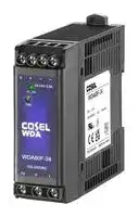
WDA60F-48
AC/DC DIN Rail Power Supply (PSU), ITE, 1 Output, 62.4 W, 48 V, 1.3 A
⚠️ Reference pricing provided. In case of supply shortages, we will connect you with our trusted procurement partners to ensure your project's continuity.
- Manufacturer: COSEL
- Product type:
- SVHC: Lead (04-Feb-2026)
- Product Range: WDA Series
- No. of Outputs: 1 Output
- Output Power Max: 62.4W
- Input Voltage VAC: 85V AC to 264V AC
- Power Supply Output Type: Fixed
- Output Current - Output 1: 1.3A
- Output Current - Output 2: -
- Output Current - Output 3: -
- Output Current - Output 4: -
- Output Voltage - Output 1: 48V
- Output Voltage - Output 2: -
- Output Voltage - Output 3: -
- Output Voltage - Output 4: -
- Power Supply Applications: ITE
| Delivery and price | |
|---|---|
| Units per pack | 10 |
| Price | 37.43 € |
| Current stock | 10+ |
| Lead time | 30 days |
Datasheet

**AC-DC Power Supplies DIN Rail Type** World wide Cost Safety EMI Inrush OCP OVP OQ Effective[mms] Approvals 5 current limiting

**WDA**

## **WDA-series**

## **Feature**

For DIN (35mm) Rail Prorducts

Built in overcurrent protection,overvoltage protection circuits Economical design

## **Safety agency approvals**

UL62368-1 C-UL (equivalent to CAN/CSA-C22.2 No.62368-1) EN62368-1

## **CE marking**

## **EMI**

Complies with CISPR32-B, EN55032-B and EN55011-B

**EMS Compliance** : EN61204-3, EN61000-6-2

EN61000-4-2 EN61000-4-3 EN61000-4-4 EN61000-4-5 EN61000-4-6 EN61000-4-8 EN61000-4-11

Low Voltage Directive RoHS Directive

**5-year warranty** (See Instruction Manual)

**WDA-1**

August 20, 2022

**AC-DC Power Supplies DIN Rail Type Ordering information - - WD A 30 F** O O **WDA30F** ~~=~~ **WDA** ~~|~~ 1 2 3 4 5 6

**==> picture [2 x 3] intentionally omitted <==**

**----- Start of picture text -----**<br>
R<br>**----- End of picture text -----**<br>


3 4 5 6 1Series name 2Single output 3Output wattage 4Universal input 5Output voltage 6Option : *5 C : With Coating

||**MODEL**<br>~~a~~<br>~~Po~~|**MODEL**<br>~~a~~<br>~~Po~~|**WDA30F-5**<br>~~a~~|**WDA30F-12**<br>~~a~~<br>~~(~~|**WDA30F-24**<br>~~a~~|**WDA30F-48**|
|---|---|---|---|---|---|---|
|**INPUT**|**VOLTAGE[V]**<br>~~Po~~||AC85 - 264 1f<br>~~(~~||||
||**CURRENT[A]**<br>~~——~~<br>~~|~~|**ACIN 115V** <br>~~——~~<br>~~|~~|0.6||||
|||**ACIN 230V** <br>~~——~~<br>~~|~~|0.3||||
||**FREQUENCY[Hz]**<br>~~|~~<br>~~po~~<br>~~ee —————~~||50/60(47-63)<br>~~—————~~||||
||**EFFICIENCY[%]**<br>~~ee —————~~|**ACIN 115V** <br>~~—————~~|80typ<br>~~—————~~|85typ<br>~~—————~~|86typ<br>~~—————~~|87typ|
|||**ACIN 230V** <br>~~—————~~<br>~~a ~~|82typ<br>~~—————~~<br> ~~a~~|86typ<br>~~—————~~|87typ<br>~~—————~~|88typ|
||**INRUSH CURRENT[A]**<br>~~ee —————~~<br>~~—=~~<br>~~|~~|**ACIN 115V** <br>~~—————~~<br>~~—=~~<br>~~|~~|20typTa=25C(at cold start)<br>~~—————~~||||
|||**ACIN 230V** <br>~~—=~~<br>~~|~~|40typTa=25C(at cold start)||||
||**LEAKAGE**<br>**CURRENT[mA]**<br>~~|~~<br>~~——~~<br>~~|~~<br>~~a~~|**ACIN115V**<br>~~|~~<br>~~——~~<br>~~|~~|0.25max||||
|||**ACIN240V**<br>~~——~~<br>~~|~~|0.5max||||
|**OUTPUT**<br>~~PO~~<br>~~Po~~|**VOLTAGE[V]**<br>~~|~~<br>~~a~~||5|12|24|48|
||**CURRENT[A]**<br>~~PT~~||6<br>~~PT~~|2.5<br>~~PT~~|1.3<br>~~PT~~|0.7|
||**WATTAGE[W]**<br>~~GG~~<br>~~PO~~||30<br>~~GG~~|30<br>~~GG~~|31.2<br>~~GG~~|33.6|
||**LINE REGULATION[mV]**<br>*1 <br>~~PO~~||50max|120max|240max|480max|
||**LOAD REGULATION[mV]** *1 <br>~~PO~~<br>~~a ~~||50max<br> ~~GG~~|120max<br>~~GG~~|240max<br>~~GG~~|480max|
||**RIPPLE NOISE[mVp-p]** *2 <br>~~a~~<br>~~Po~~|**lo=100%** <br>~~a~~|150(Bandwidth 20MHz)||||
||**TEMPERATURE REGULATION[mV] **<br>~~Po~~|**0~+50**C|100max|180max|360max|720max|
||**START-UP TIME[ms]**<br>~~Po~~<br>~~——~~<br>~~|~~|**ACIN 115V** <br>~~——~~<br>~~|~~|100typ||||
|||<br>**ACIN 230V**<br>~~——~~<br>~~|~~|||||
||**HOLD-UP TIME[ms]**<br>~~|~~<br>~~——~~|**ACIN 115V** <br>~~|~~<br>~~——~~|10typ||||
|||**ACIN 230V** <br>~~——~~<br>~~|~~|20typ||||
||**OUTPUT VOLTAGE ADJUSTMENT RANGE[V]** <br>~~fC~~||4.50 to 5.50<br>~~fC~~|10.8 to 13.2<br>~~fC~~|21.6 to 26.4<br>~~fC~~|43.2 to 52.8|
||**OUTPUT VOLTAGE SETTING[V]**<br>~~Po~~||4.90 to 5.30<br>~~Po~~|11.75 to 12.25<br>~~Po~~|23.5 to 24.5<br>~~Po~~|47.0 to 49.0|
|**PROTECTION**<br>**CIRCUIT AND**<br>**OTHERS**|**OVERCURRENT PROTECTION[A]**<br>~~Po~~||Works over 105% of ratingand recovers automatically||||
||**OVERVOLTAGE PROTECTION[V]**<br>~~DC~~||5.75 to 7.00<br>~~DC~~|13.8 to 16.8<br>~~DC~~|27.6 to 33.6<br>~~DC~~|54.0 to 67.2|
||**OPERATING INDICATION**<br>~~Po~~||LED(Green)||||
|**ISOLATION**|**INPUT-OUTPUT**<br>~~po~~||AC3,000V 1minute,Cutoff current  = 10mA,DC500V 50MΩmin(At Room Temperature)||||
||**INPUT-FG**<br>~~po~~||AC2,000V 1minute,Cutoff current = 10mA,DC500V 50MΩmin(At Room Temperature)||||
||**OUTPUT-FG**<br>~~Po~~||AC500V 1minute,Cutoff current = 100mA,DC500V 50MΩmin(At Room Temperature)||||
|**ENVIRONMENT**|**OPERATING TEMP.,HUMID.** *3 <br>~~Po~~||-20 to +70C,20 - 90%RH(Non condensing)||||
||**STORAGE TEMP.,HUMID.**<br>~~po~~||-30 to +85C,20 - 90%RH(Non condensing)||||
||**VIBRATION**<br>~~Po~~||10 - 55Hz,19.6m/s2(2G),3minutesperiod,60minutes each alongZ axis(Non operating.mounted on DIN Rail)||||
||**IMPACT**<br>~~Po~~||196.1m/s2(20G), 11ms, once each X, Y and Z axis(Packingstate)||||
|**SAFETY AND**<br>**EMC**|**AGENCY APPROVALS**<br>~~Po~~||UL62368-1,C-UL(equivalent to CAN/CSA-C22.2 No.62368-1),EN62368-1||||
||**EMC EMISSON**<br>~~Po~~||Complies with CISPR32-B,EN55032-B,EN55011-B||||
||**EMC EMMUNITY**<br>~~Po~~||Complies with EN61000-4-2,3,4,5,6,8,11||||
||**HARMONIC ATTENUATOR**<br>~~po~~||Complies with IEC61000-3-2(Class A)No built-in active PFC||||
|**OTHERS**|**CASE SIZE/WEIGHT**<br>~~Po~~||32X90X90mm(WXHXD) [1.26X3.54X3.54 inches]/ 200gmax||||
||**COOLING METHOD**<br>~~Po~~||Convection||||
|**WARRANTY **|**WARRANTY**<br>*4<br>~~po~~||5years(subject to the operatingconditions)||||


*1 Consult us about dynamic load and input response. Measure the output voltage by using the average mode of the tester to deal with the burst operation at low (Io=0~20%typ) load.

- *2 This is the result of measurement of the testing board with capacitors of 47μF and 0.1μF placed at 150 mm from the output terminals by a 20MHz oscilloscope or a ripple-noise meter equivalent to Keisoku-GikenRM104.

When the load factor is low (Io=0~20%Atyp), the switching power loss is reduced by burst operation, which will cause ripple noise to go beyond the specifications.

- *3 Output power derating is required. Refer to "Derating"

*5 The listed options may affect the published standard specifications. Please contact us for detailed product specifications and safety approvals. * All parameters not specially mentioned are measured at ACIN 230V, rated load and 25℃ of ambient temperature.

* Do not use the power supply in overcurrent conditions or in unspecified input voltage ranges. Otherwise the internal components may be damaged. * Parallel operation is not possible with this model.

   - Acoustic noise may be heard from the power supply when used for pulse load.

- *4 Consult us about details.

**WDA-2**

August 20, 2022

**WDA30F**

**WDA**

**External view** ~~D7~~

## <WDA30F>

**==> picture [239 x 182] intentionally omitted <==**

**----- Start of picture text -----**<br>
6.5 6.4 90<br>[0.26] [0.25] [3.54]<br>TB2<br>Output terminal(+)<br>Output terminal(-)<br>LED(DC_OK)<br>Output voltage<br>adjustable potentiometer<br>AC(L)<br>AC(N)<br>PE<br>TB1<br>6.5 9.5 94.5<br>[0.26] [0.37] [3.72]<br>11.2 Name plate<br>[0.44]<br>a 32 Po<br>[1.26]<br>※  Tolerance : ±1 [±0.04]<br>※  Weight  : 200g max<br>※  Chassis - Case material : PBT<br>※  Din rail attachment material : PC/ABS<br>※  Dimensions in mm, [   ] = inches<br>±1.5<br>75.5 [2.97] 90 [3.54] 99 [3.9]<br>60 [2.36]<br>(48) [1.89]<br>±1.5<br>7.25 [0.29]<br>**----- End of picture text -----**<br>


※ Screw tightening torque : 1N - m max

## ~~D7~~ **Derating Curve**

**==> picture [464 x 167] intentionally omitted <==**

**----- Start of picture text -----**<br>
100 100<br>ae<br>90 90<br>80706050403020100 P|PotPtP|P| Pt P|Pt tftT|tTtTtT tt Pttt||||| |||||| | ttttEttTttttte tt tttTft ft tNENQT 80706050403020100<br>85 115 264<br>-20  -10  0  10  20 30 40  50  60 70<br>Ambient temperature ( ) Input Voltage(VAC)<br>Load factor (%) Load factor (%)<br>**----- End of picture text -----**<br>


*In the shaded area. it may take several seconds to determine the output voltage during cold start, but it can be used without any problems. Fig.1  Derating curve depending on ambient temperature

**==> picture [150 x 7] intentionally omitted <==**

**----- Start of picture text -----**<br>
Fig.2 Derating curve depending on input voltage<br>**----- End of picture text -----**<br>


**WDA-3**

August 20, 2022

**AC-DC Power Supplies DIN Rail Type**

**WDA**

**==> picture [2 x 3] intentionally omitted <==**

**----- Start of picture text -----**<br>
R<br>**----- End of picture text -----**<br>


## **WDA60F**

**==> picture [227 x 108] intentionally omitted <==**

**----- Start of picture text -----**<br>
Ordering information<br>- -<br>WD  A  60  F  O  O<br>1  2  3  4  5  6<br>1Series name<br>2Single output<br>3Output wattage<br>4Universal input<br>5Output voltage<br>6Option : *5<br> C : With Coating<br>**----- End of picture text -----**<br>


*Make sure necessary tests will be carried out on your end equipment with the power supply installed in accordance with any required EMC/EMI regulations.

||**MODEL**<br>~~a~~|**MODEL**<br>~~a~~|**WDA60F-12**|**WDA60F-24**|**WDA60F-48**|
|---|---|---|---|---|---|
|**INPUT**|**VOLTAGE[V]**<br>~~Po~~||AC85 - 264 1f|||
||**CURRENT[A]**<br>~~Ee~~<br>~~|~~|**ACIN 115V** <br>~~Ee~~<br>~~|~~|1.2|||
|||**ACIN 230V** <br>~~Ee~~<br>~~||~~|0.6|||
||**FREQUENCY[Hz]**<br>~~|~~<br>~~po~~<br>~~eeeee~~||50/60(47-63)<br>~~eee~~|||
||**EFFICIENCY[%]**<br>~~ee~~|**ACIN 115V** <br>~~eee~~|84typ<br>~~eee~~|86typ<br>~~eee~~|87typ|
|||**ACIN 230V** <br>~~eee~~<br>~~a~~|86typ<br>~~eee~~<br>~~a~~|88typ<br>~~eee~~|89typ|
||**INRUSH CURRENT[A]**<br>~~ee~~<br>~~—~~|**ACIN 115V** <br>~~eee~~<br>~~—~~|20typTa=25C(at cold start)<br>~~eee~~<br>|||
|||**ACIN 230V** <br>~~—|~~|40typTa=25C(at cold start)<br>~~|~~|||
||**LEAKAGE**<br>**CURRENT[mA]**<br>~~—~~|**ACIN 115V** <br>~~—~~|0.25max|||
|||**ACIN240V** <br>~~—~~<br>~~||~~|0.5max|||
|**OUTPUT**|**VOLTAGE[V]**<br>~~a~~||12<br>~~CO~~|24<br>~~CO~~|48|
||**CURRENT[A]**<br>~~GC~~||5<br>~~GC~~|2.5<br>~~GC~~|1.3|
||**WATTAGE[W]**<br>~~CG~~||60<br>~~CG~~|60<br>~~CG~~|62.4|
||**LINE REGULATION[mV]**<br>*1 <br>~~GO~~||120max<br>~~GO~~|240max<br>~~GO~~|480max|
||**LOAD REGULATION[mV]**<br>*1 <br>~~GG~~||120max<br>~~GG~~|240max<br>~~GG~~|480max|
||**RIPPLE NOISE[mVp-p]** *2 <br>~~po~~|**lo=100%** <br>~~po~~|150max(Bandwidth 20MHz)|||
||**TEMPERATURE REGULATION[mV] **<br>~~PO~~|**0~+50**C <br>~~PO~~|180max<br>~~PO~~|360max<br>~~PO~~|720max|
||**START-UP TIME[ms]**<br>~~pF~~|**ACIN 115V** <br>~~pF~~|100typ<br>~~|~~|||
|||<br>**ACIN 230V**<br>~~pF|~~||||
||**HOLD-UP TIME[ms]**<br>~~—~~|**ACIN 115V** <br>~~—~~|10typ|||
|||**ACIN 230V** <br>~~—~~<br>~~||~~|20typ|||
||**OUTPUT VOLTAGE ADJUSTMENT RANGE[V]** <br>~~GG~~||10.8 to 13.2<br>~~GG~~|21.6 to 26.4<br>~~GG~~|43.2 to 52.8|
||**OUTPUT VOLTAGE SETTING[V]**<br>~~GD~~||11.75 to 12.25<br>~~GD~~|23.5 to 24.5<br>~~GD~~|47.0 to 49.0|
|**PROTECTION**<br>**CIRCUIT AND**<br>**OTHERS**|**OVERCURRENT PROTECTION[A]**<br>~~po~~||Works over 105% of ratingand recovers automatically|||
||**OVERVOLTAGE PROTECTION[V]**<br>~~OD~~||13.8 to 16.8<br>~~OD~~|27.6 to 33.6<br>~~OD~~|54.0 to 67.2|
||**OPERATING INDICATION**<br>~~Po~~||LED(Green)|||
|**ISOLATION**|**INPUT-OUTPUT**<br>~~Po~~||AC3,000V 1minute, Cutoff current  = 10mA,DC500V 50MΩmin(At Room Temperature)|||
||**INPUT-FG**<br>~~po~~||AC2,000V 1minute, Cutoff current = 10mA,DC500V 50MΩmin(At Room Temperature)|||
||**OUTPUT-FG**<br>~~Po~~||AC500V 1minute, Cutoff current = 100mA,DC500V 50MΩmin(At Room Temperature)|||
|**ENVIRONMENT**|**OPERATING TEMP.,HUMID.** *3 <br>~~Po~~||-20 to +70C,20-90%RH(Non condensing)|||
||**STORAGE TEMP.,HUMID.**<br>~~po~~||-30 to +85C,20-90%RH(Non condensing)|||
||**VIBRATION**<br>~~po~~||10-55Hz,19.6m/s2(2G),3minutesperiod, 60minutes each alongZ axis(Non operating.mounted on DIN Rail)|||
||**IMPACT**<br>~~Po~~||196.1m/s2(20G), 11ms, once each X, Y and Z axis(Packingstate)|||
|**SAFETY AND**<br>**EMC**|**AGENCY APPROVALS**<br>~~Po~~||UL62368-1,C-UL(equivalent to CAN/CSA-C22.2 No.62368-1),EN62368-1|||
||**EMC EMISSON**<br>~~po~~||Complies withCISPR32-B,EN55032-B,EN55011-B|||
||**EMC EMMUNITY**<br>~~po~~||Complies with EN61000-4-2,3,4,5,6,8,11|||
||**HARMONIC ATTENUATOR**<br>~~Po~~||Complies with IEC61000-3-2(Class A)No built-in active PFC|||
|**OTHERS**<br>~~Pp~~|**CASE SIZE/WEIGHT**<br>~~Po~~||32X90X90mm(WXHXD) [1.26X3.54X3.54 inches]/ 250gmax|||
||**COOLING METHOD**<br>~~Po~~<br>~~Pp~~||Convection|||
|**WARRANTY **<br>~~Pp~~|**WARRANTY**<br>*4<br>~~Pp~~||5years(subject to the operatingconditions)|||


- *1 Consult us about dynamic load and input response. Measure the output voltage by using the average mode of the tester to deal with the burst operation at low (Io=0~20%typ) load.

- *2 This is the result of measurement of the testing board with capacitors of 47μF and 0.1μF placed at 150 mm from the output terminals by a 20MHz oscilloscope or a ripple-noise meter equivalent to Keisoku-GikenRM104.

When the load factor is low (Io=0~20%Atyp), the switching power loss is reduced by burst operation, which will cause ripple noise to go beyond the specifications. *3 Output power derating is required. Refer to "Derating"

*5 The listed options may affect the published standard specifications. Please contact us for detailed product specifications and safety approvals. * All parameters not specially mentioned are measured at ACIN 230V, rated load and 25℃ of ambient temperature. * Do not use the power supply in overcurrent conditions or in unspecified input voltage ranges. Otherwise the internal components may be damaged. * Parallel operation is not possible with this model. * Acoustic noise may be heard from the power supply when used for pulse load.

- *4 Consult us about details.

**WDA-4**

August 20, 2022

**WDA60F**

**External view** ~~rs~~

**WDA**

## <WDA60F>

**==> picture [464 x 423] intentionally omitted <==**

**----- Start of picture text -----**<br>
6.5 6.4 90<br>[0.26] [0.25] [3.54]<br>TB2<br>Output terminal(+) sow | i OOOABEBSEBEEULU<br>Output terminal(-)<br>LED(DC_OK)<br>Output voltage<br>adjustable potentiometer<br>AC(L)<br>AC(N)<br>PE<br>TB1<br>6.5 — 9.5 ean 94.5<br>[0.26] [0.37] [3.72]<br>| 11.2 as Name plate<br>[0.44]<br>32<br>[1.26]<br>※  Tolerance : ±1 [±0.04]<br>※  Weight  : 250g max<br>※  Chassis - Case material : PBT<br>※  Din rail attachment material : PC/ABS<br>※  Dimensions in mm, [   ] = inches<br>※  Screw tightening torque : 1N - m max<br>es Derating Curve<br>100 100<br>90 90<br>80 soneyy | |, |, 12V  NAL 80 Wz<br>70 70<br>24V,48V<br>60 a eea 60<br>50 50<br>ee<br>40 40<br>i<br>30 30<br>a<br>20 20<br>ee<br>10 10<br>ee<br>0 0<br>85 115 264<br>-20  -10  0  10  20 30 40  50  60 70<br>Ambient temperature ( Cc ) Input Voltage(VAC)<br>±1.5<br>75.5 [2.97] 90 [3.54] 99 [3.9]<br>60 [2.36]<br>(48) [1.89]<br>±1.5<br>7.25 [0.29]<br>Load factor (%) Load factor (%)<br>**----- End of picture text -----**<br>


## ~~es~~ **Derating Curve**

- *In the shaded area. it may take several seconds to determine the output voltage during cold start, but it can be used without any problems. Fig.1  Derating curve depending on ambient temperature

Fig.2 Derating curve depending on input voltage

**WDA-5**

August 20, 2022

**AC-DC Power Supplies DIN Rail Type WDA90F**

**WDA**

**==> picture [2 x 3] intentionally omitted <==**

**----- Start of picture text -----**<br>
R<br>**----- End of picture text -----**<br>


**==> picture [228 x 115] intentionally omitted <==**

**----- Start of picture text -----**<br>
Ordering information<br>- -<br>WD  A  90  F  O  O<br>BS<br>1  2  3  4  5  6<br>1Series name<br>2Single output<br>3Output wattage<br>4Input voltage selectable<br>by switch<br>5Output voltage<br>6Option : *5<br> C : With Coating<br>**----- End of picture text -----**<br>


||**MODEL**<br>~~ee~~<br>~~——~~|**MODEL**<br>~~ee~~<br>~~——~~|**WDA90F-12**<br>~~EE~~<br>~~——_—~~|**WDA90F-24**<br>~~EE~~<br>~~——_—~~|**WDA90F-48**|
|---|---|---|---|---|---|
|**INPUT**|**VOLTAGE[V]**<br>~~——~~<br>~~TCE~~||AC85 - 264 1f<br>~~EE~~<br>~~——_—~~|||
||**CURRENT[A]**<br>~~——~~<br>~~TCE~~|**ACIN 115V** <br>~~—~~<br>~~TCE~~|1.8<br>~~EE~~|||
|||**ACIN 230V** <br>~~TCE~~<br>~~—_~~|0.9|||
||**FREQUENCY[Hz]**<br>~~TCE~~<br>~~OO ~~||50/60(47-63)<br>|||
||**EFFICIENCY[%]**<br><br>~~2 ~~<br>|**ACIN 115V** <br> <br>~~eee~~<br>~~—_~~|84<br> ~~a~~<br>~~eee~~<br>~~—_~~<br>~~_~~|87<br>~~_~~|88|
|||**ACIN 230V** <br> <br> ~~eee~~<br>~~—_~~|86<br> ~~a~~<br>~~eee~~<br>~~—_~~<br>~~_~~|89<br>~~_~~|90|
||**INRUSH CURRENT[A]**<br>~~PCE~~|**ACIN 115V** <br>~~PCE—_~~|20typTa=25C(at cold start)<br>~~—_~~<br>~~_~~|||
|||**ACIN 230V** <br>~~PCE—_~~|40typTa=25C(at cold start)<br>~~—_~~<br>~~_~~|||
||**LEAKAGE**<br>**CURRENT[mA]**<br><br>~~oF~~<br>~~a~~|**ACIN 115V** <br>~~—_~~<br>~~oF~~|0.4max<br>~~—_~~<br>~~_~~|||
|||**ACIN 240V** <br>~~oF~~<br>~~a~~|0.75max|||
|**OUTPUT**|**VOLTAGE[V]**<br>~~a~~<br>~~a_i~~||12<br>~~a_i~~<br>~~_—~~|24<br>~~a_i~~<br>~~_—~~|48|
||**CURRENT[A]**<br>~~a_i~~<br>~~————~~||7.5<br>~~a_i~~<br>~~_—~~<br>~~———— OO~~|3.8<br>~~a_i~~<br>~~_—~~<br>~~OO~~|1.9|
||**WATTAGE[W]**<br>~~a_i~~<br>~~————~~||90<br>~~a_i~~<br>~~_—~~<br>~~———— OO~~|91.2<br>~~a_i~~<br>~~_—~~<br>~~OO~~|91.2|
||**LINE REGULATION[mV]**<br>*1 <br>~~a~~<br>~~————~~<br>~~es~~||120max<br>~~———— OO~~<br>~~SS_—~~|240max<br>~~OO~~<br>~~_—~~|480max|
||**LOAD REGULATION[mV]**<br>*1 <br>~~————~~<br>~~es~~<br>~~ae~~||120max<br>~~———— OO~~<br>~~SS_—~~<br>~~ae~~|240max<br>~~OO~~<br>~~_—~~|480max|
||**RIPPLE NOISE[mVp-p]** *2 <br>~~————~~<br>~~es~~|**lo=100%** <br>~~————~~<br>~~es~~<br>~~ae~~|150max(Bandwidth 20MHz)<br>~~———— OO~~<br>~~SS _—~~<br>~~ae~~<br>~~_~~|||
||**TEMPERATURE REGULATION[mV] **<br>~~es~~|**0~+50**C <br>~~ae~~<br>~~es~~|180max<br>~~ae~~<br>~~es~~<br>~~_~~|360max<br>~~_~~|720max|
||**START-UP TIME[ms]**<br>~~PCE~~|**ACIN 115V** <br>~~PCE~~|100typ<br>~~_~~|||
|||<br>**ACIN 230V**<br>~~PCE~~<br>~~—~~||||
||**HOLD-UP TIME[ms]**<br>~~PCE~~|**ACIN 115V** <br>~~PCE~~|10typ|||
|||**ACIN 230V** <br>~~PCE~~|20typ|||
||**OUTPUT VOLTAGE ADJUSTMENT RANGE[V]** <br>~~-____I—————————~~||10.8 to 13.2<br>~~—————————~~|21.6 to 26.4<br>~~—————————~~|43.2 to 52.8|
||**OUTPUT VOLTAGE SETTING[V]**<br>~~—————————~~||11.75 to 12.25<br>~~—————————~~|23.5 to 24.5<br>~~—————————~~<br>~~OO~~|47.0 to 49.0|
|**PROTECTION**<br>**CIRCUIT AND**<br>**OTHERS**<br>~~_~~|**OVERCURRENT PROTECTION[A]**<br>~~ee~~||Works over 105% of ratingand recovers automatically<br>~~~~~|||
||**OVERVOLTAGE PROTECTION[V]**<br>~~OO~~<br>~~————~~||13.8 to 16.8<br>~~————~~<br>~~~~~|27.6 to 33.6<br>~~~~~|54.0 to 67.2|
||**OPERATING INDICATION**<br>~~————~~<br>~~_~~||LED(Green)<br>~~————~~<br>~~~~~|||
|**ISOLATION**<br>~~_~~<br>~~—~~|**INPUT-OUTPUT**<br>~~_~~||AC3,000V 1minute, Cutoff current  = 10mA,DC500V 50MΩmin(At Room Temperature)|||
||**INPUT-FG**<br>~~_~~<br>~~OO~~||AC2,000V 1minute, Cutoff current = 10mA,DC500V 50MΩmin(At Room Temperature)|||
||**OUTPUT-FG**<br>~~OO~~<br>~~—~~||AC500V 1minute, Cutoff current = 100mA,DC500V 50MΩmin(At Room Temperature)|||
|**ENVIRONMENT**<br>~~—~~<br>~~_—~~|**OPERATING TEMP.,HUMID.** *3 <br>~~—~~||-20 to +70C,20-90%RH(Non condensing)|||
||**STORAGE TEMP.,HUMID.**<br>~~—OO~~||-30 to +85C,20-90%RH(Non condensing)|||
||**VIBRATION**<br>~~ee~~||10 - 55Hz,19.6m/s2(2G),3minutesperiod,60minutes each alongZ axis(Non operating.mounted on DIN Rail)|||
||**IMPACT**<br>~~_—~~||196.1m/s2(20G), 11ms, once each X, Y and Z axis(Packingstate)|||
|**SAFETY AND**<br>**EMC**<br>~~_—~~<br>~~——~~|**AGENCY APPROVALS**<br>~~_—~~||UL62368-1,C-UL(equivalent to CAN/CSA-C22.2 No.62368-1),EN62368-1|||
||**EMC EMISSON**<br>~~_—ee~~||Complies withCISPR32-B,EN55032-B,EN55011-B|||
||**EMC EMMUNITY**<br>~~ee~~||Complies with EN61000-4-2,3,4,5,6,8,11|||
||**HARMONIC ATTENUATOR**<br>~~ee~~<br>~~——~~||Complies with IEC61000-3-2(Class A)No built-in active PFC|||
|**OTHERS**<br>~~——~~|**CASE SIZE/WEIGHT**<br>~~——~~||50X90X90mm(WXHXD) [1.97X3.54X3.54 inches]/ 350gmax|||
||**COOLING METHOD**<br>~~——OO~~||Convection|||
|**WARRANTY **|**WARRANTY**<br>*4<br>~~ae~~||5years(subject to the operatingconditions)|||


*1 Consult us about dynamic load and input response. Measure the output voltage by using the average mode of the tester to deal with the burst operation at low (Io=0~20%typ) load.

- *2 This is the result of measurement of the testing board with capacitors of 47μF and 0.1μF placed at 150 mm from the output terminals by a 20MHz oscilloscope or a ripple-noise meter equivalent to Keisoku-GikenRM104.

When the load factor is low (Io=0~20%Atyp), the switching power loss is reduced by burst operation, which will cause ripple noise to go beyond the specifications. *3 Output power derating is required. Refer to "Derating"

*5 The listed options may affect the published standard specifications. Please contact us for detailed product specifications and safety approvals. * All parameters not specially mentioned are measured at ACIN 230V, rated load and 25℃ of ambient temperature.

* Do not use the power supply in overcurrent conditions or in unspecified input voltage ranges. Otherwise the internal components may be damaged. * Parallel operation is not possible with this model. * Acoustic noise may be heard from the power supply when used for pulse load.

- *4 Consult us about details.

**WDA-6**

August 20, 2022

**WDA90F**

**WDA**

## **External view** ~~D7~~

## <WDA90F>

**==> picture [248 x 136] intentionally omitted <==**

**----- Start of picture text -----**<br>
15.5 6.4 90<br>TB2 [0.61] [0.25] [3.54]<br>Output terminal(+) ssa CC |<br>Output terminal(-)<br>LED(DC_OK)<br>Output voltage<br>adjustable potentiometer<br>AC(L)<br>AC(N)<br>PE<br>TB1 ml1 oT |<br>‘al “Toll |<br>15.5 9.5 94.5<br>li [0.61] en [0.37] [3.72] 7]<br>11.2 Name plate<br>aa [0.44] 50<br>[1.97]<br> ±1.5<br>75.5 [2.97] 90 [3.54] 99 [3.9]<br>60 [2.36]<br>(48) [1.89]<br> ±1.5<br>7.25 [0.29]<br>**----- End of picture text -----**<br>


※ Tolerance : ±1 [±0.04] ※ Weight  : 350g max

- ※ Chassis - Case material : PBT

- ※ Din rail attachment material : PC/ABS ※ Dimensions in mm, [   ] = inches

※ Screw tightening torque : 1N - m max

**==> picture [505 x 211] intentionally omitted <==**

**----- Start of picture text -----**<br>
D7 Derating Curve<br>100 100<br>90 90<br>77 TTT NAL /<br>80 Pit | PAY 12V 80<br>70 70<br>24V,48V<br>IPf NG<br>60 60<br>50 Pt | |ft| 50<br>40 Pt EN 40<br>30 Pt | tp 30<br>20 Pt ft | pe 20<br>10 Pt | tt 10<br>0 Pt | fttt ttEE 0<br>85 115 264<br>-20  -10  0  10  20 30 40  50  60 70<br>Ambient temperature ( C ) Input Voltage(VAC)<br>Load factor (%) Load factor (%)<br>**----- End of picture text -----**<br>


*In the shaded area. it may take several seconds to determine the output voltage during cold start, but it can be used without any problems. Fig.1  Derating curve depending on ambient temperature

Fig.2 Derating curve depending on input voltage

**WDA-7**

August 20, 2022

## **WDA-series**

## **WDA**

## **Terminal Blocks**

## ● WDA30F

**==> picture [60 x 142] intentionally omitted <==**

**----- Start of picture text -----**<br>
4<br>5<br>6<br>7<br>3<br>2<br>1<br>**----- End of picture text -----**<br>


## ● WDA60F

**==> picture [60 x 141] intentionally omitted <==**

**----- Start of picture text -----**<br>
4<br>5<br>6<br>7<br>3<br>2<br>1<br>**----- End of picture text -----**<br>


## ● WDA90F

**==> picture [86 x 141] intentionally omitted <==**

**----- Start of picture text -----**<br>
4<br>5<br>6<br>7<br>3<br>2<br>1<br>**----- End of picture text -----**<br>


|Terminal<br>Number|<br>Terminal<br>Name|Function|
|---|---|---|
|1|PE|Protective earth Terminal|
|2|AC(N)|Input Terminals|
|3|AC(L)||
|4|+VOUT|+Output Terminals|
|5|-VOUT|-Output Terminals|
|6|DC_OK|LED for output voltage confrmation|
|7|TRM|<br>Adjustment of output voltage|


**WDA-8**

August 20, 2022

**WDA-series**

**WDA**

## ~~a~~ **Assembling and Installation Method**

## Installation method

- About DIN-Rail Attachment available with DIN EN60715 TH

- 35 (35×7.5mm or 35×15mm) (Top hat shaped DIN rail)

- Below shows mounting orientation.

If install other than standard mounting orientation (A), please fix the power supply for withstand the impact and vibration.

**==> picture [41 x 8] intentionally omitted <==**

**----- Start of picture text -----**<br>
(A) Standard<br>**----- End of picture text -----**<br>


- When you mount a power supply on a DIN rail, have the area marked A catch one side of the rail and push the unit to the direction of B. To remove the power supply from the rail, either push down the area marked C or insert a tool such as driver to the area marked D and pull the unit apart from the rail. When you couldn’t remove the unit easily, push down the area marked C while lightly pushing the unit to the direction of E.

- Shown below the notes about installation clearance of a unit.

- 1 Installation clearance at above and below the unit.

- Please have clearance of at least 25mm above and below the unit to avoid heat accumulation.

- 2 Installation clearance at the side of the unit.

Please have clearance of at least 5mm side the unit to insulating the internal components. However, refer to right figure, if adjacent device of the unit (including power supply) is a heat source.

**==> picture [232 x 331] intentionally omitted <==**

**----- Start of picture text -----**<br>
E<br>A<br>B<br>D<br>Convection 25 mm<br>or more<br>hee!<br>Sf ={-E<br>Convection 25 mm<br>or more<br>Adjacent device of the unit<br>No. Model<br>Non-heat source Heat source( * )<br>1 WDA30F/60F/90F 5mm or more 15mm or more<br>**----- End of picture text -----**<br>


* Reference value when same power units are adjacent.

**WDA-9**

August 20, 2022

## **WDA-series**

## a **WDA Instruction Manual**

◆ It is neccessary to read the “Instruction Manual” and “Before using our product” before you use our product.

Instruction Manual Before using our product

https://en.cosel.co.jp/product/powersupply/WDA/ https://en.cosel.co.jp/technical/caution/index.html **WDA NOTICE**

**Basic Characteristics Data**

|Model<br>~~ee~~|Circuit method<br>~~ee~~|Switching<br>frequency<br>[kHz]<br>~~|~~<br>~~ee~~|Input<br>current<br>[A]<br>~~|~~<br>~~|~~<br>~~ee~~|Rated<br>input fuse<br>~~|~~<br>~~||~~|Inrush<br>current<br>protection<br>circuit<br>~~|~~|PCB/Pattern<br>~~Ferri~~|PCB/Pattern<br>~~Ferri~~|PCB/Pattern<br>~~Ferri~~|Parallel<br>operation<br>~~Ferri~~<br>~~Th~~|
|---|---|---|---|---|---|---|---|---|---|
|||||||Material<br>~~Ferri~~|Single<br>sided<br>~~Ferri~~<br>~~Th~~|Double<br>sided<br>~~Ferri~~<br>~~Th~~||
|WDA30F<br>~~ee~~|Flyback converter<br>~~ee~~|50 to 120<br>~~ee~~|0.6<br>~~|~~<br>~~ee~~|250V  2.5A<br>~~||~~|Thermistor<br>~~|~~|CEM-3/FR4<br>~~Ferri~~|Yes<br>~~Ferri~~<br>~~Th~~|Yes<br>~~Ferri~~<br>~~Th~~|No<br>~~Ferri~~<br>~~Th~~|
|WDA60F<br>~~ee~~|Flyback converter<br>~~ee~~|50 to 120<br>~~ee~~|1.2<br>~~|~~<br>~~ee~~|250V  2.5A<br>~~| |~~|Thermistor<br>~~| ~~|CEM-3/FR4<br> ~~Ferri~~|Yes<br>~~Ferri~~|Yes<br>~~Ferri~~|No<br>~~Ferri~~|
|WDA90F|Flyback converter|50 to 120|1.8|250V 3.15A|Thermistor|CEM-3/FR4|Yes|Yes|No|


- The value of input current is at ACIN 115V and 100%.

- Burst operation at light loading, frequency is change by use condition. Please contact us about detail.

**WDA-10**

August 20, 2022
Updated at June 9, 2026
About Novapart
Novapart is a B2B electronic component broker specialising in stock shortages and cost reduction. We source hard-to-find parts and identify compliant alternatives across a catalogue of 410,000+ components from 500+ manufacturers.
Learn more →Stock Shortage Specialist
When a component is unavailable, discontinued or has an unacceptable lead time, we tap into our network of vetted European and Asian distributors to source what you need — without compromising on quality or traceability.
Request a quote →Compliant Alternatives
We identify pin-to-pin, electrically equivalent substitutes that meet the same certifications (RoHS, AEC-Q100, REACH) as your original specification — validated against datasheets, not just part numbers. Often at a lower cost.
BOM Analysis service →